JP7304145B2 - リードフレーム、半導体装置及びリードフレームの製造方法 - Google Patents
リードフレーム、半導体装置及びリードフレームの製造方法 Download PDFInfo
- Publication number
- JP7304145B2 JP7304145B2 JP2018209997A JP2018209997A JP7304145B2 JP 7304145 B2 JP7304145 B2 JP 7304145B2 JP 2018209997 A JP2018209997 A JP 2018209997A JP 2018209997 A JP2018209997 A JP 2018209997A JP 7304145 B2 JP7304145 B2 JP 7304145B2
- Authority
- JP
- Japan
- Prior art keywords
- lead
- plating layer
- lead frame
- plating
- layer
- Prior art date
- Legal status (The legal status is an assumption and is not a legal conclusion. Google has not performed a legal analysis and makes no representation as to the accuracy of the status listed.)
- Active
Links
Images


Classifications
-
- H—ELECTRICITY
- H01—ELECTRIC ELEMENTS
- H01L—SEMICONDUCTOR DEVICES NOT COVERED BY CLASS H10
- H01L23/00—Details of semiconductor or other solid state devices
- H01L23/48—Arrangements for conducting electric current to or from the solid state body in operation, e.g. leads, terminal arrangements ; Selection of materials therefor
- H01L23/488—Arrangements for conducting electric current to or from the solid state body in operation, e.g. leads, terminal arrangements ; Selection of materials therefor consisting of soldered or bonded constructions
- H01L23/495—Lead-frames or other flat leads
- H01L23/49579—Lead-frames or other flat leads characterised by the materials of the lead frames or layers thereon
- H01L23/49582—Metallic layers on lead frames
-
- H—ELECTRICITY
- H01—ELECTRIC ELEMENTS
- H01L—SEMICONDUCTOR DEVICES NOT COVERED BY CLASS H10
- H01L23/00—Details of semiconductor or other solid state devices
- H01L23/48—Arrangements for conducting electric current to or from the solid state body in operation, e.g. leads, terminal arrangements ; Selection of materials therefor
- H01L23/488—Arrangements for conducting electric current to or from the solid state body in operation, e.g. leads, terminal arrangements ; Selection of materials therefor consisting of soldered or bonded constructions
- H01L23/495—Lead-frames or other flat leads
- H01L23/49541—Geometry of the lead-frame
- H01L23/49548—Cross section geometry
-
- H—ELECTRICITY
- H01—ELECTRIC ELEMENTS
- H01L—SEMICONDUCTOR DEVICES NOT COVERED BY CLASS H10
- H01L21/00—Processes or apparatus adapted for the manufacture or treatment of semiconductor or solid state devices or of parts thereof
- H01L21/02—Manufacture or treatment of semiconductor devices or of parts thereof
- H01L21/04—Manufacture or treatment of semiconductor devices or of parts thereof the devices having at least one potential-jump barrier or surface barrier, e.g. PN junction, depletion layer or carrier concentration layer
- H01L21/48—Manufacture or treatment of parts, e.g. containers, prior to assembly of the devices, using processes not provided for in a single one of the subgroups H01L21/06 - H01L21/326
- H01L21/4814—Conductive parts
- H01L21/4821—Flat leads, e.g. lead frames with or without insulating supports
- H01L21/4828—Etching
-
- H—ELECTRICITY
- H01—ELECTRIC ELEMENTS
- H01L—SEMICONDUCTOR DEVICES NOT COVERED BY CLASS H10
- H01L23/00—Details of semiconductor or other solid state devices
- H01L23/48—Arrangements for conducting electric current to or from the solid state body in operation, e.g. leads, terminal arrangements ; Selection of materials therefor
- H01L23/488—Arrangements for conducting electric current to or from the solid state body in operation, e.g. leads, terminal arrangements ; Selection of materials therefor consisting of soldered or bonded constructions
- H01L23/495—Lead-frames or other flat leads
- H01L23/49541—Geometry of the lead-frame
-
- H—ELECTRICITY
- H01—ELECTRIC ELEMENTS
- H01L—SEMICONDUCTOR DEVICES NOT COVERED BY CLASS H10
- H01L23/00—Details of semiconductor or other solid state devices
- H01L23/48—Arrangements for conducting electric current to or from the solid state body in operation, e.g. leads, terminal arrangements ; Selection of materials therefor
- H01L23/488—Arrangements for conducting electric current to or from the solid state body in operation, e.g. leads, terminal arrangements ; Selection of materials therefor consisting of soldered or bonded constructions
- H01L23/495—Lead-frames or other flat leads
- H01L23/49572—Lead-frames or other flat leads consisting of thin flexible metallic tape with or without a film carrier
-
- H—ELECTRICITY
- H01—ELECTRIC ELEMENTS
- H01L—SEMICONDUCTOR DEVICES NOT COVERED BY CLASS H10
- H01L23/00—Details of semiconductor or other solid state devices
- H01L23/48—Arrangements for conducting electric current to or from the solid state body in operation, e.g. leads, terminal arrangements ; Selection of materials therefor
- H01L23/488—Arrangements for conducting electric current to or from the solid state body in operation, e.g. leads, terminal arrangements ; Selection of materials therefor consisting of soldered or bonded constructions
- H01L23/495—Lead-frames or other flat leads
- H01L23/49579—Lead-frames or other flat leads characterised by the materials of the lead frames or layers thereon
- H01L23/49586—Insulating layers on lead frames
-
- H—ELECTRICITY
- H01—ELECTRIC ELEMENTS
- H01L—SEMICONDUCTOR DEVICES NOT COVERED BY CLASS H10
- H01L2224/00—Indexing scheme for arrangements for connecting or disconnecting semiconductor or solid-state bodies and methods related thereto as covered by H01L24/00
- H01L2224/01—Means for bonding being attached to, or being formed on, the surface to be connected, e.g. chip-to-package, die-attach, "first-level" interconnects; Manufacturing methods related thereto
- H01L2224/10—Bump connectors; Manufacturing methods related thereto
- H01L2224/1012—Auxiliary members for bump connectors, e.g. spacers
- H01L2224/10152—Auxiliary members for bump connectors, e.g. spacers being formed on an item to be connected not being a semiconductor or solid-state body
- H01L2224/10175—Flow barriers
-
- H—ELECTRICITY
- H01—ELECTRIC ELEMENTS
- H01L—SEMICONDUCTOR DEVICES NOT COVERED BY CLASS H10
- H01L2224/00—Indexing scheme for arrangements for connecting or disconnecting semiconductor or solid-state bodies and methods related thereto as covered by H01L24/00
- H01L2224/01—Means for bonding being attached to, or being formed on, the surface to be connected, e.g. chip-to-package, die-attach, "first-level" interconnects; Manufacturing methods related thereto
- H01L2224/10—Bump connectors; Manufacturing methods related thereto
- H01L2224/15—Structure, shape, material or disposition of the bump connectors after the connecting process
- H01L2224/16—Structure, shape, material or disposition of the bump connectors after the connecting process of an individual bump connector
- H01L2224/161—Disposition
- H01L2224/16151—Disposition the bump connector connecting between a semiconductor or solid-state body and an item not being a semiconductor or solid-state body, e.g. chip-to-substrate, chip-to-passive
- H01L2224/16221—Disposition the bump connector connecting between a semiconductor or solid-state body and an item not being a semiconductor or solid-state body, e.g. chip-to-substrate, chip-to-passive the body and the item being stacked
- H01L2224/16245—Disposition the bump connector connecting between a semiconductor or solid-state body and an item not being a semiconductor or solid-state body, e.g. chip-to-substrate, chip-to-passive the body and the item being stacked the item being metallic
-
- H—ELECTRICITY
- H01—ELECTRIC ELEMENTS
- H01L—SEMICONDUCTOR DEVICES NOT COVERED BY CLASS H10
- H01L2224/00—Indexing scheme for arrangements for connecting or disconnecting semiconductor or solid-state bodies and methods related thereto as covered by H01L24/00
- H01L2224/80—Methods for connecting semiconductor or other solid state bodies using means for bonding being attached to, or being formed on, the surface to be connected
- H01L2224/81—Methods for connecting semiconductor or other solid state bodies using means for bonding being attached to, or being formed on, the surface to be connected using a bump connector
- H01L2224/81007—Methods for connecting semiconductor or other solid state bodies using means for bonding being attached to, or being formed on, the surface to be connected using a bump connector involving a permanent auxiliary member being left in the finished device, e.g. aids for holding or protecting the bump connector during or after the bonding process
-
- H—ELECTRICITY
- H01—ELECTRIC ELEMENTS
- H01L—SEMICONDUCTOR DEVICES NOT COVERED BY CLASS H10
- H01L23/00—Details of semiconductor or other solid state devices
- H01L23/28—Encapsulations, e.g. encapsulating layers, coatings, e.g. for protection
- H01L23/31—Encapsulations, e.g. encapsulating layers, coatings, e.g. for protection characterised by the arrangement or shape
- H01L23/3107—Encapsulations, e.g. encapsulating layers, coatings, e.g. for protection characterised by the arrangement or shape the device being completely enclosed
-
- H—ELECTRICITY
- H01—ELECTRIC ELEMENTS
- H01L—SEMICONDUCTOR DEVICES NOT COVERED BY CLASS H10
- H01L2924/00—Indexing scheme for arrangements or methods for connecting or disconnecting semiconductor or solid-state bodies as covered by H01L24/00
- H01L2924/15—Details of package parts other than the semiconductor or other solid state devices to be connected
- H01L2924/181—Encapsulation
Description
[リードフレームの構成]
図1は、リードフレームの概略平面図である。図1に示すように、リードフレーム1は、平面視略矩形状の基板フレーム2を有する。基板フレーム2の材料としては、例えば銅(Cu)、Cuをベースにした合金、鉄-ニッケル(Fe-Ni)又はFe-Niをベースにした合金等を用いることができる。基板フレーム2の厚さは、例えば0.05~0.25mm程度とすることができる。
次に、図6を参照して、本実施例に係るリードフレーム100を用いて作成された半導体装置200について説明する。図6は、実施例に係るリードフレームを用いて作成された半導体装置の断面図である。図6は、リード102に半導体素子21を搭載した状態の半導体装置200の図2におけるIV-IV断面と同じ位置の断面を表す。
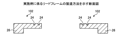
次に、図2に示すリードフレーム100の製造方法について、図8A~8Kを参照して説明する。図8A~8Kは、実施例に係るリードフレームの製造方法を示す断面図である。
図6に示した半導体装置200の製造方法について、図12A~12Cを参照して説明する。図12A~12Cは、実施例に係る半導体装置の製造方法を示す断面図である。
なお、上記実施例は、以下の態様で実施してもよい。なお、以下の説明では、上述した実施例と同様の部材については同じ符号を付し、説明の一部またはすべてを省略する場合がある。
21 半導体素子
22 Cuピラー
23 めっき層
24 凹部
25 酸化層
30 はんだ
100 単位リードフレーム
102 リード
200 半導体装置
Claims (10)
- 第1部分と前記第1部分よりも薄い第2部分とを有するリード部と、
前記リード部の前記第2部分に位置する半導体素子の接続領域に設けられ、前記リード部の幅方向の両側まで延びるめっき層と、
前記リード部の前記第2部分上において前記めっき層を挟んで互いに対向し、前記リード部を幅方向に貫通する一対の凹部と、
前記リード部の前記一対の凹部を含む表面に設けられた酸化層と
を備え、
前記めっき層の外周は、円弧状であり、
前記一対の凹部の各々は、前記リード部の幅方向に垂直な断面において、底面が曲面状であり、
前記一対の凹部の各々の内周は、円弧状であり且つ平面視で前記めっき層の外周と重なる位置に位置する
ことを特徴とするリードフレーム。 - 前記一対の凹部は、前記めっき層の周囲を囲うことを特徴とする請求項1に記載のリードフレーム。
- 前記リード部は、銅を材料とし、
前記めっき層は、銀を材料とする
ことを特徴とする請求項1又は2に記載のリードフレーム。 - 前記酸化層は、前記リード部の材料となる金属の酸化物からなることを特徴とする請求項1~3のいずれか一つに記載のリードフレーム。
- 第1部分と前記第1部分よりも薄い第2部分とを有するリード部と、
前記リード部の前記第2部分に位置する半導体素子の接続領域に設けられ、前記リード部の幅方向の両側まで延びるめっき層と、
前記リード部の前記第2部分上において前記めっき層を挟んで互いに対向し、前記リード部を幅方向に貫通する一対の凹部と、
前記リード部の前記一対の凹部を含む表面に設けられた酸化層と、
前記めっき層にはんだにより端子が接続された半導体素子と、
前記リード部及び前記半導体素子を被覆する封止樹脂と
を備え、
前記めっき層の外周は、円弧状であり、
前記一対の凹部の各々は、前記リード部の幅方向に垂直な断面において、底面が曲面状であり、
前記一対の凹部の各々の内周は、円弧状であり且つ平面視で前記めっき層の外周と重なる位置に位置する
ことを特徴とする半導体装置。 - リードと、前記リードの半導体素子の接続領域の周囲に設けられた凹部とを形成する第1工程と、
前記接続領域にめっき層を形成する第2工程と、
前記リードの前記凹部を含む表面に酸化層を形成する第3工程と
を備え、
前記第1工程は、
金属基板に、エッチングレジスト層を形成する工程と、
前記エッチングレジスト層をマスクとして前記金属基板にハーフエッチングを施すことにより、前記金属基板における所定領域の隣接領域に凹部を有する前記リードを形成する工程と、
前記金属基板から前記エッチングレジスト層を除去する工程とを含み、
前記第2工程は、
前記リードの前記凹部及び前記所定領域を含む領域にめっきレジストを形成する工程と、
前記所定領域よりも面積が大きいマスクで所定領域を覆い前記めっきレジストを露光し次いで現像することで、前記所定領域のめっきレジストを除く工程と、
前記所定領域にめっき層を形成する工程とを含み、
前記第3工程は、
前記リードから前記めっきレジストを除去する工程と、
前記凹部を含み且つ前記所定領域を除く前記リード上の領域に酸化層を形成する工程とを含む
ことを特徴とするリードフレームの製造方法。 - 前記凹部は、底面が曲面状であることを特徴とする請求項6に記載のリードフレームの製造方法。
- 前記凹部は、前記めっき層の全周を囲うことを特徴とする請求項6又は7に記載のリードフレームの製造方法。
- 前記リードは、銅を材料とし、
前記めっき層は、銀を材料とする
ことを特徴とする請求項6~8のいずれか一つに記載のリードフレームの製造方法。 - 前記第3工程は、前記リードの基材となる金属を酸化処理することで前記酸化層を形成する工程を含むことを特徴とする請求項6~9のいずれか一つに記載のリードフレームの製造方法。
Priority Applications (2)
| Application Number | Priority Date | Filing Date | Title |
|---|---|---|---|
| JP2018209997A JP7304145B2 (ja) | 2018-11-07 | 2018-11-07 | リードフレーム、半導体装置及びリードフレームの製造方法 |
| US16/668,078 US11791250B2 (en) | 2018-11-07 | 2019-10-30 | Lead frame, semiconductor device, and lead frame manufacturing method |
Applications Claiming Priority (1)
| Application Number | Priority Date | Filing Date | Title |
|---|---|---|---|
| JP2018209997A JP7304145B2 (ja) | 2018-11-07 | 2018-11-07 | リードフレーム、半導体装置及びリードフレームの製造方法 |
Publications (2)
| Publication Number | Publication Date |
|---|---|
| JP2020077747A JP2020077747A (ja) | 2020-05-21 |
| JP7304145B2 true JP7304145B2 (ja) | 2023-07-06 |
Family
ID=70459863
Family Applications (1)
| Application Number | Title | Priority Date | Filing Date |
|---|---|---|---|
| JP2018209997A Active JP7304145B2 (ja) | 2018-11-07 | 2018-11-07 | リードフレーム、半導体装置及びリードフレームの製造方法 |
Country Status (2)
| Country | Link |
|---|---|
| US (1) | US11791250B2 (ja) |
| JP (1) | JP7304145B2 (ja) |
Citations (3)
| Publication number | Priority date | Publication date | Assignee | Title |
|---|---|---|---|---|
| JP2015153987A (ja) | 2014-02-18 | 2015-08-24 | 株式会社デンソー | モールドパッケージ |
| JP2017028152A (ja) | 2015-07-24 | 2017-02-02 | 株式会社三井ハイテック | リードフレーム及びその製造方法 |
| JP2018056386A (ja) | 2016-09-29 | 2018-04-05 | Shマテリアル株式会社 | リードフレーム |
Family Cites Families (16)
| Publication number | Priority date | Publication date | Assignee | Title |
|---|---|---|---|---|
| JPH1041325A (ja) * | 1996-07-25 | 1998-02-13 | Hitachi Cable Ltd | Loc用リードフレーム |
| JP3562311B2 (ja) * | 1998-05-27 | 2004-09-08 | 松下電器産業株式会社 | リードフレームおよび樹脂封止型半導体装置の製造方法 |
| JP3706533B2 (ja) * | 2000-09-20 | 2005-10-12 | 三洋電機株式会社 | 半導体装置および半導体モジュール |
| JP4034073B2 (ja) * | 2001-05-11 | 2008-01-16 | 株式会社ルネサステクノロジ | 半導体装置の製造方法 |
| JP3879452B2 (ja) * | 2001-07-23 | 2007-02-14 | 松下電器産業株式会社 | 樹脂封止型半導体装置およびその製造方法 |
| US6841854B2 (en) * | 2002-04-01 | 2005-01-11 | Matsushita Electric Industrial Co., Ltd. | Semiconductor device |
| US8236612B2 (en) * | 2002-04-29 | 2012-08-07 | Unisem (Mauritius) Holdings Limited | Partially patterned lead frames and methods of making and using the same in semiconductor packaging |
| JP3883543B2 (ja) | 2003-04-16 | 2007-02-21 | 新光電気工業株式会社 | 導体基材及び半導体装置 |
| JP3841768B2 (ja) | 2003-05-22 | 2006-11-01 | 新光電気工業株式会社 | パッケージ部品及び半導体パッケージ |
| JP2006108306A (ja) * | 2004-10-04 | 2006-04-20 | Yamaha Corp | リードフレームおよびそれを用いた半導体パッケージ |
| KR100827388B1 (ko) * | 2006-12-19 | 2008-05-07 | 주식회사 씨오엘테크 | 반도체 패키지의 제조방법 |
| US8124447B2 (en) * | 2009-04-10 | 2012-02-28 | Advanced Semiconductor Engineering, Inc. | Manufacturing method of advanced quad flat non-leaded package |
| WO2010150365A1 (ja) * | 2009-06-24 | 2010-12-29 | アオイ電子株式会社 | 半導体装置および半導体装置の製造方法 |
| US8633063B2 (en) * | 2011-05-05 | 2014-01-21 | Stats Chippac Ltd. | Integrated circuit packaging system with pad connection and method of manufacture thereof |
| JP2014007363A (ja) * | 2012-06-27 | 2014-01-16 | Renesas Electronics Corp | 半導体装置の製造方法および半導体装置 |
| JP6253531B2 (ja) * | 2014-06-30 | 2017-12-27 | ルネサスエレクトロニクス株式会社 | 半導体装置 |
-
2018
- 2018-11-07 JP JP2018209997A patent/JP7304145B2/ja active Active
-
2019
- 2019-10-30 US US16/668,078 patent/US11791250B2/en active Active
Patent Citations (3)
| Publication number | Priority date | Publication date | Assignee | Title |
|---|---|---|---|---|
| JP2015153987A (ja) | 2014-02-18 | 2015-08-24 | 株式会社デンソー | モールドパッケージ |
| JP2017028152A (ja) | 2015-07-24 | 2017-02-02 | 株式会社三井ハイテック | リードフレーム及びその製造方法 |
| JP2018056386A (ja) | 2016-09-29 | 2018-04-05 | Shマテリアル株式会社 | リードフレーム |
Also Published As
| Publication number | Publication date |
|---|---|
| US20200144166A1 (en) | 2020-05-07 |
| JP2020077747A (ja) | 2020-05-21 |
| US11791250B2 (en) | 2023-10-17 |
Similar Documents
| Publication | Publication Date | Title |
|---|---|---|
| KR100811338B1 (ko) | 수지밀봉형 반도체장치, 이 장치에 이용되는 회로부재 및회로부재의 제조방법 | |
| JP6653139B2 (ja) | リードフレーム及びその製造方法 | |
| CN109285823B (zh) | 半导体元件搭载用基板以及其制造方法 | |
| JP5930843B2 (ja) | リードフレーム及びその製造方法 | |
| TWI787343B (zh) | 半導體元件搭載用基板及其製造方法 | |
| JP6679125B2 (ja) | リードフレーム及びこれを用いた半導体装置、並びにそれらの製造方法 | |
| CN110943064A (zh) | 引线框架及其制造方法 | |
| JP6892796B2 (ja) | 電子部品装置及びその製造方法 | |
| JP7304145B2 (ja) | リードフレーム、半導体装置及びリードフレームの製造方法 | |
| US10622286B2 (en) | Lead frame and method for manufacturing the same | |
| JP5850347B2 (ja) | 樹脂封止型半導体装置 | |
| JP2017163106A (ja) | リードフレーム集合基板及び半導体装置集合体 | |
| JP2022168143A (ja) | 半導体装置用基板、および半導体装置 | |
| JP4357728B2 (ja) | 樹脂封止型半導体装置 | |
| TW201826480A (zh) | 導線框 | |
| JP2014049718A (ja) | 半導体装置の製造方法並びにそれに用いられる半導体素子搭載用基板とその製造方法 | |
| JP2017168511A (ja) | 半導体素子搭載用基板、半導体装置、半導体素子搭載用基板の製造方法、及び半導体装置の製造方法 | |
| JP5943386B2 (ja) | リードフレーム及びその製造方法 | |
| JP2017162944A (ja) | 半導体装置及びその製造方法並びにその半導体装置の製造に用いるテープレスqfn用リードフレーム及びその製造方法 |
Legal Events
| Date | Code | Title | Description |
|---|---|---|---|
| A621 | Written request for application examination |
Free format text: JAPANESE INTERMEDIATE CODE: A621 Effective date: 20210915 |
|
| A977 | Report on retrieval |
Free format text: JAPANESE INTERMEDIATE CODE: A971007 Effective date: 20220714 |
|
| A131 | Notification of reasons for refusal |
Free format text: JAPANESE INTERMEDIATE CODE: A131 Effective date: 20220802 |
|
| A521 | Request for written amendment filed |
Free format text: JAPANESE INTERMEDIATE CODE: A523 Effective date: 20220922 |
|
| A131 | Notification of reasons for refusal |
Free format text: JAPANESE INTERMEDIATE CODE: A131 Effective date: 20230117 |
|
| A521 | Request for written amendment filed |
Free format text: JAPANESE INTERMEDIATE CODE: A523 Effective date: 20230306 |
|
| TRDD | Decision of grant or rejection written | ||
| A01 | Written decision to grant a patent or to grant a registration (utility model) |
Free format text: JAPANESE INTERMEDIATE CODE: A01 Effective date: 20230613 |
|
| A61 | First payment of annual fees (during grant procedure) |
Free format text: JAPANESE INTERMEDIATE CODE: A61 Effective date: 20230626 |
|
| R150 | Certificate of patent or registration of utility model |
Ref document number: 7304145 Country of ref document: JP Free format text: JAPANESE INTERMEDIATE CODE: R150 |