EP1085576B1 - El display device and method for manufacturing the same - Google Patents
El display device and method for manufacturing the same Download PDFInfo
- Publication number
- EP1085576B1 EP1085576B1 EP00119584A EP00119584A EP1085576B1 EP 1085576 B1 EP1085576 B1 EP 1085576B1 EP 00119584 A EP00119584 A EP 00119584A EP 00119584 A EP00119584 A EP 00119584A EP 1085576 B1 EP1085576 B1 EP 1085576B1
- Authority
- EP
- European Patent Office
- Prior art keywords
- film
- display device
- substrate
- tft
- counter substrate
- Prior art date
- Legal status (The legal status is an assumption and is not a legal conclusion. Google has not performed a legal analysis and makes no representation as to the accuracy of the status listed.)
- Expired - Lifetime
Links
Images


Classifications
-
- H—ELECTRICITY
- H10—SEMICONDUCTOR DEVICES; ELECTRIC SOLID-STATE DEVICES NOT OTHERWISE PROVIDED FOR
- H10F—INORGANIC SEMICONDUCTOR DEVICES SENSITIVE TO INFRARED RADIATION, LIGHT, ELECTROMAGNETIC RADIATION OF SHORTER WAVELENGTH OR CORPUSCULAR RADIATION
- H10F55/00—Radiation-sensitive semiconductor devices covered by groups H10F10/00, H10F19/00 or H10F30/00 being structurally associated with electric light sources and electrically or optically coupled thereto
-
- H—ELECTRICITY
- H10—SEMICONDUCTOR DEVICES; ELECTRIC SOLID-STATE DEVICES NOT OTHERWISE PROVIDED FOR
- H10K—ORGANIC ELECTRIC SOLID-STATE DEVICES
- H10K59/00—Integrated devices, or assemblies of multiple devices, comprising at least one organic light-emitting element covered by group H10K50/00
- H10K59/30—Devices specially adapted for multicolour light emission
- H10K59/38—Devices specially adapted for multicolour light emission comprising colour filters or colour changing media [CCM]
-
- G—PHYSICS
- G09—EDUCATION; CRYPTOGRAPHY; DISPLAY; ADVERTISING; SEALS
- G09G—ARRANGEMENTS OR CIRCUITS FOR CONTROL OF INDICATING DEVICES USING STATIC MEANS TO PRESENT VARIABLE INFORMATION
- G09G3/00—Control arrangements or circuits, of interest only in connection with visual indicators other than cathode-ray tubes
- G09G3/20—Control arrangements or circuits, of interest only in connection with visual indicators other than cathode-ray tubes for presentation of an assembly of a number of characters, e.g. a page, by composing the assembly by combination of individual elements arranged in a matrix no fixed position being assigned to or needed to be assigned to the individual characters or partial characters
- G09G3/22—Control arrangements or circuits, of interest only in connection with visual indicators other than cathode-ray tubes for presentation of an assembly of a number of characters, e.g. a page, by composing the assembly by combination of individual elements arranged in a matrix no fixed position being assigned to or needed to be assigned to the individual characters or partial characters using controlled light sources
- G09G3/30—Control arrangements or circuits, of interest only in connection with visual indicators other than cathode-ray tubes for presentation of an assembly of a number of characters, e.g. a page, by composing the assembly by combination of individual elements arranged in a matrix no fixed position being assigned to or needed to be assigned to the individual characters or partial characters using controlled light sources using electroluminescent panels
-
- H—ELECTRICITY
- H05—ELECTRIC TECHNIQUES NOT OTHERWISE PROVIDED FOR
- H05B—ELECTRIC HEATING; ELECTRIC LIGHT SOURCES NOT OTHERWISE PROVIDED FOR; CIRCUIT ARRANGEMENTS FOR ELECTRIC LIGHT SOURCES, IN GENERAL
- H05B33/00—Electroluminescent light sources
- H05B33/10—Apparatus or processes specially adapted to the manufacture of electroluminescent light sources
-
- H—ELECTRICITY
- H10—SEMICONDUCTOR DEVICES; ELECTRIC SOLID-STATE DEVICES NOT OTHERWISE PROVIDED FOR
- H10D—INORGANIC ELECTRIC SEMICONDUCTOR DEVICES
- H10D86/00—Integrated devices formed in or on insulating or conducting substrates, e.g. formed in silicon-on-insulator [SOI] substrates or on stainless steel or glass substrates
- H10D86/40—Integrated devices formed in or on insulating or conducting substrates, e.g. formed in silicon-on-insulator [SOI] substrates or on stainless steel or glass substrates characterised by multiple TFTs
- H10D86/411—Integrated devices formed in or on insulating or conducting substrates, e.g. formed in silicon-on-insulator [SOI] substrates or on stainless steel or glass substrates characterised by multiple TFTs characterised by materials, geometry or structure of the substrates
-
- H—ELECTRICITY
- H10—SEMICONDUCTOR DEVICES; ELECTRIC SOLID-STATE DEVICES NOT OTHERWISE PROVIDED FOR
- H10D—INORGANIC ELECTRIC SEMICONDUCTOR DEVICES
- H10D86/00—Integrated devices formed in or on insulating or conducting substrates, e.g. formed in silicon-on-insulator [SOI] substrates or on stainless steel or glass substrates
- H10D86/40—Integrated devices formed in or on insulating or conducting substrates, e.g. formed in silicon-on-insulator [SOI] substrates or on stainless steel or glass substrates characterised by multiple TFTs
- H10D86/441—Interconnections, e.g. scanning lines
-
- H—ELECTRICITY
- H10—SEMICONDUCTOR DEVICES; ELECTRIC SOLID-STATE DEVICES NOT OTHERWISE PROVIDED FOR
- H10D—INORGANIC ELECTRIC SEMICONDUCTOR DEVICES
- H10D86/00—Integrated devices formed in or on insulating or conducting substrates, e.g. formed in silicon-on-insulator [SOI] substrates or on stainless steel or glass substrates
- H10D86/40—Integrated devices formed in or on insulating or conducting substrates, e.g. formed in silicon-on-insulator [SOI] substrates or on stainless steel or glass substrates characterised by multiple TFTs
- H10D86/60—Integrated devices formed in or on insulating or conducting substrates, e.g. formed in silicon-on-insulator [SOI] substrates or on stainless steel or glass substrates characterised by multiple TFTs wherein the TFTs are in active matrices
-
- H—ELECTRICITY
- H10—SEMICONDUCTOR DEVICES; ELECTRIC SOLID-STATE DEVICES NOT OTHERWISE PROVIDED FOR
- H10K—ORGANIC ELECTRIC SOLID-STATE DEVICES
- H10K50/00—Organic light-emitting devices
- H10K50/80—Constructional details
- H10K50/84—Passivation; Containers; Encapsulations
- H10K50/841—Self-supporting sealing arrangements
-
- H—ELECTRICITY
- H10—SEMICONDUCTOR DEVICES; ELECTRIC SOLID-STATE DEVICES NOT OTHERWISE PROVIDED FOR
- H10K—ORGANIC ELECTRIC SOLID-STATE DEVICES
- H10K50/00—Organic light-emitting devices
- H10K50/80—Constructional details
- H10K50/84—Passivation; Containers; Encapsulations
- H10K50/844—Encapsulations
-
- H—ELECTRICITY
- H10—SEMICONDUCTOR DEVICES; ELECTRIC SOLID-STATE DEVICES NOT OTHERWISE PROVIDED FOR
- H10K—ORGANIC ELECTRIC SOLID-STATE DEVICES
- H10K50/00—Organic light-emitting devices
- H10K50/80—Constructional details
- H10K50/84—Passivation; Containers; Encapsulations
- H10K50/846—Passivation; Containers; Encapsulations comprising getter material or desiccants
-
- H—ELECTRICITY
- H10—SEMICONDUCTOR DEVICES; ELECTRIC SOLID-STATE DEVICES NOT OTHERWISE PROVIDED FOR
- H10K—ORGANIC ELECTRIC SOLID-STATE DEVICES
- H10K50/00—Organic light-emitting devices
- H10K50/80—Constructional details
- H10K50/86—Arrangements for improving contrast, e.g. preventing reflection of ambient light
- H10K50/865—Arrangements for improving contrast, e.g. preventing reflection of ambient light comprising light absorbing layers, e.g. light-blocking layers
-
- H—ELECTRICITY
- H10—SEMICONDUCTOR DEVICES; ELECTRIC SOLID-STATE DEVICES NOT OTHERWISE PROVIDED FOR
- H10K—ORGANIC ELECTRIC SOLID-STATE DEVICES
- H10K59/00—Integrated devices, or assemblies of multiple devices, comprising at least one organic light-emitting element covered by group H10K50/00
- H10K59/10—OLED displays
- H10K59/12—Active-matrix OLED [AMOLED] displays
- H10K59/121—Active-matrix OLED [AMOLED] displays characterised by the geometry or disposition of pixel elements
- H10K59/1213—Active-matrix OLED [AMOLED] displays characterised by the geometry or disposition of pixel elements the pixel elements being TFTs
-
- H—ELECTRICITY
- H10—SEMICONDUCTOR DEVICES; ELECTRIC SOLID-STATE DEVICES NOT OTHERWISE PROVIDED FOR
- H10K—ORGANIC ELECTRIC SOLID-STATE DEVICES
- H10K59/00—Integrated devices, or assemblies of multiple devices, comprising at least one organic light-emitting element covered by group H10K50/00
- H10K59/10—OLED displays
- H10K59/12—Active-matrix OLED [AMOLED] displays
- H10K59/123—Connection of the pixel electrodes to the thin film transistors [TFT]
-
- H—ELECTRICITY
- H10—SEMICONDUCTOR DEVICES; ELECTRIC SOLID-STATE DEVICES NOT OTHERWISE PROVIDED FOR
- H10K—ORGANIC ELECTRIC SOLID-STATE DEVICES
- H10K59/00—Integrated devices, or assemblies of multiple devices, comprising at least one organic light-emitting element covered by group H10K50/00
- H10K59/10—OLED displays
- H10K59/12—Active-matrix OLED [AMOLED] displays
- H10K59/124—Insulating layers formed between TFT elements and OLED elements
-
- H—ELECTRICITY
- H10—SEMICONDUCTOR DEVICES; ELECTRIC SOLID-STATE DEVICES NOT OTHERWISE PROVIDED FOR
- H10K—ORGANIC ELECTRIC SOLID-STATE DEVICES
- H10K59/00—Integrated devices, or assemblies of multiple devices, comprising at least one organic light-emitting element covered by group H10K50/00
- H10K59/10—OLED displays
- H10K59/12—Active-matrix OLED [AMOLED] displays
- H10K59/126—Shielding, e.g. light-blocking means over the TFTs
-
- H—ELECTRICITY
- H10—SEMICONDUCTOR DEVICES; ELECTRIC SOLID-STATE DEVICES NOT OTHERWISE PROVIDED FOR
- H10K—ORGANIC ELECTRIC SOLID-STATE DEVICES
- H10K59/00—Integrated devices, or assemblies of multiple devices, comprising at least one organic light-emitting element covered by group H10K50/00
- H10K59/80—Constructional details
- H10K59/87—Passivation; Containers; Encapsulations
- H10K59/873—Encapsulations
-
- H—ELECTRICITY
- H10—SEMICONDUCTOR DEVICES; ELECTRIC SOLID-STATE DEVICES NOT OTHERWISE PROVIDED FOR
- H10K—ORGANIC ELECTRIC SOLID-STATE DEVICES
- H10K59/00—Integrated devices, or assemblies of multiple devices, comprising at least one organic light-emitting element covered by group H10K50/00
- H10K59/80—Constructional details
- H10K59/87—Passivation; Containers; Encapsulations
- H10K59/874—Passivation; Containers; Encapsulations including getter material or desiccant
-
- H—ELECTRICITY
- H10—SEMICONDUCTOR DEVICES; ELECTRIC SOLID-STATE DEVICES NOT OTHERWISE PROVIDED FOR
- H10K—ORGANIC ELECTRIC SOLID-STATE DEVICES
- H10K59/00—Integrated devices, or assemblies of multiple devices, comprising at least one organic light-emitting element covered by group H10K50/00
- H10K59/80—Constructional details
- H10K59/8791—Arrangements for improving contrast, e.g. preventing reflection of ambient light
- H10K59/8792—Arrangements for improving contrast, e.g. preventing reflection of ambient light comprising light absorbing layers, e.g. black layers
-
- H—ELECTRICITY
- H10—SEMICONDUCTOR DEVICES; ELECTRIC SOLID-STATE DEVICES NOT OTHERWISE PROVIDED FOR
- H10K—ORGANIC ELECTRIC SOLID-STATE DEVICES
- H10K71/00—Manufacture or treatment specially adapted for the organic devices covered by this subclass
-
- H—ELECTRICITY
- H10—SEMICONDUCTOR DEVICES; ELECTRIC SOLID-STATE DEVICES NOT OTHERWISE PROVIDED FOR
- H10K—ORGANIC ELECTRIC SOLID-STATE DEVICES
- H10K2102/00—Constructional details relating to the organic devices covered by this subclass
- H10K2102/301—Details of OLEDs
- H10K2102/302—Details of OLEDs of OLED structures
- H10K2102/3023—Direction of light emission
- H10K2102/3026—Top emission
-
- H—ELECTRICITY
- H10—SEMICONDUCTOR DEVICES; ELECTRIC SOLID-STATE DEVICES NOT OTHERWISE PROVIDED FOR
- H10K—ORGANIC ELECTRIC SOLID-STATE DEVICES
- H10K50/00—Organic light-emitting devices
- H10K50/80—Constructional details
- H10K50/84—Passivation; Containers; Encapsulations
- H10K50/842—Containers
- H10K50/8426—Peripheral sealing arrangements, e.g. adhesives, sealants
-
- H—ELECTRICITY
- H10—SEMICONDUCTOR DEVICES; ELECTRIC SOLID-STATE DEVICES NOT OTHERWISE PROVIDED FOR
- H10K—ORGANIC ELECTRIC SOLID-STATE DEVICES
- H10K59/00—Integrated devices, or assemblies of multiple devices, comprising at least one organic light-emitting element covered by group H10K50/00
- H10K59/10—OLED displays
- H10K59/12—Active-matrix OLED [AMOLED] displays
- H10K59/131—Interconnections, e.g. wiring lines or terminals
-
- H—ELECTRICITY
- H10—SEMICONDUCTOR DEVICES; ELECTRIC SOLID-STATE DEVICES NOT OTHERWISE PROVIDED FOR
- H10K—ORGANIC ELECTRIC SOLID-STATE DEVICES
- H10K59/00—Integrated devices, or assemblies of multiple devices, comprising at least one organic light-emitting element covered by group H10K50/00
- H10K59/80—Constructional details
- H10K59/87—Passivation; Containers; Encapsulations
- H10K59/871—Self-supporting sealing arrangements
- H10K59/8722—Peripheral sealing arrangements, e.g. adhesives, sealants
Definitions
- the present invention relates to an EL (Electro-luminescence) display device formed by fabricating a semiconductor device (a device utilizing a semiconductor thin film; typically a thin film transistor) on a substrate, and an electronic device having such an EL display device as a display portion.
- a semiconductor device a device utilizing a semiconductor thin film; typically a thin film transistor
- a technique for forming a thin film transistor (hereinafter referred to as the TFT) on a substrate has been significantly improved in these days, and development for application thereof to an active matrix type display device has continued.
- a TFT utilizing a polysilicon film has a field effect mobility higher than that obtainable in a TFT utilizing a conventional amorphous silicon film, thereby realizing an operation at higher speed.
- Such an active matrix type display device has drawn much attention thereto since the device can realize various advantages, such as reduction in manufacturing cost, down-sizing of a display device, an improved yield, a reduced throughput or the like, by fabricating various circuits and devices on one and the same substrate.
- each pixel is provided with a switching device made of a TFT, and a driving device for controlling a current is activated by the switching device to cause an EL layer (more strictly speaking, a light emitting layer) to emit light.
- the EL display device is disclosed, for example, in Japanese Laid-open Patent Publication No. Hei 10-189252 .
- EP0845812A2 discloses a display apparatus having two opposing substrates with color filters, wavelength conversion layers and pixel structures therebetween.
- JP10289789 discloses an organic electro-luminescent element.
- This disclosure describes a transparent support body having a luminous conversion layer faced to an insulation substrate having an organic electro-luminescent cell made of an organic luminous layer or the like clamped with a cathode and an anode, and an active matrix circuit element for driving the cell.
- the present invention is intended to provide an inexpensive EL display device capable of displaying an image with high definition. Furthermore, the present invention is also intended to provide an electronic device having a high recognizability of a display portion by utilizing such an EL display device as the display portion.
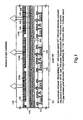
- reference numeral 101 denotes a substrate having an insulating surface.
- an insulating substrate such as a quartz substrate can be used.
- various kinds of substrate such as a glass substrate, a semiconductor substrate, a ceramic substrate, a crystallized substrate, a metal substrate, or a plastic substrate, can be used by providing an insulating film on a surface thereof.
- pixels 102 are formed on the substrate 101. Although only three of the pixels are illustrated in Fig. 1 , a higher number of pixels are actually formed in matrix. In addition, although one of these three pixels will be described below, the other pixels have the same structure.
- each of the pixels 102 two TFTs are formed; one of them is a switching TFT 103, and the other is a current control TFT 104.
- a drain of the switching TFT 103 is electrically connected to a gate of the current control TFT 104.
- a drain of the current control TFT 104 is electrically connected to a pixel electrode 105 (which in this case, also functions as a cathode of an EL element). The pixel 102 is thus formed.
- Various wirings of the TFT as well as the pixel electrode can be formed of a metal film having a low resistivity.
- a metal film having a low resistivity For example, an aluminum alloy film may be used for this purpose.
- an insulating compound 106 (hereinbelow, referred to as the alkaline compound) including an alkali metal or an alkaline-earth metal over all of the pixel electrodes. Note that the outline of the alkaline compound is indicated by a dotted line in Fig. 1 . This is because the alkaline compound 106 has a thickness which is as thin as several nm, and it is not known whether the compound 106 is formed as a layer or in an island-shape.
- lithium fluoride (LiF), lithium oxide (Li 2 O), barium fluoride (BaF 2 ), barium oxide (BaO), calcium fluoride (CaF 2 ), calcium oxide (CaO), strontium oxide (SrO), or cesium oxide (Cs 2 O) can be used. Since these are insulating materials, short-circuiting between the pixel electrodes does not occur even when the alkaline compound 106 is formed as a layer.
- cathode a known conductive material as an MgAg electrode.
- the cathode itself has to be selectively formed or patterned into a certain shape in order to avoid short-circuiting between the pixel electrodes.
- an EL layer (Electro-luminescence layer) 107 is formed thereover.
- a material capable of emitting white light is used in the present invention.
- a light emitting layer providing a field for recombination may be employed for the EL layer.
- an electron injection layer, an electron transport layer, a hole transport layer, an electron blocking layer, a hole device layer, or a hole injection layer may be further layered. In the present specification, all of those layered intended to realize injection, transport or recombination of carriers are collectively referred to as the EL layer.
- an organic material to be used as the EL layer 107 either a low-molecule type organic material or a polymer type (high-molecule type) organic material can be used.
- a polymer type organic material that can be formed by an easy formation technique such as a spin coat technique, a printing technique or the like.
- the structure illustrated in Fig. 1 is of the color display scheme in which an EL layer for emitting white light is combined with a color filter.
- a color display scheme in which an EL layer for emitting blue or blue-green light is combined with fluorescent material (fluorescent color conversion layer; CCM), or another color display scheme in which EL layers respectively corresponding to RGB are overlaid one upon another to provide color display, can also be employed.
- a transparent conductive film is formed as an anode 108.
- a compound of indium oxide and tin oxide referred to as ITO
- a compound of indium oxide and zinc oxide, tin oxide or zinc oxide can be used.
- an insulating film as a passivation film 109 is provided.
- a silicon nitride film or a silicon oxynitride film (represented as SiOxNy) is preferably used.
- SiOxNy silicon oxynitride film
- an insulating film with as low an oxygen content as possible is preferred.
- the substrate fabricated up to this stage is referred to as an active matrix substrate in the present application. More specifically, the substrate on which a TFT, a pixel electrode electrically connected to the TFT, and an EL element (a capacitor made of a cathode, an EL layer, and an anode) utilizing the pixel electrode as the cathode are formed is referred to as the active matrix substrate.
- a counter substrate 110 is attached to the active matrix substrate with the EL element being interposed therebetween.
- the counter substrate 110 is provided with a light shielding film 112 and color filters 113a to 113c.
- the light shielding film 112 is provided so that a gap 111 formed between the pixel electrodes 105 is unseen from the viewing direction of an observer (i.e., from a direction normal to the counter substrate.) More specifically, the light shielding film 112 is provided to overlap (align with) the periphery of the pixel when viewed from the direction normal to the counter substrate. This is because this portion is non-emitting portion, and furthermore, electric field becomes complicated at the edge portion of the pixel electrode and thus light cannot be emitted with a desired luminance or chromaticity.
- the light shielding film 112 is provided at the position corresponding to the periphery (edge portion) of the pixel electrode 105 and the gap 111, contour between the pixels can be made clear. It can be also said that in the present invention, the light shielding film 112 is provided at the position corresponding to the periphery (edge portion) of the pixel because the contour of the pixel electrode corresponds to the contour of the pixel. Note that the position corresponding to the periphery of the pixel refers to the position aligned with the periphery of the pixel when viewed from the aforementioned direction which is normal to the counter substrate.
- the color filter 113a is the one for obtaining red light
- the color filter 113b is the one for obtaining green light
- the color filter 113c is the one for obtaining blue light.
- These color filters are formed at positions respectively corresponding to the different pixels 102, and thus, different color of light can be obtained for the respective pixels. In theory, this is the same as the color display scheme in a liquid crystal display device which uses color filters.
- the position corresponding to the pixel refers to the position overlapped (aligned) with the pixel when viewed from the aforementioned direction which is normal to the counter substrate.
- the color filters 113a to 113c are provided so as to overlap the pixels respectively corresponding thereto when viewed from the direction normal to the counter substrate.
- the color filter is a filter for improving the color purity of light which has passed therethrough by extracting light of a specific wavelength. Accordingly, in the case where the light component of the wavelength to be extracted is small, there may be disadvantages in which the light of that wavelength has extremely small luminance or deteriorated color purity. Thus, although no limitation is imposed to an EL layer for emitting white light which can be used in the present invention, it is preferable that the spectrum of the emitted white light includes emission spectrums of red, green and blue light components having as high purity as possible.
- Figs. 16A and 16B show typical x-y chromaticity diagrams of an EL layer to be used in the present invention. More specifically, Fig. 16A shows the chromaticity coordinate of light emitted from a known polymer type organic material for emitting white light. In the known material, the red color emission with high color purity cannot be realized. Therefore, yellow light or orange light is used instead of red light. Accordingly, white color obtained by adhesive color mixing seems to slightly include green color or yellow color. In addition, the respective emission spectrums of red light, green light, and blue light are so broad that it also becomes difficult to obtain monochromatic light having high purity when these light are mixed.
- the organic material as represented in the chromaticity diagram in Fig. 16B is an example in which an EL layer for emitting white light is formed by mixing organic materials capable of providing monochromatic light with high purity.
- organic materials capable of providing monochromatic light with high purity In order to obtain light emission spectrums of red, green and blue colors having high color purity from a color filter, it is necessary to form an EL layer for emitting white light by mixing organic materials respectively exhibiting light emission spectrums of red, green and blue colors with high color purity.
- materials capable of providing a spectrum not only with high color purity but also with a narrow half-peak width white color with a sharp spectrum can be reproduced.
- the present invention can display a further brighter color image.
- the counter substrate 110 is adhered to the active matrix substrate by means of a sealing agent, so that a space designated with reference numeral 114 is a closed space.
- the EL display device having the above-mentioned construction in accordance with the present invention
- light emitted from the EL element passes through the counter substrate to be emitted toward an observer's eyes. Accordingly, the observer can recognize an image through the counter substrate.
- one of the features of the EL display device in accordance with the present invention is that the light shielding film 112 is disposed between the EL element and the observer so as to conceal the gap 111 between the pixel electrodes 105.
- the contour between the pixels can be made clear, thereby resulting in an image display with high definition.
- This advantage can be obtained due to the light shielding film 112 provided at the counter substrate 110. When at least the light shielding film 112 is provided, this advantage can be obtained.
- the light shielding film 112 and the color filters 113a to 113c are disposed at the counter substrate 110, and the counter substrate 110 also functions as a ceiling substrate for suppressing deterioration of the EL element.
- the counter substrate 110 also functions as a ceiling substrate for suppressing deterioration of the EL element.
- the structure in accordance with the present invention in which the counter substrate 110 is provided with the light shielding film 112 and the color filters 113a to 113c and adhered to the active matrix substrate by means of the sealing agent has features common to the structure of a liquid crystal display device. Accordingly, it is possible to fabricate the EL display device of the present invention with most of an existing manufacturing line for liquid crystal display devices. Thus, an amount of equipment investment can be significantly reduced, thereby resulting in a reduction in the total manufacturing cost.
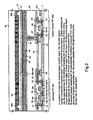
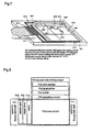
- Fig. 2 shows a cross-sectional view of a pixel portion in an EL display device in accordance with the present invention.
- Fig. 3A shows a top view of the pixel portion
- Fig. 3B shows the circuit configuration thereof.
- pixels are arranged in a plurality of lines to be in matrix, thereby forming a pixel portion (image display portion).
- Fig. 2 illustrates a cross-sectional view taken along the line A-A' in Fig. 3A . Accordingly, the same components are commonly designated by the same reference numerals in both of the figures, and it will be advantageous for understanding the structure to make reference to both of the figures.
- the two pixels illustrated in the top view of Fig. 3A have the same structure.
- reference numeral 11 denotes a substrate
- 12 denotes a base insulating film (hereinafter referred to as the base film).
- the substrate 11 a glass substrate, a glass ceramic substrate, a quartz substrate, a silicon substrate, a ceramic substrate, a metal substrate, or a plastic substrate (including a plastic film) can be used.
- the base film 12 is especially advantageous for a substrate including mobile ions or a substrate having conductivity, but does not necessarily have to be provided for a quartz substrate.
- an insulating film containing silicon may be used as the base film 12.
- the "insulating film containing silicon” refers to an insulating film containing silicon and oxygen or nitrogen at a predetermined ratio, and more specifically, a silicon oxide film, a silicon nitride film, or a silicon oxynitride film (represented as SiOxNy.)
- a TFT 201 functions as a switching device (hereinafter referred to as the switching TFT), and a TFT 202 functions as a current controlling device for controlling an amount of current to flow through the EL element (hereinafter referred to as the current control TFT.)
- Both of the TFTs 201 and 202 are made of the n-channel type TFT.
- the n-channel type TFT has a field effect mobility higher than that of the p-channel type TFT, the n-channel type TFT can operate at higher speed and accept a large amount of current. Furthermore, a current of the same amount can flow through the n-channel type TFT of smaller size as compared to the p-channel type TFT. Accordingly, it is preferable to use the n-channel type TFT as the current control TFT since this results in an increased effective area of the display portion.
- the p-channel type TFT has advantages, e.g., in which the injection of hot carriers becomes hardly a problem and an OFF current value is small.
- advantages e.g., in which the injection of hot carriers becomes hardly a problem and an OFF current value is small.
- the disadvantages in connection with the injection of hot carriers and a small OFF current value can be overcome even in the n-channel type TFT by providing the structure with shifted LDD regions.
- the present invention is not limited to the case where the switching TFT and the current control TFT are made of the n-channel type TFTs. It is possible to use the p-channel type TFT as both or either of the switching TFT and the current control TFT.
- the gate electrodes 19a and 19b are electrically connected to each other by means of a gate wiring 211 which is made of a different material (that has a lower resistivity than the gate electrodes 19a and 19b), thereby forming a double-gate structure.
- a gate wiring 211 which is made of a different material (that has a lower resistivity than the gate electrodes 19a and 19b), thereby forming a double-gate structure.
- the so-called multigate structure a structure including an active layer which contains two or more channel forming regions connected in series
- the multigate structure is significantly advantageous for decreasing of OFF current value.
- a switching device having a low OFF current value can be realized by providing the switching device 201 in the pixel with the multigate structure.
- the active layer is formed of a semiconductor film that includes a crystalline structure. This may be a single crystalline semiconductor film, a polycrystalline semiconductor film, or a microcrystalline semiconductor film.
- the gate insulating film 18 may be formed of an insulating film containing silicon.
- any kind of conductive films can be used as the gate electrode, the source wiring, or the drain wiring.
- an offset region (which is made of a semiconductor layer having the same composition as the channel forming regions and a gate voltage is not applied thereto) between the channel forming regions and the LDD regions.
- the high concentration impurities region disposed between the channel forming regions is effective for reducing the OFF current value.
- the length (width) of the LDD regions to be formed in the switching TFT 201 is set in the range from 0.5 to 3.5 ⁇ m, typically in the range from 2.0 to 2.5 ⁇ m.
- the EL display device as shown in Fig. 2 has features in which the LDD region 33 is provided between the drain region 32 and the channel forming region 34 in the current control TFT 202, and part of the LDD region 33 overlaps the gate electrode 35 through the gate insulating film 18 while the remaining portion does not.
- a parasitic capacitance is generated in the region where the gate electrode overlaps the LDD region, and therefore, such an overlap region should not be provided between the source region 31 and the channel forming region 34. Since carriers (electrons) always travel in the same direction in the current control TFT, it is sufficient to provide the LDD region only on the side closer to the drain region.
- a thin film made of the material having the foregoing heat radiating effect can be used alone, it is effective to stack these thin films and a silicon nitride film (SixNy) or silicon nitride oxide film (SiOxNy). Note that in the silicon nitride film or silicon nitride oxide film, x and y are respectively arbitrary integers.
- a second interlayer insulating film 42 (also referred to as a planarizing film) is formed to cover the respective TFTs, and thus steps caused by the TFTs are planarized.
- a second interlayer insulating film 42 an organic resin film is preferred, and polyimide, polyamide, acrylic, BCB (benzocyclobutane), or the like can be used.
- An inorganic film can be also used of course, so long as sufficient planarization is realized.
- the planarization of the steps caused by the TFTs by means of the second interlayer insulating film 42 is very important.
- the EL layer to be formed in the subsequent step is so thin that the steps may cause to defect in light emission. Accordingly, in order to form the EL layer on a flat surface as much as possible, it is preferable to perform a planarization process prior to the formation of the pixel electrode.
- a lithium fluoride film having a thickness of 5 to 10 nm is formed by a vapor deposition method as the alkaline compound 44 on the pixel electrode 43.
- the lithium fluoride film is an insulating film, and thus, when the thickness thereof is too large, a current cannot flow to the EL layer. No adverse effect is generated even when the lithium fluoride film is formed in an island-like pattern, not in a layer.
- the thickness of the above material can be set to be in the range from 30 to 150 nm (preferably 40 to 100 nm).
- the hole transport layer polytetra hydrothiophenyl phenylene that is the polymer precursor, is used, which is heated to be converted into polyphenylene vinylene.
- the thickness thereof can be set to be in the range from 30 to 100 nm (preferably 40 to 80 nm).
- the polymer type organic material is advantageous especially for emitting white light since color adjustment can be easily performed by adding a fluorescent pigment into a solution in which a host material is solved.
- the EL element is formed by using the polymer type organic material in the above description, any low molecule type organic material can be used.
- the EL layer can be formed with an inorganic material.
- the counter substrate 48 is disposed to face the active matrix substrate thus completed.
- a glass substrate is used as the counter substrate 48.
- the counter substrate 48 is provided with light shielding films 49a and 49b made of resin with a black-colored pigment being dispersed therein, and a color filter 50 made of resin with a red-colored, green-colored, or blue-colored pigment being dispersed therein.
- These light shielding films 49a and 49b are disposed so as to conceal a gap between the pixel electrode 43 and its adjacent pixel electrode.
- the light shielding films 49a and 49b contains a drying agent such as barium oxide or the like. Other material such as those disclosed in Japanese Laid-Open Patent Publication No. Hei 9-148066 can be used as the drying agent.
- the color filter 50 is formed at the position corresponding to the pixel 102.
- the active matrix substrate is adhered to the counter substrate 48 by means of a sealing agent (not illustrated) to form a closed space 51.
- the closed space is filled with argon gas. It is of course possible to place the above-mentioned drying agent in the closed space 51.
- the EL display device in accordance with the present embodiment includes a pixel portion composed of pixels each having the structure as shown in Fig. 2 , in which the TFTs having the different structures in accordance with their functions in pixels are arranged. More specifically, the switching TFT having a sufficiently low OFF current value and the current control TFT which is not vulnerable to the injection of hot carriers are formed in the same pixel. Thus, the EL display device with high reliability capable of displaying an image with high definition can be obtained.
- a base film 301 is formed with a 300 nm thickness on a glass substrate 300.
- Oxidized silicon nitride films are laminated as the base film 301 in embodiment 1. It is good to set the nitrogen concentration at between 10 and 25 wt% in the film contacting the glass substrate 300.
- the base film 301 it is effective to provide an insulating film made of a material similar to the first passivation film 41 shown in Fig. 2 .
- the current controlling TFT is apt to generate heat since a large current is made to flow, and it is effective to provide an insulating film having a heat radiating effect at a place as close as possible.
- an amorphous silicon film (not shown in the figures) is formed with a thickness of 50 nm on the base film 301 by a known deposition method. Note that it is not necessary to limit this to the amorphous silicon film, and another film may be formed provided that it is a semiconductor film containing an amorphous structure (including a microcrystalline semiconductor film). In addition, a compound semiconductor film containing an amorphous structure, such as an amorphous silicon germanium film, may also be used. Further, the film thickness may be made from 20 to 100 nm.
- the amorphous silicon film is then crystallized by a known method, forming a crystalline silicon film (also referred to as a polycrystalline silicon film or a polysilicon film) 302.
- a crystalline silicon film also referred to as a polycrystalline silicon film or a polysilicon film
- Thermal crystallization using an electric furnace, laser annealing crystallization using a laser, and lamp annealing crystallization using an infrared lamp exist as known crystallization methods. Crystallization is performed in embodiment 1 using an excimer laser light which uses XeCl gas.
- pulse emission type excimer laser light formed into a linear shape is used in embodiment 1, but a rectangular shape may also be used, and continuous emission argon laser light and continuous emission excimer laser light can also be used.
- the crystalline silicon film is used as the active layer of the TFT, it is also possible to use an amorphous silicon film. Further, it is possible to form the active layer of the switching TFT, in which there is a necessity to reduce the off current, by the amorphous silicon film, and to form the active layer of the current control TFT by the crystalline silicon film. Electric current flows with difficulty in the amorphous silicon film because the carrier mobility is low, and the off current does not easily flow. In other words, the most can be made of the advantages of both the amorphous silicon film, through which current does not flow easily, and the crystalline silicon film, through which current easily flows.
- a protecting film 303 is formed on the crystalline silicon film 302 with a silicon oxide film having a thickness of 130 nm. This thickness may be chosen within the range of 100 to 200 nm (preferably between 130 and 170 nm). Furthermore, other films may also be used providing that they are insulating films containing silicon.
- the protecting film 303 is formed so that the crystalline silicon film is not directly exposed to plasma during addition of an impurity, and so that it is possible to have delicate concentration control of the impurity.
- Resist masks 304a and 304b are then formed on the protecting film 303, and an impurity element which imparts n-type conductivity (hereafter referred to as an n-type impurity element) is added.
- an impurity element which imparts n-type conductivity hereafter referred to as an n-type impurity element
- elements residing in periodic table group 15 are generally used as the n-type impurity element, and typically phosphorous or arsenic can be used.
- a plasma doping method is used, in which phosphine (PH 3 ) is plasma activated without separation of mass, and phosphorous is added at a concentration of 1x10 18 atoms/cm 3 in embodiment 1.
- An ion implantation method, in which separation of mass is performed, may also be used, of course.
- the dose amount is regulated so that the n-type impurity element is contained in n-type impurity regions 305 and 306, thus formed by this process, at a concentration of 2x10 16 to 5x10 19 atoms/cm 3 (typically between 5x10 17 and 5x10 18 atoms/cm 3 ).
- the protecting film 303 is removed, and an activation of the added periodic table group 15 elements is performed.
- a known technique of activation may be used as the means of activation, but activation is done in embodiment 1 by irradiation of excimer laser light.
- a pulse emission type excimer laser and a continuous emission type excimer laser may both, be used, and it is not necessary to place any limits on the use of excimer laser light.
- the goal is the activation of the added impurity element, and it is preferable that irradiation is performed at an energy level at which the crystalline silicon film does not melt. Note that the laser irradiation may also be performed with the protecting film 303 in place.
- the activation by heat treatment may also be performed along with activation of the impurity element by laser light.
- activation is performed by heat treatment, considering the heat resistance of the substrate, it is good to perform heat treatment on the order of 450 to 550°C.
- a boundary portion (connecting portion) with end portions of the n-type impurity regions 305 and 306, namely regions, in which the n-type impurity element is not added, on the periphery of the n-type impurity regions 305 and 306, is not added, is delineated by this process. This means that, at the point when the TFTs are later completed, extremely good connections can be formed between LDD regions and channel forming regions.
- a gate insulating film 311 is formed, covering the active layers 307 to 310.
- a single layer structure or a lamination structure may be used.
- a 110 nm thick oxidized silicon nitride film is used in embodiment 1.
- a conductive film having a thickness of 200 to 400 nm is formed and patterned to form gate electrodes 312 to 316. Respective end portions of these gate electrodes 312 to 316 may be tapered.
- the gate electrodes and wirings (hereinafter referred to as the gate wirings) electrically connected to the gate electrodes for providing conducting paths are formed of different materials from each other. More specifically, the gate wirings are made of a material having a lower resistivity than the gate electrodes. Thus, a material enabling fine processing is used for the gate electrodes, while the gate wirings are formed of a material that can provide a smaller wiring resistance but is not suitable for fine processing. It is of course possible to form the gate electrodes and the gate wirings with the same material.
- the gate electrode can be made of a single-layered conductive film, it is preferable to form a lamination film with two, three or more layers for the gate electrode if necessary. Any known conductive materials can be used for the gate electrode. It should be noted, however, that it is preferable to use such a material that enables fine processing, and more specifically, a material that can be patterned with a line width of 2 ⁇ m or less.
- the films may be used as a single layer or a laminate layer.
- a laminate film of a tungsten nitride (WN) film having a thickness of 50 nm and a tungsten (W) film having a thickness of 350 nm is used.
- This may be formed by a sputtering method.
- an inert gas of Xe, Ne or the like is added as a sputtering gas, film peeling due to stress can be prevented.
- the gate electrodes 313 and 316 are formed at this time so as to overlap a portion of the n-type impurity regions 305 and 306, respectively, sandwiching the gate insulating film 311. This overlapping portion later becomes an LDD region overlapping the gate electrode.
- an n-type impurity element (phosphorous is used in embodiment 1) is added in a self-aligning manner with the gate electrodes 312 to 316 as masks, as shown in Fig. 5A .
- the addition is regulated so that phosphorous is added to impurity regions 317 to 323 thus formed at a concentration of 1/10 to 1 ⁇ 2 that of the impurity regions 305 and 306 (typically between 1/4 and 1/3).
- a concentration of 1x10 16 to 5x10 18 atoms/cm 3 (typically 3x10 17 to 3x10 18 atoms/cm 3 ) is preferable.
- Resist masks 324a to 324c are formed next, with a shape covering the gate electrodes etc., as shown in Fig. 5B , and an n-type impurity element (phosphorous is used in embodiment 1) is added, forming impurity regions 325 to 331 containing phosphorous at high concentration of phosphorous.
- Ion doping using phosphine (PH 3 ) is also performed here, and is regulated so that the phosphorous concentration of these regions is from 1x10 20 to 1x10 21 atoms/cm 3 (typically between 2x10 20 and 5x10 21 atoms/cm 3 ).
- the resist masks 324a to 324c are removed, and a new resist mask 332 is formed.
- a p-type impurity element (boron is used in embodiment 1) is then added, forming impurity regions 333 and 334 containing boron at high concentration. Boron is added here to form impurity regions 333 and 334 at a concentration of 3x10 20 to 3x10 21 atoms/cm 3 (typically between 5x10 20 and 1x10 21 atoms/cm 3 ) by ion doping using diborane (B 2 H 6 ).
- phosphorous has already been added to the impurity regions 333 and 334 at a concentration of 1x10 20 to 1x10 21 atoms/cm 3 , but boron is added here at a concentration of at least 3 times that of the phosphorous. Therefore, the n-type impurity regions already formed completely invert to p-type, and function as p-type impurity regions.
- the n-type and p-type impurity elements added to the active layer at respective concentrations are activated.
- Furnace annealing, laser annealing or lamp annealing can be used as a means of activation.
- heat treatment is performed for 4 hours at 550°C in a nitrogen atmosphere in an electric furnace.
- the oxygen concentration in the surrounding atmosphere for the activation process is set at 1 ppm or less, preferably at 0.1 ppm or less.
- the gate wiring 335 having a thickness of 300 nm is formed.
- a metal film containing aluminum (Al) or copper (Cu) as its main component (occupied 50 to 100% in the composition) can be used.
- the gate wiring 335 is arranged, as the gate wiring 211 shown in Figs. 3A , so as to provide electrical connection for the gate electrodes 314 and 315 (corresponding to the gate electrodes 19a and 19b in Fig. 3A ) of the switching TFT (see Fig. 5D ).
- a first interlayer insulating film 336 is formed next, as shown in Fig. 6A .
- a single layer insulating film containing silicon is used as the first interlayer insulating film 336, while a lamination film may be used. Further, a film thickness of between 400 nm and 1.5 ⁇ m may be used.
- a lamination structure of an 800 nm thick silicon oxide film on a 200 nm thick oxidized silicon nitride film is used in embodiment 1.
- the hydrogenation processing may also be inserted during the formation of the first interlayer insulating film 336. Namely, hydrogen processing may be performed as above after forming the 200 nm thick oxidized silicon nitride film, and then the remaining 800 nm thick silicon oxide film may be formed.
- a first passivation film 344 is formed next with a thickness of 50 to 500 nm (typically between 200 and 300 nm).
- a 300 nm thick oxidized silicon nitride film is used as the first passivation film 344 in embodiment 1. This may also be substituted by a silicon nitride film. It is of course possible to use the same materials as those of the first passivation film 41 of Fig. 2 .
- a second interlayer insulating film 345 made of organic resin is formed.
- the organic resin it is possible to use polyimide, polyamide, acryl, BCB (benzocyclobutene) or the like.
- the second interlayer insulating film 345 is primarily used for flattening, acryl excellent in flattening properties is preferable.
- an acrylic film is formed to a thickness sufficient to flatten a stepped portion formed by TFTs. It is appropriate that the thickness is made 1 to 5 ⁇ m (more preferably, 2 to 4 ⁇ m).
- a contact hole is formed in the second interlayer insulating film 345 and the first passivation film 344 to reach the drain wiring 343, and then the pixel electrode 346 is formed.
- an aluminum alloy film (an aluminum film containing titanium of 1wt%) having a thickness of 300 nm is formed as the pixel electrode 346.
- Reference numeral 347 denotes an end portion of the adjacent pixel electrode.
- the alkaline compound 348 is formed, as shown in Fig. 6C .
- a lithium fluoride film is formed by a vapor deposition method so as to have a film thickness of 5 nm.
- the EL layer 349 having a thickness of 100 nm is formed by spin coating.
- the materials disclosed in Japanese Laid-Open Patent Publication No. Hei 8-96959 or No. Hei 9-63770 can be used.
- the EL layer 349 has a single layer structure including only the above-mentioned light emitting layer.
- an electron injection layer, an electron transport layer, a hole transport layer, a hole injection layer, an electron blocking layer, or a hole element layer can be further formed, if necessary.
- the anode 350 made of a transparent conductive film having a thickness of 200 nm is formed to cover the EL layer 349.
- a film made of a compound of indium oxide and zinc oxide is formed by a vapor deposition and then patterned to obtain the anode.
- the second passivation film 351 made of a silicon nitride film is formed by a plasma CVD to have a thickness of 100 nm.
- This second passivation film 351 is intended to provide protection for the EL layer 349 against water or the like, and also function to release heat generated in the EL layer 349.
- it is advantageous to form the second passivation film by forming a silicon nitride film and a carbon film (preferably a diamond-like carbon film) into the lamination structure.
- an active matrix EL display device having a structure as shown in Fig. 6C is completed.
- a TFT having an optimum structure is disposed in not only the pixel portion but also the driving circuit portion, so that very high reliability is obtained and operation characteristics can also be improved.
- a TFT having a structure to decrease hot carrier injection so as not to drop the operation speed thereof as much as possible is used as an n-channel type TFT 205 of a CMOS circuit forming a driving circuit.
- the driving circuit here includes a shift register, a buffer, a level shifter, a sampling circuit (sample and hold circuit) and the like.
- a signal conversion circuit such as a D/A converter can also be included.
- the active layer of the n-channel TFT 205 includes a source region 355, a drain region 356, an LDD region 357 and a channel forming region 358, and the LDD region 357 overlaps with the gate electrode 313 through the gate insulating film 311.
- the LDD region 357 is made to completely overlap with the gate electrode to decrease a resistance component to a minimum. That is, it is preferable to remove the so-called offset.
- deterioration of the p-channel type TFT 206 in the CMOS circuit due to the injection of hot carriers is almost negligible, and thus, it is not necessary to provide any LDD region for the p-channel type TFT 206. It is of course possible to provide the LDD region for the p-channel type TFT 206, similarly for the n-channel type TFT 205, to exhibit countermeasure against the hot carriers.
- the sampling circuit is somewhat unique compared to the other circuits, in that a large electric current flows in both directions in the channel forming region. Namely, the roles of the source region and the drain region are interchanged. In addition, it is necessary to control the value of the off current to be as small as possible, and with that in mind, it is preferable to use a TFT having functions which are on an intermediate level between the switching TFT and the current control TFT in the sampling circuit.
- a combination of an n-channel type TFT 207 and a p-channel type TFT 208 as shown in Fig. 10 is used as the sampling circuit in embodiment 1.
- the TFTs having the structure as shown in Fig. 10 .
- portions of the LDD regions 901a and 901b overlap the gate electrode 903 through the gate insulating film 902.
- the advantages obtainable by this structure have been already described with respect to the current control TFT 202.
- the LDD regions are disposed to interpose the channel forming region 904 therebetween, which is different from the case of the current control TFT.
- the EL layer is sealed in the closed space by using the counter substrate provided with the light shielding film, as previously described with reference to Figs. 1 and 2 .
- the reliability (lifetime) of the EL layer can be improved by setting an inert atmosphere within the closed space or disposing a moisture absorbing material (e.g., barium oxide) in the closed space.
- a moisture absorbing material e.g., barium oxide
- Such a sealing process of the EL layer can be performed by using the technique to be used in the cell assembly step for liquid crystal display devices.
- a connector flexible print circuit: FPC
- FPC flexible print circuit
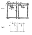
- the active matrix EL display device of this embodiment is constituted by a pixel portion 602, a gate side driving circuit 603, and a source side driving circuit 604 formed on a glass substrate 601.
- a switching TFT 605 of a pixel portion is an n-channel type TFT, and is disposed at an intersection point of a gate wiring line 606 connected to the gate side driving circuit 603 and a source wiring line 607 connected to the source side driving circuit 604.
- the drain of the switching TFT 605 is connected to the gate of a current control TFT 608.
- the source side of the current control TFT 608 is connected to the power supply line 609.
- the power supply line 609 is connected to the source of the EL element 610, and the drain of the current control TFT 608 is connected to the EL element 610.
- the current control TFT 608 is an n-channel type TFT, then a cathode of the EL element 610 is electrically connected to the drain. Further, in a case of using a p-channel type TFT for the current control TFT 608, an anode of the EL element 610 is electrically connected to the drain.
- Input/output wiring lines (connection wiring lines) 612 and 613 for transmitting signals to the driving circuits and a connection wiring line 614 connected to the current supply line 609 are provided in an FPC 611 as an external input/output terminal.
- the EL display device of this embodiment includes a source side driving circuit 701, a gate side driving circuit (A) 707, a gate side driving circuit (B) 711, and a pixel portion 706.
- the term driving circuit is a general term including the source side driving circuit and the gate side driving circuit.
- the source side driving circuit 701 is provided with a shift register 702, a level shifter 703, a buffer 704, and a sampling circuit (sample and hold circuit) 705.
- the gate side driving circuit (A) 707 is provided with a shift register 708, a level shifter 709, and a buffer 710.
- the gate side driving circuit (B) 711 also has the same structure.
- the shift registers 702 and 708 have driving voltages of 5 to 16 V (typically 10 V) respectively, and the structure indicated by 205 in Fig. 6C is suitable for an n-channel type TFT used in a CMOS circuit forming the circuit.
- the CMOS circuit including the n-channel type TFT 205 of Fig. 6C is suitable. Note that it is effective to make a gate wiring line a multi-gate structure such as a double gate structure or a triple gate structure in improving reliability of each circuit.
- CMOS circuit including the n-channel type TFT 208 of Fig. 10 is suitable for the sampling circuit 705.
- the pixel portion 706 is disposed with pixels having the structure shown in Fig. 2 .
- the foregoing structure can be easily realized by manufacturing TFTs in accordance with the manufacturing steps shown in Figs. 4A to 6C .
- this embodiment although only the structure of the pixel portion and the driving circuit is shown, if the manufacturing steps of this embodiment are used, it is possible to form a logical circuit other than the driving circuit, such as a signal dividing circuit, a D/A converter circuit, an operational amplifier circuit, a 5-correction circuit, or the like on the same substrate, and further, it is considered that a memory portion, a microprocessor, or the like can be formed.
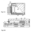
- EL display device in accordance with the present embodiment will be described with reference to Figs. 11A and 11B .
- the reference signs used in Figs. 7 and 8 are referred if necessary.
- a substrate 1000 (including an base film beneath TFTs) is an active matrix substrate.
- a pixel portion 1001, a source side driving circuit 1002, and a gate side driving circuit 1003 are formed on the substrate.
- Various wirings from the respective driving circuits are extended through connection wirings 612 to 614 to reach an FPC 611 and be connected to an external device.
- a counter substrate 1004 is provided to surround at least the pixel portion, and more preferably, the driving circuits and the pixel portion.
- the counter substrate 1004 is adhered to the active matrix substrate 1000 by means of an adhesive (sealing agent) 1005 to form a closed space 1006.
- an adhesive adhesive (sealing agent) 1005 to form a closed space 1006.
- a photocurable epoxy resin is used as the adhesive 1005.
- the adhesive 1005 can be applied by a coating device such as a dispenser.
- the closed space 1006 between the counter substrate 1004 and the active matrix substrate 1000 is filed with nitrogen gas.
- the counter substrate 1004 is provided on its inner side (on the side closer to the closed space) with a light shielding film 1007 and a color filter 1008, as described with reference to Figs. 1 and 2 .
- a resin film containing barium oxide and a black-colored pigment is used as the light shielding film 1007, and a resin film containing a red-colored, green-colored, or blue-colored pigment can be used as the color filter 1008.
- the pixel portion is provided with a plurality of pixels each including an individually separated EL element. All of these EL elements share an anode 1009 as a common electrode.
- the EL layer may be provided only in the pixel portion, but is not required to be disposed over the driving circuits.
- a vapor deposition method employing a shadow mask, a lift-off method, a dry etching method, or a laser scribing method can be used.
- connection wiring 1010 is a power supply line to be used for supplying a predetermined voltage to the anode 1009, and is connected to the FPC 611 through a conductive paste material 1011. Although only the connection wiring 1010 is described herein, the other connection wirings 612 to 614 are also electrically connected to the FPC 611 in the similar manner.
- the structure as shown in Figs. 11A and 11B can display an image on its pixel portion by connecting the FPC 611 to a terminal of an external device.
- the EL display device is defined as a product in which an image display becomes possible when an FPC is attached thereto, in other words, a product obtained by attaching an active matrix substrate to a counter substrate (including the one provided with an FPC attached thereto.)
- the structure of this embodiment can be easily realized in accordance with the manufacturing steps of the embodiment 1, and with respect to the TFT structure or the like, the description of the embodiment 1 or Fig. 2 may be referred to.
- the present invention is not limited to the TFT structure, and may be applied to a bottom gate type TFT (typically, inverted stagger type TFT).
- the inverted stagger type TFT may be formed by any means.
- the inverted stagger type TFT has such a structure that the number of steps can be easily made smaller than the top gate type TFT, it is very advantageous in reducing the manufacturing cost, which is the object of the present invention.
- the structure of this embodiment can be freely combined with any structure of the embodiments 2 and 3.
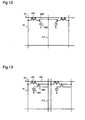
- Fig. 3B shows that the amount of the off current value in the switching TFT in the pixel of the EL display device is reduced by using a multi-gate structure for the switching TFT, and the need for a storage capacitor is eliminated.
- a structure of disposing a storage capacitor as is done conventionally.
- a storage capacitor 1301 is formed in parallel to the gate of the current control TFT 202 with respect to the drain of the switching TFT 201.
- a storage capacitor is merely formed within a pixel and it is not to limit the TFT structure, materials of EL layer, etc.
- Laser crystallization is used as the means of forming the crystalline silicon film 302 in embodiment 1, and a case of using a different means of crystallization is explained in embodiment 5.
- crystallization is performed using the technique recorded in Japanese Patent Application Laid-open No. Hei 7-130652 .
- the technique recorded in the above patent application is one of obtaining a crystalline silicon film having good crystallinity by using an element such as nickel as a catalyst for promoting crystallization.
- a process of removing the catalyst used in the crystallization may be performed.
- the catalyst may be gettered using the technique recorded in Japanese Patent Application Laid-open No. Hei 10-270363 or Japanese Patent Application Laid-open No. Hei 8-330602 .
- a TFT may be formed using the technique recorded in the specification of Japanese Patent Application No. Hei 11-076967 by the applicant of the present invention.
- analog driving can be performed using an analog signal as an image signal
- digital driving can be performed using a digital signal
- the analog signal When analog driving is performed, the analog signal is sent to a source wiring of a switching TFT, and the analog signal, which contains gray scale information, becomes the gate voltage of a current control TFT.
- the current flowing in an EL element is then controlled by the current control TFT, the EL element emitting intensity is controlled, and gray scale display is performed.
- gray scale display is performed by time division driving.
- the EL element has an extremely fast response speed in comparison to a liquid crystal element, and therefore it is possible to have high speed driving. Therefore, the EL element is one, which is suitable for time ratio gray scale driving, in which one frame is partitioned into a plural number of subframes and then gray scale display is performed.
- the EL display device uses light emitted from itself, and thus, does not require any back light.
- a reflection type liquid crystal display device requires a back light in a dark place where sufficient light is not available, although it has a feature in that an image can be displayed with outdoor light.
- the EL display device is not suffered from such a disadvantage in a dark place, since it is of the self-emission type.
- an electronic device including the EL display device as its display portion when actually used outdoors, it may be of course used both in a light place and in a dark place. In such a situation, an image can be sufficiently recognized in a dark place even when the luminance is not so high, while an image may not be recognized in a light place if the luminance is not sufficiently high.
- An amount of light emitted from the EL layer varies depending on an amount of current to flow.
- a larger amount of current to flow requires the higher luminance, resulting in an increased power consumption.
- the luminance of emitted light is set at such a high level, too brighter image than necessary with too large power consumption will be displayed in a dark place.
- the EL display device in accordance with the present invention preferably has a function to detect the lightness in the surrounding atmosphere by means of a sensor, and adjust the luminance of the light emitted from the EL layer in accordance with the sensed lightness. More specifically, the luminance of the emitted light is set at a high level in a light place, while at a low level in a dark place, so that an increase in power consumption is avoided.
- the EL display device in accordance with the present invention can realize reduction in power consumption.
- CMOS sensor As a sensor to be used for detecting lightness in the surrounding atmosphere, a CMOS sensor, a CCD or the like can be used.
- a CMOS sensor can be formed with any known technique on the identical substrate with driving circuits and a pixel portion of the EL display device.
- a semiconductor chip on which a CCD is formed can be attached onto the EL display device.
- a CCD or a CMOS sensor may be provided as a portion of an electronic device including the EL display device as its display portion.
- a circuit for adjusting a current to flow into the EL layer based on a signal obtained by the sensor for detecting the lightness in the surrounding atmosphere is provided.
- the luminance of the light emitted from the EL layer can be adjusted in accordance with the lightness in the surrounding atmosphere.
- the structure in the present embodiment is applicable in combination with any structure in Embodiment 1 through 6.
- the EL display device fabricated in accordance with the present invention is of the self-emission type, and thus exhibits more excellent recognizability of the displayed image in a light place as compared to the liquid crystal display device. Furthermore, the EL display device has a wider viewing angle. Accordingly, the EL display device can be applied to a display portion in various electronic devices. For example, in order to view a TV program or the like on a large-sized screen, the EL display device in accordance with the present invention can be used as a display portion of an EL display (i.e., a display in which an EL display device is installed into a frame) having a diagonal size of 30 inches or larger (typically 40 inches or larger.)
- the EL display includes all kinds of displays to be used for displaying information, such as a display for a personal computer, a display for receiving a TV broadcasting program, a display for advertisement display. Moreover, the EL display device in accordance with the present invention can be used as a display portion of other various electric devices.
- Such electronic devices include a video camera, a digital camera, a goggles-type display (head mount display), a car navigation system, a car audio equipment, note-size personal computer, a game machine, a portable information terminal (a mobile computer, a portable telephone, a portable game machine, an electronic book, or the like), an image reproduction apparatus including a recording medium (more specifically, an apparatus which can reproduce a recording medium such as a compact disc (CD), a laser disc (LD), a digital video disc (DVD), and includes a display for displaying the reproduced image), or the like.
- a recording medium more specifically, an apparatus which can reproduce a recording medium such as a compact disc (CD), a laser disc (LD), a digital video disc (DVD), and includes a display for displaying the reproduced image
- Figs. 14A to 14F respectively show various specific examples of such electronic devices.
- Fig. 14C illustrates a portion (the right-half piece) of an EL display of head mount type, which includes a main body 2201, signal cables 2202, a head mount band 2203, a display portion 2204, an optical system 2205, an EL display device 2206, or the like.
- the present invention is applicable to the EL display device 2206.
- Fig. 14E illustrates a portable (mobile) computer which includes a main body 2401, a camera portion 2402, an image receiving portion 2403, operation switches 2404, a display portion 2405, or the like.
- the EL display device in accordance with the present invention can be used as the display portion 2405.
- the EL display device in accordance with the present invention will be applicable to a front-type or rear-type projector in which light including output image information is enlarged by means of lenses or the like to be projected.
- the aforementioned electronic devices are more likely to be used for display information distributed through a telecommunication path such as Internet, a CATV (cable television system), and in particular likely to display moving picture information.
- the EL display device is suitable for displaying moving pictures since the EL material can exhibit high response speed.
- the contour between the pixels becomes unclear, the moving pictures as a whole cannot be clearly displayed. Since the EL display device in accordance with the present invention can make the contour between the pixels clear, it is significantly advantageous to apply the EL display device of the present invention to a display portion of the electronic devices.
- a portion of the EL display device that is emitting light consumes power, so it is desirable to display information in such a manner that the light emitting portion therein becomes as small as possible. Accordingly, when the EL display device is applied to a display portion which mainly displays character information, e.g., a display portion of a portable information terminal, and more particular, a portable telephone or a car audio equipment, it is desirable to drive the EL display device so that the character information is formed by a light-emitting portion while a non-emission portion corresponds to the background.
- character information e.g., a display portion of a portable information terminal, and more particular, a portable telephone or a car audio equipment
- a portable telephone which includes a main body 2601, an audio output portion 2602, an audio input portion 2603, a display portion 2604, operation switches 2605, and an antenna 2606.
- the EL display device in accordance with the present invention can be used as the display portion 2604.
- the display portion 2604 can reduce power consumption of the portable telephone by displaying white-colored characters on a black-colored background.
- Fig. 15B illustrates a car audio equipment which includes a main body 2701, a display portion 2702, and operation switches 2703 and 2704.
- the EL display device in accordance with the present invention can be used as the display portion 2702.
- the car audio equipment of the mount type is shown in the present embodiment, the present invention is also applicable to a car audio of the set type.
- the display portion 2702 can reduce power consumption by displaying white-colored characters on a black-colored background, which is particularly advantageous for the car audio of the set type.
- the present invention can be applied variously to a wide range of electronic devices in all fields.
- the electronic device in the present embodiment can be obtained by utilizing an EL display device having the configuration in which the structures in Embodiments 1 through 7 are freely combined.
- the contour between the pixels can be made clear, and the EL display device capable of displaying an image with high definition can be provided.
- the light shielding film to be used for concealing the gaps between the pixels is provided on the counter substrate, thereby preventing yield from decreasing.
- the EL display device in accordance with the present invention can be fabricated by using a manufacturing line for liquid crystal display devices, and thus, equipment investment can be suppressed to a small level. Accordingly, in accordance with the present invention, an inexpensive EL display device capable of displaying an image with high definition can be obtained.
- the present invention can also provide an electronic device having a display portion with a high recognizability by utilizing such an EL display device as the display portion.
Landscapes
- Engineering & Computer Science (AREA)
- Physics & Mathematics (AREA)
- Microelectronics & Electronic Packaging (AREA)
- Optics & Photonics (AREA)
- Manufacturing & Machinery (AREA)
- General Physics & Mathematics (AREA)
- Computer Hardware Design (AREA)
- Theoretical Computer Science (AREA)
- Geometry (AREA)
- Electroluminescent Light Sources (AREA)
- Devices For Indicating Variable Information By Combining Individual Elements (AREA)
- Thin Film Transistor (AREA)
- Control Of Indicators Other Than Cathode Ray Tubes (AREA)
- Control Of El Displays (AREA)
- Metal-Oxide And Bipolar Metal-Oxide Semiconductor Integrated Circuits (AREA)
Priority Applications (1)
| Application Number | Priority Date | Filing Date | Title |
|---|---|---|---|
| EP10177425.5A EP2259322B1 (en) | 1999-09-17 | 2000-09-07 | Electroluminescence display device |
Applications Claiming Priority (8)
| Application Number | Priority Date | Filing Date | Title |
|---|---|---|---|
| JP26467299 | 1999-09-17 | ||
| JP26468099 | 1999-09-17 | ||
| JP26467299 | 1999-09-17 | ||
| JP26468099 | 1999-09-17 | ||
| JP33624899 | 1999-11-26 | ||
| JP33624799 | 1999-11-26 | ||
| JP33624799 | 1999-11-26 | ||
| JP33624899 | 1999-11-26 |
Related Child Applications (2)
| Application Number | Title | Priority Date | Filing Date |
|---|---|---|---|
| EP10177425.5A Division EP2259322B1 (en) | 1999-09-17 | 2000-09-07 | Electroluminescence display device |
| EP10177425.5 Division-Into | 2010-09-17 |
Publications (3)
| Publication Number | Publication Date |
|---|---|
| EP1085576A2 EP1085576A2 (en) | 2001-03-21 |
| EP1085576A3 EP1085576A3 (en) | 2004-04-28 |
| EP1085576B1 true EP1085576B1 (en) | 2010-12-15 |
Family
ID=27478695
Family Applications (2)
| Application Number | Title | Priority Date | Filing Date |
|---|---|---|---|
| EP00119584A Expired - Lifetime EP1085576B1 (en) | 1999-09-17 | 2000-09-07 | El display device and method for manufacturing the same |
| EP10177425.5A Expired - Lifetime EP2259322B1 (en) | 1999-09-17 | 2000-09-07 | Electroluminescence display device |
Family Applications After (1)
| Application Number | Title | Priority Date | Filing Date |
|---|---|---|---|
| EP10177425.5A Expired - Lifetime EP2259322B1 (en) | 1999-09-17 | 2000-09-07 | Electroluminescence display device |
Country Status (7)
| Country | Link |
|---|---|
| US (10) | US6445005B1 (enExample) |
| EP (2) | EP1085576B1 (enExample) |
| JP (6) | JP2011071141A (enExample) |
| KR (2) | KR100788873B1 (enExample) |
| CN (2) | CN101266996B (enExample) |
| DE (1) | DE60045361D1 (enExample) |
| TW (2) | TW522453B (enExample) |
Families Citing this family (170)
| Publication number | Priority date | Publication date | Assignee | Title |
|---|---|---|---|---|
| TW522453B (en) | 1999-09-17 | 2003-03-01 | Semiconductor Energy Lab | Display device |
| JP3942770B2 (ja) | 1999-09-22 | 2007-07-11 | 株式会社半導体エネルギー研究所 | El表示装置及び電子装置 |
| JP2001092413A (ja) | 1999-09-24 | 2001-04-06 | Semiconductor Energy Lab Co Ltd | El表示装置および電子装置 |
| US6641933B1 (en) | 1999-09-24 | 2003-11-04 | Semiconductor Energy Laboratory Co., Ltd. | Light-emitting EL display device |
| US6876145B1 (en) * | 1999-09-30 | 2005-04-05 | Semiconductor Energy Laboratory Co., Ltd. | Organic electroluminescent display device |
| US6646287B1 (en) | 1999-11-19 | 2003-11-11 | Semiconductor Energy Laboratory Co., Ltd. | Semiconductor device with tapered gate and insulating film |
| TW511298B (en) * | 1999-12-15 | 2002-11-21 | Semiconductor Energy Lab | EL display device |
| TW494447B (en) | 2000-02-01 | 2002-07-11 | Semiconductor Energy Lab | Semiconductor device and manufacturing method thereof |
| US7579203B2 (en) | 2000-04-25 | 2009-08-25 | Semiconductor Energy Laboratory Co., Ltd. | Light emitting device |
| US6879110B2 (en) | 2000-07-27 | 2005-04-12 | Semiconductor Energy Laboratory Co., Ltd. | Method of driving display device |
| US6605826B2 (en) * | 2000-08-18 | 2003-08-12 | Semiconductor Energy Laboratory Co., Ltd. | Light-emitting device and display device |
| US7178927B2 (en) * | 2000-11-14 | 2007-02-20 | Semiconductor Energy Laboratory Co., Ltd. | Electroluminescent device having drying agent |
| US7222981B2 (en) | 2001-02-15 | 2007-05-29 | Semiconductor Energy Laboratory Co., Ltd. | EL display device and electronic device |
| US6822391B2 (en) * | 2001-02-21 | 2004-11-23 | Semiconductor Energy Laboratory Co., Ltd. | Light emitting device, electronic equipment, and method of manufacturing thereof |
| KR100495701B1 (ko) * | 2001-03-07 | 2005-06-14 | 삼성에스디아이 주식회사 | 유기 전계 발광 표시장치의 제조방법 |
| US6509941B2 (en) * | 2001-03-22 | 2003-01-21 | Eastman Kodak Company | Light-producing display having high aperture ratio pixels |
| TW546857B (en) * | 2001-07-03 | 2003-08-11 | Semiconductor Energy Lab | Light-emitting device, method of manufacturing a light-emitting device, and electronic equipment |
| JP4152665B2 (ja) | 2001-07-11 | 2008-09-17 | 株式会社半導体エネルギー研究所 | 発光装置及びその作製方法 |
| KR100448448B1 (ko) * | 2001-07-12 | 2004-09-13 | 주식회사 디알텍 | X선 센서용 스위칭소자 및 그 제조방법 |
| KR100600846B1 (ko) * | 2001-10-15 | 2006-07-14 | 삼성에스디아이 주식회사 | 액티브 매트릭스형 유기전계 발광표시소자 및 그의 제조방법 |
| US7365713B2 (en) | 2001-10-24 | 2008-04-29 | Semiconductor Energy Laboratory Co., Ltd. | Semiconductor device and driving method thereof |
| JP3724725B2 (ja) * | 2001-11-01 | 2005-12-07 | ソニー株式会社 | 表示装置の製造方法 |
| JP4149168B2 (ja) | 2001-11-09 | 2008-09-10 | 株式会社半導体エネルギー研究所 | 発光装置 |
| US7042024B2 (en) | 2001-11-09 | 2006-05-09 | Semiconductor Energy Laboratory Co., Ltd. | Light emitting apparatus and method for manufacturing the same |
| US6903377B2 (en) * | 2001-11-09 | 2005-06-07 | Semiconductor Energy Laboratory Co., Ltd. | Light emitting apparatus and method for manufacturing the same |
| JP2003234186A (ja) * | 2001-12-06 | 2003-08-22 | Sony Corp | 表示装置およびその製造方法 |
| CN1245703C (zh) * | 2001-12-11 | 2006-03-15 | 精工爱普生株式会社 | 显示装置及其电子机器 |
| TW591971B (en) * | 2001-12-11 | 2004-06-11 | Seiko Epson Corp | Display apparatus and electronic machine |
| JP3705264B2 (ja) * | 2001-12-18 | 2005-10-12 | セイコーエプソン株式会社 | 表示装置及び電子機器 |
| JP4101511B2 (ja) * | 2001-12-27 | 2008-06-18 | 株式会社半導体エネルギー研究所 | 発光装置及びその作製方法 |
| US6815723B2 (en) | 2001-12-28 | 2004-11-09 | Semiconductor Energy Laboratory Co., Ltd. | Light emitting device, method of manufacturing the same, and manufacturing apparatus therefor |
| KR100834342B1 (ko) * | 2001-12-29 | 2008-06-02 | 엘지디스플레이 주식회사 | 능동행렬 유기전기발광소자 및 그의 제조 방법 |
| US20030127972A1 (en) * | 2002-01-05 | 2003-07-10 | Cheng-Xian Han | Dual-panel active matrix organic electroluminscent display |
| US6909240B2 (en) * | 2002-01-18 | 2005-06-21 | Semiconductor Energy Laboratory Co., Ltd. | Light-emitting device |
| US7098069B2 (en) | 2002-01-24 | 2006-08-29 | Semiconductor Energy Laboratory Co., Ltd. | Light emitting device, method of preparing the same and device for fabricating the same |
| TWI258317B (en) * | 2002-01-25 | 2006-07-11 | Semiconductor Energy Lab | A display device and method for manufacturing thereof |
| JP3723507B2 (ja) * | 2002-01-29 | 2005-12-07 | 三洋電機株式会社 | 駆動回路 |
| TW200401944A (en) * | 2002-02-01 | 2004-02-01 | Seiko Epson Corp | Circuit substrate, electro-optical device and electronic appliances |
| WO2003069957A1 (en) * | 2002-02-12 | 2003-08-21 | Idemitsu Kosan Co., Ltd. | Organic el display and its production method |
| WO2003069652A2 (en) * | 2002-02-13 | 2003-08-21 | The Regents Of The University Of California | A multilayer structure to form an active matrix display having single crystalline drivers over a transmissive substrate |
| US6933520B2 (en) * | 2002-02-13 | 2005-08-23 | Semiconductor Energy Laboratory Co., Ltd. | Light emitting device |
| KR20030069707A (ko) | 2002-02-22 | 2003-08-27 | 엘지.필립스 엘시디 주식회사 | 유기전계발광 소자 및 그의 제조방법 |
| KR100426964B1 (ko) * | 2002-03-20 | 2004-04-13 | 엘지.필립스 엘시디 주식회사 | 유기전계발광 소자 및 그의 제조방법 |
| JP4046267B2 (ja) * | 2002-03-26 | 2008-02-13 | 株式会社半導体エネルギー研究所 | 表示装置 |
| US7579771B2 (en) | 2002-04-23 | 2009-08-25 | Semiconductor Energy Laboratory Co., Ltd. | Light emitting device and method of manufacturing the same |
| US7786496B2 (en) | 2002-04-24 | 2010-08-31 | Semiconductor Energy Laboratory Co., Ltd. | Semiconductor device and method of manufacturing same |
| KR100464864B1 (ko) * | 2002-04-25 | 2005-01-06 | 엘지.필립스 엘시디 주식회사 | 유기전계발광 소자 및 그의 제조방법 |
| JP2003317971A (ja) | 2002-04-26 | 2003-11-07 | Semiconductor Energy Lab Co Ltd | 発光装置およびその作製方法 |
| JP3986051B2 (ja) | 2002-04-30 | 2007-10-03 | 株式会社半導体エネルギー研究所 | 発光装置、電子機器 |
| JP2003332054A (ja) * | 2002-05-16 | 2003-11-21 | Bunwa Ko | 冷光片の製造方法 |
| US7474045B2 (en) * | 2002-05-17 | 2009-01-06 | Semiconductor Energy Laboratory Co., Ltd. | Display device having TFT with radiation-absorbing film |
| US6882106B2 (en) * | 2002-05-24 | 2005-04-19 | Wen-Hao Kao | Electroluminescent display device |
| US7897979B2 (en) | 2002-06-07 | 2011-03-01 | Semiconductor Energy Laboratory Co., Ltd. | Light emitting device and manufacturing method thereof |
| US6563134B1 (en) * | 2002-06-14 | 2003-05-13 | Taiwan Semiconductor Manufacturing Co., Ltd | Optoelectronic microelectronic fabrication with attenuated light leakage |
| JP4216008B2 (ja) | 2002-06-27 | 2009-01-28 | 株式会社半導体エネルギー研究所 | 発光装置およびその作製方法、ならびに前記発光装置を有するビデオカメラ、デジタルカメラ、ゴーグル型ディスプレイ、カーナビゲーション、パーソナルコンピュータ、dvdプレーヤー、電子遊技機器、または携帯情報端末 |
| JP3864863B2 (ja) * | 2002-07-10 | 2007-01-10 | 株式会社豊田自動織機 | カラー表示装置 |
| US7081704B2 (en) | 2002-08-09 | 2006-07-25 | Semiconductor Energy Laboratory Co., Ltd. | Semiconductor device and manufacturing method thereof |
| KR100478759B1 (ko) * | 2002-08-20 | 2005-03-24 | 엘지.필립스 엘시디 주식회사 | 유기전계 발광소자와 그 제조방법 |
| KR100479770B1 (ko) | 2002-08-29 | 2005-04-06 | 엘지.필립스 엘시디 주식회사 | 오프스트레스에 의한 전계효과트랜지스터의 오프전류 감소방법 및 시스템 |
| JP2004119016A (ja) * | 2002-09-20 | 2004-04-15 | Semiconductor Energy Lab Co Ltd | 発光装置 |
| JP2004119015A (ja) * | 2002-09-20 | 2004-04-15 | Semiconductor Energy Lab Co Ltd | 発光装置およびその作製方法 |
| US7936338B2 (en) * | 2002-10-01 | 2011-05-03 | Sony Corporation | Display unit and its manufacturing method |
| JPWO2004036960A1 (ja) * | 2002-10-16 | 2006-02-16 | 出光興産株式会社 | 有機エレクトロルミネッセンス表示装置及びその製造方法 |
| AU2003275614A1 (en) | 2002-10-30 | 2004-05-25 | Semiconductor Energy Laboratory Co., Ltd. | Semiconductor device and method for manufacturing semiconductor device |
| KR100915233B1 (ko) * | 2002-11-05 | 2009-09-02 | 삼성전자주식회사 | 박막 트랜지스터 어레이 기판 |
| US20040099926A1 (en) * | 2002-11-22 | 2004-05-27 | Semiconductor Energy Laboratory Co., Ltd. | Semiconductor device, display device, and light-emitting device, and methods of manufacturing the same |
| KR100484092B1 (ko) | 2002-12-26 | 2005-04-18 | 엘지.필립스 엘시디 주식회사 | 듀얼패널타입 유기전계발광 소자 및 그 제조방법 |
| JP4373086B2 (ja) | 2002-12-27 | 2009-11-25 | 株式会社半導体エネルギー研究所 | 発光装置 |
| US7652359B2 (en) * | 2002-12-27 | 2010-01-26 | Semiconductor Energy Laboratory Co., Ltd. | Article having display device |
| US6936960B2 (en) * | 2003-01-10 | 2005-08-30 | Eastman Kodak Company | OLED displays having improved contrast |
| EP2326143B1 (en) | 2003-01-24 | 2013-04-24 | Semiconductor Energy Laboratory Co., Ltd. | Electronic book |
| US20040227197A1 (en) * | 2003-02-28 | 2004-11-18 | Shinji Maekawa | Composition of carbon nitride, thin film transistor with the composition of carbon nitride, display device with the thin film transistor, and manufacturing method thereof |
| JP4531342B2 (ja) * | 2003-03-17 | 2010-08-25 | 株式会社半導体エネルギー研究所 | 白色有機発光素子および発光装置 |
| JP2004296353A (ja) * | 2003-03-27 | 2004-10-21 | Seiko Epson Corp | 電気光学装置及びその製造方法並びに表示装置 |
| US6861669B2 (en) * | 2003-03-31 | 2005-03-01 | Agilent Technologies, Inc. | Compound display |
| TWI363574B (en) * | 2003-04-07 | 2012-05-01 | Semiconductor Energy Lab | Electronic apparatus |
| US7862906B2 (en) * | 2003-04-09 | 2011-01-04 | Semiconductor Energy Laboratory Co., Ltd. | Electroluminescent element and light-emitting device |
| JP2004327634A (ja) * | 2003-04-23 | 2004-11-18 | Semiconductor Energy Lab Co Ltd | レーザ発振器 |
| CN100413085C (zh) * | 2003-04-24 | 2008-08-20 | 统宝光电股份有限公司 | 上发光型全彩有机发光显示器结构 |
| JP4428979B2 (ja) * | 2003-09-30 | 2010-03-10 | 三洋電機株式会社 | 有機elパネル |
| JP4497881B2 (ja) * | 2003-09-30 | 2010-07-07 | 三洋電機株式会社 | 有機el素子および有機elパネル |
| JP4716699B2 (ja) * | 2003-09-30 | 2011-07-06 | 三洋電機株式会社 | 有機elパネル |
| US7541734B2 (en) * | 2003-10-03 | 2009-06-02 | Semiconductor Energy Laboratory Co., Ltd. | Light emitting device having a layer with a metal oxide and a benzoxazole derivative |
| KR100552975B1 (ko) * | 2003-11-22 | 2006-02-15 | 삼성에스디아이 주식회사 | 능동 매트릭스 유기전계발광표시장치 및 그의 제조방법 |
| US7893438B2 (en) * | 2003-10-16 | 2011-02-22 | Samsung Mobile Display Co., Ltd. | Organic light-emitting display device including a planarization pattern and method for manufacturing the same |
| US7229900B2 (en) | 2003-10-28 | 2007-06-12 | Semiconductor Energy Laboratory Co., Ltd. | Semiconductor device, method of manufacturing thereof, and method of manufacturing base material |
| CN100489569C (zh) | 2003-10-28 | 2009-05-20 | 株式会社半导体能源研究所 | 制作光学膜的方法 |
| US7453531B2 (en) * | 2003-11-22 | 2008-11-18 | Lg Display Co., Ltd. | LCD driving device having plural TFT channels connected in parallel with either increasing channel widths or decreasing channel distances from central part to edges of the device |
| TWI250823B (en) * | 2003-11-26 | 2006-03-01 | Rohm Co Ltd | D/A converter circuit, organic EL drive circuit and organic EL display device |
| KR101061730B1 (ko) | 2003-11-28 | 2011-09-05 | 가부시키가이샤 한도오따이 에네루기 켄큐쇼 | 발광 장치 및 그 제조 방법 |
| KR101095293B1 (ko) | 2003-11-28 | 2011-12-16 | 가부시키가이샤 한도오따이 에네루기 켄큐쇼 | 표시 장치 제조 방법 |
| JP4475942B2 (ja) * | 2003-12-26 | 2010-06-09 | 三洋電機株式会社 | 表示装置及びその製造方法 |
| JP4439260B2 (ja) * | 2003-12-26 | 2010-03-24 | 三洋電機株式会社 | 表示装置の製造方法 |
| JP2005197009A (ja) * | 2003-12-26 | 2005-07-21 | Sanyo Electric Co Ltd | 表示装置及びその製造方法及び製造装置 |
| KR100595456B1 (ko) * | 2003-12-29 | 2006-06-30 | 엘지.필립스 엘시디 주식회사 | 액정표시소자의 제조방법 |
| JP4286216B2 (ja) * | 2004-03-24 | 2009-06-24 | 三洋電機株式会社 | 発光表示装置 |
| US7202504B2 (en) * | 2004-05-20 | 2007-04-10 | Semiconductor Energy Laboratory Co., Ltd. | Light-emitting element and display device |
| TWI272039B (en) * | 2004-06-18 | 2007-01-21 | Sanyo Electric Co | Electroluminescence panel |
| KR100615236B1 (ko) * | 2004-08-05 | 2006-08-25 | 삼성에스디아이 주식회사 | 박막 트랜지스터 및 이를 구비한 평판 디스플레이 장치 |
| JP2006058332A (ja) * | 2004-08-17 | 2006-03-02 | Seiko Epson Corp | 電気光学装置及び電子機器 |
| US7365494B2 (en) * | 2004-12-03 | 2008-04-29 | Semiconductor Energy Laboratory Co., Ltd. | Display device and manufacturing method thereof |
| JP4272142B2 (ja) * | 2004-12-07 | 2009-06-03 | 株式会社ルネサステクノロジ | スイッチング素子並びにそれを用いたアンテナスイッチ回路及び高周波モジュール |
| CN100455153C (zh) * | 2004-12-24 | 2009-01-21 | 中华映管股份有限公司 | 有机电致发光显示器及其制造方法 |
| US8633473B2 (en) | 2004-12-28 | 2014-01-21 | Semiconductor Energy Laboratory Co., Ltd. | High contrast light emitting device and method for manufacturing the same |
| US7948171B2 (en) * | 2005-02-18 | 2011-05-24 | Semiconductor Energy Laboratory Co., Ltd. | Light emitting device |
| JP4573672B2 (ja) | 2005-02-28 | 2010-11-04 | 三洋電機株式会社 | 有機elパネル |
| TWI254594B (en) * | 2005-03-17 | 2006-05-01 | Ind Tech Res Inst | Color organic light-emitting display and manufacturing process thereof |
| US20060290276A1 (en) * | 2005-06-22 | 2006-12-28 | Eastman Kodak Company | OLED device having spacers |
| US7531959B2 (en) * | 2005-06-29 | 2009-05-12 | Eastman Kodak Company | White light tandem OLED display with filters |
| EP1793264A1 (en) * | 2005-12-05 | 2007-06-06 | Semiconductor Energy Laboratory Co., Ltd. | Liquid crystal display device |
| KR100771607B1 (ko) * | 2005-12-21 | 2007-10-31 | 엘지전자 주식회사 | 유기 el 디스플레이 |
| WO2007072766A1 (en) * | 2005-12-22 | 2007-06-28 | Semiconductor Energy Laboratory Co., Ltd. | Display device |
| EP1804114B1 (en) * | 2005-12-28 | 2014-03-05 | Semiconductor Energy Laboratory Co., Ltd. | Display device |
| KR101424784B1 (ko) | 2006-01-10 | 2014-07-31 | 가부시키가이샤 한도오따이 에네루기 켄큐쇼 | 표시장치 및 그의 제조방법 |
| EP1832915B1 (en) * | 2006-01-31 | 2012-04-18 | Semiconductor Energy Laboratory Co., Ltd. | Display device with improved contrast |
| EP1816508A1 (en) | 2006-02-02 | 2007-08-08 | Semiconductor Energy Laboratory Co., Ltd. | Display device |
| US7919855B2 (en) * | 2006-02-21 | 2011-04-05 | Lockheed Martin | Topside thermal management of semiconductor devices using boron phosphide contacting a gate terminal |
| EP1826605A1 (en) * | 2006-02-24 | 2007-08-29 | Semiconductor Energy Laboratory Co., Ltd. | Display device |
| EP1826606B1 (en) | 2006-02-24 | 2012-12-26 | Semiconductor Energy Laboratory Co., Ltd. | Display device |
| US7659664B2 (en) * | 2006-05-30 | 2010-02-09 | Tpo Displays Corp. | System for displaying image |
| US7528448B2 (en) * | 2006-07-17 | 2009-05-05 | E.I. Du Pont De Nemours And Company | Thin film transistor comprising novel conductor and dielectric compositions |
| US7994021B2 (en) * | 2006-07-28 | 2011-08-09 | Semiconductor Energy Laboratory Co., Ltd. | Method of manufacturing semiconductor device |
| US7943287B2 (en) * | 2006-07-28 | 2011-05-17 | Semiconductor Energy Laboratory Co., Ltd. | Method for manufacturing display device |
| WO2008023630A1 (en) | 2006-08-24 | 2008-02-28 | Semiconductor Energy Laboratory Co., Ltd. | Method for manufacturing display device |
| US8563431B2 (en) * | 2006-08-25 | 2013-10-22 | Semiconductor Energy Laboratory Co., Ltd. | Method for manufacturing semiconductor device |
| US7795154B2 (en) | 2006-08-25 | 2010-09-14 | Semiconductor Energy Laboratory Co., Ltd. | Method for manufacturing semiconductor device that uses laser ablation, to selectively remove one or more material layers |
| US7651896B2 (en) * | 2006-08-30 | 2010-01-26 | Semiconductor Energy Laboratory Co., Ltd. | Method for manufacturing semiconductor device |
| JP5110830B2 (ja) * | 2006-08-31 | 2012-12-26 | 株式会社半導体エネルギー研究所 | 半導体装置の作製方法 |
| US7988057B2 (en) * | 2006-11-28 | 2011-08-02 | Semiconductor Energy Laboratory Co., Ltd. | Memory device and semiconductor device |
| JP4978997B2 (ja) * | 2006-12-25 | 2012-07-18 | 株式会社ジャパンディスプレイイースト | 表示装置の製造方法 |
| US7960261B2 (en) * | 2007-03-23 | 2011-06-14 | Semiconductor Energy Laboratory Co., Ltd. | Method for manufacturing crystalline semiconductor film and method for manufacturing thin film transistor |
| US8513678B2 (en) * | 2007-05-18 | 2013-08-20 | Semiconductor Energy Laboratory Co., Ltd. | Light-emitting device |
| US20090001360A1 (en) * | 2007-06-29 | 2009-01-01 | Masaya Nakayama | Organic el display and method for producing the same |
| GB0807767D0 (en) * | 2008-04-29 | 2008-06-04 | Plastic Logic Ltd | Off-set top pixel electrode configuration |
| KR102383642B1 (ko) | 2008-07-10 | 2022-04-08 | 가부시키가이샤 한도오따이 에네루기 켄큐쇼 | 발광장치 및 전자기기 |
| KR20100037876A (ko) * | 2008-10-02 | 2010-04-12 | 삼성전자주식회사 | 유기발광 표시장치 및 이의 제조방법 |
| CN102549638B (zh) * | 2009-10-09 | 2015-04-01 | 株式会社半导体能源研究所 | 发光显示器件以及包括该发光显示器件的电子设备 |
| EP2513966B1 (en) * | 2009-12-18 | 2020-09-16 | Semiconductor Energy Laboratory Co., Ltd. | Semiconductor device |
| KR101135539B1 (ko) * | 2010-03-05 | 2012-04-13 | 삼성모바일디스플레이주식회사 | 유기 발광 표시 장치 |
| KR20120026970A (ko) | 2010-09-10 | 2012-03-20 | 가부시키가이샤 한도오따이 에네루기 켄큐쇼 | 반도체 장치 및 발광 장치 |
| US8884509B2 (en) | 2011-03-02 | 2014-11-11 | Semiconductor Energy Laboratory Co., Ltd. | Optical device, display device, and lighting device |
| JP5720887B2 (ja) * | 2011-03-30 | 2015-05-20 | ソニー株式会社 | 表示装置および電子機器 |
| US9030837B2 (en) | 2011-06-10 | 2015-05-12 | Scott Moncrieff | Injection molded control panel with in-molded decorated plastic film that includes an internal connector |
| TW201316109A (zh) * | 2011-10-05 | 2013-04-16 | Chunghwa Picture Tubes Ltd | 反射式電泳顯示裝置之畫素結構及其製作方法 |
| KR101924996B1 (ko) | 2012-03-29 | 2018-12-05 | 삼성디스플레이 주식회사 | 유기 발광 표시 장치 |
| KR102082793B1 (ko) | 2012-05-10 | 2020-02-28 | 가부시키가이샤 한도오따이 에네루기 켄큐쇼 | 표시 장치 및 그 제작 방법 |
| JP2014067522A (ja) * | 2012-09-25 | 2014-04-17 | Toshiba Corp | 表示装置およびその製造方法 |
| CN103907190B (zh) | 2012-10-16 | 2017-05-17 | 深圳市柔宇科技有限公司 | 一种oled拼接显示屏及其制造方法 |
| KR102000642B1 (ko) * | 2012-12-12 | 2019-07-17 | 엘지디스플레이 주식회사 | 고 휘도 유기발광 다이오드 표시장치 |
| KR102092842B1 (ko) * | 2013-08-07 | 2020-04-16 | 삼성디스플레이 주식회사 | 표시 패널 및 이의 제조 방법 |
| CN103500754B (zh) | 2013-09-29 | 2016-11-02 | 京东方科技集团股份有限公司 | Oled显示面板及其制作方法、显示装置 |
| TWI642170B (zh) | 2013-10-18 | 2018-11-21 | 半導體能源研究所股份有限公司 | 顯示裝置及電子裝置 |
| JP2015128003A (ja) | 2013-12-27 | 2015-07-09 | ソニー株式会社 | 表示装置および電子機器 |
| KR102138906B1 (ko) * | 2013-12-30 | 2020-07-28 | 엘지디스플레이 주식회사 | 백색 유기발광 소자 및 컬러 필터를 이용한 유기발광 표시장치 |
| US9349768B2 (en) * | 2014-03-28 | 2016-05-24 | Taiwan Semiconductor Manufacturing Company, Ltd. | CMOS image sensor with epitaxial passivation layer |
| KR20150131522A (ko) * | 2014-05-15 | 2015-11-25 | 엘지디스플레이 주식회사 | 유기 발광 표시 소자 디스플레이 패널 |
| KR102239842B1 (ko) * | 2014-07-30 | 2021-04-14 | 삼성디스플레이 주식회사 | 유기 발광 표시 장치 |
| KR102397799B1 (ko) * | 2015-06-30 | 2022-05-16 | 엘지디스플레이 주식회사 | 박막 트랜지스터 기판 및 이를 포함하는 표시장치 |
| CN105118844A (zh) * | 2015-07-01 | 2015-12-02 | 深圳市华星光电技术有限公司 | 一种柔性显示面板的制备方法及柔性显示面板 |
| CN108141554B (zh) * | 2015-09-30 | 2021-02-09 | 株式会社尼康 | 拍摄元件、拍摄装置及电子设备 |
| KR102554963B1 (ko) * | 2015-10-29 | 2023-07-11 | 엘지디스플레이 주식회사 | 유기 발광 표시 장치 |
| JP6299783B2 (ja) * | 2016-02-15 | 2018-03-28 | セイコーエプソン株式会社 | 電気光学装置、および電子機器 |
| JP6715708B2 (ja) * | 2016-07-08 | 2020-07-01 | 株式会社ジャパンディスプレイ | 表示装置 |
| US11006489B2 (en) * | 2017-02-02 | 2021-05-11 | Pioneer Corporation | Optical device |
| JP6504206B2 (ja) | 2017-06-30 | 2019-04-24 | セイコーエプソン株式会社 | 電気光学装置、および電子機器 |
| CN107369700B (zh) * | 2017-07-13 | 2020-01-07 | 京东方科技集团股份有限公司 | 一种阵列基板、其制备方法、显示面板及显示装置 |
| KR102490896B1 (ko) * | 2018-01-17 | 2023-01-25 | 삼성디스플레이 주식회사 | 유기발광 표시 장치 |
| JP7117974B2 (ja) * | 2018-10-30 | 2022-08-15 | キヤノン株式会社 | 表示装置および電子機器 |
| KR102063314B1 (ko) * | 2018-11-28 | 2020-01-08 | 삼성디스플레이 주식회사 | 유기 발광 표시 장치 |
| KR20230102392A (ko) * | 2021-12-30 | 2023-07-07 | 엘지디스플레이 주식회사 | 표시장치 |
Citations (1)
| Publication number | Priority date | Publication date | Assignee | Title |
|---|---|---|---|---|
| JPS6196695A (ja) * | 1984-10-18 | 1986-05-15 | 松下電器産業株式会社 | Elパネル |
Family Cites Families (115)
| Publication number | Priority date | Publication date | Assignee | Title |
|---|---|---|---|---|
| US4357557A (en) * | 1979-03-16 | 1982-11-02 | Sharp Kabushiki Kaisha | Glass sealed thin-film electroluminescent display panel free of moisture and the fabrication method thereof |
| JPS5955487A (ja) * | 1982-09-25 | 1984-03-30 | 日本精機株式会社 | 電界発光表示素子 |
| JPS61224290A (ja) * | 1985-03-28 | 1986-10-04 | シャープ株式会社 | 薄膜el素子 |
| JPS6290260A (ja) | 1985-10-16 | 1987-04-24 | Tdk Corp | サ−マルヘツド用耐摩耗性保護膜 |
| JPS62290096A (ja) * | 1986-05-23 | 1987-12-16 | 株式会社小松製作所 | 薄膜el素子 |
| FI891288L (fi) * | 1986-09-19 | 1989-03-17 | Komatsu Mfg Co Ltd | Tunnskikt-el-apparat. |
| JP2620240B2 (ja) * | 1987-06-10 | 1997-06-11 | 株式会社日立製作所 | 液晶表示装置 |
| JP2742057B2 (ja) | 1988-07-14 | 1998-04-22 | シャープ株式会社 | 薄膜elパネル |
| DE68920702T2 (de) * | 1988-11-10 | 1995-06-14 | Toshiba Kawasaki Kk | Flüssigkristall-Anzeigevorrichtung, Farbfilter hierfür und Verfahren zur Herstellung des Farbfilters. |
| US5189405A (en) | 1989-01-26 | 1993-02-23 | Sharp Kabushiki Kaisha | Thin film electroluminescent panel |
| JPH032592U (enExample) | 1989-05-26 | 1991-01-11 | ||
| JPH032592A (ja) | 1989-05-30 | 1991-01-08 | Wataru Yamamoto | 時計 |
| JPH0329291A (ja) | 1989-06-27 | 1991-02-07 | Sumitomo Bakelite Co Ltd | 有機分散型elランプ用捕水フィルム |
| US5402254B1 (en) * | 1990-10-17 | 1998-09-22 | Hitachi Ltd | Liquid crystal display device with tfts in which pixel electrodes are formed in the same plane as the gate electrodes with anodized oxide films before the deposition of silicon |
| US5206749A (en) * | 1990-12-31 | 1993-04-27 | Kopin Corporation | Liquid crystal display having essentially single crystal transistors pixels and driving circuits |
| JP3197305B2 (ja) | 1991-10-08 | 2001-08-13 | ティーディーケイ株式会社 | 電界発光素子の保護 |
| JP2784615B2 (ja) * | 1991-10-16 | 1998-08-06 | 株式会社半導体エネルギー研究所 | 電気光学表示装置およびその駆動方法 |
| JPH05241201A (ja) | 1992-03-02 | 1993-09-21 | Sony Corp | 垂直駆動回路 |
| JPH08501887A (ja) * | 1992-09-11 | 1996-02-27 | コピン・コーポレーシヨン | ディスプレイ・パネルのためのカラーフィルター・システム |
| US5859627A (en) * | 1992-10-19 | 1999-01-12 | Fujitsu Limited | Driving circuit for liquid-crystal display device |
| EP1463028A2 (en) * | 1993-04-22 | 2004-09-29 | Matsushita Electric Industrial Co., Ltd. | Display device and projection-type display apparatus using the device |
| JP2677167B2 (ja) * | 1993-07-08 | 1997-11-17 | 日本電気株式会社 | 駆動回路内蔵型液晶表示装置の製造方法 |
| US5923962A (en) | 1993-10-29 | 1999-07-13 | Semiconductor Energy Laboratory Co., Ltd. | Method for manufacturing a semiconductor device |
| JP3431033B2 (ja) | 1993-10-29 | 2003-07-28 | 株式会社半導体エネルギー研究所 | 半導体作製方法 |
| TW264575B (enExample) | 1993-10-29 | 1995-12-01 | Handotai Energy Kenkyusho Kk | |
| JP3170542B2 (ja) | 1993-12-08 | 2001-05-28 | 出光興産株式会社 | 有機el素子 |
| JPH07220871A (ja) | 1994-01-28 | 1995-08-18 | Res Dev Corp Of Japan | 有機エレクトロルミネッセンスデバイス |
| JPH07249766A (ja) * | 1994-03-10 | 1995-09-26 | Fujitsu Ltd | 半導体装置及びその製造方法 |
| JP2839133B2 (ja) * | 1994-03-31 | 1998-12-16 | キヤノン株式会社 | カラーフィルタの製造方法及び製造装置及び液晶表示装置の製造方法及び液晶表示装置を備えた装置の製造方法 |
| US5617228A (en) * | 1994-07-13 | 1997-04-01 | Kabushiki Kaisha Toshiba | Polymer-dispersed liquid crystal display device and method to set liquid crystal layer thickness in association with driving voltage |
| JP3715996B2 (ja) * | 1994-07-29 | 2005-11-16 | 株式会社日立製作所 | 液晶表示装置 |
| US5962962A (en) | 1994-09-08 | 1999-10-05 | Idemitsu Kosan Co., Ltd. | Method of encapsulating organic electroluminescence device and organic electroluminescence device |
| JPH0875908A (ja) * | 1994-09-08 | 1996-03-22 | Nippon Sheet Glass Co Ltd | 光学的2次元画像伝送装置 |
| JP3372671B2 (ja) * | 1994-09-14 | 2003-02-04 | キヤノン株式会社 | カラーフィルタの製造方法及び製造装置 |
| JPH0896959A (ja) | 1994-09-27 | 1996-04-12 | Sumitomo Electric Ind Ltd | 有機エレクトロルミネッセンス素子 |
| JP3240858B2 (ja) * | 1994-10-19 | 2001-12-25 | ソニー株式会社 | カラー表示装置 |
| JPH08234018A (ja) | 1994-11-18 | 1996-09-13 | Semiconductor Energy Lab Co Ltd | 表示装置用光学機能手段及びその作製方法及びその作 製装置 |
| US5550066A (en) * | 1994-12-14 | 1996-08-27 | Eastman Kodak Company | Method of fabricating a TFT-EL pixel |
| JPH08213169A (ja) * | 1995-02-01 | 1996-08-20 | Fuji Electric Co Ltd | 薄膜電場発光素子 |
| DE69623443T2 (de) | 1995-02-06 | 2003-01-23 | Idemitsu Kosan Co | Vielfarbige lichtemissionsvorrichtung und verfahren zur herstellung derselben |
| JP3962436B2 (ja) | 1995-02-14 | 2007-08-22 | 出光興産株式会社 | 多色発光装置 |
| TW345654B (en) * | 1995-02-15 | 1998-11-21 | Handotai Energy Kenkyusho Kk | Active matrix display device |
| TW344901B (en) * | 1995-02-15 | 1998-11-11 | Handotai Energy Kenkyusho Kk | Active matrix display device |
| JP3539821B2 (ja) | 1995-03-27 | 2004-07-07 | 株式会社半導体エネルギー研究所 | 半導体装置の作製方法 |
| KR19990007825A (ko) | 1995-04-25 | 1999-01-25 | 하루타히로시 | 유기 전계 발광 장치 |
| US5771562A (en) | 1995-05-02 | 1998-06-30 | Motorola, Inc. | Passivation of organic devices |
| JPH08321380A (ja) * | 1995-05-25 | 1996-12-03 | Chisso Corp | 有機電界発光素子 |
| JPH0963770A (ja) | 1995-08-24 | 1997-03-07 | Kemipuro Kasei Kk | 単層型白色発光有機el素子 |
| JPH09134781A (ja) * | 1995-11-09 | 1997-05-20 | Sharp Corp | 薄膜エレクトロルミネッセンスパネルおよびその製造方法 |
| JPH09148066A (ja) * | 1995-11-24 | 1997-06-06 | Pioneer Electron Corp | 有機el素子 |
| US5811177A (en) | 1995-11-30 | 1998-09-22 | Motorola, Inc. | Passivation of electroluminescent organic devices |
| US5686360A (en) | 1995-11-30 | 1997-11-11 | Motorola | Passivation of organic devices |
| JP3647542B2 (ja) * | 1996-02-20 | 2005-05-11 | 株式会社半導体エネルギー研究所 | 液晶表示装置 |
| WO1997031508A1 (en) | 1996-02-26 | 1997-08-28 | Idemitsu Kosan Co., Ltd. | Organic electroluminescent element and method for manufacturing the same |
| US5693956A (en) | 1996-07-29 | 1997-12-02 | Motorola | Inverted oleds on hard plastic substrate |
| JPH10104606A (ja) * | 1996-09-27 | 1998-04-24 | Toray Ind Inc | 液晶表示装置 |
| JPH10107266A (ja) | 1996-09-27 | 1998-04-24 | New Japan Radio Co Ltd | Mos型fetの製造方法 |
| JP4022274B2 (ja) | 1996-10-14 | 2007-12-12 | 出光興産株式会社 | 有機el発光装置 |
| JPH10162952A (ja) | 1996-11-27 | 1998-06-19 | Sharp Corp | 薄膜elパネル及びその製造方法 |
| JP3457819B2 (ja) * | 1996-11-28 | 2003-10-20 | カシオ計算機株式会社 | 表示装置 |
| DE69739633D1 (de) * | 1996-11-28 | 2009-12-10 | Casio Computer Co Ltd | Anzeigevorrichtung |
| JPH10162958A (ja) | 1996-11-28 | 1998-06-19 | Casio Comput Co Ltd | El素子 |
| JPH10161563A (ja) * | 1996-11-29 | 1998-06-19 | Tdk Corp | 有機el表示装置 |
| JP3392672B2 (ja) * | 1996-11-29 | 2003-03-31 | 三洋電機株式会社 | 表示装置 |
| JPH10172762A (ja) * | 1996-12-11 | 1998-06-26 | Sanyo Electric Co Ltd | エレクトロルミネッセンス素子を用いた表示装置の製造方法及び表示装置 |
| JP3463971B2 (ja) | 1996-12-26 | 2003-11-05 | 出光興産株式会社 | 有機アクティブel発光装置 |
| JP3453488B2 (ja) * | 1996-12-27 | 2003-10-06 | キヤノン株式会社 | 照明装置及びこれを用いた画像読み取り装置 |
| US5869929A (en) * | 1997-02-04 | 1999-02-09 | Idemitsu Kosan Co., Ltd. | Multicolor luminescent device |
| US6049167A (en) | 1997-02-17 | 2000-04-11 | Tdk Corporation | Organic electroluminescent display device, and method and system for making the same |
| JPH10241857A (ja) * | 1997-02-24 | 1998-09-11 | Fuji Electric Co Ltd | 薄膜電場発光素子の製造方法 |
| JPH10247587A (ja) * | 1997-02-28 | 1998-09-14 | Tdk Corp | 有機エレクトロルミネッセンス表示装置およびその製造方法 |
| JP3641342B2 (ja) * | 1997-03-07 | 2005-04-20 | Tdk株式会社 | 半導体装置及び有機elディスプレイ装置 |
| JP3524711B2 (ja) | 1997-03-18 | 2004-05-10 | 三洋電機株式会社 | 有機エレクトロルミネッセンス素子及びその製造方法 |
| US5952778A (en) | 1997-03-18 | 1999-09-14 | International Business Machines Corporation | Encapsulated organic light emitting device |
| JP3544280B2 (ja) | 1997-03-27 | 2004-07-21 | 株式会社半導体エネルギー研究所 | 半導体装置の作製方法 |
| JPH10289784A (ja) * | 1997-04-14 | 1998-10-27 | Mitsubishi Chem Corp | 有機電界発光素子 |
| JP3290375B2 (ja) | 1997-05-12 | 2002-06-10 | 松下電器産業株式会社 | 有機電界発光素子 |
| JPH10319910A (ja) * | 1997-05-15 | 1998-12-04 | Tdk Corp | 有機elディスプレイの駆動装置 |
| JP3566028B2 (ja) * | 1997-05-15 | 2004-09-15 | シャープ株式会社 | 液晶表示装置及びその製造方法 |
| JP3530341B2 (ja) * | 1997-05-16 | 2004-05-24 | Tdk株式会社 | 画像表示装置 |
| JP3269787B2 (ja) * | 1997-05-27 | 2002-04-02 | シャープ株式会社 | 液晶表示装置 |
| US5920080A (en) * | 1997-06-23 | 1999-07-06 | Fed Corporation | Emissive display using organic light emitting diodes |
| JP3304287B2 (ja) | 1997-06-30 | 2002-07-22 | 出光興産株式会社 | 有機el多色発光表示装置 |
| JPH1126155A (ja) | 1997-06-30 | 1999-01-29 | Mitsui Chem Inc | エレクトロルミネッセンス素子用保護フィルム |
| US6198220B1 (en) | 1997-07-11 | 2001-03-06 | Emagin Corporation | Sealing structure for organic light emitting devices |
| JPH1140346A (ja) * | 1997-07-22 | 1999-02-12 | Pioneer Electron Corp | 有機エレクトロルミネセンス表示装置 |
| JPH1154273A (ja) * | 1997-08-01 | 1999-02-26 | Idemitsu Kosan Co Ltd | 色変換フィルタおよびその製造方法 |
| CN1155930C (zh) * | 1997-08-21 | 2004-06-30 | 精工爱普生株式会社 | 有源矩阵型显示装置 |
| JP3580092B2 (ja) * | 1997-08-21 | 2004-10-20 | セイコーエプソン株式会社 | アクティブマトリクス型表示装置 |
| EP0899987A1 (en) * | 1997-08-29 | 1999-03-03 | TDK Corporation | Organic electroluminescent device |
| JP3439636B2 (ja) | 1997-09-01 | 2003-08-25 | 株式会社クボタ | 早期安定型埋立処分方法 |
| JPH11109890A (ja) * | 1997-09-29 | 1999-04-23 | Idemitsu Kosan Co Ltd | プラズマアドレス型有機el装置 |
| JPH11144864A (ja) * | 1997-11-13 | 1999-05-28 | Mitsubishi Chemical Corp | 有機電界発光素子及びその製造方法 |
| KR100249784B1 (ko) | 1997-11-20 | 2000-04-01 | 정선종 | 고분자복합막을이용한유기물혹은고분자전기발광소자의패키징방법 |
| GB9724682D0 (en) * | 1997-11-21 | 1998-01-21 | Cambridge Display Tech Ltd | Electroluminescent device |
| JPH11231805A (ja) | 1998-02-10 | 1999-08-27 | Sanyo Electric Co Ltd | 表示装置 |
| GB9803441D0 (en) * | 1998-02-18 | 1998-04-15 | Cambridge Display Tech Ltd | Electroluminescent devices |
| JPH11251059A (ja) * | 1998-02-27 | 1999-09-17 | Sanyo Electric Co Ltd | カラー表示装置 |
| JPH11326954A (ja) * | 1998-05-15 | 1999-11-26 | Semiconductor Energy Lab Co Ltd | 半導体装置 |
| JP2000003783A (ja) | 1998-06-12 | 2000-01-07 | Tdk Corp | 有機el表示装置 |
| US6146225A (en) | 1998-07-30 | 2000-11-14 | Agilent Technologies, Inc. | Transparent, flexible permeability barrier for organic electroluminescent devices |
| JP2000077191A (ja) | 1998-08-31 | 2000-03-14 | Sanyo Electric Co Ltd | 表示装置 |
| JP2000173766A (ja) * | 1998-09-30 | 2000-06-23 | Sanyo Electric Co Ltd | 表示装置 |
| US6274887B1 (en) | 1998-11-02 | 2001-08-14 | Semiconductor Energy Laboratory Co., Ltd. | Semiconductor device and manufacturing method therefor |
| EP1016894A3 (en) * | 1998-12-28 | 2001-03-28 | Kyocera Corporation | Liquid crystal display device |
| JP2000305483A (ja) | 1999-04-20 | 2000-11-02 | Toshiba Corp | アクティブマトリクス基板の製造方法 |
| EP2256808A2 (en) * | 1999-04-30 | 2010-12-01 | Semiconductor Energy Laboratory Co, Ltd. | Semiconductor device and manufacturing method therof |
| TW527735B (en) * | 1999-06-04 | 2003-04-11 | Semiconductor Energy Lab | Electro-optical device |
| US7288420B1 (en) * | 1999-06-04 | 2007-10-30 | Semiconductor Energy Laboratory Co., Ltd. | Method for manufacturing an electro-optical device |
| US6466281B1 (en) * | 1999-08-23 | 2002-10-15 | Industrial Technology Research Institute | Integrated black matrix/color filter structure for TFT-LCD |
| TW522453B (en) | 1999-09-17 | 2003-03-01 | Semiconductor Energy Lab | Display device |
| JP3942770B2 (ja) * | 1999-09-22 | 2007-07-11 | 株式会社半導体エネルギー研究所 | El表示装置及び電子装置 |
| US6413645B1 (en) | 2000-04-20 | 2002-07-02 | Battelle Memorial Institute | Ultrabarrier substrates |
| TW511298B (en) * | 1999-12-15 | 2002-11-21 | Semiconductor Energy Lab | EL display device |
| JP5241201B2 (ja) | 2007-11-02 | 2013-07-17 | キヤノン株式会社 | 電子機器 |
-
2000
- 2000-08-31 TW TW091115307A patent/TW522453B/zh not_active IP Right Cessation
- 2000-08-31 TW TW089117815A patent/TW516244B/zh not_active IP Right Cessation
- 2000-09-07 EP EP00119584A patent/EP1085576B1/en not_active Expired - Lifetime
- 2000-09-07 EP EP10177425.5A patent/EP2259322B1/en not_active Expired - Lifetime
- 2000-09-07 DE DE60045361T patent/DE60045361D1/de not_active Expired - Lifetime
- 2000-09-13 US US09/661,022 patent/US6445005B1/en not_active Expired - Lifetime
- 2000-09-15 CN CN2008100819370A patent/CN101266996B/zh not_active Expired - Lifetime
- 2000-09-15 CN CNB001287567A patent/CN100383983C/zh not_active Expired - Lifetime
- 2000-09-16 KR KR1020000054382A patent/KR100788873B1/ko not_active Expired - Lifetime
-
2002
- 2002-07-26 US US10/206,018 patent/US6894312B2/en not_active Expired - Lifetime
-
2005
- 2005-03-01 US US11/070,121 patent/US7518146B2/en not_active Expired - Lifetime
- 2005-09-14 KR KR1020050085682A patent/KR100746657B1/ko not_active Expired - Lifetime
-
2009
- 2009-04-06 US US12/418,749 patent/US7952103B2/en not_active Expired - Fee Related
-
2011
- 2011-01-07 JP JP2011001642A patent/JP2011071141A/ja not_active Withdrawn
- 2011-05-27 US US13/117,319 patent/US8183571B2/en not_active Expired - Fee Related
-
2012
- 2012-05-18 US US13/475,523 patent/US8450745B2/en not_active Expired - Fee Related
- 2012-09-27 JP JP2012214477A patent/JP5683047B2/ja not_active Expired - Fee Related
-
2013
- 2013-05-22 US US13/899,893 patent/US8735900B2/en not_active Expired - Fee Related
-
2014
- 2014-05-23 US US14/286,171 patent/US9059049B2/en not_active Expired - Fee Related
- 2014-08-20 JP JP2014167335A patent/JP2014239252A/ja not_active Withdrawn
-
2015
- 2015-06-11 US US14/736,648 patent/US9431470B2/en not_active Expired - Fee Related
- 2015-10-21 JP JP2015207045A patent/JP2016066617A/ja not_active Withdrawn
-
2016
- 2016-08-26 US US15/248,664 patent/US9735218B2/en not_active Expired - Fee Related
- 2016-12-23 JP JP2016250252A patent/JP6571630B2/ja not_active Expired - Lifetime
-
2018
- 2018-06-01 JP JP2018105820A patent/JP2018156952A/ja not_active Withdrawn
Patent Citations (1)
| Publication number | Priority date | Publication date | Assignee | Title |
|---|---|---|---|---|
| JPS6196695A (ja) * | 1984-10-18 | 1986-05-15 | 松下電器産業株式会社 | Elパネル |
Also Published As
Similar Documents
| Publication | Publication Date | Title |
|---|---|---|
| EP1085576B1 (en) | El display device and method for manufacturing the same | |
| JP4942867B2 (ja) | El表示装置及び電子装置 | |
| EP1109225B1 (en) | Electroluminescence display device | |
| KR100713019B1 (ko) | 전기광학장치의 제작방법 | |
| KR20050076723A (ko) | 능동 매트릭스 디스플레이 디바이스 제조 방법 |
Legal Events
| Date | Code | Title | Description |
|---|---|---|---|
| PUAI | Public reference made under article 153(3) epc to a published international application that has entered the european phase |
Free format text: ORIGINAL CODE: 0009012 |
|
| AK | Designated contracting states |
Kind code of ref document: A2 Designated state(s): AT BE CH CY DE DK ES FI FR GB GR IE IT LI LU MC NL PT SE |
|
| AX | Request for extension of the european patent |
Free format text: AL;LT;LV;MK;RO;SI |
|
| PUAL | Search report despatched |
Free format text: ORIGINAL CODE: 0009013 |
|
| AK | Designated contracting states |
Kind code of ref document: A3 Designated state(s): AT BE CH CY DE DK ES FI FR GB GR IE IT LI LU MC NL PT SE |
|
| AX | Request for extension of the european patent |
Extension state: AL LT LV MK RO SI |
|
| 17P | Request for examination filed |
Effective date: 20041005 |
|
| AKX | Designation fees paid |
Designated state(s): DE FI FR GB NL |
|
| 17Q | First examination report despatched |
Effective date: 20050419 |
|
| RIN1 | Information on inventor provided before grant (corrected) |
Inventor name: KONUMA, TOSHIMITSU,SEMICOND. ENERGY LAB.CO.LTD. Inventor name: MIZUKAMI, MAYUMI,SEMICONDUCTOR ENERGY LAB.CO.LTD. Inventor name: YAMAZAKI, SHUNPEI,C/O SEMICONDUCTOR ENERGY |
|
| RIC1 | Information provided on ipc code assigned before grant |
Ipc: H01L 27/32 20060101AFI20100324BHEP |
|
| GRAJ | Information related to disapproval of communication of intention to grant by the applicant or resumption of examination proceedings by the epo deleted |
Free format text: ORIGINAL CODE: EPIDOSDIGR1 |
|
| GRAP | Despatch of communication of intention to grant a patent |
Free format text: ORIGINAL CODE: EPIDOSNIGR1 |
|
| GRAP | Despatch of communication of intention to grant a patent |
Free format text: ORIGINAL CODE: EPIDOSNIGR1 |
|
| GRAS | Grant fee paid |
Free format text: ORIGINAL CODE: EPIDOSNIGR3 |
|
| GRAA | (expected) grant |
Free format text: ORIGINAL CODE: 0009210 |
|
| AK | Designated contracting states |
Kind code of ref document: B1 Designated state(s): DE FI FR GB NL |
|
| REG | Reference to a national code |
Ref country code: GB Ref legal event code: FG4D |
|
| REF | Corresponds to: |
Ref document number: 60045361 Country of ref document: DE Date of ref document: 20110127 Kind code of ref document: P |
|
| REG | Reference to a national code |
Ref country code: NL Ref legal event code: VDEP Effective date: 20101215 |
|
| PG25 | Lapsed in a contracting state [announced via postgrant information from national office to epo] |
Ref country code: NL Free format text: LAPSE BECAUSE OF FAILURE TO SUBMIT A TRANSLATION OF THE DESCRIPTION OR TO PAY THE FEE WITHIN THE PRESCRIBED TIME-LIMIT Effective date: 20101215 Ref country code: FI Free format text: LAPSE BECAUSE OF FAILURE TO SUBMIT A TRANSLATION OF THE DESCRIPTION OR TO PAY THE FEE WITHIN THE PRESCRIBED TIME-LIMIT Effective date: 20101215 |
|
| PLBE | No opposition filed within time limit |
Free format text: ORIGINAL CODE: 0009261 |
|
| STAA | Information on the status of an ep patent application or granted ep patent |
Free format text: STATUS: NO OPPOSITION FILED WITHIN TIME LIMIT |
|
| 26N | No opposition filed |
Effective date: 20110916 |
|
| REG | Reference to a national code |
Ref country code: DE Ref legal event code: R097 Ref document number: 60045361 Country of ref document: DE Effective date: 20110916 |
|
| REG | Reference to a national code |
Ref country code: FR Ref legal event code: PLFP Year of fee payment: 17 |
|
| PGFP | Annual fee paid to national office [announced via postgrant information from national office to epo] |
Ref country code: GB Payment date: 20160907 Year of fee payment: 17 |
|
| PGFP | Annual fee paid to national office [announced via postgrant information from national office to epo] |
Ref country code: FR Payment date: 20160816 Year of fee payment: 17 |
|
| PGFP | Annual fee paid to national office [announced via postgrant information from national office to epo] |
Ref country code: DE Payment date: 20170830 Year of fee payment: 18 |
|
| GBPC | Gb: european patent ceased through non-payment of renewal fee |
Effective date: 20170907 |
|
| REG | Reference to a national code |
Ref country code: FR Ref legal event code: ST Effective date: 20180531 |
|
| PG25 | Lapsed in a contracting state [announced via postgrant information from national office to epo] |
Ref country code: GB Free format text: LAPSE BECAUSE OF NON-PAYMENT OF DUE FEES Effective date: 20170907 |
|
| PG25 | Lapsed in a contracting state [announced via postgrant information from national office to epo] |
Ref country code: FR Free format text: LAPSE BECAUSE OF NON-PAYMENT OF DUE FEES Effective date: 20171002 |
|
| REG | Reference to a national code |
Ref country code: DE Ref legal event code: R119 Ref document number: 60045361 Country of ref document: DE |
|
| PG25 | Lapsed in a contracting state [announced via postgrant information from national office to epo] |
Ref country code: DE Free format text: LAPSE BECAUSE OF NON-PAYMENT OF DUE FEES Effective date: 20190402 |