KR20150135543A - Method for package-on-package assembly with wire bonds to encapsulation surface - Google Patents
Method for package-on-package assembly with wire bonds to encapsulation surface Download PDFInfo
- Publication number
- KR20150135543A KR20150135543A KR1020157032865A KR20157032865A KR20150135543A KR 20150135543 A KR20150135543 A KR 20150135543A KR 1020157032865 A KR1020157032865 A KR 1020157032865A KR 20157032865 A KR20157032865 A KR 20157032865A KR 20150135543 A KR20150135543 A KR 20150135543A
- Authority
- KR
- South Korea
- Prior art keywords
- wire
- substrate
- wire bond
- microelectronic
- bond
- Prior art date
Links
- 238000005538 encapsulation Methods 0.000 title claims abstract description 26
- 238000000034 method Methods 0.000 title claims description 57
- 238000004377 microelectronic Methods 0.000 claims abstract description 210
- 239000000758 substrate Substances 0.000 claims abstract description 123
- 239000002775 capsule Substances 0.000 claims abstract description 58
- 238000005520 cutting process Methods 0.000 claims description 39
- 229910052751 metal Inorganic materials 0.000 claims description 31
- 239000002184 metal Substances 0.000 claims description 31
- 238000004519 manufacturing process Methods 0.000 claims description 19
- 230000008569 process Effects 0.000 claims description 19
- 230000008878 coupling Effects 0.000 claims 1
- 238000010168 coupling process Methods 0.000 claims 1
- 238000005859 coupling reaction Methods 0.000 claims 1
- 239000010410 layer Substances 0.000 description 109
- 229910000679 solder Inorganic materials 0.000 description 31
- 239000000463 material Substances 0.000 description 23
- 239000008393 encapsulating agent Substances 0.000 description 11
- 238000000429 assembly Methods 0.000 description 10
- 230000000712 assembly Effects 0.000 description 10
- 239000010949 copper Substances 0.000 description 10
- RYGMFSIKBFXOCR-UHFFFAOYSA-N Copper Chemical compound [Cu] RYGMFSIKBFXOCR-UHFFFAOYSA-N 0.000 description 8
- PXHVJJICTQNCMI-UHFFFAOYSA-N Nickel Chemical compound [Ni] PXHVJJICTQNCMI-UHFFFAOYSA-N 0.000 description 8
- 239000011248 coating agent Substances 0.000 description 8
- 238000000576 coating method Methods 0.000 description 8
- 229910052802 copper Inorganic materials 0.000 description 8
- 239000004065 semiconductor Substances 0.000 description 8
- 239000003989 dielectric material Substances 0.000 description 7
- 238000000926 separation method Methods 0.000 description 7
- 230000015572 biosynthetic process Effects 0.000 description 6
- 239000004020 conductor Substances 0.000 description 6
- 238000005530 etching Methods 0.000 description 6
- PCHJSUWPFVWCPO-UHFFFAOYSA-N gold Chemical compound [Au] PCHJSUWPFVWCPO-UHFFFAOYSA-N 0.000 description 6
- 229910052737 gold Inorganic materials 0.000 description 6
- 239000010931 gold Substances 0.000 description 6
- 229910052782 aluminium Inorganic materials 0.000 description 5
- XAGFODPZIPBFFR-UHFFFAOYSA-N aluminium Chemical compound [Al] XAGFODPZIPBFFR-UHFFFAOYSA-N 0.000 description 5
- 238000006073 displacement reaction Methods 0.000 description 5
- 230000007246 mechanism Effects 0.000 description 5
- 230000004048 modification Effects 0.000 description 5
- 238000012986 modification Methods 0.000 description 5
- CURLTUGMZLYLDI-UHFFFAOYSA-N Carbon dioxide Chemical compound O=C=O CURLTUGMZLYLDI-UHFFFAOYSA-N 0.000 description 4
- 229910052759 nickel Inorganic materials 0.000 description 4
- 238000003491 array Methods 0.000 description 3
- 238000000151 deposition Methods 0.000 description 3
- 238000010438 heat treatment Methods 0.000 description 3
- 238000006664 bond formation reaction Methods 0.000 description 2
- 229910002092 carbon dioxide Inorganic materials 0.000 description 2
- 238000004140 cleaning Methods 0.000 description 2
- 238000000227 grinding Methods 0.000 description 2
- 238000010329 laser etching Methods 0.000 description 2
- BASFCYQUMIYNBI-UHFFFAOYSA-N platinum Chemical compound [Pt] BASFCYQUMIYNBI-UHFFFAOYSA-N 0.000 description 2
- 229920001343 polytetrafluoroethylene Polymers 0.000 description 2
- 239000004810 polytetrafluoroethylene Substances 0.000 description 2
- 239000011241 protective layer Substances 0.000 description 2
- 239000011347 resin Substances 0.000 description 2
- 229920005989 resin Polymers 0.000 description 2
- 239000010409 thin film Substances 0.000 description 2
- 238000001039 wet etching Methods 0.000 description 2
- 239000004593 Epoxy Substances 0.000 description 1
- 239000004642 Polyimide Substances 0.000 description 1
- BQCADISMDOOEFD-UHFFFAOYSA-N Silver Chemical compound [Ag] BQCADISMDOOEFD-UHFFFAOYSA-N 0.000 description 1
- 229910045601 alloy Inorganic materials 0.000 description 1
- 239000000956 alloy Substances 0.000 description 1
- 238000004873 anchoring Methods 0.000 description 1
- 238000005452 bending Methods 0.000 description 1
- 239000003990 capacitor Substances 0.000 description 1
- 239000001569 carbon dioxide Substances 0.000 description 1
- 239000000969 carrier Substances 0.000 description 1
- 230000001413 cellular effect Effects 0.000 description 1
- 238000003486 chemical etching Methods 0.000 description 1
- 239000002131 composite material Substances 0.000 description 1
- 150000001875 compounds Chemical class 0.000 description 1
- 230000008021 deposition Effects 0.000 description 1
- 238000011161 development Methods 0.000 description 1
- 230000018109 developmental process Effects 0.000 description 1
- 238000007598 dipping method Methods 0.000 description 1
- 238000001312 dry etching Methods 0.000 description 1
- 239000012777 electrically insulating material Substances 0.000 description 1
- 239000011521 glass Substances 0.000 description 1
- 238000003384 imaging method Methods 0.000 description 1
- 238000007654 immersion Methods 0.000 description 1
- 238000001746 injection moulding Methods 0.000 description 1
- 239000011810 insulating material Substances 0.000 description 1
- 238000005304 joining Methods 0.000 description 1
- 229910001338 liquidmetal Inorganic materials 0.000 description 1
- 239000011159 matrix material Substances 0.000 description 1
- 239000000155 melt Substances 0.000 description 1
- 238000002844 melting Methods 0.000 description 1
- 230000008018 melting Effects 0.000 description 1
- 230000003287 optical effect Effects 0.000 description 1
- 238000004806 packaging method and process Methods 0.000 description 1
- 238000005192 partition Methods 0.000 description 1
- 229910052697 platinum Inorganic materials 0.000 description 1
- 229920001721 polyimide Polymers 0.000 description 1
- -1 polytetrafluoroethylene Polymers 0.000 description 1
- 230000000717 retained effect Effects 0.000 description 1
- 239000000565 sealant Substances 0.000 description 1
- 239000003566 sealing material Substances 0.000 description 1
- 238000010008 shearing Methods 0.000 description 1
- 229910052709 silver Inorganic materials 0.000 description 1
- 239000004332 silver Substances 0.000 description 1
- 239000007787 solid Substances 0.000 description 1
- 239000002195 soluble material Substances 0.000 description 1
- 239000002904 solvent Substances 0.000 description 1
- 238000010408 sweeping Methods 0.000 description 1
- 229920001169 thermoplastic Polymers 0.000 description 1
- 229920001187 thermosetting polymer Polymers 0.000 description 1
- 239000004416 thermosoftening plastic Substances 0.000 description 1
- 230000009466 transformation Effects 0.000 description 1
- 238000000844 transformation Methods 0.000 description 1
- 230000007704 transition Effects 0.000 description 1
- 238000011282 treatment Methods 0.000 description 1
- 210000005239 tubule Anatomy 0.000 description 1
- XLYOFNOQVPJJNP-UHFFFAOYSA-N water Substances O XLYOFNOQVPJJNP-UHFFFAOYSA-N 0.000 description 1
Images


Classifications
-
- H—ELECTRICITY
- H01—ELECTRIC ELEMENTS
- H01L—SEMICONDUCTOR DEVICES NOT COVERED BY CLASS H10
- H01L23/00—Details of semiconductor or other solid state devices
- H01L23/28—Encapsulations, e.g. encapsulating layers, coatings, e.g. for protection
- H01L23/31—Encapsulations, e.g. encapsulating layers, coatings, e.g. for protection characterised by the arrangement or shape
- H01L23/3107—Encapsulations, e.g. encapsulating layers, coatings, e.g. for protection characterised by the arrangement or shape the device being completely enclosed
- H01L23/3121—Encapsulations, e.g. encapsulating layers, coatings, e.g. for protection characterised by the arrangement or shape the device being completely enclosed a substrate forming part of the encapsulation
- H01L23/3128—Encapsulations, e.g. encapsulating layers, coatings, e.g. for protection characterised by the arrangement or shape the device being completely enclosed a substrate forming part of the encapsulation the substrate having spherical bumps for external connection
-
- H—ELECTRICITY
- H01—ELECTRIC ELEMENTS
- H01L—SEMICONDUCTOR DEVICES NOT COVERED BY CLASS H10
- H01L21/00—Processes or apparatus adapted for the manufacture or treatment of semiconductor or solid state devices or of parts thereof
- H01L21/02—Manufacture or treatment of semiconductor devices or of parts thereof
- H01L21/04—Manufacture or treatment of semiconductor devices or of parts thereof the devices having potential barriers, e.g. a PN junction, depletion layer or carrier concentration layer
- H01L21/48—Manufacture or treatment of parts, e.g. containers, prior to assembly of the devices, using processes not provided for in a single one of the subgroups H01L21/06 - H01L21/326
- H01L21/4814—Conductive parts
- H01L21/4846—Leads on or in insulating or insulated substrates, e.g. metallisation
- H01L21/4853—Connection or disconnection of other leads to or from a metallisation, e.g. pins, wires, bumps
-
- H—ELECTRICITY
- H01—ELECTRIC ELEMENTS
- H01L—SEMICONDUCTOR DEVICES NOT COVERED BY CLASS H10
- H01L23/00—Details of semiconductor or other solid state devices
- H01L23/28—Encapsulations, e.g. encapsulating layers, coatings, e.g. for protection
- H01L23/31—Encapsulations, e.g. encapsulating layers, coatings, e.g. for protection characterised by the arrangement or shape
- H01L23/3107—Encapsulations, e.g. encapsulating layers, coatings, e.g. for protection characterised by the arrangement or shape the device being completely enclosed
- H01L23/3121—Encapsulations, e.g. encapsulating layers, coatings, e.g. for protection characterised by the arrangement or shape the device being completely enclosed a substrate forming part of the encapsulation
-
- H—ELECTRICITY
- H01—ELECTRIC ELEMENTS
- H01L—SEMICONDUCTOR DEVICES NOT COVERED BY CLASS H10
- H01L23/00—Details of semiconductor or other solid state devices
- H01L23/48—Arrangements for conducting electric current to or from the solid state body in operation, e.g. leads, terminal arrangements ; Selection of materials therefor
- H01L23/488—Arrangements for conducting electric current to or from the solid state body in operation, e.g. leads, terminal arrangements ; Selection of materials therefor consisting of soldered or bonded constructions
- H01L23/495—Lead-frames or other flat leads
- H01L23/49517—Additional leads
-
- H—ELECTRICITY
- H01—ELECTRIC ELEMENTS
- H01L—SEMICONDUCTOR DEVICES NOT COVERED BY CLASS H10
- H01L23/00—Details of semiconductor or other solid state devices
- H01L23/48—Arrangements for conducting electric current to or from the solid state body in operation, e.g. leads, terminal arrangements ; Selection of materials therefor
- H01L23/488—Arrangements for conducting electric current to or from the solid state body in operation, e.g. leads, terminal arrangements ; Selection of materials therefor consisting of soldered or bonded constructions
- H01L23/498—Leads, i.e. metallisations or lead-frames on insulating substrates, e.g. chip carriers
- H01L23/49811—Additional leads joined to the metallisation on the insulating substrate, e.g. pins, bumps, wires, flat leads
-
- H—ELECTRICITY
- H01—ELECTRIC ELEMENTS
- H01L—SEMICONDUCTOR DEVICES NOT COVERED BY CLASS H10
- H01L24/00—Arrangements for connecting or disconnecting semiconductor or solid-state bodies; Methods or apparatus related thereto
- H01L24/01—Means for bonding being attached to, or being formed on, the surface to be connected, e.g. chip-to-package, die-attach, "first-level" interconnects; Manufacturing methods related thereto
- H01L24/02—Bonding areas ; Manufacturing methods related thereto
- H01L24/03—Manufacturing methods
-
- H—ELECTRICITY
- H01—ELECTRIC ELEMENTS
- H01L—SEMICONDUCTOR DEVICES NOT COVERED BY CLASS H10
- H01L24/00—Arrangements for connecting or disconnecting semiconductor or solid-state bodies; Methods or apparatus related thereto
- H01L24/01—Means for bonding being attached to, or being formed on, the surface to be connected, e.g. chip-to-package, die-attach, "first-level" interconnects; Manufacturing methods related thereto
- H01L24/02—Bonding areas ; Manufacturing methods related thereto
- H01L24/04—Structure, shape, material or disposition of the bonding areas prior to the connecting process
- H01L24/06—Structure, shape, material or disposition of the bonding areas prior to the connecting process of a plurality of bonding areas
-
- H—ELECTRICITY
- H01—ELECTRIC ELEMENTS
- H01L—SEMICONDUCTOR DEVICES NOT COVERED BY CLASS H10
- H01L24/00—Arrangements for connecting or disconnecting semiconductor or solid-state bodies; Methods or apparatus related thereto
- H01L24/01—Means for bonding being attached to, or being formed on, the surface to be connected, e.g. chip-to-package, die-attach, "first-level" interconnects; Manufacturing methods related thereto
- H01L24/42—Wire connectors; Manufacturing methods related thereto
- H01L24/47—Structure, shape, material or disposition of the wire connectors after the connecting process
- H01L24/49—Structure, shape, material or disposition of the wire connectors after the connecting process of a plurality of wire connectors
-
- H—ELECTRICITY
- H01—ELECTRIC ELEMENTS
- H01L—SEMICONDUCTOR DEVICES NOT COVERED BY CLASS H10
- H01L25/00—Assemblies consisting of a plurality of individual semiconductor or other solid state devices ; Multistep manufacturing processes thereof
- H01L25/03—Assemblies consisting of a plurality of individual semiconductor or other solid state devices ; Multistep manufacturing processes thereof all the devices being of a type provided for in the same subgroup of groups H01L27/00 - H01L33/00, or in a single subclass of H10K, H10N, e.g. assemblies of rectifier diodes
- H01L25/04—Assemblies consisting of a plurality of individual semiconductor or other solid state devices ; Multistep manufacturing processes thereof all the devices being of a type provided for in the same subgroup of groups H01L27/00 - H01L33/00, or in a single subclass of H10K, H10N, e.g. assemblies of rectifier diodes the devices not having separate containers
- H01L25/065—Assemblies consisting of a plurality of individual semiconductor or other solid state devices ; Multistep manufacturing processes thereof all the devices being of a type provided for in the same subgroup of groups H01L27/00 - H01L33/00, or in a single subclass of H10K, H10N, e.g. assemblies of rectifier diodes the devices not having separate containers the devices being of a type provided for in group H01L27/00
- H01L25/0657—Stacked arrangements of devices
-
- H—ELECTRICITY
- H01—ELECTRIC ELEMENTS
- H01L—SEMICONDUCTOR DEVICES NOT COVERED BY CLASS H10
- H01L25/00—Assemblies consisting of a plurality of individual semiconductor or other solid state devices ; Multistep manufacturing processes thereof
- H01L25/03—Assemblies consisting of a plurality of individual semiconductor or other solid state devices ; Multistep manufacturing processes thereof all the devices being of a type provided for in the same subgroup of groups H01L27/00 - H01L33/00, or in a single subclass of H10K, H10N, e.g. assemblies of rectifier diodes
- H01L25/10—Assemblies consisting of a plurality of individual semiconductor or other solid state devices ; Multistep manufacturing processes thereof all the devices being of a type provided for in the same subgroup of groups H01L27/00 - H01L33/00, or in a single subclass of H10K, H10N, e.g. assemblies of rectifier diodes the devices having separate containers
- H01L25/105—Assemblies consisting of a plurality of individual semiconductor or other solid state devices ; Multistep manufacturing processes thereof all the devices being of a type provided for in the same subgroup of groups H01L27/00 - H01L33/00, or in a single subclass of H10K, H10N, e.g. assemblies of rectifier diodes the devices having separate containers the devices being of a type provided for in group H01L27/00
-
- H—ELECTRICITY
- H01—ELECTRIC ELEMENTS
- H01L—SEMICONDUCTOR DEVICES NOT COVERED BY CLASS H10
- H01L2224/00—Indexing scheme for arrangements for connecting or disconnecting semiconductor or solid-state bodies and methods related thereto as covered by H01L24/00
- H01L2224/01—Means for bonding being attached to, or being formed on, the surface to be connected, e.g. chip-to-package, die-attach, "first-level" interconnects; Manufacturing methods related thereto
- H01L2224/02—Bonding areas; Manufacturing methods related thereto
- H01L2224/04—Structure, shape, material or disposition of the bonding areas prior to the connecting process
- H01L2224/0401—Bonding areas specifically adapted for bump connectors, e.g. under bump metallisation [UBM]
-
- H—ELECTRICITY
- H01—ELECTRIC ELEMENTS
- H01L—SEMICONDUCTOR DEVICES NOT COVERED BY CLASS H10
- H01L2224/00—Indexing scheme for arrangements for connecting or disconnecting semiconductor or solid-state bodies and methods related thereto as covered by H01L24/00
- H01L2224/01—Means for bonding being attached to, or being formed on, the surface to be connected, e.g. chip-to-package, die-attach, "first-level" interconnects; Manufacturing methods related thereto
- H01L2224/02—Bonding areas; Manufacturing methods related thereto
- H01L2224/04—Structure, shape, material or disposition of the bonding areas prior to the connecting process
- H01L2224/04042—Bonding areas specifically adapted for wire connectors, e.g. wirebond pads
-
- H—ELECTRICITY
- H01—ELECTRIC ELEMENTS
- H01L—SEMICONDUCTOR DEVICES NOT COVERED BY CLASS H10
- H01L2224/00—Indexing scheme for arrangements for connecting or disconnecting semiconductor or solid-state bodies and methods related thereto as covered by H01L24/00
- H01L2224/01—Means for bonding being attached to, or being formed on, the surface to be connected, e.g. chip-to-package, die-attach, "first-level" interconnects; Manufacturing methods related thereto
- H01L2224/10—Bump connectors; Manufacturing methods related thereto
- H01L2224/12—Structure, shape, material or disposition of the bump connectors prior to the connecting process
- H01L2224/13—Structure, shape, material or disposition of the bump connectors prior to the connecting process of an individual bump connector
- H01L2224/13001—Core members of the bump connector
- H01L2224/13099—Material
- H01L2224/131—Material with a principal constituent of the material being a metal or a metalloid, e.g. boron [B], silicon [Si], germanium [Ge], arsenic [As], antimony [Sb], tellurium [Te] and polonium [Po], and alloys thereof
-
- H—ELECTRICITY
- H01—ELECTRIC ELEMENTS
- H01L—SEMICONDUCTOR DEVICES NOT COVERED BY CLASS H10
- H01L2224/00—Indexing scheme for arrangements for connecting or disconnecting semiconductor or solid-state bodies and methods related thereto as covered by H01L24/00
- H01L2224/01—Means for bonding being attached to, or being formed on, the surface to be connected, e.g. chip-to-package, die-attach, "first-level" interconnects; Manufacturing methods related thereto
- H01L2224/10—Bump connectors; Manufacturing methods related thereto
- H01L2224/15—Structure, shape, material or disposition of the bump connectors after the connecting process
- H01L2224/16—Structure, shape, material or disposition of the bump connectors after the connecting process of an individual bump connector
- H01L2224/161—Disposition
- H01L2224/16135—Disposition the bump connector connecting between different semiconductor or solid-state bodies, i.e. chip-to-chip
- H01L2224/16145—Disposition the bump connector connecting between different semiconductor or solid-state bodies, i.e. chip-to-chip the bodies being stacked
-
- H—ELECTRICITY
- H01—ELECTRIC ELEMENTS
- H01L—SEMICONDUCTOR DEVICES NOT COVERED BY CLASS H10
- H01L2224/00—Indexing scheme for arrangements for connecting or disconnecting semiconductor or solid-state bodies and methods related thereto as covered by H01L24/00
- H01L2224/01—Means for bonding being attached to, or being formed on, the surface to be connected, e.g. chip-to-package, die-attach, "first-level" interconnects; Manufacturing methods related thereto
- H01L2224/10—Bump connectors; Manufacturing methods related thereto
- H01L2224/15—Structure, shape, material or disposition of the bump connectors after the connecting process
- H01L2224/16—Structure, shape, material or disposition of the bump connectors after the connecting process of an individual bump connector
- H01L2224/161—Disposition
- H01L2224/16151—Disposition the bump connector connecting between a semiconductor or solid-state body and an item not being a semiconductor or solid-state body, e.g. chip-to-substrate, chip-to-passive
- H01L2224/16221—Disposition the bump connector connecting between a semiconductor or solid-state body and an item not being a semiconductor or solid-state body, e.g. chip-to-substrate, chip-to-passive the body and the item being stacked
- H01L2224/16225—Disposition the bump connector connecting between a semiconductor or solid-state body and an item not being a semiconductor or solid-state body, e.g. chip-to-substrate, chip-to-passive the body and the item being stacked the item being non-metallic, e.g. insulating substrate with or without metallisation
- H01L2224/16227—Disposition the bump connector connecting between a semiconductor or solid-state body and an item not being a semiconductor or solid-state body, e.g. chip-to-substrate, chip-to-passive the body and the item being stacked the item being non-metallic, e.g. insulating substrate with or without metallisation the bump connector connecting to a bond pad of the item
-
- H—ELECTRICITY
- H01—ELECTRIC ELEMENTS
- H01L—SEMICONDUCTOR DEVICES NOT COVERED BY CLASS H10
- H01L2224/00—Indexing scheme for arrangements for connecting or disconnecting semiconductor or solid-state bodies and methods related thereto as covered by H01L24/00
- H01L2224/01—Means for bonding being attached to, or being formed on, the surface to be connected, e.g. chip-to-package, die-attach, "first-level" interconnects; Manufacturing methods related thereto
- H01L2224/26—Layer connectors, e.g. plate connectors, solder or adhesive layers; Manufacturing methods related thereto
- H01L2224/31—Structure, shape, material or disposition of the layer connectors after the connecting process
- H01L2224/32—Structure, shape, material or disposition of the layer connectors after the connecting process of an individual layer connector
- H01L2224/321—Disposition
- H01L2224/32151—Disposition the layer connector connecting between a semiconductor or solid-state body and an item not being a semiconductor or solid-state body, e.g. chip-to-substrate, chip-to-passive
- H01L2224/32221—Disposition the layer connector connecting between a semiconductor or solid-state body and an item not being a semiconductor or solid-state body, e.g. chip-to-substrate, chip-to-passive the body and the item being stacked
- H01L2224/32225—Disposition the layer connector connecting between a semiconductor or solid-state body and an item not being a semiconductor or solid-state body, e.g. chip-to-substrate, chip-to-passive the body and the item being stacked the item being non-metallic, e.g. insulating substrate with or without metallisation
-
- H—ELECTRICITY
- H01—ELECTRIC ELEMENTS
- H01L—SEMICONDUCTOR DEVICES NOT COVERED BY CLASS H10
- H01L2224/00—Indexing scheme for arrangements for connecting or disconnecting semiconductor or solid-state bodies and methods related thereto as covered by H01L24/00
- H01L2224/01—Means for bonding being attached to, or being formed on, the surface to be connected, e.g. chip-to-package, die-attach, "first-level" interconnects; Manufacturing methods related thereto
- H01L2224/26—Layer connectors, e.g. plate connectors, solder or adhesive layers; Manufacturing methods related thereto
- H01L2224/31—Structure, shape, material or disposition of the layer connectors after the connecting process
- H01L2224/32—Structure, shape, material or disposition of the layer connectors after the connecting process of an individual layer connector
- H01L2224/321—Disposition
- H01L2224/32151—Disposition the layer connector connecting between a semiconductor or solid-state body and an item not being a semiconductor or solid-state body, e.g. chip-to-substrate, chip-to-passive
- H01L2224/32221—Disposition the layer connector connecting between a semiconductor or solid-state body and an item not being a semiconductor or solid-state body, e.g. chip-to-substrate, chip-to-passive the body and the item being stacked
- H01L2224/32245—Disposition the layer connector connecting between a semiconductor or solid-state body and an item not being a semiconductor or solid-state body, e.g. chip-to-substrate, chip-to-passive the body and the item being stacked the item being metallic
-
- H—ELECTRICITY
- H01—ELECTRIC ELEMENTS
- H01L—SEMICONDUCTOR DEVICES NOT COVERED BY CLASS H10
- H01L2224/00—Indexing scheme for arrangements for connecting or disconnecting semiconductor or solid-state bodies and methods related thereto as covered by H01L24/00
- H01L2224/01—Means for bonding being attached to, or being formed on, the surface to be connected, e.g. chip-to-package, die-attach, "first-level" interconnects; Manufacturing methods related thereto
- H01L2224/42—Wire connectors; Manufacturing methods related thereto
- H01L2224/44—Structure, shape, material or disposition of the wire connectors prior to the connecting process
- H01L2224/45—Structure, shape, material or disposition of the wire connectors prior to the connecting process of an individual wire connector
- H01L2224/45001—Core members of the connector
- H01L2224/45099—Material
- H01L2224/451—Material with a principal constituent of the material being a metal or a metalloid, e.g. boron (B), silicon (Si), germanium (Ge), arsenic (As), antimony (Sb), tellurium (Te) and polonium (Po), and alloys thereof
- H01L2224/45117—Material with a principal constituent of the material being a metal or a metalloid, e.g. boron (B), silicon (Si), germanium (Ge), arsenic (As), antimony (Sb), tellurium (Te) and polonium (Po), and alloys thereof the principal constituent melting at a temperature of greater than or equal to 400°C and less than 950°C
- H01L2224/45124—Aluminium (Al) as principal constituent
-
- H—ELECTRICITY
- H01—ELECTRIC ELEMENTS
- H01L—SEMICONDUCTOR DEVICES NOT COVERED BY CLASS H10
- H01L2224/00—Indexing scheme for arrangements for connecting or disconnecting semiconductor or solid-state bodies and methods related thereto as covered by H01L24/00
- H01L2224/01—Means for bonding being attached to, or being formed on, the surface to be connected, e.g. chip-to-package, die-attach, "first-level" interconnects; Manufacturing methods related thereto
- H01L2224/42—Wire connectors; Manufacturing methods related thereto
- H01L2224/44—Structure, shape, material or disposition of the wire connectors prior to the connecting process
- H01L2224/45—Structure, shape, material or disposition of the wire connectors prior to the connecting process of an individual wire connector
- H01L2224/45001—Core members of the connector
- H01L2224/45099—Material
- H01L2224/451—Material with a principal constituent of the material being a metal or a metalloid, e.g. boron (B), silicon (Si), germanium (Ge), arsenic (As), antimony (Sb), tellurium (Te) and polonium (Po), and alloys thereof
- H01L2224/45138—Material with a principal constituent of the material being a metal or a metalloid, e.g. boron (B), silicon (Si), germanium (Ge), arsenic (As), antimony (Sb), tellurium (Te) and polonium (Po), and alloys thereof the principal constituent melting at a temperature of greater than or equal to 950°C and less than 1550°C
- H01L2224/45144—Gold (Au) as principal constituent
-
- H—ELECTRICITY
- H01—ELECTRIC ELEMENTS
- H01L—SEMICONDUCTOR DEVICES NOT COVERED BY CLASS H10
- H01L2224/00—Indexing scheme for arrangements for connecting or disconnecting semiconductor or solid-state bodies and methods related thereto as covered by H01L24/00
- H01L2224/01—Means for bonding being attached to, or being formed on, the surface to be connected, e.g. chip-to-package, die-attach, "first-level" interconnects; Manufacturing methods related thereto
- H01L2224/42—Wire connectors; Manufacturing methods related thereto
- H01L2224/44—Structure, shape, material or disposition of the wire connectors prior to the connecting process
- H01L2224/45—Structure, shape, material or disposition of the wire connectors prior to the connecting process of an individual wire connector
- H01L2224/45001—Core members of the connector
- H01L2224/45099—Material
- H01L2224/451—Material with a principal constituent of the material being a metal or a metalloid, e.g. boron (B), silicon (Si), germanium (Ge), arsenic (As), antimony (Sb), tellurium (Te) and polonium (Po), and alloys thereof
- H01L2224/45138—Material with a principal constituent of the material being a metal or a metalloid, e.g. boron (B), silicon (Si), germanium (Ge), arsenic (As), antimony (Sb), tellurium (Te) and polonium (Po), and alloys thereof the principal constituent melting at a temperature of greater than or equal to 950°C and less than 1550°C
- H01L2224/45147—Copper (Cu) as principal constituent
-
- H—ELECTRICITY
- H01—ELECTRIC ELEMENTS
- H01L—SEMICONDUCTOR DEVICES NOT COVERED BY CLASS H10
- H01L2224/00—Indexing scheme for arrangements for connecting or disconnecting semiconductor or solid-state bodies and methods related thereto as covered by H01L24/00
- H01L2224/01—Means for bonding being attached to, or being formed on, the surface to be connected, e.g. chip-to-package, die-attach, "first-level" interconnects; Manufacturing methods related thereto
- H01L2224/42—Wire connectors; Manufacturing methods related thereto
- H01L2224/44—Structure, shape, material or disposition of the wire connectors prior to the connecting process
- H01L2224/45—Structure, shape, material or disposition of the wire connectors prior to the connecting process of an individual wire connector
- H01L2224/45001—Core members of the connector
- H01L2224/45099—Material
- H01L2224/451—Material with a principal constituent of the material being a metal or a metalloid, e.g. boron (B), silicon (Si), germanium (Ge), arsenic (As), antimony (Sb), tellurium (Te) and polonium (Po), and alloys thereof
- H01L2224/45138—Material with a principal constituent of the material being a metal or a metalloid, e.g. boron (B), silicon (Si), germanium (Ge), arsenic (As), antimony (Sb), tellurium (Te) and polonium (Po), and alloys thereof the principal constituent melting at a temperature of greater than or equal to 950°C and less than 1550°C
- H01L2224/45155—Nickel (Ni) as principal constituent
-
- H—ELECTRICITY
- H01—ELECTRIC ELEMENTS
- H01L—SEMICONDUCTOR DEVICES NOT COVERED BY CLASS H10
- H01L2224/00—Indexing scheme for arrangements for connecting or disconnecting semiconductor or solid-state bodies and methods related thereto as covered by H01L24/00
- H01L2224/01—Means for bonding being attached to, or being formed on, the surface to be connected, e.g. chip-to-package, die-attach, "first-level" interconnects; Manufacturing methods related thereto
- H01L2224/42—Wire connectors; Manufacturing methods related thereto
- H01L2224/47—Structure, shape, material or disposition of the wire connectors after the connecting process
- H01L2224/48—Structure, shape, material or disposition of the wire connectors after the connecting process of an individual wire connector
- H01L2224/4805—Shape
- H01L2224/4809—Loop shape
- H01L2224/48091—Arched
-
- H—ELECTRICITY
- H01—ELECTRIC ELEMENTS
- H01L—SEMICONDUCTOR DEVICES NOT COVERED BY CLASS H10
- H01L2224/00—Indexing scheme for arrangements for connecting or disconnecting semiconductor or solid-state bodies and methods related thereto as covered by H01L24/00
- H01L2224/01—Means for bonding being attached to, or being formed on, the surface to be connected, e.g. chip-to-package, die-attach, "first-level" interconnects; Manufacturing methods related thereto
- H01L2224/42—Wire connectors; Manufacturing methods related thereto
- H01L2224/47—Structure, shape, material or disposition of the wire connectors after the connecting process
- H01L2224/48—Structure, shape, material or disposition of the wire connectors after the connecting process of an individual wire connector
- H01L2224/481—Disposition
- H01L2224/48135—Connecting between different semiconductor or solid-state bodies, i.e. chip-to-chip
- H01L2224/48145—Connecting between different semiconductor or solid-state bodies, i.e. chip-to-chip the bodies being stacked
-
- H—ELECTRICITY
- H01—ELECTRIC ELEMENTS
- H01L—SEMICONDUCTOR DEVICES NOT COVERED BY CLASS H10
- H01L2224/00—Indexing scheme for arrangements for connecting or disconnecting semiconductor or solid-state bodies and methods related thereto as covered by H01L24/00
- H01L2224/01—Means for bonding being attached to, or being formed on, the surface to be connected, e.g. chip-to-package, die-attach, "first-level" interconnects; Manufacturing methods related thereto
- H01L2224/42—Wire connectors; Manufacturing methods related thereto
- H01L2224/47—Structure, shape, material or disposition of the wire connectors after the connecting process
- H01L2224/48—Structure, shape, material or disposition of the wire connectors after the connecting process of an individual wire connector
- H01L2224/481—Disposition
- H01L2224/48151—Connecting between a semiconductor or solid-state body and an item not being a semiconductor or solid-state body, e.g. chip-to-substrate, chip-to-passive
- H01L2224/48221—Connecting between a semiconductor or solid-state body and an item not being a semiconductor or solid-state body, e.g. chip-to-substrate, chip-to-passive the body and the item being stacked
- H01L2224/48225—Connecting between a semiconductor or solid-state body and an item not being a semiconductor or solid-state body, e.g. chip-to-substrate, chip-to-passive the body and the item being stacked the item being non-metallic, e.g. insulating substrate with or without metallisation
- H01L2224/48227—Connecting between a semiconductor or solid-state body and an item not being a semiconductor or solid-state body, e.g. chip-to-substrate, chip-to-passive the body and the item being stacked the item being non-metallic, e.g. insulating substrate with or without metallisation connecting the wire to a bond pad of the item
-
- H—ELECTRICITY
- H01—ELECTRIC ELEMENTS
- H01L—SEMICONDUCTOR DEVICES NOT COVERED BY CLASS H10
- H01L2224/00—Indexing scheme for arrangements for connecting or disconnecting semiconductor or solid-state bodies and methods related thereto as covered by H01L24/00
- H01L2224/01—Means for bonding being attached to, or being formed on, the surface to be connected, e.g. chip-to-package, die-attach, "first-level" interconnects; Manufacturing methods related thereto
- H01L2224/42—Wire connectors; Manufacturing methods related thereto
- H01L2224/47—Structure, shape, material or disposition of the wire connectors after the connecting process
- H01L2224/48—Structure, shape, material or disposition of the wire connectors after the connecting process of an individual wire connector
- H01L2224/481—Disposition
- H01L2224/48151—Connecting between a semiconductor or solid-state body and an item not being a semiconductor or solid-state body, e.g. chip-to-substrate, chip-to-passive
- H01L2224/48221—Connecting between a semiconductor or solid-state body and an item not being a semiconductor or solid-state body, e.g. chip-to-substrate, chip-to-passive the body and the item being stacked
- H01L2224/48225—Connecting between a semiconductor or solid-state body and an item not being a semiconductor or solid-state body, e.g. chip-to-substrate, chip-to-passive the body and the item being stacked the item being non-metallic, e.g. insulating substrate with or without metallisation
- H01L2224/4824—Connecting between the body and an opposite side of the item with respect to the body
-
- H—ELECTRICITY
- H01—ELECTRIC ELEMENTS
- H01L—SEMICONDUCTOR DEVICES NOT COVERED BY CLASS H10
- H01L2224/00—Indexing scheme for arrangements for connecting or disconnecting semiconductor or solid-state bodies and methods related thereto as covered by H01L24/00
- H01L2224/01—Means for bonding being attached to, or being formed on, the surface to be connected, e.g. chip-to-package, die-attach, "first-level" interconnects; Manufacturing methods related thereto
- H01L2224/42—Wire connectors; Manufacturing methods related thereto
- H01L2224/47—Structure, shape, material or disposition of the wire connectors after the connecting process
- H01L2224/48—Structure, shape, material or disposition of the wire connectors after the connecting process of an individual wire connector
- H01L2224/481—Disposition
- H01L2224/48151—Connecting between a semiconductor or solid-state body and an item not being a semiconductor or solid-state body, e.g. chip-to-substrate, chip-to-passive
- H01L2224/48221—Connecting between a semiconductor or solid-state body and an item not being a semiconductor or solid-state body, e.g. chip-to-substrate, chip-to-passive the body and the item being stacked
- H01L2224/48245—Connecting between a semiconductor or solid-state body and an item not being a semiconductor or solid-state body, e.g. chip-to-substrate, chip-to-passive the body and the item being stacked the item being metallic
- H01L2224/48247—Connecting between a semiconductor or solid-state body and an item not being a semiconductor or solid-state body, e.g. chip-to-substrate, chip-to-passive the body and the item being stacked the item being metallic connecting the wire to a bond pad of the item
-
- H—ELECTRICITY
- H01—ELECTRIC ELEMENTS
- H01L—SEMICONDUCTOR DEVICES NOT COVERED BY CLASS H10
- H01L2224/00—Indexing scheme for arrangements for connecting or disconnecting semiconductor or solid-state bodies and methods related thereto as covered by H01L24/00
- H01L2224/01—Means for bonding being attached to, or being formed on, the surface to be connected, e.g. chip-to-package, die-attach, "first-level" interconnects; Manufacturing methods related thereto
- H01L2224/42—Wire connectors; Manufacturing methods related thereto
- H01L2224/47—Structure, shape, material or disposition of the wire connectors after the connecting process
- H01L2224/49—Structure, shape, material or disposition of the wire connectors after the connecting process of a plurality of wire connectors
- H01L2224/491—Disposition
- H01L2224/4912—Layout
- H01L2224/49171—Fan-out arrangements
-
- H—ELECTRICITY
- H01—ELECTRIC ELEMENTS
- H01L—SEMICONDUCTOR DEVICES NOT COVERED BY CLASS H10
- H01L2224/00—Indexing scheme for arrangements for connecting or disconnecting semiconductor or solid-state bodies and methods related thereto as covered by H01L24/00
- H01L2224/73—Means for bonding being of different types provided for in two or more of groups H01L2224/10, H01L2224/18, H01L2224/26, H01L2224/34, H01L2224/42, H01L2224/50, H01L2224/63, H01L2224/71
- H01L2224/732—Location after the connecting process
- H01L2224/73201—Location after the connecting process on the same surface
- H01L2224/73203—Bump and layer connectors
- H01L2224/73204—Bump and layer connectors the bump connector being embedded into the layer connector
-
- H—ELECTRICITY
- H01—ELECTRIC ELEMENTS
- H01L—SEMICONDUCTOR DEVICES NOT COVERED BY CLASS H10
- H01L2224/00—Indexing scheme for arrangements for connecting or disconnecting semiconductor or solid-state bodies and methods related thereto as covered by H01L24/00
- H01L2224/73—Means for bonding being of different types provided for in two or more of groups H01L2224/10, H01L2224/18, H01L2224/26, H01L2224/34, H01L2224/42, H01L2224/50, H01L2224/63, H01L2224/71
- H01L2224/732—Location after the connecting process
- H01L2224/73201—Location after the connecting process on the same surface
- H01L2224/73215—Layer and wire connectors
-
- H—ELECTRICITY
- H01—ELECTRIC ELEMENTS
- H01L—SEMICONDUCTOR DEVICES NOT COVERED BY CLASS H10
- H01L2224/00—Indexing scheme for arrangements for connecting or disconnecting semiconductor or solid-state bodies and methods related thereto as covered by H01L24/00
- H01L2224/73—Means for bonding being of different types provided for in two or more of groups H01L2224/10, H01L2224/18, H01L2224/26, H01L2224/34, H01L2224/42, H01L2224/50, H01L2224/63, H01L2224/71
- H01L2224/732—Location after the connecting process
- H01L2224/73251—Location after the connecting process on different surfaces
- H01L2224/73265—Layer and wire connectors
-
- H—ELECTRICITY
- H01—ELECTRIC ELEMENTS
- H01L—SEMICONDUCTOR DEVICES NOT COVERED BY CLASS H10
- H01L2224/00—Indexing scheme for arrangements for connecting or disconnecting semiconductor or solid-state bodies and methods related thereto as covered by H01L24/00
- H01L2224/74—Apparatus for manufacturing arrangements for connecting or disconnecting semiconductor or solid-state bodies and for methods related thereto
- H01L2224/78—Apparatus for connecting with wire connectors
- H01L2224/7825—Means for applying energy, e.g. heating means
- H01L2224/783—Means for applying energy, e.g. heating means by means of pressure
- H01L2224/78301—Capillary
-
- H—ELECTRICITY
- H01—ELECTRIC ELEMENTS
- H01L—SEMICONDUCTOR DEVICES NOT COVERED BY CLASS H10
- H01L2224/00—Indexing scheme for arrangements for connecting or disconnecting semiconductor or solid-state bodies and methods related thereto as covered by H01L24/00
- H01L2224/80—Methods for connecting semiconductor or other solid state bodies using means for bonding being attached to, or being formed on, the surface to be connected
- H01L2224/81—Methods for connecting semiconductor or other solid state bodies using means for bonding being attached to, or being formed on, the surface to be connected using a bump connector
- H01L2224/818—Bonding techniques
- H01L2224/81801—Soldering or alloying
-
- H—ELECTRICITY
- H01—ELECTRIC ELEMENTS
- H01L—SEMICONDUCTOR DEVICES NOT COVERED BY CLASS H10
- H01L2225/00—Details relating to assemblies covered by the group H01L25/00 but not provided for in its subgroups
- H01L2225/03—All the devices being of a type provided for in the same subgroup of groups H01L27/00 - H01L33/648 and H10K99/00
- H01L2225/04—All the devices being of a type provided for in the same subgroup of groups H01L27/00 - H01L33/648 and H10K99/00 the devices not having separate containers
- H01L2225/065—All the devices being of a type provided for in the same subgroup of groups H01L27/00 - H01L33/648 and H10K99/00 the devices not having separate containers the devices being of a type provided for in group H01L27/00
- H01L2225/06503—Stacked arrangements of devices
- H01L2225/06506—Wire or wire-like electrical connections between devices
-
- H—ELECTRICITY
- H01—ELECTRIC ELEMENTS
- H01L—SEMICONDUCTOR DEVICES NOT COVERED BY CLASS H10
- H01L2225/00—Details relating to assemblies covered by the group H01L25/00 but not provided for in its subgroups
- H01L2225/03—All the devices being of a type provided for in the same subgroup of groups H01L27/00 - H01L33/648 and H10K99/00
- H01L2225/04—All the devices being of a type provided for in the same subgroup of groups H01L27/00 - H01L33/648 and H10K99/00 the devices not having separate containers
- H01L2225/065—All the devices being of a type provided for in the same subgroup of groups H01L27/00 - H01L33/648 and H10K99/00 the devices not having separate containers the devices being of a type provided for in group H01L27/00
- H01L2225/06503—Stacked arrangements of devices
- H01L2225/0651—Wire or wire-like electrical connections from device to substrate
-
- H—ELECTRICITY
- H01—ELECTRIC ELEMENTS
- H01L—SEMICONDUCTOR DEVICES NOT COVERED BY CLASS H10
- H01L2225/00—Details relating to assemblies covered by the group H01L25/00 but not provided for in its subgroups
- H01L2225/03—All the devices being of a type provided for in the same subgroup of groups H01L27/00 - H01L33/648 and H10K99/00
- H01L2225/04—All the devices being of a type provided for in the same subgroup of groups H01L27/00 - H01L33/648 and H10K99/00 the devices not having separate containers
- H01L2225/065—All the devices being of a type provided for in the same subgroup of groups H01L27/00 - H01L33/648 and H10K99/00 the devices not having separate containers the devices being of a type provided for in group H01L27/00
- H01L2225/06503—Stacked arrangements of devices
- H01L2225/06513—Bump or bump-like direct electrical connections between devices, e.g. flip-chip connection, solder bumps
-
- H—ELECTRICITY
- H01—ELECTRIC ELEMENTS
- H01L—SEMICONDUCTOR DEVICES NOT COVERED BY CLASS H10
- H01L2225/00—Details relating to assemblies covered by the group H01L25/00 but not provided for in its subgroups
- H01L2225/03—All the devices being of a type provided for in the same subgroup of groups H01L27/00 - H01L33/648 and H10K99/00
- H01L2225/04—All the devices being of a type provided for in the same subgroup of groups H01L27/00 - H01L33/648 and H10K99/00 the devices not having separate containers
- H01L2225/065—All the devices being of a type provided for in the same subgroup of groups H01L27/00 - H01L33/648 and H10K99/00 the devices not having separate containers the devices being of a type provided for in group H01L27/00
- H01L2225/06503—Stacked arrangements of devices
- H01L2225/06517—Bump or bump-like direct electrical connections from device to substrate
-
- H—ELECTRICITY
- H01—ELECTRIC ELEMENTS
- H01L—SEMICONDUCTOR DEVICES NOT COVERED BY CLASS H10
- H01L2225/00—Details relating to assemblies covered by the group H01L25/00 but not provided for in its subgroups
- H01L2225/03—All the devices being of a type provided for in the same subgroup of groups H01L27/00 - H01L33/648 and H10K99/00
- H01L2225/04—All the devices being of a type provided for in the same subgroup of groups H01L27/00 - H01L33/648 and H10K99/00 the devices not having separate containers
- H01L2225/065—All the devices being of a type provided for in the same subgroup of groups H01L27/00 - H01L33/648 and H10K99/00 the devices not having separate containers the devices being of a type provided for in group H01L27/00
- H01L2225/06503—Stacked arrangements of devices
- H01L2225/06555—Geometry of the stack, e.g. form of the devices, geometry to facilitate stacking
- H01L2225/06562—Geometry of the stack, e.g. form of the devices, geometry to facilitate stacking at least one device in the stack being rotated or offset
-
- H—ELECTRICITY
- H01—ELECTRIC ELEMENTS
- H01L—SEMICONDUCTOR DEVICES NOT COVERED BY CLASS H10
- H01L2225/00—Details relating to assemblies covered by the group H01L25/00 but not provided for in its subgroups
- H01L2225/03—All the devices being of a type provided for in the same subgroup of groups H01L27/00 - H01L33/648 and H10K99/00
- H01L2225/04—All the devices being of a type provided for in the same subgroup of groups H01L27/00 - H01L33/648 and H10K99/00 the devices not having separate containers
- H01L2225/065—All the devices being of a type provided for in the same subgroup of groups H01L27/00 - H01L33/648 and H10K99/00 the devices not having separate containers the devices being of a type provided for in group H01L27/00
- H01L2225/06503—Stacked arrangements of devices
- H01L2225/06555—Geometry of the stack, e.g. form of the devices, geometry to facilitate stacking
- H01L2225/06565—Geometry of the stack, e.g. form of the devices, geometry to facilitate stacking the devices having the same size and there being no auxiliary carrier between the devices
-
- H—ELECTRICITY
- H01—ELECTRIC ELEMENTS
- H01L—SEMICONDUCTOR DEVICES NOT COVERED BY CLASS H10
- H01L2225/00—Details relating to assemblies covered by the group H01L25/00 but not provided for in its subgroups
- H01L2225/03—All the devices being of a type provided for in the same subgroup of groups H01L27/00 - H01L33/648 and H10K99/00
- H01L2225/04—All the devices being of a type provided for in the same subgroup of groups H01L27/00 - H01L33/648 and H10K99/00 the devices not having separate containers
- H01L2225/065—All the devices being of a type provided for in the same subgroup of groups H01L27/00 - H01L33/648 and H10K99/00 the devices not having separate containers the devices being of a type provided for in group H01L27/00
- H01L2225/06503—Stacked arrangements of devices
- H01L2225/06555—Geometry of the stack, e.g. form of the devices, geometry to facilitate stacking
- H01L2225/06568—Geometry of the stack, e.g. form of the devices, geometry to facilitate stacking the devices decreasing in size, e.g. pyramidical stack
-
- H—ELECTRICITY
- H01—ELECTRIC ELEMENTS
- H01L—SEMICONDUCTOR DEVICES NOT COVERED BY CLASS H10
- H01L2225/00—Details relating to assemblies covered by the group H01L25/00 but not provided for in its subgroups
- H01L2225/03—All the devices being of a type provided for in the same subgroup of groups H01L27/00 - H01L33/648 and H10K99/00
- H01L2225/10—All the devices being of a type provided for in the same subgroup of groups H01L27/00 - H01L33/648 and H10K99/00 the devices having separate containers
- H01L2225/1005—All the devices being of a type provided for in the same subgroup of groups H01L27/00 - H01L33/648 and H10K99/00 the devices having separate containers the devices being of a type provided for in group H01L27/00
- H01L2225/1011—All the devices being of a type provided for in the same subgroup of groups H01L27/00 - H01L33/648 and H10K99/00 the devices having separate containers the devices being of a type provided for in group H01L27/00 the containers being in a stacked arrangement
- H01L2225/1017—All the devices being of a type provided for in the same subgroup of groups H01L27/00 - H01L33/648 and H10K99/00 the devices having separate containers the devices being of a type provided for in group H01L27/00 the containers being in a stacked arrangement the lowermost container comprising a device support
- H01L2225/1023—All the devices being of a type provided for in the same subgroup of groups H01L27/00 - H01L33/648 and H10K99/00 the devices having separate containers the devices being of a type provided for in group H01L27/00 the containers being in a stacked arrangement the lowermost container comprising a device support the support being an insulating substrate
-
- H—ELECTRICITY
- H01—ELECTRIC ELEMENTS
- H01L—SEMICONDUCTOR DEVICES NOT COVERED BY CLASS H10
- H01L2225/00—Details relating to assemblies covered by the group H01L25/00 but not provided for in its subgroups
- H01L2225/03—All the devices being of a type provided for in the same subgroup of groups H01L27/00 - H01L33/648 and H10K99/00
- H01L2225/10—All the devices being of a type provided for in the same subgroup of groups H01L27/00 - H01L33/648 and H10K99/00 the devices having separate containers
- H01L2225/1005—All the devices being of a type provided for in the same subgroup of groups H01L27/00 - H01L33/648 and H10K99/00 the devices having separate containers the devices being of a type provided for in group H01L27/00
- H01L2225/1011—All the devices being of a type provided for in the same subgroup of groups H01L27/00 - H01L33/648 and H10K99/00 the devices having separate containers the devices being of a type provided for in group H01L27/00 the containers being in a stacked arrangement
- H01L2225/1041—Special adaptations for top connections of the lowermost container, e.g. redistribution layer, integral interposer
-
- H—ELECTRICITY
- H01—ELECTRIC ELEMENTS
- H01L—SEMICONDUCTOR DEVICES NOT COVERED BY CLASS H10
- H01L2225/00—Details relating to assemblies covered by the group H01L25/00 but not provided for in its subgroups
- H01L2225/03—All the devices being of a type provided for in the same subgroup of groups H01L27/00 - H01L33/648 and H10K99/00
- H01L2225/10—All the devices being of a type provided for in the same subgroup of groups H01L27/00 - H01L33/648 and H10K99/00 the devices having separate containers
- H01L2225/1005—All the devices being of a type provided for in the same subgroup of groups H01L27/00 - H01L33/648 and H10K99/00 the devices having separate containers the devices being of a type provided for in group H01L27/00
- H01L2225/1011—All the devices being of a type provided for in the same subgroup of groups H01L27/00 - H01L33/648 and H10K99/00 the devices having separate containers the devices being of a type provided for in group H01L27/00 the containers being in a stacked arrangement
- H01L2225/1047—Details of electrical connections between containers
- H01L2225/1052—Wire or wire-like electrical connections
-
- H—ELECTRICITY
- H01—ELECTRIC ELEMENTS
- H01L—SEMICONDUCTOR DEVICES NOT COVERED BY CLASS H10
- H01L2225/00—Details relating to assemblies covered by the group H01L25/00 but not provided for in its subgroups
- H01L2225/03—All the devices being of a type provided for in the same subgroup of groups H01L27/00 - H01L33/648 and H10K99/00
- H01L2225/10—All the devices being of a type provided for in the same subgroup of groups H01L27/00 - H01L33/648 and H10K99/00 the devices having separate containers
- H01L2225/1005—All the devices being of a type provided for in the same subgroup of groups H01L27/00 - H01L33/648 and H10K99/00 the devices having separate containers the devices being of a type provided for in group H01L27/00
- H01L2225/1011—All the devices being of a type provided for in the same subgroup of groups H01L27/00 - H01L33/648 and H10K99/00 the devices having separate containers the devices being of a type provided for in group H01L27/00 the containers being in a stacked arrangement
- H01L2225/1047—Details of electrical connections between containers
- H01L2225/1058—Bump or bump-like electrical connections, e.g. balls, pillars, posts
-
- H—ELECTRICITY
- H01—ELECTRIC ELEMENTS
- H01L—SEMICONDUCTOR DEVICES NOT COVERED BY CLASS H10
- H01L24/00—Arrangements for connecting or disconnecting semiconductor or solid-state bodies; Methods or apparatus related thereto
- H01L24/01—Means for bonding being attached to, or being formed on, the surface to be connected, e.g. chip-to-package, die-attach, "first-level" interconnects; Manufacturing methods related thereto
- H01L24/10—Bump connectors ; Manufacturing methods related thereto
- H01L24/15—Structure, shape, material or disposition of the bump connectors after the connecting process
- H01L24/16—Structure, shape, material or disposition of the bump connectors after the connecting process of an individual bump connector
-
- H—ELECTRICITY
- H01—ELECTRIC ELEMENTS
- H01L—SEMICONDUCTOR DEVICES NOT COVERED BY CLASS H10
- H01L24/00—Arrangements for connecting or disconnecting semiconductor or solid-state bodies; Methods or apparatus related thereto
- H01L24/01—Means for bonding being attached to, or being formed on, the surface to be connected, e.g. chip-to-package, die-attach, "first-level" interconnects; Manufacturing methods related thereto
- H01L24/42—Wire connectors; Manufacturing methods related thereto
- H01L24/44—Structure, shape, material or disposition of the wire connectors prior to the connecting process
- H01L24/45—Structure, shape, material or disposition of the wire connectors prior to the connecting process of an individual wire connector
-
- H—ELECTRICITY
- H01—ELECTRIC ELEMENTS
- H01L—SEMICONDUCTOR DEVICES NOT COVERED BY CLASS H10
- H01L24/00—Arrangements for connecting or disconnecting semiconductor or solid-state bodies; Methods or apparatus related thereto
- H01L24/01—Means for bonding being attached to, or being formed on, the surface to be connected, e.g. chip-to-package, die-attach, "first-level" interconnects; Manufacturing methods related thereto
- H01L24/42—Wire connectors; Manufacturing methods related thereto
- H01L24/47—Structure, shape, material or disposition of the wire connectors after the connecting process
- H01L24/48—Structure, shape, material or disposition of the wire connectors after the connecting process of an individual wire connector
-
- H—ELECTRICITY
- H01—ELECTRIC ELEMENTS
- H01L—SEMICONDUCTOR DEVICES NOT COVERED BY CLASS H10
- H01L24/00—Arrangements for connecting or disconnecting semiconductor or solid-state bodies; Methods or apparatus related thereto
- H01L24/73—Means for bonding being of different types provided for in two or more of groups H01L24/10, H01L24/18, H01L24/26, H01L24/34, H01L24/42, H01L24/50, H01L24/63, H01L24/71
-
- H—ELECTRICITY
- H01—ELECTRIC ELEMENTS
- H01L—SEMICONDUCTOR DEVICES NOT COVERED BY CLASS H10
- H01L24/00—Arrangements for connecting or disconnecting semiconductor or solid-state bodies; Methods or apparatus related thereto
- H01L24/74—Apparatus for manufacturing arrangements for connecting or disconnecting semiconductor or solid-state bodies
- H01L24/78—Apparatus for connecting with wire connectors
-
- H—ELECTRICITY
- H01—ELECTRIC ELEMENTS
- H01L—SEMICONDUCTOR DEVICES NOT COVERED BY CLASS H10
- H01L24/00—Arrangements for connecting or disconnecting semiconductor or solid-state bodies; Methods or apparatus related thereto
- H01L24/80—Methods for connecting semiconductor or other solid state bodies using means for bonding being attached to, or being formed on, the surface to be connected
- H01L24/81—Methods for connecting semiconductor or other solid state bodies using means for bonding being attached to, or being formed on, the surface to be connected using a bump connector
-
- H—ELECTRICITY
- H01—ELECTRIC ELEMENTS
- H01L—SEMICONDUCTOR DEVICES NOT COVERED BY CLASS H10
- H01L24/00—Arrangements for connecting or disconnecting semiconductor or solid-state bodies; Methods or apparatus related thereto
- H01L24/80—Methods for connecting semiconductor or other solid state bodies using means for bonding being attached to, or being formed on, the surface to be connected
- H01L24/85—Methods for connecting semiconductor or other solid state bodies using means for bonding being attached to, or being formed on, the surface to be connected using a wire connector
-
- H—ELECTRICITY
- H01—ELECTRIC ELEMENTS
- H01L—SEMICONDUCTOR DEVICES NOT COVERED BY CLASS H10
- H01L2924/00—Indexing scheme for arrangements or methods for connecting or disconnecting semiconductor or solid-state bodies as covered by H01L24/00
- H01L2924/0001—Technical content checked by a classifier
- H01L2924/00014—Technical content checked by a classifier the subject-matter covered by the group, the symbol of which is combined with the symbol of this group, being disclosed without further technical details
-
- H—ELECTRICITY
- H01—ELECTRIC ELEMENTS
- H01L—SEMICONDUCTOR DEVICES NOT COVERED BY CLASS H10
- H01L2924/00—Indexing scheme for arrangements or methods for connecting or disconnecting semiconductor or solid-state bodies as covered by H01L24/00
- H01L2924/10—Details of semiconductor or other solid state devices to be connected
- H01L2924/11—Device type
- H01L2924/12—Passive devices, e.g. 2 terminal devices
- H01L2924/1204—Optical Diode
- H01L2924/12042—LASER
-
- H—ELECTRICITY
- H01—ELECTRIC ELEMENTS
- H01L—SEMICONDUCTOR DEVICES NOT COVERED BY CLASS H10
- H01L2924/00—Indexing scheme for arrangements or methods for connecting or disconnecting semiconductor or solid-state bodies as covered by H01L24/00
- H01L2924/15—Details of package parts other than the semiconductor or other solid state devices to be connected
- H01L2924/151—Die mounting substrate
- H01L2924/153—Connection portion
- H01L2924/1531—Connection portion the connection portion being formed only on the surface of the substrate opposite to the die mounting surface
- H01L2924/15311—Connection portion the connection portion being formed only on the surface of the substrate opposite to the die mounting surface being a ball array, e.g. BGA
-
- H—ELECTRICITY
- H01—ELECTRIC ELEMENTS
- H01L—SEMICONDUCTOR DEVICES NOT COVERED BY CLASS H10
- H01L2924/00—Indexing scheme for arrangements or methods for connecting or disconnecting semiconductor or solid-state bodies as covered by H01L24/00
- H01L2924/15—Details of package parts other than the semiconductor or other solid state devices to be connected
- H01L2924/181—Encapsulation
- H01L2924/1815—Shape
-
- H—ELECTRICITY
- H01—ELECTRIC ELEMENTS
- H01L—SEMICONDUCTOR DEVICES NOT COVERED BY CLASS H10
- H01L2924/00—Indexing scheme for arrangements or methods for connecting or disconnecting semiconductor or solid-state bodies as covered by H01L24/00
- H01L2924/19—Details of hybrid assemblies other than the semiconductor or other solid state devices to be connected
- H01L2924/191—Disposition
- H01L2924/19101—Disposition of discrete passive components
- H01L2924/19107—Disposition of discrete passive components off-chip wires
Landscapes
- Engineering & Computer Science (AREA)
- Microelectronics & Electronic Packaging (AREA)
- Power Engineering (AREA)
- Computer Hardware Design (AREA)
- Physics & Mathematics (AREA)
- Condensed Matter Physics & Semiconductors (AREA)
- General Physics & Mathematics (AREA)
- Manufacturing & Machinery (AREA)
- Ceramic Engineering (AREA)
- Wire Bonding (AREA)
- Mechanical Engineering (AREA)
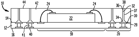
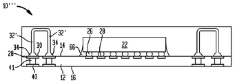
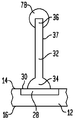
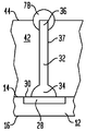
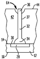
Abstract
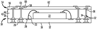
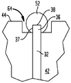
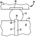
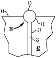
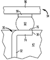
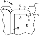
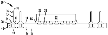
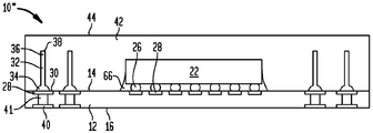
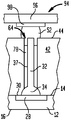
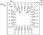
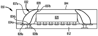
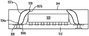
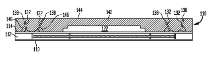
마이크로전자 어셈블리(10)는 제 1 및 제 2 대항면을 가지는 기판(12)을 포함한다. 마이크로전자 소자(22)는 제 1 면에 상재하고 제 1 전도성 엘리먼트(28)는 제 1 면 또는 제 2 면 중 적어도 하나에 노출될 수 있다. 제 1 도전성 엘리먼트(28) 중 일부는 마이크로전자 소자(22)에 전기적으로 접속된다. 와이어 본드(32)는 도전성 엘리먼트(28)에 결합된 베이스(34) 및 기판 및 베이스로부터 원격인 단부면(38)을 가지고, 각각의 와이어 본드는 베이스 및 단부면 사이에서 연장하는 에지면(37)을 정의한다. 캡슐층(42)은 제 1 면으로부터 연장하고 와이어 본드들 사이의 공간을 충진함으로써, 와이어 본드가 캡슐층에 의하여 분리될 수 있게 할 수 있다. 와이어의 본드(32)의 비캡슐화된 부분들은 캡슐층(42)에 의하여 덮이지 않는 와이어 본드의 단부면(38)의 적어도 일부에 의하여 정의된다.The microelectronic assembly 10 includes a substrate 12 having first and second opposing surfaces. The microelectronic element 22 may be on the first side and the first conductive element 28 may be exposed on at least one of the first side or the second side. A portion of the first conductive element 28 is electrically connected to the microelectronic element 22. The wire bond 32 has a base 34 coupled to the conductive element 28 and an end face 38 remote from the substrate and the base and each wire bond having an edge surface 37 extending between the base and the end surface ). The capsule layer 42 extends from the first side and fills the space between the wire bonds so that the wire bonds can be separated by the capsule layer. The non-encapsulated portions of the bond 32 of wire are defined by at least a portion of the end face 38 of the wire bond that is not covered by the encapsulation layer 42.
Description
관련 출원에 대한 상호 참조Cross-reference to related application
본 출원은 2013 년 1 월 29 일에 출원된 미국 특허 출원 번호 제 13/752,485 호의 계속 출원인데, 이것은 2013 년 2 월 12 일에 발행된 현재 미국 특허 번호 제 8,372,741 호인 2012 년 2 월 24 일에 출원된 미국 특허출원 번호 제 13/405,125 호의 계속출원이고, 이들의 개시물은 여기에서 원용에 의해 본 명세서에 포함된다.This application is a continuation-in-part of U.S. Patent Application No. 13 / 752,485, filed January 29, 2013, which is filed on February 24, 2012, which is now U.S. Patent No. 8,372,741, issued February 12, No. 13 / 405,125, the disclosures of which are incorporated herein by reference in their entirety.
발명의 배경BACKGROUND OF THE INVENTION
본 발명의 실시예는 여기에서 패키지-온-패키지 어셈블리에서 사용될 수 있는 마이크로전자 패키지를 제조하는 다양한 구조 및 방법에 관련되며, 특히, 패키지-온-패키지 접속의 일부로서 이를 위하여 와이어 본드를 포함하는 그러한 구조에 관련된다.Embodiments of the present invention relate to various structures and methods for making microelectronic packages that can be used in package-on-package assemblies herein, and in particular, as part of a package-on- Such structure.
반도체 칩과 같은 마이크로전자 디바이스는 통상적으로 많은 입력 및 다른 전자적 컴포넌트로의 출력 연결을 요구한다. 반도체 칩 또는 다른 비견되는 디바이스의 입력 및 출력 콘택은 일반적으로 디바이스의 표면을 실질적으로 덮는 그리드-유사 패턴으로(공통적으로 "영역 어레이"라고 지칭됨) 또는 인접한 디바이스의 전면의 에지와 평행하고 인접하게 연장할 수도 있는 길다란 행으로, 또는 전면의 중앙에 배치된다. 통상적으로, 칩과 같은 디바이스는 인쇄 회로 보드와 같은 기판 상에 물리적으로 탑재되어야 하고, 디바이스의 콘택은 회로 보드의 전도성 피쳐에 전기적으로 접속되어야 한다.Microelectronic devices, such as semiconductor chips, typically require output connections to many inputs and other electronic components. The input and output contacts of a semiconductor chip or other comparable device are generally parallel and adjacent to the edge of the front surface of an adjacent device in a grid-like pattern (commonly referred to as an "area array") that substantially covers the surface of the device In a long row that may extend, or in the center of the front. Typically, a device such as a chip must be physically mounted on a substrate, such as a printed circuit board, and the contacts of the device must be electrically connected to the conductive features of the circuit board.
반도체 칩은 제조 도중에 그리고 그 칩의 회로 보드 또는 다른 회로 패널과 같은 외부 기판 상에의 실장 도중에 그 칩의 핸들링을 용이하게 하는 패키지 내에 공통적으로 제공된다. 예를 들어, 많은 반도체 칩이 표면 실장을 위하여 적합한 패키지 내에 제공된다. 이러한 일반적 타입의 다수의 패키지가 다양한 애플리케이션에 대하여 제안되어 왔다. 거의 공통적으로, 이러한 패키지는, 유전체 상에 도금되거나 에칭된 금속성 구조로서 형성된 단자를 가지는 "칩 캐리어"라고 공통적으로 불리는 절연 엘리먼트를 포함한다. 이러한 단자는 칩 캐리어 자체를 따라서 연장하는 박막 트레이스와 같은 피쳐에 의하여 그리고 칩의 콘택과 단자 또는 트레이스 사이에서 연장하는 미세 리드 또는 와이어에 의하여 칩 자체의 콘택에 접속된다. 표면 실장 동작에서, 패키지는, 패키지 상의 각각의 단자가 회로 보드 상의 대응하는 콘택 패드와 정렬되도록 회로 보드 상에 배치된다. 솔더 또는 다른 본딩 물질은 단말과 콘택 패드 사이에 제공된다. 패키지는 솔더를 용해시키거나 "리플로우(reflow)" 시키기 위하여 또는 그렇지 않으면 본딩 물질을 활성화시키기 위하여 어셈블리를 가열함으로써 제자리에 영구적으로 본딩될 수 있다.The semiconductor chip is commonly provided in a package that facilitates handling of the chip during manufacture and during mounting onto an external substrate such as a circuit board or other circuit panel of the chip. For example, many semiconductor chips are provided in packages suitable for surface mounting. A number of packages of this general type have been proposed for various applications. Most commonly, such packages include insulating elements commonly referred to as "chip carriers" having terminals formed as a metallic structure plated or etched on a dielectric. Such terminals are connected to the contacts of the chip itself by features such as thin film traces extending along the chip carrier itself and by micro-leads or wires extending between the contacts of the chip and the terminals or traces. In surface mount operation, the package is placed on the circuit board such that each terminal on the package is aligned with a corresponding contact pad on the circuit board. Solder or other bonding material is provided between the terminal and the contact pad. The package may be permanently bonded in place by melting or "reflowing" the solder or otherwise heating the assembly to activate the bonding material.
많은 패키지는, 통상적으로 직경에 있어서 약 0.1 mm 및 약 0.8 mm(5 및 30 mils)이며 패키지의 단자에 부착된 솔더 볼의 형태를 가지는 솔더 매쓰(solder mass)를 포함한다. 자신의 하단 표면으로부터 돌출하는 솔더 볼의 어레이를 가지는 패키지는 공통적으로 볼 그리드 어레이 또는 "BGA" 패키지라고 지칭된다. 랜드 그리드 어레이 또는 "LGA" 패키지라고 지칭되는 다른 패키지는 솔더로부터 형성된 박막층 또는 랜드에 의하여 기판에 고정된다. 이러한 타입의 패키지는 매우 콤팩트할 수 있다. 공통적으로 "칩 스케일 패키지"라고 불리는 어떤 패키지는 그 패키지 내에 내장된 디바이스의 면적과 같거나 또는 다소 큰 회로 보드의 면적을 점유한다. 이것이 어셈블리의 전체 사이즈를 감소시킨다는 점 및 기판 상의 다양한 디바이스들 사이에 짧은 상호접속을 사용하도록 허용한다는 점에 있어서 이것은 유리한데, 이것은 차례대로 디바이스들 사이의 신호 전파 시간을 한정하고 따라서 고속에서의 어셈블리의 동작을 용이하게 한다.Many packages typically include solder masses having a diameter of about 0.1 mm and about 0.8 mm (5 and 30 mils) and in the form of solder balls attached to the terminals of the package. A package having an array of solder balls protruding from its lower surface is commonly referred to as a ball grid array or "BGA" package. Another package, referred to as a land grid array or "LGA" package, is secured to the substrate by a thin film layer or land formed from the solder. This type of package can be very compact. A package, commonly referred to as a "chip scale package " occupies an area of the circuit board that is equal to or somewhat larger than the area of the device embedded in the package. This is advantageous in that it reduces the overall size of the assembly and allows for the use of short interconnections between the various devices on the substrate, which in turn limits the signal propagation time between the devices, Lt; / RTI >
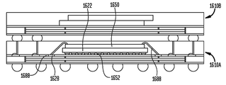
패키지된 반도체 칩은 흔히 "적층된" 배치구성으로 제공되는데, 여기에서 하나의 패키지는 예를 들어, 회로 보드 상에 제공되고, 다른 패키지는 제 1 패키지 상단에 탑재된다. 이러한 배치구성은 다수 개의 상이한 칩들이 회로 보드 상의 단일 풋프린트 내에 탑재되도록 허용할 수 있고 더 나아가 패키지들 사이에 짧은 상호접속을 제공함으로써 고속 동작을 가능하게 할 수도 있다. 흔히, 이러한 상호접속 거리는 칩 자체의 두께보다 겨우 조금만 더 크다. 상호접속이 칩 패키지의 스택에서 획득되기 위해서는, 기계적 및 전기적 접속을 위한 구조를 각각의 패키지(최상층 패키지 제외)의 양측 모두에 제공하는 것이 필요하다. 이것은 예를 들어, 콘택 패드 또는 랜드를 칩이 탑재되는 기판의 양측에 제공함으로써 이루어져 왔는데, 패드는 도전성 비아 또는 기타 등등에 의하여 기판을 통해 연결된다. 솔더 볼 등이 하부 기판의 상단 상의 콘택 및 다음 높은 기판의 하단 상의 콘택 사이의 갭을 브리징(bridge)하기 위하여 사용되어 왔다. 솔더 볼은 콘택들을 연결하기 위하여 칩의 높이보다 더 높아야 한다. 적층된 칩 배치구성 및 상호접속 구조의 예들은 미국 특허 출원 번호 제 2010/0232129 호("'129 공개 문서")에 제공되는데, 그 개시물은 그 전체로서 본 명세서에서 원용에 의해 통합된다.A packaged semiconductor chip is often provided in a "stacked" configuration, wherein one package is provided, for example, on a circuit board, and the other package is mounted on top of the first package. This arrangement may allow a plurality of different chips to be mounted within a single footprint on the circuit board, and may further enable high speed operation by providing short interconnections between the packages. Often, this interconnect distance is slightly more than the thickness of the chip itself. In order for interconnection to be obtained in the stack of chip packages, it is necessary to provide a structure for both mechanical and electrical connections on both sides of each package (except the top-layer package). This has been done, for example, by providing contact pads or lands on both sides of the substrate on which the chip is mounted, the pads being connected via a substrate by conductive vias or the like. Solder balls, etc. have been used to bridge the gap between the contact on the top of the lower substrate and the contact on the bottom of the next higher substrate. The solder balls must be higher than the chip height to connect the contacts. Examples of stacked chip placement and interconnect structures are provided in U. S. Patent Application No. < RTI ID = 0.0 > 2010/0232129 < / RTI > ("129 Open Publication") the disclosure of which is incorporated herein by reference in its entirety.
길쭉한 포스트 또는 핀의 형태인 마이크로콘택 엘리먼트가 마이크로전자 패키지를 회로 보드로 연결하기 위하여 그리고 마이크로전자 패키징 내의 다른 접속들에 대하여 사용될 수도 있다. 몇 가지 실례들에서, 마이크로콘택은 하나 이상의 금속성 계층을 포함하는 금속 구조를 에칭하여 마이크로콘택을 형성함으로써 형성되어 왔다. 에칭 공정은 마이크로콘택의 사이즈를 제한한다. 종래의 에칭 공정은 통상적으로 본 명세서에서 "종횡비"라고 지칭되는 높이 대 최대 폭의 큰 비율을 가지는 마이크로콘택을 형성할 수 없다. 감지가능한(appreciable) 높이 및 인접한 마이크로콘택들 사이의 매우 작은 피치 또는 스페이싱을 가진 마이크로콘택의 어레이를 형성하는 것은 어렵거나 불가능한 일이었다. 더욱이, 종래의 에칭 공정에 의하여 형성되는 마이크로콘택의 구조는 제한된다.A microcontact element in the form of an elongated post or pin may be used to connect the microelectronic package to the circuit board and to other connections in the microelectronic packaging. In some instances, microcontacts have been formed by etching a metal structure comprising one or more metallic layers to form microcontacts. The etching process limits the size of the microcontact. Conventional etching processes typically can not form microcontacts having a high ratio of height to maximum width, referred to herein as the "aspect ratio. &Quot; It has been difficult or impossible to form an array of microcontacts with appreciable height and very small pitch or spacing between adjacent microcontacts. Moreover, the structure of the microcontact formed by the conventional etching process is limited.
당업계에서의 위에서 설명된 모든 발전에도 불구하고, 마이크로전자 패키지를 제조하고 테스팅하는 데 있어서 추가적인 개선이 소망될만할 것이다.Despite all the developments described above in the art, further improvements in the fabrication and testing of microelectronic packages will be desirable.
발명의 개요Summary of the Invention
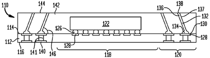
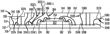
마이크로전자 어셈블리는 제 1 및 제 2 대항면을 가지는 기판을 포함한다. 마이크로전자 소자는 제 1 면에 상재할 수 있고 제 1 전기적으로 도전성 엘리먼트는 제 1 면 또는 제 2 면 중 적어도 하나에 노출될 수 있다. 제 1 도전성 엘리먼트 중 일부는 마이크로전자 소자에 전기적으로 접속될 수도 있다. 와이어 본드는 도전성 엘리먼트에 결합되는 베이스 및 기판 베이스로부터 원격인 단부면을 가진다. 각각의 와이어 본드는 베이스 및 단부면 사이에서 연장하는 에지면을 정의할 수 있다. 캡슐층은 제 1 면으로부터 연장하고 와이어 본드들 사이의 공간을 충진함으로써, 와이어 본드가 캡슐층에 의하여 분리될 수 있게 할 수 있다. 와이어의 본드의 비캡슐화된 부분들은 캡슐층에 의하여 덮이지 않는 와이어 본드의 단부면의 적어도 일부에 의하여 정의될 수도 있다.The microelectronic assembly includes a substrate having first and second opposing surfaces. The microelectronic element may be on a first side and the first electrically conductive element may be exposed on at least one of a first side or a second side. Some of the first conductive elements may be electrically connected to the microelectronic device. The wire bond has a base coupled to the conductive element and an end surface remote from the substrate base. Each wire bond may define an edge surface extending between the base and the end surface. The capsule layer extends from the first side and fills the space between the wire bonds so that the wire bonds can be separated by the capsule layer. The non-encapsulated portions of the bond of the wire may be defined by at least a portion of the end face of the wire bond that is not covered by the encapsulation layer.
도전성 엘리먼트, 예를 들어, 기판 상의 도전성 패드로부터 상향으로 연장하는 수직 접속으로서 기능하는 와이어 본드를 포함하는 다양한 패키지 구조들이 본 명세서에서 개시된다. 이러한 와이어 본드는 유전체 캡슐의 표면에 상재하는 마이크로전자 패키지로써 패키지 온 패키지 전기적 접속을 제조하는 데에서 사용될 수 있다. 추가적으로, 마이크로전자 패키지 또는 마이크로전자 어셈블리를 제조하기 위한 방법들의 다양한 실시예가 본 명세서에서 개시된다.Various package structures are disclosed herein that include a conductive element, for example, a wire bond that functions as a vertical connection extending upwardly from the conductive pad on the substrate. Such a wire bond can be used to fabricate a package-on-package electrical connection as a microelectronic package overlying the surface of the dielectric capsule. Additionally, various embodiments of methods for manufacturing microelectronic packages or microelectronic assemblies are disclosed herein.
따라서, 본 발명의 일 양태에 따르는 마이크로전자 패키지를 제조하는 방법은 a) 선결정된 길이를 가지는 금속 와이어 세그먼트를 본딩 툴의 모세관 밖으로 공급하는 단계; b) 상기 본딩 툴을 사용하여 상기 금속 와이어의 일부를 기판의 제 1 면에서 노출된 도전성 엘리먼트에 본딩시키고, 이를 통하여 상기 도전성 엘리먼트 상에 와이어 본드의 베이스를 형성하는 단계; c) 상기 와이어의 일부를 상기 본딩 툴 내에서 클램핑하는 단계; d) 상기 금속 와이어를 클램핑된 부분 및 베이스 부분 사이의 위치에서 절단하여 상기 와이어 본드의 단부면을 적어도 부분적으로 정의하는 단계로서, 상기 와이어 본드의 에지면은 상기 베이스 및 단부면 사이에서 정의되는, 단계; e) 단계 (a) 내지 단계 (d)를 반복하여 복수 개의 와이어 본드를 상기 기판의 복수 개의 도전성 엘리먼트에 형성하는 단계; 및 e) 그러면 상기 기판의 표면에 상재하는(overlying) 유전 캡슐층을 형성하는 단계로서, 상기 캡슐층은 상기 기판의 표면 및 상기 와이어 본드의 부분을 적어도 부분적으로 커버하도록 형성됨으로써, 상기 와이어 본드의 비캡슐화된 부분이 상기 캡슐층에 의하여 덮이지 않는, 그것의 단부면 또는 에지면 중 적어도 하나의 부분에 의하여 정의되게 하는, 단계를 포함할 수 있다.Accordingly, a method of manufacturing a microelectronic package according to an aspect of the present invention comprises the steps of: a) supplying a metal wire segment having a predetermined length out of the capillary of a bonding tool; b) bonding a portion of the metal wire to a conductive element exposed on a first side of the substrate using the bonding tool, thereby forming a base of the wire bond on the conductive element; c) clamping a portion of the wire in the bonding tool; d) cutting the metal wire at a location between the clamped portion and the base portion to at least partially define an end face of the wire bond, wherein the edge face of the wire bond is defined between the base and the end face, step; e) repeating steps (a) through (d) to form a plurality of wire bonds on the plurality of conductive elements of the substrate; And e) forming a dielectric capping layer overlying a surface of the substrate, the capsule layer being configured to at least partially cover a surface of the substrate and a portion of the wire bond, Such that the non-encapsulated portion is defined by at least one portion of its end face or edge face that is not covered by the capsule layer.
따라서, 본 발명의 양태에 따르면, 선결정된 길이를 가지는 금속 와이어 세그먼트가 본딩 툴의 모세관 외부로 공급될 수 있다. 본딩 툴은 금속 와이어의 일부를 기판의 제 1 면에서 노출된 도전성 엘리먼트로 본딩하기 위하여 사용될 수 있다. 이러한 본딩은 도전성 엘리먼트 상에 와이어 본드의 베이스를 형성할 수 있다. 와이어의 일부는 도전성 엘리먼트와의 본딩을 형성한 이후에 클램핑될 수 있다. 클램핑된 와이어의 일부는 본딩 툴 내에 있을 수 있다. 금속 와이어는 클램핑된 부분 및 베이스 부분 사이의 위치에서 절단될 수 있고, 와이어를 절단하는 것은 와이어 본드의 단부면(end surface)을 적어도 부분적으로 정의할 수도 있다. 와이어 본드의 에지면은 베이스 및 단부면 사이에서 정의될 수 있다. 앞선 것들이 반복되어 기판의 복수 개의 도전성 엘리먼트에 복수 개의 와이어 본드를 형성할 수 있다. 그러면, 기판의 표면에 상재하여 유전 캡슐층이 형성될 수 있다. 캡슐층은 기판의 표면 및 와이어 본드의 일부를 적어도 부분적으로 커버하기 위하여 형성될 수 있다. 와이어의 본드의 비캡슐화된 부분들은 캡슐층에 의하여 덮이지 않는 그것의 단부면 또는 에지면 중 적어도 하나의 일부에 의하여 정의될 수도 있다.Thus, according to an aspect of the present invention, a metal wire segment having a predetermined length can be supplied to the outside of the capillary of the bonding tool. The bonding tool may be used to bond a portion of the metal wire to the exposed conductive element on the first side of the substrate. Such bonding may form the base of the wire bond on the conductive element. A portion of the wire may be clamped after forming a bond with the conductive element. Some of the clamped wires may be in the bonding tool. The metal wire may be cut at a location between the clamped portion and the base portion, and cutting the wire may at least partially define an end surface of the wire bond. The edge face of the wire bond can be defined between the base and the end face. The foregoing can be repeated to form a plurality of wire bonds in a plurality of conductive elements of the substrate. Then, a dielectric capsule layer can be formed on the surface of the substrate. The capsule layer may be formed to at least partially cover the surface of the substrate and a portion of the wire bonds. The non-encapsulated portions of the bond of the wire may be defined by a portion of at least one of its end face or edge face that is not covered by the capsule layer.
일 예에서, 금속 와이어는 그것을 통해 오직 부분적으로 절단될 수 있다. 본딩 툴은 와이어의 일부가 클램핑된 상태로 유지되는 동안 기판의 표면으로부터 멀어지게 이동될 수 있다. 이러한 공정에서, 와이어는 절단의 위치에서 부러지도록 될 수 있다. 단부면은 절단 및 부러짐에 의하여 형성될 수 있다.In one example, the metal wire can only be partially cut through it. The bonding tool can be moved away from the surface of the substrate while a portion of the wire remains clamped. In such a process, the wire may be broken at the location of the cut. The end face can be formed by cutting and breaking.
일 예에서, 절단은 와이어 본드의 에지면에 실질적으로 수직인 방향에서 와이어 세그먼트를 통해서 완전히 이루어질 수 있다. 상기 와이어 본드의 단부면은 절단에 의하여 형성될 수 있다.In one example, the cutting can be done completely through the wire segment in a direction substantially perpendicular to the edge plane of the wire bond. The end face of the wire bond may be formed by cutting.
일 예에서, 적어도 하나의 마이크로전자 소자는 기판의 제 1 면에 상재할 수 있다. 기판은 제 1 지역 및 제 2 지역을 가질 수 있고, 상기 마이크로전자 소자는 예를 들어 제 1 지역에 상재하는 상태로 상기 제 1 지역 내에 위치될 수 있다. 도전성 엘리먼트는, 예를 들어 그 안에서 제 1 면에 노출된 도전성 엘리먼트로서 제 2 지역 내에 위치될 수 있다. 도전성 엘리먼트는 적어도 하나의 마이크로전자 소자에 전기적으로 접속될 수 있다. 유전 캡슐층은 그것의 적어도 제 2 지역에서 상기 기판의 제 1 면에 상재하며 형성될 수 있는데, 하지만 제 1 지역 및 제 2 지역 내에서 제 1 면의 적어도 일부에 상재할 수도 있다.In one example, at least one microelectronic element may be mounted on a first side of the substrate. The substrate may have a first region and a second region, and the microelectronic device may be located within the first region, for example, in a first region. The conductive element may be located, for example, in the second region as the conductive element exposed on the first side thereof. The conductive element may be electrically connected to at least one microelectronic device. The dielectric capsule layer may be formed on and over at least a portion of the first side of the substrate in at least a second region thereof, but may be formed over at least a portion of the first side within the first region and the second region.
일 예에서, 패키지는, 상기 와이어 본드 중 제 1 와이어 본드가 제 1 신호 전위를 운반하기 위하여 적응되고 상기 와이어 본드 중 제 2 와이어 본드가 제 1 신호 전위와는 상이한 제 2 신호 전위를 동시에 운반하기 위하여 적응되도록 구성될 수 있다.In one example, the package is configured such that a first wire bond of the wire bonds is adapted to carry a first signal potential and a second one of the wire bonds carries a second signal potential different from the first signal potential simultaneously And may be configured to be adapted to.
일 예에서, 금속 와이어 세그먼트는 상기 본딩 툴 상에 탑재된 레이저를 사용하여 절단될 수 있다. 이러한 예에서, 본딩 툴의 모세관은 상기 와이어 세그먼트가 이를 통하여 공급되는 그것의 페이스를 정의할 수 있다. 상기 레이저는 상기 본딩 툴 상에 탑재되어 절단 빔이 상기 본딩 툴의 페이스 및 상기 와이어 본드의 베이스 사이에 포지셔닝된 와이어 세그먼트의 위치로 디렉팅될 수 있도록 할 수 있다.In one example, metal wire segments may be cut using a laser mounted on the bonding tool. In this example, the capillary of the bonding tool may define its face through which the wire segment is fed through. The laser may be mounted on the bonding tool so that a cutting beam may be directed to a position of the wire segment positioned between the face of the bonding tool and the base of the wire bond.
일 예에서, 상기 본딩 툴은 상기 와이어 세그먼트가 이를 통하여 공급되는 그것의 페이스를 정의하는 모세관을 포함할 수 있다. 상기 모세관은 그것의 측벽 내에 형성되는 벽을 포함할 수도 있고, 상기 레이저는 본딩 상에 또는 이와 함께 탑재되어 절단 빔이 상기 개구를 통하여 상기 모세관 내에 포지셔닝된 와이어 세그먼트의 위치로 지나갈 수 있게 할 수 있다.In one example, the bonding tool may include a capillary that defines its pace through which the wire segment is fed. The capillary may comprise a wall formed in its sidewall and the laser may be mounted on or together with the bonding to allow a cutting beam to pass through the opening to the position of the wire segment positioned in the capillary .
일 예에서, 상기 레이저는: CO2, Nd:YAG, 또는 Cu 증기 레이저 중 하나일 수 있다.In one example, the laser may be one of: CO2, Nd: YAG, or a Cu vapor laser.
일 예에서, 상기 금속 와이어는 상기 모세관 내에서 연장하는 절단 에지를 사용하여 절단될 수 있다. 상기 절단 에지는 상기 와이어 세그먼트에 반대인 상기 모세관의 벽을 향하는 방향에서 연장할 수 있다. 일 예에서, 상기 금속 와이어는, 상기 절단 에지를 제 1 절단 에지로서 사용하고, 상기 모세관 내에서 연장하는 제 2 절단 에지와 조합하여 절단될 수 있다. 제 2 절단 에지는 제 1 절단 에지에 반대로 포지셔닝될 수도 있다.In one example, the metal wire may be cut using a cutting edge that extends in the capillary. The cutting edge may extend in a direction toward the wall of the capillary opposite the wire segment. In one example, the metal wire may be cut in combination with a second cutting edge that uses the cutting edge as the first cutting edge and extends in the capillary. The second cutting edge may be positioned opposite to the first cutting edge.
일 예에서, 상기 모세관은 상기 와이어 세그먼트가 이를 통하여 공급되는 페이스를 정의할 수도 있다. 상기 금속 와이어는 제 1 및 제 2 대항 절단 에지를 가지는 절단 기구를 사용하여 절단될 수 있다. 상기 절단 기구는 상기 본딩 툴 상에 또는 이와 함께 탑재되어 상기 와이어가 상기 본딩 툴의 페이스 및 상기 와이어 본드의 베이스 사이에 포지셔닝된 위치에서 절단될 수 있도록 할 수 있다.In one example, the capillary may define a face through which the wire segment is supplied. The metal wire may be cut using a cutting mechanism having first and second opposing cutting edges. The cutting mechanism may be mounted on or together with the bonding tool so that the wire can be cut at a position that is positioned between the face of the bonding tool and the base of the wire bond.
이 방법의 하나의 예는 스텐실을 기판 상에 포지셔닝하는 단계를 포함할 수도 있다. 상기 스텐실은 그 안에 상기 도전성 엘리먼트의 적어도 일부에 상재하고 노출시키는 복수 개의 개구를 가질 수 있다. 상기 개구는 상기 기판 상의 제 1 높이에 포지셔닝된 개별 에지들을 정의할 수 있다. 상기 와이어 세그먼트는 상기 스텐실 개구의 에지에 대항하는 상기 와이어의 측방향 이동에 의하여 절단될 수 있다.One example of this method may include positioning the stencil on the substrate. The stencil may have a plurality of apertures therein to expose and expose at least a portion of the conductive element. The aperture may define individual edges positioned at a first height on the substrate. The wire segment may be cut by lateral movement of the wire against the edge of the stencil opening.
본 발명의 일 양태에 따르는 마이크로전자 패키지를 제조하는 방법은: 스텐실을 제 1 표면 및 그로부터 원격인 제 2 면을 가지는 기판을 포함하는 공정중 유닛(in-process unit) 상부에 포지셔닝하는 단계를 포함할 수 있다. 특정 실시예에서, 마이크로전자 소자는 기판의 제 1 면에 탑재될 수 있다. 복수 개의 도전성 엘리먼트는 제 1 면에 노출될 수 있다. 일 예에서, 도전성 엘리먼트의 적어도 일부는 마이크로전자 소자에 전기적으로 접속될 수 있다. 상기 스텐실은 그 안에 상기 도전성 엘리먼트의 적어도 일부에 상재하고 노출시키는 복수 개의 개구를 가질 수 있다. 상기 개구는 상기 기판 상의 제 1 높이에 포지셔닝되는 개별 에지들을 정의할 수도 있다.A method of manufacturing a microelectronic package in accordance with an aspect of the present invention includes positioning a stencil over an in-process unit including a substrate having a first surface and a second surface remote from the stencil can do. In certain embodiments, the microelectronic device can be mounted on the first side of the substrate. The plurality of conductive elements may be exposed on the first surface. In one example, at least a portion of the conductive element may be electrically connected to the microelectronic element. The stencil may have a plurality of apertures therein to expose and expose at least a portion of the conductive element. The aperture may define individual edges that are positioned at a first height on the substrate.
이러한 양태에 따르면, 이 방법은 금속 와이어를 본딩 툴의 모세세관 외부로 공급하여 선결정된 길이가 모세세관의 페이스를 넘어 연장하고 금속 와이어 세그먼트를 정의하도록 하는 것을 포함하는 공정에 의하여 와이어 본드를 형성하는 단계를 포함할 수 있다. 상기 와이어 세그먼트의 부분은 상기 복수 개의 도전성 엘리먼트 중 하나와 결합되어 상기 와이어 본드의 베이스를 형성할 수 있다. 상기 금속 와이어 세그먼트의 적어도 일부는 상기 스텐실 개구의 에지에 대항하는 상기 와이어의 측방향 이동에 의하여 그것에 연결된 와이어의 다른 부분으로부터 전단되어 상기 와이어 본드를 상기 와이어의 잔여 부분으로부터 분리할 수 있다. 금속 와이어의 전단은 와이어 본드의 단부면을 정의할 수 있고, 와이어 본드는 베이스 및 단부면 사이에서 연장하는 에지면을 가진다. 위에서 설명된 바와 같은 금속 와이어 외부로의 공급, 본딩, 및 그것의 전단은 스텐실의 하나 이상의 개구를 사용하여 복수 회 반복되어 복수 개의 와이어 본드를 복수 개의 도전성 엘리먼트 상에 형성할 수 있다.According to this aspect, the method comprises forming a wire bond by feeding a metal wire out of the capillary tubing of the bonding tool to allow a predetermined length to extend beyond the face of the capillary tubule and define a metal wire segment Step < / RTI > The portion of the wire segment may be combined with one of the plurality of conductive elements to form the base of the wire bond. At least a portion of the metal wire segment may be sheared from another portion of the wire connected thereto by a lateral movement of the wire against the edge of the stencil opening to separate the wire bond from the remainder of the wire. The front end of the metal wire may define an end face of the wire bond, and the wire bond has an edge face extending between the base and the end face. Feeding, bonding, and the front end thereof to the outside of the metal wire as described above may be repeated a plurality of times using one or more openings of the stencil to form a plurality of wire bonds on the plurality of conductive elements.
이러한 방법의 일 예에서, 유전 캡슐층은 상기 공정중 유닛 상에 형성될 수 있는데, 상기 캡슐층은 상기 제 1 면 및 상기 와이어 본드의 부분을 적어도 부분적으로 커버 하도록 형성된다. 상기 와이어 본드의 비캡슐화된 부분은 상기 캡슐층에 의하여 덮이지 않는, 그것의 단부면 또는 에지면 중 적어도 하나의 부분에 의하여 정의될 수 있다.In one example of such a method, a dielectric capsule layer may be formed on the unit during the process, wherein the capsule layer is formed to at least partially cover the first surface and portions of the wire bonds. The non-encapsulated portion of the wire bond may be defined by at least one of its end face or edge face that is not covered by the capsule layer.
이러한 방법의 일 예에서, 모세관의 페이스를 넘어 연장하고 금속 와이어의 전단 이후에 남아 있는 금속 와이어의 일부는 적어도 후속 와이어 본드의 베이스를 형성하기에 충분한 길이일 수 있다.In one example of such a method, a portion of the metal wire that extends beyond the face of the capillary and remains after the shearing of the metal wire may be at least long enough to form the base of the subsequent wire bond.
이 방법의 일 예에서, 스텐실은 홀들 중 하나의 연장하는 축의 방향에서, 예를 들어, 기판의 표면으로부터 멀어지는 방향에서 두께를 정의할 수 있다. 홀들 중 몇몇 또는 모두는 스텐실의 두께에 걸쳐 일관적이거나 일정한 직경을 가질 수 있다.In one example of this method, the stencil may define the thickness in the direction of the extending axis of one of the holes, e.g., in a direction away from the surface of the substrate. Some or all of the holes may have a consistent or constant diameter across the thickness of the stencil.
이 방법의 일 예에서, 스텐실은 홀들 또는 개구 중 하나의 축의 방향에서, 예를 들어, 기판의 표면으로부터 멀어지는 방향에서 두께를 정의할 수 있다. 스텐실 내의 홀 또는 개구 중 일부 또는 전부는 상기 개구 내의 노출된 에지에서의 제 1 너비 또는 더 작은 직경으로부터 상기 홀 또는 개구 내의 그리고 상기 기판에 더 가까운 사이의 위치에서의 제 2 의 더 큰 너비 또는 더 큰 직경으로 테이퍼링될 수 있다.In one example of this method, the stencil may define a thickness in the direction of one of the holes or apertures, e.g., in a direction away from the surface of the substrate. Some or all of the holes or openings in the stencil may have a second larger width or a smaller diameter at the exposed edge in the opening or a second greater width or more at a location within the hole or opening and closer to the substrate Can be tapered to a large diameter.
일 예에서, 상기 스텐실은 상기 기판의 하나 이상의 에지를 따라 연장하는 상기 기판의 두께의 방향에서 제 1 두께를 가지는 에지 부재를 포함할 수도 있다. 제 1 두께는 제 1 높이를 정의할 수 있다. 중앙부는 홀 또는 개구를 포함할 수도 있고 에지 부재에 의하여 경계지어질 수 있다. 중앙부는 기판으로부터 멀어지게 대향하는 외부면을 가질 수 있다. 외부면은 제 1 높이에 배치될 수 있다. 중앙부는 제 1 두께보다 더 적은 두께를 가질 수 있다.In one example, the stencil may include an edge member having a first thickness in a direction of thickness of the substrate extending along at least one edge of the substrate. The first thickness may define a first height. The central portion may include a hole or opening and may be bordered by an edge member. The central portion may have an outer surface facing away from the substrate. The outer surface may be disposed at a first height. The central portion may have a thickness less than the first thickness.
패키지-온-패키지 어셈블리에서 사용될 수 있는 마이크로전자 패키지를 제조하는 다양한 구조 및 방법에서, 특히, 패키지-온-패키지 접속의 일부로서 이를 위하여 와이어 본드를 포함하는 그러한 구조를 제공한다.This provides a structure, such as a wire bond, for this purpose as part of a package-on-package connection, in various structures and methods for manufacturing microelectronic packages that can be used in package-on-package assemblies.
도 1 은 본 발명의 일 실시예에 따른 마이크로전자 패키지를 도시한다;
도 2 는 도 1 의 마이크로전자 패키지의 상단 정면도(top elevation view)를 도시한다;
도 3 은 본 발명의 다른 실시예에 따른 마이크로전자 패키지를 도시한다;
도 4 는 본 발명의 다른 실시예에 따른 마이크로전자 패키지를 도시한다;
도 5 는 본 발명의 다른 실시예에 따른 마이크로전자 패키지를 도시한다;
도 6 은 본 발명의 일 실시예에 따른 마이크로전자 패키지를 포함하는 적층된 마이크로전자 어셈블리를 도시한다;
도 7 은 본 발명의 다른 실시예에 따른 마이크로전자 패키지를 도시한다;
도 8a 내지 도 8e 는 본 발명의 다양한 실시예에 따른 마이크로전자 패키지의 일부의 상세도를 도시한다;
도 9 는 본 발명의 다른 실시예에 따른 마이크로전자 패키지의 일부의 상세도를 도시한다;
도 10a 내지 도 10d 는 본 발명의 다양한 실시예에 따른 마이크로전자 패키지의 일부의 상세도를 도시한다;
도 11 내지 도 14 는 본 발명의 일 실시예에 따른 그것의 제작의 다양한 단계 도중의 마이크로전자 패키지를 도시한다;
도 15 는 본 발명의 다른 실시예에 따른 제작 단계 도중의 마이크로전자 패키지를 도시한다;
도 16a 내지 도 16c 는 본 발명의 일 실시예에 따른 그것의 제작의 다양한 단계 도중의 마이크로전자 패키지의 일부의 상세도를 도시한다;
도 17a 내지 도 17c 는 본 발명의 다른 실시예에 따른 그것의 제작의 다양한 단계 도중의 마이크로전자 패키지의 일부의 상세도를 도시한다;
도 18 은 본 발명의 다른 실시예에 따른 마이크로전자 패키지의 상단 정면도를 도시한다;
도 19 는 본 발명의 일 실시예에 따른 마이크로전자 패키지의 일부의 상단 정면도를 도시한다;
도 20 은 본 발명의 또 다른 실시예에 따른 마이크로전자 패키지의 상면도를 도시한다;
도 21 은 도 20 의 마이크로전자 패키지의 정면도(front elevation view)를 도시한다;
도 22 는 본 발명의 또 다른 실시예에 따른 마이크로전자 패키지의 정면도를 도시한다;
도 23 은 본 발명의 다른 실시예에 따른 시스템을 도시한다;
도 24 는 본 발명의 또 다른 실시예에 따른 마이크로전자 패키지의 정면도를 도시한다;
도 25 는 본 발명의 또 다른 실시예에 따른 마이크로전자 패키지의 정면도를 도시한다;
도 26 은 도 25 의 실시예의 변형에 따른 마이크로전자 패키지의 상면도를 도시한다;
도 27 은 본 발명의 또 다른 실시예에 따른 마이크로전자 패키지의 정면도를 도시한다;
도 28 은 도 27 의 실시예의 변형에 따른 마이크로전자 패키지의 상면도를 도시한다;
도 29 는 다른 실시예에 따른 마이크로전자 패키지의 단면도이다;
도 30 은 다른 실시예에 따른 마이크로전자 패키지의 단면도를 도시한다;
도 31a 내지 도 31c 는 다른 실시예에 따른 마이크로전자 패키지의 실시예의 예를 도시하는 단면도이다;
도 32a 및 도 32b 는 본 개시물의 다른 실시예에 따르는 방법의 다양한 스테이지에서 다양한 와이어 본드 비아를 형성하는 데에 사용될 수 있는 머신의 일부를 도시한다;
도 33 은 본 개시물의 다른 실시예에 따르는 방법에서 상응하는 다양한 와이어 본드 비아를 형성하는 데에 사용될 수 있는 머신의 일부를 도시한다; 그리고
도 34a 내지 도 34c 는 본 개시물의 일 실시예에 따른 와이어 본드를 제조하기 위한 방법에서 사용될 수 있는 기구의 다양한 형태를 도시한다.Figure 1 illustrates a microelectronic package in accordance with one embodiment of the present invention;
Figure 2 shows a top elevation view of the microelectronic package of Figure 1;
Figure 3 illustrates a microelectronic package according to another embodiment of the present invention;
Figure 4 illustrates a microelectronic package according to another embodiment of the present invention;
Figure 5 illustrates a microelectronic package according to another embodiment of the present invention;
Figure 6 illustrates a stacked microelectronic assembly including a microelectronic package in accordance with one embodiment of the present invention;
Figure 7 illustrates a microelectronic package according to another embodiment of the present invention;
Figures 8A-8E show a detailed view of a portion of a microelectronic package in accordance with various embodiments of the present invention;
Figure 9 shows a detail view of a portion of a microelectronic package according to another embodiment of the present invention;
10A-10D show a detail view of a portion of a microelectronic package in accordance with various embodiments of the present invention;
Figures 11-14 illustrate a microelectronic package during various stages of its fabrication according to an embodiment of the present invention;
Figure 15 illustrates a microelectronic package during a fabrication step according to another embodiment of the present invention;
16A-16C show a detail view of a portion of a microelectronic package during various stages of its fabrication according to an embodiment of the invention;
17A-17C show a detail view of a portion of a microelectronic package during various stages of its fabrication according to another embodiment of the present invention;
18 shows a top elevational view of a microelectronic package according to another embodiment of the present invention;
Figure 19 illustrates a top, top view of a portion of a microelectronic package in accordance with one embodiment of the present invention;
Figure 20 shows a top view of a microelectronic package according to another embodiment of the present invention;
Figure 21 shows a front elevation view of the microelectronic package of Figure 20;
22 shows a front view of a microelectronic package according to another embodiment of the present invention;
23 illustrates a system according to another embodiment of the present invention;
Figure 24 illustrates a front view of a microelectronic package according to another embodiment of the present invention;
Figure 25 shows a front view of a microelectronic package according to another embodiment of the present invention;
Figure 26 shows a top view of a microelectronic package according to a modification of the embodiment of Figure 25;
Figure 27 illustrates a front view of a microelectronic package according to another embodiment of the present invention;
28 shows a top view of a microelectronic package according to a modification of the embodiment of Fig. 27;
29 is a cross-sectional view of a microelectronic package according to another embodiment;
30 shows a cross-sectional view of a microelectronic package according to another embodiment;
31A to 31C are cross-sectional views illustrating an example of an embodiment of a microelectronic package according to another embodiment;
32A and 32B illustrate a portion of a machine that may be used to form various wire bond vias at various stages of the method according to another embodiment of the present disclosure;
33 illustrates a portion of a machine that may be used to form the corresponding various wire bond vias in a method according to another embodiment of the present disclosure; And
Figures 34A-C illustrate various forms of apparatus that can be used in a method for manufacturing wire bonds in accordance with one embodiment of the present disclosure.
이제 유사한 참조 번호들이 유사한 피쳐를 표시하기 위하여 사용되는 도면으로 돌아가면, 도 1 에서 본 발명의 일 실시예에 따르는 마이크로전자 어셈블리(10)가 도시된다. 도 1 의 실시예는 컴퓨터 또는 다른 전자 애플리케이션에서 사용되는 반도체 칩 어셈블리와 같은 패키지된 마이크로전자 소자의 형태인 마이크로전자 어셈블리이다. Turning now to the drawings in which like reference numerals are used to denote like features, there is shown in Fig. 1 a
도 1 의 마이크로전자 어셈블리(10)는 제 1 면(14) 및 제 2 면(16)을 가지는 기판(12)을 포함한다. 기판(12)은 통상적으로 실질적으로 평평한 유전체 엘리먼트의 형태이다. 유전체 엘리먼트는 시트-유사 모양일 수도 있고 얇을 수도 있다. 특정 실시예에서, 유전체 엘리먼트는 한정하는 것이 아니라: 폴리이미드, 폴리테트라 플루오로에틸렌("PTFE"), 에폭시, 에폭시-유리, FR-4, BT 수지, 열가소성, 또는 열경화성 플라스틱 재료와 같은 유기 유전체 재료 또는 합성물 유전체 재료의 하나 이상의 층을 포함할 수 있다. 제 1 면(14) 및 제 2 면(16)은 바람직하게는 서로 실질적으로 평행이고 기판(12)의 두께를 정의하는 표면(14, 16)에 수직인 소정 거리에서 이격된다. 기판(12)의 두께는 바람직하게는 본 출원에 대한 일반적으로 수락가능한 두께의 범위 내에 속한다. 일 실시예에서, 제 1 면(14) 및 제 2 면(16) 간의 거리는 약 25 내지 500 μm 사이이다. 이러한 논의를 하기 위하여, 제 1 면(14)은 제 2 면(16)에 반대이거나 이로부터 원격으로 포지셔닝되는 것으로 설명될 수도 있다. 이러한 설명 및 본 명세서에서 사용되는 엘리먼트의 상대적인 포지션의, 이러한 엘리먼트의 수직 또는 수평 포지션을 지칭하는 임의의 다른 설명은 도면 내의 엘리먼트들의 포지션과 대응하도록 오직 예시를 위한 목적으로 이루어지는 것이며, 한정하는 것이 아니다.The
바람직한 실시예에서, 기판(12)은 제 1 지역(18) 및 제 2 지역(20)으로 분할되는 것으로 간주된다. 제 1 지역(18)은 제 2 지역(20) 내에 있으며 기판(12)의 중앙부를 포함하고 그로부터 외부로 연장한다. 제 2 지역(20)은 제 1 지역(18)을 실질적으로 둘러싸고 및 그로부터 기판(12)의 외부 에지까지 외부로 연장한다. 이러한 실시예에서, 기판 자체의 특정한 특징은 물리적으로 두 개의 지역을 분할하지 않는다; 그러나, 지역들은 거기에 적용되거나 그 안에 포함되는 처치 또는 피쳐에 대한 본 명세서에서의 논의의 목적을 위하여 디마킹된다(demarked).In a preferred embodiment, the
마이크로전자 소자(22)는 제 1 지역(18) 내에서 기판(12)의 제 1 면(14)에 탑재될 수 있다. 마이크로전자 소자(22)는 반도체 칩 또는 다른 비견되는 디바이스일 수 있다. 도 1 의 실시예에서, 마이크로전자 소자(22)는 통상적 또는 "페이스-업" 방식이라고 알려진 방식으로 제 1 면(14)에 탑재된다. 이러한 실시예에서, 와이어 리드(24)가 마이크로전자 소자(22)를 제 1 면(14)에서 노출되는 복수 개의 도전성 엘리먼트(28) 중 일부로 전기적으로 접속시키기 위하여 사용될 수 있다. 와이어 리드(24)는 또한 트레이스(미도시) 또는 차례대로, 도전성 엘리먼트(28)에 접속되는 기판(12)의 다른 도전성 피쳐에 결합될 수 있다.The
도전성 엘리먼트(28)는 기판(12)의 제 1 면(14)에 노출되는 개별적인 "콘택" 또는 패드(30)를 포함한다. 본 설명에서 사용될 때, 전도성 엘리먼트가 유전체 구조를 가지는 다른 엘리먼트의 표면에서 "노출된다"고 설명되는 경우, 이것은 전도성 구조가 유전체 구조의 표면에 수직인 방향에서 유전체 구조의 외부로부터 유전체 구조의 표면까지 이동하는 이론적 포인트과의 접촉을 위하여 이용가능하다는 것을 표시한다. 따라서, 유전체 구조의 면에 노출된 단자 또는 다른 도전성 구조는 이러한 면으로부터 돌출될 수도 있고; 이러한 면과 같은 높이일 수도 있으며; 또는 이러한 면에 상대적으로 리세싱되고 그 유전체 내의 홀 또는 오목부를 통하여 노출될 수도 있다. 도전성 엘리먼트(28)는 그 안에서 패드(30)가 기판(12)의 제 1 면(14)에서 노출되는 평평한, 얇은 엘리먼트일 수 있다. 일 실시예에서, 도전성 엘리먼트(28)는 실질적으로 원형일 수 있고 서로 또는 트레이스(미도시)에 의하여 마이크로전자 소자(22)에 상호접속될 수 있다. 도전성 엘리먼트(28)는 적어도 기판(12)의 제 2 지역(20) 내에 형성될 수 있다. 추가적으로, 특정 실시예들에서, 도전성 엘리먼트(28)도 역시 제 1 지역(18) 내에 형성될 수 있다. 이러한 배치구성은 마이크로전자 소자(122)(도 3)를 "플립-칩" 구성이라고 알려진 방식으로 기판(112)에 탑재시킬 때 특히 유용한데, 여기에서 마이크로전자 소자(122) 상의 콘택은 마이크로전자 소자(122) 아래에 포지셔닝되는 솔더 범프(126) 등에 의하여 제 1 지역(118) 내의 도전성 엘리먼트(128)에 연결될 수 있다. 도 22 에 도시된 바와 같은 다른 구성에서, 마이크로전자 소자(622)는 페이스-다운되어 기판(612) 상에 탑재되고 기판(612)의 표면(616)과 같은 외부로 대향하는 표면 상에서 연장하는 와이어 리드(624)에 의하여 칩 상의 도전성 피쳐에 전기적으로 접속된다. 도시된 실시예에서, 와이어 리드(625)는 기판(612) 내의 개구(625)를 통하여 지나가며 오버몰드(699)에 의하여 캡슐화될 수 있다.The
실시예에서, 도전성 엘리먼트(28)는 구리, 금, 니켈, 또는 구리, 금, 니켈 또는 이들의 조합 중 하나 이상을 포함하는 다양한 합금을 포함하는, 이러한 애플리케이션에 대하여 수락가능한 다른 재료와 같은 고체 금속 재료로 형성된다.In an embodiment, the
도전성 엘리먼트(28)의 적어도 일부는 기판(12)의 제 2 면(16)에서 노출되는 도전성 패드와 같은 대응하는 제 2 도전성 엘리먼트(40)에 상호접속될 수 있다. 이러한 상호접속은, 도전성 엘리먼트(28 및 40)와 동일한 재료일 수 있는 도전성 금속으로써 라이닝되거나 충진될 수 있는 기판(12) 내에 형성된 비아(41)를 사용하여 완료될 수 있다. 선택적으로, 도전성 엘리먼트(40)는 기판(12) 상에 트레이스에 의하여 더 상호접속될 수 있다.At least a portion of the
마이크로전자 어셈블리(10)는 도전성 엘리먼트(28)의 적어도 일부에, 예컨대 그것의 패드(30) 상에 결합되는 복수 개의 와이어 본드(32)를 더 포함한다. 와이어 본드(32)는 그것의 베이스(34)에서 도전성 소자(28)로 조인되며, 개별적인 베이스(34)로부터 그리고 기판(12)으로부터 떨어져 있는 자유단(36)으로 연장할 수 있다. 와이어 본드(32)의 단부(36)는, 이들이 차례대로 마이크로전자 소자(22)에 접속되는, 마이크로전자 소자(22), 또는 마이크로전자 어셈블리(10) 내의 임의의 다른 도전성 피쳐에 전기적으로 접속되거나 또는 그렇지 않으면 결합되지 않는다는 점에서 자유롭다고 특징지어진다. 다르게 말하면, 자유단(36)은 직접적으로 또는 간접적으로 솔더 볼 또는 본 명세서에서 논의되는 다른 피쳐를 통하는 것처럼 어셈블리(10) 외부의 도전성 피쳐로의 전자적 접속을 위하여 가용이다. 단부(36)가, 예를 들어 봉합재층(42)에 의하여 선결정된 포지션에서 유지되거나 또는 그렇지 않으면 다른 도전성 피쳐에 조인되거나 전기적으로 접속될 수 있다는 사실은, 임의의 이러한 피쳐가 마이크로전자 소자(22)에 전기적으로 접속되지 않는 한, 본 명세서에서 설명된 바와 같이 "자유"가 아니라는 것을 의미하지 않는다. 반대로, 베이스(34)는 본 명세서에서 설명된 바와 같이 이것이 직접적으로 또는 간접적으로 마이크로전자 소자(22)에 전기적으로 접속되기 때문에 자유가 아니다. 도 1 에 도시된 바와 같이, 베이스(34)는 형상에 있어서 실질적으로 라운드될 수 있으며, 베이스(34) 및 단부(36) 사이에서 정의된 와이어 본드(32)의 에지면(37)으로부터 외부로 연장한다. 베이스(34)의 특정 사이즈 및 형상은 와이어 본드(32)를 형성하기 위하여 사용되는 재료의 타입, 와이어 본드(32) 및 도전성 엘리먼트(28) 사이의 접속의 원하는 강도, 또는 와이어 본드(32)를 형성하기 위한 특정 공정에 따라서 변동할 수 있다. 와이어 본드(28)를 제조하기 위한 예시적인 방법은 오트렘바(Otremba)에게 허여된 미국 특허 번호 제 7,391,121 호에서 그리고 미국 특허 출원 공개 번호 제 2005/0095835 호(와이어 본딩의 형태인 것으로 간주될 수 있는 쐐기-본딩 프로시저를 기술함)에서 설명되는데, 이들의 개시물은 모두 그들의 전부가 원용에 의하여 본 명세서에 포함된다. 와이어 본드(32)가 기판(12)의 제 2 면(16)에서 연장되고 그로부터 멀어지게 연장하는 도전성 엘리먼트(40)에 추가적으로 또는 대안적으로는 결합된다.The
와이어 본드(32)는 구리, 금, 니켈, 솔더, 알루미늄 또는 기타 등등과 같은 도전성 물질로 제작될 수 있다. 추가적으로, 와이어 본드(32)는 구리 또는 알루미늄과 같은 도전성 물질의 코어로부터와 같은 물질의, 예를 들어 코어 상에 적용된 코팅과의 조합으로부터 제조될 수 있다. 코팅은 제 2 도전성 물질, 예컨대 알루미늄, 니켈 또는 기타 등등의 것일 수 있다. 대안적으로는, 코팅은 절연 재킷과 같은 절연 물질의 것일 수 있다. 일 실시예에서, 와이어 본드(32)를 형성하기 위하여 사용된 와이어는, 즉 와이어의 길이에 대해 횡단하는 방향에서 약 15 μm 및 150 μm 사이의 두께를 가질 수 있다. 쐐기 본딩이 사용되는 것들을 포함하는 다른 실시예들에서, 와이어 본드(32)는 약 500 μm까지의 두께를 가질 수 있다. 일반적으로, 와이어 본드는 당업계에 공지된 전문화된 장비를 사용하여 도전성 엘리먼트(28), 패드, 트레이스 또는 기타 등등과 같은 도전성 엘리먼트 상에 형성된다. 와이어 세그먼트의 선행단(leading end)은 가열되고 와이어 세그먼트가 결합하는 수납면(receiving surface)에 대해 눌려지고, 통상적으로 도전성 소자(28)의 표면에 결합되는 볼 또는 볼-유사 베이스(34)를 형성한다. 와이어 본드를 형성하기 위한 와이어 세그먼트의 원하는 길이는 본딩 툴 외부로 견인되고, 그러면 이것은 와이어 본드를 원하는 길이에서 절단할 수 있다. 예를 들어 알루미늄의 와이어 본드를 형성하기 위하여 사용될 수 있는 쐐기 본딩은 와이어의 가열된 일부가 수납면을 거쳐 드래깅되어 그 표면에 일반적으로 평행하게 놓인 쐐기를 형성하는 공정이다. 그러면 쐐기-본딩된 와이어 본드는 필요할 경우 상향으로 휘어지고 절단 이전에 원하는 길이 또는 포지션으로 연장될 수 있다. 특정 실시예에서, 와이어 본드를 형성하기 위하여 사용되는 와이어는 단면에 있어서 원통형일 수 있다. 그렇지 않으면, 와이어 본드 또는 쐐기-본딩된 와이어 본드를 형성하기 위하여 툴로부터 공급되는 와이어는 예를 들어 사각형 또는 사다리꼴의 다각형 단면을 가질 수도 있다.
와이어 본드(32)의 자유단(36)은 단부면(38)을 가진다. 단부면(38)은 복수 개의 와이어 본드(32)의 개별적인 단부면(38)에 의하여 형성된 어레이 내의 콘택의 적어도 부분을 형성할 수 있다. 도 2 는 단부면(38)에 의하여 형성되는 콘택의 이러한 어레이에 대한 예시적인 패턴을 보여준다. 이러한 어레이는 영역 어레이 구조로 형성될 수 있는데, 이것의 변형이 본 명세서에서 설명되는 구조를 사용하여 구현될 수 있다. 이러한 어레이는 마이크로전자 어셈블리(10)를 다른 마이크로전자 구조로, 예컨대 인쇄 회로 보드("PCB")로, 또는 다른 패키지된 마이크로전자 소자로 전기적으로 및 기계적으로 접속하기 위하여 사용될 수 있으며, 이것의 예가 도 6 에 도시된다. 이러한 적층된 배치구성에서, 와이어 본드(32) 및 도전성 엘리먼트(28 및 40)는 이를 통하여 다중 전자 신호를 운반할 수 있으며, 각각은 상이한 신호 포텐셜을 가짐으로써 상이한 신호들이 단일 적층 내에서 상이한 마이크로전자 소자에 의하여 처리되도록 한다. 솔더 매쓰(52)는 이러한 스택 내의 마이크로전자 어셈블리를, 예컨대 단부면(38)을 도전성 엘리먼트(40)로 전자적으로 및 기계적으로 부착시킴으로써 상호접속하기 위하여 사용될 수 있다.The free end (36) of the wire bond (32) has an end face (38). The end face 38 may form at least a portion of the contacts in the array formed by the respective end faces 38 of the plurality of wire bonds 32. FIG. 2 shows an exemplary pattern for such an array of contacts formed by end faces 38. Such arrays may be formed in a region array structure, and variations thereof may be implemented using the structures described herein. This array can be used to electrically and mechanically connect the
마이크로전자 어셈블리(10)는 유전체 재료로 형성된 캡슐층(42)을 더 포함한다. 도 1 의 실시예에서, 캡슐층(42)은 그렇지 않으면 마이크로전자 소자(22), 또는 도전성 엘리먼트(28)에 의하여 커버되거나 점유되지 않는 기판(12)의 제 1 면(14)의 부분 상에 형성된다. 이와 유사하게, 캡슐층(42)은 그것의 패드(30)를 포함하며 그렇지 않으면 와이어 본드(32)에 의하여 덮이지 않는 도전성 엘리먼트(28)의 부분 상에 형성된다. 또한 캡슐층(42)은 마이크로전자 소자(22), 베이스(34) 및 그것의 에지면(37)의 적어도 일부를 포함하는 와이어 본드(32)를 실질적으로 커버할 수 있다. 와이어 본드(32)의 부분은 캡슐층(42)에 의하여 상태로 유지될 수 있으며, 이것은 미봉합된 것으로도 지칭될 수 있고, 이를 통하여 와이어 본드가 캡슐층(42)의 외부에 위치된 피쳐 또는 소자로의 전기적 접속을 위하여 가용하게 한다. 일 실시예에서, 와이어 본드(32)의 단부면(38)은 캡슐층(42)의 주면(44) 내에서 캡슐층(42)에 의하여 상태를 유지한다. 에지면(37)이 캡슐층(42)에 의하여 상태를 유지하도록 하는 것에 추가적으로 또는 이에 대한 대안으로서, 에지면(38)의 부분이 캡슐층(42)에 의하여 다른 실시예가 가능하다. 다르게 말하면, 캡슐층(42)은 마이크로전자 어셈블리(10)의 전부를, 와이어 본드(36)의 부분, 예컨대 단부면(38), 에지면(37), 또는 이들의 조합을 제외하고 제 1 면(14)으로부터 그 위로 커버할 수 있다. 도면에 도시된 실시예에서, 캡슐층(42)의 주면(major surface; 44)과 같은 표면은 마이크로전자 소자(22)를 커버하기에 충분히 큰 거리에서 기판(12)의 제 1 면(14)으로부터 이격될 수 있다. 이에 상응하여, 와이어 본드(32)의 단부(38)가 표면(44)과 같은 높이인(flush) 마이크로전자 어셈블리(10)의 실시예는 마이크로전자 소자(22) 보다 더 큰 와이어 본드(32) 및 플립 칩 접속을 위한 임의의 하재(下在) 솔더 범프를 포함할 것이다. 그러나, 캡슐층(42)의 다른 구성이 가능하다. 예를 들어, 캡슐층은 변동하는 높이를 가진 다중 표면을 가질 수 있다. 이러한 구성에서, 그 안에 단부(38)가 포지셔닝되는 표면(44)은 그 아래에 마이크로전자 소자(22)가 위치되는 상향으로 대향하는 표면보다 더 높거나 더 낮을 수 있다.The
캡슐층(42)은 마이크로전자 어셈블리(10) 내의 다른 엘리먼트, 특히 와이어 본드(32)를 보호하는 역할을 한다. 이것이 그것의 테스트에 의하여 또는 다른 마이크로전자 구조로의 어셈블리의 운송 도중에 손상입을 가능성이 더 적은 더 강건한 구조를 허용한다. 캡슐층(42)은 미국 특허 출원 번호 제 2010/0232129 호에서 설명되는 바와 같은 절연 성질이 있는 유전체 재료로 형성될 수 있는데, 이것은 그 전체로서 원용에 의하여 본 명세서에 통합된다.The
도 3 은 그것의 개별적인 베이스(34) 바로 위에 포지셔닝되지 않는 단부(136)가 있는 와이어 본드(132)를 가지는 마이크로전자 어셈블리(110)의 일 실시예를 도시한다. 즉, 기판(112)의 제 1 면(114)이 평면을 실질적으로 정의하기 위하여 두 개의 측방향에서 연장하고 있는 것으로 간주하면, 단부(136) 또는 와이어 본드(132)의 적어도 하나는 이러한 측방향의 적어도 하나에서 베이스(134)의 대응하는 측방향 포지션으로부터 변위된다. 도 3 에 도시된 바와 같이, 와이어 본드(132)는 도 1 의 실시예에서와 같이 그것의 수평 축을 따라 실질적으로 직선일 수 있는데, 수평 축은 기판(112)의 제 1 면(114)에 대하여 소정 각도(146)만큼 각을 이룬다(angled). 비록 도 3 의 단면도는 제 1 면(114)에 수직인 제 1 평면을 통한 각도(146)만을 도시하지만, 와이어 본드(132)는 제 1 평면에 그리고 제 1 면(114)에 모두 수직인 다른 평면 내의 제 1 면(114)에 대하여 각을 이룰 수도 있다. 이러한 각도는 각도(146)와 실질적으로 동일하거나 이것과는 다를 수 있다. 즉 베이스(134)에 상대적인 단부(136)의 변위는 두 개의 측방향에서 이루어질 수 있고, 이러한 방향 각각에서 동일하거나 상이한 거리에 의하여 이루어질 수 있다.Figure 3 shows one embodiment of a
일 실시예에서, 와이어 본드(132)의 다양한 것들이 상이한 방향으로 그리고 어셈블리(110)에 걸쳐 상이한 양만큼 변위될 수 있다. 이러한 배치구성은 어셈블리(110)가 기판(12)의 레벨에 비하여 표면(144)의 레벨 상에 상이하게 구성되는 어레이를 가지도록 허용한다. 예를 들어, 어레이는 기판(112)의 제 1 면(114)에 비하여 제 1 면(114) 레벨에서보다 더 작은 전체 영역을 커버하거나 더 작은 피치를 가질 수 있다. 더 나아가, 몇몇 와이어 본드(132)는 마이크로전자 소자(122) 위에 포지셔닝되어 상이한 사이즈의 패키지된 마이크로전자 소자의 적층된 배치구성을 수용하는 단부(136)를 가질 수 있다. 도 19 에 도시되는 다른 예에서, 와이어 본드(132)는 하나의 와이어 본드(132A)의 단부면(138A)이 다른 와이어 본드(132B)의 베이스(134B)의 실질적으로 위에 포지셔닝되도록 구성될 수 있는데, 그 와이어 본드(132B)의 단부면(138B)은 다른 곳에서 포지셔닝된다. 이러한 배치구성은 제 2 면(116) 상의 대응하는 콘택 어레이의 포지션에 비하여, 콘택들의 어레이 내의 콘택 단부면(138)의 상대적인 포지션을 변경하는 것으로 지칭될 수 있다. 이러한 어레이 내에서, 콘택 단부면의 상대적인 포지션은 소망되는 바에 따라 마이크로전자 어셈블리의 애플리케이션 또는 다른 요구 사항에 의존하여 변화되거나 변동될 수 있다.In one embodiment, various of the
도 30 에 도시되는 추가적인 예에서, 와이어 본드(132)는 베이스(134)가 그것의 피치를 가지는 제 1 패턴으로 배치되도록 구현될 수 있다. 와이어 본드(132)는, 단부면(138)을 포함하는 그것의 비캡슐화된 부분(139)이 도전성 엘리먼트(128)에 부착된 와이어 본드의 개별 인접 베이스(134) 사이의 최소 피치 보다 더 큰 최소 피치를 가지는 캡슐층(142)의 주면(144)에 있는 포지션에 배치될 수 있도록 구성될 수 있다. 이에 상응하여, 캡슐화 표면(146)에서의 인접한 와이어 본드 사이의 최소 피치는 와이어 본드가 부착되는 기판의 도전성 엘리먼트(128)들 사이의 대응하는 최소 피치 보다 더 클 수 있다.In a further example shown in Figure 30, the
이것을 획득하기 위하여, 와이어 본드는 도 30 에 도시된 바와 같이 각지어질 수 있거나, 또는 예를 들어 도 4 에서 도시된 바와 같이 만곡될 수 있음으로써, 단부면(138)이 위에서 논의된 바와 같이 베이스(134)로부터 하나 이상의 측방향으로 변위되게 한다. 도 30 에 더 도시되는 바와 같이, 도전성 엘리먼트(128) 및 단부면(138)은 개별적인 행 또는 열 내에 배치될 수 있고, 하나의 행 내의 단부면(138)의 측방향 변위는 다른 행에서보다 더 클 수 있다. 이것을 획득하기 위하여, 와이어 본드(132)는 예를 들어, 기판(112)의 표면(116)에 대해 상이한 각도(146A, 146B) 일 수 있다.To obtain this, the wire bonds may be angled as shown in FIG. 30, or may be curved, for example, as shown in FIG. 4, so that the
도 4 는 베이스(234)에 대하여 변위된 측방향 포지션에 배치되는 단부(236)가 있는 와이어 본드(232)를 가지는 마이크로전자 서브어셈블리(210)의 다른 실시예를 도시한다. 도 4 의 실시예에서, 와이어 본드(132)는 그 안에 만곡된 부분(248)을 포함함으로써 이러한 측방향 이격을 획득한다. 만곡된 부분(248)은 와이어 본드 형성 공정 도중에 추가적 단계에서 형성될 수 있고, 예를 들어, 와이어 부분이 원하는 길이로 견인되고 있는 동안에 발생할 수 있다. 이러한 단계는 이용가능한 와이어-본딩 장비를 사용하여 수행될 수 있는데, 이것은 단일 머신의 사용을 포함할 수 있다.4 shows another embodiment of a
만곡된 부분(248)은 와이어 본드(232)의 단부(236)의 원하는 포지션을 달성하기 위하여 필요한 바와 같은 다양한 형상을 띨 수 있다. 예를 들어, 만곡된 부분(248)은 다양한 형상의 S-곡선으로서, 예컨대 도 4 에 도시되거나 더 부드러운 형태(도 5 에 도시되는 것과 같은)를 가지는 것으로서 형성될 수 있다. 추가적으로, 만곡된 부분(248)은 단부(236) 보다 베이스(234)에 더 가까이 포지셔닝될 수 있고, 그 반대도 마찬가지이다. 또한 만곡된 부분(248)은 나선형 또는 루프의 형태일 수 있고, 또는 다중 방향을 가진 또는 상이한 형상 또는 캐릭터의 것인 곡선을 포함하는 화합물일 수 있다.The
도 5 는 베이스(334) 및 단부(336) 사이의 다양한 상대적인 측방향 변위로 유도하는 다양한 형상을 가지는 와이어 본드(332)의 조합을 가지는 마이크로전자 패키지(310)의 다른 예시적인 실시예를 도시한다. 와이어 본드(332A) 중 일부는 단부(336A)가 그들의 개별적인 베이스(334A) 상부에 포지셔닝되며 실질적으로 직선인 반면에, 다른 와이어 본드(332B)는 단부(336B) 및 베이스(334B) 사이의 다소 적은 상대적인 측방향 변위로 유도하는 미세(subtle) 만곡된 부분(348B)을 포함한다. 더 나아가, 몇몇 와이어 본드(332C)는 단부(334B)의 거리보다 더 큰 거리에서 상대적인 베이스(334C)로부터 측방향으로 변위되는 단부(336C)를 초래하는 스위핑(sweeping) 형상을 가지는 만곡된 부분(348C)을 포함한다. 도 5 는 또한 기판-레벨 어레이의 동일한 행 내에 포지셔닝된 베이스(334Ci 및 334Cii) 및 대응하는 표면-레벨 어레이의 상이한 행에 포지셔닝된 단부(336Ci 및 336Cii)를 가지는 이러한 와이어 본드(332Ci 및 332Cii)의 예시적인 쌍을 도시한다.5 illustrates another exemplary embodiment of a
그것의 측면(47)상에 캡슐층(342)에 의하여 덮이지 않도록 구성되는 와이어 본드(332D)의 추가적 변동이 도시된다. 도시된 실시예에서 자유단(336D)은 덮여있지 않는데, 하지만 에지면(337D)의 부분은 추가적으로 또는 대안적으로 캡슐층(342)에 의하여 덮이지 않을 수 있다. 이러한 구성은 적합한 피쳐로의 전기적 접속에 의한 마이크로전자 어셈블리(10)의 접지를 위하여 또는 마이크로전자 어셈블리(310)에 측면으로 배치된 다른 피쳐들로의 기계적 또는 전기적 접속을 위하여 사용될 수 있다. 추가적으로, 도 5 는 에칭되거나, 몰딩되거나 또는 그렇지 않으면 주면(342)보다 기판(12)에 더 근접하도록 포지셔닝되는 함몰면(345)을 정의하도록 형성되는 캡슐층(342)의 영역을 도시한다. 와이어 본드(332A)와 같은 하나 이상의 와이어 본드는 함몰면(345)을 따르는 영역 내에서는 덮여있지 않을 수 있다. 도 5 에 도시되는 예시적인 실시예에서, 단부면(338A) 및 에지면(337A)의 부분은 캡슐층(342)에 의하여 덮이지 않는다. 이러한 구성은, 솔더가 단부면(338)에 조인하는 것에 추가적으로 에지면(337A)을 따라서 위킹하여(wick) 거기에 조인하도록 함으로써, 다른 도전성 소자로의 접속을 예컨대 솔더 볼 또는 기타 등등에 의하여 제공할 수 있다. 단부면이 캡슐층(342)의 임의의 다른 표면에 대하여 함몰면(345) 또는 본 명세서에서 도시된 다른 구성과 실질적으로 동일 높이가 되는 것을 포함하여, 와이어 본드의 일부가 함몰면(345)을 따라 캡슐층(342)에 의하여 덮여있지 않을 수 있게 하는 다른 구성이 가능하다. 이와 유사하게, 와이어 본드의 일부(332D)가 측면(347)을 따라 캡슐층(342)에 의하여 덮여있지 않게 하는 다른 구성은 캡슐층의 주면의 변동에 대하여 본 명세서의 다른 곳에서 논의된 것들과 유사할 수 있다.An additional variation of the
도 5 는 마이크로전자 소자(350)가, 페이스-업으로 마이크로전자 소자(322) 상에 적층되는 예시적인 배치구성에서 두 개의 마이크로전자 소자(322 및 350)를 가지는 마이크로전자 어셈블리(310)를 더 도시한다. 이러한 배치구성에서, 리드(324)는 마이크로전자 소자(322)를 기판(312) 상의 도전성 피쳐에 전기적으로 접속시키도록 사용된다. 다양한 리드가 마이크로전자 소자(350)를 마이크로전자 어셈블리(310)의 다양한 다른 피쳐에 전자적으로 접속시키도록 사용된다. 예를 들어, 리드(380)는 마이크로전자 소자(350)를 기판(312)의 도전성 피쳐에 전기적으로 접속시키고, 리드(382)는 마이크로전자 소자(350)를 마이크로전자 소자(322)로 전기적으로 접속시킨다. 더 나아가, 구조에 있어서 와이어 본드(332)의 다양한 것들과 유사할 수 있는 와이어 본드(384)는 캡슐층(342)의 표면(344) 상에 마이크로전자 소자(350)에 전기적으로 접속된 콘택 표면(386)을 형성하도록 사용된다. 이것은 다른 마이크로전자 어셈블리의 피쳐를 위의 캡슐층(342)으로부터의 마이크로전자 소자(350)로 직접적으로 전기적으로 접속시키도록 사용될 수 있다. 또한 마이크로전자 소자(322)에 접속되는 이러한 리드가, 이러한 마이크로전자 소자가 그 위에 부착되는(affixed) 제 2 마이크로전자 소자(350)가 존재하는 경우를 포함하여 포함될 수 있다. 그것의 표면(344)으로부터 어느 포인트로, 예를 들어 리드(380)를 통하여 연장함으로써 이를 통하여 표면(344) 밖에 위치된 소자에 의하여 거기로의 전기적 접속을 위한 리드(380)로의 액세스를 제공하는 개구(미도시)가 캡슐층(342) 내에 형성될 수 있다. 유사한 개구는 다른 리드 또는 와이어 본드(332) 중 임의의 것 상에, 예컨대 그것의 단부(336C)로부터 멀어지는 포인트에서 와이어 본드(332C) 상에 형성될 수 있다. 이러한 실시예에서, 단부(336C)는 표면(344) 아래에 포지셔닝될 수 있고, 개구는 거기로의 전기적 접속을 위한 액세스만을 제공한다.5 illustrates a
도 6 은 마이크로전자 어셈블리(410 및 488)의 적층된 패키지를 도시한다. 이러한 배치구성에서 솔더 매쓰(452)는 어셈블리(410)의 단부면(438)을 어셈블리(488)의 도전성 엘리먼트(440)로 전기적으로 그리고 기계적으로 연결한다. 적층된 패키지는 추가적 어셈블리를 포함할 수 있고 궁극적으로 전자 디바이스에서의 사용을 위하여 PCB(490) 등 상의 콘택(492)에 부착될 수 있다. 이러한 적층된 배치구성에서, 와이어 본드(432) 및 도전성 엘리먼트(430)는 이를 통하여 다중 전자 신호를 운반할 수 있으며, 각각은 상이한 신호 포텐셜을 가짐으로써 상이한 신호들이 단일 적층 내에서 상이한 마이크로전자 소자, 예컨대 마이크로전자 소자(422) 또는 마이크로전자 소자(489)에 의하여 처리되도록 한다.FIG. 6 illustrates a stacked package of
도 6 의 예시적인 구성에서, 와이어 본드(432)는 만곡된 부분(448)이 있도록 구성됨으로써, 와이어 본드(432)의 단부(436)의 적어도 일부는 마이크로전자 소자(422)의 주면(424)에 상재하는 영역으로 연장하게 한다. 이러한 영역은 마이크로전자 소자(422)의 외부 주면에 의하여 정의될 수 있으며 그로부터 상향으로 연장한다. 이러한 구성의 일 예는 도 18 에서 기판(412)의 제 1 면(414)을 향해 대향하는 뷰(view)로부터 도시되는데, 여기에서 와이어 본드(432)는 그것의 전면 페이스(425)에서 기판(412)에 플립-칩 본딩된 마이크로전자 소자(422)의 후면 주면에 상재한다. 다른 구성에서(도 5), 마이크로전자 소자(422)는 기판(312)에 페이스-업으로 탑재될 수 있는데, 전면 페이스(325)는 기판(312)으로부터 멀어지게 대향하고 적어도 하나의 와이어 본드(336)는 마이크로전자 소자(322)의 전면 페이스에 상재한다. 일 실시예에서, 이러한 와이어 본드(336)는 마이크로전자 소자(322)와 전기적으로 접속되지 않는다. 기판(312)에 본딩된 와이어 본드(336)는 또한 마이크로전자 소자(350)의 전면 또는 후면 페이스에 상재할 수도 있다. 도 18 에 도시되는 마이크로전자 어셈블리(410)의 실시예는 도전성 엘리먼트(428)가, 그 안에서 도전성 엘리먼트(428)가 마이크로전자 소자(422)를 둘러싸고 감싸는 행 및 열로 배치되는 제 1 어레이를 형성하는 패턴으로 배치되고 개개의 도전성 엘리먼트(428) 사이에 선결정된 피치를 가질 수도 있다. 와이어 본드(432)는 도전성 엘리먼트(428)에 결합됨으로써 그것의 개별적인 베이스(434)가 도전성 엘리먼트(428)에 의하여 외부에 설정되는 바와 같은 제 1 어레이의 패턴을 따르게 한다. 그러나, 와이어 본드(432)는 그것의 개별적인 단부(436)가 제 2 어레이 구성에 따르는 상이한 패턴으로 배치될 수 있게 한다. 도시된 실시예에서 제 2 어레이의 피치는 제 1 어레이의 그것과는 상이하고 몇 가지 경우들에서는 그것보다 더 정밀하다. 그러나, 제 2 어레이의 피치가 제 1 어레이의 그것보다 더 크거나, 또는 도전성 엘리먼트(428)가 선결정된 어레이 내에 포지셔닝되지 않지만 와이어 본드(432)의 단부(436)는 포지셔닝되는 다른 실시예들도 가능하다. 더 나아가, 도전성 엘리먼트(428)는 기판(412) 전체에 걸쳐 포지셔닝된 어레이의 세트 내에 구성될 수 있고, 와이어 본드(432)는 단부(436)가 어레이의 상이한 세트에 또는 단일 어레이에 존재하도록 구성될 수 있다.6, the
도 6 은 더 나아가 마이크로전자 소자(422)의 표면을 따라 연장하는 절연층(421)을 도시한다. 절연층(421)은 와이어 본드를 형성하기에 앞서 유전체 또는 다른 전기적 절연 재료로 형성될 수 있다. 절연층(421)은 마이크로전자 소자를 그것 위로 연장하는 와이어 본드(423) 중 임의의 것과 접촉하지 못하게 보호할 수 있다. 특히, 절연층(421)은 와이어 본드들 사이의 전기적 단락 및 와이어 본드 및 마이크로전자 소자(422) 사이의 단락을 회피할 수 있다. 이러한 방식으로, 절연층(421)은 오동작 또는 와이어 본드(432) 및 마이크로전자 소자(422) 사이의 의도하지 않은 전기적 콘택에 기인한 가능한 손상을 회피하는 것을 도울 수 있다.Figure 6 further illustrates an insulating
도 6 및 도 18 에 도시되는 와이어 본드 구성은, 예를 들어 마이크로전자 어셈블리(488) 및 마이크로전자 소자(422)의 상대적인 사이즈들이 그렇지 않으면 허용하지 않을 특정 경우에서, 마이크로전자 어셈블리(410)가 마이크로전자 어셈블리(488)와 같은 다른 마이크로전자 어셈블리로 접속하도록 허용할 수 있다. 도 6 의 실시예에서 마이크로전자 어셈블리(488)는 콘택 패드(440) 중 일부가 마이크로전자 소자(422)의 전면 또는 후면 표면(424 또는 426)의 영역보다 더 작은 영역 내에서 어레이 내에 있도록 크기결정된다. 와이어 본드(432) 대신에 실질적으로 수직인 도전성 피쳐, 예컨대 필라를 가지는 마이크로전자 어셈블리에서, 도전성 엘리먼트(428) 및 패드(440) 사이의 직접 접속은 가능하지 않을 것이다. 그러나, 도 6 에 도시된 바와 같이, 적합하게-구성된 만곡된 부분(448)을 가지는 와이어 본드(432)는 적합한 포지션에 단부(436)를 가짐으로써 마이크로전자 어셈블리(410) 및 마이크로전자 어셈블리(488) 사이의 필요한 전자적 접속을 이룰 수 있다. 이러한 배치구성은 마이크로전자 어셈블리(418)가 예를 들어 선결정된 패드 어레이를 가지는 DRAM 칩 등인 적층된 패키지를 제조하기 위하여 사용될 수 있는데, 여기에서 마이크로전자 소자(422)는 DRAM 칩을 제어하도록 구성되는 로직 칩이다. 이것은 DRAM 칩의 단일 타입이, DRAM 칩보다 더 큰 것들을 포함하여 변동하는 사이즈의 여러 상이한 로직 칩과 함께 사용되도록 허용할 수 있는데, 이는 와이어 본드(432)가 DRAM 칩과의 원하는 접속을 제조하기 위하여 필요한 모든 곳에 포지셔닝되는 단부(436)를 가질 수 있기 때문이다. 대안적인 실시예에서, 마이크로전자 패키지(410)는 다른 구성에서 인쇄 회로 보드(490) 상에 탑재될 수 있는데, 여기에서 와이어 본드(432)의 비캡슐화된 표면(436)은 회로 보드(490)의 패드(492)로 전기적으로 접속된다. 더 나아가, 이러한 실시예에서, 다른 마이크로전자 패키지, 예컨대 패키지(488)의 수정된 버전은 패드(440)에 결합되는 솔더 볼(452)에 의하여 패키지(410) 상에 탑재될 수 있다.The wire bond configurations shown in Figs. 6 and 18 may be used in a microelectronic assembly where the
다중 마이크로전자 소자를 가지는 마이크로전자 패키지에 대한 추가적 배치구성이 도 31a 내지 도 31c 에 도시된다. 이러한 배치구성은 아래에서 더욱 논의되는 도 6 의 적층된 패키지 배치구성 내의 예를 들어 도 5 에서 도시되는 와이어 본드 배치구성과 연계하여 사용될 수 있다. 구체적으로 설명하면, 도 31a 는 더 낮은 마이크로전자 소자(1622)가 기판(1612)의 표면(1614) 상의 도전성 엘리먼트(1628)에 플립-칩 본딩되는 배치구성을 도시한다. 제 2 마이크로전자 소자(1650)는 제 1 마이크로전자 소자(1622)의 상단에 페이스-업으로 탑재되고 추가적 도전성 엘리먼트(1628)로 와이어 본드(1688)를 통해 연결된다. 도 31b 는 제 1 마이크로전자 소자(1722)가 표면(1714) 상에 페이스-업 탑재되고 와이어 본드(1788)를 통하여 도전성 엘리먼트(1728)에 접속되는 배치구성을 도시한다. 제 2 마이크로전자 소자(1750)는 제 1 마이크로전자 소자(1722)의 전면 페이스 상의 대응하는 콘택에 대향하고 거기에 결합되는 제 2 마이크로전자 소자(1750)의 콘택(1726)의 세트를 통하여 제 1 마이크로전자 소자(1722)의 상부에 플립-칩 탑재된다. 제 1 마이크로전자 소자(1722) 상의 이러한 콘택은 이제 제 1 마이크로전자 소자(1722)의 회로 패턴을 통하여 접속될 수 있고 와이어 본드(1788) 중 일부에 의하여 기판(1712) 상의 도전성 엘리먼트(1728)에 접속될 수 있다.Additional arrangements for a microelectronic package with multiple microelectronic elements are shown in Figures 31A-C. This arrangement can be used in conjunction with the wire bond arrangement shown in FIG. 5, for example, in the stacked package arrangement of FIG. 6 discussed further below. 31A illustrates a layout configuration in which a lower
도 31c 는 제 1(1822) 및 제 2(1850) 마이크로전자 소자가 기판(1812)의 표면(1814) 상에 나란히 탑재되는 배치구성을 도시한다. 마이크로전자 소자(및 추가적 마이크로전자 소자) 중 하나 또는 모두는 본 명세서에서 설명되는 페이스-업 또는 플립-칩 구성에서 탑재될 수 있다. 더 나아가, 이러한 배치구성에서 채용되는 마이크로전자 소자 중 임의의 것은 하나의 또는 양자의 이러한 마이크로전자 소자 상의 또는 기판 상의 또는 이들 모두 위의 회로 패턴을 통하여 서로 접속될 수 있는데, 이것은 마이크로전자 소자가 전기적으로 접속되는 개별적인 도전성 엘리먼트(1828)를 전기적으로 접속시킨다.Figure 31c shows a configuration in which the first 1822 and second 1850 microelectronic components are mounted side by side on the surface 1814 of the substrate 1812. One or both of the microelectronic elements (and additional microelectronic elements) may be mounted in a face-up or flip-chip configuration as described herein. Further, any of the microelectronic elements employed in such a configuration may be connected to each other through circuit patterns on one or both of these microelectronic elements, or on or both of them, To electrically connect the individual
도 7 은 도 1 에 도시되는 타입이며 캡슐층(42)의 표면(44)을 따라 연장하는 재분포층(redistribution layer; 54)이 있는 마이크로전자 어셈블리(10)를 도시한다. 도 7 에 도시된 바와 같이, 트레이스(58)는 와이어 본드(32)의 단부면(38)에 전기적으로 접속된 내부 콘택 패드(61)로 전기적으로 접속되고 재분포층(54)의 기판(56)을 통하여 기판(56)의 표면(62) 상에 노출된 콘택 패드(60)로 연장한다. 그러면 추가적 마이크로전자 어셈블리는 솔더 매쓰 등에 의하여 콘택 패드(60)에 접속될 수 있다. 재분포층(54)으로의 유사한 구조가 팬-아웃층(fan-out layer)이라고 알려지는 것에서 기판(12)의 제 2 면(16)을 따라 연장할 수 있다. 팬-아웃층은 마이크로전자 어셈블리(10)가 도전성 엘리먼트(40) 어레이가 그렇지 않으면 허용할 것과 상이한 구조의 어레이로 접속되도록 허용할 수 있다.7 shows a
도 8a 내지 도 8e 는 도 1 내지 도 7 의 구조에서 또는 그것에 유사한 구조에서 와이어 본드(32)의 단부(36)에 근접하게 구현될 수 있는 다양한 구조를 도시한다. 도 8a 는 캐비티(64)가 캡슐층(42)의 부분 내에 형성됨으로써, 와이어 본드(32)의 단부(36)가 캐비티(64)에서 캡슐층의 부면(minor surface; 43) 위에 돌출하게 하는 구조를 도시한다. 도시된 실시예에서, 단부면(38)은 캡슐층(42)의 주면(44) 아래에 포지셔닝되고, 캐비티(64)는 단부면(38)을 표면(44)에서 노출시켜 전자적 구조가 거기에 접속하도록 허용하도록 구성된다. 단부면(38)이 실질적으로 표면(44)과 평행하거나(even) 또는 표면(44) 위로 이격되는 다른 실시예도 가능하다. 더 나아가, 캐비티(64)는 그것의 단부(36)에 근접한 와이어 본드(32)의 에지면(37)의 부분이 캐비티(64) 내에서 캡슐층(42)에 의하여 덮이지 않을 수 있게 구성될 수 있다. 이것은 어셈블리(10) 외부로부터의 와이어 본드(32)로의 접속, 예컨대 솔더 접속이 단부면(38) 및 단부(36)에 근접한 에지면(37)의 덮이지 않는 부분 모두로부터 이루어지도록 허용할 수 있다. 이러한 접속은 도 8b 에 도시되고 솔더 매쓰(52)를 사용하여 제 2 기판(94)으로의 더 강건한 접속을 제공할 수 있다. 실시예에서, 캐비티(64)는 약 10 μm 및 50 μm 사이의 표면(44) 아래의 깊이를 가질 수 있고 약 100 μm 및 300 μm 사이의 너비를 가질 수 있다. 도 8b 는 도 8a 의 그것과 유사한 구조를 가지지만 테이퍼링된 측벽(65)을 가진 캐비티를 도시한다. 더 나아가, 도 8b 는 그것의 기판(98)의 표면에서 노출되는 콘택 패드(96)에서 솔더 매쓰(52)에 의하여 와이어 본드(32)로 전기적으로 및 기계적으로 접속되는 제 2 마이크로전자 어셈블리(94)를 도시한다.Figs. 8A-8E illustrate various structures that may be implemented close to the
캐비티(64)는 캐비티(64)의 원하는 영역 내의 캡슐층(42)의 부분을 제거함으로써 형성될 수 있다. 이것은 레이저 에칭, 습식 에칭, 래핑(lapping) 또는 기타 등등을 포함하는 공지된 공정에 의하여 수행될 수 있다. 대안적으로는, 캡슐층(42)이 사출 성형에 의하여 형성되는 실시예에서, 캐비티(64)는 몰드 내에 대응하는 피쳐를 포함함으로써 형성될 수 있다. 이러한 공정은 미국 특허 출원 공개 번호 제 2010/0232129 호에서 논의되는데, 이것은 본 명세서에서 그 전체가 원용에 의해 포함된다. 도 8b 에 도시되는 캐비티(64)의 테이퍼링된 형상은 그것의 형성에서 사용되는 특정 에칭 공정의 결과일 수 있다.
도 8c 및 도 8e 는 와이어 본드(32) 상에 실질적으로 라운드된 단부 부분(70)을 포함하는 단부 구조를 도시한다. 라운드된 단부 부분(70)은 베이스(34) 및 단부(36) 사이의 와이어 본드의 일부(32)의 부분의 단면 보다 더 넓은 단면을 가지도록 구성된다. 더 나아가 라운드된 단부 부분(70)은 그들 사이의 천이 시에 와이어 본드(32)의 에지면(37)으로부터 외부로 연장하는 에지면(71)을 포함한다. 라운드된 에지 부분(70)을 포함하는 것은 앵커링(anchoring) 피쳐를 제공함으로써 캡슐층(42) 내에 와이어 본드(32)를 단단하게 고정하는 역할을 할 수 있는데, 여기에서 표면(71)의 방향에서의 변화는 캡슐층(42)에게 세 개의 측면 상에서 단부(70)를 둘러쌀 위치를 제공한다. 이것은 와이어 본드(32)가 기판(12) 상의 도전성 엘리먼트(28)로부터 분리되어 결과적으로 고장난 전기적 접속을 초래하는 것을 방지하는 것을 도울 수 있다. 추가적으로, 라운드된 단부 부분(70)은 전자적 접속이 이루어질 수 있는 표면(44) 내에 캡슐층(42)에 의하여 증가된 표면적을 제공할 수 있다. 도 8e 에 도시된 바와 같이, 라운드된 단부 부분(70)은 표면(44) 위로 연장할 수 있다. 대안적으로는, 도 8c 에 도시된 바와 같이, 라운드된 단부 부분(70)은 더 나아가 접지되거나 그렇지 않으면 납작해져서(flattened) 표면(44)과 실질적으로 동일 높이인 표면을 제공할 수 있고, 와이어 본드(32)의 단면 보다 더 큰 면적을 가질 수 있다.Figs. 8C and 8E illustrate an end structure including a substantially
라운드된 단부 부분(70)은 국부화된 열을 화염 또는 스파크의 형태로 와이어 본드(32)를 이루는데 사용되는 와이어의 단부에 인가함으로써 형성될 수 있다. 공지된 와이어 본딩 머신은 이러한 단계를 수행하도록 변경될 수 있는데, 이것은 와이어를 절단한 직후에 수행될 수 있다. 이러한 공정에서, 열은 와이어를 그것의 단부에서 용융시킨다. 액체 금속의 이러한 국부화된 부분은 그것의 표면 장력에 의하여 둥글게 되며 금속이 냉각할 때 유지된다.The
도 8d 는 와이어 본드(32)의 단부(36)가 캡슐층(42)의 주면(44) 위로 이격되는 표면(38)을 포함하는 마이크로전자 어셈블리(10)에 대한 구성을 도시한다. 이러한 구성은 표면(44) 위의 캡슐층(42)에 의하여 에지면(37)의 부분을 따라서 위킹하는(wick), 솔더 매쓰(68)와의 더 강건한 접속을 제공함으로써, 위에서 특히 캐비티(64)에 관련하여 논의되는 것과 유사한 이점을 제공할 수 있다. 실시예에서, 단부면(38)은 약 10 μm 및 50 μm 사이의 거리에서 표면(42) 위로 이격될 수 있다. 추가적으로, 도 8d 의 실시예에서 및 에지면(37)의 부분이 캡슐층(42)의 표면 위에서 캡슐층(42)에 의하여 다른 실시예 중 임의의 것에서, 단부는 그 위에 형성된 보호층을 포함할 수 있다. 이러한 계층은 금, 산화물 코팅 또는 OSP로 제조되는 것을 포함하여 산화 보호층을 포함할 수 있다.8D shows a configuration for a
도 9 는 와이어 본드(32)의 단부면(38) 상에 형성된 스터드 범프(72)가 있는 마이크로전자 어셈블리(10)의 일 실시예를 도시한다. 스터드 범프(72)는 다른 변경된 와이어 본드를 단부면(44)의 상단에 적용하고 선택적으로 표면(44)의 부분을 따라 연장시킴으로써 마이크로전자 어셈블리(10)를 제조한 이후에 형성될 수 있다. 변경된 와이어 본드는 절단되거나 그렇지 않으면 일정 길이의 와이어를 견인함이 없이 그것의 베이스 근처에서 잘라진다. 특정 금속을 포함하는 스터드 범프(72)는 우선 UBM과 같은 본딩층을 우선 적용함이 없이 단부(38)에 직접적으로 적용될 수도 있고, 따라서 솔더에 의하여 직접적으로 가용성(wettable)이 되지 않은 본드 패드로의 도전성 상호접속을 형성할 방법을 제공한다. 이것은 와이어 본드(32)가 비-가용성 금속으로 제조되는 경우 유용할 수 있다. 일반적으로, 본질적으로 구리, 니켈, 은, 백금 및 금으로 이루어진 스터드 범프가 이러한 방식으로 적용될 수 있다. 도 9 는 추가적 마이크로전자 어셈블리로의 전자적 또는 기계적 접속을 위하여 스터드 범프(72) 상에 형성되는 솔더 매쓰(68)를 도시한다.Figure 9 illustrates one embodiment of a
도 10a 내지 도 10d 는 구부러지거나 또는 만곡된 형상을 포함하는 와이어 본드(32)의 단부(36)에 대한 구성을 도시한다. 각각의 실시예에서, 와이어 본드(32)의 단부(36)는 구부러져서 그것의 부분(74)이 캡슐층(42)의 표면(44)에 실질적으로 평행으로 연장함으로써, 에지면(76)의 적어도 일부가, 예를 들어 주면(44)에 의하여 덮이지 않게 한다. 에지면(37)의 이러한 부분은 표면(44) 외부로 상향으로 연장할 수 있으며 표면(44)과 실질적으로 동일 높이로 연장하도록 접지되거나 그렇지 않으면 납작해질 수 있다. 도 10a 의 실시예는 표면(44)에 평행하며 표면(44)에 실질적으로 수직인 단부면(38)에서 종결하는 단부(36)의 부분(74)에서 와이어 본드(32)의 갑작스런 구부러짐을 포함한다. 도 10b 는 도 10a 에 도시되는 것 보다 표면(44)에 평행인 단부(36)의 부분(74) 근처의 더 점진적 커브를 가지는 단부(36)를 도시한다. 도 3, 도 4, 또는 도 5 에 도시되는 것들에 따르는 와이어 본드의 일부가 표면(44)에 실질적으로 평행한 이것의 일부 및 표면(44) 내의 위치에서 캡슐층(42)에 의하여 그것의 에지면의 부분을 가지는 단부를 포함하는 것들을 포함하는 다른 구성들이 가능하다. 추가적으로, 도 10b 의 실시예는 그것의 단부 상에 후크형(hooked) 부분(75)을 포함하는데 이것은 단부면(38)을 캡슐층(42) 내의 표면(44) 아래에 포지셔닝한다. 이것은 캡슐층(42) 내에서 분리될 가능성이 더 적은, 단부(36)에 대한 더 강건한 구조를 제공할 수 있다. 도 10c 및 도 10d 는 도 10a 및 도 10b 에 도시되는 것들과 각각 유사하지만 캡슐층(42) 내에 형성된 캐비티(64)에 의하여 표면(44)을 따라 어느 위치에서 캡슐층(42)에 의하여 구조들을 도시한다. 이러한 캐비티는 구조에 있어서 도 8a 및 도 8b 에 대하여 위에서 논의된 것들과 유사할 수 있다. 표면(44)에 평행하게 연장하는 그것의 부분(74)을 포함하는 단부(36)의 포함은 길쭉한 에지면(75) 덕분에 그것과의 접속에 대한 증가된 표면적을 제공할 수 있다. 이러한 부분(74)의 길이는 와이어 본드(32)를 형성하기 위하여 사용되는 와이어의 단면의 폭 보다 더 클 수 있다.FIGS. 10A-10D illustrate arrangements for the
도 29 에 도시되는 추가적인 예에서, 다중 와이어 본드(1432)가 단일 도전성 엘리먼트(1428) 상에 결합될 수 있다. 와이어 본드(1432)의 이러한 그룹은 도전성 엘리먼트(1428)와의 전기적 접속을 위한 캡슐층(1442) 상에서의 추가적 접속 포인트를 만들기 위하여 사용될 수 있다. 공통적으로-결합된 와이어 본드(1432)의 노출된 부분(1439)은 캡슐층(1442)의 표면(1444) 상에서, 예를 들어 도전성 엘리먼트(1428) 자체의 사이즈에 대하여 어느 영역에서, 또는 와이어 본드(1432) 그룹과의 외부 접속을 만들기 위한 본딩 매쓰의 의도된 사이즈를 근사화하는 다른 영역에서 함께 그루핑될 수 있다. 이러한 와이어 본드(1432)는 도시되는 바와 같이 볼-본딩되거나 또는 위에서 설명된 바와 같이 도전성 엘리먼트(1428) 상에 에지 본딩될 수 있다. 와이어 본딩 공정 도중에 금속 와이어를, 예를 들어 레이저 또는 다른 절단 기구로써 자르기 위한, 본 명세서에서 설명되는 다양한 기법들은 다중 와이어 본드를 기판 상의 도전성 엘리먼트로 형성할 때에 채용될 수 있다.In a further example shown in FIG. 29,
도 11 내지 도 15 는 그것의 제작 방법의 다양한 단계에서 마이크로전자 어셈블리(10)를 도시한다. 도 11 은 마이크로전자 소자(22)가 제 1 면(14) 상에서 그리고 그것의 제 1 지역(18) 안에서 기판(12)에 전기적으로 및 기계적으로 연결된 바 있는 단계에서의 마이크로전자 어셈블리(10')를 도시한다. 마이크로전자 소자(22)는 플립-칩 배치구성으로, 예컨대 기판의 마주보는 표면(14) 상의 대응하는 콘택을 대향하고 이에 결합되는 마이크로전자 소자(22)에 콘택을 통하여 기판(12) 상에 탑재되는 것으로 도 11 에 도시된다. 예를 들어, 마이크로전자 소자 및 기판 간의 콘택들 사이의 조인트는 매쓰(26), 예를 들어, 도전성 페이스트, 도전성 매트릭스 재료, 솔더 매쓰와 같은 전도성 재료를 통하여 이루어질 수 있고, 콘택들은 다른 것들 중에서 패드, 포스트, 예를 들어, 마이크로필러, 스터드 범프, 등과 같은 임의의 적합한 구성일 수 있다. "플립-칩 본딩"은 본 명세서에서 마이크로전자 소자 및 기판 사이의 대응하는 콘택들 사이의 또는 마이크로전자 소자 및 다른 마이크로전자 소자 사이의 페이스-투-페이스 전기적 본딩의 이러한 배치구성을 의미하는 것으로 사용된다.11-15 illustrate the
대안적으로는 마이크로전자 소자의 콘택의 기판으로의 페이스-업 와이어 본딩이 예컨대 도 1 의 예에서 보이는 것과 같이 대신 사용될 수 있다. 도 11 에 도시되는 방법 단계의 실시예에서, 유전체 언더필층(66)은 마이크로전자 소자(22) 및 기판(12) 사이에 제공될 수도 있다.Alternatively, face-up wire bonding of the contacts of the microelectronic element to the substrate may be used instead, for example as shown in the example of Fig. 11, a
도 12 는 기판(12)의 제 1 면(14) 상에 노출된 도전성 엘리먼트(28)의 패드(30)에 적용되는 와이어 본드(32)를 가지는 마이크로전자 어셈블리(10'')를 도시한다. 논의된 바와 같이, 와이어 본드(32)는 와이어 세그먼트의 단부를 가열하여 그 단부를 부드럽게 함으로써 이것이 거기에 눌러지면 도전성 엘리먼트(28)로의 침착 본딩을 형성하도록 하여 적용될 수 있으며 베이스(34)를 형성한다. 그러면 와이어는 도전성 엘리먼트(28)로부터 견인되고, 원하는 경우에는 절단되거나 그렇지 않으면 잘라져서 와이어 본드(32)의 단부(36) 및 단부면(38)을 형성하기 이전에 특정 형상으로 조작된다. 대안적으로는, 와이어 본드(32)는, 예를 들어 쐐기 본딩에 의하여 알루미늄 와이어로부터 형성될 수 있다. 쐐기-본딩은 그것의 단부에 인접한 와이어의 일부를 가열하고 이것을 거기에 인가된 압력으로써 도전성 엘리먼트(28)를 따라 끌어당김으로써 형성된다. 이러한 공정은 미국 특허 번호 제 7,391,121 호에서 설명되는데, 이것은 본 명세서에서 그 전체가 원용에 의해 포함된다.12 shows a
도 13 에서 캡슐층(42)은 기판의 제 1 면(14) 위에서 적용됨으로써 마이크로전자 어셈블리(10''')에 추가되었으며, 그로부터 상향으로 그리고 와이어 본드(32)의 에지면(37)을 따라 연장한다. 캡슐층(42)은 언더필층(66)도 커버한다. 캡슐층(42)은 수지를 도 12 에 도시되는 마이크로전자 어셈블리(10'') 상에 침착시킴으로써 형성될 수 있다. 이것은 어셈블리(10'')를 어셈블리(10')를 수납할 수 있는, 캡슐층(42)의 원하는 형상에서 캐비티를 가지는 적합하게 구성된 몰드 내에 배치함으로써 수신할 수 있다. 이러한 몰드 및 이를 이용한 캡슐층의 형성의 방법은 미국 특허 출원 공개 번호 제 2010/0232129 호에서 도시되고 설명될 수 있는데, 그 개시물은 전체로서 본 명세서에서 원용에 의해 통합된다. 대안적으로는, 캡슐층(42)은 적어도 부분적으로 유연한 재료로부터 원하는 형상으로 선제작될 수 있다. 이러한 구성에서, 유전체 재료의 유연한 성질은 캡슐층(42)이 와이어 본드(32) 및 마이크로전자 소자(22) 상의 포지션으로 눌러지도록 허용한다. 이러한 단계에서, 와이어 본드(32)는 그 안에 개별적인 홀을 형성하는 유연한 재료 내로 관통하고, 이를 따라 캡슐층(42)이 에지면(37)과 접촉한다. 더 나아가, 마이크로전자 소자(22)는 그 내부에 수납될 수 있도록 유연한 재료를 변형시킬 수도 있다. 유연한 유전체 재료는 압축되어 외부면(44) 상에 단부면(38)을 노출시킬 수 있다. 대안적으로는, 임의의 과잉 유연한 유전체 재료는 캡슐층으로부터 제거되어 그 위에 와이어 본드(32)의 단부면(38)이 표면(44)을 형성할 수 있고, 또는 단부면(38)을 표면(63) 내의 위치에서 언커버(uncover)하는 캐비티(64)가 형성될 수 있다.13 the
도 13 에 도시되는 실시예에서, 캡슐층은 처음에, 그것의 표면(44)이 와이어 본드(32)의 단부면(38) 위에 배치된다. 단부면(38)을 노출시키기 위하여, 단부면(38) 위에 있는 캡슐층(42)의 부분이 제거될 수 있고, 도 14 에 도시된 바와 같이 단부면(42)과 실질적으로 동일 높이인 새 표면(44')을 노출시킬 수 있다. 대안적으로는, 단부면(38)이 캡슐층(42)에 의하여 , 도 8a 및 도 8b 에 도시되는 것들과 같은 캐비티(64)가 형성될 수 있다. 추가적인 대체예에서, 캡슐층(42)은 표면(44)이 단부면(48)과 이미 실질적으로 동일 높이이도록 또는 표면(44)이 도 8d 에 도시된 바와 같이 단부면(48) 아래에 포지셔닝되도록 형성될 수 있다. 필요한 경우, 캡슐층(42)의 부분의 제거가 그라인딩(grinding), 드라이 에칭, 레이저 에칭, 습식 에칭, 래핑(lapping), 또는 기타 등등에 의하여 획득될 수 있다. 원하는 경우에는, 와이어 본드(32)의 단부(36)의 부분은 또한 동일한, 또는 추가적 단계에서 제거되어 표면(44)과 실질적으로 동일 높이인 실질적으로 평면형인 단부면(38)을 획득할 수 있다. 원하는 경우에는, 캐비티(64)는 또한 이러한 단계 이후에 형성될 수 있고, 또는 도 10 에 도시된 바와 같은 스터드 범프도 역시 적용될 수 있다. 그러면 결과적인 마이크로전자 어셈블리(10)는 PCB 상에 첨부되거나 또는 그렇지 않으면, 도 6 에 도시된 바와 같이 다른 어셈블리 예를 들어 적층된 패키지 내에 통합될 수 있다.In the embodiment shown in FIG. 13, the capsule layer is initially placed on its
도 15 에 도시되는 대안적인 실시예에서, 와이어 본드(32)는 처음에 와이어 루프(86)의 부분(32')과 같이 쌍으로 형성된다. 이러한 실시예에서, 루프(86)는 위에서 논의된 바와 같이 와이어 본드의 형태로 제조된다. 와이어 세그먼트는 위로 견인되고, 그리고 구부려지며 적어도 그것의 컴포넌트를 기판(13)의 제 1 면(14)의 방향에서 가지는 방향으로 그리고 인접한 도전성 엘리먼트(28)에 실질적으로 상재하는 포지션으로 견인된다. 그러면 와이어는 실질적으로 하향하여 절단되거나 그렇지 않으면 잘라지기 이전에 인접한 도전성 엘리먼트(28)에 근접한 포지션까지 견인된다. 그러면 와이어는 가열되고 침착 본딩 등에 의하여 인접한 도전성 엘리먼트(28)로 연결되어 루프(86)를 형성한다. 그러면 루프(86)를 실질적으로 커버하기 위하여 캡슐층(42)이 형성된다. 그러면 캡슐층(42)의 부분이 루프가 잘라지고 두 개의 부분들(32')로 분할되도록 루프(86)의 부분을 역시 제거하는 공정에 의하여 그라인딩, 에칭 등에 의하여 제거되고, 이를 통하여 캡슐층(42) 상에 형성된 표면(44)을 따르는 위치에서 캡슐층(42)에 의하여 단부면(38)을 가진 와이어 본드(32)를 형성한다. 그러면 후속 마감 단계가 위에서 논의된 바와 같이 어셈블리(10)에 적용될 수 있다.15, the
도 16a 내지 도 16c 는 위에서 논의된 바와 같이 와이어 본드(32)의 단부(36)를 둘러싸는 캐비티(64)를 제조하기 위한 대안적인 실시예에서의 단계들을 도시한다. 도 16a 는 도 1 내지 도 6 에 대하여 위에서 논의된 일반적 타입의 와이어 본드(32)를 도시한다. 와이어 본드(32)는 그것의 단부(36) 상에 적용된 희생 재료(78)의 매쓰를 가진다. 희생 재료 매쓰(78)는 형상에 있어서 그것의 형성 도중에 재료의 표면 장력으로부터 초래될 수 있는 실질적으로 구형이거나 당업자에 의하여 이해될 수 있을 다른 원하는 형상일 수 있다. 희생 재료 매쓰(78)는 와이어 본드(32)의 단부(36)를 솔더 페이스트 내에 침지시켜 그것의 단부를 코팅함으로써 형성될 수 있다. 솔더 페이스트의 점성은 침지 이전에 조절되어 위킹(wicking) 및 표면 장력이 단부(36)에 부착하도록 야기하는 솔더 매쓰의 양을 제어할 수 있다. 이에 상응하여, 이것은 단부(36)에 적용되는 매쓰(78)의 사이즈에 영향을 준다. 대안적으로는, 매쓰(78)는 수용성 재료를 와이어 본드(32)의 단부(36) 상에 침착시킴으로써 형성될 수 있다. 다른 가능한 매쓰(78)는 단부 상의 개개의 솔더 볼 또는 다른 매쓰일 수 있으며, 마이크로전자 컴포넌트 제작에서 사용되는 구리 또는 금 플래싱과 같은 다른 재료를 사용하는, 추후 제거될 수 있는 수단에 의한 것일 수 있다.16A-16C illustrate steps in an alternative embodiment for fabricating the
도 16b 에서, 유전층(42)은 와이어 본드(32)의 에지면(37)을 따라 상향을 포함하여 어셈블리(10)에 추가된 것으로 도시된다. 유전층은 또한 희생 재료 매쓰(78)의 표면의 부분을 따라서 연장함으로써, 이것이 이를 통하여 와이어 본드(32)의 단부(36)로부터 이격되도록 한다. 후속하여, 희생 재료 매쓰(78)가 예컨대 세척, 용매 안에서의 세정, 용융, 화학적 에칭 또는 다른 기법에 의하여 제거되어 그것의 제거 이전에 매쓰(78)의 실질적으로 음의 형상(negative shape)을 가진 캐비티(64)를 유전층(42) 내에 남겨두며, 와이어 본드(32)의 단부(36)에 근접한 에지면(37)의 부분을 노출시킨다.In Figure 16B, a
대안적으로는, 희생 재료 매쓰(78)는 그것의 에지면(37)을 따라 연장함으로써 와이어 본드(32)의 실질적으로 전부를 코팅하도록 형성될 수 있다. 이러한 배치구성이 도 17a 에 도시된다. 이러한 코팅은 위에서 논의된 바와 같이 어셈블리(10) 상의 형성 이후에 와이어 본드(32) 위에 적용될 수 있고, 또는 와이어 본드(32)를 만들기 위하여 사용되는 와이어로의 코팅으로서 적용될 수 있다. 이것은 본질적으로, 예를 들어 구리의 내부 코어 및 솔더 코팅을 가지는, 코팅된 와이어 또는 두-부분 와이어의 형태일 것이다. 도 17b 는 희생 매쓰(78)의 에지면(79)을 따라 연장하기 위하여 와이어 본드(32) 및 희생 매쓰(78) 위에서 적용되며, 이를 통하여 유전층(42)을 실질적으로 그것의 길이를 따라 와이어 본드(32)로부터 이격시키는 유전층(42)을 도시한다.Alternatively, the
도 17c 는 희생 재료 매쓰(78)의 일부를 제거하여 캐비티(64)를 단부(36) 주위에 형성하고 에지면(37)의 부분을 노출시키는 것으로부터 초래되는 구조를 도시한다. 이러한 실시예에서, 희생 재료 매쓰(78)의 거의 전부 또는 적어도 일부는 유전층(42) 및 와이어 본드(32) 사이의 자리에 남겨질 수 있다. 도 17c 는 더 나아가 와이어 본드(32)를 다른 마이크로전자 구조(10A)의 콘택 패드(40A)에 전기적으로 및 기계적으로 연결하는 솔더 매쓰(52)를 더 도시한다.17C shows a structure resulting from removing a portion of the
와이어 세그먼트의 형성 및 특히 위에서 논의된 볼 본딩 타입의 와이어 본드를 형성하기 위한 그것의 도전성 엘리먼트로의 본딩 이후에, 와이어 본드(예를 들어 도 1 의 32)는 이제 모세관(도 32 의 804 와 같음) 내의 와이어의 잔여 부분으로부터 분리된다. 이것은 와이어 본드(32)의 베이스(34)로부터 원격인 임의의 위치에서 수행되고, 바람직하게는 와이어 본드(32)의 원하는 높이를 정의하기에 적어도 충분한 거리에 의하여 베이스(34)로부터 원격인 위치에서 수행된다. 이러한 분리는 모세관(804) 또는 내에 배치되거나 모세관(804) 외부에서 와이어 본드(32)의 페이스(806) 및 베이스(34) 사이에 배치되는 매커니즘에 의하여 수행될 수 있다. 하나의 방법에서, 와이어 세그먼트(800)는 원하는 분리 포인트에서 와이어(800)를 통해 효과적으로 버닝함으로써 분리될 수 있는데, 이것은 거기에 스파크 또는 화염을 인가함으로써 수행될 수 있다. 와이어 본드 높이에서 더 큰 정확도를 획득하기 위하여, 와이어 세그먼트(800)의 절단의 상이한 형태들이 구현될 수 있다. 본 명세서에서 설명된 바와 같이, 절단은 원하는 위치에서 와이어를 약화시킬 수 있는 부분적인 절단 또는 잔여 와이어 세그먼트(800)로부터 와이어 본드(32)의 완전한 분리를 위한 와이어를 통한 완전한 절단을 설명하기 위하여 사용될 수 있다.After formation of the wire segment and, in particular, bonding to its conductive element to form a wire bond of the ball bonding type discussed above, the wire bond (e.g., 32 of FIG. 1) is now capillary ) From the remaining portion of the wire. This is done at any location remote from the
도 32 에 도시되는 일 예에서, 절단 날(805)은 본드 헤드 어셈블리, 예컨대 모세관(804) 내에 통합될 수 있다. 도시된 바와 같이, 개구(807)는 그를 통해 절단 날(805)이 연장할 수 있는 모세관(804)의 측벽(820) 내에 포함될 수 있다. 절단 날(805)은 모세관(804)의 내부 안에서 그리고 밖에서 이동가능할 수 있음으로써, 와이어(800)가 자유롭게 이것을 통하여 지나가거나 와이어(800)를 구속하도록 교번하여 허용할 수 있다. 이에 상응하여, 와이어(800)는 밖으로 견인될 수 있고 와이어 본드(32)는 모세관 내부 밖의 포지션에서 절단 날(805)로써 도전성 엘리먼트(28)에 형성되고 결합될 수 있다. 본드 형성 이후에, 와이어 세그먼트(800)는 와이어의 포지션을 고정하기 위하여 본드 헤드 어셈블리 내에 통합된 클램프(803)를 사용하여 클램핑될 수 있다. 그러면 절단 날(803)은 와이어 세그먼트로 이동되어 와이어를 완전히 절단하거나 또는 와이어를 부분적으로 절단하거나 약화시킬 수 있다. 완전 절단은 모세관(804)이 와이어 본드(32)로부터 멀어지게, 예를 들어 다른 와이어 본드를 형성하기 위하여 이동될 수 있는 포인트에서 와이어 본드(32)의 단부면(38)을 형성할 수 있다. 이와 유사하게, 와이어 세그먼트(800)가 절단 날(805)에 의하여 약화된다면, 와이어가 여전히 와이어 클램프(803)에 의하여 홀딩되는 동안 본드 헤드 유닛의 이동은 그 와이어(800)를 부분적인 절단에 의하여 약화된 영역에서 부러뜨림으로써 분리를 야기할 수 있다.In one example shown in FIG. 32, the
절단 날(805)의 이동은 기력(pneumatics)에 의하여 또는 오프셋 캠을 사용하여 서보 모터에 의하여 활성화될 수 있다. 다른 예들에서 절단 날(805) 이동은 스프링 또는 격판에 의하여 작동될 수 있다. 절단 날(805) 작동을 위한 트리거 신호는 볼 본드의 형성으로부터 카운트 다운하는 시간 지연에 기초할 수 있거나 또는 와이어 본드 베이스(34) 상의 선결정된 높이로의 모세관(804)의 이동에 의하여 작동될 수 있다. 이러한 신호는 본딩 머신을 작동시켜서 절단 날(805) 포지션이 임의의 후속 본딩 형성에 선행하여 재설정될 수 있게 하는 다른 소프트웨어에 링크될 수 있다. 또한 절단 매커니즘은 와이어를 그것의 반대면들로부터 절단하기 위한 날(805)에 반대로 이격되는 제 2 날(미도시)을 더 포함할 수 있다.The movement of the
다른 예에서, 레이저(809)는 본드 헤드 유닛과 조립되고 와이어 세그먼트를 절단하도록 포지셔닝될 수 있다. 도 33 에 도시된 바와 같이, 레이저 헤드(809)는 예컨대 거기로의 또는 모세관(804)을 포함하는 본드 헤드 유닛 상의 다른 포인트로 탑재에 의하는 것과 같이 모세관(804)의 외부에 포지셔닝될 수 있다. 레이저는 원하는 시간에, 예컨대 도 32 에서 와이어(800)를 절단하여 와이어 본드(32)의 단부면(38)을 베이스(34) 위의 원하는 높이에서 형성하는 절단 날(805)에 대하여 위에서 논의되는 것들과 같이 작동될 수 있다. 다른 구현형태들에서, 레이저(809)는 절단 빔을 모세관(804) 자체를 통하여 또는 그 내부로 디렉팅하도록 포지셔닝될 수 있고 본드 헤드 유닛 내부에 있을 수 있다. 일 예에서, 탄소 이산화물 레이저가 사용될 수 있고, 또는 대체예로서 Nd:YAG 또는 Cu 증기 레이저가 사용될 수 있다.In another example, a
다른 실시예에서 도 34a 내지 도 34c 에 도시된 바와 같은 스텐실(824)이 와이어 본드(32)를 잔여 와이어 세그먼트(800)로부터 분리시키기 위하여 사용될 수 있다. 도 34a 에 도시된 바와 같이, 스텐실(824)은 와이어 본드(32)의 원하는 높이에서 또는 이에 근접한 상면(826)을 정의하는 본체를 가지는 구조일 수 있다. 스텐실(824)은 도전성 엘리먼트(28) 또는 기판(12)의 임의의 부분을 도전성 엘리먼트들(28) 사이에 접촉시키도록 구성될 수 있다. 스텐실은 와이어 본드(32)에 대한 원하는 위치, 예컨대 도전성 엘리먼트(28) 위에 대응할 수 있는 복수 개의 홀(828)을 포함한다. 홀(828)은 본드 헤드 유닛의 모세관(804)을 그 내부에 수락하도록 크기결정됨으로써, 모세관이 도전성 엘리먼트(28)에 상대적인 포지션까지 홀 내로 연장하여 와이어(800)를 도전성 엘리먼트(28)로 본딩하고 베이스(34)를 예컨대 볼 본딩 또는 기타 등등에 의하여 형성할 수 있게 한다. 그러면 모세관(804)은 와이어 세그먼트를 원하는 길이로 끄집어 내면서 수직으로 홀(828)의 외부로 이동될 수 있다. 홀(828)로부터 자유로워지면, 와이어 세그먼트는 본드 헤드 유닛 내에서, 예컨대 클램프(803)에 의하여 클램핑될 수 있고, 모세관(804)은 측방향(스텐실(824)의 표면(826)에 평행한 것과 같음)으로 이동되어 와이어 세그먼트(800)를 홀(828)의 표면 및 스텐실(824)의 외면(826)의 인터섹션에 의하여 정의되는 스텐실(824)의 에지(829)와 접촉하게 이동시킬 수 있다. 이러한 이동은 여전히 모세관(804) 내에 홀딩되는 와이어 세그먼트(800)의 잔여 부분으로부터 와이어 본드(32)의 분리를 야기할 수 있다. 이러한 공정은 반복되어 원하는 개수의 와이어 본드(32)를 원하는 위치에 형성할 수 있다. 일 구현형태에서, 모세관은 와이어 분리 이전에 수직으로 이동됨으로써, 잔여 와이어 세그먼트가 후속 볼 본딩을 형성하기에 충분한 거리(802)에 의하여 모세관(804)의 페이스(806)를 넘어 돌출되도록 할 수 있다. 도 34b 는 홀들이(828) 표면(826)에서의 제 1 직경으로부터 표면(826)으로부터 멀어질수록 더 큰 직경까지 증가하는 직경을 가지도록 테이퍼링되는, 스텐실(824)의 변동을 도시한다. 도 34c 에 도시된 바와 같은 다른 변동에서, 기판(12)으로부터 원하는 거리에서 표면(826)을 이격시키기에 충분한 두께를 가진 외부 프레임(821)을 가지는 스텐실이 형성될 수 있다. 프레임(821)은, 스텐실(824)의 두께가 표면(826) 및 개방된 영역(823)으로부터 연장함으로써 홀(828)을 포함하는 스텐실(824)의 부분이 그 위에 포지셔닝될 때 기판(12)으로부터 이격되도록, 기판(12)에 인접하여 포지셔닝되도록 구성되는 캐비티(823)를 적어도 부분적으로 둘러쌀 수 있다.In another embodiment, a
도 20 및 도 21 은 와이어 본드(532)가 리드-프레임 구조 상에서 형성되는 마이크로전자 어셈블리(510)의 다른 실시예를 도시한다. 리드 프레임 구조의 예는 미국 특허 번호 제 7,176,506 호 및 제 6,765,287 호에 도시되고 설명되는데, 이들의 개시물은 여기에서 원용에 의하여 본 명세서에 통합된다. 일반적으로, 리드 프레임은 도전성 금속, 예컨대 복수 개의 리드를 포함하는 세그먼트로 패터닝되는 구리와 같은 도전성 금속의 시트(sheet)로부터 형성되는 구조이며 패들(paddle) 및 프레임을 더 포함할 수 있다. 프레임은 리드 및 패들이 사용될 경우 어셈블리의 제작 도중에 고정시키도록 사용된다. 일 실시예에서, 마이크로전자 소자, 예컨대 다이 또는 칩은 페이스-업으로 패들에 결합되고 와이어 본드를 사용하여 리드에 전기적으로 접속될 수 있다. 대안적으로는, 마이크로전자 소자는 리드 상에 직접적으로 탑재될 수 있고, 이것은 마이크로전자 소자 아래에서 연장할 수 있다. 이러한 실시예에서, 마이크로전자 소자 상의 콘택은 솔더 볼 또는 기타 등등에 의하여 전기적으로 접속될 수 있다. 그러면, 리드는 전자적 신호 포텐셜을 마이크로전자 소자로 그리고 그로부터 운반하기 위한 다양한 다른 도전성 구조로의 전기적 접속을 형성하기 위하여 사용될 수 있다. 캡슐화 층을 그 위에 형성하는 것을 포함할 수 있는, 구조의 어셈블리가 완료되면, 프레임의 일시적 소자는 리드 프레임의 리드 및 패들로부터 제거되어, 개개의 리드를 형성할 수 있다. 본 개시물의 목적을 위하여, 개개의 리드(513) 및 패들(515)은, 총괄하여 그것과 함께 일체로 형성되는 부분들 내에 도전성 엘리먼트(528)를 포함하는 기판(512)을 포함하는 것의 세그멘트화된 부분인 것으로 간주된다. 더 나아가, 이러한 실시예에서, 패들(515)은 기판(512)의 제 1 지역(518) 내에 있는 것으로 간주되고 리드(513)는 제 2 지역(520) 내에 있는 것으로 간주된다. 도 21 의 정면도 에도 역시 도시되는 와이어 본드(524)는 패들(515) 상에서 운반되는 마이크로전자 소자(22)를 리드(515)의 도전성 엘리먼트(528)로 연결한다. 와이어 본드(532)는 더 나아가 그것의 베이스(534)에서 리드(515) 상의 추가적 도전성 엘리먼트(528)로 결합될 수 있다. 캡슐층(542)이 어셈블리(510) 상에 형성되어 와이어 본드(532)의 단부(538)가 표면(544) 내의 위치에서는 덮이지 않게 남겨둔다. 와이어 본드(532)는 그것의 본 명세서에서 다른 실시예에 대하여 설명된 것들에 대응하는 구조에서 캡슐층(542)에 의하여 그것의 추가적 또는 대안적 부분을 가질 수 있다.Figures 20 and 21 illustrate another embodiment of a microelectronic assembly 510 in which a
도 24 내지 도 26 은 폐루프 와이어 본드(832)를 가지는 마이크로전자 패키지(810)의 추가적인 대안적인 실시예를 도시한다. 이러한 실시예의 와이어 본드(832)는 도 24 에 도시된 바와 같이 인접한 도전성 엘리먼트(828a 및 828b)에 결합될 수 있는 두 개의 베이스(834a 및 834b)를 포함한다. 대안적으로는, 베이스(834a, 834b)는 도 25 및 도 26 에 도시된 바와 같이 공통 도전성 엘리먼트(828) 상에 모두 결합될 수 있다. 이러한 실시예에서, 와이어 본드(832)는 루프에서 두 개의 베이스(834a, 834b)들 사이에서 연장하는 에지면(837)을 정의함으로써, 에지면(837)이 개별적인 부분(837a 및 837b)에서 베이스로부터 기판(812) 위의 캡슐층(842)의 표면(844)에 있는 정점(839)까지 상향으로 연장하게 한다. 캡슐층(842)은 에지면 부분(837a, 837b)중의 적어도 일부를 따라 연장하여 개별적인 부분들을 서로로부터, 그리고 패키지(810) 내의 다른 와이어 본드(832)로부터 분리시킨다. 정점(839)에서, 에지면(837)의 적어도 일부는 캡슐층(842)에 의하여 덮여있지 않음으로써, 와이어 본드(832)가 다른 컴포넌트와의 전기적 상호접속을 위하여 가용이 되도록 하는데, 이것은, 예를 들어 커패시터 또는 인덕터와 같은 이산 엘리먼트인 다른 마이크로전자 컴포넌트 또는 다른 컴포넌트일 수 있다. 도 24 내지 도 26 에 도시된 바와 같이, 와이어 본드(832)는 정점(839)이 기판(812)의 표면에 걸쳐 적어도 하나의 측방향에서 도전성 엘리먼트(828)로부터 오프셋되도록 형성된다. 일 예에서, 정점(839)은 마이크로전자 소자(820)의 주면에 상재하거나 또는 그렇지 않으면 마이크로전자 소자(820)가 정렬되는 기판(812)의 제 1 지역에 상재할 수 있다. 정점(839)이 다른 실시예에서 논의되는 와이어 본드의 단부면의 위치 중 임의의 것 내에 포지셔닝되는 구성을 포함하여, 와이어 본드(832)에 대한 다른 구성이 가능하다. 더 나아가, 정점(839)은 도 8a 에 도시된 바와 같이 홀 내에서 덮여있지 않을 수 있다. 또 다른 정점(839)은 길쭉할 수 있고 도 10a 내지 도 10d 에서 에지면에 대하여 도시된 바와 같은, 그것의 길이 상에서 연장하는 표면(844) 상에 덮여지지 않을 수 있다. 접속 피쳐를, 하나가 아니라 두 개의 베이스(834a, 834b) 사이에서 연장하는 와이어 본드(832)에 의하여 지지되는 정점(839)을 둘러싸는 에지면(837)의 형태로 제공함으로써, 주면(844)에 의하여 정의되는 방향에서의 접속 피쳐의 더 정확한 배치가 달성될 수 있다.24-26 illustrate a further alternative embodiment of a
도 27 및 도 28 은 도 24 내지 도 26 의 실시예의 변형을 도시하는데, 여기에서는 본드 리본(934)이 와이어 본드(834) 대신에 사용된다. 본드 리본은 도전성 재료, 예컨대 와이어 본드의 형성을 위하여 이전에 논의된 재료들 중 임의의 것의 일반적으로 평평한 조각일 수 있다. 본드 리본 구조는 단면에 있어서 일반적으로 원형인 와이어 본드에 반하여 이것이 두꺼운 것보다 더 넓을 수 있다. 도 27 에 도시된 바와 같이, 본드 리본(934) 각각은 도전성 엘리먼트(928)의 부분을 따라서 연장하여 본딩될 수 있는 제 1 베이스(934a)를 포함한다. 리본 본드(932)는 제 1 베이스(934a)의 부분에 결합될 수 있다. 에지면(937)은 두 개의 대응하는 부분(937a 및 937b)에서 베이스(934a 및 934b) 사이에서 정점(939)까지 연장한다. 정점(939)의 영역 내의 에지면의 일부는 그것의 주면(944)의 부분을 따라서 봉합재(942)에 의하여 덮이지 않는다. 여기에 개시된 다른 실시예에서 사용되는 와이어 본드에 대하여 설명된 것들과 같은 다른 변형들도 가능하다.Figs. 27 and 28 illustrate a variation of the embodiment of Figs. 24-26, wherein a bond ribbon 934 is used instead of the wire bond 834. Fig. The bond ribbon may be a generally planar piece of any of the materials discussed previously for the formation of a conductive material, e.g., a wire bond. The bond ribbon structure may be wider than the thicker wire in contrast to a generally circular wire bond in cross-section. 27, each of the bond ribbons 934 includes a
위에서 논의된 구조들은 다양한 전자 시스템을 제작하는 데에 이용될 수 있다. 예를 들어, 본 발명의 다른 실시예에 따르는 시스템(711)은 다른 전자 컴포넌트(713 및 715)와 공동으로 위에서 설명된 바와 같은 마이크로전자 어셈블리(710)를 포함한다. 묘사된 예에서, 컴포넌트(713)는 반도체 칩인 반면에 컴포넌트(715)는 디스플레이 스크린인데, 하지만 임의의 다른 컴포넌트도 사용될 수 있다. 물론, 예시의 명확화를 위하여 비록 오직 두 개의 추가적 컴포넌트가 도 23 에서 묘사되지만, 시스템은 임의의 개수의 이러한 컴포넌트를 포함할 수도 있다. 위에서 설명된 바와 같은 마이크로전자 어셈블리(710)는, 예를 들어 도 1 과 연계하여 위에서 설명된 바와 같은 마이크로전자 어셈블리 또는 도 6 을 참조하여 논의된 바와 같은 복수의 마이크로전자 어셈블리를 내장하는 구조일 수 있다. 어셈블리(710)는 도 2 내지 도 22 에서 설명된 실시예들 중 임의의 하나를 더 포함할 수 있다. 다른 변형예에서는 다중 변형들이 제공될 수도 있으며, 임의의 개수의 이러한 구조가 사용될 수도 있다.The structures discussed above can be used to fabricate various electronic systems. For example, a
마이크로전자 어셈블리(710) 및 컴포넌트(713 및 715)는, 개략적으로 파선으로 묘사된 공통 하우징(719) 내에 탑재되고, 필요에 따라 서로 전기적으로 상호접속되어 원하는 회로를 형성한다. 도시된 예시적인 시스템에서, 시스템은 회로 패널 또는 가요성 인쇄 회로 보드와 같은 회로 패널(717)을 포함하는데, 회로 패널은 다수의 도체(721)를 포함하며, 이들 중에서 오직 하나가 도 23 에서 컴포넌트들을 서로 상호접속하는 것으로 묘사된다. 그러나, 이것은 단순히 예시적인 것일 뿐이다; 전기 접속을 이루기 위한 임의의 적합한 구조가 사용될 수 있다.The
하우징(719)은, 예를 들어 셀룰러 전화기 또는 개인 휴대정보 단자기 내에서 사용가능한 타입의 휴대용 하우징으로서 묘사되며, 스크린(715)은 하우징의 면에서 노출된다. 마이크로전자 어셈블리(710)가 이미징 칩과 같은 광 감응성 소자를 포함하는 경우에는, 렌즈(723) 또는 다른 광학적 디바이스가 광을 그 구조로 라우팅하기 위하여 역시 제공될 수도 있다. 다시 말하건대, 도 23 에 도시된 단순화된 시스템은 단순히 예시적인 것이다; 공통적으로 고정된 구조라고 간주되는 시스템을 포함하는 다른 시스템, 예컨대 데스크탑 컴퓨터, 라우터 등도 위에서 논의된 구조를 사용하여 제작될 수 있다.The
본 발명의 위에서 설명된 실시예 및 변형예는 위에서 특정하여 설명된 것이 아닌 방식으로 결합될 수 있다. 본 발명의 범위 및 사상에 속하는 모든 이러한 변형예를 커버하는 것이 의도된다.The above-described embodiments and modifications of the present invention may be combined in a manner not specifically described above. It is intended to cover all such modifications falling within the scope and spirit of the present invention.
비록 본 명세서에서 본 발명은 특정 실시예를 참조하여 설명되었지만, 이러한 실시예는 본 발명의 원리 및 적용의 단순한 예에 지나지 않는다는 것이 이해되어야 한다. 그러므로 수많은 변경이 예시적인 실시예에 이루어질 수도 있다는 것과 다른 배치구성물이 첨부된 청구범위에 정의되는 바와 같은 본 발명의 사상 및 범위로부터 벗어나지 않으면서 고안될 수도 있다는 것이 이해되어야 한다.Although the present invention has been described herein with reference to particular embodiments, it should be understood that these embodiments are merely illustrative of the principles and applications of the present invention. It is therefore to be understood that numerous modifications may be made to the exemplary embodiments and that other arrangements may be devised without departing from the spirit and scope of the invention as defined in the appended claims.
10: 마이크로전자 어셈블리
12: 기판
14: 제 1 면
16: 제 2 면
18: 제 1 지역
20: 제 2 지역
22: 마이크로전자 소자
24: 와이어 리드10: Microelectronic assembly
12: substrate
14: first side
16: second side
18:
20: Second Area
22: Microelectronic device
24: Wire lead
Claims (20)
a) 공정중(in-process) 유닛의 기판과 연관된 구조의 표면을 제공하는 단계로서, 상기 기판은 제 1 면 및 그로부터 원격인 제 2 면을 가지고, 복수 개의 도전성 엘리먼트가 상기 제 1 면에서 노출되며, 상기 구조는 상기 도전성 엘리먼트의 적어도 일부에 상재하고(overlying) 노출시키는 복수 개의 개구를 그 안에 가지는, 단계; 및
b) 와이어 본드를, 본딩 툴의 모세관을 통하여 금속 와이어를 공급하는 것, 상기 와이어의 부분을 상기 도전성 엘리먼트 중 하나와 결합하여 상기 와이어 본드의 베이스를 형성하는 것, 상기 본딩 툴을 상기 와이어 본드의 베이스에 상대적으로 이동시켜 상기 와이어 본드에 대하여 상기 와이어의 선결정된 길이를 제공하는 것, 및 상기 와이어 본드를 상기 구조의 표면에 상대적인 상기 본딩 툴의 이동을 통하여 상기 와이어의 잔여 부분으로부터 분리하여 상기 와이어 본드의 베이스로부터 원격인 상기 와이어 본드의 자유단을 정의하는 것을 포함하는 공정에 의하여, 형성하는 단계
를 포함하는,
마이크로전자 패키지의 제조 방법.A method of fabricating a microelectronic package,
comprising the steps of: a) providing a surface of a structure associated with a substrate of an in-process unit, the substrate having a first side and a second side remote from the side, wherein a plurality of conductive elements are exposed Wherein the structure has a plurality of openings therein for overlying and exposing at least a portion of the conductive element; And
b) applying a wire bond to the wire bond through a capillary of the bonding tool; coupling a portion of the wire with one of the conductive elements to form a base of the wire bond; Moving the wire bond relative to the base to provide a predetermined length of the wire relative to the wire bond and separating the wire bond from the remaining portion of the wire through movement of the bonding tool relative to the surface of the structure, By a process comprising defining a free end of the wire bond remote from the base of the bond,
/ RTI >
A method of manufacturing a microelectronic package.
상기 구조는 착탈식 스텐실인, 마이크로전자 패키지의 제조 방법.The method according to claim 1,
Wherein the structure is a removable stencil.
상기 구조는 상기 기판의 제 1 면 상에 포지셔닝되는, 마이크로전자 패키지의 제조 방법.The method according to claim 1,
Wherein the structure is positioned on a first side of the substrate.
상기 구조의 표면은 상기 개구 중 적어도 하나에 에지를 포함하고, 상기 와이어는 상기 와이어 본드가 상기 와이어로부터 분리될 때까지 상기 에지에 반대인 상기 와이어의 이동에 의하여 전단되는, 마이크로전자 패키지의 제조 방법.The method according to claim 1,
Wherein a surface of the structure comprises an edge in at least one of the apertures and the wire is sheared by movement of the wire opposite the edge until the wire bond is separated from the wire. .
마이크로전자 소자가 상기 기판의 제 1 면에 탑재되고, 상기 도전성 엘리먼트 중 적어도 일부는 상기 마이크로전자 소자에 전기적으로 접속되는, 마이크로전자 패키지의 제조 방법.The method according to claim 1,
Wherein a microelectronic element is mounted on a first side of the substrate and at least some of the conductive elements are electrically connected to the microelectronic element.
c) 단계 (b)를 반복하여 복수 개의 와이어 본드를 복수 개의 도전성 엘리먼트 상에 형성하는 단계를 더 포함하는, 마이크로전자 패키지의 제조 방법.The method according to claim 1,
c) repeating step (b) to form a plurality of wire bonds on the plurality of conductive elements.
유전 캡슐층을 상기 공정중 유닛 상에 형성하는 단계를 더 포함하며,
상기 캡슐층은 상기 제 1 면 및 상기 와이어 본드의 부분을 적어도 부분적으로 커버 하도록 형성됨으로써, 상기 와이어 본드의 비캡슐화된 부분이 상기 캡슐층에 의하여 덮이지 않는, 상기 자유단의 단부면 또는 상기 베이스 및 그것의 단부면 사이에서 연장하는 에지면 중 적어도 하나의 부분에 의하여 정의되게 하는, 마이크로전자 패키지의 제조 방법.The method according to claim 6,
Further comprising forming a dielectric capsule layer on the unit during the process,
Wherein the capsule layer is configured to at least partially cover the first surface and the portion of the wire bond such that the non-encapsulated portion of the wire bond is not covered by the encapsulation layer, And at least one portion of the edge surface extending between the end surfaces of the first and second end surfaces.
상기 모세관의 페이스를 넘어 연장하는 상기 와이어의 잔여 부분은 후속 와이어 본드의 적어도 베이스를 형성하기에 충분한 길이인, 마이크로전자 패키지의 제조 방법.The method according to claim 1,
Wherein the remaining portion of the wire extending beyond the face of the capillary is of sufficient length to form at least a base of a subsequent wire bond.
상기 구조는 상기 개구들 중 하나의 축의 방향에서 두께를 정의하고, 상기 개구들 중 적어도 일부는 상기 구조의 두께에 걸쳐 일관적인 직경인, 마이크로전자 패키지의 제조 방법.The method according to claim 1,
Wherein the structure defines a thickness in the direction of one of the apertures and wherein at least some of the apertures are consistent diameters across the thickness of the structure.
상기 구조는 상기 개구들 중 하나의 축의 방향에서 두께를 정의하고, 상기 개구들 중 적어도 일부는 상기 기판 위에 제 1 높이에 포지셔닝되는 상기 구조의 표면의 에지에 인접한 더 작은 직경으로부터 상기 에지 및 기판 사이의 위치에서의 더 큰 직경으로 테이퍼링되는, 마이크로전자 패키지의 제조 방법.The method according to claim 1,
Wherein the structure defines a thickness in the direction of one of the apertures and wherein at least some of the apertures extend from a smaller diameter adjacent the edge of the surface of the structure to be positioned at a first height above the substrate, Lt; RTI ID = 0.0 > 1, < / RTI >
상기 구조는 에지 부재 및 중앙부를 포함하고,
상기 에지 부재는 상기 기판의 하나 이상의 에지를 따라 연장하는 상기 기판의 두께의 방향에서 제 1 두께를 가지고, 상기 제 1 두께는 상기 구조의 표면의 에지가 상기 기판 위에 포지셔닝되는 제 1 높이를 정의하고,
상기 중앙부는, 상기 개구를 포함하고 상기 에지 부재에 의해 경계지어지고 상기 기판으로부터 멀어지게 대향하는 외부면을 가지고, 상기 외부면은 제 1 높이에 배치되며, 상기 중앙부는 상기 제 1 두께보다 작은 두께를 가지는, 마이크로전자 패키지의 제조 방법.The method according to claim 1,
The structure includes an edge member and a central portion,
The edge member having a first thickness in a direction of a thickness of the substrate extending along at least one edge of the substrate, the first thickness defining a first height at which the edge of the surface of the structure is positioned over the substrate ,
The central portion having an outer surface including the opening and bordered by the edge member and facing away from the substrate, the outer surface being disposed at a first height, the middle portion having a thickness less than the first thickness Gt; of claim < / RTI >
a) 금속 와이어를 기판의 제 1 면에 노출되는 도전성 엘리먼트에 본딩하는 단계;
b) 본딩 툴의 모세관을 통하여 금속 와이어의 길이를 연장하는 단계;
c) 상기 와이어 본드의 베이스로부터 선결정된 거리에서 상기 와이어 본드의 단부면을 적어도 부분적으로 정의하도록, 상기 모세관 내의 상기 금속 와이어를, 상기 본딩 툴 내의 금속 와이어의 클램핑된 부분 및 베이스 사이의 위치에서 절단하는 단계; 및
d) 상기 와이어 본드의 단면보다 넓은 단면을 갖는 단부면에서의 단부 부분을 형성하는 단계
를 포함하는,
마이크로전자 어셈블리의 제조 방법.A method of manufacturing a microelectronic assembly,
a) bonding a metal wire to a conductive element exposed on a first side of the substrate;
b) extending the length of the metal wire through the capillary of the bonding tool;
c) cutting the metal wire in the capillary at a location between the clamped portion of the metal wire and the base in the bonding tool so as to at least partially define an end face of the wire bond at a predetermined distance from the base of the wire bond. ; And
d) forming an end portion in an end face having a wider cross section than the end face of the wire bond
/ RTI >
A method of manufacturing a microelectronic assembly.
상기 단부 부분은 실질적으로 라운드된 구조인 것인, 마이크로전자 어셈블리의 제조 방법.13. The method of claim 12,
Wherein the end portion is a substantially rounded structure.
상기 단부 부분은 볼(ball) 형상인 것인, 마이크로전자 어셈블리의 제조 방법.13. The method of claim 12,
Wherein the end portion is ball-shaped.
상기 절단하는 단계는, 상기 단부 부분을 형성하는 단계 전에 수행되는, 마이크로전자 어셈블리의 제조 방법.13. The method of claim 12,
Wherein the cutting is performed prior to forming the end portion.
상기 기판의 제 1 면에 상재하는 유전 캡슐층을 형성하는 단계를 더 포함하고, 상기 캡슐층은 상기 기판의 제 1 면 및 상기 와이어 본드의 부분을 적어도 부분적으로 커버 하도록 형성됨으로써, 상기 와이어 본드의 비캡슐화된 부분이 상기 단부 부분의 부분에 의하여 정의되게 하는, 마이크로전자 어셈블리의 제조 방법.13. The method of claim 12,
Further comprising forming a dielectric capsule layer overlying a first side of the substrate, the capsule layer being configured to at least partially cover a first side of the substrate and a portion of the wire bond, Wherein the non-encapsulated portion is defined by the portion of the end portion.
제 1 면 및 상기 제 1 면에 노출되는 도전성 엘리먼트를 갖는 기판; 및
상기 도전성 엘리먼트에 본딩되는 베이스 및 상기 베이스로부터 선결정된 거리에 있는 단부면을 갖는 와이어 본드
를 포함하고,
상기 단부면은 상기 와이어 본드의 단면보다 넓은 단면을 갖는 단부 부분을 포함하는,
마이크로전자 어셈블리.As a microelectronic assembly,
A substrate having a first surface and a conductive element exposed to the first surface; And
A wire bond having a base bonded to the conductive element and an end face at a predetermined distance from the base,
Lt; / RTI >
Wherein the end face comprises an end portion having a wider cross section than the cross-
Microelectronic assembly.
상기 단부 부분은 실질적으로 라운드된 구조인 것인, 마이크로전자 어셈블리.18. The method of claim 17,
Wherein the end portion is a substantially rounded structure.
상기 단부 부분은 볼 형상인 것인, 마이크로전자 어셈블리.18. The method of claim 17,
Wherein the end portion is ball-shaped.
상기 기판의 제 1 면에 상재하는 유전 캡슐층을 더 포함하고, 상기 캡슐층은 상기 기판의 제 1 면 및 상기 와이어 본드의 부분을 적어도 부분적으로 커버 하도록 형성됨으로써, 상기 와이어 본드의 비캡슐화된 부분이 상기 단부 부분의 부분에 의하여 정의되게 하는, 마이크로전자 어셈블리.
18. The method of claim 17,
Further comprising a dielectric capsule layer overlying a first side of the substrate, the capsule layer being configured to at least partially cover a first side of the substrate and a portion of the wire bond, thereby forming a non-encapsulated portion of the wire bond Is defined by a portion of the end portion.
Applications Claiming Priority (5)
| Application Number | Priority Date | Filing Date | Title |
|---|---|---|---|
| US13/405,125 | 2012-02-24 | ||
| US13/405,125 US8372741B1 (en) | 2012-02-24 | 2012-02-24 | Method for package-on-package assembly with wire bonds to encapsulation surface |
| US13/752,485 US8772152B2 (en) | 2012-02-24 | 2013-01-29 | Method for package-on-package assembly with wire bonds to encapsulation surface |
| US13/752,485 | 2013-01-29 | ||
| PCT/US2013/026126 WO2013126269A1 (en) | 2012-02-24 | 2013-02-14 | Method for package-on-package assembly with wire bonds to encapsulation surface |
Related Parent Applications (1)
| Application Number | Title | Priority Date | Filing Date |
|---|---|---|---|
| KR1020147025992A Division KR101571457B1 (en) | 2012-02-24 | 2013-02-14 | Method for package-on-package assembly with wire bonds to encapsulation surface |
Publications (1)
| Publication Number | Publication Date |
|---|---|
| KR20150135543A true KR20150135543A (en) | 2015-12-02 |
Family
ID=47631935
Family Applications (2)
| Application Number | Title | Priority Date | Filing Date |
|---|---|---|---|
| KR1020147025992A KR101571457B1 (en) | 2012-02-24 | 2013-02-14 | Method for package-on-package assembly with wire bonds to encapsulation surface |
| KR1020157032865A KR20150135543A (en) | 2012-02-24 | 2013-02-14 | Method for package-on-package assembly with wire bonds to encapsulation surface |
Family Applications Before (1)
| Application Number | Title | Priority Date | Filing Date |
|---|---|---|---|
| KR1020147025992A KR101571457B1 (en) | 2012-02-24 | 2013-02-14 | Method for package-on-package assembly with wire bonds to encapsulation surface |
Country Status (7)
| Country | Link |
|---|---|
| US (3) | US8372741B1 (en) |
| EP (1) | EP2817823B1 (en) |
| JP (2) | JP6025875B2 (en) |
| KR (2) | KR101571457B1 (en) |
| CN (1) | CN104170083B (en) |
| TW (2) | TWI553754B (en) |
| WO (1) | WO2013126269A1 (en) |
Families Citing this family (86)
| Publication number | Priority date | Publication date | Assignee | Title |
|---|---|---|---|---|
| KR101313391B1 (en) | 2004-11-03 | 2013-10-01 | 테세라, 인코포레이티드 | Stacked packaging improvements |
| US8058101B2 (en) | 2005-12-23 | 2011-11-15 | Tessera, Inc. | Microelectronic packages and methods therefor |
| JP5081578B2 (en) * | 2007-10-25 | 2012-11-28 | ローム株式会社 | Resin-sealed semiconductor device |
| JP5688289B2 (en) | 2008-05-09 | 2015-03-25 | インヴェンサス・コーポレイション | Manufacturing method of chip size double-sided connection package |
| US9941195B2 (en) | 2009-11-10 | 2018-04-10 | Taiwan Semiconductor Manufacturing Co., Ltd. | Vertical metal insulator metal capacitor |
| US8482111B2 (en) | 2010-07-19 | 2013-07-09 | Tessera, Inc. | Stackable molded microelectronic packages |
| US9159708B2 (en) | 2010-07-19 | 2015-10-13 | Tessera, Inc. | Stackable molded microelectronic packages with area array unit connectors |
| US9721872B1 (en) * | 2011-02-18 | 2017-08-01 | Amkor Technology, Inc. | Methods and structures for increasing the allowable die size in TMV packages |
| KR101128063B1 (en) | 2011-05-03 | 2012-04-23 | 테세라, 인코포레이티드 | Package-on-package assembly with wire bonds to encapsulation surface |
| US8404520B1 (en) | 2011-10-17 | 2013-03-26 | Invensas Corporation | Package-on-package assembly with wire bond vias |
| US8946757B2 (en) | 2012-02-17 | 2015-02-03 | Invensas Corporation | Heat spreading substrate with embedded interconnects |
| US8372741B1 (en) | 2012-02-24 | 2013-02-12 | Invensas Corporation | Method for package-on-package assembly with wire bonds to encapsulation surface |
| US8835228B2 (en) | 2012-05-22 | 2014-09-16 | Invensas Corporation | Substrate-less stackable package with wire-bond interconnect |
| US9391008B2 (en) | 2012-07-31 | 2016-07-12 | Invensas Corporation | Reconstituted wafer-level package DRAM |
| US9502390B2 (en) | 2012-08-03 | 2016-11-22 | Invensas Corporation | BVA interposer |
| US8642393B1 (en) * | 2012-08-08 | 2014-02-04 | Taiwan Semiconductor Manufacturing Company, Ltd. | Package on package devices and methods of forming same |
| JP5972735B2 (en) | 2012-09-21 | 2016-08-17 | 株式会社東芝 | Semiconductor device |
| US8878353B2 (en) | 2012-12-20 | 2014-11-04 | Invensas Corporation | Structure for microelectronic packaging with bond elements to encapsulation surface |
| US9136254B2 (en) | 2013-02-01 | 2015-09-15 | Invensas Corporation | Microelectronic package having wire bond vias and stiffening layer |
| US8970023B2 (en) * | 2013-02-04 | 2015-03-03 | Taiwan Semiconductor Manufacturing Company, Ltd. | Package structure and methods of forming same |
| US8884427B2 (en) * | 2013-03-14 | 2014-11-11 | Invensas Corporation | Low CTE interposer without TSV structure |
| US9016552B2 (en) * | 2013-03-15 | 2015-04-28 | Sanmina Corporation | Method for forming interposers and stacked memory devices |
| US9446943B2 (en) | 2013-05-31 | 2016-09-20 | Stmicroelectronics S.R.L. | Wafer-level packaging of integrated devices, and manufacturing method thereof |
| US9167710B2 (en) | 2013-08-07 | 2015-10-20 | Invensas Corporation | Embedded packaging with preformed vias |
| US9685365B2 (en) | 2013-08-08 | 2017-06-20 | Invensas Corporation | Method of forming a wire bond having a free end |
| US20150076714A1 (en) | 2013-09-16 | 2015-03-19 | Invensas Corporation | Microelectronic element with bond elements to encapsulation surface |
| US9082753B2 (en) | 2013-11-12 | 2015-07-14 | Invensas Corporation | Severing bond wire by kinking and twisting |
| US9087815B2 (en) * | 2013-11-12 | 2015-07-21 | Invensas Corporation | Off substrate kinking of bond wire |
| US9583456B2 (en) | 2013-11-22 | 2017-02-28 | Invensas Corporation | Multiple bond via arrays of different wire heights on a same substrate |
| US9379074B2 (en) | 2013-11-22 | 2016-06-28 | Invensas Corporation | Die stacks with one or more bond via arrays of wire bond wires and with one or more arrays of bump interconnects |
| US9263394B2 (en) | 2013-11-22 | 2016-02-16 | Invensas Corporation | Multiple bond via arrays of different wire heights on a same substrate |
| US9583411B2 (en) | 2014-01-17 | 2017-02-28 | Invensas Corporation | Fine pitch BVA using reconstituted wafer with area array accessible for testing |
| TWI587412B (en) * | 2014-05-08 | 2017-06-11 | 矽品精密工業股份有限公司 | Package structures and methods for fabricating the same |
| US10381326B2 (en) * | 2014-05-28 | 2019-08-13 | Invensas Corporation | Structure and method for integrated circuits packaging with increased density |
| US9899794B2 (en) * | 2014-06-30 | 2018-02-20 | Texas Instruments Incorporated | Optoelectronic package |
| US9449908B2 (en) | 2014-07-30 | 2016-09-20 | Taiwan Semiconductor Manufacturing Company, Ltd. | Semiconductor package system and method |
| US10319607B2 (en) * | 2014-08-22 | 2019-06-11 | Taiwan Semiconductor Manufacturing Company, Ltd. | Package-on-package structure with organic interposer |
| US9368470B2 (en) * | 2014-10-31 | 2016-06-14 | Freescale Semiconductor, Inc. | Coated bonding wire and methods for bonding using same |
| US9735084B2 (en) | 2014-12-11 | 2017-08-15 | Invensas Corporation | Bond via array for thermal conductivity |
| US9802813B2 (en) | 2014-12-24 | 2017-10-31 | Stmicroelectronics (Malta) Ltd | Wafer level package for a MEMS sensor device and corresponding manufacturing process |
| KR20160093248A (en) * | 2015-01-29 | 2016-08-08 | 에스케이하이닉스 주식회사 | Semiconductor package and fabrication method of the same |
| US9888579B2 (en) | 2015-03-05 | 2018-02-06 | Invensas Corporation | Pressing of wire bond wire tips to provide bent-over tips |
| US9530749B2 (en) | 2015-04-28 | 2016-12-27 | Invensas Corporation | Coupling of side surface contacts to a circuit platform |
| US9502372B1 (en) * | 2015-04-30 | 2016-11-22 | Invensas Corporation | Wafer-level packaging using wire bond wires in place of a redistribution layer |
| US9761554B2 (en) | 2015-05-07 | 2017-09-12 | Invensas Corporation | Ball bonding metal wire bond wires to metal pads |
| JP6392171B2 (en) * | 2015-05-28 | 2018-09-19 | 新光電気工業株式会社 | Semiconductor device and manufacturing method thereof |
| US9779940B2 (en) * | 2015-07-01 | 2017-10-03 | Zhuahai Advanced Chip Carriers & Electronic Substrate Solutions Technologies Co. Ltd. | Chip package |
| TWI620296B (en) * | 2015-08-14 | 2018-04-01 | 矽品精密工業股份有限公司 | Electronic package and method of manufacture thereof |
| US9806052B2 (en) * | 2015-09-15 | 2017-10-31 | Qualcomm Incorporated | Semiconductor package interconnect |
| US9490222B1 (en) | 2015-10-12 | 2016-11-08 | Invensas Corporation | Wire bond wires for interference shielding |
| US10490528B2 (en) | 2015-10-12 | 2019-11-26 | Invensas Corporation | Embedded wire bond wires |
| US10332854B2 (en) | 2015-10-23 | 2019-06-25 | Invensas Corporation | Anchoring structure of fine pitch bva |
| US10181457B2 (en) | 2015-10-26 | 2019-01-15 | Invensas Corporation | Microelectronic package for wafer-level chip scale packaging with fan-out |
| ITUB20155408A1 (en) * | 2015-11-10 | 2017-05-10 | St Microelectronics Srl | PACKAGING SUBSTRATE FOR SEMICONDUCTOR, EQUIPMENT AND CORRESPONDENT PROCEDURES |
| PL3168874T3 (en) | 2015-11-11 | 2021-07-12 | Lipac Co., Ltd. | Semiconductor chip package with optical interface |
| US9911718B2 (en) | 2015-11-17 | 2018-03-06 | Invensas Corporation | ‘RDL-First’ packaged microelectronic device for a package-on-package device |
| US9659848B1 (en) | 2015-11-18 | 2017-05-23 | Invensas Corporation | Stiffened wires for offset BVA |
| US9984992B2 (en) | 2015-12-30 | 2018-05-29 | Invensas Corporation | Embedded wire bond wires for vertical integration with separate surface mount and wire bond mounting surfaces |
| US9831155B2 (en) * | 2016-03-11 | 2017-11-28 | Nanya Technology Corporation | Chip package having tilted through silicon via |
| TWI567897B (en) * | 2016-06-02 | 2017-01-21 | 力成科技股份有限公司 | Thin fan-out stacked chip package and its manufacturing method |
| TWI602269B (en) * | 2016-06-08 | 2017-10-11 | 力成科技股份有限公司 | Package-on-package stacking method and device |
| JP6712050B2 (en) * | 2016-06-21 | 2020-06-17 | 富士通株式会社 | Resin substrate and manufacturing method thereof, circuit board and manufacturing method thereof |
| US9930773B2 (en) * | 2016-06-21 | 2018-03-27 | Microsoft Technology Licensing, Llc | Flexible interconnect |
| US9935075B2 (en) | 2016-07-29 | 2018-04-03 | Invensas Corporation | Wire bonding method and apparatus for electromagnetic interference shielding |
| US20180114786A1 (en) * | 2016-10-21 | 2018-04-26 | Powertech Technology Inc. | Method of forming package-on-package structure |
| US10299368B2 (en) | 2016-12-21 | 2019-05-21 | Invensas Corporation | Surface integrated waveguides and circuit structures therefor |
| TWI637536B (en) * | 2017-02-24 | 2018-10-01 | 矽品精密工業股份有限公司 | Electronic package structure and the manufacture thereof |
| US10522505B2 (en) * | 2017-04-06 | 2019-12-31 | Advanced Semiconductor Engineering, Inc. | Semiconductor device package and method for manufacturing the same |
| US10181447B2 (en) * | 2017-04-21 | 2019-01-15 | Invensas Corporation | 3D-interconnect |
| US10426030B2 (en) * | 2017-04-21 | 2019-09-24 | International Business Machines Corporation | Trace/via hybrid structure multichip carrier |
| CN108807430A (en) * | 2017-04-28 | 2018-11-13 | 南昌欧菲光电技术有限公司 | Camera module and its combined type photosensory assembly |
| US10707635B2 (en) * | 2017-05-15 | 2020-07-07 | Current Lighting Solutions, Llc | Method for providing a wire connection to a printed circuit board |
| DE102017114771B4 (en) * | 2017-06-29 | 2022-01-27 | Pac Tech - Packaging Technologies Gmbh | Method and device for producing a wire connection and component arrangement with wire connection |
| US20190035715A1 (en) * | 2017-07-31 | 2019-01-31 | Innolux Corporation | Package device and manufacturing method thereof |
| US10312198B2 (en) * | 2017-10-20 | 2019-06-04 | Advanced Semiconductor Engineering, Inc. | Semiconductor device package |
| US10529693B2 (en) * | 2017-11-29 | 2020-01-07 | Advanced Micro Devices, Inc. | 3D stacked dies with disparate interconnect footprints |
| US10566279B2 (en) | 2018-01-25 | 2020-02-18 | Advanced Semiconductor Engineering, Inc. | Package device, semiconductor device, and method for manufacturing the package device |
| US10727204B2 (en) | 2018-05-29 | 2020-07-28 | Advances Micro Devices, Inc. | Die stacking for multi-tier 3D integration |
| US10937755B2 (en) | 2018-06-29 | 2021-03-02 | Advanced Micro Devices, Inc. | Bond pads for low temperature hybrid bonding |
| US11139283B2 (en) * | 2018-12-22 | 2021-10-05 | Xcelsis Corporation | Abstracted NAND logic in stacks |
| KR20230024413A (en) | 2020-07-29 | 2023-02-20 | 교세라 가부시키가이샤 | Circuit board and probe card |
| JP2022033633A (en) | 2020-08-17 | 2022-03-02 | キオクシア株式会社 | Semiconductor device |
| US12040284B2 (en) | 2021-11-12 | 2024-07-16 | Invensas Llc | 3D-interconnect with electromagnetic interference (“EMI”) shield and/or antenna |
| WO2023100517A1 (en) * | 2021-12-01 | 2023-06-08 | 株式会社村田製作所 | Circuit module |
| TWI777872B (en) | 2021-12-14 | 2022-09-11 | 頎邦科技股份有限公司 | Semiconductor package and method for manufacturing the same |
| CN115132687B (en) * | 2022-09-02 | 2022-11-22 | 甬矽电子(宁波)股份有限公司 | Package stacking structure and package stacking method |
Family Cites Families (550)
| Publication number | Priority date | Publication date | Assignee | Title |
|---|---|---|---|---|
| DE1439262B2 (en) * | 1963-07-23 | 1972-03-30 | Siemens AG, 1000 Berlin u. 8000 München | METHOD OF CONTACTING SEMICONDUCTOR COMPONENTS BY THERMOCOMPRESSION |
| US3358897A (en) * | 1964-03-31 | 1967-12-19 | Tempress Res Co | Electric lead wire bonding tools |
| US3430835A (en) | 1966-06-07 | 1969-03-04 | Westinghouse Electric Corp | Wire bonding apparatus for microelectronic components |
| US3623649A (en) | 1969-06-09 | 1971-11-30 | Gen Motors Corp | Wedge bonding tool for the attachment of semiconductor leads |
| DE2119567C2 (en) | 1970-05-05 | 1983-07-14 | International Computers Ltd., London | Electrical connection device and method for making the same |
| DE2228703A1 (en) | 1972-06-13 | 1974-01-10 | Licentia Gmbh | PROCESS FOR MANUFACTURING A SPECIFIED SOLDER THICKNESS IN THE MANUFACTURING OF SEMI-CONDUCTOR COMPONENTS |
| JPS5150661A (en) | 1974-10-30 | 1976-05-04 | Hitachi Ltd | |
| US4067104A (en) | 1977-02-24 | 1978-01-10 | Rockwell International Corporation | Method of fabricating an array of flexible metallic interconnects for coupling microelectronics components |
| US4213556A (en) | 1978-10-02 | 1980-07-22 | General Motors Corporation | Method and apparatus to detect automatic wire bonder failure |
| US4327860A (en) | 1980-01-03 | 1982-05-04 | Kulicke And Soffa Ind. Inc. | Method of making slack free wire interconnections |
| US4422568A (en) | 1981-01-12 | 1983-12-27 | Kulicke And Soffa Industries, Inc. | Method of making constant bonding wire tail lengths |
| NL184184C (en) * | 1981-03-20 | 1989-05-01 | Philips Nv | METHOD FOR APPLYING CONTACT INCREASES TO CONTACT PLACES OF AN ELECTRONIC MICROCKETES |
| US4437604A (en) | 1982-03-15 | 1984-03-20 | Kulicke & Soffa Industries, Inc. | Method of making fine wire interconnections |
| JPS59189069A (en) | 1983-04-12 | 1984-10-26 | Alps Electric Co Ltd | Device and method for coating solder on terminal |
| JPS61125062A (en) * | 1984-11-22 | 1986-06-12 | Hitachi Ltd | Method and device for attaching pin |
| US4604644A (en) | 1985-01-28 | 1986-08-05 | International Business Machines Corporation | Solder interconnection structure for joining semiconductor devices to substrates that have improved fatigue life, and process for making |
| US4642889A (en) | 1985-04-29 | 1987-02-17 | Amp Incorporated | Compliant interconnection and method therefor |
| US5917707A (en) | 1993-11-16 | 1999-06-29 | Formfactor, Inc. | Flexible contact structure with an electrically conductive shell |
| US5476211A (en) | 1993-11-16 | 1995-12-19 | Form Factor, Inc. | Method of manufacturing electrical contacts, using a sacrificial member |
| US4924353A (en) | 1985-12-20 | 1990-05-08 | Hughes Aircraft Company | Connector system for coupling to an integrated circuit chip |
| US4716049A (en) | 1985-12-20 | 1987-12-29 | Hughes Aircraft Company | Compressive pedestal for microminiature connections |
| JPS62158338A (en) | 1985-12-28 | 1987-07-14 | Tanaka Denshi Kogyo Kk | Semiconductor device |
| US4793814A (en) | 1986-07-21 | 1988-12-27 | Rogers Corporation | Electrical circuit board interconnect |
| US4695870A (en) | 1986-03-27 | 1987-09-22 | Hughes Aircraft Company | Inverted chip carrier |
| JPS62226307A (en) | 1986-03-28 | 1987-10-05 | Toshiba Corp | Robot device |
| US4771930A (en) * | 1986-06-30 | 1988-09-20 | Kulicke And Soffa Industries Inc. | Apparatus for supplying uniform tail lengths |
| JPS6397941A (en) | 1986-10-14 | 1988-04-28 | Fuji Photo Film Co Ltd | Photosensitive material |
| US4955523A (en) * | 1986-12-17 | 1990-09-11 | Raychem Corporation | Interconnection of electronic components |
| DE3703694A1 (en) | 1987-02-06 | 1988-08-18 | Dynapert Delvotec Gmbh | BALL BONDING METHOD AND DEVICE FOR CARRYING OUT THE SAME |
| US5195237A (en) * | 1987-05-21 | 1993-03-23 | Cray Computer Corporation | Flying leads for integrated circuits |
| KR970003915B1 (en) | 1987-06-24 | 1997-03-22 | 미다 가쓰시게 | Semiconductor device and the use memory module |
| JP2642359B2 (en) | 1987-09-11 | 1997-08-20 | 株式会社日立製作所 | Semiconductor device |
| US5138438A (en) | 1987-06-24 | 1992-08-11 | Akita Electronics Co. Ltd. | Lead connections means for stacked tab packaged IC chips |
| US4804132A (en) | 1987-08-28 | 1989-02-14 | Difrancesco Louis | Method for cold bonding |
| US4845354A (en) | 1988-03-08 | 1989-07-04 | International Business Machines Corporation | Process control for laser wire bonding |
| JPH01313969A (en) | 1988-06-13 | 1989-12-19 | Hitachi Ltd | Semiconductor device |
| US4998885A (en) * | 1989-10-27 | 1991-03-12 | International Business Machines Corporation | Elastomeric area array interposer |
| US5077598A (en) | 1989-11-08 | 1991-12-31 | Hewlett-Packard Company | Strain relief flip-chip integrated circuit assembly with test fixturing |
| US5095187A (en) | 1989-12-20 | 1992-03-10 | Raychem Corporation | Weakening wire supplied through a wire bonder |
| AU637874B2 (en) | 1990-01-23 | 1993-06-10 | Sumitomo Electric Industries, Ltd. | Substrate for packaging a semiconductor device |
| AU645283B2 (en) | 1990-01-23 | 1994-01-13 | Sumitomo Electric Industries, Ltd. | Substrate for packaging a semiconductor device |
| US5948533A (en) | 1990-02-09 | 1999-09-07 | Ormet Corporation | Vertically interconnected electronic assemblies and compositions useful therefor |
| US5376403A (en) | 1990-02-09 | 1994-12-27 | Capote; Miguel A. | Electrically conductive compositions and methods for the preparation and use thereof |
| US5083697A (en) | 1990-02-14 | 1992-01-28 | Difrancesco Louis | Particle-enhanced joining of metal surfaces |
| US4975079A (en) | 1990-02-23 | 1990-12-04 | International Business Machines Corp. | Connector assembly for chip testing |
| US4999472A (en) * | 1990-03-12 | 1991-03-12 | Neinast James E | Electric arc system for ablating a surface coating |
| US5241456A (en) | 1990-07-02 | 1993-08-31 | General Electric Company | Compact high density interconnect structure |
| US5679977A (en) | 1990-09-24 | 1997-10-21 | Tessera, Inc. | Semiconductor chip assemblies, methods of making same and components for same |
| US5148266A (en) | 1990-09-24 | 1992-09-15 | Ist Associates, Inc. | Semiconductor chip assemblies having interposer and flexible lead |
| US5148265A (en) | 1990-09-24 | 1992-09-15 | Ist Associates, Inc. | Semiconductor chip assemblies with fan-in leads |
| US5067382A (en) | 1990-11-02 | 1991-11-26 | Cray Computer Corporation | Method and apparatus for notching a lead wire attached to an IC chip to facilitate severing the wire |
| KR940001149B1 (en) | 1991-04-16 | 1994-02-14 | 삼성전자 주식회사 | Chip bonding method of semiconductor device |
| JPH04346436A (en) * | 1991-05-24 | 1992-12-02 | Fujitsu Ltd | Bump manufacturing method and device |
| US5316788A (en) | 1991-07-26 | 1994-05-31 | International Business Machines Corporation | Applying solder to high density substrates |
| US5203075A (en) | 1991-08-12 | 1993-04-20 | Inernational Business Machines | Method of bonding flexible circuit to cicuitized substrate to provide electrical connection therebetween using different solders |
| US5133495A (en) | 1991-08-12 | 1992-07-28 | International Business Machines Corporation | Method of bonding flexible circuit to circuitized substrate to provide electrical connection therebetween |
| WO1993004375A1 (en) | 1991-08-23 | 1993-03-04 | Nchip, Inc. | Burn-in technologies for unpackaged integrated circuits |
| US5220489A (en) | 1991-10-11 | 1993-06-15 | Motorola, Inc. | Multicomponent integrated circuit package |
| US5238173A (en) | 1991-12-04 | 1993-08-24 | Kaijo Corporation | Wire bonding misattachment detection apparatus and that detection method in a wire bonder |
| JP2931936B2 (en) * | 1992-01-17 | 1999-08-09 | 株式会社日立製作所 | Method for manufacturing lead frame for semiconductor device, lead frame for semiconductor device, and resin-sealed semiconductor device |
| US5831836A (en) | 1992-01-30 | 1998-11-03 | Lsi Logic | Power plane for semiconductor device |
| US5222014A (en) | 1992-03-02 | 1993-06-22 | Motorola, Inc. | Three-dimensional multi-chip pad array carrier |
| US5438224A (en) | 1992-04-23 | 1995-08-01 | Motorola, Inc. | Integrated circuit package having a face-to-face IC chip arrangement |
| US5494667A (en) | 1992-06-04 | 1996-02-27 | Kabushiki Kaisha Hayahibara | Topically applied hair restorer containing pine extract |
| KR100209457B1 (en) | 1992-07-24 | 1999-07-15 | 토마스 디스테파노 | Semiconductor connection component and methods with releasable lead support |
| US5977618A (en) | 1992-07-24 | 1999-11-02 | Tessera, Inc. | Semiconductor connection components and methods with releasable lead support |
| US6054756A (en) | 1992-07-24 | 2000-04-25 | Tessera, Inc. | Connection components with frangible leads and bus |
| US5371654A (en) * | 1992-10-19 | 1994-12-06 | International Business Machines Corporation | Three dimensional high performance interconnection package |
| US20050062492A1 (en) * | 2001-08-03 | 2005-03-24 | Beaman Brian Samuel | High density integrated circuit apparatus, test probe and methods of use thereof |
| US6295729B1 (en) * | 1992-10-19 | 2001-10-02 | International Business Machines Corporation | Angled flying lead wire bonding process |
| JP2716336B2 (en) | 1993-03-10 | 1998-02-18 | 日本電気株式会社 | Integrated circuit device |
| JPH06268101A (en) | 1993-03-17 | 1994-09-22 | Hitachi Ltd | Semiconductor device and its manufacture, electronic device, lead frame, and mounting substrate |
| US5340771A (en) | 1993-03-18 | 1994-08-23 | Lsi Logic Corporation | Techniques for providing high I/O count connections to semiconductor dies |
| US7368924B2 (en) * | 1993-04-30 | 2008-05-06 | International Business Machines Corporation | Probe structure having a plurality of discrete insulated probe tips projecting from a support surface, apparatus for use thereof and methods of fabrication thereof |
| US5811982A (en) | 1995-11-27 | 1998-09-22 | International Business Machines Corporation | High density cantilevered probe for electronic devices |
| US20030048108A1 (en) * | 1993-04-30 | 2003-03-13 | Beaman Brian Samuel | Structural design and processes to control probe position accuracy in a wafer test probe assembly |
| JP2981385B2 (en) | 1993-09-06 | 1999-11-22 | シャープ株式会社 | Structure of chip component type LED and method of manufacturing the same |
| US5346118A (en) | 1993-09-28 | 1994-09-13 | At&T Bell Laboratories | Surface mount solder assembly of leadless integrated circuit packages to substrates |
| US6835898B2 (en) | 1993-11-16 | 2004-12-28 | Formfactor, Inc. | Electrical contact structures formed by configuring a flexible wire to have a springable shape and overcoating the wire with at least one layer of a resilient conductive material, methods of mounting the contact structures to electronic components, and applications for employing the contact structures |
| US5455390A (en) | 1994-02-01 | 1995-10-03 | Tessera, Inc. | Microelectronics unit mounting with multiple lead bonding |
| KR100437437B1 (en) | 1994-03-18 | 2004-06-25 | 히다치 가세고교 가부시끼가이샤 | Semiconductor package manufacturing method and semiconductor package |
| US5802699A (en) | 1994-06-07 | 1998-09-08 | Tessera, Inc. | Methods of assembling microelectronic assembly with socket for engaging bump leads |
| US5615824A (en) | 1994-06-07 | 1997-04-01 | Tessera, Inc. | Soldering with resilient contacts |
| JPH07335783A (en) | 1994-06-13 | 1995-12-22 | Fujitsu Ltd | Semiconductor device and semiconductor device unit |
| US5468995A (en) | 1994-07-05 | 1995-11-21 | Motorola, Inc. | Semiconductor device having compliant columnar electrical connections |
| US5518964A (en) | 1994-07-07 | 1996-05-21 | Tessera, Inc. | Microelectronic mounting with multiple lead deformation and bonding |
| US6177636B1 (en) | 1994-12-29 | 2001-01-23 | Tessera, Inc. | Connection components with posts |
| US5989936A (en) | 1994-07-07 | 1999-11-23 | Tessera, Inc. | Microelectronic assembly fabrication with terminal formation from a conductive layer |
| US6117694A (en) | 1994-07-07 | 2000-09-12 | Tessera, Inc. | Flexible lead structures and methods of making same |
| US5688716A (en) | 1994-07-07 | 1997-11-18 | Tessera, Inc. | Fan-out semiconductor chip assembly |
| US6828668B2 (en) | 1994-07-07 | 2004-12-07 | Tessera, Inc. | Flexible lead structures and methods of making same |
| US5656550A (en) | 1994-08-24 | 1997-08-12 | Fujitsu Limited | Method of producing a semicondutor device having a lead portion with outer connecting terminal |
| US5659952A (en) | 1994-09-20 | 1997-08-26 | Tessera, Inc. | Method of fabricating compliant interface for semiconductor chip |
| US5541567A (en) * | 1994-10-17 | 1996-07-30 | International Business Machines Corporation | Coaxial vias in an electronic substrate |
| US5495667A (en) | 1994-11-07 | 1996-03-05 | Micron Technology, Inc. | Method for forming contact pins for semiconductor dice and interconnects |
| US5736074A (en) | 1995-06-30 | 1998-04-07 | Micro Fab Technologies, Inc. | Manufacture of coated spheres |
| US5971253A (en) | 1995-07-31 | 1999-10-26 | Tessera, Inc. | Microelectronic component mounting with deformable shell terminals |
| US5872051A (en) | 1995-08-02 | 1999-02-16 | International Business Machines Corporation | Process for transferring material to semiconductor chip conductive pads using a transfer substrate |
| US5810609A (en) | 1995-08-28 | 1998-09-22 | Tessera, Inc. | Socket for engaging bump leads on a microelectronic device and methods therefor |
| US5766987A (en) | 1995-09-22 | 1998-06-16 | Tessera, Inc. | Microelectronic encapsulation methods and equipment |
| US6211572B1 (en) | 1995-10-31 | 2001-04-03 | Tessera, Inc. | Semiconductor chip package with fan-in leads |
| JP3332308B2 (en) | 1995-11-07 | 2002-10-07 | 新光電気工業株式会社 | Semiconductor device and manufacturing method thereof |
| JPH09134934A (en) | 1995-11-07 | 1997-05-20 | Sumitomo Metal Ind Ltd | Semiconductor package and semiconductor device |
| US5718361A (en) | 1995-11-21 | 1998-02-17 | International Business Machines Corporation | Apparatus and method for forming mold for metallic material |
| US5731709A (en) | 1996-01-26 | 1998-03-24 | Motorola, Inc. | Method for testing a ball grid array semiconductor device and a device for such testing |
| US5994152A (en) * | 1996-02-21 | 1999-11-30 | Formfactor, Inc. | Fabricating interconnects and tips using sacrificial substrates |
| JP3146345B2 (en) * | 1996-03-11 | 2001-03-12 | アムコー テクノロジー コリア インコーポレーティド | Bump forming method for bump chip scale semiconductor package |
| US6000126A (en) | 1996-03-29 | 1999-12-14 | General Dynamics Information Systems, Inc. | Method and apparatus for connecting area grid arrays to printed wire board |
| US6821821B2 (en) | 1996-04-18 | 2004-11-23 | Tessera, Inc. | Methods for manufacturing resistors using a sacrificial layer |
| DE19618227A1 (en) | 1996-05-07 | 1997-11-13 | Herbert Streckfus Gmbh | Method and device for soldering electronic components on a printed circuit board |
| KR100186333B1 (en) * | 1996-06-20 | 1999-03-20 | 문정환 | Chip-sized semiconductor package and its manufacturing method |
| JPH1012769A (en) | 1996-06-24 | 1998-01-16 | Ricoh Co Ltd | Semiconductor device and its manufacture |
| JPH10135220A (en) * | 1996-10-29 | 1998-05-22 | Taiyo Yuden Co Ltd | Bump-forming method |
| JPH10135221A (en) * | 1996-10-29 | 1998-05-22 | Taiyo Yuden Co Ltd | Bump-forming method |
| US6492719B2 (en) | 1999-07-30 | 2002-12-10 | Hitachi, Ltd. | Semiconductor device |
| US5976913A (en) | 1996-12-12 | 1999-11-02 | Tessera, Inc. | Microelectronic mounting with multiple lead deformation using restraining straps |
| US6225688B1 (en) | 1997-12-11 | 2001-05-01 | Tessera, Inc. | Stacked microelectronic assembly and method therefor |
| US6133072A (en) | 1996-12-13 | 2000-10-17 | Tessera, Inc. | Microelectronic connector with planar elastomer sockets |
| US6054337A (en) | 1996-12-13 | 2000-04-25 | Tessera, Inc. | Method of making a compliant multichip package |
| US6121676A (en) | 1996-12-13 | 2000-09-19 | Tessera, Inc. | Stacked microelectronic assembly and method therefor |
| JP3400279B2 (en) * | 1997-01-13 | 2003-04-28 | 株式会社新川 | Bump forming method |
| US5898991A (en) * | 1997-01-16 | 1999-05-04 | International Business Machines Corporation | Methods of fabrication of coaxial vias and magnetic devices |
| US5839191A (en) | 1997-01-24 | 1998-11-24 | Unisys Corporation | Vibrating template method of placing solder balls on the I/O pads of an integrated circuit package |
| JPH1118364A (en) | 1997-06-27 | 1999-01-22 | Matsushita Electric Ind Co Ltd | Capstan motor |
| DE69838849T2 (en) | 1997-08-19 | 2008-12-11 | Hitachi, Ltd. | Multi-chip module structure and its manufacture |
| CA2213590C (en) | 1997-08-21 | 2006-11-07 | Keith C. Carroll | Flexible circuit connector and method of making same |
| JP3859318B2 (en) | 1997-08-29 | 2006-12-20 | シチズン電子株式会社 | Electronic circuit packaging method |
| US6525414B2 (en) | 1997-09-16 | 2003-02-25 | Matsushita Electric Industrial Co., Ltd. | Semiconductor device including a wiring board and semiconductor elements mounted thereon |
| JP3937265B2 (en) | 1997-09-29 | 2007-06-27 | エルピーダメモリ株式会社 | Semiconductor device |
| JP3262531B2 (en) | 1997-10-02 | 2002-03-04 | インターナショナル・ビジネス・マシーンズ・コーポレーション | Bent flying lead wire bonding process |
| JP2978861B2 (en) | 1997-10-28 | 1999-11-15 | 九州日本電気株式会社 | Molded BGA type semiconductor device and manufacturing method thereof |
| US6038136A (en) | 1997-10-29 | 2000-03-14 | Hestia Technologies, Inc. | Chip package with molded underfill |
| JP3393800B2 (en) | 1997-11-05 | 2003-04-07 | 新光電気工業株式会社 | Manufacturing method of semiconductor device |
| JPH11219984A (en) | 1997-11-06 | 1999-08-10 | Sharp Corp | Semiconductor device package, its manufacture and circuit board therefor |
| US6222136B1 (en) | 1997-11-12 | 2001-04-24 | International Business Machines Corporation | Printed circuit board with continuous connective bumps |
| US6002168A (en) | 1997-11-25 | 1999-12-14 | Tessera, Inc. | Microelectronic component with rigid interposer |
| US6038133A (en) | 1997-11-25 | 2000-03-14 | Matsushita Electric Industrial Co., Ltd. | Circuit component built-in module and method for producing the same |
| JPH11163022A (en) | 1997-11-28 | 1999-06-18 | Sony Corp | Semiconductor and manufacture of the same and electronic equipment |
| US6124546A (en) | 1997-12-03 | 2000-09-26 | Advanced Micro Devices, Inc. | Integrated circuit chip package and method of making the same |
| US6260264B1 (en) | 1997-12-08 | 2001-07-17 | 3M Innovative Properties Company | Methods for making z-axis electrical connections |
| US6052287A (en) | 1997-12-09 | 2000-04-18 | Sandia Corporation | Silicon ball grid array chip carrier |
| US5973391A (en) | 1997-12-11 | 1999-10-26 | Read-Rite Corporation | Interposer with embedded circuitry and method for using the same to package microelectronic units |
| JPH11220082A (en) | 1998-02-03 | 1999-08-10 | Oki Electric Ind Co Ltd | Semiconductor device |
| JP3536650B2 (en) * | 1998-02-27 | 2004-06-14 | 富士ゼロックス株式会社 | Bump forming method and apparatus |
| JPH11260856A (en) * | 1998-03-11 | 1999-09-24 | Matsushita Electron Corp | Semiconductor device and its manufacture and mounting structure of the device |
| KR100260997B1 (en) | 1998-04-08 | 2000-07-01 | 마이클 디. 오브라이언 | Semiconductor package |
| US6329224B1 (en) | 1998-04-28 | 2001-12-11 | Tessera, Inc. | Encapsulation of microelectronic assemblies |
| US6180881B1 (en) | 1998-05-05 | 2001-01-30 | Harlan Ruben Isaak | Chip stack and method of making same |
| JPH11330134A (en) | 1998-05-12 | 1999-11-30 | Hitachi Ltd | Wire-bonding method and device, and semiconductor device |
| KR100266693B1 (en) | 1998-05-30 | 2000-09-15 | 김영환 | Stackable ball grid array semiconductor package and fabrication method thereof |
| KR100265563B1 (en) | 1998-06-29 | 2000-09-15 | 김영환 | Ball grid array package and fabricating method thereof |
| US6414391B1 (en) | 1998-06-30 | 2002-07-02 | Micron Technology, Inc. | Module assembly for stacked BGA packages with a common bus bar in the assembly |
| US6164523A (en) | 1998-07-01 | 2000-12-26 | Semiconductor Components Industries, Llc | Electronic component and method of manufacture |
| US6399426B1 (en) | 1998-07-21 | 2002-06-04 | Miguel Albert Capote | Semiconductor flip-chip package and method for the fabrication thereof |
| US5854507A (en) | 1998-07-21 | 1998-12-29 | Hewlett-Packard Company | Multiple chip assembly |
| US6515355B1 (en) | 1998-09-02 | 2003-02-04 | Micron Technology, Inc. | Passivation layer for packaged integrated circuits |
| JP2000091383A (en) | 1998-09-07 | 2000-03-31 | Ngk Spark Plug Co Ltd | Wiring board |
| US6194250B1 (en) | 1998-09-14 | 2001-02-27 | Motorola, Inc. | Low-profile microelectronic package |
| US6158647A (en) | 1998-09-29 | 2000-12-12 | Micron Technology, Inc. | Concave face wire bond capillary |
| US6684007B2 (en) | 1998-10-09 | 2004-01-27 | Fujitsu Limited | Optical coupling structures and the fabrication processes |
| US6268662B1 (en) | 1998-10-14 | 2001-07-31 | Texas Instruments Incorporated | Wire bonded flip-chip assembly of semiconductor devices |
| JP3407275B2 (en) * | 1998-10-28 | 2003-05-19 | インターナショナル・ビジネス・マシーンズ・コーポレーション | Bump and method of forming the same |
| US6332270B2 (en) | 1998-11-23 | 2001-12-25 | International Business Machines Corporation | Method of making high density integral test probe |
| US6926796B1 (en) | 1999-01-29 | 2005-08-09 | Matsushita Electric Industrial Co., Ltd. | Electronic parts mounting method and device therefor |
| US6206273B1 (en) * | 1999-02-17 | 2001-03-27 | International Business Machines Corporation | Structures and processes to create a desired probetip contact geometry on a wafer test probe |
| KR100319609B1 (en) | 1999-03-09 | 2002-01-05 | 김영환 | A wire arrayed chip size package and the fabrication method thereof |
| US6177729B1 (en) | 1999-04-03 | 2001-01-23 | International Business Machines Corporation | Rolling ball connector |
| US6211574B1 (en) | 1999-04-16 | 2001-04-03 | Advanced Semiconductor Engineering Inc. | Semiconductor package with wire protection and method therefor |
| US6376769B1 (en) | 1999-05-18 | 2002-04-23 | Amerasia International Technology, Inc. | High-density electronic package, and method for making same |
| US6258625B1 (en) | 1999-05-18 | 2001-07-10 | International Business Machines Corporation | Method of interconnecting electronic components using a plurality of conductive studs |
| JP3398721B2 (en) | 1999-05-20 | 2003-04-21 | アムコー テクノロジー コリア インコーポレーティド | Semiconductor package and manufacturing method thereof |
| US6228687B1 (en) | 1999-06-28 | 2001-05-08 | Micron Technology, Inc. | Wafer-level package and methods of fabricating |
| TW417839U (en) | 1999-07-30 | 2001-01-01 | Shen Ming Tung | Stacked memory module structure and multi-layered stacked memory module structure using the same |
| JP4526651B2 (en) * | 1999-08-12 | 2010-08-18 | 富士通セミコンダクター株式会社 | Semiconductor device |
| JP5333337B2 (en) * | 1999-08-12 | 2013-11-06 | 富士通セミコンダクター株式会社 | Manufacturing method of semiconductor device |
| US6168965B1 (en) | 1999-08-12 | 2001-01-02 | Tower Semiconductor Ltd. | Method for making backside illuminated image sensor |
| KR101084525B1 (en) | 1999-09-02 | 2011-11-18 | 이비덴 가부시키가이샤 | Printed circuit board and method of manufacturing printed circuit board |
| US6867499B1 (en) | 1999-09-30 | 2005-03-15 | Skyworks Solutions, Inc. | Semiconductor packaging |
| JP3513444B2 (en) * | 1999-10-20 | 2004-03-31 | 株式会社新川 | Method for forming pin-shaped wires |
| JP2001127246A (en) | 1999-10-29 | 2001-05-11 | Fujitsu Ltd | Semiconductor device |
| US6362525B1 (en) | 1999-11-09 | 2002-03-26 | Cypress Semiconductor Corp. | Circuit structure including a passive element formed within a grid array substrate and method for making the same |
| JP3619410B2 (en) | 1999-11-18 | 2005-02-09 | 株式会社ルネサステクノロジ | Bump forming method and system |
| JP3798597B2 (en) | 1999-11-30 | 2006-07-19 | 富士通株式会社 | Semiconductor device |
| JP3566156B2 (en) * | 1999-12-02 | 2004-09-15 | 株式会社新川 | Method for forming pin-shaped wires |
| KR100426494B1 (en) | 1999-12-20 | 2004-04-13 | 앰코 테크놀로지 코리아 주식회사 | Semiconductor package and its manufacturing method |
| US6790757B1 (en) * | 1999-12-20 | 2004-09-14 | Agere Systems Inc. | Wire bonding method for copper interconnects in semiconductor devices |
| KR20010061849A (en) | 1999-12-29 | 2001-07-07 | 박종섭 | Wafer level package |
| JP2001196407A (en) | 2000-01-14 | 2001-07-19 | Seiko Instruments Inc | Semiconductor device and method of forming the same |
| US6710454B1 (en) | 2000-02-16 | 2004-03-23 | Micron Technology, Inc. | Adhesive layer for an electronic apparatus having multiple semiconductor devices |
| JP2001339011A (en) | 2000-03-24 | 2001-12-07 | Shinko Electric Ind Co Ltd | Semiconductor device and its manufacturing method |
| JP3980807B2 (en) | 2000-03-27 | 2007-09-26 | 株式会社東芝 | Semiconductor device and semiconductor module |
| JP2001274196A (en) | 2000-03-28 | 2001-10-05 | Rohm Co Ltd | Semiconductor device |
| KR100583491B1 (en) | 2000-04-07 | 2006-05-24 | 앰코 테크놀로지 코리아 주식회사 | Semiconductor package and its manufacturing method |
| US6578754B1 (en) | 2000-04-27 | 2003-06-17 | Advanpack Solutions Pte. Ltd. | Pillar connections for semiconductor chips and method of manufacture |
| US6531335B1 (en) | 2000-04-28 | 2003-03-11 | Micron Technology, Inc. | Interposers including upwardly protruding dams, semiconductor device assemblies including the interposers, and methods |
| JP2001326236A (en) | 2000-05-12 | 2001-11-22 | Nec Kyushu Ltd | Manufacturing method of semiconductor device |
| JP2001326304A (en) | 2000-05-15 | 2001-11-22 | Toshiba Corp | Semiconductor device and its manufacturing method |
| US6522018B1 (en) | 2000-05-16 | 2003-02-18 | Micron Technology, Inc. | Ball grid array chip packages having improved testing and stacking characteristics |
| US6647310B1 (en) | 2000-05-30 | 2003-11-11 | Advanced Micro Devices, Inc. | Temperature control of an integrated circuit |
| US6531784B1 (en) | 2000-06-02 | 2003-03-11 | Amkor Technology, Inc. | Semiconductor package with spacer strips |
| US6560117B2 (en) | 2000-06-28 | 2003-05-06 | Micron Technology, Inc. | Packaged microelectronic die assemblies and methods of manufacture |
| US6476583B2 (en) | 2000-07-21 | 2002-11-05 | Jomahip, Llc | Automatic battery charging system for a battery back-up DC power supply |
| SE517086C2 (en) | 2000-08-08 | 2002-04-09 | Ericsson Telefon Ab L M | Method for securing solder beads and any components attached to one and the same side of a substrate |
| US20020020898A1 (en) | 2000-08-16 | 2002-02-21 | Vu Quat T. | Microelectronic substrates with integrated devices |
| US6462575B1 (en) | 2000-08-28 | 2002-10-08 | Micron Technology, Inc. | Method and system for wafer level testing and burning-in semiconductor components |
| JP3874062B2 (en) | 2000-09-05 | 2007-01-31 | セイコーエプソン株式会社 | Semiconductor device |
| US6507104B2 (en) | 2000-09-07 | 2003-01-14 | Siliconware Precision Industries Co., Ltd. | Semiconductor package with embedded heat-dissipating device |
| US7009297B1 (en) | 2000-10-13 | 2006-03-07 | Bridge Semiconductor Corporation | Semiconductor chip assembly with embedded metal particle |
| US6423570B1 (en) | 2000-10-18 | 2002-07-23 | Intel Corporation | Method to protect an encapsulated die package during back grinding with a solder metallization layer and devices formed thereby |
| JP4505983B2 (en) | 2000-12-01 | 2010-07-21 | 日本電気株式会社 | Semiconductor device |
| JP3798620B2 (en) | 2000-12-04 | 2006-07-19 | 富士通株式会社 | Manufacturing method of semiconductor device |
| TW511405B (en) | 2000-12-27 | 2002-11-21 | Matsushita Electric Ind Co Ltd | Device built-in module and manufacturing method thereof |
| KR100393102B1 (en) | 2000-12-29 | 2003-07-31 | 앰코 테크놀로지 코리아 주식회사 | Stacked semiconductor package |
| AUPR244801A0 (en) | 2001-01-10 | 2001-02-01 | Silverbrook Research Pty Ltd | A method and apparatus (WSM01) |
| US6388322B1 (en) | 2001-01-17 | 2002-05-14 | Aralight, Inc. | Article comprising a mechanically compliant bump |
| US6653170B1 (en) | 2001-02-06 | 2003-11-25 | Charles W. C. Lin | Semiconductor chip assembly with elongated wire ball bonded to chip and electrolessly plated to support circuit |
| JP2002280414A (en) | 2001-03-22 | 2002-09-27 | Mitsubishi Electric Corp | Semiconductor device and its manufacturing method |
| JP2002289769A (en) | 2001-03-26 | 2002-10-04 | Matsushita Electric Ind Co Ltd | Stacked semiconductor device and its manufacturing method |
| SG108245A1 (en) | 2001-03-30 | 2005-01-28 | Micron Technology Inc | Ball grid array interposer, packages and methods |
| US7115986B2 (en) | 2001-05-02 | 2006-10-03 | Micron Technology, Inc. | Flexible ball grid array chip scale packages |
| US6825552B2 (en) | 2001-05-09 | 2004-11-30 | Tessera, Inc. | Connection components with anisotropic conductive material interconnection |
| TW544826B (en) | 2001-05-18 | 2003-08-01 | Nec Electronics Corp | Flip-chip-type semiconductor device and manufacturing method thereof |
| US6930256B1 (en) | 2002-05-01 | 2005-08-16 | Amkor Technology, Inc. | Integrated circuit substrate having laser-embedded conductive patterns and method therefor |
| US6754407B2 (en) | 2001-06-26 | 2004-06-22 | Intel Corporation | Flip-chip package integrating optical and electrical devices and coupling to a waveguide on a board |
| US20030006494A1 (en) | 2001-07-03 | 2003-01-09 | Lee Sang Ho | Thin profile stackable semiconductor package and method for manufacturing |
| US6451626B1 (en) | 2001-07-27 | 2002-09-17 | Charles W.C. Lin | Three-dimensional stacked semiconductor package |
| US6765287B1 (en) | 2001-07-27 | 2004-07-20 | Charles W. C. Lin | Three-dimensional stacked semiconductor package |
| JP4023159B2 (en) | 2001-07-31 | 2007-12-19 | ソニー株式会社 | Manufacturing method of semiconductor device and manufacturing method of laminated semiconductor device |
| US6550666B2 (en) | 2001-08-21 | 2003-04-22 | Advanpack Solutions Pte Ltd | Method for forming a flip chip on leadframe semiconductor package |
| WO2003019654A1 (en) | 2001-08-22 | 2003-03-06 | Tessera, Inc. | Stacked chip assembly with stiffening layer |
| US7176506B2 (en) | 2001-08-28 | 2007-02-13 | Tessera, Inc. | High frequency chip packages with connecting elements |
| US20030057544A1 (en) | 2001-09-13 | 2003-03-27 | Nathan Richard J. | Integrated assembly protocol |
| US6977440B2 (en) | 2001-10-09 | 2005-12-20 | Tessera, Inc. | Stacked packages |
| JP2005506690A (en) | 2001-10-09 | 2005-03-03 | テッセラ,インコーポレイテッド | Stacked package |
| JP2003122611A (en) | 2001-10-11 | 2003-04-25 | Oki Electric Ind Co Ltd | Data providing method and server device |
| JP4257771B2 (en) | 2001-10-16 | 2009-04-22 | シンジーテック株式会社 | Conductive blade |
| US20030094666A1 (en) | 2001-11-16 | 2003-05-22 | R-Tec Corporation | Interposer |
| JP3875077B2 (en) | 2001-11-16 | 2007-01-31 | 富士通株式会社 | Electronic device and device connection method |
| JP2003174124A (en) | 2001-12-04 | 2003-06-20 | Sainekkusu:Kk | Method of forming external electrode of semiconductor device |
| JP3507059B2 (en) | 2002-06-27 | 2004-03-15 | 沖電気工業株式会社 | Stacked multi-chip package |
| JP2003197669A (en) * | 2001-12-28 | 2003-07-11 | Seiko Epson Corp | Bonding method and bonding apparatus |
| TW584950B (en) | 2001-12-31 | 2004-04-21 | Megic Corp | Chip packaging structure and process thereof |
| JP3935370B2 (en) * | 2002-02-19 | 2007-06-20 | セイコーエプソン株式会社 | Bumped semiconductor element manufacturing method, semiconductor device and manufacturing method thereof, circuit board, and electronic device |
| SG115456A1 (en) | 2002-03-04 | 2005-10-28 | Micron Technology Inc | Semiconductor die packages with recessed interconnecting structures and methods for assembling the same |
| US6653723B2 (en) | 2002-03-09 | 2003-11-25 | Fujitsu Limited | System for providing an open-cavity low profile encapsulated semiconductor package |
| KR100452819B1 (en) | 2002-03-18 | 2004-10-15 | 삼성전기주식회사 | Chip scale package and method of fabricating the same |
| US6979230B2 (en) | 2002-03-20 | 2005-12-27 | Gabe Cherian | Light socket |
| US7323767B2 (en) | 2002-04-25 | 2008-01-29 | Micron Technology, Inc. | Standoffs for centralizing internals in packaging process |
| US7633765B1 (en) | 2004-03-23 | 2009-12-15 | Amkor Technology, Inc. | Semiconductor package including a top-surface metal layer for implementing circuit features |
| US7078822B2 (en) | 2002-06-25 | 2006-07-18 | Intel Corporation | Microelectronic device interconnects |
| JP2004047702A (en) | 2002-07-11 | 2004-02-12 | Toshiba Corp | Semiconductor device laminated module |
| US6756252B2 (en) | 2002-07-17 | 2004-06-29 | Texas Instrument Incorporated | Multilayer laser trim interconnect method |
| US6987032B1 (en) | 2002-07-19 | 2006-01-17 | Asat Ltd. | Ball grid array package and process for manufacturing same |
| US7053485B2 (en) | 2002-08-16 | 2006-05-30 | Tessera, Inc. | Microelectronic packages with self-aligning features |
| TW549592U (en) | 2002-08-16 | 2003-08-21 | Via Tech Inc | Integrated circuit package with a balanced-part structure |
| US6740546B2 (en) | 2002-08-21 | 2004-05-25 | Micron Technology, Inc. | Packaged microelectronic devices and methods for assembling microelectronic devices |
| US6964881B2 (en) | 2002-08-27 | 2005-11-15 | Micron Technology, Inc. | Multi-chip wafer level system packages and methods of forming same |
| JP3765778B2 (en) | 2002-08-29 | 2006-04-12 | ローム株式会社 | Capillary for wire bonding and wire bonding method using the same |
| JP2004095799A (en) | 2002-08-30 | 2004-03-25 | Toshiba Corp | Semiconductor device and method of manufacturing the same |
| US7246431B2 (en) | 2002-09-06 | 2007-07-24 | Tessera, Inc. | Methods of making microelectronic packages including folded substrates |
| US7294928B2 (en) | 2002-09-06 | 2007-11-13 | Tessera, Inc. | Components, methods and assemblies for stacked packages |
| US7071547B2 (en) | 2002-09-11 | 2006-07-04 | Tessera, Inc. | Assemblies having stacked semiconductor chips and methods of making same |
| US7229906B2 (en) * | 2002-09-19 | 2007-06-12 | Kulicke And Soffa Industries, Inc. | Method and apparatus for forming bumps for semiconductor interconnections using a wire bonding machine |
| JP2006501677A (en) | 2002-09-30 | 2006-01-12 | アドバンスド インターコネクト テクノロジーズ リミテッド | Heat resistant package for block molded assemblies |
| US7045884B2 (en) | 2002-10-04 | 2006-05-16 | International Rectifier Corporation | Semiconductor device package |
| TWI322448B (en) | 2002-10-08 | 2010-03-21 | Chippac Inc | Semiconductor stacked multi-package module having inverted second package |
| US6989122B1 (en) | 2002-10-17 | 2006-01-24 | National Semiconductor Corporation | Techniques for manufacturing flash-free contacts on a semiconductor package |
| TW567601B (en) | 2002-10-18 | 2003-12-21 | Siliconware Precision Industries Co Ltd | Module device of stacked semiconductor package and method for fabricating the same |
| TWI221664B (en) | 2002-11-07 | 2004-10-01 | Via Tech Inc | Structure of chip package and process thereof |
| JP2004172157A (en) | 2002-11-15 | 2004-06-17 | Shinko Electric Ind Co Ltd | Semiconductor package and package stack semiconductor device |
| JP2004172477A (en) * | 2002-11-21 | 2004-06-17 | Kaijo Corp | Wire loop form, semiconductor device having the same, wire bonding method, and semiconductor manufacturing apparatus |
| JP4464041B2 (en) | 2002-12-13 | 2010-05-19 | キヤノン株式会社 | Columnar structure, electrode having columnar structure, and manufacturing method thereof |
| KR100621991B1 (en) | 2003-01-03 | 2006-09-13 | 삼성전자주식회사 | Chip scale stack package |
| JP2004221257A (en) * | 2003-01-14 | 2004-08-05 | Seiko Epson Corp | Wire bonding method and device thereof |
| WO2004077525A2 (en) | 2003-02-25 | 2004-09-10 | Tessera, Inc. | Ball grid array with bumps |
| TW583757B (en) | 2003-02-26 | 2004-04-11 | Advanced Semiconductor Eng | A structure of a flip-chip package and a process thereof |
| US20040217471A1 (en) | 2003-02-27 | 2004-11-04 | Tessera, Inc. | Component and assemblies with ends offset downwardly |
| JP3885747B2 (en) | 2003-03-13 | 2007-02-28 | 株式会社デンソー | Wire bonding method |
| JP2004343030A (en) | 2003-03-31 | 2004-12-02 | North:Kk | Wiring circuit board, manufacturing method thereof, circuit module provided with this wiring circuit board |
| JP2004319892A (en) | 2003-04-18 | 2004-11-11 | Renesas Technology Corp | Manufacturing method of semiconductor device |
| JP4199588B2 (en) | 2003-04-25 | 2008-12-17 | テセラ・インターコネクト・マテリアルズ,インコーポレイテッド | Wiring circuit board manufacturing method and semiconductor integrated circuit device manufacturing method using the wiring circuit board |
| DE10320646A1 (en) | 2003-05-07 | 2004-09-16 | Infineon Technologies Ag | Electronic component, typically integrated circuit, system support and manufacturing method, with support containing component positions in lines and columns, starting with coating auxiliary support with photosensitive layer |
| JP2005002765A (en) | 2003-06-11 | 2005-01-06 | Tamotsu Shimauchi | Automatic opening device for emergency escape upon earthquake disaster |
| JP4145730B2 (en) | 2003-06-17 | 2008-09-03 | 松下電器産業株式会社 | Module with built-in semiconductor |
| KR100604821B1 (en) | 2003-06-30 | 2006-07-26 | 삼성전자주식회사 | Stack type Ball grid array package and method for manufacturing the same |
| US20040262728A1 (en) | 2003-06-30 | 2004-12-30 | Sterrett Terry L. | Modular device assemblies |
| JP2005033141A (en) | 2003-07-11 | 2005-02-03 | Sony Corp | Semiconductor device, its manufacturing method, false wafer, its manufacturing method, and packaging structure of semiconductor device |
| US7227095B2 (en) * | 2003-08-06 | 2007-06-05 | Micron Technology, Inc. | Wire bonders and methods of wire-bonding |
| KR100537892B1 (en) | 2003-08-26 | 2005-12-21 | 삼성전자주식회사 | Chip stack package and manufacturing method thereof |
| KR100546374B1 (en) | 2003-08-28 | 2006-01-26 | 삼성전자주식회사 | Multi chip package having center pads and method for manufacturing the same |
| US7372151B1 (en) | 2003-09-12 | 2008-05-13 | Asat Ltd. | Ball grid array package and process for manufacturing same |
| US7061096B2 (en) | 2003-09-24 | 2006-06-13 | Silicon Pipe, Inc. | Multi-surface IC packaging structures and methods for their manufacture |
| JP2007516602A (en) | 2003-09-26 | 2007-06-21 | テッセラ,インコーポレイテッド | Manufacturing structure and method of a capped tip containing a flowable conductive medium |
| US7462936B2 (en) | 2003-10-06 | 2008-12-09 | Tessera, Inc. | Formation of circuitry with modification of feature height |
| JP4272968B2 (en) | 2003-10-16 | 2009-06-03 | エルピーダメモリ株式会社 | Semiconductor device and semiconductor chip control method |
| JP4167965B2 (en) | 2003-11-07 | 2008-10-22 | テセラ・インターコネクト・マテリアルズ,インコーポレイテッド | Method for manufacturing wiring circuit member |
| KR100564585B1 (en) | 2003-11-13 | 2006-03-28 | 삼성전자주식회사 | Double stacked BGA package and multi-stacked BGA package |
| TWI227555B (en) | 2003-11-17 | 2005-02-01 | Advanced Semiconductor Eng | Structure of chip package and the process thereof |
| KR100621992B1 (en) | 2003-11-19 | 2006-09-13 | 삼성전자주식회사 | structure and method of wafer level stack for devices of different kind and system-in-package using the same |
| JP2005183923A (en) | 2003-11-28 | 2005-07-07 | Matsushita Electric Ind Co Ltd | Semiconductor device and its manufacturing method |
| US7345361B2 (en) | 2003-12-04 | 2008-03-18 | Intel Corporation | Stackable integrated circuit packaging |
| JP2005175019A (en) | 2003-12-08 | 2005-06-30 | Sharp Corp | Semiconductor device and multilayer semiconductor device |
| JP5197961B2 (en) | 2003-12-17 | 2013-05-15 | スタッツ・チップパック・インコーポレイテッド | Multi-chip package module and manufacturing method thereof |
| DE10360708B4 (en) | 2003-12-19 | 2008-04-10 | Infineon Technologies Ag | Semiconductor module with a semiconductor stack, rewiring plate, and method of making the same |
| JP4334996B2 (en) | 2003-12-24 | 2009-09-30 | 株式会社フジクラ | SUBSTRATE FOR MULTILAYER WIRING BOARD, DOUBLE WIRE WIRING BOARD AND METHOD FOR PRODUCING THEM |
| US7495644B2 (en) | 2003-12-26 | 2009-02-24 | Semiconductor Energy Laboratory Co., Ltd. | Display device and method for manufacturing display device |
| US6900530B1 (en) | 2003-12-29 | 2005-05-31 | Ramtek Technology, Inc. | Stacked IC |
| US6917098B1 (en) | 2003-12-29 | 2005-07-12 | Texas Instruments Incorporated | Three-level leadframe for no-lead packages |
| US8207604B2 (en) | 2003-12-30 | 2012-06-26 | Tessera, Inc. | Microelectronic package comprising offset conductive posts on compliant layer |
| US7709968B2 (en) | 2003-12-30 | 2010-05-04 | Tessera, Inc. | Micro pin grid array with pin motion isolation |
| US7176043B2 (en) | 2003-12-30 | 2007-02-13 | Tessera, Inc. | Microelectronic packages and methods therefor |
| JP2005203497A (en) | 2004-01-14 | 2005-07-28 | Toshiba Corp | Semiconductor device and method for manufacturing same |
| US20050173807A1 (en) | 2004-02-05 | 2005-08-11 | Jianbai Zhu | High density vertically stacked semiconductor device |
| US8399972B2 (en) | 2004-03-04 | 2013-03-19 | Skyworks Solutions, Inc. | Overmolded semiconductor package with a wirebond cage for EMI shielding |
| US7095105B2 (en) | 2004-03-23 | 2006-08-22 | Texas Instruments Incorporated | Vertically stacked semiconductor device |
| US8092734B2 (en) | 2004-05-13 | 2012-01-10 | Aptina Imaging Corporation | Covers for microelectronic imagers and methods for wafer-level packaging of microelectronics imagers |
| US7629695B2 (en) | 2004-05-20 | 2009-12-08 | Kabushiki Kaisha Toshiba | Stacked electronic component and manufacturing method thereof |
| US6962864B1 (en) * | 2004-05-26 | 2005-11-08 | National Chung Cheng University | Wire-bonding method for chips with copper interconnects by introducing a thin layer |
| US7233057B2 (en) | 2004-05-28 | 2007-06-19 | Nokia Corporation | Integrated circuit package with optimized mold shape |
| TWI255022B (en) | 2004-05-31 | 2006-05-11 | Via Tech Inc | Circuit carrier and manufacturing process thereof |
| US7453157B2 (en) | 2004-06-25 | 2008-11-18 | Tessera, Inc. | Microelectronic packages and methods therefor |
| TWI250596B (en) | 2004-07-23 | 2006-03-01 | Ind Tech Res Inst | Wafer-level chip scale packaging method |
| JP4385329B2 (en) | 2004-10-08 | 2009-12-16 | Okiセミコンダクタ株式会社 | Manufacturing method of semiconductor device |
| WO2006050691A2 (en) | 2004-11-02 | 2006-05-18 | Imasys Ag | Laying device, contacting device, advancing system, laying and contacting unit, production system, method for the production and a transponder unit |
| KR101313391B1 (en) | 2004-11-03 | 2013-10-01 | 테세라, 인코포레이티드 | Stacked packaging improvements |
| US7268421B1 (en) | 2004-11-10 | 2007-09-11 | Bridge Semiconductor Corporation | Semiconductor chip assembly with welded metal pillar that includes enlarged ball bond |
| US7750483B1 (en) * | 2004-11-10 | 2010-07-06 | Bridge Semiconductor Corporation | Semiconductor chip assembly with welded metal pillar and enlarged plated contact terminal |
| KR100674926B1 (en) | 2004-12-08 | 2007-01-26 | 삼성전자주식회사 | Memory card and method of fabricating the same |
| JP4504798B2 (en) | 2004-12-16 | 2010-07-14 | パナソニック株式会社 | Multistage semiconductor module |
| JP2006186086A (en) | 2004-12-27 | 2006-07-13 | Itoo:Kk | Method for soldering printed circuit board and guide plate for preventing bridge |
| DE102005006333B4 (en) | 2005-02-10 | 2007-10-18 | Infineon Technologies Ag | Semiconductor device having a plurality of bonding terminals and bonded contact elements of different metal composition and method for producing the same |
| DE102005006995B4 (en) | 2005-02-15 | 2008-01-24 | Infineon Technologies Ag | Semiconductor device with plastic housing and external connections and method for producing the same |
| KR100630741B1 (en) | 2005-03-04 | 2006-10-02 | 삼성전자주식회사 | Stack type semiconductor package having a multiple molding process and manufacturing method thereof |
| US7939934B2 (en) | 2005-03-16 | 2011-05-10 | Tessera, Inc. | Microelectronic packages and methods therefor |
| US7371676B2 (en) * | 2005-04-08 | 2008-05-13 | Micron Technology, Inc. | Method for fabricating semiconductor components with through wire interconnects |
| TWI284394B (en) | 2005-05-12 | 2007-07-21 | Advanced Semiconductor Eng | Lid used in package structure and the package structure of having the same |
| JP2006324553A (en) * | 2005-05-20 | 2006-11-30 | Renesas Technology Corp | Semiconductor device and method of manufacturing same |
| US7216794B2 (en) * | 2005-06-09 | 2007-05-15 | Texas Instruments Incorporated | Bond capillary design for ribbon wire bonding |
| JP4322844B2 (en) | 2005-06-10 | 2009-09-02 | シャープ株式会社 | Semiconductor device and stacked semiconductor device |
| EP1905083A2 (en) | 2005-07-01 | 2008-04-02 | Koninklijke Philips Electronics N.V. | Electronic device |
| US7476608B2 (en) * | 2005-07-14 | 2009-01-13 | Hewlett-Packard Development Company, L.P. | Electrically connecting substrate with electrical device |
| TWI263313B (en) | 2005-08-15 | 2006-10-01 | Phoenix Prec Technology Corp | Stack structure of semiconductor component embedded in supporting board |
| SG130055A1 (en) | 2005-08-19 | 2007-03-20 | Micron Technology Inc | Microelectronic devices, stacked microelectronic devices, and methods for manufacturing microelectronic devices |
| SG130066A1 (en) | 2005-08-26 | 2007-03-20 | Micron Technology Inc | Microelectronic device packages, stacked microelectronic device packages, and methods for manufacturing microelectronic devices |
| JP5522561B2 (en) | 2005-08-31 | 2014-06-18 | マイクロン テクノロジー, インク. | Microelectronic device package, stacked microelectronic device package, and method of manufacturing microelectronic device |
| US7675152B2 (en) | 2005-09-01 | 2010-03-09 | Texas Instruments Incorporated | Package-on-package semiconductor assembly |
| US7504716B2 (en) | 2005-10-26 | 2009-03-17 | Texas Instruments Incorporated | Structure and method of molded QFN device suitable for miniaturization, multiple rows and stacking |
| JP2007123595A (en) | 2005-10-28 | 2007-05-17 | Nec Corp | Semiconductor device and its mounting structure |
| EP1946364A1 (en) | 2005-11-01 | 2008-07-23 | Koninklijke Philips Electronics N.V. | Methods of packaging a semiconductor die and package formed by the methods |
| JP4530975B2 (en) * | 2005-11-14 | 2010-08-25 | 株式会社新川 | Wire bonding method |
| JP2007142042A (en) | 2005-11-16 | 2007-06-07 | Sharp Corp | Semiconductor package, manufacturing method thereof, semiconductor module, and electronic equipment |
| US7344917B2 (en) | 2005-11-30 | 2008-03-18 | Freescale Semiconductor, Inc. | Method for packaging a semiconductor device |
| US7307348B2 (en) | 2005-12-07 | 2007-12-11 | Micron Technology, Inc. | Semiconductor components having through wire interconnects (TWI) |
| US8058101B2 (en) | 2005-12-23 | 2011-11-15 | Tessera, Inc. | Microelectronic packages and methods therefor |
| JP4530984B2 (en) | 2005-12-28 | 2010-08-25 | 株式会社新川 | Wire bonding apparatus, bonding control program, and bonding method |
| US20070190747A1 (en) | 2006-01-23 | 2007-08-16 | Tessera Technologies Hungary Kft. | Wafer level packaging to lidded chips |
| JP2007208159A (en) | 2006-02-06 | 2007-08-16 | Hitachi Ltd | Semiconductor device |
| SG135074A1 (en) | 2006-02-28 | 2007-09-28 | Micron Technology Inc | Microelectronic devices, stacked microelectronic devices, and methods for manufacturing such devices |
| JP2007234845A (en) * | 2006-03-01 | 2007-09-13 | Nec Corp | Semiconductor device |
| US7390700B2 (en) | 2006-04-07 | 2008-06-24 | Texas Instruments Incorporated | Packaged system of semiconductor chips having a semiconductor interposer |
| US7759782B2 (en) | 2006-04-07 | 2010-07-20 | Tessera, Inc. | Substrate for a microelectronic package and method of fabricating thereof |
| JP5598787B2 (en) | 2006-04-17 | 2014-10-01 | マイクロンメモリジャパン株式会社 | Manufacturing method of stacked semiconductor device |
| US7659612B2 (en) | 2006-04-24 | 2010-02-09 | Micron Technology, Inc. | Semiconductor components having encapsulated through wire interconnects (TWI) |
| US7242081B1 (en) | 2006-04-24 | 2007-07-10 | Advanced Semiconductor Engineering Inc. | Stacked package structure |
| US7780064B2 (en) | 2006-06-02 | 2010-08-24 | Asm Technology Singapore Pte Ltd | Wire bonding method for forming low-loop profiles |
| JP4961848B2 (en) | 2006-06-12 | 2012-06-27 | 日本電気株式会社 | WIRING BOARD HAVING METAL POST, SEMICONDUCTOR DEVICE, AND SEMICONDUCTOR DEVICE MODULE MANUFACTURING METHOD |
| US20070290325A1 (en) | 2006-06-16 | 2007-12-20 | Lite-On Semiconductor Corporation | Surface mounting structure and packaging method thereof |
| US7967062B2 (en) | 2006-06-16 | 2011-06-28 | International Business Machines Corporation | Thermally conductive composite interface, cooled electronic assemblies employing the same, and methods of fabrication thereof |
| KR101043484B1 (en) | 2006-06-29 | 2011-06-23 | 인텔 코포레이션 | Apparatus, system, and method for wireless connection in integrated circuit packages |
| KR100792352B1 (en) | 2006-07-06 | 2008-01-08 | 삼성전기주식회사 | Bottom substrate of pop and manufacturing method thereof |
| KR100800478B1 (en) | 2006-07-18 | 2008-02-04 | 삼성전자주식회사 | Stack type semiconductor package and method of fabricating the same |
| US20080023805A1 (en) | 2006-07-26 | 2008-01-31 | Texas Instruments Incorporated | Array-Processed Stacked Semiconductor Packages |
| US8048479B2 (en) | 2006-08-01 | 2011-11-01 | Qimonda Ag | Method for placing material onto a target board by means of a transfer board |
| JP2008039502A (en) | 2006-08-03 | 2008-02-21 | Alps Electric Co Ltd | Contact and its manufacturing method |
| US7486525B2 (en) | 2006-08-04 | 2009-02-03 | International Business Machines Corporation | Temporary chip attach carrier |
| US7425758B2 (en) | 2006-08-28 | 2008-09-16 | Micron Technology, Inc. | Metal core foldover package structures |
| KR20080020069A (en) | 2006-08-30 | 2008-03-05 | 삼성전자주식회사 | Semiconductor package and method for fabricating the same |
| KR100891516B1 (en) | 2006-08-31 | 2009-04-06 | 주식회사 하이닉스반도체 | Stackable fbga type semiconductor package and stack package using the same |
| KR100770934B1 (en) | 2006-09-26 | 2007-10-26 | 삼성전자주식회사 | Semiconductor package and semiconductor system in package |
| TWI336502B (en) | 2006-09-27 | 2011-01-21 | Advanced Semiconductor Eng | Semiconductor package and semiconductor device and the method of making the same |
| US7901989B2 (en) | 2006-10-10 | 2011-03-08 | Tessera, Inc. | Reconstituted wafer level stacking |
| TWI312561B (en) | 2006-10-27 | 2009-07-21 | Advanced Semiconductor Eng | Structure of package on package and method for fabricating the same |
| KR100817073B1 (en) | 2006-11-03 | 2008-03-26 | 삼성전자주식회사 | Semiconductor chip stack package with reinforce member for preventing package warpage connected to pcb |
| US8193034B2 (en) | 2006-11-10 | 2012-06-05 | Stats Chippac, Ltd. | Semiconductor device and method of forming vertical interconnect structure using stud bumps |
| WO2008065896A1 (en) | 2006-11-28 | 2008-06-05 | Kyushu Institute Of Technology | Method for manufacturing semiconductor device having dual-face electrode structure and semiconductor device manufactured by the method |
| US8598717B2 (en) | 2006-12-27 | 2013-12-03 | Spansion Llc | Semiconductor device and method for manufacturing the same |
| JP2008166439A (en) * | 2006-12-27 | 2008-07-17 | Spansion Llc | Semiconductor device and manufacturing method thereof |
| KR100757345B1 (en) | 2006-12-29 | 2007-09-10 | 삼성전자주식회사 | Flip chip package and method of manufacturing the same |
| US20080156518A1 (en) | 2007-01-03 | 2008-07-03 | Tessera, Inc. | Alignment and cutting of microelectronic substrates |
| TWI332702B (en) | 2007-01-09 | 2010-11-01 | Advanced Semiconductor Eng | Stackable semiconductor package and the method for making the same |
| JP5347222B2 (en) * | 2007-01-10 | 2013-11-20 | 富士通株式会社 | Manufacturing method of semiconductor device |
| US7719122B2 (en) | 2007-01-11 | 2010-05-18 | Taiwan Semiconductor Manufacturing Co., Ltd. | System-in-package packaging for minimizing bond wire contamination and yield loss |
| KR100827667B1 (en) | 2007-01-16 | 2008-05-07 | 삼성전자주식회사 | Semiconductor package having semiconductor chip in substrate and method of fabricating the same |
| JP4823089B2 (en) | 2007-01-31 | 2011-11-24 | 株式会社東芝 | Manufacturing method of stacked semiconductor device |
| KR101057368B1 (en) | 2007-01-31 | 2011-08-18 | 후지쯔 세미컨덕터 가부시키가이샤 | Semiconductor device and manufacturing method thereof |
| US8685792B2 (en) | 2007-03-03 | 2014-04-01 | Stats Chippac Ltd. | Integrated circuit package system with interposer |
| JP5584474B2 (en) | 2007-03-05 | 2014-09-03 | インヴェンサス・コーポレイション | Chip with rear contact connected to front contact by through via |
| US7517733B2 (en) | 2007-03-22 | 2009-04-14 | Stats Chippac, Ltd. | Leadframe design for QFN package with top terminal leads |
| TWI335070B (en) | 2007-03-23 | 2010-12-21 | Advanced Semiconductor Eng | Semiconductor package and the method of making the same |
| US8183684B2 (en) * | 2007-03-23 | 2012-05-22 | Semiconductor Components Industries, Llc | Semiconductor device and method of manufacturing the same |
| JP4926787B2 (en) | 2007-03-30 | 2012-05-09 | アオイ電子株式会社 | Manufacturing method of semiconductor device |
| WO2008120755A1 (en) | 2007-03-30 | 2008-10-09 | Nec Corporation | Circuit board incorporating functional element, method for manufacturing the circuit board, and electronic device |
| US7589394B2 (en) | 2007-04-10 | 2009-09-15 | Ibiden Co., Ltd. | Interposer |
| JP5003260B2 (en) | 2007-04-13 | 2012-08-15 | 日本電気株式会社 | Semiconductor device and manufacturing method thereof |
| US7994622B2 (en) | 2007-04-16 | 2011-08-09 | Tessera, Inc. | Microelectronic packages having cavities for receiving microelectric elements |
| KR20080094251A (en) | 2007-04-19 | 2008-10-23 | 삼성전자주식회사 | Wafer level package and method for the manufacturing same |
| JP5601751B2 (en) | 2007-04-26 | 2014-10-08 | スパンション エルエルシー | Semiconductor device |
| US20080284045A1 (en) | 2007-05-18 | 2008-11-20 | Texas Instruments Incorporated | Method for Fabricating Array-Molded Package-On-Package |
| JP2008306128A (en) | 2007-06-11 | 2008-12-18 | Shinko Electric Ind Co Ltd | Semiconductor device and its production process |
| KR100865125B1 (en) | 2007-06-12 | 2008-10-24 | 삼성전기주식회사 | Semiconductor and method for manufacturing thereof |
| US20080308305A1 (en) | 2007-06-15 | 2008-12-18 | Ngk Spark Plug Co., Ltd. | Wiring substrate with reinforcing member |
| US7944034B2 (en) | 2007-06-22 | 2011-05-17 | Texas Instruments Incorporated | Array molded package-on-package having redistribution lines |
| JP5179787B2 (en) | 2007-06-22 | 2013-04-10 | ラピスセミコンダクタ株式会社 | Semiconductor device and manufacturing method thereof |
| US7911805B2 (en) | 2007-06-29 | 2011-03-22 | Tessera, Inc. | Multilayer wiring element having pin interface |
| SG148901A1 (en) | 2007-07-09 | 2009-01-29 | Micron Technology Inc | Packaged semiconductor assemblies and methods for manufacturing such assemblies |
| KR20090007120A (en) | 2007-07-13 | 2009-01-16 | 삼성전자주식회사 | An wafer level stacked package having a via contact in encapsulation portion and manufacturing method thereof |
| US7781877B2 (en) | 2007-08-07 | 2010-08-24 | Micron Technology, Inc. | Packaged integrated circuit devices with through-body conductive vias, and methods of making same |
| JP2009044110A (en) | 2007-08-13 | 2009-02-26 | Elpida Memory Inc | Semiconductor device and its manufacturing method |
| SG150396A1 (en) | 2007-08-16 | 2009-03-30 | Micron Technology Inc | Microelectronic die packages with leadframes, including leadframe-based interposer for stacked die packages, and associated systems and methods |
| US8039960B2 (en) | 2007-09-21 | 2011-10-18 | Stats Chippac, Ltd. | Solder bump with inner core pillar in semiconductor package |
| JP2009088254A (en) | 2007-09-28 | 2009-04-23 | Toshiba Corp | Electronic component package, and manufacturing method for electronic component package |
| KR101388538B1 (en) | 2007-09-28 | 2014-04-23 | 테세라, 인코포레이티드 | Flip chip interconnection with double post |
| KR20090033605A (en) | 2007-10-01 | 2009-04-06 | 삼성전자주식회사 | Stack-type semicondoctor package, method of forming the same and electronic system including the same |
| US7777351B1 (en) | 2007-10-01 | 2010-08-17 | Amkor Technology, Inc. | Thin stacked interposer package |
| US20090091009A1 (en) | 2007-10-03 | 2009-04-09 | Corisis David J | Stackable integrated circuit package |
| US8008183B2 (en) | 2007-10-04 | 2011-08-30 | Texas Instruments Incorporated | Dual capillary IC wirebonding |
| US7834464B2 (en) | 2007-10-09 | 2010-11-16 | Infineon Technologies Ag | Semiconductor chip package, semiconductor chip assembly, and method for fabricating a device |
| TWI389220B (en) | 2007-10-22 | 2013-03-11 | 矽品精密工業股份有限公司 | Semiconductor package and method for fabricating the same |
| TWI360207B (en) | 2007-10-22 | 2012-03-11 | Advanced Semiconductor Eng | Chip package structure and method of manufacturing |
| JP2009123863A (en) | 2007-11-14 | 2009-06-04 | Tessera Interconnect Materials Inc | Method of forming bump structure and the bump structure |
| US20090127686A1 (en) | 2007-11-21 | 2009-05-21 | Advanced Chip Engineering Technology Inc. | Stacking die package structure for semiconductor devices and method of the same |
| KR100886100B1 (en) | 2007-11-29 | 2009-02-27 | 앰코 테크놀로지 코리아 주식회사 | Semiconductor package and method for manufacturing the same |
| JP2009135398A (en) | 2007-11-29 | 2009-06-18 | Ibiden Co Ltd | Combination substrate |
| US7902644B2 (en) | 2007-12-07 | 2011-03-08 | Stats Chippac Ltd. | Integrated circuit package system for electromagnetic isolation |
| US7964956B1 (en) | 2007-12-10 | 2011-06-21 | Oracle America, Inc. | Circuit packaging and connectivity |
| US8390117B2 (en) | 2007-12-11 | 2013-03-05 | Panasonic Corporation | Semiconductor device and method of manufacturing the same |
| JP2009158593A (en) | 2007-12-25 | 2009-07-16 | Tessera Interconnect Materials Inc | Bump structure and method of manufacturing the same |
| US20090170241A1 (en) | 2007-12-26 | 2009-07-02 | Stats Chippac, Ltd. | Semiconductor Device and Method of Forming the Device Using Sacrificial Carrier |
| JP5292827B2 (en) * | 2008-01-24 | 2013-09-18 | 富士通株式会社 | Semiconductor device manufacturing method and semiconductor device manufacturing apparatus |
| US8048720B2 (en) | 2008-01-30 | 2011-11-01 | Kulicke And Soffa Industries, Inc. | Wire loop and method of forming the wire loop |
| US8120186B2 (en) | 2008-02-15 | 2012-02-21 | Qimonda Ag | Integrated circuit and method |
| US8258015B2 (en) | 2008-02-22 | 2012-09-04 | Stats Chippac Ltd. | Integrated circuit package system with penetrable film adhesive |
| US7956456B2 (en) | 2008-02-27 | 2011-06-07 | Texas Instruments Incorporated | Thermal interface material design for enhanced thermal performance and improved package structural integrity |
| US7919871B2 (en) | 2008-03-21 | 2011-04-05 | Stats Chippac Ltd. | Integrated circuit package system for stackable devices |
| KR101501739B1 (en) | 2008-03-21 | 2015-03-11 | 삼성전자주식회사 | Method of Fabricating Semiconductor Packages |
| US8072079B2 (en) | 2008-03-27 | 2011-12-06 | Stats Chippac, Ltd. | Through hole vias at saw streets including protrusions or recesses for interconnection |
| JP5043743B2 (en) | 2008-04-18 | 2012-10-10 | ラピスセミコンダクタ株式会社 | Manufacturing method of semiconductor device |
| KR20090123680A (en) | 2008-05-28 | 2009-12-02 | 주식회사 하이닉스반도체 | Stacked semiconductor package |
| US8021907B2 (en) | 2008-06-09 | 2011-09-20 | Stats Chippac, Ltd. | Method and apparatus for thermally enhanced semiconductor package |
| EP2308087B1 (en) | 2008-06-16 | 2020-08-12 | Tessera, Inc. | Stacking of wafer-level chip scale packages having edge contacts |
| US7932170B1 (en) | 2008-06-23 | 2011-04-26 | Amkor Technology, Inc. | Flip chip bump structure and fabrication method |
| TWI473553B (en) | 2008-07-03 | 2015-02-11 | Advanced Semiconductor Eng | Chip package structure |
| US7859033B2 (en) | 2008-07-09 | 2010-12-28 | Eastman Kodak Company | Wafer level processing for backside illuminated sensors |
| JP5339800B2 (en) | 2008-07-10 | 2013-11-13 | 三菱電機株式会社 | Manufacturing method of semiconductor device |
| TWI372453B (en) * | 2008-09-01 | 2012-09-11 | Advanced Semiconductor Eng | Copper bonding wire, wire bonding structure and method for processing and bonding a wire |
| TWI573201B (en) | 2008-07-18 | 2017-03-01 | 聯測總部私人有限公司 | Packaging structural member |
| US8004093B2 (en) | 2008-08-01 | 2011-08-23 | Stats Chippac Ltd. | Integrated circuit package stacking system |
| US20100044860A1 (en) | 2008-08-21 | 2010-02-25 | Tessera Interconnect Materials, Inc. | Microelectronic substrate or element having conductive pads and metal posts joined thereto using bond layer |
| KR100997793B1 (en) | 2008-09-01 | 2010-12-02 | 주식회사 하이닉스반도체 | Semiconductor pacakge and method of manufacturing thereof |
| KR20100033012A (en) | 2008-09-19 | 2010-03-29 | 주식회사 하이닉스반도체 | Semiconductor package and stacked semiconductor package having the same |
| US7842541B1 (en) | 2008-09-24 | 2010-11-30 | Amkor Technology, Inc. | Ultra thin package and fabrication method |
| US8063475B2 (en) | 2008-09-26 | 2011-11-22 | Stats Chippac Ltd. | Semiconductor package system with through silicon via interposer |
| JPWO2010041630A1 (en) | 2008-10-10 | 2012-03-08 | 日本電気株式会社 | Semiconductor device and manufacturing method thereof |
| JP5185062B2 (en) | 2008-10-21 | 2013-04-17 | パナソニック株式会社 | Multilayer semiconductor device and electronic device |
| MY149251A (en) | 2008-10-23 | 2013-07-31 | Carsem M Sdn Bhd | Wafer-level package using stud bump coated with solder |
| KR101461630B1 (en) | 2008-11-06 | 2014-11-20 | 삼성전자주식회사 | Wafer level chip on chip package, package on package improving solder joint reliability but reducing mounting height and manufacturing method thereof |
| TW201023308A (en) | 2008-12-01 | 2010-06-16 | Advanced Semiconductor Eng | Package-on-package device, semiconductor package and method for manufacturing the same |
| KR101011863B1 (en) | 2008-12-02 | 2011-01-31 | 앰코 테크놀로지 코리아 주식회사 | Semiconductor package and fabricating?method thereof |
| US7642128B1 (en) | 2008-12-12 | 2010-01-05 | Stats Chippac, Ltd. | Semiconductor device and method of forming a vertical interconnect structure for 3-D FO-WLCSP |
| US7898083B2 (en) | 2008-12-17 | 2011-03-01 | Texas Instruments Incorporated | Method for low stress flip-chip assembly of fine-pitch semiconductor devices |
| US8012797B2 (en) | 2009-01-07 | 2011-09-06 | Advanced Semiconductor Engineering, Inc. | Method for forming stackable semiconductor device packages including openings with conductive bumps of specified geometries |
| JP2010199528A (en) | 2009-01-27 | 2010-09-09 | Tatsuta System Electronics Kk | Bonding wire |
| JP2010177597A (en) | 2009-01-30 | 2010-08-12 | Sanyo Electric Co Ltd | Semiconductor module and portable device |
| US20100200981A1 (en) | 2009-02-09 | 2010-08-12 | Advanced Semiconductor Engineering, Inc. | Semiconductor package and method of manufacturing the same |
| US9142586B2 (en) | 2009-02-24 | 2015-09-22 | Taiwan Semiconductor Manufacturing Company, Ltd. | Pad design for backside illuminated image sensor |
| JP2010206007A (en) | 2009-03-04 | 2010-09-16 | Nec Corp | Semiconductor device and method of manufacturing the same |
| WO2010101163A1 (en) | 2009-03-04 | 2010-09-10 | 日本電気株式会社 | Substrate with built-in functional element, and electronic device using the substrate |
| US8106498B2 (en) | 2009-03-05 | 2012-01-31 | Stats Chippac Ltd. | Integrated circuit packaging system with a dual board-on-chip structure and method of manufacture thereof |
| US8258010B2 (en) | 2009-03-17 | 2012-09-04 | Stats Chippac, Ltd. | Making a semiconductor device having conductive through organic vias |
| US20100244276A1 (en) | 2009-03-25 | 2010-09-30 | Lsi Corporation | Three-dimensional electronics package |
| US8194411B2 (en) | 2009-03-31 | 2012-06-05 | Hong Kong Applied Science and Technology Research Institute Co. Ltd | Electronic package with stacked modules with channels passing through metal layers of the modules |
| US20100289142A1 (en) | 2009-05-15 | 2010-11-18 | Il Kwon Shim | Integrated circuit packaging system with coin bonded interconnects and method of manufacture thereof |
| US8020290B2 (en) * | 2009-06-14 | 2011-09-20 | Jayna Sheats | Processes for IC fabrication |
| TWI379367B (en) | 2009-06-15 | 2012-12-11 | Kun Yuan Technology Co Ltd | Chip packaging method and structure thereof |
| US20100327419A1 (en) | 2009-06-26 | 2010-12-30 | Sriram Muthukumar | Stacked-chip packages in package-on-package apparatus, methods of assembling same, and systems containing same |
| JP5214554B2 (en) | 2009-07-30 | 2013-06-19 | ラピスセミコンダクタ株式会社 | Semiconductor chip built-in package and manufacturing method thereof, and package-on-package semiconductor device and manufacturing method thereof |
| US7923304B2 (en) | 2009-09-10 | 2011-04-12 | Stats Chippac Ltd. | Integrated circuit packaging system with conductive pillars and method of manufacture thereof |
| US8264091B2 (en) | 2009-09-21 | 2012-09-11 | Stats Chippac Ltd. | Integrated circuit packaging system with encapsulated via and method of manufacture thereof |
| US8390108B2 (en) | 2009-12-16 | 2013-03-05 | Stats Chippac Ltd. | Integrated circuit packaging system with stacking interconnect and method of manufacture thereof |
| US8169065B2 (en) | 2009-12-22 | 2012-05-01 | Epic Technologies, Inc. | Stackable circuit structures and methods of fabrication thereof |
| TWI392066B (en) | 2009-12-28 | 2013-04-01 | 矽品精密工業股份有限公司 | Package structure and fabrication method thereof |
| US9496152B2 (en) | 2010-03-12 | 2016-11-15 | STATS ChipPAC Pte. Ltd. | Carrier system with multi-tier conductive posts and method of manufacture thereof |
| US7928552B1 (en) | 2010-03-12 | 2011-04-19 | Stats Chippac Ltd. | Integrated circuit packaging system with multi-tier conductive interconnects and method of manufacture thereof |
| KR101667656B1 (en) | 2010-03-24 | 2016-10-20 | 삼성전자주식회사 | Method of forming package on package |
| US8278746B2 (en) | 2010-04-02 | 2012-10-02 | Advanced Semiconductor Engineering, Inc. | Semiconductor device packages including connecting elements |
| US8624374B2 (en) | 2010-04-02 | 2014-01-07 | Advanced Semiconductor Engineering, Inc. | Semiconductor device packages with fan-out and with connecting elements for stacking and manufacturing methods thereof |
| US8564141B2 (en) | 2010-05-06 | 2013-10-22 | SK Hynix Inc. | Chip unit and stack package having the same |
| US8217502B2 (en) | 2010-06-08 | 2012-07-10 | Stats Chippac Ltd. | Integrated circuit packaging system with multipart conductive pillars and method of manufacture thereof |
| US8330272B2 (en) | 2010-07-08 | 2012-12-11 | Tessera, Inc. | Microelectronic packages with dual or multiple-etched flip-chip connectors |
| KR20120007839A (en) | 2010-07-15 | 2012-01-25 | 삼성전자주식회사 | Manufacturing method of stack type package |
| US8482111B2 (en) | 2010-07-19 | 2013-07-09 | Tessera, Inc. | Stackable molded microelectronic packages |
| US8847376B2 (en) | 2010-07-23 | 2014-09-30 | Tessera, Inc. | Microelectronic elements with post-assembly planarization |
| KR101683814B1 (en) | 2010-07-26 | 2016-12-08 | 삼성전자주식회사 | Semiconductor apparatus having through vias |
| US8580607B2 (en) | 2010-07-27 | 2013-11-12 | Tessera, Inc. | Microelectronic packages with nanoparticle joining |
| US8304900B2 (en) | 2010-08-11 | 2012-11-06 | Stats Chippac Ltd. | Integrated circuit packaging system with stacked lead and method of manufacture thereof |
| US8518746B2 (en) | 2010-09-02 | 2013-08-27 | Stats Chippac, Ltd. | Semiconductor device and method of forming TSV semiconductor wafer with embedded semiconductor die |
| US20120063090A1 (en) | 2010-09-09 | 2012-03-15 | Taiwan Semiconductor Manufacturing Company, Ltd. | Cooling mechanism for stacked die package and method of manufacturing the same |
| US8409922B2 (en) | 2010-09-14 | 2013-04-02 | Stats Chippac, Ltd. | Semiconductor device and method of forming leadframe interposer over semiconductor die and TSV substrate for vertical electrical interconnect |
| US20120080787A1 (en) | 2010-10-05 | 2012-04-05 | Qualcomm Incorporated | Electronic Package and Method of Making an Electronic Package |
| JP2012104790A (en) | 2010-10-12 | 2012-05-31 | Elpida Memory Inc | Semiconductor device |
| US8618646B2 (en) | 2010-10-12 | 2013-12-31 | Headway Technologies, Inc. | Layered chip package and method of manufacturing same |
| US8263435B2 (en) | 2010-10-28 | 2012-09-11 | Stats Chippac, Ltd. | Semiconductor device and method of stacking semiconductor die in mold laser package interconnected by bumps and conductive vias |
| US8697492B2 (en) | 2010-11-02 | 2014-04-15 | Tessera, Inc. | No flow underfill |
| US8525318B1 (en) | 2010-11-10 | 2013-09-03 | Amkor Technology, Inc. | Semiconductor device and fabricating method thereof |
| KR101075241B1 (en) | 2010-11-15 | 2011-11-01 | 테세라, 인코포레이티드 | Microelectronic package with terminals on dielectric mass |
| US8502387B2 (en) | 2010-12-09 | 2013-08-06 | Stats Chippac Ltd. | Integrated circuit packaging system with vertical interconnection and method of manufacture thereof |
| US8853558B2 (en) | 2010-12-10 | 2014-10-07 | Tessera, Inc. | Interconnect structure |
| KR101215271B1 (en) | 2010-12-29 | 2012-12-26 | 앰코 테크놀로지 코리아 주식회사 | Semiconductor package structure and method of manufacturing the same |
| US20120184116A1 (en) | 2011-01-18 | 2012-07-19 | Tyco Electronics Corporation | Interposer |
| US8476115B2 (en) | 2011-05-03 | 2013-07-02 | Stats Chippac, Ltd. | Semiconductor device and method of mounting cover to semiconductor die and interposer with adhesive material |
| US8618659B2 (en) | 2011-05-03 | 2013-12-31 | Tessera, Inc. | Package-on-package assembly with wire bonds to encapsulation surface |
| KR101128063B1 (en) | 2011-05-03 | 2012-04-23 | 테세라, 인코포레이티드 | Package-on-package assembly with wire bonds to encapsulation surface |
| US9006031B2 (en) | 2011-06-23 | 2015-04-14 | Stats Chippac, Ltd. | Semiconductor device and method of forming EWLB package with standoff conductive layer over encapsulant bumps |
| US8487421B2 (en) | 2011-08-01 | 2013-07-16 | Tessera, Inc. | Microelectronic package with stacked microelectronic elements and method for manufacture thereof |
| US8937309B2 (en) | 2011-08-08 | 2015-01-20 | Micron Technology, Inc. | Semiconductor die assemblies, semiconductor devices including same, and methods of fabrication |
| US20130037929A1 (en) | 2011-08-09 | 2013-02-14 | Kay S. Essig | Stackable wafer level packages and related methods |
| US20130049218A1 (en) | 2011-08-31 | 2013-02-28 | Zhiwei Gong | Semiconductor device packaging having pre-encapsulation through via formation |
| KR101800440B1 (en) | 2011-08-31 | 2017-11-23 | 삼성전자주식회사 | Semiconductor package having plural semiconductor chips and method of forming the same |
| US9177832B2 (en) | 2011-09-16 | 2015-11-03 | Stats Chippac, Ltd. | Semiconductor device and method of forming a reconfigured stackable wafer level package with vertical interconnect |
| KR101906408B1 (en) | 2011-10-04 | 2018-10-11 | 삼성전자주식회사 | Semiconductor package and method of manufacturing the same |
| US8404520B1 (en) | 2011-10-17 | 2013-03-26 | Invensas Corporation | Package-on-package assembly with wire bond vias |
| US9105552B2 (en) | 2011-10-31 | 2015-08-11 | Taiwan Semiconductor Manufacturing Company, Ltd. | Package on package devices and methods of packaging semiconductor dies |
| KR101297015B1 (en) | 2011-11-03 | 2013-08-14 | 주식회사 네패스 | Method of manufacturing fan-out semiconductor package using lead frame, semiconductor package thereof, and package on package thereof |
| US8912651B2 (en) | 2011-11-30 | 2014-12-16 | Taiwan Semiconductor Manufacturing Company, Ltd. | Package-on-package (PoP) structure including stud bulbs and method |
| US8680684B2 (en) | 2012-01-09 | 2014-03-25 | Invensas Corporation | Stackable microelectronic package structures |
| US9258922B2 (en) | 2012-01-18 | 2016-02-09 | Taiwan Semiconductor Manufacturing Company, Ltd. | PoP structures including through-assembly via modules |
| US8372741B1 (en) | 2012-02-24 | 2013-02-12 | Invensas Corporation | Method for package-on-package assembly with wire bonds to encapsulation surface |
| US9349706B2 (en) | 2012-02-24 | 2016-05-24 | Invensas Corporation | Method for package-on-package assembly with wire bonds to encapsulation surface |
| US20130234317A1 (en) | 2012-03-09 | 2013-09-12 | Taiwan Semiconductor Manufacturing Company, Ltd. | Packaging Methods and Packaged Semiconductor Devices |
| US9082763B2 (en) | 2012-03-15 | 2015-07-14 | Taiwan Semiconductor Manufacturing Company, Ltd. | Joint structure for substrates and methods of forming |
| US8835228B2 (en) | 2012-05-22 | 2014-09-16 | Invensas Corporation | Substrate-less stackable package with wire-bond interconnect |
| US9171790B2 (en) | 2012-05-30 | 2015-10-27 | Taiwan Semiconductor Manufacturing Company, Ltd. | Package on package devices and methods of packaging semiconductor dies |
| US9502390B2 (en) | 2012-08-03 | 2016-11-22 | Invensas Corporation | BVA interposer |
| US8828860B2 (en) | 2012-08-30 | 2014-09-09 | International Business Machines Corporation | Double solder bumps on substrates for low temperature flip chip bonding |
| KR101419597B1 (en) | 2012-11-06 | 2014-07-14 | 앰코 테크놀로지 코리아 주식회사 | Semiconductor device and manufacturing method thereof |
| US8878353B2 (en) | 2012-12-20 | 2014-11-04 | Invensas Corporation | Structure for microelectronic packaging with bond elements to encapsulation surface |
| US9136254B2 (en) | 2013-02-01 | 2015-09-15 | Invensas Corporation | Microelectronic package having wire bond vias and stiffening layer |
| US8940630B2 (en) | 2013-02-01 | 2015-01-27 | Invensas Corporation | Method of making wire bond vias and microelectronic package having wire bond vias |
| US9299670B2 (en) | 2013-03-14 | 2016-03-29 | Freescale Semiconductor, Inc. | Stacked microelectronic packages having sidewall conductors and methods for the fabrication thereof |
| US9685365B2 (en) | 2013-08-08 | 2017-06-20 | Invensas Corporation | Method of forming a wire bond having a free end |
-
2012
- 2012-02-24 US US13/405,125 patent/US8372741B1/en active Active
-
2013
- 2013-01-29 US US13/752,485 patent/US8772152B2/en active Active
- 2013-02-14 CN CN201380013536.0A patent/CN104170083B/en active Active
- 2013-02-14 WO PCT/US2013/026126 patent/WO2013126269A1/en active Application Filing
- 2013-02-14 KR KR1020147025992A patent/KR101571457B1/en active IP Right Grant
- 2013-02-14 KR KR1020157032865A patent/KR20150135543A/en not_active Application Discontinuation
- 2013-02-14 JP JP2014558769A patent/JP6025875B2/en active Active
- 2013-02-14 EP EP13710116.8A patent/EP2817823B1/en active Active
- 2013-02-22 TW TW102106326A patent/TWI553754B/en active
- 2013-02-22 TW TW105127427A patent/TWI596682B/en active
-
2016
- 2016-05-19 US US15/159,287 patent/US9691679B2/en active Active
- 2016-10-07 JP JP2016199236A patent/JP6239718B2/en active Active
Also Published As
| Publication number | Publication date |
|---|---|
| US20130224914A1 (en) | 2013-08-29 |
| CN104170083B (en) | 2018-01-09 |
| KR20140124011A (en) | 2014-10-23 |
| JP2017038074A (en) | 2017-02-16 |
| KR101571457B1 (en) | 2015-11-24 |
| US20160260647A1 (en) | 2016-09-08 |
| WO2013126269A1 (en) | 2013-08-29 |
| TWI596682B (en) | 2017-08-21 |
| US9691679B2 (en) | 2017-06-27 |
| JP6239718B2 (en) | 2017-11-29 |
| TWI553754B (en) | 2016-10-11 |
| TW201347059A (en) | 2013-11-16 |
| JP2015508240A (en) | 2015-03-16 |
| US8372741B1 (en) | 2013-02-12 |
| EP2817823A1 (en) | 2014-12-31 |
| US8772152B2 (en) | 2014-07-08 |
| CN104170083A (en) | 2014-11-26 |
| EP2817823B1 (en) | 2018-09-12 |
| JP6025875B2 (en) | 2016-11-16 |
| TW201643975A (en) | 2016-12-16 |
Similar Documents
| Publication | Publication Date | Title |
|---|---|---|
| KR101571457B1 (en) | Method for package-on-package assembly with wire bonds to encapsulation surface | |
| US11424211B2 (en) | Package-on-package assembly with wire bonds to encapsulation surface | |
| US9349706B2 (en) | Method for package-on-package assembly with wire bonds to encapsulation surface | |
| US9093435B2 (en) | Package-on-package assembly with wire bonds to encapsulation surface | |
| KR101904410B1 (en) | Package-on-package assembly with wire bond vias | |
| US11830845B2 (en) | Package-on-package assembly with wire bonds to encapsulation surface | |
| KR101921156B1 (en) | Package-on-package assembly with wire bonds to encapsulation surface |
Legal Events
| Date | Code | Title | Description |
|---|---|---|---|
| A107 | Divisional application of patent | ||
| WITN | Application deemed withdrawn, e.g. because no request for examination was filed or no examination fee was paid |