JP6392171B2 - Semiconductor device and manufacturing method thereof - Google Patents
Semiconductor device and manufacturing method thereof Download PDFInfo
- Publication number
- JP6392171B2 JP6392171B2 JP2015108811A JP2015108811A JP6392171B2 JP 6392171 B2 JP6392171 B2 JP 6392171B2 JP 2015108811 A JP2015108811 A JP 2015108811A JP 2015108811 A JP2015108811 A JP 2015108811A JP 6392171 B2 JP6392171 B2 JP 6392171B2
- Authority
- JP
- Japan
- Prior art keywords
- substrate
- pad
- connecting member
- semiconductor chip
- semiconductor device
- Prior art date
- Legal status (The legal status is an assumption and is not a legal conclusion. Google has not performed a legal analysis and makes no representation as to the accuracy of the status listed.)
- Active
Links
Images


Classifications
-
- H—ELECTRICITY
- H01—ELECTRIC ELEMENTS
- H01L—SEMICONDUCTOR DEVICES NOT COVERED BY CLASS H10
- H01L25/00—Assemblies consisting of a plurality of individual semiconductor or other solid state devices ; Multistep manufacturing processes thereof
- H01L25/03—Assemblies consisting of a plurality of individual semiconductor or other solid state devices ; Multistep manufacturing processes thereof all the devices being of a type provided for in the same subgroup of groups H01L27/00 - H01L33/00, or in a single subclass of H10K, H10N, e.g. assemblies of rectifier diodes
- H01L25/04—Assemblies consisting of a plurality of individual semiconductor or other solid state devices ; Multistep manufacturing processes thereof all the devices being of a type provided for in the same subgroup of groups H01L27/00 - H01L33/00, or in a single subclass of H10K, H10N, e.g. assemblies of rectifier diodes the devices not having separate containers
- H01L25/065—Assemblies consisting of a plurality of individual semiconductor or other solid state devices ; Multistep manufacturing processes thereof all the devices being of a type provided for in the same subgroup of groups H01L27/00 - H01L33/00, or in a single subclass of H10K, H10N, e.g. assemblies of rectifier diodes the devices not having separate containers the devices being of a type provided for in group H01L27/00
- H01L25/0657—Stacked arrangements of devices
-
- H—ELECTRICITY
- H01—ELECTRIC ELEMENTS
- H01L—SEMICONDUCTOR DEVICES NOT COVERED BY CLASS H10
- H01L21/00—Processes or apparatus adapted for the manufacture or treatment of semiconductor or solid state devices or of parts thereof
- H01L21/02—Manufacture or treatment of semiconductor devices or of parts thereof
- H01L21/04—Manufacture or treatment of semiconductor devices or of parts thereof the devices having at least one potential-jump barrier or surface barrier, e.g. PN junction, depletion layer or carrier concentration layer
- H01L21/48—Manufacture or treatment of parts, e.g. containers, prior to assembly of the devices, using processes not provided for in a single one of the subgroups H01L21/06 - H01L21/326
- H01L21/4814—Conductive parts
- H01L21/4846—Leads on or in insulating or insulated substrates, e.g. metallisation
- H01L21/4853—Connection or disconnection of other leads to or from a metallisation, e.g. pins, wires, bumps
-
- H—ELECTRICITY
- H01—ELECTRIC ELEMENTS
- H01L—SEMICONDUCTOR DEVICES NOT COVERED BY CLASS H10
- H01L21/00—Processes or apparatus adapted for the manufacture or treatment of semiconductor or solid state devices or of parts thereof
- H01L21/02—Manufacture or treatment of semiconductor devices or of parts thereof
- H01L21/04—Manufacture or treatment of semiconductor devices or of parts thereof the devices having at least one potential-jump barrier or surface barrier, e.g. PN junction, depletion layer or carrier concentration layer
- H01L21/50—Assembly of semiconductor devices using processes or apparatus not provided for in a single one of the subgroups H01L21/06 - H01L21/326, e.g. sealing of a cap to a base of a container
- H01L21/56—Encapsulations, e.g. encapsulation layers, coatings
- H01L21/565—Moulds
-
- H—ELECTRICITY
- H01—ELECTRIC ELEMENTS
- H01L—SEMICONDUCTOR DEVICES NOT COVERED BY CLASS H10
- H01L23/00—Details of semiconductor or other solid state devices
- H01L23/28—Encapsulations, e.g. encapsulating layers, coatings, e.g. for protection
- H01L23/31—Encapsulations, e.g. encapsulating layers, coatings, e.g. for protection characterised by the arrangement or shape
- H01L23/3107—Encapsulations, e.g. encapsulating layers, coatings, e.g. for protection characterised by the arrangement or shape the device being completely enclosed
- H01L23/3121—Encapsulations, e.g. encapsulating layers, coatings, e.g. for protection characterised by the arrangement or shape the device being completely enclosed a substrate forming part of the encapsulation
- H01L23/3128—Encapsulations, e.g. encapsulating layers, coatings, e.g. for protection characterised by the arrangement or shape the device being completely enclosed a substrate forming part of the encapsulation the substrate having spherical bumps for external connection
-
- H—ELECTRICITY
- H01—ELECTRIC ELEMENTS
- H01L—SEMICONDUCTOR DEVICES NOT COVERED BY CLASS H10
- H01L23/00—Details of semiconductor or other solid state devices
- H01L23/28—Encapsulations, e.g. encapsulating layers, coatings, e.g. for protection
- H01L23/31—Encapsulations, e.g. encapsulating layers, coatings, e.g. for protection characterised by the arrangement or shape
- H01L23/3107—Encapsulations, e.g. encapsulating layers, coatings, e.g. for protection characterised by the arrangement or shape the device being completely enclosed
- H01L23/3142—Sealing arrangements between parts, e.g. adhesion promotors
-
- H—ELECTRICITY
- H01—ELECTRIC ELEMENTS
- H01L—SEMICONDUCTOR DEVICES NOT COVERED BY CLASS H10
- H01L23/00—Details of semiconductor or other solid state devices
- H01L23/48—Arrangements for conducting electric current to or from the solid state body in operation, e.g. leads, terminal arrangements ; Selection of materials therefor
- H01L23/488—Arrangements for conducting electric current to or from the solid state body in operation, e.g. leads, terminal arrangements ; Selection of materials therefor consisting of soldered or bonded constructions
- H01L23/498—Leads, i.e. metallisations or lead-frames on insulating substrates, e.g. chip carriers
- H01L23/49811—Additional leads joined to the metallisation on the insulating substrate, e.g. pins, bumps, wires, flat leads
-
- H—ELECTRICITY
- H01—ELECTRIC ELEMENTS
- H01L—SEMICONDUCTOR DEVICES NOT COVERED BY CLASS H10
- H01L23/00—Details of semiconductor or other solid state devices
- H01L23/48—Arrangements for conducting electric current to or from the solid state body in operation, e.g. leads, terminal arrangements ; Selection of materials therefor
- H01L23/488—Arrangements for conducting electric current to or from the solid state body in operation, e.g. leads, terminal arrangements ; Selection of materials therefor consisting of soldered or bonded constructions
- H01L23/498—Leads, i.e. metallisations or lead-frames on insulating substrates, e.g. chip carriers
- H01L23/49827—Via connections through the substrates, e.g. pins going through the substrate, coaxial cables
-
- H—ELECTRICITY
- H01—ELECTRIC ELEMENTS
- H01L—SEMICONDUCTOR DEVICES NOT COVERED BY CLASS H10
- H01L23/00—Details of semiconductor or other solid state devices
- H01L23/48—Arrangements for conducting electric current to or from the solid state body in operation, e.g. leads, terminal arrangements ; Selection of materials therefor
- H01L23/488—Arrangements for conducting electric current to or from the solid state body in operation, e.g. leads, terminal arrangements ; Selection of materials therefor consisting of soldered or bonded constructions
- H01L23/498—Leads, i.e. metallisations or lead-frames on insulating substrates, e.g. chip carriers
- H01L23/49838—Geometry or layout
-
- H—ELECTRICITY
- H01—ELECTRIC ELEMENTS
- H01L—SEMICONDUCTOR DEVICES NOT COVERED BY CLASS H10
- H01L23/00—Details of semiconductor or other solid state devices
- H01L23/52—Arrangements for conducting electric current within the device in operation from one component to another, i.e. interconnections, e.g. wires, lead frames
- H01L23/538—Arrangements for conducting electric current within the device in operation from one component to another, i.e. interconnections, e.g. wires, lead frames the interconnection structure between a plurality of semiconductor chips being formed on, or in, insulating substrates
- H01L23/5389—Arrangements for conducting electric current within the device in operation from one component to another, i.e. interconnections, e.g. wires, lead frames the interconnection structure between a plurality of semiconductor chips being formed on, or in, insulating substrates the chips being integrally enclosed by the interconnect and support structures
-
- H—ELECTRICITY
- H01—ELECTRIC ELEMENTS
- H01L—SEMICONDUCTOR DEVICES NOT COVERED BY CLASS H10
- H01L24/00—Arrangements for connecting or disconnecting semiconductor or solid-state bodies; Methods or apparatus related thereto
- H01L24/01—Means for bonding being attached to, or being formed on, the surface to be connected, e.g. chip-to-package, die-attach, "first-level" interconnects; Manufacturing methods related thereto
- H01L24/10—Bump connectors ; Manufacturing methods related thereto
- H01L24/15—Structure, shape, material or disposition of the bump connectors after the connecting process
- H01L24/17—Structure, shape, material or disposition of the bump connectors after the connecting process of a plurality of bump connectors
-
- H—ELECTRICITY
- H01—ELECTRIC ELEMENTS
- H01L—SEMICONDUCTOR DEVICES NOT COVERED BY CLASS H10
- H01L25/00—Assemblies consisting of a plurality of individual semiconductor or other solid state devices ; Multistep manufacturing processes thereof
- H01L25/03—Assemblies consisting of a plurality of individual semiconductor or other solid state devices ; Multistep manufacturing processes thereof all the devices being of a type provided for in the same subgroup of groups H01L27/00 - H01L33/00, or in a single subclass of H10K, H10N, e.g. assemblies of rectifier diodes
- H01L25/10—Assemblies consisting of a plurality of individual semiconductor or other solid state devices ; Multistep manufacturing processes thereof all the devices being of a type provided for in the same subgroup of groups H01L27/00 - H01L33/00, or in a single subclass of H10K, H10N, e.g. assemblies of rectifier diodes the devices having separate containers
- H01L25/105—Assemblies consisting of a plurality of individual semiconductor or other solid state devices ; Multistep manufacturing processes thereof all the devices being of a type provided for in the same subgroup of groups H01L27/00 - H01L33/00, or in a single subclass of H10K, H10N, e.g. assemblies of rectifier diodes the devices having separate containers the devices being of a type provided for in group H01L27/00
-
- H—ELECTRICITY
- H01—ELECTRIC ELEMENTS
- H01L—SEMICONDUCTOR DEVICES NOT COVERED BY CLASS H10
- H01L25/00—Assemblies consisting of a plurality of individual semiconductor or other solid state devices ; Multistep manufacturing processes thereof
- H01L25/50—Multistep manufacturing processes of assemblies consisting of devices, each device being of a type provided for in group H01L27/00 or H01L29/00
-
- H—ELECTRICITY
- H01—ELECTRIC ELEMENTS
- H01L—SEMICONDUCTOR DEVICES NOT COVERED BY CLASS H10
- H01L2224/00—Indexing scheme for arrangements for connecting or disconnecting semiconductor or solid-state bodies and methods related thereto as covered by H01L24/00
- H01L2224/01—Means for bonding being attached to, or being formed on, the surface to be connected, e.g. chip-to-package, die-attach, "first-level" interconnects; Manufacturing methods related thereto
- H01L2224/10—Bump connectors; Manufacturing methods related thereto
- H01L2224/12—Structure, shape, material or disposition of the bump connectors prior to the connecting process
- H01L2224/13—Structure, shape, material or disposition of the bump connectors prior to the connecting process of an individual bump connector
- H01L2224/13001—Core members of the bump connector
- H01L2224/13099—Material
- H01L2224/131—Material with a principal constituent of the material being a metal or a metalloid, e.g. boron [B], silicon [Si], germanium [Ge], arsenic [As], antimony [Sb], tellurium [Te] and polonium [Po], and alloys thereof
- H01L2224/13138—Material with a principal constituent of the material being a metal or a metalloid, e.g. boron [B], silicon [Si], germanium [Ge], arsenic [As], antimony [Sb], tellurium [Te] and polonium [Po], and alloys thereof the principal constituent melting at a temperature of greater than or equal to 950°C and less than 1550°C
- H01L2224/13144—Gold [Au] as principal constituent
-
- H—ELECTRICITY
- H01—ELECTRIC ELEMENTS
- H01L—SEMICONDUCTOR DEVICES NOT COVERED BY CLASS H10
- H01L2224/00—Indexing scheme for arrangements for connecting or disconnecting semiconductor or solid-state bodies and methods related thereto as covered by H01L24/00
- H01L2224/01—Means for bonding being attached to, or being formed on, the surface to be connected, e.g. chip-to-package, die-attach, "first-level" interconnects; Manufacturing methods related thereto
- H01L2224/10—Bump connectors; Manufacturing methods related thereto
- H01L2224/12—Structure, shape, material or disposition of the bump connectors prior to the connecting process
- H01L2224/13—Structure, shape, material or disposition of the bump connectors prior to the connecting process of an individual bump connector
- H01L2224/13001—Core members of the bump connector
- H01L2224/13099—Material
- H01L2224/131—Material with a principal constituent of the material being a metal or a metalloid, e.g. boron [B], silicon [Si], germanium [Ge], arsenic [As], antimony [Sb], tellurium [Te] and polonium [Po], and alloys thereof
- H01L2224/13138—Material with a principal constituent of the material being a metal or a metalloid, e.g. boron [B], silicon [Si], germanium [Ge], arsenic [As], antimony [Sb], tellurium [Te] and polonium [Po], and alloys thereof the principal constituent melting at a temperature of greater than or equal to 950°C and less than 1550°C
- H01L2224/13147—Copper [Cu] as principal constituent
-
- H—ELECTRICITY
- H01—ELECTRIC ELEMENTS
- H01L—SEMICONDUCTOR DEVICES NOT COVERED BY CLASS H10
- H01L2224/00—Indexing scheme for arrangements for connecting or disconnecting semiconductor or solid-state bodies and methods related thereto as covered by H01L24/00
- H01L2224/01—Means for bonding being attached to, or being formed on, the surface to be connected, e.g. chip-to-package, die-attach, "first-level" interconnects; Manufacturing methods related thereto
- H01L2224/10—Bump connectors; Manufacturing methods related thereto
- H01L2224/15—Structure, shape, material or disposition of the bump connectors after the connecting process
- H01L2224/16—Structure, shape, material or disposition of the bump connectors after the connecting process of an individual bump connector
- H01L2224/161—Disposition
- H01L2224/16113—Disposition the whole bump connector protruding from the surface
-
- H—ELECTRICITY
- H01—ELECTRIC ELEMENTS
- H01L—SEMICONDUCTOR DEVICES NOT COVERED BY CLASS H10
- H01L2224/00—Indexing scheme for arrangements for connecting or disconnecting semiconductor or solid-state bodies and methods related thereto as covered by H01L24/00
- H01L2224/01—Means for bonding being attached to, or being formed on, the surface to be connected, e.g. chip-to-package, die-attach, "first-level" interconnects; Manufacturing methods related thereto
- H01L2224/10—Bump connectors; Manufacturing methods related thereto
- H01L2224/15—Structure, shape, material or disposition of the bump connectors after the connecting process
- H01L2224/16—Structure, shape, material or disposition of the bump connectors after the connecting process of an individual bump connector
- H01L2224/161—Disposition
- H01L2224/16151—Disposition the bump connector connecting between a semiconductor or solid-state body and an item not being a semiconductor or solid-state body, e.g. chip-to-substrate, chip-to-passive
- H01L2224/16221—Disposition the bump connector connecting between a semiconductor or solid-state body and an item not being a semiconductor or solid-state body, e.g. chip-to-substrate, chip-to-passive the body and the item being stacked
- H01L2224/16225—Disposition the bump connector connecting between a semiconductor or solid-state body and an item not being a semiconductor or solid-state body, e.g. chip-to-substrate, chip-to-passive the body and the item being stacked the item being non-metallic, e.g. insulating substrate with or without metallisation
- H01L2224/16227—Disposition the bump connector connecting between a semiconductor or solid-state body and an item not being a semiconductor or solid-state body, e.g. chip-to-substrate, chip-to-passive the body and the item being stacked the item being non-metallic, e.g. insulating substrate with or without metallisation the bump connector connecting to a bond pad of the item
-
- H—ELECTRICITY
- H01—ELECTRIC ELEMENTS
- H01L—SEMICONDUCTOR DEVICES NOT COVERED BY CLASS H10
- H01L2224/00—Indexing scheme for arrangements for connecting or disconnecting semiconductor or solid-state bodies and methods related thereto as covered by H01L24/00
- H01L2224/01—Means for bonding being attached to, or being formed on, the surface to be connected, e.g. chip-to-package, die-attach, "first-level" interconnects; Manufacturing methods related thereto
- H01L2224/10—Bump connectors; Manufacturing methods related thereto
- H01L2224/15—Structure, shape, material or disposition of the bump connectors after the connecting process
- H01L2224/16—Structure, shape, material or disposition of the bump connectors after the connecting process of an individual bump connector
- H01L2224/161—Disposition
- H01L2224/16151—Disposition the bump connector connecting between a semiconductor or solid-state body and an item not being a semiconductor or solid-state body, e.g. chip-to-substrate, chip-to-passive
- H01L2224/16221—Disposition the bump connector connecting between a semiconductor or solid-state body and an item not being a semiconductor or solid-state body, e.g. chip-to-substrate, chip-to-passive the body and the item being stacked
- H01L2224/16225—Disposition the bump connector connecting between a semiconductor or solid-state body and an item not being a semiconductor or solid-state body, e.g. chip-to-substrate, chip-to-passive the body and the item being stacked the item being non-metallic, e.g. insulating substrate with or without metallisation
- H01L2224/16235—Disposition the bump connector connecting between a semiconductor or solid-state body and an item not being a semiconductor or solid-state body, e.g. chip-to-substrate, chip-to-passive the body and the item being stacked the item being non-metallic, e.g. insulating substrate with or without metallisation the bump connector connecting to a via metallisation of the item
-
- H—ELECTRICITY
- H01—ELECTRIC ELEMENTS
- H01L—SEMICONDUCTOR DEVICES NOT COVERED BY CLASS H10
- H01L2224/00—Indexing scheme for arrangements for connecting or disconnecting semiconductor or solid-state bodies and methods related thereto as covered by H01L24/00
- H01L2224/01—Means for bonding being attached to, or being formed on, the surface to be connected, e.g. chip-to-package, die-attach, "first-level" interconnects; Manufacturing methods related thereto
- H01L2224/10—Bump connectors; Manufacturing methods related thereto
- H01L2224/15—Structure, shape, material or disposition of the bump connectors after the connecting process
- H01L2224/16—Structure, shape, material or disposition of the bump connectors after the connecting process of an individual bump connector
- H01L2224/161—Disposition
- H01L2224/16151—Disposition the bump connector connecting between a semiconductor or solid-state body and an item not being a semiconductor or solid-state body, e.g. chip-to-substrate, chip-to-passive
- H01L2224/16221—Disposition the bump connector connecting between a semiconductor or solid-state body and an item not being a semiconductor or solid-state body, e.g. chip-to-substrate, chip-to-passive the body and the item being stacked
- H01L2224/16225—Disposition the bump connector connecting between a semiconductor or solid-state body and an item not being a semiconductor or solid-state body, e.g. chip-to-substrate, chip-to-passive the body and the item being stacked the item being non-metallic, e.g. insulating substrate with or without metallisation
- H01L2224/16237—Disposition the bump connector connecting between a semiconductor or solid-state body and an item not being a semiconductor or solid-state body, e.g. chip-to-substrate, chip-to-passive the body and the item being stacked the item being non-metallic, e.g. insulating substrate with or without metallisation the bump connector connecting to a bonding area disposed in a recess of the surface of the item
-
- H—ELECTRICITY
- H01—ELECTRIC ELEMENTS
- H01L—SEMICONDUCTOR DEVICES NOT COVERED BY CLASS H10
- H01L2224/00—Indexing scheme for arrangements for connecting or disconnecting semiconductor or solid-state bodies and methods related thereto as covered by H01L24/00
- H01L2224/01—Means for bonding being attached to, or being formed on, the surface to be connected, e.g. chip-to-package, die-attach, "first-level" interconnects; Manufacturing methods related thereto
- H01L2224/26—Layer connectors, e.g. plate connectors, solder or adhesive layers; Manufacturing methods related thereto
- H01L2224/31—Structure, shape, material or disposition of the layer connectors after the connecting process
- H01L2224/32—Structure, shape, material or disposition of the layer connectors after the connecting process of an individual layer connector
- H01L2224/321—Disposition
- H01L2224/32151—Disposition the layer connector connecting between a semiconductor or solid-state body and an item not being a semiconductor or solid-state body, e.g. chip-to-substrate, chip-to-passive
- H01L2224/32221—Disposition the layer connector connecting between a semiconductor or solid-state body and an item not being a semiconductor or solid-state body, e.g. chip-to-substrate, chip-to-passive the body and the item being stacked
- H01L2224/32225—Disposition the layer connector connecting between a semiconductor or solid-state body and an item not being a semiconductor or solid-state body, e.g. chip-to-substrate, chip-to-passive the body and the item being stacked the item being non-metallic, e.g. insulating substrate with or without metallisation
-
- H—ELECTRICITY
- H01—ELECTRIC ELEMENTS
- H01L—SEMICONDUCTOR DEVICES NOT COVERED BY CLASS H10
- H01L2224/00—Indexing scheme for arrangements for connecting or disconnecting semiconductor or solid-state bodies and methods related thereto as covered by H01L24/00
- H01L2224/73—Means for bonding being of different types provided for in two or more of groups H01L2224/10, H01L2224/18, H01L2224/26, H01L2224/34, H01L2224/42, H01L2224/50, H01L2224/63, H01L2224/71
- H01L2224/732—Location after the connecting process
- H01L2224/73201—Location after the connecting process on the same surface
- H01L2224/73203—Bump and layer connectors
- H01L2224/73204—Bump and layer connectors the bump connector being embedded into the layer connector
-
- H—ELECTRICITY
- H01—ELECTRIC ELEMENTS
- H01L—SEMICONDUCTOR DEVICES NOT COVERED BY CLASS H10
- H01L2224/00—Indexing scheme for arrangements for connecting or disconnecting semiconductor or solid-state bodies and methods related thereto as covered by H01L24/00
- H01L2224/80—Methods for connecting semiconductor or other solid state bodies using means for bonding being attached to, or being formed on, the surface to be connected
- H01L2224/81—Methods for connecting semiconductor or other solid state bodies using means for bonding being attached to, or being formed on, the surface to be connected using a bump connector
- H01L2224/8119—Arrangement of the bump connectors prior to mounting
- H01L2224/81191—Arrangement of the bump connectors prior to mounting wherein the bump connectors are disposed only on the semiconductor or solid-state body
-
- H—ELECTRICITY
- H01—ELECTRIC ELEMENTS
- H01L—SEMICONDUCTOR DEVICES NOT COVERED BY CLASS H10
- H01L2224/00—Indexing scheme for arrangements for connecting or disconnecting semiconductor or solid-state bodies and methods related thereto as covered by H01L24/00
- H01L2224/80—Methods for connecting semiconductor or other solid state bodies using means for bonding being attached to, or being formed on, the surface to be connected
- H01L2224/81—Methods for connecting semiconductor or other solid state bodies using means for bonding being attached to, or being formed on, the surface to be connected using a bump connector
- H01L2224/812—Applying energy for connecting
- H01L2224/81201—Compression bonding
- H01L2224/81203—Thermocompression bonding, e.g. diffusion bonding, pressure joining, thermocompression welding or solid-state welding
-
- H—ELECTRICITY
- H01—ELECTRIC ELEMENTS
- H01L—SEMICONDUCTOR DEVICES NOT COVERED BY CLASS H10
- H01L2225/00—Details relating to assemblies covered by the group H01L25/00 but not provided for in its subgroups
- H01L2225/03—All the devices being of a type provided for in the same subgroup of groups H01L27/00 - H01L33/648 and H10K99/00
- H01L2225/04—All the devices being of a type provided for in the same subgroup of groups H01L27/00 - H01L33/648 and H10K99/00 the devices not having separate containers
- H01L2225/065—All the devices being of a type provided for in the same subgroup of groups H01L27/00 - H01L33/648 and H10K99/00 the devices not having separate containers the devices being of a type provided for in group H01L27/00
- H01L2225/06503—Stacked arrangements of devices
- H01L2225/06517—Bump or bump-like direct electrical connections from device to substrate
-
- H—ELECTRICITY
- H01—ELECTRIC ELEMENTS
- H01L—SEMICONDUCTOR DEVICES NOT COVERED BY CLASS H10
- H01L2225/00—Details relating to assemblies covered by the group H01L25/00 but not provided for in its subgroups
- H01L2225/03—All the devices being of a type provided for in the same subgroup of groups H01L27/00 - H01L33/648 and H10K99/00
- H01L2225/04—All the devices being of a type provided for in the same subgroup of groups H01L27/00 - H01L33/648 and H10K99/00 the devices not having separate containers
- H01L2225/065—All the devices being of a type provided for in the same subgroup of groups H01L27/00 - H01L33/648 and H10K99/00 the devices not having separate containers the devices being of a type provided for in group H01L27/00
- H01L2225/06503—Stacked arrangements of devices
- H01L2225/0652—Bump or bump-like direct electrical connections from substrate to substrate
-
- H—ELECTRICITY
- H01—ELECTRIC ELEMENTS
- H01L—SEMICONDUCTOR DEVICES NOT COVERED BY CLASS H10
- H01L2225/00—Details relating to assemblies covered by the group H01L25/00 but not provided for in its subgroups
- H01L2225/03—All the devices being of a type provided for in the same subgroup of groups H01L27/00 - H01L33/648 and H10K99/00
- H01L2225/04—All the devices being of a type provided for in the same subgroup of groups H01L27/00 - H01L33/648 and H10K99/00 the devices not having separate containers
- H01L2225/065—All the devices being of a type provided for in the same subgroup of groups H01L27/00 - H01L33/648 and H10K99/00 the devices not having separate containers the devices being of a type provided for in group H01L27/00
- H01L2225/06503—Stacked arrangements of devices
- H01L2225/06548—Conductive via connections through the substrate, container, or encapsulation
-
- H—ELECTRICITY
- H01—ELECTRIC ELEMENTS
- H01L—SEMICONDUCTOR DEVICES NOT COVERED BY CLASS H10
- H01L2225/00—Details relating to assemblies covered by the group H01L25/00 but not provided for in its subgroups
- H01L2225/03—All the devices being of a type provided for in the same subgroup of groups H01L27/00 - H01L33/648 and H10K99/00
- H01L2225/04—All the devices being of a type provided for in the same subgroup of groups H01L27/00 - H01L33/648 and H10K99/00 the devices not having separate containers
- H01L2225/065—All the devices being of a type provided for in the same subgroup of groups H01L27/00 - H01L33/648 and H10K99/00 the devices not having separate containers the devices being of a type provided for in group H01L27/00
- H01L2225/06503—Stacked arrangements of devices
- H01L2225/06572—Auxiliary carrier between devices, the carrier having an electrical connection structure
-
- H—ELECTRICITY
- H01—ELECTRIC ELEMENTS
- H01L—SEMICONDUCTOR DEVICES NOT COVERED BY CLASS H10
- H01L2225/00—Details relating to assemblies covered by the group H01L25/00 but not provided for in its subgroups
- H01L2225/03—All the devices being of a type provided for in the same subgroup of groups H01L27/00 - H01L33/648 and H10K99/00
- H01L2225/04—All the devices being of a type provided for in the same subgroup of groups H01L27/00 - H01L33/648 and H10K99/00 the devices not having separate containers
- H01L2225/065—All the devices being of a type provided for in the same subgroup of groups H01L27/00 - H01L33/648 and H10K99/00 the devices not having separate containers the devices being of a type provided for in group H01L27/00
- H01L2225/06503—Stacked arrangements of devices
- H01L2225/06582—Housing for the assembly, e.g. chip scale package [CSP]
- H01L2225/06586—Housing with external bump or bump-like connectors
-
- H—ELECTRICITY
- H01—ELECTRIC ELEMENTS
- H01L—SEMICONDUCTOR DEVICES NOT COVERED BY CLASS H10
- H01L23/00—Details of semiconductor or other solid state devices
- H01L23/48—Arrangements for conducting electric current to or from the solid state body in operation, e.g. leads, terminal arrangements ; Selection of materials therefor
- H01L23/488—Arrangements for conducting electric current to or from the solid state body in operation, e.g. leads, terminal arrangements ; Selection of materials therefor consisting of soldered or bonded constructions
- H01L23/498—Leads, i.e. metallisations or lead-frames on insulating substrates, e.g. chip carriers
- H01L23/49811—Additional leads joined to the metallisation on the insulating substrate, e.g. pins, bumps, wires, flat leads
- H01L23/49816—Spherical bumps on the substrate for external connection, e.g. ball grid arrays [BGA]
-
- H—ELECTRICITY
- H01—ELECTRIC ELEMENTS
- H01L—SEMICONDUCTOR DEVICES NOT COVERED BY CLASS H10
- H01L24/00—Arrangements for connecting or disconnecting semiconductor or solid-state bodies; Methods or apparatus related thereto
- H01L24/01—Means for bonding being attached to, or being formed on, the surface to be connected, e.g. chip-to-package, die-attach, "first-level" interconnects; Manufacturing methods related thereto
- H01L24/10—Bump connectors ; Manufacturing methods related thereto
- H01L24/12—Structure, shape, material or disposition of the bump connectors prior to the connecting process
- H01L24/13—Structure, shape, material or disposition of the bump connectors prior to the connecting process of an individual bump connector
-
- H—ELECTRICITY
- H01—ELECTRIC ELEMENTS
- H01L—SEMICONDUCTOR DEVICES NOT COVERED BY CLASS H10
- H01L24/00—Arrangements for connecting or disconnecting semiconductor or solid-state bodies; Methods or apparatus related thereto
- H01L24/01—Means for bonding being attached to, or being formed on, the surface to be connected, e.g. chip-to-package, die-attach, "first-level" interconnects; Manufacturing methods related thereto
- H01L24/10—Bump connectors ; Manufacturing methods related thereto
- H01L24/15—Structure, shape, material or disposition of the bump connectors after the connecting process
- H01L24/16—Structure, shape, material or disposition of the bump connectors after the connecting process of an individual bump connector
-
- H—ELECTRICITY
- H01—ELECTRIC ELEMENTS
- H01L—SEMICONDUCTOR DEVICES NOT COVERED BY CLASS H10
- H01L24/00—Arrangements for connecting or disconnecting semiconductor or solid-state bodies; Methods or apparatus related thereto
- H01L24/80—Methods for connecting semiconductor or other solid state bodies using means for bonding being attached to, or being formed on, the surface to be connected
- H01L24/81—Methods for connecting semiconductor or other solid state bodies using means for bonding being attached to, or being formed on, the surface to be connected using a bump connector
-
- H—ELECTRICITY
- H01—ELECTRIC ELEMENTS
- H01L—SEMICONDUCTOR DEVICES NOT COVERED BY CLASS H10
- H01L2924/00—Indexing scheme for arrangements or methods for connecting or disconnecting semiconductor or solid-state bodies as covered by H01L24/00
- H01L2924/01—Chemical elements
- H01L2924/01028—Nickel [Ni]
-
- H—ELECTRICITY
- H01—ELECTRIC ELEMENTS
- H01L—SEMICONDUCTOR DEVICES NOT COVERED BY CLASS H10
- H01L2924/00—Indexing scheme for arrangements or methods for connecting or disconnecting semiconductor or solid-state bodies as covered by H01L24/00
- H01L2924/01—Chemical elements
- H01L2924/01029—Copper [Cu]
-
- H—ELECTRICITY
- H01—ELECTRIC ELEMENTS
- H01L—SEMICONDUCTOR DEVICES NOT COVERED BY CLASS H10
- H01L2924/00—Indexing scheme for arrangements or methods for connecting or disconnecting semiconductor or solid-state bodies as covered by H01L24/00
- H01L2924/01—Chemical elements
- H01L2924/01046—Palladium [Pd]
-
- H—ELECTRICITY
- H01—ELECTRIC ELEMENTS
- H01L—SEMICONDUCTOR DEVICES NOT COVERED BY CLASS H10
- H01L2924/00—Indexing scheme for arrangements or methods for connecting or disconnecting semiconductor or solid-state bodies as covered by H01L24/00
- H01L2924/01—Chemical elements
- H01L2924/01047—Silver [Ag]
-
- H—ELECTRICITY
- H01—ELECTRIC ELEMENTS
- H01L—SEMICONDUCTOR DEVICES NOT COVERED BY CLASS H10
- H01L2924/00—Indexing scheme for arrangements or methods for connecting or disconnecting semiconductor or solid-state bodies as covered by H01L24/00
- H01L2924/01—Chemical elements
- H01L2924/0105—Tin [Sn]
-
- H—ELECTRICITY
- H01—ELECTRIC ELEMENTS
- H01L—SEMICONDUCTOR DEVICES NOT COVERED BY CLASS H10
- H01L2924/00—Indexing scheme for arrangements or methods for connecting or disconnecting semiconductor or solid-state bodies as covered by H01L24/00
- H01L2924/01—Chemical elements
- H01L2924/01051—Antimony [Sb]
-
- H—ELECTRICITY
- H01—ELECTRIC ELEMENTS
- H01L—SEMICONDUCTOR DEVICES NOT COVERED BY CLASS H10
- H01L2924/00—Indexing scheme for arrangements or methods for connecting or disconnecting semiconductor or solid-state bodies as covered by H01L24/00
- H01L2924/01—Chemical elements
- H01L2924/01079—Gold [Au]
-
- H—ELECTRICITY
- H01—ELECTRIC ELEMENTS
- H01L—SEMICONDUCTOR DEVICES NOT COVERED BY CLASS H10
- H01L2924/00—Indexing scheme for arrangements or methods for connecting or disconnecting semiconductor or solid-state bodies as covered by H01L24/00
- H01L2924/01—Chemical elements
- H01L2924/01082—Lead [Pb]
-
- H—ELECTRICITY
- H01—ELECTRIC ELEMENTS
- H01L—SEMICONDUCTOR DEVICES NOT COVERED BY CLASS H10
- H01L2924/00—Indexing scheme for arrangements or methods for connecting or disconnecting semiconductor or solid-state bodies as covered by H01L24/00
- H01L2924/013—Alloys
- H01L2924/014—Solder alloys
-
- H—ELECTRICITY
- H01—ELECTRIC ELEMENTS
- H01L—SEMICONDUCTOR DEVICES NOT COVERED BY CLASS H10
- H01L2924/00—Indexing scheme for arrangements or methods for connecting or disconnecting semiconductor or solid-state bodies as covered by H01L24/00
- H01L2924/053—Oxides composed of metals from groups of the periodic table
- H01L2924/0544—14th Group
- H01L2924/05442—SiO2
-
- H—ELECTRICITY
- H01—ELECTRIC ELEMENTS
- H01L—SEMICONDUCTOR DEVICES NOT COVERED BY CLASS H10
- H01L2924/00—Indexing scheme for arrangements or methods for connecting or disconnecting semiconductor or solid-state bodies as covered by H01L24/00
- H01L2924/06—Polymers
- H01L2924/0665—Epoxy resin
-
- H—ELECTRICITY
- H01—ELECTRIC ELEMENTS
- H01L—SEMICONDUCTOR DEVICES NOT COVERED BY CLASS H10
- H01L2924/00—Indexing scheme for arrangements or methods for connecting or disconnecting semiconductor or solid-state bodies as covered by H01L24/00
- H01L2924/15—Details of package parts other than the semiconductor or other solid state devices to be connected
- H01L2924/151—Die mounting substrate
- H01L2924/156—Material
- H01L2924/157—Material with a principal constituent of the material being a metal or a metalloid, e.g. boron [B], silicon [Si], germanium [Ge], arsenic [As], antimony [Sb], tellurium [Te] and polonium [Po], and alloys thereof
- H01L2924/15738—Material with a principal constituent of the material being a metal or a metalloid, e.g. boron [B], silicon [Si], germanium [Ge], arsenic [As], antimony [Sb], tellurium [Te] and polonium [Po], and alloys thereof the principal constituent melting at a temperature of greater than or equal to 950 C and less than 1550 C
- H01L2924/15747—Copper [Cu] as principal constituent
-
- H—ELECTRICITY
- H01—ELECTRIC ELEMENTS
- H01L—SEMICONDUCTOR DEVICES NOT COVERED BY CLASS H10
- H01L2924/00—Indexing scheme for arrangements or methods for connecting or disconnecting semiconductor or solid-state bodies as covered by H01L24/00
- H01L2924/15—Details of package parts other than the semiconductor or other solid state devices to be connected
- H01L2924/181—Encapsulation
- H01L2924/186—Material
-
- H—ELECTRICITY
- H01—ELECTRIC ELEMENTS
- H01L—SEMICONDUCTOR DEVICES NOT COVERED BY CLASS H10
- H01L2924/00—Indexing scheme for arrangements or methods for connecting or disconnecting semiconductor or solid-state bodies as covered by H01L24/00
- H01L2924/19—Details of hybrid assemblies other than the semiconductor or other solid state devices to be connected
- H01L2924/1901—Structure
- H01L2924/1904—Component type
- H01L2924/19041—Component type being a capacitor
-
- H—ELECTRICITY
- H01—ELECTRIC ELEMENTS
- H01L—SEMICONDUCTOR DEVICES NOT COVERED BY CLASS H10
- H01L2924/00—Indexing scheme for arrangements or methods for connecting or disconnecting semiconductor or solid-state bodies as covered by H01L24/00
- H01L2924/19—Details of hybrid assemblies other than the semiconductor or other solid state devices to be connected
- H01L2924/1901—Structure
- H01L2924/1904—Component type
- H01L2924/19043—Component type being a resistor
-
- H—ELECTRICITY
- H01—ELECTRIC ELEMENTS
- H01L—SEMICONDUCTOR DEVICES NOT COVERED BY CLASS H10
- H01L2924/00—Indexing scheme for arrangements or methods for connecting or disconnecting semiconductor or solid-state bodies as covered by H01L24/00
- H01L2924/19—Details of hybrid assemblies other than the semiconductor or other solid state devices to be connected
- H01L2924/191—Disposition
- H01L2924/19101—Disposition of discrete passive components
- H01L2924/19105—Disposition of discrete passive components in a side-by-side arrangement on a common die mounting substrate
Description
本発明は、半導体装置及びその製造方法に関する。 The present invention relates to a semiconductor device and a manufacturing method thereof.
近年、小型化や省スペース化等のため、半導体チップが埋め込まれた半導体装置が提案されている。 In recent years, a semiconductor device in which a semiconductor chip is embedded has been proposed for downsizing, space saving, and the like.
このような半導体装置の一例としては、半導体チップがフェイスダウン状態でフリップチップ実装された第1の基板上に、はんだボール等の基板接続部材を介して第2の基板を積層し、第1の基板と第2の基板との間を樹脂封止した構造を挙げることができる。第2の基板上には、第2の半導体チップが実装される。 As an example of such a semiconductor device, a second substrate is stacked via a substrate connecting member such as a solder ball on a first substrate on which a semiconductor chip is flip-chip mounted in a face-down state, A structure in which a resin is sealed between the substrate and the second substrate can be given. A second semiconductor chip is mounted on the second substrate.
ところで、上記のような半導体装置において、第1の基板と半導体チップとの間にアンダーフィル樹脂を設ける場合がある。この場合、アンダーフィル樹脂が第1の基板上において半導体チップの周囲の領域へ流動するため、アンダーフィル樹脂が流動する領域内には基板接続部材を設けることができない。その結果、基板接続部材の位置と第2の半導体チップの電極端子の位置が一致しない場合があり、この場合、第1の基板から基板接続部材を介して第2の半導体チップまで最短配線距離を得ることができず、性能低下や動作不具合等につながるおそれがある。 By the way, in the semiconductor device as described above, an underfill resin may be provided between the first substrate and the semiconductor chip. In this case, since the underfill resin flows to the area around the semiconductor chip on the first substrate, the substrate connecting member cannot be provided in the area where the underfill resin flows. As a result, the position of the board connecting member may not match the position of the electrode terminal of the second semiconductor chip. In this case, the shortest wiring distance from the first board to the second semiconductor chip through the board connecting member is reduced. It cannot be obtained, and there is a risk that it may lead to performance degradation or malfunction.
本発明は、上記に鑑みてなされたもので、基板と半導体チップとの配線距離を従来よりも短縮した半導体装置を提供することを課題とする。 The present invention has been made in view of the above, and an object of the present invention is to provide a semiconductor device in which a wiring distance between a substrate and a semiconductor chip is shorter than that of the conventional one.
本半導体装置は、一方の面に搭載された第1の半導体チップと、前記一方の面と前記第1の半導体チップとの間に形成されて前記第1の半導体チップの外形よりも外側に延出した樹脂と、平面視において前記樹脂の外側に配置された第1のパッドと、を備えた第1の基板と、一方の面及び前記一方の面の反対面となる他方の面を有し、前記他方の面に第2のパッドを備え、前記第2のパッド側が前記第1のパッド側と対向するように、前記第1の基板の上方に積層された第2の基板と、前記第1の基板と前記第2の基板との間に設けられ、前記第1の基板と前記第2の基板とを電気的に接続する柱状の基板接続部材と、を有し、前記第2のパッドは、平面視において、前記樹脂と全部又は一部が重複する位置に設けられ、前記基板接続部材は、柱状のコアと、前記コアの外周面を被覆するはんだめっきと、を備え、前記基板接続部材は、前記第1のパッドと前記第2のパッドとの間に斜めに配置されて、前記はんだめっきが前記第1のパッド上に延伸して前記基板接続部材の一端が前記第1のパッドと接合され、前記はんだめっきが前記第2のパッド上に延伸して前記基板接続部材の他端が前記第2のパッドと接合されていることを要件とする。 The present semiconductor device is formed between a first semiconductor chip mounted on one surface and the one surface and the first semiconductor chip, and extends outside the outer shape of the first semiconductor chip. A first substrate provided with the extracted resin and a first pad disposed outside the resin in plan view, and having one surface and the other surface opposite to the one surface A second substrate provided on the other surface, the second substrate being stacked above the first substrate so that the second pad side faces the first pad side, and A columnar substrate connecting member provided between the first substrate and the second substrate and electrically connecting the first substrate and the second substrate; and the second pad in a plan view, provided at a position where the resin and all or partially overlap, the substrate connecting member Comprising a columnar core, and a solder plating covering the outer peripheral surface of the core, the board connecting member is arranged diagonally between the second pad and the first pad, the solder plating Extends on the first pad and one end of the board connecting member is joined to the first pad, the solder plating extends on the second pad and the other end of the board connecting member is connected to the first pad. It is a requirement to be joined to the second pad.
開示の技術によれば、基板と半導体チップとの配線距離を従来よりも短縮した半導体装置を提供できる。 According to the disclosed technology, it is possible to provide a semiconductor device in which the wiring distance between the substrate and the semiconductor chip is shortened compared to the conventional art.
以下、図面を参照して発明を実施するための形態について説明する。なお、各図面において、同一構成部分には同一符号を付し、重複した説明を省略する場合がある。 Hereinafter, embodiments for carrying out the invention will be described with reference to the drawings. In addition, in each drawing, the same code | symbol is attached | subjected to the same component and the overlapping description may be abbreviate | omitted.
〈第1の実施の形態〉
[第1の実施の形態に係る半導体装置の構造]
まず、第1の実施の形態に係る半導体装置の構造について説明する。図1は、第1の実施の形態に係る半導体装置を例示する断面図である。
<First Embodiment>
[Structure of Semiconductor Device According to First Embodiment]
First, the structure of the semiconductor device according to the first embodiment will be described. FIG. 1 is a cross-sectional view illustrating the semiconductor device according to the first embodiment.
図1を参照するに、半導体装置1は、第1の基板10と、第2の基板20と、基板接続部材30と、第1の半導体チップ40と、アンダーフィル樹脂50と、モールド樹脂60と、バンプ70と、第2の半導体チップ80と、バンプ90とを有する。半導体装置1において、第1の基板10の上方に基板接続部材30を挟んで第2の基板20が積層されている。
Referring to FIG. 1, a
なお、本実施の形態では、便宜上、半導体装置1の第2の半導体チップ80側を上側又は一方の側、バンプ70側を下側又は他方の側とする。又、各部位の第2の半導体チップ80側の面を一方の面又は上面、バンプ70側の面を他方の面又は下面とする。但し、半導体装置1は天地逆の状態で用いることができ、又は任意の角度で配置することができる。又、平面視とは対象物を第1の基板10の一方の面の法線方向から視ることを指し、平面形状とは対象物を第1の基板10の一方の面の法線方向から視た形状を指すものとする。
In the present embodiment, for convenience, the
第1の基板10は、絶縁層11と、配線層12と、パッド13と、配線層14と、ソルダーレジスト層15及び16とを有する。
The
第1の基板10において、絶縁層11としては、例えば、ガラスクロスにエポキシ系樹脂等の絶縁性樹脂を含浸させた所謂ガラスエポキシ基板等を用いることができる。絶縁層11として、ガラス繊維、炭素繊維、アラミド繊維等の織布や不織布にエポキシ系樹脂等の絶縁性樹脂を含浸させた基板等を用いてもよい。絶縁層11の厚さは、例えば、60〜200μm程度とすることができる。なお、各図において、ガラスクロス等の図示は省略されている。
In the
配線層12及びパッド13は、絶縁層11の一方の面に形成されている。パッド13は、第1の半導体チップ40の電極(図示せず)に形成された突起電極45と、例えば、はんだ(図示せず)を介して、電気的に接続されている。突起電極45としては、例えば、銅(Cu)ポストや金(Au)バンプ等を用いることができる。
The
配線層12及びパッド13の材料としては、例えば、銅(Cu)等を用いることができる。配線層12及びパッド13の厚さは、例えば、10〜20μm程度とすることができる。配線層12は、絶縁層11を介して、配線層14と電気的に接続されてもよい。又、絶縁層11の内部に他の配線層を設けて第1の基板10を多層配線基板としてもよい。又、パッド13は、配線層12や配線層14、或いは絶縁層11の内部に設けられた他の配線層等と接続することができる。
As a material for the
配線層14は、絶縁層11の他方の面に形成されている。配線層14の材料や厚さは、例えば、配線層12と同様とすることができる。
The
ソルダーレジスト層15は、絶縁層11の一方の面に、配線層12を覆うように形成されている。ソルダーレジスト層15は、例えば、感光性樹脂等から形成できる。ソルダーレジスト層15の厚さは、例えば15〜35μm程度とすることができる。ソルダーレジスト層15は、開口部15xを有し、開口部15x内には配線層12の一部が露出している。開口部15x内に露出する配線層12は、基板接続部材30と接続されるパッド(第1のパッド)として機能する。
The
ソルダーレジスト層16は、絶縁層11の他方の面に、配線層14を覆うように形成されている。ソルダーレジスト層16は、例えば、感光性樹脂等から形成できる。ソルダーレジスト層16の厚さは、例えば15〜35μm程度とすることができる。ソルダーレジスト層16は、開口部16xを有し、開口部16x内には配線層14の一部が露出している。開口部16x内に露出する配線層14は、他の配線基板等と接続されるパッドとして機能する。
The
必要に応じ、開口部15x内に露出する配線層12の一方の面や開口部16x内に露出する配線層14の他方の面に金属層を形成してもよい。金属層の例としては、Au層や、Ni/Au層(Ni層とAu層をこの順番で積層した金属層)、Ni/Pd/Au層(Ni層とPd層とAu層をこの順番で積層した金属層)等を挙げることができる。又、金属層の形成に代えて、OSP(Organic Solderability Preservative)処理等の酸化防止処理を施してもよい。なお、OSP処理により形成される表面処理層は、アゾール化合物やイミダゾール化合物等からなる有機被膜である。
If necessary, a metal layer may be formed on one surface of the
第1の基板10の一方の面には、第1の半導体チップ40がフェイスダウン状態で(回路形成面を第1の基板10の一方の面に向けて)フリップチップ実装されている。
The
第1の半導体チップ40の回路形成面(突起電極45側の面)と第1の基板10の一方の面との間にはアンダーフィル樹脂50が充填されており、アンダーフィル樹脂50は、第1の半導体チップ40の外形よりも外側に延出している。アンダーフィル樹脂50は、第1の半導体チップ40の各側面を被覆してもよい。アンダーフィル樹脂50の材料としては、例えば、熱硬化性のエポキシ系樹脂等の絶縁性樹脂を用いることができる。アンダーフィル樹脂50は、シリカ(SiO2)等のフィラーを含有しても構わない。
An
Eは、アンダーフィル樹脂50が流動する最大領域(ブリードアウトエリア)を示している。ブリードアウトエリアEには、パッドとなる配線層12を露出する開口部15xを設けることができないため、開口部15xは平面視においてブリードアウトエリアEの外側(アンダーフィル樹脂50の外側)に配置されている。
E indicates the maximum region (bleed out area) through which the
第2の基板20は、絶縁層21と、配線層22と、配線層23と、ソルダーレジスト層24及び25とを有する。第2の基板20は、配線層23側が第1の基板10の配線層12側と対向するように、第1の基板10の上方に積層されている。
The
第2の基板20において、絶縁層21の材料や厚さは、例えば、絶縁層11と同様とすることができる。配線層22は、絶縁層21を貫通し配線層23の一方の面を露出するビアホール21x内に充填されたビア配線(垂直配線)、及び絶縁層21の一方の面に形成された配線パターンを含んで構成されている。配線層22の材料や配線層22を構成する配線パターンの厚さは、例えば、配線層12と同様とすることができる。
In the
ビアホール21xは、ソルダーレジスト層24側に開口されている開口部の径が配線層23の一方の面によって形成された開口部の底面の径よりも大きい逆円錐台状の凹部とされている。
The via
配線層23は、絶縁層21の他方の面に形成されている。配線層23の一方の面は、ビアホール21x内に充填された配線層22のビア配線の下端部と接して導通している。配線層23の材料や厚さは、例えば、配線層12と同様とすることができる。なお、絶縁層21の内部に他の配線層を設けて第2の基板20を多層配線基板としてもよい。
The
ソルダーレジスト層24は、絶縁層21の一方の面に、配線層22を覆うように形成されている。ソルダーレジスト層24の材料や厚さは、例えば、ソルダーレジスト層15と同様とすることができる。ソルダーレジスト層24は、開口部24xを有し、開口部24x内には配線層22の一部が露出している。開口部24x内に露出する配線層22は、第2の半導体チップ80と接続されるパッドとして機能する。
The solder resist
ソルダーレジスト層25は、絶縁層21の他方の面に、配線層23を覆うように形成されている。ソルダーレジスト層25の材料や厚さは、例えば、ソルダーレジスト層15と同様とすることができる。ソルダーレジスト層25は、開口部25xを有し、開口部25x内には配線層23の一部が露出している。開口部25x内に露出する配線層23は、基板接続部材30と接続されるパッド(第2のパッド)として機能する。開口部25x内に露出する配線層23は、平面視において、第2の半導体チップ80の電極に対応する位置(重複する位置)であって、かつ、ブリードアウトエリアE(アンダーフィル樹脂50)と全部又は一部が重複する位置に設けられている。
The solder resist
必要に応じ、開口部24x内に露出する配線層22の一方の面や開口部25x内に露出する配線層23の他方の面に前述の金属層を形成してもよい。又、金属層の形成に代えて、OSP処理等の酸化防止処理を施してもよい。
If necessary, the aforementioned metal layer may be formed on one surface of the
基板接続部材30は、第1の基板10と第2の基板20との間に配置されて、第1の基板10と第2の基板20とを電気的に接続する柱状の部材である。基板接続部材30は、第1の基板10の一方の面に対して傾斜角θ(θ<90deg)で斜めに配置されている(第2の基板20の他方の面に対しても同様)。傾斜角θは、例えば、60〜80deg程度とすることができる。なお、複数個の基板接続部材30が、平面視において、第1の半導体チップ40の周囲に例えばペリフェラル状に配置されているが、全ての基板接続部材30は、上部が第1の半導体チップ40に近づく方向に傾斜している。基板接続部材30を傾斜して配置する技術的意義については後述する。
The
基板接続部材30としては、例えば、柱状のコア31と、コア31の外周面を被覆するはんだめっき32とを備えた部材を用いることができる。コア31は、例えば、円柱状や角柱状とすることができる。基板接続部材30は、一端が開口部15x内に露出する配線層12と接合され、他端が開口部25x内に露出する配線層23と接合されている。より詳しくは、はんだめっき32が開口部15x内に露出する配線層12上及び開口部25x内に露出する配線層23上に延伸して、両者と接合されている。又、コア31の一端は開口部15x内に露出する配線層12に接し、他端は開口部25x内に露出する配線層23に接している。これにより、第1の基板10と第2の基板20との間に所定の間隔を確保することができる。
As the
コア31の材料は、金属等の導電性材料、樹脂等の絶縁性材料の何れを用いても構わないが、金属等の導電性材料(例えば、銅)を用いると基板接続部材30を低抵抗化できる点で好適である。はんだめっき32の材料としては、例えば、Pbを含む合金、SnとCuの合金、SnとSbの合金、SnとAgの合金、SnとAgとCuの合金等を用いることができる。基板接続部材30の径は、例えば、50〜100μm程度とすることができる。基板接続部材30のピッチは、例えば、150〜200μm程度とすることができる。
The core 31 may be made of a conductive material such as metal or an insulating material such as resin. However, if a conductive material such as metal (for example, copper) is used, the
モールド樹脂60は、基板接続部材30、第1の半導体チップ40、及びアンダーフィル樹脂50を封止するように、第1の基板10と第2の基板20の夫々の対向する面の間に充填されている。モールド樹脂60としては、例えば、フィラーを含有した熱硬化性のエポキシ系樹脂等の絶縁性樹脂を用いることができる。なお、モールド樹脂60は、本発明に係る第2の樹脂の代表的な一例である。
The
第1の基板10のソルダーレジスト層16の開口部16x内に露出する配線層14の他方の面には、バンプ70が形成されている。但し、バンプ70は、必要に応じて形成すればよい。バンプ70としては、例えば、はんだバンプを用いることができる。はんだバンプの材料としては、例えば、はんだめっき32と同様の材料を用いることができる。
第2の基板20の一方の面には、第2の半導体チップ80がフェイスダウン状態で(回路形成面を第2の基板20の一方の面に向けて)フリップチップ実装されている。バンプ90は、第2の基板20のソルダーレジスト層24の開口部24x内に露出する配線層22の一方の面と第2の半導体チップ80の電極(図示せず)とを電気的に接続している。バンプ90としては、例えば、はんだバンプを用いることができる。はんだバンプの材料としては、例えば、はんだめっき32と同様の材料を用いることができる。第2の基板20の一方の面に、更に、抵抗やコンデンサ等の表面実装部品を実装してもよい。
The
[第1の実施の形態に係る半導体装置の製造方法]
次に、第1の実施の形態に係る半導体装置の製造方法について説明する。図2〜図6は、第1の実施の形態に係る半導体装置の製造工程を例示する図である。
[Method of Manufacturing Semiconductor Device According to First Embodiment]
Next, a method for manufacturing the semiconductor device according to the first embodiment will be described. 2 to 6 are diagrams illustrating the manufacturing process of the semiconductor device according to the first embodiment.
まず、図2(a)及び図2(b)に示す工程では、周知の手法により第2の基板20を作製し、第2の基板20の開口部25x内に露出する配線層23上に印刷法等によりはんだペースト32aを形成する。なお、図2(a)は平面図、図2(b)は図2(a)のA−A線に沿う断面図であり、図2(b)では図1とは上下を反転させた状態で第2の基板20を図示している。
First, in the process shown in FIGS. 2A and 2B, the
次に、図3(a)に示す工程では、複数の収容部500xを備えた振込治具500を準備し、基板接続部材30を矢印方向に吸着して、各収容部500x内に基板接続部材30を振り込む。なお、収容部500xは、例えば、図2(a)に示した第2の基板20の開口部25xの一列の配列に合わせたピッチで形成されている。
Next, in the process shown in FIG. 3A, a
次に、図3(b)に示す工程では、振込治具500を上下反転させて所定位置に移動させた後、吸着を解除して各基板接続部材30をはんだペースト32a上に落下させる。例えば、図2(a)に示した第2の基板20の開口部25xの紙面左側の縦一列のはんだペースト32a上に略垂直状態で4個の基板接続部材30が同時に仮固定される。
Next, in the step shown in FIG. 3B, after the
次に、図3(c)に示す工程では、収容部500xの下部が基板接続部材30の上部近傍に来るように振込治具500を所定位置まで垂直に上昇させた後、振込治具500を矢印方向に水平に移動させる。これにより、基板接続部材30は、下部がはんだペースト32aに仮固定された状態で、上部が振込治具500と共に移動するので、第2の基板20の他方の面(図3(c)では上側の面)に対して傾斜した状態となる。その後、振込治具500を基板接続部材30の高さ以上の位置まで上昇させることにより、基板接続部材30は第2の基板20の他方の面に対して傾斜角θで傾いた状態で仮固定される。なお、振込治具500の矢印方向への移動量は、第2の基板20の他方の面に対する基板接続部材30の傾斜角θに対応して適宜決定することができる。
Next, in the step shown in FIG. 3C, the
次に、図4(a)に示す工程では、図2(a)に示した第2の基板20の開口部25xの他の列(縦及び横)に対しても図3(a)〜図3(c)と同様の工程を実行する。これにより、全ての基板接続部材30が第2の基板20の他方の面に対して傾斜角θで傾いた状態で仮固定される。
Next, in the process shown in FIG. 4A, the other rows (vertical and horizontal) of the
なお、図3(a)〜図3(c)の工程は一例であり、他の方法により、基板接続部材30を第2の基板20の他方の面に対して傾斜角θで傾いた状態で仮固定してもよい。例えば、基板接続部材30は、図2(a)に示した第2の基板20の開口部25xの列ごとに配置する必要はなく、複数列を同時に配置してもよい。振込治具500を、各列に対応した収容部500x近傍が独立して所定方向(例えば、水平面内の4方向)に移動可能な構造とすることにより、一回の動作で傾斜方向の異なる複数の基板接続部材30を配置することが可能となる。
3A to 3C is an example, and the
又、図4(b)に示すように、振込治具500とは別の傾斜用治具600を用いて基板接続部材30を傾斜させてもよい。この場合には、図3(b)の工程ではんだペースト32a上に略垂直状態に基板接続部材30を仮固定した後、振込治具500を基板接続部材30の高さ以上の位置まで垂直に上昇させて第2の基板20上から除去する。その後、図4(b)に示すように、振込治具500とは別の傾斜用治具600を矢印方向に水平に移動させ、基板接続部材30を第2の基板20の他方の面に対して傾斜角θで傾いた状態で仮固定する。
In addition, as shown in FIG. 4B, the
次に、図4(c)に示す工程では、基板接続部材30が第2の基板20の他方の面に対して傾斜角θで傾いて仮固定された状態で、リフロー等により基板接続部材30を加熱し、その後常温に戻す。これにより、はんだペースト32a及び基板接続部材30のはんだめっき32が溶融して一体化(合金化)し、その後凝固する。この際、基板接続部材30の第2の基板20とは反対側の端部にはんだが集まって例えばドーム状となる。第2の基板20に基板接続部材30を実装した後、必要に応じてフラックス洗浄を実施してもよい。
Next, in the step shown in FIG. 4C, the
次に、図5(a)に示す工程では、周知の手法により第1の基板10を作製し、第1の基板10の一方の面に第1の半導体チップ40をフェイスダウン状態でフリップチップ実装する。そして、第1の半導体チップ40の回路形成面と第1の基板10の一方の面との間にアンダーフィル樹脂50を充填する。その後、図4(c)に示す構造体を上下反転させて第1の基板10上に配置する。この時、各基板接続部材30の端部が、各開口部15x内に露出する配線層12の一方の面に接する状態となる。なお、予め、各開口部15x内に露出する配線層12の一方の面に、はんだペースト等を塗布しても構わない。
Next, in the process shown in FIG. 5A, the
次に、図5(b)に示す工程では、第1の基板10と第2の基板20とを基板接続部材30を介して積層する。第1の基板10と第2の基板20との接続は、例えば、サーマルコンプレッション方式により行うことができる。すなわち、第1の基板10、第2の基板20、及び基板接続部材30を加熱しながら第2の基板20を第1の基板10側に押圧する。これにより、はんだめっき32が溶融し、基板接続部材30の端部が各開口部15x内に露出する配線層12の一方の面に接合される。この際、第1の基板10と第2の基板20との間隔を規定するための治具等を用いてもよい。
Next, in the step shown in FIG. 5B, the
次に、図6(a)に示す工程では、基板接続部材30、第1の半導体チップ40、アンダーフィル樹脂50を封止するように、第1の基板10と第2の基板20の夫々の対向する面の間にモールド樹脂60を充填する。モールド樹脂60としては、例えば、フィラーを含有した熱硬化性のエポキシ系樹脂等の絶縁性樹脂を用いることができる。モールド樹脂60は、例えば、封止金型を用いたトランスファーモールド法により形成できる。
Next, in the step shown in FIG. 6A, the
次に、図6(b)に示す工程では、第1の基板10の開口部16x内に露出する配線層14の他方の面にバンプ70を形成する。又、第2の基板20の一方の面に、バンプ90を介して第2の半導体チップ80をフェイスダウン状態でフリップチップ実装する。バンプ90は、第2の基板20の開口部24x内に露出する配線層22の一方の面と第2の半導体チップ80の電極(図示せず)とを電気的に接続する。これにより、図1に示す半導体装置1が完成する。
Next, in the step shown in FIG. 6B, the
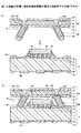
ここで、比較例を参照しながら、半導体装置1が奏する特有の効果について説明する。図7は、比較例に係る半導体装置を例示する図である。図7を参照するに、比較例に係る半導体装置100は、基板接続部材30が基板接続部材300に置換された点が、半導体装置1(図1参照)と相違する。基板接続部材300は、略球状のコア310の周囲をはんだめっき320で被覆したはんだボールである。
Here, with reference to a comparative example, a specific effect produced by the
半導体装置100は、半導体装置1と同様に、ブリードアウトエリアEを有し、ブリードアウトエリアEには基板接続部材300を設けることができない。そのため、平面視において、第2の半導体チップ80の電極の位置が基板接続部材300の位置と一致していない場合には、矢印R1のような電流経路となり最短配線距離を得ることができない。その結果、伝送遅延やノイズリスクが高まり、第2の半導体チップ80の種類によっては性能低下や動作不具合等につながる。
Similar to the
これに対して、図8に示すように、半導体装置1では、基板接続部材30を所定の傾斜角θで傾いた状態で配置しているため、ブリードアウトエリアE上の領域を有効利用することができる。すなわち、平面視において、第2の半導体チップ80の電極がブリードアウトエリアEと重複する場合であっても(一部が重複する場合及び全部が重複する場合を含む)、矢印R2のような電流経路を実現可能となり、比較例よりも配線距離を短縮することができる。その結果、伝送速度の向上やノイズの低減を実現することが可能となる。
On the other hand, as shown in FIG. 8, in the
〈第2の実施の形態〉
第2の実施の形態では、基板接続部材30の過剰な倒れを防止する突起部を設ける例を示す。なお、第2の実施の形態において、既に説明した実施の形態と同一構成部についての説明は省略する場合がある。
<Second Embodiment>
In 2nd Embodiment, the example which provides the projection part which prevents the excessive fall of the board |
図9は、第2の実施の形態に係る半導体装置を例示する断面図である。図9を参照するに、第2の実施の形態に係る半導体装置1Aは、第1の突起部19及び第2の突起部29が設けられた点が、第1の実施の形態に係る半導体装置1(図1参照)と相違する。
FIG. 9 is a cross-sectional view illustrating a semiconductor device according to the second embodiment. Referring to FIG. 9, the
第1の突起部19は、第1の基板10の第2の基板20側の面の(ソルダーレジスト層15の表面の)、開口部15xとアンダーフィル樹脂50との間に、第2の基板20側に突起して基板接続部材30と接するように設けられている。同様に、第2の突起部29は、第2の基板20の第1の基板10側の面の(ソルダーレジスト層25の表面の)、開口部25xの周囲で、平面視したときに第1の半導体チップ40と重なる位置とは反対側にあたる位置に、第1の基板10側に突起して基板接続部材30と接するように設けられている。第1の突起部19及び第2の突起部29を設けたことにより、基板接続部材30の過剰な倒れを防止することができる。
The
図10及び図11は、第2の実施の形態に係る半導体装置の製造工程を例示する図である。 10 and 11 are diagrams illustrating the manufacturing process of the semiconductor device according to the second embodiment.
まず、図10(a)に示す工程では、周知の手法により第2の基板20を作製する。そして、第2の基板20のソルダーレジスト層25の表面から突起する第2の突起部29を設ける。第2の突起部29は、例えば、ソルダーレジスト層25と同様の材料を用いてフォトリソグラフィ法により形成できる。この場合は、第2の突起部29を第2の基板20の製造工程中に形成できるメリットがある。或いは、第2の突起部29をエポキシ系樹脂等の絶縁性樹脂やシリコン等の無機材料を用いて印刷法やディスペンス法等により形成してもよい。この場合は、第2の基板20を作製後、別工程で第2の突起部29を形成することになる。
First, in the step shown in FIG. 10A, the
なお、第2の突起部29は必ずしも絶縁材料から形成する必要はなく、金属等の導電材料から形成してもよい。但し、金属を用いる場合には、はんだめっき32が濡れ広がり難い材料(すなわち、表面酸化が進み易い材料)を選択することが好ましい。
Note that the
又、第2の突起部29を、接着性を有するBステージ状態の樹脂から形成すると好適である。後工程で基板接続部材30が第2の突起部29に接した際に接着されて保持力が高まり、基板接続部材30の位置決めが更に容易になるからである。又、リフロー等により基板接続部材30を加熱する際に、はんだめっき32が溶融しても第2の突起部29に接着された基板接続部材30が自由に動くことを防止可能となり、位置決め精度を更に向上できるからである。この場合、Bステージ状態の樹脂は、リフロー等により基板接続部材30を加熱する際に硬化し、基板接続部材30の保持を継続する。
The
次に、図10(b)及び図10(c)に示す工程では、図3(a)〜図4(c)と同様の工程を実施する。この際、第2の突起部29が存在することにより、基板接続部材30の第2の基板20の他方の面に対する傾斜角θは第2の突起部29により規定され、基板接続部材30の過剰な倒れを防止することができる。又、基板接続部材30は第2の突起部29に接するため、基板接続部材30の配置精度(水平方向の位置精度)を向上することができる。又、図3(b)に相当する工程において、振込治具500が下降する際に、第2の突起部29を下側の位置決めとしても利用できる。つまり、第2の突起部29の上面と接するまで振込治具500を下降させればよい。
Next, in the steps shown in FIGS. 10B and 10C, the same steps as in FIGS. 3A to 4C are performed. At this time, due to the presence of the
次に、図11(a)に示す工程では、周知の手法により第1の基板10を作製する。そして、第1の基板10のソルダーレジスト層15の表面から突起する第1の突起部19を設ける。第1の突起部19は、例えば、第2の突起部29と同様の方法により形成できる。その後、第1の基板10の一方の面に第1の半導体チップ40をフェイスダウン状態でフリップチップ実装する。そして、第1の半導体チップ40の回路形成面と第1の基板10の一方の面との間にアンダーフィル樹脂50を充填する。その後、図10(c)に示す構造体を上下反転させて第1の基板10上に配置する。この際、第1の突起部19及び第2の突起部29が存在することにより、基板接続部材30の第1の基板10の一方の面に対する傾斜角θは第1の突起部19及び第2の突起部29により規定され、基板接続部材30の過剰な倒れを防止することができる。
Next, in the step shown in FIG. 11A, the
次に、図11(b)に示す工程では、図5(b)及び図6(a)と同様の工程を実施する。モールド樹脂60を充填する際に、第1の基板10及び第2の基板20を金型により上下から押し込む場合がある。しかし、この場合でも、基板接続部材30が第1の突起部19及び第2の突起部29に接してそれ以上倒れないため、基板接続部材30の傾斜角θを一定に保持することができる。
Next, in the step shown in FIG. 11B, the same steps as those in FIGS. 5B and 6A are performed. When filling the
次に、図11(b)に示す工程の後、図6(b)に示す工程と同様の工程を実施することにより、図9に示す半導体装置1Aが完成する。この際、はんだめっき32が融点以上の温度に加熱されたとしても、基板接続部材30が第1の突起部19及び第2の突起部29に接してそれ以上倒れないため、はんだめっき32が再溶融して基板接続部材30の傾斜角θが変わることを防止できる。
Next, after the step shown in FIG. 11B, a step similar to the step shown in FIG. 6B is performed to complete the
このように、第1の突起部19及び第2の突起部29を設けることにより、基板接続部材30の傾斜角θの制御精度を向上できる。又、基板接続部材30に外力や応力、熱等が加わった際に、基板接続部材30の傾斜角θや基板接続部材30の水平方向の位置が変動することを防止できる。
Thus, by providing the
〈突起部の形状のバリエーション〉
第2の実施の形態で示した突起部のバリエーションについて説明する。第1の突起部19及び第2の突起部29は、基板接続部材30に接することで、基板接続部材30の過剰な倒れを防止するものであるから、その目的を達成できれば如何なる形状であっても構わないが、ここで好適な例をいくつか示す。なお、ここでは、第1の突起部19についてのみ示すが、第2の突起部29についても同様である。
<Variation of protrusion shape>
Variations of the protrusion shown in the second embodiment will be described. Since the
図12は、突起部のバリエーションを例示する平面図である。なお、矢印は、基板接続部材30の傾斜方向を示している。図12(a)のように、第1の突起部19の平面形状は、基板接続部材30の傾斜方向に設けられた、1本の直線状の部位とすることができる。又、図12(b)のように、第1の突起部19の平面形状は、基板接続部材30の傾斜方向に設けられた、開口部15xの外縁に沿った円環の一部からなる形状の部位であってもよい。或いは、図示はしないが、開口部15xの外縁の全体を円環で囲うようにしてもよい。
FIG. 12 is a plan view illustrating a variation of the protrusion. The arrow indicates the direction of inclination of the
又、図12(c)のように、第1の突起部19の平面形状は、基板接続部材30の傾斜方向に設けられた、2本の直線状の部位が所定の角度で交わった部位であってもよい。又、図12(d)のように、第1の突起部19の平面形状は、基板接続部材30の傾斜方向に設けられた、コの字状の部位であってもよい。又、図12(e)のように、第1の突起部19の平面形状は、4本の直線状の部位が互いに独立して開口部15xの外縁の全体を囲う形状にしてもよい。又、図12(f)のように、第1の突起部19の平面形状は、開口部15xの外縁の全体を四角環で囲う形状にしてもよい。
Further, as shown in FIG. 12C, the planar shape of the
第1の突起部19は、図12(a)〜図12(f)の何れの平面形状であっても、或いはこれらに類する平面形状であっても、前述のように、基板接続部材30の傾斜角θの制御精度を向上する等の効果を奏する。特に、図12(b)及び図12(c)に示す平面形状の場合には、他の場合と比べて第1の突起部19と基板接続部材30との接触面積が増加するため、基板接続部材30の傾斜方向及び傾斜角をいっそう精度よく制御可能である。
As described above, the
以上、好ましい実施の形態等について詳説したが、上述した実施の形態等に制限されることはなく、特許請求の範囲に記載された範囲を逸脱することなく、上述した実施の形態等に種々の変形及び置換を加えることができる。 The preferred embodiments and the like have been described in detail above, but the present invention is not limited to the above-described embodiments and the like, and various modifications can be made to the above-described embodiments and the like without departing from the scope described in the claims. Variations and substitutions can be added.
例えば、第1の基板10や第2の基板20として、より多層の配線層や絶縁層が形成されたビルドアップ基板等を用いても構わない。その際、コアレスのビルドアップ基板等を用いても構わない。或いは、第1の基板10や第2の基板20として、シリコン基板やセラミック基板等を用いても構わない。
For example, as the
又、基板接続部材30のコア31の上端面及び下端面は、コア31の長手方向に対して垂直でなくても構わない。例えば、上端面及び下端面が第1の基板10の一方の面に平行であり、長手方向が第1の基板10の一方の面に対して傾斜した部材を用いてもよい。
Further, the upper end surface and the lower end surface of the
又、半導体装置1等の製造工程において、基板接続部材30を第2の基板20に先に実装する例を示したが、基板接続部材30を第1の基板10に先に実装してもよい。
Further, in the manufacturing process of the
1、1A 半導体装置
10 第1の基板
11、21 絶縁層
12、14、22、23 配線層
13 パッド
15、16、24、25 ソルダーレジスト層
15x、16x、24x、25x 開口部
19 第1の突起部
20 第2の基板
21x ビアホール
29 第2の突起部
30 基板接続部材
31 コア
32 はんだめっき
32a はんだペースト
40 第1の半導体チップ
45 突起電極
50 アンダーフィル樹脂
60 モールド樹脂
70、90 バンプ
80 第2の半導体チップ
500 振込治具
500x 収容部
600 傾斜用治具
DESCRIPTION OF
Claims (9)
一方の面及び前記一方の面の反対面となる他方の面を有し、前記他方の面に第2のパッドを備え、前記第2のパッド側が前記第1のパッド側と対向するように、前記第1の基板の上方に積層された第2の基板と、
前記第1の基板と前記第2の基板との間に設けられ、前記第1の基板と前記第2の基板とを電気的に接続する柱状の基板接続部材と、を有し、
前記第2のパッドは、平面視において、前記樹脂と全部又は一部が重複する位置に設けられ、
前記基板接続部材は、柱状のコアと、前記コアの外周面を被覆するはんだめっきと、を備え、
前記基板接続部材は、前記第1のパッドと前記第2のパッドとの間に斜めに配置されて、前記はんだめっきが前記第1のパッド上に延伸して前記基板接続部材の一端が前記第1のパッドと接合され、前記はんだめっきが前記第2のパッド上に延伸して前記基板接続部材の他端が前記第2のパッドと接合されている半導体装置。 A first semiconductor chip mounted on one surface, and a resin formed between the one surface and the first semiconductor chip and extending outside the outer shape of the first semiconductor chip; A first pad provided on the outside of the resin in plan view, and a first substrate,
One surface and the other surface opposite to the one surface, the second surface is provided with a second pad, and the second pad side faces the first pad side, A second substrate stacked above the first substrate;
A columnar substrate connecting member provided between the first substrate and the second substrate and electrically connecting the first substrate and the second substrate;
The second pad is provided at a position where the resin partially or entirely overlaps in plan view,
The board connecting member includes a columnar core and solder plating that covers an outer peripheral surface of the core,
The board connecting member is disposed obliquely between the first pad and the second pad, the solder plating extends on the first pad, and one end of the board connecting member is the first pad . A semiconductor device that is bonded to one pad, the solder plating extends onto the second pad, and the other end of the substrate connecting member is bonded to the second pad.
前記第2のパッドと前記第2の半導体チップの電極とは、平面視したときに重なる位置に配置されており、前記第2の基板を貫通する垂直配線を介して電気的に接続されている請求項1又は2記載の半導体装置。 A second semiconductor chip is mounted on one surface of the second substrate;
The second pad and the electrode of the second semiconductor chip are arranged at positions overlapping when viewed in plan, and are electrically connected via a vertical wiring penetrating the second substrate. the semiconductor device according to claim 1 or 2, wherein.
一方の面及び前記一方の面の反対面となる他方の面を有し、前記他方の面に第2のパッドを備えた第2の基板を準備する工程と、
前記第2のパッド側が前記第1のパッド側と対向するように、前記第1の基板の上方に前記第2の基板を積層し、前記第1の基板と前記第2の基板とを、柱状のコアと、前記コアの外周面を被覆するはんだめっきと、を備えた基板接続部材を介して電気的に接続する工程と、を有し、
前記第2のパッドは、平面視において、前記樹脂と全部又は一部が重複する位置に設けられ、
前記基板接続部材は、前記第1のパッドと前記第2のパッドとの間に斜めに配置されて、前記はんだめっきが前記第1のパッド上に延伸して前記基板接続部材の一端が前記第1のパッドと接合され、前記はんだめっきが前記第2のパッド上に延伸して前記基板接続部材の他端が前記第2のパッドと接合される半導体装置の製造方法。 A first semiconductor chip mounted on one surface, and a resin formed between the one surface and the first semiconductor chip and extending outside the outer shape of the first semiconductor chip; Preparing a first substrate provided with a first pad disposed outside the resin in plan view;
Preparing a second substrate having one surface and the other surface opposite to the one surface, and having a second pad on the other surface;
The second substrate is stacked above the first substrate so that the second pad side faces the first pad side, and the first substrate and the second substrate are formed in a column shape. And a step of electrically connecting via a board connecting member provided with a core and a solder plating covering the outer peripheral surface of the core ,
The second pad is provided at a position where the resin partially or entirely overlaps in plan view,
The board connecting member is disposed obliquely between the first pad and the second pad, the solder plating extends on the first pad, and one end of the board connecting member is the first pad . A method of manufacturing a semiconductor device, wherein the solder plating is extended onto the second pad, and the other end of the substrate connecting member is bonded to the second pad.
Priority Applications (2)
| Application Number | Priority Date | Filing Date | Title |
|---|---|---|---|
| JP2015108811A JP6392171B2 (en) | 2015-05-28 | 2015-05-28 | Semiconductor device and manufacturing method thereof |
| US15/155,175 US9564421B2 (en) | 2015-05-28 | 2016-05-16 | Semiconductor device |
Applications Claiming Priority (1)
| Application Number | Priority Date | Filing Date | Title |
|---|---|---|---|
| JP2015108811A JP6392171B2 (en) | 2015-05-28 | 2015-05-28 | Semiconductor device and manufacturing method thereof |
Publications (3)
| Publication Number | Publication Date |
|---|---|
| JP2016225414A JP2016225414A (en) | 2016-12-28 |
| JP2016225414A5 JP2016225414A5 (en) | 2018-01-25 |
| JP6392171B2 true JP6392171B2 (en) | 2018-09-19 |
Family
ID=57398977
Family Applications (1)
| Application Number | Title | Priority Date | Filing Date |
|---|---|---|---|
| JP2015108811A Active JP6392171B2 (en) | 2015-05-28 | 2015-05-28 | Semiconductor device and manufacturing method thereof |
Country Status (2)
| Country | Link |
|---|---|
| US (1) | US9564421B2 (en) |
| JP (1) | JP6392171B2 (en) |
Families Citing this family (7)
| Publication number | Priority date | Publication date | Assignee | Title |
|---|---|---|---|---|
| KR102420126B1 (en) * | 2016-02-01 | 2022-07-12 | 삼성전자주식회사 | Semiconductor Device |
| JP7078821B2 (en) * | 2017-04-28 | 2022-06-01 | 東北マイクロテック株式会社 | Solid-state image sensor |
| WO2018230534A1 (en) * | 2017-06-16 | 2018-12-20 | 株式会社村田製作所 | Circuit board, circuit module, method for producing circuit board, and method for producing circuit module |
| JP7015721B2 (en) * | 2018-04-05 | 2022-02-03 | 新光電気工業株式会社 | Wiring board, electronic device |
| US11569159B2 (en) * | 2019-08-30 | 2023-01-31 | Taiwan Semiconductor Manufacturing Company, Ltd. | Structure and formation method of chip package with through vias |
| CN110782799B (en) * | 2019-11-21 | 2022-01-04 | 昆山国显光电有限公司 | Display panel and preparation method thereof |
| US11094668B2 (en) * | 2019-12-12 | 2021-08-17 | Micron Technology, Inc. | Solderless interconnect for semiconductor device assembly |
Family Cites Families (9)
| Publication number | Priority date | Publication date | Assignee | Title |
|---|---|---|---|---|
| JP2003347722A (en) | 2002-05-23 | 2003-12-05 | Ibiden Co Ltd | Multilayer electronic parts mounting substrate and its fabricating method |
| US6974330B2 (en) * | 2002-08-08 | 2005-12-13 | Micron Technology, Inc. | Electronic devices incorporating electrical interconnections with improved reliability and methods of fabricating same |
| JP4765468B2 (en) * | 2005-08-03 | 2011-09-07 | 株式会社村田製作所 | Method for manufacturing ceramic substrate and ceramic substrate |
| JP2007123595A (en) * | 2005-10-28 | 2007-05-17 | Nec Corp | Semiconductor device and its mounting structure |
| JP2009192309A (en) * | 2008-02-13 | 2009-08-27 | Shinko Electric Ind Co Ltd | Semiconductor inspection device |
| JP2010135671A (en) * | 2008-12-08 | 2010-06-17 | Panasonic Corp | Semiconductor equipment and method of manufacturing the same |
| JP5707902B2 (en) * | 2010-12-02 | 2015-04-30 | ソニー株式会社 | Semiconductor device and manufacturing method thereof |
| US9105483B2 (en) * | 2011-10-17 | 2015-08-11 | Invensas Corporation | Package-on-package assembly with wire bond vias |
| US8372741B1 (en) * | 2012-02-24 | 2013-02-12 | Invensas Corporation | Method for package-on-package assembly with wire bonds to encapsulation surface |
-
2015
- 2015-05-28 JP JP2015108811A patent/JP6392171B2/en active Active
-
2016
- 2016-05-16 US US15/155,175 patent/US9564421B2/en active Active
Also Published As
| Publication number | Publication date |
|---|---|
| JP2016225414A (en) | 2016-12-28 |
| US20160351544A1 (en) | 2016-12-01 |
| US9564421B2 (en) | 2017-02-07 |
Similar Documents
| Publication | Publication Date | Title |
|---|---|---|
| JP6392171B2 (en) | Semiconductor device and manufacturing method thereof | |
| JP6342794B2 (en) | Wiring board and method of manufacturing wiring board | |
| KR102032844B1 (en) | Built-in electronic component substrate and method for manufacturing the substrate | |
| US9570414B2 (en) | Semiconductor device and method of manufacturing the semiconductor device | |
| JP6282454B2 (en) | Manufacturing method of semiconductor package | |
| JP6352644B2 (en) | Wiring substrate and semiconductor package manufacturing method | |
| US9935053B2 (en) | Electronic component integrated substrate | |
| JP2017174849A (en) | Semiconductor device and semiconductor device manufacturing method | |
| JP2013115336A (en) | Semiconductor device and manufacturing method of the same | |
| JP2006114604A (en) | Semiconductor device and assembly method thereof | |
| JP4182144B2 (en) | Manufacturing method of chip embedded substrate | |
| KR20120058118A (en) | Method of fabricating stacked package, and method of mounting stacked package fabricated by the same | |
| JP6454384B2 (en) | Electronic component built-in substrate and manufacturing method thereof | |
| JP5015065B2 (en) | Wiring board | |
| JP2017028156A (en) | Mounting structure and manufacturing method therefor | |
| JP6713289B2 (en) | Semiconductor device and method of manufacturing semiconductor device | |
| JP6495130B2 (en) | Semiconductor device and manufacturing method thereof | |
| TW201733076A (en) | Semiconductor device and manufacturing method thereof capable of raising the production rate of semiconductor devices constituting a lower part of a PoP-type semiconductor device | |
| US20160329269A1 (en) | Chip package structure and manufacturing method thereof | |
| JP4186055B2 (en) | Electronic component device and electronic component manufacturing method | |
| KR101776305B1 (en) | The printed circuit board and the method for manufacturing the same | |
| JP2009266972A (en) | Laminated semiconductor module and method of manufacturing the same | |
| JP5187207B2 (en) | Semiconductor device, semiconductor element, and method for manufacturing semiconductor device | |
| US20230276575A1 (en) | Embedded printed circuit board | |
| JP4828997B2 (en) | SEMICONDUCTOR PACKAGE AND ITS MOUNTING METHOD, AND INSULATED WIRING BOARD USED FOR THE SEMICONDUCTOR PACKAGE AND MANUFACTURING METHOD |
Legal Events
| Date | Code | Title | Description |
|---|---|---|---|
| A521 | Request for written amendment filed |
Free format text: JAPANESE INTERMEDIATE CODE: A523 Effective date: 20171205 |
|
| A621 | Written request for application examination |
Free format text: JAPANESE INTERMEDIATE CODE: A621 Effective date: 20171205 |
|
| A977 | Report on retrieval |
Free format text: JAPANESE INTERMEDIATE CODE: A971007 Effective date: 20180808 |
|
| TRDD | Decision of grant or rejection written | ||
| A01 | Written decision to grant a patent or to grant a registration (utility model) |
Free format text: JAPANESE INTERMEDIATE CODE: A01 Effective date: 20180814 |
|
| A61 | First payment of annual fees (during grant procedure) |
Free format text: JAPANESE INTERMEDIATE CODE: A61 Effective date: 20180822 |
|
| R150 | Certificate of patent or registration of utility model |
Ref document number: 6392171 Country of ref document: JP Free format text: JAPANESE INTERMEDIATE CODE: R150 |