JP5601811B2 - 半導体装置 - Google Patents
半導体装置 Download PDFInfo
- Publication number
- JP5601811B2 JP5601811B2 JP2009229211A JP2009229211A JP5601811B2 JP 5601811 B2 JP5601811 B2 JP 5601811B2 JP 2009229211 A JP2009229211 A JP 2009229211A JP 2009229211 A JP2009229211 A JP 2009229211A JP 5601811 B2 JP5601811 B2 JP 5601811B2
- Authority
- JP
- Japan
- Prior art keywords
- layer
- wiring
- thin film
- oxide semiconductor
- film transistor
- Prior art date
- Legal status (The legal status is an assumption and is not a legal conclusion. Google has not performed a legal analysis and makes no representation as to the accuracy of the status listed.)
- Active
Links
- 239000004065 semiconductor Substances 0.000 title claims description 213
- 239000010410 layer Substances 0.000 claims description 349
- 238000000034 method Methods 0.000 claims description 75
- 239000011241 protective layer Substances 0.000 claims description 51
- 230000008569 process Effects 0.000 claims description 23
- 239000011701 zinc Substances 0.000 claims description 9
- 229910052733 gallium Inorganic materials 0.000 claims description 7
- 229910052738 indium Inorganic materials 0.000 claims description 4
- 229910052725 zinc Inorganic materials 0.000 claims description 4
- GYHNNYVSQQEPJS-UHFFFAOYSA-N Gallium Chemical compound [Ga] GYHNNYVSQQEPJS-UHFFFAOYSA-N 0.000 claims description 3
- 229910052723 transition metal Inorganic materials 0.000 claims description 3
- 150000003624 transition metals Chemical class 0.000 claims description 2
- HCHKCACWOHOZIP-UHFFFAOYSA-N Zinc Chemical compound [Zn] HCHKCACWOHOZIP-UHFFFAOYSA-N 0.000 claims 2
- APFVFJFRJDLVQX-UHFFFAOYSA-N indium atom Chemical compound [In] APFVFJFRJDLVQX-UHFFFAOYSA-N 0.000 claims 2
- 239000010409 thin film Substances 0.000 description 242
- 239000010408 film Substances 0.000 description 232
- 239000000758 substrate Substances 0.000 description 88
- 239000013078 crystal Substances 0.000 description 53
- 238000004544 sputter deposition Methods 0.000 description 53
- 239000004973 liquid crystal related substance Substances 0.000 description 49
- 229910007541 Zn O Inorganic materials 0.000 description 39
- 239000000463 material Substances 0.000 description 39
- 238000005530 etching Methods 0.000 description 33
- XKRFYHLGVUSROY-UHFFFAOYSA-N Argon Chemical compound [Ar] XKRFYHLGVUSROY-UHFFFAOYSA-N 0.000 description 28
- 230000015572 biosynthetic process Effects 0.000 description 27
- 238000004519 manufacturing process Methods 0.000 description 25
- 230000006870 function Effects 0.000 description 24
- 239000000123 paper Substances 0.000 description 23
- 230000001681 protective effect Effects 0.000 description 22
- 239000012300 argon atmosphere Substances 0.000 description 19
- 239000011159 matrix material Substances 0.000 description 19
- 238000005401 electroluminescence Methods 0.000 description 18
- 239000012298 atmosphere Substances 0.000 description 17
- 239000002245 particle Substances 0.000 description 17
- 229910052782 aluminium Chemical group 0.000 description 16
- 239000003990 capacitor Substances 0.000 description 15
- 239000007789 gas Substances 0.000 description 15
- 238000010438 heat treatment Methods 0.000 description 15
- 239000010936 titanium Chemical group 0.000 description 15
- IJGRMHOSHXDMSA-UHFFFAOYSA-N Atomic nitrogen Chemical compound N#N IJGRMHOSHXDMSA-UHFFFAOYSA-N 0.000 description 14
- XAGFODPZIPBFFR-UHFFFAOYSA-N aluminium Chemical group [Al] XAGFODPZIPBFFR-UHFFFAOYSA-N 0.000 description 14
- 229910052786 argon Inorganic materials 0.000 description 14
- XLOMVQKBTHCTTD-UHFFFAOYSA-N Zinc monoxide Chemical compound [Zn]=O XLOMVQKBTHCTTD-UHFFFAOYSA-N 0.000 description 13
- 229910052581 Si3N4 Inorganic materials 0.000 description 12
- VYPSYNLAJGMNEJ-UHFFFAOYSA-N Silicium dioxide Chemical compound O=[Si]=O VYPSYNLAJGMNEJ-UHFFFAOYSA-N 0.000 description 12
- 239000004020 conductor Substances 0.000 description 12
- HQVNEWCFYHHQES-UHFFFAOYSA-N silicon nitride Chemical compound N12[Si]34N5[Si]62N3[Si]51N64 HQVNEWCFYHHQES-UHFFFAOYSA-N 0.000 description 12
- 229910052814 silicon oxide Inorganic materials 0.000 description 12
- 239000000956 alloy Substances 0.000 description 11
- 238000004891 communication Methods 0.000 description 11
- 239000011521 glass Substances 0.000 description 11
- 238000000206 photolithography Methods 0.000 description 11
- 229910045601 alloy Inorganic materials 0.000 description 10
- 229910052751 metal Inorganic materials 0.000 description 10
- QVGXLLKOCUKJST-UHFFFAOYSA-N atomic oxygen Chemical compound [O] QVGXLLKOCUKJST-UHFFFAOYSA-N 0.000 description 9
- 239000003094 microcapsule Substances 0.000 description 9
- 239000001301 oxygen Substances 0.000 description 9
- 229910052760 oxygen Inorganic materials 0.000 description 9
- 229920005989 resin Polymers 0.000 description 9
- 239000011347 resin Substances 0.000 description 9
- 230000002441 reversible effect Effects 0.000 description 9
- 239000000565 sealant Substances 0.000 description 9
- 239000002356 single layer Substances 0.000 description 9
- 229910052719 titanium Inorganic materials 0.000 description 9
- 239000002184 metal Substances 0.000 description 8
- 229910052750 molybdenum Inorganic materials 0.000 description 8
- ZOKXTWBITQBERF-UHFFFAOYSA-N Molybdenum Chemical group [Mo] ZOKXTWBITQBERF-UHFFFAOYSA-N 0.000 description 7
- PXHVJJICTQNCMI-UHFFFAOYSA-N Nickel Chemical compound [Ni] PXHVJJICTQNCMI-UHFFFAOYSA-N 0.000 description 7
- XUIMIQQOPSSXEZ-UHFFFAOYSA-N Silicon Chemical compound [Si] XUIMIQQOPSSXEZ-UHFFFAOYSA-N 0.000 description 7
- RTAQQCXQSZGOHL-UHFFFAOYSA-N Titanium Chemical group [Ti] RTAQQCXQSZGOHL-UHFFFAOYSA-N 0.000 description 7
- AMGQUBHHOARCQH-UHFFFAOYSA-N indium;oxotin Chemical compound [In].[Sn]=O AMGQUBHHOARCQH-UHFFFAOYSA-N 0.000 description 7
- 239000011733 molybdenum Chemical group 0.000 description 7
- 229910052757 nitrogen Inorganic materials 0.000 description 7
- 230000003287 optical effect Effects 0.000 description 7
- 229910052710 silicon Inorganic materials 0.000 description 7
- 239000010703 silicon Substances 0.000 description 7
- 229910052721 tungsten Inorganic materials 0.000 description 7
- 239000011787 zinc oxide Substances 0.000 description 7
- 239000011651 chromium Substances 0.000 description 6
- 239000000428 dust Substances 0.000 description 6
- 230000005684 electric field Effects 0.000 description 6
- 229910052734 helium Inorganic materials 0.000 description 6
- 239000001307 helium Substances 0.000 description 6
- SWQJXJOGLNCZEY-UHFFFAOYSA-N helium atom Chemical compound [He] SWQJXJOGLNCZEY-UHFFFAOYSA-N 0.000 description 6
- 239000001257 hydrogen Substances 0.000 description 6
- 229910052739 hydrogen Inorganic materials 0.000 description 6
- 125000004435 hydrogen atom Chemical class [H]* 0.000 description 6
- 238000003780 insertion Methods 0.000 description 6
- 230000037431 insertion Effects 0.000 description 6
- 239000000126 substance Substances 0.000 description 6
- 239000010937 tungsten Substances 0.000 description 6
- 238000001039 wet etching Methods 0.000 description 6
- 238000004458 analytical method Methods 0.000 description 5
- 239000010949 copper Substances 0.000 description 5
- 229910003437 indium oxide Inorganic materials 0.000 description 5
- PJXISJQVUVHSOJ-UHFFFAOYSA-N indium(iii) oxide Chemical compound [O-2].[O-2].[O-2].[In+3].[In+3] PJXISJQVUVHSOJ-UHFFFAOYSA-N 0.000 description 5
- 239000000203 mixture Substances 0.000 description 5
- 238000009832 plasma treatment Methods 0.000 description 5
- 229920003023 plastic Polymers 0.000 description 5
- 239000004033 plastic Substances 0.000 description 5
- WFKWXMTUELFFGS-UHFFFAOYSA-N tungsten Chemical group [W] WFKWXMTUELFFGS-UHFFFAOYSA-N 0.000 description 5
- RYGMFSIKBFXOCR-UHFFFAOYSA-N Copper Chemical compound [Cu] RYGMFSIKBFXOCR-UHFFFAOYSA-N 0.000 description 4
- MYMOFIZGZYHOMD-UHFFFAOYSA-N Dioxygen Chemical compound O=O MYMOFIZGZYHOMD-UHFFFAOYSA-N 0.000 description 4
- 229910005191 Ga 2 O 3 Inorganic materials 0.000 description 4
- 240000002329 Inga feuillei Species 0.000 description 4
- GWEVSGVZZGPLCZ-UHFFFAOYSA-N Titan oxide Chemical compound O=[Ti]=O GWEVSGVZZGPLCZ-UHFFFAOYSA-N 0.000 description 4
- 229910021417 amorphous silicon Inorganic materials 0.000 description 4
- 229910052804 chromium Inorganic materials 0.000 description 4
- 229920001940 conductive polymer Polymers 0.000 description 4
- 229910052802 copper Inorganic materials 0.000 description 4
- 229910001882 dioxygen Inorganic materials 0.000 description 4
- 239000000945 filler Substances 0.000 description 4
- 239000007788 liquid Substances 0.000 description 4
- 230000007246 mechanism Effects 0.000 description 4
- 239000002159 nanocrystal Substances 0.000 description 4
- 229910052759 nickel Inorganic materials 0.000 description 4
- QGLKJKCYBOYXKC-UHFFFAOYSA-N nonaoxidotritungsten Chemical compound O=[W]1(=O)O[W](=O)(=O)O[W](=O)(=O)O1 QGLKJKCYBOYXKC-UHFFFAOYSA-N 0.000 description 4
- 230000004044 response Effects 0.000 description 4
- 239000012798 spherical particle Substances 0.000 description 4
- 229910052715 tantalum Inorganic materials 0.000 description 4
- OGIDPMRJRNCKJF-UHFFFAOYSA-N titanium oxide Inorganic materials [Ti]=O OGIDPMRJRNCKJF-UHFFFAOYSA-N 0.000 description 4
- 229910001930 tungsten oxide Inorganic materials 0.000 description 4
- YVTHLONGBIQYBO-UHFFFAOYSA-N zinc indium(3+) oxygen(2-) Chemical compound [O--].[Zn++].[In+3] YVTHLONGBIQYBO-UHFFFAOYSA-N 0.000 description 4
- QTBSBXVTEAMEQO-UHFFFAOYSA-N Acetic acid Chemical compound CC(O)=O QTBSBXVTEAMEQO-UHFFFAOYSA-N 0.000 description 3
- VYZAMTAEIAYCRO-UHFFFAOYSA-N Chromium Chemical compound [Cr] VYZAMTAEIAYCRO-UHFFFAOYSA-N 0.000 description 3
- XEEYBQQBJWHFJM-UHFFFAOYSA-N Iron Chemical compound [Fe] XEEYBQQBJWHFJM-UHFFFAOYSA-N 0.000 description 3
- 229910052779 Neodymium Inorganic materials 0.000 description 3
- NRTOMJZYCJJWKI-UHFFFAOYSA-N Titanium nitride Chemical compound [Ti]#N NRTOMJZYCJJWKI-UHFFFAOYSA-N 0.000 description 3
- NIXOWILDQLNWCW-UHFFFAOYSA-N acrylic acid group Chemical group C(C=C)(=O)O NIXOWILDQLNWCW-UHFFFAOYSA-N 0.000 description 3
- 239000000969 carrier Substances 0.000 description 3
- 230000001413 cellular effect Effects 0.000 description 3
- 238000000151 deposition Methods 0.000 description 3
- 230000008021 deposition Effects 0.000 description 3
- 238000010586 diagram Methods 0.000 description 3
- KPUWHANPEXNPJT-UHFFFAOYSA-N disiloxane Chemical class [SiH3]O[SiH3] KPUWHANPEXNPJT-UHFFFAOYSA-N 0.000 description 3
- 230000000694 effects Effects 0.000 description 3
- 230000005669 field effect Effects 0.000 description 3
- QEFYFXOXNSNQGX-UHFFFAOYSA-N neodymium atom Chemical compound [Nd] QEFYFXOXNSNQGX-UHFFFAOYSA-N 0.000 description 3
- 239000012299 nitrogen atmosphere Substances 0.000 description 3
- 150000002894 organic compounds Chemical class 0.000 description 3
- TWNQGVIAIRXVLR-UHFFFAOYSA-N oxo(oxoalumanyloxy)alumane Chemical compound O=[Al]O[Al]=O TWNQGVIAIRXVLR-UHFFFAOYSA-N 0.000 description 3
- 238000005268 plasma chemical vapour deposition Methods 0.000 description 3
- 229920006267 polyester film Polymers 0.000 description 3
- 229920002620 polyvinyl fluoride Polymers 0.000 description 3
- 229910052706 scandium Inorganic materials 0.000 description 3
- SIXSYDAISGFNSX-UHFFFAOYSA-N scandium atom Chemical compound [Sc] SIXSYDAISGFNSX-UHFFFAOYSA-N 0.000 description 3
- 239000000243 solution Substances 0.000 description 3
- 238000003860 storage Methods 0.000 description 3
- GUVRBAGPIYLISA-UHFFFAOYSA-N tantalum atom Chemical compound [Ta] GUVRBAGPIYLISA-UHFFFAOYSA-N 0.000 description 3
- 238000012546 transfer Methods 0.000 description 3
- -1 tungsten nitride Chemical class 0.000 description 3
- WZJUBBHODHNQPW-UHFFFAOYSA-N 2,4,6,8-tetramethyl-1,3,5,7,2$l^{3},4$l^{3},6$l^{3},8$l^{3}-tetraoxatetrasilocane Chemical compound C[Si]1O[Si](C)O[Si](C)O[Si](C)O1 WZJUBBHODHNQPW-UHFFFAOYSA-N 0.000 description 2
- UWCWUCKPEYNDNV-LBPRGKRZSA-N 2,6-dimethyl-n-[[(2s)-pyrrolidin-2-yl]methyl]aniline Chemical compound CC1=CC=CC(C)=C1NC[C@H]1NCCC1 UWCWUCKPEYNDNV-LBPRGKRZSA-N 0.000 description 2
- QGZKDVFQNNGYKY-UHFFFAOYSA-N Ammonia Chemical compound N QGZKDVFQNNGYKY-UHFFFAOYSA-N 0.000 description 2
- CURLTUGMZLYLDI-UHFFFAOYSA-N Carbon dioxide Chemical compound O=C=O CURLTUGMZLYLDI-UHFFFAOYSA-N 0.000 description 2
- VEXZGXHMUGYJMC-UHFFFAOYSA-N Hydrochloric acid Chemical compound Cl VEXZGXHMUGYJMC-UHFFFAOYSA-N 0.000 description 2
- MHAJPDPJQMAIIY-UHFFFAOYSA-N Hydrogen peroxide Chemical compound OO MHAJPDPJQMAIIY-UHFFFAOYSA-N 0.000 description 2
- NBIIXXVUZAFLBC-UHFFFAOYSA-N Phosphoric acid Chemical compound OP(O)(O)=O NBIIXXVUZAFLBC-UHFFFAOYSA-N 0.000 description 2
- 239000004642 Polyimide Substances 0.000 description 2
- BOTDANWDWHJENH-UHFFFAOYSA-N Tetraethyl orthosilicate Chemical compound CCO[Si](OCC)(OCC)OCC BOTDANWDWHJENH-UHFFFAOYSA-N 0.000 description 2
- 238000002441 X-ray diffraction Methods 0.000 description 2
- 230000001133 acceleration Effects 0.000 description 2
- 238000000137 annealing Methods 0.000 description 2
- SWXQKHHHCFXQJF-UHFFFAOYSA-N azane;hydrogen peroxide Chemical compound [NH4+].[O-]O SWXQKHHHCFXQJF-UHFFFAOYSA-N 0.000 description 2
- DQXBYHZEEUGOBF-UHFFFAOYSA-N but-3-enoic acid;ethene Chemical compound C=C.OC(=O)CC=C DQXBYHZEEUGOBF-UHFFFAOYSA-N 0.000 description 2
- 238000005229 chemical vapour deposition Methods 0.000 description 2
- PMHQVHHXPFUNSP-UHFFFAOYSA-M copper(1+);methylsulfanylmethane;bromide Chemical compound Br[Cu].CSC PMHQVHHXPFUNSP-UHFFFAOYSA-M 0.000 description 2
- 238000001312 dry etching Methods 0.000 description 2
- 230000005611 electricity Effects 0.000 description 2
- 239000007772 electrode material Substances 0.000 description 2
- 239000005038 ethylene vinyl acetate Substances 0.000 description 2
- 230000005281 excited state Effects 0.000 description 2
- 230000001747 exhibiting effect Effects 0.000 description 2
- 239000000284 extract Substances 0.000 description 2
- 239000005262 ferroelectric liquid crystals (FLCs) Substances 0.000 description 2
- 239000011152 fibreglass Substances 0.000 description 2
- 238000007667 floating Methods 0.000 description 2
- 125000001153 fluoro group Chemical group F* 0.000 description 2
- 239000012535 impurity Substances 0.000 description 2
- 238000001095 inductively coupled plasma mass spectrometry Methods 0.000 description 2
- 238000002347 injection Methods 0.000 description 2
- 239000007924 injection Substances 0.000 description 2
- 229910010272 inorganic material Inorganic materials 0.000 description 2
- 229910052742 iron Inorganic materials 0.000 description 2
- 239000011572 manganese Substances 0.000 description 2
- 239000007769 metal material Substances 0.000 description 2
- 239000011859 microparticle Substances 0.000 description 2
- 150000004767 nitrides Chemical class 0.000 description 2
- HMMGMWAXVFQUOA-UHFFFAOYSA-N octamethylcyclotetrasiloxane Chemical compound C[Si]1(C)O[Si](C)(C)O[Si](C)(C)O[Si](C)(C)O1 HMMGMWAXVFQUOA-UHFFFAOYSA-N 0.000 description 2
- 125000000962 organic group Chemical group 0.000 description 2
- 239000011368 organic material Substances 0.000 description 2
- 230000003647 oxidation Effects 0.000 description 2
- 238000007254 oxidation reaction Methods 0.000 description 2
- BPUBBGLMJRNUCC-UHFFFAOYSA-N oxygen(2-);tantalum(5+) Chemical compound [O-2].[O-2].[O-2].[O-2].[O-2].[Ta+5].[Ta+5] BPUBBGLMJRNUCC-UHFFFAOYSA-N 0.000 description 2
- 238000005192 partition Methods 0.000 description 2
- 239000000049 pigment Substances 0.000 description 2
- 229920001200 poly(ethylene-vinyl acetate) Polymers 0.000 description 2
- 229920002037 poly(vinyl butyral) polymer Polymers 0.000 description 2
- 229910021420 polycrystalline silicon Inorganic materials 0.000 description 2
- 229920001721 polyimide Polymers 0.000 description 2
- 229920000915 polyvinyl chloride Polymers 0.000 description 2
- 239000004800 polyvinyl chloride Substances 0.000 description 2
- 238000001552 radio frequency sputter deposition Methods 0.000 description 2
- 238000005546 reactive sputtering Methods 0.000 description 2
- 230000009467 reduction Effects 0.000 description 2
- 239000002904 solvent Substances 0.000 description 2
- 125000006850 spacer group Chemical group 0.000 description 2
- 230000003068 static effect Effects 0.000 description 2
- 229910001936 tantalum oxide Inorganic materials 0.000 description 2
- CZDYPVPMEAXLPK-UHFFFAOYSA-N tetramethylsilane Chemical compound C[Si](C)(C)C CZDYPVPMEAXLPK-UHFFFAOYSA-N 0.000 description 2
- 230000007704 transition Effects 0.000 description 2
- 238000001771 vacuum deposition Methods 0.000 description 2
- 210000003462 vein Anatomy 0.000 description 2
- XLYOFNOQVPJJNP-UHFFFAOYSA-N water Substances O XLYOFNOQVPJJNP-UHFFFAOYSA-N 0.000 description 2
- 239000004925 Acrylic resin Substances 0.000 description 1
- 229920000178 Acrylic resin Polymers 0.000 description 1
- 229910000838 Al alloy Inorganic materials 0.000 description 1
- 229910017073 AlLi Inorganic materials 0.000 description 1
- 239000004986 Cholesteric liquid crystals (ChLC) Substances 0.000 description 1
- 239000004593 Epoxy Substances 0.000 description 1
- 206010052128 Glare Diseases 0.000 description 1
- DGAQECJNVWCQMB-PUAWFVPOSA-M Ilexoside XXIX Chemical compound C[C@@H]1CC[C@@]2(CC[C@@]3(C(=CC[C@H]4[C@]3(CC[C@@H]5[C@@]4(CC[C@@H](C5(C)C)OS(=O)(=O)[O-])C)C)[C@@H]2[C@]1(C)O)C)C(=O)O[C@H]6[C@@H]([C@H]([C@@H]([C@H](O6)CO)O)O)O.[Na+] DGAQECJNVWCQMB-PUAWFVPOSA-M 0.000 description 1
- PWHULOQIROXLJO-UHFFFAOYSA-N Manganese Chemical compound [Mn] PWHULOQIROXLJO-UHFFFAOYSA-N 0.000 description 1
- GRYLNZFGIOXLOG-UHFFFAOYSA-N Nitric acid Chemical compound O[N+]([O-])=O GRYLNZFGIOXLOG-UHFFFAOYSA-N 0.000 description 1
- OAICVXFJPJFONN-UHFFFAOYSA-N Phosphorus Chemical compound [P] OAICVXFJPJFONN-UHFFFAOYSA-N 0.000 description 1
- 239000004952 Polyamide Substances 0.000 description 1
- BLRPTPMANUNPDV-UHFFFAOYSA-N Silane Chemical compound [SiH4] BLRPTPMANUNPDV-UHFFFAOYSA-N 0.000 description 1
- 229910002808 Si–O–Si Inorganic materials 0.000 description 1
- 229910006404 SnO 2 Inorganic materials 0.000 description 1
- 206010047571 Visual impairment Diseases 0.000 description 1
- GDFCWFBWQUEQIJ-UHFFFAOYSA-N [B].[P] Chemical compound [B].[P] GDFCWFBWQUEQIJ-UHFFFAOYSA-N 0.000 description 1
- 230000004913 activation Effects 0.000 description 1
- 125000000217 alkyl group Chemical group 0.000 description 1
- 229910000147 aluminium phosphate Inorganic materials 0.000 description 1
- 239000005407 aluminoborosilicate glass Substances 0.000 description 1
- 229910021529 ammonia Inorganic materials 0.000 description 1
- 125000003118 aryl group Chemical group 0.000 description 1
- 229910052788 barium Inorganic materials 0.000 description 1
- DSAJWYNOEDNPEQ-UHFFFAOYSA-N barium atom Chemical compound [Ba] DSAJWYNOEDNPEQ-UHFFFAOYSA-N 0.000 description 1
- 230000008901 benefit Effects 0.000 description 1
- UMIVXZPTRXBADB-UHFFFAOYSA-N benzocyclobutene Chemical compound C1=CC=C2CCC2=C1 UMIVXZPTRXBADB-UHFFFAOYSA-N 0.000 description 1
- 230000002457 bidirectional effect Effects 0.000 description 1
- 239000011230 binding agent Substances 0.000 description 1
- 239000005380 borophosphosilicate glass Substances 0.000 description 1
- 239000005388 borosilicate glass Substances 0.000 description 1
- 239000001569 carbon dioxide Substances 0.000 description 1
- 229910002092 carbon dioxide Inorganic materials 0.000 description 1
- 239000000919 ceramic Substances 0.000 description 1
- 239000003795 chemical substances by application Substances 0.000 description 1
- 230000003098 cholesteric effect Effects 0.000 description 1
- 229910017052 cobalt Inorganic materials 0.000 description 1
- 239000010941 cobalt Substances 0.000 description 1
- GUTLYIVDDKVIGB-UHFFFAOYSA-N cobalt atom Chemical compound [Co] GUTLYIVDDKVIGB-UHFFFAOYSA-N 0.000 description 1
- 238000004040 coloring Methods 0.000 description 1
- 239000002131 composite material Substances 0.000 description 1
- 150000001875 compounds Chemical class 0.000 description 1
- 239000000356 contaminant Substances 0.000 description 1
- 229920001577 copolymer Polymers 0.000 description 1
- 230000007797 corrosion Effects 0.000 description 1
- 238000005260 corrosion Methods 0.000 description 1
- 229910021419 crystalline silicon Inorganic materials 0.000 description 1
- 238000007872 degassing Methods 0.000 description 1
- 238000013461 design Methods 0.000 description 1
- 238000001514 detection method Methods 0.000 description 1
- 239000003989 dielectric material Substances 0.000 description 1
- 238000009792 diffusion process Methods 0.000 description 1
- 238000006073 displacement reaction Methods 0.000 description 1
- 230000009977 dual effect Effects 0.000 description 1
- 238000005516 engineering process Methods 0.000 description 1
- 239000003822 epoxy resin Substances 0.000 description 1
- 239000004744 fabric Substances 0.000 description 1
- 230000002349 favourable effect Effects 0.000 description 1
- 239000011888 foil Substances 0.000 description 1
- 230000005283 ground state Effects 0.000 description 1
- FFUAGWLWBBFQJT-UHFFFAOYSA-N hexamethyldisilazane Chemical compound C[Si](C)(C)N[Si](C)(C)C FFUAGWLWBBFQJT-UHFFFAOYSA-N 0.000 description 1
- 230000005525 hole transport Effects 0.000 description 1
- 239000011261 inert gas Substances 0.000 description 1
- 150000002484 inorganic compounds Chemical class 0.000 description 1
- 239000011147 inorganic material Substances 0.000 description 1
- 239000012212 insulator Substances 0.000 description 1
- 150000002500 ions Chemical class 0.000 description 1
- 238000003475 lamination Methods 0.000 description 1
- 238000005224 laser annealing Methods 0.000 description 1
- 239000000696 magnetic material Substances 0.000 description 1
- 230000005389 magnetism Effects 0.000 description 1
- 238000000838 magnetophoresis Methods 0.000 description 1
- 238000001755 magnetron sputter deposition Methods 0.000 description 1
- 229910052748 manganese Inorganic materials 0.000 description 1
- 238000005259 measurement Methods 0.000 description 1
- 238000000691 measurement method Methods 0.000 description 1
- 229910021645 metal ion Inorganic materials 0.000 description 1
- 239000011259 mixed solution Substances 0.000 description 1
- 238000012986 modification Methods 0.000 description 1
- 230000004048 modification Effects 0.000 description 1
- 229910017604 nitric acid Inorganic materials 0.000 description 1
- 238000007645 offset printing Methods 0.000 description 1
- 239000012788 optical film Substances 0.000 description 1
- 150000001282 organosilanes Chemical class 0.000 description 1
- AHLBNYSZXLDEJQ-FWEHEUNISA-N orlistat Chemical compound CCCCCCCCCCC[C@H](OC(=O)[C@H](CC(C)C)NC=O)C[C@@H]1OC(=O)[C@H]1CCCCCC AHLBNYSZXLDEJQ-FWEHEUNISA-N 0.000 description 1
- 230000003071 parasitic effect Effects 0.000 description 1
- 229910052698 phosphorus Inorganic materials 0.000 description 1
- 239000011574 phosphorus Substances 0.000 description 1
- 229920002647 polyamide Polymers 0.000 description 1
- 229920000767 polyaniline Polymers 0.000 description 1
- 229920000647 polyepoxide Polymers 0.000 description 1
- 229920000128 polypyrrole Polymers 0.000 description 1
- 229920001296 polysiloxane Polymers 0.000 description 1
- 229920000123 polythiophene Polymers 0.000 description 1
- 238000011002 quantification Methods 0.000 description 1
- 230000005855 radiation Effects 0.000 description 1
- 230000008707 rearrangement Effects 0.000 description 1
- 230000006798 recombination Effects 0.000 description 1
- 238000005215 recombination Methods 0.000 description 1
- 238000005001 rutherford backscattering spectroscopy Methods 0.000 description 1
- 238000007650 screen-printing Methods 0.000 description 1
- 229910000077 silane Inorganic materials 0.000 description 1
- 239000002210 silicon-based material Substances 0.000 description 1
- 229920002050 silicone resin Polymers 0.000 description 1
- 238000009751 slip forming Methods 0.000 description 1
- 229910052708 sodium Inorganic materials 0.000 description 1
- 239000011734 sodium Substances 0.000 description 1
- 238000004528 spin coating Methods 0.000 description 1
- 238000005507 spraying Methods 0.000 description 1
- 239000010935 stainless steel Substances 0.000 description 1
- 229910001220 stainless steel Inorganic materials 0.000 description 1
- 239000007858 starting material Substances 0.000 description 1
- 125000001424 substituent group Chemical group 0.000 description 1
- 230000001360 synchronised effect Effects 0.000 description 1
- MZLGASXMSKOWSE-UHFFFAOYSA-N tantalum nitride Chemical compound [Ta]#N MZLGASXMSKOWSE-UHFFFAOYSA-N 0.000 description 1
- 239000013077 target material Substances 0.000 description 1
- 238000002230 thermal chemical vapour deposition Methods 0.000 description 1
- 229920001187 thermosetting polymer Polymers 0.000 description 1
- 150000003608 titanium Chemical class 0.000 description 1
- 229910000314 transition metal oxide Inorganic materials 0.000 description 1
- 238000002834 transmittance Methods 0.000 description 1
- QQQSFSZALRVCSZ-UHFFFAOYSA-N triethoxysilane Chemical compound CCO[SiH](OCC)OCC QQQSFSZALRVCSZ-UHFFFAOYSA-N 0.000 description 1
- 238000007740 vapor deposition Methods 0.000 description 1
- OYQCBJZGELKKPM-UHFFFAOYSA-N zinc indium(3+) oxygen(2-) Chemical compound [O-2].[Zn+2].[O-2].[In+3] OYQCBJZGELKKPM-UHFFFAOYSA-N 0.000 description 1
Images


Classifications
-
- H—ELECTRICITY
- H01—ELECTRIC ELEMENTS
- H01L—SEMICONDUCTOR DEVICES NOT COVERED BY CLASS H10
- H01L27/00—Devices consisting of a plurality of semiconductor or other solid-state components formed in or on a common substrate
- H01L27/02—Devices consisting of a plurality of semiconductor or other solid-state components formed in or on a common substrate including semiconductor components specially adapted for rectifying, oscillating, amplifying or switching and having at least one potential-jump barrier or surface barrier; including integrated passive circuit elements with at least one potential-jump barrier or surface barrier
- H01L27/12—Devices consisting of a plurality of semiconductor or other solid-state components formed in or on a common substrate including semiconductor components specially adapted for rectifying, oscillating, amplifying or switching and having at least one potential-jump barrier or surface barrier; including integrated passive circuit elements with at least one potential-jump barrier or surface barrier the substrate being other than a semiconductor body, e.g. an insulating body
- H01L27/1214—Devices consisting of a plurality of semiconductor or other solid-state components formed in or on a common substrate including semiconductor components specially adapted for rectifying, oscillating, amplifying or switching and having at least one potential-jump barrier or surface barrier; including integrated passive circuit elements with at least one potential-jump barrier or surface barrier the substrate being other than a semiconductor body, e.g. an insulating body comprising a plurality of TFTs formed on a non-semiconducting substrate, e.g. driving circuits for AMLCDs
- H01L27/1222—Devices consisting of a plurality of semiconductor or other solid-state components formed in or on a common substrate including semiconductor components specially adapted for rectifying, oscillating, amplifying or switching and having at least one potential-jump barrier or surface barrier; including integrated passive circuit elements with at least one potential-jump barrier or surface barrier the substrate being other than a semiconductor body, e.g. an insulating body comprising a plurality of TFTs formed on a non-semiconducting substrate, e.g. driving circuits for AMLCDs with a particular composition, shape or crystalline structure of the active layer
- H01L27/1225—Devices consisting of a plurality of semiconductor or other solid-state components formed in or on a common substrate including semiconductor components specially adapted for rectifying, oscillating, amplifying or switching and having at least one potential-jump barrier or surface barrier; including integrated passive circuit elements with at least one potential-jump barrier or surface barrier the substrate being other than a semiconductor body, e.g. an insulating body comprising a plurality of TFTs formed on a non-semiconducting substrate, e.g. driving circuits for AMLCDs with a particular composition, shape or crystalline structure of the active layer with semiconductor materials not belonging to the group IV of the periodic table, e.g. InGaZnO
-
- H—ELECTRICITY
- H01—ELECTRIC ELEMENTS
- H01L—SEMICONDUCTOR DEVICES NOT COVERED BY CLASS H10
- H01L27/00—Devices consisting of a plurality of semiconductor or other solid-state components formed in or on a common substrate
- H01L27/02—Devices consisting of a plurality of semiconductor or other solid-state components formed in or on a common substrate including semiconductor components specially adapted for rectifying, oscillating, amplifying or switching and having at least one potential-jump barrier or surface barrier; including integrated passive circuit elements with at least one potential-jump barrier or surface barrier
- H01L27/12—Devices consisting of a plurality of semiconductor or other solid-state components formed in or on a common substrate including semiconductor components specially adapted for rectifying, oscillating, amplifying or switching and having at least one potential-jump barrier or surface barrier; including integrated passive circuit elements with at least one potential-jump barrier or surface barrier the substrate being other than a semiconductor body, e.g. an insulating body
- H01L27/1214—Devices consisting of a plurality of semiconductor or other solid-state components formed in or on a common substrate including semiconductor components specially adapted for rectifying, oscillating, amplifying or switching and having at least one potential-jump barrier or surface barrier; including integrated passive circuit elements with at least one potential-jump barrier or surface barrier the substrate being other than a semiconductor body, e.g. an insulating body comprising a plurality of TFTs formed on a non-semiconducting substrate, e.g. driving circuits for AMLCDs
- H01L27/124—Devices consisting of a plurality of semiconductor or other solid-state components formed in or on a common substrate including semiconductor components specially adapted for rectifying, oscillating, amplifying or switching and having at least one potential-jump barrier or surface barrier; including integrated passive circuit elements with at least one potential-jump barrier or surface barrier the substrate being other than a semiconductor body, e.g. an insulating body comprising a plurality of TFTs formed on a non-semiconducting substrate, e.g. driving circuits for AMLCDs with a particular composition, shape or layout of the wiring layers specially adapted to the circuit arrangement, e.g. scanning lines in LCD pixel circuits
-
- H—ELECTRICITY
- H01—ELECTRIC ELEMENTS
- H01L—SEMICONDUCTOR DEVICES NOT COVERED BY CLASS H10
- H01L29/00—Semiconductor devices adapted for rectifying, amplifying, oscillating or switching, or capacitors or resistors with at least one potential-jump barrier or surface barrier, e.g. PN junction depletion layer or carrier concentration layer; Details of semiconductor bodies or of electrodes thereof ; Multistep manufacturing processes therefor
- H01L29/02—Semiconductor bodies ; Multistep manufacturing processes therefor
- H01L29/12—Semiconductor bodies ; Multistep manufacturing processes therefor characterised by the materials of which they are formed
- H01L29/24—Semiconductor bodies ; Multistep manufacturing processes therefor characterised by the materials of which they are formed including, apart from doping materials or other impurities, only semiconductor materials not provided for in groups H01L29/16, H01L29/18, H01L29/20, H01L29/22
-
- H—ELECTRICITY
- H01—ELECTRIC ELEMENTS
- H01L—SEMICONDUCTOR DEVICES NOT COVERED BY CLASS H10
- H01L29/00—Semiconductor devices adapted for rectifying, amplifying, oscillating or switching, or capacitors or resistors with at least one potential-jump barrier or surface barrier, e.g. PN junction depletion layer or carrier concentration layer; Details of semiconductor bodies or of electrodes thereof ; Multistep manufacturing processes therefor
- H01L29/40—Electrodes ; Multistep manufacturing processes therefor
- H01L29/41—Electrodes ; Multistep manufacturing processes therefor characterised by their shape, relative sizes or dispositions
- H01L29/423—Electrodes ; Multistep manufacturing processes therefor characterised by their shape, relative sizes or dispositions not carrying the current to be rectified, amplified or switched
- H01L29/42312—Gate electrodes for field effect devices
- H01L29/42316—Gate electrodes for field effect devices for field-effect transistors
- H01L29/4232—Gate electrodes for field effect devices for field-effect transistors with insulated gate
- H01L29/42356—Disposition, e.g. buried gate electrode
-
- H—ELECTRICITY
- H01—ELECTRIC ELEMENTS
- H01L—SEMICONDUCTOR DEVICES NOT COVERED BY CLASS H10
- H01L29/00—Semiconductor devices adapted for rectifying, amplifying, oscillating or switching, or capacitors or resistors with at least one potential-jump barrier or surface barrier, e.g. PN junction depletion layer or carrier concentration layer; Details of semiconductor bodies or of electrodes thereof ; Multistep manufacturing processes therefor
- H01L29/66—Types of semiconductor device ; Multistep manufacturing processes therefor
- H01L29/68—Types of semiconductor device ; Multistep manufacturing processes therefor controllable by only the electric current supplied, or only the electric potential applied, to an electrode which does not carry the current to be rectified, amplified or switched
- H01L29/76—Unipolar devices, e.g. field effect transistors
- H01L29/772—Field effect transistors
- H01L29/78—Field effect transistors with field effect produced by an insulated gate
- H01L29/786—Thin film transistors, i.e. transistors with a channel being at least partly a thin film
- H01L29/78606—Thin film transistors, i.e. transistors with a channel being at least partly a thin film with supplementary region or layer in the thin film or in the insulated bulk substrate supporting it for controlling or increasing the safety of the device
-
- H—ELECTRICITY
- H01—ELECTRIC ELEMENTS
- H01L—SEMICONDUCTOR DEVICES NOT COVERED BY CLASS H10
- H01L29/00—Semiconductor devices adapted for rectifying, amplifying, oscillating or switching, or capacitors or resistors with at least one potential-jump barrier or surface barrier, e.g. PN junction depletion layer or carrier concentration layer; Details of semiconductor bodies or of electrodes thereof ; Multistep manufacturing processes therefor
- H01L29/66—Types of semiconductor device ; Multistep manufacturing processes therefor
- H01L29/68—Types of semiconductor device ; Multistep manufacturing processes therefor controllable by only the electric current supplied, or only the electric potential applied, to an electrode which does not carry the current to be rectified, amplified or switched
- H01L29/76—Unipolar devices, e.g. field effect transistors
- H01L29/772—Field effect transistors
- H01L29/78—Field effect transistors with field effect produced by an insulated gate
- H01L29/786—Thin film transistors, i.e. transistors with a channel being at least partly a thin film
- H01L29/7869—Thin film transistors, i.e. transistors with a channel being at least partly a thin film having a semiconductor body comprising an oxide semiconductor material, e.g. zinc oxide, copper aluminium oxide, cadmium stannate
Description

ここでは、2つのnチャネル型の薄膜トランジスタを用いてインバータ回路を構成する例を基に本発明の一形態を以下に説明する。
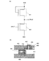
実施の形態1は、EDMOS回路の例を示したが、本実施の形態では、EEMOS回路の等価回路を図2(A)に示す。図2(A)の等価回路においては、どちらもエンハンスメント型のnチャネル型トランジスタとする組み合わせを用いた駆動回路である。
本実施の形態では、インバータ回路の作製において、実施の形態2とは異なる作製工程の例を図4(A)、図4(B)、図4(C)、及び図4(D)を用いて説明する。
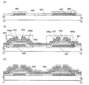
本実施の形態では、本発明の一形態の薄膜トランジスタを含む表示装置の作製工程について、図5乃至図12を用いて説明する。
ここでは、実施の形態1において、配線と半導体層とが接する構成の薄膜トランジスタを有する表示装置の例を図30に示す。
本実施の形態では、本発明の半導体装置の一例である表示装置において、同一基板上に少なくとも駆動回路の一部と、画素部に配置する薄膜トランジスタを作製する例について以下に説明する。
本発明の一形態の薄膜トランジスタを作製し、該薄膜トランジスタを画素部、さらには駆動回路に用いて表示機能を有する半導体装置(表示装置ともいう)を作製することができる。また、本発明の一形態の薄膜トランジスタを駆動回路の一部または全体を、画素部と同じ基板上に一体形成し、システムオンパネルを形成することができる。
本実施の形態では、本発明の一形態の半導体装置として発光表示装置の例を示す。表示装置の有する表示素子としては、ここではエレクトロルミネッセンスを利用する発光素子を用いて示す。エレクトロルミネッセンスを利用する発光素子は、発光材料が有機化合物であるか、無機化合物であるかによって区別され、一般的に、前者は有機EL素子、後者は無機EL素子と呼ばれている。
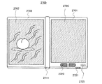
本発明の一形態の半導体装置は、電子ペーパーとして適用することができる。電子ペーパーは、情報を表示するものであればあらゆる分野の電子機器に用いることが可能である。例えば、電子ペーパーを用いて、電子書籍(電子ブック)、ポスター、電車などの乗り物の車内広告、クレジットカード等の各種カードにおける表示等に適用することができる。電子機器の一例を図25、図26に示す。
本発明の一形態の半導体装置は、さまざまな電子機器(遊技機も含む)に適用することができる。電子機器としては、例えば、テレビジョン装置(テレビ、またはテレビジョン受信機ともいう)、コンピュータ用などのモニタ、デジタルカメラ、デジタルビデオカメラ、デジタルフォトフレーム、携帯電話機(携帯電話、携帯電話装置ともいう)、携帯型ゲーム機、携帯情報端末、音響再生装置、パチンコ機などの大型ゲーム機などが挙げられる。
Claims (4)
- 端子部と、
インバータを有する駆動回路と、有し、
前記インバータは、第1のトランジスタ及び第2のトランジスタを有し、
前記第1のトランジスタは、第1のゲート電極、第1の酸化物半導体層、及び第1のチャネル保護層を有し、
前記第2のトランジスタは、第2のゲート電極、第2の酸化物半導体層、及び第2のチャネル保護層を有し、
前記第1のゲート電極上及び前記第2のゲート電極上の第1の絶縁層と、
前記第1の絶縁層上において、前記第1のゲート電極と重なる領域を有する前記第1の酸化物半導体層と、
前記第1の絶縁層上において、前記第2のゲート電極と重なる領域を有する前記第2の酸化物半導体層と、
前記第1の酸化物半導体層上の前記第1のチャネル保護層と、
前記第2の酸化物半導体層上の前記第2のチャネル保護層と、
前記第1のチャネル保護層上及び前記第1の酸化物半導体層上の第1の配線と、
前記第2のチャネル保護層上及び前記第2の酸化物半導体層上の第2の配線と、
前記第1のチャネル保護層上、前記第1の酸化物半導体層上、前記第2のチャネル保護層上、及び前記第2の酸化物半導体層上の第3の配線と、を有し、
前記第1の配線は、前記第1のトランジスタの第1のソース電極及び第1のドレイン電極の一方として機能する部分を有し、
前記第2の配線は、前記第2のトランジスタの第2のソース電極及び第2のドレイン電極の一方として機能する部分を有し、
前記第3の配線は、前記第1のトランジスタの前記第1のソース電極及び前記第1のドレイン電極の他方として機能する部分と、前記第2のトランジスタの前記第2のソース電極及び前記第2のドレイン電極の他方として機能する部分とを有し、
前記第3の配線は、前記第1の絶縁層に設けられたコンタクトホールを介して、前記第2のゲート電極と直接接続し、
前記第1の酸化物半導体層及び前記第2の酸化物半導体層は、インジウム、ガリウム、及び亜鉛を含み、
前記端子部は、第1の導電膜と、前記第1の導電膜上の前記第1の絶縁層と、前記第1の絶縁層上の第2の導電膜と、前記第2の導電膜上の第2の絶縁層と、前記第2の絶縁層上の第3の導電膜とを有し、
前記第2の導電膜は、前記第1の絶縁層に設けられたコンタクトホールを介して、前記第1の導電膜と電気的に接続され、
前記第1の導電膜と、前記第1のゲート電極と、前記第2のゲート電極とは、同一の導電膜を加工する工程を経て形成されたものであり、
前記第2の導電膜と、前記第1の配線と、前記第2の配線と、前記第3の配線とは、同一の導電膜を加工する工程を経て形成されたものであることを特徴とする半導体装置。 - 請求項1において、
前記第1のトランジスタ及び前記第2のトランジスタは、nチャネル型トランジスタであることを特徴とする半導体装置。 - 請求項1または請求項2において、
前記第1の酸化物半導体層及び前記第2の酸化物半導体層は、遷移金属を含むことを特徴とする半導体装置。 - 請求項1乃至請求項3のいずれか一において、
前記駆動回路により駆動される画素部を有し、
前記画素部は第3のトランジスタと、前記第3のトランジスタと電気的に接続される画素電極とを有し、
前記第3のトランジスタは、第3のゲート電極、第3の酸化物半導体層、及び第3のチャネル保護層を有し、
前記第3のゲート電極上の前記第1の絶縁層と、
前記第1の絶縁層上の前記第3の酸化物半導体層と、
前記第3の酸化物半導体層上の前記第3のチャネル保護層と、
前記第3のチャネル保護層上及び前記第3の酸化物半導体層上の第4の導電膜と、
前記第3のチャネル保護層上及び前記第3の酸化物半導体層上の第5の導電膜と、を有し、
前記第4の導電膜は、前記第3のトランジスタの第3のソース電極及び第3のドレイン電極の一方として機能する部分を有し、
前記第5の導電膜は、前記第3のトランジスタの第3のソース電極及び第3のドレイン電極の他方として機能する部分を有し、
前記第3の酸化物半導体層は、インジウム、ガリウム、及び亜鉛を含み、
前記第3のゲート電極と、前記第1のゲート電極とは、同一の導電膜を加工する工程を経て形成されたものであり、
前記第4の導電膜と、前記第5の導電膜と、前記第1の配線とは、同一の導電膜を加工する工程を経て形成されたものであることを特徴とする半導体装置。
Priority Applications (1)
| Application Number | Priority Date | Filing Date | Title |
|---|---|---|---|
| JP2009229211A JP5601811B2 (ja) | 2008-10-03 | 2009-10-01 | 半導体装置 |
Applications Claiming Priority (3)
| Application Number | Priority Date | Filing Date | Title |
|---|---|---|---|
| JP2008259031 | 2008-10-03 | ||
| JP2008259031 | 2008-10-03 | ||
| JP2009229211A JP5601811B2 (ja) | 2008-10-03 | 2009-10-01 | 半導体装置 |
Related Child Applications (1)
| Application Number | Title | Priority Date | Filing Date |
|---|---|---|---|
| JP2014166582A Division JP5860512B2 (ja) | 2008-10-03 | 2014-08-19 | 半導体装置 |
Publications (3)
| Publication Number | Publication Date |
|---|---|
| JP2010109357A JP2010109357A (ja) | 2010-05-13 |
| JP2010109357A5 JP2010109357A5 (ja) | 2012-10-25 |
| JP5601811B2 true JP5601811B2 (ja) | 2014-10-08 |
Family
ID=41510919
Family Applications (9)
| Application Number | Title | Priority Date | Filing Date |
|---|---|---|---|
| JP2009229211A Active JP5601811B2 (ja) | 2008-10-03 | 2009-10-01 | 半導体装置 |
| JP2014166582A Active JP5860512B2 (ja) | 2008-10-03 | 2014-08-19 | 半導体装置 |
| JP2015247006A Withdrawn JP2016096352A (ja) | 2008-10-03 | 2015-12-18 | 半導体装置 |
| JP2016033058A Active JP6228617B2 (ja) | 2008-10-03 | 2016-02-24 | 半導体装置 |
| JP2017199362A Active JP6445111B2 (ja) | 2008-10-03 | 2017-10-13 | 電子機器 |
| JP2018222002A Withdrawn JP2019071421A (ja) | 2008-10-03 | 2018-11-28 | 半導体装置 |
| JP2021064694A Active JP7064634B2 (ja) | 2008-10-03 | 2021-04-06 | 表示装置 |
| JP2022070502A Active JP7404434B2 (ja) | 2008-10-03 | 2022-04-22 | 半導体装置 |
| JP2023209783A Pending JP2024036318A (ja) | 2008-10-03 | 2023-12-13 | 半導体装置 |
Family Applications After (8)
| Application Number | Title | Priority Date | Filing Date |
|---|---|---|---|
| JP2014166582A Active JP5860512B2 (ja) | 2008-10-03 | 2014-08-19 | 半導体装置 |
| JP2015247006A Withdrawn JP2016096352A (ja) | 2008-10-03 | 2015-12-18 | 半導体装置 |
| JP2016033058A Active JP6228617B2 (ja) | 2008-10-03 | 2016-02-24 | 半導体装置 |
| JP2017199362A Active JP6445111B2 (ja) | 2008-10-03 | 2017-10-13 | 電子機器 |
| JP2018222002A Withdrawn JP2019071421A (ja) | 2008-10-03 | 2018-11-28 | 半導体装置 |
| JP2021064694A Active JP7064634B2 (ja) | 2008-10-03 | 2021-04-06 | 表示装置 |
| JP2022070502A Active JP7404434B2 (ja) | 2008-10-03 | 2022-04-22 | 半導体装置 |
| JP2023209783A Pending JP2024036318A (ja) | 2008-10-03 | 2023-12-13 | 半導体装置 |
Country Status (6)
| Country | Link |
|---|---|
| US (5) | US9324874B2 (ja) |
| EP (1) | EP2172977A1 (ja) |
| JP (9) | JP5601811B2 (ja) |
| KR (6) | KR101785688B1 (ja) |
| CN (2) | CN101714547B (ja) |
| TW (6) | TWI726479B (ja) |
Families Citing this family (93)
| Publication number | Priority date | Publication date | Assignee | Title |
|---|---|---|---|---|
| EP3229066A1 (en) | 2005-12-05 | 2017-10-11 | Semiconductor Energy Laboratory Co., Ltd. | Transflective liquid crystal display with a horizontal electric field configuration |
| KR20160113329A (ko) | 2008-10-03 | 2016-09-28 | 가부시키가이샤 한도오따이 에네루기 켄큐쇼 | 표시장치 |
| CN101714546B (zh) | 2008-10-03 | 2014-05-14 | 株式会社半导体能源研究所 | 显示装置及其制造方法 |
| CN101719493B (zh) * | 2008-10-08 | 2014-05-14 | 株式会社半导体能源研究所 | 显示装置 |
| JP5361651B2 (ja) * | 2008-10-22 | 2013-12-04 | 株式会社半導体エネルギー研究所 | 半導体装置の作製方法 |
| EP2180518B1 (en) | 2008-10-24 | 2018-04-25 | Semiconductor Energy Laboratory Co, Ltd. | Method for manufacturing semiconductor device |
| KR101310473B1 (ko) | 2008-10-24 | 2013-09-24 | 가부시키가이샤 한도오따이 에네루기 켄큐쇼 | 반도체 장치 |
| JP5616012B2 (ja) * | 2008-10-24 | 2014-10-29 | 株式会社半導体エネルギー研究所 | 半導体装置の作製方法 |
| US8106400B2 (en) | 2008-10-24 | 2012-01-31 | Semiconductor Energy Laboratory Co., Ltd. | Semiconductor device and method for manufacturing the same |
| KR101667909B1 (ko) | 2008-10-24 | 2016-10-28 | 가부시키가이샤 한도오따이 에네루기 켄큐쇼 | 반도체장치의 제조방법 |
| US8741702B2 (en) * | 2008-10-24 | 2014-06-03 | Semiconductor Energy Laboratory Co., Ltd. | Method for manufacturing semiconductor device |
| KR101631454B1 (ko) * | 2008-10-31 | 2016-06-17 | 가부시키가이샤 한도오따이 에네루기 켄큐쇼 | 논리회로 |
| KR101432764B1 (ko) * | 2008-11-13 | 2014-08-21 | 가부시키가이샤 한도오따이 에네루기 켄큐쇼 | 반도체장치의 제조방법 |
| KR102556313B1 (ko) | 2008-11-21 | 2023-07-18 | 가부시키가이샤 한도오따이 에네루기 켄큐쇼 | 표시 장치 |
| KR101642620B1 (ko) * | 2009-07-10 | 2016-07-25 | 가부시키가이샤 한도오따이 에네루기 켄큐쇼 | 반도체 장치 및 그 제조 방법 |
| KR101782176B1 (ko) | 2009-07-18 | 2017-09-26 | 가부시키가이샤 한도오따이 에네루기 켄큐쇼 | 반도체 장치 및 반도체 장치의 제조 방법 |
| KR102221207B1 (ko) | 2009-09-04 | 2021-03-03 | 가부시키가이샤 한도오따이 에네루기 켄큐쇼 | 발광 장치 및 발광 장치를 제작하기 위한 방법 |
| KR101730347B1 (ko) | 2009-09-16 | 2017-04-27 | 가부시키가이샤 한도오따이 에네루기 켄큐쇼 | 반도체 장치 및 그 제작 방법 |
| KR101301461B1 (ko) * | 2009-09-16 | 2013-08-29 | 가부시키가이샤 한도오따이 에네루기 켄큐쇼 | 반도체 장치 및 산화물 반도체층 |
| WO2011034012A1 (en) * | 2009-09-16 | 2011-03-24 | Semiconductor Energy Laboratory Co., Ltd. | Logic circuit, light emitting device, semiconductor device, and electronic device |
| WO2011036999A1 (en) * | 2009-09-24 | 2011-03-31 | Semiconductor Energy Laboratory Co., Ltd. | Oxide semiconductor film and semiconductor device |
| KR101991006B1 (ko) | 2009-10-08 | 2019-06-20 | 가부시키가이샤 한도오따이 에네루기 켄큐쇼 | 반도체 장치 |
| KR101376461B1 (ko) | 2009-10-08 | 2014-03-19 | 가부시키가이샤 한도오따이 에네루기 켄큐쇼 | 산화물 반도체층 및 반도체 장치 |
| KR101959693B1 (ko) * | 2009-10-09 | 2019-03-18 | 가부시키가이샤 한도오따이 에네루기 켄큐쇼 | 반도체 장치 및 그 제조 방법 |
| SG188112A1 (en) | 2009-10-30 | 2013-03-28 | Semiconductor Energy Lab | Logic circuit and semiconductor device |
| KR102378013B1 (ko) | 2009-11-06 | 2022-03-24 | 가부시키가이샤 한도오따이 에네루기 켄큐쇼 | 반도체 장치 및 반도체 장치의 제작 방법 |
| KR102286284B1 (ko) | 2009-11-06 | 2021-08-06 | 가부시키가이샤 한도오따이 에네루기 켄큐쇼 | 반도체 장치 및 그 제작 방법 |
| KR102513073B1 (ko) | 2009-11-13 | 2023-03-24 | 가부시키가이샤 한도오따이 에네루기 켄큐쇼 | 반도체 장치 및 그 제작 방법 |
| KR101943109B1 (ko) | 2009-12-04 | 2019-01-28 | 가부시키가이샤 한도오따이 에네루기 켄큐쇼 | 반도체 장치 및 그 제조 방법 |
| WO2011068032A1 (en) | 2009-12-04 | 2011-06-09 | Semiconductor Energy Laboratory Co., Ltd. | Display device |
| WO2011101918A1 (ja) * | 2010-02-22 | 2011-08-25 | パナソニック株式会社 | 発光装置とその製造方法 |
| JP5714973B2 (ja) | 2010-05-21 | 2015-05-07 | 株式会社半導体エネルギー研究所 | 半導体装置 |
| JP5852793B2 (ja) * | 2010-05-21 | 2016-02-03 | 株式会社半導体エネルギー研究所 | 液晶表示装置の作製方法 |
| US8552425B2 (en) | 2010-06-18 | 2013-10-08 | Semiconductor Energy Laboratory Co., Ltd. | Semiconductor device |
| US9473714B2 (en) * | 2010-07-01 | 2016-10-18 | Semiconductor Energy Laboratory Co., Ltd. | Solid-state imaging device and semiconductor display device |
| US8614474B2 (en) | 2010-07-05 | 2013-12-24 | Sharp Kabushiki Kaisha | Thin film transistor memory and display unit including the same |
| US8766253B2 (en) * | 2010-09-10 | 2014-07-01 | Semiconductor Energy Laboratory Co., Ltd. | Semiconductor device |
| US8558960B2 (en) | 2010-09-13 | 2013-10-15 | Semiconductor Energy Laboratory Co., Ltd. | Liquid crystal display device and method for manufacturing the same |
| JP2012256821A (ja) * | 2010-09-13 | 2012-12-27 | Semiconductor Energy Lab Co Ltd | 記憶装置 |
| WO2012035984A1 (en) | 2010-09-15 | 2012-03-22 | Semiconductor Energy Laboratory Co., Ltd. | Semiconductor device and display device |
| KR102637010B1 (ko) | 2010-12-03 | 2024-02-16 | 가부시키가이샤 한도오따이 에네루기 켄큐쇼 | 산화물 반도체막 및 반도체 장치 |
| US9911858B2 (en) | 2010-12-28 | 2018-03-06 | Semiconductor Energy Laboratory Co., Ltd. | Semiconductor device and method for manufacturing the same |
| US8829512B2 (en) | 2010-12-28 | 2014-09-09 | Semiconductor Energy Laboratory Co., Ltd. | Semiconductor device and method for manufacturing the same |
| JP2012204548A (ja) * | 2011-03-24 | 2012-10-22 | Sony Corp | 表示装置およびその製造方法 |
| TWI420672B (zh) * | 2011-06-13 | 2013-12-21 | Au Optronics Corp | 主動元件及具有此主動元件的電泳顯示器 |
| CN105590897A (zh) * | 2011-07-26 | 2016-05-18 | 群创光电股份有限公司 | 显示面板及其制作方法 |
| CN102937757B (zh) * | 2011-08-15 | 2015-07-08 | 群康科技(深圳)有限公司 | 蓝相液晶显示装置及其驱动方法 |
| TWI455104B (zh) * | 2011-08-15 | 2014-10-01 | Innolux Corp | 藍相液晶顯示裝置及其驅動方法 |
| US9082663B2 (en) * | 2011-09-16 | 2015-07-14 | Semiconductor Energy Laboratory Co., Ltd. | Semiconductor device and manufacturing method thereof |
| JP2013084333A (ja) | 2011-09-28 | 2013-05-09 | Semiconductor Energy Lab Co Ltd | シフトレジスタ回路 |
| US8716708B2 (en) | 2011-09-29 | 2014-05-06 | Semiconductor Energy Laboratory Co., Ltd. | Semiconductor device and method for manufacturing the same |
| SG11201505088UA (en) | 2011-09-29 | 2015-08-28 | Semiconductor Energy Lab | Semiconductor device |
| US9287405B2 (en) * | 2011-10-13 | 2016-03-15 | Semiconductor Energy Laboratory Co., Ltd. | Semiconductor device comprising oxide semiconductor |
| IN2014DN03274A (ja) | 2011-10-14 | 2015-05-22 | Semiconductor Energy Lab | |
| KR20130040706A (ko) | 2011-10-14 | 2013-04-24 | 가부시키가이샤 한도오따이 에네루기 켄큐쇼 | 반도체 장치 및 반도체 장치의 제작 방법 |
| KR20140086954A (ko) | 2011-10-28 | 2014-07-08 | 가부시키가이샤 한도오따이 에네루기 켄큐쇼 | 반도체 장치 및 그 제작 방법 |
| TWI445168B (zh) | 2011-11-16 | 2014-07-11 | E Ink Holdings Inc | 光感測元件 |
| US8829528B2 (en) * | 2011-11-25 | 2014-09-09 | Semiconductor Energy Laboratory Co., Ltd. | Semiconductor device including groove portion extending beyond pixel electrode |
| US9076871B2 (en) | 2011-11-30 | 2015-07-07 | Semiconductor Energy Laboratory Co., Ltd. | Semiconductor device and method for manufacturing the same |
| JP6220526B2 (ja) | 2012-02-29 | 2017-10-25 | 株式会社半導体エネルギー研究所 | 半導体装置の作製方法 |
| KR101950834B1 (ko) * | 2012-03-06 | 2019-02-21 | 엘지디스플레이 주식회사 | 산화물 박막 트랜지스터 및 이의 제조 방법 |
| KR102113160B1 (ko) * | 2012-06-15 | 2020-05-20 | 가부시키가이샤 한도오따이 에네루기 켄큐쇼 | 반도체 장치 |
| TWI681233B (zh) | 2012-10-12 | 2020-01-01 | 日商半導體能源研究所股份有限公司 | 液晶顯示裝置、觸控面板及液晶顯示裝置的製造方法 |
| JP6351947B2 (ja) | 2012-10-12 | 2018-07-04 | 株式会社半導体エネルギー研究所 | 液晶表示装置の作製方法 |
| KR20220150439A (ko) | 2012-11-08 | 2022-11-10 | 가부시키가이샤 한도오따이 에네루기 켄큐쇼 | 디스플레이 장치 |
| US9231111B2 (en) * | 2013-02-13 | 2016-01-05 | Semiconductor Energy Laboratory Co., Ltd. | Semiconductor device |
| US9153650B2 (en) | 2013-03-19 | 2015-10-06 | Semiconductor Energy Laboratory Co., Ltd. | Oxide semiconductor |
| JP6083089B2 (ja) * | 2013-03-27 | 2017-02-22 | 株式会社Joled | 半導体装置、表示装置および電子機器 |
| KR102178766B1 (ko) * | 2013-03-29 | 2020-11-13 | 엘지디스플레이 주식회사 | 박막 트랜지스터, 박막 트랜지스터 제조 방법 및 박막 트랜지스터를 포함하는 표시 장치 |
| TWI652822B (zh) | 2013-06-19 | 2019-03-01 | 日商半導體能源研究所股份有限公司 | 氧化物半導體膜及其形成方法 |
| TWI608523B (zh) | 2013-07-19 | 2017-12-11 | 半導體能源研究所股份有限公司 | Oxide semiconductor film, method of manufacturing oxide semiconductor film, and semiconductor device |
| WO2015132697A1 (en) | 2014-03-07 | 2015-09-11 | Semiconductor Energy Laboratory Co., Ltd. | Semiconductor device |
| KR101640192B1 (ko) * | 2014-08-05 | 2016-07-18 | 삼성디스플레이 주식회사 | 디스플레이 장치 |
| CN104183608B (zh) * | 2014-09-02 | 2017-05-03 | 深圳市华星光电技术有限公司 | Tft背板结构及其制作方法 |
| JP6521794B2 (ja) | 2014-09-03 | 2019-05-29 | 株式会社半導体エネルギー研究所 | 半導体装置、及び電子機器 |
| KR102322014B1 (ko) * | 2014-10-24 | 2021-11-05 | 삼성디스플레이 주식회사 | 유기 발광 표시 장치 및 그 제조방법 |
| US10109659B2 (en) * | 2015-03-04 | 2018-10-23 | Shenzhen China Star Optoelectronics Technology Co., Ltd | TFT backplate structure comprising transistors having gate isolation layers of different thicknesses and manufacture method thereof |
| CN104867959B (zh) * | 2015-04-14 | 2017-09-26 | 深圳市华星光电技术有限公司 | 双栅极氧化物半导体tft基板的制作方法及其结构 |
| CN104752343B (zh) * | 2015-04-14 | 2017-07-28 | 深圳市华星光电技术有限公司 | 双栅极氧化物半导体tft基板的制作方法及其结构 |
| WO2016175034A1 (ja) * | 2015-04-28 | 2016-11-03 | 三菱電機株式会社 | トランジスタ、薄膜トランジスタ基板および液晶表示装置 |
| CN108369724A (zh) * | 2015-12-08 | 2018-08-03 | 柯尼卡美能达株式会社 | 光学式指纹认证装置 |
| JP6785563B2 (ja) * | 2016-02-19 | 2020-11-18 | 三菱電機株式会社 | 非線形素子、アレイ基板、およびアレイ基板の製造方法 |
| KR102477989B1 (ko) * | 2018-01-10 | 2022-12-16 | 삼성디스플레이 주식회사 | 표시 장치 및 본딩 저항 검사 방법 |
| JP7109928B2 (ja) * | 2018-01-31 | 2022-08-01 | キオクシア株式会社 | トランジスタ及び半導体記憶装置並びにトランジスタの製造方法 |
| KR20200019308A (ko) | 2018-08-13 | 2020-02-24 | 삼성디스플레이 주식회사 | 유기 발광 표시 장치 |
| CN110858035B (zh) * | 2018-08-24 | 2022-12-02 | 夏普株式会社 | 液晶显示装置 |
| KR102469187B1 (ko) | 2018-09-04 | 2022-11-21 | 삼성디스플레이 주식회사 | 표시 장치 및 그 제조 방법 |
| TWI699892B (zh) * | 2018-09-21 | 2020-07-21 | 友達光電股份有限公司 | 電子裝置及其製造方法 |
| CN109166542A (zh) * | 2018-09-26 | 2019-01-08 | 合肥鑫晟光电科技有限公司 | 移位寄存器单元及驱动方法、栅极驱动电路、显示装置 |
| CN110767106B (zh) * | 2018-09-30 | 2020-09-08 | 云谷(固安)科技有限公司 | 显示面板、显示屏及显示终端 |
| JP7065147B2 (ja) * | 2020-04-28 | 2022-05-11 | 株式会社ジャパンディスプレイ | 半導体装置 |
| TWI758872B (zh) * | 2020-09-17 | 2022-03-21 | 大陸商北京集創北方科技股份有限公司 | 顯示器之過驅動補償方法及利用其之顯示裝置和手持裝置 |
| TWI813217B (zh) * | 2021-12-09 | 2023-08-21 | 友達光電股份有限公司 | 半導體裝置及其製造方法 |
Family Cites Families (181)
| Publication number | Priority date | Publication date | Assignee | Title |
|---|---|---|---|---|
| JPS58191461A (ja) | 1982-05-04 | 1983-11-08 | Toshiba Corp | 半導体装置の製造方法 |
| JPS60198861A (ja) | 1984-03-23 | 1985-10-08 | Fujitsu Ltd | 薄膜トランジスタ |
| JPH0244256B2 (ja) | 1987-01-28 | 1990-10-03 | Kagaku Gijutsucho Mukizaishitsu Kenkyushocho | Ingazn2o5deshimesarerurotsuhoshokeinosojokozoojusurukagobutsuoyobisonoseizoho |
| JPH0244258B2 (ja) | 1987-02-24 | 1990-10-03 | Kagaku Gijutsucho Mukizaishitsu Kenkyushocho | Ingazn3o6deshimesarerurotsuhoshokeinosojokozoojusurukagobutsuoyobisonoseizoho |
| JPH0244260B2 (ja) | 1987-02-24 | 1990-10-03 | Kagaku Gijutsucho Mukizaishitsu Kenkyushocho | Ingazn5o8deshimesarerurotsuhoshokeinosojokozoojusurukagobutsuoyobisonoseizoho |
| JPS63210023A (ja) | 1987-02-24 | 1988-08-31 | Natl Inst For Res In Inorg Mater | InGaZn↓4O↓7で示される六方晶系の層状構造を有する化合物およびその製造法 |
| JPH0244262B2 (ja) | 1987-02-27 | 1990-10-03 | Kagaku Gijutsucho Mukizaishitsu Kenkyushocho | Ingazn6o9deshimesarerurotsuhoshokeinosojokozoojusurukagobutsuoyobisonoseizoho |
| JPH0244263B2 (ja) | 1987-04-22 | 1990-10-03 | Kagaku Gijutsucho Mukizaishitsu Kenkyushocho | Ingazn7o10deshimesarerurotsuhoshokeinosojokozoojusurukagobutsuoyobisonoseizoho |
| JPS63301565A (ja) | 1987-05-30 | 1988-12-08 | Matsushita Electric Ind Co Ltd | 薄膜集積回路 |
| JPH02156676A (ja) | 1988-12-09 | 1990-06-15 | Fuji Xerox Co Ltd | 薄膜半導体装置 |
| JP2585118B2 (ja) | 1990-02-06 | 1997-02-26 | 株式会社半導体エネルギー研究所 | 薄膜トランジスタの作製方法 |
| EP0445535B1 (en) | 1990-02-06 | 1995-02-01 | Sel Semiconductor Energy Laboratory Co., Ltd. | Method of forming an oxide film |
| JP2875844B2 (ja) * | 1990-03-27 | 1999-03-31 | キヤノン株式会社 | 薄膜トランジスタ型光センサの駆動方法及び駆動装置 |
| JPH05251705A (ja) | 1992-03-04 | 1993-09-28 | Fuji Xerox Co Ltd | 薄膜トランジスタ |
| JP2572003B2 (ja) | 1992-03-30 | 1997-01-16 | 三星電子株式会社 | 三次元マルチチャンネル構造を有する薄膜トランジスタの製造方法 |
| JPH06202156A (ja) | 1992-12-28 | 1994-07-22 | Sharp Corp | ドライバーモノリシック駆動素子 |
| JP3479375B2 (ja) | 1995-03-27 | 2003-12-15 | 科学技術振興事業団 | 亜酸化銅等の金属酸化物半導体による薄膜トランジスタとpn接合を形成した金属酸化物半導体装置およびそれらの製造方法 |
| DE69635107D1 (de) | 1995-08-03 | 2005-09-29 | Koninkl Philips Electronics Nv | Halbleiteranordnung mit einem transparenten schaltungselement |
| US5930607A (en) * | 1995-10-03 | 1999-07-27 | Seiko Epson Corporation | Method to prevent static destruction of an active element comprised in a liquid crystal display device |
| US5847410A (en) | 1995-11-24 | 1998-12-08 | Semiconductor Energy Laboratory Co. | Semiconductor electro-optical device |
| KR100190041B1 (ko) | 1995-12-28 | 1999-06-01 | 윤종용 | 액정표시장치의 제조방법 |
| JP3625598B2 (ja) | 1995-12-30 | 2005-03-02 | 三星電子株式会社 | 液晶表示装置の製造方法 |
| JPH10290012A (ja) | 1997-04-14 | 1998-10-27 | Nec Corp | アクティブマトリクス型液晶表示装置およびその製造方法 |
| US6218219B1 (en) * | 1997-09-29 | 2001-04-17 | Semiconductor Energy Laboratory Co., Ltd. | Semiconductor device and fabrication method thereof |
| JP4170454B2 (ja) | 1998-07-24 | 2008-10-22 | Hoya株式会社 | 透明導電性酸化物薄膜を有する物品及びその製造方法 |
| JP2000150861A (ja) | 1998-11-16 | 2000-05-30 | Tdk Corp | 酸化物薄膜 |
| JP3276930B2 (ja) | 1998-11-17 | 2002-04-22 | 科学技術振興事業団 | トランジスタ及び半導体装置 |
| JP2001053283A (ja) | 1999-08-12 | 2001-02-23 | Semiconductor Energy Lab Co Ltd | 半導体装置及びその作製方法 |
| TW460731B (en) | 1999-09-03 | 2001-10-21 | Ind Tech Res Inst | Electrode structure and production method of wide viewing angle LCD |
| JP3415508B2 (ja) * | 1999-09-27 | 2003-06-09 | エヌイーシーマイクロシステム株式会社 | ドライバ回路及びその出力安定化方法 |
| JP4963140B2 (ja) | 2000-03-02 | 2012-06-27 | 株式会社半導体エネルギー研究所 | 半導体装置 |
| WO2001073170A1 (fr) * | 2000-03-27 | 2001-10-04 | Tohoku Techno Arch Co., Ltd. | Materiau a semi-conducteurs d'oxyde de zinc |
| JP2001284592A (ja) | 2000-03-29 | 2001-10-12 | Sony Corp | 薄膜半導体装置及びその駆動方法 |
| JP2001324725A (ja) | 2000-05-12 | 2001-11-22 | Hitachi Ltd | 液晶表示装置およびその製造方法 |
| US7633471B2 (en) | 2000-05-12 | 2009-12-15 | Semiconductor Energy Laboratory Co., Ltd. | Light-emitting device and electric appliance |
| US6828587B2 (en) * | 2000-06-19 | 2004-12-07 | Semiconductor Energy Laboratory Co., Ltd. | Semiconductor device |
| US6730538B1 (en) * | 2000-06-22 | 2004-05-04 | The University Of Tennessee Research Corporation | Fabricating electronic devices using actinide oxide semiconductor materials |
| JP3813463B2 (ja) * | 2000-07-24 | 2006-08-23 | シャープ株式会社 | 液晶表示装置の駆動回路及びそれを用いた液晶表示装置並びにその液晶表示装置を用いた電子機器 |
| JP4089858B2 (ja) | 2000-09-01 | 2008-05-28 | 国立大学法人東北大学 | 半導体デバイス |
| US6549071B1 (en) | 2000-09-12 | 2003-04-15 | Silicon Laboratories, Inc. | Power amplifier circuitry and method using an inductance coupled to power amplifier switching devices |
| KR20020038482A (ko) | 2000-11-15 | 2002-05-23 | 모리시타 요이찌 | 박막 트랜지스터 어레이, 그 제조방법 및 그것을 이용한표시패널 |
| JP3997731B2 (ja) | 2001-03-19 | 2007-10-24 | 富士ゼロックス株式会社 | 基材上に結晶性半導体薄膜を形成する方法 |
| JP2002289859A (ja) | 2001-03-23 | 2002-10-04 | Minolta Co Ltd | 薄膜トランジスタ |
| JP3686845B2 (ja) * | 2001-05-21 | 2005-08-24 | 埼玉日本電気株式会社 | 折り畳み型携帯電話機 |
| EP1399974A1 (en) * | 2001-06-21 | 2004-03-24 | Massachusetts Institute Of Technology | Mosfets with strained semiconductor layers |
| JP4090716B2 (ja) | 2001-09-10 | 2008-05-28 | 雅司 川崎 | 薄膜トランジスタおよびマトリクス表示装置 |
| JP3925839B2 (ja) | 2001-09-10 | 2007-06-06 | シャープ株式会社 | 半導体記憶装置およびその試験方法 |
| WO2003040441A1 (en) | 2001-11-05 | 2003-05-15 | Japan Science And Technology Agency | Natural superlattice homologous single crystal thin film, method for preparation thereof, and device using said single crystal thin film |
| JP4164562B2 (ja) | 2002-09-11 | 2008-10-15 | 独立行政法人科学技術振興機構 | ホモロガス薄膜を活性層として用いる透明薄膜電界効果型トランジスタ |
| JP4083486B2 (ja) | 2002-02-21 | 2008-04-30 | 独立行政法人科学技術振興機構 | LnCuO(S,Se,Te)単結晶薄膜の製造方法 |
| JP4069648B2 (ja) | 2002-03-15 | 2008-04-02 | カシオ計算機株式会社 | 半導体装置および表示駆動装置 |
| CN1445821A (zh) | 2002-03-15 | 2003-10-01 | 三洋电机株式会社 | ZnO膜和ZnO半导体层的形成方法、半导体元件及其制造方法 |
| JP2003280034A (ja) | 2002-03-20 | 2003-10-02 | Sharp Corp | Tft基板およびそれを用いる液晶表示装置 |
| JP3933591B2 (ja) | 2002-03-26 | 2007-06-20 | 淳二 城戸 | 有機エレクトロルミネッセント素子 |
| JP2003309266A (ja) | 2002-04-17 | 2003-10-31 | Konica Minolta Holdings Inc | 有機薄膜トランジスタ素子の製造方法 |
| US20030198008A1 (en) | 2002-04-18 | 2003-10-23 | Gateway, Inc. | Computer having detachable wireless independently operable computer |
| US7339187B2 (en) | 2002-05-21 | 2008-03-04 | State Of Oregon Acting By And Through The Oregon State Board Of Higher Education On Behalf Of Oregon State University | Transistor structures |
| JP2004022625A (ja) | 2002-06-13 | 2004-01-22 | Murata Mfg Co Ltd | 半導体デバイス及び該半導体デバイスの製造方法 |
| US7105868B2 (en) | 2002-06-24 | 2006-09-12 | Cermet, Inc. | High-electron mobility transistor with zinc oxide |
| KR100870522B1 (ko) * | 2002-09-17 | 2008-11-26 | 엘지디스플레이 주식회사 | 액정표시소자 및 그 제조방법 |
| US7067843B2 (en) | 2002-10-11 | 2006-06-27 | E. I. Du Pont De Nemours And Company | Transparent oxide semiconductor thin film transistors |
| JP4314843B2 (ja) | 2003-03-05 | 2009-08-19 | カシオ計算機株式会社 | 画像読取装置及び個人認証システム |
| JP4166105B2 (ja) | 2003-03-06 | 2008-10-15 | シャープ株式会社 | 半導体装置およびその製造方法 |
| JP2004273732A (ja) | 2003-03-07 | 2004-09-30 | Sharp Corp | アクティブマトリクス基板およびその製造方法 |
| JP2004349583A (ja) | 2003-05-23 | 2004-12-09 | Sharp Corp | トランジスタの製造方法 |
| TW576602U (en) * | 2003-05-30 | 2004-02-11 | Hon Hai Prec Ind Co Ltd | Multi-functional handset |
| JP4108633B2 (ja) | 2003-06-20 | 2008-06-25 | シャープ株式会社 | 薄膜トランジスタおよびその製造方法ならびに電子デバイス |
| JP4605690B2 (ja) * | 2003-06-24 | 2011-01-05 | 株式会社アマダ | ワーク切断方法 |
| US7262463B2 (en) | 2003-07-25 | 2007-08-28 | Hewlett-Packard Development Company, L.P. | Transistor including a deposited channel region having a doped portion |
| US7633470B2 (en) * | 2003-09-29 | 2009-12-15 | Michael Gillis Kane | Driver circuit, as for an OLED display |
| US20070171157A1 (en) | 2003-10-15 | 2007-07-26 | Samsung Electronics Co., Ltd | Display apparatus having photo sensor |
| KR100957585B1 (ko) | 2003-10-15 | 2010-05-13 | 삼성전자주식회사 | 광 감지부를 갖는 전자 디스플레이 장치 |
| KR101019045B1 (ko) | 2003-11-25 | 2011-03-04 | 엘지디스플레이 주식회사 | 액정표시장치용 어레이기판과 그 제조방법 |
| CN100533808C (zh) * | 2004-01-26 | 2009-08-26 | 株式会社半导体能源研究所 | 显示器件及其制造方法以及电视设备 |
| US7282782B2 (en) | 2004-03-12 | 2007-10-16 | Hewlett-Packard Development Company, L.P. | Combined binary oxide semiconductor device |
| US7145174B2 (en) | 2004-03-12 | 2006-12-05 | Hewlett-Packard Development Company, Lp. | Semiconductor device |
| CN102867855B (zh) | 2004-03-12 | 2015-07-15 | 独立行政法人科学技术振兴机构 | 薄膜晶体管及其制造方法 |
| US7297977B2 (en) | 2004-03-12 | 2007-11-20 | Hewlett-Packard Development Company, L.P. | Semiconductor device |
| KR20050104800A (ko) | 2004-04-29 | 2005-11-03 | 엘지.필립스 엘시디 주식회사 | 액정표시패널 및 그 제조방법 |
| KR101116816B1 (ko) | 2004-06-05 | 2012-02-28 | 엘지디스플레이 주식회사 | 반투과형 박막 트랜지스터 기판 및 그 제조 방법 |
| US7211825B2 (en) | 2004-06-14 | 2007-05-01 | Yi-Chi Shih | Indium oxide-based thin film transistors and circuits |
| JP2006100760A (ja) | 2004-09-02 | 2006-04-13 | Casio Comput Co Ltd | 薄膜トランジスタおよびその製造方法 |
| US7285501B2 (en) | 2004-09-17 | 2007-10-23 | Hewlett-Packard Development Company, L.P. | Method of forming a solution processed device |
| US7298084B2 (en) | 2004-11-02 | 2007-11-20 | 3M Innovative Properties Company | Methods and displays utilizing integrated zinc oxide row and column drivers in conjunction with organic light emitting diodes |
| US7829444B2 (en) | 2004-11-10 | 2010-11-09 | Canon Kabushiki Kaisha | Field effect transistor manufacturing method |
| JP5138163B2 (ja) | 2004-11-10 | 2013-02-06 | キヤノン株式会社 | 電界効果型トランジスタ |
| RU2369940C2 (ru) | 2004-11-10 | 2009-10-10 | Кэнон Кабусики Кайся | Аморфный оксид и полевой транзистор с его использованием |
| AU2005302963B2 (en) | 2004-11-10 | 2009-07-02 | Cannon Kabushiki Kaisha | Light-emitting device |
| CA2585071A1 (en) | 2004-11-10 | 2006-05-18 | Canon Kabushiki Kaisha | Field effect transistor employing an amorphous oxide |
| US7863611B2 (en) | 2004-11-10 | 2011-01-04 | Canon Kabushiki Kaisha | Integrated circuits utilizing amorphous oxides |
| US7791072B2 (en) | 2004-11-10 | 2010-09-07 | Canon Kabushiki Kaisha | Display |
| US7453065B2 (en) | 2004-11-10 | 2008-11-18 | Canon Kabushiki Kaisha | Sensor and image pickup device |
| JP5053537B2 (ja) | 2004-11-10 | 2012-10-17 | キヤノン株式会社 | 非晶質酸化物を利用した半導体デバイス |
| JP5036173B2 (ja) | 2004-11-26 | 2012-09-26 | 株式会社半導体エネルギー研究所 | 半導体装置の作製方法 |
| US8003449B2 (en) | 2004-11-26 | 2011-08-23 | Semiconductor Energy Laboratory Co., Ltd. | Method of manufacturing a semiconductor device having a reverse staggered thin film transistor |
| US7579224B2 (en) | 2005-01-21 | 2009-08-25 | Semiconductor Energy Laboratory Co., Ltd. | Method for manufacturing a thin film semiconductor device |
| TWI562380B (en) | 2005-01-28 | 2016-12-11 | Semiconductor Energy Lab Co Ltd | Semiconductor device, electronic device, and method of manufacturing semiconductor device |
| JP4761981B2 (ja) * | 2005-01-28 | 2011-08-31 | 株式会社半導体エネルギー研究所 | 半導体装置の作製方法 |
| TWI481024B (zh) | 2005-01-28 | 2015-04-11 | Semiconductor Energy Lab | 半導體裝置,電子裝置,和半導體裝置的製造方法 |
| US7858451B2 (en) | 2005-02-03 | 2010-12-28 | Semiconductor Energy Laboratory Co., Ltd. | Electronic device, semiconductor device and manufacturing method thereof |
| JP5238132B2 (ja) * | 2005-02-03 | 2013-07-17 | 株式会社半導体エネルギー研究所 | 半導体装置、モジュール、および電子機器 |
| US7948171B2 (en) | 2005-02-18 | 2011-05-24 | Semiconductor Energy Laboratory Co., Ltd. | Light emitting device |
| US20060197092A1 (en) | 2005-03-03 | 2006-09-07 | Randy Hoffman | System and method for forming conductive material on a substrate |
| US8681077B2 (en) | 2005-03-18 | 2014-03-25 | Semiconductor Energy Laboratory Co., Ltd. | Semiconductor device, and display device, driving method and electronic apparatus thereof |
| US7544967B2 (en) | 2005-03-28 | 2009-06-09 | Massachusetts Institute Of Technology | Low voltage flexible organic/transparent transistor for selective gas sensing, photodetecting and CMOS device applications |
| US7645478B2 (en) | 2005-03-31 | 2010-01-12 | 3M Innovative Properties Company | Methods of making displays |
| US8300031B2 (en) | 2005-04-20 | 2012-10-30 | Semiconductor Energy Laboratory Co., Ltd. | Semiconductor device comprising transistor having gate and drain connected through a current-voltage conversion element |
| JP2006344849A (ja) | 2005-06-10 | 2006-12-21 | Casio Comput Co Ltd | 薄膜トランジスタ |
| US7402506B2 (en) | 2005-06-16 | 2008-07-22 | Eastman Kodak Company | Methods of making thin film transistors comprising zinc-oxide-based semiconductor materials and transistors made thereby |
| US7691666B2 (en) | 2005-06-16 | 2010-04-06 | Eastman Kodak Company | Methods of making thin film transistors comprising zinc-oxide-based semiconductor materials and transistors made thereby |
| US7507618B2 (en) | 2005-06-27 | 2009-03-24 | 3M Innovative Properties Company | Method for making electronic devices using metal oxide nanoparticles |
| KR100711890B1 (ko) | 2005-07-28 | 2007-04-25 | 삼성에스디아이 주식회사 | 유기 발광표시장치 및 그의 제조방법 |
| JP2007059128A (ja) | 2005-08-23 | 2007-03-08 | Canon Inc | 有機el表示装置およびその製造方法 |
| JP4280736B2 (ja) | 2005-09-06 | 2009-06-17 | キヤノン株式会社 | 半導体素子 |
| JP4850457B2 (ja) | 2005-09-06 | 2012-01-11 | キヤノン株式会社 | 薄膜トランジスタ及び薄膜ダイオード |
| JP2007073705A (ja) | 2005-09-06 | 2007-03-22 | Canon Inc | 酸化物半導体チャネル薄膜トランジスタおよびその製造方法 |
| JP5116225B2 (ja) | 2005-09-06 | 2013-01-09 | キヤノン株式会社 | 酸化物半導体デバイスの製造方法 |
| JP5064747B2 (ja) | 2005-09-29 | 2012-10-31 | 株式会社半導体エネルギー研究所 | 半導体装置、電気泳動表示装置、表示モジュール、電子機器、及び半導体装置の作製方法 |
| EP1995787A3 (en) | 2005-09-29 | 2012-01-18 | Semiconductor Energy Laboratory Co, Ltd. | Semiconductor device having oxide semiconductor layer and manufacturing method therof |
| JP5078246B2 (ja) | 2005-09-29 | 2012-11-21 | 株式会社半導体エネルギー研究所 | 半導体装置、及び半導体装置の作製方法 |
| JP5037808B2 (ja) | 2005-10-20 | 2012-10-03 | キヤノン株式会社 | アモルファス酸化物を用いた電界効果型トランジスタ、及び該トランジスタを用いた表示装置 |
| CN101577293B (zh) | 2005-11-15 | 2012-09-19 | 株式会社半导体能源研究所 | 半导体器件及其制造方法 |
| JP5250929B2 (ja) | 2005-11-30 | 2013-07-31 | 凸版印刷株式会社 | トランジスタおよびその製造方法 |
| TWI292281B (en) | 2005-12-29 | 2008-01-01 | Ind Tech Res Inst | Pixel structure of active organic light emitting diode and method of fabricating the same |
| US7867636B2 (en) | 2006-01-11 | 2011-01-11 | Murata Manufacturing Co., Ltd. | Transparent conductive film and method for manufacturing the same |
| JP4977478B2 (ja) | 2006-01-21 | 2012-07-18 | 三星電子株式会社 | ZnOフィルム及びこれを用いたTFTの製造方法 |
| US7576394B2 (en) | 2006-02-02 | 2009-08-18 | Kochi Industrial Promotion Center | Thin film transistor including low resistance conductive thin films and manufacturing method thereof |
| US7977169B2 (en) | 2006-02-15 | 2011-07-12 | Kochi Industrial Promotion Center | Semiconductor device including active layer made of zinc oxide with controlled orientations and manufacturing method thereof |
| JP5128102B2 (ja) | 2006-02-23 | 2013-01-23 | 三菱電機株式会社 | シフトレジスタ回路およびそれを備える画像表示装置 |
| JP5110803B2 (ja) | 2006-03-17 | 2012-12-26 | キヤノン株式会社 | 酸化物膜をチャネルに用いた電界効果型トランジスタ及びその製造方法 |
| JP5317392B2 (ja) * | 2006-04-06 | 2013-10-16 | 三菱電機株式会社 | デコード回路および表示装置 |
| KR20070101595A (ko) | 2006-04-11 | 2007-10-17 | 삼성전자주식회사 | ZnO TFT |
| US20070252928A1 (en) | 2006-04-28 | 2007-11-01 | Toppan Printing Co., Ltd. | Structure, transmission type liquid crystal display, reflection type display and manufacturing method thereof |
| JP5135709B2 (ja) | 2006-04-28 | 2013-02-06 | 凸版印刷株式会社 | 薄膜トランジスタ及びその製造方法 |
| KR100847640B1 (ko) | 2006-05-23 | 2008-07-21 | 가시오게산키 가부시키가이샤 | 표시장치 |
| JP2007316104A (ja) | 2006-05-23 | 2007-12-06 | Casio Comput Co Ltd | 表示装置 |
| KR100801961B1 (ko) | 2006-05-26 | 2008-02-12 | 한국전자통신연구원 | 듀얼 게이트 유기트랜지스터를 이용한 인버터 |
| JP5028033B2 (ja) | 2006-06-13 | 2012-09-19 | キヤノン株式会社 | 酸化物半導体膜のドライエッチング方法 |
| US20070298753A1 (en) * | 2006-06-22 | 2007-12-27 | Tom Tary | Rechargeable cellular telephone |
| KR101217555B1 (ko) | 2006-06-28 | 2013-01-02 | 삼성전자주식회사 | 접합 전계 효과 박막 트랜지스터 |
| KR101295192B1 (ko) * | 2006-06-29 | 2013-08-09 | 엘지디스플레이 주식회사 | 유기전계 발광소자와 그 제조방법 |
| JP4999400B2 (ja) | 2006-08-09 | 2012-08-15 | キヤノン株式会社 | 酸化物半導体膜のドライエッチング方法 |
| JP4609797B2 (ja) | 2006-08-09 | 2011-01-12 | Nec液晶テクノロジー株式会社 | 薄膜デバイス及びその製造方法 |
| JP4332545B2 (ja) | 2006-09-15 | 2009-09-16 | キヤノン株式会社 | 電界効果型トランジスタ及びその製造方法 |
| JP4274219B2 (ja) | 2006-09-27 | 2009-06-03 | セイコーエプソン株式会社 | 電子デバイス、有機エレクトロルミネッセンス装置、有機薄膜半導体装置 |
| JP5164357B2 (ja) | 2006-09-27 | 2013-03-21 | キヤノン株式会社 | 半導体装置及び半導体装置の製造方法 |
| KR100790761B1 (ko) | 2006-09-29 | 2008-01-03 | 한국전자통신연구원 | 인버터 |
| JP4932415B2 (ja) * | 2006-09-29 | 2012-05-16 | 株式会社半導体エネルギー研究所 | 半導体装置 |
| US7622371B2 (en) | 2006-10-10 | 2009-11-24 | Hewlett-Packard Development Company, L.P. | Fused nanocrystal thin film semiconductor and method |
| US7772021B2 (en) | 2006-11-29 | 2010-08-10 | Samsung Electronics Co., Ltd. | Flat panel displays comprising a thin-film transistor having a semiconductive oxide in its channel and methods of fabricating the same for use in flat panel displays |
| JP2008140984A (ja) * | 2006-12-01 | 2008-06-19 | Sharp Corp | 半導体素子、半導体素子の製造方法、及び表示装置 |
| JP2008140684A (ja) | 2006-12-04 | 2008-06-19 | Toppan Printing Co Ltd | カラーelディスプレイおよびその製造方法 |
| KR100816498B1 (ko) | 2006-12-07 | 2008-03-24 | 한국전자통신연구원 | 표면 처리된 층을 포함하는 유기 인버터 및 그 제조 방법 |
| KR101303578B1 (ko) | 2007-01-05 | 2013-09-09 | 삼성전자주식회사 | 박막 식각 방법 |
| US8207063B2 (en) | 2007-01-26 | 2012-06-26 | Eastman Kodak Company | Process for atomic layer deposition |
| JP4420032B2 (ja) | 2007-01-31 | 2010-02-24 | ソニー株式会社 | 薄膜半導体装置の製造方法 |
| US7968382B2 (en) | 2007-02-02 | 2011-06-28 | Semiconductor Energy Laboratory Co., Ltd. | Method of manufacturing semiconductor device |
| KR101410926B1 (ko) | 2007-02-16 | 2014-06-24 | 삼성전자주식회사 | 박막 트랜지스터 및 그 제조방법 |
| KR100858088B1 (ko) | 2007-02-28 | 2008-09-10 | 삼성전자주식회사 | 박막 트랜지스터 및 그 제조 방법 |
| JP4910779B2 (ja) | 2007-03-02 | 2012-04-04 | 凸版印刷株式会社 | 有機elディスプレイおよびその製造方法 |
| KR100851215B1 (ko) | 2007-03-14 | 2008-08-07 | 삼성에스디아이 주식회사 | 박막 트랜지스터 및 이를 이용한 유기 전계 발광표시장치 |
| JP4888199B2 (ja) | 2007-04-06 | 2012-02-29 | 株式会社デンソー | 負荷駆動装置 |
| US7795613B2 (en) | 2007-04-17 | 2010-09-14 | Toppan Printing Co., Ltd. | Structure with transistor |
| KR101325053B1 (ko) | 2007-04-18 | 2013-11-05 | 삼성디스플레이 주식회사 | 박막 트랜지스터 기판 및 이의 제조 방법 |
| KR20080094300A (ko) | 2007-04-19 | 2008-10-23 | 삼성전자주식회사 | 박막 트랜지스터 및 그 제조 방법과 박막 트랜지스터를포함하는 평판 디스플레이 |
| KR101334181B1 (ko) | 2007-04-20 | 2013-11-28 | 삼성전자주식회사 | 선택적으로 결정화된 채널층을 갖는 박막 트랜지스터 및 그제조 방법 |
| CN101663762B (zh) | 2007-04-25 | 2011-09-21 | 佳能株式会社 | 氧氮化物半导体 |
| KR101345376B1 (ko) | 2007-05-29 | 2013-12-24 | 삼성전자주식회사 | ZnO 계 박막 트랜지스터 및 그 제조방법 |
| US8202365B2 (en) | 2007-12-17 | 2012-06-19 | Fujifilm Corporation | Process for producing oriented inorganic crystalline film, and semiconductor device using the oriented inorganic crystalline film |
| KR101490112B1 (ko) | 2008-03-28 | 2015-02-05 | 삼성전자주식회사 | 인버터 및 그를 포함하는 논리회로 |
| TWI577027B (zh) | 2008-07-31 | 2017-04-01 | 半導體能源研究所股份有限公司 | 半導體裝置及其製造方法 |
| JP5258467B2 (ja) * | 2008-09-11 | 2013-08-07 | 富士フイルム株式会社 | 薄膜電界効果型トランジスタおよびそれを用いた表示装置 |
| JP4623179B2 (ja) | 2008-09-18 | 2011-02-02 | ソニー株式会社 | 薄膜トランジスタおよびその製造方法 |
| KR101623958B1 (ko) | 2008-10-01 | 2016-05-25 | 삼성전자주식회사 | 인버터 및 그의 동작방법과 인버터를 포함하는 논리회로 |
| CN101714546B (zh) | 2008-10-03 | 2014-05-14 | 株式会社半导体能源研究所 | 显示装置及其制造方法 |
| KR20160113329A (ko) | 2008-10-03 | 2016-09-28 | 가부시키가이샤 한도오따이 에네루기 켄큐쇼 | 표시장치 |
| JP5451280B2 (ja) | 2008-10-09 | 2014-03-26 | キヤノン株式会社 | ウルツ鉱型結晶成長用基板およびその製造方法ならびに半導体装置 |
| US8106400B2 (en) | 2008-10-24 | 2012-01-31 | Semiconductor Energy Laboratory Co., Ltd. | Semiconductor device and method for manufacturing the same |
| KR101310473B1 (ko) | 2008-10-24 | 2013-09-24 | 가부시키가이샤 한도오따이 에네루기 켄큐쇼 | 반도체 장치 |
| KR101432764B1 (ko) | 2008-11-13 | 2014-08-21 | 가부시키가이샤 한도오따이 에네루기 켄큐쇼 | 반도체장치의 제조방법 |
| KR102556313B1 (ko) | 2008-11-21 | 2023-07-18 | 가부시키가이샤 한도오따이 에네루기 켄큐쇼 | 표시 장치 |
-
2009
- 2009-09-17 EP EP09170486A patent/EP2172977A1/en not_active Ceased
- 2009-09-24 TW TW108140589A patent/TWI726479B/zh not_active IP Right Cessation
- 2009-09-24 TW TW107118779A patent/TWI677953B/zh not_active IP Right Cessation
- 2009-09-24 TW TW106103707A patent/TWI632658B/zh active
- 2009-09-24 TW TW110114194A patent/TWI790599B/zh active
- 2009-09-24 TW TW104135830A patent/TWI582935B/zh active
- 2009-09-24 TW TW098132322A patent/TWI517336B/zh active
- 2009-09-28 CN CN200910175793.XA patent/CN101714547B/zh active Active
- 2009-09-28 CN CN201410186225.0A patent/CN104064563B/zh active Active
- 2009-09-28 US US12/568,120 patent/US9324874B2/en active Active
- 2009-09-29 KR KR1020090092521A patent/KR101785688B1/ko active IP Right Grant
- 2009-10-01 JP JP2009229211A patent/JP5601811B2/ja active Active
-
2014
- 2014-08-19 JP JP2014166582A patent/JP5860512B2/ja active Active
- 2014-09-16 KR KR1020140123039A patent/KR101785711B1/ko active IP Right Grant
-
2015
- 2015-12-18 JP JP2015247006A patent/JP2016096352A/ja not_active Withdrawn
-
2016
- 2016-02-24 JP JP2016033058A patent/JP6228617B2/ja active Active
- 2016-04-05 US US15/090,925 patent/US9978776B2/en active Active
-
2017
- 2017-09-29 KR KR1020170128270A patent/KR20170117977A/ko active Application Filing
- 2017-10-13 JP JP2017199362A patent/JP6445111B2/ja active Active
-
2018
- 2018-03-29 US US15/939,918 patent/US10685985B2/en active Active
- 2018-11-28 JP JP2018222002A patent/JP2019071421A/ja not_active Withdrawn
-
2019
- 2019-04-17 KR KR1020190044702A patent/KR20190042531A/ko active Application Filing
-
2020
- 2020-01-02 KR KR1020200000286A patent/KR102270638B1/ko active IP Right Grant
- 2020-03-19 US US16/823,691 patent/US20200219904A1/en not_active Abandoned
-
2021
- 2021-04-06 JP JP2021064694A patent/JP7064634B2/ja active Active
- 2021-06-23 KR KR1020210081505A patent/KR102378244B1/ko active IP Right Grant
-
2022
- 2022-04-22 JP JP2022070502A patent/JP7404434B2/ja active Active
-
2023
- 2023-06-30 US US18/216,963 patent/US20230343791A1/en active Pending
- 2023-12-13 JP JP2023209783A patent/JP2024036318A/ja active Pending
Also Published As
Similar Documents
| Publication | Publication Date | Title |
|---|---|---|
| JP6445111B2 (ja) | 電子機器 | |
| JP6710256B2 (ja) | 半導体装置 | |
| JP6391870B2 (ja) | 表示装置 | |
| JP6220999B2 (ja) | 半導体装置の作製方法 | |
| JP5476098B2 (ja) | 半導体装置及びその作製方法 | |
| JP6005773B2 (ja) | 半導体装置の作製方法 | |
| JP2010153842A (ja) | 半導体装置及びその作製方法 | |
| JP5775628B2 (ja) | 半導体装置 | |
| JP2010098304A (ja) | 表示装置 | |
| JP2010098305A (ja) | 表示装置 |
Legal Events
| Date | Code | Title | Description |
|---|---|---|---|
| A521 | Request for written amendment filed |
Free format text: JAPANESE INTERMEDIATE CODE: A523 Effective date: 20120907 |
|
| A621 | Written request for application examination |
Free format text: JAPANESE INTERMEDIATE CODE: A621 Effective date: 20120907 |
|
| A131 | Notification of reasons for refusal |
Free format text: JAPANESE INTERMEDIATE CODE: A131 Effective date: 20131217 |
|
| A521 | Request for written amendment filed |
Free format text: JAPANESE INTERMEDIATE CODE: A523 Effective date: 20140210 |
|
| A131 | Notification of reasons for refusal |
Free format text: JAPANESE INTERMEDIATE CODE: A131 Effective date: 20140325 |
|
| A521 | Request for written amendment filed |
Free format text: JAPANESE INTERMEDIATE CODE: A523 Effective date: 20140509 |
|
| TRDD | Decision of grant or rejection written | ||
| A01 | Written decision to grant a patent or to grant a registration (utility model) |
Free format text: JAPANESE INTERMEDIATE CODE: A01 Effective date: 20140729 |
|
| A61 | First payment of annual fees (during grant procedure) |
Free format text: JAPANESE INTERMEDIATE CODE: A61 Effective date: 20140819 |
|
| R150 | Certificate of patent or registration of utility model |
Ref document number: 5601811 Country of ref document: JP Free format text: JAPANESE INTERMEDIATE CODE: R150 |
|
| R250 | Receipt of annual fees |
Free format text: JAPANESE INTERMEDIATE CODE: R250 |
|
| R250 | Receipt of annual fees |
Free format text: JAPANESE INTERMEDIATE CODE: R250 |
|
| R250 | Receipt of annual fees |
Free format text: JAPANESE INTERMEDIATE CODE: R250 |
|
| R250 | Receipt of annual fees |
Free format text: JAPANESE INTERMEDIATE CODE: R250 |
|
| R250 | Receipt of annual fees |
Free format text: JAPANESE INTERMEDIATE CODE: R250 |
|
| R250 | Receipt of annual fees |
Free format text: JAPANESE INTERMEDIATE CODE: R250 |
|
| R250 | Receipt of annual fees |
Free format text: JAPANESE INTERMEDIATE CODE: R250 |