JP2016504751A - ポリマー内への薄型チップの埋込み - Google Patents
ポリマー内への薄型チップの埋込み Download PDFInfo
- Publication number
- JP2016504751A JP2016504751A JP2015536868A JP2015536868A JP2016504751A JP 2016504751 A JP2016504751 A JP 2016504751A JP 2015536868 A JP2015536868 A JP 2015536868A JP 2015536868 A JP2015536868 A JP 2015536868A JP 2016504751 A JP2016504751 A JP 2016504751A
- Authority
- JP
- Japan
- Prior art keywords
- polymer
- thin
- conductive material
- chip
- well region
- Prior art date
- Legal status (The legal status is an assumption and is not a legal conclusion. Google has not performed a legal analysis and makes no representation as to the accuracy of the status listed.)
- Pending
Links
- 229920000642 polymer Polymers 0.000 title claims abstract description 266
- 239000004020 conductor Substances 0.000 claims abstract description 183
- 229920005570 flexible polymer Polymers 0.000 claims abstract description 130
- 238000000034 method Methods 0.000 claims abstract description 117
- 239000000758 substrate Substances 0.000 claims abstract description 99
- 239000000853 adhesive Substances 0.000 claims description 120
- 230000001070 adhesive effect Effects 0.000 claims description 120
- 230000008569 process Effects 0.000 claims description 49
- 239000000463 material Substances 0.000 claims description 42
- 238000004891 communication Methods 0.000 claims description 29
- 239000010949 copper Substances 0.000 claims description 23
- RYGMFSIKBFXOCR-UHFFFAOYSA-N Copper Chemical compound [Cu] RYGMFSIKBFXOCR-UHFFFAOYSA-N 0.000 claims description 20
- 229910052802 copper Inorganic materials 0.000 claims description 20
- 238000005530 etching Methods 0.000 claims description 19
- PXHVJJICTQNCMI-UHFFFAOYSA-N Nickel Chemical compound [Ni] PXHVJJICTQNCMI-UHFFFAOYSA-N 0.000 claims description 18
- 229920001721 polyimide Polymers 0.000 claims description 18
- 239000004642 Polyimide Substances 0.000 claims description 17
- 239000010931 gold Substances 0.000 claims description 16
- PCHJSUWPFVWCPO-UHFFFAOYSA-N gold Chemical compound [Au] PCHJSUWPFVWCPO-UHFFFAOYSA-N 0.000 claims description 14
- 229910052737 gold Inorganic materials 0.000 claims description 14
- 238000000227 grinding Methods 0.000 claims description 13
- 230000007935 neutral effect Effects 0.000 claims description 13
- 229920000106 Liquid crystal polymer Polymers 0.000 claims description 10
- 239000004977 Liquid-crystal polymers (LCPs) Substances 0.000 claims description 10
- 238000000608 laser ablation Methods 0.000 claims description 10
- 229910052782 aluminium Inorganic materials 0.000 claims description 9
- XAGFODPZIPBFFR-UHFFFAOYSA-N aluminium Chemical compound [Al] XAGFODPZIPBFFR-UHFFFAOYSA-N 0.000 claims description 9
- 229910052759 nickel Inorganic materials 0.000 claims description 9
- 239000011651 chromium Substances 0.000 claims description 8
- VYZAMTAEIAYCRO-UHFFFAOYSA-N Chromium Chemical compound [Cr] VYZAMTAEIAYCRO-UHFFFAOYSA-N 0.000 claims description 7
- RTAQQCXQSZGOHL-UHFFFAOYSA-N Titanium Chemical compound [Ti] RTAQQCXQSZGOHL-UHFFFAOYSA-N 0.000 claims description 7
- 229910052804 chromium Inorganic materials 0.000 claims description 7
- 239000003989 dielectric material Substances 0.000 claims description 7
- 229910052719 titanium Inorganic materials 0.000 claims description 7
- 239000010936 titanium Substances 0.000 claims description 7
- 238000010329 laser etching Methods 0.000 claims description 5
- WFKWXMTUELFFGS-UHFFFAOYSA-N tungsten Chemical compound [W] WFKWXMTUELFFGS-UHFFFAOYSA-N 0.000 claims description 5
- 229910052721 tungsten Inorganic materials 0.000 claims description 5
- 239000010937 tungsten Substances 0.000 claims description 5
- 239000010409 thin film Substances 0.000 claims 1
- 238000000059 patterning Methods 0.000 abstract description 10
- 239000010410 layer Substances 0.000 description 163
- 229910052751 metal Inorganic materials 0.000 description 31
- 239000002184 metal Substances 0.000 description 31
- 238000000576 coating method Methods 0.000 description 21
- 238000001465 metallisation Methods 0.000 description 18
- 238000012545 processing Methods 0.000 description 18
- 239000011248 coating agent Substances 0.000 description 17
- 238000004519 manufacturing process Methods 0.000 description 17
- 239000002346 layers by function Substances 0.000 description 12
- 239000012790 adhesive layer Substances 0.000 description 8
- 239000002998 adhesive polymer Substances 0.000 description 7
- 238000005553 drilling Methods 0.000 description 7
- -1 polyethylene terephthalate Polymers 0.000 description 7
- 238000003491 array Methods 0.000 description 6
- 238000001816 cooling Methods 0.000 description 6
- 238000005538 encapsulation Methods 0.000 description 6
- 238000010438 heat treatment Methods 0.000 description 6
- WYTGDNHDOZPMIW-RCBQFDQVSA-N alstonine Natural products C1=CC2=C3C=CC=CC3=NC2=C2N1C[C@H]1[C@H](C)OC=C(C(=O)OC)[C@H]1C2 WYTGDNHDOZPMIW-RCBQFDQVSA-N 0.000 description 5
- 238000009713 electroplating Methods 0.000 description 5
- 229910001092 metal group alloy Inorganic materials 0.000 description 5
- XUIMIQQOPSSXEZ-UHFFFAOYSA-N Silicon Chemical compound [Si] XUIMIQQOPSSXEZ-UHFFFAOYSA-N 0.000 description 4
- 230000008878 coupling Effects 0.000 description 4
- 238000010168 coupling process Methods 0.000 description 4
- 238000005859 coupling reaction Methods 0.000 description 4
- 230000003287 optical effect Effects 0.000 description 4
- 239000002861 polymer material Substances 0.000 description 4
- 239000004065 semiconductor Substances 0.000 description 4
- 229910052710 silicon Inorganic materials 0.000 description 4
- 239000010703 silicon Substances 0.000 description 4
- 239000004698 Polyethylene Substances 0.000 description 3
- 239000012620 biological material Substances 0.000 description 3
- 238000005520 cutting process Methods 0.000 description 3
- 235000012489 doughnuts Nutrition 0.000 description 3
- 238000012634 optical imaging Methods 0.000 description 3
- 229920003223 poly(pyromellitimide-1,4-diphenyl ether) Polymers 0.000 description 3
- 229920000573 polyethylene Polymers 0.000 description 3
- 229920005989 resin Polymers 0.000 description 3
- 239000011347 resin Substances 0.000 description 3
- 108010022355 Fibroins Proteins 0.000 description 2
- KDLHZDBZIXYQEI-UHFFFAOYSA-N Palladium Chemical compound [Pd] KDLHZDBZIXYQEI-UHFFFAOYSA-N 0.000 description 2
- PPBRXRYQALVLMV-UHFFFAOYSA-N Styrene Chemical compound C=CC1=CC=CC=C1 PPBRXRYQALVLMV-UHFFFAOYSA-N 0.000 description 2
- 230000008901 benefit Effects 0.000 description 2
- 239000000872 buffer Substances 0.000 description 2
- 239000002826 coolant Substances 0.000 description 2
- MPTQRFCYZCXJFQ-UHFFFAOYSA-L copper(II) chloride dihydrate Chemical compound O.O.[Cl-].[Cl-].[Cu+2] MPTQRFCYZCXJFQ-UHFFFAOYSA-L 0.000 description 2
- 239000008393 encapsulating agent Substances 0.000 description 2
- 238000005516 engineering process Methods 0.000 description 2
- MSNOMDLPLDYDME-UHFFFAOYSA-N gold nickel Chemical compound [Ni].[Au] MSNOMDLPLDYDME-UHFFFAOYSA-N 0.000 description 2
- 239000011229 interlayer Substances 0.000 description 2
- 229920003023 plastic Polymers 0.000 description 2
- 239000004033 plastic Substances 0.000 description 2
- BASFCYQUMIYNBI-UHFFFAOYSA-N platinum Chemical compound [Pt] BASFCYQUMIYNBI-UHFFFAOYSA-N 0.000 description 2
- 229920000139 polyethylene terephthalate Polymers 0.000 description 2
- 239000005020 polyethylene terephthalate Substances 0.000 description 2
- 229920002635 polyurethane Polymers 0.000 description 2
- 239000004814 polyurethane Substances 0.000 description 2
- 239000000243 solution Substances 0.000 description 2
- 238000004544 sputter deposition Methods 0.000 description 2
- 238000002560 therapeutic procedure Methods 0.000 description 2
- 241000255789 Bombyx mori Species 0.000 description 1
- OKTJSMMVPCPJKN-UHFFFAOYSA-N Carbon Chemical compound [C] OKTJSMMVPCPJKN-UHFFFAOYSA-N 0.000 description 1
- 102000009123 Fibrin Human genes 0.000 description 1
- 108010073385 Fibrin Proteins 0.000 description 1
- BWGVNKXGVNDBDI-UHFFFAOYSA-N Fibrin monomer Chemical compound CNC(=O)CNC(=O)CN BWGVNKXGVNDBDI-UHFFFAOYSA-N 0.000 description 1
- 229910001218 Gallium arsenide Inorganic materials 0.000 description 1
- WQZGKKKJIJFFOK-GASJEMHNSA-N Glucose Natural products OC[C@H]1OC(O)[C@H](O)[C@@H](O)[C@@H]1O WQZGKKKJIJFFOK-GASJEMHNSA-N 0.000 description 1
- 108010015776 Glucose oxidase Proteins 0.000 description 1
- 239000004366 Glucose oxidase Substances 0.000 description 1
- VVQNEPGJFQJSBK-UHFFFAOYSA-N Methyl methacrylate Chemical compound COC(=O)C(C)=C VVQNEPGJFQJSBK-UHFFFAOYSA-N 0.000 description 1
- 239000004677 Nylon Substances 0.000 description 1
- 239000004962 Polyamide-imide Substances 0.000 description 1
- 239000004693 Polybenzimidazole Substances 0.000 description 1
- 239000004697 Polyetherimide Substances 0.000 description 1
- 239000004721 Polyphenylene oxide Substances 0.000 description 1
- 239000004734 Polyphenylene sulfide Substances 0.000 description 1
- 239000004954 Polyphthalamide Substances 0.000 description 1
- 239000004743 Polypropylene Substances 0.000 description 1
- BQCADISMDOOEFD-UHFFFAOYSA-N Silver Chemical compound [Ag] BQCADISMDOOEFD-UHFFFAOYSA-N 0.000 description 1
- 229910001080 W alloy Inorganic materials 0.000 description 1
- HCHKCACWOHOZIP-UHFFFAOYSA-N Zinc Chemical compound [Zn] HCHKCACWOHOZIP-UHFFFAOYSA-N 0.000 description 1
- BUUNILCKFRLOQJ-UHFFFAOYSA-N [Ti].[V].[Ni] Chemical compound [Ti].[V].[Ni] BUUNILCKFRLOQJ-UHFFFAOYSA-N 0.000 description 1
- 150000001252 acrylic acid derivatives Chemical class 0.000 description 1
- 229910045601 alloy Inorganic materials 0.000 description 1
- 239000000956 alloy Substances 0.000 description 1
- 239000007864 aqueous solution Substances 0.000 description 1
- QVGXLLKOCUKJST-UHFFFAOYSA-N atomic oxygen Chemical compound [O] QVGXLLKOCUKJST-UHFFFAOYSA-N 0.000 description 1
- 210000000270 basal cell Anatomy 0.000 description 1
- 230000000975 bioactive effect Effects 0.000 description 1
- 229920002988 biodegradable polymer Polymers 0.000 description 1
- 239000004621 biodegradable polymer Substances 0.000 description 1
- 230000015572 biosynthetic process Effects 0.000 description 1
- 230000003139 buffering effect Effects 0.000 description 1
- 229910052799 carbon Inorganic materials 0.000 description 1
- 230000036755 cellular response Effects 0.000 description 1
- 229920002678 cellulose Polymers 0.000 description 1
- 239000001913 cellulose Substances 0.000 description 1
- 230000008859 change Effects 0.000 description 1
- 238000006243 chemical reaction Methods 0.000 description 1
- ZTXONRUJVYXVTJ-UHFFFAOYSA-N chromium copper Chemical compound [Cr][Cu][Cr] ZTXONRUJVYXVTJ-UHFFFAOYSA-N 0.000 description 1
- 239000011247 coating layer Substances 0.000 description 1
- 230000000295 complement effect Effects 0.000 description 1
- 230000006835 compression Effects 0.000 description 1
- 238000007906 compression Methods 0.000 description 1
- 230000001010 compromised effect Effects 0.000 description 1
- 238000013270 controlled release Methods 0.000 description 1
- IUYOGGFTLHZHEG-UHFFFAOYSA-N copper titanium Chemical compound [Ti].[Cu] IUYOGGFTLHZHEG-UHFFFAOYSA-N 0.000 description 1
- 238000005260 corrosion Methods 0.000 description 1
- 230000007797 corrosion Effects 0.000 description 1
- 238000005336 cracking Methods 0.000 description 1
- 238000000151 deposition Methods 0.000 description 1
- 230000008021 deposition Effects 0.000 description 1
- 238000002405 diagnostic procedure Methods 0.000 description 1
- 238000002845 discoloration Methods 0.000 description 1
- 229920001971 elastomer Polymers 0.000 description 1
- 239000000806 elastomer Substances 0.000 description 1
- 230000007613 environmental effect Effects 0.000 description 1
- 229950003499 fibrin Drugs 0.000 description 1
- 239000004811 fluoropolymer Substances 0.000 description 1
- 229920002313 fluoropolymer Polymers 0.000 description 1
- 239000008103 glucose Substances 0.000 description 1
- 229940116332 glucose oxidase Drugs 0.000 description 1
- 235000019420 glucose oxidase Nutrition 0.000 description 1
- FZQYVWUONRVDQB-UHFFFAOYSA-N gold titanium tungsten Chemical compound [Ti][W][Au] FZQYVWUONRVDQB-UHFFFAOYSA-N 0.000 description 1
- 230000005484 gravity Effects 0.000 description 1
- 238000003306 harvesting Methods 0.000 description 1
- 238000003384 imaging method Methods 0.000 description 1
- 238000007654 immersion Methods 0.000 description 1
- AMGQUBHHOARCQH-UHFFFAOYSA-N indium;oxotin Chemical compound [In].[Sn]=O AMGQUBHHOARCQH-UHFFFAOYSA-N 0.000 description 1
- 238000010030 laminating Methods 0.000 description 1
- 239000007788 liquid Substances 0.000 description 1
- 238000005259 measurement Methods 0.000 description 1
- 239000000155 melt Substances 0.000 description 1
- 239000012528 membrane Substances 0.000 description 1
- 229910044991 metal oxide Inorganic materials 0.000 description 1
- 150000004706 metal oxides Chemical class 0.000 description 1
- 150000002739 metals Chemical class 0.000 description 1
- 230000004048 modification Effects 0.000 description 1
- 238000012986 modification Methods 0.000 description 1
- 229920001778 nylon Polymers 0.000 description 1
- 230000005693 optoelectronics Effects 0.000 description 1
- 229910052760 oxygen Inorganic materials 0.000 description 1
- 239000001301 oxygen Substances 0.000 description 1
- 229910052763 palladium Inorganic materials 0.000 description 1
- 238000001020 plasma etching Methods 0.000 description 1
- 229910052697 platinum Inorganic materials 0.000 description 1
- 229920000058 polyacrylate Polymers 0.000 description 1
- 229920002239 polyacrylonitrile Polymers 0.000 description 1
- 229920002312 polyamide-imide Polymers 0.000 description 1
- 229920002480 polybenzimidazole Polymers 0.000 description 1
- 229920001748 polybutylene Polymers 0.000 description 1
- 239000004417 polycarbonate Substances 0.000 description 1
- 229920000515 polycarbonate Polymers 0.000 description 1
- 229920000728 polyester Polymers 0.000 description 1
- 229920001601 polyetherimide Polymers 0.000 description 1
- 229920001470 polyketone Polymers 0.000 description 1
- 239000011116 polymethylpentene Substances 0.000 description 1
- 229920000306 polymethylpentene Polymers 0.000 description 1
- 229920006324 polyoxymethylene Polymers 0.000 description 1
- 229920006380 polyphenylene oxide Polymers 0.000 description 1
- 229920000069 polyphenylene sulfide Polymers 0.000 description 1
- 229920006375 polyphtalamide Polymers 0.000 description 1
- 229920001155 polypropylene Polymers 0.000 description 1
- 230000002265 prevention Effects 0.000 description 1
- 108090000623 proteins and genes Proteins 0.000 description 1
- 102000004169 proteins and genes Human genes 0.000 description 1
- 229910052709 silver Inorganic materials 0.000 description 1
- 239000004332 silver Substances 0.000 description 1
- 229910000679 solder Inorganic materials 0.000 description 1
- 239000003381 stabilizer Substances 0.000 description 1
- 229920001169 thermoplastic Polymers 0.000 description 1
- 229920002725 thermoplastic elastomer Polymers 0.000 description 1
- 229920001187 thermosetting polymer Polymers 0.000 description 1
- 239000004416 thermosoftening plastic Substances 0.000 description 1
- MAKDTFFYCIMFQP-UHFFFAOYSA-N titanium tungsten Chemical compound [Ti].[W] MAKDTFFYCIMFQP-UHFFFAOYSA-N 0.000 description 1
- 238000010023 transfer printing Methods 0.000 description 1
- 229910052723 transition metal Inorganic materials 0.000 description 1
- 150000003624 transition metals Chemical class 0.000 description 1
- 238000007740 vapor deposition Methods 0.000 description 1
- 125000000391 vinyl group Chemical group [H]C([*])=C([H])[H] 0.000 description 1
- 229920002554 vinyl polymer Polymers 0.000 description 1
- XLYOFNOQVPJJNP-UHFFFAOYSA-N water Substances O XLYOFNOQVPJJNP-UHFFFAOYSA-N 0.000 description 1
- 229910052725 zinc Inorganic materials 0.000 description 1
- 239000011701 zinc Substances 0.000 description 1
Images


Classifications
-
- H—ELECTRICITY
- H01—ELECTRIC ELEMENTS
- H01L—SEMICONDUCTOR DEVICES NOT COVERED BY CLASS H10
- H01L23/00—Details of semiconductor or other solid state devices
- H01L23/48—Arrangements for conducting electric current to or from the solid state body in operation, e.g. leads, terminal arrangements ; Selection of materials therefor
- H01L23/488—Arrangements for conducting electric current to or from the solid state body in operation, e.g. leads, terminal arrangements ; Selection of materials therefor consisting of soldered or bonded constructions
- H01L23/498—Leads, i.e. metallisations or lead-frames on insulating substrates, e.g. chip carriers
- H01L23/4985—Flexible insulating substrates
-
- H—ELECTRICITY
- H01—ELECTRIC ELEMENTS
- H01L—SEMICONDUCTOR DEVICES NOT COVERED BY CLASS H10
- H01L21/00—Processes or apparatus adapted for the manufacture or treatment of semiconductor or solid state devices or of parts thereof
- H01L21/02—Manufacture or treatment of semiconductor devices or of parts thereof
- H01L21/04—Manufacture or treatment of semiconductor devices or of parts thereof the devices having potential barriers, e.g. a PN junction, depletion layer or carrier concentration layer
- H01L21/50—Assembly of semiconductor devices using processes or apparatus not provided for in a single one of the subgroups H01L21/06 - H01L21/326, e.g. sealing of a cap to a base of a container
- H01L21/56—Encapsulations, e.g. encapsulation layers, coatings
-
- H—ELECTRICITY
- H01—ELECTRIC ELEMENTS
- H01L—SEMICONDUCTOR DEVICES NOT COVERED BY CLASS H10
- H01L21/00—Processes or apparatus adapted for the manufacture or treatment of semiconductor or solid state devices or of parts thereof
- H01L21/67—Apparatus specially adapted for handling semiconductor or electric solid state devices during manufacture or treatment thereof; Apparatus specially adapted for handling wafers during manufacture or treatment of semiconductor or electric solid state devices or components ; Apparatus not specifically provided for elsewhere
- H01L21/683—Apparatus specially adapted for handling semiconductor or electric solid state devices during manufacture or treatment thereof; Apparatus specially adapted for handling wafers during manufacture or treatment of semiconductor or electric solid state devices or components ; Apparatus not specifically provided for elsewhere for supporting or gripping
- H01L21/6835—Apparatus specially adapted for handling semiconductor or electric solid state devices during manufacture or treatment thereof; Apparatus specially adapted for handling wafers during manufacture or treatment of semiconductor or electric solid state devices or components ; Apparatus not specifically provided for elsewhere for supporting or gripping using temporarily an auxiliary support
- H01L21/6836—Wafer tapes, e.g. grinding or dicing support tapes
-
- H—ELECTRICITY
- H01—ELECTRIC ELEMENTS
- H01L—SEMICONDUCTOR DEVICES NOT COVERED BY CLASS H10
- H01L23/00—Details of semiconductor or other solid state devices
- H01L23/16—Fillings or auxiliary members in containers or encapsulations, e.g. centering rings
-
- H—ELECTRICITY
- H01—ELECTRIC ELEMENTS
- H01L—SEMICONDUCTOR DEVICES NOT COVERED BY CLASS H10
- H01L23/00—Details of semiconductor or other solid state devices
- H01L23/28—Encapsulations, e.g. encapsulating layers, coatings, e.g. for protection
- H01L23/31—Encapsulations, e.g. encapsulating layers, coatings, e.g. for protection characterised by the arrangement or shape
- H01L23/3107—Encapsulations, e.g. encapsulating layers, coatings, e.g. for protection characterised by the arrangement or shape the device being completely enclosed
- H01L23/3121—Encapsulations, e.g. encapsulating layers, coatings, e.g. for protection characterised by the arrangement or shape the device being completely enclosed a substrate forming part of the encapsulation
-
- H—ELECTRICITY
- H01—ELECTRIC ELEMENTS
- H01L—SEMICONDUCTOR DEVICES NOT COVERED BY CLASS H10
- H01L23/00—Details of semiconductor or other solid state devices
- H01L23/48—Arrangements for conducting electric current to or from the solid state body in operation, e.g. leads, terminal arrangements ; Selection of materials therefor
- H01L23/488—Arrangements for conducting electric current to or from the solid state body in operation, e.g. leads, terminal arrangements ; Selection of materials therefor consisting of soldered or bonded constructions
- H01L23/498—Leads, i.e. metallisations or lead-frames on insulating substrates, e.g. chip carriers
- H01L23/49822—Multilayer substrates
-
- H—ELECTRICITY
- H01—ELECTRIC ELEMENTS
- H01L—SEMICONDUCTOR DEVICES NOT COVERED BY CLASS H10
- H01L23/00—Details of semiconductor or other solid state devices
- H01L23/48—Arrangements for conducting electric current to or from the solid state body in operation, e.g. leads, terminal arrangements ; Selection of materials therefor
- H01L23/488—Arrangements for conducting electric current to or from the solid state body in operation, e.g. leads, terminal arrangements ; Selection of materials therefor consisting of soldered or bonded constructions
- H01L23/498—Leads, i.e. metallisations or lead-frames on insulating substrates, e.g. chip carriers
- H01L23/49827—Via connections through the substrates, e.g. pins going through the substrate, coaxial cables
-
- H—ELECTRICITY
- H01—ELECTRIC ELEMENTS
- H01L—SEMICONDUCTOR DEVICES NOT COVERED BY CLASS H10
- H01L23/00—Details of semiconductor or other solid state devices
- H01L23/52—Arrangements for conducting electric current within the device in operation from one component to another, i.e. interconnections, e.g. wires, lead frames
- H01L23/538—Arrangements for conducting electric current within the device in operation from one component to another, i.e. interconnections, e.g. wires, lead frames the interconnection structure between a plurality of semiconductor chips being formed on, or in, insulating substrates
- H01L23/5389—Arrangements for conducting electric current within the device in operation from one component to another, i.e. interconnections, e.g. wires, lead frames the interconnection structure between a plurality of semiconductor chips being formed on, or in, insulating substrates the chips being integrally enclosed by the interconnect and support structures
-
- H—ELECTRICITY
- H01—ELECTRIC ELEMENTS
- H01L—SEMICONDUCTOR DEVICES NOT COVERED BY CLASS H10
- H01L24/00—Arrangements for connecting or disconnecting semiconductor or solid-state bodies; Methods or apparatus related thereto
- H01L24/01—Means for bonding being attached to, or being formed on, the surface to be connected, e.g. chip-to-package, die-attach, "first-level" interconnects; Manufacturing methods related thereto
- H01L24/02—Bonding areas ; Manufacturing methods related thereto
- H01L24/03—Manufacturing methods
-
- H—ELECTRICITY
- H01—ELECTRIC ELEMENTS
- H01L—SEMICONDUCTOR DEVICES NOT COVERED BY CLASS H10
- H01L24/00—Arrangements for connecting or disconnecting semiconductor or solid-state bodies; Methods or apparatus related thereto
- H01L24/01—Means for bonding being attached to, or being formed on, the surface to be connected, e.g. chip-to-package, die-attach, "first-level" interconnects; Manufacturing methods related thereto
- H01L24/02—Bonding areas ; Manufacturing methods related thereto
- H01L24/04—Structure, shape, material or disposition of the bonding areas prior to the connecting process
- H01L24/05—Structure, shape, material or disposition of the bonding areas prior to the connecting process of an individual bonding area
-
- H—ELECTRICITY
- H01—ELECTRIC ELEMENTS
- H01L—SEMICONDUCTOR DEVICES NOT COVERED BY CLASS H10
- H01L24/00—Arrangements for connecting or disconnecting semiconductor or solid-state bodies; Methods or apparatus related thereto
- H01L24/01—Means for bonding being attached to, or being formed on, the surface to be connected, e.g. chip-to-package, die-attach, "first-level" interconnects; Manufacturing methods related thereto
- H01L24/02—Bonding areas ; Manufacturing methods related thereto
- H01L24/04—Structure, shape, material or disposition of the bonding areas prior to the connecting process
- H01L24/06—Structure, shape, material or disposition of the bonding areas prior to the connecting process of a plurality of bonding areas
-
- H—ELECTRICITY
- H01—ELECTRIC ELEMENTS
- H01L—SEMICONDUCTOR DEVICES NOT COVERED BY CLASS H10
- H01L24/00—Arrangements for connecting or disconnecting semiconductor or solid-state bodies; Methods or apparatus related thereto
- H01L24/01—Means for bonding being attached to, or being formed on, the surface to be connected, e.g. chip-to-package, die-attach, "first-level" interconnects; Manufacturing methods related thereto
- H01L24/26—Layer connectors, e.g. plate connectors, solder or adhesive layers; Manufacturing methods related thereto
- H01L24/28—Structure, shape, material or disposition of the layer connectors prior to the connecting process
- H01L24/29—Structure, shape, material or disposition of the layer connectors prior to the connecting process of an individual layer connector
-
- H—ELECTRICITY
- H01—ELECTRIC ELEMENTS
- H01L—SEMICONDUCTOR DEVICES NOT COVERED BY CLASS H10
- H01L24/00—Arrangements for connecting or disconnecting semiconductor or solid-state bodies; Methods or apparatus related thereto
- H01L24/80—Methods for connecting semiconductor or other solid state bodies using means for bonding being attached to, or being formed on, the surface to be connected
- H01L24/82—Methods for connecting semiconductor or other solid state bodies using means for bonding being attached to, or being formed on, the surface to be connected by forming build-up interconnects at chip-level, e.g. for high density interconnects [HDI]
-
- H—ELECTRICITY
- H05—ELECTRIC TECHNIQUES NOT OTHERWISE PROVIDED FOR
- H05K—PRINTED CIRCUITS; CASINGS OR CONSTRUCTIONAL DETAILS OF ELECTRIC APPARATUS; MANUFACTURE OF ASSEMBLAGES OF ELECTRICAL COMPONENTS
- H05K1/00—Printed circuits
- H05K1/18—Printed circuits structurally associated with non-printed electric components
- H05K1/189—Printed circuits structurally associated with non-printed electric components characterised by the use of a flexible or folded printed circuit
-
- H—ELECTRICITY
- H01—ELECTRIC ELEMENTS
- H01L—SEMICONDUCTOR DEVICES NOT COVERED BY CLASS H10
- H01L2221/00—Processes or apparatus adapted for the manufacture or treatment of semiconductor or solid state devices or of parts thereof covered by H01L21/00
- H01L2221/67—Apparatus for handling semiconductor or electric solid state devices during manufacture or treatment thereof; Apparatus for handling wafers during manufacture or treatment of semiconductor or electric solid state devices or components; Apparatus not specifically provided for elsewhere
- H01L2221/683—Apparatus for handling semiconductor or electric solid state devices during manufacture or treatment thereof; Apparatus for handling wafers during manufacture or treatment of semiconductor or electric solid state devices or components; Apparatus not specifically provided for elsewhere for supporting or gripping
- H01L2221/68304—Apparatus for handling semiconductor or electric solid state devices during manufacture or treatment thereof; Apparatus for handling wafers during manufacture or treatment of semiconductor or electric solid state devices or components; Apparatus not specifically provided for elsewhere for supporting or gripping using temporarily an auxiliary support
- H01L2221/68327—Apparatus for handling semiconductor or electric solid state devices during manufacture or treatment thereof; Apparatus for handling wafers during manufacture or treatment of semiconductor or electric solid state devices or components; Apparatus not specifically provided for elsewhere for supporting or gripping using temporarily an auxiliary support used during dicing or grinding
-
- H—ELECTRICITY
- H01—ELECTRIC ELEMENTS
- H01L—SEMICONDUCTOR DEVICES NOT COVERED BY CLASS H10
- H01L2221/00—Processes or apparatus adapted for the manufacture or treatment of semiconductor or solid state devices or of parts thereof covered by H01L21/00
- H01L2221/67—Apparatus for handling semiconductor or electric solid state devices during manufacture or treatment thereof; Apparatus for handling wafers during manufacture or treatment of semiconductor or electric solid state devices or components; Apparatus not specifically provided for elsewhere
- H01L2221/683—Apparatus for handling semiconductor or electric solid state devices during manufacture or treatment thereof; Apparatus for handling wafers during manufacture or treatment of semiconductor or electric solid state devices or components; Apparatus not specifically provided for elsewhere for supporting or gripping
- H01L2221/68304—Apparatus for handling semiconductor or electric solid state devices during manufacture or treatment thereof; Apparatus for handling wafers during manufacture or treatment of semiconductor or electric solid state devices or components; Apparatus not specifically provided for elsewhere for supporting or gripping using temporarily an auxiliary support
- H01L2221/68381—Details of chemical or physical process used for separating the auxiliary support from a device or wafer
-
- H—ELECTRICITY
- H01—ELECTRIC ELEMENTS
- H01L—SEMICONDUCTOR DEVICES NOT COVERED BY CLASS H10
- H01L2224/00—Indexing scheme for arrangements for connecting or disconnecting semiconductor or solid-state bodies and methods related thereto as covered by H01L24/00
- H01L2224/01—Means for bonding being attached to, or being formed on, the surface to be connected, e.g. chip-to-package, die-attach, "first-level" interconnects; Manufacturing methods related thereto
- H01L2224/02—Bonding areas; Manufacturing methods related thereto
- H01L2224/023—Redistribution layers [RDL] for bonding areas
- H01L2224/0237—Disposition of the redistribution layers
- H01L2224/02379—Fan-out arrangement
-
- H—ELECTRICITY
- H01—ELECTRIC ELEMENTS
- H01L—SEMICONDUCTOR DEVICES NOT COVERED BY CLASS H10
- H01L2224/00—Indexing scheme for arrangements for connecting or disconnecting semiconductor or solid-state bodies and methods related thereto as covered by H01L24/00
- H01L2224/01—Means for bonding being attached to, or being formed on, the surface to be connected, e.g. chip-to-package, die-attach, "first-level" interconnects; Manufacturing methods related thereto
- H01L2224/02—Bonding areas; Manufacturing methods related thereto
- H01L2224/03—Manufacturing methods
- H01L2224/034—Manufacturing methods by blanket deposition of the material of the bonding area
- H01L2224/0343—Manufacturing methods by blanket deposition of the material of the bonding area in solid form
- H01L2224/03436—Lamination of a preform, e.g. foil, sheet or layer
-
- H—ELECTRICITY
- H01—ELECTRIC ELEMENTS
- H01L—SEMICONDUCTOR DEVICES NOT COVERED BY CLASS H10
- H01L2224/00—Indexing scheme for arrangements for connecting or disconnecting semiconductor or solid-state bodies and methods related thereto as covered by H01L24/00
- H01L2224/01—Means for bonding being attached to, or being formed on, the surface to be connected, e.g. chip-to-package, die-attach, "first-level" interconnects; Manufacturing methods related thereto
- H01L2224/02—Bonding areas; Manufacturing methods related thereto
- H01L2224/03—Manufacturing methods
- H01L2224/036—Manufacturing methods by patterning a pre-deposited material
-
- H—ELECTRICITY
- H01—ELECTRIC ELEMENTS
- H01L—SEMICONDUCTOR DEVICES NOT COVERED BY CLASS H10
- H01L2224/00—Indexing scheme for arrangements for connecting or disconnecting semiconductor or solid-state bodies and methods related thereto as covered by H01L24/00
- H01L2224/01—Means for bonding being attached to, or being formed on, the surface to be connected, e.g. chip-to-package, die-attach, "first-level" interconnects; Manufacturing methods related thereto
- H01L2224/02—Bonding areas; Manufacturing methods related thereto
- H01L2224/04—Structure, shape, material or disposition of the bonding areas prior to the connecting process
- H01L2224/0401—Bonding areas specifically adapted for bump connectors, e.g. under bump metallisation [UBM]
-
- H—ELECTRICITY
- H01—ELECTRIC ELEMENTS
- H01L—SEMICONDUCTOR DEVICES NOT COVERED BY CLASS H10
- H01L2224/00—Indexing scheme for arrangements for connecting or disconnecting semiconductor or solid-state bodies and methods related thereto as covered by H01L24/00
- H01L2224/01—Means for bonding being attached to, or being formed on, the surface to be connected, e.g. chip-to-package, die-attach, "first-level" interconnects; Manufacturing methods related thereto
- H01L2224/02—Bonding areas; Manufacturing methods related thereto
- H01L2224/04—Structure, shape, material or disposition of the bonding areas prior to the connecting process
- H01L2224/04105—Bonding areas formed on an encapsulation of the semiconductor or solid-state body, e.g. bonding areas on chip-scale packages
-
- H—ELECTRICITY
- H01—ELECTRIC ELEMENTS
- H01L—SEMICONDUCTOR DEVICES NOT COVERED BY CLASS H10
- H01L2224/00—Indexing scheme for arrangements for connecting or disconnecting semiconductor or solid-state bodies and methods related thereto as covered by H01L24/00
- H01L2224/01—Means for bonding being attached to, or being formed on, the surface to be connected, e.g. chip-to-package, die-attach, "first-level" interconnects; Manufacturing methods related thereto
- H01L2224/02—Bonding areas; Manufacturing methods related thereto
- H01L2224/04—Structure, shape, material or disposition of the bonding areas prior to the connecting process
- H01L2224/05—Structure, shape, material or disposition of the bonding areas prior to the connecting process of an individual bonding area
- H01L2224/05001—Internal layers
- H01L2224/05099—Material
- H01L2224/051—Material with a principal constituent of the material being a metal or a metalloid, e.g. boron [B], silicon [Si], germanium [Ge], arsenic [As], antimony [Sb], tellurium [Te] and polonium [Po], and alloys thereof
- H01L2224/05138—Material with a principal constituent of the material being a metal or a metalloid, e.g. boron [B], silicon [Si], germanium [Ge], arsenic [As], antimony [Sb], tellurium [Te] and polonium [Po], and alloys thereof the principal constituent melting at a temperature of greater than or equal to 950°C and less than 1550°C
- H01L2224/05144—Gold [Au] as principal constituent
-
- H—ELECTRICITY
- H01—ELECTRIC ELEMENTS
- H01L—SEMICONDUCTOR DEVICES NOT COVERED BY CLASS H10
- H01L2224/00—Indexing scheme for arrangements for connecting or disconnecting semiconductor or solid-state bodies and methods related thereto as covered by H01L24/00
- H01L2224/01—Means for bonding being attached to, or being formed on, the surface to be connected, e.g. chip-to-package, die-attach, "first-level" interconnects; Manufacturing methods related thereto
- H01L2224/02—Bonding areas; Manufacturing methods related thereto
- H01L2224/04—Structure, shape, material or disposition of the bonding areas prior to the connecting process
- H01L2224/05—Structure, shape, material or disposition of the bonding areas prior to the connecting process of an individual bonding area
- H01L2224/05001—Internal layers
- H01L2224/05099—Material
- H01L2224/051—Material with a principal constituent of the material being a metal or a metalloid, e.g. boron [B], silicon [Si], germanium [Ge], arsenic [As], antimony [Sb], tellurium [Te] and polonium [Po], and alloys thereof
- H01L2224/05138—Material with a principal constituent of the material being a metal or a metalloid, e.g. boron [B], silicon [Si], germanium [Ge], arsenic [As], antimony [Sb], tellurium [Te] and polonium [Po], and alloys thereof the principal constituent melting at a temperature of greater than or equal to 950°C and less than 1550°C
- H01L2224/05155—Nickel [Ni] as principal constituent
-
- H—ELECTRICITY
- H01—ELECTRIC ELEMENTS
- H01L—SEMICONDUCTOR DEVICES NOT COVERED BY CLASS H10
- H01L2224/00—Indexing scheme for arrangements for connecting or disconnecting semiconductor or solid-state bodies and methods related thereto as covered by H01L24/00
- H01L2224/01—Means for bonding being attached to, or being formed on, the surface to be connected, e.g. chip-to-package, die-attach, "first-level" interconnects; Manufacturing methods related thereto
- H01L2224/02—Bonding areas; Manufacturing methods related thereto
- H01L2224/04—Structure, shape, material or disposition of the bonding areas prior to the connecting process
- H01L2224/05—Structure, shape, material or disposition of the bonding areas prior to the connecting process of an individual bonding area
- H01L2224/05001—Internal layers
- H01L2224/05099—Material
- H01L2224/051—Material with a principal constituent of the material being a metal or a metalloid, e.g. boron [B], silicon [Si], germanium [Ge], arsenic [As], antimony [Sb], tellurium [Te] and polonium [Po], and alloys thereof
- H01L2224/05163—Material with a principal constituent of the material being a metal or a metalloid, e.g. boron [B], silicon [Si], germanium [Ge], arsenic [As], antimony [Sb], tellurium [Te] and polonium [Po], and alloys thereof the principal constituent melting at a temperature of greater than 1550°C
- H01L2224/05166—Titanium [Ti] as principal constituent
-
- H—ELECTRICITY
- H01—ELECTRIC ELEMENTS
- H01L—SEMICONDUCTOR DEVICES NOT COVERED BY CLASS H10
- H01L2224/00—Indexing scheme for arrangements for connecting or disconnecting semiconductor or solid-state bodies and methods related thereto as covered by H01L24/00
- H01L2224/01—Means for bonding being attached to, or being formed on, the surface to be connected, e.g. chip-to-package, die-attach, "first-level" interconnects; Manufacturing methods related thereto
- H01L2224/02—Bonding areas; Manufacturing methods related thereto
- H01L2224/04—Structure, shape, material or disposition of the bonding areas prior to the connecting process
- H01L2224/05—Structure, shape, material or disposition of the bonding areas prior to the connecting process of an individual bonding area
- H01L2224/05001—Internal layers
- H01L2224/05099—Material
- H01L2224/051—Material with a principal constituent of the material being a metal or a metalloid, e.g. boron [B], silicon [Si], germanium [Ge], arsenic [As], antimony [Sb], tellurium [Te] and polonium [Po], and alloys thereof
- H01L2224/05163—Material with a principal constituent of the material being a metal or a metalloid, e.g. boron [B], silicon [Si], germanium [Ge], arsenic [As], antimony [Sb], tellurium [Te] and polonium [Po], and alloys thereof the principal constituent melting at a temperature of greater than 1550°C
- H01L2224/05171—Chromium [Cr] as principal constituent
-
- H—ELECTRICITY
- H01—ELECTRIC ELEMENTS
- H01L—SEMICONDUCTOR DEVICES NOT COVERED BY CLASS H10
- H01L2224/00—Indexing scheme for arrangements for connecting or disconnecting semiconductor or solid-state bodies and methods related thereto as covered by H01L24/00
- H01L2224/01—Means for bonding being attached to, or being formed on, the surface to be connected, e.g. chip-to-package, die-attach, "first-level" interconnects; Manufacturing methods related thereto
- H01L2224/02—Bonding areas; Manufacturing methods related thereto
- H01L2224/04—Structure, shape, material or disposition of the bonding areas prior to the connecting process
- H01L2224/05—Structure, shape, material or disposition of the bonding areas prior to the connecting process of an individual bonding area
- H01L2224/05001—Internal layers
- H01L2224/05099—Material
- H01L2224/051—Material with a principal constituent of the material being a metal or a metalloid, e.g. boron [B], silicon [Si], germanium [Ge], arsenic [As], antimony [Sb], tellurium [Te] and polonium [Po], and alloys thereof
- H01L2224/05163—Material with a principal constituent of the material being a metal or a metalloid, e.g. boron [B], silicon [Si], germanium [Ge], arsenic [As], antimony [Sb], tellurium [Te] and polonium [Po], and alloys thereof the principal constituent melting at a temperature of greater than 1550°C
- H01L2224/05184—Tungsten [W] as principal constituent
-
- H—ELECTRICITY
- H01—ELECTRIC ELEMENTS
- H01L—SEMICONDUCTOR DEVICES NOT COVERED BY CLASS H10
- H01L2224/00—Indexing scheme for arrangements for connecting or disconnecting semiconductor or solid-state bodies and methods related thereto as covered by H01L24/00
- H01L2224/01—Means for bonding being attached to, or being formed on, the surface to be connected, e.g. chip-to-package, die-attach, "first-level" interconnects; Manufacturing methods related thereto
- H01L2224/02—Bonding areas; Manufacturing methods related thereto
- H01L2224/04—Structure, shape, material or disposition of the bonding areas prior to the connecting process
- H01L2224/05—Structure, shape, material or disposition of the bonding areas prior to the connecting process of an individual bonding area
- H01L2224/0554—External layer
- H01L2224/05541—Structure
- H01L2224/05548—Bonding area integrally formed with a redistribution layer on the semiconductor or solid-state body
-
- H—ELECTRICITY
- H01—ELECTRIC ELEMENTS
- H01L—SEMICONDUCTOR DEVICES NOT COVERED BY CLASS H10
- H01L2224/00—Indexing scheme for arrangements for connecting or disconnecting semiconductor or solid-state bodies and methods related thereto as covered by H01L24/00
- H01L2224/01—Means for bonding being attached to, or being formed on, the surface to be connected, e.g. chip-to-package, die-attach, "first-level" interconnects; Manufacturing methods related thereto
- H01L2224/26—Layer connectors, e.g. plate connectors, solder or adhesive layers; Manufacturing methods related thereto
- H01L2224/28—Structure, shape, material or disposition of the layer connectors prior to the connecting process
- H01L2224/29—Structure, shape, material or disposition of the layer connectors prior to the connecting process of an individual layer connector
- H01L2224/29001—Core members of the layer connector
- H01L2224/29099—Material
- H01L2224/2919—Material with a principal constituent of the material being a polymer, e.g. polyester, phenolic based polymer, epoxy
-
- H—ELECTRICITY
- H01—ELECTRIC ELEMENTS
- H01L—SEMICONDUCTOR DEVICES NOT COVERED BY CLASS H10
- H01L2224/00—Indexing scheme for arrangements for connecting or disconnecting semiconductor or solid-state bodies and methods related thereto as covered by H01L24/00
- H01L2224/01—Means for bonding being attached to, or being formed on, the surface to be connected, e.g. chip-to-package, die-attach, "first-level" interconnects; Manufacturing methods related thereto
- H01L2224/26—Layer connectors, e.g. plate connectors, solder or adhesive layers; Manufacturing methods related thereto
- H01L2224/28—Structure, shape, material or disposition of the layer connectors prior to the connecting process
- H01L2224/29—Structure, shape, material or disposition of the layer connectors prior to the connecting process of an individual layer connector
- H01L2224/29001—Core members of the layer connector
- H01L2224/29099—Material
- H01L2224/29198—Material with a principal constituent of the material being a combination of two or more materials in the form of a matrix with a filler, i.e. being a hybrid material, e.g. segmented structures, foams
- H01L2224/29199—Material of the matrix
- H01L2224/2929—Material of the matrix with a principal constituent of the material being a polymer, e.g. polyester, phenolic based polymer, epoxy
-
- H—ELECTRICITY
- H01—ELECTRIC ELEMENTS
- H01L—SEMICONDUCTOR DEVICES NOT COVERED BY CLASS H10
- H01L2224/00—Indexing scheme for arrangements for connecting or disconnecting semiconductor or solid-state bodies and methods related thereto as covered by H01L24/00
- H01L2224/01—Means for bonding being attached to, or being formed on, the surface to be connected, e.g. chip-to-package, die-attach, "first-level" interconnects; Manufacturing methods related thereto
- H01L2224/26—Layer connectors, e.g. plate connectors, solder or adhesive layers; Manufacturing methods related thereto
- H01L2224/28—Structure, shape, material or disposition of the layer connectors prior to the connecting process
- H01L2224/29—Structure, shape, material or disposition of the layer connectors prior to the connecting process of an individual layer connector
- H01L2224/29001—Core members of the layer connector
- H01L2224/29099—Material
- H01L2224/29198—Material with a principal constituent of the material being a combination of two or more materials in the form of a matrix with a filler, i.e. being a hybrid material, e.g. segmented structures, foams
- H01L2224/29298—Fillers
- H01L2224/29299—Base material
- H01L2224/293—Base material with a principal constituent of the material being a metal or a metalloid, e.g. boron [B], silicon [Si], germanium [Ge], arsenic [As], antimony [Sb], tellurium [Te] and polonium [Po], and alloys thereof
-
- H—ELECTRICITY
- H01—ELECTRIC ELEMENTS
- H01L—SEMICONDUCTOR DEVICES NOT COVERED BY CLASS H10
- H01L2224/00—Indexing scheme for arrangements for connecting or disconnecting semiconductor or solid-state bodies and methods related thereto as covered by H01L24/00
- H01L2224/01—Means for bonding being attached to, or being formed on, the surface to be connected, e.g. chip-to-package, die-attach, "first-level" interconnects; Manufacturing methods related thereto
- H01L2224/26—Layer connectors, e.g. plate connectors, solder or adhesive layers; Manufacturing methods related thereto
- H01L2224/31—Structure, shape, material or disposition of the layer connectors after the connecting process
- H01L2224/32—Structure, shape, material or disposition of the layer connectors after the connecting process of an individual layer connector
- H01L2224/321—Disposition
- H01L2224/32151—Disposition the layer connector connecting between a semiconductor or solid-state body and an item not being a semiconductor or solid-state body, e.g. chip-to-substrate, chip-to-passive
- H01L2224/32221—Disposition the layer connector connecting between a semiconductor or solid-state body and an item not being a semiconductor or solid-state body, e.g. chip-to-substrate, chip-to-passive the body and the item being stacked
- H01L2224/32225—Disposition the layer connector connecting between a semiconductor or solid-state body and an item not being a semiconductor or solid-state body, e.g. chip-to-substrate, chip-to-passive the body and the item being stacked the item being non-metallic, e.g. insulating substrate with or without metallisation
-
- H—ELECTRICITY
- H01—ELECTRIC ELEMENTS
- H01L—SEMICONDUCTOR DEVICES NOT COVERED BY CLASS H10
- H01L2224/00—Indexing scheme for arrangements for connecting or disconnecting semiconductor or solid-state bodies and methods related thereto as covered by H01L24/00
- H01L2224/01—Means for bonding being attached to, or being formed on, the surface to be connected, e.g. chip-to-package, die-attach, "first-level" interconnects; Manufacturing methods related thereto
- H01L2224/26—Layer connectors, e.g. plate connectors, solder or adhesive layers; Manufacturing methods related thereto
- H01L2224/31—Structure, shape, material or disposition of the layer connectors after the connecting process
- H01L2224/32—Structure, shape, material or disposition of the layer connectors after the connecting process of an individual layer connector
- H01L2224/321—Disposition
- H01L2224/32151—Disposition the layer connector connecting between a semiconductor or solid-state body and an item not being a semiconductor or solid-state body, e.g. chip-to-substrate, chip-to-passive
- H01L2224/32221—Disposition the layer connector connecting between a semiconductor or solid-state body and an item not being a semiconductor or solid-state body, e.g. chip-to-substrate, chip-to-passive the body and the item being stacked
- H01L2224/32245—Disposition the layer connector connecting between a semiconductor or solid-state body and an item not being a semiconductor or solid-state body, e.g. chip-to-substrate, chip-to-passive the body and the item being stacked the item being metallic
-
- H—ELECTRICITY
- H01—ELECTRIC ELEMENTS
- H01L—SEMICONDUCTOR DEVICES NOT COVERED BY CLASS H10
- H01L2224/00—Indexing scheme for arrangements for connecting or disconnecting semiconductor or solid-state bodies and methods related thereto as covered by H01L24/00
- H01L2224/73—Means for bonding being of different types provided for in two or more of groups H01L2224/10, H01L2224/18, H01L2224/26, H01L2224/34, H01L2224/42, H01L2224/50, H01L2224/63, H01L2224/71
- H01L2224/732—Location after the connecting process
- H01L2224/73251—Location after the connecting process on different surfaces
- H01L2224/73267—Layer and HDI connectors
-
- H—ELECTRICITY
- H01—ELECTRIC ELEMENTS
- H01L—SEMICONDUCTOR DEVICES NOT COVERED BY CLASS H10
- H01L2224/00—Indexing scheme for arrangements for connecting or disconnecting semiconductor or solid-state bodies and methods related thereto as covered by H01L24/00
- H01L2224/80—Methods for connecting semiconductor or other solid state bodies using means for bonding being attached to, or being formed on, the surface to be connected
- H01L2224/82—Methods for connecting semiconductor or other solid state bodies using means for bonding being attached to, or being formed on, the surface to be connected by forming build-up interconnects at chip-level, e.g. for high density interconnects [HDI]
- H01L2224/82009—Pre-treatment of the connector or the bonding area
- H01L2224/8203—Reshaping, e.g. forming vias
- H01L2224/82035—Reshaping, e.g. forming vias by heating means
- H01L2224/82039—Reshaping, e.g. forming vias by heating means using a laser
-
- H—ELECTRICITY
- H01—ELECTRIC ELEMENTS
- H01L—SEMICONDUCTOR DEVICES NOT COVERED BY CLASS H10
- H01L2224/00—Indexing scheme for arrangements for connecting or disconnecting semiconductor or solid-state bodies and methods related thereto as covered by H01L24/00
- H01L2224/80—Methods for connecting semiconductor or other solid state bodies using means for bonding being attached to, or being formed on, the surface to be connected
- H01L2224/83—Methods for connecting semiconductor or other solid state bodies using means for bonding being attached to, or being formed on, the surface to be connected using a layer connector
- H01L2224/8312—Aligning
- H01L2224/83121—Active alignment, i.e. by apparatus steering, e.g. optical alignment using marks or sensors
- H01L2224/83132—Active alignment, i.e. by apparatus steering, e.g. optical alignment using marks or sensors using marks formed outside the semiconductor or solid-state body, i.e. "off-chip"
-
- H—ELECTRICITY
- H01—ELECTRIC ELEMENTS
- H01L—SEMICONDUCTOR DEVICES NOT COVERED BY CLASS H10
- H01L2224/00—Indexing scheme for arrangements for connecting or disconnecting semiconductor or solid-state bodies and methods related thereto as covered by H01L24/00
- H01L2224/80—Methods for connecting semiconductor or other solid state bodies using means for bonding being attached to, or being formed on, the surface to be connected
- H01L2224/83—Methods for connecting semiconductor or other solid state bodies using means for bonding being attached to, or being formed on, the surface to be connected using a layer connector
- H01L2224/8312—Aligning
- H01L2224/83136—Aligning involving guiding structures, e.g. spacers or supporting members
- H01L2224/83138—Aligning involving guiding structures, e.g. spacers or supporting members the guiding structures being at least partially left in the finished device
- H01L2224/8314—Guiding structures outside the body
-
- H—ELECTRICITY
- H01—ELECTRIC ELEMENTS
- H01L—SEMICONDUCTOR DEVICES NOT COVERED BY CLASS H10
- H01L2224/00—Indexing scheme for arrangements for connecting or disconnecting semiconductor or solid-state bodies and methods related thereto as covered by H01L24/00
- H01L2224/80—Methods for connecting semiconductor or other solid state bodies using means for bonding being attached to, or being formed on, the surface to be connected
- H01L2224/83—Methods for connecting semiconductor or other solid state bodies using means for bonding being attached to, or being formed on, the surface to be connected using a layer connector
- H01L2224/8319—Arrangement of the layer connectors prior to mounting
- H01L2224/83192—Arrangement of the layer connectors prior to mounting wherein the layer connectors are disposed only on another item or body to be connected to the semiconductor or solid-state body
-
- H—ELECTRICITY
- H01—ELECTRIC ELEMENTS
- H01L—SEMICONDUCTOR DEVICES NOT COVERED BY CLASS H10
- H01L2224/00—Indexing scheme for arrangements for connecting or disconnecting semiconductor or solid-state bodies and methods related thereto as covered by H01L24/00
- H01L2224/80—Methods for connecting semiconductor or other solid state bodies using means for bonding being attached to, or being formed on, the surface to be connected
- H01L2224/83—Methods for connecting semiconductor or other solid state bodies using means for bonding being attached to, or being formed on, the surface to be connected using a layer connector
- H01L2224/838—Bonding techniques
- H01L2224/8385—Bonding techniques using a polymer adhesive, e.g. an adhesive based on silicone, epoxy, polyimide, polyester
- H01L2224/83851—Bonding techniques using a polymer adhesive, e.g. an adhesive based on silicone, epoxy, polyimide, polyester being an anisotropic conductive adhesive
-
- H—ELECTRICITY
- H01—ELECTRIC ELEMENTS
- H01L—SEMICONDUCTOR DEVICES NOT COVERED BY CLASS H10
- H01L2224/00—Indexing scheme for arrangements for connecting or disconnecting semiconductor or solid-state bodies and methods related thereto as covered by H01L24/00
- H01L2224/91—Methods for connecting semiconductor or solid state bodies including different methods provided for in two or more of groups H01L2224/80 - H01L2224/90
- H01L2224/92—Specific sequence of method steps
- H01L2224/922—Connecting different surfaces of the semiconductor or solid-state body with connectors of different types
- H01L2224/9222—Sequential connecting processes
- H01L2224/92242—Sequential connecting processes the first connecting process involving a layer connector
- H01L2224/92244—Sequential connecting processes the first connecting process involving a layer connector the second connecting process involving a build-up interconnect
-
- H—ELECTRICITY
- H01—ELECTRIC ELEMENTS
- H01L—SEMICONDUCTOR DEVICES NOT COVERED BY CLASS H10
- H01L2924/00—Indexing scheme for arrangements or methods for connecting or disconnecting semiconductor or solid-state bodies as covered by H01L24/00
- H01L2924/06—Polymers
- H01L2924/078—Adhesive characteristics other than chemical
- H01L2924/07802—Adhesive characteristics other than chemical not being an ohmic electrical conductor
-
- H—ELECTRICITY
- H01—ELECTRIC ELEMENTS
- H01L—SEMICONDUCTOR DEVICES NOT COVERED BY CLASS H10
- H01L2924/00—Indexing scheme for arrangements or methods for connecting or disconnecting semiconductor or solid-state bodies as covered by H01L24/00
- H01L2924/10—Details of semiconductor or other solid state devices to be connected
- H01L2924/11—Device type
- H01L2924/12—Passive devices, e.g. 2 terminal devices
- H01L2924/1204—Optical Diode
- H01L2924/12042—LASER
-
- H—ELECTRICITY
- H01—ELECTRIC ELEMENTS
- H01L—SEMICONDUCTOR DEVICES NOT COVERED BY CLASS H10
- H01L2924/00—Indexing scheme for arrangements or methods for connecting or disconnecting semiconductor or solid-state bodies as covered by H01L24/00
- H01L2924/10—Details of semiconductor or other solid state devices to be connected
- H01L2924/11—Device type
- H01L2924/12—Passive devices, e.g. 2 terminal devices
- H01L2924/1204—Optical Diode
- H01L2924/12043—Photo diode
-
- H—ELECTRICITY
- H01—ELECTRIC ELEMENTS
- H01L—SEMICONDUCTOR DEVICES NOT COVERED BY CLASS H10
- H01L2924/00—Indexing scheme for arrangements or methods for connecting or disconnecting semiconductor or solid-state bodies as covered by H01L24/00
- H01L2924/15—Details of package parts other than the semiconductor or other solid state devices to be connected
- H01L2924/151—Die mounting substrate
- H01L2924/1515—Shape
- H01L2924/15153—Shape the die mounting substrate comprising a recess for hosting the device
-
- H—ELECTRICITY
- H05—ELECTRIC TECHNIQUES NOT OTHERWISE PROVIDED FOR
- H05K—PRINTED CIRCUITS; CASINGS OR CONSTRUCTIONAL DETAILS OF ELECTRIC APPARATUS; MANUFACTURE OF ASSEMBLAGES OF ELECTRICAL COMPONENTS
- H05K1/00—Printed circuits
- H05K1/02—Details
- H05K1/0277—Bendability or stretchability details
- H05K1/0283—Stretchable printed circuits
-
- H—ELECTRICITY
- H05—ELECTRIC TECHNIQUES NOT OTHERWISE PROVIDED FOR
- H05K—PRINTED CIRCUITS; CASINGS OR CONSTRUCTIONAL DETAILS OF ELECTRIC APPARATUS; MANUFACTURE OF ASSEMBLAGES OF ELECTRICAL COMPONENTS
- H05K1/00—Printed circuits
- H05K1/18—Printed circuits structurally associated with non-printed electric components
- H05K1/182—Printed circuits structurally associated with non-printed electric components associated with components mounted in the printed circuit board, e.g. insert mounted components [IMC]
- H05K1/185—Components encapsulated in the insulating substrate of the printed circuit or incorporated in internal layers of a multilayer circuit
-
- H—ELECTRICITY
- H05—ELECTRIC TECHNIQUES NOT OTHERWISE PROVIDED FOR
- H05K—PRINTED CIRCUITS; CASINGS OR CONSTRUCTIONAL DETAILS OF ELECTRIC APPARATUS; MANUFACTURE OF ASSEMBLAGES OF ELECTRICAL COMPONENTS
- H05K2203/00—Indexing scheme relating to apparatus or processes for manufacturing printed circuits covered by H05K3/00
- H05K2203/14—Related to the order of processing steps
- H05K2203/1461—Applying or finishing the circuit pattern after another process, e.g. after filling of vias with conductive paste, after making printed resistors
- H05K2203/1469—Circuit made after mounting or encapsulation of the components
Landscapes
- Engineering & Computer Science (AREA)
- Microelectronics & Electronic Packaging (AREA)
- Computer Hardware Design (AREA)
- Power Engineering (AREA)
- Physics & Mathematics (AREA)
- Condensed Matter Physics & Semiconductors (AREA)
- General Physics & Mathematics (AREA)
- Manufacturing & Machinery (AREA)
- Structure Of Printed Boards (AREA)
- Production Of Multi-Layered Print Wiring Board (AREA)
- Wire Bonding (AREA)
- Structures For Mounting Electric Components On Printed Circuit Boards (AREA)
Abstract
Description
本出願は、2012年10月9日出願の「Embedding Thinned Chips and Interconnects in Flex Polymer」という名称の米国仮特許出願第61/711,629号明細書、および2013年3月15日出願の「EMBEDDING THIN CHIPS IN POLYMER」という名称の米国特許出願第13/844,638号明細書の優先権を主張するものであり、各特許出願の全体を、図面も含め、参照により本明細書に組み込む。
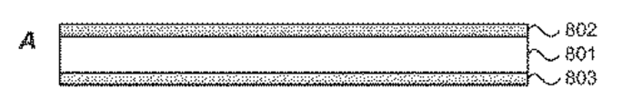
特定の例では、可撓性ポリマーの層は、約8μm、約10μm、約15μm、約25μm、約35μm、約50μm、約60μm、約75μm、または約85μmの厚さを有することができ、第1の導電性材料の層は、約2μm、約5μm、約8μm、約12μm、約15μm、約25μm、約35μm、約50μm、約60μm、または約70μmの厚さを有することができる。一例では、薄型チップは、約2μm、約5μm、約8μm、約12μm、約15μm、約25μm、約35μm、約50μm、約60μm、または約70μmの厚さを有することができる。
一例では、スタンドオフが、薄型チップの一部分を取り囲む。別の例では、スタンドオフは、薄型チップを完全に取り囲むことができる。一例では、スタンドオフと薄型チップの一部分との間に誘電体材料を配設することができる。
特定の例では、配設ステップはまた、スタンドオフの高さが薄型チップの高さよりも大きくなる、またはほぼ等しくなるように、スタンドオフの近位の可撓性ポリマーの一部分の上に薄型チップを配設するステップも含むことができる。
一例では、少なくとも1つのポリマー壁が、薄型チップの一部分を取り囲むことができる。別の例では、少なくとも1つのポリマー壁は、薄型チップを完全に取り囲むことができる。
別の例では、薄型チップは、少なくとも1つのポリマー壁の高さを薄型チップの高さよりも大きくする、またはほぼ等しくすることができるように、ウェル領域の内部に配設することができる。薄型チップは、少なくとも1つのポリマー壁の高さを薄型チップの高さよりも小さくすることができるように、ウェル領域の内部に配設することができる。一例では、少なくとも1つのポリマー壁と薄型チップの一部分との間に誘電体材料を配設することができる。
Kim et al.,“Stretchable and Foldable Silicon Integrated Circuits,”Science Express,March 27,2008,10.1126/science.1154367;
Ko et al.,“A Hemispherical Electronic Eye Camera Based on Compressible Silicon Optoelectronics,”Nature,August 7,2008,vol.454,pp.748−753;
Kim et al.,“Complementary Metal Oxide Silicon Integrated Circuits Incorporating Monolithically Integrated Stretchable Wavy Interconnects,”Applied Physics Letters,July 31,2008,vol.93,044102;
Kim et al.,“Materials and Noncoplanar Mesh Designs for Integrated Circuits with Linear Elastic Responses to Extreme Mechanical Deformations,”PNAS,December 2,2008,vol.105,no.48,pp.18675−18680;
Meitl et al.,“Transfer Printing by Kinetic Control of Adhesion to an Elastomeric Stamp,”Nature Materials,January,2006,vol.5,pp.33−38;
2009年3月5日出願、2010年1月7日公開の、「STRETCHABLE AND FOLDABLE ELECTRONIC DEVICES」という名称の米国特許出願公開第2010 0002402−A1号明細書;
2009年10月7日出願、2010年4月8日公開の、「CATHETER BALLOON HAVING STRETCHABLE INTEGRATED CIRCUITRY AND SENSOR ARRAY」という名称の米国特許出願公開第2010 0087782−A1号明細書;
2009年11月12日出願、2010年5月13日公開の、「EXTREMELY STRETCHABLE ELECTRONICS」という名称の米国特許出願公開第2010 0116526−A1号明細書;
2010年1月12日出願、2010年7月15日公開の、「METHODS AND APPLICATIONS OF NON−PLANAR IMAGING ARRAYS」という名称の米国特許出願公開第2010 0178722−A1号明細書;
2009年11月24日出願、2010年10月28日公開の、「SYSTEMS,DEVICES,AND METHODS UTILIZING STRETCHABLE ELECTRONICS TO MEASURE TIRE OR ROAD SURFACE CONDITIONS」という名称の米国特許出願公開第2010 027119−A1号明細書;
Kim,D.H.et al.(2010).Dissolvable films of silk fibroin for ultrathin conformal bio−integrated electronics.Nature Materials,9,511−517;
Omenetto,F.G.and D.L.Kaplan.(2008).A new route for silk.Nature Photonics,2,641−643;
Omenetto,F.G.,Kaplan,D.L.(2010).New opportunities for an ancient material.Science,329,528−531;
Halsed,W.S.(1913).Ligature and suture material.Journal of the American Medical Association,60,1119−1126;
Masuhiro,T.,Yoko,G.,Masaobu,N.,et al.(1994).Structural changes of silk fibroin membranes induced by immersion in methanol aqueous solutions.Journal of Polymer Science,5,961−968;
Lawrence,B.D.,Cronin−Golomb,M.,Georgakoudi,I.,et al.(2008).Bioactive silk protein biomaterial systems for optical devices.Biomacromolecules,9,1214−1220;
Demura,M.,Asakura,T.(1989).Immobilization of glucose oxidase with Bombyx mori silk fibroin by only stretching treatment and its application to glucose sensor.Biotechnololgy and Bioengineering,33,598−603;
Wang,X.,Zhang,X.,Castellot,J.et al.(2008).Controlled release from multilayer silk biomaterial coatings to modulate vascular cell responses.Biomaterials,29,894−903;
2010年3月12日出願の、「SYSTEMS,METHODS,AND DEVICES FOR SENSING AND TREATMENT HAVING STRETCHABLE INTEGRATED CIRCUITRY」という名称の米国特許出願第12/723,475号明細書;
2010年1月12日出願の、「Methods and Applications of Non−Planar Imaging Arrays」という名称の米国特許出願第12/686,076号明細書;
2009年12月11日出願の、「Systems,Methods,and Devices Using Stretchable or Flexible Electronics for Medical Applications」という名称の米国特許出願第12/636,071号明細書;
2012年3月15日出願の、「METHODS AND APPARATUS FOR MEASURING TECHNICAL PARAMETERS OF EQUIPMENT,TOOLS AND COMPONENTS VIA CONFORMAL ELECTRONICS」という名称の米国特許出願公開第2012−0065937−A1号明細書;
2009年11月12日出願の、「Extremely Stretchable Electronics」という名称の米国特許出願第12/616,922号明細書;
2009年10月7日出願の、「Catheter Balloon Having Stretchable Integrated Circuitry and Sensor Array」という名称の米国特許出願第12/575,008号明細書;
2011年12月23日出願の、「Systems,Methods,and Devices Having Stretchable Integrated Circuitry for Sensing and Delivering Therapy」という名称の米国特許出願第13/336,518号明細書
前述の概念および以下において詳細に説明される追加的概念の全ての組合せが、(そのような概念が互いに矛盾していないと仮定して)本明細書で開示される本発明の主題の一部として考えられることを理解すべきである。また、参照により援用する任意の開示に現れることもある、本明細書で明示的に採用される用語は、本明細書で開示される特定の概念と最も一貫性のある意味を与えられるものとすることを理解すべきである。
本明細書で使用される語句「および/または」は、そのように連結された要素の「いずれかまたは両方」を意味するものと理解すべきであり、すなわち、要素は、いくつかの場合には接続的に存在し、他の場合には離接的に存在する。「および/または」を用いて列挙される複数の要素も同様に解釈すべきであり、すなわち、そのように連結された要素の「1つまたは複数」である。任意選択で、特に識別される要素に関係するか無関係であるかに関わらず、「および/または」節によって特に識別される要素以外の他の要素が存在してもよい。したがって、非限定的な例として、「備える」など制限のない語に関連して使用されるときの「Aおよび/またはB」への言及は、例えば、一実施形態では、(任意選択でB以外の要素を含んで)Aのみを表すことができ、別の実施形態では、(任意選択でA以外の要素を含んで)Bのみを表すことができ、さらに別の実施形態では、(任意選択で他の要素を含んで)AとBの両方を表すことができる。
Claims (98)
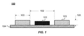
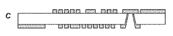
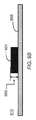
- A)スタンドオフウェル領域を備える基板を備える装置であって、
前記基板が、可撓性ポリマーの層の上に配設された第1の導電性材料の層を備え、
前記第1の導電性材料のパターン形成部分が、露出された可撓性ポリマーの一部分と境界を画すスタンドオフを備え、それにより前記スタンドオフウェル領域を形成し、
装置がさらに、
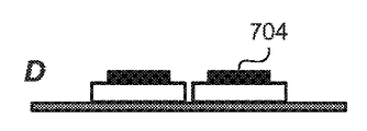
B)前記スタンドオフの近位の前記露出された可撓性ポリマーの一部分の上で前記スタンドオフウェル領域の内部に配設された薄型チップを備え、
前記スタンドオフの高さが、前記薄型チップの高さと同等である
装置。 - 前記スタンドオフの近位の前記露出された可撓性ポリマーの一部分で、前記スタンドオフウェル領域の内部に塗着された接着材を備え、前記薄型チップが、前記スタンドオフの近位の前記接着材の上に配設される請求項1に記載の装置。
- 前記接着材が、約8μm、約10μm、約12μm、約15μm、約20μm、約25μm、または約30μmの厚さを有する請求項2に記載の装置。
- 前記接着材が、導電性接着剤または非導電性接着剤を含む請求項2に記載の装置。
- 前記第1の導電性材料の前記パターン形成部分が、レーザアブレーションまたはエッチングを使用して形成される請求項1に記載の装置。
- 前記可撓性ポリマーが、ポリイミドまたは液晶ポリマーである請求項1に記載の装置。
- 前記第1の導電性材料が、銅、金、アルミニウム、またはそれらの何らかの組合せを含む請求項1に記載の装置。
- 前記基板が、銅−クラッドポリイミドである請求項1に記載の装置。
- 前記可撓性ポリマーの層が、約8μm、約10μm、約15μm、約25μm、約35μm、約50μm、約60μm、約75μm、または約85μmの厚さを有する請求項1に記載の装置。
- 前記第1の導電性材料の層が、約2μm、約5μm、約8μm、約12μm、約15μm、約25μm、約35μm、約50μm、約60μm、または約70μmの厚さを有する請求項1に記載の装置。
- 前記薄型チップが、約2μm、約5μm、約8μm、約12μm、約15μm、約25μm、約35μm、約50μm、約60μm、または約70μmの厚さを有する請求項1に記載の装置。
- 前記薄型チップが、薄型化されたチップである請求項1に記載の装置。
- 前記薄型化されたチップが、エッチングプロセスまたは研削プロセスを使用して薄型化されたチップから形成される請求項12に記載の装置。
- 前記スタンドオフの前記高さが前記薄型チップの前記高さよりも大きくなる、またはほぼ等しくなるように、前記薄型チップが前記スタンドオフウェル領域の内部に配設される請求項1に記載の装置。
- 前記スタンドオフの前記高さが前記薄型チップの前記高さよりも小さくなるように、前記薄型チップが前記スタンドオフウェル領域の内部に配設される請求項1に記載の装置。
- 前記薄型チップが、約2μm、約5μm、約8μm、約12μm、約15μm、約25μm、約35μm、約50μm、約60μm、または約70μmの厚さを有する第1の導電性材料の層を有する請求項1に記載の装置。
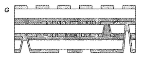
- 前記基板の上に配設されたポリマーシートと、
前記ポリマーシートを通して形成された少なくとも1つのバイアと、
前記少なくとも1つのバイアの近位の前記ポリマーシートの一部分の上に配設された第2の導電性材料とをさらに備え、それにより、前記第2の導電性材料が、前記薄型チップの電気コンタクトとの電気的連絡を形成する
請求項1に記載の装置。 - 前記第2の導電性材料が、チタン、タングステン、金、ニッケル、クロム、またはそれらの何らかの組合せを含む請求項17に記載の装置。
- 前記スタンドオフが、前記薄型チップの一部分を取り囲む請求項1に記載の装置。
- 前記スタンドオフが、前記薄型チップを完全に取り囲む請求項1に記載の装置。
- 誘電体材料が、前記スタンドオフと前記薄型チップの一部分との間に配設される請求項1に記載の装置。
- 前記第1の導電性材料の上または前記可撓性ポリマーの上に配設された少なくとも1つの追加の層をさらに備え、前記少なくとも1つの追加の層が、前記薄型チップを前記装置の中立機械面に位置決めする請求項1に記載の装置。
- 薄型チップを埋め込むための方法であって、
A)スタンドオフウェル領域を備える基板を提供するステップを含み、
前記基板が、可撓性ポリマーの層の上に配設された第1の導電性材料の層を備え、
前記第1の導電性材料の少なくとも一部分が、露出された可撓性ポリマーの一部分と境界を画すスタンドオフを形成するようにパターン形成され、それにより前記スタンドオフウェル領域を形成し、
方法がさらに、
B)前記スタンドオフの高さが前記薄型チップの高さと同等になるように、前記スタンドオフの近位の前記露出された可撓性ポリマーの一部分の上に薄型チップを配設するステップ
を含む方法。 - ステップB)の前に、前記スタンドオフの近位の前記露出された可撓性ポリマーの一部分に接着材を配設するステップを含み、ステップB)が、前記スタンドオフの近位の前記露出された可撓性ポリマーの前記部分に塗着された接着材上に前記薄型チップを配設するステップを含む請求項23に記載の方法。
- 前記スタンドオフの前記高さが、薄型チップの前記高さよりも大きい、またはほぼ等しい請求項23に記載の方法。
- ステップB)が、前記スタンドオフの前記高さが前記薄型チップの前記高さよりも大きくなる、またはほぼ等しくなるように、前記スタンドオフの近位の前記可撓性ポリマーの一部分の上に前記薄型チップを配設するステップを含む請求項23に記載の方法。
- 前記薄型チップが、薄型化されたチップであり、ステップB)が、前記薄型化されたチップを提供するために、エッチングプロセスまたは研削プロセスを使用してチップを薄型化するステップと、前記スタンドオフの前記高さが前記薄型化されたチップの前記高さと同等になるように、前記スタンドオフの近位の前記露出された可撓性ポリマーの一部分の上に前記薄型化されたチップを配設するステップとを含む請求項23に記載の方法。
- 前記基板の上にポリマーシートを配設するステップと、
前記ポリマーシートを通して少なくとも1つのバイアを形成するステップと、
前記少なくとも1つのバイアの近位の前記第2のポリマーシートの一部分の上に導電性材料を配設するステップとをさらに含み、それにより、前記導電性材料が、前記薄型チップの電気コンタクトとの電気的連絡を形成する
請求項23に記載の方法。 - 前記第1の導電性材料の上または前記可撓性ポリマーの上に少なくとも1つの追加の層を配設するステップをさらに含み、前記少なくとも1つの追加の層が、前記薄型チップを前記装置の中立機械面に位置決めする請求項23に記載の方法。
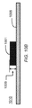
- A)ポリマーウェル領域を備える基板を備える装置であって、
前記基板が、第1の導電性材料の層の上に配設された可撓性ポリマーの層を備え、
前記可撓性ポリマーの少なくとも一部分にキャビティが形成されて、露出された第1の導電性材料の一部分と境界を画す少なくとも1つのポリマー壁を形成し、それによりポリマーウェル領域を形成し、
装置がさらに、
B)前記少なくとも1つのポリマー壁の近位の前記露出された第1の導電性材料の少なくとも一部分の上でポリマーウェル領域の内部に配設された薄型チップ
を備える装置。 - 前記少なくとも1つのポリマー壁の近位の前記露出された第1の導電性材料の少なくとも一部分で、前記ポリマーウェル領域の内部に塗着された接着材を備え、前記薄型チップが、前記少なくとも1つのポリマー壁の近位の前記接着材の上に配設される請求項30に記載の装置。
- 前記接着材が、約8μm、約10μm、約12μm、約15μm、約20μm、約25μm、または約30μmの厚さを有する請求項31に記載の装置。
- 前記接着材が、導電性接着剤または非導電性接着剤を含む請求項31に記載の装置。
- 前記キャビティが、レーザアブレーションまたはエッチングを使用して形成される請求項30に記載の装置。
- 前記可撓性ポリマーが、ポリイミドまたは液晶ポリマーである請求項30に記載の装置。
- 前記第1の導電性材料が、銅、金、アルミニウム、またはそれらの何らかの組合せを含む請求項30に記載の装置。
- 前記基板が、銅−クラッドポリイミドである請求項30に記載の装置。
- 前記可撓性ポリマーの層が、約8μm、約10μm、約15μm、約25μm、約35μm、約50μm、約60μm、約75μm、または約85μmの厚さを有する請求項30に記載の装置。
- 前記第1の導電性材料の層が、約2μm、約5μm、約8μm、約12μm、約15μm、約25μm、約35μm、約50μm、約60μm、または約70μmの厚さを有する請求項30に記載の装置。
- 前記薄型チップが、約2μm、約5μm、約8μm、約12μm、約15μm、約25μm、約35μm、約50μm、約60μm、または約70μmの厚さを有する請求項30に記載の装置。
- 前記薄型チップが、薄型化されたチップである請求項30に記載の装置。
- 前記薄型化されたチップが、エッチングプロセスまたは研削プロセスを使用して薄型化されたチップから形成される請求項40に記載の装置。
- 前記少なくとも1つのポリマー壁の前記高さが前記薄型チップの前記高さよりも大きくなる、またはほぼ等しくなるように、前記薄型チップが前記ポリマーウェル領域の内部に配設される請求項30に記載の装置。
- 前記少なくとも1つのポリマー壁の前記高さが前記薄型チップの前記高さよりも小さくなるように、前記薄型チップが前記ポリマーウェル領域の内部に配設される請求項30に記載の装置。
- 前記薄型チップが、約2μm、約5μm、約8μm、約12μm、約15μm、約25μm、約35μm、約50μm、約60μm、または約70μmの厚さを有する第1の導電性材料の層を有する請求項30に記載の装置。
- 前記基板の上に配設されたポリマーシートと、
前記ポリマーシートを通して形成された少なくとも1つのバイアと、
前記少なくとも1つのバイアの近位の前記ポリマーシートの一部分の上に配設された第2の導電性材料とをさらに備え、それにより、前記第2の導電性材料が、前記薄型チップの電気コンタクトとの電気的連絡を形成する
を備える請求項30に記載の装置。 - 前記第2の導電性材料が、チタン、タングステン、金、ニッケル、クロム、またはそれらの何らかの組合せを含む請求項46に記載の装置。
- 前記少なくとも1つのポリマー壁が、前記薄型チップの一部分を取り囲む請求項30に記載の装置。
- 前記少なくとも1つのポリマー壁が、前記薄型チップを完全に取り囲む請求項30に記載の装置。
- 前記少なくとも1つのポリマー壁と前記薄型チップの一部分との間に誘電体材料が配設される請求項30に記載の装置。
- 前記第1の導電性材料の上または前記可撓性ポリマーの上に配設された少なくとも1つの追加の層をさらに備え、前記少なくとも1つの追加の層が、前記薄型チップを前記装置の中立機械面に位置決めする請求項30に記載の装置。
- 前記薄型チップが、薄型化されたチップであり、ステップB)が、前記薄型化されたチップを提供するために、エッチングプロセスまたは研削プロセスを使用してチップを薄型化するステップと、前記少なくとも1つの壁の前記高さが前記薄型化されたチップの前記高さと同等になるように、前記少なくとも1つのポリマー壁の近位の前記露出された第1の導電性材料の少なくとも一部分の上で前記ポリマーウェル領域内に前記薄型化されたチップを配設するステップとを含む請求項30に記載の装置。
- 薄型チップを埋め込むための方法であって、
A)ポリマーウェル領域を備える基板を提供するステップを含み、前記基板が、可撓性ポリマーの層と、第1の導電性材料の層とを備え、前記ポリマーウェル領域が、前記可撓性ポリマーの一部分から形成された少なくとも1つのポリマー壁と、前記第1の導電性材料の少なくとも一部分から形成されたベース領域とを備え、
方法がさらに、
B)前記少なくとも1つのポリマー壁の近位の前記第1の導電性材料の一部分の上で前記ポリマーウェル領域内に前記薄型チップを配設するステップ
を含む方法。 - ステップB)の前に、前記少なくとも1つのポリマー壁の近位の前記第1の導電の前記部分に接着材を配設するステップを含み、ステップB)が、前記少なくとも1つのポリマー壁の近位の前記接着材上に前記薄型チップを配設するステップを含む請求項53に記載の方法。
- 前記少なくとも1つのポリマー壁の前記高さが前記薄型チップの前記高さよりも大きくなる、またはほぼ等しくなるように、前記薄型チップが前記ポリマーウェル領域の内部に配設される請求項53に記載の方法。
- 前記少なくとも1つのポリマー壁の前記高さが前記薄型チップの前記高さよりも小さくなるように、前記薄型チップが前記ポリマーウェル領域の内部に配設される請求項53に記載の方法。
- 前記第1の導電性材料が前記薄型チップと物理的および電気的に連絡するように、前記薄型チップが前記ポリマーウェル領域の内部に配設される請求項53に記載の方法。
- 前記基板の上に配設されたポリマーシートと、
前記ポリマーシートを通して形成された少なくとも1つのバイアと、
前記少なくとも1つのバイアの近位の前記ポリマーシートの一部分の上に配設された第2の導電性材料とをさらに備え、それにより、前記第2の導電性材料が、前記薄型チップの電気コンタクトとの電気的連絡を形成する
請求項53に記載の方法。 - 前記第1の導電性材料の上または前記可撓性ポリマーの上に少なくとも1つの追加の層を配設するステップをさらに含み、前記少なくとも1つの追加の層が、前記薄型チップを前記装置の中立機械面に位置決めする請求項53に記載の方法。
- A)ウェル領域を備える可撓性基板を備える装置であって、前記可撓性基板が、ポリイミドまたは液晶ポリマーを備え、前記可撓性基板が、前記可撓性基板にウェル領域を形成するキャビティを含み、
装置がさらに、
B)前記ウェル領域の内部に配設された薄型チップを備え、前記ウェル領域の少なくとも1つのポリマー壁の高さが、前記薄型チップの高さと同等であり、
装置がさらに、
C)前記薄型チップの少なくとも一部分と実質的に接触する、前記ウェル領域の内部に配設されたポリマー接着材
を備える装置。 - 前記可撓性基板の上に配設されたポリマーシートと、
前記ポリマーシートを通して形成された少なくとも1つのバイアと、
前記少なくとも1つのバイアの近位の前記ポリマーシートの一部分の上に配設された導電性材料とをさらに備え、それにより、前記第2の導電性材料が、前記薄型チップの電気コンタクトとの電気的連絡を形成する
請求項60に記載の装置。 - 前記ポリマー接着材を通して形成された少なくとも1つのバイアと、
前記少なくとも1つのバイアの近位の前記ポリマー接着材の一部分の上に配設された導電性材料とをさらに備え、それにより、前記導電性材料が、前記薄型チップの電気コンタクトとの電気的連絡を形成する
請求項60に記載の装置。 - 前記ウェル領域の内部に塗着された接着材を備え、前記薄型チップが前記接着材の上に配設される請求項60に記載の装置。
- 前記少なくとも1つのポリマー壁の前記高さが前記薄型チップの前記高さよりも大きくなる、またはほぼ等しくなるように、前記薄型チップが前記ウェル領域の内部に配設される請求項60に記載の装置。
- 前記少なくとも1つのポリマー壁の前記高さが前記薄型チップの前記高さよりも小さくなるように、前記薄型チップが前記ウェル領域の内部に配設される請求項60に記載の装置。
- 前記少なくとも1つのポリマー壁と前記薄型チップの一部分との間に誘電体材料が配設される請求項60に記載の装置。
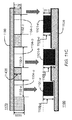
- A)少なくとも2つのスタンドオフウェル領域を備える基板を備える装置であって、
前記基板が、可撓性ポリマーの層の上に配設された第1の導電性材料の層を備え、
前記第1の導電性材料のパターン形成部分が、露出された可撓性ポリマーの幾つかの部分と境界を画す少なくとも2つのスタンドオフを備え、前記スタンドオフがそれぞれ、前記少なくとも2つのスタンドオフウェル領域の少なくとも1つを形成し、
装置がさらに、
B)少なくとも2つの薄型チップを備え、各薄型チップが、前記少なくとも2つのスタンドオフウェル領域の各1つの前記スタンドオフの近位の前記露出された可撓性ポリマーの一部分の上で、前記少なくとも2つのスタンドオフウェル領域の各1つの内部に配設され、
前記少なくとも2つの薄型チップの1つの厚さが、前記少なくとも2つの薄型チップの別のものの厚さよりも大きく、
前記スタンドオフの高さが、前記少なくとも2つの薄型チップの1つの高さと同等である
装置。 - 前記少なくとも2つのスタンドオフウェル領域の各1つの前記スタンドオフの近位の前記露出された可撓性ポリマーの一部分で、前記少なくとも2つのスタンドオフウェル領域の少なくとも1つの内部に塗着された接着材を備え、前記少なくとも2つの薄型チップの少なくとも1つが、前記スタンドオフの近位の前記接着材の上に配設される請求項67に記載の装置。
- 前記接着材が、約8μm、約10μm、約12μm、約15μm、約20μm、約25μm、約30μm、約40μm、約50μm、または約55μmの厚さを有する請求項68に記載の装置。
- 前記接着材が、導電性接着剤、および/または熱伝導性接着剤、および/または非導電性接着剤を含む請求項68に記載の装置。
- 前記接着材が導電性接着剤を含み、前記導電性接着剤を介して、前記少なくとも2つの薄型チップの少なくとも1つに接地電位が印加される請求項70に記載の装置。
- 前記第1の導電性材料の前記パターン形成部分が、レーザアブレーションまたはエッチングを使用して形成される請求項67に記載の装置。
- 前記可撓性ポリマーが、ポリイミドまたは液晶ポリマーである請求項67に記載の装置。
- 前記第1の導電性材料が、銅、金、アルミニウム、またはそれらの何らかの組合せを含む請求項67に記載の装置。
- 前記可撓性ポリマーの層が、約8μm、約10μm、約15μm、約25μm、約35μm、約50μm、約60μm、約75μm、約85μm、約100μm、約125μm、約150μm、約175μm、または約200μmの厚さを有する請求項67に記載の装置。
- 前記第1の導電性材料の層が、約2μm、約5μm、約8μm、約12μm、約15μm、約25μm、約35μm、約50μm、約60μm、または約70μmの厚さを有する請求項67に記載の装置。
- 前記少なくとも2つの薄型チップの少なくとも1つが、約2μm、約5μm、約8μm、約12μm、約15μm、約25μm、約35μm、約50μm、約60μm、約70μm、80マイクロメートル、約90マイクロメートル、約100マイクロメートル、約120マイクロメートル、約135マイクロメートル、または約150マイクロメートルの厚さを有する請求項67に記載の装置。
- 前記少なくとも2つの薄型チップの少なくとも1つが、薄型化されたチップであり、前記薄型化されたチップが、エッチングプロセスまたは研削プロセスを使用して薄型化されたチップから形成される請求項67に記載の装置。
- 前記スタンドオフの前記高さが前記基板の上での前記薄型チップの前記高さよりも約10マイクロメートル、約20マイクロメートル、約25マイクロメートル、約30マイクロメートル、約35マイクロメートル、約40マイクロメートル、または約45マイクロメートルだけ大きくなるように、前記少なくとも2つの薄型チップの少なくとも1つが前記少なくとも2つのスタンドオフウェル領域の少なくとも1つの内部に配設される請求項67に記載の装置。
- 前記スタンドオフの前記高さが前記薄型チップの前記高さよりも小さくなるように、前記少なくとも2つの薄型チップの少なくとも1つが前記スタンドオフウェル領域の少なくとも1つの内部に配設される請求項67に記載の装置。
- 前記少なくとも2つの薄型チップの少なくとも1つが、約2μm、約5μm、約8μm、約12μm、約15μm、約25μm、約35μm、約50μm、約60μm、または約70μmの厚さを有する第1の導電性材料の層を有する請求項67に記載の装置。
- 前記基板の上に配設されたポリマーシートと、
前記ポリマーシートを通して形成された少なくとも1つのバイアと、
前記少なくとも1つのバイアの近位の前記ポリマーシートの一部分の上に配設された第2の導電性材料とをさらに備え、それにより、前記第2の導電性材料が、前記少なくとも2つの薄型チップの少なくとも1つの電気コンタクトとの電気的連絡を形成する
請求項67に記載の装置。 - 前記第2の導電性材料が、チタン、タングステン、金、ニッケル、クロム、またはそれらの何らかの組合せを含む請求項82に記載の装置。
- 前記スタンドオフが、前記薄型チップの一部分を取り囲む請求項67に記載の装置。
- 前記少なくとも2つのスタンドオフの少なくとも1つと、前記少なくとも2つの薄型チップの1つの一部分との間に誘電体材料が配設されて接触する請求項67に記載の装置。
- 前記第1の導電性材料の上または前記可撓性ポリマーの上に配設された少なくとも1つの追加の層をさらに備え、前記少なくとも1つの追加の層が、前記少なくとも2つの薄型チップの少なくとも1つを前記装置の中立機械面に位置決めする請求項67に記載の装置。
- A)少なくとも1つのポリマーウェル領域と、少なくとも1つのスタンドオフウェル領域とを備える基板を備える装置であって、
前記基板が、第1の導電性材料の層の上に配設された可撓性ポリマーの層を備え、
前記可撓性ポリマーの少なくとも一部分にキャビティが形成されて、露出された第1の導電性材料の一部分と境界を画す少なくとも1つのポリマー壁を形成し、それによりポリマーウェル領域を形成し、
前記第1の導電性材料のパターン形成部分が、露出された可撓性ポリマーの一部分と境界を画すスタンドオフを備え、それにより前記スタンドオフウェル領域を形成し、
装置がさらに、
B)少なくとも2つの薄型チップを備え、
前記少なくとも2つの薄型チップの1つが、前記少なくとも1つのポリマー壁の近位の前記露出された第1の導電性材料の少なくとも一部分の上で前記ポリマーウェル領域の内部に配設され、
前記少なくとも2つの薄型チップの別のものが、前記スタンドオフの近位の前記露出された可撓性ポリマーの少なくとも一部分の上で前記スタンドオフウェル領域の内部に配設され、
前記少なくとも2つの薄型チップの1つの厚さが、前記少なくとも2つの薄型チップの別のものの厚さよりも大きい
装置。 - (a)前記少なくとも1つのポリマー壁の近位の前記露出された第1の導電性材料の少なくとも一部分の上で前記ポリマーウェル領域の内部に、または(b)前記スタンドオフの近位の前記露出された可撓性ポリマーの一部分で、前記スタンドオフウェル領域の内部に塗着された接着材を備え、前記少なくとも2つの薄型チップの少なくとも1つが前記接着材の上に配設される請求項87に記載の装置。
- 前記接着材が、約8μm、約10μm、約12μm、約15μm、約20μm、約25μm、約30μm、約40μm、約50μm、または約55μmの厚さを有する請求項88に記載の装置。
- 前記接着材が、導電性接着剤、および/または熱伝導性接着剤、および/または非導電性接着剤を含む請求項88に記載の装置。
- 前記可撓性ポリマーが、ポリイミドまたは液晶ポリマーである請求項87に記載の装置。
- 前記第1の導電性材料が、銅、金、アルミニウム、またはそれらの何らかの組合せを含む請求項87に記載の装置。
- 前記可撓性ポリマーの層が、約8μm、約10μm、約15μm、約25μm、約35μm、約50μm、約60μm、約75μm、約85μm、約100μm、約125μm、約150μm、約175μm、または約200μmの厚さを有する請求項87に記載の装置。
- 前記第1の導電性材料の層が、約2μm、約5μm、約8μm、約12μm、約15μm、約25μm、約35μm、約50μm、約60μm、または約70μmの厚さを有する請求項87に記載の装置。
- 前記少なくとも2つの薄型チップの少なくとも1つが、約2μm、約5μm、約8μm、約12μm、約15μm、約25μm、約35μm、約50μm、約60μm、約70μm、80マイクロメートル、約90マイクロメートル、約100マイクロメートル、約120マイクロメートル、約135マイクロメートル、または約150マイクロメートルの厚さを有する請求項87に記載の装置。
- 前記少なくとも2つの薄型チップの少なくとも1つが、薄型化されたチップであり、前記薄型化されたチップが、エッチングプロセスまたは研削プロセスを使用して薄型化されたチップから形成される請求項87に記載の装置。
- 前記基板の上に配設されたポリマーシートと、
前記ポリマーシートを通して形成された少なくとも1つのバイアと、
前記少なくとも1つのバイアの近位の前記ポリマーシートの一部分の上に配設された第2の導電性材料とをさらに備え、それにより、前記第2の導電性材料が、前記少なくとも2つの薄型チップの少なくとも1つの電気コンタクトとの電気的連絡を形成する
請求項87に記載の装置。 - 前記第1の導電性材料の上または前記可撓性ポリマーの上に配設された少なくとも1つの追加の層をさらに備え、前記少なくとも1つの追加の層が、前記薄型チップを前記装置の中立機械面に位置決めする請求項97に記載の装置。
Applications Claiming Priority (5)
| Application Number | Priority Date | Filing Date | Title |
|---|---|---|---|
| US201261711629P | 2012-10-09 | 2012-10-09 | |
| US61/711,629 | 2012-10-09 | ||
| US13/844,638 US9171794B2 (en) | 2012-10-09 | 2013-03-15 | Embedding thin chips in polymer |
| US13/844,638 | 2013-03-15 | ||
| PCT/US2013/064152 WO2014059032A1 (en) | 2012-10-09 | 2013-10-09 | Embedding thin chips in polymer |
Publications (2)
| Publication Number | Publication Date |
|---|---|
| JP2016504751A true JP2016504751A (ja) | 2016-02-12 |
| JP2016504751A5 JP2016504751A5 (ja) | 2016-10-13 |
Family
ID=50477861
Family Applications (1)
| Application Number | Title | Priority Date | Filing Date |
|---|---|---|---|
| JP2015536868A Pending JP2016504751A (ja) | 2012-10-09 | 2013-10-09 | ポリマー内への薄型チップの埋込み |
Country Status (6)
| Country | Link |
|---|---|
| US (3) | US9171794B2 (ja) |
| EP (1) | EP2907159A4 (ja) |
| JP (1) | JP2016504751A (ja) |
| KR (1) | KR20150067302A (ja) |
| CN (1) | CN104798196A (ja) |
| WO (1) | WO2014059032A1 (ja) |
Cited By (3)
| Publication number | Priority date | Publication date | Assignee | Title |
|---|---|---|---|---|
| JP6191808B1 (ja) * | 2016-04-20 | 2017-09-06 | 株式会社村田製作所 | 多層基板および電子機器 |
| JP2017183649A (ja) * | 2016-03-31 | 2017-10-05 | 大日本印刷株式会社 | 電子デバイス及びその製造方法 |
| WO2017183394A1 (ja) * | 2016-04-20 | 2017-10-26 | 株式会社村田製作所 | 多層基板および電子機器 |
Families Citing this family (88)
| Publication number | Priority date | Publication date | Assignee | Title |
|---|---|---|---|---|
| CA2704769C (en) | 2006-11-03 | 2016-01-12 | Trustees Of Tufts College | Nanopatterned biopolymer optical device and method of manufacturing the same |
| JP2010509593A (ja) | 2006-11-03 | 2010-03-25 | トラスティーズ オブ タフツ カレッジ | バイオポリマーセンサーおよびその製造方法 |
| US8574461B2 (en) * | 2006-11-03 | 2013-11-05 | Tufts University | Electroactive biopolymer optical and electro-optical devices and method of manufacturing the same |
| US9119533B2 (en) | 2008-10-07 | 2015-09-01 | Mc10, Inc. | Systems, methods, and devices having stretchable integrated circuitry for sensing and delivering therapy |
| US9123614B2 (en) | 2008-10-07 | 2015-09-01 | Mc10, Inc. | Methods and applications of non-planar imaging arrays |
| US9545216B2 (en) | 2011-08-05 | 2017-01-17 | Mc10, Inc. | Catheter balloon methods and apparatus employing sensing elements |
| US8389862B2 (en) | 2008-10-07 | 2013-03-05 | Mc10, Inc. | Extremely stretchable electronics |
| US8097926B2 (en) | 2008-10-07 | 2012-01-17 | Mc10, Inc. | Systems, methods, and devices having stretchable integrated circuitry for sensing and delivering therapy |
| US9289132B2 (en) | 2008-10-07 | 2016-03-22 | Mc10, Inc. | Catheter balloon having stretchable integrated circuitry and sensor array |
| US8886334B2 (en) | 2008-10-07 | 2014-11-11 | Mc10, Inc. | Systems, methods, and devices using stretchable or flexible electronics for medical applications |
| US9723122B2 (en) | 2009-10-01 | 2017-08-01 | Mc10, Inc. | Protective cases with integrated electronics |
| EP2681538B1 (en) | 2011-03-11 | 2019-03-06 | Mc10, Inc. | Integrated devices to facilitate quantitative assays and diagnostics |
| JP2014523633A (ja) | 2011-05-27 | 2014-09-11 | エムシー10 インコーポレイテッド | 電子的、光学的、且つ/又は機械的装置及びシステム並びにこれらの装置及びシステムを製造する方法 |
| US9757050B2 (en) | 2011-08-05 | 2017-09-12 | Mc10, Inc. | Catheter balloon employing force sensing elements |
| WO2013033724A1 (en) | 2011-09-01 | 2013-03-07 | Mc10, Inc. | Electronics for detection of a condition of tissue |
| DE112012004146T5 (de) | 2011-10-05 | 2014-11-06 | Mc10, Inc. | Herzkatheter mit Verwendung oberflächentreuer Elektronik zur Abbildung |
| WO2017185050A1 (en) * | 2016-04-21 | 2017-10-26 | Sensoria, Inc. | Sensor assemblies; sensor-enabled garments and objects; devices and systems for data collection |
| FR2988223B1 (fr) * | 2012-03-19 | 2016-09-02 | Solarwell | Dispositif emettant de la lumiere contenant des nanocristaux colloidaux semiconducteurs anisotropes aplatis et procede de fabrication de tels dispositifs |
| US9226402B2 (en) | 2012-06-11 | 2015-12-29 | Mc10, Inc. | Strain isolation structures for stretchable electronics |
| US9247637B2 (en) | 2012-06-11 | 2016-01-26 | Mc10, Inc. | Strain relief structures for stretchable interconnects |
| JP2015521894A (ja) | 2012-07-05 | 2015-08-03 | エムシー10 インコーポレイテッドMc10,Inc. | 流量センシングを含むカテーテルデバイス |
| US9295842B2 (en) | 2012-07-05 | 2016-03-29 | Mc10, Inc. | Catheter or guidewire device including flow sensing and use thereof |
| US9171794B2 (en) * | 2012-10-09 | 2015-10-27 | Mc10, Inc. | Embedding thin chips in polymer |
| KR20150072415A (ko) | 2012-10-09 | 2015-06-29 | 엠씨10, 인크 | 의류에 집적되는 컨포멀 전자기기 |
| DE102012110358B4 (de) * | 2012-10-30 | 2016-04-07 | Leibniz-Institut für Neurobiologie Magdeburg | Mikroelektrodenarray |
| US10840536B2 (en) * | 2013-02-06 | 2020-11-17 | The Board Of Trustees Of The University Of Illinois | Stretchable electronic systems with containment chambers |
| US9706647B2 (en) | 2013-05-14 | 2017-07-11 | Mc10, Inc. | Conformal electronics including nested serpentine interconnects |
| KR20160040670A (ko) | 2013-08-05 | 2016-04-14 | 엠씨10, 인크 | 곡면부착형 전자기기를 포함하는 유연한 온도 센서 |
| KR20160065948A (ko) | 2013-10-07 | 2016-06-09 | 엠씨10, 인크 | 감지 및 분석용 등각 센서 시스템 |
| CN105813545A (zh) | 2013-11-22 | 2016-07-27 | Mc10股份有限公司 | 用于感测和分析心搏的适形传感器系统 |
| WO2015103580A2 (en) | 2014-01-06 | 2015-07-09 | Mc10, Inc. | Encapsulated conformal electronic systems and devices, and methods of making and using the same |
| US10485118B2 (en) | 2014-03-04 | 2019-11-19 | Mc10, Inc. | Multi-part flexible encapsulation housing for electronic devices and methods of making the same |
| EP3117206A4 (en) | 2014-03-12 | 2017-11-15 | Mc10, Inc. | Quantification of a change in assay |
| US10492703B2 (en) * | 2014-03-28 | 2019-12-03 | Board Of Regents, The University Of Texas System | Epidermal sensor system and process |
| US9899330B2 (en) | 2014-10-03 | 2018-02-20 | Mc10, Inc. | Flexible electronic circuits with embedded integrated circuit die |
| US10297572B2 (en) * | 2014-10-06 | 2019-05-21 | Mc10, Inc. | Discrete flexible interconnects for modules of integrated circuits |
| USD781270S1 (en) | 2014-10-15 | 2017-03-14 | Mc10, Inc. | Electronic device having antenna |
| FR3030112B1 (fr) * | 2014-12-12 | 2018-02-02 | Stmicroelectronics (Crolles 2) Sas | Assemblage d'une puce de circuits integres et d'une plaque |
| US10477354B2 (en) | 2015-02-20 | 2019-11-12 | Mc10, Inc. | Automated detection and configuration of wearable devices based on on-body status, location, and/or orientation |
| WO2016140961A1 (en) | 2015-03-02 | 2016-09-09 | Mc10, Inc. | Perspiration sensor |
| US9633883B2 (en) | 2015-03-20 | 2017-04-25 | Rohinni, LLC | Apparatus for transfer of semiconductor devices |
| US10264669B2 (en) * | 2015-05-01 | 2019-04-16 | Research Triangle Institute | Flexible electronic assemblies with embedded electronic devices and methods for their fabrication |
| US10182284B2 (en) * | 2015-06-11 | 2019-01-15 | Facebook Technologies, Llc | Connector assembly for detachable audio system |
| TWI555044B (zh) * | 2015-06-25 | 2016-10-21 | Wafer Mems Co Ltd | A method for producing a passive element with a terminal electrode |
| TWI592955B (zh) | 2015-06-25 | 2017-07-21 | Wafer Mems Co Ltd | Embedded passive components and methods of mass production |
| WO2017015000A1 (en) | 2015-07-17 | 2017-01-26 | Mc10, Inc. | Conductive stiffener, method of making a conductive stiffener, and conductive adhesive and encapsulation layers |
| WO2017031129A1 (en) | 2015-08-19 | 2017-02-23 | Mc10, Inc. | Wearable heat flux devices and methods of use |
| WO2017052254A1 (ko) * | 2015-09-23 | 2017-03-30 | 주식회사 아모그린텍 | 웨어러블 디바이스 및 그의 제조 방법 |
| WO2017059215A1 (en) | 2015-10-01 | 2017-04-06 | Mc10, Inc. | Method and system for interacting with a virtual environment |
| CN108289630A (zh) | 2015-10-05 | 2018-07-17 | Mc10股份有限公司 | 用于神经调节和刺激的方法和系统 |
| WO2017070030A1 (en) | 2015-10-21 | 2017-04-27 | Massachusetts Institute Of Technology | Nanowire fet imaging system and related techniques |
| US10083888B2 (en) * | 2015-11-19 | 2018-09-25 | Advanced Semiconductor Engineering, Inc. | Semiconductor device package |
| EP3206229B1 (en) | 2016-02-09 | 2020-10-07 | AT & S Austria Technologie & Systemtechnik Aktiengesellschaft | Methods of manufacturing flexible electronic devices |
| CN115175014A (zh) | 2016-02-22 | 2022-10-11 | 美谛达解决方案公司 | 贴身传感器系统 |
| CN108781313B (zh) | 2016-02-22 | 2022-04-08 | 美谛达解决方案公司 | 用以贴身获取传感器信息的耦接的集线器和传感器节点的系统、装置和方法 |
| WO2017156502A1 (en) | 2016-03-10 | 2017-09-14 | Carnegie Mellon University | Integrated electronic device with flexible and stretchable substrate |
| EP3445230B1 (en) | 2016-04-19 | 2024-03-13 | Medidata Solutions, Inc. | Method and system for measuring perspiration |
| US9930773B2 (en) | 2016-06-21 | 2018-03-27 | Microsoft Technology Licensing, Llc | Flexible interconnect |
| US10815121B2 (en) * | 2016-07-12 | 2020-10-27 | Hewlett-Packard Development Company, L.P. | Composite wafers |
| US10447347B2 (en) | 2016-08-12 | 2019-10-15 | Mc10, Inc. | Wireless charger and high speed data off-loader |
| US10141215B2 (en) | 2016-11-03 | 2018-11-27 | Rohinni, LLC | Compliant needle for direct transfer of semiconductor devices |
| US10504767B2 (en) | 2016-11-23 | 2019-12-10 | Rohinni, LLC | Direct transfer apparatus for a pattern array of semiconductor device die |
| US10471545B2 (en) | 2016-11-23 | 2019-11-12 | Rohinni, LLC | Top-side laser for direct transfer of semiconductor devices |
| US10902310B2 (en) | 2016-12-14 | 2021-01-26 | Trackonomy Systems, Inc. | Wireless communications and transducer based event detection platform |
| US10885420B2 (en) | 2016-12-14 | 2021-01-05 | Ajay Khoche | Package sealing tape types with varied transducer sampling densities |
| US10445634B2 (en) | 2016-12-14 | 2019-10-15 | Trackonomy Systems, Inc. | Fabricating multifunction adhesive product for ubiquitous realtime tracking |
| US11138490B2 (en) | 2016-12-14 | 2021-10-05 | Ajay Khoche | Hierarchical combination of distributed statistics in a monitoring network |
| US10062588B2 (en) | 2017-01-18 | 2018-08-28 | Rohinni, LLC | Flexible support substrate for transfer of semiconductor devices |
| EP3948750A4 (en) * | 2018-02-06 | 2022-11-16 | Wickersham, Jill Anne | SYSTEMS AND PROCEDURES FOR REAL-TIME DETECTION AND PROCUREMENT OF ARTICLES |
| WO2020162935A1 (en) * | 2019-02-06 | 2020-08-13 | Wickersham Jill Anne | Systems and methods for real-time item identification and sourcing |
| US10410905B1 (en) | 2018-05-12 | 2019-09-10 | Rohinni, LLC | Method and apparatus for direct transfer of multiple semiconductor devices |
| EP3768186B1 (en) * | 2018-05-31 | 2022-09-14 | St. Jude Medical, Cardiology Division, Inc. | Catheter handle with compliant circuit |
| US11094571B2 (en) | 2018-09-28 | 2021-08-17 | Rohinni, LLC | Apparatus to increase transferspeed of semiconductor devices with micro-adjustment |
| JP2020150168A (ja) * | 2019-03-14 | 2020-09-17 | キオクシア株式会社 | 半導体装置および半導体装置の製造方法 |
| US11768262B2 (en) | 2019-03-14 | 2023-09-26 | Massachusetts Institute Of Technology | Interface responsive to two or more sensor modalities |
| WO2020247354A1 (en) | 2019-06-05 | 2020-12-10 | Trackonomy Systems, Inc. | Temperature monitoring in cold supply chains |
| WO2021051087A1 (en) | 2019-09-13 | 2021-03-18 | Trackonomy Systems, Inc. | Roll-to-roll additive manufacturing method and device |
| US11464451B1 (en) | 2020-03-11 | 2022-10-11 | Huxley Medical, Inc. | Patch for improved biometric data capture and related processes |
| US11123011B1 (en) | 2020-03-23 | 2021-09-21 | Nix, Inc. | Wearable systems, devices, and methods for measurement and analysis of body fluids |
| US11864058B1 (en) | 2020-10-04 | 2024-01-02 | Trackonomy Systems, Inc. | Flexible tracking device for cables and equipment |
| US11900195B2 (en) | 2020-07-24 | 2024-02-13 | Trackonomy Systems, Inc. | Tearing to turn on wireless node with multiple cutouts for re-use |
| US12047841B2 (en) | 2020-09-21 | 2024-07-23 | Trackonomy Systems, Inc. | Detecting special events and strategically important areas in an IoT tracking system |
| US11527148B1 (en) | 2020-10-04 | 2022-12-13 | Trackonomy Systems, Inc. | Augmented reality for guiding users to assets in IOT applications |
| US12051916B1 (en) | 2020-10-05 | 2024-07-30 | Trackonomy Systems, Inc. | Method for recharging wireless IOT devices and system thereof |
| WO2022126020A1 (en) | 2020-12-12 | 2022-06-16 | Trackonomy Systems, Inc. | Flexible solar-powered wireless communication device |
| US20220264703A1 (en) * | 2021-02-12 | 2022-08-18 | William Marsh Rice University | Integrated microheater array for efficient and localized heating of magnetic nanoparticles at microwave frequencies |
| US11660005B1 (en) | 2021-06-04 | 2023-05-30 | Huxley Medical, Inc. | Processing and analyzing biometric data |
| US12109010B1 (en) | 2021-08-24 | 2024-10-08 | Huxley Medical, Inc. | Photoplethysmography sensors and processes |
Citations (11)
| Publication number | Priority date | Publication date | Assignee | Title |
|---|---|---|---|---|
| US20020079572A1 (en) * | 2000-12-22 | 2002-06-27 | Khan Reza-Ur Rahman | Enhanced die-up ball grid array and method for making the same |
| US20030045025A1 (en) * | 2000-01-26 | 2003-03-06 | Coyle Anthony L. | Method of fabricating a molded package for micromechanical devices |
| JP2005108942A (ja) * | 2003-09-29 | 2005-04-21 | Nitto Denko Corp | フレキシブル配線回路基板の製造方法 |
| JP2007294724A (ja) * | 2006-04-26 | 2007-11-08 | Toppan Printing Co Ltd | 多層回路配線基板及び半導体装置 |
| WO2008056499A1 (en) * | 2006-11-06 | 2008-05-15 | Nec Corporation | Semiconductor device and method for manufacturing same |
| US20080211087A1 (en) * | 2006-12-20 | 2008-09-04 | Infineon Technologies Ag | Chip module and method for producing a chip module |
| JP2008244473A (ja) * | 2007-03-26 | 2008-10-09 | Endicott Interconnect Technologies Inc | スタンドオフ付きフレキシブル電子回路パッケージ、及びその製造方法 |
| US20110051384A1 (en) * | 2006-02-02 | 2011-03-03 | Arno Kriechbaum | Printed circuit board element having at least one component embedded therein and method for embedding at least one component in a printed circuit board element |
| JP2011517370A (ja) * | 2008-03-05 | 2011-06-02 | ザ ボード オブ トラスティーズ オブ ザ ユニヴァーシティー オブ イリノイ | 伸張可能及び折畳み可能な電子デバイス |
| JP2011176112A (ja) * | 2010-02-24 | 2011-09-08 | Renesas Electronics Corp | 半導体集積回路及びその製造方法 |
| JP2012023237A (ja) * | 2010-07-15 | 2012-02-02 | Nec Corp | 機能素子内蔵基板 |
Family Cites Families (780)
| Publication number | Priority date | Publication date | Assignee | Title |
|---|---|---|---|---|
| US3716861A (en) | 1971-03-22 | 1973-02-13 | J Root | Serpentine antenna mounted on a rotatable capacitive coupler |
| US3805427A (en) | 1972-12-18 | 1974-04-23 | H Epstein | Medical alarm bracelet |
| US3838240A (en) | 1973-04-04 | 1974-09-24 | Rca Corp | Bonding tool and method of bonding therewith |
| US4058418A (en) | 1974-04-01 | 1977-11-15 | Solarex Corporation | Fabrication of thin film solar cells utilizing epitaxial deposition onto a liquid surface to obtain lateral growth |
| US3949410A (en) | 1975-01-23 | 1976-04-06 | International Business Machines Corporation | Jet nozzle structure for electrohydrodynamic droplet formation and ink jet printing system therewith |
| CA1105565A (en) | 1978-09-12 | 1981-07-21 | Kaufman (John G.) Hospital Products Ltd. | Electrosurgical electrode |
| US4278474A (en) | 1980-03-25 | 1981-07-14 | The United States Of America As Represented By The United States Department Of Energy | Device for conversion of electromagnetic radiation into electrical current |
| US4416288A (en) | 1980-08-14 | 1983-11-22 | The Regents Of The University Of California | Apparatus and method for reconstructing subsurface electrophysiological patterns |
| US4471003A (en) | 1980-11-25 | 1984-09-11 | Cann Gordon L | Magnetoplasmadynamic apparatus and process for the separation and deposition of materials |
| US4487162A (en) | 1980-11-25 | 1984-12-11 | Cann Gordon L | Magnetoplasmadynamic apparatus for the separation and deposition of materials |
| US4392451A (en) | 1980-12-31 | 1983-07-12 | The Boeing Company | Apparatus for forming thin-film heterojunction solar cells employing materials selected from the class of I-III-VI2 chalcopyrite compounds |
| US4658153A (en) | 1984-06-18 | 1987-04-14 | Amnon Brosh | Planar coil apparatus for providing a frequency output vs. position |
| US4761335A (en) | 1985-03-07 | 1988-08-02 | National Starch And Chemical Corporation | Alpha-particle protection of semiconductor devices |
| US4855017A (en) | 1985-05-03 | 1989-08-08 | Texas Instruments Incorporated | Trench etch process for a single-wafer RIE dry etch reactor |
| US4784720A (en) | 1985-05-03 | 1988-11-15 | Texas Instruments Incorporated | Trench etch process for a single-wafer RIE dry etch reactor |
| US4663828A (en) | 1985-10-11 | 1987-05-12 | Energy Conversion Devices, Inc. | Process and apparatus for continuous production of lightweight arrays of photovoltaic cells |
| US4763275A (en) | 1986-02-20 | 1988-08-09 | Carlin John A | Force accumulating device for sporting protective gear |
| US4918811A (en) * | 1986-09-26 | 1990-04-24 | General Electric Company | Multichip integrated circuit packaging method |
| US4766670A (en) | 1987-02-02 | 1988-08-30 | International Business Machines Corporation | Full panel electronic packaging structure and method of making same |
| JPH01223064A (ja) | 1988-03-02 | 1989-09-06 | Hitachi Ltd | 駆動輪空転防止装置 |
| US5439575A (en) | 1988-06-30 | 1995-08-08 | Board Of Trustees Of The University Of Illinois | Hybrid method for depositing semi-conductive materials |
| CA1292572C (en) | 1988-10-25 | 1991-11-26 | Fernando C. Lebron | Cardiac mapping system simulator |
| US4911169A (en) | 1989-03-13 | 1990-03-27 | Ferrari Robert K | Biomedical electrode with limb band |
| US5178957A (en) | 1989-05-02 | 1993-01-12 | Minnesota Mining And Manufacturing Company | Noble metal-polymer composites and flexible thin-film conductors prepared therefrom |
| US5250903A (en) | 1989-05-31 | 1993-10-05 | Amoco Corporation | Method and apparatus using oscillatory magnetic field to determine state of charge of an electrolytic storage cell |
| US5086785A (en) | 1989-08-10 | 1992-02-11 | Abrams/Gentille Entertainment Inc. | Angular displacement sensors |
| US5059424A (en) | 1989-11-01 | 1991-10-22 | Ndm Acquisition Corp. | Hydrogel wound dressing product |
| US5118400A (en) | 1990-01-29 | 1992-06-02 | Spire Corporation | Method of making biocompatible electrodes |
| US5108819A (en) | 1990-02-14 | 1992-04-28 | Eli Lilly And Company | Thin film electrical component |
| DE59109246D1 (de) | 1990-05-03 | 2003-04-03 | Hoffmann La Roche | Mikrooptischer Sensor |
| US5147519A (en) | 1990-07-27 | 1992-09-15 | Motorola, Inc. | Method of manufacturing elastomers containing fine line conductors |
| US5206749A (en) | 1990-12-31 | 1993-04-27 | Kopin Corporation | Liquid crystal display having essentially single crystal transistors pixels and driving circuits |
| US5475514A (en) | 1990-12-31 | 1995-12-12 | Kopin Corporation | Transferred single crystal arrayed devices including a light shield for projection displays |
| US6387052B1 (en) | 1991-01-29 | 2002-05-14 | Edwards Lifesciences Corporation | Thermodilution catheter having a safe, flexible heating element |
| US5560974A (en) | 1991-03-22 | 1996-10-01 | Kappler Safety Group, Inc. | Breathable non-woven composite barrier fabric and fabrication process |
| WO1992017240A1 (en) | 1991-04-05 | 1992-10-15 | Medtronic, Inc. | Subcutaneous multi-electrode sensing system |
| US5204144A (en) | 1991-05-10 | 1993-04-20 | Celestech, Inc. | Method for plasma deposition on apertured substrates |
| JPH0587511A (ja) | 1991-07-24 | 1993-04-06 | Yamaha Corp | 曲げ検出装置 |
| US5246003A (en) | 1991-08-28 | 1993-09-21 | Nellcor Incorporated | Disposable pulse oximeter sensor |
| US5272375A (en) | 1991-12-26 | 1993-12-21 | E. I. Du Pont De Nemours And Company | Electronic assembly with optimum heat dissipation |
| US5539935A (en) | 1992-01-10 | 1996-07-30 | Rush, Iii; Gus A. | Sports helmet |
| US5313094A (en) | 1992-01-28 | 1994-05-17 | International Business Machines Corportion | Thermal dissipation of integrated circuits using diamond paths |
| US5491651A (en) | 1992-05-15 | 1996-02-13 | Key, Idea Development | Flexible wearable computer |
| US5306917A (en) | 1992-08-12 | 1994-04-26 | Reliant Laser Corporation | Electro-optical system for measuring and analyzing accumulated short-wave and long-wave ultraviolet radiation exposure |
| US5309910A (en) | 1992-09-25 | 1994-05-10 | Ep Technologies, Inc. | Cardiac mapping and ablation systems |
| US5549108A (en) | 1992-09-25 | 1996-08-27 | Ep Technologies, Inc. | Cardiac mapping and ablation systems |
| US5471982A (en) | 1992-09-29 | 1995-12-05 | Ep Technologies, Inc. | Cardiac mapping and ablation systems |
| US5687737A (en) | 1992-10-09 | 1997-11-18 | Washington University | Computerized three-dimensional cardiac mapping with interactive visual displays |
| DE4241045C1 (de) | 1992-12-05 | 1994-05-26 | Bosch Gmbh Robert | Verfahren zum anisotropen Ätzen von Silicium |
| AU676711B2 (en) | 1992-12-31 | 1997-03-20 | Alza Corporation | Electrotransport system having flexible means |
| US6233491B1 (en) | 1993-03-16 | 2001-05-15 | Ep Technologies, Inc. | Cardiac mapping and ablation systems |
| GB2276326B (en) | 1993-03-23 | 1996-10-09 | Mclaughlin James A | Profiled biosignal electrode device |
| US5617870A (en) | 1993-04-29 | 1997-04-08 | Scimed Life Systems, Inc. | Intravascular flow measurement system |
| US5477088A (en) | 1993-05-12 | 1995-12-19 | Rockett; Angus A. | Multi-phase back contacts for CIS solar cells |
| US5326521A (en) | 1993-05-26 | 1994-07-05 | East Douglas A | Method for preparing silicone mold tooling |
| US5860974A (en) | 1993-07-01 | 1999-01-19 | Boston Scientific Corporation | Heart ablation catheter with expandable electrode and method of coupling energy to an electrode on a catheter shaft |
| US5837546A (en) | 1993-08-24 | 1998-11-17 | Metrika, Inc. | Electronic assay device and method |
| CA2170402C (en) | 1993-08-24 | 2000-07-18 | Michael P. Allen | Novel disposable electronic assay device |
| US5591941A (en) | 1993-10-28 | 1997-01-07 | International Business Machines Corporation | Solder ball interconnected assembly |
| US5793107A (en) | 1993-10-29 | 1998-08-11 | Vlsi Technology, Inc. | Polysilicon pillar heat sinks for semiconductor on insulator circuits |
| US5360987A (en) | 1993-11-17 | 1994-11-01 | At&T Bell Laboratories | Semiconductor photodiode device with isolation region |
| US5427096A (en) | 1993-11-19 | 1995-06-27 | Cmc Assemblers, Inc. | Water-degradable electrode |
| US5545291A (en) | 1993-12-17 | 1996-08-13 | The Regents Of The University Of California | Method for fabricating self-assembling microstructures |
| US5904545A (en) | 1993-12-17 | 1999-05-18 | The Regents Of The University Of California | Apparatus for fabricating self-assembling microstructures |
| US6864570B2 (en) | 1993-12-17 | 2005-03-08 | The Regents Of The University Of California | Method and apparatus for fabricating self-assembling microstructures |
| US5824186A (en) | 1993-12-17 | 1998-10-20 | The Regents Of The University Of California | Method and apparatus for fabricating self-assembling microstructures |
| US5514242A (en) | 1993-12-30 | 1996-05-07 | Saint Gobain/Norton Industrial Ceramics Corporation | Method of forming a heat-sinked electronic component |
| EP0676814B1 (en) | 1994-04-06 | 2006-03-22 | Denso Corporation | Process of producing trench semiconductor device |
| US5434751A (en) | 1994-04-11 | 1995-07-18 | Martin Marietta Corporation | Reworkable high density interconnect structure incorporating a release layer |
| US5753529A (en) | 1994-05-05 | 1998-05-19 | Siliconix Incorporated | Surface mount and flip chip technology for total integrated circuit isolation |
| US5454270A (en) | 1994-06-06 | 1995-10-03 | Motorola, Inc. | Hermetically sealed pressure sensor and method thereof |
| US5567975A (en) | 1994-06-30 | 1996-10-22 | Santa Barbara Research Center | Group II-VI radiation detector for simultaneous visible and IR detection |
| US5525815A (en) | 1994-10-03 | 1996-06-11 | General Electric Company | Diamond film structure with high thermal conductivity |
| US5767578A (en) | 1994-10-12 | 1998-06-16 | Siliconix Incorporated | Surface mount and flip chip technology with diamond film passivation for total integated circuit isolation |
| US5625471A (en) | 1994-11-02 | 1997-04-29 | Litel Instruments | Dual plate holographic imaging technique and masks |
| US6266623B1 (en) | 1994-11-21 | 2001-07-24 | Phatrat Technology, Inc. | Sport monitoring apparatus for determining loft time, speed, power absorbed and other factors such as height |
| US5686697A (en) | 1995-01-06 | 1997-11-11 | Metatech Corporation | Electrical circuit suspension system |
| US6176842B1 (en) | 1995-03-08 | 2001-01-23 | Ekos Corporation | Ultrasound assembly for use with light activated drugs |
| US5917534A (en) | 1995-06-29 | 1999-06-29 | Eastman Kodak Company | Light-emitting diode arrays with integrated photodetectors formed as a monolithic device and methods and apparatus for using same |
| US6459418B1 (en) | 1995-07-20 | 2002-10-01 | E Ink Corporation | Displays combining active and non-active inks |
| US6639578B1 (en) | 1995-07-20 | 2003-10-28 | E Ink Corporation | Flexible displays |
| US6023638A (en) | 1995-07-28 | 2000-02-08 | Scimed Life Systems, Inc. | System and method for conducting electrophysiological testing using high-voltage energy pulses to stun tissue |
| US5872051A (en) | 1995-08-02 | 1999-02-16 | International Business Machines Corporation | Process for transferring material to semiconductor chip conductive pads using a transfer substrate |
| GB9611437D0 (en) | 1995-08-03 | 1996-08-07 | Secr Defence | Biomaterial |
| EP0784542B1 (en) | 1995-08-04 | 2001-11-28 | International Business Machines Corporation | Stamp for a lithographic process |
| US6518168B1 (en) | 1995-08-18 | 2003-02-11 | President And Fellows Of Harvard College | Self-assembled monolayer directed patterning of surfaces |
| US5612513A (en) | 1995-09-19 | 1997-03-18 | Micron Communications, Inc. | Article and method of manufacturing an enclosed electrical circuit using an encapsulant |
| US5772905A (en) | 1995-11-15 | 1998-06-30 | Regents Of The University Of Minnesota | Nanoimprint lithography |
| NL1001890C2 (nl) | 1995-12-13 | 1997-06-17 | Cordis Europ | Catheter met plaatvormige elektrode-reeks. |
| JP3316820B2 (ja) | 1995-12-28 | 2002-08-19 | シィグナス インコーポレィティド | 被験者の生理的分析物の継続モニタリング装置及び方法 |
| GB9601289D0 (en) | 1996-01-23 | 1996-03-27 | Nimbus Manufacturing Uk Limite | Manufacture of optical data storage disc |
| SE9600334D0 (sv) | 1996-01-30 | 1996-01-30 | Radi Medical Systems | Combined flow, pressure and temperature sensor |
| JP3957803B2 (ja) | 1996-02-22 | 2007-08-15 | キヤノン株式会社 | 光電変換装置 |
| US5880369A (en) | 1996-03-15 | 1999-03-09 | Analog Devices, Inc. | Micromachined device with enhanced dimensional control |
| US5790151A (en) | 1996-03-27 | 1998-08-04 | Imaging Technology International Corp. | Ink jet printhead and method of making |
| US6628987B1 (en) | 2000-09-26 | 2003-09-30 | Medtronic, Inc. | Method and system for sensing cardiac contractions during vagal stimulation-induced cardiopalegia |
| US5968839A (en) | 1996-05-13 | 1999-10-19 | Metrika, Inc. | Method and device producing a predetermined distribution of detectable change in assays |
| US6784023B2 (en) | 1996-05-20 | 2004-08-31 | Micron Technology, Inc. | Method of fabrication of stacked semiconductor devices |
| US5978972A (en) | 1996-06-14 | 1999-11-09 | Johns Hopkins University | Helmet system including at least three accelerometers and mass memory and method for recording in real-time orthogonal acceleration data of a head |
| DE19643550A1 (de) | 1996-10-24 | 1998-05-14 | Leybold Systems Gmbh | Lichttransparentes, Wärmestrahlung reflektierendes Schichtensystem |
| US5691245A (en) | 1996-10-28 | 1997-11-25 | He Holdings, Inc. | Methods of forming two-sided HDMI interconnect structures |
| US5817008A (en) | 1996-10-31 | 1998-10-06 | Spacelabs Medical, Inc. | Conformal pulse oximetry sensor and monitor |
| GB9704737D0 (en) | 1997-03-07 | 1997-04-23 | Optel Instr Limited | Biological measurement system |
| US6980196B1 (en) | 1997-03-18 | 2005-12-27 | Massachusetts Institute Of Technology | Printable electronic display |
| US5998291A (en) | 1997-04-07 | 1999-12-07 | Raytheon Company | Attachment method for assembly of high density multiple interconnect structures |
| US6063046A (en) | 1997-04-11 | 2000-05-16 | Allum; John H. | Method and apparatus for the diagnosis and rehabilitation of balance disorders |
| AUPO662497A0 (en) | 1997-05-05 | 1997-05-29 | Cardiac Crc Nominees Pty Limited | An epicardial electrode array |
| US5907189A (en) | 1997-05-29 | 1999-05-25 | Lsi Logic Corporation | Conformal diamond coating for thermal improvement of electronic packages |
| DE19829309B4 (de) | 1997-07-04 | 2008-02-07 | Fuji Electric Co., Ltd., Kawasaki | Verfahren zur Herstellung eines thermischen Oxidfilms auf Siliciumcarbid |
| US6024702A (en) | 1997-09-03 | 2000-02-15 | Pmt Corporation | Implantable electrode manufactured with flexible printed circuit |
| US5928001A (en) | 1997-09-08 | 1999-07-27 | Motorola, Inc. | Surface mountable flexible interconnect |
| FR2769640B1 (fr) | 1997-10-15 | 1999-12-17 | Sgs Thomson Microelectronics | Amelioration de la resistance mecanique d'une tranche de silicium monocristallin |
| US6730047B2 (en) | 1997-10-24 | 2004-05-04 | Creative Sports Technologies, Inc. | Head gear including a data augmentation unit for detecting head motion and providing feedback relating to the head motion |
| DE19748173A1 (de) | 1997-10-31 | 1999-05-06 | Ahlers Horst Dr Ing Habil | Elektronikbauelemente einschließlich Sensoren |
| US6171730B1 (en) | 1997-11-07 | 2001-01-09 | Canon Kabushiki Kaisha | Exposure method and exposure apparatus |
| US20050096513A1 (en) | 1997-11-11 | 2005-05-05 | Irvine Sensors Corporation | Wearable biomonitor with flexible thinned integrated circuit |
| US6009632A (en) | 1997-12-12 | 2000-01-04 | Mercury Diagnostics, Inc. | Alignment system for optical analyte testing meter components |
| WO1999035488A1 (fr) | 1997-12-31 | 1999-07-15 | Jean Desarnaud | Capteurs capacitifs de mesure d'humidite et procede de fabrication de tels capteurs |
| JP3219043B2 (ja) | 1998-01-07 | 2001-10-15 | 日本電気株式会社 | 半導体装置のパッケージ方法および半導体装置 |
| US5955781A (en) | 1998-01-13 | 1999-09-21 | International Business Machines Corporation | Embedded thermal conductors for semiconductor chips |
| JP3359910B2 (ja) | 1998-01-22 | 2002-12-24 | フラウンホーファー−ゲゼルシャフト・ツール・フェルデルング・デル・アンゲヴァンテン・フォルシュング・アインゲトラーゲネル・フェライン | マイクロシステム及びマイクロシステムを製造する方法 |
| GB9805214D0 (en) | 1998-03-11 | 1998-05-06 | Univ Glasgow | Cell adhesion |
| US6316283B1 (en) | 1998-03-25 | 2001-11-13 | Asulab Sa | Batch manufacturing method for photovoltaic cells |
| WO1999052588A1 (en) | 1998-04-14 | 1999-10-21 | Koninklijke Philips Electronics N.V. | Electro-stimulation apparatus |
| US6181551B1 (en) | 1998-04-15 | 2001-01-30 | Dell Usa, L.P. | Pin soldering enhancement and method |
| US6338727B1 (en) | 1998-08-13 | 2002-01-15 | Alsius Corporation | Indwelling heat exchange catheter and method of using same |
| US5979972A (en) | 1998-04-29 | 1999-11-09 | Fleetwood Folding Trailers, Inc. | Folding trailer with integral cargo platform |
| US6057212A (en) | 1998-05-04 | 2000-05-02 | International Business Machines Corporation | Method for making bonded metal back-plane substrates |
| KR100275730B1 (ko) | 1998-05-11 | 2000-12-15 | 윤종용 | 트렌치 소자분리 방법 |
| JP3511895B2 (ja) | 1998-06-05 | 2004-03-29 | 株式会社村田製作所 | セラミック多層基板の製造方法 |
| US6322963B1 (en) | 1998-06-15 | 2001-11-27 | Biosensor Systems Design., Inc. | Sensor for analyte detection |
| US7209787B2 (en) | 1998-08-05 | 2007-04-24 | Bioneuronics Corporation | Apparatus and method for closed-loop intracranial stimulation for optimal control of neurological disease |
| US6239980B1 (en) * | 1998-08-31 | 2001-05-29 | General Electric Company | Multimodule interconnect structure and process |
| US6148127A (en) | 1998-09-23 | 2000-11-14 | Lucent Technologies Inc. | Tunable dispersion compensator and optical system comprising same |
| WO2000030084A1 (en) | 1998-11-16 | 2000-05-25 | Cambridge Scientific, Inc. | Biopolymer-based holographic optical element |
| US6097984A (en) | 1998-11-25 | 2000-08-01 | Medtronic, Inc. | System and method of stimulation for treating gastro-esophageal reflux disease |
| IT1310000B1 (it) | 1999-01-26 | 2002-02-05 | Consiglio Nazionale Ricerche | Sensore a fibra ottica e trasduttore fotocromico per fotometria eradiometria e relativo metodo |
| US6236883B1 (en) | 1999-02-03 | 2001-05-22 | The Trustees Of Columbia University In The City Of New York | Methods and systems for localizing reentrant circuits from electrogram features |
| KR100686784B1 (ko) | 1999-02-05 | 2007-02-23 | 알리엔 테크놀로지 코포레이션 | 어셈블리를 형성하는 방법 및 장치 |
| US6281038B1 (en) | 1999-02-05 | 2001-08-28 | Alien Technology Corporation | Methods for forming assemblies |
| US6850312B2 (en) | 1999-03-16 | 2005-02-01 | Alien Technology Corporation | Apparatuses and methods for flexible displays |
| US6683663B1 (en) | 1999-02-05 | 2004-01-27 | Alien Technology Corporation | Web fabrication of devices |
| US6274508B1 (en) | 1999-02-05 | 2001-08-14 | Alien Technology Corporation | Apparatuses and methods used in forming assemblies |
| US6555408B1 (en) | 1999-02-05 | 2003-04-29 | Alien Technology Corporation | Methods for transferring elements from a template to a substrate |
| US6291896B1 (en) | 1999-02-16 | 2001-09-18 | Alien Technology Corporation | Functionally symmetric integrated circuit die |
| US6606079B1 (en) | 1999-02-16 | 2003-08-12 | Alien Technology Corporation | Pixel integrated circuit |
| US6380729B1 (en) | 1999-02-16 | 2002-04-30 | Alien Technology Corporation | Testing integrated circuit dice |
| US6752505B2 (en) | 1999-02-23 | 2004-06-22 | Solid State Opto Limited | Light redirecting films and film systems |
| US6334960B1 (en) | 1999-03-11 | 2002-01-01 | Board Of Regents, The University Of Texas System | Step and flash imprint lithography |
| US6316278B1 (en) | 1999-03-16 | 2001-11-13 | Alien Technology Corporation | Methods for fabricating a multiple modular assembly |
| US6468638B2 (en) | 1999-03-16 | 2002-10-22 | Alien Technology Corporation | Web process interconnect in electronic assemblies |
| KR100434537B1 (ko) | 1999-03-31 | 2004-06-05 | 삼성전자주식회사 | 다공질 실리콘 혹은 다공질 산화 실리콘을 이용한 두꺼운 희생층을 가진 다층 구조 웨이퍼 및 그 제조방법 |
| US6433401B1 (en) | 1999-04-06 | 2002-08-13 | Analog Devices Imi, Inc. | Microfabricated structures with trench-isolation using bonded-substrates and cavities |
| EE04249B1 (et) | 1999-04-21 | 2004-02-16 | Asper O� | Meetod biopolümeermaatriksi lugemiseks ja fluorestsentsdetektor |
| US6276775B1 (en) | 1999-04-29 | 2001-08-21 | Hewlett-Packard Company | Variable drop mass inkjet drop generator |
| US6225149B1 (en) | 1999-05-03 | 2001-05-01 | Feng Yuan Gan | Methods to fabricate thin film transistors and circuits |
| US6150602A (en) | 1999-05-25 | 2000-11-21 | Hughes Electronics Corporation | Large area solar cell extended life interconnect |
| US7426409B2 (en) | 1999-06-25 | 2008-09-16 | Board Of Regents, The University Of Texas System | Method and apparatus for detecting vulnerable atherosclerotic plaque |
| JP3419348B2 (ja) | 1999-06-28 | 2003-06-23 | 日本電気株式会社 | 集積回路素子接続用ケーブルおよびその製造方法 |
| US20020082515A1 (en) | 1999-07-01 | 2002-06-27 | Campbell Thomas H. | Thermography catheter |
| DE60043441D1 (de) | 1999-07-21 | 2010-01-14 | E Ink Corp | Bevorzugte methode, elektrische leiterbahnen für dellen |
| US6517995B1 (en) | 1999-09-14 | 2003-02-11 | Massachusetts Institute Of Technology | Fabrication of finely featured devices by liquid embossing |
| GB2355116B (en) | 1999-10-08 | 2003-10-08 | Nokia Mobile Phones Ltd | An antenna assembly and method of construction |
| WO2001031082A1 (en) | 1999-10-28 | 2001-05-03 | P1 Diamond, Inc. | Improved diamond thermal management components |
| US6623579B1 (en) | 1999-11-02 | 2003-09-23 | Alien Technology Corporation | Methods and apparatus for fluidic self assembly |
| US6479395B1 (en) | 1999-11-02 | 2002-11-12 | Alien Technology Corporation | Methods for forming openings in a substrate and apparatuses with these openings and methods for creating assemblies with openings |
| US6420266B1 (en) | 1999-11-02 | 2002-07-16 | Alien Technology Corporation | Methods for creating elements of predetermined shape and apparatuses using these elements |
| US6527964B1 (en) | 1999-11-02 | 2003-03-04 | Alien Technology Corporation | Methods and apparatuses for improved flow in performing fluidic self assembly |
| US6451191B1 (en) | 1999-11-18 | 2002-09-17 | 3M Innovative Properties Company | Film based addressable programmable electronic matrix articles and methods of manufacturing and using the same |
| US6641860B1 (en) | 2000-01-03 | 2003-11-04 | T-Ink, L.L.C. | Method of manufacturing printed circuit boards |
| US6220916B1 (en) | 2000-01-21 | 2001-04-24 | Philip D. Bart | Toy band with pre-recorded message |
| WO2001053559A1 (en) | 2000-01-24 | 2001-07-26 | Smart Therapeutics, Inc. | Thin-film shape memory alloy device and method |
| AU2001240043A1 (en) | 2000-03-06 | 2001-09-17 | University Of Connecticut | Apparatus and method for fabrication of photonic crystals |
| JP4360015B2 (ja) | 2000-03-17 | 2009-11-11 | セイコーエプソン株式会社 | 有機el表示体の製造方法、半導体素子の配置方法、半導体装置の製造方法 |
| ATE280976T1 (de) * | 2000-03-24 | 2004-11-15 | Infineon Technologies Ag | Gehäuse für biometrische sensorchips |
| CA2404923A1 (en) | 2000-03-31 | 2001-10-11 | Rita Medical Systems, Inc. | Tissue biopsy and treatment apparatus and method |
| US7252664B2 (en) | 2000-05-12 | 2007-08-07 | Cardima, Inc. | System and method for multi-channel RF energy delivery with coagulum reduction |
| US7070098B1 (en) | 2000-05-24 | 2006-07-04 | Silverbrook Res Pty Ltd | Printed page tag encoder |
| US6360615B1 (en) | 2000-06-06 | 2002-03-26 | Technoskin, Llc | Wearable effect-emitting strain gauge device |
| WO2001097276A1 (en) | 2000-06-14 | 2001-12-20 | Sekisui Chemical Co., Ltd. | Microparticle arrangement film, electrical connection film, electrical connection structure, and microparticle arrangement method |
| US6787052B1 (en) | 2000-06-19 | 2004-09-07 | Vladimir Vaganov | Method for fabricating microstructures with deep anisotropic etching of thick silicon wafers |
| CN1214286C (zh) | 2000-06-22 | 2005-08-10 | 皇家菲利浦电子有限公司 | 形成光学图象的方法、用于本方法的掩模、用本方法制造器件的方法及实施本方法的设备 |
| US6403397B1 (en) | 2000-06-28 | 2002-06-11 | Agere Systems Guardian Corp. | Process for fabricating organic semiconductor device involving selective patterning |
| US6723576B2 (en) | 2000-06-30 | 2004-04-20 | Seiko Epson Corporation | Disposing method for semiconductor elements |
| US6511478B1 (en) | 2000-06-30 | 2003-01-28 | Scimed Life Systems, Inc. | Medical probe with reduced number of temperature sensor wires |
| JP4120184B2 (ja) | 2000-06-30 | 2008-07-16 | セイコーエプソン株式会社 | 実装用微小構造体および光伝送装置 |
| EP1297387A2 (en) | 2000-06-30 | 2003-04-02 | President And Fellows of Harvard College | Electric microcontact printing method and apparatus |
| EP1178302B1 (en) | 2000-07-03 | 2005-10-26 | Matsushita Electric Works, Ltd. | Capacitance type moisture sensor and method of producing the same |
| EP1305659B1 (en) | 2000-07-21 | 2004-12-08 | Micro Managed Photons A/S | Surface plasmon polariton band gap structures |
| US6938783B2 (en) * | 2000-07-26 | 2005-09-06 | Amerasia International Technology, Inc. | Carrier tape |
| DE10037715A1 (de) | 2000-08-02 | 2002-02-14 | Endress Hauser Gmbh Co | Vorrichtung zur Messung des Füllstands eines Füllguts in einem Behälter |
| US6836744B1 (en) | 2000-08-18 | 2004-12-28 | Fareid A. Asphahani | Portable system for analyzing human gait |
| US6780696B1 (en) | 2000-09-12 | 2004-08-24 | Alien Technology Corporation | Method and apparatus for self-assembly of functional blocks on a substrate facilitated by electrode pairs |
| JP2002092984A (ja) | 2000-09-18 | 2002-03-29 | Hitachi Maxell Ltd | スタンパ及びその製造方法、並びにプラスチック基板 |
| US6980184B1 (en) | 2000-09-27 | 2005-12-27 | Alien Technology Corporation | Display devices and integrated circuits |
| US6640120B1 (en) | 2000-10-05 | 2003-10-28 | Scimed Life Systems, Inc. | Probe assembly for mapping and ablating pulmonary vein tissue and method of using same |
| US6826509B2 (en) | 2000-10-11 | 2004-11-30 | Riddell, Inc. | System and method for measuring the linear and rotational acceleration of a body part |
| US7526389B2 (en) | 2000-10-11 | 2009-04-28 | Riddell, Inc. | Power management of a system for measuring the acceleration of a body part |
| US6814898B1 (en) | 2000-10-17 | 2004-11-09 | Seagate Technology Llc | Imprint lithography utilizing room temperature embossing |
| US6775906B1 (en) | 2000-10-20 | 2004-08-17 | Silverbrook Research Pty Ltd | Method of manufacturing an integrated circuit carrier |
| US6421016B1 (en) | 2000-10-23 | 2002-07-16 | Motorola, Inc. | Antenna system with channeled RF currents |
| GB2385975B (en) | 2000-11-21 | 2004-10-13 | Avery Dennison Corp | Display device and methods of manufacture and control |
| JP2004521485A (ja) | 2000-11-27 | 2004-07-15 | コピン コーポレーション | 格子整合されたベース層を有するバイポーラトランジスタ |
| JP2004520870A (ja) | 2000-11-28 | 2004-07-15 | アレズ フィジオニックス リミテッド | 非侵襲的な生理学的評価システムおよびその方法 |
| US6743982B2 (en) | 2000-11-29 | 2004-06-01 | Xerox Corporation | Stretchable interconnects using stress gradient films |
| AUPR174800A0 (en) | 2000-11-29 | 2000-12-21 | Australian National University, The | Semiconductor processing |
| GB0029312D0 (en) | 2000-12-01 | 2001-01-17 | Philips Corp Intellectual Pty | Flexible electronic device |
| US20020070443A1 (en) * | 2000-12-08 | 2002-06-13 | Xiao-Chun Mu | Microelectronic package having an integrated heat sink and build-up layers |
| US6603440B2 (en) | 2000-12-14 | 2003-08-05 | Protura Wireless, Inc. | Arrayed-segment loop antenna |
| US6608360B2 (en) | 2000-12-15 | 2003-08-19 | University Of Houston | One-chip micro-integrated optoelectronic sensor |
| US20070031607A1 (en) | 2000-12-19 | 2007-02-08 | Alexander Dubson | Method and apparatus for coating medical implants |
| US6541098B2 (en) * | 2000-12-22 | 2003-04-01 | Avery Dennison Corporation | Three-dimensional flexible adhesive film structures |
| US6666821B2 (en) | 2001-01-08 | 2003-12-23 | Medtronic, Inc. | Sensor system |
| AU2002241834B2 (en) | 2001-01-09 | 2006-11-09 | Microchips, Inc. | Flexible microchip devices for opthalmic and other applications |
| US7078582B2 (en) | 2001-01-17 | 2006-07-18 | 3M Innovative Properties Company | Stretch removable adhesive articles and methods |
| US6655286B2 (en) | 2001-01-19 | 2003-12-02 | Lucent Technologies Inc. | Method for preventing distortions in a flexibly transferred feature pattern |
| US20030017848A1 (en) | 2001-07-17 | 2003-01-23 | Engstrom G. Eric | Personalizing electronic devices and smart covering |
| US6944482B2 (en) | 2001-01-22 | 2005-09-13 | Wildseed Ltd. | Visualization supplemented wireless mobile telephony |
| US20020110766A1 (en) | 2001-02-09 | 2002-08-15 | Industrial Technology Research Institute | Process method of using excimer laser for forming micro spherical and non-spherical polymeric structure array |
| JP3665579B2 (ja) | 2001-02-26 | 2005-06-29 | ソニーケミカル株式会社 | 電気装置製造方法 |
| ES2587906T3 (es) | 2001-03-06 | 2016-10-27 | Samsung Electronics Co., Ltd. | Dispositivo de visualización |
| EP1370322B1 (en) | 2001-03-08 | 2005-11-09 | Medtronic, Inc. | Lead with adjustable angular and spatial relationships between electrodes |
| WO2002073699A2 (en) | 2001-03-14 | 2002-09-19 | University Of Massachusetts | Nanofabrication |
| US6417025B1 (en) | 2001-04-02 | 2002-07-09 | Alien Technology Corporation | Integrated circuit packages assembled utilizing fluidic self-assembly |
| US6600363B2 (en) | 2001-04-05 | 2003-07-29 | Cornell Research Foundation, Inc. | Folded floating-gate differential pair amplifier |
| US6667548B2 (en) | 2001-04-06 | 2003-12-23 | Intel Corporation | Diamond heat spreading and cooling technique for integrated circuits |
| US6477417B1 (en) | 2001-04-12 | 2002-11-05 | Pacesetter, Inc. | System and method for automatically selecting electrode polarity during sensing and stimulation |
| US7232460B2 (en) | 2001-04-25 | 2007-06-19 | Xillus, Inc. | Nanodevices, microdevices and sensors on in-vivo structures and method for the same |
| US6864435B2 (en) | 2001-04-25 | 2005-03-08 | Alien Technology Corporation | Electrical contacts for flexible displays |
| KR100380107B1 (ko) | 2001-04-30 | 2003-04-11 | 삼성전자주식회사 | 발열체를 갖는 회로 기판과 기밀 밀봉부를 갖는 멀티 칩패키지 |
| DE10122324A1 (de) | 2001-05-08 | 2002-11-14 | Philips Corp Intellectual Pty | Flexible integrierte monolithische Schaltung |
| US6455931B1 (en) | 2001-05-15 | 2002-09-24 | Raytheon Company | Monolithic microelectronic array structure having substrate islands and its fabrication |
| US6533731B2 (en) | 2001-05-15 | 2003-03-18 | Lifecheck, Llc | Method and apparatus for measuring heat flow |
| WO2002092778A2 (en) | 2001-05-17 | 2002-11-21 | The Board Of Trustees Of The Leland Stanford Junior University | Device and method for three-dimensional spatial localization and functional interconnection of different types of cells |
| US6988667B2 (en) | 2001-05-31 | 2006-01-24 | Alien Technology Corporation | Methods and apparatuses to identify devices |
| US6606247B2 (en) | 2001-05-31 | 2003-08-12 | Alien Technology Corporation | Multi-feature-size electronic structures |
| WO2002103760A2 (en) | 2001-06-14 | 2002-12-27 | Amberware Systems Corporation | Method of selective removal of sige alloys |
| US6626940B2 (en) | 2001-06-15 | 2003-09-30 | Scimed Life Systems, Inc. | Medical device activation system |
| US20030006527A1 (en) | 2001-06-22 | 2003-01-09 | Rabolt John F. | Method of fabricating micron-and submicron-scale elastomeric templates for surface patterning |
| US6984934B2 (en) | 2001-07-10 | 2006-01-10 | The Trustees Of Princeton University | Micro-lens arrays for display intensity enhancement |
| US6410971B1 (en) | 2001-07-12 | 2002-06-25 | Ferrotec (Usa) Corporation | Thermoelectric module with thin film substrates |
| US6657289B1 (en) | 2001-07-13 | 2003-12-02 | Alien Technology Corporation | Apparatus relating to block configurations and fluidic self-assembly processes |
| US6590346B1 (en) | 2001-07-16 | 2003-07-08 | Alien Technology Corporation | Double-metal background driven displays |
| US6856830B2 (en) | 2001-07-19 | 2005-02-15 | Bin He | Method and apparatus of three dimension electrocardiographic imaging |
| WO2003009396A2 (en) | 2001-07-20 | 2003-01-30 | Microlink Devices, Inc. | Algaas or ingap low turn-on voltage gaas-based heterojunction bipolar transistor |
| US6661037B2 (en) | 2001-07-20 | 2003-12-09 | Microlink Devices, Inc. | Low emitter resistance contacts to GaAs high speed HBT |
| AU2002322581A1 (en) | 2001-07-20 | 2003-03-03 | Microlink Devices, Inc. | Graded base gaassb for high speed gaas hbt |
| US6706402B2 (en) | 2001-07-25 | 2004-03-16 | Nantero, Inc. | Nanotube films and articles |
| US6770966B2 (en) | 2001-07-31 | 2004-08-03 | Intel Corporation | Electronic assembly including a die having an integrated circuit and a layer of diamond to transfer heat |
| JP4638626B2 (ja) | 2001-08-01 | 2011-02-23 | 北川工業株式会社 | 磁性体の成形方法、磁性体、およびプリント基板 |
| US6949199B1 (en) | 2001-08-16 | 2005-09-27 | Seagate Technology Llc | Heat-transfer-stamp process for thermal imprint lithography |
| US6863219B1 (en) | 2001-08-17 | 2005-03-08 | Alien Technology Corporation | Apparatuses and methods for forming electronic assemblies |
| US6731353B1 (en) | 2001-08-17 | 2004-05-04 | Alien Technology Corporation | Method and apparatus for transferring blocks |
| US6861757B2 (en) * | 2001-09-03 | 2005-03-01 | Nec Corporation | Interconnecting substrate for carrying semiconductor device, method of producing thereof and package of semiconductor device |
| WO2003021679A2 (en) | 2001-09-03 | 2003-03-13 | National Microelectronic Research Centre University College Cork - National University Of Ireland Cork | Integrated circuit structure and a method of making an integrated circuit structure |
| JP2003077940A (ja) | 2001-09-06 | 2003-03-14 | Sony Corp | 素子の転写方法及びこれを用いた素子の配列方法、画像表示装置の製造方法 |
| AUPR795401A0 (en) | 2001-09-28 | 2001-10-18 | University Of Queensland, The | Components based on melanin and melanin-like bio-molecules and processes for their production |
| US7193504B2 (en) | 2001-10-09 | 2007-03-20 | Alien Technology Corporation | Methods and apparatuses for identification |
| US6936181B2 (en) | 2001-10-11 | 2005-08-30 | Kovio, Inc. | Methods for patterning using liquid embossing |
| TW594947B (en) | 2001-10-30 | 2004-06-21 | Semiconductor Energy Lab | Semiconductor device and method of manufacturing the same |
| US7146221B2 (en) | 2001-11-16 | 2006-12-05 | The Regents Of The University Of California | Flexible electrode array for artifical vision |
| AU2002360407A1 (en) | 2001-11-20 | 2003-09-02 | California Institute Of Technology | Neural prosthetic micro system |
| JP4301950B2 (ja) | 2001-12-04 | 2009-07-22 | オリジン エナジー ソーラー ピーティーワイ リミテッド | 太陽電池用の薄いシリコンシートを製造する方法 |
| US6844673B1 (en) | 2001-12-06 | 2005-01-18 | Alien Technology Corporation | Split-fabrication for light emitting display structures |
| US20040092806A1 (en) | 2001-12-11 | 2004-05-13 | Sagon Stephen W | Microelectrode catheter for mapping and ablation |
| JP4263400B2 (ja) | 2001-12-21 | 2009-05-13 | 株式会社ブリヂストン | 路面摩擦係数推定方法と路面摩擦係数推定装置 |
| US6887450B2 (en) | 2002-01-02 | 2005-05-03 | Zyvex Corporation | Directional assembly of carbon nanotube strings |
| US7998080B2 (en) | 2002-01-15 | 2011-08-16 | Orsan Medical Technologies Ltd. | Method for monitoring blood flow to brain |
| DE10202123A1 (de) | 2002-01-21 | 2003-07-31 | Infineon Technologies Ag | Verfahren und Vorrichtung zur Integration von Elektronik in Textilien |
| US6653030B2 (en) | 2002-01-23 | 2003-11-25 | Hewlett-Packard Development Company, L.P. | Optical-mechanical feature fabrication during manufacture of semiconductors and other micro-devices and nano-devices that include micron and sub-micron features |
| AU2003205307B2 (en) | 2002-01-23 | 2009-03-26 | Ruizhang Technology Limited Company | Apparatus incorporating small-feature-size and large-feature-size components and method for making same |
| US6608370B1 (en) | 2002-01-28 | 2003-08-19 | Motorola, Inc. | Semiconductor wafer having a thin die and tethers and methods of making the same |
| US20030149456A1 (en) | 2002-02-01 | 2003-08-07 | Rottenberg William B. | Multi-electrode cardiac lead adapter with multiplexer |
| US6693384B1 (en) | 2002-02-01 | 2004-02-17 | Alien Technology Corporation | Interconnect structure for electronic devices |
| US20030162507A1 (en) | 2002-02-20 | 2003-08-28 | Vatt Gregory B. | Semiconductor structure for high speed digital and radio frequency processing |
| JP3975272B2 (ja) | 2002-02-21 | 2007-09-12 | 独立行政法人産業技術総合研究所 | 超微細流体ジェット装置 |
| EP1340622B1 (en) | 2002-03-01 | 2006-12-13 | Dai Nippon Printing Co., Ltd. | Thermally transferable image protective sheet, method for protective layer formation, and record produced by said method |
| AU2003212753A1 (en) | 2002-03-07 | 2003-09-16 | Acreo Ab | Electrochemical device |
| JP3889700B2 (ja) | 2002-03-13 | 2007-03-07 | 三井金属鉱業株式会社 | Cofフィルムキャリアテープの製造方法 |
| US6950220B2 (en) | 2002-03-18 | 2005-09-27 | E Ink Corporation | Electro-optic displays, and methods for driving same |
| US20060134713A1 (en) | 2002-03-21 | 2006-06-22 | Lifescan, Inc. | Biosensor apparatus and methods of use |
| JP3980918B2 (ja) | 2002-03-28 | 2007-09-26 | 株式会社東芝 | アクティブマトリクス基板及びその製造方法、表示装置 |
| JP2003297974A (ja) | 2002-03-29 | 2003-10-17 | Seiko Epson Corp | 半導体装置、電気光学装置および半導体装置の製造方法 |
| US6872645B2 (en) | 2002-04-02 | 2005-03-29 | Nanosys, Inc. | Methods of positioning and/or orienting nanostructures |
| US20040026684A1 (en) | 2002-04-02 | 2004-02-12 | Nanosys, Inc. | Nanowire heterostructures for encoding information |
| WO2003089515A1 (fr) | 2002-04-22 | 2003-10-30 | Konica Minolta Holdings, Inc. | Composition de semi-conducteur organique, element semi-conducteur organique et procede pour les produire |
| US8328420B2 (en) | 2003-04-22 | 2012-12-11 | Marcio Marc Abreu | Apparatus and method for measuring biologic parameters |
| KR100896167B1 (ko) | 2002-04-24 | 2009-05-11 | 이 잉크 코포레이션 | 전자 표시장치 |
| US6946205B2 (en) | 2002-04-25 | 2005-09-20 | Matsushita Electric Industrial Co., Ltd. | Wiring transfer sheet and method for producing the same, and wiring board and method for producing the same |
| DE10219120A1 (de) | 2002-04-29 | 2003-11-20 | Infineon Technologies Ag | Oberflächenfunktionalisierte anorganische Halbleiterpartikel als elektrische Halbleiter für mikroelektronische Anwendungen |
| US7307293B2 (en) | 2002-04-29 | 2007-12-11 | Silicon Pipe, Inc. | Direct-connect integrated circuit signaling system for bypassing intra-substrate printed circuit signal paths |
| US6930608B2 (en) | 2002-05-14 | 2005-08-16 | Motorola, Inc | Apparel having multiple alternative sensors and corresponding method |
| JP4052631B2 (ja) | 2002-05-17 | 2008-02-27 | 株式会社東芝 | アクティブマトリクス型表示装置 |
| WO2004000915A2 (en) | 2002-06-24 | 2003-12-31 | Tufts University | Silk biomaterials and methods of use thereof |
| AU2003253690A1 (en) | 2002-06-24 | 2004-01-06 | Massachusetts Institute Of Technology | Silk biomaterials and methods of use thereof |
| AU2003258969A1 (en) | 2002-06-27 | 2004-01-19 | Nanosys Inc. | Planar nanowire based sensor elements, devices, systems and methods for using and making same |
| US6665187B1 (en) * | 2002-07-16 | 2003-12-16 | International Business Machines Corporation | Thermally enhanced lid for multichip modules |
| US7371963B2 (en) | 2002-07-31 | 2008-05-13 | Kyocera Corporation | Photovoltaic power generation system |
| US6980777B2 (en) | 2002-07-31 | 2005-12-27 | Nokia Corporation | Smart pouch cover for mobile device |
| AU2003281855A1 (en) | 2002-07-31 | 2004-02-23 | Schering Aktiengesellschaft | Vegfr-2 and vegfr-3 inhibitory anthranylamidopyridines |
| US7117581B2 (en) | 2002-08-02 | 2006-10-10 | Symbol Technologies, Inc. | Method for high volume assembly of radio frequency identification tags |
| WO2004014169A2 (en) | 2002-08-07 | 2004-02-19 | Phoenix Consultants, Ltd | Temperature regulated clothing |
| US6965160B2 (en) * | 2002-08-15 | 2005-11-15 | Micron Technology, Inc. | Semiconductor dice packages employing at least one redistribution layer |
| NL1021298C2 (nl) | 2002-08-19 | 2004-02-20 | Tno | Voertuigbediening die gebruikmaakt van een wegdek-band interactiemodel. |
| EP1530510A1 (de) | 2002-08-27 | 2005-05-18 | Nanosys GMBH | Verfahren zur hydrophobierung der oberfläche eines porösen substrats unter beibehaltung seiner porosität |
| US6805809B2 (en) | 2002-08-28 | 2004-10-19 | Board Of Trustees Of University Of Illinois | Decal transfer microfabrication |
| EP1540741B1 (en) | 2002-09-05 | 2014-10-29 | Nanosys, Inc. | Nanostructure and nanocomposite based compositions and photovoltaic devices |
| KR101032672B1 (ko) | 2002-09-05 | 2011-05-06 | 나노시스, 인크. | 나노구조로의 전하 이동 또는 나노구조로부터의 전하 이동을 용이하게 하는 유기종 |
| AU2003298998A1 (en) | 2002-09-05 | 2004-04-08 | Nanosys, Inc. | Oriented nanostructures and methods of preparing |
| US7068898B2 (en) | 2002-09-05 | 2006-06-27 | Nanosys, Inc. | Nanocomposites |
| US7227240B2 (en) | 2002-09-10 | 2007-06-05 | Semiconductor Components Industries, L.L.C. | Semiconductor device with wire bond inductor and method |
| KR100512960B1 (ko) | 2002-09-26 | 2005-09-07 | 삼성전자주식회사 | 플렉서블 mems 트랜스듀서와 그 제조방법 및 이를채용한 플렉서블 mems 무선 마이크로폰 |
| EP2218681A2 (en) | 2002-09-30 | 2010-08-18 | Nanosys, Inc. Et AL. | Applications of Nano-Enabled Large Area Macroelectronic Substrates Incorporating Nanowires and Nanowire Composites |
| US7051945B2 (en) | 2002-09-30 | 2006-05-30 | Nanosys, Inc | Applications of nano-enabled large area macroelectronic substrates incorporating nanowires and nanowire composites |
| EP1563480A4 (en) | 2002-09-30 | 2010-03-03 | Nanosys Inc | INTEGRATED ADS WITH NANOWIRE TRANSISTORS |
| AU2003283973B2 (en) | 2002-09-30 | 2008-10-30 | Oned Material Llc | Large-area nanoenabled macroelectronic substrates and uses therefor |
| US7698909B2 (en) | 2002-10-01 | 2010-04-20 | Nellcor Puritan Bennett Llc | Headband with tension indicator |
| WO2004034025A2 (en) | 2002-10-10 | 2004-04-22 | Nanosys, Inc. | Nano-chem-fet based biosensors |
| US20040081384A1 (en) | 2002-10-25 | 2004-04-29 | Datesman Aaron M. | Multiple-mode planar-waveguide sensor, fabrication materials and techniques |
| US20040085469A1 (en) | 2002-10-30 | 2004-05-06 | Eastman Kodak Company | Method to eliminate bus voltage drop effects for pixel source follower amplifiers |
| TWI239606B (en) | 2002-11-07 | 2005-09-11 | Kobe Steel Ltd | Heat spreader and semiconductor device and package using the same |
| JP2006509537A (ja) | 2002-11-14 | 2006-03-23 | エシコン・エンド−サージェリィ・インコーポレイテッド | 組織細胞を検出するための方法および機器 |
| JP2004179258A (ja) | 2002-11-25 | 2004-06-24 | Hamamatsu Photonics Kk | 紫外線センサ |
| US7204130B2 (en) | 2002-12-03 | 2007-04-17 | Ppg Industries Ohio, Inc. | Windshield moisture detector |
| US20040200734A1 (en) | 2002-12-19 | 2004-10-14 | Co Man Sung | Nanotube-based sensors for biomolecules |
| US7842780B2 (en) | 2003-01-07 | 2010-11-30 | Trustees Of Tufts College | Silk fibroin materials and use thereof |
| JP2006517117A (ja) | 2003-01-16 | 2006-07-20 | ガリル メディカル リミテッド | 血管のプラク誘発狭窄を検出し、位置確認し、かつ識別するための装置、システム、及び方法 |
| US7190051B2 (en) | 2003-01-17 | 2007-03-13 | Second Sight Medical Products, Inc. | Chip level hermetic and biocompatible electronics package using SOI wafers |
| US6894265B2 (en) | 2003-01-31 | 2005-05-17 | Foveon, Inc. | Vertical color filter sensor group and semiconductor integrated circuit fabrication method for fabricating same |
| US20040149921A1 (en) | 2003-02-05 | 2004-08-05 | Alexander Smyk | Personal solar adviser |
| AU2004269297A1 (en) | 2003-03-11 | 2005-03-10 | Nanosys, Inc. | Process for producing nanocrystals and nanocrystals produced thereby |
| US6855638B2 (en) | 2003-03-24 | 2005-02-15 | Union Semiconductor Technology Corporation | Process to pattern thick TiW metal layers using uniform and selective etching |
| US7253735B2 (en) | 2003-03-24 | 2007-08-07 | Alien Technology Corporation | RFID tags and processes for producing RFID tags |
| US7491892B2 (en) | 2003-03-28 | 2009-02-17 | Princeton University | Stretchable and elastic interconnects |
| US20050227389A1 (en) | 2004-04-13 | 2005-10-13 | Rabin Bhattacharya | Deformable organic devices |
| US7465678B2 (en) | 2003-03-28 | 2008-12-16 | The Trustees Of Princeton University | Deformable organic devices |
| EP1467224A1 (en) | 2003-04-07 | 2004-10-13 | CSEM Centre Suisse d'Electronique et de Microtechnique SA | Optical proximity detector |
| WO2005012606A2 (en) | 2003-04-10 | 2005-02-10 | Tufts University | Concentrated aqueous silk fibroin solution and use thereof |
| US7056409B2 (en) | 2003-04-17 | 2006-06-06 | Nanosys, Inc. | Structures, systems and methods for joining articles and materials and uses therefor |
| US7074294B2 (en) | 2003-04-17 | 2006-07-11 | Nanosys, Inc. | Structures, systems and methods for joining articles and materials and uses therefor |
| US20050038498A1 (en) | 2003-04-17 | 2005-02-17 | Nanosys, Inc. | Medical device applications of nanostructured surfaces |
| AU2004256392B2 (en) | 2003-04-28 | 2009-10-01 | Oned Material Llc | Super-hydrophobic surfaces, methods of their construction and uses therefor |
| US20040211458A1 (en) | 2003-04-28 | 2004-10-28 | General Electric Company | Tandem photovoltaic cell stacks |
| US7337012B2 (en) | 2003-04-30 | 2008-02-26 | Lawrence Livermore National Security, Llc | Stretchable polymer-based electronic device |
| TWI427709B (zh) | 2003-05-05 | 2014-02-21 | Nanosys Inc | 用於增加表面面積之應用的奈米纖維表面 |
| US7803574B2 (en) | 2003-05-05 | 2010-09-28 | Nanosys, Inc. | Medical device applications of nanostructured surfaces |
| AU2003902270A0 (en) | 2003-05-09 | 2003-05-29 | Origin Energy Solar Pty Ltd | Separating and assembling semiconductor strips |
| US7244326B2 (en) | 2003-05-16 | 2007-07-17 | Alien Technology Corporation | Transfer assembly for manufacturing electronic devices |
| US7374949B2 (en) | 2003-05-29 | 2008-05-20 | Bayer Healthcare Llc | Diagnostic test strip for collecting and detecting an analyte in a fluid sample |
| US7265298B2 (en) | 2003-05-30 | 2007-09-04 | The Regents Of The University Of California | Serpentine and corduroy circuits to enhance the stretchability of a stretchable electronic device |
| US7129935B2 (en) | 2003-06-02 | 2006-10-31 | Synaptics Incorporated | Sensor patterns for a capacitive sensing apparatus |
| US7317532B2 (en) | 2003-06-04 | 2008-01-08 | Inverness Medical Switzerland Gmbh | Flow sensing for determination of assay results |
| WO2005000483A1 (en) | 2003-06-06 | 2005-01-06 | Tufts University | Method for forming inorganic coatings |
| CN1788481B (zh) | 2003-06-12 | 2010-04-21 | 诺基亚有限公司 | 移动通信装置外壳及其操作方法 |
| US7494896B2 (en) | 2003-06-12 | 2009-02-24 | International Business Machines Corporation | Method of forming magnetic random access memory (MRAM) devices on thermally-sensitive substrates using laser transfer |
| US7413919B2 (en) | 2003-06-20 | 2008-08-19 | Acellent Technologies, Inc. | Method of manufacturing a structural health monitoring layer |
| US7033961B1 (en) | 2003-07-15 | 2006-04-25 | Rf Micro Devices, Inc. | Epitaxy/substrate release layer |
| US7439158B2 (en) | 2003-07-21 | 2008-10-21 | Micron Technology, Inc. | Strained semiconductor by full wafer bonding |
| US20080119703A1 (en) | 2006-10-04 | 2008-05-22 | Mark Brister | Analyte sensor |
| AU2004265938B2 (en) | 2003-08-04 | 2009-07-02 | Nanosys, Inc. | System and process for producing nanowire composites and electronic substrates therefrom |
| JP2005052212A (ja) | 2003-08-05 | 2005-03-03 | Axiom Co Ltd | 肌センサ |
| WO2005015480A2 (en) | 2003-08-09 | 2005-02-17 | Alien Technology Corporation | Methods and apparatuses to identify devices |
| US7223609B2 (en) | 2003-08-14 | 2007-05-29 | Agilent Technologies, Inc. | Arrays for multiplexed surface plasmon resonance detection of biological molecules |
| JP4554176B2 (ja) | 2003-08-19 | 2010-09-29 | 株式会社ブリヂストン | 路面状態推定方法 |
| CA2539547A1 (en) | 2003-08-20 | 2005-03-03 | Philometron, Inc. | Hydration monitoring |
| JP2005072528A (ja) | 2003-08-28 | 2005-03-17 | Shin Etsu Chem Co Ltd | 薄層電界効果トランジスター及びその製造方法 |
| DE202004021946U1 (de) | 2003-09-12 | 2013-05-29 | Vessix Vascular, Inc. | Auswählbare exzentrische Remodellierung und/oder Ablation von atherosklerotischem Material |
| US7029951B2 (en) | 2003-09-12 | 2006-04-18 | International Business Machines Corporation | Cooling system for a semiconductor device and method of fabricating same |
| JP2007507101A (ja) | 2003-09-24 | 2007-03-22 | コーニンクレッカ フィリップス エレクトロニクス エヌ ヴィ | 半導体装置、半導体装置の製造方法、識別ラベル及び情報担体 |
| EP1519220A1 (en) | 2003-09-27 | 2005-03-30 | 3M Innovative Properties Company | Electrochemical display device |
| GB0323285D0 (en) | 2003-10-04 | 2003-11-05 | Koninkl Philips Electronics Nv | Device and method of making a device having a patterned layer on a flexible substrate |
| GB0323286D0 (en) | 2003-10-04 | 2003-11-05 | Koninkl Philips Electronics Nv | Device and method of making a device having a flexible layer structure |
| US20050082526A1 (en) | 2003-10-15 | 2005-04-21 | International Business Machines Corporation | Techniques for layer transfer processing |
| DE10349963A1 (de) | 2003-10-24 | 2005-06-02 | Leonhard Kurz Gmbh & Co. Kg | Verfahren zur Herstellung einer Folie |
| JP2005126595A (ja) | 2003-10-24 | 2005-05-19 | Dainippon Ink & Chem Inc | ポリウレタン樹脂組成物、及びそれを用いてなるホットメルト接着剤 |
| US7689260B2 (en) | 2003-11-06 | 2010-03-30 | The Regents Of The University Of Colorado | Shape-memory polymer coated electrodes |
| WO2005045483A1 (en) | 2003-11-11 | 2005-05-19 | Tae Il Kim | Advertising sheet using micro-prism retroreflective sheet and method for manufacturing the same |
| US20050113744A1 (en) | 2003-11-21 | 2005-05-26 | Cyberkinetics, Inc. | Agent delivery systems and related methods under control of biological electrical signals |
| JP2007523468A (ja) | 2003-12-01 | 2007-08-16 | ザ ボード オブ トラスティーズ オブ ザ ユニヴァーシティー オブ イリノイ | 3次元ナノスケール構造を形成するための方法及び装置 |
| US20050124712A1 (en) | 2003-12-05 | 2005-06-09 | 3M Innovative Properties Company | Process for producing photonic crystals |
| WO2005058083A2 (en) | 2003-12-12 | 2005-06-30 | Beck Gregory S | Safety helmet with shock detector, helmet attachement device with shock detector & methods |
| US7632087B2 (en) | 2003-12-19 | 2009-12-15 | Wd Media, Inc. | Composite stamper for imprint lithography |
| EP1704585B1 (en) | 2003-12-19 | 2017-03-15 | The University Of North Carolina At Chapel Hill | Methods for fabricating isolated micro- and nano- structures using soft or imprint lithography |
| US20090198293A1 (en) | 2003-12-19 | 2009-08-06 | Lawrence Cauller | Microtransponder Array for Implant |
| DE10361940A1 (de) | 2003-12-24 | 2005-07-28 | Restate Patent Ag | Degradationssteuerung biodegradierbarer Implantate durch Beschichtung |
| KR20050066128A (ko) | 2003-12-26 | 2005-06-30 | 주식회사 팬택앤큐리텔 | 체인지 커버를 이용한 메모리카드의 교체구조 및 방법 |
| US7150745B2 (en) | 2004-01-09 | 2006-12-19 | Barrx Medical, Inc. | Devices and methods for treatment of luminal tissue |
| US20060003709A1 (en) | 2004-06-30 | 2006-01-05 | Nokia Corporation | Protective enclosure for a mobile terminal |
| US8025960B2 (en) | 2004-02-02 | 2011-09-27 | Nanosys, Inc. | Porous substrates, articles, systems and compositions comprising nanofibers and methods of their use and production |
| US7618260B2 (en) | 2004-02-27 | 2009-11-17 | Daniel Simon R | Wearable modular interface strap |
| ATE490567T1 (de) | 2004-03-08 | 2010-12-15 | Univ Illinois | Mikrofluidische elektrochemische reaktoren |
| DE102004011617B4 (de) | 2004-03-10 | 2013-07-18 | Hilti Aktiengesellschaft | Planetengetriebe |
| TWI299358B (en) | 2004-03-12 | 2008-08-01 | Hon Hai Prec Ind Co Ltd | Thermal interface material and method for making same |
| US20050203366A1 (en) | 2004-03-12 | 2005-09-15 | Donoghue John P. | Neurological event monitoring and therapy systems and related methods |
| US7727228B2 (en) | 2004-03-23 | 2010-06-01 | Medtronic Cryocath Lp | Method and apparatus for inflating and deflating balloon catheters |
| AU2005232074A1 (en) | 2004-03-29 | 2005-10-20 | LumaChip, Inc. | Roll-to-roll fabricated light sheet and encapsulated semiconductor circuit devices |
| US7259030B2 (en) | 2004-03-29 | 2007-08-21 | Articulated Technologies, Llc | Roll-to-roll fabricated light sheet and encapsulated semiconductor circuit devices |
| US7052924B2 (en) | 2004-03-29 | 2006-05-30 | Articulated Technologies, Llc | Light active sheet and methods for making the same |
| CN100383213C (zh) | 2004-04-02 | 2008-04-23 | 清华大学 | 一种热界面材料及其制造方法 |
| EP1742893B1 (en) | 2004-04-27 | 2012-10-10 | The Board Of Trustees Of The University Of Illinois | Composite patterning devices for soft lithography |
| US20080055581A1 (en) | 2004-04-27 | 2008-03-06 | Rogers John A | Devices and methods for pattern generation by ink lithography |
| JP4814873B2 (ja) | 2004-04-28 | 2011-11-16 | アイユーシーエフ‐エイチワイユー | 可撓性電気光学装置及びその製造方法 |
| US7302751B2 (en) | 2004-04-30 | 2007-12-04 | Hewlett-Packard Development Company, L.P. | Method of fabricating a rat's nest RFID antenna |
| TWI255572B (en) | 2004-05-05 | 2006-05-21 | Advanced Connectek Inc | A portable electrical power unit with transmission display |
| JP2005322858A (ja) | 2004-05-11 | 2005-11-17 | Shinko Electric Ind Co Ltd | 半導体装置の製造方法 |
| US7473816B2 (en) | 2004-05-18 | 2009-01-06 | Lohmann & Rauscher, Inc. | Multilayer moisture management fabric |
| CN103954668B (zh) | 2004-05-21 | 2016-11-23 | 埃葛梅崔克斯股份有限公司 | 电化学电池和生产电化学电池的方法 |
| US20050261561A1 (en) | 2004-05-24 | 2005-11-24 | Christopher W. Jones | Blood testing and therapeutic compound delivery system |
| US7799699B2 (en) | 2004-06-04 | 2010-09-21 | The Board Of Trustees Of The University Of Illinois | Printable semiconductor structures and related methods of making and assembling |
| US8217381B2 (en) | 2004-06-04 | 2012-07-10 | The Board Of Trustees Of The University Of Illinois | Controlled buckling structures in semiconductor interconnects and nanomembranes for stretchable electronics |
| US7943491B2 (en) | 2004-06-04 | 2011-05-17 | The Board Of Trustees Of The University Of Illinois | Pattern transfer printing by kinetic control of adhesion to an elastomeric stamp |
| CN103633099B (zh) | 2004-06-04 | 2016-09-28 | 伊利诺伊大学评议会 | 可拉伸半导体元件、可拉伸电路及其制造方法 |
| US7521292B2 (en) | 2004-06-04 | 2009-04-21 | The Board Of Trustees Of The University Of Illinois | Stretchable form of single crystal silicon for high performance electronics on rubber substrates |
| EP1605502A1 (en) | 2004-06-08 | 2005-12-14 | Interuniversitair Microelektronica Centrum Vzw | Transfer method for the manufacturing of electronic devices |
| US6987314B1 (en) * | 2004-06-08 | 2006-01-17 | Amkor Technology, Inc. | Stackable semiconductor package with solder on pads on which second semiconductor package is stacked |
| CA2608862C (en) | 2004-06-11 | 2020-05-05 | Trustees Of Tufts College | Silk-based drug delivery system |
| US7629691B2 (en) | 2004-06-16 | 2009-12-08 | Honeywell International Inc. | Conductor geometry for electronic circuits fabricated on flexible substrates |
| EP1761792A2 (en) | 2004-06-17 | 2007-03-14 | Koninklijke Philips Electronics N.V. | Flexible and wearable radio frequency coil garments for magnetic resonance imaging |
| US7425523B2 (en) | 2004-07-05 | 2008-09-16 | Dai Nippon Printing Co., Ltd. | Thermal transfer recording material and thermal transfer recording method |
| JP2006044383A (ja) | 2004-08-02 | 2006-02-16 | Fuji Heavy Ind Ltd | 車両のタイヤ情報表示装置 |
| US7687886B2 (en) | 2004-08-19 | 2010-03-30 | Microlink Devices, Inc. | High on-state breakdown heterojunction bipolar transistor |
| WO2006026748A1 (en) | 2004-08-31 | 2006-03-09 | Lifescan Scotland Limited | Method of manufacturing an auto-calibrating sensor |
| US7214189B2 (en) | 2004-09-02 | 2007-05-08 | Proteus Biomedical, Inc. | Methods and apparatus for tissue activation and monitoring |
| WO2006028996A2 (en) | 2004-09-03 | 2006-03-16 | Trustees Of Tufts College | Emulsan-alginate microspheres and methods of use thereof |
| US8920414B2 (en) | 2004-09-10 | 2014-12-30 | Vessix Vascular, Inc. | Tuned RF energy and electrical tissue characterization for selective treatment of target tissues |
| KR100643756B1 (ko) | 2004-09-10 | 2006-11-10 | 삼성전자주식회사 | 유연소자, 유연압력센서, 및 이들의 제조방법 |
| US20060068576A1 (en) | 2004-09-30 | 2006-03-30 | Burdick William E Jr | Lithography transfer for high density interconnect circuits |
| JP2006108431A (ja) | 2004-10-06 | 2006-04-20 | Sharp Corp | 半導体装置 |
| WO2006042287A2 (en) | 2004-10-12 | 2006-04-20 | Trustees Of Tufts College | Method for producing biomaterial scaffolds |
| US7662545B2 (en) | 2004-10-14 | 2010-02-16 | The Board Of Trustees Of The University Of Illinois | Decal transfer lithography |
| JP2006118441A (ja) | 2004-10-21 | 2006-05-11 | Toyota Motor Corp | 内燃機関の制御装置 |
| US7621044B2 (en) | 2004-10-22 | 2009-11-24 | Formfactor, Inc. | Method of manufacturing a resilient contact |
| US20060095121A1 (en) | 2004-10-28 | 2006-05-04 | Medtronic Vascular, Inc. | Autologous platelet gel on a stent graft |
| WO2006050325A2 (en) | 2004-10-29 | 2006-05-11 | Worcester Polytechnic Institute | System and method for multi-channel electrophysiologic signal data acquisition |
| GB2419940B (en) | 2004-11-04 | 2007-03-07 | Mesophotonics Ltd | Metal nano-void photonic crystal for enhanced raman spectroscopy |
| JP4825488B2 (ja) | 2004-11-09 | 2011-11-30 | 株式会社リコー | 画像形成装置 |
| US7695602B2 (en) | 2004-11-12 | 2010-04-13 | Xerox Corporation | Systems and methods for transporting particles |
| JP2006186294A (ja) | 2004-12-03 | 2006-07-13 | Toppan Printing Co Ltd | 薄膜トランジスタ及びその製造方法 |
| US7999023B2 (en) | 2004-12-03 | 2011-08-16 | 3M Innovative Properties Company | Process for making pressure sensitive adhesive hydrogels |
| US20060127817A1 (en) | 2004-12-10 | 2006-06-15 | Eastman Kodak Company | In-line fabrication of curved surface transistors |
| US20060129056A1 (en) | 2004-12-10 | 2006-06-15 | Washington University | Electrocorticography telemitter |
| JP4517845B2 (ja) | 2004-12-13 | 2010-08-04 | 日本電気株式会社 | フレキシブルケーブル及び電子機器の製造方法 |
| US7229901B2 (en) | 2004-12-16 | 2007-06-12 | Wisconsin Alumni Research Foundation | Fabrication of strained heterojunction structures |
| US8118740B2 (en) | 2004-12-20 | 2012-02-21 | Ipventure, Inc. | Moisture sensor for skin |
| EP1827583B1 (en) | 2004-12-22 | 2013-01-23 | Proteus Digital Health, Inc. | Implantable hermetically sealed structures |
| JP4137061B2 (ja) | 2005-01-11 | 2008-08-20 | 株式会社カイジョー | ワイヤループ形状、そのワイヤループ形状を備えた半導体装置、ワイヤボンディング方法 |
| WO2006076711A2 (en) | 2005-01-14 | 2006-07-20 | Trustees Of Tufts College | Fibrous protein fusions and use thereof in the formation of advanced organic/inorganic composite materials |
| KR100688826B1 (ko) | 2005-01-20 | 2007-03-02 | 삼성전기주식회사 | 리지드-플렉시블 인쇄회로기판 제조방법 |
| US7374968B2 (en) | 2005-01-28 | 2008-05-20 | Hewlett-Packard Development Company, L.P. | Method of utilizing a contact printing stamp |
| US7794742B2 (en) | 2005-02-08 | 2010-09-14 | University Of Washington | Devices for promoting epithelial cell differentiation and keratinization |
| US20090291508A1 (en) | 2008-05-20 | 2009-11-26 | Rapid Pathogen Screening Inc. | Nanoparticles in diagnostic tests |
| EP1856931A1 (en) | 2005-02-15 | 2007-11-21 | Vodafone Group PLC | Improved security for wireless communication |
| EP2765839A1 (en) | 2005-02-28 | 2014-08-13 | Commonwealth Scientific and Industrial Research Organisation | Flexible electronic device |
| GB0505826D0 (en) | 2005-03-22 | 2005-04-27 | Uni Microelektronica Ct Vsw | Methods for embedding of conducting material and devices resulting from said methods |
| JP4914828B2 (ja) | 2005-03-28 | 2012-04-11 | パイオニア株式会社 | ゲート絶縁膜、有機トランジスタ、有機el表示装置の製造方法、ディスプレイ |
| EP2438877B1 (en) | 2005-03-28 | 2016-02-17 | Vessix Vascular, Inc. | Intraluminal electrical tissue characterization and tuned RF energy for selective treatment of atheroma and other target tissues |
| US9290579B2 (en) | 2005-04-20 | 2016-03-22 | Trustees Of Tufts College | Covalently immobilized protein gradients in three-dimensional porous scaffolds |
| US8101498B2 (en) | 2005-04-21 | 2012-01-24 | Pinnington Thomas Henry | Bonded intermediate substrate and method of making same |
| WO2008103195A2 (en) | 2005-04-28 | 2008-08-28 | Second Sight Medical Products, Inc. | Flexible circuit electrode array |
| US7300631B2 (en) | 2005-05-02 | 2007-11-27 | Bioscale, Inc. | Method and apparatus for detection of analyte using a flexural plate wave device and magnetic particles |
| US8252191B2 (en) | 2005-05-10 | 2012-08-28 | Dow Corning Corporation | Sub-micron decal transfer lithography |
| CA2608252A1 (en) | 2005-05-13 | 2006-11-16 | Imbibo Incorporated | Method for customizing cover for electronic device |
| US8688189B2 (en) | 2005-05-17 | 2014-04-01 | Adnan Shennib | Programmable ECG sensor patch |
| US20060266475A1 (en) | 2005-05-24 | 2006-11-30 | American Standard Circuits, Inc. | Thermally conductive interface |
| US8024022B2 (en) | 2005-05-25 | 2011-09-20 | Alfred E. Mann Foundation For Scientific Research | Hermetically sealed three-dimensional electrode array |
| US7501069B2 (en) | 2005-06-01 | 2009-03-10 | The Board Of Trustees Of The University Of Illinois | Flexible structures for sensors and electronics |
| WO2006130721A2 (en) | 2005-06-02 | 2006-12-07 | The Board Of Trustees Of The University Of Illinois | Printable semiconductor structures and related methods of making and assembling |
| TWI427802B (zh) | 2005-06-02 | 2014-02-21 | Univ Illinois | 可印刷半導體結構及製造和組合之相關方法 |
| US7763353B2 (en) | 2005-06-10 | 2010-07-27 | Ut-Battelle, Llc | Fabrication of high thermal conductivity arrays of carbon nanotubes and their composites |
| US20070103697A1 (en) * | 2005-06-17 | 2007-05-10 | Degertekin Fahrettin L | Integrated displacement sensors for probe microscopy and force spectroscopy |
| WO2007002579A2 (en) | 2005-06-23 | 2007-01-04 | Bioveris Corporation | Assay cartridges and methods for point of care instruments |
| US7226821B2 (en) * | 2005-06-24 | 2007-06-05 | Cardiac Pacemakers, Inc. | Flip chip die assembly using thin flexible substrates |
| WO2007000037A1 (en) | 2005-06-29 | 2007-01-04 | Mitchell, Richard, J. | Bendable high flux led array |
| WO2007003019A2 (en) | 2005-07-01 | 2007-01-11 | K.U. Leuven Research & Development | Means for functional restoration of a damaged nervous system |
| US7479404B2 (en) | 2005-07-08 | 2009-01-20 | The Board Of Trustees Of The University Of Illinois | Photonic crystal biosensor structure and fabrication method |
| US20070015357A1 (en) * | 2005-07-15 | 2007-01-18 | Government Of The Usa, As Represented By Secretary Of U.S. Army | Process of adhesive bonding with patternable polymers for producing microstructure devices on a wafer assembly |
| US7268428B2 (en) * | 2005-07-19 | 2007-09-11 | International Business Machines Corporation | Thermal paste containment for semiconductor modules |
| US20070027485A1 (en) | 2005-07-29 | 2007-02-01 | Kallmyer Todd A | Implantable medical device bus system and method |
| US7769472B2 (en) | 2005-07-29 | 2010-08-03 | Medtronic, Inc. | Electrical stimulation lead with conformable array of electrodes |
| US8354501B2 (en) | 2005-08-02 | 2013-01-15 | Trustees Of Tufts College | Methods for stepwise deposition of silk fibroin coatings |
| US20070043416A1 (en) | 2005-08-19 | 2007-02-22 | Cardiac Pacemakers, Inc. | Implantable electrode array |
| US8657814B2 (en) | 2005-08-22 | 2014-02-25 | Medtronic Ablation Frontiers Llc | User interface for tissue ablation system |
| KR100758699B1 (ko) | 2005-08-29 | 2007-09-14 | 재단법인서울대학교산학협력재단 | 고종횡비 나노구조물 형성방법 및 이를 이용한 미세패턴형성방법 |
| US8005526B2 (en) | 2005-08-31 | 2011-08-23 | The Regents Of The University Of Michigan | Biologically integrated electrode devices |
| JP4784606B2 (ja) * | 2005-09-30 | 2011-10-05 | パナソニック株式会社 | シート状複合電子部品とその製造方法 |
| CN101288348A (zh) | 2005-10-13 | 2008-10-15 | Nxp股份有限公司 | 电子器件或电路及其制造方法 |
| KR100730152B1 (ko) | 2005-10-14 | 2007-06-19 | 삼성에스디아이 주식회사 | 플렉시블 평판 표시장치 |
| JP2007105316A (ja) | 2005-10-14 | 2007-04-26 | Konica Minolta Sensing Inc | 生体情報測定器 |
| US20070233185A1 (en) | 2005-10-20 | 2007-10-04 | Thomas Anderson | Systems and methods for sealing a vascular opening |
| US8097025B2 (en) | 2005-10-25 | 2012-01-17 | X-Spine Systems, Inc. | Pedicle screw system configured to receive a straight or curved rod |
| WO2007056183A1 (en) | 2005-11-02 | 2007-05-18 | Second Sight Medical Products, Inc. | Implantable microelectronic device and method of manufacture |
| US8771805B2 (en) | 2005-11-10 | 2014-07-08 | Second Sight Medical Products, Inc. | Polymer layer comprising silicone and at least one metal trace and a process of manufacturing the same |
| US7271393B2 (en) | 2005-11-15 | 2007-09-18 | Nokia Corporation | UV radiation meter using visible light sensors |
| US7759167B2 (en) | 2005-11-23 | 2010-07-20 | Imec | Method for embedding dies |
| US20070122819A1 (en) | 2005-11-25 | 2007-05-31 | Industrial Technology Research Institute | Analyte assay structure in microfluidic chip for quantitative analysis and method for using the same |
| KR101199250B1 (ko) | 2005-12-12 | 2012-11-09 | 삼성디스플레이 주식회사 | 연성회로필름 및 이를 갖는 표시패널 어셈블리 |
| US20070139451A1 (en) | 2005-12-20 | 2007-06-21 | Somasiri Nanayakkara L | Microfluidic device having hydrophilic microchannels |
| US20070179373A1 (en) | 2005-12-22 | 2007-08-02 | Provex Technologies, Llc. | Integrated patch and assay device with visual detection means |
| US9629567B2 (en) | 2006-01-12 | 2017-04-25 | Biosense Webster, Inc. | Mapping of complex fractionated atrial electrogram |
| US7936062B2 (en) * | 2006-01-23 | 2011-05-03 | Tessera Technologies Ireland Limited | Wafer level chip packaging |
| DE102006008501B3 (de) | 2006-02-23 | 2007-10-25 | Albert-Ludwigs-Universität Freiburg | Sonde und Verfahren zur Datenübertragung zwischen einem Gehirn und einer Datenverarbeitungsvorrichtung |
| BRPI0707961A2 (pt) | 2006-02-28 | 2011-05-10 | Coloplast As | mÉtodo para detectar o desprendimento de um curativo, curativo apropriado para aplicar o mÉtodo, conjunto sensor e blindagem para reduzir o acoplamento capacitivo a partir das vizinhanÇas ambientais para os eletrodos do curativo |
| WO2007126412A2 (en) | 2006-03-03 | 2007-11-08 | The Board Of Trustees Of The University Of Illinois | Methods of making spatially aligned nanotubes and nanotube arrays |
| WO2007103442A1 (en) | 2006-03-06 | 2007-09-13 | Board Of Supervisors Of Louisiana State Universityand Agricultural And Mechanical College | Biocompatible scaffolds and adipose-derived stem cells |
| IL174211A0 (en) | 2006-03-09 | 2007-07-04 | Rotschild Carmel | Method and system for using a cellular phone in water activities |
| US20070233208A1 (en) | 2006-03-28 | 2007-10-04 | Eastman Kodak Company | Light therapy bandage with imbedded emitters |
| US20070227586A1 (en) | 2006-03-31 | 2007-10-04 | Kla-Tencor Technologies Corporation | Detection and ablation of localized shunting defects in photovoltaics |
| US20090283891A1 (en) | 2006-04-07 | 2009-11-19 | Koninklijke Philips Electronics N.V. | Elastically deformable integrated-circuit device |
| US7809441B2 (en) | 2006-05-17 | 2010-10-05 | Cardiac Pacemakers, Inc. | Implantable medical device with chemical sensor and related methods |
| WO2007136726A2 (en) | 2006-05-18 | 2007-11-29 | Ndi Medical, Llc | Portable assemblies, systems, and methods for providing functional or therapeutic neurostimulation |
| TWI288067B (en) | 2006-06-22 | 2007-10-11 | Univ Chung Hua | Microarray bioprobe device integrated with a semiconductor amplifier |
| US20080046080A1 (en) | 2006-07-07 | 2008-02-21 | Interuniversitair Microelektronica Centrum (Imec) | Method for forming packaged microelectronic devices and devices thus obtained |
| US7705280B2 (en) | 2006-07-25 | 2010-04-27 | The Board Of Trustees Of The University Of Illinois | Multispectral plasmonic crystal sensors |
| KR101272332B1 (ko) | 2006-07-26 | 2013-06-07 | 삼성디스플레이 주식회사 | 유기 발광 표시 장치 |
| US7368930B2 (en) | 2006-08-04 | 2008-05-06 | Formfactor, Inc. | Adjustment mechanism |
| DE102006037433B4 (de) | 2006-08-09 | 2010-08-19 | Ovd Kinegram Ag | Verfahren zur Herstellung eines Mehrschichtkörpers sowie Mehrschichtkörper |
| US20080036097A1 (en) | 2006-08-10 | 2008-02-14 | Teppei Ito | Semiconductor package, method of production thereof and encapsulation resin |
| TWI378747B (en) | 2006-08-18 | 2012-12-01 | Ind Tech Res Inst | Flexible electronic assembly |
| US8786033B2 (en) | 2006-09-01 | 2014-07-22 | IVI Holdings, Ltd. | Biometric sensor and sensor panel, method for detecting biometric pattern using the same, and method for manufacturing the same |
| AU2007289057C1 (en) | 2006-09-01 | 2014-01-16 | Pacific Biosciences Of California, Inc. | Substrates, systems and methods for analyzing materials |
| TWI587527B (zh) | 2006-09-06 | 2017-06-11 | 美國伊利諾大學理事會 | 二維設備陣列 |
| US7932123B2 (en) | 2006-09-20 | 2011-04-26 | The Board Of Trustees Of The University Of Illinois | Release strategies for making transferable semiconductor structures, devices and device components |
| US7751663B2 (en) * | 2006-09-21 | 2010-07-06 | Uni-Pixel Displays, Inc. | Backside reflection optical display |
| US20080077225A1 (en) | 2006-09-22 | 2008-03-27 | Carlin Donald B | Accuracy lumen sizing and stent expansion |
| EP1903000B1 (fr) | 2006-09-25 | 2019-09-18 | Sorin CRM SAS | Composant biocompatible implantable incorporant un élément actif intégré tel qu'un capteur de mesure d'un paramètre physiologique, microsystème électromécanique ou circuit électronique |
| US20100028451A1 (en) | 2006-09-26 | 2010-02-04 | Trustees Of Tufts College | Silk microspheres for encapsulation and controlled release |
| US20080074383A1 (en) | 2006-09-27 | 2008-03-27 | Dean Kenneth A | Portable electronic device having appearance customizable housing |
| WO2008049087A2 (en) | 2006-10-18 | 2008-04-24 | Minnow Medical, Inc. | System for inducing desirable temperature effects on body tissue |
| AU2007310986B2 (en) | 2006-10-18 | 2013-07-04 | Boston Scientific Scimed, Inc. | Inducing desirable temperature effects on body tissue |
| US8046039B2 (en) | 2006-10-20 | 2011-10-25 | Lg Electronics Inc. | Mobile terminal and case for mobile terminal |
| US8574461B2 (en) | 2006-11-03 | 2013-11-05 | Tufts University | Electroactive biopolymer optical and electro-optical devices and method of manufacturing the same |
| JP2010509593A (ja) | 2006-11-03 | 2010-03-25 | トラスティーズ オブ タフツ カレッジ | バイオポリマーセンサーおよびその製造方法 |
| US20100068740A1 (en) | 2006-11-03 | 2010-03-18 | Trustees Of Tufts College | Microfluidic device with a cylindrical microchannel and a method for fabricating same |
| US20100046902A1 (en) | 2006-11-03 | 2010-02-25 | Trustees Of Tufts College | Biopolymer photonic crystals and method of manufacturing the same |
| CA2704769C (en) | 2006-11-03 | 2016-01-12 | Trustees Of Tufts College | Nanopatterned biopolymer optical device and method of manufacturing the same |
| US7868354B2 (en) | 2006-11-08 | 2011-01-11 | Duke University | GaN-based nitric oxide sensors and methods of making and using the same |
| WO2008108838A2 (en) | 2006-11-21 | 2008-09-12 | Charles Stark Draper Laboratory, Inc. | Microfluidic devices and methods for fabricating the same |
| WO2008070809A2 (en) | 2006-12-06 | 2008-06-12 | Spinal Modulation, Inc. | Implantable flexible circuit leads and methods of use |
| US8979755B2 (en) | 2006-12-08 | 2015-03-17 | The Boeing Company | Devices and systems for remote physiological monitoring |
| KR100849363B1 (ko) | 2006-12-27 | 2008-07-29 | 동부일렉트로닉스 주식회사 | 반도체 소자 및 그 제조 방법 |
| US20120223293A1 (en) | 2007-01-05 | 2012-09-06 | Borenstein Jeffrey T | Biodegradable Electronic Devices |
| WO2008143635A1 (en) | 2007-01-17 | 2008-11-27 | The Board Of Trustees Of The University Of Illinois | Optical systems fabricated by printing-based assembly |
| US20100117660A1 (en) | 2007-01-19 | 2010-05-13 | Douglas Malcolm F | Cable for a capacitive proximity sensor |
| JP2008202022A (ja) | 2007-01-23 | 2008-09-04 | Fujifilm Corp | 光ナノインプリントリソグラフィ用硬化性組成物およびそれを用いたパターン形成方法 |
| US8057390B2 (en) | 2007-01-26 | 2011-11-15 | The Regents Of The University Of Michigan | High-resolution mapping of bio-electric fields |
| US7709812B2 (en) | 2007-02-01 | 2010-05-04 | Barrington L. Simon | Ultraviolet radiation monitoring device and a method of using the same |
| US9944031B2 (en) | 2007-02-13 | 2018-04-17 | 3M Innovative Properties Company | Molded optical articles and methods of making same |
| US20080200973A1 (en) | 2007-02-20 | 2008-08-21 | General Electric Company | Method and system using MRI compatibility defibrillation pads |
| WO2008106485A2 (en) | 2007-02-27 | 2008-09-04 | Trustees Of Tufts College | Tissue-engineered silk organs |
| US8761846B2 (en) | 2007-04-04 | 2014-06-24 | Motorola Mobility Llc | Method and apparatus for controlling a skin texture surface on a device |
| US20080262381A1 (en) | 2007-04-12 | 2008-10-23 | Magneto Inertial Sensing Technology, Inc. | Infant SID Monitor Based On Accelerometer |
| TWI339087B (en) | 2007-04-18 | 2011-03-11 | Ind Tech Res Inst | Stretchable flexible printed circuit (fpc) and fabricating method thereof |
| WO2008136958A1 (en) | 2007-04-30 | 2008-11-13 | Opthera, Inc. | Uva1-led phototherapy device and method |
| US7525304B1 (en) | 2007-05-14 | 2009-04-28 | Kla-Tencor Corporation | Measurement of effective capacitance |
| US7693167B2 (en) | 2007-05-22 | 2010-04-06 | Rockwell Collins, Inc. | Mobile nodal based communication system, method and apparatus |
| KR101839659B1 (ko) | 2007-05-29 | 2018-03-16 | 트러스티즈 오브 터프츠 칼리지 | 음파 처리를 이용한 실크 피브로인 겔화 방법 |
| JP5584616B2 (ja) | 2007-06-08 | 2014-09-03 | コーニンクレッカ フィリップス エヌ ヴェ | 光出力デバイス |
| US8140154B2 (en) | 2007-06-13 | 2012-03-20 | Zoll Medical Corporation | Wearable medical treatment device |
| US8877565B2 (en) | 2007-06-28 | 2014-11-04 | Intel Corporation | Method of forming a multilayer substrate core structure using sequential microvia laser drilling and substrate core structure formed according to the method |
| US20090000377A1 (en) | 2007-06-29 | 2009-01-01 | Shipps J Clay | Brain impact measurement system |
| US20090015560A1 (en) | 2007-07-13 | 2009-01-15 | Motorola, Inc. | Method and apparatus for controlling a display of a device |
| WO2009011709A1 (en) | 2007-07-19 | 2009-01-22 | The Board Of Trustees Of The University Of Illinois | High resolution electrohydrodynamic jet printing for manufacturing systems |
| US7651891B1 (en) * | 2007-08-09 | 2010-01-26 | National Semiconductor Corporation | Integrated circuit package with stress reduction |
| WO2009023615A1 (en) | 2007-08-10 | 2009-02-19 | Trustees Of Tufts College | Tubular silk compositions and methods of use thereof |
| WO2009026139A1 (en) | 2007-08-17 | 2009-02-26 | Isis Biopolymer Llc | Iontophoretic drug delivery system |
| US8764653B2 (en) | 2007-08-22 | 2014-07-01 | Bozena Kaminska | Apparatus for signal detection, processing and communication |
| US20090076345A1 (en) | 2007-09-14 | 2009-03-19 | Corventis, Inc. | Adherent Device with Multiple Physiological Sensors |
| DE102007046886B4 (de) | 2007-09-28 | 2010-07-29 | Dieter Miehlich | EMS-Kleidungsstück und Elektrode sowie EMS-Modul dafür |
| US20090088750A1 (en) | 2007-09-28 | 2009-04-02 | Tyco Healthcare Group Lp | Insulating Boot with Silicone Overmold for Electrosurgical Forceps |
| US7739791B2 (en) | 2007-10-26 | 2010-06-22 | Delphi Technologies, Inc. | Method of producing an overmolded electronic module with a flexible circuit pigtail |
| US9599891B2 (en) | 2007-11-05 | 2017-03-21 | Trustees Of Tufts College | Fabrication of silk fibroin photonic structures by nanocontact imprinting |
| US20090149930A1 (en) | 2007-12-07 | 2009-06-11 | Thermage, Inc. | Apparatus and methods for cooling a treatment apparatus configured to non-invasively deliver electromagnetic energy to a patient's tissue |
| EP2219726B1 (en) | 2007-12-10 | 2013-02-13 | Neuronano Ab | Medical electrode, electrode bundle and electrode bundle array |
| US8290557B2 (en) | 2007-12-12 | 2012-10-16 | Medtronic, Inc. | Implantable optical sensor and method for use |
| KR100919642B1 (ko) | 2007-12-17 | 2009-09-30 | 한국전자통신연구원 | 지향성 음향 생성 장치 및 그를 이용한 휴대용 단말기 |
| JP2009170173A (ja) | 2008-01-11 | 2009-07-30 | Denso Corp | El素子及びその製造方法 |
| GB0800797D0 (en) | 2008-01-16 | 2008-02-27 | Cambridge Entpr Ltd | Neural interface |
| JP4530180B2 (ja) | 2008-01-22 | 2010-08-25 | Okiセミコンダクタ株式会社 | 紫外線センサおよびその製造方法 |
| US9504575B2 (en) | 2008-02-07 | 2016-11-29 | Trustees Of Tufts College | 3-dimensional silk hydroxyapatite compositions |
| JP2011513952A (ja) | 2008-02-25 | 2011-04-28 | フェアチャイルド・セミコンダクター・コーポレーション | 一体化薄膜インダクタを含むマイクロモジュール及びその製造方法 |
| US8728025B2 (en) | 2008-03-10 | 2014-05-20 | S.E.A. Medical Systems, Inc. | Intravenous fluid monitoring |
| WO2009114689A1 (en) | 2008-03-12 | 2009-09-17 | The Trustees Of The University Of Pennsylvania | Flexible and scalable sensor arrays for recording and modulating physiologic activity |
| US8206774B2 (en) | 2008-03-13 | 2012-06-26 | Trustees Of Tufts College | Diazonium salt modification of silk polymer |
| US8152744B2 (en) | 2008-03-25 | 2012-04-10 | Comfort Lab. Inc. | Shoe or insole fitting navigation system |
| CN102027615A (zh) | 2008-03-26 | 2011-04-20 | 皇家飞利浦电子股份有限公司 | 发光二极管器件 |
| US8470701B2 (en) | 2008-04-03 | 2013-06-25 | Advanced Diamond Technologies, Inc. | Printable, flexible and stretchable diamond for thermal management |
| US9068282B2 (en) | 2008-04-08 | 2015-06-30 | Trustees Of Tufts College | System and method for making biomaterial structures |
| US7619416B2 (en) | 2008-04-17 | 2009-11-17 | Universität Zürich Prorektorat Forschung Eidgenössische Technische Hochschule | Coil assembly and multiple coil arrangement for magnetic resonance imaging |
| JP2009275060A (ja) * | 2008-05-12 | 2009-11-26 | Nitto Denko Corp | 粘着シート、その粘着シートを使用した被着体の加工方法、及び粘着シート剥離装置 |
| WO2010005707A1 (en) | 2008-06-16 | 2010-01-14 | The Board Of Trustees Of The University Of Illinois | Medium scale carbon nanotube thin film integrated circuits on flexible plastic substrates |
| US8207473B2 (en) | 2008-06-24 | 2012-06-26 | Imec | Method for manufacturing a stretchable electronic device |
| US20090322480A1 (en) | 2008-06-30 | 2009-12-31 | Robert Leon Benedict | Rfid tag and method of vehicle attachment thereof |
| WO2010033901A1 (en) | 2008-09-19 | 2010-03-25 | Sensors For Medicine & Science, Inc. | Optical sensor assembly |
| US8679888B2 (en) | 2008-09-24 | 2014-03-25 | The Board Of Trustees Of The University Of Illinois | Arrays of ultrathin silicon solar microcells |
| JP5885505B2 (ja) | 2008-09-26 | 2016-03-15 | タフツ ユニバーシティー/トラスティーズ オブ タフツ カレッジ | 活性なシルク粘液接着剤、シルク電気的ゲル化方法、およびデバイス |
| US20100152629A1 (en) | 2008-10-02 | 2010-06-17 | Haas Jr Douglas D | Integrated system to assist in the rehabilitation and/or exercising of a single leg after stroke or other unilateral injury |
| US9545216B2 (en) | 2011-08-05 | 2017-01-17 | Mc10, Inc. | Catheter balloon methods and apparatus employing sensing elements |
| WO2010042957A2 (en) | 2008-10-07 | 2010-04-15 | Mc10, Inc. | Systems, devices, and methods utilizing stretchable electronics to measure tire or road surface conditions |
| US9123614B2 (en) | 2008-10-07 | 2015-09-01 | Mc10, Inc. | Methods and applications of non-planar imaging arrays |
| US8389862B2 (en) | 2008-10-07 | 2013-03-05 | Mc10, Inc. | Extremely stretchable electronics |
| US9119533B2 (en) | 2008-10-07 | 2015-09-01 | Mc10, Inc. | Systems, methods, and devices having stretchable integrated circuitry for sensing and delivering therapy |
| US8372726B2 (en) | 2008-10-07 | 2013-02-12 | Mc10, Inc. | Methods and applications of non-planar imaging arrays |
| US8097926B2 (en) | 2008-10-07 | 2012-01-17 | Mc10, Inc. | Systems, methods, and devices having stretchable integrated circuitry for sensing and delivering therapy |
| US9289132B2 (en) | 2008-10-07 | 2016-03-22 | Mc10, Inc. | Catheter balloon having stretchable integrated circuitry and sensor array |
| US8886334B2 (en) | 2008-10-07 | 2014-11-11 | Mc10, Inc. | Systems, methods, and devices using stretchable or flexible electronics for medical applications |
| US20100271191A1 (en) | 2008-10-07 | 2010-10-28 | De Graff Bassel | Systems, devices, and methods utilizing stretchable electronics to measure tire or road surface conditions |
| BRPI0920453A2 (pt) | 2008-10-09 | 2015-12-22 | Tufts College | pelicula de seda, construção para engenharia de tecido, metodos para preparar uma película de seda, para cobrir uma superfície de um substrato com uma composição de seda, e para embutir pelo menos um agente ativo em uma película de seda, e, substrato coberto com película de sedal |
| US9750592B2 (en) | 2008-10-10 | 2017-09-05 | Carsten Nils Gutt | Arrangement for implanting and method for implanting |
| US8056819B2 (en) | 2008-10-14 | 2011-11-15 | Hong Kong Applied Science And Technology Research Institute Co., Ltd. | Miniature and multi-band RF coil design |
| FR2937511B1 (fr) | 2008-10-23 | 2014-05-16 | Oreal | Dispositif de distribution d'un produit avec ajustement automatique ou semi-automatique des proprietes du produit grace a un capteur d'ambiance integre |
| EP2345069B1 (en) | 2008-10-27 | 2016-02-17 | Nxp B.V. | Method of manufacturing a biocompatible electrode |
| KR101013557B1 (ko) | 2008-11-06 | 2011-02-14 | 주식회사 하이닉스반도체 | 플랙시블 반도체 패키지 및 이를 제조하기 위한 와이어 본딩 장치 |
| WO2010056857A2 (en) | 2008-11-12 | 2010-05-20 | Mc10, Inc. | Extremely stretchable electronics |
| US9427499B2 (en) | 2008-11-17 | 2016-08-30 | Trustees Of Tufts College | Surface modification of silk fibroin matrices with poly(ethylene glycol) useful as anti-adhesion barriers and anti-thrombotic materials |
| US20110101789A1 (en) | 2008-12-01 | 2011-05-05 | Salter Jr Thomas Steven | Rf power harvesting circuit |
| WO2010065957A2 (en) | 2008-12-05 | 2010-06-10 | Trustees Of Tufts College | Vascularized living skin constructs and methods of use thereof |
| WO2010082993A2 (en) | 2008-12-11 | 2010-07-22 | Mc10, Inc. | Systems, methods, and devices using stretchable or flexible electronics for medical applications |
| WO2010081137A2 (en) | 2009-01-12 | 2010-07-15 | Mc10, Inc. | Methods and applications of non-planar imaging arrays |
| GR1006723B (el) | 2009-01-16 | 2010-03-09 | ������������ ������������-������� ����������� ����������� ��������� ������� (���� ������� 5%) | Ολοκληρωμενο ή τυπωμενο πηνιο σε σχημα μαργαριτας |
| US20100188799A1 (en) | 2009-01-28 | 2010-07-29 | Avx Corporation | Controlled esr low inductance capacitor |
| WO2010086033A1 (en) | 2009-01-30 | 2010-08-05 | Interuniversitair Microelektronica Centrum Vzw | Stretchable electronic device |
| EP2392196B1 (en) | 2009-01-30 | 2018-08-22 | IMEC vzw | Stretchable electronic device |
| KR100992411B1 (ko) | 2009-02-06 | 2010-11-05 | (주)실리콘화일 | 피사체의 근접여부 판단이 가능한 이미지센서 |
| WO2010126640A2 (en) | 2009-02-12 | 2010-11-04 | Trustees Of Tufts College | Nanoimprinting of silk fibroin structures for biomedical and biophotonic applications |
| EP2404171A4 (en) | 2009-03-03 | 2016-01-27 | Mc10 Inc | SYSTEMS, METHODS AND DEVICES HAVING INTEGRATED INTEGRATED CIRCUIT ELEMENTS FOR DETECTING AND ADMINISTERING THERAPY |
| JP5909362B2 (ja) | 2009-03-04 | 2016-04-26 | タフツ ユニバーシティー/トラスティーズ オブ タフツ カレッジ | 抗生物質送達のための絹フィブロインシステム |
| RU2521734C2 (ru) | 2009-03-13 | 2014-07-10 | Конинклейке Филипс Электроникс Н.В. | Датчик измерения температуры нулевого теплового потока |
| US10729357B2 (en) | 2010-04-22 | 2020-08-04 | Leaf Healthcare, Inc. | Systems and methods for generating and/or adjusting a repositioning schedule for a person |
| AU2010232407B2 (en) | 2009-04-03 | 2014-10-30 | Intrapace, Inc. | Feedback systems and methods to enhance obstructive and other obesity treatments |
| US8476668B2 (en) | 2009-04-06 | 2013-07-02 | Cree, Inc. | High voltage low current surface emitting LED |
| US8332053B1 (en) | 2009-04-28 | 2012-12-11 | Hrl Laboratories, Llc | Method for fabrication of a stretchable electronic skin |
| KR101706915B1 (ko) | 2009-05-12 | 2017-02-15 | 더 보드 오브 트러스티즈 오브 더 유니버시티 오브 일리노이 | 변형가능 및 반투과 디스플레이를 위한 초박형, 미세구조 무기발광다이오드의 인쇄 어셈블리 |
| US20120070427A1 (en) | 2009-06-01 | 2012-03-22 | Trustees Of Tufts College | Vortex-induced silk fibroin gelation for encapsulation and delivery |
| US8593256B2 (en) | 2009-06-23 | 2013-11-26 | Avery Dennison Corporation | Washable RFID device for apparel tracking |
| US20100327387A1 (en) | 2009-06-26 | 2010-12-30 | Ichiro Kasai | Avalanche Photodiode |
| US20110135674A1 (en) | 2009-06-30 | 2011-06-09 | Abbott Laboratories | Markers of XMRV Infection and Uses Thereof |
| JP4788850B2 (ja) | 2009-07-03 | 2011-10-05 | 株式会社村田製作所 | アンテナモジュール |
| US9188963B2 (en) | 2009-07-06 | 2015-11-17 | Autonomous Id Canada Inc. | Gait-based authentication system |
| JP2011018805A (ja) * | 2009-07-09 | 2011-01-27 | Sumitomo Bakelite Co Ltd | 半導体用フィルムおよび半導体装置の製造方法 |
| WO2011006133A2 (en) | 2009-07-10 | 2011-01-13 | Trustees Of Tufts College | Bioengineered silk protein-based nucleic acid delivery systems |
| EP2453931A4 (en) | 2009-07-14 | 2014-04-30 | Tufts College | WOUND HEALING SYSTEMS WITH AN ELECTRO-SPONSORED SILK MATERIAL |
| EP2275805A1 (en) | 2009-07-16 | 2011-01-19 | Acreo AB | Moister sensor |
| WO2011046652A2 (en) | 2009-07-20 | 2011-04-21 | Trustees Of Tufts College | All-protein implantable, resorbable reflectors |
| US8293486B2 (en) | 2009-07-21 | 2012-10-23 | Trustees Of Tufts College | Functionalization of silk material by avidin-biotin interaction |
| TW201104540A (en) | 2009-07-22 | 2011-02-01 | Ritdisplay Corp | Capacitive type touch sensor |
| WO2011026101A2 (en) | 2009-08-31 | 2011-03-03 | Trustees Of Tufts College | Silk transistor devices |
| US20110066041A1 (en) | 2009-09-15 | 2011-03-17 | Texas Instruments Incorporated | Motion/activity, heart-rate and respiration from a single chest-worn sensor, circuits, devices, processes and systems |
| US20110071603A1 (en) | 2009-09-24 | 2011-03-24 | Joshua John Edward Moore | Cyclic Heat Therapy Device |
| EP2483460B1 (en) | 2009-09-28 | 2015-09-02 | Trustees Of Tufts College | Method to prepare drawn silk egel fibers |
| JP5730317B2 (ja) | 2009-09-29 | 2015-06-10 | タフツ ユニバーシティー/トラスティーズ オブ タフツ カレッジ | 絹ナノスフェアおよび絹マイクロスフェアならびにこれらを作製する方法 |
| US20130192356A1 (en) | 2009-10-01 | 2013-08-01 | Mc10, Inc. | Methods and apparatus for measuring technical parameters of equipment, tools, and components via conformal electronics |
| US9723122B2 (en) | 2009-10-01 | 2017-08-01 | Mc10, Inc. | Protective cases with integrated electronics |
| WO2011127331A2 (en) | 2010-04-07 | 2011-10-13 | Mc10, Inc. | Methods and apparatus for measuring technical parameters of equipment, tools and components via conformal electronics |
| US20120065937A1 (en) | 2009-10-01 | 2012-03-15 | Mc10, Inc. | Methods and apparatus for measuring technical parameters of equipment, tools and components via conformal electronics |
| US20110218756A1 (en) | 2009-10-01 | 2011-09-08 | Mc10, Inc. | Methods and apparatus for conformal sensing of force and/or acceleration at a person's head |
| WO2011041507A1 (en) | 2009-10-01 | 2011-04-07 | Board Of Supervisors Of Louisiana State University And Agricultural And Mechanical College | Apparatus and method for nanocomposite sensors |
| KR101611422B1 (ko) | 2009-11-17 | 2016-04-12 | 삼성전자주식회사 | 그래핀과 나노구조체의 복합 구조체 및 그 제조방법 |
| US8390516B2 (en) | 2009-11-23 | 2013-03-05 | Harris Corporation | Planar communications antenna having an epicyclic structure and isotropic radiation, and associated methods |
| WO2011066215A1 (en) | 2009-11-30 | 2011-06-03 | Corning Incorporated | Rfid condition latching |
| US10441185B2 (en) | 2009-12-16 | 2019-10-15 | The Board Of Trustees Of The University Of Illinois | Flexible and stretchable electronic systems for epidermal electronics |
| JP6046491B2 (ja) | 2009-12-16 | 2016-12-21 | ザ ボード オブ トラスティーズ オブ ザ ユニヴァーシティー オブ イリノイ | コンフォーマル電子機器を使用した生体内での電気生理学 |
| US9936574B2 (en) | 2009-12-16 | 2018-04-03 | The Board Of Trustees Of The University Of Illinois | Waterproof stretchable optoelectronics |
| US20130118255A1 (en) | 2009-12-17 | 2013-05-16 | Gilman Callsen | Methods and apparatus for conformal sensing of force and/or change in motion |
| US8618914B2 (en) | 2010-01-05 | 2013-12-31 | The Regents Of The University Of California | MEMS sensor enabled RFID system and method for operating the same |
| US9057994B2 (en) | 2010-01-08 | 2015-06-16 | The Board Of Trustees Of The University Of Illinois | High resolution printing of charge |
| KR101732178B1 (ko) | 2010-01-15 | 2017-05-04 | 삼성전자주식회사 | 나노 섬유-나노 와이어 복합체 및 그 제조방법 |
| US8872663B2 (en) | 2010-01-19 | 2014-10-28 | Avery Dennison Corporation | Medication regimen compliance monitoring systems and methods |
| US20110184320A1 (en) | 2010-01-26 | 2011-07-28 | Shipps J Clay | Measurement system using body mounted physically decoupled sensor |
| US20110185611A1 (en) | 2010-01-29 | 2011-08-04 | Global Emergency Resources, Llc | Apparatus and method for rapid identification and tracking of individuals in an emergency situation |
| US8930147B2 (en) | 2010-02-05 | 2015-01-06 | Prima-Temp, Inc. | Multi-sensor patch and system |
| TWI623063B (zh) | 2010-03-12 | 2018-05-01 | 美國伊利諾大學理事會 | 生物醫學裝置及其製造方法、流體遞送監視器、監視在管子中流動之流體的方法、近接感測器及感測兩個物件之間的距離的方法 |
| JP2012013676A (ja) | 2010-03-15 | 2012-01-19 | Seiko Instruments Inc | 紫外線測定装置および紫外線計測機能付電子腕時計 |
| CN102892356B (zh) | 2010-03-17 | 2016-01-13 | 伊利诺伊大学评议会 | 基于生物可吸收基质的可植入生物医学装置 |
| GB201005889D0 (en) | 2010-04-08 | 2010-05-26 | Cambridge Entpr Ltd | Tuning of mechanical properties of polymers |
| KR101130697B1 (ko) | 2010-05-07 | 2012-04-02 | 삼성전자주식회사 | 복수 층의 신축성 배선 |
| SG185131A1 (en) | 2010-05-08 | 2012-12-28 | Univ California | Sem scanner sensing apparatus, system and methodology for early detection of ulcers |
| KR101834023B1 (ko) | 2010-05-20 | 2018-03-02 | 쓰리엠 이노베이티브 프로퍼티즈 컴파니 | 가요성 회로 커버필름 부착성 향상 |
| CN103068346B (zh) | 2010-06-11 | 2016-03-02 | W·R·曼德尔 | 用于对人或哺乳动物的身体部分进行治疗性冷却和加温的装置 |
| US8715204B2 (en) | 2010-07-14 | 2014-05-06 | Prima Temp, Inc. | Wireless vaginal sensor probe |
| WO2012011289A1 (ja) | 2010-07-23 | 2012-01-26 | パナソニック株式会社 | Nfc通信装置およびその制御方法 |
| US8198109B2 (en) | 2010-08-27 | 2012-06-12 | Quarkstar Llc | Manufacturing methods for solid state light sheet or strip with LEDs connected in series for general illumination |
| US8035284B2 (en) | 2010-09-22 | 2011-10-11 | Bridgelux, Inc. | Distributed LED-based light source |
| US8836101B2 (en) | 2010-09-24 | 2014-09-16 | Infineon Technologies Ag | Multi-chip semiconductor packages and assembly thereof |
| US8506158B2 (en) | 2010-10-12 | 2013-08-13 | P.S.L. Limited | Watch |
| DE102010042567B3 (de) * | 2010-10-18 | 2012-03-29 | Fraunhofer-Gesellschaft zur Förderung der angewandten Forschung e.V. | Verfahren zum Herstellen eines Chip-Package und Chip-Package |
| TW201221165A (en) | 2010-10-20 | 2012-06-01 | Medtronic Ardian Luxembourg | Catheter apparatuses having expandable mesh structures for renal neuromodulation and associated systems and methods |
| CN107007348B (zh) | 2010-10-25 | 2019-05-31 | 美敦力Af卢森堡有限责任公司 | 用于神经调节治疗的估算及反馈的装置、系统及方法 |
| US8520399B2 (en) * | 2010-10-29 | 2013-08-27 | Palo Alto Research Center Incorporated | Stretchable electronics modules and circuits |
| US8562095B2 (en) | 2010-11-01 | 2013-10-22 | The Board Of Trustees Of The University Of Illinois | High resolution sensing and control of electrohydrodynamic jet printing |
| US8456021B2 (en) | 2010-11-24 | 2013-06-04 | Texas Instruments Incorporated | Integrated circuit device having die bonded to the polymer side of a polymer substrate |
| FR2968532B1 (fr) | 2010-12-14 | 2013-04-26 | Commissariat Energie Atomique | Dispositif et procede de determination d'un taux d'excretion d'un fluide corporel par un individu ou un animal |
| US8391947B2 (en) | 2010-12-30 | 2013-03-05 | Biosense Webster (Israel), Ltd. | Catheter with sheet array of electrodes |
| US9442285B2 (en) | 2011-01-14 | 2016-09-13 | The Board Of Trustees Of The University Of Illinois | Optical component array having adjustable curvature |
| EP2484750A1 (en) | 2011-02-07 | 2012-08-08 | Ecole Polytechnique Fédérale de Lausanne (EPFL) | Monitoring system for cell culture |
| WO2012112407A1 (en) | 2011-02-14 | 2012-08-23 | Chung Wayne | Wireless physiological sensor system and method |
| US8581731B2 (en) | 2011-02-16 | 2013-11-12 | Connor Kent Purks | Circuits, systems, and methods for monitoring and reporting foot impact, foot placement, shoe life, and other running/walking characteristics |
| JP2014514032A (ja) | 2011-03-11 | 2014-06-19 | プロテウス デジタル ヘルス, インコーポレイテッド | 様々な物理的構成を備えた着用式個人身体関連装置 |
| EP2681538B1 (en) | 2011-03-11 | 2019-03-06 | Mc10, Inc. | Integrated devices to facilitate quantitative assays and diagnostics |
| KR20120111661A (ko) | 2011-04-01 | 2012-10-10 | 삼성전자주식회사 | 신축가능한 전도성 나노섬유, 이를 이용한 신축가능한 섬유전극 및 그 제조방법 |
| JP2012218147A (ja) | 2011-04-11 | 2012-11-12 | Imec | マイクロキャビティを封止するための方法 |
| CN202068986U (zh) | 2011-04-19 | 2011-12-14 | 江苏太阳鸟校园服饰有限公司 | 防紫外线的智能预警服装 |
| US20120279762A1 (en) | 2011-05-03 | 2012-11-08 | Industry-Academic Cooperation Foundation, Yonsei University | Composition for forming stretchable conductive pattern, method of producing the stretchable conductive pattern using the composition, and electronic device including stretchable conductive electrode |
| US9765934B2 (en) | 2011-05-16 | 2017-09-19 | The Board Of Trustees Of The University Of Illinois | Thermally managed LED arrays assembled by printing |
| JP2014523633A (ja) | 2011-05-27 | 2014-09-11 | エムシー10 インコーポレイテッド | 電子的、光学的、且つ/又は機械的装置及びシステム並びにこれらの装置及びシステムを製造する方法 |
| US8934965B2 (en) | 2011-06-03 | 2015-01-13 | The Board Of Trustees Of The University Of Illinois | Conformable actively multiplexed high-density surface electrode array for brain interfacing |
| US20120316455A1 (en) | 2011-06-10 | 2012-12-13 | Aliphcom | Wearable device and platform for sensory input |
| US20130185003A1 (en) | 2011-07-14 | 2013-07-18 | Mc10, Inc. | Detection of a force on a foot or footwear |
| US9555644B2 (en) | 2011-07-14 | 2017-01-31 | The Board Of Trustees Of The University Of Illinois | Non-contact transfer printing |
| US9757050B2 (en) | 2011-08-05 | 2017-09-12 | Mc10, Inc. | Catheter balloon employing force sensing elements |
| US9176530B2 (en) | 2011-08-17 | 2015-11-03 | Apple Inc. | Bi-stable spring with flexible display |
| US8702619B2 (en) | 2011-08-26 | 2014-04-22 | Symap Holding Limited | Mapping sympathetic nerve distribution for renal ablation and catheters for same |
| US20130116520A1 (en) | 2011-09-01 | 2013-05-09 | Masoud Roham | Single and multi node, semi-disposable wearable medical electronic patches for bio-signal monitoring and robust feature extraction |
| WO2013033724A1 (en) | 2011-09-01 | 2013-03-07 | Mc10, Inc. | Electronics for detection of a condition of tissue |
| WO2013034987A2 (en) | 2011-09-08 | 2013-03-14 | Offshore Incorporations (Cayman) Limited, | Sensor device and system for fitness equipment |
| US8496842B2 (en) * | 2011-09-12 | 2013-07-30 | Texas Instruments Incorporated | MEMS device fabricated with integrated circuit |
| WO2013049716A1 (en) | 2011-09-28 | 2013-04-04 | Mc10, Inc. | Electronics for detection of a property of a surface |
| DE112012004146T5 (de) | 2011-10-05 | 2014-11-06 | Mc10, Inc. | Herzkatheter mit Verwendung oberflächentreuer Elektronik zur Abbildung |
| US8836136B2 (en) | 2011-10-17 | 2014-09-16 | Invensas Corporation | Package-on-package assembly with wire bond vias |
| US9603560B2 (en) | 2012-01-26 | 2017-03-28 | The University Of Akron | Flexible electrode for detecting changes in temperature, humidity, and sodium ion concentration in sweat |
| US9320907B2 (en) | 2012-02-02 | 2016-04-26 | The United States Government, As Represented By The Department Of Veterans Affairs | Integrated surface stimulation device for pain management and wound therapy |
| EP2626755B1 (en) | 2012-02-10 | 2019-04-10 | Nxp B.V. | Calibration method, calibration device and measurement device |
| WO2013126591A1 (en) | 2012-02-21 | 2013-08-29 | Zih Corp. | Method and apparatus for implementing near field communications with a printer |
| US9184798B2 (en) | 2012-03-12 | 2015-11-10 | Broadcom Corporation | Near field communications (NFC) device having adjustable gain |
| US8895864B2 (en) | 2012-03-30 | 2014-11-25 | Nokia Corporation | Deformable apparatus and method |
| US20140121540A1 (en) | 2012-05-09 | 2014-05-01 | Aliphcom | System and method for monitoring the health of a user |
| US20130316645A1 (en) | 2012-05-23 | 2013-11-28 | Health & Life Co., Ltd. | Near field communication enabled medical device system |
| US20130321373A1 (en) | 2012-05-31 | 2013-12-05 | Semiconductor Energy Laboratory Co., Ltd. | Electronic device, program, and recording medium |
| US8803089B2 (en) | 2012-06-01 | 2014-08-12 | Landauer, Inc. | System and method for wireless, motion and position-sensing, integrating radiation sensor for occupational and environmental dosimetry |
| US20130331914A1 (en) | 2012-06-11 | 2013-12-12 | Martin Lee | Thermal therapy system and method of use |
| US9247637B2 (en) | 2012-06-11 | 2016-01-26 | Mc10, Inc. | Strain relief structures for stretchable interconnects |
| US9226402B2 (en) | 2012-06-11 | 2015-12-29 | Mc10, Inc. | Strain isolation structures for stretchable electronics |
| US8948832B2 (en) | 2012-06-22 | 2015-02-03 | Fitbit, Inc. | Wearable heart rate monitor |
| JP2015521894A (ja) | 2012-07-05 | 2015-08-03 | エムシー10 インコーポレイテッドMc10,Inc. | 流量センシングを含むカテーテルデバイス |
| US9295842B2 (en) | 2012-07-05 | 2016-03-29 | Mc10, Inc. | Catheter or guidewire device including flow sensing and use thereof |
| WO2014047205A1 (en) | 2012-09-21 | 2014-03-27 | Proteus Digital Health, Inc. | Wireless wearable apparatus, system, and method |
| KR20150072415A (ko) | 2012-10-09 | 2015-06-29 | 엠씨10, 인크 | 의류에 집적되는 컨포멀 전자기기 |
| US9171794B2 (en) | 2012-10-09 | 2015-10-27 | Mc10, Inc. | Embedding thin chips in polymer |
| US20140188426A1 (en) | 2012-12-27 | 2014-07-03 | Steven FASTERT | Monitoring hit count for impact events |
| JP2016506281A (ja) | 2013-01-08 | 2016-03-03 | エムシー10 インコーポレイテッドMc10,Inc. | 表面の特性のモニタリングの応用 |
| EP2954762B1 (en) | 2013-02-06 | 2022-04-06 | The Board of Trustees of the University of Illinois | Stretchable electronic systems with containment chambers |
| US9516743B2 (en) * | 2013-02-27 | 2016-12-06 | Apple Inc. | Electronic device with reduced-stress flexible display |
| US9425627B2 (en) | 2013-03-04 | 2016-08-23 | Hello Inc. | Telemetry system with remote firmware updates |
| US20150164377A1 (en) | 2013-03-13 | 2015-06-18 | Vaidhi Nathan | System and method of body motion analytics recognition and alerting |
| US10456038B2 (en) | 2013-03-15 | 2019-10-29 | Cercacor Laboratories, Inc. | Cloud-based physiological monitoring system |
| US20140308930A1 (en) | 2013-04-12 | 2014-10-16 | Bao Tran | Timely, glanceable information on a wearable device |
| US20140350883A1 (en) | 2013-05-10 | 2014-11-27 | Abraham Carter | Platform for Generating Sensor Data |
| US9706647B2 (en) | 2013-05-14 | 2017-07-11 | Mc10, Inc. | Conformal electronics including nested serpentine interconnects |
| EP3003149A4 (en) | 2013-06-03 | 2017-06-14 | Kacyvenski, Isaiah | Motion sensor and analysis |
| US10524661B2 (en) | 2013-06-12 | 2020-01-07 | Proactive Live, Inc. | Sleep monitoring and stimulation |
| EP3010360A4 (en) | 2013-06-21 | 2017-02-22 | Mc10, Inc. | Band with conformable electronics |
| US20150035743A1 (en) | 2013-07-31 | 2015-02-05 | Plantronics, Inc. | Wrist Worn Platform for Sensors |
| KR20160040670A (ko) | 2013-08-05 | 2016-04-14 | 엠씨10, 인크 | 곡면부착형 전자기기를 포함하는 유연한 온도 센서 |
| KR20160065948A (ko) | 2013-10-07 | 2016-06-09 | 엠씨10, 인크 | 감지 및 분석용 등각 센서 시스템 |
| CA2924005A1 (en) | 2013-10-09 | 2015-04-16 | Mc10, Inc. | Utility gear including conformal sensors |
| CN105813545A (zh) | 2013-11-22 | 2016-07-27 | Mc10股份有限公司 | 用于感测和分析心搏的适形传感器系统 |
| WO2015102951A2 (en) | 2014-01-03 | 2015-07-09 | Mc10, Inc. | Catheter or guidewire device including flow sensing and use thereof |
| KR20160105819A (ko) | 2014-01-03 | 2016-09-07 | 엠씨10, 인크 | 저전력 정량적 측정을 위한 집적된 디바이스 |
| WO2015103580A2 (en) | 2014-01-06 | 2015-07-09 | Mc10, Inc. | Encapsulated conformal electronic systems and devices, and methods of making and using the same |
| CN106030798A (zh) | 2014-02-24 | 2016-10-12 | Mc10股份有限公司 | 具有变形指示器的适形电子器件 |
| US10485118B2 (en) | 2014-03-04 | 2019-11-19 | Mc10, Inc. | Multi-part flexible encapsulation housing for electronic devices and methods of making the same |
| EP3117206A4 (en) | 2014-03-12 | 2017-11-15 | Mc10, Inc. | Quantification of a change in assay |
| EP3122295A1 (en) | 2014-03-28 | 2017-02-01 | Lini, Mario | Body temperature regulating device and method |
| US20160015962A1 (en) | 2014-07-16 | 2016-01-21 | Mehdi Shokoueinejad Maragheh | Smart Patch For Wound Management |
| US20160086909A1 (en) | 2014-09-22 | 2016-03-24 | Mc10, Inc. | Methods and apparatuses for shaping and looping bonding wires that serve as stretchable and bendable interconnects |
| US9899330B2 (en) | 2014-10-03 | 2018-02-20 | Mc10, Inc. | Flexible electronic circuits with embedded integrated circuit die |
| US10297572B2 (en) | 2014-10-06 | 2019-05-21 | Mc10, Inc. | Discrete flexible interconnects for modules of integrated circuits |
| USD781270S1 (en) | 2014-10-15 | 2017-03-14 | Mc10, Inc. | Electronic device having antenna |
| WO2016081244A1 (en) | 2014-11-18 | 2016-05-26 | Mc10, Inc. | System, device, and method for electronic device activation |
| US10393414B2 (en) | 2014-12-19 | 2019-08-27 | Palo Alto Research Center Incorporated | Flexible thermal regulation device |
| WO2016127050A1 (en) | 2015-02-05 | 2016-08-11 | Mc10, Inc. | Method and system for interacting with an environment |
| US10477354B2 (en) | 2015-02-20 | 2019-11-12 | Mc10, Inc. | Automated detection and configuration of wearable devices based on on-body status, location, and/or orientation |
| WO2016140961A1 (en) | 2015-03-02 | 2016-09-09 | Mc10, Inc. | Perspiration sensor |
| WO2016187536A1 (en) | 2015-05-20 | 2016-11-24 | Mc10 Inc. | Ultra-thin wearable sensing device |
| CN107708991A (zh) | 2015-06-15 | 2018-02-16 | Mc10股份有限公司 | 用于皮肤安装装置的吸湿粘合剂 |
| WO2016209909A1 (en) | 2015-06-22 | 2016-12-29 | Mc10 Inc. | Method and system for structural health monitoring |
| WO2017015000A1 (en) | 2015-07-17 | 2017-01-26 | Mc10, Inc. | Conductive stiffener, method of making a conductive stiffener, and conductive adhesive and encapsulation layers |
| WO2017031129A1 (en) | 2015-08-19 | 2017-02-23 | Mc10, Inc. | Wearable heat flux devices and methods of use |
| CN108293174A (zh) | 2015-09-22 | 2018-07-17 | Mc10股份有限公司 | 用于众包算法开发的方法和系统 |
| WO2017059215A1 (en) | 2015-10-01 | 2017-04-06 | Mc10, Inc. | Method and system for interacting with a virtual environment |
| CN108289630A (zh) | 2015-10-05 | 2018-07-17 | Mc10股份有限公司 | 用于神经调节和刺激的方法和系统 |
-
2013
- 2013-03-15 US US13/844,638 patent/US9171794B2/en active Active
- 2013-10-09 WO PCT/US2013/064152 patent/WO2014059032A1/en active Application Filing
- 2013-10-09 KR KR1020157011793A patent/KR20150067302A/ko not_active Application Discontinuation
- 2013-10-09 EP EP13845644.7A patent/EP2907159A4/en not_active Withdrawn
- 2013-10-09 JP JP2015536868A patent/JP2016504751A/ja active Pending
- 2013-10-09 CN CN201380052896.1A patent/CN104798196A/zh active Pending
-
2015
- 2015-09-18 US US14/859,112 patent/US9583428B2/en active Active
-
2017
- 2017-01-23 US US15/412,993 patent/US10032709B2/en active Active
Patent Citations (11)
| Publication number | Priority date | Publication date | Assignee | Title |
|---|---|---|---|---|
| US20030045025A1 (en) * | 2000-01-26 | 2003-03-06 | Coyle Anthony L. | Method of fabricating a molded package for micromechanical devices |
| US20020079572A1 (en) * | 2000-12-22 | 2002-06-27 | Khan Reza-Ur Rahman | Enhanced die-up ball grid array and method for making the same |
| JP2005108942A (ja) * | 2003-09-29 | 2005-04-21 | Nitto Denko Corp | フレキシブル配線回路基板の製造方法 |
| US20110051384A1 (en) * | 2006-02-02 | 2011-03-03 | Arno Kriechbaum | Printed circuit board element having at least one component embedded therein and method for embedding at least one component in a printed circuit board element |
| JP2007294724A (ja) * | 2006-04-26 | 2007-11-08 | Toppan Printing Co Ltd | 多層回路配線基板及び半導体装置 |
| WO2008056499A1 (en) * | 2006-11-06 | 2008-05-15 | Nec Corporation | Semiconductor device and method for manufacturing same |
| US20080211087A1 (en) * | 2006-12-20 | 2008-09-04 | Infineon Technologies Ag | Chip module and method for producing a chip module |
| JP2008244473A (ja) * | 2007-03-26 | 2008-10-09 | Endicott Interconnect Technologies Inc | スタンドオフ付きフレキシブル電子回路パッケージ、及びその製造方法 |
| JP2011517370A (ja) * | 2008-03-05 | 2011-06-02 | ザ ボード オブ トラスティーズ オブ ザ ユニヴァーシティー オブ イリノイ | 伸張可能及び折畳み可能な電子デバイス |
| JP2011176112A (ja) * | 2010-02-24 | 2011-09-08 | Renesas Electronics Corp | 半導体集積回路及びその製造方法 |
| JP2012023237A (ja) * | 2010-07-15 | 2012-02-02 | Nec Corp | 機能素子内蔵基板 |
Cited By (4)
| Publication number | Priority date | Publication date | Assignee | Title |
|---|---|---|---|---|
| JP2017183649A (ja) * | 2016-03-31 | 2017-10-05 | 大日本印刷株式会社 | 電子デバイス及びその製造方法 |
| JP6191808B1 (ja) * | 2016-04-20 | 2017-09-06 | 株式会社村田製作所 | 多層基板および電子機器 |
| WO2017183394A1 (ja) * | 2016-04-20 | 2017-10-26 | 株式会社村田製作所 | 多層基板および電子機器 |
| US10187975B2 (en) | 2016-04-20 | 2019-01-22 | Murata Manufacturing Co., Ltd. | Multilayer substrate and electronic device |
Also Published As
| Publication number | Publication date |
|---|---|
| US9583428B2 (en) | 2017-02-28 |
| US20160111353A1 (en) | 2016-04-21 |
| US20170200670A1 (en) | 2017-07-13 |
| US20140110859A1 (en) | 2014-04-24 |
| CN104798196A (zh) | 2015-07-22 |
| US10032709B2 (en) | 2018-07-24 |
| EP2907159A1 (en) | 2015-08-19 |
| US9171794B2 (en) | 2015-10-27 |
| EP2907159A4 (en) | 2016-06-01 |
| KR20150067302A (ko) | 2015-06-17 |
| WO2014059032A1 (en) | 2014-04-17 |
Similar Documents
| Publication | Publication Date | Title |
|---|---|---|
| JP2016504751A (ja) | ポリマー内への薄型チップの埋込み | |
| CA2959699C (en) | Flexible electronic circuits with embedded integrated circuit die and methods of making and using the same | |
| US10297572B2 (en) | Discrete flexible interconnects for modules of integrated circuits | |
| EP3657915A2 (en) | Method of manufacturing a component carrier using a separation component, the component carrier, and a semi-finished product | |
| EP3582593B1 (en) | Method of manufacturing a component carrier with a stepped cavity and a stepped component assembly being embedded within the stepped cavity | |
| EP3478033A1 (en) | Embedding component with pre-connected pillar in component carrier | |
| EP3340752B1 (en) | Method using an air permeable temporary carrier tape for embedding component in component carrier | |
| EP3349552A1 (en) | Embedding component in component carrier by rigid temporary carrier | |
| US11895780B2 (en) | Manufacturing method of package structure | |
| US20220375919A1 (en) | Manufacturing method of package structure | |
| CN116314123A (zh) | 混合器件载体及其制造方法 | |
| EP3349247B1 (en) | Patterned cover layer on base structure defining cavity and alignment marker | |
| US11127670B2 (en) | Component carrier with stabilizing structure for interface adhesion | |
| US11410965B2 (en) | Electronic device with embedded component carrier | |
| Zoschke et al. | Flexible and Stretchable Systems for Healthcare and Mobility | |
| US20200068721A1 (en) | Package structure and manufacturing method thereof | |
| US20140116613A1 (en) | Method of Forming Thermal Conductive Pillar in Metal Core Printed Circuit Board | |
| EP3540766A1 (en) | Layer stack of component carrier material with embedded components and common high temperature robust dielectric structure |
Legal Events
| Date | Code | Title | Description |
|---|---|---|---|
| A521 | Request for written amendment filed |
Free format text: JAPANESE INTERMEDIATE CODE: A523 Effective date: 20160824 |
|
| A621 | Written request for application examination |
Free format text: JAPANESE INTERMEDIATE CODE: A621 Effective date: 20160824 |
|
| A977 | Report on retrieval |
Free format text: JAPANESE INTERMEDIATE CODE: A971007 Effective date: 20170928 |
|
| A131 | Notification of reasons for refusal |
Free format text: JAPANESE INTERMEDIATE CODE: A131 Effective date: 20171024 |
|
| A601 | Written request for extension of time |
Free format text: JAPANESE INTERMEDIATE CODE: A601 Effective date: 20180117 |
|
| A02 | Decision of refusal |
Free format text: JAPANESE INTERMEDIATE CODE: A02 Effective date: 20180619 |