WO2017183394A1 - 多層基板および電子機器 - Google Patents
多層基板および電子機器 Download PDFInfo
- Publication number
- WO2017183394A1 WO2017183394A1 PCT/JP2017/012283 JP2017012283W WO2017183394A1 WO 2017183394 A1 WO2017183394 A1 WO 2017183394A1 JP 2017012283 W JP2017012283 W JP 2017012283W WO 2017183394 A1 WO2017183394 A1 WO 2017183394A1
- Authority
- WO
- WIPO (PCT)
- Prior art keywords
- region
- multilayer substrate
- profile component
- profile
- low
- Prior art date
Links
Images


Classifications
-
- H—ELECTRICITY
- H05—ELECTRIC TECHNIQUES NOT OTHERWISE PROVIDED FOR
- H05K—PRINTED CIRCUITS; CASINGS OR CONSTRUCTIONAL DETAILS OF ELECTRIC APPARATUS; MANUFACTURE OF ASSEMBLAGES OF ELECTRICAL COMPONENTS
- H05K1/00—Printed circuits
- H05K1/02—Details
- H05K1/0271—Arrangements for reducing stress or warp in rigid printed circuit boards, e.g. caused by loads, vibrations or differences in thermal expansion
-
- H—ELECTRICITY
- H05—ELECTRIC TECHNIQUES NOT OTHERWISE PROVIDED FOR
- H05K—PRINTED CIRCUITS; CASINGS OR CONSTRUCTIONAL DETAILS OF ELECTRIC APPARATUS; MANUFACTURE OF ASSEMBLAGES OF ELECTRICAL COMPONENTS
- H05K1/00—Printed circuits
- H05K1/02—Details
- H05K1/0201—Thermal arrangements, e.g. for cooling, heating or preventing overheating
- H05K1/0212—Printed circuits or mounted components having integral heating means
-
- H—ELECTRICITY
- H05—ELECTRIC TECHNIQUES NOT OTHERWISE PROVIDED FOR
- H05K—PRINTED CIRCUITS; CASINGS OR CONSTRUCTIONAL DETAILS OF ELECTRIC APPARATUS; MANUFACTURE OF ASSEMBLAGES OF ELECTRICAL COMPONENTS
- H05K1/00—Printed circuits
- H05K1/02—Details
- H05K1/0277—Bendability or stretchability details
- H05K1/028—Bending or folding regions of flexible printed circuits
- H05K1/0281—Reinforcement details thereof
-
- H—ELECTRICITY
- H05—ELECTRIC TECHNIQUES NOT OTHERWISE PROVIDED FOR
- H05K—PRINTED CIRCUITS; CASINGS OR CONSTRUCTIONAL DETAILS OF ELECTRIC APPARATUS; MANUFACTURE OF ASSEMBLAGES OF ELECTRICAL COMPONENTS
- H05K1/00—Printed circuits
- H05K1/18—Printed circuits structurally associated with non-printed electric components
- H05K1/182—Printed circuits structurally associated with non-printed electric components associated with components mounted in the printed circuit board, e.g. insert mounted components [IMC]
- H05K1/183—Components mounted in and supported by recessed areas of the printed circuit board
-
- H—ELECTRICITY
- H05—ELECTRIC TECHNIQUES NOT OTHERWISE PROVIDED FOR
- H05K—PRINTED CIRCUITS; CASINGS OR CONSTRUCTIONAL DETAILS OF ELECTRIC APPARATUS; MANUFACTURE OF ASSEMBLAGES OF ELECTRICAL COMPONENTS
- H05K1/00—Printed circuits
- H05K1/18—Printed circuits structurally associated with non-printed electric components
- H05K1/182—Printed circuits structurally associated with non-printed electric components associated with components mounted in the printed circuit board, e.g. insert mounted components [IMC]
- H05K1/185—Components encapsulated in the insulating substrate of the printed circuit or incorporated in internal layers of a multilayer circuit
- H05K1/186—Components encapsulated in the insulating substrate of the printed circuit or incorporated in internal layers of a multilayer circuit manufactured by mounting on or connecting to patterned circuits before or during embedding
-
- H—ELECTRICITY
- H05—ELECTRIC TECHNIQUES NOT OTHERWISE PROVIDED FOR
- H05K—PRINTED CIRCUITS; CASINGS OR CONSTRUCTIONAL DETAILS OF ELECTRIC APPARATUS; MANUFACTURE OF ASSEMBLAGES OF ELECTRICAL COMPONENTS
- H05K1/00—Printed circuits
- H05K1/18—Printed circuits structurally associated with non-printed electric components
- H05K1/189—Printed circuits structurally associated with non-printed electric components characterised by the use of a flexible or folded printed circuit
-
- H—ELECTRICITY
- H05—ELECTRIC TECHNIQUES NOT OTHERWISE PROVIDED FOR
- H05K—PRINTED CIRCUITS; CASINGS OR CONSTRUCTIONAL DETAILS OF ELECTRIC APPARATUS; MANUFACTURE OF ASSEMBLAGES OF ELECTRICAL COMPONENTS
- H05K3/00—Apparatus or processes for manufacturing printed circuits
- H05K3/46—Manufacturing multilayer circuits
- H05K3/4611—Manufacturing multilayer circuits by laminating two or more circuit boards
- H05K3/4623—Manufacturing multilayer circuits by laminating two or more circuit boards the circuit boards having internal via connections between two or more circuit layers before lamination, e.g. double-sided circuit boards
-
- H—ELECTRICITY
- H05—ELECTRIC TECHNIQUES NOT OTHERWISE PROVIDED FOR
- H05K—PRINTED CIRCUITS; CASINGS OR CONSTRUCTIONAL DETAILS OF ELECTRIC APPARATUS; MANUFACTURE OF ASSEMBLAGES OF ELECTRICAL COMPONENTS
- H05K3/00—Apparatus or processes for manufacturing printed circuits
- H05K3/46—Manufacturing multilayer circuits
- H05K3/4611—Manufacturing multilayer circuits by laminating two or more circuit boards
- H05K3/4626—Manufacturing multilayer circuits by laminating two or more circuit boards characterised by the insulating layers or materials
- H05K3/4635—Manufacturing multilayer circuits by laminating two or more circuit boards characterised by the insulating layers or materials laminating flexible circuit boards using additional insulating adhesive materials between the boards
-
- H—ELECTRICITY
- H05—ELECTRIC TECHNIQUES NOT OTHERWISE PROVIDED FOR
- H05K—PRINTED CIRCUITS; CASINGS OR CONSTRUCTIONAL DETAILS OF ELECTRIC APPARATUS; MANUFACTURE OF ASSEMBLAGES OF ELECTRICAL COMPONENTS
- H05K3/00—Apparatus or processes for manufacturing printed circuits
- H05K3/46—Manufacturing multilayer circuits
- H05K3/4688—Composite multilayer circuits, i.e. comprising insulating layers having different properties
- H05K3/4691—Rigid-flexible multilayer circuits comprising rigid and flexible layers, e.g. having in the bending regions only flexible layers
-
- H—ELECTRICITY
- H05—ELECTRIC TECHNIQUES NOT OTHERWISE PROVIDED FOR
- H05K—PRINTED CIRCUITS; CASINGS OR CONSTRUCTIONAL DETAILS OF ELECTRIC APPARATUS; MANUFACTURE OF ASSEMBLAGES OF ELECTRICAL COMPONENTS
- H05K3/00—Apparatus or processes for manufacturing printed circuits
- H05K3/46—Manufacturing multilayer circuits
- H05K3/4697—Manufacturing multilayer circuits having cavities, e.g. for mounting components
-
- H—ELECTRICITY
- H05—ELECTRIC TECHNIQUES NOT OTHERWISE PROVIDED FOR
- H05K—PRINTED CIRCUITS; CASINGS OR CONSTRUCTIONAL DETAILS OF ELECTRIC APPARATUS; MANUFACTURE OF ASSEMBLAGES OF ELECTRICAL COMPONENTS
- H05K2201/00—Indexing scheme relating to printed circuits covered by H05K1/00
- H05K2201/01—Dielectrics
- H05K2201/0137—Materials
- H05K2201/0141—Liquid crystal polymer [LCP]
-
- H—ELECTRICITY
- H05—ELECTRIC TECHNIQUES NOT OTHERWISE PROVIDED FOR
- H05K—PRINTED CIRCUITS; CASINGS OR CONSTRUCTIONAL DETAILS OF ELECTRIC APPARATUS; MANUFACTURE OF ASSEMBLAGES OF ELECTRICAL COMPONENTS
- H05K3/00—Apparatus or processes for manufacturing printed circuits
- H05K3/22—Secondary treatment of printed circuits
- H05K3/28—Applying non-metallic protective coatings
- H05K3/281—Applying non-metallic protective coatings by means of a preformed insulating foil
Definitions
- the present invention relates to a multilayer substrate including a substrate body in which a plurality of flexible base materials are stacked, and a component mounted on the substrate body, and an electronic device including the multilayer substrate.
- the circuit substrate described in Patent Document 1 includes a substrate body in which a plurality of flexible base materials are stacked.
- the board body includes a relatively hard rigid area and a relatively soft flexible area.
- the rigid region includes a conductor pattern having a large area inside the substrate. Thereby, the rigid region is relatively harder than the flexible region.
- the component is mounted in the rigid area.
- the rigid region may be deformed as well as the flexible region. Then, due to deformation of the rigid region, stress is applied to the component, and the component may come off the board. Moreover, when a stress is applied to the component, the component may be damaged. In particular, a part having a large planar shape is easily subjected to stress and is more easily detached from the substrate. In addition, parts having a large planar shape are more likely to be damaged.
- an object of the present invention is to provide a multilayer substrate that suppresses breakage of parts due to stress such as bending and detachment of parts.
- the multilayer substrate according to the present invention includes a substrate body in which a plurality of flexible insulating base materials are stacked, a low-profile component mounted on the substrate body, a first high-profile component and a second component disposed on the substrate assembly, respectively.
- High-profile parts The substrate body includes a first region and a second region. The first region is surrounded by the second region in plan view and has a lower height than the second region.
- the low-profile component is mounted on the bottom surface of the recess formed by the first region and the second region.
- the first tall component and the second tall component are embedded in the second region of the board body, include a position of the mounting surface of the low profile component in the height direction of the board body, and the board body. Are arranged at positions sandwiching the first region in plan view.
- the multilayer substrate of the present invention includes a third high-profile component built in the second region.
- the multilayer substrate of the present invention preferably has the following configuration.
- the second region has four recessed side wall surfaces, each of which forms a first portion, a second portion, a third portion, and a fourth portion.
- the first portion and the second portion sandwich the first region, and the third portion and the fourth portion sandwich the first region.
- the first high-profile component is disposed in the first portion, and the second high-profile component is disposed in the second portion.
- This configuration shows a case where the dent is rectangular in plan view, and with this configuration, the first tall part and the second tall part are arranged so as to sandwich the first region.
- the third high-profile component is disposed on at least one of the first portion and the second portion.
- the rigidity of at least one of the first part and the second part is improved.
- the third high-profile component is disposed in at least one of the third portion and the fourth portion.
- the high-profile components are arranged in at least three directions around the first region where the low-profile components are mounted. Therefore, it is difficult to apply stress to the mounting surface of the low-profile component.
- the thickness of the low-profile component may be smaller than the thickness of the thinnest flexible insulating base material among the plurality of flexible insulating base materials.
- the above-described configuration effectively suppresses the damage of the low-profile component and the detachment of the low-profile component.
- the substrate body includes a third region having a lower height than the second region, and the third region is disposed on the opposite side of the first region with respect to the second region. Also good.
- the multilayer substrate of the present invention preferably includes an elastic member having a Young's modulus lower than that of the substrate body, and the elastic member covers the boundary between the second region and the third region.
- a protective member is provided on the surface of the elastic member opposite to the substrate body.
- the third region may be bent.
- an electronic device of the present invention includes any one of the multilayer substrates described above and a circuit substrate.
- An external connection conductor is formed in the third region. The external connection conductor is electrically connected to the circuit board.
- the first region and the second region are arranged on one main surface side of the circuit board, and the external connection conductor is electrically connected to the circuit board on the other main surface side of the circuit board. It may be connected.
- (A) is a top view of the multilayer substrate concerning the 1st embodiment of the present invention
- (B) is a sectional view of the multilayer substrate concerning the 1st embodiment of the present invention.
- 1 is an exploded perspective view of a multilayer substrate according to a first embodiment of the present invention. It is a top view which shows the structure of the multilayer board
- FIG. 1A is a plan view of a multilayer substrate according to the first embodiment of the present invention
- FIG. 1B is a cross-sectional view of the multilayer substrate according to the first embodiment of the present invention.
- FIG. 1B is a cross-sectional view taken along line AA in FIG.
- the multilayer substrate 10 includes a substrate body 20, a low-profile component 31, and a plurality of high-profile components 41 and 42.
- the tall part 41 corresponds to the “first tall part” of the present invention
- the tall part 42 corresponds to the “second tall part” of the present invention.
- the substrate body 20 is rectangular in plan view.
- the substrate body 20 is a laminated body in which a plurality of flexible insulating base materials 21, 22, 23, and 24 are laminated (see FIG. 2).
- the substrate body 20 includes a first region 201 and a second region 202 in plan view.
- the second region 202 surrounds the first region 201 in plan view of the substrate body 20.
- the second region 202 includes a first portion 2021 and a second portion 2022 that sandwich the first region 201 along the first direction.
- a conductor pattern of an electric circuit realized by the multilayer substrate 10 is formed on the substrate body 20.
- the first area 201 is lower than the second area 202. That is, the thickness (the dimension in the height direction) of the first region 201 is smaller than the thickness of the second region 202.
- One end surface in the height direction of the first region 201 and one end surface in the height direction of the second region 202 are flush with each other.
- the substrate body 20 includes a recess 81 in which a part of the substrate body 20 is recessed in the height direction. That is, when the substrate body 20 is viewed in plan, a portion forming the bottom surface of the recess 81 is the first region 201, and a portion forming the wall surrounding the recess 81 is the second region 202.
- the low-profile component 31 is, for example, various IC chips.
- the plurality of high-profile parts 41 and 42 are mounted elements such as capacitors, inductors, and resistors, respectively. It should be noted that the plurality of high-profile parts 41 and 42 may be those having no electrical function.
- the low-profile part 31 is lower than the plurality of high-profile parts 41 and 42. Specifically, as shown in FIG. 1B, the thickness H31 of the low-profile component 31 is smaller than the thickness H42 of the high-profile component 42.
- the thickness of the high-profile component 41 is the same as the thickness H42 of the high-profile component 42.
- the thicknesses of the plurality of high-profile parts 41 and 42 do not have to be the same, and each of them may be thicker than the low-profile part 31.
- the low-profile component 31 is mounted on the first region 201, that is, the bottom surface of the recess 81. Specifically, a mounting land conductor 61 is formed on the bottom surface of the recess 81. The low-profile component 31 is mounted on the mounting land conductor 61 by solder or the like. An anisotropic conductive film or the like can be used without using solder. The low-profile component 31 may be ultrasonically bonded to the mounting land conductor 61. As described above, the bottom surface of the recess 81 is a mounting surface of the low-profile component 31. Note that the thickness H31 of the low-profile component 31 is smaller than the height (depth) of the recess 81. Therefore, the low-profile component 31 is accommodated in the recess 81.
- the high-profile component 41 is built in the first portion 2021 in the second region 202.
- the high-profile component 41 is disposed so as to include the position of the mounting surface of the low-profile component 31 in the height direction.
- the high-profile component 41 is disposed so as to straddle the position of the mounting surface of the low-profile component 31 in the height direction.
- the high-profile component 42 is built in the second portion 2022 in the second region 202.
- the high-profile component 42 is disposed so as to include the position of the mounting surface of the low-profile component 31 in the height direction.
- the high-profile component 42 is disposed so as to straddle the position of the mounting surface of the low-profile component 31 in the height direction.
- the high-profile parts 41 and 42 are parts having higher rigidity than the insulating bases constituting the plurality of flexible insulating bases 21, 22, 23, and 24.
- the first region 201 is surrounded by the second region 202 that is thicker than the first region 201. Therefore, it is difficult for external stress due to bending or the like to be applied to the first region 201. Therefore, it is difficult for stress to be applied to the first region 201 and the low-profile component 31, damage to the low-profile component 31 is suppressed, and the low-profile component 31 is prevented from being detached from the mounting land conductor 61.
- a plurality of high-profile parts 41 and 42 are built in the second region 202, and the rigidity of the second region 202 is improved. Thereby, stress is not easily applied to the first region 201 and the low-profile component 31, damage to the low-profile component 31 is further suppressed, and the low-profile component 31 is further suppressed from coming off from the mounting land conductor 61.
- a plurality of high-profile parts 41 and 42 are arranged at positions sandwiching the first region 201.
- the rigidity of both sides in the first direction of the first region 201 becomes substantially uniform. Accordingly, it is difficult for stress to be further applied to the first region 201 and the low-profile component 31, damage to the low-profile component 31 is further suppressed, and the low-profile component 31 is further suppressed from coming off from the mounting land conductor 61.
- the flexible insulating base material flows and deforms. In this case, stress is applied to the components built in the board body.
- the low-profile component 31 is not built in the substrate body 20, and damage to the low-profile component 31 due to such stress during manufacturing is suppressed.
- the plurality of high-profile parts 41 and 42 are harder to break than the low-profile part 31, even if they are built in the multilayer substrate 10, the plurality of high-profile parts 41 and 42 are not easily damaged.
- the thickness of the portion of the second region 202 is larger than that of mounting the plurality of high-profile components 41 and 42 on the surface of the multilayer substrate 10. Without increasing the thickness more than necessary, it is possible to suppress problems such as the separation of the plurality of high-profile components 41, 42 from the surface of the multilayer substrate 10 when stress is applied to the plurality of high-profile components 41, 42.
- the multilayer substrate 10 is realized by the structure shown in FIG. FIG. 2 is an exploded perspective view of the multilayer substrate according to the first embodiment of the present invention.
- the substrate body 20 includes a plurality of flexible insulating base materials 21, 22, 23, and 24.
- the plurality of flexible insulating base materials 21, 22, 23, and 24 are mainly made of a liquid crystal polymer, for example.
- the plurality of flexible insulating base materials 21, 22, 23, and 24 are laminated.
- the thickness of the plurality of flexible insulating base materials 21, 22, 23, 24 is smaller than the thickness of the plurality of high-profile components 41, 42.
- the thicknesses of the plurality of high-profile components 41 and 42 are substantially the same as the total thickness of the flexible insulating base material 22 and the flexible insulating base material 23.
- a plurality of interlayer connection conductors 51 and 52 are exposed on the surface of the flexible insulating substrate 21 on the flexible insulating substrate 22 side, respectively.
- the high-profile component 41 is joined to the plurality of interlayer connection conductors 51.
- the high-profile component 42 is joined to the plurality of interlayer connection conductors 52.
- a plurality of mounting land conductors 61 are formed on the surface of the flexible insulating substrate 22 on the flexible insulating substrate 23 side. Specifically, the plurality of mounting land conductors 61 are formed in a portion that becomes the first region 201 of the substrate body 20.
- a plurality of through holes 71 and 72 are formed in the flexible insulating base material 22.
- the through hole 71 has a shape through which the high-profile component 41 is inserted.
- the through hole 72 has a shape through which the high-profile component 42 is inserted.
- the plurality of through holes 71 and 72 are formed across a region where the plurality of mounting land conductors 61 are formed. Specifically, the through hole 71 is formed in a portion that becomes the first portion 2021 of the second region 202 of the substrate body 20. The through hole 72 is formed in a portion that becomes the second portion 2022 of the second region 202 of the substrate body 20.
- a plurality of through holes 71, 72, and 810 are formed in the flexible insulating base material 23.
- the through hole 71 has a shape through which the high-profile component 41 is inserted.
- the through hole 72 has a shape through which the high-profile component 42 is inserted.
- the through-hole 810 has a shape that can accommodate the low-profile component 31, and has a shape in which a plurality of mounting land conductors 61 are included in the hole when the substrate body 20 is viewed in plan.
- the plurality of through holes 71 and 72 are formed with the through hole 810 interposed therebetween.
- the through hole 71 is formed in a portion that becomes the first portion 2021 of the second region 202 of the substrate body 20.
- the through hole 71 of the flexible insulating base material 23 communicates with the through hole 71 of the flexible insulating base material 22.
- the through hole 72 is formed in a portion that becomes the second portion 2022 of the second region 202 of the substrate body 20.
- the through hole 72 of the flexible insulating base material 23 communicates with the through hole 72 of the flexible insulating base material 22. ing.
- a through hole 810 is formed in the flexible insulating substrate 24.
- the through-hole 810 has a shape that can accommodate the low-profile component 31, and has a shape in which a plurality of mounting land conductors 61 are included in the hole when the substrate body 20 is viewed in plan.
- the through hole 810 of the flexible insulating base material 24 communicates with the through hole 810 of the flexible insulating base material 23. ing.
- the low-profile component 31 is mounted on a plurality of mounting land conductors 61.
- the thickness (the dimension in the height direction) of the low-profile component 31 is smaller than the thickness of each of the flexible insulating base materials 21, 22, 23, and 24.
- the high-profile component 41 is built in the first portion 2021 of the second region 202 of the substrate body 20.
- the tall component 42 is built in the second portion 2022 of the second region 202 of the substrate body 20.
- the plurality of high-profile components 41 and 42 are arranged so as to include (mount across) the mounting surface of the low-profile component 31 in the height direction of the substrate body 20.
- the thickness H31 of the low-profile component 31 is smaller than the thickness of the plurality of flexible insulating base materials 21, 22, 23, 24, the above-described stress is easily received. Therefore, when the thickness H31 of the low-profile component 31 is smaller than the thickness of the plurality of flexible insulating bases 21, 22, 23, 24, the configuration of the present invention is more effective. In particular, when the thickness of each of the flexible insulating base materials 21, 22, 23, and 24 is different and the thickness of the low-profile component 31 is small relative to the thickness of the thinnest flexible insulating base material, The configuration of the present invention is more effective.
- the multilayer substrate 10 having such a configuration is manufactured by the following manufacturing method.
- a plurality of flexible insulating base materials 21, 22, 23, and 24 each having a conductor attached to one side are prepared.
- the attached conductor is, for example, copper.
- a conductor pattern is formed on a plurality of flexible insulating base materials 21, 22, 23, and 24 attached with a single-sided conductor using a technique such as pattern etching.
- a plurality of mounting land conductors 61 are formed on the flexible insulating substrate 22 as part of the conductor pattern.
- conductor patterns for the interlayer connection conductors 51 and 52 are formed on the flexible insulating substrate 21.
- Through holes for the interlayer connection conductors 51 and 52 are formed in the flexible insulating base material 21 with the conductor pattern for the interlayer connection conductors 51 and 52 as a lid (bottom surface), and each through hole is filled with a conductive paste. To do.
- a plurality of through holes 71 and 72 are formed in the flexible insulating substrate 22.
- a plurality of through holes 71, 72, and 810 are formed in the flexible insulating base material 23 by punching, laser processing, or the like.
- a through hole 810 is formed in the flexible insulating substrate 24.
- the high-profile component 41 is placed over the through hole for the interlayer connection conductor 51 filled with the conductive paste, and the high-profile component 42 is placed over the through-hole for the interlayer connection conductor 52 filled with the conductive paste.
- a plurality of flexible insulating base materials 21, 22, 23, and 24 are laminated and heated and pressed.
- substrate body 20 provided with the dent 81 is formed.
- the recess 81 is formed by laminating a plurality of flexible insulating base materials 21, 22, 23, and 24 without forming the through-holes 810 in the flexible insulating base materials 23 and 24.
- the dent 81 may be formed by excavating from the flexible insulating base 24 side with a laser or the like.
- the low-profile component 31 is accommodated in the recess 81, and the low-profile component 31 is mounted on the plurality of mounting land conductors 61 with solder or the like.
- the length (the length in the second direction in FIG. 1) where the wall surface of the dent 81 in which the high-profile parts 41 and 42 are close to each other and the high-profile parts 41 and 42 oppose each other is approximately 1 / of the length of the wall surface. It is preferably 3 or more, more preferably about 1/2 or more.
- the rigidity of the second region 202 can be further improved, the damage to the low-profile component 31 is more effectively suppressed, and the low-profile component 31 is more effectively suppressed from coming off the mounting land conductor 61.
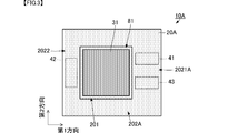
- FIG. 3 is a plan view showing the configuration of the multilayer substrate according to the second embodiment of the present invention.
- the multilayer substrate 10A according to this embodiment is different from the multilayer substrate 10 according to the first embodiment in that a high-profile component 43 is further provided.
- Other configurations of the multilayer substrate 10A except the configuration related to the high-profile component 43 are the same as those of the multilayer substrate 10 according to the first embodiment, and the description of the same portions is omitted.
- This high-profile part 43 corresponds to the “third high-profile part” of the present invention.
- the multilayer substrate 10A includes a substrate body 20A.
- the substrate body 20A includes a first region 201 and a second region 202A.
- the second region 202A includes a first portion 2021A and a second portion 2022 that are disposed with the first region 201 interposed therebetween when the substrate body 20A is viewed in plan.
- the high-profile part 43 is a part similar to the plurality of high-profile parts 41 and 42.
- the thickness of the high-profile component 43 is substantially the same as that of the plurality of high-profile components 41 and 42 and is higher than that of the low-profile component 31.
- the tall part 41 and the tall part 43 are disposed in the first portion 2021A of the second region 202A.
- the high-profile component 43 is also built in the board body 20A, and is disposed so as to include the mounting surface of the low-profile component 31 in the height direction of the board body 20A. ing.
- the tall part 41 and the tall part 43 are arranged so that the tall part 41 and the tall part 43 in the recess 81 are parallel to the closest wall surface.
- FIG. 4 is a plan view showing the configuration of the multilayer substrate according to the third embodiment of the present invention.
- the multilayer substrate 10B according to the present embodiment is different from the multilayer substrate 10A according to the second embodiment in that a plurality of high-profile parts 44 and 45 are further provided.
- Other configurations of the multilayer substrate 10B except the configurations related to the high-profile components 44 and 45 are the same as those of the multilayer substrate 10A according to the second embodiment, and the description of the same portions is omitted.
- Each of the plurality of high-profile parts 44 and 45 corresponds to the “third high-profile part” of the present invention.
- the multilayer substrate 10B includes a substrate body 20B.
- the substrate body 20B includes a first region 201 and a second region 202B.
- the second region 202B includes a first portion 2021B and a second portion 2022B that are disposed across the first region 201 along the first direction in plan view of the substrate body 20B.
- the second region 202B includes a third portion 2023B and a fourth portion 2024B that are disposed across the first region 201 along the second direction in plan view of the substrate body 20B.
- the first region 201 is surrounded by the first portion 2021B, the second portion 2022B, the third portion 2023B, and the fourth portion 2024B that form the four wall surfaces of the recess 81. .
- the plurality of high-profile parts 44 and 45 are similar to the plurality of high-profile parts 41, 42, and 43.
- the thicknesses of the plurality of high-profile components 44 and 45 are substantially the same as the plurality of high-profile components 41, 42, and 43, and are higher than the low-profile component 31.
- the plurality of high-profile components 41, 42, 43, 44, 45 are built in the board body 20B, and include the mounting surface of the low-profile parts 31 in the height direction of the board body 20B. Has been placed.
- the high-profile parts 41 and 43 are disposed in the first portion 2021B of the second region 202B.
- the high-profile component 42 is disposed in the second portion 2022B of the second region 202B.
- the high-profile component 44 is disposed in the third portion 2023B of the second region 202B.
- the high-profile component 45 is disposed in the fourth portion 2024B of the second region 202B.
- the low-profile component 31 is damaged and the low-profile component 31 may be detached from the mounting land conductor 61. Effectively suppressed.
- the substrate body 20B is viewed in plan, and high-profile parts are built in all four sides surrounding the first region 201 in the second region 202B. Thereby, the rigidity of the 2nd field 202B improves further.
- a configuration in which the third portion 2023B is provided with the high-profile component 44 and the fourth portion 2024B is not provided with the high-profile component 45 can also be applied.
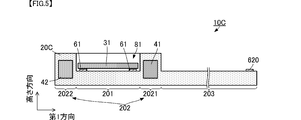
- FIG. 5 is a cross-sectional view showing the structure of the multilayer substrate according to the fourth embodiment of the present invention.
- the multilayer substrate 10 ⁇ / b> C according to the present embodiment is different from the multilayer substrate 10 according to the first embodiment in that the substrate body 20 ⁇ / b> C includes a third region 203.
- Other configurations of the multilayer substrate 10C are the same as those of the multilayer substrate 10 according to the first embodiment, and the description of the same portions is omitted.
- the substrate body 20 ⁇ / b> C includes a third region 203.
- the third area is connected to the first portion 2021 of the second area 202.
- the third region 203 is connected to the opposite side of the first region 201 with respect to the first portion 2021 of the second region 202.
- the third area 203 is integrally formed with the first area 201 and the second area 202.
- the thickness of the third region 203 is smaller than that of the second region 202.
- the thickness of the first region 201 is the same as the thickness of the third region 203.
- the plurality of flexible insulating base materials forming the first region 201 and the plurality of flexible insulating base materials forming the third region 203 are the same. Note that the thickness of the third region 203 may be different from the thickness of the first region 201.
- the external connection conductor 620 is formed at the end of the third region 203 opposite to the end connected to the first portion 2021.
- the external connection conductor 620 is connected to the conductor pattern in the second region 202 by a conductor pattern formed in the third region 203. These conductor patterns are not shown in FIG. Moreover, you may arrange
- the external connection conductor 620 is arranged at the end opposite to the end connected to the first portion 2021 in the third region 203, when the multilayer substrate 10C is mounted on the external circuit board, the external connection conductor 620 is externally connected. The connecting conductor 620 can be easily routed. At this time, the stress relating to the first region 201 and the second region 202 can be suppressed.
- the third region 203 is connected to the first portion 2021, but may be connected to the second portion 2022, and connected to both the first portion 2021 and the second portion 2022. It may be. Furthermore, it may be connected to at least one of the third portion 2023B and the fourth portion 2024B as shown in the multilayer substrate 10B of FIG.
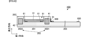
- FIG. 6 is a cross-sectional view showing the structure of the multilayer substrate according to the fifth embodiment of the present invention.
- the multilayer substrate 10D according to this embodiment is different from the multilayer substrate 10C according to the fourth embodiment in that an elastic member 91 is added.
- Other configurations of the multilayer substrate 10D are the same as those of the multilayer substrate 10C according to the fourth embodiment, and description of the same portions is omitted.
- the multilayer substrate 10D includes an elastic member 91.
- the Young's modulus of the elastic member 91 is lower than the Young's modulus of the flexible insulating base material forming the substrate body 20C.
- the elastic member 91 covers a step boundary 900 formed by the first portion 2021 and the third region 203 of the second region 202.
- the third region 203 and the second region 202 have a difference in rigidity. For this reason, if the elastic member 91 is not provided, the boundary 900 is easily damaged by a stress such as bending of the third region 203. On the other hand, by providing the elastic member 91, the breakage of the boundary 900 due to this stress is suppressed.
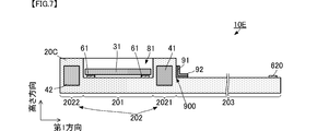
- FIG. 7 is a cross-sectional view showing the structure of the multilayer substrate according to the sixth embodiment of the present invention.
- the multilayer substrate 10E according to this embodiment is different from the multilayer substrate 10D according to the fifth embodiment in that a protection member 92 is added.
- Other configurations of the multilayer substrate 10E are the same as those of the multilayer substrate 10D according to the fifth embodiment, and description of the same portions is omitted.
- the multilayer substrate 10E includes a protection member 92.
- the protection member 92 is disposed on the surface of the elastic member 91 opposite to the substrate body 20C.
- the member composed of the protection member 92 and the elastic member 91 can be realized by, for example, an adhesive tape.
- Such a configuration further reliably suppresses breakage of the boundary 900 due to stress.
- FIG. 8 is a cross-sectional view showing the structure of an electronic device including a multilayer substrate according to the seventh embodiment of the present invention.
- the multilayer substrate 10F according to the present embodiment differs from the multilayer substrate 10C according to the fourth embodiment in the arrangement of the external connection conductors 620.
- the other configuration of the multilayer substrate 10F is the same as that of the multilayer substrate 10C, and the description of the same parts is omitted.
- the external connection conductor 620 is an end of the third region 203 of the multilayer substrate 10F opposite to the end connected to the first portion 2021, and the third region 203 is connected to the first region 201 and the second region 202. It is placed on the same surface.
- the multilayer substrate 10F constitutes the electronic apparatus 1 together with the circuit board 2.
- the multilayer substrate 10F is mounted on the circuit board 2.
- the circuit board 2 includes a front surface (one main surface) 2H and a back surface (other main surface) 2R facing each other, and a predetermined circuit pattern is formed.
- the first region 201 and the second region 202 in the multilayer substrate 10F are mounted on the surface 2H of the circuit board 2.
- the third region 203 in the multilayer substrate 10F is curved along the side surface of the circuit board 2, and the end of the third region 203 opposite to the side connected to the first portion 2021 of the second region 202 is a circuit.
- the substrate 2 is disposed on the back surface 2R side.
- the external connection conductor 620 is joined to the land conductor 3 provided on the back surface 2R of the circuit board 2. That is, the external connection conductor 620 is electrically connected to the circuit board 2 on the back surface 2R side of the circuit board 2.
- the multilayer substrate 10 ⁇ / b> F is shaped so as to be wound around the circuit board 2 from the front surface 2 ⁇ / b> H side of the circuit board 2 to the back surface 2 ⁇ / b> R side through the side surface side. Easy to implement. That is, the multilayer substrate 10F can be mounted on the circuit board 2 with a high degree of freedom.
- the shape of the dent 81 in plan view is rectangular is shown.
- the shape of the recess 81 is not limited to a rectangle as long as a high-profile component is disposed in each of two portions sandwiching the first region in the second region. .
- the external connection conductor 620 is electrically connected to the circuit board 2 on the back surface 2R side of the circuit board 2, but the present invention is not limited to this.
- the third region 203 of the multilayer substrate 10F may be bent or not electrically connected to the circuit board 2.
- the circuit board 2 and the multilayer board 10F are in contact with each other in almost the entire region on the surface 2H side, but the invention is not limited to this, and part or all of them may not be in contact with each other.
- the circuit board 2 and the multilayer board 10 ⁇ / b> F may not be in contact except for a connection portion with the external connection conductor 620.
- 10, 10A, 10B, 10C, 10D, 10E, 10F Multilayer substrates 20, 20A, 20B, 20C: Substrate bodies 21, 22, 23, 24: Flexible insulating base material 31: Low-profile parts 41, 42, 43 44, 45: High-profile parts 51, 52: Interlayer connection conductor 61: Mounting land conductor 71, 72: Through hole 81: Recess 91: Elastic member 92: Protection member 201: First region 202, 202A, 202B: No.
Abstract
多層基板(10)は、複数の可撓性絶縁基材を積層した基板本体(20)と、低背部品(31)、高背部品(41、42)と、を備えている。基板本体(20)は、第1領域(201)と第2領域(202)とを備える。第1領域(201)は、平面視して第2領域(202)に囲まれており、且つ、第2領域(202)よりも低背である。低背部品(31)は、第1領域(201)と第2領域(202)によって形成される凹み(81)の底面に実装されている。高背部品(41、42)は、基板本体(20)における第2領域(202)に内蔵され、基板本体(20)の高さ方向における低背部品(31)の実装面の位置を含む位置で、且つ、基板本体(20)を平面視して第1領域(201)を挟む位置にそれぞれ配置されている。
Description
本発明は、複数の可撓性基材を積層した基板本体と、該基板本体に実装された部品と、を備える多層基板および当該多層基板を備える電子機器に関する。
従来、複数の可撓性基材が積層された構造を有する多層基板が各種考案されている。このような多層基板として、特許文献1に記載の回路基板は、複数の可撓性基材を積層した基板本体を備える。
特許文献1の回路基板では、基板本体は、相対的に硬いリジッド領域と、相対的に軟らかいフレキシブル領域とを備える。リジッド領域は、面積の大きな導体パターンを基板の内部に備えている。これにより、リジッド領域は、フレキシブル領域よりも相対的に硬い。部品は、リジッド領域に実装されている。
しかしながら、上述の構成では、フレキシブル領域と同様に、リジッド領域も変形することがある。そして、リジッド領域の変形によって、部品に応力が加わり、部品が基板から外れてしまうことがある。また、部品に応力が加わることによって、部品が破損してしまうことがある。特に、平面形状の大きな部品は、応力を受けやすく、基板からさらに外れ易い。また、平面形状の大きな部品は、さらに破損し易い。
したがって、本発明の目的は、曲げ等の応力による部品の破損および部品の外れを抑制する多層基板を提供することにある。
この発明の多層基板は、複数の可撓性絶縁基材を積層した基板本体と、基板本体に実装された低背部品と、基板本体にそれぞれ配置された第1の高背部品および第2の高背部品と、を備えている。基板本体は、第1領域と第2領域とを備える。第1領域は、平面視して第2領域に囲まれており、且つ、第2領域よりも低背である。低背部品は、第1領域と第2領域によって形成される凹みの底面に実装されている。第1の高背部品と第2の高背部品とは、基板本体における第2領域に内蔵され、基板本体の高さ方向における低背部品の実装面の位置を含む位置で、且つ、基板本体を平面視して第1領域を挟む位置にそれぞれ配置されている。
この構成では、第1の高背部品と第2の高背部品とによって、基板本体の曲げ等による応力が低背部品の実装面に加わり難い。
また、この発明の多層基板では、第2領域に内蔵された第3の高背部品を備えることが好ましい。
この構成では、第3の高背部品を備えることによって、低背部品の実装面への応力がさらに加わり難い。
また、この発明の多層基板では、次の構成であることが好ましい。第2領域は、凹みの四つの側壁面を有しており、この側壁面のそれぞれは、第1部分、第2部分、第3部分および第4部分を形成する。第1部分と第2部分とは第1領域を挟み、第3部分と第4部分とは第1領域を挟む。第1の高背部品は第1部分に配置されており、第2の高背部品は第2部分に配置されている。
この構成では、凹みが平面視して矩形の場合を示しており、この構成によって、第1の高背部品と第2の高背部分とが、第1領域を挟むよう配置される。
また、この発明の多層基板では、第3の高背部品は、第1部分および第2部分の少なくとも一方に配置されていることが好ましい。
この構成では、第1部分および第2部分の少なくとも一方の剛性が向上する。
また、第3の高背部品は、第3部分および第4部分の少なくとも一方に配置されていることが好ましい。
この構成では、基板本体を平面視して、低背部品が実装される第1領域の周囲の少なくとも三方向に、それぞれ高背部品が配置される。したがって、低背部品の実装面への応力がさらに加わり難い。
また、この発明の多層基板では、低背部品の厚みは、複数の可撓性絶縁基材のうち最も薄い可撓性絶縁基材の厚みよりも小さくてもよい。
このように、低背部品が薄くても、上述の構成によって、この低背部品の破損、低背部品の実装の外れが効果的に抑制される。
また、この発明の多層基板では、基板本体は、第2領域よりも低背の第3領域を備え、第3領域は、第2領域を基準にして第1領域と反対側に配置されていてもよい。
この構成では、基板本体に対して、可撓性の高い部分が設けられる。
また、この発明の多層基板では、基板本体よりもヤング率の低い弾性部材を備え、弾性部材は、第2領域と第3領域との境界を覆っていることが好ましい。
この構成では、第2領域と第3領域との境界での破損が抑制される。
また、この発明の多層基板では、弾性部材における基板本体と反対側の面に、保護部材を備えることが好ましい。
この構成では、第2領域と第3領域との境界での破損がさらに抑制される。
また、この発明の多層基板では、第3領域が曲げられていてもよい。
この構成では、多層基板の配置自由度が向上する。
また、この発明の電子機器は、上述のいずれかに記載の多層基板と、回路基板と、を備える。第3領域には、外部接続用導体が形成されている。外部接続用導体は、回路基板に電気的に接続されている。
この構成では、回路基板に対する多層基板の実装、接合の構造の自由度が向上する。
また、この発明の電子機器では、第1領域と第2領域は、回路基板の一方主面側に配置され、外部接続用導体は、回路基板の他方主面側において、回路基板に電気的に接続されていてもよい。
この構成では、回路基板に対して多層基板を巻き付けるような構成が容易に実現される。
この発明によれば、基板からの部品の外れおよび部品の破損を抑制できる。
本発明の第1の実施形態に係る多層基板について、図を参照して説明する。図1(A)は本発明の第1の実施形態に係る多層基板の平面図であり、図1(B)は本発明の第1の実施形態に係る多層基板の断面図である。図1(B)は、図1(A)におけるA-A断面図である。
多層基板10は、基板本体20、低背部品31、および、複数の高背部品41、42を備える。高背部品41が本発明の「第1の高背部品」に対応し、高背部品42が本発明の「第2の高背部品」に対応する。
基板本体20は、平面視して矩形である。基板本体20は、複数の可撓性絶縁基材21、22、23、24が積層された積層体である(図2参照)。基板本体20は、平面視して第1領域201と第2領域202とを備える。基板本体20を平面視して、第2領域202は、第1領域201を囲んでいる。第2領域202は、第1方向に沿って第1領域201を挟む第1部分2021と第2部分2022を備えている。なお、図示を省略しているが、基板本体20には、多層基板10によって実現される電気回路の導体パターンが形成されている。
第1領域201は、第2領域202よりも低背である。すなわち、第1領域201の厚み(高さ方向の寸法)は、第2領域202の厚みよりも小さい。そして、第1領域201の高さ方向の一方の端面と第2領域202の高さ方向の一方の端面は、面一である。これにより、基板本体20は、基板本体20の一部を高さ方向において凹ませた凹み81を備える。すなわち、基板本体20を平面視して、凹み81の底面を成す部分が第1領域201であり、凹み81を囲む壁を成す部分が第2領域202である。
低背部品31は、例えば、各種のICチップである。複数の高背部品41、42は、それぞれコンデンサ、インダクタ、抵抗等の実装型素子である。なお、複数の高背部品41、42は、電気的に機能を有さないものを用いることも可能である。
低背部品31は、複数の高背部品41、42よりも低背である。具体的に図1(B)に示すように、低背部品31の厚みH31は、高背部品42の厚みH42よりも小さい。なお、高背部品41の厚みは、高背部品42の厚みH42と同じである。なお、複数の高背部品41、42の厚みは同じでなくてもよく、それぞれが低背部品31よりも厚ければよい。
低背部品31は、第1領域201、すなわち、凹み81の底面に実装されている。具体的には、凹み81の底面には、実装用ランド導体61が形成されている。低背部品31は、実装用ランド導体61にはんだ等によって実装されている。なお、はんだを用いずに異方性導電膜等を用いることもできる。また、低背部品31は、実装用ランド導体61に超音波接合されていてもよい。このように、凹み81の底面は、低背部品31の実装面である。なお、低背部品31の厚みH31は、凹み81の高さ(深さ)よりも小さい。したがって、低背部品31は、凹み81内に収容される。
高背部品41は、第2領域202における第1部分2021に内蔵されている。高背部品41は、高さ方向において低背部品31の実装面の位置を含むように、配置されている。言い換えれば、高背部品41は、高さ方向において低背部品31の実装面の位置を跨ぐように、配置されている。
高背部品42は、第2領域202における第2部分2022に内蔵されている。高背部品42は、高さ方向において低背部品31の実装面の位置を含むように、配置されている。言い換えれば、高背部品42は、高さ方向において低背部品31の実装面の位置を跨ぐように、配置されている。
高背部品41、42は、複数の可撓性絶縁基材21、22、23、24を構成する絶縁基材よりも剛性が高い部品である。
多層基板10の構成によって、第1領域201よりも厚い第2領域202によって、第1領域201が囲まれるので、第1領域201に、曲げ等による外部からの応力が加わり難い。したがって、第1領域201および低背部品31に応力が加わり難く、低背部品31の破損が抑制され、低背部品31が実装用ランド導体61から外れることが抑制される。
また、多層基板10の構成では、第2領域202に複数の高背部品41、42が内蔵されており、第2領域202の剛性が向上する。これにより、第1領域201および低背部品31に応力がさらに加わり難く、低背部品31の破損がさらに抑制され、低背部品31が実装用ランド導体61から外れることがさらに抑制される。
また、多層基板10の構成では、第1領域201を挟む位置に、複数の高背部品41、42が配置されている。これにより、第1領域201の第1方向の両側の剛性が略均一に高くなる。したがって、第1領域201および低背部品31に応力がさらに加わり難く、低背部品31の破損がさらに抑制され、低背部品31が実装用ランド導体61から外れることがさらに抑制される。
また、複数の可撓性絶縁基材を積層してなる基板本体の製造時には、可撓性絶縁基材が流動し変形する。この場合、基板本体に内蔵された部品には応力が加わる。しかしながら、本実施形態の多層基板10では、低背部品31が基板本体20に内蔵されておらず、このような製造時の応力による低背部品31の破損が抑制される。
また、複数の高背部品41、42は低背部品31よりも割れにくいため、多層基板10に内蔵しても、複数の高背部品41、42は破損し難い。また、複数の高背部品41、42が多層基板10に内蔵されることにより、複数の高背部品41、42を多層基板10の表面に実装するよりも、第2領域202の部分の厚さを必要以上に厚くすることなく、複数の高背部品41、42に応力がかかった際に、多層基板10の表面から複数の高背部品41、42が脱離する等の不具合を抑制できる。
多層基板10は、より具体的には、図2に示す構造によって実現される。図2は、本発明の第1の実施形態に係る多層基板の分解斜視図である。
図2に示すように、基板本体20は、複数の可撓性絶縁基材21、22、23、24を備える。複数の可撓性絶縁基材21、22、23、24は、例えば液晶ポリマを主材料としている。複数の可撓性絶縁基材21、22、23、24は、積層されている。複数の可撓性絶縁基材21、22、23、24の厚みは、複数の高背部品41、42の厚みよりも小さい。具体的には、複数の高背部品41、42の厚みは、可撓性絶縁基材22の厚みと可撓性絶縁基材23の厚みとの合計厚みと略同じである。
可撓性絶縁基材21における可撓性絶縁基材22側の面には、それぞれに複数の層間接続導体51、52が露出している。高背部品41は、複数の層間接続導体51に接合されている。高背部品42は、複数の層間接続導体52に接合されている。
可撓性絶縁基材22における可撓性絶縁基材23側の面には、複数の実装用ランド導体61が形成されている。具体的には、複数の実装用ランド導体61は、基板本体20の第1領域201となる部分に形成されている。可撓性絶縁基材22には、複数の貫通孔71、72が形成されている。貫通孔71は、高背部品41が挿通する形状である。貫通孔72は、高背部品42が挿通する形状である。
複数の貫通孔71、72は、複数の実装用ランド導体61が形成されている領域を挟んで形成されている。具体的には、貫通孔71は、基板本体20の第2領域202の第1部分2021となる部分に形成されている。貫通孔72は、基板本体20の第2領域202の第2部分2022となる部分に形成されている。
可撓性絶縁基材23には、複数の貫通孔71、72、810が形成されている。貫通孔71は、高背部品41が挿通する形状である。貫通孔72は、高背部品42が挿通する形状である。貫通孔810は、低背部品31が収容可能な形状であり、基板本体20を平面視して、複数の実装用ランド導体61が孔内に含まれる形状である。
複数の貫通孔71、72は、貫通孔810を挟んで形成されている。貫通孔71は、基板本体20の第2領域202の第1部分2021となる部分に形成されている。可撓性絶縁基材22と可撓性絶縁基材23とが積層された状態において、可撓性絶縁基材23の貫通孔71は、可撓性絶縁基材22の貫通孔71に連通している。貫通孔72は、基板本体20の第2領域202の第2部分2022となる部分に形成されている。可撓性絶縁基材22と可撓性絶縁基材23とが積層された状態において、可撓性絶縁基材23の貫通孔72は、可撓性絶縁基材22の貫通孔72に連通している。
可撓性絶縁基材24には、貫通孔810が形成されている。貫通孔810は、低背部品31が収容可能な形状であり、基板本体20を平面視して、複数の実装用ランド導体61が孔内に含まれる形状である。可撓性絶縁基材23と可撓性絶縁基材24とが積層された状態において、可撓性絶縁基材24の貫通孔810は、可撓性絶縁基材23の貫通孔810に連通している。
低背部品31は、複数の実装用ランド導体61に実装されている。低背部品31の厚み(高さ方向の寸法)は、可撓性絶縁基材21、22、23、24のそれぞれの厚みよりも小さい。
このような構成によって、高背部品41は、基板本体20の第2領域202の第1部分2021に内蔵される。高背部品42は、基板本体20の第2領域202の第2部分2022に内蔵される。そして、この構成を用いることによって、基板本体20の高さ方向において低背部品31の実装面を含むように(跨ぐように)、複数の高背部品41、42は配置されている。
なお、低背部品31の厚みH31は、複数の可撓性絶縁基材21、22、23、24の厚みよりも小さいと、上述の応力を受けやすい。したがって、低背部品31の厚みH31が複数の可撓性絶縁基材21、22、23、24の厚みよりも小さい場合に、本発明の構成は、より効果的である。特に、可撓性絶縁基材21、22、23、24のそれぞれの厚みが異なる場合であって、最も薄い可撓性絶縁基材の厚みに対して低背部品31の厚みが小さい場合に、本発明の構成は、より効果的である。
このような構成の多層基板10は、次に示す製造方法によって製造されている。まず、それぞれに片面に導体が貼り付けられた複数の可撓性絶縁基材21、22、23、24を用意する。貼り付けられた導体は、例えば、銅である。片面導体貼りの複数の可撓性絶縁基材21、22、23、24に対して、パターンエッチング等の技法を用いて、導体パターンを形成する。この際、導体パターンの一部として、可撓性絶縁基材22に複数の実装用ランド導体61が形成される。また、可撓性絶縁基材21に層間接続導体51、52用の導体パターンが形成される。
可撓性絶縁基材21に、層間接続導体51、52用の導体パターンを蓋(底面)として、層間接続導体51、52用の貫通孔をそれぞれ形成して、各貫通孔に導電ペーストを充填する。可撓性絶縁基材22に複数の貫通孔71、72を形成する。パンチングやレーザ加工等により、可撓性絶縁基材23に複数の貫通孔71、72、810を形成する。可撓性絶縁基材24に貫通孔810を形成する。
導電ペーストが充填された層間接続導体51用の貫通孔に重ねて高背部品41を配置し、導電ペーストが充填された層間接続導体52用の貫通孔に重ねて高背部品42を配置する。
この状態において、複数の可撓性絶縁基材21、22、23、24を積層して加熱プレスする。これにより、凹み81を備えた基板本体20が形成される。なお、凹み81は、可撓性絶縁基材23、24に貫通孔810を形成せずに複数の可撓性絶縁基材21、22、23、24を積層して加熱プレスし、この後に、可撓性絶縁基材24側からレーザ等によって掘削することで、凹み81を形成してもよい。
凹み81内に、低背部品31を収容し、はんだ等によって複数の実装用ランド導体61に低背部品31を実装する。
なお、凹み81における高背部品41、42が近接する壁面と高背部品41、42とが対向する長さ(図1における第2方向の長さ)は、当該壁面の長さの略1/3以上であることが好ましく、略1/2以上であるとより好ましい。これにより、第2領域202の剛性をより向上でき、低背部品31の破損がより効果的に抑制され、低背部品31が実装用ランド導体61から外れることがより効果的に抑制される。
次に、本発明の第2の実施形態に係る多層基板について、図を参照して説明する。図3は、本発明の第2の実施形態に係る多層基板の構成を示す平面図である。
本実施形態に係る多層基板10Aは、第1の実施形態に係る多層基板10に対して、さらに、高背部品43を備えた点において異なる。高背部品43に関係する構成を除く多層基板10Aの他の構成は、第1の実施形態に係る多層基板10と同じであり、同じ箇所の説明は省略する。この高背部品43が本発明の「第3の高背部品」に対応する。
多層基板10Aは、基板本体20Aを備える。基板本体20Aは、第1領域201と第2領域202Aとを備える。第2領域202Aは、基板本体20Aを平面視して、第1領域201を挟んで配置された第1部分2021Aと第2部分2022を備える。
高背部品43は、複数の高背部品41、42と同類の部品である。高背部品43の厚みは、複数の高背部品41、42と略同じであり、低背部品31よりも高い。
高背部品41と高背部品43とは、第2領域202Aの第1部分2021Aに配置されている。高背部品43も、高背部品41と同様に、基板本体20Aに内蔵されており、基板本体20Aの高さ方向において低背部品31の実装面を含むように(跨ぐように)、配置されている。
高背部品41と高背部品43とは、凹み81における高背部品41と高背部品43とが最も近接する壁面に並行するように配置されている。
このような構成であっても、第1の実施形態に係る多層基板10と同様に、低背部品31の破損、低背部品31が実装用ランド導体61から外れることがより効果的に抑制される。さらに、本実施形態の構成では、第2領域202Aの第1部分2021Aに内蔵される高背部品の個数が多くなり、第1部分2021Aの剛性をさらに向上できる。
次に、本発明の第3の実施形態に係る多層基板について、図を参照して説明する。図4は、本発明の第3の実施形態に係る多層基板の構成を示す平面図である。
図4に示すように、本実施形態に係る多層基板10Bは、第2の実施形態に係る多層基板10Aに対して、さらに、複数の高背部品44、45を備えた点において異なる。高背部品44、45に関係する構成を除く多層基板10Bの他の構成は、第2の実施形態に係る多層基板10Aと同じであり、同じ箇所の説明は省略する。複数の高背部品44、45のそれぞれが本発明の「第3の高背部品」に対応する。
多層基板10Bは、基板本体20Bを備える。基板本体20Bは、第1領域201と第2領域202Bとを備える。第2領域202Bは、基板本体20Bを平面視して、第1方向に沿って第1領域201を挟んで配置された第1部分2021Bと第2部分2022Bを備える。また、第2領域202Bは、基板本体20Bを平面視して、第2方向に沿って第1領域201を挟んで配置された第3部分2023Bと第4部分2024Bを備える。すなわち、基板本体20Bを平面視して、第1領域201は、凹み81の四壁面を形成する第1部分2021B、第2部分2022B、第3部分2023B、および第4部分2024Bによって囲まれている。
複数の高背部品44、45は、複数の高背部品41、42、43と同類の部品である。複数の高背部品44、45の厚みは、複数の高背部品41、42、43と略同じであり、低背部品31よりも高い。
複数の高背部品41、42、43、44、45は、基板本体20Bに内蔵されており、基板本体20Bの高さ方向において低背部品31の実装面を含むように(跨ぐように)、配置されている。
高背部品41、43は、第2領域202Bの第1部分2021Bに配置されている。高背部品42は、第2領域202Bの第2部分2022Bに配置されている。高背部品44は、第2領域202Bの第3部分2023Bに配置されている。高背部品45は、第2領域202Bの第4部分2024Bに配置されている。
このような構成であっても、第1、第2の実施形態に係る多層基板10、10Aと同様に、低背部品31の破損、低背部品31が実装用ランド導体61から外れることがより効果的に抑制される。
さらに、本実施形態の構成では、基板本体20Bを平面視して、第2領域202Bにおける第1領域201を囲む四方の全てに高背部品が内蔵されている。これにより、第2領域202Bの剛性がさらに向上する。
なお、第3部分2023Bに高背部品44を備え、第4部分2024Bに高背部品45を備えない構成を適用することもできる。また、第3部分2023Bに高背部品44を備えず、第4部分2024Bに高背部品45を備える構成を適用することもできる。
次に、本発明の第4の実施形態に係る多層基板について、図を参照して説明する。図5は、本発明の第4の実施形態に係る多層基板の構造を示す断面図である。
図5に示すように、本実施形態に係る多層基板10Cは、第1の実施形態に係る多層基板10に対して、基板本体20Cが第3領域203を備える点において異なる。多層基板10Cの他の構成は、第1の実施形態に係る多層基板10と同じであり、同じ箇所の説明は省略する。
基板本体20Cは、第3領域203を備える。第3領域は、第2領域202の第1部分2021に接続されている。第3領域203は、第2領域202の第1部分2021を基準にして第1領域201と反対側に接続されている。第3領域203は、第1領域201および第2領域202と一体形成されている。
第3領域203の厚みは、第2領域202よりも小さい。例えば、図5の例であれば、第1領域201の厚みと、第3領域203の厚みとは同じである。また、図5の例であれば、第1領域201を形成する複数の可撓性絶縁基材と第3領域203を形成する複数の可撓性絶縁基材とは同じである。なお、第3領域203の厚みは、第1領域201の厚みと異なっていてもよい。
第3領域203における第1部分2021と接続する端部と反対側の端部には、外部接続用導体620が形成されている。この外部接続用導体620は、第3領域203に形成された導体パターンによって、第2領域202の導体パターンに接続されている。なお、これらの導体パターンは、図5において図示を省略している。また、外部接続用導体として、コネクタ部品等を配置してもよい。
このような構成では、第3領域203のフレキシブル性を確保しながら、低背部品31の破損が抑制され、低背部品31が実装用ランド導体61から外れることが抑制される。そして、外部接続用導体620が第3領域203における第1部分2021と接続する端部と反対側の端部に配置されていることにより、多層基板10Cを外部回路基板へ実装する際に、外部接続用導体620を容易に引き回すことができる。また、この際に、第1領域201および第2領域202に係る応力を抑制できる。
なお、多層基板10Cでは、第3領域203は、第1部分2021に接続しているが、第2部分2022に接続していてもよく、第1部分2021と第2部分2022の両方に接続していてもよい。さらには、図4の多層基板10Bに示すような第3部分2023Bおよび第4部分2024Bの少なくとも一方に接続されていてもよい。
次に、本発明の第5の実施形態に係る多層基板について、図を参照して説明する。図6は、本発明の第5の実施形態に係る多層基板の構造を示す断面図である。
図6に示すように、本実施形態に係る多層基板10Dは、第4の実施形態に係る多層基板10Cに対して、弾性部材91を追加した点で異なる。多層基板10Dの他の構成は、第4の実施形態に係る多層基板10Cと同じであり、同じ箇所の説明は省略する。
多層基板10Dは、弾性部材91を備える。弾性部材91のヤング率は、基板本体20Cを形成する可撓性絶縁基材のヤング率よりも低い。弾性部材91は、第2領域202の第1部分2021と第3領域203とによって形成される段差の境界900を覆っている。
この構成では、第3領域203と第2領域202とは、剛性の差を有する。このため、弾性部材91を備えていなければ、第3領域203の曲げ等の応力によって境界900が破損し易くなる。一方、弾性部材91を備えていることによって、この応力による境界900の破損が抑制される。
次に、本発明の第6の実施形態に係る多層基板について、図を参照して説明する。図7は、本発明の第6の実施形態に係る多層基板の構造を示す断面図である。
図7に示すように、本実施形態に係る多層基板10Eは、第5の実施形態に係る多層基板10Dに対して、保護部材92を追加した点で異なる。多層基板10Eの他の構成は、第5の実施形態に係る多層基板10Dと同じであり、同じ箇所の説明は省略する。
多層基板10Eは、保護部材92を備える。保護部材92は、弾性部材91における基板本体20Cと反対側の面に配置されている。保護部材92と弾性部材91とからなる部材は、例えば接着テープによって実現できる。
このような構成によって、応力による境界900の破損がさらに確実に抑制される。
次に、本発明の第7の実施形態に係る多層基板および電子機器について、図を参照して説明する。図8は、本発明の第7の実施形態に係る多層基板を含む電子機器の構造を示す断面図である。
図8に示すように、本実施形態に係る多層基板10Fは、第4の実施形態に係る多層基板10Cに対して、外部接続用導体620の配置において異なる。多層基板10Fの他の構成は、多層基板10Cと同様であり、同様の箇所の説明は省略する。
外部接続用導体620は、多層基板10Fの第3領域203における第1部分2021と接続する端部と反対側の端部であって、第3領域203が第1領域201および第2領域202と面一になる面に配置されている。
多層基板10Fは、回路基板2とともに、電子機器1を構成している。多層基板10Fは、回路基板2に実装されている。回路基板2は、互いに対向する表面(一方主面)2Hと裏面(他方主面)2Rとを備え、所定の回路パターンが形成されている。
この際、多層基板10Fにおける第1領域201および第2領域202は、回路基板2の表面2Hに実装されている。多層基板10Fにおける第3領域203は、回路基板2の側面に沿って湾曲しており、第3領域203における第2領域202の第1部分2021と接続する側と反対側の端部は、回路基板2の裏面2R側に配置されている。そして、外部接続用導体620は、回路基板2の裏面2Rに設けられたランド導体3に接合されている。すなわち、外部接続用導体620は、回路基板2の裏面2R側で回路基板2と電気的に接続されている。
多層基板10Fの第3領域203は第2領域202に対して薄く低背であるので、第3領域203の厚み方向への湾曲は、容易である。したがって、図8に示すように、多層基板10Fを、回路基板2の表面2H側から側面側を介して裏面2R側に至るように、回路基板2に巻き付けるような形状にして、回路基板2に実装することが容易である。すなわち、回路基板2に対して高い自由度で多層基板10Fを実装できる。
そして、第3領域203と第1領域201との間に剛性の高い第2領域202が存在することによって、第3領域203が大きく湾曲しても、当該湾曲による第1領域201および第2領域202への応力を抑制できる。したがって、第1領域201および第2領域202の破損、部品の外れ等の不具合の発生を抑制できる。
なお、上述の各実施形態では、凹み81を平面視した形状が矩形の場合を示した。しかしながら、本発明の各実施形態に係る多層基板は、第2領域における第1領域を挟む2つの部分のそれぞれに高背部品が配置されていれば、凹み81の形状は矩形に限るものではない。
また、上述の電子機器の実施形態において、外部接続用導体620は、回路基板2の裏面2R側で回路基板2と電気的に接続されていたがこれに限るものではなく、回路基板2の表面2H側において、多層基板10Fの第3領域203を曲げて、あるいは曲げずに回路基板2と電気的に接続されていてもよい。また、図8において、回路基板2と多層基板10Fとが表面2H側のほぼ全領域において接触しているが、これに限るものではなく、一部または全部が接触していなくてもよいし、回路基板2と多層基板10Fとは、外部接続用導体620との接続部分を除き接触していなくてもよい。
また、上述の各実施形態の構成は、適宜組み合わせることができ、それぞれの組合せに応じた作用効果を得ることができる。
10、10A、10B、10C、10D、10E、10F:多層基板
20、20A、20B、20C:基板本体
21、22、23、24:可撓性絶縁基材
31:低背部品
41、42、43、44、45:高背部品
51、52:層間接続導体
61:実装用ランド導体
71、72:貫通孔
81:凹み
91:弾性部材
92:保護部材
201:第1領域
202、202A、202B:第2領域
203:第3領域
620:外部接続用導体
810:貫通孔
900:境界
2021、2021A、2021B:第1部分
2022、2022B:第2部分
2023B:第3部分
2024B:第4部分
1:電子機器
2:回路基板
3:ランド導体
20、20A、20B、20C:基板本体
21、22、23、24:可撓性絶縁基材
31:低背部品
41、42、43、44、45:高背部品
51、52:層間接続導体
61:実装用ランド導体
71、72:貫通孔
81:凹み
91:弾性部材
92:保護部材
201:第1領域
202、202A、202B:第2領域
203:第3領域
620:外部接続用導体
810:貫通孔
900:境界
2021、2021A、2021B:第1部分
2022、2022B:第2部分
2023B:第3部分
2024B:第4部分
1:電子機器
2:回路基板
3:ランド導体
Claims (12)
- 複数の可撓性絶縁基材を積層した基板本体と、
前記基板本体にそれぞれ配置された、低背部品、第1の高背部品および第2の高背部品と、を備え、
前記基板本体は、第1領域と第2領域とを備え、
前記第1領域は、平面視して前記第2領域に囲まれており、且つ、前記第2領域よりも低背であり、
前記低背部品は、前記第1領域と前記第2領域とによって形成される凹みの底面に実装されており、
前記第1の高背部品と前記第2の高背部品とは、
前記基板本体における前記第2領域に内蔵され、前記基板本体の高さ方向における前記低背部品の実装面の位置を含むように、且つ、前記基板本体を平面視して前記第1領域を挟む位置にそれぞれ配置されている、
多層基板。 - 前記第2領域に内蔵された第3の高背部品を備える、
請求項1に記載の多層基板。 - 前記第2領域は、前記凹みを囲む四つの側壁面を有しており、該側壁面のぞれぞれは、第1部分、第2部分、第3部分および第4部分を形成し、
前記第1部分と前記第2部分とは前記第1領域を挟み、前記第3部分と前記第4部分とは前記第1領域を挟み、
前記第1の高背部品は、前記第1部分に配置され、
前記第2の高背部品は、前記第2部分に配置された、
請求項2に記載の多層基板。 - 前記第3の高背部品は、前記第1部分および前記第2部分の少なくとも一方に配置されている、
請求項3に記載の多層基板。 - 前記第3の高背部品は、前記第3部分および前記第4部分の少なくとも一方に配置されている、
請求項3または請求項4に記載の多層基板。 - 前記低背部品の厚みは、前記複数の可撓性絶縁基材のうち最も薄い可撓性絶縁基材の厚みよりも小さい、
請求項1乃至請求項5のいずれかに記載の多層基板。 - 前記基板本体は、前記第2領域よりも低背の第3領域を備え、
前記第3領域は、前記第2領域を基準にして前記第1領域と反対側に配置されている、
請求項1乃至請求項6のいずれかに記載の多層基板。 - 前記基板本体よりもヤング率の低い弾性部材を備え、
前記弾性部材は、前記第2領域と前記第3領域との境界を覆っている、
請求項7に記載の多層基板。 - 前記弾性部材における前記基板本体と反対側の面に、保護部材を備える、
請求項8に記載の多層基板。 - 前記第3領域が曲げられている、
請求項7乃至請求項9のいずれかに記載の多層基板。 - 請求項7乃至請求項10のいずれかに記載の多層基板と、
回路基板と、
を備えた電子機器であって、
前記第3領域には、外部接続用導体が形成されており、
前記外部接続用導体は、前記回路基板に電気的に接続されている、
電子機器。 - 前記第1領域と前記第2領域は、前記回路基板の一方主面側に配置され、
前記外部接続用導体は、前記回路基板の他方主面側において、前記回路基板に電気的に接続されている、
請求項11に記載の電子機器。
Priority Applications (3)
| Application Number | Priority Date | Filing Date | Title |
|---|---|---|---|
| CN201790000231.XU CN207802503U (zh) | 2016-04-20 | 2017-03-27 | 多层基板以及电子设备 |
| JP2017533051A JP6191808B1 (ja) | 2016-04-20 | 2017-03-27 | 多層基板および電子機器 |
| US15/726,501 US10187975B2 (en) | 2016-04-20 | 2017-10-06 | Multilayer substrate and electronic device |
Applications Claiming Priority (2)
| Application Number | Priority Date | Filing Date | Title |
|---|---|---|---|
| JP2016084371 | 2016-04-20 | ||
| JP2016-084371 | 2016-04-20 |
Related Child Applications (1)
| Application Number | Title | Priority Date | Filing Date |
|---|---|---|---|
| US15/726,501 Continuation US10187975B2 (en) | 2016-04-20 | 2017-10-06 | Multilayer substrate and electronic device |
Publications (1)
| Publication Number | Publication Date |
|---|---|
| WO2017183394A1 true WO2017183394A1 (ja) | 2017-10-26 |
Family
ID=60115895
Family Applications (1)
| Application Number | Title | Priority Date | Filing Date |
|---|---|---|---|
| PCT/JP2017/012283 WO2017183394A1 (ja) | 2016-04-20 | 2017-03-27 | 多層基板および電子機器 |
Country Status (3)
| Country | Link |
|---|---|
| US (1) | US10187975B2 (ja) |
| CN (1) | CN207802503U (ja) |
| WO (1) | WO2017183394A1 (ja) |
Families Citing this family (3)
| Publication number | Priority date | Publication date | Assignee | Title |
|---|---|---|---|---|
| FR3084556B1 (fr) | 2018-07-30 | 2020-11-06 | Commissariat Energie Atomique | Structure electronique souple et son procede d'elaboration. |
| JP7341641B2 (ja) * | 2018-08-24 | 2023-09-11 | 太陽誘電株式会社 | マルチプレクサ |
| KR20210006218A (ko) * | 2019-07-08 | 2021-01-18 | 삼성전기주식회사 | 인쇄회로기판 |
Citations (4)
| Publication number | Priority date | Publication date | Assignee | Title |
|---|---|---|---|---|
| WO2012132524A1 (ja) * | 2011-03-31 | 2012-10-04 | 株式会社村田製作所 | フレキシブル多層基板 |
| US20140247570A1 (en) * | 2013-03-01 | 2014-09-04 | Unimicron Technology Corporation | Circuit board structure having electronic components embedded therein and method of fabricating the same |
| WO2015156141A1 (ja) * | 2014-04-10 | 2015-10-15 | 株式会社村田製作所 | 部品内蔵多層基板 |
| JP2016504751A (ja) * | 2012-10-09 | 2016-02-12 | エムシー10 インコーポレイテッドMc10,Inc. | ポリマー内への薄型チップの埋込み |
Family Cites Families (3)
| Publication number | Priority date | Publication date | Assignee | Title |
|---|---|---|---|---|
| JP5201270B2 (ja) | 2009-09-30 | 2013-06-05 | 株式会社村田製作所 | 回路基板及びその製造方法 |
| JP5573645B2 (ja) * | 2010-12-15 | 2014-08-20 | 富士通セミコンダクター株式会社 | 半導体装置及び半導体装置の製造方法 |
| JP6034725B2 (ja) * | 2013-03-05 | 2016-11-30 | 太陽誘電株式会社 | カメラモジュール |
-
2017
- 2017-03-27 WO PCT/JP2017/012283 patent/WO2017183394A1/ja active Application Filing
- 2017-03-27 CN CN201790000231.XU patent/CN207802503U/zh active Active
- 2017-10-06 US US15/726,501 patent/US10187975B2/en active Active
Patent Citations (4)
| Publication number | Priority date | Publication date | Assignee | Title |
|---|---|---|---|---|
| WO2012132524A1 (ja) * | 2011-03-31 | 2012-10-04 | 株式会社村田製作所 | フレキシブル多層基板 |
| JP2016504751A (ja) * | 2012-10-09 | 2016-02-12 | エムシー10 インコーポレイテッドMc10,Inc. | ポリマー内への薄型チップの埋込み |
| US20140247570A1 (en) * | 2013-03-01 | 2014-09-04 | Unimicron Technology Corporation | Circuit board structure having electronic components embedded therein and method of fabricating the same |
| WO2015156141A1 (ja) * | 2014-04-10 | 2015-10-15 | 株式会社村田製作所 | 部品内蔵多層基板 |
Also Published As
| Publication number | Publication date |
|---|---|
| US10187975B2 (en) | 2019-01-22 |
| CN207802503U (zh) | 2018-08-31 |
| US20180042107A1 (en) | 2018-02-08 |
Similar Documents
| Publication | Publication Date | Title |
|---|---|---|
| US9986641B2 (en) | Circuit board | |
| JP4930567B2 (ja) | 中継基板、プリント基板ユニットおよび中継基板の製造方法 | |
| JP6365794B2 (ja) | 樹脂多層基板、および、電子機器 | |
| WO2017183394A1 (ja) | 多層基板および電子機器 | |
| JP5434167B2 (ja) | 回路基板 | |
| JP5962746B2 (ja) | 圧電トランス装置 | |
| JP2012009478A (ja) | 接続構造、電子機器 | |
| JPWO2019131647A1 (ja) | 基板接合構造 | |
| JP6191808B1 (ja) | 多層基板および電子機器 | |
| KR20190099709A (ko) | 인쇄회로기판 | |
| JP6323622B2 (ja) | 部品実装基板 | |
| JP5344033B2 (ja) | 電子装置 | |
| JPWO2006082745A1 (ja) | 接続部品、積層基板 | |
| US10188000B2 (en) | Component mounting board | |
| JP6863230B2 (ja) | 回路素子および電子機器 | |
| JP5574068B2 (ja) | 部品内蔵基板 | |
| JP6477894B2 (ja) | 樹脂回路基板、部品搭載樹脂回路基板 | |
| JP2017130607A (ja) | 部品実装基板、部品実装基板の製造方法 | |
| JP2019083239A (ja) | 電子機器 |
Legal Events
| Date | Code | Title | Description |
|---|---|---|---|
| ENP | Entry into the national phase |
Ref document number: 2017533051 Country of ref document: JP Kind code of ref document: A |
|
| NENP | Non-entry into the national phase |
Ref country code: DE |
|
| 121 | Ep: the epo has been informed by wipo that ep was designated in this application |
Ref document number: 17785736 Country of ref document: EP Kind code of ref document: A1 |
|
| 122 | Ep: pct application non-entry in european phase |
Ref document number: 17785736 Country of ref document: EP Kind code of ref document: A1 |