EP2950148B1 - Système environnemental incluant un systéme de recirculation sous vide pour un appareil de lithographie par immersion - Google Patents
Système environnemental incluant un systéme de recirculation sous vide pour un appareil de lithographie par immersion Download PDFInfo
- Publication number
- EP2950148B1 EP2950148B1 EP15162758.5A EP15162758A EP2950148B1 EP 2950148 B1 EP2950148 B1 EP 2950148B1 EP 15162758 A EP15162758 A EP 15162758A EP 2950148 B1 EP2950148 B1 EP 2950148B1
- Authority
- EP
- European Patent Office
- Prior art keywords
- stage
- exposure apparatus
- fluid
- gap
- exposure
- Prior art date
- Legal status (The legal status is an assumption and is not a legal conclusion. Google has not performed a legal analysis and makes no representation as to the accuracy of the status listed.)
- Expired - Lifetime
Links
- 230000007613 environmental effect Effects 0.000 title claims description 62
- 238000000671 immersion lithography Methods 0.000 title description 4
- 239000012530 fluid Substances 0.000 claims description 282
- 238000007654 immersion Methods 0.000 claims description 126
- 230000003287 optical effect Effects 0.000 claims description 121
- 238000000034 method Methods 0.000 claims description 57
- 238000004519 manufacturing process Methods 0.000 claims description 15
- 238000005259 measurement Methods 0.000 claims description 15
- 230000000712 assembly Effects 0.000 claims description 10
- 238000000429 assembly Methods 0.000 claims description 10
- 238000012544 monitoring process Methods 0.000 claims description 2
- 235000012431 wafers Nutrition 0.000 description 117
- 230000004888 barrier function Effects 0.000 description 79
- 238000004891 communication Methods 0.000 description 24
- 238000013461 design Methods 0.000 description 23
- 238000005286 illumination Methods 0.000 description 15
- 230000008569 process Effects 0.000 description 14
- 239000000758 substrate Substances 0.000 description 13
- 238000000206 photolithography Methods 0.000 description 12
- XLYOFNOQVPJJNP-UHFFFAOYSA-N water Substances O XLYOFNOQVPJJNP-UHFFFAOYSA-N 0.000 description 9
- 239000004065 semiconductor Substances 0.000 description 8
- 238000001459 lithography Methods 0.000 description 5
- 239000000203 mixture Substances 0.000 description 5
- 229920002120 photoresistant polymer Polymers 0.000 description 5
- 238000012545 processing Methods 0.000 description 5
- 230000000717 retained effect Effects 0.000 description 5
- 238000003384 imaging method Methods 0.000 description 4
- 238000012546 transfer Methods 0.000 description 4
- 238000006243 chemical reaction Methods 0.000 description 3
- 238000005530 etching Methods 0.000 description 3
- 238000001704 evaporation Methods 0.000 description 3
- 239000000463 material Substances 0.000 description 3
- 239000003921 oil Substances 0.000 description 3
- 238000012805 post-processing Methods 0.000 description 3
- 238000007781 pre-processing Methods 0.000 description 3
- 230000005855 radiation Effects 0.000 description 3
- 238000005276 aerator Methods 0.000 description 2
- 230000015572 biosynthetic process Effects 0.000 description 2
- 230000008859 change Effects 0.000 description 2
- 239000000356 contaminant Substances 0.000 description 2
- 230000000694 effects Effects 0.000 description 2
- 229920001971 elastomer Polymers 0.000 description 2
- 230000008020 evaporation Effects 0.000 description 2
- 239000011521 glass Substances 0.000 description 2
- 238000002347 injection Methods 0.000 description 2
- 239000007924 injection Substances 0.000 description 2
- 239000007788 liquid Substances 0.000 description 2
- 229920003023 plastic Polymers 0.000 description 2
- 239000004033 plastic Substances 0.000 description 2
- 230000002000 scavenging effect Effects 0.000 description 2
- 239000004215 Carbon black (E152) Substances 0.000 description 1
- 229920002449 FKM Polymers 0.000 description 1
- 229920000459 Nitrile rubber Polymers 0.000 description 1
- WUKWITHWXAAZEY-UHFFFAOYSA-L calcium difluoride Chemical compound [F-].[F-].[Ca+2] WUKWITHWXAAZEY-UHFFFAOYSA-L 0.000 description 1
- 230000003749 cleanliness Effects 0.000 description 1
- 238000010276 construction Methods 0.000 description 1
- 230000001419 dependent effect Effects 0.000 description 1
- 239000010408 film Substances 0.000 description 1
- 239000010436 fluorite Substances 0.000 description 1
- NBVXSUQYWXRMNV-UHFFFAOYSA-N fluoromethane Chemical compound FC NBVXSUQYWXRMNV-UHFFFAOYSA-N 0.000 description 1
- 229930195733 hydrocarbon Natural products 0.000 description 1
- 150000002430 hydrocarbons Chemical class 0.000 description 1
- 238000009413 insulation Methods 0.000 description 1
- 238000005468 ion implantation Methods 0.000 description 1
- 150000002500 ions Chemical class 0.000 description 1
- 239000004973 liquid crystal related substance Substances 0.000 description 1
- QSHDDOUJBYECFT-UHFFFAOYSA-N mercury Chemical compound [Hg] QSHDDOUJBYECFT-UHFFFAOYSA-N 0.000 description 1
- 229910052753 mercury Inorganic materials 0.000 description 1
- 229910052751 metal Inorganic materials 0.000 description 1
- 239000002184 metal Substances 0.000 description 1
- 230000003647 oxidation Effects 0.000 description 1
- 238000007254 oxidation reaction Methods 0.000 description 1
- 238000012858 packaging process Methods 0.000 description 1
- 238000009428 plumbing Methods 0.000 description 1
- 229920001084 poly(chloroprene) Polymers 0.000 description 1
- 230000036316 preload Effects 0.000 description 1
- 239000010453 quartz Substances 0.000 description 1
- 238000011084 recovery Methods 0.000 description 1
- 239000012858 resilient material Substances 0.000 description 1
- VYPSYNLAJGMNEJ-UHFFFAOYSA-N silicon dioxide Inorganic materials O=[Si]=O VYPSYNLAJGMNEJ-UHFFFAOYSA-N 0.000 description 1
- 239000002210 silicon-based material Substances 0.000 description 1
- 229910001220 stainless steel Inorganic materials 0.000 description 1
- 239000010935 stainless steel Substances 0.000 description 1
- 230000003068 static effect Effects 0.000 description 1
- 239000010409 thin film Substances 0.000 description 1
- 238000007740 vapor deposition Methods 0.000 description 1
- 238000009834 vaporization Methods 0.000 description 1
- 230000008016 vaporization Effects 0.000 description 1
Images


Classifications
-
- G—PHYSICS
- G03—PHOTOGRAPHY; CINEMATOGRAPHY; ANALOGOUS TECHNIQUES USING WAVES OTHER THAN OPTICAL WAVES; ELECTROGRAPHY; HOLOGRAPHY
- G03F—PHOTOMECHANICAL PRODUCTION OF TEXTURED OR PATTERNED SURFACES, e.g. FOR PRINTING, FOR PROCESSING OF SEMICONDUCTOR DEVICES; MATERIALS THEREFOR; ORIGINALS THEREFOR; APPARATUS SPECIALLY ADAPTED THEREFOR
- G03F7/00—Photomechanical, e.g. photolithographic, production of textured or patterned surfaces, e.g. printing surfaces; Materials therefor, e.g. comprising photoresists; Apparatus specially adapted therefor
- G03F7/20—Exposure; Apparatus therefor
- G03F7/2041—Exposure; Apparatus therefor in the presence of a fluid, e.g. immersion; using fluid cooling means
-
- G—PHYSICS
- G03—PHOTOGRAPHY; CINEMATOGRAPHY; ANALOGOUS TECHNIQUES USING WAVES OTHER THAN OPTICAL WAVES; ELECTROGRAPHY; HOLOGRAPHY
- G03F—PHOTOMECHANICAL PRODUCTION OF TEXTURED OR PATTERNED SURFACES, e.g. FOR PRINTING, FOR PROCESSING OF SEMICONDUCTOR DEVICES; MATERIALS THEREFOR; ORIGINALS THEREFOR; APPARATUS SPECIALLY ADAPTED THEREFOR
- G03F7/00—Photomechanical, e.g. photolithographic, production of textured or patterned surfaces, e.g. printing surfaces; Materials therefor, e.g. comprising photoresists; Apparatus specially adapted therefor
- G03F7/70—Microphotolithographic exposure; Apparatus therefor
- G03F7/708—Construction of apparatus, e.g. environment aspects, hygiene aspects or materials
- G03F7/70858—Environment aspects, e.g. pressure of beam-path gas, temperature
- G03F7/70866—Environment aspects, e.g. pressure of beam-path gas, temperature of mask or workpiece
- G03F7/70875—Temperature, e.g. temperature control of masks or workpieces via control of stage temperature
-
- G—PHYSICS
- G03—PHOTOGRAPHY; CINEMATOGRAPHY; ANALOGOUS TECHNIQUES USING WAVES OTHER THAN OPTICAL WAVES; ELECTROGRAPHY; HOLOGRAPHY
- G03F—PHOTOMECHANICAL PRODUCTION OF TEXTURED OR PATTERNED SURFACES, e.g. FOR PRINTING, FOR PROCESSING OF SEMICONDUCTOR DEVICES; MATERIALS THEREFOR; ORIGINALS THEREFOR; APPARATUS SPECIALLY ADAPTED THEREFOR
- G03F7/00—Photomechanical, e.g. photolithographic, production of textured or patterned surfaces, e.g. printing surfaces; Materials therefor, e.g. comprising photoresists; Apparatus specially adapted therefor
- G03F7/70—Microphotolithographic exposure; Apparatus therefor
- G03F7/70216—Mask projection systems
- G03F7/70341—Details of immersion lithography aspects, e.g. exposure media or control of immersion liquid supply
-
- G—PHYSICS
- G03—PHOTOGRAPHY; CINEMATOGRAPHY; ANALOGOUS TECHNIQUES USING WAVES OTHER THAN OPTICAL WAVES; ELECTROGRAPHY; HOLOGRAPHY
- G03F—PHOTOMECHANICAL PRODUCTION OF TEXTURED OR PATTERNED SURFACES, e.g. FOR PRINTING, FOR PROCESSING OF SEMICONDUCTOR DEVICES; MATERIALS THEREFOR; ORIGINALS THEREFOR; APPARATUS SPECIALLY ADAPTED THEREFOR
- G03F7/00—Photomechanical, e.g. photolithographic, production of textured or patterned surfaces, e.g. printing surfaces; Materials therefor, e.g. comprising photoresists; Apparatus specially adapted therefor
- G03F7/70—Microphotolithographic exposure; Apparatus therefor
- G03F7/70691—Handling of masks or workpieces
- G03F7/70775—Position control, e.g. interferometers or encoders for determining the stage position
-
- G—PHYSICS
- G03—PHOTOGRAPHY; CINEMATOGRAPHY; ANALOGOUS TECHNIQUES USING WAVES OTHER THAN OPTICAL WAVES; ELECTROGRAPHY; HOLOGRAPHY
- G03F—PHOTOMECHANICAL PRODUCTION OF TEXTURED OR PATTERNED SURFACES, e.g. FOR PRINTING, FOR PROCESSING OF SEMICONDUCTOR DEVICES; MATERIALS THEREFOR; ORIGINALS THEREFOR; APPARATUS SPECIALLY ADAPTED THEREFOR
- G03F7/00—Photomechanical, e.g. photolithographic, production of textured or patterned surfaces, e.g. printing surfaces; Materials therefor, e.g. comprising photoresists; Apparatus specially adapted therefor
- G03F7/70—Microphotolithographic exposure; Apparatus therefor
- G03F7/708—Construction of apparatus, e.g. environment aspects, hygiene aspects or materials
- G03F7/70808—Construction details, e.g. housing, load-lock, seals or windows for passing light in or out of apparatus
- G03F7/70816—Bearings
-
- G—PHYSICS
- G03—PHOTOGRAPHY; CINEMATOGRAPHY; ANALOGOUS TECHNIQUES USING WAVES OTHER THAN OPTICAL WAVES; ELECTROGRAPHY; HOLOGRAPHY
- G03F—PHOTOMECHANICAL PRODUCTION OF TEXTURED OR PATTERNED SURFACES, e.g. FOR PRINTING, FOR PROCESSING OF SEMICONDUCTOR DEVICES; MATERIALS THEREFOR; ORIGINALS THEREFOR; APPARATUS SPECIALLY ADAPTED THEREFOR
- G03F7/00—Photomechanical, e.g. photolithographic, production of textured or patterned surfaces, e.g. printing surfaces; Materials therefor, e.g. comprising photoresists; Apparatus specially adapted therefor
- G03F7/70—Microphotolithographic exposure; Apparatus therefor
- G03F7/708—Construction of apparatus, e.g. environment aspects, hygiene aspects or materials
- G03F7/70858—Environment aspects, e.g. pressure of beam-path gas, temperature
- G03F7/70866—Environment aspects, e.g. pressure of beam-path gas, temperature of mask or workpiece
-
- G—PHYSICS
- G03—PHOTOGRAPHY; CINEMATOGRAPHY; ANALOGOUS TECHNIQUES USING WAVES OTHER THAN OPTICAL WAVES; ELECTROGRAPHY; HOLOGRAPHY
- G03F—PHOTOMECHANICAL PRODUCTION OF TEXTURED OR PATTERNED SURFACES, e.g. FOR PRINTING, FOR PROCESSING OF SEMICONDUCTOR DEVICES; MATERIALS THEREFOR; ORIGINALS THEREFOR; APPARATUS SPECIALLY ADAPTED THEREFOR
- G03F7/00—Photomechanical, e.g. photolithographic, production of textured or patterned surfaces, e.g. printing surfaces; Materials therefor, e.g. comprising photoresists; Apparatus specially adapted therefor
- G03F7/70—Microphotolithographic exposure; Apparatus therefor
- G03F7/708—Construction of apparatus, e.g. environment aspects, hygiene aspects or materials
- G03F7/70858—Environment aspects, e.g. pressure of beam-path gas, temperature
- G03F7/709—Vibration, e.g. vibration detection, compensation, suppression or isolation
-
- H—ELECTRICITY
- H01—ELECTRIC ELEMENTS
- H01L—SEMICONDUCTOR DEVICES NOT COVERED BY CLASS H10
- H01L21/00—Processes or apparatus adapted for the manufacture or treatment of semiconductor or solid state devices or of parts thereof
- H01L21/02—Manufacture or treatment of semiconductor devices or of parts thereof
- H01L21/027—Making masks on semiconductor bodies for further photolithographic processing not provided for in group H01L21/18 or H01L21/34
- H01L21/0271—Making masks on semiconductor bodies for further photolithographic processing not provided for in group H01L21/18 or H01L21/34 comprising organic layers
- H01L21/0273—Making masks on semiconductor bodies for further photolithographic processing not provided for in group H01L21/18 or H01L21/34 comprising organic layers characterised by the treatment of photoresist layers
- H01L21/0274—Photolithographic processes
Definitions
- Lithography exposure apparatuses are commonly used to transfer images from a reticle onto a semiconductor wafer during semiconductor processing.
- a typical exposure apparatus includes an illumination source, a reticle stage assembly that positions a reticle, an optical assembly, a wafer stage assembly that positions a semiconductor wafer, and a measurement system that precisely monitors the position of the reticle and the wafer.
- Immersion lithography systems utilize a layer of immersion fluid that completely fills a gap between the optical assembly and the wafer.
- the wafer is moved rapidly in a typical lithography system and it would be expected to carry the immersion fluid away from the gap.
- This immersion fluid that escapes from the gap can interfere with the operation of other components of the lithography system.
- the immersion fluid and its vapor can interfere with the measurement system that monitors the position of the wafer.
- US 5,997,963A and DD 221 563 A1 disclose prior exposure apparatus.
- JP 2002 134384 discloses vibration-reduction techniques for an exposure apparatus.
- an exposure apparatus as recited in Claim 1 below.
- the present disclosure is directed to an environmental system for controlling an environment in a gap between an optical assembly and a device that is retained by a device stage.
- the environmental system includes a fluid barrier and an immersion fluid system.
- the fluid barrier is positioned near the device and encircles the gap.
- the immersion fluid system delivers an immersion fluid that fills the gap.
- the immersion fluid system collects the immersion fluid that is directly between the fluid barrier and at least one of the device and the device stage.
- the fluid barrier includes a scavenge inlet that is positioned near the device, and the immersion fluid system includes a low pressure source that is in fluid communication with the scavenge inlet. Additionally, the fluid barrier can confine and contain the immersion fluid and any of the vapor from the immersion fluid in the area near the gap.
- the environmental system includes a bearing fluid source that directs a bearing fluid between the fluid barrier and the device to support the fluid barrier relative to the device.
- the fluid barrier includes a bearing outlet that is positioned near the device. Further, the bearing outlet is in fluid communication with the bearing fluid source.
- the environmental system can include a pressure equalizer that allows the pressure in the gap to be approximately equal to the pressure outside the fluid barrier.
- the pressure equalizer is a channel that extends through the fluid barrier.
- the device stage can include a stage surface that is in approximately the same plane as a device exposed surface of the device.
- the device stage can include a device holder that retains the device, a guard that defines the stage surface, and a mover assembly that moves one of the device holder and the guard so that the device exposed surface is approximately in the same plane as the stage surface.
- the mover assembly moves the guard relative to the device and the device holder. In another configuration, the mover assembly moves the device holder and the device relative to the guard.
- the present disclosure is also directed to an exposure apparatus, a wafer, a device, a method for controlling an environment in a gap, a method for making an exposure apparatus, a method for making a device, and a method for manufacturing a wafer.
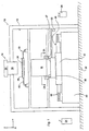
- FIG 1 is a schematic illustration of a precision assembly, namely an exposure apparatus 10 having features of the present invention.
- the exposure apparatus 10 includes an apparatus frame 12, an illumination system 14 (irradiation apparatus), an optical assembly 16, a reticle stage assembly 18, a device stage assembly 20, a measurement system 22, a control system 24, and a fluid environmental system 26.
- the design of the components of the exposure apparatus 10 can be varied to suit the design requirements of the exposure apparatus 10.
- a number of Figures include an orientation system that illustrates an X axis, a Y axis that is orthogonal to the X axis, and a Z axis that is orthogonal to the X and Y axes. It should be noted that these axes can also be referred to as the first, second and third axes.
- the exposure apparatus 10 is particularly useful as a lithographic device that transfers a pattern (not shown) of an integrated circuit from a reticle 28 onto a semiconductor wafer 30 (illustrated in phantom).
- the wafer 30 is also referred to generally as a device or work piece.
- the exposure apparatus 10 mounts to a mounting base 32, e. g., the ground, a base, or floor or some other supporting structure.
- the exposure apparatus 10 can be used as a scanning type photolithography system that exposes the pattern from the reticle 28 onto the wafer 30 with the reticle 28 and the wafer 30 moving synchronously.
- a scanning type lithographic device the reticle 28 is moved perpendicularly to an optical axis of the optical assembly 16 by the reticle stage assembly 18 and the wafer 30 is moved perpendicularly to the optical axis of the optical assembly 16 by the wafer stage assembly 20. Scanning of the reticle 28 and the wafer 30 occurs while the reticle 28 and the wafer 30 are moving synchronously.
- the exposure apparatus 10 can be a step-and-repeat type photolithography system that exposes the reticle 28 while the reticle 28 and the wafer 30 are stationary.
- the wafer 30 is in a constant position relative to the reticle 28 and the optical assembly 16 during the exposure of an individual field.
- the wafer 30 is consecutively moved with the wafer stage assembly 20 perpendicularly to the optical axis of the optical assembly 16 so that the next field of the wafer 30 is brought into position relative to the optical assembly 16 and the reticle 28 for exposure.
- the images on the reticle 28 are sequentially exposed onto the fields of the wafer 30, and then the next field of the wafer 30 is brought into position relative to the optical assembly 16 and the reticle 28.
- the use of the exposure apparatus 10 provided herein is not limited to a photolithography system for semiconductor manufacturing.
- the exposure apparatus 10, for example, can be used as an LCD photolithography system that exposes a liquid crystal display device pattern onto a rectangular glass plate or a photolithography system for manufacturing a thin film magnetic head.
- the apparatus frame 12 supports the components of the exposure apparatus 10.
- the apparatus frame 12 illustrated in Figure 1 supports the reticle stage assembly 18, the wafer stage assembly 20, the optical assembly 16 and the illumination system 14 above the mounting base 32.
- the illumination system 14 includes an illumination source 34 and an illumination optical assembly 36.
- the illumination source 34 emits a beam (irradiation) of light energy.
- the illumination optical assembly 36 guides the beam of light energy from the illumination source 34 to the optical assembly 16.
- the beam illuminates selectively different portions of the reticle 28 and exposes the wafer 30.
- the illumination source 34 is illustrated as being supported above the reticle stage assembly 18. Typically, however, the illumination source 34 is secured to one of the sides of the apparatus frame 12 and the energy beam from the illumination source 34 is directed to above the reticle stage assembly 18 with the illumination optical assembly 36.
- the illumination source 34 can be a light source such as a mercury g-line source (436 nm) or i-line source (365 nm), a KrF excimer laser (248 nm), an ArF excimer laser (193 nm) or a F 2 laser (157 nm).
- the optical assembly 16 projects and/or focuses the light passing through the reticle 28 to the wafer 30. Depending upon the design of the exposure apparatus 10, the optical assembly 16 can magnify or reduce the image illuminated on the reticle 28. It could also be a 1x magnification system.
- optical assembly 16 When far ultra-violet radiation such as from the excimer laser is used, glass materials such as quartz and fluorite that transmit far ultra-violet rays can be used in the optical assembly 16.
- the optical assembly 16 can be either catadioptric or refractive.
- the catadioptric type optical system can be considered.
- the catadioptric type of optical system include the disclosure Japan Patent Application Disclosure No. 8-171054 published in the Official Gazette for Laid-Open Patent Applications and its counterpart U.S. Patent No. 5,668,672 , as well as Japan Patent Application Disclosure No. 10-20195 and its counterpart U. S. Patent No. 5,835,275 .
- the reflecting optical device can be a catadioptric optical system incorporating a beam splitter and concave mirror.
- Japan Patent Application Disclosure No. 8-334695 published in the Official Gazette for Laid-Open Patent Applications and its counterpart U.S. Patent No.
- the optical assembly 16 is secured to the apparatus frame 12 with one or more optical mount isolators 37.
- the optical mount isolators 37 inhibit vibration of the apparatus frame 12 from causing vibration to the optical assembly 16.
- Each optical mount isolator 37 can include a pneumatic cylinder (not shown) that isolates vibration and an actuator (not shown) that isolates vibration and controls the position with at least two degrees of motion.
- Suitable optical mount isolators 37 are sold by Integrated Dynamics Engineering, located in Wobum, MA.
- two spaced apart optical mount isolators 37 are shown as being used to secure the optical assembly 16 to the apparatus frame 12.
- three spaced apart optical mount isolators 37 can be used to kinematically secure the optical assembly 16 to the apparatus frame 12.
- the reticle stage assembly 18 holds and positions the reticle 28 relative to the optical assembly 16 and the wafer 30.
- the reticle stage assembly 18 includes a reticle stage 38 that retains the reticle 28 and a reticle stage mover assembly 40 that moves and positions the reticle stage 38 and reticle 28.
- the device stage assembly 20 holds and positions the wafer 30 with respect to the projected image of the illuminated portions of the reticle 28.
- the device stage assembly 20 includes a device stage 42 that retains the wafer 30, a device stage base 43 that supports and guides the device stage 42, and a device stage mover assembly 44 that moves and positions the device stage 42 and the wafer 28 relative to the optical assembly 16 and the device stage base 43.
- the device stage 42 is described in more detail below.
- Each stage mover assembly 40, 44 can move the respective stage 38, 42 with three degrees of freedom, less than three degrees of freedom, or more than three degrees of freedom.
- each stage mover assembly 40, 44 can move the respective stage 38, 42 with one, two, three, four, five or six degrees of freedom.
- the reticle stage mover assembly 40 and the device stage mover assembly 44 can each include one or more movers, such as rotary motors, voice coil motors, linear motors utilizing a Lorentz force to generate drive force, electromagnetic movers, planar motors, or some other force movers.
- one of the stages could be driven by a planar motor, which drives the stage by an electromagnetic force generated by a magnet unit having two-dimensionally arranged magnets and an armature coil unit having two-dimensionally arranged coils in facing positions.
- a planar motor which drives the stage by an electromagnetic force generated by a magnet unit having two-dimensionally arranged magnets and an armature coil unit having two-dimensionally arranged coils in facing positions.
- either the magnet unit or the armature coil unit is connected to the stage base and the other unit is mounted on the moving plane side of the stage.
- Movement of the stages as described above generates reaction forces that can affect performance of the photolithography system.
- Reaction forces generated by the wafer (substrate) stage motion can be mechanically transferred to the floor (ground) by use of a frame member as described in US Patent No. 5,528,100 and published Japanese Patent Application Disclosure No. 8-136475 .
- reaction forces generated by the reticle (mask) stage motion can be mechanically transferred to the floor (ground) by use of a frame member as described in US Patent No. 5,874,820 and published Japanese Patent Application Disclosure No. 8-330224 .
- the measurement system 22 monitors movement of the reticle 28 and the wafer 30 relative to the optical assembly 16 or some other reference.
- control system 24 can control the reticle stage assembly 18 to precisely position the reticle 28 and the device stage assembly 20 to precisely position the wafer 30.
- the design of the measurement system 22 can vary.
- the measurement system 22 can utilize multiple laser interferometers, encoders, mirrors, and/or other measuring device.
- the stability of the measurement system 22 is essential for accurate transfer of an image from the reticle 28 to the wafer 30.
- the control system 24 receives information from the measurement system 22 and controls the stage mover assemblies 18, 20 to precisely position the reticle 28 and the wafer 30. Additionally, the control system 24 can control the operation of the environmental system 26.
- the control system 24 can include one or more processors and circuits.
- the environmental system 26 controls the environment in a gap 246 (illustrated in Figure 2B ) between the optical assembly 16 and the wafer 30.
- the gap 246 includes an imaging field 250 (illustrated in Figure 2A ).
- the imaging field 250 includes the area adjacent to the region of the wafer 30 that is being exposed and the area in which the beam of light energy travels between the optical assembly 16 and the wafer 30.
- the environment system 26 can control the environment in the exposure area 250.
- the desired environment created and/or controlled in the gap 246 by the environmental system 26 can vary accordingly to the wafer 30 and the design of the rest of the components of the exposure apparatus 10, including the illumination system 14.
- the desired controlled environment can be a fluid such as water.
- the environmental system 26 is described in more detail below.
- a photolithography system (an exposure apparatus) according to the embodiments described herein can be built by assembling various subsystems, including each element listed in the appended claims, in such a manner that prescribed mechanical accuracy, electrical accuracy, and optical accuracy are maintained.
- every optical system is adjusted to achieve its optical accuracy.
- every mechanical system and every electrical system are adjusted to achieve their respective mechanical and electrical accuracies.
- the process of assembling each subsystem into a photolithography system includes mechanical interfaces, electrical circuit wiring connections and air pressure plumbing connections between each subsystem. Needless to say, there is also a process where each subsystem is assembled prior to assembling a photolithography system from the various subsystems. Once a photolithography system is assembled using the various subsystems, a total adjustment is performed to make sure that accuracy is maintained in the complete photolithography system. Additionally, it is desirable to manufacture an exposure system in a clean room where the temperature and cleanliness are controlled.
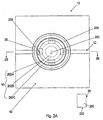
- Figure 2A is a cut-away view taken on line 2A-2A in Figure 1 that illustrates a portion of the exposure apparatus 10 including the optical assembly 16, the device stage 42, the environmental system 26, and the wafer 30.
- the imaging field 250 (Illustrated in phantom) is also illustrated in Figure 2A .
- the environmental system 26 fills the imaging field 250 and the rest of the gap 246 (illustrated in Figure 2B ) with an immersion fluid 248 (illustrated in Figure 2B ).
- the term "fluid” shall mean and include a liquid and/or a gas, including any fluid vapor.
- the environmental system 26 includes an immersion fluid system 252 and a fluid barrier 254.
- the immersion fluid system 252 delivers and/or injects the immersion fluid 248 into the gap 246 and captures the immersion fluid 248 flowing from the gap 246, and
- the fluid barrier 254 inhibits the flow of the immersion fluid 248 away from near the gap 246.
- the design of the immersion fluid system 252 can vary.
- the immersion fluid system 252 can inject the immersion fluid 248 at one or more locations at or near the gap 246 and/or the edge of the optical assembly 16.
- the immersion fluid 248 may be injected directly between the optical assembly 16 and the wafer 30.
- the immersion fluid system 252 can scavenge the immersion fluid 248 at one or more locations at or near the gap 246 and/or the edge of the optical assembly 16.
- the immersion fluid system 252 includes four, spaced apart injector/scavenge pads 258 (illustrated in phantom) positioned near the perimeter of the optical assembly 16 and an injector/scavenge source 260. These components are described in more detail below.
- Figure 2A also illustrates that the optical assembly 16 includes an optical housing 262A, a last optical element 262B, and an element retainer 262C that secures the last optical element 262B to the optical housing 262A.
- Figure 2B is a cut-away view of the portion of the exposure apparatus 10 of Figure 2A , including (i) the optical assembly 16 with the optical housing 262A, the optical element 262B, and the element retainer 262C, (ii) the device stage 42, and (iii) the environmental system 26.
- Figure 2B also illustrates the gap 246 between the last optical element 262B and the wafer 30, and that the immersion fluid 248 (illustrated as circles) fills the gap 246.
- the gap 246 is approximately 1mm.
- the fluid barrier 254 contains the immersion fluid 248, including any fluid vapor 249 (illustrated as triangles) in the area near the gap 246 and forms and defines an interior chamber 263 around the gap 246.
- the fluid barrier 254 includes a containment frame 264 (also referred to herein as a surrounding member), a seal 266, and a frame support 268.
- the interior chamber 263 represents the enclosed volume defined by the containment frame 264, the seal 266, the optical housing 262A and the wafer 30.
- the fluid barrier 254 restricts the flow of the immersion fluid 248 from the gap 246, assists in maintaining the gap 246 full of the immersion fluid 248, allows for the recovery of the immersion fluid 248 that escapes from the gap 246, and contains any vapor 249 from the fluid.
- the fluid barrier 254 encircles and runs entirely around the gap 246. Further, in one embodiment, the fluid barrier 254 confines the immersion fluid 248 and its vapor 249 to a region on the wafer 30 and the device stage 42 centered on the optical assembly 16.
- Containment of both the immersion fluid 248 and its vapor 249 can be important for the stability of the lithography tool.
- stage measurement interferometers are sensitive to the index of refraction of the ambient atmosphere. For the case of air with some water vapor present at room temperature and 633 nm laser light for the interferometer beam, a change of 1% in relative humidity causes a change in refractive index of approximately 10 -8 . For a 1 m total beam path this can represent an error of 10 nm in stage position. If the immersion fluid 248 is water, a droplet of water 7 mm in diameter evaporating into a 1 m 3 volume changes the relative humidity by 1%.
- Relative humidity is typically monitored and corrected for by the control system 24, but this is based on the assumption that the relative humidity is uniform, so that its value is the same in the interferometer beams as at the monitoring point. However, if droplets of water and its attendant vapor are scattered around on the wafer and stage surfaces, the assumption of uniform relative humidity may not be valid.
- water evaporation may also create temperature control problems.
- the heat of vaporization of water is about 44 kJ/mole. Evaporation of the 7 mm drop mentioned above will absorb about 430 J which must be supplied by the adjacent surfaces.
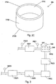
- Figure 2C illustrates a perspective view of one embodiment of the containment frame 264.
- the containment frame 264 is annular ring shaped and encircles the gap 246 (illustrated in Figure 2B ).
- the containment frame 264 includes a top side 270A, an opposed bottom side 270B (also referred to as a first surface) that faces the wafer 30, an inner side 270C that faces the gap 246, and an outer side 270D.
- top and bottom are used merely for convenience and the orientation of the containment frame 264 can be rotated.
- the containment frame 264 can have another shape.
- the containment frame 264 can be rectangular frame shaped or octagonal frame shaped.
- the containment frame 254 may be temperature controlled to stabilize the temperature of the immersion fluid 248.
- the seal 266 seals the containment frame 264 to the optical assembly 16 and allows for some motion of the containment frame 264 relative to the optical assembly 16.
- the seal 266 is made of a flexible, resilient material that is not influenced by the immersion fluid 248. Suitable materials for the seal 266 include rubber, Buna-N, neoprene, Viton or plastic. Alternatively the seal 266 may be a bellows made of a metal such as stainless steel or rubber or a plastic.
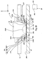
- Figure 2D illustrates an enlarged view of a portion of Figure 2B , in partial cut-away.
- the frame support 268 connects and supports the containment frame 264 to the apparatus frame 12 and the optical assembly 16 above the wafer 30 and the device stage 42.
- the frame support 268 supports all of the weight of the containment frame 264.
- the frame support 268 can support only a portion of the weight of the containment frame 264.
- the frame support 268 can include one or more support assemblies 274.
- the frame support 268 can include three spaced apart support assemblies 274 (only two are illustrated). In this embodiment, each support assembly 274 extends between the apparatus frame 12 and the top side 270A of the containment frame 264.
- each support assembly 274 is a flexure.
- the term "flexure” shall mean a part that has relatively high stiffness in some directions and relatively low stiffness in other directions.
- the flexures cooperate (i) to be relatively stiff along the X axis and along the Y axis, and (ii) to be relatively flexible along the Z axis.
- the ratio of relatively stiff to relatively flexible is at least approximately 100/1, and can be at least approximately 1000/1.
- the flexures can allow for motion of the containment frame 264 along the Z axis and inhibit motion of the containment frame 264 along the X axis and the Y axis.
- the support assembly 274 passively supports the containment frame 264.
- each support assembly 274 can be an actuator that can be used to adjust the position of the containment frame 264 relative to the wafer 30 and the device stage 42.
- the frame support 268 can include a frame measurement system 275 that monitors the position of the containment frame 264.
- the frame measurement system 275 can monitor the position of the containment frame 264 along the Z axis, about the X axis, and/or about the Y axis. With this information, the support assemblies 274 can be used to adjust the position of the containment frame 264. In this embodiment, the support assembly 274 can actively adjust the position of the containment frame 264.
- the environmental system 26 includes one or more pressure equalizers 276 that can be used to control the pressure in the chamber 263.
- the pressure equalizers 276 inhibit atmospheric pressure changes or pressure changes associated with the fluid control from creating forces between the containment frame 264 and the wafer 30 or the last optical element 262B.
- the pressure equalizers 276 can cause the pressure on the inside of the chamber 263 and/or in the gap 246 to be approximately equal to the pressure on the outside of the chamber 263.
- each pressure equalizer 276 can be a channel that extends through the containment frame 264.
- a tube 277 (only one is illustrated) is attached to the channel of each pressure equalizer 276 to convey any fluid vapor away from the measurement system 22 (illustrated in Figure 1 ).
- the pressure equalizer 276 allow for a pressure difference of less than approximately 70Pa, 340Pa, 700Pa, 3400Pa, or 7000Pa (0.01, 0.05, 0.1, 0.5, or 1.0 PSI).
- FIG. 2B also illustrates several injector/scavenge pads 258.
- Figure 2D illustrates one injector/scavenge pad 258 in more detail.
- each of the injector/scavenge pads 258 includes a pad outlet 278A and a pad inlet 278B that are in fluid communication with the injector/scavenge source 260.
- the injector/scavenge source 260 provides immersion fluid 248 to the pad outlet 278A that is released into the chamber 263 and draws immersion fluid 248 through the pad inlets 278B from the chamber 263.
- Figures 2B and 2D also illustrate that the immersion fluid 248 in the chamber 263 sits on top of the wafer 30. As the wafer 30 moves under the optical assembly 16, it will drag the immersion fluid 248 in the vicinity of a top, device surface 279 of the wafer 30 with the wafer 30 into the gap 246.
- the device stage 42 includes a stage surface 280 that has approximately the same height along the Z axis as the top, device exposed surface 279 of the wafer 30. Stated another way, in one embodiment, the stage surface 280 is in approximately the same plane as the device exposed surface 279. In alternative embodiments, for example, approximately the same plane shall mean that the planes are within approximately 1, 10, 100 or 500 microns. As a result thereof, the distance between the bottom side 270B of the containment frame 264 and the wafer 30 is approximately equal to the distance between the bottom side 270B of the containment frame 264 and the device stage 42. In one embodiment, for example, the device stage 42 can include a disk shaped recess 282 for receiving the wafer 30. Alternative designs of the device stage 42 are discussed below.
- Figure 2D illustrates that a frame gap 284 exists between the bottom side 270B of the containment frame 264 and the wafer 30 and/or the device stage 42 to allow for ease of movement of the device stage 42 and the wafer 30 relative to the containment frame 264.
- the size of the frame gap 284 can vary.
- the frame gap 284 can be between approximately 5 ⁇ m and 3 mm.
- the frame gap 284 can be approximately 5, 10, 50, 100, 150, 200, 250, 300, 400, or 500 microns.
- the distance between the bottom side 270B and at least one of the wafer 30 and/or the device stage 42 is shorter than a distance between the end surface (e.g. the last optical element 262B or the bottom of the optical housing 262A) of the optical assembly 16 and at least one of the wafer 30 and/or the device stage 42.
- a wafer gap 285 can exist between the edge of the wafer 30 and the wafer stage 42.
- the wafer gap 285 is as narrow as possible to minimize leakage when the wafer 30 is off-center from the optical assembly 16 and lying partly within and partly outside the fluid containment frame 264 region.
- the wafer gap 285 can be approximately 1, 10, 50, 100, 500, or 1000 microns.
- Figure 2D also illustrates that some of the immersion fluid 248 flows between the containment frame 264 and the wafer 30 and/or the device stage 42.
- the containment frame 264 includes one or more scavenge inlets 286 that are positioned at or near the bottom side 270B of the containment frame 264.
- the one or more scavenge inlets 286 are in fluid communication with the injector/scavenge source 260 (illustrated in Figure 2B ).
- the immersion fluid 248 that escapes in the frame gap 284 can be scavenged by the injector/scavenge source 260.
- the bottom side 270B of the containment frame 264 includes one scavenge inlet 286 that is substantially annular groove shaped and is substantially concentric with the optical assembly 16.
- the bottom side 270B of the containment frame 264 can include a plurality of spaced apart annular groove shaped, scavenge inlets 286 that are substantially concentric with the optical assembly 16 to inhibit the immersion fluid 248 from completely exiting the frame gap 284.
- a plurality of spaced apart apertures oriented in a circle can be used instead of an annular shaped groove.
- the injector/scavenge source 260 applies a vacuum and/or partial vacuum on the scavenge inlet 286.
- the partial vacuum draws the immersion fluid 248 between (i) a small land area 288 on the bottom side 270B, and (ii) the wafer 30 and/or the device stage 42.
- the immersion fluid 248 in the frame gap 284 acts as a fluid bearing 289A (illustrated as an arrow) that supports the containment frame 264 above the wafer 30 and/or the device stage 42, allows for the containment frame 264 to float with minimal friction on the wafer 30 and/or the device stage 42, and allows for a relatively small frame gap 284.
- most of the immersion fluid 248 is confined within the fluid barrier 254 and most of the leakage around the periphery is scavenged within the narrow frame gap 284.
- the environmental system 26 can include a device for creating an additional fluid bearing 289B (illustrated as an arrow) between the containment frame 264 and the wafer 30 and/or the device stage 42.
- the containment frame 264 can include one or more bearing outlets 290A that are in fluid communication with a bearing fluid source 290B of a bearing fluid 290C (illustrated as triangles).
- the bearing fluid 290C is air.
- the bearing fluid source 290B provides pressurized air 290C to the bearing outlet 290A to create the aerostatic bearing 289B.
- the fluid bearings 289A, 289B can support all or a portion of the weight of the containment frame 264.
- one or both of the fluid bearings 289A, 289B support approximately 1, 5, 10, 20, 30, 40, 50, 60, 70, 80, 90, or 100 percent of the weight of the containment frame 264.
- the concentric fluid bearings 289A, 289B are used to maintain the frame gap 284.
- the bearing fluid 290C can have the same composition or a different composition than the immersion fluid 248. However, some of the bearing fluid 290C may escape from the fluid barrier 254. In one embodiment, the type of bearing fluid 290C is be chosen so that the bearing fluid 290C and its vapor do not interfere with the measurement system 22 or temperature stability of the exposure apparatus 10.
- the partial vacuum in the scavenge inlets 286 pulls and urges the containment frame 264 towards the wafer 30.
- the fluid bearing 289B supports part of the weight of the containment frame 264 as well as opposes the pre-load imposed by the partial vacuum in the scavenge inlets 286.
- the pressurized air 290C helps to contain the immersion fluid 248 within the containment frame 264.
- the immersion fluid 248 in the frame gap 284 is mostly drawn out through the scavenge inlets 286.
- any immersion fluid 248 which leaks beyond the scavenge inlets 286 is pushed back to the scavenge inlets 286 by the bearing fluid 290C.
- the frame gap 284 may vary radially, from the inner side 270C to the outer side 270D, to optimize bearing and scavenging functions.
- the bearing outlet 290A is substantially annular groove shaped, is substantially concentric with the optical assembly 16 and the scavenge inlet 286, and has a diameter that is greater than the diameter of the scavenge inlet 286.
- the bottom side 270B of the containment frame 264 can include a plurality of spaced apart annular groove shaped, bearing outlets 290A that are substantially concentric with the optical assembly 16.
- a plurality of spaced apart apertures oriented in a circle can be used instead of an annular shaped groove.
- a magnetic type bearing could be used to support the containment frame 264.
- FIG. 2E is an illustration of the portion of the exposure apparatus 10 of Figure 2A with the device stage 42 and the wafer 30 moved relative to the optical assembly 16. In this position, the wafer 30 and the device stage 42 are no longer centered under the optical assembly 16, and the fluid bearings 289A, 289A (illustrated in Figure 2D ) support the containment frame 264 above the wafer 30 and the device stage 42.
- Figure 3 is a first embodiment of the injector/scavenge source 260.
- the injector/scavenge source 260 includes (i) a low pressure source 392A, e.g. a pump, having an inlet that is at a vacuum or partial vacuum that is in fluid communication with the scavenge inlet 286 (illustrated in Figure 2D ) and the pad inlets 278B (illustrated in Figures 2B and 2D ) and a pump outlet that provides pressurized immersion fluid 248, (ii) a filter 392B in fluid communication with the pump outlet that filters the immersion fluid 248, (iii) an aerator 392C in fluid communication with the filter 392B that removes any air, contaminants, or gas from the immersion fluid 248, (iv) a temperature control 392D in fluid communication with the aerator 392C that controls the temperature of the immersion fluid 248, (v) a reservoir 392E in fluid communication with the temperature control 392D that retains the immersion fluid 248, and
- control system 24 (illustrated in Figure 1 ) to control the flow rate of the immersion fluid 248 to the pad outlets 278A, the temperature of the immersion fluid 248 at the pad outlets 278A, the pressure of the immersion fluid 248 at the pad outlets 278A, and/or the pressure at the scavenge inlets 286 and the pad inlets 278B.
- the injector/scavenge source 260 can include (i) a pair of pressure sensors 392G that measure the pressure near the pad outlets 278A, the scavenge inlet 286 and the pad inlets 278B, (ii) a flow sensor 392H that measures the flow to the pad outlets 278A, and/or (iii) a temperature sensor 392I that measures the temperature of the immersion fluid 248 delivered to the pad outlets 278A.
- the information from these sensors 392G-392I can be transferred to the control system 24 so that that control system 24 can appropriately adjust the other components of the injector/scavenge source 260 to achieve the desired temperature, flow and/or pressure of the immersion fluid 248.
- orientation of the components of the injector/scavenge source 260 can be varied. Further, one or more of the components may not be necessary and/or some of the components can be duplicated.
- the injector/scavenge source 260 can include multiple pumps, multiple reservoirs, temperature controllers or other components.
- the environmental system 26 can include multiple injector/scavenge sources 26.
- the rate at which the immersion fluid 248 is pumped into and out of the chamber 263 can be adjusted to suit the design requirements of the system. Further, the rate at which the immersion fluid 248 is scavenged from the pad inlets 278B and the scavenge inlets 286 can vary. In one embodiment, the immersion fluid 248 is scavenged from the pad inlets 278B at a first rate and is scavenged from the scavenge inlets 286 at a second rate. As an example, the first rate can be between approximately 0.1- 5 liters/minute and the second rate can be between approximately 0.01- 0.5 liters/minute. However, other first and second rates can be utilized.
- the rates at which the immersion fluid 248 is pumped into and out of the chamber 263 can be adjusted to (i) control the leakage of the immersion fluid 248 below the fluid barrier, (ii) control the leakage of the immersion fluid 248 from the wafer gap 285 when the wafer 30 is off-center from the optical assembly 16, and/or (iii) control the temperature and purity of the immersion fluid 248 in the gap 246.
- the rates can be increased in the event the wafer 30 is off-center, the temperature of the immersion fluid 248 becomes too high and/or there is an unacceptable percentage of contaminants in the immersion fluid 248 in the gap 246.
- the type of immersion fluid 248 can be varied to suit the design requirements of the apparatus 10.
- the immersion fluid 248 is water.
- the immersion fluid 248 can be a fluorocarbon fluid, Fomblin oil, a hydrocarbon oil, or another type of oil.
- the fluid should satisfy certain conditions: 1) it must be relatively transparent to the exposure radiation; 2) its refractive index must be comparable to that of the last optical element 262B; 3) it should not react chemically with components of the exposure system 10 with which it comes into contact; 4) it must be homogeneous; and 5) its viscosity should be low enough to avoid transmitting vibrations of a significant magnitude from the stage system to the last optical element 262B.
- Figure 4A is an enlarged view of a portion of another embodiment of the fluid barrier 454A, a portion of the wafer 30, and a portion of the device stage 42.
- the fluid barrier 454A is somewhat similar to the corresponding component described above and illustrated in Figure 2D .
- the containment frame 464A includes two concentric, scavenge inlets 486A that are positioned at the bottom side 470B of the containment frame 464A.
- the two scavenge inlets 486A are in fluid communication with the injector/scavenge source 260 (illustrated in Figure 2B ).
- the immersion fluid 248 that escapes in the frame gap 284 can be scavenged by the injector/scavenge source 260.
- the bottom side 470B of the containment frame 464 includes two scavenge inlets 486A that are each substantially annular groove shaped and are substantially concentric with the optical assembly 16.
- the injector/scavenge source 260 applies a vacuum or partial vacuum on the scavenge inlets 486A.
- the partial vacuum draws the immersion fluid 24B between a small land area 488 on the bottom side 470B and the wafer 30 and/or the device stage 42.
- the majority of the immersion fluid 248 flows under the land 488 and into the inner scavenge inlet 486A.
- the immersion fluid 248 not removed at the inner scavenge inlet 486A is drawn into the outer scavenge inlet 486A.
- Figure 4B is an enlarged view of a portion of another embodiment of the fluid barrier 454B, a portion of the wafer 30, and a portion of the device stage 42.
- the fluid barrier 454B is somewhat similar to the corresponding component described above and illustrated in Figure 2D .
- the containment frame 464B includes one bearing outlet 490B and two scavenge inlets 486B that are positioned at the bottom side 470B.
- the scavenge inlets 486B are in fluid communication with the injector/scavenge source 260 (illustrated in Figure 2B ) and the bearing outlet 490B is in fluid communication with the bearing fluid source 290C (illustrated in Figure 2D ).
- the bearing outlet 490B is positioned within and concentric with the scavenge inlets 486B. Stated another way, the bearing outlet 490B has a smaller diameter than the scavenge inlets 486B and the bearing outlet 490B is closer to the optical assembly 16 than the scavenge inlets 486B.
- the bearing fluid 290C (illustrated in Figure 2D ) can be a liquid that is the same in composition as the immersion fluid 248. With this design, the bearing fluid 290C in the frame gap 284 can be scavenged by the injector/scavenge source 260 via the scavenge inlets 486B.
- Figure 4C is an enlarged view of a portion of another embodiment of the fluid barrier 454C, a portion of the wafer 30, and a portion of the device stage 42.
- the fluid barrier 454C is somewhat similar to the corresponding component described above and illustrated in Figure 2D .
- the containment frame 464C includes one bearing outlet 490C and two scavenge inlets 486C that are positioned at the bottom side 470B.
- the scavenge inlets 486C are in fluid communication with the injector/scavenge source 260 (illustrated in Figure 2B ) and the bearing outlet 490C is in fluid communication with the bearing fluid source 290C (illustrated in Figure 2D ).
- the bearing outlet 490C is positioned between the two scavenge inlets 486C.
- the inner scavenge inlet 486C has a smaller diameter than the bearing outlet 490C and the bearing outlet 490C has a smaller diameter than the outer scavenge inlet 486C.
- the inner scavenge inlet 486C is closer to the optical assembly 16 than the bearing outlet 490C.
- Figure 5A is a cut-away view of a portion of another embodiment of the exposure apparatus 510, including the optical assembly 516, the device stage 542, and the environmental system 526 that are similar to the corresponding components described above.
- Figure 5A also illustrates the wafer 30, the gap 546, and that the immersion fluid 548 fills the gap 546.
- Figure 5B illustrates an enlarged portion of the Figure 5A taken on line 5B-5B.
- the fluid barrier 554 includes an inner barrier 555 in addition to the containment frame 564, the seal 566, and the frame support 568.
- the inner barrier 555 is annular ring shaped, encircles the bottom of the optical assembly 516, is concentric with the optical assembly 516, and is positioned within the containment frame 564 adjacent to the seal 566.
- the inner barrier 555 can serve several purposes.
- the inner barrier 555 can limit the amount of immersion fluid 548 escaping to the containment frame 564, reducing the scavenging requirements at the scavenge inlets 586, and also reducing the leakage of immersion fluid 548 into the wafer gap 285 when the wafer 30 is off-center from the optical assembly 516 and lying partly within and partly outside the fluid containment frame 564 region.
- the fluid injection/scavenge pads 558 can be used to recover the majority of the immersion fluid 548 from the chamber 563.
- the immersion fluid 548 is maintained at or near the level of the top of the inner barrier 555, pressure surges associated with injection of the immersion fluid 548 can be reduced, because excess immersion fluid 548 overflows the top of the inner barrier 555, creating a static pressure head. Some pressure surge may remain even in this situation due to surface tension effects. These effects can be reduced by increasing the distance W shown in Fig. 5B . For example, if the immersion fluid is water, W should preferably be several mm or more. Additionally, the remaining pressure surge can be reduced or eliminated by adjusting the "wettability" of the surfaces of inner barrier 555 and optical assembly 516 in contact with the immersion fluid 548 to reduce surface tension forces. in one embodiment, the inner barrier 555 can maintain a significant fluid height difference with a gap of approximately 50 ⁇ m between the bottom of the inner barrier 55 and the top of the wafer 30 or the device stage 42.
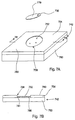
- Figure 6 is a perspective view of one embodiment of a device stage 642 with a wafer 630 positioned above the device stage 642.
- the device stage 642 includes a device table 650, a device holder 652, a guard 654, and a guard mover assembly 656.
- the device table 650 is generally rectangular plate shaped.
- the device holder 652 retains the wafer 630.
- the device holder 652 is a chuck or another type of clamp that is secured to the device table 650.
- the guard 654 surrounds and/or encircles the wafer 630.
- the guard 654 is generally rectangular plate shaped and includes a circular shaped aperture 658 for receiving the wafer 630.
- the guard 654 can include a first section 660 and a second section 662.
- One or more of the sections 660, 662 can be moved, removed or recessed to provide easy access for loading and removing the wafer 630.
- the guard mover assembly 656 secures the guard 654 to the device table 650, and moves and positions the guard 654 relative to the device table 650, the device holder 652, and the wafer 630. With this design, the guard mover assembly 656 can move the guard 654 so that the top, stage surface 680 of the guard 654 is approximately at the same Z height as the top device exposed surface 679 of the wafer 630. Stated another way, the guard mover assembly 656 moves the guard 654 so that the device exposed surface 680 is approximately in the same plane as the device exposed surface 679. As a result thereof, the guard 654 can be moved to adjust for wafers 630 of alternative heights.
- the design of the guard mover assembly 656 can be varied.
- the guard mover assembly 656 can include one or more rotary motors, voice coil motors, linear motors, electromagnetic actuators, and/or some other type of force actuators.
- the guard mover assembly 656 moves and positions the guard 654 along the Z axis, about the X axis and about the Y axis under the control of the control system 24 (illustrated in Figure 1 ).
- a sensor 681 (illustrated as a box) can be used to measure the relative heights of the guard surface 680 and the wafer top surface 679. Information from the sensor 681 can be transferred to the control system 24 (illustrated in Figure 1 ) which uses information from the height sensor 681 to control the guard mover assembly 656.
- Figure 7A is a perspective view of another embodiment of a device stage 742 with a wafer 730 positioned above the device stage 742.
- Figure 7B is a cut-away view taken from Figure 7A .
- the device stage 742 includes a device table 750, a device holder 752, a guard 754, and a holder mover assembly 756.
- the device table 750 is generally rectangular plate shaped.
- the device holder 752 retains the wafer 730.
- the guard 754 is generally rectangular plate shaped and includes a circular shaped aperture 758 for the wafer 730. In this embodiment, the guard 754 is fixedly secured to the device table 750.
- the holder mover assembly 756 secures the device holder 752 to the device table 750 and moves and positions the device holder 752 relative to the device table 750 and the guard 754. With this design, the holder mover assembly 756 can move the device holder 752 and the wafer 730 so that the top stage surface 780 of the guard 754 is approximately at the same Z height as the top device exposed surface 779 of the wafer 730.
- a sensor 781 can be used to measure the relative heights of the top stage surface 780 and the top device exposed surface 779. The information from the sensor 781 can be transferred to the control system 24 (illustrated in Figure 1 ) which uses information from the height sensor to control the holder mover assembly 756.
- the holder mover assembly 756 can include one or more rotary motors, voice coil motors, linear motors, electromagnetic actuators, and/or some other type of force actuators.
- the holder mover assembly 756 moves and positions the device holder 750 and the wafer 730 along the Z axis, about the X axis and about the Y axis under the control of the control system 24 (illustrated in Figure 1 ).
- step 801 the device's function and performance characteristics are designed.
- step 802 a mask (reticle) having a pattern is designed according to the previous designing step, and in a parallel step 803 a wafer is made from a silicon material.
- the mask pattern designed in step 802 is exposed onto the wafer from step 803 in step 804 by a photolithography system described hereinabove in accordance with the present invention.
- step 805 the semiconductor device is assembled (including the dicing process, bonding process and packaging process), finally, the device is then inspected in step 806.
- FIG 8B illustrates a detailed flowchart example of the above-mentioned step 804 in the case of fabricating semiconductor devices.
- step 811 oxidation step
- step 812 CVD step
- step 813 electrode formation step
- step 814 ion implantation step
- ions are implanted in the wafer.
- steps 811 - 814 form the preprocessing steps for wafers during wafer processing, and selection is made at each step according to processing requirements.
- step 815 photoresist formation step
- step 816 exposure step
- step 817 developing step
- step 818 etching step
- steps other than residual photoresist exposed material surface
- step 819 photoresist removal step
Claims (31)
- Appareil d'exposition (10) pour transférer une image sur un dispositif, l'appareil d'exposition comprenant :un ensemble optique (16),un étage de dispositif (42, 742) pour retenir le dispositif, etun système environnemental (26) pour réguler un environnement dans un espace entre l'ensemble optique et le dispositif, le système environnemental comprenant un élément d'enceinte (264) ayant une première surface (270B) orientée au moins face à l'un du dispositif etde l'étage de dispositif, un système à fluide d'immersion (252) pour distribuer un fluide d'immersion dans l'élément d'enceinte pour remplir l'espace, et une partie d'entrée (286) sur la première surface de l'élément d'enceinte pour empêcher les fuites du fluide d'immersion,caractérisé en ce que l'appareil d'exposition comprend en outre un cadre d'appareil (12) par lequel l'ensemble optique est supporté avec des isolateurs à montage optique (37), chacun d'eux ayant un cylindre pneumatique pour isoler les vibrations et un actionneur pour isoler les vibrations et contrôler la position de l'ensemble optique ; eten ce que l'étage de dispositif comprend une surface d'étage (280, 680, 780) agencée de façon à être approximativement sur le même plan qu'une surface d'exposition du dispositif.
- Appareil d'exposition selon la revendication 1, dans lequel l'élément d'enceinte est agencé de sorte qu'une distance entre la première surface et au moins l'un du dispositif et de l'étage de dispositif soit plus courte qu'une distance entre une surface d'extrémité de l'ensemble optique et au moins l'un du dispositif et de l'étage de dispositif.
- Appareil d'exposition selon l'une quelconque des revendications précédentes, dans lequel la partie d'entrée est agencée de façon à former un palier de fluide dans l'espace entre la première surface et au moins l'un du dispositif et de l'étage de dispositif, en coopération avec une partie de sortie (290A) pour fournir un fluide de palier à l'espace.
- Appareil d'exposition selon l'une quelconque des revendications 1 à 3, dans lequel le système environnemental comprend une partie de sortie (290A) sur la première surface de l'élément d'enceinte.
- Appareil d'exposition selon la revendication 4, dans lequel la partie de sortie est agencée de façon à fournir un gaz pressurisé.
- Appareil d'exposition selon la revendication 4 ou 5, dans lequel la partie de sortie est agencée de façon à former un palier gazeux dans l'espace entre la première surface et au moins l'un du dispositif et de l'étage de dispositif.
- Appareil d'exposition selon l'une quelconque des revendications 4 à 6, dans lequel la partie de sortie est disposée hors de la partie d'entrée relativement à l'espace adjacent à l'ensemble optique.
- Appareil d'exposition selon l'une quelconque des revendications 4 à 7, dans lequel le système environnemental comprend une autre partie de sortie (486A, 486B, 486C).
- Appareil d'exposition selon la revendication 8, dans lequel la partie de sortie (490C) est agencée entre la partie d'entrée (486C) et la partie d'entrée supplémentaire (486C).
- Appareil d'exposition selon la revendication 8, dans lequel la partie d'entrée supplémentaire (486A, 486B) est agencée entre la partie d'entrée (486A, 486B) et la partie de sortie (490B).
- Appareil d'exposition selon l'une quelconque des revendications précédentes, comprenant en outre un support de cadre (268) avec lequel l'élément d'enceinte est supporté par le cadre d'appareil.
- Appareil d'exposition selon la revendication 11, dans lequel le support de cadre comprend un ou plusieurs ensembles de support (274).
- Appareil d'exposition selon la revendication 12, dans lequel chacun desdits un ou plusieurs ensembles de support s'étend entre le cadre d"appareil et l'élément d'enceinte.
- Appareil d'exposition selon la revendication 12 ou 13, dans lequel chacun des un ou plusieurs éléments de support est un élément flexible.
- Appareil d'exposition selon la revendication 12 ou 13, dans lequel chacun des un ou plusieurs ensembles de support est un actionneur pour ajuster une position de l'élément d'enceinte.
- Appareil d'exposition selon la revendication 15, dans lequel le support de cadre comprend un système de mesure de cadre (275) pour contrôler la position de l'élément d'enceinte.
- Appareil d'exposition selon l'une quelconque des revendications précédentes, comprenant en outre un égaliseur de pression (276) pour permettre à la pression dans l'espace d'être approximativement égale à la pression hors de l'élément d'enceinte.
- Appareil d'exposition selon la revendication 17, dans lequel l'égaliseur de pression est un canal qui s'étend à travers l'élément d'enceinte.
- Appareil d'exposition selon l'une quelconque des revendications précédentes, dans lequel l'étage de dispositif comprend un support de dispositif (652, 752) pour retenir le dispositif, une protection (654, 754) pour définir la surface d'étage, et un ensemble de déplacement (656, 756) pour déplacer l'un du support de dispositif et de la protection, de sorte que la surface d'exposition du dispositif soit approximativement dans le même plan que la surface d'étage.
- Appareil d'exposition selon la revendication 19, dans lequel l'ensemble de déplacement (656) est agencé de façon à déplacer la protection (654) relativement au dispositif et au support de dispositif (652).
- Procédé de fabrication comprenant les étapes de fourniture d'un dispositif et de transfert d'une image sur le dispositif avec l'appareil d'exposition selon l'une quelconque des revendications précédentes.
- Procédé d'exposition consistant à transférer une image sur un dispositif, le procédé comprenant les étapes consistant à :supporter un ensemble optique (16) par un cadre d'appareil (12) avec des isolateurs à montage optique (37), dont chacun a un cylindre pneumatique pour isoler les vibrations et un actionneur pour isoler les vibrations et contrôler la position de l'ensemble optique ;retenir un dispositif avec un étage de dispositif (42, 642, 742) etcontrôler un environnement dans un espace entre l'ensemble optique et le dispositif avec un système environnemental, dans lequelle système environnemental comprend un élément d'enceinte (264) qui présentent une première surface (270B) faisant face à au moins l'un du dispositif et de l'étage du dispositif, un système à fluide d'immersion (252) pour fournir un fluide d'immersion dans l'élément d'enceinte afin de remplir l'espace, et une partie d'entrée (286) sur la première surface de l'élément d'enceinte pour empêcher les fuites du fluide d'immersion,dans lequel l'étage de dispositif comprend une surface d'étage (280, 680, 780) agencée de façon à être approximativement dans le même plan qu'une surface d'exposition du dispositif.
- Procédé d'exposition selon la revendication 22, dans lequel le système environnemental comprend une partie de sortie (290A) sur la première surface de l'élément d'enceinte.
- Procédé d'exposition selon la revendication 23, dans lequel la partie de sortie est disposée de façon à fournir un gaz pressurisé.
- Procédé d'exposition selon la revendication 23 ou 24, dans lequel le système environnemental comprend une autre partie d'entrée (486A, 486B, 486C).
- Procédé d'exposition selon la revendication 25, dans lequel la partie de sortie (490C) est ménagée entre la partie d'entrée (486C) et la partie d'entrée supplémentaire (486C).
- Procédé d'exposition selon la revendication 25, dans lequel la partie d'entrée supplémentaire (486A, 486B) est agencée entre la partie d'entrée (486A, 486B) et la partie de sortie (490B).
- Procédé d'exposition selon l'une quelconque des revendications 22 à 27, comprenant en outre un support de cadre (268) avec lequel l'élément d'enceinte est supporté par le cadre de l'appareil, dans lequel le support de cadre comprend un ou plusieurs ensembles de support (274).
- Procédé d'exposition selon la revendication 28, dans lequel chacun des un ou plusieurs ensembles de support est un actionneur qui est utilisé pour ajuster une position de l'élément d'enceinte.
- Procédé d'exposition selon la revendication 29, dans lequel le support de cadre comprend un système de mesure de cadre (275) qui surveille la position de l'élément d'enceinte.
- Procédé de fabrication comprenant :l'exposition d'un dispositif utilisant l'appareil selon l'une quelconque des revendications 1 à 20, oul'utilisation du procédé d'exposition selon l'une quelconque des revendications 22 à 30 ; etle développement du dispositif exposé.
Applications Claiming Priority (3)
| Application Number | Priority Date | Filing Date | Title |
|---|---|---|---|
| US46211203P | 2003-04-10 | 2003-04-10 | |
| US48447603P | 2003-07-01 | 2003-07-01 | |
| EP04758599.7A EP1611485B1 (fr) | 2003-04-10 | 2004-03-29 | Système environnemental incluant une conduite de recirculation sous vide pour un appareil de lithographie par immersion |
Related Parent Applications (2)
| Application Number | Title | Priority Date | Filing Date |
|---|---|---|---|
| EP04758599.7A Division-Into EP1611485B1 (fr) | 2003-04-10 | 2004-03-29 | Système environnemental incluant une conduite de recirculation sous vide pour un appareil de lithographie par immersion |
| EP04758599.7A Division EP1611485B1 (fr) | 2003-04-10 | 2004-03-29 | Système environnemental incluant une conduite de recirculation sous vide pour un appareil de lithographie par immersion |
Publications (2)
| Publication Number | Publication Date |
|---|---|
| EP2950148A1 EP2950148A1 (fr) | 2015-12-02 |
| EP2950148B1 true EP2950148B1 (fr) | 2016-09-21 |
Family
ID=33162259
Family Applications (7)
| Application Number | Title | Priority Date | Filing Date |
|---|---|---|---|
| EP04758599.7A Expired - Lifetime EP1611485B1 (fr) | 2003-04-10 | 2004-03-29 | Système environnemental incluant une conduite de recirculation sous vide pour un appareil de lithographie par immersion |
| EP15162756.9A Expired - Lifetime EP2950147B1 (fr) | 2003-04-10 | 2004-03-29 | Système environnemental incluant un systéme de recirculation sous vide pour un appareil de lithographie par immersion |
| EP20130196627 Expired - Lifetime EP2717098B1 (fr) | 2003-04-10 | 2004-03-29 | Système environnemental incluant une conduite de recirculation sous vide pour un appareil de lithographie par immersion |
| EP15162758.5A Expired - Lifetime EP2950148B1 (fr) | 2003-04-10 | 2004-03-29 | Système environnemental incluant un systéme de recirculation sous vide pour un appareil de lithographie par immersion |
| EP17161308.6A Withdrawn EP3232271A1 (fr) | 2003-04-10 | 2004-03-29 | Système environnemental à piégeage à vide pour un appareil de lithographie par immersion |
| EP20130180843 Expired - Lifetime EP2667252B1 (fr) | 2003-04-10 | 2004-03-29 | Système environnemental incluant une conduite de recirculation sous vide pour un appareil de lithographie par immersion |
| EP13180845.3A Expired - Lifetime EP2667253B1 (fr) | 2003-04-10 | 2004-03-29 | Système environnemental incluant une conduite de recirculation sous vide pour un appareil de lithographie par immersion |
Family Applications Before (3)
| Application Number | Title | Priority Date | Filing Date |
|---|---|---|---|
| EP04758599.7A Expired - Lifetime EP1611485B1 (fr) | 2003-04-10 | 2004-03-29 | Système environnemental incluant une conduite de recirculation sous vide pour un appareil de lithographie par immersion |
| EP15162756.9A Expired - Lifetime EP2950147B1 (fr) | 2003-04-10 | 2004-03-29 | Système environnemental incluant un systéme de recirculation sous vide pour un appareil de lithographie par immersion |
| EP20130196627 Expired - Lifetime EP2717098B1 (fr) | 2003-04-10 | 2004-03-29 | Système environnemental incluant une conduite de recirculation sous vide pour un appareil de lithographie par immersion |
Family Applications After (3)
| Application Number | Title | Priority Date | Filing Date |
|---|---|---|---|
| EP17161308.6A Withdrawn EP3232271A1 (fr) | 2003-04-10 | 2004-03-29 | Système environnemental à piégeage à vide pour un appareil de lithographie par immersion |
| EP20130180843 Expired - Lifetime EP2667252B1 (fr) | 2003-04-10 | 2004-03-29 | Système environnemental incluant une conduite de recirculation sous vide pour un appareil de lithographie par immersion |
| EP13180845.3A Expired - Lifetime EP2667253B1 (fr) | 2003-04-10 | 2004-03-29 | Système environnemental incluant une conduite de recirculation sous vide pour un appareil de lithographie par immersion |
Country Status (8)
| Country | Link |
|---|---|
| US (13) | US7321415B2 (fr) |
| EP (7) | EP1611485B1 (fr) |
| JP (10) | JP4775256B2 (fr) |
| KR (13) | KR101599182B1 (fr) |
| CN (7) | CN103439864B (fr) |
| HK (8) | HK1086637A1 (fr) |
| SG (6) | SG2012050829A (fr) |
| WO (1) | WO2004090634A2 (fr) |
Families Citing this family (202)
| Publication number | Priority date | Publication date | Assignee | Title |
|---|---|---|---|---|
| CN101470360B (zh) | 2002-11-12 | 2013-07-24 | Asml荷兰有限公司 | 光刻装置和器件制造方法 |
| US7372541B2 (en) * | 2002-11-12 | 2008-05-13 | Asml Netherlands B.V. | Lithographic apparatus and device manufacturing method |
| US10503084B2 (en) | 2002-11-12 | 2019-12-10 | Asml Netherlands B.V. | Lithographic apparatus and device manufacturing method |
| SG121819A1 (en) | 2002-11-12 | 2006-05-26 | Asml Netherlands Bv | Lithographic apparatus and device manufacturing method |
| US9482966B2 (en) | 2002-11-12 | 2016-11-01 | Asml Netherlands B.V. | Lithographic apparatus and device manufacturing method |
| SG121818A1 (en) | 2002-11-12 | 2006-05-26 | Asml Netherlands Bv | Lithographic apparatus and device manufacturing method |
| SG150388A1 (en) | 2002-12-10 | 2009-03-30 | Nikon Corp | Exposure apparatus and method for producing device |
| EP1571698A4 (fr) | 2002-12-10 | 2006-06-21 | Nikon Corp | Appareil d'exposition, procede d'exposition et procede de fabrication d'un dispositif |
| US7242455B2 (en) | 2002-12-10 | 2007-07-10 | Nikon Corporation | Exposure apparatus and method for producing device |
| SG171468A1 (en) | 2002-12-10 | 2011-06-29 | Nikon Corp | Exposure apparatus and method for producing device |
| CN100446179C (zh) | 2002-12-10 | 2008-12-24 | 株式会社尼康 | 曝光设备和器件制造法 |
| US7948604B2 (en) | 2002-12-10 | 2011-05-24 | Nikon Corporation | Exposure apparatus and method for producing device |
| DE10261775A1 (de) | 2002-12-20 | 2004-07-01 | Carl Zeiss Smt Ag | Vorrichtung zur optischen Vermessung eines Abbildungssystems |
| EP3301511A1 (fr) | 2003-02-26 | 2018-04-04 | Nikon Corporation | Appareil d'exposition, procédé d'exposition et procédé de production de dispositif |
| KR20050110033A (ko) | 2003-03-25 | 2005-11-22 | 가부시키가이샤 니콘 | 노광 장치 및 디바이스 제조 방법 |
| KR101176817B1 (ko) | 2003-04-07 | 2012-08-24 | 가부시키가이샤 니콘 | 노광장치 및 디바이스 제조방법 |
| KR20110104084A (ko) | 2003-04-09 | 2011-09-21 | 가부시키가이샤 니콘 | 액침 리소그래피 유체 제어 시스템 |
| CN1771463A (zh) | 2003-04-10 | 2006-05-10 | 株式会社尼康 | 用于沉浸光刻装置收集液体的溢出通道 |
| EP3062152B1 (fr) | 2003-04-10 | 2017-12-20 | Nikon Corporation | Système environnemental comprenant une zone de transport pour un appareil de lithographie par immersion |
| SG2012050829A (en) | 2003-04-10 | 2015-07-30 | Nippon Kogaku Kk | Environmental system including vacuum scavange for an immersion lithography apparatus |
| KR101697896B1 (ko) | 2003-04-11 | 2017-01-18 | 가부시키가이샤 니콘 | 액침 리소그래피 머신에서 웨이퍼 교환동안 투영 렌즈 아래의 갭에서 액침 액체를 유지하는 장치 및 방법 |
| JP4582089B2 (ja) | 2003-04-11 | 2010-11-17 | 株式会社ニコン | 液浸リソグラフィ用の液体噴射回収システム |
| KR101324818B1 (ko) | 2003-04-11 | 2013-11-01 | 가부시키가이샤 니콘 | 액침 리소그래피에 의한 광학기기의 세정방법 |
| EP1614000B1 (fr) | 2003-04-17 | 2012-01-18 | Nikon Corporation | Appareil de lithographie à immersion |
| TWI295414B (en) | 2003-05-13 | 2008-04-01 | Asml Netherlands Bv | Lithographic apparatus and device manufacturing method |
| TW201806001A (zh) | 2003-05-23 | 2018-02-16 | 尼康股份有限公司 | 曝光裝置及元件製造方法 |
| TWI463533B (zh) | 2003-05-23 | 2014-12-01 | 尼康股份有限公司 | An exposure method, an exposure apparatus, and an element manufacturing method |
| KR20150036794A (ko) | 2003-05-28 | 2015-04-07 | 가부시키가이샤 니콘 | 노광 방법, 노광 장치, 및 디바이스 제조 방법 |
| TWI347741B (en) * | 2003-05-30 | 2011-08-21 | Asml Netherlands Bv | Lithographic apparatus and device manufacturing method |
| US7213963B2 (en) | 2003-06-09 | 2007-05-08 | Asml Netherlands B.V. | Lithographic apparatus and device manufacturing method |
| EP2261741A3 (fr) * | 2003-06-11 | 2011-05-25 | ASML Netherlands B.V. | Appareil lithographique et méthode de fabrication d'un dispositif |
| TW200511388A (en) | 2003-06-13 | 2005-03-16 | Nikon Corp | Exposure method, substrate stage, exposure apparatus and method for manufacturing device |
| KR101475634B1 (ko) | 2003-06-19 | 2014-12-22 | 가부시키가이샤 니콘 | 노광 장치 및 디바이스 제조방법 |
| US6867844B2 (en) | 2003-06-19 | 2005-03-15 | Asml Holding N.V. | Immersion photolithography system and method using microchannel nozzles |
| US6809794B1 (en) | 2003-06-27 | 2004-10-26 | Asml Holding N.V. | Immersion photolithography system and method using inverted wafer-projection optics interface |
| JP3862678B2 (ja) * | 2003-06-27 | 2006-12-27 | キヤノン株式会社 | 露光装置及びデバイス製造方法 |
| EP1491956B1 (fr) | 2003-06-27 | 2006-09-06 | ASML Netherlands B.V. | Appareil lithographique et méthode de fabrication d'un dispositif |
| EP1498778A1 (fr) | 2003-06-27 | 2005-01-19 | ASML Netherlands B.V. | Appareil lithographique et méthode de fabrication d'un dispositif |
| JP4697138B2 (ja) | 2003-07-08 | 2011-06-08 | 株式会社ニコン | 液浸リソグラフィ装置、液浸リソグラフィ方法、デバイス製造方法 |
| WO2005006418A1 (fr) | 2003-07-09 | 2005-01-20 | Nikon Corporation | Dispositif d'exposition et procede de fabrication |
| ATE513309T1 (de) | 2003-07-09 | 2011-07-15 | Nikon Corp | Belichtungsvorrichtung und verfahren zur bauelementeherstellung |
| ATE489724T1 (de) | 2003-07-09 | 2010-12-15 | Nikon Corp | Belichtungsvorrichtung und verfahren zur bauelementherstellung |
| US7738074B2 (en) | 2003-07-16 | 2010-06-15 | Asml Netherlands B.V. | Lithographic apparatus and device manufacturing method |
| WO2005010960A1 (fr) | 2003-07-25 | 2005-02-03 | Nikon Corporation | Systeme d'inspection , dispositif d'inspection et procede de production pour systeme de projection optique |
| EP1503244A1 (fr) | 2003-07-28 | 2005-02-02 | ASML Netherlands B.V. | Appareil de projection lithographique et méthode de fabrication d'un dispositif |
| CN102043350B (zh) | 2003-07-28 | 2014-01-29 | 株式会社尼康 | 曝光装置、器件制造方法、及曝光装置的控制方法 |
| US7175968B2 (en) | 2003-07-28 | 2007-02-13 | Asml Netherlands B.V. | Lithographic apparatus, device manufacturing method and a substrate |
| US7779781B2 (en) | 2003-07-31 | 2010-08-24 | Asml Netherlands B.V. | Lithographic apparatus and device manufacturing method |
| KR101288632B1 (ko) | 2003-08-21 | 2013-07-22 | 가부시키가이샤 니콘 | 노광 장치, 노광 방법 및 디바이스 제조 방법 |
| KR101094114B1 (ko) * | 2003-08-26 | 2011-12-15 | 가부시키가이샤 니콘 | 광학소자 및 노광장치 |
| WO2005022616A1 (fr) | 2003-08-29 | 2005-03-10 | Nikon Corporation | Appareil d'exposition et procede de production d'un dispositif |
| TWI263859B (en) | 2003-08-29 | 2006-10-11 | Asml Netherlands Bv | Lithographic apparatus and device manufacturing method |
| TWI245163B (en) | 2003-08-29 | 2005-12-11 | Asml Netherlands Bv | Lithographic apparatus and device manufacturing method |
| EP1660925B1 (fr) | 2003-09-03 | 2015-04-29 | Nikon Corporation | Appareil et procede de fourniture de liquide pour la lithographie par immersion |
| WO2005029559A1 (fr) | 2003-09-19 | 2005-03-31 | Nikon Corporation | Appareil d'insolation et procede permettant de produire un dispositif |
| KR101441840B1 (ko) | 2003-09-29 | 2014-11-04 | 가부시키가이샤 니콘 | 노광장치, 노광방법 및 디바이스 제조방법 |
| JP4319188B2 (ja) | 2003-10-08 | 2009-08-26 | 株式会社蔵王ニコン | 基板搬送装置及び基板搬送方法、露光装置及び露光方法、デバイス製造装置及びデバイス製造方法 |
| KR20060126949A (ko) | 2003-10-08 | 2006-12-11 | 가부시키가이샤 니콘 | 기판 반송 장치와 기판 반송 방법, 노광 장치와 노광 방법,및 디바이스 제조 방법 |
| TW201738932A (zh) | 2003-10-09 | 2017-11-01 | Nippon Kogaku Kk | 曝光裝置及曝光方法、元件製造方法 |
| WO2005041276A1 (fr) | 2003-10-28 | 2005-05-06 | Nikon Corporation | Appareil d'exposition, procede d'exposition et procede pour produire le dispositif |
| US7352433B2 (en) | 2003-10-28 | 2008-04-01 | Asml Netherlands B.V. | Lithographic apparatus and device manufacturing method |
| US7411653B2 (en) | 2003-10-28 | 2008-08-12 | Asml Netherlands B.V. | Lithographic apparatus |
| US7528929B2 (en) | 2003-11-14 | 2009-05-05 | Asml Netherlands B.V. | Lithographic apparatus and device manufacturing method |
| JP2005150533A (ja) * | 2003-11-18 | 2005-06-09 | Canon Inc | 露光装置 |
| TWI605315B (zh) | 2003-12-03 | 2017-11-11 | Nippon Kogaku Kk | Exposure device, exposure method, and device manufacturing method |
| JP4720506B2 (ja) | 2003-12-15 | 2011-07-13 | 株式会社ニコン | ステージ装置、露光装置、及び露光方法 |
| US7394521B2 (en) | 2003-12-23 | 2008-07-01 | Asml Netherlands B.V. | Lithographic apparatus and device manufacturing method |
| WO2005067013A1 (fr) | 2004-01-05 | 2005-07-21 | Nikon Corporation | Appareil et procede d'exposition, dispositif associe |
| JP4371822B2 (ja) * | 2004-01-06 | 2009-11-25 | キヤノン株式会社 | 露光装置 |
| JP4429023B2 (ja) * | 2004-01-07 | 2010-03-10 | キヤノン株式会社 | 露光装置及びデバイス製造方法 |
| ATE459898T1 (de) | 2004-01-20 | 2010-03-15 | Zeiss Carl Smt Ag | Belichtungsvorrichtung und messeinrichtung für eine projektionslinse |
| JP4319189B2 (ja) | 2004-01-26 | 2009-08-26 | 株式会社ニコン | 露光装置及びデバイス製造方法 |
| US7589822B2 (en) | 2004-02-02 | 2009-09-15 | Nikon Corporation | Stage drive method and stage unit, exposure apparatus, and device manufacturing method |
| KR101377815B1 (ko) | 2004-02-03 | 2014-03-26 | 가부시키가이샤 니콘 | 노광 장치 및 디바이스 제조 방법 |
| DE102004013886A1 (de) | 2004-03-16 | 2005-10-06 | Carl Zeiss Smt Ag | Verfahren zur Mehrfachbelichtung, Mikrolithografie-Projektionsbelichtungsanlage und Projektionssystem |
| TW201816844A (zh) | 2004-03-25 | 2018-05-01 | 日商尼康股份有限公司 | 曝光裝置、曝光方法、及元件製造方法 |
| US7898642B2 (en) | 2004-04-14 | 2011-03-01 | Asml Netherlands B.V. | Lithographic apparatus and device manufacturing method |
| WO2005104195A1 (fr) | 2004-04-19 | 2005-11-03 | Nikon Corporation | Appareil d’exposition et procédé de fabrication du dispositif |
| EP1747499A2 (fr) | 2004-05-04 | 2007-01-31 | Nikon Corporation | Appareil et procede d'approvisionnement en fluide pour la lithographie par immersion |
| US7616383B2 (en) | 2004-05-18 | 2009-11-10 | Asml Netherlands B.V. | Lithographic apparatus and device manufacturing method |
| US7486381B2 (en) | 2004-05-21 | 2009-02-03 | Asml Netherlands B.V. | Lithographic apparatus and device manufacturing method |
| US7796274B2 (en) | 2004-06-04 | 2010-09-14 | Carl Zeiss Smt Ag | System for measuring the image quality of an optical imaging system |
| KR101421915B1 (ko) | 2004-06-09 | 2014-07-22 | 가부시키가이샤 니콘 | 노광 장치 및 디바이스 제조 방법 |
| US8717533B2 (en) | 2004-06-10 | 2014-05-06 | Nikon Corporation | Exposure apparatus, exposure method, and method for producing device |
| KR101556454B1 (ko) | 2004-06-10 | 2015-10-13 | 가부시키가이샤 니콘 | 노광 장치, 노광 방법 및 디바이스 제조 방법 |
| KR101505756B1 (ko) | 2004-06-10 | 2015-03-26 | 가부시키가이샤 니콘 | 노광 장치, 노광 방법, 및 디바이스 제조 방법 |
| US8508713B2 (en) | 2004-06-10 | 2013-08-13 | Nikon Corporation | Exposure apparatus, exposure method, and method for producing device |
| US8373843B2 (en) | 2004-06-10 | 2013-02-12 | Nikon Corporation | Exposure apparatus, exposure method, and method for producing device |
| KR101259190B1 (ko) * | 2004-06-17 | 2013-04-29 | 가부시키가이샤 니콘 | 액침 리소그래피 렌즈에 대한 유체 압력 보상 |
| KR101285905B1 (ko) | 2004-07-01 | 2013-07-12 | 가부시키가이샤 니콘 | 액침 리소그래피용 동적 유체 제어 시스템 |
| US7463330B2 (en) | 2004-07-07 | 2008-12-09 | Asml Netherlands B.V. | Lithographic apparatus and device manufacturing method |
| KR101433491B1 (ko) | 2004-07-12 | 2014-08-22 | 가부시키가이샤 니콘 | 노광 장치 및 디바이스 제조 방법 |
| US7304715B2 (en) | 2004-08-13 | 2007-12-04 | Asml Netherlands B.V. | Lithographic apparatus and device manufacturing method |
| JP4983257B2 (ja) | 2004-08-18 | 2012-07-25 | 株式会社ニコン | 露光装置、デバイス製造方法、計測部材、及び計測方法 |
| US7701550B2 (en) | 2004-08-19 | 2010-04-20 | Asml Netherlands B.V. | Lithographic apparatus and device manufacturing method |
| KR101618493B1 (ko) | 2004-09-17 | 2016-05-04 | 가부시키가이샤 니콘 | 노광 장치, 노광 방법 및 디바이스 제조 방법 |
| CN100539019C (zh) * | 2004-09-17 | 2009-09-09 | 株式会社尼康 | 曝光装置、曝光方法以及器件制造方法 |
| US7423720B2 (en) | 2004-11-12 | 2008-09-09 | Asml Netherlands B.V. | Lithographic apparatus and device manufacturing method |
| US7411657B2 (en) | 2004-11-17 | 2008-08-12 | Asml Netherlands B.V. | Lithographic apparatus and device manufacturing method |
| TWI654661B (zh) * | 2004-11-18 | 2019-03-21 | 日商尼康股份有限公司 | 位置測量方法、位置控制方法、測量方法、裝載方法、曝光方法及曝光裝置、及元件製造方法 |
| US7446850B2 (en) | 2004-12-03 | 2008-11-04 | Asml Netherlands B.V. | Lithographic apparatus and device manufacturing method |
| US7196770B2 (en) | 2004-12-07 | 2007-03-27 | Asml Netherlands B.V. | Prewetting of substrate before immersion exposure |
| US7365827B2 (en) | 2004-12-08 | 2008-04-29 | Asml Netherlands B.V. | Lithographic apparatus and device manufacturing method |
| US7352440B2 (en) | 2004-12-10 | 2008-04-01 | Asml Netherlands B.V. | Substrate placement in immersion lithography |
| US7403261B2 (en) | 2004-12-15 | 2008-07-22 | Asml Netherlands B.V. | Lithographic apparatus and device manufacturing method |
| EP2995997B1 (fr) * | 2004-12-15 | 2017-08-30 | Nikon Corporation | Appareil d'exposition, procédé d'exposition et procédé de fabrication d'un dispositif |
| US7528931B2 (en) | 2004-12-20 | 2009-05-05 | Asml Netherlands B.V. | Lithographic apparatus and device manufacturing method |
| US7880860B2 (en) | 2004-12-20 | 2011-02-01 | Asml Netherlands B.V. | Lithographic apparatus and device manufacturing method |
| US7491661B2 (en) | 2004-12-28 | 2009-02-17 | Asml Netherlands B.V. | Device manufacturing method, top coat material and substrate |
| US7405805B2 (en) | 2004-12-28 | 2008-07-29 | Asml Netherlands B.V. | Lithographic apparatus and device manufacturing method |
| US20060147821A1 (en) | 2004-12-30 | 2006-07-06 | Asml Netherlands B.V. | Lithographic apparatus and device manufacturing method |
| DE602006012746D1 (de) | 2005-01-14 | 2010-04-22 | Asml Netherlands Bv | Lithografische Vorrichtung und Herstellungsverfahren |
| JP4830303B2 (ja) * | 2005-01-27 | 2011-12-07 | Jsr株式会社 | 液浸露光用液体の製造方法およびリサイクル方法 |
| US8692973B2 (en) | 2005-01-31 | 2014-04-08 | Nikon Corporation | Exposure apparatus and method for producing device |
| KR101427056B1 (ko) | 2005-01-31 | 2014-08-05 | 가부시키가이샤 니콘 | 노광 장치 및 디바이스 제조 방법 |
| CN101128775B (zh) | 2005-02-10 | 2012-07-25 | Asml荷兰有限公司 | 浸没液体、曝光装置及曝光方法 |
| US7378025B2 (en) | 2005-02-22 | 2008-05-27 | Asml Netherlands B.V. | Fluid filtration method, fluid filtered thereby, lithographic apparatus and device manufacturing method |
| US7224431B2 (en) | 2005-02-22 | 2007-05-29 | Asml Netherlands B.V. | Lithographic apparatus and device manufacturing method |
| US8018573B2 (en) | 2005-02-22 | 2011-09-13 | Asml Netherlands B.V. | Lithographic apparatus and device manufacturing method |
| US7428038B2 (en) | 2005-02-28 | 2008-09-23 | Asml Netherlands B.V. | Lithographic apparatus, device manufacturing method and apparatus for de-gassing a liquid |
| US7282701B2 (en) | 2005-02-28 | 2007-10-16 | Asml Netherlands B.V. | Sensor for use in a lithographic apparatus |
| JP4262252B2 (ja) * | 2005-03-02 | 2009-05-13 | キヤノン株式会社 | 露光装置 |
| US7324185B2 (en) | 2005-03-04 | 2008-01-29 | Asml Netherlands B.V. | Lithographic apparatus and device manufacturing method |
| US7684010B2 (en) | 2005-03-09 | 2010-03-23 | Asml Netherlands B.V. | Lithographic apparatus, device manufacturing method, seal structure, method of removing an object and a method of sealing |
| US7330238B2 (en) | 2005-03-28 | 2008-02-12 | Asml Netherlands, B.V. | Lithographic apparatus, immersion projection apparatus and device manufacturing method |
| US7411654B2 (en) | 2005-04-05 | 2008-08-12 | Asml Netherlands B.V. | Lithographic apparatus and device manufacturing method |
| US7291850B2 (en) | 2005-04-08 | 2007-11-06 | Asml Netherlands B.V. | Lithographic apparatus and device manufacturing method |
| USRE43576E1 (en) | 2005-04-08 | 2012-08-14 | Asml Netherlands B.V. | Dual stage lithographic apparatus and device manufacturing method |
| US20060232753A1 (en) * | 2005-04-19 | 2006-10-19 | Asml Holding N.V. | Liquid immersion lithography system with tilted liquid flow |
| KR101466533B1 (ko) | 2005-04-25 | 2014-11-27 | 가부시키가이샤 니콘 | 노광 방법, 노광 장치 및 액체 공급 방법 |
| US8248577B2 (en) | 2005-05-03 | 2012-08-21 | Asml Netherlands B.V. | Lithographic apparatus and device manufacturing method |
| US7433016B2 (en) | 2005-05-03 | 2008-10-07 | Asml Netherlands B.V. | Lithographic apparatus and device manufacturing method |
| JP4708860B2 (ja) * | 2005-05-23 | 2011-06-22 | キヤノン株式会社 | 液浸露光装置 |
| WO2006130338A1 (fr) * | 2005-06-01 | 2006-12-07 | Nikon Corporation | Systeme de confinement de bains et procede de lithographie humide |
| US7385673B2 (en) * | 2005-06-10 | 2008-06-10 | International Business Machines Corporation | Immersion lithography with equalized pressure on at least projection optics component and wafer |
| US7652746B2 (en) | 2005-06-21 | 2010-01-26 | Asml Netherlands B.V. | Lithographic apparatus and device manufacturing method |
| JP2007005731A (ja) * | 2005-06-27 | 2007-01-11 | Jsr Corp | 液浸露光用液体およびその精製方法 |
| US7474379B2 (en) | 2005-06-28 | 2009-01-06 | Asml Netherlands B.V. | Lithographic apparatus and device manufacturing method |
| US7834974B2 (en) | 2005-06-28 | 2010-11-16 | Asml Netherlands B.V. | Lithographic apparatus and device manufacturing method |
| WO2007020067A1 (fr) * | 2005-08-16 | 2007-02-22 | Carl Zeiss Smt Ag | Objectif pour lithographie par immersion |
| US8054445B2 (en) | 2005-08-16 | 2011-11-08 | Asml Netherlands B.V. | Lithographic apparatus and device manufacturing method |
| US7580112B2 (en) * | 2005-08-25 | 2009-08-25 | Nikon Corporation | Containment system for immersion fluid in an immersion lithography apparatus |
| WO2007026573A1 (fr) * | 2005-08-29 | 2007-03-08 | Mitsui Chemicals, Inc. | Solution pour exposition en immersion et procédé d’exposition en immersion |
| KR101371874B1 (ko) * | 2005-10-05 | 2014-03-07 | 가부시키가이샤 니콘 | 노광 장치 및 노광 방법 |
| US7411658B2 (en) | 2005-10-06 | 2008-08-12 | Asml Netherlands B.V. | Lithographic apparatus and device manufacturing method |
| US7804577B2 (en) | 2005-11-16 | 2010-09-28 | Asml Netherlands B.V. | Lithographic apparatus |
| US7864292B2 (en) | 2005-11-16 | 2011-01-04 | Asml Netherlands B.V. | Lithographic apparatus and device manufacturing method |
| US7633073B2 (en) | 2005-11-23 | 2009-12-15 | Asml Netherlands B.V. | Lithographic apparatus and device manufacturing method |
| US7773195B2 (en) | 2005-11-29 | 2010-08-10 | Asml Holding N.V. | System and method to increase surface tension and contact angle in immersion lithography |
| US7782442B2 (en) | 2005-12-06 | 2010-08-24 | Nikon Corporation | Exposure apparatus, exposure method, projection optical system and device producing method |
| US7420194B2 (en) | 2005-12-27 | 2008-09-02 | Asml Netherlands B.V. | Lithographic apparatus and substrate edge seal |
| WO2007077875A1 (fr) | 2005-12-28 | 2007-07-12 | Nikon Corporation | Appareil et procede d'exposition, et procede de production du dispositif |
| US7649611B2 (en) | 2005-12-30 | 2010-01-19 | Asml Netherlands B.V. | Lithographic apparatus and device manufacturing method |
| EP1986223A4 (fr) | 2006-02-16 | 2010-08-25 | Nikon Corp | Appareil d'exposition, procédé d'exposition et procédé de fabrication de dispositif |
| EP1986222A4 (fr) | 2006-02-16 | 2010-09-01 | Nikon Corp | Appareil d'exposition, procédé d'exposition, et procédé de fabrication du dispositif |
| US8908145B2 (en) * | 2006-02-21 | 2014-12-09 | Nikon Corporation | Pattern forming apparatus and pattern forming method, movable body drive system and movable body drive method, exposure apparatus and exposure method, and device manufacturing method |
| US8045134B2 (en) | 2006-03-13 | 2011-10-25 | Asml Netherlands B.V. | Lithographic apparatus, control system and device manufacturing method |
| JP4889331B2 (ja) * | 2006-03-22 | 2012-03-07 | 大日本スクリーン製造株式会社 | 基板処理装置および基板処理方法 |
| KR20080108341A (ko) | 2006-04-03 | 2008-12-12 | 가부시키가이샤 니콘 | 액침 액체에 대해 소용매성인 입사면 및 광학 윈도우 |
| US9477158B2 (en) | 2006-04-14 | 2016-10-25 | Asml Netherlands B.V. | Lithographic apparatus and device manufacturing method |
| DE102006021797A1 (de) | 2006-05-09 | 2007-11-15 | Carl Zeiss Smt Ag | Optische Abbildungseinrichtung mit thermischer Dämpfung |
| KR101486086B1 (ko) * | 2006-05-10 | 2015-01-23 | 가부시키가이샤 니콘 | 노광 장치 및 디바이스 제조 방법 |
| US8144305B2 (en) * | 2006-05-18 | 2012-03-27 | Asml Netherlands B.V. | Lithographic apparatus and device manufacturing method |
| US7656502B2 (en) * | 2006-06-22 | 2010-02-02 | Asml Netherlands B.V. | Lithographic apparatus and device manufacturing method |
| US8045135B2 (en) | 2006-11-22 | 2011-10-25 | Asml Netherlands B.V. | Lithographic apparatus with a fluid combining unit and related device manufacturing method |
| US9632425B2 (en) | 2006-12-07 | 2017-04-25 | Asml Holding N.V. | Lithographic apparatus, a dryer and a method of removing liquid from a surface |
| US8634053B2 (en) | 2006-12-07 | 2014-01-21 | Asml Netherlands B.V. | Lithographic apparatus and device manufacturing method |
| US7866637B2 (en) | 2007-01-26 | 2011-01-11 | Asml Netherlands B.V. | Humidifying apparatus, lithographic apparatus and humidifying method |
| US8237911B2 (en) | 2007-03-15 | 2012-08-07 | Nikon Corporation | Apparatus and methods for keeping immersion fluid adjacent to an optical assembly during wafer exchange in an immersion lithography machine |
| US9013672B2 (en) | 2007-05-04 | 2015-04-21 | Asml Netherlands B.V. | Cleaning device, a lithographic apparatus and a lithographic apparatus cleaning method |
| US7866330B2 (en) * | 2007-05-04 | 2011-01-11 | Asml Netherlands B.V. | Cleaning device, a lithographic apparatus and a lithographic apparatus cleaning method |
| US8947629B2 (en) | 2007-05-04 | 2015-02-03 | Asml Netherlands B.V. | Cleaning device, a lithographic apparatus and a lithographic apparatus cleaning method |
| US8011377B2 (en) * | 2007-05-04 | 2011-09-06 | Asml Netherlands B.V. | Cleaning device and a lithographic apparatus cleaning method |
| US7576833B2 (en) | 2007-06-28 | 2009-08-18 | Nikon Corporation | Gas curtain type immersion lithography tool using porous material for fluid removal |
| JP4533416B2 (ja) * | 2007-09-25 | 2010-09-01 | キヤノン株式会社 | 露光装置およびデバイス製造方法 |
| NL1036009A1 (nl) * | 2007-10-05 | 2009-04-07 | Asml Netherlands Bv | An Immersion Lithography Apparatus. |
| US8741967B2 (en) * | 2007-12-12 | 2014-06-03 | Children's Hospital & Research Center At Oakland | Use of unsaturated sphingosine compounds as chemotherapeutic agents for the treatment of cancer |
| JP5097166B2 (ja) | 2008-05-28 | 2012-12-12 | エーエスエムエル ネザーランズ ビー.ブイ. | リソグラフィ装置及び装置の動作方法 |
| TWI457714B (zh) * | 2008-09-17 | 2014-10-21 | Asml Netherlands Bv | 微影裝置及其操作方法 |
| NL2003392A (en) | 2008-09-17 | 2010-03-18 | Asml Netherlands Bv | Lithographic apparatus and a method of operating the apparatus. |
| US8047354B2 (en) * | 2008-09-26 | 2011-11-01 | Corning Incorporated | Liquid-ejecting bearings for transport of glass sheets |
| EP2172766A1 (fr) * | 2008-10-03 | 2010-04-07 | ASML Netherlands B.V. | Appareil lithographique et système de mesure de l'humidité |
| US8511461B2 (en) | 2008-11-25 | 2013-08-20 | Corning Incorporated | Gas-ejecting bearings for transport of glass sheets |
| NL2003638A (en) * | 2008-12-03 | 2010-06-07 | Asml Netherlands Bv | Lithographic apparatus and device manufacturing method. |
| NL2004497A (en) | 2009-05-01 | 2010-11-02 | Asml Netherlands Bv | Lithographic apparatus and a method of operating the apparatus. |
| JP5016705B2 (ja) | 2009-06-09 | 2012-09-05 | エーエスエムエル ネザーランズ ビー.ブイ. | 流体ハンドリング構造 |
| NL2005207A (en) | 2009-09-28 | 2011-03-29 | Asml Netherlands Bv | Heat pipe, lithographic apparatus and device manufacturing method. |
| US9120700B2 (en) | 2010-03-26 | 2015-09-01 | Corning Incorporated | Non-contact etching of moving glass sheets |
| EP2381310B1 (fr) | 2010-04-22 | 2015-05-06 | ASML Netherlands BV | Structure de manipulation de fluide et appareil lithographique |
| NL2008199A (en) * | 2011-02-28 | 2012-08-29 | Asml Netherlands Bv | A fluid handling structure, a lithographic apparatus and a device manufacturing method. |
| US8728334B2 (en) | 2011-11-29 | 2014-05-20 | Intermolecular, Inc. | Dynamic gas flow control of touchless reactor cells |
| US8715518B2 (en) | 2011-10-12 | 2014-05-06 | Intermolecular, Inc. | Gas barrier with vent ring for protecting a surface region from liquid |
| US8617409B2 (en) | 2011-11-22 | 2013-12-31 | Intermolecular, Inc. | Magnetically levitated gas cell for touchless site-isolated wet processing |
| US9016289B2 (en) | 2011-11-28 | 2015-04-28 | Intermolecular, Inc. | System and method for reducing particles and marks on wafer surface following reactor processing |
| US8690136B2 (en) | 2011-11-29 | 2014-04-08 | Intermolecular, Inc. | Internal rinsing in touchless interstitial processing |
| US8883607B2 (en) | 2011-12-27 | 2014-11-11 | Intermolecular, Inc. | Full wafer processing by multiple passes through a combinatorial reactor |
| US9268231B2 (en) * | 2012-04-10 | 2016-02-23 | Nikon Corporation | Liquid immersion member, exposure apparatus, exposing method, method for manufacturing device, program, and recording medium |
| WO2016000883A1 (fr) * | 2014-07-04 | 2016-01-07 | Asml Netherlands B.V. | Appareil lithographique et procédé de fabrication d'un dispositif à l'aide d'un appareil lithographique |
| US9405287B1 (en) * | 2015-07-22 | 2016-08-02 | Applied Materials, Inc. | Apparatus and method for optical calibration of wafer placement by a robot |
| CN109143768A (zh) * | 2018-09-13 | 2019-01-04 | 杭州行开科技有限公司 | 一种适于激光投影的裸眼3d显示系统 |
| WO2022169742A1 (fr) * | 2021-02-03 | 2022-08-11 | Applied Materials, Inc. | Système de flexion à commande pneumatique pour la stabilisation d'un dispositif de projection |
| US11543754B1 (en) * | 2021-06-16 | 2023-01-03 | Taiwan Semiconductor Manufacturing Company, Ltd. | Extractor piping on outermost sidewall of immersion hood apparatus |
Family Cites Families (228)
| Publication number | Priority date | Publication date | Assignee | Title |
|---|---|---|---|---|
| US273683A (en) * | 1883-03-06 | John f | ||
| US279795A (en) * | 1883-06-19 | Paper-weight | ||
| US181859A (en) * | 1876-09-05 | Improvement in warming floors | ||
| GB1242527A (en) | 1967-10-20 | 1971-08-11 | Kodak Ltd | Optical instruments |
| DE2102922C3 (de) * | 1971-01-22 | 1978-08-24 | Ernst Leitz Wetzlar Gmbh, 6330 Wetzlar | Anordnung zum selbsttätigen Fokussieren auf in optischen Geräten zu betrachtende Objekte |
| US4346164A (en) * | 1980-10-06 | 1982-08-24 | Werner Tabarelli | Photolithographic method for the manufacture of integrated circuits |
| US4509852A (en) * | 1980-10-06 | 1985-04-09 | Werner Tabarelli | Apparatus for the photolithographic manufacture of integrated circuit elements |
| JPS57153433A (en) | 1981-03-18 | 1982-09-22 | Hitachi Ltd | Manufacturing device for semiconductor |
| JPS5822299A (ja) * | 1981-07-29 | 1983-02-09 | 日産自動車株式会社 | フオ−クリフト |
| JPS58202448A (ja) | 1982-05-21 | 1983-11-25 | Hitachi Ltd | 露光装置 |
| JPS5919912A (ja) | 1982-07-26 | 1984-02-01 | Hitachi Ltd | 液浸距離保持装置 |
| US4441808A (en) * | 1982-11-15 | 1984-04-10 | Tre Semiconductor Equipment Corp. | Focusing device for photo-exposure system |
| DD242880A1 (de) * | 1983-01-31 | 1987-02-11 | Kuch Karl Heinz | Einrichtung zur fotolithografischen strukturuebertragung |
| DD221563A1 (de) * | 1983-09-14 | 1985-04-24 | Mikroelektronik Zt Forsch Tech | Immersionsobjektiv fuer die schrittweise projektionsabbildung einer maskenstruktur |
| DD224448A1 (de) * | 1984-03-01 | 1985-07-03 | Zeiss Jena Veb Carl | Einrichtung zur fotolithografischen strukturuebertragung |
| JPS6265326A (ja) | 1985-09-18 | 1987-03-24 | Hitachi Ltd | 露光装置 |
| JPS63157419A (ja) | 1986-12-22 | 1988-06-30 | Toshiba Corp | 微細パタ−ン転写装置 |
| US4837443A (en) | 1987-10-15 | 1989-06-06 | The Perkin-Elmer Corporation | Guard ring for a differentially pumped seal apparatus |
| JPH04305915A (ja) | 1991-04-02 | 1992-10-28 | Nikon Corp | 密着型露光装置 |
| JPH04305917A (ja) | 1991-04-02 | 1992-10-28 | Nikon Corp | 密着型露光装置 |
| JPH0562877A (ja) | 1991-09-02 | 1993-03-12 | Yasuko Shinohara | 光によるlsi製造縮小投影露光装置の光学系 |
| JP3374413B2 (ja) * | 1992-07-20 | 2003-02-04 | 株式会社ニコン | 投影露光装置、投影露光方法、並びに集積回路製造方法 |
| JP3246615B2 (ja) | 1992-07-27 | 2002-01-15 | 株式会社ニコン | 照明光学装置、露光装置、及び露光方法 |
| JPH06188169A (ja) | 1992-08-24 | 1994-07-08 | Canon Inc | 結像方法及び該方法を用いる露光装置及び該方法を用いるデバイス製造方法 |
| JPH06124873A (ja) * | 1992-10-09 | 1994-05-06 | Canon Inc | 液浸式投影露光装置 |
| JP2753930B2 (ja) * | 1992-11-27 | 1998-05-20 | キヤノン株式会社 | 液浸式投影露光装置 |
| JP3747958B2 (ja) | 1995-04-07 | 2006-02-22 | 株式会社ニコン | 反射屈折光学系 |
| JP3212199B2 (ja) | 1993-10-04 | 2001-09-25 | 旭硝子株式会社 | 平板型陰極線管 |
| JPH07220990A (ja) | 1994-01-28 | 1995-08-18 | Hitachi Ltd | パターン形成方法及びその露光装置 |
| US5528118A (en) | 1994-04-01 | 1996-06-18 | Nikon Precision, Inc. | Guideless stage with isolated reaction stage |
| US5874820A (en) | 1995-04-04 | 1999-02-23 | Nikon Corporation | Window frame-guided stage mechanism |
| US5623853A (en) | 1994-10-19 | 1997-04-29 | Nikon Precision Inc. | Precision motion stage with single guide beam and follower stage |
| JPH08136475A (ja) | 1994-11-14 | 1996-05-31 | Kawasaki Steel Corp | 板状材の表面観察装置 |
| JPH08171054A (ja) | 1994-12-16 | 1996-07-02 | Nikon Corp | 反射屈折光学系 |
| JPH08316125A (ja) | 1995-05-19 | 1996-11-29 | Hitachi Ltd | 投影露光方法及び露光装置 |
| JPH08316124A (ja) * | 1995-05-19 | 1996-11-29 | Hitachi Ltd | 投影露光方法及び露光装置 |
| JPH09148235A (ja) * | 1995-11-22 | 1997-06-06 | Nikon Corp | 走査型投影露光装置 |
| US5707535A (en) | 1996-01-11 | 1998-01-13 | Harris; Ronald B. | Vacuum loadable divided phase separator for liquid/solid separation |
| JPH103039A (ja) | 1996-06-14 | 1998-01-06 | Nikon Corp | 反射屈折光学系 |
| JPH1020195A (ja) | 1996-06-28 | 1998-01-23 | Nikon Corp | 反射屈折光学系 |
| JP3227595B2 (ja) | 1996-08-20 | 2001-11-12 | 東京エレクトロン株式会社 | 現像処理方法及び現像処理装置 |
| US6104687A (en) * | 1996-08-26 | 2000-08-15 | Digital Papyrus Corporation | Method and apparatus for coupling an optical lens to a disk through a coupling medium having a relatively high index of refraction |
| US5825043A (en) * | 1996-10-07 | 1998-10-20 | Nikon Precision Inc. | Focusing and tilting adjustment system for lithography aligner, manufacturing apparatus or inspection apparatus |
| JP4029183B2 (ja) | 1996-11-28 | 2008-01-09 | 株式会社ニコン | 投影露光装置及び投影露光方法 |
| CN1244021C (zh) | 1996-11-28 | 2006-03-01 | 株式会社尼康 | 光刻装置和曝光方法 |
| JP4029182B2 (ja) | 1996-11-28 | 2008-01-09 | 株式会社ニコン | 露光方法 |
| JP3728613B2 (ja) | 1996-12-06 | 2005-12-21 | 株式会社ニコン | 走査型露光装置の調整方法及び該方法を使用する走査型露光装置 |
| EP0890136B9 (fr) | 1996-12-24 | 2003-12-10 | ASML Netherlands B.V. | Dispositif de positionnement bidimensionnellement equilibre a deux porte-objets, et dispositif lithographique comportant ledit dispositif |
| US6262796B1 (en) | 1997-03-10 | 2001-07-17 | Asm Lithography B.V. | Positioning device having two object holders |
| JPH10255319A (ja) | 1997-03-12 | 1998-09-25 | Hitachi Maxell Ltd | 原盤露光装置及び方法 |
| JP3747566B2 (ja) * | 1997-04-23 | 2006-02-22 | 株式会社ニコン | 液浸型露光装置 |
| JP3817836B2 (ja) * | 1997-06-10 | 2006-09-06 | 株式会社ニコン | 露光装置及びその製造方法並びに露光方法及びデバイス製造方法 |
| US20010003028A1 (en) * | 1997-09-19 | 2001-06-07 | Nikon Corporation | Scanning Exposure Method |
| JP4210871B2 (ja) | 1997-10-31 | 2009-01-21 | 株式会社ニコン | 露光装置 |
| JPH11176727A (ja) * | 1997-12-11 | 1999-07-02 | Nikon Corp | 投影露光装置 |
| JPH11260791A (ja) | 1998-03-10 | 1999-09-24 | Toshiba Mach Co Ltd | 半導体ウエハの乾燥方法および乾燥装置 |
| WO1999049504A1 (fr) * | 1998-03-26 | 1999-09-30 | Nikon Corporation | Procede et systeme d'exposition par projection |
| US5997963A (en) * | 1998-05-05 | 1999-12-07 | Ultratech Stepper, Inc. | Microchamber |
| JP2000058436A (ja) * | 1998-08-11 | 2000-02-25 | Nikon Corp | 投影露光装置及び露光方法 |
| JP2000076707A (ja) * | 1998-08-31 | 2000-03-14 | Sony Corp | 光学記録媒体作製用原盤記録装置 |
| US6538719B1 (en) * | 1998-09-03 | 2003-03-25 | Nikon Corporation | Exposure apparatus and exposure method, and device and method for producing the same |
| EP1052552A3 (fr) | 1999-04-19 | 2003-03-12 | ASML Netherlands B.V. | Paliers à gaz pour utilisation avec chambres à vide et leur application dans appareils de projection lithographique |
| JP3653198B2 (ja) | 1999-07-16 | 2005-05-25 | アルプス電気株式会社 | 乾燥用ノズルおよびこれを用いた乾燥装置ならびに洗浄装置 |
| JP2001118773A (ja) * | 1999-10-18 | 2001-04-27 | Nikon Corp | ステージ装置及び露光装置 |
| WO2001035168A1 (fr) | 1999-11-10 | 2001-05-17 | Massachusetts Institute Of Technology | Lithographie interferentielle utilisant des faisceaux de balayage a verrouillage de phase |
| TWI264617B (en) * | 1999-12-21 | 2006-10-21 | Asml Netherlands Bv | Balanced positioning system for use in lithographic apparatus |
| US6995930B2 (en) * | 1999-12-29 | 2006-02-07 | Carl Zeiss Smt Ag | Catadioptric projection objective with geometric beam splitting |
| US7187503B2 (en) * | 1999-12-29 | 2007-03-06 | Carl Zeiss Smt Ag | Refractive projection objective for immersion lithography |
| JP3630054B2 (ja) | 2000-01-11 | 2005-03-16 | 松下電器産業株式会社 | プリント配線板の製造装置およびそれを用いたプリント配線板の製造方法 |
| TW579664B (en) | 2000-01-11 | 2004-03-11 | Matsushita Electric Ind Co Ltd | Apparatus and method for manufacturing printed circuit board |
| US7000622B2 (en) | 2002-09-30 | 2006-02-21 | Lam Research Corporation | Methods and systems for processing a bevel edge of a substrate using a dynamic liquid meniscus |
| US6488040B1 (en) * | 2000-06-30 | 2002-12-03 | Lam Research Corporation | Capillary proximity heads for single wafer cleaning and drying |
| TW591653B (en) * | 2000-08-08 | 2004-06-11 | Koninkl Philips Electronics Nv | Method of manufacturing an optically scannable information carrier |
| WO2002025711A1 (fr) * | 2000-09-21 | 2002-03-28 | Nikon Corporation | Procede de mesure des caracteristiques d'une image, et procede d'exposition |
| JP2002134384A (ja) * | 2000-10-20 | 2002-05-10 | Nikon Corp | 露光方法及び装置、並びにデバイス製造方法 |
| KR100866818B1 (ko) * | 2000-12-11 | 2008-11-04 | 가부시키가이샤 니콘 | 투영광학계 및 이 투영광학계를 구비한 노광장치 |
| US20020080339A1 (en) * | 2000-12-25 | 2002-06-27 | Nikon Corporation | Stage apparatus, vibration control method and exposure apparatus |
| US6731372B2 (en) | 2001-03-27 | 2004-05-04 | Nikon Corporation | Multiple chamber fluid mount |
| WO2002091078A1 (fr) | 2001-05-07 | 2002-11-14 | Massachusetts Institute Of Technology | Procedes et appareil utilisant un support d'adaptation d'indice |
| TW529172B (en) | 2001-07-24 | 2003-04-21 | Asml Netherlands Bv | Imaging apparatus |
| US7032658B2 (en) | 2002-01-31 | 2006-04-25 | Smart Drilling And Completion, Inc. | High power umbilicals for electric flowline immersion heating of produced hydrocarbons |
| JP2003124180A (ja) | 2001-10-16 | 2003-04-25 | Ebara Corp | 基板処理装置 |
| US6811613B2 (en) | 2001-11-26 | 2004-11-02 | Tokyo Electron Limited | Coating film forming apparatus |
| US6764386B2 (en) * | 2002-01-11 | 2004-07-20 | Applied Materials, Inc. | Air bearing-sealed micro-processing chamber |
| EP1480258A4 (fr) * | 2002-01-29 | 2005-11-09 | Nikon Corp | Dispositif et procede d'exposition |
| AU2003209019A1 (en) | 2002-02-06 | 2003-09-02 | Akrion, Llc | Capillary drying of substrates |
| US7092069B2 (en) * | 2002-03-08 | 2006-08-15 | Carl Zeiss Smt Ag | Projection exposure method and projection exposure system |
| DE10229818A1 (de) * | 2002-06-28 | 2004-01-15 | Carl Zeiss Smt Ag | Verfahren zur Fokusdetektion und Abbildungssystem mit Fokusdetektionssystem |
| DE10210899A1 (de) * | 2002-03-08 | 2003-09-18 | Zeiss Carl Smt Ag | Refraktives Projektionsobjektiv für Immersions-Lithographie |
| JP2004029063A (ja) * | 2002-06-21 | 2004-01-29 | Adtec Engineeng Co Ltd | 密着型露光装置 |
| KR20050035890A (ko) | 2002-08-23 | 2005-04-19 | 가부시키가이샤 니콘 | 투영 광학계, 포토리소그래피 방법, 노광 장치 및 그 이용방법 |
| US7383843B2 (en) | 2002-09-30 | 2008-06-10 | Lam Research Corporation | Method and apparatus for processing wafer surfaces using thin, high velocity fluid layer |
| US7240679B2 (en) | 2002-09-30 | 2007-07-10 | Lam Research Corporation | System for substrate processing with meniscus, vacuum, IPA vapor, drying manifold |
| US6988327B2 (en) * | 2002-09-30 | 2006-01-24 | Lam Research Corporation | Methods and systems for processing a substrate using a dynamic liquid meniscus |
| US6988326B2 (en) * | 2002-09-30 | 2006-01-24 | Lam Research Corporation | Phobic barrier meniscus separation and containment |
| US7093375B2 (en) * | 2002-09-30 | 2006-08-22 | Lam Research Corporation | Apparatus and method for utilizing a meniscus in substrate processing |
| US7367345B1 (en) | 2002-09-30 | 2008-05-06 | Lam Research Corporation | Apparatus and method for providing a confined liquid for immersion lithography |
| US7520285B2 (en) | 2002-09-30 | 2009-04-21 | Lam Research Corporation | Apparatus and method for processing a substrate |
| US6954993B1 (en) * | 2002-09-30 | 2005-10-18 | Lam Research Corporation | Concentric proximity processing head |
| US6788477B2 (en) * | 2002-10-22 | 2004-09-07 | Taiwan Semiconductor Manufacturing Co., Ltd. | Apparatus for method for immersion lithography |
| SG121818A1 (en) * | 2002-11-12 | 2006-05-26 | Asml Netherlands Bv | Lithographic apparatus and device manufacturing method |
| EP1420300B1 (fr) * | 2002-11-12 | 2015-07-29 | ASML Netherlands B.V. | Appareil lithographique et méthode de fabrication d'un dispositif |
| EP1420298B1 (fr) * | 2002-11-12 | 2013-02-20 | ASML Netherlands B.V. | Appareil lithographique |
| SG121819A1 (en) | 2002-11-12 | 2006-05-26 | Asml Netherlands Bv | Lithographic apparatus and device manufacturing method |
| EP1420299B1 (fr) * | 2002-11-12 | 2011-01-05 | ASML Netherlands B.V. | Appareil lithographique à immersion et méthode de fabrication d'un dispositif |
| DE60335595D1 (de) * | 2002-11-12 | 2011-02-17 | Asml Netherlands Bv | Lithographischer Apparat mit Immersion und Verfahren zur Herstellung einer Vorrichtung |
| SG121822A1 (en) * | 2002-11-12 | 2006-05-26 | Asml Netherlands Bv | Lithographic apparatus and device manufacturing method |
| CN101470360B (zh) * | 2002-11-12 | 2013-07-24 | Asml荷兰有限公司 | 光刻装置和器件制造方法 |
| US7110081B2 (en) * | 2002-11-12 | 2006-09-19 | Asml Netherlands B.V. | Lithographic apparatus and device manufacturing method |
| SG131766A1 (en) * | 2002-11-18 | 2007-05-28 | Asml Netherlands Bv | Lithographic apparatus and device manufacturing method |
| DE10253679A1 (de) * | 2002-11-18 | 2004-06-03 | Infineon Technologies Ag | Optische Einrichtung zur Verwendung bei einem Lithographie-Verfahren, insbesondere zur Herstellung eines Halbleiter-Bauelements, sowie optisches Lithographieverfahren |
| DE10258718A1 (de) * | 2002-12-09 | 2004-06-24 | Carl Zeiss Smt Ag | Projektionsobjektiv, insbesondere für die Mikrolithographie, sowie Verfahren zur Abstimmung eines Projektionsobjektives |
| EP1571698A4 (fr) | 2002-12-10 | 2006-06-21 | Nikon Corp | Appareil d'exposition, procede d'exposition et procede de fabrication d'un dispositif |
| US6992750B2 (en) * | 2002-12-10 | 2006-01-31 | Canon Kabushiki Kaisha | Exposure apparatus and method |
| CN100446179C (zh) | 2002-12-10 | 2008-12-24 | 株式会社尼康 | 曝光设备和器件制造法 |
| SG150388A1 (en) | 2002-12-10 | 2009-03-30 | Nikon Corp | Exposure apparatus and method for producing device |
| JP4184346B2 (ja) | 2002-12-13 | 2008-11-19 | コーニンクレッカ フィリップス エレクトロニクス エヌ ヴィ | 層上のスポットを照射するための方法及び装置における液体除去 |
| CN100385535C (zh) | 2002-12-19 | 2008-04-30 | 皇家飞利浦电子股份有限公司 | 照射光敏层上斑点的方法和装置 |
| US7010958B2 (en) * | 2002-12-19 | 2006-03-14 | Asml Holding N.V. | High-resolution gas gauge proximity sensor |
| US7514699B2 (en) | 2002-12-19 | 2009-04-07 | Koninklijke Philips Electronics N.V. | Method and device for irradiating spots on a layer |
| US6781670B2 (en) * | 2002-12-30 | 2004-08-24 | Intel Corporation | Immersion lithography |
| US7090964B2 (en) * | 2003-02-21 | 2006-08-15 | Asml Holding N.V. | Lithographic printing with polarized light |
| JP4352930B2 (ja) | 2003-02-26 | 2009-10-28 | 株式会社ニコン | 露光装置、露光方法及びデバイス製造方法 |
| EP3301511A1 (fr) * | 2003-02-26 | 2018-04-04 | Nikon Corporation | Appareil d'exposition, procédé d'exposition et procédé de production de dispositif |
| US6943941B2 (en) * | 2003-02-27 | 2005-09-13 | Asml Netherlands B.V. | Stationary and dynamic radial transverse electric polarizer for high numerical aperture systems |
| US7206059B2 (en) * | 2003-02-27 | 2007-04-17 | Asml Netherlands B.V. | Stationary and dynamic radial transverse electric polarizer for high numerical aperture systems |
| US7029832B2 (en) | 2003-03-11 | 2006-04-18 | Samsung Electronics Co., Ltd. | Immersion lithography methods using carbon dioxide |
| US20050164522A1 (en) | 2003-03-24 | 2005-07-28 | Kunz Roderick R. | Optical fluids, and systems and methods of making and using the same |
| KR20050110033A (ko) | 2003-03-25 | 2005-11-22 | 가부시키가이샤 니콘 | 노광 장치 및 디바이스 제조 방법 |
| KR101176817B1 (ko) | 2003-04-07 | 2012-08-24 | 가부시키가이샤 니콘 | 노광장치 및 디바이스 제조방법 |
| KR20110104084A (ko) * | 2003-04-09 | 2011-09-21 | 가부시키가이샤 니콘 | 액침 리소그래피 유체 제어 시스템 |
| CN1771463A (zh) | 2003-04-10 | 2006-05-10 | 株式会社尼康 | 用于沉浸光刻装置收集液体的溢出通道 |
| EP3062152B1 (fr) * | 2003-04-10 | 2017-12-20 | Nikon Corporation | Système environnemental comprenant une zone de transport pour un appareil de lithographie par immersion |
| SG2012050829A (en) * | 2003-04-10 | 2015-07-30 | Nippon Kogaku Kk | Environmental system including vacuum scavange for an immersion lithography apparatus |
| WO2004090633A2 (fr) | 2003-04-10 | 2004-10-21 | Nikon Corporation | Systeme environnemental avec un element electro-osmotique pour un appareil lithographique a immersion |
| KR101324818B1 (ko) | 2003-04-11 | 2013-11-01 | 가부시키가이샤 니콘 | 액침 리소그래피에 의한 광학기기의 세정방법 |
| KR101697896B1 (ko) | 2003-04-11 | 2017-01-18 | 가부시키가이샤 니콘 | 액침 리소그래피 머신에서 웨이퍼 교환동안 투영 렌즈 아래의 갭에서 액침 액체를 유지하는 장치 및 방법 |
| JP4582089B2 (ja) | 2003-04-11 | 2010-11-17 | 株式会社ニコン | 液浸リソグラフィ用の液体噴射回収システム |
| EP1614000B1 (fr) | 2003-04-17 | 2012-01-18 | Nikon Corporation | Appareil de lithographie à immersion |
| JP2004321968A (ja) * | 2003-04-25 | 2004-11-18 | Nec Corp | 廃棄物処理システムおよび廃棄物処理方法 |
| JP4025683B2 (ja) * | 2003-05-09 | 2007-12-26 | 松下電器産業株式会社 | パターン形成方法及び露光装置 |
| JP4146755B2 (ja) * | 2003-05-09 | 2008-09-10 | 松下電器産業株式会社 | パターン形成方法 |
| TWI295414B (en) | 2003-05-13 | 2008-04-01 | Asml Netherlands Bv | Lithographic apparatus and device manufacturing method |
| EP1477856A1 (fr) | 2003-05-13 | 2004-11-17 | ASML Netherlands B.V. | Appareil lithographique et méthode de fabrication d'un dispositif |
| TWI463533B (zh) * | 2003-05-23 | 2014-12-01 | 尼康股份有限公司 | An exposure method, an exposure apparatus, and an element manufacturing method |
| JP2004349645A (ja) | 2003-05-26 | 2004-12-09 | Sony Corp | 液浸差動排液静圧浮上パッド、原盤露光装置および液侵差動排液による露光方法 |
| TWI347741B (en) * | 2003-05-30 | 2011-08-21 | Asml Netherlands Bv | Lithographic apparatus and device manufacturing method |
| DE10324477A1 (de) | 2003-05-30 | 2004-12-30 | Carl Zeiss Smt Ag | Mikrolithographische Projektionsbelichtungsanlage |
| US7213963B2 (en) | 2003-06-09 | 2007-05-08 | Asml Netherlands B.V. | Lithographic apparatus and device manufacturing method |
| JP4084710B2 (ja) | 2003-06-12 | 2008-04-30 | 松下電器産業株式会社 | パターン形成方法 |
| JP4054285B2 (ja) * | 2003-06-12 | 2008-02-27 | 松下電器産業株式会社 | パターン形成方法 |
| US6867844B2 (en) * | 2003-06-19 | 2005-03-15 | Asml Holding N.V. | Immersion photolithography system and method using microchannel nozzles |
| KR101475634B1 (ko) * | 2003-06-19 | 2014-12-22 | 가부시키가이샤 니콘 | 노광 장치 및 디바이스 제조방법 |
| JP4029064B2 (ja) * | 2003-06-23 | 2008-01-09 | 松下電器産業株式会社 | パターン形成方法 |
| JP4084712B2 (ja) * | 2003-06-23 | 2008-04-30 | 松下電器産業株式会社 | パターン形成方法 |
| JP3862678B2 (ja) | 2003-06-27 | 2006-12-27 | キヤノン株式会社 | 露光装置及びデバイス製造方法 |
| EP1498778A1 (fr) | 2003-06-27 | 2005-01-19 | ASML Netherlands B.V. | Appareil lithographique et méthode de fabrication d'un dispositif |
| US6809794B1 (en) * | 2003-06-27 | 2004-10-26 | Asml Holding N.V. | Immersion photolithography system and method using inverted wafer-projection optics interface |
| EP1639391A4 (fr) | 2003-07-01 | 2009-04-29 | Nikon Corp | Utilisation de fluides specifies isotopiquement comme elements optiques |
| US6919647B2 (en) * | 2003-07-03 | 2005-07-19 | American Semiconductor, Inc. | SRAM cell |
| KR101209539B1 (ko) | 2003-07-09 | 2012-12-07 | 가부시키가이샤 니콘 | 노광 장치 및 디바이스 제조 방법 |
| US7384149B2 (en) | 2003-07-21 | 2008-06-10 | Asml Netherlands B.V. | Lithographic projection apparatus, gas purging method and device manufacturing method and purge gas supply system |
| US7006209B2 (en) | 2003-07-25 | 2006-02-28 | Advanced Micro Devices, Inc. | Method and apparatus for monitoring and controlling imaging in immersion lithography systems |
| US7326522B2 (en) * | 2004-02-11 | 2008-02-05 | Asml Netherlands B.V. | Device manufacturing method and a substrate |
| US7175968B2 (en) * | 2003-07-28 | 2007-02-13 | Asml Netherlands B.V. | Lithographic apparatus, device manufacturing method and a substrate |
| US7061578B2 (en) * | 2003-08-11 | 2006-06-13 | Advanced Micro Devices, Inc. | Method and apparatus for monitoring and controlling imaging in immersion lithography systems |
| US7700267B2 (en) * | 2003-08-11 | 2010-04-20 | Taiwan Semiconductor Manufacturing Company, Ltd. | Immersion fluid for immersion lithography, and method of performing immersion lithography |
| US7579135B2 (en) * | 2003-08-11 | 2009-08-25 | Taiwan Semiconductor Manufacturing Company, Ltd. | Lithography apparatus for manufacture of integrated circuits |
| US7085075B2 (en) * | 2003-08-12 | 2006-08-01 | Carl Zeiss Smt Ag | Projection objectives including a plurality of mirrors with lenses ahead of mirror M3 |
| US6844206B1 (en) | 2003-08-21 | 2005-01-18 | Advanced Micro Devices, Llp | Refractive index system monitor and control for immersion lithography |
| US7070915B2 (en) * | 2003-08-29 | 2006-07-04 | Tokyo Electron Limited | Method and system for drying a substrate |
| US6954256B2 (en) * | 2003-08-29 | 2005-10-11 | Asml Netherlands B.V. | Gradient immersion lithography |
| US7014966B2 (en) * | 2003-09-02 | 2006-03-21 | Advanced Micro Devices, Inc. | Method and apparatus for elimination of bubbles in immersion medium in immersion lithography systems |
| EP1660925B1 (fr) | 2003-09-03 | 2015-04-29 | Nikon Corporation | Appareil et procede de fourniture de liquide pour la lithographie par immersion |
| JP4378136B2 (ja) * | 2003-09-04 | 2009-12-02 | キヤノン株式会社 | 露光装置及びデバイス製造方法 |
| US20050069499A1 (en) * | 2003-09-25 | 2005-03-31 | Moshe Arkin | Foamable compositions, processes of preparing same and uses thereof |
| US6961186B2 (en) * | 2003-09-26 | 2005-11-01 | Takumi Technology Corp. | Contact printing using a magnified mask image |
| EP1519230A1 (fr) | 2003-09-29 | 2005-03-30 | ASML Netherlands B.V. | Appareil lithographique et méthode de fabrication d'un dispositif |
| JP4515209B2 (ja) | 2003-10-02 | 2010-07-28 | 株式会社ニコン | 露光装置及び露光方法、並びにデバイス製造方法 |
| JP4513299B2 (ja) | 2003-10-02 | 2010-07-28 | 株式会社ニコン | 露光装置、露光方法、及びデバイス製造方法 |
| US7369217B2 (en) * | 2003-10-03 | 2008-05-06 | Micronic Laser Systems Ab | Method and device for immersion lithography |
| US7678527B2 (en) * | 2003-10-16 | 2010-03-16 | Intel Corporation | Methods and compositions for providing photoresist with improved properties for contacting liquids |
| JP2005159322A (ja) | 2003-10-31 | 2005-06-16 | Nikon Corp | 定盤、ステージ装置及び露光装置並びに露光方法 |
| JP2007525824A (ja) | 2003-11-05 | 2007-09-06 | ディーエスエム アイピー アセッツ ビー.ブイ. | マイクロチップを製造するための方法および装置 |
| US7924397B2 (en) * | 2003-11-06 | 2011-04-12 | Taiwan Semiconductor Manufacturing Company, Ltd. | Anti-corrosion layer on objective lens for liquid immersion lithography applications |
| US7545481B2 (en) | 2003-11-24 | 2009-06-09 | Asml Netherlands B.V. | Lithographic apparatus and device manufacturing method |
| WO2005054953A2 (fr) | 2003-11-24 | 2005-06-16 | Carl-Zeiss Smt Ag | Dispositif de support d'element optique dans un objectif |
| US7125652B2 (en) | 2003-12-03 | 2006-10-24 | Advanced Micro Devices, Inc. | Immersion lithographic process using a conforming immersion medium |
| KR100965330B1 (ko) | 2003-12-15 | 2010-06-22 | 칼 짜이스 에스엠티 아게 | 적어도 한 개의 액체 렌즈를 가진 마이크로리소그래피 투사대물렌즈로서의 대물렌즈 |
| JP5106858B2 (ja) | 2003-12-15 | 2012-12-26 | カール・ツァイス・エスエムティー・ゲーエムベーハー | 高開口数と平面状端面とを有する投影対物レンズ |
| WO2005059645A2 (fr) | 2003-12-19 | 2005-06-30 | Carl Zeiss Smt Ag | Objectif de projection de microlithographie comprenant des éléments cristallins |
| US7460206B2 (en) * | 2003-12-19 | 2008-12-02 | Carl Zeiss Smt Ag | Projection objective for immersion lithography |
| US20050185269A1 (en) * | 2003-12-19 | 2005-08-25 | Carl Zeiss Smt Ag | Catadioptric projection objective with geometric beam splitting |
| JP2005183744A (ja) | 2003-12-22 | 2005-07-07 | Nikon Corp | 露光装置及びデバイス製造方法 |
| US7394521B2 (en) | 2003-12-23 | 2008-07-01 | Asml Netherlands B.V. | Lithographic apparatus and device manufacturing method |
| US7589818B2 (en) * | 2003-12-23 | 2009-09-15 | Asml Netherlands B.V. | Lithographic apparatus, alignment apparatus, device manufacturing method, and a method of converting an apparatus |
| US7119884B2 (en) | 2003-12-24 | 2006-10-10 | Asml Netherlands B.V. | Lithographic apparatus and device manufacturing method |
| US20050147920A1 (en) * | 2003-12-30 | 2005-07-07 | Chia-Hui Lin | Method and system for immersion lithography |
| US7088422B2 (en) * | 2003-12-31 | 2006-08-08 | International Business Machines Corporation | Moving lens for immersion optical lithography |
| JP4371822B2 (ja) * | 2004-01-06 | 2009-11-25 | キヤノン株式会社 | 露光装置 |
| JP4429023B2 (ja) * | 2004-01-07 | 2010-03-10 | キヤノン株式会社 | 露光装置及びデバイス製造方法 |
| US20050153424A1 (en) * | 2004-01-08 | 2005-07-14 | Derek Coon | Fluid barrier with transparent areas for immersion lithography |
| JP5420821B2 (ja) | 2004-01-14 | 2014-02-19 | カール・ツァイス・エスエムティー・ゲーエムベーハー | 反射屈折投影対物レンズ |
| KR101295439B1 (ko) | 2004-01-16 | 2013-08-09 | 칼 짜이스 에스엠티 게엠베하 | 편광변조 광학소자 |
| WO2005069078A1 (fr) | 2004-01-19 | 2005-07-28 | Carl Zeiss Smt Ag | Dispositif d'exposition par projection microlithographique avec objectif de projection par immersion |
| ATE459898T1 (de) | 2004-01-20 | 2010-03-15 | Zeiss Carl Smt Ag | Belichtungsvorrichtung und messeinrichtung für eine projektionslinse |
| US7026259B2 (en) * | 2004-01-21 | 2006-04-11 | International Business Machines Corporation | Liquid-filled balloons for immersion lithography |
| US7391501B2 (en) * | 2004-01-22 | 2008-06-24 | Intel Corporation | Immersion liquids with siloxane polymer for immersion lithography |
| EP1723467A2 (fr) * | 2004-02-03 | 2006-11-22 | Rochester Institute of Technology | Proc d de photolithographie utilisant un fluide et syst me associ |
| EP1716454A1 (fr) | 2004-02-09 | 2006-11-02 | Carl Zeiss SMT AG | Objectif de projection pour appareil d'exposition microlithographique a projection |
| US7050146B2 (en) * | 2004-02-09 | 2006-05-23 | Asml Netherlands B.V. | Lithographic apparatus and device manufacturing method |
| US20070165198A1 (en) | 2004-02-13 | 2007-07-19 | Carl Zeiss Smt Ag | Projection objective for a microlithographic projection exposure apparatus |
| EP1721201A1 (fr) | 2004-02-18 | 2006-11-15 | Corning Incorporated | Systeme d'imagerie catadioptrique pour imagerie a ouverture numerique elevee avec lumiere a uv lointain |
| US20050205108A1 (en) * | 2004-03-16 | 2005-09-22 | Taiwan Semiconductor Manufacturing Co., Ltd. | Method and system for immersion lithography lens cleaning |
| US7027125B2 (en) * | 2004-03-25 | 2006-04-11 | International Business Machines Corporation | System and apparatus for photolithography |
| US7084960B2 (en) * | 2004-03-29 | 2006-08-01 | Intel Corporation | Lithography using controlled polarization |
| US7034917B2 (en) | 2004-04-01 | 2006-04-25 | Asml Netherlands B.V. | Lithographic apparatus, device manufacturing method and device manufactured thereby |
| US7227619B2 (en) | 2004-04-01 | 2007-06-05 | Asml Netherlands B.V. | Lithographic apparatus and device manufacturing method |
| US7295283B2 (en) | 2004-04-02 | 2007-11-13 | Asml Netherlands B.V. | Lithographic apparatus and device manufacturing method |
| US7091502B2 (en) | 2004-05-12 | 2006-08-15 | Taiwan Semiconductor Manufacturing, Co., Ltd. | Apparatus and method for immersion lithography |
| US7486381B2 (en) | 2004-05-21 | 2009-02-03 | Asml Netherlands B.V. | Lithographic apparatus and device manufacturing method |
| KR101259190B1 (ko) | 2004-06-17 | 2013-04-29 | 가부시키가이샤 니콘 | 액침 리소그래피 렌즈에 대한 유체 압력 보상 |
| US7057702B2 (en) * | 2004-06-23 | 2006-06-06 | Asml Netherlands B.V. | Lithographic apparatus and device manufacturing method |
| KR101285905B1 (ko) | 2004-07-01 | 2013-07-12 | 가부시키가이샤 니콘 | 액침 리소그래피용 동적 유체 제어 시스템 |
| US7701550B2 (en) * | 2004-08-19 | 2010-04-20 | Asml Netherlands B.V. | Lithographic apparatus and device manufacturing method |
| US7355674B2 (en) | 2004-09-28 | 2008-04-08 | Asml Netherlands B.V. | Lithographic apparatus, device manufacturing method and computer program product |
| US7161654B2 (en) | 2004-12-02 | 2007-01-09 | Asml Netherlands B.V. | Lithographic apparatus and device manufacturing method |
| US7265813B2 (en) | 2004-12-28 | 2007-09-04 | Asml Netherlands B.V. | Lithographic apparatus and device manufacturing method |
-
2004
- 2004-03-29 SG SG2012050829A patent/SG2012050829A/en unknown
- 2004-03-29 KR KR1020147032380A patent/KR101599182B1/ko active IP Right Grant
- 2004-03-29 SG SG200800251-1A patent/SG141426A1/en unknown
- 2004-03-29 KR KR1020127013759A patent/KR101319152B1/ko active IP Right Grant
- 2004-03-29 CN CN201310339659.5A patent/CN103439864B/zh not_active Expired - Fee Related
- 2004-03-29 CN CN201610221854.1A patent/CN105700301B/zh not_active Expired - Fee Related
- 2004-03-29 WO PCT/IB2004/002704 patent/WO2004090634A2/fr active Application Filing
- 2004-03-29 KR KR1020137022423A patent/KR101469405B1/ko active IP Right Grant
- 2004-03-29 EP EP04758599.7A patent/EP1611485B1/fr not_active Expired - Lifetime
- 2004-03-29 CN CN201410838351.XA patent/CN104597717B/zh not_active Expired - Fee Related
- 2004-03-29 EP EP15162756.9A patent/EP2950147B1/fr not_active Expired - Lifetime
- 2004-03-29 KR KR1020057019305A patent/KR101121655B1/ko active IP Right Grant
- 2004-03-29 KR KR1020117016454A patent/KR101178754B1/ko active IP Right Grant
- 2004-03-29 CN CN201310236773.5A patent/CN103383528B/zh not_active Expired - Fee Related
- 2004-03-29 KR KR1020187022187A patent/KR20180089562A/ko not_active Application Discontinuation
- 2004-03-29 KR KR1020127005579A patent/KR101280628B1/ko active IP Right Grant
- 2004-03-29 EP EP20130196627 patent/EP2717098B1/fr not_active Expired - Lifetime
- 2004-03-29 EP EP15162758.5A patent/EP2950148B1/fr not_active Expired - Lifetime
- 2004-03-29 KR KR1020127009421A patent/KR101364889B1/ko active IP Right Grant
- 2004-03-29 JP JP2006506634A patent/JP4775256B2/ja not_active Expired - Fee Related
- 2004-03-29 CN CN201310235130.9A patent/CN103383527B/zh not_active Expired - Fee Related
- 2004-03-29 SG SG2014015184A patent/SG2014015184A/en unknown
- 2004-03-29 KR KR1020177008966A patent/KR101886027B1/ko active IP Right Grant
- 2004-03-29 SG SG2014015176A patent/SG2014015176A/en unknown
- 2004-03-29 KR KR1020147008472A patent/KR101506431B1/ko active IP Right Grant
- 2004-03-29 CN CN200480009675.7A patent/CN101061429B/zh not_active Expired - Fee Related
- 2004-03-29 SG SG200800250-3A patent/SG141425A1/en unknown
- 2004-03-29 SG SG10201604762UA patent/SG10201604762UA/en unknown
- 2004-03-29 KR KR1020157019817A patent/KR101724117B1/ko active IP Right Grant
- 2004-03-29 KR KR1020137000739A patent/KR101369016B1/ko active IP Right Grant
- 2004-03-29 EP EP17161308.6A patent/EP3232271A1/fr not_active Withdrawn
- 2004-03-29 KR KR1020137000740A patent/KR101364928B1/ko active IP Right Grant
- 2004-03-29 EP EP20130180843 patent/EP2667252B1/fr not_active Expired - Lifetime
- 2004-03-29 EP EP13180845.3A patent/EP2667253B1/fr not_active Expired - Lifetime
- 2004-04-01 CN CN2004800096738A patent/CN1774668B/zh not_active Expired - Fee Related
-
2005
- 2005-09-29 US US11/237,799 patent/US7321415B2/en not_active Expired - Lifetime
- 2005-10-20 US US11/253,597 patent/US20060033899A1/en not_active Abandoned
-
2006
- 2006-01-11 US US11/329,269 patent/US7355676B2/en not_active Expired - Fee Related
- 2006-06-02 HK HK06106368.5A patent/HK1086637A1/xx not_active IP Right Cessation
- 2006-12-28 US US11/646,238 patent/US20070103662A1/en not_active Abandoned
-
2007
- 2007-02-02 US US11/701,378 patent/US8089610B2/en not_active Expired - Fee Related
- 2007-06-25 US US11/819,089 patent/US7456930B2/en not_active Expired - Fee Related
-
2009
- 2009-03-20 US US12/382,661 patent/US8456610B2/en not_active Expired - Fee Related
-
2010
- 2010-02-08 JP JP2010026002A patent/JP5152219B2/ja not_active Expired - Fee Related
- 2010-10-21 US US12/926,029 patent/US8810768B2/en not_active Expired - Fee Related
-
2011
- 2011-04-25 JP JP2011097540A patent/JP5550188B2/ja not_active Expired - Fee Related
-
2012
- 2012-03-30 JP JP2012083119A patent/JP5541309B2/ja not_active Expired - Fee Related
- 2012-06-21 US US13/529,663 patent/US8836914B2/en not_active Expired - Fee Related
-
2013
- 2013-08-12 JP JP2013167890A patent/JP5692304B2/ja not_active Expired - Fee Related
- 2013-12-27 JP JP2013272247A patent/JP5745611B2/ja not_active Expired - Lifetime
-
2014
- 2014-04-24 HK HK14103956.0A patent/HK1190797A1/xx not_active IP Right Cessation
- 2014-04-24 HK HK14103957.9A patent/HK1190798A1/xx not_active IP Right Cessation
- 2014-07-07 US US14/324,607 patent/US9244362B2/en not_active Expired - Fee Related
- 2014-08-01 HK HK14107893.7A patent/HK1194486A1/xx not_active IP Right Cessation
- 2014-11-10 JP JP2014227827A patent/JP5949876B2/ja not_active Expired - Fee Related
-
2015
- 2015-09-22 HK HK15109292.9A patent/HK1208736A1/xx not_active IP Right Cessation
- 2015-11-06 JP JP2015218810A patent/JP6137276B2/ja not_active Expired - Fee Related
- 2015-12-01 US US14/955,909 patent/US9658537B2/en not_active Expired - Fee Related
-
2016
- 2016-04-26 HK HK16104744.3A patent/HK1216781A1/zh not_active IP Right Cessation
- 2016-04-26 HK HK16104745.2A patent/HK1216782A1/zh not_active IP Right Cessation
- 2016-09-26 HK HK16111263.9A patent/HK1223161A1/zh not_active IP Right Cessation
- 2016-10-13 JP JP2016201561A patent/JP6332394B2/ja not_active Expired - Fee Related
-
2017
- 2017-05-03 US US15/585,624 patent/US9977350B2/en not_active Expired - Fee Related
- 2017-11-30 JP JP2017229742A patent/JP2018028705A/ja active Pending
-
2018
- 2018-05-16 US US15/981,243 patent/US20180259860A1/en not_active Abandoned
Also Published As
Similar Documents
| Publication | Publication Date | Title |
|---|---|---|
| EP2950148B1 (fr) | Système environnemental incluant un systéme de recirculation sous vide pour un appareil de lithographie par immersion |
Legal Events
| Date | Code | Title | Description |
|---|---|---|---|
| AC | Divisional application: reference to earlier application |
Ref document number: 1611485 Country of ref document: EP Kind code of ref document: P |
|
| AK | Designated contracting states |
Kind code of ref document: A1 Designated state(s): AT BE BG CH CY CZ DE DK EE ES FI FR GB GR HU IE IT LI LU MC NL PL PT RO SE SI SK TR |
|
| PUAI | Public reference made under article 153(3) epc to a published international application that has entered the european phase |
Free format text: ORIGINAL CODE: 0009012 |
|
| 17P | Request for examination filed |
Effective date: 20151204 |
|
| RBV | Designated contracting states (corrected) |
Designated state(s): AT BE BG CH CY CZ DE DK EE ES FI FR GB GR HU IE IT LI LU MC NL PL PT RO SE SI SK TR |
|
| GRAP | Despatch of communication of intention to grant a patent |
Free format text: ORIGINAL CODE: EPIDOSNIGR1 |
|
| INTG | Intention to grant announced |
Effective date: 20160405 |
|
| GRAS | Grant fee paid |
Free format text: ORIGINAL CODE: EPIDOSNIGR3 |
|
| GRAA | (expected) grant |
Free format text: ORIGINAL CODE: 0009210 |
|
| RIN1 | Information on inventor provided before grant (corrected) |
Inventor name: HAZELTON, ANDREW, J. Inventor name: SOGARD, MICHAEL |
|
| AC | Divisional application: reference to earlier application |
Ref document number: 1611485 Country of ref document: EP Kind code of ref document: P |
|
| AK | Designated contracting states |
Kind code of ref document: B1 Designated state(s): AT BE BG CH CY CZ DE DK EE ES FI FR GB GR HU IE IT LI LU MC NL PL PT RO SE SI SK TR |
|
| REG | Reference to a national code |
Ref country code: GB Ref legal event code: FG4D |
|
| REG | Reference to a national code |
Ref country code: CH Ref legal event code: EP |
|
| REG | Reference to a national code |
Ref country code: AT Ref legal event code: REF Ref document number: 831526 Country of ref document: AT Kind code of ref document: T Effective date: 20161015 |
|
| REG | Reference to a national code |
Ref country code: IE Ref legal event code: FG4D |
|
| REG | Reference to a national code |
Ref country code: DE Ref legal event code: R096 Ref document number: 602004050001 Country of ref document: DE |
|
| REG | Reference to a national code |
Ref country code: NL Ref legal event code: FP |
|
| REG | Reference to a national code |
Ref country code: HK Ref legal event code: DE Ref document number: 1216782 Country of ref document: HK |
|
| PG25 | Lapsed in a contracting state [announced via postgrant information from national office to epo] |
Ref country code: FI Free format text: LAPSE BECAUSE OF FAILURE TO SUBMIT A TRANSLATION OF THE DESCRIPTION OR TO PAY THE FEE WITHIN THE PRESCRIBED TIME-LIMIT Effective date: 20160921 |
|
| REG | Reference to a national code |
Ref country code: AT Ref legal event code: MK05 Ref document number: 831526 Country of ref document: AT Kind code of ref document: T Effective date: 20160921 |
|
| PG25 | Lapsed in a contracting state [announced via postgrant information from national office to epo] |
Ref country code: GR Free format text: LAPSE BECAUSE OF FAILURE TO SUBMIT A TRANSLATION OF THE DESCRIPTION OR TO PAY THE FEE WITHIN THE PRESCRIBED TIME-LIMIT Effective date: 20161222 Ref country code: SE Free format text: LAPSE BECAUSE OF FAILURE TO SUBMIT A TRANSLATION OF THE DESCRIPTION OR TO PAY THE FEE WITHIN THE PRESCRIBED TIME-LIMIT Effective date: 20160921 |
|
| PG25 | Lapsed in a contracting state [announced via postgrant information from national office to epo] |
Ref country code: EE Free format text: LAPSE BECAUSE OF FAILURE TO SUBMIT A TRANSLATION OF THE DESCRIPTION OR TO PAY THE FEE WITHIN THE PRESCRIBED TIME-LIMIT Effective date: 20160921 Ref country code: RO Free format text: LAPSE BECAUSE OF FAILURE TO SUBMIT A TRANSLATION OF THE DESCRIPTION OR TO PAY THE FEE WITHIN THE PRESCRIBED TIME-LIMIT Effective date: 20160921 |
|
| PG25 | Lapsed in a contracting state [announced via postgrant information from national office to epo] |
Ref country code: PL Free format text: LAPSE BECAUSE OF FAILURE TO SUBMIT A TRANSLATION OF THE DESCRIPTION OR TO PAY THE FEE WITHIN THE PRESCRIBED TIME-LIMIT Effective date: 20160921 Ref country code: BG Free format text: LAPSE BECAUSE OF FAILURE TO SUBMIT A TRANSLATION OF THE DESCRIPTION OR TO PAY THE FEE WITHIN THE PRESCRIBED TIME-LIMIT Effective date: 20161221 Ref country code: ES Free format text: LAPSE BECAUSE OF FAILURE TO SUBMIT A TRANSLATION OF THE DESCRIPTION OR TO PAY THE FEE WITHIN THE PRESCRIBED TIME-LIMIT Effective date: 20160921 Ref country code: CZ Free format text: LAPSE BECAUSE OF FAILURE TO SUBMIT A TRANSLATION OF THE DESCRIPTION OR TO PAY THE FEE WITHIN THE PRESCRIBED TIME-LIMIT Effective date: 20160921 Ref country code: AT Free format text: LAPSE BECAUSE OF FAILURE TO SUBMIT A TRANSLATION OF THE DESCRIPTION OR TO PAY THE FEE WITHIN THE PRESCRIBED TIME-LIMIT Effective date: 20160921 Ref country code: SK Free format text: LAPSE BECAUSE OF FAILURE TO SUBMIT A TRANSLATION OF THE DESCRIPTION OR TO PAY THE FEE WITHIN THE PRESCRIBED TIME-LIMIT Effective date: 20160921 Ref country code: PT Free format text: LAPSE BECAUSE OF FAILURE TO SUBMIT A TRANSLATION OF THE DESCRIPTION OR TO PAY THE FEE WITHIN THE PRESCRIBED TIME-LIMIT Effective date: 20170123 |
|
| REG | Reference to a national code |
Ref country code: DE Ref legal event code: R097 Ref document number: 602004050001 Country of ref document: DE |
|
| PG25 | Lapsed in a contracting state [announced via postgrant information from national office to epo] |
Ref country code: IT Free format text: LAPSE BECAUSE OF FAILURE TO SUBMIT A TRANSLATION OF THE DESCRIPTION OR TO PAY THE FEE WITHIN THE PRESCRIBED TIME-LIMIT Effective date: 20160921 |
|
| PLBE | No opposition filed within time limit |
Free format text: ORIGINAL CODE: 0009261 |
|
| STAA | Information on the status of an ep patent application or granted ep patent |
Free format text: STATUS: NO OPPOSITION FILED WITHIN TIME LIMIT |
|
| PG25 | Lapsed in a contracting state [announced via postgrant information from national office to epo] |
Ref country code: DK Free format text: LAPSE BECAUSE OF FAILURE TO SUBMIT A TRANSLATION OF THE DESCRIPTION OR TO PAY THE FEE WITHIN THE PRESCRIBED TIME-LIMIT Effective date: 20160921 |
|
| 26N | No opposition filed |
Effective date: 20170622 |
|
| REG | Reference to a national code |
Ref country code: HK Ref legal event code: GR Ref document number: 1216782 Country of ref document: HK |
|
| REG | Reference to a national code |
Ref country code: CH Ref legal event code: PL |
|
| GBPC | Gb: european patent ceased through non-payment of renewal fee |
Effective date: 20170329 |
|
| PG25 | Lapsed in a contracting state [announced via postgrant information from national office to epo] |
Ref country code: SI Free format text: LAPSE BECAUSE OF FAILURE TO SUBMIT A TRANSLATION OF THE DESCRIPTION OR TO PAY THE FEE WITHIN THE PRESCRIBED TIME-LIMIT Effective date: 20160921 Ref country code: MC Free format text: LAPSE BECAUSE OF FAILURE TO SUBMIT A TRANSLATION OF THE DESCRIPTION OR TO PAY THE FEE WITHIN THE PRESCRIBED TIME-LIMIT Effective date: 20160921 |
|
| REG | Reference to a national code |
Ref country code: FR Ref legal event code: ST Effective date: 20171130 |
|
| PG25 | Lapsed in a contracting state [announced via postgrant information from national office to epo] |
Ref country code: FR Free format text: LAPSE BECAUSE OF NON-PAYMENT OF DUE FEES Effective date: 20170331 Ref country code: LU Free format text: LAPSE BECAUSE OF NON-PAYMENT OF DUE FEES Effective date: 20170329 |
|
| PG25 | Lapsed in a contracting state [announced via postgrant information from national office to epo] |
Ref country code: GB Free format text: LAPSE BECAUSE OF NON-PAYMENT OF DUE FEES Effective date: 20170329 Ref country code: CH Free format text: LAPSE BECAUSE OF NON-PAYMENT OF DUE FEES Effective date: 20170331 Ref country code: LI Free format text: LAPSE BECAUSE OF NON-PAYMENT OF DUE FEES Effective date: 20170331 |
|
| PGFP | Annual fee paid to national office [announced via postgrant information from national office to epo] |
Ref country code: NL Payment date: 20190214 Year of fee payment: 16 |
|
| PGFP | Annual fee paid to national office [announced via postgrant information from national office to epo] |
Ref country code: DE Payment date: 20190319 Year of fee payment: 16 Ref country code: IE Payment date: 20190311 Year of fee payment: 16 |
|
| PGFP | Annual fee paid to national office [announced via postgrant information from national office to epo] |
Ref country code: BE Payment date: 20190215 Year of fee payment: 16 |
|
| PG25 | Lapsed in a contracting state [announced via postgrant information from national office to epo] |
Ref country code: HU Free format text: LAPSE BECAUSE OF FAILURE TO SUBMIT A TRANSLATION OF THE DESCRIPTION OR TO PAY THE FEE WITHIN THE PRESCRIBED TIME-LIMIT; INVALID AB INITIO Effective date: 20040329 |
|
| PG25 | Lapsed in a contracting state [announced via postgrant information from national office to epo] |
Ref country code: CY Free format text: LAPSE BECAUSE OF FAILURE TO SUBMIT A TRANSLATION OF THE DESCRIPTION OR TO PAY THE FEE WITHIN THE PRESCRIBED TIME-LIMIT Effective date: 20160921 |
|
| PG25 | Lapsed in a contracting state [announced via postgrant information from national office to epo] |
Ref country code: TR Free format text: LAPSE BECAUSE OF FAILURE TO SUBMIT A TRANSLATION OF THE DESCRIPTION OR TO PAY THE FEE WITHIN THE PRESCRIBED TIME-LIMIT Effective date: 20160921 |
|
| REG | Reference to a national code |
Ref country code: DE Ref legal event code: R119 Ref document number: 602004050001 Country of ref document: DE |
|
| REG | Reference to a national code |
Ref country code: NL Ref legal event code: MM Effective date: 20200401 |
|
| REG | Reference to a national code |
Ref country code: BE Ref legal event code: MM Effective date: 20200331 |
|
| PG25 | Lapsed in a contracting state [announced via postgrant information from national office to epo] |
Ref country code: NL Free format text: LAPSE BECAUSE OF NON-PAYMENT OF DUE FEES Effective date: 20200401 |
|
| PG25 | Lapsed in a contracting state [announced via postgrant information from national office to epo] |
Ref country code: IE Free format text: LAPSE BECAUSE OF NON-PAYMENT OF DUE FEES Effective date: 20200329 Ref country code: DE Free format text: LAPSE BECAUSE OF NON-PAYMENT OF DUE FEES Effective date: 20201001 |
|
| PG25 | Lapsed in a contracting state [announced via postgrant information from national office to epo] |
Ref country code: BE Free format text: LAPSE BECAUSE OF NON-PAYMENT OF DUE FEES Effective date: 20200331 |