EP2618376B1 - Solid-state image sensor - Google Patents
Solid-state image sensor Download PDFInfo
- Publication number
- EP2618376B1 EP2618376B1 EP13151168.5A EP13151168A EP2618376B1 EP 2618376 B1 EP2618376 B1 EP 2618376B1 EP 13151168 A EP13151168 A EP 13151168A EP 2618376 B1 EP2618376 B1 EP 2618376B1
- Authority
- EP
- European Patent Office
- Prior art keywords
- pixel
- column signal
- signal lines
- wiring layer
- photoelectric conversion
- Prior art date
- Legal status (The legal status is an assumption and is not a legal conclusion. Google has not performed a legal analysis and makes no representation as to the accuracy of the status listed.)
- Active
Links
Images


Classifications
-
- H—ELECTRICITY
- H04—ELECTRIC COMMUNICATION TECHNIQUE
- H04N—PICTORIAL COMMUNICATION, e.g. TELEVISION
- H04N25/00—Circuitry of solid-state image sensors [SSIS]; Control thereof
- H04N25/70—SSIS architectures; Circuits associated therewith
- H04N25/76—Addressed sensors, e.g. MOS or CMOS sensors
-
- G—PHYSICS
- G06—COMPUTING OR CALCULATING; COUNTING
- G06T—IMAGE DATA PROCESSING OR GENERATION, IN GENERAL
- G06T5/00—Image enhancement or restoration
- G06T5/20—Image enhancement or restoration using local operators
-
- H—ELECTRICITY
- H04—ELECTRIC COMMUNICATION TECHNIQUE
- H04N—PICTORIAL COMMUNICATION, e.g. TELEVISION
- H04N25/00—Circuitry of solid-state image sensors [SSIS]; Control thereof
-
- H—ELECTRICITY
- H04—ELECTRIC COMMUNICATION TECHNIQUE
- H04N—PICTORIAL COMMUNICATION, e.g. TELEVISION
- H04N25/00—Circuitry of solid-state image sensors [SSIS]; Control thereof
- H04N25/70—SSIS architectures; Circuits associated therewith
- H04N25/701—Line sensors
-
- H—ELECTRICITY
- H04—ELECTRIC COMMUNICATION TECHNIQUE
- H04N—PICTORIAL COMMUNICATION, e.g. TELEVISION
- H04N25/00—Circuitry of solid-state image sensors [SSIS]; Control thereof
- H04N25/70—SSIS architectures; Circuits associated therewith
- H04N25/709—Circuitry for control of the power supply
-
- H—ELECTRICITY
- H04—ELECTRIC COMMUNICATION TECHNIQUE
- H04N—PICTORIAL COMMUNICATION, e.g. TELEVISION
- H04N25/00—Circuitry of solid-state image sensors [SSIS]; Control thereof
- H04N25/70—SSIS architectures; Circuits associated therewith
- H04N25/76—Addressed sensors, e.g. MOS or CMOS sensors
- H04N25/7795—Circuitry for generating timing or clock signals
-
- H—ELECTRICITY
- H04—ELECTRIC COMMUNICATION TECHNIQUE
- H04N—PICTORIAL COMMUNICATION, e.g. TELEVISION
- H04N25/00—Circuitry of solid-state image sensors [SSIS]; Control thereof
- H04N25/70—SSIS architectures; Circuits associated therewith
- H04N25/76—Addressed sensors, e.g. MOS or CMOS sensors
- H04N25/78—Readout circuits for addressed sensors, e.g. output amplifiers or A/D converters
-
- H—ELECTRICITY
- H10—SEMICONDUCTOR DEVICES; ELECTRIC SOLID-STATE DEVICES NOT OTHERWISE PROVIDED FOR
- H10F—INORGANIC SEMICONDUCTOR DEVICES SENSITIVE TO INFRARED RADIATION, LIGHT, ELECTROMAGNETIC RADIATION OF SHORTER WAVELENGTH OR CORPUSCULAR RADIATION
- H10F39/00—Integrated devices, or assemblies of multiple devices, comprising at least one element covered by group H10F30/00, e.g. radiation detectors comprising photodiode arrays
- H10F39/10—Integrated devices
- H10F39/12—Image sensors
- H10F39/18—Complementary metal-oxide-semiconductor [CMOS] image sensors; Photodiode array image sensors
- H10F39/182—Colour image sensors
-
- H—ELECTRICITY
- H10—SEMICONDUCTOR DEVICES; ELECTRIC SOLID-STATE DEVICES NOT OTHERWISE PROVIDED FOR
- H10F—INORGANIC SEMICONDUCTOR DEVICES SENSITIVE TO INFRARED RADIATION, LIGHT, ELECTROMAGNETIC RADIATION OF SHORTER WAVELENGTH OR CORPUSCULAR RADIATION
- H10F39/00—Integrated devices, or assemblies of multiple devices, comprising at least one element covered by group H10F30/00, e.g. radiation detectors comprising photodiode arrays
- H10F39/80—Constructional details of image sensors
- H10F39/802—Geometry or disposition of elements in pixels, e.g. address-lines or gate electrodes
- H10F39/8027—Geometry of the photosensitive area
-
- H—ELECTRICITY
- H10—SEMICONDUCTOR DEVICES; ELECTRIC SOLID-STATE DEVICES NOT OTHERWISE PROVIDED FOR
- H10F—INORGANIC SEMICONDUCTOR DEVICES SENSITIVE TO INFRARED RADIATION, LIGHT, ELECTROMAGNETIC RADIATION OF SHORTER WAVELENGTH OR CORPUSCULAR RADIATION
- H10F39/00—Integrated devices, or assemblies of multiple devices, comprising at least one element covered by group H10F30/00, e.g. radiation detectors comprising photodiode arrays
- H10F39/80—Constructional details of image sensors
- H10F39/803—Pixels having integrated switching, control, storage or amplification elements
-
- H—ELECTRICITY
- H10—SEMICONDUCTOR DEVICES; ELECTRIC SOLID-STATE DEVICES NOT OTHERWISE PROVIDED FOR
- H10F—INORGANIC SEMICONDUCTOR DEVICES SENSITIVE TO INFRARED RADIATION, LIGHT, ELECTROMAGNETIC RADIATION OF SHORTER WAVELENGTH OR CORPUSCULAR RADIATION
- H10F39/00—Integrated devices, or assemblies of multiple devices, comprising at least one element covered by group H10F30/00, e.g. radiation detectors comprising photodiode arrays
- H10F39/80—Constructional details of image sensors
- H10F39/805—Coatings
- H10F39/8053—Colour filters
-
- H—ELECTRICITY
- H10—SEMICONDUCTOR DEVICES; ELECTRIC SOLID-STATE DEVICES NOT OTHERWISE PROVIDED FOR
- H10F—INORGANIC SEMICONDUCTOR DEVICES SENSITIVE TO INFRARED RADIATION, LIGHT, ELECTROMAGNETIC RADIATION OF SHORTER WAVELENGTH OR CORPUSCULAR RADIATION
- H10F39/00—Integrated devices, or assemblies of multiple devices, comprising at least one element covered by group H10F30/00, e.g. radiation detectors comprising photodiode arrays
- H10F39/80—Constructional details of image sensors
- H10F39/805—Coatings
- H10F39/8057—Optical shielding
-
- H—ELECTRICITY
- H10—SEMICONDUCTOR DEVICES; ELECTRIC SOLID-STATE DEVICES NOT OTHERWISE PROVIDED FOR
- H10F—INORGANIC SEMICONDUCTOR DEVICES SENSITIVE TO INFRARED RADIATION, LIGHT, ELECTROMAGNETIC RADIATION OF SHORTER WAVELENGTH OR CORPUSCULAR RADIATION
- H10F39/00—Integrated devices, or assemblies of multiple devices, comprising at least one element covered by group H10F30/00, e.g. radiation detectors comprising photodiode arrays
- H10F39/80—Constructional details of image sensors
- H10F39/806—Optical elements or arrangements associated with the image sensors
- H10F39/8063—Microlenses
-
- H—ELECTRICITY
- H10—SEMICONDUCTOR DEVICES; ELECTRIC SOLID-STATE DEVICES NOT OTHERWISE PROVIDED FOR
- H10F—INORGANIC SEMICONDUCTOR DEVICES SENSITIVE TO INFRARED RADIATION, LIGHT, ELECTROMAGNETIC RADIATION OF SHORTER WAVELENGTH OR CORPUSCULAR RADIATION
- H10F39/00—Integrated devices, or assemblies of multiple devices, comprising at least one element covered by group H10F30/00, e.g. radiation detectors comprising photodiode arrays
- H10F39/80—Constructional details of image sensors
- H10F39/811—Interconnections
-
- G—PHYSICS
- G06—COMPUTING OR CALCULATING; COUNTING
- G06T—IMAGE DATA PROCESSING OR GENERATION, IN GENERAL
- G06T2207/00—Indexing scheme for image analysis or image enhancement
- G06T2207/10—Image acquisition modality
- G06T2207/10024—Color image
Definitions
- the present invention relates to a solid-state image sensor and a camera comprising the same.
- a plurality of column signal lines can be arranged at each column of a pixel array in order to increase the reading speed of the pixel array in which a plurality of pixels are arrayed in a matrix, and to individually read out signals from two photoelectric conversion portions in a unit pixel.
- a shield pattern can be interposed between these column signal lines to prevent so-called crosstalk in which signals from column signal lines interfere with each other.
- the aperture ratio of each pixel of the solid-state image sensor may decrease because these wiring lines block incident light.
- a solid-state imaging device wherein a pixel array is provided in which cells are arranged in a matrix, and each cell includes a photodiode, an FD, a transfer transistor, a reset transistor, an amplifying transistor having a gate electrode connected to the FD, a drain connected to a power supply line, and a source connected to a vertical signal line, and an FD wire.
- the FD wire is provided in a first wiring line
- the vertical signal line is provided in a second wiring line positioned over the first wiring layer. Since the potential of the FD wire follows the potential of the vertical signal line, it is possible to suppress a variation in capacitance occurring in the FD when a position of the vertical signal is shifted, depending on a position of the cell.
- shield lines are provided between a wiring of a line for outputting signals from an amplifying transistor of one pixel or a floating diffusion area for holding a charge outputted from a PN junction area constituting a photoelectric conversion area and a wiring for connecting at least the floating diffusion area, a gate electrode of the amplifying transistor and a resetting MOS transistor of one pixel and a signal output line of another adjacent pixel.
- an image sensor that outputs a signal for detecting a focus state of a photographing lens, wherein the image sensor includes a microlens; a light-receiving pixel; a first focus state detection pixel pair for outputting a focus state detection signal, in which aperture areas of the first focus state detection pixel pair are small in comparison to the light-receiving pixel; and a second focus state detection pixel pair for outputting a focus state detection signal, in which aperture areas of the second focus state detection pixel pair are small in comparison to the light-receiving pixel, wherein the second focus state detection pixel pair is arranged at a position that is shifted by a predetermined amount relative to each aperture position, with respect to the microlens of the first focus state detection pixel pair.
- the present invention provides a technique advantageous for suppressing a decrease in aperture ratio caused by an increase in the number of wiring lines.
- the present invention in its first aspect provides a solid-state image sensor as specified in claims 1 to 6.
- the present invention in its second aspect provides a camera as specified in claim 7.
- FIG. 1 is a block diagram for explaining the arrangement of the solid-state image sensor.
- the solid-state image sensor includes a pixel array 2 in which a plurality of pixels 3 are arrayed in a matrix having a plurality of rows and a plurality of columns.
- the pixel array 2 illustrated has 4 ⁇ 4 pixels 3.
- First column signal lines 4A and second column signal lines 4B are arranged to transfer pixel signals read out from the pixel array 2 to horizontal scanning circuits 8A and 8B, respectively.
- the pixel signals of the pixels 3 on odd-numbered rows (first and third rows) in the pixel array 2 are output to the first column signal lines 4A.
- the pixel signals of the pixels 3 on even-numbered rows (second and fourth rows) are output to the second column signal lines 4B.
- Power supply wiring 5 and power supply wiring 6 are arranged at each column of the pixel array 2.
- a timing control circuit 9A can output a control signal to the horizontal scanning circuit 8A to control the processing timing of a pixel signal.
- a timing control circuit 9B can output a control signal to the horizontal scanning circuit 8B.
- a vertical scanning circuit 7 can output control signals RES1, TX1, SEL1, and the like to the respective pixels 3 of the pixel array 2 to read out pixel signals.
- Each of the horizontal scanning circuits 8A and 8B can include, for example, a noise suppression circuit, amplifier circuit, and analog-to-digital conversion circuit. With this arrangement, each pixel signal output from the pixel array 2 by the vertical scanning circuit 7 can undergo a signal process by the horizontal scanning circuit 8A or 8B, and can be read out.
- Fig. 2 exemplifies the arrangement of the circuit of the pixel 3 (unit pixel).
- the pixel 3 includes a photoelectric conversion portion 10 (for example, photodiode), transfer transistor 11, floating diffusion capacitor 14, reset transistor 15, source follower transistor 17, and selection transistor 18.
- VDD power is supplied to a power supply terminal 21 (the power supply wiring 5 is connected to it), and the ground potential is supplied to a power supply terminal 22 (the power supply wiring 6 is connected to it).
- the control signal TX1 is supplied to a gate terminal 12 of the transfer transistor 11. When the control signal TX1 is activated, charges which are generated upon receiving light and accumulated in the photoelectric conversion portion 10 are transferred by the transfer transistor 11 to the floating diffusion capacitor 14.
- the amount of current flowing through the source follower transistor 17 can change depending on potential fluctuations at a node 13, that are caused by charges transferred to the floating diffusion capacitor 14.
- the control signal SEL1 is supplied to a gate terminal 19 of the selection transistor 18.
- the selection transistor 18 can output a pixel signal corresponding to the current amount of the source follower transistor 17 from a pixel signal output portion 20.
- the pixel signal output portion 20 is connected to the first or second column signal line 4A or 4B.
- the control signal RES1 is supplied to the gate terminal of the reset transistor 15. When the control signal RES1 is activated, the reset transistor 15 can reset the potential of the node 13.
- Fig. 3 is a plan view schematically showing the layout of 2 ⁇ 3 pixels 3 in the pixel array 2 of the solid-state image sensor.
- the illustration of wiring lines for the control signals RES1, TX1, SEL1, and the like is omitted.
- the illustration of the first and second column signal lines 4A and 4B, the power supply wiring 5, and the power supply wiring 6 is omitted.
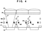
- Fig. 4 schematically shows a typical structure in which the first and second column signal lines 4A and 4B are arranged in the same wiring layer in a sectional structure along a cutline A - B in Fig. 3 .
- the photoelectric conversion portion 10 receives light entering a microlens 25 via a color filter 24.
- the pixel array 2 includes a first wiring layer M1, and a second wiring layer M2 arranged above it.
- the first wiring layer M1 can be, for example, a lowermost layer among a plurality of wiring layers.
- both the first and second column signal lines 4A and 4B are arranged in the first wiring layer M1.
- a conductive shield pattern (for example, the power supply wiring 5) is interposed between the first column signal line 4A and the second column signal line 4B.
- the first column signal line 4A, power supply wiring 5, and second column signal line 4B are spaced apart from each other at an inter-wiring distance W1 (for example, the critical dimension which can be decided by the manufacturing process).
- Another shield pattern (for example, the power supply wiring 6) is arranged in the second wiring layer M2.
- the power supply wiring 5 for VDD power and the power supply wiring 6 for ground (GND) can be used as these shield patterns, as in the embodiment, or wiring lines which receive other reference potentials may also be used.
- a solid line L1 indicates a range where the optical path of light entering the microlens 25 is not blocked by the first and second column signal lines 4A and 4B.
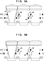
- Fig. 5A schematically shows a sectional structure along the cutline A - B when the embodiment is applied.
- the first wiring layer M1 includes the first column signal line 4A arranged at each column of the pixel array 2.
- the second wiring layer M2 includes the second column signal line 4B arranged at each column of the pixel array 2.
- At least the first wiring layer M1 out of the first wiring layer M1 and second wiring layer M2 preferably further includes a conductive shield pattern.
- the shield pattern (in this case, the power supply wiring 5) is arranged adjacent to the first column signal line 4A of the first wiring layer M1.
- the second column signal line 4B is arranged at a position shifted from a position immediately above the first column signal line 4A.
- the second wiring layer M2 also includes another shield pattern (in this case, the power supply wiring 6).
- This shield pattern is arranged adjacent to the second column signal line 4B.
- a solid line L2 shown in Fig. 5A indicates a range where the optical path of light entering the microlens 25 is not blocked by the second column signal line 4B and the shield pattern (power supply wiring 6).
- a broken line L1 shown in Fig. 5A is identical to the solid line L1 in the reference example ( Fig. 4 ).
- a comparison between L1 and L2 reveals that the photoelectric conversion portion 10 can receive a larger amount of light thanks to the wiring arrangement in the embodiment. This phenomenon stands out more in the peripheral region of the pixel array 2 than in the center region.
- a plurality of column signal lines are arranged in different wiring layers. This arrangement can reduce an area where the optical path is blocked, and suppress a decrease in the aperture ratio of the solid-state image sensor.
- crosstalk noise between column signal lines can be suppressed by shifting the position of the second column signal line 4B arranged in the second wiring layer M2 from a position immediately above the first column signal line arranged in the first wiring layer M1.
- shield patterns can be arranged above and below the column signal line and on the left and right sides of it.
- a shield pattern is arranged only on one side of the column signal line, or above or below it. The first embodiment can therefore suppress an image signal propagation delay arising from the wiring capacitance.
- Fig. 5B schematically shows an application example in which the wiring position is changed from that in the structure of Fig. 5A .
- the first column signal line 4A and the shield pattern (power supply wiring 5) in the first wiring layer M1 are arranged at a large distance W2 which nevertheless does not hamper the range (solid line L2) of the optical path shown in Fig. 5A .
- the distance W2 is decided within a range where the capacitance value difference between the wiring capacitance of the first column signal line 4A and that of the second column signal line 4B falls below a permissible value. This can further reduce, for example, generation of a short circuit between wiring lines in the wiring formation process, and increase the yield.
- a solid-state image sensor which constitutes an illustrative example which is not according to the present invention but useful for understanding, will be described with reference to Figs. 6 to 8 .
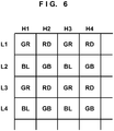
- the solid-state image sensor is obtained by applying color filters of the Bayer arrangement exemplified in Fig. 6 to the solid-state image sensor in the first embodiment.
- RD represents a pixel (red pixel) which detects red light
- BL represents a pixel (blue pixel) which detects blue light
- GR and GB represent pixels (green pixels) which detect green light
- H represents a column
- L represents a row.
- Fig. 7 is a block diagram for explaining the arrangement of the solid-state image sensor, similar to the first embodiment.
- a pixel 3RD which detects red light, a pixel 3BL which detects blue light, and pixels 3GR and 3GB which detect green light are illustrated in a pixel array 2.
- Pixel signal output portions 20 of the pixels 3GR and 3GB are connected to first column signal lines 4A.
- the pixel signal output portions 20 of the pixels 3RD and 3BL are connected to second column signal lines 4B.
- Fig. 8 is a plan view schematically showing the layout of 2 ⁇ 3 pixels 3RD, 3BL, 3GR, and 3GB in the pixel array 2 of the solid-state image sensor, similar to the first embodiment.
- a noise suppression circuit which can be included in a horizontal scanning circuit 8A can clamp in advance, as a noise level, an output obtained when the potential of a node 13 is reset in reading out a pixel signal from each of the pixels 3RD, 3BL, 3GR, and 3GB. Then, the difference between the readout signal and the noise level can be read out to suppress noise, and the resultant signal can be processed as a pixel signal. Since outputs from the pixels 3GR and 3GB undergo a signal process by the common horizontal scanning circuit 8A, noise levels arising from the horizontal scanning circuit 8A can be made uniform. In addition to the effects of the first embodiment, the second embodiment can single out a noise level arising from the horizontal scanning circuit 8A.
- FIG. 9 is a block diagram for explaining the arrangement of the solid-state image sensor, similar to the first and second embodiments.
- the third embodiment is different from the first and second embodiments in that four column signal lines 4A to 4D are arranged at each column of a pixel array 2. Further, color filters of the Bayer arrangement are applied, similar to the second embodiment.
- Pixel signal output portions 20 of a pixel 3GR on the first row and first column and a pixel 3GB on the second row and second column are connected to the column signal lines 4A.
- pixel signal output portions 20 of a pixel 3RD on the first row and second column and a pixel 3BL on the second row and first column are connected to the column signal lines 4B.
- the pixel signal output portions 20 of the pixel 3GR on the third row and first column and the pixel 3GB on the fourth row and second column are connected to the column signal lines 4C.
- the pixel signal output portions 20 of the pixel 3RD on the third row and second column and the pixel 3BL on the fourth row and first column are connected to the column signal lines 4D. This also applies to the remaining pixels.
- Fig. 10 is a plan view schematically showing the layout of 4 ⁇ 3 pixels 3RD, 3BL, 3GR, and 3GB in the pixel array 2 of the solid-state image sensor, similar to the first and second embodiments.
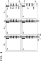
- Fig. 11 schematically shows a reference example of a sectional structure along a cutline C - D in Fig. 10 .
- a first wiring layer M1 includes the column signal lines 4A to 4D.
- a second wiring layer M2 includes shield patterns (for example, power supply wiring 5 and power supply wiring 6).
- Parasitic capacitance components which may be generated between adjacent wiring lines are shown on the right side of Fig. 11 . Note that a capacitive component (including a fringe capacitive component) between wiring lines adjacent to each other in the horizontal or vertical direction is illustrated. Another capacitive component (for example, between wiring lines positioned in a diagonal direction or wiring lines spaced apart by two or more layers) is small and is not illustrated.
- CL1 is a capacitive component which may be generated between wiring lines adjacent to each other in the first wiring layer M1.
- CH1 is a capacitive component which may be generated between the wiring layer of the first wiring layer M1 and that of the second wiring layer M2 immediately above it.
- each of capacitive components which may be generated in the column signal lines 4A and 4D is CL1.
- Each of capacitive components which may be generated in the column signal lines 4B and 4C is 2 ⁇ CL1 + CH1.
- the column signal lines may have a capacitance value difference (CL1 + CH1). This difference leads to a signal propagation delay difference in the column signal lines 4A to 4D, and the subsequent signal process is rate-determined by a column signal line having a large delay.
- adjacent column signal lines may generate signal crosstalk.
- Fig. 12A schematically shows a sectional structure along the cutline C - D when the embodiment is applied.
- At least the first wiring layer M1 out of the first wiring layer M1 and second wiring layer M2 further includes a conductive shield pattern (in this case, the power supply wiring 5).
- the first column signal line of the first wiring layer M1 includes at least two column signal lines (in this case, the column signal lines 4A and 4C).
- the shield pattern (power supply wiring 5) is interposed between the two column signal lines 4A and 4C.
- the second wiring layer M2 also includes two column signal lines (in this case, the column signal lines 4B and 4D), and another shield pattern (in this case, the power supply wiring 6) interposed between the two column signal lines 4B and 4D.
- Parasitic capacitance components which may be generated between adjacent wiring lines are schematically shown on the right side of Fig. 12A , similar to Fig. 11 .
- CL2 is a capacitive component which may be generated between wiring lines adjacent to each other in the first wiring layer M1.
- CL3 is a capacitive component which may be generated between wiring lines adjacent to each other in the second wiring layer M2.
- CH2 is a capacitive component which may be generated between the wiring layer of the first wiring layer M1 and that of the second wiring layer M2 immediately above it.
- the capacitive component which may be generated between the column signal lines 4A and 4C is CL2 + CH2.
- the capacitive component which may be generated between the column signal lines 4B and 4D, is CL3 + CH2.
- the difference between these capacitance values is
- signal propagation delay differences in the column signal lines 4A to 4D can be suppressed.
- column signal lines for propagating pixel signals of the same color are preferably arranged to be symmetrical about the shield pattern in the same wiring layer (for example, the column signal lines 4A and 4C or the column signal lines 4B and 4D).
- the capacitive component CH2 between different wiring layers is preferably smaller than each of the capacitive components CL2 and CL3 between adjacent wiring lines in the same wiring layers.
- a shield pattern may be further added to an immediately upper or lower wiring layer.
- a plurality of column signal lines are arranged in different wiring layers.
- This arrangement can reduce an area where the optical path is blocked, and suppress a decrease in the aperture ratio of the solid-state image sensor.
- the thickness of an interlayer dielectric film is larger than the distance (for example, the critical dimension which can be decided by the manufacturing process) between wiring lines adjacent to each other in the same wiring layer.
- the capacitance between wiring lines in different wiring layers becomes smaller than that between adjacent wiring lines in the same wiring layer, and crosstalk noise between column signal lines can be suppressed.
- shield patterns can be arranged above and below the column signal line and on the left and right sides of it.
- a shield pattern is arranged only on one side of the column signal line, or above or below it.
- the third embodiment can suppress even an image signal propagation delay arising from the wiring capacitance.
- Fig. 12B schematically shows an application example in which the wiring position is changed from that in the structure of Fig. 12A . That is, the column signal lines 4A and 4C and the shield pattern (power supply wiring 5) in the first wiring layer M1 are arranged at, for example, a distance W4 larger than W3. This can further reduce, for example, generation of a short circuit between wiring lines in the wiring formation process, and increase the yield while ensuring the light receiving amount of a photoelectric conversion portion 10.
- Parasitic capacitance components which may be generated between adjacent wiring lines are similarly shown on the right side of Fig. 12B .
- CL4 is a capacitive component which may be generated between wiring lines adjacent to each other in the first wiring layer M1.
- CL5 is a capacitive component which may be generated between wiring lines adjacent to each other in the second wiring layer M2.
- CH3 is a capacitive component which may be generated between the wiring layer of the first wiring layer M1 and that of the second wiring layer M2 immediately above it.
- the distance W4 is decided within, for example, a range where the difference
- the shield pattern (in this case, the power supply wiring 6) is arranged not in the second wiring layer M2 but in another wiring layer (for example, third wiring layer).
- parasitic capacitance components which may be generated between adjacent wiring lines are schematically shown on the right side of Fig. 12C .
- CL6 is a capacitive component which may be generated between wiring lines adjacent to each other in the first wiring layer M1.
- CL7 is a capacitive component which may be generated between wiring lines adjacent to each other in the second wiring layer M2.
- CH4 is a capacitive component which may be generated between the wiring layer of the first wiring layer M1 and that of the second wiring layer M2 immediately above it.
- the shield pattern may be arranged in another wiring layer (for example, third wiring layer).
- FIG. 13 is a block diagram for explaining the arrangement of the solid-state image sensor, similar to the third embodiment.
- the fourth embodiment is different from the third embodiment in that each unit pixel 3 includes two photoelectric conversion portions (photodiodes 10A and 10B). More specifically, light enters the photodiodes 10A and 10B via a microlens common to them. Signals read out from the photodiodes 10A and 10B contain focus detection signals, and can be used in a focus detection operation to be described later. As exemplified in Fig.
- each of the photodiodes 10A and 10B is connected to various transistors for reading out signals, including a transfer transistor 11.
- the unit pixels 3 will be referred to as divided pixels 3RD-A, 3BL-A, 3GR-A, 3GB-A, 3RD-B, 3BL-B, 3GR-B, and 3GB-B.
- a circuit arrangement including no selection transistor 18 is employed in Fig. 14
- a circuit arrangement including a selection transistor 18 may be adopted, as described in the first embodiment ( Fig. 2 ).
- Pixel signal output portions 20A of the divided pixel 3GR-A on the first row and first column and the divided pixel 3GB-A on the second row and second column are connected to column signal lines 4A.
- the pixel signal output portions 20A of the divided pixel 3RD-A on the first row and second column and the divided pixel 3BL-A on the second row and first column are connected to column signal lines 4B.
- Pixel signal output portions 20B of the divided pixel 3GB-B on the first row and first column and the divided pixel 3GR-B on the second row and second column are connected to column signal lines 4C.
- the pixel signal output portions 20B of the divided pixel 3RD-B on the first row and second column and the divided pixel 3BL-B on the second row and first column are connected to column signal lines 4D. This also applies to the remaining pixels.
- Fig. 15 is a plan view schematically showing the layout of 2 ⁇ 3 pixels 3 in a pixel array 2 of the solid-state image sensor, similar to the first to third embodiments.
- the column signal lines 4A to 4D are preferably arranged as in the fourth embodiment. Accordingly, the fourth embodiment can obtain the same effects as those of the first to third embodiments while maintaining the pixel signal reading speed of the pixel array 2.
- Figs. 18A and 18B show modification 1 to the fourth embodiment, which constitutes an embodiment according to the present invention.
- the same reference numerals as those in Figs. 13 to 15 denote portions having the same functions, and a detailed description thereof will not be repeated.
- Fig. 18A is a plan view schematically showing the layout of 2 ⁇ 3 pixels 3 in the pixel array 2 of the solid-state image sensor, similar to Fig. 15 .
- Fig. 18B schematically shows the sectional structure of a portion including the column signal line and power supply wiring. In this modification, as shown in Fig.
- signals in the divided pixels 3BL-A and 3BL-B are read out in the first wiring layer, and signals in the divided pixels 3GR-A and 3GR-B are read out in the second wiring layer.
- signals in the divided pixels 3RD-A and 3RD-B are read out in the first wiring layer, and signals in the divided pixels 3GB-A and 3GB-B are read out in the second wiring layer.
- Fig. 19 shows modification 2, similar to Figs. 18A and 18B , which constitutes an illustrative example which is not according to the present invention but useful for understanding.
- the difference of modification 2 from modification 1 is the layout of column signal lines. Column signal lines are interposed not between divided pixels, but between adjacent pixels. Further, column signal lines for transferring signals of the same color are distributed to different wiring layers, and arranged close to each other. This layout can reduce the influence of color mixing in the column signal lines because close column signal lines transfer signals of the same color.
- Fig. 20 shows modification 3, similar to Figs. 18A and 18B , which constitutes an illustrative example which is not according to the present invention but useful for understanding.
- the difference of modification 3 from modification 2 is the layout of column signal lines.
- column signal lines for transferring signals from the divided pixels 3GR-A, 3GR-B, 3GB-A, and 3GB-B are arranged close to each other using two layers. This layout can reduce the influence of color mixing for signals of green pixels in the column signal lines.
- Fig. 16 is a view schematically showing a state in which a beam emerging from an exit pupil 902 of a photographing lens 900 enters a solid-state image sensor 901.
- the solid-state image sensor 901 includes a microlens 202, a color filter 301, and two photoelectric conversion portions PD1 and PD2 for each unit pixel.
- Light having passed through the exit pupil 902 enters the solid-state image sensor 901 using an optical axis 903 as the center.
- Reference numerals 906 and 907 denote rays at the outermost periphery of light passing through a partial region 904 of the exit pupil 902.
- Reference numerals 908 and 909 denote rays at the outermost periphery of light passing through another partial region 905 of the exit pupil 902.
- those illustrated above the optical axis 903 enter the photoelectric conversion portion PD1, and those illustrated below it enter the photoelectric conversion portion PD2.
- the photoelectric conversion portions PD1 and PD2 receive beams having passed through different regions of the exit pupil 902 of the photographing lens 900.
- signals output from the photoelectric conversion portions PD1 upon receiving light in respective pixels on one column of the pixel array will be defined as the first line data.
- signals output from the photoelectric conversion portions PD2 will be defined as the second line data.
- a processor (not shown) which performs the focus detection operation determines whether an image is in focus.
- Fig. 17A shows line data in an in-focus state when a point light source is formed into an image.
- Fig. 17B shows line data in an out-of-focus state.
- the abscissa represents the position of each pixel, and the ordinate represents the output value of each pixel.
- the processor can calculate, from a shift amount 1001 between these outputs, a distance by which the lens position is moved to focus on the image.
- the focus detection operation may be executed by the above-described processor.
- an arithmetic unit configured to execute the focus detection operation may be included in the solid-state image sensor, as needed.
- a larger difference of the incident light amount may be generated between the photoelectric conversion portions PD1 and PD2 of each pixel in the peripheral region of the pixel array than in the center region.
- focus detection pixels are preferably arranged in the peripheral region of the pixel array.
- signals output from the two photoelectric conversion portions PD1 and PD2 are separately read out and used for focus detection.
- the signals output from the photoelectric conversion portions PD1 and PD2 in response to light entering each pixel 3 are added, obtaining the pixel signal of the pixel 3.
- a sequence to determine that the reliability of the signal is poor, and not to perform phase detection or to stop it can be adopted. In this way, the above operation may be controlled in accordance with the states (charge amounts and signals) of the photoelectric conversion portions PD1 and PD2.
- the present invention is not limited to them.
- the purpose, state, application, function, and other specifications can be properly changed, and the present invention can be practiced by another embodiment, as a matter of course.
- the arrangement of the column signal lines 4A to 4D is not limited to these embodiments.
- the column signal lines 4A and 4C may be arranged in the second wiring layer M2, and the column signal lines 4B and 4D may be arranged in the first wiring layer M1.
- the power supply wiring 5 for VDD power and the power supply wiring 6 for ground (GND) are used for the conductive shield patterns in each of the above embodiments, but wiring lines for another application may be used.
- Color filters of the Bayer arrangement are used in each of the above embodiments, but color filters of another array may be used or color filters may be implemented by monochrome sensors.
- the pixel array 2 has been described as a CMOS image sensor in each of the above embodiments, but may be another sensor. All or part of the operation of each functional block in each of the above embodiments may be controlled by an OS or the like running on a computer, together with or instead of the computer.
- a solid-state image sensor incorporated in a camera has been described.
- the concept of the camera includes not only an apparatus mainly for shooting, but also an apparatus accessorily having the a shooting function (for example, a personal computer or a mobile terminal).
- the camera can include the solid-state image sensor according to the present invention which has been exemplified in the embodiments, and a processor which processes a signal output from the solid-state image sensor.
- the processor can include, for example, an A/D converter, and a processor which processes digital data output from the A/D converter.
- a solid-state image sensor comprising a pixel array (2) in which a plurality of pixels (3) are arrayed in a matrix having a plurality of rows and a plurality of columns, wherein the pixel array includes a first wiring layer (M1) and a second wiring layer (M2) arranged above the first wiring layer, the first wiring layer includes first column signal lines (4A) arranged at the respective columns of the pixel array, and the second wiring layer includes second column signal lines (4B) arranged at the respective columns of the pixel array.
- M1 first wiring layer
- M2 second wiring layer
- a further example useful for understanding the present invention concerns a solid-state image sensor comprising a pixel array (2) in which a plurality of pixels (3) are arrayed in a matrix having a plurality of rows and a plurality of columns, wherein the pixel array includes a first wiring layer (M1) and a second wiring layer (M2) arranged above the first wiring layer, the first wiring layer includes first column signal lines (4A) arranged at the respective columns of the pixel array, and the second wiring layer includes second column signal lines (4B) arranged at the respective columns of the pixel array.
- M1 first wiring layer
- M2 second wiring layer
Landscapes
- Engineering & Computer Science (AREA)
- Multimedia (AREA)
- Signal Processing (AREA)
- Physics & Mathematics (AREA)
- General Physics & Mathematics (AREA)
- Theoretical Computer Science (AREA)
- Solid State Image Pick-Up Elements (AREA)
- Transforming Light Signals Into Electric Signals (AREA)
- Internal Circuitry In Semiconductor Integrated Circuit Devices (AREA)
Applications Claiming Priority (2)
| Application Number | Priority Date | Filing Date | Title |
|---|---|---|---|
| JP2012008447 | 2012-01-18 | ||
| JP2012281754A JP6053505B2 (ja) | 2012-01-18 | 2012-12-25 | 固体撮像装置 |
Publications (3)
| Publication Number | Publication Date |
|---|---|
| EP2618376A2 EP2618376A2 (en) | 2013-07-24 |
| EP2618376A3 EP2618376A3 (en) | 2014-10-22 |
| EP2618376B1 true EP2618376B1 (en) | 2021-08-25 |
Family
ID=47561385
Family Applications (1)
| Application Number | Title | Priority Date | Filing Date |
|---|---|---|---|
| EP13151168.5A Active EP2618376B1 (en) | 2012-01-18 | 2013-01-14 | Solid-state image sensor |
Country Status (5)
| Country | Link |
|---|---|
| US (2) | US9153610B2 (enExample) |
| EP (1) | EP2618376B1 (enExample) |
| JP (1) | JP6053505B2 (enExample) |
| CN (1) | CN103220475B (enExample) |
| RU (1) | RU2546137C2 (enExample) |
Families Citing this family (74)
| Publication number | Priority date | Publication date | Assignee | Title |
|---|---|---|---|---|
| JP6053505B2 (ja) * | 2012-01-18 | 2016-12-27 | キヤノン株式会社 | 固体撮像装置 |
| JP5967944B2 (ja) | 2012-01-18 | 2016-08-10 | キヤノン株式会社 | 固体撮像装置およびカメラ |
| WO2014002366A1 (ja) * | 2012-06-27 | 2014-01-03 | パナソニック株式会社 | 固体撮像装置 |
| JP5923061B2 (ja) | 2013-06-20 | 2016-05-24 | キヤノン株式会社 | 固体撮像装置 |
| JP2015015596A (ja) | 2013-07-04 | 2015-01-22 | キヤノン株式会社 | 撮像装置及びその駆動方法 |
| JP6287058B2 (ja) * | 2013-10-24 | 2018-03-07 | 株式会社リコー | 縮小光学系用の光電変換素子、画像読取装置、画像形成装置及び画像読取方法 |
| JP2017004985A (ja) * | 2013-11-08 | 2017-01-05 | パナソニックIpマネジメント株式会社 | 固体撮像装置 |
| JP6216229B2 (ja) | 2013-11-20 | 2017-10-18 | キヤノン株式会社 | 撮像素子及び撮像システム |
| JP6261361B2 (ja) | 2014-02-04 | 2018-01-17 | キヤノン株式会社 | 固体撮像装置およびカメラ |
| JP6741343B2 (ja) | 2014-03-07 | 2020-08-19 | リキュリウム アイピー ホールディングス リミテッド ライアビリティー カンパニー | プロペラン誘導体および合成 |
| JP6274567B2 (ja) | 2014-03-14 | 2018-02-07 | キヤノン株式会社 | 固体撮像装置及び撮像システム |
| JP6595750B2 (ja) | 2014-03-14 | 2019-10-23 | キヤノン株式会社 | 固体撮像装置及び撮像システム |
| JP2015185823A (ja) * | 2014-03-26 | 2015-10-22 | ソニー株式会社 | 固体撮像素子、及び、撮像装置 |
| JP6541347B2 (ja) | 2014-03-27 | 2019-07-10 | キヤノン株式会社 | 固体撮像装置および撮像システム |
| JP6305169B2 (ja) * | 2014-04-07 | 2018-04-04 | キヤノン株式会社 | 固体撮像素子、撮像装置及びその制御方法、プログラム、記憶媒体 |
| JP6393070B2 (ja) * | 2014-04-22 | 2018-09-19 | キヤノン株式会社 | 固体撮像装置、その製造方法およびカメラ |
| JP2016012905A (ja) | 2014-06-02 | 2016-01-21 | ソニー株式会社 | 撮像素子、撮像方法、および電子機器 |
| KR102419715B1 (ko) * | 2014-06-09 | 2022-07-13 | 가부시키가이샤 한도오따이 에네루기 켄큐쇼 | 촬상 장치 |
| JP6549366B2 (ja) | 2014-09-19 | 2019-07-24 | 株式会社リコー | 光電変換素子、画像読取装置及び画像形成装置 |
| JP6587497B2 (ja) * | 2014-10-31 | 2019-10-09 | 株式会社半導体エネルギー研究所 | 半導体装置 |
| JP6417197B2 (ja) | 2014-11-27 | 2018-10-31 | キヤノン株式会社 | 固体撮像装置 |
| KR102499585B1 (ko) | 2015-01-13 | 2023-02-14 | 소니 세미컨덕터 솔루션즈 가부시키가이샤 | 고체 촬상 소자 및 그 제조 방법, 및 전자 기기 |
| JP6579774B2 (ja) | 2015-03-30 | 2019-09-25 | キヤノン株式会社 | 固体撮像装置およびカメラ |
| US9768213B2 (en) | 2015-06-03 | 2017-09-19 | Canon Kabushiki Kaisha | Solid-state image sensor and camera |
| JP6632242B2 (ja) | 2015-07-27 | 2020-01-22 | キヤノン株式会社 | 撮像装置及び撮像システム |
| JP6570384B2 (ja) | 2015-09-11 | 2019-09-04 | キヤノン株式会社 | 撮像装置及び撮像システム |
| US10205894B2 (en) | 2015-09-11 | 2019-02-12 | Canon Kabushiki Kaisha | Imaging device and imaging system |
| JP6541523B2 (ja) | 2015-09-11 | 2019-07-10 | キヤノン株式会社 | 撮像装置、撮像システム、および、撮像装置の制御方法 |
| JP6244499B2 (ja) * | 2015-12-25 | 2017-12-06 | 太陽誘電株式会社 | プリント配線板、及びカメラモジュール |
| JP2017118378A (ja) * | 2015-12-25 | 2017-06-29 | セイコーエプソン株式会社 | 画像読取装置及び半導体装置 |
| CN118281017A (zh) * | 2015-12-25 | 2024-07-02 | 株式会社尼康 | 拍摄装置 |
| KR102486651B1 (ko) | 2016-03-03 | 2023-01-11 | 삼성전자주식회사 | 이미지 센서 |
| JP6579259B2 (ja) * | 2016-03-10 | 2019-09-25 | 株式会社リコー | 光電変換装置 |
| JP6774207B2 (ja) * | 2016-04-08 | 2020-10-21 | キヤノン株式会社 | 撮像素子及び撮像装置 |
| CN111741200B (zh) | 2016-04-08 | 2021-12-21 | 佳能株式会社 | 图像传感器和摄像设备 |
| CN105914216B (zh) * | 2016-05-05 | 2019-01-18 | 上海集成电路研发中心有限公司 | 一种图像传感器结构及其制作方法 |
| JP6688165B2 (ja) | 2016-06-10 | 2020-04-28 | キヤノン株式会社 | 撮像装置及び撮像システム |
| JP6727938B2 (ja) | 2016-06-10 | 2020-07-22 | キヤノン株式会社 | 撮像装置、撮像装置の制御方法、及び撮像システム |
| JP6776011B2 (ja) | 2016-06-10 | 2020-10-28 | キヤノン株式会社 | 撮像装置及び撮像システム |
| JP2019153822A (ja) | 2016-07-13 | 2019-09-12 | ソニーセミコンダクタソリューションズ株式会社 | 固体撮像素子、及び、固体撮像素子の制御方法 |
| JP7013119B2 (ja) | 2016-07-21 | 2022-01-31 | キヤノン株式会社 | 固体撮像素子、固体撮像素子の製造方法、及び撮像システム |
| WO2018027027A1 (en) | 2016-08-04 | 2018-02-08 | The Vollrath Company, L.L.C. | Wireless temperature probe |
| US11134321B2 (en) | 2016-08-04 | 2021-09-28 | The Vollrath Company, L.L.C. | Wireless temperature probe |
| JP6832649B2 (ja) * | 2016-08-17 | 2021-02-24 | ブリルニクス インク | 固体撮像装置、固体撮像装置の駆動方法、および電子機器 |
| JP2018092976A (ja) | 2016-11-30 | 2018-06-14 | キヤノン株式会社 | 撮像装置 |
| JP6957157B2 (ja) | 2017-01-26 | 2021-11-02 | キヤノン株式会社 | 固体撮像装置、撮像システム、および固体撮像装置の製造方法 |
| JP6701108B2 (ja) | 2017-03-21 | 2020-05-27 | キヤノン株式会社 | 固体撮像装置及び撮像システム |
| JP6929114B2 (ja) | 2017-04-24 | 2021-09-01 | キヤノン株式会社 | 光電変換装置及び撮像システム |
| JP6949557B2 (ja) * | 2017-05-25 | 2021-10-13 | キヤノン株式会社 | 撮像装置、撮像システム、移動体 |
| US10818715B2 (en) | 2017-06-26 | 2020-10-27 | Canon Kabushiki Kaisha | Solid state imaging device and manufacturing method thereof |
| JP6987562B2 (ja) | 2017-07-28 | 2022-01-05 | キヤノン株式会社 | 固体撮像素子 |
| WO2019066056A1 (ja) * | 2017-09-29 | 2019-04-04 | 株式会社ニコン | 撮像素子および撮像装置 |
| JP6953263B2 (ja) * | 2017-10-05 | 2021-10-27 | キヤノン株式会社 | 固体撮像装置および撮像システム |
| JP7023684B2 (ja) * | 2017-11-30 | 2022-02-22 | キヤノン株式会社 | 撮像装置、撮像システム、移動体 |
| US11153514B2 (en) * | 2017-11-30 | 2021-10-19 | Brillnics Singapore Pte. Ltd. | Solid-state imaging device, method for driving solid-state imaging device, and electronic apparatus |
| JP7023685B2 (ja) | 2017-11-30 | 2022-02-22 | キヤノン株式会社 | 撮像装置、撮像システム、移動体 |
| JP7091080B2 (ja) | 2018-02-05 | 2022-06-27 | キヤノン株式会社 | 装置、システム、および移動体 |
| JP6489247B2 (ja) * | 2018-02-06 | 2019-03-27 | 株式会社リコー | 光電変換素子、画像読取装置、画像形成装置及び画像読取方法 |
| JP7161317B2 (ja) | 2018-06-14 | 2022-10-26 | キヤノン株式会社 | 撮像装置、撮像システム及び移動体 |
| JP2020004888A (ja) * | 2018-06-29 | 2020-01-09 | ソニーセミコンダクタソリューションズ株式会社 | 撮像素子、撮像装置、及び、電子機器 |
| JP7245014B2 (ja) | 2018-09-10 | 2023-03-23 | キヤノン株式会社 | 固体撮像装置、撮像システム、および固体撮像装置の駆動方法 |
| JP7245016B2 (ja) | 2018-09-21 | 2023-03-23 | キヤノン株式会社 | 光電変換装置および撮像システム |
| JP7353752B2 (ja) | 2018-12-06 | 2023-10-02 | キヤノン株式会社 | 光電変換装置及び撮像システム |
| JP7292868B2 (ja) | 2018-12-18 | 2023-06-19 | キヤノン株式会社 | 検出器 |
| JP2020113573A (ja) * | 2019-01-08 | 2020-07-27 | キヤノン株式会社 | 光電変換装置 |
| JP7237622B2 (ja) | 2019-02-05 | 2023-03-13 | キヤノン株式会社 | 光電変換装置 |
| US10819936B2 (en) * | 2019-02-13 | 2020-10-27 | Omnivision Technologies, Inc. | Bias circuit for use with divided bit lines |
| JP6699772B2 (ja) * | 2019-02-28 | 2020-05-27 | 株式会社リコー | 光電変換素子、画像読取装置、画像形成装置及び画像読取方法 |
| US11515437B2 (en) * | 2019-12-04 | 2022-11-29 | Omnivision Technologies, Inc. | Light sensing system and light sensor with polarizer |
| JP7467380B2 (ja) * | 2021-03-18 | 2024-04-15 | 株式会社東芝 | 固体撮像装置 |
| US11619857B2 (en) | 2021-05-25 | 2023-04-04 | Apple Inc. | Electrically-tunable optical filter |
| JP7753044B2 (ja) | 2021-10-20 | 2025-10-14 | キヤノン株式会社 | 光電変換装置 |
| US12114089B2 (en) | 2022-08-19 | 2024-10-08 | Apple Inc. | Pixel output parasitic capacitance reduction and predictive settling assist |
| JP2024146291A (ja) * | 2023-03-31 | 2024-10-15 | キヤノン株式会社 | 光電変換装置、光電変換システムおよび移動体 |
Family Cites Families (44)
| Publication number | Priority date | Publication date | Assignee | Title |
|---|---|---|---|---|
| DE3615342A1 (de) * | 1985-05-08 | 1986-11-13 | Fuji Photo Film Co., Ltd., Minami-Ashigara, Kanagawa | Farbbildsensor |
| EP1152471A3 (en) * | 2000-04-28 | 2004-04-07 | Eastman Kodak Company | Image sensor pixel for configurable output |
| JP4050906B2 (ja) * | 2002-01-25 | 2008-02-20 | 富士フイルム株式会社 | 固体撮像装置 |
| JP4508619B2 (ja) | 2003-12-03 | 2010-07-21 | キヤノン株式会社 | 固体撮像装置の製造方法 |
| JP3793202B2 (ja) | 2004-02-02 | 2006-07-05 | キヤノン株式会社 | 固体撮像装置 |
| JP3890333B2 (ja) | 2004-02-06 | 2007-03-07 | キヤノン株式会社 | 固体撮像装置 |
| JP4067054B2 (ja) * | 2004-02-13 | 2008-03-26 | キヤノン株式会社 | 固体撮像装置および撮像システム |
| JP4979893B2 (ja) * | 2005-03-23 | 2012-07-18 | ソニー株式会社 | 物理量分布検知装置並びに物理情報取得方法および物理情報取得装置 |
| WO2007077286A1 (en) * | 2006-01-05 | 2007-07-12 | Artto Aurola | Semiconductor radiation detector detecting visible light |
| JP2007208817A (ja) * | 2006-02-03 | 2007-08-16 | Toshiba Corp | 固体撮像装置 |
| KR20070093335A (ko) | 2006-03-13 | 2007-09-18 | 마쯔시다덴기산교 가부시키가이샤 | 고체 촬상장치 및 그 구동방법 |
| JP2007243094A (ja) * | 2006-03-13 | 2007-09-20 | Matsushita Electric Ind Co Ltd | 固体撮像装置 |
| JP4818018B2 (ja) | 2006-08-01 | 2011-11-16 | キヤノン株式会社 | 光電変換装置及びそれを用いた撮像システム |
| JP5132102B2 (ja) | 2006-08-01 | 2013-01-30 | キヤノン株式会社 | 光電変換装置および光電変換装置を用いた撮像システム |
| JP2008192648A (ja) * | 2007-01-31 | 2008-08-21 | Sanyo Electric Co Ltd | 撮像装置 |
| JP2008282961A (ja) * | 2007-05-10 | 2008-11-20 | Matsushita Electric Ind Co Ltd | 固体撮像装置 |
| JP5040458B2 (ja) * | 2007-06-16 | 2012-10-03 | 株式会社ニコン | 固体撮像素子及びこれを用いた撮像装置 |
| JP5142696B2 (ja) | 2007-12-20 | 2013-02-13 | キヤノン株式会社 | 光電変換装置、及び光電変換装置を用いた撮像システム |
| JP5106092B2 (ja) * | 2007-12-26 | 2012-12-26 | パナソニック株式会社 | 固体撮像装置およびカメラ |
| JP5215681B2 (ja) | 2008-01-28 | 2013-06-19 | キヤノン株式会社 | 撮像装置及び撮像システム |
| JP5173493B2 (ja) | 2008-02-29 | 2013-04-03 | キヤノン株式会社 | 撮像装置及び撮像システム |
| JP5213501B2 (ja) | 2008-04-09 | 2013-06-19 | キヤノン株式会社 | 固体撮像装置 |
| JP4759590B2 (ja) | 2008-05-09 | 2011-08-31 | キヤノン株式会社 | 光電変換装置及びそれを用いた撮像システム |
| JP5279352B2 (ja) | 2008-06-06 | 2013-09-04 | キヤノン株式会社 | 固体撮像装置 |
| JP2010010896A (ja) * | 2008-06-25 | 2010-01-14 | Panasonic Corp | 固体撮像装置 |
| JP5274166B2 (ja) | 2008-09-10 | 2013-08-28 | キヤノン株式会社 | 光電変換装置及び撮像システム |
| JP5465244B2 (ja) * | 2008-11-27 | 2014-04-09 | キヤノン株式会社 | 固体撮像素子及び撮像装置 |
| JP4743294B2 (ja) * | 2009-02-17 | 2011-08-10 | 株式会社ニコン | 裏面照射型撮像素子および撮像装置 |
| KR101094246B1 (ko) * | 2009-03-16 | 2011-12-19 | 이재웅 | 넓은 동적범위를 갖는 씨모스 이미지 센서 |
| JP5493448B2 (ja) | 2009-04-21 | 2014-05-14 | ソニー株式会社 | 固体撮像装置および撮像装置 |
| JP5233828B2 (ja) * | 2009-05-11 | 2013-07-10 | ソニー株式会社 | 固体撮像装置、固体撮像装置の駆動方法および電子機器 |
| JP2010268080A (ja) | 2009-05-12 | 2010-11-25 | Canon Inc | 固体撮像装置 |
| JP5511220B2 (ja) * | 2009-05-19 | 2014-06-04 | キヤノン株式会社 | 固体撮像装置 |
| JP5539105B2 (ja) | 2009-09-24 | 2014-07-02 | キヤノン株式会社 | 光電変換装置およびそれを用いた撮像システム |
| JP4881987B2 (ja) * | 2009-10-06 | 2012-02-22 | キヤノン株式会社 | 固体撮像装置および撮像装置 |
| JP2011114843A (ja) * | 2009-11-30 | 2011-06-09 | Toshiba Corp | 固体撮像装置 |
| JP5232189B2 (ja) * | 2010-03-11 | 2013-07-10 | 株式会社東芝 | 固体撮像装置 |
| JP5025746B2 (ja) * | 2010-03-19 | 2012-09-12 | 株式会社東芝 | 固体撮像装置 |
| JP5631050B2 (ja) | 2010-05-10 | 2014-11-26 | キヤノン株式会社 | 固体撮像装置およびカメラ |
| JP5716347B2 (ja) * | 2010-10-21 | 2015-05-13 | ソニー株式会社 | 固体撮像装置及び電子機器 |
| JP2012199301A (ja) * | 2011-03-18 | 2012-10-18 | Panasonic Corp | 固体撮像装置 |
| JP5864990B2 (ja) * | 2011-10-03 | 2016-02-17 | キヤノン株式会社 | 固体撮像装置およびカメラ |
| JP5979882B2 (ja) | 2012-01-13 | 2016-08-31 | キヤノン株式会社 | 固体撮像装置 |
| JP6053505B2 (ja) * | 2012-01-18 | 2016-12-27 | キヤノン株式会社 | 固体撮像装置 |
-
2012
- 2012-12-25 JP JP2012281754A patent/JP6053505B2/ja active Active
-
2013
- 2013-01-14 US US13/741,228 patent/US9153610B2/en active Active
- 2013-01-14 EP EP13151168.5A patent/EP2618376B1/en active Active
- 2013-01-17 RU RU2013102310/07A patent/RU2546137C2/ru active
- 2013-01-18 CN CN201310018720.6A patent/CN103220475B/zh active Active
-
2015
- 2015-08-03 US US14/816,372 patent/US9445026B2/en active Active
Non-Patent Citations (1)
| Title |
|---|
| None * |
Also Published As
| Publication number | Publication date |
|---|---|
| CN103220475A (zh) | 2013-07-24 |
| JP2013168634A (ja) | 2013-08-29 |
| RU2013102310A (ru) | 2014-07-27 |
| US9153610B2 (en) | 2015-10-06 |
| RU2546137C2 (ru) | 2015-04-10 |
| US9445026B2 (en) | 2016-09-13 |
| EP2618376A2 (en) | 2013-07-24 |
| US20130182163A1 (en) | 2013-07-18 |
| CN103220475B (zh) | 2016-12-07 |
| JP6053505B2 (ja) | 2016-12-27 |
| EP2618376A3 (en) | 2014-10-22 |
| US20150341579A1 (en) | 2015-11-26 |
Similar Documents
| Publication | Publication Date | Title |
|---|---|---|
| EP2618376B1 (en) | Solid-state image sensor | |
| JP5864990B2 (ja) | 固体撮像装置およびカメラ | |
| JP2024038309A (ja) | 撮像素子 | |
| JP5004775B2 (ja) | 撮像装置及び撮像システム | |
| KR101691660B1 (ko) | 촬상 장치 | |
| JP5744545B2 (ja) | 固体撮像装置およびカメラ | |
| US8111311B2 (en) | Image sensing device and image sensing system | |
| US20230111474A1 (en) | Image sensor and image capturing device | |
| JP5629995B2 (ja) | 撮像素子および撮像装置 | |
| US11165979B2 (en) | Imaging device including semiconductor substrate and pixels | |
| JP6704677B2 (ja) | 固体撮像装置 | |
| JP7751557B2 (ja) | 撮像素子及び撮像装置 | |
| US20070201114A1 (en) | Solid-state image sensing device having photoelectric conversion cells each configured by n pixels in vertical direction | |
| JP6526115B2 (ja) | 固体撮像装置 | |
| JP2023104684A (ja) | 撮像素子及び撮像装置 | |
| JP6178835B2 (ja) | 固体撮像装置およびカメラ | |
| JP2015180077A (ja) | 固体撮像装置およびカメラ | |
| US20240171879A1 (en) | Image sensor and image capturing apparatus | |
| KR20250120090A (ko) | 이미지 센싱 장치 | |
| CN119318224A (zh) | 图像传感器和摄像设备 | |
| WO2023013261A1 (ja) | 固体撮像素子および電子機器 |
Legal Events
| Date | Code | Title | Description |
|---|---|---|---|
| PUAI | Public reference made under article 153(3) epc to a published international application that has entered the european phase |
Free format text: ORIGINAL CODE: 0009012 |
|
| AK | Designated contracting states |
Kind code of ref document: A2 Designated state(s): AL AT BE BG CH CY CZ DE DK EE ES FI FR GB GR HR HU IE IS IT LI LT LU LV MC MK MT NL NO PL PT RO RS SE SI SK SM TR |
|
| AX | Request for extension of the european patent |
Extension state: BA ME |
|
| RIC1 | Information provided on ipc code assigned before grant |
Ipc: H04N 5/335 20110101ALI20140516BHEP Ipc: H01L 27/146 20060101AFI20140516BHEP |
|
| PUAL | Search report despatched |
Free format text: ORIGINAL CODE: 0009013 |
|
| AK | Designated contracting states |
Kind code of ref document: A3 Designated state(s): AL AT BE BG CH CY CZ DE DK EE ES FI FR GB GR HR HU IE IS IT LI LT LU LV MC MK MT NL NO PL PT RO RS SE SI SK SM TR |
|
| AX | Request for extension of the european patent |
Extension state: BA ME |
|
| RIC1 | Information provided on ipc code assigned before grant |
Ipc: H04N 5/335 20110101ALI20140917BHEP Ipc: H01L 27/146 20060101AFI20140917BHEP |
|
| 17P | Request for examination filed |
Effective date: 20150422 |
|
| RBV | Designated contracting states (corrected) |
Designated state(s): AL AT BE BG CH CY CZ DE DK EE ES FI FR GB GR HR HU IE IS IT LI LT LU LV MC MK MT NL NO PL PT RO RS SE SI SK SM TR |
|
| 17Q | First examination report despatched |
Effective date: 20150803 |
|
| STAA | Information on the status of an ep patent application or granted ep patent |
Free format text: STATUS: EXAMINATION IS IN PROGRESS |
|
| GRAP | Despatch of communication of intention to grant a patent |
Free format text: ORIGINAL CODE: EPIDOSNIGR1 |
|
| STAA | Information on the status of an ep patent application or granted ep patent |
Free format text: STATUS: GRANT OF PATENT IS INTENDED |
|
| INTG | Intention to grant announced |
Effective date: 20210316 |
|
| RIN1 | Information on inventor provided before grant (corrected) |
Inventor name: ONO, TOSHIAKI Inventor name: TAKADA, HIDEAKI Inventor name: KOBAYASHI, MASAHIRO |
|
| GRAS | Grant fee paid |
Free format text: ORIGINAL CODE: EPIDOSNIGR3 |
|
| GRAA | (expected) grant |
Free format text: ORIGINAL CODE: 0009210 |
|
| STAA | Information on the status of an ep patent application or granted ep patent |
Free format text: STATUS: THE PATENT HAS BEEN GRANTED |
|
| AK | Designated contracting states |
Kind code of ref document: B1 Designated state(s): AL AT BE BG CH CY CZ DE DK EE ES FI FR GB GR HR HU IE IS IT LI LT LU LV MC MK MT NL NO PL PT RO RS SE SI SK SM TR |
|
| REG | Reference to a national code |
Ref country code: GB Ref legal event code: FG4D |
|
| REG | Reference to a national code |
Ref country code: CH Ref legal event code: EP |
|
| REG | Reference to a national code |
Ref country code: IE Ref legal event code: FG4D Ref country code: AT Ref legal event code: REF Ref document number: 1424687 Country of ref document: AT Kind code of ref document: T Effective date: 20210915 |
|
| REG | Reference to a national code |
Ref country code: DE Ref legal event code: R096 Ref document number: 602013078921 Country of ref document: DE |
|
| REG | Reference to a national code |
Ref country code: LT Ref legal event code: MG9D |
|
| REG | Reference to a national code |
Ref country code: NL Ref legal event code: MP Effective date: 20210825 |
|
| REG | Reference to a national code |
Ref country code: AT Ref legal event code: MK05 Ref document number: 1424687 Country of ref document: AT Kind code of ref document: T Effective date: 20210825 |
|
| PG25 | Lapsed in a contracting state [announced via postgrant information from national office to epo] |
Ref country code: HR Free format text: LAPSE BECAUSE OF FAILURE TO SUBMIT A TRANSLATION OF THE DESCRIPTION OR TO PAY THE FEE WITHIN THE PRESCRIBED TIME-LIMIT Effective date: 20210825 Ref country code: SE Free format text: LAPSE BECAUSE OF FAILURE TO SUBMIT A TRANSLATION OF THE DESCRIPTION OR TO PAY THE FEE WITHIN THE PRESCRIBED TIME-LIMIT Effective date: 20210825 Ref country code: FI Free format text: LAPSE BECAUSE OF FAILURE TO SUBMIT A TRANSLATION OF THE DESCRIPTION OR TO PAY THE FEE WITHIN THE PRESCRIBED TIME-LIMIT Effective date: 20210825 Ref country code: ES Free format text: LAPSE BECAUSE OF FAILURE TO SUBMIT A TRANSLATION OF THE DESCRIPTION OR TO PAY THE FEE WITHIN THE PRESCRIBED TIME-LIMIT Effective date: 20210825 Ref country code: RS Free format text: LAPSE BECAUSE OF FAILURE TO SUBMIT A TRANSLATION OF THE DESCRIPTION OR TO PAY THE FEE WITHIN THE PRESCRIBED TIME-LIMIT Effective date: 20210825 Ref country code: NO Free format text: LAPSE BECAUSE OF FAILURE TO SUBMIT A TRANSLATION OF THE DESCRIPTION OR TO PAY THE FEE WITHIN THE PRESCRIBED TIME-LIMIT Effective date: 20211125 Ref country code: PT Free format text: LAPSE BECAUSE OF FAILURE TO SUBMIT A TRANSLATION OF THE DESCRIPTION OR TO PAY THE FEE WITHIN THE PRESCRIBED TIME-LIMIT Effective date: 20211227 Ref country code: BG Free format text: LAPSE BECAUSE OF FAILURE TO SUBMIT A TRANSLATION OF THE DESCRIPTION OR TO PAY THE FEE WITHIN THE PRESCRIBED TIME-LIMIT Effective date: 20211125 Ref country code: AT Free format text: LAPSE BECAUSE OF FAILURE TO SUBMIT A TRANSLATION OF THE DESCRIPTION OR TO PAY THE FEE WITHIN THE PRESCRIBED TIME-LIMIT Effective date: 20210825 Ref country code: LT Free format text: LAPSE BECAUSE OF FAILURE TO SUBMIT A TRANSLATION OF THE DESCRIPTION OR TO PAY THE FEE WITHIN THE PRESCRIBED TIME-LIMIT Effective date: 20210825 |
|
| PG25 | Lapsed in a contracting state [announced via postgrant information from national office to epo] |
Ref country code: PL Free format text: LAPSE BECAUSE OF FAILURE TO SUBMIT A TRANSLATION OF THE DESCRIPTION OR TO PAY THE FEE WITHIN THE PRESCRIBED TIME-LIMIT Effective date: 20210825 Ref country code: LV Free format text: LAPSE BECAUSE OF FAILURE TO SUBMIT A TRANSLATION OF THE DESCRIPTION OR TO PAY THE FEE WITHIN THE PRESCRIBED TIME-LIMIT Effective date: 20210825 Ref country code: GR Free format text: LAPSE BECAUSE OF FAILURE TO SUBMIT A TRANSLATION OF THE DESCRIPTION OR TO PAY THE FEE WITHIN THE PRESCRIBED TIME-LIMIT Effective date: 20211126 |
|
| PG25 | Lapsed in a contracting state [announced via postgrant information from national office to epo] |
Ref country code: NL Free format text: LAPSE BECAUSE OF FAILURE TO SUBMIT A TRANSLATION OF THE DESCRIPTION OR TO PAY THE FEE WITHIN THE PRESCRIBED TIME-LIMIT Effective date: 20210825 |
|
| PG25 | Lapsed in a contracting state [announced via postgrant information from national office to epo] |
Ref country code: DK Free format text: LAPSE BECAUSE OF FAILURE TO SUBMIT A TRANSLATION OF THE DESCRIPTION OR TO PAY THE FEE WITHIN THE PRESCRIBED TIME-LIMIT Effective date: 20210825 |
|
| REG | Reference to a national code |
Ref country code: DE Ref legal event code: R097 Ref document number: 602013078921 Country of ref document: DE |
|
| PG25 | Lapsed in a contracting state [announced via postgrant information from national office to epo] |
Ref country code: SM Free format text: LAPSE BECAUSE OF FAILURE TO SUBMIT A TRANSLATION OF THE DESCRIPTION OR TO PAY THE FEE WITHIN THE PRESCRIBED TIME-LIMIT Effective date: 20210825 Ref country code: SK Free format text: LAPSE BECAUSE OF FAILURE TO SUBMIT A TRANSLATION OF THE DESCRIPTION OR TO PAY THE FEE WITHIN THE PRESCRIBED TIME-LIMIT Effective date: 20210825 Ref country code: RO Free format text: LAPSE BECAUSE OF FAILURE TO SUBMIT A TRANSLATION OF THE DESCRIPTION OR TO PAY THE FEE WITHIN THE PRESCRIBED TIME-LIMIT Effective date: 20210825 Ref country code: EE Free format text: LAPSE BECAUSE OF FAILURE TO SUBMIT A TRANSLATION OF THE DESCRIPTION OR TO PAY THE FEE WITHIN THE PRESCRIBED TIME-LIMIT Effective date: 20210825 Ref country code: CZ Free format text: LAPSE BECAUSE OF FAILURE TO SUBMIT A TRANSLATION OF THE DESCRIPTION OR TO PAY THE FEE WITHIN THE PRESCRIBED TIME-LIMIT Effective date: 20210825 Ref country code: AL Free format text: LAPSE BECAUSE OF FAILURE TO SUBMIT A TRANSLATION OF THE DESCRIPTION OR TO PAY THE FEE WITHIN THE PRESCRIBED TIME-LIMIT Effective date: 20210825 |
|
| PLBE | No opposition filed within time limit |
Free format text: ORIGINAL CODE: 0009261 |
|
| STAA | Information on the status of an ep patent application or granted ep patent |
Free format text: STATUS: NO OPPOSITION FILED WITHIN TIME LIMIT |
|
| PG25 | Lapsed in a contracting state [announced via postgrant information from national office to epo] |
Ref country code: IT Free format text: LAPSE BECAUSE OF FAILURE TO SUBMIT A TRANSLATION OF THE DESCRIPTION OR TO PAY THE FEE WITHIN THE PRESCRIBED TIME-LIMIT Effective date: 20210825 |
|
| 26N | No opposition filed |
Effective date: 20220527 |
|
| PG25 | Lapsed in a contracting state [announced via postgrant information from national office to epo] |
Ref country code: SI Free format text: LAPSE BECAUSE OF FAILURE TO SUBMIT A TRANSLATION OF THE DESCRIPTION OR TO PAY THE FEE WITHIN THE PRESCRIBED TIME-LIMIT Effective date: 20210825 Ref country code: MC Free format text: LAPSE BECAUSE OF FAILURE TO SUBMIT A TRANSLATION OF THE DESCRIPTION OR TO PAY THE FEE WITHIN THE PRESCRIBED TIME-LIMIT Effective date: 20210825 |
|
| REG | Reference to a national code |
Ref country code: CH Ref legal event code: PL |
|
| GBPC | Gb: european patent ceased through non-payment of renewal fee |
Effective date: 20220114 |
|
| REG | Reference to a national code |
Ref country code: BE Ref legal event code: MM Effective date: 20220131 |
|
| PG25 | Lapsed in a contracting state [announced via postgrant information from national office to epo] |
Ref country code: LU Free format text: LAPSE BECAUSE OF NON-PAYMENT OF DUE FEES Effective date: 20220114 Ref country code: GB Free format text: LAPSE BECAUSE OF NON-PAYMENT OF DUE FEES Effective date: 20220114 |
|
| PG25 | Lapsed in a contracting state [announced via postgrant information from national office to epo] |
Ref country code: FR Free format text: LAPSE BECAUSE OF NON-PAYMENT OF DUE FEES Effective date: 20220131 Ref country code: BE Free format text: LAPSE BECAUSE OF NON-PAYMENT OF DUE FEES Effective date: 20220131 |
|
| PG25 | Lapsed in a contracting state [announced via postgrant information from national office to epo] |
Ref country code: LI Free format text: LAPSE BECAUSE OF NON-PAYMENT OF DUE FEES Effective date: 20220131 Ref country code: CH Free format text: LAPSE BECAUSE OF NON-PAYMENT OF DUE FEES Effective date: 20220131 |
|
| PG25 | Lapsed in a contracting state [announced via postgrant information from national office to epo] |
Ref country code: IE Free format text: LAPSE BECAUSE OF NON-PAYMENT OF DUE FEES Effective date: 20220114 |
|
| PG25 | Lapsed in a contracting state [announced via postgrant information from national office to epo] |
Ref country code: HU Free format text: LAPSE BECAUSE OF FAILURE TO SUBMIT A TRANSLATION OF THE DESCRIPTION OR TO PAY THE FEE WITHIN THE PRESCRIBED TIME-LIMIT; INVALID AB INITIO Effective date: 20130114 |
|
| PG25 | Lapsed in a contracting state [announced via postgrant information from national office to epo] |
Ref country code: MK Free format text: LAPSE BECAUSE OF FAILURE TO SUBMIT A TRANSLATION OF THE DESCRIPTION OR TO PAY THE FEE WITHIN THE PRESCRIBED TIME-LIMIT Effective date: 20210825 Ref country code: CY Free format text: LAPSE BECAUSE OF FAILURE TO SUBMIT A TRANSLATION OF THE DESCRIPTION OR TO PAY THE FEE WITHIN THE PRESCRIBED TIME-LIMIT Effective date: 20210825 |
|
| PG25 | Lapsed in a contracting state [announced via postgrant information from national office to epo] |
Ref country code: MT Free format text: LAPSE BECAUSE OF FAILURE TO SUBMIT A TRANSLATION OF THE DESCRIPTION OR TO PAY THE FEE WITHIN THE PRESCRIBED TIME-LIMIT Effective date: 20210825 |
|
| REG | Reference to a national code |
Ref country code: DE Ref legal event code: R079 Ref document number: 602013078921 Country of ref document: DE Free format text: PREVIOUS MAIN CLASS: H01L0027146000 Ipc: H10F0039180000 |
|
| PGFP | Annual fee paid to national office [announced via postgrant information from national office to epo] |
Ref country code: DE Payment date: 20241218 Year of fee payment: 13 |
|
| PG25 | Lapsed in a contracting state [announced via postgrant information from national office to epo] |
Ref country code: TR Free format text: LAPSE BECAUSE OF FAILURE TO SUBMIT A TRANSLATION OF THE DESCRIPTION OR TO PAY THE FEE WITHIN THE PRESCRIBED TIME-LIMIT Effective date: 20210825 |