EP2613194B1 - Apparatus and method for maintaining immersion fluid in the gap under the projection lens during wafer exchange in an immersion lithography machine - Google Patents
Apparatus and method for maintaining immersion fluid in the gap under the projection lens during wafer exchange in an immersion lithography machine Download PDFInfo
- Publication number
- EP2613194B1 EP2613194B1 EP13154186.4A EP13154186A EP2613194B1 EP 2613194 B1 EP2613194 B1 EP 2613194B1 EP 13154186 A EP13154186 A EP 13154186A EP 2613194 B1 EP2613194 B1 EP 2613194B1
- Authority
- EP
- European Patent Office
- Prior art keywords
- pad
- optical element
- immersion
- immersion exposure
- wafer
- Prior art date
- Legal status (The legal status is an assumption and is not a legal conclusion. Google has not performed a legal analysis and makes no representation as to the accuracy of the status listed.)
- Expired - Lifetime
Links
- 238000007654 immersion Methods 0.000 title claims description 140
- 238000000034 method Methods 0.000 title claims description 35
- 239000012530 fluid Substances 0.000 title description 89
- 238000000671 immersion lithography Methods 0.000 title description 18
- 230000003287 optical effect Effects 0.000 claims description 181
- 238000001459 lithography Methods 0.000 claims description 31
- 239000000758 substrate Substances 0.000 claims description 21
- 239000007788 liquid Substances 0.000 claims description 14
- 238000005259 measurement Methods 0.000 claims description 11
- 238000004519 manufacturing process Methods 0.000 claims description 8
- 230000007704 transition Effects 0.000 claims 8
- 235000012431 wafers Nutrition 0.000 description 201
- 230000007613 environmental effect Effects 0.000 description 16
- 238000005286 illumination Methods 0.000 description 16
- 238000013461 design Methods 0.000 description 10
- 238000000206 photolithography Methods 0.000 description 10
- 239000004065 semiconductor Substances 0.000 description 10
- 239000000463 material Substances 0.000 description 5
- 229920002120 photoresistant polymer Polymers 0.000 description 5
- 238000012545 processing Methods 0.000 description 5
- 238000012546 transfer Methods 0.000 description 5
- 238000003384 imaging method Methods 0.000 description 4
- 239000004809 Teflon Substances 0.000 description 3
- 229920006362 Teflon® Polymers 0.000 description 3
- 230000015572 biosynthetic process Effects 0.000 description 3
- 239000000919 ceramic Substances 0.000 description 3
- 238000006243 chemical reaction Methods 0.000 description 3
- 238000005530 etching Methods 0.000 description 3
- 239000002184 metal Substances 0.000 description 3
- 239000004033 plastic Substances 0.000 description 3
- 238000012805 post-processing Methods 0.000 description 3
- 238000007781 pre-processing Methods 0.000 description 3
- XLYOFNOQVPJJNP-UHFFFAOYSA-N water Substances O XLYOFNOQVPJJNP-UHFFFAOYSA-N 0.000 description 3
- 230000000712 assembly Effects 0.000 description 2
- 238000000429 assembly Methods 0.000 description 2
- 238000010586 diagram Methods 0.000 description 2
- 238000005339 levitation Methods 0.000 description 2
- 239000011148 porous material Substances 0.000 description 2
- 238000010276 construction Methods 0.000 description 1
- 230000001419 dependent effect Effects 0.000 description 1
- 238000005516 engineering process Methods 0.000 description 1
- 239000010408 film Substances 0.000 description 1
- 239000011521 glass Substances 0.000 description 1
- 238000009413 insulation Methods 0.000 description 1
- 238000005468 ion implantation Methods 0.000 description 1
- 150000002500 ions Chemical class 0.000 description 1
- 239000004973 liquid crystal related substance Substances 0.000 description 1
- 230000003647 oxidation Effects 0.000 description 1
- 238000007254 oxidation reaction Methods 0.000 description 1
- 238000012858 packaging process Methods 0.000 description 1
- 230000005855 radiation Effects 0.000 description 1
- 238000011084 recovery Methods 0.000 description 1
- 230000002000 scavenging effect Effects 0.000 description 1
- 239000002210 silicon-based material Substances 0.000 description 1
- 239000007921 spray Substances 0.000 description 1
- 239000010409 thin film Substances 0.000 description 1
- 238000007740 vapor deposition Methods 0.000 description 1
Images


Classifications
-
- G—PHYSICS
- G03—PHOTOGRAPHY; CINEMATOGRAPHY; ANALOGOUS TECHNIQUES USING WAVES OTHER THAN OPTICAL WAVES; ELECTROGRAPHY; HOLOGRAPHY
- G03F—PHOTOMECHANICAL PRODUCTION OF TEXTURED OR PATTERNED SURFACES, e.g. FOR PRINTING, FOR PROCESSING OF SEMICONDUCTOR DEVICES; MATERIALS THEREFOR; ORIGINALS THEREFOR; APPARATUS SPECIALLY ADAPTED THEREFOR
- G03F7/00—Photomechanical, e.g. photolithographic, production of textured or patterned surfaces, e.g. printing surfaces; Materials therefor, e.g. comprising photoresists; Apparatus specially adapted therefor
- G03F7/70—Microphotolithographic exposure; Apparatus therefor
- G03F7/70216—Mask projection systems
- G03F7/70341—Details of immersion lithography aspects, e.g. exposure media or control of immersion liquid supply
-
- H—ELECTRICITY
- H01—ELECTRIC ELEMENTS
- H01L—SEMICONDUCTOR DEVICES NOT COVERED BY CLASS H10
- H01L21/00—Processes or apparatus adapted for the manufacture or treatment of semiconductor or solid state devices or of parts thereof
- H01L21/02—Manufacture or treatment of semiconductor devices or of parts thereof
- H01L21/027—Making masks on semiconductor bodies for further photolithographic processing not provided for in group H01L21/18 or H01L21/34
- H01L21/0271—Making masks on semiconductor bodies for further photolithographic processing not provided for in group H01L21/18 or H01L21/34 comprising organic layers
- H01L21/0273—Making masks on semiconductor bodies for further photolithographic processing not provided for in group H01L21/18 or H01L21/34 comprising organic layers characterised by the treatment of photoresist layers
- H01L21/0274—Photolithographic processes
-
- G—PHYSICS
- G03—PHOTOGRAPHY; CINEMATOGRAPHY; ANALOGOUS TECHNIQUES USING WAVES OTHER THAN OPTICAL WAVES; ELECTROGRAPHY; HOLOGRAPHY
- G03B—APPARATUS OR ARRANGEMENTS FOR TAKING PHOTOGRAPHS OR FOR PROJECTING OR VIEWING THEM; APPARATUS OR ARRANGEMENTS EMPLOYING ANALOGOUS TECHNIQUES USING WAVES OTHER THAN OPTICAL WAVES; ACCESSORIES THEREFOR
- G03B27/00—Photographic printing apparatus
- G03B27/32—Projection printing apparatus, e.g. enlarger, copying camera
- G03B27/52—Details
-
- G—PHYSICS
- G03—PHOTOGRAPHY; CINEMATOGRAPHY; ANALOGOUS TECHNIQUES USING WAVES OTHER THAN OPTICAL WAVES; ELECTROGRAPHY; HOLOGRAPHY
- G03F—PHOTOMECHANICAL PRODUCTION OF TEXTURED OR PATTERNED SURFACES, e.g. FOR PRINTING, FOR PROCESSING OF SEMICONDUCTOR DEVICES; MATERIALS THEREFOR; ORIGINALS THEREFOR; APPARATUS SPECIALLY ADAPTED THEREFOR
- G03F7/00—Photomechanical, e.g. photolithographic, production of textured or patterned surfaces, e.g. printing surfaces; Materials therefor, e.g. comprising photoresists; Apparatus specially adapted therefor
- G03F7/20—Exposure; Apparatus therefor
- G03F7/2002—Exposure; Apparatus therefor with visible light or UV light, through an original having an opaque pattern on a transparent support, e.g. film printing, projection printing; by reflection of visible or UV light from an original such as a printed image
- G03F7/2012—Exposure; Apparatus therefor with visible light or UV light, through an original having an opaque pattern on a transparent support, e.g. film printing, projection printing; by reflection of visible or UV light from an original such as a printed image using liquid photohardening compositions, e.g. for the production of reliefs such as flexographic plates or stamps
-
- G—PHYSICS
- G03—PHOTOGRAPHY; CINEMATOGRAPHY; ANALOGOUS TECHNIQUES USING WAVES OTHER THAN OPTICAL WAVES; ELECTROGRAPHY; HOLOGRAPHY
- G03F—PHOTOMECHANICAL PRODUCTION OF TEXTURED OR PATTERNED SURFACES, e.g. FOR PRINTING, FOR PROCESSING OF SEMICONDUCTOR DEVICES; MATERIALS THEREFOR; ORIGINALS THEREFOR; APPARATUS SPECIALLY ADAPTED THEREFOR
- G03F7/00—Photomechanical, e.g. photolithographic, production of textured or patterned surfaces, e.g. printing surfaces; Materials therefor, e.g. comprising photoresists; Apparatus specially adapted therefor
- G03F7/20—Exposure; Apparatus therefor
- G03F7/2041—Exposure; Apparatus therefor in the presence of a fluid, e.g. immersion; using fluid cooling means
-
- G—PHYSICS
- G03—PHOTOGRAPHY; CINEMATOGRAPHY; ANALOGOUS TECHNIQUES USING WAVES OTHER THAN OPTICAL WAVES; ELECTROGRAPHY; HOLOGRAPHY
- G03F—PHOTOMECHANICAL PRODUCTION OF TEXTURED OR PATTERNED SURFACES, e.g. FOR PRINTING, FOR PROCESSING OF SEMICONDUCTOR DEVICES; MATERIALS THEREFOR; ORIGINALS THEREFOR; APPARATUS SPECIALLY ADAPTED THEREFOR
- G03F7/00—Photomechanical, e.g. photolithographic, production of textured or patterned surfaces, e.g. printing surfaces; Materials therefor, e.g. comprising photoresists; Apparatus specially adapted therefor
- G03F7/20—Exposure; Apparatus therefor
- G03F7/2051—Exposure without an original mask, e.g. using a programmed deflection of a point source, by scanning, by drawing with a light beam, using an addressed light or corpuscular source
- G03F7/2053—Exposure without an original mask, e.g. using a programmed deflection of a point source, by scanning, by drawing with a light beam, using an addressed light or corpuscular source using a laser
- G03F7/2055—Exposure without an original mask, e.g. using a programmed deflection of a point source, by scanning, by drawing with a light beam, using an addressed light or corpuscular source using a laser for the production of printing plates; Exposure of liquid photohardening compositions
-
- G—PHYSICS
- G03—PHOTOGRAPHY; CINEMATOGRAPHY; ANALOGOUS TECHNIQUES USING WAVES OTHER THAN OPTICAL WAVES; ELECTROGRAPHY; HOLOGRAPHY
- G03F—PHOTOMECHANICAL PRODUCTION OF TEXTURED OR PATTERNED SURFACES, e.g. FOR PRINTING, FOR PROCESSING OF SEMICONDUCTOR DEVICES; MATERIALS THEREFOR; ORIGINALS THEREFOR; APPARATUS SPECIALLY ADAPTED THEREFOR
- G03F7/00—Photomechanical, e.g. photolithographic, production of textured or patterned surfaces, e.g. printing surfaces; Materials therefor, e.g. comprising photoresists; Apparatus specially adapted therefor
- G03F7/20—Exposure; Apparatus therefor
- G03F7/2051—Exposure without an original mask, e.g. using a programmed deflection of a point source, by scanning, by drawing with a light beam, using an addressed light or corpuscular source
- G03F7/2059—Exposure without an original mask, e.g. using a programmed deflection of a point source, by scanning, by drawing with a light beam, using an addressed light or corpuscular source using a scanning corpuscular radiation beam, e.g. an electron beam
- G03F7/2063—Exposure without an original mask, e.g. using a programmed deflection of a point source, by scanning, by drawing with a light beam, using an addressed light or corpuscular source using a scanning corpuscular radiation beam, e.g. an electron beam for the production of exposure masks or reticles
-
- G—PHYSICS
- G03—PHOTOGRAPHY; CINEMATOGRAPHY; ANALOGOUS TECHNIQUES USING WAVES OTHER THAN OPTICAL WAVES; ELECTROGRAPHY; HOLOGRAPHY
- G03F—PHOTOMECHANICAL PRODUCTION OF TEXTURED OR PATTERNED SURFACES, e.g. FOR PRINTING, FOR PROCESSING OF SEMICONDUCTOR DEVICES; MATERIALS THEREFOR; ORIGINALS THEREFOR; APPARATUS SPECIALLY ADAPTED THEREFOR
- G03F7/00—Photomechanical, e.g. photolithographic, production of textured or patterned surfaces, e.g. printing surfaces; Materials therefor, e.g. comprising photoresists; Apparatus specially adapted therefor
- G03F7/26—Processing photosensitive materials; Apparatus therefor
- G03F7/30—Imagewise removal using liquid means
-
- G—PHYSICS
- G03—PHOTOGRAPHY; CINEMATOGRAPHY; ANALOGOUS TECHNIQUES USING WAVES OTHER THAN OPTICAL WAVES; ELECTROGRAPHY; HOLOGRAPHY
- G03F—PHOTOMECHANICAL PRODUCTION OF TEXTURED OR PATTERNED SURFACES, e.g. FOR PRINTING, FOR PROCESSING OF SEMICONDUCTOR DEVICES; MATERIALS THEREFOR; ORIGINALS THEREFOR; APPARATUS SPECIALLY ADAPTED THEREFOR
- G03F7/00—Photomechanical, e.g. photolithographic, production of textured or patterned surfaces, e.g. printing surfaces; Materials therefor, e.g. comprising photoresists; Apparatus specially adapted therefor
- G03F7/70—Microphotolithographic exposure; Apparatus therefor
- G03F7/70691—Handling of masks or workpieces
- G03F7/70716—Stages
- G03F7/70725—Stages control
-
- G—PHYSICS
- G03—PHOTOGRAPHY; CINEMATOGRAPHY; ANALOGOUS TECHNIQUES USING WAVES OTHER THAN OPTICAL WAVES; ELECTROGRAPHY; HOLOGRAPHY
- G03F—PHOTOMECHANICAL PRODUCTION OF TEXTURED OR PATTERNED SURFACES, e.g. FOR PRINTING, FOR PROCESSING OF SEMICONDUCTOR DEVICES; MATERIALS THEREFOR; ORIGINALS THEREFOR; APPARATUS SPECIALLY ADAPTED THEREFOR
- G03F7/00—Photomechanical, e.g. photolithographic, production of textured or patterned surfaces, e.g. printing surfaces; Materials therefor, e.g. comprising photoresists; Apparatus specially adapted therefor
- G03F7/70—Microphotolithographic exposure; Apparatus therefor
- G03F7/70691—Handling of masks or workpieces
- G03F7/70733—Handling masks and workpieces, e.g. exchange of workpiece or mask, transport of workpiece or mask
-
- G—PHYSICS
- G03—PHOTOGRAPHY; CINEMATOGRAPHY; ANALOGOUS TECHNIQUES USING WAVES OTHER THAN OPTICAL WAVES; ELECTROGRAPHY; HOLOGRAPHY
- G03F—PHOTOMECHANICAL PRODUCTION OF TEXTURED OR PATTERNED SURFACES, e.g. FOR PRINTING, FOR PROCESSING OF SEMICONDUCTOR DEVICES; MATERIALS THEREFOR; ORIGINALS THEREFOR; APPARATUS SPECIALLY ADAPTED THEREFOR
- G03F7/00—Photomechanical, e.g. photolithographic, production of textured or patterned surfaces, e.g. printing surfaces; Materials therefor, e.g. comprising photoresists; Apparatus specially adapted therefor
- G03F7/70—Microphotolithographic exposure; Apparatus therefor
- G03F7/708—Construction of apparatus, e.g. environment aspects, hygiene aspects or materials
- G03F7/70808—Construction details, e.g. housing, load-lock, seals or windows for passing light in or out of apparatus
- G03F7/70833—Mounting of optical systems, e.g. mounting of illumination system, projection system or stage systems on base-plate or ground
Definitions
- a typical lithography system includes an optical assembly, a reticle stage for holding a reticle defining a pattern, a wafer stage assembly that positions a semiconductor wafer, and a measurement system that precisely monitors the position of the reticle and the wafer.
- an image defined by the reticle is projected by the optical assembly onto the wafer.
- the projected image is typically the size of one or more die on the wafer.
- the wafer stage assembly moves the wafer and another exposure takes place. This process is repeated until all the dice on the wafer are exposed. The wafer is then removed and a new wafer is exchanged in its place.
- Immersion lithography systems utilize a layer of immersion fluid that completely fills a gap between the optical assembly and the wafer during the exposure of the wafer.
- the optic properties of the immersion fluid, along with the optical assembly, allow the projection of smaller feature sizes than is currently possible using standard optical lithography.
- immersion lithography is currently being considered for next generation semiconductor technologies including 65 nanometers, 45 nanometers, and beyond. Immersion lithography therefore represents a significant technological breakthrough that will likely enable the continued use of optical lithography for the foreseeable future.
- a wafer After a wafer is exposed, it is removed and exchanged with a new wafer. As currently contemplated in immersion systems, the immersion fluid would be removed from the gap and then replenished after the wafer is exchanged. Morse specifically, when a wafer is to be exchanged, the fluid supply to the gap is turned off, the fluid is removed from the gap (i.e., by vacuum), the old wafer is removed, a new wafer is aligned and placed under the optical assembly, and then the gap is re-filied with fresh immersion fluid. Once all of the above steps are complete, exposure of the new wafer can begin.
- Wafer exchange with immersion lithography as described above is problematic for a number of reasons.
- the repeated filling and draining of the gap may cause variations in the immersion fluid and may cause bubbles to form within the immersion fluid. Bubbles and the unsteady fluid may interfere with the projection of the image on the reticle onto the wafer, thereby reducing yields.
- the overall process also involves many steps and is time consuming, which reduces the overall throughput of the machine.
- An apparatus and method for maintaining immersion fluid in the gap adjacent the projection lens when the wafer stage moves away from the projection lens, for example during wafer exchange, is therefore needed.
- an immersion exposure apparatus as recited in Claim 1 below.
- An apparatus and method for maintaining immersion fluid in the gap adjacent the projection lens in a lithography machine includes an optical assembly configured to project an image onto a work piece and a stage assembly including a work piece table configured to support the work piece adjacent the optical assembly.
- An environmental system is provided to supply and remove an immersion fluid from the gap. After exposure of the work piece is complete, an exchange system removes the work piece and replaces it with a second work piece.
- An immersion fluid system is provided to maintain the immersion fluid in the gap when the work piece table moves away from the projection lens. The gap therefore does not have to be refilled with immersion fluid when the first work piece is replaced with a second work piece.
- FIG. 1 is a schematic illustration of a lithography machine 10.
- the lithography machine 10 includes a frame 12, an illumination system 14 (irradiation apparatus), an optical assembly 16, a reticle stage assembly 18, a work piece stage assembly 20, a measurement system 22, a control system 24, and a fluid environmental system 26.
- the design of the components of the lithography machine 10 can be varied to suit the design requirements of the lithography machine 10.
- the lithography machine 10 is used to transfer a pattern (not shown) of an integrated circuit from a reticle 28 onto a semiconductor wafer 30 (illustrated in phantom).
- the lithography machine 10 mounts to a mounting base 32, e.g., the ground, a base, or floor or some other supporting structure.
- the lithography machine 10 can be used as a scanning type photolithography system that exposes the pattern from the reticle 28 onto the wafer 30 with the reticle 28 and the wafer 30 moving synchronously.
- a scanning type lithographic machine the reticle 28 is moved perpendicularly to an optical axis of the optical assembly 16 by the reticle stage assembly 18 and the wafer 30 is moved perpendicularly to the optical axis of the optical assembly 16 by the wafer stage assembly 20. Scanning of the reticle 28 and the wafer 30 occurs while the reticle 28 and the wafer 30 are moving synchronously.
- the lithography machine 10 can be a step-and-repeat type photolithography system that exposes the reticle 28 while the reticle 28 and the wafer 30 are stationary.
- the wafer 30 is in a constant position relative to the reticle 28 and the optical assembly 16 during the exposure of an individual field.
- the wafer 30 is consecutively moved with the wafer stage assembly 20 perpendicularly to the optical axis of the optical assembly 16 so that the next field of the wafer 30 is brought into position relative to the optical assembly 16 and the reticle 28 for exposure.
- the images on the reticle 28 are sequentially exposed onto the fields of the wafer 30, and then the next field of the wafer 30 is brought into position relative to the optical assembly 16 and the reticle 28.
- the use of the lithography machine 10 provided herein is not necessarily limited to a photolithography for semiconductor manufacturing.
- the lithography machine 10 for example, can be used as an LCD photolithography system that exposes a liquid crystal display work piece pattern onto a rectangular glass plate or a photolithography system for manufacturing a thin film magnetic head.
- the term "work piece” is generically used herein to refer to any device that may be patterned using lithography, such as but not limited to wafers or LCD substrates.
- the apparatus frame 12 supports the components of the lithography machine 10.
- the apparatus frame 12 illustrated in Figure 1 supports the reticle stage assembly 18, the wafer stage assembly 20, the optical assembly 16 and the illumination system 14 above the mounting base 32.
- the illumination system 14 includes an illumination source 34 and an illumination optical assembly 36.
- the illumination source 34 emits a beam (irradiation) of light energy.
- the illumination optical assembly 36 guides the beam of light energy from the illumination source 34 to the optical assembly 16.
- the beam illuminates selectively different portions of the reticle 28 and exposes the wafer 30.
- the illumination source 34 is illustrated as being supported above the reticle stage assembly 18. Typically, however, the illumination source 34 is secured to one of the sides of the apparatus frame 12 and the energy beam from the illumination source 34 is directed to above the reticle stage assembly 18 with the illumination optical assembly 36.
- the illumination source 34 can be a g-line source (436 nm), an i-line source (365 nm), a KrF excimer laser (248 nm), an ArF excimer laser (193 nm) or a F 2 laser (157 nm). Alternatively, the illumination source 34 can generate charged an x-ray.
- the optical assembly 16 projects and/or focuses the light passing through the reticle 28 to the wafer 30. Depending upon the design of the lithography machine 10, the optical assembly 16 can magnify or reduce the image illuminated on the reticle 28.
- the optical assembly 16 need not be limited to a reduction system. It could also be a 1x or greater magnification system.
- the catadioptric type optical system can be considered.
- the catadioptric type of optical system include the disclosure Japan Patent Application Disclosure No. 8-171054 published in the Official Gazette for Laid-Open Patent Applications and its counterpart U.S. Patent No, 5,668,672 , as well as Japan Patent Application Disclosure No. 10-20195 and its counterpart U.S. Patent No. 5,835,275 .
- the reflecting optical work piece can be a catadioptric optical system incorporating a beam splitter and concave mirror.
- the reticle stage assembly 18 holds and positions the reticle 28 relative to the optical assembly 16 and the wafer 30.
- the reticle stage assembly 18 includes a reticle stage 38 that retains the reticle 28 and a reticle stage mover assembly 40 that moves and positions the reticle stage 38 and reticle 28.
- Each stage mover assembly 40, 44 can move the respective stage 38, 42 with three degrees of freedom, less than three degrees of freedom, or more than three degrees of freedom.
- each stage mover assembly 40, 44 can move the respective stage. 38, 42 with one, two, three, four, five or six degrees of freedom.
- the reticle stage mover assembly 40 and the work piece stage mover assembly 44 can each include one or more movers, such as rotary motors, voice coil motors, linear motors utilizing a Lorentz force to generate drive force, electromagnetic movers, planar motors, or some other force movers.
- the linear motors can be either an air levitation type employing air bearings or a magnetic levitation type using Lorentz force or reactance force.
- the stage could move along a guide, or it could be a guideless type stage that uses no guide.
- one of the stages could be driven by a planar motor, which drives the stage by an electromagnetic force generated by a magnet unit having two-dimensionally arranged magnets and an armature coil unit having two-dimensionally arranged coils in facing positions.
- a planar motor which drives the stage by an electromagnetic force generated by a magnet unit having two-dimensionally arranged magnets and an armature coil unit having two-dimensionally arranged coils in facing positions.
- either the magnet unit or the armature coil unit is connected to the stage base and the other unit is mounted on the moving plane side of the stage.
- reaction forces generated by the wafer (substrate) stage motion can be mechanically transferred to the floor (ground) by use of a frame member as described in US Patent No. 5,528,100 and published Japanese Patent Application Disclosure No. 8-136475 .
- reaction forces generated by the reticle (mask) stage motion can be mechanically transferred to the floor (ground) by use of a frame member as described in US Patent No. 5,874,820 and published Japanese Patent Application Disclosure No. 8-330224 .
- the measurement system 22 monitors movement of the reticle 28 and the wafer 30 relative to the optical assembly 16 or some other reference. With this information, the control system 24 can control the reticle stage assembly 18 to precisely position the reticle 28 and the work piece stage assembly 20 to precisely position the wafer 30.
- the design of the measurement system 22 can vary. For example, the measurement system 22 can utilize multiple laser interferometers, encoders, mirrors, and/or other measuring devices.
- the control system 24 receives information from the measurement system 22 and controls the stage mover assemblies 18, 20 to precisely position the reticle 28 and the wafer 30. Additionally, the control system 24 can control the operation of the components of the environmental system 26.
- the control system 24 can include one or more processors and circuits.
- the environmental system 26 controls the environment in a gap (not shown) between the optical assembly 16 and the wafer 30.
- the gap includes an imaging field.
- the imaging field includes the area adjacent to the region of the wafer 30 that is being exposed and the area in which the beam of light energy travels between the optical assembly 16 and the wafer 30.
- the environmental system 26 can control the environment in the imaging field.
- the desired environment created and/or controlled in the gap by the environmental system 26 can vary accordingly to the wafer 30 and the design of the rest of the components of the lithography machine 10, including the illumination system 14.
- the desired controlled environment can be a fluid such as water.
- the desired controlled environment can be another type of fluid such as a gas.
- the gap may range from 0.1mm to 10mm in height between top surface of the wafer 30 and the last optical element of the optical assembly 16.
- the environmental system 26 fills the imaging field and the rest of the gap with an immersion fluid.
- the design of the environmental system 26 and the components of the environmental system 26 can be varied.
- the environmental system 26 delivers and/or injects immersion fluid into the gap using spray nozzles, electro-kinetic sponges, porous materials, etc. and removes the fluid from the gap using vacuum pumps, sponges, and the like.
- the design of the environmental system 26 can vary. For example, it can inject the immersion fluid at one or more locations at or near the gap. Further, the immersion fluid system can assist in removing and/or scavenging the immersion fluid at one or more locations at or near the work piece 30, the gap and/or the edge of the optical assembly 16.
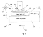
- the lithography machine 200 includes a optical assembly 16 and a stage assembly 202 that includes a wafer table 204 and a wafer stage 206.
- the wafer table 204 is configured to support a wafer 208 (or any other type of work piece) under the optical assembly 16.
- An environmental system 26, surrounding the optical assembly 16, is used to supply and remove immersion fluid 212 from the gap between the wafer 208 and the last optical element of the optical assembly 16.
- a work piece exchange system 216 including a wafer loader 218 (i.e., a robot) and an alignment tool 220 (i.e., a microscope and CCD camera), is configured to remove the wafer 208 on the wafer table 204 and replace it with a second wafer. This is typically accomplished using the wafer loader 218 to lift and remove the wafer 208 from the wafer table 204. Subsequently, the second wafer (not shown) is placed onto the wafer chuck 218, aligned using the alignment tool 220, and then positioned under the optical assembly 16 on the wafer table 204.
- a wafer loader 218 i.e., a robot
- an alignment tool 220 i.e., a microscope and CCD camera
- the wafer stage 206 includes an immersion fluid containment system 214 that is configured to maintain the immersion fluid 212 in the gap adjacent the last optical element of the optical assembly 16 during wafer exchange.
- the immersion fluid containment system 214 includes a pad 222 that is adjacent the wafer table 204.
- a support member 224 provided between the pad 222 and the wafer stage 206, is used to support the pad 222.
- the wafer table 204 has a flat upper surface which is coplanar with a surface of the wafer 208.
- the pad 222 also has a flat upper surface which is coplanar with the upper surface of the wafer table 204 and the wafer surface.
- the pad 222 is arranged adjacent the wafer table 204 with a very small gap (e.g.
- the wafer stage 206 is moved in the direction of arrow 226 so that the pad 222 is positioned under the optical assembly 16 in place of the wafer table 204, maintaining the fluid in the gap or maintaining the size of the fluid gap.
- the wafer stage is moved back to its original position so that the pad 222 is removed from the gap as the second wafer is positioned under the optical assembly 16.
- the pad 222 is disposed continuously adjacent the wafer table 204 with no gap.
- Vertical position and/or tilt of the wafer table 204 can be adjusted so that the wafer table surface is coplanar with the pad surface, before the wafer table 204 is moved out from under the optical assembly 16. Maintaining the gap between the pad 222 and the optical assembly 16 is not limited to just a wafer exchange operation.
- the pad 222 can be large enough to maintain the immersion fluid 212 in the space between the pad 222 and the optical assembly 16 during an alignment operation or a measurement operation. In those operations, a part of the area occupied by the immersion fluid 212 may be on the upper surface of the wafer table 204.
- the lithography machine 300 includes an optical assembly 16 and a stage assembly 302 that includes a wafer table 304 and a wafer stage 306.
- the wafer table 304 is configured to support a wafer 308 (or any other type of work piece) under the optical assembly 16.
- An environmental system 26, surrounding the optical assembly 16, is used to supply and remove immersion fluid 312 from the gap between the wafer 308 and the lower most optical element of the optical assembly 16.
- a work piece exchange system 316 including a wafer loader 318 and an alignment tool 320, is configured to remove the wafer 308 on the wafer table 304 and replace it with a second wafer.
- a set of motors 322 are used to move the wafer assembly 302 including the wafer table 304 and wafer stage 306 in two degrees of freedom (X and Y) during operation.
- the motors 322 can be any type of motors, such as linear motors, rotary motors, voice coil motors, etc.
- the immersion lithography machine 300 also includes an immersion fluid containment system 324 that is configured to maintain the immersion fluid 312 in the space below the optical assembly 16 while the wafer table 304 is away from under the optical assembly.
- The, immersion fluid containment system 324 includes a pad 326, a motor 328, and a control system 330.
- the pad 326 can be positioned adjacent the optical assembly 16 and the wafer table 204.
- the wafer table 304 has a flat upper surface which is coplanar with a surface of the wafer 308.
- the pad 326 has a flat upper surface which is coplanar with the upper surface of the wafer table 304 and the wafer surface.
- the pad 326 is movable in the X and Y directions using the motor 328 which is controlled by the control system 330.
- the motor 328 can be any type of motors as well as the motors 322.
- the pad 326 is positioned under the optical assembly 16 when the wafer table 304 (the wafer stage 306) is away from under the optical assembly 16. During a wafer exchange, the wafer table 304 moves away from the optical assembly 16. Simultaneously, the control system 330 directs the motor 328 to move pad 326 under the optical assembly 16, replacing the wafer table 308. The pad 326 thus retains the immersion fluid 312 within the gap under the optical assembly 16. After the new wafer has been aligned using the alignment tool 320, the wafer table 304 is repositioned under the optical assembly 16.
- the control system 330 directs the motor 328 to retract the pad 326 from the gap, preventing the escape of the immersion fluid 312.
- the control system 330 moves the wafer table 304 and the pad 326 with a small gap between the wafer table 304 and the pad 326, while the immersion fluid 312 below the optical assembly 16 moves between the wafer table 304 and the pad 326.
- the immersion fluid containment system 324 thus maintains the immersion fluid 312 from the gap during wafer exchange.
- the wafer table 304 (the wafer stage 306) and the pad 326 are movable separately. Therefore, the wafer table 326 is movable freely while the immersion fluid 312 is maintained in the space between the pad 326 and the optical assembly 16.
- control system 330 may be a separate control system or it can be integrated into the control system used to control the motors 322 for positioning the wafer stage 302 and wafer table 304.
- Vertical position and/or tilt of at least one of the wafer table 304 and the pad 326 may be adjusted so that the wafer table surface is coplanar with the pad surface, before the wafer table is moved out from under the optical assembly 16.
- the operation, in which the wafer table 304 is away from the optical assembly 16, is not necessarily limited to a wafer exchange operation. For example, an alignment operation, a measurement operation or other operation may be executed while maintaining the immersion fluid 312 in the space between the pad 326 and the optical assembly 16.
- the lithography machine 400 includes an optical assembly 16 and a stage assembly 402 that includes a wafer table 404 and a wafer stage 406.
- the wafer table 404 is configured to support a wafer 408 (or any other type of work piece) under the optical assembly 16.
- An environmental system 26, surrounding the optical assembly 16, is used to supply and remove immersion fluid 412 from the gap between the wafer 408 and the lower most optical element of the optical assembly 16.
- a work piece exchange system 416 including a wafer loader 418 and an alignment tool 420, is configured to remove the wafer 408 on the wafer table 404 and replace it with a second wafer.
- the wafer loader 418 to remove the wafer 408 from the wafer table 404.
- the second wafer (not shown) is placed onto the wafer chuck 418, aligned using the alignment tool 420, and then positioned under the optical assembly 16 as illustrated in the Figure 4A .
- the immersion lithography machine 400 also includes an immersion fluid containment system 424 that is configured to maintain the immersion fluid 412 in the space below the optical assembly 16 while the wafer table 404 is away from under the optical assembly 16.
- the immersion fluid containment system 424 includes a pad 426, a first clamp 428 provided on the optical assembly 16 and a second clamp 430 provided on the wafer table 404.
- the pad 426 is held by the second clamp 430 in place on the wafer table 404.
- the pad 426 When the wafer table 404 is away from the optical assembly 16, for example during a wafer exchange operation, the pad 426 is detached from the wafer table 404 and held by the first clamp 428 to maintain the immersion fluid 412 between the optical assembly 16 and the pad 426.
- the wafer table 404 has a flat upper surface which is coplanar with a surface of the wafer 408.
- the pad 426 held on the wafer table 404 also has a flat upper surface which is coplanar with the upper surface of the wafer table 404 and the wafer surface. Therefore, the immersion pad 426 and wafer 408 can be moved under the optical assembly without the immersion fluid leaking.
- the clamps 428 and 430 can be vacuum clamps, magnetic, electro-static, or mechanical.
- the pad 426 is positioned on the wafer table 404 during exposure of the wafer 408.
- the second clamp 430 is used to hold the pad 426 in place on the table 404 during the wafer exposure.
- the wafer table 404 is moved in the direction of arrow 432 so that the pad 426 is positioned under the optical assembly 16 in place of the wafer 408.
- the second clamp 430 holding the pad 426 to the wafer table 404 is released while first clamp 428 clamps the pad 426 to the optical assembly 16.
- the immersion fluid 412 is maintained under the optical assembly while the wafer 408 is exchanged.
- the wafer table 404 is moved in the direction opposite arrow 432 so that the new wafer is positioned under the optical assembly. Prior to this motion, the first clamp 428 is released while the second clamp 430 again clamps the pad 426 to the wafer table 404. In this embodiment, the wafer table 404 is freely movable while the pad 426 is clamped by the first clamp 428.
- the operation, in which the pad 426 is clamped by the first clamp 428 is not limited to only a wafer exchange operation.
- An alignment operation, a measurement operation, or any other operation can be executed while the immersion fluid 312 is maintained in the space between the optical assembly 16 and the pad 426 clamped by the first clamp 428.
- the clamp 428 can be provided on the frame 12 or other support member, and the clamp 430 can be provided on the wafer stage 406.
- the pad 426 can be held on a movable member other than the stage assembly 402.
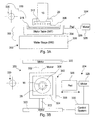
- FIGS. 5A and 5B are top down views of two different twin stage immersion lithography systems of the present invention.
- a pair of wafer stages WS1 and WS2 are shown.
- Motors 502 are used to move or position the two stages WS1 and WS2 in the horizontal directions whereas motors 504 are used to move or position the stages WS1 and WS2 in the vertical direction.
- the motors 502 and 504 are used to alternatively position one stage under the optical assembly 16 while a wafer exchange and alignment is performed on the other stage.
- each wafer stage SW1 and SW2 of either Figure 5A or 5B can be modified to include a pad 222 and a support member 224.
- a single pad 326, motor 328, and control system 330 could be used adjacent the optical assembly 16. The pad 326 is movable separately from the stage SW1 and SW2.
- stage SW1 and SW2 are to be swapped.
- the pad 326 is moved to under the optical assembly 16 to maintain the immersion fluid 312 below the optical assembly 16.
- a detachable single pad can be used.
- the pad 426 is used to maintain the immersion fluid in the gap as illustrated in Figure 4B .
- the pad is clamped onto the wafer table on the wafer stage that is being exposed. In this manner, only a single pad is needed for the two stages WS1 and WS2.
- the second stage can also be used as the pad.
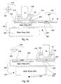
- the immersion lithography system 600 includes first stage 604 and second stage 606.
- the two stages are moved in the X and Y directions by motors 602.
- the stages 604 and 606 themselves are used to contain the immersion fluid in the gap.
- the first stage 604 is positioned under the optical assembly 16.
- the motors 602 are used to position the second stage 606 with a second work piece adjacent the first stage 604. With the two stages positioned side-by-side, they substantially form a continuous surface.
- the motors 602 are then used to move the two stages in unison so that the second stage 604 is position under the optical assembly 16 and the first stage is no longer under the optical assembly 16.
- the immersion fluid in the gap is maintained by the second stage 606 which forms the substantially continuous surface with the first stage.
- the second stage 606 could also be a "pad" stage that contains a pad that is used to maintain the immersion liquid in the gap while a second work piece is being placed onto the first stage 604.
- the motor arrangement shown in either Figure 5A or 5B could be used.
- Figure 6B-6E a series of diagrams illustrating a work piece exchange is illustrated.
- Figure 6B shows a wafer on stage 604 after exposure is completed.
- Figure 6C shows the second stage 606 in contact (or immediately adjacent) with the first stage 604 under the optical assembly 16.
- Figure 6C shows a transfer taking place, i.e., the second stage 606 is positioned under the optical assembly 16.
- the first stage 604 is moved away from the optical assembly 16.
- the two stages 604 and 606 provide a continuous surface under the optical assembly 16 during a transfer, thus maintaining the immersion fluid in the gap.
- the second stage 606 is a pad stage. This stage, however, could also be a work piece stage as noted above.
- the pad can be made of a number of different materials, such as ceramic, metal plastic. These materials may also be coated with Teflon according to other embodiments.
- the size of the pad also should be sufficient to cover the area occupied by the immersion fluid.
- the surface of the last optical element, of the optical assembly 16 is constantly under immersion fluid environment, preventing the formation of a fluid mark (e.g. "a water mark").
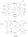
- step 701 the work piece's function and performance characteristics are designed.
- step 702 a mask (reticle) having a pattern is designed according to the previous designing step, and in a parallel step 703 a wafer is made from a silicon material.
- the mask pattern designed in step 702 is exposed onto the wafer from step 703 in step 704 by a photolithography system described hereinabove in accordance with the present invention.
- step 705 the semiconductor work piece is assembled (including the dicing process, bonding process and packaging process), finally, the work piece is then inspected in step 606.
- FIG. 7B illustrates a detailed flowchart example of the above-mentioned step 704 in the case of fabricating semiconductor work pieces.
- step 711 oxidation step
- step 712 CVD step
- step 713 electrode formation step
- step 714 ion implantation step
- steps 711 - 714 form the preprocessing steps for wafers during wafer processing, and selection is made at each step according to processing requirements.
- step 715 photoresist formation step
- step 716 exposure step
- step 717 developing step
- step 718 etching step
- steps other than residual photoresist exposed material surface
- circuit patterns are formed by repetition of these preprocessing and post-processing steps.
Landscapes
- Physics & Mathematics (AREA)
- General Physics & Mathematics (AREA)
- Engineering & Computer Science (AREA)
- Condensed Matter Physics & Semiconductors (AREA)
- Manufacturing & Machinery (AREA)
- Computer Hardware Design (AREA)
- Microelectronics & Electronic Packaging (AREA)
- Power Engineering (AREA)
- Health & Medical Sciences (AREA)
- Optics & Photonics (AREA)
- Environmental & Geological Engineering (AREA)
- Epidemiology (AREA)
- Public Health (AREA)
- Toxicology (AREA)
- Exposure And Positioning Against Photoresist Photosensitive Materials (AREA)
- Exposure Of Semiconductors, Excluding Electron Or Ion Beam Exposure (AREA)
- Container, Conveyance, Adherence, Positioning, Of Wafer (AREA)
Applications Claiming Priority (2)
| Application Number | Priority Date | Filing Date | Title |
|---|---|---|---|
| US46249903P | 2003-04-11 | 2003-04-11 | |
| EP04721260.0A EP1616220B1 (en) | 2003-04-11 | 2004-03-17 | Apparatus and method for maintaining immersion fluid under a lithographic projection lens |
Related Parent Applications (2)
| Application Number | Title | Priority Date | Filing Date |
|---|---|---|---|
| EP04721260.0A Division EP1616220B1 (en) | 2003-04-11 | 2004-03-17 | Apparatus and method for maintaining immersion fluid under a lithographic projection lens |
| EP04721260.0 Division | 2004-03-17 |
Publications (3)
| Publication Number | Publication Date |
|---|---|
| EP2613194A2 EP2613194A2 (en) | 2013-07-10 |
| EP2613194A3 EP2613194A3 (en) | 2014-06-11 |
| EP2613194B1 true EP2613194B1 (en) | 2015-09-16 |
Family
ID=33159850
Family Applications (8)
| Application Number | Title | Priority Date | Filing Date |
|---|---|---|---|
| EP04721260.0A Expired - Lifetime EP1616220B1 (en) | 2003-04-11 | 2004-03-17 | Apparatus and method for maintaining immersion fluid under a lithographic projection lens |
| EP14200551.1A Expired - Lifetime EP2887143B1 (en) | 2003-04-11 | 2004-03-17 | Apparatus and method for maintaining immersion fluid in the gap under the projection lens during wafer exchange in an immersion lithography machine |
| EP13154183.1A Expired - Lifetime EP2613192B1 (en) | 2003-04-11 | 2004-03-17 | Apparatus and method for maintaining immersion fluid in the gap under the projection lens during wafer exchange in an immersion lithography machine |
| EP13154185.6A Expired - Lifetime EP2613193B1 (en) | 2003-04-11 | 2004-03-17 | Apparatus and method for maintaining immersion fluid in the gap under the projection lens during wafer exchange in an immersion lithography machine |
| EP13154187.2A Expired - Lifetime EP2613195B1 (en) | 2003-04-11 | 2004-03-17 | Apparatus and method for maintaining immersion fluid in the gap under the projection lens during wafer exchange in an immersion lithography machine |
| EP13154181.5A Expired - Lifetime EP2618213B1 (en) | 2003-04-11 | 2004-03-17 | Apparatus and method for maintaining immersion fluid in the gap under the projection lens during wafer exchange in an immersion lithography machine |
| EP16186292.5A Withdrawn EP3141953A3 (en) | 2003-04-11 | 2004-03-17 | Apparatus and method for maintaining immersion fluid in the gap under the projection lens during wafer exchange in an immersion lithography machine |
| EP13154186.4A Expired - Lifetime EP2613194B1 (en) | 2003-04-11 | 2004-03-17 | Apparatus and method for maintaining immersion fluid in the gap under the projection lens during wafer exchange in an immersion lithography machine |
Family Applications Before (7)
| Application Number | Title | Priority Date | Filing Date |
|---|---|---|---|
| EP04721260.0A Expired - Lifetime EP1616220B1 (en) | 2003-04-11 | 2004-03-17 | Apparatus and method for maintaining immersion fluid under a lithographic projection lens |
| EP14200551.1A Expired - Lifetime EP2887143B1 (en) | 2003-04-11 | 2004-03-17 | Apparatus and method for maintaining immersion fluid in the gap under the projection lens during wafer exchange in an immersion lithography machine |
| EP13154183.1A Expired - Lifetime EP2613192B1 (en) | 2003-04-11 | 2004-03-17 | Apparatus and method for maintaining immersion fluid in the gap under the projection lens during wafer exchange in an immersion lithography machine |
| EP13154185.6A Expired - Lifetime EP2613193B1 (en) | 2003-04-11 | 2004-03-17 | Apparatus and method for maintaining immersion fluid in the gap under the projection lens during wafer exchange in an immersion lithography machine |
| EP13154187.2A Expired - Lifetime EP2613195B1 (en) | 2003-04-11 | 2004-03-17 | Apparatus and method for maintaining immersion fluid in the gap under the projection lens during wafer exchange in an immersion lithography machine |
| EP13154181.5A Expired - Lifetime EP2618213B1 (en) | 2003-04-11 | 2004-03-17 | Apparatus and method for maintaining immersion fluid in the gap under the projection lens during wafer exchange in an immersion lithography machine |
| EP16186292.5A Withdrawn EP3141953A3 (en) | 2003-04-11 | 2004-03-17 | Apparatus and method for maintaining immersion fluid in the gap under the projection lens during wafer exchange in an immersion lithography machine |
Country Status (9)
| Country | Link |
|---|---|
| US (18) | US7372538B2 (OSRAM) |
| EP (8) | EP1616220B1 (OSRAM) |
| JP (12) | JP4315198B2 (OSRAM) |
| KR (15) | KR101225884B1 (OSRAM) |
| CN (3) | CN101980086B (OSRAM) |
| IL (5) | IL170735A (OSRAM) |
| SG (12) | SG2012031738A (OSRAM) |
| TW (16) | TWI346345B (OSRAM) |
| WO (1) | WO2004090577A2 (OSRAM) |
Families Citing this family (222)
| Publication number | Priority date | Publication date | Assignee | Title |
|---|---|---|---|---|
| US10503084B2 (en) | 2002-11-12 | 2019-12-10 | Asml Netherlands B.V. | Lithographic apparatus and device manufacturing method |
| EP1420299B1 (en) | 2002-11-12 | 2011-01-05 | ASML Netherlands B.V. | Immersion lithographic apparatus and device manufacturing method |
| JP3953460B2 (ja) | 2002-11-12 | 2007-08-08 | エーエスエムエル ネザーランズ ビー.ブイ. | リソグラフィ投影装置 |
| US7110081B2 (en) | 2002-11-12 | 2006-09-19 | Asml Netherlands B.V. | Lithographic apparatus and device manufacturing method |
| US9482966B2 (en) | 2002-11-12 | 2016-11-01 | Asml Netherlands B.V. | Lithographic apparatus and device manufacturing method |
| TWI232357B (en) | 2002-11-12 | 2005-05-11 | Asml Netherlands Bv | Lithographic apparatus and device manufacturing method |
| US7372541B2 (en) | 2002-11-12 | 2008-05-13 | Asml Netherlands B.V. | Lithographic apparatus and device manufacturing method |
| SG121822A1 (en) * | 2002-11-12 | 2006-05-26 | Asml Netherlands Bv | Lithographic apparatus and device manufacturing method |
| DE60335595D1 (de) | 2002-11-12 | 2011-02-17 | Asml Netherlands Bv | Lithographischer Apparat mit Immersion und Verfahren zur Herstellung einer Vorrichtung |
| JP4352874B2 (ja) | 2002-12-10 | 2009-10-28 | 株式会社ニコン | 露光装置及びデバイス製造方法 |
| WO2004053956A1 (ja) | 2002-12-10 | 2004-06-24 | Nikon Corporation | 露光装置及び露光方法、デバイス製造方法 |
| CN1723541B (zh) | 2002-12-10 | 2010-06-02 | 株式会社尼康 | 曝光装置和器件制造方法 |
| CN101424883B (zh) | 2002-12-10 | 2013-05-15 | 株式会社尼康 | 曝光设备和器件制造法 |
| US7242455B2 (en) | 2002-12-10 | 2007-07-10 | Nikon Corporation | Exposure apparatus and method for producing device |
| KR101085372B1 (ko) | 2002-12-10 | 2011-11-21 | 가부시키가이샤 니콘 | 노광 장치 및 디바이스 제조 방법 |
| US7948604B2 (en) | 2002-12-10 | 2011-05-24 | Nikon Corporation | Exposure apparatus and method for producing device |
| DE10261775A1 (de) | 2002-12-20 | 2004-07-01 | Carl Zeiss Smt Ag | Vorrichtung zur optischen Vermessung eines Abbildungssystems |
| KR101921572B1 (ko) | 2003-02-26 | 2018-11-26 | 가부시키가이샤 니콘 | 노광 장치, 노광 방법 및 디바이스 제조 방법 |
| EP1610361B1 (en) | 2003-03-25 | 2014-05-21 | Nikon Corporation | Exposure system and device production method |
| WO2004090956A1 (ja) | 2003-04-07 | 2004-10-21 | Nikon Corporation | 露光装置及びデバイス製造方法 |
| WO2004093159A2 (en) | 2003-04-09 | 2004-10-28 | Nikon Corporation | Immersion lithography fluid control system |
| EP3352010A1 (en) | 2003-04-10 | 2018-07-25 | Nikon Corporation | Run-off path to collect liquid for an immersion lithography apparatus |
| KR101745223B1 (ko) | 2003-04-10 | 2017-06-08 | 가부시키가이샤 니콘 | 액침 리소그래피 장치용 운반 영역을 포함하는 환경 시스템 |
| SG2014015176A (en) | 2003-04-10 | 2015-06-29 | Nippon Kogaku Kk | Environmental system including vacuum scavange for an immersion lithography apparatus |
| SG2012031738A (en) | 2003-04-11 | 2015-07-30 | Nippon Kogaku Kk | Apparatus having an immersion fluid system configured to maintain immersion fluid in a gap adjacent an optical assembly |
| WO2004092830A2 (en) | 2003-04-11 | 2004-10-28 | Nikon Corporation | Liquid jet and recovery system for immersion lithography |
| CN101825847B (zh) | 2003-04-11 | 2013-10-16 | 株式会社尼康 | 用于沉浸式光刻光学系统的清洗方法 |
| JP2006523958A (ja) | 2003-04-17 | 2006-10-19 | 株式会社ニコン | 液浸リソグラフィで使用するためのオートフォーカス素子の光学的構造 |
| TWI295414B (en) | 2003-05-13 | 2008-04-01 | Asml Netherlands Bv | Lithographic apparatus and device manufacturing method |
| KR20060009356A (ko) | 2003-05-15 | 2006-01-31 | 가부시키가이샤 니콘 | 노광 장치 및 디바이스 제조 방법 |
| TWI612556B (zh) | 2003-05-23 | 2018-01-21 | Nikon Corp | 曝光裝置、曝光方法及元件製造方法 |
| TWI470671B (zh) | 2003-05-23 | 2015-01-21 | 尼康股份有限公司 | Exposure method and exposure apparatus, and device manufacturing method |
| EP2453465A3 (en) | 2003-05-28 | 2018-01-03 | Nikon Corporation | Exposure method, exposure apparatus, and method for producing a device |
| US7213963B2 (en) | 2003-06-09 | 2007-05-08 | Asml Netherlands B.V. | Lithographic apparatus and device manufacturing method |
| US7317504B2 (en) | 2004-04-08 | 2008-01-08 | Asml Netherlands B.V. | Lithographic apparatus and device manufacturing method |
| EP1486827B1 (en) | 2003-06-11 | 2011-11-02 | ASML Netherlands B.V. | Lithographic apparatus and device manufacturing method |
| KR101528089B1 (ko) | 2003-06-13 | 2015-06-11 | 가부시키가이샤 니콘 | 노광 방법, 기판 스테이지, 노광 장치, 및 디바이스 제조 방법 |
| KR101931923B1 (ko) * | 2003-06-19 | 2018-12-21 | 가부시키가이샤 니콘 | 노광 장치 및 디바이스 제조방법 |
| US6867844B2 (en) | 2003-06-19 | 2005-03-15 | Asml Holding N.V. | Immersion photolithography system and method using microchannel nozzles |
| JP3862678B2 (ja) | 2003-06-27 | 2006-12-27 | キヤノン株式会社 | 露光装置及びデバイス製造方法 |
| US6809794B1 (en) | 2003-06-27 | 2004-10-26 | Asml Holding N.V. | Immersion photolithography system and method using inverted wafer-projection optics interface |
| EP1491956B1 (en) | 2003-06-27 | 2006-09-06 | ASML Netherlands B.V. | Lithographic apparatus and device manufacturing method |
| KR20060027832A (ko) | 2003-07-01 | 2006-03-28 | 가부시키가이샤 니콘 | 광학 엘리먼트로서 동위원소적으로 특정된 유체를 사용하는방법 |
| EP2843472B1 (en) | 2003-07-08 | 2016-12-07 | Nikon Corporation | Wafer table for immersion lithography |
| KR101296501B1 (ko) | 2003-07-09 | 2013-08-13 | 가부시키가이샤 니콘 | 노광 장치 및 디바이스 제조 방법 |
| EP2264531B1 (en) | 2003-07-09 | 2013-01-16 | Nikon Corporation | Exposure apparatus and device manufacturing method |
| KR20060026883A (ko) | 2003-07-09 | 2006-03-24 | 가부시키가이샤 니콘 | 결합장치, 노광장치 및 디바이스 제조방법 |
| EP1650787A4 (en) | 2003-07-25 | 2007-09-19 | Nikon Corp | INVESTIGATION METHOD AND INVESTIGATION DEVICE FOR AN OPTICAL PROJECTION SYSTEM AND METHOD OF MANUFACTURING AN OPTICAL PROJECTION SYSTEM |
| EP1503244A1 (en) | 2003-07-28 | 2005-02-02 | ASML Netherlands B.V. | Lithographic projection apparatus and device manufacturing method |
| US7326522B2 (en) | 2004-02-11 | 2008-02-05 | Asml Netherlands B.V. | Device manufacturing method and a substrate |
| KR101935709B1 (ko) | 2003-07-28 | 2019-01-04 | 가부시키가이샤 니콘 | 노광 장치 및 디바이스 제조 방법, 그리고 노광 장치의 제어 방법 |
| US7175968B2 (en) | 2003-07-28 | 2007-02-13 | Asml Netherlands B.V. | Lithographic apparatus, device manufacturing method and a substrate |
| US7779781B2 (en) | 2003-07-31 | 2010-08-24 | Asml Netherlands B.V. | Lithographic apparatus and device manufacturing method |
| KR101242886B1 (ko) | 2003-08-29 | 2013-03-12 | 가부시키가이샤 니콘 | 노광 장치 및 디바이스 제조 방법 |
| TWI263859B (en) | 2003-08-29 | 2006-10-11 | Asml Netherlands Bv | Lithographic apparatus and device manufacturing method |
| KR20170070264A (ko) | 2003-09-03 | 2017-06-21 | 가부시키가이샤 니콘 | 액침 리소그래피용 유체를 제공하기 위한 장치 및 방법 |
| JP4444920B2 (ja) | 2003-09-19 | 2010-03-31 | 株式会社ニコン | 露光装置及びデバイス製造方法 |
| EP2312395B1 (en) | 2003-09-29 | 2015-05-13 | Nikon Corporation | Exposure apparatus, exposure method, and method for producing a device |
| JP2005136364A (ja) | 2003-10-08 | 2005-05-26 | Zao Nikon Co Ltd | 基板搬送装置、露光装置、並びにデバイス製造方法 |
| KR101361892B1 (ko) | 2003-10-08 | 2014-02-12 | 가부시키가이샤 자오 니콘 | 기판 반송 장치 및 기판 반송 방법, 노광 장치 및 노광 방법, 디바이스 제조 방법 |
| EP1672682A4 (en) | 2003-10-08 | 2008-10-15 | Zao Nikon Co Ltd | SUBSTRATE TRANSPORT DEVICE AND METHOD, EXPOSURE DEVICE AND METHOD AND COMPONENT MANUFACTURING METHOD |
| TW201738932A (zh) | 2003-10-09 | 2017-11-01 | Nippon Kogaku Kk | 曝光裝置及曝光方法、元件製造方法 |
| US7352433B2 (en) | 2003-10-28 | 2008-04-01 | Asml Netherlands B.V. | Lithographic apparatus and device manufacturing method |
| US7411653B2 (en) | 2003-10-28 | 2008-08-12 | Asml Netherlands B.V. | Lithographic apparatus |
| JP4295712B2 (ja) | 2003-11-14 | 2009-07-15 | エーエスエムエル ネザーランズ ビー.ブイ. | リソグラフィ装置及び装置製造方法 |
| TW201804262A (zh) | 2003-12-03 | 2018-02-01 | 尼康股份有限公司 | 曝光裝置、曝光方法、元件製造方法 |
| KR101281397B1 (ko) | 2003-12-15 | 2013-07-02 | 가부시키가이샤 니콘 | 스테이지 장치, 노광 장치, 및 노광 방법 |
| US7394521B2 (en) | 2003-12-23 | 2008-07-01 | Asml Netherlands B.V. | Lithographic apparatus and device manufacturing method |
| WO2005071491A2 (en) | 2004-01-20 | 2005-08-04 | Carl Zeiss Smt Ag | Exposure apparatus and measuring device for a projection lens |
| US7589822B2 (en) * | 2004-02-02 | 2009-09-15 | Nikon Corporation | Stage drive method and stage unit, exposure apparatus, and device manufacturing method |
| JP4506674B2 (ja) | 2004-02-03 | 2010-07-21 | 株式会社ニコン | 露光装置及びデバイス製造方法 |
| KR20180042456A (ko) | 2004-03-25 | 2018-04-25 | 가부시키가이샤 니콘 | 노광 장치 및 디바이스 제조 방법 |
| US7034917B2 (en) | 2004-04-01 | 2006-04-25 | Asml Netherlands B.V. | Lithographic apparatus, device manufacturing method and device manufactured thereby |
| US7898642B2 (en) | 2004-04-14 | 2011-03-01 | Asml Netherlands B.V. | Lithographic apparatus and device manufacturing method |
| WO2005103788A1 (de) * | 2004-04-26 | 2005-11-03 | Carl Zeiss Smt Ag | Verfahren zum verbinden eines optischen elements mit einer haltestruktur |
| WO2005111722A2 (en) | 2004-05-04 | 2005-11-24 | Nikon Corporation | Apparatus and method for providing fluid for immersion lithography |
| US7616383B2 (en) | 2004-05-18 | 2009-11-10 | Asml Netherlands B.V. | Lithographic apparatus and device manufacturing method |
| US7796274B2 (en) | 2004-06-04 | 2010-09-14 | Carl Zeiss Smt Ag | System for measuring the image quality of an optical imaging system |
| KR101162128B1 (ko) | 2004-06-09 | 2012-07-03 | 가부시키가이샤 니콘 | 노광 장치 및 디바이스 제조 방법 |
| KR101421870B1 (ko) | 2004-06-09 | 2014-07-22 | 가부시키가이샤 니콘 | 기판 유지 장치 및 그것을 구비하는 노광 장치, 노광 방법, 디바이스 제조 방법, 그리고 발액 플레이트 |
| US7463330B2 (en) | 2004-07-07 | 2008-12-09 | Asml Netherlands B.V. | Lithographic apparatus and device manufacturing method |
| WO2006006565A1 (ja) | 2004-07-12 | 2006-01-19 | Nikon Corporation | 露光装置及びデバイス製造方法 |
| US8169591B2 (en) * | 2004-08-03 | 2012-05-01 | Nikon Corporation | Exposure apparatus, exposure method, and method for producing device |
| TW200615716A (en) * | 2004-08-05 | 2006-05-16 | Nikon Corp | Stage device and exposure device |
| JP4983257B2 (ja) | 2004-08-18 | 2012-07-25 | 株式会社ニコン | 露光装置、デバイス製造方法、計測部材、及び計測方法 |
| US7701550B2 (en) | 2004-08-19 | 2010-04-20 | Asml Netherlands B.V. | Lithographic apparatus and device manufacturing method |
| SG156635A1 (en) | 2004-10-15 | 2009-11-26 | Nikon Corp | Exposure apparatus and device manufacturing method |
| US7119876B2 (en) | 2004-10-18 | 2006-10-10 | Asml Netherlands B.V. | Lithographic apparatus and device manufacturing method |
| KR101318037B1 (ko) | 2004-11-01 | 2013-10-14 | 가부시키가이샤 니콘 | 노광 장치 및 디바이스 제조 방법 |
| JP4517354B2 (ja) * | 2004-11-08 | 2010-08-04 | 株式会社ニコン | 露光装置及びデバイス製造方法 |
| US7583357B2 (en) * | 2004-11-12 | 2009-09-01 | Asml Netherlands B.V. | Lithographic apparatus and device manufacturing method |
| US7411657B2 (en) | 2004-11-17 | 2008-08-12 | Asml Netherlands B.V. | Lithographic apparatus and device manufacturing method |
| TWI553703B (zh) | 2004-11-18 | 2016-10-11 | 尼康股份有限公司 | A position measuring method, a position control method, a measuring method, a loading method, an exposure method and an exposure apparatus, and a device manufacturing method |
| US20080123067A1 (en) * | 2004-11-25 | 2008-05-29 | Nikon Corporation | Movable Body System, Exposure Apparatus, And Device Manufacturing Method |
| US7446850B2 (en) | 2004-12-03 | 2008-11-04 | Asml Netherlands B.V. | Lithographic apparatus and device manufacturing method |
| WO2006062065A1 (ja) | 2004-12-06 | 2006-06-15 | Nikon Corporation | メンテナンス方法、メンテナンス機器、露光装置、及びデバイス製造方法 |
| US7397533B2 (en) | 2004-12-07 | 2008-07-08 | Asml Netherlands B.V. | Lithographic apparatus and device manufacturing method |
| US7196770B2 (en) | 2004-12-07 | 2007-03-27 | Asml Netherlands B.V. | Prewetting of substrate before immersion exposure |
| US7365827B2 (en) | 2004-12-08 | 2008-04-29 | Asml Netherlands B.V. | Lithographic apparatus and device manufacturing method |
| JP4752473B2 (ja) | 2004-12-09 | 2011-08-17 | 株式会社ニコン | 露光装置、露光方法及びデバイス製造方法 |
| US7352440B2 (en) | 2004-12-10 | 2008-04-01 | Asml Netherlands B.V. | Substrate placement in immersion lithography |
| US7403261B2 (en) | 2004-12-15 | 2008-07-22 | Asml Netherlands B.V. | Lithographic apparatus and device manufacturing method |
| US7528931B2 (en) * | 2004-12-20 | 2009-05-05 | Asml Netherlands B.V. | Lithographic apparatus and device manufacturing method |
| US7880860B2 (en) | 2004-12-20 | 2011-02-01 | Asml Netherlands B.V. | Lithographic apparatus and device manufacturing method |
| US7491661B2 (en) | 2004-12-28 | 2009-02-17 | Asml Netherlands B.V. | Device manufacturing method, top coat material and substrate |
| US7405805B2 (en) | 2004-12-28 | 2008-07-29 | Asml Netherlands B.V. | Lithographic apparatus and device manufacturing method |
| US20060147821A1 (en) | 2004-12-30 | 2006-07-06 | Asml Netherlands B.V. | Lithographic apparatus and device manufacturing method |
| DE602006012746D1 (de) | 2005-01-14 | 2010-04-22 | Asml Netherlands Bv | Lithografische Vorrichtung und Herstellungsverfahren |
| US8692973B2 (en) | 2005-01-31 | 2014-04-08 | Nikon Corporation | Exposure apparatus and method for producing device |
| KR20160135859A (ko) | 2005-01-31 | 2016-11-28 | 가부시키가이샤 니콘 | 노광 장치 및 디바이스 제조 방법 |
| CN102385260B (zh) | 2005-02-10 | 2014-11-05 | Asml荷兰有限公司 | 浸没液体、曝光装置及曝光方法 |
| US7378025B2 (en) | 2005-02-22 | 2008-05-27 | Asml Netherlands B.V. | Fluid filtration method, fluid filtered thereby, lithographic apparatus and device manufacturing method |
| US7224431B2 (en) | 2005-02-22 | 2007-05-29 | Asml Netherlands B.V. | Lithographic apparatus and device manufacturing method |
| US8018573B2 (en) | 2005-02-22 | 2011-09-13 | Asml Netherlands B.V. | Lithographic apparatus and device manufacturing method |
| US7428038B2 (en) | 2005-02-28 | 2008-09-23 | Asml Netherlands B.V. | Lithographic apparatus, device manufacturing method and apparatus for de-gassing a liquid |
| US7282701B2 (en) | 2005-02-28 | 2007-10-16 | Asml Netherlands B.V. | Sensor for use in a lithographic apparatus |
| US7324185B2 (en) | 2005-03-04 | 2008-01-29 | Asml Netherlands B.V. | Lithographic apparatus and device manufacturing method |
| US7684010B2 (en) | 2005-03-09 | 2010-03-23 | Asml Netherlands B.V. | Lithographic apparatus, device manufacturing method, seal structure, method of removing an object and a method of sealing |
| US7330238B2 (en) | 2005-03-28 | 2008-02-12 | Asml Netherlands, B.V. | Lithographic apparatus, immersion projection apparatus and device manufacturing method |
| KR20070115860A (ko) * | 2005-03-30 | 2007-12-06 | 가부시키가이샤 니콘 | 노광 장치 및 노광 방법, 그리고 디바이스 제조 방법 |
| US7411654B2 (en) | 2005-04-05 | 2008-08-12 | Asml Netherlands B.V. | Lithographic apparatus and device manufacturing method |
| USRE43576E1 (en) | 2005-04-08 | 2012-08-14 | Asml Netherlands B.V. | Dual stage lithographic apparatus and device manufacturing method |
| US7291850B2 (en) | 2005-04-08 | 2007-11-06 | Asml Netherlands B.V. | Lithographic apparatus and device manufacturing method |
| US20060232753A1 (en) | 2005-04-19 | 2006-10-19 | Asml Holding N.V. | Liquid immersion lithography system with tilted liquid flow |
| JP5239337B2 (ja) * | 2005-04-28 | 2013-07-17 | 株式会社ニコン | 露光方法及び露光装置、並びにデバイス製造方法 |
| US7433016B2 (en) | 2005-05-03 | 2008-10-07 | Asml Netherlands B.V. | Lithographic apparatus and device manufacturing method |
| US8248577B2 (en) | 2005-05-03 | 2012-08-21 | Asml Netherlands B.V. | Lithographic apparatus and device manufacturing method |
| US7317507B2 (en) | 2005-05-03 | 2008-01-08 | Asml Netherlands B.V. | Lithographic apparatus and device manufacturing method |
| US7751027B2 (en) | 2005-06-21 | 2010-07-06 | Asml Netherlands B.V. | Lithographic apparatus and device manufacturing method |
| US7652746B2 (en) | 2005-06-21 | 2010-01-26 | Asml Netherlands B.V. | Lithographic apparatus and device manufacturing method |
| US7834974B2 (en) | 2005-06-28 | 2010-11-16 | Asml Netherlands B.V. | Lithographic apparatus and device manufacturing method |
| US7468779B2 (en) | 2005-06-28 | 2008-12-23 | Asml Netherlands B.V. | Lithographic apparatus and device manufacturing method |
| US7474379B2 (en) | 2005-06-28 | 2009-01-06 | Asml Netherlands B.V. | Lithographic apparatus and device manufacturing method |
| US7583358B2 (en) | 2005-07-25 | 2009-09-01 | Micron Technology, Inc. | Systems and methods for retrieving residual liquid during immersion lens photolithography |
| EP1918983A4 (en) | 2005-08-05 | 2010-03-31 | Nikon Corp | STAGE EQUIPMENT AND EXPOSURE DEVICE |
| US8054445B2 (en) | 2005-08-16 | 2011-11-08 | Asml Netherlands B.V. | Lithographic apparatus and device manufacturing method |
| WO2007029829A1 (ja) * | 2005-09-09 | 2007-03-15 | Nikon Corporation | 露光装置及び露光方法、並びにデバイス製造方法 |
| US7417710B2 (en) * | 2005-09-26 | 2008-08-26 | Asml Netherlands B.V. | Lithographic apparatus and device manufacturing method |
| JP4164508B2 (ja) * | 2005-10-04 | 2008-10-15 | キヤノン株式会社 | 露光装置及びデバイス製造方法 |
| JP3997244B2 (ja) * | 2005-10-04 | 2007-10-24 | キヤノン株式会社 | 露光装置及びデバイス製造方法 |
| JP3997245B2 (ja) * | 2005-10-04 | 2007-10-24 | キヤノン株式会社 | 露光装置及びデバイス製造方法 |
| US7411658B2 (en) | 2005-10-06 | 2008-08-12 | Asml Netherlands B.V. | Lithographic apparatus and device manufacturing method |
| EP1947683A4 (en) * | 2005-11-09 | 2010-08-25 | Nikon Corp | EXPOSURE DEVICE, EXPOSURE METHOD AND COMPONENT MANUFACTURING METHOD |
| US7804577B2 (en) | 2005-11-16 | 2010-09-28 | Asml Netherlands B.V. | Lithographic apparatus |
| US7864292B2 (en) | 2005-11-16 | 2011-01-04 | Asml Netherlands B.V. | Lithographic apparatus and device manufacturing method |
| US7656501B2 (en) | 2005-11-16 | 2010-02-02 | Asml Netherlands B.V. | Lithographic apparatus |
| US7633073B2 (en) | 2005-11-23 | 2009-12-15 | Asml Netherlands B.V. | Lithographic apparatus and device manufacturing method |
| US7773195B2 (en) | 2005-11-29 | 2010-08-10 | Asml Holding N.V. | System and method to increase surface tension and contact angle in immersion lithography |
| US8125610B2 (en) | 2005-12-02 | 2012-02-28 | ASML Metherlands B.V. | Method for preventing or reducing contamination of an immersion type projection apparatus and an immersion type lithographic apparatus |
| US7420194B2 (en) | 2005-12-27 | 2008-09-02 | Asml Netherlands B.V. | Lithographic apparatus and substrate edge seal |
| US7839483B2 (en) | 2005-12-28 | 2010-11-23 | Asml Netherlands B.V. | Lithographic apparatus, device manufacturing method and a control system |
| US7649611B2 (en) * | 2005-12-30 | 2010-01-19 | Asml Netherlands B.V. | Lithographic apparatus and device manufacturing method |
| US8472004B2 (en) * | 2006-01-18 | 2013-06-25 | Micron Technology, Inc. | Immersion photolithography scanner |
| KR101889245B1 (ko) * | 2006-01-19 | 2018-08-16 | 가부시키가이샤 니콘 | 이동체 구동 방법 및 이동체 구동 시스템, 패턴 형성 방법 및 패턴 형성 장치, 노광 방법 및 노광 장치, 그리고 디바이스 제조 방법 |
| EP3267258A1 (en) * | 2006-02-21 | 2018-01-10 | Nikon Corporation | Exposure apparatus, exposure method and device manufacturing method |
| US8045134B2 (en) | 2006-03-13 | 2011-10-25 | Asml Netherlands B.V. | Lithographic apparatus, control system and device manufacturing method |
| US7760324B2 (en) * | 2006-03-20 | 2010-07-20 | Asml Netherlands B.V. | Lithographic apparatus and device manufacturing method |
| JP4889331B2 (ja) * | 2006-03-22 | 2012-03-07 | 大日本スクリーン製造株式会社 | 基板処理装置および基板処理方法 |
| US8027019B2 (en) | 2006-03-28 | 2011-09-27 | Asml Netherlands B.V. | Lithographic apparatus and device manufacturing method |
| KR20080108341A (ko) * | 2006-04-03 | 2008-12-12 | 가부시키가이샤 니콘 | 액침 액체에 대해 소용매성인 입사면 및 광학 윈도우 |
| US9477158B2 (en) | 2006-04-14 | 2016-10-25 | Asml Netherlands B.V. | Lithographic apparatus and device manufacturing method |
| DE102006021797A1 (de) | 2006-05-09 | 2007-11-15 | Carl Zeiss Smt Ag | Optische Abbildungseinrichtung mit thermischer Dämpfung |
| CN100456138C (zh) | 2006-06-13 | 2009-01-28 | 上海微电子装备有限公司 | 浸没式光刻机浸液流场维持系统 |
| TWI596444B (zh) * | 2006-08-31 | 2017-08-21 | 尼康股份有限公司 | Exposure method and device, and device manufacturing method |
| US7872730B2 (en) * | 2006-09-15 | 2011-01-18 | Nikon Corporation | Immersion exposure apparatus and immersion exposure method, and device manufacturing method |
| CN100468212C (zh) * | 2006-09-22 | 2009-03-11 | 上海微电子装备有限公司 | 双台定位交换系统 |
| KR101419196B1 (ko) | 2006-09-29 | 2014-07-15 | 가부시키가이샤 니콘 | 노광 장치 및 노광 방법, 그리고 디바이스 제조 방법 |
| US20080158531A1 (en) * | 2006-11-15 | 2008-07-03 | Nikon Corporation | Exposure apparatus, exposure method, and method for producing device |
| US7973910B2 (en) * | 2006-11-17 | 2011-07-05 | Nikon Corporation | Stage apparatus and exposure apparatus |
| JP5089143B2 (ja) * | 2006-11-20 | 2012-12-05 | キヤノン株式会社 | 液浸露光装置 |
| US8045135B2 (en) | 2006-11-22 | 2011-10-25 | Asml Netherlands B.V. | Lithographic apparatus with a fluid combining unit and related device manufacturing method |
| US9632425B2 (en) | 2006-12-07 | 2017-04-25 | Asml Holding N.V. | Lithographic apparatus, a dryer and a method of removing liquid from a surface |
| US8634053B2 (en) | 2006-12-07 | 2014-01-21 | Asml Netherlands B.V. | Lithographic apparatus and device manufacturing method |
| US7728952B2 (en) * | 2007-01-25 | 2010-06-01 | Taiwan Semiconductor Manufacturing Company, Ltd. | Method and system for closing plate take-over in immersion lithography |
| US8237911B2 (en) * | 2007-03-15 | 2012-08-07 | Nikon Corporation | Apparatus and methods for keeping immersion fluid adjacent to an optical assembly during wafer exchange in an immersion lithography machine |
| US8947629B2 (en) | 2007-05-04 | 2015-02-03 | Asml Netherlands B.V. | Cleaning device, a lithographic apparatus and a lithographic apparatus cleaning method |
| US9013672B2 (en) | 2007-05-04 | 2015-04-21 | Asml Netherlands B.V. | Cleaning device, a lithographic apparatus and a lithographic apparatus cleaning method |
| WO2008146819A1 (ja) * | 2007-05-28 | 2008-12-04 | Nikon Corporation | 露光装置、デバイス製造方法、洗浄装置、及びクリーニング方法並びに露光方法 |
| US8279399B2 (en) | 2007-10-22 | 2012-10-02 | Nikon Corporation | Exposure apparatus, exposure method, and device manufacturing method |
| JP4986185B2 (ja) | 2007-11-07 | 2012-07-25 | 株式会社ニコン | 露光装置及び露光方法、並びにデバイス製造方法 |
| SG183057A1 (en) * | 2007-12-17 | 2012-08-30 | Nikon Corp | Exposure apparatus, exposure method and device manufacturing method |
| US8451425B2 (en) | 2007-12-28 | 2013-05-28 | Nikon Corporation | Exposure apparatus, exposure method, cleaning apparatus, and device manufacturing method |
| JP2009182110A (ja) * | 2008-01-30 | 2009-08-13 | Nikon Corp | 露光装置、露光方法、及びデバイス製造方法 |
| US8610873B2 (en) | 2008-03-17 | 2013-12-17 | Nikon Corporation | Immersion lithography apparatus and method having movable liquid diverter between immersion liquid confinement member and substrate |
| US20100039628A1 (en) * | 2008-03-19 | 2010-02-18 | Nikon Corporation | Cleaning tool, cleaning method, and device fabricating method |
| US8654306B2 (en) * | 2008-04-14 | 2014-02-18 | Nikon Corporation | Exposure apparatus, cleaning method, and device fabricating method |
| US9176393B2 (en) * | 2008-05-28 | 2015-11-03 | Asml Netherlands B.V. | Lithographic apparatus and a method of operating the apparatus |
| US20100053588A1 (en) * | 2008-08-29 | 2010-03-04 | Nikon Corporation | Substrate Stage movement patterns for high throughput While Imaging a Reticle to a pair of Imaging Locations |
| US20100060106A1 (en) * | 2008-09-10 | 2010-03-11 | Hiwin Mikrosystem Corp. | Linear planar servomotor with spare-mover standby area |
| DE102009015717B4 (de) * | 2009-03-31 | 2012-12-13 | Globalfoundries Dresden Module One Limited Liability Company & Co. Kg | Verfahren und System zum Erkennen einer Teilchenkontamination in einer Immersionslithographieanlage |
| US8970820B2 (en) | 2009-05-20 | 2015-03-03 | Nikon Corporation | Object exchange method, exposure method, carrier system, exposure apparatus, and device manufacturing method |
| US8792084B2 (en) | 2009-05-20 | 2014-07-29 | Nikon Corporation | Exposure apparatus, exposure method, and device manufacturing method |
| US20100294742A1 (en) * | 2009-05-22 | 2010-11-25 | Enrico Magni | Modifications to Surface Topography of Proximity Head |
| NL2005207A (en) | 2009-09-28 | 2011-03-29 | Asml Netherlands Bv | Heat pipe, lithographic apparatus and device manufacturing method. |
| US20110199591A1 (en) * | 2009-10-14 | 2011-08-18 | Nikon Corporation | Exposure apparatus, exposing method, maintenance method and device fabricating method |
| TWI643027B (zh) | 2009-11-09 | 2018-12-01 | 尼康股份有限公司 | 曝光裝置、曝光方法、曝光裝置之維修方法、曝光裝置之調整方法、以及元件製造方法 |
| US8896810B2 (en) * | 2009-12-29 | 2014-11-25 | Globalfoundries Singapore Pte. Ltd. | Liquid immersion scanning exposure system using an immersion liquid confined within a lens hood |
| EP2381310B1 (en) | 2010-04-22 | 2015-05-06 | ASML Netherlands BV | Fluid handling structure and lithographic apparatus |
| US8883024B2 (en) | 2010-10-18 | 2014-11-11 | Tokyo Electron Limited | Using vacuum ultra-violet (VUV) data in radio frequency (RF) sources |
| US20120188521A1 (en) | 2010-12-27 | 2012-07-26 | Nikon Corporation | Cleaning method, liquid immersion member, immersion exposure apparatus, device fabricating method, program and storage medium |
| US20120162619A1 (en) | 2010-12-27 | 2012-06-28 | Nikon Corporation | Liquid immersion member, immersion exposure apparatus, exposing method, device fabricating method, program, and storage medium |
| US9329496B2 (en) | 2011-07-21 | 2016-05-03 | Nikon Corporation | Exposure apparatus, exposure method, method of manufacturing device, program, and storage medium |
| US20130135594A1 (en) | 2011-11-25 | 2013-05-30 | Nikon Corporation | Liquid immersion member, immersion exposure apparatus, exposure method, device manufacturing method, program, and recording medium |
| US20130169944A1 (en) | 2011-12-28 | 2013-07-04 | Nikon Corporation | Exposure apparatus, exposure method, device manufacturing method, program, and recording medium |
| US9207549B2 (en) | 2011-12-29 | 2015-12-08 | Nikon Corporation | Exposure apparatus and exposure method, and device manufacturing method with encoder of higher reliability for position measurement |
| JP6037732B2 (ja) * | 2012-09-03 | 2016-12-07 | オリンパス株式会社 | 浸液保持具、観察部位固定装置、及び、顕微鏡 |
| US9772564B2 (en) | 2012-11-12 | 2017-09-26 | Nikon Corporation | Exposure apparatus and exposure method, and device manufacturing method |
| JP6362312B2 (ja) * | 2013-09-09 | 2018-07-25 | キヤノン株式会社 | 露光装置、それを用いたデバイスの製造方法 |
| US10534277B2 (en) * | 2014-03-26 | 2020-01-14 | Nikon Corporation | Movable body apparatus, exposure apparatus, manufacturing method of flat panel display, and device manufacturing method |
| US10890748B2 (en) | 2014-05-29 | 2021-01-12 | Rarecyte, Inc. | Automated substrate loading |
| US10802260B2 (en) | 2014-05-29 | 2020-10-13 | Rarecyte, Inc. | Automated substrate loading |
| US11300769B2 (en) | 2014-05-29 | 2022-04-12 | Rarecyte, Inc. | Automated substrate loading |
| US11422352B2 (en) | 2014-05-29 | 2022-08-23 | Rarecyte, Inc. | Automated substrate loading |
| CN106415356B (zh) | 2014-05-29 | 2019-03-26 | 瑞尔赛特股份有限公司 | 用来将基板保持在二级装置内的设备 |
| KR102022471B1 (ko) * | 2014-09-19 | 2019-09-18 | 한화정밀기계 주식회사 | 기판 검사장치 |
| US10632556B2 (en) * | 2014-11-07 | 2020-04-28 | Kiffer Industries, Inc. | Method and apparatus for eliminating cut taper |
| CN106166323A (zh) * | 2015-05-19 | 2016-11-30 | 雅培心血管系统有限公司 | 囊体导管 |
| SG11201804115UA (en) * | 2015-11-20 | 2018-06-28 | Asml Netherlands Bv | Lithographic apparatus and method of operating a lithographic apparatus |
| JP7069177B2 (ja) | 2016-09-21 | 2022-05-17 | ネクストキュア インコーポレイテッド | シグレック-15に対する抗体及びその使用方法 |
| CN113678046B (zh) | 2019-03-01 | 2024-08-13 | 瑞尔赛特股份有限公司 | 将基底保持在辅助装置中 |
| US10948830B1 (en) | 2019-12-23 | 2021-03-16 | Waymo Llc | Systems and methods for lithography |
| KR20220011903A (ko) | 2020-07-22 | 2022-02-03 | 삼성전자주식회사 | 식기 세척기 |
Family Cites Families (317)
| Publication number | Priority date | Publication date | Assignee | Title |
|---|---|---|---|---|
| US211920A (en) * | 1879-02-04 | Improvement in manufacture of boots | ||
| GB1242527A (en) | 1967-10-20 | 1971-08-11 | Kodak Ltd | Optical instruments |
| US4026653A (en) | 1975-05-09 | 1977-05-31 | Bell Telephone Laboratories, Incorporated | Proximity printing method |
| US4341164A (en) | 1980-06-13 | 1982-07-27 | Charles H. Ruble | Folding camp table |
| US4509852A (en) * | 1980-10-06 | 1985-04-09 | Werner Tabarelli | Apparatus for the photolithographic manufacture of integrated circuit elements |
| US4346164A (en) | 1980-10-06 | 1982-08-24 | Werner Tabarelli | Photolithographic method for the manufacture of integrated circuits |
| JPS57117238A (en) | 1981-01-14 | 1982-07-21 | Nippon Kogaku Kk <Nikon> | Exposing and baking device for manufacturing integrated circuit with illuminometer |
| JPS57153433A (en) | 1981-03-18 | 1982-09-22 | Hitachi Ltd | Manufacturing device for semiconductor |
| JPS58202448A (ja) | 1982-05-21 | 1983-11-25 | Hitachi Ltd | 露光装置 |
| JPS5919912A (ja) | 1982-07-26 | 1984-02-01 | Hitachi Ltd | 液浸距離保持装置 |
| DD221563A1 (de) | 1983-09-14 | 1985-04-24 | Mikroelektronik Zt Forsch Tech | Immersionsobjektiv fuer die schrittweise projektionsabbildung einer maskenstruktur |
| US4650983A (en) | 1983-11-07 | 1987-03-17 | Nippon Kogaku K. K. | Focusing apparatus for projection optical system |
| DD224448A1 (de) | 1984-03-01 | 1985-07-03 | Zeiss Jena Veb Carl | Einrichtung zur fotolithografischen strukturuebertragung |
| US4780617A (en) | 1984-08-09 | 1988-10-25 | Nippon Kogaku K.K. | Method for successive alignment of chip patterns on a substrate |
| JPS6144429A (ja) | 1984-08-09 | 1986-03-04 | Nippon Kogaku Kk <Nikon> | 位置合わせ方法、及び位置合せ装置 |
| JPS6265326A (ja) | 1985-09-18 | 1987-03-24 | Hitachi Ltd | 露光装置 |
| JPS62121417A (ja) * | 1985-11-22 | 1987-06-02 | Hitachi Ltd | 液浸対物レンズ装置 |
| JPS63157419A (ja) | 1986-12-22 | 1988-06-30 | Toshiba Corp | 微細パタ−ン転写装置 |
| JP2940553B2 (ja) | 1988-12-21 | 1999-08-25 | 株式会社ニコン | 露光方法 |
| JP2897355B2 (ja) | 1990-07-05 | 1999-05-31 | 株式会社ニコン | アライメント方法,露光装置,並びに位置検出方法及び装置 |
| US5121256A (en) | 1991-03-14 | 1992-06-09 | The Board Of Trustees Of The Leland Stanford Junior University | Lithography system employing a solid immersion lens |
| JPH04305915A (ja) | 1991-04-02 | 1992-10-28 | Nikon Corp | 密着型露光装置 |
| JPH04305917A (ja) | 1991-04-02 | 1992-10-28 | Nikon Corp | 密着型露光装置 |
| US5243195A (en) | 1991-04-25 | 1993-09-07 | Nikon Corporation | Projection exposure apparatus having an off-axis alignment system and method of alignment therefor |
| JP3200874B2 (ja) | 1991-07-10 | 2001-08-20 | 株式会社ニコン | 投影露光装置 |
| JPH0562877A (ja) | 1991-09-02 | 1993-03-12 | Yasuko Shinohara | 光によるlsi製造縮小投影露光装置の光学系 |
| JP3203719B2 (ja) * | 1991-12-26 | 2001-08-27 | 株式会社ニコン | 露光装置、その露光装置により製造されるデバイス、露光方法、およびその露光方法を用いたデバイス製造方法 |
| JPH05304072A (ja) | 1992-04-08 | 1993-11-16 | Nec Corp | 半導体装置の製造方法 |
| US5469963A (en) * | 1992-04-08 | 1995-11-28 | Asyst Technologies, Inc. | Sealable transportable container having improved liner |
| JPH06124873A (ja) * | 1992-10-09 | 1994-05-06 | Canon Inc | 液浸式投影露光装置 |
| JP2753930B2 (ja) * | 1992-11-27 | 1998-05-20 | キヤノン株式会社 | 液浸式投影露光装置 |
| KR100300618B1 (ko) | 1992-12-25 | 2001-11-22 | 오노 시게오 | 노광방법,노광장치,및그장치를사용하는디바이스제조방법 |
| JP3316833B2 (ja) | 1993-03-26 | 2002-08-19 | 株式会社ニコン | 走査露光方法、面位置設定装置、走査型露光装置、及び前記方法を使用するデバイス製造方法 |
| JPH06208058A (ja) * | 1993-01-13 | 1994-07-26 | Olympus Optical Co Ltd | 顕微鏡対物レンズ |
| US5591958A (en) | 1993-06-14 | 1997-01-07 | Nikon Corporation | Scanning exposure method and apparatus |
| JP3412704B2 (ja) | 1993-02-26 | 2003-06-03 | 株式会社ニコン | 投影露光方法及び装置、並びに露光装置 |
| US5636066A (en) | 1993-03-12 | 1997-06-03 | Nikon Corporation | Optical apparatus |
| JP3747951B2 (ja) | 1994-11-07 | 2006-02-22 | 株式会社ニコン | 反射屈折光学系 |
| JP3747958B2 (ja) | 1995-04-07 | 2006-02-22 | 株式会社ニコン | 反射屈折光学系 |
| JP3635684B2 (ja) | 1994-08-23 | 2005-04-06 | 株式会社ニコン | 反射屈折縮小投影光学系、反射屈折光学系、並びに投影露光方法及び装置 |
| JPH09311278A (ja) | 1996-05-20 | 1997-12-02 | Nikon Corp | 反射屈折光学系 |
| US5534970A (en) | 1993-06-11 | 1996-07-09 | Nikon Corporation | Scanning exposure apparatus |
| JP3265503B2 (ja) | 1993-06-11 | 2002-03-11 | 株式会社ニコン | 露光方法及び装置 |
| JP3212199B2 (ja) | 1993-10-04 | 2001-09-25 | 旭硝子株式会社 | 平板型陰極線管 |
| DE59502762D1 (de) * | 1994-01-13 | 1998-08-13 | Ims Ionen Mikrofab Syst | Teilchenoptisches abbildungssystem |
| JPH07220990A (ja) * | 1994-01-28 | 1995-08-18 | Hitachi Ltd | パターン形成方法及びその露光装置 |
| US5528118A (en) | 1994-04-01 | 1996-06-18 | Nikon Precision, Inc. | Guideless stage with isolated reaction stage |
| US6989647B1 (en) | 1994-04-01 | 2006-01-24 | Nikon Corporation | Positioning device having dynamically isolated frame, and lithographic device provided with such a positioning device |
| US5874820A (en) * | 1995-04-04 | 1999-02-23 | Nikon Corporation | Window frame-guided stage mechanism |
| US7365513B1 (en) | 1994-04-01 | 2008-04-29 | Nikon Corporation | Positioning device having dynamically isolated frame, and lithographic device provided with such a positioning device |
| JP3395801B2 (ja) | 1994-04-28 | 2003-04-14 | 株式会社ニコン | 反射屈折投影光学系、走査型投影露光装置、及び走査投影露光方法 |
| JP3555230B2 (ja) | 1994-05-18 | 2004-08-18 | 株式会社ニコン | 投影露光装置 |
| JPH07335748A (ja) | 1994-06-07 | 1995-12-22 | Miyazaki Oki Electric Co Ltd | 半導体素子の製造方法 |
| US5715064A (en) * | 1994-06-17 | 1998-02-03 | International Business Machines Corporation | Step and repeat apparatus having enhanced accuracy and increased throughput |
| USRE38438E1 (en) | 1994-08-23 | 2004-02-24 | Nikon Corporation | Catadioptric reduction projection optical system and exposure apparatus having the same |
| JPH0883753A (ja) | 1994-09-13 | 1996-03-26 | Nikon Corp | 焦点検出方法 |
| US5623853A (en) | 1994-10-19 | 1997-04-29 | Nikon Precision Inc. | Precision motion stage with single guide beam and follower stage |
| JPH08136475A (ja) | 1994-11-14 | 1996-05-31 | Kawasaki Steel Corp | 板状材の表面観察装置 |
| JP3387075B2 (ja) | 1994-12-12 | 2003-03-17 | 株式会社ニコン | 走査露光方法、露光装置、及び走査型露光装置 |
| JPH08171054A (ja) | 1994-12-16 | 1996-07-02 | Nikon Corp | 反射屈折光学系 |
| US5677758A (en) | 1995-02-09 | 1997-10-14 | Mrs Technology, Inc. | Lithography System using dual substrate stages |
| US5699201A (en) | 1995-03-27 | 1997-12-16 | Hewlett-Packard Co. | Low-profile, high-gain, wide-field-of-view, non-imaging optics |
| US6008500A (en) | 1995-04-04 | 1999-12-28 | Nikon Corporation | Exposure apparatus having dynamically isolated reaction frame |
| JPH08316125A (ja) | 1995-05-19 | 1996-11-29 | Hitachi Ltd | 投影露光方法及び露光装置 |
| JPH08316124A (ja) | 1995-05-19 | 1996-11-29 | Hitachi Ltd | 投影露光方法及び露光装置 |
| JP3526042B2 (ja) | 1995-08-09 | 2004-05-10 | 株式会社ニコン | 投影露光装置 |
| JPH09232213A (ja) | 1996-02-26 | 1997-09-05 | Nikon Corp | 投影露光装置 |
| US5964441A (en) | 1996-04-01 | 1999-10-12 | Lear Corporation | Linkage assembly with extruded hole member |
| JPH103039A (ja) | 1996-06-14 | 1998-01-06 | Nikon Corp | 反射屈折光学系 |
| JPH1020195A (ja) | 1996-06-28 | 1998-01-23 | Nikon Corp | 反射屈折光学系 |
| US5825043A (en) * | 1996-10-07 | 1998-10-20 | Nikon Precision Inc. | Focusing and tilting adjustment system for lithography aligner, manufacturing apparatus or inspection apparatus |
| JP4029181B2 (ja) | 1996-11-28 | 2008-01-09 | 株式会社ニコン | 投影露光装置 |
| JP4029182B2 (ja) | 1996-11-28 | 2008-01-09 | 株式会社ニコン | 露光方法 |
| JP4029183B2 (ja) | 1996-11-28 | 2008-01-09 | 株式会社ニコン | 投影露光装置及び投影露光方法 |
| CN1244018C (zh) | 1996-11-28 | 2006-03-01 | 株式会社尼康 | 曝光方法和曝光装置 |
| WO1998028665A1 (en) | 1996-12-24 | 1998-07-02 | Koninklijke Philips Electronics N.V. | Two-dimensionally balanced positioning device with two object holders, and lithographic device provided with such a positioning device |
| US5815246A (en) | 1996-12-24 | 1998-09-29 | U.S. Philips Corporation | Two-dimensionally balanced positioning device, and lithographic device provided with such a positioning device |
| JPH10209039A (ja) | 1997-01-27 | 1998-08-07 | Nikon Corp | 投影露光方法及び投影露光装置 |
| JP3612920B2 (ja) | 1997-02-14 | 2005-01-26 | ソニー株式会社 | 光学記録媒体の原盤作製用露光装置 |
| US6262796B1 (en) * | 1997-03-10 | 2001-07-17 | Asm Lithography B.V. | Positioning device having two object holders |
| JPH10255319A (ja) | 1997-03-12 | 1998-09-25 | Hitachi Maxell Ltd | 原盤露光装置及び方法 |
| JP3747566B2 (ja) * | 1997-04-23 | 2006-02-22 | 株式会社ニコン | 液浸型露光装置 |
| JP3817836B2 (ja) * | 1997-06-10 | 2006-09-06 | 株式会社ニコン | 露光装置及びその製造方法並びに露光方法及びデバイス製造方法 |
| JPH1116816A (ja) | 1997-06-25 | 1999-01-22 | Nikon Corp | 投影露光装置、該装置を用いた露光方法、及び該装置を用いた回路デバイスの製造方法 |
| US5900354A (en) | 1997-07-03 | 1999-05-04 | Batchelder; John Samuel | Method for optical inspection and lithography |
| KR100521704B1 (ko) | 1997-09-19 | 2005-10-14 | 가부시키가이샤 니콘 | 스테이지장치, 주사형 노광장치 및 방법, 그리고 이것으로제조된 디바이스 |
| JP2000106340A (ja) | 1997-09-26 | 2000-04-11 | Nikon Corp | 露光装置及び走査露光方法、並びにステージ装置 |
| JP4210871B2 (ja) | 1997-10-31 | 2009-01-21 | 株式会社ニコン | 露光装置 |
| WO1999027568A1 (en) * | 1997-11-21 | 1999-06-03 | Nikon Corporation | Projection aligner and projection exposure method |
| JPH11176727A (ja) | 1997-12-11 | 1999-07-02 | Nikon Corp | 投影露光装置 |
| US6897963B1 (en) | 1997-12-18 | 2005-05-24 | Nikon Corporation | Stage device and exposure apparatus |
| EP1041357A4 (en) | 1997-12-18 | 2005-06-15 | Nikon Corp | PLATINUM AND EXPOSURE APPARATUS |
| JP4264676B2 (ja) | 1998-11-30 | 2009-05-20 | 株式会社ニコン | 露光装置及び露光方法 |
| US6208407B1 (en) | 1997-12-22 | 2001-03-27 | Asm Lithography B.V. | Method and apparatus for repetitively projecting a mask pattern on a substrate, using a time-saving height measurement |
| AU2747999A (en) * | 1998-03-26 | 1999-10-18 | Nikon Corporation | Projection exposure method and system |
| JP2000058436A (ja) | 1998-08-11 | 2000-02-25 | Nikon Corp | 投影露光装置及び露光方法 |
| AU5650399A (en) | 1998-09-17 | 2000-04-10 | Nikon Corporation | Method of adjusting optical projection system |
| EP1135795B1 (en) | 1998-12-02 | 2008-03-12 | Newport Corporation | Specimen holding robotic arm end effector |
| AU2325900A (en) * | 1999-03-12 | 2000-10-04 | Nikon Corporation | Exposure device, exposure method, and device manufacturing method |
| JP4365934B2 (ja) * | 1999-05-10 | 2009-11-18 | キヤノン株式会社 | 露光装置、半導体製造装置およびデバイス製造方法 |
| JP4504479B2 (ja) | 1999-09-21 | 2010-07-14 | オリンパス株式会社 | 顕微鏡用液浸対物レンズ |
| JP2001118773A (ja) | 1999-10-18 | 2001-04-27 | Nikon Corp | ステージ装置及び露光装置 |
| WO2001035168A1 (en) | 1999-11-10 | 2001-05-17 | Massachusetts Institute Of Technology | Interference lithography utilizing phase-locked scanning beams |
| TWI223734B (en) | 1999-12-21 | 2004-11-11 | Asml Netherlands Bv | Crash prevention in positioning apparatus for use in lithographic projection apparatus |
| TW546551B (en) | 1999-12-21 | 2003-08-11 | Asml Netherlands Bv | Balanced positioning system for use in lithographic apparatus |
| EP1111471B1 (en) | 1999-12-21 | 2005-11-23 | ASML Netherlands B.V. | Lithographic projection apparatus with collision preventing device |
| US6995930B2 (en) | 1999-12-29 | 2006-02-07 | Carl Zeiss Smt Ag | Catadioptric projection objective with geometric beam splitting |
| US7187503B2 (en) | 1999-12-29 | 2007-03-06 | Carl Zeiss Smt Ag | Refractive projection objective for immersion lithography |
| JP2001267239A (ja) | 2000-01-14 | 2001-09-28 | Nikon Corp | 露光方法及び装置、並びにデバイス製造方法 |
| JP2001313250A (ja) | 2000-02-25 | 2001-11-09 | Nikon Corp | 露光装置、その調整方法、及び前記露光装置を用いるデバイス製造方法 |
| SG124257A1 (en) | 2000-02-25 | 2006-08-30 | Nikon Corp | Exposure apparatus and exposure method capable of controlling illumination distribution |
| JP2001241439A (ja) | 2000-02-25 | 2001-09-07 | Canon Inc | 静圧軸受を備えた移動装置 |
| US6426790B1 (en) | 2000-02-28 | 2002-07-30 | Nikon Corporation | Stage apparatus and holder, and scanning exposure apparatus and exposure apparatus |
| JP2001257143A (ja) * | 2000-03-09 | 2001-09-21 | Nikon Corp | ステージ装置及び露光装置、並びにデバイス製造方法 |
| US20020041377A1 (en) | 2000-04-25 | 2002-04-11 | Nikon Corporation | Aerial image measurement method and unit, optical properties measurement method and unit, adjustment method of projection optical system, exposure method and apparatus, making method of exposure apparatus, and device manufacturing method |
| JP2002014005A (ja) | 2000-04-25 | 2002-01-18 | Nikon Corp | 空間像計測方法、結像特性計測方法、空間像計測装置及び露光装置 |
| WO2001084241A1 (en) * | 2000-05-03 | 2001-11-08 | Silicon Valley Group, Inc. | Non-contact seal using purge gas |
| TW591653B (en) | 2000-08-08 | 2004-06-11 | Koninkl Philips Electronics Nv | Method of manufacturing an optically scannable information carrier |
| JP4405071B2 (ja) | 2000-10-23 | 2010-01-27 | パナソニック株式会社 | 送り装置及びそれを具備する光ディスク原盤記録装置 |
| KR100866818B1 (ko) | 2000-12-11 | 2008-11-04 | 가부시키가이샤 니콘 | 투영광학계 및 이 투영광학계를 구비한 노광장치 |
| JP2002305140A (ja) | 2001-04-06 | 2002-10-18 | Nikon Corp | 露光装置及び基板処理システム |
| US20020163629A1 (en) | 2001-05-07 | 2002-11-07 | Michael Switkes | Methods and apparatus employing an index matching medium |
| US6788385B2 (en) | 2001-06-21 | 2004-09-07 | Nikon Corporation | Stage device, exposure apparatus and method |
| TW529172B (en) | 2001-07-24 | 2003-04-21 | Asml Netherlands Bv | Imaging apparatus |
| US6680774B1 (en) | 2001-10-09 | 2004-01-20 | Ultratech Stepper, Inc. | Method and apparatus for mechanically masking a workpiece |
| US6665054B2 (en) | 2001-10-22 | 2003-12-16 | Nikon Corporation | Two stage method |
| US7134668B2 (en) | 2001-10-24 | 2006-11-14 | Ebara Corporation | Differential pumping seal apparatus |
| JP2003249443A (ja) | 2001-12-21 | 2003-09-05 | Nikon Corp | ステージ装置、ステージ位置管理方法、露光方法及び露光装置、並びにデバイス製造方法 |
| DE10229249A1 (de) | 2002-03-01 | 2003-09-04 | Zeiss Carl Semiconductor Mfg | Refraktives Projektionsobjektiv mit einer Taille |
| US7154676B2 (en) | 2002-03-01 | 2006-12-26 | Carl Zeiss Smt A.G. | Very-high aperture projection objective |
| US7190527B2 (en) | 2002-03-01 | 2007-03-13 | Carl Zeiss Smt Ag | Refractive projection objective |
| DE10229818A1 (de) | 2002-06-28 | 2004-01-15 | Carl Zeiss Smt Ag | Verfahren zur Fokusdetektion und Abbildungssystem mit Fokusdetektionssystem |
| US7092069B2 (en) | 2002-03-08 | 2006-08-15 | Carl Zeiss Smt Ag | Projection exposure method and projection exposure system |
| DE10210899A1 (de) | 2002-03-08 | 2003-09-18 | Zeiss Carl Smt Ag | Refraktives Projektionsobjektiv für Immersions-Lithographie |
| WO2003085708A1 (en) | 2002-04-09 | 2003-10-16 | Nikon Corporation | Exposure method, exposure device, and device manufacturing method |
| KR20040104691A (ko) | 2002-05-03 | 2004-12-10 | 칼 짜이스 에스엠테 아게 | 높은 개구를 갖는 투영 대물렌즈 |
| JP2004017261A (ja) | 2002-06-20 | 2004-01-22 | Shinya Tsukamoto | 機械加工装置および機械加工方法ならびに機械加工システム |
| TWI249082B (en) | 2002-08-23 | 2006-02-11 | Nikon Corp | Projection optical system and method for photolithography and exposure apparatus and method using same |
| US6988326B2 (en) | 2002-09-30 | 2006-01-24 | Lam Research Corporation | Phobic barrier meniscus separation and containment |
| US7383843B2 (en) | 2002-09-30 | 2008-06-10 | Lam Research Corporation | Method and apparatus for processing wafer surfaces using thin, high velocity fluid layer |
| US6954993B1 (en) | 2002-09-30 | 2005-10-18 | Lam Research Corporation | Concentric proximity processing head |
| US7093375B2 (en) | 2002-09-30 | 2006-08-22 | Lam Research Corporation | Apparatus and method for utilizing a meniscus in substrate processing |
| US7367345B1 (en) | 2002-09-30 | 2008-05-06 | Lam Research Corporation | Apparatus and method for providing a confined liquid for immersion lithography |
| US6788477B2 (en) | 2002-10-22 | 2004-09-07 | Taiwan Semiconductor Manufacturing Co., Ltd. | Apparatus for method for immersion lithography |
| JP3953460B2 (ja) | 2002-11-12 | 2007-08-08 | エーエスエムエル ネザーランズ ビー.ブイ. | リソグラフィ投影装置 |
| EP1420300B1 (en) | 2002-11-12 | 2015-07-29 | ASML Netherlands B.V. | Lithographic apparatus and device manufacturing method |
| TWI232357B (en) | 2002-11-12 | 2005-05-11 | Asml Netherlands Bv | Lithographic apparatus and device manufacturing method |
| US7110081B2 (en) | 2002-11-12 | 2006-09-19 | Asml Netherlands B.V. | Lithographic apparatus and device manufacturing method |
| DE60335595D1 (de) * | 2002-11-12 | 2011-02-17 | Asml Netherlands Bv | Lithographischer Apparat mit Immersion und Verfahren zur Herstellung einer Vorrichtung |
| CN101470360B (zh) | 2002-11-12 | 2013-07-24 | Asml荷兰有限公司 | 光刻装置和器件制造方法 |
| EP1420299B1 (en) * | 2002-11-12 | 2011-01-05 | ASML Netherlands B.V. | Immersion lithographic apparatus and device manufacturing method |
| US7372541B2 (en) | 2002-11-12 | 2008-05-13 | Asml Netherlands B.V. | Lithographic apparatus and device manufacturing method |
| SG121822A1 (en) | 2002-11-12 | 2006-05-26 | Asml Netherlands Bv | Lithographic apparatus and device manufacturing method |
| DE10253679A1 (de) | 2002-11-18 | 2004-06-03 | Infineon Technologies Ag | Optische Einrichtung zur Verwendung bei einem Lithographie-Verfahren, insbesondere zur Herstellung eines Halbleiter-Bauelements, sowie optisches Lithographieverfahren |
| SG131766A1 (en) | 2002-11-18 | 2007-05-28 | Asml Netherlands Bv | Lithographic apparatus and device manufacturing method |
| DE10258718A1 (de) | 2002-12-09 | 2004-06-24 | Carl Zeiss Smt Ag | Projektionsobjektiv, insbesondere für die Mikrolithographie, sowie Verfahren zur Abstimmung eines Projektionsobjektives |
| JP4701606B2 (ja) * | 2002-12-10 | 2011-06-15 | 株式会社ニコン | 露光方法及び露光装置、デバイス製造方法 |
| EP1429190B1 (en) | 2002-12-10 | 2012-05-09 | Canon Kabushiki Kaisha | Exposure apparatus and method |
| JP4645027B2 (ja) * | 2002-12-10 | 2011-03-09 | 株式会社ニコン | 露光装置及び露光方法、デバイス製造方法 |
| JP4352874B2 (ja) | 2002-12-10 | 2009-10-28 | 株式会社ニコン | 露光装置及びデバイス製造方法 |
| DE10257766A1 (de) | 2002-12-10 | 2004-07-15 | Carl Zeiss Smt Ag | Verfahren zur Einstellung einer gewünschten optischen Eigenschaft eines Projektionsobjektivs sowie mikrolithografische Projektionsbelichtungsanlage |
| JP4232449B2 (ja) * | 2002-12-10 | 2009-03-04 | 株式会社ニコン | 露光方法、露光装置、及びデバイス製造方法 |
| CN101424883B (zh) | 2002-12-10 | 2013-05-15 | 株式会社尼康 | 曝光设备和器件制造法 |
| ATE424026T1 (de) | 2002-12-13 | 2009-03-15 | Koninkl Philips Electronics Nv | Flüssigkeitsentfernung in einem verfahren und einer einrichtung zum bestrahlen von flecken auf einer schicht |
| US7010958B2 (en) | 2002-12-19 | 2006-03-14 | Asml Holding N.V. | High-resolution gas gauge proximity sensor |
| ATE335272T1 (de) | 2002-12-19 | 2006-08-15 | Koninkl Philips Electronics Nv | Verfahren und anordnung zum bestrahlen einer schicht mittels eines lichtpunkts |
| TWI251116B (en) * | 2002-12-19 | 2006-03-11 | Asml Netherlands Bv | Device manufacturing method, computer-readable medium and lithographic apparatus |
| DE60314668T2 (de) | 2002-12-19 | 2008-03-06 | Koninklijke Philips Electronics N.V. | Verfahren und anordnung zum bestrahlen einer schicht mittels eines lichtpunkts |
| US6781670B2 (en) | 2002-12-30 | 2004-08-24 | Intel Corporation | Immersion lithography |
| TWI247339B (en) | 2003-02-21 | 2006-01-11 | Asml Holding Nv | Lithographic printing with polarized light |
| US7206059B2 (en) | 2003-02-27 | 2007-04-17 | Asml Netherlands B.V. | Stationary and dynamic radial transverse electric polarizer for high numerical aperture systems |
| US6943941B2 (en) | 2003-02-27 | 2005-09-13 | Asml Netherlands B.V. | Stationary and dynamic radial transverse electric polarizer for high numerical aperture systems |
| US7029832B2 (en) | 2003-03-11 | 2006-04-18 | Samsung Electronics Co., Ltd. | Immersion lithography methods using carbon dioxide |
| US20050164522A1 (en) | 2003-03-24 | 2005-07-28 | Kunz Roderick R. | Optical fluids, and systems and methods of making and using the same |
| WO2004090956A1 (ja) | 2003-04-07 | 2004-10-21 | Nikon Corporation | 露光装置及びデバイス製造方法 |
| WO2004093159A2 (en) | 2003-04-09 | 2004-10-28 | Nikon Corporation | Immersion lithography fluid control system |
| SG2014015176A (en) | 2003-04-10 | 2015-06-29 | Nippon Kogaku Kk | Environmental system including vacuum scavange for an immersion lithography apparatus |
| JP4656057B2 (ja) | 2003-04-10 | 2011-03-23 | 株式会社ニコン | 液浸リソグラフィ装置用電気浸透素子 |
| KR101745223B1 (ko) | 2003-04-10 | 2017-06-08 | 가부시키가이샤 니콘 | 액침 리소그래피 장치용 운반 영역을 포함하는 환경 시스템 |
| EP3352010A1 (en) | 2003-04-10 | 2018-07-25 | Nikon Corporation | Run-off path to collect liquid for an immersion lithography apparatus |
| CN101825847B (zh) | 2003-04-11 | 2013-10-16 | 株式会社尼康 | 用于沉浸式光刻光学系统的清洗方法 |
| SG2012031738A (en) | 2003-04-11 | 2015-07-30 | Nippon Kogaku Kk | Apparatus having an immersion fluid system configured to maintain immersion fluid in a gap adjacent an optical assembly |
| WO2004092830A2 (en) | 2003-04-11 | 2004-10-28 | Nikon Corporation | Liquid jet and recovery system for immersion lithography |
| JP2006523958A (ja) | 2003-04-17 | 2006-10-19 | 株式会社ニコン | 液浸リソグラフィで使用するためのオートフォーカス素子の光学的構造 |
| JP4025683B2 (ja) | 2003-05-09 | 2007-12-26 | 松下電器産業株式会社 | パターン形成方法及び露光装置 |
| JP4146755B2 (ja) | 2003-05-09 | 2008-09-10 | 松下電器産業株式会社 | パターン形成方法 |
| TWI295414B (en) | 2003-05-13 | 2008-04-01 | Asml Netherlands Bv | Lithographic apparatus and device manufacturing method |
| TWI612556B (zh) | 2003-05-23 | 2018-01-21 | Nikon Corp | 曝光裝置、曝光方法及元件製造方法 |
| CN1307456C (zh) | 2003-05-23 | 2007-03-28 | 佳能株式会社 | 投影光学系统、曝光装置及器件的制造方法 |
| JP2004349645A (ja) | 2003-05-26 | 2004-12-09 | Sony Corp | 液浸差動排液静圧浮上パッド、原盤露光装置および液侵差動排液による露光方法 |
| TWI442694B (zh) | 2003-05-30 | 2014-06-21 | Asml Netherlands Bv | 微影裝置及元件製造方法 |
| US7213963B2 (en) | 2003-06-09 | 2007-05-08 | Asml Netherlands B.V. | Lithographic apparatus and device manufacturing method |
| EP1486827B1 (en) | 2003-06-11 | 2011-11-02 | ASML Netherlands B.V. | Lithographic apparatus and device manufacturing method |
| JP4054285B2 (ja) | 2003-06-12 | 2008-02-27 | 松下電器産業株式会社 | パターン形成方法 |
| JP4084710B2 (ja) | 2003-06-12 | 2008-04-30 | 松下電器産業株式会社 | パターン形成方法 |
| US6867844B2 (en) | 2003-06-19 | 2005-03-15 | Asml Holding N.V. | Immersion photolithography system and method using microchannel nozzles |
| KR101931923B1 (ko) | 2003-06-19 | 2018-12-21 | 가부시키가이샤 니콘 | 노광 장치 및 디바이스 제조방법 |
| JP4029064B2 (ja) | 2003-06-23 | 2008-01-09 | 松下電器産業株式会社 | パターン形成方法 |
| JP4084712B2 (ja) | 2003-06-23 | 2008-04-30 | 松下電器産業株式会社 | パターン形成方法 |
| JP4343597B2 (ja) | 2003-06-25 | 2009-10-14 | キヤノン株式会社 | 露光装置及びデバイス製造方法 |
| JP2005019616A (ja) | 2003-06-25 | 2005-01-20 | Canon Inc | 液浸式露光装置 |
| JP3862678B2 (ja) | 2003-06-27 | 2006-12-27 | キヤノン株式会社 | 露光装置及びデバイス製造方法 |
| EP1498778A1 (en) | 2003-06-27 | 2005-01-19 | ASML Netherlands B.V. | Lithographic apparatus and device manufacturing method |
| EP1491956B1 (en) | 2003-06-27 | 2006-09-06 | ASML Netherlands B.V. | Lithographic apparatus and device manufacturing method |
| US6809794B1 (en) | 2003-06-27 | 2004-10-26 | Asml Holding N.V. | Immersion photolithography system and method using inverted wafer-projection optics interface |
| EP1494074A1 (en) | 2003-06-30 | 2005-01-05 | ASML Netherlands B.V. | Lithographic apparatus and device manufacturing method |
| KR20060027832A (ko) | 2003-07-01 | 2006-03-28 | 가부시키가이샤 니콘 | 광학 엘리먼트로서 동위원소적으로 특정된 유체를 사용하는방법 |
| EP2843472B1 (en) | 2003-07-08 | 2016-12-07 | Nikon Corporation | Wafer table for immersion lithography |
| SG109000A1 (en) | 2003-07-16 | 2005-02-28 | Asml Netherlands Bv | Lithographic apparatus and device manufacturing method |
| US7384149B2 (en) | 2003-07-21 | 2008-06-10 | Asml Netherlands B.V. | Lithographic projection apparatus, gas purging method and device manufacturing method and purge gas supply system |
| EP1500982A1 (en) | 2003-07-24 | 2005-01-26 | ASML Netherlands B.V. | Lithographic apparatus and device manufacturing method |
| US7006209B2 (en) | 2003-07-25 | 2006-02-28 | Advanced Micro Devices, Inc. | Method and apparatus for monitoring and controlling imaging in immersion lithography systems |
| EP1503244A1 (en) | 2003-07-28 | 2005-02-02 | ASML Netherlands B.V. | Lithographic projection apparatus and device manufacturing method |
| JP4492239B2 (ja) | 2003-07-28 | 2010-06-30 | 株式会社ニコン | 露光装置及びデバイス製造方法、並びに露光装置の制御方法 |
| US7175968B2 (en) | 2003-07-28 | 2007-02-13 | Asml Netherlands B.V. | Lithographic apparatus, device manufacturing method and a substrate |
| US7326522B2 (en) | 2004-02-11 | 2008-02-05 | Asml Netherlands B.V. | Device manufacturing method and a substrate |
| KR101935709B1 (ko) | 2003-07-28 | 2019-01-04 | 가부시키가이샤 니콘 | 노광 장치 및 디바이스 제조 방법, 그리고 노광 장치의 제어 방법 |
| US7779781B2 (en) | 2003-07-31 | 2010-08-24 | Asml Netherlands B.V. | Lithographic apparatus and device manufacturing method |
| JP2005057294A (ja) | 2003-08-07 | 2005-03-03 | Asml Netherlands Bv | インタフェースユニット、該インタフェースユニットを含むリソグラフィ投影装置、及びデバイス製造方法 |
| US7700267B2 (en) | 2003-08-11 | 2010-04-20 | Taiwan Semiconductor Manufacturing Company, Ltd. | Immersion fluid for immersion lithography, and method of performing immersion lithography |
| US7579135B2 (en) | 2003-08-11 | 2009-08-25 | Taiwan Semiconductor Manufacturing Company, Ltd. | Lithography apparatus for manufacture of integrated circuits |
| US7061578B2 (en) | 2003-08-11 | 2006-06-13 | Advanced Micro Devices, Inc. | Method and apparatus for monitoring and controlling imaging in immersion lithography systems |
| US7085075B2 (en) | 2003-08-12 | 2006-08-01 | Carl Zeiss Smt Ag | Projection objectives including a plurality of mirrors with lenses ahead of mirror M3 |
| US6844206B1 (en) | 2003-08-21 | 2005-01-18 | Advanced Micro Devices, Llp | Refractive index system monitor and control for immersion lithography |
| TWI245163B (en) | 2003-08-29 | 2005-12-11 | Asml Netherlands Bv | Lithographic apparatus and device manufacturing method |
| TWI263859B (en) | 2003-08-29 | 2006-10-11 | Asml Netherlands Bv | Lithographic apparatus and device manufacturing method |
| US7070915B2 (en) | 2003-08-29 | 2006-07-04 | Tokyo Electron Limited | Method and system for drying a substrate |
| US6954256B2 (en) | 2003-08-29 | 2005-10-11 | Asml Netherlands B.V. | Gradient immersion lithography |
| US7014966B2 (en) | 2003-09-02 | 2006-03-21 | Advanced Micro Devices, Inc. | Method and apparatus for elimination of bubbles in immersion medium in immersion lithography systems |
| KR20170070264A (ko) | 2003-09-03 | 2017-06-21 | 가부시키가이샤 니콘 | 액침 리소그래피용 유체를 제공하기 위한 장치 및 방법 |
| JP4378136B2 (ja) | 2003-09-04 | 2009-12-02 | キヤノン株式会社 | 露光装置及びデバイス製造方法 |
| JP3870182B2 (ja) | 2003-09-09 | 2007-01-17 | キヤノン株式会社 | 露光装置及びデバイス製造方法 |
| US6961186B2 (en) | 2003-09-26 | 2005-11-01 | Takumi Technology Corp. | Contact printing using a magnified mask image |
| US7158211B2 (en) | 2003-09-29 | 2007-01-02 | Asml Netherlands B.V. | Lithographic apparatus and device manufacturing method |
| EP1519230A1 (en) | 2003-09-29 | 2005-03-30 | ASML Netherlands B.V. | Lithographic apparatus and device manufacturing method |
| EP1519231B1 (en) | 2003-09-29 | 2005-12-21 | ASML Netherlands B.V. | Lithographic apparatus and device manufacturing method |
| US7369217B2 (en) | 2003-10-03 | 2008-05-06 | Micronic Laser Systems Ab | Method and device for immersion lithography |
| JP2005136374A (ja) | 2003-10-06 | 2005-05-26 | Matsushita Electric Ind Co Ltd | 半導体製造装置及びそれを用いたパターン形成方法 |
| EP1524557A1 (en) | 2003-10-15 | 2005-04-20 | ASML Netherlands B.V. | Lithographic apparatus and device manufacturing method |
| EP1524558A1 (en) | 2003-10-15 | 2005-04-20 | ASML Netherlands B.V. | Lithographic apparatus and device manufacturing method |
| US7678527B2 (en) | 2003-10-16 | 2010-03-16 | Intel Corporation | Methods and compositions for providing photoresist with improved properties for contacting liquids |
| US7411653B2 (en) | 2003-10-28 | 2008-08-12 | Asml Netherlands B.V. | Lithographic apparatus |
| US7352433B2 (en) | 2003-10-28 | 2008-04-01 | Asml Netherlands B.V. | Lithographic apparatus and device manufacturing method |
| JP2005159322A (ja) | 2003-10-31 | 2005-06-16 | Nikon Corp | 定盤、ステージ装置及び露光装置並びに露光方法 |
| JP2007525824A (ja) | 2003-11-05 | 2007-09-06 | ディーエスエム アイピー アセッツ ビー.ブイ. | マイクロチップを製造するための方法および装置 |
| EP1530217A2 (en) * | 2003-11-05 | 2005-05-11 | Fujitsu Limited | Semiconductor integrated circuit having temperature detector |
| US7924397B2 (en) | 2003-11-06 | 2011-04-12 | Taiwan Semiconductor Manufacturing Company, Ltd. | Anti-corrosion layer on objective lens for liquid immersion lithography applications |
| JP2005150290A (ja) | 2003-11-13 | 2005-06-09 | Canon Inc | 露光装置およびデバイスの製造方法 |
| EP1531362A3 (en) | 2003-11-13 | 2007-07-25 | Matsushita Electric Industrial Co., Ltd. | Semiconductor manufacturing apparatus and pattern formation method |
| JP4295712B2 (ja) | 2003-11-14 | 2009-07-15 | エーエスエムエル ネザーランズ ビー.ブイ. | リソグラフィ装置及び装置製造方法 |
| EP1695148B1 (en) | 2003-11-24 | 2015-10-28 | Carl Zeiss SMT GmbH | Immersion objective |
| US7545481B2 (en) | 2003-11-24 | 2009-06-09 | Asml Netherlands B.V. | Lithographic apparatus and device manufacturing method |
| DE10355301B3 (de) | 2003-11-27 | 2005-06-23 | Infineon Technologies Ag | Verfahren zur Abbildung einer Struktur auf einen Halbleiter-Wafer mittels Immersionslithographie |
| US7125652B2 (en) | 2003-12-03 | 2006-10-24 | Advanced Micro Devices, Inc. | Immersion lithographic process using a conforming immersion medium |
| JP2005175016A (ja) | 2003-12-08 | 2005-06-30 | Canon Inc | 基板保持装置およびそれを用いた露光装置ならびにデバイス製造方法 |
| JP2005175034A (ja) | 2003-12-09 | 2005-06-30 | Canon Inc | 露光装置 |
| WO2005059654A1 (en) | 2003-12-15 | 2005-06-30 | Carl Zeiss Smt Ag | Objective as a microlithography projection objective with at least one liquid lens |
| EP1697798A2 (en) | 2003-12-15 | 2006-09-06 | Carl Zeiss SMT AG | Projection objective having a high aperture and a planar end surface |
| JP4308638B2 (ja) | 2003-12-17 | 2009-08-05 | パナソニック株式会社 | パターン形成方法 |
| US20050185269A1 (en) | 2003-12-19 | 2005-08-25 | Carl Zeiss Smt Ag | Catadioptric projection objective with geometric beam splitting |
| WO2005059645A2 (en) | 2003-12-19 | 2005-06-30 | Carl Zeiss Smt Ag | Microlithography projection objective with crystal elements |
| JP4323946B2 (ja) | 2003-12-19 | 2009-09-02 | キヤノン株式会社 | 露光装置 |
| US7460206B2 (en) | 2003-12-19 | 2008-12-02 | Carl Zeiss Smt Ag | Projection objective for immersion lithography |
| US7394521B2 (en) | 2003-12-23 | 2008-07-01 | Asml Netherlands B.V. | Lithographic apparatus and device manufacturing method |
| US7589818B2 (en) | 2003-12-23 | 2009-09-15 | Asml Netherlands B.V. | Lithographic apparatus, alignment apparatus, device manufacturing method, and a method of converting an apparatus |
| US7119884B2 (en) | 2003-12-24 | 2006-10-10 | Asml Netherlands B.V. | Lithographic apparatus and device manufacturing method |
| US20050147920A1 (en) | 2003-12-30 | 2005-07-07 | Chia-Hui Lin | Method and system for immersion lithography |
| US7088422B2 (en) | 2003-12-31 | 2006-08-08 | International Business Machines Corporation | Moving lens for immersion optical lithography |
| JP4371822B2 (ja) | 2004-01-06 | 2009-11-25 | キヤノン株式会社 | 露光装置 |
| JP4429023B2 (ja) | 2004-01-07 | 2010-03-10 | キヤノン株式会社 | 露光装置及びデバイス製造方法 |
| US20050153424A1 (en) | 2004-01-08 | 2005-07-14 | Derek Coon | Fluid barrier with transparent areas for immersion lithography |
| CN1910494B (zh) | 2004-01-14 | 2011-08-10 | 卡尔蔡司Smt有限责任公司 | 反射折射投影物镜 |
| US8279524B2 (en) | 2004-01-16 | 2012-10-02 | Carl Zeiss Smt Gmbh | Polarization-modulating optical element |
| WO2005069078A1 (en) | 2004-01-19 | 2005-07-28 | Carl Zeiss Smt Ag | Microlithographic projection exposure apparatus with immersion projection lens |
| WO2005071491A2 (en) | 2004-01-20 | 2005-08-04 | Carl Zeiss Smt Ag | Exposure apparatus and measuring device for a projection lens |
| US7026259B2 (en) | 2004-01-21 | 2006-04-11 | International Business Machines Corporation | Liquid-filled balloons for immersion lithography |
| US7391501B2 (en) | 2004-01-22 | 2008-06-24 | Intel Corporation | Immersion liquids with siloxane polymer for immersion lithography |
| US7589822B2 (en) | 2004-02-02 | 2009-09-15 | Nikon Corporation | Stage drive method and stage unit, exposure apparatus, and device manufacturing method |
| JP4506674B2 (ja) | 2004-02-03 | 2010-07-21 | 株式会社ニコン | 露光装置及びデバイス製造方法 |
| KR20070039869A (ko) | 2004-02-03 | 2007-04-13 | 브루스 더블유. 스미스 | 용액을 사용한 포토리소그래피 방법 및 관련 시스템 |
| EP1716454A1 (en) | 2004-02-09 | 2006-11-02 | Carl Zeiss SMT AG | Projection objective for a microlithographic projection exposure apparatus |
| US7050146B2 (en) | 2004-02-09 | 2006-05-23 | Asml Netherlands B.V. | Lithographic apparatus and device manufacturing method |
| US20070165198A1 (en) | 2004-02-13 | 2007-07-19 | Carl Zeiss Smt Ag | Projection objective for a microlithographic projection exposure apparatus |
| CN1922528A (zh) | 2004-02-18 | 2007-02-28 | 康宁股份有限公司 | 用于具有深紫外光的高数值孔径成象的反折射成象系统 |
| JP2005236087A (ja) | 2004-02-20 | 2005-09-02 | Nikon Corp | 露光装置 |
| JP4622340B2 (ja) | 2004-03-04 | 2011-02-02 | 株式会社ニコン | 露光装置、デバイス製造方法 |
| JP2005259789A (ja) | 2004-03-09 | 2005-09-22 | Nikon Corp | 検知システム及び露光装置、デバイス製造方法 |
| US20050205108A1 (en) | 2004-03-16 | 2005-09-22 | Taiwan Semiconductor Manufacturing Co., Ltd. | Method and system for immersion lithography lens cleaning |
| JP2005268700A (ja) | 2004-03-22 | 2005-09-29 | Nikon Corp | ステージ装置及び露光装置 |
| US7027125B2 (en) | 2004-03-25 | 2006-04-11 | International Business Machines Corporation | System and apparatus for photolithography |
| US7084960B2 (en) | 2004-03-29 | 2006-08-01 | Intel Corporation | Lithography using controlled polarization |
| US7227619B2 (en) | 2004-04-01 | 2007-06-05 | Asml Netherlands B.V. | Lithographic apparatus and device manufacturing method |
| US7034917B2 (en) | 2004-04-01 | 2006-04-25 | Asml Netherlands B.V. | Lithographic apparatus, device manufacturing method and device manufactured thereby |
| US7295283B2 (en) | 2004-04-02 | 2007-11-13 | Asml Netherlands B.V. | Lithographic apparatus and device manufacturing method |
| WO2005098504A1 (en) | 2004-04-08 | 2005-10-20 | Carl Zeiss Smt Ag | Imaging system with mirror group |
| US7898642B2 (en) | 2004-04-14 | 2011-03-01 | Asml Netherlands B.V. | Lithographic apparatus and device manufacturing method |
| US7271878B2 (en) | 2004-04-22 | 2007-09-18 | International Business Machines Corporation | Wafer cell for immersion lithography |
| US7244665B2 (en) | 2004-04-29 | 2007-07-17 | Micron Technology, Inc. | Wafer edge ring structures and methods of formation |
| US7379159B2 (en) | 2004-05-03 | 2008-05-27 | Asml Netherlands B.V. | Lithographic apparatus and device manufacturing method |
| WO2005111722A2 (en) | 2004-05-04 | 2005-11-24 | Nikon Corporation | Apparatus and method for providing fluid for immersion lithography |
| US20060244938A1 (en) | 2004-05-04 | 2006-11-02 | Karl-Heinz Schuster | Microlitographic projection exposure apparatus and immersion liquid therefore |
| US7091502B2 (en) | 2004-05-12 | 2006-08-15 | Taiwan Semiconductor Manufacturing, Co., Ltd. | Apparatus and method for immersion lithography |
| KR101213831B1 (ko) | 2004-05-17 | 2012-12-24 | 칼 짜이스 에스엠티 게엠베하 | 중간이미지를 갖는 카타디옵트릭 투사 대물렌즈 |
| US7616383B2 (en) | 2004-05-18 | 2009-11-10 | Asml Netherlands B.V. | Lithographic apparatus and device manufacturing method |
| US7486381B2 (en) | 2004-05-21 | 2009-02-03 | Asml Netherlands B.V. | Lithographic apparatus and device manufacturing method |
| KR101199076B1 (ko) | 2004-06-04 | 2012-11-07 | 칼 짜이스 에스엠티 게엠베하 | 강도 변동이 보상된 투사 시스템 및 이를 위한 보상 요소 |
| US7796274B2 (en) | 2004-06-04 | 2010-09-14 | Carl Zeiss Smt Ag | System for measuring the image quality of an optical imaging system |
| US7057702B2 (en) | 2004-06-23 | 2006-06-06 | Asml Netherlands B.V. | Lithographic apparatus and device manufacturing method |
| US7463330B2 (en) | 2004-07-07 | 2008-12-09 | Asml Netherlands B.V. | Lithographic apparatus and device manufacturing method |
| SG156635A1 (en) | 2004-10-15 | 2009-11-26 | Nikon Corp | Exposure apparatus and device manufacturing method |
| US7119876B2 (en) | 2004-10-18 | 2006-10-10 | Asml Netherlands B.V. | Lithographic apparatus and device manufacturing method |
| US7583357B2 (en) | 2004-11-12 | 2009-09-01 | Asml Netherlands B.V. | Lithographic apparatus and device manufacturing method |
| US7403261B2 (en) | 2004-12-15 | 2008-07-22 | Asml Netherlands B.V. | Lithographic apparatus and device manufacturing method |
| US7528931B2 (en) | 2004-12-20 | 2009-05-05 | Asml Netherlands B.V. | Lithographic apparatus and device manufacturing method |
| SG124351A1 (en) | 2005-01-14 | 2006-08-30 | Asml Netherlands Bv | Lithographic apparatus and device manufacturing method |
| US7161659B2 (en) | 2005-04-08 | 2007-01-09 | Asml Netherlands B.V. | Dual stage lithographic apparatus and device manufacturing method |
| CN101385124B (zh) | 2006-05-23 | 2011-02-09 | 株式会社尼康 | 维修方法、曝光方法及装置、以及组件制造方法 |
-
2004
- 2004-03-17 SG SG2012031738A patent/SG2012031738A/en unknown
- 2004-03-17 SG SG10201404132YA patent/SG10201404132YA/en unknown
- 2004-03-17 KR KR1020117014236A patent/KR101225884B1/ko not_active Expired - Fee Related
- 2004-03-17 SG SG2012031217A patent/SG2012031217A/en unknown
- 2004-03-17 KR KR1020117014237A patent/KR101225829B1/ko not_active Expired - Fee Related
- 2004-03-17 SG SG10201603067VA patent/SG10201603067VA/en unknown
- 2004-03-17 KR KR1020117031356A patent/KR101177332B1/ko not_active Expired - Fee Related
- 2004-03-17 EP EP04721260.0A patent/EP1616220B1/en not_active Expired - Lifetime
- 2004-03-17 SG SG200717564-9A patent/SG139735A1/en unknown
- 2004-03-17 SG SG200717562-3A patent/SG139734A1/en unknown
- 2004-03-17 KR KR1020117014234A patent/KR101178756B1/ko not_active Expired - Fee Related
- 2004-03-17 SG SG200717561-5A patent/SG139733A1/en unknown
- 2004-03-17 KR KR1020187013961A patent/KR20180054929A/ko not_active Abandoned
- 2004-03-17 KR KR1020157029869A patent/KR101697896B1/ko not_active Expired - Fee Related
- 2004-03-17 SG SG10201504396VA patent/SG10201504396VA/en unknown
- 2004-03-17 EP EP14200551.1A patent/EP2887143B1/en not_active Expired - Lifetime
- 2004-03-17 KR KR1020147022733A patent/KR101533206B1/ko not_active Expired - Fee Related
- 2004-03-17 EP EP13154183.1A patent/EP2613192B1/en not_active Expired - Lifetime
- 2004-03-17 KR KR1020147017763A patent/KR101577555B1/ko not_active Expired - Fee Related
- 2004-03-17 KR KR1020157002445A patent/KR101612681B1/ko not_active Expired - Fee Related
- 2004-03-17 SG SG2012031746A patent/SG194264A1/en unknown
- 2004-03-17 KR KR1020057019366A patent/KR101159564B1/ko not_active Expired - Fee Related
- 2004-03-17 KR KR1020147000451A patent/KR101475657B1/ko not_active Expired - Fee Related
- 2004-03-17 EP EP13154185.6A patent/EP2613193B1/en not_active Expired - Lifetime
- 2004-03-17 CN CN201010510290.6A patent/CN101980086B/zh not_active Expired - Lifetime
- 2004-03-17 CN CN2004800097020A patent/CN101002140B/zh not_active Expired - Lifetime
- 2004-03-17 EP EP13154187.2A patent/EP2613195B1/en not_active Expired - Lifetime
- 2004-03-17 KR KR1020127006823A patent/KR101245031B1/ko not_active Expired - Fee Related
- 2004-03-17 CN CN2010105103063A patent/CN101980087B/zh not_active Expired - Lifetime
- 2004-03-17 WO PCT/IB2004/001259 patent/WO2004090577A2/en not_active Ceased
- 2004-03-17 SG SG2012031209A patent/SG2012031209A/en unknown
- 2004-03-17 SG SG2012031233A patent/SG194260A1/en unknown
- 2004-03-17 KR KR1020137013439A patent/KR101498405B1/ko not_active Expired - Fee Related
- 2004-03-17 JP JP2006506525A patent/JP4315198B2/ja not_active Expired - Fee Related
- 2004-03-17 SG SG200717576-3A patent/SG139736A1/en unknown
- 2004-03-17 KR KR1020177000845A patent/KR101861493B1/ko not_active Expired - Fee Related
- 2004-03-17 EP EP13154181.5A patent/EP2618213B1/en not_active Expired - Lifetime
- 2004-03-17 EP EP16186292.5A patent/EP3141953A3/en not_active Withdrawn
- 2004-03-17 EP EP13154186.4A patent/EP2613194B1/en not_active Expired - Lifetime
- 2004-03-17 KR KR1020127006824A patent/KR101304105B1/ko not_active Expired - Fee Related
- 2004-04-09 TW TW096142839A patent/TWI346345B/zh not_active IP Right Cessation
- 2004-04-09 TW TW100122562A patent/TWI364623B/zh not_active IP Right Cessation
- 2004-04-09 TW TW107100503A patent/TWI648589B/zh not_active IP Right Cessation
- 2004-04-09 TW TW102115385A patent/TWI486701B/zh not_active IP Right Cessation
- 2004-04-09 TW TW096142837A patent/TWI382270B/zh not_active IP Right Cessation
- 2004-04-09 TW TW102115386A patent/TWI437351B/zh not_active IP Right Cessation
- 2004-04-09 TW TW104111404A patent/TWI545387B/zh not_active IP Right Cessation
- 2004-04-09 TW TW101108065A patent/TWI397762B/zh not_active IP Right Cessation
- 2004-04-09 TW TW103123289A patent/TWI545386B/zh not_active IP Right Cessation
- 2004-04-09 TW TW106103664A patent/TWI614564B/zh not_active IP Right Cessation
- 2004-04-09 TW TW104142913A patent/TWI578091B/zh not_active IP Right Cessation
- 2004-04-09 TW TW100122561A patent/TWI372309B/zh not_active IP Right Cessation
- 2004-04-09 TW TW101108066A patent/TWI425302B/zh not_active IP Right Cessation
- 2004-04-09 TW TW100127308A patent/TW201144925A/zh not_active IP Right Cessation
- 2004-04-09 TW TW093109873A patent/TWI342036B/zh not_active IP Right Cessation
- 2004-04-09 TW TW096142836A patent/TWI346349B/zh not_active IP Right Cessation
-
2005
- 2005-09-07 IL IL170735A patent/IL170735A/en active IP Right Grant
- 2005-09-29 US US11/237,721 patent/US7372538B2/en not_active Expired - Lifetime
- 2005-10-27 US US11/259,061 patent/US7327435B2/en not_active Expired - Lifetime
-
2007
- 2007-04-18 US US11/785,539 patent/US9081298B2/en not_active Expired - Fee Related
- 2007-05-11 US US11/798,262 patent/US7545479B2/en not_active Expired - Fee Related
- 2007-06-22 US US11/812,925 patent/US8848168B2/en not_active Expired - Fee Related
- 2007-07-10 US US11/822,804 patent/US8514367B2/en not_active Expired - Fee Related
- 2007-08-06 US US11/882,837 patent/US8269944B2/en not_active Expired - Fee Related
- 2007-11-26 US US11/984,980 patent/US8035795B2/en not_active Expired - Fee Related
-
2008
- 2008-04-22 JP JP2008111219A patent/JP4775402B2/ja not_active Expired - Fee Related
-
2010
- 2010-01-22 JP JP2010012365A patent/JP4952804B2/ja not_active Expired - Fee Related
- 2010-04-19 US US12/662,471 patent/US8351019B2/en not_active Expired - Fee Related
- 2010-10-08 US US12/923,823 patent/US8879047B2/en not_active Expired - Fee Related
- 2010-10-08 US US12/923,822 patent/US8488100B2/en not_active Expired - Fee Related
- 2010-11-10 IL IL209222A patent/IL209222A0/en active IP Right Grant
- 2010-11-10 IL IL209224A patent/IL209224A/en active IP Right Grant
- 2010-11-10 IL IL209223A patent/IL209223A/en active IP Right Grant
- 2010-11-18 IL IL209439A patent/IL209439A/en active IP Right Grant
-
2011
- 2011-05-19 JP JP2011112549A patent/JP5440551B2/ja not_active Expired - Fee Related
- 2011-12-05 JP JP2011266301A patent/JP5660016B2/ja not_active Expired - Fee Related
- 2011-12-05 JP JP2011266300A patent/JP5556798B2/ja not_active Expired - Fee Related
-
2012
- 2012-03-29 JP JP2012078264A patent/JP5556840B2/ja not_active Expired - Fee Related
-
2013
- 2013-06-18 JP JP2013127364A patent/JP5510596B2/ja not_active Expired - Lifetime
- 2013-07-17 US US13/944,487 patent/US9329493B2/en not_active Expired - Lifetime
- 2013-07-18 US US13/945,407 patent/US8610875B2/en not_active Expired - Fee Related
- 2013-07-18 US US13/945,201 patent/US8634057B2/en not_active Expired - Fee Related
- 2013-07-19 US US13/946,317 patent/US8848166B2/en not_active Expired - Fee Related
-
2014
- 2014-07-02 JP JP2014136910A patent/JP5862716B2/ja not_active Expired - Fee Related
-
2015
- 2015-01-23 JP JP2015010863A patent/JP5900669B2/ja not_active Expired - Fee Related
- 2015-06-09 US US14/734,783 patent/US9946163B2/en not_active Expired - Fee Related
- 2015-06-25 JP JP2015127873A patent/JP6028838B2/ja not_active Expired - Fee Related
-
2016
- 2016-02-15 JP JP2016026294A patent/JP6090486B2/ja not_active Expired - Fee Related
- 2016-04-26 US US15/138,829 patent/US9500960B2/en not_active Expired - Fee Related
-
2018
- 2018-04-11 US US15/950,619 patent/US20180231898A1/en not_active Abandoned
Also Published As
Similar Documents
| Publication | Publication Date | Title |
|---|---|---|
| EP2613194B1 (en) | Apparatus and method for maintaining immersion fluid in the gap under the projection lens during wafer exchange in an immersion lithography machine | |
| HK1230288A1 (en) | Apparatus and method for maintaining immersion fluid in the gap under the projection lens during wafer exchange in an immersion lithography machine | |
| HK1230288A (en) | Apparatus and method for maintaining immersion fluid in the gap under the projection lens during wafer exchange in an immersion lithography machine | |
| HK1185668B (en) | Apparatus and method for maintaining immersion fluid in the gap under the projection lens during wafer exchange in an immersion lithography machine | |
| HK1185666B (en) | Apparatus and method for maintaining immersion fluid in the gap under the projection lens during wafer exchange in an immersion lithography machine | |
| HK1185665B (en) | Apparatus and method for maintaining immersion fluid in the gap under the projection lens during wafer exchange in an immersion lithography machine | |
| HK1210279B (en) | Apparatus and method for maintaining immersion fluid in the gap under the projection lens during wafer exchange in an immersion lithography machine | |
| HK1186526B (en) | Apparatus and method for maintaining immersion fluid in the gap under the projection lens during wafer exchange in an immersion lithography machine | |
| HK1087782B (en) | Apparatus and method for maintaining immersion fluid under a lithographic projection lens |
Legal Events
| Date | Code | Title | Description |
|---|---|---|---|
| PUAI | Public reference made under article 153(3) epc to a published international application that has entered the european phase |
Free format text: ORIGINAL CODE: 0009012 |
|
| AC | Divisional application: reference to earlier application |
Ref document number: 1616220 Country of ref document: EP Kind code of ref document: P |
|
| AK | Designated contracting states |
Kind code of ref document: A2 Designated state(s): AT BE BG CH CY CZ DE DK EE ES FI FR GB GR HU IE IT LI LU MC NL PL PT RO SE SI SK TR |
|
| REG | Reference to a national code |
Ref country code: HK Ref legal event code: DE Ref document number: 1185667 Country of ref document: HK |
|
| PUAL | Search report despatched |
Free format text: ORIGINAL CODE: 0009013 |
|
| AK | Designated contracting states |
Kind code of ref document: A3 Designated state(s): AT BE BG CH CY CZ DE DK EE ES FI FR GB GR HU IE IT LI LU MC NL PL PT RO SE SI SK TR |
|
| RIC1 | Information provided on ipc code assigned before grant |
Ipc: G03B 27/58 20060101ALI20140502BHEP Ipc: G03B 27/52 20060101ALI20140502BHEP Ipc: G03B 27/42 20060101ALI20140502BHEP Ipc: G03F 7/20 20060101ALI20140502BHEP Ipc: G03B 27/32 20060101AFI20140502BHEP |
|
| 17P | Request for examination filed |
Effective date: 20140924 |
|
| RBV | Designated contracting states (corrected) |
Designated state(s): AT BE BG CH CY CZ DE DK EE ES FI FR GB GR HU IE IT LI LU MC NL PL PT RO SE SI SK TR |
|
| GRAP | Despatch of communication of intention to grant a patent |
Free format text: ORIGINAL CODE: EPIDOSNIGR1 |
|
| INTG | Intention to grant announced |
Effective date: 20150506 |
|
| GRAS | Grant fee paid |
Free format text: ORIGINAL CODE: EPIDOSNIGR3 |
|
| GRAA | (expected) grant |
Free format text: ORIGINAL CODE: 0009210 |
|
| RAP1 | Party data changed (applicant data changed or rights of an application transferred) |
Owner name: NIKON CORPORATION |
|
| AC | Divisional application: reference to earlier application |
Ref document number: 1616220 Country of ref document: EP Kind code of ref document: P |
|
| AK | Designated contracting states |
Kind code of ref document: B1 Designated state(s): AT BE BG CH CY CZ DE DK EE ES FI FR GB GR HU IE IT LI LU MC NL PL PT RO SE SI SK TR |
|
| REG | Reference to a national code |
Ref country code: GB Ref legal event code: FG4D |
|
| REG | Reference to a national code |
Ref country code: CH Ref legal event code: EP |
|
| REG | Reference to a national code |
Ref country code: IE Ref legal event code: FG4D |
|
| REG | Reference to a national code |
Ref country code: AT Ref legal event code: REF Ref document number: 750248 Country of ref document: AT Kind code of ref document: T Effective date: 20151015 |
|
| REG | Reference to a national code |
Ref country code: DE Ref legal event code: R096 Ref document number: 602004047930 Country of ref document: DE |
|
| REG | Reference to a national code |
Ref country code: NL Ref legal event code: FP |
|
| PG25 | Lapsed in a contracting state [announced via postgrant information from national office to epo] |
Ref country code: FI Free format text: LAPSE BECAUSE OF FAILURE TO SUBMIT A TRANSLATION OF THE DESCRIPTION OR TO PAY THE FEE WITHIN THE PRESCRIBED TIME-LIMIT Effective date: 20150916 Ref country code: GR Free format text: LAPSE BECAUSE OF FAILURE TO SUBMIT A TRANSLATION OF THE DESCRIPTION OR TO PAY THE FEE WITHIN THE PRESCRIBED TIME-LIMIT Effective date: 20151217 |
|
| REG | Reference to a national code |
Ref country code: AT Ref legal event code: MK05 Ref document number: 750248 Country of ref document: AT Kind code of ref document: T Effective date: 20150916 |
|
| PG25 | Lapsed in a contracting state [announced via postgrant information from national office to epo] |
Ref country code: SE Free format text: LAPSE BECAUSE OF FAILURE TO SUBMIT A TRANSLATION OF THE DESCRIPTION OR TO PAY THE FEE WITHIN THE PRESCRIBED TIME-LIMIT Effective date: 20150916 |
|
| REG | Reference to a national code |
Ref country code: FR Ref legal event code: PLFP Year of fee payment: 13 |
|
| PG25 | Lapsed in a contracting state [announced via postgrant information from national office to epo] |
Ref country code: ES Free format text: LAPSE BECAUSE OF FAILURE TO SUBMIT A TRANSLATION OF THE DESCRIPTION OR TO PAY THE FEE WITHIN THE PRESCRIBED TIME-LIMIT Effective date: 20150916 Ref country code: CZ Free format text: LAPSE BECAUSE OF FAILURE TO SUBMIT A TRANSLATION OF THE DESCRIPTION OR TO PAY THE FEE WITHIN THE PRESCRIBED TIME-LIMIT Effective date: 20150916 Ref country code: SK Free format text: LAPSE BECAUSE OF FAILURE TO SUBMIT A TRANSLATION OF THE DESCRIPTION OR TO PAY THE FEE WITHIN THE PRESCRIBED TIME-LIMIT Effective date: 20150916 Ref country code: EE Free format text: LAPSE BECAUSE OF FAILURE TO SUBMIT A TRANSLATION OF THE DESCRIPTION OR TO PAY THE FEE WITHIN THE PRESCRIBED TIME-LIMIT Effective date: 20150916 |
|
| REG | Reference to a national code |
Ref country code: HK Ref legal event code: GR Ref document number: 1185667 Country of ref document: HK |
|
| PG25 | Lapsed in a contracting state [announced via postgrant information from national office to epo] |
Ref country code: RO Free format text: LAPSE BECAUSE OF FAILURE TO SUBMIT A TRANSLATION OF THE DESCRIPTION OR TO PAY THE FEE WITHIN THE PRESCRIBED TIME-LIMIT Effective date: 20150916 Ref country code: PT Free format text: LAPSE BECAUSE OF FAILURE TO SUBMIT A TRANSLATION OF THE DESCRIPTION OR TO PAY THE FEE WITHIN THE PRESCRIBED TIME-LIMIT Effective date: 20160118 Ref country code: AT Free format text: LAPSE BECAUSE OF FAILURE TO SUBMIT A TRANSLATION OF THE DESCRIPTION OR TO PAY THE FEE WITHIN THE PRESCRIBED TIME-LIMIT Effective date: 20150916 Ref country code: PL Free format text: LAPSE BECAUSE OF FAILURE TO SUBMIT A TRANSLATION OF THE DESCRIPTION OR TO PAY THE FEE WITHIN THE PRESCRIBED TIME-LIMIT Effective date: 20150916 |
|
| REG | Reference to a national code |
Ref country code: DE Ref legal event code: R097 Ref document number: 602004047930 Country of ref document: DE |
|
| PLBE | No opposition filed within time limit |
Free format text: ORIGINAL CODE: 0009261 |
|
| STAA | Information on the status of an ep patent application or granted ep patent |
Free format text: STATUS: NO OPPOSITION FILED WITHIN TIME LIMIT |
|
| 26N | No opposition filed |
Effective date: 20160617 |
|
| PG25 | Lapsed in a contracting state [announced via postgrant information from national office to epo] |
Ref country code: DK Free format text: LAPSE BECAUSE OF FAILURE TO SUBMIT A TRANSLATION OF THE DESCRIPTION OR TO PAY THE FEE WITHIN THE PRESCRIBED TIME-LIMIT Effective date: 20150916 Ref country code: BE Free format text: LAPSE BECAUSE OF NON-PAYMENT OF DUE FEES Effective date: 20160331 |
|
| PG25 | Lapsed in a contracting state [announced via postgrant information from national office to epo] |
Ref country code: LU Free format text: LAPSE BECAUSE OF FAILURE TO SUBMIT A TRANSLATION OF THE DESCRIPTION OR TO PAY THE FEE WITHIN THE PRESCRIBED TIME-LIMIT Effective date: 20160317 Ref country code: MC Free format text: LAPSE BECAUSE OF FAILURE TO SUBMIT A TRANSLATION OF THE DESCRIPTION OR TO PAY THE FEE WITHIN THE PRESCRIBED TIME-LIMIT Effective date: 20150916 |
|
| REG | Reference to a national code |
Ref country code: CH Ref legal event code: PL |
|
| GBPC | Gb: european patent ceased through non-payment of renewal fee |
Effective date: 20160317 |
|
| PG25 | Lapsed in a contracting state [announced via postgrant information from national office to epo] |
Ref country code: SI Free format text: LAPSE BECAUSE OF FAILURE TO SUBMIT A TRANSLATION OF THE DESCRIPTION OR TO PAY THE FEE WITHIN THE PRESCRIBED TIME-LIMIT Effective date: 20150916 |
|
| PG25 | Lapsed in a contracting state [announced via postgrant information from national office to epo] |
Ref country code: BE Free format text: LAPSE BECAUSE OF FAILURE TO SUBMIT A TRANSLATION OF THE DESCRIPTION OR TO PAY THE FEE WITHIN THE PRESCRIBED TIME-LIMIT Effective date: 20150916 |
|
| PG25 | Lapsed in a contracting state [announced via postgrant information from national office to epo] |
Ref country code: CH Free format text: LAPSE BECAUSE OF NON-PAYMENT OF DUE FEES Effective date: 20160331 Ref country code: LI Free format text: LAPSE BECAUSE OF NON-PAYMENT OF DUE FEES Effective date: 20160331 Ref country code: GB Free format text: LAPSE BECAUSE OF NON-PAYMENT OF DUE FEES Effective date: 20160317 |
|
| REG | Reference to a national code |
Ref country code: FR Ref legal event code: PLFP Year of fee payment: 14 |
|
| REG | Reference to a national code |
Ref country code: FR Ref legal event code: PLFP Year of fee payment: 15 |
|
| PG25 | Lapsed in a contracting state [announced via postgrant information from national office to epo] |
Ref country code: CY Free format text: LAPSE BECAUSE OF FAILURE TO SUBMIT A TRANSLATION OF THE DESCRIPTION OR TO PAY THE FEE WITHIN THE PRESCRIBED TIME-LIMIT Effective date: 20150916 Ref country code: HU Free format text: LAPSE BECAUSE OF FAILURE TO SUBMIT A TRANSLATION OF THE DESCRIPTION OR TO PAY THE FEE WITHIN THE PRESCRIBED TIME-LIMIT; INVALID AB INITIO Effective date: 20040317 |
|
| PG25 | Lapsed in a contracting state [announced via postgrant information from national office to epo] |
Ref country code: TR Free format text: LAPSE BECAUSE OF FAILURE TO SUBMIT A TRANSLATION OF THE DESCRIPTION OR TO PAY THE FEE WITHIN THE PRESCRIBED TIME-LIMIT Effective date: 20150916 |
|
| PG25 | Lapsed in a contracting state [announced via postgrant information from national office to epo] |
Ref country code: BG Free format text: LAPSE BECAUSE OF FAILURE TO SUBMIT A TRANSLATION OF THE DESCRIPTION OR TO PAY THE FEE WITHIN THE PRESCRIBED TIME-LIMIT Effective date: 20150916 |
|
| PGFP | Annual fee paid to national office [announced via postgrant information from national office to epo] |
Ref country code: NL Payment date: 20190214 Year of fee payment: 16 |
|
| PGFP | Annual fee paid to national office [announced via postgrant information from national office to epo] |
Ref country code: IE Payment date: 20190311 Year of fee payment: 16 Ref country code: IT Payment date: 20190326 Year of fee payment: 16 Ref country code: DE Payment date: 20190305 Year of fee payment: 16 |
|
| PGFP | Annual fee paid to national office [announced via postgrant information from national office to epo] |
Ref country code: FR Payment date: 20190213 Year of fee payment: 16 |
|
| REG | Reference to a national code |
Ref country code: DE Ref legal event code: R119 Ref document number: 602004047930 Country of ref document: DE |
|
| REG | Reference to a national code |
Ref country code: NL Ref legal event code: MM Effective date: 20200401 |
|
| PG25 | Lapsed in a contracting state [announced via postgrant information from national office to epo] |
Ref country code: NL Free format text: LAPSE BECAUSE OF NON-PAYMENT OF DUE FEES Effective date: 20200401 |
|
| PG25 | Lapsed in a contracting state [announced via postgrant information from national office to epo] |
Ref country code: IE Free format text: LAPSE BECAUSE OF NON-PAYMENT OF DUE FEES Effective date: 20200317 Ref country code: DE Free format text: LAPSE BECAUSE OF NON-PAYMENT OF DUE FEES Effective date: 20201001 Ref country code: FR Free format text: LAPSE BECAUSE OF NON-PAYMENT OF DUE FEES Effective date: 20200331 |
|
| PG25 | Lapsed in a contracting state [announced via postgrant information from national office to epo] |
Ref country code: IT Free format text: LAPSE BECAUSE OF NON-PAYMENT OF DUE FEES Effective date: 20200317 |