EP2043077A2 - Procédé de commande de panneau d'affichage à plasma et appareil de panneau d'affichage à plasma capable d'afficher des images haute qualité avec une grande efficacité lumineuse - Google Patents
Procédé de commande de panneau d'affichage à plasma et appareil de panneau d'affichage à plasma capable d'afficher des images haute qualité avec une grande efficacité lumineuse Download PDFInfo
- Publication number
- EP2043077A2 EP2043077A2 EP08020420A EP08020420A EP2043077A2 EP 2043077 A2 EP2043077 A2 EP 2043077A2 EP 08020420 A EP08020420 A EP 08020420A EP 08020420 A EP08020420 A EP 08020420A EP 2043077 A2 EP2043077 A2 EP 2043077A2
- Authority
- EP
- European Patent Office
- Prior art keywords
- pulse
- discharge
- pulses
- sustain
- voltage
- Prior art date
- Legal status (The legal status is an assumption and is not a legal conclusion. Google has not performed a legal analysis and makes no representation as to the accuracy of the status listed.)
- Withdrawn
Links
Images


Classifications
-
- G—PHYSICS
- G09—EDUCATION; CRYPTOGRAPHY; DISPLAY; ADVERTISING; SEALS
- G09G—ARRANGEMENTS OR CIRCUITS FOR CONTROL OF INDICATING DEVICES USING STATIC MEANS TO PRESENT VARIABLE INFORMATION
- G09G3/00—Control arrangements or circuits, of interest only in connection with visual indicators other than cathode-ray tubes
- G09G3/20—Control arrangements or circuits, of interest only in connection with visual indicators other than cathode-ray tubes for presentation of an assembly of a number of characters, e.g. a page, by composing the assembly by combination of individual elements arranged in a matrix no fixed position being assigned to or needed to be assigned to the individual characters or partial characters
- G09G3/22—Control arrangements or circuits, of interest only in connection with visual indicators other than cathode-ray tubes for presentation of an assembly of a number of characters, e.g. a page, by composing the assembly by combination of individual elements arranged in a matrix no fixed position being assigned to or needed to be assigned to the individual characters or partial characters using controlled light sources
- G09G3/28—Control arrangements or circuits, of interest only in connection with visual indicators other than cathode-ray tubes for presentation of an assembly of a number of characters, e.g. a page, by composing the assembly by combination of individual elements arranged in a matrix no fixed position being assigned to or needed to be assigned to the individual characters or partial characters using controlled light sources using luminous gas-discharge panels, e.g. plasma panels
- G09G3/288—Control arrangements or circuits, of interest only in connection with visual indicators other than cathode-ray tubes for presentation of an assembly of a number of characters, e.g. a page, by composing the assembly by combination of individual elements arranged in a matrix no fixed position being assigned to or needed to be assigned to the individual characters or partial characters using controlled light sources using luminous gas-discharge panels, e.g. plasma panels using AC panels
- G09G3/291—Control arrangements or circuits, of interest only in connection with visual indicators other than cathode-ray tubes for presentation of an assembly of a number of characters, e.g. a page, by composing the assembly by combination of individual elements arranged in a matrix no fixed position being assigned to or needed to be assigned to the individual characters or partial characters using controlled light sources using luminous gas-discharge panels, e.g. plasma panels using AC panels controlling the gas discharge to control a cell condition, e.g. by means of specific pulse shapes
- G09G3/292—Control arrangements or circuits, of interest only in connection with visual indicators other than cathode-ray tubes for presentation of an assembly of a number of characters, e.g. a page, by composing the assembly by combination of individual elements arranged in a matrix no fixed position being assigned to or needed to be assigned to the individual characters or partial characters using controlled light sources using luminous gas-discharge panels, e.g. plasma panels using AC panels controlling the gas discharge to control a cell condition, e.g. by means of specific pulse shapes for reset discharge, priming discharge or erase discharge occurring in a phase other than addressing
- G09G3/2927—Details of initialising
-
- G—PHYSICS
- G09—EDUCATION; CRYPTOGRAPHY; DISPLAY; ADVERTISING; SEALS
- G09G—ARRANGEMENTS OR CIRCUITS FOR CONTROL OF INDICATING DEVICES USING STATIC MEANS TO PRESENT VARIABLE INFORMATION
- G09G3/00—Control arrangements or circuits, of interest only in connection with visual indicators other than cathode-ray tubes
- G09G3/20—Control arrangements or circuits, of interest only in connection with visual indicators other than cathode-ray tubes for presentation of an assembly of a number of characters, e.g. a page, by composing the assembly by combination of individual elements arranged in a matrix no fixed position being assigned to or needed to be assigned to the individual characters or partial characters
- G09G3/22—Control arrangements or circuits, of interest only in connection with visual indicators other than cathode-ray tubes for presentation of an assembly of a number of characters, e.g. a page, by composing the assembly by combination of individual elements arranged in a matrix no fixed position being assigned to or needed to be assigned to the individual characters or partial characters using controlled light sources
- G09G3/28—Control arrangements or circuits, of interest only in connection with visual indicators other than cathode-ray tubes for presentation of an assembly of a number of characters, e.g. a page, by composing the assembly by combination of individual elements arranged in a matrix no fixed position being assigned to or needed to be assigned to the individual characters or partial characters using controlled light sources using luminous gas-discharge panels, e.g. plasma panels
- G09G3/288—Control arrangements or circuits, of interest only in connection with visual indicators other than cathode-ray tubes for presentation of an assembly of a number of characters, e.g. a page, by composing the assembly by combination of individual elements arranged in a matrix no fixed position being assigned to or needed to be assigned to the individual characters or partial characters using controlled light sources using luminous gas-discharge panels, e.g. plasma panels using AC panels
- G09G3/291—Control arrangements or circuits, of interest only in connection with visual indicators other than cathode-ray tubes for presentation of an assembly of a number of characters, e.g. a page, by composing the assembly by combination of individual elements arranged in a matrix no fixed position being assigned to or needed to be assigned to the individual characters or partial characters using controlled light sources using luminous gas-discharge panels, e.g. plasma panels using AC panels controlling the gas discharge to control a cell condition, e.g. by means of specific pulse shapes
- G09G3/293—Control arrangements or circuits, of interest only in connection with visual indicators other than cathode-ray tubes for presentation of an assembly of a number of characters, e.g. a page, by composing the assembly by combination of individual elements arranged in a matrix no fixed position being assigned to or needed to be assigned to the individual characters or partial characters using controlled light sources using luminous gas-discharge panels, e.g. plasma panels using AC panels controlling the gas discharge to control a cell condition, e.g. by means of specific pulse shapes for address discharge
- G09G3/2932—Addressed by writing selected cells that are in an OFF state
-
- G—PHYSICS
- G09—EDUCATION; CRYPTOGRAPHY; DISPLAY; ADVERTISING; SEALS
- G09G—ARRANGEMENTS OR CIRCUITS FOR CONTROL OF INDICATING DEVICES USING STATIC MEANS TO PRESENT VARIABLE INFORMATION
- G09G3/00—Control arrangements or circuits, of interest only in connection with visual indicators other than cathode-ray tubes
- G09G3/20—Control arrangements or circuits, of interest only in connection with visual indicators other than cathode-ray tubes for presentation of an assembly of a number of characters, e.g. a page, by composing the assembly by combination of individual elements arranged in a matrix no fixed position being assigned to or needed to be assigned to the individual characters or partial characters
- G09G3/22—Control arrangements or circuits, of interest only in connection with visual indicators other than cathode-ray tubes for presentation of an assembly of a number of characters, e.g. a page, by composing the assembly by combination of individual elements arranged in a matrix no fixed position being assigned to or needed to be assigned to the individual characters or partial characters using controlled light sources
- G09G3/28—Control arrangements or circuits, of interest only in connection with visual indicators other than cathode-ray tubes for presentation of an assembly of a number of characters, e.g. a page, by composing the assembly by combination of individual elements arranged in a matrix no fixed position being assigned to or needed to be assigned to the individual characters or partial characters using controlled light sources using luminous gas-discharge panels, e.g. plasma panels
- G09G3/288—Control arrangements or circuits, of interest only in connection with visual indicators other than cathode-ray tubes for presentation of an assembly of a number of characters, e.g. a page, by composing the assembly by combination of individual elements arranged in a matrix no fixed position being assigned to or needed to be assigned to the individual characters or partial characters using controlled light sources using luminous gas-discharge panels, e.g. plasma panels using AC panels
- G09G3/291—Control arrangements or circuits, of interest only in connection with visual indicators other than cathode-ray tubes for presentation of an assembly of a number of characters, e.g. a page, by composing the assembly by combination of individual elements arranged in a matrix no fixed position being assigned to or needed to be assigned to the individual characters or partial characters using controlled light sources using luminous gas-discharge panels, e.g. plasma panels using AC panels controlling the gas discharge to control a cell condition, e.g. by means of specific pulse shapes
- G09G3/294—Control arrangements or circuits, of interest only in connection with visual indicators other than cathode-ray tubes for presentation of an assembly of a number of characters, e.g. a page, by composing the assembly by combination of individual elements arranged in a matrix no fixed position being assigned to or needed to be assigned to the individual characters or partial characters using controlled light sources using luminous gas-discharge panels, e.g. plasma panels using AC panels controlling the gas discharge to control a cell condition, e.g. by means of specific pulse shapes for lighting or sustain discharge
- G09G3/2942—Control arrangements or circuits, of interest only in connection with visual indicators other than cathode-ray tubes for presentation of an assembly of a number of characters, e.g. a page, by composing the assembly by combination of individual elements arranged in a matrix no fixed position being assigned to or needed to be assigned to the individual characters or partial characters using controlled light sources using luminous gas-discharge panels, e.g. plasma panels using AC panels controlling the gas discharge to control a cell condition, e.g. by means of specific pulse shapes for lighting or sustain discharge with special waveforms to increase luminous efficiency
-
- G—PHYSICS
- G09—EDUCATION; CRYPTOGRAPHY; DISPLAY; ADVERTISING; SEALS
- G09G—ARRANGEMENTS OR CIRCUITS FOR CONTROL OF INDICATING DEVICES USING STATIC MEANS TO PRESENT VARIABLE INFORMATION
- G09G3/00—Control arrangements or circuits, of interest only in connection with visual indicators other than cathode-ray tubes
- G09G3/20—Control arrangements or circuits, of interest only in connection with visual indicators other than cathode-ray tubes for presentation of an assembly of a number of characters, e.g. a page, by composing the assembly by combination of individual elements arranged in a matrix no fixed position being assigned to or needed to be assigned to the individual characters or partial characters
- G09G3/22—Control arrangements or circuits, of interest only in connection with visual indicators other than cathode-ray tubes for presentation of an assembly of a number of characters, e.g. a page, by composing the assembly by combination of individual elements arranged in a matrix no fixed position being assigned to or needed to be assigned to the individual characters or partial characters using controlled light sources
- G09G3/28—Control arrangements or circuits, of interest only in connection with visual indicators other than cathode-ray tubes for presentation of an assembly of a number of characters, e.g. a page, by composing the assembly by combination of individual elements arranged in a matrix no fixed position being assigned to or needed to be assigned to the individual characters or partial characters using controlled light sources using luminous gas-discharge panels, e.g. plasma panels
- G09G3/288—Control arrangements or circuits, of interest only in connection with visual indicators other than cathode-ray tubes for presentation of an assembly of a number of characters, e.g. a page, by composing the assembly by combination of individual elements arranged in a matrix no fixed position being assigned to or needed to be assigned to the individual characters or partial characters using controlled light sources using luminous gas-discharge panels, e.g. plasma panels using AC panels
- G09G3/296—Driving circuits for producing the waveforms applied to the driving electrodes
-
- G—PHYSICS
- G09—EDUCATION; CRYPTOGRAPHY; DISPLAY; ADVERTISING; SEALS
- G09G—ARRANGEMENTS OR CIRCUITS FOR CONTROL OF INDICATING DEVICES USING STATIC MEANS TO PRESENT VARIABLE INFORMATION
- G09G2310/00—Command of the display device
- G09G2310/02—Addressing, scanning or driving the display screen or processing steps related thereto
- G09G2310/0264—Details of driving circuits
- G09G2310/0267—Details of drivers for scan electrodes, other than drivers for liquid crystal, plasma or OLED displays
-
- G—PHYSICS
- G09—EDUCATION; CRYPTOGRAPHY; DISPLAY; ADVERTISING; SEALS
- G09G—ARRANGEMENTS OR CIRCUITS FOR CONTROL OF INDICATING DEVICES USING STATIC MEANS TO PRESENT VARIABLE INFORMATION
- G09G2310/00—Command of the display device
- G09G2310/02—Addressing, scanning or driving the display screen or processing steps related thereto
- G09G2310/0264—Details of driving circuits
- G09G2310/0275—Details of drivers for data electrodes, other than drivers for liquid crystal, plasma or OLED displays, not related to handling digital grey scale data or to communication of data to the pixels by means of a current
-
- G—PHYSICS
- G09—EDUCATION; CRYPTOGRAPHY; DISPLAY; ADVERTISING; SEALS
- G09G—ARRANGEMENTS OR CIRCUITS FOR CONTROL OF INDICATING DEVICES USING STATIC MEANS TO PRESENT VARIABLE INFORMATION
- G09G2310/00—Command of the display device
- G09G2310/06—Details of flat display driving waveforms
- G09G2310/066—Waveforms comprising a gently increasing or decreasing portion, e.g. ramp
-
- G—PHYSICS
- G09—EDUCATION; CRYPTOGRAPHY; DISPLAY; ADVERTISING; SEALS
- G09G—ARRANGEMENTS OR CIRCUITS FOR CONTROL OF INDICATING DEVICES USING STATIC MEANS TO PRESENT VARIABLE INFORMATION
- G09G2320/00—Control of display operating conditions
- G09G2320/02—Improving the quality of display appearance
- G09G2320/0238—Improving the black level
-
- G—PHYSICS
- G09—EDUCATION; CRYPTOGRAPHY; DISPLAY; ADVERTISING; SEALS
- G09G—ARRANGEMENTS OR CIRCUITS FOR CONTROL OF INDICATING DEVICES USING STATIC MEANS TO PRESENT VARIABLE INFORMATION
- G09G2320/00—Control of display operating conditions
- G09G2320/02—Improving the quality of display appearance
- G09G2320/0247—Flicker reduction other than flicker reduction circuits used for single beam cathode-ray tubes
-
- G—PHYSICS
- G09—EDUCATION; CRYPTOGRAPHY; DISPLAY; ADVERTISING; SEALS
- G09G—ARRANGEMENTS OR CIRCUITS FOR CONTROL OF INDICATING DEVICES USING STATIC MEANS TO PRESENT VARIABLE INFORMATION
- G09G2330/00—Aspects of power supply; Aspects of display protection and defect management
- G09G2330/02—Details of power systems and of start or stop of display operation
- G09G2330/021—Power management, e.g. power saving
-
- G—PHYSICS
- G09—EDUCATION; CRYPTOGRAPHY; DISPLAY; ADVERTISING; SEALS
- G09G—ARRANGEMENTS OR CIRCUITS FOR CONTROL OF INDICATING DEVICES USING STATIC MEANS TO PRESENT VARIABLE INFORMATION
- G09G2360/00—Aspects of the architecture of display systems
- G09G2360/12—Frame memory handling
- G09G2360/126—The frame memory having additional data ports, not inclusive of standard details of the output serial port of a VRAM
-
- G—PHYSICS
- G09—EDUCATION; CRYPTOGRAPHY; DISPLAY; ADVERTISING; SEALS
- G09G—ARRANGEMENTS OR CIRCUITS FOR CONTROL OF INDICATING DEVICES USING STATIC MEANS TO PRESENT VARIABLE INFORMATION
- G09G2360/00—Aspects of the architecture of display systems
- G09G2360/18—Use of a frame buffer in a display terminal, inclusive of the display panel
-
- G—PHYSICS
- G09—EDUCATION; CRYPTOGRAPHY; DISPLAY; ADVERTISING; SEALS
- G09G—ARRANGEMENTS OR CIRCUITS FOR CONTROL OF INDICATING DEVICES USING STATIC MEANS TO PRESENT VARIABLE INFORMATION
- G09G3/00—Control arrangements or circuits, of interest only in connection with visual indicators other than cathode-ray tubes
- G09G3/20—Control arrangements or circuits, of interest only in connection with visual indicators other than cathode-ray tubes for presentation of an assembly of a number of characters, e.g. a page, by composing the assembly by combination of individual elements arranged in a matrix no fixed position being assigned to or needed to be assigned to the individual characters or partial characters
- G09G3/2092—Details of a display terminals using a flat panel, the details relating to the control arrangement of the display terminal and to the interfaces thereto
-
- G—PHYSICS
- G09—EDUCATION; CRYPTOGRAPHY; DISPLAY; ADVERTISING; SEALS
- G09G—ARRANGEMENTS OR CIRCUITS FOR CONTROL OF INDICATING DEVICES USING STATIC MEANS TO PRESENT VARIABLE INFORMATION
- G09G3/00—Control arrangements or circuits, of interest only in connection with visual indicators other than cathode-ray tubes
- G09G3/20—Control arrangements or circuits, of interest only in connection with visual indicators other than cathode-ray tubes for presentation of an assembly of a number of characters, e.g. a page, by composing the assembly by combination of individual elements arranged in a matrix no fixed position being assigned to or needed to be assigned to the individual characters or partial characters
- G09G3/22—Control arrangements or circuits, of interest only in connection with visual indicators other than cathode-ray tubes for presentation of an assembly of a number of characters, e.g. a page, by composing the assembly by combination of individual elements arranged in a matrix no fixed position being assigned to or needed to be assigned to the individual characters or partial characters using controlled light sources
- G09G3/28—Control arrangements or circuits, of interest only in connection with visual indicators other than cathode-ray tubes for presentation of an assembly of a number of characters, e.g. a page, by composing the assembly by combination of individual elements arranged in a matrix no fixed position being assigned to or needed to be assigned to the individual characters or partial characters using controlled light sources using luminous gas-discharge panels, e.g. plasma panels
- G09G3/288—Control arrangements or circuits, of interest only in connection with visual indicators other than cathode-ray tubes for presentation of an assembly of a number of characters, e.g. a page, by composing the assembly by combination of individual elements arranged in a matrix no fixed position being assigned to or needed to be assigned to the individual characters or partial characters using controlled light sources using luminous gas-discharge panels, e.g. plasma panels using AC panels
- G09G3/291—Control arrangements or circuits, of interest only in connection with visual indicators other than cathode-ray tubes for presentation of an assembly of a number of characters, e.g. a page, by composing the assembly by combination of individual elements arranged in a matrix no fixed position being assigned to or needed to be assigned to the individual characters or partial characters using controlled light sources using luminous gas-discharge panels, e.g. plasma panels using AC panels controlling the gas discharge to control a cell condition, e.g. by means of specific pulse shapes
Definitions
- the present invention relates to a plasma display panel driving method and a plasma display panel display apparatus used as the display screen for computers, televisions and the like, and in particular to a driving method which uses an address-display-period-separated sub-field (hereafter referred to as ADS) method.
- ADS address-display-period-separated sub-field
- PDPs plasma display panels
- DC PDPs can be broadly divided into two types: direct current (DC) and alternating current (AC).
- DC PDP direct current
- AC PDPs alternating current
- High-definition television in which high resolutions of up to 1920 x 1080 pixels is currently being introduced and PDPs should preferably be compatible with this kind of high-definition display, just as with other types of display.
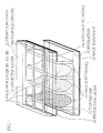
- Fig. 1 is a view of a conventional alternating current (AC) PDP.
- a front substrate 11 and a back substrate 12 are placed in parallel so as to face each other with a space in between. The edges of the substrates are then sealed.
- Scanning electrode group 19a and sustain electrode group 19b are formed in parallel strips on the inward-facing surface of the front substrate 11.
- the electrode groups 19a and 19b are covered by a dielectric layer 17 composed of lead glass or similar.
- the surface of the dielectric layer 17 is then covered with a protective layer 18 of magnesium oxide (MgO).
- a data electrode group 14 formed in parallel strips is covered by an insulating layer 13 composed of lead glass or similar are placed on the inward-facing surface of the back substrate 12.
- Barrier ribs 15 are placed on top of the insulating layer 13, in parallel with the data electrode group 14.
- the space between the front substrate 11 and the back substrate 12 is divided into spaces of 100 to 200 microns by the barrier ribs 15. Discharge gas is sealed in these spaces.
- the pressure at which the discharge gas is enclosed is normally set below external (atmospheric) pressure, typically in a range of between 200 to 500 torr.
- Fig. 2 shows an electrode matrix for the PDP.
- the electrode groups 19a and 19b are arranged at right angles to the data electrode group 14.
- Discharge cells are formed in the space between the substrates, at the points where the electrodes intersect.
- the barrier ribs 15 separate adjacent discharge cells preventing discharge diffusion between adjacent discharge cells so that a high resolution display can be achieved.
- a gas mixture composed mainly of neon is used as the discharge gas, emitting visible light when discharge is performed.
- a color PDP like the one in Fig . 1
- a phosphor layer 16 composed of phosphors for the three primary colors red (R), green (G) and blue (B) is formed on the inner walls of the discharge cells, and a gas mixture composed mainly of xenon (such as neon/xenon or helium/xenon) is used as the discharge gas.
- Color display takes place by converting ultraviolet light generated by the discharge into visible light of various colors using the phosphor layer 16.
- Discharge cells in this kind of PDP are fundamentally only capable of two display states, ON and OFF.
- an ADS method in which one frame (one field) is divided into a plurality of sub-frames (sub-fields) and the ON and OFF states in each sub-frame are combined to express a gray scale is used.
- Fig. 3 shows a division method for one frame when a 256-level gray scale is expressed.
- the horizontal axis shows time and the shaded parts show discharge sustain periods.
- one frame is made up of eight sub-frames.
- the ratios of the discharge sustain period for the sub-frames are set respectively at 1, 2, 4, 8, 16, 32, 64, and 128.
- These eight-bit binary combinations express a 256 gray scale.
- the NTSC (National Television System Committee) standard for television images stipulates a frame rate of 60 frames per second, so the time for one frame is set at 16.7 ms.
- Each sub-frame is composed of the following sequence: a set-up period, a write period, a discharge sustain period and an erase period.
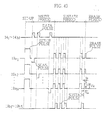
- Fig. 4 is a time chart showing when pulses are applied to electrodes during one sub-frame in one related art.
- all the discharge cells are set-up by applying set-up pulses to all of the scan electrodes 19a.
- data pulses are applied to selected data electrodes 14 while scan pulses are applied sequentially to the scan electrodes 19a. This causes a wall charge to accumulate in the cells to be ignited, writing one screen of pixel data.
- a bulk pulse voltage is applied across the scan electrodes 19a and the sustain electrodes 19b, causing discharge to occur in the discharge cells where the wall charge has accumulated, and light to be emitted for a certain period.
- narrow erase pulses are applied in bulk to the scan electrodes 19a, causing the wall charges in all of the discharge cells to be erased.
- the above PDP driving method also should make the discharge sustain period in each frame as long as possible in order to improve luminance. Accordingly, the write pulses (scan pulses and data pulses) should preferably be as short as possible, so that writing can be performed at high speed.
- High resolution PDPs have a large number of scan electrodes, so it is particularly desirable that the write pulses (scan pulses and data pulses) be narrow to enable driving to be performed at high speed.
- the voltage for the write pulse is high and the pulse narrow, writing may conceivably be performed at high speed without write defects.
- higher speed data drivers have lower ability to withstand voltage, so that it is difficult to realize a driving circuit which can write at both a high voltage and a high speed.
- An object of the present invention is to provide a PDP driving method that operates at high speed, and improves contrast without causing write defects.
- a further object of the present invention is to provide a PDP driving method that improves luminous efficiency.
- Yet another object of the present invention is to provide a PDP driving method that produces high image quality and high luminance without causing flicker and roughness on the screen.
- a staircase waveform that rises in two steps or more is used for the set-up pulses.
- Using this kind of waveform for the set-up pulses rather than a simple rectangular pulse improves contrast without producing write defects.
- Using a staircase waveform that falls in two steps or more for the write pulses rather than a simple rectangular pulse enables high speed driving to be performed without causing write defects.
- a staircase waveform that falls in two steps or more rather than a simple rectangular waveform for the sustain pulses allows a high voltage to be set for the sustain pulses and ensures that operations are performed stably, so that high image quality can be realized.
- luminous efficiency is improved.
- a particularly marked improvement in luminous efficiency is achieved when the second step of the rising portion and the first step of the falling portion of the waveform correspond to a continuous function.
- Luminous efficiency may also be improved by using a waveform whose rising portion is a slope for the sustain pulses.
- Another way of improving luminous efficiency is using a waveform in which the voltage at a time when the discharge current is highest is higher than the applied voltage occurring at a time when the pulse starts for the sustain pulses.
- Using a staircase waveform with two or more steps for the first sustain pulse to be applied during the discharge sustain period improves image quality.
- staircase waveforms for the set-up, write, sustain and erase pulses simultaneously.
- Staircase waveforms that rise and fall in two steps like the ones described as being used for the set-up, write, sustain and erase pulses, are realized by adding two or more pulses together.
- a PDP 10 used in all of the embodiments has the same physical structure as the PDP explained in the related art section of the application with reference to Fig. 1 , so the same numerical references will be used as in Fig. 1 .
- the driving method of the embodiments basically uses the ADS method explained in the related art section of the application.
- at least one of the set-up pulses, scan pulses, sustain pulses and erase pulses that are respectively applied in the set-up, scan, sustain and erase periods has either a staircase or a slope waveform, rather than a simple rectangular wave.
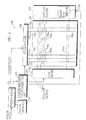
- Fig. 5 is a block diagram showing a structure of a driving apparatus 100.
- the driving apparatus 100 includes a preprocessor 101, a frame memory 102, a synchronization pulse generating unit 103, a scan driver 104, a sustain driver 105 and a data driver 106.
- the preprocessor 101 processes image data input from an external image output device.
- the frame memory 102 stores the processed data.
- the synchronization pulse generating unit 103 generates synchronization pulses for each frame and each sub-frame.
- the scan driver 104 applies pulses to the scan electrodes 19a, the sustain driver 105 to the sustain electrodes 19b, and the data driver to the data electrodes 14.
- the preprocessor 101 extracts image data for each frame from the input image data, produces image data for each sub-frame from the extracted image data (the sub-frame image data) and stores it in the frame memory 102.
- the preprocessor 101 then outputs the current sub-frame image data stored in the frame memory 102 line by line to the data driver 106, detects synchronization signals such as horizontal synchronization signals and vertical synchronization signals from the input image data and sends synchronization signals for each frame and sub-frame to the synchronization pulse generating unit 103.
- the frame memory 102 is capable of storing the data for each frame split into sub-frame image data for each sub-frame.
- the frame memory 102 is a two-port frame memory provided with two memory areas each capable of storing one frame (eight sub-frame images). An operation in which frame image data is written in one memory area, while the frame data written in the other frame memory area is read can be performed alternately on the memory areas.
- the synchronization pulse generating unit 103 generates trigger signals indicating the timing at which each of the set-up, scan, sustain and erase pulses should rise. These trigger signals are generated with reference to the synchronization signals received from the preprocessor 101 regarding each frame and each sub-frame, and sent to the drivers 104 to 106.
- the scan driver 104 generates and applies the set-up, scan, sustain and erase pulses in response to the trigger signals received from the synchronization pulse generating unit 103.
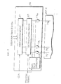
- Fig. 6 is a block diagram showing a structure of the scan driver 104.
- the set-up, sustain, and erase pulses are applied to all of the scan electrodes 19a.
- the required pulse waveform is different in each case.
- the scan driver 104 has three pulse generators, one for generating each kind of pulse, as shown in Fig. 6 . These are a set-up pulse generator 111, a sustain pulse generator 112a and an erase pulse generator 113. The three pulse generators are connected in series using a floating ground method and apply the set-up, sustain and erase pulses in turn to the scan electrode group 19a, in response to the trigger signals from the synchronization pulse generating unit 103.
- the scan driver 104 also includes a multiplexer 115 which, along with the scan pulse generator 114 to which it is connected, enables the scan pulses to be applied in sequence to the scan electrodes 19a 1 , 19a and so on, as far as 19a N .
- a multiplexer 115 which, along with the scan pulse generator 114 to which it is connected, enables the scan pulses to be applied in sequence to the scan electrodes 19a 1 , 19a and so on, as far as 19a N .
- a method in which pulses are generated in the scan pulse generator 114 and output switched by the multiplexer 115 is used, but a structure in which a separate scan pulse generating circuit is provided for each scan electrode 19a may also be used.
- Switches SW 1 and SW 2 are arranged in the scan driver 104 to selectively apply the output from the above pulse generators 111 to 113 and the output from the scan pulse generator 114 to the scan electrode group 19a.
- the sustain driver 105 has a sustain pulse generator 112b and generates sustain pulses in response to the trigger signals from the synchronization pulse generating unit 103, and applies the sustain pulses to the sustain electrodes 19b.
- the data driver 106 outputs data pulses to the data electrodes 14 1 to 14 M in parallel. Output takes place based on sub-field information which is input serially into the data driver 106 one line at a time.
- Fig. 7 is a block diagram of a structure for the data driver 106.
- the data driver 106 includes a first latch circuit 121 which fetches one scan line of sub-frame data at a time, a second Latch circuit 122 which stores one line of sub-frame data, a data pulse generator 123 which generates data pulses, and AND gates 124 1 to 124 M located at the entrance to each electrode 14 1 to 14 M .
- sub-frame data sent in order from the preprocessor 101 is synchronized with a CLK (clock) signal and fetched sequentially so many bits at a time.
- CLK clock
- the second latch circuit 122 opens the AND gates from the AND gates 124, to 124 M belonging to the data electrodes that are to have the pulses applied, in response to the trigger signals from the synchronization pulse generating unit 122.
- the data pulse generator 123 generates the data pulses simultaneously with this, and the data pulses are applied to the data electrodes with open AND gates.
- the operations for one sub-frame composed of a sequence of the set-up, write, discharge sustain and erase periods are repeated eight times to display a one-frame image.
- switches SW 1 and SW 2 in the scan driver 104 are ON and OFF respectively.
- the set-up pulse generator 111 applies a set-up pulse to all of the scan electrodes 12a, causing a set-up discharge to occur in all of the discharge cells, and a wall charge to accumulate in each discharge cell. Applying a certain amount of wall voltage to each cell enables the write discharge occurring in the following write period to commence sooner.
- the switches SW 1 and SW 2 in the scan driver 104 are OFF and ON respectively.
- Negative scan pulses generated by the scan pulse generator 114 are applied sequentially from the first row of scan electrodes 19a 1 to the last row of scan electrodes 19a N.
- the data driver 106 performs a write discharge by applying positive data pulses to the data electrodes 14 1 to 14 M corresponding to the discharge cells to be ignited, accumulating a wall charge in these discharge cells.
- a one-screen latent image is written by accumulating a wall charge on the surface of the dielectric layer in the discharge cells which are to be ignited.
- the scan pulses and the data pulses should be set as narrow as possible to enable driving to be performed at high speed. However, if the write pulses are too narrow, write defects are likely. Additionally, limitations in the type of circuitry that may be used mean that the pulse width usually needs to be set at about 1.25 ⁇ m or more.
- the switches SW 1 and SW 2 in the scan driver 104 are ON and OFF respectively.
- the operations in which the sustain pulse generator 112a applies a discharge pulse of a fixed length (for example 1 to 5 ⁇ s) to the entire scan electrode group 12a and the sustain driver 105 applies a discharge pulse of a fixed length to the entire sustain electrode group 12b are alternated repeatedly.
- This operation raises the electric potential of the surface of the dielectric layer above the discharge starting voltage (hereafter referred to as the starting voltage) in the discharge cells in which a wall charge had accumulated during the write period, so that discharge occurs in such cells.
- This sustain discharge causes ultraviolet light to be emitted within the discharge cells. The ultraviolet light excites the phosphors in the phosphor layer to emit visible light corresponding to the color of the phosphor layer in each discharge cell.
- Narrow erase pulses are applied to the entire scan electrode group 19a, erasing the wall charge in each discharge cell by generating a partial discharge.
- Fig. 8 is a time chart showing a PDP driving method relating to the present embodiment.
- the set-up pulses had a simple rectangular wave. In this embodiment, however, the set-up pulses use a staircase waveform that rises in two steps.
- This kind of waveform is achieved by adding two pulse waveforms and applying them.
- Fig. 9 is a block diagram of a pulse adding circuit which generates the staircase waveform.
- the pulse adding circuit includes a first pulse generator 131, a second pulse generator 132 and a time-delay circuit 133.
- the first and second pulse generators 131 and 132 are connected in series using a floating ground method, and the output voltage of the two generators added.
- Fig. 10A shows a situation in which the pulse adding circuit synchronizes first and second pulses to form a staircase waveform which rises in two steps.
- the first pulse generated by the first pulse generator 131 is a wide rectangular wave and the second pulse generated by the second pulse generator 132 is a narrow rectangular wave.
- the first pulse is generated by the first pulse generator 131 and then the second pulse is generated by the second pulse generator 132 having been delayed by the time-delay circuit 133 for a set amount of time.
- the pulses are generated in response to trigger signals from the added pulse generating unit 103.
- the width of each pulse is set so that the first and second pulses fall at almost the same time.
- the first and second pulses are added in this way, causing the output pulse to rise in two steps.
- the first and second pulse generators 131 and 132 may be connected in parallel and the first and second pulses output so that they overlap.
- a staircase pulse which has a two-step rise can be generated by causing the second pulse generator 132 to generate a second pulse at a higher level than the first pulse.
- the set-up pulse generator 111 in this embodiment has one such circuit and uses a staircase waveform that has a two-step rise for the set-up pulses.
- set-up pulses are applied to the discharge cells to accumulate a certain amount of wall charge in each discharge cell, with the aim of creating conditions in which writing can be performed accurately in a short time during the write period.
- Wall charge may also be accumulated stably and brightness limited by using a slope for the rising part of the waveform, as is taught for example by Weber in US Patent No. 5,745,086 .
- the rise time in Weber is extremely long. Using the two-step rising waveform of the present invention instead means that set-up can be performed stably using a narrower pulse.
- set-up can be performed stably during a short set-up period, making it possible to perform driving at a much higher speed.
- the PDP driving method of this embodiment can thus drive the panel at high-speed without write defects, and improve contrast to achieve superior image quality.
- the ratio of V 1 to V st should be set at 0.3 to 0.4 or more, and the ratio of (V st - V 1 ) to V st should be set at 0.6 to 0.7 or less.
- the ratio of t p to t w should be set at 0.8 to 0.9 or less.
- the first-step rise voltage V 1 should preferably be set within the range V f - 70V ⁇ V 1 ⁇ V f .
- V f is the starting voltage at the driving apparatus.
- the starting voltage V f is a fixed value determined by the structure of the PDP 10, and is measured by, for example, applying a very slowly increasing voltage between the scan electrodes 12a and the sustain electrodes 12b and reading the applied voltage when the discharge cells start to ignite.
- a two-step rise waveform was used for the set-up pulses when driving a PDP. While driving was performed, the peak voltage V st and the pulse width t w remained fixed, but the t p to t w ratio and the (V st -V 1 ) to V st ratio were changed to various values and the variations in contrast and brightness measured.
- Each of the waveforms for the set-up pulses was generated by a given waveform generator and the voltage of this output was amplified by a high-speed high-voltage amplifier before being applied to the PDP.
- Contrast was measured by igniting one part of the PDP to produce white color in a dark room and measuring the luminance ratio of the dark part to the' light part.
- Fig. 11 shows the results of this experiment, displaying the relation between the ratio t p to t w and the ratio (V st -V 1 ) to V and contrast.
- the shaded area in the drawing is the area in which contrast is high and variations in luminance caused by write defects are low; in other words, the acceptable area.
- the area outside of the shaded area shows unacceptable results.
- the ratio t p to t w should preferably 0.8 to 0.9 or less and the ratio (V st -V 1 ) to V 0.6 to 0.7 or less
- the ratios be set at 0.05 or above.
- the present embodiment uses a waveform in which two pulses are added to form a two-step rising staircase waveform as the set-up pulse.
- the same superior image effects may be achieved by adding three or more pulses to generate a multi-step waveform having three or more rises.
- Fig. 12 is a time chart showing a PDP driving method relating to the present embodiment.
- a two-step rising waveform was used for the set-up pulses, but in this embodiment a two-step falling waveform is used for the set-up pulse.
- Fig. 13 shows a situation in which the pulse adding circuit adds first and second pulses to form a staircase waveform which falls in two steps.
- the two-step falling waveform uses a pulse adding circuit like the one explained in the first embodiment and can be generated by adding a first pulse generated by the first pulse generator 131 and a second pulse generated by the second pulse generator 132.
- a pulse adding circuit like the one in Fig. 9 in which a first pulse generator and a second pulse generator are connected in series using a floating ground method, is used.
- a first pulse with a wide rectangular wave is raised by the first pulse generator 131 at almost the same time as a second pulse with a narrow rectangular wave is raised by the second pulse generator 132.
- a two-step falling waveform is generated by adding the two pulses.
- a pulse adding circuit in which the first and second pulse generators are connected in parallel is used. In this case, as shown in Fig.
- the first pulse generator raises a first pulse which is a narrow rectangular wave at a relatively high level and the second pulse generator a second pulse which is a rectangular wave at a relatively low level.
- the two pulses are added to generate a two-step falling waveform.
- the priming effect is also weakened.
- the wall charge may be accumulated stably and brightness controlled in a similar way, but the fall time for the waveform is long.
- the use of a two-step falling waveform enables set-up to be performed stably with a narrower pulse.
- using the two-step falling waveform enables set-up to be performed in a short set-up period, allowing driving to be performed at a higher speed.
- the PDP driving method of this embodiment enables driving to be performed at high speed without write defects, and contrast is drastically improved. As a result, superior image quality can be realized.
- a technique using a pulse having a waveform with a stepped falling time is disclosed, for example, in the IBM Technical Disclosure Bulletin (Vol. 21, No. 3, August 1978 ). This reference teaches use of a write pulse with a stepped falling time as a way of avoiding self-erasing. However, to obtain the above effects, a set-up pulse should preferably be set as described hereafter.
- the ratio of V 1 to V st should be set at no more than 0.8 to 0.9.
- the ratio of t p to t w should be set at no more than 0.6 to 0.8.
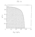
- a PDP was driven using the same method as in the experiment of the first embodiment, using various set-up pulses with different two-step falling waveforms, and the contrast measured in each case.
- Fig. 14 shows the results of this experiment, displaying the relation between the ratio t p to t w and the ratio V 1 to V st and contrast.
- the shaded area in the drawing is the area in which contrast is high and variations in luminance caused by write defects are low; in other words, the acceptable area.
- the area outside of the shaded area shows unacceptable results.
- the ratios t p to t w and V 1 to V st should not be too large, so that the ratio t p to t w should preferably be no more than 0.6 to 0.8 and the ratio no more than V 1 to V st 0.8 to 0.9. However, if the ratios t p to t w and V 1 to V st are too small useful effects will not be achieved, so it is preferable that the ratios be set at 0.05 or above.
- the present embodiment uses a waveform in which two pulses are added to form a two-step falling staircase waveform as the set-up pulse.
- the same effect may be achieved by adding three or more pulses to generate a multi-step waveform having three or more falls that may realize superior image quality.
- Fig. 15 is a time chart showing a PDP driving method relating to the present embodiment.
- a two-step rising waveform was used for the set-up pulses.
- the present embodiment uses a multi-step staircase waveform which rises in three or more steps (for example five steps).
- This kind of multi-step waveform set-up pulse can be obtained by using a staircase wave generating circuit as the set-up pulse generator 111.
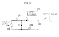
- Fig. 16 is a block diagram of a staircase wave generating circuit described in 'Denshi Tsushin Handobuku' (Electronic Communication Handbook) published by Denshi Tsushin Gakkai.
- the staircase wave generating circuit includes a clock pulse generator 141, which generates a fixed number (in this case five) of successive negative pulses (voltage V p ), capacitors 142 and 143, and a reset switch 144.
- a capacitance C 1 of the capacitor 142 is set higher than a capacitance C 2 of the capacitor 143.
- the voltage of an output unit 195 rises to C 1 /(C 1 +C 2 )V p .
- the voltage of the output unit 145 rises to C 1 ⁇ C 2 /(C 1 +C 2 ) 2 V p when a second pulse is issued and to C 1 ⁇ C 2 /(C 1 +C 2 ) 3 V p when a third, pulse is issued.
- the effect obtained by using this kind of multi-step rising waveform is basically the same as that in the first embodiment. However, although the voltage rises to the same level, the rise in voltage for each step is smaller, enabling a greater effect to be obtained.
- the average value for the rate of voltage change in steps after the first step should preferably be set at not less than 1V/ ⁇ s but not more than 9V/ ⁇ s.
- the average rate of voltage change ⁇ is set at 10V/ ⁇ s s or more, the light emitted by the set-up pulse discharge is stronger and contrast drops markedly. If the average rate of voltage change ⁇ stays within this range, however, and especially if it is set at 6V/ ⁇ s or less, the light emitted by the set-up pulse discharge is much weaker than that emitted by the sustain discharge and contrast is almost totally unaffected.
- the voltage V 1 for the first-step rise should be set in relation to the starting voltage V f so that V f - 70V ⁇ V 1 ⁇ V f .
- the average rate of voltage change ⁇ [V/ ⁇ s] following the first step was set at various values between 2.1 and 10.5 and measurements taken.
- Set-up pulses with variously-shaped waveforms were generated using a given waveform generator and their voltage amplified by a high-speed high-voltage amplifier before being applied to the PDP.
- the voltage of the set-up pulse in the first-step rise was set at 180V, 20V lower than the starting voltage V f .
- the wall charge transfer amount ⁇ Q was measured by connecting a wall charge measuring apparatus to the PDP.
- This circuit used the same principle as Sawyer-Tower circuits employed when evaluating the characteristics of ferroelectrics and the like.
- Fig. 17 shows the results of this measurement, illustrating the relation between write pulse voltage V data and wall charge transfer amount ⁇ Q for each value of an average rate of voltage change ⁇ .
- V data is accompanied by an increase in the wall charge transfer amount ⁇ Q produced by the write discharge. This shows that increasing V data increases the probability of discharge and reduces write defects.
- V data occupies a small range, showing that the wall charge transfer amount ⁇ Q is larger for higher values of the average rate of voltage change ⁇ .
- the average rate of voltage change ⁇ is set at a relatively high level within this range, the level of the wall charge transfer amount ⁇ Q is maintained and the PDP can be correctly driven even if V data is set at a low value.
- the wall charge at the completion of the set-up period can be restricted to the desired level without losing contrast and write discharge defects restricted.
- image quality deterioration as flicker and roughness can be limited and superior image quality achieved.
- the present embodiment showed an example in which a multi-step rising pulse waveform was used for the set-up pulses, but a staircase waveform which has multi-steps in both its rising and falling portions may also be used for the set-up pulse to achieve the same high level of image quality.
- Fig. 18 is a time chart showing a PDP driving method relating to this embodiment.
- the present embodiment uses a staircase waveform that falls in two steps as a data pulse.
- a pulse adding circuit such as the one explained in the second embodiment may be used in the data pulse generator 123 to apply the two-step falling staircase waveform for the data pulses.
- a data pulse width set at no more than 2 ⁇ s causes the discharge efficiency of the sustain discharge to fall and there will be a tendency for sharp reductions in image quality caused by write defects to occur.
- the use of a two-step falling staircase waveform for the data pulses instead of a simple rectangular wave enables the write pulses (scan pulses and data pulses) to be set at a smaller width without reducing discharge efficiency during the sustain discharge.
- the width of the write pulses can be set as narrow as 1.25 ⁇ s.
- the discharge operation from the write period to the discharge sustain period is performed in the following way. First, discharge is performed in the scan electrodes and the data electrodes by applying write pulses. As a result of this priming, a sustain discharge can be performed between the scan electrodes and the sustain electrodes when sustain pulses are applies.
- the discharge delay from when the pulse is applied to when discharge is performed is long and the discharge delay time (the time from when the pulse rises until the discharge peak) is around 700 to 900 ns. This means that shortening the time between the rise and the fall of the data pulse is likely to produce discharge defects. Additionally, discharge delay is caused in the discharge sustain period also, making unstable light emission likely.
- the discharge delay time is reduced to a short 300 to 500 ns, and discharge completed in a short time. This means that discharge can be achieved reliably even if the time between the rise and the fall of the data pulses, i.e. the pulse width, is shortened, enabling writing to be performed stably.
- a driver IC power MOSFET
- This driver IC has a low ability to withstand voltage of 100 V or less and a fast slewing rate in the rising period of the pulse. This means that driving can be performed at both a high voltage and a high speed.
- the PDP driving method of the present embodiment uses a low cost driving circuit to achieve high-speed, stable writing.
- the first-step fall should preferably be set in the range of 10V to 100V. This is because effects are difficult to obtain at less than 10V and a waveform with a first-step fall of more than 100V is difficult to achieve with a driver IC that has a low ability to withstand voltage.
- a technique using a pulse having a stepped fall time is disclosed, for example, in the IBM Technical Disclosure Bulletin (Vol. 21, No. 3, August 1978 ). This reference teaches that a stepped falling waveform is valuable in order to avoid selferasing. However, in order to achieve the above effects., it is desirable to set pulse width in a range of 0.5 ⁇ s to 2.0 ⁇ s when the peak voltage of the write pulse is between 70V and 100V, as shown by the results of the following experiment.
- a PDP was driven by applying data pulses, composed of waveforms in which a pulse width PW was set at various values, to the data electrodes, and the wall charge transfer amount ⁇ Q [pC] was measured before and after the write discharge.
- the data pulse voltage V data was set variously at 60, 70, 80, 90 and 100 V.
- the wall charge transfer amount ⁇ Q was measured by connecting the wall charge measuring apparatus of the third embodiment to the PDP.
- Fig. 19 shows the results of this measurement, illustrating the relation between the data pulse width PW and wall charge transfer amount ⁇ Q for each value of the data pulse voltage V data
- V data is set higher than this, the wall charge transfer amount ⁇ Q can be maintained at a high value, even if the pulse width PW is reduced, and write discharge can still be performed normally.
- V data is 100V, for example, even if the pulse width PW is set at 1.0 ⁇ s , a high value of around 6 [pC] can be obtained for the wall charge transfer amount ⁇ Q and write discharge is performed normally.
- the wall charge transfer amount ⁇ Q can be maintained at roughly the same value, and the voltage V data can be stabilized in a range of 5.50 to 6.00 pC.
- the pulse width PW is 2.0 ⁇ s or less, a voltage V data of between 70V and 100V has a much larger wall charge amount than a voltage V data of 60V.
- pulse width PW is set in a range of 2.0 ⁇ s or less
- a write pulse with a peak voltage of between 70V and 100V is desirable in order to accumulate a satisfactory wall charge.
- the value of the wall charge transfer amount ⁇ Q will be less than the stable range (5.50 to 6.00 pC) when pulse width PW is less than 0.5 ⁇ s. Consequently, a pulse width PW of 0.5 ⁇ s or more is required to to accumulate a satisfactory wall charge when the peak voltage of the write pulse is 100V or less.
- the PDP was driven using both a rectangular wave with a maximum voltage V p of 60 (V) and a two-step falling staircase waveform with a maximum voltage of 100V like that in the present embodiment as a data pulse.
- the applied voltage waveform and the wall charge transfer amount ⁇ Q waveform were measured in each case, along with the average discharge delay time for the write discharge. Screen flicker was also measured.
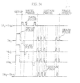
- Fig. 20 is a time chart showing a PDP driving method relating to the present embodiment.
- a two-step rising staircase waveform is used for a data pulse.
- a pulse adding circuit such as the one explained in the first embodiment may be used as the data pulse generator 123 of Fig. 7 to apply the two-step rising staircase waveform for the data pulses.
- the voltage of the data pulses applied to the data electrodes is set at a low level, the light emission caused by the data pulses can be restricted, but the discharge delay for the write discharge increases. This means that write defects are generated and deterioration in image quality is likely to occur.
- the voltage variation for each step is small and the pulse can be raised to a high voltage, enabling the light emission caused by the data pulse to be restricted without producing write defects.
- driver Ies with a low ability to withstand voltage of 100V or less are used for the first and second pulse generators in the pulse adding circuit, allowing the PDP to be driven at high speed. Even if a two-step rising staircase waveform is used for the write pulses, however, the second step rise should preferably be set within the range of 10V to 100V.
- the PDP 10 was driven by the reflated art driving method using a simple rectangular wave as the data pulse, and light emissions produced by the write discharge and the sustain discharge were observed.
- Fig. 21A shows the change over time of data pulse voltage V data scan pulse voltage V SCN-SUS , and brightness occurring when the write discharge is performed.
- Fig. 21B shows the change over time of sustain pulse voltage V SCN-SUS and brightness occurring when the sustain discharge is performed.
- the peak brightness of the write discharge shown in Fig. 21A is larger than the peak brightness for the first sustain pulse caused by the sustain discharge, and has the same peak brightness area as the peak brightness for the second sustain pulse.
- the PDP was driven using both a simple rectangular wave and a two-step rising staircase waveform described in the present embodiment, for the data pulses, and the image quality and screen flicker were measured.
- the data pulse was generated using a given waveform generator, and its voltage amplified by a high-speed high-voltage amplifier before being applied to the PDP.
- the maximum voltage V P in both cases was 100V.
- Table Two shows the results of the Experiment. Table Two MAX. VOLTAGE V p [V] EQUALITY OF DISPLAY IMAGE FLICKER RECTANGULAR WAVE 100 HALF TONE DISCONTINUITY NO WAVEFORM OF FIFTH EMBODIMENT 100 SATISFACTORY NO
- Fig. 22 is a time chart showing a PDP driving method relating to the present embodiment.
- the present embodiment uses a two-step falling staircase waveform as a sustain pulse.
- a pulse adding circuit like the one explained in the second embodiment should preferably be used as the sustain pulse generators 112a and 112b shown in Figs. 5 and 6 .
- This phenomenon is generally referred to as the self-erasing discharge, and occurs when an overly strong discharge at the rise time causes the wall charge accumulated inside the discharge cells to be too high. This means that discharge at the fall time takes place in the reverse direction to that at the rise time. If this self-erasing discharge is generated, the wall charge accumulated by the discharge during the rise time is reduced, causing a corresponding drop in luminance. Additionally, when discharge is performed by the next pulse voltage in the reverse direction, the reduction in effective voltage applied to the discharge gas inside the discharge cell causes an abnormal operation in which unstable discharge is produced.
- the sustain pulse voltage is set at a high level and light emission of a high luminance produced, while stable operation can be ensured, enabling superior image quality to be achieved.
- Fig. 2 of this reference teaches a technique in which an enhancement pulse is added to a conventional pulse to form a staircase waveform. In order to achieve the above effects, however, it is desirable to set the sustain pulse as described below.
- the PDP was driven using a simple rectangular wave as a sustain pulse, and changes over time in the voltage between the scan electrodes and the sustain electrodes, and the brightness-measured. A reasonably high drive voltage and one similar to that in a conventional PDP was used.
- the PDP was then driven at a reasonably high voltage using a two-step staircase waveform for the sustain pulses.
- the changes over time in voltage between the scan electrodes and the sustain electrodes, and in brightness were measured.
- the PDP was driven under each of the conditions above and the luminance in each case measured in the following way.
- a photo diode was used to observe brightness and the relative luminance in each case calculated from the integral value of the peak brightness. Measurement of the waveforms in each case was performed using a digital oscilloscope.
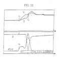
- Fig. 23 and 24 show the results of measurement of changes over time in the voltage V and brightness B .
- Fig. 23A shows results for a rectangular wave at a regular drive voltage
- Fig. 23B for a rectangular wave at a reasonably high drive voltage
- Fig. 24 shows results for a two-step falling staircase waveform at a reasonably high voltage.
- Table Three shows the maximum voltage V p of the sustain pulses, the luminance measurement result (relative value) and whether a self-erasing discharge is present or not.
- the relative luminance values in Table Three reveal that luminance is higher when a two-step falling staircase waveform is used than when a rectangular wave is used.
- a two-step falling staircase waveform was used for the sustain pulses and light emission checked with the maximum voltage set at various levels. It was observed that no light emission peak was visible at the fall time when the maximum voltage was no more than twice as much (2V smin ) the minimum discharge sustain voltage V smin and that a light emission peak was visible at the fall time when the maximum voltage was more than twice as much (2V smin ) as the minimum discharge sustain voltage self-erasing discharge V smin
- Fig. 25 is a time chart showing a PDP driving method relating to the present embodiment.
- the present embodiment uses a staircase waveform that rises and falls in two steps for the sustain pulses.
- a pulse adding circuit like the one explained in the first embodiment may be used as the sustain pulse generators 112a and 112b shown in Figs. 5 and 6 , with the second pulse set more narrowly.
- a two-step rising and falling staircase waveform can be generated in the following way.
- the kind of pulse adding circuit shown in Fig. 9 in which first and second pulse generators are connected in series using a floating ground method, may be used.
- a broad rectangular wave is raised as a first pulse by the first pulse generator.
- a very narrow rectangular wave is raised as a second pulse by the second pulse generator.
- the two pulses are then added.
- a pulse adding circuit in which the first and second pulse generators are connected in parallel may be used.
- a wide rectangular wave is raised as the first pulse by the first pulse generator at a low level.
- a narrow rectangular wave is raised as the second pulse by the second pulse generator at a high level.
- a two-step rising and falling staircase waveform is then generated by adding the two pulse.
- the maximum voltage of the sustain pulses can be set at a high level, so that even if light is emitted at a high luminance, power consumption will not be very large.
- the PDP driving method of the present embodiment has higher luminance and a rate of increase in power consumption which is relatively lower than the rate of increase in luminance, enabling discharge efficiency to be increased.
- Fig. 2 of this reference teaches a technique in which an enhancement pulse is added to a conventional pulse to form a staircase waveform. In order to achieve the above effects, however, it is desirable to set the sustain pulse as described below.
- the voltage raised in the first step is set in relation to the starting voltage V f so that it is in the range of not less than V f - 20V but not more than.
- V f - 30V the voltage sustaining period between the first step rise and the second step rise is set in relation to the discharge delay time T df so that it is not less than T df - 0.2 ⁇ s but not more than T df + 0.2 ⁇ s.
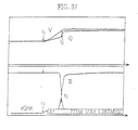
- a PDP using a two-step rising and falling staircase waveform for the sustain pulses was driven and the amount of power consumed inside discharge cells when the sustain discharge was produced evaluated by observing a V-Q Lissajous's figure.
- the sustain pulses were generated by a given waveform generator and applied to the PDP after their voltage was amplified by a high-speed high-voltage amplifier.
- the V-Q Lissajous's figure shows the way in which the wall charge Q accumulated in the discharge cells during the first cycle of the pulse changes in a loop.
- the loop area WS in the V-Q Lissajous's figure has a relation to the power consumption W during discharge that is expressed by the formula (1) below.
- W fS (note that f is a driving frequency)
- the wall charge Q accumulated in the discharge cells is measured by connecting a wall charge measuring apparatus to the PDP.
- This apparatus uses the same principle as Sawyer-Tower circuits employed to evaluate characteristics of ferroelectrics and the like.
- Fig. 27 shows V-Q Lissajous ⁇ s figures occurring when a PDP using a simple rectangular wave as the sustain pulse was driven, a is the figures showing when the PDP was driven using a low voltage and b when the PDP was driven using a high voltage.
- Lissajous's figures a and b are analogous parallelograms. This illustrates the fact that when a rectangular pulse is used, increases in the drive voltage produce proportional increases in power consumption.
- Fig. 28 is an example of a V-Q Lissajous's figure observed when the PDP is driven using a two-step rising and falling staircase waveform as the sustain pulse.
- V-Q Lissajous's figure shown in the drawing is an flattened lozenge shape rather than the parallelograms shown in Fig. 28 .
- V-Q Lissajous's figures were measured for a PDP driven using a two-step rising and falling staircase waveform for the sustain pulses when various values were used for the voltage in the first-step rise and the voltage sustaining period from the first-step rise to the second-step rise.
- the rising voltage in the first step was set in the range of V f - 20V to V f + 30V, a comparatively flattened loop was measured.
- the voltage sustaining period was set in the range of T df - 0.2 ⁇ s to T df + 0.2 ⁇ s a comparatively flattened loop was also measured.
- the PDP 10 was driven, using both a simple rectangular wave and a two-step rising and falling staircase waveform for the sustain pulses, and the luminance and power consumption in each case were measured.
- the relative luminance value was calculated from the integral value of the peak brightness.
- the power consumed when driving the PDP was also measured and a relative luminous efficiency ⁇ calculated from the relative luminance and the relative power consumption.
- Table Four shows the relative values for relative luminance, relative power consumption and relative luminous efficiency. Table Four RELATIVE BRIGHTNESS RELATIVE POWER CONSUMPTION RELATIVE EFFICIENCY RECTANGULAR WAVE 1.00 1.00 1.00 WAVEFORM OF SEVENTH EMBODIMENT 1.30 1.15 1.13
- the PDP driving method of the present embodiment enables superior driving with higher luminance and luminous efficiency than in the driving method of the related art to be realized.
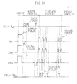
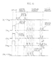
- Fig. 29 is a time chart showing a PDP driving method relating to the present embodiment.
- the present embodiment uses a two-step rising and falling staircase waveform as the sustain pulse, as was the case in the seventh embodiment, but the waveform has the following unique features.
- Fig. 30 shows the waveform for the sustain pulse used in the present embodiment.
- a pulse adding circuit as explained in the eighth embodiment may be used as the sustain pulse generators 112a and 112b shown in Figs. 5 and 6 , in order to apply a staircase waveform having the above unique characteristics for the sustain pulses.
- a pulse oscillator having a RLC (resistor-inductor-capacitator) circuit is used for the second pulse generator, so as to determine the rise and fall portions of the second pulse trigonometrically.
- a waveform having the above unique characteristics can be generated in the following way.
- a pulse adding circuit having first and second pulse generators connected in series using a floating ground method as in Fig. 9 is used.
- a wide waveform is raised as a first pulse by the first pulse generator.
- an extremely narrow trigonometrically altered waveform is raised as the second pulse by the second pulse generator.
- the two pulses are then added.
- a pulse adding circuit in which first and second pulse generators are connected in parallel may be used.
- a wide rectangular wave is raised at a comparatively low level as the first pulse by the first pulse generator.
- a narrow trigonometrically determined second pulse is raised at a comparatively high level by the second pulse generator.
- the two pulses are added to generate a waveform with the unique characteristics described above.
- the slope at which the second pulse rises and falls can be adjusted by adjusting the time constant of the RLC circuit in the second pulse generator.
- the driving method of this embodiment like that of the seventh embodiment, improves luminance while restricting increases in power consumption, and improving luminous efficiency.
- the effects produced by this embodiment are much greater however.
- the reason that luminous efficiency is even higher when using the waveform of the present embodiment lies in the fact that the phase of the voltage variation is delayed until after the phase of the discharge current in the second step of the rising period by using characteristics (1) and (2) above. This causes a situation in the discharge cells where an overvoltage is applied from the power source after discharge has started to take place within the cells, causing power to be forcibly injected into the plasma inside the discharge cells.
- luminous efficiency is increased by creating a situation in which a high voltage is applied to the discharge cells primarily during the period in which light emission takes place. This is achieved using characteristics (3) and (4) above.
- the phase of the voltage (terminal voltage for the discharge cells) variation in the second step during the rising period should preferably be set later than the phase of the discharge current, so that luminous efficiency can be improved.
- the second step rise should preferably be performed within a discharge period T dise during which a discharge current is flowing, so that luminous efficiency can be improved.
- the discharge period T dise is the period between the completion of a charge period T chg in which the discharge cells are charged to capacity and the end of the flow of the discharge current.
- the 'discharge cell capacity' can be viewed as a geometric capacity decided by the structure of the discharge cells formed by the scan electrodes, the sustain electrodes, the dielectric layer and the discharge gas.
- the discharge period T dise can be described as 'the period from the completion of the charge period T chg during which the discharge cells are charged to geometric capacity to the completion of the discharge current'.
- a trigonometrically determined pulse may also be used for the first pulse. This generates a pulse in which both the first and second steps of the rising period are trigonometrically determined to be used for the sustain pulse.
- the first-step rise is a discharge period dscp from the start of the discharge period T dise until the discharge current has reached its maximum value.
- the second-step rise is a period between the time that the discharge current has reached its maximum value until the completion of the discharge period T dise .
- the PDP was driven using a waveform with the characteristics described above for the sustain pulses.
- a voltage V occurring between electrodes (scan and sustain electrodes) in the discharge cells, a wall charge amount Q accumulated in the discharge cells, the amount of variation in the wall charge amount dQ / dt and brightness B of the PDP were measured and a V-Q Lissajous ⁇ s figure was also observed.
- Figs. 32 and 33 show the results of these measurements.
- the electrode voltage V and the wall voltage Q , and the variation in wall voltage amount ⁇ Q and brightness B are plotted along a time axis.
- Fig. 33 is an example of a V-Q Lissajous ⁇ s figure.
- the period during which the brightness B is at a high level coincides with the period in which a high voltage is applied to the discharge cells, revealing that a high voltage is applied to the discharge cells primarily during the period when light i.s being emitted.
- the V-Q Lissajous ⁇ s figure of Fig. 33 is a flattened diamond shape, with curved indentations at both left and right ends. These indentations show that the loop area has decreased, even though the wall charge transfer amount in the discharge cells remains the same. In other words, the power consumption is smaller although the amount of light emitted is the same.
- the PDP 10 was driven by the same method as in the experiment in the seventh embodiment, using a simple rectangular wave and then the staircase waveform of the present embodiment for the sustain pulses.
- Luminance and power consumption were measured, and relative luminous efficiency calculated from relative luminance and relative power consumption.
- Table Five shows the values for relative luminance and relative power consumption and relative luminous efficiency.
- Table Five RELATIVE BRIGHTNESS RELATIVE POWER CONSUMPTION RELATIVE EFFICIENCY RECTANGULAR WAVE 1.00 1.00 1.00 WAVEFORM OF EIGHTH EMBODIMENT 2.11 1.62 1.30
- the present embodiment shows an example which used a waveform whose second step in the rising period and first step in the falling period were trigonometrically determined, but any continuous function may be used to achieve similar effects.
- a waveform altered by an exponential function or a Gaussian function may also be used.
- Fig. 34 is a time chart showing a DDP driving method relating to the present embodiment.
- the present embodiment uses a trapezoid waveform, shaped so that no impact is made on the rate at which voltage is driven upward during the rise time, for the sustain pulses.
- This kind of rising slope waveform may be applied for the sustain pulses using, for example a trapezoid waveform generating circuit shown in Fig. 35 as the sustain pulse generators 112a and 112b shown in Figs. 5 and 6 .
- This trapezoid waveform generating circuit is composed of a clock pulse oscillator 151, a triangular wave generating circuit 152 and a voltage limiter 153.
- the voltage limiter 153 cuts the voltage at a certain level.
- the clock pulse oscillator 151 generates a rectangular wave shown in Fig. 36A in response to a trigger signal from the added pulse generator 103.
- the triangular waveform generating circuit 152 generates a triangular waveform shown in Fig. 36B based on this rectangular wave. Then the voltage limiter 153 cuts off the peak of the triangular waveform to generate a trapezoid waveform shown in Fig. 36C .
- a mirror integrated saw wave generating circuit may be used for the triangular waveform generator 151, as shown in Fig. 35 .
- the mirror integrated cut wave generating circuit of Fig. 35 is described in the Denshi Tsushin Handobuku already mentioned.
- a Zener diode limiter may be used, for example, as the voltage limiter 153.
- Using a rising slope waveform for the sustain pulses rather than the simple rectangular wave of the related art enables power consumption to be kept at a low level without reducing luminance. In other words, superior image quality can be realized with low power consumption.
- a waveform in which the rise period is a slope and the fall period is in two steps may also be used for the sustain pulses to obtain the same effects as those in the seventh embodiment.
- the angle of the rise slope in the sustain pulse should preferably be in the range of 20V to 8.00V / ⁇ s.
- the angle should preferably be in the range of 40V to 400V / ⁇ s.
- the PDP was driven using a rising slope sustain pulse, and the voltage occurring between electrodes V (scan and sustain electrodes), the wall charge amount Q accumulated in the discharge cells, the variation dQ / dt in the wall charge amount Q and brightness B of the PDP were measured in the same way as for Experiment 8B in the eighth embodiment. A V-Q Lissajous ⁇ s figure was also observed.
- the rising slope of the sustain pulse had a gradient of 200v/ ⁇ s.
- Figs. 37 and 38 show the results of these measurements.
- the electrode voltage V and the wall voltage Q , and the variation in wall voltage amount ⁇ Q and brightness B are plotted along a time axis.
- Fig. 38 is an example of a V-Q Lissajous ⁇ s figure.
- the V-Q Lissajous ⁇ s figure of Fig. 38 is a thin flattened lozenge shape. This V-Q Lissajous ⁇ s figure is formed with slanting left and right ends due to the fact the starting voltage is lower that the ending voltage.
- the PDP 10 was driven by the same method as in the experiment of the seventh embodiment, using either a simple rectangular wave or a rising slope waveform like the one in the present embodiment for the sustain pulses.
- the luminance and power consumption were measured in each case, and a relative luminous efficiency ⁇ calculated from the relative luminance and the relative power consumption.
- Table Six shows values for the relative luminance and relative power consumption and the relative luminous efficiency ⁇ .
- Table Six RELATIVE BRIGHTNESS RELATIVE POWER CONSUMPTION RELATIVE EFFICIENCY RECTANGULAR WAVE 1.00 1.00 1.00 WAVEFORM OF NINTH EMBODIMENT 0.93 0.87 1.07
- Fig. 39 is a time chart showing a PDP driving method relating to the present embodiment.
- a first sustain pulse applied in the discharge sustain period uses a waveform that has been altered to a two-step rising and falling one, but from the second sustain pulse onward uses the same simple rectangular wave as in the related art.
- the pulse adding circuit explained in the first embodiment is used as the sustain pulse generator 112b shown in Fig. 5 .
- a switch is provided to turn the operation of the second pulse generator ON and OFF.
- the second pulse generator is switched ON only when the first sustain pulses are applied.
- a first pulse generated by the first pulse generator and a second pulse generated by the second pulse generator are added to generate a two-step rising and falling staircase waveform, as shown in Fig. 26 relating to the seventh embodiment.
- the second and subsequent sustain pulses are generated, only the first pulse is generated by the first pulse generator.
- the discharge generated by the first sustain pulses applied during the discharge sustain period is unstable (low discharge probability) and the light emitted is a comparatively small amount. This is one reason for deterioration in image quality caused by screen flicker.
- the following may be given as reasons for the comparatively low discharge probability generated by the first sustain pulses.
- the discharge delay there is a time delay (the discharge delay) from when a pulse is applied to when the discharge current is generated.
- the discharge delay has a strong correlation with the applied voltage. It is widely recognized in the art that higher voltage reduces the discharge delay, and causes the distribution of the discharge delay to be narrowed. The problem of a long discharge delay causing unstable discharge is also applicable to the sustain pulse.
- a voltage V gas applied to the discharge gas within the discharge cells is dependent on a drive voltage supplied from a power source outside of the discharge cells and the wall voltage accumulated on the dielectric layer covering the electrodes.
- the discharge delay is heavily influenced by the wall voltage.
- the discharge delay is decreased.
- the discharge probability when the first sustain pulses are applied is increased, reducing screen flicker.
- Similar stability may be achieved during discharge by using a simple rectangular wave for the first sustain pulses if a wide pulse is used.
- using a added two-step staircase waveform for the pulses, as in the present embodiment enables narrow pulses to be used, so that driving can be performed at high speed.
- the first-step rise should be raised to the vicinity of a minimum discharge sustain voltage V s .
- the waveform starts to fall rapidly from near to the discharge end point.
- the voltage for the first step fall should then be reduced to the vicinity of the minimum discharge sustain voltage V s .
- the period from the second-step rise to the first-step fall should preferably be set at no less than 0.02 ⁇ s and at no more than 90% of the pulse width PW.
- the maximum voltage sustain period for the first sustain pulses PW max1 should be set at not less than 0.1 ⁇ s longer than the maximum voltage sustain period for the second and subsequent pulses PW max2 . At this setting, the discharge probability for the first sustain pulses increases sharply and a satisfactory image can be obtained without flicker.
- the PDP was driven using the simple rectangular wave of the related art .and the staircase waveform of the present embodiment for the first sustain pulses and the voltage V SCN-SUS occurring between the electrodes (scan and sustain electrodes in the discharge cells and the luminous efficiency B of the PDP were measured in each case.
- the sustain pulses were generated by a given waveform generator and their voltage amplified by a high-speed high-voltage amplifier before being applied to the PDP.
- the voltage waveforms and brightness waveforms were measured by a digital oscilloscope.
- Fig. 40 shows the results of these measurements, A when a rectangular wave was used for the first sustain pulses and B when a staircase waveform was used for the first sustain pulses.
- the electrode voltage V SCN-SUS and the brightness B are plotted along a time axis.
- the period between the pulse rise start point and the light emission peak in other words the discharge delay time, is lower in B than in A. Additionally, it can be seen that the light emission caused by discharge is stronger in B than in A.
- the PDP 10 was driven using a simple rectangular wave with a maximum voltage V p of 180V and a two-step rising and falling staircase waveform with a maximum voltage of 230V for the first sustain pulses.
- the voltage waveform and the brightness waveform in each case were measured and an average discharge delay time calculated. Luminance and screen flicker were also measured. These results are shown in Table Seven. Table Seven MAX. VOLTAGE V p [V] AVERAGE DISCHARGE DELAY TIME [ ⁇ s] RELATIVE BRIGHTNESS FLICKER RECTANGULAR WAVE 180 1.86 1.00 YES WAVEFORM OF TENTH EMBODIMENT 230 0.81 1.11 NO
- the PDP driving method of the present embodiment thus enables a PDP with superior high-resolution images to be realized.
- Fig. 41 is a time chart showing a PDP driving method relating to the present embodiment.
- the present embodiment uses a two-step rising staircase waveform for the erase pulses.
- a pulse adding circuit like the one explained in the first embodiment may be used as the erase pulse generator 113 in Fig. 6 .
- a driver IC with a low ability to withstand voltage is used as the first and second pulse generators in the pulse adding circuit to generate erase pulses by adding first and second pulses together. This enables driving to be performed at high speed.
- the ratio of V 1 to V e should preferably be set at no less than 0.05 to 0.2 and the ratio of (V e - V 1 ) to V e at no more than 0.8 to 0.95.
- the ratio of t p to t w should be set at 0.8 or less.
- the voltage V 1 in the first step of the rising period should preferably be set within the range of V f - 50V to V f + 30V and the maximum peak voltage V e within the range V f to V f + 100V.
- V f is the starting voltage.
- the PDP was driven using two-step rising staircase waveform for the erase pulses.
- the peak voltage Ve and the pulse width t w were set at fixed values, but the ratio of the flat part of the first step in the rising period t p to the pulse width t w and the ratio of the voltage for the second step (V e - V 1 ) to the peak voltage V e were set at various values, and contrast measured in the same way as in the experiment in the first embodiment .
- Fig. 42 shows the results of these measurements.
- the drawing shows the relation between the ratios t p to t w and (V e -V 1 ) to V e and contrast for when a two-step rising waveform is used for the erase pulses.
- the shaded area shows the range of acceptable results, in which contrast is high and luminance variations resulting from write defects uncommon.
- the area outside the shaded area shows unacceptable results.
- the ratio t p to t w should preferably be set at 0.8 or less and the ratio (V e - V 1 ) to Ve at 0.8 to 0.95 or less.
- the ratios t p to t w and ( V e -V 1 ) to Ve are set at too low a value, effects can not be obtained, so the ratios should preferably be set higher than 0.05.
- the present embodiment used a two-step rising staircase waveform for the erase pulses, but a multi-step staircase waveform having three or more steps may be used to realize the same superior image quality.
- Fig. 43 is a time chart showing a PDP driving method relating to the present embodiment.
- the present embodiment uses a two-step falling waveform for the erase pulses.
- the pulse adding unit described in the second embodiment should preferably be used as the erase pulse generator 113 in Fig. 6 to apply this kind of two-step falling waveform for the erase pulses.
- driver ICs with a low ability to withstand voltage are used as the first and second pulse generators in the pulse adding circuit to generated the erase pulses by adding first and second pulses. This enables driving to be performed at high speed.
- the period Pwer from the rise time to the completion of the maximum voltage sustain period should be set at between T d f -0.1 ⁇ s and T d f +0.1 ⁇ s.
- T d f is the discharge delay time.
- the maximum voltage Vmax should be set in the range of V f to V + 100V in order to achieve the most satisfactory image quality.
- the PDP 10 was driven using a simple rectangular wave with a maximum voltage V p of 180V, and a pulse width of 1.50 ⁇ s , and a two-step falling staircase waveform with a maximum voltage of 200V and a pulse width of 0.77 ⁇ s as the erase pulses. Voltage waveforms and brightness waveforms were measured in each case and the average discharge delay time for the erase period measured. The condition of the screen was observed to judge whether the erase operation had been successful or not.
- a two-step falling staircase waveform was used for the erase pulses, but the same effects can be achieved by using a multi-step falling staircase waveform with three steps or more.
- the PDP used in this embodiment has the same basic structure as the PDP 10 in Fig. 1 , but a mixture of the four gases helium, neon, xenon and argon is used instead of a mixture of neon and xenon or helium and xenon as the enclosed discharge gas, and the pressure in the enclosed space is set at 800 to 4000 torr, a pressure higher than atmospheric pressure.
- Fig. 44 is a time chart showing a PDP driving method relating to the present embodiment.
- driving is performed using two-step falling staircase waveforms for both the data pulses applied in the write period and the sustain pulses applied in the discharge sustain period.
- the present embodiment uses a two-step falling waveform as a data pulse, as in the fourth embodiment and a two-step falling waveform as a sustain pulse, as in the sixth embodiment.
- the present embodiment combines structural features with features of the waveforms applied when driving the PDP, as explained below, to improve luminance and luminous efficiency while restricting increases in discharge voltage and display images of a satisfactory quality.
- the pressure used is normally less than 500 torr.
- the ultraviolet light generated following discharge is mainly resonance lines with a center wavelength of 147 nm. If, however, the pressure in the enclosed space is high (a large number of atoms are enclosed in the discharge space), as above, the proportion of excimer radiation with a center wavelength of 154 nm or 172 nm is larger.
- Resonance lines have a tendency towards self-absorption, while molecule beams have little or no self-absorption, meaning that the amount of ultraviolet light reflected by the phosphor layer is greater in this case, improving luminance and luminous efficiency.
- the efficiency of the conversion from ultraviolet to visible light by a normal phosphor layer is greater the longer the wavelength, so this is another reason why the present embodiment improves luminance and luminous efficiency.
- the discharge has a first glow phase, but if a high pressure setting of 800 to 4 000 torr is used for in the present invention, a filament glow phase or a second glow phase can be more easily produced. This causes the density of electrons in the positive column to increase, supplying concentrated energy, and increasing the amount of ultraviolet light emitted.
- the enclosed gas medium is a mixture of the four gases mentioned above, having a comparatively small amount of Xenon, which enables high luminance and luminous efficiency to be obtained while preserving a low discharge voltage.
- a two-step falling staircase waveform is used for the data pulses in the present embodiment, reducing the discharge delay, and enabling the write discharge to be completed within the period in which the data pulse is being applied. As a result, the wall charge amount produced by the write discharge increases and write defects are reduced.
- This staircase waveform is generated by adding two pulses together, meaning that driver ICs with a low ability to withstand voltage can be used as the pulse generators. As a result, driving can be performed at high speed.
- a two-step falling staircase waveform is also used for the sustain pulses, so that a high sustain pulse voltage is set, increasing luminance and maintaining stable operations. This enables superior image quality without flicker and the like to be realized.
- PDPs with a electrode distance of 40 ⁇ m and having discharge gases composed of the following combinations of gas were produced: helium 50%, neon 48%, xenon 2%; helium 50%, neon 48%, xenon 2%, argon 0.1%; helium 30%, neon 68%, xenon 2%; helium 30%, neon 67.9%, xenon 2%, argon 0.1%.
- the relation between Pd area and starting voltage V f was examined for each of the PDPs .
- the graph in Fig. 45 shows these results. Beneath the graph is a table showing the luminance (discharge voltage is 250V) for PDPs using different kinds of gas.
- luminance is comparatively good and the starting voltage can be kept within the effective starting voltage area (less than 220V) even if the Pd area is kept beneath 6 (torr x cm), meaning that the electrode distance d is 60 ⁇ m and the pressure in the enclosed space 1 000 torr.
- PDPs each with barrier ribs having a height of 60 ⁇ m and the above mixture of four gases enclosed at a pressure of 2000 torr were driven by a driving method using the simple rectangular wave of the related art shown in Fig. 4 and by a driving method using the staircase waveform of the present invention shown in Fig. 44 .
- Actual image display was performed and relative luminance, luminous efficiency ⁇ and image quality (flicker) evaluated.
- the driving method of the present embodiment was applied to a PDP in which a mixture of four gases was enclosed at a pressure of 2 000 torr, as in the present embodiment, and a PDP with a mixture of neon (95%) and xenon (5%) enclosed at a pressure of 500 torr.
- the luminous efficiency ⁇ in each case was compared and the efficiency of the former PDP was found to be about one and a half times greater than the latter. This confirms that the combination of driving method and discharge gas composition and pressure stipulated by the present embodiment is a valid one.
- both the data pulses and the sustain pulses have two-step falling waveforms, but as an alternative example the same effect may be achieved if one or the other or both of the data pulses and sustain pulses has two-step rising waveforms.
- Fig. 46 is a time chart showing a PDP driving method relating to the present embodiment.
- the present embodiment uses staircase waveforms for the set-up pulses, write pulses, the first sustain pulses and the erase pulses.
- a two-step rising staircase waveform is used for the set-up pulses, as in the first embodiment, a two-step falling staircase waveform is used for the data pulses as in the fourth embodiment, a two-step rising and falling staircase waveform is used for the first sustain pulses as in the tenth embodiment and a two-step rising staircase waveform is used for the erase pulses as in the eleventh embodiment.
- staircase waveforms for the set-up and erase pulses enables contrast to be improved during the set-up and erase discharges, but also has a tendency to increase the size of the discharge delay Td add in the write discharge and the discharge delay Td sus1 in the first sustain discharge.
- the reason for this is that using a staircase waveform for the set-up and erase pulses causes discharge to become weaker, decreasing the amount of transfer charge and hence the amount of wall transfer charge occurring in the set-up period.
- the operation for reducing the discharge delay Td add by using a staircase waveform for the data pulses and the operation for reducing the discharge delay Td susl by using a staircase waveform for the first sustain pulses prevents discharge delay and so flicker is not generated.
- PDP 10 was driven with simple rectangular waves used for both the write and sustain pulses, and both simple rectangular waves and two-step rising and falling waveforms used for the set-up and erase pulses.
- An average discharge delay time Td add ( ⁇ s) occurring at the write discharge, an average discharge delay time Td sus1 ( ⁇ s) occurring at the first sustain discharge, the contrast ratio and a discharge efficiency P (%) for the first sustain discharge were measured.
- the discharge efficiency P was measured by performing the operation from writing to the sustain discharge 10 000 times and counting how many times light was emitted in the first sustain discharge.
- the PDP 10 was driven using a staircase waveform for both the set-up and erase pulses and a simple rectangular wave for all of the sustain pulses, with a simple rectangular wave and a two-step rising and falling staircase waveform variously used for the write pulses.
- the average discharge delay time Td add ( ⁇ s) occurring at the write discharge, the average discharge delay time Td sus1 ( ⁇ s) occurring at the first sustain discharge, the contrast ratio and the discharge efficiency P (%) for the first sustain discharge were measured.
- the PDP 10 was driven using a staircase waveform for the set-up, erase and write pulses, with a simple rectangular wave and a two-step rising and falling staircase waveform variously used for the first sustain pulses.
- the average discharge delay time Td add ( ⁇ s) occurring at the write discharge, the average discharge delay time Td sus1 ( ⁇ s) occurring at the first sustain discharge, the contrast ratio and the discharge efficiency P (%) for the first sustain discharge were measured.
- Table Ten shows the results of Experiments 14A, 14B and 14C.
- Fig. 47 is a time chart showing a PDP driving method relating to the present embodiment.
- staircase waveforms are used for the set-up, write, and erase pulses as in the fourteenth embodiment.
- Staircase waveforms are also used not just for the first, but for all of the sustain pulses.
- a two-step rising staircase waveform is used for the set-up pulses, as in the first embodiment, a two-step falling staircase waveform is used for the data pulses as in the fourth embodiment, a two-step rising and falling staircase waveform is used for the sustain pulses as in the seventh embodiment and a two-step rising staircase waveform is used for the erase pulses as in the eleventh embodiment.
- PDP with a higher resolution tend to have lower luminous efficiency. This is most likely due to the fact that smaller discharge cells mean that the wall surface area per each unit of volume in the discharge space is larger, causing the wall surface loss of excitons and charged particles from the discharge gas to increase. PDPs with a higher resolution are also more likely to have a larger amount of impurities such as steam remaining from an evacuation process performed during the manufacturing process. This is most likely due to the fact that reductions in the intervals between the barrier ribs worsen conductance. A large amount of impurities in the discharge gas also tends to increase the starting voltage.
- a high resolution PDP can be driven stably even at a high speed of around 1.25 ⁇ s, enabling driving to be performed stably while displaying a high vision image at full specification.
- the PDP was driven using a staircase waveform for the set-up and erase pulses, and a simple rectangular wave for all the sustain pulses, with a simple rectangular wave and a two-step rising and falling staircase waveform variously used for the write pulses.
- Cell pitch was set at 360 ⁇ m and 140 ⁇ m. Relative luminous efficiency ⁇ and contrast ratio were measured.
- the PDP was driven using a staircase waveform for the write pulses as well as for the set-up and erase pulses, and a simple rectangular wave for all the write pulses, with a simple rectangular wave and a two-step rising and falling staircase waveform variously used for the sustain pulses.
- Cell pitch was set at 360 ⁇ m and 140 ⁇ m. Relative luminous efficiency ⁇ and contrast ratio were measured.
- a PDP with a cell pitch of 140 ⁇ m generally has a lower luminous efficiency than a PDP with a cell pitch of 360 ⁇ m.
- the present invention obtains improved contrast, image quality and luminous efficiency by using unique waveforms, in particular a staircase waveform, for the set-up, write, sustain and erase pulses, as described above.
- unique waveforms in particular a staircase waveform
- the means of applying pulses to the scan electrodes, sustain electrodes and data electrodes need not be restricted to that described in the above embodiments, provided that such a means can be generally employed when driving a PDP using the ADS method.
- a staircase waveform was used for the data pulses applied to the data electrodes 14 as one example of using a staircase waveform for the write pulses, but a staircase waveform may also be used for the scan pulses applied to the scan electrodes 19a.
- the panel structure of the PDP also need not be the same as that described in the above embodiments.
- the driving method of the present invention can also be applied when driving a conventional surface discharge PDP or to an opposing discharge PDP.
- the PDP driving method and display apparatus relating to the present invention may be used effectively in computer and television displays, and in particular in large scale apparatuses of this type.
Applications Claiming Priority (5)
| Application Number | Priority Date | Filing Date | Title |
|---|---|---|---|
| JP25074998 | 1998-09-04 | ||
| JP34807298A JP3482894B2 (ja) | 1998-01-22 | 1998-12-08 | プラズマディスプレイパネルの駆動方法及び画像表示装置 |
| EP07014566A EP1862997A3 (fr) | 1998-09-04 | 1999-07-19 | Procédé de commande de panneau d'affichage à plasma et appareil à panneau d'affichage à plasma susceptible de commander des images de grande qualité avec une grande efficacité lumineuse |
| EP01204985A EP1202241B1 (fr) | 1998-09-04 | 1999-07-19 | Procédé de commande d'écran au plasma et appareil à écran au plasma capable d'afficher des images de haute qualité à haut rendement lumineux |
| EP99929894A EP1116203B1 (fr) | 1998-09-04 | 1999-07-19 | Procede de commande d'ecran au plasma et appareil a ecran au plasma capable d'afficher des images de haute qualite a haut rendement lumineux |
Related Parent Applications (1)
| Application Number | Title | Priority Date | Filing Date |
|---|---|---|---|
| EP07014566A Division EP1862997A3 (fr) | 1998-09-04 | 1999-07-19 | Procédé de commande de panneau d'affichage à plasma et appareil à panneau d'affichage à plasma susceptible de commander des images de grande qualité avec une grande efficacité lumineuse |
Publications (2)
| Publication Number | Publication Date |
|---|---|
| EP2043077A2 true EP2043077A2 (fr) | 2009-04-01 |
| EP2043077A3 EP2043077A3 (fr) | 2009-06-24 |
Family
ID=26539904
Family Applications (11)
| Application Number | Title | Priority Date | Filing Date |
|---|---|---|---|
| EP01204985A Expired - Lifetime EP1202241B1 (fr) | 1998-09-04 | 1999-07-19 | Procédé de commande d'écran au plasma et appareil à écran au plasma capable d'afficher des images de haute qualité à haut rendement lumineux |
| EP01204986A Withdrawn EP1199699A3 (fr) | 1998-09-04 | 1999-07-19 | Panneau d'affichage à plasma et son procédé de commande |
| EP07014566A Withdrawn EP1862997A3 (fr) | 1998-09-04 | 1999-07-19 | Procédé de commande de panneau d'affichage à plasma et appareil à panneau d'affichage à plasma susceptible de commander des images de grande qualité avec une grande efficacité lumineuse |
| EP02022984A Expired - Lifetime EP1329870B1 (fr) | 1998-09-04 | 1999-07-19 | Panneau d'affichage à plasma et son procédé de commande |
| EP01204984A Expired - Lifetime EP1199698B1 (fr) | 1998-09-04 | 1999-07-19 | Panneau d'affichage à plasma et son procédé de commande |
| EP99929894A Expired - Lifetime EP1116203B1 (fr) | 1998-09-04 | 1999-07-19 | Procede de commande d'ecran au plasma et appareil a ecran au plasma capable d'afficher des images de haute qualite a haut rendement lumineux |
| EP08172616A Withdrawn EP2048645A3 (fr) | 1998-09-04 | 1999-07-19 | Procédé de commande de panneau d'affichage à plasma et appareil de panneau d'affichage à plasma capable d'afficher des images haute qualité avec une grande efficacité lumineuse |
| EP08172617A Withdrawn EP2051231A3 (fr) | 1998-09-04 | 1999-07-19 | Procédé de commande de panneau d'affichage à plasma et appareil de panneau d'affichage à plasma capable d'afficher des images haute qualité avec une grande efficacité lumineuse |
| EP08172614A Withdrawn EP2051230A3 (fr) | 1998-09-04 | 1999-07-19 | Procédé de commande de panneau d'affichage à plasma et appareil de panneau d'affichage à plasma capable d'afficher des images haute qualité avec une grande efficacité lumineuse |
| EP01204987A Expired - Lifetime EP1199700B1 (fr) | 1998-09-04 | 1999-07-19 | Panneau d'affichage à plasma et son procédé de commande |
| EP08020420A Withdrawn EP2043077A3 (fr) | 1998-09-04 | 1999-07-19 | Procédé de commande de panneau d'affichage à plasma et appareil de panneau d'affichage à plasma capable d'afficher des images haute qualité avec une grande efficacité lumineuse |
Family Applications Before (10)
| Application Number | Title | Priority Date | Filing Date |
|---|---|---|---|
| EP01204985A Expired - Lifetime EP1202241B1 (fr) | 1998-09-04 | 1999-07-19 | Procédé de commande d'écran au plasma et appareil à écran au plasma capable d'afficher des images de haute qualité à haut rendement lumineux |
| EP01204986A Withdrawn EP1199699A3 (fr) | 1998-09-04 | 1999-07-19 | Panneau d'affichage à plasma et son procédé de commande |
| EP07014566A Withdrawn EP1862997A3 (fr) | 1998-09-04 | 1999-07-19 | Procédé de commande de panneau d'affichage à plasma et appareil à panneau d'affichage à plasma susceptible de commander des images de grande qualité avec une grande efficacité lumineuse |
| EP02022984A Expired - Lifetime EP1329870B1 (fr) | 1998-09-04 | 1999-07-19 | Panneau d'affichage à plasma et son procédé de commande |
| EP01204984A Expired - Lifetime EP1199698B1 (fr) | 1998-09-04 | 1999-07-19 | Panneau d'affichage à plasma et son procédé de commande |
| EP99929894A Expired - Lifetime EP1116203B1 (fr) | 1998-09-04 | 1999-07-19 | Procede de commande d'ecran au plasma et appareil a ecran au plasma capable d'afficher des images de haute qualite a haut rendement lumineux |
| EP08172616A Withdrawn EP2048645A3 (fr) | 1998-09-04 | 1999-07-19 | Procédé de commande de panneau d'affichage à plasma et appareil de panneau d'affichage à plasma capable d'afficher des images haute qualité avec une grande efficacité lumineuse |
| EP08172617A Withdrawn EP2051231A3 (fr) | 1998-09-04 | 1999-07-19 | Procédé de commande de panneau d'affichage à plasma et appareil de panneau d'affichage à plasma capable d'afficher des images haute qualité avec une grande efficacité lumineuse |
| EP08172614A Withdrawn EP2051230A3 (fr) | 1998-09-04 | 1999-07-19 | Procédé de commande de panneau d'affichage à plasma et appareil de panneau d'affichage à plasma capable d'afficher des images haute qualité avec une grande efficacité lumineuse |
| EP01204987A Expired - Lifetime EP1199700B1 (fr) | 1998-09-04 | 1999-07-19 | Panneau d'affichage à plasma et son procédé de commande |
Country Status (6)
| Country | Link |
|---|---|
| US (12) | US6653993B1 (fr) |
| EP (11) | EP1202241B1 (fr) |
| KR (15) | KR100709837B1 (fr) |
| CN (7) | CN100367330C (fr) |
| DE (5) | DE69935018T2 (fr) |
| WO (1) | WO2000014711A2 (fr) |
Families Citing this family (77)
| Publication number | Priority date | Publication date | Assignee | Title |
|---|---|---|---|---|
| KR100438752B1 (ko) * | 1999-02-04 | 2004-07-05 | 컬킨 조셉 브래들리 | 영상 디스플레이 및 영상 증강기 시스템 |
| US6985125B2 (en) | 1999-04-26 | 2006-01-10 | Imaging Systems Technology, Inc. | Addressing of AC plasma display |
| US7595774B1 (en) | 1999-04-26 | 2009-09-29 | Imaging Systems Technology | Simultaneous address and sustain of plasma-shell display |
| US7619591B1 (en) | 1999-04-26 | 2009-11-17 | Imaging Systems Technology | Addressing and sustaining of plasma display with plasma-shells |
| JP3560143B2 (ja) * | 2000-02-28 | 2004-09-02 | 日本電気株式会社 | プラズマディスプレイパネルの駆動方法及び駆動回路 |
| TWI244103B (en) * | 2000-10-16 | 2005-11-21 | Matsushita Electric Ind Co Ltd | Plasma display panel apparatus and method of driving the plasma display panel apparatus |
| JP2002323872A (ja) * | 2001-04-24 | 2002-11-08 | Nec Corp | プラズマディスプレイパネルの駆動方法及びプラズマ表示装置 |
| EP1418563A4 (fr) | 2001-06-12 | 2009-01-21 | Panasonic Corp | Ecran au plasma et son procede de commande |
| CN1539131A (zh) * | 2001-06-12 | 2004-10-20 | ���µ�����ҵ��ʽ���� | 等离子体显示装置 |
| KR100382506B1 (ko) * | 2001-07-06 | 2003-05-09 | 엘지전자 주식회사 | 피디피 티브이의 전원 제어장치 |
| KR100403698B1 (ko) * | 2001-07-13 | 2003-10-30 | 삼성에스디아이 주식회사 | 다계조 화상 표시 방법 및 그 장치 |
| JP4093295B2 (ja) * | 2001-07-17 | 2008-06-04 | 株式会社日立プラズマパテントライセンシング | Pdpの駆動方法および表示装置 |
| JP4158882B2 (ja) * | 2002-02-14 | 2008-10-01 | 株式会社日立プラズマパテントライセンシング | プラズマディスプレイパネルの駆動方法 |
| KR100458569B1 (ko) * | 2002-02-15 | 2004-12-03 | 삼성에스디아이 주식회사 | 플라즈마 디스플레이 패널의 구동방법 |
| US7157854B1 (en) | 2002-05-21 | 2007-01-02 | Imaging Systems Technology | Tubular PDP |
| US7122961B1 (en) | 2002-05-21 | 2006-10-17 | Imaging Systems Technology | Positive column tubular PDP |
| JP4271902B2 (ja) * | 2002-05-27 | 2009-06-03 | 株式会社日立製作所 | プラズマディスプレイパネル及びそれを用いた画像表示装置 |
| JP4151756B2 (ja) * | 2002-05-30 | 2008-09-17 | 株式会社日立プラズマパテントライセンシング | プラズマ表示装置 |
| JP3679784B2 (ja) * | 2002-06-13 | 2005-08-03 | キヤノン株式会社 | 画像表示素子の変調装置および画像表示装置 |
| JP4251389B2 (ja) * | 2002-06-28 | 2009-04-08 | 株式会社日立プラズマパテントライセンシング | プラズマディスプレイパネルの駆動装置 |
| JP4144665B2 (ja) * | 2002-08-30 | 2008-09-03 | 株式会社日立プラズマパテントライセンシング | プラズマディスプレイパネルの駆動方法 |
| MXPA05008191A (es) * | 2003-02-05 | 2006-02-17 | Fmc Corp | Composiciones de pasta dental con capacidad de abrasion reducida. |
| JP4619014B2 (ja) * | 2003-03-28 | 2011-01-26 | 株式会社日立製作所 | プラズマディスプレイパネルの駆動方法 |
| KR100508921B1 (ko) | 2003-04-29 | 2005-08-17 | 삼성에스디아이 주식회사 | 플라즈마 디스플레이 패널 및 그 구동 방법 |
| KR100490631B1 (ko) * | 2003-05-14 | 2005-05-17 | 삼성에스디아이 주식회사 | 플라즈마 디스플레이 패널 및 이의 구동방법 |
| KR100499374B1 (ko) | 2003-06-12 | 2005-07-04 | 엘지전자 주식회사 | 에너지 회수장치 및 방법과 이를 이용한 플라즈마디스플레이 패널의 구동방법 |
| JP5009492B2 (ja) | 2003-06-23 | 2012-08-22 | 三星エスディアイ株式会社 | プラズマディスプレイパネルの駆動装置及び駆動方法 |
| US20050035660A1 (en) * | 2003-07-31 | 2005-02-17 | John Santhoff | Electromagnetic pulse generator |
| JP4399638B2 (ja) * | 2003-10-02 | 2010-01-20 | 株式会社日立プラズマパテントライセンシング | プラズマディスプレイパネルの駆動方法 |
| KR20050034767A (ko) * | 2003-10-07 | 2005-04-15 | 엘지전자 주식회사 | 플라즈마 디스플레이 패널의 구동방법 |
| KR100596546B1 (ko) * | 2003-10-14 | 2006-07-03 | 재단법인서울대학교산학협력재단 | 플라즈마 디스플레이 패널의 구동 방법 |
| KR100603292B1 (ko) * | 2003-10-15 | 2006-07-20 | 삼성에스디아이 주식회사 | 패널 구동 방법 |
| JP4647220B2 (ja) * | 2004-03-24 | 2011-03-09 | 日立プラズマディスプレイ株式会社 | プラズマディスプレイ装置の駆動方法 |
| KR100598184B1 (ko) * | 2004-04-09 | 2006-07-10 | 엘지전자 주식회사 | 플라즈마 표시 패널의 구동 장치 |
| KR100515327B1 (ko) * | 2004-04-12 | 2005-09-15 | 삼성에스디아이 주식회사 | 플라즈마 표시 패널의 구동 방법 및 플라즈마 표시 장치 |
| JP4509649B2 (ja) * | 2004-05-24 | 2010-07-21 | パナソニック株式会社 | プラズマディスプレイ装置 |
| US7710372B2 (en) * | 2004-07-26 | 2010-05-04 | Panasonic Corporation | PDP data driver, PDP driving method, plasma display device, and control method for the same |
| KR100598185B1 (ko) * | 2004-07-27 | 2006-07-10 | 엘지전자 주식회사 | 피크펄스를 이용한 플라즈마 표시 패널의 구동 방법 및구동 장치 |
| KR100589248B1 (ko) * | 2004-11-05 | 2006-06-19 | 엘지전자 주식회사 | 플라즈마 디스플레이 패널의 구동방법 및 구동장치 |
| JP4652797B2 (ja) * | 2004-12-15 | 2011-03-16 | 日立プラズマディスプレイ株式会社 | プラズマディスプレイ装置及びその駆動方法 |
| KR100612504B1 (ko) * | 2005-03-03 | 2006-08-14 | 엘지전자 주식회사 | 플라즈마 디스플레이 패널의 구동 장치 |
| KR100719084B1 (ko) * | 2005-04-21 | 2007-05-17 | 엘지전자 주식회사 | 플라즈마 디스플레이 패널, 장치, 패널의 구동 장치 및구동 방법 |
| KR100737184B1 (ko) * | 2005-09-23 | 2007-07-10 | 엘지전자 주식회사 | 플라즈마 디스플레이 장치 및 그의 구동 방법 |
| KR100673471B1 (ko) * | 2005-09-29 | 2007-01-24 | 엘지전자 주식회사 | 플라즈마 디스플레이 패널 장치와 구동방법 |
| KR100774916B1 (ko) * | 2005-12-12 | 2007-11-09 | 엘지전자 주식회사 | 플라즈마 디스플레이 장치 |
| JP2007264414A (ja) * | 2006-03-29 | 2007-10-11 | Pioneer Electronic Corp | プラズマ表示装置、その駆動方法及びプログラム |
| US20090167752A1 (en) * | 2006-08-09 | 2009-07-02 | Akihiro Takagi | Plasma display panel driving method and plasma display device |
| KR100796692B1 (ko) * | 2006-09-20 | 2008-01-21 | 삼성에스디아이 주식회사 | 플라즈마 표시 장치 및 그 구동 장치와 그 구동 방법 |
| US20120035577A1 (en) * | 2006-11-07 | 2012-02-09 | Tomes Dietz Kimberly L | Disposable urine collector with pad and shell |
| US20100103161A1 (en) * | 2006-12-05 | 2010-04-29 | Panasonic Corporation | Plasma display device and method of driving the same |
| KR20080092749A (ko) * | 2007-04-13 | 2008-10-16 | 엘지전자 주식회사 | 플라즈마 디스플레이 장치 |
| KR20080092751A (ko) * | 2007-04-13 | 2008-10-16 | 엘지전자 주식회사 | 플라즈마 디스플레이 장치 |
| KR100831018B1 (ko) * | 2007-05-03 | 2008-05-20 | 삼성에스디아이 주식회사 | 플라즈마 표시 장치 및 그 구동 방법 |
| KR100867580B1 (ko) * | 2007-07-03 | 2008-11-10 | 엘지전자 주식회사 | 플라즈마 디스플레이 패널 |
| KR20090002873A (ko) * | 2007-07-04 | 2009-01-09 | 엘지전자 주식회사 | 플라즈마 디스플레이 패널 |
| KR101100016B1 (ko) * | 2007-07-25 | 2011-12-29 | 파나소닉 주식회사 | 플라즈마 디스플레이 장치 및 그 구동 방법 |
| KR101121651B1 (ko) * | 2007-09-11 | 2012-02-28 | 파나소닉 주식회사 | 구동 장치, 구동 방법 및 플라즈마 디스플레이 장치 |
| JP5275244B2 (ja) * | 2007-09-26 | 2013-08-28 | パナソニック株式会社 | 駆動装置、駆動方法およびプラズマディスプレイ装置 |
| EP2252546A2 (fr) * | 2008-02-11 | 2010-11-24 | QUALCOMM MEMS Technologies, Inc. | Mesures et appareil pour mesures électriques des paramètres de pilote électrique destiné à un afficheur à base de systèmes micro-électromécaniques "mems" |
| EP2246838A4 (fr) * | 2008-02-27 | 2011-11-30 | Panasonic Corp | Dispositif et procédé pour commander un panneau d'affichage à plasma, et dispositif d'affichage à plasma |
| US8335762B2 (en) * | 2008-10-06 | 2012-12-18 | Microsoft Corporation | Resource tracking |
| JP5277905B2 (ja) * | 2008-11-27 | 2013-08-28 | セイコーエプソン株式会社 | 電気泳動表示装置の駆動方法、電気泳動表示装置、及び電子機器 |
| KR100981972B1 (ko) * | 2009-01-28 | 2010-09-13 | 삼성모바일디스플레이주식회사 | 플리커 측정 장치, 플리커 측정 방법, 및 측정 방법을 실행하기 위한 컴퓨터 프로그램을 저장한 기록매체 |
| JPWO2012102043A1 (ja) * | 2011-01-28 | 2014-06-30 | パナソニック株式会社 | プラズマディスプレイパネルの駆動方法およびプラズマディスプレイ装置 |
| WO2013044011A1 (fr) * | 2011-09-23 | 2013-03-28 | 360Brandvision, LLC | Dispositif et procédé pour un affichage d'image omnidirectionnel |
| CN102760399A (zh) * | 2012-07-04 | 2012-10-31 | 四川虹欧显示器件有限公司 | 一种等离子显示面板电路可靠性改进方法 |
| KR101982285B1 (ko) * | 2012-09-21 | 2019-05-27 | 삼성디스플레이 주식회사 | 표시 장치 및 그의 구동 방법 |
| CN103903555A (zh) * | 2014-03-31 | 2014-07-02 | 四川虹欧显示器件有限公司 | 等离子体显示器复位期的斜坡上升波形驱动方法 |
| CN104410392B (zh) * | 2014-10-11 | 2017-03-29 | 昆山龙腾光电有限公司 | 一种阶梯型时钟信号产生电路 |
| TWI588810B (zh) * | 2015-11-27 | 2017-06-21 | 友達光電股份有限公司 | 顯示驅動方法及其行動裝置 |
| US10515559B2 (en) | 2017-08-11 | 2019-12-24 | The Boeing Company | Automated detection and avoidance system |
| KR102035392B1 (ko) | 2017-11-10 | 2019-10-22 | 연세대학교 산학협력단 | 산화물 반도체 박막 트랜지스터 및 그 제조 방법 |
| KR102059636B1 (ko) | 2017-12-07 | 2020-02-20 | 연세대학교 산학협력단 | 산화물 반도체 박막 트랜지스터 및 그 제조 방법 |
| CN109543259B (zh) * | 2018-11-09 | 2023-03-31 | 中国汽车技术研究中心有限公司 | 一种构建等效实车碰撞波形的方法 |
| CN111445843B (zh) * | 2019-01-17 | 2021-05-04 | 米彩股份有限公司 | 显示器驱动模块及驱动方法 |
| CN110366292A (zh) * | 2019-07-15 | 2019-10-22 | 苏州市悠越电子有限公司 | 降低led发光后频闪的方法 |
| CN114325189B (zh) * | 2021-12-29 | 2024-04-05 | 上海联影医疗科技股份有限公司 | 一种磁控管的工作状态检测方法、系统、装置及设备 |
Citations (4)
| Publication number | Priority date | Publication date | Assignee | Title |
|---|---|---|---|---|
| US4104563A (en) | 1976-12-30 | 1978-08-01 | International Business Machines Corporation | Writing and erasing in AC plasma displays |
| US4140945A (en) | 1978-01-06 | 1979-02-20 | Owens-Illinois, Inc. | Sustainer wave form having enhancement pulse for increased brightness in a gas discharge device |
| EP0762461A2 (fr) | 1995-08-31 | 1997-03-12 | Matsushita Electronics Corporation | Dispositif d'affichage d'image par plasma et son procédé de commande |
| US5745086A (en) | 1995-11-29 | 1998-04-28 | Plasmaco Inc. | Plasma panel exhibiting enhanced contrast |
Family Cites Families (104)
| Publication number | Priority date | Publication date | Assignee | Title |
|---|---|---|---|---|
| US4320A (en) * | 1845-12-20 | Improvement in cultivators | ||
| US4591847A (en) * | 1969-12-15 | 1986-05-27 | International Business Machines Corporation | Method and apparatus for gas display panel |
| US3919591A (en) | 1973-06-29 | 1975-11-11 | Ibm | Gas panel with improved write-erase and sustain circuits and operations |
| US4063131A (en) * | 1976-01-16 | 1977-12-13 | Owens-Illinois, Inc. | Slow rise time write pulse for gas discharge device |
| US4087805A (en) * | 1976-02-03 | 1978-05-02 | Owens-Illinois, Inc. | Slow rise time write pulse for gas discharge device |
| JPS6013194B2 (ja) | 1976-06-10 | 1985-04-05 | 富士通株式会社 | ガス放電パネルの駆動方式 |
| JPS6012637B2 (ja) | 1976-06-10 | 1985-04-02 | 富士通株式会社 | ガス放電パネルの駆動方式 |
| US4100535A (en) * | 1976-11-02 | 1978-07-11 | University Of Illinois Foundation | Method and apparatus for addressing and sustaining gas discharge panels |
| JPS5913746B2 (ja) | 1977-02-16 | 1984-03-31 | シャープ株式会社 | 三層構造薄膜el素子のメモリ−消去法 |
| US4180762A (en) | 1978-05-05 | 1979-12-25 | Interstate Electronics Corp. | Driver circuitry for plasma display panel |
| US4320418A (en) * | 1978-12-08 | 1982-03-16 | Pavliscak Thomas J | Large area display |
| US4316123A (en) | 1980-01-08 | 1982-02-16 | International Business Machines Corporation | Staggered sustain voltage generator and technique |
| JPS56142593A (en) | 1980-04-05 | 1981-11-06 | Fujitsu Ltd | Light emission maintaining system for discharge display panel |
| JPS5830038A (ja) * | 1981-08-17 | 1983-02-22 | Sony Corp | 放電表示装置 |
| JPS5865485A (ja) | 1981-10-08 | 1983-04-19 | 富士通株式会社 | 表示装置の信号線電極駆動方法 |
| US4570159A (en) * | 1982-08-09 | 1986-02-11 | International Business Machines Corporation | "Selstain" integrated circuitry |
| JPS5961886A (ja) | 1982-09-30 | 1984-04-09 | インタ−ナシヨナル ビジネス マシ−ンズ コ−ポレ−シヨン | 駆動回路 |
| JPS59181393A (ja) | 1983-03-31 | 1984-10-15 | 富士通株式会社 | ガス放電パネルの駆動方法 |
| JPS61107297A (ja) | 1984-10-31 | 1986-05-26 | 株式会社日立製作所 | ガス放電形平面表示パネルの駆動方法 |
| US4683470A (en) * | 1985-03-05 | 1987-07-28 | International Business Machines Corporation | Video mode plasma panel display |
| JPH0797263B2 (ja) | 1986-02-25 | 1995-10-18 | 日本放送協会 | 放電表示パネルの駆動方法 |
| JP2642956B2 (ja) | 1988-07-20 | 1997-08-20 | 富士通株式会社 | プラズマディスプレイパネル駆動方法及びその回路 |
| JP2902019B2 (ja) * | 1989-12-05 | 1999-06-07 | 日本放送協会 | 気体放電表示パネルの駆動方法および装置 |
| JP2876688B2 (ja) | 1990-03-08 | 1999-03-31 | 日本電気株式会社 | プラズマディスプレイパネルの駆動方法 |
| JP3220136B2 (ja) | 1990-09-04 | 2001-10-22 | 株式会社日立製作所 | 任意波形発生装置 |
| JP3156258B2 (ja) | 1991-02-22 | 2001-04-16 | 日本電気株式会社 | ガス放電表示素子の駆動方法 |
| JP3161542B2 (ja) | 1991-06-28 | 2001-04-25 | 沖電気工業株式会社 | 気体放電発光装置の駆動方法 |
| US5143200A (en) * | 1991-07-05 | 1992-09-01 | Fuller Stuart C | Guide wall module for ordering apparatus having rotator walls |
| JPH05183341A (ja) | 1992-01-06 | 1993-07-23 | Mitsubishi Electric Corp | 正弦波発生回路 |
| JP3259183B2 (ja) | 1992-03-04 | 2002-02-25 | トミー株式会社 | 歯科矯正用ブラケット |
| JPH0667617A (ja) | 1992-08-20 | 1994-03-11 | Sony Corp | 表示装置 |
| JPH08503551A (ja) | 1992-11-20 | 1996-04-16 | ブリティッシュ・テクノロジー・グループ・リミテッド | 画像再生 |
| JPH06187915A (ja) | 1992-12-17 | 1994-07-08 | Oki Electric Ind Co Ltd | 気体放電発光装置およびその駆動方法 |
| US5483252A (en) * | 1993-03-12 | 1996-01-09 | Pioneer Electronic Corporation | Driving apparatus of plasma display panel |
| JP3025598B2 (ja) * | 1993-04-30 | 2000-03-27 | 富士通株式会社 | 表示駆動装置及び表示駆動方法 |
| JP3036296B2 (ja) | 1993-05-25 | 2000-04-24 | 富士通株式会社 | プラズマディスプレイ装置の電源装置 |
| JP2616663B2 (ja) * | 1993-07-20 | 1997-06-04 | 日本電気株式会社 | プラズマディスプレイパネルの駆動方法 |
| JPH07134566A (ja) | 1993-11-10 | 1995-05-23 | Oki Electric Ind Co Ltd | 直流型気体放電発光装置の駆動方法 |
| JPH07146667A (ja) | 1993-11-24 | 1995-06-06 | Oki Electric Ind Co Ltd | ガス放電表示装置の駆動方法、ガス放電表示装置 |
| JP2772753B2 (ja) * | 1993-12-10 | 1998-07-09 | 富士通株式会社 | プラズマディスプレイパネル並びにその駆動方法及び駆動回路 |
| JP3489884B2 (ja) | 1994-02-08 | 2004-01-26 | 富士通株式会社 | フレーム内時分割型表示装置及びフレーム内時分割型表示装置における中間調表示方法 |
| JP3108271B2 (ja) | 1994-04-07 | 2000-11-13 | 三洋電機株式会社 | 波形制御回路 |
| JP2655076B2 (ja) | 1994-04-27 | 1997-09-17 | 日本電気株式会社 | プラズマディスプレイパネルの駆動方法 |
| JPH07295507A (ja) | 1994-04-28 | 1995-11-10 | Mitsubishi Electric Corp | 放電表示装置およびその駆動方法 |
| JP2895397B2 (ja) | 1994-07-15 | 1999-05-24 | 松下電子工業株式会社 | 気体放電型表示装置の駆動方法 |
| US5656893A (en) * | 1994-04-28 | 1997-08-12 | Matsushita Electric Industrial Co., Ltd. | Gas discharge display apparatus |
| JP3462286B2 (ja) | 1995-02-09 | 2003-11-05 | 松下電器産業株式会社 | 気体放電型表示装置の駆動方法 |
| JP3369395B2 (ja) | 1995-04-17 | 2003-01-20 | パイオニア株式会社 | マトリクス方式プラズマディスプレイパネルの駆動方法 |
| JPH08303228A (ja) | 1995-05-09 | 1996-11-19 | Sumitomo Electric Ind Ltd | ディーゼルエンジン用パティキュレートトラップ |
| JP3522013B2 (ja) | 1995-09-04 | 2004-04-26 | 富士通株式会社 | 画像表示装置、および画像表示装置の駆動方法 |
| JP3499058B2 (ja) * | 1995-09-13 | 2004-02-23 | 富士通株式会社 | プラズマディスプレイの駆動方法及びプラズマディスプレイ装置 |
| JP3121247B2 (ja) | 1995-10-16 | 2000-12-25 | 富士通株式会社 | Ac型プラズマディスプレイパネルおよび駆動方法 |
| JP3408680B2 (ja) | 1995-10-31 | 2003-05-19 | 富士通株式会社 | 表示装置及びその駆動方法 |
| JP3339554B2 (ja) * | 1995-12-15 | 2002-10-28 | 松下電器産業株式会社 | プラズマディスプレイパネル及びその製造方法 |
| JP3433032B2 (ja) | 1995-12-28 | 2003-08-04 | パイオニア株式会社 | 面放電交流型プラズマディスプレイ装置及びその駆動方法 |
| KR100299876B1 (ko) * | 1996-02-15 | 2001-10-26 | 마츠시타 덴끼 산교 가부시키가이샤 | 고휘도,고효율의플라즈마디스플레이패널및플라즈마디스플레이패널의구동방법 |
| JPH09259767A (ja) * | 1996-03-19 | 1997-10-03 | Fujitsu Ltd | Ac型pdp及びその駆動方法 |
| JPH09257967A (ja) | 1996-03-21 | 1997-10-03 | Yazaki Corp | 料金算出メータ用時刻修正装置 |
| JPH09297557A (ja) | 1996-05-08 | 1997-11-18 | Mitsubishi Electric Corp | ガス放電表示装置 |
| JP3145309B2 (ja) * | 1996-06-12 | 2001-03-12 | 富士通株式会社 | 平面表示装置及びプラズマディスプレイパネルの近赤外線放出影響防止方法 |
| KR0177363B1 (ko) * | 1996-08-07 | 1999-02-01 | 백영배 | 폴리에스터 지오-그리드의 제조방법 |
| JP2914494B2 (ja) | 1996-09-30 | 1999-06-28 | 日本電気株式会社 | 交流放電メモリ型プラズマディスプレイパネルの駆動方法 |
| SG64446A1 (en) * | 1996-10-08 | 1999-04-27 | Hitachi Ltd | Plasma display driving apparatus of plasma display panel and driving method thereof |
| KR100406781B1 (ko) | 1996-11-08 | 2004-03-24 | 삼성에스디아이 주식회사 | 방전장치의 구동방법 |
| JP3318497B2 (ja) * | 1996-11-11 | 2002-08-26 | 富士通株式会社 | Ac型pdpの駆動方法 |
| JP3596197B2 (ja) * | 1996-11-18 | 2004-12-02 | 三菱電機株式会社 | プラズマディスプレイ装置 |
| JPH10177363A (ja) * | 1996-12-18 | 1998-06-30 | Pioneer Electron Corp | プラズマディスプレイパネルの駆動方法 |
| FR2758204B1 (fr) | 1997-01-07 | 1999-04-09 | Thomson Tubes Electroniques | Procede de commande d'adressage d'un panneau a plasma de type alternatif |
| JP3445911B2 (ja) * | 1997-01-22 | 2003-09-16 | 株式会社日立製作所 | プラズマディスプレイパネルの電荷消去方法 |
| JP3221341B2 (ja) | 1997-01-27 | 2001-10-22 | 富士通株式会社 | プラズマディスプレイパネルの駆動方法、プラズマディスプレイパネル及び表示装置 |
| JP3033546B2 (ja) * | 1997-01-28 | 2000-04-17 | 日本電気株式会社 | 交流放電メモリ型プラズマディスプレイパネルの駆動方法 |
| US6020687A (en) | 1997-03-18 | 2000-02-01 | Fujitsu Limited | Method for driving a plasma display panel |
| JP3457173B2 (ja) | 1997-03-18 | 2003-10-14 | 富士通株式会社 | プラズマディスプレイパネルの駆動方法 |
| WO1998044531A1 (fr) | 1997-03-31 | 1998-10-08 | Mitsubishi Denki Kabushiki Kaisha | Panneau d'affichage plan, son procede de fabrication, organe de commande destine a agir dessus et procede de commande de ce panneau |
| JP3608903B2 (ja) | 1997-04-02 | 2005-01-12 | パイオニア株式会社 | 面放電型プラズマディスプレイパネルの駆動方法 |
| US6160530A (en) | 1997-04-02 | 2000-12-12 | Nec Corporation | Method and device for driving a plasma display panel |
| JP3008888B2 (ja) | 1997-05-02 | 2000-02-14 | 日本電気株式会社 | プラズマディスプレイパネルの駆動方法 |
| KR100230437B1 (ko) * | 1997-04-22 | 1999-11-15 | 손욱 | 면 방전형 교류 플라즈마 표시 패널의 구동 방법 |
| JP3633761B2 (ja) | 1997-04-30 | 2005-03-30 | パイオニア株式会社 | プラズマディスプレイパネルの駆動装置 |
| JPH10307561A (ja) * | 1997-05-08 | 1998-11-17 | Mitsubishi Electric Corp | プラズマディスプレイパネルの駆動方法 |
| JP3028075B2 (ja) | 1997-05-30 | 2000-04-04 | 日本電気株式会社 | プラズマディスプレイパネルの駆動方法 |
| US6426732B1 (en) * | 1997-05-30 | 2002-07-30 | Nec Corporation | Method of energizing plasma display panel |
| JP3324639B2 (ja) | 1997-08-21 | 2002-09-17 | 日本電気株式会社 | プラズマディスプレイパネルの駆動方法 |
| JP3573968B2 (ja) * | 1997-07-15 | 2004-10-06 | 富士通株式会社 | プラズマディスプレイの駆動方法及び駆動装置 |
| JP3897896B2 (ja) | 1997-07-16 | 2007-03-28 | 三菱電機株式会社 | プラズマディスプレイパネルの駆動方法及びプラズマディスプレイ装置 |
| JP3596846B2 (ja) * | 1997-07-22 | 2004-12-02 | パイオニア株式会社 | プラズマディスプレイパネルの駆動方法 |
| JPH1152908A (ja) | 1997-08-01 | 1999-02-26 | Pioneer Electron Corp | プラズマディスプレイパネルの駆動装置 |
| JP3249440B2 (ja) | 1997-08-08 | 2002-01-21 | パイオニア株式会社 | プラズマディスプレイパネルの駆動装置 |
| JPH1165516A (ja) * | 1997-08-18 | 1999-03-09 | Hitachi Ltd | プラズマディスプレイパネルの駆動方法および駆動装置 |
| JP3681029B2 (ja) | 1997-08-25 | 2005-08-10 | 三菱電機株式会社 | プラズマディスプレイパネルの駆動方法 |
| JPH1185093A (ja) * | 1997-09-02 | 1999-03-30 | Pioneer Electron Corp | 表示パネル駆動装置 |
| FR2769115B1 (fr) | 1997-09-30 | 1999-12-03 | Thomson Tubes Electroniques | Procede de commande d'un panneau de visualisation alternatif integrant une ionisation |
| JPH11109914A (ja) | 1997-10-03 | 1999-04-23 | Mitsubishi Electric Corp | プラズマディスプレイパネルの駆動方法 |
| JPH11133914A (ja) | 1997-10-29 | 1999-05-21 | Matsushita Electric Ind Co Ltd | 気体放電型表示装置の駆動回路 |
| JP3039500B2 (ja) | 1998-01-13 | 2000-05-08 | 日本電気株式会社 | プラズマディスプレイパネルの駆動方法 |
| JPH11296136A (ja) | 1998-04-16 | 1999-10-29 | Matsushita Electric Ind Co Ltd | プラズマディスプレイパネルの駆動方法 |
| JP4210805B2 (ja) | 1998-06-05 | 2009-01-21 | 株式会社日立プラズマパテントライセンシング | ガス放電デバイスの駆動方法 |
| KR100388901B1 (ko) * | 1998-07-29 | 2003-08-19 | 삼성에스디아이 주식회사 | 플라즈마 표시 패널의 리셋팅 방법 |
| JP2000047635A (ja) | 1998-07-29 | 2000-02-18 | Pioneer Electron Corp | プラズマディスプレイ装置の駆動方法 |
| JP2000047634A (ja) | 1998-07-29 | 2000-02-18 | Pioneer Electron Corp | プラズマディスプレイ装置の駆動方法 |
| JP3175711B2 (ja) | 1998-10-16 | 2001-06-11 | 日本電気株式会社 | 交流放電メモリ動作型プラズマディスプレイパネルの駆動方法 |
| JP3365324B2 (ja) * | 1998-10-27 | 2003-01-08 | 日本電気株式会社 | プラズマディスプレイ及びその駆動方法 |
| JP3466098B2 (ja) | 1998-11-20 | 2003-11-10 | 富士通株式会社 | ガス放電パネルの駆動方法 |
| JP4113754B2 (ja) | 2002-09-27 | 2008-07-09 | 岩崎電気株式会社 | Led低位置照明方式及びled低位置照明装置 |
-
1999
- 1999-07-19 CN CNB2004100457225A patent/CN100367330C/zh not_active Expired - Fee Related
- 1999-07-19 KR KR1020067014447A patent/KR100709837B1/ko not_active IP Right Cessation
- 1999-07-19 DE DE69935018T patent/DE69935018T2/de not_active Expired - Lifetime
- 1999-07-19 KR KR1020087003626A patent/KR100826366B1/ko not_active IP Right Cessation
- 1999-07-19 KR KR1020017002841A patent/KR100631258B1/ko not_active IP Right Cessation
- 1999-07-19 EP EP01204985A patent/EP1202241B1/fr not_active Expired - Lifetime
- 1999-07-19 CN CN200910217142A patent/CN101819748A/zh not_active Withdrawn
- 1999-07-19 KR KR1020087003622A patent/KR100893993B1/ko not_active IP Right Cessation
- 1999-07-19 CN CN201010161862A patent/CN101859528A/zh active Pending
- 1999-07-19 EP EP01204986A patent/EP1199699A3/fr not_active Withdrawn
- 1999-07-19 EP EP07014566A patent/EP1862997A3/fr not_active Withdrawn
- 1999-07-19 KR KR1020077016859A patent/KR100762066B1/ko not_active IP Right Cessation
- 1999-07-19 CN CNB998126497A patent/CN1192344C/zh not_active Expired - Fee Related
- 1999-07-19 KR KR1020077016855A patent/KR100762065B1/ko not_active IP Right Cessation
- 1999-07-19 CN CN2009102171403A patent/CN101819746B/zh not_active Expired - Fee Related
- 1999-07-19 KR KR1020067001939A patent/KR100688852B1/ko not_active IP Right Cessation
- 1999-07-19 EP EP02022984A patent/EP1329870B1/fr not_active Expired - Lifetime
- 1999-07-19 EP EP01204984A patent/EP1199698B1/fr not_active Expired - Lifetime
- 1999-07-19 DE DE69937122T patent/DE69937122T2/de not_active Expired - Lifetime
- 1999-07-19 KR KR1020077016861A patent/KR100764338B1/ko not_active IP Right Cessation
- 1999-07-19 KR KR1020067025839A patent/KR100731444B1/ko not_active IP Right Cessation
- 1999-07-19 EP EP99929894A patent/EP1116203B1/fr not_active Expired - Lifetime
- 1999-07-19 EP EP08172616A patent/EP2048645A3/fr not_active Withdrawn
- 1999-07-19 WO PCT/JP1999/003873 patent/WO2000014711A2/fr active IP Right Grant
- 1999-07-19 KR KR1020067014446A patent/KR100633670B1/ko not_active IP Right Cessation
- 1999-07-19 DE DE69911984T patent/DE69911984T2/de not_active Expired - Lifetime
- 1999-07-19 EP EP08172617A patent/EP2051231A3/fr not_active Withdrawn
- 1999-07-19 KR KR1020067025841A patent/KR100822567B1/ko not_active IP Right Cessation
- 1999-07-19 US US09/786,384 patent/US6653993B1/en not_active Expired - Fee Related
- 1999-07-19 KR KR1020067025840A patent/KR100731445B1/ko not_active IP Right Cessation
- 1999-07-19 KR KR1020067014448A patent/KR100631257B1/ko not_active IP Right Cessation
- 1999-07-19 KR KR1020087003624A patent/KR100869413B1/ko not_active IP Right Cessation
- 1999-07-19 CN CNB2004100457210A patent/CN100359547C/zh not_active Expired - Fee Related
- 1999-07-19 CN CN200910217141A patent/CN101819747A/zh active Pending
- 1999-07-19 EP EP08172614A patent/EP2051230A3/fr not_active Withdrawn
- 1999-07-19 DE DE69939785T patent/DE69939785D1/de not_active Expired - Lifetime
- 1999-07-19 DE DE69937008T patent/DE69937008T2/de not_active Expired - Lifetime
- 1999-07-19 EP EP01204987A patent/EP1199700B1/fr not_active Expired - Lifetime
- 1999-07-19 EP EP08020420A patent/EP2043077A3/fr not_active Withdrawn
- 1999-07-19 KR KR1020087003630A patent/KR100831499B1/ko not_active IP Right Cessation
-
2003
- 2003-07-30 US US10/630,586 patent/US7468714B2/en not_active Expired - Fee Related
-
2007
- 2007-10-29 US US11/927,292 patent/US7683859B2/en not_active Expired - Fee Related
- 2007-10-29 US US11/927,204 patent/US7652643B2/en not_active Expired - Fee Related
- 2007-10-29 US US11/927,449 patent/US7728793B2/en not_active Expired - Fee Related
- 2007-10-29 US US11/927,358 patent/US7701417B2/en not_active Expired - Fee Related
- 2007-10-29 US US11/927,136 patent/US7649511B2/en not_active Expired - Fee Related
- 2007-10-30 US US11/927,863 patent/US7701418B2/en not_active Expired - Fee Related
- 2007-10-30 US US11/927,908 patent/US7724214B2/en not_active Expired - Fee Related
- 2007-10-30 US US11/927,821 patent/US7705807B2/en not_active Expired - Fee Related
-
2008
- 2008-01-04 US US11/969,466 patent/US7728794B2/en not_active Expired - Fee Related
- 2008-02-29 US US12/040,736 patent/US7728795B2/en not_active Expired - Fee Related
Patent Citations (4)
| Publication number | Priority date | Publication date | Assignee | Title |
|---|---|---|---|---|
| US4104563A (en) | 1976-12-30 | 1978-08-01 | International Business Machines Corporation | Writing and erasing in AC plasma displays |
| US4140945A (en) | 1978-01-06 | 1979-02-20 | Owens-Illinois, Inc. | Sustainer wave form having enhancement pulse for increased brightness in a gas discharge device |
| EP0762461A2 (fr) | 1995-08-31 | 1997-03-12 | Matsushita Electronics Corporation | Dispositif d'affichage d'image par plasma et son procédé de commande |
| US5745086A (en) | 1995-11-29 | 1998-04-28 | Plasmaco Inc. | Plasma panel exhibiting enhanced contrast |
Non-Patent Citations (2)
| Title |
|---|
| "Denshi Tsushin Handobuku", DENSHI TSUSHIN GAKKAI |
| IBM TECHNICAL DISCLOSURE BULLETIN, vol. 21, no. 3, August 1978 (1978-08-01) |
Also Published As
Similar Documents
| Publication | Publication Date | Title |
|---|---|---|
| EP1199698B1 (fr) | Panneau d'affichage à plasma et son procédé de commande |
Legal Events
| Date | Code | Title | Description |
|---|---|---|---|
| PUAI | Public reference made under article 153(3) epc to a published international application that has entered the european phase |
Free format text: ORIGINAL CODE: 0009012 |
|
| 17P | Request for examination filed |
Effective date: 20081222 |
|
| AC | Divisional application: reference to earlier application |
Ref document number: 1202241 Country of ref document: EP Kind code of ref document: P Ref document number: 1116203 Country of ref document: EP Kind code of ref document: P Ref document number: 1862997 Country of ref document: EP Kind code of ref document: P |
|
| AK | Designated contracting states |
Kind code of ref document: A2 Designated state(s): DE FR GB |
|
| PUAL | Search report despatched |
Free format text: ORIGINAL CODE: 0009013 |
|
| AK | Designated contracting states |
Kind code of ref document: A3 Designated state(s): DE FR GB |
|
| AKX | Designation fees paid |
Designated state(s): DE FR GB |
|
| 17Q | First examination report despatched |
Effective date: 20110211 |
|
| GRAP | Despatch of communication of intention to grant a patent |
Free format text: ORIGINAL CODE: EPIDOSNIGR1 |
|
| RIC1 | Information provided on ipc code assigned before grant |
Ipc: G09G 3/288 20060101AFI20110811BHEP |
|
| STAA | Information on the status of an ep patent application or granted ep patent |
Free format text: STATUS: THE APPLICATION HAS BEEN WITHDRAWN |
|
| 18W | Application withdrawn |
Effective date: 20110930 |