EP1443557A2 - Halbleitervorrichtung und Verfahren zu deren Herstellung - Google Patents
Halbleitervorrichtung und Verfahren zu deren Herstellung Download PDFInfo
- Publication number
- EP1443557A2 EP1443557A2 EP03019375A EP03019375A EP1443557A2 EP 1443557 A2 EP1443557 A2 EP 1443557A2 EP 03019375 A EP03019375 A EP 03019375A EP 03019375 A EP03019375 A EP 03019375A EP 1443557 A2 EP1443557 A2 EP 1443557A2
- Authority
- EP
- European Patent Office
- Prior art keywords
- wiring
- semiconductor device
- wiring insulating
- seal ring
- insulating film
- Prior art date
- Legal status (The legal status is an assumption and is not a legal conclusion. Google has not performed a legal analysis and makes no representation as to the accuracy of the status listed.)
- Withdrawn
Links
Images







Classifications
-
- H—ELECTRICITY
- H10—SEMICONDUCTOR DEVICES; ELECTRIC SOLID-STATE DEVICES NOT OTHERWISE PROVIDED FOR
- H10P—GENERIC PROCESSES OR APPARATUS FOR THE MANUFACTURE OR TREATMENT OF DEVICES COVERED BY CLASS H10
- H10P74/00—Testing or measuring during manufacture or treatment of wafers, substrates or devices
- H10P74/27—Structural arrangements therefor
- H10P74/273—Interconnections for measuring or testing, e.g. probe pads
-
- H—ELECTRICITY
- H10—SEMICONDUCTOR DEVICES; ELECTRIC SOLID-STATE DEVICES NOT OTHERWISE PROVIDED FOR
- H10W—GENERIC PACKAGES, INTERCONNECTIONS, CONNECTORS OR OTHER CONSTRUCTIONAL DETAILS OF DEVICES COVERED BY CLASS H10
- H10W42/00—Arrangements for protection of devices
-
- H—ELECTRICITY
- H10—SEMICONDUCTOR DEVICES; ELECTRIC SOLID-STATE DEVICES NOT OTHERWISE PROVIDED FOR
- H10W—GENERIC PACKAGES, INTERCONNECTIONS, CONNECTORS OR OTHER CONSTRUCTIONAL DETAILS OF DEVICES COVERED BY CLASS H10
- H10W20/00—Interconnections in chips, wafers or substrates
- H10W20/40—Interconnections external to wafers or substrates, e.g. back-end-of-line [BEOL] metallisations or vias connecting to gate electrodes
- H10W20/41—Interconnections external to wafers or substrates, e.g. back-end-of-line [BEOL] metallisations or vias connecting to gate electrodes characterised by their conductive parts
- H10W20/44—Conductive materials thereof
- H10W20/4403—Conductive materials thereof based on metals, e.g. alloys, metal silicides
- H10W20/4421—Conductive materials thereof based on metals, e.g. alloys, metal silicides the principal metal being copper
-
- H—ELECTRICITY
- H10—SEMICONDUCTOR DEVICES; ELECTRIC SOLID-STATE DEVICES NOT OTHERWISE PROVIDED FOR
- H10W—GENERIC PACKAGES, INTERCONNECTIONS, CONNECTORS OR OTHER CONSTRUCTIONAL DETAILS OF DEVICES COVERED BY CLASS H10
- H10W72/00—Interconnections or connectors in packages
- H10W72/071—Connecting or disconnecting
- H10W72/075—Connecting or disconnecting of bond wires
-
- H—ELECTRICITY
- H10—SEMICONDUCTOR DEVICES; ELECTRIC SOLID-STATE DEVICES NOT OTHERWISE PROVIDED FOR
- H10W—GENERIC PACKAGES, INTERCONNECTIONS, CONNECTORS OR OTHER CONSTRUCTIONAL DETAILS OF DEVICES COVERED BY CLASS H10
- H10W72/00—Interconnections or connectors in packages
- H10W72/20—Bump connectors, e.g. solder bumps or copper pillars; Dummy bumps; Thermal bumps
- H10W72/29—Bond pads specially adapted therefor
-
- H—ELECTRICITY
- H10—SEMICONDUCTOR DEVICES; ELECTRIC SOLID-STATE DEVICES NOT OTHERWISE PROVIDED FOR
- H10W—GENERIC PACKAGES, INTERCONNECTIONS, CONNECTORS OR OTHER CONSTRUCTIONAL DETAILS OF DEVICES COVERED BY CLASS H10
- H10W72/00—Interconnections or connectors in packages
- H10W72/50—Bond wires
- H10W72/59—Bond pads specially adapted therefor
-
- H—ELECTRICITY
- H10—SEMICONDUCTOR DEVICES; ELECTRIC SOLID-STATE DEVICES NOT OTHERWISE PROVIDED FOR
- H10W—GENERIC PACKAGES, INTERCONNECTIONS, CONNECTORS OR OTHER CONSTRUCTIONAL DETAILS OF DEVICES COVERED BY CLASS H10
- H10W72/00—Interconnections or connectors in packages
- H10W72/90—Bond pads, in general
- H10W72/931—Shapes of bond pads
- H10W72/932—Plan-view shape, i.e. in top view
-
- H—ELECTRICITY
- H10—SEMICONDUCTOR DEVICES; ELECTRIC SOLID-STATE DEVICES NOT OTHERWISE PROVIDED FOR
- H10W—GENERIC PACKAGES, INTERCONNECTIONS, CONNECTORS OR OTHER CONSTRUCTIONAL DETAILS OF DEVICES COVERED BY CLASS H10
- H10W72/00—Interconnections or connectors in packages
- H10W72/90—Bond pads, in general
- H10W72/941—Dispositions of bond pads
- H10W72/9415—Dispositions of bond pads relative to the surface, e.g. recessed, protruding
-
- H—ELECTRICITY
- H10—SEMICONDUCTOR DEVICES; ELECTRIC SOLID-STATE DEVICES NOT OTHERWISE PROVIDED FOR
- H10W—GENERIC PACKAGES, INTERCONNECTIONS, CONNECTORS OR OTHER CONSTRUCTIONAL DETAILS OF DEVICES COVERED BY CLASS H10
- H10W72/00—Interconnections or connectors in packages
- H10W72/90—Bond pads, in general
- H10W72/951—Materials of bond pads
-
- H—ELECTRICITY
- H10—SEMICONDUCTOR DEVICES; ELECTRIC SOLID-STATE DEVICES NOT OTHERWISE PROVIDED FOR
- H10W—GENERIC PACKAGES, INTERCONNECTIONS, CONNECTORS OR OTHER CONSTRUCTIONAL DETAILS OF DEVICES COVERED BY CLASS H10
- H10W72/00—Interconnections or connectors in packages
- H10W72/90—Bond pads, in general
- H10W72/951—Materials of bond pads
- H10W72/952—Materials of bond pads comprising metals or metalloids, e.g. PbSn, Ag or Cu
-
- H—ELECTRICITY
- H10—SEMICONDUCTOR DEVICES; ELECTRIC SOLID-STATE DEVICES NOT OTHERWISE PROVIDED FOR
- H10W—GENERIC PACKAGES, INTERCONNECTIONS, CONNECTORS OR OTHER CONSTRUCTIONAL DETAILS OF DEVICES COVERED BY CLASS H10
- H10W72/00—Interconnections or connectors in packages
- H10W72/90—Bond pads, in general
- H10W72/981—Auxiliary members, e.g. spacers
- H10W72/983—Reinforcing structures, e.g. collars
-
- H—ELECTRICITY
- H10—SEMICONDUCTOR DEVICES; ELECTRIC SOLID-STATE DEVICES NOT OTHERWISE PROVIDED FOR
- H10W—GENERIC PACKAGES, INTERCONNECTIONS, CONNECTORS OR OTHER CONSTRUCTIONAL DETAILS OF DEVICES COVERED BY CLASS H10
- H10W90/00—Package configurations
- H10W90/701—Package configurations characterised by the relative positions of pads or connectors relative to package parts
- H10W90/721—Package configurations characterised by the relative positions of pads or connectors relative to package parts of bump connectors
- H10W90/722—Package configurations characterised by the relative positions of pads or connectors relative to package parts of bump connectors between stacked chips
-
- H—ELECTRICITY
- H10—SEMICONDUCTOR DEVICES; ELECTRIC SOLID-STATE DEVICES NOT OTHERWISE PROVIDED FOR
- H10W—GENERIC PACKAGES, INTERCONNECTIONS, CONNECTORS OR OTHER CONSTRUCTIONAL DETAILS OF DEVICES COVERED BY CLASS H10
- H10W90/00—Package configurations
- H10W90/701—Package configurations characterised by the relative positions of pads or connectors relative to package parts
- H10W90/721—Package configurations characterised by the relative positions of pads or connectors relative to package parts of bump connectors
- H10W90/724—Package configurations characterised by the relative positions of pads or connectors relative to package parts of bump connectors between a chip and a stacked insulating package substrate, interposer or RDL
Definitions
- the present invention relates to a semiconductor device and a method for manufacturing the same and, more particularly, to the semiconductor device and the method for manufacturing the same, in which the semiconductor device is provided with a seal ring for preventing water, moisture, and a like from penetrating into it through a dicing face of each of semiconductor dices separated from a semiconductor substrate by dicing.
- a Large Scale Integration such as a microprocessor or a memory known as a representative of semiconductor devices has become finer in size of each of its elements as higher levels of integration are achieved, so that correspondingly a size of a semiconductor region making up each of the elements has also become finer.
- LSI Large Scale Integration
- a wiring line to be connected to each of the semiconductor regions in order to reserve a high wiring density corresponding to a high integration density, it is not enough to form the wiring line only in a plane direction of a semiconductor substrate, so that multi-layer wiring technologies have been employed, by which the wiring lines are formed on a plurality of layers in a thickness direction of the semiconductor substrate.
- a multi-layer wiring structure including six to nine layers is realized in an example of a microprocessor, which is a representative of the LSIs.
- a resistance value of the wiring lines has a large influence on characteristics such as an operating speed, so that the wiring line is desired to have a smaller resistance value.
- aluminum (Al) excellent in electrical characteristics, processability, and a like, or aluminum-based metal has been used generally.
- aluminum and aluminum-based metal hereinafter may be referred simply to as aluminum-based metal have a drawback of being low in electro-migration resistance, stress-migration resistance, and a like.
- a copper-based compound which has a low vapor pressure, is difficult to pattern into a desired shape utilizing dry etching technologies as compared to aluminum-based metal. Therefore, to form the wiring line using copper-based metal, a known single damascene wiring technology is employed, by which after forming beforehand a wiring trench in a wiring insulating film formed on the semiconductor substrate and the copper-based metal film throughout a surface including this wiring trench, an unnecessary portion of the copper-based metal on the wiring insulating film is removed by Chemical Mechanical Polishing (CMP) so as to provide as the wiring line a portion of the copper-based metal film left (buried) only in the wiring trench. Further, a dual damascene wiring technology, which is an extension of the single damascene wiring technology, is employed, by which a structure suited for fine-patterned multi-layer wiring is realized.
- CMP Chemical Mechanical Polishing
- the dual-damascene wiring structure on the semiconductor substrate on which a lower-layer wiring line is formed beforehand, an via insulating film (so-called an inter-layer dielectric) and a wiring insulating film are stacked, then a via hole and an upper-layer wiring trench are formed through these wiring insulating films respectively, then a copper-based metal film is formed throughout a surface, and then an unnecessary portion of the copper-based metal film is removed by CMP or a like so as to leave the copper-based metal film only in the via hole and the upper-layer wiring trench, thereby forming a via plug and an upper-layer wiring simultaneously.
- the dual damascene wiring structure can be realized, in which the lower-layer and the upper-layer wiring are interconnected through the via plug.
- a high-speed operation is affected by a signal delay due to, for example, an increase in inter-wiring line capacitance (hereinafter referred to also as capacitance simply) given by an wiring insulating film present between a lower-layer wiring line and an upper-layer wiring line or an increase in inter-wiring line capacitance caused by a decrease in plane directional inter-wiring-line interval caused by an improvement in fine patterning. Therefore, there is a tendency to use a low-dielectric constant film ("so-called" low- ⁇ insulation film) as the wiring insulating film in order to reduce the capacitance due to the wiring insulating film.
- a low-dielectric constant film so-called" low- ⁇ insulation film
- the semiconductor substrate is separated into individual semiconductor dice by dicing.
- a dicing face of the semiconductor chip that is, a sidewall of an wiring insulating film is exposed, so that water, moisture, and a like (hereinafter referred to as "water and a like”) penetrates through the dicing face, thus deteriorating moisture resistance.
- the LSI employing such a multi-layer wiring structure as described above has a larger number of wiring insulating film layers and so tends more to suffer from such deterioration in moisture resistance. It, therefore, may lead to a drawback such as an increase in leakage current or in dielectric constant of an originally low-dielectric constant film. To solve the drawback, it is desired to improve the moisture resistance.
- various kinds of pads such as an assembly pad including a bonding pad for electrically interconnecting the circuit elements and an outside of the LSI, an intra-LSI characteristics evaluation pad, or a screening evaluation pad are provided on a surface of the semiconductor substrate. Then, for example, a wire is bonded to the assembly pad at the time of assembly of the LSI, while a test probe of an electrical measuring device is brought in contact with the characteristics evaluation pad or the screening evaluation pad at the time of, for example, product-shipment screening.
- LSI semiconductor device arranged to improve moisture resistance by preventing water and a like from penetrating through a dicing face as described above is disclosed in Japanese Patent Application Laid-open No. 2000-232104 (See pp. 3-5, Fig. 1. ) .
- a seal ring 104 is provided in such a manner as to surround the circuit formation portion 102.
- the seal ring 104 is formed by sequentially stacking: a tungsten plug 108 provided in each of three first seal trenches 106 formed in a first wiring insulating film 105 via the respective barrier metal layers 107; a first-layer metal electrode 109 that covers the tungsten plugs 108 entirely; a second tungsten plug 113 provided in each of two second seal trenches 111 formed in a second wiring insulating film 110 via respective barrier metal layers 112, to cover the first-layer metal electrode 109; and a second-layer metal electrode 114 that covers the second tungsten plugs 113 entirely.
- the conventional semiconductor device as described in Japanese Patent Application No. 2000-232104 has a problem of insufficient moisture resistance at an interface between a wiring layer and an wiring insulating film that make up a seal ring 104, so that resultantly, even in such a configuration that a multi-tungsten plug structure is arranged as part of the seal ring 104, the LSI semiconductor device has a problem that its moisture resistance cannot sufficiently be improved.
- the seal ring 104 provided to the LSI semiconductor device disclosed in the above patent document includes: the tungsten plugs 108 and 113 that are formed in such a manner as to surround the circuit formation portion 102 multiply; and the first-layer and second-layer metal electrodes 109 and 114 that are formed as one region physically.
- the first-layer and second-layer metal electrodes 109 and 114 are both stacked together with the second wiring insulating film 110.
- An interface between each of the first-layer and second-layer metal electrodes 109 and 114 and the wiring insulating film 110 is generally low in moisture resistance, so that if chipping occurs at the time of dicing, water and a like penetrating through a dicing face readily reaches the first-layer and second-layer metal electrodes 109 and 114. As a result, the first-layer or second-layer metal electrode 109 or 114 starts deteriorating, so that the water and a like progressively penetrates further deeply beyond the first-layer or second-layer metal electrode 109 or 114.
- the conventional semiconductor device described in the above patent document has a problem that the seal ring 104, which is shaped endlessly, encounters an induction current flowing through it if a magnetic field occurs during a process of manufacturing the LSI semiconductor device.
- a film formation technology such as Chemical Vapor Deposition (CVD) or sputtering that utilizes plasma and a process technology such as dry etching are widely implemented in the LSI semiconductor device manufacturing process
- a process technology as to utilize plasma involves occurrence of a magnetic field, so that as shown in FIG. 27 a magnetic field H that has occurred in such a manner interlinks with the seal ring 104, on which a current I is induced.
- plasma etching is performed to form, for example, copper-made wiring line.
- FIG. 28 such a phenomenon is observed that a copper layer 115 breaks out around a via hole 116 owing to an influence of the induced current. Therefore, the copper wiring line becomes defective, thus deteriorating a manufacture yield.
- the conventional semiconductor device described in the above patent document takes into account countermeasures against penetration of water and a like through the dicing face but not at all those against such pad cracks as described above.
- the present invention has been developed, and it is an object of the present invention to provide a semiconductor device and a method for manufacturing the same for enabling improving moisture resistance sufficiently in a configuration in which the device is provided with a seal ring that surrounds a circuit formation portion.
- a semiconductor device having:
- a preferable mode is one wherein the at least one conductive layer is connected to a diffusion region formed in the semiconductor substrate.
- Another preferable mode is one wherein at least one of the plurality of wiring insulating films includes a low-dielectric constant film.
- a semiconductor device having:
- a semiconductor device having:
- a preferable mode is one wherein the at least one seal ring includes a damascene wiring structure as well as the multi-layer interconnection of the circuit formation portion.
- Another preferable mode is one wherein a damascene wiring structure includes a single damascene wiring structure.
- Still another preferable mode is one wherein the damascene wiring structure includes a dual damascene wiring structure.
- An additional preferable mode is one wherein the damascene wiring structure includes a combination of a single damascene wiring structure and a dual damascene wiring structure.
- a still additional preferable mode is one wherein the at least one seal ring is connected to a diffusion region formed in the semiconductor substrate.
- a further preferable mode is one wherein the at least one seal ring is connected via a contact to a diffusion region formed in the semiconductor substrate, the contact and the diffusion region being formed so as to match approximately the at least one seal ring in shape.
- Still further preferable mode is one wherein the at least one seal ring is connected via a contact to a diffusion region formed in the semiconductor substrate, the contact and the diffusion region being formed without matching the at least one seal ring.
- an additional preferable mode is one wherein the at least one seal ring includes copper or a copper-based conductive material.
- a preferable mode is one wherein at least one of the plurality of wiring insulating films includes a low-dielectric constant film.
- a preferable mode is one wherein the second step and the third step are repeated alternately as occasion demands.
- a method for manufacturing a semiconductor device including:
- Another preferable mode is one that wherein, when forming the plurality of first wirings, the plurality of via wirings and the plurality of second wirings to form a plurality of seal rings, one or more slit-like notches are at specified positions on each of the plurality of seal rings.
- a method for manufacturing a semiconductor device including:
- Another preferable mode is one wherein the second step is repeated, hereby forming sequentially a third insulating film wherein a plurality of third wirings is buried, and a subsequent insulating film wherein a plurality of subsequent wirings is buried.
- Still another preferable mode is one wherein the second step, after the second wiring insulating film and the third wiring insulating film are formed sequentially on the plurality of first wirings and the first insulating film, includes a step of forming simultaneously a plurality of wiring trenches in the third wiring insulating film and a plurality of via wiring trenches in the second wiring insulating film, a plurality of wiring trenches each communicate with the corresponding via wiring trench.
- a further preferable mode is one that wherein, wherein forming the plurality of first wiring, the plurality of via wirings and the plurality of second wirings to form a plurality of seal rings, one or more slit-like notches are at specified positions on each of the plurality of seal rings.
- a semiconductor device including:
- a preferable mode is one wherein, at least one bottomed seal ring, being not connected with the semiconductor substrate, is formed in such a manner as to surround the assembly pad, the characteristics evaluation pad, or the screening evaluation pad.
- Another preferable mode is one wherein the at least one seal ring includes a damascene wiring structure.
- Still another preferable mode is one wherein the at least one bottomed seal ring includes a damascene wiring structure.
- a semiconductor device including:
- a preferable mode is one wherein, at least one bottomed seal ring, being not connected with the semiconductor substrate, is formed in such a manner as to surround the plurality of fuse elements.
- Another preferable mode is one wherein the at least one seal ring includes a damascene wiring structure.
- Still another mode is one wherein the at least one bottomed seal ring includes a damascene wiring structure.
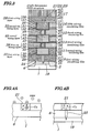
- a seal ring or a bottomed seal ring is provided in such a manner as to surround the pad, so that even upon occurrence of a pad crack, water and a like, if having penetrated through a dicing face, can be blocked from penetrating further deeply inward by the presence of the seal ring.
- a seal ring or a bottomed seal ring is provided in such a manner as to surround the plurality of fuse elements, so that even upon occurrence of a fuse element crack, water and a like, if having penetrated through a dicing face, can be blocked from penetrating further deeply inward by the presence of the seal ring.
- a semiconductor device of the present embodiment has a semiconductor chip 10 made up of a semiconductor substrate 1 being, for example, P-type silicon.
- a semiconductor substrate 1 being, for example, P-type silicon.
- a pair of N-type diffusion regions 3, 4 to serve as source and drain regions between which a gate portion 5 is formed.
- contacts 7A through 7C are formed through a protective insulation film 6 so as to connect between each of the N-type diffusion regions 3 and 4 and the gate portion 5 and the corresponding wiring 9A to 9C.
- the gate portion 5 to which the contact 7B is connected is composed of a gate insulation film made up of silicon oxide or a like and a gate electrode made up of a poly-silicon film or a like formed on this gate insulation film. Both the N-type diffusion regions 3 and 4 and the gate portion 5 make up an N-channel Metal Oxide Semiconductor (MOS) transistor Tr.
- MOS Metal Oxide Semiconductor
- first wiring layers 9A through 9C made of copper are formed by a damascene wiring technology; in a second wiring insulating film (with a first via wiring layer 38 buried therein; so-called an inter-layer dielectric) 11 formed on the first wiring insulating film 8, a via wiring layer 12 made of copper is formed by the damascene wiring technology in such a manner as to be connected with the first wiring layer 9B; and in a third wiring insulating film 13 formed on the second wiring insulating film 11, a second wiring layer 14 made of copper is formed by the damascene wiring technology in such a manner as to be connected with the via wiring layer 12.
- a fourth wiring insulating film (with a second via wiring layer 52 buried therein; so-called an inter-layer dielectric) 15 is formed, while on the fourth wiring insulating film 15, a passivation film 17 is formed via a fifth wiring insulating film 16, to protect a surface entirely.
- a circuit formation portion 18 including multi-layer interconnection made up of the first wiring layers 9A through 9B and the second wiring layer 14 is provided on the semiconductor chip 10.
- first through third seal rings 21 to 23 made up of conductive layers extended in a film-thickness direction of the first through fifth wiring insulating films 8, 11, 13, 15, and 16 so as to be electrically connected one after another to other N-type diffusion regions 19 surrounded by the element isolation region 2 are provided as insulated from each other endlessly and concentrically along a periphery of the semiconductor chip 10 in such a manner as to surround the circuit formation portion 18.
- the N-type diffusion regions 19 are formed at a same time in the same process as the one pair of N-type diffusion regions 3 and 4 are formed in the circuit formation portion 18.
- the first seal ring 21 is provided nearest a dicing face 20 of the semiconductor chip 10, followed by the second seal ring 22 and the third seal ring 23 in an order of separation from the dicing face 20.
- the first through third seal rings 21 to 23 each have a configuration given by using, for example, a single damascene wiring technology as shown in Fig. 3. It is to be noted that the configuration of only the first seal ring 21 is shown as one example in Fig. 3 and the second seal ring 22 and the third seal ring 23 have also the similar configuration.
- a contact hole 24 is formed by a known photolithographic technology.
- a contact 25 is formed which includes a tungsten layer and a barrier metal layer (not shown) having configuration of stacked layers made up of a titanium (Ti) film having a film thickness of 5 to 15nm and a titanium nitride film (TiN) having a film thickness of 10 to 20nm.
- Ti titanium
- TiN titanium nitride film
- the first wiring insulating film 8 is formed so as to have a configuration of stacked layers made up of a silicon nitride film 26 having a film thickness of 10 to 50nm and a silicon oxide film 27 having a film thickness of 200to 400nm, in which the first wiring insulating film 8 a trench (wiring trench) 28 is formed.
- a first wiring layer 31 is formed which includes a copper layer 30 and a barrier metal layer 29 having configuration of stacked layers made up of a tantalum (Ta) film and a tantalum nitride (TaN) film that have a film thickness of 10 to 30nm.
- This first wiring layer 31 is formed simultaneously in the same process as that in which the first wiring layers 9A to 9C are formed in the circuit formation portion 18 as shown in Fig. 2.
- the second wiring insulating film (first inter-via layer insulation film) 11 is formed so as to have configuration of stacked layers made up of a silicon nitride film 32 having a film thickness of 10 to 50nm, a low-dielectric constant film 33 having a film thickness of 150 to 300nm, and a silicon oxide film 34 having a film thickness of 50 to 150nm, in which the second wiring insulating film 11 a via hole (via wiring trench) 35 is formed, in which the via hole 35 a first via wiring layer 38 is formed which includes a copper layer 37 and a barrier metal layer 36 having configuration of stacked layers made up of a tantalum film and a tantalum nitride film that have a film thickness of 10 to 30nm.
- This first via wiring layer 38 is formed in the same step as that in which the via wiring layer 12 is formed in such the circuit formation portion 18 as shown in Fig. 2.
- the third wiring insulation 13 is formed so as to have configuration of stacked layers made up of a silicon nitride film 39 having a film thickness 10 to 50nm, a low-dielectric constant film 40 having a film thickness of 150 to 300nm, and a silicon oxide film 41 having a film thickness of 50 to 150nm, in which the third wiring insulating film 13 a trench 42 is formed, in which the trench 42 a second wiring layer 45 is formed which includes a copper layer 44 and a barrier metal layer 43 having configuration of stacked layers made up of a tantalum film and a tantalum nitride film that have a film thickness of 10 to 30nm.
- This is second wiring layer 45 is formed at a same time in the same process as that in which the second wiring layer 14 is formed in such a circuit formation portion 18 as shown in Fig. 2.
- a second via wiring layer 52 having almost the same configuration as that of the first via wiring layer 38 and a third wiring layer 59 having almost the same configuration as that of the second wiring layer 45 are formed.
- reference numerals 46 and 53 indicate a silicon nitride film
- reference numerals 47 and 54 indicate a low-dielectric constant film
- reference numerals 48 and 55 indicate a silicon oxide film
- a reference numeral 49 indicates a via hole (via wiring trench)
- reference numerals 50 and 57 indicate a barrier metal layer
- reference numerals 51 and 58 indicate a copper layer
- a reference numeral 56 indicates a trench.
- the first seal ring 21 is formed by interconnecting the contact 25 electrically connected with the N-type diffusion region 19, the first wiring layer 31, the first via wiring layer 38, the second wiring layer 45, the second via wiring layer 52, and the third wiring layer 59 which are all formed in such a manner as to extend in the film thickness direction of the first through fifth wiring insulating films 8, 11, 13, 15, and 16, and then the second and third seal rings 22 and 23 are formed similarly.
- widths of the first wiring layer 31, the second wiring layer 45, and the third wiring layer 59 are selected to 0.28-2.0 ⁇ m and a spacing between the mutually adjacent wiring layers, the first wiring layer 31, the second wiring layer 45, and the third wiring layer is selected to 1.0 to 2.0 ⁇ m. Further, widths of the first via wiring layer 38 and the second via wiring layer 52 are selected to 0.1-0.48 ⁇ m and a spacing between the mutually adjacent wiring layers, the first via wiring layer 38 and the second via wiring layer 52 is selected to 1.0 to 2.0 ⁇ m.
- the low-dielectric constant films 33, 40, 47, and 54 making up a main portion of each of the wiring insulating films, (second through fifth wiring insulation films) 11, 13, 15, and 16 respectively an organic film known as SiLK (registered trademark of Dow Chemical Company) is used in one example.
- SiLK registered trademark of Dow Chemical Company
- This low-dielectric constant film has a dielectric constant that is several times as small as those of the silicon oxide film, silicon nitride film, and a like which have been used conventionally.
- the passivation film 17 having configuration of stacked layers made up of a silicon nitride film 60 having a film thickness of 10 to 50nm, a silicon oxide film 61 having a film thickness of 500 to 800nm, a silicon oxide film 62 having a film thickness of 100to 200nm, and a silicon nitride film 63 having a film thickness of 1000 to 2000nm.
- the N-type diffusion region 19 and the contact 25 are shaped so as to match shapes of the first through third seal rings 21 through 23. That is, so as to match the shapes of the first through third seal rings 21 through 23 formed endlessly as described above, the N-type diffusion region 19 and the contact 25 are shaped endlessly along a periphery of the semiconductor chip 10 in such a manner as to surround the circuit formation portion 18.
- the N-type diffusion region 19 and the contact 25 need not necessarily be shaped so as to match the shapes of the first through third seal rings 21 through 23 and may have any shape.
- the barrier metal layer can also be used so that it may act as a barrier against water and a like having penetrated from the surroundings as described above.
- the silicon nitride films 32, 39, 46, 53, and a like that are formed at lower-part layers of the second through fifth wiring insulating films 11, 13, 15, 16, and a like are used so that they may act as a diffusion preventing film (second copper diffusion preventing film) for preventing copper from being diffused to surroundings from the copper layers 37, 44, 51, and 58 buried in the via hole 35, the trench 42, the via hole 49, and the trench 56 respectively, so that these silicon nitride films 32, 39, 46, 53, and a like have actions similar to those of the barrier metal layers 36, 43, 50, 57, and a like.
- barrier actions of the barrier metal layers 36, 43, 50, 57, and a like and of the silicon nitride films 32, 39, 46, 53, and a like water and a like having penetrated through the dicing face 20 can be prevented from penetrating further deeply inward, so that basically even one seal ring is effective in the action
- the first seal ring 21 nearest the dicing face 20 may peel off as indicated by an arrow 66 owing to chipping at the time of dicing. Therefore, in such a case, water and a like penetrates in a direction of the arrow 66 but is blocked from penetrating beyond the second seal ring 22 further inward because the second seal ring 22 is present inside the first seal ring 21 as shown in Figs. 1 and 2. Furthermore, even if the second seal ring 22 is damaged by such chipping as described above, the third seal ring 23, which is present inside the second seal ring 22, acts as a backup, to block the water and a like from penetrating further deeply inward.
- first through third seal rings 21 to 23 are exposed to plasma in a process of etching, CVD, and a like, ions having positive charge hit the semiconductor substrate 1, so that such a phenomenon occurs that the first through third seal rings 21 to 23 are deprived of their inner electrons by the ions to thereby charge the wiring layers positively.
- the seal ring 21 is in an electrically floating state, it continues to accumulate charge in it until it is discharged, whereupon the substrate 1 is destroyed.
- the first seal ring 21 is connected via the contact 25 to the N-type region 19, so that its charge can be released through the semiconductor substrate 1, thereby preventing destruction of the semiconductor substrate 1.
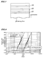
- a seal ring is provided as in the present embodiment, a life of the device can be improved by a factor of about ten as compared to the case where it is not provided.
- the element isolation region 2 is formed in a formation-expected region of a seal ring on the P-type silicon substrate 1.
- the N-type diffusion region 19 is formed.
- the pair of N-type diffusion regions 3 and 4 are formed by forming a silicon oxide film and a poly-silicon film sequentially on the substrate 1, then patterning them into a desired shape to thereby form the gate portion 5 made up of a gate insulation film and a gate electrode, and then injecting ions of an N-type impurity by self-alignment using the gate portion 5 as a mask. Therefore, the N-type diffusion region 19 is also formed at the same time and by roughly the same process as the pair of the N-type diffusion regions 3 and 4.
- the protective insulation film 6 made of a silicon oxide film having a film thickness of 500 to 800nm is formed throughout the surface by CVD and then, by plasma etching by use of a photolithographic technology, the contact hole 24 required to form the seal ring is formed.
- a tungsten layer and a barrier metal layer (not shown) having configuration of stacked layers made up of a titanium film having a film thickness of 5-15nm and a titanium nitride film having a film thickness of 10 to 20nm are formed throughout the surface by CVD and sputtering and then unnecessary portions of the barrier metal and tungsten layers are removed by CMP, to make up the contact 25 of the barrier metal and the tungsten that are left (buried) only in the contact hole 24.
- the silicon nitride film 26 having a film thickness of 10 to 50nm and the silicon oxide film 27 having a film thickness of 200 to 400nm are stacked sequentially by CVD to thereby form the first wiring insulating film 8 and then the trench 28 is formed in the first wiring insulating film 8 by plasma etching.
- a tantalum nitride film and a tantalum film that have a film thickness of 10 to 30nm are sequentially stacked by sputtering to form the barrier metal layer 29, then a copper layer having a film thickness of 50 to 150nm is formed by sputtering and then plated to be completely buried into the trench 28.
- unnecessary portions of the barrier metal and copper layers are removed by CMP, to make up the first wiring layer 31 of portions of the barrier metal layer 29 and the copper layer 30 that are left only in the trench 28.
- the silicon nitride film 32 having a film thickness of 10 to 50nm, the low-dielectric constant film 33 having a film thickness of 150 to 300nm, and the silicon oxide film 34 having a film thickness of 50 to 150nm are sequentially stacked throughout the surface by CVD to thereby form the second wiring insulating film (first inter-via layer insulation film) 11 and then the via hole 35 is formed in the second wiring insulating film 11 by plasma etching.
- a tantalum nitride film and a tantalum film that have a film thickness of 10 to 30nm are sequentially stacked throughout the surface by sputtering to thereby form the barrier metal layer 36, then a copper layer having a film thickness of 50 to 150nm is formed by sputtering and then plated to be completely buried into the via hole 35.
- unnecessary portions of the barrier metal and copper layers are removed by CMP to make up the first via wiring layer 38 of portions of the barrier metal layer 36 and the copper layer 37 that are left only in the via hole 35.
- the silicon nitride film having a film thickness of 10 to 50nm, the low-dielectric constant film 40 having a film thickness of 150 to 300nm, and the silicon oxide film 41 having a film thickness of 50 to 150nm are sequentially stacked throughout the surface by CVD to form the third wiring insulating film 13 and then the trench 42 is formed in the third wiring insulating film 13 by plasma etching.
- a tantalum nitride film and a tantalum film that have a film thickness of 10 to 30nm are formed sequentially throughout the surface by sputtering to form the barrier metal layer 43, then the copper layer 44 having a film thickness of 50 to 150nm is formed by sputtering and then plated to be completely buried into the trench 42.
- unnecessary portions of the barrier metal layer 43 and the copper layer 44 are removed by CMP to make up the second wiring layer 45 of portions of the barrier metal layer 43 and the copper layer 44 that are left only in the trench 42.
- the second via wiring layer 52 is formed so as to be connected with the second wiring layer 45 in much the same way as the first via wiring layer 38 is formed, then the third wiring layer 59 is formed so as to be connected with the second via wiring layer 52 in much the same way as the second wiring layer 45 is formed.
- the silicon nitride film 60 having a film thickness of 10 to 50nm, the silicon oxide film 61 having a film thickness of 500 to 800nm, the silicon oxide film 62 having a film thickness of 100 to 200nm, and the silicon nitride film 63 having a film thickness of 1000 to 2000nm are sequentially stacked throughout the surface of the fifth wiring insulating film 16 by CVD, to form the passivation film 17, thereby completing a structure of Fig. 3.
- the manufacturing method described above by using the single damascene wiring technology, it is possible to form the first through third seal rings 21 to 23 simultaneously in the same process as that in which a multi-layer interconnection is formed in the circuit formation portion 18, so that the first through third seal rings 21 to 23 can be provided simply without increasing costs.
- the first through third seal rings 21 to 23 made up of the conductive layers extended in a film-thickness direction of the first through fifth wiring insulating films 8, 11, 13, 15, and 16 so as to be electrically connected one after another to the N-type diffusion regions 19 surrounded by the element isolation region 2 are provided as insulated from each other along the periphery of the semiconductor chip 10 in such a manner as to surround the circuit formation portion 18, so that it is possible to block water and a like, if having penetrated through the dicing face 20, from penetrating further deeply inward by the presence of the second or the third seal ring 22 or 23.
- the manufacturing method of the present embodiment by using the single damascene wiring technology, it is possible to form the first through third seal rings 21 to 23 at a same time in the same process as that in which the multi-layer interconnection is formed in the circuit formation portion 18, so that the first through third seal rings 21 to 23 can be provided simply without increasing the costs.
- a semiconductor device greatly differs in configuration from that of the first embodiment in that seal rings are manufactured using a dual damascene wiring technology.
- first through third seal rings 21 to 23 made up of conductive layers extended in a film-thickness direction of first through fifth wiring insulating films 8, 11, 13, 15, and 16 so as to be electrically connected one after another to the N-type diffusion regions 19 surrounded by an element isolation region 2 are provided as insulated from each other along a periphery of a semiconductor chip 10 in such a manner as to surround a circuit formation portion 18, a second wiring layer 45 and a first via wiring layer 38 that make up a conductive path are formed integrally and simultaneously, while a third wiring layer 59 and a second via wiring layer 52 are formed integrally and simultaneously.
- Fig.9E shows one example of such a configuration that the first seal ring 21 is provided, the second and third seal rings 22 and 23 also have the same configuration.
- the second wiring layer 45 and first via wiring layer 38 that are vertical adjacent to each other and the third wiring layer 59 and the second via wiring layer 52 that are vertically adjacent to each other can be formed integrally and simultaneously respectively, thus further simplifying formation of the first through third seal rings 21 to 23.
- the wiring layer and the via wiring layer are formed integrally, there exists no boundary between them, thereby providing an advantage that water and a like having penetrated through a dicing face can be blocked securely from penetrating further deeply inward.
- a silicon nitride film 32 having a film thickness of 10 to 50nm, a low-dielectric constant film 33 having a film thickness of 150 to 300nm, and a silicon oxide film 34 having a film thickness of 50 to 150nm are stacked sequentially by CVD to thereby form the second wiring insulating film (first inter-via layer insulation film) 11 and then a low-dielectric constant film 40 having a film thickness of 150 to 300nm and a silicon oxide film 41 having a film thickness of 50 to 150nm are stacked sequentially throughout the surface by CVD to thereby form the third wiring insulating film 13.
- a first via hole 35 is formed in the second wiring insulating film 11.
- a tantalum nitride film and a tantalum film that have a film thickness of 10 to 30nm are stacked sequentially throughout the surface by sputtering to thereby form a barrier metal layer 43, then a copper layer 44 having a film thickness of 50 to 150nm is formed by sputtering and then plated to be completely buried into the trench 42 and the first via hole 35.
- a second via hole 49 is formed simultaneously with a trench 56 and also a second via wiring layer 52 is formed simultaneously with a third wiring layer 59 and, further, a passivation film 17 not shown in Figs. 11A and 11B is formed, thereby completing a structure of Fig.10.
- the first through third seal rings 21 to 23 are provided by the dial damascene wiring technology, so that there exists no boundary between a bottom of the wiring and a top of the wiring layer, thus improving an effect of blocking penetration of water and a like
- a semiconductor device greatly differs in configuration from that of the first embodiment in that a slit-like notch (hereinafter referred to as slit) is formed in each of first through third seal rings 21 to 23.
- slit a slit-like notch
- first through third seal rings 21 to 23 made up of conductive layers extended in a film-thickness direction of first through fifth wiring insulating films 8, 11, 13, 15, and 16 so as to be electrically connected one after another to the N-type diffusion regions 19 surrounded by an element isolation region 2 are provided as insulated from each other along a periphery of a semiconductor chip 10 in such a manner as to surround a circuit formation portion 18, three slits 21A to 23A are formed at length-directional parts of the first through third seal rings 21 to 23 respectively in such a manner that length-directional positions of at least mutually adjacent ones of the first through third seal rings 21 to 23 at which the slits 21A to 23A are formed respectively may not be aligned with each other.
- the N-type diffusion region 19 and a contact 25 are shaped so as to match shapes of the first through third seal rings 21 to 23. That is, in order to match the shapes of the first through third seal rings 21 to 23 provided with the respective slits 21A to 23A as described above, the N-type diffusion region 19 and the contact 25 are shaped in such a manner that the 21A to 23A slits may be formed at a position along a periphery of the semiconductor chip 10 that surrounds the circuit formation portion 18.
- the N-type diffusion region 19 and the contact 25 need not necessarily be shaped so as to match the shapes of the first through third seal rings 21 to 23 and may have any shape.
- a penetration path 67 of water and a like has such a distance as to be given by connecting the slits 21A to 23A in the respective first through third seal rings 21 to 23 one after another, so that the distance is large enough to block penetration of water and a like.
- the blocking becomes more effective by setting the formation positions of the slits 21A to 23A in such a manner that the distance of the penetration path 67 may be larger.
- the penetration path 67 of water and a like can thus be elongated, thus sufficiently relaxing occurrence of Electro-Migration (EM).
- EM Electro-Migration
- the first through third seal rings 21 to 23 are each configured not to be endless in shape, so that even if a magnetic field occurs in a process of manufacturing the semiconductor device, no induced current occurs on the first through third seal rings 21 to 23. Therefore, such a phenomenon is eliminated that a copper layer breaks out as described with reference to Fig. 28.
- the element isolation region 2 is formed in a region on the P-type silicon substrate 1 in which the first through third seal rings 21 to 23 are expected to be formed.
- the N-type diffusion region 19 is formed.
- the protective insulation film 6 and the first wiring insulating film 8 having configuration of stacked layers made up of a silicon nitride film 26 and a silicon oxide film 27 are etched off sequentially in the seal ring formation-expected region (not shown).
- the protective insulation film 6, the silicon nitride film 26, and the silicon oxide film 27 are all left as not being etched off.
- the second wiring insulating film 11 having configuration of stacked layers made up of a silicon nitride film 32, a low-dielectric constant film 33, and a silicon oxide film 34 and the third wiring insulating film 13 having configuration of stacked layers made up of a silicon nitride film 39, a low-dielectric constant film 40, and a silicon oxide film 41 are etched off sequentially in the seal ring formation-expected region (not shown).
- the silicon nitride film 32, the low-dielectric constant film 33, the silicon oxide film 34, the silicon nitride film 39, the low-dielectric constant film 40, and the silicon oxide film 41 are all left as not being etched off.
- the fourth wiring insulating film 15 having configuration of stacked layers made up of a silicon nitride film 46, a low-dielectric constant film 47, and a silicon oxide film 48 and the fifth wiring insulating film 16 having configuration of stacked layers made up of a silicon nitride film 53, a low-dielectric constant film 54, and a silicon oxide film 55 are etched off sequentially.
- the silicon nitride film 46, the low-dielectric constant film 47, the silicon oxide film 48, the silicon nitride film 53, the low-dielectric constant film 54, and the silicon oxide film 55 are all left as not being etched off.
- the slit 23A is formed in the slit formation-expected region (not shown) of the third seal ring 23.
- the slits 21A and 22A can be formed respectively.
- the slit is formed in each of the seal rings, so that an induced current can be prevented from occurring on any of the seal rings even if it is placed in a magnetic field.
- a semiconductor device greatly differs in configuration from that of the first embodiment in that a seal ring is provided as a countermeasure against pad cracks.
- a seal ring 71 made up of a conductive layer extended in a film-thickness direction of first through fifth wiring insulating films 8, 11, 13, 15, and 16 so as to be electrically connected one after another to N-type diffusion regions 19 surrounded by an element isolation region 2 is provided endlessly in such a manner as to surround the assembly pad 70.
- This seal ring 71 is, as shown in Fig. 17, formed by connecting a contact 25 electrically connected with the N-type diffusion region 19, a first wiring layer 31, a first via wiring layer 38, a second wiring layer 45, a second via wiring layer 52, and a third wiring layer 59 one after another.
- the assembly pad 70 is made up of a 400 to 300nm thick layer made of aluminum or aluminum-based metal and, as shown in Fig. 17, drawn out from a desired circuit element formed in a circuit formation portion 18 and connected to an uppermost wiring layer 72 and an external terminal layer 84 both having a film thickness of 300 to 2000nm that are formed simultaneously with the third wiring layer 59 and that are made of copper or copper-based metal.
- the uppermost wiring layer 72 and a like are covered by an insulation film 74 made of a silicon oxide film (SiO 2 ), a silicon nitride film (SiN), a silicon oxy-nitride film (SiON) film, or a like that has a film thickness of 100 to 2000nm, over which uppermost wiring layer 72, the assembly pad 70 is arranged through a contact hole 75 formed in the insulation film 74.
- an insulation film 74 made of a silicon oxide film (SiO 2 ), a silicon nitride film (SiN), a silicon oxy-nitride film (SiON) film, or a like that has a film thickness of 100 to 2000nm, over which uppermost wiring layer 72, the assembly pad 70 is arranged through a contact hole 75 formed in the insulation film 74.
- the assembly pad 70 is in turn covered by a cover insulation film 76 made of a poly-imide film, a silicon nitride film, a silicon oxy-nitride film, or a like that has a film thickness of 1-10 ⁇ m, in such a configuration that an exposed face 70A exposed through an opening 77 formed in the cover insulation film 76 is arranged directly on the uppermost wiring layer 72.
- a wire is bonded onto the exposed face 70A of the assembly pad 70 to electrically interconnect each circuit element and an outside of the LSI.
- the assembly pad 70 is used also as a connection terminal in the case of performing flip-chip bonding for stacking the LSI with other semiconductor chips to interconnect them or face-down bonding of a semiconductor chip on a wiring substrate. Furthermore, on a desired wiring insulating film, there is formed a wiring line (not shown) coming from the outside for connecting to the seal ring 71.
- the single damascene wiring technology employed to form the first through third seal rings 21 to 23 in the first embodiment described with reference to Figs. 9 and 10 or the dual damascene wiring technology employed to form the same first through third seal rings 21 to 23 in the second embodiment described with reference to Figs. 12A to 12B can be applied as it is and so description thereof is omitted.
- an inner size L1 of a bottom of the opening in the cover insulation film 76, an outer size L2 of the assembly pad 70, a contact hole size L3, and an inner size L4 of the seal ring 71 are set so as to satisfy relationships of L1 ⁇ L4 and L1 ⁇ L2 as an indispensable restriction in design so that the opening 77 in the cover insulation film 76 may be within the seal ring 71.
- a relationship between L1 and L3 can be set arbitrarily.
- the seal ring 71 is provided in such a manner as to surround the assembly pad 70, even if a pad crack occurs due to a load applied at the time of, for example, wire bonding for bonding a wire onto the exposed face 70A of the assembly pad 70 at the time of assembly of an LSI, it is possible to block water and a like, if having penetrated through a dicing face, from penetrating further deeply inward by the presence of the seal ring 71.
- a characteristics evaluation pad for evaluating characteristics of a discrete circuit element such as a transistor or a resistor and a screening evaluation pad for screening based on evaluation of the characteristics are provided on the surface of the semiconductor substrate 1. These pads are shaped in roughly the same structure as that of the assembly pad 70.
- a test probe of an electrical measurement apparatus is brought in contact with the characteristics evaluation pad or the screening evaluation pad, to perform characteristics evaluation or screening evaluation respectively. In this case, a load due to contacting of the test probe is applied to these pads, so that a pad crack is liable to occur, to deteriorate moisture resistance as in the case of the assembly pad 70.
- the characteristics evaluation pad or the screening evaluation pad is provided in place of the assembly pad 70, by arranging a seal ring similar to the seal ring 71 in such a manner as to surround these pads, it is possible to block, by the presence of the seal ring 71, water and a like, if having penetrated through the dicing face, from penetrating further deeply inward even when a pad crack has occurred owing to a load being applied when the test probe has come in contact with any one of these pads.
- the seal ring 71 made up of the conductive layers extended in a film-thickness direction of the first through fifth wiring insulating films 8, 11, 13, 15, and 16 so as to be electrically connected one after another to the N-type diffusion regions 19 surrounded by the element isolation region 2 is provided in such a manner as to surround the assembly pad 70, the characteristics evaluation pad, or the screening evaluation pad, so that it is possible to block water and a like from penetrating inward by the presence of the seal ring 71 even if a pad crack occurs.
- a semiconductor device greatly differs in configuration from that of the fourth embodiment in that an assembly pad 70 is provided as shifted in arrangement.
- the assembly pad 70 is connected to an external terminal layer 84 that is a 300nm- through 2000nm-thick film made of copper or copper-based metal and that is formed simultaneously with a third wiring layer 59.
- sizes are set so as to satisfy relationships of L1 ⁇ L4 and L1 ⁇ L2 as an indispensable restriction in design so that an opening 77 in a cover insulation film 76 may be within a seal ring 71.
- a relationship between L1 and L3 can be set arbitrarily.
- an exposed face 70A of the assembly pad 70 is arranged as shifted from a position directly above the underlying external terminal layer 84, so that even if a load due to wire bonding is applied, for example, when a wire is bonded onto the exposed face 70A at the time of assembly of an LSI, it is possible to control a load directly applied on a semiconductor chip. It is, therefore, possible to mitigate a degree of occurrence of a pad crack, thus improving an assembly strength. This holds true also with a case where a characteristics evaluation pad or a screening evaluation pad is provided in place of the assembly pad 70.
- a semiconductor device greatly differs in configuration from that of the fourth embodiment in that a bottomed seal ring is provided as a countermeasure against pad cracks.
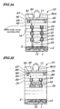
- a bottomed seal ring 78 is provided endlessly in such a manner as to surround an assembly pad 70 in a configuration of the fourth embodiment such as shown in Fig. 17 in which the assembly pad 70 is connected with an uppermost wiring layer 72 which is made of a layer of copper or a copper-based metal which is formed simultaneously with a third wiring layer 59 and also with an external terminal layer 84.
- the bottomed seal ring 78 is formed by connecting a second wiring layer 79 serving as a bottom-portion conductive layer formed directly below the uppermost wiring layer 72, a second via wiring layer 52, and the third wiring layer 59 one after another.
- a seal ring 71 electrically connected to an N-type diffusion region 19 as described with the fourth embodiment shown in Fig. 17 is replaced by the bottomed seal ring 78 formed by connecting the second wiring layer 79 serving as the bottom-portion conductive layer, the second via wiring layer 52, and the third wiring layer 59 one after another as shown in Fig. 19, so that the bottomed seal ring 78 surrounds the assembly pad 70.
- the bottomed seal ring 78 can be formed specifically by applying the single damascene wiring technology employed to form first through third seal rings 21to 23 in the first embodiment described with reference to Figs.
- the second wiring layer 79 serving as the bottom-portion conductive layer that makes up the bottomed seal ring 78 is specifically formed large enough to cover a bottom of the upper-most wiring layer 72 sufficiently when forming a second wiring layer 45 in Fig.9D.
- sizes are set so as to satisfy relationships of L1 ⁇ L4 and L1 ⁇ L2 as an indispensable restriction in design so that an opening 77 in a cover insulation film 76 may be within the seal ring 71.
- a relationship between L1 and L3 can be set arbitrarily.
- bottomed seal ring 78 having the same potential throughout a semiconductor substrate 1 as in the present embodiment, even if a slit is formed in none of first through third seal rings 21 to 23, an induced current can be prevented from occurring on any of the seal rings even if they are placed in a magnetic field, as described with the third embodiment shown in Fig.12. This holds true also with a case where the assembly pad 70 is replaced by a characteristics evaluation pad or a screening evaluation pad.
- the bottomed seal ring is provided in such a manner as to surround each pad, it is possible to reserve the region below the bottom-portion conductive layer as a clearance region, thus increasing the utilization ratio of the semiconductor chip.
- a semiconductor device greatly differs in configuration from that of the fifth embodiment in that a bottomed seal ring is provided as a countermeasure against pad cracks.
- a bottomed seal ring 78 is provided endlessly in such a manner as to surround an assembly pad 70 in a configuration such as described with the fifth embodiment shown in Fig. 17 in which the assembly pad 70 is connected with an external terminal layer 84 which is formed simultaneously with a third wiring layer 59.
- the bottomed seal ring 78 is formed in roughly the same way as that in the sixth embodiment shown in Fig. 19.
- sizes are set so as to satisfy relationships of L1 ⁇ L4 and L1 ⁇ L2 as an indispensable restriction in design so that an opening 77 in a cover insulation film 76 may be within the seal ring 71.
- a relationship between L1 and L3 can be set arbitrarily.
- the bottomed seal ring 78 is provided in such a manner as to surround each pad, so that it is possible to reserve a region below a bottom-portion conductive layer as a clearance region, thus increasing a utilization ratio of a semiconductor chip.
- a semiconductor device greatly differs in configuration from that of the fourth embodiment in that a seal ring is provided not as a countermeasure against pad cracks but as a countermeasure against fuse element cracks.
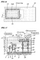
- a seal ring 81 made up of conductive layers extended in a film-thickness direction of first through fifth wiring insulating films 8, 11, 13, 15, and 16 so as to be electrically connected to the respective N-type diffusion regions 19 surrounded by an element isolation region 2 is provided endlessly in such a manner as to surround the plurality of the fuse elements 80.
- the seal ring 81 is formed by connecting a contact 25 electrically connected with the N-type diffusion region 19, a first wiring layer 31, a first via wiring layer 38, a second wiring layer 45, a second via wiring layer 52, and a third wiring layer 59 one after another.
- the seal ring 81 can be formed specifically by applying a single damascene wiring technology employed to form first through third seal rings 21 to 23 in the first embodiment described with reference to Figs. 9 and 10 or the dual damascene wiring technology employed to form the same first through third seal rings 21-23 in the second embodiment described with reference to Figs. 11A to 11B.
- the plurality of fuse elements 80 is a 20nm- to 30nm-thick film made of titanium nitride or copper-based or aluminum-based metal and formed on a sixth wiring insulating film 82 so as to be electrically connected via a contact 83 formed through the sixth wiring insulating film 82 with an external terminal layer 84 formed through the fifth wiring insulating film 16.
- the external terminal layer 84 is formed simultaneously in the same process as that in which the third wiring layer 59 is formed.
- the fuse elements 80 are subjected to a later-described laser trimming on its exposed face 80A, which is indirectly exposed via a first cover insulation film 86 made up of a silicon oxide film, a silicon nitride film, or a like through an opening 77 formed in a second cover insulation film 87 made up of a poly-imide film or a like
- the plurality of fuse elements 80 is prepared beforehand and, when a semiconductor memory is mounted in a semiconductor device, electrically connected with a desired circuit element formed in a circuit formation portion 18 for replacement of a defective bit.
- a defective bit specifically laser trimming is performed on the exposed face 80A of the fuse element 80 that makes up the defective bit, thus cutting off part of a conductive path.
- the wiring insulating film is liable to partially encounter a crack, a so-called fuse element crack.
- a pad crack occurring on the assembly pad 70 and a like as described above water and a like, if having penetrated through a dicing face, penetrates further deeply through the fuse element crack, thus deteriorating moisture resistance. Therefore, it is necessary to take measures against fuse element cracks.
- sizes are set so as to satisfy relationships that an inner size L5 of a bottom of the opening in the second cover insulation film 87 may be smaller than an inner size L6 of the seal ring 81 as an indispensable restriction in design so that the opening 77 in the second cover insulation film 87 may be within the seal ring 81.
- the seal ring 81 is provided in such a manner as to surround the plurality of the fuse elements 80, even if a fuse element crack occurs due to laser trimming performed via the first cover insulation film 86 on the exposed faces 80A of the plurality of fuse elements 80, water and a like, if having penetrated through the dicing face, can be prevented from penetrating further deeply inward by the presence of the seal ring 81.
- the seal ring 81 made up of conductive layers extended in a film-thickness direction of the first through fifth wiring insulating films 8, 11, 13, 15, and 16 so as to be connected to the N-type diffusion regions 19 surrounded by the element isolation region 2 is provided in such a manner as to surround the plurality of the fuse elements 80, so that even if a fuse element crack occurs, water and a like can be prevented from penetrating deeply inward by the presence of the seal ring 81.
- a semiconductor device greatly differs in configuration from that of the eighth embodiment in that a bottomed seal ring is provided as a countermeasure against fuse element cracks.
- a bottomed seal ring 85 is provided endlessly in such a manner as to surround a plurality of fuse elements 80 in a configuration of the eighth embodiment in which the plurality of fuse elements 80 is provided as shown in Fig. 22.
- the bottomed seal ring 85 is formed in roughly the same way as in the case of the sixth embodiment shown in Fig. 19.
- sizes are set so as to satisfy a relationship of L5 ⁇ L6 as an indispensable restriction in design so that an opening 77 in a second cover insulation film 87 may be within the bottomed seal ring 85.
- the bottomed seal ring 85 is provided in such a manner as to surround the plurality of fuse elements 80, so that it is possible to reserve a region below a bottom-portion conductive layer as a clearance region, thus increasing a utilization ratio of a semiconductor chip.
- a semiconductor device greatly differs in configuration from that of the eighth embodiment in that fuse elements 80 are provided as shifted with respect to a seal ring 81 in arrangement.
- contact 88 serving as the two electrodes of the fuse elements 80 respectively are formed as separated from a third wiring layer 59 that makes up the seal ring 81 in a configuration such as described with the eighth embodiment shown in Fig. 22 in which a plurality of fuse elements 80 is surrounded by the seal ring 81. That is, the contact 88 is formed through a sixth wiring insulating film 82 that is separated from the third wiring layer 59 via a seventh wiring insulating film 89. This eliminates a necessity of using a via wiring line in order to form the contacts 88 serving as the two electrodes respectively on a fifth wiring insulating film 16, to enable decreasing the number of manufacturing processes, thereby contributing to cost reduction.
- the plurality of fuse elements 80 can be formed as separated from the seal ring 81, thus reducing the number of processes.
- a semiconductor device greatly differs in configuration from that of the ninth embodiment in that fuse elements are provided as shifted with respect to a seal ring in arrangement.
- contacts 88 serving as two electrodes of the fuse element 80 respectively are formed as separated from a third wiring layer 59 that makes up the seal ring 85. That is, the contact 88 is formed through a sixth wiring insulating film 82 that is separated from the third wiring layer 59 via a seventh wiring insulating film 89.
- the plurality of fuse elements can be formed as separated from the seal ring, thus reducing the number of processes.
- the present invention is not limited to the above embodiments but may be changed and modified without departing from the scope and spirit of the invention.
- the first embodiment has been described in an example where the seal ring is provided as many as three, the number of the seal rings is not limited thereto and only needs to be at least two.
- the third embodiment has been described in an example where the seal ring having a slit formed therein is provided as many as three, the number of the seal rings only needs to be at least two.
- the seal ring having the slit formed therein as many as two and at least by forming the slits at mutually misaligned positions on the two respective seal rings, the slit formed in the outer or inner seal ring is for sure covered by the adjacent inner or outer seal ring respectively to enable making a penetration path long enough to prevent water and a like, if having penetrated through a dicing face, from penetrating further deeply inward, thereby improving moisture resistance sufficiently.
- the present invention is not limited thereto and may combine the single damascene and dual damascene technologies in manufacture.
- the second wiring layer may be formed using the single damascene technology to then form the third wiring layer using the dual damascene technology.
- either the single damascene technology or the dual damascene technology is employed or, as described above, the two technologies may be combined in manufacture.
- the fourth through eleventh embodiments two or more of seal rings or two or more of bottomed seal rings may be provided therein.
- the embodiments have been described in an example where copper is used as a material of a conductive layer that makes up a seal ring or a bottomed seal ring, the material is not limited thereto and may be copper-based metal containing copper as its component and a small amount of any other materials such as tin (Sn), silver (Ag) , magnesium (Mg) , lead (Pb) , aluminum (Al), silicon (Si), or titanium (Ti).
- the embodiments have been described in an example where five films of the first through fifth wiring insulating films and the corresponding respective conductive layers have been formed so as to provide a seal ring, the present invention can be applied also to the case of forming six wiring insulating films or more.
- SiLK is used as'a material of a low-dielectric constant film that makes up a main portion of the wiring insulating film
- the material is not limited thereto and may be any other such as Methyl-silsesquioxane (MSQ), Hydrogen- silsesquioxane (HSQ), or Ladder- oxide (L-Ox: registered trademark of NEC).
- MSQ Methyl-silsesquioxane
- HSQ Hydrogen- silsesquioxane
- L-Ox Ladder- oxide
- the wiring insulating film is not limited in use to a silicon oxide film or silicon nitride film and may be any other such as a Boron-Silicate Glass (BSG) film, a Phospho-Silicate Glass (PSG) film, or Boron-Phospho-Silicate Glass (BPSG) film.
- BSG Boron-Silicate Glass
- PSG Phospho-Silicate Glass
- BPSG Boron-Phospho-Silicate Glass
- the prevention film is not limited thereto and may be any other SiC-based film such as a silicon carbonate (SiC) film or a silicon carbonitride (SiCN) film.
- the pattern formation technology is not limited in use to photolithography and may be any other lithographic technology such as Electron-Beam (EB) lithography.
- the diffusion region for connection of the seal ring may be of any one of N-type and P-type conductivities.
Landscapes
- Internal Circuitry In Semiconductor Integrated Circuit Devices (AREA)
Applications Claiming Priority (4)
| Application Number | Priority Date | Filing Date | Title |
|---|---|---|---|
| JP2003026526 | 2003-02-03 | ||
| JP2003026526 | 2003-02-03 | ||
| JP2003113412 | 2003-04-17 | ||
| JP2003113412A JP4502173B2 (ja) | 2003-02-03 | 2003-04-17 | 半導体装置及びその製造方法 |
Publications (1)
| Publication Number | Publication Date |
|---|---|
| EP1443557A2 true EP1443557A2 (de) | 2004-08-04 |
Family
ID=32658622
Family Applications (1)
| Application Number | Title | Priority Date | Filing Date |
|---|---|---|---|
| EP03019375A Withdrawn EP1443557A2 (de) | 2003-02-03 | 2003-08-27 | Halbleitervorrichtung und Verfahren zu deren Herstellung |
Country Status (4)
| Country | Link |
|---|---|
| US (1) | US6998712B2 (de) |
| EP (1) | EP1443557A2 (de) |
| JP (1) | JP4502173B2 (de) |
| CN (1) | CN100355067C (de) |
Cited By (5)
| Publication number | Priority date | Publication date | Assignee | Title |
|---|---|---|---|---|
| WO2006075015A1 (en) * | 2005-01-12 | 2006-07-20 | Hewlett-Packard Development Company, L.P. | Semiconductor device and fabrication thereof |
| CN101593738A (zh) * | 2008-05-30 | 2009-12-02 | 株式会社瑞萨科技 | 半导体器件及制造该半导体器件的方法 |
| WO2010070304A1 (en) * | 2008-12-15 | 2010-06-24 | Cambridge Silicon Radio Ltd | Improved die seal ring |
| WO2010085466A1 (en) * | 2009-01-20 | 2010-07-29 | Plasma-Therm, Llc | Conductive seal ring electrostatic chuck |
| CN101636834B (zh) * | 2007-03-20 | 2012-02-08 | 富士通半导体股份有限公司 | 半导体器件及其制造方法 |
Families Citing this family (388)
| Publication number | Priority date | Publication date | Assignee | Title |
|---|---|---|---|---|
| US7125781B2 (en) * | 2003-09-04 | 2006-10-24 | Micron Technology, Inc. | Methods of forming capacitor devices |
| US7067385B2 (en) * | 2003-09-04 | 2006-06-27 | Micron Technology, Inc. | Support for vertically oriented capacitors during the formation of a semiconductor device |
| JP2005129717A (ja) * | 2003-10-23 | 2005-05-19 | Renesas Technology Corp | 半導体装置 |
| JP2005136215A (ja) * | 2003-10-30 | 2005-05-26 | Toshiba Corp | 半導体装置 |
| CN1617312A (zh) | 2003-11-10 | 2005-05-18 | 松下电器产业株式会社 | 半导体器件及其制造方法 |
| TWI227936B (en) * | 2004-01-14 | 2005-02-11 | Taiwan Semiconductor Mfg | Sealed ring for IC protection |
| JP4065855B2 (ja) * | 2004-01-21 | 2008-03-26 | 株式会社日立製作所 | 生体および化学試料検査装置 |
| US7223684B2 (en) * | 2004-07-14 | 2007-05-29 | International Business Machines Corporation | Dual damascene wiring and method |
| US7387939B2 (en) * | 2004-07-19 | 2008-06-17 | Micron Technology, Inc. | Methods of forming semiconductor structures and capacitor devices |
| US9318378B2 (en) * | 2004-08-21 | 2016-04-19 | Globalfoundries Singapore Pte. Ltd. | Slot designs in wide metal lines |
| US7439152B2 (en) * | 2004-08-27 | 2008-10-21 | Micron Technology, Inc. | Methods of forming a plurality of capacitors |
| US20060046055A1 (en) * | 2004-08-30 | 2006-03-02 | Nan Ya Plastics Corporation | Superfine fiber containing grey dope dyed component and the fabric made of the same |
| US7547945B2 (en) | 2004-09-01 | 2009-06-16 | Micron Technology, Inc. | Transistor devices, transistor structures and semiconductor constructions |
| JP4776195B2 (ja) * | 2004-09-10 | 2011-09-21 | ルネサスエレクトロニクス株式会社 | 半導体装置 |
| US7777338B2 (en) * | 2004-09-13 | 2010-08-17 | Taiwan Semiconductor Manufacturing Co., Ltd. | Seal ring structure for integrated circuit chips |
| JP4689244B2 (ja) | 2004-11-16 | 2011-05-25 | ルネサスエレクトロニクス株式会社 | 半導体装置 |
| JP4504791B2 (ja) * | 2004-11-24 | 2010-07-14 | パナソニック株式会社 | 半導体回路装置及びその製造方法 |
| US7320911B2 (en) * | 2004-12-06 | 2008-01-22 | Micron Technology, Inc. | Methods of forming pluralities of capacitors |
| FR2879295B1 (fr) * | 2004-12-14 | 2007-03-16 | St Microelectronics Sa | Structure de test pour circuit electronique integre |
| KR100590575B1 (ko) * | 2004-12-24 | 2006-06-19 | 삼성전자주식회사 | 새로운 물질을 이용한 전자빔 리소그래피 방법 |
| JP2006196668A (ja) * | 2005-01-13 | 2006-07-27 | Toshiba Corp | 半導体装置及びその製造方法 |
| JP4455356B2 (ja) | 2005-01-28 | 2010-04-21 | Necエレクトロニクス株式会社 | 半導体装置 |
| US7170144B2 (en) * | 2005-02-25 | 2007-01-30 | United Microelectronics Corp. | System-on-chip with shield rings for shielding functional blocks therein from electromagnetic interference |
| US7786546B2 (en) * | 2005-02-25 | 2010-08-31 | United Microelectronics Corp. | System-on-chip with shield rings for shielding functional blocks therein from electromagnetic interference |
| US7557015B2 (en) * | 2005-03-18 | 2009-07-07 | Micron Technology, Inc. | Methods of forming pluralities of capacitors |
| JP4366328B2 (ja) * | 2005-03-18 | 2009-11-18 | 富士通株式会社 | 半導体装置およびその製造方法 |
| JP2006303073A (ja) * | 2005-04-19 | 2006-11-02 | Seiko Epson Corp | 半導体装置及びその製造方法 |
| US7615841B2 (en) * | 2005-05-02 | 2009-11-10 | Taiwan Semiconductor Manufacturing Company, Ltd. | Design structure for coupling noise prevention |
| US7517753B2 (en) | 2005-05-18 | 2009-04-14 | Micron Technology, Inc. | Methods of forming pluralities of capacitors |
| US7544563B2 (en) * | 2005-05-18 | 2009-06-09 | Micron Technology, Inc. | Methods of forming a plurality of capacitors |
| US7445966B2 (en) * | 2005-06-24 | 2008-11-04 | International Business Machines Corporation | Method and structure for charge dissipation during fabrication of integrated circuits and isolation thereof |
| JP2007019128A (ja) * | 2005-07-06 | 2007-01-25 | Sony Corp | 半導体装置 |
| US7282401B2 (en) | 2005-07-08 | 2007-10-16 | Micron Technology, Inc. | Method and apparatus for a self-aligned recessed access device (RAD) transistor gate |
| KR100672728B1 (ko) * | 2005-07-12 | 2007-01-22 | 동부일렉트로닉스 주식회사 | 반도체 소자의 제조방법 |
| JP2007027639A (ja) * | 2005-07-21 | 2007-02-01 | Nec Electronics Corp | 半導体装置 |
| US7224069B2 (en) * | 2005-07-25 | 2007-05-29 | Taiwan Semiconductor Manufacturing Company, Ltd. | Dummy structures extending from seal ring into active circuit area of integrated circuit chip |
| US7199005B2 (en) * | 2005-08-02 | 2007-04-03 | Micron Technology, Inc. | Methods of forming pluralities of capacitors |
| US7867851B2 (en) | 2005-08-30 | 2011-01-11 | Micron Technology, Inc. | Methods of forming field effect transistors on substrates |
| EP1760776B1 (de) * | 2005-08-31 | 2019-12-25 | Semiconductor Energy Laboratory Co., Ltd. | Herstellungsverfahren für Halbleiterbauelement mit flexiblem Substrat |
| JP4890819B2 (ja) * | 2005-09-02 | 2012-03-07 | 富士通セミコンダクター株式会社 | 半導体装置の製造方法およびウェハ |
| US7397103B2 (en) * | 2005-09-28 | 2008-07-08 | Agere Systems, Inc. | Semiconductor with damage detection circuitry |
| US8624346B2 (en) | 2005-10-11 | 2014-01-07 | Taiwan Semiconductor Manufacturing Company, Ltd. | Exclusion zone for stress-sensitive circuit design |
| US7547572B2 (en) * | 2005-11-16 | 2009-06-16 | Emcore Corporation | Method of protecting semiconductor chips from mechanical and ESD damage during handling |
| CN100527389C (zh) * | 2005-11-24 | 2009-08-12 | 联华电子股份有限公司 | 多层裂缝防止环结构与具有此结构的晶片 |
| US20070120256A1 (en) * | 2005-11-28 | 2007-05-31 | Taiwan Semiconductor Manufacturing Co., Ltd. | Reinforced interconnection structures |
| CN100413066C (zh) * | 2005-11-30 | 2008-08-20 | 中芯国际集成电路制造(上海)有限公司 | 低k介电材料的接合焊盘和用于制造半导体器件的方法 |
| KR100790974B1 (ko) * | 2005-12-01 | 2008-01-02 | 삼성전자주식회사 | 퓨즈 포커스 디텍터를 구비한 반도체 소자 및 그 제조방법과 이를 이용한 레이저 리페어 방법 |
| TWI281724B (en) * | 2005-12-09 | 2007-05-21 | Via Tech Inc | Semiconductor chip and shielding structure thereof |
| US8188565B2 (en) * | 2005-12-09 | 2012-05-29 | Via Technologies, Inc. | Semiconductor chip and shielding structure thereof |
| KR101005028B1 (ko) | 2005-12-27 | 2010-12-30 | 후지쯔 세미컨덕터 가부시키가이샤 | 반도체 장치 |
| US7977795B2 (en) | 2006-01-05 | 2011-07-12 | Kabushiki Kaisha Toshiba | Semiconductor device, method of fabricating the same, and pattern generating method |
| US7456507B2 (en) * | 2006-01-12 | 2008-11-25 | Taiwan Semiconductor Manufacturing Co., Ltd. | Die seal structure for reducing stress induced during die saw process |
| JP5104317B2 (ja) | 2006-01-18 | 2012-12-19 | 富士通セミコンダクター株式会社 | 半導体装置、半導体ウエハ構造、及び半導体ウエハ構造の製造方法 |
| US7700441B2 (en) | 2006-02-02 | 2010-04-20 | Micron Technology, Inc. | Methods of forming field effect transistors, methods of forming field effect transistor gates, methods of forming integrated circuitry comprising a transistor gate array and circuitry peripheral to the gate array, and methods of forming integrated circuitry comprising a transistor gate array including first gates and second grounded isolation gates |
| US7557013B2 (en) * | 2006-04-10 | 2009-07-07 | Micron Technology, Inc. | Methods of forming a plurality of capacitors |
| JP4949733B2 (ja) * | 2006-05-11 | 2012-06-13 | ルネサスエレクトロニクス株式会社 | 半導体装置 |
| US8723321B2 (en) * | 2006-06-08 | 2014-05-13 | GLOBALFOUNDIES Inc. | Copper interconnects with improved electromigration lifetime |
| US7602001B2 (en) | 2006-07-17 | 2009-10-13 | Micron Technology, Inc. | Capacitorless one transistor DRAM cell, integrated circuitry comprising an array of capacitorless one transistor DRAM cells, and method of forming lines of capacitorless one transistor DRAM cells |
| US7622364B2 (en) * | 2006-08-18 | 2009-11-24 | International Business Machines Corporation | Bond pad for wafer and package for CMOS imager |
| US7772632B2 (en) | 2006-08-21 | 2010-08-10 | Micron Technology, Inc. | Memory arrays and methods of fabricating memory arrays |
| US7589995B2 (en) | 2006-09-07 | 2009-09-15 | Micron Technology, Inc. | One-transistor memory cell with bias gate |
| US7557444B2 (en) * | 2006-09-20 | 2009-07-07 | Infineon Technologies Ag | Power-via structure for integration in advanced logic/smart-power technologies |
| US7902081B2 (en) * | 2006-10-11 | 2011-03-08 | Micron Technology, Inc. | Methods of etching polysilicon and methods of forming pluralities of capacitors |
| DE102007050610A1 (de) * | 2006-10-24 | 2008-05-08 | Denso Corp., Kariya | Halbleitervorrichtung, Verdrahtung einer Halbleitervorrichtung und Verfahren zum Bilden einer Verdrahtung |
| KR100840642B1 (ko) * | 2006-12-05 | 2008-06-24 | 동부일렉트로닉스 주식회사 | 반도체 소자의 가드링 및 그 형성방법 |
| JP4553892B2 (ja) * | 2006-12-27 | 2010-09-29 | Okiセミコンダクタ株式会社 | 半導体装置及びその製造方法 |
| US7646078B2 (en) * | 2007-01-17 | 2010-01-12 | Taiwan Semiconductor Manufacturing Company, Ltd. | Die saw crack stopper |
| JP5065695B2 (ja) * | 2007-02-01 | 2012-11-07 | ルネサスエレクトロニクス株式会社 | 半導体装置 |
| US7785962B2 (en) | 2007-02-26 | 2010-08-31 | Micron Technology, Inc. | Methods of forming a plurality of capacitors |
| KR100995558B1 (ko) * | 2007-03-22 | 2010-11-22 | 후지쯔 세미컨덕터 가부시키가이샤 | 반도체 장치 및 반도체 장치의 제조 방법 |
| US7893459B2 (en) * | 2007-04-10 | 2011-02-22 | Taiwan Semiconductor Manufacturing Company, Ltd. | Seal ring structures with reduced moisture-induced reliability degradation |
| JP5448304B2 (ja) | 2007-04-19 | 2014-03-19 | パナソニック株式会社 | 半導体装置 |
| US7952167B2 (en) * | 2007-04-27 | 2011-05-31 | Taiwan Semiconductor Manufacturing Company, Ltd. | Scribe line layout design |
| US8217394B2 (en) * | 2007-05-10 | 2012-07-10 | Taiwan Semiconductor Manufacturing Company, Ltd. | Probe pad on a corner stress relief region in a semiconductor chip |
| US8237160B2 (en) | 2007-05-10 | 2012-08-07 | Taiwan Semiconductor Manufacturing Company, Ltd. | Probe pad on a corner stress relief region in a semiconductor chip |
| US8125052B2 (en) * | 2007-05-14 | 2012-02-28 | Taiwan Semiconductor Manufacturing Co., Ltd. | Seal ring structure with improved cracking protection |
| US7538346B2 (en) * | 2007-05-29 | 2009-05-26 | Taiwan Semiconductor Manufacturing Co., Ltd. | Semiconductor device |
| US7923373B2 (en) | 2007-06-04 | 2011-04-12 | Micron Technology, Inc. | Pitch multiplication using self-assembling materials |
| JP5106933B2 (ja) * | 2007-07-04 | 2012-12-26 | ラピスセミコンダクタ株式会社 | 半導体装置 |
| US7682924B2 (en) | 2007-08-13 | 2010-03-23 | Micron Technology, Inc. | Methods of forming a plurality of capacitors |
| US8589832B2 (en) * | 2007-08-24 | 2013-11-19 | International Business Machines Corporation | On chip shielding structure for integrated circuits or devices on a substrate and method of shielding |
| US8566759B2 (en) * | 2007-08-24 | 2013-10-22 | International Business Machines Corporation | Structure for on chip shielding structure for integrated circuits or devices on a substrate |
| US20090079080A1 (en) * | 2007-09-24 | 2009-03-26 | Infineon Technologies Ag | Semiconductor Device with Multi-Layer Metallization |
| US8643147B2 (en) * | 2007-11-01 | 2014-02-04 | Taiwan Semiconductor Manufacturing Company, Ltd. | Seal ring structure with improved cracking protection and reduced problems |
| KR20090046993A (ko) * | 2007-11-07 | 2009-05-12 | 주식회사 동부하이텍 | 반도체 소자 및 그 제조 방법 |
| JP2009117710A (ja) * | 2007-11-08 | 2009-05-28 | Nec Electronics Corp | 半導体チップ、及び半導体装置 |
| KR101374338B1 (ko) * | 2007-11-14 | 2014-03-14 | 삼성전자주식회사 | 관통 전극을 갖는 반도체 장치 및 그 제조방법 |
| US8227902B2 (en) * | 2007-11-26 | 2012-07-24 | Taiwan Semiconductor Manufacturing Company, Ltd. | Structures for preventing cross-talk between through-silicon vias and integrated circuits |
| US8388851B2 (en) | 2008-01-08 | 2013-03-05 | Micron Technology, Inc. | Capacitor forming methods |
| JP2009231513A (ja) * | 2008-03-21 | 2009-10-08 | Elpida Memory Inc | 半導体装置 |
| US8274777B2 (en) | 2008-04-08 | 2012-09-25 | Micron Technology, Inc. | High aspect ratio openings |
| JP5324822B2 (ja) * | 2008-05-26 | 2013-10-23 | ラピスセミコンダクタ株式会社 | 半導体装置 |
| US8274146B2 (en) * | 2008-05-30 | 2012-09-25 | Freescale Semiconductor, Inc. | High frequency interconnect pad structure |
| US8334582B2 (en) * | 2008-06-26 | 2012-12-18 | Taiwan Semiconductor Manufacturing Company, Ltd. | Protective seal ring for preventing die-saw induced stress |
| US7968974B2 (en) * | 2008-06-27 | 2011-06-28 | Texas Instruments Incorporated | Scribe seal connection |
| US7948060B2 (en) * | 2008-07-01 | 2011-05-24 | Xmos Limited | Integrated circuit structure |
| US7759193B2 (en) | 2008-07-09 | 2010-07-20 | Micron Technology, Inc. | Methods of forming a plurality of capacitors |
| US8242586B2 (en) * | 2008-09-09 | 2012-08-14 | Mediatek Inc. | Integrated circuit chip with seal ring structure |
| US8063469B2 (en) * | 2008-09-30 | 2011-11-22 | Infineon Technologies Ag | On-chip radio frequency shield with interconnect metallization |
| US8889548B2 (en) | 2008-09-30 | 2014-11-18 | Infineon Technologies Ag | On-chip RF shields with backside redistribution lines |
| US8169059B2 (en) * | 2008-09-30 | 2012-05-01 | Infineon Technologies Ag | On-chip RF shields with through substrate conductors |
| US7948064B2 (en) * | 2008-09-30 | 2011-05-24 | Infineon Technologies Ag | System on a chip with on-chip RF shield |
| US8178953B2 (en) | 2008-09-30 | 2012-05-15 | Infineon Technologies Ag | On-chip RF shields with front side redistribution lines |
| US8803290B2 (en) * | 2008-10-03 | 2014-08-12 | Qualcomm Incorporated | Double broken seal ring |
| JP2010093163A (ja) * | 2008-10-10 | 2010-04-22 | Panasonic Corp | 半導体装置 |
| KR101470530B1 (ko) * | 2008-10-24 | 2014-12-08 | 삼성전자주식회사 | 일체화된 가드 링 패턴과 공정 모니터링 패턴을 포함하는 반도체 웨이퍼 및 반도체 소자 |
| US7906836B2 (en) | 2008-11-14 | 2011-03-15 | Taiwan Semiconductor Manufacturing Company, Ltd. | Heat spreader structures in scribe lines |
| US8053902B2 (en) * | 2008-12-02 | 2011-11-08 | Taiwan Semiconductor Manufacturing Company, Ltd. | Isolation structure for protecting dielectric layers from degradation |
| JP5535490B2 (ja) * | 2009-01-30 | 2014-07-02 | 住友電工デバイス・イノベーション株式会社 | 半導体装置 |
| US8368180B2 (en) * | 2009-02-18 | 2013-02-05 | Taiwan Semiconductor Manufacturing Company, Ltd. | Scribe line metal structure |
| JP4987897B2 (ja) | 2009-03-23 | 2012-07-25 | 株式会社東芝 | 半導体装置 |
| JP5439901B2 (ja) * | 2009-03-31 | 2014-03-12 | 富士通セミコンダクター株式会社 | 半導体装置及びその製造方法 |
| US20100289065A1 (en) * | 2009-05-12 | 2010-11-18 | Pixart Imaging Incorporation | Mems integrated chip with cross-area interconnection |
| JP5638205B2 (ja) * | 2009-06-16 | 2014-12-10 | ルネサスエレクトロニクス株式会社 | 半導体装置 |
| JP5521422B2 (ja) * | 2009-07-22 | 2014-06-11 | 株式会社リコー | 半導体装置 |
| KR101068387B1 (ko) * | 2009-08-05 | 2011-09-28 | 주식회사 하이닉스반도체 | 반도체 소자의 금속 배선 및 그 형성 방법 |
| JP5304536B2 (ja) * | 2009-08-24 | 2013-10-02 | ソニー株式会社 | 半導体装置 |
| US11018133B2 (en) | 2009-10-12 | 2021-05-25 | Monolithic 3D Inc. | 3D integrated circuit |
| US12027518B1 (en) | 2009-10-12 | 2024-07-02 | Monolithic 3D Inc. | 3D semiconductor devices and structures with metal layers |
| US10043781B2 (en) | 2009-10-12 | 2018-08-07 | Monolithic 3D Inc. | 3D semiconductor device and structure |
| US10366970B2 (en) | 2009-10-12 | 2019-07-30 | Monolithic 3D Inc. | 3D semiconductor device and structure |
| US11374118B2 (en) | 2009-10-12 | 2022-06-28 | Monolithic 3D Inc. | Method to form a 3D integrated circuit |
| US10354995B2 (en) | 2009-10-12 | 2019-07-16 | Monolithic 3D Inc. | Semiconductor memory device and structure |
| US10388863B2 (en) | 2009-10-12 | 2019-08-20 | Monolithic 3D Inc. | 3D memory device and structure |
| US11984445B2 (en) | 2009-10-12 | 2024-05-14 | Monolithic 3D Inc. | 3D semiconductor devices and structures with metal layers |
| US10157909B2 (en) | 2009-10-12 | 2018-12-18 | Monolithic 3D Inc. | 3D semiconductor device and structure |
| US10910364B2 (en) | 2009-10-12 | 2021-02-02 | Monolitaic 3D Inc. | 3D semiconductor device |
| JP5401301B2 (ja) * | 2009-12-28 | 2014-01-29 | ルネサスエレクトロニクス株式会社 | 半導体装置の製造方法及び半導体装置 |
| JP6375275B2 (ja) * | 2010-03-24 | 2018-08-15 | 富士通セミコンダクター株式会社 | 半導体ウエハと半導体装置の製造方法 |
| JP5830843B2 (ja) | 2010-03-24 | 2015-12-09 | 富士通セミコンダクター株式会社 | 半導体ウエハとその製造方法、及び半導体チップ |
| US8933567B2 (en) * | 2010-05-21 | 2015-01-13 | Qualcomm Incorporated | Electrically broken, but mechanically continuous die seal for integrated circuits |
| JP2012033894A (ja) | 2010-06-30 | 2012-02-16 | Canon Inc | 固体撮像装置 |
| JP6342033B2 (ja) * | 2010-06-30 | 2018-06-13 | キヤノン株式会社 | 固体撮像装置 |
| US10217667B2 (en) | 2011-06-28 | 2019-02-26 | Monolithic 3D Inc. | 3D semiconductor device, fabrication method and system |
| US8518788B2 (en) | 2010-08-11 | 2013-08-27 | Micron Technology, Inc. | Methods of forming a plurality of capacitors |
| US8338917B2 (en) | 2010-08-13 | 2012-12-25 | Taiwan Semiconductor Manufacturing Company, Ltd. | Multiple seal ring structure |
| US11482440B2 (en) | 2010-12-16 | 2022-10-25 | Monolithic 3D Inc. | 3D semiconductor device and structure with a built-in test circuit for repairing faulty circuits |
| US10497713B2 (en) | 2010-11-18 | 2019-12-03 | Monolithic 3D Inc. | 3D semiconductor memory device and structure |
| US12362219B2 (en) | 2010-11-18 | 2025-07-15 | Monolithic 3D Inc. | 3D semiconductor memory device and structure |
| US11469271B2 (en) | 2010-10-11 | 2022-10-11 | Monolithic 3D Inc. | Method to produce 3D semiconductor devices and structures with memory |
| US11257867B1 (en) | 2010-10-11 | 2022-02-22 | Monolithic 3D Inc. | 3D semiconductor device and structure with oxide bonds |
| US10896931B1 (en) | 2010-10-11 | 2021-01-19 | Monolithic 3D Inc. | 3D semiconductor device and structure |
| US11315980B1 (en) | 2010-10-11 | 2022-04-26 | Monolithic 3D Inc. | 3D semiconductor device and structure with transistors |
| US11018191B1 (en) | 2010-10-11 | 2021-05-25 | Monolithic 3D Inc. | 3D semiconductor device and structure |
| US10290682B2 (en) | 2010-10-11 | 2019-05-14 | Monolithic 3D Inc. | 3D IC semiconductor device and structure with stacked memory |
| US11600667B1 (en) | 2010-10-11 | 2023-03-07 | Monolithic 3D Inc. | Method to produce 3D semiconductor devices and structures with memory |
| US11158674B2 (en) | 2010-10-11 | 2021-10-26 | Monolithic 3D Inc. | Method to produce a 3D semiconductor device and structure |
| US11024673B1 (en) | 2010-10-11 | 2021-06-01 | Monolithic 3D Inc. | 3D semiconductor device and structure |
| US11227897B2 (en) | 2010-10-11 | 2022-01-18 | Monolithic 3D Inc. | Method for producing a 3D semiconductor memory device and structure |
| US11133344B2 (en) | 2010-10-13 | 2021-09-28 | Monolithic 3D Inc. | Multilevel semiconductor device and structure with image sensors |
| US12360310B2 (en) | 2010-10-13 | 2025-07-15 | Monolithic 3D Inc. | Multilevel semiconductor device and structure with oxide bonding |
| US11404466B2 (en) | 2010-10-13 | 2022-08-02 | Monolithic 3D Inc. | Multilevel semiconductor device and structure with image sensors |
| US11605663B2 (en) | 2010-10-13 | 2023-03-14 | Monolithic 3D Inc. | Multilevel semiconductor device and structure with image sensors and wafer bonding |
| US11984438B2 (en) | 2010-10-13 | 2024-05-14 | Monolithic 3D Inc. | Multilevel semiconductor device and structure with oxide bonding |
| US10943934B2 (en) | 2010-10-13 | 2021-03-09 | Monolithic 3D Inc. | Multilevel semiconductor device and structure |
| US11163112B2 (en) | 2010-10-13 | 2021-11-02 | Monolithic 3D Inc. | Multilevel semiconductor device and structure with electromagnetic modulators |
| US10833108B2 (en) | 2010-10-13 | 2020-11-10 | Monolithic 3D Inc. | 3D microdisplay device and structure |
| US11063071B1 (en) | 2010-10-13 | 2021-07-13 | Monolithic 3D Inc. | Multilevel semiconductor device and structure with waveguides |
| US11869915B2 (en) | 2010-10-13 | 2024-01-09 | Monolithic 3D Inc. | Multilevel semiconductor device and structure with image sensors and wafer bonding |
| US11043523B1 (en) | 2010-10-13 | 2021-06-22 | Monolithic 3D Inc. | Multilevel semiconductor device and structure with image sensors |
| US11855100B2 (en) | 2010-10-13 | 2023-12-26 | Monolithic 3D Inc. | Multilevel semiconductor device and structure with oxide bonding |
| US12080743B2 (en) | 2010-10-13 | 2024-09-03 | Monolithic 3D Inc. | Multilevel semiconductor device and structure with image sensors and wafer bonding |
| US10978501B1 (en) | 2010-10-13 | 2021-04-13 | Monolithic 3D Inc. | Multilevel semiconductor device and structure with waveguides |
| US10679977B2 (en) | 2010-10-13 | 2020-06-09 | Monolithic 3D Inc. | 3D microdisplay device and structure |
| US10998374B1 (en) | 2010-10-13 | 2021-05-04 | Monolithic 3D Inc. | Multilevel semiconductor device and structure |
| US11164898B2 (en) | 2010-10-13 | 2021-11-02 | Monolithic 3D Inc. | Multilevel semiconductor device and structure |
| US11437368B2 (en) | 2010-10-13 | 2022-09-06 | Monolithic 3D Inc. | Multilevel semiconductor device and structure with oxide bonding |
| US11929372B2 (en) | 2010-10-13 | 2024-03-12 | Monolithic 3D Inc. | Multilevel semiconductor device and structure with image sensors and wafer bonding |
| US12094892B2 (en) | 2010-10-13 | 2024-09-17 | Monolithic 3D Inc. | 3D micro display device and structure |
| US11855114B2 (en) | 2010-10-13 | 2023-12-26 | Monolithic 3D Inc. | Multilevel semiconductor device and structure with image sensors and wafer bonding |
| US11327227B2 (en) | 2010-10-13 | 2022-05-10 | Monolithic 3D Inc. | Multilevel semiconductor device and structure with electromagnetic modulators |
| US11694922B2 (en) | 2010-10-13 | 2023-07-04 | Monolithic 3D Inc. | Multilevel semiconductor device and structure with oxide bonding |
| US8587089B2 (en) * | 2010-11-03 | 2013-11-19 | Taiwan Semiconductor Manufacturing Company, Ltd. | Seal ring structure with polyimide layer adhesion |
| US11508605B2 (en) | 2010-11-18 | 2022-11-22 | Monolithic 3D Inc. | 3D semiconductor memory device and structure |
| US11018042B1 (en) | 2010-11-18 | 2021-05-25 | Monolithic 3D Inc. | 3D semiconductor memory device and structure |
| US11482439B2 (en) | 2010-11-18 | 2022-10-25 | Monolithic 3D Inc. | Methods for producing a 3D semiconductor memory device comprising charge trap junction-less transistors |
| US12243765B2 (en) | 2010-11-18 | 2025-03-04 | Monolithic 3D Inc. | 3D semiconductor device and structure with metal layers and memory cells |
| US12068187B2 (en) | 2010-11-18 | 2024-08-20 | Monolithic 3D Inc. | 3D semiconductor device and structure with bonding and DRAM memory cells |
| US11784082B2 (en) | 2010-11-18 | 2023-10-10 | Monolithic 3D Inc. | 3D semiconductor device and structure with bonding |
| US11804396B2 (en) | 2010-11-18 | 2023-10-31 | Monolithic 3D Inc. | Methods for producing a 3D semiconductor device and structure with memory cells and multiple metal layers |
| US12144190B2 (en) | 2010-11-18 | 2024-11-12 | Monolithic 3D Inc. | 3D semiconductor device and structure with bonding and memory cells preliminary class |
| US11004719B1 (en) | 2010-11-18 | 2021-05-11 | Monolithic 3D Inc. | Methods for producing a 3D semiconductor memory device and structure |
| US11164770B1 (en) | 2010-11-18 | 2021-11-02 | Monolithic 3D Inc. | Method for producing a 3D semiconductor memory device and structure |
| US11031275B2 (en) | 2010-11-18 | 2021-06-08 | Monolithic 3D Inc. | 3D semiconductor device and structure with memory |
| US12136562B2 (en) | 2010-11-18 | 2024-11-05 | Monolithic 3D Inc. | 3D semiconductor device and structure with single-crystal layers |
| US12100611B2 (en) | 2010-11-18 | 2024-09-24 | Monolithic 3D Inc. | Methods for producing a 3D semiconductor device and structure with memory cells and multiple metal layers |
| US11862503B2 (en) | 2010-11-18 | 2024-01-02 | Monolithic 3D Inc. | Method for producing a 3D semiconductor device and structure with memory cells and multiple metal layers |
| US12154817B1 (en) | 2010-11-18 | 2024-11-26 | Monolithic 3D Inc. | Methods for producing a 3D semiconductor memory device and structure |
| US11854857B1 (en) | 2010-11-18 | 2023-12-26 | Monolithic 3D Inc. | Methods for producing a 3D semiconductor device and structure with memory cells and multiple metal layers |
| US11615977B2 (en) | 2010-11-18 | 2023-03-28 | Monolithic 3D Inc. | 3D semiconductor memory device and structure |
| US12033884B2 (en) | 2010-11-18 | 2024-07-09 | Monolithic 3D Inc. | Methods for producing a 3D semiconductor device and structure with memory cells and multiple metal layers |
| US11735462B2 (en) | 2010-11-18 | 2023-08-22 | Monolithic 3D Inc. | 3D semiconductor device and structure with single-crystal layers |
| JP5685060B2 (ja) * | 2010-11-18 | 2015-03-18 | ルネサスエレクトロニクス株式会社 | 半導体装置 |
| US11355381B2 (en) | 2010-11-18 | 2022-06-07 | Monolithic 3D Inc. | 3D semiconductor memory device and structure |
| US12272586B2 (en) | 2010-11-18 | 2025-04-08 | Monolithic 3D Inc. | 3D semiconductor memory device and structure with memory and metal layers |
| US11211279B2 (en) | 2010-11-18 | 2021-12-28 | Monolithic 3D Inc. | Method for processing a 3D integrated circuit and structure |
| US11121021B2 (en) | 2010-11-18 | 2021-09-14 | Monolithic 3D Inc. | 3D semiconductor device and structure |
| US11901210B2 (en) | 2010-11-18 | 2024-02-13 | Monolithic 3D Inc. | 3D semiconductor device and structure with memory |
| US11569117B2 (en) | 2010-11-18 | 2023-01-31 | Monolithic 3D Inc. | 3D semiconductor device and structure with single-crystal layers |
| US11482438B2 (en) | 2010-11-18 | 2022-10-25 | Monolithic 3D Inc. | Methods for producing a 3D semiconductor memory device and structure |
| US11094576B1 (en) | 2010-11-18 | 2021-08-17 | Monolithic 3D Inc. | Methods for producing a 3D semiconductor memory device and structure |
| US12125737B1 (en) | 2010-11-18 | 2024-10-22 | Monolithic 3D Inc. | 3D semiconductor device and structure with metal layers and memory cells |
| US11521888B2 (en) | 2010-11-18 | 2022-12-06 | Monolithic 3D Inc. | 3D semiconductor device and structure with high-k metal gate transistors |
| US11610802B2 (en) | 2010-11-18 | 2023-03-21 | Monolithic 3D Inc. | Method for producing a 3D semiconductor device and structure with single crystal transistors and metal gate electrodes |
| US11107721B2 (en) | 2010-11-18 | 2021-08-31 | Monolithic 3D Inc. | 3D semiconductor device and structure with NAND logic |
| US11495484B2 (en) | 2010-11-18 | 2022-11-08 | Monolithic 3D Inc. | 3D semiconductor devices and structures with at least two single-crystal layers |
| US11923230B1 (en) | 2010-11-18 | 2024-03-05 | Monolithic 3D Inc. | 3D semiconductor device and structure with bonding |
| US11443971B2 (en) | 2010-11-18 | 2022-09-13 | Monolithic 3D Inc. | 3D semiconductor device and structure with memory |
| US11355380B2 (en) | 2010-11-18 | 2022-06-07 | Monolithic 3D Inc. | Methods for producing 3D semiconductor memory device and structure utilizing alignment marks |
| KR101129031B1 (ko) | 2010-12-15 | 2012-03-27 | 주식회사 하이닉스반도체 | 반도체 소자 및 그 형성방법 |
| US12463076B2 (en) | 2010-12-16 | 2025-11-04 | Monolithic 3D Inc. | 3D semiconductor device and structure |
| CN102918637A (zh) * | 2011-01-14 | 2013-02-06 | 松下电器产业株式会社 | 半导体装置及倒装芯片安装件 |
| US9082769B2 (en) * | 2011-02-07 | 2015-07-14 | Rohm Co., Ltd. | Semiconductor device and fabrication method thereof |
| US9460840B2 (en) | 2011-03-03 | 2016-10-04 | Skyworks Solutions, Inc. | Seal ring inductor and method of forming the same |
| CN102171821B (zh) * | 2011-04-19 | 2013-02-27 | 华为技术有限公司 | 焊盘的防水结构、防水焊盘和形成该防水结构的方法 |
| US10388568B2 (en) | 2011-06-28 | 2019-08-20 | Monolithic 3D Inc. | 3D semiconductor device and system |
| CN102881661B (zh) * | 2011-07-11 | 2015-05-27 | 台湾积体电路制造股份有限公司 | 在角应力消除区域上方具有探针焊盘的半导体芯片 |
| US8710630B2 (en) * | 2011-07-11 | 2014-04-29 | Taiwan Semiconductor Manufacturing Company, Ltd. | Mechanisms for marking the orientation of a sawed die |
| US8349666B1 (en) * | 2011-07-22 | 2013-01-08 | Freescale Semiconductor, Inc. | Fused buss for plating features on a semiconductor die |
| JP5953974B2 (ja) * | 2011-09-15 | 2016-07-20 | 富士通セミコンダクター株式会社 | 半導体装置及び半導体装置の製造方法 |
| US9048019B2 (en) | 2011-09-27 | 2015-06-02 | Infineon Technologies Ag | Semiconductor structure including guard ring |
| US8637963B2 (en) * | 2011-10-05 | 2014-01-28 | Sandisk Technologies Inc. | Radiation-shielded semiconductor device |
| KR101893889B1 (ko) * | 2011-10-06 | 2018-09-03 | 삼성전자주식회사 | 반도체 칩 및 그것의 제조 방법 |
| US9064841B2 (en) * | 2011-10-07 | 2015-06-23 | Taiwan Semiconductor Manufacturing Company, Ltd. | Metal-oxide-metal capacitor apparatus with a via-hole region |
| US8558350B2 (en) * | 2011-10-14 | 2013-10-15 | Taiwan Semiconductor Manufacturing Company, Ltd. | Metal-oxide-metal capacitor structure |
| US9076680B2 (en) | 2011-10-18 | 2015-07-07 | Micron Technology, Inc. | Integrated circuitry, methods of forming capacitors, and methods of forming integrated circuitry comprising an array of capacitors and circuitry peripheral to the array |
| US8624348B2 (en) * | 2011-11-11 | 2014-01-07 | Invensas Corporation | Chips with high fracture toughness through a metal ring |
| US8946043B2 (en) | 2011-12-21 | 2015-02-03 | Micron Technology, Inc. | Methods of forming capacitors |
| JP2013197516A (ja) * | 2012-03-22 | 2013-09-30 | Seiko Instruments Inc | 半導体装置 |
| US11164811B2 (en) | 2012-04-09 | 2021-11-02 | Monolithic 3D Inc. | 3D semiconductor device with isolation layers and oxide-to-oxide bonding |
| US11616004B1 (en) | 2012-04-09 | 2023-03-28 | Monolithic 3D Inc. | 3D semiconductor device and structure with metal layers and a connective path |
| US11410912B2 (en) | 2012-04-09 | 2022-08-09 | Monolithic 3D Inc. | 3D semiconductor device with vias and isolation layers |
| US11594473B2 (en) | 2012-04-09 | 2023-02-28 | Monolithic 3D Inc. | 3D semiconductor device and structure with metal layers and a connective path |
| US11735501B1 (en) | 2012-04-09 | 2023-08-22 | Monolithic 3D Inc. | 3D semiconductor device and structure with metal layers and a connective path |
| US11881443B2 (en) | 2012-04-09 | 2024-01-23 | Monolithic 3D Inc. | 3D semiconductor device and structure with metal layers and a connective path |
| US10600888B2 (en) | 2012-04-09 | 2020-03-24 | Monolithic 3D Inc. | 3D semiconductor device |
| US11694944B1 (en) | 2012-04-09 | 2023-07-04 | Monolithic 3D Inc. | 3D semiconductor device and structure with metal layers and a connective path |
| US11088050B2 (en) | 2012-04-09 | 2021-08-10 | Monolithic 3D Inc. | 3D semiconductor device with isolation layers |
| US11476181B1 (en) | 2012-04-09 | 2022-10-18 | Monolithic 3D Inc. | 3D semiconductor device and structure with metal layers |
| JP5947093B2 (ja) * | 2012-04-25 | 2016-07-06 | ルネサスエレクトロニクス株式会社 | 半導体集積回路装置の製造方法 |
| US20130320522A1 (en) * | 2012-05-30 | 2013-12-05 | Taiwan Semiconductor Manufacturing Company, Ltd. | Re-distribution Layer Via Structure and Method of Making Same |
| US20130328158A1 (en) * | 2012-06-11 | 2013-12-12 | Broadcom Corporation | Semiconductor seal ring design for noise isolation |
| JP6008603B2 (ja) * | 2012-06-15 | 2016-10-19 | エスアイアイ・セミコンダクタ株式会社 | 半導体装置 |
| JP2014011176A (ja) * | 2012-06-27 | 2014-01-20 | Canon Inc | 半導体装置の製造方法 |
| JP5968711B2 (ja) * | 2012-07-25 | 2016-08-10 | ルネサスエレクトロニクス株式会社 | 半導体装置及び半導体装置の製造方法 |
| US8652926B1 (en) | 2012-07-26 | 2014-02-18 | Micron Technology, Inc. | Methods of forming capacitors |
| US8530997B1 (en) * | 2012-07-31 | 2013-09-10 | Taiwan Semiconductor Manufacturing Company, Ltd. | Double seal ring |
| US9397032B2 (en) * | 2012-09-07 | 2016-07-19 | Mediatek Singapore Pte. Ltd. | Guard ring structure and method for forming the same |
| US9490190B2 (en) | 2012-09-21 | 2016-11-08 | Taiwan Semiconductor Manufacturing Company, Ltd. | Thermal dissipation through seal rings in 3DIC structure |
| JP6157100B2 (ja) * | 2012-12-13 | 2017-07-05 | ルネサスエレクトロニクス株式会社 | 半導体装置 |
| US11063024B1 (en) | 2012-12-22 | 2021-07-13 | Monlithic 3D Inc. | Method to form a 3D semiconductor device and structure |
| US12051674B2 (en) | 2012-12-22 | 2024-07-30 | Monolithic 3D Inc. | 3D semiconductor device and structure with metal layers |
| US11967583B2 (en) | 2012-12-22 | 2024-04-23 | Monolithic 3D Inc. | 3D semiconductor device and structure with metal layers |
| US11018116B2 (en) | 2012-12-22 | 2021-05-25 | Monolithic 3D Inc. | Method to form a 3D semiconductor device and structure |
| US11784169B2 (en) | 2012-12-22 | 2023-10-10 | Monolithic 3D Inc. | 3D semiconductor device and structure with metal layers |
| US11916045B2 (en) | 2012-12-22 | 2024-02-27 | Monolithic 3D Inc. | 3D semiconductor device and structure with metal layers |
| US11217565B2 (en) | 2012-12-22 | 2022-01-04 | Monolithic 3D Inc. | Method to form a 3D semiconductor device and structure |
| US11309292B2 (en) | 2012-12-22 | 2022-04-19 | Monolithic 3D Inc. | 3D semiconductor device and structure with metal layers |
| US11961827B1 (en) | 2012-12-22 | 2024-04-16 | Monolithic 3D Inc. | 3D semiconductor device and structure with metal layers |
| US11087995B1 (en) | 2012-12-29 | 2021-08-10 | Monolithic 3D Inc. | 3D semiconductor device and structure |
| US10600657B2 (en) | 2012-12-29 | 2020-03-24 | Monolithic 3D Inc | 3D semiconductor device and structure |
| US10892169B2 (en) | 2012-12-29 | 2021-01-12 | Monolithic 3D Inc. | 3D semiconductor device and structure |
| US12249538B2 (en) | 2012-12-29 | 2025-03-11 | Monolithic 3D Inc. | 3D semiconductor device and structure including power distribution grids |
| US10651054B2 (en) | 2012-12-29 | 2020-05-12 | Monolithic 3D Inc. | 3D semiconductor device and structure |
| US10115663B2 (en) | 2012-12-29 | 2018-10-30 | Monolithic 3D Inc. | 3D semiconductor device and structure |
| US11430668B2 (en) | 2012-12-29 | 2022-08-30 | Monolithic 3D Inc. | 3D semiconductor device and structure with bonding |
| US11177140B2 (en) | 2012-12-29 | 2021-11-16 | Monolithic 3D Inc. | 3D semiconductor device and structure |
| US9385058B1 (en) * | 2012-12-29 | 2016-07-05 | Monolithic 3D Inc. | Semiconductor device and structure |
| US10903089B1 (en) | 2012-12-29 | 2021-01-26 | Monolithic 3D Inc. | 3D semiconductor device and structure |
| US11430667B2 (en) | 2012-12-29 | 2022-08-30 | Monolithic 3D Inc. | 3D semiconductor device and structure with bonding |
| US11004694B1 (en) | 2012-12-29 | 2021-05-11 | Monolithic 3D Inc. | 3D semiconductor device and structure |
| US20170256506A1 (en) * | 2013-01-11 | 2017-09-07 | Renesas Electronics Corporation | Semiconductor device |
| US8994148B2 (en) | 2013-02-19 | 2015-03-31 | Infineon Technologies Ag | Device bond pads over process control monitor structures in a semiconductor die |
| US11869965B2 (en) | 2013-03-11 | 2024-01-09 | Monolithic 3D Inc. | 3D semiconductor device and structure with metal layers and memory cells |
| US12094965B2 (en) | 2013-03-11 | 2024-09-17 | Monolithic 3D Inc. | 3D semiconductor device and structure with metal layers and memory cells |
| US8902663B1 (en) | 2013-03-11 | 2014-12-02 | Monolithic 3D Inc. | Method of maintaining a memory state |
| US10325651B2 (en) | 2013-03-11 | 2019-06-18 | Monolithic 3D Inc. | 3D semiconductor device with stacked memory |
| US11935949B1 (en) | 2013-03-11 | 2024-03-19 | Monolithic 3D Inc. | 3D semiconductor device and structure with metal layers and memory cells |
| US10840239B2 (en) | 2014-08-26 | 2020-11-17 | Monolithic 3D Inc. | 3D semiconductor device and structure |
| JP6026322B2 (ja) | 2013-03-12 | 2016-11-16 | ルネサスエレクトロニクス株式会社 | 半導体装置およびレイアウト設計システム |
| US12100646B2 (en) | 2013-03-12 | 2024-09-24 | Monolithic 3D Inc. | 3D semiconductor device and structure with metal layers |
| US11398569B2 (en) | 2013-03-12 | 2022-07-26 | Monolithic 3D Inc. | 3D semiconductor device and structure |
| US11088130B2 (en) | 2014-01-28 | 2021-08-10 | Monolithic 3D Inc. | 3D semiconductor device and structure |
| US11923374B2 (en) | 2013-03-12 | 2024-03-05 | Monolithic 3D Inc. | 3D semiconductor device and structure with metal layers |
| US10224279B2 (en) | 2013-03-15 | 2019-03-05 | Monolithic 3D Inc. | Semiconductor device and structure |
| US11720736B2 (en) | 2013-04-15 | 2023-08-08 | Monolithic 3D Inc. | Automation methods for 3D integrated circuits and devices |
| US11270055B1 (en) | 2013-04-15 | 2022-03-08 | Monolithic 3D Inc. | Automation for monolithic 3D devices |
| US11487928B2 (en) | 2013-04-15 | 2022-11-01 | Monolithic 3D Inc. | Automation for monolithic 3D devices |
| US11574109B1 (en) | 2013-04-15 | 2023-02-07 | Monolithic 3D Inc | Automation methods for 3D integrated circuits and devices |
| US11341309B1 (en) | 2013-04-15 | 2022-05-24 | Monolithic 3D Inc. | Automation for monolithic 3D devices |
| US11030371B2 (en) | 2013-04-15 | 2021-06-08 | Monolithic 3D Inc. | Automation for monolithic 3D devices |
| US9021414B1 (en) | 2013-04-15 | 2015-04-28 | Monolithic 3D Inc. | Automation for monolithic 3D devices |
| US9305887B2 (en) * | 2013-06-05 | 2016-04-05 | United Microelectronics Corp. | Seal ring structure with a v-shaped dielectric layer conformally overlapping a conductive layer |
| DE102013212301B4 (de) | 2013-06-26 | 2022-11-17 | Zf Friedrichshafen Ag | Aufnahmevorrichtung für ein Steuergerät |
| JP6115408B2 (ja) * | 2013-08-29 | 2017-04-19 | 三菱電機株式会社 | 半導体装置 |
| KR102199128B1 (ko) * | 2013-11-29 | 2021-01-07 | 삼성전자주식회사 | 반도체 장치 |
| CN104701271A (zh) * | 2013-12-05 | 2015-06-10 | 中芯国际集成电路制造(上海)有限公司 | 半导体结构及其形成方法 |
| US9806119B2 (en) | 2014-01-09 | 2017-10-31 | Taiwan Semiconductor Manufacturing Company, Ltd. | 3DIC seal ring structure and methods of forming same |
| US12094829B2 (en) | 2014-01-28 | 2024-09-17 | Monolithic 3D Inc. | 3D semiconductor device and structure |
| US10297586B2 (en) | 2015-03-09 | 2019-05-21 | Monolithic 3D Inc. | Methods for processing a 3D semiconductor device |
| US11107808B1 (en) | 2014-01-28 | 2021-08-31 | Monolithic 3D Inc. | 3D semiconductor device and structure |
| US11031394B1 (en) | 2014-01-28 | 2021-06-08 | Monolithic 3D Inc. | 3D semiconductor device and structure |
| JP2014132676A (ja) * | 2014-02-24 | 2014-07-17 | Renesas Electronics Corp | 半導体装置 |
| US20150262902A1 (en) | 2014-03-12 | 2015-09-17 | Invensas Corporation | Integrated circuits protected by substrates with cavities, and methods of manufacture |
| US9852998B2 (en) * | 2014-05-30 | 2017-12-26 | Taiwan Semiconductor Manufacturing Company, Ltd. | Ring structures in device die |
| US20150371956A1 (en) * | 2014-06-19 | 2015-12-24 | Globalfoundries Inc. | Crackstops for bulk semiconductor wafers |
| JP6471426B2 (ja) * | 2014-08-08 | 2019-02-20 | 株式会社ニコン | 基板 |
| JP2016111084A (ja) * | 2014-12-03 | 2016-06-20 | トヨタ自動車株式会社 | 半導体装置とその製造方法 |
| KR102341726B1 (ko) * | 2015-02-06 | 2021-12-23 | 삼성전자주식회사 | 반도체 소자 |
| JP6479532B2 (ja) * | 2015-03-30 | 2019-03-06 | ルネサスエレクトロニクス株式会社 | 半導体装置の製造方法 |
| CN104749806B (zh) * | 2015-04-13 | 2016-03-02 | 京东方科技集团股份有限公司 | 一种阵列基板、显示面板及显示装置 |
| US12615784B2 (en) | 2015-11-07 | 2026-04-28 | Monolithic 3D Inc. | 3D semiconductor memory device and structure |
| US10418369B2 (en) | 2015-10-24 | 2019-09-17 | Monolithic 3D Inc. | Multi-level semiconductor memory device and structure |
| US11114427B2 (en) | 2015-11-07 | 2021-09-07 | Monolithic 3D Inc. | 3D semiconductor processor and memory device and structure |
| US12016181B2 (en) | 2015-10-24 | 2024-06-18 | Monolithic 3D Inc. | 3D semiconductor device and structure with logic and memory |
| US12219769B2 (en) | 2015-10-24 | 2025-02-04 | Monolithic 3D Inc. | 3D semiconductor device and structure with logic and memory |
| US10381328B2 (en) | 2015-04-19 | 2019-08-13 | Monolithic 3D Inc. | Semiconductor device and structure |
| US11056468B1 (en) | 2015-04-19 | 2021-07-06 | Monolithic 3D Inc. | 3D semiconductor device and structure |
| US10847540B2 (en) | 2015-10-24 | 2020-11-24 | Monolithic 3D Inc. | 3D semiconductor memory device and structure |
| US11978731B2 (en) | 2015-09-21 | 2024-05-07 | Monolithic 3D Inc. | Method to produce a multi-level semiconductor memory device and structure |
| US12035531B2 (en) | 2015-10-24 | 2024-07-09 | Monolithic 3D Inc. | 3D semiconductor device and structure with logic and memory |
| US11937422B2 (en) | 2015-11-07 | 2024-03-19 | Monolithic 3D Inc. | Semiconductor memory device and structure |
| US11011507B1 (en) | 2015-04-19 | 2021-05-18 | Monolithic 3D Inc. | 3D semiconductor device and structure |
| US10825779B2 (en) | 2015-04-19 | 2020-11-03 | Monolithic 3D Inc. | 3D semiconductor device and structure |
| US11114464B2 (en) | 2015-10-24 | 2021-09-07 | Monolithic 3D Inc. | 3D semiconductor device and structure |
| US12477752B2 (en) | 2015-09-21 | 2025-11-18 | Monolithic 3D Inc. | 3D semiconductor memory devices and structures |
| US11296115B1 (en) | 2015-10-24 | 2022-04-05 | Monolithic 3D Inc. | 3D semiconductor device and structure |
| WO2016180756A1 (de) * | 2015-05-11 | 2016-11-17 | Robert Bosch Gmbh | Kontaktviakette als korrosionsdetektor |
| US10366956B2 (en) * | 2015-06-10 | 2019-07-30 | Taiwan Semiconductor Manufacturing Co., Ltd. | Semiconductor device and manufacturing method thereof |
| TWI557844B (zh) * | 2015-08-19 | 2016-11-11 | 矽品精密工業股份有限公司 | 封裝結構及其製法 |
| US11956952B2 (en) | 2015-08-23 | 2024-04-09 | Monolithic 3D Inc. | Semiconductor memory device and structure |
| US12100658B2 (en) | 2015-09-21 | 2024-09-24 | Monolithic 3D Inc. | Method to produce a 3D multilayer semiconductor device and structure |
| DE112016004265T5 (de) | 2015-09-21 | 2018-06-07 | Monolithic 3D Inc. | 3d halbleitervorrichtung und -struktur |
| US12178055B2 (en) | 2015-09-21 | 2024-12-24 | Monolithic 3D Inc. | 3D semiconductor memory devices and structures |
| US12250830B2 (en) | 2015-09-21 | 2025-03-11 | Monolithic 3D Inc. | 3D semiconductor memory devices and structures |
| US10522225B1 (en) | 2015-10-02 | 2019-12-31 | Monolithic 3D Inc. | Semiconductor device with non-volatile memory |
| CN106601693B (zh) * | 2015-10-15 | 2019-05-17 | 中芯国际集成电路制造(上海)有限公司 | 一种密封环结构及电子装置 |
| US11991884B1 (en) | 2015-10-24 | 2024-05-21 | Monolithic 3D Inc. | 3D semiconductor device and structure with logic and memory |
| US12120880B1 (en) | 2015-10-24 | 2024-10-15 | Monolithic 3D Inc. | 3D semiconductor device and structure with logic and memory |
| DE102016125120B4 (de) | 2015-12-29 | 2022-12-01 | Taiwan Semiconductor Manufacturing Co. Ltd. | Verfahren zum Herstellen eines 3D-IC-Die mit Dichtringstruktur zum Stapeln integrierter Schaltungen |
| US9972603B2 (en) | 2015-12-29 | 2018-05-15 | Taiwan Semiconductor Manufacturing Co., Ltd. | Seal-ring structure for stacking integrated circuits |
| US9741669B2 (en) * | 2016-01-26 | 2017-08-22 | Taiwan Semiconductor Manufacturing Company, Ltd. | Forming large chips through stitching |
| WO2017174608A1 (en) * | 2016-04-06 | 2017-10-12 | Abb Schweiz Ag | Semiconductor chip with moisture protection layer |
| CN107591373A (zh) * | 2016-07-08 | 2018-01-16 | 中芯国际集成电路制造(上海)有限公司 | 保护环结构及其制作方法 |
| US10546780B2 (en) * | 2016-09-07 | 2020-01-28 | Texas Instruments Incorporated | Methods and apparatus for scribe seal structures |
| US11711928B2 (en) | 2016-10-10 | 2023-07-25 | Monolithic 3D Inc. | 3D memory devices and structures with control circuits |
| US12225704B2 (en) | 2016-10-10 | 2025-02-11 | Monolithic 3D Inc. | 3D memory devices and structures with memory arrays and metal layers |
| US11869591B2 (en) | 2016-10-10 | 2024-01-09 | Monolithic 3D Inc. | 3D memory devices and structures with control circuits |
| US11329059B1 (en) | 2016-10-10 | 2022-05-10 | Monolithic 3D Inc. | 3D memory devices and structures with thinned single crystal substrates |
| US11812620B2 (en) | 2016-10-10 | 2023-11-07 | Monolithic 3D Inc. | 3D DRAM memory devices and structures with control circuits |
| US11251149B2 (en) | 2016-10-10 | 2022-02-15 | Monolithic 3D Inc. | 3D memory device and structure |
| US11930648B1 (en) | 2016-10-10 | 2024-03-12 | Monolithic 3D Inc. | 3D memory devices and structures with metal layers |
| US10014234B2 (en) | 2016-12-02 | 2018-07-03 | Globalfoundries Inc. | Semiconductor device comprising a die seal including long via lines |
| US10002844B1 (en) | 2016-12-21 | 2018-06-19 | Invensas Bonding Technologies, Inc. | Bonded structures |
| DE102016125686B4 (de) * | 2016-12-23 | 2024-08-29 | Infineon Technologies Ag | Halbleiteranordnung mit einer dichtstruktur |
| JP7030825B2 (ja) | 2017-02-09 | 2022-03-07 | インヴェンサス ボンディング テクノロジーズ インコーポレイテッド | 接合構造物 |
| US10128201B2 (en) * | 2017-02-16 | 2018-11-13 | Globalfoundries Singapore Pte. Ltd. | Seal ring for wafer level package |
| JP6936027B2 (ja) * | 2017-03-09 | 2021-09-15 | ルネサスエレクトロニクス株式会社 | 半導体装置およびその製造方法 |
| US10508030B2 (en) | 2017-03-21 | 2019-12-17 | Invensas Bonding Technologies, Inc. | Seal for microelectronic assembly |
| US11380597B2 (en) | 2017-12-22 | 2022-07-05 | Invensas Bonding Technologies, Inc. | Bonded structures |
| US10923408B2 (en) | 2017-12-22 | 2021-02-16 | Invensas Bonding Technologies, Inc. | Cavity packages |
| CN109991232B (zh) * | 2017-12-29 | 2022-02-15 | 上海微电子装备(集团)股份有限公司 | 芯片崩边缺陷检测方法 |
| JP2019186473A (ja) * | 2018-04-16 | 2019-10-24 | エイブリック株式会社 | 半導体装置及びその製造方法 |
| US11004757B2 (en) | 2018-05-14 | 2021-05-11 | Invensas Bonding Technologies, Inc. | Bonded structures |
| KR102511200B1 (ko) * | 2018-06-27 | 2023-03-17 | 삼성전자주식회사 | 반도체 장치 및 그 제조 방법 |
| US10580744B1 (en) * | 2018-09-20 | 2020-03-03 | Nanya Technology Corporation | Semiconductor device |
| CN111696952B (zh) * | 2019-03-13 | 2025-07-11 | 住友电工光电子器件创新株式会社 | 微波集成电路 |
| JP2020170799A (ja) | 2019-04-04 | 2020-10-15 | 株式会社村田製作所 | 半導体チップ |
| US11158652B1 (en) | 2019-04-08 | 2021-10-26 | Monolithic 3D Inc. | 3D memory semiconductor devices and structures |
| US11296106B2 (en) | 2019-04-08 | 2022-04-05 | Monolithic 3D Inc. | 3D memory semiconductor devices and structures |
| US10892016B1 (en) | 2019-04-08 | 2021-01-12 | Monolithic 3D Inc. | 3D memory semiconductor devices and structures |
| US11018156B2 (en) | 2019-04-08 | 2021-05-25 | Monolithic 3D Inc. | 3D memory semiconductor devices and structures |
| US11763864B2 (en) | 2019-04-08 | 2023-09-19 | Monolithic 3D Inc. | 3D memory semiconductor devices and structures with bit-line pillars |
| US12374641B2 (en) | 2019-06-12 | 2025-07-29 | Adeia Semiconductor Bonding Technologies Inc. | Sealed bonded structures and methods for forming the same |
| US11456247B2 (en) * | 2019-06-13 | 2022-09-27 | Nanya Technology Corporation | Semiconductor device and fabrication method for the same |
| JP7218678B2 (ja) * | 2019-06-18 | 2023-02-07 | 株式会社Jvcケンウッド | 半導体ウエハ、及び、半導体チップの製造方法 |
| CN112347726B (zh) * | 2019-08-08 | 2024-07-12 | 台湾积体电路制造股份有限公司 | 分析集成电路中电迁移的方法 |
| JP7269483B2 (ja) * | 2019-08-08 | 2023-05-09 | 富士通株式会社 | 半導体装置及び電子機器 |
| US20210125910A1 (en) * | 2019-10-25 | 2021-04-29 | Nanya Technology Corporation | Semiconductor structure |
| CN111370368B (zh) * | 2020-03-06 | 2021-04-13 | 长江存储科技有限责任公司 | 一种半导体芯片密封环及其制造方法 |
| US11373962B2 (en) | 2020-08-14 | 2022-06-28 | Taiwan Semiconductor Manufacturing Co., Ltd. | Advanced seal ring structure and method of making the same |
| KR20220028539A (ko) | 2020-08-28 | 2022-03-08 | 에스케이하이닉스 주식회사 | 반도체 장치 |
| US12154850B2 (en) * | 2021-04-23 | 2024-11-26 | Taiwan Semiconductor Manufacturing Company, Ltd. | Semiconductor interconnection structures and methods of forming the same |
| US12230587B2 (en) * | 2021-08-27 | 2025-02-18 | Samsung Electronics Co., Ltd. | Semiconductor device with crack-preventing structure |
| CN115064578A (zh) * | 2022-05-16 | 2022-09-16 | 长江存储科技有限责任公司 | 半导体结构及其制作方法 |
| KR20240030452A (ko) * | 2022-08-30 | 2024-03-07 | 삼성전자주식회사 | 반도체 칩, 및 그 반도체 칩을 포함한 반도체 패키지 |
| KR20240051648A (ko) * | 2022-10-13 | 2024-04-22 | 삼성전자주식회사 | 반도체 장치 |
| US20250038105A1 (en) * | 2023-07-27 | 2025-01-30 | Taiwan Semiconductor Manufacturing Company, Ltd. | Semiconductor device with seal ring structure and method making the same |
Family Cites Families (8)
| Publication number | Priority date | Publication date | Assignee | Title |
|---|---|---|---|---|
| US6365958B1 (en) * | 1998-02-06 | 2002-04-02 | Texas Instruments Incorporated | Sacrificial structures for arresting insulator cracks in semiconductor devices |
| JP2000232104A (ja) | 1999-02-09 | 2000-08-22 | Sanyo Electric Co Ltd | チップサイズパッケージ |
| JP3502288B2 (ja) * | 1999-03-19 | 2004-03-02 | 富士通株式会社 | 半導体装置およびその製造方法 |
| JP2000277465A (ja) * | 1999-03-26 | 2000-10-06 | Sanyo Electric Co Ltd | 半導体装置の製造方法 |
| US6444544B1 (en) * | 2000-08-01 | 2002-09-03 | Taiwan Semiconductor Manufacturing Company | Method of forming an aluminum protection guard structure for a copper metal structure |
| JP4118029B2 (ja) * | 2001-03-09 | 2008-07-16 | 富士通株式会社 | 半導体集積回路装置とその製造方法 |
| JP2002353307A (ja) * | 2001-05-25 | 2002-12-06 | Toshiba Corp | 半導体装置 |
| JP3813562B2 (ja) * | 2002-03-15 | 2006-08-23 | 富士通株式会社 | 半導体装置及びその製造方法 |
-
2003
- 2003-04-17 JP JP2003113412A patent/JP4502173B2/ja not_active Expired - Fee Related
- 2003-08-27 EP EP03019375A patent/EP1443557A2/de not_active Withdrawn
- 2003-08-28 US US10/649,771 patent/US6998712B2/en not_active Expired - Lifetime
- 2003-08-29 CN CNB031577210A patent/CN100355067C/zh not_active Expired - Fee Related
Cited By (7)
| Publication number | Priority date | Publication date | Assignee | Title |
|---|---|---|---|---|
| WO2006075015A1 (en) * | 2005-01-12 | 2006-07-20 | Hewlett-Packard Development Company, L.P. | Semiconductor device and fabrication thereof |
| CN101636834B (zh) * | 2007-03-20 | 2012-02-08 | 富士通半导体股份有限公司 | 半导体器件及其制造方法 |
| CN101593738A (zh) * | 2008-05-30 | 2009-12-02 | 株式会社瑞萨科技 | 半导体器件及制造该半导体器件的方法 |
| CN101593738B (zh) * | 2008-05-30 | 2013-10-23 | 瑞萨电子株式会社 | 半导体器件及制造该半导体器件的方法 |
| WO2010070304A1 (en) * | 2008-12-15 | 2010-06-24 | Cambridge Silicon Radio Ltd | Improved die seal ring |
| US8710616B2 (en) | 2008-12-15 | 2014-04-29 | Cambridge Silicon Radio Ltd. | Die seal ring |
| WO2010085466A1 (en) * | 2009-01-20 | 2010-07-29 | Plasma-Therm, Llc | Conductive seal ring electrostatic chuck |
Also Published As
| Publication number | Publication date |
|---|---|
| CN100355067C (zh) | 2007-12-12 |
| JP4502173B2 (ja) | 2010-07-14 |
| US6998712B2 (en) | 2006-02-14 |
| US20040150070A1 (en) | 2004-08-05 |
| JP2004297022A (ja) | 2004-10-21 |
| CN1519924A (zh) | 2004-08-11 |
Similar Documents
| Publication | Publication Date | Title |
|---|---|---|
| US6998712B2 (en) | Semiconductor device and method for manufacturing the same | |
| US9536821B2 (en) | Semiconductor integrated circuit device having protective split at peripheral area of bonding pad and method of manufacturing same | |
| JP5622433B2 (ja) | 半導体装置およびその製造方法 | |
| US9640489B2 (en) | Seal ring structure with capacitor | |
| US7642624B2 (en) | Semiconductor device having a guard ring | |
| US8169080B2 (en) | Semiconductor device and method of manufacture thereof | |
| US20060145347A1 (en) | Semiconductor device and method for fabricating the same | |
| US7795705B2 (en) | Semiconductor device and manufacturing method thereof | |
| US9466575B2 (en) | Semiconductor device | |
| US6787907B2 (en) | Semiconductor device with dual damascene wiring | |
| US20090121322A1 (en) | Semiconductor chip and semiconductor device | |
| US7675175B2 (en) | Semiconductor device having isolated pockets of insulation in conductive seal ring | |
| US20050093169A1 (en) | Semiconductor device and method of manufacturing semiconductor device | |
| CN104485313A (zh) | 半导体装置 | |
| US7692265B2 (en) | Fuse and seal ring | |
| US20070007655A1 (en) | Semiconductor device | |
| JP4848137B2 (ja) | 半導体装置およびその製造方法 |
Legal Events
| Date | Code | Title | Description |
|---|---|---|---|
| PUAI | Public reference made under article 153(3) epc to a published international application that has entered the european phase |
Free format text: ORIGINAL CODE: 0009012 |
|
| AK | Designated contracting states |
Kind code of ref document: A2 Designated state(s): AT BE BG CH CY CZ DE DK EE ES FI FR GB GR HU IE IT LI LU MC NL PT RO SE SI SK TR |
|
| AX | Request for extension of the european patent |
Extension state: AL LT LV MK |
|
| RAP1 | Party data changed (applicant data changed or rights of an application transferred) |
Owner name: RENESAS ELECTRONICS CORPORATION |
|
| RAP1 | Party data changed (applicant data changed or rights of an application transferred) |
Owner name: RENESAS ELECTRONICS CORPORATION |
|
| RIC1 | Information provided on ipc code assigned before grant |
Ipc: H01L 21/66 20060101ALI20160826BHEP Ipc: H01L 23/00 20060101ALI20160826BHEP Ipc: H01L 23/58 20060101AFI20160826BHEP Ipc: H01L 23/532 20060101ALI20160826BHEP |
|
| RIN1 | Information on inventor provided before grant (corrected) |
Inventor name: OKADA, NORIO Inventor name: AIZAWA, HIROKAZU Inventor name: MINDA, HIROYASU |
|
| STAA | Information on the status of an ep patent application or granted ep patent |
Free format text: STATUS: THE APPLICATION HAS BEEN PUBLISHED |
|
| STAA | Information on the status of an ep patent application or granted ep patent |
Free format text: STATUS: THE APPLICATION IS DEEMED TO BE WITHDRAWN |
|
| 18D | Application deemed to be withdrawn |
Effective date: 20170301 |