WO2013108890A1 - 樹脂組成物、積層体、多層プリント配線板及び多層フレキシブル配線板並びにその製造方法 - Google Patents
樹脂組成物、積層体、多層プリント配線板及び多層フレキシブル配線板並びにその製造方法 Download PDFInfo
- Publication number
- WO2013108890A1 WO2013108890A1 PCT/JP2013/050978 JP2013050978W WO2013108890A1 WO 2013108890 A1 WO2013108890 A1 WO 2013108890A1 JP 2013050978 W JP2013050978 W JP 2013050978W WO 2013108890 A1 WO2013108890 A1 WO 2013108890A1
- Authority
- WO
- WIPO (PCT)
- Prior art keywords
- resin composition
- layer
- wiring board
- resin
- polyimide
- Prior art date
Links
Images


Classifications
-
- B—PERFORMING OPERATIONS; TRANSPORTING
- B32—LAYERED PRODUCTS
- B32B—LAYERED PRODUCTS, i.e. PRODUCTS BUILT-UP OF STRATA OF FLAT OR NON-FLAT, e.g. CELLULAR OR HONEYCOMB, FORM
- B32B15/00—Layered products comprising a layer of metal
- B32B15/04—Layered products comprising a layer of metal comprising metal as the main or only constituent of a layer, which is next to another layer of the same or of a different material
- B32B15/08—Layered products comprising a layer of metal comprising metal as the main or only constituent of a layer, which is next to another layer of the same or of a different material of synthetic resin
- B32B15/088—Layered products comprising a layer of metal comprising metal as the main or only constituent of a layer, which is next to another layer of the same or of a different material of synthetic resin comprising polyamides
-
- B—PERFORMING OPERATIONS; TRANSPORTING
- B32—LAYERED PRODUCTS
- B32B—LAYERED PRODUCTS, i.e. PRODUCTS BUILT-UP OF STRATA OF FLAT OR NON-FLAT, e.g. CELLULAR OR HONEYCOMB, FORM
- B32B27/00—Layered products comprising a layer of synthetic resin
- B32B27/28—Layered products comprising a layer of synthetic resin comprising synthetic resins not wholly covered by any one of the sub-groups B32B27/30 - B32B27/42
- B32B27/281—Layered products comprising a layer of synthetic resin comprising synthetic resins not wholly covered by any one of the sub-groups B32B27/30 - B32B27/42 comprising polyimides
-
- B—PERFORMING OPERATIONS; TRANSPORTING
- B32—LAYERED PRODUCTS
- B32B—LAYERED PRODUCTS, i.e. PRODUCTS BUILT-UP OF STRATA OF FLAT OR NON-FLAT, e.g. CELLULAR OR HONEYCOMB, FORM
- B32B27/00—Layered products comprising a layer of synthetic resin
- B32B27/34—Layered products comprising a layer of synthetic resin comprising polyamides
-
- C—CHEMISTRY; METALLURGY
- C08—ORGANIC MACROMOLECULAR COMPOUNDS; THEIR PREPARATION OR CHEMICAL WORKING-UP; COMPOSITIONS BASED THEREON
- C08G—MACROMOLECULAR COMPOUNDS OBTAINED OTHERWISE THAN BY REACTIONS ONLY INVOLVING UNSATURATED CARBON-TO-CARBON BONDS
- C08G18/00—Polymeric products of isocyanates or isothiocyanates
- C08G18/06—Polymeric products of isocyanates or isothiocyanates with compounds having active hydrogen
- C08G18/28—Polymeric products of isocyanates or isothiocyanates with compounds having active hydrogen characterised by the compounds used containing active hydrogen
- C08G18/40—High-molecular-weight compounds
- C08G18/58—Epoxy resins
-
- C—CHEMISTRY; METALLURGY
- C08—ORGANIC MACROMOLECULAR COMPOUNDS; THEIR PREPARATION OR CHEMICAL WORKING-UP; COMPOSITIONS BASED THEREON
- C08G—MACROMOLECULAR COMPOUNDS OBTAINED OTHERWISE THAN BY REACTIONS ONLY INVOLVING UNSATURATED CARBON-TO-CARBON BONDS
- C08G18/00—Polymeric products of isocyanates or isothiocyanates
- C08G18/06—Polymeric products of isocyanates or isothiocyanates with compounds having active hydrogen
- C08G18/28—Polymeric products of isocyanates or isothiocyanates with compounds having active hydrogen characterised by the compounds used containing active hydrogen
- C08G18/40—High-molecular-weight compounds
- C08G18/61—Polysiloxanes
-
- C—CHEMISTRY; METALLURGY
- C08—ORGANIC MACROMOLECULAR COMPOUNDS; THEIR PREPARATION OR CHEMICAL WORKING-UP; COMPOSITIONS BASED THEREON
- C08G—MACROMOLECULAR COMPOUNDS OBTAINED OTHERWISE THAN BY REACTIONS ONLY INVOLVING UNSATURATED CARBON-TO-CARBON BONDS
- C08G18/00—Polymeric products of isocyanates or isothiocyanates
- C08G18/06—Polymeric products of isocyanates or isothiocyanates with compounds having active hydrogen
- C08G18/70—Polymeric products of isocyanates or isothiocyanates with compounds having active hydrogen characterised by the isocyanates or isothiocyanates used
- C08G18/72—Polyisocyanates or polyisothiocyanates
- C08G18/73—Polyisocyanates or polyisothiocyanates acyclic
-
- C—CHEMISTRY; METALLURGY
- C08—ORGANIC MACROMOLECULAR COMPOUNDS; THEIR PREPARATION OR CHEMICAL WORKING-UP; COMPOSITIONS BASED THEREON
- C08G—MACROMOLECULAR COMPOUNDS OBTAINED OTHERWISE THAN BY REACTIONS ONLY INVOLVING UNSATURATED CARBON-TO-CARBON BONDS
- C08G59/00—Polycondensates containing more than one epoxy group per molecule; Macromolecules obtained by polymerising compounds containing more than one epoxy group per molecule using curing agents or catalysts which react with the epoxy groups
- C08G59/18—Macromolecules obtained by polymerising compounds containing more than one epoxy group per molecule using curing agents or catalysts which react with the epoxy groups ; e.g. general methods of curing
- C08G59/40—Macromolecules obtained by polymerising compounds containing more than one epoxy group per molecule using curing agents or catalysts which react with the epoxy groups ; e.g. general methods of curing characterised by the curing agents used
-
- C—CHEMISTRY; METALLURGY
- C08—ORGANIC MACROMOLECULAR COMPOUNDS; THEIR PREPARATION OR CHEMICAL WORKING-UP; COMPOSITIONS BASED THEREON
- C08G—MACROMOLECULAR COMPOUNDS OBTAINED OTHERWISE THAN BY REACTIONS ONLY INVOLVING UNSATURATED CARBON-TO-CARBON BONDS
- C08G73/00—Macromolecular compounds obtained by reactions forming a linkage containing nitrogen with or without oxygen or carbon in the main chain of the macromolecule, not provided for in groups C08G12/00 - C08G71/00
- C08G73/06—Polycondensates having nitrogen-containing heterocyclic rings in the main chain of the macromolecule
- C08G73/10—Polyimides; Polyester-imides; Polyamide-imides; Polyamide acids or similar polyimide precursors
- C08G73/1003—Preparatory processes
- C08G73/1007—Preparatory processes from tetracarboxylic acids or derivatives and diamines
-
- C—CHEMISTRY; METALLURGY
- C08—ORGANIC MACROMOLECULAR COMPOUNDS; THEIR PREPARATION OR CHEMICAL WORKING-UP; COMPOSITIONS BASED THEREON
- C08G—MACROMOLECULAR COMPOUNDS OBTAINED OTHERWISE THAN BY REACTIONS ONLY INVOLVING UNSATURATED CARBON-TO-CARBON BONDS
- C08G73/00—Macromolecular compounds obtained by reactions forming a linkage containing nitrogen with or without oxygen or carbon in the main chain of the macromolecule, not provided for in groups C08G12/00 - C08G71/00
- C08G73/06—Polycondensates having nitrogen-containing heterocyclic rings in the main chain of the macromolecule
- C08G73/10—Polyimides; Polyester-imides; Polyamide-imides; Polyamide acids or similar polyimide precursors
- C08G73/1042—Copolyimides derived from at least two different tetracarboxylic compounds or two different diamino compounds
-
- C—CHEMISTRY; METALLURGY
- C08—ORGANIC MACROMOLECULAR COMPOUNDS; THEIR PREPARATION OR CHEMICAL WORKING-UP; COMPOSITIONS BASED THEREON
- C08G—MACROMOLECULAR COMPOUNDS OBTAINED OTHERWISE THAN BY REACTIONS ONLY INVOLVING UNSATURATED CARBON-TO-CARBON BONDS
- C08G73/00—Macromolecular compounds obtained by reactions forming a linkage containing nitrogen with or without oxygen or carbon in the main chain of the macromolecule, not provided for in groups C08G12/00 - C08G71/00
- C08G73/06—Polycondensates having nitrogen-containing heterocyclic rings in the main chain of the macromolecule
- C08G73/10—Polyimides; Polyester-imides; Polyamide-imides; Polyamide acids or similar polyimide precursors
- C08G73/1046—Polyimides containing oxygen in the form of ether bonds in the main chain
- C08G73/105—Polyimides containing oxygen in the form of ether bonds in the main chain with oxygen only in the diamino moiety
-
- C—CHEMISTRY; METALLURGY
- C08—ORGANIC MACROMOLECULAR COMPOUNDS; THEIR PREPARATION OR CHEMICAL WORKING-UP; COMPOSITIONS BASED THEREON
- C08G—MACROMOLECULAR COMPOUNDS OBTAINED OTHERWISE THAN BY REACTIONS ONLY INVOLVING UNSATURATED CARBON-TO-CARBON BONDS
- C08G73/00—Macromolecular compounds obtained by reactions forming a linkage containing nitrogen with or without oxygen or carbon in the main chain of the macromolecule, not provided for in groups C08G12/00 - C08G71/00
- C08G73/06—Polycondensates having nitrogen-containing heterocyclic rings in the main chain of the macromolecule
- C08G73/10—Polyimides; Polyester-imides; Polyamide-imides; Polyamide acids or similar polyimide precursors
- C08G73/1046—Polyimides containing oxygen in the form of ether bonds in the main chain
- C08G73/1053—Polyimides containing oxygen in the form of ether bonds in the main chain with oxygen only in the tetracarboxylic moiety
-
- C—CHEMISTRY; METALLURGY
- C08—ORGANIC MACROMOLECULAR COMPOUNDS; THEIR PREPARATION OR CHEMICAL WORKING-UP; COMPOSITIONS BASED THEREON
- C08G—MACROMOLECULAR COMPOUNDS OBTAINED OTHERWISE THAN BY REACTIONS ONLY INVOLVING UNSATURATED CARBON-TO-CARBON BONDS
- C08G73/00—Macromolecular compounds obtained by reactions forming a linkage containing nitrogen with or without oxygen or carbon in the main chain of the macromolecule, not provided for in groups C08G12/00 - C08G71/00
- C08G73/06—Polycondensates having nitrogen-containing heterocyclic rings in the main chain of the macromolecule
- C08G73/10—Polyimides; Polyester-imides; Polyamide-imides; Polyamide acids or similar polyimide precursors
- C08G73/1057—Polyimides containing other atoms than carbon, hydrogen, nitrogen or oxygen in the main chain
- C08G73/106—Polyimides containing other atoms than carbon, hydrogen, nitrogen or oxygen in the main chain containing silicon
-
- C—CHEMISTRY; METALLURGY
- C08—ORGANIC MACROMOLECULAR COMPOUNDS; THEIR PREPARATION OR CHEMICAL WORKING-UP; COMPOSITIONS BASED THEREON
- C08G—MACROMOLECULAR COMPOUNDS OBTAINED OTHERWISE THAN BY REACTIONS ONLY INVOLVING UNSATURATED CARBON-TO-CARBON BONDS
- C08G73/00—Macromolecular compounds obtained by reactions forming a linkage containing nitrogen with or without oxygen or carbon in the main chain of the macromolecule, not provided for in groups C08G12/00 - C08G71/00
- C08G73/06—Polycondensates having nitrogen-containing heterocyclic rings in the main chain of the macromolecule
- C08G73/10—Polyimides; Polyester-imides; Polyamide-imides; Polyamide acids or similar polyimide precursors
- C08G73/1067—Wholly aromatic polyimides, i.e. having both tetracarboxylic and diamino moieties aromatically bound
- C08G73/1071—Wholly aromatic polyimides containing oxygen in the form of ether bonds in the main chain
-
- C—CHEMISTRY; METALLURGY
- C08—ORGANIC MACROMOLECULAR COMPOUNDS; THEIR PREPARATION OR CHEMICAL WORKING-UP; COMPOSITIONS BASED THEREON
- C08G—MACROMOLECULAR COMPOUNDS OBTAINED OTHERWISE THAN BY REACTIONS ONLY INVOLVING UNSATURATED CARBON-TO-CARBON BONDS
- C08G73/00—Macromolecular compounds obtained by reactions forming a linkage containing nitrogen with or without oxygen or carbon in the main chain of the macromolecule, not provided for in groups C08G12/00 - C08G71/00
- C08G73/06—Polycondensates having nitrogen-containing heterocyclic rings in the main chain of the macromolecule
- C08G73/10—Polyimides; Polyester-imides; Polyamide-imides; Polyamide acids or similar polyimide precursors
- C08G73/1075—Partially aromatic polyimides
-
- C—CHEMISTRY; METALLURGY
- C08—ORGANIC MACROMOLECULAR COMPOUNDS; THEIR PREPARATION OR CHEMICAL WORKING-UP; COMPOSITIONS BASED THEREON
- C08K—Use of inorganic or non-macromolecular organic substances as compounding ingredients
- C08K5/00—Use of organic ingredients
- C08K5/16—Nitrogen-containing compounds
- C08K5/29—Compounds containing one or more carbon-to-nitrogen double bonds
-
- C—CHEMISTRY; METALLURGY
- C08—ORGANIC MACROMOLECULAR COMPOUNDS; THEIR PREPARATION OR CHEMICAL WORKING-UP; COMPOSITIONS BASED THEREON
- C08K—Use of inorganic or non-macromolecular organic substances as compounding ingredients
- C08K5/00—Use of organic ingredients
- C08K5/16—Nitrogen-containing compounds
- C08K5/34—Heterocyclic compounds having nitrogen in the ring
- C08K5/35—Heterocyclic compounds having nitrogen in the ring having also oxygen in the ring
- C08K5/353—Five-membered rings
-
- C—CHEMISTRY; METALLURGY
- C08—ORGANIC MACROMOLECULAR COMPOUNDS; THEIR PREPARATION OR CHEMICAL WORKING-UP; COMPOSITIONS BASED THEREON
- C08L—COMPOSITIONS OF MACROMOLECULAR COMPOUNDS
- C08L79/00—Compositions of macromolecular compounds obtained by reactions forming in the main chain of the macromolecule a linkage containing nitrogen with or without oxygen or carbon only, not provided for in groups C08L61/00 - C08L77/00
- C08L79/04—Polycondensates having nitrogen-containing heterocyclic rings in the main chain; Polyhydrazides; Polyamide acids or similar polyimide precursors
- C08L79/08—Polyimides; Polyester-imides; Polyamide-imides; Polyamide acids or similar polyimide precursors
-
- H—ELECTRICITY
- H05—ELECTRIC TECHNIQUES NOT OTHERWISE PROVIDED FOR
- H05K—PRINTED CIRCUITS; CASINGS OR CONSTRUCTIONAL DETAILS OF ELECTRIC APPARATUS; MANUFACTURE OF ASSEMBLAGES OF ELECTRICAL COMPONENTS
- H05K1/00—Printed circuits
- H05K1/02—Details
- H05K1/0201—Thermal arrangements, e.g. for cooling, heating or preventing overheating
-
- H—ELECTRICITY
- H05—ELECTRIC TECHNIQUES NOT OTHERWISE PROVIDED FOR
- H05K—PRINTED CIRCUITS; CASINGS OR CONSTRUCTIONAL DETAILS OF ELECTRIC APPARATUS; MANUFACTURE OF ASSEMBLAGES OF ELECTRICAL COMPONENTS
- H05K1/00—Printed circuits
- H05K1/02—Details
- H05K1/0296—Conductive pattern lay-out details not covered by sub groups H05K1/02 - H05K1/0295
- H05K1/0298—Multilayer circuits
-
- H—ELECTRICITY
- H05—ELECTRIC TECHNIQUES NOT OTHERWISE PROVIDED FOR
- H05K—PRINTED CIRCUITS; CASINGS OR CONSTRUCTIONAL DETAILS OF ELECTRIC APPARATUS; MANUFACTURE OF ASSEMBLAGES OF ELECTRICAL COMPONENTS
- H05K1/00—Printed circuits
- H05K1/02—Details
- H05K1/03—Use of materials for the substrate
- H05K1/0313—Organic insulating material
- H05K1/032—Organic insulating material consisting of one material
- H05K1/0346—Organic insulating material consisting of one material containing N
-
- H—ELECTRICITY
- H05—ELECTRIC TECHNIQUES NOT OTHERWISE PROVIDED FOR
- H05K—PRINTED CIRCUITS; CASINGS OR CONSTRUCTIONAL DETAILS OF ELECTRIC APPARATUS; MANUFACTURE OF ASSEMBLAGES OF ELECTRICAL COMPONENTS
- H05K1/00—Printed circuits
- H05K1/02—Details
- H05K1/03—Use of materials for the substrate
- H05K1/0313—Organic insulating material
- H05K1/0353—Organic insulating material consisting of two or more materials, e.g. two or more polymers, polymer + filler, + reinforcement
- H05K1/036—Multilayers with layers of different types
-
- H—ELECTRICITY
- H05—ELECTRIC TECHNIQUES NOT OTHERWISE PROVIDED FOR
- H05K—PRINTED CIRCUITS; CASINGS OR CONSTRUCTIONAL DETAILS OF ELECTRIC APPARATUS; MANUFACTURE OF ASSEMBLAGES OF ELECTRICAL COMPONENTS
- H05K1/00—Printed circuits
- H05K1/02—Details
- H05K1/11—Printed elements for providing electric connections to or between printed circuits
- H05K1/115—Via connections; Lands around holes or via connections
-
- H—ELECTRICITY
- H05—ELECTRIC TECHNIQUES NOT OTHERWISE PROVIDED FOR
- H05K—PRINTED CIRCUITS; CASINGS OR CONSTRUCTIONAL DETAILS OF ELECTRIC APPARATUS; MANUFACTURE OF ASSEMBLAGES OF ELECTRICAL COMPONENTS
- H05K1/00—Printed circuits
- H05K1/02—Details
- H05K1/11—Printed elements for providing electric connections to or between printed circuits
- H05K1/118—Printed elements for providing electric connections to or between printed circuits specially for flexible printed circuits, e.g. using folded portions
-
- H—ELECTRICITY
- H05—ELECTRIC TECHNIQUES NOT OTHERWISE PROVIDED FOR
- H05K—PRINTED CIRCUITS; CASINGS OR CONSTRUCTIONAL DETAILS OF ELECTRIC APPARATUS; MANUFACTURE OF ASSEMBLAGES OF ELECTRICAL COMPONENTS
- H05K3/00—Apparatus or processes for manufacturing printed circuits
- H05K3/0058—Laminating printed circuit boards onto other substrates, e.g. metallic substrates
- H05K3/0064—Laminating printed circuit boards onto other substrates, e.g. metallic substrates onto a polymeric substrate
-
- H—ELECTRICITY
- H05—ELECTRIC TECHNIQUES NOT OTHERWISE PROVIDED FOR
- H05K—PRINTED CIRCUITS; CASINGS OR CONSTRUCTIONAL DETAILS OF ELECTRIC APPARATUS; MANUFACTURE OF ASSEMBLAGES OF ELECTRICAL COMPONENTS
- H05K3/00—Apparatus or processes for manufacturing printed circuits
- H05K3/40—Forming printed elements for providing electric connections to or between printed circuits
- H05K3/42—Plated through-holes or plated via connections
-
- H—ELECTRICITY
- H05—ELECTRIC TECHNIQUES NOT OTHERWISE PROVIDED FOR
- H05K—PRINTED CIRCUITS; CASINGS OR CONSTRUCTIONAL DETAILS OF ELECTRIC APPARATUS; MANUFACTURE OF ASSEMBLAGES OF ELECTRICAL COMPONENTS
- H05K3/00—Apparatus or processes for manufacturing printed circuits
- H05K3/46—Manufacturing multilayer circuits
- H05K3/4602—Manufacturing multilayer circuits characterized by a special circuit board as base or central core whereon additional circuit layers are built or additional circuit boards are laminated
-
- H—ELECTRICITY
- H05—ELECTRIC TECHNIQUES NOT OTHERWISE PROVIDED FOR
- H05K—PRINTED CIRCUITS; CASINGS OR CONSTRUCTIONAL DETAILS OF ELECTRIC APPARATUS; MANUFACTURE OF ASSEMBLAGES OF ELECTRICAL COMPONENTS
- H05K3/00—Apparatus or processes for manufacturing printed circuits
- H05K3/46—Manufacturing multilayer circuits
- H05K3/4644—Manufacturing multilayer circuits by building the multilayer layer by layer, i.e. build-up multilayer circuits
- H05K3/4652—Adding a circuit layer by laminating a metal foil or a preformed metal foil pattern
- H05K3/4655—Adding a circuit layer by laminating a metal foil or a preformed metal foil pattern by using a laminate characterized by the insulating layer
-
- B—PERFORMING OPERATIONS; TRANSPORTING
- B32—LAYERED PRODUCTS
- B32B—LAYERED PRODUCTS, i.e. PRODUCTS BUILT-UP OF STRATA OF FLAT OR NON-FLAT, e.g. CELLULAR OR HONEYCOMB, FORM
- B32B2311/00—Metals, their alloys or their compounds
- B32B2311/12—Copper
-
- B—PERFORMING OPERATIONS; TRANSPORTING
- B32—LAYERED PRODUCTS
- B32B—LAYERED PRODUCTS, i.e. PRODUCTS BUILT-UP OF STRATA OF FLAT OR NON-FLAT, e.g. CELLULAR OR HONEYCOMB, FORM
- B32B2379/00—Other polymers having nitrogen, with or without oxygen or carbon only, in the main chain
- B32B2379/08—Polyimides
-
- B—PERFORMING OPERATIONS; TRANSPORTING
- B32—LAYERED PRODUCTS
- B32B—LAYERED PRODUCTS, i.e. PRODUCTS BUILT-UP OF STRATA OF FLAT OR NON-FLAT, e.g. CELLULAR OR HONEYCOMB, FORM
- B32B2457/00—Electrical equipment
- B32B2457/08—PCBs, i.e. printed circuit boards
-
- H—ELECTRICITY
- H05—ELECTRIC TECHNIQUES NOT OTHERWISE PROVIDED FOR
- H05K—PRINTED CIRCUITS; CASINGS OR CONSTRUCTIONAL DETAILS OF ELECTRIC APPARATUS; MANUFACTURE OF ASSEMBLAGES OF ELECTRICAL COMPONENTS
- H05K1/00—Printed circuits
- H05K1/02—Details
- H05K1/03—Use of materials for the substrate
- H05K1/0393—Flexible materials
-
- H—ELECTRICITY
- H05—ELECTRIC TECHNIQUES NOT OTHERWISE PROVIDED FOR
- H05K—PRINTED CIRCUITS; CASINGS OR CONSTRUCTIONAL DETAILS OF ELECTRIC APPARATUS; MANUFACTURE OF ASSEMBLAGES OF ELECTRICAL COMPONENTS
- H05K2201/00—Indexing scheme relating to printed circuits covered by H05K1/00
- H05K2201/01—Dielectrics
- H05K2201/0137—Materials
- H05K2201/0154—Polyimide
-
- H—ELECTRICITY
- H05—ELECTRIC TECHNIQUES NOT OTHERWISE PROVIDED FOR
- H05K—PRINTED CIRCUITS; CASINGS OR CONSTRUCTIONAL DETAILS OF ELECTRIC APPARATUS; MANUFACTURE OF ASSEMBLAGES OF ELECTRICAL COMPONENTS
- H05K2201/00—Indexing scheme relating to printed circuits covered by H05K1/00
- H05K2201/05—Flexible printed circuits [FPCs]
- H05K2201/051—Rolled
-
- H—ELECTRICITY
- H05—ELECTRIC TECHNIQUES NOT OTHERWISE PROVIDED FOR
- H05K—PRINTED CIRCUITS; CASINGS OR CONSTRUCTIONAL DETAILS OF ELECTRIC APPARATUS; MANUFACTURE OF ASSEMBLAGES OF ELECTRICAL COMPONENTS
- H05K3/00—Apparatus or processes for manufacturing printed circuits
- H05K3/40—Forming printed elements for providing electric connections to or between printed circuits
- H05K3/42—Plated through-holes or plated via connections
- H05K3/425—Plated through-holes or plated via connections characterised by the sequence of steps for plating the through-holes or via connections in relation to the conductive pattern
- H05K3/427—Plated through-holes or plated via connections characterised by the sequence of steps for plating the through-holes or via connections in relation to the conductive pattern initial plating of through-holes in metal-clad substrates
-
- Y—GENERAL TAGGING OF NEW TECHNOLOGICAL DEVELOPMENTS; GENERAL TAGGING OF CROSS-SECTIONAL TECHNOLOGIES SPANNING OVER SEVERAL SECTIONS OF THE IPC; TECHNICAL SUBJECTS COVERED BY FORMER USPC CROSS-REFERENCE ART COLLECTIONS [XRACs] AND DIGESTS
- Y10—TECHNICAL SUBJECTS COVERED BY FORMER USPC
- Y10T—TECHNICAL SUBJECTS COVERED BY FORMER US CLASSIFICATION
- Y10T428/00—Stock material or miscellaneous articles
- Y10T428/31504—Composite [nonstructural laminate]
- Y10T428/31678—Of metal
- Y10T428/31681—Next to polyester, polyamide or polyimide [e.g., alkyd, glue, or nylon, etc.]
-
- Y—GENERAL TAGGING OF NEW TECHNOLOGICAL DEVELOPMENTS; GENERAL TAGGING OF CROSS-SECTIONAL TECHNOLOGIES SPANNING OVER SEVERAL SECTIONS OF THE IPC; TECHNICAL SUBJECTS COVERED BY FORMER USPC CROSS-REFERENCE ART COLLECTIONS [XRACs] AND DIGESTS
- Y10—TECHNICAL SUBJECTS COVERED BY FORMER USPC
- Y10T—TECHNICAL SUBJECTS COVERED BY FORMER US CLASSIFICATION
- Y10T428/00—Stock material or miscellaneous articles
- Y10T428/31504—Composite [nonstructural laminate]
- Y10T428/31721—Of polyimide
Definitions
- the present invention relates to a resin composition, a laminate, a multilayer printed wiring board, a multilayer flexible wiring board, and a method for producing the same.
- polyimide having excellent heat resistance has been used as a surface protective film for semiconductor elements, an interlayer insulating film, a bonding sheet, a protective insulating film for printed wiring boards, and a substrate for printed wiring boards.
- printed wiring boards are required to mount electronic components and the like at high density. For this reason, the process which can be electrically connected between the conductive layers of a printed wiring board with high density is required.
- via holes and through holes are formed by NC drilling, plasma etching, laser drilling, punching, etc., and the formed via holes and through holes are plated to make conductive layers conductive.
- NC drilling plasma etching
- laser drilling it is necessary to form via holes and through holes one by one. For this reason, continuous production by the roll-to-roll method becomes difficult, and it is a major obstacle in terms of cost reduction and productivity improvement.
- polyimide has low solubility in a sodium hydroxide solution generally used in the manufacturing process of printed wiring boards. For this reason, the etching rate of chemical etching is not sufficient, which is a major obstacle in terms of cost reduction and production improvement.
- an adhesive composition using a polyimide having an alkali-soluble functional group and an oxazoline compound has been proposed (for example, see Patent Document 1).
- the present invention has been made in view of the above points, and includes a resin composition layer excellent in alkali workability, embedding during pressing, heat resistance, flexibility, insulation reliability, adhesion to a conductive layer, and the like. It aims at providing the resin composition from which a resin cured material layer is obtained. Moreover, an object of this invention is to provide the laminated body provided with the resin composition layer, and a multilayer printed wiring board. Another object of the present invention is to provide a multilayer printed wiring board that can be thinned by plating. Another object of the present invention is to provide a multilayer flexible wiring board that has good folding mountability and excellent smoothness of the resin composition layer on the wiring circuit and the via hole, and a method for producing the same.
- the resin composition according to the present invention is a resin composition comprising (A) a polyimide having an acidic functional group and (B) a compound having a functional group that reacts with an acidic functional group, wherein (a) the resin The dissolution rate of the composition in a 3% by mass sodium hydroxide aqueous solution at 45 ° C. after 10 minutes of heat history at 90 ° C. is 0.95 or more, with 1 before the heat history, (b) the resin composition The dissolution rate of the product in a 3% by mass sodium hydroxide aqueous solution at 45 ° C. after a heat history of 180 ° C.
- the resin composition The bleed-out amount when the product is kept at 40 ° C. for 2 weeks after a heat history of 180 ° C. for 60 minutes is 50 mg / m 2 or less, and (d) from 40 ° C. to 10 ° C. by thermogravimetric analysis (TG) At 260 ° C measured at a temperature rise of °C / min Thermogravimetric reduction is 2.0% or less, and wherein the.
- TG thermogravimetric analysis
- the resin composition according to the present invention comprises (A-1) a polyimide having a structure represented by the following general formula (1) as a polyimide having a phenolic hydroxyl group, and (B-1) an oxazoline compound.
- A-1) a polyimide having a structure represented by the following general formula (1) as a polyimide having a phenolic hydroxyl group
- B-1) an oxazoline compound.
- X represents a single bond or —C (—CF 3 ) 2 —
- n represents an integer of 1 to 4.
- the multilayer printed wiring board according to the present invention includes a first conductive layer, a resin composition layer provided on the surface of the first conductive layer, and a second conductive layer provided on the surface of the resin composition layer. And a part of the second conductive layer is removed to form an opening, and the second conductive layer in which the opening is formed is used as a mask to expose the opening.
- the resin composition layer is removed by etching using an alkaline solution to form a via hole formed in the resin composition layer so that a part of the first conductive layer is exposed, and the first portion including the inside of the via hole is formed.
- the 2 is a multilayer printed wiring board obtained by plating the surface of the conductive layer, and when the vertical cross section of the via hole is observed, from the end surface inside the opening of the second conductive layer, the second of the via hole.
- Water to the end on the conductive layer side The distance x is ⁇ 30 ⁇ m or more and 0 ⁇ m or less, and the horizontal distance y from the end surface inside the opening of the second conductive layer to the end of the via hole on the first conductive layer side is ⁇ 10 ⁇ m or more and 20 ⁇ m
- the residual concentration of alkali metal ions contained in the alkali solution is 50 ppm or more in the resin composition layer forming the sidewall surface of the via hole.
- the thickness T in the horizontal direction from the side wall surface of the resin-modified portion is 10 ⁇ m or more.
- the multilayer flexible wiring board according to the present invention comprises an outer layer substrate comprising an outer layer conductive layer and a single cured resin layer provided on the surface of the outer layer conductive layer.
- a multilayer flexible wiring board formed by laminating a core substrate made of a flexible substrate so that the cured resin layer is disposed on the surface side of the core substrate, wherein a part of the outer conductive layer is removed.
- a flexible portion is formed, and a repulsive force when the multilayer flexible wiring board is bent at a curvature R of 0.5 mm in the flexible portion is 0.001 to 0.5 N / mm, and is formed on the core substrate.
- the surface unevenness of the cured resin layer on the wiring circuit or on the opening of the via hole is 5 ⁇ m
- the surface of the cured resin layer is 180 ° C., 60 ° C. Bleed-out amount when held 2 weeks at 40 ° C. after thermal history is at 50 mg / m 2 or less, and, characterized in that the thickness of the cured resin layer on the wiring circuit is 5 ⁇ m or more 40 ⁇ m or less
- the thickness of the cured resin layer on the wiring circuit is 5 ⁇ m or more 40 ⁇ m or less
- a wiring circuit and a via hole are formed on an outer layer substrate including an outer layer conductive layer and a resin composition layer provided on the surface of the outer layer conductive layer.
- a vacuum laminator capable of heating, and the outer conductive layer circumference when the laminating conditions are 70 ° C. or higher and 180 ° C. or lower and 0.3 MPa or higher and 3 MPa or lower. Resin flow amount from the wherein the at 1mm or less than 0.001 mm.
- a wiring board can be provided.
- FIG. 1 is a schematic cross-sectional view showing each step of the method for manufacturing a double-sided flexible wiring board according to the present embodiment.
- the laminated body 11 is used (refer FIG. 1A).
- the laminate 11 is provided with a conductive layer 12a (for example, copper foil F2-WS (12 ⁇ m)) and the conductive layer 12a, and the resin composition containing the above-described alkali-soluble resin according to the present embodiment.
- a resin composition layer 14 for example, having a thickness of 12.5 ⁇ m).
- Laminate 11 is an organic solvent contained in resin composition layer 14 by applying a resin composition according to the present embodiment dissolved in an organic solvent on conductive layer 12a and then heating at 95 ° C. for 12 minutes. It is manufactured by drying and removing.
- the laminate 13 is obtained by a method such as vacuum pressing the conductive layer 12b on the resin composition layer 14 of the laminate 11 at 100 ° C. for 1 minute under the condition of 4 MPa (see FIG. 1B).
- a photosensitive resist layer is formed on the conductive layers 12a and 12b of the laminate 13, and a part of the conductive layers 12a and 12b is removed by exposing and developing the resist layer and etching the conductive layers 12a and 12b. To form a conformal mask.
- the resin composition layer 14 exposed at the etched portions of the conductive layers 12a and 12b is dissolved and removed with an alkaline solution through a conformal mask to form a through hole 15 and the resist layer is peeled off (see FIG. 1C). ).
- the resin composition layer 14 is cured by heating at 180 ° C. for 1 hour, for example, by using a curing and drying furnace, so that the cured resin layer 16 is obtained.
- the conductive layers 12a and 12b are electrically connected by a method such as electrolytic plating after carbon black is attached to the inner wall of the through hole 15.
- the double-sided flexible wiring board 10 is manufactured by patterning the conductive layers 12a and 12b by a subtractive method or the like to form a circuit (see FIG. 1D).
- FIG. 2 is a schematic cross-sectional view showing each step of the method for manufacturing a multilayer flexible wiring board according to the present embodiment.
- the double-sided flexible wiring board 10 obtained by the manufacturing method shown in FIG. 1 is used (see FIG. 2A).
- a commercially available double-sided copper-clad laminate (Espanex M (registered trademark): insulating layer thickness 25 ⁇ m, manufactured by Nippon Steel Chemical Co., Ltd.) may be used.
- the double-sided flexible wiring board 10 includes a cured resin layer 16 and a pair of conductive layers (copper foils) 12 a and 12 b provided on both main surfaces of the cured resin layer 16.
- outer layer substrates 21a and 21b are stacked on the conductive layers 12a and 12b (see FIG. 2B).
- the outer layer substrates 21a and 21b are composed of conductive layers 22a and 22b (copper foil: F2-WS (18 ⁇ m), manufactured by Furukawa Circuit Foil Co., Ltd.), and the resin composition and organic material according to the present embodiment on the conductive layers 22a and 22b. It is provided with resin composition layers 23a and 23b provided by applying an adhesive resin varnish containing a solvent and removing the organic solvent.
- the outer layer substrates 21a and 21b are laminated on the double-sided flexible wiring board 10 by, for example, vacuum pressing at 100 ° C. for 1 minute under the condition of 4 MPa.
- the resin composition layers 23a and 23b are provided on the conductive layers 12a and 12b of the double-sided flexible wiring board 10, respectively, and the conductive layers 22a and 22b are sequentially laminated on the resin composition layers 23a and 23b. (See FIG. 2C).
- the resin composition layers 23a and 23b are heated under conditions that do not allow the resin composition layers 23a and 23b to harden (for example, at 100 ° C. for about 2 minutes), and the resin composition layers 23a and 23b are melted to form the conductive layers 22a, It is embedded and crimped between the circuit patterns 22b.
- the holes in the through holes 15 formed in the double-sided flexible wiring board 10 may be completely closed in advance by electrolytic plating, conductive paste, insulating resin for filling holes, but the resin composition layers 23a and 23b may be used at the time of lamination. It can also be filled. In that case, if the melting of the resin during pressing is insufficient, voids may be generated in the holes.
- the degree of difficulty in filling the resin into the through hole 15 depends on the aspect ratio defined by the total thickness / hole diameter of the double-sided flexible wiring board 10, but in the resin composition according to the present embodiment, the aspect ratio is It is possible to fill the through holes 15 of 0.5 or more.
- a photosensitive resist layer (not shown) is formed on the conductive layers 22a and 22b, and a part of the conductive layers 22a and 22b is removed by exposing and developing the resist layer and etching the conductive layers 22a and 22b. Then, a conformal mask is formed. Next, the resin composition layers 23a and 23b exposed at the etched portions of the conductive layers 22a and 22b are dissolved and removed with an alkaline solution through a conformal mask to form via holes 24 and the resist layer is peeled off (FIG. 2D). reference).
- the resin composition layers 23a and 23b are thermally cured to form resin cured product layers 31a and 31b.
- the cured resin layers 31a and 31b on the inner walls of the via holes 24 are plated to electrically connect the conductive layers 12a and 22a and the conductive layers 12b and 22b. To do.
- a circuit is formed by patterning the conductive layers 22a and 22b by a subtractive method or the like (see FIG. 2E).
- surface treatment such as formation of the cover coat 25 is performed to manufacture the multilayer flexible wiring board 1 (see FIG. 2F).
- the resin composition according to the present embodiment can be used as a surface protective film of a flexible wiring board, and good insulating properties can be obtained.
- the surface protective film according to the present embodiment is obtained by coating and drying the solution of the resin composition on the conductive layers 12a and 12b of the double-sided flexible wiring board 10 and the conductive layers 22a and 22b of the multilayer flexible wiring board 1 described above. It is obtained by thermosetting the resin composition layer provided. Moreover, in this surface protective film, an unnecessary surface protective film can also be removed by processing with an alkaline solution before thermosetting.
- the film thickness of the surface protective film is preferably 1 ⁇ m to 50 ⁇ m.
- the film thickness is 1 ⁇ m or more, the handling becomes easy, and when the film thickness is 50 ⁇ m or less, it is easy to bend and incorporate easily.
- the resin composition according to the present embodiment since it contains an alkali-soluble resin, for example, hydroxylation that is generally used for peeling a dry film for wiring processing in a manufacturing process of a flexible printed wiring board.
- Via holes such as blind vias or through holes can be processed using an aqueous sodium solution.
- the method for manufacturing a wiring board using the resin composition according to the present embodiment it is possible to process a via hole with an alkali.
- the method is not necessarily limited thereto, and the conventional technique is a drill or laser. Can also be processed.
- via hole includes a through via hole, that is, a through hole and a non-through via hole.
- the non-through via hole includes a blind via that is a via hole used for connection from the outer layer to the inner layer and a buried via that is a via hole used for connection between the inner layers.
- 1st Embodiment is related with the resin composition which can be used suitably for the resin composition layers 14, 23a, and 23b in the manufacturing method of the wiring board which concerns on embodiment of the above-mentioned this invention.
- the second embodiment relates to a via hole forming technique capable of further thinning electroless copper plating.
- the third embodiment relates to a low-repulsion multilayer flexible wiring board excellent in smoothness of a resin composition layer on a wiring circuit and a via hole having good chip mounting and bending mounting properties.
- the fourth embodiment relates to a pressing method for improving the surface smoothness of the resin composition layers 23a and 23b.
- epoxy resins have the problem that flexibility, low resilience, and flame retardancy cannot be obtained sufficiently.
- epoxy resins lack reactivity due to reactivity.
- the crosslinking reaction proceeds significantly in the heating process such as the solvent drying process or the pressing process, so that it is embedded between wirings, through holes and via holes. Sex cannot be obtained sufficiently.
- the embedding property becomes particularly important as the flexible printed circuit board becomes thinner.
- the conventional high-elasticity polyimide film can realize a reduction in warpage and high heat resistance, but cannot adhere to the conductive layer alone.
- thermoplastic polyimide In addition, developments related to thermoplastic polyimide are also underway. However, it is necessary to add a crosslinking agent in order to make a thermoplastic polyimide into a cured film. When a crosslinking agent is added, the reaction proceeds at a low temperature as in the case of the epoxy resin system, and sufficient embedding properties cannot be obtained during pressing, outgassing due to by-products during the crosslinking reaction, and bending after curing. Problems such as inability to obtain.
- thermoplastic polyimide having an acidic functional group and a specific compound that reacts with the reactive functional group.
- the resin composition according to the first embodiment can be used for the resin composition layers 14, 23 a and 23 b shown in FIGS. 1 and 2, and the through hole 15 and the via hole (blind via) 24.
- the resin composition according to the first embodiment is a resin composition containing (A) a polyimide having an acidic functional group and (B) a compound having a functional group that reacts with an acidic functional group, The parameters (a) to (d) are satisfied.
- the dissolution rate of the resin composition in a 3% by mass sodium hydroxide aqueous solution at 45 ° C. after a thermal history of 90 ° C. for 10 minutes is 0.95 or more, with 1 before the thermal history.
- the dissolution rate of the resin composition in a 3% by mass sodium hydroxide aqueous solution at 45 ° C. after a heat history of 180 ° C. for 60 minutes is 0.001 ⁇ m / second to 0.02 ⁇ m / second.
- the bleed-out amount of the resin composition when held at 40 ° C. for 2 weeks after a heat history of 180 ° C. for 60 minutes is 50 mg / m 2 or less.
- Thermogravimetric analysis (TG) of the resin composition has a thermogravimetric decrease at 260 ° C. measured at 40 ° C. to 10 ° C./min under 2.0% or less.
- the resin composition layers 23a and 23b are heated and pressed onto the core substrate 10 at, for example, 70 to 140 ° C. At this time, it is required to completely fill the resin composition also between the wirings of the conductive layers 12 a and 12 b of the core substrate 10 and in the through holes 15.
- the reaction proceeds between (A) a polyimide having an acidic functional group, which is a component of the resin composition, and (B) a compound having a reactive functional group that reacts with the acidic functional group, during the heat pressing.
- the fluidity of the resin composition is remarkably lowered and the embedding property is lowered.
- the resin composition layers 23a and 23b are thermally cured at 150 to 220 ° C., for example, to form the cured resin layers 31a and 31b. At this time, it is necessary that the reaction between (A) the polyimide having an acidic functional group and (B) the compound having a functional group that reacts with the acidic functional group is sufficiently active.
- the reactivity of (A) a polyimide having an acidic functional group and (B) a compound having a functional group that reacts with an acidic functional group can be determined by a decrease in the alkali dissolution rate of the resin composition. .
- the requirement of suppressing the reaction by the heating at the time of the above-mentioned press can be paraphrased as follows. That is, when the alkali dissolution rate of the resin composition after the heat history is 1, the ratio of the alkali dissolution rate after the heat history at 90 ° C. for 10 minutes is 0.95 or more. This heat history condition assumes a heating condition during pressing.
- the resin composition can improve the embedding property at the time of press by satisfying this parameter (a).
- the alkali dissolution rate ratio can be calculated by measuring the alkali dissolution rate with the same concentration, temperature and base species solution.
- the alkali dissolution rate is calculated using a 3 mass% sodium hydroxide aqueous solution at 45 ° C.
- the alkali dissolution rate can be calculated by measuring the time until it is done.
- the residual solvent and by-products in the resin composition layers 23a and 23b are the heat curing process and printed wiring of the resin composition layers 23a and 23b.
- the solder reflow of the board it becomes a factor that generates outgas.
- the resin composition layers 23a and 23b need to reduce the residual solvent and suppress the by-products during heat curing to reduce outgas in order to suppress the generation of outgas.
- the resin composition according to the first embodiment is the above-described 70 ° C. to 220 ° C. which is the temperature condition of the subsequent thermosetting step, and the reflow temperature assumed when using lead-free solder. It is necessary to reduce the outgas in the temperature range up to 260 ° C. That is, it is necessary that the thermogravimetric decrease at 260 ° C. measured at 40 ° C. to 10 ° C./min by thermogravimetric analysis before curing is 2.0% or less. When the resin composition satisfies this parameter (d), the generation of outgas based on the volatilization of the residual solvent and by-products in the resin composition layers 23a and 23b can be reduced.
- the resin composition according to the first embodiment has an alkali dissolution rate of 0 with respect to a 3% by mass sodium hydroxide aqueous solution at 45 ° C. in the state of a cured resin after thermosetting at 180 ° C. for 1 hour. It is necessary to be within the range of 0.001 ⁇ m / second to 0.02 ⁇ m / second. When the alkali dissolution rate of the cured resin is 0.02 ⁇ m / second or less, the alkali resistance required for the interlayer insulating film can be made sufficient, and good insulation reliability can be obtained.
- the alkali dissolution rate of the resin cured product is 0.001 ⁇ m / second or more, it is formed between (A) a polyimide having an acidic functional group and (B) a compound having a functional group that reacts with the acidic functional group.
- the three-dimensional cross-linked structure thus obtained can have an appropriate density, and good flexibility can be obtained.
- the alkali resistance, insulation reliability, and flexibility of the cured resin layers 31a and 32b using the resin composition according to the present embodiment are obtained. It becomes possible to achieve both. From the viewpoint of making these physical properties compatible at a higher level, the alkali dissolution rate of the cured resin is more preferably in the range of 0.002 ⁇ m / second to 0.01 ⁇ m / second.
- the alkali dissolution rate of the cured resin can be calculated by the above-described method. However, since the cured resin is hardly soluble in alkali, spray is sprayed for a maximum of 1000 seconds, the moisture of the remaining cured resin is dried and removed, the film thickness is measured again, and calculated from the difference in film thickness before and after spraying. To do.
- the resin in the cured resin and Incompatible materials may bleed out to the surface over time.
- the bleed-out component inhibits the adhesion between the cured resin and the conductive layers 12a and 12b, and the cured resin layer is affected by a physical impact such as mounting reflow, thermal cycle test, or bending test in a subsequent process. There is a risk of delamination between 31a and 31b and the conductive layers 12a and 12b.
- the cured resin formed from the resin composition according to the first embodiment has reduced bleed out. That is, it is necessary that the amount of bleed out when the resin composition is held at 40 ° C. for 2 weeks after a heat history of 180 ° C. for 60 minutes is 50 mg / m 2 or less.
- the alkali dissolution rate in a 3% by mass sodium hydroxide aqueous solution at 45 ° C. is 0. 0 before the thermal history. If it is 10 ⁇ m / sec or more, first, the resin composition layers 23a, 23b before curing can be quickly removed by washing with an alkali solution and water, so that the resin composition layers 23a, 23a, 23b can be realized. Therefore, in the method for manufacturing the multilayer flexible wiring board 1, the via hole 24 can be easily formed. Further, the resin residue on the inner conductive layers 12a and 12b can be reduced, and the connection reliability of the via hole 24 can be improved.
- the resin composition in the present embodiment all of the parameters according to the first embodiment described above are satisfied, so that the embedding property, heat resistance, flexibility, insulation reliability, and adhesion with the conductive layer during pressing are close. Therefore, it is possible to realize a resin composition that can be suitably used as a material for a surface protective film of a semiconductor element, an interlayer insulating film, a protective insulating film for a printed wiring board, an interlayer insulating film, and the like.
- A Polyimide having an acidic functional group
- the polyimide having an acidic functional group is not particularly limited as long as it has an acidic functional group, and (A-1) a polyimide having a phenolic hydroxyl group or (A -2) Polyimide having a carboxyl group, (A-3) polyimide having an acid dianhydride terminal, and the like.
- A-1) A polyimide having a phenolic hydroxyl group and (A-2) a polyimide having a carboxyl group are preferred.
- (A-1) a polyimide having a phenolic hydroxyl group More preferred.
- the polyimide having an acidic functional group may be used in combination of a plurality of polyimides (A-1) to (A-3) as long as they are within the parameters related to the present embodiment.
- a plurality of reactive functional groups such as phenolic hydroxyl groups, carboxyl groups, and acid dianhydride terminals may be introduced into one polyimide molecule, and phenol resins, resole resins, novolac resins, polystyrene resins, acrylic resins. And other resins such as polyvinylphenol resin may be used in combination.
- A-1) Polyimide having a phenolic hydroxyl group
- the polyimide having a phenolic hydroxyl group is not particularly limited as long as it has a phenolic hydroxyl group in the structure, but is soluble in an organic solvent and reactive during polymerization. From the viewpoint of availability, it is preferable to have a structure represented by the following general formula (1).
- X represents a single bond, —C (—CF 3 ) 2 —, and n represents an integer of 1 to 4.
- the polyimide preferably includes a structure represented by the following general formula (2) from the viewpoint of heat resistance and solvent solubility.
- An aromatic group is preferable from the viewpoint of heat resistance, and an alicyclic group is preferable from the viewpoint of solvent solubility with a wide solvent selection range.
- Y represents a tetravalent organic group containing an aromatic group and / or an alicyclic group.
- the polyimide includes a structure represented by the following general formula (3) from the viewpoints of flexibility and resin embedding in a through hole.
- Q1 represents an alkylene group having 1 to 18 carbon atoms
- n is an integer of 1 or more
- Q1 may be different for each repeating unit of n.
- the polyoxyalkylene skeleton represented by the general formula (3) is not limited to one derived from an acid dianhydride or a diamine, but the acid dianhydride and / or diamine containing the structure of the general formula (3) is not limited.
- the content is preferably 25 to 55% by mass and more preferably 35 to 48% by mass with respect to the total polyimide. If the content of the acid dianhydride and / or diamine containing the structure of the general formula (3) is 25% by mass or more, excellent flexibility and through-hole embedding are shown, and if it is 55% by mass or less, an alkali Excellent solubility and solder resistance.
- the content of the general formula (3) in the polymer can be measured using, for example, pyrolysis GC / MS, but is defined as follows here. First, the mass content (p) of the structure of the general formula (3) in the raw material (for example, polyalkyl ether diamine) containing the general formula (3) is obtained. Next, a value obtained by subtracting the theoretical mass of the by-product generated by polymerization (water generated by imidization) from the total charged amount of each raw material is defined as the total amount (W) of the polymer.
- the charging amount of the raw material including the general formula (3) is w, and the content mass% of the general formula (3) is represented by the formula (w ⁇ p) / W.
- the alkylene group of the general formula (3) includes a skeleton of a linear tetramethylene group from the viewpoint of solvent solubility, alkali processability, and resin embedding property in a through hole.
- Polyimide is obtained by reacting tetracarboxylic dianhydride and diamine.
- tetracarboxylic dianhydride examples include 3,3 ′, 4,4′-biphenyltetracarboxylic dianhydride, 2,3,3 ′, 4′-biphenyltetracarboxylic dianhydride, 2,2 ′, 3,3′-biphenyltetracarboxylic dianhydride, 3,3 ′, 4,4′-benzophenone tetracarboxylic dianhydride, 2,2 ′, 3,3′-benzophenone tetracarboxylic dianhydride, 3 , 3′-oxydiphthalic dianhydride, 4,4′-oxydiphthalic dianhydride, bis (3,4-dicarboxyphenyl) sulfone dianhydride, polydimethylsiloxane-containing acid dianhydride, bicyclo [2,2 , 2] Oct-7-ene-2,3,5,6-tetracarboxylic dianhydride, 1,2,3,4-but
- tetracarboxylic dianhydrides may be used alone or in combination of two or more. Furthermore, from the viewpoint of reducing the elastic modulus of the resin composition and improving the flexibility and embedding in a through hole, the polyoxyalkylene skeleton-containing acid dianhydride represented by the general formula (3) is used. Also good.
- CRD-2 ethylene oxide 2 mol adduct
- CRD-30 ethylene oxide 30 mol adduct
- CRD-060 propylene oxide 6 mol adduct
- CRD-101 propylene oxide 10 mol adduct
- CRD-181 propylene oxide 18 mol adduct
- tetracarboxylic dianhydride other conventionally known tetracarboxylic dianhydrides can also be used within a range where the effects of the present embodiment are exhibited.
- examples of other tetracarboxylic dianhydrides include aromatic tetracarboxylic dianhydrides and aliphatic tetracarboxylic dianhydrides.
- aromatic tetracarboxylic dianhydride examples include pyromellitic dianhydride, 2,2-bis (3,4-dicarboxyphenyl) propane dianhydride, 2,2-bis (2,3-di Carboxyphenyl) propane dianhydride, 1,1-bis (3,4-dicarboxyphenyl) ethane dianhydride, 1,1-bis (2,3-dicarboxyphenyl) ethane dianhydride, bis (3 4-dicarboxyphenyl) methane dianhydride, bis (2,3-dicarboxyphenyl) methane dianhydride, 2,2-bis (4- (4-aminophenoxy) phenyl) propane, 1,3-dihydro- 1,3-dioxo-5-isobenzofurancarboxylic acid-1,4-phenylene ester, 4- (2,5-dioxotetrahydrofuran-3-yl) -1,2,3,4-tetrahydrona
- aliphatic tetracarboxylic dianhydride examples include cyclobutane tetracarboxylic dianhydride, 1,2,3,4-cyclopentanetetracarboxylic dianhydride, and 2,3,5,6-cyclohexanetetracarboxylic acid.
- dianhydrides 5- (2,5-dioxotetrahydro-3-furanyl) -3-methyl-3-cyclohexene-1,2-dicarboxylic dianhydride, and the like. These tetracarboxylic dianhydrides may be used alone or in combination of two or more.
- tetracarboxylic dianhydrides 4,4′-oxydiphthalic dianhydride, polydimethylsiloxane-containing acid dianhydride, bicyclosiloxane are used from the viewpoint of flexibility, solubility, insulation reliability and polymerization rate of polyimide.
- Oct-7-ene-2,3,5,6-tetracarboxylic dianhydride is preferred.
- diamines examples include 3,3′-diaminobiphenyl-4,4′-diol, 3,3′-diaminobiphenyl-4,4′-diol, 4,3′-diaminobiphenyl-3,4′-diol, , 4'-diaminobiphenyl-3,3 ', 5,5'-tetraol, 3,3'-diaminobiphenyl-4,4', 5,5'-tetraol, 2,2-bis (3-amino -4-hydroxyphenyl) hexafluoropropane, 2,2'-bis (3-amino-2,4-dihydroxyphenyl) hexafluoropropane, 2,2'-bis (4-amino-3,5-dihydroxyphenyl) Examples include hexafluoropropane. These diamines may be used alone or in combination of two or more.
- 3,3′-diaminobiphenyl-4,4′-diol, 2,2-bis (3-amino-4) are considered from the viewpoints of solubility of polyimide, insulation reliability, polymerization rate, and availability.
- -Hydroxyphenyl) hexafluoropropane is preferred.
- diamine other conventionally known diamines can be used within the range where the effects of the present embodiment are exhibited.
- Other diamines include, for example, 3,3′-diaminobenzophenone, 4,4′-diaminobenzophenone, 3,3′-diaminodiphenyl ether, 4,4′-diaminodiphenyl ether, 1,3-bis (3-aminophenoxy ) Benzene, 1,4-bis (4-aminophenoxy) benzene, bis (3- (3-aminophenoxy) phenyl) ether, bis (4- (4-aminophenoxy) phenyl) ether, 1,3-bis ( 3- (3-aminophenoxy) phenoxy) benzene, 1,4-bis (4- (4-aminophenoxy) phenoxy) benzene, bis (3- (3- (3-aminophenoxy) phenoxy) phenyl) ether, bis (4- (4-Aminophen
- polyoxyethylenediamine, polyoxypropylenediamine, polyoxytetramethylene having the structure of the above general formula (3) from the viewpoint of reducing the elastic modulus of the resin composition and improving the flexibility and embedding property in the through hole.
- a diamine and other polyoxyalkylene diamines (polyalkyl ether diamines) containing oxyalkylene groups having different numbers of carbon chains may be used.
- diamines having the structure of the general formula (3) include polyoxyethylene diamines such as Jeffamine ED-600, ED-900, ED-2003, EDR-148, and HK-511 manufactured by Huntsman, Inc.
- the content of the diamine represented by the general formula (2) is preferably 5 mol% to 30 mol%, more preferably 10 mol% to 25 mol%, based on the total diamine. If the diamine content is 5 mol% or more, alkali solubility is exhibited, and if it is 30 mol% or less, the solvent solubility is excellent.
- the polyimide production method according to the first embodiment can be applied to all methods that can produce polyimide, including known methods. Among these, it is preferable to perform the reaction in an organic solvent.
- the solvent used in such a reaction include N, N-dimethylformamide, N, N-dimethylacetamide, N-methyl-2-pyrrolidone, ⁇ -butyrolactone, 1,2-dimethoxyethane, tetrahydrofuran, 1,3 -Dioxane, 1,4-dioxane, dimethyl sulfoxide, benzene, toluene, xylene, mesitylene, phenol, cresol, ethyl benzoate, butyl benzoate and the like. These may be used alone or in combination of two or more.
- the concentration of the reaction raw material in this reaction is usually 2% by mass to 80% by mass, preferably 20% by mass to 50% by mass.
- the molar ratio of tetracarboxylic dianhydride to be reacted and diamine is in the range of 0.8 to 1.2. Within this range, the molecular weight can be increased, and the elongation and the like are excellent.
- the molar ratio is preferably 0.9 to 1.1, more preferably 0.92 to 1.07.
- the weight average molecular weight of the polyimide precursor is preferably 5000 or more and 100,000 or less.
- the weight average molecular weight refers to a molecular weight measured by gel permeation chromatography using polystyrene having a known number average molecular weight as a standard.
- the weight average molecular weight is more preferably from 10,000 to 60,000, and most preferably from 15,000 to 50,000.
- the weight average molecular weight is 5,000 or more and 100,000 or less, the strength and elongation of the protective film obtained using the resin composition is improved, and the mechanical properties are excellent. Furthermore, it can be applied without bleeding at a desired film thickness during coating.
- Polyimide can be obtained by the following method. First, a polyimide precursor having a polyamic acid structure is produced by subjecting a reaction raw material to a polycondensation reaction from room temperature to 80 ° C. Next, the polyimide precursor is heated to 100 ° C. to 400 ° C. to be imidized, or chemically imidized using an imidizing agent such as acetic anhydride to have a repeating unit structure corresponding to polyamic acid. A polyimide is obtained. In the case of imidization by heating, in order to remove water produced as a by-product, dehydration may be performed under reflux using a Dean-Stark dehydrator in the presence of an azeotropic agent (for example, toluene or xylene). preferable.
- an azeotropic agent for example, toluene or xylene.
- a polyimide by performing the reaction at 80 ° C. to 220 ° C., it is possible to obtain a polyimide by proceeding both with the generation of the polyimide precursor and the thermal imidization reaction. That is, a diamine component and an acid dianhydride component are suspended or dissolved in an organic solvent and reacted under heating at 80 ° C. to 220 ° C. to cause both generation of a polyimide precursor and dehydration imidization. It is also preferable to obtain polyimide.
- the polyimide of the present embodiment is further end-capped with a terminal capping agent comprising a monoamine derivative or a carboxylic acid derivative.
- terminal blocking agent comprising a monoamine derivative
- examples of the terminal blocking agent comprising a monoamine derivative include aniline, o-toluidine, m-toluidine, p-toluidine, 2,3-xylidine, 2,6-xylidine, 3,4-xylidine, and 3,5-xylidine.
- Examples of the end-capping agent comprising a carboxylic acid derivative mainly include carboxylic anhydride derivatives.
- carboxylic anhydride derivatives include phthalic anhydride, 2,3-benzophenone dicarboxylic anhydride, 3,4-benzophenone dicarboxylic anhydride, 2,3-dicarboxyphenyl phenyl ether anhydride, 3,4-dicarboxyphenyl Phenyl ether anhydride, 2,3-biphenyl dicarboxylic anhydride, 3,4-biphenyl dicarboxylic anhydride, 2,3-dicarboxyphenyl phenyl sulfone anhydride, 3,4-dicarboxyphenyl phenyl sulfone anhydride, 2 , 3-dicarboxyphenyl phenyl sulfide anhydride, 3,4-dicarboxyphenyl phenyl sulfide anhydride, 1,2-naphthalenedicar
- the obtained polyimide solution may be used as it is without removing the solvent, or may be used as a resin composition solution according to the first embodiment by further blending necessary solvents, additives and the like.
- A-2) Polyimide having a carboxyl group The polyimide having a carboxyl group may be the same as the above-mentioned hydroxyl group-containing polyimide except that the hydroxyl group of the hydroxyl group-containing polyimide becomes a carboxyl group.
- the carboxyl group-containing polyimide is synthesized using a carboxyl group-containing diamine.
- the carboxyl group-containing polyimide obtained may be 3,5-diaminobenzoic acid, 3,5-diaminobenzoic acid, 3′-dicarboxy-4,4′-diaminodiphenylmethane (hereinafter also abbreviated as MBAA) and the like can be used.
- MBAA 3′-dicarboxy-4,4′-diaminodiphenylmethane
- the structure represented by the general formula (2) and the general formula can be used from the viewpoints of solvent solubility and heat resistance of the resin composition and low elasticity of the resin composition, and imparting flexibility and flexibility. Those containing a flexible segment of formula (3) are preferred.
- (B) Compound having a functional group that reacts with an acidic functional group
- (A) a compound having a functional group that reacts with a polyimide having an acidic functional group, and
- thermogravimetric decrease due to generation of outgas components derived from by-products during the reaction is within the range of the above-mentioned parameter (d).
- Examples of such compounds include (B-1) oxazoline compounds, (B-2) epoxy compounds, (B-3) isocyanate compounds, (B-4) benzoxazine compounds, methylol compounds, melamine resins, urea resins, Examples thereof include carbodiimide compounds and oxetane compounds.
- (B-1) oxazoline compound, (B-2) epoxy compound, (B-3) isocyanate compound, and (B-4) benzoxazine compound are preferable from the viewpoint of reactivity and availability. From the viewpoint of insulation reliability, (B-1) oxazoline compounds, (B-2) epoxy compounds, and (B-3) isocyanate compounds are more preferred.
- the acidic functional group / reactive functional group is 4.0 or less, the alkali solubility of the resin composition is improved, and when the acidic functional group / reactive functional group is 0.5 or more, the resin composition , The outgas resulting from the low molecular residual component can be reduced, and the bleed out due to the low molecular residual component can be reduced.
- An oxazoline compound is a compound having at least one oxazoline group in the molecule.
- the oxazoline compound those having two or more oxazoline groups in the molecule are preferable from the viewpoint of sealing the hydroxyl group of polyimide and forming a cross-link with the polyimide.
- oxazoline compound examples include 1,3-bis (4,5-dihydro-2-oxazolyl) benzene (hereinafter also referred to as PBO), K-2010E, K-2020E, K-2030E manufactured by Nippon Shokubai Co., Ltd., 2 , 6-bis (4-isopropyl-2-oxazolin-2-yl) pyridine, 2,6-bis (4-phenyl-2-oxazolin-2-yl) pyridine, 2,2′-isopropylidenebis (4- Phenyl-2-oxazoline), 2,2′-isopropylidenebis (4-tertiarybutyl-2-oxazoline) and the like.
- the (B-1) oxazoline compound (A) suppresses the reaction in the low temperature region with the acidic functional group of the polyimide (A) and reacts remarkably in the high temperature region to form an appropriate three-dimensional crosslinked structure. Since there is no low molecular weight product produced as a by-product, it is suitable to satisfy the parameters (a) to (d) according to the first embodiment. Further, within the range of the parameters (a) to (d) according to the first embodiment, (B-2) an epoxy compound, (B-3) an isocyanate compound, (B-4) a benzoxazine compound and You may use it in combination.
- Epoxy Compound is a compound having at least one epoxy group in the molecule.
- An epoxy compound what has two or more epoxy groups in a molecule
- bifunctional epoxy compound examples include bisphenol A type epoxy resin, bisphenol S type epoxy resin, bisphenol type epoxy resin such as bisphenol F type epoxy resin, phenol novolac epoxy resin, cresol novolac type epoxy resin, novolak such as bisphenol type novolak.
- bisphenol A type epoxy resin, novolac type epoxy resin, modified novolac type epoxy resin and dicyclopentadiene type epoxy resin are used from the viewpoint of excellent heat resistance, solvent resistance, and plating solution resistance. Is preferred.
- Examples of the bisphenol A type epoxy compound include EPICRON (registered trademark) 840 (hereinafter 840) manufactured by DIC, jER 828EL, jER 1001, jER 1004 manufactured by Mitsubishi Chemical Corporation, and Guatemala Resin BEO-60E manufactured by Shin Nippon Chemical Co., Ltd.
- EPICRON registered trademark
- 840 manufactured by DIC, jER 828EL, jER 1001, jER 1004 manufactured by Mitsubishi Chemical Corporation, and Rica Resin BEO-60E manufactured by Shin Nippon Chemical Co., Ltd.
- Examples of the dicyclopentadiene type epoxy resin include XD-1000 (trade name: manufactured by Nippon Kayaku Co., Ltd.) and HP-7200 (trade name: manufactured by DIC).
- Examples of the novolak type epoxy resin include NC-7000L (trade name: manufactured by Nippon Kayaku Co., Ltd.) and Epicron N-680 (trade name: manufactured by DIC).
- Examples of the modified novolac type epoxy resin include NC-3000 (trade name: manufactured by Nippon Kayaku Co., Ltd.). These epoxy compounds (epoxy resins) may be used alone or in admixture of two or more.
- the impurity ions such as alkali metal ions, alkaline earth metal ions, halogen ions, particularly chlorine ions and hydrolyzable chlorine are reduced to 300 ppm or less for these epoxy resins. This is preferable for prevention of corrosion and corrosion of metal conductor circuits.
- a curing agent can be used as necessary.
- the curing agent include phenolic compounds, aliphatic amines, alicyclic amines, aromatic polyamines, polyamides, aliphatic acid anhydrides, alicyclic acid anhydrides, aromatic acid anhydrides, dicyandiamide, and organic acid dihydrazides. , Boron trifluoride amine complexes, imidazoles, tertiary amines and the like.
- phenolic compounds are preferable, and phenolic compounds having at least two phenolic hydroxyl groups in the molecule are more preferable.
- Examples of such compounds include phenol novolak resins, cresol novolak resins, t-butylphenol novolak resins, dicyclopentagen cresol novolak resins, dicyclopentagen phenol novolak resins, xylylene-modified phenol novolak resins, naphthol compounds, tris
- Examples thereof include phenol compounds, tetrakisphenol novolac resins, bisphenol A novolac resins, poly-p-vinylphenol resins, and phenol aralkyl resins. These compounds preferably have a number average molecular weight in the range of 400-1500. Thereby, the outgas which becomes a cause of contamination of a semiconductor element or a device at the time of assembling and heating the semiconductor device can be effectively reduced.
- An isocyanate compound is a compound having at least one isocyanate group in the molecule.
- the isocyanate compound those having two or more isocyanate groups in the molecule are preferable from the viewpoint of sealing the acidic functional group of polyimide and forming a cross-link with the polyimide.
- diphenylmethane-2,4 '-Diisocyanate 3,2'-,3,3'-,4,2'-,4,3'-,5,2'-,5,3'-,6,2'- or 6,3'-Dimethyldiphenylmethane-2,4'-diisocyanate;3,2'-,3,3'-,4,2'-,4,3'-,5,2'-,5,3'-, 6,2 '-Or 6,3'-diethyldiphenylmethane-2,4'-diisocyanate;3,2'-,3,3'-,4,2'-,4,3'-,5,2'-, 5, 3'-, 6,2'- or 6,3'-dimethoxydiphenylmethane-2,4'-diisocyanate;diphenylmethane-4,4'-diisocyanateDiphenylmethane-3,3′-diisocyanate; diphenylmethane diphenyl
- the blocked isocyanate group containing a blocked isocyanate group obtained by reacting a blocking agent with a polyfunctional isocyanate compound containing two or more isocyanate groups is useful in terms of suppressing the reaction at low temperature.
- the blocking agent is desorbed during thermosetting and outgas is generated, which is not suitable from the viewpoint of heat resistance.
- (B-4) Benzoxazine Compound As the benzoxazine compound, a compound consisting only of a monomer may be used, or a compound in which several molecules are polymerized into an oligomer state may be used. Further, as the benzoxazine compound, a plurality of benzoxazine compounds having different structures may be used in combination. Examples of the benzoxazine compound include bisphenol type benzoxazine.
- the reaction with the acidic functional group of the polyimide is moderately suppressed at low temperatures, and it reacts with the acidic functional group of the polyimide at the time of curing to form an appropriate cross-linked structure.
- the phenolic hydroxyl group is by-produced by the self-reaction between benzoxazines during thermal curing, so the alkali dissolution rate of the cured film cannot be reduced sufficiently, There is a problem from the viewpoint of insulation reliability, and further, the above-mentioned by-product phenolic hydroxyl group forms an ester in the reflow step with the carboxyl group remaining in the polyimide, and water is by-produced. It is difficult to satisfy all the parameters according to the first embodiment by using alone, and (B-1) an oxazoline compound and ( -2) is preferably used in combination with an epoxy compound.
- the combination of (A) a polyimide having an acidic functional group that is optimal for satisfying the parameters according to the first embodiment and (B) a compound having a functional group that reacts with an acidic functional group is (A -1) a polyimide having a phenolic hydroxyl group and (B-2) an oxazoline compound, wherein (A-1) is a polyimide having a structure represented by the following general formula (1).
- (A-1) is a polyimide having a structure represented by the following general formula (1).
- X represents a single bond, —C (—CF 3 ) 2 —, and n represents an integer of 1 to 4.
- the amount of the oxazoline compound added is preferably a ratio of the number of hydroxyl groups in the polyimide having a hydroxyl group to the number of oxazoline groups, that is, the hydroxyl group / oxazoline group is preferably in the range of 4.0 to 0.5. More preferably, it is in the range of -0.7.
- the hydroxyl group / oxazoline group is 4.0 or less, the alkali processability of the resin composition is improved, and when the hydroxyl group / oxazoline group is 0.5 or more, the flexibility and heat resistance of the resin composition are improved. To do.
- the reactivity of the phenolic hydroxyl group of polyimide with respect to the oxazoline group of the oxazoline compound is moderately low, so that the resin composition solution can be used under general drying conditions (for example, 95 ° C., 30 minutes).
- the crosslinking reaction between the polyimide and the oxazoline compound when removing the solvent can be suppressed. Thereby, since the fall of the alkali solubility of the resin composition after solvent removal can be prevented, the resin composition layer excellent in alkali workability is obtained.
- the resin composition layer after thermosetting has high alkali resistance.
- the reaction temperature between the polyimide and the oxazoline compound becomes moderately high, so that thermosetting is possible after removing the solvent by heating.
- the amount of residual solvent in the resin composition layer after thermosetting can be reduced, even when the resin composition layer after thermosetting is heated, swelling of the resin composition layer based on volatilization of the residual solvent is caused.
- the resin composition according to the first embodiment can be suitably used as a surface protective film of a semiconductor element.
- a polyfunctional hydroxyl compound may be added for the purpose of assisting crosslinking with the compound having a group and imparting flexibility and flexibility.
- the polyfunctional hydroxyl group-containing compound refers to a compound containing two or more hydroxyl groups per molecular chain.
- Specific examples of the polyfunctional hydroxyl group-containing compound include polytetramethylene diol such as PTMG1000 (manufactured by Mitsubishi Chemical Corporation), polybutadiene diol such as G-1000 (manufactured by Nippon Soda Co., Ltd.), and GI-1000 (manufactured by Nippon Soda Co., Ltd.).
- the polyfunctional hydroxyl group-containing compound is preferably a liquid compound at room temperature in terms of warpage reduction and solubility in an organic solvent.
- the molecular weight is preferably 500 to 3000, and particularly preferably 500 to 2000.
- the addition amount of the polyfunctional hydroxyl group-containing compound is desirably less than 3% by mass. By being less than 3% by mass, bleeding out due to unreacted components after thermosetting can be suppressed, and the resin composition layers 14, 23a, 23b and the conductive layers 12a, 12b, 22a, 22b are high. Adhesion can be obtained.
- a flame retardant can also be contained and used from a viewpoint of improving a flame retardance.
- the type of flame retardant is not particularly limited, and examples thereof include halogen-containing compounds, phosphorus-containing compounds, and inorganic flame retardants. These flame retardants may be used alone or in combination of two or more.
- the amount of the flame retardant added is generally preferably in the range of 5% by mass to 50% by mass based on the polyimide in the resin composition.
- halogen-containing compounds include organic compounds containing chlorine atoms and bromine atoms.
- examples of the halogen-containing compound flame retardant include pentabromodiphenyl ether, octabromodiphenyl ether, decabromodiphenyl ether, tetrabromobisphenol A, hexabromocyclododecane tetrabromobisphenol A, and the like.
- Examples of phosphorus-containing compounds include phosphazenes, phosphines, phosphine oxides, phosphate esters, and phosphites.
- phosphazene, phosphite oxide, or phosphate ester is preferably used.
- the phosphazene for example, substituted hexa (phenoxy) cyclotriphosphazene having a cyano group or a hydroxyl group can be used.
- the addition amount of the phosphorus-containing flame retardant is less than 40% by mass. By being less than 40% by mass, bleed-out caused by unreacted components after thermosetting can be suppressed, and high adhesion with the conductive layer can be obtained.
- Inorganic flame retardants include antimony compounds and metal hydroxides.
- examples of the antimony compound include antimony trioxide and antimony pentoxide.
- antimony oxide pulls out halogen atoms from the flame retardant to produce antimony halide in the thermal decomposition temperature range of the plastic, thus synergistically increasing the flame retardancy.
- Examples of the metal hydroxide include aluminum hydroxide and magnesium hydroxide.
- Inorganic flame retardant does not dissolve in organic solvents.
- the particle size of the powder is 100 micrometers or less. If the particle size of the powder is 100 ⁇ m or less, it is preferable that the powder is easily mixed into the resin composition and the transparency of the cured resin is not impaired. Furthermore, from the viewpoint of improving flame retardancy, the particle size of the powder is more preferably 50 ⁇ m or less, and even more preferably 10 ⁇ m or less.
- a filler or a thixotropic agent can be added and used. It is also possible to add additives such as known antifoaming agents, leveling agents and pigments.
- antioxidant can also be used from a viewpoint of preventing the oxidation of a resin composition.
- antioxidant for example, bis [3- (3-tert-butyl-4-hydroxy-5-methylphenyl) propionic acid] [ethylene bis (oxyethylene)] (trade name: IRGANOX 245), BASF) and the like can be used.
- the resin composition which concerns on 1st Embodiment from a viewpoint of improving the adhesiveness between the resin composition layer containing a resin composition, and an electroconductive layer, it can also be used by making it contain an adhesive material.
- an adhesive material A phenol compound, a nitrogen-containing organic compound, an acetylacetone metal complex etc. can be mentioned. Among these, a phenol compound is preferable.
- the resin composition according to the first embodiment can be used as a negative photosensitive resin composition by further adding an acrylic monomer and a photo radical generator.
- the resin composition according to the first embodiment can be used as a positive photosensitive resin composition by adding a photoacid generator.
- the resin composition according to the first embodiment can be dissolved in an organic solvent and used as a resin composition solution.
- organic solvents examples include N, N-dimethylacetamide, N, N-diethylacetamide, N, N-dimethylformamide, N, N-diethylformamide, N-methyl-2-pyrrolidone, 1,3-dimethyl- Amide solvents such as 2-imidazolidinone, lactone solvents such as ⁇ -butyrolactone and ⁇ -valerolactone, sulfur-containing solvents such as dimethyl sulfoxide, diethyl sulfoxide and hexamethyl sulfoxide, phenol solvents such as cresol and phenol, diethylene glycol dimethyl ether Ether solvents such as (diglyme), triethylene glycol dimethyl ether (triglyme), tetraglyme, dioxane, tetrahydrofuran, and ester solvents such as butyl benzoate, ethyl benzoate, and methyl benzoate Is mentioned. These organic solvents may be used alone or in combination.
- the resin composition solution according to the first embodiment is applied onto a resin film such as PET or a conductor (conductive layer) and dried, whereby an interlayer insulating film such as a multilayer flexible wiring board or a substrate is obtained. It can be suitably used as a material.
- the resin composition solution according to the first embodiment can be suitably used as a protective film for a wiring pattern on a wiring board by directly applying the resin composition solution so as to cover the wiring pattern formed on the substrate. .
- the laminated body which concerns on 1st Embodiment comprises a base material and the resin composition which concerns on the above-mentioned 1st Embodiment provided on the base material.
- the base material is preferably a carrier film.
- the laminate according to the first embodiment it is preferable to provide a cover film on the resin composition.
- the base material is preferably a conductor such as a copper foil.
- the laminate according to the first embodiment can be obtained by heating after applying the resin composition solution.
- the embodiment of heating is not particularly limited, but from the viewpoint of sufficiently removing volatile components such as solvent and residual monomer and making it soluble in an alkaline aqueous solution, heating at 70 to 140 ° C. for 1 to 60 minutes. Is preferable, and may be carried out by a vacuum drying method or the like.
- the resin composition according to the first embodiment is soluble in an alkaline aqueous solution even after being heated at 70 ° C. to 140 ° C. for 1 minute to 60 minutes. For this reason, the laser drilling process etc. which are used by manufacture of a flexible printed wiring board are unnecessary, and it can use suitably as an interlayer insulation material at the time of carrying out a via-hole process and a through-hole process with alkaline aqueous solution.
- the thickness of the resin composition layer is 5 ⁇ m to 50 ⁇ m.
- the thickness of the resin composition layer is 5 ⁇ m or more, handling becomes easy, and when the thickness of the resin composition layer is 50 ⁇ m or less, folding and incorporation are easy when used for a flexible printed wiring board.
- the laminate according to the first embodiment can be used for manufacturing a wiring board. That is, a method for manufacturing a wiring board using the above laminate includes a step of patterning a conductor of the laminate produced as described above, a step of thermosetting the patterned resin composition layer, and a patterning of the conductor. Process. Further, in the step of thermosetting the resin composition layer, it is preferable to heat at 150 ° C. to 220 ° C. for 10 minutes to 100 minutes.
- the multilayer flexible wiring board 1 has been described as an example with reference to FIGS. 1 and 2, but the resin composition according to the first embodiment is a multilayer flexible wiring board.
- the present invention is not limited to a wiring board, and can be applied to a multilayer printed wiring board. That is, the multilayer printed wiring board according to the first embodiment includes a substrate having wiring and the resin composition according to the first embodiment provided so as to cover the wiring. It is characterized by that.
- the multilayer printed wiring board according to the first embodiment is preferably in a roll shape from the viewpoint of handling the printed wiring board.
- the invention according to the second embodiment has been made in view of the above points, and in the above-described method for manufacturing a wiring board according to the present embodiment, as shown in FIG. 2D, resin composition layers 23a and 23b.
- the resin-modified portions formed when the resin composition layers 23a and 23b forming the side wall surfaces of the via holes 24 remaining in the step of forming the via holes 24 by removing the alkali by washing with an alkaline solution and containing the alkaline solution are electroless.
- the inventors of the present invention have found that it is possible to increase the throwing power of metal plating and to reduce the thickness of electroless metal plating.
- the multilayer flexible wiring board according to the second embodiment includes a first conductive layer, a resin composition layer provided on the surface of the first conductive layer, and a surface of the resin composition layer.
- an opening is formed by removing a part of the second conductive layer, and the second conductive layer in which the opening is formed is used as a mask.
- the resin composition layer exposed in the opening is removed by etching using an alkaline solution to form a via hole formed in the resin composition layer so that a part of the first conductive layer is exposed, and the via hole is formed.
- the horizontal distance x is ⁇ 30 ⁇ m or more and 0 ⁇ m or less
- the horizontal distance y from the end surface inside the opening of the second conductive layer to the end of the via hole on the first conductive layer side is ⁇
- the total residual concentration of alkali metal ions contained in the alkali solution in the resin composition layer forming the sidewall surface of the via hole in TOF-SIMS measurement of a vertical cross section of the via hole of 10 ⁇ m or more and 20 ⁇ m or less.
- the thickness T in the horizontal direction from the side wall surface of the resin-modified portion having a thickness of 50 ppm or more is 10 ⁇ m or more.
- the multilayer flexible wiring board according to the second embodiment will be described.
- the formation of the via hole 24 in the resin composition layer 23a will be described as an example.
- FIG. 3 is a schematic cross-sectional view showing each process of forming a via hole in the method for manufacturing a multilayer flexible wiring board according to the second embodiment.
- a resin composition layer 23a is provided on the surface of the conductive layer 12a of the core substrate 10
- a conductive layer 22a is provided on the surface of the resin composition layer 23a.
- a resist mask 101 using a dry film is formed on the surface of the conductive layer 22a on the laminate composed of the conductive layer 12a / resin composition layer 23a / conductive layer 22a. To do.
- the conductive layer 22a exposed in the opening 101a formed in the resist mask 101 is removed by etching to form a conformal mask.
- the resin composition layer 23a exposed to the opening 22a-1 of the conformal mask is removed by etching using an alkaline solution to form a via hole (blind via) 24 as shown in FIG. 3C.
- Etching using an alkaline solution can be performed, for example, by spraying a sodium hydroxide solution and then washing with water using a spray. Further, the resist mask 101 is peeled off during this etching.
- an electroless copper plating process is performed on the surface of the conductive layer 22a including the resin composition layer 23a that forms the side wall surface of the via hole 24 and the surface of the conductive layer 12a exposed to the via hole 24.
- the copper plating layer 102 is formed to obtain electrical continuity between the conductive layer 12a and the conductive layer 22a.
- FIG. 4 is a partial schematic cross-sectional view showing a wiring board according to the second embodiment.
- a resin-modified portion 103 modified by containing an alkaline solution is formed on a part of the resin composition layer 23 a that forms the side wall surface of the via hole 24 by etching using an alkaline solution.
- the resin-modified portion 103 is an alkali metal ion contained in an alkali solution in the resin composition layer 23a that forms the side wall surface of the via hole 24 in TOF-SIMS measurement of the vertical cross section of the via hole 24. It is defined as a portion where the total residual concentration of is 50 ppm or more.
- the alkali metal ion is, for example, a sodium ion when a sodium hydroxide solution is used as the alkaline solution, and a potassium ion when potassium hydroxide is used.
- TOF-SIMS measurement is a time-of-flight secondary ion mass spectrometry method.
- primary ions are irradiated onto the vertical cross section of the via hole 24, and the mass of the generated secondary ions is measured by a reflectron mass spectrometry.
- the secondary ion mass spectrum is obtained.
- the secondary ion mass spectrum is analyzed, and the total amount of alkali metal ions contained in the resin composition can be calculated from the normalized detection intensity of the secondary ions.
- the thickness T is the maximum distance in the horizontal direction from the side wall surface 24a of the via hole 24.
- the thickness T of the resin-modified portion 103 is 10 ⁇ m or more, the permeability of the electroless metal plating solution to the resin-modified portion 103 is increased, and the plating coverage is remarkably improved.
- the alkali etching rate of a resin composition is 0.10 micrometer / second or more, More preferably, it is 0.20 micrometer / second or more.
- the polyimide etching method using a special chemical solution containing hydrazine or the like in the prior art cannot form a resin-modified portion having a thickness T of 10 ⁇ m or more because the alkali etching rate is extremely low.
- FIG. 5 is a schematic cross-sectional view showing a via hole in the wiring board according to the second embodiment.
- a vertical cross section of the via hole 24 is observed, from the end face 105 inside the opening 22a-1 of the conductive layer 22a, the via hole 24 on the conductive layer 22a side (upper side in FIG. 5).
- a horizontal distance to the end 106 is defined as a parameter x.
- the parameter x is + when the end 106 of the via hole 24 is on the inner side than the end surface 105, and-when the end 106 is on the outer side.
- the horizontal distance from the inner end face 105 of the opening 22a-1 of the conductive layer 22a to the end 107 of the via hole 24 on the conductive layer 12a side is defined as a parameter y. More specifically, the parameter y draws a perpendicular line A from the inner end face 105 of the opening 22a-1 of the conductive layer 22a toward the conductive layer 12a (in other words, toward the bottom of the via hole 24), and the via hole 24 The distance from the end 107 on the conductive layer 12a side.
- the parameter y is set to + when the end 107 of the via hole 24 is on the inner side than the perpendicular A, and is set to be on the outer side.
- the parameter x needs to be ⁇ 30 ⁇ m to 0 ⁇ m and the parameter y needs to be ⁇ 10 ⁇ m to 20 ⁇ m.
- the parameter x is ⁇ 30 ⁇ m or more and / or the parameter y is ⁇ 10 ⁇ m or more, the permeability of the electroless metal plating solution to the surface opposite to the resin composition layer 23a of the conductive layer 22a as the outer conductive layer As a result, the revolving property with plating is remarkably improved.
- the parameter x is more preferably ⁇ 20 ⁇ m or more.
- the parameter y is ⁇ 10 ⁇ m or more, it can be joined to the land at the bottom of the via hole 24 without being cut off, and if it is 20 ⁇ m or less, the via grounding sufficient to provide sufficient connection reliability on the conductive layer 12a side. An area can be secured.
- the alkaline solution is preferably a sodium hydroxide or potassium hydroxide solution
- the alkali injection treatment time is 0.1 to 0 of the time during which the resin is completely etched. .6 times is preferable from the viewpoint of reducing the blind via parameter x. Further, it is more preferably 0.1 to 0.3 times from the viewpoint of further reducing the parameter x and the ability of electroless metal plating. If the alkali injection treatment time is less than 1.0 times the time for completely etching the resin, the resin remains at the bottom of the via hole 24, but then the resin is completely removed by continuously washing with water. can do.
- the treatment is performed at a water pressure of 0.1 MPa or more and 0.3 MPa or less for 30 seconds or more and 120 seconds or less, and from the viewpoint of suppressing resin peeling from the conductive layer 12a of the core substrate 10, 0.1 MPa or more and 0 or less. It is particularly preferable to perform the treatment at a water pressure of 2 MPa or less for 60 seconds to 120 seconds.
- the side wall formed of the resin composition layer 23a of the via hole 24 obtained in this way is exposed to alkali at the time of via hole processing, so that the thickness T is 10 ⁇ m or more by curing while containing alkali metal ions.
- the resin-modified portion is formed, and the parameters x and y related to the via hole can satisfy the above range with respect to the shape of the via hole 24.
- the resin-modified portion containing alkali metal ions as described above has a high water absorption rate. For this reason, the permeability of the electroless metal plating (for example, electroless copper plating) solution is increased, and since the ion exchange with the metal ion (for example, copper ion) is performed, the throwing power of the electroless metal (for example, electroless copper) is improved. To do.
- the electroless metal plating for example, electroless copper plating
- the surface of the resin composition layer 23a in contact with the conductive layer 12a has a bleed-out amount of 50 mg / m 2 or less when held at 40 ° C. for 2 weeks. It is preferable from the viewpoint of adhesion between the conductor layer and the resin composition layer.
- the multilayer flexible wiring board 1 in which the conductive layers 22a and 22b are arranged on both surfaces of the core substrate 10 shown in FIG. 2 has been described as an example.
- the present invention is not limited to this.
- the invention can be applied to the formation of via holes in a wiring board having at least two conductive layers and insulating the conductive layers by arranging a resin composition layer using a resin composition containing an alkali-soluble resin.
- the present invention can be applied to the formation of the through hole 15 of the core substrate shown in FIG.
- the wiring board is not limited to a multilayer flexible wiring board, and may be a multilayer printed wiring board.
- a single-sided flexible wiring board is laminated on a core substrate layer composed of a double-sided flexible wiring board using a vacuum press device or the like via an adhesive resin composition layer, and then the single-sided flexible wiring board In addition to forming a terminal portion for mounting a semiconductor element, etc. and a wiring circuit derived therefrom, a blind via or a through hole for electrically connecting with a land portion previously formed on the core substrate is formed. Forming a mounting portion of the multilayer flexible wiring board.
- the mounting method is mainly surface mounting.
- the multilayer flexible wiring board is mounted with a small bending radius along with the mother board, module board, or display device. Therefore, due to demands for peeling resistance of the mounting part, connection reliability, and ease of installation. Therefore, a low repulsive force is required when the bending radius is reduced. Further, in the semiconductor element mounting portion of the multilayer flexible wiring board, further surface smoothness of the substrate is required from the requirement of mounting connection reliability.
- the invention according to the third embodiment has been made in view of such a point, and the repulsive force when bent by reducing the radius of curvature of the flexible portion is reduced, and is laminated on the wiring circuit of the core substrate.
- the inventors of the present invention have found that the bend mounting property of the flexible part and the mounting property of the semiconductor element in the mounting part can be improved by forming the resin composition layer of the outer substrate thin and smooth.
- a wiring circuit or a via hole is formed on an outer layer substrate including an outer layer conductive layer and a resin composition layer provided on the surface of the outer layer conductive layer.
- a multilayer flexible wiring board formed by laminating a core substrate composed of a double-sided flexible substrate so that the resin composition layer is disposed on the surface side of the core substrate, and a part of the outer conductive layer And a flexible part is formed, and when the multilayer flexible wiring board is bent at a curvature R of 0.5 mm in the flexible part, a repulsive force is 0.001 to 0.5 N / mm, and the core substrate
- the height of the irregularities on the surface of the resin composition layer on the wiring circuit or on the opening of the via hole is 5 ⁇ m, and the core substrate of the resin composition layer At the surface of, 180 ° C., and the bleeding out amount when held for 2 weeks at 40 ° C. After 60 minutes of heat history 50 mg / m 2 or less, and the thickness
- FIG. 6 is a schematic cross-sectional view showing a multilayer flexible wiring board according to the third embodiment.
- the multilayer flexible wiring board 200 shown in FIG. 6 has the same configuration as that of the multilayer flexible wiring board 1 shown in FIG. 2, but the conductive layer 12b, the cured resin layer 31b, and the conductive layers 22a and 22b are partially removed, The difference is that the flexible part 201 is formed.
- the flexible part 31 is a part that has bendability and bendability and is desired to have a small repulsive force after being bent.
- the cured resin layers 31a and 31b are resin compositions containing an alkali-soluble resin like the multilayer flexible wiring board 1 according to the first embodiment.
- the product is not limited to a cured resin.
- the cured resin layers 31a and 31b preferably contain a polyimide resin from the viewpoint of flexibility and insulation reliability.
- the multilayer flexible wiring board 200 according to the third embodiment has a roll shape.
- conductive layers 22a and 22b as outer layer substrates 26a and 26b and cured resin layers 31a and 31b as a single cured resin layer are laminated on the core substrate 10.
- the cured resin layers 31a and 31b function as interlayer insulating layers in the mounting portion.
- the conductive layers 12a, 12b, 22a, 22b and a part of the resin composition layer are removed by etching, and the resin composition is cured to form the cured resin layers 31a, 31b. Function as a cover coat layer for the conductive layers 12a and 12b constituting the wiring circuit.
- the cured resin layers 31a and 31b of the outer substrate 26a and 26b are made of a cured product obtained by curing a single resin composition, so that the thickness and productivity of the flexible substrate 201 and the low resilience of the flexible portion 201 are reduced. From the viewpoint of blind via processability in the mounting part.
- the repulsive force of the flexible part 201 is used with a bending radius as small as possible from the viewpoint of miniaturization and thinning of electronic equipment.
- the repulsive force is preferably small, and when the curvature R is 0.5 mm, the repulsive force is 0.001 N / mm or more and 0.5 N / mm or less. Or from the viewpoint of ease of incorporation into an electronic device. Moreover, it is more preferable that it is 0.005 N / mm or more and 0.25 N / mm or less from a viewpoint of the connection reliability of a bending mounting part.
- the multilayer flexible wiring board 200 is further 0.005 N / mm or more and 0.1 N / mm or less. preferable.
- the repulsive force is less than 0.5 N / mm, the mounting connection portion is difficult to peel off during bending mounting, and disconnection of a wiring circuit or a via hole at the time of bending can be suppressed.
- the multilayer flexible wiring board 200 can be thinned with a total thickness of 400 ⁇ m or less. When it is larger than 0.001 N / mm, the waist of the substrate is obtained, and the handling property is improved.
- the resin composition used for the cured resin layers 31a and 31b laminated on the mounting portion of the core substrate 10 is a wiring circuit formed by the conductive layers 12a and 12b formed on the core substrate 10, the through holes 15 or Via holes (blind vias) 24 can be embedded, and surface smoothness when cured to form a cured product layer is required.
- the height of the irregularities on the outer layer side surfaces of the cured resin layers 31a and 31b is preferably 5 ⁇ m from the viewpoint of mountability by a mass production machine such as a semiconductor element mounter.
- the height of the unevenness is 3 ⁇ m or less from the viewpoint of mounting shape and reliability.
- the film thickness of the cured resin layers 31a and 31b on the wiring circuit layer including the conductive layers 12a and 12b is 5 ⁇ m or more and 40 ⁇ m or less. It is preferably 5 ⁇ m or more and 20 ⁇ m or less.
- the film thickness is 40 ⁇ m or less, the multilayer flexible wiring board 200 can be thinned, and low resilience can be imparted. By being 5 ⁇ m or more, the interlayer insulation reliability and the coverage at the end of the wiring circuit are improved.
- the amount of bleed out when held at 40 ° C. for 2 weeks after a heat history of 180 ° C. for 60 minutes is 50 mg / m 2 or less, so that solder reflow during mounting
- the invention according to the fourth embodiment has been made in view of such a point, and embeds resin in between circuits, through holes, and via holes while suppressing the amount of the resin composition flowing out from the end of the wiring board.
- This is a method for producing a multilayer flexible wiring board that is excellent in performance and surface smoothness of a substrate, and has excellent component mounting properties and interlayer insulation reliability.
- the present inventors have a rubber base material in which an outer substrate composed of a resin composition layer functioning as an interlayer insulator of a multilayer flexible wiring board and a conductive layer provided on the resin composition layer is integrated with a reinforcing material.
- the manufacturing method of the multilayer flexible wiring board according to the fourth embodiment includes an outer layer substrate including an outer layer conductor layer and a resin composition layer provided on the surface of the outer layer conductor layer.
- a step of superimposing the resin composition layer on a surface side of the core substrate on a core substrate composed of a double-sided flexible substrate in which wiring circuits and via holes are formed; and the outer layer substrate and the core superimposed And a step of laminating the substrate by heating and pressurizing under predetermined lamination conditions, wherein the substrate is integrated with the reinforcing material in the step of laminating the outer layer substrate and the core substrate.
- the laminating conditions are 70 ° C. or higher and 180 ° C. or lower, 0.3 MPa or higher and 3 MPa or lower
- the resin flow amount from the peripheral outer conductor layer characterized in that at 1mm or less than 0.001 mm.
- a more preferable temperature condition is 70 ° C. to 120 ° C. from the viewpoint of suppressing the reactivity of the embedding resin composition and maintaining fluidity.
- the melt viscosity when the temperature is raised at 5 ° C./min using a cone-plate rheometer of the resin composition forming the resin composition layer is a temperature at which the melt viscosity is 100 Pa ⁇ s or higher and lower than the minimum melt viscosity. It is preferable that the temperature is within the range of the above lamination temperature condition.
- the temperature related to the melt viscosity is within the range of the lamination temperature condition, in the lamination step, high embedding property can be expressed while appropriately suppressing the amount of resin flow from the periphery of the conductor layer.
- the reinforcing material is made of cloth or non-woven fabric, and the rubber is made of silicone or urethane having a surface hardness of 30 degrees or more and 70 degrees or less. It is preferable that it is a sheet
- the vacuum laminating apparatus refers to a laminating apparatus that performs laminating at a vacuum degree of 0.01 kPa to 50 kPa, for example.
- surface smoothness and film thickness can be obtained without depending on the shape of the wiring circuit provided on the core substrate by laminating with a vacuum laminating apparatus having a rubber base material integrated with the reinforcing material. Uniformity can be ensured. If the surface smoothness is excellent, it is possible to prevent floating and tilting during chip mounting and to improve the component mounting property. Further, since the film thickness is uniform, it is possible to avoid a portion where the resin thickness is extremely thin at the wiring step portion, and to improve the interlayer insulation reliability. As a result, component mountability and interlayer insulation reliability can be improved.
- FIG. 7 is a schematic cross-sectional view showing the manufacturing process of the multilayer flexible wiring board according to the fourth embodiment.
- a multilayer flexible wiring board is manufactured using a double-sided flexible wiring board as the core substrate 10.
- a double-sided flexible wiring board having conductive layers 12a and 12b as conductive layers on both main surfaces of the cured resin layer 16 is used (FIG. 7A).
- substrate 10 it can also manufacture using various flexible wiring boards, such as a single-sided flexible wiring board, a double-sided flexible wiring board, or a multilayer flexible wiring board.
- a double-sided flexible wiring board manufactured by the above-described manufacturing method may be used as the core substrate 10.
- resin composition layers 23a and 23b are provided on the conductive layers 12a and 12b of the core substrate 10, and the conductive layers 22a and 22b are sequentially stacked on the resin composition layers 23a and 23b (FIG. 7B).
- resin composition layers 23a and 23b and conductive layers 22a and 22b constitute outer layer substrates 21a and 21b and outer layer substrates 21a and 21b.
- the rubber base material 100 is provided in a laminating apparatus for laminating the outer layer substrates 21 a and 21 b on the core substrate 10.
- This laminating apparatus is configured to be able to be heated and pressurized while the rubber base material 100 is in contact with the conductive layers 22a and 22b constituting the outer substrate 21a and 21b.
- the rubber substrate 100 is integrated with a reinforcing plate having a wider contact area than the conductive layers 22a and 22b constituting the outer substrate 21a and 21b.
- a part of the conductive layers 22a and 22b is removed by exposure and development of the dry film and etching of the conductive layers 22a and 22b.
- a conformal mask is formed.
- the resin composition contained in the resin composition layers 23a and 23b is cured by heating at 70 to 220 ° C. for 10 minutes to 5 hours using a curing and drying furnace.
- the via is formed after the resin is thermally cured by the heating step.
- Electrolytic copper plating is performed to form plating on the surfaces of the via hole 24 and the conductive layers 12a and 12b.
- the conductive layer 12a on one main surface side of the core substrate 10 and the conductive layer 22a on the outer layer substrate 26a, and the conductive layer 12b on the other main surface side of the core substrate 10 and the outer layer substrate 26b The conductive layer 22b is electrically connected to each other.
- circuit formation is performed by patterning the conductive layers 22a and 22b of the outer substrate 26a and 26b by the subtractive method (FIG. 7D).
- insulation processing such as formation of the cover coat 25 is performed in the same manner as the conventional flexible substrate wiring board method to manufacture the multilayer flexible wiring board 300 (FIG. 7E).
- the resin composition layers 23a and 23b are used, and lamination is performed by a vacuum laminating apparatus having a rubber substrate 100 integrated with a reinforcing material.
- a vacuum laminating apparatus having a rubber substrate 100 integrated with a reinforcing material.
- the adhesiveness with the resin composition layer as described above, the through holes and wirings formed in the double-sided flexible substrate constituting the core substrate 10 From the viewpoint of embedding resin in the circuit, a vacuum laminating apparatus capable of performing thermal vacuum lamination or the like is used.
- This vacuum laminating apparatus is provided with a rubber base material including a reinforcing material between the press surface plate and the laminated body when vacuum laminating.
- the rubber substrate may be fixed to the vacuum laminator or may be independent.
- the reinforcing material it is preferable to use a cloth or a non-woven fabric from the viewpoint of suppressing deformation of the rubber base material, suppressing pressure variation in the press surface, and uniform lamination.
- the material may be any glass fiber or steel fiber as long as it has heat resistance.
- the rubber base material may be anything as long as it has heat resistance up to about 200 ° C., more preferably silicone or urethane material.
- the rubber has a surface hardness of preferably 30 degrees or more and 70 degrees or less, more preferably 30 degrees or more and 50 degrees or less. Further, from the viewpoint of continuous productivity by a roll-to-roll manufacturing apparatus or the like, it is more preferable that the rubber surface is embossed with a minute uneven structure.
- the size of the rubber base material is larger than the laminate, which suppresses unnecessary resin flow from the end of the substrate of the resin composition, heat conduction of the press surface plate, pressure uniformity, what kind of lamination There is no need to change the body size depending on the size, which is preferable because it does not depend on the size of the press device.
- the lamination conditions at the time of press lamination are as follows.
- the temperature is 70 ° C. or higher and 180 ° C. or lower and the pressure is 0.3 MPa or higher and 3 MPa or lower
- the resin composition constituting the resin composition layers 23a and 23b is melted and the conductive layers 22a
- the amount of resin flow that protrudes from the outer peripheral edge of 22b is preferably 0.001 mm or more and 1 mm or less from the viewpoint of resin embedding in the wiring circuit and via of the inner layer substrate. Further, it is particularly preferably from 0.001 mm to 0.2 mm from the viewpoint of surface smoothness. From the viewpoint of improving embeddability and smoothness, it is preferable that the temperature is 70 ° C.
- the temperature is preferably 180 ° C. or less and the pressure is 3 MPa or less, and the reaction of the resin composition is suppressed during pressing to maintain fluidity. In view of this, the temperature is more preferably 120 ° C. or lower.
- the stacking condition range of the fourth embodiment is not particularly dependent on a vacuum press or a vacuum laminator device, and therefore can be suitably used for a vacuum laminator, a quick press device or the like in shortening the production time.
- the resin composition is not particularly limited as long as it has a function as an adhesive and a function of an interlayer insulating film of a flexible wiring board after thermosetting.
- the resin composition preferably has a low elastic modulus in order to impart flexibility at the flexible portion of the flexible wiring board or to enable molding by a roll-to-roll method.
- the elastic modulus of the resin composition is preferably 0.05 GPa to 3.0 GPa and the glass transition temperature is preferably 150 ° C. or less, and more preferably the elastic modulus is 0.2 GPa to 2.0 GPa.
- the elastic modulus of the resin composition layer is 0.05 GPa to 3.0 GPa, the warp of the substrate is small, and the flexibility and flexibility are excellent.
- the glass transition temperature is 150 ° C. or lower, preferably 50 ° C. to 120 ° C., laminating using a general laminating apparatus is possible.
- a resin composition having a constant resin flow amount under a predetermined lamination condition (temperature condition, pressure condition) is used for the resin composition layer, and
- a vacuum laminating apparatus having a rubber base material integrated with a reinforcing material By laminating with a vacuum laminating apparatus having a rubber base material integrated with a reinforcing material, it is possible to ensure surface smoothness and film thickness uniformity without depending on the shape of the wiring circuit provided on the core substrate 10. Component mountability and interlayer insulation reliability can be improved.
- the vacuum drying method is performed by vacuum drying at 90 ° C. for 30 minutes using a vacuum dryer (DRR420DA) (ADVANTEC) and a belt-driven oil rotary vacuum pump (TSW-150) (Sato Vacuum). (Under reduced pressure of about 6.7 ⁇ 10 ⁇ 2 Pa).
- A-1 Alkali dissolution rate before curing
- SPHH-10l hot air oven
- a 3% by mass sodium hydroxide aqueous solution was sprayed at 0.18 MPa on the resin surface of the laminate A at 48 ° C., and the time taken for the resin to dissolve or swell and peel was measured and evaluated based on the film reduction rate.
- the sample after the evaluation was observed on the surface of copper by observation with a 10-fold stereomicroscope to confirm whether a thin film of the resin composition remained on the conductor surface.
- A-2 Alkali dissolution rate ratio The alkali dissolution rate ratio after 10 minutes of heat history at 90 ° C. was calculated with the alkali dissolution rate of the resin composition before the heat history being 1.
- A-3 Alkali dissolution rate after curing Further, regarding the alkali dissolution rate of the cured resin layer, the laminate A was subjected to a heat treatment at 180 ° C. for 60 minutes in a hot air oven (SPHH-10l) (manufactured by ESPEC). For the laminate having the cured resin layer obtained, after spraying with alkali for 1000 seconds, the cured resin layer is dried at 100 ° C. for 30 minutes, and then the film thickness is measured. Divided by the calculation.
- membrane of the obtained resin composition was peeled off from PET film.
- the temperature was increased from 40 ° C. to 300 ° C. at a rate of 10 ° C./min in the atmosphere using a differential thermothermal gravimetric simultaneous measurement apparatus (TG / DTA6200) (manufactured by SII Nanotechnology).
- the weight reduction rate at 260 ° C. was measured when the temperature at 40 ° C. was 100%.
- Laminate A was thermally cured at 180 ° C. for 60 minutes using a hot air oven (SPHH-10l) (manufactured by ESPEC) to obtain a laminate having a cured resin layer. This was cut into 250 mm length ⁇ 250 mm width, the surface of the cured resin layer was washed with pure water, water droplets were wiped off with gauze, and the film was weighed (W1). This was placed in a constant temperature bath at 40 ° C., left for 2 weeks, the bleed-out plasticizer was wiped off with a waste cloth, and the film was weighed (W2). From the mass before and after aging, the bleed-out amount was calculated by the following formula (1).
- Formula (1) Bleed-out amount (%) (W1-W2) / W1 ⁇ 16
- the solder resistance was evaluated by a test in which the above sample cut to 3 cm ⁇ 3 cm was immersed in a solder bath at 260 ° C. for 10 seconds according to the JPCA-BM02 standard.
- ⁇ When observed with a 500x microscope and no abnormalities such as blisters were found on the film surface, ⁇ , and some abnormalities such as blisters were observed, but no blisters larger than 2 mm ⁇ were observed was marked with ⁇ , and a case where swelling of 2 mm ⁇ or more was observed was marked with ⁇ .
- the swelling here refers to the rise of 5 ⁇ m or more on the surface of the cured film, which was observed after the immersion in the solder bath.
- Flexibility was evaluated by a test in which the sample was bent at 180 degrees, a weight of 500 g / (cm ⁇ cm) was added for 5 minutes, and then returned to its original state, and the same bending was further performed 5 times in total. If no abnormalities such as cracks or cracks were found even after 5 times, ⁇ if the abnormality was observed between the 3rd and 5th times, and if there was an abnormality in the 2nd time Was marked with ⁇ , and when an abnormality was observed from the first time, x was marked.
- the laminate A was placed on both surfaces of the substrate having the through holes so that the resin surface of the laminate A was in contact with the substrate, and was laminated by vacuum pressing at 140 ° C. for 2 minutes and 4 MPa. After that, the obtained laminate was cut with scissors in the vicinity of the through hole portion, and polished with water-resistant abrasive paper (roughing: # 600 and main cutting: # 1200) until the cross section of the through hole portion could be observed. 10 holes were observed, and the embedding property was evaluated based on the following criteria.
- voids of less than 10% of the cross-sectional area were observed in 2 of 10 holes.
- X A void of 10% or more of the cross-sectional area was observed in 2 or more of 10 holes. Alternatively, voids were confirmed in 3 or more of 10 holes.
- the insulation reliability evaluation was performed as follows.
- the resin composition solutions of Examples or Comparative Examples were applied to a PET film, and the solvent was dried in a hot air oven (SPHH-10l) (manufactured by ESPEC) at 90 ° C. for 30 minutes.
- the obtained PET film with a resin composition layer was pressed on a comb-type substrate having a line and space of 20 ⁇ m / 20 ⁇ m with a vacuum press machine (manufactured by Kitagawa Seiki Co., Ltd.) at 100 ° C. and 1.0 MPa for 1 minute.
- After peeling off the PET film it was cured by heating at 180 ° C. for 60 minutes in a hot air oven (SPHH-10l) (manufactured by ESPEC) to obtain a substrate having a cured resin layer.
- a migration tester cable was soldered to the substrate, and an insulation reliability test was conducted under the following conditions.
- Insulation deterioration evaluation system SIR-12 (Enomoto Kasei Co., Ltd.) Constant temperature and humidity chamber: SH-641 (Espec Corp.) Temperature: 85 ° C Humidity: 85% Applied voltage: 20V Application time: 1000 hours
- the resin composition layer side of the copper foil with resin is laminated on the copper foil of a single-sided flexible wiring board (Espanex (registered trademark) M) (manufactured by Nippon Steel Chemical Co., Ltd.) having a copper foil thickness of 12 ⁇ m and an insulating resin layer thickness of 20 ⁇ m. Then, a laminate was prepared in which both sides were sandwiched between release films.
- a single-sided flexible wiring board (Espanex (registered trademark) M) (manufactured by Nippon Steel Chemical Co., Ltd.) having a copper foil thickness of 12 ⁇ m and an insulating resin layer thickness of 20 ⁇ m.
- a double-sided flexible wiring board (Espanex (registered trademark) M) (manufactured by Nippon Steel Chemical Co., Ltd.) having a copper foil thickness of 12 ⁇ m and an insulating resin layer thickness of 20 ⁇ m was prepared and acid-washed with a 3% hydrochloric acid aqueous solution.
- the above resin composition layer of the laminate was pressurized at 100 to 120 ° C. and 1.0 MPa for 1 to 2 minutes with a vacuum press (manufactured by Kitagawa Seiki Co., Ltd.). And laminated. This was placed in a constant temperature bath at 40 ° C. and left for 2 weeks.
- the obtained multilayer flexible wiring board was used for the evaluation described below.
- the peel strength was measured according to JIS C6471 standard.
- the multilayer flexible wiring board was cut into a size of 15 cm long ⁇ 2.5 cm wide.
- the obtained test piece was masked with a 2.5 cm width on the surface on the double-sided flexible wiring board side using a masking tape, and on the other hand, a mask with a center width of 1 cm was masked on the surface on the laminate side.
- the copper foil was etched using the solution.
- the etched specimen was left to dry at 105 ° C. for 1 hour.
- the test piece was attached to a FR-4 substrate having a thickness of 3 mm with a double-sided adhesive tape.
- a part of the copper foil on the surface of the laminate of the test piece is peeled off at the interface with the resin composition layer with a width of 1 cm, and a part of the peeled copper foil is attached to an aluminum tape as a grip allowance.
- the obtained sample was fixed to a tensile tester (manufactured by Shimadzu Corporation, Autograph AG-10KNI).
- a jig was attached to the sample in order to surely peel it off at 90 °.
- the load at the time of peeling 50 mm at a speed of about 50 mm / min was measured and calculated as the adhesive strength per 1 mm.
- the peel strength is 0.7 N / mm or more, ⁇ , when 0.5 N / mm or more and less than 0.7 N / mm, ⁇ , when 0.2 N / mm or more and less than 0.5 N / mm, ⁇ , 0.
- the case of less than 2 N / mm was evaluated as x.
- a dry film resist (Sunfort (registered trademark) AQ2578) (manufactured by Asahi Kasei E-Materials Co., Ltd.) is laminated on the conductive layer of the laminate A to form a 500 ⁇ m ⁇ hole pattern, and then ferric chloride etching is performed.
- the conductive layer in the circular hole forming part was removed by etching with a liquid.
- a 3% by mass aqueous sodium hydroxide solution heated to 50 ° C. is sprayed onto the resin composition layer at a pressure of 0.18 MPa, and then sprayed at 20 ° C. in ion exchange water at a pressure of 0.20 MPa for 2 minutes.
- a via hole was formed.
- a resin composition layer having a thickness of 40 ⁇ m can be removed within an alkali spray time of 3 minutes or less, and the conductive layer of the double-sided flexible substrate is completely exposed at the bottom of the via hole. The case where the resin composition layer remained was set as x.
- polyimide O varnish was obtained by pressure-filtering the product with a 5 ⁇ m filter.
- the weight average molecular weight was 28,000.
- the content of the structure represented by the general formula (3) in the total mass of the polymer O was calculated from the charged amount, and the result was 42%.
- Example 1 A resin composition was prepared so that the solid content of polyimide A was 84% by mass and 1,3-bis (4,5-dihydro-2-oxazolyl) benzene (PBO) as an oxazoline compound was 16% by mass, and ⁇ -Diluted with butyrolactone so that the total solid content of the resin composition was 40 wt%. A laminate was produced using this resin composition solution, and the produced laminate was evaluated.
- Examples 2 to 25, Experimental Example 1 The resin compositions of Examples 2 to 25 and Experimental Example 1 were prepared in the same manner as in Example 1 so that the compositions shown in Table 1 and Table 2 were obtained, and a laminate was produced using the resin composition. And the produced laminated body was evaluated.
- epoxy compound bisphenol A bis (triethylene glycol glycidyl ether) ether (trade name: BEO-60E, manufactured by Shin Nippon Rika Co., Ltd.), and as a benzoxazine compound, bisphenol S-type benzoxazine (trade name: BS-BXZ, Manufactured by Konishi Chemical Industry Co., Ltd.), as an isocyanate compound, hexamethylene diisocyanate compound (trade name: TPA-100, manufactured by Asahi Kasei Chemicals), and X-22-1821 (hydroxyl value: 38 mgKOH / g Shin-Etsu Chemical Co., Ltd.), phosphazene compound A having a cyano group as a flame retardant, phosphazene compound B having a phenolic hydroxyl group, composite magnesium hydroxide (trade name: MGZ-5R, manufactured by Sakai Chemical Industry Co., Ltd.), Irga as an antioxidant Knox 45 (IRG245, manufactured
- Example 2 In the same manner as in Example 1, a laminate was prepared using a solution diluted with ⁇ -butyrolactone so that the total solid content of the resin composition was 40% by mass, and the prepared laminate was evaluated.
- the evaluation results of Examples 1 to 25 and Experimental Example 1 are shown in Tables 4 and 5.
- a resin composition was prepared in the same manner as in Example 1 so as to have the composition shown in Table 3, a laminate was produced using the resin composition, and the produced laminate was evaluated.
- a trifunctional epoxy resin (trade name: VG3101, manufactured by Printec Co., Ltd.) was used as the epoxy compound, and a hexamethylene diisocyanate block isocyanate (trade name: SBN-70D, manufactured by Asahi Kasei Chemicals) was used as the block isocyanate.
- Table 6 shows the evaluation results of the resin compositions of Comparative Examples 1 to 10.
- the resin composition containing polyimide A to polyimide N and oxazoline compound (PBO) has an alkali dissolution rate ratio of 0.95 or more, and has good through-hole embedding during pressing. (Examples 1 to 18).
- polyimide A to polyimide N have a phenolic hydroxyl group structure represented by the above general formula (A-1). Therefore, after the laminate was heated at 95 ° C. for 15 minutes, Since the cross-linking reaction between polyimide A to polyimide N and (B-1) oxazoline compound (PBO) under a heat history of 90 ° C. and 10 minutes after heating was suppressed at 90 ° C. for 30 minutes, the fluidity was not impaired. it is conceivable that.
- Examples 11, 12, and 14 to 18 using polyimides G, H, J, K, L, M, and N in which the ends of the polyimide are sealed show a very good alkali dissolution rate ratio, and are embedded. The property was also good. This is probably because the acid dianhydride at the polymer end of the unsealed polyimide and the oxazoline compound have a relatively high reactivity, but the reaction did not proceed due to sealing.
- the resin composition containing polyimide A to polyimide N and oxazoline compound (PBO) has an alkali dissolution rate after thermosetting in the range of 0.002 to 0.005 ⁇ m / second, and has both good flexibility and insulation reliability. This result is considered to be because the crosslinking density between the polyimide and the oxazoline compound was appropriately controlled.
- the initial alkali dissolution rate and alkali dissolution rate ratio after solvent drying are 0.95 or more, and the evaluation of alkali processability is good.
- the laminate was heated at 95 ° C. for 15 minutes. Thereafter, the crosslinking reaction between polyimide A to polyimide N and (B-1) oxazoline compound (PBO) under 90 ° C. for 30 minutes under vacuum) and after a thermal history at 90 ° C. for 10 minutes is considered to be suppressed.
- the ratio of (A-1) the phenolic hydroxyl group of the polyimide having a phenolic hydroxyl group to (B-1) the oxazoline group of the oxazoline compound is in the range of 0.5 to 4.0. It is. In this range, all the parameters (a) to (d) according to the first embodiment are satisfied, and good evaluation results are obtained.
- the resin compositions according to Examples 1 to 25 can be suitably used as a surface protective film of a semiconductor element.
- (A-2) the resin composition containing polyimide O, which is a polyimide having a carboxyl group, has a low initial alkali dissolution rate and alkali dissolution rate ratio, and evaluation of through-hole embedding property and alkali processability Became defective (Comparative Examples 2 to 5). This result is considered due to the progress of the crosslinking reaction between the polyimide O and the oxazoline compound (PBO) under the above drying conditions.
- Comparative Examples 3, 5, and 6 contain a highly reactive (B-2) epoxy compound, so that the reaction proceeds at a low temperature, the through-hole filling property is poor, and the amount of added epoxy is particularly large.
- B-2 highly reactive epoxy compound
- the crosslinking density was improved during heat curing, and the alkali dissolution rate of the cured product was 0. In this case, the insulation reliability was good, but the flexibility was insufficient.
- Comparative Example 7 (B-3) contains a large amount of benzoxazine and has high alkali solubility after curing. This is probably because benzoxazine self-reacted during thermosetting and phenolic hydroxyl groups were by-produced, and the insulation reliability and heat resistance were insufficient.
- Comparative Example 8 was rich in reactivity (B-4) and contained a large amount of an isocyanate compound, so that the reaction proceeded at a low temperature as in the case of the epoxy compound, and the through-hole filling property deteriorated.
- Comparative Example 9 contains blocked isocyanate, the reactivity at low temperature was suppressed and the through-hole embedding property was good. However, in the temperature rising process up to 260 ° C., the blocking agent was removed and volatilized. The amount of weight loss was very large, and in the heat resistance test, delamination occurred entirely between copper and the cured resin.
- the resin composition layer side of the copper foil with resin is laminated on the copper foil of a single-sided flexible wiring board (Espanex (registered trademark) M) (manufactured by Nippon Steel Chemical Co., Ltd.) having a copper foil thickness of 12 ⁇ m and an insulating resin layer thickness of 20 ⁇ m. And prepared by sandwiching the film with a release film from both sides.
- a single-sided flexible wiring board (Espanex (registered trademark) M) (manufactured by Nippon Steel Chemical Co., Ltd.) having a copper foil thickness of 12 ⁇ m and an insulating resin layer thickness of 20 ⁇ m.
- the laminate was heated in advance to 100 ° C. with a vacuum press device (made by Kitagawa Seiki Co., Ltd.) in which a heat-resistant silicon rubber having a hardness of 50 degrees was bonded to the upper and lower double-sided surface plates, and then the laminate was put. Vacuuming was performed in a state where no pressure was applied for 2 minutes, and then pressure was applied at a pressure of 1 MPa for 2 minutes for pressure bonding.
- a vacuum press device made by Kitagawa Seiki Co., Ltd.
- the blind via of the flexible wiring board produced by the method described in each example is embedded in an epoxy resin, and the center of the blind via diameter is perpendicular to the embedded wiring board using a polishing apparatus (manufactured by Marumoto Stratos). After performing the cross-section polishing to the position, it was observed with an optical microscope with a length measuring function, and the values of the via-shaped parameters x and y described with reference to FIG. 5 in the formed blind via were measured. For evaluation, 10 blind via holes were observed and the average values of parameters x and y were calculated.
- evaluation K Resin-modified part thickness evaluation
- the surface layer of the sample for cross-sectional observation of evaluation J described above was dry-etched by 3 ⁇ m with an Ar ion beam, analyzed by time-of-flight secondary ion mass spectrometry (TOF-SIMS), and from the portion in contact with the via wall of the interlayer resin layer
- TOF-SIMS time-of-flight secondary ion mass spectrometry
- TOF-SIMS The measurement conditions for TOF-SIMS are shown below.
- Equipment TOF-SIM 5 manufactured by ION TOF, Germany
- the blind via was observed 2 holes per level, the resin-modified part thickness was the maximum value of 2 holes.
- An electroless copper plating chemical solution (electroless copper plating OPC-750) (Okuno Pharmaceutical Co., Ltd.) was used for the blind via of the flexible wiring board produced by the method described in each of Examples 26 to 31 under the above conditions. After performing electroless copper plating of ⁇ 1 ⁇ m thickness, a copper plating layer was formed with a copper sulfate plating chemical solution under the condition that the electrolytic copper plating thickness was 10 ⁇ m.
- ⁇ indicates that the copper plating thickness is 7 ⁇ m or more and is uniformly copper-plated, and if the copper plating thickness is 5 ⁇ m or more and less than 7 ⁇ m, the copper plating is uniformly copper less than 5 ⁇ m. Those plated were ⁇ , and those that were partially and non-uniformly copper plated at less than 5 ⁇ m were marked with ⁇ .
- the solid content of polyimide G is 51% by mass, 1,3-bis (4,5-dihydro-2-oxazolyl) benzene (PBO) is 7% by mass, composite magnesium hydroxide (trade name: MGZ-5R, Sakai Chemical Industry)
- the resin composition is prepared so that the amount of Irganox 245 (IRG245, manufactured by BASF) as an antioxidant is 40% by mass, and the total solid content of the resin composition is 40 with ⁇ -butyrolactone. It diluted so that it might become mass%, and the laminated body and the conformal mask for via
- the etching rate of the resin composition layer was 0.26 ⁇ m / second.
- an exposed resin composition layer was heated to 45 ° C. with 3% by weight aqueous sodium hydroxide solution of 0.18 MPa (jet amount 0.92 L / Min) using a full cone spray nozzle for 30 seconds, then 0.12 MPa (spout amount 0.75 L / min) spray was washed with water for 120 seconds, and the resin composition layer exposed from the conformal mask was removed. Etching was removed to form blind vias.
- the resin composition layer was cured by heating at 180 ° C. for 1 hour using a drying furnace.
- electroless copper plating with a thickness of 0.5 ⁇ m was performed, and electrolytic copper plating treatment was performed under the condition of 10 ⁇ m to obtain a blind via with plating.
- x in FIG. 5 was ⁇ 15 ⁇ m
- y was 20 ⁇ m
- the resin-modified portion thickness in FIG. 3 was 15 ⁇ m.
- the thin electroless copper coverage evaluation was ⁇ and the connection reliability was ⁇ .
- Example 27 A via hole is provided in the same manner as in Example 26 except that a 3 mass% sodium hydroxide aqueous solution heated to 45 ° C. is spray-treated for 45 seconds using a 0.18 MPa (jet amount 0.92 L / min) full cone spray nozzle. A substrate was fabricated and evaluated. Table 7 shows the evaluation results.
- Example 28 A substrate with via holes was prepared and evaluated in the same manner as in Example 27 except that the electroless copper plating thickness was 1.0 ⁇ m. Table 7 shows the evaluation results.
- Example 29 A substrate with a via hole was prepared and evaluated in the same manner as in Example 26 except that desmear treatment was performed with a KMnO solution (Nippon McDermid) before electroless copper plating. Table 7 shows the evaluation results.
- Polyimide C has a solid content of 52 mass%, 1,3-bis (4,5-dihydro-2-oxazolyl) benzene (PBO) 6 mass%, phosphazene compound A 10 mass%, composite magnesium hydroxide (trade name) : MGZ-5R (manufactured by Sakai Chemical Industry Co., Ltd.) is 30% by mass, and a resin composition is prepared so that Irganox 245 (IRG245, manufactured by BASF Corp.) is 2% by mass as an antioxidant, and resin with ⁇ -butyrolactone It diluted so that the total solid content of a composition might be 40 mass%, and this resin composition solution was used.
- Irganox 245 IRG245, manufactured by BASF Corp.
- Polyimide I has a solid content of 51% by mass, 1,3-bis (4,5-dihydro-2-oxazolyl) benzene (PBO) 9% by mass, phosphazene compound B 10% by mass, composite magnesium hydroxide (trade name) : MGZ-5R (manufactured by Sakai Chemical Industry Co., Ltd.) is 30% by mass, and the resin composition is diluted with ⁇ -butyrolactone so that the total solid content of the resin composition is 40% by mass. A composition solution was used. Also, a 3 mass% sodium hydroxide aqueous solution heated to 45 ° C.
- Example 7 a substrate with a via hole was prepared and evaluated in the same manner as in Example 26.
- the etching rate of the resin composition layer in Example 30 was 0.15 ⁇ m / second.
- Other evaluation results are shown in Table 7.
- Example 11 A via hole is provided in the same manner as in Example 26 except that a 3 mass% sodium hydroxide aqueous solution heated to 45 ° C. is sprayed for 11 seconds using a 0.18 MPa (jet amount 0.92 L / min) full cone spray nozzle. A substrate was fabricated and evaluated. Table 7 shows the evaluation results.
- Example 12 A via hole is provided in the same manner as in Example 26 except that a 3 mass% aqueous sodium hydroxide solution heated to 45 ° C. is sprayed for 75 seconds using a 0.18 MPa (jet amount 0.92 L / min) full cone spray nozzle. A substrate was fabricated and evaluated. Table 7 shows the evaluation results.
- the insulating resin layer with the 3 mm circular hole pattern exposed was heated to 80 ° C. and sprayed in a liquid using a polyimide chemical etching solution (trade name: TPE3000, manufactured by Toray Engineering Co., Ltd.).
- the etching rate of the resin layer was 0.04 ⁇ m / second.
- the sample obtained in the above process was wet etched under the following conditions.
- a pretreatment after being immersed in a 0.5% aqueous solution of Surfinol 104E (trade name) manufactured by Nissin Chemical Industry, which is a nonionic surfactant, for 30 seconds, it was put into an in-liquid spray type horizontal conveyance type etching apparatus. .
- Etching solution TPE-3000 manufactured by Toray Engineering Co., Ltd. was used as the etching solution, and the treatment temperature was 80 ° C.
- the insulating resin layer with the 3 mm circular hole pattern exposed was heated to 80 ° C. and sprayed in a liquid using a polyimide chemical etching solution (trade name: TPE3000, manufactured by Toray Engineering Co., Ltd.).
- the etching rate of the insulating resin layer was 0.04 ⁇ m / second.
- the sample on which the 100 ⁇ m ⁇ conformal mask was formed was treated with the pretreatment liquid, sprayed with the polyimide etching solution at 80 ° C. for 600 seconds, and then 0.12 MPa (ejection amount of 0.75 L / min) ) Was washed with water for 120 seconds to form blind vias.
- electroless copper plating with a thickness of 0.5 ⁇ m was applied, and electrolytic copper plating treatment was performed under the condition of 10 ⁇ m to obtain a blind via with plating.
- Comparative Example 14 Comparative Example, except that the polyimide chemical etching solution was sprayed in the liquid at 80 ° C. for 700 seconds, and then sprayed with 0.12 MPa (spout amount: 0.75 L / min) was washed with water for 120 seconds to form a blind via. Evaluation was carried out in the same manner as in FIG. The results are shown in Table 7.
- Comparative Example 15 Using a double-sided flexible wiring board with a 100 ⁇ m ⁇ conformal mask formed at 300 ⁇ m pitch intervals in the same manner as Comparative Example 13, the insulating resin layer is irradiated with a carbon dioxide laser (manufactured by Hitachi Construction Machinery Co., Ltd.). Then blind vias were formed. No desmear treatment was performed.
- Comparative Example 16 Evaluation was performed in the same manner as in Comparative Example 15 except that a blind via was formed by irradiating a carbon dioxide laser (manufactured by Hitachi Construction Machinery Co., Ltd.), and then desmearing treatment was performed using a KMnO solution (Nippon McDermid Co., Ltd.). The results are shown in Table 7.
- the resin etching rate with alkali was 0.10 ⁇ m / second or more, and the time required to completely remove the 25 ⁇ m thick resin composition layer with alkali ⁇ 0
- the thickness of the resin-modified portion on the via sidewall is 10 ⁇ m or more
- the parameter x relating to the shape of the via hole described with reference to FIG. 5 is in the range of ⁇ 15 to ⁇ 25 ⁇ m
- the parameter y is in the range of ⁇ 5 to 20 ⁇ m.
- the plating coverage can be dramatically improved. Further, it was confirmed that it can be suitably used for a multilayer printed wiring board in which further thinning of electroless copper is required.
- the entire surface of the surface layer copper is etched and then electroless copper plating is applied, so that it can also be applied to a semi-additive process. is there. In the semi-additive process, it is desired to further reduce the thickness of electroless copper plating from the viewpoint of miniaturization.
- Comparative Example 12 where the time required to completely remove the resin layer ⁇ alkaline spray time is longer than 0.6 times, x is ⁇ 35 ⁇ m, and the back side of the metal foil layer of the second conductor layer As a result, the permeability of the electroless copper plating solution to the metal was insufficient, resulting in poor plating coverage and connection reliability even under the conventional electroless plating conditions of 1 ⁇ m thickness.
- Comparative Examples 13 and 14 are examples in which vias were formed using polyimide etching of the prior art.
- Comparative Example 13 which is shorter than the time required to completely remove the etching time ⁇ 1 time, the via bottom is completely
- the parameter x related to the via shape was good, but the parameter y was a large value.
- the resin-modified part was not able to be confirmed in these polyimide etching. Therefore, under the electroless copper plating conditions of 0.5 ⁇ m, the plating coverage is poor and the connection reliability is poor.
- Comparative Examples 15 and 16 are examples in which vias were formed using a conventional laser via processing machine. Regarding Example 15 in which laser vias and desmear were not performed, both the throwing power of plating and the connection reliability were poor. Also in Example 16 where the desmear was performed, the parameter x was good, but the parameter y was a large value. Also, no resin-modified part was confirmed on the wall surface of the laser via where desmearing was performed. Therefore, under the electroless copper plating conditions of 0.5 ⁇ m, the plating coverage is poor and the connection reliability is poor.
- An inner core substrate was produced as follows. First, a double-sided flexible wiring board (Espanex (registered trademark) M) (manufactured by Nippon Steel Chemical Co., Ltd.) having a copper foil thickness of 12 ⁇ m and an insulating resin layer thickness of 20 ⁇ m was prepared. The base copper of this double-sided flexible wiring board was half-etched to reduce the thickness of the copper foil to 5 ⁇ m, and then a through hole with a diameter of 100 ⁇ m was drilled with an NC drill and plated with 15 ⁇ m thickness. Here, the aspect ratio of the through hole was 0.9.
- a wiring circuit pattern having a land of 300 ⁇ m ⁇ and a line and space (L / S) of 50/50 ⁇ m around the through hole is formed as a dry film resist (Sunfort (registered trademark) AQ2578). It was formed on a copper foil using (Asahi Kasei E-Materials Co., Ltd.), and then the copper foil was etched to form a copper wiring circuit. The copper wiring circuit at this time was formed with a thickness of 20 ⁇ m.
- a resin-coated copper foil to be laminated on the outer layer of the inner layer core substrate was produced as follows.
- the resin composition solutions of Examples 32 to 37 were coated on a 12 ⁇ m thick electrolytic copper foil (F2-WS) (Furukawa Electric) using a bar coater, and then heated in an oven heated to 95 ° C. for 15 minutes. After that, vacuum drying was performed at 90 ° C. for 30 minutes to obtain a resin-coated copper foil having a resin thickness of 15 to 60 ⁇ m.
- F2-WS electrolytic copper foil
- the multilayer flexible wiring board produced by the method described in Examples 32-37 was embedded in an epoxy resin, and then the center part of a 100 ⁇ m pitch wiring circuit was subjected to cross-section polishing and observed with an optical microscope with a length measuring function.
- the 100 ⁇ m pitch wiring circuit was observed at 10 locations, and the resin thickness on the circuit was the resin layer thickness (evaluation N-1) on the thinnest wiring circuit among the 10 locations. -2) is the average of 10 locations.
- the repulsive force of the flexible part of the multilayer flexible wiring board produced by the method described in Examples 32 to 37 was performed by the following method. First, the flexible part was cut into a size of 10 mm ⁇ 5 mm. Next, as an apparatus for measuring the repulsive force, an automatic servo gauge that can move up and down at a constant speed and that has a clearance accuracy of 0.1 mm or less, and a force gauge attached thereto was used. A 50 mm square parallel plate was attached to the tip of the force gauge, the force gauge was operated at a constant speed of 600 mm / min, and the clearance of the parallel plate was set to stop at 1 mm.
- the interval between the parallel plates was set to 20 mm, and the substrate cut out during this period was sandwiched in a bent state without being bent.
- the flexible substrate is bent to a bending radius of 0.5 mm.
- the force gauge load after 1 minute was measured as it was, and the force divided by the substrate width was calculated as the repulsive force.
- Repulsive force is ⁇ less than 0.1 N / mm, ⁇ from 0.1 N / mm to less than 0.2 N / mm, ⁇ from 0.2 N / mm to less than 0.3 N / mm, 0.3 N / mm or more or halfway In the case where cracking or peeling occurred, x was marked.
- a solder paste (lead-free solder M705) (manufactured by Senju Metal Co., Ltd.) is printed on a circuit pattern formed on the outer layer of the multilayer flexible wiring board produced by the method described in Examples 32 to 37, and then a chip resistor (1005) by a chip mounter. Chip) (manufactured by NSI Co., Ltd.) is automatically mounted, then the component is mounted by four reflow treatments at a maximum temperature of 250 ° C for 5 seconds, and the solder mounting position shifts and the component floats by visual inspection. The slope was evaluated. Even after 4 passes, none of these abnormalities were observed, and no abnormality was found in the fillet shape. ⁇ Fourth abnormality was observed. ⁇ , 1st to 3rd. The thing where crab abnormality was recognized was set as x.
- the solid content of polyimide G is 51% by mass, 1,3-bis (4,5-dihydro-2-oxazolyl) benzene (PBO) is 7% by mass, composite magnesium hydroxide (trade name: MGZ-5R, Sakai Chemical Industry)
- the resin composition is prepared so that the amount of Irganox 245 (IRG245, manufactured by BASF) as an antioxidant is 40% by mass, and the total solid content of the resin composition is 40 with ⁇ -butyrolactone. It diluted so that it might become mass%, and the laminated body which has a 15-micrometer-thick resin composition layer using this resin composition solution was produced. When the bleed-out test of evaluation P was implemented about this laminated body, the bleed-out amount was 20 mg / m ⁇ 2 > or less.
- This resin-coated copper foil was placed on the upper and lower surfaces of the inner layer core substrate, and was further prepared in advance by sandwiching it with release films from both sides.
- a diaphragm type vacuum laminator (manufactured by Meiki Seisakusho Co., Ltd.) capable of laminating by roll-to-roll was used as the laminating apparatus.
- the silicon rubber surface temperature of the diaphragm was set to 140 ° C., and after the laminate was transported into the vacuum laminator, vacuuming was performed for 2 minutes without pressing the laminate, and then the pressure was 0.9 MPa. Pressurized for 2 minutes and crimped.
- the copper foil at a predetermined position where the component is mounted is etched by exposure, development and etching. After removing, a 100 ⁇ m ⁇ conformal mask was formed so as to be located above the copper land formed on the inner layer core substrate.
- the resin composition layer is cured by heating at 180 ° C. for 1 hour, and then a carbon dioxide laser (manufactured by Hitachi Construction Machinery Co., Ltd.) is irradiated on the conformal mask portion of the cured resin layer. Then, a blind via was formed, and desmear treatment with a KMnO solution (Nippon McDermid) was performed.
- a carbon dioxide laser manufactured by Hitachi Construction Machinery Co., Ltd.
- a blind via plating process was performed.
- a palladium catalyst was attached to the resin cured material layer on the inner wall of the hole for activation treatment, and an electroless copper plating layer was formed while aeration was performed in an electroless copper plating bath. Thereafter, electrolytic copper plating was performed to complete the electrical connection between the conductive layer of the inner core substrate and the outer conductive layer.
- a circuit formation process was performed on the same outer layer substrate as the conventional multilayer flexible wiring board.
- an unnecessary copper layer on the outer substrate was removed by etching for the flexible part to be used at the same time, and the cured resin layer of the outer substrate was formed to be a cover layer of the wiring circuit formed on the inner core substrate.
- the repulsive force was 0.07 N / mm.
- the thus produced multilayer flexible wiring board was embedded in an epoxy resin, then subjected to cross-section polishing and observed with an optical microscope.
- the surface unevenness of the physical layer was very smooth at 5 ⁇ m or less.
- the minimum resin layer thickness on the wiring circuit layer was about 5 ⁇ m.
- Example 33 A multilayer flexible wiring board was produced in the same manner as in Example 32 except that the resin composition layer of the copper foil with resin was 25 ⁇ m thick. The minimum thickness of the resin layer and the surface unevenness on the wiring circuit layer of the obtained substrate were measured by cross-sectional observation, and chip mountability and bending mountability evaluation were performed. The results are shown in Table 8.
- Example 34 A multilayer flexible wiring board was produced in the same manner as in Example 32 except that the resin composition layer of the copper foil with resin was 40 ⁇ m thick. The minimum thickness of the resin layer and the surface unevenness on the wiring circuit layer of the obtained substrate were measured by cross-sectional observation, and chip mountability and bending mountability evaluation were performed. The results are shown in Table 8.
- Example 35 The resin composition was adjusted so that the solid content of polyimide I was 65% by mass, 1,3-bis (4,5-dihydro-2-oxazolyl) benzene (PBO) was 5% by mass, and phosphazene compound A was 30% by mass. It was prepared and diluted with ⁇ -butyrolactone so that the total solid content of the resin composition was 40% by mass, and a laminate having a resin composition layer having a thickness of 25 ⁇ m was prepared using this resin composition solution.
- PBO 1,3-bis (4,5-dihydro-2-oxazolyl) benzene
- Example 32 Other than that was carried out in the same manner as in Example 32 to produce a multilayer flexible wiring board.
- the minimum thickness of the resin layer and the surface unevenness on the wiring circuit layer of the obtained substrate were measured by cross-sectional observation, and chip mountability and bending mountability evaluation were performed. The results are shown in Table 8.
- Polyimide G has a solid content of 47% by mass, 1,3-bis (4,5-dihydro-2-oxazolyl) benzene (PBO) 11% by mass, phosphazene compound B 10% by mass, composite magnesium hydroxide (trade name) : MGZ-5R (manufactured by Sakai Chemical Industry Co., Ltd.) is 30% by mass, and a resin composition is prepared so that Irganox 245 (IRG245, manufactured by BASF Corp.) is 2% by mass as an antioxidant, and resin with ⁇ -butyrolactone It diluted so that the total solid content of a composition might be 40 mass%, and the laminated body which has a 25-micrometer-thick resin composition layer using this resin composition solution was produced.
- Irganox 245 IRG245, manufactured by BASF Corp.
- Example 32 Other than that was carried out in the same manner as in Example 32 to produce a multilayer flexible wiring board.
- the minimum thickness of the resin layer and the surface unevenness on the wiring circuit layer of the obtained substrate were measured by cross-sectional observation, and chip mountability and bending mountability evaluation were performed. The results are shown in Table 8.
- Polyimide G has a solid content of 49 mass%, 1,3-bis (4,5-dihydro-2-oxazolyl) benzene (PBO) 5 mass%, trifunctional epoxy resin (trade name: VG3101, manufactured by Printec) 4% by mass, composite magnesium hydroxide (trade name: MGZ-5R, manufactured by Sakai Chemical Industry Co., Ltd.) is 40% by mass, and Irganox 245 (IRG245, manufactured by BASF) is 2% by mass as an antioxidant.
- a resin composition was prepared, diluted with ⁇ -butyrolactone so that the total solid content of the resin composition became 40% by mass, and a laminate having a resin composition layer having a thickness of 25 ⁇ m was prepared using this resin composition solution. did.
- Example 32 Other than that was carried out in the same manner as in Example 32 to produce a multilayer flexible wiring board.
- the minimum thickness of the resin layer and the surface unevenness on the wiring circuit layer of the obtained substrate were measured by cross-sectional observation, and chip mountability and bending mountability evaluation were performed. The results are shown in Table 8.
- Example 17 A multilayer flexible wiring board was produced in the same manner as in Example 32 except that the resin composition layer of the copper foil with resin was 10 ⁇ m thick. The minimum thickness of the resin layer and the surface unevenness on the wiring circuit layer of the obtained substrate were measured by cross-sectional observation, and chip mountability and bending mountability evaluation were performed. The results are shown in Table 8.
- Example 18 A multilayer flexible wiring board was produced in the same manner as in Example 32, except that the resin composition layer of the copper foil with resin was 60 ⁇ m thick. The minimum thickness of the resin layer and the surface unevenness on the wiring circuit layer of the obtained substrate were measured by cross-sectional observation, and chip mountability and bending mountability evaluation were performed. The results are shown in Table 8.
- Polyimide I had a solid content of 57% by mass, 1,3-bis (4,5-dihydro-2-oxazolyl) benzene (PBO) was 8% by mass, and X-22-1821 (hydroxyl group) as a phenol-modified silicone at both ends.
- a resin composition was prepared such that the value was 38 mg KOH / g, manufactured by Shin-Etsu Chemical Co., Ltd.) and the phosphazene compound A was 30% by mass, and the total solid content of the resin composition was 40% by mass with ⁇ -butyrolactone.
- a laminate having a resin composition layer with a thickness of 25 ⁇ m was prepared using this resin composition solution. When a bleed-out test was performed on this laminate, the bleed-out amount was 110 mg / m 2 .
- Example 32 Other than that was carried out in the same manner as in Example 32 to produce a multilayer flexible wiring board.
- the minimum thickness of the resin layer and the surface unevenness on the wiring circuit layer of the obtained substrate were measured by cross-sectional observation, and chip mountability and bending mountability evaluation were performed. The results are shown in Table 8.
- the solid content of the epoxy resin A is 75% by mass
- the aminotriazine novolak resin (“LA-1356” manufactured by DIC Corporation) is 10% by mass
- the phosphazene compound A is 30% by mass
- the curing accelerator is 2%.
- a resin composition was prepared such that ethyl-4-methylimidazole (“2E4MZ” manufactured by Shikoku Kasei Kogyo Co., Ltd.) was 0.1% by mass, and the total solid content of the resin composition with N-methyl-2-pyrrolidone was prepared. It diluted so that a part might be 40 mass%, and the laminated body which has a 25-micrometer-thick resin composition layer using this resin composition solution was produced.
- Example 32 Other than that was carried out in the same manner as in Example 32 to produce a multilayer flexible wiring board.
- the minimum thickness of the resin layer and the surface unevenness on the wiring circuit layer of the obtained substrate were measured by cross-sectional observation, and chip mountability and bending mountability evaluation were performed. The results are shown in Table 8.
- a laminate of two resin layers was produced by the following procedure. First, a resin composition solution of polyimide Q was applied onto a 12 ⁇ m thick electrolytic copper foil (F2-WS, manufactured by Furukawa Electric) using a bar coater, and then heat-treated in an oven heated to 95 ° C. for 15 minutes. Thereafter, vacuum drying was performed at 120 ° C. for 3 hours to obtain a resin-coated copper foil having a resin thickness of 12.5 ⁇ m. Further, the resin composition of Comparative Example 20 was applied to the resin surface side of the resin-coated copper foil so as to have a thickness of 15 ⁇ m, and then heat-treated at 95 ° C. for 15 minutes, and then vacuum-dried at 90 ° C. for 30 minutes. A two-layer laminate having a total thickness of 27.5 ⁇ m was produced.
- F2-WS electrolytic copper foil
- Example 32 Other than that was carried out in the same manner as in Example 32 to produce a multilayer flexible wiring board.
- the minimum thickness of the resin layer and the surface unevenness on the wiring circuit layer of the obtained substrate were measured by cross-sectional observation, and chip mountability and bending mountability evaluation were performed. The results are shown in Table 8.
- the thickness T1 indicates the thickness of the resin composition layer before pressing.
- the thickness T2 indicates the minimum thickness of the resin layer on the circuit wiring.
- Examples 32-36 which are resin compositions containing an oxazoline compound
- bending is particularly true with respect to Examples 32-34, 36 which are particularly excellent in folding mountability and contain polyimide G containing a tetramethylene oxide group in the skeleton. It was excellent in mountability.
- a flexible substrate using a resin-coated copper foil having a film thickness of 15 to 25 ⁇ m was particularly excellent in bending mounting.
- the unevenness on the surface of the resin layer immediately above the circuit was 5 ⁇ m or less, and in Examples 33 to 36, the unevenness on the surface of the resin layer was 3 ⁇ m or less, which was excellent in smoothness and chip mountability.
- Multi-layer flexible wiring boards are mounted with a small bending radius along with a motherboard, module board, or display device, so the bending radius is required to meet the requirements of peeling resistance of the mounting part, connection reliability, and ease of installation. Low repulsive force is required when the diameter is reduced.
- Comparative Example 17 using a resin-coated copper foil with a film thickness of 10 ⁇ m the conductor layer-shaped resin layer minimum thickness is 2 ⁇ m, the coating is insufficient, and voids are also confirmed in the through-holes. The result was also poor, and it was confirmed that the chip floated during reflow of the chip mounting evaluation. Further, in Comparative Example 18 using a resin-coated copper foil having a film thickness of 60 ⁇ m, the surface smoothness was good, but the repulsive force was large, and the bending mountability was poor.
- Comparative Example 19 the surface smoothness was good and the repulsion was low, but delamination occurred at the interface between the resin layer and the copper of the inner layer core substrate at the time of bending mountability evaluation.
- bleed-out was confirmed on the surface over time, and the adhesion force with the copper derived from the bleed-out component was reduced during the temperature cycle of the bending mountability evaluation. It is thought that it was unable to endure and peeled off at the interface with copper.
- Comparative Example 20 using an epoxy resin and Comparative Example 21 using a resin-coated copper foil having a two-layer structure of epoxy resin and polyimide Q having a high elastic modulus the repulsive force is high and the resin surface is smooth. As a result, both chip mounting evaluation and bending mounting evaluation were bad.
- the polyimide A varnish was poured into distilled water and reprecipitated, and the resulting precipitate was dried with a vacuum drier to obtain a polyimide R solid.
- solder paste (lead-free solder M705, manufactured by Senju Metal Co., Ltd.) is printed on the circuit pattern formed on the outer layer of the multilayer flexible wiring board produced by the method described in Examples 38 to 43, a chip resistor (1005 chips) , Made by NSI Co., Ltd.), and the parts are mounted by two reflow treatments at a maximum temperature of 250 ° C for 5 seconds, and the solder mounting position is shifted, the parts are lifted, and tilted by visual inspection. No was observed and no abnormality was observed in the fillet shape, and x was defined as an abnormality observed in either.
- Example 38 Espanex M (manufactured by Nippon Steel Chemical Co., Ltd., copper foil thickness 12 ⁇ m, insulating resin layer thickness 20 ⁇ m) was used as a double-sided flexible wiring board as the inner layer core substrate.
- the double-sided flexible wiring board was formed with a diameter of 100 ⁇ m by drilling and copper plating. Further, a copper wiring circuit (28 ⁇ m thickness) having a minimum pitch of 130 ⁇ m was formed.
- the copper foil with resin used as the outer layer material was coated in an oven heated at 95 ° C. by applying the resin composition solution onto a 12 ⁇ m thick electrolytic copper foil (F2-WS, manufactured by Furukawa Electric) using a bar coater. And dried for 12 minutes.
- This resin-coated copper foil was placed on the upper and lower surfaces of the core substrate, and a sandwiched release film was prepared from both sides.
- a heat-resistant silicon rubber having a hardness of 50 degrees including a glass cloth inside was attached to the entire upper and lower double-sided surface plate of a vacuum press apparatus (manufactured by Kitagawa Seiki).
- the silicon rubber was a 50 cm square size.
- the above-mentioned laminated body was put in a state where the silicon rubber surface temperature was preliminarily heated to 120 ° C., evacuated without applying pressure for 2 minutes, and then pressurized and laminated at a pressure of 1 MPa for 5 minutes.
- the amount of resin flow from the periphery was about 50 ⁇ m.
- the copper foil at a predetermined position is removed by exposure / development and etching.
- a 200 ⁇ m ⁇ conformal mask was formed at a site where blind vias were required.
- the resin composition layer can be removed by spraying the exposed resin composition layer on the exposed resin composition layer with a 3% by weight aqueous sodium hydroxide solution heated to 50 ° C. for about 45 seconds. Formed.
- the resin composition layer was cured by heating at 180 ° C. for 1 hour using a curing and drying furnace. Resin residue was not observed on the wall surface and bottom of the obtained blind via, and blind via formation was good, and a desmear process using an aqueous potassium permanganate solution or the like was unnecessary.
- a blind via plating process was performed.
- carbon fine particles were attached to the cured resin layer on the inner wall of the hole to form a conductive particle layer.
- the dispersion wrinkles were removed with an acid-based aqueous solution.
- electrolytic copper plating was applied to complete electrical connection on both sides.
- the multilayer flexible substrate produced in Example 38 was excellent in component mountability and interlayer insulation reliability.
- DMSO dimethylsulfoxide
- the polyimide R in the resin composition solution is 60% by mass and 1,3-bis (4,5-dihydro-2-oxazolyl) benzene (as the compound containing an oxazoline group) Resin composition so that PBO) is 15% by mass, phosphazene compound A and phosphazene compound B are 6% by mass and 18% by mass, respectively, and Irganox 245 (IRG245, manufactured by BASF) is 1% by mass as an antioxidant.
- a product solution was prepared.
- the resin-coated copper foil as the outer layer material was coated in an oven heated at 110 ° C. by applying the resin composition solution onto a 12 ⁇ m thick electrolytic copper foil (F2-WS, manufactured by Furukawa Electric) using a bar coater. And dried for 12 minutes.
- This resin-coated copper foil was placed on the upper and lower surfaces of the core substrate, and a sandwiched release film was prepared from both sides.
- Example 2 the same procedure as in Example 1 was performed by using a heat-resistant silicon rubber having a hardness of 50 degrees containing glass cloth inside, which was bonded to the entire surface of the upper and lower double-sided surface plates of the vacuum press apparatus.
- a laminating method the above-mentioned laminated body was put in a state where the silicon rubber surface temperature was preliminarily heated to 100 ° C., evacuation was performed without pressurizing for 2 minutes, and then pressurization was performed at a pressure of 1 MPa for 2 minutes for lamination.
- the amount of resin flow from the periphery was about 80 ⁇ m.
- the copper foil at a predetermined position is removed by exposure / development and etching.
- a 150 ⁇ m ⁇ conformal mask was formed at a site where a blind via was required.
- the resin composition layer was cured by heating at 180 ° C. for 1 hour using a curing and drying furnace. Resin residue was not observed on the wall surface and bottom of the obtained blind via, and blind via formation was good, and a desmear process using an aqueous potassium permanganate solution or the like was unnecessary.
- a blind via plating process was performed.
- carbon fine particles were attached to the cured resin layer on the inner wall of the hole to form a conductive particle layer.
- the dispersion wrinkles were removed with an acid-based aqueous solution.
- electrolytic copper plating was applied to complete electrical connection on both sides.
- Table 9 shows the composition of the resin composition, press conditions, resin flow amount, and evaluation results.
- the multilayer flexible substrate manufactured in Example 39 was excellent in component mounting property and interlayer insulation reliability.
- Example 40 The double-sided flexible wiring board produced in Example 38 was used as the core substrate.
- the resin composition solution obtained in Example 39 was applied onto a 12 ⁇ m thick electrolytic copper foil (F2-WS, manufactured by Furukawa Electric) using a bar coater, and then heated to 95 ° C. Obtained by drying in a heated oven for 12 minutes.
- This uncured adhesive resin-attached copper foil was placed on the upper and lower surfaces of the core substrate, and was further sandwiched from both sides with a release film.
- the copper foil at a predetermined position is removed by exposure / development and etching.
- a 75 ⁇ m ⁇ conformal mask was formed at the site where blind vias were required.
- the exposed resin composition layer is sprayed onto the exposed resin composition layer with a 3% by mass aqueous sodium hydroxide solution heated to 50 ° C. for about 20 seconds to remove the resin composition layer, and the blind via Formed.
- the resin composition layer was cured by heating at 95 ° C. for 3 hours and then heating at 180 ° C. for 1 hour. Resin residue was not observed on the wall surface and bottom of the obtained blind via, and blind via formation was good, and a desmear process using an aqueous potassium permanganate solution or the like was unnecessary.
- a blind via plating process was performed.
- carbon fine particles were attached to the cured resin layer on the inner wall of the hole to form a conductive particle layer.
- the dispersion wrinkles were removed with an acid-based aqueous solution.
- electrolytic copper plating was applied to complete electrical connection on both sides.
- the multilayer flexible substrate produced in Example 40 was excellent in component mountability and interlayer insulation reliability.
- Example 41 A substrate is formed in the same manner as in Example 40 except that a heat resistant silicon rubber having a hardness of 30 degrees including glass cloth inside is bonded to the entire surface of the upper and lower surface plates of the vacuum press apparatus and laminated. Produced.
- the resin flow amount from the periphery after the lamination step was about 60 ⁇ m.
- the multilayer flexible substrate produced in Example 41 was excellent in component mountability and interlayer insulation reliability.
- Example 42 A substrate was formed in the same manner as in Example 40 except that a heat resistant silicon rubber having a hardness of 70 degrees including glass cloth inside was bonded to the entire surface of the upper and lower surface plates of the vacuum press apparatus and laminated. Produced. In Example 42, the resin flow amount from the periphery after the lamination step was about 100 ⁇ m.
- the multilayer flexible substrate produced in Example 42 was excellent in component mountability and interlayer insulation reliability.
- Example 43 The double-sided flexible wiring board produced in Example 1 was used as the core substrate.
- the resin composition solution was prepared so that the compound A might be 25 mass%.
- the copper foil with resin used as the outer layer material was coated in an oven heated at 95 ° C. by applying the resin composition solution onto a 12 ⁇ m thick electrolytic copper foil (F2-WS, manufactured by Furukawa Electric) using a bar coater. And dried for 12 minutes. This resin-coated copper foil was placed on the upper and lower surfaces of the core substrate, and a sandwiched release film was prepared from both sides.
- a heat-resistant silicon rubber having a hardness of 50 degrees including a glass cloth inside was attached to the entire surface of the upper and lower double-sided surface plates of the vacuum press apparatus.
- the silicon rubber was a 50 cm square size.
- the above-mentioned laminate was put in a state where the surface temperature of the silicon rubber was preliminarily heated to 120 ° C., evacuated without applying pressure for 2 minutes, and then pressurized and laminated at a pressure of 1 MPa for 2 minutes.
- the amount of resin flow from the periphery was about 50 ⁇ m.
- the copper foil at a predetermined position is removed by exposure / development and etching.
- a 75 ⁇ m ⁇ conformal mask was formed at the site where blind vias were required.
- the copper foil was removed in the same process for the part to be the flexible part.
- the exposed resin composition layer is sprayed onto the exposed resin composition layer with a 3% by mass aqueous sodium hydroxide solution heated to 50 ° C. for about 20 seconds to remove the resin composition layer, and the blind via And the flexible part alkali-soluble resin was removed.
- the resin composition layer was cured by heating at 95 ° C. for 3 hours and then heating at 180 ° C. for 1 hour. Resin residue was not observed on the wall surface and bottom of the obtained blind via, and blind via formation was good, and a desmear process using an aqueous potassium permanganate solution or the like was unnecessary.
- a blind via plating process was performed.
- carbon fine particles were attached to the cured resin layer on the inner wall of the hole to form a conductive particle layer.
- the dispersion wrinkles were removed with an acid-based aqueous solution.
- electrolytic copper plating was applied to complete electrical connection on both sides.
- copper plating was applied to the flexible film on the base film.
- the same circuit formation process as that of the conventional multilayer flexible wiring board was performed.
- the copper plating attached to the flexible part was simultaneously removed by etching to form a structure in which the outer layer was removed.
- the subsequent steps were performed in the same manner as in the conventional method for manufacturing a flexible wiring board.
- the multilayer flexible wiring board having the flexible part produced in Example 43 was excellent in component mounting property and interlayer insulation reliability.
- Example 22 The double-sided flexible wiring board produced in Example 38 was used as the core substrate.
- the resin-coated copper foil as the outer layer material was obtained by applying the resin composition solution used in Example 43 on a 12 ⁇ m thick polyester film using a die coater, drying at 95 ° C. for 30 minutes, and a film having a thickness of 25 ⁇ m. It was created. This laminated film is laminated on the rough side of electrolytic copper foil (thickness 12 ⁇ m, F1-WS / Furukawa Electric Co., Ltd.) and laminated for 1 minute at 90 ° C and 0.5MPa using a vacuum press to produce a single-sided flexible substrate. did.
- a dry film was laminated on the copper foil, exposed and developed, and then the copper foil at a predetermined position was removed by ferric chloride etching to form a conformal mask having a 75 ⁇ m ⁇ circular hole at the site. Furthermore, a 3 mass% sodium hydroxide solution was sprayed for 30 seconds at the site where the copper foil was removed, and the resin composition layer was dissolved and removed to form a blind via. Next, after peeling the polyester film on the back surface, the resin composition layer was cured by heating at 180 ° C. for 1 hour using a curing and drying furnace.
- a single-sided flexible board with blind vias formed on both the top and bottom surfaces of the core board is aligned at a predetermined position, and the entire surface of the top and bottom double-sided surface plate of the vacuum press machine does not contain any reinforcing material inside.
- a multi-layer flexible substrate was prepared by laminating and bonding at 120 ° C. and 4.0 MPa for 5 minutes using a laminate of 50-degree heat-resistant silicon rubber. The amount of resin flow from the periphery was about 1.3 mm.
- Table 9 shows the composition of the resin composition, press conditions, resin flow amount and evaluation results.
- Example 23 The double-sided flexible wiring board produced in Example 38 was used as the core substrate.
- the resin-coated copper foil as the outer layer material was obtained by applying the resin composition solution used in Example 39 on a 12 ⁇ m thick polyester film using a die coater, drying at 95 ° C. for 30 minutes, and a film having a thickness of 25 ⁇ m. It was created.
- This laminated film is laminated on the rough surface side of an electrolytic copper foil (F1-WS) (Furukawa Electric Co., Ltd.) having a thickness of 12 ⁇ m, and laminated at 90 ° C. and 0.5 MPa for 1 minute using a vacuum press to form a single-sided flexible substrate.
- F1-WS electrolytic copper foil
- a dry film was laminated on the copper foil, exposed and developed, and then the copper foil at a predetermined position was removed by ferric chloride etching to form a conformal mask having a 75 ⁇ m ⁇ circular hole at the site. Furthermore, a 3 mass% sodium hydroxide solution was sprayed for 30 seconds at the site where the copper foil was removed, and the resin composition layer was dissolved and removed to form a blind via. Next, after peeling the polyester film on the back surface, the resin composition layer was cured by heating at 180 ° C. for 1 hour using a curing and drying furnace.
- a single-sided flexible board with blind vias formed on both the top and bottom surfaces of the core board is aligned at a predetermined position, and the entire surface of the top and bottom double-sided surface plate of the vacuum press machine does not contain any reinforcing material inside.
- a multi-layer flexible substrate was prepared by laminating and bonding at 120 ° C. and 4.0 MPa for 5 minutes using a laminate of 50-degree heat-resistant silicon rubber. The amount of resin flow from the periphery was about 1.5 mm, and then blind via plating similar to that for the multilayer flexible wiring board was performed to complete the electrical connection. Next, the same circuit formation process as the conventional multilayer flexible wiring board was performed.
- Table 9 shows the composition of the resin composition, press conditions, resin flow amount and evaluation results.
- Example 24 The double-sided flexible wiring board produced in Example 38 was used as the core substrate.
- the resin-coated copper foil as the outer layer material was obtained by applying the resin composition solution used in Example 39 on a 12 ⁇ m thick polyester film using a die coater, drying at 95 ° C. for 30 minutes, and a film having a thickness of 25 ⁇ m. It was created.
- This laminated film is laminated on the rough surface side of an electrolytic copper foil (F1-WS) (Furukawa Electric Co., Ltd.) having a thickness of 12 ⁇ m, and laminated at 90 ° C. and 0.5 MPa for 1 minute using a vacuum press to form a single-sided flexible substrate.
- F1-WS electrolytic copper foil
- a dry film was laminated on the copper foil, exposed and developed, and then the copper foil at a predetermined position was removed by ferric chloride etching to form a conformal mask having a 75 ⁇ m ⁇ circular hole at the site. Furthermore, a 3 mass% sodium hydroxide solution was sprayed for 30 seconds at the site where the copper foil was removed, and the resin composition layer was dissolved and removed to form a blind via. Next, after peeling the polyester film on the back surface, the resin composition layer was cured by heating at 180 ° C. for 1 hour using a curing and drying furnace.
- Table 9 shows the composition of the resin composition, press conditions, resin flow amount and evaluation results.
- the present invention can be suitably used particularly for a surface protective film of a semiconductor element, an interlayer insulating film, a bonding sheet, a protective insulating film for a printed wiring board, and a printed wiring board substrate.
Abstract
Description

近年、携帯電話などの電子機器の高機能化及び軽量化に伴い、電子機器に用いられるフレキシブルプリント基板の薄型化や部品実装などの高機能化が進められている。フレキシブルプリント基板の製造工程においては、エポキシ系樹脂などの接着剤を高弾性のポリイミドフィルムに貼り合わせたものなどが用いられている。
(b)樹脂組成物の、180℃、60分の熱履歴後における45℃での3質量%水酸化ナトリウム水溶液への溶解速度が0.001μm/秒~0.02μm/秒である。
(c)樹脂組成物の、180℃、60分の熱履歴後に40℃で2週間保持した際のブリードアウト量が50mg/m2以下である。
(d)樹脂組成物の、熱重量分析(TG)により、40℃から10℃/分の昇温条件で測定した260℃における熱重量減少が2.0%以下である。
(A)酸性官能基を有するポリイミドとしては、酸性官能基を有するものであれば、特に制限はなく、(A-1)フェノール性水酸基を有するポリイミドや(A-2)カルボキシル基を有するポリイミド、(A-3)酸二無水物末端を有するポリイミド、などが挙げられる。これらの中でも、(B)酸性官能基と反応する官能基を有する化合物と硬化後に適度な3次元架橋を形成するという観点、及び硬化前の樹脂組成物にアルカリ加工性を付与する観点から、(A-1)フェノール性水酸基を有するポリイミドや、(A-2)カルボキシル基を有するポリイミドが好ましく、樹脂組成物溶液の状態における常温での保存安定性と、溶媒乾燥時及びプレス時に(B)酸性官能基と反応する官能基を有する化合物との架橋反応の進行を抑制し、回路間、スルーホール、ビアホールへの埋め込み性を損なわないという観点で、(A-1)フェノール性水酸基を有するポリイミドがより好ましい。(A)酸性官能基を有するポリイミドは、前記の本実施の形態に関わるパラメータの範囲内であれば、(A-1)から(A-3)のポリイミドを複数組み合わせて使用しても良く、フェノール性水酸基、カルボキシル基、酸二無水物末端などの反応性官能基を1種類のポリイミドの分子内に複数導入しても良く、また、フェノール樹脂、レゾール樹脂、ノボラック樹脂、ポリスチレン樹脂、アクリル樹脂及びポリビニルフェノール樹脂などのその他の樹脂と組み合わせて使用しても良い。
フェノール性水酸基を有するポリイミドとしては、フェノール性水酸基を構造中に有していれば特に制限はないが、有機溶媒への溶解性、重合時の反応性、入手性などの観点から、下記一般式(1)で表される構造を有することが好ましい。


カルボキシル基を有するポリイミドとしては、水酸基含有ポリイミドの水酸基がカルボキシル基となること以外は、上述した水酸基含有ポリイミドと同様のものを用いることができる。カルボキシル基含有ポリイミドは、カルボキシル基含有ジアミンを用いて合成される。得られるカルボキシル基含有ポリイミドのアルカリ溶解性、重合速度、溶液を構成する有機溶媒への溶解性の観点や入手性の観点から、カルボキシル基含有ジアミンとしては、3,5-ジアミノ安息香酸、3,3’-ジカルボキシ-4,4’-ジアミノジフェニルメタン(以下MBAAとも略称する)などを用いることができる。
酸性官能基と反応する官能基を有する化合物としては、(A)酸性官能基を有するポリイミドと反応する官能基を有する化合物であり、かつ、反応時の副生物に由来するアウトガス成分の発生による熱重量減少が上述のパラメータ(d)の範囲内であれば特に制限はない。このような化合物としては、例えば(B-1)オキサゾリン化合物、(B-2)エポキシ化合物、(B-3)イソシアネート化合物、(B-4)ベンゾオキサジン化合物、メチロール化合物、メラミン樹脂、尿素樹脂、カルボジイミド化合物、オキセタン化合物などが挙げられる。これらの中でも、反応性、入手性などの観点で、(B-1)オキサゾリン化合物、(B-2)エポキシ化合物、(B-3)イソシアネート化合物、(B-4)ベンゾオキサジン化合物が好ましい。絶縁信頼性の観点で(B-1)オキサゾリン化合物、(B-2)エポキシ化合物、(B-3)イソシアネート化合物がより好ましい。樹脂組成物溶液の状態での常温での保存安定性と溶媒乾燥時及びプレス時に(A)酸性官能基を有するポリイミドとの架橋反応の進行を抑制する観点、上述のパラメータ(a)で規定した90℃、10分の熱履歴後のアルカリ溶解速度比を満たす観点、及び、熱硬化後に適度な3次元架橋構造を形成することにより、上述のパラメータ(b)で規定した0.001μm/秒の~0.02μm/秒のアルカリ溶解速度を実現するという観点で、(B-1)オキサゾリン化合物がさらに好ましい。
オキサゾリン化合物とは、分子内に少なくとも1個のオキサゾリン基を有する化合物である。オキサゾリン化合物としては、ポリイミドの水酸基を封止し、さらにポリイミドとの間に架橋を形成する観点から、分子内に2個以上のオキサゾリン基を有するものが好ましい。
エポキシ化合物とは、分子内に少なくとも1個のエポキシ基を有する化合物である。エポキシ化合物としては、ポリイミドの酸性官能基を封止し、さらにポリイミドとの間に架橋を形成する観点から、分子内に2個以上のエポキシ基を有するものが好ましい。
イソシアネート化合物とは、分子内に少なくとも1個のイソシアネート基を有する化合物である。イソシアネート化合物としては、ポリイミドの酸性官能基を封止し、さらにポリイミドとの間に架橋を形成する観点から、分子内に2個以上のイソシアネート基を有するものが好ましく、例えば、ジフェニルメタン-2,4’-ジイソシアネート;3,2’-、3,3’-、4,2’-、4,3’-、5,2’-、5,3’-、6,2’-又は6,3’-ジメチルジフェニルメタン-2,4’-ジイソシアネート;3,2’-、3,3’-、4,2’-、4,3’-、5,2’-、5,3’-、6,2’-又は6,3’-ジエチルジフェニルメタン-2,4’-ジイソシアネート;3,2’-、3,3’-、4,2’-、4,3’-、5,2’-、5,3’-、6,2’-又は6,3’-ジメトキシジフェニルメタン-2,4’-ジイソシアネート;ジフェニルメタン-4,4’-ジイソシアネート;ジフェニルメタン-3,3’-ジイソシアネート;ジフェニルメタン-3,4’-ジイソシアネートなどのジフェニルメタンジイソシアネート化合物及びこれらの水添物;ジフェニルエーテル-4,4’-ジイソシアネート;ベンゾフェノン-4,4’-ジイソシアネート;ジフェニルスルホン-4,4’-ジイソシアネート;トリレン-2,4-ジイソシアネート;トリレン-2,6-ジイソシアネート;2,4-トリレンジイソシアネート;2,6-トリレンジイソシアネート;m-キシリレンジイソシアネート;p-キシリレンジイソシアネート;1,5-ナフタレンジイソシアネート;4,4’-[2,2ビス(4-フェノキシフェニル)プロパン]ジイソシアネートなどの芳香族イソシアネート化合物やヘキサメチレンジイソシアネート、2,2,4-トリメチルヘキサメチレンジイソシアネート、イソホロンジイソシアネート、4,4’-ジシクロヘキシルメタンジイソシアネート、トランスシクロヘキサン-1,4-ジイソシアネート、水添m-キシリレンジイソシアネート、及びリジンジイソシアネートなどの脂肪族又は脂環式イソシアネートを使用することができるが、低温での反応性を抑制するという観点で脂肪族又は脂環式イソシアネート化合物が好ましい。
ベンゾオキサジン化合物としては、モノマーのみからなるものを用いてもよく、数分子が重合してオリゴマー状態となっているものを用いてもよい。また、ベンゾオキサジン化合物としては、異なる構造を有する複数のベンゾオキサジン化合物を併用してもよい。ベンゾオキサジン化合物としては、ビスフェノール型ベンゾオキサジンなどが挙げられる。小西化学工業社製のビスフェノールF型ベンゾオキサジン(商品名:BF-BXZ)、ビスフェノールS型ベンゾオキサジン(商品名:BS-BXZ)、ビスフェノールA型ベンゾオキサジン(商品名:BA-BXZ)などの市販品を用いることができる。

第1の実施の形態に係る樹脂組成物に関しては、硬化時に(A)酸性官能基を有するポリイミドと(B)酸性官能基と反応する官能基を有する化合物との架橋を補助し、かつ柔軟性や屈曲性などを付与する目的で多官能水酸基化合物を添加しても良い。
また、第1の実施の形態に係る樹脂組成物においては、難燃性を向上する観点から、難燃剤を含有させて用いることもできる。難燃剤の種類としては、特に制限はないが、含ハロゲン化合物、含リン化合物及び無機難燃剤などが挙げられる。これらの難燃剤は、単独で用いてもよく、二種以上を混合して用いてもよい。
第1の実施の形態に係る樹脂組成物においては、樹脂組成物の酸化を防ぐ観点から、酸化防止剤を用いることもできる。酸化防止剤としては、例えば、ビス[3-(3-tert-ブチル-4-ヒドロキシ-5-メチルフェニル)プロピオン酸][エチレンビス(オキシエチレン)](商品名:イルガノックス245(IRGANOX245)、BASF社製)などを用いることができる。
第1の実施の形態に係る樹脂組成物は、有機溶媒に溶解して、樹脂組成物溶液として使用することができる。
第1の実施の形態に係る積層体は、基材と、基材上に設けられた上述の第1の実施の形態に係る樹脂組成物と、を具備する。
上述の第1の実施の形態においては、図1及び図2を参照して、多層フレキシブル配線板1を例に挙げて説明したが、第1の実施の形態に係る樹脂組成物は、多層フレキシブル配線板に限定されず、多層プリント配線板に適用することができる。即ち、第1の実施の形態に係る多層プリント配線板は、配線を有する基材と、前記配線を覆うように設けられた上述の第1の実施の形態に係る樹脂組成物と、を具備することを特徴とする。
従来の多層フレキシブル配線板において、層間を電気的に接続するビアホールは炭酸ガスレーザー、又はYAGレーザ加工機を用いてレーザ光を照射し、樹脂組成物層を部分除去し、両面フレキシブル基板を過マンガン酸カリウム液などの強アルカリ加熱液に浸漬し、レーザ加工時に銅箔面に付着した樹脂の残渣(スミア)を除去した後、無電解銅めっき工程を経て、電解銅めっきを施すという製造方法を用いている。現状、無電解めっき銅厚は1.0μmから2.0μmが一般的であるが、コストのかかる無電解銅めっき液の消費量削減及び配線パターンの更なる微細化の要求が高まる中、更なる薄化が要求されている。
従来の多層フレキシブル配線板において、真空プレス装置などを用い両面フレキシブル配線板などからなるコア基板層に接着性を有する樹脂組成物層を介して片面フレキシブル配線板を積層し、次いで前記片面フレキシブル配線板に半導体素子など実装するための端子部とそこから派生する配線回路を形成すると共に、コア基板に予め形成されているランド部と電気的に接続を取るためのブラインドビア、又はスルーホールを形成して多層フレキシブル配線板の実装部を形成する。
従来の多層フレキシブル配線板の製造方法においては、内層基板(コア基板)に形成された配線回路やスルーホール、ビアホールの形状に依存して、積層後の外層基板における所望の表面平滑性及び/又は膜厚均一性を得ることができず、部品実装性や層間絶縁信頼性が劣化する事態が発生し得る。これを解決ためには、プレス圧を高圧にしたり、プレス時間を長時間にしたり、する方法が挙げられるが、その場合、樹脂組成物が配線板の端部から流れ出してしまい、配線部の端部の絶縁層の厚みが薄くなり、絶縁性が低下する恐れがある。
(ブラインドビアを用いた多層フレキシブル配線板の製造方法)
まず、ブラインドビアを用いた多層フレキシブル配線板の製造方法について説明する。図7は、第4の実施の形態に係る多層フレキシブル配線板の製造工程を示す断面概略図である。
次に、第4の実施の形態に係るフレキシブル配線板の製造方法に用いられる樹脂組成物について説明する。前記樹脂組成物は、接着剤としての機能と熱硬化後にフレキシブル配線板の層間絶縁膜の機能を併せ持つものであれば特に限定されない。
第1の実施の形態に関する実施例1~25について説明する。
(積層体Aの作製)
実施例又は比較例の樹脂組成物を溶媒に溶解した樹脂組成物溶液を、12μm厚の電解銅箔(F2-WS)(古河電工社製)のマット面にバーコータを用いて塗布し、室温で5分間~10分間レベリングを行った。この樹脂組成物溶液を塗布した銅箔を、常圧乾燥法及び減圧乾燥法により順次乾燥して、25μmの厚みの樹脂組成物層が銅箔上に積層された積層体Aを得た。なお、常圧乾燥法は、熱風オーブン(SPHH-10l)(ESPEC社製)にて95℃で15分間加熱して行った。また、減圧乾燥法は、真空乾燥器(DRR420DA)(ADVANTEC社製)、及び、ベルト駆動型油回転真空ポンプ(TSW-150)(佐藤真空社製)を用い、90℃にて30分間真空乾燥(約6.7×10⁻²Paの減圧下)して行った。
A-1:硬化前のアルカリ溶解速度
積層体Aを、そのまま及び熱風オーブン(SPHH-10l)(ESPEC社製)にて90℃で10分の加熱処理を施した。その後、積層体Aの樹脂面に、48℃にて3質量%水酸化ナトリウム水溶液を0.18MPaでスプレー噴霧し、樹脂が溶解又は膨潤剥離する時間を測定して求めた減膜速度により評価した。評価後のサンプルは10倍の実体顕微鏡観察にて銅の表面を観察し、樹脂組成物の薄い被膜が導体表面に残存しているか確認した。もし被膜が残存していた場合、再度評価を実施し、サンプルの膜厚を被膜が完全に除去できるまでの時間で除して、アルカリ溶解速度を算出した。1000秒間スプレーしても被膜が完全に除去できない場合「被膜あり」と記載した。
90℃、10分の熱履歴後におけるアルカリ溶解速度比は、熱履歴前の樹脂組成物のアルカリ溶解速度を1として算出した。
また、樹脂硬化物層のアルカリ溶解速度に関しては、積層体Aに熱風オーブン(SPHH-10l)(ESPEC社製)にて180℃で60分の加熱処理を施し、得られた樹脂硬化物層を有する積層体に関して、1000秒間アルカリでスプレー後に樹脂硬化物層を100℃、30分乾燥させてから膜厚を測定し、スプレー前後の減膜量を1000で除して算出した。
PETフィルム(N152Q)(帝人デュポンフィルム社製)を真空吸着及び加熱できる塗工台(マツキ科学社製)上に敷き、真空吸着により貼り付けた後、ギャップが125μmのアプリケーター(マツキ科学社製)を用いて、このPET上に実施例又は比較例の樹脂組成物溶液を塗布した。その後、積層体Aの作製と同様の常圧乾燥法及び減圧乾燥法により、一定時間脱溶媒を行った。さらに、得られた積層体に対して、熱風オーブン(SPHH-10l)(ESPEC社製)を用いて、80℃で2時間、脱湿乾燥を実施した。この後、得られた樹脂組成物の膜をPETフィルム上から引き剥がした。この樹脂組成物の膜について、示差熱熱重量同時測定装置(TG/DTA6200)(エスアイアイ・ナノテクノロジー社製)を用いて、大気中で40℃から10℃/分の速度で300℃まで昇温し、40℃の際の重量を100%とした場合の、260℃における重量減少率を測定した。
積層体Aを、熱風オーブン(SPHH-10l)(ESPEC社製)により、180℃、60分の条件で熱硬化し、樹脂硬化物層を有する積層体を得た。これを縦250mm×横250mmに切り出し、樹脂硬化物層の表面を純水で洗浄し、水滴をガーゼで拭き取った後、フィルムを秤量(W1)した。これを40℃の恒温槽に入れ、2週間放置し、ブリードアウトした可塑剤をウェスで拭き取って、フィルムを秤量(W2)した。経時前後の質量から、ブリードアウト量を次式(1)により算出した。
式(1)
ブリードアウト量(%)=(W1-W2)/W1×16
積層体Aの樹脂面と銅箔のマット面とを140℃にて2分、4MPaの条件で真空プレスにより積層し、次いで熱風オーブン(SPHH-10l)(ESPEC社製)にて180℃、60分間加熱したものを、はんだ耐性の評価用の試料とした。
積層体Aの樹脂面と銅箔のマット面とを140℃にて2分、4MPaの条件で真空プレスにより積層し、次いで熱風オーブン(SPHH-10l)(ESPEC社製)にて180℃、60分間加熱したものを屈曲性評価用の試料とした。
あらかじめ、銅箔厚み12μm、絶縁性樹脂層厚み20μmの両面フレキシブル配線基板(エスパネックス(登録商標)M)(新日鉄化学社製)に直径100μmのスルーホールを穴あけし、15μm厚のスルーホールめっきを施したものを準備した(スルーホールのアスペクト比=1.1)。
◎:10穴ともスルーホールが完全に埋め込まれ、ボイドが認められなかった。
○:10穴中1穴において、断面積の10%未満のボイドが認められた。
△:10穴中1穴において、断面積の10%以上のボイドが認められた。又は、10穴中2穴において、断面積の10%未満のボイドが認められた。
×:10穴中2穴以上において、断面積の10%以上のボイドが認められた。又は、10穴中3穴以上にボイドが確認された。
絶縁信頼性評価は、以下のように実施した。実施例又は比較例の樹脂組成物溶液をPETフィルムに塗布し、熱風オーブン(SPHH-10l)(ESPEC社製)にて大気中90℃で30分間溶媒乾燥を行った。得られた樹脂組成物層付のPETフィルムをラインアンドスペースが20μm/20μmのくし型基板上に、真空プレス機(北川精機社製)にて、100℃、1.0MPaで1分間加圧し、PETフィルムを引きはがした後に熱風オーブン(SPHH-10l)(ESPEC社製)にて、180℃で60分間加熱硬化して、樹脂硬化物層を有する基板を得た。基板にマイグレーションテスタのケーブルをはんだ付けし、下記条件にて絶縁信頼性試験を行った。
恒温恒湿チャンバー:SH-641(エスペック社製)
温度:85℃
湿度:85%
印加電圧:20V
印加時間:1000時間
実施例又は比較例の樹脂組成物溶液を、12μm厚の電解銅箔(F2-WS)(古河電工社製)上にバーコータを用いて塗布し、その後95℃に加温されたオーブン中で15分間加熱し、その後95℃で30分間真空乾燥して溶媒を除去して、外層材となる25μmの厚みの樹脂組成物層を有する樹脂付き銅箔を得た。この樹脂付き銅箔の樹脂組成物層側を、銅箔厚み12μm、絶縁性樹脂層厚み20μmの片面フレキシブル配線基板(エスパネックス(登録商標)M)(新日鉄化学社製)の銅箔上に重ねて置き、さらに両面から離形用フィルムで挟んだ積層体を準備した。
絶縁層の厚さ25μm、導電層が12μm厚の電解銅箔(F2-WS)(古河電工社製)の両面フレキシブル基板(エスパネックス(登録商標)M)(新日鉄化学社製)を用意した。この両面フレキシブル基板を3%塩酸水溶液で酸洗浄した。その後、両面フレキシブル基板の一方の導電層上に、積層体Aの樹脂組成物層を真空プレス機(北川精機社製)にて、100~120℃、1.0MPaで1~2分間加圧して積層した。
三口セパラブルフラスコに窒素導入管、温度計、水分分離トラップを備えた玉付冷却管を取り付けた。オイルバス80℃で、N-メチル-2-ピロリドン(NMP)120.4g、トルエン45g、4,4’-オキシジフタル酸二無水物(ODPA)21.5gを入れ均一になるまで攪拌した。さらに、シリコーンジアミン(KF-8010、信越化学社製)21.1g、3,3’-ジアミノビフェニル-4,4’-ジオール(HAB)9gを少しずつ添加した後、180℃まで昇温し、2時間加熱した。反応中に副生する水は、トルエン還流下、トルエンとの共沸脱水により反応系内から除去した。水分分離トラップから副生した水を抜いた後、還流を止めてトルエンを除去して室温まで冷却した。次に生成物を5μmのフィルターで加圧ろ過することでポリイミドAワニスを得た。重量平均分子量は4.2万であった。
三口セパラブルフラスコに窒素導入管、温度計、水分分離トラップを備えた玉付冷却管を取り付けた。オイルバス80℃で、N-メチル-2-ピロリドン(NMP)117g、トルエン45g、4,4’-オキシジフタル酸二無水物(ODPA)21.5gを入れ均一になるまで攪拌した。さらに、シリコーンジアミン(KF-8010、信越化学社製)20g、3,3’-ジアミノビフェニル-4,4’-ジオール(HAB)8.5gを少しずつ添加した後、180℃まで昇温し、2時間加熱した。反応中に副生する水は、トルエン還流下、トルエンとの共沸脱水により反応系内から除去した。水分分離トラップから副生した水を抜いた後、還流を止めてトルエンを除去して室温まで冷却した。次に生成物を5μmのフィルターで加圧ろ過することでポリイミドBワニスを得た。重量平均分子量は2.1万であった。
三口セパラブルフラスコに窒素導入管、温度計、水分分離トラップを備えた玉付冷却管を取り付けた。オイルバス室温で、1,3-ジメチル-2-イミダゾリジノン(DMI)344g、トルエン90g、ジメチルスルホキシド78.4g、2,2-ビス(3-アミノ-4-ヒドロキシフェニル)ヘキサフルオロプロパン(6FAP)48.8g、ポリアルキルエーテルジアミン(商品名:Baxxodur(登録商標)EC302、BASF社製)112.8gを入れ均一になるまで攪拌した。さらに、3,3’,4,4’-ビフェニルテトラカルボン酸二無水物(BPDA)120gを少しずつ添加した後、180℃まで昇温し、3時間加熱した。反応中に副生する水は、トルエン還流下、トルエンとの共沸脱水により反応系内から除去した。水分分離トラップから副生した水を抜いた後、還流を止めてトルエンを除去して室温まで冷却した。次に生成物を5μmのフィルターで加圧ろ過することでポリイミドCワニスを得た。重量平均分子量は2.8万であった。ポリマーCの全質量中の一般式(3)で示す構造の含有率を仕込み量から計算した結果は35%であった。
三口セパラブルフラスコに窒素導入管、温度計、水分分離トラップを備えた玉付冷却管を取り付けた。オイルバス室温で、γ-ブチロラクトン(GBL)121g、トルエン45g、ビシクロ[2,2,2]オクト-7-エン-2,3,5,6-テトラカルボン酸二無水物(BTA)23.1gを入れ80℃に昇温した後に、2,2’-ビス(3-アミノ-4-ヒドロキシフェニル)ヘキサフルオロプロパン(6FAP)17.2g、シリコーンジアミン(KF-8010、信越化学社製)40.3gを入れ均一になるまで攪拌した。さらに、180℃まで昇温し、2時間加熱した。反応中に副生する水は、トルエン還流下、トルエンとの共沸脱水により反応系内から除去した。水分分離トラップから副生した水を抜いた後、還流を止めてトルエンを除去して室温まで冷却した。次に生成物を5μmのフィルターで加圧ろ過することでポリイミドDワニスを得た。重量平均分子量は1.9万であった。
三口セパラブルフラスコに窒素導入管、温度計、水分分離トラップを備えた玉付冷却管を取り付けた。オイルバス室温で、γ-ブチロラクトン(GBL)121g、トルエン45g、1,2,3,4-ブタンテトラカルボン酸二無水物18.7gを入れ80℃に昇温した後に、2,2-ビス(3-アミノ-4-ヒドロキシフェニル)ヘキサフルオロプロパン(6FAP)17.2g、シリコーンジアミン(KF-8010、信越化学社製)40.3gを入れ均一になるまで攪拌した。さらに、180℃まで昇温し、2時間加熱した。反応中に副生する水は、トルエン還流下、トルエンとの共沸脱水により反応系内から除去した。水分分離トラップから副生した水を抜いた後、還流を止めてトルエンを除去して室温まで冷却した。次に生成物を5μmのフィルターで加圧ろ過することでポリイミドEワニスを得た。重量平均分子量は1.8万であった。
三口セパラブルフラスコに窒素導入管、温度計、水分分離トラップを備えた玉付冷却管を取り付けた。オイルバス室温で、γ―ブチロラクトン181.4g、トルエン50.0g、2,2’-ビス(3-アミノ-4-ヒドロキシフェニル)ヘキサフルオロプロパン(6FAP)18.13g、ポリアルキルエーテルジアミン(商品名:ジェファーミン(XTJ-542)、ハンツマン社製)48.50gを入れ60℃で均一になるまで攪拌した。さらに、4,4’-オキシジフタル酸二無水物(ODPA)31.02gを少しずつ添加した後に180℃まで昇温し、2時間加熱した。反応中、副生する水は、トルエンと共沸し、水分分離トラップを備えた玉付冷却管を用いて、還流下、脱水を行った。副生水を抜いた後、還流を止め、トルエンを全抜きし、室温まで冷却した。次に生成物を5μmのフィルターで加圧ろ過することでポリイミドFワニスを得た。重量平均分子量は11.4万であった。ポリマーFの全質量中の一般式(3)で示す構造の含有率を仕込み量から計算した結果は48%であった。
三口セパラブルフラスコに窒素導入管、温度計、水分分離トラップを備えた玉付冷却管を取り付けた。オイルバス室温で、γ―ブチロラクトン175.7g、トルエン50.0g、2,2’-ビス(3-アミノ-4-ヒドロキシフェニル)ヘキサフルオロプロパン(6FAP)21.02g、ポリアルキルエーテルジアミン(商品名:ジェファーミン(XTJ-542)、ハンツマン社製)42.60gを入れ60℃で均一になるまで攪拌した。さらに、4,4’-オキシジフタル酸二無水物(ODPA)30.09gを少しずつ添加した。30分後、無水フタル酸0.89gを添加した後に180℃まで昇温し、2時間加熱した。反応中、副生する水は、トルエンと共沸し、水分分離トラップを備えた玉付冷却管を用いて、還流下、脱水を行った。副生水を抜いた後、還流を止め、トルエンを全抜きし、室温まで冷却した。次に生成物を5μmのフィルターで加圧ろ過することでポリイミドGワニスを得た。重量平均分子量は8.3万であった。ポリマーGの全質量中の一般式(3)で示す構造の含有率を仕込み量から計算した結果は、42%であった。
三口セパラブルフラスコに窒素導入管、温度計、水分分離トラップを備えた玉付冷却管を取り付けた。オイルバス室温で、γ―ブチロラクトン72.7g、トルエン38.0g、4,4’-オキシジフタル酸二無水物(ODPA)30.09gを60℃で均一になるまで攪拌した。さらに、ポリアルキルエーテルジアミン(商品名:ジェファーミン(XTJ-542)、ハンツマン社製)42.32gを少しずつ添加した後に180℃まで昇温し、3時間加熱撹拌した。反応中、副生する水は、トルエンと共沸し、水分分離トラップを備えた玉付冷却管を用いて、還流下、脱水を行った。この反応溶液を一旦35℃まで冷却した後、無水フタル酸0.89gを加え、均一になるまで撹拌し、γ―ブチロラクトン101.9g、トルエン12.0g、2,2’-ビス(3-アミノ-4-ヒドロキシフェニル)ヘキサフルオロプロパン(6FAP)21.12gを少しずつ加え、70℃で3時間加熱撹拌した。さらに反応溶液を180℃まで昇温し、3時間還流した。副生水を抜いた後、還流を止め、トルエンを全抜きし、室温まで冷却した。次に生成物を5μmのフィルターで加圧ろ過することでポリイミドHワニスを得た。重量平均分子量は8.7万であった。ポリマーHの全質量中の一般式(3)で示す構造の含有率を仕込み量から計算した結果は、42%であった。
三口セパラブルフラスコに窒素導入管、温度計、水分分離トラップを備えた玉付冷却管を取り付けた。オイルバス室温で、γ―ブチロラクトン45.1g、トルエン40.0g、2,2’-ビス(3-アミノ-4-ヒドロキシフェニル)ヘキサフルオロプロパン(6FAP)5.02g、1,3-ビス(3-アミノフェノキシ)ベンゼン(商品名:APB-N、三井化学社製)4.91gを入れ60℃で均一になるまで攪拌した。さらに、4,4’-オキシジフタル酸二無水物(ODPA)1.46g、両末端酸二無水物変性シリコーン(商品名:X-22-2290AS、信越化学社製)25.50gを少しずつ添加した。その後、180℃まで昇温し、2時間加熱した。反応中、副生する水は、トルエンと共沸し、水分分離トラップを備えた玉付冷却管を用いて、還流下、脱水を行った。副生水を抜いた後、還流を止め、トルエンを全抜きし、室温まで冷却した。次に生成物を5μmのフィルターで加圧ろ過することでポリイミドIワニスを得た。重量平均分子量は2.2万であった。
三口セパラブルフラスコに窒素導入管、温度計、水分分離トラップを備えた玉付冷却管を取り付けた。オイルバス室温で、γ―ブチロラクトン151.6g、トルエン50.0g、2,2’-ビス(3-アミノ-4-ヒドロキシフェニル)ヘキサフルオロプロパン(6FAP)28.53g、ポリアルキルエーテルジアミン(商品名:ジェファーミン(XTJ-542)、ハンツマン社製)22.10gを入れ60℃で均一になるまで攪拌した。さらに、4,4’-オキシジフタル酸二無水物(ODPA)30.09gを少しずつ添加した。30分後、無水フタル酸0.89gを添加した後に180℃まで昇温し、2時間加熱した。反応中、副生する水は、トルエンと共沸し、水分分離トラップを備えた玉付冷却管を用いて、還流下、脱水を行った。副生水を抜いた後、還流を止め、トルエンを全抜きし、室温まで冷却した。次に生成物を5μmのフィルターで加圧ろ過することでポリイミドJワニスを得た。重量平均分子量は9.1万であった。ポリマーJの全質量中の一般式(3)で示す構造の含有率を仕込み量から計算した結果は、25%であった。
三口セパラブルフラスコに窒素導入管、温度計、水分分離トラップを備えた玉付冷却管を取り付けた。オイルバス室温で、γ―ブチロラクトン130.0g、トルエン50.0g、2,2’-ビス(3-アミノ-4-ヒドロキシフェニル)ヘキサフルオロプロパン(6FAP)22.71g、ポリアルキルエーテルジアミン(商品名:Baxxodur(登録商標)EC302、BASF社製)16.34gを入れ60℃で均一になるまで攪拌した。さらに、4,4’-オキシジフタル酸二無水物(ODPA)29.47gを少しずつ添加した。30分後、無水フタル酸1.48gを添加した後に180℃まで昇温し、2時間加熱した。反応中、副生する水は、トルエンと共沸し、水分分離トラップを備えた玉付冷却管を用いて、還流下、脱水を行った。副生水を抜いた後、還流を止め、トルエンを全抜きし、室温まで冷却した。次に生成物を5μmのフィルターで加圧ろ過することでポリイミドKワニスを得た。重量平均分子量は3.2万であった。ポリマーKの全質量中の一般式(3)で示す構造の含有率を仕込み量から計算した結果は、20%であった。
三口セパラブルフラスコに窒素導入管、温度計、水分分離トラップを備えた玉付冷却管を取り付けた。オイルバス室温で、γ―ブチロラクトン145.6g、トルエン50.0g、2,2’-ビス(3-アミノ-4-ヒドロキシフェニル)ヘキサフルオロプロパン(6FAP)30.4g、ポリアルキルエーテルジアミン(商品名:ジェファーミン(XTJ-542)、ハンツマン社製)17.00gを入れ60℃で均一になるまで攪拌した。さらに、4,4’-オキシジフタル酸二無水物(ODPA)30.09gを少しずつ添加した。30分後、無水フタル酸0.89gを添加した後に180℃まで昇温し、2時間加熱した。反応中、副生する水は、トルエンと共沸し、水分分離トラップを備えた玉付冷却管を用いて、還流下、脱水を行った。副生水を抜いた後、還流を止め、トルエンを全抜きし、室温まで冷却した。次に生成物を5μmのフィルターで加圧ろ過することでポリイミドLワニスを得た。重量平均分子量は9.1万であった。ポリマーLの全質量中の一般式(3)で示す構造の含有率を仕込み量から計算した結果は、20%であった。
三口セパラブルフラスコに窒素導入管、温度計、水分分離トラップを備えた玉付冷却管を取り付けた。オイルバス室温で、γ―ブチロラクトン199.7g、トルエン50.0g、2,2’-ビス(3-アミノ-4-ヒドロキシフェニル)ヘキサフルオロプロパン(6FAP)13.55g、ポリアルキルエーテルジアミン(商品名:ジェファーミン(XTJ-542)、ハンツマン社製)63.00gを入れ60℃で均一になるまで攪拌した。さらに、4,4’-オキシジフタル酸二無水物(ODPA)30.09gを少しずつ添加した。30分後、無水フタル酸0.89gを添加した後に180℃まで昇温し、2時間加熱した。反応中、副生する水は、トルエンと共沸し、水分分離トラップを備えた玉付冷却管を用いて、還流下、脱水を行った。副生水を抜いた後、還流を止め、トルエンを全抜きし、室温まで冷却した。次に生成物を5μmのフィルターで加圧ろ過することでポリイミドMワニスを得た。重量平均分子量は8.6万であった。ポリマーMの全質量中の一般式(3)で示す構造の含有率を仕込み量から計算した結果は55%であった。
三口セパラブルフラスコに窒素導入管、温度計、水分分離トラップを備えた玉付冷却管を取り付けた。オイルバス室温で、γ―ブチロラクトン213.8g、トルエン50.0g、2,2’-ビス(3-アミノ-4-ヒドロキシフェニル)ヘキサフルオロプロパン(6FAP)9.16g、ポリアルキルエーテルジアミン(商品名:ジェファーミン(XTJ-542)、ハンツマン社製)75.00gを入れ60℃で均一になるまで攪拌した。さらに、4,4’-オキシジフタル酸二無水物(ODPA)30.09gを少しずつ添加した。30分後、無水フタル酸0.89gを添加した後に180℃まで昇温し、2時間加熱した。反応中、副生する水は、トルエンと共沸し、水分分離トラップを備えた玉付冷却管を用いて、還流下、脱水を行った。副生水を抜いた後、還流を止め、トルエンを全抜きし、室温まで冷却した。次に生成物を5μmのフィルターで加圧ろ過することでポリイミドLワニスを得た。重量平均分子量は9.1万であった。ポリマーLの全質量中の一般式(3)で示す構造の含有率を仕込み量から計算した結果は61%であった。
三口セパラブルフラスコに窒素導入管、温度計、水分分離トラップを備えた玉付冷却管を取り付けた。オイルバス80℃で、γ―ブチロラクトン171.6g、トルエン50g、4,4’-オキシジフタル酸二無水物(ODPA)16.31gを入れ均一になるまで攪拌した。さらに、シリコーンジアミン(LP-7100、信越化学社製)1.37g、5,5’-メチレン-ビス(アントラニリックアシッド)(MBAA)1.86g、ポリアルキルエーテルジアミン(Baxxodur(登録商標)EC302、BASF社製)15.83gを少しずつ添加した後、180℃まで昇温し、2時間加熱した。反応中に副生する水は、トルエン還流下、トルエンとの共沸脱水により反応系内から除去した。水分分離トラップから副生した水を抜いた後、還流を止めてトルエンを除去して室温まで冷却した。次に生成物を5μmのフィルターで加圧ろ過することでポリイミドOワニスを得た。重量平均分子量は2.8万であった。ポリマーOの全質量中の一般式(3)で示す構造の含有率を仕込み量から計算した結果は42%であった。
三口セパラブルフラスコに窒素導入管、温度計、水分分離トラップを備えた玉付冷却管を取り付けた。オイルバス室温で、γ―ブチロラクトン171.6g、トルエン50.0g、2,2’-ビス(3-アミノ-4-ヒドロキシフェニル)ヘキサフルオロプロパン(6FAP)10.99g、5,5’-メチレン-ビス(アントラニリックアシッド)(MBAA)7.84g、ポリアルキルエーテルジアミン(商品名:ジェファーミン(XTJ-542)、ハンツマン社製)42.60gを入れ60℃で均一になるまで攪拌した。さらに、4,4’-オキシジフタル酸二無水物(ODPA)30.09gを少しずつ添加した。30分後、無水フタル酸0.89gを添加した後に180℃まで昇温し、2時間加熱した。反応中、副生する水は、トルエンと共沸し、水分分離トラップを備えた玉付冷却管を用いて、還流下、脱水を行った。副生水を抜いた後、還流を止め、トルエンを全抜きし、室温まで冷却した。次に生成物を5μmのフィルターで加圧ろ過することでポリイミドPワニスを得た。重量平均分子量は7.6万であった。ポリマーPの全質量中の一般式(3)で示す構造の含有率を仕込み量から計算した結果は45%であった。
シアノ基を有するホスファゼン化合物Aは、特開2002-114981号公報の合成例17記載の方法で合成した。
フェノール性水酸基を有するホスファゼン化合物Bは、国際公開第2005/019231号パンフレットの合成例4記載の方法で合成した。
ポリイミドAの固形分が84質量%、オキサゾリン化合物としての1,3-ビス(4,5-ジヒドロ-2-オキサゾリル)ベンゼン(PBO)が16質量%になるように樹脂組成物を調製し、γ-ブチロラクトンで樹脂組成物の総固形分が40質量%になるように希釈した。この樹脂組成物溶液を用いて積層体を作製し、作製した積層体を評価した。
表1及び表2に示す組成になるように、実施例1と同様にして、実施例2~実施例25及び実験例1の樹脂組成物を調製し、樹脂組成物を用いて積層体を作製し、作製した積層体を評価した。
表3に示す組成になるように、実施例1と同様にして樹脂組成物を調製し、樹脂組成物を使用して積層体を作製し、作製した積層体を評価した。


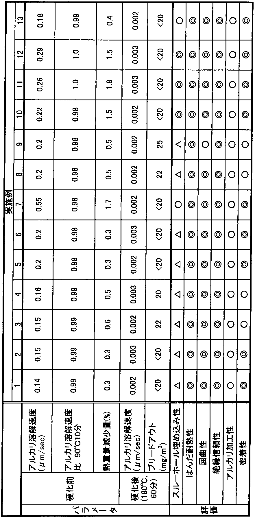


第2の実施の形態に関する実施例26~実施例31について説明する。
(積層体及びビア形成用コンフォーマルマスク製作)
樹脂組成物溶液を、12μm厚の電解銅箔(F2-WS)(古河電工社製)上にバーコータを用いて塗布し、その後95℃に加温されたオーブン中で15分間加熱し、その後95℃で30分間真空乾燥して溶媒を除去して、外層材となる25μmの厚みの樹脂組成物層を有する樹脂付き銅箔を得た。この樹脂付き銅箔の樹脂組成物層側を、銅箔厚み12μm、絶縁性樹脂層厚み20μmの片面フレキシブル配線基板(エスパネックス(登録商標)M)(新日鉄化学社製)の銅箔上に重ねて置き、さらに両面から離形用フィルムで挟んだものを準備した。
各実施例記載の方法により作製したフレキシブル配線板のブラインドビアは、エポキシ樹脂で包埋し、包埋された配線板に垂直に研磨装置(丸本ストラトス社製)を用いてブラインドビア径の中央位置まで断面研磨加工を行った後、測長機能付光学顕微鏡により観察し、形成されたブラインドビアにおける、図5を参照して説明したビア形状のパラメータx、yの値を測定した。なお、評価に関してはブラインドビア10穴の観察を行い、パラメータx、yの平均値を算出した。
前述の評価Jの断面観察用サンプルの表層をArイオンビームで3μmドライエッチし、飛行時間型二次イオン質量分析法(TOF-SIMS)により分析し、層間樹脂層のビアの壁面に接する部位からナトリウム(Na)とカリウム(K)が計50ppm含まれている部位までの水平方向の距離の最大値(樹脂変性部分の最大厚み)を測長した。
装置:独ION TOF社製 TOF-SIM 5
一次イオン:Bi3
加速電圧:25keV、電流量:0.3pA-10kHz
まず、事前に銅箔厚み12μm、絶縁性樹脂層厚み20μmの片面フレキシブル配線基板(エスパネックス(登録商標)M)(新日鉄化学社製)の基材を100×30mmに切り出し、事前に重量を測定しておき、基材の銅上に無電解銅めっき処理した後、100℃で60分間乾燥して吸湿成分を除去してから重量を測定することでめっき銅の質量を算出し、それに基づき算出した。こうして算出した結果を元に0.5μm厚無電解銅めっき条件及び1.0μm厚無電解銅めっき条件を決定した。
各実施例26~31記載の方法により作製したフレキシブル配線板において、100μmφブラインドビアを介してコア基板の配線回路と外層基板の配線回路を無電解/電解銅めっきによりデイジーチェーン接続させて形成した配線回路を用い、125℃と-40℃のそれぞれの恒温漕を15分毎に交互に往復させ、その時の接続抵抗値を測定した。各温度での接続抵抗値の初期値からの変動幅が10%以内であるサイクル数が、1000サイクル以上の場合を◎、500サイクル以上1000サイクル未満の場合を○とし、500サイクル未満の場合を×とした。
ポリイミドGの固形分が51質量%、1,3-ビス(4,5-ジヒドロ-2-オキサゾリル)ベンゼン(PBO)が7質量%、複合水酸化マグネシウム(商品名:MGZ-5R、堺化学工業社製)が40質量%、酸化防止剤としてイルガノックス245(IRG245、BASF社製)が2質量%になるように樹脂組成物を調製し、γ-ブチロラクトンで樹脂組成物の総固形分が40質量%になるように希釈し、この樹脂組成物溶液を用いて積層体及びビア形成用コンフォーマルマスクを形成した。
45℃に加温した3質量%水酸化ナトリウム水溶液を0.18MPa(噴出量0.92L/分)のフルコーン型スプレーノズルを用いて45秒間スプレー噴射処理した以外は実施例26と同様にビアホール付基板を作製し、評価した。評価結果を表7に示す。
無電解銅めっき厚を1.0μmにした以外は実施例27と同様にビアホール付基板を作製し、評価した。評価結果を表7に示す。
無電解銅めっきを実施する前にKMnO溶液(日本マクダーミッド社)でデスミア処理をした以外は実施例26と同様にビアホール付基板を作製し、評価した。評価結果を表7に示す。
ポリイミドCの固形分が52質量%、1,3-ビス(4,5-ジヒドロ-2-オキサゾリル)ベンゼン(PBO)が6質量%、ホスファゼン化合物Aが10質量%、複合水酸化マグネシウム(商品名:MGZ-5R、堺化学工業社製)が30質量%、酸化防止剤としてイルガノックス245(IRG245、BASF社製)が2質量%になるように樹脂組成物を調製し、γ-ブチロラクトンで樹脂組成物の総固形分が40質量%になるように希釈し、この樹脂組成物溶液を用いた。また、45℃に加温した3質量%水酸化ナトリウム水溶液を0.18MPa(噴出量0.92L/分)のフルコーン型スプレーノズルを用いて25秒間スプレー噴射処理し、その後0.12MPa(噴出量0.75L/分)のスプレーを120秒間水洗処理し、コンフォーマルマスクから露出した樹脂組成物層をエッチング除去しブラインドビアを形成した。それ以外は、実施例26と同様にビアホール付基板を作製し、評価した。実施例30における樹脂組成物層のエッチング速度は0.48μm/秒であった。その他評価結果を表7に示す。
ポリイミドIの固形分が51質量%、1,3-ビス(4,5-ジヒドロ-2-オキサゾリル)ベンゼン(PBO)が9質量%、ホスファゼン化合物Bが10質量%、複合水酸化マグネシウム(商品名:MGZ-5R、堺化学工業社製)が30質量%になるように樹脂組成物を調製し、γ-ブチロラクトンで樹脂組成物の総固形分が40質量%になるように希釈し、この樹脂組成物溶液を用いた。また、45℃に加温した3質量%水酸化ナトリウム水溶液を0.18MPa(噴出量0.92L/分)のフルコーン型スプレーノズルを用いて35秒間スプレー噴射処理し、その後0.12MPa(噴出量0.75L/分)のスプレーを120秒間水洗処理し、コンフォーマルマスクから露出した樹脂組成物層をエッチング除去しブラインドビアを形成した。
45℃に加温した3質量%水酸化ナトリウム水溶液を0.18MPa(噴出量0.92L/分)のフルコーン型スプレーノズルを用いて11秒間スプレー噴射処理した以外は実施例26と同様にビアホール付基板を作製し、評価した。評価結果を表7に示す。
45℃に加温した3質量%水酸化ナトリウム水溶液を0.18MPa(噴出量0.92L/分)のフルコーン型スプレーノズルを用いて75秒間スプレー噴射処理した以外は実施例26と同様にビアホール付基板を作製し、評価した。評価結果を表7に示す。
両面フレキシブル配線板としてエスパネックスM(新日鉄化学製、銅箔厚み12μm、絶縁性樹脂層厚25μm)を用いて銅箔上にドライフィルムレジスト(サンフォート(登録商標)AQ2578)(旭化成イーマテリアルズ社製)をロールラミネータにより貼り合せた後、露光・現像、及びエッチングにより、所定の位置の銅箔を片面のみエッチング除去し、300μmピッチ間隔で100μmφのコンフォーマルマスク及び、直径3mmの円孔パターンを形成した。
80℃で700秒間、前記ポリイミドケミカルエッチング液を液中スプレーした後、0.12MPa(噴出量0.75L/分)のスプレーを120秒間水洗処理して、ブラインドビアを形成した以外は、比較例13と同様に評価を実施した。結果を表7に示す。
比較例13と同様の方法で300μmピッチ間隔で100μmφのコンフォーマルマスクを形成した両面フレキシブル配線板を用い、このコンフォーマルマスク部から絶縁性樹脂層に炭酸ガスレーザー(日立建機社製)を照射してブラインドビアを形成した。デスミア処理は行わなかった。
炭酸ガスレーザー(日立建機社製)を照射してブラインドビアを形成した後、KMnO溶液(日本マクダーミッド社)によるデスミア処理を実施した以外は比較例15と同様に評価を実施した。結果を表7に示す。

第3の実施の形態に係る実施例32~37について説明する。
(内層コア基板の作製)
以下のようにして内層コア基板を作製した。まず、銅箔厚み12μm、絶縁性樹脂層厚み20μmの両面フレキシブル配線基板(エスパネックス(登録商標)M)(新日鉄化学社製)を用意した。この両面フレキシブル配線基板の基材銅をハーフエッチング処理をして、銅箔厚みを5μmに薄化した後、直径100μmのスルーホールをNCドリルで穴あけし、15μm厚のスルーホールめっきを施した。ここで、スルーホールのアスペクト比は0.9であった。次いで、スルーホールを有する両面フレキシブル基板において、スルーホール周囲に300μmφのランドとラインアンドスペース(L/S)が50/50μmとなる配線回路パターンを、ドライフィルムレジスト(サンフォート(登録商標)AQ2578)(旭化成イーマテリアルズ社製)を用いて銅箔上に形成し、次いで、銅箔にエッチングを施し、銅配線回路を形成した。このときの銅配線回路は20μm厚で形成した。
以下のようにして、前記内層コア基板の外層に積層する樹脂付き銅箔を作製した。実施例32~37の樹脂組成物溶液を12μm厚の電解銅箔(F2-WS)(古河電工製)上にバーコータを用いて塗布し、その後95℃に加温されたオーブン中で15分加熱処理し、その後90℃で30分間真空乾燥処理をして樹脂厚15~60μmである樹脂付き銅箔を得た。
実施例32~37記載の方法により作製した多層フレキシブル配線板を、エポキシ樹脂で包埋した後に100μmピッチ配線回路の中心部を断面研磨し、測長機能付光学顕微鏡で観察した。100μmピッチ配線回路を10か所観察し、回路上樹脂厚は10か所のうち、最も薄い配線回路上の樹脂層厚(評価N-1)とし、併せて樹脂層の表面凹凸量(評価N-2)は10か所の平均値とした。樹脂層の表面凹凸性が±3μm以下である場合を◎、±3μm超±5μm以下である場合を〇とし、±5μm超である場合を×とした。
実施例32~37記載の方法により作製した多層フレキシブル配線板のフレキシブル部の反発力は、以下の方法により実施した。まずフレキシブル部を10mm×5mmサイズに切り出した。次いで反発力の測定装置としては、一定速度で上下動可能であり、クリアランス精度0.1mm以下の自動サーボゲージに、フォースゲージを取り付けたものを使用した。フォースゲージの先端に50mm角の平行平板を取り付け、フォースゲージを600mm/分の一定速度で稼働し、且つ平行平板のクリアランスが1mmで停止する様に設定した。
実施例32~37において作成した積層体を用いて、上述の評価Cで説明した方法に従ってブリードアウト量を算出した。
実施例32~37記載の方法により作製した多層フレキシブル配線板の外層に形成した回路パターンにはんだペースト(鉛フリーはんだM705)(千住金属社製)を印刷した後、チップマウンターによりチップ抵抗器(1005チップ)(エヌエスアイ社製)を自動で乗せた後、最高到達温度条件が250℃で5秒間のリフロー処理を4回通して部品実装を行い、目視検査によりはんだ実装の位置ずれ、部品の浮き、傾きを評価した。4回通した後も、これらの異常がいずれも認められず、またフィレット形状にも異常が認められなかったものを○、4回目に異常が認められたものを△、1~3回目のいずれかに異常が認められたものを×とした。
各実施例32~37記載の方法により作製した、多層フレキシブル配線板のフレキシブル部の一端を、1mm厚のガラス基板の一辺とACF(日立化成製)で固着した後、フレキシブル部のもう一端を、外層基板の樹脂層が内側となる様に折り曲げてガラス基板の背面に両面テープで固着した。これを-40℃/125℃の各温度での15分保持を1サイクルとし、1000サイクルまで温度サイクル試験を実施した。1000サイクル後に剥離や膨らみの発生が認められなかったものを〇、剥離や膨らみの発生が認められたものを×とした。
ポリイミドGの固形分が51質量%、1,3-ビス(4,5-ジヒドロ-2-オキサゾリル)ベンゼン(PBO)が7質量%、複合水酸化マグネシウム(商品名:MGZ-5R、堺化学工業社製)が40質量%、酸化防止剤としてイルガノックス245(IRG245、BASF社製)が2質量%になるように樹脂組成物を調製し、γ-ブチロラクトンで樹脂組成物の総固形分が40質量%になるように希釈し、この樹脂組成物溶液を用いて15μm厚みの樹脂組成物層を有する積層体を作製した。この積層体に関して評価Pのブリードアウト試験を実施したところ、ブリードアウト量は20mg/m2以下であった。
前記樹脂付き銅箔の樹脂組成物層が25μm厚であること以外は、実施例32と同様に実施し、多層フレキシブル配線板を作製した。得られた基板の配線回路層上の樹脂層最小厚み及び表面凹凸量を断面観察により測定し、チップ実装性、折り曲げ実装性評価を実施した。結果を表8に示す。
前記樹脂付き銅箔の樹脂組成物層が40μm厚であること以外は、実施例32と同様に実施し、多層フレキシブル配線板を作製した。得られた基板の配線回路層上の樹脂層最小厚み及び表面凹凸量を断面観察により測定し、チップ実装性、折り曲げ実装性評価を実施した。結果を表8に示す。
ポリイミドIの固形分が65質量%、1,3-ビス(4,5-ジヒドロ-2-オキサゾリル)ベンゼン(PBO)が5質量%、ホスファゼン化合物Aが30質量%になるように樹脂組成物を調製し、γ-ブチロラクトンで樹脂組成物の総固形分が40質量%になるように希釈し、この樹脂組成物溶液を用いて25μm厚みの樹脂組成物層を有する積層体を作製した。
ポリイミドGの固形分が47質量%、1,3-ビス(4,5-ジヒドロ-2-オキサゾリル)ベンゼン(PBO)が11質量%、ホスファゼン化合物Bが10質量%、複合水酸化マグネシウム(商品名:MGZ-5R、堺化学工業社製)が30質量%、酸化防止剤としてイルガノックス245(IRG245、BASF社製)が2質量%になるように樹脂組成物を調製し、γ-ブチロラクトンで樹脂組成物の総固形分が40質量%になるように希釈し、この樹脂組成物溶液を用いて25μm厚みの樹脂組成物層を有する積層体を作製した。
ポリイミドGの固形分が49質量%、1,3-ビス(4,5-ジヒドロ-2-オキサゾリル)ベンゼン(PBO)が5質量%、3官能エポキシ樹脂(商品名:VG3101、プリンテック社製)が4質量%、複合水酸化マグネシウム(商品名:MGZ-5R、堺化学工業社製)が40質量%、酸化防止剤としてイルガノックス245(IRG245、BASF社製)が2質量%になるように樹脂組成物を調製し、γ-ブチロラクトンで樹脂組成物の総固形分が40質量%になるように希釈し、この樹脂組成物溶液を用いて25μm厚みの樹脂組成物層を有する積層体を作製した。
前記樹脂付銅箔の樹脂組成物層が10μm厚であること以外は、実施例32と同様に実施し、多層フレキシブル配線板を作製した。得られた基板の配線回路層上の樹脂層最小厚み及び表面凹凸量を断面観察により測定し、チップ実装性、折り曲げ実装性評価を実施した。結果を表8に示す。
前記樹脂付銅箔の樹脂組成物層が60μm厚であること以外は、実施例32と同様に実施し、多層フレキシブル配線板を作製した。得られた基板の配線回路層上の樹脂層最小厚み及び表面凹凸量を断面観察により測定し、チップ実装性、折り曲げ実装性評価を実施した。結果を表8に示す。
ポリイミドIの固形分が57質量%、1,3-ビス(4,5-ジヒドロ-2-オキサゾリル)ベンゼン(PBO)が8質量%、両末端型のフェノール変性シリコーンとしてX-22-1821(水酸基価38mgKOH/g、信越化学社製)を5質量%、ホスファゼン化合物Aが30質量%になるように樹脂組成物を調製し、γ-ブチロラクトンで樹脂組成物の総固形分が40質量%になるように希釈し、この樹脂組成物溶液を用いて25μm厚みの樹脂組成物層を有する積層体を作製した。この積層体に関してブリードアウト試験を実施したところ、ブリードアウト量は110mg/m2であった。
三口セパラブルフラスコに窒素導入管、温度計、水分分離トラップを備えた玉付冷却管を取り付けた。オイルバス室温でN-メチル-2-ピロリドン(NMP)330g、2,2’-ビス(4-(4-アミノフェノキシ)フェニル)プロパン40g、3,3’,4,4’-ジフェニルスルホンテトラカルボン酸二無水物50gを少しずつ添加した後、180℃まで昇温し、3時間加熱した。反応中、副生する水は、トルエンと共沸し、水分分離トラップを備えた玉付冷却管を用いて、還流下、脱水を行った。副生水を抜いた後、還流を止め、トルエンを全抜きし、室温まで冷却した。次に生成物を5μmのフィルターで加圧ろ過することでポリイミドQワニスを得た。重量平均分子量は110000であった。
ナフタレン骨格エポキシ樹脂(日本化薬(株)製「NC-7000L」)29.9g、ポリアミドイミド樹脂(東洋紡績(株)製「HR15ET」)30g、スチレン・ブタジエン系エラストマー(旭化成ケミカルズ(株)製「タフプレン」)15gを固形分濃度が40質量%になるようにN-メチル-2-ピロリドンで希釈し、エポキシ樹脂Aの溶液を得た。
エポキシ樹脂Aの固形分が75質量%、エポキシの硬化剤としてアミノトリアジンノボラック樹脂(DIC(株)製「LA-1356」)が10質量%、ホスファゼン化合物Aが30質量%、硬化促進剤として2-エチル-4-メチルイミダゾール(四国化成工業(株)製「2E4MZ」)が0.1質量%になるように樹脂組成物を調製し、N-メチル-2-ピロリドンで樹脂組成物の総固形分が40質量%になるように希釈し、この樹脂組成物溶液を用いて25μm厚みの樹脂組成物層を有する積層体を作製した。
下記の手順で、樹脂2層の積層体を製作した。まず、ポリイミドQの樹脂組成物溶液を12μm厚の電解銅箔(F2-WS、古河電工製)上にバーコータを用いて塗布し、その後95℃に加温されたオーブン中で15分加熱処理し、その後120℃で3時間真空乾燥処理をして樹脂厚12.5μmである樹脂付き銅箔を得た。さらにこの樹脂付き銅箔の樹脂面側に比較例20の樹脂組成物が15μm厚みになるように塗工してから95℃で15分加熱処理し、その後90℃で30分間真空乾燥し、樹脂総厚27.5μmの2層構造の積層体を作製した。

以下、第4の実施の形態に係る実施例38~43について説明する。
[フェノールノボラック樹脂A]
撹拌装置、コンデンサー、及び窒素ガス導入管を備えたガラス製反応釜に、フェノール404.2g(4.30モル)、4,4’-ジ(クロロメチル)ビフェニル150.70g(0.6モル)を仕込み100℃で3時間反応させ、その後42%ホルマリン水溶液28.57g(0.4モル)を添加し、その後、100℃で3時間反応させた。その間、生成するメタノールを留去した。反応終了後、得られた反応溶液を冷却し、水洗を3回行った。油層を分離し、減圧蒸留により未反応フェノールを留去することにより251gのフェノールノボラック樹脂Aを得た。
三口セパラブルフラスコに窒素導入管、温度計、水分分離トラップを備えた玉付冷却管を取り付けた。オイルバス室温で、1,3-ジメチル-2-イミダゾリジノン(DMI)344g、トルエン90g、ジメチルスルホキシド78.4g、2,2’-ビス(3-アミノ-4-ヒドロキシフェニル)ヘキサフルオロプロパン(6FAP)48.8g、ポリアルキルエーテルジアミンBaxxodur(TM) EC302(BASF社製)112.8gを入れ均一になるまで攪拌した。さらに、3,3’,4,4’-ビフェニルテトラカルボン酸二無水物(BPDA)120gを少しずつ添加した後、180℃まで昇温し、3時間加熱した。反応中、副生する水は、トルエンと共沸し、水分分離トラップを備えた玉付冷却管を用いて、還流下、脱水を行った。副生水を抜いた後、還流を止め、トルエンを全抜きし、室温まで冷却した。次に生成物を5μmのフィルターで加圧ろ過することでポリイミドRワニスを得た。重量平均分子量は28000であった。
三口セパラブルフラスコに窒素導入管、温度計、水分分離トラップを備えた玉付冷却管を取り付けた。オイルバス室温で、トリエチレングリコールジメチルエーテル(22.5g)、γ―ブチロラクトン(52.5g)、トルエン(20.0g)、4,4’-オキシジフタル酸二無水物(ODPA)1.00g、両末端酸二無水物変性シリコーン(X-22-2290AS、信越化学(株)製)35.00gを入れ均一になるまで攪拌した。さらに、2,2’-ビス(3-アミノ-4-ヒドロキシフェニル)ヘキサフルオロプロパン(6FAP)14.00g、を少しずつ添加した後、180℃まで昇温し、2時間加熱した。反応中、副生する水は、トルエンと共沸し、水分分離トラップを備えた玉付冷却管を用いて、還流下、脱水を行った。副生水を抜いた後、還流を止め、トルエンを全抜きし、室温まで冷却した。次に生成物を5μmのフィルターで加圧ろ過することでポリイミドSワニスを得た。重量平均分子量は27000であった。
ゴム硬度は、JISK6253に従い、デュロメータ(タイプA)にて測定した。
実施例38~43記載の方法により作製した多層フレキシブル配線板のコア基板の配線回路(銅配線厚み平均25μm、配線ピッチ130μm~500μm)や貫通ビア(ビア径100μmφ、ビア深さ約60μm)での表面平滑性の評価は断面構造解析により実施した。まず基板をエポキシ樹脂で包埋し、貫通ビアや配線回路の断面方向に研磨加工を行った後、測長機能付光学顕微鏡観察により評価した。表面平滑性は銅配線回路上と回路間との段差が5μm以内ならば○とし、5μmを超えた場合は×とした。
実施例38~43記載の方法により作製した多層フレキシブル配線板の外層に形成した回路パターンにはんだペースト(鉛フリーはんだM705、千住金属社製)を印刷した後、チップマウンターによりチップ抵抗器(1005チップ、エヌエスアイ社製)を自動で乗せた後、最高到達温度条件が250℃で5秒間のリフロー処理を2回通して部品実装を行い、目視検査によりはんだ実装の位置ずれ、部品の浮き、傾きがいずれも認められず、またフィレット形状にも異常が認められなかったものを○、いずれかに異常が認められたものをとした×とした。
実施例38~43記載の方法により作製した多層フレキシブル配線板の絶縁層の内層及び外層の相対する位置に形成した0.5mmΦの円形電極パターンを用いて、85℃85%RHの恒温恒湿オーブン内で50VDCを1000時間連続で印加した時の絶縁抵抗値を測定した。絶縁抵抗値が106Ω以上であったものを○、106Ω未満になったものを×とした。
内層のコア基板として両面フレキシブル配線板としてエスパネックスM(新日鉄化学製、銅箔厚み12μm、絶縁性樹脂層厚20μm)を用いた。両面フレキシブル配線板には、ドリル加工及び銅めっき処理により100μmφを形成した。また最少130μmピッチの銅配線回路(28μm厚)を形成した。
実施例38で作製した両面フレキシブル配線板をコア基板として用いた。次にポリイミドR固形物に、樹脂組成物溶液の固形分が40質量%になるようにγ-ブチロラクトン:ジメチルスルホキシド(DMSO)=80:20の混合溶媒を添加し、かつ接着性樹脂ワニスの固形分合計を100質量%とした際に、樹脂組成物溶液の中のポリイミドRが60質量%、オキサゾリン基を含有する化合物として1,3-ビス(4,5-ジヒドロ-2-オキサゾリル)ベンゼン(PBO)が15質量%、難燃剤としてホスファゼン化合物Aとホスファゼン化合物Bをそれぞれ6質量%と18質量%、酸化防止剤としてイルガノックス245(IRG245、BASF製)を1質量%になるように樹脂組成物溶液を調合した。
実施例38で作製した両面フレキシブル配線板をコア基板として用いた。外層材となる樹脂付き銅箔は、実施例39より得られた樹脂組成物溶液を12μm厚の電解銅箔(F2-WS、古河電工製)上にバーコータを用いて塗布し、その後95℃に加温されたオーブン中で12分乾燥処理をして得た。この未硬化接着性樹脂付き銅箔をコア基板の上下面に重ねて置き、さらに両面から離形用フィルムで挟んだものを準備した。
真空プレス装置の上下両面定盤の全面に、内部にガラスクロスを含んでいる硬度30度の耐熱シリコンラバーを全面に貼りあわせたものを用いて、積層した以外は実施例40と同様に基板を作製した。実施例41において、積層工程後の周辺からの樹脂フロー量は約60μmであった。
真空プレス装置の上下両面定盤の全面に、内部にガラスクロスを含んでいる硬度70度の耐熱シリコンラバーを全面に貼りあわせたものを用いて、積層した以外は実施例40と同様に基板を作製した。実施例42において、積層工程後の周辺からの樹脂フロー量は約100μmであった。
実施例1で作製した両面フレキシブル配線板をコア基板として用いた。
実施例38で作製した両面フレキシブル配線板をコア基板として用いた。外層材となる樹脂付き銅箔は、実施例43で用いた樹脂組成物溶液を12μm厚のポリエステルフィルム上にダイコーターを用いて塗布し、95℃、30分乾燥して、膜厚25μmのフィルムを作成した。この積層フィルムを電解銅箔(厚み12μm、F1-WS/古河電工社製)の粗面側に重ねて真空プレスを用いて90℃、0.5MPaで1分ラミネートして、片面フレキシブル基板を製作した。この銅箔上にドライフィルムをラミネートし、露光、現像した後、塩化第二鉄エッチングにより、所定の位置の銅箔を除去し、部位に75μmφ円孔のコンフォーマルマスクを形成した。さらに銅箔が除去された部位に、3質量%の水酸化ナトリウム溶液を30秒スプレーし樹脂組成物層を溶解除去して、ブラインドビアを形成した。次に裏面のポリエステルフィルムを剥離した後、硬化乾燥炉を用いて、180℃で1時間加熱することにより、樹脂組成物層を硬化させたものを作製した。
実施例38で作製した両面フレキシブル配線板をコア基板として用いた。外層材となる樹脂付き銅箔は、実施例39で用いた樹脂組成物溶液を12μm厚のポリエステルフィルム上にダイコーターを用いて塗布し、95℃、30分乾燥して、膜厚25μmのフィルムを作成した。この積層フィルムを厚み12μmの電解銅箔(F1-WS)(古河電工社製)の粗面側に重ねて真空プレスを用いて90℃、0.5MPaで1分ラミネートして、片面フレキシブル基板を製作した。この銅箔上にドライフィルムをラミネートし、露光、現像した後、塩化第二鉄エッチングにより、所定の位置の銅箔を除去し、部位に75μmφ円孔のコンフォーマルマスクを形成した。さらに銅箔が除去された部位に、3質量%の水酸化ナトリウム溶液を30秒スプレーし樹脂組成物層を溶解除去して、ブラインドビアを形成した。次に裏面のポリエステルフィルムを剥離した後、硬化乾燥炉を用いて、180℃で1時間加熱することにより、樹脂組成物層を硬化させたものを作製した。
実施例38で作製した両面フレキシブル配線板をコア基板として用いた。外層材となる樹脂付き銅箔は、実施例39で用いた樹脂組成物溶液を12μm厚のポリエステルフィルム上にダイコーターを用いて塗布し、95℃、30分乾燥して、膜厚25μmのフィルムを作成した。この積層フィルムを厚み12μmの電解銅箔(F1-WS)(古河電工社製)の粗面側に重ねて真空プレスを用いて90℃、0.5MPaで1分ラミネートして、片面フレキシブル基板を製作した。この銅箔上にドライフィルムをラミネートし、露光、現像した後、塩化第二鉄エッチングにより、所定の位置の銅箔を除去し、部位に75μmφ円孔のコンフォーマルマスクを形成した。さらに銅箔が除去された部位に、3質量%の水酸化ナトリウム溶液を30秒スプレーし樹脂組成物層を溶解除去して、ブラインドビアを形成した。次に裏面のポリエステルフィルムを剥離した後、硬化乾燥炉を用いて、180℃で1時間加熱することにより、樹脂組成物層を硬化させたものを作製した。

Claims (34)
- (A)酸性官能基を有するポリイミドと、(B)酸性官能基と反応する官能基を有する化合物と、を含む樹脂組成物であって、
(a)前記樹脂組成物の、90℃、10分の熱履歴後における45℃での3質量%水酸化ナトリウム水溶液への溶解速度が、熱履歴前を1として0.95以上であり、
(b)前記樹脂組成物の、180℃、60分の熱履歴後における45℃での3質量%水酸化ナトリウム水溶液への溶解速度が0.001μm/秒以上0.02μm/秒以下であり、
(c)前記樹脂組成物の、180℃、60分の熱履歴後に40℃で2週間保持した際のブリードアウト量が50mg/m2以下であり、且つ、
(d)熱重量分析(TG)により、40℃から10℃/分の昇温条件で測定した260℃における熱重量減少が2.0%以下である、
ことを特徴とする樹脂組成物。 - 前記樹脂組成物の、熱履歴前の45℃での3質量%水酸化ナトリウム水溶液への溶解速度が0.10μm/秒以上であることを特徴とする請求項1記載の樹脂組成物。
- 前記ポリイミド(A)の酸性官能基がフェノール性水酸基を含む構造であることを特徴とする請求項1又は請求項2記載の樹脂組成物。
- 前記化合物(B)がオキサゾリン基を含む構造であることを特徴とする請求項1から請求項3のいずれかに記載の樹脂組成物。
- (A-1)フェノール性水酸基を有するポリイミドとして下記一般式(1)で表される構造を有するポリイミドと、(B-1)オキサゾリン化合物と、を含むことを特徴とする樹脂組成物。

- 前記ポリイミドが、下記一般式(2)で表される構造を有することを特徴とする請求項5記載の樹脂組成物。

- 前記ポリイミドが有する水酸基と、前記オキサゾリン化合物が有するオキサゾリン基(B-1)との比(水酸基/オキサゾリン基)が、4.0~0.5の範囲であることを特徴とする請求項5又は請求項6記載の樹脂組成物。
- 前記ポリイミドが、さらに下記一般式(3)の構造を有することを特徴とする請求項5から請求項7のいずれかに記載の樹脂組成物。

- 前記ポリイミドのポリマー全質量中に前記一般式(3)の構造を25~55質量%含むことを特徴とする請求項8記載の樹脂組成物。
- 前記ポリイミド中の前記一般式(3)中のQ1が直鎖状テトラメチレン基である構造を含むことを特徴とする請求項8又は請求項9記載の樹脂組成物。
- 前記ポリイミドが、モノアミン誘導体又はカルボン酸誘導体からなる末端封止剤で末端封止されていることを特徴とする請求項5から請求項10のいずれかに記載の樹脂組成物。
- 180℃、60分の熱履歴後に40℃で2週間保持した際のブリードアウト量が50mg/m2以下であることを特徴とする請求項5から請求項11のいずれかに記載の樹脂組成物。
- (C)2以上の水酸基を有する多官能水酸基含有化合物の含有率が0以上3質量%以下であることを特徴とする請求項5から請求項12のいずれかに記載の樹脂組成物。
- 請求項1から請求項13のいずれかに記載の樹脂組成物を、有機溶媒に溶かしてなることを特徴とする樹脂組成物溶液。
- 基材と、前記基材上に設けられた請求項1から請求項13のいずれかに記載の樹脂組成物と、を具備することを特徴とする積層体。
- 前記基材が、キャリアフィルムであることを特徴とする請求項15記載の積層体。
- 前記樹脂組成物上に設けられたカバーフィルムをさらに具備することを特徴とする請求項15又は請求項16記載の積層体。
- 前記基材が、導電体であることを特徴とする請求項15から請求項17のいずれかに記載の積層体。
- 前記導電体が、銅箔であることを特徴とする、請求項18記載の積層体。
- 配線を有する基材と、前記配線を覆うように設けられた請求項1から請求項13のいずれかに記載の樹脂組成物と、を具備することを特徴とする多層プリント配線板。
- ロール形状であることを特徴とする請求項20記載の多層プリント配線板。
- 第1導電層と、前記第1導電層の表面上に設けられた樹脂組成物層と、前記樹脂組成物層の表面上に設けられた第2導電層と、を具備する積層体において、前記第2導電層の一部を除去して開口部を形成し、前記開口部が形成された前記第2導電層をマスクとして、前記開口部に露出した前記樹脂組成物層を、アルカリ溶液を用いたエッチングにより除去して前記第1導電層の一部が露出するように前記樹脂組成物層に形成したビアホールを形成し、前記ビアホールの内部を含む前記第2導電層の表面にめっきを施して得られる多層プリント配線板であって、
前記ビアホールの垂直断面を観察した場合、前記第2導電層の前記開口部内側の端面から、前記ビアホールの前記第2導電層側の端部までの水平距離xが、-30μm以上0μm以下であり、
前記第2導電層の前記開口部内側の端面から、前記ビアホールの前記第1の導電層側の端部までの水平距離yが、-10μm以上20μm以下であり、且つ、
前記ビアホールの垂直断面のTOF-SIMS測定において、前記ビアホールの側壁面を形成する前記樹脂組成物層のうち、前記アルカリ溶液が含有するアルカリ金属イオンの残存濃度総量が50ppm以上である樹脂変性部分の前記側壁面から水平方向の厚みTが10μm以上である
ことを特徴とする多層プリント配線板。 - 前記樹脂組成物層の前記第1導体層に接する樹脂組成物面において、40℃で2週間保持した際のブリードアウト量が50mg/m2以下であることを特徴とする請求項22記載の多層プリント配線板。
- 前記樹脂組成物層を形成する樹脂組成物が、45℃での3質量%水酸化ナトリウム水溶液へのアルカリ溶解速度が、熱履歴前の状態で0.10μm/秒以上であることを特徴とする請求項22又は請求項23に記載の多層プリント配線板。
- 前記樹脂組成物層を形成する樹脂組成物がポリイミドを含むことを特徴とする請求項22から請求項24のいずれかに記載の多層プリント配線板。
- ロール形状であることを特徴とする請求項22から請求項25のいずれかに記載の多層プリント配線板。
- 外層導電層と、前記外層導電層の表面上に設けられた単一の樹脂硬化物層とを備えた外層基板を、配線回路又はビアホールが形成された両面フレキシブル基板からなるコア基板に、前記コア基板の表面側に前記樹脂硬化物層が配置されるように積層して形成される多層フレキシブル配線板であって、
前記外層導電層の一部を除去してフレキシブル部が形成されており、前記フレキシブル部において前記多層フレキシブル配線板を曲率R0.5mmで屈曲させたときの反発力が0.001~0.5N/mmであり、前記コア基板に形成された前記配線回路上、又は、前記ビアホールの開口部上における前記樹脂硬化物層の表面凹凸量が5μmであり、
前記樹脂硬化物層の表面における、180℃、60分の熱履歴後に40℃で2週間保持した際のブリードアウト量が50mg/m2以下であり、且つ、
前記配線回路上における前記樹脂硬化物層の厚さが5μm以上40μm以下である
ことを特徴とする多層フレキシブル配線板。 - 前記樹脂硬化物層がポリイミドを含むことを特徴とする請求項27記載の多層フレキシブル配線板。
- ロール形状であることを特徴とする請求項27又は請求項28記載の多層フレキシブル配線板。
- 外層導電層と、前記外層導電層の表面上に設けられた樹脂組成物層と、を備えた外層基板を、配線回路及びビアホールが形成された両面フレキシブル基板からなるコア基板に、前記樹脂組成物層が前記コア基板の表面側に配置されるように、重ね合わせる工程と、
重ね合わせた前記外層基板及び前記コア基板を所定の積層条件で加熱及び加圧して積層する工程と、
を具備する多層フレキシブル配線板の製造方法であって、
前記外層基板及び前記コア基板を積層する工程において、補強材と一体化したラバー基材を有する加圧及び加熱が可能な真空積層装置を用いること、且つ、
前記積層条件が、70℃以上180℃以下、0.3MPa以上3MPa以下であるときの、前記外層導電層周辺からの樹脂フロー量が0.001mm以上1mm以下である
ことを特徴とする多層フレキシブル配線板の製造方法。 - 前記積層条件において、70℃以上120℃以下、0.3MPa以上3MPa以下であるときの前記外層導電層周辺からの樹脂フロー量が、0.005mm以上1mm以下であることを特徴とする請求項30記載の多層フレキシブル配線板の製造方法。
- 前記積層条件において、コーンプレート型レオメータを用いて5℃/分で昇温したときの溶融粘度が100Pa・s以上である温度で、且つ、最低溶融粘度より低い温度であることを特徴とする請求項30又は請求項31記載の多層フレキシブル配線板の製造方法。
- 前記積層条件において、加圧時間が20秒以上10分以下であるときの前記外層導電層周辺からの樹脂フロー量が、0.001mm以上1mm以下であることを特徴とする請求項30から請求項32のいずれかに記載の多層フレキシブル配線板の製造方法。
- 前記補強材がクロス又は不織布からなり、且つ、前記ラバー基材が表面硬度30度以上70度以下のシリコーン又はウレタンからなるシート又はロール形状であることを特徴とする請求項30から請求項33のいずれかに記載の多層フレキシブル配線板の製造方法。
Priority Applications (8)
| Application Number | Priority Date | Filing Date | Title |
|---|---|---|---|
| KR1020147019600A KR101597478B1 (ko) | 2012-01-20 | 2013-01-18 | 수지 조성물, 적층체, 다층 프린트 배선판 및 다층 플렉시블 배선판 및 그 제조 방법 |
| KR1020157025530A KR101634918B1 (ko) | 2012-01-20 | 2013-01-18 | 수지 조성물, 적층체, 다층 프린트 배선판 및 다층 플렉시블 배선판 및 그 제조 방법 |
| KR1020167003006A KR101669396B1 (ko) | 2012-01-20 | 2013-01-18 | 수지 조성물, 적층체, 다층 프린트 배선판 및 다층 플렉시블 배선판 및 그 제조 방법 |
| US14/373,218 US9896546B2 (en) | 2012-01-20 | 2013-01-18 | Resin composition, layered product, multilayer printed wiring board, multilayer flexible wiring board and manufacturing method of the same |
| CN201380005546.XA CN104053724B (zh) | 2012-01-20 | 2013-01-18 | 树脂组合物、层积体、多层印刷线路板和多层柔性线路板及其制造方法 |
| SG11201404196XA SG11201404196XA (en) | 2012-01-20 | 2013-01-18 | Resin composition, layered product, multilayer printed wiring board, multilayer flexible wiring board and manufacturing method of the same |
| KR1020167003007A KR20160020587A (ko) | 2012-01-20 | 2013-01-18 | 수지 조성물, 적층체, 다층 프린트 배선판 및 다층 플렉시블 배선판 및 그 제조 방법 |
| JP2013554362A JP5785274B2 (ja) | 2012-01-20 | 2013-01-18 | 樹脂組成物、積層体、多層プリント配線板 |
Applications Claiming Priority (6)
| Application Number | Priority Date | Filing Date | Title |
|---|---|---|---|
| JP2012010515 | 2012-01-20 | ||
| JP2012-010515 | 2012-01-20 | ||
| JP2012-071172 | 2012-03-27 | ||
| JP2012071172 | 2012-03-27 | ||
| JP2012-252578 | 2012-11-16 | ||
| JP2012252578 | 2012-11-16 |
Publications (1)
| Publication Number | Publication Date |
|---|---|
| WO2013108890A1 true WO2013108890A1 (ja) | 2013-07-25 |
Family
ID=48799311
Family Applications (1)
| Application Number | Title | Priority Date | Filing Date |
|---|---|---|---|
| PCT/JP2013/050978 WO2013108890A1 (ja) | 2012-01-20 | 2013-01-18 | 樹脂組成物、積層体、多層プリント配線板及び多層フレキシブル配線板並びにその製造方法 |
Country Status (7)
| Country | Link |
|---|---|
| US (1) | US9896546B2 (ja) |
| JP (3) | JP5785274B2 (ja) |
| KR (4) | KR101669396B1 (ja) |
| CN (4) | CN105636366B (ja) |
| SG (1) | SG11201404196XA (ja) |
| TW (3) | TWI583723B (ja) |
| WO (1) | WO2013108890A1 (ja) |
Cited By (11)
| Publication number | Priority date | Publication date | Assignee | Title |
|---|---|---|---|---|
| JP2015074660A (ja) * | 2013-10-04 | 2015-04-20 | 旭化成イーマテリアルズ株式会社 | 樹脂組成物、積層体、プリント配線板、及びその製造方法 |
| US9051465B1 (en) | 2012-02-21 | 2015-06-09 | Park Electrochemical Corporation | Thermosetting resin composition containing a polyphenylene ether and a brominated fire retardant compound |
| JP2015211095A (ja) * | 2014-04-25 | 2015-11-24 | 旭化成イーマテリアルズ株式会社 | 積層体、多層プリント配線板の製造方法及び多層プリント配線板 |
| KR20150131965A (ko) * | 2014-05-15 | 2015-11-25 | 제이에스알 가부시끼가이샤 | 감방사선성 수지 조성물, 절연막 및 그의 제조 방법, 그리고 유기 el 소자 |
| US9243164B1 (en) | 2012-02-21 | 2016-01-26 | Park Electrochemical Corporation | Thermosetting resin composition containing a polyphenylene ether and a brominated fire retardant compound |
| JP2016222797A (ja) * | 2015-05-29 | 2016-12-28 | 三菱瓦斯化学株式会社 | ポリイミド樹脂組成物 |
| CN106463706A (zh) * | 2014-06-05 | 2017-02-22 | 宇部兴产株式会社 | 电极的制造方法 |
| WO2017170643A1 (ja) * | 2016-03-31 | 2017-10-05 | 住友ベークライト株式会社 | 熱硬化性樹脂組成物、キャリア付樹脂膜、プリプレグ、金属張積層板、樹脂基板、プリント配線基板および半導体装置 |
| WO2018016526A1 (ja) * | 2016-07-21 | 2018-01-25 | 三菱瓦斯化学株式会社 | ポリイミド樹脂フィルム及びポリイミド樹脂フィルムの製造方法 |
| TWI715541B (zh) * | 2014-11-17 | 2021-01-11 | 日商日東電工股份有限公司 | 附分隔件之密封用片材、及半導體裝置之製造方法 |
| WO2022181291A1 (ja) * | 2021-02-25 | 2022-09-01 | 三菱マテリアル株式会社 | ポリイミド樹脂組成物及び金属ベース基板 |
Families Citing this family (32)
| Publication number | Priority date | Publication date | Assignee | Title |
|---|---|---|---|---|
| KR102142521B1 (ko) * | 2013-12-26 | 2020-08-07 | 삼성전기주식회사 | 경연성 인쇄회로기판 및 그의 제조 방법 |
| US10579236B2 (en) * | 2014-06-20 | 2020-03-03 | Ati Technologies Ulc | Responding to user input including providing user feedback |
| TWI578517B (zh) * | 2015-08-14 | 2017-04-11 | 群創光電股份有限公司 | 有機發光二極體顯示面板 |
| JP6459930B2 (ja) * | 2015-11-27 | 2019-01-30 | オムロン株式会社 | 接合構造体の製造方法および接合構造体 |
| CN108353497A (zh) * | 2015-12-18 | 2018-07-31 | Dic株式会社 | 热固性粘接片、带有增强部的柔性印刷配线板、其制造方法以及电子设备 |
| KR102190177B1 (ko) * | 2016-05-09 | 2020-12-11 | 쇼와덴코머티리얼즈가부시끼가이샤 | 반도체 장치의 제조 방법 |
| CN107404804B (zh) * | 2016-05-20 | 2020-05-22 | 鹏鼎控股(深圳)股份有限公司 | 电路板及其制作方法 |
| KR101831860B1 (ko) * | 2016-05-31 | 2018-02-26 | 에스케이씨 주식회사 | 안테나 소자 및 이의 제조방법 |
| CN107452461B (zh) | 2016-05-31 | 2020-04-14 | Skc株式会社 | 磁性片、导电磁性复合片、天线设备及其制备方法 |
| KR101947150B1 (ko) * | 2016-08-09 | 2019-02-12 | 주식회사 엘지화학 | 절연층 제조방법 및 다층인쇄회로기판 제조방법 |
| KR102040225B1 (ko) * | 2016-11-11 | 2019-11-06 | 주식회사 엘지화학 | 절연층 제조방법 및 다층인쇄회로기판 제조방법 |
| KR101877847B1 (ko) * | 2017-02-23 | 2018-07-12 | 한국에너지기술연구원 | 박막 태양전지용 연성기판의 응력 완화 방법 |
| CN109219236B (zh) * | 2017-06-30 | 2021-11-02 | 宏启胜精密电子(秦皇岛)有限公司 | 透明柔性电路板及其制备方法 |
| TWI665260B (zh) | 2017-09-19 | 2019-07-11 | 臻鼎科技股份有限公司 | 低介電聚醯亞胺組合物、聚醯亞胺、聚醯亞胺膜及覆銅板 |
| JP6983044B2 (ja) * | 2017-11-27 | 2021-12-17 | 日本メクトロン株式会社 | 伸縮性基板、伸縮性基板の製造方法 |
| CN108241240B (zh) * | 2018-02-08 | 2021-05-14 | 上海天马微电子有限公司 | 一种显示面板以及显示装置 |
| JP7272351B2 (ja) * | 2018-03-30 | 2023-05-12 | 日本ゼオン株式会社 | 樹脂薄膜の剥離片の製造方法 |
| JP7137354B2 (ja) | 2018-05-17 | 2022-09-14 | スタンレー電気株式会社 | 多層回路基板、および、その製造方法 |
| CN109486189A (zh) * | 2018-11-09 | 2019-03-19 | 李梅 | 一种用于fpc行业的tpi薄膜及其制备方法 |
| US10499509B1 (en) * | 2018-12-31 | 2019-12-03 | General Electric Company | Methods and systems for a flexible circuit |
| US11419213B2 (en) * | 2019-03-26 | 2022-08-16 | Western Digital Technologies, Inc. | Multilayer flex circuit with non-plated outer metal layer |
| JP7025376B2 (ja) | 2019-06-17 | 2022-02-24 | 矢崎総業株式会社 | バスバモジュール |
| JP7341766B2 (ja) * | 2019-07-19 | 2023-09-11 | 三菱製紙株式会社 | 樹脂組成物用のエッチング方法 |
| JP7381323B2 (ja) * | 2019-12-17 | 2023-11-15 | 日東電工株式会社 | 両面配線回路基板の製造方法および両面配線回路基板 |
| JP2021141214A (ja) * | 2020-03-05 | 2021-09-16 | モレックス エルエルシー | 成形回路基板とその製造方法 |
| JP2021150311A (ja) | 2020-03-16 | 2021-09-27 | キオクシア株式会社 | 半導体装置 |
| CN115551189A (zh) * | 2021-06-29 | 2022-12-30 | 富佳生技股份有限公司 | 多层柔性线路板的制造方法、多层柔性线路板及其应用 |
| KR20230104148A (ko) * | 2020-11-05 | 2023-07-07 | 디아이씨 가부시끼가이샤 | 세미 애디티브 공법용 적층체 및 그것을 이용한 프린트 배선판 |
| KR20230098579A (ko) * | 2020-11-05 | 2023-07-04 | 디아이씨 가부시끼가이샤 | 세미 애디티브 공법용 적층체 및 그것을 이용한 프린트 배선판 |
| TWI796737B (zh) * | 2021-07-23 | 2023-03-21 | 群光電能科技股份有限公司 | 背光模組 |
| CN117528897A (zh) * | 2022-07-27 | 2024-02-06 | 宏启胜精密电子(秦皇岛)有限公司 | 软性电路板及其制造方法 |
| CN117295255A (zh) * | 2023-09-28 | 2023-12-26 | 电子科技大学 | 一种可拉伸电路板和柔性电路板结合的方法 |
Citations (15)
| Publication number | Priority date | Publication date | Assignee | Title |
|---|---|---|---|---|
| JPH10330616A (ja) * | 1997-05-30 | 1998-12-15 | Hitachi Chem Co Ltd | 耐熱樹脂ペースト |
| JPH11246777A (ja) * | 1998-03-03 | 1999-09-14 | Hitachi Chem Co Ltd | 耐熱樹脂ペーストの製造方法 |
| JP2001264980A (ja) * | 2000-03-17 | 2001-09-28 | Toshiba Chem Corp | 感光性樹脂組成物およびその製造方法 |
| JP2003124603A (ja) * | 2001-10-12 | 2003-04-25 | Matsushita Electric Ind Co Ltd | 回路形成基板製造用クッション材およびその製造方法 |
| JP2003179321A (ja) * | 2001-12-11 | 2003-06-27 | Fujikura Ltd | 回路基板及び多層回路基板及び回路基板の製造方法 |
| JP2004176031A (ja) * | 2002-02-06 | 2004-06-24 | Sekisui Chem Co Ltd | 樹脂組成物 |
| JP2006057099A (ja) * | 2002-02-06 | 2006-03-02 | Sekisui Chem Co Ltd | 樹脂組成物 |
| JP2007192936A (ja) * | 2006-01-17 | 2007-08-02 | Asahi Kasei Electronics Co Ltd | ポジ型感光性樹脂組成物 |
| JP2010083951A (ja) * | 2008-09-30 | 2010-04-15 | Sony Chemical & Information Device Corp | 感光性シロキサンポリイミド樹脂組成物 |
| JP2011165889A (ja) * | 2010-02-09 | 2011-08-25 | Asahi Kasei E-Materials Corp | フレキシブル配線板の製造方法及びフレキシブル配線板 |
| JP2011228493A (ja) * | 2010-04-20 | 2011-11-10 | Asahi Kasei E-Materials Corp | フレキシブル配線板の製造方法 |
| JP2011236315A (ja) * | 2010-05-10 | 2011-11-24 | Kaneka Corp | 新規な熱硬化性樹脂組成物及びその利用 |
| JP2012015465A (ja) * | 2010-07-05 | 2012-01-19 | Kyocera Chemical Corp | 層間接着シートおよび多層フレキシブル配線板の製造方法 |
| WO2012098734A1 (ja) * | 2011-01-18 | 2012-07-26 | 旭化成イーマテリアルズ株式会社 | 樹脂組成物、硬化物、樹脂フィルム及び配線板 |
| JP2012169346A (ja) * | 2011-02-10 | 2012-09-06 | Asahi Kasei E-Materials Corp | フレキシブル配線板の製造方法及びフレキシブル配線板 |
Family Cites Families (38)
| Publication number | Priority date | Publication date | Assignee | Title |
|---|---|---|---|---|
| JPH06314869A (ja) * | 1993-04-30 | 1994-11-08 | Eastern:Kk | プリント配線板のスルーホール形成方法 |
| JPH0715146A (ja) * | 1993-06-22 | 1995-01-17 | Toagosei Co Ltd | ブラインドホールを有する多層プリント配線板 |
| JPH0766560A (ja) * | 1993-08-26 | 1995-03-10 | Toagosei Co Ltd | ブラインドホールを有する多層プリント配線板の製造方法 |
| JP3624967B2 (ja) * | 1995-06-01 | 2005-03-02 | 日立化成工業株式会社 | 多層プリント配線板の製造方法 |
| JP2002114981A (ja) | 1997-02-14 | 2002-04-16 | Otsuka Chem Co Ltd | 難燃剤、難燃性樹脂組成物及び難燃性樹脂成形体 |
| US6596893B2 (en) | 1997-10-15 | 2003-07-22 | Otsuka Chemical Co., Ltd. | Crosslinked phenoxyphosphazene compounds, flame retardants, flame-retardant resin compositions, and moldings of flame-retardant resins |
| JP2000053858A (ja) * | 1998-08-07 | 2000-02-22 | Showa Denko Kk | 高剛性難燃ポリアミド複合材料 |
| JP3710945B2 (ja) * | 1999-01-21 | 2005-10-26 | 凸版印刷株式会社 | 多層プリント配線板用絶縁性樹脂組成物および多層プリント配線板 |
| EP1207730B1 (en) * | 1999-08-06 | 2009-09-16 | Ibiden Co., Ltd. | Electroplating solution, method for fabricating multilayer printed wiring board using the solution, and multilayer printed wiring board |
| KR100677782B1 (ko) * | 2000-01-17 | 2007-02-05 | 제이에스알 가부시끼가이샤 | 절연막 형성용 재료의 제조 방법 |
| MY131961A (en) * | 2000-03-06 | 2007-09-28 | Hitachi Chemical Co Ltd | Resin composition, heat-resistant resin paste and semiconductor device using them and method for manufacture thereof |
| JP3788917B2 (ja) * | 2001-04-02 | 2006-06-21 | 日東電工株式会社 | フレキシブル多層配線回路基板の製造方法 |
| JP2003179330A (ja) * | 2001-12-12 | 2003-06-27 | Hitachi Chem Co Ltd | 多層印刷配線板とその製造方法 |
| WO2003066741A1 (fr) | 2002-02-06 | 2003-08-14 | Sekisui Chemical Co., Ltd. | Composition de resine |
| CN100372892C (zh) | 2002-02-06 | 2008-03-05 | 积水化学工业株式会社 | 树脂组合物 |
| JP2003264370A (ja) * | 2002-03-11 | 2003-09-19 | Kyocera Chemical Corp | 多層プリント配線板とその製造方法、およびそれに用いるプリント配線板用銅箔付き樹脂シート |
| CN100579333C (zh) * | 2003-01-23 | 2010-01-06 | 东丽株式会社 | 电路基板用部件、电路基板的制造方法及电路基板的制造装置 |
| JP4695512B2 (ja) | 2003-06-05 | 2011-06-08 | 株式会社カネカ | ホスファゼン化合物、及び感光性樹脂組成物並びにその利用 |
| JP2005251895A (ja) | 2004-03-03 | 2005-09-15 | Hitachi Chem Co Ltd | 多層配線板及び多層配線板の製造方法 |
| JP4192870B2 (ja) * | 2004-09-13 | 2008-12-10 | 新神戸電機株式会社 | 積層板および配線板 |
| CN101268146B (zh) * | 2005-09-15 | 2012-01-25 | 积水化学工业株式会社 | 树脂组合物、片状成型体、预浸料、固化体、层叠板及多层层叠板 |
| JP4929665B2 (ja) * | 2005-09-30 | 2012-05-09 | 大日本印刷株式会社 | 電子部品用感光性樹脂組成物、電子部品、ハードディスクドライブ用サスペンション、及びそれらの製造方法 |
| CN100377627C (zh) * | 2006-02-28 | 2008-03-26 | 友达光电股份有限公司 | 可防止相邻焊垫短路的电路板 |
| JP4926840B2 (ja) | 2006-06-07 | 2012-05-09 | ニチゴー・モートン株式会社 | 積層装置およびそれを用いた積層方法 |
| JP2008053682A (ja) * | 2006-07-26 | 2008-03-06 | Sharp Corp | ポリイミド配線板の製造方法 |
| CN101578320B (zh) * | 2006-12-26 | 2011-10-05 | 株式会社钟化 | 新型聚酰亚胺前体组合物及其用途和制备方法 |
| JP2008187154A (ja) * | 2007-01-31 | 2008-08-14 | Nitto Denko Corp | フレキシブル配線回路基板の接続構造および電子機器 |
| JP5217408B2 (ja) * | 2007-03-19 | 2013-06-19 | 日立化成株式会社 | 接着剤組成物、フィルム状接着剤、接着シート、接着剤パターン、接着剤層付半導体ウェハ、半導体装置、及び、半導体装置の製造方法 |
| JP2009064926A (ja) * | 2007-09-06 | 2009-03-26 | Sharp Corp | ポリイミド樹脂表面への金属薄膜形成方法 |
| JP4881344B2 (ja) * | 2008-03-31 | 2012-02-22 | 京セラケミカル株式会社 | 接着剤付きフレキシブル片面金属張板並びに多層フレキシブル配線板及びその製造方法 |
| JP5178296B2 (ja) | 2008-04-16 | 2013-04-10 | 株式会社カネカ | 新規な感光性樹脂組成物及びその利用並びに絶縁膜の製造方法 |
| JP5256018B2 (ja) * | 2008-12-26 | 2013-08-07 | 旭化成イーマテリアルズ株式会社 | 組成物、組成物からなる塗膜、塗膜を含む積層体、及び積層体を組み込んだ電子機器 |
| JP5805367B2 (ja) * | 2009-01-30 | 2015-11-04 | 日東電工株式会社 | ダイシングテープ一体型ウエハ裏面保護フィルム |
| JP5036004B2 (ja) * | 2009-02-27 | 2012-09-26 | 新日鐵化学株式会社 | 回路配線基板の製造方法 |
| WO2011059089A1 (ja) * | 2009-11-16 | 2011-05-19 | 旭化成イーマテリアルズ株式会社 | ポリイミド前駆体及び該ポリイミド前駆体を含む感光性樹脂組成物 |
| TWI418268B (zh) * | 2009-12-10 | 2013-12-01 | Unimicron Technology Corp | 內埋式線路板及其製造方法 |
| JP5340203B2 (ja) * | 2010-02-26 | 2013-11-13 | 積水化学工業株式会社 | 成形体 |
| JP2011208087A (ja) * | 2010-03-30 | 2011-10-20 | Nitto Denko Corp | ロール状粘着テープ又はシート |
-
2013
- 2013-01-18 TW TW104115670A patent/TWI583723B/zh active
- 2013-01-18 JP JP2013554362A patent/JP5785274B2/ja active Active
- 2013-01-18 KR KR1020167003006A patent/KR101669396B1/ko active IP Right Grant
- 2013-01-18 SG SG11201404196XA patent/SG11201404196XA/en unknown
- 2013-01-18 TW TW102102154A patent/TWI488886B/zh not_active IP Right Cessation
- 2013-01-18 CN CN201510958651.6A patent/CN105636366B/zh active Active
- 2013-01-18 KR KR1020157025530A patent/KR101634918B1/ko active IP Right Grant
- 2013-01-18 CN CN201510957399.7A patent/CN105584149A/zh active Pending
- 2013-01-18 KR KR1020147019600A patent/KR101597478B1/ko active IP Right Grant
- 2013-01-18 KR KR1020167003007A patent/KR20160020587A/ko not_active Application Discontinuation
- 2013-01-18 CN CN201380005546.XA patent/CN104053724B/zh active Active
- 2013-01-18 WO PCT/JP2013/050978 patent/WO2013108890A1/ja active Application Filing
- 2013-01-18 CN CN201510958412.0A patent/CN105602247B/zh active Active
- 2013-01-18 TW TW105128671A patent/TWI597306B/zh active
- 2013-01-18 US US14/373,218 patent/US9896546B2/en active Active
-
2015
- 2015-04-10 JP JP2015081198A patent/JP6105669B2/ja not_active Expired - Fee Related
-
2017
- 2017-01-13 JP JP2017004066A patent/JP6309119B2/ja active Active
Patent Citations (15)
| Publication number | Priority date | Publication date | Assignee | Title |
|---|---|---|---|---|
| JPH10330616A (ja) * | 1997-05-30 | 1998-12-15 | Hitachi Chem Co Ltd | 耐熱樹脂ペースト |
| JPH11246777A (ja) * | 1998-03-03 | 1999-09-14 | Hitachi Chem Co Ltd | 耐熱樹脂ペーストの製造方法 |
| JP2001264980A (ja) * | 2000-03-17 | 2001-09-28 | Toshiba Chem Corp | 感光性樹脂組成物およびその製造方法 |
| JP2003124603A (ja) * | 2001-10-12 | 2003-04-25 | Matsushita Electric Ind Co Ltd | 回路形成基板製造用クッション材およびその製造方法 |
| JP2003179321A (ja) * | 2001-12-11 | 2003-06-27 | Fujikura Ltd | 回路基板及び多層回路基板及び回路基板の製造方法 |
| JP2004176031A (ja) * | 2002-02-06 | 2004-06-24 | Sekisui Chem Co Ltd | 樹脂組成物 |
| JP2006057099A (ja) * | 2002-02-06 | 2006-03-02 | Sekisui Chem Co Ltd | 樹脂組成物 |
| JP2007192936A (ja) * | 2006-01-17 | 2007-08-02 | Asahi Kasei Electronics Co Ltd | ポジ型感光性樹脂組成物 |
| JP2010083951A (ja) * | 2008-09-30 | 2010-04-15 | Sony Chemical & Information Device Corp | 感光性シロキサンポリイミド樹脂組成物 |
| JP2011165889A (ja) * | 2010-02-09 | 2011-08-25 | Asahi Kasei E-Materials Corp | フレキシブル配線板の製造方法及びフレキシブル配線板 |
| JP2011228493A (ja) * | 2010-04-20 | 2011-11-10 | Asahi Kasei E-Materials Corp | フレキシブル配線板の製造方法 |
| JP2011236315A (ja) * | 2010-05-10 | 2011-11-24 | Kaneka Corp | 新規な熱硬化性樹脂組成物及びその利用 |
| JP2012015465A (ja) * | 2010-07-05 | 2012-01-19 | Kyocera Chemical Corp | 層間接着シートおよび多層フレキシブル配線板の製造方法 |
| WO2012098734A1 (ja) * | 2011-01-18 | 2012-07-26 | 旭化成イーマテリアルズ株式会社 | 樹脂組成物、硬化物、樹脂フィルム及び配線板 |
| JP2012169346A (ja) * | 2011-02-10 | 2012-09-06 | Asahi Kasei E-Materials Corp | フレキシブル配線板の製造方法及びフレキシブル配線板 |
Cited By (19)
| Publication number | Priority date | Publication date | Assignee | Title |
|---|---|---|---|---|
| US9051465B1 (en) | 2012-02-21 | 2015-06-09 | Park Electrochemical Corporation | Thermosetting resin composition containing a polyphenylene ether and a brominated fire retardant compound |
| US9243164B1 (en) | 2012-02-21 | 2016-01-26 | Park Electrochemical Corporation | Thermosetting resin composition containing a polyphenylene ether and a brominated fire retardant compound |
| JP2015074660A (ja) * | 2013-10-04 | 2015-04-20 | 旭化成イーマテリアルズ株式会社 | 樹脂組成物、積層体、プリント配線板、及びその製造方法 |
| JP2015211095A (ja) * | 2014-04-25 | 2015-11-24 | 旭化成イーマテリアルズ株式会社 | 積層体、多層プリント配線板の製造方法及び多層プリント配線板 |
| KR20150131965A (ko) * | 2014-05-15 | 2015-11-25 | 제이에스알 가부시끼가이샤 | 감방사선성 수지 조성물, 절연막 및 그의 제조 방법, 그리고 유기 el 소자 |
| JP2015232688A (ja) * | 2014-05-15 | 2015-12-24 | Jsr株式会社 | 感放射線性樹脂組成物、絶縁膜及びその製造方法、並びに有機el素子 |
| KR102373855B1 (ko) * | 2014-05-15 | 2022-03-11 | 제이에스알 가부시끼가이샤 | 감방사선성 수지 조성물, 절연막 및 그의 제조 방법, 그리고 유기 el 소자 |
| US10511025B2 (en) | 2014-06-05 | 2019-12-17 | Ube Industries, Ltd. | Electrode manufacturing method |
| CN106463706A (zh) * | 2014-06-05 | 2017-02-22 | 宇部兴产株式会社 | 电极的制造方法 |
| EP3154110A4 (en) * | 2014-06-05 | 2017-12-13 | UBE Industries, Ltd. | Electrode manufacturing method |
| TWI715541B (zh) * | 2014-11-17 | 2021-01-11 | 日商日東電工股份有限公司 | 附分隔件之密封用片材、及半導體裝置之製造方法 |
| JP2016222797A (ja) * | 2015-05-29 | 2016-12-28 | 三菱瓦斯化学株式会社 | ポリイミド樹脂組成物 |
| WO2017170643A1 (ja) * | 2016-03-31 | 2017-10-05 | 住友ベークライト株式会社 | 熱硬化性樹脂組成物、キャリア付樹脂膜、プリプレグ、金属張積層板、樹脂基板、プリント配線基板および半導体装置 |
| JPWO2017170643A1 (ja) * | 2016-03-31 | 2019-02-07 | 住友ベークライト株式会社 | 熱硬化性樹脂組成物、キャリア付樹脂膜、プリプレグ、金属張積層板、樹脂基板、プリント配線基板および半導体装置 |
| JPWO2018016526A1 (ja) * | 2016-07-21 | 2019-05-09 | 三菱瓦斯化学株式会社 | ポリイミド樹脂フィルム及びポリイミド樹脂フィルムの製造方法 |
| US11261303B2 (en) | 2016-07-21 | 2022-03-01 | Mitsubishi Gas Chemical Company, Inc. | Polyimide resin film and method for producing polyimide resin film |
| WO2018016526A1 (ja) * | 2016-07-21 | 2018-01-25 | 三菱瓦斯化学株式会社 | ポリイミド樹脂フィルム及びポリイミド樹脂フィルムの製造方法 |
| JP7036012B2 (ja) | 2016-07-21 | 2022-03-15 | 三菱瓦斯化学株式会社 | ポリイミド樹脂フィルム及びポリイミド樹脂フィルムの製造方法 |
| WO2022181291A1 (ja) * | 2021-02-25 | 2022-09-01 | 三菱マテリアル株式会社 | ポリイミド樹脂組成物及び金属ベース基板 |
Also Published As
| Publication number | Publication date |
|---|---|
| CN105584149A (zh) | 2016-05-18 |
| CN105636366A (zh) | 2016-06-01 |
| KR20150113988A (ko) | 2015-10-08 |
| US9896546B2 (en) | 2018-02-20 |
| JP2017069586A (ja) | 2017-04-06 |
| JP2015128198A (ja) | 2015-07-09 |
| SG11201404196XA (en) | 2014-09-26 |
| TW201336893A (zh) | 2013-09-16 |
| CN105636366B (zh) | 2019-02-19 |
| CN104053724B (zh) | 2018-05-08 |
| TWI583723B (zh) | 2017-05-21 |
| KR101669396B1 (ko) | 2016-10-25 |
| KR20140104487A (ko) | 2014-08-28 |
| CN105602247A (zh) | 2016-05-25 |
| JP6105669B2 (ja) | 2017-03-29 |
| TW201700543A (zh) | 2017-01-01 |
| KR20160020586A (ko) | 2016-02-23 |
| JP5785274B2 (ja) | 2015-09-24 |
| JPWO2013108890A1 (ja) | 2015-05-11 |
| CN104053724A (zh) | 2014-09-17 |
| TWI597306B (zh) | 2017-09-01 |
| KR101597478B1 (ko) | 2016-02-24 |
| CN105602247B (zh) | 2018-05-08 |
| US20150027754A1 (en) | 2015-01-29 |
| TWI488886B (zh) | 2015-06-21 |
| JP6309119B2 (ja) | 2018-04-11 |
| KR101634918B1 (ko) | 2016-06-29 |
| KR20160020587A (ko) | 2016-02-23 |
| TW201531498A (zh) | 2015-08-16 |
Similar Documents
| Publication | Publication Date | Title |
|---|---|---|
| JP6309119B2 (ja) | 多層フレキシブル配線板 | |
| US10645804B2 (en) | Adhesive film, multilayer printed wiring board using adhesive film, and method for manufacturing multilayer printed wiring board | |
| JP6061470B2 (ja) | フレキシブル配線板 | |
| JP6325791B2 (ja) | 樹脂組成物、積層体、プリント配線板、及びその製造方法 | |
| JP6016581B2 (ja) | 樹脂組成物、積層体及び配線板 | |
| JP6161293B2 (ja) | フレキシブル配線板の製造方法 | |
| JP6257435B2 (ja) | 積層体、多層プリント配線板の製造方法及び多層プリント配線板 | |
| JP6057513B2 (ja) | 多層フレキシブル配線板 | |
| JP6076454B2 (ja) | 多層フレキシブル配線板の製造方法 | |
| JP5971960B2 (ja) | 積層体、積層体の製造方法及びプリント配線基板の製造方法 |
Legal Events
| Date | Code | Title | Description |
|---|---|---|---|
| 121 | Ep: the epo has been informed by wipo that ep was designated in this application |
Ref document number: 13738306 Country of ref document: EP Kind code of ref document: A1 |
|
| ENP | Entry into the national phase |
Ref document number: 2013554362 Country of ref document: JP Kind code of ref document: A |
|
| ENP | Entry into the national phase |
Ref document number: 20147019600 Country of ref document: KR Kind code of ref document: A |
|
| WWE | Wipo information: entry into national phase |
Ref document number: 14373218 Country of ref document: US |
|
| NENP | Non-entry into the national phase |
Ref country code: DE |
|
| 122 | Ep: pct application non-entry in european phase |
Ref document number: 13738306 Country of ref document: EP Kind code of ref document: A1 |