US9502450B2 - Solid-state imaging device, manufacturing method of solid-state imaging device, and electronic device - Google Patents
Solid-state imaging device, manufacturing method of solid-state imaging device, and electronic device Download PDFInfo
- Publication number
- US9502450B2 US9502450B2 US14/001,652 US201214001652A US9502450B2 US 9502450 B2 US9502450 B2 US 9502450B2 US 201214001652 A US201214001652 A US 201214001652A US 9502450 B2 US9502450 B2 US 9502450B2
- Authority
- US
- United States
- Prior art keywords
- imaging device
- solid
- state imaging
- substrate
- film
- Prior art date
- Legal status (The legal status is an assumption and is not a legal conclusion. Google has not performed a legal analysis and makes no representation as to the accuracy of the status listed.)
- Active
Links
- 238000003384 imaging method Methods 0.000 title claims abstract description 235
- 238000004519 manufacturing process Methods 0.000 title claims abstract description 41
- 239000000758 substrate Substances 0.000 claims abstract description 185
- 238000000576 coating method Methods 0.000 claims description 2
- 239000011248 coating agent Substances 0.000 claims 1
- 239000007888 film coating Substances 0.000 claims 1
- 238000009501 film coating Methods 0.000 claims 1
- 230000003287 optical effect Effects 0.000 abstract description 19
- 238000002156 mixing Methods 0.000 abstract description 14
- 230000002829 reductive effect Effects 0.000 abstract description 7
- 230000000903 blocking effect Effects 0.000 description 76
- 238000000034 method Methods 0.000 description 65
- 239000000463 material Substances 0.000 description 56
- 238000010586 diagram Methods 0.000 description 47
- 230000008569 process Effects 0.000 description 36
- 239000004065 semiconductor Substances 0.000 description 33
- 238000009792 diffusion process Methods 0.000 description 26
- 230000008901 benefit Effects 0.000 description 19
- VYPSYNLAJGMNEJ-UHFFFAOYSA-N Silicium dioxide Chemical compound O=[Si]=O VYPSYNLAJGMNEJ-UHFFFAOYSA-N 0.000 description 16
- 230000002349 favourable effect Effects 0.000 description 16
- XUIMIQQOPSSXEZ-UHFFFAOYSA-N Silicon Chemical compound [Si] XUIMIQQOPSSXEZ-UHFFFAOYSA-N 0.000 description 13
- 229910052710 silicon Inorganic materials 0.000 description 13
- 239000010703 silicon Substances 0.000 description 13
- 238000000231 atomic layer deposition Methods 0.000 description 11
- 238000005229 chemical vapour deposition Methods 0.000 description 11
- 239000007769 metal material Substances 0.000 description 10
- 239000012535 impurity Substances 0.000 description 9
- 238000000926 separation method Methods 0.000 description 9
- 238000009826 distribution Methods 0.000 description 8
- 229910052814 silicon oxide Inorganic materials 0.000 description 8
- 238000009825 accumulation Methods 0.000 description 6
- 238000010276 construction Methods 0.000 description 6
- 238000009413 insulation Methods 0.000 description 6
- 229910052782 aluminium Inorganic materials 0.000 description 5
- XAGFODPZIPBFFR-UHFFFAOYSA-N aluminium Chemical compound [Al] XAGFODPZIPBFFR-UHFFFAOYSA-N 0.000 description 5
- 230000006870 function Effects 0.000 description 5
- 230000006872 improvement Effects 0.000 description 5
- 239000011810 insulating material Substances 0.000 description 5
- 238000005240 physical vapour deposition Methods 0.000 description 5
- 238000004544 sputter deposition Methods 0.000 description 5
- 239000010936 titanium Substances 0.000 description 5
- IJGRMHOSHXDMSA-UHFFFAOYSA-N Atomic nitrogen Chemical compound N#N IJGRMHOSHXDMSA-UHFFFAOYSA-N 0.000 description 4
- 229910052681 coesite Inorganic materials 0.000 description 4
- 229910052906 cristobalite Inorganic materials 0.000 description 4
- 238000002347 injection Methods 0.000 description 4
- 239000007924 injection Substances 0.000 description 4
- 150000004767 nitrides Chemical class 0.000 description 4
- 238000000059 patterning Methods 0.000 description 4
- 239000000377 silicon dioxide Substances 0.000 description 4
- 235000012239 silicon dioxide Nutrition 0.000 description 4
- 229910052682 stishovite Inorganic materials 0.000 description 4
- 229910052905 tridymite Inorganic materials 0.000 description 4
- WFKWXMTUELFFGS-UHFFFAOYSA-N tungsten Chemical compound [W] WFKWXMTUELFFGS-UHFFFAOYSA-N 0.000 description 4
- 229910052721 tungsten Inorganic materials 0.000 description 4
- 239000010937 tungsten Substances 0.000 description 4
- 229910052581 Si3N4 Inorganic materials 0.000 description 3
- 241000519995 Stachys sylvatica Species 0.000 description 3
- RTAQQCXQSZGOHL-UHFFFAOYSA-N Titanium Chemical compound [Ti] RTAQQCXQSZGOHL-UHFFFAOYSA-N 0.000 description 3
- 230000000694 effects Effects 0.000 description 3
- 238000005530 etching Methods 0.000 description 3
- 150000002500 ions Chemical class 0.000 description 3
- 230000004048 modification Effects 0.000 description 3
- 238000012986 modification Methods 0.000 description 3
- 230000009467 reduction Effects 0.000 description 3
- 239000011347 resin Substances 0.000 description 3
- 229920005989 resin Polymers 0.000 description 3
- HQVNEWCFYHHQES-UHFFFAOYSA-N silicon nitride Chemical compound N12[Si]34N5[Si]62N3[Si]51N64 HQVNEWCFYHHQES-UHFFFAOYSA-N 0.000 description 3
- 230000003595 spectral effect Effects 0.000 description 3
- 230000001629 suppression Effects 0.000 description 3
- 229910052719 titanium Inorganic materials 0.000 description 3
- BOTDANWDWHJENH-UHFFFAOYSA-N Tetraethyl orthosilicate Chemical compound CCO[Si](OCC)(OCC)OCC BOTDANWDWHJENH-UHFFFAOYSA-N 0.000 description 2
- 230000003321 amplification Effects 0.000 description 2
- 230000001413 cellular effect Effects 0.000 description 2
- 238000006243 chemical reaction Methods 0.000 description 2
- 239000010949 copper Substances 0.000 description 2
- 230000007423 decrease Effects 0.000 description 2
- 230000003247 decreasing effect Effects 0.000 description 2
- 230000006866 deterioration Effects 0.000 description 2
- 230000005684 electric field Effects 0.000 description 2
- 229910052735 hafnium Inorganic materials 0.000 description 2
- VBJZVLUMGGDVMO-UHFFFAOYSA-N hafnium atom Chemical compound [Hf] VBJZVLUMGGDVMO-UHFFFAOYSA-N 0.000 description 2
- 230000002401 inhibitory effect Effects 0.000 description 2
- 229910052757 nitrogen Inorganic materials 0.000 description 2
- 238000003199 nucleic acid amplification method Methods 0.000 description 2
- 230000002441 reversible effect Effects 0.000 description 2
- 230000035945 sensitivity Effects 0.000 description 2
- 229910052684 Cerium Inorganic materials 0.000 description 1
- RYGMFSIKBFXOCR-UHFFFAOYSA-N Copper Chemical compound [Cu] RYGMFSIKBFXOCR-UHFFFAOYSA-N 0.000 description 1
- 229910052692 Dysprosium Inorganic materials 0.000 description 1
- 229910052693 Europium Inorganic materials 0.000 description 1
- 229910052688 Gadolinium Inorganic materials 0.000 description 1
- 229910052689 Holmium Inorganic materials 0.000 description 1
- 229910052765 Lutetium Inorganic materials 0.000 description 1
- 229910052779 Neodymium Inorganic materials 0.000 description 1
- 229910052777 Praseodymium Inorganic materials 0.000 description 1
- 229910052773 Promethium Inorganic materials 0.000 description 1
- 229910052772 Samarium Inorganic materials 0.000 description 1
- BLRPTPMANUNPDV-UHFFFAOYSA-N Silane Chemical compound [SiH4] BLRPTPMANUNPDV-UHFFFAOYSA-N 0.000 description 1
- 229910052771 Terbium Inorganic materials 0.000 description 1
- 229910052775 Thulium Inorganic materials 0.000 description 1
- 229910052769 Ytterbium Inorganic materials 0.000 description 1
- 230000015572 biosynthetic process Effects 0.000 description 1
- 239000000969 carrier Substances 0.000 description 1
- GWXLDORMOJMVQZ-UHFFFAOYSA-N cerium Chemical compound [Ce] GWXLDORMOJMVQZ-UHFFFAOYSA-N 0.000 description 1
- 229910052802 copper Inorganic materials 0.000 description 1
- KBQHZAAAGSGFKK-UHFFFAOYSA-N dysprosium atom Chemical compound [Dy] KBQHZAAAGSGFKK-UHFFFAOYSA-N 0.000 description 1
- OGPBJKLSAFTDLK-UHFFFAOYSA-N europium atom Chemical compound [Eu] OGPBJKLSAFTDLK-UHFFFAOYSA-N 0.000 description 1
- UIWYJDYFSGRHKR-UHFFFAOYSA-N gadolinium atom Chemical compound [Gd] UIWYJDYFSGRHKR-UHFFFAOYSA-N 0.000 description 1
- KJZYNXUDTRRSPN-UHFFFAOYSA-N holmium atom Chemical compound [Ho] KJZYNXUDTRRSPN-UHFFFAOYSA-N 0.000 description 1
- 230000005764 inhibitory process Effects 0.000 description 1
- 238000010030 laminating Methods 0.000 description 1
- 229910052746 lanthanum Inorganic materials 0.000 description 1
- FZLIPJUXYLNCLC-UHFFFAOYSA-N lanthanum atom Chemical compound [La] FZLIPJUXYLNCLC-UHFFFAOYSA-N 0.000 description 1
- OHSVLFRHMCKCQY-UHFFFAOYSA-N lutetium atom Chemical compound [Lu] OHSVLFRHMCKCQY-UHFFFAOYSA-N 0.000 description 1
- 239000011159 matrix material Substances 0.000 description 1
- QEFYFXOXNSNQGX-UHFFFAOYSA-N neodymium atom Chemical compound [Nd] QEFYFXOXNSNQGX-UHFFFAOYSA-N 0.000 description 1
- 239000011368 organic material Substances 0.000 description 1
- 239000002245 particle Substances 0.000 description 1
- 230000002093 peripheral effect Effects 0.000 description 1
- 238000005268 plasma chemical vapour deposition Methods 0.000 description 1
- PUDIUYLPXJFUGB-UHFFFAOYSA-N praseodymium atom Chemical compound [Pr] PUDIUYLPXJFUGB-UHFFFAOYSA-N 0.000 description 1
- VQMWBBYLQSCNPO-UHFFFAOYSA-N promethium atom Chemical compound [Pm] VQMWBBYLQSCNPO-UHFFFAOYSA-N 0.000 description 1
- KZUNJOHGWZRPMI-UHFFFAOYSA-N samarium atom Chemical compound [Sm] KZUNJOHGWZRPMI-UHFFFAOYSA-N 0.000 description 1
- VSZWPYCFIRKVQL-UHFFFAOYSA-N selanylidenegallium;selenium Chemical compound [Se].[Se]=[Ga].[Se]=[Ga] VSZWPYCFIRKVQL-UHFFFAOYSA-N 0.000 description 1
- 229910000077 silane Inorganic materials 0.000 description 1
- 239000007787 solid Substances 0.000 description 1
- 239000000243 solution Substances 0.000 description 1
- 238000003860 storage Methods 0.000 description 1
- 238000005728 strengthening Methods 0.000 description 1
- 229910052715 tantalum Inorganic materials 0.000 description 1
- GUVRBAGPIYLISA-UHFFFAOYSA-N tantalum atom Chemical compound [Ta] GUVRBAGPIYLISA-UHFFFAOYSA-N 0.000 description 1
- GZCRRIHWUXGPOV-UHFFFAOYSA-N terbium atom Chemical compound [Tb] GZCRRIHWUXGPOV-UHFFFAOYSA-N 0.000 description 1
- FRNOGLGSGLTDKL-UHFFFAOYSA-N thulium atom Chemical compound [Tm] FRNOGLGSGLTDKL-UHFFFAOYSA-N 0.000 description 1
- 239000011800 void material Substances 0.000 description 1
- NAWDYIZEMPQZHO-UHFFFAOYSA-N ytterbium Chemical compound [Yb] NAWDYIZEMPQZHO-UHFFFAOYSA-N 0.000 description 1
- 229910052727 yttrium Inorganic materials 0.000 description 1
- VWQVUPCCIRVNHF-UHFFFAOYSA-N yttrium atom Chemical compound [Y] VWQVUPCCIRVNHF-UHFFFAOYSA-N 0.000 description 1
Images


Classifications
-
- H—ELECTRICITY
- H01—ELECTRIC ELEMENTS
- H01L—SEMICONDUCTOR DEVICES NOT COVERED BY CLASS H10
- H01L27/00—Devices consisting of a plurality of semiconductor or other solid-state components formed in or on a common substrate
- H01L27/14—Devices consisting of a plurality of semiconductor or other solid-state components formed in or on a common substrate including semiconductor components sensitive to infrared radiation, light, electromagnetic radiation of shorter wavelength or corpuscular radiation and specially adapted either for the conversion of the energy of such radiation into electrical energy or for the control of electrical energy by such radiation
- H01L27/144—Devices controlled by radiation
- H01L27/146—Imager structures
- H01L27/14601—Structural or functional details thereof
- H01L27/1463—Pixel isolation structures
-
- H—ELECTRICITY
- H01—ELECTRIC ELEMENTS
- H01L—SEMICONDUCTOR DEVICES NOT COVERED BY CLASS H10
- H01L27/00—Devices consisting of a plurality of semiconductor or other solid-state components formed in or on a common substrate
- H01L27/14—Devices consisting of a plurality of semiconductor or other solid-state components formed in or on a common substrate including semiconductor components sensitive to infrared radiation, light, electromagnetic radiation of shorter wavelength or corpuscular radiation and specially adapted either for the conversion of the energy of such radiation into electrical energy or for the control of electrical energy by such radiation
- H01L27/144—Devices controlled by radiation
- H01L27/146—Imager structures
- H01L27/14601—Structural or functional details thereof
- H01L27/14625—Optical elements or arrangements associated with the device
- H01L27/14629—Reflectors
-
- H—ELECTRICITY
- H01—ELECTRIC ELEMENTS
- H01L—SEMICONDUCTOR DEVICES NOT COVERED BY CLASS H10
- H01L27/00—Devices consisting of a plurality of semiconductor or other solid-state components formed in or on a common substrate
- H01L27/14—Devices consisting of a plurality of semiconductor or other solid-state components formed in or on a common substrate including semiconductor components sensitive to infrared radiation, light, electromagnetic radiation of shorter wavelength or corpuscular radiation and specially adapted either for the conversion of the energy of such radiation into electrical energy or for the control of electrical energy by such radiation
- H01L27/144—Devices controlled by radiation
- H01L27/146—Imager structures
- H01L27/14601—Structural or functional details thereof
- H01L27/14609—Pixel-elements with integrated switching, control, storage or amplification elements
- H01L27/1461—Pixel-elements with integrated switching, control, storage or amplification elements characterised by the photosensitive area
-
- H—ELECTRICITY
- H01—ELECTRIC ELEMENTS
- H01L—SEMICONDUCTOR DEVICES NOT COVERED BY CLASS H10
- H01L27/00—Devices consisting of a plurality of semiconductor or other solid-state components formed in or on a common substrate
- H01L27/14—Devices consisting of a plurality of semiconductor or other solid-state components formed in or on a common substrate including semiconductor components sensitive to infrared radiation, light, electromagnetic radiation of shorter wavelength or corpuscular radiation and specially adapted either for the conversion of the energy of such radiation into electrical energy or for the control of electrical energy by such radiation
- H01L27/144—Devices controlled by radiation
- H01L27/146—Imager structures
- H01L27/14601—Structural or functional details thereof
- H01L27/14609—Pixel-elements with integrated switching, control, storage or amplification elements
- H01L27/14612—Pixel-elements with integrated switching, control, storage or amplification elements involving a transistor
- H01L27/14614—Pixel-elements with integrated switching, control, storage or amplification elements involving a transistor having a special gate structure
-
- H—ELECTRICITY
- H01—ELECTRIC ELEMENTS
- H01L—SEMICONDUCTOR DEVICES NOT COVERED BY CLASS H10
- H01L27/00—Devices consisting of a plurality of semiconductor or other solid-state components formed in or on a common substrate
- H01L27/14—Devices consisting of a plurality of semiconductor or other solid-state components formed in or on a common substrate including semiconductor components sensitive to infrared radiation, light, electromagnetic radiation of shorter wavelength or corpuscular radiation and specially adapted either for the conversion of the energy of such radiation into electrical energy or for the control of electrical energy by such radiation
- H01L27/144—Devices controlled by radiation
- H01L27/146—Imager structures
- H01L27/14601—Structural or functional details thereof
- H01L27/1462—Coatings
- H01L27/14621—Colour filter arrangements
-
- H—ELECTRICITY
- H01—ELECTRIC ELEMENTS
- H01L—SEMICONDUCTOR DEVICES NOT COVERED BY CLASS H10
- H01L27/00—Devices consisting of a plurality of semiconductor or other solid-state components formed in or on a common substrate
- H01L27/14—Devices consisting of a plurality of semiconductor or other solid-state components formed in or on a common substrate including semiconductor components sensitive to infrared radiation, light, electromagnetic radiation of shorter wavelength or corpuscular radiation and specially adapted either for the conversion of the energy of such radiation into electrical energy or for the control of electrical energy by such radiation
- H01L27/144—Devices controlled by radiation
- H01L27/146—Imager structures
- H01L27/14601—Structural or functional details thereof
- H01L27/1462—Coatings
- H01L27/14623—Optical shielding
-
- H—ELECTRICITY
- H01—ELECTRIC ELEMENTS
- H01L—SEMICONDUCTOR DEVICES NOT COVERED BY CLASS H10
- H01L27/00—Devices consisting of a plurality of semiconductor or other solid-state components formed in or on a common substrate
- H01L27/14—Devices consisting of a plurality of semiconductor or other solid-state components formed in or on a common substrate including semiconductor components sensitive to infrared radiation, light, electromagnetic radiation of shorter wavelength or corpuscular radiation and specially adapted either for the conversion of the energy of such radiation into electrical energy or for the control of electrical energy by such radiation
- H01L27/144—Devices controlled by radiation
- H01L27/146—Imager structures
- H01L27/14601—Structural or functional details thereof
- H01L27/14625—Optical elements or arrangements associated with the device
- H01L27/14627—Microlenses
-
- H—ELECTRICITY
- H01—ELECTRIC ELEMENTS
- H01L—SEMICONDUCTOR DEVICES NOT COVERED BY CLASS H10
- H01L27/00—Devices consisting of a plurality of semiconductor or other solid-state components formed in or on a common substrate
- H01L27/14—Devices consisting of a plurality of semiconductor or other solid-state components formed in or on a common substrate including semiconductor components sensitive to infrared radiation, light, electromagnetic radiation of shorter wavelength or corpuscular radiation and specially adapted either for the conversion of the energy of such radiation into electrical energy or for the control of electrical energy by such radiation
- H01L27/144—Devices controlled by radiation
- H01L27/146—Imager structures
- H01L27/14601—Structural or functional details thereof
- H01L27/14636—Interconnect structures
-
- H—ELECTRICITY
- H01—ELECTRIC ELEMENTS
- H01L—SEMICONDUCTOR DEVICES NOT COVERED BY CLASS H10
- H01L27/00—Devices consisting of a plurality of semiconductor or other solid-state components formed in or on a common substrate
- H01L27/14—Devices consisting of a plurality of semiconductor or other solid-state components formed in or on a common substrate including semiconductor components sensitive to infrared radiation, light, electromagnetic radiation of shorter wavelength or corpuscular radiation and specially adapted either for the conversion of the energy of such radiation into electrical energy or for the control of electrical energy by such radiation
- H01L27/144—Devices controlled by radiation
- H01L27/146—Imager structures
- H01L27/14601—Structural or functional details thereof
- H01L27/1464—Back illuminated imager structures
-
- H—ELECTRICITY
- H01—ELECTRIC ELEMENTS
- H01L—SEMICONDUCTOR DEVICES NOT COVERED BY CLASS H10
- H01L27/00—Devices consisting of a plurality of semiconductor or other solid-state components formed in or on a common substrate
- H01L27/14—Devices consisting of a plurality of semiconductor or other solid-state components formed in or on a common substrate including semiconductor components sensitive to infrared radiation, light, electromagnetic radiation of shorter wavelength or corpuscular radiation and specially adapted either for the conversion of the energy of such radiation into electrical energy or for the control of electrical energy by such radiation
- H01L27/144—Devices controlled by radiation
- H01L27/146—Imager structures
- H01L27/14601—Structural or functional details thereof
- H01L27/14641—Electronic components shared by two or more pixel-elements, e.g. one amplifier shared by two pixel elements
-
- H—ELECTRICITY
- H01—ELECTRIC ELEMENTS
- H01L—SEMICONDUCTOR DEVICES NOT COVERED BY CLASS H10
- H01L27/00—Devices consisting of a plurality of semiconductor or other solid-state components formed in or on a common substrate
- H01L27/14—Devices consisting of a plurality of semiconductor or other solid-state components formed in or on a common substrate including semiconductor components sensitive to infrared radiation, light, electromagnetic radiation of shorter wavelength or corpuscular radiation and specially adapted either for the conversion of the energy of such radiation into electrical energy or for the control of electrical energy by such radiation
- H01L27/144—Devices controlled by radiation
- H01L27/146—Imager structures
- H01L27/14643—Photodiode arrays; MOS imagers
- H01L27/14645—Colour imagers
-
- H—ELECTRICITY
- H01—ELECTRIC ELEMENTS
- H01L—SEMICONDUCTOR DEVICES NOT COVERED BY CLASS H10
- H01L27/00—Devices consisting of a plurality of semiconductor or other solid-state components formed in or on a common substrate
- H01L27/14—Devices consisting of a plurality of semiconductor or other solid-state components formed in or on a common substrate including semiconductor components sensitive to infrared radiation, light, electromagnetic radiation of shorter wavelength or corpuscular radiation and specially adapted either for the conversion of the energy of such radiation into electrical energy or for the control of electrical energy by such radiation
- H01L27/144—Devices controlled by radiation
- H01L27/146—Imager structures
- H01L27/14683—Processes or apparatus peculiar to the manufacture or treatment of these devices or parts thereof
- H01L27/14685—Process for coatings or optical elements
-
- H—ELECTRICITY
- H01—ELECTRIC ELEMENTS
- H01L—SEMICONDUCTOR DEVICES NOT COVERED BY CLASS H10
- H01L27/00—Devices consisting of a plurality of semiconductor or other solid-state components formed in or on a common substrate
- H01L27/14—Devices consisting of a plurality of semiconductor or other solid-state components formed in or on a common substrate including semiconductor components sensitive to infrared radiation, light, electromagnetic radiation of shorter wavelength or corpuscular radiation and specially adapted either for the conversion of the energy of such radiation into electrical energy or for the control of electrical energy by such radiation
- H01L27/144—Devices controlled by radiation
- H01L27/146—Imager structures
- H01L27/14683—Processes or apparatus peculiar to the manufacture or treatment of these devices or parts thereof
- H01L27/14689—MOS based technologies
-
- H—ELECTRICITY
- H01—ELECTRIC ELEMENTS
- H01L—SEMICONDUCTOR DEVICES NOT COVERED BY CLASS H10
- H01L27/00—Devices consisting of a plurality of semiconductor or other solid-state components formed in or on a common substrate
- H01L27/14—Devices consisting of a plurality of semiconductor or other solid-state components formed in or on a common substrate including semiconductor components sensitive to infrared radiation, light, electromagnetic radiation of shorter wavelength or corpuscular radiation and specially adapted either for the conversion of the energy of such radiation into electrical energy or for the control of electrical energy by such radiation
- H01L27/144—Devices controlled by radiation
- H01L27/146—Imager structures
- H01L27/14601—Structural or functional details thereof
- H01L27/14625—Optical elements or arrangements associated with the device
Definitions
- the present disclosure relates to a back face-projection type solid-state imaging device, a manufacturing method thereof, and an electronic device.
- the solid-state imaging device of PTL 1 provides a light blocking film at pixel borders in order to reduce optical color mixing.
- the present disclosure provides a solid-state imaging device having further improved properties of reduction in optical color mixing or the like. Also, an electronic device using the solid-state imaging device thereof is provided.
- the solid-state imaging device provides a substrate and multiple photoelectric converters formed on the substrate. Also, an element separating unit configured with an insulating film having a fixed charge form so as to coat the inner wall face of the groove portion, within the groove portion formed in the depth direction from the light input side of the substrate.
- the solid-state imaging device has a substrate and multiple photoelectric converters formed on the substrate. Also, a groove portion formed in the depth direction from the light input side on the substrate, and an element separating unit having a film that is provided so as to coat the inner wall face of the groove portion and having a hollow construction, are provided.
- a manufacturing method of a solid-state imaging device includes a process to form multiple pixels having photoelectric converters on a substrate and a process to form a groove portion of a desired depth in the depth direction from the back face side of the substrate. There is a process to then form an insulating film having a fixed charge on the inner wall face of the groove portion, and to form an element separating unit.
- the manufacturing method of the solid-state imaging device has a process to form multiple pixels having photoelectric converters on a substrate and a process to form a groove portion of a desired depth in the depth direction from the back face side of the substrate. There is a process to then form an element separating unit by forming a film that is a desired film on the inner wall face of the groove portion so that a hollow portion is formed within the groove portion.
- An electronic device of the present disclosure has an optical lens, the solid-state imaging device in which light collected in the optical lens is input, and a signal processing circuit to process the output signal that is output from the solid-state imaging device.
- FIG. 1 is a diagram illustrating an overall configuration of a solid-state imaging device relating to a first embodiment of the present disclosure.
- FIG. 2 is a diagram illustrating a configuration of a cross-section of key portions of the solid-state imaging device relating to the first embodiment of the present disclosure.
- FIG. 3 is a plan layout of the solid-state imaging device relating to the first embodiment of the present disclosure.
- FIG. 4 A of FIG. 4 and B of FIG. 4 are diagrams illustrating a manufacturing method of the solid-state imaging device relating to the first embodiment of the present disclosure.
- FIG. 5 C of FIG. 4 and D of FIG. 4 are diagrams illustrating a manufacturing method of the solid-state imaging device relating to the first embodiment of the present disclosure.
- FIG. 6 is a potential distribution diagram of key portions of the solid-state imaging device relating to the first embodiment of the present disclosure and a conventional solid-state imaging device.
- FIG. 7 is a plan layout of the solid-state imaging device relating to a first modified example of the first embodiment.
- FIG. 8 is a plan layout of the solid-state imaging device relating to a second modified example of the first embodiment.
- FIG. 9 is a diagram illustrating a configuration of a cross-section of key portions of a solid-state imaging device relating to a second embodiment of the present disclosure.
- FIG. 10 A in FIG. 10 through C in FIG. 10 are diagrams illustrating a manufacturing method of the solid-state imaging device relating to the second embodiment of the present disclosure.
- FIG. 11 is a diagram illustrating a configuration of a cross-section of key portions of a solid-state imaging device relating to a third embodiment of the present disclosure.
- FIG. 12 is a diagram illustrating a configuration of a cross-section of key portions of a solid-state imaging device relating to a fourth embodiment of the present disclosure.
- FIG. 13 A in FIG. 13 and B in FIG. 13 are diagrams illustrating a manufacturing method of the solid-state imaging device relating to the fourth embodiment of the present disclosure.
- FIG. 14 C in FIG. 14 is a diagram illustrating a manufacturing method of the solid-state imaging device relating to the fourth embodiment of the present disclosure.
- FIG. 15 is a diagram illustrating a configuration of a cross-section of key portions of a solid-state imaging device relating to a fifth embodiment of the present disclosure.
- FIG. 16 is a diagram illustrating a configuration of a cross-section of key portions of a solid-state imaging device relating to a sixth embodiment of the present disclosure.
- FIG. 17 is a diagram illustrating a configuration of a cross-section of key portions of a solid-state imaging device relating to a seventh embodiment of the present disclosure.
- FIG. 18 A in FIG. 18 and B in FIG. 18 are diagrams illustrating a manufacturing method of the solid-state imaging device relating to the seventh embodiment of the present disclosure.
- FIG. 19 is a diagram illustrating a configuration of a cross-section of key portions of a solid-state imaging device relating to an eighth embodiment of the present disclosure.
- FIG. 20 A in FIG. 20 and B in FIG. 20 are diagrams illustrating a manufacturing method of the solid-state imaging device relating to the eighth embodiment of the present disclosure.
- FIG. 21 is a diagram illustrating a configuration of a cross-section of key portions of a solid-state imaging device relating to a modified example.
- FIG. 22 is a schematic configuration diagram of an electronic device relating to a ninth embodiment of the present disclosure.
- a semiconductor layer on which photodiodes are formed is formed thinner compared to a front-face projection type solid-state imaging device. Therefore, in a conventional front-face projection type solid-state imaging device, a configuration has been taken where the signal charge overflowing at the photodiodes is caused to overflow in the depth direction (vertical direction) of the semiconductor layer, but in a back-face projection type solid-state imaging device, causing to overflow in the depth direction of the semiconductor layer is not possible. Therefore, the back-face projection type solid-state imaging device is configured so that the electrons overflowing at the photodiode flow to a floating diffusion (so-called lateral overflow).
- a solid-state imaging device relating to embodiments of the present disclosure, the manufacturing method thereof, and an example of an electronic device, will be described below while referencing FIG. 1 through FIG. 22 .
- the embodiments of the present disclosure will be described in the following order. Note that the present disclosure is not limited to the examples below.
- Solid-state Imaging device (example of four pixels sharing one floating diffusion)
- Solid-state Imaging device (example of blocking film formed within element separation portion)
- Solid-state Imaging device (example of only end portion of substrate back face side of element separation portion touching a p-type semiconductor region.
- FIG. 1 is a schematic configuration diagram illustrating overall a CMOS-type solid-state imaging device relating to a first embodiment of the present disclosure.
- a solid-state imaging device 1 of the present embodiment is configured having a pixel region 3 that has multiple pixels 2 arrayed on a substrate 11 made of silicon, a vertical driving circuit 4 , column signal processing circuit 5 , horizontal driving circuit 6 , output circuit 7 , and control circuit 8 and the like.
- the multiple pixels 2 are configured of multiple pixel transistors and a photoelectric converter made of a photodiode, and are arrayed regularly in a two-dimensional array on the substrate 11 .
- the pixel transistor configuring the pixel 2 may be four MOS transistors made up of a transfer transistor, reset transistor, selecting transistor, and amplifying transistor, or may be three transistors excluding the selecting transistor.
- the pixel region 3 has multiple pixels 2 regularly arrayed in a two-dimensional array.
- the pixel region 3 is configured of an effective pixel region that actually receives light, amplifies the signal charge generated by photoelectric conversion, and reads out to the column signal processing circuit 5 , and a black standard pixel region (unshown) for outputting optical black that will be the standard for the black level.
- the black standard pixel region is normally formed on the periphery of the effective pixel region.
- the control circuit 8 generates a clock signal and control signal and the like serving as a standard for operations of the vertical driving circuit 4 , column signal processing circuit 5 , and horizontal driving circuit 6 and so forth, based on a vertical synchronizing signal, horizontal synchronizing signal, and master clock.
- the clock signal and control signal and the like generated by the control circuit 8 are input into the vertical driving circuit 4 , column signal processing circuit 5 , horizontal driving circuit 6 , and so forth.
- the vertical driving circuit 4 is configured by a shift register, for example, and selectively scans each of the pixels 2 of the pixel region 3 , in row increments, sequentially in the vertical direction. Also, the pixel signals based on the signal charge generated according to the light receiving amount in the photodiodes of each of the pixels 2 are supplied to the column signal processing circuit 5 through a vertical signal line.
- the column signal processing circuit 5 is disposed in each row of the pixels 2 , for example, and performs signal processing such as noise reduction and signal amplification and the like on signals output from one row worth of pixels 2 with signals from the black standard pixel region (unshown, but formed on the periphery of the effective pixel region) for each column of pixels.
- a horizontal selecting switch (unshown) is provided between the output step of the column signal processing circuit 5 and the horizontal signal line 10 .
- the horizontal driving circuit 6 is configured with a shift register, for example, sequentially selects each of the column signal processing circuits 5 by sequentially outputting a horizontal scanning pulse, and outputs a pixel signal from each of the column signal processing circuits 5 to the horizontal signal line 10 .
- the output circuit 7 performs signal processing, and outputs, as to the sequentially supplied signals from each of the column signal processing circuits 5 through the horizontal signal line 10 .
- FIG. 2 illustrates a cross-sectional configuration in the pixel region 3 of the solid-state imaging device 1 of the present embodiment
- FIG. 3 illustrates a plan layout of the pixel region 3 of the solid-state imaging device 1 of the present embodiment.
- the solid-state imaging device 1 of the present embodiment is exemplified by a back-face projection type CMOS-type solid-state imaging device, and is an example of a so-called four-pixel sharing being one unit, where a required pixel transistor is shared as to four photoelectric converters.
- a first conducting type will be described as a p-type
- a second conducting type as an n-type.
- the solid-state imaging device 1 of the present embodiment has a substrate 12 having multiple pixels, a wiring layer 13 formed on the front face side of the substrate 12 , and a supporting substrate 31 . Also, an insulating film having a fixed charged (hereafter, fixed charge film) 20 , an insulating film 21 , light blocking film 25 , planarizing film 26 , color filter layer 27 , and on-chip lens 28 are further provided, formed sequentially on the back face side of the substrate 12 .
- a fixed charged (hereafter, fixed charge film) 20 an insulating film 21 , light blocking film 25 , planarizing film 26 , color filter layer 27 , and on-chip lens 28 are further provided, formed sequentially on the back face side of the substrate 12 .
- the substrate 12 is configured with a semiconductor substrate made of silicon, and is formed having a thickness of 1 ⁇ m to 6 ⁇ m, for example.
- Multiple photoelectric converters 40 made of a photodiode, and pixels configured of multiple pixel transistors (Tr 1 through Tr 4 ) making up a pixel circuit unit are formed in a two-dimensional matrix in the pixel region 3 of the substrate 12 .
- adjacent photoelectric converters 40 are separated electrically by an element separating unit 19 .
- peripheral circuit portions are configured in the periphery region of the pixel region formed on the substrate 12 .
- the photoelectric converter 40 is configured of first conductive type (hereafter, p-type) semiconductor regions 23 and 24 that are formed on the front face side and back face side of the substrate 12 , and a second conductive type (hereafter, n-type) semiconductor region 22 formed therebetween.
- primary photodiodes are configured at pn junctions between the p-type semiconductor regions 23 and 24 and the n-type semiconductor region 22 .
- signal charge according to the light amount of the incident light is generated and accumulated in the n-type semiconductor region 22 .
- electrons that serve as the cause of dark current occurring at the interface of substrate 12 are absorbed into multiple holes which are carriers in the p-type semiconductor regions 23 and 24 formed on the front face and back face of the substrate 12 , whereby dark current is suppressed.
- the photoelectric converters 40 are each electrically separated by a pixel separating layer 18 configured with a p-type semiconductor region and an element separating unit 19 formed within the pixel separating layer 18 thereof.
- the pixel transistor is configured of four transistors, which are a transfer transistor Tr 1 , reset transistor Tr 2 , amplifying transistor Tr 3 , and selecting transistor Tr 4 .
- the transfer transistor Tr 1 is configured of a floating diffusion unit 30 formed in the center portion of the four photoelectric converters 40 that has been formed in two rows and two columns, and a transfer gate electrode 16 .
- the floating diffusion unit 30 is configured with a n-type semiconductor region that has been formed by an n-type impurity being subjected to ion injection at high concentration into the p-well layer 29 formed on the front face side of the substrate 12 , as illustrated in FIG. 2 .
- the transfer gate electrode 16 is formed on the substrate 12 front face side between the photoelectric converter 40 and floating diffusion unit 30 , via a gate insulation layer 17 .
- the reset transistor Tr 2 the amplification transistor Tr 3 , and selecting transistor Tr 4 are formed for every four photoelectric converters 40 that share a floating diffusion unit 30 .
- These pixel transistors are disposed on one side of a group configured with four photoelectric converters 40 as illustrated in FIG. 3 .
- the reset transistor Tr 2 is configured from a pair of source/drain regions 35 and 36 , and a reset gate electrode 32 formed between the source/drain regions 35 and 36 thereof.
- the amplifying transistor Tr 3 is configured from a pair of source/drain regions 36 and 37 , and an amplifying gate electrode 33 formed between the source/drain regions 36 and 37 thereof.
- the selecting transistor Tr 4 is configured from a pair of source/drain regions 37 and 38 , and a selector gate electrode 34 formed between the source/drain regions 37 and 38 thereof.
- the diagram illustrations of the cross-sectional configurations of the reset transistor Tr 2 , amplifying transistor Tr 3 , and selecting transistor Tr 4 are omitted, but these pixel transistor are also configured similar to the transfer transistor Tr 1 . That is to say, the source/drain regions 35 through 38 are configured in an n-type high concentration impurity region formed within a p-well layer 29 on the front face of the substrate 12 , similar to the floating diffusion unit 30 . Also, the reset gate electrode 32 , amplifying gate electrode 33 , and selecting gate 34 are formed via the gate insulating film 17 on the front face side of the substrate 12 .
- the element separating unit 19 is configured with a fixed charge film 20 and insulating film 21 that are form so as to be imbedded in sequence within the groove portion 39 , which is formed in the depth direction from the back face side of the substrate 12 , and formed so as to be carved within the pixel separating layer 18 formed on the substrate 12 . That is to say, the element separating unit 19 is formed in a grid shape so as to surround the pixels, as illustrated in the diagram. Also, in the case that the pixel transistor is formed between adjacent photoelectric converter 40 and photoelectric converter 40 , disposal is made so as to overlap floating diffusion unit 30 and source/drain region.
- the element dividing portion 19 is formed in a depth reaching the p-well layer 29 in which the pixel transistor is formed, and formed at a depth that does not reach the floating diffusion unit 30 or source/drain region. If the depth of the floating diffusion unit 30 and source/drain region is less than 1 ⁇ m, the element dividing unit 19 can be formed at a depth of up to approximately 0.25 to 5.0 ⁇ m from the substrate 12 front face. According to the present embodiment, the formation is at a depth reaching the p-well layer 29 of the pixel transistor, but only has to be formed so that the end portion of the element separating unit 19 at the substrate 12 back face side touches the p-type semiconductor, and the depth does not necessarily have to reach the p-well layer 29 . In the case of forming within the pixel separating layer 18 that is made of a p-type semiconductor layer as with the present embodiment, even with a configuration that does not reach the p-well layer 29 , the advantages of the insulation separation can be obtained.
- the inner periphery face and base face of the groove portion 30 are described together as “inner wall face”.
- a fixed charge film 20 using a material that can cause a fixed charge to occur by laminating onto a substrate such as silicon or the like and strengthening the pinning is desirable, and a high refractive index material film or high conductivity film having a negative charge can be used.
- an oxide or nitride material including at least one of the elements of hafnium (Hf), aluminum (Al), zirconium (Zr), tantalum (Ta), and titanium (Ti) can be used.
- a film forming method for example a chemical vapor deposition method (hereinafter, CVD (Chemical Vapor Deposition) method), sputtering method, atomic layer deposition method (hereinafter, ALD (Atomic Layer Deposition) method), and the like may be given.
- CVD Chemical Vapor Deposition
- ALD atomic layer deposition
- a SiO2 film that reduces the interface level in the film can be formed simultaneously at a film thickness of approximately 1 nm.
- an oxide or nitride material including at least one of the elements of Lanthanum (La), Praseodymium (Pr), Cerium (Ce), Neodymium (Nd), Promethium (Pm), Samarium (Sm), Europium (Eu), Gadolinium (Gd), Terbium (Tb), Dysprosium (Dy), Holmium (Ho), Thulium (Tm), Ytterbium (Yb), Lutetium (Lu), and Yttrium (Y) may be given.
- the fixed charge film described above may be formed with an oxynitride hafnium film or an oxynitride aluminum film.
- Silicon (Si) and nitrogen (N) may be added to the materials in the film for the above-described fixed charge film 20 , within a range of not losing insulation properties.
- the concentration thereof is determined appropriately to be in a range that the film does not lose insulation properties.
- a fixed charge film 20 having a negative charge is formed on the inner wall face of the groove portion 39 and the back face of the substrate 12 , whereby an inversion layer is formed on the face touching the fixed charge film 20 .
- the silicon interface is pinned by the inversion layer, so the occurrence of dark current is suppressed.
- physical damage occurs to the side wall and base face of the groove portion 39 , and there is a possibility of unpinning occurring in the periphery portion of the groove portion 39 .
- unpinning can be prevented by forming a fixed charge film 20 having a large fixed charge on the side wall and base face of the groove portion 39 .
- the insulating film 21 is imbedded in the groove portion 39 on which the fixed charge film 20 is formed, and is formed on the entire back face side of the substrate 12 . It is favorable to form the material for the insulation layer 21 with a material having a refractive index differing from the fixed charge film 20 , and for example, silicon oxide, silicon nitride, silicon oxynitride, resin, and so forth can be used. Also, a material having a feature of not having a positive fixed charge or having a small positive fixed charge can be used for the insulating film 21 .
- the groove portion 39 being embedded in the insulating film 21 , the photoelectric converters 40 that configure the pixels are separated via the insulation layer 21 .
- the signal charge it is difficult for the signal charge to leak into an adjacent pixel, wherein in a case that a signal charge exceeding a saturation charge amount (Qs) occurs, the leaked signal charge leaking into the adjacent photoelectric converter 40 can be reduced. Therefore, electronic color mixing can be suppressed.
- Qs saturation charge amount
- the two-layer configuration of the fixed charge film 20 and insulating film 21 formed on the back face side which is the incident face side of the substrate 12 has the function of a reflection preventing film because of the difference in refractive index thereof.
- reflection on the back face side of the substrate 12 of light that is input from the back face side of the substrate 12 is prevented.
- the light blocking film 25 is formed on a desired region on the insulating film 21 that is formed on the back face of the substrate 12 , and in the pixel region is formed in a grid shape so as to open the photoelectric converter 40 . That is to say, the light blocking firm 25 is formed at a position corresponding to the element separating unit 19 .
- the material to configure the light blocking film 25 only has to be a material that blocks light, and for example, tungsten (W), aluminum (Al), or copper (Cu) may be used.
- the planarizing film 26 is formed over the entire insulating film 21 including the light blocking film 25 , whereby the face on the back face side of the substrate 12 is planarized.
- An organic material such as a resin, for example, can be used as the material for the planarizing film 26 .
- the color filter layer 27 is formed on the upper face of the planarizing film 26 , and is formed corresponding to R (red), G (green), B (blue), for example, for each pixel. With the color filter layer 27 , a desired wavelength of light is transmitted, and the transmitted light is input into the photoelectric converter 40 in the substrate 12 .
- the on-chip lens 28 is formed on the upper face of the color filter layer 27 . With the on-chip lens 28 , the radiated light is collected, and the collected light is efficiently input into each photoelectric converter 40 via the color filter layer 27 .
- the wiring layer 13 is formed on the front face side of the substrate 12 , and is configured to having multiple layers (three layer according to the present embodiment) of wiring 15 accumulated via the intra-layer insulating film 14 .
- the pixel transistor Tr that configures the pixel 2 is driven via the wiring 15 formed on the wiring layer 13 .
- the supporting substrate 31 is formed on the face on the opposite side from the side of the wiring layer 13 that faces the substrate 12 .
- the supporting substrate 31 herein is configured to secure the strength of the substrate 12 at the manufacturing state, and is configured with a silicon substrate, for example.
- the solid-state imaging device 1 With the solid-state imaging device 1 having the above configurations, light is irradiated from the back face side of the substrate 12 , and the light transmitting the on-chip lens 28 and color filter layer 27 is subjected to photoelectric conversion at the photoelectric converters 40 , whereby a signal charge is generated.
- the signal charge generated at the photoelectric converters 40 is then output as a pixel signal by the vertical signal line formed with a desired wiring 15 in the wiring layer 13 , via the pixel transistors formed on the front face side of the substrate 12 .
- FIG. 4 and FIG. 5 are cross-sectional diagrams illustrating a manufacturing process of the solid-state imaging device of the present embodiment.
- the wiring layer 13 is formed by forming the intra-layer insulating film 14 and wiring 15 alternately on the front face of the substrate 12 .
- the impurity region of the photoelectric converters 40 and so forth that are formed on the substrate 12 are formed by subjecting the desired impurity to ion injection from the front face side of the substrate 12 .
- the supporting substrate 31 made of a silicon substrate is adhered to the uppermost layer of the wiring layer 13 and inverted.
- the manufacturing process up to now is similar to a normal back face-projection type solid-state imaging device. Note that while omitted from the diagram, upon inverting the substrate 12 , generally the substrate 12 is polished from the back face side and thinned to a desired thickness.
- a hard mask (unshown) having a desired opening is formed on the back face of the substrate 12 , and etching is performed via the hard mask thereof, thereby forming the groove portion.
- the depth of the groove portion 39 it is favorable for the depth of the groove portion 39 to be 0.2 ⁇ m or greater from the back face of the substrate 12 , and more favorable to be 1.0 ⁇ m or greater.
- the width of the groove portion 39 it is favorable for the width of the groove portion 39 to be 0.02 ⁇ m or greater, according to the spectral properties.
- Processing the groove portion 39 is easier by setting the width of the groove portion 39 to be wide, but the wider the width of the groove portion 39 is, the more the spectral properties and saturation charge amount decreases, and therefore it is desirable for the width of the groove portion 39 to be approximately 0.02 ⁇ m.
- a groove portion 39 is formed of a depth that reaches the p-well layer 29 of the pixel transistor, and that does not reach the floating diffusion portion 30 or the source/drain region. Note that the process to form the groove portion 39 can be shared with other substrate through processes and performed, and in the case of sharing, the number of processes may be reduced.
- the hard mask used to process the groove portion 39 is removed, and the fixed charge film 20 is formed so as to coat the side wall and base face of the groove portion 39 and the back face of the substrate 12 , using a CVD method, sputtering method, ALD, or the like, as illustrated in C in FIG. 5 .
- the insulating film 21 is formed to be embedded in the groove portion 39 , using the CVD method, while forming the insulating film 21 on the upper face of the fixed charge film 20 on the back face side of the substrate 12 .
- the light blocking material layer upon forming the light blocking material layer over the entire upper portion of the insulating film 21 , the light blocking material layer thereof is patterned in a desired shape.
- the photoelectric converters 40 are opened as illustrated in D in FIG. 5 , and the light blocking film 25 that blocks the light between adjacent pixel and pixel is formed.
- the solid-state imaging device 1 illustrated in FIG. 2 is completed.
- the solid-state imaging device 1 is formed, in which pixel separation is performed by the element separating unit 19 that is formed by the insulating film 21 being embedded in the substrate 12 .
- the photoelectric converters 40 of each pixel are separated by the element separating unit 19 that is formed by the insulating film 21 being embedded in the groove portion 39 . Therefore, leaking of the signal charge accumulated in a photoelectric converter 40 to an adjacent photoelectric converter 40 side can be reduced more than with the case of separating only with an impurity region. Consequently, in the case that a signal charge that is greater than the saturation charge amount is generated in the photoelectric converter 40 , the charge can be discharged to the floating diffusion portion 30 side more efficiently. Thus, the occurrence of blooming can be suppressed.
- FIG. 6 illustrates a potential distribution at the time of charge accumulation, and is a diagram to describe a horizontal-type overflow configuration (lateral overflow configuration).
- a diagram of a potential distribution of two adjacent photoelectric converters 40 of the solid-state imaging device 1 of the present embodiment and the substrate 12 at a portion where the transfer transistor Tr 1 is formed are illustrated in FIG. 6 .
- a diagram of a potential distribution of a portion on a substrate where photoelectric converters and a transfer transistor of a conventional solid-state imaging device, where adjacent photoelectric converters that are separated only by the element separating region 100 formed by ion injection, are formed are illustrated together in FIG. 6 .
- portions corresponding to FIG. 2 have the same reference numerals appended thereto.
- the potential of the transfer gate is set deeper than the potential of the element separating region 100 between the two adjacent photoelectric converters 40 .
- the signal charge exceeding the saturation charge amount of the photoelectric converters 40 does not flow in the direction of the adjacent photoelectric converter 40 , and is discharged through the transfer gate to the floating diffusion portion 30 , and therefore has a configuration where blooming is suppressed.
- the depth needs to be set deeper than the potential of the element separating region 100 between the two adjacent photoelectric converters 40 . Therefore, a predetermined potential has needed to be supplied to the transfer gate electrode at the time of charge accumulation, and the potential of the transfer gate set deep, whereby the saturation charge amount (Qs) has been decreased in the amount thereof.
- the solid-state imaging device 1 of the present embodiment has the adjacent photoelectric converters 40 separated with the element separating unit 19 .
- the signal charge exceeding the saturation charge amount of the photoelectric converter 40 does not flow in the direction of the adjacent photoelectric converter 40 , and is discharged to the floating diffusion unit 30 .
- the photoelectric converters 40 are separated with an element separating unit 19 that is configured with an insulating film 21 , whereby, as compared to conventional art, the potential of the element separating unit 19 becomes shallow by an amount equivalent to ⁇ 1. Therefore, the potential of the transfer gate at the time of charge accumulation does not have to be deep. As illustrated in FIG. 6 , the potential of the transfer gate can be made shallow by an amount equivalent to ⁇ 2, as compared to conventional art, and consequently with the solid-state imaging device 1 of the present embodiment, the saturation charge amount can be increased as compared to conventional art. In other words, with the solid-state imaging device 1 of the present embodiment, the saturation charge amount can be improved while suppressing blooming. Also, the electric field within the photoelectric converters 40 does not have to be increased because of the saturation property improvement, and the concentration of the n-type semiconductor region that configures the photoelectric converters 40 can be set low, so white spots can be maintained to a low level.
- a solid charge film 20 having a negative charge is formed in the groove portion 39 . Therefore, from a negative bias advantage of the fixed charge film 20 , the occurrence of interface leveling can be suppressed, and the occurrence of dark current resulting from interface leveling can be suppressed. Further, an inversion layer (p-type) is formed on the face touching the fixed charge film 20 , and a plus charge is induced. Therefore, even if the p-well layer 29 and pixel separating layer 18 configured with a p-type semiconductor region are formed with a p-type impurity concentration that is approximately one row thinner than a conventional solid-state imaging device, pixel separating functions and dark current suppressing advantages can be sufficiently exercised.
- the p-well layer 29 and pixel separating layer 18 can be formed with an impurity concentration that is thinner than a conventional solid-state imaging device, whereby the n-type semiconductor region 22 that makes up the photoelectric converters 40 is not eroded by the p-type semiconductor region.
- the saturation charge amount can be improved.
- the p-type impurity concentration of the p-well layer 29 and pixel separating layer 18 can be set low, whereby the occurrence of a strong electrical field in the p-well layer 29 and pixel separating layer 18 can be suppressed, and noise occurrence can be suppressed.
- the element separating unit 19 is formed so as to touch the p-well layer 29 serving as a ground potential, whereby the inversion layer (p-type) formed in the periphery of the element separating unit 19 is fixed and pinned to the ground potential, and therefore, the occurrence of dark current is suppressed.
- the element separating unit 19 can be formed on a region that overlaps on the pixel transistor and in the light input direction. Therefore, the element separating unit 19 can be formed without influencing the layout of the pixel transistor in any way, and a separate region for the element separating unit 19 does not have to be provided, so the pixel area does not increase greatly.
- FIG. 7 is a plan layout of the solid-state imaging device relating to the first modified example.
- portions corresponding to FIG. 3 will have the same reference numerals appended, and duplicative descriptions will be omitted.
- the transfer transistor is configured of a floating diffusion portion 30 that is formed in the center portion of two photoelectric converters 40 formed as one row, two columns, and a transfer gate electrode 16 .
- the reset transistor Tr 2 , amplifying transistor Tr 3 , and selecting transistor Tr 4 are formed for every two photoelectric converters 40 that share a floating diffusion portion 30 .
- These reset transistor Tr 2 , amplifying transistor Tr 3 , and selecting transistor Tr 4 are disposed on one side of a group configured with the two photoelectric converters 40 .
- the element separating unit 19 is formed in a grid shape so as to surround the photoelectric converters 40 for each pixel, and is disposed in a region overlapping the pixel transistors when in a region where the pixel transistors are formed.
- cross-sectional configuration including the transfer transistor Tr 1 of the solid-state imaging device relating to the first modified example is similar to the configuration in FIG. 2 .
- the photoelectric converters 40 of each pixel are insulated with the element separating unit 19 , whereby the signal charge generated with the photoelectric converters 40 does not easily leak into the photoelectric converter 40 of the adjacent pixel. Therefore, similar advantages as the present embodiment can be obtained, such as blooming being able to be suppressed while saturation properties are maintained, and so forth.
- FIG. 8 is a plan layout of the solid-state imaging device relating to the second modified example.
- portions corresponding to FIG. 3 will have the same reference numerals appended, and duplicative descriptions will be omitted.
- the transfer transistor Tr 1 , reset transistor Tr 2 , and amplifying transistor Tr 3 are formed for each pixel, and a selecting transistor is not configured.
- the pixel transistors formed for each photoelectric converter 40 are formed in one direction of the photoelectric converters 40 .
- the element separating unit 19 is formed in a grid shape so as to surround the photoelectric converters 40 for each pixel, and is disposed in a region where a portion overlaps the pixel transistors.
- the cross-sectional configuration of the solid-state imaging device relating to the second modified example will be omitted from the diagrams, but the solid-state imaging device in the second modified example has one floating diffusion portion 30 formed as to each photoelectric converter 40 .
- the photoelectric converters 40 of each pixel are insulated with the element separating unit 19 , so the signal charge generated by each photoelectric converter 40 does not easily leak into the photoelectric converter 40 of an adjacent pixel. Therefore, similar advantages as the present embodiment can be obtained, such as blooming being able to be suppressed while saturation properties are maintained, and so forth.
- the configuration of the element separating unit 19 as to the photoelectric converters 40 can have a similar configuration in either case.
- FIG. 9 is a diagram illustrating a configuration of a cross-section of key portions of a solid-state imaging device 52 of the present embodiment.
- portions corresponding to FIG. 2 will have the same reference numerals appended thereto, and duplicative descriptions will be omitted.
- the solid-state imaging device 52 of the present embodiment is an example having a configuration of an element separating unit 49 that is different from the first embodiment.
- the element separating unit 49 is configured with a fixed charge film 20 , insulating film 48 , and light blocking layer 50 that are embedded sequentially in the groove portion 39 .
- the light blocking layer 50 is formed in the depth direction within the groove portion 39 wherein the fixed charge film 20 and insulating film 48 have been formed, and is configured so as to be connected to the light blocking film 25 that is formed on the back face side of the substrate 12 .
- a through C in FIG. 10 are cross-sectional diagrams illustrating a manufacturing process of the solid-state imaging device 52 of the present embodiment.
- the process up to forming the groove portion 39 is similar to the process described in A in FIG. 4 and B in FIG. 4 , so the processes thereafter will be described.
- the fixed charge film 20 is formed so as to coat the inner wall face of the groove portion 39 and the back face side of the substrate 12 , as illustrated in A in FIG. 10 .
- the fixed charge film 20 herein is formed similar to the first embodiment.
- the insulating film 48 is formed within the groove portion 39 , and the back face side of the substrate 12 , so as to coat the fixed charge film 20 .
- the insulating film 48 that forms the groove portion 39 is formed to a thickness that does not fill in the entire groove portion 39 .
- the insulating film 48 can be formed using a sputtering method, for example.
- the light blocking material layer 24 a is formed so as to coat the back face side of the substrate 12 , while completely filling in the groove portion 39 .
- the light blocking material layer 24 a can be formed similar to the first embodiment, but in particular, it is favorable to use a material having good embedding properties.
- the light blocking material layer 24 a is patterned so that a light blocking material layer remains in the border portion between adjacent pixel and pixel.
- the light blocking layer 50 embedded in the groove portion 39 and the light blocking film 25 that is electrically connected to the light blocking layer 50 thereof are formed.
- the solid-state imaging device 52 of the present embodiment is completed.
- a ground potential or a negative potential is supplied to the light blocking film 25 and light blocking layer 50 .
- a ground potential or negative potential is supplied to the light blocking film 25 and light blocking layer 50 .
- the effects of hole pinning on the front face of the element separating unit 19 can be stabilized.
- it becomes easy for an inversion layer to be formed on the face of the substrate 12 that touches the element separating unit 19 and the effects of suppressing dark current can be increased.
- the light blocking layer 50 is formed within the groove portion 39 , whereby the light that is diagonally incident can be prevented from entering in an adjacent photoelectric converter 40 , and optical color mixing is suppressed. Otherwise, the same advantages as the first embodiment can be obtained.
- FIG. 11 is a configuration diagram of a cross-section of key portions of a solid-state imaging device 55 of the present embodiment.
- portions corresponding to FIG. 2 will have the same reference numerals appended thereto, and duplicative descriptions will be omitted.
- the solid-state imaging device 55 of the present embodiment is an example where the pixel separating layer 18 , which is made of a p-type semiconductor region formed on the substrate 12 in the solid-state imaging device 1 relating to the first embodiment, is not formed. That is to say, with the solid-state imaging device 55 of the present embodiment, photoelectric converters 56 are separated by pixel with only the element separating unit 19 . However, in this case also, the end portion on the front face side of the element separating unit 19 is formed so as to touch the p-well layer 29 of the pixel transistors.
- the photoelectric converters 65 are configured of a p-type semiconductor region 23 that is formed on the front face side of the substrate 12 and an n-type semiconductor region 51 that is formed from the lower portion of the p-type semiconductor region 23 to the back face side of the substrate 12 . That is to say, with the present embodiment, the n-type semiconductor region 51 which is the charge accumulating region in the photoelectric converters 56 is formed to be large as compared to the n-type semiconductor region 22 which is the charge accumulating region of the photoelectric converters 40 in the first embodiment. Therefore, the saturation charge amount can be further improved.
- a pixel separating layer to separate the photoelectric converters 56 of each pixel with a p-type impurity region and a p-type semiconductor region on the back face side of the substrate 12 for dark current suppression are not formed.
- the insulating film 20 having a negative fixed charge is formed on the element separating unit 19 , whereby an inversion layer is formed on the face that touches the fixed charge film 20 , and the occurrence of dark current can be suppressed.
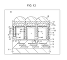
- FIG. 12 is a configuration diagram of a cross-section of key portions of a solid-state imaging device 57 of the present embodiment.
- portions corresponding to FIG. 2 will have the same reference numerals appended thereto, and duplicative descriptions will be omitted.
- the solid-state imaging device 57 of the present embodiment is an example where a portion of an element separating unit 59 passes through the substrate 12 .
- the element separating unit 59 is formed so as to pass through the substrate 12 . That is to say, the element separating unit 19 in regions that do not overlap with the pixel transistor is configured with a fixed charge film 20 and insulating film 21 that are sequentially embedded within the groove portion 60 formed so as to pass through the substrate 12 .
- the end portion on the front face side of the element separating unit 19 is formed so as to touch the p-well layer 29 of the pixel transistor. At this time, the end portion on the front face side of the element separating unit 19 is formed so as to not reach the floating diffusion portion 30 and source/drain region that make up the pixel transistor.
- FIG. 13 and FIG. 14 are cross-sectional diagrams illustrating a manufacturing process of the solid-state imaging device 57 of the present embodiment.
- the process up to before forming groove portions 39 and 60 is similar to the process described in A in FIG. 4 , so the processes thereafter will be described.
- groove portions 39 and 60 which have different depths are formed, as illustrated in A in FIG. 13 .
- the groove portion 60 In a region where the element separating unit 59 that passes through the substrate 12 is formed, the groove portion 60 that passes through the substrate 12 is formed, and in a region where the element separating unit 19 does not pass through is formed, the groove portion 39 is formed to a depth that reaches the p-well layer 29 of the pixel transistor.
- the groove portions 39 and 60 having different depths herein can be formed by performing etching processing that is divided into multiple stages.
- the light blocking material layer is patterned into a desired shape.
- the photoelectric converters 40 are opened as illustrated in FIG. 14C , and the light blocking film 25 which blocks the light between adjacent pixel and pixel is formed.
- the solid-state imaging device 57 illustrated in FIG. 12 is completed.
- the element separating unit 59 is formed so as to pass through the substrate 12 , whereby leakage of the signal charge between adjacent photoelectric converters 40 can be further reduced.
- the advantage of suppressing the blooming can be increased. Additionally, similar advantages to the first embodiment can be obtained.
- FIG. 15 is a configuration diagram of a cross-section of key portions of a solid-state imaging device 64 of the present embodiment.
- portions corresponding to FIG. 2 will have the same reference numerals appended thereto, and duplicative descriptions will be omitted.
- the solid-state imaging device 64 of the present embodiment is an example of the solid-state imaging device 52 relating to the second embodiment, having an element separating unit 62 that passes through the substrate 12 in a portion (for example, an edge) of the pixel region, and forming a light blocking layer 63 that is exposed on the front face side of the substrate 12 within the element separating unit 62 thereof.
- the element separating unit 62 that passes through the substrate 12 is configured of a groove portion 60 that is formed so as to pass through the substrate 12 , and a fixed charge film 20 , insulating film 48 , and light blocking layer 63 which are formed sequentially within the groove portion 60 thereof, and the light blocking layer 63 is formed so as to be exposed on the front face side of the substrate 12 .
- the light blocking layer 63 which is formed so as to be exposed on the front face side of the substrate 12 is connected to a desired wiring 15 via a contact portion 61 formed in the intra-layer insulating film 14 that makes up the wiring layer 13 .
- a ground potential or negative potential is supplied from the wiring 15 to the light blocking layer 63 herein, whereby a ground potential or negative potential is supplied to the light blocking layer 50 and light blocking film 25 formed in the pixel region.
- the light blocking material is embedded in the groove portions 39 and 60 while the light blocking material is formed on the back face side of the substrate 12 , while the wiring layer 13 is in an exposed state in the base face of the groove portion 60 that passes through the substrate 12 , and by patterning into a desired shape, the light blocking layers 50 and 63 and the light blocking film 25 are formed.
- the light blocking layer 50 that passes through the substrate 12 can be drawn out to the wiring layer 13 side, and a desired potential can be supplied from the wiring 15 of the wiring layer 13 to the light blocking layer 50 .
- the contact portion 61 to connect to the light blocking layer 63 is formed beforehand.
- the light blocking layer 63 can be drawn out to the wiring layer 13 side of the substrate 12 by forming a portion of the element separating unit 62 to pass through the substrate 12 . Also, electrical connection between the light blocking film 25 and light blocking layers 50 and 63 and the wiring 15 , and manufacturing of the element separating units 19 and 62 can be performed in the same process, so the number of processes can be reduced.
- FIG. 16 is a configuration diagram of a cross-section of key portions of a solid-state imaging device 41 of the present embodiment.
- portions corresponding to FIG. 2 will have the same reference numerals appended thereto, and duplicative descriptions will be omitted.
- the configuration of an element separating unit 42 of the solid-state imaging device 41 of the present embodiment differs from the first embodiment.
- the element separating unit 42 has a first fixed charge film 43 , second fixed charge film 44 , first insulating film 45 , and second insulating film 46 , formed so as to be embedded in sequence in the groove portion 39 .
- the side faces of the groove portion 39 are formed in a tapered shape, and the opening diameter is small in the depth direction of the substrate 12 .
- Each film formed in the groove portion 39 and on the back face of the substrate 12 will be described below, together with the manufacturing methods thereof.
- the first fixed charge film 43 is formed so as to coat the inner wall face of the groove portion 39 and the back face of the substrate 12 , and is formed using a CVD method or ALD method.
- material to form the first fixed charge film 43 similar material as the material of the fixed charge film 20 in the first embodiment can be used.
- a SiO2 film to reduce the interface level while forming the film is formed simultaneously. It is favorable for the SiO2 film herein to be formed in a thickness of approximately 1 nm. In the case of removing the thickness of the SiO2 film formed at the substrate interface herein, it is favorable for the first fixed charge film 43 to be formed in a thickness of 3 nm or greater, and for example, it is favorable to be formed as 3 nm or greater and 20 nm or less.
- the second fixed charge film 44 is formed within the groove portion 39 and on the back face of the substrate 12 so as to coat the first fixed charge film 43 , and is formed using a PVD (Physical Vapor Deposition) method, for example.
- material to form the second fixed charge film 44 similar material as the material of the fixed charge film 20 in the first embodiment can be used, similar to the first fixed charge film 43 .
- the second fixed charge film 44 may be formed with the same material as the first fixed charge film 43 , or may be formed with a different material.
- the second fixed charge film 44 is favorable for the second fixed charge film 44 to be formed in a thickness of 40 nm or more and 60 nm or less, for example, on the back face of the substrate 12 .
- the second fixed charge film 44 is formed in a thickness of 40 nm or more and 60 nm or less, advantages of pinning on the back face side of the substrate 12 and advantages of a later-described reflection inhibiting film can be securely obtained.
- the first insulating film 45 is formed within the groove portion 39 and on the back face of the substrate 12 so as to coat the second fixed charge film 44 , and is formed as an anisotropic oxide film formed with a PVD method or VCD method, and for example, is formed with an oxide film including TEOS (Tetra Ethyl Ortho Silicate) material or silane material. It is favorable for the first insulating film 45 to be formed in a thickness of 0 nm or greater and 600 nm or less, for example, on the back face of the substrate 12 .
- TEOS Tetra Ethyl Ortho Silicate
- the second insulating film 46 is formed within the groove portion 39 and on the back face of the substrate 12 so as to coat the first insulating film 45 , and in the present embodiment is formed as an isotropic oxide film formed with an ALD method or CVD method, and for example, is formed with a silicon oxide film or the like. With the present embodiment, the groove portion 39 is completely filled in with the second insulating film 46 .
- the second insulating film 46 is formed in a thickness of 0 nm or greater and 300 nm or less, for example, on the back face of the substrate 12 , and the film thickness of the first insulating film 45 and second insulating film 46 together is formed to be 10 nm or greater and 900 nm or less, and it is favorable to be 50 nm or greater and 700 nm or less, and more favorable to be 100 nm or greater and 500 nm or less.
- the layered film made up of the first fixed charge film 43 , second fixed charge film 44 , first insulating film 45 , and second insulating film 46 that is formed on the back face side of the substrate 12 and within the groove portion 39 also serves to function as a reflection inhibiting film.
- a case of forming a two-layer insulating film of the first insulating film 45 and second insulating film 46 is described, but the present disclosure is not limited to this, and it is sufficient if one of the first and second insulating films 45 and 46 is formed. Also, a case of forming an anisotropic film as the first insulating film 45 and an isotropic film as the second insulating film 46 is described, but the reverse may be the case.
- the inner periphery face of the groove portion 39 may have a configuration where all or a portion of the first fixed charge film 43 , second fixed charge film 44 , first insulating film 45 , and second insulating film 46 are layered, or may have a configuration where none of the above-mentioned films are layered.
- FIG. 17 is a configuration diagram of a cross-section of key portions of a solid-state imaging device 47 of the present embodiment.
- portions corresponding to FIG. 2 will have the same reference numerals appended thereto, and duplicative descriptions will be omitted.
- the solid-state imaging device 47 of the present embodiment differs from the first embodiment from the point that the element separating unit 53 has a hollow construction.
- the element separating unit 53 has a fixed charge film 20 and insulating film 54 that are formed embedded in sequence in the groove portion 39 which is formed in the depth direction from the back face side of the substrate 12 , and a hollow portion (a so-called void) 58 is formed within the groove portion 39 .
- the insulating film 54 is formed so as to coat the fixed charge film 20 that is formed on the inner wall face of the groove portion 39 and on the back face of the substrate 12 . Also, in order to form the hollow portion 58 in the groove portion 39 , the insulating film 54 is formed in a thickness so that the entire groove portion 39 is not filled in within the groove portion 39 , and is formed so as to close off the groove portion 39 at the opening end of the groove portion 39 .
- the insulating film 54 can be formed with a material similar to the material of the insulating film 21 used in the first embodiment.
- a manufacturing process of the solid-state imaging device 47 of the present embodiment is illustrated in A in FIG. 18 and B in FIG. 18 .
- the processes up to forming the groove portion 39 are similar to the first embodiment, so duplicative descriptions will be omitted.
- the fixed charge film 20 is formed so as to coat the inner periphery face and base face of the groove portion 39 and the back face of the substrate 12 , using a CVD method, sputtering method, or ALD method or the like.
- the insulating film 54 is formed so as to coat the fixed charge film 20 that is formed on the inner wall face of the groove portion 39 and the back face of the substrate 12 , using a CVD method, sputtering method, coating method, or the like.
- a film forming condition is set so that, the before the inner portion of the groove portion 39 is completely filled in with the insulating film 54 , the opening end side of the groove portion 39 is closed off.
- the element separating unit 53 having a hollow portion 58 as illustrated in B in FIG. 18 can be formed.
- the inner portion of the hollow portion 58 formed in the element separating unit 53 may be in a state filled by air, or may be in a vacuum state. Also, in order to prevent light from mixing in at portions near the incident side, having a hollow portion exist in the upper portion (light input side) from the silicon face of the back face (interface between the substrate 12 and fixed charge film 20 ) is more favorable.
- the solid-state imaging device 47 of the present embodiment illustrated in FIG. 17 is completed.
- the refractive index of the hollow portion 58 is 1, and the refractive index of the fixed charge film 20 and insulating film 54 are each 1 or greater, whereby light reflection easily occurs at the element separating unit 53 , and optical color mixing can be suppressed.
- optical light blocking properties can be improved in the element separating unit 53 .
- similar advantages as the first embodiment can be obtained.
- the fixed charge film 20 is formed at the element separating unit 53 , but the fixed charge film 20 does not have to be formed.
- material to form the insulating film an insulating material having a refractive index of 1 or greater is used, and the insulating film is formed so as to form a hollow portion within the groove portion 39 , whereby optical light blocking features can be improved and optical color mixing can be suppressed.
- FIG. 19 is a configuration diagram of a cross-section of key portions of a solid-state imaging device 65 of the present embodiment.
- portions corresponding to FIG. 2 will have the same reference numerals appended thereto, and duplicative descriptions will be omitted.
- the solid-state imaging device 65 of the present embodiment is the same as the seventh embodiment from the point that the element separating unit 66 has a hollow construction, but differs in the film configuration of the element separating unit 66 and the film forming method thereof.
- the element separating unit 66 has a first film 67 and second film 68 that are formed embedded in sequence within the groove portion 39 that is formed in the depth direction from the back face side of the substrate 12 , and a hollow portion 58 is formed within the groove portion 39 .
- the first film 67 is formed so as to coat the inner wall face of the groove portion 39 and the back face of the substrate 12
- the second film 68 is formed on the inner wall face of the groove portion 39 and the back face of the substrate 12 so as to layer over the first film 67 .
- the opening end side of the groove portion 39 is closed off by the first film 67 and second film 68 , in the case of a hollow portion 58 having been formed therein.
- the first film 67 is formed with an anisotropic film forming method, and is provided so as to narrow the opening diameter on the opening end side of the groove portion 39 .
- the second film 68 is formed with an isotropic film forming method, and is provided so as to close off the opening end of the groove portion 39 that has been narrowed by the first film 67 .
- the first film 67 and second film 68 can be forming using an insulating material such as silicon oxide, silicon nitride, silicon oxynitride, resin, and the like, for example. Also, the first film 67 and second film 68 may be formed with the same material, or may be formed with different material. In the case of forming the first film 67 and second film 68 with different materials, it is favorable to select materials each having conditions where the film stress of the first film 67 is smaller than the film stress of the second film 68 , and where the refractive index of the first film 67 is greater than the refractive index of the second film 68 . The present embodiment is described for a case where, as an example, both the first film 67 and second film 68 are formed with a silicon oxide.
- a manufacturing process of the solid-state imaging device 65 of the present embodiment is illustrated in A in FIG. 20 and B in FIG. 20 .
- the process up to forming the groove portion 39 is similar to the first embodiment so duplicative descriptions will be omitted.
- the first film 67 made of silicon oxide is formed, as illustrated in A in FIG. 20 .
- the first film 67 is formed using an anisotropic film forming method, for example a plasma CVD method or PVD method.
- the first film 67 is formed to be anisotropic, so the film thickness of the first film 67 at the base face of the groove portion 39 and back face of the substrate 12 is thicker than the film thickness of the first film 67 of the inner periphery face of the groove portion 39 . Therefore, from the differences in the film forming rate on the back face of the substrate 12 and inner periphery face of the groove portion 39 , the first film 67 has an overhang shape at the opening end side of the groove portion 39 , and the opening diameter of the opening end side of the groove portion 39 is smaller than the opening diameter of the base face side of the groove portion 39 , as illustrated in A in FIG. 20 .
- the first film 67 is formed to a thickness that does not completely close off the groove portion 39 .
- the second film 68 made of silicon oxide is formed.
- the second film 68 is formed using an isotropic method, an ALD method for example.
- the second film 68 is formed to be isotropic, so the second film 68 is formed at approximately the same thickness on top of the first film 67 , on the inner wall face of the groove portion 39 and the back face of the substrate 12 .
- the second film 68 is formed to a thickness to close off the groove portion 39 at the opening end side of the groove portion 39 .
- the opening diameter on the opening end side of the groove portion 39 is narrower than the opening diameter on the base face side of the groove portion 39 . Accordingly, the opening end side is closed off in a state of maintaining a hollow construction in the groove portion 39 .
- a hollow portion 58 is formed within the groove portion 39 . Also, even if the first film 67 is switched to an isotropic film, and the second film 68 is switched to an anisotropic film, the opening end side can be closed off in a state of maintaining a hollow construction of the groove portion 39 .
- the hollow portion in order to prevent light mixing in at a portion near the incident side, it is favorable for the hollow portion to exist up to upwards (light input side) from the silicon face of the back face (interface between the substrate 12 and the first film 67 ).
- the solid-state imaging device 65 of the present embodiment illustrated in FIG. 19 is completed.
- the hollow portion 58 is formed in the element separating unit 66 , whereby similar advantages as the seventh embodiment can be obtained.
- an example is given of forming the element separating unit 66 with a two-layer film of the first film 67 and second film 68 , but three or more layers of film may be formed as necessary.
- the stress of the film material to be formed first is lower as compared to the stress of the film material to be formed later, the stress to the substrate 12 can be suppressed, and dark current and white spots that result from stress can be suppressed.
- the refractive index of the film material to be formed later to be lower as compared to the refractive index of the film material to be formed first, optical color mixing can be suppressed.
- a film having a negative fixed charge may be formed between the first film 67 and substrate 12 .
- a fixed charge film similar material as the first embodiment can be used.
- the second film 68 may be formed with a metallic material such as tungsten (W), aluminum (Al), titanium (Ti), or the like, or an oxide or nitride thereof.
- a metallic material such as tungsten (W), aluminum (Al), titanium (Ti), or the like, or an oxide or nitride thereof.
- the metallic material film formed on the light input side of the photoelectric converters 40 has to be removed.
- a case of forming the first film 67 with a silicon oxide and forming the second film 68 with a metallic material will be described below as a modified example.
- FIG. 21 is a cross-sectional configuration diagram of a solid-state imaging device 70 relating to a modified example. Portions in FIG. 21 that correspond to FIG. 19 have the same reference numerals appended thereto, and duplicative descriptions will be omitted. With the solid-state imaging device 70 relating to the modified example, a second film 71 that configures an element separating unit 72 differs from the present embodiment.
- the second film 71 is formed of tungsten (W), for example, and is formed so as to coat the first film 67 in the inner wall face of the groove portion 39 and the light blocking region on the back face side of the substrate 12 . That is to say, on the back face side of the substrate 12 , the second film 71 is formed on a region corresponding to the position where the light blocking film 25 is formed, and is provided in a grid shape so as to open the photoelectric converters 40 .
- W tungsten
- the second film 71 is formed on the front face of the first film 67 , using an isotropic film forming method. Also, upon forming the light blocking material layer to be the blocking film 25 over the entire face on the upper portion of the second film 71 on the back face side of the substrate 12 , the light blocking material layer thereof and the second film 71 are simultaneously patterned, whereby the second film 71 on the upper portions of the photoelectric converter 40 is removed. Subsequently, with a process similar to the first embodiment, the solid-state imaging device 70 illustrated in FIG. 21 can be manufactured.
- the modified example in the case of forming the film that is formed within the groove portion 39 using a metallic material, patterning is performed simultaneously with the patterning process of the light blocking film 25 that is formed on the back face side of the substrate 12 , whereby the metallic material on the upper portion of the photoelectric converter 40 can be removed.
- forming the light blocking film 25 is exemplified, but in the case that light can be blocked sufficiently with only the second film 71 , the light blocking film 25 does not have to be separately provided. In this case, the number of film layers formed on the light input face side of the substrate 12 can be reduced, whereby the distance between the front face of the on-chip lens 28 and the substrate 12 can be shortened, and the sensitivity can be improved.
- the configuration of the solid-state imaging device 70 relating to the modified example, similar to the second embodiment, may supply a ground potential or negative potential to the second film 71 that is made of metallic material.
- a ground potential or negative potential By supplying a ground potential or negative potential to the second film 71 , the advantages of hole pinning on the front face of the element separating unit 72 can be stabilized, and dark current can be suppressed.
- the opening end side of the groove portion 39 is closed off by a film formed within the groove portion 39 , but closing the hollow portion 58 within the groove portion 39 with a film formed on the back face side of the substrate 12 is sufficient. Accordingly, the open end side of the groove portion 39 does not necessarily have to be closed off with the film formed within the groove portion 39 .
- the description is of a CMOS-type solid-state imaging device as an example, but a back face-projection type CCD-type solid-state imaging device may also be applicable.
- the element separating unit that electrically separates the photoelectric converters by embedding an insulating film in the groove portion formed from the face on the opposite side from the light input side, advantages similar to the advantages of the above-described first through fifth embodiments can be obtained.
- the configuration of the solid-state imaging device relating to the first through eighth embodiments is set to that the signal charge overflowing into the floating diffusion portion is overflowed, as a lateral overflow configuration.
- the present disclosure is not to be limited to such a configuration, and a configuration may be made to have the overflow into the source/drain region of other pixel transistors.
- a configuration may have the signal charge overflowing into a region where VDD potential is supplied, such as the drain region of the reset transistor, to overflow.
- a configuration is illustrated of a case using a negative charge (electron) as the signal charge, but the present disclosure may be applied in the case also of using a positive charge (hole) as the signal charge.
- a hole as a signal charge
- using a material having a positive fixed charge as the fixed charge film is sufficient, and also, configuring the p-type region and n-type region within the substrate in reverse is sufficient. That is to say, using a material with a fixed charge that is the same charge as the signal charge as the fixed charge film is sufficient.
- the configuration is given as forming a fixed charge film in the groove portion, and further, embedding the insulating film, but the configuration of the present disclosure stands also as a configuration where only the fixed charge film is embedded in the groove portion.
- the first through eighth embodiments may be appropriately combined.
- the element separating unit is formed in a grid shape that surrounds the photoelectric converters, but besides a grid shape, various types of configurations can be made.
- the present disclosure is not restricted to application to a solid-state imaging device that detects the distribution of the amount of incident light that is visible light as an image, and images this, and application may be made also to a solid-state imaging device that images a distribution of infrared rays or X-rays, or an input quantity such as particles or the like, as an image.
- application can be made as to all solid-state imaging devices (physical quantity distribution detecting devices) such as a fingerprint detecting sensor or the like that detects the distribution of other physical quantities such as pressure and capacitance, and images this as an image.
- the present disclosure is not to be limited to a solid-state imaging device that scans each unit pixel in an image region in row increments sequentially and reads out pixel signals from each pixel unit.
- Application can also be made as to an X-Y address type of solid-state imaging device that selects optional pixels in pixel increments, and reads out a signal from the selected pixels in pixel increments.
- the solid-state imaging device made be arranged in a one-chip form, or may be arranged in a module form having a pixel region and a signal processing unit or optical system packaged together as an imaging function.
- an imaging apparatus refers to a camera system such as a digital still camera or video camera or the like, and an electronic device having an imaging function such as a cellular phone.
- an imaging device may be an imaging device.
- FIG. 22 is a schematic configuration diagram of an electronic device 200 relating to the ninth embodiment of the present disclosure.
- the electronic device 200 relating to the present embodiment has a solid-state imaging device 203 , optical lens 201 , shutter device 202 , driving circuit 205 , and signal processing circuit 204 .
- the electronic device 200 of the present embodiment illustrates an embodiment in the case of using the solid-state imaging device 1 in the first embodiment of the present disclosure described above as the solid-state imaging device 203 in an electronic device (camera).
- the optical lens 201 forms an image from the image light (incident light) from a subject on an imaging face of the solid-state imaging device 203 . From this the signal charge is accumulated within the solid-state imaging device 203 for a fixed time period.
- the shutter device 202 controls the time period for light radiating and time period for light blocking to the solid-state imaging device 203 .
- the driving circuit 205 supplies a driving signal to control the transfer operation of the solid-state imaging device 203 and the shutter operation of the shutter device 202 .
- Signal transferring of the solid-state imaging device 203 is performed with the driving signal (timing signal) supplied from the driving circuit 205 .
- the signal processing circuit 204 performs various types of signal processing.
- a picture signal subjected to signal processing is stored in a storage medium such as a memory, or is output to a monitor.
- an electronic device 200 to which the solid-state imaging device 1 can be applied is not limited to a camera, and may be applied to a digital still camera, and further to an imaging device such as a camera module for mobile devices such as a cellular phone or the like.
- the solid-state imaging device 1 in the first embodiment is configured to be used as the solid-state imaging device 203 for the electronic device, but a solid-state imaging device manufactured as in the second through eighth embodiments may also be used.
- present disclosure may also take a configuration such as the following.
- a solid-state imaging device including:
- an element separating unit provided with an insulating film having a fixed charge, which is formed so as to coat the inner wall face of the groove portion.
- the solid-state imaging device wherein the element separating unit is formed in a grid shape so as to surround each photoelectric converter.
- the solid-state imaging device according to any one of (1) through (3), wherein the end portion of the light input side of the element separating unit is formed so as to touch a well layer on which a pixel transistor on the front face side of the substrate is formed.
- the solid-state imaging device according to one of (1) through (4), wherein a region touching a side face of the element separating unit has the same conductivity type as a semiconductor region making up a charge accumulating unit of the photoelectric converter.
- the solid-state imaging device according to any one of (1) through (5), wherein a portion of the element separating unit is formed so as to pass through the substrate.
- the solid-state imaging device according to any one of (3) through (6), wherein a portion of the element separating unit is formed so as to pass through the substrate, and wherein the light blocking layer passes through the substrate and is connected to a wiring layer formed on the front face side of the substrate.
- the solid-state imaging device according to any one of (1) through (7), wherein the light blocking layer is formed on the back face side of the substrate, and is electrically connected to the light blocking film which blocks light in the interface region between adjacent photoelectric converters.
- the solid-state imaging device according to any one of (1) through (8), wherein the fixed charge film is formed within the groove portion, while being formed so as to coat the back face of the substrate.
- the solid-state imaging device according to any one of (1) through (10), wherein the fixed charge film is formed of multiple layers of film.
- a solid-state imaging device comprising:
- an element separating unit having a film that is provided so as to coat the inner wall face of the groove portion, and having a hollow construction.
- the solid-state imaging device wherein the element separating unit has a film that is two or more layers formed in sequence from the inner wall face side of the groove portion.
- the solid-state imaging device according to any one of (12) through (15), wherein a film touching the inner wall face of the groove portion is an insulating film having a fixed charge.
- the solid-state imaging device according to any one of (12) through (16), wherein the film is formed with an insulating material or metallic material.
- the solid-state imaging device according to any one of (13) through (16), wherein the element separating unit has a layered film of a film of one or more layers made of an insulating material and a film of one or more layers made of a metallic material.
- the solid-state imaging device according to either (17) or (18), wherein the insulating material is silicon oxide, silicon nitride, or silicon oxynitride.
- a manufacturing method of a solid-state imaging device including
- a light blocking material layer is formed to coat the back face side of the substrate
- a manufacturing method of a solid-state imaging device including:
- a manufacturing method of a solid-state imaging device according to (30) or (31), wherein the anisotropic film forming method is a CVD method or a PVD method, and the isotropic film forming method is an ALD method.
- An electronic device comprising:
- a solid-state imaging device into which light collected in the optical lens is input including
- a signal processing circuit to process an output signal output from the solid-state imaging device.
Applications Claiming Priority (5)
| Application Number | Priority Date | Filing Date | Title |
|---|---|---|---|
| JP2011045269 | 2011-03-02 | ||
| JP2011-045269 | 2011-03-02 | ||
| JP2012011405 | 2012-01-23 | ||
| JP2012-011405 | 2012-01-23 | ||
| PCT/JP2012/054390 WO2012117931A1 (fr) | 2011-03-02 | 2012-02-23 | Dispositif d'imagerie à semi-conducteurs et son procédé de fabrication, et instrument électronique |
Related Parent Applications (1)
| Application Number | Title | Priority Date | Filing Date |
|---|---|---|---|
| PCT/JP2012/054390 A-371-Of-International WO2012117931A1 (fr) | 2011-03-02 | 2012-02-23 | Dispositif d'imagerie à semi-conducteurs et son procédé de fabrication, et instrument électronique |
Related Child Applications (1)
| Application Number | Title | Priority Date | Filing Date |
|---|---|---|---|
| US15/084,287 Continuation US9673235B2 (en) | 2011-03-02 | 2016-03-29 | Solid-state imaging device, manufacturing method of solid-state imaging device, and electronic device |
Publications (2)
| Publication Number | Publication Date |
|---|---|
| US20140054662A1 US20140054662A1 (en) | 2014-02-27 |
| US9502450B2 true US9502450B2 (en) | 2016-11-22 |
Family
ID=46757868
Family Applications (7)
| Application Number | Title | Priority Date | Filing Date |
|---|---|---|---|
| US14/001,652 Active US9502450B2 (en) | 2011-03-02 | 2012-02-23 | Solid-state imaging device, manufacturing method of solid-state imaging device, and electronic device |
| US15/084,287 Active US9673235B2 (en) | 2011-03-02 | 2016-03-29 | Solid-state imaging device, manufacturing method of solid-state imaging device, and electronic device |
| US15/222,755 Active US9595557B2 (en) | 2011-03-02 | 2016-07-28 | Solid-state imaging device, manufacturing method of solid-state imaging device, and electronic device |
| US15/435,476 Active US9923010B2 (en) | 2011-03-02 | 2017-02-17 | Solid-state imaging device, manufacturing method of solid-state imaging device, and electronic device |
| US15/610,345 Active US10128291B2 (en) | 2011-03-02 | 2017-05-31 | Solid-state imaging device, manufacturing method of solid-state imaging device, and electronic device |
| US16/130,666 Active US10418404B2 (en) | 2011-03-02 | 2018-09-13 | Solid-state imaging device, manufacturing method of solid-state imaging device, and electronic device |
| US16/295,719 Active US10504953B2 (en) | 2011-03-02 | 2019-03-07 | Solid-state imaging device, manufacturing method of solid-state imaging device, and electronic device |
Family Applications After (6)
| Application Number | Title | Priority Date | Filing Date |
|---|---|---|---|
| US15/084,287 Active US9673235B2 (en) | 2011-03-02 | 2016-03-29 | Solid-state imaging device, manufacturing method of solid-state imaging device, and electronic device |
| US15/222,755 Active US9595557B2 (en) | 2011-03-02 | 2016-07-28 | Solid-state imaging device, manufacturing method of solid-state imaging device, and electronic device |
| US15/435,476 Active US9923010B2 (en) | 2011-03-02 | 2017-02-17 | Solid-state imaging device, manufacturing method of solid-state imaging device, and electronic device |
| US15/610,345 Active US10128291B2 (en) | 2011-03-02 | 2017-05-31 | Solid-state imaging device, manufacturing method of solid-state imaging device, and electronic device |
| US16/130,666 Active US10418404B2 (en) | 2011-03-02 | 2018-09-13 | Solid-state imaging device, manufacturing method of solid-state imaging device, and electronic device |
| US16/295,719 Active US10504953B2 (en) | 2011-03-02 | 2019-03-07 | Solid-state imaging device, manufacturing method of solid-state imaging device, and electronic device |
Country Status (5)
| Country | Link |
|---|---|
| US (7) | US9502450B2 (fr) |
| JP (4) | JP6299058B2 (fr) |
| KR (4) | KR20140015326A (fr) |
| CN (4) | CN106229323B (fr) |
| WO (1) | WO2012117931A1 (fr) |
Cited By (5)
| Publication number | Priority date | Publication date | Assignee | Title |
|---|---|---|---|---|
| US20170200763A1 (en) * | 2015-10-30 | 2017-07-13 | Taiwan Semiconductor Manufacturing Co., Ltd. | Method for manufacturing image sensor structure having wide contact |
| US10194104B2 (en) * | 2017-02-22 | 2019-01-29 | Panasonic Intellectual Property Management Co., Ltd. | Imaging device and imaging module |
| US20200027909A1 (en) * | 2018-07-18 | 2020-01-23 | Sony Semiconductor Solutions Corporation | Light receiving element, ranging module, and electronic apparatus |
| US20210249454A1 (en) * | 2018-06-15 | 2021-08-12 | Sony Semiconductor Solutions Corporation | Solid-state imaging element, method of manufacturing solid-state imaging element, and electronic apparatus |
| US11239273B2 (en) | 2015-12-28 | 2022-02-01 | Semiconductor Energy Laboratory Co., Ltd. | Imaging device and electronic device |
Families Citing this family (163)
| Publication number | Priority date | Publication date | Assignee | Title |
|---|---|---|---|---|
| JP2502098B2 (ja) * | 1987-08-12 | 1996-05-29 | 株式会社フジクラ | 超電導電磁シ−ルド体 |
| US7442629B2 (en) | 2004-09-24 | 2008-10-28 | President & Fellows Of Harvard College | Femtosecond laser-induced formation of submicrometer spikes on a semiconductor substrate |
| US7057256B2 (en) | 2001-05-25 | 2006-06-06 | President & Fellows Of Harvard College | Silicon-based visible and near-infrared optoelectric devices |
| US8692198B2 (en) | 2010-04-21 | 2014-04-08 | Sionyx, Inc. | Photosensitive imaging devices and associated methods |
| EP2583312A2 (fr) | 2010-06-18 | 2013-04-24 | Sionyx, Inc. | Dispositifs photosensibles à grande vitesse et procédés associés |
| JP6299058B2 (ja) * | 2011-03-02 | 2018-03-28 | ソニー株式会社 | 固体撮像装置、固体撮像装置の製造方法及び電子機器 |
| US9496308B2 (en) | 2011-06-09 | 2016-11-15 | Sionyx, Llc | Process module for increasing the response of backside illuminated photosensitive imagers and associated methods |
| JP2014525091A (ja) | 2011-07-13 | 2014-09-25 | サイオニクス、インク. | 生体撮像装置および関連方法 |
| US9064764B2 (en) | 2012-03-22 | 2015-06-23 | Sionyx, Inc. | Pixel isolation elements, devices, and associated methods |
| JP2014096490A (ja) * | 2012-11-09 | 2014-05-22 | Sony Corp | 撮像素子、製造方法 |
| WO2014157579A1 (fr) * | 2013-03-29 | 2014-10-02 | ソニー株式会社 | Elément et appareil d'imagerie |
| JP2014220403A (ja) * | 2013-05-09 | 2014-11-20 | 浜松ホトニクス株式会社 | 半導体エネルギー線検出素子及び半導体エネルギー線検出素子の製造方法 |
| JP6130221B2 (ja) | 2013-05-24 | 2017-05-17 | ソニー株式会社 | 固体撮像装置、および電子機器 |
| WO2014209421A1 (fr) | 2013-06-29 | 2014-12-31 | Sionyx, Inc. | Régions texturées formées de tranchées peu profondes et procédés associés. |
| JP6641605B2 (ja) * | 2013-07-03 | 2020-02-05 | ソニー株式会社 | 固体撮像装置およびその製造方法 |
| JP6303803B2 (ja) | 2013-07-03 | 2018-04-04 | ソニー株式会社 | 固体撮像装置およびその製造方法 |
| JP6060851B2 (ja) * | 2013-08-09 | 2017-01-18 | ソニー株式会社 | 固体撮像装置の製造方法 |
| JP6079502B2 (ja) * | 2013-08-19 | 2017-02-15 | ソニー株式会社 | 固体撮像素子および電子機器 |
| JP6170379B2 (ja) * | 2013-08-30 | 2017-07-26 | 浜松ホトニクス株式会社 | 半導体エネルギー線検出素子 |
| JP6465545B2 (ja) * | 2013-09-27 | 2019-02-06 | ソニー株式会社 | 撮像素子およびその製造方法ならびに電子機器 |
| JP6242211B2 (ja) * | 2013-12-26 | 2017-12-06 | キヤノン株式会社 | 撮像装置および撮像システム |
| KR102209097B1 (ko) * | 2014-02-27 | 2021-01-28 | 삼성전자주식회사 | 이미지 센서 및 이의 제조 방법 |
| US9293490B2 (en) * | 2014-03-14 | 2016-03-22 | Taiwan Semiconductor Manufacturing Company, Ltd. | Deep trench isolation with air-gap in backside illumination image sensor chips |
| KR102380829B1 (ko) * | 2014-04-23 | 2022-03-31 | 가부시키가이샤 한도오따이 에네루기 켄큐쇼 | 촬상 장치 |
| KR102268712B1 (ko) | 2014-06-23 | 2021-06-28 | 삼성전자주식회사 | 자동 초점 이미지 센서 및 이를 포함하는 디지털 영상 처리 장치 |
| JP6576025B2 (ja) * | 2014-09-29 | 2019-09-18 | キヤノン株式会社 | 光電変換装置、及び撮像システム |
| KR102336665B1 (ko) | 2014-10-02 | 2021-12-07 | 삼성전자 주식회사 | 데드존을 줄이는 씨모스 이미지 센서 |
| US9825078B2 (en) * | 2014-11-13 | 2017-11-21 | Visera Technologies Company Limited | Camera device having an image sensor comprising a conductive layer and a reflection layer stacked together to form a light pipe structure accommodating a filter unit |
| JP2016100347A (ja) * | 2014-11-18 | 2016-05-30 | ソニー株式会社 | 固体撮像装置及びその製造方法、並びに電子機器 |
| KR102410019B1 (ko) * | 2015-01-08 | 2022-06-16 | 삼성전자주식회사 | 이미지 센서 |
| KR102384890B1 (ko) * | 2015-01-13 | 2022-04-11 | 삼성전자주식회사 | 이미지 센서 및 그 형성 방법 |
| US10008530B2 (en) * | 2015-01-30 | 2018-06-26 | Taiwan Semiconductor Manufacturing Company Ltd. | Image sensing device and manufacturing method thereof |
| US10283539B2 (en) * | 2015-03-05 | 2019-05-07 | Dartmouth College | Gateless reset for image sensor pixels |
| WO2016143531A1 (fr) * | 2015-03-09 | 2016-09-15 | ソニー株式会社 | Élément de prise de vue et son procédé de fabrication, et dispositif électronique |
| US9991303B2 (en) * | 2015-03-16 | 2018-06-05 | Taiwan Semiconductor Manufacturing Co., Ltd. | Image sensor device structure |
| CN114744002A (zh) | 2015-03-31 | 2022-07-12 | 索尼半导体解决方案公司 | 半导体装置 |
| JP6856974B2 (ja) | 2015-03-31 | 2021-04-14 | ソニーセミコンダクタソリューションズ株式会社 | 固体撮像素子および電子機器 |
| CN104867950B (zh) * | 2015-04-07 | 2018-10-12 | 联想(北京)有限公司 | 感光元件及其制备方法 |
| US9799654B2 (en) | 2015-06-18 | 2017-10-24 | International Business Machines Corporation | FET trench dipole formation |
| KR102497812B1 (ko) * | 2015-08-10 | 2023-02-09 | 삼성전자주식회사 | 이미지 센서 |
| KR102435031B1 (ko) | 2015-08-11 | 2022-08-22 | 삼성전자주식회사 | 고정 전하막을 갖는 이미지 센서 |
| KR102460175B1 (ko) * | 2015-08-21 | 2022-10-28 | 삼성전자주식회사 | 쉐어드 픽셀 및 이를 포함하는 이미지 센서 |
| CN108174619B (zh) * | 2015-09-30 | 2022-09-20 | 株式会社尼康 | 摄像元件及摄像装置 |
| JP6754157B2 (ja) | 2015-10-26 | 2020-09-09 | ソニーセミコンダクタソリューションズ株式会社 | 撮像装置 |
| FR3043250A1 (fr) | 2015-10-30 | 2017-05-05 | St Microelectronics Crolles 2 Sas | Capteur d'image |
| US10531020B2 (en) | 2015-11-18 | 2020-01-07 | Sony Semiconductor Solutions Corporation | Solid-state image pickup device, manufacturing method therefor, and electronic apparatus |
| US9875989B2 (en) * | 2016-01-12 | 2018-01-23 | Taiwan Semiconductor Manufacturing Co., Ltd. | Semiconductor device structure |
| KR102541701B1 (ko) * | 2016-01-15 | 2023-06-13 | 삼성전자주식회사 | 씨모스 이미지 센서 |
| JP6700811B2 (ja) * | 2016-01-26 | 2020-05-27 | キヤノン株式会社 | 半導体装置および半導体装置の製造方法 |
| TWI785618B (zh) * | 2016-01-27 | 2022-12-01 | 日商新力股份有限公司 | 固體攝像元件及電子機器 |
| WO2017159362A1 (fr) * | 2016-03-15 | 2017-09-21 | ソニー株式会社 | Capteur d'imagerie à semi-conducteurs et procédé de fabrication de celui-ci et instrument électronique |
| JP2017168566A (ja) | 2016-03-15 | 2017-09-21 | ソニー株式会社 | 固体撮像素子、および電子機器 |
| US10163949B2 (en) * | 2016-03-17 | 2018-12-25 | Taiwan Semiconductor Manufacturing Company Ltd. | Image device having multi-layered refractive layer on back surface |
| FR3049389A1 (fr) * | 2016-03-22 | 2017-09-29 | St Microelectronics Crolles 2 Sas | Mur d'isolement et son procede de fabrication |
| JP6789653B2 (ja) * | 2016-03-31 | 2020-11-25 | キヤノン株式会社 | 光電変換装置およびカメラ |
| JP6911767B2 (ja) * | 2016-04-25 | 2021-07-28 | ソニーグループ株式会社 | 固体撮像素子およびその製造方法、並びに電子機器 |
| JP6808348B2 (ja) * | 2016-04-28 | 2021-01-06 | キヤノン株式会社 | 光電変換装置およびカメラ |
| KR20230035137A (ko) * | 2016-07-06 | 2023-03-10 | 소니 세미컨덕터 솔루션즈 가부시키가이샤 | 촬상 소자, 촬상 소자의 제조 방법 및 전자 기기 |
| KR102563588B1 (ko) | 2016-08-16 | 2023-08-03 | 삼성전자주식회사 | 이미지 센서 및 이의 제조 방법 |
| CN116525632A (zh) * | 2016-10-18 | 2023-08-01 | 索尼半导体解决方案公司 | 光检测设备 |
| JP6316902B2 (ja) * | 2016-10-28 | 2018-04-25 | ソニー株式会社 | 固体撮像装置、および電子機器 |
| WO2018083990A1 (fr) * | 2016-11-02 | 2018-05-11 | ソニーセミコンダクタソリューションズ株式会社 | Élément d'imagerie, dispositif d'imagerie et dispositif électronique |
| KR102610588B1 (ko) * | 2016-11-08 | 2023-12-07 | 에스케이하이닉스 주식회사 | 이미지 센서 및 이미지 센서 형성 방법 |
| KR20180079518A (ko) | 2016-12-30 | 2018-07-11 | 삼성전자주식회사 | 씨모스 이미지 센서 |
| CN117059640A (zh) * | 2017-01-30 | 2023-11-14 | 索尼半导体解决方案公司 | 固态成像装置和电子设备 |
| KR102604687B1 (ko) | 2017-02-01 | 2023-11-20 | 삼성전자주식회사 | 이미지 센서 및 그 제조 방법 |
| JP7079739B2 (ja) | 2017-02-17 | 2022-06-02 | ソニーセミコンダクタソリューションズ株式会社 | 撮像素子および電子機器 |
| US11069739B2 (en) * | 2017-02-21 | 2021-07-20 | Sony Semiconductor Solutions Corporation | Imaging device and electronic apparatus |
| CN109155325A (zh) * | 2017-03-22 | 2019-01-04 | 索尼半导体解决方案公司 | 摄像装置和信号处理装置 |
| JP2018186151A (ja) | 2017-04-25 | 2018-11-22 | ソニーセミコンダクタソリューションズ株式会社 | 撮像素子および撮像装置 |
| WO2018207340A1 (fr) * | 2017-05-12 | 2018-11-15 | オリンパス株式会社 | Dispositif d'imagerie à semi-conducteurs |
| WO2018207345A1 (fr) * | 2017-05-12 | 2018-11-15 | オリンパス株式会社 | Dispositif de capture d'image à semi-conducteurs |
| US10211244B2 (en) * | 2017-06-30 | 2019-02-19 | Taiwan Semiconductor Manufacturing Co., Ltd. | Image sensor device with reflective structure and method for forming the same |
| US10644060B2 (en) * | 2017-09-28 | 2020-05-05 | Taiwan Semiconductor Manufacturing Co., Ltd. | Image sensor with high quantum efficiency surface structure |
| JP2019075515A (ja) | 2017-10-19 | 2019-05-16 | ソニーセミコンダクタソリューションズ株式会社 | 半導体装置、撮像装置、製造装置 |
| KR102494604B1 (ko) | 2017-10-31 | 2023-02-02 | 삼성전자주식회사 | 이미지 센서 |
| CN107833900A (zh) * | 2017-11-07 | 2018-03-23 | 德淮半导体有限公司 | 背照式互补金属氧化物半导体图像传感器及其制造方法 |
| WO2019093479A1 (fr) | 2017-11-09 | 2019-05-16 | ソニーセミコンダクタソリューションズ株式会社 | Dispositif d'imagerie à semi-conducteur et dispositif électronique |
| WO2019093150A1 (fr) * | 2017-11-09 | 2019-05-16 | ソニーセミコンダクタソリューションズ株式会社 | Élément de capture d'image et appareil électronique |
| US11552119B2 (en) | 2017-11-09 | 2023-01-10 | Sony Semiconductor Solutions Corporation | Solid-state imaging device and electronic equipment |
| JP7366751B2 (ja) * | 2017-11-09 | 2023-10-23 | ソニーセミコンダクタソリューションズ株式会社 | 固体撮像装置、および電子機器 |
| KR102427639B1 (ko) | 2017-11-13 | 2022-08-01 | 삼성전자주식회사 | 이미지 센싱 소자 |
| JP7078919B2 (ja) * | 2017-11-14 | 2022-06-01 | マッハコーポレーション株式会社 | 固体撮像素子及びその形成方法 |
| KR20190070485A (ko) * | 2017-12-13 | 2019-06-21 | 주식회사 디비하이텍 | 후면 조사형 이미지 센서 및 그 제조 방법 |
| KR102652492B1 (ko) * | 2018-01-11 | 2024-03-29 | 소니 세미컨덕터 솔루션즈 가부시키가이샤 | 고체 촬상 장치, 전자 기기 |
| JP6779929B2 (ja) | 2018-02-09 | 2020-11-04 | キヤノン株式会社 | 光電変換装置および機器 |
| JP2019165066A (ja) * | 2018-03-19 | 2019-09-26 | ソニーセミコンダクタソリューションズ株式会社 | 撮像素子、電子機器 |
| JP6607275B2 (ja) * | 2018-03-28 | 2019-11-20 | ソニー株式会社 | 固体撮像装置、および電子機器 |
| CN108461514A (zh) * | 2018-03-28 | 2018-08-28 | 德淮半导体有限公司 | Cmos图形传感器的隔离结构及其形成方法 |
| JP7214373B2 (ja) * | 2018-06-04 | 2023-01-30 | キヤノン株式会社 | 固体撮像素子及び固体撮像素子の製造方法、撮像システム |
| US11348955B2 (en) * | 2018-06-05 | 2022-05-31 | Brillnics Singapore Pte. Ltd. | Pixel structure for image sensors |
| JP2020013817A (ja) * | 2018-07-13 | 2020-01-23 | ソニーセミコンダクタソリューションズ株式会社 | 固体撮像素子および電子機器 |
| JP2020027884A (ja) * | 2018-08-13 | 2020-02-20 | ソニーセミコンダクタソリューションズ株式会社 | 固体撮像装置及び電子機器 |
| KR102646903B1 (ko) | 2018-09-04 | 2024-03-12 | 삼성전자주식회사 | 이미지 센서 |
| JP6981383B2 (ja) * | 2018-09-05 | 2021-12-15 | 住友電気工業株式会社 | 半導体受光デバイス |
| JP7182968B2 (ja) | 2018-09-12 | 2022-12-05 | キヤノン株式会社 | 光電変換装置および機器 |
| JP2020053450A (ja) * | 2018-09-25 | 2020-04-02 | ソニーセミコンダクタソリューションズ株式会社 | 撮像素子、電子機器 |
| KR20210075973A (ko) | 2018-10-11 | 2021-06-23 | 소니 세미컨덕터 솔루션즈 가부시키가이샤 | 고체 촬상 장치 및 전자 기기 |
| US11121160B2 (en) | 2018-10-17 | 2021-09-14 | Canon Kabushiki Kaisha | Photoelectric conversion apparatus and equipment comprising a light shielding part in a light receiving region and a light shielding film in a light shielded region |
| US11244978B2 (en) | 2018-10-17 | 2022-02-08 | Canon Kabushiki Kaisha | Photoelectric conversion apparatus and equipment including the same |
| JP2022017616A (ja) * | 2018-11-09 | 2022-01-26 | ソニーセミコンダクタソリューションズ株式会社 | 固体撮像装置、固体撮像装置の製造方法および電子機器 |
| JP2020085666A (ja) * | 2018-11-26 | 2020-06-04 | ソニーセミコンダクタソリューションズ株式会社 | 生体由来物質検出用チップ、生体由来物質検出装置及び生体由来物質検出システム |
| JP7280034B2 (ja) * | 2018-12-03 | 2023-05-23 | ソニーセミコンダクタソリューションズ株式会社 | 固体撮像素子、固体撮像素子の製造方法、および電子機器 |
| KR102637626B1 (ko) * | 2019-01-08 | 2024-02-20 | 삼성전자주식회사 | 이미지 센서 |
| KR102651605B1 (ko) | 2019-01-11 | 2024-03-27 | 삼성전자주식회사 | 이미지 센서 |
| KR20200108133A (ko) * | 2019-03-06 | 2020-09-17 | 삼성전자주식회사 | 이미지 센서 및 이미징 장치 |
| JP7236692B2 (ja) * | 2019-03-27 | 2023-03-10 | パナソニックIpマネジメント株式会社 | 光検出器及び光検出器の製造方法 |
| JP2020167249A (ja) * | 2019-03-29 | 2020-10-08 | ソニーセミコンダクタソリューションズ株式会社 | センサチップおよび測距装置 |
| CN110164887A (zh) * | 2019-04-30 | 2019-08-23 | 德淮半导体有限公司 | 图像传感器及其形成方法 |
| TW202121671A (zh) * | 2019-05-31 | 2021-06-01 | 日商索尼半導體解決方案公司 | 固體攝像裝置 |
| JP7398215B2 (ja) * | 2019-06-25 | 2023-12-14 | ブリルニクス シンガポール プライベート リミテッド | 固体撮像装置、固体撮像装置の製造方法、および電子機器 |
| KR20210012437A (ko) * | 2019-07-25 | 2021-02-03 | 삼성전자주식회사 | 자동 초점 이미지 센서의 픽셀 어레이 및 이를 포함하는 자동 초점 이미지 센서 |
| JP7479801B2 (ja) * | 2019-08-27 | 2024-05-09 | ソニーセミコンダクタソリューションズ株式会社 | 撮像素子、製造方法、および電子機器 |
| CN114008781A (zh) * | 2019-09-30 | 2022-02-01 | Oppo广东移动通信有限公司 | 图像传感器、摄像头组件及移动终端 |
| US11705472B2 (en) | 2019-10-10 | 2023-07-18 | Visera Technologies Company Limited | Biosensor and method of distinguishing a light |
| US11630062B2 (en) * | 2019-10-10 | 2023-04-18 | Visera Technologies Company Limited | Biosensor and method of forming the same |
| JP2021068788A (ja) * | 2019-10-21 | 2021-04-30 | キヤノン株式会社 | 光電変換装置、光電変換装置の製造方法、および撮像システム |
| JP2021077708A (ja) | 2019-11-06 | 2021-05-20 | ソニーセミコンダクタソリューションズ株式会社 | 受光素子および測距装置 |
| JP2021086851A (ja) * | 2019-11-25 | 2021-06-03 | キヤノン株式会社 | 半導体装置および機器 |
| CN111029352B (zh) * | 2019-12-02 | 2022-07-01 | 武汉新芯集成电路制造有限公司 | 半导体器件及其制造方法 |
| CN114730779A (zh) | 2019-12-17 | 2022-07-08 | 索尼半导体解决方案公司 | 摄像元件、摄像元件驱动方法和电子装置 |
| TW202133460A (zh) * | 2020-01-20 | 2021-09-01 | 日商索尼半導體解決方案公司 | 受光元件、攝像元件及攝像裝置 |
| JPWO2021149577A1 (fr) * | 2020-01-24 | 2021-07-29 | ||
| US20210265416A1 (en) * | 2020-02-21 | 2021-08-26 | Applied Materials, Inc. | Structure & material engineering methods for optoelectronic devices signal to noise ratio enhancement |
| WO2021167060A1 (fr) * | 2020-02-21 | 2021-08-26 | タワー パートナーズ セミコンダクター株式会社 | Dispositif d'imagerie à semi-conducteur |
| JP7441086B2 (ja) * | 2020-03-23 | 2024-02-29 | 株式会社東芝 | 光検出器、光検出システム、ライダー装置、及び車 |
| JP7462263B2 (ja) * | 2020-03-24 | 2024-04-05 | パナソニックIpマネジメント株式会社 | 半導体素子および固体撮像装置 |
| WO2021199701A1 (fr) * | 2020-03-31 | 2021-10-07 | ソニーセミコンダクタソリューションズ株式会社 | Élément récepteur de lumière et équipement électronique |
| JP2021163899A (ja) * | 2020-04-01 | 2021-10-11 | キヤノン株式会社 | 光電変換装置及びその製造方法 |
| JP2020102656A (ja) * | 2020-04-06 | 2020-07-02 | キヤノン株式会社 | 半導体装置および半導体装置の製造方法 |
| WO2021215303A1 (fr) * | 2020-04-20 | 2021-10-28 | ソニーセミコンダクタソリューションズ株式会社 | Élément d'imagerie à semi-conducteurs et appareil électronique |
| WO2021215290A1 (fr) * | 2020-04-20 | 2021-10-28 | ソニーセミコンダクタソリューションズ株式会社 | Élément d'imagerie à semi-conducteurs |
| US11152520B1 (en) * | 2020-05-07 | 2021-10-19 | Globalfoundries U.S. Inc. | Photodetector with reflector with air gap adjacent photodetecting region |
| JP2021190466A (ja) * | 2020-05-26 | 2021-12-13 | ソニーセミコンダクタソリューションズ株式会社 | 固体撮像装置、電子機器、及び固体撮像装置の製造方法 |
| US11664403B2 (en) * | 2020-06-12 | 2023-05-30 | Taiwan Semiconductor Manufacturing Co., Ltd. | Manufacturing method of image sensor device having metal grid partially embedded in buffer layer |
| KR20220005888A (ko) * | 2020-07-07 | 2022-01-14 | 삼성전자주식회사 | 이미지 센서 |
| KR20220045476A (ko) * | 2020-10-05 | 2022-04-12 | 삼성전자주식회사 | 이미지 센서 및 이를 포함하는 전자 시스템 |
| KR20220045831A (ko) * | 2020-10-06 | 2022-04-13 | 삼성전자주식회사 | 이미지 센서 |
| US11784204B2 (en) * | 2020-10-19 | 2023-10-10 | Taiwan Semiconductor Manufacturing Company, Ltd. | Enhanced trench isolation structure |
| JP2023182872A (ja) * | 2020-11-12 | 2023-12-27 | ソニーグループ株式会社 | 固体撮像素子およびその製造方法 |
| CN116325780A (zh) * | 2020-11-19 | 2023-06-23 | 华为技术有限公司 | 固态成像设备 |
| CN116783709A (zh) * | 2020-11-20 | 2023-09-19 | 索尼半导体解决方案公司 | 成像装置 |
| JP2021040166A (ja) * | 2020-12-09 | 2021-03-11 | キヤノン株式会社 | 光電変換装置およびカメラ |
| TW202226564A (zh) | 2020-12-25 | 2022-07-01 | 日商索尼半導體解決方案公司 | 固態攝像裝置及其製造方法 |
| US11908878B2 (en) * | 2021-01-15 | 2024-02-20 | Taiwan Semiconductor Manufacturing Company, Ltd. | Image sensor and manufacturing method thereof |
| US11862654B2 (en) * | 2021-01-15 | 2024-01-02 | Taiwan Semiconductor Manufacturing Company, Ltd. | Trench isolation structure for image sensors |
| JP2022114224A (ja) * | 2021-01-26 | 2022-08-05 | ソニーセミコンダクタソリューションズ株式会社 | 固体撮像装置 |
| JP2022135130A (ja) * | 2021-03-04 | 2022-09-15 | ソニーセミコンダクタソリューションズ株式会社 | 光検出装置及び電子機器 |
| US20220336505A1 (en) * | 2021-04-19 | 2022-10-20 | Taiwan Semiconductor Manufacturing Co., Ltd. | Csi with controllable isolation structure and methods of manufacturing and using the same |
| CN117121207A (zh) | 2021-04-20 | 2023-11-24 | 索尼半导体解决方案公司 | 光检测装置和电子设备 |
| US20220344383A1 (en) * | 2021-04-27 | 2022-10-27 | Taiwan Semiconductor Manufacturing Co., Ltd. | Backside structure for image sensor |
| JP2023012890A (ja) * | 2021-07-14 | 2023-01-26 | ソニーセミコンダクタソリューションズ株式会社 | 光検出装置及び電子機器 |
| KR20240037943A (ko) | 2021-08-06 | 2024-03-22 | 소니 세미컨덕터 솔루션즈 가부시키가이샤 | 촬상 장치 |
| TW202310378A (zh) * | 2021-08-06 | 2023-03-01 | 日商索尼半導體解決方案公司 | 光檢測器、光檢測器之製造方法及電子機器 |
| JPWO2023021787A1 (fr) | 2021-08-16 | 2023-02-23 | ||
| CN117716504A (zh) * | 2021-09-16 | 2024-03-15 | 索尼半导体解决方案公司 | 光检测装置、光检测装置的制造方法和电子设备 |
| WO2023157818A1 (fr) * | 2022-02-15 | 2023-08-24 | ソニーセミコンダクタソリューションズ株式会社 | Dispositif photodétecteur et procédé de fabrication de dispositif photodétecteur |
| JP7364826B1 (ja) | 2022-02-15 | 2023-10-18 | ソニーセミコンダクタソリューションズ株式会社 | 光検出装置および電子機器 |
| JP2023144526A (ja) * | 2022-03-28 | 2023-10-11 | ソニーセミコンダクタソリューションズ株式会社 | 光検出装置及び電子機器 |
| WO2023248926A1 (fr) * | 2022-06-24 | 2023-12-28 | ソニーセミコンダクタソリューションズ株式会社 | Élément d'imagerie et dispositif électronique |
| WO2024014326A1 (fr) * | 2022-07-14 | 2024-01-18 | ソニーセミコンダクタソリューションズ株式会社 | Appareil de détection de lumière |
| WO2024053401A1 (fr) * | 2022-09-06 | 2024-03-14 | ソニーセミコンダクタソリューションズ株式会社 | Appareil de détection de lumière, dispositif numérique et procédé de production d'appareil de détection de lumière |
| CN117238842B (zh) * | 2023-11-14 | 2024-03-08 | 合肥晶合集成电路股份有限公司 | 深沟槽的形成方法以及背照式图像传感器制造方法 |
Citations (18)
| Publication number | Priority date | Publication date | Assignee | Title |
|---|---|---|---|---|
| JPH04280677A (ja) | 1991-03-08 | 1992-10-06 | Sony Corp | 積層型固体撮像装置 |
| WO2005069377A1 (fr) | 2004-01-19 | 2005-07-28 | Matsushita Electric Industrial Co., Ltd. | Dispositif de formation d'images a semi-conducteurs et son procede de fabrication |
| US20050184353A1 (en) | 2004-02-20 | 2005-08-25 | Chandra Mouli | Reduced crosstalk sensor and method of formation |
| JP2005251947A (ja) | 2004-03-03 | 2005-09-15 | Matsushita Electric Ind Co Ltd | 固体撮像装置とその製造方法および固体撮像装置を用いたカメラ |
| US20070284692A1 (en) * | 2006-06-12 | 2007-12-13 | Samsung Electronics Co., Ltd. | Device isolation structure incorporated in semiconductor device and method of forming the same |
| JP2008010544A (ja) | 2006-06-28 | 2008-01-17 | Renesas Technology Corp | 固体撮像素子 |
| JP2008506261A (ja) | 2004-07-08 | 2008-02-28 | マイクロン テクノロジー インコーポレイテッド | 画像センサのための重水素化構造体およびその形成方法 |
| JP2009522814A (ja) | 2006-01-09 | 2009-06-11 | マイクロン テクノロジー, インク. | 表面空乏が改良されたイメージセンサ |
| JP2009182223A (ja) | 2008-01-31 | 2009-08-13 | Fujifilm Corp | 裏面照射型固体撮像素子 |
| JP2009206356A (ja) | 2008-02-28 | 2009-09-10 | Toshiba Corp | 固体撮像装置およびその製造方法 |
| US20100006923A1 (en) * | 2008-07-08 | 2010-01-14 | Ryota Fujitsuka | Semiconductor device and method for manufacturing the same |
| US20100201834A1 (en) * | 2009-02-10 | 2010-08-12 | Sony Corporation | Solid-state imaging device, method of manufacturing the same, and electronic apparatus |
| JP2010186818A (ja) | 2009-02-10 | 2010-08-26 | Sony Corp | 固体撮像装置とその製造方法、及び電子機器 |
| US20100214454A1 (en) * | 2009-02-23 | 2010-08-26 | Sony Corporation | Solid-state imaging device and electronic apparatus |
| JP2010225818A (ja) | 2009-03-23 | 2010-10-07 | Toshiba Corp | 固体撮像装置及びその製造方法 |
| JP2011003860A (ja) | 2009-06-22 | 2011-01-06 | Sony Corp | 固体撮像装置とその製造方法、及び電子機器 |
| US20110024857A1 (en) * | 2009-06-04 | 2011-02-03 | Sony Corporation | Solid-state image pickup element, method of manufacturing the same, and electronic apparatus using the same |
| US20110156186A1 (en) * | 2009-12-28 | 2011-06-30 | Kabushiki Kaisha Toshiba | Solid-state imaging device |
Family Cites Families (39)
| Publication number | Priority date | Publication date | Assignee | Title |
|---|---|---|---|---|
| JPH0691237B2 (ja) * | 1986-09-10 | 1994-11-14 | 日本電気株式会社 | 固体撮像素子 |
| EP1398831A3 (fr) * | 2002-09-13 | 2008-02-20 | Shipley Co. L.L.C. | Formation d'espaces d'air |
| JP2005123449A (ja) * | 2003-10-17 | 2005-05-12 | Matsushita Electric Ind Co Ltd | 固体撮像装置およびその製造方法 |
| JP4483442B2 (ja) * | 2004-07-13 | 2010-06-16 | ソニー株式会社 | 固体撮像素子と固体撮像装置、固体撮像素子の製造方法 |
| JP4595464B2 (ja) * | 2004-09-22 | 2010-12-08 | ソニー株式会社 | Cmos固体撮像素子の製造方法 |
| KR100678269B1 (ko) * | 2004-10-18 | 2007-02-02 | 삼성전자주식회사 | 씨모스 방식의 이미지 센서와 그 제작 방법 |
| JP2007227761A (ja) * | 2006-02-24 | 2007-09-06 | Matsushita Electric Ind Co Ltd | 固体撮像装置用素子 |
| JP4361072B2 (ja) * | 2006-06-15 | 2009-11-11 | 日本テキサス・インスツルメンツ株式会社 | 固体撮像装置及びその製造方法 |
| US7916195B2 (en) * | 2006-10-13 | 2011-03-29 | Sony Corporation | Solid-state imaging device, imaging apparatus and camera |
| JP2008244021A (ja) * | 2007-03-26 | 2008-10-09 | Matsushita Electric Ind Co Ltd | 固体撮像装置およびそれを用いたカメラ |
| TWI413240B (zh) * | 2007-05-07 | 2013-10-21 | Sony Corp | A solid-state imaging device, a manufacturing method thereof, and an image pickup device |
| JP5104036B2 (ja) * | 2007-05-24 | 2012-12-19 | ソニー株式会社 | 固体撮像素子とその製造方法及び撮像装置 |
| JP2008300537A (ja) * | 2007-05-30 | 2008-12-11 | Toshiba Corp | 固体撮像装置 |
| JP5055026B2 (ja) * | 2007-05-31 | 2012-10-24 | 富士フイルム株式会社 | 撮像素子、撮像素子の製造方法、及び、撮像素子用の半導体基板 |
| JP4621719B2 (ja) * | 2007-09-27 | 2011-01-26 | 富士フイルム株式会社 | 裏面照射型撮像素子 |
| JP5151375B2 (ja) * | 2007-10-03 | 2013-02-27 | ソニー株式会社 | 固体撮像装置およびその製造方法および撮像装置 |
| JP2009272596A (ja) * | 2008-04-09 | 2009-11-19 | Sony Corp | 固体撮像装置とその製造方法、及び電子機器 |
| JP5401928B2 (ja) * | 2008-11-06 | 2014-01-29 | ソニー株式会社 | 固体撮像装置、及び電子機器 |
| JP2010073902A (ja) * | 2008-09-18 | 2010-04-02 | Sony Corp | イオン注入方法、固体撮像装置の製造方法、固体撮像装置、並びに電子機器 |
| JP5297135B2 (ja) * | 2008-10-01 | 2013-09-25 | キヤノン株式会社 | 光電変換装置、撮像システム、及び光電変換装置の製造方法 |
| JP5353201B2 (ja) * | 2008-11-21 | 2013-11-27 | ソニー株式会社 | 固体撮像装置の製造方法 |
| JP5558857B2 (ja) * | 2009-03-09 | 2014-07-23 | キヤノン株式会社 | 光電変換装置およびそれを用いた撮像システム |
| JP5446374B2 (ja) * | 2009-03-27 | 2014-03-19 | 凸版印刷株式会社 | 固体撮像素子及びその製造方法 |
| JP2010258157A (ja) * | 2009-04-23 | 2010-11-11 | Panasonic Corp | 固体撮像装置およびその製造方法 |
| JP5552768B2 (ja) * | 2009-07-27 | 2014-07-16 | ソニー株式会社 | 固体撮像装置とその製造方法、及び電子機器 |
| JP2011035154A (ja) * | 2009-07-31 | 2011-02-17 | Sony Corp | 固体撮像装置、および、その製造方法、電子機器 |
| JP2011054741A (ja) * | 2009-09-01 | 2011-03-17 | Toshiba Corp | 裏面照射型固体撮像装置 |
| KR101788124B1 (ko) * | 2010-07-07 | 2017-10-20 | 삼성전자 주식회사 | 후면 조사형 이미지 센서 및 그 제조 방법 |
| JP2012023207A (ja) * | 2010-07-14 | 2012-02-02 | Toshiba Corp | 裏面照射型固体撮像装置 |
| JP2012169530A (ja) * | 2011-02-16 | 2012-09-06 | Sony Corp | 固体撮像装置、および、その製造方法、電子機器 |
| JP5606961B2 (ja) * | 2011-02-25 | 2014-10-15 | ルネサスエレクトロニクス株式会社 | 半導体装置 |
| JP5810551B2 (ja) * | 2011-02-25 | 2015-11-11 | ソニー株式会社 | 固体撮像装置、および、その製造方法、電子機器 |
| JP6299058B2 (ja) * | 2011-03-02 | 2018-03-28 | ソニー株式会社 | 固体撮像装置、固体撮像装置の製造方法及び電子機器 |
| JP5794068B2 (ja) * | 2011-09-16 | 2015-10-14 | ソニー株式会社 | 固体撮像素子および製造方法、並びに電子機器 |
| TW201405792A (zh) * | 2012-07-30 | 2014-02-01 | Sony Corp | 固體攝像裝置、固體攝像裝置之製造方法及電子機器 |
| JP2014096490A (ja) * | 2012-11-09 | 2014-05-22 | Sony Corp | 撮像素子、製造方法 |
| JP6119432B2 (ja) * | 2013-05-31 | 2017-04-26 | ソニー株式会社 | 固体撮像素子、電子機器、および製造方法 |
| JP2015023259A (ja) * | 2013-07-23 | 2015-02-02 | 株式会社東芝 | 固体撮像装置およびその製造方法 |
| WO2016114377A1 (fr) * | 2015-01-16 | 2016-07-21 | 雫石 誠 | Dispositif semiconducteur et son procédé de fabrication |
-
2012
- 2012-02-14 JP JP2012029431A patent/JP6299058B2/ja active Active
- 2012-02-23 CN CN201610628567.2A patent/CN106229323B/zh active Active
- 2012-02-23 KR KR1020137021456A patent/KR20140015326A/ko active Search and Examination
- 2012-02-23 KR KR1020197038554A patent/KR102202281B1/ko active IP Right Grant
- 2012-02-23 CN CN201610639444.9A patent/CN106067468B/zh active Active
- 2012-02-23 US US14/001,652 patent/US9502450B2/en active Active
- 2012-02-23 KR KR1020177015983A patent/KR20170070266A/ko active Search and Examination
- 2012-02-23 WO PCT/JP2012/054390 patent/WO2012117931A1/fr active Application Filing
- 2012-02-23 CN CN201510701319.1A patent/CN105405856B/zh active Active
- 2012-02-23 CN CN201280009331.0A patent/CN103403869B/zh active Active
- 2012-02-23 KR KR1020187026037A patent/KR102065291B1/ko active IP Right Grant
-
2016
- 2016-03-29 US US15/084,287 patent/US9673235B2/en active Active
- 2016-07-28 US US15/222,755 patent/US9595557B2/en active Active
-
2017
- 2017-02-17 US US15/435,476 patent/US9923010B2/en active Active
- 2017-05-31 US US15/610,345 patent/US10128291B2/en active Active
- 2017-06-28 JP JP2017126692A patent/JP6862298B6/ja active Active
-
2018
- 2018-09-13 US US16/130,666 patent/US10418404B2/en active Active
-
2019
- 2019-03-07 US US16/295,719 patent/US10504953B2/en active Active
-
2020
- 2020-02-07 JP JP2020019340A patent/JP2020080418A/ja active Pending
-
2022
- 2022-01-04 JP JP2022000076A patent/JP2022046719A/ja active Pending
Patent Citations (20)
| Publication number | Priority date | Publication date | Assignee | Title |
|---|---|---|---|---|
| JPH04280677A (ja) | 1991-03-08 | 1992-10-06 | Sony Corp | 積層型固体撮像装置 |
| WO2005069377A1 (fr) | 2004-01-19 | 2005-07-28 | Matsushita Electric Industrial Co., Ltd. | Dispositif de formation d'images a semi-conducteurs et son procede de fabrication |
| US20050184353A1 (en) | 2004-02-20 | 2005-08-25 | Chandra Mouli | Reduced crosstalk sensor and method of formation |
| JP2005251947A (ja) | 2004-03-03 | 2005-09-15 | Matsushita Electric Ind Co Ltd | 固体撮像装置とその製造方法および固体撮像装置を用いたカメラ |
| JP2008506261A (ja) | 2004-07-08 | 2008-02-28 | マイクロン テクノロジー インコーポレイテッド | 画像センサのための重水素化構造体およびその形成方法 |
| JP2009522814A (ja) | 2006-01-09 | 2009-06-11 | マイクロン テクノロジー, インク. | 表面空乏が改良されたイメージセンサ |
| US20070284692A1 (en) * | 2006-06-12 | 2007-12-13 | Samsung Electronics Co., Ltd. | Device isolation structure incorporated in semiconductor device and method of forming the same |
| JP2008010544A (ja) | 2006-06-28 | 2008-01-17 | Renesas Technology Corp | 固体撮像素子 |
| JP2009182223A (ja) | 2008-01-31 | 2009-08-13 | Fujifilm Corp | 裏面照射型固体撮像素子 |
| US20110019050A1 (en) * | 2008-02-28 | 2011-01-27 | Hirofumi Yamashita | Solid-state imaging device and manufacturing method thereof |
| JP2009206356A (ja) | 2008-02-28 | 2009-09-10 | Toshiba Corp | 固体撮像装置およびその製造方法 |
| US20100006923A1 (en) * | 2008-07-08 | 2010-01-14 | Ryota Fujitsuka | Semiconductor device and method for manufacturing the same |
| JP2010186818A (ja) | 2009-02-10 | 2010-08-26 | Sony Corp | 固体撮像装置とその製造方法、及び電子機器 |
| US20100201834A1 (en) * | 2009-02-10 | 2010-08-12 | Sony Corporation | Solid-state imaging device, method of manufacturing the same, and electronic apparatus |
| US20100214454A1 (en) * | 2009-02-23 | 2010-08-26 | Sony Corporation | Solid-state imaging device and electronic apparatus |
| JP2010225818A (ja) | 2009-03-23 | 2010-10-07 | Toshiba Corp | 固体撮像装置及びその製造方法 |
| US20110024857A1 (en) * | 2009-06-04 | 2011-02-03 | Sony Corporation | Solid-state image pickup element, method of manufacturing the same, and electronic apparatus using the same |
| JP2011003860A (ja) | 2009-06-22 | 2011-01-06 | Sony Corp | 固体撮像装置とその製造方法、及び電子機器 |
| US20110156186A1 (en) * | 2009-12-28 | 2011-06-30 | Kabushiki Kaisha Toshiba | Solid-state imaging device |
| JP2011138905A (ja) | 2009-12-28 | 2011-07-14 | Toshiba Corp | 固体撮像装置 |
Non-Patent Citations (4)
| Title |
|---|
| International Search Report prepared by the Japanese Patent Office on May 15, 2012, for International Application No. PCT/JP2012/054390. |
| Official Action (with English translation) for Chinese Patent Application No. 201280009331.0 dated Jul. 28, 2015, 17 pages. |
| Official Action (with English translation) for Japanese Patent Application No. 2012-029431 mailed Jan. 5, 2016, 18 pages. |
| Official Action (with English translation) for Japanese Patent Application No. 2012-029431 mailed Sep. 6, 2016, 16 pages. |
Cited By (14)
| Publication number | Priority date | Publication date | Assignee | Title |
|---|---|---|---|---|
| US9978805B2 (en) * | 2015-10-30 | 2018-05-22 | Taiwan Semiconductor Manufacturing Co., Ltd. | Method for manufacturing image sensor structure having wide contact |
| US20170200763A1 (en) * | 2015-10-30 | 2017-07-13 | Taiwan Semiconductor Manufacturing Co., Ltd. | Method for manufacturing image sensor structure having wide contact |
| US11239273B2 (en) | 2015-12-28 | 2022-02-01 | Semiconductor Energy Laboratory Co., Ltd. | Imaging device and electronic device |
| US11942497B2 (en) | 2015-12-28 | 2024-03-26 | Semiconductor Energy Laboratory Co., Ltd. | Imaging device and electronic device |
| US11626439B2 (en) | 2015-12-28 | 2023-04-11 | Semiconductor Energy Laboratory Co., Ltd. | Imaging device and electronic device |
| US10194104B2 (en) * | 2017-02-22 | 2019-01-29 | Panasonic Intellectual Property Management Co., Ltd. | Imaging device and imaging module |
| US20210249454A1 (en) * | 2018-06-15 | 2021-08-12 | Sony Semiconductor Solutions Corporation | Solid-state imaging element, method of manufacturing solid-state imaging element, and electronic apparatus |
| US20200027909A1 (en) * | 2018-07-18 | 2020-01-23 | Sony Semiconductor Solutions Corporation | Light receiving element, ranging module, and electronic apparatus |
| US11114490B2 (en) * | 2018-07-18 | 2021-09-07 | Sony Semiconductor Solutions Corporation | Light receiving element, ranging module, and electronic apparatus |
| US11538845B2 (en) | 2018-07-18 | 2022-12-27 | Sony Semiconductor Solutions Corporation | Light receiving element, ranging module, and electronic apparatus |
| US11049896B2 (en) | 2018-07-18 | 2021-06-29 | Sony Semiconductor Solutions Corporation | Light receiving element, ranging module, and electronic apparatus |
| US11764246B2 (en) | 2018-07-18 | 2023-09-19 | Sony Semiconductor Solutions Corporation | Light receiving element, ranging module, and electronic apparatus |
| US20230420479A1 (en) * | 2018-07-18 | 2023-12-28 | Sony Semiconductor Solutions Corporation | Light receiving element, ranging module, and electronic apparatus |
| US11018178B2 (en) | 2018-07-18 | 2021-05-25 | Sony Semiconductor Solutions Corporation | Light receiving element, ranging module, and electronic apparatus |
Also Published As
Similar Documents
| Publication | Publication Date | Title |
|---|---|---|
| US10504953B2 (en) | Solid-state imaging device, manufacturing method of solid-state imaging device, and electronic device | |
| US11024660B2 (en) | Solid-state imaging device, method of manufacturing solid-state imaging device, and electronic apparatus | |
| US10593720B2 (en) | Solid state imaging device, method of manufacturing solid-state imaging device, and electronic apparatus | |
| JP6065448B2 (ja) | 固体撮像装置、固体撮像装置の製造方法及び電子機器 | |
| US8450728B2 (en) | Solid-state imaging device, method of manufacturing the same, and electronic apparatus | |
| JP5810551B2 (ja) | 固体撮像装置、および、その製造方法、電子機器 | |
| JP2023078261A (ja) | 固体撮像装置 | |
| JP5682174B2 (ja) | 固体撮像装置とその製造方法、並びに電子機器 | |
| KR101900102B1 (ko) | 고체 촬상 장치, 고체 촬상 장치의 제조 방법, 및 전자 기기 | |
| CN111799287B (zh) | 摄像器件、摄像器件的制造方法和电子装置 |
Legal Events
| Date | Code | Title | Description |
|---|---|---|---|
| AS | Assignment |
Owner name: SONY CORPORATION, JAPAN Free format text: ASSIGNMENT OF ASSIGNORS INTEREST;ASSIGNORS:YANAGITA, TAKESHI;OSHIYAMA, ITARU;ENOMOTO, TAKAYUKI;AND OTHERS;SIGNING DATES FROM 20130819 TO 20130826;REEL/FRAME:031129/0204 |
|
| STCF | Information on status: patent grant |
Free format text: PATENTED CASE |
|
| FEPP | Fee payment procedure |
Free format text: PAYOR NUMBER ASSIGNED (ORIGINAL EVENT CODE: ASPN); ENTITY STATUS OF PATENT OWNER: LARGE ENTITY |
|
| MAFP | Maintenance fee payment |
Free format text: PAYMENT OF MAINTENANCE FEE, 4TH YEAR, LARGE ENTITY (ORIGINAL EVENT CODE: M1551); ENTITY STATUS OF PATENT OWNER: LARGE ENTITY Year of fee payment: 4 |
|
| MAFP | Maintenance fee payment |
Free format text: PAYMENT OF MAINTENANCE FEE, 8TH YEAR, LARGE ENTITY (ORIGINAL EVENT CODE: M1552); ENTITY STATUS OF PATENT OWNER: LARGE ENTITY Year of fee payment: 8 |