EP2454735B1 - System and method utilizing distributed byte-wise buffers on a memory module - Google Patents
System and method utilizing distributed byte-wise buffers on a memory module Download PDFInfo
- Publication number
- EP2454735B1 EP2454735B1 EP10730021.2A EP10730021A EP2454735B1 EP 2454735 B1 EP2454735 B1 EP 2454735B1 EP 10730021 A EP10730021 A EP 10730021A EP 2454735 B1 EP2454735 B1 EP 2454735B1
- Authority
- EP
- European Patent Office
- Prior art keywords
- memory
- module
- data
- load
- signal lines
- Prior art date
- Legal status (The legal status is an assumption and is not a legal conclusion. Google has not performed a legal analysis and makes no representation as to the accuracy of the status listed.)
- Active
Links
Images


Classifications
-
- G—PHYSICS
- G06—COMPUTING OR CALCULATING; COUNTING
- G06F—ELECTRIC DIGITAL DATA PROCESSING
- G06F12/00—Accessing, addressing or allocating within memory systems or architectures
-
- G—PHYSICS
- G11—INFORMATION STORAGE
- G11C—STATIC STORES
- G11C5/00—Details of stores covered by group G11C11/00
- G11C5/02—Disposition of storage elements, e.g. in the form of a matrix array
-
- G—PHYSICS
- G11—INFORMATION STORAGE
- G11C—STATIC STORES
- G11C5/00—Details of stores covered by group G11C11/00
- G11C5/02—Disposition of storage elements, e.g. in the form of a matrix array
- G11C5/025—Geometric lay-out considerations of storage- and peripheral-blocks in a semiconductor storage device
-
- G—PHYSICS
- G11—INFORMATION STORAGE
- G11C—STATIC STORES
- G11C5/00—Details of stores covered by group G11C11/00
- G11C5/02—Disposition of storage elements, e.g. in the form of a matrix array
- G11C5/04—Supports for storage elements, e.g. memory modules; Mounting or fixing of storage elements on such supports
-
- G—PHYSICS
- G11—INFORMATION STORAGE
- G11C—STATIC STORES
- G11C5/00—Details of stores covered by group G11C11/00
- G11C5/06—Arrangements for interconnecting storage elements electrically, e.g. by wiring
-
- G—PHYSICS
- G11—INFORMATION STORAGE
- G11C—STATIC STORES
- G11C5/00—Details of stores covered by group G11C11/00
- G11C5/06—Arrangements for interconnecting storage elements electrically, e.g. by wiring
- G11C5/066—Means for reducing external access-lines for a semiconductor memory clip, e.g. by multiplexing at least address and data signals
-
- G—PHYSICS
- G11—INFORMATION STORAGE
- G11C—STATIC STORES
- G11C7/00—Arrangements for writing information into, or reading information out from, a digital store
- G11C7/10—Input/output [I/O] data interface arrangements, e.g. I/O data control circuits, I/O data buffers
-
- G—PHYSICS
- G11—INFORMATION STORAGE
- G11C—STATIC STORES
- G11C8/00—Arrangements for selecting an address in a digital store
- G11C8/12—Group selection circuits, e.g. for memory block selection, chip selection, array selection
Definitions
- the present disclosure relates generally to memory subsystems of computer systems, and more specifically to systems, devices, and methods for improving the performance and the memory capacity of memory subsystems or memory "boards,” particularly memory boards that include dual in-line memory modules (DIMMs).
- DIMMs dual in-line memory modules
- DRAM dynamic random-access memory
- SDRAM synchronous dynamic random access memory
- PCB printed circuit board
- the memory devices of a memory module are generally arranged as ranks or rows of memory, each rank of memory generally having a bit width.
- each rank of memory generally having a bit width.
- a memory module in which each rank of the memory module is 64 bits wide is described as having an "x64" or “by 64” organization.
- a memory module having 72-bit-wide ranks is described as having an "x72" or "by 72" organization.
- the memory capacity of a memory module increases with the number of memory devices.
- the number of memory devices of a memory module can be increased by increasing the number of memory devices per rank or by increasing the number of ranks. Rather than referring to the memory capacity of the memory module, in certain circumstances, the memory density of the memory module is referred to instead.
- the ranks of a memory module are selected or activated by control signals that are received from the processor.
- control signals include, but are not limited to, rank-select signals, also called chip-select signals.
- rank-select signals also called chip-select signals.
- Most computer and server systems support a limited number of ranks per memory module, which limits the memory density that can be incorporated in each memory module.
- the memory space in an electronic system is limited by the physically addressable space that is defined by the number of address bits, or by the number of chips selected.
- JEDEC Joint Electron Device Engineering Council
- US 2006/262586 A1 is directed at a memory module including a plurality of memory devices and a circuit. Each memory device has a corresponding load.
- the circuit is electrically coupled to the plurality of memory devices and is configured to be electrically coupled to a memory controller of a computer system.
- the circuit selectively isolates one or more of the loads of the memory devices from the computer system.
- US 2008/162790 A1 describes a NAND flash memory in which a command/address pin is separated from a data input/output pin.
- the NAND flash memory includes a memory cell array used for storing data, a command/address pin through which a command and an address are received for transmitting data in the memory cell array, and a data input/output pin through which data are transmitted in the memory cell array.
- the command/address pin is separated from the data input/output pin in the NAND flash memory.
- the specifications of the memory subsystem may be guided by physical limitations associated with these attributes. For example, high thermal dissipation may limit the speed of the operation, or the physical size of the memory module may limit the density of the module.
- One method for increasing memory space is based on an address decoding scheme. This method is very widely adopted in the electronics industry in designing Application-Specific Integrated Circuit (ASIC) and System-On-Chip (SOC) devices to expand system memories. Another method increases the addressable memory space without extensive alteration of the software or hardware of an existing electronics system. This method combines chip-select signals with an address signal to increase the number of physically addressable memory spaces (e.g., by a factor of 2, by a factor of 4, by a factor of 8, or by other factors as well).
- ASIC Application-Specific Integrated Circuit
- SOC System-On-Chip
- control lines and “control paths” include address lines or paths and command lines or paths
- control signals includes address signals and command signals.
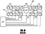
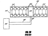
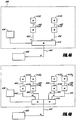
- Figures 1A and 1B illustrate a prior art approach of increasing the number of memory devices.
- Figure 1A shows a conventional memory subsystem 100 with at least one JEDEC-standard two-rank memory module 110, such as a registered dual in-line memory module (RDIMM), only one of which is shown for clarity.
- Each rank of the memory module 110 comprises a plurality of memory devices 112, such as dynamic random access memory (DRAM) devices or synchronous DRAM (SDRAM) devices.
- DRAM dynamic random access memory
- SDRAM synchronous DRAM
- a register 130 receives a plurality of control lines 140 (shown as a single solid line) from the system memory controller 120 and is connected via control lines 142 to the memory devices 112 of each rank of the memory module 110.
- This memory subsystem 100 connects each data line of an array of data lines 150 (shown as dashed lines) from a system memory controller 120 to corresponding memory devices 112 in the two ranks in each memory module 110. Therefore, during a write operation, the system memory controller 120 sees all the memory devices 112 as its load via the data lines 150, and during a read operation, each memory device 112 sees multiple other memory devices 112, as well as the system memory controller 120, as its load via the data lines 150.
- Figure 1B is a schematic view of another conventional memory subsystem 100' with at least one JEDEC-standard four-rank memory module 110' (only one of which is shown for clarity), each rank comprising a plurality of memory devices 112'.
- the register 130' receives the plurality of control lines 140' (shown as a single solid line) from the system memory controller 120' and is connected via control lines 142' to the memory devices 112' of each rank of the memory module 110'.
- Each data line of the array of data lines 150' (shown as dashed lines) from the system memory controller 120' is connected (e.g., by four fanouts) to corresponding memory devices 112' in the four ranks in each memory module 110'.
- the system memory controller 120' sees all the memory devices 112' as its load via the data lines 150', and during a read operation, each memory device 112' sees multiple other memory devices 112' and the system memory controller 120' as its load via the data lines 150'.
- the multiple loads seen by the memory controller 120, 120' during write operations and the multiple loads seen by the memory devices 112, 112' during read operations cause significant performance issues.
- time delays of the various signals are desired to be substantially equal to one another such that the operation of the memory module 110, 110' is synchronized with the system bus of the computer system.
- the trace lengths of the memory module 110, 110' are selected such that the signals are at the same clock phase.
- the lengths of the control lines 142, 142' from the register 130, 130' to each of the memory devices 112, 112' are substantially equal to one another.
- these prior art techniques not only reduce the speed of the memory systems, but they also require hardware modifications to minimize any deviation of the transmission line wave characteristics from the original design specification.
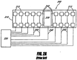
- Figures 2A and 2B illustrate another prior art approach of increasing the number of memory devices.
- Figure 2A shows a conventional memory subsystem 200 with at least one two-rank memory module 210, only one of which is shown for clarity.
- Each rank of the memory module 210 comprises a plurality of memory devices 212, such as dynamic random access memory (DRAM) devices or synchronous DRAM (SDRAM) devices.
- a register 230 receives a plurality of control lines 240 (shown as a single solid line) from the system memory controller 220 and is connected via control lines 242 to the memory devices 212 of each rank of the memory module 210.
- DRAM dynamic random access memory
- SDRAM synchronous DRAM
- This memory subsystem 200 connects each data line of an array of data lines 250 (shown as dashed lines) from a system memory controller 220 to corresponding memory devices 212 in the two ranks in each memory module 210. Therefore, during a write operation, the system memory controller 220 sees all the memory devices 212 as its load via the data lines 250, and during a read operation, each memory device 212 sees multiple other memory devices 212, as well as the system memory controller 220, as its load via the data lines 250.
- Figure 2B is a schematic view of another conventional memory subsystem 200' with at least one four-rank memory module 210' (only one of which is shown for clarity), each rank comprising a plurality of memory devices 212'.
- the register 230' receives the plurality of control lines 240' (shown as a single solid line) from the system memory controller 220' and is connected via control lines 242' to the memory devices 212' of each rank of the memory module 210'.
- Each data line of the array of data lines 250' (shown as dashed lines) from the system memory controller 220' is connected (e.g., by four fanouts) to corresponding memory devices 212' in the four ranks in each memory module 210'.
- the system memory controller 220' sees all the memory devices 212' as its load via the data lines 250', and during a read operation, each memory device 212' sees multiple other memory devices 212' and the system memory controller 220' as its load via the data lines 250'.
- control lines 242, 242' have a "fly-by" configuration.
- control signals are sent along the control lines 242, 242' (e.g., in a single-path daisy-chain) from the register 230, 230' to the memory devices 212, 212' of a given rank.
- These control signals reach each memory device 212, 212' of the rank sequentially, with the control signals first reaching the memory device 212, 212' having the shortest control line 242, 242', then reaching the memory device 212, 212' having the next-shortest control line 242, 242', and so on.
- a control signal may reach the memory device 212, 212' having the longest control line 242, 242' a significant period of time after the same control signal reaches the memory device 212, 212' having the shortest control line 242, 242'.
- the memory subsystems 200, 200' have the data lines 250, 250' configured so that the time delays of the various data signals between the memory controller 220, 220' and the particular memory devices 212, 212' are substantially tailored such that the data signals and the control signals reach the particular memory device 212, 212' so that operation of the memory module 210, 210' is synchronized with the system bus of the computer system.
- Such "fly-by" configurations have been described as operating in “local sync" while having “global async.”
- the memory controller 220, 220' of Figures 2A and 2B is more complicated than the memory controller 120, 120' of Figures 1A and 1B in that the memory controller 220, 220' accounts for the time delays between the various memory devices 212, 212' and adjusts the timing of these signals appropriately for synchronous operation.
- the clock cycle time is approximately equal to or less than the time difference (e.g., about 900 picoseconds) between the control signals reaching the memory device 212, 212' having the longest control line 242, 242' and reaching the memory device 212, 212' having the shortest control line 242, 242'. Under such situations, synchronous operation is not achievable.
- the time difference between the control signals reaching the memory devices 212, 212' at the extremes of the control lines 242, 242' provide a limit to the clock speed with which the memory module 210, 210' may be operated. These time differences, which can be more than one clock cycle, will limit the operational speed and performance of the memory module.
- the "fly-by" memory subsystems 200, 200' of Figures 2A and 2B suffer from large loads which result in slower clock speeds.
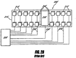
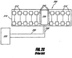
- FIGS 2C and 2D schematically illustrate a conventional two-rank memory module 310 and a four-rank memory module 310', respectively, each comprising a memory buffer 330, 330'.
- the control lines 340, 340' provide conduits for control signals from the memory controller 320, 320' to the memory buffer 330, 330', and the control lines 342, 342' provide conduits for control signals from the memory buffer 330, 330' to the memory devices 312, 312'.
- the plurality of data lines 350, 350' (shown as one dashed line for clarity) provide conduits for data signals from the memory controller 320, 320' to the memory buffer 330, 330', and data lines (not shown for clarity) on the memory module 310, 310' provide conduits for data signals from the memory controller 320, 320' to the memory devices 312, 312'.
- the configurations of Figures 2C and 2D seek to have both the data signals and the control signals going to the memory buffer 330, 330'.
- the memory module 310, 310' includes an extremely large number of data lines (not shown for clarity) coupling the memory buffer 330, 330' to the memory devices 312, 312'.
- the memory buffer 330, 330' for an LRDIMM is a 628-pin device, which is extremely large.
- the logistics of tailoring the time delays of these many data lines is complicated or difficult to provide the desired timing of data signals from the memory buffer 330, 330' to the memory devices 312, 312'.
- the memory module 310, 310' utilizes significant modifications of the memory controller 320, 320' since the memory buffer 330, 330' is taking over some of the control of data signal timing that conventional memory controllers have. Even so, the memory modules 310, 310' of Figures 2C and 2D can only operate in asynchronous mode, not synchronous mode, due to the long fly-by times as compared to the desired clock frequencies. For example, for a fly-by delay of 1 nanosecond, if the data rate is 1 Gb/second, there is the possibility of collisions on the data lines during read/write turnaround. To combat such collisions, the data rate can be slowed down or "dead" cycles can be inserted.
- the memory module 310, 310' as a single unit, cannot be operated in synchronous mode, but operates as locally synchronous, globally (DIMM level) asynchronous.
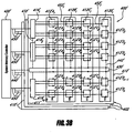
- Figure 3A schematically illustrates an example memory subsystem 400 with load-reduced memory modules 402 in accordance with certain embodiments described herein.
- Figure 3B schematically illustrates another example memory subsystem 400' with load-reduced memory modules 402' in accordance with certain embodiments described herein.
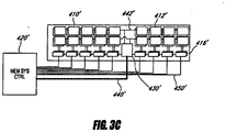
- Figure 3C schematically illustrates an example layout of the memory devices 412', the data transmission circuits 416', and the control circuit 430' of a memory module 402' in accordance with certain embodiments described herein.
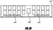
- Figure 3D is a photograph of an example memory subsystem in accordance with certain embodiments described herein.
- control lines e.g., address and control lines 440, 440' coupling the system memory controller 420, 420' to the memory modules 410, 410'
- data lines e.g., data lines 450, 450' coupling the system memory controller 420, 420' to the memory modules 410, 410'
- input/output connections are shown as black dots.
- the address and control lines 440, 440' coupling the system memory controller 420, 420' to the memory module 410, 410' are separate from the data lines 450, 450' coupling the system memory controller 420, 420' to the memory module 410, 410' (e.g., to the data transmission circuits 416, 416').
- the memory subsystem 400, 400' is designed, for example, to deliver higher speed and higher memory density with lower thermal dissipation as compared with conventional memory subsystems.
- aspects of the example subsystem 400 and corresponding components e.g., memory modules 402, memory devices 412A, 412B, 412C, 412D, data transmission circuits 416, control circuit 430
- aspects of the example subsystem 400 and corresponding components e.g., memory modules 402, memory devices 412A, 412B, 412C, 412D, data transmission circuits 416, control circuit 430
- aspects of the example subsystem 400 and corresponding components e.g., memory modules 402', memory devices 412'A 1 , 412'A 2 , 412'B 1 , 412'B 2 , 412'C 1 , 412'C 2 , 412'D 1 , 412'D 2 , data transmission circuits 416', control circuit 430'
- the example memory module 402, 402' comprises at least one printed circuit board 410, 410' and a plurality of memory devices 412, 412' mechanically coupled to the at least one printed circuit board 410, 410'.
- the memory module 402, 402' further comprises a control circuit 430, 430' mechanically coupled to the at least one printed circuit board 410, 410'.
- the control circuit 430, 430' is configurable to receive control signals from the system memory controller 420, 420' and to transmit module control signals to the plurality of memory devices 412, 412'.
- the memory module 402, 402' further comprises a plurality of data transmission circuits 416, 416' mechanically coupled to the at least one printed circuit board 410, 410' and distributed at corresponding positions relative to the at least one printed circuit board 410, 410'.
- the plurality of data transmission circuits 416, 416' is configurable to be operatively coupled to the system memory controller 420, 420' and configurable to receive module control signals from the control circuit 430, 430'.
- At least one first data transmission circuit of the plurality of data transmission circuits 416, 416' is operatively coupled to at least two memory devices of the plurality of memory devices 412, 412'.
- At least one second data transmission circuit of the plurality of data transmission circuits 416, 416' is operatively coupled to at least two memory devices of the plurality of memory devices 412, 412'.
- the at least one first data transmission circuit is configurable to respond to the module control signals by selectively allowing or inhibiting data transmission between the system memory controller 420, 420' and at least one selected memory device of the at least two memory devices operatively coupled to the at least one first data transmission circuit.
- the at least one second data transmission circuit is configurable to respond to the module control signals by selectively allowing or inhibiting data transmission between the system memory controller 420, 420' and at least one selected memory device of the at least two memory devices operatively coupled to the at least one second data transmission circuit.
- the memory subsystem 400, 400' is configurable to be operationally coupled to a system memory controller 420, 420', of a type well-known in the art (e.g., Intel Nehalem EP, EX chipsets; AMD Opteron chipset).
- the memory subsystem 400, 400' typically comprises one or more memory modules 402, 402', such as DIMMs or RDIMMs, additional details of which are shown only for one for clarity.
- Various types of memory modules 402, 402' are compatible with embodiments described herein. For example, memory modules having memory capacities of 512 MB, 1 GB, 2 GB, 4 GB, 8 GB, as well as other capacities, are compatible with embodiments described herein.
- memory modules 402, 402' compatible with embodiments described herein include, but are not limited to, single in-line memory modules (SIMMs), dual in-line memory modules (DIMMs), small-outline DIMMs (SO-DIMMs), unbuffered DIMMs (UDIMMs), registered DIMMs (RDIMMs), fully-buffered DIMMs (FBDIMMs), mini-DIMMs, and micro-DIMMs.
- SIMMs single in-line memory modules
- DIMMs dual in-line memory modules
- SO-DIMMs small-outline DIMMs
- UDIMMs unbuffered DIMMs
- RDIMMs registered DIMMs
- BBDIMMs fully-buffered DIMMs
- mini-DIMMs mini-DIMMs
- micro-DIMMs micro-DIMMs.
- the one or more memory modules 402, 402' comprise one or more printed circuit boards (PCBs) 410, 410', which may be arranged in a vertical stack (as shown), or in a back-to-back array.
- PCBs printed circuit boards
- Each memory module 402, 402' in certain embodiments comprises a single PCB 410, 410', while in certain other embodiments, each of one or more of the memory modules 402 comprises multiple PCBs 410, 410'.
- the PCBs 410, 410' are mountable in module slots (not shown) of the computer system.
- a PCB 410, 410' of certain such embodiments has at least one edge connector (not shown) comprising a plurality of electrical contacts which are positioned on an edge of the PCB 410, 410' and are configured to be releasably coupled to corresponding contacts of a computer system socket to provide electrical conductivity between the system memory controller 420, 420' and the various components of the memory modules 402, 401' on the PCBs 410, 410'.
- At least one memory module 402, 402' comprises a plurality of memory devices 412, 412' (such as DRAMs or SDRAMs).
- the memory devices 412, 412' of the memory module 402, 402' may advantageously be arranged in a plurality of rows or ranks.
- Memory devices 412, 412' compatible with embodiments described herein include, but are not limited to, random-access memory (RAM), dynamic random-access memory (DRAM), synchronous DRAM (SDRAM), and double-data-rate DRAM (e.g., DDR, DDR2, DDR3, etc.).
- RAM random-access memory
- DRAM dynamic random-access memory
- SDRAM synchronous DRAM
- double-data-rate DRAM e.g., DDR, DDR2, DDR3, etc.
- memory devices 412, 412' having bit widths of 4, 8, 16, 32, as well as other bit widths are compatible with embodiments described herein.
- Memory devices 412, 412' compatible with embodiments described herein have packaging which include, but are not limited to, thin small-outline package (TSOP), ball-grid-array (BGA), fine-pitch BGA (FBGA), micro-BGA ( ⁇ BGA), mini-BGA (mBGA), and chip-scale packaging (CSP).
- TSOP thin small-outline package
- BGA ball-grid-array
- FBGA fine-pitch BGA
- ⁇ BGA micro-BGA
- mini-BGA mini-BGA
- CSP chip-scale packaging
- the memory devices 412, 412' of the memory module 402, 402' are arranged in four ranks, although embodiments with less than four ranks (e.g., one rank , two ranks, three ranks) or more than four ranks (e.g., 6 ranks, 8 ranks) per memory module 402, 402' may be employed.
- each rank comprises eight or nine memory modules, while in certain other embodiments, other numbers of memory modules per rank may also be used.
- the memory devices 412 are arranged in four ranks, denoted A, B, C, and D, and each rank comprises n memory devices.
- rank A comprises memory devices 412A 1 , 412A 2 , ..., 412A n
- rank B comprises memory devices 412B 1 , 412B 2 , ..., 412B n
- rank C comprises memory devices 412C 1 , 412C 2 , ..., 412C n
- rank D comprises memory devices 412D 1 , 412D 2 , ..., 412D n .
- rank A comprises memory devices 412'A 1 , 412'A 2 , ..., 412'A n
- rank B comprises memory devices 412'B 1 , 412'B 2 , ..., 412'B n
- rank C comprises memory devices 412'C 1 , 412'C 2 , ..., 412'C n
- rank D comprises memory devices 412'D 1 , 412'D 2 , ..., 412'D n .
- At least one memory module 402, 402' comprises one or more electrical components (not shown) which may be mounted on the PCB 410, 410', within the PCB 410, 410', or both on and within the PCB 410, 410', and are operationally coupled to one another and to the plurality of memory devices 412, 412'.
- the electrical components may be surface-mounted, through-hole mounted, embedded or buried between layers of the PCB 410, 410', or otherwise connected to the PCB 410, 410'.
- These electrical components may include, but are not limited to, electrical conduits, resistors, capacitors, inductors, transistors, buffers, registers, logic elements, or other circuit elements.
- at least some of these electrical components are discrete, while in other certain embodiments, at least some of these electrical components are constituents of one or more integrated circuits.
- At least one memory module 402, 402' comprises a control circuit 430, 430' configured to be operatively coupled to the system memory controller 420, 420' and to the memory devices 412, 412' of the memory module 402, 402' (e.g., via lines 442, 442').
- the control circuit 430, 430' may include one or more functional devices, such as a programmable-logic device (PLD), an application-specific integrated circuit (ASIC), a field-programmable gate array (FPGA), a custom-designed semiconductor device, or a complex programmable-logic device (CPLD).
- PLD programmable-logic device
- ASIC application-specific integrated circuit
- FPGA field-programmable gate array
- CPLD complex programmable-logic device
- the control circuit 430, 430' may comprise one or more custom devices.
- the control circuit 430, 430' may comprise various discrete electrical elements; while in other embodiments, the control circuit 430, 430' may comprise one or more integrated circuits.
- the control circuit 430, 430' of certain embodiments is configurable to be operatively coupled to control lines 440, 440' to receive control signals (e.g., bank address signals, row address signals, column address signals, address strobe signals, and rank-address or chip-select signals) from the system memory controller 420, 420'.
- the control circuit 430, 430' of certain embodiments registers signals from the control lines 440, 440' in a manner functionally comparable to the address register of a conventional RDIMM.
- the registered control lines 440, 440' are also operatively coupled to the memory devices 412, 412'.
- control circuit 430, 430' supplies control signals for the data transmission circuits 416, 416' (e.g., via lines 432, 432'), as described more fully below.
- the control signals indicate, for example, the direction of data flow, that is, to or from the memory devices 412, 412'.
- the control circuit 430, 430' may produce additional chip-select signals or output enable signals based on address decoding. Examples of circuits which can serve as the control circuit 430, 430' are described in more detail by U.S. Pat. Nos. 7,289,386 and 7,532,537 , each of which is incorporated in its entirety by reference herein.
- At least one memory module 402, 402' comprises a plurality of data transmission circuits 416, 416' mounted on the one or more PCBs 410, 410', within the one or more PCBs 410, 410', or both on and within the one or more PCBs 410, 410'.
- the plurality of data transmission circuits 416, 416' are operatively coupled to the control circuit 430, 430' (e.g., via lines 432, 432'), and configured to be operatively coupled to the system memory controller 420, 420' (e.g., via the data lines 450, 450') upon operatively coupling the memory module 402, 402' to the computer system.
- these data transmission circuits 416, 416' can be referred to as "load-reducing circuits” or “load-reducing switching circuits.”
- the terms “load-reducing” or “load-reducing switching” refer to the use of the data transmission circuits 416, 416' to reduce the load seen by the system memory controller 420, 420' when operatively coupled to the memory module 402, 402'.
- the memory module 402 comprises n data transmission circuits 416, where n is the number of memory devices per rank of the memory module 410.
- the memory devices 412 of the memory module 410 are arranged in four ranks of n memory devices each, and the memory module 410 comprises at least a first data transmission circuit 416 1 and a second data transmission circuit 416 2 .
- the first data transmission circuit 416 1 of certain such embodiments is operatively coupled to at least one memory device 412 of each rank (e.g., memory devices 412A 1 , 412B 1 , 412C 1 , 412D 1 ).
- the second data transmission circuit 416 2 of certain such embodiments is operatively coupled to at least one memory device 412 of each rank (e.g., memory devices 412A 2 , 412B 2 , 412C 2 , 412D 2 ).
- the memory module 402' comprises n / 2 data transmission circuits 416', where n is the number of memory devices per rank of the memory module 410'.
- n is the number of memory devices per rank of the memory module 410'.
- the memory devices 412' of the memory module 410' are arranged in four ranks of n memory devices each, and the memory module 410' comprises at least a first data transmission circuit 416' 1 and a second data transmission circuit 416' 2 .
- the first data transmission circuit 416' 1 of certain such embodiments is operatively coupled to at least two memory devices 412' of each rank (e.g., memory devices 412'A 1 , 412'A 2 , 412'B 1 , 412'B 2 , 412'C 1 , 412'C 2 , 412'D 1 , 412'D 2 ).
- the second data transmission circuit 416' 2 of certain such embodiments is operatively coupled to at least two memory devices 412' of each rank (e.g., memory devices 412'A 3 , 412'A 4 , 412'B 3 , 412'B 4 , 412'C 3 , 412'C 4 , 412'D 3 , 412'D 4 ).
- At least one data transmission circuit 416, 416' selectively switches between two or more memory devices 412, 412' so as to operatively couple at least one selected memory device 412, 412' to the system memory controller 420, 420' (e.g., the data transmission circuit 416, 416' is configurable to respond to module control signals by selectively allowing or inhibiting data transmission between the system memory controller 420, 420' and at least one selected memory device 412, 412').
- the at least one data transmission circuit 416, 416' selectively operatively couples two selected memory devices to the system memory controller 420, 420'.
- the first data transmission circuit 416 1 is configurable to respond to module control signals by selectively allowing or inhibiting data transmission between the system memory controller 420 and either selected memory devices 412A 1 and 412C 1 or selected memory devices 412B 1 and 412D 1
- the second data transmission circuit 416 2 is configurable to respond to module control signals by selectively allowing or inhibiting data transmission between the system memory controller 420 and either selected memory devices 412A 2 and 412C 2 or selected memory devices 412B 2 and 412D 2 ).
- the two or more memory devices 412 are concurrently operatively coupled to the system memory controller 420.
- a data transmission circuit 416 of certain embodiments bidirectionally buffer data signals between the memory controller 420 and the memory devices 412 corresponding to the data transmission circuit 416.
- the first data transmission circuit 416' 1 is configurable to respond to module control signals by selectively allowing or inhibiting data transmission between the system memory controller 420' and either selected memory devices 412'A 1 and 412'C 1 or selected memory devices 412'B 1 and 412'D 1 and either selected memory devices 412'A 2 and 412'C 2 or selected memory devices 412'B 2 and 412'D 2 ), and the second data transmission circuit 416' 2 is configurable to respond to module control signals by selectively allowing or inhibiting data transmission between the system memory controller 420' and either selected memory devices 412'A 3 and 412'C 3 or selected memory devices 412'B 3 and 412'D 3 and either selected memory devices 412'A 4 and 412'C 4 or selected memory devices 412'B 4 and 412'D 4 ).
- two or more of the data transmission circuits 416, 416' are mechanically coupled to the at least PCB 410, 410' at corresponding positions which are separate from one another.
- the first data transmission circuit 416 1 and the second data transmission circuit 416 2 are at corresponding positions which are separate from one another (e.g., the package containing the first data transmission circuit 416 1 is at a location spaced from the location of the package containing the second data transmission circuit 416 2 ).
- the first data transmission circuit 416' 1 and the second data transmission circuit 416' 2 are at corresponding positions which are separate from one another (e.g., the package containing the first data transmission circuit 416' 1 is at a location spaced from the location of the package containing the second data transmission circuit 416' 2 ).
- two or more of the data transmission circuits 416, 416' are distributed across a surface of the PCB 410, 410' of the memory module 402, 402'.
- the corresponding positions of two or more data transmission circuits 416, 416' are along an edge 411, 411' of the at least one PCB 410, 410' such that a data transmission circuit 416, 416' is located substantially between the edge 411, 411' and at least some of the at least two memory devices 412, 412' to which the data transmission circuit 416, 416' is operatively coupled.
- the first data transmission circuit 416 1 is located substantially between the edge 411 and the memory devices 412A 1 , 412B 1 , 412C 1 , 412D 1 to which the first data transmission circuit 416 1 is operatively coupled
- the second data transmission circuit 416 2 is located substantially between the edge 411 and the memory devices 412A 2 , 412B 2 , 412C 2 , 412D 2 to which the second data transmission circuit 416 1 is operatively coupled.
- the first data transmission circuit 416' 1 is located substantially between the edge 411' and the memory devices 412'A 1 , 412'A 2 , 412'B 1 , 412'B 2 , 412'C 1 , 412'C 2 , 412'D 1 , 412'D 2 to which the first data transmission circuit 416' 1 is operatively coupled
- the second data transmission circuit 416' 2 is located substantially between the edge 411' and the memory devices 412'A 3 , 412'A 4 412'B 3 , 412'B 4 , 412'C 3 , 412'C 4 , 412'D 3 , 412'D 4 to which the second data transmission circuit 416' 2 is operatively coupled.
- Figures 3C and 3D illustrate the positioning of the data transmission circuits 416' in accordance with certain embodiments described herein.
- the position of at least one of the data transmission circuits 416' is generally aligned with one or more of the memory devices 412' to which the data transmission circuit 416' is operatively coupled.
- the one or more of the data transmission circuits 416' and the memory devices 412' to which it is operatively coupled can be positioned generally along a line that is substantially perpendicular to the edge 411' of the PCB 410'.
- the position of at least one of the data transmission circuits 416' is generally offset from a line defined by the positions of the one or more of the memory devices 412' to which the data transmission circuit 416' is operatively coupled.
- the memory devices 412' operatively coupled to a data transmission circuit 416' can be positioned along a line that is substantially perpendicular to the edge 411' of the PCB 410' and the data transmission circuit 416' can be generally offset from this line in a direction generally along the edge 411' of the PCB 410'.
- the data transmission circuits 416' are sufficiently small in width and breadth (e.g., 2.5 mm by 7.5 mm) to fit between the edge 411' and the corresponding memory devices 412' while maintaining the desired size of the memory module 400'.
- Other positions and sizes of the separate data transmission circuits 416' are also compatible with certain embodiments described herein.
- one or more of the data transmission circuits 416, 416' can be positioned between two or more memory devices 412, 412', or can be spaced away from an edge 411, 411' of the PCB 410, 410' with one or more memory devices 412, 412' between the edge 411, 411' and the one or more data transmission circuits 416, 416'.
- the data transmission circuit 416 comprises or functions as a byte-wise buffer.
- each of the one or more data transmission circuits 416 has the same bit width as does the associated memory devices 412 per rank to which the data transmission circuit 416 is operatively coupled.
- Figure 4A which corresponds generally to Figure 3A
- the data transmission circuit 416 can be operatively coupled to a single memory device 412 per rank, and both the data transmission circuit 416 and the memory device 412 per rank to which the data transmission circuit 416 is operatively coupled can each have the same bit width (e.g., 4 bits, 8 bits, or 16 bits).
- the data transmission circuit 416 of Figure 4A has a bit width of 8 bits, and receives data bits 0-7 from the system memory controller 420 and selectively transmits the data bits 0-7 to selected memory devices 412A, 412B, 412C, 412D in response to the module control signals from the control circuit 430.
- data transmission circuits 416' of certain embodiments can function as a byte-wise buffer for associated memory devices 412'A, 412'B, 412'C, 412'D to which the data transmission circuits 416' are operatively coupled in response to the module control signals from the control circuit 430'.
- bit widths of one or more of the memory devices 412 may be different from the bit widths of the one or more data transmission circuits 416 to which they are connected.
- the data transmission circuits 416 may have a first bit width (e.g., a bit width of 8 bits) and the memory devices 412 may have a second bit width which is less than the first bit width (e.g., one-half the first bit width, or a bit width of 4 bits), with each data transmission circuit 416 operatively coupled to multiple memory devices 412 per rank (e.g., two memory devices 412 in each rank).
- the total bit width of the multiple memory devices 412 per rank connected to the circuit 416 equals the bit width of the circuit 416 (e.g., 4 bits, 8 bits, or 16 bits).
- the data transmission circuit 416 of Figure 4B has a total bit width of 8 bits, and receives data bits 0-7 from the system memory controller 420 and selectively transmits data bits 0-3 to a first memory device 412A 1 , 412B 1 , 412C 1 , 412D 1 and data bits 4-7 to a second memory device 412A 2 , 412B 2 , 412C 2 , 412D 2 in response to the module control signals from the control circuit 430.
- data transmission circuits 416' of certain embodiments can function with different bit widths than those of the associated memory devices 412'A 1 , 412'A 2 , 412'B 1 , 412'B 2 , 412'C 1 , 412'C 2 , 412'D 1 , 412'D 2 to which the data transmission circuits 416' are operatively coupled in response to the module control signals from the control circuit 430'.
- the data transmission circuit 416 comprise or serve as a "byte-wise" buffer (e.g., as shown in the examples of Figures 4A and 4B ), the data signals are synchronous with the synch clock.
- the memory module 400 can be designed to optimize the circuits of a smaller number of components as compared to other configurations which do not utilize byte-wide buffering (e.g., having four ranks of 8-bit memory devices and having two 4-bit buffers).
- the data transmission circuits 416 are used for bit slicing in which the data are defined in sections.
- the data can be defined or sliced in 16-bit-wide sections (e.g., [15:0], [31:16], [47:32], [63:48]).
- 16-bit-wide sections e.g., [15:0], [31:16], [47:32], [63:48].
- not all the bits are grouped together and not all the bits produce the same behavior (e.g., logic- and/or time-wise).
- One or more of the data transmission circuits 416 is operatively coupled to a corresponding one or more of the data lines 452 connected to one or more memory devices 412 in each of the ranks A, B, C, D.
- each data transmission circuit 416 is connected to one or more data lines 452 connected to one corresponding memory device in each of the ranks (e.g., memory devices 204A, 204B, 204C, and 204D, as shown in Figure 3A ).
- Each data line 450, 452 thus carries data from the system memory controller 420, through the data transmission circuits 416, to the memory devices 204A, 204B, 204C, 204D connected to the data transmission circuits 416.
- the data transmission circuits 416 of certain embodiments may be used to drive each data bit to and from the memory controller 420 and the memory devices 412, instead of the memory controller 420 and the memory devices 412 directly driving each data bit to and from the memory controller 420 and the memory devices 412.
- one side of each data transmission circuit 416 of certain embodiments is operatively coupled to a memory device 412 in each rank (e.g., via data lines 452), while the other side of the data transmission circuit 416 is operatively coupled to the corresponding data line 450 of the memory controller 420.
- the data transmission circuit 416 of certain embodiments is advantageously configured to be recognized by the system memory controller 420 as a single memory load. This advantageous result is desirably achieved in certain embodiments by using the data transmission circuits 416 to electrically couple only the enabled memory devices 412 to the memory controller 420 (e.g., the one, two, or more memory devices 412 to which data is to be written) and to electrically isolate the other memory devices 412 from the memory controller 420 (e.g., the one, two, or more memory devices 412 to which data is not to be written).
- each data bit from the system memory controller 420 sees a single load from the memory module 400, presented by one of the data transmission circuits 416, instead of concurrently seeing the loads of all of the four memory devices 412A, 412B, 412C, 412D to which the data transmission circuit 416 is operatively coupled.
- each data bit from the system memory controller 420 sees a single load from the memory module 402, which is presented by one of the data transmission circuits 416, instead of concurrently seeing the loads of all of the four memory devices 412A, 412B, 412C, 412D to which the data transmission circuits 416 is operatively coupled.
- the memory system 402 of certain embodiments may reduce the load on the system memory controller 420 by a factor of four.
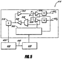
- Figure 5 schematically illustrates an example data transmission circuit 416 compatible with certain embodiments described herein.
- the data transmission circuits 416 includes control logic circuitry 502 used to control the various components of the data transmission circuit 416, which may include one or more buffers, one or more switches, and one or more multiplexers among other components.
- the illustrated embodiment of Figure 5 is 1-bit wide and switches a single data line 518 between the memory controller 420 and the memory devices 412.
- the data transmission circuit 416 may be multiple bits wide, for example, 8 bits, and switch a corresponding number of data lines 518.
- the control logic circuitry 502 may be shared over the multiple bits.
- the data transmission circuits 416 allow for "driving" write data and "merging" read data.
- data entering a data transmission circuit 416 via a data line 518 is driven onto two data paths, labeled path A and path B, preferably after passing through a write buffer 503.
- the ranks of memory devices 412 are likewise divided into two groups with one group associated with path A and one group associated with path B. As shown in Figure 3A , rank A and rank C are in the first group, and rank B and rank D are in the second group.
- the memory devices 412A, 412C of rank A and rank C are connected to the data transmission circuits 416 by a first one of the two data paths, and the memory devices 412B, 412D of rank B and rank D are connected to the data transmission circuits 416 by a second one of the two data paths.
- the driving of write data and merging of read data may be performed over more than two data paths.
- CAS latency is a delay time which elapses between the moment the memory controller 420 informs the memory modules 402 to access a particular column in a selected rank or row and the moment the data for or from the particular column is on the output pins of the selected rank or row.
- the latency may be used by the memory module to control operation of the data transmission circuits 416.
- address and control signals pass from the memory controller 420 to the control circuit 430 which produces controls sent to the control logic circuitry 502 (e.g., via lines 432) which then controls operation of the components of the data transmission circuits 416.
- the control circuit 430 provides enable control signals to the control logic circuitry 502 of each data transmission circuit 416, whereby the control logic circuitry 502 selects either path A or path B to direct the data. Accordingly, when the control logic circuitry 502 receives, for example, an "enable A" signal, a first tristate buffer 504 in path A is enabled and actively drives the data value on its output, while a second tristate buffer 506 in path B is disabled with its output in a high impedance condition.
- the data transmission circuit 416 allows the data to be directed along path A to a first terminal Y1, which is connected to and communicates only with the first group of the memory devices 412, e.g., those in ranks A and C.
- the first tristate 504 opens path A and the second tristate 506 closes path B, thus directing the data to a second terminal Y2, which is connected to and communicates only with the second group of the memory devices 412, e.g., those in ranks B and D.
- the data transmission circuit 416 operates as a multiplexing circuit.
- data signals read from the memory devices 412 of a rank are received at the first or second terminals Y1, Y2 of the data transmission circuit 416.
- the data signals are fed to a multiplexer 508, which selects one to route to its output.
- the control logic circuitry 502 generates a select signal to select the appropriate data signal, and the selected data signal is transmitted to the system memory controller 420 along a single data line 518, preferably after passing through a read buffer 509.
- the read buffer 509 may be a tristate buffer that is enabled by the control logic circuitry 502 during read operations.
- the multiplexer 508 and the read buffer 509 may be combined in one component.
- the multiplexer 508 and the read buffer 509 operations may be split over two tristate buffers, one to enable the value from Y1 to the data line 518 and another to enable the value from Y2 to the data line 518.
- the data transmission circuits 416 present a load on the data lines 518 from the write buffer 503 and the read buffer 509.
- the write buffer 503 is comparable to an input buffer on one of the memory devices 412
- the read buffer 509 is comparable to an output buffer on one of the memory devices 412. Therefore, the data transmission circuits 416 present a load to the memory controller 420 that is substantially the same as the load that one of the memory devices 412 would present.
- the data transmission circuits 416 present a load on the first and second terminals Y1, Y2 from the multiplexer 508 and the first tristate buffer 504 (on the first terminal Y1) and the second tristate buffer 506 (on the second terminal Y2).
- the multiplexer 508 is comparable in loading to an input buffer on the memory controller 420, and the first and second tristate buffers 504, 506 are each comparable to an output buffer on the memory controller 420. Therefore, the data transmission circuits 416 present a load to the memory devices 412 that is substantially the same as the load that the memory controller 420would present.
- the data transmission circuits 416 operate to ameliorate quality of the data signals passing between the memory controller 420 and the memory devices 412.
- waveforms of data signals may be substantially degraded or distorted from a desired shape between source and sink.
- signal quality may be degraded by lossy transmission line characteristics, mismatch between characteristics of transmission line segments, signal crosstalk, or electrical noise.
- the read buffer 509 regenerates the signals from the memory devices 412 thereby restoring the desired signal waveform shapes.
- the first tristate buffer 504 and the second tristate buffer 506 regenerate the signals from the memory controller 420 thereby restoring the desired signal waveform shapes.
- each specific operation is targeted to a specific one of the ranks A, B, C, and D of a specific memory module 402.
- the data transmission circuit 416 on the specifically targeted one of the memory modules 402 functions as a bidirectional repeater/multiplexor, such that it drives the data signal when connecting from the system memory controller 420 to the memory devices 412.
- the other data transmission circuits 416 on the remaining memory modules 402 are disabled for the specific operation. For example, the data signal entering on data line 518 entering into data transmission circuit 416 is driven to memory devices 412A and 412C or 412B and 412C depending on which memory devices are active and enabled.
- the data transmission circuit 416 then multiplexes the signal from the memory devices 412A, 412B, 412C, 412D to the system memory controller 420.
- the data transmission circuits 416 may each control, for example, a nibble-wide data path or a byte-wide-data path.
- the data transmission circuits 416 associated with each module 402 are operable to merge data read signals and to drive data write signals, enabling the proper data paths between the system memory controller 420 and the targeted or selected memory devices 412.
- the memory controller 420 when there are four four-rank memory modules, sees four load-reducing switching circuit loads, instead of sixteen memory device loads.
- the reduced load on the memory controller 420 enhances the performance and reduces the power requirements of the memory system, as compared with, for example, the conventional systems described above with reference to Figures 1A , 1B and 2A-2D .
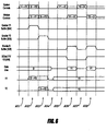
- FIG. 6 an illustrative timing diagram of signals of the memory module 402.
- the timing diagram includes first through eighth time periods 601-608.
- each of the time periods 601-608 may correspond to one clock cycle of the memory devices 404.
- the first, second, and third time periods 601-603 illustrate write operations with data passing from the memory controller 401 to the memory module 402.
- the fourth time period 604 is a transition between the write operations and subsequent read operations.
- the timing diagram shows a write operation to the first group of memory devices 412A, 412C connected to the first terminals Y1 of the data transmission circuits 416 and a write operation to the second group of memory devices 412B, 412D connected to the second terminals Y2 of the data transmission circuits 416. Recalling the CAS latency described above, each write operation extends over two time periods in a pipelined manner.
- the write to the first group of memory devices 412A, 412C appears in the first time period 601 when system address and control signals 440 pass from the memory controller 420 to the module controller 430.
- the control circuit 430 evaluates the address and control signals 440 to determine that data is to be written to memory devices 412A, 412C in the first group.
- the control circuit 430 supplies control signals to the control logic circuitry 502 to enable the first tristate buffer 504 and to disable the second tristate buffer 506 and the read buffer 509.
- data bits pass from the data lines 518 to the first terminal Y1 and on to the memory devices 412A, 412C.
- the write to the second group of memory devices 412A, 412C appears in the second time period 602 when system address and control signals 440 pass from the memory controller 420 to the control circuit 430.
- the control circuit 430 evaluates the address and control signals 440 to determine that data is to be written to memory devices 412B, 412D in the second group.
- the control circuit 430 supplies control signals to the control logic circuitry 502 to enable the second tristate buffer 506 and to disable the first tristate buffer 504 and the read buffer 509.
- data bits pass from the data lines 518 to the second terminal Y2 and on to the memory devices 412B, 412D.
- the fifth, sixth, seventh, and eighth time periods 605-608 illustrate read operations with data passing to the memory controller 420 from the memory module 402.
- the timing diagram shows a read operation from the first group of memory devices 412A, 412C connected to the first terminals Y1 of the data transmission circuits 416 and a read operation from the second group of memory devices 412B, 412D connected to the second terminals Y2 of the data transmission circuits 416.
- each read operation extends over two time periods in a pipelined manner.
- the read from the first group of memory devices 412A, 412C appears in the fifth time period 605 when system address and control signals 440 pass from the memory controller 420 to the control circuit 430.
- the control circuit 430 evaluates the address and control signals 440 to determine that data is to be read from memory devices 412A, 412C in the first group.
- the control circuit 430 supplies control signals to the control logic circuitry 502 to cause the multiplexer 58 to select data from the first terminal Y1, to enable the read buffer 509, and to disable the first tristate buffer 504 and the second tristate buffer 506.
- data bits pass from the memory devices 412A, 412C via the first terminal Y1 to data lines 518 and on to the memory controller 420.
- the read from the second group of memory devices 412B, 412D appears in the seventh time period 607 when system address and control signals 440 pass from the memory controller 420 to the control circuit 430.
- the control circuit 430 evaluates the address and control signals 440 to determine that data is to be read from memory devices 412B, 412D in the second group.
- the control circuit 430 supplies control signals to the control logic circuitry 502 to cause the multiplexer 508 to select data from the second terminal Y2, to enable the read buffer 509, and to disable the first tristate buffer 504 and the second tristate buffer 506.
- data bits pass from the memory devices 412B, 412D via the second terminal Y2 to data lines 518 and on to the memory controller 420.
Landscapes
- Engineering & Computer Science (AREA)
- Theoretical Computer Science (AREA)
- Microelectronics & Electronic Packaging (AREA)
- Physics & Mathematics (AREA)
- General Engineering & Computer Science (AREA)
- General Physics & Mathematics (AREA)
- Dram (AREA)
- Static Random-Access Memory (AREA)
- Memory System (AREA)
Priority Applications (4)
| Application Number | Priority Date | Filing Date | Title |
|---|---|---|---|
| PL10730021T PL2454735T3 (pl) | 2009-07-16 | 2010-07-01 | System i sposób stosowania rozproszonych buforów o zakresie bajtowym w module pamięci |
| EP21174133.5A EP3923286A1 (en) | 2009-07-16 | 2010-07-01 | System and method utilizing distributed byte-wise buffers on a memory module |
| EP18179414.0A EP3404660B1 (en) | 2009-07-16 | 2010-07-01 | System and method utilizing distributed byte-wise buffers on a memory module |
| PL18179414T PL3404660T3 (pl) | 2009-07-16 | 2010-07-01 | System i sposób wykorzystania rozproszonych buforów bajtowych w module pamięci |
Applications Claiming Priority (3)
| Application Number | Priority Date | Filing Date | Title |
|---|---|---|---|
| US12/504,131 US8417870B2 (en) | 2009-07-16 | 2009-07-16 | System and method of increasing addressable memory space on a memory board |
| US12/761,179 US8516185B2 (en) | 2009-07-16 | 2010-04-15 | System and method utilizing distributed byte-wise buffers on a memory module |
| PCT/US2010/040826 WO2011008580A1 (en) | 2009-07-16 | 2010-07-01 | System and method utilizing distributed byte-wise buffers on a memory module |
Related Child Applications (3)
| Application Number | Title | Priority Date | Filing Date |
|---|---|---|---|
| EP21174133.5A Division EP3923286A1 (en) | 2009-07-16 | 2010-07-01 | System and method utilizing distributed byte-wise buffers on a memory module |
| EP18179414.0A Division EP3404660B1 (en) | 2009-07-16 | 2010-07-01 | System and method utilizing distributed byte-wise buffers on a memory module |
| EP18179414.0A Division-Into EP3404660B1 (en) | 2009-07-16 | 2010-07-01 | System and method utilizing distributed byte-wise buffers on a memory module |
Publications (2)
| Publication Number | Publication Date |
|---|---|
| EP2454735A1 EP2454735A1 (en) | 2012-05-23 |
| EP2454735B1 true EP2454735B1 (en) | 2020-12-09 |
Family
ID=42610062
Family Applications (3)
| Application Number | Title | Priority Date | Filing Date |
|---|---|---|---|
| EP10730021.2A Active EP2454735B1 (en) | 2009-07-16 | 2010-07-01 | System and method utilizing distributed byte-wise buffers on a memory module |
| EP18179414.0A Active EP3404660B1 (en) | 2009-07-16 | 2010-07-01 | System and method utilizing distributed byte-wise buffers on a memory module |
| EP21174133.5A Pending EP3923286A1 (en) | 2009-07-16 | 2010-07-01 | System and method utilizing distributed byte-wise buffers on a memory module |
Family Applications After (2)
| Application Number | Title | Priority Date | Filing Date |
|---|---|---|---|
| EP18179414.0A Active EP3404660B1 (en) | 2009-07-16 | 2010-07-01 | System and method utilizing distributed byte-wise buffers on a memory module |
| EP21174133.5A Pending EP3923286A1 (en) | 2009-07-16 | 2010-07-01 | System and method utilizing distributed byte-wise buffers on a memory module |
Country Status (10)
| Country | Link |
|---|---|
| US (5) | US8516185B2 (enExample) |
| EP (3) | EP2454735B1 (enExample) |
| JP (1) | JP2012533793A (enExample) |
| KR (1) | KR20120062714A (enExample) |
| CN (2) | CN105161126B (enExample) |
| CZ (1) | CZ31172U1 (enExample) |
| DE (1) | DE202010018501U1 (enExample) |
| PL (2) | PL2454735T3 (enExample) |
| TW (2) | TWI446167B (enExample) |
| WO (1) | WO2011008580A1 (enExample) |
Cited By (1)
| Publication number | Priority date | Publication date | Assignee | Title |
|---|---|---|---|---|
| US11994982B2 (en) | 2009-07-16 | 2024-05-28 | Netlist, Inc. | Memory module with distributed data buffers |
Families Citing this family (71)
| Publication number | Priority date | Publication date | Assignee | Title |
|---|---|---|---|---|
| US8250295B2 (en) * | 2004-01-05 | 2012-08-21 | Smart Modular Technologies, Inc. | Multi-rank memory module that emulates a memory module having a different number of ranks |
| US7916574B1 (en) | 2004-03-05 | 2011-03-29 | Netlist, Inc. | Circuit providing load isolation and memory domain translation for memory module |
| US7289386B2 (en) * | 2004-03-05 | 2007-10-30 | Netlist, Inc. | Memory module decoder |
| WO2008127458A2 (en) | 2006-12-06 | 2008-10-23 | Fusion Multisystems, Inc. (Dba Fusion-Io) | Apparatus, system, and method for a shared, front-end, distributed raid |
| US8874831B2 (en) | 2007-06-01 | 2014-10-28 | Netlist, Inc. | Flash-DRAM hybrid memory module |
| US8417870B2 (en) * | 2009-07-16 | 2013-04-09 | Netlist, Inc. | System and method of increasing addressable memory space on a memory board |
| US8154901B1 (en) | 2008-04-14 | 2012-04-10 | Netlist, Inc. | Circuit providing load isolation and noise reduction |
| US9128632B2 (en) | 2009-07-16 | 2015-09-08 | Netlist, Inc. | Memory module with distributed data buffers and method of operation |
| US8289801B2 (en) | 2009-09-09 | 2012-10-16 | Fusion-Io, Inc. | Apparatus, system, and method for power reduction management in a storage device |
| US8688899B2 (en) | 2010-09-28 | 2014-04-01 | Fusion-Io, Inc. | Apparatus, system, and method for an interface between a memory controller and a non-volatile memory controller using a command protocol |
| WO2012061633A2 (en) | 2010-11-03 | 2012-05-10 | Netlist, Inc. | Method and apparatus for optimizing driver load in a memory package |
| US10817502B2 (en) | 2010-12-13 | 2020-10-27 | Sandisk Technologies Llc | Persistent memory management |
| US9218278B2 (en) | 2010-12-13 | 2015-12-22 | SanDisk Technologies, Inc. | Auto-commit memory |
| US9047178B2 (en) | 2010-12-13 | 2015-06-02 | SanDisk Technologies, Inc. | Auto-commit memory synchronization |
| US10817421B2 (en) | 2010-12-13 | 2020-10-27 | Sandisk Technologies Llc | Persistent data structures |
| US9208071B2 (en) | 2010-12-13 | 2015-12-08 | SanDisk Technologies, Inc. | Apparatus, system, and method for accessing memory |
| US8924641B2 (en) * | 2010-12-13 | 2014-12-30 | Seagate Technology Llc | Selectively depowering portion of a controller to facilitate hard disk drive safeguard operations |
| US8527693B2 (en) | 2010-12-13 | 2013-09-03 | Fusion IO, Inc. | Apparatus, system, and method for auto-commit memory |
| US9779020B2 (en) | 2011-02-08 | 2017-10-03 | Diablo Technologies Inc. | System and method for providing an address cache for memory map learning |
| US9552175B2 (en) | 2011-02-08 | 2017-01-24 | Diablo Technologies Inc. | System and method for providing a command buffer in a memory system |
| US8713379B2 (en) | 2011-02-08 | 2014-04-29 | Diablo Technologies Inc. | System and method of interfacing co-processors and input/output devices via a main memory system |
| US9575908B2 (en) | 2011-02-08 | 2017-02-21 | Diablo Technologies Inc. | System and method for unlocking additional functions of a module |
| US9176671B1 (en) | 2011-04-06 | 2015-11-03 | P4tents1, LLC | Fetching data between thread execution in a flash/DRAM/embedded DRAM-equipped system |
| US9158546B1 (en) | 2011-04-06 | 2015-10-13 | P4tents1, LLC | Computer program product for fetching from a first physical memory between an execution of a plurality of threads associated with a second physical memory |
| US8930647B1 (en) | 2011-04-06 | 2015-01-06 | P4tents1, LLC | Multiple class memory systems |
| US9170744B1 (en) | 2011-04-06 | 2015-10-27 | P4tents1, LLC | Computer program product for controlling a flash/DRAM/embedded DRAM-equipped system |
| US9164679B2 (en) | 2011-04-06 | 2015-10-20 | Patents1, Llc | System, method and computer program product for multi-thread operation involving first memory of a first memory class and second memory of a second memory class |
| US9025409B2 (en) * | 2011-08-05 | 2015-05-05 | Rambus Inc. | Memory buffers and modules supporting dynamic point-to-point connections |
| US9417754B2 (en) | 2011-08-05 | 2016-08-16 | P4tents1, LLC | User interface system, method, and computer program product |
| JP2013114416A (ja) * | 2011-11-28 | 2013-06-10 | Elpida Memory Inc | メモリモジュール |
| KR20130072066A (ko) * | 2011-12-21 | 2013-07-01 | 에스케이하이닉스 주식회사 | 반도체 메모리 장치 및 그의 구동 방법 |
| US8806071B2 (en) * | 2012-01-25 | 2014-08-12 | Spansion Llc | Continuous read burst support at high clock rates |
| US20130318280A1 (en) | 2012-05-22 | 2013-11-28 | Xockets IP, LLC | Offloading of computation for rack level servers and corresponding methods and systems |
| US9258276B2 (en) | 2012-05-22 | 2016-02-09 | Xockets, Inc. | Efficient packet handling, redirection, and inspection using offload processors |
| US9542343B2 (en) * | 2012-11-29 | 2017-01-10 | Samsung Electronics Co., Ltd. | Memory modules with reduced rank loading and memory systems including same |
| US9424043B1 (en) * | 2012-12-27 | 2016-08-23 | Altera Corporation | Forward-flow selection |
| US9378161B1 (en) | 2013-01-17 | 2016-06-28 | Xockets, Inc. | Full bandwidth packet handling with server systems including offload processors |
| US20140201409A1 (en) | 2013-01-17 | 2014-07-17 | Xockets IP, LLC | Offload processor modules for connection to system memory, and corresponding methods and systems |
| US9489323B2 (en) | 2013-02-20 | 2016-11-08 | Rambus Inc. | Folded memory modules |
| CN104123234B (zh) | 2013-04-27 | 2017-04-05 | 华为技术有限公司 | 内存访问方法及内存系统 |
| EP3028153B1 (en) * | 2013-07-27 | 2019-03-06 | Netlist, Inc. | Memory module with local synchronization |
| EP3099456B1 (en) * | 2013-12-30 | 2020-07-15 | Robert Bosch GmbH | Airflow and illumination system for a table saw |
| US10048962B2 (en) | 2014-04-24 | 2018-08-14 | Xitore, Inc. | Apparatus, system, and method for non-volatile data storage and retrieval |
| US9354872B2 (en) | 2014-04-24 | 2016-05-31 | Xitore, Inc. | Apparatus, system, and method for non-volatile data storage and retrieval |
| US10241940B2 (en) | 2014-05-27 | 2019-03-26 | Rambus Inc. | Memory module with reduced read/write turnaround overhead |
| US9792965B2 (en) | 2014-06-17 | 2017-10-17 | Rambus Inc. | Memory module and system supporting parallel and serial access modes |
| US9696923B2 (en) * | 2015-03-10 | 2017-07-04 | Samsung Electronics Co., Ltd. | Reliability-aware memory partitioning mechanisms for future memory technologies |
| US10254992B2 (en) * | 2015-04-30 | 2019-04-09 | International Business Machines Corporation | Rebalancing data storage in a dispersed storage network |
| CN105159836B (zh) * | 2015-08-03 | 2019-01-08 | 北京联想核芯科技有限公司 | 一种信息处理方法及电子设备 |
| KR102497239B1 (ko) | 2015-12-17 | 2023-02-08 | 삼성전자주식회사 | 고속 신호 특성을 갖는 반도체 모듈 |
| KR20170082798A (ko) | 2016-01-07 | 2017-07-17 | 에스케이하이닉스 주식회사 | 메모리 모듈 |
| US9841922B2 (en) * | 2016-02-03 | 2017-12-12 | SK Hynix Inc. | Memory system includes a memory controller |
| AU2017238095B2 (en) * | 2016-03-22 | 2020-03-19 | Nkb Properties Management, Llc | Data in motion storage system and method |
| US10474581B2 (en) | 2016-03-25 | 2019-11-12 | Micron Technology, Inc. | Apparatuses and methods for cache operations |
| US10679722B2 (en) | 2016-08-26 | 2020-06-09 | Sandisk Technologies Llc | Storage system with several integrated components and method for use therewith |
| KR20180102268A (ko) * | 2017-03-07 | 2018-09-17 | 에스케이하이닉스 주식회사 | 메모리 모듈 및 이를 포함하는 메모리 시스템 |
| KR102064873B1 (ko) * | 2018-02-21 | 2020-01-10 | 삼성전자주식회사 | 메모리 모듈 및 이를 구비하는 메모리 시스템 |
| KR102769614B1 (ko) * | 2018-12-31 | 2025-02-20 | 마이크론 테크놀로지, 인크 | 메모리 모듈에 대한 구성 가능한 데이터 경로 |
| US10764455B2 (en) | 2018-12-31 | 2020-09-01 | Kyocera Document Solutions Inc. | Memory control method, memory control apparatus, and image forming method that uses memory control method |
| US11994943B2 (en) * | 2018-12-31 | 2024-05-28 | Lodestar Licensing Group Llc | Configurable data path for memory modules |
| US10579318B1 (en) * | 2018-12-31 | 2020-03-03 | Kyocera Document Solutions Inc. | Memory control method, memory control apparatus, and image forming method that uses memory control method |
| US11169940B2 (en) * | 2019-02-20 | 2021-11-09 | Qualcomm Incorporated | Trace length on printed circuit board (PCB) based on input/output (I/O) operating speed |
| TWI810262B (zh) * | 2019-03-22 | 2023-08-01 | 美商高通公司 | 用於計算機器的可變位元寬資料格式的單打包和拆包網路及方法 |
| US10529412B1 (en) * | 2019-04-09 | 2020-01-07 | Micron Technology, Inc. | Output buffer circuit with non-target ODT function |
| CN111831209B (zh) * | 2019-04-16 | 2024-08-09 | 西安诺瓦星云科技股份有限公司 | 数据存取装置及系统 |
| US11944982B2 (en) * | 2019-06-05 | 2024-04-02 | Battelle Memorial Institute | Polymer-functionalized magnetic particle embodiments for solute separation, and devices and systems for using the same |
| US11443776B2 (en) * | 2019-06-14 | 2022-09-13 | Qualcomm Incorporated | Memory system design for signal integrity crosstalk reduction with asymmetry |
| US11455250B2 (en) | 2019-07-02 | 2022-09-27 | Seagate Technology Llc | Managing unexpected shutdown in a disk drive with multiple actuators and controllers |
| US11238909B2 (en) * | 2019-08-14 | 2022-02-01 | Micron Technology, Inc. | Apparatuses and methods for setting operational parameters of a memory included in a memory module based on location information |
| TWI709046B (zh) * | 2019-09-09 | 2020-11-01 | 英業達股份有限公司 | 多地址響應的複雜可程式邏輯裝置及運作方法 |
| KR102728326B1 (ko) * | 2019-12-16 | 2024-11-11 | 에스케이하이닉스 주식회사 | 반도체시스템 및 반도체장치 |
Family Cites Families (327)
| Publication number | Priority date | Publication date | Assignee | Title |
|---|---|---|---|---|
| US5459846A (en) | 1988-12-02 | 1995-10-17 | Hyatt; Gilbert P. | Computer architecture system having an imporved memory |
| US4218740A (en) | 1974-10-30 | 1980-08-19 | Motorola, Inc. | Interface adaptor architecture |
| IT1089225B (it) | 1977-12-23 | 1985-06-18 | Honeywell Inf Systems | Memoria con dispositivo rivelatore e correttore a intervento selettivo |
| US4426689A (en) * | 1979-03-12 | 1984-01-17 | International Business Machines Corporation | Vertical semiconductor integrated circuit chip packaging |
| JPS5847793B2 (ja) | 1979-11-12 | 1983-10-25 | 富士通株式会社 | 半導体記憶装置 |
| US4368515A (en) | 1981-05-07 | 1983-01-11 | Atari, Inc. | Bank switchable memory system |
| IT1142074B (it) | 1981-11-24 | 1986-10-08 | Honeywell Inf Systems | Sistema di elaborazione dati con allocazione automatica dell'indirizzo in una memoria modulare |
| IT1153611B (it) | 1982-11-04 | 1987-01-14 | Honeywell Inf Systems | Procedimento di mappatura della memoria in sistema di elaborazione dati |
| US4633429A (en) | 1982-12-27 | 1986-12-30 | Motorola, Inc. | Partial memory selection using a programmable decoder |
| JPS603771A (ja) | 1983-06-22 | 1985-01-10 | Mitsubishi Electric Corp | プログラマブルコントロ−ラのインタ−フエ−ス回路 |
| JPS618785A (ja) | 1984-06-21 | 1986-01-16 | Fujitsu Ltd | 記憶装置アクセス制御方式 |
| US4739473A (en) | 1985-07-02 | 1988-04-19 | Honeywell Information Systems Inc. | Computer memory apparatus |
| US4670748A (en) | 1985-08-09 | 1987-06-02 | Harris Corporation | Programmable chip select decoder |
| US4980850A (en) | 1987-05-14 | 1990-12-25 | Digital Equipment Corporation | Automatic sizing memory system with multiplexed configuration signals at memory modules |
| IT1216087B (it) | 1988-03-15 | 1990-02-22 | Honeywell Bull Spa | Sistema di memoria con selezione predittiva di modulo. |
| US4961204A (en) | 1988-05-23 | 1990-10-02 | Hitachi, Ltd. | PCM signal generating/reproducing apparatus |
| JP2865170B2 (ja) | 1988-07-06 | 1999-03-08 | 三菱電機株式会社 | 電子回路装置 |
| US4961172A (en) | 1988-08-11 | 1990-10-02 | Waferscale Integration, Inc. | Decoder for a memory address bus |
| US5452231A (en) * | 1988-10-05 | 1995-09-19 | Quickturn Design Systems, Inc. | Hierarchically connected reconfigurable logic assembly |
| EP1462964A3 (en) * | 1988-10-05 | 2006-06-07 | Quickturn Design Systems, Inc. | Method for stimulating functional logic circuit with logical stimulus |
| US5537584A (en) | 1989-06-13 | 1996-07-16 | Hitachi Maxell, Ltd. | Power instability control of a memory card and a data processing device therefor |
| IL96808A (en) | 1990-04-18 | 1996-03-31 | Rambus Inc | Introductory / Origin Circuit Agreed Using High-Performance Brokerage |
| WO1992002879A1 (en) | 1990-08-03 | 1992-02-20 | Du Pont Pixel Systems Limited | Virtual memory system |
| EP0473139B1 (en) | 1990-08-30 | 1999-06-09 | Gold Star Co. Ltd | Memory decoding system for a portable data terminal |
| EP0473804A1 (en) | 1990-09-03 | 1992-03-11 | International Business Machines Corporation | Alignment of line elements for memory to cache data transfer |
| JP3242101B2 (ja) | 1990-10-05 | 2001-12-25 | 三菱電機株式会社 | 半導体集積回路 |
| US5392252A (en) | 1990-11-13 | 1995-02-21 | Vlsi Technology, Inc. | Programmable memory addressing |
| US5247643A (en) | 1991-01-08 | 1993-09-21 | Ast Research, Inc. | Memory control circuit for optimizing copy back/line fill operation in a copy back cache system |
| US5313624A (en) | 1991-05-14 | 1994-05-17 | Next Computer, Inc. | DRAM multiplexer |
| JPH0581850A (ja) | 1991-07-19 | 1993-04-02 | Mitsubishi Electric Corp | メモリic及びメモリ装置 |
| US5333293A (en) * | 1991-09-11 | 1994-07-26 | Compaq Computer Corp. | Multiple input frequency memory controller |
| US5541448A (en) | 1991-10-16 | 1996-07-30 | Texas Instruments Inc. | Electronic circuit card |
| US5485589A (en) | 1991-12-31 | 1996-01-16 | Dell Usa, L.P. | Predictive addressing architecture |
| US5388072A (en) | 1992-04-10 | 1995-02-07 | International Business Machines Corporation | Bit line switch array for electronic computer memory |
| US5270964A (en) | 1992-05-19 | 1993-12-14 | Sun Microsystems, Inc. | Single in-line memory module |
| US5371866A (en) | 1992-06-01 | 1994-12-06 | Staktek Corporation | Simulcast standard multichip memory addressing system |
| DE69331061T2 (de) * | 1992-08-10 | 2002-06-06 | Monolithic System Tech Inc | Fehlertolerantes hierarchisiertes Bussystem |
| WO1994007242A1 (en) | 1992-09-21 | 1994-03-31 | Atmel Corporation | High speed redundant memory |
| US6279116B1 (en) * | 1992-10-02 | 2001-08-21 | Samsung Electronics Co., Ltd. | Synchronous dynamic random access memory devices that utilize clock masking signals to control internal clock signal generation |
| JP2988804B2 (ja) | 1993-03-19 | 1999-12-13 | 株式会社東芝 | 半導体メモリ装置 |
| US5272664A (en) | 1993-04-21 | 1993-12-21 | Silicon Graphics, Inc. | High memory capacity DRAM SIMM |
| US5572691A (en) | 1993-04-21 | 1996-11-05 | Gi Corporation | Apparatus and method for providing multiple data streams from stored data using dual memory buffers |
| US5506814A (en) | 1993-05-28 | 1996-04-09 | Micron Technology, Inc. | Video random access memory device and method implementing independent two WE nibble control |
| JPH09504654A (ja) | 1993-08-13 | 1997-05-06 | イルビン センサーズ コーポレーション | 単一icチップに代わるicチップ積層体 |
| JP3304531B2 (ja) | 1993-08-24 | 2002-07-22 | 富士通株式会社 | 半導体記憶装置 |
| US5502667A (en) | 1993-09-13 | 1996-03-26 | International Business Machines Corporation | Integrated multichip memory module structure |
| JP3077866B2 (ja) | 1993-11-18 | 2000-08-21 | 日本電気株式会社 | メモリモジュール |
| CA2137504C (en) | 1993-12-09 | 1998-08-25 | Young W. Lee | Memory monitoring circuit for detecting unauthorized memory access |
| US5655113A (en) | 1994-07-05 | 1997-08-05 | Monolithic System Technology, Inc. | Resynchronization circuit for a memory system and method of operating same |
| US5717851A (en) | 1994-08-15 | 1998-02-10 | Motorola, Inc. | Breakpoint detection circuit in a data processor and method therefor |
| US5617559A (en) | 1994-08-31 | 1997-04-01 | Motorola Inc. | Modular chip select control circuit and method for performing pipelined memory accesses |
| US5699542A (en) | 1994-09-30 | 1997-12-16 | Intel Corporation | Address space manipulation in a processor |
| US5513135A (en) | 1994-12-02 | 1996-04-30 | International Business Machines Corporation | Synchronous memory packaged in single/dual in-line memory module and method of fabrication |
| EP0733976A1 (en) | 1995-03-23 | 1996-09-25 | Canon Kabushiki Kaisha | Chip select signal generator |
| US5638534A (en) | 1995-03-31 | 1997-06-10 | Samsung Electronics Co., Ltd. | Memory controller which executes read and write commands out of order |
| US5630096A (en) | 1995-05-10 | 1997-05-13 | Microunity Systems Engineering, Inc. | Controller for a synchronous DRAM that maximizes throughput by allowing memory requests and commands to be issued out of order |
| US5724604A (en) | 1995-08-02 | 1998-03-03 | Motorola, Inc. | Data processing system for accessing an external device and method therefor |
| US5655153A (en) | 1995-11-07 | 1997-08-05 | Emc Corporation | Buffer system |
| US5590071A (en) | 1995-11-16 | 1996-12-31 | International Business Machines Corporation | Method and apparatus for emulating a high capacity DRAM |
| JPH09161471A (ja) | 1995-12-06 | 1997-06-20 | Internatl Business Mach Corp <Ibm> | Dramシステム、dramシステムの動作方法 |
| US6882177B1 (en) * | 1996-01-10 | 2005-04-19 | Altera Corporation | Tristate structures for programmable logic devices |
| US5745914A (en) | 1996-02-09 | 1998-04-28 | International Business Machines Corporation | Technique for converting system signals from one address configuration to a different address configuration |
| US5926827A (en) | 1996-02-09 | 1999-07-20 | International Business Machines Corp. | High density SIMM or DIMM with RAS address re-mapping |
| JPH09223389A (ja) | 1996-02-15 | 1997-08-26 | Mitsubishi Electric Corp | 同期型半導体記憶装置 |
| JPH09231130A (ja) | 1996-02-26 | 1997-09-05 | Mitsubishi Electric Corp | マイクロコンピュータ |
| US5802541A (en) | 1996-02-28 | 1998-09-01 | Motorola, Inc. | Method and apparatus in a data processing system for using chip selects to perform a memory management function |
| JPH09237492A (ja) | 1996-03-01 | 1997-09-09 | Toshiba Corp | メモリ制御装置 |
| JP3171097B2 (ja) | 1996-03-25 | 2001-05-28 | 日本電気株式会社 | 半導体記憶装置 |
| JP2822986B2 (ja) | 1996-06-28 | 1998-11-11 | 日本電気株式会社 | Dma内蔵シングルチップマイクロコンピュータ |
| US5802395A (en) | 1996-07-08 | 1998-09-01 | International Business Machines Corporation | High density memory modules with improved data bus performance |
| US5784705A (en) * | 1996-07-15 | 1998-07-21 | Mosys, Incorporated | Method and structure for performing pipeline burst accesses in a semiconductor memory |
| US5905401A (en) | 1996-09-09 | 1999-05-18 | Micron Technology, Inc. | Device and method for limiting the extent to which circuits in integrated circuit dice electrically load bond pads and other circuit nodes in the dice |
| US6088774A (en) | 1996-09-20 | 2000-07-11 | Advanced Memory International, Inc. | Read/write timing for maximum utilization of bidirectional read/write bus |
| US5946245A (en) * | 1996-11-27 | 1999-08-31 | Texas Instruments Incorporated | Memory array test circuit and method |
| US6055600A (en) * | 1996-12-19 | 2000-04-25 | International Business Machines Corporation | Method and apparatus for detecting the presence and identification of level two cache modules |
| US5966736A (en) | 1997-03-07 | 1999-10-12 | Advanced Micro Devices, Inc. | Multiplexing DRAM control signals and chip select on a processor |
| US6226736B1 (en) | 1997-03-10 | 2001-05-01 | Philips Semiconductors, Inc. | Microprocessor configuration arrangement for selecting an external bus width |
| JP2964983B2 (ja) | 1997-04-02 | 1999-10-18 | 日本電気株式会社 | 三次元メモリモジュール及びそれを用いた半導体装置 |
| US5805520A (en) | 1997-04-25 | 1998-09-08 | Hewlett-Packard Company | Integrated circuit address reconfigurability |
| JPH10320270A (ja) | 1997-05-15 | 1998-12-04 | Matsushita Electric Ind Co Ltd | メモリモジュール |
| US6594168B2 (en) | 1997-05-30 | 2003-07-15 | Micron Technology, Inc. | 256 Meg dynamic random access memory |
| US6061754A (en) | 1997-06-25 | 2000-05-09 | Compaq Computer Corporation | Data bus having switch for selectively connecting and disconnecting devices to or from the bus |
| WO1999000734A1 (en) | 1997-06-27 | 1999-01-07 | Hitachi, Ltd. | Memory module and data processing system |
| US6134638A (en) | 1997-08-13 | 2000-10-17 | Compaq Computer Corporation | Memory controller supporting DRAM circuits with different operating speeds |
| JPH1166841A (ja) | 1997-08-22 | 1999-03-09 | Mitsubishi Electric Corp | 半導体記憶装置 |
| US5822251A (en) | 1997-08-25 | 1998-10-13 | Bit Microsystems, Inc. | Expandable flash-memory mass-storage using shared buddy lines and intermediate flash-bus between device-specific buffers and flash-intelligent DMA controllers |
| US6295299B1 (en) | 1997-08-29 | 2001-09-25 | Extreme Networks, Inc. | Data path architecture for a LAN switch |
| US6226709B1 (en) | 1997-10-24 | 2001-05-01 | Compaq Computer Corporation | Memory refresh control system |
| US6011710A (en) | 1997-10-30 | 2000-01-04 | Hewlett-Packard Company | Capacitance reducing memory system, device and method |
| US6108745A (en) | 1997-10-31 | 2000-08-22 | Hewlett-Packard Company | Fast and compact address bit routing scheme that supports various DRAM bank sizes and multiple interleaving schemes |
| JPH11134243A (ja) | 1997-10-31 | 1999-05-21 | Brother Ind Ltd | 記憶装置の制御装置及びデータ処理システムにおける記憶装置の制御方法 |
| US6070227A (en) | 1997-10-31 | 2000-05-30 | Hewlett-Packard Company | Main memory bank indexing scheme that optimizes consecutive page hits by linking main memory bank address organization to cache memory address organization |
| US5953215A (en) | 1997-12-01 | 1999-09-14 | Karabatsos; Chris | Apparatus and method for improving computer memory speed and capacity |
| US7007130B1 (en) | 1998-02-13 | 2006-02-28 | Intel Corporation | Memory system including a memory module having a memory module controller interfacing between a system memory controller and memory devices of the memory module |
| KR100278653B1 (ko) | 1998-01-23 | 2001-02-01 | 윤종용 | 이중 데이터율 모드 반도체 메모리 장치 |
| US6349051B1 (en) | 1998-01-29 | 2002-02-19 | Micron Technology, Inc. | High speed data bus |
| US6721860B2 (en) | 1998-01-29 | 2004-04-13 | Micron Technology, Inc. | Method for bus capacitance reduction |
| US6742098B1 (en) | 2000-10-03 | 2004-05-25 | Intel Corporation | Dual-port buffer-to-memory interface |
| US7024518B2 (en) | 1998-02-13 | 2006-04-04 | Intel Corporation | Dual-port buffer-to-memory interface |
| US5963464A (en) | 1998-02-26 | 1999-10-05 | International Business Machines Corporation | Stackable memory card |
| US5909388A (en) | 1998-03-31 | 1999-06-01 | Siemens Aktiengesellschaft | Dynamic random access memory circuit and methods therefor |
| US6233650B1 (en) | 1998-04-01 | 2001-05-15 | Intel Corporation | Using FET switches for large memory arrays |
| KR100529706B1 (ko) | 1998-04-21 | 2005-11-22 | 마츠시타 덴끼 산교 가부시키가이샤 | 반도체 기억장치 |
| US6446184B2 (en) | 1998-04-28 | 2002-09-03 | International Business Machines Corporation | Address re-mapping for memory module using presence detect data |
| US6209074B1 (en) | 1998-04-28 | 2001-03-27 | International Business Machines Corporation | Address re-mapping for memory module using presence detect data |
| US6247088B1 (en) | 1998-05-08 | 2001-06-12 | Lexmark International, Inc. | Bridgeless embedded PCI computer system using syncronous dynamic ram architecture |
| US6173357B1 (en) | 1998-06-30 | 2001-01-09 | Shinemore Technology Corp. | External apparatus for combining partially defected synchronous dynamic random access memories |
| US6260127B1 (en) | 1998-07-13 | 2001-07-10 | Compaq Computer Corporation | Method and apparatus for supporting heterogeneous memory in computer systems |
| US6185654B1 (en) | 1998-07-17 | 2001-02-06 | Compaq Computer Corporation | Phantom resource memory address mapping system |
| KR100297727B1 (ko) | 1998-08-13 | 2001-09-26 | 윤종용 | 분리 제어라인의 큰 부하에 의한 스피드 손실을 방지할 수 있는반도체 메모리 장치 |
| US6587912B2 (en) | 1998-09-30 | 2003-07-01 | Intel Corporation | Method and apparatus for implementing multiple memory buses on a memory module |
| US6122189A (en) * | 1998-10-02 | 2000-09-19 | Rambus Inc. | Data packet with embedded mask |
| US6081477A (en) | 1998-12-03 | 2000-06-27 | Micron Technology, Inc. | Write scheme for a double data rate SDRAM |
| US6044032A (en) | 1998-12-03 | 2000-03-28 | Micron Technology, Inc. | Addressing scheme for a double data rate SDRAM |
| US6275900B1 (en) | 1999-01-27 | 2001-08-14 | International Business Machines Company | Hybrid NUMA/S-COMA system and method |
| US6115278A (en) | 1999-02-09 | 2000-09-05 | Silicon Graphics, Inc. | Memory system with switching for data isolation |
| US6621496B1 (en) | 1999-02-26 | 2003-09-16 | Micron Technology, Inc. | Dual mode DDR SDRAM/SGRAM |
| KR100304705B1 (ko) | 1999-03-03 | 2001-10-29 | 윤종용 | 포스티드 카스 레이턴시 기능을 가지는 동기식 반도체 메모리 장치 및 카스 레이턴시 제어 방법 |
| JP4187346B2 (ja) | 1999-03-31 | 2008-11-26 | 富士通マイクロエレクトロニクス株式会社 | 同期型半導体記憶装置 |
| KR100287190B1 (ko) * | 1999-04-07 | 2001-04-16 | 윤종용 | 선택되는 메모리 모듈만을 데이터 라인에 연결하는 메모리 모듈 시스템 및 이를 이용한 데이터 입출력 방법 |
| US6141245A (en) | 1999-04-30 | 2000-10-31 | International Business Machines Corporation | Impedance control using fuses |
| US6446158B1 (en) | 1999-05-17 | 2002-09-03 | Chris Karabatsos | Memory system using FET switches to select memory banks |
| US6414868B1 (en) | 1999-06-07 | 2002-07-02 | Sun Microsystems, Inc. | Memory expansion module including multiple memory banks and a bank control circuit |
| JP3977961B2 (ja) * | 1999-06-24 | 2007-09-19 | 松下電器産業株式会社 | プロセッサ装置 |
| US6629312B1 (en) * | 1999-08-20 | 2003-09-30 | Hewlett-Packard Development Company, L.P. | Programmatic synthesis of a machine description for retargeting a compiler |
| JP2001102914A (ja) * | 1999-09-29 | 2001-04-13 | Oki Electric Ind Co Ltd | 双方向信号制御回路 |
| US6223650B1 (en) | 1999-09-30 | 2001-05-01 | Robert M. Stuck | Apparatus for conveyorized toasting of breads and like food items |
| US6530033B1 (en) | 1999-10-28 | 2003-03-04 | Hewlett-Packard Company | Radial arm memory bus for a high availability computer system |
| US6408356B1 (en) | 1999-11-16 | 2002-06-18 | International Business Machines Corporation | Apparatus and method for modifying signals from a CPU to a memory card |
| US6683372B1 (en) | 1999-11-18 | 2004-01-27 | Sun Microsystems, Inc. | Memory expansion module with stacked memory packages and a serial storage unit |
| TW451193B (en) | 1999-11-30 | 2001-08-21 | Via Tech Inc | A method to determine the timing setting value of dynamic random access memory |
| US6453381B1 (en) | 1999-12-02 | 2002-09-17 | Etron Technology, Inc. | DDR DRAM data coherence scheme |
| JP2001169068A (ja) | 1999-12-14 | 2001-06-22 | Ricoh Co Ltd | 画像処理装置、画像処理方法およびその方法をコンピュータに実行させるプログラムを記録したコンピュータ読み取り可能な記録媒体 |
| US6502161B1 (en) | 2000-01-05 | 2002-12-31 | Rambus Inc. | Memory system including a point-to-point linked memory subsystem |
| US20050010737A1 (en) | 2000-01-05 | 2005-01-13 | Fred Ware | Configurable width buffered module having splitter elements |
| US7356639B2 (en) | 2000-01-05 | 2008-04-08 | Rambus Inc. | Configurable width buffered module having a bypass circuit |
| US6154419A (en) | 2000-03-13 | 2000-11-28 | Ati Technologies, Inc. | Method and apparatus for providing compatibility with synchronous dynamic random access memory (SDRAM) and double data rate (DDR) memory |
| US6741520B1 (en) | 2000-03-16 | 2004-05-25 | Mosel Vitelic, Inc. | Integrated data input sorting and timing circuit for double data rate (DDR) dynamic random access memory (DRAM) devices |
| US6415374B1 (en) | 2000-03-16 | 2002-07-02 | Mosel Vitelic, Inc. | System and method for supporting sequential burst counts in double data rate (DDR) synchronous dynamic random access memories (SDRAM) |
| US6826104B2 (en) | 2000-03-24 | 2004-11-30 | Kabushiki Kaisha Toshiba | Synchronous semiconductor memory |
| US6646949B1 (en) | 2000-03-29 | 2003-11-11 | International Business Machines Corporation | Word line driver for dynamic random access memories |
| US6518794B2 (en) | 2000-04-24 | 2003-02-11 | International Business Machines Corporation | AC drive cross point adjust method and apparatus |
| JP3534681B2 (ja) * | 2000-06-01 | 2004-06-07 | 松下電器産業株式会社 | 半導体記憶装置 |
| US6470417B1 (en) | 2000-06-12 | 2002-10-22 | International Business Machines Corporation | Emulation of next generation DRAM technology |
| US6738880B2 (en) | 2000-06-12 | 2004-05-18 | Via Technologies, Inc. | Buffer for varying data access speed and system applying the same |
| JP4162364B2 (ja) | 2000-06-26 | 2008-10-08 | 富士通株式会社 | 半導体記憶装置 |
| EP1168632A1 (en) | 2000-06-28 | 2002-01-02 | TELEFONAKTIEBOLAGET LM ERICSSON (publ) | Communication device with configurable sigma-delta modulator |
| KR100608346B1 (ko) | 2000-06-30 | 2006-08-09 | 주식회사 하이닉스반도체 | 반도체 메모리 장치의 시스템 버스 구조 |
| US6721843B1 (en) | 2000-07-07 | 2004-04-13 | Lexar Media, Inc. | Flash memory architecture implementing simultaneously programmable multiple flash memory banks that are host compatible |
| US6438062B1 (en) | 2000-07-28 | 2002-08-20 | International Business Machines Corporation | Multiple memory bank command for synchronous DRAMs |
| TW528948B (en) * | 2000-09-14 | 2003-04-21 | Intel Corp | Memory module having buffer for isolating stacked memory devices |
| US6487102B1 (en) | 2000-09-18 | 2002-11-26 | Intel Corporation | Memory module having buffer for isolating stacked memory devices |
| US6625687B1 (en) | 2000-09-18 | 2003-09-23 | Intel Corporation | Memory module employing a junction circuit for point-to-point connection isolation, voltage translation, data synchronization, and multiplexing/demultiplexing |
| US6317352B1 (en) | 2000-09-18 | 2001-11-13 | Intel Corporation | Apparatus for implementing a buffered daisy chain connection between a memory controller and memory modules |
| US6553450B1 (en) | 2000-09-18 | 2003-04-22 | Intel Corporation | Buffer to multiply memory interface |
| US6618791B1 (en) | 2000-09-29 | 2003-09-09 | Intel Corporation | System and method for controlling power states of a memory device via detection of a chip select signal |
| US6553449B1 (en) | 2000-09-29 | 2003-04-22 | Intel Corporation | System and method for providing concurrent row and column commands |
| US6697888B1 (en) | 2000-09-29 | 2004-02-24 | Intel Corporation | Buffering and interleaving data transfer between a chipset and memory modules |
| US6480439B2 (en) | 2000-10-03 | 2002-11-12 | Mitsubishi Denki Kabushiki Kaisha | Semiconductor device |
| US6658509B1 (en) | 2000-10-03 | 2003-12-02 | Intel Corporation | Multi-tier point-to-point ring memory interface |
| KR100401490B1 (ko) * | 2000-10-31 | 2003-10-11 | 주식회사 하이닉스반도체 | 로오 버퍼를 내장한 반도체 메모리 장치 |
| GB0026849D0 (en) | 2000-11-03 | 2000-12-20 | Acuid Corp Ltd | DDR SDRAM memory test system with fault strobe synchronization |
| JP2002184175A (ja) | 2000-12-08 | 2002-06-28 | Murata Mach Ltd | Sdramのランダムアクセス装置 |
| JP2002184176A (ja) | 2000-12-13 | 2002-06-28 | Nec Tohoku Ltd | Sdram制御回路およびsdramモジュール |
| US20020122435A1 (en) | 2000-12-28 | 2002-09-05 | Vishweshwara Mundkur | Scalable multi-channel frame aligner |
| US6515901B2 (en) | 2000-12-29 | 2003-02-04 | Intel Corporation | Method and apparatus for allowing continuous application of high voltage to a flash memory device power pin |
| KR100355032B1 (ko) | 2001-01-08 | 2002-10-05 | 삼성전자 주식회사 | 고집적 패키지 메모리 장치, 이 장치를 이용한 메모리 모듈, 및 이 모듈의 제어방법 |
| US6765812B2 (en) | 2001-01-17 | 2004-07-20 | Honeywell International Inc. | Enhanced memory module architecture |
| US6889304B2 (en) | 2001-02-28 | 2005-05-03 | Rambus Inc. | Memory device supporting a dynamically configurable core organization |
| JP2004288225A (ja) | 2001-03-29 | 2004-10-14 | Internatl Business Mach Corp <Ibm> | Dram及びアクセス方法 |
| TW588235B (en) | 2001-04-02 | 2004-05-21 | Via Tech Inc | Motherboard with less power consumption |
| US6675272B2 (en) * | 2001-04-24 | 2004-01-06 | Rambus Inc. | Method and apparatus for coordinating memory operations among diversely-located memory components |
| US8391039B2 (en) | 2001-04-24 | 2013-03-05 | Rambus Inc. | Memory module with termination component |
| US6948084B1 (en) | 2001-05-17 | 2005-09-20 | Cypress Semiconductor Corporation | Method for interfacing a synchronous memory to an asynchronous memory interface and logic of same |
| US20030090879A1 (en) | 2001-06-14 | 2003-05-15 | Doblar Drew G. | Dual inline memory module |
| US6714433B2 (en) | 2001-06-15 | 2004-03-30 | Sun Microsystems, Inc. | Memory module with equal driver loading |
| JP2003007963A (ja) | 2001-06-20 | 2003-01-10 | Hitachi Ltd | 半導体記憶装置および製造方法 |
| US6944694B2 (en) | 2001-07-11 | 2005-09-13 | Micron Technology, Inc. | Routability for memory devices |
| KR100389928B1 (ko) | 2001-07-20 | 2003-07-04 | 삼성전자주식회사 | 액티브 터미네이션 제어를 위한 반도체 메모리 시스템 |
| US6496058B1 (en) | 2001-07-24 | 2002-12-17 | Virtual Ip Group | Method for designing an integrated circuit containing multiple integrated circuit designs and an integrated circuit so designed |
| KR100448702B1 (ko) | 2001-08-01 | 2004-09-16 | 삼성전자주식회사 | 반도체 메모리 장치 및 이 장치의 라이트 레이턴시 제어방법 |
| US6625081B2 (en) | 2001-08-13 | 2003-09-23 | Micron Technology, Inc. | Synchronous flash memory with virtual segment architecture |
| CN1280734C (zh) | 2001-09-07 | 2006-10-18 | 皇家菲利浦电子有限公司 | 用于分段存取控制的控制装置和方法和具有该控制装置的视频存储器装置 |
| US6636935B1 (en) | 2001-09-10 | 2003-10-21 | Rambus Inc. | Techniques for increasing bandwidth in port-per-module memory systems having mismatched memory modules |
| TW516118B (en) | 2001-09-11 | 2003-01-01 | Leadtek Research Inc | Decoding conversion device and method capable of supporting multiple memory chips and their application system |
| JP3813849B2 (ja) * | 2001-09-14 | 2006-08-23 | 株式会社東芝 | カード装置 |
| US6681301B1 (en) | 2001-10-02 | 2004-01-20 | Advanced Micro Devices, Inc. | System for controlling multiple memory types |
| TW563132B (en) | 2001-10-09 | 2003-11-21 | Via Tech Inc | Common DRAM controller supports double-data-rate and quad-data-rate memory |
| KR100443505B1 (ko) | 2001-10-23 | 2004-08-09 | 주식회사 하이닉스반도체 | 확장 모드 레지스터 세트의 레지스터 회로 |
| US6914324B2 (en) | 2001-10-26 | 2005-07-05 | Staktek Group L.P. | Memory expansion and chip scale stacking system and method |
| US6925534B2 (en) * | 2001-12-31 | 2005-08-02 | Intel Corporation | Distributed memory module cache prefetch |
| US6981089B2 (en) | 2001-12-31 | 2005-12-27 | Intel Corporation | Memory bus termination with memory unit having termination control |
| US6832303B2 (en) | 2002-01-03 | 2004-12-14 | Hewlett-Packard Development Company, L.P. | Method and system for managing an allocation of a portion of a memory |
| US6880094B2 (en) | 2002-01-14 | 2005-04-12 | Micron Technology, Inc. | Cas latency select utilizing multilevel signaling |
| JP3963744B2 (ja) | 2002-03-15 | 2007-08-22 | 富士通株式会社 | チップセレクト信号による制御を変更可能なメモリ装置 |
| JP3835328B2 (ja) | 2002-03-27 | 2006-10-18 | ブラザー工業株式会社 | メモリ制御装置 |
| US6912628B2 (en) | 2002-04-22 | 2005-06-28 | Sun Microsystems Inc. | N-way set-associative external cache with standard DDR memory devices |
| US6819602B2 (en) | 2002-05-10 | 2004-11-16 | Samsung Electronics Co., Ltd. | Multimode data buffer and method for controlling propagation delay time |
| US6807650B2 (en) | 2002-06-03 | 2004-10-19 | International Business Machines Corporation | DDR-II driver impedance adjustment control algorithm and interface circuits |
| US6731548B2 (en) | 2002-06-07 | 2004-05-04 | Micron Technology, Inc. | Reduced power registered memory module and method |
| US7133972B2 (en) | 2002-06-07 | 2006-11-07 | Micron Technology, Inc. | Memory hub with internal cache and/or memory access prediction |
| US7065626B2 (en) | 2002-07-10 | 2006-06-20 | Hewlett-Packard Development Company, L.P. | Method for changing computer system memory density |
| US6854042B1 (en) | 2002-07-22 | 2005-02-08 | Chris Karabatsos | High-speed data-rate converting and switching circuit |
| JP4159415B2 (ja) * | 2002-08-23 | 2008-10-01 | エルピーダメモリ株式会社 | メモリモジュール及びメモリシステム |
| US6807125B2 (en) | 2002-08-22 | 2004-10-19 | International Business Machines Corporation | Circuit and method for reading data transfers that are sent with a source synchronous clock signal |
| US7124260B2 (en) | 2002-08-26 | 2006-10-17 | Micron Technology, Inc. | Modified persistent auto precharge command protocol system and method for memory devices |
| US6785189B2 (en) | 2002-09-16 | 2004-08-31 | Emulex Design & Manufacturing Corporation | Method and apparatus for improving noise immunity in a DDR SDRAM system |
| US7073041B2 (en) | 2002-10-30 | 2006-07-04 | Motorola, Inc. | Virtual memory translation unit for multimedia accelerators |
| US7142461B2 (en) | 2002-11-20 | 2006-11-28 | Micron Technology, Inc. | Active termination control though on module register |
| US6996686B2 (en) | 2002-12-23 | 2006-02-07 | Sun Microsystems, Inc. | Memory subsystem including memory modules having multiple banks |
| US7272709B2 (en) | 2002-12-26 | 2007-09-18 | Micron Technology, Inc. | Using chip select to specify boot memory |
| US6705877B1 (en) | 2003-01-17 | 2004-03-16 | High Connection Density, Inc. | Stackable memory module with variable bandwidth |
| JP2004240713A (ja) | 2003-02-06 | 2004-08-26 | Matsushita Electric Ind Co Ltd | データ転送方法及びデータ転送装置 |
| DE10305837B4 (de) | 2003-02-12 | 2009-03-19 | Qimonda Ag | Speichermodul mit einer Mehrzahl von integrierten Speicherbauelementen |
| TW591388B (en) | 2003-02-21 | 2004-06-11 | Via Tech Inc | Memory address decoding method and related apparatus by bit-pattern matching |
| US7392442B2 (en) | 2003-03-20 | 2008-06-24 | Qualcomm Incorporated | Built-in self-test (BIST) architecture having distributed interpretation and generalized command protocol |
| US7149841B2 (en) | 2003-03-31 | 2006-12-12 | Micron Technology, Inc. | Memory devices with buffered command address bus |
| EP1611513B1 (en) | 2003-04-04 | 2010-12-15 | Oracle America, Inc. | Multi-node system in which global address generated by processing subsystem includes global to local translation information |
| US20040201968A1 (en) | 2003-04-09 | 2004-10-14 | Eric Tafolla | Multi-bank memory module |
| JP4471582B2 (ja) * | 2003-04-21 | 2010-06-02 | 株式会社ルネサステクノロジ | 半導体集積回路及び回路設計装置 |
| US6950366B1 (en) | 2003-04-30 | 2005-09-27 | Advanced Micro Devices, Inc. | Method and system for providing a low power memory array |
| US6982892B2 (en) | 2003-05-08 | 2006-01-03 | Micron Technology, Inc. | Apparatus and methods for a physical layout of simultaneously sub-accessible memory modules |
| US6947304B1 (en) | 2003-05-12 | 2005-09-20 | Pericon Semiconductor Corp. | DDR memory modules with input buffers driving split traces with trace-impedance matching at trace junctions |
| DE112004000821B4 (de) * | 2003-05-13 | 2016-12-01 | Advanced Micro Devices, Inc. | System mit einem Hauptrechner, der mit mehreren Speichermodulen über eine serielle Speicherverbindung verbunden ist |
| US6674684B1 (en) | 2003-06-11 | 2004-01-06 | Infineon Technologies North America Corp. | Multi-bank chip compatible with a controller designed for a lesser number of banks and method of operating |
| US7120727B2 (en) | 2003-06-19 | 2006-10-10 | Micron Technology, Inc. | Reconfigurable memory module and method |
| JP3761544B2 (ja) | 2003-06-25 | 2006-03-29 | インターナショナル・ビジネス・マシーンズ・コーポレーション | 設定装置、情報処理装置、設定方法、プログラム、及び記録媒体 |
| DE10334779B4 (de) | 2003-07-30 | 2005-09-29 | Infineon Technologies Ag | Halbleiterspeichermodul |
| US7047361B2 (en) | 2003-08-04 | 2006-05-16 | Phison Electronics Corp. | Data storage device using SDRAM |
| US20050044301A1 (en) | 2003-08-20 | 2005-02-24 | Vasilevsky Alexander David | Method and apparatus for providing virtual computing services |
| US7078793B2 (en) | 2003-08-29 | 2006-07-18 | Infineon Technologies Ag | Semiconductor memory module |
| JP3950831B2 (ja) | 2003-09-16 | 2007-08-01 | エヌイーシーコンピュータテクノ株式会社 | メモリインタリーブ方式 |
| US7225303B2 (en) | 2003-09-22 | 2007-05-29 | Micron Technology, Inc. | Method and apparatus for accessing a dynamic memory device by providing at least one of burst and latency information over at least one of redundant row and column address lines |
| US7054179B2 (en) | 2003-10-30 | 2006-05-30 | Hewlett-Packard Development Company, L.P. | Double-high memory system compatible with termination schemes for single-high memory systems |
| US7370238B2 (en) | 2003-10-31 | 2008-05-06 | Dell Products L.P. | System, method and software for isolating dual-channel memory during diagnostics |
| US7127584B1 (en) | 2003-11-14 | 2006-10-24 | Intel Corporation | System and method for dynamic rank specific timing adjustments for double data rate (DDR) components |
| EP1538630A1 (en) | 2003-11-18 | 2005-06-08 | Buffalo Inc. | Memory module and memory-assist module |
| US20050138267A1 (en) * | 2003-12-23 | 2005-06-23 | Bains Kuljit S. | Integral memory buffer and serial presence detect capability for fully-buffered memory modules |
| US7380039B2 (en) | 2003-12-30 | 2008-05-27 | 3Tera, Inc. | Apparatus, method and system for aggregrating computing resources |
| US7281079B2 (en) | 2003-12-31 | 2007-10-09 | Intel Corporation | Method and apparatus to counter mismatched burst lengths |
| US7133960B1 (en) | 2003-12-31 | 2006-11-07 | Intel Corporation | Logical to physical address mapping of chip selects |
| US8250295B2 (en) | 2004-01-05 | 2012-08-21 | Smart Modular Technologies, Inc. | Multi-rank memory module that emulates a memory module having a different number of ranks |
| US7363427B2 (en) | 2004-01-12 | 2008-04-22 | Hewlett-Packard Development Company, L.P. | Memory controller connection to RAM using buffer interface |
| US7532537B2 (en) | 2004-03-05 | 2009-05-12 | Netlist, Inc. | Memory module with a circuit providing load isolation and memory domain translation |
| US7916574B1 (en) | 2004-03-05 | 2011-03-29 | Netlist, Inc. | Circuit providing load isolation and memory domain translation for memory module |
| US7286436B2 (en) | 2004-03-05 | 2007-10-23 | Netlist, Inc. | High-density memory module utilizing low-density memory components |
| US7289386B2 (en) | 2004-03-05 | 2007-10-30 | Netlist, Inc. | Memory module decoder |
| JP4005576B2 (ja) | 2004-03-12 | 2007-11-07 | 松下電器産業株式会社 | 半導体集積回路装置 |
| US7401302B2 (en) * | 2004-04-29 | 2008-07-15 | Taiwan Semiconductor Manufacturing Company Ltd. | System on chip development with reconfigurable multi-project wafer technology |
| JP4721776B2 (ja) * | 2004-07-13 | 2011-07-13 | ルネサスエレクトロニクス株式会社 | 半導体記憶装置 |
| US7389375B2 (en) | 2004-07-30 | 2008-06-17 | International Business Machines Corporation | System, method and storage medium for a multi-mode memory buffer device |
| US7046538B2 (en) | 2004-09-01 | 2006-05-16 | Micron Technology, Inc. | Memory stacking system and method |
| WO2006028446A1 (en) * | 2004-09-02 | 2006-03-16 | Thomson Licensing | Method for dynamic configuration of an electronic system with variable input and output signals |
| US7512762B2 (en) | 2004-10-29 | 2009-03-31 | International Business Machines Corporation | System, method and storage medium for a memory subsystem with positional read data latency |
| US7277988B2 (en) * | 2004-10-29 | 2007-10-02 | International Business Machines Corporation | System, method and storage medium for providing data caching and data compression in a memory subsystem |
| US7395476B2 (en) | 2004-10-29 | 2008-07-01 | International Business Machines Corporation | System, method and storage medium for providing a high speed test interface to a memory subsystem |
| US7334150B2 (en) | 2004-12-03 | 2008-02-19 | Infineon Technologies Ag | Memory module with a clock signal regeneration circuit and a register circuit for temporarily storing the incoming command and address signals |
| US7266639B2 (en) | 2004-12-10 | 2007-09-04 | Infineon Technologies Ag | Memory rank decoder for a multi-rank Dual Inline Memory Module (DIMM) |
| US20060129712A1 (en) * | 2004-12-10 | 2006-06-15 | Siva Raghuram | Buffer chip for a multi-rank dual inline memory module (DIMM) |
| US7200021B2 (en) | 2004-12-10 | 2007-04-03 | Infineon Technologies Ag | Stacked DRAM memory chip for a dual inline memory module (DIMM) |
| US7437591B1 (en) | 2005-01-18 | 2008-10-14 | Altera Corporation | Method and apparatus for hardware timing optimizer |
| US7360104B2 (en) * | 2005-01-31 | 2008-04-15 | Hewlett-Packard Development Company, L.P. | Redundant voltage distribution system and method for a memory module having multiple external voltages |
| US7516264B2 (en) | 2005-02-09 | 2009-04-07 | International Business Machines Corporation | Programmable bank/timer address folding in memory devices |
| US7233169B1 (en) * | 2005-02-10 | 2007-06-19 | Xilinx, Inc. | Bidirectional register segmented data busing |
| JP4309368B2 (ja) | 2005-03-30 | 2009-08-05 | エルピーダメモリ株式会社 | 半導体記憶装置 |
| US7610455B2 (en) | 2005-05-11 | 2009-10-27 | Infineon Technologies Ag | Technique to read special mode register |
| US7414312B2 (en) | 2005-05-24 | 2008-08-19 | Kingston Technology Corp. | Memory-module board layout for use with memory chips of different data widths |
| US20060277355A1 (en) * | 2005-06-01 | 2006-12-07 | Mark Ellsberry | Capacity-expanding memory device |
| US8335894B1 (en) | 2008-07-25 | 2012-12-18 | Google Inc. | Configurable memory system with interface circuit |
| WO2008063251A2 (en) | 2006-07-31 | 2008-05-29 | Metaram, Inc. | Memory circuit system and method |
| US7609567B2 (en) | 2005-06-24 | 2009-10-27 | Metaram, Inc. | System and method for simulating an aspect of a memory circuit |
| WO2007002324A2 (en) | 2005-06-24 | 2007-01-04 | Metaram, Inc. | An integrated memory core and memory interface circuit |
| US8130560B1 (en) * | 2006-11-13 | 2012-03-06 | Google Inc. | Multi-rank partial width memory modules |
| US8089795B2 (en) | 2006-02-09 | 2012-01-03 | Google Inc. | Memory module with memory stack and interface with enhanced capabilities |
| US8244971B2 (en) | 2006-07-31 | 2012-08-14 | Google Inc. | Memory circuit system and method |
| US7411843B2 (en) * | 2005-09-15 | 2008-08-12 | Infineon Technologies Ag | Semiconductor memory arrangement with branched control and address bus |
| US7263019B2 (en) * | 2005-09-15 | 2007-08-28 | Infineon Technologies Ag | Serial presence detect functionality on memory component |
| US7464225B2 (en) | 2005-09-26 | 2008-12-09 | Rambus Inc. | Memory module including a plurality of integrated circuit memory devices and a plurality of buffer devices in a matrix topology |
| US20070109911A1 (en) | 2005-11-16 | 2007-05-17 | Neubauer Anthony C | High speed and direct driven rotating equipment for polyolefin manufacturing |
| WO2007099474A1 (en) * | 2006-03-01 | 2007-09-07 | Koninklijke Philips Electronics, N.V. | Linear array ultrasound transducer with variable patch boundaries |
| US7471538B2 (en) | 2006-03-30 | 2008-12-30 | Micron Technology, Inc. | Memory module, system and method of making same |
| US7486104B2 (en) * | 2006-06-02 | 2009-02-03 | Rambus Inc. | Integrated circuit with graduated on-die termination |
| US7530854B2 (en) | 2006-06-15 | 2009-05-12 | Ortronics, Inc. | Low noise multiport connector |
| US7379361B2 (en) | 2006-07-24 | 2008-05-27 | Kingston Technology Corp. | Fully-buffered memory-module with redundant memory buffer in serializing advanced-memory buffer (AMB) for repairing DRAM |
| US20080028135A1 (en) | 2006-07-31 | 2008-01-31 | Metaram, Inc. | Multiple-component memory interface system and method |
| DE102006035612B4 (de) | 2006-07-31 | 2011-05-05 | Qimonda Ag | Speicherpuffer, FB-DIMM und Verfahren zum Betrieb eines Speicherpuffers |
| JP5087886B2 (ja) | 2006-08-18 | 2012-12-05 | 富士通株式会社 | メモリ制御装置 |
| US7793043B2 (en) * | 2006-08-24 | 2010-09-07 | Hewlett-Packard Development Company, L.P. | Buffered memory architecture |
| JP2008059711A (ja) * | 2006-09-01 | 2008-03-13 | Toshiba Corp | 半導体記憶装置 |
| US8806116B2 (en) | 2008-02-12 | 2014-08-12 | Virident Systems, Inc. | Memory modules for two-dimensional main memory |
| US7518947B2 (en) * | 2006-09-28 | 2009-04-14 | Freescale Semiconductor, Inc. | Self-timed memory having common timing control circuit and method therefor |
| WO2008051940A2 (en) | 2006-10-23 | 2008-05-02 | Virident Systems, Inc. | Methods and apparatus of dual inline memory modules for flash memory |
| US20080104352A1 (en) | 2006-10-31 | 2008-05-01 | Advanced Micro Devices, Inc. | Memory system including a high-speed serial buffer |
| DE102006051514B4 (de) * | 2006-10-31 | 2010-01-21 | Qimonda Ag | Speichermodul und Verfahren zum Betreiben eines Speichermoduls |
| US7593273B2 (en) | 2006-11-06 | 2009-09-22 | Altera Corporation | Read-leveling implementations for DDR3 applications on an FPGA |
| DE102006053151A1 (de) * | 2006-11-10 | 2008-05-15 | Qimonda Ag | Speichermodul mit Speichervorrichtungen |
| JP5078338B2 (ja) * | 2006-12-12 | 2012-11-21 | ルネサスエレクトロニクス株式会社 | 半導体記憶装置 |
| EP2509075B1 (en) | 2006-12-14 | 2019-05-15 | Rambus Inc. | Multi-die memory device |
| CN201017277Y (zh) * | 2006-12-22 | 2008-02-06 | 杭州华三通信技术有限公司 | 嵌入式系统的测试行动联合组隔离电路 |
| KR100851545B1 (ko) | 2006-12-29 | 2008-08-11 | 삼성전자주식회사 | 커맨드 및 어드레스 핀을 갖는 낸드 플래시 메모리 및그것을 포함한 플래시 메모리 시스템 |
| US7589555B1 (en) * | 2007-01-08 | 2009-09-15 | Altera Corporation | Variable sized soft memory macros in structured cell arrays, and related methods |
| US20080225503A1 (en) * | 2007-03-15 | 2008-09-18 | Qimonda Ag | Electronic system with integrated circuit device and passive component |
| US20080246626A1 (en) * | 2007-04-03 | 2008-10-09 | Vizionware, Inc. | Data transaction direction detection in an adaptive two-wire bus |
| US7644216B2 (en) * | 2007-04-16 | 2010-01-05 | International Business Machines Corporation | System and method for providing an adapter for re-use of legacy DIMMS in a fully buffered memory environment |
| EP1988473B1 (en) | 2007-05-04 | 2012-02-08 | Helge Hofmeister | A server with a core using a virtual file system and a method for securely redirecting a persistent storage device operation to a middleware infrastructure |
| KR100906999B1 (ko) * | 2007-06-11 | 2009-07-08 | 주식회사 하이닉스반도체 | 메모리 모듈 및 메모리 시스템 |
| KR20090013342A (ko) * | 2007-08-01 | 2009-02-05 | 삼성전자주식회사 | 멀티 포트 반도체 메모리 장치 및 그에 따른 리프레쉬 방법 |
| US7865674B2 (en) * | 2007-08-31 | 2011-01-04 | International Business Machines Corporation | System for enhancing the memory bandwidth available through a memory module |
| US7802216B2 (en) * | 2007-09-13 | 2010-09-21 | Rapid Bridge Llc | Area and power saving standard cell methodology |
| US20090103387A1 (en) | 2007-10-19 | 2009-04-23 | Uniram Technology Inc. | High performance high capacity memory systems |
| US8099539B2 (en) * | 2008-03-10 | 2012-01-17 | Lsi Corporation | Method and system of a shared bus architecture |
| US8654556B2 (en) | 2008-03-31 | 2014-02-18 | Montage Technology Inc. | Registered DIMM memory system |
| US8001434B1 (en) | 2008-04-14 | 2011-08-16 | Netlist, Inc. | Memory board with self-testing capability |
| US8516185B2 (en) | 2009-07-16 | 2013-08-20 | Netlist, Inc. | System and method utilizing distributed byte-wise buffers on a memory module |
| US8154901B1 (en) | 2008-04-14 | 2012-04-10 | Netlist, Inc. | Circuit providing load isolation and noise reduction |
| US8417870B2 (en) | 2009-07-16 | 2013-04-09 | Netlist, Inc. | System and method of increasing addressable memory space on a memory board |
| US9104557B2 (en) * | 2008-08-01 | 2015-08-11 | Lenovo Enterprise Solutions (Singapore) Pte. Ltd. | Encoded chip select for supporting more memory ranks |
| US8452917B2 (en) | 2008-09-15 | 2013-05-28 | Diablo Technologies Inc. | Load reduction dual in-line memory module (LRDIMM) and method for programming the same |
| WO2010054669A1 (en) * | 2008-11-11 | 2010-05-20 | Verigy (Singapore) Pte.Ltd. | Re-configurable test circuit, method for operating an automated test equipment, apparatus, method and computer program for setting up an automated test equipment |
| US8019921B2 (en) * | 2008-11-14 | 2011-09-13 | GlobalFoundries, Inc. | Intelligent memory buffer |
| US20100162037A1 (en) * | 2008-12-22 | 2010-06-24 | International Business Machines Corporation | Memory System having Spare Memory Devices Attached to a Local Interface Bus |
| US8539145B1 (en) * | 2009-07-28 | 2013-09-17 | Hewlett-Packard Development Company, L.P. | Increasing the number of ranks per channel |
| US8271763B2 (en) | 2009-09-25 | 2012-09-18 | Nvidia Corporation | Unified addressing and instructions for accessing parallel memory spaces |
| US8982140B2 (en) | 2010-09-24 | 2015-03-17 | Nvidia Corporation | Hierarchical memory addressing |
| US8761189B2 (en) | 2012-06-28 | 2014-06-24 | Mellanox Technologies Ltd. | Responding to dynamically-connected transport requests |
| EP3069344B1 (en) * | 2013-11-11 | 2019-01-09 | Rambus Inc. | High capacity memory system using standard controller component |
| WO2022051128A1 (en) * | 2020-09-01 | 2022-03-10 | Rambus Inc. | Data-buffer controller/control-signal redriver |
-
2010
- 2010-04-15 US US12/761,179 patent/US8516185B2/en not_active Expired - Fee Related
- 2010-07-01 CN CN201510483986.7A patent/CN105161126B/zh active Active
- 2010-07-01 CZ CZ2017-33417U patent/CZ31172U1/cs not_active IP Right Cessation
- 2010-07-01 EP EP10730021.2A patent/EP2454735B1/en active Active
- 2010-07-01 PL PL10730021T patent/PL2454735T3/pl unknown
- 2010-07-01 KR KR1020127004038A patent/KR20120062714A/ko not_active Abandoned
- 2010-07-01 CN CN201080039043.0A patent/CN102576565B/zh not_active Ceased
- 2010-07-01 EP EP18179414.0A patent/EP3404660B1/en active Active
- 2010-07-01 JP JP2012520662A patent/JP2012533793A/ja active Pending
- 2010-07-01 PL PL18179414T patent/PL3404660T3/pl unknown
- 2010-07-01 WO PCT/US2010/040826 patent/WO2011008580A1/en not_active Ceased
- 2010-07-01 EP EP21174133.5A patent/EP3923286A1/en active Pending
- 2010-07-01 DE DE202010018501.7U patent/DE202010018501U1/de not_active Ceased
- 2010-07-13 TW TW102144491A patent/TWI446167B/zh active
- 2010-07-13 TW TW099123030A patent/TWI428740B/zh not_active IP Right Cessation
-
2013
- 2013-08-20 US US13/970,606 patent/US9606907B2/en not_active Expired - Fee Related
-
2017
- 2017-03-27 US US15/470,856 patent/US10949339B2/en active Active
-
2021
- 2021-03-15 US US17/202,021 patent/US11994982B2/en active Active
-
2024
- 2024-05-27 US US18/675,127 patent/US20240394177A1/en active Pending
Non-Patent Citations (1)
| Title |
|---|
| None * |
Cited By (1)
| Publication number | Priority date | Publication date | Assignee | Title |
|---|---|---|---|---|
| US11994982B2 (en) | 2009-07-16 | 2024-05-28 | Netlist, Inc. | Memory module with distributed data buffers |
Also Published As
| Publication number | Publication date |
|---|---|
| PL2454735T3 (pl) | 2021-06-14 |
| EP3404660B1 (en) | 2021-06-23 |
| US8516185B2 (en) | 2013-08-20 |
| CN102576565B (zh) | 2015-09-30 |
| US20210271593A1 (en) | 2021-09-02 |
| EP2454735A1 (en) | 2012-05-23 |
| EP3923286A1 (en) | 2021-12-15 |
| WO2011008580A1 (en) | 2011-01-20 |
| TW201113699A (en) | 2011-04-16 |
| TW201415222A (zh) | 2014-04-16 |
| CN105161126B (zh) | 2018-02-06 |
| CZ31172U1 (cs) | 2017-11-14 |
| US20110016250A1 (en) | 2011-01-20 |
| TWI428740B (zh) | 2014-03-01 |
| EP3404660A1 (en) | 2018-11-21 |
| DE202010018501U1 (de) | 2017-02-06 |
| US11994982B2 (en) | 2024-05-28 |
| US20170337125A1 (en) | 2017-11-23 |
| CN105161126A (zh) | 2015-12-16 |
| US20140040568A1 (en) | 2014-02-06 |
| US10949339B2 (en) | 2021-03-16 |
| CN102576565A (zh) | 2012-07-11 |
| US20240394177A1 (en) | 2024-11-28 |
| US9606907B2 (en) | 2017-03-28 |
| TWI446167B (zh) | 2014-07-21 |
| KR20120062714A (ko) | 2012-06-14 |
| JP2012533793A (ja) | 2012-12-27 |
| PL3404660T3 (pl) | 2022-01-03 |
Similar Documents
| Publication | Publication Date | Title |
|---|---|---|
| US11994982B2 (en) | Memory module with distributed data buffers | |
| US8417870B2 (en) | System and method of increasing addressable memory space on a memory board | |
| US10489314B2 (en) | Memory module with data buffering | |
| US8756364B1 (en) | Multirank DDR memory modual with load reduction | |
| EP1422717B1 (en) | Memory system and memory subsystem | |
| EP3447770B1 (en) | High capacity memory system using standard controller component | |
| EP3629123B1 (en) | Memory module with local synchronization | |
| US20030043613A1 (en) | Memory module with equal driver loading | |
| US20040143773A1 (en) | Adaptive memory module | |
| US10109324B2 (en) | Extended capacity memory module with dynamic data buffers | |
| US10762010B2 (en) | Multi-mode memory module and memory component | |
| WO2008048793A2 (en) | Memory system having baseboard located memory buffer unit | |
| CN113886313B (zh) | 存储器子系统寄存器时钟驱动器时钟t型配线 |
Legal Events
| Date | Code | Title | Description |
|---|---|---|---|
| PUAI | Public reference made under article 153(3) epc to a published international application that has entered the european phase |
Free format text: ORIGINAL CODE: 0009012 |
|
| 17P | Request for examination filed |
Effective date: 20120203 |
|
| AK | Designated contracting states |
Kind code of ref document: A1 Designated state(s): AL AT BE BG CH CY CZ DE DK EE ES FI FR GB GR HR HU IE IS IT LI LT LU LV MC MK MT NL NO PL PT RO SE SI SK SM TR |
|
| DAX | Request for extension of the european patent (deleted) | ||
| 17Q | First examination report despatched |
Effective date: 20140214 |
|
| RAP1 | Party data changed (applicant data changed or rights of an application transferred) |
Owner name: NETLIST, INC. |
|
| STAA | Information on the status of an ep patent application or granted ep patent |
Free format text: STATUS: EXAMINATION IS IN PROGRESS |
|
| GRAP | Despatch of communication of intention to grant a patent |
Free format text: ORIGINAL CODE: EPIDOSNIGR1 |
|
| STAA | Information on the status of an ep patent application or granted ep patent |
Free format text: STATUS: GRANT OF PATENT IS INTENDED |
|
| INTG | Intention to grant announced |
Effective date: 20200805 |
|
| GRAS | Grant fee paid |
Free format text: ORIGINAL CODE: EPIDOSNIGR3 |
|
| GRAA | (expected) grant |
Free format text: ORIGINAL CODE: 0009210 |
|
| STAA | Information on the status of an ep patent application or granted ep patent |
Free format text: STATUS: THE PATENT HAS BEEN GRANTED |
|
| AK | Designated contracting states |
Kind code of ref document: B1 Designated state(s): AL AT BE BG CH CY CZ DE DK EE ES FI FR GB GR HR HU IE IS IT LI LT LU LV MC MK MT NL NO PL PT RO SE SI SK SM TR |
|
| REG | Reference to a national code |
Ref country code: GB Ref legal event code: FG4D |
|
| REG | Reference to a national code |
Ref country code: AT Ref legal event code: REF Ref document number: 1344218 Country of ref document: AT Kind code of ref document: T Effective date: 20201215 Ref country code: CH Ref legal event code: EP |
|
| REG | Reference to a national code |
Ref country code: DE Ref legal event code: R096 Ref document number: 602010066109 Country of ref document: DE |
|
| REG | Reference to a national code |
Ref country code: IE Ref legal event code: FG4D |
|
| PG25 | Lapsed in a contracting state [announced via postgrant information from national office to epo] |
Ref country code: NO Free format text: LAPSE BECAUSE OF FAILURE TO SUBMIT A TRANSLATION OF THE DESCRIPTION OR TO PAY THE FEE WITHIN THE PRESCRIBED TIME-LIMIT Effective date: 20210309 Ref country code: FI Free format text: LAPSE BECAUSE OF FAILURE TO SUBMIT A TRANSLATION OF THE DESCRIPTION OR TO PAY THE FEE WITHIN THE PRESCRIBED TIME-LIMIT Effective date: 20201209 Ref country code: GR Free format text: LAPSE BECAUSE OF FAILURE TO SUBMIT A TRANSLATION OF THE DESCRIPTION OR TO PAY THE FEE WITHIN THE PRESCRIBED TIME-LIMIT Effective date: 20210310 |
|
| REG | Reference to a national code |
Ref country code: AT Ref legal event code: MK05 Ref document number: 1344218 Country of ref document: AT Kind code of ref document: T Effective date: 20201209 |
|
| PG25 | Lapsed in a contracting state [announced via postgrant information from national office to epo] |
Ref country code: SE Free format text: LAPSE BECAUSE OF FAILURE TO SUBMIT A TRANSLATION OF THE DESCRIPTION OR TO PAY THE FEE WITHIN THE PRESCRIBED TIME-LIMIT Effective date: 20201209 Ref country code: LV Free format text: LAPSE BECAUSE OF FAILURE TO SUBMIT A TRANSLATION OF THE DESCRIPTION OR TO PAY THE FEE WITHIN THE PRESCRIBED TIME-LIMIT Effective date: 20201209 Ref country code: BG Free format text: LAPSE BECAUSE OF FAILURE TO SUBMIT A TRANSLATION OF THE DESCRIPTION OR TO PAY THE FEE WITHIN THE PRESCRIBED TIME-LIMIT Effective date: 20210309 |
|
| REG | Reference to a national code |
Ref country code: NL Ref legal event code: MP Effective date: 20201209 |
|
| PG25 | Lapsed in a contracting state [announced via postgrant information from national office to epo] |
Ref country code: HR Free format text: LAPSE BECAUSE OF FAILURE TO SUBMIT A TRANSLATION OF THE DESCRIPTION OR TO PAY THE FEE WITHIN THE PRESCRIBED TIME-LIMIT Effective date: 20201209 Ref country code: NL Free format text: LAPSE BECAUSE OF FAILURE TO SUBMIT A TRANSLATION OF THE DESCRIPTION OR TO PAY THE FEE WITHIN THE PRESCRIBED TIME-LIMIT Effective date: 20201209 |
|
| REG | Reference to a national code |
Ref country code: LT Ref legal event code: MG9D |
|
| PG25 | Lapsed in a contracting state [announced via postgrant information from national office to epo] |
Ref country code: EE Free format text: LAPSE BECAUSE OF FAILURE TO SUBMIT A TRANSLATION OF THE DESCRIPTION OR TO PAY THE FEE WITHIN THE PRESCRIBED TIME-LIMIT Effective date: 20201209 Ref country code: RO Free format text: LAPSE BECAUSE OF FAILURE TO SUBMIT A TRANSLATION OF THE DESCRIPTION OR TO PAY THE FEE WITHIN THE PRESCRIBED TIME-LIMIT Effective date: 20201209 Ref country code: SK Free format text: LAPSE BECAUSE OF FAILURE TO SUBMIT A TRANSLATION OF THE DESCRIPTION OR TO PAY THE FEE WITHIN THE PRESCRIBED TIME-LIMIT Effective date: 20201209 Ref country code: PT Free format text: LAPSE BECAUSE OF FAILURE TO SUBMIT A TRANSLATION OF THE DESCRIPTION OR TO PAY THE FEE WITHIN THE PRESCRIBED TIME-LIMIT Effective date: 20210409 Ref country code: SM Free format text: LAPSE BECAUSE OF FAILURE TO SUBMIT A TRANSLATION OF THE DESCRIPTION OR TO PAY THE FEE WITHIN THE PRESCRIBED TIME-LIMIT Effective date: 20201209 Ref country code: LT Free format text: LAPSE BECAUSE OF FAILURE TO SUBMIT A TRANSLATION OF THE DESCRIPTION OR TO PAY THE FEE WITHIN THE PRESCRIBED TIME-LIMIT Effective date: 20201209 |
|
| PG25 | Lapsed in a contracting state [announced via postgrant information from national office to epo] |
Ref country code: AT Free format text: LAPSE BECAUSE OF FAILURE TO SUBMIT A TRANSLATION OF THE DESCRIPTION OR TO PAY THE FEE WITHIN THE PRESCRIBED TIME-LIMIT Effective date: 20201209 |
|
| REG | Reference to a national code |
Ref country code: DE Ref legal event code: R097 Ref document number: 602010066109 Country of ref document: DE |
|
| PG25 | Lapsed in a contracting state [announced via postgrant information from national office to epo] |
Ref country code: IS Free format text: LAPSE BECAUSE OF FAILURE TO SUBMIT A TRANSLATION OF THE DESCRIPTION OR TO PAY THE FEE WITHIN THE PRESCRIBED TIME-LIMIT Effective date: 20210409 |
|
| PLBE | No opposition filed within time limit |
Free format text: ORIGINAL CODE: 0009261 |
|
| STAA | Information on the status of an ep patent application or granted ep patent |
Free format text: STATUS: NO OPPOSITION FILED WITHIN TIME LIMIT |
|
| PG25 | Lapsed in a contracting state [announced via postgrant information from national office to epo] |
Ref country code: IT Free format text: LAPSE BECAUSE OF FAILURE TO SUBMIT A TRANSLATION OF THE DESCRIPTION OR TO PAY THE FEE WITHIN THE PRESCRIBED TIME-LIMIT Effective date: 20201209 Ref country code: AL Free format text: LAPSE BECAUSE OF FAILURE TO SUBMIT A TRANSLATION OF THE DESCRIPTION OR TO PAY THE FEE WITHIN THE PRESCRIBED TIME-LIMIT Effective date: 20201209 |
|
| 26N | No opposition filed |
Effective date: 20210910 |
|
| PG25 | Lapsed in a contracting state [announced via postgrant information from national office to epo] |
Ref country code: ES Free format text: LAPSE BECAUSE OF FAILURE TO SUBMIT A TRANSLATION OF THE DESCRIPTION OR TO PAY THE FEE WITHIN THE PRESCRIBED TIME-LIMIT Effective date: 20201209 Ref country code: DK Free format text: LAPSE BECAUSE OF FAILURE TO SUBMIT A TRANSLATION OF THE DESCRIPTION OR TO PAY THE FEE WITHIN THE PRESCRIBED TIME-LIMIT Effective date: 20201209 Ref country code: SI Free format text: LAPSE BECAUSE OF FAILURE TO SUBMIT A TRANSLATION OF THE DESCRIPTION OR TO PAY THE FEE WITHIN THE PRESCRIBED TIME-LIMIT Effective date: 20201209 |
|
| REG | Reference to a national code |
Ref country code: CH Ref legal event code: PL |
|
| PG25 | Lapsed in a contracting state [announced via postgrant information from national office to epo] |
Ref country code: MC Free format text: LAPSE BECAUSE OF FAILURE TO SUBMIT A TRANSLATION OF THE DESCRIPTION OR TO PAY THE FEE WITHIN THE PRESCRIBED TIME-LIMIT Effective date: 20201209 |
|
| REG | Reference to a national code |
Ref country code: BE Ref legal event code: MM Effective date: 20210731 |
|
| PG25 | Lapsed in a contracting state [announced via postgrant information from national office to epo] |
Ref country code: LI Free format text: LAPSE BECAUSE OF NON-PAYMENT OF DUE FEES Effective date: 20210731 Ref country code: CH Free format text: LAPSE BECAUSE OF NON-PAYMENT OF DUE FEES Effective date: 20210731 |
|
| PG25 | Lapsed in a contracting state [announced via postgrant information from national office to epo] |
Ref country code: IS Free format text: LAPSE BECAUSE OF FAILURE TO SUBMIT A TRANSLATION OF THE DESCRIPTION OR TO PAY THE FEE WITHIN THE PRESCRIBED TIME-LIMIT Effective date: 20210409 Ref country code: LU Free format text: LAPSE BECAUSE OF NON-PAYMENT OF DUE FEES Effective date: 20210701 Ref country code: FR Free format text: LAPSE BECAUSE OF NON-PAYMENT OF DUE FEES Effective date: 20210731 |
|
| PG25 | Lapsed in a contracting state [announced via postgrant information from national office to epo] |
Ref country code: BE Free format text: LAPSE BECAUSE OF NON-PAYMENT OF DUE FEES Effective date: 20210731 |
|
| REG | Reference to a national code |
Ref country code: DE Ref legal event code: R039 Ref document number: 602010066109 Country of ref document: DE Ref country code: DE Ref legal event code: R008 Ref document number: 602010066109 Country of ref document: DE |
|
| PG25 | Lapsed in a contracting state [announced via postgrant information from national office to epo] |
Ref country code: HU Free format text: LAPSE BECAUSE OF FAILURE TO SUBMIT A TRANSLATION OF THE DESCRIPTION OR TO PAY THE FEE WITHIN THE PRESCRIBED TIME-LIMIT; INVALID AB INITIO Effective date: 20100701 Ref country code: CY Free format text: LAPSE BECAUSE OF FAILURE TO SUBMIT A TRANSLATION OF THE DESCRIPTION OR TO PAY THE FEE WITHIN THE PRESCRIBED TIME-LIMIT Effective date: 20201209 |
|
| P01 | Opt-out of the competence of the unified patent court (upc) registered |
Effective date: 20230525 |
|
| PG25 | Lapsed in a contracting state [announced via postgrant information from national office to epo] |
Ref country code: MK Free format text: LAPSE BECAUSE OF FAILURE TO SUBMIT A TRANSLATION OF THE DESCRIPTION OR TO PAY THE FEE WITHIN THE PRESCRIBED TIME-LIMIT Effective date: 20201209 |
|
| PG25 | Lapsed in a contracting state [announced via postgrant information from national office to epo] |
Ref country code: MT Free format text: LAPSE BECAUSE OF FAILURE TO SUBMIT A TRANSLATION OF THE DESCRIPTION OR TO PAY THE FEE WITHIN THE PRESCRIBED TIME-LIMIT Effective date: 20201209 |
|
| PGFP | Annual fee paid to national office [announced via postgrant information from national office to epo] |
Ref country code: PL Payment date: 20250623 Year of fee payment: 16 |
|
| PGFP | Annual fee paid to national office [announced via postgrant information from national office to epo] |
Ref country code: CZ Payment date: 20250619 Year of fee payment: 16 |
|
| PGFP | Annual fee paid to national office [announced via postgrant information from national office to epo] |
Ref country code: DE Payment date: 20250725 Year of fee payment: 16 |
|
| PGFP | Annual fee paid to national office [announced via postgrant information from national office to epo] |
Ref country code: GB Payment date: 20250724 Year of fee payment: 16 |
|
| PGFP | Annual fee paid to national office [announced via postgrant information from national office to epo] |
Ref country code: IE Payment date: 20250723 Year of fee payment: 16 |
|
| PG25 | Lapsed in a contracting state [announced via postgrant information from national office to epo] |
Ref country code: TR Free format text: LAPSE BECAUSE OF FAILURE TO SUBMIT A TRANSLATION OF THE DESCRIPTION OR TO PAY THE FEE WITHIN THE PRESCRIBED TIME-LIMIT Effective date: 20201209 |