EP2020681A2 - Procédé de fabrication de dispositif à semi-conducteur de grille à tranchée - Google Patents
Procédé de fabrication de dispositif à semi-conducteur de grille à tranchée Download PDFInfo
- Publication number
- EP2020681A2 EP2020681A2 EP08016928A EP08016928A EP2020681A2 EP 2020681 A2 EP2020681 A2 EP 2020681A2 EP 08016928 A EP08016928 A EP 08016928A EP 08016928 A EP08016928 A EP 08016928A EP 2020681 A2 EP2020681 A2 EP 2020681A2
- Authority
- EP
- European Patent Office
- Prior art keywords
- trench
- layer
- oxide
- sidewalls
- semiconductor material
- Prior art date
- Legal status (The legal status is an assumption and is not a legal conclusion. Google has not performed a legal analysis and makes no representation as to the accuracy of the status listed.)
- Granted
Links
- 238000000034 method Methods 0.000 title claims abstract description 41
- 239000004065 semiconductor Substances 0.000 title claims abstract description 24
- 238000004519 manufacturing process Methods 0.000 title claims abstract description 6
- 229910021420 polycrystalline silicon Inorganic materials 0.000 claims abstract description 41
- 229920005591 polysilicon Polymers 0.000 claims abstract description 41
- 239000000463 material Substances 0.000 claims abstract description 20
- 238000000151 deposition Methods 0.000 claims abstract description 14
- XUIMIQQOPSSXEZ-UHFFFAOYSA-N Silicon Chemical compound [Si] XUIMIQQOPSSXEZ-UHFFFAOYSA-N 0.000 claims abstract description 7
- 238000005530 etching Methods 0.000 claims abstract description 7
- 229910052710 silicon Inorganic materials 0.000 claims abstract description 7
- 239000010703 silicon Substances 0.000 claims abstract description 7
- 238000006243 chemical reaction Methods 0.000 claims abstract description 5
- 238000010438 heat treatment Methods 0.000 claims abstract description 5
- 229920002120 photoresistant polymer Polymers 0.000 claims description 10
- 230000001590 oxidative effect Effects 0.000 claims description 2
- 239000010410 layer Substances 0.000 description 86
- 230000005684 electric field Effects 0.000 description 12
- 230000008021 deposition Effects 0.000 description 7
- 239000011521 glass Substances 0.000 description 6
- 238000007254 oxidation reaction Methods 0.000 description 6
- QVGXLLKOCUKJST-UHFFFAOYSA-N atomic oxygen Chemical compound [O] QVGXLLKOCUKJST-UHFFFAOYSA-N 0.000 description 5
- 229910052760 oxygen Inorganic materials 0.000 description 5
- 239000001301 oxygen Substances 0.000 description 5
- 230000003647 oxidation Effects 0.000 description 4
- 239000000758 substrate Substances 0.000 description 4
- 238000010586 diagram Methods 0.000 description 3
- BLRPTPMANUNPDV-UHFFFAOYSA-N Silane Chemical compound [SiH4] BLRPTPMANUNPDV-UHFFFAOYSA-N 0.000 description 2
- 210000000746 body region Anatomy 0.000 description 2
- 238000005229 chemical vapour deposition Methods 0.000 description 2
- 230000005669 field effect Effects 0.000 description 2
- 229910052739 hydrogen Inorganic materials 0.000 description 2
- 239000001257 hydrogen Substances 0.000 description 2
- 150000002500 ions Chemical class 0.000 description 2
- 230000000873 masking effect Effects 0.000 description 2
- 239000002184 metal Substances 0.000 description 2
- 238000005334 plasma enhanced chemical vapour deposition Methods 0.000 description 2
- 238000000623 plasma-assisted chemical vapour deposition Methods 0.000 description 2
- 229910000077 silane Inorganic materials 0.000 description 2
- 238000004544 sputter deposition Methods 0.000 description 2
- VXEGSRKPIUDPQT-UHFFFAOYSA-N 4-[4-(4-methoxyphenyl)piperazin-1-yl]aniline Chemical compound C1=CC(OC)=CC=C1N1CCN(C=2C=CC(N)=CC=2)CC1 VXEGSRKPIUDPQT-UHFFFAOYSA-N 0.000 description 1
- UFHFLCQGNIYNRP-UHFFFAOYSA-N Hydrogen Chemical compound [H][H] UFHFLCQGNIYNRP-UHFFFAOYSA-N 0.000 description 1
- 239000004642 Polyimide Substances 0.000 description 1
- MXSJNBRAMXILSE-UHFFFAOYSA-N [Si].[P].[B] Chemical compound [Si].[P].[B] MXSJNBRAMXILSE-UHFFFAOYSA-N 0.000 description 1
- 230000009286 beneficial effect Effects 0.000 description 1
- 230000015572 biosynthetic process Effects 0.000 description 1
- 239000003990 capacitor Substances 0.000 description 1
- 239000004020 conductor Substances 0.000 description 1
- MROCJMGDEKINLD-UHFFFAOYSA-N dichlorosilane Chemical compound Cl[SiH2]Cl MROCJMGDEKINLD-UHFFFAOYSA-N 0.000 description 1
- 239000002019 doping agent Substances 0.000 description 1
- 150000002431 hydrogen Chemical class 0.000 description 1
- 230000003071 parasitic effect Effects 0.000 description 1
- 230000000737 periodic effect Effects 0.000 description 1
- 229920001721 polyimide Polymers 0.000 description 1
- 229920000642 polymer Polymers 0.000 description 1
- 239000005049 silicon tetrachloride Substances 0.000 description 1
- 239000002356 single layer Substances 0.000 description 1
- 230000007704 transition Effects 0.000 description 1
- XLYOFNOQVPJJNP-UHFFFAOYSA-N water Chemical compound O XLYOFNOQVPJJNP-UHFFFAOYSA-N 0.000 description 1
Images


Classifications
-
- H—ELECTRICITY
- H01—ELECTRIC ELEMENTS
- H01L—SEMICONDUCTOR DEVICES NOT COVERED BY CLASS H10
- H01L29/00—Semiconductor devices adapted for rectifying, amplifying, oscillating or switching, or capacitors or resistors with at least one potential-jump barrier or surface barrier, e.g. PN junction depletion layer or carrier concentration layer; Details of semiconductor bodies or of electrodes thereof ; Multistep manufacturing processes therefor
- H01L29/66—Types of semiconductor device ; Multistep manufacturing processes therefor
- H01L29/68—Types of semiconductor device ; Multistep manufacturing processes therefor controllable by only the electric current supplied, or only the electric potential applied, to an electrode which does not carry the current to be rectified, amplified or switched
- H01L29/76—Unipolar devices, e.g. field effect transistors
- H01L29/772—Field effect transistors
- H01L29/78—Field effect transistors with field effect produced by an insulated gate
- H01L29/7801—DMOS transistors, i.e. MISFETs with a channel accommodating body or base region adjoining a drain drift region
- H01L29/7802—Vertical DMOS transistors, i.e. VDMOS transistors
- H01L29/7813—Vertical DMOS transistors, i.e. VDMOS transistors with trench gate electrode, e.g. UMOS transistors
-
- H—ELECTRICITY
- H01—ELECTRIC ELEMENTS
- H01L—SEMICONDUCTOR DEVICES NOT COVERED BY CLASS H10
- H01L21/00—Processes or apparatus adapted for the manufacture or treatment of semiconductor or solid state devices or of parts thereof
- H01L21/70—Manufacture or treatment of devices consisting of a plurality of solid state components formed in or on a common substrate or of parts thereof; Manufacture of integrated circuit devices or of parts thereof
- H01L21/71—Manufacture of specific parts of devices defined in group H01L21/70
- H01L21/76—Making of isolation regions between components
- H01L21/762—Dielectric regions, e.g. EPIC dielectric isolation, LOCOS; Trench refilling techniques, SOI technology, use of channel stoppers
-
- H—ELECTRICITY
- H01—ELECTRIC ELEMENTS
- H01L—SEMICONDUCTOR DEVICES NOT COVERED BY CLASS H10
- H01L29/00—Semiconductor devices adapted for rectifying, amplifying, oscillating or switching, or capacitors or resistors with at least one potential-jump barrier or surface barrier, e.g. PN junction depletion layer or carrier concentration layer; Details of semiconductor bodies or of electrodes thereof ; Multistep manufacturing processes therefor
- H01L29/02—Semiconductor bodies ; Multistep manufacturing processes therefor
- H01L29/06—Semiconductor bodies ; Multistep manufacturing processes therefor characterised by their shape; characterised by the shapes, relative sizes, or dispositions of the semiconductor regions ; characterised by the concentration or distribution of impurities within semiconductor regions
- H01L29/08—Semiconductor bodies ; Multistep manufacturing processes therefor characterised by their shape; characterised by the shapes, relative sizes, or dispositions of the semiconductor regions ; characterised by the concentration or distribution of impurities within semiconductor regions with semiconductor regions connected to an electrode carrying current to be rectified, amplified or switched and such electrode being part of a semiconductor device which comprises three or more electrodes
- H01L29/0843—Source or drain regions of field-effect devices
- H01L29/0847—Source or drain regions of field-effect devices of field-effect transistors with insulated gate
- H01L29/0852—Source or drain regions of field-effect devices of field-effect transistors with insulated gate of DMOS transistors
- H01L29/0873—Drain regions
- H01L29/0878—Impurity concentration or distribution
-
- H—ELECTRICITY
- H01—ELECTRIC ELEMENTS
- H01L—SEMICONDUCTOR DEVICES NOT COVERED BY CLASS H10
- H01L29/00—Semiconductor devices adapted for rectifying, amplifying, oscillating or switching, or capacitors or resistors with at least one potential-jump barrier or surface barrier, e.g. PN junction depletion layer or carrier concentration layer; Details of semiconductor bodies or of electrodes thereof ; Multistep manufacturing processes therefor
- H01L29/40—Electrodes ; Multistep manufacturing processes therefor
- H01L29/41—Electrodes ; Multistep manufacturing processes therefor characterised by their shape, relative sizes or dispositions
- H01L29/423—Electrodes ; Multistep manufacturing processes therefor characterised by their shape, relative sizes or dispositions not carrying the current to be rectified, amplified or switched
- H01L29/42312—Gate electrodes for field effect devices
- H01L29/42316—Gate electrodes for field effect devices for field-effect transistors
- H01L29/4232—Gate electrodes for field effect devices for field-effect transistors with insulated gate
- H01L29/42364—Gate electrodes for field effect devices for field-effect transistors with insulated gate characterised by the insulating layer, e.g. thickness or uniformity
- H01L29/42368—Gate electrodes for field effect devices for field-effect transistors with insulated gate characterised by the insulating layer, e.g. thickness or uniformity the thickness being non-uniform
-
- H—ELECTRICITY
- H01—ELECTRIC ELEMENTS
- H01L—SEMICONDUCTOR DEVICES NOT COVERED BY CLASS H10
- H01L29/00—Semiconductor devices adapted for rectifying, amplifying, oscillating or switching, or capacitors or resistors with at least one potential-jump barrier or surface barrier, e.g. PN junction depletion layer or carrier concentration layer; Details of semiconductor bodies or of electrodes thereof ; Multistep manufacturing processes therefor
- H01L29/66—Types of semiconductor device ; Multistep manufacturing processes therefor
- H01L29/66007—Multistep manufacturing processes
- H01L29/66075—Multistep manufacturing processes of devices having semiconductor bodies comprising group 14 or group 13/15 materials
- H01L29/66227—Multistep manufacturing processes of devices having semiconductor bodies comprising group 14 or group 13/15 materials the devices being controllable only by the electric current supplied or the electric potential applied, to an electrode which does not carry the current to be rectified, amplified or switched, e.g. three-terminal devices
- H01L29/66409—Unipolar field-effect transistors
- H01L29/66477—Unipolar field-effect transistors with an insulated gate, i.e. MISFET
- H01L29/66674—DMOS transistors, i.e. MISFETs with a channel accommodating body or base region adjoining a drain drift region
- H01L29/66712—Vertical DMOS transistors, i.e. VDMOS transistors
- H01L29/66734—Vertical DMOS transistors, i.e. VDMOS transistors with a step of recessing the gate electrode, e.g. to form a trench gate electrode
-
- H—ELECTRICITY
- H01—ELECTRIC ELEMENTS
- H01L—SEMICONDUCTOR DEVICES NOT COVERED BY CLASS H10
- H01L29/00—Semiconductor devices adapted for rectifying, amplifying, oscillating or switching, or capacitors or resistors with at least one potential-jump barrier or surface barrier, e.g. PN junction depletion layer or carrier concentration layer; Details of semiconductor bodies or of electrodes thereof ; Multistep manufacturing processes therefor
- H01L29/66—Types of semiconductor device ; Multistep manufacturing processes therefor
- H01L29/68—Types of semiconductor device ; Multistep manufacturing processes therefor controllable by only the electric current supplied, or only the electric potential applied, to an electrode which does not carry the current to be rectified, amplified or switched
- H01L29/76—Unipolar devices, e.g. field effect transistors
- H01L29/772—Field effect transistors
- H01L29/78—Field effect transistors with field effect produced by an insulated gate
- H01L29/7801—DMOS transistors, i.e. MISFETs with a channel accommodating body or base region adjoining a drain drift region
- H01L29/7802—Vertical DMOS transistors, i.e. VDMOS transistors
- H01L29/7803—Vertical DMOS transistors, i.e. VDMOS transistors structurally associated with at least one other device
- H01L29/7808—Vertical DMOS transistors, i.e. VDMOS transistors structurally associated with at least one other device the other device being a breakdown diode, e.g. Zener diode
-
- H—ELECTRICITY
- H01—ELECTRIC ELEMENTS
- H01L—SEMICONDUCTOR DEVICES NOT COVERED BY CLASS H10
- H01L29/00—Semiconductor devices adapted for rectifying, amplifying, oscillating or switching, or capacitors or resistors with at least one potential-jump barrier or surface barrier, e.g. PN junction depletion layer or carrier concentration layer; Details of semiconductor bodies or of electrodes thereof ; Multistep manufacturing processes therefor
- H01L29/66—Types of semiconductor device ; Multistep manufacturing processes therefor
- H01L29/68—Types of semiconductor device ; Multistep manufacturing processes therefor controllable by only the electric current supplied, or only the electric potential applied, to an electrode which does not carry the current to be rectified, amplified or switched
- H01L29/76—Unipolar devices, e.g. field effect transistors
- H01L29/772—Field effect transistors
- H01L29/78—Field effect transistors with field effect produced by an insulated gate
- H01L29/7801—DMOS transistors, i.e. MISFETs with a channel accommodating body or base region adjoining a drain drift region
- H01L29/7802—Vertical DMOS transistors, i.e. VDMOS transistors
- H01L29/7811—Vertical DMOS transistors, i.e. VDMOS transistors with an edge termination structure
-
- H—ELECTRICITY
- H01—ELECTRIC ELEMENTS
- H01L—SEMICONDUCTOR DEVICES NOT COVERED BY CLASS H10
- H01L29/00—Semiconductor devices adapted for rectifying, amplifying, oscillating or switching, or capacitors or resistors with at least one potential-jump barrier or surface barrier, e.g. PN junction depletion layer or carrier concentration layer; Details of semiconductor bodies or of electrodes thereof ; Multistep manufacturing processes therefor
- H01L29/66—Types of semiconductor device ; Multistep manufacturing processes therefor
- H01L29/68—Types of semiconductor device ; Multistep manufacturing processes therefor controllable by only the electric current supplied, or only the electric potential applied, to an electrode which does not carry the current to be rectified, amplified or switched
- H01L29/76—Unipolar devices, e.g. field effect transistors
- H01L29/772—Field effect transistors
- H01L29/78—Field effect transistors with field effect produced by an insulated gate
- H01L29/7827—Vertical transistors
- H01L29/7828—Vertical transistors without inversion channel, e.g. vertical ACCUFETs, normally-on vertical MISFETs
-
- H—ELECTRICITY
- H01—ELECTRIC ELEMENTS
- H01L—SEMICONDUCTOR DEVICES NOT COVERED BY CLASS H10
- H01L29/00—Semiconductor devices adapted for rectifying, amplifying, oscillating or switching, or capacitors or resistors with at least one potential-jump barrier or surface barrier, e.g. PN junction depletion layer or carrier concentration layer; Details of semiconductor bodies or of electrodes thereof ; Multistep manufacturing processes therefor
- H01L29/02—Semiconductor bodies ; Multistep manufacturing processes therefor
- H01L29/06—Semiconductor bodies ; Multistep manufacturing processes therefor characterised by their shape; characterised by the shapes, relative sizes, or dispositions of the semiconductor regions ; characterised by the concentration or distribution of impurities within semiconductor regions
- H01L29/08—Semiconductor bodies ; Multistep manufacturing processes therefor characterised by their shape; characterised by the shapes, relative sizes, or dispositions of the semiconductor regions ; characterised by the concentration or distribution of impurities within semiconductor regions with semiconductor regions connected to an electrode carrying current to be rectified, amplified or switched and such electrode being part of a semiconductor device which comprises three or more electrodes
- H01L29/0843—Source or drain regions of field-effect devices
- H01L29/0847—Source or drain regions of field-effect devices of field-effect transistors with insulated gate
-
- H—ELECTRICITY
- H01—ELECTRIC ELEMENTS
- H01L—SEMICONDUCTOR DEVICES NOT COVERED BY CLASS H10
- H01L29/00—Semiconductor devices adapted for rectifying, amplifying, oscillating or switching, or capacitors or resistors with at least one potential-jump barrier or surface barrier, e.g. PN junction depletion layer or carrier concentration layer; Details of semiconductor bodies or of electrodes thereof ; Multistep manufacturing processes therefor
- H01L29/02—Semiconductor bodies ; Multistep manufacturing processes therefor
- H01L29/06—Semiconductor bodies ; Multistep manufacturing processes therefor characterised by their shape; characterised by the shapes, relative sizes, or dispositions of the semiconductor regions ; characterised by the concentration or distribution of impurities within semiconductor regions
- H01L29/10—Semiconductor bodies ; Multistep manufacturing processes therefor characterised by their shape; characterised by the shapes, relative sizes, or dispositions of the semiconductor regions ; characterised by the concentration or distribution of impurities within semiconductor regions with semiconductor regions connected to an electrode not carrying current to be rectified, amplified or switched and such electrode being part of a semiconductor device which comprises three or more electrodes
- H01L29/1095—Body region, i.e. base region, of DMOS transistors or IGBTs
-
- H—ELECTRICITY
- H01—ELECTRIC ELEMENTS
- H01L—SEMICONDUCTOR DEVICES NOT COVERED BY CLASS H10
- H01L29/00—Semiconductor devices adapted for rectifying, amplifying, oscillating or switching, or capacitors or resistors with at least one potential-jump barrier or surface barrier, e.g. PN junction depletion layer or carrier concentration layer; Details of semiconductor bodies or of electrodes thereof ; Multistep manufacturing processes therefor
- H01L29/40—Electrodes ; Multistep manufacturing processes therefor
- H01L29/41—Electrodes ; Multistep manufacturing processes therefor characterised by their shape, relative sizes or dispositions
- H01L29/423—Electrodes ; Multistep manufacturing processes therefor characterised by their shape, relative sizes or dispositions not carrying the current to be rectified, amplified or switched
- H01L29/42312—Gate electrodes for field effect devices
- H01L29/42316—Gate electrodes for field effect devices for field-effect transistors
- H01L29/4232—Gate electrodes for field effect devices for field-effect transistors with insulated gate
- H01L29/42372—Gate electrodes for field effect devices for field-effect transistors with insulated gate characterised by the conducting layer, e.g. the length, the sectional shape or the lay-out
- H01L29/4238—Gate electrodes for field effect devices for field-effect transistors with insulated gate characterised by the conducting layer, e.g. the length, the sectional shape or the lay-out characterised by the surface lay-out
-
- H—ELECTRICITY
- H01—ELECTRIC ELEMENTS
- H01L—SEMICONDUCTOR DEVICES NOT COVERED BY CLASS H10
- H01L29/00—Semiconductor devices adapted for rectifying, amplifying, oscillating or switching, or capacitors or resistors with at least one potential-jump barrier or surface barrier, e.g. PN junction depletion layer or carrier concentration layer; Details of semiconductor bodies or of electrodes thereof ; Multistep manufacturing processes therefor
- H01L29/66—Types of semiconductor device ; Multistep manufacturing processes therefor
- H01L29/68—Types of semiconductor device ; Multistep manufacturing processes therefor controllable by only the electric current supplied, or only the electric potential applied, to an electrode which does not carry the current to be rectified, amplified or switched
- H01L29/70—Bipolar devices
- H01L29/72—Transistor-type devices, i.e. able to continuously respond to applied control signals
- H01L29/739—Transistor-type devices, i.e. able to continuously respond to applied control signals controlled by field-effect, e.g. bipolar static induction transistors [BSIT]
- H01L29/7393—Insulated gate bipolar mode transistors, i.e. IGBT; IGT; COMFET
- H01L29/7395—Vertical transistors, e.g. vertical IGBT
- H01L29/7396—Vertical transistors, e.g. vertical IGBT with a non planar surface, e.g. with a non planar gate or with a trench or recess or pillar in the surface of the emitter, base or collector region for improving current density or short circuiting the emitter and base regions
- H01L29/7397—Vertical transistors, e.g. vertical IGBT with a non planar surface, e.g. with a non planar gate or with a trench or recess or pillar in the surface of the emitter, base or collector region for improving current density or short circuiting the emitter and base regions and a gate structure lying on a slanted or vertical surface or formed in a groove, e.g. trench gate IGBT
-
- H—ELECTRICITY
- H01—ELECTRIC ELEMENTS
- H01L—SEMICONDUCTOR DEVICES NOT COVERED BY CLASS H10
- H01L29/00—Semiconductor devices adapted for rectifying, amplifying, oscillating or switching, or capacitors or resistors with at least one potential-jump barrier or surface barrier, e.g. PN junction depletion layer or carrier concentration layer; Details of semiconductor bodies or of electrodes thereof ; Multistep manufacturing processes therefor
- H01L29/66—Types of semiconductor device ; Multistep manufacturing processes therefor
- H01L29/68—Types of semiconductor device ; Multistep manufacturing processes therefor controllable by only the electric current supplied, or only the electric potential applied, to an electrode which does not carry the current to be rectified, amplified or switched
- H01L29/76—Unipolar devices, e.g. field effect transistors
- H01L29/772—Field effect transistors
- H01L29/80—Field effect transistors with field effect produced by a PN or other rectifying junction gate, i.e. potential-jump barrier
- H01L29/808—Field effect transistors with field effect produced by a PN or other rectifying junction gate, i.e. potential-jump barrier with a PN junction gate, e.g. PN homojunction gate
- H01L29/8083—Vertical transistors
Definitions
- This invention relates to a process of manufacturing a trench gate semiconductor device.
- a gate electrode is formed in a trench that extends from the surface of a semiconductor chip.
- a trench-gated MOSFET includes insulated gate bipolar transistors (IGBTs), junction field-effect transistors (JFETs) and accumulation-mode field-effect transistors (ACCUFETs). All of these devices share the common characteristic of a trench structure where the bottom of the trench for some reason can be exposed to high electric fields or where the bottom of the trench might form a parasitic capacitor including the gate electrode and the semiconductor material surrounding the trench.
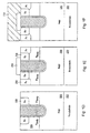
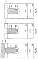
- Figs.1A - 1F illustrate a typical process of forming a trench MOSFET.
- the process starts with an N-epitaxial layer 220 grown on an N+ substrate 222 ( Fig. 1A ).
- a polysilicon-filled trench 224 is formed in N-epi layer 220 ( Fig. 1B ).
- the surface may or may not be planar depending on how the surface oxides are made in the process.
- a P body 226 is introduced, although the P-body 226 could be introduced prior to the formation of the trench 224 ( Fig. 1C ). Both process flows are manufacturable, but forming the trench first is preferable because the etching process can influence the doping concentrations in the P-body.
- N+ source region 228 is implanted ( Fig. 1D ).
- An optional shallow P+ region 230 is implanted to ohmic contact between the P-body and a metal layer to be deposited later.
- P+ region 230 can be implanted through an opening in an oxide layer 232 that is deposited across the region and then etched to form a contact mask.
- the contact mask may or may not be used to define the P+ region 232.
- a metal layer 234 is deposited on the surface to contact the N+ source region 228 and P+ region 230 ( Fig.1F ).
- the processes of the invention provide a "keyhole" shaped trench, wherein a thick dielectric layer extends some distance upward on the sidewalls of the trench.
- a relatively thick oxide lining is grown or deposited on the bottom and sidewalls of the trench.
- the trench is filled with polysilicon, and the polysilicon is then etched back such that only a portion remains at the bottom of the trench, overlying the oxide lining.
- the exposed oxide lining is removed from the sidewalls of the trench.
- the polysilicon is then partially oxidized by heating to form an oxide layer at its exposed surface, and during the same heating process an oxide layer is formed on the sidewalls of the trench.
- the trench is then subjected to an oxide etch, which removes the oxide layer formed from the polysilicon as well as some of the oxide layer from the sidewalls of the trench.
- the trench is then refilled with polysilicon to yield a keyhole-shaped gate electrode.
- a masking material such as photoresist is deposited over the oxide lining at the bottom of the trench.
- An oxide etch is then performed to removed the oxide lining from the sidewalls of the trench, and the masking material is removed from the bottom of the trench.
- a relatively thin gate oxide layer is grown on the sidewalls of the trench, and the trench is filled with a conductive material such as polysilicon which forms the gate electrode.
- a trench-gated semiconductor device having a dielectric layer separating the gate electrode from the semiconductor material surrounding the trench wherein the thickness of the dielectric layer is greater in a region at the bottom of the trench.
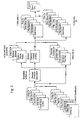
- Fig. 2 is a schematic diagram of several process flows that can be used to fabricate gate trenches in accordance with this invention. The details of these process flows are shown in Fig. 3 .
- Fig. 2 illustrates in block diagram form that the trench may be formed using a photoresist mask or a hard mask sequence, followed by a directed oxide deposition planarized by either a selective etch, a dipback, or a selective oxidization. A selective oxidization can be used without a directed deposition.
- the trench is filled with polysilicon using a one-step or two-step process.
- the trench is formed using a mask that is later removed, so that the mask is not available as a reference for other processing steps.
- the other option is to use a "hard" mask to form the trench, which is then employed as a reference later in the process.
- a sacrificial oxide layer is grown on the walls of the trench and then removed.
- An oxide lining may then be formed on the walls of the trench. This stage yields a trench having a uniform oxide layer on its walls, with or without a hard mask on the top surface of the silicon.
- a selective etchback can be performed, allowing thick oxide to remain at the bottom of the trench and removing the oxide from the sidewalls of the trench.
- a "dipback" to remove the oxide layer from the sidewalls of the trench.
- a selective oxidation wherby a polysilicon layer is formed at the bottom of the trench and then oxidized to form additional oxide at the bottom of the trench.
- the selective oxidation of a polysilicon layer can be performed instead of or in addition to the directed dielectric deposition.
- a trench has been fabricated with a thick oxide layer on the bottom. There may or may not be a "hard” mask on the top surface of the semiconductor.
- a thin oxide layer is grown on the walls of the trench and the trench is filled with polysilicon.
- the polysilicon may be deposited as a single layer or it can be deposited as two layers with an etchback between the depositions.
- Depositing the polysilicon in a two-stage process may be beneficial to the introduction of dopants into the "mesa" between the trenches, and to make a more lightly doped polysilicon layer available on the surface of the wafer to produce diodes, resistors, and other polysilicon devices. Finally a glass layer is deposited and contact openings are formed in the glass layer.
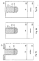
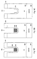
- Figs. 3A - 3N illustrate a process using the oxide "dipback" method.
- the process starts with an epi layer 262 formed on a substrate 260.
- a mask layer 264 is formed on the top surface of epi layer 262, with an opening where the trench is to be formed.
- Mask layer 264 may be photoresist or some other material and may be formed on top of an oxide layer 262.
- a trench 268 is then formed using conventional processes, as shown in Fig. 1A .
- a sacrificial oxide layer 270 has been formed on the surface of the trench. Sacrificial oxide layer 270 is then removed, as shown in Fig. 3C .
- Sacrificial oxide layer 270 could be from 100 ⁇ to 1000 ⁇ thick; typically, it would be in the range of 300 ⁇ thick. It can be formed by heating the structure at 800 °C to 1100 °C for 10 minutes to five hours in an oxidizing ambient.
- the ambient could be either oxygen or it could be oxygen and hydrogen. If the ambient is a combination of oxygen and hydrogen, it is considered a "wet" oxidation because the reaction would produce water vapor and this would affect the consistency and growth rate of the oxide.
- an oxide lining 272 is then formed on the walls of trench 268.
- Lining 272 could have a thickness in the range of 100 ⁇ to 600 ⁇ . Lining 272 prevents the deposited oxides from contacting the silicon directly, which would have the potential for charged states, especially at the interface between the silicon and the deposited oxide.. Adding a clean oxide layer on the walls of the trench provides a reduced charge state.
- an electric field is applied above the surface of epi layer 262, and dielectric ions are formed and directed downward into trench 268 by means of the electric field.
- a plasma-enhanced chemical vapour deposition chamber is used for this process.
- the electric field accelerates the dielectric ions downward so that they preferentially deposit on horizontal surfaces, including the bottom of trench 268.
- the chemical vapor deposition of oxide involves a gaseous chemical reaction of oxygen and silane, dichlorosilane, or silicon tetrachloride.
- the source of oxygen is typically nitreous oxide, and silane is typically the silicon source.
- Plasma-enhanced chemical vapour deposition machines are available from such companies as Novellus Systems and Applied Materials.
- Another method to achieve a directional deposition is to sputter a oxide film from an oxide-coated target onto the wafer. Since sputtering is a momentum transfer process, the deposition occurs in a straight line.
- oxide layer 270 has been formed inside and outside the trench 268. Note that oxide layer 270 is thicker at the bottom of trench 268 than on the sidewalls of trench 268. It is also thicker on the flat surfaces of epi layer 262. Processes other than chemical vapor deposition, such as sputtering, could also be used to produce oxide layer 270.
- Layer 270 could be formed of materials other than oxide, such as phosphorus-doped glass or boron phosphorus silicon glass. It could also consist of other materials having a low dielectric constant K, such as polymers or polyimide. Air bubbles could be incorporated in layer 270 to reduce its dielectric constant.
- oxide layer 270 has been etched back or dipped back to remove the portions on the sidewalls of trench 268. A bottom portion 274 of oxide layer 270 remains at the bottom of trench 268. As shown in Fig. 3H , the structure is then heated to form a thin oxide layer 276 on the sidewalls of trench 268. A polysilicon layer 278 is then deposited to fill trench 268 and overflow the top surface of the structure. This is shown in Fig. 3I .
- polysilicon layer 278 is then etched back until it is roughly coplanar with the top surface of epi layer 262.
- the portions of oxide layer 270 on the surface of epi layer 262 are removed, taking care not to etch too much of the oxide layer 276 on the sidewalls of the trench.
- the result of this step is shown in Fig. 3K . Avoiding the removal of oxide layer 276 is best performed by having polysilicon layer 278 protrude slightly above the oxide layer 276.
- the entire top surface of the structure, including the top surface of polysilicon layer 278, has been oxidized to form an oxide layer 280.
- a glass layer 282 is laid down over the surface of oxide layer 280, and glass layer 282 and oxide layer 280 are then patterned and etched to form contact openings to the epi layer 262, yielding the structure shown in Fig. 3N .
- Figs. 4 - 8 illustrate several embodiments in which the polysilicon gate is "keyhole"shaped in cross-section.
- the thicker gate oxide extends not only along the bottom of the trench but also along the sidewalls of the trench towards the junction between the P body region and the N epi layer.
- the thickened gate oxide along the sidewalls of the trench helps to soften the electric field at that junction.
- Fig. 4 shows a MOSFET having flat-bottomed P body regions and a diode cell incorporated at periodic intervals among the MOSFET cells.
- a keyhole-shaped gate is employed.
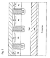
- Fig. 5 shows an embodiment where the P body does not extend to the surface but instead is contacted in the third dimension.
- a shallow P+ region is shown within the mesa at a depth greater than the N+ source regions.
- Fig. 6 shows an embodiment wherein the trenches extend into an N buried layer formed at the interface between the epi layer and the substrate.
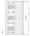
- Fig. 7 shows an embodiment where the P body is contacted in the third dimension, and the trenches extend into an N buried layer.
- FIGs. 8A-8L A process sequence for forming a device having a keyhole shaped trench is illustrated in Figs. 8A-8L .
- the process starts with an epi layer 602 grown on a substrate 600.
- An oxide layer 604 is formed at the top surface of epi layer 602, as shown in Fig. 8A .
- Oxide layer 604 is patterned and a trench 606 is etched, as shown in Fig. 8B .
- a sacrificial oxide layer (not shown) is formed on the walls of the trench and removed.
- An oxide lining 608 is then grown on the walls of trench 606 (as shown in Fig. 8C ).
- a polysilicon layer 610 is deposited to fill the trench 606 and then etched back such that a portion 612 remains at the bottom of the trench.
- the oxide lining 608 is then etched from the walls of the trench 606, as shown in Fig. 8F .
- An anisotropic silicon etch is then performed to depress the top surface of polysilicon portion 612 below the top surface of oxide lining 608, as shown in Fig. 8G .
- a thermal oxidation process is then applied, forming an oxide layer 616 on the walls of the trench 606 and an oxide layer 618 at the top surface of polysilicon portion 612. The result is shown in Fig. 8H .
- Oxide layer 618 is then etched, a portion of oxide layer 616 being removed in the process, producing the structure shown in Fig.8I .
- a second polysilicon layer 619 is then deposited over the entire structure, as shown in Fig. 8J .
- Polysilicon layer 619 is etched back, as shown in Fig. 8K .
- the top surface of polysilicon layer 619 is then oxidized, as shown in Fig. 8L .
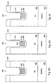
- FIGs. 9A-9F A variation of this process is illustrated in Figs. 9A-9F .
- a photoresist layer is applied, developed, and washed away, leaving only a portion 630 at the bottom of the trench 606. This is shown in Fig. 9A .
- Oxide lining 608 is then etched from the walls of the trench 606, as shown in Fig.9B and the portion 630 of the photoresist layer is removed from the bottom of the trench. This yields the structure shown in Fig.9C .
- a gate oxide layer 632 is thermally grown on the walls of trench 606, and trench 606 is filled with a polysilicon layer 634, as shown in Figs. 9D and 9E .
- Polysilicon layer 634 is etched back to the level of the top surface of the epi layer 602. Polysilicon layer 634 is then oxidized thermally to produce the device shown in Fig. 9F .
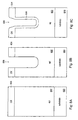
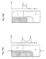
- Figs. 10A-10C show a comparison of the strength of the electric field along the sidewall of the trench in a prior art trench device with the strength of the electric field in embodiments of this invention.
- Fig. 9A shows that in the prior art device the electric field has two sharp peaks which occur, respectively, at the body-drain junction and the bottom of the gate electrode.
- Fig. 10B shows a device having a thick oxide layer on the bottom of the trench. As indicated, the electric field still has a sharp peak at the body-drain junction but the peak at the bottom of the gate electrode is somewhat lower than in the prior art device.
- Fig. 10C shows a device having a keyhole shaped gate electrode. In this case, the electric field still reaches a peak at the body-drain junction, but the sharp peak at the bottom of the gate electrode is eliminated.
Applications Claiming Priority (2)
| Application Number | Priority Date | Filing Date | Title |
|---|---|---|---|
| US09/318,403 US6291298B1 (en) | 1999-05-25 | 1999-05-25 | Process of manufacturing Trench gate semiconductor device having gate oxide layer with multiple thicknesses |
| EP00932771A EP1186019B1 (fr) | 1999-05-25 | 2000-05-24 | Dispositif semi-conducteur a tranchees pourvu d'une couche d'oxyde de grille a profondeurs multiples et procedes de fabrication correspondants |
Related Parent Applications (2)
| Application Number | Title | Priority Date | Filing Date |
|---|---|---|---|
| EP00932771A Division EP1186019B1 (fr) | 1999-05-25 | 2000-05-24 | Dispositif semi-conducteur a tranchees pourvu d'une couche d'oxyde de grille a profondeurs multiples et procedes de fabrication correspondants |
| EP00932771.9 Division | 2000-05-24 |
Publications (3)
| Publication Number | Publication Date |
|---|---|
| EP2020681A2 true EP2020681A2 (fr) | 2009-02-04 |
| EP2020681A3 EP2020681A3 (fr) | 2009-06-10 |
| EP2020681B1 EP2020681B1 (fr) | 2011-09-14 |
Family
ID=23238055
Family Applications (2)
| Application Number | Title | Priority Date | Filing Date |
|---|---|---|---|
| EP00932771A Expired - Lifetime EP1186019B1 (fr) | 1999-05-25 | 2000-05-24 | Dispositif semi-conducteur a tranchees pourvu d'une couche d'oxyde de grille a profondeurs multiples et procedes de fabrication correspondants |
| EP08016928A Expired - Lifetime EP2020681B1 (fr) | 1999-05-25 | 2000-05-24 | Procédé de fabrication d'un dispositif semi-conducteur à grille en tranchée |
Family Applications Before (1)
| Application Number | Title | Priority Date | Filing Date |
|---|---|---|---|
| EP00932771A Expired - Lifetime EP1186019B1 (fr) | 1999-05-25 | 2000-05-24 | Dispositif semi-conducteur a tranchees pourvu d'une couche d'oxyde de grille a profondeurs multiples et procedes de fabrication correspondants |
Country Status (9)
| Country | Link |
|---|---|
| US (6) | US6291298B1 (fr) |
| EP (2) | EP1186019B1 (fr) |
| JP (1) | JP4834228B2 (fr) |
| KR (1) | KR100700322B1 (fr) |
| CN (1) | CN1205658C (fr) |
| AU (1) | AU5044600A (fr) |
| DE (1) | DE60044396D1 (fr) |
| TW (1) | TW457629B (fr) |
| WO (1) | WO2000072372A1 (fr) |
Families Citing this family (170)
| Publication number | Priority date | Publication date | Assignee | Title |
|---|---|---|---|---|
| US7084456B2 (en) * | 1999-05-25 | 2006-08-01 | Advanced Analogic Technologies, Inc. | Trench MOSFET with recessed clamping diode using graded doping |
| US6291298B1 (en) * | 1999-05-25 | 2001-09-18 | Advanced Analogic Technologies, Inc. | Process of manufacturing Trench gate semiconductor device having gate oxide layer with multiple thicknesses |
| TW442972B (en) * | 1999-10-01 | 2001-06-23 | Anpec Electronics Corp | Fabricating method of trench-type gate power metal oxide semiconductor field effect transistor |
| US6825087B1 (en) | 1999-11-24 | 2004-11-30 | Fairchild Semiconductor Corporation | Hydrogen anneal for creating an enhanced trench for trench MOSFETS |
| US20030017164A1 (en) | 2001-07-03 | 2003-01-23 | Mallinckrodt Inc. | Dye-azide compounds for dual phototherapy |
| TW479363B (en) * | 2000-03-17 | 2002-03-11 | Gen Semiconductor Inc | Trench DMOS transistor having a double gate structure |
| US6391699B1 (en) * | 2000-06-05 | 2002-05-21 | Fairchild Semiconductor Corporation | Method of manufacturing a trench MOSFET using selective growth epitaxy |
| JP2002043573A (ja) * | 2000-07-28 | 2002-02-08 | Toyota Motor Corp | 半導体装置および半導体装置の製造方法 |
| US7745289B2 (en) | 2000-08-16 | 2010-06-29 | Fairchild Semiconductor Corporation | Method of forming a FET having ultra-low on-resistance and low gate charge |
| US6509233B2 (en) | 2000-10-13 | 2003-01-21 | Siliconix Incorporated | Method of making trench-gated MOSFET having cesium gate oxide layer |
| KR100338783B1 (en) * | 2000-10-28 | 2002-06-01 | Samsung Electronics Co Ltd | Semiconductor device having expanded effective width of active region and fabricating method thereof |
| US6730606B1 (en) * | 2000-11-03 | 2004-05-04 | Semiconductor Components Industries, L.L.C. | Trench growth techniques using selective epitaxy |
| US6368912B1 (en) * | 2000-12-08 | 2002-04-09 | Nanya Technology Corporation | Method of fabricating an isolation structure between a vertical transistor and a deep trench capacitor |
| US6916745B2 (en) | 2003-05-20 | 2005-07-12 | Fairchild Semiconductor Corporation | Structure and method for forming a trench MOSFET having self-aligned features |
| US6818513B2 (en) | 2001-01-30 | 2004-11-16 | Fairchild Semiconductor Corporation | Method of forming a field effect transistor having a lateral depletion structure |
| US6803626B2 (en) | 2002-07-18 | 2004-10-12 | Fairchild Semiconductor Corporation | Vertical charge control semiconductor device |
| JP4073176B2 (ja) | 2001-04-02 | 2008-04-09 | 新電元工業株式会社 | 半導体装置およびその製造方法 |
| US7291884B2 (en) * | 2001-07-03 | 2007-11-06 | Siliconix Incorporated | Trench MIS device having implanted drain-drift region and thick bottom oxide |
| US7033876B2 (en) | 2001-07-03 | 2006-04-25 | Siliconix Incorporated | Trench MIS device having implanted drain-drift region and thick bottom oxide and process for manufacturing the same |
| US20060038223A1 (en) * | 2001-07-03 | 2006-02-23 | Siliconix Incorporated | Trench MOSFET having drain-drift region comprising stack of implanted regions |
| US6764906B2 (en) | 2001-07-03 | 2004-07-20 | Siliconix Incorporated | Method for making trench mosfet having implanted drain-drift region |
| US7009247B2 (en) * | 2001-07-03 | 2006-03-07 | Siliconix Incorporated | Trench MIS device with thick oxide layer in bottom of gate contact trench |
| US6849898B2 (en) * | 2001-08-10 | 2005-02-01 | Siliconix Incorporated | Trench MIS device with active trench corners and thick bottom oxide |
| US6882000B2 (en) * | 2001-08-10 | 2005-04-19 | Siliconix Incorporated | Trench MIS device with reduced gate-to-drain capacitance |
| EP1302987A1 (fr) * | 2001-10-16 | 2003-04-16 | Siliconix, Inc. | MOSFET vertical à grille en tranchée avec une couche d'oxyde contenant cesium et son procédé de fabrication |
| US6674124B2 (en) * | 2001-11-15 | 2004-01-06 | General Semiconductor, Inc. | Trench MOSFET having low gate charge |
| JP3891090B2 (ja) * | 2001-12-06 | 2007-03-07 | 株式会社デンソー | 還流ダイオードおよび負荷駆動回路 |
| GB0129450D0 (en) * | 2001-12-08 | 2002-01-30 | Koninkl Philips Electronics Nv | Trenched semiconductor devices and their manufacture |
| DE10207309B4 (de) * | 2002-02-21 | 2015-07-23 | Infineon Technologies Ag | MOS-Transistoreinrichtung |
| TWI248136B (en) * | 2002-03-19 | 2006-01-21 | Infineon Technologies Ag | Method for fabricating a transistor arrangement having trench transistor cells having a field electrode |
| KR100878220B1 (ko) * | 2002-05-24 | 2009-01-13 | 삼성전자주식회사 | 액정표시장치 |
| KR100845227B1 (ko) * | 2002-06-27 | 2008-07-09 | 매그나칩 반도체 유한회사 | 소자 분리막 형성 방법 |
| US6855985B2 (en) * | 2002-09-29 | 2005-02-15 | Advanced Analogic Technologies, Inc. | Modular bipolar-CMOS-DMOS analog integrated circuit & power transistor technology |
| US7576388B1 (en) | 2002-10-03 | 2009-08-18 | Fairchild Semiconductor Corporation | Trench-gate LDMOS structures |
| US6710418B1 (en) | 2002-10-11 | 2004-03-23 | Fairchild Semiconductor Corporation | Schottky rectifier with insulation-filled trenches and method of forming the same |
| WO2004055884A1 (fr) | 2002-12-14 | 2004-07-01 | Koninklijke Philips Electronics N.V. | Fabrication d'un dispositif a semi-conducteurs a tranchees et a grille |
| GB0229210D0 (en) * | 2002-12-14 | 2003-01-22 | Koninkl Philips Electronics Nv | Method of manufacture of a trench semiconductor device |
| GB0229212D0 (en) | 2002-12-14 | 2003-01-22 | Koninkl Philips Electronics Nv | Method of manufacture of a trench semiconductor device |
| ES2578678T3 (es) * | 2003-01-21 | 2016-07-29 | Ambixtra (Pty) Ltd | Dispositivo semiconductor de puerta aislada de potencia de conmutación rápida |
| US6861701B2 (en) * | 2003-03-05 | 2005-03-01 | Advanced Analogic Technologies, Inc. | Trench power MOSFET with planarized gate bus |
| US6939817B2 (en) * | 2003-05-08 | 2005-09-06 | Micron Technology, Inc. | Removal of carbon from an insulative layer using ozone |
| US7638841B2 (en) | 2003-05-20 | 2009-12-29 | Fairchild Semiconductor Corporation | Power semiconductor devices and methods of manufacture |
| US7754550B2 (en) * | 2003-07-10 | 2010-07-13 | International Rectifier Corporation | Process for forming thick oxides on Si or SiC for semiconductor devices |
| JP3954541B2 (ja) * | 2003-08-05 | 2007-08-08 | 株式会社東芝 | 半導体装置及びその製造方法 |
| KR100994719B1 (ko) | 2003-11-28 | 2010-11-16 | 페어차일드코리아반도체 주식회사 | 슈퍼정션 반도체장치 |
| US7368777B2 (en) | 2003-12-30 | 2008-05-06 | Fairchild Semiconductor Corporation | Accumulation device with charge balance structure and method of forming the same |
| DE10361697B4 (de) * | 2003-12-30 | 2011-08-11 | Infineon Technologies AG, 81669 | Verfahren zum Herstellen einer Grabenstruktur mit Oxidationsauskleidung, zum Herstellen einer integrierten Halbleiterschaltungsanordnung oder eines Chips, zum Herstellen eines Halbleiterbauelements sowie mit diesem Verfahren hergestellte integrierte Halbleiterschaltungsanordnung, hergestellter Chip, hergestelltes Halbleiterbauelement |
| KR100545177B1 (ko) * | 2003-12-31 | 2006-01-24 | 동부아남반도체 주식회사 | 반도체 소자의 소자 분리막 및 그의 제조 방법 |
| JP2005340626A (ja) * | 2004-05-28 | 2005-12-08 | Toshiba Corp | 半導体装置 |
| US7268395B2 (en) | 2004-06-04 | 2007-09-11 | International Rectifier Corporation | Deep trench super switch device |
| US7417266B1 (en) * | 2004-06-10 | 2008-08-26 | Qspeed Semiconductor Inc. | MOSFET having a JFET embedded as a body diode |
| WO2006011882A1 (fr) | 2004-06-30 | 2006-02-02 | Advanced Analogic Technologies, Inc. | Transistor mos a tranches comprenant une diode de blocage |
| US7352036B2 (en) | 2004-08-03 | 2008-04-01 | Fairchild Semiconductor Corporation | Semiconductor power device having a top-side drain using a sinker trench |
| JP4791723B2 (ja) * | 2004-10-18 | 2011-10-12 | 株式会社東芝 | 半導体装置及びその製造方法 |
| US7371641B2 (en) * | 2004-10-29 | 2008-05-13 | International Rectifier Corporation | Method of making a trench MOSFET with deposited oxide |
| US20060163650A1 (en) * | 2005-01-27 | 2006-07-27 | Ling Ma | Power semiconductor device with endless gate trenches |
| KR100729923B1 (ko) * | 2005-03-31 | 2007-06-18 | 주식회사 하이닉스반도체 | 스텝 sti 프로파일을 이용한 낸드 플래쉬 메모리 소자의트랜지스터 형성방법 |
| CN101882583A (zh) | 2005-04-06 | 2010-11-10 | 飞兆半导体公司 | 沟栅场效应晶体管及其形成方法 |
| US8115252B2 (en) * | 2005-05-12 | 2012-02-14 | M-Mos Sdn.Bhd | Elimination of gate oxide weak spot in deep trench |
| JP4955222B2 (ja) | 2005-05-20 | 2012-06-20 | ルネサスエレクトロニクス株式会社 | 半導体装置の製造方法 |
| AT504290A2 (de) | 2005-06-10 | 2008-04-15 | Fairchild Semiconductor | Feldeffekttransistor mit ladungsgleichgewicht |
| EP1742257B1 (fr) * | 2005-07-08 | 2012-09-05 | STMicroelectronics Srl | Méthode de fabrication d'un dispositif semi-conducteur de puissance |
| US7943990B2 (en) * | 2005-08-17 | 2011-05-17 | International Rectifier Corporation | Power semiconductor device with interconnected gate trenches |
| CN101506956A (zh) * | 2005-08-17 | 2009-08-12 | 国际整流器公司 | 半导体设备的制作方法 |
| JP4622905B2 (ja) * | 2006-03-24 | 2011-02-02 | トヨタ自動車株式会社 | 絶縁ゲート型半導体装置の製造方法 |
| US7446374B2 (en) | 2006-03-24 | 2008-11-04 | Fairchild Semiconductor Corporation | High density trench FET with integrated Schottky diode and method of manufacture |
| US7319256B1 (en) | 2006-06-19 | 2008-01-15 | Fairchild Semiconductor Corporation | Shielded gate trench FET with the shield and gate electrodes being connected together |
| US8642441B1 (en) * | 2006-12-15 | 2014-02-04 | Spansion Llc | Self-aligned STI with single poly for manufacturing a flash memory device |
| KR100824205B1 (ko) * | 2006-12-26 | 2008-04-21 | 매그나칩 반도체 유한회사 | Dmos 트랜지스터 및 그 제조방법 |
| US7723172B2 (en) * | 2007-04-23 | 2010-05-25 | Icemos Technology Ltd. | Methods for manufacturing a trench type semiconductor device having a thermally sensitive refill material |
| JP5183959B2 (ja) * | 2007-04-23 | 2013-04-17 | 新日本無線株式会社 | Mosfet型半導体装置の製造方法 |
| US8222874B2 (en) | 2007-06-26 | 2012-07-17 | Vishay-Siliconix | Current mode boost converter using slope compensation |
| US8129779B2 (en) * | 2007-09-03 | 2012-03-06 | Rohm Co., Ltd. | Trench gate type VDMOSFET device with thicker gate insulation layer portion for reducing gate to source capacitance |
| WO2009039441A1 (fr) | 2007-09-21 | 2009-03-26 | Fairchild Semiconductor Corporation | Structures à superjonction pour dispositifs de puissance et procédés de fabrication |
| WO2009041742A1 (fr) | 2007-09-28 | 2009-04-02 | Sanyo Electric Co., Ltd. | Transistor du type grille en tranchée et procédé de production dudit transistor |
| JP2009088188A (ja) * | 2007-09-28 | 2009-04-23 | Sanyo Electric Co Ltd | トレンチゲート型トランジスタ及びその製造方法 |
| TWI383500B (zh) * | 2007-10-12 | 2013-01-21 | Promos Technologies Inc | 功率金氧半導體陣列 |
| TW200921912A (en) * | 2007-11-05 | 2009-05-16 | Anpec Electronics Corp | Power transistor capable of decreasing capacitance between gate and drain |
| KR100970282B1 (ko) * | 2007-11-19 | 2010-07-15 | 매그나칩 반도체 유한회사 | 트렌치 mosfet 및 그 제조방법 |
| JP5266738B2 (ja) * | 2007-12-05 | 2013-08-21 | トヨタ自動車株式会社 | トレンチゲート型半導体装置の製造方法 |
| US20100013009A1 (en) * | 2007-12-14 | 2010-01-21 | James Pan | Structure and Method for Forming Trench Gate Transistors with Low Gate Resistance |
| US7772668B2 (en) | 2007-12-26 | 2010-08-10 | Fairchild Semiconductor Corporation | Shielded gate trench FET with multiple channels |
| JP2009182114A (ja) * | 2008-01-30 | 2009-08-13 | Elpida Memory Inc | 半導体装置およびその製造方法 |
| JP5452876B2 (ja) * | 2008-03-13 | 2014-03-26 | ローム株式会社 | 半導体装置およびその製造方法 |
| KR101535222B1 (ko) * | 2008-04-17 | 2015-07-08 | 삼성전자주식회사 | 반도체 소자 및 그의 제조 방법 |
| US7838389B2 (en) * | 2008-05-30 | 2010-11-23 | Freescale Semiconductor, Inc. | Enclosed void cavity for low dielectric constant insulator |
| US7919388B2 (en) * | 2008-05-30 | 2011-04-05 | Freescale Semiconductor, Inc. | Methods for fabricating semiconductor devices having reduced gate-drain capacitance |
| US7807576B2 (en) * | 2008-06-20 | 2010-10-05 | Fairchild Semiconductor Corporation | Structure and method for forming a thick bottom dielectric (TBD) for trench-gate devices |
| US8642459B2 (en) * | 2008-08-28 | 2014-02-04 | Infineon Technologies Ag | Method for forming a semiconductor device with an isolation region on a gate electrode |
| TWI414019B (zh) * | 2008-09-11 | 2013-11-01 | He Jian Technology Suzhou Co Ltd | 一種閘氧化層的製造方法 |
| US20120273916A1 (en) | 2011-04-27 | 2012-11-01 | Yedinak Joseph A | Superjunction Structures for Power Devices and Methods of Manufacture |
| US7910983B2 (en) * | 2008-09-30 | 2011-03-22 | Infineon Technologies Austria Ag | MOS transistor having an increased gate-drain capacitance |
| TWI435447B (zh) * | 2009-01-09 | 2014-04-21 | Niko Semiconductor Co Ltd | 功率金氧半導體場效電晶體及其製造方法 |
| US8426275B2 (en) * | 2009-01-09 | 2013-04-23 | Niko Semiconductor Co., Ltd. | Fabrication method of trenched power MOSFET |
| CN101859700B (zh) * | 2009-04-09 | 2012-05-30 | 上海先进半导体制造股份有限公司 | 多晶硅淀积工艺 |
| CN101866849B (zh) * | 2009-04-16 | 2012-06-27 | 上海华虹Nec电子有限公司 | 在沟槽底部制备氧化膜的方法 |
| JP5613995B2 (ja) * | 2009-04-28 | 2014-10-29 | 富士電機株式会社 | 炭化珪素半導体装置およびその製造方法 |
| CN101887852B (zh) * | 2009-05-13 | 2012-08-01 | 上海华虹Nec电子有限公司 | 深沟槽填充方法 |
| US8058670B2 (en) * | 2009-06-04 | 2011-11-15 | Force—MOS Technology Corporation | Insulated gate bipolar transistor (IGBT) with monolithic deep body clamp diode to prevent latch-up |
| US8264066B2 (en) * | 2009-07-08 | 2012-09-11 | Taiwan Semiconductor Manufacturing Company, Ltd. | Liner formation in 3DIC structures |
| US9425305B2 (en) | 2009-10-20 | 2016-08-23 | Vishay-Siliconix | Structures of and methods of fabricating split gate MIS devices |
| US9419129B2 (en) | 2009-10-21 | 2016-08-16 | Vishay-Siliconix | Split gate semiconductor device with curved gate oxide profile |
| US8129778B2 (en) * | 2009-12-02 | 2012-03-06 | Fairchild Semiconductor Corporation | Semiconductor devices and methods for making the same |
| CN102097378B (zh) * | 2009-12-10 | 2013-12-04 | 力士科技股份有限公司 | 一种沟槽金属氧化物半导体场效应管的制造方法 |
| US20110198689A1 (en) * | 2010-02-17 | 2011-08-18 | Suku Kim | Semiconductor devices containing trench mosfets with superjunctions |
| CN102859699B (zh) | 2010-03-02 | 2016-01-06 | 维西埃-硅化物公司 | 制造双栅极装置的结构和方法 |
| US8378392B2 (en) * | 2010-04-07 | 2013-02-19 | Force Mos Technology Co., Ltd. | Trench MOSFET with body region having concave-arc shape |
| US8319290B2 (en) | 2010-06-18 | 2012-11-27 | Fairchild Semiconductor Corporation | Trench MOS barrier schottky rectifier with a planar surface using CMP techniques |
| CN102024848A (zh) * | 2010-11-04 | 2011-04-20 | 天津环鑫科技发展有限公司 | 用于功率器件的沟槽结构及其制造方法 |
| US8415747B2 (en) * | 2010-12-28 | 2013-04-09 | Infineon Technologies Austria Ag | Semiconductor device including diode |
| US8598654B2 (en) | 2011-03-16 | 2013-12-03 | Fairchild Semiconductor Corporation | MOSFET device with thick trench bottom oxide |
| US8772868B2 (en) | 2011-04-27 | 2014-07-08 | Fairchild Semiconductor Corporation | Superjunction structures for power devices and methods of manufacture |
| US8786010B2 (en) | 2011-04-27 | 2014-07-22 | Fairchild Semiconductor Corporation | Superjunction structures for power devices and methods of manufacture |
| US8673700B2 (en) | 2011-04-27 | 2014-03-18 | Fairchild Semiconductor Corporation | Superjunction structures for power devices and methods of manufacture |
| US8836028B2 (en) | 2011-04-27 | 2014-09-16 | Fairchild Semiconductor Corporation | Superjunction structures for power devices and methods of manufacture |
| CN103688363B (zh) | 2011-05-18 | 2017-08-04 | 威世硅尼克斯公司 | 半导体器件 |
| US20130023097A1 (en) * | 2011-07-14 | 2013-01-24 | Purtell Robert J | U-mos trench profile optimization and etch damage removal using microwaves |
| TWI413193B (zh) * | 2011-08-11 | 2013-10-21 | Super Group Semiconductor Co Ltd | 溝槽式功率金氧半場效電晶體之製作方法 |
| KR101776319B1 (ko) | 2011-08-23 | 2017-09-08 | 현대자동차주식회사 | 반도체 소자 |
| CN103000521B (zh) * | 2011-09-13 | 2015-05-27 | 帅群微电子股份有限公司 | 沟槽式功率金氧半场效晶体管的制作方法 |
| JP5704039B2 (ja) * | 2011-10-06 | 2015-04-22 | 信越半導体株式会社 | 貼り合わせsoiウェーハの製造方法 |
| US8633094B2 (en) | 2011-12-01 | 2014-01-21 | Power Integrations, Inc. | GaN high voltage HFET with passivation plus gate dielectric multilayer structure |
| US8940620B2 (en) | 2011-12-15 | 2015-01-27 | Power Integrations, Inc. | Composite wafer for fabrication of semiconductor devices |
| CN103247529B (zh) * | 2012-02-10 | 2016-08-03 | 无锡华润上华半导体有限公司 | 一种沟槽场效应器件及其制作方法 |
| US8946814B2 (en) | 2012-04-05 | 2015-02-03 | Icemos Technology Ltd. | Superjunction devices having narrow surface layout of terminal structures, buried contact regions and trench gates |
| US8642425B2 (en) * | 2012-05-29 | 2014-02-04 | Semiconductor Components Industries, Llc | Method of making an insulated gate semiconductor device and structure |
| JP2013258333A (ja) * | 2012-06-13 | 2013-12-26 | Toshiba Corp | 電力用半導体装置 |
| CN103578952B (zh) * | 2012-08-09 | 2016-12-28 | 中国科学院微电子研究所 | 半导体器件制造方法 |
| JP5811973B2 (ja) * | 2012-09-12 | 2015-11-11 | 住友電気工業株式会社 | 炭化珪素半導体装置の製造方法 |
| JP6056292B2 (ja) * | 2012-09-12 | 2017-01-11 | 住友電気工業株式会社 | 炭化珪素半導体装置の製造方法 |
| JP2014056913A (ja) | 2012-09-12 | 2014-03-27 | Sumitomo Electric Ind Ltd | 炭化珪素半導体装置 |
| CN103824764A (zh) * | 2012-11-19 | 2014-05-28 | 上海华虹宏力半导体制造有限公司 | 一种沟槽型mos器件中沟槽栅的制备方法 |
| TWI521693B (zh) | 2012-11-27 | 2016-02-11 | 財團法人工業技術研究院 | 蕭基能障二極體及其製造方法 |
| CN103943503A (zh) * | 2013-01-23 | 2014-07-23 | 上海华虹宏力半导体制造有限公司 | Mosfet的bto结构制造工艺方法 |
| US8928037B2 (en) | 2013-02-28 | 2015-01-06 | Power Integrations, Inc. | Heterostructure power transistor with AlSiN passivation layer |
| US9349856B2 (en) * | 2013-03-26 | 2016-05-24 | Toyoda Gosei Co., Ltd. | Semiconductor device including first interface and second interface as an upper surface of a convex protruded from first interface and manufacturing device thereof |
| US10249721B2 (en) | 2013-04-04 | 2019-04-02 | Infineon Technologies Austria Ag | Semiconductor device including a gate trench and a source trench |
| JP2014207403A (ja) * | 2013-04-16 | 2014-10-30 | 住友電気工業株式会社 | 炭化珪素半導体装置の製造方法 |
| JP6131689B2 (ja) * | 2013-04-16 | 2017-05-24 | 住友電気工業株式会社 | 炭化珪素半導体装置の製造方法 |
| CN103311112B (zh) * | 2013-06-14 | 2016-01-27 | 矽力杰半导体技术(杭州)有限公司 | 在沟槽内形成多晶硅的方法 |
| US9570570B2 (en) * | 2013-07-17 | 2017-02-14 | Cree, Inc. | Enhanced gate dielectric for a field effect device with a trenched gate |
| US9666663B2 (en) | 2013-08-09 | 2017-05-30 | Infineon Technologies Ag | Semiconductor device with cell trench structures and contacts and method of manufacturing a semiconductor device |
| CN104008975A (zh) * | 2014-06-09 | 2014-08-27 | 苏州东微半导体有限公司 | 一种沟槽型功率mos晶体管的制造方法 |
| CN104008976A (zh) * | 2014-06-09 | 2014-08-27 | 苏州东微半导体有限公司 | 一种沟槽功率器件的制造方法 |
| CN104022041A (zh) * | 2014-06-09 | 2014-09-03 | 苏州东微半导体有限公司 | 一种沟槽型mos晶体管的制造方法 |
| EP3183753A4 (fr) | 2014-08-19 | 2018-01-10 | Vishay-Siliconix | Circuit électronique |
| CN105632931B (zh) | 2014-11-04 | 2020-04-28 | 台湾积体电路制造股份有限公司 | 半导体器件的制造方法及半导体器件 |
| JP6514035B2 (ja) * | 2015-05-27 | 2019-05-15 | 株式会社豊田中央研究所 | 半導体装置 |
| CN106910767A (zh) * | 2015-12-23 | 2017-06-30 | 株洲南车时代电气股份有限公司 | 沟槽栅igbt制作方法及沟槽栅igbt |
| CN105514022B (zh) * | 2015-12-31 | 2018-04-17 | 上海华虹宏力半导体制造有限公司 | 在沟槽内部表面形成场氧化硅的方法 |
| CN105702570A (zh) * | 2016-01-29 | 2016-06-22 | 上海华虹宏力半导体制造有限公司 | 沟槽型mos器件中沟槽底部形成屏蔽膜层的方法 |
| TWI715711B (zh) * | 2017-01-25 | 2021-01-11 | 聯華電子股份有限公司 | 半導體元件及其製造方法 |
| JP6724844B2 (ja) * | 2017-03-30 | 2020-07-15 | 豊田合成株式会社 | 半導体装置 |
| DE102017108738B4 (de) * | 2017-04-24 | 2022-01-27 | Infineon Technologies Ag | SiC-HALBLEITERVORRICHTUNG MIT EINEM VERSATZ IN EINEM GRABENBODEN UND HERSTELLUNGSVERFAHREN HIERFÜR |
| KR102471277B1 (ko) | 2018-09-19 | 2022-11-28 | 삼성전자주식회사 | 게이트 절연층을 갖는 반도체 소자 |
| US11217541B2 (en) | 2019-05-08 | 2022-01-04 | Vishay-Siliconix, LLC | Transistors with electrically active chip seal ring and methods of manufacture |
| CN112447507A (zh) * | 2019-08-30 | 2021-03-05 | 株洲中车时代半导体有限公司 | 一种提高沟槽栅击穿特性的goi测试样片制造方法 |
| US11218144B2 (en) | 2019-09-12 | 2022-01-04 | Vishay-Siliconix, LLC | Semiconductor device with multiple independent gates |
| CN111180316A (zh) * | 2020-02-22 | 2020-05-19 | 重庆伟特森电子科技有限公司 | 一种碳化硅厚底氧化层沟槽mos制备方法 |
| CN111489961A (zh) * | 2020-04-17 | 2020-08-04 | 重庆伟特森电子科技有限公司 | 沟槽转角处栅氧具有高场强承受力的SiC-MOSFET栅的制备方法 |
| CN111489963B (zh) * | 2020-04-17 | 2023-04-18 | 重庆伟特森电子科技有限公司 | 一种沟槽转角处具有厚栅氧化层的SiC-MOSFET栅的制备方法 |
| CN111477679B (zh) * | 2020-04-17 | 2023-06-13 | 重庆伟特森电子科技有限公司 | 不对称沟槽型SiC-MOSFET栅的制备方法 |
| CN111403487B (zh) * | 2020-05-07 | 2024-02-06 | 创能动力科技有限公司 | 一种集成mosfet及二极管的半导体装置及其制造方法 |
| US11527618B2 (en) | 2020-07-18 | 2022-12-13 | Semiconductor Components Industries, Llc | Up-diffusion suppression in a power MOSFET |
| US11855140B2 (en) | 2020-09-29 | 2023-12-26 | Taiwan Semiconductor Manufacturing Co., Ltd. | Gate oxide of nanostructure transistor with increased corner thickness |
| CN112309975B (zh) * | 2020-10-27 | 2024-02-02 | 杭州士兰微电子股份有限公司 | 双向功率器件的制造方法 |
| CN113066867B (zh) * | 2021-03-15 | 2022-09-09 | 无锡新洁能股份有限公司 | 高可靠的碳化硅mosfet器件及其工艺方法 |
| US11302776B1 (en) | 2021-05-31 | 2022-04-12 | Genesic Semiconductor Inc. | Method and manufacture of robust, high-performance devices |
| US11830943B2 (en) * | 2021-07-26 | 2023-11-28 | Analog Power Conversion LLC | RF SiC MOSFET with recessed gate dielectric |
| CN115513061A (zh) * | 2022-11-22 | 2022-12-23 | 广东芯粤能半导体有限公司 | 半导体结构的制备方法及半导体结构 |
Family Cites Families (53)
| Publication number | Priority date | Publication date | Assignee | Title |
|---|---|---|---|---|
| US78814A (en) * | 1868-06-09 | John p | ||
| JP2647884B2 (ja) * | 1988-01-27 | 1997-08-27 | 株式会社日立製作所 | 半導体装置の製造方法 |
| US4967245A (en) * | 1988-03-14 | 1990-10-30 | Siliconix Incorporated | Trench power MOSFET device |
| US5283201A (en) * | 1988-05-17 | 1994-02-01 | Advanced Power Technology, Inc. | High density power device fabrication process |
| JPH06232163A (ja) * | 1993-02-05 | 1994-08-19 | Omron Corp | 縦型mosfet装置及びその製造方法 |
| US5357397A (en) | 1993-03-15 | 1994-10-18 | Hewlett-Packard Company | Electric field emitter device for electrostatic discharge protection of integrated circuits |
| US5843581A (en) * | 1993-06-03 | 1998-12-01 | Cryovac, Inc. | Barrier blend and food packaging film containing the blend |
| US5726084A (en) * | 1993-06-24 | 1998-03-10 | Northern Telecom Limited | Method for forming integrated circuit structure |
| JPH07122749A (ja) * | 1993-09-01 | 1995-05-12 | Toshiba Corp | 半導体装置及びその製造方法 |
| US5529943A (en) * | 1994-09-30 | 1996-06-25 | United Microelectronics Corporation | Method of making buried bit line ROM with low bit line resistance |
| FR2738394B1 (fr) * | 1995-09-06 | 1998-06-26 | Nippon Denso Co | Dispositif a semi-conducteur en carbure de silicium, et son procede de fabrication |
| KR0159075B1 (ko) * | 1995-11-11 | 1998-12-01 | 김광호 | 트렌치 dmos장치 및 그의 제조방법 |
| JPH09181304A (ja) * | 1995-12-21 | 1997-07-11 | Toyota Motor Corp | 半導体装置及びその製造方法 |
| US5637898A (en) * | 1995-12-22 | 1997-06-10 | North Carolina State University | Vertical field effect transistors having improved breakdown voltage capability and low on-state resistance |
| JPH09246550A (ja) * | 1996-03-05 | 1997-09-19 | Toyota Central Res & Dev Lab Inc | 半導体装置,半導体装置の製造方法,絶縁ゲート型半導体装置および絶縁ゲート型半導体装置の製造方法 |
| JPH09266309A (ja) * | 1996-03-27 | 1997-10-07 | Toyota Central Res & Dev Lab Inc | 半導体装置およびその製造方法 |
| US5770878A (en) * | 1996-04-10 | 1998-06-23 | Harris Corporation | Trench MOS gate device |
| JPH09283535A (ja) * | 1996-04-18 | 1997-10-31 | Toyota Motor Corp | 半導体装置の製造方法 |
| US6236099B1 (en) | 1996-04-22 | 2001-05-22 | International Rectifier Corp. | Trench MOS device and process for radhard device |
| US5872392A (en) * | 1996-04-30 | 1999-02-16 | Nippon Steel Corporation | Semiconductor device and a method of fabricating the same |
| US5824580A (en) * | 1996-07-30 | 1998-10-20 | International Business Machines Corporation | Method of manufacturing an insulated gate field effect transistor |
| US5937296A (en) * | 1996-12-20 | 1999-08-10 | Siemens Aktiengesellschaft | Memory cell that includes a vertical transistor and a trench capacitor |
| JP3904648B2 (ja) * | 1997-01-31 | 2007-04-11 | 株式会社ルネサステクノロジ | 半導体装置 |
| JPH10294456A (ja) * | 1997-04-17 | 1998-11-04 | Toshiba Corp | 半導体装置 |
| US5851900A (en) | 1997-04-28 | 1998-12-22 | Mosel Vitelic Inc. | Method of manufacturing a shallow trench isolation for a semiconductor device |
| US5872058A (en) * | 1997-06-17 | 1999-02-16 | Novellus Systems, Inc. | High aspect ratio gapfill process by using HDP |
| JP3976374B2 (ja) * | 1997-07-11 | 2007-09-19 | 三菱電機株式会社 | トレンチmosゲート構造を有する半導体装置及びその製造方法 |
| US5981356A (en) | 1997-07-28 | 1999-11-09 | Integrated Device Technology, Inc. | Isolation trenches with protected corners |
| US6206970B1 (en) | 1997-09-03 | 2001-03-27 | Micron Technology, Inc. | Semiconductor wafer processor, semiconductor processor gas filtering system and semiconductor processing methods |
| US5843820A (en) | 1997-09-29 | 1998-12-01 | Vanguard International Semiconductor Corporation | Method of fabricating a new dynamic random access memory (DRAM) cell having a buried horizontal trench capacitor |
| US6383864B2 (en) * | 1997-09-30 | 2002-05-07 | Siemens Aktiengesellschaft | Memory cell for dynamic random access memory (DRAM) |
| US5943581A (en) | 1997-11-05 | 1999-08-24 | Vanguard International Semiconductor Corporation | Method of fabricating a buried reservoir capacitor structure for high-density dynamic random access memory (DRAM) circuits |
| US6960818B1 (en) | 1997-12-30 | 2005-11-01 | Siemens Aktiengesellschaft | Recessed shallow trench isolation structure nitride liner and method for making same |
| US6091105A (en) * | 1998-03-30 | 2000-07-18 | Advanced Micro Devices, Inc. | Method of making a self-aligned dopant enhanced RTA MOSFET |
| US5989978A (en) * | 1998-07-16 | 1999-11-23 | Chartered Semiconductor Manufacturing, Ltd. | Shallow trench isolation of MOSFETS with reduced corner parasitic currents |
| US6074909A (en) * | 1998-07-31 | 2000-06-13 | Siemens Aktiengesellschaft | Apparatus and method for forming controlled deep trench top isolation layers |
| US6143624A (en) | 1998-10-14 | 2000-11-07 | Advanced Micro Devices, Inc. | Shallow trench isolation formation with spacer-assisted ion implantation |
| US6150219A (en) * | 1998-11-19 | 2000-11-21 | United Microelectronics Corp. | Method for fabricating a high bias device |
| US6144054A (en) | 1998-12-04 | 2000-11-07 | International Business Machines Corporation | DRAM cell having an annular signal transfer region |
| US6235606B1 (en) * | 1999-01-04 | 2001-05-22 | United Microelectronics Corp. | Method of fabricating shallow trench isolation |
| US6165882A (en) * | 1999-04-02 | 2000-12-26 | Advanced Micro Devices, Inc. | Polysilicon gate having a metal plug, for reduced gate resistance, within a trench extending into the polysilicon layer of the gate |
| US6413822B2 (en) | 1999-04-22 | 2002-07-02 | Advanced Analogic Technologies, Inc. | Super-self-aligned fabrication process of trench-gate DMOS with overlying device layer |
| US6291298B1 (en) | 1999-05-25 | 2001-09-18 | Advanced Analogic Technologies, Inc. | Process of manufacturing Trench gate semiconductor device having gate oxide layer with multiple thicknesses |
| US6200881B1 (en) * | 1999-07-23 | 2001-03-13 | Worldwide Semiconductor Manufacturing Corp. | Method of forming a shallow trench isolation |
| US6265295B1 (en) * | 1999-09-03 | 2001-07-24 | Taiwan Semiconductor Manufacturing Company | Method of preventing tilting over |
| US6344415B1 (en) * | 1999-09-15 | 2002-02-05 | United Microelectronics Corp. | Method for forming a shallow trench isolation structure |
| US6882000B2 (en) | 2001-08-10 | 2005-04-19 | Siliconix Incorporated | Trench MIS device with reduced gate-to-drain capacitance |
| US6784505B2 (en) * | 2002-05-03 | 2004-08-31 | Fairchild Semiconductor Corporation | Low voltage high density trench-gated power device with uniformly doped channel and its edge termination technique |
| US6919259B2 (en) * | 2002-10-21 | 2005-07-19 | Taiwan Semiconductor Manufacturing Co., Ltd | Method for STI etching using endpoint detection |
| US6903013B2 (en) | 2003-05-16 | 2005-06-07 | Chartered Semiconductor Manufacturing Ltd. | Method to fill a trench and tunnel by using ALD seed layer and electroless plating |
| US6800509B1 (en) * | 2003-06-24 | 2004-10-05 | Anpec Electronics Corporation | Process for enhancement of voltage endurance and reduction of parasitic capacitance for a trench power MOSFET |
| JP2005026380A (ja) * | 2003-06-30 | 2005-01-27 | Toshiba Corp | 不揮発性メモリを含む半導体装置及びその製造方法 |
| US7078814B2 (en) | 2004-05-25 | 2006-07-18 | International Business Machines Corporation | Method of forming a semiconductor device having air gaps and the structure so formed |
-
1999
- 1999-05-25 US US09/318,403 patent/US6291298B1/en not_active Expired - Lifetime
-
2000
- 2000-05-24 KR KR1020017015071A patent/KR100700322B1/ko not_active IP Right Cessation
- 2000-05-24 EP EP00932771A patent/EP1186019B1/fr not_active Expired - Lifetime
- 2000-05-24 JP JP2000620671A patent/JP4834228B2/ja not_active Expired - Fee Related
- 2000-05-24 WO PCT/US2000/014363 patent/WO2000072372A1/fr active IP Right Grant
- 2000-05-24 AU AU50446/00A patent/AU5044600A/en not_active Abandoned
- 2000-05-24 CN CNB008101647A patent/CN1205658C/zh not_active Expired - Fee Related
- 2000-05-24 EP EP08016928A patent/EP2020681B1/fr not_active Expired - Lifetime
- 2000-05-24 DE DE60044396T patent/DE60044396D1/de not_active Expired - Lifetime
- 2000-08-15 TW TW089110160A patent/TW457629B/zh not_active IP Right Cessation
-
2001
- 2001-02-21 US US09/792,667 patent/US20010026961A1/en not_active Abandoned
-
2004
- 2004-03-04 US US10/793,089 patent/US6900100B2/en not_active Expired - Lifetime
-
2005
- 2005-05-25 US US11/137,056 patent/US7282412B2/en not_active Expired - Fee Related
- 2005-05-25 US US11/137,151 patent/US7238568B2/en not_active Expired - Fee Related
- 2005-05-25 US US11/137,001 patent/US7276411B2/en not_active Expired - Fee Related
Non-Patent Citations (1)
| Title |
|---|
| None |
Also Published As
| Publication number | Publication date |
|---|---|
| DE60044396D1 (de) | 2010-06-24 |
| KR100700322B1 (ko) | 2007-03-29 |
| EP1186019A1 (fr) | 2002-03-13 |
| US20050215027A1 (en) | 2005-09-29 |
| EP2020681B1 (fr) | 2011-09-14 |
| US7282412B2 (en) | 2007-10-16 |
| AU5044600A (en) | 2000-12-12 |
| US7276411B2 (en) | 2007-10-02 |
| EP1186019B1 (fr) | 2010-05-12 |
| TW457629B (en) | 2001-10-01 |
| US20010026961A1 (en) | 2001-10-04 |
| WO2000072372A8 (fr) | 2002-09-26 |
| JP4834228B2 (ja) | 2011-12-14 |
| US20050215013A1 (en) | 2005-09-29 |
| US7238568B2 (en) | 2007-07-03 |
| US6291298B1 (en) | 2001-09-18 |
| CN1360735A (zh) | 2002-07-24 |
| US6900100B2 (en) | 2005-05-31 |
| WO2000072372A1 (fr) | 2000-11-30 |
| CN1205658C (zh) | 2005-06-08 |
| JP2003509836A (ja) | 2003-03-11 |
| EP2020681A3 (fr) | 2009-06-10 |
| KR20020037726A (ko) | 2002-05-22 |
| EP1186019A4 (fr) | 2004-05-26 |
| US20050215012A1 (en) | 2005-09-29 |
| US20040203200A1 (en) | 2004-10-14 |
Similar Documents
| Publication | Publication Date | Title |
|---|---|---|
| EP2020681A2 (fr) | Procédé de fabrication de dispositif à semi-conducteur de grille à tranchée | |
| US6319777B1 (en) | Trench semiconductor device manufacture with a thicker upper insulating layer | |
| US7394144B2 (en) | Trench semiconductor device and method of manufacturing it | |
| CN102683390B (zh) | 屏蔽栅极mosfet器件中的多晶硅层间电介质 | |
| US6444528B1 (en) | Selective oxide deposition in the bottom of a trench | |
| US20010026989A1 (en) | Low voltage power MOSFET device and process for its manufacture | |
| US20030080351A1 (en) | Trench DMOS device with improved drain contact | |
| US8487368B2 (en) | Low voltage power MOSFET device and process for its manufacture | |
| EP1052690A2 (fr) | Procédé de fabrication de dispositifs à grille MOS avec des tranchées auto-alignées | |
| WO2003046997A1 (fr) | Transistor mos a tranchee presentant une meilleure resistance a l'etat passant | |
| CN108735605A (zh) | 改善沟槽底部场板形貌的屏蔽栅沟槽mosfet制造方法 | |
| JP4198465B2 (ja) | トレンチ・ゲート半導体装置の製造 | |
| WO2002015254A2 (fr) | Fabrication de dispositifs a semiconducteurs a tranchee-grille | |
| CN111490094A (zh) | 一种带ESD保护结构的trench分离栅DMOS器件制作方法 | |
| CN1726586A (zh) | 沟槽-栅半导体器件的制作方法 | |
| US20230065066A1 (en) | Transistor with single termination trench having depth more than 10 microns |
Legal Events
| Date | Code | Title | Description |
|---|---|---|---|
| PUAI | Public reference made under article 153(3) epc to a published international application that has entered the european phase |
Free format text: ORIGINAL CODE: 0009012 |
|
| AC | Divisional application: reference to earlier application |
Ref document number: 1186019 Country of ref document: EP Kind code of ref document: P |
|
| AK | Designated contracting states |
Kind code of ref document: A2 Designated state(s): DE FR GB NL |
|
| PUAL | Search report despatched |
Free format text: ORIGINAL CODE: 0009013 |
|
| AK | Designated contracting states |
Kind code of ref document: A3 Designated state(s): DE FR GB NL |
|
| RIC1 | Information provided on ipc code assigned before grant |
Ipc: H01L 29/10 20060101ALN20090506BHEP Ipc: H01L 21/336 20060101AFI20081219BHEP Ipc: H01L 29/78 20060101ALI20090506BHEP Ipc: H01L 29/739 20060101ALN20090506BHEP Ipc: H01L 29/808 20060101ALN20090506BHEP Ipc: H01L 29/423 20060101ALI20090506BHEP |
|
| 17P | Request for examination filed |
Effective date: 20090930 |
|
| 17Q | First examination report despatched |
Effective date: 20091027 |
|
| AKX | Designation fees paid |
Designated state(s): DE FR GB NL |
|
| GRAP | Despatch of communication of intention to grant a patent |
Free format text: ORIGINAL CODE: EPIDOSNIGR1 |
|
| RTI1 | Title (correction) |
Free format text: PROCESS OF MANUFACTURING A TRENCH GATE SEMICONDUCTOR DEVICE |
|
| GRAS | Grant fee paid |
Free format text: ORIGINAL CODE: EPIDOSNIGR3 |
|
| GRAA | (expected) grant |
Free format text: ORIGINAL CODE: 0009210 |
|
| AC | Divisional application: reference to earlier application |
Ref document number: 1186019 Country of ref document: EP Kind code of ref document: P |
|
| AK | Designated contracting states |
Kind code of ref document: B1 Designated state(s): DE FR GB NL |
|
| REG | Reference to a national code |
Ref country code: GB Ref legal event code: FG4D |
|
| REG | Reference to a national code |
Ref country code: DE Ref legal event code: R096 Ref document number: 60046449 Country of ref document: DE Effective date: 20111208 |
|
| REG | Reference to a national code |
Ref country code: NL Ref legal event code: T3 |
|
| PLBE | No opposition filed within time limit |
Free format text: ORIGINAL CODE: 0009261 |
|
| STAA | Information on the status of an ep patent application or granted ep patent |
Free format text: STATUS: NO OPPOSITION FILED WITHIN TIME LIMIT |
|
| 26N | No opposition filed |
Effective date: 20120615 |
|
| REG | Reference to a national code |
Ref country code: DE Ref legal event code: R097 Ref document number: 60046449 Country of ref document: DE Effective date: 20120615 |
|
| REG | Reference to a national code |
Ref country code: FR Ref legal event code: PLFP Year of fee payment: 17 |
|
| REG | Reference to a national code |
Ref country code: DE Ref legal event code: R082 Ref document number: 60046449 Country of ref document: DE Representative=s name: ISARPATENT - PATENT- UND RECHTSANWAELTE BEHNIS, DE Ref country code: DE Ref legal event code: R082 Ref document number: 60046449 Country of ref document: DE Representative=s name: ISARPATENT - PATENTANWAELTE- UND RECHTSANWAELT, DE |
|
| REG | Reference to a national code |
Ref country code: NL Ref legal event code: HC Owner name: ADVANCED ANALOGIC TECHNOLOGIES INCORPORATED; US Free format text: DETAILS ASSIGNMENT: CHANGE OF OWNER(S), CHANGE OF OWNER(S) NAME; FORMER OWNER NAME: ADVANCED ANALOGIC TECHNOLOGIES, INC. Effective date: 20170321 |
|
| REG | Reference to a national code |
Ref country code: GB Ref legal event code: S117 Free format text: REQUEST FILED; REQUEST FOR CORRECTION UNDER SECTION 117 FILED ON 20 MARCH 2017 |
|
| REG | Reference to a national code |
Ref country code: FR Ref legal event code: PLFP Year of fee payment: 18 |
|
| REG | Reference to a national code |
Ref country code: GB Ref legal event code: S117 Free format text: REQUEST NOT PROCEEDED WITH; REQUEST FOR CORRECTION UNDER SECTION 117 FILED ON 20 MARCH 2017 NOT PROCEEDED WITH ON 30 JUNE 2017 |
|
| REG | Reference to a national code |
Ref country code: FR Ref legal event code: CA Effective date: 20170920 Ref country code: FR Ref legal event code: CD Owner name: ADVANCED ANALOGIC TECHNOLOGIES INCORPORATED, US Effective date: 20170920 |
|
| REG | Reference to a national code |
Ref country code: FR Ref legal event code: PLFP Year of fee payment: 19 |
|
| PGFP | Annual fee paid to national office [announced via postgrant information from national office to epo] |
Ref country code: DE Payment date: 20180529 Year of fee payment: 19 |
|
| PGFP | Annual fee paid to national office [announced via postgrant information from national office to epo] |
Ref country code: FR Payment date: 20180525 Year of fee payment: 19 Ref country code: NL Payment date: 20180526 Year of fee payment: 19 |
|
| PGFP | Annual fee paid to national office [announced via postgrant information from national office to epo] |
Ref country code: GB Payment date: 20180529 Year of fee payment: 19 |
|
| REG | Reference to a national code |
Ref country code: DE Ref legal event code: R119 Ref document number: 60046449 Country of ref document: DE |
|
| REG | Reference to a national code |
Ref country code: NL Ref legal event code: MM Effective date: 20190601 |
|
| GBPC | Gb: european patent ceased through non-payment of renewal fee |
Effective date: 20190524 |
|
| PG25 | Lapsed in a contracting state [announced via postgrant information from national office to epo] |
Ref country code: NL Free format text: LAPSE BECAUSE OF NON-PAYMENT OF DUE FEES Effective date: 20190601 Ref country code: DE Free format text: LAPSE BECAUSE OF NON-PAYMENT OF DUE FEES Effective date: 20191203 Ref country code: GB Free format text: LAPSE BECAUSE OF NON-PAYMENT OF DUE FEES Effective date: 20190524 |
|
| PG25 | Lapsed in a contracting state [announced via postgrant information from national office to epo] |
Ref country code: FR Free format text: LAPSE BECAUSE OF NON-PAYMENT OF DUE FEES Effective date: 20190531 |
|
| REG | Reference to a national code |
Ref country code: DE Ref legal event code: R081 Ref document number: 60046449 Country of ref document: DE Owner name: ADVANCED ANALOGIC TECHNOLOGIES INCORPORATED, S, US Free format text: FORMER OWNER: ADVANCED ANALOGIC TECHNOLOGIES, INC., SUNNYVALE, CALIF., US Ref country code: DE Ref legal event code: R082 Ref document number: 60046449 Country of ref document: DE Representative=s name: ISARPATENT - PATENT- UND RECHTSANWAELTE BEHNIS, DE |