EP1787335B1 - Verfahren zur herstellung einer leuchtdiode mit substratmodifikationen zur erhöhung der lichtextraktion - Google Patents
Verfahren zur herstellung einer leuchtdiode mit substratmodifikationen zur erhöhung der lichtextraktion Download PDFInfo
- Publication number
- EP1787335B1 EP1787335B1 EP05761972.8A EP05761972A EP1787335B1 EP 1787335 B1 EP1787335 B1 EP 1787335B1 EP 05761972 A EP05761972 A EP 05761972A EP 1787335 B1 EP1787335 B1 EP 1787335B1
- Authority
- EP
- European Patent Office
- Prior art keywords
- substrate
- rie
- type
- led
- layer
- Prior art date
- Legal status (The legal status is an assumption and is not a legal conclusion. Google has not performed a legal analysis and makes no representation as to the accuracy of the status listed.)
- Active
Links
Images

Classifications
-
- H—ELECTRICITY
- H01—ELECTRIC ELEMENTS
- H01L—SEMICONDUCTOR DEVICES NOT COVERED BY CLASS H10
- H01L33/00—Semiconductor devices with at least one potential-jump barrier or surface barrier specially adapted for light emission; Processes or apparatus specially adapted for the manufacture or treatment thereof or of parts thereof; Details thereof
- H01L33/02—Semiconductor devices with at least one potential-jump barrier or surface barrier specially adapted for light emission; Processes or apparatus specially adapted for the manufacture or treatment thereof or of parts thereof; Details thereof characterised by the semiconductor bodies
- H01L33/20—Semiconductor devices with at least one potential-jump barrier or surface barrier specially adapted for light emission; Processes or apparatus specially adapted for the manufacture or treatment thereof or of parts thereof; Details thereof characterised by the semiconductor bodies with a particular shape, e.g. curved or truncated substrate
- H01L33/22—Roughened surfaces, e.g. at the interface between epitaxial layers
-
- H—ELECTRICITY
- H01—ELECTRIC ELEMENTS
- H01L—SEMICONDUCTOR DEVICES NOT COVERED BY CLASS H10
- H01L2224/00—Indexing scheme for arrangements for connecting or disconnecting semiconductor or solid-state bodies and methods related thereto as covered by H01L24/00
- H01L2224/01—Means for bonding being attached to, or being formed on, the surface to be connected, e.g. chip-to-package, die-attach, "first-level" interconnects; Manufacturing methods related thereto
- H01L2224/10—Bump connectors; Manufacturing methods related thereto
- H01L2224/12—Structure, shape, material or disposition of the bump connectors prior to the connecting process
- H01L2224/13—Structure, shape, material or disposition of the bump connectors prior to the connecting process of an individual bump connector
-
- H—ELECTRICITY
- H01—ELECTRIC ELEMENTS
- H01L—SEMICONDUCTOR DEVICES NOT COVERED BY CLASS H10
- H01L2924/00—Indexing scheme for arrangements or methods for connecting or disconnecting semiconductor or solid-state bodies as covered by H01L24/00
- H01L2924/0001—Technical content checked by a classifier
- H01L2924/00011—Not relevant to the scope of the group, the symbol of which is combined with the symbol of this group
-
- H—ELECTRICITY
- H01—ELECTRIC ELEMENTS
- H01L—SEMICONDUCTOR DEVICES NOT COVERED BY CLASS H10
- H01L2924/00—Indexing scheme for arrangements or methods for connecting or disconnecting semiconductor or solid-state bodies as covered by H01L24/00
- H01L2924/0001—Technical content checked by a classifier
- H01L2924/00014—Technical content checked by a classifier the subject-matter covered by the group, the symbol of which is combined with the symbol of this group, being disclosed without further technical details
-
- H—ELECTRICITY
- H01—ELECTRIC ELEMENTS
- H01L—SEMICONDUCTOR DEVICES NOT COVERED BY CLASS H10
- H01L2924/00—Indexing scheme for arrangements or methods for connecting or disconnecting semiconductor or solid-state bodies as covered by H01L24/00
- H01L2924/10—Details of semiconductor or other solid state devices to be connected
- H01L2924/1015—Shape
- H01L2924/10155—Shape being other than a cuboid
- H01L2924/10158—Shape being other than a cuboid at the passive surface
-
- H—ELECTRICITY
- H01—ELECTRIC ELEMENTS
- H01L—SEMICONDUCTOR DEVICES NOT COVERED BY CLASS H10
- H01L33/00—Semiconductor devices with at least one potential-jump barrier or surface barrier specially adapted for light emission; Processes or apparatus specially adapted for the manufacture or treatment thereof or of parts thereof; Details thereof
- H01L33/005—Processes
- H01L33/0095—Post-treatment of devices, e.g. annealing, recrystallisation or short-circuit elimination
Definitions
- This invention relates to light emitting diodes (LEDs) and more particularly to new surface morphologies for enhancing the extraction of light from LEDs and methods of manufacturing LEDs having such surfaces.
- LEDs Light emitting diodes
- LEDs are an important class of solid state devices that convert electric energy to light and generally comprise an active layer of semiconductor material sandwiched between two oppositely doped layers. When a bias is applied across the doped layers, holes and electrons are injected into the active layer where they recombine to generate light. Light is emitted omnidirectionally from the active layer and from all surfaces of the LED.
- the doped and active layers are typically formed on a substrate that can be made of different materials such as silicon (Si), silicon carbide (SiC), and sapphire (Al 2 O 3 ). SiC wafers are often preferred because they have a much closer crystal lattice match to Group-III nitrides, which results in Group-III nitride films of higher quality.
- SiC also has a very high thermal conductivity so that the total output power of Group III nitride devices on SiC is not limited by the thermal resistance of the wafer (as is the case with some devices formed on sapphire or Si). Also, the availability of semi insulating SiC wafers provides the capacity for device isolation and reduced parasitic capacitance that make commercial devices possible. SiC substrates are available from Cree, Inc., of Durham, North Carolina and methods for producing them are set forth in the scientific literature as well as in U.S. Patents, Nos. Re. 34,861 ; 4,946,547 ; and 5,200,022 .
- TIR total internal reflection
- LEDs with SiC substrates have relatively low light extraction efficiencies because the high index of refraction of SiC (approximately 2.7) compared to the index of refraction for the surrounding material, such as epoxy (approximately 1.5). This difference results in a small escape cone from which light rays from the active area can transmit from the SiC substrate into the epoxy and ultimately escape from the LED package.
- U.S. Patent No. 6,410,942 assigned to Cree, Inc., discloses an LED structure that includes an array of electrically interconnected micro LEDs formed between first and second spreading layers. When a bias is applied across the spreaders, the micro LEDs emit light. Light from each of the micro LEDs reaches a surface after traveling only a short distance, thereby reducing TIR.
- U.S. Patent No. 6,657,236 also assigned to Cree Inc., discloses structures for enhancing light extraction in LEDs through the use of internal and external optical elements formed in an array.
- the optical elements have many different shapes, such as hemispheres and pyramids, and may be located on the surface of, or within, various layers of the LED.
- the elements provide surfaces from which light refracts or scatters.
- US 5,087,949 A discloses a process for sawing V-shaped grooves in the front face of a wafer on which LEDs are fabricated.
- EP 1 263 058 A2 discloses that a substrate in a light-emitting element is cut by a plurality of grooves.
- the invention is directed to a process for forming light emitting diodes (LEDs) that allows for the creation of surfaces that provide enhanced light extraction and methods of manufacturing LEDs having such surfaces.
- the process of fabricating the LED includes a substrate having a light emitting surface.
- the process includes applying a reactive ion etch (RIE) process to at least a portion of the light emitting surface for a time duration sufficient to change the morphology of the surface.
- RIE reactive ion etch
- the invention provides a process of forming an LED as recited in claim 1.
- the present invention provides improved light extraction for light emitting diodes (LEDs) through the addition of a particular type of surface morphology to the back surface of the LED substrate.
- the surface morphology is created in the substrate through one or more additional steps in the LED fabrication process.
- the back surface morphology of a SiC substrate is modified using a reactive ion etch (RIE) process and more particularly an inductively coupled plasma reactive ion etch (ICP-RIE) process.
- RIE reactive ion etch
- ICP-RIE inductively coupled plasma reactive ion etch
- This process creates one or more surface areas characterized by a dimpled texture on a microscopic scale.
- the dimpled surface provides a varying surface that allows light that would otherwise be trapped in the LED, by total internal reflection (TIR), to escape from the substrate to contribute to light emission.
- TIR total internal reflection
- the variations in the surface increase the chances that the TIR light will reach the substrate surface within the critical angle and will be emitted.
- the variations of the surface reflect the light at different angles, increasing the chances that the light will escape on the next pass.
- the resultant scattering surface morphology leads to an improvement in light extraction and more light out of a packaged LED die compared to a conventional device.
- etched features such as pyramids or truncated pyramids, are created in the substrate surface prior to the RIE process. These etched features are created by cutting macroscopic facets or bevels into the SiC using an angled saw blade. Despite optical modeling results suggesting they should, the bevel cuts do not by themselves result in improved light output. This is because the process of cutting the SiC substrate is believed to leave an absorbing damaged layer of material at the cut surfaces. In this instance, the RIE process removes the damaged layer of material at the cut surfaces and creates a dimpled surface on one or more substrate surface areas. The combination of the scattering dimpled surface morphology and the removal of damaged material left by the substrate cutting provides improved light output relative to a conventional device.
- etched features such as pyramids, truncated pyramids, cones, hexagonal pyramids, etc.
- SiC etching processes including the RIE process and wet chemistry processes such as GaP etching.
- These etched features may be made smaller, in both height and surface area, to produce a substrate surface having a more dense concentration of etched features than a surface with etched features made using the cutting technique.
- the RIE process is applied to the substrate back surface after etched features have been created in the SiC and after conventional sidewall cuts have been made.
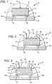
- an LED package 10 that is provided for the purpose of reference only, which includes an LED 12 comprising a substrate 14 having a modified back surface 16 to improve light extraction of LED light passing through the substrate.
- the substrate 14 can be made of many materials and can be many different thicknesses, with a suitable substrate being a 4H polytype of silicon carbide with a thickness range of 125-500 microns, although other silicon carbide polytypes can also be used including 3C, 6H and 15R polytypes. Silicon carbide has a much closer crystal lattice match to Group III nitrides than sapphire and results in Group III nitride films of higher quality.
- Silicon carbide also has a very high thermal conductivity so that the total output power of Group III nitride devices on silicon carbide is not limited by the thermal dissipation of the substrate (as may be the case with some devices formed on sapphire). Also, the availability of silicon carbide substrates provides the capacity for device isolation and reduced parasitic capacitance that make commercial devices possible.
- the LED 12 comprises a standard emission region 18 formed on the substrate 14 using known processes such as metal-organic chemical vapor deposition (MOCVD).
- MOCVD metal-organic chemical vapor deposition
- the operational details of conventional LEDs are known and are only briefly discussed.
- the LED's emission region 18 can include an active layer sandwiched between two oppositely doped layers, with the layers having standard thicknesses and the active layer emitting light omnidirectionally when a bias is applied across the oppositely doped layers.
- the layers of the emission region may be fabricated from different material systems such as the Group III nitride based material systems.
- Group III nitrides refer to those semiconductor compounds formed between nitrogen and the elements in the Group III of the periodic table, usually aluminum (Al), gallium (Ga), and indium (In).
- Al aluminum
- Ga gallium
- In indium
- the term also refers to ternary and tertiary compounds such as AlGaN and AlInGaN.
- the material forming the doped layers is GaN and the material forming the active layer is InGaN.
- the material of the doped layers may be AlGaN, AlGaAs or AlGaInP.
- the LED 12 is arranged in the package 10 in a flip-chip orientation with the top of the substrate 14 being the LED's primary emission surface. Other surfaces of the substrate 14, such as the sides, also emit light but the top surface is generally the primary emission surface.
- the LED 12 is flip-chip mounted on first and second metal layers or solder bumps 20a, 20b which are part of a submount 22.
- a first contact 24 is coupled between the first metal layer 20a and one of the oppositely doped layers in the emission region 18 and a second contact 26 is coupled between the second metal layer 20b and the emission region's other doped layer.
- a bias can be applied to the contacts 24, 26 through the first and second metal layers 20a, 20b, and the bias is then conducted through the contact 24, 26 to the oppositely doped layers in the emission region, causing the active layer to emit light.
- a substrate contact 28 can be used to apply a bias to one of the oppositely doped layers.
- the other doped layer is contacted to one of the contacts 24, 26 arranged between the metal layers 20a, 20b and the LED.
- a bias is applied to the LED through contact 28 and one of the metal layers 20a, 20b, and the bias can be conducted to the substrate contact from the other of the metal layers, through a conductive wire (not shown) that runs from the metal layer to the substrate contact.
- the top surface of the metal layers 20a, 20b can also be reflective so that light emitted from the emission region toward the metal layers is reflected back to contribute to the overall emission of the LED package 10.
- the LED 12 and its contacts can be encased in a clear protective material 30, which is typically a transparent epoxy covering the LED 12 and the top surface of the metal layers 20a, 20b.
- the LED 12 can be mounted on the horizontal base of a "metal cup" that typically has conductive paths (not shown) for applying a bias across the contacts on the emission regions oppositely doped layers.
- the top surface of the metal cup can also be reflective to reflect light from the emission region such that the light contributes to the light emission of the LED package.
- the substrate 14 comprises a modified back surface 16 that, in the flip-chip arrangement of the LED 12 is the top and primary emission surface of the LED.
- the modified surface 16 enhances the light emission of the LED 12.
- the efficiency of conventional LEDs is limited by their inability to emit all of the light that is generated by the active layer.
- the flip-chip arranged LED is emitting, light reaches the primary emitting substrate surface at many different angles.
- Typical substrate semiconductor materials have a high index of refraction compared to ambient air or encapsulating epoxy. Light traveling from a region having a high index of refraction to a region with a low index of refraction that is within a certain critical angle (relative to the surface normal direction) will cross to the lower index region.
- TIR total internal reflection
- the modified surface 16 improves light extraction of the LED 12 by providing a varying surface that allows light that would otherwise be trapped in the LED, by total internal reflection (TIR), to escape from the substrate to contribute to light emission.
- TIR total internal reflection
- the variations in the modified surface increase the chances that the TIR light will reach the substrate surface within the critical angle and will be emitted.
- the variations of the modified surface reflect the light at different angles, increasing the chances that the light will escape on the next pass.
- FIG. 2 shows an LED package 40 that may be formed according to an embodiment of the process of the present invention.
- the package includes an LED 42 having a substrate 44 with a semiconductor emission region 46 formed on one of its surfaces.
- the emission region 46 is similar to the emission region 18 in FIG. 1 .
- the LED 42 is mounted on first and second metal layers 48a, 48b having contacts 50, 52 to contact the oppositely doped layers in the emission region 46.
- a bias applied to the metal layers 48a, 48b can be applied to the oppositely doped layers through the contacts 50, 52.
- the LED 42 is flip-chip mounted such that the substrate's bottom surface is the primary emitting surface of the LED 42.
- the LED 42 can also be encased in a protective transparent epoxy 54.
- the emitting surface 56 of the LED (surface of substrate 44) is not flat, but instead has a plurality of etched features 57, which in the configuration of FIG. 2 , are truncated pyramids.
- the truncated pyramids 57 may be formed by cutting a plurality of bevel cuts 58 in a grid pattern using an angled saw blade.
- the size and shape of the truncated pyramids 57 may be varied by adjusting the depth to which the saw blade cuts into the surface of the substrate 44. In another configuration, the cut depth may be set so as to form a pyramid. It is known that the cutting process produces substantially smooth cut surfaces 59 having an overlying layer of damaged material that is light absorbing.
- the ICP-RIE process is applied to the emitting surface 56, including the cut surfaces 59 and the uncut surfaces 60.
- the end result is an emitting surface 56 having numerous dimpled surface areas corresponding to the uncut surfaces 60 and smooth, damage free surfaces corresponding to the cut surfaces 59. It has been observed that the ICP-RIE process changes the surface morphology of initially rough surfaces, such as the uncut surfaces 60, to dimpled surfaces; removes damaged layers of material; and leaves initially smooth surfaces, such as the cut surfaces 59, unchanged.
- the etched features 57 enhance light extraction by providing a further variance to the surface to allow TIR light to escape from the LED.
- the etched features 57 in combination with the dimpled surface areas provide a greater degree of light extraction compared to a flat dimpled substrate surface, such as shown in FIG. 1 .
- FIG. 3 shows another LED package 70 that may be formed according to an embodiment of the process of the present invention.
- the package also has a flip-chip mounted LED 72 comprising a substrate 74 and an emission region 76.
- the LED 72 is mounted to metal layers 78a, 78b with contacts 80, 82 to apply a bias to the emission region 76.
- the LED 72 is also encased in a protective transparent epoxy 84.
- the emitting surface 86 of the LED 72 includes a plurality of etched features 88, formed by a plurality of bevel cuts 90 in a manner similar to the etched features described with respect to FIG. 2 .
- the LED 72 includes a sidewall cut 92 around its perimeter which is created using an angled saw blade.
- the sidewall cut 92 includes two substrate surfaces, a vertical sidewall surface 94 and an angled sidewall surface 96.
- the sidewall surfaces 94, 96 like the bevel cut surfaces 98, have layers of damaged material associated with them.
- the ICP-RIE process is applied to the substrate surface 86, including the bevel cut surfaces 98, the angled sidewall surface 96 and the uncut surfaces 100. Because the application of the ICP-RIE process is perpendicular to the uncut surfaces 100, the process does not affect the vertical sidewall surface 94. The end result is an emitting surface 86 having numerous dimpled surface areas corresponding to the uncut surfaces 100 and smooth, damage free surfaces corresponding to the bevel cut surfaces 98 and the angled sidewall surface 96.
- the etched features 80 and sidewall cut 92 enhance light extraction by providing a further variance to the surface to allow TIR light to escape from the LED.
- the combination of etched features 80, sidewall cuts 92 and dimpled surface areas provide a greater degree of light extraction compared to a flat dimpled substrate surface, such as shown in FIGS. 1 and 2 .
- the previously described LEDs are manufactured using methods that include etching process, particularly an ICP-RIE process.
- etching process particularly an ICP-RIE process.
- Exemplary LEDs were manufactured as follows: In general, the ICP-RIE process was applied to bare 4H and 6H SiC wafers with standard backside surface finish. The ICP-RIE process involved SF 6 as the etchant and used standard processing conditions for SiC etching. Wafers were placed face down on sapphire carrier wafers during the ICP-RIE process.
- the ICP-RIE process removes substrate material.
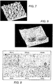
- the ICP-RIE etch causes specific surfaces to form a dimpled texture on a microscopic scale. More specifically, it has been observed that an initially roughened substrate surface, such as that which results from wire cutting a substrate material core to create a wafer, will form a dimpled surface when etched, as shown in FIG. 4 , while an initially smooth surface, such as that which results from saw cutting to form bevels, will remain smooth when etched, as shown in FIG. 5 .
- the change in surface morphology from an initially roughened surface to a dimpled surface is shown in FIGS. 6 , 7 and 8 .
- FIG. 6 , 7 and 8 The change in surface morphology from an initially roughened surface to a dimpled surface is shown in FIGS. 6 , 7 and 8 .
- FIG. 6 is a 20 ⁇ m x 20 ⁇ m scale image of an SiC wafer before ICP-RIE etching.
- FIG. 7 is a 100 ⁇ m x 100 ⁇ m scale image of a SiC wafer after ICP-RIE etching for approximately 5 minutes.
- FIG. 8 is a 20 ⁇ m x 20 ⁇ m scale image of a SiC wafer after ICP-RIE etching for approximately 30 minutes.
- FIG. 9 shows the evolution of the SiC surface morphology with increasing etch time. From this figure it is apparent that the dimpled produced by the ICP-RIE process increase with increased etch time. Thus, it is possible to control the surface morphology by adjusting the etch time to obtain the desired dimple size.
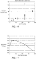
- the thickness of SiC removed by the etching process varies as a function of time.
- FIG. 10 is a graph of SiC material removed verses etch time. Following the etch; wafers were characterized using a total integrated scatter (TIS) tool. The TIS signal gauges how effectively surface roughness internally scatters light in a wafer and is thus a proxy for LED light extraction. TIS data shown in FIG. 11 suggest an etch time of 15 to 60 minutes is optional for the current process conditions.
- TIS total integrated scatter
- the unique, dimpled surface texture created by the ICP-RIE etch is beneficial in several respects.
- the dimple morphology is more consistent and regular compared to other surface morphologies that result from other well known roughening processes (e.g. mechanical lapping), which may contribute to the enhanced light extraction observed.
- the etch process is more controllable, and less likely to leave a damaged surface or subsurface layer than other roughening processes (e.g. mechanical lapping).
- the ICP-RIE etch process does not require photolithography or masking or other patterning to generate the dimple features. It is applied to a uniform, exposed SiC surface and the dimple features form spontaneously (although, as previously indicated, the formation of a dimpled surface is dependent on the specific starting surface, i.e., roughened verses smooth). Thus, the etch process is relatively simple and inexpensive to integrate into the LED fabrication flow. Fourth, the ICP-RIE etch process is flexible in that it can be inserted at a number of points in the LED fabrication process, including prior to epi growth.
- the ICP-RIE process was applied to 900 ⁇ m x 900 ⁇ m LEDs as the final wafer level process step.
- Standard LED wafers were fabricated similar to the XB900-type LEDs manufactured by Cree Inc., of Durham, North Carolina, except with lateral contact geometry so that the n-contact was on the epi-sides of the wafer (back surface remains bare).
- lateral geometry devices have previously been shown to perform similarly in lamps compared to conventional, vertical geometry XB900 devices. After processing, the lateral geometry LEDs were singulated as usual, including sidewall facets, then flip-chip mounted to a Si submount with PbSn solder bumps, and then made into lamps the normal way.
- RIE#1 In one process run (RIE#1), a 120 minute ICP-RIE process was applied to a 4H wafer.
- the ICP-RIE samples resulted in 23% brighter lamps compared to the historical average for conventional XB900 devices made from comparable epi material.
- the etch process required using a full wafer so a control sample (no etch, same wafer) was not available for direct comparison.
- RIE#3 In another process run (RIE#3), a 120 minute ICP-RIE process was applied. For one 4H and one 6H wafer, the ICP-RIE samples resulted in 5% and 9% brighter lamps, respectively, compared to the historical average for conventional XB900 devices made from comparable epi material. The etch process required using a full wafer so control samples (no etch, same wafer) were not available for direct comparison.
- etched features were added to the substrate surface using bevel cuts that were made in the back surface of an LED wafer prior to the ICP-RIE process.
- the bevel cuts were made using an angled saw blade, set such that depth of the cuts was ⁇ 100 ⁇ m to ⁇ 150 ⁇ m.
- the LEDs were XB900-like except with a lateral contact geometry.
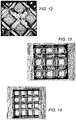
- FIGs. 12-18 show some examples of bevel cuts. In FIGs. 12 and 16 , the bevel cuts are arranged diagonally relative to the perimeter of the LED, while in FIGS. 13-15 , 17 and 18 , the cuts are arranged perpendicularly. In FIGS.
- the depth of the cuts were such that the etched features created were truncated pyramids.
- the depth of the cuts was increased such that the etched features created were pyramids.
- the saw blade shape and depth of cuts were such that the etched features created were truncated pyramids with a square, upright projection.
- RIE#9 In yet another process run (RIE#9), quarter wafers were used for the ICP-RIE process. Diagonal bevels ⁇ 100 ⁇ m deep were applied to the SiC prior to etching for (a) 30 minutes and (b) 60 minutes.
- the bevel + 30' ICP-RIE and bevel + 60' ICP-RIE process resulted in 10% and 14% brighter lamps, respectively, compared to control samples (no etch, no bevels).
- the bevel + 30' ICP-RIE and bevel + 60' ICP-RIE process resulted in 14% and 22% brighter lamps, respectively, compared to control samples.
- additional process steps included the application of faceted saw cuts ("bevels") across the back surface of the substrate, followed by an ICP-RIE process that creates areas having dimpled surface texture and removes surface damage related to the saw cuts.
- bevels faceted saw cuts
- ICP-RIE iCP-RIE
- the dimpled surface texture provided by the ICP-RIE helps scatter TIR light into the escape cones of the bevels. It also may be easier to manufacture in the sense that the front side of the wafer is easier to protect from the etchant.
- the ICP-RIE process was applied after bevel cuts and conventional sidewall (ATON) cuts were made to lateral geometry XB900 wafers.
- the LED wafer was bonded to a sapphire carrier wafer during the ICP-RIE process to prevent premature breaking at the deep sidewall cuts. Otherwise the process was similar to that described above. Since the ICP-RIE process occurred last, substantially all saw damage is removed.
- the ICP-RIE process may be applied to substrates of various thicknesses including those used in ultra thin LEDs such as the EZ-XT LEDs manufactured by Cree, Inc.
- the ICP-RIE process may also be applied to future "thin chip” LEDs, including chipscale package LEDs, where a highly scattering surface roughness is desired.
- the present invention may be used in all flip-chip LED products, but especially large area LEDs. It is easiest to implement with lateral contact geometry devices but is applicable to vertical geometry devices as well.
- the ICP-RIE process may be applied to all ATON or otherwise cut surfaces to remove saw damage.
- the ICP-RIE process may be applicable for other types of LED substrates (sapphire, GaP, etc.).
- the invention may allow for greater flexibility in mechanical treatment processes currently applied to SiC (i.e. grit size of saw, wire saw speed, dicing saw speed) by providing a means to remove surface damage.
- FIG. 19 shows another LED 110, which is described for the purpose of reference only, that includes a conductive substrate 112 with a semiconductor emission region 114 formed on one of its surfaces.
- the emission region 114 is similar to the emission region 18 in FIG. 1 .
- the LED 110 includes first and second contacts 116, 118 that contact the oppositely doped layers in the emission region 114. When a bias is applied to the oppositely doped layers, through the contacts 116, 118, light is emitted.
- the LED 110 may be flip-chip mounted such that the substrate surface 120 opposite the emission region 114 is the primary emitting surface of the LED.
- Portions 122 of the primary emitting surface 120 include a surface morphology that includes a collection of geometric elements. Attributes, including element "profile” or shape, e.g., cones, pyramids, hemispheres, and element “depth”, along with the "periodicity" of elements, i.e., spacing between like features, e.g., peaks, of adjacent elements, may be used to characterize a particular surface morphology. As explained below, in one configuration, these morphed portions 122 of the emitting surface 120 are formed entirely and directly in the substrate 112 and preferably without the use of a mask. In other configurations, the morphed portions 122 are formed at least partially within the substrate. In other configurations the morphed portions 122 are formed in another layer of material on top of the emitting surface 120 of the substrate 112.
- portions 124 of the primary emitting surface 120 are substantially smooth.
- the smooth surface provides for a large surface area of direct contact between the contact 116 and the substrate 112 which in turn allows for efficient transfer of current from the contact into the substrate.
- the primary emitting surface 120 includes additional smooth surface areas 126.
- Conductive elements 128 are formed on these surface areas 126 and are electrically connected to the first contact 116. These additional conductive elements 128 form a current spreading structure that provides for more efficient distribution of current across the surface area of the substrate 112.
- These smooth portions 124, 126 are formed by masking the top surface 120 of the substrate prior to creating the morphed portions 122.
- the current spreading layer 130 is a layer of transparent conducting material that is deposited on the primary emitting surface 120.
- the transparent conducting material may a metal, such as Pd, Ni or Au, having a thickness of between approximately 2 nm and 20 nm; a transparent conducting oxide, such as indium tin oxide, having a thickness of approximately 100 nm; or a semiconductor material.
- the material may be an additional layer of heavily doped semiconductor material that is deposited on the primary emitting surface 120.
- “heavily doped” means more doped than the substrate 112.
- Such semiconductor materials may include, for example, SiC, GaN and AllnGaN.
- the material generally has the same or similar refractive index as the substrate 112 and the same n-type or p-type doping as the substrate.
- the substrate 112 is formed of n-type SiC
- the layer of additional material 130 may be n-type SiC or AllnGaN; and if the substrate is formed of n-type GaN, the additional material would be n-type GaN.
- the thickness of the semiconductor material layer depends on the doping concentration. For example, if the doping concentration is greater than 1 20 cm -3 , a thickness of approximately 100 nm should be sufficient.
- the current spreading layer 130 is part of the substrate 112 itself.
- a top surface region 132 of the substrate 112 is subjected to further doping to increase its conductivity.
- the heavily doped, top surface region 132 of the substrate 112 provides current spreading without the need for an additional layer of material.
- “heavily doped” means that the top surface region 132 of the substrate 112 is more heavily doped than the remaining portion of the substrate.
- the thickness of this more heavily doped region 132 of the substrate depends on the doping concentration. For example, if the doping concentration is greater than 1 20 cm -3 , a thickness of approximately 100 nm should be sufficient.
- the morphed portions 122 of the primary emitting surface 120 may be formed using anyone of several processes, each employing techniques that are well known in the art.
- the morphed portions 122 are formed by directly etching the primary emitting surface 120 of the substrate 112, without the use of a mask, using a dry etching process such as reactive ion etching (RIE).
- RIE reactive ion etching
- This process is known to cause substrate surfaces to assume a surface morphology like that shown in FIG. 23 .
- Such a morphology has been referred to as a "moth-eye" surface. See Kasugai et al., Moth-Eye Light Emitting Diodes, Mater. Res. Soc. Symp. Proc. Vol. 831, 2005 Material Research Society .
- the morphed portions 122 are formed by coating the emitting surface 120 with a thin, non-continuous layer 134 of material or particles.
- a "non-continuous layer” as used herein means a layer, which may be formed of one or more sub-layers, having top surface elements 136 that cause the layer to have a cross section of non-uniform thickness, at a microscopic level.
- the density of elements in the layer 134 and the size of the elements may be selected such that the top surface of the layer has a morphology with a periodicity, profile and, depth similar to the moth-eye surface achieved through RIE etching.
- the surface morphology 138 of the non-continuous layer 134 is then transferred at least partially to the substrate 112 by either partially or completely removing the non-continuous layer. "Transferred” as used in this context means that after partial or complete removal of the non-continuous layer 134, the substrate 112 surface has substantially the same surface morphology that the non-continuous layer had prior to the removal or partial-removal process.
- the non-continuous layer 134 is preferably removed using a dry etch process.
- the dry etching process is preferably not an RIE process, and may be, for example, involve etching with a fluorine-containing gas such as nitrogen trifluoride, nitrous oxide, ammonium trifluoride, oxygen, sulfur hexafluoride, carbon tetrafluoride, or mixtures thereof.
- a fluorine-containing gas such as nitrogen trifluoride, nitrous oxide, ammonium trifluoride, oxygen, sulfur hexafluoride, carbon tetrafluoride, or mixtures thereof.
- Exemplary techniques for dry etching silicon carbide are set forth in U.S. Pat. Nos. 4,865,685 and 4,981,551 which are incorporated entirely herein by reference.
- the non-continuous layer 134 is made of material or materials that etch at approximately the same rate as the substrate 112. Such an etching rate ensures that the surface morphology 138 of the non
- the surface morphology 138 of the non-continuous layer 134 may not match the desired surface morphology for the substrate 112.
- the depth of the elements 136 on the surface of the non-continuous layer 134 may be larger than desired.
- the non-continuous layer 134 may be made of material or materials that etch at a faster rate relative to the substrate 112.
- the end result is a substrate 112 with a surface morphology having elements with less depth than the elements 136 of the non-continuous layer 134.
- the characteristics of the surface morphology of the non-continuous layer 134 and the etch rates of the non-continuous layer relative to the substrate 112, allow for control of the shape of the substrate surface morphology. Through proper selection of each, the desired substrate surface morphology may be obtained.
- the non-continuous layer 134 is formed by depositing a thin layer of metal, e.g., gold or aluminum, under conditions that make the layer non-continuous.
- the metal may be exposed to a temperature that is high enough to result in diffusion of the metal and formation of islands projecting from the surface of the layer. Higher temperatures and longer exposure times will result in fewer, larger islands.
- the size, shape and density of the islands may be controlled by temperature and exposure time to create the desired surface morphology.
- the non-continuous layer 134 is formed by first depositing a uniform layer of metal and then making the uniform layer non-uniform by 1) depositing a non-continuous mask layer over the uniform layer and then etching the layer of metal to form the desired surface morphology; or 2) depositing nanoparticles on the uniform layer using an aerosol or other gas-phase chemical reaction and then etching to form the desired surface morphology on the underlying uniform layer.
- the non-uniform layer 134 may be formed of nanoparticles.
- the particles may be suspended in a liquid that is evenly deposited over the substrate surface 120 by, for example, using a spinner with a rotation speed determined by the desired thickness of the layer of particles and the properties of the liquid. Once the liquid layer is deposited, the liquid may be evaporated at elevated or room temperature to remove the liquid and leave only the particles.
- a layer of particles may be sprayed directly on the substrate surface 120.
- the particles may be formed of metals such as gold or aluminum, ceramics such as alumina or silicon carbide or silica or boron nitride, carbon such as graphite or bucky balls, or organic materials.
- a damaged layer of material may remain on the morphed portions 122 of the emitting surface 120.
- the material forming the damaged layer may be removed by etching the morphed portions 122 using known chemical etching processes, such as a KOH process or flowing gases such as hydrogen or hydrogen chloride.
- the damaging effects of the material forming the damaged layer may be substantially reduced by annealing processes.
- the annealing process serves two functions; it activates the dopants in the substrate and it reduces the effect of the damaged layer.
- the morphed portions 122 are created using well known grit polishing processes.
- grit particles e.g., diamond particles
- the density of particles in the grit, the size of the particles, and the abrasive force between the particles and the surface 120 are selected such that the resultant surface morphology has a periodicity, profile and depth similar to the moth-eye surface achieved through the previously described RIE etching process.
- the morphed portions 122 are formed in a layer of material 132 that is deposited on top of the emitting surface 120 of the substrate 112.
- the material has a refractive index that is substantially the same as the substrate.
- the material 140 is deposited on a SiC substrate 112 may be SiC or AlInGaN; while the material deposited in a GaN substrate may be GaN.
- the material 140 also has the same n-type or p-type doping as the substrate 112.
- the material may be deposited using well known, lower temperature techniques, such as MOCVD, CVD, HVPE, MBE or sputtering.
- the desired surface morphology may be obtained through control of growth conditions, such as temperature.
- a medium deposition temperature is more likely to produce the desired surface morphology as opposed to too high or too cool deposition temperatures which would likely result in a smooth surface.
- Surface morphology formation is also dependent on the type of wide bandgap semiconductor being deposited. For GaN, the group V/III ratio will significantly impact morphology. Also, N-polar GaN is typically highly faceted grown under typical MOCVD growth conditions.
- particles of the substrate 112 material or a material having a similar index of refraction are deposited on the top surface 120 of the substrate.
- the particles are then mechanically fixed to the surface 120 through adhesion or annealing.
- the size, shape and density of the particles are selected such that the resultant surface morphology 122 has a periodicity, profile and depth similar to the moth-eye surface achieved through the previously described RIE etching process.
Claims (9)
- Prozess zum Bilden einer Leuchtdiode (LED) (42; 72), umfassend:Züchten eines Lichtausstrahlungsbereichs (46; 76) auf einer erstseitigen Oberfläche eines Substrats (44; 74), wobei der Lichtausstrahlungsbereich (46; 76) eine Materialschicht vom p-Typ, eine Materialschicht vom n-Typ und eine aktive Schicht zwischen der Schicht vom p-Typ und der Schicht vom n-Typ umfasst;Schneiden des Substrats, um eine Vielzahl von Schnittmerkmalen (59; 98) auf einer zweiseitigen Oberfläche (56; 86) des Substrats gegenüber der erstseitigen Oberfläche zu erzeugen, wobei das Schneiden dazu führt, dass die zweitseitige Oberfläche beschädigte Abschnitte bei den Schnittmerkmalen (59; 98) umfasst; undAnwenden eines reaktiven Ionenätzungs-(RIE)-Prozesses auf mindestens einen Abschnitt der zweiseitigen Oberfläche (56; 86) für eine Zeitdauer, die ausreicht, die Oberflächenmorphologie mindestens einer Vielzahl von ungeschnittenen Oberflächen (60; 80) so zu ändern, dass sie eingedellte Oberflächen umfasst, und mindestens Teil der beschädigten Abschnitte der Schnittmerkmale (59; 98) der zweitseitigen Oberfläche (56; 86) zu entfernen, wobei die verarbeitete zweitseitige Oberfläche (56; 86) eine Lichtextraktionsoberfläche umfasst.
- Prozess nach Anspruch 1, wobei der RIE-Prozess ein induktiv gekoppelter reaktiver Plasmaionenätzungs-(ICP-RIE)-Prozess ist.
- Prozess nach Anspruch 1, wobei der RIE-Prozess vor Züchten des Ausstrahlungsbereichs (46; 76) angewendet wird.
- Prozess nach Anspruch 1, wobei der RIE-Prozess nach Züchten des Ausstrahlungsbereichs (46; 76) angewendet wird.
- Prozess nach Anspruch 1, wobei das Schneiden ein Schneiden einer Vielzahl von Schrägungen (58; 90) in die zweitseitige Oberfläche umfasst, um die Schnittmerkmale zu bilden, die zugehörige Oberflächenareale (59; 98) aufweisen, die mindestens Teil der zweitseitigen Oberfläche (56; 86) bilden.
- Prozess nach Anspruch 1, weiter umfassend Bilden einer Vielzahl von Seitenwandschnitten (92), die Seitenwandoberflächen (94; 96) bilden, die mindestens Teil der zweitseitigen Oberfläche (86) bilden.
- Prozess nach Anspruch 1, weiter umfassend Bilden von Kontakten (50, 52; 80, 82) vom p-Typ und n-Typ an der erstseitigen Oberfläche des Substrats (42; 72), sodass die Kontakte (50, 52; 80, 82) vom p-Typ und n-Typ jeweils das Material vom p-Typ und n-Typ des Lichtausstrahlungsbereichs (46; 76) kontaktieren.
- Prozess nach Anspruch 1, weiter umfassend Bilden eines Kontakts vom p-Typ an einer Seite der erstseitigen und zweitseitigen Oberfläche des Substrats und Bilden eines Kontakts vom n-Typ auf der anderen Seite der erstseitigen und zweitseitigen Oberfläche, sodass die Kontakte vom p-Typ und n-Typ jeweils das Material vom p-Typ und n-Typ des Lichtausstrahlungsbereichs kontaktieren.
- Prozess nach Anspruch 1, weiter umfassend Hinzufügen einer durchsichtigen Stromverteilungsschicht an mindestens einem Abschnitt der zweitseitigen Oberfläche.
Applications Claiming Priority (3)
| Application Number | Priority Date | Filing Date | Title |
|---|---|---|---|
| US58532604P | 2004-07-02 | 2004-07-02 | |
| US11/083,460 US7534633B2 (en) | 2004-07-02 | 2005-03-17 | LED with substrate modifications for enhanced light extraction and method of making same |
| PCT/US2005/020603 WO2006016955A1 (en) | 2004-07-02 | 2005-06-09 | Led with substrate modifications for enhanced light extraction and method of making same |
Publications (2)
| Publication Number | Publication Date |
|---|---|
| EP1787335A1 EP1787335A1 (de) | 2007-05-23 |
| EP1787335B1 true EP1787335B1 (de) | 2019-10-16 |
Family
ID=35004287
Family Applications (1)
| Application Number | Title | Priority Date | Filing Date |
|---|---|---|---|
| EP05761972.8A Active EP1787335B1 (de) | 2004-07-02 | 2005-06-09 | Verfahren zur herstellung einer leuchtdiode mit substratmodifikationen zur erhöhung der lichtextraktion |
Country Status (5)
| Country | Link |
|---|---|
| US (6) | US7534633B2 (de) |
| EP (1) | EP1787335B1 (de) |
| JP (1) | JP5570697B2 (de) |
| TW (1) | TWI449160B (de) |
| WO (1) | WO2006016955A1 (de) |
Families Citing this family (130)
| Publication number | Priority date | Publication date | Assignee | Title |
|---|---|---|---|---|
| US7638346B2 (en) | 2001-12-24 | 2009-12-29 | Crystal Is, Inc. | Nitride semiconductor heterostructures and related methods |
| US20060005763A1 (en) | 2001-12-24 | 2006-01-12 | Crystal Is, Inc. | Method and apparatus for producing large, single-crystals of aluminum nitride |
| US8545629B2 (en) | 2001-12-24 | 2013-10-01 | Crystal Is, Inc. | Method and apparatus for producing large, single-crystals of aluminum nitride |
| US7915085B2 (en) * | 2003-09-18 | 2011-03-29 | Cree, Inc. | Molded chip fabrication method |
| US20080121918A1 (en) * | 2006-11-15 | 2008-05-29 | The Regents Of The University Of California | High light extraction efficiency sphere led |
| US7217583B2 (en) | 2004-09-21 | 2007-05-15 | Cree, Inc. | Methods of coating semiconductor light emitting elements by evaporating solvent from a suspension |
| US7265374B2 (en) * | 2005-06-10 | 2007-09-04 | Arima Computer Corporation | Light emitting semiconductor device |
| US8674375B2 (en) * | 2005-07-21 | 2014-03-18 | Cree, Inc. | Roughened high refractive index layer/LED for high light extraction |
| WO2007065018A2 (en) | 2005-12-02 | 2007-06-07 | Crystal Is, Inc. | Doped aluminum nitride crystals and methods of making them |
| JP2007165613A (ja) * | 2005-12-14 | 2007-06-28 | Showa Denko Kk | 窒化ガリウム系化合物半導体発光素子及びその製造方法 |
| CN103925521A (zh) * | 2005-12-21 | 2014-07-16 | 科锐公司 | 照明装置 |
| KR100844722B1 (ko) | 2006-03-07 | 2008-07-07 | 엘지전자 주식회사 | 나노콘 성장방법 및 이를 이용한 발광 다이오드의제조방법 |
| EP2007933B1 (de) | 2006-03-30 | 2017-05-10 | Crystal Is, Inc. | Verfahren zur gesteuerten dotierung von aluminiumnitrid-massenkristallen |
| US9034103B2 (en) | 2006-03-30 | 2015-05-19 | Crystal Is, Inc. | Aluminum nitride bulk crystals having high transparency to ultraviolet light and methods of forming them |
| US8969908B2 (en) * | 2006-04-04 | 2015-03-03 | Cree, Inc. | Uniform emission LED package |
| US7943952B2 (en) | 2006-07-31 | 2011-05-17 | Cree, Inc. | Method of uniform phosphor chip coating and LED package fabricated using method |
| CN101606246B (zh) | 2006-10-05 | 2012-07-04 | 三菱化学株式会社 | 使用GaN LED芯片的发光器件 |
| TWI338380B (en) * | 2006-10-11 | 2011-03-01 | Chuan Yu Hung | Light emitting diode incorporating high refractive index material |
| US10295147B2 (en) | 2006-11-09 | 2019-05-21 | Cree, Inc. | LED array and method for fabricating same |
| US9318327B2 (en) * | 2006-11-28 | 2016-04-19 | Cree, Inc. | Semiconductor devices having low threading dislocations and improved light extraction and methods of making the same |
| US9028612B2 (en) | 2010-06-30 | 2015-05-12 | Crystal Is, Inc. | Growth of large aluminum nitride single crystals with thermal-gradient control |
| WO2008088838A1 (en) | 2007-01-17 | 2008-07-24 | Crystal Is, Inc. | Defect reduction in seeded aluminum nitride crystal growth |
| US9771666B2 (en) | 2007-01-17 | 2017-09-26 | Crystal Is, Inc. | Defect reduction in seeded aluminum nitride crystal growth |
| US9024349B2 (en) * | 2007-01-22 | 2015-05-05 | Cree, Inc. | Wafer level phosphor coating method and devices fabricated utilizing method |
| US8232564B2 (en) | 2007-01-22 | 2012-07-31 | Cree, Inc. | Wafer level phosphor coating technique for warm light emitting diodes |
| US9159888B2 (en) * | 2007-01-22 | 2015-10-13 | Cree, Inc. | Wafer level phosphor coating method and devices fabricated utilizing method |
| JP5730484B2 (ja) | 2007-01-26 | 2015-06-10 | クリスタル アイエス インコーポレイテッド | 厚みのある擬似格子整合型の窒化物エピタキシャル層 |
| US8080833B2 (en) | 2007-01-26 | 2011-12-20 | Crystal Is, Inc. | Thick pseudomorphic nitride epitaxial layers |
| US8088220B2 (en) | 2007-05-24 | 2012-01-03 | Crystal Is, Inc. | Deep-eutectic melt growth of nitride crystals |
| US10505083B2 (en) * | 2007-07-11 | 2019-12-10 | Cree, Inc. | Coating method utilizing phosphor containment structure and devices fabricated using same |
| US9401461B2 (en) * | 2007-07-11 | 2016-07-26 | Cree, Inc. | LED chip design for white conversion |
| TWI492412B (zh) * | 2007-09-07 | 2015-07-11 | Cree Inc | 晶圓級磷光體塗佈方法及使用該方法製造之裝置 |
| US20100283074A1 (en) * | 2007-10-08 | 2010-11-11 | Kelley Tommie W | Light emitting diode with bonded semiconductor wavelength converter |
| DE102007057756B4 (de) * | 2007-11-30 | 2022-03-10 | OSRAM Opto Semiconductors Gesellschaft mit beschränkter Haftung | Verfahren zur Herstellung eines optoelektronischen Halbleiterkörpers |
| TWI452726B (zh) | 2007-11-30 | 2014-09-11 | Univ California | 利用表面粗糙之高度光取出效率之氮化物基發光二極體 |
| CN101897038B (zh) * | 2007-12-10 | 2012-08-29 | 3M创新有限公司 | 波长转换发光二极管及其制造方法 |
| US9041285B2 (en) | 2007-12-14 | 2015-05-26 | Cree, Inc. | Phosphor distribution in LED lamps using centrifugal force |
| US8167674B2 (en) | 2007-12-14 | 2012-05-01 | Cree, Inc. | Phosphor distribution in LED lamps using centrifugal force |
| US8552445B2 (en) | 2007-12-28 | 2013-10-08 | Nichia Corporation | Semiconductor light emitting device and method for manufacturing the same |
| US8878219B2 (en) * | 2008-01-11 | 2014-11-04 | Cree, Inc. | Flip-chip phosphor coating method and devices fabricated utilizing method |
| US8637883B2 (en) | 2008-03-19 | 2014-01-28 | Cree, Inc. | Low index spacer layer in LED devices |
| US8877524B2 (en) * | 2008-03-31 | 2014-11-04 | Cree, Inc. | Emission tuning methods and devices fabricated utilizing methods |
| JP5167974B2 (ja) * | 2008-06-16 | 2013-03-21 | 豊田合成株式会社 | Iii族窒化物系化合物半導体発光素子及びその製造方法 |
| US8240875B2 (en) | 2008-06-25 | 2012-08-14 | Cree, Inc. | Solid state linear array modules for general illumination |
| JP5282503B2 (ja) * | 2008-09-19 | 2013-09-04 | 日亜化学工業株式会社 | 半導体発光素子 |
| KR101363022B1 (ko) * | 2008-12-23 | 2014-02-14 | 삼성디스플레이 주식회사 | 유기 발광 표시 장치 |
| CN101800274B (zh) * | 2009-02-11 | 2011-11-09 | 晶发光电股份有限公司 | 具有凹凸基板的半导体元件的制造方法 |
| CN101877377B (zh) * | 2009-04-30 | 2011-12-14 | 比亚迪股份有限公司 | 一种分立发光二极管的外延片及其制造方法 |
| WO2010129409A1 (en) | 2009-05-05 | 2010-11-11 | 3M Innovative Properties Company | Semiconductor devices grown on indium-containing substrates utilizing indium depletion mechanisms |
| KR20120016262A (ko) | 2009-05-05 | 2012-02-23 | 쓰리엠 이노베이티브 프로퍼티즈 컴파니 | 향상된 추출 효율을 갖는 재발광 반도체 구조물 |
| JP2012526394A (ja) | 2009-05-05 | 2012-10-25 | スリーエム イノベイティブ プロパティズ カンパニー | Ledとともに使用するための再発光半導体キャリア素子及び製造方法 |
| US8541803B2 (en) | 2009-05-05 | 2013-09-24 | 3M Innovative Properties Company | Cadmium-free re-emitting semiconductor construction |
| US8434883B2 (en) | 2009-05-11 | 2013-05-07 | SemiOptoelectronics Co., Ltd. | LLB bulb having light extracting rough surface pattern (LERSP) and method of fabrication |
| US8299341B2 (en) * | 2009-05-13 | 2012-10-30 | The California Institute Of Technology | Fabrication of vertically aligned metallic nanopillars |
| US7977123B2 (en) * | 2009-05-22 | 2011-07-12 | Lam Research Corporation | Arrangements and methods for improving bevel etch repeatability among substrates |
| JP2012532453A (ja) | 2009-06-30 | 2012-12-13 | スリーエム イノベイティブ プロパティズ カンパニー | 調節可能な色温度を備えた白色光エレクトロルミネセンスデバイス |
| WO2011008474A1 (en) | 2009-06-30 | 2011-01-20 | 3M Innovative Properties Company | Electroluminescent devices with color adjustment based on current crowding |
| EP2282360A1 (de) * | 2009-08-06 | 2011-02-09 | Nederlandse Organisatie voor toegepast -natuurwetenschappelijk onderzoek TNO | Optoelektrische Vorrichtung und Verfahren zu deren Herstellung |
| KR101114047B1 (ko) * | 2009-10-22 | 2012-03-09 | 엘지이노텍 주식회사 | 발광소자 및 그 제조방법 |
| WO2011056675A1 (en) * | 2009-11-03 | 2011-05-12 | The Regents Of The University Of California | Superluminescent diodes by crystallographic etching |
| DE102010008603A1 (de) | 2010-02-19 | 2011-08-25 | OSRAM Opto Semiconductors GmbH, 93055 | Elektrisches Widerstandselement |
| US8349626B2 (en) * | 2010-03-23 | 2013-01-08 | Gtat Corporation | Creation of low-relief texture for a photovoltaic cell |
| WO2011156042A2 (en) | 2010-03-23 | 2011-12-15 | California Institute Of Technology | Heterojunction wire array solar cells |
| US8538224B2 (en) | 2010-04-22 | 2013-09-17 | 3M Innovative Properties Company | OLED light extraction films having internal nanostructures and external microstructures |
| US10546846B2 (en) | 2010-07-23 | 2020-01-28 | Cree, Inc. | Light transmission control for masking appearance of solid state light sources |
| KR20130128420A (ko) | 2010-11-18 | 2013-11-26 | 쓰리엠 이노베이티브 프로퍼티즈 컴파니 | 폴리실라잔 결합층을 포함하는 발광 다이오드 성분 |
| US8841145B2 (en) | 2010-12-08 | 2014-09-23 | Bridgelux, Inc. | System for wafer-level phosphor deposition |
| US8482020B2 (en) | 2010-12-08 | 2013-07-09 | Bridgelux, Inc. | System for wafer-level phosphor deposition |
| JP5758116B2 (ja) * | 2010-12-16 | 2015-08-05 | 株式会社ディスコ | 分割方法 |
| US9166126B2 (en) | 2011-01-31 | 2015-10-20 | Cree, Inc. | Conformally coated light emitting devices and methods for providing the same |
| TWI426624B (zh) * | 2011-02-14 | 2014-02-11 | 私立中原大學 | 高效率發光二極體之製作方法 |
| KR101781438B1 (ko) * | 2011-06-14 | 2017-09-25 | 삼성전자주식회사 | 반도체 발광소자의 제조방법 |
| US9337387B2 (en) | 2011-06-15 | 2016-05-10 | Sensor Electronic Technology, Inc. | Emitting device with improved extraction |
| US10319881B2 (en) | 2011-06-15 | 2019-06-11 | Sensor Electronic Technology, Inc. | Device including transparent layer with profiled surface for improved extraction |
| US10522714B2 (en) | 2011-06-15 | 2019-12-31 | Sensor Electronic Technology, Inc. | Device with inverted large scale light extraction structures |
| KR20140047070A (ko) | 2011-06-15 | 2014-04-21 | 센서 일렉트로닉 테크놀로지, 인크 | 역전된 대면적 광 추출 구조들을 갖는 디바이스 |
| US9142741B2 (en) | 2011-06-15 | 2015-09-22 | Sensor Electronic Technology, Inc. | Emitting device with improved extraction |
| US9741899B2 (en) | 2011-06-15 | 2017-08-22 | Sensor Electronic Technology, Inc. | Device with inverted large scale light extraction structures |
| US10170668B2 (en) | 2011-06-21 | 2019-01-01 | Micron Technology, Inc. | Solid state lighting devices with improved current spreading and light extraction and associated methods |
| US8274091B1 (en) * | 2011-07-07 | 2012-09-25 | Yuan Ze University | Light emitting device with light extraction layer and fabricating method thereof |
| US8962359B2 (en) | 2011-07-19 | 2015-02-24 | Crystal Is, Inc. | Photon extraction from nitride ultraviolet light-emitting devices |
| EP2737575B1 (de) | 2011-07-29 | 2024-05-01 | University of Saskatchewan | Resonatorantennen auf polymerbasis |
| KR101772588B1 (ko) | 2011-08-22 | 2017-09-13 | 한국전자통신연구원 | 클리어 컴파운드 에폭시로 몰딩한 mit 소자 및 그것을 포함하는 화재 감지 장치 |
| WO2013033841A1 (en) | 2011-09-06 | 2013-03-14 | Trilogy Environmental Systems Inc. | Hybrid desalination system |
| US9324560B2 (en) | 2011-09-06 | 2016-04-26 | Sensor Electronic Technology, Inc. | Patterned substrate design for layer growth |
| US10032956B2 (en) | 2011-09-06 | 2018-07-24 | Sensor Electronic Technology, Inc. | Patterned substrate design for layer growth |
| US8957440B2 (en) | 2011-10-04 | 2015-02-17 | Cree, Inc. | Light emitting devices with low packaging factor |
| US9159876B2 (en) * | 2011-10-06 | 2015-10-13 | Koninklijke Philips N.V. | Surface treatment of a semiconductor light emitting device |
| EP2613367A3 (de) * | 2012-01-06 | 2013-09-04 | Imec | Verfahren zur Herstellung einer LED-Vorrichtung |
| WO2013126432A1 (en) | 2012-02-21 | 2013-08-29 | California Institute Of Technology | Axially-integrated epitaxially-grown tandem wire arrays |
| US9947816B2 (en) | 2012-04-03 | 2018-04-17 | California Institute Of Technology | Semiconductor structures for fuel generation |
| CN103378223B (zh) * | 2012-04-25 | 2016-07-06 | 清华大学 | 外延结构体的制备方法 |
| WO2014006539A1 (en) * | 2012-07-05 | 2014-01-09 | Koninklijke Philips N.V. | Phosphor separated from led by transparent spacer |
| EP2896077B1 (de) * | 2012-09-17 | 2019-01-16 | Lumileds Holding B.V. | Lichtemittierende vorrichtung mit geformtem substrat |
| US9536924B2 (en) * | 2012-12-06 | 2017-01-03 | Seoul Viosys Co., Ltd. | Light-emitting diode and application therefor |
| DE112013005849T5 (de) * | 2012-12-06 | 2015-08-20 | Seoul Viosys Co., Ltd. | Lichtemittierende Diode und Anwendung dafür |
| US9553223B2 (en) | 2013-01-24 | 2017-01-24 | California Institute Of Technology | Method for alignment of microwires |
| EP2951885B1 (de) * | 2013-01-31 | 2020-01-15 | University of Saskatchewan | Metamaterial-resonatorantennen |
| EP2973664B1 (de) | 2013-03-15 | 2020-10-14 | Crystal Is, Inc. | Ultraviolet-lichtemittierende vorrichtung und herstellungsverfahren eines kontaktes zu einer ultraviolet-lichtemittierenden vorrichtung |
| FR3009428B1 (fr) * | 2013-08-05 | 2015-08-07 | Commissariat Energie Atomique | Procede de fabrication d'une structure semi-conductrice avec collage temporaire via des couches metalliques |
| EP3075028B1 (de) | 2013-12-20 | 2021-08-25 | University of Saskatchewan | Dielektrische resonatorantennenarrays |
| CN103794688B (zh) * | 2014-02-13 | 2016-11-09 | 厦门大学 | 一种光子晶体结构GaN基LED的制备方法 |
| US20160064631A1 (en) * | 2014-05-10 | 2016-03-03 | Sensor Electronic Technology, Inc. | Packaging for Ultraviolet Optoelectronic Device |
| US10147854B2 (en) | 2014-05-10 | 2018-12-04 | Sensor Electronic Technology, Inc. | Packaging for ultraviolet optoelectronic device |
| US9263653B2 (en) | 2014-05-15 | 2016-02-16 | Empire Technology Development Llc | Light-emissive devices and light-emissive displays |
| GB201420860D0 (en) | 2014-11-24 | 2015-01-07 | Infiniled Ltd | Micro-LED device |
| US9633883B2 (en) | 2015-03-20 | 2017-04-25 | Rohinni, LLC | Apparatus for transfer of semiconductor devices |
| KR101729683B1 (ko) * | 2015-09-16 | 2017-04-25 | 한국기계연구원 | 선격자 편광자의 제조 방법 |
| US10400322B2 (en) | 2015-12-04 | 2019-09-03 | The University Of Florida Research Foundation, Inc. | Fabrication of thermally stable nanocavities and particle-in-cavity nanostructures |
| WO2017127461A1 (en) | 2016-01-18 | 2017-07-27 | Sensor Electronic Technology, Inc. | Semiconductor device with improved light propagation |
| CN108351604B (zh) | 2016-01-27 | 2020-10-30 | 株式会社Lg化学 | 膜掩模、其制备方法、使用膜掩模的图案形成方法和由膜掩模形成的图案 |
| KR102138960B1 (ko) | 2016-01-27 | 2020-07-28 | 주식회사 엘지화학 | 필름 마스크, 이의 제조방법, 이를 이용한 패턴 형성 방법 및 이를 이용하여 형성된 패턴 |
| US10969677B2 (en) | 2016-01-27 | 2021-04-06 | Lg Chem, Ltd. | Film mask, method for manufacturing same, and method for forming pattern using film mask |
| WO2018038927A1 (en) | 2016-08-26 | 2018-03-01 | The Penn State Research Foundation | High light-extraction efficiency (lee) light-emitting diode (led) |
| JP6871706B2 (ja) * | 2016-09-30 | 2021-05-12 | 日機装株式会社 | 半導体発光素子の製造方法 |
| US10141215B2 (en) | 2016-11-03 | 2018-11-27 | Rohinni, LLC | Compliant needle for direct transfer of semiconductor devices |
| US10471545B2 (en) | 2016-11-23 | 2019-11-12 | Rohinni, LLC | Top-side laser for direct transfer of semiconductor devices |
| US10504767B2 (en) | 2016-11-23 | 2019-12-10 | Rohinni, LLC | Direct transfer apparatus for a pattern array of semiconductor device die |
| US10062588B2 (en) | 2017-01-18 | 2018-08-28 | Rohinni, LLC | Flexible support substrate for transfer of semiconductor devices |
| WO2019083729A1 (en) * | 2017-10-23 | 2019-05-02 | Trustees Of Boston University | ENHANCED THERMAL TRANSPORT THROUGH INTERFACES |
| US10410905B1 (en) | 2018-05-12 | 2019-09-10 | Rohinni, LLC | Method and apparatus for direct transfer of multiple semiconductor devices |
| US11094571B2 (en) | 2018-09-28 | 2021-08-17 | Rohinni, LLC | Apparatus to increase transferspeed of semiconductor devices with micro-adjustment |
| CN109585685B (zh) * | 2018-12-07 | 2021-06-01 | 纳晶科技股份有限公司 | 光取出结构、其制作方法及发光器件 |
| US20200220054A1 (en) | 2019-01-07 | 2020-07-09 | Glint Photonics, Inc. | Antireflective structures for light emitting diodes |
| CN112864296B (zh) * | 2019-01-29 | 2022-06-28 | 泉州三安半导体科技有限公司 | 一种led封装器件 |
| DE102019114169A1 (de) * | 2019-05-27 | 2020-12-03 | OSRAM Opto Semiconductors Gesellschaft mit beschränkter Haftung | Optoelektronisches halbleiterbauelement mit verbindungsbereichen und verfahren zur herstellung des optoelektronischen halbleiterbauelements |
| CN110600598B (zh) * | 2019-08-21 | 2021-02-05 | 苏州紫灿科技有限公司 | 一种双层纳米阵列结构的倒装紫外led及制备方法 |
| JP2021170595A (ja) | 2020-04-15 | 2021-10-28 | 国立大学法人東海国立大学機構 | 窒化ガリウム半導体装置およびその製造方法 |
| US11088093B1 (en) | 2020-05-28 | 2021-08-10 | X-Celeprint Limited | Micro-component anti-stiction structures |
| FR3132593A1 (fr) * | 2022-02-08 | 2023-08-11 | Centre National De La Recherche Scientifique - Cnrs - | Creation d’une fenetre de sortie de rayonnement pour un composant photoemetteur |
Family Cites Families (317)
| Publication number | Priority date | Publication date | Assignee | Title |
|---|---|---|---|---|
| JPS508494Y1 (de) | 1970-11-13 | 1975-03-14 | ||
| US3896479A (en) | 1973-09-24 | 1975-07-22 | Bell Telephone Labor Inc | Reduced stresses in iii-v semiconductor devices |
| US4152044A (en) * | 1977-06-17 | 1979-05-01 | International Telephone And Telegraph Corporation | Galium aluminum arsenide graded index waveguide |
| JPS5722581Y2 (de) * | 1979-08-21 | 1982-05-17 | ||
| US4476620A (en) * | 1979-10-19 | 1984-10-16 | Matsushita Electric Industrial Co., Ltd. | Method of making a gallium nitride light-emitting diode |
| DE3128187A1 (de) | 1981-07-16 | 1983-02-03 | Joachim 8068 Pfaffenhofen Sieg | Opto-elektronisches bauelement |
| US4675575A (en) | 1984-07-13 | 1987-06-23 | E & G Enterprises | Light-emitting diode assemblies and systems therefore |
| JPS6159886A (ja) | 1984-08-31 | 1986-03-27 | Fujitsu Ltd | 光半導体装置の製造方法 |
| FR2586844B1 (fr) | 1985-08-27 | 1988-04-29 | Sofrela Sa | Dispositif de signalisation utilisant des diodes electroluminescentes. |
| JPH07120807B2 (ja) | 1986-12-20 | 1995-12-20 | 富士通株式会社 | 定電流半導体装置 |
| JPS63156367A (ja) | 1986-12-20 | 1988-06-29 | Fujitsu Ltd | レベル・シフト・ダイオ−ド |
| JPS63288061A (ja) | 1987-05-20 | 1988-11-25 | Fujitsu Ltd | 半導体負性抵抗素子 |
| US4866005A (en) * | 1987-10-26 | 1989-09-12 | North Carolina State University | Sublimation of silicon carbide to produce large, device quality single crystals of silicon carbide |
| US4865685A (en) * | 1987-11-03 | 1989-09-12 | North Carolina State University | Dry etching of silicon carbide |
| US4981551A (en) | 1987-11-03 | 1991-01-01 | North Carolina State University | Dry etching of silicon carbide |
| JPH0770755B2 (ja) * | 1988-01-21 | 1995-07-31 | 三菱化学株式会社 | 高輝度led用エピタキシャル基板及びその製造方法 |
| US4912532A (en) * | 1988-08-26 | 1990-03-27 | Hewlett-Packard Company | Electro-optical device with inverted transparent substrate and method for making same |
| EP0405757A3 (en) * | 1989-06-27 | 1991-01-30 | Hewlett-Packard Company | High efficiency light-emitting diode |
| US5087949A (en) * | 1989-06-27 | 1992-02-11 | Hewlett-Packard Company | Light-emitting diode with diagonal faces |
| US5103271A (en) * | 1989-09-28 | 1992-04-07 | Kabushiki Kaisha Toshiba | Semiconductor light emitting device and method of fabricating the same |
| US4946547A (en) * | 1989-10-13 | 1990-08-07 | Cree Research, Inc. | Method of preparing silicon carbide surfaces for crystal growth |
| JPH0644567B2 (ja) * | 1989-12-18 | 1994-06-08 | 株式会社日立製作所 | 半導体形状の改善方法 |
| US5034783A (en) | 1990-07-27 | 1991-07-23 | At&T Bell Laboratories | Semiconductor device including cascadable polarization independent heterostructure |
| US5200022A (en) * | 1990-10-03 | 1993-04-06 | Cree Research, Inc. | Method of improving mechanically prepared substrate surfaces of alpha silicon carbide for deposition of beta silicon carbide thereon and resulting product |
| JP2765256B2 (ja) * | 1991-04-10 | 1998-06-11 | 日立電線株式会社 | 発光ダイオード |
| FR2679253B1 (fr) * | 1991-07-15 | 1994-09-02 | Pasteur Institut | Proteines de resistance a la cycloheximide. utilisation comme marqueur de selection par exemple pour controler le transfert d'acides nucleiques. |
| JP3068119B2 (ja) | 1991-09-10 | 2000-07-24 | サンケン電気株式会社 | ショットキ障壁を有する半導体装置 |
| US5198390A (en) * | 1992-01-16 | 1993-03-30 | Cornell Research Foundation, Inc. | RIE process for fabricating submicron, silicon electromechanical structures |
| JP3173117B2 (ja) | 1992-03-30 | 2001-06-04 | 株式会社村田製作所 | ショットキーバリア半導体装置 |
| DE4228895C2 (de) * | 1992-08-29 | 2002-09-19 | Bosch Gmbh Robert | Kraftfahrzeug-Beleuchtungseinrichtung mit mehreren Halbleiterlichtquellen |
| US5298767A (en) | 1992-10-06 | 1994-03-29 | Kulite Semiconductor Products, Inc. | Porous silicon carbide (SiC) semiconductor device |
| JP2932467B2 (ja) | 1993-03-12 | 1999-08-09 | 日亜化学工業株式会社 | 窒化ガリウム系化合物半導体発光素子 |
| US5376580A (en) * | 1993-03-19 | 1994-12-27 | Hewlett-Packard Company | Wafer bonding of light emitting diode layers |
| US5705321A (en) * | 1993-09-30 | 1998-01-06 | The University Of New Mexico | Method for manufacture of quantum sized periodic structures in Si materials |
| GB9320291D0 (en) | 1993-10-01 | 1993-11-17 | Brown John H | Optical directing devices for light emitting diodes |
| JP2932468B2 (ja) | 1993-12-10 | 1999-08-09 | 日亜化学工業株式会社 | 窒化ガリウム系化合物半導体発光素子 |
| JP2800666B2 (ja) | 1993-12-17 | 1998-09-21 | 日亜化学工業株式会社 | 窒化ガリウム系化合物半導体レーザ素子 |
| US5656832A (en) * | 1994-03-09 | 1997-08-12 | Kabushiki Kaisha Toshiba | Semiconductor heterojunction device with ALN buffer layer of 3nm-10nm average film thickness |
| JPH08148280A (ja) | 1994-04-14 | 1996-06-07 | Toshiba Corp | 半導体装置およびその製造方法 |
| JP2994219B2 (ja) | 1994-05-24 | 1999-12-27 | シャープ株式会社 | 半導体デバイスの製造方法 |
| JP2790242B2 (ja) | 1994-10-07 | 1998-08-27 | 日亜化学工業株式会社 | 窒化物半導体発光ダイオード |
| JP2921746B2 (ja) | 1995-01-31 | 1999-07-19 | 日亜化学工業株式会社 | 窒化物半導体レーザ素子 |
| US5628917A (en) * | 1995-02-03 | 1997-05-13 | Cornell Research Foundation, Inc. | Masking process for fabricating ultra-high aspect ratio, wafer-free micro-opto-electromechanical structures |
| US5614734A (en) * | 1995-03-15 | 1997-03-25 | Yale University | High efficency LED structure |
| US5670798A (en) * | 1995-03-29 | 1997-09-23 | North Carolina State University | Integrated heterostructures of Group III-V nitride semiconductor materials including epitaxial ohmic contact non-nitride buffer layer and methods of fabricating same |
| US5900650A (en) * | 1995-08-31 | 1999-05-04 | Kabushiki Kaisha Toshiba | Semiconductor device and method of manufacturing the same |
| JP3135041B2 (ja) | 1995-09-29 | 2001-02-13 | 日亜化学工業株式会社 | 窒化物半導体発光素子 |
| JP2891348B2 (ja) | 1995-11-24 | 1999-05-17 | 日亜化学工業株式会社 | 窒化物半導体レーザ素子 |
| JP2900990B2 (ja) | 1995-11-24 | 1999-06-02 | 日亜化学工業株式会社 | 窒化物半導体発光素子 |
| JP3298390B2 (ja) | 1995-12-11 | 2002-07-02 | 日亜化学工業株式会社 | 窒化物半導体多色発光素子の製造方法 |
| US6388272B1 (en) | 1996-03-07 | 2002-05-14 | Caldus Semiconductor, Inc. | W/WC/TAC ohmic and rectifying contacts on SiC |
| US5779924A (en) * | 1996-03-22 | 1998-07-14 | Hewlett-Packard Company | Ordered interface texturing for a light emitting device |
| US5985687A (en) | 1996-04-12 | 1999-11-16 | The Regents Of The University Of California | Method for making cleaved facets for lasers fabricated with gallium nitride and other noncubic materials |
| US5612567A (en) | 1996-05-13 | 1997-03-18 | North Carolina State University | Schottky barrier rectifiers and methods of forming same |
| JP2760344B2 (ja) | 1996-06-12 | 1998-05-28 | 日本電気株式会社 | 照光スイッチ |
| US6550949B1 (en) | 1996-06-13 | 2003-04-22 | Gentex Corporation | Systems and components for enhancing rear vision from a vehicle |
| US20040239243A1 (en) | 1996-06-13 | 2004-12-02 | Roberts John K. | Light emitting assembly |
| US5803579A (en) | 1996-06-13 | 1998-09-08 | Gentex Corporation | Illuminator assembly incorporating light emitting diodes |
| US6030848A (en) * | 1996-06-28 | 2000-02-29 | Kabushiki Kaisha Toshiba | Method for manufacturing a GaN-based compound semiconductor light emitting device |
| TW383508B (en) | 1996-07-29 | 2000-03-01 | Nichia Kagaku Kogyo Kk | Light emitting device and display |
| DE19640594B4 (de) | 1996-10-01 | 2016-08-04 | Osram Gmbh | Bauelement |
| JPH10163535A (ja) | 1996-11-27 | 1998-06-19 | Kasei Optonix Co Ltd | 白色発光素子 |
| CN100485984C (zh) | 1997-01-09 | 2009-05-06 | 日亚化学工业株式会社 | 氮化物半导体元器件 |
| JPH10209569A (ja) | 1997-01-16 | 1998-08-07 | Hewlett Packard Co <Hp> | p型窒化物半導体装置とその製造方法 |
| FR2759188B1 (fr) | 1997-01-31 | 1999-04-30 | Thery Hindrick | Dispositif de signalisation lumineuse, notamment pour regulation du trafic routier |
| ATE464586T1 (de) | 1997-02-13 | 2010-04-15 | Honeywell Int Inc | Beleuchtungssystem mit wiederverwendung des lichts zur erhöhung der helligkeit |
| US5767534A (en) | 1997-02-24 | 1998-06-16 | Minnesota Mining And Manufacturing Company | Passivation capping layer for ohmic contact in II-VI semiconductor light transducing device |
| US5939732A (en) | 1997-05-22 | 1999-08-17 | Kulite Semiconductor Products, Inc. | Vertical cavity-emitting porous silicon carbide light-emitting diode device and preparation thereof |
| JP3642157B2 (ja) | 1997-05-26 | 2005-04-27 | ソニー株式会社 | p型III族ナイトライド化合物半導体、発光ダイオードおよび半導体レーザ |
| US6784463B2 (en) | 1997-06-03 | 2004-08-31 | Lumileds Lighting U.S., Llc | III-Phospide and III-Arsenide flip chip light-emitting devices |
| DE19723176C1 (de) | 1997-06-03 | 1998-08-27 | Daimler Benz Ag | Leistungshalbleiter-Bauelement und Verfahren zu dessen Herstellung |
| US5888886A (en) * | 1997-06-30 | 1999-03-30 | Sdl, Inc. | Method of doping gan layers p-type for device fabrication |
| JP3606015B2 (ja) | 1997-07-23 | 2005-01-05 | 豊田合成株式会社 | 3族窒化物半導体素子の製造方法 |
| CN1142598C (zh) | 1997-07-25 | 2004-03-17 | 日亚化学工业株式会社 | 氮化物半导体发光器件 |
| JP3744211B2 (ja) | 1997-09-01 | 2006-02-08 | 日亜化学工業株式会社 | 窒化物半導体素子 |
| US7014336B1 (en) | 1999-11-18 | 2006-03-21 | Color Kinetics Incorporated | Systems and methods for generating and modulating illumination conditions |
| US6071795A (en) * | 1998-01-23 | 2000-06-06 | The Regents Of The University Of California | Separation of thin films from transparent substrates by selective optical processing |
| JPH11238913A (ja) | 1998-02-20 | 1999-08-31 | Namiki Precision Jewel Co Ltd | 半導体発光デバイスチップ |
| WO1999046822A1 (fr) | 1998-03-12 | 1999-09-16 | Nichia Chemical Industries, Ltd. | Dispositif semi-conducteur electroluminescent au nitrure |
| DE19813269A1 (de) * | 1998-03-25 | 1999-09-30 | Hoechst Diafoil Gmbh | Siegelfähige Polyesterfolie mit hoher Sauerstoffbarriere, Verfahren zu ihrer Herstellung und ihre Verwendung |
| JPH11330552A (ja) | 1998-05-18 | 1999-11-30 | Nichia Chem Ind Ltd | 窒化物半導体発光素子及び発光装置 |
| DE19829197C2 (de) | 1998-06-30 | 2002-06-20 | Siemens Ag | Strahlungsaussendendes und/oder -empfangendes Bauelement |
| US6225647B1 (en) | 1998-07-27 | 2001-05-01 | Kulite Semiconductor Products, Inc. | Passivation of porous semiconductors for improved optoelectronic device performance and light-emitting diode based on same |
| JP3817915B2 (ja) | 1998-07-31 | 2006-09-06 | 株式会社デンソー | ショットキーダイオード及びその製造方法 |
| US6063699A (en) * | 1998-08-19 | 2000-05-16 | International Business Machines Corporation | Methods for making high-aspect ratio holes in semiconductor and its application to a gate damascene process for sub- 0.05 micron mosfets |
| US5959316A (en) * | 1998-09-01 | 1999-09-28 | Hewlett-Packard Company | Multiple encapsulation of phosphor-LED devices |
| WO2000016411A1 (fr) | 1998-09-10 | 2000-03-23 | Rohm Co., Ltd. | Del a semi-conducteur et son procede de fabrication |
| JP3525061B2 (ja) * | 1998-09-25 | 2004-05-10 | 株式会社東芝 | 半導体発光素子の製造方法 |
| EP1046196B9 (de) | 1998-09-28 | 2013-01-09 | Koninklijke Philips Electronics N.V. | Beleuchtungsanordnung |
| JP3063756B1 (ja) | 1998-10-06 | 2000-07-12 | 日亜化学工業株式会社 | 窒化物半導体素子 |
| JP2000133883A (ja) | 1998-10-22 | 2000-05-12 | Nichia Chem Ind Ltd | 窒化物半導体素子 |
| US6274924B1 (en) * | 1998-11-05 | 2001-08-14 | Lumileds Lighting, U.S. Llc | Surface mountable LED package |
| JP2000150920A (ja) | 1998-11-12 | 2000-05-30 | Nippon Telegr & Teleph Corp <Ntt> | ショットキ接合型半導体ダイオード装置の製法 |
| JP3470622B2 (ja) | 1998-11-18 | 2003-11-25 | 日亜化学工業株式会社 | 窒化物半導体発光素子 |
| US6429583B1 (en) * | 1998-11-30 | 2002-08-06 | General Electric Company | Light emitting device with ba2mgsi2o7:eu2+, ba2sio4:eu2+, or (srxcay ba1-x-y)(a1zga1-z)2sr:eu2+phosphors |
| JP3705047B2 (ja) | 1998-12-15 | 2005-10-12 | 日亜化学工業株式会社 | 窒化物半導体発光素子 |
| US6744800B1 (en) * | 1998-12-30 | 2004-06-01 | Xerox Corporation | Method and structure for nitride based laser diode arrays on an insulating substrate |
| US6212213B1 (en) | 1999-01-29 | 2001-04-03 | Agilent Technologies, Inc. | Projector light source utilizing a solid state green light source |
| US6320206B1 (en) * | 1999-02-05 | 2001-11-20 | Lumileds Lighting, U.S., Llc | Light emitting devices having wafer bonded aluminum gallium indium nitride structures and mirror stacks |
| US20010042866A1 (en) * | 1999-02-05 | 2001-11-22 | Carrie Carter Coman | Inxalygazn optical emitters fabricated via substrate removal |
| US6389051B1 (en) | 1999-04-09 | 2002-05-14 | Xerox Corporation | Structure and method for asymmetric waveguide nitride laser diode |
| JP3656456B2 (ja) | 1999-04-21 | 2005-06-08 | 日亜化学工業株式会社 | 窒化物半導体素子 |
| DE19918370B4 (de) | 1999-04-22 | 2006-06-08 | Osram Opto Semiconductors Gmbh | LED-Weißlichtquelle mit Linse |
| US6258699B1 (en) * | 1999-05-10 | 2001-07-10 | Visual Photonics Epitaxy Co., Ltd. | Light emitting diode with a permanent subtrate of transparent glass or quartz and the method for manufacturing the same |
| JP3719047B2 (ja) | 1999-06-07 | 2005-11-24 | 日亜化学工業株式会社 | 窒化物半導体素子 |
| JP2000353826A (ja) | 1999-06-09 | 2000-12-19 | Sanyo Electric Co Ltd | 混成集積回路装置および光照射装置 |
| EP1065734B1 (de) * | 1999-06-09 | 2009-05-13 | Kabushiki Kaisha Toshiba | Bond-typ Halbleitersubstrat, lichtemittierendes Halbleiterbauelement und Herstellungsverfahren |
| US6489637B1 (en) | 1999-06-09 | 2002-12-03 | Sanyo Electric Co., Ltd. | Hybrid integrated circuit device |
| EP1059668A3 (de) | 1999-06-09 | 2007-07-18 | Sanyo Electric Co., Ltd. | Integrierte Hybridschaltungsanordnung |
| JP2000357820A (ja) * | 1999-06-15 | 2000-12-26 | Pioneer Electronic Corp | 窒化ガリウム系半導体発光素子及びその製造方法 |
| KR100425566B1 (ko) | 1999-06-23 | 2004-04-01 | 가부시키가이샤 시티즌 덴시 | 발광 다이오드 |
| DE19931689A1 (de) * | 1999-07-08 | 2001-01-11 | Patent Treuhand Ges Fuer Elektrische Gluehlampen Mbh | Optoelektronische Bauteilgruppe |
| JP4055303B2 (ja) * | 1999-10-12 | 2008-03-05 | 豊田合成株式会社 | 窒化ガリウム系化合物半導体及び半導体素子 |
| US6482711B1 (en) | 1999-10-28 | 2002-11-19 | Hrl Laboratories, Llc | InPSb/InAs BJT device and method of making |
| DE19952932C1 (de) * | 1999-11-03 | 2001-05-03 | Osram Opto Semiconductors Gmbh | LED-Weißlichtquelle mit breitbandiger Anregung |
| US6513949B1 (en) | 1999-12-02 | 2003-02-04 | Koninklijke Philips Electronics N.V. | LED/phosphor-LED hybrid lighting systems |
| US6410942B1 (en) * | 1999-12-03 | 2002-06-25 | Cree Lighting Company | Enhanced light extraction through the use of micro-LED arrays |
| US6350041B1 (en) * | 1999-12-03 | 2002-02-26 | Cree Lighting Company | High output radial dispersing lamp using a solid state light source |
| EP1234344B1 (de) * | 1999-12-03 | 2020-12-02 | Cree, Inc. | Lichtemittierende dioden mit verbesserter lichtauskoppelung durch verwendung von internen und externen optischen elementen |
| US6573537B1 (en) * | 1999-12-22 | 2003-06-03 | Lumileds Lighting, U.S., Llc | Highly reflective ohmic contacts to III-nitride flip-chip LEDs |
| US6646292B2 (en) | 1999-12-22 | 2003-11-11 | Lumileds Lighting, U.S., Llc | Semiconductor light emitting device and method |
| JP2000315826A (ja) | 2000-01-01 | 2000-11-14 | Nichia Chem Ind Ltd | 発光装置及びその形成方法、砲弾型発光ダイオード、チップタイプled |
| TW465123B (en) | 2000-02-02 | 2001-11-21 | Ind Tech Res Inst | High power white light LED |
| WO2001059851A1 (en) | 2000-02-09 | 2001-08-16 | Nippon Leiz Corporation | Light source |
| DE10008583A1 (de) * | 2000-02-24 | 2001-09-13 | Osram Opto Semiconductors Gmbh | Verfahren zum Herstellen eines optisch transparenten Substrates und Verfahren zum Herstellen eines lichtemittierenden Halbleiterchips |
| US6538371B1 (en) | 2000-03-27 | 2003-03-25 | The General Electric Company | White light illumination system with improved color output |
| JP4060511B2 (ja) * | 2000-03-28 | 2008-03-12 | パイオニア株式会社 | 窒化物半導体素子の分離方法 |
| US6331944B1 (en) | 2000-04-13 | 2001-12-18 | International Business Machines Corporation | Magnetic random access memory using a series tunnel element select mechanism |
| CN1252837C (zh) | 2000-04-26 | 2006-04-19 | 奥斯兰姆奥普托半导体股份有限两合公司 | 在GaN基板上的发光二极管芯片和用GaN基板上的发光二极管芯片制造发光二极管元件的方法 |
| US6534346B2 (en) | 2000-05-16 | 2003-03-18 | Nippon Electric Glass Co., Ltd. | Glass and glass tube for encapsulating semiconductors |
| JP2001332770A (ja) | 2000-05-23 | 2001-11-30 | Koha Co Ltd | Ledチップの樹脂封止方法 |
| KR100784573B1 (ko) | 2000-05-29 | 2007-12-10 | 파텐트-트로이한트-게젤샤프트 퓌어 엘렉트리쉐 글뤼람펜 엠베하 | 발광다이오드에 기반을 둔 백색광을 방출하는 조명 기구 |
| US6577073B2 (en) | 2000-05-31 | 2003-06-10 | Matsushita Electric Industrial Co., Ltd. | Led lamp |
| JP4386693B2 (ja) | 2000-05-31 | 2009-12-16 | パナソニック株式会社 | Ledランプおよびランプユニット |
| JP2001345485A (ja) * | 2000-06-02 | 2001-12-14 | Toyoda Gosei Co Ltd | 発光装置 |
| US6526082B1 (en) | 2000-06-02 | 2003-02-25 | Lumileds Lighting U.S., Llc | P-contact for GaN-based semiconductors utilizing a reverse-biased tunnel junction |
| US6331915B1 (en) | 2000-06-13 | 2001-12-18 | Kenneth J. Myers | Lighting element including light emitting diodes, microprism sheet, reflector, and diffusing agent |
| US6330111B1 (en) * | 2000-06-13 | 2001-12-11 | Kenneth J. Myers, Edward Greenberg | Lighting elements including light emitting diodes, microprism sheet, reflector, and diffusing agent |
| US6737801B2 (en) | 2000-06-28 | 2004-05-18 | The Fox Group, Inc. | Integrated color LED chip |
| US6586762B2 (en) | 2000-07-07 | 2003-07-01 | Nichia Corporation | Nitride semiconductor device with improved lifetime and high output power |
| US6562648B1 (en) * | 2000-08-23 | 2003-05-13 | Xerox Corporation | Structure and method for separation and transfer of semiconductor thin films onto dissimilar substrate materials |
| DE10042947A1 (de) * | 2000-08-31 | 2002-03-21 | Osram Opto Semiconductors Gmbh | Strahlungsemittierendes Halbleiterbauelement auf GaN-Basis |
| JP3839236B2 (ja) * | 2000-09-18 | 2006-11-01 | 株式会社小糸製作所 | 車両用灯具 |
| JP3466144B2 (ja) * | 2000-09-22 | 2003-11-10 | 士郎 酒井 | 半導体の表面を荒くする方法 |
| US6429460B1 (en) * | 2000-09-28 | 2002-08-06 | United Epitaxy Company, Ltd. | Highly luminous light emitting device |
| US6998281B2 (en) | 2000-10-12 | 2006-02-14 | General Electric Company | Solid state lighting device with reduced form factor including LED with directional emission and package with microoptics |
| DE60039535D1 (de) * | 2000-10-20 | 2008-08-28 | Josuke Nakata | Lichtemittierdende bzw. lichtempfindliche halbleiteranordnung und ihre herstellungsmethode |
| JP4091261B2 (ja) * | 2000-10-31 | 2008-05-28 | 株式会社東芝 | 半導体発光素子及びその製造方法 |
| JP2002151928A (ja) | 2000-11-08 | 2002-05-24 | Toshiba Corp | アンテナ、及びアンテナを内蔵する電子機器 |
| AU2002235132A1 (en) * | 2000-11-16 | 2002-05-27 | Emcore Corporation | Led packages having improved light extraction |
| NL1016779C2 (nl) * | 2000-12-02 | 2002-06-04 | Cornelis Johannes Maria V Rijn | Matrijs, werkwijze voor het vervaardigen van precisieproducten met behulp van een matrijs, alsmede precisieproducten, in het bijzonder microzeven en membraanfilters, vervaardigd met een dergelijke matrijs. |
| AT410266B (de) | 2000-12-28 | 2003-03-25 | Tridonic Optoelectronics Gmbh | Lichtquelle mit einem lichtemittierenden element |
| US6930737B2 (en) * | 2001-01-16 | 2005-08-16 | Visteon Global Technologies, Inc. | LED backlighting system |
| MY131962A (en) | 2001-01-24 | 2007-09-28 | Nichia Corp | Light emitting diode, optical semiconductor device, epoxy resin composition suited for optical semiconductor device, and method for manufacturing the same |
| US6791119B2 (en) * | 2001-02-01 | 2004-09-14 | Cree, Inc. | Light emitting diodes including modifications for light extraction |
| JP3830083B2 (ja) | 2001-03-07 | 2006-10-04 | スタンレー電気株式会社 | 半導体装置およびその製造方法 |
| US6468824B2 (en) * | 2001-03-22 | 2002-10-22 | Uni Light Technology Inc. | Method for forming a semiconductor device having a metallic substrate |
| US6746889B1 (en) * | 2001-03-27 | 2004-06-08 | Emcore Corporation | Optoelectronic device with improved light extraction |
| US6833566B2 (en) | 2001-03-28 | 2004-12-21 | Toyoda Gosei Co., Ltd. | Light emitting diode with heat sink |
| JP2003115204A (ja) | 2001-10-04 | 2003-04-18 | Toyoda Gosei Co Ltd | 遮光反射型デバイス及び光源 |
| JP2002299699A (ja) | 2001-03-30 | 2002-10-11 | Sumitomo Electric Ind Ltd | 発光装置およびその製造方法 |
| JP2004532133A (ja) | 2001-03-30 | 2004-10-21 | ザ・リージェンツ・オブ・ザ・ユニバーシティ・オブ・カリフォルニア | ナノ構造及びナノワイヤーの組立方法並びにそれらから組立てられた装置 |
| JP4101468B2 (ja) | 2001-04-09 | 2008-06-18 | 豊田合成株式会社 | 発光装置の製造方法 |
| US6686676B2 (en) | 2001-04-30 | 2004-02-03 | General Electric Company | UV reflectors and UV-based light sources having reduced UV radiation leakage incorporating the same |
| US6616862B2 (en) | 2001-05-21 | 2003-09-09 | General Electric Company | Yellow light-emitting halophosphate phosphors and light sources incorporating the same |
| JP3940596B2 (ja) | 2001-05-24 | 2007-07-04 | 松下電器産業株式会社 | 照明光源 |
| JP3767420B2 (ja) * | 2001-05-29 | 2006-04-19 | 豊田合成株式会社 | 発光素子 |
| US6946788B2 (en) | 2001-05-29 | 2005-09-20 | Toyoda Gosei Co., Ltd. | Light-emitting element |
| JP4789350B2 (ja) | 2001-06-11 | 2011-10-12 | シチズン電子株式会社 | 発光ダイオードの製造方法 |
| JP4098568B2 (ja) * | 2001-06-25 | 2008-06-11 | 株式会社東芝 | 半導体発光素子及びその製造方法 |
| DE10131698A1 (de) | 2001-06-29 | 2003-01-30 | Osram Opto Semiconductors Gmbh | Oberflächenmontierbares strahlungsemittierendes Bauelement und Verfahren zu dessen Herstellung |
| JP3548735B2 (ja) * | 2001-06-29 | 2004-07-28 | 士郎 酒井 | 窒化ガリウム系化合物半導体の製造方法 |
| US20030015708A1 (en) | 2001-07-23 | 2003-01-23 | Primit Parikh | Gallium nitride based diodes with low forward voltage and low reverse current operation |
| US20030020069A1 (en) | 2001-07-25 | 2003-01-30 | Motorola, Inc. | Structure and method for optimizing transmission media through dielectric layering and doping in semiconductor structures and devices utilizing the formation of a compliant substrate |
| TW552726B (en) | 2001-07-26 | 2003-09-11 | Matsushita Electric Works Ltd | Light emitting device in use of LED |
| US20030030063A1 (en) | 2001-07-27 | 2003-02-13 | Krzysztof Sosniak | Mixed color leds for auto vanity mirrors and other applications where color differentiation is critical |
| JP2003046117A (ja) * | 2001-07-30 | 2003-02-14 | Kyocera Corp | 半導体発光素子の製造方法 |
| JP4147755B2 (ja) | 2001-07-31 | 2008-09-10 | 日亜化学工業株式会社 | 発光装置とその製造方法 |
| TW506145B (en) * | 2001-10-04 | 2002-10-11 | United Epitaxy Co Ltd | High Luminescence LED having transparent substrate flip-chip type LED die |
| US6498355B1 (en) | 2001-10-09 | 2002-12-24 | Lumileds Lighting, U.S., Llc | High flux LED array |
| JP3905343B2 (ja) | 2001-10-09 | 2007-04-18 | シチズン電子株式会社 | 発光ダイオード |
| US6833564B2 (en) | 2001-11-02 | 2004-12-21 | Lumileds Lighting U.S., Llc | Indium gallium nitride separate confinement heterostructure light emitting devices |
| AU2002222025A1 (en) | 2001-11-22 | 2003-06-10 | Mireille Georges | Light-emitting diode illuminating optical device |
| WO2003050849A2 (en) | 2001-12-06 | 2003-06-19 | Hrl Laboratories, Llc | High power-low noise microwave gan heterojunction field effet transistor |
| US6552495B1 (en) | 2001-12-19 | 2003-04-22 | Koninklijke Philips Electronics N.V. | Adaptive control system and method with spatial uniform color metric for RGB LED based white light illumination |
| JP4077312B2 (ja) * | 2001-12-28 | 2008-04-16 | 株式会社東芝 | 発光素子の製造方法および発光素子 |
| TW520616B (en) * | 2001-12-31 | 2003-02-11 | Ritdisplay Corp | Manufacturing method of organic surface light emitting device |
| US6480389B1 (en) | 2002-01-04 | 2002-11-12 | Opto Tech Corporation | Heat dissipation structure for solid-state light emitting device package |
| JP3802424B2 (ja) | 2002-01-15 | 2006-07-26 | 株式会社東芝 | 半導体発光素子及びその製造方法 |
| JP3782357B2 (ja) | 2002-01-18 | 2006-06-07 | 株式会社東芝 | 半導体発光素子の製造方法 |
| ATE445233T1 (de) | 2002-01-28 | 2009-10-15 | Nichia Corp | Nitrid-halbleiterbauelement mit einem trägersubstrat und verfahren zu seiner herstellung |
| US6878975B2 (en) | 2002-02-08 | 2005-04-12 | Agilent Technologies, Inc. | Polarization field enhanced tunnel structures |
| JP2003234509A (ja) * | 2002-02-08 | 2003-08-22 | Citizen Electronics Co Ltd | 発光ダイオード |
| JP4504610B2 (ja) | 2002-03-01 | 2010-07-14 | 株式会社日立製作所 | リッジ型半導体レーザ素子 |
| KR200277135Y1 (ko) | 2002-03-04 | 2002-05-30 | 주식회사 토우그린 | 레이저 안개등 |
| JP3801931B2 (ja) | 2002-03-05 | 2006-07-26 | ローム株式会社 | Ledチップを使用した発光装置の構造及び製造方法 |
| US6716654B2 (en) * | 2002-03-12 | 2004-04-06 | Opto Tech Corporation | Light-emitting diode with enhanced brightness and method for fabricating the same |
| KR100961322B1 (ko) * | 2002-03-22 | 2010-06-04 | 니치아 카가쿠 고교 가부시키가이샤 | 질화물 형광체와 그 제조 방법 및 발광 장치 |
| EP1490453B1 (de) | 2002-03-25 | 2012-08-15 | Philips Intellectual Property & Standards GmbH | Dreifarben-weisslicht-led-lampe |
| US7262434B2 (en) | 2002-03-28 | 2007-08-28 | Rohm Co., Ltd. | Semiconductor device with a silicon carbide substrate and ohmic metal layer |
| JP2003298115A (ja) * | 2002-04-05 | 2003-10-17 | Citizen Electronics Co Ltd | 発光ダイオード |
| US6878634B2 (en) * | 2002-04-10 | 2005-04-12 | Canon Kabushiki Kaisha | Structure having recesses and projections, method of manufacturing structure, and functional device |
| GB0212011D0 (en) * | 2002-05-24 | 2002-07-03 | Univ Heriot Watt | Process for fabricating a security device |
| JP2003347601A (ja) | 2002-05-28 | 2003-12-05 | Matsushita Electric Works Ltd | 発光ダイオード照明装置 |
| US6870311B2 (en) | 2002-06-07 | 2005-03-22 | Lumileds Lighting U.S., Llc | Light-emitting devices utilizing nanoparticles |
| JP2004031856A (ja) * | 2002-06-28 | 2004-01-29 | Sumitomo Electric Ind Ltd | ZnSe系発光装置およびその製造方法 |
| US7244965B2 (en) | 2002-09-04 | 2007-07-17 | Cree Inc, | Power surface mount light emitting die package |
| JP4349782B2 (ja) | 2002-09-11 | 2009-10-21 | 東芝ライテック株式会社 | Led照明装置 |
| TW546859B (en) * | 2002-09-20 | 2003-08-11 | Formosa Epitaxy Inc | Structure and manufacturing method of GaN light emitting diode |
| JP2004119839A (ja) * | 2002-09-27 | 2004-04-15 | Toshiba Corp | 光半導体装置及びその製造方法 |
| JP2004127988A (ja) | 2002-09-30 | 2004-04-22 | Toyoda Gosei Co Ltd | 白色発光装置 |
| TW569479B (en) * | 2002-12-20 | 2004-01-01 | Ind Tech Res Inst | White-light LED applying omnidirectional reflector |
| KR100495215B1 (ko) | 2002-12-27 | 2005-06-14 | 삼성전기주식회사 | 수직구조 갈륨나이트라이드 발광다이오드 및 그 제조방법 |
| US7091653B2 (en) * | 2003-01-27 | 2006-08-15 | 3M Innovative Properties Company | Phosphor based light sources having a non-planar long pass reflector |
| US6786390B2 (en) * | 2003-02-04 | 2004-09-07 | United Epitaxy Company Ltd. | LED stack manufacturing method and its structure thereof |
| US6936857B2 (en) | 2003-02-18 | 2005-08-30 | Gelcore, Llc | White light LED device |
| US6693357B1 (en) * | 2003-03-13 | 2004-02-17 | Texas Instruments Incorporated | Methods and semiconductor devices with wiring layer fill structures to improve planarization uniformity |
| US20040183081A1 (en) | 2003-03-20 | 2004-09-23 | Alexander Shishov | Light emitting diode package with self dosing feature and methods of forming same |
| JP4377600B2 (ja) | 2003-03-24 | 2009-12-02 | 株式会社東芝 | 3族窒化物半導体の積層構造、その製造方法、及び3族窒化物半導体装置 |
| JP4274843B2 (ja) | 2003-04-21 | 2009-06-10 | シャープ株式会社 | Ledデバイスおよびそれを用いた携帯電話機器、デジタルカメラおよびlcd表示装置 |
| US6964507B2 (en) * | 2003-04-25 | 2005-11-15 | Everbrite, Llc | Sign illumination system |
| US7087936B2 (en) * | 2003-04-30 | 2006-08-08 | Cree, Inc. | Methods of forming light-emitting devices having an antireflective layer that has a graded index of refraction |
| US7005679B2 (en) | 2003-05-01 | 2006-02-28 | Cree, Inc. | Multiple component solid state white light |
| DE602004028115D1 (de) * | 2003-05-02 | 2010-08-26 | Univ College Cork Nat Univ Ie | Lichtemittierende mesastrukturen mit hohem höhe-zu-breite-verhältnis und quasi-parabolischen seitenwänden und ihre herstellung |
| US6869812B1 (en) * | 2003-05-13 | 2005-03-22 | Heng Liu | High power AllnGaN based multi-chip light emitting diode |
| JP4030463B2 (ja) | 2003-05-20 | 2008-01-09 | 三洋電機株式会社 | Led光源及びその製造方法 |
| JP2004356116A (ja) | 2003-05-26 | 2004-12-16 | Citizen Electronics Co Ltd | 発光ダイオード |
| US6923002B2 (en) | 2003-08-28 | 2005-08-02 | General Electric Company | Combustion liner cap assembly for combustion dynamics reduction |
| US20050173724A1 (en) * | 2004-02-11 | 2005-08-11 | Heng Liu | Group III-nitride based LED having a transparent current spreading layer |
| US6806112B1 (en) * | 2003-09-22 | 2004-10-19 | National Chung-Hsing University | High brightness light emitting diode |
| US6972438B2 (en) * | 2003-09-30 | 2005-12-06 | Cree, Inc. | Light emitting diode with porous SiC substrate and method for fabricating |
| US20050077535A1 (en) | 2003-10-08 | 2005-04-14 | Joinscan Electronics Co., Ltd | LED and its manufacturing process |
| KR20050034936A (ko) | 2003-10-10 | 2005-04-15 | 삼성전기주식회사 | 형광체를 이용한 파장변환형 발광 다이오드 패키지 및제조방법 |
| US20050082562A1 (en) * | 2003-10-15 | 2005-04-21 | Epistar Corporation | High efficiency nitride based light emitting device |
| JP4458804B2 (ja) | 2003-10-17 | 2010-04-28 | シチズン電子株式会社 | 白色led |
| US6841804B1 (en) | 2003-10-27 | 2005-01-11 | Formosa Epitaxy Incorporation | Device of white light-emitting diode |
| JP4590905B2 (ja) | 2003-10-31 | 2010-12-01 | 豊田合成株式会社 | 発光素子および発光装置 |
| JP2005142311A (ja) | 2003-11-06 | 2005-06-02 | Tzu-Chi Cheng | 発光装置 |
| JP4124102B2 (ja) | 2003-11-12 | 2008-07-23 | 松下電工株式会社 | 多重反射防止構造を備えた発光素子とその製造方法 |
| TWI291770B (en) | 2003-11-14 | 2007-12-21 | Hon Hai Prec Ind Co Ltd | Surface light source device and light emitting diode |
| WO2005050748A1 (ja) | 2003-11-19 | 2005-06-02 | Nichia Corporation | 半導体素子及びその製造方法 |
| JP2005166937A (ja) | 2003-12-02 | 2005-06-23 | Toyoda Gosei Co Ltd | 発光装置 |
| JP2005167079A (ja) | 2003-12-04 | 2005-06-23 | Toyoda Gosei Co Ltd | 発光装置 |
| US7095056B2 (en) | 2003-12-10 | 2006-08-22 | Sensor Electronic Technology, Inc. | White light emitting device and method |
| JP4289144B2 (ja) | 2003-12-15 | 2009-07-01 | シチズン電子株式会社 | 発光ダイオード |
| US6932497B1 (en) * | 2003-12-17 | 2005-08-23 | Jean-San Huang | Signal light and rear-view mirror arrangement |
| US7102152B2 (en) | 2004-10-14 | 2006-09-05 | Avago Technologies Ecbu Ip (Singapore) Pte. Ltd. | Device and method for emitting output light using quantum dots and non-quantum fluorescent material |
| JP4442216B2 (ja) | 2003-12-19 | 2010-03-31 | 豊田合成株式会社 | Ledランプ装置 |
| US7066623B2 (en) | 2003-12-19 | 2006-06-27 | Soo Ghee Lee | Method and apparatus for producing untainted white light using off-white light emitting diodes |
| JP4637478B2 (ja) | 2003-12-26 | 2011-02-23 | 日本パイオニクス株式会社 | 気相成長装置 |
| KR100566700B1 (ko) * | 2004-01-15 | 2006-04-03 | 삼성전자주식회사 | 반도체 공정에서 포토레지스트 패턴 형성 방법,포토레지스트 패턴 형성용 템플레이트 및 이의 제조 방법. |
| US7170111B2 (en) | 2004-02-05 | 2007-01-30 | Cree, Inc. | Nitride heterojunction transistors having charge-transfer induced energy barriers and methods of fabricating the same |
| JP4233466B2 (ja) | 2004-02-12 | 2009-03-04 | 三菱化学株式会社 | 発光装置、照明装置および表示装置 |
| JP4363215B2 (ja) | 2004-02-19 | 2009-11-11 | 日亜化学工業株式会社 | アルカリ土類金属アルミン酸塩蛍光体及びそれを用いた発光装置 |
| JP2005266124A (ja) | 2004-03-17 | 2005-09-29 | Sharp Corp | 粉体排出装置及び画像形成装置 |
| US7009285B2 (en) * | 2004-03-19 | 2006-03-07 | Lite-On Technology Corporation | Optoelectronic semiconductor component |
| US7517728B2 (en) | 2004-03-31 | 2009-04-14 | Cree, Inc. | Semiconductor light emitting devices including a luminescent conversion element |
| US7419912B2 (en) * | 2004-04-01 | 2008-09-02 | Cree, Inc. | Laser patterning of light emitting devices |
| JP2005294736A (ja) | 2004-04-05 | 2005-10-20 | Stanley Electric Co Ltd | 半導体発光装置の製造方法 |
| US7868343B2 (en) | 2004-04-06 | 2011-01-11 | Cree, Inc. | Light-emitting devices having multiple encapsulation layers with at least one of the encapsulation layers including nanoparticles and methods of forming the same |
| CN100454596C (zh) | 2004-04-19 | 2009-01-21 | 松下电器产业株式会社 | Led照明光源的制造方法及led照明光源 |
| DE102004020363A1 (de) * | 2004-04-23 | 2005-11-17 | Schott Ag | Verfahren zur Herstellung eines Masters, Master und Verfahren zur Herstellung von optischen Elementen sowie optischen Element |
| JP4128564B2 (ja) | 2004-04-27 | 2008-07-30 | 松下電器産業株式会社 | 発光装置 |
| EP1594001B1 (de) * | 2004-05-07 | 2015-12-30 | Obducat AB | Gerät und Verfahren für die Imprint-Lithographie |
| KR100658700B1 (ko) | 2004-05-13 | 2006-12-15 | 서울옵토디바이스주식회사 | Rgb 발광소자와 형광체를 조합한 발광장치 |
| US7795623B2 (en) * | 2004-06-30 | 2010-09-14 | Cree, Inc. | Light emitting devices having current reducing structures and methods of forming light emitting devices having current reducing structures |
| CN101032034A (zh) * | 2004-06-30 | 2007-09-05 | 克里公司 | 用于封装发光器件的芯片级方法和芯片级封装的发光器件 |
| CN1820378A (zh) | 2004-07-12 | 2006-08-16 | 罗姆股份有限公司 | 半导体发光元件 |
| TWI274209B (en) | 2004-07-16 | 2007-02-21 | Chi Lin Technology Co Ltd | Light emitting diode and backlight module having light emitting diode |
| US7203409B2 (en) | 2004-08-16 | 2007-04-10 | Covega Corporation | Superluminescent diodes having high output power and reduced internal reflections |
| KR100524098B1 (ko) | 2004-09-10 | 2005-10-26 | 럭스피아 주식회사 | 반도체 발광장치 및 그 제조방법 |
| US7217583B2 (en) * | 2004-09-21 | 2007-05-15 | Cree, Inc. | Methods of coating semiconductor light emitting elements by evaporating solvent from a suspension |
| US8513686B2 (en) | 2004-09-22 | 2013-08-20 | Cree, Inc. | High output small area group III nitride LEDs |
| US8174037B2 (en) | 2004-09-22 | 2012-05-08 | Cree, Inc. | High efficiency group III nitride LED with lenticular surface |
| CN100487931C (zh) | 2004-09-27 | 2009-05-13 | 松下电器产业株式会社 | 半导体发光元件及其制造方法和安装方法、发光器件 |
| US7488084B2 (en) | 2004-10-29 | 2009-02-10 | Pentair Water Pool And Spa, Inc. | Selectable beam lens for underwater light |
| US7194170B2 (en) * | 2004-11-04 | 2007-03-20 | Palo Alto Research Center Incorporated | Elastic microchannel collimating arrays and method of fabrication |
| US7419839B2 (en) | 2004-11-12 | 2008-09-02 | Philips Lumileds Lighting Company, Llc | Bonding an optical element to a light emitting device |
| US7462502B2 (en) * | 2004-11-12 | 2008-12-09 | Philips Lumileds Lighting Company, Llc | Color control by alteration of wavelength converting element |
| US7858408B2 (en) * | 2004-11-15 | 2010-12-28 | Koninklijke Philips Electronics N.V. | LED with phosphor tile and overmolded phosphor in lens |
| US7344902B2 (en) * | 2004-11-15 | 2008-03-18 | Philips Lumileds Lighting Company, Llc | Overmolded lens over LED die |
| US7413918B2 (en) * | 2005-01-11 | 2008-08-19 | Semileds Corporation | Method of making a light emitting diode |
| JP5140922B2 (ja) | 2005-01-17 | 2013-02-13 | オムロン株式会社 | 発光光源及び発光光源アレイ |
| US7374968B2 (en) * | 2005-01-28 | 2008-05-20 | Hewlett-Packard Development Company, L.P. | Method of utilizing a contact printing stamp |
| TWI255566B (en) | 2005-03-04 | 2006-05-21 | Jemitek Electronics Corp | Led |
| WO2006099741A1 (en) * | 2005-03-24 | 2006-09-28 | Tir Systems Ltd. | Solid-state lighting device package |
| WO2006116030A2 (en) | 2005-04-21 | 2006-11-02 | Aonex Technologies, Inc. | Bonded intermediate substrate and method of making same |
| KR100682874B1 (ko) | 2005-05-02 | 2007-02-15 | 삼성전기주식회사 | 백색 led |
| TWM277882U (en) | 2005-05-31 | 2005-10-11 | Sheng-Li Yang | Diffusion type light source structure |
| US7348212B2 (en) | 2005-09-13 | 2008-03-25 | Philips Lumileds Lighting Company Llc | Interconnects for semiconductor light emitting devices |
| US7491626B2 (en) | 2005-06-20 | 2009-02-17 | Sensor Electronic Technology, Inc. | Layer growth using metal film and/or islands |
| KR20080042798A (ko) | 2005-06-27 | 2008-05-15 | 라미나 라이팅, 인크. | 발광 다이오드 패키지 및 제작방법 |
| JP2008545279A (ja) | 2005-07-05 | 2008-12-11 | インターナショナル レクティファイアー コーポレイション | サージ能力が向上されたショットキーダイオード |
| JP2007036010A (ja) | 2005-07-28 | 2007-02-08 | Toshiba Corp | ショットキーバリアダイオード装置及びその製造方法 |
| CN100449888C (zh) | 2005-07-29 | 2009-01-07 | 日亚化学工业株式会社 | 半导体激光元件 |
| US7265911B2 (en) | 2005-08-22 | 2007-09-04 | Eastman Kodak Company | Zoom lens system having variable power element |
| US7214626B2 (en) * | 2005-08-24 | 2007-05-08 | United Microelectronics Corp. | Etching process for decreasing mask defect |
| JP4857735B2 (ja) | 2005-11-28 | 2012-01-18 | 日亜化学工業株式会社 | 発光装置 |
| US7514721B2 (en) | 2005-11-29 | 2009-04-07 | Koninklijke Philips Electronics N.V. | Luminescent ceramic element for a light emitting device |
| US7213940B1 (en) | 2005-12-21 | 2007-05-08 | Led Lighting Fixtures, Inc. | Lighting device and lighting method |
| CN101351891B (zh) | 2005-12-22 | 2014-11-19 | 科锐公司 | 照明装置 |
| US7682850B2 (en) * | 2006-03-17 | 2010-03-23 | Philips Lumileds Lighting Company, Llc | White LED for backlight with phosphor plates |
| US7364338B2 (en) * | 2006-03-29 | 2008-04-29 | Tpo Displays Corp. | Systems for providing backlight module with stacked light source |
| JP2009534799A (ja) | 2006-04-18 | 2009-09-24 | ラミナ ライティング インコーポレーテッド | 制御された色混合のための光学デバイス |
| JP2009534866A (ja) * | 2006-04-24 | 2009-09-24 | クリー, インコーポレイティッド | 横向き平面実装白色led |
| US8080828B2 (en) | 2006-06-09 | 2011-12-20 | Philips Lumileds Lighting Company, Llc | Low profile side emitting LED with window layer and phosphor layer |
| US7626210B2 (en) | 2006-06-09 | 2009-12-01 | Philips Lumileds Lighting Company, Llc | Low profile side emitting LED |
| US20070295968A1 (en) * | 2006-06-27 | 2007-12-27 | Kheng Leng Tan | Electroluminescent device with high refractive index and UV-resistant encapsulant |
| US7820075B2 (en) | 2006-08-10 | 2010-10-26 | Intematix Corporation | Phosphor composition with self-adjusting chromaticity |
| US7999283B2 (en) * | 2007-06-14 | 2011-08-16 | Cree, Inc. | Encapsulant with scatterer to tailor spatial emission pattern and color uniformity in light emitting diodes |
| DE102007046743A1 (de) | 2007-09-28 | 2009-04-02 | Osram Opto Semiconductors Gmbh | Optoelektronisches Bauelement sowie Verfahren zu dessen Herstellung |
| US9012937B2 (en) | 2007-10-10 | 2015-04-21 | Cree, Inc. | Multiple conversion material light emitting diode package and method of fabricating same |
| DE102007057674A1 (de) | 2007-11-30 | 2009-06-04 | Osram Opto Semiconductors Gmbh | LED mit Stromaufweitungsschicht |
| US20090173958A1 (en) * | 2008-01-04 | 2009-07-09 | Cree, Inc. | Light emitting devices with high efficiency phospor structures |
| JP5388666B2 (ja) * | 2008-04-21 | 2014-01-15 | キヤノン株式会社 | 面発光レーザ |
| JP5371375B2 (ja) | 2008-10-30 | 2013-12-18 | 三菱レイヨン・テキスタイル株式会社 | ワイピング用布帛 |
| US20110018013A1 (en) * | 2009-07-21 | 2011-01-27 | Koninklijke Philips Electronics N.V. | Thin-film flip-chip series connected leds |
-
2005
- 2005-03-17 US US11/083,460 patent/US7534633B2/en active Active
- 2005-06-09 WO PCT/US2005/020603 patent/WO2006016955A1/en active Search and Examination
- 2005-06-09 JP JP2007520314A patent/JP5570697B2/ja active Active
- 2005-06-09 EP EP05761972.8A patent/EP1787335B1/de active Active
- 2005-06-24 TW TW094121086A patent/TWI449160B/zh active
- 2005-08-23 US US11/210,713 patent/US7759682B2/en active Active
-
2006
- 2006-08-02 US US11/498,418 patent/US7932106B2/en active Active
-
2009
- 2009-04-01 US US12/384,277 patent/US8617909B2/en active Active
-
2010
- 2010-06-22 US US12/821,069 patent/US8034647B2/en active Active
-
2011
- 2011-03-10 US US13/045,246 patent/US8507924B2/en active Active
Non-Patent Citations (1)
| Title |
|---|
| None * |
Also Published As
| Publication number | Publication date |
|---|---|
| US8617909B2 (en) | 2013-12-31 |
| US20060267029A1 (en) | 2006-11-30 |
| US20060001056A1 (en) | 2006-01-05 |
| EP1787335A1 (de) | 2007-05-23 |
| US20060001046A1 (en) | 2006-01-05 |
| WO2006016955A1 (en) | 2006-02-16 |
| US8507924B2 (en) | 2013-08-13 |
| US20110169030A1 (en) | 2011-07-14 |
| TWI449160B (zh) | 2014-08-11 |
| US20100273280A1 (en) | 2010-10-28 |
| JP2008505507A (ja) | 2008-02-21 |
| TW200616206A (en) | 2006-05-16 |
| JP5570697B2 (ja) | 2014-08-13 |
| US7534633B2 (en) | 2009-05-19 |
| US8034647B2 (en) | 2011-10-11 |
| US20090233394A1 (en) | 2009-09-17 |
| US7932106B2 (en) | 2011-04-26 |
| US7759682B2 (en) | 2010-07-20 |
Similar Documents
| Publication | Publication Date | Title |
|---|---|---|
| EP1787335B1 (de) | Verfahren zur herstellung einer leuchtdiode mit substratmodifikationen zur erhöhung der lichtextraktion | |
| US9660142B2 (en) | Light emitting diode with nanostructured layer and methods of making and using | |
| CA2393081C (en) | Enhanced light extraction in leds through the use of internal and external optical elements | |
| EP2362445B1 (de) | Leuchtdiode mit verbesserter Lichtausbeute beruhend auf kristallographischen facettierten Oberflächen | |
| US8709845B2 (en) | Solid state lighting devices with cellular arrays and associated methods of manufacturing | |
| US8405068B2 (en) | Reflecting light emitting structure and method of manufacture thereof | |
| US6091085A (en) | GaN LEDs with improved output coupling efficiency | |
| TWI385821B (zh) | 表面紋理化之發光二極體及其製造方法 | |
| EP1858090A2 (de) | Leuchtdiode mit mehrfacher Strukturierung | |
| US20080073655A1 (en) | Optoelectronic semiconductor chip | |
| CN106463574B (zh) | 具有图案化衬底的发光器件 | |
| CN110350060B (zh) | 发光二极管芯片及其制作方法 | |
| CN115207175A (zh) | 基于图形化衬底的发光二极管芯片及其制备方法 |
Legal Events
| Date | Code | Title | Description |
|---|---|---|---|
| PUAI | Public reference made under article 153(3) epc to a published international application that has entered the european phase |
Free format text: ORIGINAL CODE: 0009012 |
|
| 17P | Request for examination filed |
Effective date: 20070201 |
|
| AK | Designated contracting states |
Kind code of ref document: A1 Designated state(s): AT BE BG CH CY CZ DE DK EE ES FI FR GB GR HU IE IS IT LI LT LU MC NL PL PT RO SE SI SK TR |
|
| RIN1 | Information on inventor provided before grant (corrected) |
Inventor name: BATRES, MAX Inventor name: SAXLER, ADAM, W. Inventor name: LI, TING Inventor name: IBBETSON, JAMES |
|
| DAX | Request for extension of the european patent (deleted) | ||
| 17Q | First examination report despatched |
Effective date: 20091201 |
|
| REG | Reference to a national code |
Ref country code: DE Ref legal event code: R079 Ref document number: 602005056325 Country of ref document: DE Free format text: PREVIOUS MAIN CLASS: H01L0033000000 Ipc: H01L0033220000 |
|
| RIC1 | Information provided on ipc code assigned before grant |
Ipc: H01L 33/00 20100101ALN20190228BHEP Ipc: H01L 33/22 20100101AFI20190228BHEP |
|
| RIC1 | Information provided on ipc code assigned before grant |
Ipc: H01L 33/22 20100101AFI20190314BHEP Ipc: H01L 33/00 20100101ALN20190314BHEP |
|
| GRAP | Despatch of communication of intention to grant a patent |
Free format text: ORIGINAL CODE: EPIDOSNIGR1 |
|
| STAA | Information on the status of an ep patent application or granted ep patent |
Free format text: STATUS: GRANT OF PATENT IS INTENDED |
|
| RIC1 | Information provided on ipc code assigned before grant |
Ipc: H01L 33/00 20100101ALN20190328BHEP Ipc: H01L 33/22 20100101AFI20190328BHEP |
|
| INTG | Intention to grant announced |
Effective date: 20190423 |
|
| GRAS | Grant fee paid |
Free format text: ORIGINAL CODE: EPIDOSNIGR3 |
|
| GRAA | (expected) grant |
Free format text: ORIGINAL CODE: 0009210 |
|
| STAA | Information on the status of an ep patent application or granted ep patent |
Free format text: STATUS: THE PATENT HAS BEEN GRANTED |
|
| REG | Reference to a national code |
Ref country code: DE Ref legal event code: R081 Ref document number: 602005056325 Country of ref document: DE Owner name: CREELED, INC. (N. D. GES. D. STAATES DELAWARE), US Free format text: FORMER OWNER: CREE, INC., DURHAM, N.C., US |
|
| AK | Designated contracting states |
Kind code of ref document: B1 Designated state(s): AT BE BG CH CY CZ DE DK EE ES FI FR GB GR HU IE IS IT LI LT LU MC NL PL PT RO SE SI SK TR |
|
| REG | Reference to a national code |
Ref country code: GB Ref legal event code: FG4D |
|
| REG | Reference to a national code |
Ref country code: CH Ref legal event code: EP |
|
| REG | Reference to a national code |
Ref country code: DE Ref legal event code: R096 Ref document number: 602005056325 Country of ref document: DE |
|
| REG | Reference to a national code |
Ref country code: IE Ref legal event code: FG4D |
|
| REG | Reference to a national code |
Ref country code: AT Ref legal event code: REF Ref document number: 1192146 Country of ref document: AT Kind code of ref document: T Effective date: 20191115 |
|
| REG | Reference to a national code |
Ref country code: NL Ref legal event code: MP Effective date: 20191016 |
|
| REG | Reference to a national code |
Ref country code: LT Ref legal event code: MG4D |
|
| REG | Reference to a national code |
Ref country code: AT Ref legal event code: MK05 Ref document number: 1192146 Country of ref document: AT Kind code of ref document: T Effective date: 20191016 |
|
| PG25 | Lapsed in a contracting state [announced via postgrant information from national office to epo] |
Ref country code: PL Free format text: LAPSE BECAUSE OF FAILURE TO SUBMIT A TRANSLATION OF THE DESCRIPTION OR TO PAY THE FEE WITHIN THE PRESCRIBED TIME-LIMIT Effective date: 20191016 Ref country code: LT Free format text: LAPSE BECAUSE OF FAILURE TO SUBMIT A TRANSLATION OF THE DESCRIPTION OR TO PAY THE FEE WITHIN THE PRESCRIBED TIME-LIMIT Effective date: 20191016 Ref country code: GR Free format text: LAPSE BECAUSE OF FAILURE TO SUBMIT A TRANSLATION OF THE DESCRIPTION OR TO PAY THE FEE WITHIN THE PRESCRIBED TIME-LIMIT Effective date: 20200117 Ref country code: FI Free format text: LAPSE BECAUSE OF FAILURE TO SUBMIT A TRANSLATION OF THE DESCRIPTION OR TO PAY THE FEE WITHIN THE PRESCRIBED TIME-LIMIT Effective date: 20191016 Ref country code: PT Free format text: LAPSE BECAUSE OF FAILURE TO SUBMIT A TRANSLATION OF THE DESCRIPTION OR TO PAY THE FEE WITHIN THE PRESCRIBED TIME-LIMIT Effective date: 20200217 Ref country code: BG Free format text: LAPSE BECAUSE OF FAILURE TO SUBMIT A TRANSLATION OF THE DESCRIPTION OR TO PAY THE FEE WITHIN THE PRESCRIBED TIME-LIMIT Effective date: 20200116 Ref country code: SE Free format text: LAPSE BECAUSE OF FAILURE TO SUBMIT A TRANSLATION OF THE DESCRIPTION OR TO PAY THE FEE WITHIN THE PRESCRIBED TIME-LIMIT Effective date: 20191016 Ref country code: ES Free format text: LAPSE BECAUSE OF FAILURE TO SUBMIT A TRANSLATION OF THE DESCRIPTION OR TO PAY THE FEE WITHIN THE PRESCRIBED TIME-LIMIT Effective date: 20191016 Ref country code: AT Free format text: LAPSE BECAUSE OF FAILURE TO SUBMIT A TRANSLATION OF THE DESCRIPTION OR TO PAY THE FEE WITHIN THE PRESCRIBED TIME-LIMIT Effective date: 20191016 Ref country code: NL Free format text: LAPSE BECAUSE OF FAILURE TO SUBMIT A TRANSLATION OF THE DESCRIPTION OR TO PAY THE FEE WITHIN THE PRESCRIBED TIME-LIMIT Effective date: 20191016 |
|
| PG25 | Lapsed in a contracting state [announced via postgrant information from national office to epo] |
Ref country code: IS Free format text: LAPSE BECAUSE OF FAILURE TO SUBMIT A TRANSLATION OF THE DESCRIPTION OR TO PAY THE FEE WITHIN THE PRESCRIBED TIME-LIMIT Effective date: 20200224 |
|
| REG | Reference to a national code |
Ref country code: DE Ref legal event code: R097 Ref document number: 602005056325 Country of ref document: DE |
|
| PG2D | Information on lapse in contracting state deleted |
Ref country code: IS |
|
| PG25 | Lapsed in a contracting state [announced via postgrant information from national office to epo] |
Ref country code: CZ Free format text: LAPSE BECAUSE OF FAILURE TO SUBMIT A TRANSLATION OF THE DESCRIPTION OR TO PAY THE FEE WITHIN THE PRESCRIBED TIME-LIMIT Effective date: 20191016 Ref country code: RO Free format text: LAPSE BECAUSE OF FAILURE TO SUBMIT A TRANSLATION OF THE DESCRIPTION OR TO PAY THE FEE WITHIN THE PRESCRIBED TIME-LIMIT Effective date: 20191016 Ref country code: DK Free format text: LAPSE BECAUSE OF FAILURE TO SUBMIT A TRANSLATION OF THE DESCRIPTION OR TO PAY THE FEE WITHIN THE PRESCRIBED TIME-LIMIT Effective date: 20191016 Ref country code: EE Free format text: LAPSE BECAUSE OF FAILURE TO SUBMIT A TRANSLATION OF THE DESCRIPTION OR TO PAY THE FEE WITHIN THE PRESCRIBED TIME-LIMIT Effective date: 20191016 Ref country code: IS Free format text: LAPSE BECAUSE OF FAILURE TO SUBMIT A TRANSLATION OF THE DESCRIPTION OR TO PAY THE FEE WITHIN THE PRESCRIBED TIME-LIMIT Effective date: 20200216 |
|
| PLBE | No opposition filed within time limit |
Free format text: ORIGINAL CODE: 0009261 |
|
| STAA | Information on the status of an ep patent application or granted ep patent |
Free format text: STATUS: NO OPPOSITION FILED WITHIN TIME LIMIT |
|
| PG25 | Lapsed in a contracting state [announced via postgrant information from national office to epo] |
Ref country code: IT Free format text: LAPSE BECAUSE OF FAILURE TO SUBMIT A TRANSLATION OF THE DESCRIPTION OR TO PAY THE FEE WITHIN THE PRESCRIBED TIME-LIMIT Effective date: 20191016 Ref country code: SK Free format text: LAPSE BECAUSE OF FAILURE TO SUBMIT A TRANSLATION OF THE DESCRIPTION OR TO PAY THE FEE WITHIN THE PRESCRIBED TIME-LIMIT Effective date: 20191016 |
|
| 26N | No opposition filed |
Effective date: 20200717 |
|
| PG25 | Lapsed in a contracting state [announced via postgrant information from national office to epo] |
Ref country code: SI Free format text: LAPSE BECAUSE OF FAILURE TO SUBMIT A TRANSLATION OF THE DESCRIPTION OR TO PAY THE FEE WITHIN THE PRESCRIBED TIME-LIMIT Effective date: 20191016 |
|
| PG25 | Lapsed in a contracting state [announced via postgrant information from national office to epo] |
Ref country code: MC Free format text: LAPSE BECAUSE OF FAILURE TO SUBMIT A TRANSLATION OF THE DESCRIPTION OR TO PAY THE FEE WITHIN THE PRESCRIBED TIME-LIMIT Effective date: 20191016 |
|
| REG | Reference to a national code |
Ref country code: CH Ref legal event code: PL |
|
| GBPC | Gb: european patent ceased through non-payment of renewal fee |
Effective date: 20200609 |
|
| PG25 | Lapsed in a contracting state [announced via postgrant information from national office to epo] |
Ref country code: LU Free format text: LAPSE BECAUSE OF NON-PAYMENT OF DUE FEES Effective date: 20200609 |
|
| REG | Reference to a national code |
Ref country code: BE Ref legal event code: MM Effective date: 20200630 |
|
| PG25 | Lapsed in a contracting state [announced via postgrant information from national office to epo] |
Ref country code: CH Free format text: LAPSE BECAUSE OF NON-PAYMENT OF DUE FEES Effective date: 20200630 Ref country code: IE Free format text: LAPSE BECAUSE OF NON-PAYMENT OF DUE FEES Effective date: 20200609 Ref country code: LI Free format text: LAPSE BECAUSE OF NON-PAYMENT OF DUE FEES Effective date: 20200630 Ref country code: GB Free format text: LAPSE BECAUSE OF NON-PAYMENT OF DUE FEES Effective date: 20200609 Ref country code: FR Free format text: LAPSE BECAUSE OF NON-PAYMENT OF DUE FEES Effective date: 20200630 |
|
| PG25 | Lapsed in a contracting state [announced via postgrant information from national office to epo] |
Ref country code: BE Free format text: LAPSE BECAUSE OF NON-PAYMENT OF DUE FEES Effective date: 20200630 |
|
| REG | Reference to a national code |
Ref country code: DE Ref legal event code: R081 Ref document number: 602005056325 Country of ref document: DE Owner name: CREELED, INC. (N. D. GES. D. STAATES DELAWARE), US Free format text: FORMER OWNER: CREE, INC., DURHAM, N.C., US |
|
| PG25 | Lapsed in a contracting state [announced via postgrant information from national office to epo] |
Ref country code: TR Free format text: LAPSE BECAUSE OF FAILURE TO SUBMIT A TRANSLATION OF THE DESCRIPTION OR TO PAY THE FEE WITHIN THE PRESCRIBED TIME-LIMIT Effective date: 20191016 Ref country code: CY Free format text: LAPSE BECAUSE OF FAILURE TO SUBMIT A TRANSLATION OF THE DESCRIPTION OR TO PAY THE FEE WITHIN THE PRESCRIBED TIME-LIMIT Effective date: 20191016 |
|
| P01 | Opt-out of the competence of the unified patent court (upc) registered |
Effective date: 20230530 |
|
| PGFP | Annual fee paid to national office [announced via postgrant information from national office to epo] |
Ref country code: DE Payment date: 20230626 Year of fee payment: 19 |