EP0916992B1 - Dispositif d'affichage à cristal liquide - Google Patents
Dispositif d'affichage à cristal liquide Download PDFInfo
- Publication number
- EP0916992B1 EP0916992B1 EP99102559A EP99102559A EP0916992B1 EP 0916992 B1 EP0916992 B1 EP 0916992B1 EP 99102559 A EP99102559 A EP 99102559A EP 99102559 A EP99102559 A EP 99102559A EP 0916992 B1 EP0916992 B1 EP 0916992B1
- Authority
- EP
- European Patent Office
- Prior art keywords
- liquid crystal
- electrodes
- electrode
- orientation
- pixel electrode
- Prior art date
- Legal status (The legal status is an assumption and is not a legal conclusion. Google has not performed a legal analysis and makes no representation as to the accuracy of the status listed.)
- Expired - Lifetime
Links
Images


Classifications
-
- G—PHYSICS
- G02—OPTICS
- G02F—OPTICAL DEVICES OR ARRANGEMENTS FOR THE CONTROL OF LIGHT BY MODIFICATION OF THE OPTICAL PROPERTIES OF THE MEDIA OF THE ELEMENTS INVOLVED THEREIN; NON-LINEAR OPTICS; FREQUENCY-CHANGING OF LIGHT; OPTICAL LOGIC ELEMENTS; OPTICAL ANALOGUE/DIGITAL CONVERTERS
- G02F1/00—Devices or arrangements for the control of the intensity, colour, phase, polarisation or direction of light arriving from an independent light source, e.g. switching, gating or modulating; Non-linear optics
- G02F1/01—Devices or arrangements for the control of the intensity, colour, phase, polarisation or direction of light arriving from an independent light source, e.g. switching, gating or modulating; Non-linear optics for the control of the intensity, phase, polarisation or colour
- G02F1/13—Devices or arrangements for the control of the intensity, colour, phase, polarisation or direction of light arriving from an independent light source, e.g. switching, gating or modulating; Non-linear optics for the control of the intensity, phase, polarisation or colour based on liquid crystals, e.g. single liquid crystal display cells
- G02F1/133—Constructional arrangements; Operation of liquid crystal cells; Circuit arrangements
- G02F1/1333—Constructional arrangements; Manufacturing methods
- G02F1/1343—Electrodes
- G02F1/134309—Electrodes characterised by their geometrical arrangement
- G02F1/134363—Electrodes characterised by their geometrical arrangement for applying an electric field parallel to the substrate, i.e. in-plane switching [IPS]
-
- G—PHYSICS
- G02—OPTICS
- G02F—OPTICAL DEVICES OR ARRANGEMENTS FOR THE CONTROL OF LIGHT BY MODIFICATION OF THE OPTICAL PROPERTIES OF THE MEDIA OF THE ELEMENTS INVOLVED THEREIN; NON-LINEAR OPTICS; FREQUENCY-CHANGING OF LIGHT; OPTICAL LOGIC ELEMENTS; OPTICAL ANALOGUE/DIGITAL CONVERTERS
- G02F1/00—Devices or arrangements for the control of the intensity, colour, phase, polarisation or direction of light arriving from an independent light source, e.g. switching, gating or modulating; Non-linear optics
- G02F1/01—Devices or arrangements for the control of the intensity, colour, phase, polarisation or direction of light arriving from an independent light source, e.g. switching, gating or modulating; Non-linear optics for the control of the intensity, phase, polarisation or colour
- G02F1/13—Devices or arrangements for the control of the intensity, colour, phase, polarisation or direction of light arriving from an independent light source, e.g. switching, gating or modulating; Non-linear optics for the control of the intensity, phase, polarisation or colour based on liquid crystals, e.g. single liquid crystal display cells
- G02F1/133—Constructional arrangements; Operation of liquid crystal cells; Circuit arrangements
- G02F1/136—Liquid crystal cells structurally associated with a semi-conducting layer or substrate, e.g. cells forming part of an integrated circuit
- G02F1/1362—Active matrix addressed cells
- G02F1/136213—Storage capacitors associated with the pixel electrode
-
- G—PHYSICS
- G02—OPTICS
- G02F—OPTICAL DEVICES OR ARRANGEMENTS FOR THE CONTROL OF LIGHT BY MODIFICATION OF THE OPTICAL PROPERTIES OF THE MEDIA OF THE ELEMENTS INVOLVED THEREIN; NON-LINEAR OPTICS; FREQUENCY-CHANGING OF LIGHT; OPTICAL LOGIC ELEMENTS; OPTICAL ANALOGUE/DIGITAL CONVERTERS
- G02F1/00—Devices or arrangements for the control of the intensity, colour, phase, polarisation or direction of light arriving from an independent light source, e.g. switching, gating or modulating; Non-linear optics
- G02F1/01—Devices or arrangements for the control of the intensity, colour, phase, polarisation or direction of light arriving from an independent light source, e.g. switching, gating or modulating; Non-linear optics for the control of the intensity, phase, polarisation or colour
- G02F1/13—Devices or arrangements for the control of the intensity, colour, phase, polarisation or direction of light arriving from an independent light source, e.g. switching, gating or modulating; Non-linear optics for the control of the intensity, phase, polarisation or colour based on liquid crystals, e.g. single liquid crystal display cells
- G02F1/133—Constructional arrangements; Operation of liquid crystal cells; Circuit arrangements
- G02F1/136—Liquid crystal cells structurally associated with a semi-conducting layer or substrate, e.g. cells forming part of an integrated circuit
- G02F1/1362—Active matrix addressed cells
- G02F1/1368—Active matrix addressed cells in which the switching element is a three-electrode device
-
- G—PHYSICS
- G02—OPTICS
- G02F—OPTICAL DEVICES OR ARRANGEMENTS FOR THE CONTROL OF LIGHT BY MODIFICATION OF THE OPTICAL PROPERTIES OF THE MEDIA OF THE ELEMENTS INVOLVED THEREIN; NON-LINEAR OPTICS; FREQUENCY-CHANGING OF LIGHT; OPTICAL LOGIC ELEMENTS; OPTICAL ANALOGUE/DIGITAL CONVERTERS
- G02F2201/00—Constructional arrangements not provided for in groups G02F1/00 - G02F7/00
- G02F2201/12—Constructional arrangements not provided for in groups G02F1/00 - G02F7/00 electrode
- G02F2201/122—Constructional arrangements not provided for in groups G02F1/00 - G02F7/00 electrode having a particular pattern
-
- G—PHYSICS
- G02—OPTICS
- G02F—OPTICAL DEVICES OR ARRANGEMENTS FOR THE CONTROL OF LIGHT BY MODIFICATION OF THE OPTICAL PROPERTIES OF THE MEDIA OF THE ELEMENTS INVOLVED THEREIN; NON-LINEAR OPTICS; FREQUENCY-CHANGING OF LIGHT; OPTICAL LOGIC ELEMENTS; OPTICAL ANALOGUE/DIGITAL CONVERTERS
- G02F2201/00—Constructional arrangements not provided for in groups G02F1/00 - G02F7/00
- G02F2201/12—Constructional arrangements not provided for in groups G02F1/00 - G02F7/00 electrode
- G02F2201/128—Constructional arrangements not provided for in groups G02F1/00 - G02F7/00 electrode field shaping
Definitions
- the present invention relates to a liquid crystal display device having at least one, preferably a plurality, of pixel elements.
- the pixel element is a liquid crystal layer (normally common to the pixel elements) extending in a plane, and there is at least one polarizing means parallel to the plane of the liquid crystal layer.
- the polarizing means is formed by two polarizing plates, one on each side of the liquid crystal layer, but is also possible to provide an arrangement with a single polarizing plate on one side of the liquid crystal layer, and a reflective element on the other side of the liquid crystal element.
- a liquid crystal display device in which electrical signals were applied to the liquid crystal layer so as to generate electric fields having components in a direction parallel to the plane of the liquid crystal layer. Such parallel field components cause reorientation of the molecules of the liquid crystal layer, thereby varying the optical transmissivity of the liquid crystal display device.
- the electrodes for applying such field were, for each pixel element, in the form of combs, the teeth of the comb formed by one electrode extending into the spaces between the teeth of the comb formed by the other electrode.
- the teeth of each electrode were electrically connected in common, and a voltage was applied between the electrodes.
- JP-B-63-21907(1988) also disclosed a liquid crystal display device in which electrical signals were applied to the liquid crystal layer so as to generate electric fields having components in a direction parallel to the plane of the liquid crystal layer.
- the electrodes for applying such fields were, for each pixel element, in the form of combs.
- Use of comb-shaped electrodes was also disclosed in US Patent Specification No. 4,345,249.
- each pixel element thus has first and second electrodes of comb shape, with the teeth of one comb extending between the teeth of the other comb. Voltages are then applied to the electrodes by a suitable control circuit. It is important to note that the teeth of the comb-shaped electrodes are not electrically independent, so that size of the pixel is determined by the size of the comb-shaped electrode.
- Such conventional liquid crystal display devices also have disadvantages in terms of picture quality.
- the problem of vertical geometrical irregularities in the transparent electrodes has been mentioned above, but similar irregularities around the controlling transistors may result in orientation failure domains being formed, requiring light shielding film to cover such transistor devices, using the light utilisation efficiency of the liquid crystal device.
- such conventional liquid crystal display devices have disadvantage that their significant change in brightness when the visual angle is changed, and reversion of some gradation levels can occur in a half-term display, at some view angles.
- the present invention seeks to provide a liquid crystal display device which is more suitable for mass production than the known liquid crystal display devices discussed above.
- the present invention provides a liquid crystal display apparatus as defined in appended claim 1.
- the apparatus has a liquid crystal layer, and may have at least one polarising means, which is normally a pair of polarising plates on opposite sides of the liquid crystal layer.
- the device has at least one, normally a plurality, of pixels (also referred to as pixel elements) and there are electrodes which receive electrical signals for controlling the optical transmissivity of light through the device.
- the electrical signals can be applied by the apparatus such that electrical fields are generated in the liquid crystal layer with components parallel to the plane of the liquid crystal layer.
- the common electrodes may extend over more than one of the pixel elements.
- all the electrodes are on the same side of the liquid crystal layer. Arrangements are also possible, however, in which the common electrodes are on the opposite side of the liquid crystal layer to the other electrodes. In either case, if there is insulating material between the common electrode and the pixel electrode for each pixel element, a capacitive device may be formed therebetween.
- the common electrodes may be in common for two adjacent pixel elements, by interacting with pixel electrodes on opposite sides of each common electrode.
- an electric field is generated in said liquid crystal layer by applying a voltage between said pixel electrode and said common electrode.
- said common electrode is composed of a metallic electrode, the surface of which is coated with one of a self-oxidized film and a self-nitridized film.
- the liquid crystal display apparatus comprises:
- an orientation direction ⁇ LC1 at one substrate side of said liquid crystal layer is approximately in parallel to an orientation direction ⁇ LC2 at another substrate side of said liquid crystal layer, and a product d ⁇ ⁇ n of the thickness d of said liquid crystal layer and an anisotropy of refractive index ⁇ n is in the range from 0.21 ⁇ m and 0.36 ⁇ m.
- an orientation direction ⁇ LC1 at one substrate side of said liquid crystal layer is crossed over an orientation direction ⁇ LC2 at another substrate side of said liquid crystal layer, so that the two orientation directions are at an angle
- said pixel electrode comprises:
- Each pixel may have an elongate transistor element (e.g. a thin film transistor) extending in a first direction, that elongate transistor element having at least one elongate electrode. There is also at least one elongate common electrode extending in the same direction as the elongate transistor element. An insulating film may separate the at least one elongate electrode of the elongate transistor element and the at least one common electrode.
- elongate transistor element e.g. a thin film transistor
- An insulating film may separate the at least one elongate electrode of the elongate transistor element and the at least one common electrode.
- An elongate common electrode may extend in the same direction as the elongate transistor element.
- that insulating film is an organic polymer.
- angles between components of electric fields in a direction parallel to the plane of said liquid crystal layer and the direction of orientation of molecules at opposite surfaces of the liquid crystal layer are peferably the same, and the product of the thickness of the liquid crystal layer and the refractive index anisotropy of the liquid crystal layer is between 0.21 ⁇ m and 0.36 ⁇ m.
- the absolute value of the difference between the angles between components of electric fields in a direction parallel, to the plane of said liquid crystal layer and the direction of orientation of molecules at opposite surfaces of the liquid crystal layer is not less than 80° and not greater than 100°, and product of the thickness of the liquid crystal layer and the refractive index anisotropy of the liquid crystal layer is between 0.4 ⁇ m and 0.6 ⁇ m.
- the dielectric constant anisotropy of the liquid crystal layer is positive, and the absolute value of the angle between components of electric fields in a direction parallel to the plane of said liquid crystal layer and the direction of orientation of molecules at the surface of the liquid crystal layer is less than 90° but not less than 45°.
- the dielectric constant anisotropy of the liquid crystal layer is negative and the absolute value of the angle between components of electric fields in a direction parallel to the plane of said liquid crystal layer and the direction of orientation of molecules at the surface of the liquid crystal layer is greater than 0° but not greater than 45°.
- the dielectric constant anisotropy of the liquid crystal layer is positive, and the value of the difference between: i) the angle between components of electric fields in a direction parallel to the plane of said liquid crystal layer and the direction of orientation of molecules at the surface of the liquid crystal layer; and ii) the angle of the polarization axis of said at least one polarizing plate and said components of electric fields in a direction parallel to the plane of said liquid crystal layer, is 3° to 15°.
- the dielectric constant anisotropy of the liquid crystal layer is negative, and the value of the difference between i) the angle of the polarization axis of said at least one polarizing plate and said components of electric fields in a direction parallel to the plane of said liquid crystal layer, and ii) the angle between components of electric fields in a direction parallel to the plane of said liquid crystal layer and the direction of orientation of molecules at the surface of the liquid crystal layer is 3° to 15°.
- the direction of orientation of molecules of said liquid crystal layer at a surface of said liquid crystal layer parallel to the plane of said liquid crystal layer and said surface is not more than 4°.
- a liquid crystal display device embodying the present invention may incorporate combinations of such features while keeping within the scope of the appended claims.
- the present invention provides advantages in the manufacture and/or operation of a liquid crystal display device, and these advantages will be discussed in more detail later.
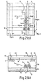
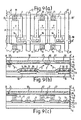
- Figs. 1(a) and 1(b) are side cross sections showing the operation of a liquid crystal display device according to the present invention.
- Fig.s 1(c) and 1(d) are front views of the liquid crystal display device.
- the thin film transistor device is omitted.
- stripes of electrodes are used to form a plurality of pixels, but the Figs. 1(a) to 1(d) show the structure of only one pixel (one cell).
- the side cross section of the cell when no voltage is applied is shown in Fig. 1(a), and the top view is shown in Fig. 1(c).
- Linear electrodes 1, 2, are formed on the inner sides of paired transparent substrates 3, over which an orientation control film 4 is applied and subjected to an orientation processing.
- a liquid crystal is held between the paired substrates 3.
- Bar shaped liquid crystal molecules 5 of the liquid crystal are oriented so that they are at a slight angle to the longitudinal direction of the electrodes 1, 2, i.e. 45 degrees ⁇ ⁇ LC ⁇ 90 degrees, when no electric field is applied.
- the liquid crystal molecules 5 change their directions and are aligned with the direction of the electric field 7, as shown in Figs. 1(b) and 1(d).
- the polarizing plates 6 By arranging the polarizing plates 6 at a specified angle 9, it is possible to change the light transmission factor when the electric field is applied. Thus, it is possible to provide a display having a contrast without using transparent electrodes.
- Figs. 1(a) and 1(b) show an arrangement in which the electrodes 1, 2, are provided separately on the upper and lower substrates respectively. However, it is possible to arrange them on one substrate and produce the same effect. Because the wiring pattern is very fine and may therefore deform due to heat and/or external forces, arranging the electrodes on a single substrate is preferable because it permits more precise alignment.
- the dielectric constant anisotropy of the liquid crystal is assumed to be positive, it may be negative.
- the initial orientation of the liquid crystal is set so that the liquid crystal molecules have a slight angle
- the one utilizes a mode in which the orientations of the liquid crystal molecules 5 on the upper and lower substrates 3 are almost parallel to each other (since color interface by birefringent phase difference is used, this mode is called a birefringent mode).
- the other structure has a mode in which the orientations of the liquid crystal molecules 5 on the upper and lower substrates 3 cross each other, twisting the molecular orientation in the cell (since light spiraling produced by rotation of the polarization plane in the liquid crystal composition layer is used, this mode is called a light spiraling mode).
- the molecular long axis 8 (optical axis) changes its direction in a plane almost parallel to the substrate interface, changing its angle with respect to the axis of a polarized plate (not shown in Figs. 1(a) and 1(b)) which is set at a specified angle. This results in a change in the light transmission factor.
- the application of a voltage similarly changes only the direction of the molecular long axis in the same plane.
- This mode utilizes a change in the light spiraling as the spiral is unraveled.
- T/T 0 sin 2 (2 ⁇ eff ) ⁇ sin 2 ( ⁇ d eff ⁇ n/ ⁇ )
- ⁇ eff is the effective direction of light axis of liquid crystal composition layer (an angle between the light axis and the polarized light transmission axis)
- d eff is the effective thickness of the liquid crystal composition layer having birefringence
- ⁇ n is the refractive index anisotropy
- ⁇ is the wave length of the light.
- the liquid crystal molecules are fixed at the interface and not all the liquid crystal molecules in the cell are parallel and uniformly oriented in one direction when an electric field is applied. Instead they are significantly deformed particularly near the interface. It is therefore convenient to assume an apparent uniform state as the average of these states.
- an effective value is used for the light axis direction of the liquid crystal composition layer.
- the polarizing plates should be arranged so that the light transmission axis (or absorption axis) of one of the polarizing plates is almost parallel to the orientation direction of the liquid crystal molecules (rubbing axis), i.e. ⁇ P2 ⁇ ⁇ LC1 ⁇ ⁇ LC2 .
- the value of ⁇ eff increases in dependence on the intensity of the electric field and becomes maximum at 45 degrees.
- the effective value of d eff ⁇ n should be set to half of the wavelength , i.e. 0.28 ⁇ m.
- there is a margin in the value and values between 0.21 ⁇ m and 0.36 ⁇ m and suitable, with the values between 0.24 ⁇ m and 0.33 ⁇ m being preferred.
- the polarizing plates need be arranged so that ⁇ eff in Equation 1 is almost 45° when no electric field is applied or an electric field of low intensity is applied.
- the value ⁇ eff decreases in dependence on the field intensity as opposed to the case of the normally closed characteristic.
- the ⁇ eff is minimum (i.e. zero)
- a significant amount of light will leak under this condition.
- the residual phase difference on the interface was 0.02 to 0.06 ⁇ m.
- this phase difference is represented as R f .
- the angle ⁇ R of the phase advance axis of the phase difference plate is set parallel to the effective light axis ⁇ eff of the liquid crystal composition layer when the voltage is applied.
- the angle of the phase advance axis should be aligned precisely with the residual phase difference that occurred when a voltage for displaying a dark state is applied. Therefore, to make the dark state compatible with the increased level of transmission factor and lightness of the bright state, the following relationship must be fulfilled. 0.21 ⁇ m ⁇ (d• ⁇ n-R f ) ⁇ 0.36 ⁇ m Or more preferably, 0.23 ⁇ m ⁇ (d• ⁇ n-R f ) ⁇ 0.33 ⁇ m II.
- a conventional twisted nematic (TN) system when the value of d• ⁇ n is set to around 0.50 ⁇ m, a first minimum condition, a high transmission factor and colorless light may be obtained. It has been found preferable to set the value in a range from 0.40 to 0.60 ⁇ m.
- the polarizing plates are arranged such that the transmission axis (or absorbing axis) of one of the polarizing plates is set almost parallel to the orientation direction (rubbing axis) of the liquid crystal molecules on the interface, i.e. ⁇ LC1 ⁇ ⁇ LC2 .
- the transmission axis of the other polarizing plate is set parallel to the orientation direction of the liquid crystal molecules, and for a normally open type, the transmission axis of the polarizing plate is set perpendicular to the orientation direction.
- the liquid crystal molecules on one of the substrates must be turned nearly 90°.
- the liquid crystal molecules need only be turned about 45°.
- the birefringence mode has a lower threshold value.
- the display mode In the display mode, the long axes of the liquid crystal molecules are almost parallel to the substrate at all times and do not become perpendicular to the substrate, so that there is only a small change in brightness when the visual angle is changed.
- This display mode gives a dark state, not by making the birefringence phase difference almost zero by applying voltage as in the case of a conventional display device, but by changing the angle between the long axes of liquid crystal molecules and the axis (absorbing or transmission axis) of the polarizing plate.
- the display mode of the present invention differs fundamentally from that of the conventional device.
- the birefringence phase difference of zero is obtained only in a visual direction perpendicular to the front or the substrate interface. Any inclination from this direction results in a birefringence phase difference, which means leakage of light in the case of the normally open type, causing reduction of contrast and reversal of tone levels.
- the display system of the present invention may have the long axis direction of the liquid crystal molecule (rubbing direction) on the substrate interface to be set in a specified direction different from 0° or 90° with respect to the electric field direction.
- the angle between the electric field direction and the long axis direction of the liquid crystal molecule on the substrate interface ⁇ LC ( ⁇ LC >0) need exceed 0° normally more than 0.5°, preferably more than 2°. If the angle is to be set exactly 0° degree, two kinds of deformations with different directions, and domains of two different states and their bordering are generated, and a possibility of deterioration in display quality occurs. If the angle is set to more than 0.5°, the apparent long axis direction of the liquid crystal molecule ( ⁇ LC (V)) increases uniformly with increasing intensity of electric field , and there is no possibility of the long axis being inclined in the reverse direction, i. e. ⁇ LC (V) ⁇ 0.
- the present system increases freedom in the selection of the orientation film material.
- the organic film can be used with ease as the orientation film simultaneously because there is no need to provide an inclination angle.
- the inclination angle preferably is set below 4° more preferably below 2°.
- the pixel electrodes and the common electrodes may have a structure in which an electric field generally parallel to the interface of the substrate is applied to the liquid crystal composition layer.
- the distance between the electrodes can be chosen to be longer than the distance between the mutually facing transparent electrodes of the conventional vertical electric field active matrix type liquid crystal display device.
- the equivalent cross section area of the electrode can be made smaller than that of the conventional arrangement.
- the electric resistance between the paired pixel electrodes of the present invention can be significantly larger than that of the mutually facing transparent electrodes of the conventional active matrix liquid crystal display device.
- the electrostatic capacitance between the pixel electrode and the common electrode of the present invention can be connected in parallel with capacitive devices, and a capacitive device having a high electric resistance can be achieved. Therefore, the electric charge accumulated in the pixel electrode can be held with ease, and sufficient holding characteristics can be achieved even if the area of the capacitive device is decreased. This area reduces the aperture factor and therefore needs to be small, if possible.
- the liquid crystal composition has an extremely high specific resistance, for instance 10 12 ⁇ cm.
- the margin for the previously described variation at the interface with the orientation film increases, and defects caused at the interfaces are rare. Consequently, processes such as inspection and ageing can be significantly simplified, and the present invention can contribute significantly to a lowering in the cost of thin film transistor type liquid crystal display devices.
- the present invention permits the pixel electrode to have a more simple shape than the known comb shaped electrode, the efficiency of utilization of the light is increased. It is not necessary to sacrifice some of the aperture factor, as in conventional methods for obtaining a capacitive device which can accumulate sufficient amount of electric charge.
- Replacement of the insulator for protecting the thin film transistors with an organic composition enables the dielectric constant to be lower than that when an inorganic composition is used, making it possible to suppress the electric field component generated in the vicinity of the pixel electrode in a vertical direction to the interface of the substrate. This enables the liquid crystal to operate in a wider region. It also contributes to an enhancement of brightness.
- the common electrode is used in common as the electrode for the adjacent pixel electrodes, it operates in the same way as the common electrode in the conventional active matrix type liquid crystal display device, but its structure can be simplified as compared with more conventional arrangements, and the aperture factor can be further increased.
- one vertical scanning period in the driving signal output from the scanning wiring driving means can be set shorter than the time constant expressed by a product of the specific resistance and the dielectric constant of the insulator of the capacitive devices. Hence, voltage variation at the pixel electrode can be reduced to sufficiently small value.
- the present invention permits a sufficient aperture factor to be maintained, without losing the described advantages (1) and (2) discussed above.
- the more simple structure of the electrode permits a practical high aperture factor to be achieved.
- the directions of the signal wiring and the common electrode cross over at the right angles to each other in order to form the comb shaped electrodes. That is, the signal wiring extends in a first direction (Y direction), and the common electrode extends in a direction perpendicular to the first direction (X direction).
- the present invention permits the avoidance of a complex structure such as comb shaped electrodes by having portions of the signal wiring, the pixel electrode, and the common electrode all extending in a common direction.
- the present invention also permits the structure to be simplified and the aperture factor increased by optionally providing the pixel electrode and the common electrode in different layers separated from each other by an insulating layer.
- This differs substantially from JP-B-63-21907 (1988) in that the pixel electrode and the common electrode are provided in separated layers.
- One advantage of this is that the region for the additional capacitive device which has been reduced by use of the lateral electric field system can be further reduced.
- overlapping of the pixel electrode and the common electrode separated by an insulating film becomes possible because they are in separate layers, and a load capacitance can be formed in the region of overlap.
- the overlapping parts can be used as a part of the wiring for the common electrodes. Hence, it is not necessary to sacrifice a part of the display in order to form a capacitive device. Accordingly, the aperture factor for the pixel can be further increased.
- the voltage holding characteristics may be significantly improved, and deterioration of the display quality rarely occurs even if severe contamination of the liquid crystal and lowering of off-resistance of the thin film transistor are generated.
- the insulating film formed between the pixel electrode and the common electrode can be commonly used in common as a gate insulating film of the scanning wiring (gate line) in the same layer. Therefore, there is no need to form a further film, and a process step for providing separate layers is not necessary.
- the common electrode and/or the pixel electrode preferably have shapes making a pattern which makes the aperture factor as large as possible.
- the pixel electrode or the common electrode has any of a flat shape selected from the group of shapes of a ring, a cross, a letter T, a letter ⁇ , a letter I, and a ladder. By suitably combining the selected shapes the aperture factor can be increased significantly, as compared with the case using comb shaped electrodes.
- the common electrode and the pixel electrode are in separate layers with an insulating film therebetween, it becomes possible to provide electrodes having shapes which overlap each other. Hence, the use of separate layers permits an increase in the aperture factor.
- the common electrode is composed of a metallic electrode whose surface is coated with self-oxidized film or self-nitrized film, short-circuit failure between the common electrode and the pixel electrode can be prevented even if the two electrodes mutually overlap, so that the high aperture factor and the prevention of the pixel defects are compatible.
- a gap d was formed by dispersing spherical polymer beads between the substrates so that the gap became 4.5 ⁇ m when the liquid crystal was sealed. Hence, ⁇ n ⁇ d was 0.324 ⁇ m.
- the resulting structure was clamped by two polarizing plates (not shown) (manufactured by e.g. Nitto Denko, with reference G1220DU).
- the structure of the thin film transistor and various electrodes for one pixel element are as shown in Fig. 2 (a) and Fig. 2 (b), such that the thin film transistor device (hatched portion in Fig. 2(a) has a pixel electrode (source electrode) 1, a signal electrode (drain electrode) 12, and a scanning electrode (gate electrode) 10.
- the pixel electrode 1 extends in a first direction (the vertical direction in Fig. 2)
- the signal electrode 12 and the common electrodes 2 extend in the first direction, and extend so as to cross over a plurality of pixels (the pixels being arranged vertically in Fig. 2)
- the thin film transistor device is located between the common electrodes 2.
- Signal waves having information are supplied to the signal electrode 12, and scanning waves are supplied to the scanning electrode 10 synchronously.
- a channel layer 16 composed of amorphous silicon (a-Si) and the thin film transistor composed from an insulating protective film 15 of silicon nitride (SiN) are arranged between adjacent common electrodes.
- Information signals are transmitted from the signal electrode 12 to the pixel electrode 1 through the thin film transistor, and a voltage is generated between the common electrode 2 and the liquid crystal 50.
- the common electrodes 2 are arranged at the facing interface side of the substrate and is enlarged in the thickness direction in the illustration in Fig. 2 (b). Therefore, although the electric field direction 7 shown in Fig. 2(b) appears to be inclined relative to the horizontal, the thickness of the liquid crystal layer 5 is actually about 6 ⁇ m as compared with the width of 48 ⁇ m, so that the inclination is very small and the supplied electric field direction is almost parallel to the interface of the substrate.
- a capacitive device 4 was formed in a structure in which the protruded pixel electrode 1 and the scanning wiring 10 held a gate insulating film 13 therebetween as shown in Fig. 1 (c).
- the electrostatic capacitance of the capacitive device 11 was about 21 fF.
- Each of the lines of the scanning wiring 10 and the signal wiring 11 were connected to a scanning wiring driving LSI and a signal wiring driving LSI respectively.
- Electric charge accumulates in the pixel electrode 1 to about 24 fF, which is a capacitance of parallel connection of the electrostatic capacitance between the pixel electrode 1 and the common electrode 2 and that of the capacitive device 11. Therefore, even if the specific resistance of the liquid crystal 50 is 5 x 10 10 ⁇ cm, the voltage variation at the pixel electrode 1 could be suppressed, and deterioration of the display quality was prevented.
- the number of the pixels were 40 (x3) x 30, and pixel pitch was 80 ⁇ m in a lateral direction (i.e. between the common electrodes) and 240 ⁇ m in a vertical direction (i.e. between the scanning electrodes).
- a high aperture factor of e.g. 50 % was obtained, with the scanning electrode 10 being of 12 ⁇ m wide and the interval between the adjacent scanning electrodes being 68 ⁇ m.
- Three stripe shaped color filters 17 being respective red (R), green (G) and blue (B) were provided on the substrate facing the substrate supporting the thin film transistors. On the color filter.
- a transparent resin 14 was laminated on the color filters 17 for surface flattening.
- the material of the transparent resin 14 was preferably, epoxy resin.
- a driving circuit was connected to the panel.
- FIG. 6 The structure of the driving circuit system in the present example is shown in Fig. 6.
- a signal electrode 23 and a common electrode 31 extend to the end of the display portion.
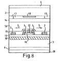
- Figs. 7 and 8 show the structure of the optical systems needed, Fig. 7 for being for a transmission type device and Fig. 8 being for a reflection type device with a reflector 30.
- the manufacturing process becomes simple, the production yield increases, and the manufacturing cost can be significantly reduced
- there is no need for extremely expensive facilities having vacuum furnaces for forming the transparent electrodes and there may thus be a significant reduction in investment in the manufacturing facilities, permitting and or accompanying cost reduction.
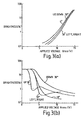
- the electro-optical characteristics showing the relationship between the effective voltage applied to the pixels and the brightness in the present example is shown in Fig. 3(a).
- the contrast ratios exceeded 150 when driven by voltages of e.g. 7 V.
- the difference between the characterising when the visual angle was changed laterally or vertically were significantly smaller than in conventional system (to be discussed in comparative example 1), and the display characteristics was not changed significantly even if the visual angle was changed.
- Orientation character of the liquid crystal was preferable, and domains of orientation defects are not generated.
- the aperture factor maintained a sufficiently high value, e.g. 50 % by simplifying the structure of the thin film transistor and the electrodes, and a bright display was achieved.
- the average transmission factor for the whole panel was 8.4 %.
- brightness is defined as the brightness of transmission when the two polarizing plates are arranged in parallel.
- the material of the liquid crystal 50 used in the first example had a dielectric constant of 6.7 and a specific resistance of 5 x 10 10 ⁇ cm
- silicon nitride was used for the insulator of the capacitive device 11 had a dielectric constant of 6.7 and a specific resistance of 5 x 10 16 ⁇ cm. That means that the specific resistances of both the liquid crystal composition and the insulator of the capacitive device 11 were over 10 10 ⁇ cm, and the product of the dielectric constant and the specific resistance of the silicon nitride, about 3 x 10 4 seconds, was larger than the product of the dielectric constant and the specific resistance of the liquid crystal composition about 0.03 seconds.
- One vertical scanning period for the driving signal output from the scanning wiring driving LSI was about 16.6 ms with an ordinary liquid display device, and the value satisfied the condition that the scanning period should be far less than about 3 x 10 4 seconds. Therefore, it was possible to derive the time constant for accumulated charge leaking from the pixel electrode 1. This facilitates the suppression of voltage variations at the pixel electrode 1, and consequently a satisfactory display quality can be obtained.
- the value of 5 x 10 10 ⁇ cm for the specific resistance of the liquid crystal is lower than that for the liquid crystal used for the conventional vertical electric field thin film transistor liquid display device, which is about 10 12 ⁇ cm. However, defects in the display quality were not generated.
- the comparison example referred to above was based on a conventional twisted nematic (TN) type of liquid crystal display device. Since this comparison example had a transparent electrode, the structure was complex and the manufacturing process was long compared with the first example described immediately above.
- the nematic liquid crystal used in the comparison example had a dielectric constant anisotropy ⁇ of positive 4.5 and a birefringence An of 0.072 (589 nm, 20°C), the same as those of the Embodiment.
- the gap was set to 7.3 ⁇ m and the twist angle to 90 degrees.
- ⁇ n - d is 0.526 ⁇ m.
- the scanning electrode which had been arranged on the substrate facing the substrate supporting the pixel in the first example was formed on the same substrate as the pixel electrode.
- the rest of the structure of the second example is generally the same as that of the first example and corresponding parts are indicated by the same reference numerals.
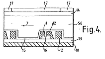
- the cross section of the structure of the thin film transistor and the electrodes in the second example are shown in Fig. 4.
- the pixel electrode 1, the signal electrode 12, and the scanning electrode 10 were all made from aluminum, and were formed simultaneously by deposited and etched. There is no conductive material on the other substrate.
- the material for the electrodes it should normally be a metal having low electric resistance, and chromium, copper, etc are thus suitable.
- the precision of alignment of photomasks is significantly higher than that for two facing glass substrates. Therefore, variations in the alignment of the electrodes can be suppressed when all of the four electrodes are formed on only one of the substrates, as in the second example because alignment of the electrodes during manufacturing can be only photomasks. Therefore, the second example is suitable for forming more precise patterns in comparison with the case when the scanning electrode is formed on the other substrate.
- a bright display having the same wide visual angle as the first example was obtained.
- the structure of the third example is generally the same as the first example except as will be described below. Components of the third example which correspond to the first example are indicated by the same reference numerals.
- Fig. 9(a) is a partial plan view of an active matrix type liquid crystal display device being the third example.
- Fig . 9(b) is a cross sectional view taken on line A-A' in Fig. 9 ( a)
- FIG. 9 (c) is a cross sectional view taken on line B-B' in Fig. 9 (a).
- the capacitive device 11 which had a structure in which the gate insulating film composed from silicon nitride 13 was located between the pixel electrode 1 and the scanning wiring 10 in the first example 1 was changed to a structure in which the liquid crystal composition layer 50 extended between parts of the pixel electrode 1 and the common electrode 2 which faced each other, as shown in Fig. 9 (c).
- the third example enables an electrostatic capacitance of the capacitive device 11 to be connected in parallel to an electrostatic capacitance between the pixel electrode 1 and the common electrode 2. Hence, any voltage variation at the signal wiring 10 does not affect the pixel electrode 1. Therefore, the voltage variation at the pixel electrode 1 could be reduced, reducing variations in the display.
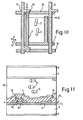
- Figs. 10 and 11 respectively show a plan view and a cross sectional view of an unit pixel of the fourth example, in which the pixel electrode 1 and the common electrode 2, are located on the same side of the liquid crystal material and are separated by an insulating layer.
- a scanning electrode 10 and a common electrode 2 of chromium were formed on a glass substrate, and a gate insulating film 13 of silicon nitride (SiN) was formed so as to cover the above electrodes.
- An amorphous film (a-Si) 16 was formed on a part of the scanning electrode 10 with the gate insulating film 13 therebetween as an active layer of the transistor.
- a signal electrode 12 and a pixel electrode 1 of molybdenum were formed to overlap on a part of the pattern of the a-Si film 16, and a protection and insulating film 15 of SiN film was formed so as to cover the resulting structure.
- the thin film transistor is operated by applying a voltage to the scanning electrode 13 of the thin film transistor, a voltage is applied to the pixel electrode 1.
- an electric field is induced between the pixel electrode 1 and the common electrode 2 the liquid crystal molecules change their orientation in the direction of the electric field and the light transmission changes.
- the common electrode 2 was formed on the same layer as the scanning electrode 10, and the pixel electrode 1 and the signal electrode 12 were separated from the common electrode 2 by the gate insulating film 13.
- the device of the fourth example thus differs from that of JP-B-63-21907 (1988), in that conventional comb shaped electrodes are not used, and the pixel electrode 1 and the common electrode 2 overlap with the gate insulating film 20 therebetween.
- the overlapping parts of the pixel electrode 1 and the common electrode 2 operate as an additional capacitance which is connected in parallel to the liquid crystal capacitance, and accordingly, it becomes possible to increase the holding ability of the liquid crystal charged voltage.
- This advantage cannot be achieved by conventional comb shaped electrodes, and the advantages are achieved only by separating the pixel electrode 1 and the signal electrode 12 from the common electrode by insulation manner.
- Fig. 10 reveals, it is not necessary to form a capacitive device by sacrificing a part of the display region, as in the case when the pixel electrode and the common electrode are formed on the same substrate, and all that is needed is to make an overlap in a part of the wiring for leading out the common electrode outside the display region.
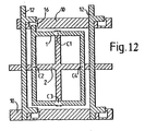
- Fig. 12 shows an plan view of a unit pixel in the fifth example in which the pixel electrode 1 and the common electrode 2 are located in different layers separated by an insulating layer.
- the cross sectional structure of the fifth example is similar to that of the fourth example (Fig. 17).
- the common electrode 2 is cruciform and the pixel electrode 1 forms a closed loop.
- the pixel electrode 1 and the common electrode 2 overlap at parts C1, C2, C3 and C4 in Fig. 18, so as to form additional capacitances.
- the distance between the common electrode 2 and the scanning electrode 10 can be made wide, and thus failures due to short circuits between the common electrode 2 and the scanning electrode 10 can be prevented. Since the pixel electrode 1 is in the form of a closed loop, normal operation can be maintained as power is supplied to all parts of the pixel electrode even if a breaking occurs at an arbitrary portion of the pixel electrode, unless a break occurs at two or more parts.
- the structure of the fifth example has a redundancy for breaking of the pixel electrode 1 and the production yield can therefore be increased.
- redundancy it becomes possible to reduce the wiring gap of the closed loop electrode 1, to make that electrode 1 is close to the wiring part of the scanning electrode 10 when they are arranged in different layers, so increasing the aperture factor.
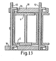
- Fig. 13 shows a plan view of a unit pixel in a first embodiment of the present invention in which the pixel electrode 1 and the common electrode 2 are located in different layers separated by an insulating layer.
- the cross sectional structure of the first embodiment is similar to that of the fourth example (Fig. 11).
- the pixel electrode 1 is in the shape of a letter I
- the common electrode 2 is in the form of a closed loop.
- the aperture factor can be improved as in the fifth example, and the additional capacitance can be increased because the overlapping of the pixel electrode 1 and the common electrode 2 can be increased.
Claims (7)
- Dispositif d'affichage à cristaux liquides, comprenant :une paire de substrats (3),un film d'orientation (4) disposé sur une grande surface de chaque substrat (3),une couche (50) de cristaux liquides intercalée entre lesdits films d'orientation (4) ;plusieurs électrodes de balayage (10) disposées sur ladite grande surface d'un desdits substrats ;plusieurs électrodes (12) de signaux disposées de façon à croiser sous la forme d'une matrice lesdites plusieurs électrodes de balayage ; etune pluralité de transistors à couches minces formés à des emplacements correspondant à des points de croisement respectifs desdites plusieurs électrodes de balayage (10) et desdites plusieurs électrodes (12) de signaux ;un pixel respectif étant formé dans des régions respectives entourées par lesdites plusieurs électrodes de balayage et lesdites plusieurs électrodes de signaux, le pixel respectif comportant une électrode (1) de pixel connectée à l'un, respectif, desdits transistors à couches minces, au moins une partie de ladite électrode de pixel s'étendant dans la même direction que la direction d'extension desdites électrodes (12) de signaux, et au moins une partie d'une électrode commune (2) s'étendant dans la même direction d'extension que la direction d'extension desdites électrodes (12) de signaux ; caractérisé en ce queladite partie de ladite électrode commune (2) s'étendant dans la même direction que la direction d'extension desdites électrodes (12) de signaux est située plus près desdites électrodes (12) de signaux que ladite partie de ladite électrode (1) de pixel s'étendant dans la même direction que la direction d'extension desdites électrodes (12) de signaux, et au moins une partie de ladite électrode (1) de pixel est chevauchée par une partie de ladite électrode commune (2) , un film isolant (13) étant intercalé entre elles.
- Dispositif d'affichage à cristaux liquides selon la revendication 1, dans lequel ladite électrode (1) de pixel et ladite électrode commune (2) sont agencées de façon que, par application d'une tension entre ladite électrode (1) de pixel et ladite électrode commune (2), un champ électrique soit généré dans ladite couche (50) de cristaux liquides.
- Dispositif d'affichage à cristaux liquides selon la revendication 1 ou la revendication 2, dans lequel
ladite électrode commune (2) est constituée par une électrode métallique dont la surface est revêtue d'un film auto-oxydé ou d'un film auto-nitruré. - Dispositif d'affichage à cristaux liquides selon l'une quelconque des revendications 1 à 3, comprenant en outre :un moyen de polarisation constitué d'au moins un polariseur disposé sur un substrat de ladite paire de substrats (3) sur une face opposée à la face sur laquelle est disposé le film d'orientation (4) ; etun réflecteur disposé sur un autre substrat de ladite paire de substrats sur une face opposée à la face sur laquelle est disposé ledit film d'orientation (4).
- Dispositif d'affichage à cristaux liquides selon l'une quelconque des revendications 1 à 4, dans lequel
la direction d'orientation ΦLC1 du côté d'un premier substrat de ladite couche (50) de cristaux liquides est approximativement parallèle à la direction d'orientation ΦLC2 du côté de l'autre de substrat de ladite couche (50) de cristaux liquides, et
le produit d · Δn de l'épaisseur d et de l'anisotropie de l'indice de réfraction Δn de ladite couche (50) de cristaux liquides est compris entre 0,21 µm et 0,36 µm. - Dispositif d'affichage à cristaux liquides selon l'une quelconque des revendications 1 à 4, dans lequel
la direction d'orientation ΦLC1 du côté d'un premier substrat de ladite couche (50) de cristaux liquides croise la direction d'orientation ΦLC2 du côté de l'autre substrat de ladite couche (50) de cristaux liquides, de façon que les deux directions d'orientation soient orientées l'une par rapport à l'autre suivant un angle |ΦLC1-ΦLC2|, ledit angle étant compris entre 80 degrés et 100 degrés, et
le produit d · Δn de l'épaisseur d et de l'anisotropie de l'indice de réfraction Δn de ladite couche (50) de cristaux liquides est compris entre 0,40 µm et 0,60 µm. - Dispositif d'affichage à cristaux liquides selon l'une quelconque des revendications 1 à 6, dans lequel
ladite électrode (1) de pixel comporte en outre :une partie s'étendant dans la même direction que la direction d'extension desdites électrodes de balayage (10) ; etladite électrode commune (2) comporte :une partie s'étendant dans la même direction que la direction d'extension desdites électrodes de balayage (10) ; etau moins ladite partie de ladite électrode de pixel s'étendant dans la même direction que la direction d'extension desdites électrodes de balayage est chevauchée par ladite partie de ladite électrode commune s'étendant dans la même direction que la direction d'extension desdites électrodes de balayage, un film isolant étant intercalé entre elles pour former une capacité au niveau de ladite partie chevauchée.
Applications Claiming Priority (7)
| Application Number | Priority Date | Filing Date | Title |
|---|---|---|---|
| JP24993892 | 1992-09-18 | ||
| JP24993892 | 1992-09-18 | ||
| JP249938/92 | 1992-09-18 | ||
| JP735593 | 1993-01-20 | ||
| JP735593 | 1993-01-20 | ||
| JP7355/93 | 1993-01-20 | ||
| EP93307154A EP0588568B1 (fr) | 1992-09-18 | 1993-09-10 | Dispositif d'affichage à cristal liquide |
Related Parent Applications (1)
| Application Number | Title | Priority Date | Filing Date |
|---|---|---|---|
| EP93307154A Division EP0588568B1 (fr) | 1992-09-18 | 1993-09-10 | Dispositif d'affichage à cristal liquide |
Publications (3)
| Publication Number | Publication Date |
|---|---|
| EP0916992A2 EP0916992A2 (fr) | 1999-05-19 |
| EP0916992A3 EP0916992A3 (fr) | 1999-06-02 |
| EP0916992B1 true EP0916992B1 (fr) | 2003-11-26 |
Family
ID=26341630
Family Applications (3)
| Application Number | Title | Priority Date | Filing Date |
|---|---|---|---|
| EP00118739A Withdrawn EP1061404A1 (fr) | 1992-09-18 | 1993-09-10 | Dispositif d'affichage à cristal liquide |
| EP99102559A Expired - Lifetime EP0916992B1 (fr) | 1992-09-18 | 1993-09-10 | Dispositif d'affichage à cristal liquide |
| EP93307154A Expired - Lifetime EP0588568B1 (fr) | 1992-09-18 | 1993-09-10 | Dispositif d'affichage à cristal liquide |
Family Applications Before (1)
| Application Number | Title | Priority Date | Filing Date |
|---|---|---|---|
| EP00118739A Withdrawn EP1061404A1 (fr) | 1992-09-18 | 1993-09-10 | Dispositif d'affichage à cristal liquide |
Family Applications After (1)
| Application Number | Title | Priority Date | Filing Date |
|---|---|---|---|
| EP93307154A Expired - Lifetime EP0588568B1 (fr) | 1992-09-18 | 1993-09-10 | Dispositif d'affichage à cristal liquide |
Country Status (4)
| Country | Link |
|---|---|
| US (6) | US5598285A (fr) |
| EP (3) | EP1061404A1 (fr) |
| KR (4) | KR100356604B1 (fr) |
| DE (2) | DE69333323T2 (fr) |
Families Citing this family (383)
| Publication number | Priority date | Publication date | Assignee | Title |
|---|---|---|---|---|
| DE69333323T2 (de) * | 1992-09-18 | 2004-09-16 | Hitachi, Ltd. | Flüssigkristall-Anzeigevorrichtung |
| JPH06301044A (ja) * | 1993-04-14 | 1994-10-28 | Matsushita Electric Ind Co Ltd | 液晶表示パネルとその製造法 |
| JP3543351B2 (ja) * | 1994-02-14 | 2004-07-14 | 株式会社日立製作所 | アクティブマトリクス型液晶表示装置 |
| US6830787B1 (en) * | 1994-03-17 | 2004-12-14 | Hitachi, Ltd. | Active matrix liquid crystal display apparatus |
| JPH10325961A (ja) * | 1994-03-17 | 1998-12-08 | Hitachi Ltd | アクティブマトリクス型液晶表示装置 |
| TW262553B (fr) * | 1994-03-17 | 1995-11-11 | Hitachi Seisakusyo Kk | |
| JP2643835B2 (ja) * | 1994-06-06 | 1997-08-20 | 日本電気株式会社 | 液晶表示装置およびその駆動方法 |
| EP0717304B1 (fr) * | 1994-06-24 | 2001-09-19 | Hitachi, Ltd. | Afficheur a cristaux liquides de type matrice active et son procede d'activation |
| TW289097B (fr) * | 1994-08-24 | 1996-10-21 | Hitachi Ltd | |
| US6525261B1 (en) | 1994-09-22 | 2003-02-25 | Semiconductor Energy Laboratory Co., Ltd. | Resin composition and an electronic device using the same |
| US6198464B1 (en) | 1995-01-13 | 2001-03-06 | Hitachi, Ltd. | Active matrix type liquid crystal display system and driving method therefor |
| DE19528106A1 (de) * | 1995-02-03 | 1996-08-08 | Merck Patent Gmbh | Elektrooptische Flüssigkristallanzeige |
| EP0807153B1 (fr) * | 1995-02-03 | 2001-03-28 | MERCK PATENT GmbH | Affichage electro-optique a cristaux liquides |
| TW354380B (en) * | 1995-03-17 | 1999-03-11 | Hitachi Ltd | A liquid crystal device with a wide visual angle |
| US5774099A (en) * | 1995-04-25 | 1998-06-30 | Hitachi, Ltd. | Liquid crystal device with wide viewing angle characteristics |
| TW477905B (en) * | 1995-06-14 | 2002-03-01 | Hitachi Ltd | Liquid crystal display device formed of high resistance black matrix with wide view angle |
| JP3289099B2 (ja) * | 1995-07-17 | 2002-06-04 | 株式会社日立製作所 | アクティブマトリクス型液晶表示装置およびその製造方法 |
| KR100230793B1 (ko) * | 1995-07-28 | 1999-11-15 | 김영환 | 엘씨디의구동방식 |
| JP3464570B2 (ja) * | 1995-08-21 | 2003-11-10 | 株式会社 日立ディスプレイズ | カラー液晶表示素子 |
| US5760856A (en) * | 1995-09-08 | 1998-06-02 | Hitachi, Ltd. | In-plane field type liquid crystal display device with light shielding pattern suitable for high aperture ratio |
| JPH0980383A (ja) * | 1995-09-11 | 1997-03-28 | Hitachi Ltd | 液晶表示装置 |
| US6266117B1 (en) * | 1995-09-14 | 2001-07-24 | Hiatchi, Ltd | Active-matrix liquid crystal display |
| TW454101B (en) * | 1995-10-04 | 2001-09-11 | Hitachi Ltd | In-plane field type liquid crystal display device comprising liquid crystal molecules with more than two different kinds of reorientation directions and its manufacturing method |
| TWI234674B (en) * | 1995-10-12 | 2005-06-21 | Hitachi Ltd | In-plane electric field LCD panel with structure for preventing electric charging |
| JP3458562B2 (ja) | 1995-10-12 | 2003-10-20 | 株式会社日立製作所 | 液晶表示装置及びその製造方法 |
| KR100405893B1 (ko) * | 1995-10-23 | 2004-10-06 | 가부시끼가이샤 히다치 세이사꾸쇼 | 액정표시장치 |
| JP3200552B2 (ja) * | 1995-10-26 | 2001-08-20 | 株式会社日立製作所 | アクティブマトリクス型液晶表示装置 |
| US5959599A (en) | 1995-11-07 | 1999-09-28 | Semiconductor Energy Laboratory Co., Ltd. | Active matrix type liquid-crystal display unit and method of driving the same |
| TW329500B (en) | 1995-11-14 | 1998-04-11 | Handotai Energy Kenkyusho Kk | Electro-optical device |
| JPH09146108A (ja) | 1995-11-17 | 1997-06-06 | Semiconductor Energy Lab Co Ltd | 液晶表示装置およびその駆動方法 |
| US5745207A (en) * | 1995-11-30 | 1998-04-28 | Matsushita Electric Industrial Co., Ltd. | Active matrix liquid crystal display having electric fields parallel to substrates |
| US6014190A (en) * | 1995-11-30 | 2000-01-11 | Samsung Electronics Co., Ltd. | In-plane switching liquid crystal display and a manufacturing method thereof |
| JP3294748B2 (ja) * | 1995-12-04 | 2002-06-24 | 株式会社日立製作所 | アクティブマトリックス型液晶表示パネル |
| JP3963974B2 (ja) * | 1995-12-20 | 2007-08-22 | 株式会社半導体エネルギー研究所 | 液晶電気光学装置 |
| US5852485A (en) * | 1996-02-27 | 1998-12-22 | Sharp Kabushiki Kaisha | Liquid crystal display device and method for producing the same |
| US6911962B1 (en) | 1996-03-26 | 2005-06-28 | Semiconductor Energy Laboratory Co., Ltd. | Driving method of active matrix display device |
| JP4026870B2 (ja) * | 1996-04-04 | 2007-12-26 | エルジー フィリップス エルシーディー カンパニー リミテッド | 液晶表示装置の製造方法 |
| KR100225910B1 (ko) | 1996-04-04 | 1999-10-15 | 구자홍 | 액정표시장치(liquid crystal display device) |
| US7098980B2 (en) * | 1996-04-16 | 2006-08-29 | Obayashiseikou Co., Ltd. | Liquid crystal display device comprising pixel and common electrodes inclined in first and second directions to form a zigzag shape which is symmetrical relative to alignment direction of liquid crystal |
| US20020044249A1 (en) * | 1996-04-16 | 2002-04-18 | Naoto Hirota | Liquid crystal display device |
| JP3194127B2 (ja) * | 1996-04-16 | 2001-07-30 | 大林精工株式会社 | 液晶表示装置 |
| JP3087668B2 (ja) * | 1996-05-01 | 2000-09-11 | 日本電気株式会社 | 液晶表示装置、その製造方法およびその駆動方法 |
| JP3396130B2 (ja) * | 1996-06-03 | 2003-04-14 | シャープ株式会社 | 液晶表示装置 |
| JP2735099B2 (ja) * | 1996-06-11 | 1998-04-02 | 日本電気株式会社 | 液晶表示装置 |
| JP2776376B2 (ja) * | 1996-06-21 | 1998-07-16 | 日本電気株式会社 | アクティブマトリクス液晶表示パネル |
| KR100209531B1 (ko) * | 1996-06-22 | 1999-07-15 | 구자홍 | 액정표시장치 |
| US6005648A (en) * | 1996-06-25 | 1999-12-21 | Semiconductor Energy Laboratory Co., Ltd. | Display device |
| JP2973934B2 (ja) * | 1996-07-11 | 1999-11-08 | 日本電気株式会社 | 液晶表示装置、及び液晶表示装置を搭載した電子機器 |
| JP3148129B2 (ja) * | 1996-08-07 | 2001-03-19 | 株式会社日立製作所 | アクティブマトリクス基板とその製法および液晶表示装置 |
| JPH1073823A (ja) * | 1996-09-02 | 1998-03-17 | Hitachi Ltd | アクティブマトリクス型液晶表示装置 |
| KR100236518B1 (ko) * | 1996-09-21 | 2000-01-15 | 구본준 | 액정표시장치 |
| US6812985B1 (en) | 1996-09-23 | 2004-11-02 | Lg.Philips Lcd Co., Ltd. | Liquid crystal display device |
| JP3460527B2 (ja) * | 1996-10-04 | 2003-10-27 | シャープ株式会社 | 液晶表示装置 |
| KR100258435B1 (ko) | 1996-10-22 | 2000-06-01 | 윤종용 | 평면 구동 방식의 액정 표시 장치용 기판 |
| KR19980028453A (ko) * | 1996-10-22 | 1998-07-15 | 김광호 | 평면 구동 방식의 액정 표시 장치 |
| JP3120751B2 (ja) * | 1996-11-06 | 2000-12-25 | 日本電気株式会社 | 横電界方式の液晶表示装置 |
| US5952988A (en) * | 1996-11-12 | 1999-09-14 | University Technology Corp | Display having gradient response pixels |
| JPH10142635A (ja) * | 1996-11-15 | 1998-05-29 | Furontetsuku:Kk | 液晶表示装置 |
| JP3788649B2 (ja) | 1996-11-22 | 2006-06-21 | 株式会社半導体エネルギー研究所 | 液晶表示装置 |
| JP3145938B2 (ja) * | 1996-11-28 | 2001-03-12 | 日本電気株式会社 | 液晶表示装置 |
| KR100250795B1 (ko) * | 1996-11-29 | 2000-04-01 | 김영환 | 액정 표시 소자 및 그 제조방법 |
| KR100250796B1 (ko) * | 1996-11-29 | 2000-04-01 | 김영환 | 액정 표시 소자 및 그 제조방법 |
| DE19650634B4 (de) * | 1996-12-06 | 2006-03-30 | Merck Patent Gmbh | Flüssigkristallines Medium |
| DE19748618B4 (de) * | 1996-12-05 | 2009-12-03 | Merck Patent Gmbh | Flüssigkristallmischung und ihre Verwendung in einer elektrooptischen Flüssigkristallanzeige |
| US6532053B2 (en) | 1996-12-18 | 2003-03-11 | Hitachi, Ltd. | Transverse electric field system liquid crystal display device suitable for improving aperture ratio |
| US6046716A (en) | 1996-12-19 | 2000-04-04 | Colorado Microdisplay, Inc. | Display system having electrode modulation to alter a state of an electro-optic layer |
| US6078303A (en) | 1996-12-19 | 2000-06-20 | Colorado Microdisplay, Inc. | Display system having electrode modulation to alter a state of an electro-optic layer |
| US6433764B1 (en) | 1997-01-23 | 2002-08-13 | Lg. Philips Lcd Co., Ltd. | Liquid crystal display |
| JP3883244B2 (ja) | 1997-01-23 | 2007-02-21 | エルジー フィリップス エルシーディー カンパニー リミテッド | 液晶表示装置 |
| JP3376379B2 (ja) * | 1997-02-20 | 2003-02-10 | 富士通ディスプレイテクノロジーズ株式会社 | 液晶表示パネル、液晶表示装置及びその製造方法 |
| DE19707807A1 (de) * | 1997-02-27 | 1998-09-03 | Merck Patent Gmbh | Elektrooptische Flüssigkristallanzeige |
| US6067140A (en) * | 1997-03-03 | 2000-05-23 | Lg Electronics Inc. | Liquid crystal display device and method of manufacturing same |
| DE19803112A1 (de) | 1997-03-14 | 1998-09-17 | Merck Patent Gmbh | Elektrooptische Flüssigkristallanzeige |
| TW531686B (en) | 1997-04-11 | 2003-05-11 | Hitachi Ltd | Liquid crystal display device |
| TW508470B (en) * | 1997-05-09 | 2002-11-01 | Hitachi Ltd | Liquid crystal display device |
| KR100257369B1 (ko) | 1997-05-19 | 2000-05-15 | 구본준 | 횡전계방식액정표시장치 |
| US6972818B1 (en) | 1997-05-19 | 2005-12-06 | Lg.Philips Lcd Co., Ltd. | In-plane switching mode liquid crystal display device |
| KR100257370B1 (ko) | 1997-05-19 | 2000-05-15 | 구본준 | 횡전계방식액정표시장치 |
| JP4024901B2 (ja) * | 1997-05-22 | 2007-12-19 | エルジー フィリップス エルシーディー カンパニー リミテッド | アクティブマトリックス型液晶表示装置 |
| KR100223601B1 (ko) * | 1997-05-29 | 1999-10-15 | 윤종용 | 액정 표시 장치 |
| CN1567066B (zh) * | 1997-05-30 | 2010-05-12 | 三星电子株式会社 | 液晶显示器 |
| KR100254856B1 (ko) | 1997-05-30 | 2000-05-01 | 김영환 | 액정 표시 소자 |
| TW434443B (en) * | 1997-05-30 | 2001-05-16 | Samsung Electronics Co Ltd | Liquid crystal display |
| US6704083B1 (en) * | 1997-05-30 | 2004-03-09 | Samsung Electronics, Co., Ltd. | Liquid crystal display including polarizing plate having polarizing directions neither parallel nor perpendicular to average alignment direction of molecules |
| WO1998057222A1 (fr) * | 1997-06-10 | 1998-12-17 | Lg. Philips Lcd Co., Ltd. | Afficheur a cristaux liquides avec angle de vision large et son procede de fabrication |
| DE69840797D1 (de) | 1997-06-12 | 2009-06-10 | Sharp Kk | Anzeigevorrichtung mit vertikal ausgerichtetem Flüssigkristall |
| KR100293806B1 (ko) * | 1997-06-25 | 2001-10-24 | 박종섭 | 액정표시소자 |
| TW476856B (en) * | 1997-06-27 | 2002-02-21 | Toshiba Corp | Liquid crystal display device |
| KR100272267B1 (ko) * | 1997-06-27 | 2000-11-15 | 김영환 | 액정 표시 소자 |
| KR100262405B1 (ko) * | 1997-06-27 | 2000-08-01 | 김영환 | 액정 표시 소자 |
| US6184961B1 (en) | 1997-07-07 | 2001-02-06 | Lg Electronics Inc. | In-plane switching mode liquid crystal display device having opposite alignment directions for two adjacent domains |
| KR100251512B1 (ko) | 1997-07-12 | 2000-04-15 | 구본준 | 횡전계방식 액정표시장치 |
| JP2991995B2 (ja) * | 1997-07-14 | 1999-12-20 | 三菱電機株式会社 | 液晶表示装置 |
| US6335770B1 (en) * | 1997-07-22 | 2002-01-01 | Lg. Philips Lcd Co., Ltd. | In-plane switching mode LCD with specific arrangement of common bus line, data electrode, and common electrode |
| US6697140B2 (en) | 1997-07-29 | 2004-02-24 | Lg. Philips Lcd Co., Ltd. | In-plane switching mode liquid crystal display device wherein portions of second gate line overlaps with data electrode |
| JPH1152403A (ja) * | 1997-07-31 | 1999-02-26 | Mitsubishi Electric Corp | 液晶表示装置 |
| KR100268104B1 (ko) * | 1997-08-13 | 2000-10-16 | 윤종용 | 공통 전극 라인을 갖는 평면 구동 방식 액정 표시 장치 및그 제조 방법 |
| KR100255931B1 (ko) | 1997-08-14 | 2000-05-01 | 구본준, 론 위라하디락사 | 횡전계방식 액정표시소자 |
| US6549258B1 (en) | 1997-09-04 | 2003-04-15 | Lg. Philips Lcd Co., Ltd. | Hybrid switching mode liquid crystal display device |
| KR100293434B1 (ko) | 1997-09-08 | 2001-08-07 | 구본준, 론 위라하디락사 | 횡전계방식액정표시소자 |
| JP3212920B2 (ja) * | 1997-09-17 | 2001-09-25 | 日本電気株式会社 | 液晶表示装置 |
| JPH11119227A (ja) * | 1997-10-13 | 1999-04-30 | Hitachi Ltd | 液晶表示装置 |
| US6133977A (en) * | 1997-10-21 | 2000-10-17 | Samsung Electronics Co., Ltd. | Liquid crystal displays having common electrode overlap with one or more data lines |
| KR100502095B1 (ko) * | 1998-01-21 | 2005-12-09 | 삼성전자주식회사 | 새로운 전극 배열을 갖는 액정 표시 장치 |
| US6577368B1 (en) | 1997-11-03 | 2003-06-10 | Samsung Electronics Co., Ltd. | IPS-LCD having a third electrode having aperture and formed on counter substrate |
| JP3723336B2 (ja) * | 1997-11-18 | 2005-12-07 | 三洋電機株式会社 | 液晶表示装置 |
| KR100279257B1 (ko) * | 1997-12-03 | 2001-01-15 | 김영환 | 액정표시장치 |
| KR100257480B1 (ko) * | 1997-12-08 | 2000-06-01 | 김영환 | 액정 표시 소자 |
| KR100471391B1 (ko) * | 1997-12-08 | 2005-06-07 | 비오이 하이디스 테크놀로지 주식회사 | 액정 표시 소자 |
| KR100293808B1 (ko) * | 1997-12-17 | 2001-10-24 | 박종섭 | 색띰방지용액정표시장치 |
| US6147666A (en) * | 1997-12-22 | 2000-11-14 | Yaniv; Zvi | Multipole liquid crystal display |
| US6281952B1 (en) | 1997-12-26 | 2001-08-28 | Sharp Kabushiki Kaisha | Liquid crystal display |
| KR100293436B1 (ko) | 1998-01-23 | 2001-08-07 | 구본준, 론 위라하디락사 | 횡전계방식액정표시장치 |
| JP2982869B2 (ja) * | 1998-04-16 | 1999-11-29 | インターナショナル・ビジネス・マシーンズ・コーポレイション | 液晶表示装置 |
| US6300926B1 (en) * | 1998-04-27 | 2001-10-09 | Hitachi, Ltd. | Active matrix type liquid crystal display |
| KR100306800B1 (ko) * | 1998-05-29 | 2002-06-20 | 박종섭 | 액정 표시 장치 및 그 제조 방법 |
| KR100293811B1 (ko) * | 1998-05-29 | 2001-10-26 | 박종섭 | 아이피에스모드의액정표시장치 |
| US6335776B1 (en) * | 1998-05-30 | 2002-01-01 | Lg. Philips Lcd Co., Ltd. | Multi-domain liquid crystal display device having an auxiliary electrode formed on the same layer as the pixel electrode |
| JP4364332B2 (ja) | 1998-06-23 | 2009-11-18 | シャープ株式会社 | 液晶表示装置 |
| KR100344844B1 (ko) | 1998-07-07 | 2002-11-18 | 엘지.필립스 엘시디 주식회사 | 액정표시소자및그제조방법 |
| KR100357213B1 (ko) | 1998-07-23 | 2002-10-18 | 엘지.필립스 엘시디 주식회사 | 멀티도메인 액정표시소자 |
| JP3114723B2 (ja) * | 1998-08-03 | 2000-12-04 | 日本電気株式会社 | 液晶表示装置およびその製造方法 |
| AU9247398A (en) * | 1998-08-06 | 2000-02-28 | Victor A. Konovalov | Liquid-cristal display and the method of its fabrication |
| KR100320416B1 (ko) | 1998-08-26 | 2002-09-17 | 엘지.필립스 엘시디 주식회사 | 횡전계방식액정표시소자 |
| US6654090B1 (en) | 1998-09-18 | 2003-11-25 | Lg. Philips Lcd Co., Ltd. | Multi-domain liquid crystal display device and method of manufacturing thereof |
| KR100313949B1 (ko) | 1998-11-11 | 2002-09-17 | 엘지.필립스 엘시디 주식회사 | 멀티도메인액정표시소자 |
| US6525794B1 (en) | 1998-10-19 | 2003-02-25 | Lg. Philips Lcd Co., Ltd. | Multi-domain liquid crystal display device having a dielectric frame controlling alignment of the liquid crystal molecules |
| JP2000147511A (ja) * | 1998-11-13 | 2000-05-26 | Fujitsu Ltd | 液晶表示装置およびその製造方法 |
| US6900869B1 (en) | 1998-11-25 | 2005-05-31 | Lg. Philips Lcd Co., Ltd. | Multi-domain liquid crystal display device with particular dielectric structures |
| US6809787B1 (en) * | 1998-12-11 | 2004-10-26 | Lg.Philips Lcd Co., Ltd. | Multi-domain liquid crystal display device |
| KR100303351B1 (ko) * | 1998-12-17 | 2002-06-20 | 박종섭 | 수직 배향 모드 액정 표시 장치 |
| JP4041610B2 (ja) * | 1998-12-24 | 2008-01-30 | シャープ株式会社 | 液晶表示装置 |
| US6287899B1 (en) * | 1998-12-31 | 2001-09-11 | Samsung Electronics Co., Ltd. | Thin film transistor array panels for a liquid crystal display and a method for manufacturing the same |
| JP3378820B2 (ja) * | 1999-01-20 | 2003-02-17 | 三洋電機株式会社 | 垂直配向型液晶表示装置 |
| JP4094759B2 (ja) * | 1999-02-05 | 2008-06-04 | 株式会社日立製作所 | 液晶表示装置 |
| KR100339332B1 (ko) | 1999-02-08 | 2002-06-03 | 구본준, 론 위라하디락사 | 멀티도메인 액정표시소자 |
| US6791647B1 (en) | 1999-02-24 | 2004-09-14 | Lg Philips Lcd Co., Ltd. | Multi-domain liquid crystal display device |
| KR100357216B1 (ko) | 1999-03-09 | 2002-10-18 | 엘지.필립스 엘시디 주식회사 | 멀티도메인 액정표시소자 |
| KR100519366B1 (ko) | 1999-04-03 | 2005-10-07 | 엘지.필립스 엘시디 주식회사 | 멀티도메인 액정표시소자 |
| US6524876B1 (en) * | 1999-04-08 | 2003-02-25 | Samsung Electronics Co., Ltd. | Thin film transistor array panels for a liquid crystal display and a method for manufacturing the same |
| DE10018598A1 (de) | 1999-04-30 | 2000-11-02 | Merck Patent Gmbh | Elektrooptische Flüssigkristallanzeige |
| KR100308161B1 (ko) * | 1999-05-07 | 2001-09-26 | 구본준, 론 위라하디락사 | 멀티도메인 액정표시소자 |
| JP2000321599A (ja) | 1999-05-10 | 2000-11-24 | Hitachi Ltd | 液晶表示装置 |
| JP2000321587A (ja) * | 1999-05-11 | 2000-11-24 | Internatl Business Mach Corp <Ibm> | 液晶表示素子及びその製造方法 |
| JP3766563B2 (ja) | 1999-05-17 | 2006-04-12 | 株式会社日立製作所 | 液晶表示装置 |
| US6449026B1 (en) * | 1999-06-25 | 2002-09-10 | Hyundai Display Technology Inc. | Fringe field switching liquid crystal display and method for manufacturing the same |
| KR100311211B1 (ko) * | 1999-06-29 | 2001-11-02 | 박종섭 | 반사형 액정 표시 장치 |
| KR100627107B1 (ko) | 1999-07-31 | 2006-09-25 | 엘지.필립스 엘시디 주식회사 | 멀티 도메인 액정표시소자 및 그 제조방법 |
| US6868154B1 (en) * | 1999-08-02 | 2005-03-15 | Robert O. Stuart | System and method for providing a service to a customer via a communication link |
| CN1378657A (zh) * | 1999-10-06 | 2002-11-06 | 松下电器产业株式会社 | 液晶元件、液晶显示装置及其制造方法 |
| KR100433596B1 (ko) * | 1999-10-21 | 2004-05-31 | 마쯔시다덴기산교 가부시키가이샤 | 액정표시장치 |
| JP3391343B2 (ja) | 1999-10-26 | 2003-03-31 | 日本電気株式会社 | アクティブマトリクス基板及びその製造方法 |
| US6671019B1 (en) | 1999-11-12 | 2003-12-30 | Case Western Reserve University | Electrode patterns for liquid crystal cells |
| TW548475B (en) * | 1999-11-18 | 2003-08-21 | Ind Tech Res Inst | Fabrication method of homeotropic aligned LCD structure and the bump structure |
| US6639641B1 (en) | 1999-11-25 | 2003-10-28 | Lg.Philips Lcd Co., Ltd. | Multi-domain liquid crystal display device |
| KR100595294B1 (ko) | 1999-12-14 | 2006-07-03 | 엘지.필립스 엘시디 주식회사 | 횡전계방식 액정표시장치용 칼라필터 기판의 제조방법 |
| KR100504531B1 (ko) | 1999-12-15 | 2005-08-03 | 엘지.필립스 엘시디 주식회사 | 횡전계방식 액정표시장치 |
| JP2001194675A (ja) * | 2000-01-12 | 2001-07-19 | Hitachi Ltd | 液晶表示装置 |
| KR100593315B1 (ko) * | 2000-01-31 | 2006-06-26 | 엘지.필립스 엘시디 주식회사 | 박막 트랜지스터 어레이 패널 및 액정표시장치 |
| DE10112954A1 (de) | 2000-04-18 | 2001-12-13 | Merck Patent Gmbh | Elektrooptische Flüssigkristallanzeige und Flüssigkristallmedium |
| US6909415B2 (en) * | 2000-04-24 | 2005-06-21 | Matsushita Electric Industrial Co., Ltd. | Display unit and drive method therefor |
| KR100736114B1 (ko) * | 2000-05-23 | 2007-07-06 | 엘지.필립스 엘시디 주식회사 | 횡전계 방식의 액정표시장치 및 그 제조방법 |
| KR100595295B1 (ko) * | 2000-06-27 | 2006-07-03 | 엘지.필립스 엘시디 주식회사 | 멀티 도메인 액정표시장치 및 그 제조방법 |
| KR100595296B1 (ko) | 2000-06-27 | 2006-07-03 | 엘지.필립스 엘시디 주식회사 | 멀티 도메인 액정표시소자 및 그 제조방법 |
| US7072017B1 (en) | 2000-06-29 | 2006-07-04 | Lg. Philips Lcd Co., Ltd. | Multi-domain liquid crystal display device having a common-auxiliary electrode and dielectric structures |
| KR100620322B1 (ko) | 2000-07-10 | 2006-09-13 | 엘지.필립스 엘시디 주식회사 | 횡전계 방식의 액정 표시장치 및 그 제조방법 |
| KR100596031B1 (ko) | 2000-07-24 | 2006-07-03 | 엘지.필립스 엘시디 주식회사 | 횡전계 방식의 액정표시장치 |
| KR100593314B1 (ko) * | 2000-07-24 | 2006-06-26 | 엘지.필립스 엘시디 주식회사 | 액정 표시장치 |
| KR100348288B1 (ko) * | 2000-08-11 | 2002-08-09 | 엘지.필립스 엘시디 주식회사 | 횡전계방식 액정표시장치 |
| KR100370113B1 (ko) | 2000-08-29 | 2003-01-29 | 엘지.필립스 엘시디 주식회사 | 횡전계 방식 액정 표시 소자 |
| KR100587366B1 (ko) * | 2000-08-30 | 2006-06-08 | 엘지.필립스 엘시디 주식회사 | 횡전계방식 액정표시장치 및 그 제조방법 |
| KR100604270B1 (ko) | 2000-09-19 | 2006-07-24 | 엘지.필립스 엘시디 주식회사 | 액정 표시소자 |
| US7710522B1 (en) * | 2000-09-23 | 2010-05-04 | Motorola, Inc. | Liquid crystal device having variable reflected wavelength |
| KR100414222B1 (ko) * | 2000-10-14 | 2004-01-07 | 삼성전자주식회사 | 횡전계형 액정표시장치 및 그 제조방법 |
| KR100604271B1 (ko) | 2000-10-16 | 2006-07-24 | 엘지.필립스 엘시디 주식회사 | 액정 표시소자 |
| JP2002131740A (ja) * | 2000-10-20 | 2002-05-09 | Nec Corp | カラーフィルタ基板、その製造方法、アクティブマトリクス型液晶表示装置及びその製造方法 |
| KR100587367B1 (ko) | 2000-10-20 | 2006-06-08 | 엘지.필립스 엘시디 주식회사 | 횡전계방식 액정표시장치 및 그 제조방법 |
| KR100617025B1 (ko) * | 2000-11-08 | 2006-08-29 | 엘지.필립스 엘시디 주식회사 | 액정 디스플레이 패널 및 그 제조방법 |
| US6784965B2 (en) * | 2000-11-14 | 2004-08-31 | Lg.Philips Lcd Co., Ltd. | In-plane switching mode liquid crystal display device and manufacturing method thereof |
| EP1337603B1 (fr) | 2000-11-29 | 2011-10-12 | Merck Patent GmbH | Dispositif d'affichage a cristaux liquides electro-optique et milieu cristallin liquide |
| KR100448046B1 (ko) * | 2000-12-05 | 2004-09-10 | 비오이 하이디스 테크놀로지 주식회사 | 반사형 프린지 필드 구동 모드 액정 표시 장치 |
| KR100730495B1 (ko) | 2000-12-15 | 2007-06-20 | 엘지.필립스 엘시디 주식회사 | 횡전계 방식의 액정표시장치 및 그 제조방법 |
| KR100386458B1 (ko) | 2000-12-20 | 2003-06-02 | 엘지.필립스 엘시디 주식회사 | 액정 표시 장치용 어레이 기판 및 그의 제조 방법 |
| KR20020052562A (ko) * | 2000-12-26 | 2002-07-04 | 구본준, 론 위라하디락사 | 횡전계방식 액정표시장치 및 그 제조방법 |
| US7161997B2 (en) * | 2000-12-26 | 2007-01-09 | Intel Corporation | Programmable baseband module |
| KR100587217B1 (ko) * | 2000-12-29 | 2006-06-08 | 엘지.필립스 엘시디 주식회사 | 횡전계 방식의 액정표시장치용 어레이기판 및 그제조방법 |
| KR20020055785A (ko) | 2000-12-29 | 2002-07-10 | 구본준, 론 위라하디락사 | 횡전계 방식의 액정표시장치 |
| KR100704510B1 (ko) | 2001-02-12 | 2007-04-09 | 엘지.필립스 엘시디 주식회사 | 횡전계형 액정표시장치용 하부 기판 및 그의 제조방법 |
| TW483173B (en) * | 2001-02-19 | 2002-04-11 | Au Optronics Corp | Thin film transistor array structure |
| KR100748442B1 (ko) * | 2001-02-26 | 2007-08-10 | 엘지.필립스 엘시디 주식회사 | 수평전계 구동방식 액정 표시 장치용 어레이 기판 및 그제조 방법 |
| JP3793915B2 (ja) * | 2001-02-28 | 2006-07-05 | 株式会社日立製作所 | 液晶表示装置 |
| JP3774858B2 (ja) * | 2001-04-07 | 2006-05-17 | 大林精工株式会社 | 液晶表示装置とその駆動方法 |
| KR100744955B1 (ko) | 2001-05-21 | 2007-08-02 | 엘지.필립스 엘시디 주식회사 | 횡전계방식 액정표시장치용 어레이기판과 그 제조방법 |
| GB0112561D0 (en) * | 2001-05-23 | 2001-07-18 | Koninl Philips Electronics Nv | Active plate |
| KR100802444B1 (ko) | 2001-06-29 | 2008-02-13 | 엘지.필립스 엘시디 주식회사 | 횡전계방식 액정표시장치용 어레이기판을 제작하기 위한건식식각장비 내 하부전극 가공방법 |
| KR100833955B1 (ko) * | 2001-07-27 | 2008-05-30 | 엘지디스플레이 주식회사 | 횡전계 방식 액정 표시장치용 어레이 기판 |
| KR100807582B1 (ko) * | 2001-07-30 | 2008-02-28 | 엘지.필립스 엘시디 주식회사 | 스토리지 커패시터 및 이를 구비한 액정 표시장치 |
| KR100820646B1 (ko) * | 2001-09-05 | 2008-04-08 | 엘지.필립스 엘시디 주식회사 | 횡전계방식 액정표시장치용 어레이기판과 그 제조방법 |
| TWI248968B (en) | 2001-09-28 | 2006-02-11 | Merck Patent Gmbh | Liquid crystalline medium and liquid crystal display |
| KR20030042221A (ko) | 2001-11-22 | 2003-05-28 | 삼성전자주식회사 | 액정 표시 장치용 박막 트랜지스터 기판 |
| US7079210B2 (en) * | 2001-11-22 | 2006-07-18 | Samsung Electronics Co., Ltd. | Liquid crystal display and thin film transistor array panel |
| KR100829785B1 (ko) * | 2001-12-11 | 2008-05-16 | 엘지디스플레이 주식회사 | 횡전계형 액정표시장치 |
| KR100835971B1 (ko) * | 2001-12-24 | 2008-06-09 | 엘지디스플레이 주식회사 | 횡전계방식 액정표시장치용 어레이기판과 그 제조방법 |
| KR100835974B1 (ko) * | 2001-12-24 | 2008-06-09 | 엘지디스플레이 주식회사 | 횡전계방식 액정표시장치용 어레이기판과 그 제조방법 |
| KR100829786B1 (ko) * | 2001-12-28 | 2008-05-16 | 엘지디스플레이 주식회사 | 횡전계 방식 액정표시장치용 어레이기판과 그 제조방법 |
| US6839111B2 (en) * | 2001-12-28 | 2005-01-04 | Lg.Philips Lcd Co., Ltd. | Array substrate for IPS mode liquid crystal display device |
| US7015999B2 (en) * | 2001-12-28 | 2006-03-21 | Lg.Philips Lcd Co., Ltd. | Method of fabricating an array substrate for IPS mode liquid crystal display device |
| KR100835975B1 (ko) * | 2001-12-28 | 2008-06-09 | 엘지디스플레이 주식회사 | 횡전계방식 액정표시장치용 어레이기판과 그 제조방법 |
| KR20030057175A (ko) | 2001-12-28 | 2003-07-04 | 동부전자 주식회사 | 웨이퍼의 후면 세정장치 |
| KR100801153B1 (ko) * | 2001-12-31 | 2008-02-05 | 엘지.필립스 엘시디 주식회사 | 횡전계방식 액정표시장치용 어레이기판과 그 제조방법 |
| KR100819369B1 (ko) * | 2001-12-31 | 2008-04-04 | 엘지.필립스 엘시디 주식회사 | 노광용 척 |
| JP3895600B2 (ja) * | 2002-01-04 | 2007-03-22 | シャープ株式会社 | 液晶表示装置用基板及びそれを備えた液晶表示装置 |
| JP3586674B2 (ja) * | 2002-01-30 | 2004-11-10 | Nec液晶テクノロジー株式会社 | 液晶表示装置 |
| US7105998B2 (en) * | 2002-05-17 | 2006-09-12 | Print Labo Co., Ltd. | EL light emitting device with waterproof function |
| JP4085170B2 (ja) * | 2002-06-06 | 2008-05-14 | 株式会社 日立ディスプレイズ | 液晶表示装置 |
| US6876420B2 (en) * | 2002-06-25 | 2005-04-05 | Lg. Philips Lcd Co., Ltd. | In-plane switching mode liquid crystal display device |
| US6970223B2 (en) * | 2002-08-17 | 2005-11-29 | Lg. Philips Lcd Co., Ltd. | In-plane switching mode LCD device and method for fabricating the same |
| KR100870665B1 (ko) | 2002-08-21 | 2008-11-26 | 엘지디스플레이 주식회사 | 횡전계방식 액정 표시 소자 및 그 제조방법 |
| KR100876403B1 (ko) * | 2002-08-27 | 2008-12-31 | 엘지디스플레이 주식회사 | 횡전계방식 액정 표시 장치 및 그 제조방법 |
| US20040104671A1 (en) * | 2002-08-30 | 2004-06-03 | Tomy Company, Ltd. | Electroluminescence light emitting device and method for manufacturing the same |
| GB2393324A (en) * | 2002-08-30 | 2004-03-24 | Tomy Co Ltd | Electroluminescent display |
| GB2392558B (en) * | 2002-08-30 | 2004-11-10 | Tomy Co Ltd | Electroluminescence light emitting display system and electroluminescence light emitting sheet |
| JP3730971B2 (ja) * | 2002-08-30 | 2006-01-05 | 株式会社トミー | El発光ディスプレイシステム |
| JP2004146340A (ja) * | 2002-08-30 | 2004-05-20 | Tomy Co Ltd | El発光シート |
| DE10241301A1 (de) * | 2002-09-04 | 2004-03-18 | Merck Patent Gmbh | Elektroptisches Lichtsteuerlement, electrooptisches Anzeige und Medium |
| KR100928917B1 (ko) | 2002-09-26 | 2009-11-30 | 엘지디스플레이 주식회사 | 액정 패널의 제전방법 및 이를 이용한 횡전계방식 액정패널의 제조방법 |
| KR100895016B1 (ko) * | 2002-10-04 | 2009-04-30 | 엘지디스플레이 주식회사 | 횡전계방식 액정 표시 소자 및 그 제조방법 |
| KR100860523B1 (ko) * | 2002-10-11 | 2008-09-26 | 엘지디스플레이 주식회사 | 횡전계방식 액정 표시 소자 및 그 제조방법 |
| US7050131B2 (en) * | 2002-10-17 | 2006-05-23 | Lg.Philips Lcd Co., Ltd. | Liquid crystal display device having black seal pattern and external resin pattern, and method of fabricating the same |
| KR100539833B1 (ko) * | 2002-10-21 | 2005-12-28 | 엘지.필립스 엘시디 주식회사 | 액정표시장치용 어레이 기판 및 그 제조방법 |
| KR100892087B1 (ko) * | 2002-10-28 | 2009-04-06 | 엘지디스플레이 주식회사 | 횡전계방식 액정표시장치용 어레이기판과 그 제조방법 |
| KR20040038355A (ko) * | 2002-10-31 | 2004-05-08 | 엘지.필립스 엘시디 주식회사 | 개구율이 향상된 횡전계모드 액정표시소자 |
| AU2003282048A1 (en) * | 2002-11-02 | 2004-06-07 | Merck Patent Gmbh | Optically compensated electro-optical light modulation elementwith optically isotropic phase |
| KR100920344B1 (ko) * | 2002-12-03 | 2009-10-07 | 삼성전자주식회사 | 액정 표시 장치용 박막 트랜지스터 표시판 |
| KR100895017B1 (ko) | 2002-12-10 | 2009-04-30 | 엘지디스플레이 주식회사 | 개구율이 향상된 횡전계모드 액정표시소자 |
| KR100928921B1 (ko) * | 2002-12-11 | 2009-11-30 | 엘지디스플레이 주식회사 | 횡전계모드 액정표시소자 |
| KR100876405B1 (ko) * | 2002-12-23 | 2008-12-31 | 엘지디스플레이 주식회사 | 액정표시소자 제조방법 |
| KR100887668B1 (ko) * | 2002-12-30 | 2009-03-11 | 엘지디스플레이 주식회사 | 횡전계방식 액정표시장치용 어레이기판과 그 제조방법 |
| KR100920923B1 (ko) * | 2002-12-31 | 2009-10-12 | 엘지디스플레이 주식회사 | 횡전계방식 액정표시장치용 어레이기판과 그 제조방법 |
| KR100919199B1 (ko) * | 2002-12-31 | 2009-09-28 | 엘지디스플레이 주식회사 | 횡전계방식 액정표시소자 |
| KR100911420B1 (ko) * | 2002-12-31 | 2009-08-11 | 엘지디스플레이 주식회사 | 횡전계방식 액정표시장치용 어레이기판 |
| KR100936959B1 (ko) * | 2002-12-31 | 2010-01-14 | 엘지디스플레이 주식회사 | 횡전계방식 액정표시장치용 어레이기판 |
| KR100919196B1 (ko) * | 2002-12-31 | 2009-09-28 | 엘지디스플레이 주식회사 | 횡전계모드 액정표시소자 |
| TWI255368B (en) * | 2003-03-19 | 2006-05-21 | Innolux Display Corp | Liquid crystal display and tis manufacting method |
| KR100930916B1 (ko) * | 2003-03-20 | 2009-12-10 | 엘지디스플레이 주식회사 | 횡전계형 액정표시장치 및 그 제조방법 |
| CN1304893C (zh) * | 2003-03-24 | 2007-03-14 | 鸿富锦精密工业(深圳)有限公司 | 液晶显示装置及其制造方法 |
| TWI242095B (en) * | 2003-03-28 | 2005-10-21 | Innolux Display Corp | An active matrix liquid crystal display |
| TWI256514B (en) * | 2003-04-04 | 2006-06-11 | Innolux Display Corp | In-plane switching mode LCD |
| KR20040089141A (ko) * | 2003-04-10 | 2004-10-21 | 삼성전자주식회사 | 액정표시장치 |
| TW594207B (en) * | 2003-04-25 | 2004-06-21 | Au Optronics Corp | In-plane switching mode liquid crystal display |
| TWI308246B (en) * | 2003-04-30 | 2009-04-01 | An active matrix liquid crystal display | |
| KR100984345B1 (ko) * | 2003-05-30 | 2010-09-30 | 삼성전자주식회사 | 박막 트랜지스터 표시판 및 이를 포함하는 액정 표시 장치 |
| KR100961695B1 (ko) * | 2003-06-12 | 2010-06-10 | 엘지디스플레이 주식회사 | 횡전계 방식 액정표시장치용 어레이기판과 그 제조방법 |
| KR100978254B1 (ko) * | 2003-06-30 | 2010-08-26 | 엘지디스플레이 주식회사 | 4화소구조 횡전계모드 액정표시소자 |
| JP2005122108A (ja) * | 2003-09-22 | 2005-05-12 | Sharp Corp | 液晶表示装置 |
| JP4082683B2 (ja) * | 2003-09-29 | 2008-04-30 | 株式会社 日立ディスプレイズ | 半透過型液晶表示装置 |
| JP4564795B2 (ja) * | 2003-09-30 | 2010-10-20 | 株式会社日立製作所 | 液晶表示装置 |
| JP3923462B2 (ja) | 2003-10-02 | 2007-05-30 | 株式会社半導体エネルギー研究所 | 薄膜トランジスタの作製方法 |
| KR101001520B1 (ko) * | 2003-10-09 | 2010-12-14 | 엘지디스플레이 주식회사 | 횡전계 방식 액정 표시 장치 및 그 제조 방법 |
| KR101016525B1 (ko) * | 2003-10-10 | 2011-02-24 | 엘지디스플레이 주식회사 | 수평전계방식 액정표시소자 |
| GB2407645A (en) * | 2003-10-30 | 2005-05-04 | Hewlett Packard Development Co | Electrophoretic liquid crystal display device |
| WO2005048222A1 (fr) | 2003-11-14 | 2005-05-26 | Semiconductor Energy Laboratory Co., Ltd. | Dispositif d'affichage electroluminescent, son procede de fabrication, et televiseur |
| KR101030056B1 (ko) | 2003-11-14 | 2011-04-21 | 가부시키가이샤 한도오따이 에네루기 켄큐쇼 | 액정표시장치 제조방법 |
| JP2005156752A (ja) * | 2003-11-21 | 2005-06-16 | Sony Corp | 液晶表示素子および投射型表示装置 |
| KR20050058058A (ko) * | 2003-12-11 | 2005-06-16 | 엘지.필립스 엘시디 주식회사 | 박막트랜지스터 어레이 기판 및 그 제조 방법 |
| US7304709B2 (en) * | 2003-12-12 | 2007-12-04 | Lg. Philips Lcd Co., Ltd. | Fringe field switching mode liquid crystal display device and method of fabricating the same |
| KR101002328B1 (ko) * | 2003-12-23 | 2010-12-17 | 엘지디스플레이 주식회사 | 횡전계방식 액정표시장치의 제조방법 |
| KR100982122B1 (ko) * | 2003-12-30 | 2010-09-14 | 엘지디스플레이 주식회사 | 수평 전계 인가형 박막 트랜지스터 기판의 불량 화소암점화 방법 |
| TW200521584A (en) * | 2003-12-31 | 2005-07-01 | Innolux Display Corp | Liquid crystal display device |
| TWI356217B (en) * | 2004-01-16 | 2012-01-11 | Chimei Innolux Corp | Liquid crystal display device |
| KR101046923B1 (ko) * | 2004-02-02 | 2011-07-06 | 삼성전자주식회사 | 박막 트랜지스터 표시판 및 이를 포함하는 액정 표시 장치 |
| TWI337683B (en) * | 2004-02-27 | 2011-02-21 | Chimei Innolux Corp | Liquid crystal display device |
| TWI312887B (en) * | 2004-02-27 | 2009-08-01 | Innolux Display Corp | Liquid crystal display device |
| TW200528895A (en) * | 2004-02-27 | 2005-09-01 | Innolux Display Corp | Liquid crystal display device |
| KR100617040B1 (ko) * | 2004-03-16 | 2006-08-30 | 엘지.필립스 엘시디 주식회사 | 횡전계방식 액정표시소자 및 그 제조방법 |
| GB2419216A (en) * | 2004-10-18 | 2006-04-19 | Hewlett Packard Development Co | Display device with greyscale capability |
| EP1743211A4 (fr) * | 2004-04-13 | 2007-11-07 | Univ Arizona | Electrodes a motifs pour dispositifs ophtalmiques electroactifs a cristaux liquides |
| KR100675635B1 (ko) * | 2004-05-10 | 2007-02-02 | 엘지.필립스 엘시디 주식회사 | 대조비가 향상된 횡전계모드 액정표시소자 |
| KR101027943B1 (ko) * | 2004-05-18 | 2011-04-12 | 엘지디스플레이 주식회사 | 액정표시장치용 어레이 기판과 제조방법 |
| JP2006003571A (ja) * | 2004-06-16 | 2006-01-05 | Dainippon Printing Co Ltd | Ips用カラーフィルタおよび液晶表示装置 |
| KR101352099B1 (ko) * | 2004-06-22 | 2014-01-23 | 엘지디스플레이 주식회사 | 횡전계방식 액정표시소자 |
| CN1977192B (zh) * | 2004-06-29 | 2010-05-12 | 夏普株式会社 | 相位差片、偏振片、液晶显示装置以及相位差片的设计方法 |
| KR100708652B1 (ko) * | 2004-11-12 | 2007-04-18 | 삼성에스디아이 주식회사 | 플라즈마 디스플레이 패널 |
| JP4523848B2 (ja) * | 2005-02-04 | 2010-08-11 | シャープ株式会社 | 液晶表示装置 |
| TW200634372A (en) * | 2005-03-22 | 2006-10-01 | Wintek Corp | Transflective liquid crystal display device |
| ATE417910T1 (de) * | 2005-05-25 | 2009-01-15 | Merck Patent Gmbh | Flüssigkristallines medium und flüssigkristallanzeige |
| TWI280421B (en) * | 2005-09-27 | 2007-05-01 | Chi Mei Optoelectronics Corp | Color filter substrate and fabricating method thereof, LCD panel and device |
| US20070076157A1 (en) * | 2005-10-04 | 2007-04-05 | Wintek Corporation | Structure of liquid crystal display with a wide viewing angle |
| US7932980B2 (en) * | 2005-11-23 | 2011-04-26 | University Of Central Florida Research Foundation, Inc. | Liquid crystal display device having patterned electrodes for repetitive divided horizontal electric field and fringing electric field |
| TWI449009B (zh) * | 2005-12-02 | 2014-08-11 | Semiconductor Energy Lab | 顯示裝置和使用該顯示裝置的電子裝置 |
| EP1813662B1 (fr) | 2006-01-27 | 2009-10-21 | MERCK PATENT GmbH | Milieu liquide cristallin et dispositif d'affichage à cristaux liquides |
| DE602007006570D1 (de) | 2006-03-17 | 2010-07-01 | Merck Patent Gmbh | Flüssigkristallines Medium und Flüssigkristallanzeige |
| KR101282402B1 (ko) * | 2006-09-15 | 2013-07-04 | 삼성디스플레이 주식회사 | 액정표시장치 |
| JP4404084B2 (ja) * | 2006-10-31 | 2010-01-27 | エプソンイメージングデバイス株式会社 | アクティブマトリクス型液晶表示装置 |
| ATE458796T1 (de) | 2006-11-27 | 2010-03-15 | Merck Patent Gmbh | Flüssigkristallines medium und flüssigkristallanzeige |
| EP1935960B1 (fr) | 2006-12-20 | 2010-11-03 | Merck Patent GmbH | Milieu à base de cristaux liquides et affichage à base de cristaux liquides |
| DE102008016053A1 (de) | 2007-04-24 | 2008-10-30 | Merck Patent Gmbh | Flüssigkristallines Medium und Flüssigkristallanzeige |
| US7782413B2 (en) * | 2007-05-09 | 2010-08-24 | Tohoku University | Liquid crystal display device and manufacturing method therefor |
| DE102008039750B4 (de) | 2007-09-10 | 2022-07-21 | Merck Patent Gmbh | Elektrooptisches Lichtsteuerelement, elektrooptische Anzeige und elektrooptisches Anzeigesystem sowie deren Verwendungen |
| KR101471546B1 (ko) * | 2007-09-12 | 2014-12-11 | 삼성디스플레이 주식회사 | 액정 표시 장치 |
| US8012370B2 (en) | 2007-10-05 | 2011-09-06 | Merck Patent Gmbh | Liquid-crystalline medium and liquid-crystal display |
| TWI506123B (zh) | 2008-02-01 | 2015-11-01 | Merck Patent Gmbh | 液晶介質及液晶顯示器 |
| US8394292B2 (en) | 2008-02-01 | 2013-03-12 | MERCK Patent Gesellschaft mit beschränkter Haftung | Liquid-crystalline medium and liquid-crystal display |
| WO2009100810A1 (fr) | 2008-02-15 | 2009-08-20 | Merck Patent Gmbh | Milieu liquide cristallin et écran à cristaux liquides |
| JP5634879B2 (ja) | 2008-02-18 | 2014-12-03 | メルク パテント ゲゼルシャフト ミット ベシュレンクテル ハフツングMerck Patent Gesellschaft mit beschraenkter Haftung | 液晶媒体および液晶ディスプレイ |
| EP2100944B1 (fr) | 2008-03-11 | 2011-10-05 | Merck Patent GmbH | Milieu à base de cristaux liquides et dispositif d'affichage à base de cristaux liquides |
| WO2009112153A1 (fr) | 2008-03-11 | 2009-09-17 | Merck Patent Gmbh | Milieu cristal liquide et affichage à cristaux liquides |
| WO2009121458A1 (fr) | 2008-03-31 | 2009-10-08 | Merck Patent Gmbh | Milieu cristallin liquide et affichage à cristaux liquides |
| DE102009018149A1 (de) | 2008-05-07 | 2009-11-12 | Merck Patent Gmbh | Flüssigkristallines Medium |
| DE102008046250B4 (de) | 2008-09-08 | 2011-12-01 | Merck Patent Gmbh | Flüssigkristallines Medium und seine Verwendung in Flüssigkristallanzeigen |
| DE102010015824B4 (de) | 2009-04-30 | 2021-12-30 | Merck Patent Gmbh | Flüssigkristallines Medium und Flüssigkristallanzeige |
| DE102010018170A1 (de) | 2009-04-30 | 2010-12-30 | Merck Patent Gmbh | Flüssigkristallines Medium und Flüssigkristallanzeige |
| DE102010052795A1 (de) | 2009-12-21 | 2011-06-22 | Merck Patent GmbH, 64293 | Flüssigkristallines Medium und Flüssigkristallanzeige |
| US9127200B2 (en) | 2010-05-06 | 2015-09-08 | Merck Patent Gmbh | Liquid crystalline medium and liquid crystal display |
| EP2606101B1 (fr) | 2010-08-19 | 2016-06-08 | Merck Patent GmbH | Milieu liquide cristallin et écrans à base de cristaux liquides |
| JP5712856B2 (ja) | 2010-09-22 | 2015-05-07 | Jnc株式会社 | 感光性化合物および該化合物からなる感光性ポリマー |
| DE102011108708A1 (de) | 2010-09-25 | 2012-03-29 | Merck Patent Gmbh | Flüssigkristallanzeigen und flüssigkristalline Medien mit homöotroper Ausrichtung |
| US8530273B2 (en) | 2010-09-29 | 2013-09-10 | Guardian Industries Corp. | Method of making oxide thin film transistor array |
| US8541792B2 (en) | 2010-10-15 | 2013-09-24 | Guardian Industries Corp. | Method of treating the surface of a soda lime silica glass substrate, surface-treated glass substrate, and device incorporating the same |
| DE102010049441B4 (de) | 2010-10-23 | 2019-05-09 | Merck Patent Gmbh | Flüssigkristallines Medium für Flüssigkristallanzeigen |
| DE102011119144A1 (de) | 2010-12-07 | 2012-06-14 | Merck Patent Gmbh | Flüssigkristallines Medium und Flüssigkristallanzeige |
| US20120200816A1 (en) | 2011-02-04 | 2012-08-09 | Guardian Industries Corp. | Electronic devices having reduced susceptibility to newton rings, and/or methods of making the same |
| KR101926207B1 (ko) | 2011-02-05 | 2018-12-06 | 메르크 파텐트 게엠베하 | 호메오트로픽 정렬을 갖는 액정 디스플레이 |
| US20130005139A1 (en) | 2011-06-30 | 2013-01-03 | Guardian Industries Corp. | Techniques for manufacturing planar patterned transparent contact and/or electronic devices including same |
| US20130005135A1 (en) | 2011-06-30 | 2013-01-03 | Guardian Industries Corp. | Planar patterned transparent contact, devices with planar patterned transparent contacts, and/or methods of making the same |
| US8747959B2 (en) | 2011-06-30 | 2014-06-10 | Guardian Industries Corp. | Planar patterned transparent contact, devices with planar patterned transparent contacts, and/or methods of making the same |
| JP6134314B2 (ja) | 2011-07-05 | 2017-05-24 | メルク パテント ゲゼルシャフト ミット ベシュレンクテル ハフツングMerck Patent Gesellschaft mit beschraenkter Haftung | ビメソゲン化合物 |
| KR101938716B1 (ko) | 2012-05-03 | 2019-01-16 | 삼성디스플레이 주식회사 | 액정 표시 장치 |
| JP5978001B2 (ja) | 2012-05-22 | 2016-08-24 | 株式会社ジャパンディスプレイ | 液晶表示装置 |
| KR20150021954A (ko) | 2012-05-25 | 2015-03-03 | 메르크 파텐트 게엠베하 | 메소젠성 매질 및 액정 디스플레이 |
| WO2013174478A1 (fr) | 2012-05-25 | 2013-11-28 | Merck Patent Gmbh | Composés bimésogènes et milieux mésogènes |
| CN104334688A (zh) | 2012-06-05 | 2015-02-04 | 默克专利股份有限公司 | 液晶介质和液晶显示器 |
| US20130331482A1 (en) | 2012-06-06 | 2013-12-12 | Jnc Petrochemical Corporation | Polymer composition having photoalignable group, liquid crystal alignment film formed of the polymer composition, and optical device having phase difference plate formed of the liquid crystal alignment film |
| KR20130139548A (ko) * | 2012-06-13 | 2013-12-23 | 삼성디스플레이 주식회사 | 액정 표시 장치 |
| US20150203756A1 (en) | 2012-07-06 | 2015-07-23 | Merck Patent Gmbh | Bimesogenic compounds and mesogenic media |
| KR20150036406A (ko) | 2012-07-06 | 2015-04-07 | 메르크 파텐트 게엠베하 | 바이메소제닉 화합물 및 메소제닉 매질 |
| US9914876B2 (en) | 2012-07-06 | 2018-03-13 | Merck Patent Gmbh | Bimesogenic compounds and mesogenic media |
| DE102012020942B8 (de) | 2012-10-25 | 2014-12-31 | Merck Patent Gmbh | Flüssigkristallines Medium und seine Verwendung |
| DE102012020939B4 (de) | 2012-10-25 | 2014-12-11 | Merck Patent Gmbh | Flüssigkristallines Medium und und seine Verwendung in einer elektrooptischen Flüssigkristallanzeige |
| DE102012020940B4 (de) | 2012-10-25 | 2014-12-11 | Merck Patent Gmbh | Flüssigkristallines Medium und seine Verwendung in einer elektrooptischen Flüssigkristallanzeige |
| CN104822800B (zh) | 2012-12-10 | 2018-03-30 | 默克专利股份有限公司 | 双介晶化合物和介晶介质 |
| US9726933B2 (en) | 2012-12-17 | 2017-08-08 | Merck Patent Gmbh | Liquid-crystal displays and liquid-crystalline media having homeotropic alignment |
| KR20140101291A (ko) | 2013-02-08 | 2014-08-19 | 제이엔씨 주식회사 | 감광성 폴리머 및 광 배향성 위상차 필름 |
| JP2014206595A (ja) * | 2013-04-11 | 2014-10-30 | 株式会社ジャパンディスプレイ | 液晶表示装置 |
| EP3071669B1 (fr) | 2013-11-22 | 2018-06-20 | Merck Patent GmbH | Milieux mésogènes et dispositif d'affichage à base de cristaux liquides |
| EP2918658B1 (fr) | 2014-03-10 | 2020-05-13 | Merck Patent GmbH | Milieux cristallins liquides présentant une disposition homéotrope |
| US10294426B2 (en) | 2014-07-28 | 2019-05-21 | Merck Patent Gmbh | Liquid crystalline media having homeotropic alignment |
| EP3215892B1 (fr) | 2014-11-06 | 2020-03-18 | Merck Patent GmbH | Élément de modulation de lumière |
| WO2016074762A1 (fr) | 2014-11-11 | 2016-05-19 | Merck Patent Gmbh | Composés bimésogènes et milieux mésogènes |
| KR20170095986A (ko) | 2014-12-19 | 2017-08-23 | 메르크 파텐트 게엠베하 | 바이메소젠성 화합물 및 메소젠성 매질 |
| KR20170097154A (ko) | 2014-12-19 | 2017-08-25 | 메르크 파텐트 게엠베하 | 광 변조 소자 |
| EP3248061B1 (fr) | 2015-01-23 | 2020-10-14 | Merck Patent GmbH | Élément de modulation de lumière |
| CN107209427A (zh) | 2015-01-23 | 2017-09-26 | 默克专利股份有限公司 | 光调制元件 |
| US20180188586A1 (en) | 2015-07-02 | 2018-07-05 | Merck Patent Gmbh | Process of preparing a light modulation element |
| CN107810442A (zh) | 2015-07-02 | 2018-03-16 | 默克专利股份有限公司 | 制备光调制元件的方法 |
| DE102016007042A1 (de) | 2015-07-03 | 2017-01-05 | Merck Patent Gmbh | Flüssigkristallines Medium und Flüssigkristallanzeige |
| EP3455328B1 (fr) | 2016-05-12 | 2020-03-04 | Merck Patent GmbH | Composés bimésogènes et milieux mésogènes |
| KR20190009317A (ko) | 2016-05-17 | 2019-01-28 | 메르크 파텐트 게엠베하 | 광 변조 소자 |
| DE102017010159A1 (de) | 2016-11-21 | 2018-05-24 | Merck Patent Gmbh | Verbindungen zur homöotropen Ausrichtung von flüssigkristallinen Medien |
| EP3551722B1 (fr) | 2016-12-09 | 2020-10-07 | Merck Patent GmbH | Milieu cristallin liquide |
| JP7301498B2 (ja) | 2017-01-09 | 2023-07-03 | メルク パテント ゲゼルシャフト ミット ベシュレンクテル ハフツング | 液晶媒体 |
| EP3375842A1 (fr) | 2017-03-16 | 2018-09-19 | Merck Patent GmbH | Milieu liquide cristallin |
| US11148228B2 (en) | 2017-07-10 | 2021-10-19 | Guardian Glass, LLC | Method of making insulated glass window units |
| US10987902B2 (en) | 2017-07-10 | 2021-04-27 | Guardian Glass, LLC | Techniques for laser ablation/scribing of coatings in pre- and post-laminated assemblies, and/or associated methods |
| US20200299579A1 (en) | 2017-11-21 | 2020-09-24 | Merck Patent Gmbh | Liquid crystal medium and light modulation element |
| EP3502209B1 (fr) | 2017-12-20 | 2020-10-14 | Merck Patent GmbH | Support à cristaux liquides doté d'un alignement homéotrope |
| DE102019000286A1 (de) | 2018-02-05 | 2019-08-08 | Merck Patent Gmbh | Verbindungen zur homöotropen Ausrichtung von flüssigkristallinen Medien |
| WO2019179962A1 (fr) | 2018-03-22 | 2019-09-26 | Merck Patent Gmbh | Milieu cristallin liquide |
| EP3617293B1 (fr) | 2018-08-28 | 2023-03-29 | Merck Patent GmbH | Support à cristaux liquides et affichage à cristaux liquides |
| CN112912468B (zh) | 2018-10-25 | 2024-03-08 | 默克专利股份有限公司 | 液晶介质 |
| EP3666853B1 (fr) | 2018-12-10 | 2021-06-16 | Merck Patent GmbH | Support à cristaux liquides |
| EP3757192A1 (fr) | 2019-06-28 | 2020-12-30 | Merck Patent GmbH | Matière à base de cristaux liquides |
| WO2021037877A1 (fr) | 2019-08-30 | 2021-03-04 | Merck Patent Gmbh | Milieu à cristaux liquides |
| EP4093837A1 (fr) | 2020-01-23 | 2022-11-30 | Merck Patent GmbH | Milieu à cristaux liquides |
| KR20210125922A (ko) | 2020-04-09 | 2021-10-19 | 메르크 파텐트 게엠베하 | 액정 매질 |
| US20220119711A1 (en) | 2020-10-19 | 2022-04-21 | Merck Patent Gmbh | Liquid-crystal medium |
| EP4247914A1 (fr) | 2020-11-19 | 2023-09-27 | Merck Patent GmbH | Milieu à cristaux liquides |
| EP4249570A1 (fr) | 2022-03-21 | 2023-09-27 | Merck Patent GmbH | Milieu à base de cristaux liquides |
| WO2023198671A1 (fr) | 2022-04-12 | 2023-10-19 | Merck Patent Gmbh | Milieu cristallin liquide |
| WO2023198669A1 (fr) | 2022-04-12 | 2023-10-19 | Merck Patent Gmbh | Milieu cristallin liquide |
| WO2023198673A1 (fr) | 2022-04-12 | 2023-10-19 | Merck Patent Gmbh | Milieu cristallin liquide |
| EP4299694A1 (fr) | 2022-07-01 | 2024-01-03 | Merck Patent GmbH | Milieu à cristaux liquides |
| EP4306614A1 (fr) | 2022-07-15 | 2024-01-17 | Merck Patent GmbH | Milieu à base de cristaux liquides |
Family Cites Families (22)
| Publication number | Priority date | Publication date | Assignee | Title |
|---|---|---|---|---|
| US3674342A (en) * | 1970-12-29 | 1972-07-04 | Rca Corp | Liquid crystal display device including side-by-side electrodes on a common substrate |
| JPS5327937B2 (fr) * | 1971-10-23 | 1978-08-11 | ||
| JPS5377646A (en) * | 1976-12-21 | 1978-07-10 | Seiko Epson Corp | Liquid crystal display element |
| JPS5436752A (en) * | 1977-08-27 | 1979-03-17 | Citizen Watch Co Ltd | Liquid crysal color disply device |
| JPS5443048A (en) * | 1977-09-12 | 1979-04-05 | Citizen Watch Co Ltd | Liquid crystal color display device |
| JPS5691277A (en) * | 1979-12-25 | 1981-07-24 | Citizen Watch Co Ltd | Liquiddcrystal display panel |
| US5365079A (en) * | 1982-04-30 | 1994-11-15 | Seiko Epson Corporation | Thin film transistor and display device including same |
| FR2546324B1 (fr) * | 1983-05-17 | 1985-07-05 | Thomson Csf | Dispositif de visualisation a memoire entretenue |
| JPH0697317B2 (ja) * | 1984-04-11 | 1994-11-30 | ホシデン株式会社 | 液晶表示器 |
| JPS62257130A (ja) * | 1986-04-30 | 1987-11-09 | Sharp Corp | 液晶表示装置 |
| JPH01306819A (ja) * | 1988-06-03 | 1989-12-11 | Hitachi Ltd | カラー液晶表示装置 |
| JP2693513B2 (ja) * | 1988-08-30 | 1997-12-24 | 株式会社東芝 | アクティブマトリクス型液晶表示素子 |
| JPH02184823A (ja) * | 1989-01-10 | 1990-07-19 | Fujitsu Ltd | アクティブマトリクス型液晶表示装置 |
| US5358810A (en) * | 1989-03-15 | 1994-10-25 | Kabushiki Kaisha Toshiba | Method of manufacturing liquid crystal display device |
| JP2881181B2 (ja) * | 1989-05-15 | 1999-04-12 | 株式会社リコー | 液晶表示素子 |
| EP0414358B1 (fr) * | 1989-07-05 | 1997-09-17 | Sharp Kabushiki Kaisha | Panneau d'affichage à matrice active |
| US5576867A (en) * | 1990-01-09 | 1996-11-19 | Merck Patent Gesellschaft Mit Beschrankter Haftung | Liquid crystal switching elements having a parallel electric field and βo which is not 0° or 90° |
| DE4042747B4 (de) * | 1990-01-09 | 2009-10-08 | Merck Patent Gmbh | Elektrooptisches Flüssigkristallschaltelement |
| DE4000451B4 (de) * | 1990-01-09 | 2004-12-09 | Merck Patent Gmbh | Elektrooptisches Flüssigkristallschaltelement |
| JP2622183B2 (ja) * | 1990-04-05 | 1997-06-18 | シャープ株式会社 | アクティブマトリクス表示装置 |
| JPH0496017A (ja) * | 1990-08-14 | 1992-03-27 | Sony Corp | 空間光変調装置 |
| DE69333323T2 (de) * | 1992-09-18 | 2004-09-16 | Hitachi, Ltd. | Flüssigkristall-Anzeigevorrichtung |
-
1993
- 1993-09-10 DE DE69333323T patent/DE69333323T2/de not_active Expired - Lifetime
- 1993-09-10 EP EP00118739A patent/EP1061404A1/fr not_active Withdrawn
- 1993-09-10 EP EP99102559A patent/EP0916992B1/fr not_active Expired - Lifetime
- 1993-09-10 EP EP93307154A patent/EP0588568B1/fr not_active Expired - Lifetime
- 1993-09-10 DE DE69332575T patent/DE69332575T2/de not_active Expired - Lifetime
- 1993-09-17 KR KR1019930018785A patent/KR100356604B1/ko not_active IP Right Cessation
- 1993-09-20 US US08/123,472 patent/US5598285A/en not_active Expired - Lifetime
-
1996
- 1996-11-06 US US08/744,451 patent/US5737051A/en not_active Expired - Lifetime
-
1997
- 1997-08-07 US US08/908,184 patent/US6124915A/en not_active Expired - Lifetime
- 1997-12-05 KR KR1019970066091A patent/KR100327613B1/ko not_active IP Right Cessation
- 1997-12-05 KR KR1019970066092A patent/KR100327614B1/ko not_active IP Right Cessation
- 1997-12-05 KR KR1019970066090A patent/KR100307942B1/ko not_active IP Right Cessation
-
2000
- 2000-04-05 US US09/543,337 patent/US6341004B1/en not_active Expired - Lifetime
-
2002
- 2002-01-17 US US10/046,825 patent/US6724455B2/en not_active Expired - Fee Related
-
2004
- 2004-04-07 US US10/819,190 patent/US20040189923A1/en not_active Abandoned
Also Published As
| Publication number | Publication date |
|---|---|
| EP0588568A3 (fr) | 1994-08-03 |
| US6124915A (en) | 2000-09-26 |
| EP0588568A2 (fr) | 1994-03-23 |
| US5737051A (en) | 1998-04-07 |
| DE69333323T2 (de) | 2004-09-16 |
| US5598285A (en) | 1997-01-28 |
| KR100327614B1 (ko) | 2002-10-04 |
| EP1061404A1 (fr) | 2000-12-20 |
| KR100307942B1 (ko) | 2002-10-04 |
| KR100327613B1 (ko) | 2002-10-04 |
| KR940007581A (ko) | 1994-04-27 |
| DE69332575T2 (de) | 2003-11-20 |
| EP0588568B1 (fr) | 2002-12-18 |
| EP0916992A2 (fr) | 1999-05-19 |
| DE69332575D1 (de) | 2003-01-30 |
| EP0916992A3 (fr) | 1999-06-02 |
| US6724455B2 (en) | 2004-04-20 |
| US20020063822A1 (en) | 2002-05-30 |
| KR100356604B1 (ko) | 2003-03-10 |
| DE69333323D1 (de) | 2004-01-08 |
| US20040189923A1 (en) | 2004-09-30 |
| US6341004B1 (en) | 2002-01-22 |
Similar Documents
| Publication | Publication Date | Title |
|---|---|---|
| EP0916992B1 (fr) | Dispositif d'affichage à cristal liquide | |
| US6266118B1 (en) | Liquid crystal display of high aperture ratio and high transmittance having multi-domain having transparent conductive pixel and counter electrodes on the same substrate | |
| KR100306798B1 (ko) | 컬러쉬프트를방지한고개구율및고투과율액정표시장치 | |
| KR100767770B1 (ko) | 공통 전극 기판 및 그것을 구비한 액정 표시 장치 | |
| US6466290B2 (en) | Fringe field switching mode LCD | |
| KR100494702B1 (ko) | 프린지 필드 스위칭 액정표시장치 | |
| US7405794B2 (en) | Substrate for in-plane switching mode liquid crystal display device with particular common electrodes on two layer levels and method for fabricating the same | |
| US7440061B2 (en) | In-plane switching LCD panel | |
| JPH1124068A (ja) | 液晶層内のデュアルドメインの形成方法、それを用いた液晶表示装置の製造方法、及び液晶表示装置 | |
| JPH06273803A (ja) | アクティブマトリクス型液晶表示装置 | |
| US6657694B2 (en) | In-plane switching LCD device having slanted corner portions | |
| US6469764B1 (en) | Liquid crystal display and method for manufacturing the same | |
| KR19980077802A (ko) | 액정표시장치 및 그 제조방법 | |
| KR19990038180A (ko) | 새로운 액정 구동 방법을 갖는 액정 표시 장치 | |
| JPH09230364A (ja) | 液晶表示装置 | |
| KR100375736B1 (ko) | 액정 표시 장치 및 그 제조방법 | |
| JPH0833542B2 (ja) | 液晶表示装置 | |
| KR19990070436A (ko) | 새로운 전극 구조를 갖는 액정 표시 장치 | |
| JP2004310141A (ja) | 液晶表示装置 | |
| JP2004240439A (ja) | アクティブマトリクス型液晶表示装置 |
Legal Events
| Date | Code | Title | Description |
|---|---|---|---|
| PUAI | Public reference made under article 153(3) epc to a published international application that has entered the european phase |
Free format text: ORIGINAL CODE: 0009012 |
|
| PUAL | Search report despatched |
Free format text: ORIGINAL CODE: 0009013 |
|
| 17P | Request for examination filed |
Effective date: 19990226 |
|
| AC | Divisional application: reference to earlier application |
Ref document number: 588568 Country of ref document: EP |
|
| AK | Designated contracting states |
Kind code of ref document: A2 Designated state(s): DE FR GB |
|
| AK | Designated contracting states |
Kind code of ref document: A3 Designated state(s): DE FR GB |
|
| RIN1 | Information on inventor provided before grant (corrected) |
Inventor name: OHWADA, JUNICHI Inventor name: KAWACHI, GENSHIRO Inventor name: SASAKI, TOHRU Inventor name: SUZUKI, KENKICHI Inventor name: OHTA, MASAYUKI Inventor name: ABE, HIDETOSHI |
|
| 17Q | First examination report despatched |
Effective date: 20000113 |
|
| RIN1 | Information on inventor provided before grant (corrected) |
Inventor name: TERAO, HIROMU Inventor name: KONDO, KATSUMI Inventor name: OHWADA, JUNICHI Inventor name: KAWACHI, GENSHIRO Inventor name: SASAKI, TOHRU Inventor name: SUZUKI, KENKICHI Inventor name: OHTA, MASAYUKI Inventor name: ABE, HIDETOSHI |
|
| GRAH | Despatch of communication of intention to grant a patent |
Free format text: ORIGINAL CODE: EPIDOS IGRA |
|
| GRAS | Grant fee paid |
Free format text: ORIGINAL CODE: EPIDOSNIGR3 |
|
| GRAA | (expected) grant |
Free format text: ORIGINAL CODE: 0009210 |
|
| AC | Divisional application: reference to earlier application |
Ref document number: 0588568 Country of ref document: EP Kind code of ref document: P |
|
| AK | Designated contracting states |
Kind code of ref document: B1 Designated state(s): DE FR GB |
|
| REG | Reference to a national code |
Ref country code: GB Ref legal event code: FG4D |
|
| RIN1 | Information on inventor provided before grant (corrected) |
Inventor name: TERAO, HIROMU Inventor name: KONDO, KATSUMI Inventor name: OHWADA, JUNICHI Inventor name: KAWACHI, GENSHIRO Inventor name: SASAKI, TOHRU Inventor name: SUZUKI, KENKICHI Inventor name: OHTA, MASUYUKI Inventor name: ABE, HIDETOSHI |
|
| REF | Corresponds to: |
Ref document number: 69333323 Country of ref document: DE Date of ref document: 20040108 Kind code of ref document: P |
|
| ET | Fr: translation filed | ||
| PLBE | No opposition filed within time limit |
Free format text: ORIGINAL CODE: 0009261 |
|
| STAA | Information on the status of an ep patent application or granted ep patent |
Free format text: STATUS: NO OPPOSITION FILED WITHIN TIME LIMIT |
|
| 26N | No opposition filed |
Effective date: 20040827 |
|
| REG | Reference to a national code |
Ref country code: FR Ref legal event code: CA Effective date: 20111005 |
|
| REG | Reference to a national code |
Ref country code: DE Ref legal event code: R082 Ref document number: 69333323 Country of ref document: DE Representative=s name: PATENTANWAELTE STREHL, SCHUEBEL-HOPF & PARTNER, DE Effective date: 20111027 Ref country code: DE Ref legal event code: R082 Ref document number: 69333323 Country of ref document: DE Representative=s name: STREHL, SCHUEBEL-HOPF & PARTNER, DE Effective date: 20111027 Ref country code: DE Ref legal event code: R081 Ref document number: 69333323 Country of ref document: DE Owner name: HITACHI DISPLAYS, LTD., MOBARA, JP Free format text: FORMER OWNER: HITACHI, LTD., TOKYO, JP Effective date: 20111027 Ref country code: DE Ref legal event code: R081 Ref document number: 69333323 Country of ref document: DE Owner name: PANASONIC LIQUID CRYSTAL DISPLAY CO., LTD., HI, JP Free format text: FORMER OWNER: HITACHI, LTD., TOKYO, JP Effective date: 20111027 Ref country code: DE Ref legal event code: R081 Ref document number: 69333323 Country of ref document: DE Owner name: PANASONIC LIQUID CRYSTAL DISPLAY CO., LTD., JP Free format text: FORMER OWNER: HITACHI, LTD., TOKYO, JP Effective date: 20111027 Ref country code: DE Ref legal event code: R081 Ref document number: 69333323 Country of ref document: DE Owner name: HITACHI DISPLAYS, LTD., JP Free format text: FORMER OWNER: HITACHI, LTD., TOKYO, JP Effective date: 20111027 |
|
| REG | Reference to a national code |
Ref country code: FR Ref legal event code: TP Owner name: HITACHI DISPLAYS, LTD., JP Effective date: 20111213 |
|
| REG | Reference to a national code |
Ref country code: GB Ref legal event code: 732E Free format text: REGISTERED BETWEEN 20120112 AND 20120118 |
|
| REG | Reference to a national code |
Ref country code: GB Ref legal event code: 732E Free format text: REGISTERED BETWEEN 20120119 AND 20120125 |
|
| REG | Reference to a national code |
Ref country code: FR Ref legal event code: TQ Owner name: PANASONIC LIQUID CRYSTAL DISPLAY CO., LTD., JP Effective date: 20120307 Ref country code: FR Ref legal event code: TQ Owner name: HITACHI DISPLAYS, LTD., JP Effective date: 20120307 |
|
| PGFP | Annual fee paid to national office [announced via postgrant information from national office to epo] |
Ref country code: GB Payment date: 20120905 Year of fee payment: 20 |
|
| PGFP | Annual fee paid to national office [announced via postgrant information from national office to epo] |
Ref country code: FR Payment date: 20120926 Year of fee payment: 20 Ref country code: DE Payment date: 20120905 Year of fee payment: 20 |
|
| REG | Reference to a national code |
Ref country code: DE Ref legal event code: R071 Ref document number: 69333323 Country of ref document: DE |
|
| REG | Reference to a national code |
Ref country code: DE Ref legal event code: R071 Ref document number: 69333323 Country of ref document: DE |
|
| REG | Reference to a national code |
Ref country code: GB Ref legal event code: PE20 Expiry date: 20130909 |
|
| PG25 | Lapsed in a contracting state [announced via postgrant information from national office to epo] |
Ref country code: DE Free format text: LAPSE BECAUSE OF EXPIRATION OF PROTECTION Effective date: 20130911 |
|
| PG25 | Lapsed in a contracting state [announced via postgrant information from national office to epo] |
Ref country code: GB Free format text: LAPSE BECAUSE OF EXPIRATION OF PROTECTION Effective date: 20130909 |