WO2011007660A1 - 信号線路及び回路基板 - Google Patents
信号線路及び回路基板 Download PDFInfo
- Publication number
- WO2011007660A1 WO2011007660A1 PCT/JP2010/060956 JP2010060956W WO2011007660A1 WO 2011007660 A1 WO2011007660 A1 WO 2011007660A1 JP 2010060956 W JP2010060956 W JP 2010060956W WO 2011007660 A1 WO2011007660 A1 WO 2011007660A1
- Authority
- WO
- WIPO (PCT)
- Prior art keywords
- signal line
- ground conductor
- axis direction
- viewed
- plan
- Prior art date
Links
Images


Classifications
-
- H—ELECTRICITY
- H01—ELECTRIC ELEMENTS
- H01P—WAVEGUIDES; RESONATORS, LINES, OR OTHER DEVICES OF THE WAVEGUIDE TYPE
- H01P3/00—Waveguides; Transmission lines of the waveguide type
- H01P3/02—Waveguides; Transmission lines of the waveguide type with two longitudinal conductors
- H01P3/08—Microstrips; Strip lines
- H01P3/081—Microstriplines
-
- H—ELECTRICITY
- H05—ELECTRIC TECHNIQUES NOT OTHERWISE PROVIDED FOR
- H05K—PRINTED CIRCUITS; CASINGS OR CONSTRUCTIONAL DETAILS OF ELECTRIC APPARATUS; MANUFACTURE OF ASSEMBLAGES OF ELECTRICAL COMPONENTS
- H05K1/00—Printed circuits
- H05K1/02—Details
- H05K1/0296—Conductive pattern lay-out details not covered by sub groups H05K1/02 - H05K1/0295
- H05K1/0298—Multilayer circuits
-
- H—ELECTRICITY
- H01—ELECTRIC ELEMENTS
- H01P—WAVEGUIDES; RESONATORS, LINES, OR OTHER DEVICES OF THE WAVEGUIDE TYPE
- H01P3/00—Waveguides; Transmission lines of the waveguide type
- H01P3/02—Waveguides; Transmission lines of the waveguide type with two longitudinal conductors
- H01P3/08—Microstrips; Strip lines
- H01P3/088—Stacked transmission lines
-
- H—ELECTRICITY
- H05—ELECTRIC TECHNIQUES NOT OTHERWISE PROVIDED FOR
- H05K—PRINTED CIRCUITS; CASINGS OR CONSTRUCTIONAL DETAILS OF ELECTRIC APPARATUS; MANUFACTURE OF ASSEMBLAGES OF ELECTRICAL COMPONENTS
- H05K1/00—Printed circuits
- H05K1/02—Details
- H05K1/0213—Electrical arrangements not otherwise provided for
- H05K1/0216—Reduction of cross-talk, noise or electromagnetic interference
- H05K1/0218—Reduction of cross-talk, noise or electromagnetic interference by printed shielding conductors, ground planes or power plane
- H05K1/0219—Printed shielding conductors for shielding around or between signal conductors, e.g. coplanar or coaxial printed shielding conductors
-
- H—ELECTRICITY
- H05—ELECTRIC TECHNIQUES NOT OTHERWISE PROVIDED FOR
- H05K—PRINTED CIRCUITS; CASINGS OR CONSTRUCTIONAL DETAILS OF ELECTRIC APPARATUS; MANUFACTURE OF ASSEMBLAGES OF ELECTRICAL COMPONENTS
- H05K1/00—Printed circuits
- H05K1/02—Details
- H05K1/0277—Bendability or stretchability details
- H05K1/028—Bending or folding regions of flexible printed circuits
-
- H—ELECTRICITY
- H05—ELECTRIC TECHNIQUES NOT OTHERWISE PROVIDED FOR
- H05K—PRINTED CIRCUITS; CASINGS OR CONSTRUCTIONAL DETAILS OF ELECTRIC APPARATUS; MANUFACTURE OF ASSEMBLAGES OF ELECTRICAL COMPONENTS
- H05K3/00—Apparatus or processes for manufacturing printed circuits
- H05K3/46—Manufacturing multilayer circuits
-
- H—ELECTRICITY
- H05—ELECTRIC TECHNIQUES NOT OTHERWISE PROVIDED FOR
- H05K—PRINTED CIRCUITS; CASINGS OR CONSTRUCTIONAL DETAILS OF ELECTRIC APPARATUS; MANUFACTURE OF ASSEMBLAGES OF ELECTRICAL COMPONENTS
- H05K1/00—Printed circuits
- H05K1/02—Details
- H05K1/0213—Electrical arrangements not otherwise provided for
- H05K1/0216—Reduction of cross-talk, noise or electromagnetic interference
- H05K1/0218—Reduction of cross-talk, noise or electromagnetic interference by printed shielding conductors, ground planes or power plane
- H05K1/0224—Patterned shielding planes, ground planes or power planes
- H05K1/0225—Single or multiple openings in a shielding, ground or power plane
-
- H—ELECTRICITY
- H05—ELECTRIC TECHNIQUES NOT OTHERWISE PROVIDED FOR
- H05K—PRINTED CIRCUITS; CASINGS OR CONSTRUCTIONAL DETAILS OF ELECTRIC APPARATUS; MANUFACTURE OF ASSEMBLAGES OF ELECTRICAL COMPONENTS
- H05K2201/00—Indexing scheme relating to printed circuits covered by H05K1/00
- H05K2201/07—Electric details
- H05K2201/0707—Shielding
- H05K2201/0715—Shielding provided by an outer layer of PCB
-
- H—ELECTRICITY
- H05—ELECTRIC TECHNIQUES NOT OTHERWISE PROVIDED FOR
- H05K—PRINTED CIRCUITS; CASINGS OR CONSTRUCTIONAL DETAILS OF ELECTRIC APPARATUS; MANUFACTURE OF ASSEMBLAGES OF ELECTRICAL COMPONENTS
- H05K2201/00—Indexing scheme relating to printed circuits covered by H05K1/00
- H05K2201/09—Shape and layout
- H05K2201/09209—Shape and layout details of conductors
- H05K2201/095—Conductive through-holes or vias
- H05K2201/09618—Via fence, i.e. one-dimensional array of vias
Definitions
- the present invention relates to a signal line and its circuit board, and more specifically to a signal line and its circuit board used by being bent.
- FIG. 5 is a cross-sectional structure diagram of the flexible substrate 500 described in Patent Document 1. As shown in FIG.
- the flexible substrate 500 is configured by alternately arranging the cross-sectional structure shown in FIG. 5A and the cross-sectional structure shown in FIG. More specifically, the flexible substrate 500 includes insulating layers 502a to 502d, a signal line 504, and ground layers 506a and 506b.
- the insulating layers 502a to 502d are sheets made of a flexible material and are laminated.
- the signal line 504 is provided on the insulating layer 502c and extends in parallel to the direction perpendicular to the paper surface of FIG.
- the ground layer 506 a is provided on the insulating layer 502 b and is located on the upper side of the signal line 504 in the stacking direction.
- the ground layer 506 b is provided on the insulating layer 502 d and is located below the signal line 504 in the stacking direction.
- the ground layers 506a and 506b overlap the signal line 504 in the stacking direction in the cross-sectional structure diagram shown in FIG.
- the ground layers 506a and 506b do not overlap the signal line 504 in the stacking direction in the cross-sectional structure diagram shown in FIG. That is, openings 508a and 508b are provided in the ground layers 506a and 506b, respectively.
- the flexible substrate 500 as described above is easy to be bent and used as described below. More specifically, since the ground layers 506a and 506b are made of metal foil or the like, they are less likely to expand and contract than the insulating layers 502a to 502d. Therefore, in the flexible substrate 500, as shown in FIG. 5B, openings 508a and 508b are provided in the ground layers 506a and 506b. Accordingly, in the portion shown in FIG. 5B, the width of the ground layers 506a and 506b is reduced, and therefore the ground layers 506a and 506b are easily expanded and contracted. As a result, the flexible substrate 500 can be easily bent.
- the flexible substrate 500 has a problem that unnecessary radiation from the signal line 504 is generated. More specifically, openings 508a and 508b are provided in the ground layers 506a and 506b. Therefore, the signal line 504 is exposed through the openings 508a and 508b when viewed in plan from the stacking direction. As a result, unnecessary radiation that should be absorbed by the ground layers 506a and 506b leaks out of the flexible substrate 500 through the openings 508a and 508b.
- an object of the present invention is to provide a signal line and a circuit board that can be easily bent and can reduce unnecessary radiation.
- the signal line according to the first aspect of the present invention includes a laminate in which a plurality of insulator layers made of a flexible material are laminated, a linear signal line provided in the laminate, and the laminate.
- a first ground conductor provided above the signal line in the body and overlapping the signal line when viewed in plan from the stacking direction; and in the stacking direction from the signal line in the stack And a second ground conductor that overlaps the signal line when viewed in plan from the stacking direction, and the first ground conductor and the second ground conductor are connected to each other.
- a plurality of first openings are arranged in the first ground conductor so as to be arranged along the signal line when viewed in plan from the stacking direction. Plan view from the stacking direction When the, in a direction in which the signal line extends, that is provided between the first opening adjacent to it said.
- a circuit board includes a main body having a plurality of insulator layers made of a flexible material and having a first circuit portion, a second circuit portion, and a signal line portion.
- a linear signal line provided in the signal line part, and the signal line provided in the signal line part above the signal line in the stacking direction and when viewed in plan from the stacking direction.
- a conductor, and a via-hole conductor connecting the first ground conductor and the second ground conductor, and the first ground conductor has the signal line when viewed in plan from the stacking direction.
- the circuit unit and the second circuit unit respectively include a first circuit and a second circuit connected to the signal line, the first ground conductor, and the second ground conductor.
- the signal line and the circuit board can be easily bent, and unnecessary radiation can be reduced.
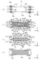
- FIG. 1 is an external perspective view of a signal line according to an embodiment of the present invention.
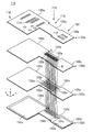
- FIG. 2 is an exploded view of the signal line in FIG. 1. It is an exploded view of the signal track concerning a modification. It is a disassembled perspective view of the circuit board which concerns on 2nd Embodiment. 2 is a cross-sectional structure diagram of a flexible substrate described in Patent Document 1.
- FIG. 1 is an external perspective view of a signal line according to an embodiment of the present invention.
- FIG. 2 is an exploded view of the signal line in FIG. 1. It is an exploded view of the signal track concerning a modification. It is a disassembled perspective view of the circuit board which concerns on 2nd Embodiment. 2 is a cross-sectional structure diagram of a flexible substrate described in Patent Document 1.
- FIG. 1 is an external perspective view of signal lines 10a and 10b according to an embodiment of the present invention.
- FIG. 2 is an exploded view of the signal line 10a of FIG. 1 and 2, the stacking direction of the signal line 10a is defined as the z-axis direction.
- the longitudinal direction of the signal line 10a is defined as the x-axis direction, and the direction orthogonal to the x-axis direction and the z-axis direction is defined as the y-axis direction.
- the signal line 10a connects two circuit boards in an electronic device such as a mobile phone. As shown in FIGS. 1 and 2, the signal line 10a includes a multilayer body 12, external terminals 14 (14a to 14f), ground conductors 30 and 34, signal lines 32, and via-hole conductors b1 to b16 and B1 to B36. Yes.
- the laminate 12 includes a signal line portion 16 and connector portions 18 and 20 as shown in FIG.
- the signal line portion 16 extends in the x-axis direction and incorporates a signal line 32 and ground conductors 30 and 34.
- the signal line portion 16 is configured to be bent in a U shape.
- the connector portions 18 and 20 are provided at both ends of the signal line portion 16 in the x-axis direction, and are connected to connectors on a circuit board (not shown).
- the laminated body 12 is configured by laminating insulating sheets (insulator layers) 22 (22a to 22d) shown in FIG. 2 in this order from the positive direction side to the negative direction side in the z-axis direction.
- the insulating sheet 22 is made of a thermoplastic resin such as a liquid crystal polymer having flexibility. As shown in FIG. 2, each of the insulating sheets 22a to 22d includes signal line portions 24a to 24d and connector portions 26a to 26d and 28a to 28d.
- the signal line portion 24 constitutes the signal line portion 16 of the laminate 12, and the connector portions 26 and 28 constitute the connector portions 18 and 20 of the laminate 12, respectively.
- the main surface on the positive side in the z-axis direction of the insulating sheet 22 is referred to as the front surface
- the main surface on the negative direction side in the z-axis direction of the insulating sheet 22 is referred to as the back surface.
- the external terminals 14a to 14c are provided on the surface of the connector portion 26a so as to be arranged in a line in the y-axis direction.
- the external terminals 14a to 14c come into contact with the terminals in the connector when the connector portion 18 is inserted into the connector of the circuit board.
- the external terminals 14a and 14c are in contact with a ground terminal in the connector, and the external terminal 14b is in contact with a signal terminal in the connector. Therefore, a ground potential is applied to the external terminals 14a and 14c, and a high-frequency signal (for example, 2 GHz) is applied to the external terminal 14b.
- a high-frequency signal for example, 2 GHz
- the external terminals 14d to 14f are provided on the surface of the connector portion 28a so as to be arranged in a line in the y-axis direction.
- the external terminals 14d to 14f contact the terminals in the connector when the connector portion 20 is inserted into the connector of the circuit board.
- the external terminals 14d and 14f are in contact with the ground terminal in the connector, and the external terminal 14e is in contact with the signal terminal in the connector. Therefore, a ground potential is applied to the external terminals 14d and 14f, and a high-frequency signal (for example, 2 GHz) is applied to the external terminal 14e.
- a high-frequency signal for example, 2 GHz
- the signal line 32 is a linear conductor provided in the multilayer body 12, and is provided on the surface of the insulating sheet 22c.
- the signal line 32 extends in the x-axis direction on the surface of the signal line portion 24c. Then, both ends of the signal line 32 are positioned at the connector portions 26c and 28c, respectively.
- the ground conductor 30 is provided on the positive side in the z-axis direction with respect to the signal line 32 in the multilayer body 12, and more specifically, is provided on the surface of the insulating sheet 22b.
- the ground conductor 30 extends in the x-axis direction on the surface of the signal line portion 24b.
- One end of the ground conductor 30 is positioned in a state of being branched into two in the connector portion 26b, and the other end of the ground conductor 30 is positioned in a state of being branched in two in the connector portion 28b.
- the ground conductor 30 overlaps the signal line 32 when viewed in plan from the z-axis direction.
- the ground conductor 30 has a plurality of slit-like openings O1 to O1 that are not provided with conductors so as to be aligned along the signal line 32 when viewed in plan from the z-axis direction.
- O8 is provided.
- the openings O1 to O8 overlap the signal line 32 when viewed in plan from the z-axis direction.
- the openings O1 to O8 have a rectangular shape having a longitudinal direction in the y-axis direction, and are arranged in a line in the x-axis direction at a constant interval. The openings O1 to O8 are provided so as not to divide the ground conductor 30.
- the conductor of the ground conductor 30 exists on the positive side and the negative side in the y-axis direction of the openings O1 to O8. Therefore, the ground conductor 30 has a ladder shape. As described above, by providing the openings O1 to O8 in the ground conductor 30, the ground conductor 30 has a relatively thick portion and a relatively thin portion in the width in the y-axis direction as shown in FIG. And are formed.
- the ground conductor 34 is provided on the negative side in the z-axis direction with respect to the signal line 32 in the multilayer body 12. More specifically, the ground conductor 34 is provided on the surface of the insulating sheet 22 d. The ground conductor 34 extends on the surface of the signal line portion 24d in the x-axis direction. One end of the ground conductor 34 is positioned in a state of being branched into two in the connector portion 26d, and the other end of the ground conductor 34 is positioned in a state of being branched in two in the connector portion 28d. Further, as shown in FIG. 2, the ground conductor 34 overlaps the signal line 32 when viewed in plan from the z-axis direction.
- the ground conductor 34 is provided with a plurality of openings O11 to O18 where no conductor is provided so as to be aligned along the signal line 32 when viewed in plan from the z-axis direction.
- the openings O11 to O18 overlap the signal line 32 when viewed in plan from the z-axis direction.
- the openings O11 to O18 overlap each other in a state where they coincide with the openings O1 to O8 when viewed in plan from the z-axis direction. That is, the openings O11 to O18 have a rectangular shape having a longitudinal direction in the y-axis direction, and are aligned in a row in the x-axis direction at regular intervals, like the openings O1 to O8.
- the openings O11 to O18 are provided so as not to divide the ground conductor 34, like the openings O1 to O8. That is, the conductor of the ground conductor 34 exists on the positive direction side and the negative direction side in the y-axis direction of the openings O11 to O18. Therefore, the ground conductor 34 has a ladder shape. As described above, by providing the openings O11 to O18 in the ground conductor 34, the ground conductor 34 has a relatively thick portion and a relatively thin portion in the width in the y-axis direction as shown in FIG. And are formed.
- the via-hole conductors b1 and b3 are provided so as to penetrate the connector portion 26a in the z-axis direction, and connect the external terminals 14a and 14c and the ground conductor 30.
- the via-hole conductor b2 is provided so as to penetrate the connector portion 26a in the z-axis direction, and is connected to the external terminal 14b.
- each of the via-hole conductors b7 and b9 is provided so as to penetrate the connector portion 26b in the z-axis direction, and is connected to the ground conductor 30.
- the via-hole conductor b8 is provided so as to penetrate the connector portion 26b in the z-axis direction, and connects the via-hole conductor b2 and the signal line 32.
- the via-hole conductors b13 and b14 are provided so as to penetrate the connector portion 26c in the z-axis direction, and connect the via-hole conductors b7 and b9 and the ground conductor 34.
- the external terminal 14a and the ground conductors 30, 34 are connected via the via-hole conductors b1, b7, b13, and the external terminal 14c and the ground conductors 30, 34 are connected via the via-hole conductors b3, b9, b14.
- the external terminal 14b and the signal line 32 are connected by via-hole conductors b2 and b8.
- the via-hole conductors b4 and b6 are provided so as to penetrate the connector portion 28a in the z-axis direction, and connect the external terminals 14d and 14f and the ground conductor 30.
- the via-hole conductor b5 is provided so as to penetrate the connector portion 28a in the z-axis direction, and is connected to the external terminal 14e.
- the via-hole conductors b10 and b12 are provided so as to penetrate the connector portion 28b in the z-axis direction, and are connected to the ground conductor 30.
- the via-hole conductor b11 is provided so as to penetrate the connector portion 28b in the z-axis direction, and connects the via-hole conductor b5 and the signal line 32.
- the via-hole conductors b15 and b16 are provided so as to penetrate the connector portion 28c in the z-axis direction, and connect the via-hole conductors b10 and b12 and the ground conductor 34.
- the external terminal 14d and the ground conductors 30 and 34 are connected via the via-hole conductors b4, b10, and b15, and the external terminal 14f and the ground conductors 30 and 34 are connected via the via-hole conductors b6, b12, and b16.
- the external terminal 14e and the signal line 32 are connected by via-hole conductors b5 and b11.
- the via-hole conductors B1 to B18 and B19 to B36 are provided so as to penetrate the signal line portions 24b and 24c in the z-axis direction, and connect the ground conductor 30 and the ground conductor 34. . Furthermore, the via-hole conductors B1 to B18 are provided between adjacent openings O1 to O8 in the direction in which the signal line 32 extends (that is, the x-axis direction) when viewed in plan from the z-axis direction. ing.
- the via-hole conductors B1, B3, B5, B7, B9, B11, B13, B15, and B17 are provided so as to be aligned at equal intervals in a straight line in the x-axis direction.
- the via-hole conductors B2, B4, B6, B8, B10, B12, B14, B16, and B18 are more negative in the y-axis direction than the via-hole conductors B1, B3, B5, B7, B9, B11, B13, B15, and B17. On the side, they are arranged in a straight line at equal intervals in the x-axis direction.
- the via-hole conductors B3 to B16 are provided on a perpendicular bisector with respect to the centers of the adjacent openings O1 to O8.
- the via-hole conductors B3 and B4 are provided between the opening O1 and the opening O2.
- the intersections of the diagonal lines of the openings O1 and O2 are referred to as the centers P1 and P2 of the openings O1 and O2.
- the vertical bisector of the centers P1 and P2 is referred to as a straight line L1.
- the via-hole conductor B3 is provided on the straight line L1 so as to overlap with the ends on the positive direction side in the y-axis direction of the openings O1 to O8 when viewed in plan from the x-axis direction. Further, the via-hole conductor B4 is provided on the straight line L1 so as to overlap with the end portion on the negative direction side in the y-axis direction of the openings O1 to O8 when viewed in plan from the x-axis direction.
- the via-hole conductors B19 to B36 are provided on the signal line portion 24c so as to overlap the via-hole conductors B1 to B18 when viewed in plan from the z-axis direction. As a result, the via-hole conductors B19 to B36 are connected to the via-hole conductors B1 to B18, respectively.
- the ground conductors 30 and 34 and the signal line 32 form a stripline structure. That is, as shown in FIG. 2, the signal line 32 is sandwiched between the ground conductor 30 and the ground conductor 34 in the z-axis direction, and the ground conductors 30 and 34 are provided when viewed in plan from the z-axis direction. It is within the area. Further, the ground conductor 30 and the ground conductor 34 are connected by via-hole conductors B1 to B36.
- the signal line 10a having the above configuration is used in a curved state. That is, the signal line 10a is curved so as to form a U shape projecting to either the positive direction side or the negative direction side in the z-axis direction when viewed in plan from the y-axis direction.
- an insulating sheet 22 having a copper foil formed on the entire surface is prepared.
- the surface of the copper foil of the insulating sheet 22 is smoothed by applying, for example, zinc plating for rust prevention.
- the external terminals 14 shown in FIG. 2 are formed on the surface of the insulating sheet 22a by a photolithography process. Specifically, a resist having the same shape as that of the external terminal 14 shown in FIG. 2 is printed on the copper foil of the insulating sheet 22a. And the copper foil of the part which is not covered with the resist is removed by performing an etching process with respect to copper foil. Thereafter, the resist is removed. Thereby, the external terminals 14 as shown in FIG. 2 are formed on the surface of the insulating sheet 22a.
- the ground conductor 30 shown in FIG. 2 is formed on the surface of the insulating sheet 22b by a photolithography process.
- 2 is formed on the surface of the insulating sheet 22c by a photolithography process.
- the ground conductor 34 shown in FIG. 2 is formed on the surface of the insulating sheet 22d by a photolithography process. Note that these photolithography processes are the same as the photolithography process for forming the external terminals 14, and thus the description thereof is omitted.
- the insulating sheets 22b and 22d having the ground conductors 30 and 34 fixed to the surface and the insulating sheet 22c having the signal line 32 fixed to the surface are prepared.
- a laser beam is irradiated from the back side to the positions where the via hole conductors b1 to b16 and B1 to B36 of the insulating sheets 22a to 22c are formed to form via holes.
- the via holes formed in the insulating sheets 22a to 22c are filled with a conductive paste mainly composed of copper to form the via hole conductors b1 to b16 and B1 to B36 shown in FIG.
- the insulating sheets 22a to 22d are stacked in this order from the positive direction side in the z-axis direction to the negative direction side so that the ground conductor 30, the signal line 32, and the ground conductor 34 form a stripline structure. Then, the insulating sheets 22a to 22d are pressure-bonded by applying force to the insulating sheets 22a to 22d from the positive and negative directions in the z-axis direction. Thereby, the signal line 10a shown in FIG. 1 is obtained.
- the signal line 10a can be easily bent into a U-shape. Since the ground conductors 30 and 34 are made of metal foil or the like, they are less likely to expand and contract than the insulating layers 22a to 22d. Therefore, in the signal line 10a, the openings O1 to O8 and O11 to O18 are provided in the ground conductors 30 and 34 as shown in FIG. Thereby, the strength of the ground conductors 30 and 34 in the portions where the openings O1 to O8 and O11 to O18 are provided is smaller than the strength of the ground conductors 30 and 34 in the other portions.
- the ground conductors 30 and 34 have portions on the positive and negative sides in the y-axis direction of the portions where the openings O1 to O8 and O11 to O18 are provided, compared to the other portions. It expands and contracts easily in the x-axis direction. As a result, the signal line 10a can be easily bent.
- the signal line 10a since the openings O1 to O8 and O11 to O18 are provided in both of the ground conductors 30 and 34, the signal line 10a has a z-axis direction when viewed in plan from the y-axis direction. Can be curved so as to form a U-shape projecting toward the positive direction side, and can also be curved so as to form a U-shape projecting toward the negative direction side in the z-axis direction.
- the signal line 10a unnecessary radiation can be reduced as described below.
- the signal line 32 is exposed through the openings O1 to O8 and O11 to O18 when viewed in plan from the z-axis direction. For this reason, unnecessary radiation from the signal line 32 may leak out of the signal line 10a through the openings O1 to O8 and O11 to O18.
- the ground conductors 30 and 34 are connected by via-hole conductors B1 to B36. As a result, the ground potential is more reliably applied to the ground conductors 30 and 34. Therefore, even if the openings O1 to O8 and O11 to O18 exist, unnecessary radiation from the signal line 32 is absorbed by the ground conductors 30 and 34. As a result, unnecessary radiation from the signal line 32 is reduced from leaking out of the signal line 10a.
- the via-hole conductors B1 to B36 are made of metal, they are less likely to be deformed than the insulating sheets 22a to 22d. For this reason, the via-hole conductors B1 to B36 may prevent the signal line 10a from being easily bent. However, for the reason described below, the signal line 10a can be easily bent even if the via-hole conductors B1 to B36 are provided.
- the ground conductor 30 extends relatively greatly in the x-axis direction.
- the ground conductor 30 extends only relatively small in the portion sandwiched between the openings O1 to O8. Therefore, the via-hole conductors B1 to B36 are provided between the openings O1 to O8 adjacent in the x-axis direction. That is, the via-hole conductors B1 to B36 are provided in a portion sandwiched between the openings O1 to O8.
- the via-hole conductors B1 to B36 do not prevent the portions where the openings O1 to O8 are provided in the positive and negative direction portions in the y-axis direction from extending significantly.
- the signal line 10a can be easily bent.
- the signal line 10a is bent in a U shape protruding in the negative direction side in the z-axis direction. Since this is basically the same as the physical phenomenon in the case where it is performed, the description thereof is omitted.
- the via-hole conductors B3 to B16 are provided on a perpendicular bisector with respect to the centers of the adjacent openings O1 to O8.
- the signal line 10a can be bent more easily.
- the portions on the positive and negative sides in the y-axis direction of the portions where the openings O1 to O8 are provided are the portions that extend most when the signal line 10a is curved.
- the perpendicular bisector with respect to the centers of the adjacent openings O1 to O8 is the positive direction side in the y-axis direction of the portion provided with the openings O1 to O8 in the portion sandwiched by the openings O1 to O8.
- the signal line 10a bends via. Inhibition of the conductors B3 to B16 can be suppressed.
- FIG. 3 is an exploded view of the signal line 10b according to the modification. Note that FIG. 1 is used as an external perspective view of the signal line 10b.
- the signal line 10b is different from the signal line 10a in that the openings O11 to O18 are not provided in the ground conductor 34. Since the other configuration of the signal line 10b is the same as that of the signal line 10a, the description thereof is omitted.
- the signal line 10 b is curved so that the ground conductor 30 is positioned on the outer peripheral side of the ground conductor 34. More specifically, when viewed from the y-axis direction, the signal line 10b is bent into a U shape that protrudes toward the positive direction side in the z-axis direction. This is because the ground conductor 30 is easier to extend than the ground conductor 34.
- the via-hole conductors B9, B10, B27, and B28 near the center of the signal line portion 16 in the x-axis direction may be omitted. In this case, the vicinity of the center of the signal line portion 16 in the x-axis direction can be more easily curved. Further, the via-hole conductors B1, B2, B17, B18, B19, B20, B35, and B36 in the vicinity of both ends of the signal line portion 16 in the x-axis direction may be omitted. In this case, the vicinity of both ends in the x-axis direction of the signal line portion 16 can be more easily curved.
- FIG. 4 is an exploded perspective view of the circuit board 110 according to the second embodiment.
- the stacking direction of the circuit board 110 is defined as the z-axis direction.
- the longitudinal direction of the circuit board 110 is defined as the x-axis direction, and the direction orthogonal to the x-axis direction and the z-axis direction is defined as the y-axis direction.
- the circuit board 110 includes a multilayer body 112, external terminals 114, ground conductors 130 (130a, 130b), 134 (134a, 134b), 140 (140a, 140b), and signal lines 132 (132a to 132d). ) And via-hole conductors B.
- external terminals 114 and via-hole conductors B only representative ones are given reference numerals.
- the laminated body 112 includes a signal line portion 116 and circuit portions 118 and 120 as shown in FIG.
- the signal line portion 116 extends in the x-axis direction and incorporates a signal line 132 and ground conductors 130 and 134.
- the signal line portion 116 is configured to be bent in a U shape.
- the circuit units 118 and 120 are provided at both ends of the signal line unit 116 in the x-axis direction and incorporate a circuit. However, in FIG. 4, the circuit is not shown.
- the laminated body 112 is configured by laminating insulating sheets (insulator layers) 122 (122a to 122d) shown in FIG. 4 in this order from the positive direction side to the negative direction side in the z-axis direction.
- the insulating sheet 122 is made of a thermoplastic resin such as a liquid crystal polymer having flexibility. As shown in FIG. 4, each of the insulating sheets 122a to 122d includes signal line portions 124a to 124d, circuit portions 126a to 126d, and 128a to 128d.
- the signal line portion 124 constitutes the signal line portion 116 of the multilayer body 112
- the circuit portions 126 and 128 constitute the circuit portions 118 and 120 of the multilayer body 112, respectively.
- the main surface on the positive direction side in the z-axis direction of the insulating sheet 122 is referred to as a front surface
- the main surface on the negative direction side in the z-axis direction of the insulating sheet 122 is referred to as a back surface.
- a plurality of external terminals 114 are provided on the surfaces of the circuit portions 126a and 128a.
- a semiconductor integrated circuit, a chip-type electronic component, or the like is mounted on the external terminal 114.
- the signal lines 132a to 132d are linear conductors provided in the signal line portion 116, and are provided on the surface of the insulating sheet 122c.
- the signal lines 132a to 132d extend in the x-axis direction in parallel with each other on the surface of the signal line portion 124c. Both ends of the signal lines 132a to 132d are located in the circuit portions 126c and 128c, respectively, and are connected to circuits (not shown) provided in the circuit portions 126c and 128c.
- the ground conductors 130a and 130b are provided in the signal line portion 116 on the positive side in the z-axis direction with respect to the signal lines 132a and 132b, and more specifically, provided on the surface of the insulating sheet 122b. It has been.
- the ground conductors 130a and 130b extend in the x-axis direction on the surface of the signal line portion 124b. Both ends of the ground conductors 130a and 130b are located in the circuit portions 126b and 128b, respectively, and are connected to circuits (not shown) provided in the circuit portions 126b and 128b. Further, as shown in FIG. 4, the ground conductors 130a and 130b overlap the signal lines 132a and 132b when viewed in plan from the z-axis direction.
- the ground conductors 130 a and 130 b have a plurality of openings O where no conductor is provided so as to be aligned along the signal lines 132 a and 132 b when viewed in plan from the z-axis direction. Is provided.
- the reference numerals of the openings O are given only to representative ones.
- the configuration of the opening O is the same as that of the openings O1 to O8 of the signal line 10a, and thus further description thereof is omitted.
- the ground conductors 134a and 134b are provided on the negative side in the z-axis direction with respect to the signal lines 132a and 132b in the signal line portion 116, and more specifically, provided on the surface of the insulating sheet 122d. It has been.
- the ground conductors 134a and 134b extend in the x-axis direction on the surface of the signal line portion 124d. Both ends of the ground conductors 134a and 134b are located in the circuit portions 126d and 128d, respectively, and are connected to the ground conductors 140a and 140b provided in the circuit portions 126d and 128d.
- the ground conductors 134a and 134b respectively overlap the signal lines 132a and 132b when viewed in plan from the z-axis direction.
- the ground conductors 134a and 134b are not provided with the opening O.
- the ground conductors 140a and 140b are provided so as to cover substantially the entire surface of the circuit portions 126d and 128d, respectively, and a ground potential is applied thereto. Since the ground conductors 140a and 140b are made of metal foil or the like, they are less likely to be deformed than the insulating sheet 122. Here, when viewed in plan from the z-axis direction, the proportion of the metal foil in the circuit portions 118 and 120 is higher than the proportion of the metal foil in the signal line portion 116. Therefore, the circuit units 118 and 120 are less likely to be deformed than the signal line unit 116. That is, in the circuit board 110, the circuit parts 118 and 120 constitute a rigid part, and the signal line part 116 constitutes a flexible part. In this way, by forming a rigid portion, electronic parts, semiconductor integrated circuits, and the like can be stably mounted on the circuit portions 118 and 120.
- the via-hole conductor B is provided so as to penetrate the signal line portion 124b in the z-axis direction, and connects the ground conductors 130a and 130b and the ground conductors 134a and 134b. Since the via hole conductor B is the same as the via hole conductors B1 to B36 of the signal line 10a, the description thereof is omitted.
- the ground conductors 130a and 134a and the signal line 132a have a stripline structure.
- the ground conductors 130b and 134b and the signal line 132b have a stripline structure.
- the ground conductors 130a and 130b and the ground conductors 134a and 134b are connected by a via-hole conductor B.
- the circuit board 110 having the above configuration is used in a curved state. That is, the signal line portion 116 is curved so as to form a U shape protruding in the positive direction side in the z-axis direction when viewed in plan from the y-axis direction.
- the circuit board 110 as described above can be easily bent and can reduce unnecessary radiation.
- an opening O may be provided for the ground conductors 134a and 134b.
- the present invention is useful for signal lines and circuit boards, and is particularly excellent in that it can be bent and unnecessary radiation can be reduced.
Landscapes
- Engineering & Computer Science (AREA)
- Microelectronics & Electronic Packaging (AREA)
- Physics & Mathematics (AREA)
- Electromagnetism (AREA)
- Manufacturing & Machinery (AREA)
- Structure Of Printed Boards (AREA)
- Waveguides (AREA)
Abstract
Description
(信号線路の構成)
以下に、本発明の第1の実施形態に係る信号線路の構成について図面を参照しながら説明する。図1は、本発明の実施形態に係る信号線路10a,10bの外観斜視図である。図2は、図1の信号線路10aの分解図である。図1及び図2において、信号線路10aの積層方向をz軸方向と定義する。また、信号線路10aの長手方向をx軸方向と定義し、x軸方向及びz軸方向に直交する方向をy軸方向と定義する。
以下に、信号線路10aの製造方法について図2を参照しながら説明する。以下では、一つの信号線路10aが作製される場合を例にとって説明するが、実際には、大判の絶縁シートが積層及びカットされることにより、同時に複数の信号線路10aが作製される。
以上のような信号線路10aによれば、以下に説明するように、信号線路10aを容易にU字状に曲げることが可能となる。グランド導体30,34は、金属箔等により構成されているため、絶縁層22a~22dに比べて伸び縮みしにくい。そこで、信号線路10aでは、図2に示すように、開口部O1~O8,O11~O18がグランド導体30,34に設けられている。これにより、開口部O1~O8,O11~O18が設けられている部分におけるグランド導体30,34の強度は、他の部分におけるグランド導体30,34の強度よりも小さくなる。具体的には、グランド導体30,34は、開口部O1~O8,O11~O18が設けられている部分のy軸方向の正方向側及び負方向側の部分において、その他の部分に比べて、x軸方向に容易に伸び縮みするようになる。その結果、信号線路10aを容易に曲げることが可能となる。なお、信号線路10aでは、グランド導体30,34の両方に、開口部O1~O8,O11~O18が設けられているので、信号線路10aは、y軸方向から平面視したときに、z軸方向の正方向側に突出するU字型をなすように湾曲でき、更に、z軸方向の負方向側に突出するU字型をなすようにも湾曲できる。
以下に、変形例に係る信号線路について図面を参照しながら説明する。図3は、変形例に係る信号線路10bの分解図である。なお、信号線路10bの外観斜視図は、図1を援用する。
以下に、本発明の第2の実施形態に係る回路基板について図面を参照しながら説明する。図4は、第2の実施形態に係る回路基板110の分解斜視図である。図4において、回路基板110の積層方向をz軸方向と定義する。また、回路基板110の長手方向をx軸方向と定義し、x軸方向及びz軸方向に直交する方向をy軸方向と定義する。
10a,10b 信号線路
12,112 積層体
14a~14f,114 外部端子
16,24a~24d,116,124a~124d 信号線部
18,20,26a~26d,28a~28d コネクタ部
118,120,126a~126d,128a~128d 回路部
22a~22d,122a~122d 絶縁シート
30,34,130a,130b,134a,134b,140a,140b グランド導体
32,132a~132d 信号線
110 回路基板
O,O1~O8,O11~O18 開口
Claims (6)
- 可撓性材料からなる複数の絶縁体層が積層されてなる積層体と、
前記積層体内に設けられている線状の信号線と、
前記積層体内において前記信号線よりも積層方向の上側に設けられ、かつ、積層方向から平面視したときに該信号線と重なっている第1のグランド導体と、
前記積層体内において前記信号線よりも積層方向の下側に設けられ、かつ、積層方向から平面視したときに該信号線と重なっている第2のグランド導体と、
前記第1のグランド導体と前記第2のグランド導体とを接続しているビアホール導体と、
を備え、
前記第1のグランド導体には、積層方向から平面視したときに、前記信号線に沿って並ぶように、複数の第1の開口部が設けられ、
前記ビアホール導体は、積層方向から平面視したときに、前記信号線が延在している方向において、隣り合う前記第1の開口部の間に設けられていること、
を特徴とする信号線路。 - 可撓性材料からなる複数の絶縁体層が積層されてなり、かつ、第1の回路部、第2の回路部及び信号線部を有する本体と、
前記信号線部内に設けられている線状の信号線と、
前記信号線部内において前記信号線よりも積層方向の上側に設けられ、かつ、積層方向から平面視したときに該信号線と重なっている第1のグランド導体と、
前記信号線部内において前記信号線よりも積層方向の下側に設けられ、かつ、積層方向から平面視したときに該信号線と重なっている第2のグランド導体と、
前記第1のグランド導体と前記第2のグランド導体とを接続しているビアホール導体と、
を備え、
前記第1のグランド導体には、積層方向から平面視したときに、前記信号線に沿って並ぶように、複数の第1の開口部が設けられ、
前記ビアホール導体は、積層方向から平面視したときに、前記信号線が延在している方向において、隣り合う前記第1の開口部の間に設けられ、
前記第1の回路部及び前記第2の回路部はそれぞれ、前記信号線、前記第1のグランド導体及び前記第2のグランド導体と接続されている第1の回路及び第2の回路を有していること、
を特徴とする回路基板。 - 前記第2のグランド導体には、積層方向から平面視したときに、前記第1の開口部と一致した状態で重なる複数の第2の開口部が設けられていること、
を特徴とする請求項1又は請求項2のいずれかに記載の信号線路又は回路基板。 - 前記第2のグランド導体には、導体層が設けられていない開口部が設けられておらず、
前記積層体は、前記第1のグランド導体が前記第2のグランド導体よりも外周側に位置するように湾曲させられること、
を特徴とする請求項1又は請求項2のいずれかに記載の信号線路又は回路基板。 - 前記ビアホール導体は、積層方向から平面視したときに、隣り合う前記第1の開口の中心に対する垂直二等分線上に設けられていること、
を特徴とする請求項1ないし請求項4のいずれかに記載の信号線路又は回路基板。 - 前記第1の開口は、積層方向から平面視したときに、前記信号線と重なっていること、
を特徴とする請求項1ないし請求項5のいずれかに記載の信号線路又は回路基板。
Priority Applications (6)
| Application Number | Priority Date | Filing Date | Title |
|---|---|---|---|
| EP10799720.7A EP2456005B1 (en) | 2009-07-13 | 2010-06-28 | Signal line and circuit board |
| JP2011522776A JP4962660B2 (ja) | 2009-07-13 | 2010-06-28 | 信号線路及び回路基板 |
| KR1020127000299A KR101378027B1 (ko) | 2009-07-13 | 2010-06-28 | 신호선로 및 회로기판 |
| CN201080032158.7A CN102473993B (zh) | 2009-07-13 | 2010-06-28 | 信号线路及电路基板 |
| US13/343,740 US8592687B2 (en) | 2009-07-13 | 2012-01-05 | Signal line and circuit substrate |
| US14/063,072 US9113560B2 (en) | 2009-07-13 | 2013-10-25 | Signal line and circuit substrate |
Applications Claiming Priority (2)
| Application Number | Priority Date | Filing Date | Title |
|---|---|---|---|
| JP2009-164820 | 2009-07-13 | ||
| JP2009164820 | 2009-07-13 |
Related Child Applications (1)
| Application Number | Title | Priority Date | Filing Date |
|---|---|---|---|
| US13/343,740 Continuation US8592687B2 (en) | 2009-07-13 | 2012-01-05 | Signal line and circuit substrate |
Publications (1)
| Publication Number | Publication Date |
|---|---|
| WO2011007660A1 true WO2011007660A1 (ja) | 2011-01-20 |
Family
ID=43449270
Family Applications (1)
| Application Number | Title | Priority Date | Filing Date |
|---|---|---|---|
| PCT/JP2010/060956 WO2011007660A1 (ja) | 2009-07-13 | 2010-06-28 | 信号線路及び回路基板 |
Country Status (6)
| Country | Link |
|---|---|
| US (2) | US8592687B2 (ja) |
| EP (1) | EP2456005B1 (ja) |
| JP (2) | JP4962660B2 (ja) |
| KR (1) | KR101378027B1 (ja) |
| CN (1) | CN102473993B (ja) |
| WO (1) | WO2011007660A1 (ja) |
Cited By (35)
| Publication number | Priority date | Publication date | Assignee | Title |
|---|---|---|---|---|
| WO2013099609A1 (ja) * | 2011-12-29 | 2013-07-04 | 株式会社村田製作所 | 高周波信号線路及び電子機器 |
| WO2013099603A1 (ja) * | 2011-12-29 | 2013-07-04 | 株式会社村田製作所 | 高周波信号線路及び電子機器 |
| WO2013099604A1 (ja) * | 2011-12-29 | 2013-07-04 | 株式会社村田製作所 | 高周波信号線路及び電子機器 |
| WO2013103130A1 (ja) * | 2012-01-06 | 2013-07-11 | 株式会社村田製作所 | 高周波伝送線路及び電子機器 |
| WO2013103075A1 (ja) * | 2012-01-06 | 2013-07-11 | 株式会社村田製作所 | 高周波信号線路及び電子機器 |
| WO2013103129A1 (ja) * | 2012-01-06 | 2013-07-11 | 株式会社村田製作所 | 高周波伝送線路及び電子機器 |
| WO2013114975A1 (ja) * | 2012-01-31 | 2013-08-08 | 株式会社村田製作所 | 高周波信号伝送線路及び電子機器 |
| WO2013190859A1 (ja) * | 2012-06-19 | 2013-12-27 | 株式会社村田製作所 | 積層型多芯ケーブル |
| WO2014003088A1 (ja) * | 2012-06-29 | 2014-01-03 | 株式会社村田製作所 | フラットケーブル |
| WO2014002786A1 (ja) * | 2012-06-29 | 2014-01-03 | 株式会社村田製作所 | 高周波信号線路及び信号線路付き基材層の製造方法 |
| WO2014003089A1 (ja) * | 2012-06-29 | 2014-01-03 | 株式会社村田製作所 | フラットケーブルおよび電子機器 |
| WO2014021372A1 (ja) * | 2012-08-03 | 2014-02-06 | 株式会社村田製作所 | フラットケーブル |
| WO2014020999A1 (ja) * | 2012-07-30 | 2014-02-06 | 株式会社村田製作所 | フラットケーブル |
| JP2014060042A (ja) * | 2012-09-18 | 2014-04-03 | Murata Mfg Co Ltd | フラットケーブル |
| WO2014057759A1 (ja) * | 2012-10-12 | 2014-04-17 | 株式会社村田製作所 | 高周波信号伝送線路及び電子機器 |
| WO2014115607A1 (ja) * | 2013-01-23 | 2014-07-31 | 株式会社村田製作所 | 伝送線路、および電子機器 |
| CN104145368A (zh) * | 2012-02-02 | 2014-11-12 | 横河电机株式会社 | 绝缘电路以及通信设备 |
| WO2015005028A1 (ja) * | 2013-07-09 | 2015-01-15 | 株式会社村田製作所 | 高周波伝送線路 |
| US20150042421A1 (en) * | 2012-06-29 | 2015-02-12 | Murata Manufacturing Co., Ltd. | Laminated flat cable and method for producing same |
| JP2015053742A (ja) * | 2014-12-17 | 2015-03-19 | 株式会社村田製作所 | 高周波伝送線路およびアンテナ装置 |
| JPWO2013080887A1 (ja) * | 2011-12-02 | 2015-04-27 | 株式会社村田製作所 | 高周波信号線路及びその製造方法並びに電子機器 |
| US9070490B2 (en) | 2012-06-29 | 2015-06-30 | Murata Manufacturing Co., Ltd. | Flat cable and electronic apparatus |
| US20150295296A1 (en) * | 2013-04-30 | 2015-10-15 | Murata Manufacturing Co., Ltd. | High-frequency transmission line |
| GB2510500B (en) * | 2011-11-10 | 2016-06-22 | Murata Manufacturing Co | High frequency signal line and electronic device provided with same |
| JP2016131375A (ja) * | 2012-06-29 | 2016-07-21 | 株式会社村田製作所 | 高周波線路及び電子機器 |
| US9462678B2 (en) | 2013-08-02 | 2016-10-04 | Murata Manufacturing Co., Ltd. | High-frequency signal transmission line and electronic device |
| US9490515B2 (en) | 2012-10-12 | 2016-11-08 | Murata Manufacturing Co., Ltd. | High-frequency signal line |
| US9490516B2 (en) | 2012-06-28 | 2016-11-08 | Murata Manufacturing Co., Ltd. | High-frequency transmission line and electronic device |
| US9583836B2 (en) | 2013-11-12 | 2017-02-28 | Murata Manufacturing Co., Ltd. | High-frequency transmission line and antenna device |
| JP2017045882A (ja) * | 2015-08-27 | 2017-03-02 | 富士通株式会社 | フレキシブル基板及びその製造方法並びに電子装置 |
| JP2017098998A (ja) * | 2014-03-27 | 2017-06-01 | 株式会社村田製作所 | 電子機器 |
| US9680195B2 (en) | 2012-10-12 | 2017-06-13 | Murata Manufacturing Co., Ltd. | High-frequency signal line |
| JPWO2021095620A1 (ja) * | 2019-11-15 | 2021-05-20 | ||
| JPWO2019235558A1 (ja) * | 2018-06-07 | 2021-06-10 | 株式会社村田製作所 | 多層基板、電子機器および多層基板の製造方法 |
| WO2023085177A1 (ja) * | 2021-11-15 | 2023-05-19 | 株式会社村田製作所 | 多層基板 |
Families Citing this family (31)
| Publication number | Priority date | Publication date | Assignee | Title |
|---|---|---|---|---|
| CN203040005U (zh) * | 2012-12-11 | 2013-07-03 | 奥特斯(中国)有限公司 | 印制电路板 |
| JP5582276B1 (ja) * | 2013-01-08 | 2014-09-03 | 株式会社村田製作所 | フレキシブル基板および電子機器 |
| CN204809363U (zh) * | 2013-01-22 | 2015-11-25 | 株式会社村田制作所 | 高频信号传输线路及电子设备 |
| CN204303949U (zh) * | 2013-01-29 | 2015-04-29 | 株式会社村田制作所 | 高频信号传输线路及电子设备 |
| WO2014119411A1 (ja) * | 2013-01-29 | 2014-08-07 | 株式会社村田製作所 | 高周波信号伝送線路及び電子機器 |
| CN103117440B (zh) * | 2013-02-07 | 2015-05-27 | 上海安费诺永亿通讯电子有限公司 | 一种低损耗扁平传输线 |
| WO2014157031A1 (ja) * | 2013-03-26 | 2014-10-02 | 株式会社村田製作所 | 高周波伝送線路、および電子機器 |
| US9402303B2 (en) * | 2013-06-03 | 2016-07-26 | Apple Inc. | Flexible printed circuit cables with slits |
| CN205093052U (zh) * | 2013-07-30 | 2016-03-16 | 株式会社村田制作所 | 多层基板 |
| CN104969667A (zh) * | 2013-12-09 | 2015-10-07 | At&S奥地利科技与系统技术股份公司 | 印制电路板 |
| JP6324738B2 (ja) * | 2014-01-27 | 2018-05-16 | ルネサスエレクトロニクス株式会社 | 半導体装置 |
| WO2015186538A1 (ja) | 2014-06-02 | 2015-12-10 | 株式会社村田製作所 | 伝送線路部材 |
| WO2015186537A1 (ja) | 2014-06-02 | 2015-12-10 | 株式会社村田製作所 | 伝送線路部材 |
| WO2015186720A1 (ja) | 2014-06-05 | 2015-12-10 | 株式会社村田製作所 | 伝送線路部材 |
| CN205752476U (zh) | 2014-06-16 | 2016-11-30 | 株式会社村田制作所 | 传输线路构件 |
| CN207166874U (zh) | 2014-08-29 | 2018-03-30 | 株式会社村田制作所 | 多层电路基板 |
| JP6103153B2 (ja) | 2014-09-26 | 2017-03-29 | 株式会社村田製作所 | 伝送線路および電子機器 |
| CN206640859U (zh) | 2014-09-30 | 2017-11-14 | 株式会社村田制作所 | 电子设备 |
| CN104779013B (zh) * | 2015-04-22 | 2017-01-25 | 上海安费诺永亿通讯电子有限公司 | 一种低损耗传输线 |
| JP6546016B2 (ja) * | 2015-06-25 | 2019-07-17 | 京セラ株式会社 | フレキシブル配線基板 |
| CN105140609B (zh) * | 2015-07-13 | 2019-05-24 | 上海安费诺永亿通讯电子有限公司 | 一种低损耗扁平传输线 |
| TWI553977B (zh) | 2015-09-02 | 2016-10-11 | 威盛電子股份有限公司 | 轉接卡及插頭電纜總成 |
| CN105742856B (zh) * | 2015-09-02 | 2018-05-18 | 威盛电子股份有限公司 | 转接卡及插头电缆总成 |
| JP6197979B1 (ja) * | 2015-12-07 | 2017-09-20 | 株式会社村田製作所 | 樹脂基板および電子機器 |
| WO2017126243A1 (ja) * | 2016-01-20 | 2017-07-27 | 株式会社村田製作所 | 樹脂多層基板、および、電子機器 |
| JP7014367B2 (ja) | 2016-11-18 | 2022-02-01 | 住友電工デバイス・イノベーション株式会社 | 光モジュール |
| JP6683264B2 (ja) * | 2017-01-05 | 2020-04-15 | 株式会社村田製作所 | 電子機器 |
| CN210405777U (zh) * | 2017-02-20 | 2020-04-24 | 株式会社村田制作所 | 电子设备 |
| KR101938105B1 (ko) * | 2018-01-25 | 2019-01-14 | 주식회사 기가레인 | 접합 위치 정확성이 개선된 연성회로기판 |
| JP7126878B2 (ja) * | 2018-06-26 | 2022-08-29 | 新光電気工業株式会社 | 配線基板 |
| CN209376018U (zh) | 2018-11-14 | 2019-09-10 | 奥特斯(中国)有限公司 | 具有改进的弯曲性能的部件承载件 |
Citations (3)
| Publication number | Priority date | Publication date | Assignee | Title |
|---|---|---|---|---|
| JPH05343564A (ja) * | 1992-06-05 | 1993-12-24 | Shinko Electric Ind Co Ltd | 高周波用電子部品の信号線路 |
| JP2006157646A (ja) * | 2004-11-30 | 2006-06-15 | Sony Corp | 配線基板 |
| JP2007123740A (ja) | 2005-10-31 | 2007-05-17 | Sony Corp | フレキシブル基板、光送受信モジュール及び光送受信装置 |
Family Cites Families (10)
| Publication number | Priority date | Publication date | Assignee | Title |
|---|---|---|---|---|
| US3962597A (en) * | 1974-07-01 | 1976-06-08 | International Business Machines Corporation | Gas discharge display panel including electrode connections in plurality of non-conductive layers |
| US20010006759A1 (en) * | 1998-09-08 | 2001-07-05 | Charles R. Shipley Jr. | Radiation sensitive compositions |
| JP2001102817A (ja) * | 1999-09-29 | 2001-04-13 | Nec Corp | 高周波回路及び該高周波回路を用いたシールディドループ型磁界検出器 |
| JP4680410B2 (ja) * | 2001-04-24 | 2011-05-11 | 日本特殊陶業株式会社 | 配線基板 |
| JP2004088020A (ja) | 2002-08-29 | 2004-03-18 | Toshiba Corp | フレキシブルプリント基板及び該基板を備えた電子機器 |
| JP3872084B2 (ja) * | 2005-04-28 | 2007-01-24 | 日東電工株式会社 | 配線回路基板 |
| US7224249B2 (en) | 2005-09-08 | 2007-05-29 | Avago Technologies General Ip (Singapore) Pte. Ltd. | Stripline structure with multiple ground vias separated by no more than 100 mil |
| JP2007193999A (ja) * | 2006-01-17 | 2007-08-02 | Sony Chemical & Information Device Corp | 伝送ケーブル |
| JP2007281145A (ja) | 2006-04-05 | 2007-10-25 | Kenwood Corp | フレキシブル配線体 |
| US8058954B2 (en) * | 2009-03-05 | 2011-11-15 | Apple Inc. | Transmission line with a cross-hatched ground plane that is either filled with conductive paint or covered by a conductive foil |
-
2010
- 2010-06-28 WO PCT/JP2010/060956 patent/WO2011007660A1/ja active Application Filing
- 2010-06-28 KR KR1020127000299A patent/KR101378027B1/ko active IP Right Grant
- 2010-06-28 EP EP10799720.7A patent/EP2456005B1/en active Active
- 2010-06-28 CN CN201080032158.7A patent/CN102473993B/zh active Active
- 2010-06-28 JP JP2011522776A patent/JP4962660B2/ja active Active
-
2012
- 2012-01-05 US US13/343,740 patent/US8592687B2/en active Active
- 2012-03-29 JP JP2012076405A patent/JP2012134551A/ja active Pending
-
2013
- 2013-10-25 US US14/063,072 patent/US9113560B2/en active Active
Patent Citations (3)
| Publication number | Priority date | Publication date | Assignee | Title |
|---|---|---|---|---|
| JPH05343564A (ja) * | 1992-06-05 | 1993-12-24 | Shinko Electric Ind Co Ltd | 高周波用電子部品の信号線路 |
| JP2006157646A (ja) * | 2004-11-30 | 2006-06-15 | Sony Corp | 配線基板 |
| JP2007123740A (ja) | 2005-10-31 | 2007-05-17 | Sony Corp | フレキシブル基板、光送受信モジュール及び光送受信装置 |
Non-Patent Citations (1)
| Title |
|---|
| See also references of EP2456005A4 * |
Cited By (98)
| Publication number | Priority date | Publication date | Assignee | Title |
|---|---|---|---|---|
| GB2510500B (en) * | 2011-11-10 | 2016-06-22 | Murata Manufacturing Co | High frequency signal line and electronic device provided with same |
| JPWO2013080887A1 (ja) * | 2011-12-02 | 2015-04-27 | 株式会社村田製作所 | 高周波信号線路及びその製造方法並びに電子機器 |
| US9713251B2 (en) | 2011-12-02 | 2017-07-18 | Murata Manufacturing Co., Ltd. | High-frequency signal line, method for producing same, and electronic device |
| US9318786B2 (en) | 2011-12-29 | 2016-04-19 | Murata Manufacturing Co., Ltd. | High-frequency signal line and electronic device |
| JPWO2013099603A1 (ja) * | 2011-12-29 | 2015-04-30 | 株式会社村田製作所 | 高周波信号線路及び電子機器 |
| GB2509407B (en) * | 2011-12-29 | 2014-12-10 | Murata Manufacturing Co | High-frequency signal path and electronic device |
| US9293799B2 (en) | 2011-12-29 | 2016-03-22 | Murata Manufacturing Co., Ltd. | High frequency signal line and electronic device |
| JP5472551B2 (ja) * | 2011-12-29 | 2014-04-16 | 株式会社村田製作所 | 高周波信号線路及び電子機器 |
| US9059493B2 (en) | 2011-12-29 | 2015-06-16 | Murata Manufacturing Co., Ltd. | High-frequency signal line and electronic device |
| JPWO2013099604A1 (ja) * | 2011-12-29 | 2015-04-30 | 株式会社村田製作所 | 高周波信号線路及び電子機器 |
| CN103733741A (zh) * | 2011-12-29 | 2014-04-16 | 株式会社村田制作所 | 高频信号线路及电子设备 |
| WO2013099604A1 (ja) * | 2011-12-29 | 2013-07-04 | 株式会社村田製作所 | 高周波信号線路及び電子機器 |
| JP5472553B2 (ja) * | 2011-12-29 | 2014-04-16 | 株式会社村田製作所 | 高周波信号線路及び電子機器 |
| GB2509407A (en) * | 2011-12-29 | 2014-07-02 | Murata Manufacturing Co | High-frequency signal line and electronic device |
| WO2013099609A1 (ja) * | 2011-12-29 | 2013-07-04 | 株式会社村田製作所 | 高周波信号線路及び電子機器 |
| WO2013099603A1 (ja) * | 2011-12-29 | 2013-07-04 | 株式会社村田製作所 | 高周波信号線路及び電子機器 |
| JPWO2013099609A1 (ja) * | 2011-12-29 | 2015-04-30 | 株式会社村田製作所 | 高周波信号線路及び電子機器 |
| JP5472552B2 (ja) * | 2011-12-29 | 2014-04-16 | 株式会社村田製作所 | 高周波信号線路及び電子機器 |
| US9781832B2 (en) | 2012-01-06 | 2017-10-03 | Murata Manufacturing Co., Ltd. | Laminated multi-conductor cable |
| CN103999285B (zh) * | 2012-01-06 | 2016-03-02 | 株式会社村田制作所 | 高频传输线路及电子设备 |
| WO2013103075A1 (ja) * | 2012-01-06 | 2013-07-11 | 株式会社村田製作所 | 高周波信号線路及び電子機器 |
| US20140376199A1 (en) * | 2012-01-06 | 2014-12-25 | Murata Manufacturing Co., Ltd. | Laminated multi-conductor cable |
| JP5472556B2 (ja) * | 2012-01-06 | 2014-04-16 | 株式会社村田製作所 | 高周波信号線路及び電子機器 |
| WO2013103129A1 (ja) * | 2012-01-06 | 2013-07-11 | 株式会社村田製作所 | 高周波伝送線路及び電子機器 |
| US9332644B2 (en) | 2012-01-06 | 2016-05-03 | Murato Manufacturing Co., Ltd. | High-frequency transmission line and electronic device |
| US9472839B2 (en) | 2012-01-06 | 2016-10-18 | Murata Manufacturing Co., Ltd. | High-frequency transmission line and electronic device |
| JPWO2013103130A1 (ja) * | 2012-01-06 | 2015-05-11 | 株式会社村田製作所 | 高周波伝送線路及び電子機器 |
| WO2013103130A1 (ja) * | 2012-01-06 | 2013-07-11 | 株式会社村田製作所 | 高周波伝送線路及び電子機器 |
| US9312590B2 (en) | 2012-01-06 | 2016-04-12 | Murata Manufacturing Co., Ltd. | High-frequency signal transmission line and electronic device |
| CN103999285A (zh) * | 2012-01-06 | 2014-08-20 | 株式会社村田制作所 | 高频传输线路及电子设备 |
| JPWO2013103129A1 (ja) * | 2012-01-06 | 2015-05-11 | 株式会社村田製作所 | 高周波伝送線路及び電子機器 |
| JP2013157308A (ja) * | 2012-01-06 | 2013-08-15 | Murata Mfg Co Ltd | 高周波信号線路 |
| US8975986B2 (en) | 2012-01-31 | 2015-03-10 | Murata Manufacturing Co., Ltd. | High-frequency signal transmission line and electronic device |
| WO2013114975A1 (ja) * | 2012-01-31 | 2013-08-08 | 株式会社村田製作所 | 高周波信号伝送線路及び電子機器 |
| JP5472555B2 (ja) * | 2012-01-31 | 2014-04-16 | 株式会社村田製作所 | 高周波信号伝送線路及び電子機器 |
| CN103733736B (zh) * | 2012-01-31 | 2016-01-20 | 株式会社村田制作所 | 高频信号传输线路及电子设备 |
| CN103733736A (zh) * | 2012-01-31 | 2014-04-16 | 株式会社村田制作所 | 高频信号传输线路及电子设备 |
| CN104145368B (zh) * | 2012-02-02 | 2016-08-24 | 横河电机株式会社 | 绝缘电路以及通信设备 |
| CN104145368A (zh) * | 2012-02-02 | 2014-11-12 | 横河电机株式会社 | 绝缘电路以及通信设备 |
| CN104205249A (zh) * | 2012-06-19 | 2014-12-10 | 株式会社村田制作所 | 层叠型多芯电缆 |
| CN106602193A (zh) * | 2012-06-19 | 2017-04-26 | 株式会社村田制作所 | 层叠型多芯电缆 |
| CN106602193B (zh) * | 2012-06-19 | 2020-01-17 | 株式会社村田制作所 | 层叠型多芯电缆 |
| WO2013190859A1 (ja) * | 2012-06-19 | 2013-12-27 | 株式会社村田製作所 | 積層型多芯ケーブル |
| US9490516B2 (en) | 2012-06-28 | 2016-11-08 | Murata Manufacturing Co., Ltd. | High-frequency transmission line and electronic device |
| JP5527494B1 (ja) * | 2012-06-29 | 2014-06-18 | 株式会社村田製作所 | フラットケーブル |
| US9177696B2 (en) | 2012-06-29 | 2015-11-03 | Murata Manufacturing Co., Ltd. | Flat cable |
| WO2014003088A1 (ja) * | 2012-06-29 | 2014-01-03 | 株式会社村田製作所 | フラットケーブル |
| GB2518034A (en) * | 2012-06-29 | 2015-03-11 | Murata Manufacturing Co | Flat bracket and electronic device |
| US20150042421A1 (en) * | 2012-06-29 | 2015-02-12 | Murata Manufacturing Co., Ltd. | Laminated flat cable and method for producing same |
| GB2518034B (en) * | 2012-06-29 | 2019-11-27 | Murata Manufacturing Co | Flat cable and electronic device |
| US9070490B2 (en) | 2012-06-29 | 2015-06-30 | Murata Manufacturing Co., Ltd. | Flat cable and electronic apparatus |
| US9627734B2 (en) | 2012-06-29 | 2017-04-18 | Murata Manufacturing Co., Ltd. | High-frequency signal line and method for producing base layer with signal line |
| CN104054141B (zh) * | 2012-06-29 | 2016-09-14 | 株式会社村田制作所 | 扁平电缆及电子设备 |
| JPWO2014002786A1 (ja) * | 2012-06-29 | 2016-05-30 | 株式会社村田製作所 | 高周波信号線路及び信号線路付き基材層の製造方法 |
| US9177697B2 (en) | 2012-06-29 | 2015-11-03 | Murata Manufacturing Co., Ltd. | Flat cable and electronic device |
| US9673501B2 (en) * | 2012-06-29 | 2017-06-06 | Murata Manufacturing Co., Ltd. | Laminated flat cable and method for producing same |
| JP5862774B2 (ja) * | 2012-06-29 | 2016-02-16 | 株式会社村田製作所 | 高周波信号線路及び信号線路付き基材層の製造方法 |
| WO2014002786A1 (ja) * | 2012-06-29 | 2014-01-03 | 株式会社村田製作所 | 高周波信号線路及び信号線路付き基材層の製造方法 |
| CN104054141A (zh) * | 2012-06-29 | 2014-09-17 | 株式会社村田制作所 | 扁平电缆及电子设备 |
| WO2014003089A1 (ja) * | 2012-06-29 | 2014-01-03 | 株式会社村田製作所 | フラットケーブルおよび電子機器 |
| JP2016131375A (ja) * | 2012-06-29 | 2016-07-21 | 株式会社村田製作所 | 高周波線路及び電子機器 |
| JP5527493B1 (ja) * | 2012-06-29 | 2014-06-18 | 株式会社村田製作所 | フラットケーブルおよび電子機器 |
| US9130251B2 (en) | 2012-07-30 | 2015-09-08 | Murata Manufacturing Co., Ltd. | Flat cable |
| GB2508568A (en) * | 2012-07-30 | 2014-06-04 | Murata Manufacturing Co | Flat cable |
| JP5556972B1 (ja) * | 2012-07-30 | 2014-07-23 | 株式会社村田製作所 | フラットケーブル |
| GB2508568B (en) * | 2012-07-30 | 2017-08-30 | Murata Manufacturing Co | Flat cable |
| WO2014020999A1 (ja) * | 2012-07-30 | 2014-02-06 | 株式会社村田製作所 | フラットケーブル |
| CN104221478A (zh) * | 2012-08-03 | 2014-12-17 | 株式会社村田制作所 | 扁平电缆 |
| WO2014021372A1 (ja) * | 2012-08-03 | 2014-02-06 | 株式会社村田製作所 | フラットケーブル |
| US9875823B2 (en) | 2012-08-03 | 2018-01-23 | Murata Manufacturing Co., Ltd. | Flat cable |
| JP2014060042A (ja) * | 2012-09-18 | 2014-04-03 | Murata Mfg Co Ltd | フラットケーブル |
| WO2014057759A1 (ja) * | 2012-10-12 | 2014-04-17 | 株式会社村田製作所 | 高周波信号伝送線路及び電子機器 |
| US9538638B2 (en) | 2012-10-12 | 2017-01-03 | Murata Manufacturing Co., Ltd. | High-frequency signal transmission line and electronic device |
| US9490515B2 (en) | 2012-10-12 | 2016-11-08 | Murata Manufacturing Co., Ltd. | High-frequency signal line |
| JP5605528B2 (ja) * | 2012-10-12 | 2014-10-15 | 株式会社村田製作所 | 高周波信号伝送線路及び電子機器 |
| JPWO2014057759A1 (ja) * | 2012-10-12 | 2016-09-05 | 株式会社村田製作所 | 高周波信号伝送線路及び電子機器 |
| US9680195B2 (en) | 2012-10-12 | 2017-06-13 | Murata Manufacturing Co., Ltd. | High-frequency signal line |
| JP5696819B2 (ja) * | 2013-01-23 | 2015-04-08 | 株式会社村田製作所 | 伝送線路、および電子機器 |
| JPWO2014115607A1 (ja) * | 2013-01-23 | 2017-01-26 | 株式会社村田製作所 | 伝送線路、および電子機器 |
| WO2014115607A1 (ja) * | 2013-01-23 | 2014-07-31 | 株式会社村田製作所 | 伝送線路、および電子機器 |
| US9666925B2 (en) | 2013-01-23 | 2017-05-30 | Murata Manufacturing Co., Ltd. | Transmission line, a transmission line apparatus, and an electronic device |
| US10164310B2 (en) * | 2013-04-30 | 2018-12-25 | Murata Manufacturing Co., Ltd. | High-frequency transmission line |
| US20150295296A1 (en) * | 2013-04-30 | 2015-10-15 | Murata Manufacturing Co., Ltd. | High-frequency transmission line |
| JPWO2015005028A1 (ja) * | 2013-07-09 | 2017-03-02 | 株式会社村田製作所 | 高周波伝送線路 |
| JP5967290B2 (ja) * | 2013-07-09 | 2016-08-10 | 株式会社村田製作所 | 高周波伝送線路 |
| US9570786B2 (en) | 2013-07-09 | 2017-02-14 | Murata Manufacturing Co., Ltd. | High-frequency transmission line |
| WO2015005028A1 (ja) * | 2013-07-09 | 2015-01-15 | 株式会社村田製作所 | 高周波伝送線路 |
| US9462678B2 (en) | 2013-08-02 | 2016-10-04 | Murata Manufacturing Co., Ltd. | High-frequency signal transmission line and electronic device |
| US9583836B2 (en) | 2013-11-12 | 2017-02-28 | Murata Manufacturing Co., Ltd. | High-frequency transmission line and antenna device |
| JP2017098998A (ja) * | 2014-03-27 | 2017-06-01 | 株式会社村田製作所 | 電子機器 |
| US9899715B2 (en) | 2014-03-27 | 2018-02-20 | Murata Manufacturing Co., Ltd. | Transmission line member and electronic apparatus |
| JP2015053742A (ja) * | 2014-12-17 | 2015-03-19 | 株式会社村田製作所 | 高周波伝送線路およびアンテナ装置 |
| JP2017045882A (ja) * | 2015-08-27 | 2017-03-02 | 富士通株式会社 | フレキシブル基板及びその製造方法並びに電子装置 |
| JPWO2019235558A1 (ja) * | 2018-06-07 | 2021-06-10 | 株式会社村田製作所 | 多層基板、電子機器および多層基板の製造方法 |
| JP7001158B2 (ja) | 2018-06-07 | 2022-01-19 | 株式会社村田製作所 | 多層基板、電子機器および多層基板の製造方法 |
| JPWO2021095620A1 (ja) * | 2019-11-15 | 2021-05-20 | ||
| JP7180788B2 (ja) | 2019-11-15 | 2022-11-30 | 株式会社村田製作所 | 伝送線路及び電子機器 |
| WO2023085177A1 (ja) * | 2021-11-15 | 2023-05-19 | 株式会社村田製作所 | 多層基板 |
Also Published As
| Publication number | Publication date |
|---|---|
| JPWO2011007660A1 (ja) | 2012-12-27 |
| JP2012134551A (ja) | 2012-07-12 |
| EP2456005B1 (en) | 2014-12-17 |
| CN102473993A (zh) | 2012-05-23 |
| CN102473993B (zh) | 2014-01-22 |
| JP4962660B2 (ja) | 2012-06-27 |
| EP2456005A4 (en) | 2013-07-24 |
| US9113560B2 (en) | 2015-08-18 |
| KR20120016171A (ko) | 2012-02-22 |
| US20140048312A1 (en) | 2014-02-20 |
| EP2456005A1 (en) | 2012-05-23 |
| US20120097433A1 (en) | 2012-04-26 |
| KR101378027B1 (ko) | 2014-03-25 |
| US8592687B2 (en) | 2013-11-26 |
Similar Documents
| Publication | Publication Date | Title |
|---|---|---|
| JP4962660B2 (ja) | 信号線路及び回路基板 | |
| JP5574030B2 (ja) | 多層基板 | |
| JP4993037B2 (ja) | 信号線路 | |
| WO2011040393A1 (ja) | 回路基板及びその製造方法 | |
| JP4985894B2 (ja) | 信号線路 | |
| JP5754554B2 (ja) | 高周波信号線路の製造方法 | |
| WO2015015959A1 (ja) | 高周波信号伝送線路及び電子機器 | |
| JP2011071403A (ja) | 信号線路 | |
| JP2014086655A (ja) | フレキシブル基板 | |
| US20140184359A1 (en) | High-frequency signal transmission line and electronic device | |
| WO2014021372A1 (ja) | フラットケーブル | |
| JP5333577B2 (ja) | 回路基板及びマザー積層体 | |
| JP5765468B2 (ja) | 高周波信号線路 | |
| JP5704286B2 (ja) | 高周波信号線路 | |
| WO2014002786A1 (ja) | 高周波信号線路及び信号線路付き基材層の製造方法 | |
| CN212907280U (zh) | 电感器电桥以及电子设备 | |
| WO2014065172A1 (ja) | フレキシブル基板 | |
| US9583810B2 (en) | High-frequency signal line | |
| JP5958122B2 (ja) | 高周波信号線路及び信号線路付き基材層の製造方法 |
Legal Events
| Date | Code | Title | Description |
|---|---|---|---|
| WWE | Wipo information: entry into national phase |
Ref document number: 201080032158.7 Country of ref document: CN |
|
| 121 | Ep: the epo has been informed by wipo that ep was designated in this application |
Ref document number: 10799720 Country of ref document: EP Kind code of ref document: A1 |
|
| WWE | Wipo information: entry into national phase |
Ref document number: 2011522776 Country of ref document: JP |
|
| WWE | Wipo information: entry into national phase |
Ref document number: 2010799720 Country of ref document: EP |
|
| ENP | Entry into the national phase |
Ref document number: 20127000299 Country of ref document: KR Kind code of ref document: A |
|
| NENP | Non-entry into the national phase |
Ref country code: DE |