JP3987795B2 - 流体圧力インプリント・リソグラフィ - Google Patents
流体圧力インプリント・リソグラフィ Download PDFInfo
- Publication number
- JP3987795B2 JP3987795B2 JP2002513006A JP2002513006A JP3987795B2 JP 3987795 B2 JP3987795 B2 JP 3987795B2 JP 2002513006 A JP2002513006 A JP 2002513006A JP 2002513006 A JP2002513006 A JP 2002513006A JP 3987795 B2 JP3987795 B2 JP 3987795B2
- Authority
- JP
- Japan
- Prior art keywords
- mold
- substrate
- layer
- moldable
- mask layer
- Prior art date
- Legal status (The legal status is an assumption and is not a legal conclusion. Google has not performed a legal analysis and makes no representation as to the accuracy of the status listed.)
- Expired - Lifetime
Links
Images


Classifications
-
- B—PERFORMING OPERATIONS; TRANSPORTING
- B29—WORKING OF PLASTICS; WORKING OF SUBSTANCES IN A PLASTIC STATE IN GENERAL
- B29C—SHAPING OR JOINING OF PLASTICS; SHAPING OF MATERIAL IN A PLASTIC STATE, NOT OTHERWISE PROVIDED FOR; AFTER-TREATMENT OF THE SHAPED PRODUCTS, e.g. REPAIRING
- B29C43/00—Compression moulding, i.e. applying external pressure to flow the moulding material; Apparatus therefor
- B29C43/02—Compression moulding, i.e. applying external pressure to flow the moulding material; Apparatus therefor of articles of definite length, i.e. discrete articles
- B29C43/021—Compression moulding, i.e. applying external pressure to flow the moulding material; Apparatus therefor of articles of definite length, i.e. discrete articles characterised by the shape of the surface
-
- H—ELECTRICITY
- H01—ELECTRIC ELEMENTS
- H01L—SEMICONDUCTOR DEVICES NOT COVERED BY CLASS H10
- H01L21/00—Processes or apparatus adapted for the manufacture or treatment of semiconductor or solid state devices or of parts thereof
- H01L21/02—Manufacture or treatment of semiconductor devices or of parts thereof
- H01L21/027—Making masks on semiconductor bodies for further photolithographic processing not provided for in group H01L21/18 or H01L21/34
-
- B—PERFORMING OPERATIONS; TRANSPORTING
- B29—WORKING OF PLASTICS; WORKING OF SUBSTANCES IN A PLASTIC STATE IN GENERAL
- B29C—SHAPING OR JOINING OF PLASTICS; SHAPING OF MATERIAL IN A PLASTIC STATE, NOT OTHERWISE PROVIDED FOR; AFTER-TREATMENT OF THE SHAPED PRODUCTS, e.g. REPAIRING
- B29C43/00—Compression moulding, i.e. applying external pressure to flow the moulding material; Apparatus therefor
- B29C43/003—Compression moulding, i.e. applying external pressure to flow the moulding material; Apparatus therefor characterised by the choice of material
-
- B—PERFORMING OPERATIONS; TRANSPORTING
- B82—NANOTECHNOLOGY
- B82Y—SPECIFIC USES OR APPLICATIONS OF NANOSTRUCTURES; MEASUREMENT OR ANALYSIS OF NANOSTRUCTURES; MANUFACTURE OR TREATMENT OF NANOSTRUCTURES
- B82Y10/00—Nanotechnology for information processing, storage or transmission, e.g. quantum computing or single electron logic
-
- B—PERFORMING OPERATIONS; TRANSPORTING
- B82—NANOTECHNOLOGY
- B82Y—SPECIFIC USES OR APPLICATIONS OF NANOSTRUCTURES; MEASUREMENT OR ANALYSIS OF NANOSTRUCTURES; MANUFACTURE OR TREATMENT OF NANOSTRUCTURES
- B82Y40/00—Manufacture or treatment of nanostructures
-
- G—PHYSICS
- G03—PHOTOGRAPHY; CINEMATOGRAPHY; ANALOGOUS TECHNIQUES USING WAVES OTHER THAN OPTICAL WAVES; ELECTROGRAPHY; HOLOGRAPHY
- G03F—PHOTOMECHANICAL PRODUCTION OF TEXTURED OR PATTERNED SURFACES, e.g. FOR PRINTING, FOR PROCESSING OF SEMICONDUCTOR DEVICES; MATERIALS THEREFOR; ORIGINALS THEREFOR; APPARATUS SPECIALLY ADAPTED THEREFOR
- G03F7/00—Photomechanical, e.g. photolithographic, production of textured or patterned surfaces, e.g. printing surfaces; Materials therefor, e.g. comprising photoresists; Apparatus specially adapted therefor
- G03F7/0002—Lithographic processes using patterning methods other than those involving the exposure to radiation, e.g. by stamping
-
- B—PERFORMING OPERATIONS; TRANSPORTING
- B29—WORKING OF PLASTICS; WORKING OF SUBSTANCES IN A PLASTIC STATE IN GENERAL
- B29C—SHAPING OR JOINING OF PLASTICS; SHAPING OF MATERIAL IN A PLASTIC STATE, NOT OTHERWISE PROVIDED FOR; AFTER-TREATMENT OF THE SHAPED PRODUCTS, e.g. REPAIRING
- B29C43/00—Compression moulding, i.e. applying external pressure to flow the moulding material; Apparatus therefor
- B29C43/02—Compression moulding, i.e. applying external pressure to flow the moulding material; Apparatus therefor of articles of definite length, i.e. discrete articles
- B29C43/021—Compression moulding, i.e. applying external pressure to flow the moulding material; Apparatus therefor of articles of definite length, i.e. discrete articles characterised by the shape of the surface
- B29C2043/023—Compression moulding, i.e. applying external pressure to flow the moulding material; Apparatus therefor of articles of definite length, i.e. discrete articles characterised by the shape of the surface having a plurality of grooves
- B29C2043/025—Compression moulding, i.e. applying external pressure to flow the moulding material; Apparatus therefor of articles of definite length, i.e. discrete articles characterised by the shape of the surface having a plurality of grooves forming a microstructure, i.e. fine patterning
-
- B—PERFORMING OPERATIONS; TRANSPORTING
- B29—WORKING OF PLASTICS; WORKING OF SUBSTANCES IN A PLASTIC STATE IN GENERAL
- B29C—SHAPING OR JOINING OF PLASTICS; SHAPING OF MATERIAL IN A PLASTIC STATE, NOT OTHERWISE PROVIDED FOR; AFTER-TREATMENT OF THE SHAPED PRODUCTS, e.g. REPAIRING
- B29C43/00—Compression moulding, i.e. applying external pressure to flow the moulding material; Apparatus therefor
- B29C43/32—Component parts, details or accessories; Auxiliary operations
- B29C2043/3205—Particular pressure exerting means for making definite articles
- B29C2043/3222—Particular pressure exerting means for making definite articles pressurized gas, e.g. air
- B29C2043/3233—Particular pressure exerting means for making definite articles pressurized gas, e.g. air exerting pressure on mould parts
-
- B—PERFORMING OPERATIONS; TRANSPORTING
- B29—WORKING OF PLASTICS; WORKING OF SUBSTANCES IN A PLASTIC STATE IN GENERAL
- B29C—SHAPING OR JOINING OF PLASTICS; SHAPING OF MATERIAL IN A PLASTIC STATE, NOT OTHERWISE PROVIDED FOR; AFTER-TREATMENT OF THE SHAPED PRODUCTS, e.g. REPAIRING
- B29C43/00—Compression moulding, i.e. applying external pressure to flow the moulding material; Apparatus therefor
- B29C43/32—Component parts, details or accessories; Auxiliary operations
- B29C2043/3205—Particular pressure exerting means for making definite articles
- B29C2043/3238—Particular pressure exerting means for making definite articles pressurized liquid acting directly or indirectly on the material to be formed
-
- B—PERFORMING OPERATIONS; TRANSPORTING
- B29—WORKING OF PLASTICS; WORKING OF SUBSTANCES IN A PLASTIC STATE IN GENERAL
- B29C—SHAPING OR JOINING OF PLASTICS; SHAPING OF MATERIAL IN A PLASTIC STATE, NOT OTHERWISE PROVIDED FOR; AFTER-TREATMENT OF THE SHAPED PRODUCTS, e.g. REPAIRING
- B29C43/00—Compression moulding, i.e. applying external pressure to flow the moulding material; Apparatus therefor
- B29C43/32—Component parts, details or accessories; Auxiliary operations
- B29C43/56—Compression moulding under special conditions, e.g. vacuum
- B29C2043/566—Compression moulding under special conditions, e.g. vacuum in a specific gas atmosphere, with or without pressure
-
- B—PERFORMING OPERATIONS; TRANSPORTING
- B29—WORKING OF PLASTICS; WORKING OF SUBSTANCES IN A PLASTIC STATE IN GENERAL
- B29C—SHAPING OR JOINING OF PLASTICS; SHAPING OF MATERIAL IN A PLASTIC STATE, NOT OTHERWISE PROVIDED FOR; AFTER-TREATMENT OF THE SHAPED PRODUCTS, e.g. REPAIRING
- B29C59/00—Surface shaping of articles, e.g. embossing; Apparatus therefor
- B29C59/02—Surface shaping of articles, e.g. embossing; Apparatus therefor by mechanical means, e.g. pressing
- B29C59/022—Surface shaping of articles, e.g. embossing; Apparatus therefor by mechanical means, e.g. pressing characterised by the disposition or the configuration, e.g. dimensions, of the embossments or the shaping tools therefor
- B29C2059/023—Microembossing
-
- B—PERFORMING OPERATIONS; TRANSPORTING
- B29—WORKING OF PLASTICS; WORKING OF SUBSTANCES IN A PLASTIC STATE IN GENERAL
- B29C—SHAPING OR JOINING OF PLASTICS; SHAPING OF MATERIAL IN A PLASTIC STATE, NOT OTHERWISE PROVIDED FOR; AFTER-TREATMENT OF THE SHAPED PRODUCTS, e.g. REPAIRING
- B29C59/00—Surface shaping of articles, e.g. embossing; Apparatus therefor
- B29C59/02—Surface shaping of articles, e.g. embossing; Apparatus therefor by mechanical means, e.g. pressing
- B29C59/022—Surface shaping of articles, e.g. embossing; Apparatus therefor by mechanical means, e.g. pressing characterised by the disposition or the configuration, e.g. dimensions, of the embossments or the shaping tools therefor
-
- H—ELECTRICITY
- H10—SEMICONDUCTOR DEVICES; ELECTRIC SOLID-STATE DEVICES NOT OTHERWISE PROVIDED FOR
- H10K—ORGANIC ELECTRIC SOLID-STATE DEVICES
- H10K71/00—Manufacture or treatment specially adapted for the organic devices covered by this subclass
- H10K71/10—Deposition of organic active material
- H10K71/12—Deposition of organic active material using liquid deposition, e.g. spin coating
- H10K71/13—Deposition of organic active material using liquid deposition, e.g. spin coating using printing techniques, e.g. ink-jet printing or screen printing
-
- Y—GENERAL TAGGING OF NEW TECHNOLOGICAL DEVELOPMENTS; GENERAL TAGGING OF CROSS-SECTIONAL TECHNOLOGIES SPANNING OVER SEVERAL SECTIONS OF THE IPC; TECHNICAL SUBJECTS COVERED BY FORMER USPC CROSS-REFERENCE ART COLLECTIONS [XRACs] AND DIGESTS
- Y10—TECHNICAL SUBJECTS COVERED BY FORMER USPC
- Y10S—TECHNICAL SUBJECTS COVERED BY FORMER USPC CROSS-REFERENCE ART COLLECTIONS [XRACs] AND DIGESTS
- Y10S438/00—Semiconductor device manufacturing: process
- Y10S438/942—Masking
- Y10S438/945—Special, e.g. metal
Description
(発明の分野)
本発明はインプリント・リソグラフィに関し、詳細には、直接流体圧力を使用して薄膜中に型を押し込むインプリント・リソグラフィに関する。このプロセスは、広い面積にわたって解像度および均一性が向上したナノインプリント・リソグラフィを提供するために特に有用である。
【0002】
(発明の背景)
リソグラフィは、半導体集積回路および多くの光学デバイス、磁気デバイス、微小機械デバイスの製造の鍵となるプロセスである。リソグラフィによって、基板に担持された薄膜上にパターンが形成され、それにより、後続するプロセス・ステップにおいて、基板または基板に追加された他の材料に、そのパターンが複製される。従来のリソグラフィは、一般に、基板にレジストの薄膜を塗布し、塗布したレジストを所望の放射線パターンで露光し、かつ、物理パターンを生成するために、露光した薄膜を現像することを必要とする。この手法では、放射線の波長によって解像度が制限され、また、フィーチャ(feature)サイズが小さくなればなるにつれて装置が高価になる。基本的に異なる原理に基づくナノインプリント・リソグラフィは、高解像度、高処理能力、低コスト、および大面積のカバレージの可能性を提供している。ナノインプリント・リソグラフィの場合、ナノスケールのフィーチャを備えた型が薄膜中に押し込まれ、それにより薄膜の形状が型のフィーチャに従って変形し、薄膜中に浮彫りパターンが形成される。型を除去した後で、薄くなった部分を除去するために薄膜を処理することができる。この除去により、その下にある基板が露出し、さらに処理される。1998年6月30日特許発行された、発明の名称「Nanoimprint Lithography」と題する本出願人による米国特許第5,772,905号に、ナノインプリント・リソグラフィの詳細が記載されている。‘905号特許に言及することにより、当該特許を本明細書に組み込む。
【0003】
薄膜中に型を押し込む通常の方法は、型および基板を、高精度機械プレスの剛性プレート上にそれぞれ位置決めすることを必要とする。このような装置を使用したプロセスにより、12in2程度の面積にわたって高度な均一性を備えた25nm未満のフィーチャが生成されるが、スループットを改善するためには、また、表示装置などの多くの応用例向けには、より広い面積にわたって均一性を備えることが大いに有利であろう。
【0004】
(発明の概要)
インプリント・リソグラフィの改良された方法は、基板に支持された薄膜中に型を押し込むために直接流体圧力を使用することを含む。有利には、型および/または基板は十分に柔軟であり、流体圧力の下で広範囲な接触を提供している。流体による押込みは、薄膜に対して型を封止し、それによって得られるアセンブリを、加圧チャンバ内に配置することによって行うことができる。流体による押込みは、型を加圧流体の噴流を浴びせることによって行うこともできる。この流体による押込みにより、解像度が向上し、かつ、広範囲にわたる高度な均一性が得られる。
【0005】
本発明の利点、性質および他の様々な特徴については、添付の図面に照らして行う、実例の実施形態についての以下の詳細な説明を考察することにより、より明白になるであろう。
【0006】
添付の図面は、本発明の概念を示すためのものであり、したがって実際のスケールどおりではないことを理解されたい。
【0007】
(詳細な説明)
高精度機械プレスを使用して薄膜中に型を押し込む場合、広範囲にわたる微小パターンの複製には許容差の問題が生じる。プレスは、複数のガイド・シャフト上を複数の開口部を通って移動し、複数のガイド・シャフトとその各々の開口部との間の隙間は、複製すべきフィーチャ(features)に比べて大きくなっている。このような隙間により、望ましくない相対並進移動および回転移動が、基板と型との間に生じる。また、いかに慎重に構築しても、リソグラフィに使用される型および基板は、完全な平面ではない。これらの型および基板がプレスの剛性プレート上に配置されるとき、広範囲にわたる平面性からの逸脱があると、成形圧力およびインプリント深さが変化することになる。したがって、機械的なプレスの限界が回避されたインプリント・リソグラフィ方法が提供されることが望ましい。
【0008】
本発明によれば、直接流体圧力を使用して、型および成形可能表面を共に押し付けることにより、機械的なプレスの望ましくない横移動の問題が改善される。本発明の方法によれば、型、成形可能表面を支持している基板、または型および基板の両方の表面全体に流体圧力が加えられる。流体圧力は等方的であるため、重大な不平衡の横方向の力が加えられることはない。また、直接流体圧力には、流体からの等方的圧力の伝達を妨害しないので、可撓性の薄膜を介して型または基板に伝達される流体圧力が含まれている。また、圧力容器内の多数の開口部からの加圧流体の流れも、ほぼ等方的直接流体圧力を型または基板に加えることができる。
【0009】
本発明は、既にパターン化されている基板上にパターンを成形する場合に重要な応用例に適用されることを意図している。型は、従来のアライメント技法を使用して、既存のパターンに整列させることができ、また、直接流体圧力によるインプリントによりあらゆる相対的な横方向の移動が最小化され、その結果、2つのパターンの配列が改善される。
【0010】
図面を参照すると、図1に、直接流体圧力を使用したインプリント・リソグラフィのための改良型プロセスの概略を示す流れ図が示されている。ブロックAに示す最初の工程は、複数の突出フィーチャを有する型および基板に支持された成形可能材料の薄膜を準備することである。突出フィーチャは、好ましくはマイクロメートル・スケールのフィーチャであるが、ナノスケールのフィーチャであることが、より有利である。この方法は、型の表面が、200nm未満の少なくとも1つの横方向寸法だけ間隔を隔てた少なくとも2つの突出フィーチャを有している場合、極めて有利である。成形可能材料は、型表面からの突出フィーチャのインプリントを保持する材料であり、あるいは型表面からの突出フィーチャのインプリントを保持するべく、硬化させることができる材料である。
【0011】
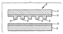
図2は、図1に示すプロセスに使用するための、突出フィーチャおよび成形可能薄膜21を支える基板20を備えた典型的な型10を示したものである。型は、本体11および所望の形状を有する複数の突出フィーチャ13を備えた成形層12を備えている。型の本体11および成形層12は、通常、溶融石英、ガラスまたはセラミックである。成形層12は、当該技術分野で良く知られている電子ビーム・リソグラフィおよびエッチング技法を使用して、ナノスケール寸法のフィーチャ13にパターン化することができる。層21の厚さは、通常、0.1nm〜10μmの範囲であり、突出フィーチャ13の範囲は、通常、0.1nm〜10μmの範囲である。
【0012】
基板は、典型的には、実質的に平面状の単結晶シリコン・ウェハなどの半導体ウェハからなっている。また、基板は、プラスチック、ガラスあるいはセラミックであっても良い。成形可能薄膜21には、圧力に対してしなやかにすることができ、かつ、圧力インプリント変形すなわちパターンを保持することができる任意の重合体を使用することができ、例えば熱に反応して一時的に軟化するポリカーボネートあるいはポリメタクリル酸メチル(PMMA)などの熱可塑性重合体であっても良い。別法としては、成形可能薄膜21は、放射に反応して硬化するUV硬化性シリコーンなどの液体であっても良く、あるいは熱によって硬化する液体であっても良い。また、成形可能薄膜21は、重合体と硬化可能な液体との複合層であっても良い。薄膜は、通常、噴霧法又はスピニング法によって基板に塗布される。薄膜重合体を型表面に粘着させないことが有利である。このような粘着を防止するために、必要に応じて、型の表面を離型剤で被覆することもできる。
【0013】
高解像度応用例では、異なる熱膨張または収縮による不整列を最小化するためには、型および基板の材料が同じ材料であることが有利である。
【0014】
型の本体11あるいは基板20(または両方)は、型および基板がその平面性からの逸脱にもかかわらず、流体圧力による力に従うよう、柔軟であることが好ましい。厚さ2mm未満のシリコン基板は、典型的なインプリント圧力に対するこのような柔軟性を備えている。
【0015】
ブロックBに示す次のステップは、型および薄膜を一体にし、かつ、型の界面を薄膜で封止し、型/薄膜アセンブリを形成することである。薄膜が既に予め形成済みのパターンを備えている場合、当該技術分野で良く知られている技法によって、型のパターンと既に存在している薄膜上のパターンとを慎重に整列させなければならない。封止の目的は、外部からの流体圧力による薄膜中への型の押し込みを可能にすることである。この封止は、様々な方法で実現することができ、例えばエラストマー・ガスケットなどのリング材を、成形すべき領域の周囲に設け、アセンブリの周囲を締め付けることによって実現することができる。
【0016】
第3のステップ(ブロックC)は、直接流体圧力によって型を薄膜中に押し込むことである。そのための方法の1つは、圧力容器内にアセンブリを配置し、加圧流体を圧力容器内に導入することである。流体圧力の利点は、流体圧力が等方的であることである。等方的流体圧力によって得られる力により、型が薄膜中に均一に押し込まれる。せん断成分すなわち回転成分は、極小である。また、型および/または基板が剛性ではなく柔軟であるため、不可避的な平面性からの逸脱とは無関係に、型と薄膜との間の整合性が実現され、その結果、成形解像度、アライメント、および薄膜の広範囲にわたる均一性のレベルが向上する。
【0017】
加圧流体は、気体であっても液体であっても良い。加圧空気が簡便であり、典型的な圧力は、1〜1000psiの範囲である。成形可能薄膜の加熱を促進するために、必要に応じて流体を加熱することができる。冷却された流体を使用して薄膜を冷却することもできる。
【0018】
図3は、封止され、圧力容器31内に配置された型/薄膜のアセンブリ30を示したものである。型/薄膜アセンブリ30は、成形すべき領域の周囲に延びた周辺エラストマー・ガスケット32によって封止されている。型/薄膜アセンブリの周囲は、封止を実現するために、クランプ(図示せず)によって軽く固定されている。圧力容器31は、好ましくは、加圧流体を導くためのバルブ制御導入口34、および加圧流体を排出するためのバルブ制御排出口35を備えている。圧力容器31は、熱可塑性又は熱硬化性の薄膜を加熱するためのヒータ36、および/または、薄膜を硬化あるいは架橋結合させるための放射線を導くための透明な窓37を任意で備えることができる。圧力容器の内部にアクセスするための封止可能な扉38が設けられている。
【0019】
ブロックDに示す次のステップは、薄膜が型のインプリントを保持するように、必要に応じて成形可能薄膜を硬化させ、かつ、型を除去することである。成形可能薄膜を硬化させるためのこのプロセスは、薄膜の材料に依存している。材料の中には、硬化プロセスを必要とすることなくインプリントを保持する材料もある。熱可塑性材料は、成形に先立って熱可塑性材料を予備加熱し、かつ、インプリント後に熱可塑性材料を冷却することによって硬化させることができる。例えばPMMAの場合、成形に先立って200℃に加熱することによって適切に軟化させ、かつ、インプリント後に冷却することによって硬化させることができる。熱硬化性材料は、インプリント中に熱を加えることによって硬化させることができる。上で説明したヒータ36および/または加熱加圧流体を使用することにより、熱硬化性材料の硬化を実現することができる。放射線硬化性材料は、インプリント中にUV放射を照射することによって硬化させることができる。UV放射は、圧力容器の窓37を通して供給することができる。放射を薄膜に到達させるために、型を透明な材料で作ることも可能である。別法としては、基板を透明にし、基板を通して薄膜に放射すべく、窓を配置することもできる。
【0020】
ブロックEに示す第5番目の工程は、応用例によっては任意の工程である。第5番目の工程は、汚染物(存在していれば)および成形済みの薄膜の凹所から過剰の材料を除去することである。成形済みの薄膜は、隆起フィーチャおよび凹所を有している。多くのリソグラフィの実施では、下に横たわっている基板を露出させてさらに処理するために、凹所から材料を除去することが望ましい。凹所からの材料の除去は、リアクティブ・イオン・エッチングを使用して簡便に実現することができる。
【0021】
図4A、4Bおよび4Cは、プロセスの様々なステージにおける成形可能層および基板を示したものである。図4Aは、矢印40の方向の流体圧力によって押し込まれる型によるインプリント中の層21を示したものである。層21に押し込まれる型の突出フィーチャ13によって、薄くなった領域41が生成される。連続した突出フィーチャと突出フィーチャの間の、型の凹所領域42によって、層21にはより厚い領域43が残される。
【0022】
図4Bは、硬化され、かつ、型が除去された後の層21を示したものである。層21は、型によってインプリントされたパターンのとおりに、薄くなった領域41および厚い領域43を保持している。
【0023】
図4Cは、凹所中にある過剰の層材料が除去された後の層および基板を示したもので、基板20のナノスケール領域44が露出している。
【0024】
重要な応用例では、結果として得られる構造は、レジストに覆われた、図4Cに示すように基板に向かって延びた凹所パターンを備えた半導体基板である。このような構造は、当該技術分野で良く知られている様々な方法で、さらに処理することができる。例えば成形済み薄膜をマスクとして使用し、基板の露出領域中の表面層を除去し、または露出領域をドープし、または露出領域上に材料を成長もしくは堆積させることができる。
【0025】
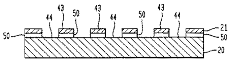
図5A、図5Bおよび図5Cは、このような他の処理を示したものである。図5Aでは、基板は、表面誘電体層50(Si上のSiO2など)を備えており、マスク層が、露出領域における誘電体の除去を可能にしている。図5Bでは、半導体の露出領域中に選択的に不純物領域51が拡散あるいは注入され、ドープ領域の局部的な電気的あるいは光学的特性を変化させている。別法としては、図5Cに示すように、凹所内の露出基板上に、伝導体層あるいはエピタキシャル層などの新しい材料層52を蒸着させ、あるいは成長させることができる。処理が終了した時点で、必要に応じて、従来の技法を使用して、成形された層の残留材料を除去することができる。例えばPMMAの場合、アセトンで洗浄することによって除去することができる。集積回路などの複雑なデバイスを完成するために、基板に対して追加のリソグラフィ・ステップを施すことができる。
【0026】
上で言及したように、加圧流体によって薄膜中に型を押し込むことができるよう、様々な方法で型/薄膜アセンブリ30を封止することができる。図6A〜図6Dは、型/薄膜アセンブリ30を封止するためのいくつかの方法を示したものである。
【0027】
図6Aは、柔軟な流体不透過性薄膜60(例えばプラスチック・バッグ)の封止カバー内にアセンブリを配置することによって、型/薄膜アセンブリを封止する配列を略図で示したものである。この配列構造の場合、外部圧力容器に対して、型と成形可能層との間の領域が封止される。成形に先立って、バッグから空気が除去されることが好ましい。
【0028】
図6Bは、代替封止配列構造を示したもので、中空弾性トロイド(toroid)の形態を取ることができる周辺封止用クランプ61によってアセンブリ30が封止されている。封止は、成形すべき領域の周囲に延びた突出領域62を型に設けることによって促進することができる。使用に際しては、クランプおよび加圧流体によって成形可能薄膜中に突出領域62が押し込まれ、成形領域が封止される。
【0029】
図6Cは、成形可能薄膜に型を軽く押し付ける周辺チューブすなわち錘63を加えることによってアセンブリ30が封止される封止配列を示したものである。周辺の突出領域62が封止を促進している。
【0030】
図6Dは、代替封止配列を示したもので、型と基板との間に設けた封止o−リング64によってアセンブリ30が封止されている。o−リングは、それぞれ型および基板の周辺凹所65、66内に位置していることが好ましい。周辺チューブすなわち錘63からの軽い圧力が封止を促進している。
【0031】
図6Eは、さらに他の封止配列を示したもので、柔軟な薄膜40Aと40Bとの間に配置されたアセンブリ30が、1対の整合シリンダ67A、67Bの内部に密閉されている。シリンダの内部に流体圧力を加えることにより、型および成形可能表面が共に押し付けられる。
【0032】
別法としては、2つのシリンダを使用して、加圧する前に、それぞれ型および表面を軽く封止することができる。さらに他の代替として、基板をサポートで支え、単一のシリンダで型あるいは薄膜を軽く封止することもできる。
【0033】
図7は、代替成形装置70を示したもので、中空の圧力キャップ72内の開口部71に隣接してアセンブリが配置され、開口部71を通って噴出する加圧流体の噴流によって、成形可能層21に型10が押し込まれる。キャップ72(圧力容器31と類似)は、加圧流体のための内部チャンバ73を有している。型と成形可能薄膜との間の領域は、型の上部表面によって圧力容器から効果的に封止されている。
【0034】
実施中は、基板ホルダ79上に基板および型が置かれる。型10の上方の所定位置に、バー74、75によってキャップ72が保持される。好ましくは気体の高圧流体が、入口76を通してチャンバ73内にポンプ供給される。チャンバ内の高圧流体により、各開口部71から噴出する流体が生成される。これらの噴流により、型10が成形可能層に対して一様に押し付けられ、型フィーチャがインプリントされる。
【0035】
有利には、キャップ72は、型10に隣接する面の周囲に沿った溝77を備えている。溝77は、キャップ72と型10との間にo−リング78を保持することができる。o−リングは、キャップ72と型10との間から流出する流体を少なくして成形圧力を高め、かつ、成形圧力をより一様にしている。
【0036】
別法としては、基板ホルダ79にキャップ72の構造と同じ構造を持たせ、同様に加圧流体の噴流によって基板を押し付けることもできる。
【0037】
(実施例)
以下の具体的な実施例を考察することにより、本発明をより深く理解することができよう。
実施例1
直径4インチのシリコン・ウェハに、厚さ150nmのPMMA層を被覆する。型は直径4インチのシリコン・ウェハでできており、その一方の表面に、厚さ100nmの複数の二酸化ケイ素突出パターンを有している。突出パターンをPMMAに向けて、型をPMMA層の上に置く。型および基板を、チャンバ内のプラスチック・バッグ中で封止し、チャンバを排気する。次に、500psiの窒素ガスをチャンバ内に導入する。チャンバ内のヒータによって、PMMAをPMMAのガラス転移温度より高い170℃に加熱し、PMMAを軟化する。気体の圧力の作用により、型がPMMA中に押し込まれる。ヒータを切り、冷窒素ガスを導入すると、PMMAの温度がガラス転移温度より低い温度に降下し、PMMAが硬化する。次に窒素ガスが大気圧に通気される。型および基板アセンブリをチャンバから取り除く。バッグを切り取り、型と基板を分離する。
【0038】
実施例2
直径4インチのシリコン・ウェハに、厚さ150nmのPMMA層を被覆し、チャック(chuck)上に置く。チャックは、その表面に複数の微小孔を有している。微小孔は、真空または加圧ガスのいずれかに接続されている。微小孔が真空に接続されると、ウェハがチャックの表面に保持される。型は直径4インチのシリコン・ウェハでできており、その一方の表面に、複数の二酸化ケイ素突出パターン(厚さ100nm)を有している。型は、基板チャックと同じ設計の第2のチャックによって保持される。型は、突出パターンをPMMAに向けて、PMMA層の頂部に置く。型および基板をチャンバ内に入れる。チャックからPMMAを加熱する。
【0039】
インプリント処理過程の間、先ずPMMAをそのガラス転移温度を超えて加熱する。型上のリング・パターンによって、リング内部の型パターンが外部の圧力から封止される。次に、両方のチャックの孔を、真空から500psiのガス圧に切り換える。加圧ガスにより、型の突出パターンをPMMA中に押し込む。型および基板の背面の粗さ、およびチャック表面の粗さに関係なく、型の突出パターンを加圧ガスによって、サブミクロンのスケールでPMMA中に一様に押し込むことが重要である。
【0040】
上で説明した実施形態は、本発明の応用例を示す多数の実施形態のうちのほんの一部を示したものに過ぎないことを理解されたい。当該技術分野の当業者にとっては、本発明の精神および範囲を逸脱することなく、他の多数の様々な配列方法が可能である。
【図面の簡単な説明】
【図1】 インプリント・リソグラフィの改良型方法のステップの概略を示す工程系統
図である。
【図2】 図1に示す改良型方法に使用される典型的な型、および成形可能薄膜を支える基板を示す図である。
【図3】 図1に示す改良型方法を実施するための装置を示す図である。
【図4A】 図1に示すプロセスの様々な段階における成形可能層および基板を示す図である。
【図4B】図1に示すプロセスの様々な段階における成形可能層および基板を示す図である。
【図4C】図1に示すプロセスの様々な段階における成形可能層および基板を示す図である。
【図5A】 基板上で実施することができる、さらに他の様々な処理ステップを示す図である。
【図5B】基板上で実施することができる、さらに他の様々な処理ステップを示す図である。
【図5C】基板上で実施することができる、さらに他の様々な処理ステップを示す図である。
【図6A】 図1に示す方法に有用な代替封止配列を示す図である。
【図6B】 図1に示す方法に有用な代替封止配列を示す図である。
【図6C】 図1に示す方法に有用な代替封止配列を示す図である。
【図6D】 図1に示す方法に有用な代替封止配列を示す図である。
【図6E】 図1に示す方法に有用な代替封止配列を示す図である。
【図7】 図1に示す方法を実施するための代替装置を示す図である。
Claims (45)
- 基板の表面に成形可能層を塗布する工程と、
複数の突出フィーチャを有する成形表面を備えた型を提供する工程と、
型と成形可能層との間の領域を封止する工程と、
直接流体圧力によって成形表面および成形可能層を共に押し付け、突出フィーチャの下側の成形可能層の厚さを薄くし薄くなった領域を生成する工程と、
成形可能層から型を取り去る工程とを含む、基板の表面を処理するための方法。 - 選択的に基板の領域を露出させるために、薄くなった領域から成形可能層の材料を除去する工程と、
基板の露出領域を選択的にさらに処理する工程とをさらに含む、請求項1に記載の方法。 - さらに処理する工程が、基板を不純物でドープすること、基板から材料を除去すること、または基板上に材料を添加することを含む、請求項2に記載の方法。
- 押付け後に成形可能層を硬化させる工程をさらに含む、請求項1に記載の方法。
- 封止することが、型と基板との間の領域を加圧流体から封止することを含む、請求項1に記載の方法。
- 基板または型あるいはその両方が十分に柔軟であり、共に流体圧力に従う、請求項1に記載の方法。
- 押付け工程が、加圧流体の流れによって、型および成形可能層を共に押し付けることを含む、請求項1に記載の方法。
- 成形表面の少なくとも2つの突出フィーチャが、横方向に200nm未満の間隔を隔てて配置される、請求項1に記載の方法。
- 成形可能層の厚さが、0.1nmから10μmの範囲である、請求項1に記載の方法。
- 示差熱膨張または収縮を最小化するために、基板および型の材料が同じ材料である、請求項1に記載の方法。
- 成形可能層が予め形成されたパターンを備えており、成形表面および成形可能層を共に押し付ける前に、予め形成されたパターンに型を整列させる、請求項1に記載の方法。
- 基板の表面に配置された成形可能層と、
成形可能層に隣接して配置される複数の突出フィーチャを含む成形表面を備えた型と、
成形表面および成形可能層を共に押し付けるための加圧流体を供給する、加圧流体が入った圧力容器と、
成形可能層と成形表面との間の領域を加圧流体から封止するためのシールと
を備えた、基板を処理するための装置。 - シールが、周辺ガスケット、o−リング、流体不透過の柔軟性の薄膜および周辺クランプから選択されるデバイスを備える、請求項12に記載の装置。
- 基板および型が圧力容器内に配置された、請求項12に記載の装置。
- 圧力容器が、成形可能層を加熱するためのヒータをさらに備える、請求項14に記載の装置。
- 圧力容器が、成形可能層に放射線を照射することができる透明窓をさらに備える、請求項14に記載の装置。
- 型または基板が放射線に対して透明である、請求項16に記載の装置。
- 圧力容器が、型および成形可能層を共に押し付けるための加圧流体を供給する複数の開口部を備える、請求項12に記載の装置。
- 成形表面の少なくとも2つの突出フィーチャが、200nm未満の間隔を隔てて配置される、請求項12に記載の装置。
- 成形可能表面の突出フィーチャが、0.1nmから10μmだけ突出する、請求項12に記載の装置。
- 半導体基板にマスク層を塗布し、
パターン化された表面を有する型を、マスク層に隣接して配置し、
チャンバに加圧流体を充填し、
型とマスク層との間の領域を、チャンバ内の流体圧力から分離するために、封止材を位置決めし、
型およびマスク層を共に押し付けるために、チャンバから型または基板を加圧流体を浴びせることを含む、半導体基板上のマスク層をパターン化するための方法。 - マスク層の材料が重合体からなり、押付けを実施した後、重合体を硬化させる工程をさらに含む、請求項21に記載の方法。
- 硬化させる工程が、マスク層を放射線で照射することを含む、請求項22に記載の方法。
- 硬化したマスク層が、インプリント・パターンを型から保護する、請求項22に記載の方法。
- マスク層をマスク層の材料が硬化する温度に冷却することをさらに含む、請求項21に記載の方法。
- マスク層の材料がレジストからなる、請求項21に記載の方法。
- マスク層の材料が液体重合体からなる、請求項26に記載の方法。
- 押付けに先立って、マスク層をマスク層の材料が軟化する温度に加熱することをさらに含む、請求項21に記載の方法。
- 押付けが、型のパターン化された面を基板に向けて押し付けるために、型の表面に流体圧力を加えることを含む、請求項21に記載の方法。
- 押付けが、基板を型のパターン化された面に向けて押し付けるために、基板の表面に流体圧力を加えることを含む、請求項21に記載の方法。
- マスク層から型を除去し、成形済み凹所をマスク層に残すことと、
基板の領域を露出させるために、成形済み凹所からマスク材料を取り除くこととをさらに含む、請求項21に記載の方法。 - 露出した基板を選択的にエッチングする工程、露出した基板中に不純物を選択的に拡散させる工程、および露出した基板上に材料を選択的に堆積させる工程のうちの1つまたは複数の工程をさらに含む、請求項31に記載の方法。
- 位置決めすることが、型とマスク層との間の領域の周囲に材料のリングを配置することを含む、請求項21に記載の方法。
- 位置決めすることが、圧力チャンバと型および基板のうちの少なくともいずれか1つとの間に、少なくとも1つの柔軟性の薄膜を配置することを含む、請求項21に記載の方法。
- 基板上にマスク材料の層を配置する工程と、
パターン化された表面を備えた型を、マスク材料の層に隣接して位置決めする工程と、
マスク材料の層を圧力チャンバから分離するために、封止デバイスを位置決めする工程と、
マスクされた基板および型を圧力チャンバ内に配置する工程と、
型のパターン化された面およびマスク材料の層を共に押し付けるために、圧力チャンバ内の加圧流体の圧力を大きくする工程とを含む、半導体基板を処理する方法。 - 封止デバイスを位置決めする工程によって、マスク材料の層と型との間の領域を、圧力チャンバ内の加圧流体から気密分離する、請求項35に記載の方法。
- 圧力を大きくする前にマスク層を加熱することをさらに含む、請求項35に記載の方法。
- 押付け後マスク層を硬化させ、型による変形部分を硬化させることをさらに含む、請求項35に記載の方法。
- 硬化後、マスク層との接触から型を除去することをさらに含む、請求項38に記載の方法。
- 型の除去後、マスク層から汚染物質を除去する工程をさらに含む、請求項39に記載の方法。
- 変形部分のマスク材料を取り除くことをさらに含む、請求項38に記載の方法。
- 基板を選択的にエッチングする工程、基板中に不純物を選択的にドープする工程、基板上に材料を選択的に追加する工程のうちの1つまたは複数の工程によって、基板をさらに処理することを含む、請求項41に記載の方法。
- 圧力を大きくすることが、チャンバ内の流体に圧力を加えることよりなる、請求項35に記載の方法。
- 流体が気体からなる、請求項35に記載の方法。
- 流体が液体からなる、請求項35に記載の方法。
Applications Claiming Priority (2)
| Application Number | Priority Date | Filing Date | Title |
|---|---|---|---|
| US09/618,174 US6482742B1 (en) | 2000-07-18 | 2000-07-18 | Fluid pressure imprint lithography |
| PCT/US2001/021005 WO2002007199A1 (en) | 2000-07-18 | 2001-07-02 | Fluid pressure imprint lithography |
Publications (3)
| Publication Number | Publication Date |
|---|---|
| JP2004504718A JP2004504718A (ja) | 2004-02-12 |
| JP2004504718A5 JP2004504718A5 (ja) | 2005-04-07 |
| JP3987795B2 true JP3987795B2 (ja) | 2007-10-10 |
Family
ID=24476613
Family Applications (1)
| Application Number | Title | Priority Date | Filing Date |
|---|---|---|---|
| JP2002513006A Expired - Lifetime JP3987795B2 (ja) | 2000-07-18 | 2001-07-02 | 流体圧力インプリント・リソグラフィ |
Country Status (7)
| Country | Link |
|---|---|
| US (3) | US6482742B1 (ja) |
| EP (1) | EP1325513A4 (ja) |
| JP (1) | JP3987795B2 (ja) |
| KR (1) | KR100873587B1 (ja) |
| CN (1) | CN1299332C (ja) |
| AU (1) | AU2001273136A1 (ja) |
| WO (1) | WO2002007199A1 (ja) |
Cited By (1)
| Publication number | Priority date | Publication date | Assignee | Title |
|---|---|---|---|---|
| WO2012121418A2 (en) | 2011-03-09 | 2012-09-13 | Fujifilm Corporation | Nanoimprinting method and nanoimprinting apparatus for executing the nanoimprinting method |
Families Citing this family (389)
| Publication number | Priority date | Publication date | Assignee | Title |
|---|---|---|---|---|
| US8728380B2 (en) * | 1995-11-15 | 2014-05-20 | Regents Of The University Of Minnesota | Lithographic method for forming a pattern |
| US20080217813A1 (en) * | 1995-11-15 | 2008-09-11 | Chou Stephen Y | Release surfaces, particularly for use in nanoimprint lithography |
| US20040036201A1 (en) * | 2000-07-18 | 2004-02-26 | Princeton University | Methods and apparatus of field-induced pressure imprint lithography |
| US20030080471A1 (en) * | 2001-10-29 | 2003-05-01 | Chou Stephen Y. | Lithographic method for molding pattern with nanoscale features |
| US6713238B1 (en) * | 1998-10-09 | 2004-03-30 | Stephen Y. Chou | Microscale patterning and articles formed thereby |
| BR9915021A (pt) | 1998-10-09 | 2001-08-14 | Genesis Res & Dev Corp Ltd | Materiais e métodos para a modificação de conteúdo de lignina da planta |
| US6334960B1 (en) * | 1999-03-11 | 2002-01-01 | Board Of Regents, The University Of Texas System | Step and flash imprint lithography |
| US6939474B2 (en) * | 1999-07-30 | 2005-09-06 | Formfactor, Inc. | Method for forming microelectronic spring structures on a substrate |
| US7432634B2 (en) | 2000-10-27 | 2008-10-07 | Board Of Regents, University Of Texas System | Remote center compliant flexure device |
| US6873087B1 (en) | 1999-10-29 | 2005-03-29 | Board Of Regents, The University Of Texas System | High precision orientation alignment and gap control stages for imprint lithography processes |
| SE515607C2 (sv) * | 1999-12-10 | 2001-09-10 | Obducat Ab | Anordning och metod vid tillverkning av strukturer |
| EP1303792B1 (en) * | 2000-07-16 | 2012-10-03 | Board Of Regents, The University Of Texas System | High-resolution overlay alignement methods and systems for imprint lithography |
| US20050160011A1 (en) * | 2004-01-20 | 2005-07-21 | Molecular Imprints, Inc. | Method for concurrently employing differing materials to form a layer on a substrate |
| KR100827741B1 (ko) | 2000-07-17 | 2008-05-07 | 보드 오브 리전츠, 더 유니버시티 오브 텍사스 시스템 | 임프린트 리소그래피 공정을 위한 자동 유체 분배 방법 및시스템 |
| US7717696B2 (en) * | 2000-07-18 | 2010-05-18 | Nanonex Corp. | Apparatus for double-sided imprint lithography |
| US20100236705A1 (en) * | 2000-07-18 | 2010-09-23 | Chou Stephen Y | Fluidic and Microdevice Apparatus and Methods For Bonding Components Thereof |
| US20080164638A1 (en) * | 2006-11-28 | 2008-07-10 | Wei Zhang | Method and apparatus for rapid imprint lithography |
| US20050037143A1 (en) * | 2000-07-18 | 2005-02-17 | Chou Stephen Y. | Imprint lithography with improved monitoring and control and apparatus therefor |
| US7322287B2 (en) * | 2000-07-18 | 2008-01-29 | Nanonex Corporation | Apparatus for fluid pressure imprint lithography |
| US7635262B2 (en) * | 2000-07-18 | 2009-12-22 | Princeton University | Lithographic apparatus for fluid pressure imprint lithography |
| AU2001286573A1 (en) | 2000-08-21 | 2002-03-04 | Board Of Regents, The University Of Texas System | Flexure based macro motion translation stage |
| EP1352295B1 (en) * | 2000-10-12 | 2015-12-23 | Board of Regents, The University of Texas System | Template for room temperature, low pressure micro- and nano-imprint lithography |
| DE10059178C2 (de) * | 2000-11-29 | 2002-11-07 | Siemens Production & Logistics | Verfahren zur Herstellung von Halbleitermodulen sowie nach dem Verfahren hergestelltes Modul |
| AUPR245201A0 (en) * | 2001-01-10 | 2001-02-01 | Silverbrook Research Pty Ltd | An apparatus and method (WSM05) |
| US7019924B2 (en) * | 2001-02-16 | 2006-03-28 | Komag, Incorporated | Patterned medium and recording head |
| US9678038B2 (en) | 2001-07-25 | 2017-06-13 | The Trustees Of Princeton University | Nanochannel arrays and their preparation and use for high throughput macromolecular analysis |
| SG187992A1 (en) | 2001-07-25 | 2013-03-28 | Univ Princeton | Nanochannel arrays and their preparation and use for high throughput macromolecular analysis |
| US20030071016A1 (en) * | 2001-10-11 | 2003-04-17 | Wu-Sheng Shih | Patterned structure reproduction using nonsticking mold |
| US6936181B2 (en) * | 2001-10-11 | 2005-08-30 | Kovio, Inc. | Methods for patterning using liquid embossing |
| US6743368B2 (en) * | 2002-01-31 | 2004-06-01 | Hewlett-Packard Development Company, L.P. | Nano-size imprinting stamp using spacer technique |
| KR20040081164A (ko) * | 2002-02-01 | 2004-09-20 | 코닌클리케 필립스 일렉트로닉스 엔.브이. | Oled 매트릭스의 잉크젯 인쇄용 구조화된 폴리머 기판 |
| US6716754B2 (en) * | 2002-03-12 | 2004-04-06 | Micron Technology, Inc. | Methods of forming patterns and molds for semiconductor constructions |
| WO2003079416A1 (en) | 2002-03-15 | 2003-09-25 | Princeton University | Laser assisted direct imprint lithography |
| US7144539B2 (en) * | 2002-04-04 | 2006-12-05 | Obducat Ab | Imprint method and device |
| US7652574B2 (en) * | 2002-04-08 | 2010-01-26 | Sayegh Adel O | Article surveillance tag having a vial |
| AU2003269813A1 (en) | 2002-04-16 | 2003-12-31 | Princeton University | Gradient structures interfacing microfluidics and nanofluidics, methods for fabrication and uses thereof |
| US6897089B1 (en) * | 2002-05-17 | 2005-05-24 | Micron Technology, Inc. | Method and system for fabricating semiconductor components using wafer level contact printing |
| WO2003099536A1 (en) * | 2002-05-24 | 2003-12-04 | Chou Stephen Y | Methods and apparatus of field-induced pressure imprint lithography |
| US6876784B2 (en) * | 2002-05-30 | 2005-04-05 | Nanoopto Corporation | Optical polarization beam combiner/splitter |
| US7235464B2 (en) * | 2002-05-30 | 2007-06-26 | International Business Machines Corporation | Patterning method |
| US7283571B2 (en) * | 2002-06-17 | 2007-10-16 | Jian Wang | Method and system for performing wavelength locking of an optical transmission source |
| US7386205B2 (en) * | 2002-06-17 | 2008-06-10 | Jian Wang | Optical device and method for making same |
| WO2003107046A2 (en) | 2002-06-18 | 2003-12-24 | Nanoopto Corporation | Optical components exhibiting enhanced functionality and method of making same |
| US7179079B2 (en) * | 2002-07-08 | 2007-02-20 | Molecular Imprints, Inc. | Conforming template for patterning liquids disposed on substrates |
| US20080160129A1 (en) | 2006-05-11 | 2008-07-03 | Molecular Imprints, Inc. | Template Having a Varying Thickness to Facilitate Expelling a Gas Positioned Between a Substrate and the Template |
| US6926929B2 (en) | 2002-07-09 | 2005-08-09 | Molecular Imprints, Inc. | System and method for dispensing liquids |
| US6932934B2 (en) | 2002-07-11 | 2005-08-23 | Molecular Imprints, Inc. | Formation of discontinuous films during an imprint lithography process |
| US7442336B2 (en) * | 2003-08-21 | 2008-10-28 | Molecular Imprints, Inc. | Capillary imprinting technique |
| US7077992B2 (en) | 2002-07-11 | 2006-07-18 | Molecular Imprints, Inc. | Step and repeat imprint lithography processes |
| US6900881B2 (en) | 2002-07-11 | 2005-05-31 | Molecular Imprints, Inc. | Step and repeat imprint lithography systems |
| US6908861B2 (en) | 2002-07-11 | 2005-06-21 | Molecular Imprints, Inc. | Method for imprint lithography using an electric field |
| US7019819B2 (en) | 2002-11-13 | 2006-03-28 | Molecular Imprints, Inc. | Chucking system for modulating shapes of substrates |
| US7027156B2 (en) * | 2002-08-01 | 2006-04-11 | Molecular Imprints, Inc. | Scatterometry alignment for imprint lithography |
| WO2004013684A2 (en) | 2002-08-01 | 2004-02-12 | Nanoopto Corporation | Precision phase retardation devices and method of making same |
| US6916584B2 (en) * | 2002-08-01 | 2005-07-12 | Molecular Imprints, Inc. | Alignment methods for imprint lithography |
| US6911385B1 (en) * | 2002-08-22 | 2005-06-28 | Kovio, Inc. | Interface layer for the fabrication of electronic devices |
| US7071088B2 (en) * | 2002-08-23 | 2006-07-04 | Molecular Imprints, Inc. | Method for fabricating bulbous-shaped vias |
| US20040132301A1 (en) * | 2002-09-12 | 2004-07-08 | Harper Bruce M. | Indirect fluid pressure imprinting |
| US6939120B1 (en) | 2002-09-12 | 2005-09-06 | Komag, Inc. | Disk alignment apparatus and method for patterned media production |
| KR100492851B1 (ko) * | 2002-09-26 | 2005-06-02 | 주식회사 미뉴타텍 | 좌굴 현상을 이용한 미세 패턴 형성 방법 |
| US20040065252A1 (en) * | 2002-10-04 | 2004-04-08 | Sreenivasan Sidlgata V. | Method of forming a layer on a substrate to facilitate fabrication of metrology standards |
| US8349241B2 (en) | 2002-10-04 | 2013-01-08 | Molecular Imprints, Inc. | Method to arrange features on a substrate to replicate features having minimal dimensional variability |
| US20050167894A1 (en) * | 2002-10-08 | 2005-08-04 | Wu-Sheng Shih | Patterned structure reproduction using nonsticking mold |
| US7013064B2 (en) * | 2002-10-09 | 2006-03-14 | Nanoopto Corporation | Freespace tunable optoelectronic device and method |
| US6920272B2 (en) * | 2002-10-09 | 2005-07-19 | Nanoopto Corporation | Monolithic tunable lasers and reflectors |
| US6980282B2 (en) * | 2002-12-11 | 2005-12-27 | Molecular Imprints, Inc. | Method for modulating shapes of substrates |
| US7641840B2 (en) | 2002-11-13 | 2010-01-05 | Molecular Imprints, Inc. | Method for expelling gas positioned between a substrate and a mold |
| US20050036223A1 (en) * | 2002-11-27 | 2005-02-17 | Wachenschwanz David E. | Magnetic discrete track recording disk |
| US7147790B2 (en) * | 2002-11-27 | 2006-12-12 | Komag, Inc. | Perpendicular magnetic discrete track recording disk |
| US20040197712A1 (en) * | 2002-12-02 | 2004-10-07 | Jacobson Joseph M. | System for contact printing |
| US7750059B2 (en) | 2002-12-04 | 2010-07-06 | Hewlett-Packard Development Company, L.P. | Polymer solution for nanoimprint lithography to reduce imprint temperature and pressure |
| US6871558B2 (en) | 2002-12-12 | 2005-03-29 | Molecular Imprints, Inc. | Method for determining characteristics of substrate employing fluid geometries |
| US20040112862A1 (en) * | 2002-12-12 | 2004-06-17 | Molecular Imprints, Inc. | Planarization composition and method of patterning a substrate using the same |
| US7365103B2 (en) * | 2002-12-12 | 2008-04-29 | Board Of Regents, The University Of Texas System | Compositions for dark-field polymerization and method of using the same for imprint lithography processes |
| TW200500811A (en) * | 2002-12-13 | 2005-01-01 | Molecular Imprints Inc | Magnification correction employing out-of-plane distortion of a substrate |
| GB0229191D0 (en) * | 2002-12-14 | 2003-01-22 | Plastic Logic Ltd | Embossing of polymer devices |
| JP2006510066A (ja) * | 2002-12-16 | 2006-03-23 | イー−インク コーポレイション | 電気光学表示装置用バックプレーン |
| US7371975B2 (en) * | 2002-12-18 | 2008-05-13 | Intel Corporation | Electronic packages and components thereof formed by substrate-imprinting |
| US20040126547A1 (en) * | 2002-12-31 | 2004-07-01 | Coomer Boyd L. | Methods for performing substrate imprinting using thermoset resin varnishes and products formed therefrom |
| US6974775B2 (en) * | 2002-12-31 | 2005-12-13 | Intel Corporation | Method and apparatus for making an imprinted conductive circuit using semi-additive plating |
| US7268946B2 (en) * | 2003-02-10 | 2007-09-11 | Jian Wang | Universal broadband polarizer, devices incorporating same, and method of making same |
| US7510946B2 (en) * | 2003-03-17 | 2009-03-31 | Princeton University | Method for filling of nanoscale holes and trenches and for planarizing of a wafer surface |
| JP4340086B2 (ja) | 2003-03-20 | 2009-10-07 | 株式会社日立製作所 | ナノプリント用スタンパ、及び微細構造転写方法 |
| US7186656B2 (en) | 2004-05-21 | 2007-03-06 | Molecular Imprints, Inc. | Method of forming a recessed structure employing a reverse tone process |
| US6943117B2 (en) * | 2003-03-27 | 2005-09-13 | Korea Institute Of Machinery & Materials | UV nanoimprint lithography process using elementwise embossed stamp and selectively additive pressurization |
| US20040209123A1 (en) * | 2003-04-17 | 2004-10-21 | Bajorek Christopher H. | Method of fabricating a discrete track recording disk using a bilayer resist for metal lift-off |
| TW568349U (en) * | 2003-05-02 | 2003-12-21 | Ind Tech Res Inst | Parallelism adjusting device for nano-transferring |
| TW570290U (en) * | 2003-05-02 | 2004-01-01 | Ind Tech Res Inst | Uniform pressing device for nanometer transfer-print |
| US6926921B2 (en) * | 2003-05-05 | 2005-08-09 | Hewlett-Packard Development Company, L.P. | Imprint lithography for superconductor devices |
| US6951173B1 (en) | 2003-05-14 | 2005-10-04 | Molecular Imprints, Inc. | Assembly and method for transferring imprint lithography templates |
| KR101055640B1 (ko) * | 2003-05-14 | 2011-08-09 | 몰레큘러 임프린츠 인코퍼레이티드 | 임프린트 리소그래피 공정 중의 주형 전사 방법, 시스템,홀더 및 어셈블리 |
| WO2004114016A2 (en) * | 2003-06-09 | 2004-12-29 | Princeton University Office Of Technology Licensing And Intellectual Property | Imprint lithography with improved monitoring and control and apparatus therefor |
| WO2004109401A1 (en) | 2003-06-09 | 2004-12-16 | Canon Kabushiki Kaisha | Process for producing structure, structure thereof, and magnetic recording medium |
| JP2005008909A (ja) * | 2003-06-16 | 2005-01-13 | Canon Inc | 構造体の製造方法 |
| US20040258355A1 (en) * | 2003-06-17 | 2004-12-23 | Jian Wang | Micro-structure induced birefringent waveguiding devices and methods of making same |
| US20060108710A1 (en) * | 2004-11-24 | 2006-05-25 | Molecular Imprints, Inc. | Method to reduce adhesion between a conformable region and a mold |
| US7157036B2 (en) * | 2003-06-17 | 2007-01-02 | Molecular Imprints, Inc | Method to reduce adhesion between a conformable region and a pattern of a mold |
| US7307118B2 (en) | 2004-11-24 | 2007-12-11 | Molecular Imprints, Inc. | Composition to reduce adhesion between a conformable region and a mold |
| US7150622B2 (en) | 2003-07-09 | 2006-12-19 | Molecular Imprints, Inc. | Systems for magnification and distortion correction for imprint lithography processes |
| JP2005045168A (ja) * | 2003-07-25 | 2005-02-17 | Tokyo Electron Ltd | インプリント方法およびインプリント装置 |
| JP4190371B2 (ja) | 2003-08-26 | 2008-12-03 | Tdk株式会社 | 凹凸パターン形成用スタンパー、凹凸パターン形成方法および磁気記録媒体 |
| US7588657B2 (en) * | 2003-09-29 | 2009-09-15 | Princeton University | Pattern-free method of making line gratings |
| US8211214B2 (en) | 2003-10-02 | 2012-07-03 | Molecular Imprints, Inc. | Single phase fluid imprint lithography method |
| US7090716B2 (en) * | 2003-10-02 | 2006-08-15 | Molecular Imprints, Inc. | Single phase fluid imprint lithography method |
| US7261830B2 (en) * | 2003-10-16 | 2007-08-28 | Molecular Imprints, Inc. | Applying imprinting material to substrates employing electromagnetic fields |
| US7122482B2 (en) | 2003-10-27 | 2006-10-17 | Molecular Imprints, Inc. | Methods for fabricating patterned features utilizing imprint lithography |
| US20050098534A1 (en) * | 2003-11-12 | 2005-05-12 | Molecular Imprints, Inc. | Formation of conductive templates employing indium tin oxide |
| WO2005047975A2 (en) * | 2003-11-12 | 2005-05-26 | Molecular Imprints, Inc. | Dispense geometry and conductive template to achieve high-speed filling and throughput |
| US20050106321A1 (en) * | 2003-11-14 | 2005-05-19 | Molecular Imprints, Inc. | Dispense geometery to achieve high-speed filling and throughput |
| US20050112505A1 (en) * | 2003-11-25 | 2005-05-26 | Huang Wen C. | Field-assisted micro- and nano-fabrication method |
| EP1538482B1 (en) * | 2003-12-05 | 2016-02-17 | Obducat AB | Device and method for large area lithography |
| US7153360B2 (en) * | 2003-12-16 | 2006-12-26 | Hewlett-Packard Development Company, Lp. | Template and methods for forming photonic crystals |
| KR100572207B1 (ko) * | 2003-12-18 | 2006-04-19 | 주식회사 디지탈바이오테크놀러지 | 플라스틱 마이크로 칩의 접합 방법 |
| US7632087B2 (en) * | 2003-12-19 | 2009-12-15 | Wd Media, Inc. | Composite stamper for imprint lithography |
| KR100965424B1 (ko) * | 2003-12-27 | 2010-06-24 | 엘지디스플레이 주식회사 | 평판 표시 소자의 제조방법 및 장치 |
| US7255805B2 (en) * | 2004-01-12 | 2007-08-14 | Hewlett-Packard Development Company, L.P. | Photonic structures, devices, and methods |
| US20050150862A1 (en) * | 2004-01-13 | 2005-07-14 | Harper Bruce M. | Workpiece alignment assembly |
| US20050151300A1 (en) * | 2004-01-13 | 2005-07-14 | Harper Bruce M. | Workpiece isothermal imprinting |
| US20050151282A1 (en) * | 2004-01-13 | 2005-07-14 | Harper Bruce M. | Workpiece handler and alignment assembly |
| US20050158419A1 (en) * | 2004-01-15 | 2005-07-21 | Watts Michael P. | Thermal processing system for imprint lithography |
| KR100566700B1 (ko) * | 2004-01-15 | 2006-04-03 | 삼성전자주식회사 | 반도체 공정에서 포토레지스트 패턴 형성 방법,포토레지스트 패턴 형성용 템플레이트 및 이의 제조 방법. |
| US20050156353A1 (en) * | 2004-01-15 | 2005-07-21 | Watts Michael P. | Method to improve the flow rate of imprinting material |
| US7686606B2 (en) * | 2004-01-20 | 2010-03-30 | Wd Media, Inc. | Imprint embossing alignment system |
| US7329114B2 (en) * | 2004-01-20 | 2008-02-12 | Komag, Inc. | Isothermal imprint embossing system |
| US20050155554A1 (en) * | 2004-01-20 | 2005-07-21 | Saito Toshiyuki M. | Imprint embossing system |
| US8535041B2 (en) * | 2006-07-28 | 2013-09-17 | Microcontinuum, Inc. | Addressable flexible patterns |
| US9307648B2 (en) | 2004-01-21 | 2016-04-05 | Microcontinuum, Inc. | Roll-to-roll patterning of transparent and metallic layers |
| US7462292B2 (en) * | 2004-01-27 | 2008-12-09 | Hewlett-Packard Development Company, L.P. | Silicon carbide imprint stamp |
| US7060625B2 (en) * | 2004-01-27 | 2006-06-13 | Hewlett-Packard Development Company, L.P. | Imprint stamp |
| KR20080031514A (ko) * | 2004-02-04 | 2008-04-08 | 스미도모쥬기가이고교 가부시키가이샤 | 가압성형장치, 금형 및 가압성형방법 |
| US7056834B2 (en) * | 2004-02-10 | 2006-06-06 | Hewlett-Packard Development Company, L.P. | Forming a plurality of thin-film devices using imprint lithography |
| US20060115999A1 (en) * | 2004-12-01 | 2006-06-01 | Molecular Imprints, Inc. | Methods of exposure for the purpose of thermal management for imprint lithography processes |
| US7019835B2 (en) * | 2004-02-19 | 2006-03-28 | Molecular Imprints, Inc. | Method and system to measure characteristics of a film disposed on a substrate |
| US8076386B2 (en) | 2004-02-23 | 2011-12-13 | Molecular Imprints, Inc. | Materials for imprint lithography |
| US20050189676A1 (en) * | 2004-02-27 | 2005-09-01 | Molecular Imprints, Inc. | Full-wafer or large area imprinting with multiple separated sub-fields for high throughput lithography |
| US7906180B2 (en) | 2004-02-27 | 2011-03-15 | Molecular Imprints, Inc. | Composition for an etching mask comprising a silicon-containing material |
| US7730834B2 (en) * | 2004-03-04 | 2010-06-08 | Asml Netherlands B.V. | Printing apparatus and device manufacturing method |
| JP4481698B2 (ja) * | 2004-03-29 | 2010-06-16 | キヤノン株式会社 | 加工装置 |
| US8235302B2 (en) * | 2004-04-20 | 2012-08-07 | Nanolnk, Inc. | Identification features |
| WO2005104756A2 (en) * | 2004-04-27 | 2005-11-10 | The Board Of Trustees Of The University Of Illinois | Composite patterning devices for soft lithography |
| US7140861B2 (en) | 2004-04-27 | 2006-11-28 | Molecular Imprints, Inc. | Compliant hard template for UV imprinting |
| EP1594001B1 (en) * | 2004-05-07 | 2015-12-30 | Obducat AB | Device and method for imprint lithography |
| US20050253307A1 (en) * | 2004-05-11 | 2005-11-17 | Molecualr Imprints, Inc. | Method of patterning a conductive layer on a substrate |
| US8025831B2 (en) * | 2004-05-24 | 2011-09-27 | Agency For Science, Technology And Research | Imprinting of supported and free-standing 3-D micro- or nano-structures |
| WO2005119802A2 (en) | 2004-05-28 | 2005-12-15 | Board Of Regents, The University Of Texas System | Adaptive shape substrate support system and method |
| TWI366218B (en) * | 2004-06-01 | 2012-06-11 | Semiconductor Energy Lab | Method for manufacturing semiconductor device |
| JP4954498B2 (ja) * | 2004-06-01 | 2012-06-13 | 株式会社半導体エネルギー研究所 | 半導体装置の作製方法 |
| DE602005022874D1 (de) * | 2004-06-03 | 2010-09-23 | Molecular Imprints Inc | Fluidausgabe und tropfenausgabe nach bedarf für die herstellung im nanobereich |
| US20050270516A1 (en) * | 2004-06-03 | 2005-12-08 | Molecular Imprints, Inc. | System for magnification and distortion correction during nano-scale manufacturing |
| JP4574240B2 (ja) * | 2004-06-11 | 2010-11-04 | キヤノン株式会社 | 加工装置、加工方法、デバイス製造方法 |
| US20070228593A1 (en) | 2006-04-03 | 2007-10-04 | Molecular Imprints, Inc. | Residual Layer Thickness Measurement and Correction |
| TWI325851B (en) * | 2004-06-18 | 2010-06-11 | Hon Hai Prec Ind Co Ltd | Method and device of manufacturing optical element |
| US7320584B1 (en) | 2004-07-07 | 2008-01-22 | Komag, Inc. | Die set having sealed compliant member |
| US7785526B2 (en) * | 2004-07-20 | 2010-08-31 | Molecular Imprints, Inc. | Imprint alignment method, system, and template |
| US7195950B2 (en) * | 2004-07-21 | 2007-03-27 | Hewlett-Packard Development Company, L.P. | Forming a plurality of thin-film devices |
| EP1773405A4 (en) * | 2004-07-22 | 2011-10-05 | Duska Scient Co | METHOD FOR DIAGNOSIS, MONITORING AND TREATMENT OF LUNG DISEASES |
| US20060017876A1 (en) * | 2004-07-23 | 2006-01-26 | Molecular Imprints, Inc. | Displays and method for fabricating displays |
| US7105452B2 (en) * | 2004-08-13 | 2006-09-12 | Molecular Imprints, Inc. | Method of planarizing a semiconductor substrate with an etching chemistry |
| US7309225B2 (en) * | 2004-08-13 | 2007-12-18 | Molecular Imprints, Inc. | Moat system for an imprint lithography template |
| US7939131B2 (en) | 2004-08-16 | 2011-05-10 | Molecular Imprints, Inc. | Method to provide a layer with uniform etch characteristics |
| US7282550B2 (en) * | 2004-08-16 | 2007-10-16 | Molecular Imprints, Inc. | Composition to provide a layer with uniform etch characteristics |
| US20070164476A1 (en) * | 2004-09-01 | 2007-07-19 | Wei Wu | Contact lithography apparatus and method employing substrate deformation |
| US7641468B2 (en) * | 2004-09-01 | 2010-01-05 | Hewlett-Packard Development Company, L.P. | Imprint lithography apparatus and method employing an effective pressure |
| US8075298B2 (en) * | 2004-09-08 | 2011-12-13 | Nil Technology Aps | Flexible nano-imprint stamp |
| WO2006033872A2 (en) | 2004-09-21 | 2006-03-30 | Molecular Imprints, Inc. | Method of forming an in-situ recessed structure |
| US7205244B2 (en) | 2004-09-21 | 2007-04-17 | Molecular Imprints | Patterning substrates employing multi-film layers defining etch-differential interfaces |
| US7547504B2 (en) | 2004-09-21 | 2009-06-16 | Molecular Imprints, Inc. | Pattern reversal employing thick residual layers |
| US7241395B2 (en) * | 2004-09-21 | 2007-07-10 | Molecular Imprints, Inc. | Reverse tone patterning on surfaces having planarity perturbations |
| US7041604B2 (en) * | 2004-09-21 | 2006-05-09 | Molecular Imprints, Inc. | Method of patterning surfaces while providing greater control of recess anisotropy |
| US7252777B2 (en) * | 2004-09-21 | 2007-08-07 | Molecular Imprints, Inc. | Method of forming an in-situ recessed structure |
| US20060062922A1 (en) | 2004-09-23 | 2006-03-23 | Molecular Imprints, Inc. | Polymerization technique to attenuate oxygen inhibition of solidification of liquids and composition therefor |
| US7244386B2 (en) | 2004-09-27 | 2007-07-17 | Molecular Imprints, Inc. | Method of compensating for a volumetric shrinkage of a material disposed upon a substrate to form a substantially planar structure therefrom |
| US20060081557A1 (en) * | 2004-10-18 | 2006-04-20 | Molecular Imprints, Inc. | Low-k dielectric functional imprinting materials |
| US8721952B2 (en) * | 2004-11-16 | 2014-05-13 | International Business Machines Corporation | Pneumatic method and apparatus for nano imprint lithography having a conforming mask |
| CN100395121C (zh) * | 2004-11-19 | 2008-06-18 | 鸿富锦精密工业(深圳)有限公司 | 热压印方法 |
| KR101275478B1 (ko) * | 2004-11-22 | 2013-06-14 | 스미토모덴키고교가부시키가이샤 | 가공방법, 가공장치 및 그 방법에 의해 제조된 미세구조체 |
| US20070231421A1 (en) | 2006-04-03 | 2007-10-04 | Molecular Imprints, Inc. | Enhanced Multi Channel Alignment |
| US7292326B2 (en) | 2004-11-30 | 2007-11-06 | Molecular Imprints, Inc. | Interferometric analysis for the manufacture of nano-scale devices |
| US7630067B2 (en) | 2004-11-30 | 2009-12-08 | Molecular Imprints, Inc. | Interferometric analysis method for the manufacture of nano-scale devices |
| EP1820619A4 (en) | 2004-11-30 | 2010-07-07 | Asahi Glass Co Ltd | MOLD AND METHOD FOR MANUFACTURING SUBSTRATES HAVING MICROMOTIVES TRANSFERRED THEREON |
| WO2006060757A2 (en) | 2004-12-01 | 2006-06-08 | Molecular Imprints, Inc. | Eliminating printability of sub-resolution defects in imprint lithography |
| US7811505B2 (en) | 2004-12-07 | 2010-10-12 | Molecular Imprints, Inc. | Method for fast filling of templates for imprint lithography using on template dispense |
| JP2006165371A (ja) * | 2004-12-09 | 2006-06-22 | Canon Inc | 転写装置およびデバイス製造方法 |
| KR100616292B1 (ko) | 2004-12-15 | 2006-08-28 | 주식회사 디엠에스 | 식각 영역을 만들기 위한 장치 |
| US7410591B2 (en) * | 2004-12-16 | 2008-08-12 | Asml Holding N.V. | Method and system for making a nano-plate for imprint lithography |
| US7363854B2 (en) * | 2004-12-16 | 2008-04-29 | Asml Holding N.V. | System and method for patterning both sides of a substrate utilizing imprint lithography |
| US7409759B2 (en) * | 2004-12-16 | 2008-08-12 | Asml Holding N.V. | Method for making a computer hard drive platen using a nano-plate |
| US7331283B2 (en) * | 2004-12-16 | 2008-02-19 | Asml Holding N.V. | Method and apparatus for imprint pattern replication |
| US7399422B2 (en) * | 2005-11-29 | 2008-07-15 | Asml Holding N.V. | System and method for forming nanodisks used in imprint lithography and nanodisk and memory disk formed thereby |
| US8069782B2 (en) * | 2004-12-20 | 2011-12-06 | Nanoink, Inc. | Stamps with micrometer- and nanometer-scale features and methods of fabrication thereof |
| US7676088B2 (en) | 2004-12-23 | 2010-03-09 | Asml Netherlands B.V. | Imprint lithography |
| KR100633019B1 (ko) * | 2004-12-24 | 2006-10-12 | 한국기계연구원 | 미세 임프린트 리소그래피 공정에서 스탬프와 기판의이격공정 및 그 장치 |
| US7490547B2 (en) * | 2004-12-30 | 2009-02-17 | Asml Netherlands B.V. | Imprint lithography |
| US7686970B2 (en) * | 2004-12-30 | 2010-03-30 | Asml Netherlands B.V. | Imprint lithography |
| US20060144274A1 (en) * | 2004-12-30 | 2006-07-06 | Asml Netherlands B.V. | Imprint lithography |
| US20060144814A1 (en) * | 2004-12-30 | 2006-07-06 | Asml Netherlands B.V. | Imprint lithography |
| US7354698B2 (en) * | 2005-01-07 | 2008-04-08 | Asml Netherlands B.V. | Imprint lithography |
| KR100632556B1 (ko) * | 2005-01-28 | 2006-10-11 | 삼성전기주식회사 | 인쇄회로기판의 제조방법 |
| US7798801B2 (en) * | 2005-01-31 | 2010-09-21 | Molecular Imprints, Inc. | Chucking system for nano-manufacturing |
| US20060177535A1 (en) * | 2005-02-04 | 2006-08-10 | Molecular Imprints, Inc. | Imprint lithography template to facilitate control of liquid movement |
| US7635263B2 (en) | 2005-01-31 | 2009-12-22 | Molecular Imprints, Inc. | Chucking system comprising an array of fluid chambers |
| US7636999B2 (en) | 2005-01-31 | 2009-12-29 | Molecular Imprints, Inc. | Method of retaining a substrate to a wafer chuck |
| US20060177532A1 (en) * | 2005-02-04 | 2006-08-10 | Molecular Imprints, Inc. | Imprint lithography method to control extrusion of a liquid from a desired region on a substrate |
| KR101117985B1 (ko) * | 2005-02-02 | 2012-03-06 | 엘지디스플레이 주식회사 | 평판표시소자의 제조장치 및 제조방법 |
| US7922474B2 (en) * | 2005-02-17 | 2011-04-12 | Asml Netherlands B.V. | Imprint lithography |
| US8097400B2 (en) * | 2005-02-22 | 2012-01-17 | Hewlett-Packard Development Company, L.P. | Method for forming an electronic device |
| TWI261308B (en) * | 2005-03-02 | 2006-09-01 | Ind Tech Res Inst | Micro-nanometer transfer printer |
| US7523701B2 (en) * | 2005-03-07 | 2009-04-28 | Asml Netherlands B.V. | Imprint lithography method and apparatus |
| CN1831644B (zh) * | 2005-03-07 | 2010-12-22 | 财团法人工业技术研究院 | 微纳米转印装置 |
| KR100729427B1 (ko) * | 2005-03-07 | 2007-06-15 | 주식회사 디엠에스 | 미세패턴 형성장치 |
| US7281920B2 (en) * | 2005-03-28 | 2007-10-16 | Komag, Inc. | Die set utilizing compliant gasket |
| US7611348B2 (en) * | 2005-04-19 | 2009-11-03 | Asml Netherlands B.V. | Imprint lithography |
| US7762186B2 (en) * | 2005-04-19 | 2010-07-27 | Asml Netherlands B.V. | Imprint lithography |
| CN101160331B (zh) * | 2005-04-21 | 2010-12-15 | 旭硝子株式会社 | 光固化性组合物、精细图案形成体及其制造方法 |
| TWI271777B (en) * | 2005-04-27 | 2007-01-21 | Ind Tech Res Inst | Uniform pressing micro-nano transfer printing apparatus |
| JP4736522B2 (ja) * | 2005-04-28 | 2011-07-27 | 旭硝子株式会社 | エッチング処理された処理基板の製造方法 |
| JP4742665B2 (ja) * | 2005-04-28 | 2011-08-10 | 旭硝子株式会社 | エッチング処理された処理基板の製造方法 |
| WO2006121906A1 (en) * | 2005-05-10 | 2006-11-16 | Dow Corning Corporation | Sub-micron decal transfer lithography |
| US7767129B2 (en) * | 2005-05-11 | 2010-08-03 | Micron Technology, Inc. | Imprint templates for imprint lithography, and methods of patterning a plurality of substrates |
| US7442029B2 (en) * | 2005-05-16 | 2008-10-28 | Asml Netherlands B.V. | Imprint lithography |
| US20060266916A1 (en) * | 2005-05-25 | 2006-11-30 | Molecular Imprints, Inc. | Imprint lithography template having a coating to reflect and/or absorb actinic energy |
| US7692771B2 (en) * | 2005-05-27 | 2010-04-06 | Asml Netherlands B.V. | Imprint lithography |
| US7708924B2 (en) * | 2005-07-21 | 2010-05-04 | Asml Netherlands B.V. | Imprint lithography |
| US20060267231A1 (en) * | 2005-05-27 | 2006-11-30 | Asml Netherlands B.V. | Imprint lithography |
| US7418902B2 (en) * | 2005-05-31 | 2008-09-02 | Asml Netherlands B.V. | Imprint lithography including alignment |
| KR20060127811A (ko) * | 2005-06-07 | 2006-12-13 | 오브듀캇 아베 | 분리 장치 및 방법 |
| JP4685161B2 (ja) * | 2005-06-13 | 2011-05-18 | コリア・インスティテュート・オブ・マシナリー・アンド・メタルズ | 均一圧でパターン形成可能なインプリント装置 |
| US7377764B2 (en) * | 2005-06-13 | 2008-05-27 | Asml Netherlands B.V. | Imprint lithography |
| KR101048712B1 (ko) * | 2005-06-24 | 2011-07-14 | 엘지디스플레이 주식회사 | 소프트 몰드를 이용한 미세패턴 형성방법 |
| US7256131B2 (en) * | 2005-07-19 | 2007-08-14 | Molecular Imprints, Inc. | Method of controlling the critical dimension of structures formed on a substrate |
| US7759407B2 (en) | 2005-07-22 | 2010-07-20 | Molecular Imprints, Inc. | Composition for adhering materials together |
| US8557351B2 (en) | 2005-07-22 | 2013-10-15 | Molecular Imprints, Inc. | Method for adhering materials together |
| US8808808B2 (en) | 2005-07-22 | 2014-08-19 | Molecular Imprints, Inc. | Method for imprint lithography utilizing an adhesion primer layer |
| US20070023976A1 (en) * | 2005-07-26 | 2007-02-01 | Asml Netherlands B.V. | Imprint lithography |
| US8529784B2 (en) * | 2005-08-10 | 2013-09-10 | President And Fellows Of Harvard College | Electrically-conductive and semi-conductive films |
| US20070035717A1 (en) | 2005-08-12 | 2007-02-15 | Wei Wu | Contact lithography apparatus, system and method |
| US7766640B2 (en) * | 2005-08-12 | 2010-08-03 | Hewlett-Packard Development Company, L.P. | Contact lithography apparatus, system and method |
| US20070074635A1 (en) * | 2005-08-25 | 2007-04-05 | Molecular Imprints, Inc. | System to couple a body and a docking plate |
| US20070064384A1 (en) * | 2005-08-25 | 2007-03-22 | Molecular Imprints, Inc. | Method to transfer a template transfer body between a motion stage and a docking plate |
| US7665981B2 (en) | 2005-08-25 | 2010-02-23 | Molecular Imprints, Inc. | System to transfer a template transfer body between a motion stage and a docking plate |
| KR100758699B1 (ko) * | 2005-08-29 | 2007-09-14 | 재단법인서울대학교산학협력재단 | 고종횡비 나노구조물 형성방법 및 이를 이용한 미세패턴형성방법 |
| JP4795356B2 (ja) * | 2005-08-30 | 2011-10-19 | 独立行政法人理化学研究所 | 微細パターン形成方法 |
| JP2008294009A (ja) * | 2005-09-05 | 2008-12-04 | Scivax Kk | 圧力を制御した微細加工方法および微細加工装置 |
| US7316554B2 (en) | 2005-09-21 | 2008-01-08 | Molecular Imprints, Inc. | System to control an atmosphere between a body and a substrate |
| US7491049B2 (en) * | 2005-09-30 | 2009-02-17 | Hon Hai Precision Industry Co., Ltd. | Apparatus for hot embossing lithography |
| US8142703B2 (en) * | 2005-10-05 | 2012-03-27 | Molecular Imprints, Inc. | Imprint lithography method |
| US20070267764A1 (en) * | 2005-10-25 | 2007-11-22 | Dai Nippon Printing Co., Ltd. | Mold for photocuring nano-imprint and its fabrication process |
| US7677877B2 (en) * | 2005-11-04 | 2010-03-16 | Asml Netherlands B.V. | Imprint lithography |
| US7878791B2 (en) * | 2005-11-04 | 2011-02-01 | Asml Netherlands B.V. | Imprint lithography |
| US8011915B2 (en) * | 2005-11-04 | 2011-09-06 | Asml Netherlands B.V. | Imprint lithography |
| KR100699270B1 (ko) | 2005-11-19 | 2007-03-28 | 삼성전자주식회사 | 패턴형성장치 |
| KR100699092B1 (ko) * | 2005-11-22 | 2007-03-23 | 삼성전자주식회사 | 패턴형성방법과 패턴형성장치 |
| US7906058B2 (en) | 2005-12-01 | 2011-03-15 | Molecular Imprints, Inc. | Bifurcated contact printing technique |
| US7803308B2 (en) | 2005-12-01 | 2010-09-28 | Molecular Imprints, Inc. | Technique for separating a mold from solidified imprinting material |
| US20070125475A1 (en) * | 2005-12-05 | 2007-06-07 | Huber Engineered Woods Llc | Handheld tape applicator and components thereof, and their methods of use |
| US7670530B2 (en) | 2006-01-20 | 2010-03-02 | Molecular Imprints, Inc. | Patterning substrates employing multiple chucks |
| WO2007067488A2 (en) | 2005-12-08 | 2007-06-14 | Molecular Imprints, Inc. | Method and system for double-sided patterning of substrates |
| US20070138699A1 (en) * | 2005-12-21 | 2007-06-21 | Asml Netherlands B.V. | Imprint lithography |
| US7517211B2 (en) * | 2005-12-21 | 2009-04-14 | Asml Netherlands B.V. | Imprint lithography |
| US7943080B2 (en) * | 2005-12-23 | 2011-05-17 | Asml Netherlands B.V. | Alignment for imprint lithography |
| US7377765B2 (en) * | 2006-02-14 | 2008-05-27 | Hitachi Global Storage Technologies | System, method, and apparatus for non-contact and diffuse curing exposure for making photopolymer nanoimprinting stamper |
| WO2007100849A2 (en) | 2006-02-27 | 2007-09-07 | Microcontinuum, Inc. | Formation of pattern replicating tools |
| JP2007250685A (ja) * | 2006-03-14 | 2007-09-27 | Engineering System Kk | ナノインプリント装置の型押し機構 |
| US7862756B2 (en) * | 2006-03-30 | 2011-01-04 | Asml Netherland B.V. | Imprint lithography |
| US8001924B2 (en) | 2006-03-31 | 2011-08-23 | Asml Netherlands B.V. | Imprint lithography |
| KR20090003153A (ko) | 2006-04-03 | 2009-01-09 | 몰레큘러 임프린츠 인코퍼레이티드 | 다수의 필드와 정렬 마크를 갖는 기판을 동시에 패턴화하는방법 |
| US8850980B2 (en) | 2006-04-03 | 2014-10-07 | Canon Nanotechnologies, Inc. | Tessellated patterns in imprint lithography |
| US8142850B2 (en) | 2006-04-03 | 2012-03-27 | Molecular Imprints, Inc. | Patterning a plurality of fields on a substrate to compensate for differing evaporation times |
| US7802978B2 (en) | 2006-04-03 | 2010-09-28 | Molecular Imprints, Inc. | Imprinting of partial fields at the edge of the wafer |
| ATE513625T1 (de) * | 2006-04-03 | 2011-07-15 | Molecular Imprints Inc | Lithographiedrucksystem |
| US8012395B2 (en) | 2006-04-18 | 2011-09-06 | Molecular Imprints, Inc. | Template having alignment marks formed of contrast material |
| JP4814682B2 (ja) * | 2006-04-18 | 2011-11-16 | 株式会社日立ハイテクノロジーズ | 微細構造パターンの転写方法及び転写装置 |
| US7854867B2 (en) * | 2006-04-21 | 2010-12-21 | Molecular Imprints, Inc. | Method for detecting a particle in a nanoimprint lithography system |
| JP4830170B2 (ja) * | 2006-05-15 | 2011-12-07 | 学校法人早稲田大学 | 転写装置 |
| US7998651B2 (en) * | 2006-05-15 | 2011-08-16 | Asml Netherlands B.V. | Imprint lithography |
| US8215946B2 (en) | 2006-05-18 | 2012-07-10 | Molecular Imprints, Inc. | Imprint lithography system and method |
| KR100857521B1 (ko) * | 2006-06-13 | 2008-09-08 | 엘지디스플레이 주식회사 | 박막트랜지스터 제조용 몰드의 제조방법 및 그 제조장비 |
| US8318253B2 (en) * | 2006-06-30 | 2012-11-27 | Asml Netherlands B.V. | Imprint lithography |
| US8015939B2 (en) | 2006-06-30 | 2011-09-13 | Asml Netherlands B.V. | Imprintable medium dispenser |
| JP4996150B2 (ja) * | 2006-07-07 | 2012-08-08 | 株式会社日立ハイテクノロジーズ | 微細構造転写装置および微細構造転写方法 |
| KR20080004983A (ko) * | 2006-07-07 | 2008-01-10 | 삼성전자주식회사 | 도광판 패턴 형성 장치 및 도광판의 제조 방법 |
| US20080020303A1 (en) | 2006-07-24 | 2008-01-24 | Wei Wu | Alignment for contact lithography |
| JP5002207B2 (ja) * | 2006-07-26 | 2012-08-15 | キヤノン株式会社 | パターンを有する構造体の製造方法 |
| US8629986B2 (en) * | 2006-08-09 | 2014-01-14 | Biozoom Technologies, Inc. | Optical filter and method for the production of the same, and device for the examination of electromagnetic radiation |
| JP4654299B2 (ja) * | 2006-09-15 | 2011-03-16 | 株式会社日立ハイテクノロジーズ | 走査型電子顕微鏡点収差計測アライメントチップ |
| US7830498B2 (en) * | 2006-10-10 | 2010-11-09 | Hewlett-Packard Development Company, L.P. | Hydraulic-facilitated contact lithography apparatus, system and method |
| US7768628B2 (en) * | 2006-10-12 | 2010-08-03 | Hewlett-Packard Development Company, L.P. | Contact lithography apparatus and method |
| KR100772441B1 (ko) * | 2006-10-12 | 2007-11-01 | 삼성전기주식회사 | 임프린팅용 스탬퍼 제조방법 |
| US7618752B2 (en) * | 2006-10-12 | 2009-11-17 | Hewlett-Packard Development Company, L.P. | Deformation-based contact lithography systems, apparatus and methods |
| US20080090160A1 (en) * | 2006-10-13 | 2008-04-17 | Jason Blackstock | Alignment for contact lithography |
| US20080089470A1 (en) * | 2006-10-13 | 2008-04-17 | Walmsley Robert G | Alignment for contact lithography |
| KR100846510B1 (ko) * | 2006-12-22 | 2008-07-17 | 삼성전자주식회사 | 자구벽 이동을 이용한 정보 저장 장치 및 그 제조방법 |
| US7957175B2 (en) * | 2006-12-22 | 2011-06-07 | Samsung Electronics Co., Ltd. | Information storage devices using movement of magnetic domain walls and methods of manufacturing the same |
| KR101319325B1 (ko) * | 2006-12-29 | 2013-10-16 | 엘지디스플레이 주식회사 | 패턴의 형성 방법 |
| KR100930925B1 (ko) | 2006-12-30 | 2009-12-10 | 고려대학교 산학협력단 | 복합 임프린팅 스탬프 및 그 제조방법 |
| WO2008100583A1 (en) | 2007-02-13 | 2008-08-21 | Yale University | Method for imprinting and erasing amorphous metal alloys |
| US8940117B2 (en) | 2007-02-27 | 2015-01-27 | Microcontinuum, Inc. | Methods and systems for forming flexible multilayer structures |
| JP4985946B2 (ja) * | 2007-03-08 | 2012-07-25 | セイコーエプソン株式会社 | 電子装置の製造方法 |
| EP2604344A3 (en) * | 2007-03-28 | 2014-07-16 | BioNano Genomics, Inc. | Methods of macromolecular analysis using nanochannel arrays |
| JP5064078B2 (ja) * | 2007-03-30 | 2012-10-31 | 株式会社日立産機システム | 微細パターン転写用金型およびそれを用いた樹脂製転写物の製造方法 |
| JP2009001002A (ja) | 2007-05-24 | 2009-01-08 | Univ Waseda | モールド、その製造方法および転写微細パターンを有する基材の製造方法 |
| US20090115094A1 (en) * | 2007-05-29 | 2009-05-07 | Chou Stephen Y | Methods for making continuous nanochannels |
| US8557082B2 (en) | 2007-07-18 | 2013-10-15 | Watlow Electric Manufacturing Company | Reduced cycle time manufacturing processes for thick film resistive devices |
| US20090038636A1 (en) * | 2007-08-09 | 2009-02-12 | Asml Netherlands B.V. | Cleaning method |
| US7854877B2 (en) | 2007-08-14 | 2010-12-21 | Asml Netherlands B.V. | Lithography meandering order |
| KR101289337B1 (ko) * | 2007-08-29 | 2013-07-29 | 시게이트 테크놀로지 엘엘씨 | 양면 임프린트 리소그래피 장치 |
| US8144309B2 (en) | 2007-09-05 | 2012-03-27 | Asml Netherlands B.V. | Imprint lithography |
| US20100215794A1 (en) * | 2007-09-06 | 2010-08-26 | Entire Technology Co., Ltd. | Diffusion film molding tool & manufacturing process thereof |
| KR100856559B1 (ko) | 2007-09-20 | 2008-09-04 | 국민대학교산학협력단 | 나노 임프린트 장비의 온도환경 제어기 및 이를 구비한나노 임프린트 장비 |
| JP2009083125A (ja) * | 2007-09-27 | 2009-04-23 | Fujifilm Corp | 機能性膜の製造方法および製造装置 |
| JP4885816B2 (ja) * | 2007-09-27 | 2012-02-29 | 富士フイルム株式会社 | 機能性膜の製造方法および製造装置 |
| EP2201136B1 (en) | 2007-10-01 | 2017-12-06 | Nabsys 2.0 LLC | Nanopore sequencing by hybridization of probes to form ternary complexes and variable range alignment |
| TWI444282B (zh) | 2007-10-19 | 2014-07-11 | Showa Denko Kk | 樹脂壓模(stamper)之製造方法及製造裝置及壓印(imprint)方法、以及磁性記錄媒體及磁性記錄再生裝置 |
| US20100297228A1 (en) * | 2007-10-29 | 2010-11-25 | Nanolnk, Inc. | Universal coating for imprinting identification features |
| JP2011507131A (ja) | 2007-12-06 | 2011-03-03 | インテバック・インコーポレイテッド | パターン化媒体を商業的に製造するシステム及び方法 |
| KR100887529B1 (ko) | 2007-12-20 | 2009-03-06 | 주식회사 디엠에스 | 스탬프 표면처리 장치 및 방법 |
| JP4578517B2 (ja) * | 2007-12-26 | 2010-11-10 | Scivax株式会社 | インプリント装置およびインプリント方法 |
| TW200932502A (en) * | 2008-01-18 | 2009-08-01 | Univ Nat Taiwan | An improved embossing apparatus |
| TW201001624A (en) * | 2008-01-24 | 2010-01-01 | Soligie Inc | Silicon thin film transistors, systems, and methods of making same |
| TWI342862B (en) | 2008-01-31 | 2011-06-01 | Univ Nat Taiwan | Method of micro/nano imprinting |
| US20110014499A1 (en) | 2008-03-07 | 2011-01-20 | Showa Denko K.K. | Uv nanoimprint method, resin replica mold and method for producing the same, magnetic recording medium and method for producing the same, and magnetic recording/reproducing apparatus |
| US20090244762A1 (en) * | 2008-03-31 | 2009-10-01 | Fujifilm Corporation | Resist pattern forming method, mold structure producing method, magnetic recording medium producing method, magnetic transfer method and magnetic recording medium |
| WO2010004006A2 (de) * | 2008-07-10 | 2010-01-14 | Singulus Technologies Ag | Vorrichtung und verfahren zum prägen von strukturen in einem substrat, insbesondere in optischen datenträgern, halbleiterstrukturen und mikrostrukturen |
| US20100015270A1 (en) * | 2008-07-15 | 2010-01-21 | Molecular Imprints, Inc. | Inner cavity system for nano-imprint lithography |
| US9650668B2 (en) | 2008-09-03 | 2017-05-16 | Nabsys 2.0 Llc | Use of longitudinally displaced nanoscale electrodes for voltage sensing of biomolecules and other analytes in fluidic channels |
| US8262879B2 (en) | 2008-09-03 | 2012-09-11 | Nabsys, Inc. | Devices and methods for determining the length of biopolymers and distances between probes bound thereto |
| JP5717634B2 (ja) | 2008-09-03 | 2015-05-13 | ナブシス, インコーポレイテッド | 流体チャネル内の生体分子および他の分析物の電圧感知のための、長手方向に変位されるナノスケールの電極の使用 |
| US20100096764A1 (en) * | 2008-10-20 | 2010-04-22 | Molecular Imprints, Inc. | Gas Environment for Imprint Lithography |
| US8309003B2 (en) * | 2008-10-30 | 2012-11-13 | Lg Display Co., Ltd. | In-plane printing resin material and method of manufacturing liquid crystal display device using the same |
| EP2194428A1 (en) * | 2008-12-08 | 2010-06-09 | Jung-Chung Hung | Uniform pressing apparatus for use in a micro-nano imprint process |
| TWI384287B (zh) * | 2008-12-15 | 2013-02-01 | Taiwan Name Plate Co Ltd | Hot pressing light guide plate device |
| TWI395655B (zh) * | 2009-01-16 | 2013-05-11 | Chenming Mold Ind Corp | Microstructure forming device and method thereof |
| JP5301648B2 (ja) | 2009-02-27 | 2013-09-25 | 三井化学株式会社 | 転写体およびその製造方法 |
| KR20120001768A (ko) * | 2009-03-23 | 2012-01-04 | 인테벡, 인코포레이티드 | 패턴드 미디어에서의 아일랜드 대 트랜치 비의 최적화를 위한 공정 |
| US20120088159A1 (en) * | 2009-06-26 | 2012-04-12 | Jayan Thomas | Nano-architectured carbon structures and methods for fabricating same |
| NL2004685A (en) | 2009-07-27 | 2011-01-31 | Asml Netherlands Bv | Imprint lithography apparatus and method. |
| US9056938B2 (en) | 2009-08-26 | 2015-06-16 | Mitsui Chemicals, Inc. | Fluorine-containing cyclic olefin polymer composition, imprint product obtained using the composition, and method for producing the same |
| JP5540628B2 (ja) * | 2009-09-28 | 2014-07-02 | 大日本印刷株式会社 | ナノインプリントパターン形成方法 |
| DK2483744T3 (en) | 2009-10-02 | 2016-07-18 | Univ Danmarks Tekniske | INJECTION MOLDING TOOL WITH micro / nano-METER PATTERNS |
| US9330685B1 (en) * | 2009-11-06 | 2016-05-03 | WD Media, LLC | Press system for nano-imprinting of recording media with a two step pressing method |
| US8402638B1 (en) | 2009-11-06 | 2013-03-26 | Wd Media, Inc. | Press system with embossing foil free to expand for nano-imprinting of recording media |
| US8496466B1 (en) | 2009-11-06 | 2013-07-30 | WD Media, LLC | Press system with interleaved embossing foil holders for nano-imprinting of recording media |
| US8747092B2 (en) * | 2010-01-22 | 2014-06-10 | Nanonex Corporation | Fast nanoimprinting apparatus using deformale mold |
| DE102010007970A1 (de) * | 2010-02-15 | 2011-08-18 | Suss MicroTec Lithography GmbH, 85748 | Verfahren und Vorrichtung zum aktiven Keilfehlerausgleich zwischen zwei im wesentlichen zueinander parallel positionierbaren Gegenständen |
| US20110203656A1 (en) * | 2010-02-24 | 2011-08-25 | Iowa State University Research Foundation, Inc. | Nanoscale High-Aspect-Ratio Metallic Structure and Method of Manufacturing Same |
| TWI576229B (zh) | 2010-04-27 | 2017-04-01 | 分子壓模公司 | 奈米壓印之安全分離技術 |
| JP5504054B2 (ja) | 2010-05-27 | 2014-05-28 | 株式会社東芝 | インプリントマスク、その製造方法、及び半導体装置の製造方法 |
| US20110291330A1 (en) | 2010-05-27 | 2011-12-01 | Mircea Despa | Replication method and articles of the method |
| JP5539113B2 (ja) * | 2010-08-30 | 2014-07-02 | キヤノン株式会社 | インプリント装置及び物品の製造方法 |
| US8715933B2 (en) | 2010-09-27 | 2014-05-06 | Nabsys, Inc. | Assay methods using nicking endonucleases |
| US8859201B2 (en) | 2010-11-16 | 2014-10-14 | Nabsys, Inc. | Methods for sequencing a biomolecule by detecting relative positions of hybridized probes |
| US8845912B2 (en) | 2010-11-22 | 2014-09-30 | Microcontinuum, Inc. | Tools and methods for forming semi-transparent patterning masks |
| WO2012109574A2 (en) | 2011-02-11 | 2012-08-16 | Nabsys, Inc. | Assay methods using dna binding proteins |
| FR2972298B1 (fr) * | 2011-03-04 | 2015-07-31 | Commissariat Energie Atomique | Procede de metallisation de surfaces texturees |
| PL2729305T3 (pl) * | 2011-07-08 | 2019-03-29 | Xtek Limited | Urządzenie do konsolidacji kompozytowych wyrobów |
| US9064808B2 (en) | 2011-07-25 | 2015-06-23 | Synopsys, Inc. | Integrated circuit devices having features with reduced edge curvature and methods for manufacturing the same |
| RU2476917C1 (ru) * | 2011-08-12 | 2013-02-27 | Открытое акционерное общество "НИИ молекулярной электроники и завод "Микрон" | Способ изготовления штампа для наноимпринт литографии |
| US8609550B2 (en) * | 2011-09-08 | 2013-12-17 | Synopsys, Inc. | Methods for manufacturing integrated circuit devices having features with reduced edge curvature |
| US10549476B2 (en) * | 2011-09-23 | 2020-02-04 | 1366 Technologies, Inc. | Methods and apparati for handling, heating and cooling a substrate upon which a pattern is made by a tool in heat flowable material coating, including substrate transport, tool laydown, tool tensioning and tool retraction |
| JP5203493B2 (ja) | 2011-09-29 | 2013-06-05 | シャープ株式会社 | 成形装置および成形方法 |
| FR2990384B1 (fr) * | 2012-05-14 | 2015-05-15 | Saint Gobain | Procede de texturation sur un substrat de grande surface |
| US20130337176A1 (en) * | 2012-06-19 | 2013-12-19 | Seagate Technology Llc | Nano-scale void reduction |
| US20140239529A1 (en) * | 2012-09-28 | 2014-08-28 | Nanonex Corporation | System and Methods For Nano-Scale Manufacturing |
| JP5949430B2 (ja) | 2012-10-18 | 2016-07-06 | 富士通株式会社 | インプリント装置及びインプリント方法 |
| US8834146B2 (en) | 2012-10-24 | 2014-09-16 | Massachusetts Institute Of Technology | System for passive alignment of surfaces |
| US9914966B1 (en) | 2012-12-20 | 2018-03-13 | Nabsys 2.0 Llc | Apparatus and methods for analysis of biomolecules using high frequency alternating current excitation |
| US10294516B2 (en) | 2013-01-18 | 2019-05-21 | Nabsys 2.0 Llc | Enhanced probe binding |
| WO2014145826A2 (en) | 2013-03-15 | 2014-09-18 | Nanonex Corporation | System and methods of mold/substrate separation for imprint lithography |
| US10105883B2 (en) * | 2013-03-15 | 2018-10-23 | Nanonex Corporation | Imprint lithography system and method for manufacturing |
| US9728802B2 (en) * | 2013-05-14 | 2017-08-08 | Giner, Inc. | Micromold methods for fabricating perforated substrates and for preparing solid polymer electrolyte composite membranes |
| US9589797B2 (en) | 2013-05-17 | 2017-03-07 | Microcontinuum, Inc. | Tools and methods for producing nanoantenna electronic devices |
| JP2017010962A (ja) | 2015-06-16 | 2017-01-12 | 株式会社東芝 | デバイス基板およびデバイス基板の製造方法並びに半導体装置の製造方法 |
| CN106597811B (zh) * | 2015-10-16 | 2019-03-08 | 中芯国际集成电路制造(上海)有限公司 | 用于监测光刻机成像平面异常的方法 |
| RU2688736C1 (ru) | 2016-02-05 | 2019-05-22 | Хави Глобал Солюшенз, Ллк | Поверхность с микроструктурами, обладающая улучшенными изоляционными свойствами и сопротивлением конденсации |
| US10687642B2 (en) | 2016-02-05 | 2020-06-23 | Havi Global Solutions, Llc | Microstructured packaging surfaces for enhanced grip |
| AU2017248301B2 (en) | 2016-04-07 | 2022-05-12 | Havi Global Solutions, Llc | Fluid pouch with inner microstructure |
| JP6220918B2 (ja) * | 2016-04-22 | 2017-10-25 | 株式会社写真化学 | 電子デバイス用の転写装置および電子デバイス用の転写方法 |
| JP7056013B2 (ja) | 2016-05-25 | 2022-04-19 | 大日本印刷株式会社 | テンプレート及びテンプレートブランクス、並びにインプリント用テンプレート基板の製造方法、インプリント用テンプレートの製造方法、及び、テンプレート |
| TWI672212B (zh) * | 2016-08-25 | 2019-09-21 | 國立成功大學 | 奈米壓印組合體及其壓印方法 |
| US10895806B2 (en) * | 2017-09-29 | 2021-01-19 | Canon Kabushiki Kaisha | Imprinting method and apparatus |
| FR3073322B1 (fr) * | 2017-11-07 | 2021-12-03 | Commissariat Energie Atomique | Procede de realisation d'au moins un circuit electronique courbe |
| US20210240075A1 (en) * | 2018-05-04 | 2021-08-05 | Ev Group E. Thallner Gmbh | Stamp and method for embossing |
| US11139402B2 (en) | 2018-05-14 | 2021-10-05 | Synopsys, Inc. | Crystal orientation engineering to achieve consistent nanowire shapes |
| DE102018215939A1 (de) * | 2018-09-19 | 2020-03-19 | Profol GmbH | Werkzeug zum Aufbringen einer Folie |
| US11264458B2 (en) | 2019-05-20 | 2022-03-01 | Synopsys, Inc. | Crystal orientation engineering to achieve consistent nanowire shapes |
| JPWO2020246457A1 (ja) * | 2019-06-05 | 2020-12-10 | ||
| JP7335978B2 (ja) * | 2019-12-25 | 2023-08-30 | Scivax株式会社 | インプリント装置およびインプリント方法 |
| CN111640651A (zh) * | 2020-01-19 | 2020-09-08 | 中国科学技术大学 | 基于离子轰击技术的亚波长表面纳米结构及其制备方法 |
| CN111562719B (zh) * | 2020-06-15 | 2022-06-21 | 京东方科技集团股份有限公司 | 纳米压印模板及其制造方法和脱模方法 |
Family Cites Families (41)
| Publication number | Priority date | Publication date | Assignee | Title |
|---|---|---|---|---|
| US3922134A (en) * | 1973-12-17 | 1975-11-25 | Robintech Inc | Pipe bending mandrel |
| US4268238A (en) * | 1978-03-13 | 1981-05-19 | Clint, Inc. | Flow molding |
| US4325779A (en) * | 1979-04-17 | 1982-04-20 | Beatrice Foods Co. | Method for shaping and finishing a workpiece |
| US4504341A (en) | 1982-09-20 | 1985-03-12 | Ppg Industries, Inc. | Fabricating shaped laminated transparencies |
| DE3484876D1 (de) | 1983-02-04 | 1991-09-12 | Solar Control France | Schlagfeste und kugelsichere verbundscheiben und verfahren zur deren herstellung. |
| US4642255A (en) | 1984-12-20 | 1987-02-10 | Frank C. Dlubak | Laminated article and process for making same |
| NL8600809A (nl) * | 1986-03-28 | 1987-10-16 | Philips Nv | Methode om een matrijs te voorzien van een loslaag. |
| DE3643817A1 (de) * | 1986-12-20 | 1988-06-30 | Agfa Gevaert Ag | Kontaktkopiergeraet |
| US5079057A (en) | 1986-12-29 | 1992-01-07 | Owens-Illinois Plastic Products Inc. | Plastic container with multilayer label applied by in-mold labeling |
| US4731155A (en) * | 1987-04-15 | 1988-03-15 | General Electric Company | Process for forming a lithographic mask |
| DE3719200A1 (de) * | 1987-06-09 | 1988-12-29 | Ibm Deutschland | Optische speicherplatte und verfahren zu ihrer herstellung |
| JPH01196749A (ja) * | 1988-01-30 | 1989-08-08 | Hoya Corp | 光情報記録媒体用基板の製造方法 |
| US5234717A (en) * | 1990-06-14 | 1993-08-10 | Nippon Sheet Glass Co., Ltd. | Process for producing a minute-patterned substrate |
| CA2052273C (en) * | 1990-09-29 | 1995-02-14 | Katsumi Kohama | Sheet for molding fiber-reinforced resin and method for producing it |
| JPH0818336B2 (ja) * | 1991-02-06 | 1996-02-28 | 松下電器産業株式会社 | 成形用部材およびその製造方法 |
| CN2128495Y (zh) * | 1991-07-22 | 1993-03-24 | 徐建明 | 冬夏两用褥自动输能器 |
| US5466146A (en) * | 1992-06-29 | 1995-11-14 | Fritz; Michael L. | Hydroforming platen and seal |
| JP2976717B2 (ja) * | 1992-09-29 | 1999-11-10 | 株式会社村田製作所 | 積層セラミック電子部品の製造方法 |
| FR2722303B1 (fr) * | 1994-07-07 | 1996-09-06 | Corning Inc | Procede et dispositif de fabrication de reseaux de microlentilles optiques |
| US5643522A (en) * | 1994-12-12 | 1997-07-01 | Park; James F. | Method and system for curing fiber reinforced composite structures |
| US5648109A (en) * | 1995-05-03 | 1997-07-15 | Massachusetts Institute Of Technology | Apparatus for diaphragm forming |
| US5997273A (en) * | 1995-08-01 | 1999-12-07 | Laquer; Henry Louis | Differential pressure HIP forging in a controlled gaseous environment |
| US5824418A (en) | 1995-09-05 | 1998-10-20 | Northrop Grumman Corporation | Optically transparent, electrically conductive semiconductor windows |
| US5772905A (en) | 1995-11-15 | 1998-06-30 | Regents Of The University Of Minnesota | Nanoimprint lithography |
| US5669303A (en) * | 1996-03-04 | 1997-09-23 | Motorola | Apparatus and method for stamping a surface |
| JPH09312361A (ja) | 1996-05-22 | 1997-12-02 | Hitachi Metals Ltd | 電子部品用複合材料およびその製造方法 |
| IT1287480B1 (it) * | 1996-09-24 | 1998-08-06 | Unifill Int Ag | Apparato per il riscaldamento di una coppia di fogli di materiale termoformabile |
| SE508968C2 (sv) * | 1996-12-19 | 1998-11-23 | Ericsson Telefon Ab L M | Förfarande för att göra elastiska kulor |
| US5863452A (en) * | 1997-04-17 | 1999-01-26 | Northrop Grumman Corporation | Isostatic pressure resin transfer molding |
| US6013563A (en) | 1997-05-12 | 2000-01-11 | Silicon Genesis Corporation | Controlled cleaning process |
| US6425972B1 (en) | 1997-06-18 | 2002-07-30 | Calipher Technologies Corp. | Methods of manufacturing microfabricated substrates |
| US6099940A (en) * | 1997-07-16 | 2000-08-08 | The Procter & Gamble Company | Selectively-activatible three-dimensional sheet material having multi-stage progressive activation to deliver a substance to a target surface |
| JP3403016B2 (ja) * | 1997-08-04 | 2003-05-06 | 住友化学工業株式会社 | 中空部を有する合成樹脂成形体の製造方法 |
| US5958326A (en) * | 1997-09-05 | 1999-09-28 | Caferro; Ronald N. | Process for producing a lighting louver |
| US5947027A (en) * | 1998-09-08 | 1999-09-07 | Motorola, Inc. | Printing apparatus with inflatable means for advancing a substrate towards the stamping surface |
| KR100378078B1 (ko) * | 1999-07-20 | 2003-03-29 | 주식회사 미뉴타텍 | 직접 가압 공정을 이용한 금속 배선층 형성 방법 |
| US6190929B1 (en) * | 1999-07-23 | 2001-02-20 | Micron Technology, Inc. | Methods of forming semiconductor devices and methods of forming field emission displays |
| SE515607C2 (sv) | 1999-12-10 | 2001-09-10 | Obducat Ab | Anordning och metod vid tillverkning av strukturer |
| US6533986B1 (en) * | 2000-02-16 | 2003-03-18 | Howmet Research Corporation | Method and apparatus for making ceramic cores and other articles |
| US6365059B1 (en) * | 2000-04-28 | 2002-04-02 | Alexander Pechenik | Method for making a nano-stamp and for forming, with the stamp, nano-size elements on a substrate |
| US6319745B1 (en) | 2000-05-31 | 2001-11-20 | International Business Machines Corporation | Formation of charge-coupled-device with image pick-up array |
-
2000
- 2000-07-18 US US09/618,174 patent/US6482742B1/en not_active Expired - Lifetime
-
2001
- 2001-07-02 KR KR1020037000754A patent/KR100873587B1/ko not_active IP Right Cessation
- 2001-07-02 WO PCT/US2001/021005 patent/WO2002007199A1/en active Application Filing
- 2001-07-02 CN CNB018129447A patent/CN1299332C/zh not_active Expired - Lifetime
- 2001-07-02 JP JP2002513006A patent/JP3987795B2/ja not_active Expired - Lifetime
- 2001-07-02 AU AU2001273136A patent/AU2001273136A1/en not_active Abandoned
- 2001-07-02 EP EP01952377A patent/EP1325513A4/en not_active Withdrawn
-
2002
- 2002-05-07 US US10/140,140 patent/US7137803B2/en not_active Expired - Lifetime
- 2002-06-04 US US10/161,776 patent/US6946360B2/en not_active Expired - Lifetime
Cited By (1)
| Publication number | Priority date | Publication date | Assignee | Title |
|---|---|---|---|---|
| WO2012121418A2 (en) | 2011-03-09 | 2012-09-13 | Fujifilm Corporation | Nanoimprinting method and nanoimprinting apparatus for executing the nanoimprinting method |
Also Published As
| Publication number | Publication date |
|---|---|
| AU2001273136A1 (en) | 2002-01-30 |
| EP1325513A4 (en) | 2006-05-03 |
| US6946360B2 (en) | 2005-09-20 |
| US20020132482A1 (en) | 2002-09-19 |
| US6482742B1 (en) | 2002-11-19 |
| CN1457505A (zh) | 2003-11-19 |
| KR20030064370A (ko) | 2003-07-31 |
| KR100873587B1 (ko) | 2008-12-11 |
| WO2002007199A1 (en) | 2002-01-24 |
| US7137803B2 (en) | 2006-11-21 |
| JP2004504718A (ja) | 2004-02-12 |
| CN1299332C (zh) | 2007-02-07 |
| EP1325513A1 (en) | 2003-07-09 |
| US20020177319A1 (en) | 2002-11-28 |
Similar Documents
| Publication | Publication Date | Title |
|---|---|---|
| JP3987795B2 (ja) | 流体圧力インプリント・リソグラフィ | |
| US7635262B2 (en) | Lithographic apparatus for fluid pressure imprint lithography | |
| US7322287B2 (en) | Apparatus for fluid pressure imprint lithography | |
| US7717696B2 (en) | Apparatus for double-sided imprint lithography | |
| US8333583B2 (en) | Methods and apparatus for rapid imprint lithography | |
| US7887739B2 (en) | Methods and apparatus of pressure imprint lithography | |
| KR20010030001A (ko) | 디바이스제조를 위한 리소그래피 공정 | |
| JP2004504718A5 (ja) | ||
| US20080213418A1 (en) | Align-transfer-imprint system for imprint lithogrphy | |
| JP2005527974A (ja) | 界誘導圧力インプリント・リソグラフィの方法および装置 | |
| JP2000194142A (ja) | パタ―ン形成方法及び半導体装置の製造方法 | |
| US20120321740A1 (en) | Pneumatic method and apparatus for nano imprint lithography having a conforming mask | |
| US8828298B2 (en) | Large area dissolvable template lithography | |
| US20110277922A1 (en) | Base material manufacturing method, nanoimprint lithography method and mold duplicating method | |
| US20180141366A1 (en) | Patterned stamp manufacturing method, patterned stamp imprinting method and imprinted article | |
| KR101390389B1 (ko) | 대면적 나노 임프린트 리소그래피 장치 | |
| CN100594137C (zh) | 图案形成方法和图案形成装置 | |
| US7964054B2 (en) | Method of applying a material on a substrate | |
| KR20130028180A (ko) | 소프트 마스크 및 롤 금형의 제작 방법 및 이에 이용되는 노광 장치 | |
| Miller et al. | Industrial applications demanding low and high resolution features realized by soft UV-NIL and hot embossing |
Legal Events
| Date | Code | Title | Description |
|---|---|---|---|
| A977 | Report on retrieval |
Free format text: JAPANESE INTERMEDIATE CODE: A971007 Effective date: 20070123 |
|
| A131 | Notification of reasons for refusal |
Free format text: JAPANESE INTERMEDIATE CODE: A131 Effective date: 20070129 |
|
| A601 | Written request for extension of time |
Free format text: JAPANESE INTERMEDIATE CODE: A601 Effective date: 20070427 |
|
| A602 | Written permission of extension of time |
Free format text: JAPANESE INTERMEDIATE CODE: A602 Effective date: 20070509 |
|
| A521 | Request for written amendment filed |
Free format text: JAPANESE INTERMEDIATE CODE: A523 Effective date: 20070529 |
|
| TRDD | Decision of grant or rejection written | ||
| A01 | Written decision to grant a patent or to grant a registration (utility model) |
Free format text: JAPANESE INTERMEDIATE CODE: A01 Effective date: 20070620 |
|
| A61 | First payment of annual fees (during grant procedure) |
Free format text: JAPANESE INTERMEDIATE CODE: A61 Effective date: 20070713 |
|
| R150 | Certificate of patent or registration of utility model |
Ref document number: 3987795 Country of ref document: JP Free format text: JAPANESE INTERMEDIATE CODE: R150 Free format text: JAPANESE INTERMEDIATE CODE: R150 |
|
| FPAY | Renewal fee payment (event date is renewal date of database) |
Free format text: PAYMENT UNTIL: 20100720 Year of fee payment: 3 |
|
| FPAY | Renewal fee payment (event date is renewal date of database) |
Free format text: PAYMENT UNTIL: 20110720 Year of fee payment: 4 |
|
| R250 | Receipt of annual fees |
Free format text: JAPANESE INTERMEDIATE CODE: R250 |
|
| FPAY | Renewal fee payment (event date is renewal date of database) |
Free format text: PAYMENT UNTIL: 20110720 Year of fee payment: 4 |
|
| FPAY | Renewal fee payment (event date is renewal date of database) |
Free format text: PAYMENT UNTIL: 20120720 Year of fee payment: 5 |
|
| R250 | Receipt of annual fees |
Free format text: JAPANESE INTERMEDIATE CODE: R250 |
|
| FPAY | Renewal fee payment (event date is renewal date of database) |
Free format text: PAYMENT UNTIL: 20120720 Year of fee payment: 5 |
|
| FPAY | Renewal fee payment (event date is renewal date of database) |
Free format text: PAYMENT UNTIL: 20130720 Year of fee payment: 6 |
|
| R250 | Receipt of annual fees |
Free format text: JAPANESE INTERMEDIATE CODE: R250 |
|
| R250 | Receipt of annual fees |
Free format text: JAPANESE INTERMEDIATE CODE: R250 |
|
| R250 | Receipt of annual fees |
Free format text: JAPANESE INTERMEDIATE CODE: R250 |
|
| R250 | Receipt of annual fees |
Free format text: JAPANESE INTERMEDIATE CODE: R250 |
|
| R250 | Receipt of annual fees |
Free format text: JAPANESE INTERMEDIATE CODE: R250 |
|
| R250 | Receipt of annual fees |
Free format text: JAPANESE INTERMEDIATE CODE: R250 |
|
| R250 | Receipt of annual fees |
Free format text: JAPANESE INTERMEDIATE CODE: R250 |
|
| R250 | Receipt of annual fees |
Free format text: JAPANESE INTERMEDIATE CODE: R250 |
|
| R250 | Receipt of annual fees |
Free format text: JAPANESE INTERMEDIATE CODE: R250 |
|
| EXPY | Cancellation because of completion of term |