JP2010098337A - 半導体装置の製造方法 - Google Patents
半導体装置の製造方法 Download PDFInfo
- Publication number
- JP2010098337A JP2010098337A JP2010021808A JP2010021808A JP2010098337A JP 2010098337 A JP2010098337 A JP 2010098337A JP 2010021808 A JP2010021808 A JP 2010021808A JP 2010021808 A JP2010021808 A JP 2010021808A JP 2010098337 A JP2010098337 A JP 2010098337A
- Authority
- JP
- Japan
- Prior art keywords
- wiring
- semiconductor device
- forming
- protective film
- manufacturing
- Prior art date
- Legal status (The legal status is an assumption and is not a legal conclusion. Google has not performed a legal analysis and makes no representation as to the accuracy of the status listed.)
- Granted
Links
Images







Classifications
-
- H—ELECTRICITY
- H10—SEMICONDUCTOR DEVICES; ELECTRIC SOLID-STATE DEVICES NOT OTHERWISE PROVIDED FOR
- H10P—GENERIC PROCESSES OR APPARATUS FOR THE MANUFACTURE OR TREATMENT OF DEVICES COVERED BY CLASS H10
- H10P72/00—Handling or holding of wafers, substrates or devices during manufacture or treatment thereof
- H10P72/70—Handling or holding of wafers, substrates or devices during manufacture or treatment thereof for supporting or gripping
- H10P72/74—Handling or holding of wafers, substrates or devices during manufacture or treatment thereof for supporting or gripping using temporarily an auxiliary support
-
- H—ELECTRICITY
- H10—SEMICONDUCTOR DEVICES; ELECTRIC SOLID-STATE DEVICES NOT OTHERWISE PROVIDED FOR
- H10W—GENERIC PACKAGES, INTERCONNECTIONS, CONNECTORS OR OTHER CONSTRUCTIONAL DETAILS OF DEVICES COVERED BY CLASS H10
- H10W20/00—Interconnections in chips, wafers or substrates
- H10W20/01—Manufacture or treatment
- H10W20/021—Manufacture or treatment of interconnections within wafers or substrates
- H10W20/023—Manufacture or treatment of interconnections within wafers or substrates the interconnections being through-semiconductor vias
-
- H—ELECTRICITY
- H10—SEMICONDUCTOR DEVICES; ELECTRIC SOLID-STATE DEVICES NOT OTHERWISE PROVIDED FOR
- H10W—GENERIC PACKAGES, INTERCONNECTIONS, CONNECTORS OR OTHER CONSTRUCTIONAL DETAILS OF DEVICES COVERED BY CLASS H10
- H10W20/00—Interconnections in chips, wafers or substrates
- H10W20/20—Interconnections within wafers or substrates, e.g. through-silicon vias [TSV]
-
- H—ELECTRICITY
- H10—SEMICONDUCTOR DEVICES; ELECTRIC SOLID-STATE DEVICES NOT OTHERWISE PROVIDED FOR
- H10W—GENERIC PACKAGES, INTERCONNECTIONS, CONNECTORS OR OTHER CONSTRUCTIONAL DETAILS OF DEVICES COVERED BY CLASS H10
- H10W74/00—Encapsulations, e.g. protective coatings
- H10W74/10—Encapsulations, e.g. protective coatings characterised by their shape or disposition
- H10W74/111—Encapsulations, e.g. protective coatings characterised by their shape or disposition the semiconductor body being completely enclosed
- H10W74/129—Encapsulations, e.g. protective coatings characterised by their shape or disposition the semiconductor body being completely enclosed forming a chip-scale package [CSP]
-
- H—ELECTRICITY
- H10—SEMICONDUCTOR DEVICES; ELECTRIC SOLID-STATE DEVICES NOT OTHERWISE PROVIDED FOR
- H10W—GENERIC PACKAGES, INTERCONNECTIONS, CONNECTORS OR OTHER CONSTRUCTIONAL DETAILS OF DEVICES COVERED BY CLASS H10
- H10W74/00—Encapsulations, e.g. protective coatings
- H10W74/10—Encapsulations, e.g. protective coatings characterised by their shape or disposition
- H10W74/131—Encapsulations, e.g. protective coatings characterised by their shape or disposition the semiconductor body being only partially enclosed
- H10W74/141—Encapsulations, e.g. protective coatings characterised by their shape or disposition the semiconductor body being only partially enclosed the encapsulations being on at least the sidewalls of the semiconductor body
-
- H—ELECTRICITY
- H10—SEMICONDUCTOR DEVICES; ELECTRIC SOLID-STATE DEVICES NOT OTHERWISE PROVIDED FOR
- H10P—GENERIC PROCESSES OR APPARATUS FOR THE MANUFACTURE OR TREATMENT OF DEVICES COVERED BY CLASS H10
- H10P72/00—Handling or holding of wafers, substrates or devices during manufacture or treatment thereof
- H10P72/70—Handling or holding of wafers, substrates or devices during manufacture or treatment thereof for supporting or gripping
- H10P72/74—Handling or holding of wafers, substrates or devices during manufacture or treatment thereof for supporting or gripping using temporarily an auxiliary support
- H10P72/7422—Handling or holding of wafers, substrates or devices during manufacture or treatment thereof for supporting or gripping using temporarily an auxiliary support used to protect an active side of a device or wafer
-
- H—ELECTRICITY
- H10—SEMICONDUCTOR DEVICES; ELECTRIC SOLID-STATE DEVICES NOT OTHERWISE PROVIDED FOR
- H10P—GENERIC PROCESSES OR APPARATUS FOR THE MANUFACTURE OR TREATMENT OF DEVICES COVERED BY CLASS H10
- H10P72/00—Handling or holding of wafers, substrates or devices during manufacture or treatment thereof
- H10P72/70—Handling or holding of wafers, substrates or devices during manufacture or treatment thereof for supporting or gripping
- H10P72/74—Handling or holding of wafers, substrates or devices during manufacture or treatment thereof for supporting or gripping using temporarily an auxiliary support
- H10P72/7438—Handling or holding of wafers, substrates or devices during manufacture or treatment thereof for supporting or gripping using temporarily an auxiliary support with parts of the auxiliary support remaining in the finished device
-
- H—ELECTRICITY
- H10—SEMICONDUCTOR DEVICES; ELECTRIC SOLID-STATE DEVICES NOT OTHERWISE PROVIDED FOR
- H10W—GENERIC PACKAGES, INTERCONNECTIONS, CONNECTORS OR OTHER CONSTRUCTIONAL DETAILS OF DEVICES COVERED BY CLASS H10
- H10W70/00—Package substrates; Interposers; Redistribution layers [RDL]
- H10W70/60—Insulating or insulated package substrates; Interposers; Redistribution layers
- H10W70/62—Insulating or insulated package substrates; Interposers; Redistribution layers characterised by their interconnections
- H10W70/65—Shapes or dispositions of interconnections
- H10W70/654—Top-view layouts
- H10W70/656—Fan-in layouts
-
- H—ELECTRICITY
- H10—SEMICONDUCTOR DEVICES; ELECTRIC SOLID-STATE DEVICES NOT OTHERWISE PROVIDED FOR
- H10W—GENERIC PACKAGES, INTERCONNECTIONS, CONNECTORS OR OTHER CONSTRUCTIONAL DETAILS OF DEVICES COVERED BY CLASS H10
- H10W72/00—Interconnections or connectors in packages
- H10W72/071—Connecting or disconnecting
- H10W72/072—Connecting or disconnecting of bump connectors
- H10W72/07251—Connecting or disconnecting of bump connectors characterised by changes in properties of the bump connectors during connecting
-
- H—ELECTRICITY
- H10—SEMICONDUCTOR DEVICES; ELECTRIC SOLID-STATE DEVICES NOT OTHERWISE PROVIDED FOR
- H10W—GENERIC PACKAGES, INTERCONNECTIONS, CONNECTORS OR OTHER CONSTRUCTIONAL DETAILS OF DEVICES COVERED BY CLASS H10
- H10W72/00—Interconnections or connectors in packages
- H10W72/20—Bump connectors, e.g. solder bumps or copper pillars; Dummy bumps; Thermal bumps
-
- H—ELECTRICITY
- H10—SEMICONDUCTOR DEVICES; ELECTRIC SOLID-STATE DEVICES NOT OTHERWISE PROVIDED FOR
- H10W—GENERIC PACKAGES, INTERCONNECTIONS, CONNECTORS OR OTHER CONSTRUCTIONAL DETAILS OF DEVICES COVERED BY CLASS H10
- H10W72/00—Interconnections or connectors in packages
- H10W72/90—Bond pads, in general
- H10W72/921—Structures or relative sizes of bond pads
- H10W72/922—Bond pads being integral with underlying chip-level interconnections
- H10W72/9223—Bond pads being integral with underlying chip-level interconnections with redistribution layers [RDL]
-
- H—ELECTRICITY
- H10—SEMICONDUCTOR DEVICES; ELECTRIC SOLID-STATE DEVICES NOT OTHERWISE PROVIDED FOR
- H10W—GENERIC PACKAGES, INTERCONNECTIONS, CONNECTORS OR OTHER CONSTRUCTIONAL DETAILS OF DEVICES COVERED BY CLASS H10
- H10W72/00—Interconnections or connectors in packages
- H10W72/90—Bond pads, in general
- H10W72/921—Structures or relative sizes of bond pads
- H10W72/923—Bond pads having multiple stacked layers
-
- H—ELECTRICITY
- H10—SEMICONDUCTOR DEVICES; ELECTRIC SOLID-STATE DEVICES NOT OTHERWISE PROVIDED FOR
- H10W—GENERIC PACKAGES, INTERCONNECTIONS, CONNECTORS OR OTHER CONSTRUCTIONAL DETAILS OF DEVICES COVERED BY CLASS H10
- H10W72/00—Interconnections or connectors in packages
- H10W72/90—Bond pads, in general
- H10W72/941—Dispositions of bond pads
- H10W72/942—Dispositions of bond pads relative to underlying supporting features, e.g. bond pads, RDLs or vias
Landscapes
- Internal Circuitry In Semiconductor Integrated Circuit Devices (AREA)
- Encapsulation Of And Coatings For Semiconductor Or Solid State Devices (AREA)
- Micromachines (AREA)
- Solid State Image Pick-Up Elements (AREA)
- Particle Formation And Scattering Control In Inkjet Printers (AREA)
- Dicing (AREA)
- Materials For Photolithography (AREA)
Abstract
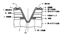
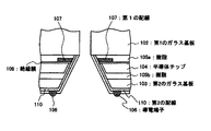
【解決手段】 第1の配線3が形成された半導体ウエハ1aの表面に樹脂5aを介して第1のガラス基板4を貼り合わせる。半導体ウエハ1aの裏面は樹脂5bを介して第2のガラス基板6を貼り合わせる。そして第1のガラス基板4の一部をノッチングして、V字型の溝VGを形成する。そして、第1の配線3と接続し、第2のガラス基板6の表面に延在する第2の配線8を形成する。次に、第2の配線8上に、スプレーコートにより、有機系樹脂から成る保護膜9、及び保護膜9に開口部Kを設けるためのレジスト層Rを形成する。そして、保護膜9をソルダーマスクとして、スクリーン印刷により、導電端子10を形成する。なお、第2のガラス基板6上に、緩衝部材7を、スプレーコートにより形成してもよい。
【選択図】 図10
Description
Claims (8)
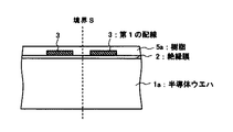
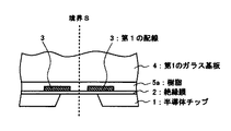
- 第1の配線が形成された半導体ウエハの表面側に第1の支持基板を貼り合わせる工程と、
前記半導体ウエハの裏面側に第2の支持基板を貼り合わせる工程と、
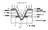
前記第2の支持基板の裏面からダイシングラインに沿って、前記第1の支持基板に至るまで切削を行うことによって溝を形成し、前記第1の配線を部分的に露出させる工程と、
前記溝内で、前記第1の配線の露出部分に接続され、前記第2の支持基板の裏面に延在する第2の配線を形成する工程と、
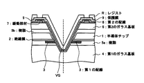
スプレーコートにより、前記溝内を完全に埋め込むことなく、前記溝内から前記第2の支持基板上に延在する前記第2の配線上に有機系樹脂から成る保護膜を形成する工程と、
前記保護膜の所定位置に前記第2の配線を露出する開口部を形成する工程と、
スクリーン印刷により前記開口部から露出した第2の配線上に導電端子を形成する工程と、を具備することを特徴とする半導体装置の製造方法。 - 前記第2の支持基板上に、スプレーコートにより、緩衝部材を形成する工程を具備することを特徴とする請求項1に記載の半導体装置の製造方法。
- 第1の配線が形成された半導体ウエハの表面側に支持基板を貼り合わせる工程と、
前記半導体ウエハの裏面に溝を形成し、前記第1の配線を部分的に露出させる工程と、
前記溝内で、前記第1の配線の露出部分に接続され、前記半導体ウエハの裏面に延在する第2の配線を形成する工程と、
スプレーコートにより、前記溝内を完全に埋め込むことなく、前記溝内から前記半導体ウエハ上に延在する前記第2の配線上に有機系樹脂から成る保護膜を形成する工程と、
前記保護膜の所定位置に前記第2の配線を露出する開口部を形成する工程と、
スクリーン印刷により前記開口部から露出した第2の配線上に導電端子を形成する工程と、を具備することを特徴とする半導体装置の製造方法。 - 前記半導体ウエハの裏面に、スプレーコートにより、緩衝部材を形成する工程を具備することを特徴とする請求項3に記載の半導体装置の製造方法。
- 前記保護膜の表面に、スプレーコートにより、レジスト層を形成する工程を具備することを特徴とする請求項1または請求項3に記載の半導体装置の製造方法。
- 前記有機系樹脂は、熱硬化性を有することを特徴とする請求項1乃至請求項5のいずれか1項に記載の半導体装置の製造方法。
- 前記有機系樹脂は、エポキシ樹脂またはレジスト材料であることを特徴とする請求項1乃至請求項6のいずれか1項に記載の半導体装置の製造方法。
- パターニング時のマスク材としてレジスト層を使用する工程において、スプレーコートを用いることを特徴とする請求項1または請求項3に記載の半導体装置の製造方法。
Priority Applications (1)
| Application Number | Priority Date | Filing Date | Title |
|---|---|---|---|
| JP2010021808A JP5258807B2 (ja) | 2002-10-30 | 2010-02-03 | 半導体装置の製造方法 |
Applications Claiming Priority (3)
| Application Number | Priority Date | Filing Date | Title |
|---|---|---|---|
| JP2002315418 | 2002-10-30 | ||
| JP2002315418 | 2002-10-30 | ||
| JP2010021808A JP5258807B2 (ja) | 2002-10-30 | 2010-02-03 | 半導体装置の製造方法 |
Related Parent Applications (1)
| Application Number | Title | Priority Date | Filing Date |
|---|---|---|---|
| JP2003356195A Division JP4562371B2 (ja) | 2002-10-30 | 2003-10-16 | 半導体装置の製造方法 |
Publications (2)
| Publication Number | Publication Date |
|---|---|
| JP2010098337A true JP2010098337A (ja) | 2010-04-30 |
| JP5258807B2 JP5258807B2 (ja) | 2013-08-07 |
Family
ID=32089519
Family Applications (1)
| Application Number | Title | Priority Date | Filing Date |
|---|---|---|---|
| JP2010021808A Expired - Fee Related JP5258807B2 (ja) | 2002-10-30 | 2010-02-03 | 半導体装置の製造方法 |
Country Status (6)
| Country | Link |
|---|---|
| US (2) | US7101735B2 (ja) |
| EP (1) | EP1416529B8 (ja) |
| JP (1) | JP5258807B2 (ja) |
| CN (2) | CN1296981C (ja) |
| DE (1) | DE60321873D1 (ja) |
| TW (1) | TWI227550B (ja) |
Cited By (1)
| Publication number | Priority date | Publication date | Assignee | Title |
|---|---|---|---|---|
| JP2014187144A (ja) * | 2013-03-22 | 2014-10-02 | Shindengen Electric Mfg Co Ltd | 半導体素子形成用基板、その製造方法、メサ型半導体素子及びその製造方法 |
Families Citing this family (87)
| Publication number | Priority date | Publication date | Assignee | Title |
|---|---|---|---|---|
| TWI232560B (en) * | 2002-04-23 | 2005-05-11 | Sanyo Electric Co | Semiconductor device and its manufacture |
| SG111069A1 (en) * | 2002-06-18 | 2005-05-30 | Micron Technology Inc | Semiconductor devices including peripherally located bond pads, assemblies, packages, and methods |
| TWI229435B (en) * | 2002-06-18 | 2005-03-11 | Sanyo Electric Co | Manufacture of semiconductor device |
| TWI227550B (en) * | 2002-10-30 | 2005-02-01 | Sanyo Electric Co | Semiconductor device manufacturing method |
| JP4401066B2 (ja) * | 2002-11-19 | 2010-01-20 | 三洋電機株式会社 | 半導体集積装置及びその製造方法 |
| JP4130158B2 (ja) | 2003-06-09 | 2008-08-06 | 三洋電機株式会社 | 半導体装置の製造方法、半導体装置 |
| EP1482553A3 (en) * | 2003-05-26 | 2007-03-28 | Sanyo Electric Co., Ltd. | Semiconductor device and manufacturing method thereof |
| JP4401181B2 (ja) * | 2003-08-06 | 2010-01-20 | 三洋電機株式会社 | 半導体装置及びその製造方法 |
| SG120123A1 (en) * | 2003-09-30 | 2006-03-28 | Micron Technology Inc | Castellated chip-scale packages and methods for fabricating the same |
| US7183137B2 (en) * | 2003-12-01 | 2007-02-27 | Taiwan Semiconductor Manufacturing Company | Method for dicing semiconductor wafers |
| JP4850392B2 (ja) * | 2004-02-17 | 2012-01-11 | 三洋電機株式会社 | 半導体装置の製造方法 |
| JP4525117B2 (ja) * | 2004-03-12 | 2010-08-18 | ルネサスエレクトロニクス株式会社 | トレイ |
| US7215018B2 (en) | 2004-04-13 | 2007-05-08 | Vertical Circuits, Inc. | Stacked die BGA or LGA component assembly |
| TWI231535B (en) * | 2004-05-26 | 2005-04-21 | Advanced Semiconductor Eng | Photoelectric device grinding process and device grinding process |
| JP4322181B2 (ja) * | 2004-07-29 | 2009-08-26 | 三洋電機株式会社 | 半導体装置の製造方法 |
| TWI267183B (en) | 2004-09-29 | 2006-11-21 | Sanyo Electric Co | Semiconductor device and manufacturing method of the same |
| JP4443379B2 (ja) * | 2004-10-26 | 2010-03-31 | 三洋電機株式会社 | 半導体装置の製造方法 |
| TWI303864B (en) * | 2004-10-26 | 2008-12-01 | Sanyo Electric Co | Semiconductor device and method for making the same |
| JP4873517B2 (ja) * | 2004-10-28 | 2012-02-08 | オンセミコンダクター・トレーディング・リミテッド | 半導体装置及びその製造方法 |
| US7485967B2 (en) * | 2005-03-10 | 2009-02-03 | Sanyo Electric Co., Ltd. | Semiconductor device with via hole for electric connection |
| JP2006278610A (ja) * | 2005-03-29 | 2006-10-12 | Sanyo Electric Co Ltd | 半導体装置及びその製造方法 |
| JP2007012995A (ja) * | 2005-07-01 | 2007-01-18 | Toshiba Corp | 超小型カメラモジュール及びその製造方法 |
| KR100629498B1 (ko) * | 2005-07-15 | 2006-09-28 | 삼성전자주식회사 | 마이크로 패키지, 멀티―스택 마이크로 패키지 및 이들의제조방법 |
| JP4487875B2 (ja) * | 2005-07-20 | 2010-06-23 | セイコーエプソン株式会社 | 電子基板の製造方法及び電気光学装置の製造方法並びに電子機器の製造方法 |
| TWI324800B (en) * | 2005-12-28 | 2010-05-11 | Sanyo Electric Co | Method for manufacturing semiconductor device |
| KR100649769B1 (ko) * | 2005-12-28 | 2006-11-27 | 삼성전기주식회사 | 반도체 발광 다이오드 및 그 제조 방법 |
| TW200737506A (en) * | 2006-03-07 | 2007-10-01 | Sanyo Electric Co | Semiconductor device and manufacturing method of the same |
| JP2008003577A (ja) * | 2006-05-25 | 2008-01-10 | Canon Inc | 画像表示装置の製造方法および分断方法 |
| JP2008010659A (ja) * | 2006-06-29 | 2008-01-17 | Disco Abrasive Syst Ltd | ビアホールの加工方法 |
| US8102039B2 (en) * | 2006-08-11 | 2012-01-24 | Sanyo Semiconductor Co., Ltd. | Semiconductor device and manufacturing method thereof |
| KR100769722B1 (ko) * | 2006-10-10 | 2007-10-24 | 삼성전기주식회사 | 이미지센서의 웨이퍼 레벨 칩 스케일 패키지 및 그제조방법 |
| US8513789B2 (en) * | 2006-10-10 | 2013-08-20 | Tessera, Inc. | Edge connect wafer level stacking with leads extending along edges |
| US7829438B2 (en) | 2006-10-10 | 2010-11-09 | Tessera, Inc. | Edge connect wafer level stacking |
| US7901989B2 (en) | 2006-10-10 | 2011-03-08 | Tessera, Inc. | Reconstituted wafer level stacking |
| US7759166B2 (en) * | 2006-10-17 | 2010-07-20 | Tessera, Inc. | Microelectronic packages fabricated at the wafer level and methods therefor |
| JP5010247B2 (ja) * | 2006-11-20 | 2012-08-29 | オンセミコンダクター・トレーディング・リミテッド | 半導体装置及びその製造方法 |
| US7468544B2 (en) * | 2006-12-07 | 2008-12-23 | Advanced Chip Engineering Technology Inc. | Structure and process for WL-CSP with metal cover |
| US7952195B2 (en) | 2006-12-28 | 2011-05-31 | Tessera, Inc. | Stacked packages with bridging traces |
| US7569409B2 (en) * | 2007-01-04 | 2009-08-04 | Visera Technologies Company Limited | Isolation structures for CMOS image sensor chip scale packages |
| US7566944B2 (en) * | 2007-01-11 | 2009-07-28 | Visera Technologies Company Limited | Package structure for optoelectronic device and fabrication method thereof |
| TWI341584B (en) * | 2007-02-26 | 2011-05-01 | Siliconware Precision Industries Co Ltd | Sensor-type semiconductor package and manufacturing method thereof |
| JP2008294405A (ja) * | 2007-04-25 | 2008-12-04 | Sanyo Electric Co Ltd | 半導体装置及びその製造方法 |
| US8723332B2 (en) * | 2007-06-11 | 2014-05-13 | Invensas Corporation | Electrically interconnected stacked die assemblies |
| CN101680091A (zh) * | 2007-06-15 | 2010-03-24 | 纳克公司 | 反应性气流沉积和无机箔的合成 |
| US7595220B2 (en) * | 2007-06-29 | 2009-09-29 | Visera Technologies Company Limited | Image sensor package and fabrication method thereof |
| JP2009021462A (ja) * | 2007-07-13 | 2009-01-29 | Disco Abrasive Syst Ltd | ウェーハの加工方法 |
| CN101809739B (zh) | 2007-07-27 | 2014-08-20 | 泰塞拉公司 | 具有后应用的衬垫延长部分的重构晶片堆封装 |
| CN101861646B (zh) | 2007-08-03 | 2015-03-18 | 泰塞拉公司 | 利用再生晶圆的堆叠封装 |
| US8043895B2 (en) | 2007-08-09 | 2011-10-25 | Tessera, Inc. | Method of fabricating stacked assembly including plurality of stacked microelectronic elements |
| US8704379B2 (en) | 2007-09-10 | 2014-04-22 | Invensas Corporation | Semiconductor die mount by conformal die coating |
| JP4348454B2 (ja) * | 2007-11-08 | 2009-10-21 | 三菱重工業株式会社 | デバイスおよびデバイス製造方法 |
| EP2075840B1 (en) * | 2007-12-28 | 2014-08-27 | Semiconductor Energy Laboratory Co., Ltd. | Method for dicing a wafer with semiconductor elements formed thereon and corresponding device |
| JP5437626B2 (ja) * | 2007-12-28 | 2014-03-12 | 株式会社半導体エネルギー研究所 | 半導体装置及び半導体装置の作製方法 |
| JP5317712B2 (ja) * | 2008-01-22 | 2013-10-16 | 株式会社半導体エネルギー研究所 | 半導体装置及び半導体装置の作製方法 |
| JP5376961B2 (ja) * | 2008-02-01 | 2013-12-25 | 株式会社半導体エネルギー研究所 | 半導体装置 |
| JP5763924B2 (ja) | 2008-03-12 | 2015-08-12 | インヴェンサス・コーポレーション | ダイアセンブリを電気的に相互接続して取り付けられたサポート |
| US7863159B2 (en) | 2008-06-19 | 2011-01-04 | Vertical Circuits, Inc. | Semiconductor die separation method |
| US9153517B2 (en) | 2008-05-20 | 2015-10-06 | Invensas Corporation | Electrical connector between die pad and z-interconnect for stacked die assemblies |
| WO2009154761A1 (en) | 2008-06-16 | 2009-12-23 | Tessera Research Llc | Stacking of wafer-level chip scale packages having edge contacts |
| JP2010027741A (ja) * | 2008-07-16 | 2010-02-04 | Sanyo Electric Co Ltd | 半導体装置及びその製造方法 |
| JP2010103300A (ja) * | 2008-10-23 | 2010-05-06 | Sanyo Electric Co Ltd | 半導体装置及びその製造方法 |
| EP2406821A2 (en) | 2009-03-13 | 2012-01-18 | Tessera, Inc. | Stacked microelectronic assemblies having vias extending through bond pads |
| TWI570879B (zh) | 2009-06-26 | 2017-02-11 | 英維瑟斯公司 | 半導體總成及晶粒堆疊總成 |
| TWI520213B (zh) | 2009-10-27 | 2016-02-01 | 英維瑟斯公司 | 加成法製程之選擇性晶粒電絕緣 |
| TWI544604B (zh) | 2009-11-04 | 2016-08-01 | 英維瑟斯公司 | 具有降低應力電互連的堆疊晶粒總成 |
| US8432032B2 (en) * | 2010-01-13 | 2013-04-30 | Chia-Sheng Lin | Chip package and fabrication method thereof |
| US8952519B2 (en) * | 2010-01-13 | 2015-02-10 | Chia-Sheng Lin | Chip package and fabrication method thereof |
| US8482105B2 (en) * | 2010-01-29 | 2013-07-09 | Headway Technologies, Inc. | Semiconductor substrate, laminated chip package, semiconductor plate and method of manufacturing the same |
| US8236613B2 (en) * | 2010-05-24 | 2012-08-07 | Alpha & Omega Semiconductor Inc. | Wafer level chip scale package method using clip array |
| US8970006B2 (en) * | 2010-06-15 | 2015-03-03 | Stmicroelectronics S.R.L. | Vertical conductive connections in semiconductor substrates |
| US8722514B2 (en) * | 2011-01-17 | 2014-05-13 | Infineon Technologies Ag | Semiconductor devices having insulating substrates and methods of formation thereof |
| DE102011112659B4 (de) * | 2011-09-06 | 2022-01-27 | Vishay Semiconductor Gmbh | Oberflächenmontierbares elektronisches Bauelement |
| US8735262B2 (en) | 2011-10-24 | 2014-05-27 | Infineon Technologies Ag | Semiconductor device having a through contact and a manufacturing method therefor |
| DE102012223904A1 (de) * | 2012-10-05 | 2014-04-10 | Continental Automotive Gmbh | Verfahren zum Herstellen eines elektronischen Hochstrom-Schaltkreises mittels Gasspritz-Technologie und Abdichten mit isolierendem Polymer |
| TWI525673B (zh) * | 2013-10-08 | 2016-03-11 | 精材科技股份有限公司 | 晶圓級晶片封裝體的製造方法 |
| US20160141280A1 (en) * | 2014-11-14 | 2016-05-19 | Omnivision Technologies, Inc. | Device-Embedded Image Sensor, And Wafer-Level Method For Fabricating Same |
| JP2017010962A (ja) * | 2015-06-16 | 2017-01-12 | 株式会社東芝 | デバイス基板およびデバイス基板の製造方法並びに半導体装置の製造方法 |
| US9825002B2 (en) | 2015-07-17 | 2017-11-21 | Invensas Corporation | Flipped die stack |
| US9490195B1 (en) | 2015-07-17 | 2016-11-08 | Invensas Corporation | Wafer-level flipped die stacks with leadframes or metal foil interconnects |
| US9871019B2 (en) | 2015-07-17 | 2018-01-16 | Invensas Corporation | Flipped die stack assemblies with leadframe interconnects |
| US9508691B1 (en) | 2015-12-16 | 2016-11-29 | Invensas Corporation | Flipped die stacks with multiple rows of leadframe interconnects |
| US10566310B2 (en) | 2016-04-11 | 2020-02-18 | Invensas Corporation | Microelectronic packages having stacked die and wire bond interconnects |
| US9595511B1 (en) | 2016-05-12 | 2017-03-14 | Invensas Corporation | Microelectronic packages and assemblies with improved flyby signaling operation |
| US9728524B1 (en) | 2016-06-30 | 2017-08-08 | Invensas Corporation | Enhanced density assembly having microelectronic packages mounted at substantial angle to board |
| DE102016116499B4 (de) * | 2016-09-02 | 2022-06-15 | Infineon Technologies Ag | Verfahren zum Bilden von Halbleiterbauelementen und Halbleiterbauelemente |
| US10868061B2 (en) * | 2018-08-13 | 2020-12-15 | Semiconductor Components Industries, Llc | Packaging structure for a sensor having a sealing layer |
| US11137559B2 (en) | 2019-04-22 | 2021-10-05 | Xintec Inc. | Optical chip package and method for forming the same |
Citations (2)
| Publication number | Priority date | Publication date | Assignee | Title |
|---|---|---|---|---|
| JP2002208655A (ja) * | 2000-06-02 | 2002-07-26 | Seiko Epson Corp | 半導体装置及びその製造方法、積層型半導体装置、回路基板並びに電子機器 |
| JP2003516634A (ja) * | 1999-12-10 | 2003-05-13 | シェルケース リミティド | パッケージ形集積回路装置の製造方法およびその製造方法により製作されたパッケージ形集積回路装置 |
Family Cites Families (118)
| Publication number | Priority date | Publication date | Assignee | Title |
|---|---|---|---|---|
| DE1933731C3 (de) | 1968-07-05 | 1982-03-25 | Honeywell Information Systems Italia S.p.A., Caluso, Torino | Verfahren zum Herstellen einer integrierten Halbleiterschaltung |
| GB1285708A (en) | 1968-10-28 | 1972-08-16 | Lucas Industries Ltd | Semi-conductor devices |
| US3648131A (en) | 1969-11-07 | 1972-03-07 | Ibm | Hourglass-shaped conductive connection through semiconductor structures |
| US4179794A (en) * | 1975-07-23 | 1979-12-25 | Nippon Gakki Seizo Kabushiki Kaisha | Process of manufacturing semiconductor devices |
| US4954875A (en) | 1986-07-17 | 1990-09-04 | Laser Dynamics, Inc. | Semiconductor wafer array with electrically conductive compliant material |
| US4978639A (en) | 1989-01-10 | 1990-12-18 | Avantek, Inc. | Method for the simultaneous formation of via-holes and wraparound plating on semiconductor chips |
| JPH0482215A (ja) | 1990-07-25 | 1992-03-16 | Sumitomo Electric Ind Ltd | ランプアニール装置 |
| US5229647A (en) | 1991-03-27 | 1993-07-20 | Micron Technology, Inc. | High density data storage using stacked wafers |
| US5927993A (en) | 1992-02-03 | 1999-07-27 | Motorola, Inc. | Backside processing method |
| US5350662A (en) | 1992-03-26 | 1994-09-27 | Hughes Aircraft Company | Maskless process for forming refractory metal layer in via holes of GaAs chips |
| US5476819A (en) | 1993-07-26 | 1995-12-19 | Litton Systems, Inc. | Substrate anchor for undercut silicon on insulator microstructures |
| TW270213B (ja) | 1993-12-08 | 1996-02-11 | Matsushita Electric Industrial Co Ltd | |
| JPH08186151A (ja) | 1994-12-29 | 1996-07-16 | Sony Corp | 半導体装置及びその製造方法 |
| US5682062A (en) | 1995-06-05 | 1997-10-28 | Harris Corporation | System for interconnecting stacked integrated circuits |
| US5648684A (en) | 1995-07-26 | 1997-07-15 | International Business Machines Corporation | Endcap chip with conductive, monolithic L-connect for multichip stack |
| US5904546A (en) | 1996-02-12 | 1999-05-18 | Micron Technology, Inc. | Method and apparatus for dicing semiconductor wafers |
| KR100410812B1 (ko) | 1996-06-25 | 2004-04-01 | 주식회사 하이닉스반도체 | 반도체장치의제조방법 |
| US6027958A (en) | 1996-07-11 | 2000-02-22 | Kopin Corporation | Transferred flexible integrated circuit |
| DE19636744C2 (de) | 1996-09-10 | 1998-09-17 | Siemens Ag | Verfahren zum Übertragen von Daten in einem hybriden Telekommunikationssystem, insbesondere einem "ISDN - DECT-spezifischen RLL/WLL"-System |
| WO1998013862A1 (fr) | 1996-09-24 | 1998-04-02 | Mitsubishi Denki Kabushiki Kaisha | Dispositif a semi-conducteur et son procede de fabrication |
| US5691245A (en) | 1996-10-28 | 1997-11-25 | He Holdings, Inc. | Methods of forming two-sided HDMI interconnect structures |
| EP0948808A4 (en) | 1996-10-29 | 2000-05-10 | Trusi Technologies Llc | INTEGRATED CIRCUITS AND METHOD FOR THE PRODUCTION |
| US6054760A (en) | 1996-12-23 | 2000-04-25 | Scb Technologies Inc. | Surface-connectable semiconductor bridge elements and devices including the same |
| US5910687A (en) * | 1997-01-24 | 1999-06-08 | Chipscale, Inc. | Wafer fabrication of die-bottom contacts for electronic devices |
| JPH10242084A (ja) | 1997-02-24 | 1998-09-11 | Lintec Corp | ウェハ貼着用粘着シートおよび電子部品の製造方法 |
| JP3286553B2 (ja) | 1997-03-17 | 2002-05-27 | 株式会社村上開明堂 | 防眩インナーミラー |
| JP3011233B2 (ja) | 1997-05-02 | 2000-02-21 | 日本電気株式会社 | 半導体パッケージ及びその半導体実装構造 |
| US6051489A (en) * | 1997-05-13 | 2000-04-18 | Chipscale, Inc. | Electronic component package with posts on the active side of the substrate |
| JP3335575B2 (ja) | 1997-06-06 | 2002-10-21 | 松下電器産業株式会社 | 半導体装置およびその製造方法 |
| FR2767223B1 (fr) | 1997-08-06 | 1999-09-17 | Commissariat Energie Atomique | Procede d'interconnexion a travers un materiau semi-conducteur, et dispositif obtenu |
| JPH11135669A (ja) * | 1997-08-27 | 1999-05-21 | Mitsui High Tec Inc | Csp型半導体装置 |
| US6432744B1 (en) | 1997-11-20 | 2002-08-13 | Texas Instruments Incorporated | Wafer-scale assembly of chip-size packages |
| DE69737262T2 (de) | 1997-11-26 | 2007-11-08 | Stmicroelectronics S.R.L., Agrate Brianza | Herstellungsverfahren für einen Vorder-Hinterseiten-Durchkontakt in mikro-integrierten Schaltungen |
| US5888884A (en) | 1998-01-02 | 1999-03-30 | General Electric Company | Electronic device pad relocation, precision placement, and packaging in arrays |
| CN1288591A (zh) | 1998-01-20 | 2001-03-21 | 时至准钟表股份有限公司 | 半导体装置和制造方法及其安装构造和安装方法 |
| IL123207A0 (en) | 1998-02-06 | 1998-09-24 | Shellcase Ltd | Integrated circuit device |
| US6624505B2 (en) | 1998-02-06 | 2003-09-23 | Shellcase, Ltd. | Packaged integrated circuits and methods of producing thereof |
| JP3497722B2 (ja) | 1998-02-27 | 2004-02-16 | 富士通株式会社 | 半導体装置及びその製造方法及びその搬送トレイ |
| JPH11345905A (ja) * | 1998-06-02 | 1999-12-14 | Mitsubishi Electric Corp | 半導体装置 |
| JP3842444B2 (ja) | 1998-07-24 | 2006-11-08 | 富士通株式会社 | 半導体装置の製造方法 |
| US6153929A (en) | 1998-08-21 | 2000-11-28 | Micron Technology, Inc. | Low profile multi-IC package connector |
| DE19846232A1 (de) | 1998-09-03 | 2000-03-09 | Fraunhofer Ges Forschung | Verfahren zur Herstellung eines Halbleiterbauelements mit Rückseitenkontaktierung |
| US6066513A (en) | 1998-10-02 | 2000-05-23 | International Business Machines Corporation | Process for precise multichip integration and product thereof |
| US6339251B2 (en) | 1998-11-10 | 2002-01-15 | Samsung Electronics Co., Ltd | Wafer grooves for reducing semiconductor wafer warping |
| US6310328B1 (en) | 1998-12-10 | 2001-10-30 | Mattson Technologies, Inc. | Rapid thermal processing chamber for processing multiple wafers |
| JP3687379B2 (ja) | 1998-12-18 | 2005-08-24 | 株式会社日立製作所 | 半導体装置の製造方法 |
| KR100315030B1 (ko) | 1998-12-29 | 2002-04-24 | 박종섭 | 반도체패키지의제조방법 |
| US6259039B1 (en) | 1998-12-29 | 2001-07-10 | Intel Corporation | Surface mount connector with pins in vias |
| FR2788375B1 (fr) * | 1999-01-11 | 2003-07-18 | Gemplus Card Int | Procede de protection de puce de circuit integre |
| JP2000286283A (ja) | 1999-03-30 | 2000-10-13 | Seiko Epson Corp | 半導体装置の製造方法 |
| JP2000294677A (ja) | 1999-04-05 | 2000-10-20 | Fujitsu Ltd | 高密度薄膜配線基板及びその製造方法 |
| US6326689B1 (en) | 1999-07-26 | 2001-12-04 | Stmicroelectronics, Inc. | Backside contact for touchchip |
| EP1130629A1 (en) | 1999-07-30 | 2001-09-05 | Nippon Sheet Glass Co., Ltd. | Method of dicing semiconductor wafer into chips, and structure of groove formed in dicing area |
| JP3687435B2 (ja) | 1999-08-27 | 2005-08-24 | セイコーエプソン株式会社 | 半導体チップおよびその製造方法、半導体装置、コンピュータ、回路基板ならびに電子機器 |
| JP2001077229A (ja) | 1999-09-02 | 2001-03-23 | Matsushita Electronics Industry Corp | 半導体装置およびその製造方法 |
| US6316287B1 (en) | 1999-09-13 | 2001-11-13 | Vishay Intertechnology, Inc. | Chip scale surface mount packages for semiconductor device and process of fabricating the same |
| KR100462980B1 (ko) | 1999-09-13 | 2004-12-23 | 비쉐이 메저먼츠 그룹, 인코포레이티드 | 반도체장치용 칩 스케일 표면 장착 패키지 및 그 제조공정 |
| JP2001127243A (ja) | 1999-10-26 | 2001-05-11 | Sharp Corp | 積層半導体装置 |
| JP2001185519A (ja) | 1999-12-24 | 2001-07-06 | Hitachi Ltd | 半導体装置及びその製造方法 |
| JP3858545B2 (ja) | 1999-12-27 | 2006-12-13 | セイコーエプソン株式会社 | 半導体モジュール及び電子機器 |
| JP2001210667A (ja) | 2000-01-28 | 2001-08-03 | New Japan Radio Co Ltd | 半導体装置の製造方法 |
| US6534751B2 (en) | 2000-02-28 | 2003-03-18 | Kyocera Corporation | Wafer heating apparatus and ceramic heater, and method for producing the same |
| US6424031B1 (en) | 2000-05-08 | 2002-07-23 | Amkor Technology, Inc. | Stackable package with heat sink |
| JP3701542B2 (ja) | 2000-05-10 | 2005-09-28 | シャープ株式会社 | 半導体装置およびその製造方法 |
| JP4329235B2 (ja) | 2000-06-27 | 2009-09-09 | セイコーエプソン株式会社 | 半導体装置及びその製造方法 |
| JP2002026270A (ja) | 2000-07-10 | 2002-01-25 | Nec Corp | 半導体装置の製造方法 |
| JP2002094082A (ja) | 2000-07-11 | 2002-03-29 | Seiko Epson Corp | 光素子及びその製造方法並びに電子機器 |
| JP2002057128A (ja) | 2000-08-15 | 2002-02-22 | Fujitsu Quantum Devices Ltd | 半導体装置及びその製造方法 |
| US6379982B1 (en) | 2000-08-17 | 2002-04-30 | Micron Technology, Inc. | Wafer on wafer packaging and method of fabrication for full-wafer burn-in and testing |
| US6406934B1 (en) | 2000-09-05 | 2002-06-18 | Amkor Technology, Inc. | Wafer level production of chip size semiconductor packages |
| JP2002083785A (ja) | 2000-09-07 | 2002-03-22 | Nec Kansai Ltd | 半導体素子の製造方法 |
| JP2002093942A (ja) | 2000-09-14 | 2002-03-29 | Nec Corp | 半導体装置およびその製造方法 |
| JP4183375B2 (ja) | 2000-10-04 | 2008-11-19 | 沖電気工業株式会社 | 半導体装置及びその製造方法 |
| US6693358B2 (en) | 2000-10-23 | 2004-02-17 | Matsushita Electric Industrial Co., Ltd. | Semiconductor chip, wiring board and manufacturing process thereof as well as semiconductor device |
| CN1332430C (zh) * | 2000-11-17 | 2007-08-15 | 矽品精密工业股份有限公司 | 集成电路封装单元分割方法 |
| JP2002163900A (ja) | 2000-11-22 | 2002-06-07 | Hitachi Ltd | 半導体ウエハ、半導体チップ、半導体装置および半導体装置の製造方法 |
| US6506681B2 (en) | 2000-12-06 | 2003-01-14 | Micron Technology, Inc. | Thin flip—chip method |
| US6524885B2 (en) | 2000-12-15 | 2003-02-25 | Eaglestone Partners I, Llc | Method, apparatus and system for building an interposer onto a semiconductor wafer using laser techniques |
| JP2004534375A (ja) * | 2000-12-21 | 2004-11-11 | シェルケース リミティド | パケージ集積回路およびその製造方法 |
| JP2002231918A (ja) | 2001-02-06 | 2002-08-16 | Olympus Optical Co Ltd | 固体撮像装置及びその製造方法 |
| US6399463B1 (en) | 2001-03-01 | 2002-06-04 | Amkor Technology, Inc. | Method of singulation using laser cutting |
| JP4497737B2 (ja) | 2001-03-12 | 2010-07-07 | 株式会社ルネサステクノロジ | 半導体装置の製造方法 |
| US6910268B2 (en) | 2001-03-27 | 2005-06-28 | Formfactor, Inc. | Method for fabricating an IC interconnect system including an in-street integrated circuit wafer via |
| US6597059B1 (en) | 2001-04-04 | 2003-07-22 | Amkor Technology, Inc. | Thermally enhanced chip scale lead on chip semiconductor package |
| JP4698877B2 (ja) | 2001-04-27 | 2011-06-08 | オリンパス株式会社 | 撮像装置 |
| US6753936B2 (en) * | 2001-05-17 | 2004-06-22 | Dai Nippon Pringing Co., Ltd. | Field sequential color liquid crystal display device |
| JP2003031647A (ja) | 2001-07-19 | 2003-01-31 | Hitachi Kokusai Electric Inc | 基板処理装置および半導体装置の製造方法 |
| JP4000507B2 (ja) | 2001-10-04 | 2007-10-31 | ソニー株式会社 | 固体撮像装置の製造方法 |
| SG102639A1 (en) | 2001-10-08 | 2004-03-26 | Micron Technology Inc | Apparatus and method for packing circuits |
| US6642127B2 (en) | 2001-10-19 | 2003-11-04 | Applied Materials, Inc. | Method for dicing a semiconductor wafer |
| US6611052B2 (en) | 2001-11-16 | 2003-08-26 | Micron Technology, Inc. | Wafer level stackable semiconductor package |
| US6955989B2 (en) | 2001-11-30 | 2005-10-18 | Xerox Corporation | Use of a U-groove as an alternative to using a V-groove for protection against dicing induced damage in silicon |
| US6607941B2 (en) * | 2002-01-11 | 2003-08-19 | National Semiconductor Corporation | Process and structure improvements to shellcase style packaging technology |
| US6908784B1 (en) | 2002-03-06 | 2005-06-21 | Micron Technology, Inc. | Method for fabricating encapsulated semiconductor components |
| US6848177B2 (en) | 2002-03-28 | 2005-02-01 | Intel Corporation | Integrated circuit die and an electronic assembly having a three-dimensional interconnection scheme |
| TWI232560B (en) | 2002-04-23 | 2005-05-11 | Sanyo Electric Co | Semiconductor device and its manufacture |
| US7340181B1 (en) | 2002-05-13 | 2008-03-04 | National Semiconductor Corporation | Electrical die contact structure and fabrication method |
| JP2003332270A (ja) | 2002-05-15 | 2003-11-21 | Renesas Technology Corp | 半導体装置およびその製造方法 |
| US7399683B2 (en) | 2002-06-18 | 2008-07-15 | Sanyo Electric Co., Ltd. | Manufacturing method of semiconductor device |
| TWI229435B (en) | 2002-06-18 | 2005-03-11 | Sanyo Electric Co | Manufacture of semiconductor device |
| US6805279B2 (en) | 2002-06-27 | 2004-10-19 | Taiwan Semiconductor Manufacturing Co., Ltd. | Fluxless bumping process using ions |
| DE10238444B4 (de) | 2002-08-22 | 2011-05-12 | United Monolithic Semiconductors Gmbh | Verfahren zur Herstellung von vereinzelten monolithisch integrierten Halbleiterschaltungen |
| US6903442B2 (en) | 2002-08-29 | 2005-06-07 | Micron Technology, Inc. | Semiconductor component having backside pin contacts |
| JP4081666B2 (ja) | 2002-09-24 | 2008-04-30 | セイコーエプソン株式会社 | 半導体装置及びその製造方法、回路基板並びに電子機器 |
| TWI227050B (en) | 2002-10-11 | 2005-01-21 | Sanyo Electric Co | Semiconductor device and method for manufacturing the same |
| TWI227550B (en) * | 2002-10-30 | 2005-02-01 | Sanyo Electric Co | Semiconductor device manufacturing method |
| TWI239607B (en) | 2002-12-13 | 2005-09-11 | Sanyo Electric Co | Method for making a semiconductor device |
| TWI229890B (en) | 2003-04-24 | 2005-03-21 | Sanyo Electric Co | Semiconductor device and method of manufacturing same |
| WO2005004195A2 (en) | 2003-07-03 | 2005-01-13 | Shellcase Ltd. | Method and apparatus for packaging integrated circuit devices |
| JP4401181B2 (ja) | 2003-08-06 | 2010-01-20 | 三洋電機株式会社 | 半導体装置及びその製造方法 |
| TWI226090B (en) | 2003-09-26 | 2005-01-01 | Advanced Semiconductor Eng | Transparent packaging in wafer level |
| JP2005191550A (ja) | 2003-12-01 | 2005-07-14 | Tokyo Ohka Kogyo Co Ltd | 基板の貼り付け方法 |
| US7183137B2 (en) | 2003-12-01 | 2007-02-27 | Taiwan Semiconductor Manufacturing Company | Method for dicing semiconductor wafers |
| JP4753170B2 (ja) | 2004-03-05 | 2011-08-24 | 三洋電機株式会社 | 半導体装置及びその製造方法 |
| JP2006093367A (ja) | 2004-09-24 | 2006-04-06 | Sanyo Electric Co Ltd | 半導体装置の製造方法 |
| TWI273682B (en) | 2004-10-08 | 2007-02-11 | Epworks Co Ltd | Method for manufacturing wafer level chip scale package using redistribution substrate |
| US7449779B2 (en) | 2005-03-22 | 2008-11-11 | Tessera, Inc. | Wire bonded wafer level cavity package |
| TWI324800B (en) | 2005-12-28 | 2010-05-11 | Sanyo Electric Co | Method for manufacturing semiconductor device |
-
2003
- 2003-10-28 TW TW092129886A patent/TWI227550B/zh not_active IP Right Cessation
- 2003-10-30 US US10/696,581 patent/US7101735B2/en not_active Expired - Lifetime
- 2003-10-30 CN CNB2003101156786A patent/CN1296981C/zh not_active Expired - Fee Related
- 2003-10-30 DE DE60321873T patent/DE60321873D1/de not_active Expired - Lifetime
- 2003-10-30 CN CN2006101625941A patent/CN101064270B/zh not_active Expired - Fee Related
- 2003-10-30 EP EP03025016A patent/EP1416529B8/en not_active Expired - Lifetime
-
2006
- 2006-07-19 US US11/488,890 patent/US7662670B2/en not_active Expired - Fee Related
-
2010
- 2010-02-03 JP JP2010021808A patent/JP5258807B2/ja not_active Expired - Fee Related
Patent Citations (2)
| Publication number | Priority date | Publication date | Assignee | Title |
|---|---|---|---|---|
| JP2003516634A (ja) * | 1999-12-10 | 2003-05-13 | シェルケース リミティド | パッケージ形集積回路装置の製造方法およびその製造方法により製作されたパッケージ形集積回路装置 |
| JP2002208655A (ja) * | 2000-06-02 | 2002-07-26 | Seiko Epson Corp | 半導体装置及びその製造方法、積層型半導体装置、回路基板並びに電子機器 |
Cited By (1)
| Publication number | Priority date | Publication date | Assignee | Title |
|---|---|---|---|---|
| JP2014187144A (ja) * | 2013-03-22 | 2014-10-02 | Shindengen Electric Mfg Co Ltd | 半導体素子形成用基板、その製造方法、メサ型半導体素子及びその製造方法 |
Also Published As
| Publication number | Publication date |
|---|---|
| US20070026639A1 (en) | 2007-02-01 |
| EP1416529B8 (en) | 2008-10-29 |
| TW200411853A (en) | 2004-07-01 |
| CN1512553A (zh) | 2004-07-14 |
| CN1296981C (zh) | 2007-01-24 |
| US20040137723A1 (en) | 2004-07-15 |
| CN101064270A (zh) | 2007-10-31 |
| JP5258807B2 (ja) | 2013-08-07 |
| EP1416529A1 (en) | 2004-05-06 |
| EP1416529B1 (en) | 2008-07-02 |
| US7101735B2 (en) | 2006-09-05 |
| US7662670B2 (en) | 2010-02-16 |
| TWI227550B (en) | 2005-02-01 |
| CN101064270B (zh) | 2011-12-07 |
| DE60321873D1 (de) | 2008-08-14 |
Similar Documents
| Publication | Publication Date | Title |
|---|---|---|
| JP5258807B2 (ja) | 半導体装置の製造方法 | |
| KR100510556B1 (ko) | 초박형 반도체 패키지 및 그 제조방법 | |
| JP3842548B2 (ja) | 半導体装置の製造方法及び半導体装置 | |
| JP2008244437A (ja) | ダイ収容開口部を備えたイメージセンサパッケージおよびその方法 | |
| US20050048740A1 (en) | Semiconductor device and manufacturing method thereof | |
| CN1219763A (zh) | 具有亚芯片规模封装构造的半导体器件及其制造方法 | |
| US6489667B1 (en) | Semiconductor device and method of manufacturing such device | |
| JPH053183A (ja) | 半導体装置及びその製造方法 | |
| TWI420610B (zh) | 半導體裝置及其製造方法 | |
| US6919264B2 (en) | Method for the solder-stop structuring of elevations on wafers | |
| JP2002313985A (ja) | チップサイズパッケージの製造方法 | |
| JP4562371B2 (ja) | 半導体装置の製造方法 | |
| JP5238985B2 (ja) | 半導体装置の製造方法 | |
| JP3877700B2 (ja) | 半導体装置及びその製造方法 | |
| JP2010016395A5 (ja) | ||
| CN100390982C (zh) | 半导体装置及半导体装置的制造方法 | |
| JP4401330B2 (ja) | 半導体装置及びその製造方法 | |
| JP4522213B2 (ja) | 半導体装置の製造方法 | |
| JP2003017655A (ja) | 半導体実装体およびそれを用いた半導体装置 | |
| CN107170715B (zh) | 半导体封装结构及其制作方法 | |
| JP3381833B2 (ja) | Bga型半導体装置およびその製造方法 | |
| JP2006173198A (ja) | 半導体装置及びその製造方法 | |
| JP2004165330A (ja) | 半導体装置の製造方法 | |
| JP2006179709A (ja) | 半導体装置の製造方法 | |
| JP2006191141A (ja) | 半導体装置 |
Legal Events
| Date | Code | Title | Description |
|---|---|---|---|
| A621 | Written request for application examination |
Free format text: JAPANESE INTERMEDIATE CODE: A621 Effective date: 20100203 |
|
| A711 | Notification of change in applicant |
Free format text: JAPANESE INTERMEDIATE CODE: A711 Effective date: 20110526 |
|
| RD02 | Notification of acceptance of power of attorney |
Free format text: JAPANESE INTERMEDIATE CODE: A7422 Effective date: 20110526 |
|
| A977 | Report on retrieval |
Free format text: JAPANESE INTERMEDIATE CODE: A971007 Effective date: 20121022 |
|
| A131 | Notification of reasons for refusal |
Free format text: JAPANESE INTERMEDIATE CODE: A131 Effective date: 20121025 |
|
| A521 | Request for written amendment filed |
Free format text: JAPANESE INTERMEDIATE CODE: A523 Effective date: 20130118 |
|
| A711 | Notification of change in applicant |
Free format text: JAPANESE INTERMEDIATE CODE: A711 Effective date: 20130207 |
|
| A521 | Request for written amendment filed |
Free format text: JAPANESE INTERMEDIATE CODE: A523 Effective date: 20130215 |
|
| RD02 | Notification of acceptance of power of attorney |
Free format text: JAPANESE INTERMEDIATE CODE: A7422 Effective date: 20130301 |
|
| A131 | Notification of reasons for refusal |
Free format text: JAPANESE INTERMEDIATE CODE: A131 Effective date: 20130307 |
|
| A521 | Request for written amendment filed |
Free format text: JAPANESE INTERMEDIATE CODE: A523 Effective date: 20130326 |
|
| TRDD | Decision of grant or rejection written | ||
| A01 | Written decision to grant a patent or to grant a registration (utility model) |
Free format text: JAPANESE INTERMEDIATE CODE: A01 Effective date: 20130410 |
|
| A61 | First payment of annual fees (during grant procedure) |
Free format text: JAPANESE INTERMEDIATE CODE: A61 Effective date: 20130423 |
|
| FPAY | Renewal fee payment (event date is renewal date of database) |
Free format text: PAYMENT UNTIL: 20160502 Year of fee payment: 3 |
|
| R150 | Certificate of patent or registration of utility model |
Ref document number: 5258807 Country of ref document: JP Free format text: JAPANESE INTERMEDIATE CODE: R150 Free format text: JAPANESE INTERMEDIATE CODE: R150 |
|
| R250 | Receipt of annual fees |
Free format text: JAPANESE INTERMEDIATE CODE: R250 |
|
| R250 | Receipt of annual fees |
Free format text: JAPANESE INTERMEDIATE CODE: R250 |
|
| R250 | Receipt of annual fees |
Free format text: JAPANESE INTERMEDIATE CODE: R250 |
|
| R250 | Receipt of annual fees |
Free format text: JAPANESE INTERMEDIATE CODE: R250 |
|
| R250 | Receipt of annual fees |
Free format text: JAPANESE INTERMEDIATE CODE: R250 |
|
| R250 | Receipt of annual fees |
Free format text: JAPANESE INTERMEDIATE CODE: R250 |
|
| LAPS | Cancellation because of no payment of annual fees |