JP4850392B2 - 半導体装置の製造方法 - Google Patents
半導体装置の製造方法 Download PDFInfo
- Publication number
- JP4850392B2 JP4850392B2 JP2004040403A JP2004040403A JP4850392B2 JP 4850392 B2 JP4850392 B2 JP 4850392B2 JP 2004040403 A JP2004040403 A JP 2004040403A JP 2004040403 A JP2004040403 A JP 2004040403A JP 4850392 B2 JP4850392 B2 JP 4850392B2
- Authority
- JP
- Japan
- Prior art keywords
- forming
- insulating layer
- layer
- semiconductor substrate
- via hole
- Prior art date
- Legal status (The legal status is an assumption and is not a legal conclusion. Google has not performed a legal analysis and makes no representation as to the accuracy of the status listed.)
- Expired - Lifetime
Links
- 239000004065 semiconductor Substances 0.000 title claims description 116
- 238000004519 manufacturing process Methods 0.000 title claims description 21
- 239000000758 substrate Substances 0.000 claims description 66
- 238000005530 etching Methods 0.000 claims description 21
- 230000004888 barrier function Effects 0.000 claims description 15
- 238000000034 method Methods 0.000 claims description 11
- 238000007747 plating Methods 0.000 claims description 10
- 239000010410 layer Substances 0.000 description 116
- 239000011521 glass Substances 0.000 description 7
- 229910052751 metal Inorganic materials 0.000 description 5
- 239000002184 metal Substances 0.000 description 5
- 239000010949 copper Substances 0.000 description 4
- 238000004544 sputter deposition Methods 0.000 description 4
- 229910052782 aluminium Inorganic materials 0.000 description 3
- XAGFODPZIPBFFR-UHFFFAOYSA-N aluminium Chemical compound [Al] XAGFODPZIPBFFR-UHFFFAOYSA-N 0.000 description 3
- 229910000838 Al alloy Inorganic materials 0.000 description 2
- 229910052581 Si3N4 Inorganic materials 0.000 description 2
- VYPSYNLAJGMNEJ-UHFFFAOYSA-N Silicium dioxide Chemical compound O=[Si]=O VYPSYNLAJGMNEJ-UHFFFAOYSA-N 0.000 description 2
- NRTOMJZYCJJWKI-UHFFFAOYSA-N Titanium nitride Chemical compound [Ti]#N NRTOMJZYCJJWKI-UHFFFAOYSA-N 0.000 description 2
- 230000006866 deterioration Effects 0.000 description 2
- 239000003822 epoxy resin Substances 0.000 description 2
- 239000000463 material Substances 0.000 description 2
- 229920000647 polyepoxide Polymers 0.000 description 2
- 239000011241 protective layer Substances 0.000 description 2
- 229920005989 resin Polymers 0.000 description 2
- 239000011347 resin Substances 0.000 description 2
- HQVNEWCFYHHQES-UHFFFAOYSA-N silicon nitride Chemical compound N12[Si]34N5[Si]62N3[Si]51N64 HQVNEWCFYHHQES-UHFFFAOYSA-N 0.000 description 2
- 229910052814 silicon oxide Inorganic materials 0.000 description 2
- 239000010936 titanium Substances 0.000 description 2
- RYGMFSIKBFXOCR-UHFFFAOYSA-N Copper Chemical compound [Cu] RYGMFSIKBFXOCR-UHFFFAOYSA-N 0.000 description 1
- RTAQQCXQSZGOHL-UHFFFAOYSA-N Titanium Chemical compound [Ti] RTAQQCXQSZGOHL-UHFFFAOYSA-N 0.000 description 1
- 239000000853 adhesive Substances 0.000 description 1
- 230000001070 adhesive effect Effects 0.000 description 1
- 239000002390 adhesive tape Substances 0.000 description 1
- 150000001875 compounds Chemical class 0.000 description 1
- 229910052802 copper Inorganic materials 0.000 description 1
- 230000007547 defect Effects 0.000 description 1
- 238000001312 dry etching Methods 0.000 description 1
- 238000002488 metal-organic chemical vapour deposition Methods 0.000 description 1
- 238000004806 packaging method and process Methods 0.000 description 1
- 230000000149 penetrating effect Effects 0.000 description 1
- 230000001681 protective effect Effects 0.000 description 1
- 239000003870 refractory metal Substances 0.000 description 1
- 238000007790 scraping Methods 0.000 description 1
- 229910000679 solder Inorganic materials 0.000 description 1
- 229910052715 tantalum Inorganic materials 0.000 description 1
- GUVRBAGPIYLISA-UHFFFAOYSA-N tantalum atom Chemical compound [Ta] GUVRBAGPIYLISA-UHFFFAOYSA-N 0.000 description 1
- MZLGASXMSKOWSE-UHFFFAOYSA-N tantalum nitride Chemical compound [Ta]#N MZLGASXMSKOWSE-UHFFFAOYSA-N 0.000 description 1
- 229910052719 titanium Inorganic materials 0.000 description 1
- MAKDTFFYCIMFQP-UHFFFAOYSA-N titanium tungsten Chemical compound [Ti].[W] MAKDTFFYCIMFQP-UHFFFAOYSA-N 0.000 description 1
Images


Classifications
-
- H—ELECTRICITY
- H01—ELECTRIC ELEMENTS
- H01L—SEMICONDUCTOR DEVICES NOT COVERED BY CLASS H10
- H01L21/00—Processes or apparatus adapted for the manufacture or treatment of semiconductor or solid state devices or of parts thereof
- H01L21/70—Manufacture or treatment of devices consisting of a plurality of solid state components formed in or on a common substrate or of parts thereof; Manufacture of integrated circuit devices or of parts thereof
- H01L21/71—Manufacture of specific parts of devices defined in group H01L21/70
- H01L21/768—Applying interconnections to be used for carrying current between separate components within a device comprising conductors and dielectrics
- H01L21/76898—Applying interconnections to be used for carrying current between separate components within a device comprising conductors and dielectrics formed through a semiconductor substrate
-
- H—ELECTRICITY
- H01—ELECTRIC ELEMENTS
- H01L—SEMICONDUCTOR DEVICES NOT COVERED BY CLASS H10
- H01L21/00—Processes or apparatus adapted for the manufacture or treatment of semiconductor or solid state devices or of parts thereof
- H01L21/02—Manufacture or treatment of semiconductor devices or of parts thereof
- H01L21/04—Manufacture or treatment of semiconductor devices or of parts thereof the devices having at least one potential-jump barrier or surface barrier, e.g. PN junction, depletion layer or carrier concentration layer
- H01L21/18—Manufacture or treatment of semiconductor devices or of parts thereof the devices having at least one potential-jump barrier or surface barrier, e.g. PN junction, depletion layer or carrier concentration layer the devices having semiconductor bodies comprising elements of Group IV of the Periodic System or AIIIBV compounds with or without impurities, e.g. doping materials
- H01L21/28—Manufacture of electrodes on semiconductor bodies using processes or apparatus not provided for in groups H01L21/20 - H01L21/268
-
- H—ELECTRICITY
- H01—ELECTRIC ELEMENTS
- H01L—SEMICONDUCTOR DEVICES NOT COVERED BY CLASS H10
- H01L24/00—Arrangements for connecting or disconnecting semiconductor or solid-state bodies; Methods or apparatus related thereto
- H01L24/01—Means for bonding being attached to, or being formed on, the surface to be connected, e.g. chip-to-package, die-attach, "first-level" interconnects; Manufacturing methods related thereto
- H01L24/10—Bump connectors ; Manufacturing methods related thereto
- H01L24/12—Structure, shape, material or disposition of the bump connectors prior to the connecting process
-
- H—ELECTRICITY
- H01—ELECTRIC ELEMENTS
- H01L—SEMICONDUCTOR DEVICES NOT COVERED BY CLASS H10
- H01L23/00—Details of semiconductor or other solid state devices
- H01L23/28—Encapsulations, e.g. encapsulating layers, coatings, e.g. for protection
- H01L23/31—Encapsulations, e.g. encapsulating layers, coatings, e.g. for protection characterised by the arrangement or shape
- H01L23/3107—Encapsulations, e.g. encapsulating layers, coatings, e.g. for protection characterised by the arrangement or shape the device being completely enclosed
- H01L23/3114—Encapsulations, e.g. encapsulating layers, coatings, e.g. for protection characterised by the arrangement or shape the device being completely enclosed the device being a chip scale package, e.g. CSP
-
- H—ELECTRICITY
- H01—ELECTRIC ELEMENTS
- H01L—SEMICONDUCTOR DEVICES NOT COVERED BY CLASS H10
- H01L23/00—Details of semiconductor or other solid state devices
- H01L23/48—Arrangements for conducting electric current to or from the solid state body in operation, e.g. leads, terminal arrangements ; Selection of materials therefor
- H01L23/481—Internal lead connections, e.g. via connections, feedthrough structures
-
- H—ELECTRICITY
- H01—ELECTRIC ELEMENTS
- H01L—SEMICONDUCTOR DEVICES NOT COVERED BY CLASS H10
- H01L2224/00—Indexing scheme for arrangements for connecting or disconnecting semiconductor or solid-state bodies and methods related thereto as covered by H01L24/00
- H01L2224/01—Means for bonding being attached to, or being formed on, the surface to be connected, e.g. chip-to-package, die-attach, "first-level" interconnects; Manufacturing methods related thereto
- H01L2224/02—Bonding areas; Manufacturing methods related thereto
- H01L2224/023—Redistribution layers [RDL] for bonding areas
- H01L2224/0237—Disposition of the redistribution layers
- H01L2224/02372—Disposition of the redistribution layers connecting to a via connection in the semiconductor or solid-state body
-
- H—ELECTRICITY
- H01—ELECTRIC ELEMENTS
- H01L—SEMICONDUCTOR DEVICES NOT COVERED BY CLASS H10
- H01L2224/00—Indexing scheme for arrangements for connecting or disconnecting semiconductor or solid-state bodies and methods related thereto as covered by H01L24/00
- H01L2224/01—Means for bonding being attached to, or being formed on, the surface to be connected, e.g. chip-to-package, die-attach, "first-level" interconnects; Manufacturing methods related thereto
- H01L2224/02—Bonding areas; Manufacturing methods related thereto
- H01L2224/023—Redistribution layers [RDL] for bonding areas
- H01L2224/0237—Disposition of the redistribution layers
- H01L2224/02379—Fan-out arrangement
-
- H—ELECTRICITY
- H01—ELECTRIC ELEMENTS
- H01L—SEMICONDUCTOR DEVICES NOT COVERED BY CLASS H10
- H01L2224/00—Indexing scheme for arrangements for connecting or disconnecting semiconductor or solid-state bodies and methods related thereto as covered by H01L24/00
- H01L2224/01—Means for bonding being attached to, or being formed on, the surface to be connected, e.g. chip-to-package, die-attach, "first-level" interconnects; Manufacturing methods related thereto
- H01L2224/02—Bonding areas; Manufacturing methods related thereto
- H01L2224/04—Structure, shape, material or disposition of the bonding areas prior to the connecting process
- H01L2224/0401—Bonding areas specifically adapted for bump connectors, e.g. under bump metallisation [UBM]
-
- H—ELECTRICITY
- H01—ELECTRIC ELEMENTS
- H01L—SEMICONDUCTOR DEVICES NOT COVERED BY CLASS H10
- H01L2224/00—Indexing scheme for arrangements for connecting or disconnecting semiconductor or solid-state bodies and methods related thereto as covered by H01L24/00
- H01L2224/01—Means for bonding being attached to, or being formed on, the surface to be connected, e.g. chip-to-package, die-attach, "first-level" interconnects; Manufacturing methods related thereto
- H01L2224/02—Bonding areas; Manufacturing methods related thereto
- H01L2224/04—Structure, shape, material or disposition of the bonding areas prior to the connecting process
- H01L2224/05—Structure, shape, material or disposition of the bonding areas prior to the connecting process of an individual bonding area
- H01L2224/05001—Internal layers
- H01L2224/05005—Structure
- H01L2224/05009—Bonding area integrally formed with a via connection of the semiconductor or solid-state body
-
- H—ELECTRICITY
- H01—ELECTRIC ELEMENTS
- H01L—SEMICONDUCTOR DEVICES NOT COVERED BY CLASS H10
- H01L2224/00—Indexing scheme for arrangements for connecting or disconnecting semiconductor or solid-state bodies and methods related thereto as covered by H01L24/00
- H01L2224/01—Means for bonding being attached to, or being formed on, the surface to be connected, e.g. chip-to-package, die-attach, "first-level" interconnects; Manufacturing methods related thereto
- H01L2224/02—Bonding areas; Manufacturing methods related thereto
- H01L2224/04—Structure, shape, material or disposition of the bonding areas prior to the connecting process
- H01L2224/05—Structure, shape, material or disposition of the bonding areas prior to the connecting process of an individual bonding area
- H01L2224/05001—Internal layers
- H01L2224/0502—Disposition
- H01L2224/05022—Disposition the internal layer being at least partially embedded in the surface
-
- H—ELECTRICITY
- H01—ELECTRIC ELEMENTS
- H01L—SEMICONDUCTOR DEVICES NOT COVERED BY CLASS H10
- H01L2224/00—Indexing scheme for arrangements for connecting or disconnecting semiconductor or solid-state bodies and methods related thereto as covered by H01L24/00
- H01L2224/01—Means for bonding being attached to, or being formed on, the surface to be connected, e.g. chip-to-package, die-attach, "first-level" interconnects; Manufacturing methods related thereto
- H01L2224/02—Bonding areas; Manufacturing methods related thereto
- H01L2224/04—Structure, shape, material or disposition of the bonding areas prior to the connecting process
- H01L2224/05—Structure, shape, material or disposition of the bonding areas prior to the connecting process of an individual bonding area
- H01L2224/05001—Internal layers
- H01L2224/05075—Plural internal layers
- H01L2224/0508—Plural internal layers being stacked
-
- H—ELECTRICITY
- H01—ELECTRIC ELEMENTS
- H01L—SEMICONDUCTOR DEVICES NOT COVERED BY CLASS H10
- H01L2224/00—Indexing scheme for arrangements for connecting or disconnecting semiconductor or solid-state bodies and methods related thereto as covered by H01L24/00
- H01L2224/01—Means for bonding being attached to, or being formed on, the surface to be connected, e.g. chip-to-package, die-attach, "first-level" interconnects; Manufacturing methods related thereto
- H01L2224/02—Bonding areas; Manufacturing methods related thereto
- H01L2224/04—Structure, shape, material or disposition of the bonding areas prior to the connecting process
- H01L2224/05—Structure, shape, material or disposition of the bonding areas prior to the connecting process of an individual bonding area
- H01L2224/05001—Internal layers
- H01L2224/05099—Material
- H01L2224/051—Material with a principal constituent of the material being a metal or a metalloid, e.g. boron [B], silicon [Si], germanium [Ge], arsenic [As], antimony [Sb], tellurium [Te] and polonium [Po], and alloys thereof
- H01L2224/05138—Material with a principal constituent of the material being a metal or a metalloid, e.g. boron [B], silicon [Si], germanium [Ge], arsenic [As], antimony [Sb], tellurium [Te] and polonium [Po], and alloys thereof the principal constituent melting at a temperature of greater than or equal to 950°C and less than 1550°C
- H01L2224/05147—Copper [Cu] as principal constituent
-
- H—ELECTRICITY
- H01—ELECTRIC ELEMENTS
- H01L—SEMICONDUCTOR DEVICES NOT COVERED BY CLASS H10
- H01L2224/00—Indexing scheme for arrangements for connecting or disconnecting semiconductor or solid-state bodies and methods related thereto as covered by H01L24/00
- H01L2224/01—Means for bonding being attached to, or being formed on, the surface to be connected, e.g. chip-to-package, die-attach, "first-level" interconnects; Manufacturing methods related thereto
- H01L2224/02—Bonding areas; Manufacturing methods related thereto
- H01L2224/04—Structure, shape, material or disposition of the bonding areas prior to the connecting process
- H01L2224/05—Structure, shape, material or disposition of the bonding areas prior to the connecting process of an individual bonding area
- H01L2224/05001—Internal layers
- H01L2224/05099—Material
- H01L2224/051—Material with a principal constituent of the material being a metal or a metalloid, e.g. boron [B], silicon [Si], germanium [Ge], arsenic [As], antimony [Sb], tellurium [Te] and polonium [Po], and alloys thereof
- H01L2224/05163—Material with a principal constituent of the material being a metal or a metalloid, e.g. boron [B], silicon [Si], germanium [Ge], arsenic [As], antimony [Sb], tellurium [Te] and polonium [Po], and alloys thereof the principal constituent melting at a temperature of greater than 1550°C
- H01L2224/05166—Titanium [Ti] as principal constituent
-
- H—ELECTRICITY
- H01—ELECTRIC ELEMENTS
- H01L—SEMICONDUCTOR DEVICES NOT COVERED BY CLASS H10
- H01L2224/00—Indexing scheme for arrangements for connecting or disconnecting semiconductor or solid-state bodies and methods related thereto as covered by H01L24/00
- H01L2224/01—Means for bonding being attached to, or being formed on, the surface to be connected, e.g. chip-to-package, die-attach, "first-level" interconnects; Manufacturing methods related thereto
- H01L2224/02—Bonding areas; Manufacturing methods related thereto
- H01L2224/04—Structure, shape, material or disposition of the bonding areas prior to the connecting process
- H01L2224/05—Structure, shape, material or disposition of the bonding areas prior to the connecting process of an individual bonding area
- H01L2224/05001—Internal layers
- H01L2224/05099—Material
- H01L2224/051—Material with a principal constituent of the material being a metal or a metalloid, e.g. boron [B], silicon [Si], germanium [Ge], arsenic [As], antimony [Sb], tellurium [Te] and polonium [Po], and alloys thereof
- H01L2224/05163—Material with a principal constituent of the material being a metal or a metalloid, e.g. boron [B], silicon [Si], germanium [Ge], arsenic [As], antimony [Sb], tellurium [Te] and polonium [Po], and alloys thereof the principal constituent melting at a temperature of greater than 1550°C
- H01L2224/05181—Tantalum [Ta] as principal constituent
-
- H—ELECTRICITY
- H01—ELECTRIC ELEMENTS
- H01L—SEMICONDUCTOR DEVICES NOT COVERED BY CLASS H10
- H01L2224/00—Indexing scheme for arrangements for connecting or disconnecting semiconductor or solid-state bodies and methods related thereto as covered by H01L24/00
- H01L2224/01—Means for bonding being attached to, or being formed on, the surface to be connected, e.g. chip-to-package, die-attach, "first-level" interconnects; Manufacturing methods related thereto
- H01L2224/02—Bonding areas; Manufacturing methods related thereto
- H01L2224/04—Structure, shape, material or disposition of the bonding areas prior to the connecting process
- H01L2224/05—Structure, shape, material or disposition of the bonding areas prior to the connecting process of an individual bonding area
- H01L2224/0554—External layer
- H01L2224/05541—Structure
- H01L2224/05548—Bonding area integrally formed with a redistribution layer on the semiconductor or solid-state body
-
- H—ELECTRICITY
- H01—ELECTRIC ELEMENTS
- H01L—SEMICONDUCTOR DEVICES NOT COVERED BY CLASS H10
- H01L2224/00—Indexing scheme for arrangements for connecting or disconnecting semiconductor or solid-state bodies and methods related thereto as covered by H01L24/00
- H01L2224/01—Means for bonding being attached to, or being formed on, the surface to be connected, e.g. chip-to-package, die-attach, "first-level" interconnects; Manufacturing methods related thereto
- H01L2224/10—Bump connectors; Manufacturing methods related thereto
- H01L2224/12—Structure, shape, material or disposition of the bump connectors prior to the connecting process
- H01L2224/13—Structure, shape, material or disposition of the bump connectors prior to the connecting process of an individual bump connector
- H01L2224/13001—Core members of the bump connector
- H01L2224/1302—Disposition
- H01L2224/13024—Disposition the bump connector being disposed on a redistribution layer on the semiconductor or solid-state body
-
- H—ELECTRICITY
- H01—ELECTRIC ELEMENTS
- H01L—SEMICONDUCTOR DEVICES NOT COVERED BY CLASS H10
- H01L2224/00—Indexing scheme for arrangements for connecting or disconnecting semiconductor or solid-state bodies and methods related thereto as covered by H01L24/00
- H01L2224/01—Means for bonding being attached to, or being formed on, the surface to be connected, e.g. chip-to-package, die-attach, "first-level" interconnects; Manufacturing methods related thereto
- H01L2224/10—Bump connectors; Manufacturing methods related thereto
- H01L2224/12—Structure, shape, material or disposition of the bump connectors prior to the connecting process
- H01L2224/13—Structure, shape, material or disposition of the bump connectors prior to the connecting process of an individual bump connector
- H01L2224/13001—Core members of the bump connector
- H01L2224/1302—Disposition
- H01L2224/13025—Disposition the bump connector being disposed on a via connection of the semiconductor or solid-state body
-
- H—ELECTRICITY
- H01—ELECTRIC ELEMENTS
- H01L—SEMICONDUCTOR DEVICES NOT COVERED BY CLASS H10
- H01L2224/00—Indexing scheme for arrangements for connecting or disconnecting semiconductor or solid-state bodies and methods related thereto as covered by H01L24/00
- H01L2224/01—Means for bonding being attached to, or being formed on, the surface to be connected, e.g. chip-to-package, die-attach, "first-level" interconnects; Manufacturing methods related thereto
- H01L2224/10—Bump connectors; Manufacturing methods related thereto
- H01L2224/12—Structure, shape, material or disposition of the bump connectors prior to the connecting process
- H01L2224/13—Structure, shape, material or disposition of the bump connectors prior to the connecting process of an individual bump connector
- H01L2224/13001—Core members of the bump connector
- H01L2224/13099—Material
-
- H—ELECTRICITY
- H01—ELECTRIC ELEMENTS
- H01L—SEMICONDUCTOR DEVICES NOT COVERED BY CLASS H10
- H01L24/00—Arrangements for connecting or disconnecting semiconductor or solid-state bodies; Methods or apparatus related thereto
- H01L24/01—Means for bonding being attached to, or being formed on, the surface to be connected, e.g. chip-to-package, die-attach, "first-level" interconnects; Manufacturing methods related thereto
- H01L24/02—Bonding areas ; Manufacturing methods related thereto
- H01L24/03—Manufacturing methods
-
- H—ELECTRICITY
- H01—ELECTRIC ELEMENTS
- H01L—SEMICONDUCTOR DEVICES NOT COVERED BY CLASS H10
- H01L24/00—Arrangements for connecting or disconnecting semiconductor or solid-state bodies; Methods or apparatus related thereto
- H01L24/01—Means for bonding being attached to, or being formed on, the surface to be connected, e.g. chip-to-package, die-attach, "first-level" interconnects; Manufacturing methods related thereto
- H01L24/02—Bonding areas ; Manufacturing methods related thereto
- H01L24/04—Structure, shape, material or disposition of the bonding areas prior to the connecting process
- H01L24/05—Structure, shape, material or disposition of the bonding areas prior to the connecting process of an individual bonding area
-
- H—ELECTRICITY
- H01—ELECTRIC ELEMENTS
- H01L—SEMICONDUCTOR DEVICES NOT COVERED BY CLASS H10
- H01L24/00—Arrangements for connecting or disconnecting semiconductor or solid-state bodies; Methods or apparatus related thereto
- H01L24/01—Means for bonding being attached to, or being formed on, the surface to be connected, e.g. chip-to-package, die-attach, "first-level" interconnects; Manufacturing methods related thereto
- H01L24/10—Bump connectors ; Manufacturing methods related thereto
- H01L24/11—Manufacturing methods
-
- H—ELECTRICITY
- H01—ELECTRIC ELEMENTS
- H01L—SEMICONDUCTOR DEVICES NOT COVERED BY CLASS H10
- H01L24/00—Arrangements for connecting or disconnecting semiconductor or solid-state bodies; Methods or apparatus related thereto
- H01L24/01—Means for bonding being attached to, or being formed on, the surface to be connected, e.g. chip-to-package, die-attach, "first-level" interconnects; Manufacturing methods related thereto
- H01L24/10—Bump connectors ; Manufacturing methods related thereto
- H01L24/12—Structure, shape, material or disposition of the bump connectors prior to the connecting process
- H01L24/13—Structure, shape, material or disposition of the bump connectors prior to the connecting process of an individual bump connector
-
- H—ELECTRICITY
- H01—ELECTRIC ELEMENTS
- H01L—SEMICONDUCTOR DEVICES NOT COVERED BY CLASS H10
- H01L2924/00—Indexing scheme for arrangements or methods for connecting or disconnecting semiconductor or solid-state bodies as covered by H01L24/00
- H01L2924/0001—Technical content checked by a classifier
- H01L2924/00014—Technical content checked by a classifier the subject-matter covered by the group, the symbol of which is combined with the symbol of this group, being disclosed without further technical details
-
- H—ELECTRICITY
- H01—ELECTRIC ELEMENTS
- H01L—SEMICONDUCTOR DEVICES NOT COVERED BY CLASS H10
- H01L2924/00—Indexing scheme for arrangements or methods for connecting or disconnecting semiconductor or solid-state bodies as covered by H01L24/00
- H01L2924/01—Chemical elements
- H01L2924/01005—Boron [B]
-
- H—ELECTRICITY
- H01—ELECTRIC ELEMENTS
- H01L—SEMICONDUCTOR DEVICES NOT COVERED BY CLASS H10
- H01L2924/00—Indexing scheme for arrangements or methods for connecting or disconnecting semiconductor or solid-state bodies as covered by H01L24/00
- H01L2924/01—Chemical elements
- H01L2924/01006—Carbon [C]
-
- H—ELECTRICITY
- H01—ELECTRIC ELEMENTS
- H01L—SEMICONDUCTOR DEVICES NOT COVERED BY CLASS H10
- H01L2924/00—Indexing scheme for arrangements or methods for connecting or disconnecting semiconductor or solid-state bodies as covered by H01L24/00
- H01L2924/01—Chemical elements
- H01L2924/01013—Aluminum [Al]
-
- H—ELECTRICITY
- H01—ELECTRIC ELEMENTS
- H01L—SEMICONDUCTOR DEVICES NOT COVERED BY CLASS H10
- H01L2924/00—Indexing scheme for arrangements or methods for connecting or disconnecting semiconductor or solid-state bodies as covered by H01L24/00
- H01L2924/01—Chemical elements
- H01L2924/01018—Argon [Ar]
-
- H—ELECTRICITY
- H01—ELECTRIC ELEMENTS
- H01L—SEMICONDUCTOR DEVICES NOT COVERED BY CLASS H10
- H01L2924/00—Indexing scheme for arrangements or methods for connecting or disconnecting semiconductor or solid-state bodies as covered by H01L24/00
- H01L2924/01—Chemical elements
- H01L2924/01022—Titanium [Ti]
-
- H—ELECTRICITY
- H01—ELECTRIC ELEMENTS
- H01L—SEMICONDUCTOR DEVICES NOT COVERED BY CLASS H10
- H01L2924/00—Indexing scheme for arrangements or methods for connecting or disconnecting semiconductor or solid-state bodies as covered by H01L24/00
- H01L2924/01—Chemical elements
- H01L2924/01029—Copper [Cu]
-
- H—ELECTRICITY
- H01—ELECTRIC ELEMENTS
- H01L—SEMICONDUCTOR DEVICES NOT COVERED BY CLASS H10
- H01L2924/00—Indexing scheme for arrangements or methods for connecting or disconnecting semiconductor or solid-state bodies as covered by H01L24/00
- H01L2924/01—Chemical elements
- H01L2924/01033—Arsenic [As]
-
- H—ELECTRICITY
- H01—ELECTRIC ELEMENTS
- H01L—SEMICONDUCTOR DEVICES NOT COVERED BY CLASS H10
- H01L2924/00—Indexing scheme for arrangements or methods for connecting or disconnecting semiconductor or solid-state bodies as covered by H01L24/00
- H01L2924/01—Chemical elements
- H01L2924/01073—Tantalum [Ta]
-
- H—ELECTRICITY
- H01—ELECTRIC ELEMENTS
- H01L—SEMICONDUCTOR DEVICES NOT COVERED BY CLASS H10
- H01L2924/00—Indexing scheme for arrangements or methods for connecting or disconnecting semiconductor or solid-state bodies as covered by H01L24/00
- H01L2924/01—Chemical elements
- H01L2924/01074—Tungsten [W]
-
- H—ELECTRICITY
- H01—ELECTRIC ELEMENTS
- H01L—SEMICONDUCTOR DEVICES NOT COVERED BY CLASS H10
- H01L2924/00—Indexing scheme for arrangements or methods for connecting or disconnecting semiconductor or solid-state bodies as covered by H01L24/00
- H01L2924/01—Chemical elements
- H01L2924/01075—Rhenium [Re]
-
- H—ELECTRICITY
- H01—ELECTRIC ELEMENTS
- H01L—SEMICONDUCTOR DEVICES NOT COVERED BY CLASS H10
- H01L2924/00—Indexing scheme for arrangements or methods for connecting or disconnecting semiconductor or solid-state bodies as covered by H01L24/00
- H01L2924/01—Chemical elements
- H01L2924/01078—Platinum [Pt]
-
- H—ELECTRICITY
- H01—ELECTRIC ELEMENTS
- H01L—SEMICONDUCTOR DEVICES NOT COVERED BY CLASS H10
- H01L2924/00—Indexing scheme for arrangements or methods for connecting or disconnecting semiconductor or solid-state bodies as covered by H01L24/00
- H01L2924/01—Chemical elements
- H01L2924/01082—Lead [Pb]
-
- H—ELECTRICITY
- H01—ELECTRIC ELEMENTS
- H01L—SEMICONDUCTOR DEVICES NOT COVERED BY CLASS H10
- H01L2924/00—Indexing scheme for arrangements or methods for connecting or disconnecting semiconductor or solid-state bodies as covered by H01L24/00
- H01L2924/013—Alloys
- H01L2924/014—Solder alloys
-
- H—ELECTRICITY
- H01—ELECTRIC ELEMENTS
- H01L—SEMICONDUCTOR DEVICES NOT COVERED BY CLASS H10
- H01L2924/00—Indexing scheme for arrangements or methods for connecting or disconnecting semiconductor or solid-state bodies as covered by H01L24/00
- H01L2924/049—Nitrides composed of metals from groups of the periodic table
- H01L2924/0494—4th Group
- H01L2924/04941—TiN
-
- H—ELECTRICITY
- H01—ELECTRIC ELEMENTS
- H01L—SEMICONDUCTOR DEVICES NOT COVERED BY CLASS H10
- H01L2924/00—Indexing scheme for arrangements or methods for connecting or disconnecting semiconductor or solid-state bodies as covered by H01L24/00
- H01L2924/049—Nitrides composed of metals from groups of the periodic table
- H01L2924/0495—5th Group
- H01L2924/04953—TaN
Description
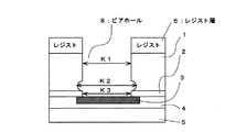
2 絶縁層
3 パッド電極
7 第1の開口
8 ビアホール
9,9A 絶縁層
10 バリア膜
11 シード層
12 再配線層
13 ボール状端子
Claims (6)
- 半導体基板の表面に第1の絶縁層を介して形成されたパッド電極を被覆するように前記半導体基板の表面側に支持体を接着する工程と、
前記半導体基板の裏面から前記パッド電極の表面に到達するようにビアホ−ルを形成する工程と、
前記ビアホールの側壁に第2の絶縁層を形成する工程と、
前記第2の絶縁層上であって、前記ビアホール内を含む前記半導体基板の裏面にバリア層を形成する工程と、
前記バリア層上にメッキ用のシード層を形成する工程と、
前記シード層上にメッキ処理により再配線層を形成する工程と、を備え、
前記ビアホ−ルを形成する工程は、前記半導体基板に対して前記第1の絶縁層が露出しない位置まで第1の開口を形成する工程と、前記半導体基板に対して前記第1の開口の開口径よりも広い開口径を有する第2の開口を前記第1の絶縁層が露出する位置まで形成する工程を含み、
前記ビアホ−ルの側壁に第2の絶縁層を形成する工程は、前記ビアホ−ルを含む半導体基板上に前記第2の絶縁層を形成した後に、前記半導体基板上に形成したレジスト層をマスクにして前記パッド電極上の前記第2の絶縁層を除去する工程であることを特徴とする半導体装置の製造方法。 - 半導体基板の表面に第1の絶縁層を介して形成されたパッド電極を被覆するように前記半導体基板の表面側に支持体を接着する工程と、
前記半導体基板の裏面から前記パッド電極の表面に到達するようにビアホ−ルを形成する工程と、
前記ビアホールの側壁に第2の絶縁層を形成する工程と、
前記第2の絶縁層上であって、前記ビアホール内を含む前記半導体基板の裏面にバリア層を形成する工程と、
前記バリア層上にメッキ用のシード層を形成する工程と、
前記シード層上にメッキ処理により再配線層を形成する工程と、を備え、
前記ビアホ−ルを形成する工程は、前記半導体基板に対して前記第1の絶縁層が露出しない位置まで第1の開口を形成する工程と、前記半導体基板に対して前記第1の開口の開口径よりも広い開口径を有する第2の開口を前記第1の絶縁層が露出する位置まで形成する工程を含み、
前記ビアホ−ルの側壁に第2の絶縁層を形成する工程は、前記ビアホ−ルを含む半導体基板上に、前記ビアホールの底部の膜厚よりも前記半導体基板上の膜厚が厚くなるように前記第2の絶縁層を形成した後に、レジスト層をマスクとして用いることなく、前記パッド電極上の前記第2の絶縁層をエッチングにより除去する工程であることを特徴とする半導体装置の製造方法。 - 前記ビアホ−ルを形成する工程は、前記第2の開口から露出した前記第1の絶縁層をエッチングして前記パッド電極を露出させる工程を含むことを特徴とする請求項1又は2に記載の半導体装置の製造方法。
- 前記再配線層に接続される導電端子を形成する工程を具備することを特徴とする請求項1又は2に記載の半導体装置の製造方法。
- 前記再配線層を形成する工程は、前記再配線層をビアホール内に中空部分を有して形成する工程であることを特徴とする請求項1又は2に記載の半導体装置の製造方法。
- 前記半導体基板を複数の半導体チップに分割する工程を具備することを特徴とする請求項1乃至5のいずれかに記載の半導体装置の製造方法。
Priority Applications (7)
| Application Number | Priority Date | Filing Date | Title |
|---|---|---|---|
| JP2004040403A JP4850392B2 (ja) | 2004-02-17 | 2004-02-17 | 半導体装置の製造方法 |
| TW094102860A TWI268534B (en) | 2004-02-17 | 2005-01-31 | Semiconductor device and method for making same |
| EP05002897.6A EP1564810B1 (en) | 2004-02-17 | 2005-02-11 | Semiconductor device and manufacturing method thereof |
| US11/055,707 US7732925B2 (en) | 2004-02-17 | 2005-02-11 | Semiconductor device and manufacturing method thereof |
| KR1020050012866A KR100658543B1 (ko) | 2004-02-17 | 2005-02-16 | 반도체 장치 및 그 제조 방법 |
| CNB2005100093666A CN100382304C (zh) | 2004-02-17 | 2005-02-17 | 半导体装置及其制造方法 |
| US11/808,667 US7750478B2 (en) | 2004-02-17 | 2007-06-12 | Semiconductor device with via hole of uneven width |
Applications Claiming Priority (1)
| Application Number | Priority Date | Filing Date | Title |
|---|---|---|---|
| JP2004040403A JP4850392B2 (ja) | 2004-02-17 | 2004-02-17 | 半導体装置の製造方法 |
Publications (3)
| Publication Number | Publication Date |
|---|---|
| JP2005235858A JP2005235858A (ja) | 2005-09-02 |
| JP2005235858A5 JP2005235858A5 (ja) | 2007-03-22 |
| JP4850392B2 true JP4850392B2 (ja) | 2012-01-11 |
Family
ID=34697995
Family Applications (1)
| Application Number | Title | Priority Date | Filing Date |
|---|---|---|---|
| JP2004040403A Expired - Lifetime JP4850392B2 (ja) | 2004-02-17 | 2004-02-17 | 半導体装置の製造方法 |
Country Status (6)
| Country | Link |
|---|---|
| US (2) | US7732925B2 (ja) |
| EP (1) | EP1564810B1 (ja) |
| JP (1) | JP4850392B2 (ja) |
| KR (1) | KR100658543B1 (ja) |
| CN (1) | CN100382304C (ja) |
| TW (1) | TWI268534B (ja) |
Families Citing this family (46)
| Publication number | Priority date | Publication date | Assignee | Title |
|---|---|---|---|---|
| JP4850392B2 (ja) | 2004-02-17 | 2012-01-11 | 三洋電機株式会社 | 半導体装置の製造方法 |
| JP2005235860A (ja) | 2004-02-17 | 2005-09-02 | Sanyo Electric Co Ltd | 半導体装置及びその製造方法 |
| SG120200A1 (en) | 2004-08-27 | 2006-03-28 | Micron Technology Inc | Slanted vias for electrical circuits on circuit boards and other substrates |
| TWI288448B (en) * | 2004-09-10 | 2007-10-11 | Toshiba Corp | Semiconductor device and method of manufacturing the same |
| JP4443379B2 (ja) | 2004-10-26 | 2010-03-31 | 三洋電機株式会社 | 半導体装置の製造方法 |
| TWI303864B (en) * | 2004-10-26 | 2008-12-01 | Sanyo Electric Co | Semiconductor device and method for making the same |
| JP4873517B2 (ja) | 2004-10-28 | 2012-02-08 | オンセミコンダクター・トレーディング・リミテッド | 半導体装置及びその製造方法 |
| US7485967B2 (en) | 2005-03-10 | 2009-02-03 | Sanyo Electric Co., Ltd. | Semiconductor device with via hole for electric connection |
| TW200641774A (en) * | 2005-04-28 | 2006-12-01 | Sanyo Electric Co | Electroluminescense display device and data line driving circuit |
| US7795134B2 (en) | 2005-06-28 | 2010-09-14 | Micron Technology, Inc. | Conductive interconnect structures and formation methods using supercritical fluids |
| US7425507B2 (en) * | 2005-06-28 | 2008-09-16 | Micron Technology, Inc. | Semiconductor substrates including vias of nonuniform cross section, methods of forming and associated structures |
| JP2007067216A (ja) * | 2005-08-31 | 2007-03-15 | Sanyo Electric Co Ltd | 半導体装置およびその製造方法、回路基板およびその製造方法 |
| US7262134B2 (en) * | 2005-09-01 | 2007-08-28 | Micron Technology, Inc. | Microfeature workpieces and methods for forming interconnects in microfeature workpieces |
| US20070045120A1 (en) * | 2005-09-01 | 2007-03-01 | Micron Technology, Inc. | Methods and apparatus for filling features in microfeature workpieces |
| US7863187B2 (en) | 2005-09-01 | 2011-01-04 | Micron Technology, Inc. | Microfeature workpieces and methods for forming interconnects in microfeature workpieces |
| JP4812512B2 (ja) * | 2006-05-19 | 2011-11-09 | オンセミコンダクター・トレーディング・リミテッド | 半導体装置の製造方法 |
| US7629249B2 (en) | 2006-08-28 | 2009-12-08 | Micron Technology, Inc. | Microfeature workpieces having conductive interconnect structures formed by chemically reactive processes, and associated systems and methods |
| US7902643B2 (en) | 2006-08-31 | 2011-03-08 | Micron Technology, Inc. | Microfeature workpieces having interconnects and conductive backplanes, and associated systems and methods |
| JP4979320B2 (ja) * | 2006-09-28 | 2012-07-18 | ルネサスエレクトロニクス株式会社 | 半導体ウェハおよびその製造方法、ならびに半導体装置の製造方法 |
| JP4380718B2 (ja) | 2007-03-15 | 2009-12-09 | ソニー株式会社 | 半導体装置の製造方法 |
| DE102007019552B4 (de) * | 2007-04-25 | 2009-12-17 | Infineon Technologies Ag | Verfahren zur Herstellung eines Substrats mit Durchführung sowie Substrat und Halbleitermodul mit Durchführung |
| JP5078509B2 (ja) * | 2007-09-04 | 2012-11-21 | 三洋電機株式会社 | 太陽電池 |
| US7884015B2 (en) | 2007-12-06 | 2011-02-08 | Micron Technology, Inc. | Methods for forming interconnects in microelectronic workpieces and microelectronic workpieces formed using such methods |
| JP2009181981A (ja) * | 2008-01-29 | 2009-08-13 | Renesas Technology Corp | 半導体装置の製造方法および半導体装置 |
| US7629264B2 (en) * | 2008-04-09 | 2009-12-08 | International Business Machines Corporation | Structure and method for hybrid tungsten copper metal contact |
| JP5356742B2 (ja) | 2008-07-10 | 2013-12-04 | ラピスセミコンダクタ株式会社 | 半導体装置、半導体装置の製造方法および半導体パッケージの製造方法 |
| CN102246299B (zh) * | 2008-10-15 | 2014-12-10 | Aac微技术有限公司 | 用于制作通路互连的方法 |
| US8030780B2 (en) * | 2008-10-16 | 2011-10-04 | Micron Technology, Inc. | Semiconductor substrates with unitary vias and via terminals, and associated systems and methods |
| JP2010114320A (ja) * | 2008-11-07 | 2010-05-20 | Panasonic Corp | 半導体装置 |
| JP5438980B2 (ja) | 2009-01-23 | 2014-03-12 | ラピスセミコンダクタ株式会社 | 半導体装置の製造方法 |
| JP5258735B2 (ja) * | 2009-11-13 | 2013-08-07 | セミコンダクター・コンポーネンツ・インダストリーズ・リミテッド・ライアビリティ・カンパニー | 半導体装置 |
| US9559001B2 (en) * | 2010-02-09 | 2017-01-31 | Xintec Inc. | Chip package and method for forming the same |
| KR101097628B1 (ko) * | 2010-06-21 | 2011-12-22 | 삼성전기주식회사 | 인쇄회로기판 및 이의 제조방법 |
| JP5733990B2 (ja) | 2011-01-12 | 2015-06-10 | キヤノン株式会社 | 半導体装置の製造方法 |
| US8901701B2 (en) * | 2011-02-10 | 2014-12-02 | Chia-Sheng Lin | Chip package and fabrication method thereof |
| US8816505B2 (en) * | 2011-07-29 | 2014-08-26 | Tessera, Inc. | Low stress vias |
| US9330975B2 (en) * | 2012-05-31 | 2016-05-03 | Micron Technology, Inc. | Integrated circuit substrates comprising through-substrate vias and methods of forming through-substrate vias |
| JP5655825B2 (ja) * | 2012-07-30 | 2015-01-21 | セイコーエプソン株式会社 | 半導体装置、半導体装置の製造方法、回路基板および電子機器 |
| US20140151095A1 (en) * | 2012-12-05 | 2014-06-05 | Samsung Electro-Mechanics Co., Ltd. | Printed circuit board and method for manufacturing the same |
| JP5588553B2 (ja) * | 2013-08-29 | 2014-09-10 | ラピスセミコンダクタ株式会社 | 半導体装置および半導体装置の製造方法 |
| TWI581389B (zh) | 2014-05-22 | 2017-05-01 | 精材科技股份有限公司 | 半導體結構及其製造方法 |
| US10727122B2 (en) | 2014-12-08 | 2020-07-28 | International Business Machines Corporation | Self-aligned via interconnect structures |
| CN105679770B (zh) | 2016-01-28 | 2019-02-26 | 京东方科技集团股份有限公司 | 阵列基板及其制造方法 |
| JP7191842B2 (ja) * | 2017-10-11 | 2022-12-19 | ソニーセミコンダクタソリューションズ株式会社 | 半導体装置およびその製造方法 |
| JP2019160893A (ja) * | 2018-03-09 | 2019-09-19 | ソニーセミコンダクタソリューションズ株式会社 | 固体撮像素子、半導体装置、電子機器、および製造方法 |
| CN111960376A (zh) * | 2020-07-21 | 2020-11-20 | 上海集成电路研发中心有限公司 | 一种mems支撑和电连接孔结构及制备方法 |
Family Cites Families (78)
| Publication number | Priority date | Publication date | Assignee | Title |
|---|---|---|---|---|
| US4097890A (en) | 1976-06-23 | 1978-06-27 | Hewlett-Packard Company | Low parasitic capacitance and resistance beamlead semiconductor component and method of manufacture |
| FR2637151A1 (fr) | 1988-09-29 | 1990-03-30 | Commissariat Energie Atomique | Procede de realisation de connexions electriques a travers un substrat |
| US5056216A (en) | 1990-01-26 | 1991-10-15 | Sri International | Method of forming a plurality of solder connections |
| US5229647A (en) | 1991-03-27 | 1993-07-20 | Micron Technology, Inc. | High density data storage using stacked wafers |
| US5149674A (en) | 1991-06-17 | 1992-09-22 | Motorola, Inc. | Method for making a planar multi-layer metal bonding pad |
| JPH0817186B2 (ja) | 1992-03-18 | 1996-02-21 | 三星電子株式会社 | 電界効果トランジスタの製造方法 |
| US5248903A (en) | 1992-09-18 | 1993-09-28 | Lsi Logic Corporation | Composite bond pads for semiconductor devices |
| US5432119A (en) | 1994-01-31 | 1995-07-11 | Hughes Aircraft Company | High yield electron-beam gate fabrication method for sub-micron gate FETS |
| WO1996013062A1 (en) * | 1994-10-19 | 1996-05-02 | Ceram Incorporated | Apparatus and method of manufacturing stacked wafer array |
| US6204074B1 (en) | 1995-01-09 | 2001-03-20 | International Business Machines Corporation | Chip design process for wire bond and flip-chip package |
| JPH08293523A (ja) | 1995-02-21 | 1996-11-05 | Seiko Epson Corp | 半導体装置およびその製造方法 |
| US6192581B1 (en) | 1996-04-30 | 2001-02-27 | Matsushita Electric Industrial Co., Ltd. | Method of making printed circuit board |
| JPH09321175A (ja) | 1996-05-30 | 1997-12-12 | Oki Electric Ind Co Ltd | マイクロ波回路及びチップ |
| US5910687A (en) | 1997-01-24 | 1999-06-08 | Chipscale, Inc. | Wafer fabrication of die-bottom contacts for electronic devices |
| EP0860876A3 (de) | 1997-02-21 | 1999-09-22 | DaimlerChrysler AG | Anordnung und Verfahren zur Herstellung von CSP-Gehäusen für elektrische Bauteile |
| US5915167A (en) | 1997-04-04 | 1999-06-22 | Elm Technology Corporation | Three dimensional structure memory |
| JP3724110B2 (ja) | 1997-04-24 | 2005-12-07 | 三菱電機株式会社 | 半導体装置の製造方法 |
| US5985749A (en) * | 1997-06-25 | 1999-11-16 | Vlsi Technology, Inc. | Method of forming a via hole structure including CVD tungsten silicide barrier layer |
| US6084173A (en) * | 1997-07-30 | 2000-07-04 | Dimatteo; Robert Stephen | Method and apparatus for the generation of charged carriers in semiconductor devices |
| IL123207A0 (en) * | 1998-02-06 | 1998-09-24 | Shellcase Ltd | Integrated circuit device |
| JP2974022B1 (ja) | 1998-10-01 | 1999-11-08 | ヤマハ株式会社 | 半導体装置のボンディングパッド構造 |
| US6734564B1 (en) | 1999-01-04 | 2004-05-11 | International Business Machines Corporation | Specially shaped contact via and integrated circuit therewith |
| TW442873B (en) | 1999-01-14 | 2001-06-23 | United Microelectronics Corp | Three-dimension stack-type chip structure and its manufacturing method |
| US6110816A (en) | 1999-03-05 | 2000-08-29 | Taiwan Semiconductor Manufacturing Company | Method for improving bondability for deep-submicron integrated circuit package |
| US6031293A (en) | 1999-04-26 | 2000-02-29 | United Microelectronics Corporation | Package-free bonding pad structure |
| US6300670B1 (en) * | 1999-07-26 | 2001-10-09 | Stmicroelectronics, Inc. | Backside bus vias |
| JP2001044197A (ja) * | 1999-08-04 | 2001-02-16 | Sharp Corp | 半導体装置及びその製造方法 |
| JP3858545B2 (ja) * | 1999-12-27 | 2006-12-13 | セイコーエプソン株式会社 | 半導体モジュール及び電子機器 |
| JP3778256B2 (ja) | 2000-02-28 | 2006-05-24 | セイコーエプソン株式会社 | 半導体装置及びその製造方法、回路基板並びに電子機器 |
| JP3879816B2 (ja) | 2000-06-02 | 2007-02-14 | セイコーエプソン株式会社 | 半導体装置及びその製造方法、積層型半導体装置、回路基板並びに電子機器 |
| JP4329235B2 (ja) * | 2000-06-27 | 2009-09-09 | セイコーエプソン株式会社 | 半導体装置及びその製造方法 |
| US6562709B1 (en) | 2000-08-22 | 2003-05-13 | Charles W. C. Lin | Semiconductor chip assembly with simultaneously electroplated contact terminal and connection joint |
| US6512292B1 (en) | 2000-09-12 | 2003-01-28 | International Business Machines Corporation | Semiconductor chip structures with embedded thermal conductors and a thermal sink disposed over opposing substrate surfaces |
| JP2002124517A (ja) * | 2000-10-13 | 2002-04-26 | Sharp Corp | 半導体装置およびその製造方法 |
| KR100366635B1 (ko) * | 2000-11-01 | 2003-01-09 | 삼성전자 주식회사 | 반도체 소자의 금속 배선 및 그 제조방법 |
| KR100382729B1 (ko) | 2000-12-09 | 2003-05-09 | 삼성전자주식회사 | 반도체 소자의 금속 컨택 구조체 및 그 형성방법 |
| JP4771607B2 (ja) | 2001-03-30 | 2011-09-14 | 富士通セミコンダクター株式会社 | 半導体装置及びその製造方法 |
| JP3530149B2 (ja) | 2001-05-21 | 2004-05-24 | 新光電気工業株式会社 | 配線基板の製造方法及び半導体装置 |
| JP4754105B2 (ja) * | 2001-07-04 | 2011-08-24 | パナソニック株式会社 | 半導体装置およびその製造方法 |
| JP2003045877A (ja) | 2001-08-01 | 2003-02-14 | Sharp Corp | 半導体装置およびその製造方法 |
| US6734568B2 (en) | 2001-08-29 | 2004-05-11 | Kabushiki Kaisha Toshiba | Semiconductor device and method of manufacturing the same |
| JP4703061B2 (ja) | 2001-08-30 | 2011-06-15 | 富士通株式会社 | 薄膜回路基板の製造方法およびビア形成基板の形成方法 |
| JP2003168818A (ja) | 2001-09-18 | 2003-06-13 | Anritsu Corp | 順メサ型アバランシェフォトダイオード及びその製造方法 |
| JP3998984B2 (ja) | 2002-01-18 | 2007-10-31 | 富士通株式会社 | 回路基板及びその製造方法 |
| US6960837B2 (en) | 2002-02-26 | 2005-11-01 | International Business Machines Corporation | Method of connecting core I/O pins to backside chip I/O pads |
| JP4110390B2 (ja) * | 2002-03-19 | 2008-07-02 | セイコーエプソン株式会社 | 半導体装置の製造方法 |
| EP1351288B1 (en) | 2002-04-05 | 2015-10-28 | STMicroelectronics Srl | Process for manufacturing an insulated interconnection through a body of semiconductor material and corresponding semiconductor device |
| JP4212293B2 (ja) * | 2002-04-15 | 2009-01-21 | 三洋電機株式会社 | 半導体装置の製造方法 |
| TWI232560B (en) * | 2002-04-23 | 2005-05-11 | Sanyo Electric Co | Semiconductor device and its manufacture |
| JP2003318178A (ja) | 2002-04-24 | 2003-11-07 | Seiko Epson Corp | 半導体装置及びその製造方法、回路基板並びに電子機器 |
| TWI229435B (en) * | 2002-06-18 | 2005-03-11 | Sanyo Electric Co | Manufacture of semiconductor device |
| US6902872B2 (en) | 2002-07-29 | 2005-06-07 | Hewlett-Packard Development Company, L.P. | Method of forming a through-substrate interconnect |
| US6716737B2 (en) | 2002-07-29 | 2004-04-06 | Hewlett-Packard Development Company, L.P. | Method of forming a through-substrate interconnect |
| JP2004103761A (ja) | 2002-09-09 | 2004-04-02 | Renesas Technology Corp | 半導体装置製造ライン |
| TWI227050B (en) | 2002-10-11 | 2005-01-21 | Sanyo Electric Co | Semiconductor device and method for manufacturing the same |
| TWI227550B (en) | 2002-10-30 | 2005-02-01 | Sanyo Electric Co | Semiconductor device manufacturing method |
| US6924221B2 (en) | 2002-12-03 | 2005-08-02 | Taiwan Semiconductor Manufacturing Co., Ltd. | Integrated process flow to improve copper filling in a damascene structure |
| JP2004186422A (ja) | 2002-12-03 | 2004-07-02 | Shinko Electric Ind Co Ltd | 電子部品実装構造及びその製造方法 |
| JP4322508B2 (ja) | 2003-01-15 | 2009-09-02 | 新光電気工業株式会社 | 半導体装置の製造方法 |
| JP4145301B2 (ja) | 2003-01-15 | 2008-09-03 | 富士通株式会社 | 半導体装置及び三次元実装半導体装置 |
| TWI239629B (en) | 2003-03-17 | 2005-09-11 | Seiko Epson Corp | Method of manufacturing semiconductor device, semiconductor device, circuit substrate and electronic apparatus |
| JP3972846B2 (ja) | 2003-03-25 | 2007-09-05 | セイコーエプソン株式会社 | 半導体装置の製造方法 |
| JP2004311948A (ja) | 2003-03-27 | 2004-11-04 | Seiko Epson Corp | 半導体装置、半導体デバイス、電子機器、および半導体装置の製造方法 |
| US7247939B2 (en) * | 2003-04-01 | 2007-07-24 | Taiwan Semiconductor Manufacturing Co., Ltd. | Metal filled semiconductor features with improved structural stability |
| JP4130158B2 (ja) | 2003-06-09 | 2008-08-06 | 三洋電機株式会社 | 半導体装置の製造方法、半導体装置 |
| US7453158B2 (en) | 2003-07-31 | 2008-11-18 | Nvidia Corporation | Pad over active circuit system and method with meshed support structure |
| JP4323303B2 (ja) * | 2003-12-17 | 2009-09-02 | 株式会社フジクラ | 基板の製造方法 |
| TWI249767B (en) * | 2004-02-17 | 2006-02-21 | Sanyo Electric Co | Method for making a semiconductor device |
| JP2005235860A (ja) | 2004-02-17 | 2005-09-02 | Sanyo Electric Co Ltd | 半導体装置及びその製造方法 |
| JP4850392B2 (ja) | 2004-02-17 | 2012-01-11 | 三洋電機株式会社 | 半導体装置の製造方法 |
| JP4803964B2 (ja) | 2004-03-17 | 2011-10-26 | 三洋電機株式会社 | 電極構造 |
| JP4373866B2 (ja) | 2004-07-16 | 2009-11-25 | 三洋電機株式会社 | 半導体装置の製造方法 |
| JP4376715B2 (ja) | 2004-07-16 | 2009-12-02 | 三洋電機株式会社 | 半導体装置の製造方法 |
| TWI303864B (en) | 2004-10-26 | 2008-12-01 | Sanyo Electric Co | Semiconductor device and method for making the same |
| JP4443379B2 (ja) | 2004-10-26 | 2010-03-31 | 三洋電機株式会社 | 半導体装置の製造方法 |
| JP4873517B2 (ja) | 2004-10-28 | 2012-02-08 | オンセミコンダクター・トレーディング・リミテッド | 半導体装置及びその製造方法 |
| US7538434B2 (en) * | 2005-03-08 | 2009-05-26 | Taiwan Semiconductor Manufacturing Company, Ltd. | Copper interconnection with conductive polymer layer and method of forming the same |
| US7485967B2 (en) | 2005-03-10 | 2009-02-03 | Sanyo Electric Co., Ltd. | Semiconductor device with via hole for electric connection |
-
2004
- 2004-02-17 JP JP2004040403A patent/JP4850392B2/ja not_active Expired - Lifetime
-
2005
- 2005-01-31 TW TW094102860A patent/TWI268534B/zh active
- 2005-02-11 EP EP05002897.6A patent/EP1564810B1/en not_active Expired - Fee Related
- 2005-02-11 US US11/055,707 patent/US7732925B2/en active Active
- 2005-02-16 KR KR1020050012866A patent/KR100658543B1/ko active IP Right Grant
- 2005-02-17 CN CNB2005100093666A patent/CN100382304C/zh active Active
-
2007
- 2007-06-12 US US11/808,667 patent/US7750478B2/en active Active
Also Published As
| Publication number | Publication date |
|---|---|
| CN1658387A (zh) | 2005-08-24 |
| US20070249158A1 (en) | 2007-10-25 |
| KR100658543B1 (ko) | 2006-12-19 |
| US7732925B2 (en) | 2010-06-08 |
| JP2005235858A (ja) | 2005-09-02 |
| CN100382304C (zh) | 2008-04-16 |
| TW200531142A (en) | 2005-09-16 |
| EP1564810A1 (en) | 2005-08-17 |
| KR20060042012A (ko) | 2006-05-12 |
| US20050189637A1 (en) | 2005-09-01 |
| TWI268534B (en) | 2006-12-11 |
| US7750478B2 (en) | 2010-07-06 |
| EP1564810B1 (en) | 2017-01-11 |
Similar Documents
| Publication | Publication Date | Title |
|---|---|---|
| JP4850392B2 (ja) | 半導体装置の製造方法 | |
| JP4307284B2 (ja) | 半導体装置の製造方法 | |
| KR100709662B1 (ko) | 반도체 장치 및 그 제조 방법 | |
| JP4775007B2 (ja) | 半導体装置及びその製造方法 | |
| KR100563887B1 (ko) | 반도체 장치 및 그 제조 방법 | |
| JP4443379B2 (ja) | 半導体装置の製造方法 | |
| US7241679B2 (en) | Method of manufacturing semiconductor device | |
| KR20060041950A (ko) | 반도체 장치 및 그 제조 방법 | |
| KR20040101924A (ko) | 반도체 장치 및 그 제조 방법 | |
| JP4726221B2 (ja) | 半導体装置及びその製造方法 | |
| JP4936695B2 (ja) | 半導体装置及びその製造方法 | |
| JP4511148B2 (ja) | 半導体装置の製造方法 | |
| JP4544902B2 (ja) | 半導体装置及びその製造方法 | |
| JP4282514B2 (ja) | 半導体装置の製造方法 | |
| JP4845986B2 (ja) | 半導体装置 |
Legal Events
| Date | Code | Title | Description |
|---|---|---|---|
| A521 | Request for written amendment filed |
Free format text: JAPANESE INTERMEDIATE CODE: A523 Effective date: 20070201 |
|
| A621 | Written request for application examination |
Free format text: JAPANESE INTERMEDIATE CODE: A621 Effective date: 20070201 |
|
| A711 | Notification of change in applicant |
Free format text: JAPANESE INTERMEDIATE CODE: A712 Effective date: 20090115 |
|
| RD02 | Notification of acceptance of power of attorney |
Free format text: JAPANESE INTERMEDIATE CODE: A7422 Effective date: 20090309 |
|
| A521 | Request for written amendment filed |
Free format text: JAPANESE INTERMEDIATE CODE: A821 Effective date: 20090309 |
|
| A977 | Report on retrieval |
Free format text: JAPANESE INTERMEDIATE CODE: A971007 Effective date: 20090527 |
|
| A131 | Notification of reasons for refusal |
Free format text: JAPANESE INTERMEDIATE CODE: A131 Effective date: 20110310 |
|
| A521 | Request for written amendment filed |
Free format text: JAPANESE INTERMEDIATE CODE: A523 Effective date: 20110425 |
|
| A131 | Notification of reasons for refusal |
Free format text: JAPANESE INTERMEDIATE CODE: A131 Effective date: 20110712 |
|
| A521 | Request for written amendment filed |
Free format text: JAPANESE INTERMEDIATE CODE: A523 Effective date: 20110905 |
|
| TRDD | Decision of grant or rejection written | ||
| A01 | Written decision to grant a patent or to grant a registration (utility model) |
Free format text: JAPANESE INTERMEDIATE CODE: A01 Effective date: 20111013 |
|
| A01 | Written decision to grant a patent or to grant a registration (utility model) |
Free format text: JAPANESE INTERMEDIATE CODE: A01 |
|
| A61 | First payment of annual fees (during grant procedure) |
Free format text: JAPANESE INTERMEDIATE CODE: A61 Effective date: 20111019 |
|
| R150 | Certificate of patent or registration of utility model |
Ref document number: 4850392 Country of ref document: JP Free format text: JAPANESE INTERMEDIATE CODE: R150 Free format text: JAPANESE INTERMEDIATE CODE: R150 |
|
| FPAY | Renewal fee payment (event date is renewal date of database) |
Free format text: PAYMENT UNTIL: 20141028 Year of fee payment: 3 |
|
| R250 | Receipt of annual fees |
Free format text: JAPANESE INTERMEDIATE CODE: R250 |
|
| R250 | Receipt of annual fees |
Free format text: JAPANESE INTERMEDIATE CODE: R250 |
|
| S111 | Request for change of ownership or part of ownership |
Free format text: JAPANESE INTERMEDIATE CODE: R313117 |
|
| S531 | Written request for registration of change of domicile |
Free format text: JAPANESE INTERMEDIATE CODE: R313531 |
|
| R350 | Written notification of registration of transfer |
Free format text: JAPANESE INTERMEDIATE CODE: R350 |
|
| S531 | Written request for registration of change of domicile |
Free format text: JAPANESE INTERMEDIATE CODE: R313531 |
|
| R350 | Written notification of registration of transfer |
Free format text: JAPANESE INTERMEDIATE CODE: R350 |
|
| R250 | Receipt of annual fees |
Free format text: JAPANESE INTERMEDIATE CODE: R250 |
|
| R250 | Receipt of annual fees |
Free format text: JAPANESE INTERMEDIATE CODE: R250 |
|
| R250 | Receipt of annual fees |
Free format text: JAPANESE INTERMEDIATE CODE: R250 |
|
| S111 | Request for change of ownership or part of ownership |
Free format text: JAPANESE INTERMEDIATE CODE: R313115 |
|
| R250 | Receipt of annual fees |
Free format text: JAPANESE INTERMEDIATE CODE: R250 |
|
| R350 | Written notification of registration of transfer |
Free format text: JAPANESE INTERMEDIATE CODE: R350 |
|
| S531 | Written request for registration of change of domicile |
Free format text: JAPANESE INTERMEDIATE CODE: R313531 |
|
| S533 | Written request for registration of change of name |
Free format text: JAPANESE INTERMEDIATE CODE: R313533 |
|
| R350 | Written notification of registration of transfer |
Free format text: JAPANESE INTERMEDIATE CODE: R350 |
|
| S111 | Request for change of ownership or part of ownership |
Free format text: JAPANESE INTERMEDIATE CODE: R313117 |
|
| R350 | Written notification of registration of transfer |
Free format text: JAPANESE INTERMEDIATE CODE: R350 |
|
| R250 | Receipt of annual fees |
Free format text: JAPANESE INTERMEDIATE CODE: R250 |
|
| R250 | Receipt of annual fees |
Free format text: JAPANESE INTERMEDIATE CODE: R250 |
|
| R250 | Receipt of annual fees |
Free format text: JAPANESE INTERMEDIATE CODE: R250 |
|
| R250 | Receipt of annual fees |
Free format text: JAPANESE INTERMEDIATE CODE: R250 |