JP4753170B2 - 半導体装置及びその製造方法 - Google Patents
半導体装置及びその製造方法 Download PDFInfo
- Publication number
- JP4753170B2 JP4753170B2 JP2004062323A JP2004062323A JP4753170B2 JP 4753170 B2 JP4753170 B2 JP 4753170B2 JP 2004062323 A JP2004062323 A JP 2004062323A JP 2004062323 A JP2004062323 A JP 2004062323A JP 4753170 B2 JP4753170 B2 JP 4753170B2
- Authority
- JP
- Japan
- Prior art keywords
- semiconductor device
- dicing
- semiconductor
- alignment mark
- manufacturing
- Prior art date
- Legal status (The legal status is an assumption and is not a legal conclusion. Google has not performed a legal analysis and makes no representation as to the accuracy of the status listed.)
- Expired - Fee Related
Links
- 239000004065 semiconductor Substances 0.000 title claims description 167
- 238000004519 manufacturing process Methods 0.000 title claims description 40
- 238000005520 cutting process Methods 0.000 claims description 62
- 239000010410 layer Substances 0.000 claims description 12
- 238000000034 method Methods 0.000 claims description 10
- 229910052751 metal Inorganic materials 0.000 claims description 9
- 239000002184 metal Substances 0.000 claims description 9
- 238000005530 etching Methods 0.000 claims description 8
- 238000001514 detection method Methods 0.000 claims description 7
- 239000000463 material Substances 0.000 claims description 4
- 239000011241 protective layer Substances 0.000 claims description 2
- 239000000758 substrate Substances 0.000 description 20
- 239000011521 glass Substances 0.000 description 19
- 229920005989 resin Polymers 0.000 description 9
- 239000011347 resin Substances 0.000 description 9
- 230000001681 protective effect Effects 0.000 description 6
- 230000015572 biosynthetic process Effects 0.000 description 4
- 238000000059 patterning Methods 0.000 description 4
- 230000006866 deterioration Effects 0.000 description 2
- 238000007747 plating Methods 0.000 description 2
- 238000003860 storage Methods 0.000 description 2
- 238000001039 wet etching Methods 0.000 description 2
- BLRPTPMANUNPDV-UHFFFAOYSA-N Silane Chemical compound [SiH4] BLRPTPMANUNPDV-UHFFFAOYSA-N 0.000 description 1
- 229910052782 aluminium Inorganic materials 0.000 description 1
- XAGFODPZIPBFFR-UHFFFAOYSA-N aluminium Chemical compound [Al] XAGFODPZIPBFFR-UHFFFAOYSA-N 0.000 description 1
- 239000003822 epoxy resin Substances 0.000 description 1
- 238000000227 grinding Methods 0.000 description 1
- 229920000647 polyepoxide Polymers 0.000 description 1
- 229910000077 silane Inorganic materials 0.000 description 1
- 229910000679 solder Inorganic materials 0.000 description 1
- 238000004528 spin coating Methods 0.000 description 1
- 239000000126 substance Substances 0.000 description 1
Images


Classifications
-
- H—ELECTRICITY
- H01—ELECTRIC ELEMENTS
- H01L—SEMICONDUCTOR DEVICES NOT COVERED BY CLASS H10
- H01L21/00—Processes or apparatus adapted for the manufacture or treatment of semiconductor or solid state devices or of parts thereof
- H01L21/70—Manufacture or treatment of devices consisting of a plurality of solid state components formed in or on a common substrate or of parts thereof; Manufacture of integrated circuit devices or of parts thereof
- H01L21/77—Manufacture or treatment of devices consisting of a plurality of solid state components or integrated circuits formed in, or on, a common substrate
- H01L21/78—Manufacture or treatment of devices consisting of a plurality of solid state components or integrated circuits formed in, or on, a common substrate with subsequent division of the substrate into plural individual devices
-
- A—HUMAN NECESSITIES
- A61—MEDICAL OR VETERINARY SCIENCE; HYGIENE
- A61M—DEVICES FOR INTRODUCING MEDIA INTO, OR ONTO, THE BODY; DEVICES FOR TRANSDUCING BODY MEDIA OR FOR TAKING MEDIA FROM THE BODY; DEVICES FOR PRODUCING OR ENDING SLEEP OR STUPOR
- A61M3/00—Medical syringes, e.g. enemata; Irrigators
- A61M3/02—Enemata; Irrigators
- A61M3/0233—Enemata; Irrigators characterised by liquid supply means, e.g. from pressurised reservoirs
- A61M3/0254—Enemata; Irrigators characterised by liquid supply means, e.g. from pressurised reservoirs the liquid being pumped
- A61M3/0262—Enemata; Irrigators characterised by liquid supply means, e.g. from pressurised reservoirs the liquid being pumped manually, e.g. by squeezing a bulb
-
- A—HUMAN NECESSITIES
- A61—MEDICAL OR VETERINARY SCIENCE; HYGIENE
- A61M—DEVICES FOR INTRODUCING MEDIA INTO, OR ONTO, THE BODY; DEVICES FOR TRANSDUCING BODY MEDIA OR FOR TAKING MEDIA FROM THE BODY; DEVICES FOR PRODUCING OR ENDING SLEEP OR STUPOR
- A61M3/00—Medical syringes, e.g. enemata; Irrigators
- A61M3/02—Enemata; Irrigators
- A61M3/0233—Enemata; Irrigators characterised by liquid supply means, e.g. from pressurised reservoirs
- A61M3/025—Enemata; Irrigators characterised by liquid supply means, e.g. from pressurised reservoirs supplied directly from the pressurised water source, e.g. with medicament supply
-
- A—HUMAN NECESSITIES
- A61—MEDICAL OR VETERINARY SCIENCE; HYGIENE
- A61M—DEVICES FOR INTRODUCING MEDIA INTO, OR ONTO, THE BODY; DEVICES FOR TRANSDUCING BODY MEDIA OR FOR TAKING MEDIA FROM THE BODY; DEVICES FOR PRODUCING OR ENDING SLEEP OR STUPOR
- A61M3/00—Medical syringes, e.g. enemata; Irrigators
- A61M3/02—Enemata; Irrigators
- A61M3/0279—Cannula; Nozzles; Tips; their connection means
-
- H—ELECTRICITY
- H01—ELECTRIC ELEMENTS
- H01L—SEMICONDUCTOR DEVICES NOT COVERED BY CLASS H10
- H01L21/00—Processes or apparatus adapted for the manufacture or treatment of semiconductor or solid state devices or of parts thereof
- H01L21/02—Manufacture or treatment of semiconductor devices or of parts thereof
- H01L21/04—Manufacture or treatment of semiconductor devices or of parts thereof the devices having at least one potential-jump barrier or surface barrier, e.g. PN junction, depletion layer or carrier concentration layer
- H01L21/50—Assembly of semiconductor devices using processes or apparatus not provided for in a single one of the subgroups H01L21/06 - H01L21/326, e.g. sealing of a cap to a base of a container
- H01L21/56—Encapsulations, e.g. encapsulation layers, coatings
- H01L21/561—Batch processing
-
- H—ELECTRICITY
- H01—ELECTRIC ELEMENTS
- H01L—SEMICONDUCTOR DEVICES NOT COVERED BY CLASS H10
- H01L23/00—Details of semiconductor or other solid state devices
- H01L23/28—Encapsulations, e.g. encapsulating layers, coatings, e.g. for protection
- H01L23/31—Encapsulations, e.g. encapsulating layers, coatings, e.g. for protection characterised by the arrangement or shape
- H01L23/3107—Encapsulations, e.g. encapsulating layers, coatings, e.g. for protection characterised by the arrangement or shape the device being completely enclosed
- H01L23/3114—Encapsulations, e.g. encapsulating layers, coatings, e.g. for protection characterised by the arrangement or shape the device being completely enclosed the device being a chip scale package, e.g. CSP
-
- H—ELECTRICITY
- H01—ELECTRIC ELEMENTS
- H01L—SEMICONDUCTOR DEVICES NOT COVERED BY CLASS H10
- H01L23/00—Details of semiconductor or other solid state devices
- H01L23/544—Marks applied to semiconductor devices or parts, e.g. registration marks, alignment structures, wafer maps
-
- H—ELECTRICITY
- H01—ELECTRIC ELEMENTS
- H01L—SEMICONDUCTOR DEVICES NOT COVERED BY CLASS H10
- H01L24/00—Arrangements for connecting or disconnecting semiconductor or solid-state bodies; Methods or apparatus related thereto
- H01L24/01—Means for bonding being attached to, or being formed on, the surface to be connected, e.g. chip-to-package, die-attach, "first-level" interconnects; Manufacturing methods related thereto
- H01L24/10—Bump connectors ; Manufacturing methods related thereto
- H01L24/12—Structure, shape, material or disposition of the bump connectors prior to the connecting process
- H01L24/13—Structure, shape, material or disposition of the bump connectors prior to the connecting process of an individual bump connector
-
- H—ELECTRICITY
- H01—ELECTRIC ELEMENTS
- H01L—SEMICONDUCTOR DEVICES NOT COVERED BY CLASS H10
- H01L24/00—Arrangements for connecting or disconnecting semiconductor or solid-state bodies; Methods or apparatus related thereto
- H01L24/93—Batch processes
- H01L24/95—Batch processes at chip-level, i.e. with connecting carried out on a plurality of singulated devices, i.e. on diced chips
- H01L24/97—Batch processes at chip-level, i.e. with connecting carried out on a plurality of singulated devices, i.e. on diced chips the devices being connected to a common substrate, e.g. interposer, said common substrate being separable into individual assemblies after connecting
-
- A—HUMAN NECESSITIES
- A61—MEDICAL OR VETERINARY SCIENCE; HYGIENE
- A61M—DEVICES FOR INTRODUCING MEDIA INTO, OR ONTO, THE BODY; DEVICES FOR TRANSDUCING BODY MEDIA OR FOR TAKING MEDIA FROM THE BODY; DEVICES FOR PRODUCING OR ENDING SLEEP OR STUPOR
- A61M2205/00—General characteristics of the apparatus
- A61M2205/07—General characteristics of the apparatus having air pumping means
- A61M2205/071—General characteristics of the apparatus having air pumping means hand operated
- A61M2205/075—Bulb type
-
- A—HUMAN NECESSITIES
- A61—MEDICAL OR VETERINARY SCIENCE; HYGIENE
- A61M—DEVICES FOR INTRODUCING MEDIA INTO, OR ONTO, THE BODY; DEVICES FOR TRANSDUCING BODY MEDIA OR FOR TAKING MEDIA FROM THE BODY; DEVICES FOR PRODUCING OR ENDING SLEEP OR STUPOR
- A61M2205/00—General characteristics of the apparatus
- A61M2205/33—Controlling, regulating or measuring
- A61M2205/3331—Pressure; Flow
- A61M2205/3334—Measuring or controlling the flow rate
-
- A—HUMAN NECESSITIES
- A61—MEDICAL OR VETERINARY SCIENCE; HYGIENE
- A61M—DEVICES FOR INTRODUCING MEDIA INTO, OR ONTO, THE BODY; DEVICES FOR TRANSDUCING BODY MEDIA OR FOR TAKING MEDIA FROM THE BODY; DEVICES FOR PRODUCING OR ENDING SLEEP OR STUPOR
- A61M2210/00—Anatomical parts of the body
- A61M2210/10—Trunk
- A61M2210/1042—Alimentary tract
- A61M2210/1064—Large intestine
-
- A—HUMAN NECESSITIES
- A61—MEDICAL OR VETERINARY SCIENCE; HYGIENE
- A61M—DEVICES FOR INTRODUCING MEDIA INTO, OR ONTO, THE BODY; DEVICES FOR TRANSDUCING BODY MEDIA OR FOR TAKING MEDIA FROM THE BODY; DEVICES FOR PRODUCING OR ENDING SLEEP OR STUPOR
- A61M2210/00—Anatomical parts of the body
- A61M2210/14—Female reproductive, genital organs
- A61M2210/1475—Vagina
-
- H—ELECTRICITY
- H01—ELECTRIC ELEMENTS
- H01L—SEMICONDUCTOR DEVICES NOT COVERED BY CLASS H10
- H01L2223/00—Details relating to semiconductor or other solid state devices covered by the group H01L23/00
- H01L2223/544—Marks applied to semiconductor devices or parts
- H01L2223/54453—Marks applied to semiconductor devices or parts for use prior to dicing
-
- H—ELECTRICITY
- H01—ELECTRIC ELEMENTS
- H01L—SEMICONDUCTOR DEVICES NOT COVERED BY CLASS H10
- H01L2223/00—Details relating to semiconductor or other solid state devices covered by the group H01L23/00
- H01L2223/544—Marks applied to semiconductor devices or parts
- H01L2223/54473—Marks applied to semiconductor devices or parts for use after dicing
- H01L2223/5448—Located on chip prior to dicing and remaining on chip after dicing
-
- H—ELECTRICITY
- H01—ELECTRIC ELEMENTS
- H01L—SEMICONDUCTOR DEVICES NOT COVERED BY CLASS H10
- H01L2224/00—Indexing scheme for arrangements for connecting or disconnecting semiconductor or solid-state bodies and methods related thereto as covered by H01L24/00
- H01L2224/01—Means for bonding being attached to, or being formed on, the surface to be connected, e.g. chip-to-package, die-attach, "first-level" interconnects; Manufacturing methods related thereto
- H01L2224/02—Bonding areas; Manufacturing methods related thereto
- H01L2224/023—Redistribution layers [RDL] for bonding areas
- H01L2224/0237—Disposition of the redistribution layers
- H01L2224/02371—Disposition of the redistribution layers connecting the bonding area on a surface of the semiconductor or solid-state body with another surface of the semiconductor or solid-state body
-
- H—ELECTRICITY
- H01—ELECTRIC ELEMENTS
- H01L—SEMICONDUCTOR DEVICES NOT COVERED BY CLASS H10
- H01L2224/00—Indexing scheme for arrangements for connecting or disconnecting semiconductor or solid-state bodies and methods related thereto as covered by H01L24/00
- H01L2224/01—Means for bonding being attached to, or being formed on, the surface to be connected, e.g. chip-to-package, die-attach, "first-level" interconnects; Manufacturing methods related thereto
- H01L2224/02—Bonding areas; Manufacturing methods related thereto
- H01L2224/04—Structure, shape, material or disposition of the bonding areas prior to the connecting process
- H01L2224/05—Structure, shape, material or disposition of the bonding areas prior to the connecting process of an individual bonding area
- H01L2224/05001—Internal layers
- H01L2224/0502—Disposition
- H01L2224/05022—Disposition the internal layer being at least partially embedded in the surface
-
- H—ELECTRICITY
- H01—ELECTRIC ELEMENTS
- H01L—SEMICONDUCTOR DEVICES NOT COVERED BY CLASS H10
- H01L2224/00—Indexing scheme for arrangements for connecting or disconnecting semiconductor or solid-state bodies and methods related thereto as covered by H01L24/00
- H01L2224/01—Means for bonding being attached to, or being formed on, the surface to be connected, e.g. chip-to-package, die-attach, "first-level" interconnects; Manufacturing methods related thereto
- H01L2224/02—Bonding areas; Manufacturing methods related thereto
- H01L2224/04—Structure, shape, material or disposition of the bonding areas prior to the connecting process
- H01L2224/05—Structure, shape, material or disposition of the bonding areas prior to the connecting process of an individual bonding area
- H01L2224/05001—Internal layers
- H01L2224/05099—Material
- H01L2224/051—Material with a principal constituent of the material being a metal or a metalloid, e.g. boron [B], silicon [Si], germanium [Ge], arsenic [As], antimony [Sb], tellurium [Te] and polonium [Po], and alloys thereof
-
- H—ELECTRICITY
- H01—ELECTRIC ELEMENTS
- H01L—SEMICONDUCTOR DEVICES NOT COVERED BY CLASS H10
- H01L2224/00—Indexing scheme for arrangements for connecting or disconnecting semiconductor or solid-state bodies and methods related thereto as covered by H01L24/00
- H01L2224/01—Means for bonding being attached to, or being formed on, the surface to be connected, e.g. chip-to-package, die-attach, "first-level" interconnects; Manufacturing methods related thereto
- H01L2224/02—Bonding areas; Manufacturing methods related thereto
- H01L2224/04—Structure, shape, material or disposition of the bonding areas prior to the connecting process
- H01L2224/05—Structure, shape, material or disposition of the bonding areas prior to the connecting process of an individual bonding area
- H01L2224/0554—External layer
- H01L2224/05541—Structure
- H01L2224/05548—Bonding area integrally formed with a redistribution layer on the semiconductor or solid-state body
-
- H—ELECTRICITY
- H01—ELECTRIC ELEMENTS
- H01L—SEMICONDUCTOR DEVICES NOT COVERED BY CLASS H10
- H01L2224/00—Indexing scheme for arrangements for connecting or disconnecting semiconductor or solid-state bodies and methods related thereto as covered by H01L24/00
- H01L2224/01—Means for bonding being attached to, or being formed on, the surface to be connected, e.g. chip-to-package, die-attach, "first-level" interconnects; Manufacturing methods related thereto
- H01L2224/02—Bonding areas; Manufacturing methods related thereto
- H01L2224/04—Structure, shape, material or disposition of the bonding areas prior to the connecting process
- H01L2224/05—Structure, shape, material or disposition of the bonding areas prior to the connecting process of an individual bonding area
- H01L2224/0554—External layer
- H01L2224/05599—Material
- H01L2224/056—Material with a principal constituent of the material being a metal or a metalloid, e.g. boron [B], silicon [Si], germanium [Ge], arsenic [As], antimony [Sb], tellurium [Te] and polonium [Po], and alloys thereof
- H01L2224/05617—Material with a principal constituent of the material being a metal or a metalloid, e.g. boron [B], silicon [Si], germanium [Ge], arsenic [As], antimony [Sb], tellurium [Te] and polonium [Po], and alloys thereof the principal constituent melting at a temperature of greater than or equal to 400°C and less than 950°C
- H01L2224/05624—Aluminium [Al] as principal constituent
-
- H—ELECTRICITY
- H01—ELECTRIC ELEMENTS
- H01L—SEMICONDUCTOR DEVICES NOT COVERED BY CLASS H10
- H01L2224/00—Indexing scheme for arrangements for connecting or disconnecting semiconductor or solid-state bodies and methods related thereto as covered by H01L24/00
- H01L2224/01—Means for bonding being attached to, or being formed on, the surface to be connected, e.g. chip-to-package, die-attach, "first-level" interconnects; Manufacturing methods related thereto
- H01L2224/02—Bonding areas; Manufacturing methods related thereto
- H01L2224/04—Structure, shape, material or disposition of the bonding areas prior to the connecting process
- H01L2224/05—Structure, shape, material or disposition of the bonding areas prior to the connecting process of an individual bonding area
- H01L2224/0554—External layer
- H01L2224/05599—Material
- H01L2224/056—Material with a principal constituent of the material being a metal or a metalloid, e.g. boron [B], silicon [Si], germanium [Ge], arsenic [As], antimony [Sb], tellurium [Te] and polonium [Po], and alloys thereof
- H01L2224/05638—Material with a principal constituent of the material being a metal or a metalloid, e.g. boron [B], silicon [Si], germanium [Ge], arsenic [As], antimony [Sb], tellurium [Te] and polonium [Po], and alloys thereof the principal constituent melting at a temperature of greater than or equal to 950°C and less than 1550°C
- H01L2224/05644—Gold [Au] as principal constituent
-
- H—ELECTRICITY
- H01—ELECTRIC ELEMENTS
- H01L—SEMICONDUCTOR DEVICES NOT COVERED BY CLASS H10
- H01L2224/00—Indexing scheme for arrangements for connecting or disconnecting semiconductor or solid-state bodies and methods related thereto as covered by H01L24/00
- H01L2224/01—Means for bonding being attached to, or being formed on, the surface to be connected, e.g. chip-to-package, die-attach, "first-level" interconnects; Manufacturing methods related thereto
- H01L2224/02—Bonding areas; Manufacturing methods related thereto
- H01L2224/04—Structure, shape, material or disposition of the bonding areas prior to the connecting process
- H01L2224/05—Structure, shape, material or disposition of the bonding areas prior to the connecting process of an individual bonding area
- H01L2224/0554—External layer
- H01L2224/05599—Material
- H01L2224/056—Material with a principal constituent of the material being a metal or a metalloid, e.g. boron [B], silicon [Si], germanium [Ge], arsenic [As], antimony [Sb], tellurium [Te] and polonium [Po], and alloys thereof
- H01L2224/05638—Material with a principal constituent of the material being a metal or a metalloid, e.g. boron [B], silicon [Si], germanium [Ge], arsenic [As], antimony [Sb], tellurium [Te] and polonium [Po], and alloys thereof the principal constituent melting at a temperature of greater than or equal to 950°C and less than 1550°C
- H01L2224/05655—Nickel [Ni] as principal constituent
-
- H—ELECTRICITY
- H01—ELECTRIC ELEMENTS
- H01L—SEMICONDUCTOR DEVICES NOT COVERED BY CLASS H10
- H01L2224/00—Indexing scheme for arrangements for connecting or disconnecting semiconductor or solid-state bodies and methods related thereto as covered by H01L24/00
- H01L2224/01—Means for bonding being attached to, or being formed on, the surface to be connected, e.g. chip-to-package, die-attach, "first-level" interconnects; Manufacturing methods related thereto
- H01L2224/10—Bump connectors; Manufacturing methods related thereto
- H01L2224/12—Structure, shape, material or disposition of the bump connectors prior to the connecting process
- H01L2224/13—Structure, shape, material or disposition of the bump connectors prior to the connecting process of an individual bump connector
- H01L2224/13001—Core members of the bump connector
- H01L2224/1302—Disposition
- H01L2224/13024—Disposition the bump connector being disposed on a redistribution layer on the semiconductor or solid-state body
-
- H—ELECTRICITY
- H01—ELECTRIC ELEMENTS
- H01L—SEMICONDUCTOR DEVICES NOT COVERED BY CLASS H10
- H01L2224/00—Indexing scheme for arrangements for connecting or disconnecting semiconductor or solid-state bodies and methods related thereto as covered by H01L24/00
- H01L2224/01—Means for bonding being attached to, or being formed on, the surface to be connected, e.g. chip-to-package, die-attach, "first-level" interconnects; Manufacturing methods related thereto
- H01L2224/10—Bump connectors; Manufacturing methods related thereto
- H01L2224/12—Structure, shape, material or disposition of the bump connectors prior to the connecting process
- H01L2224/13—Structure, shape, material or disposition of the bump connectors prior to the connecting process of an individual bump connector
- H01L2224/13001—Core members of the bump connector
- H01L2224/13099—Material
-
- H—ELECTRICITY
- H01—ELECTRIC ELEMENTS
- H01L—SEMICONDUCTOR DEVICES NOT COVERED BY CLASS H10
- H01L24/00—Arrangements for connecting or disconnecting semiconductor or solid-state bodies; Methods or apparatus related thereto
- H01L24/01—Means for bonding being attached to, or being formed on, the surface to be connected, e.g. chip-to-package, die-attach, "first-level" interconnects; Manufacturing methods related thereto
- H01L24/02—Bonding areas ; Manufacturing methods related thereto
- H01L24/04—Structure, shape, material or disposition of the bonding areas prior to the connecting process
- H01L24/05—Structure, shape, material or disposition of the bonding areas prior to the connecting process of an individual bonding area
-
- H—ELECTRICITY
- H01—ELECTRIC ELEMENTS
- H01L—SEMICONDUCTOR DEVICES NOT COVERED BY CLASS H10
- H01L2924/00—Indexing scheme for arrangements or methods for connecting or disconnecting semiconductor or solid-state bodies as covered by H01L24/00
- H01L2924/01—Chemical elements
- H01L2924/01005—Boron [B]
-
- H—ELECTRICITY
- H01—ELECTRIC ELEMENTS
- H01L—SEMICONDUCTOR DEVICES NOT COVERED BY CLASS H10
- H01L2924/00—Indexing scheme for arrangements or methods for connecting or disconnecting semiconductor or solid-state bodies as covered by H01L24/00
- H01L2924/01—Chemical elements
- H01L2924/01006—Carbon [C]
-
- H—ELECTRICITY
- H01—ELECTRIC ELEMENTS
- H01L—SEMICONDUCTOR DEVICES NOT COVERED BY CLASS H10
- H01L2924/00—Indexing scheme for arrangements or methods for connecting or disconnecting semiconductor or solid-state bodies as covered by H01L24/00
- H01L2924/01—Chemical elements
- H01L2924/01013—Aluminum [Al]
-
- H—ELECTRICITY
- H01—ELECTRIC ELEMENTS
- H01L—SEMICONDUCTOR DEVICES NOT COVERED BY CLASS H10
- H01L2924/00—Indexing scheme for arrangements or methods for connecting or disconnecting semiconductor or solid-state bodies as covered by H01L24/00
- H01L2924/01—Chemical elements
- H01L2924/01023—Vanadium [V]
-
- H—ELECTRICITY
- H01—ELECTRIC ELEMENTS
- H01L—SEMICONDUCTOR DEVICES NOT COVERED BY CLASS H10
- H01L2924/00—Indexing scheme for arrangements or methods for connecting or disconnecting semiconductor or solid-state bodies as covered by H01L24/00
- H01L2924/01—Chemical elements
- H01L2924/01033—Arsenic [As]
-
- H—ELECTRICITY
- H01—ELECTRIC ELEMENTS
- H01L—SEMICONDUCTOR DEVICES NOT COVERED BY CLASS H10
- H01L2924/00—Indexing scheme for arrangements or methods for connecting or disconnecting semiconductor or solid-state bodies as covered by H01L24/00
- H01L2924/01—Chemical elements
- H01L2924/01078—Platinum [Pt]
-
- H—ELECTRICITY
- H01—ELECTRIC ELEMENTS
- H01L—SEMICONDUCTOR DEVICES NOT COVERED BY CLASS H10
- H01L2924/00—Indexing scheme for arrangements or methods for connecting or disconnecting semiconductor or solid-state bodies as covered by H01L24/00
- H01L2924/01—Chemical elements
- H01L2924/01079—Gold [Au]
-
- H—ELECTRICITY
- H01—ELECTRIC ELEMENTS
- H01L—SEMICONDUCTOR DEVICES NOT COVERED BY CLASS H10
- H01L2924/00—Indexing scheme for arrangements or methods for connecting or disconnecting semiconductor or solid-state bodies as covered by H01L24/00
- H01L2924/01—Chemical elements
- H01L2924/01082—Lead [Pb]
-
- H—ELECTRICITY
- H01—ELECTRIC ELEMENTS
- H01L—SEMICONDUCTOR DEVICES NOT COVERED BY CLASS H10
- H01L2924/00—Indexing scheme for arrangements or methods for connecting or disconnecting semiconductor or solid-state bodies as covered by H01L24/00
- H01L2924/013—Alloys
- H01L2924/014—Solder alloys
Description
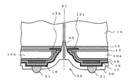
04bの間に、半導体チップ101が樹脂105a、105bを介して封止されている。第2のガラス基板104bの一主面上、即ちBGA型の半導体装置100の裏面上には、ボール状の端子(以下、導電端子111と称す)が格子状に複数配置されている。この導電端子111は、第2の配線109を介して半導体チップ101へと接続される。複数の第2の配線109には、それぞれ半導体チップ101の内部から引き出されたアルミニウム配線が接続されており、各導電端子111と半導体チップ101との電気的接続がなされている。
9と接続されている。この第2の配線109は、第1の配線103の一端から第2のガラス基板104bの表面に延在している。そして、第2のガラス基板104b上に延在した第2の配線109上には、ボール状の導電端子111が形成されている。
4bが接着された半導体ウェハをダイシングラインに沿って個々の半導体チップに分割する際、切削のためのダイシングブレードを、ダイシングラインの中心に位置合せする。しかしながら、従来より、そのような位置合せを正確に行うことは困難であった。その結果ダイシングの際の切削精度が低下するという問題が生じていた。
ットエッチング(もしくはディップエッチング)を行う。
ータとのずれ量を補正して算出される)に基づいて決定される。もしくは、センターライン61,62の位置は、1本のダイシング領域60上の複数箇所におけるアラインメントマークの位置の平均値を取った検出結果(予め不図示の記憶手段が持っている初期値データとのずれ量を補正して算出される)に基づいて決定される。
20を形成する。ここで、例えば、半導体ウェハ10の裏面を上方に向けた後、有機樹脂の回転塗布により、切削溝40内を含む半導体ウェハ10の裏面全体に、当該有機樹脂を行きわたらせる。これにより、切削溝40内に露出する全ての層、即ち、第2の絶縁膜16、半導体ウェハ10、第1の絶縁膜12、樹脂15及びガラス基板14の露出面が保護膜20によって覆われる。
12 第1の絶縁膜 14 ガラス基板 15 樹脂
16 第2の絶縁膜 17 緩衝部材
18,18a,18b 第2の配線 8a,8b 端部
19 メッキ膜 20 保護膜 21 導電端子
30 ウィンドウ 40 切削溝
51a,51b,52a,52c アラインメントマーク
60 ダイシング領域 61,62 センターライン
Claims (9)
- 半導体ウェハの表面に画定されたダイシング領域に沿って1対のパッドが配置され、前記半導体ウェハの裏面において前記1対のパッドに対応する位置に限り、当該1対のパッドを露出し得るように開口されたウィンドウが形成され、かつ前記半導体ウェハの表面に支持体が貼り付けられて成る積層体を、前記ダイシング領域に沿ってブレードを移動させながら、前記半導体ウェハの裏面から前記支持体の厚さ方向の途中まで達するように切削して、当該積層体に切削溝を形成する半導体装置の製造方法であって、
前記半導体ウェハの裏面における前記ダイシング領域の両側に、当該ダイシング領域を挟むようにして互いに対向する1対のアラインメントマークを形成し、当該1対のアラインメントマークの位置を認識手段により検出し、当該検出結果に基づいて前記ダイシング領域のセンターラインを求め、当該センターライン上にブレードの位置を合わせて切削を行い、前記ウィンドウが形成された前記半導体ウェハの裏面側から前記支持体の厚さ方向の途中まで達する切削溝を形成する工程と、
前記切削溝を形成した後の工程において、
前記1対のアラインメントマークの位置を認識手段により検出し、当該検出結果に基づいて前記ダイシング領域のセンターラインを求め、当該センターライン上にブレードの位置を合わせて、前記半導体ウェハの裏面から切削を行うことにより、前記積層体を個々の半導体チップに分離することを特徴とする半導体装置の製造方法。 - 前記1対のアライメントマークが複数形成され、当該複数の1対のアライメントマークの位置を前記認識手段により検出し、前記複数の1対のアライメントマークの位置の平均値に基づいて前記ダイシング領域のセンターラインを求めることを特徴とする請求項1記載の半導体装置の製造方法。
- 前記アラインメントマークは、半導体装置の製造工程で用いられる材料により形成され
ることを特徴とする請求項1または請求項2に記載の半導体装置の製造方法。 - 前記アラインメントマークは、エッチングによって形成される突起もしくは窪み、または金属層であることを特徴とする請求項1,2,3のうちいずれか1項に記載の半導体装置の製造方法。
- 半導体チップの表面に画定されたダイシング領域に沿って配置されたパッドと、前記半導体チップの裏面において前記パッドに対応する位置に限り、当該半導体チップを開口するウィンドウを介して前記パッドと接続され、前記半導体チップの裏面に延在した配線と、前記半導体チップの表面に貼り付けられ、その厚さ方向の途中まで達する切削溝を有する支持体と、前記支持体の側面のうち、少なくとも切削溝が形成された部分及び配線を被覆する保護層と、前記半導体チップの裏面における前記ダイシング領域に沿って形成されたアラインメントマークと、を具備し、
前記半導体チップは第1,第2,第3及び第4の角部を有し、
前記ダイシング領域は、前記第1の角部から前記第2の角部への方向と平行な第1の方向のダイシング領域と、
前記第1の角部から前記第3の角部への方向と平行であって、前記第1の方向のダイシング領域と直交する第2のダイシング領域とから成り、
前記アライメントマークは前記半導体チップの前記第1,第2,及び第3の角部に形成され、
前記第1の角部に形成されたアライメントマークは、前記第1及び第2の方向のダイシング領域のそれぞれの方向に沿って形成され、
前記第1の角部の対角にある第4の角部にアライメントマークが形成されておらず、
前記第2の角部に形成されたアライメントマークは、前記第2の方向のダイシング領域に沿って形成され、
前記第3の角部に形成されたアライメントマークは、前記第1の方向のダイシング領域に沿って形成されていることを特徴とする半導体装置。 - 前記アラインメントマークは、半導体装置の製造工程で用いられる材料により形成されることを特徴とする請求項5に記載の半導体装置。
- 前記アラインメントマークは、エッチングによって形成される突起もしくは窪み、または金属層であることを特徴とする請求項5または請求項6に記載の半導体装置。
- 前記ダイシング領域は、第1の方向のダイシング領域と、前記第1の方向のダイシング領域と直交する第2のダイシング領域とから成り、
前記1対のアライメントマークは、前記第1の方向のダイシング領域の両側に、当該ダイシング領域を挟むようにして互いに対向する第1の1対のアライメントマークと、前記第2の方向のダイシング領域の両側に、当該ダイシング領域を挟むようにして向かい合う第2の1対のアライメントマークとを有し、
前記第1及び第2の1対のアライメントマークは分割される個々の半導体チップの角部に形成されており、
前記個々の半導体チップの一部の角部にはアライメントマークが形成されていないことを特徴とする請求項1に記載の半導体装置の製造方法。 - 前記請求項8に記載された半導体装置の製造方法によって個々に分割された半導体装置。
Priority Applications (7)
| Application Number | Priority Date | Filing Date | Title |
|---|---|---|---|
| JP2004062323A JP4753170B2 (ja) | 2004-03-05 | 2004-03-05 | 半導体装置及びその製造方法 |
| TW094104769A TWI288956B (en) | 2004-03-05 | 2005-02-18 | Semiconductor device and manufacturing method thereof |
| US11/069,061 US7456083B2 (en) | 2004-03-05 | 2005-03-02 | Semiconductor device and manufacturing method of the same |
| CNB2005100530225A CN100446187C (zh) | 2004-03-05 | 2005-03-04 | 半导体装置及其制造方法 |
| KR1020050018007A KR100682003B1 (ko) | 2004-03-05 | 2005-03-04 | 반도체 장치 및 그 제조 방법 |
| SG200501359A SG114787A1 (en) | 2004-03-05 | 2005-03-05 | Semiconductor device and manufacturing method of the same |
| EP05004918A EP1575086A3 (en) | 2004-03-05 | 2005-03-07 | Semiconductor device and manufacturing method of the same, including a dicing step |
Applications Claiming Priority (1)
| Application Number | Priority Date | Filing Date | Title |
|---|---|---|---|
| JP2004062323A JP4753170B2 (ja) | 2004-03-05 | 2004-03-05 | 半導体装置及びその製造方法 |
Related Child Applications (1)
| Application Number | Title | Priority Date | Filing Date |
|---|---|---|---|
| JP2010127140A Division JP2010199625A (ja) | 2010-06-02 | 2010-06-02 | 半導体装置及びその製造方法 |
Publications (3)
| Publication Number | Publication Date |
|---|---|
| JP2005252078A JP2005252078A (ja) | 2005-09-15 |
| JP2005252078A5 JP2005252078A5 (ja) | 2007-04-19 |
| JP4753170B2 true JP4753170B2 (ja) | 2011-08-24 |
Family
ID=34824512
Family Applications (1)
| Application Number | Title | Priority Date | Filing Date |
|---|---|---|---|
| JP2004062323A Expired - Fee Related JP4753170B2 (ja) | 2004-03-05 | 2004-03-05 | 半導体装置及びその製造方法 |
Country Status (7)
| Country | Link |
|---|---|
| US (1) | US7456083B2 (ja) |
| EP (1) | EP1575086A3 (ja) |
| JP (1) | JP4753170B2 (ja) |
| KR (1) | KR100682003B1 (ja) |
| CN (1) | CN100446187C (ja) |
| SG (1) | SG114787A1 (ja) |
| TW (1) | TWI288956B (ja) |
Families Citing this family (41)
| Publication number | Priority date | Publication date | Assignee | Title |
|---|---|---|---|---|
| TWI232560B (en) | 2002-04-23 | 2005-05-11 | Sanyo Electric Co | Semiconductor device and its manufacture |
| TWI229435B (en) * | 2002-06-18 | 2005-03-11 | Sanyo Electric Co | Manufacture of semiconductor device |
| TWI227550B (en) * | 2002-10-30 | 2005-02-01 | Sanyo Electric Co | Semiconductor device manufacturing method |
| JP4401181B2 (ja) * | 2003-08-06 | 2010-01-20 | 三洋電機株式会社 | 半導体装置及びその製造方法 |
| JP3962713B2 (ja) * | 2003-09-30 | 2007-08-22 | キヤノン株式会社 | アライメントマークの形成方法、およびデバイスが構成される基板 |
| JP4322181B2 (ja) * | 2004-07-29 | 2009-08-26 | 三洋電機株式会社 | 半導体装置の製造方法 |
| US20060258051A1 (en) * | 2005-05-10 | 2006-11-16 | Texas Instruments Incorporated | Method and system for solder die attach |
| KR100652435B1 (ko) * | 2005-10-07 | 2006-12-01 | 삼성전자주식회사 | 첫 번째 다이의 위치를 구분할 수 있는 표시수단을구비하는 웨이퍼 및 웨이퍼의 다이 부착 방법 |
| US8153464B2 (en) * | 2005-10-18 | 2012-04-10 | International Rectifier Corporation | Wafer singulation process |
| TWI324800B (en) | 2005-12-28 | 2010-05-11 | Sanyo Electric Co | Method for manufacturing semiconductor device |
| TW200737506A (en) * | 2006-03-07 | 2007-10-01 | Sanyo Electric Co | Semiconductor device and manufacturing method of the same |
| JP2007329153A (ja) * | 2006-06-06 | 2007-12-20 | Fujitsu Ltd | デバイスの製造方法、ダイシング方法、およびダイシング装置 |
| TWI367557B (en) | 2006-08-11 | 2012-07-01 | Sanyo Electric Co | Semiconductor device and manufaturing method thereof |
| JP5076407B2 (ja) * | 2006-09-05 | 2012-11-21 | ミツミ電機株式会社 | 半導体装置及びその製造方法 |
| KR100784388B1 (ko) * | 2006-11-14 | 2007-12-11 | 삼성전자주식회사 | 반도체 패키지 및 제조방법 |
| JP5010247B2 (ja) | 2006-11-20 | 2012-08-29 | オンセミコンダクター・トレーディング・リミテッド | 半導体装置及びその製造方法 |
| US7569409B2 (en) * | 2007-01-04 | 2009-08-04 | Visera Technologies Company Limited | Isolation structures for CMOS image sensor chip scale packages |
| US7679167B2 (en) * | 2007-01-08 | 2010-03-16 | Visera Technologies Company, Limited | Electronic assembly for image sensor device and fabrication method thereof |
| JP2008294405A (ja) * | 2007-04-25 | 2008-12-04 | Sanyo Electric Co Ltd | 半導体装置及びその製造方法 |
| JP2008288285A (ja) * | 2007-05-15 | 2008-11-27 | Sharp Corp | 積層基板の切断方法、半導体装置の製造方法、半導体装置、発光装置及びバックライト装置 |
| DE102007030284B4 (de) * | 2007-06-29 | 2009-12-31 | Schott Ag | Verfahren zum Verpacken von Halbleiter-Bauelementen und verfahrensgemäß hergestelltes Zwischenprodukt |
| US8338267B2 (en) * | 2007-07-11 | 2012-12-25 | Sematech, Inc. | Systems and methods for vertically integrating semiconductor devices |
| WO2009007930A2 (en) * | 2007-07-12 | 2009-01-15 | Nxp B.V. | Integrated circuits on a wafer and method for separating integrated circuits on a wafer |
| TWI375321B (en) * | 2007-08-24 | 2012-10-21 | Xintec Inc | Electronic device wafer level scale packages and fabrication methods thereof |
| CN101950729B (zh) * | 2007-09-05 | 2012-09-26 | 精材科技股份有限公司 | 电子元件的晶圆级封装及其制造方法 |
| JP2010103300A (ja) * | 2008-10-23 | 2010-05-06 | Sanyo Electric Co Ltd | 半導体装置及びその製造方法 |
| US8289388B2 (en) * | 2009-05-14 | 2012-10-16 | Asm Assembly Automation Ltd | Alignment method for singulation system |
| CN102800656B (zh) * | 2011-05-20 | 2015-11-25 | 精材科技股份有限公司 | 晶片封装体、晶片封装体的形成方法以及封装晶圆 |
| DE102011112659B4 (de) * | 2011-09-06 | 2022-01-27 | Vishay Semiconductor Gmbh | Oberflächenmontierbares elektronisches Bauelement |
| JP6096442B2 (ja) * | 2012-09-10 | 2017-03-15 | ラピスセミコンダクタ株式会社 | 半導体装置および半導体装置の製造方法 |
| JP6193665B2 (ja) * | 2013-07-26 | 2017-09-06 | ルネサスエレクトロニクス株式会社 | 半導体装置の製造方法 |
| JP6257291B2 (ja) * | 2013-12-04 | 2018-01-10 | 株式会社ディスコ | パッケージ基板の加工方法 |
| CN104977745B (zh) * | 2015-06-24 | 2018-05-25 | 武汉华星光电技术有限公司 | 液晶显示面板用基板及液晶显示面板切割方法 |
| JP2017053999A (ja) * | 2015-09-09 | 2017-03-16 | 株式会社東芝 | 半導体装置および検査パターン配置方法 |
| JP6607639B2 (ja) * | 2015-12-24 | 2019-11-20 | 株式会社ディスコ | ウェーハの加工方法 |
| US10163954B2 (en) * | 2016-04-11 | 2018-12-25 | Omnivision Technologies, Inc. | Trenched device wafer, stepped-sidewall device die, and associated method |
| JP2019054172A (ja) * | 2017-09-15 | 2019-04-04 | 東芝メモリ株式会社 | 半導体装置 |
| JP7075652B2 (ja) * | 2017-12-28 | 2022-05-26 | 三星ダイヤモンド工業株式会社 | スクライブ装置およびスクライブ方法 |
| DE102019204457B4 (de) * | 2019-03-29 | 2024-01-25 | Disco Corporation | Substratbearbeitungsverfahren |
| CN110549351B (zh) * | 2019-09-19 | 2020-10-30 | 中国科学院合肥物质科学研究院 | 一种物料氧化层打磨机器人控制系统及其控制方法 |
| CN111128966A (zh) * | 2019-12-25 | 2020-05-08 | 华天科技(昆山)电子有限公司 | 对位结构及封装切割方法 |
Family Cites Families (20)
| Publication number | Priority date | Publication date | Assignee | Title |
|---|---|---|---|---|
| JPS6030314A (ja) | 1983-07-08 | 1985-02-15 | 富士通株式会社 | ダイシング装置 |
| JPH04177715A (ja) * | 1990-11-10 | 1992-06-24 | Fujitsu Ltd | 半導体装置 |
| US5777392A (en) | 1995-03-28 | 1998-07-07 | Nec Corporation | Semiconductor device having improved alignment marks |
| JP2666761B2 (ja) | 1995-03-28 | 1997-10-22 | 日本電気株式会社 | 半導体ウェハ |
| KR970008386A (ko) * | 1995-07-07 | 1997-02-24 | 하라 세이지 | 기판의 할단(割斷)방법 및 그 할단장치 |
| IL123207A0 (en) * | 1998-02-06 | 1998-09-24 | Shellcase Ltd | Integrated circuit device |
| US6271102B1 (en) | 1998-02-27 | 2001-08-07 | International Business Machines Corporation | Method and system for dicing wafers, and semiconductor structures incorporating the products thereof |
| JP3065309B1 (ja) * | 1999-03-11 | 2000-07-17 | 沖電気工業株式会社 | 半導体装置の製造方法 |
| WO2001009927A1 (en) * | 1999-07-28 | 2001-02-08 | Infineon Technologies North America Corp. | Semiconductor structures and manufacturing methods |
| US6309943B1 (en) * | 2000-04-25 | 2001-10-30 | Amkor Technology, Inc. | Precision marking and singulation method |
| US6579738B2 (en) * | 2000-12-15 | 2003-06-17 | Micron Technology, Inc. | Method of alignment for buried structures formed by surface transformation of empty spaces in solid state materials |
| US6869861B1 (en) * | 2001-03-08 | 2005-03-22 | Amkor Technology, Inc. | Back-side wafer singulation method |
| JP3603828B2 (ja) * | 2001-05-28 | 2004-12-22 | 富士ゼロックス株式会社 | インクジェット式記録ヘッド及びその製造方法並びにインクジェット式記録装置 |
| JP3872319B2 (ja) * | 2001-08-21 | 2007-01-24 | 沖電気工業株式会社 | 半導体装置及びその製造方法 |
| JP2003100666A (ja) * | 2001-09-26 | 2003-04-04 | Toshiba Corp | 半導体装置の製造方法 |
| JP2004006820A (ja) * | 2002-04-23 | 2004-01-08 | Sanyo Electric Co Ltd | 半導体装置及びその製造方法 |
| JP3877700B2 (ja) * | 2002-04-23 | 2007-02-07 | 三洋電機株式会社 | 半導体装置及びその製造方法 |
| JP2003347476A (ja) * | 2002-05-22 | 2003-12-05 | Sanyo Electric Co Ltd | 半導体集積装置及びその製造方法 |
| CN2552163Y (zh) * | 2002-05-23 | 2003-05-21 | 立卫科技股份有限公司 | 封装切单的辨识点电镀线的结构 |
| JP3796202B2 (ja) * | 2002-07-05 | 2006-07-12 | 三洋電機株式会社 | 半導体集積装置の製造方法 |
-
2004
- 2004-03-05 JP JP2004062323A patent/JP4753170B2/ja not_active Expired - Fee Related
-
2005
- 2005-02-18 TW TW094104769A patent/TWI288956B/zh not_active IP Right Cessation
- 2005-03-02 US US11/069,061 patent/US7456083B2/en active Active
- 2005-03-04 KR KR1020050018007A patent/KR100682003B1/ko not_active IP Right Cessation
- 2005-03-04 CN CNB2005100530225A patent/CN100446187C/zh not_active Expired - Fee Related
- 2005-03-05 SG SG200501359A patent/SG114787A1/en unknown
- 2005-03-07 EP EP05004918A patent/EP1575086A3/en not_active Withdrawn
Also Published As
| Publication number | Publication date |
|---|---|
| US20050208735A1 (en) | 2005-09-22 |
| EP1575086A3 (en) | 2006-06-14 |
| TWI288956B (en) | 2007-10-21 |
| KR20060043788A (ko) | 2006-05-15 |
| JP2005252078A (ja) | 2005-09-15 |
| SG114787A1 (en) | 2005-09-28 |
| CN100446187C (zh) | 2008-12-24 |
| CN1664991A (zh) | 2005-09-07 |
| KR100682003B1 (ko) | 2007-02-15 |
| EP1575086A2 (en) | 2005-09-14 |
| TW200535941A (en) | 2005-11-01 |
| US7456083B2 (en) | 2008-11-25 |
Similar Documents
| Publication | Publication Date | Title |
|---|---|---|
| JP4753170B2 (ja) | 半導体装置及びその製造方法 | |
| JP3739375B2 (ja) | 半導体装置及びその製造方法 | |
| JP4934053B2 (ja) | 半導体装置およびその製造方法 | |
| JP4401181B2 (ja) | 半導体装置及びその製造方法 | |
| KR100543481B1 (ko) | 반도체 장치 및 그 제조 방법 | |
| US6759745B2 (en) | Semiconductor device and manufacturing method thereof | |
| KR101397203B1 (ko) | 반도체 장치 | |
| JP4379102B2 (ja) | 半導体装置の製造方法 | |
| KR20040092435A (ko) | 반도체 장치 및 그 제조 방법 | |
| US7759808B2 (en) | Semiconductor substrate including first and second recognition marks and method for manufacturing semiconductor device | |
| KR20060048058A (ko) | 반도체 장치 및 그 제조 방법 | |
| JP2003086762A (ja) | 半導体装置及びその製造方法 | |
| JP4334397B2 (ja) | 半導体装置及びその製造方法 | |
| KR101059625B1 (ko) | 웨이퍼 레벨 칩 스케일 패키지 및 그 제조방법 | |
| JP2010199625A (ja) | 半導体装置及びその製造方法 | |
| JP4737995B2 (ja) | 半導体装置 | |
| JP2002026064A (ja) | 半導体素子のボンディングパッド構造体及びその製造方法 | |
| JP2010016395A5 (ja) | ||
| JP4522213B2 (ja) | 半導体装置の製造方法 | |
| US11688715B2 (en) | Semiconductor die with multiple contact pads electrically coupled to a lead of a lead frame | |
| JP4805362B2 (ja) | 半導体装置の製造方法 | |
| JP2003188333A (ja) | 半導体装置およびその製造方法 | |
| JP5188039B2 (ja) | 半導体装置及び半導体構成体並びにそれらの製造方法 | |
| JP4597182B2 (ja) | 半導体装置及びその製造方法 | |
| JP2008294318A (ja) | 半導体装置およびその製造方法 |
Legal Events
| Date | Code | Title | Description |
|---|---|---|---|
| A521 | Request for written amendment filed |
Free format text: JAPANESE INTERMEDIATE CODE: A523 Effective date: 20070302 |
|
| A621 | Written request for application examination |
Free format text: JAPANESE INTERMEDIATE CODE: A621 Effective date: 20070302 |
|
| A977 | Report on retrieval |
Free format text: JAPANESE INTERMEDIATE CODE: A971007 Effective date: 20091215 |
|
| A131 | Notification of reasons for refusal |
Free format text: JAPANESE INTERMEDIATE CODE: A131 Effective date: 20091218 |
|
| A521 | Request for written amendment filed |
Free format text: JAPANESE INTERMEDIATE CODE: A523 Effective date: 20100210 |
|
| A02 | Decision of refusal |
Free format text: JAPANESE INTERMEDIATE CODE: A02 Effective date: 20100304 |
|
| A521 | Request for written amendment filed |
Free format text: JAPANESE INTERMEDIATE CODE: A523 Effective date: 20100602 |
|
| A911 | Transfer to examiner for re-examination before appeal (zenchi) |
Free format text: JAPANESE INTERMEDIATE CODE: A911 Effective date: 20100611 |
|
| A912 | Re-examination (zenchi) completed and case transferred to appeal board |
Free format text: JAPANESE INTERMEDIATE CODE: A912 Effective date: 20100702 |
|
| A521 | Request for written amendment filed |
Free format text: JAPANESE INTERMEDIATE CODE: A523 Effective date: 20110405 |
|
| A01 | Written decision to grant a patent or to grant a registration (utility model) |
Free format text: JAPANESE INTERMEDIATE CODE: A01 |
|
| A61 | First payment of annual fees (during grant procedure) |
Free format text: JAPANESE INTERMEDIATE CODE: A61 Effective date: 20110516 |
|
| FPAY | Renewal fee payment (event date is renewal date of database) |
Free format text: PAYMENT UNTIL: 20140603 Year of fee payment: 3 |
|
| FPAY | Renewal fee payment (event date is renewal date of database) |
Free format text: PAYMENT UNTIL: 20140603 Year of fee payment: 3 |
|
| A711 | Notification of change in applicant |
Free format text: JAPANESE INTERMEDIATE CODE: A711 Effective date: 20110614 |
|
| RD02 | Notification of acceptance of power of attorney |
Free format text: JAPANESE INTERMEDIATE CODE: A7422 Effective date: 20110614 |
|
| A521 | Request for written amendment filed |
Free format text: JAPANESE INTERMEDIATE CODE: A821 Effective date: 20110614 |
|
| A072 | Dismissal of procedure [no reply to invitation to correct request for examination] |
Free format text: JAPANESE INTERMEDIATE CODE: A072 Effective date: 20111114 |
|
| LAPS | Cancellation because of no payment of annual fees |