EP3244394A1 - Dispositif d'affichage à cristaux liquides et appareil électronique comprenant celui-ci - Google Patents
Dispositif d'affichage à cristaux liquides et appareil électronique comprenant celui-ci Download PDFInfo
- Publication number
- EP3244394A1 EP3244394A1 EP17173363.7A EP17173363A EP3244394A1 EP 3244394 A1 EP3244394 A1 EP 3244394A1 EP 17173363 A EP17173363 A EP 17173363A EP 3244394 A1 EP3244394 A1 EP 3244394A1
- Authority
- EP
- European Patent Office
- Prior art keywords
- layer
- oxide semiconductor
- transistor
- insulating layer
- oxide
- Prior art date
- Legal status (The legal status is an assumption and is not a legal conclusion. Google has not performed a legal analysis and makes no representation as to the accuracy of the status listed.)
- Withdrawn
Links
- 239000004973 liquid crystal related substance Substances 0.000 title claims abstract description 167
- 238000000034 method Methods 0.000 claims abstract description 127
- 239000004065 semiconductor Substances 0.000 claims description 495
- 239000003990 capacitor Substances 0.000 claims description 34
- 238000003860 storage Methods 0.000 claims description 23
- 239000011701 zinc Substances 0.000 claims description 10
- 229910052738 indium Inorganic materials 0.000 claims description 3
- APFVFJFRJDLVQX-UHFFFAOYSA-N indium atom Chemical compound [In] APFVFJFRJDLVQX-UHFFFAOYSA-N 0.000 claims description 3
- GYHNNYVSQQEPJS-UHFFFAOYSA-N Gallium Chemical compound [Ga] GYHNNYVSQQEPJS-UHFFFAOYSA-N 0.000 claims 1
- HCHKCACWOHOZIP-UHFFFAOYSA-N Zinc Chemical compound [Zn] HCHKCACWOHOZIP-UHFFFAOYSA-N 0.000 claims 1
- 229910052733 gallium Inorganic materials 0.000 claims 1
- 229910052725 zinc Inorganic materials 0.000 claims 1
- 239000010410 layer Substances 0.000 description 991
- 239000010408 film Substances 0.000 description 392
- 239000010409 thin film Substances 0.000 description 202
- 239000000758 substrate Substances 0.000 description 190
- 238000010438 heat treatment Methods 0.000 description 177
- 238000004544 sputter deposition Methods 0.000 description 132
- 239000007789 gas Substances 0.000 description 113
- 239000001257 hydrogen Substances 0.000 description 105
- 229910052739 hydrogen Inorganic materials 0.000 description 105
- 230000002829 reductive effect Effects 0.000 description 98
- VYPSYNLAJGMNEJ-UHFFFAOYSA-N silicon dioxide Inorganic materials O=[Si]=O VYPSYNLAJGMNEJ-UHFFFAOYSA-N 0.000 description 92
- UFHFLCQGNIYNRP-UHFFFAOYSA-N Hydrogen Chemical compound [H][H] UFHFLCQGNIYNRP-UHFFFAOYSA-N 0.000 description 87
- XKRFYHLGVUSROY-UHFFFAOYSA-N Argon Chemical compound [Ar] XKRFYHLGVUSROY-UHFFFAOYSA-N 0.000 description 82
- 229910052814 silicon oxide Inorganic materials 0.000 description 80
- 239000000463 material Substances 0.000 description 79
- 229910007541 Zn O Inorganic materials 0.000 description 67
- QVGXLLKOCUKJST-UHFFFAOYSA-N atomic oxygen Chemical compound [O] QVGXLLKOCUKJST-UHFFFAOYSA-N 0.000 description 67
- 239000001301 oxygen Substances 0.000 description 67
- 229910052760 oxygen Inorganic materials 0.000 description 67
- 239000010936 titanium Substances 0.000 description 66
- 230000015572 biosynthetic process Effects 0.000 description 65
- 239000012535 impurity Substances 0.000 description 65
- XUIMIQQOPSSXEZ-UHFFFAOYSA-N Silicon Chemical compound [Si] XUIMIQQOPSSXEZ-UHFFFAOYSA-N 0.000 description 61
- 239000012298 atmosphere Substances 0.000 description 61
- 229910052710 silicon Inorganic materials 0.000 description 61
- 239000010703 silicon Substances 0.000 description 61
- 229910052581 Si3N4 Inorganic materials 0.000 description 58
- HQVNEWCFYHHQES-UHFFFAOYSA-N silicon nitride Chemical compound N12[Si]34N5[Si]62N3[Si]51N64 HQVNEWCFYHHQES-UHFFFAOYSA-N 0.000 description 58
- 238000000151 deposition Methods 0.000 description 57
- 230000001681 protective effect Effects 0.000 description 56
- 229910052719 titanium Inorganic materials 0.000 description 55
- 230000008021 deposition Effects 0.000 description 54
- XLYOFNOQVPJJNP-UHFFFAOYSA-N water Substances O XLYOFNOQVPJJNP-UHFFFAOYSA-N 0.000 description 54
- 230000006870 function Effects 0.000 description 53
- RTAQQCXQSZGOHL-UHFFFAOYSA-N Titanium Chemical compound [Ti] RTAQQCXQSZGOHL-UHFFFAOYSA-N 0.000 description 50
- 238000005530 etching Methods 0.000 description 49
- 229910052782 aluminium Inorganic materials 0.000 description 42
- 238000000206 photolithography Methods 0.000 description 42
- 229910052786 argon Inorganic materials 0.000 description 41
- 238000004519 manufacturing process Methods 0.000 description 41
- 230000003247 decreasing effect Effects 0.000 description 40
- IJGRMHOSHXDMSA-UHFFFAOYSA-N Atomic nitrogen Chemical compound N#N IJGRMHOSHXDMSA-UHFFFAOYSA-N 0.000 description 39
- XAGFODPZIPBFFR-UHFFFAOYSA-N aluminium Chemical compound [Al] XAGFODPZIPBFFR-UHFFFAOYSA-N 0.000 description 38
- 150000002431 hydrogen Chemical class 0.000 description 34
- 229910052721 tungsten Inorganic materials 0.000 description 33
- 238000010586 diagram Methods 0.000 description 29
- 239000011521 glass Substances 0.000 description 29
- 239000000956 alloy Substances 0.000 description 28
- 125000002887 hydroxy group Chemical group [H]O* 0.000 description 27
- 239000010937 tungsten Substances 0.000 description 27
- 229910052750 molybdenum Inorganic materials 0.000 description 25
- 229910045601 alloy Inorganic materials 0.000 description 23
- 239000002356 single layer Substances 0.000 description 23
- 239000011651 chromium Substances 0.000 description 22
- 150000004678 hydrides Chemical class 0.000 description 21
- 230000015654 memory Effects 0.000 description 21
- 239000012299 nitrogen atmosphere Substances 0.000 description 21
- WFKWXMTUELFFGS-UHFFFAOYSA-N tungsten Chemical compound [W] WFKWXMTUELFFGS-UHFFFAOYSA-N 0.000 description 21
- MHAJPDPJQMAIIY-UHFFFAOYSA-N Hydrogen peroxide Chemical compound OO MHAJPDPJQMAIIY-UHFFFAOYSA-N 0.000 description 20
- ZOKXTWBITQBERF-UHFFFAOYSA-N Molybdenum Chemical compound [Mo] ZOKXTWBITQBERF-UHFFFAOYSA-N 0.000 description 20
- 230000008859 change Effects 0.000 description 20
- 150000001875 compounds Chemical class 0.000 description 20
- 239000000203 mixture Substances 0.000 description 20
- 239000011733 molybdenum Substances 0.000 description 20
- 239000000969 carrier Substances 0.000 description 19
- 239000011261 inert gas Substances 0.000 description 19
- 229910052757 nitrogen Inorganic materials 0.000 description 19
- 230000008569 process Effects 0.000 description 19
- 239000010949 copper Substances 0.000 description 18
- 229910052802 copper Inorganic materials 0.000 description 17
- 229910052804 chromium Inorganic materials 0.000 description 16
- 229910052715 tantalum Inorganic materials 0.000 description 16
- 229910044991 metal oxide Inorganic materials 0.000 description 15
- 150000004706 metal oxides Chemical class 0.000 description 15
- 230000018044 dehydration Effects 0.000 description 14
- 238000006297 dehydration reaction Methods 0.000 description 14
- 238000006356 dehydrogenation reaction Methods 0.000 description 14
- 125000004435 hydrogen atom Chemical group [H]* 0.000 description 14
- 108010083687 Ion Pumps Proteins 0.000 description 13
- 230000007274 generation of a signal involved in cell-cell signaling Effects 0.000 description 13
- 238000000859 sublimation Methods 0.000 description 13
- 230000008022 sublimation Effects 0.000 description 13
- QTBSBXVTEAMEQO-UHFFFAOYSA-N Acetic acid Chemical compound CC(O)=O QTBSBXVTEAMEQO-UHFFFAOYSA-N 0.000 description 12
- 150000004767 nitrides Chemical class 0.000 description 12
- VYZAMTAEIAYCRO-UHFFFAOYSA-N Chromium Chemical compound [Cr] VYZAMTAEIAYCRO-UHFFFAOYSA-N 0.000 description 11
- XLOMVQKBTHCTTD-UHFFFAOYSA-N Zinc monoxide Chemical compound [Zn]=O XLOMVQKBTHCTTD-UHFFFAOYSA-N 0.000 description 11
- 229910052799 carbon Inorganic materials 0.000 description 11
- 239000001307 helium Substances 0.000 description 11
- 229910052734 helium Inorganic materials 0.000 description 11
- SWQJXJOGLNCZEY-UHFFFAOYSA-N helium atom Chemical compound [He] SWQJXJOGLNCZEY-UHFFFAOYSA-N 0.000 description 11
- 230000007257 malfunction Effects 0.000 description 11
- TWNQGVIAIRXVLR-UHFFFAOYSA-N oxo(oxoalumanyloxy)alumane Chemical compound O=[Al]O[Al]=O TWNQGVIAIRXVLR-UHFFFAOYSA-N 0.000 description 11
- 238000001552 radio frequency sputter deposition Methods 0.000 description 11
- GUVRBAGPIYLISA-UHFFFAOYSA-N tantalum atom Chemical compound [Ta] GUVRBAGPIYLISA-UHFFFAOYSA-N 0.000 description 11
- -1 tungsten nitride Chemical class 0.000 description 11
- VHUUQVKOLVNVRT-UHFFFAOYSA-N Ammonium hydroxide Chemical compound [NH4+].[OH-] VHUUQVKOLVNVRT-UHFFFAOYSA-N 0.000 description 10
- MYMOFIZGZYHOMD-UHFFFAOYSA-N Dioxygen Chemical compound O=O MYMOFIZGZYHOMD-UHFFFAOYSA-N 0.000 description 10
- 229910052779 Neodymium Inorganic materials 0.000 description 10
- 235000011114 ammonium hydroxide Nutrition 0.000 description 10
- PMHQVHHXPFUNSP-UHFFFAOYSA-M copper(1+);methylsulfanylmethane;bromide Chemical compound Br[Cu].CSC PMHQVHHXPFUNSP-UHFFFAOYSA-M 0.000 description 10
- 229910001882 dioxygen Inorganic materials 0.000 description 10
- QEFYFXOXNSNQGX-UHFFFAOYSA-N neodymium atom Chemical compound [Nd] QEFYFXOXNSNQGX-UHFFFAOYSA-N 0.000 description 10
- 238000009832 plasma treatment Methods 0.000 description 10
- 239000010453 quartz Substances 0.000 description 10
- 229910052706 scandium Inorganic materials 0.000 description 10
- SIXSYDAISGFNSX-UHFFFAOYSA-N scandium atom Chemical compound [Sc] SIXSYDAISGFNSX-UHFFFAOYSA-N 0.000 description 10
- NRTOMJZYCJJWKI-UHFFFAOYSA-N Titanium nitride Chemical compound [Ti]#N NRTOMJZYCJJWKI-UHFFFAOYSA-N 0.000 description 9
- 125000004429 atom Chemical group 0.000 description 9
- QVQLCTNNEUAWMS-UHFFFAOYSA-N barium oxide Chemical compound [Ba]=O QVQLCTNNEUAWMS-UHFFFAOYSA-N 0.000 description 9
- 229910052751 metal Inorganic materials 0.000 description 9
- 239000002184 metal Substances 0.000 description 9
- 238000005268 plasma chemical vapour deposition Methods 0.000 description 9
- 238000001039 wet etching Methods 0.000 description 9
- NBIIXXVUZAFLBC-UHFFFAOYSA-N Phosphoric acid Chemical compound OP(O)(O)=O NBIIXXVUZAFLBC-UHFFFAOYSA-N 0.000 description 8
- PJXISJQVUVHSOJ-UHFFFAOYSA-N indium(III) oxide Inorganic materials [O-2].[O-2].[O-2].[In+3].[In+3] PJXISJQVUVHSOJ-UHFFFAOYSA-N 0.000 description 8
- 238000004151 rapid thermal annealing Methods 0.000 description 8
- VZGDMQKNWNREIO-UHFFFAOYSA-N tetrachloromethane Chemical compound ClC(Cl)(Cl)Cl VZGDMQKNWNREIO-UHFFFAOYSA-N 0.000 description 8
- OKTJSMMVPCPJKN-UHFFFAOYSA-N Carbon Chemical compound [C] OKTJSMMVPCPJKN-UHFFFAOYSA-N 0.000 description 7
- 229910020923 Sn-O Inorganic materials 0.000 description 7
- 238000001312 dry etching Methods 0.000 description 7
- 238000007667 floating Methods 0.000 description 7
- 230000005855 radiation Effects 0.000 description 7
- 230000002441 reversible effect Effects 0.000 description 7
- 238000001004 secondary ion mass spectrometry Methods 0.000 description 7
- QGZKDVFQNNGYKY-UHFFFAOYSA-N Ammonia Chemical compound N QGZKDVFQNNGYKY-UHFFFAOYSA-N 0.000 description 6
- ZAMOUSCENKQFHK-UHFFFAOYSA-N Chlorine atom Chemical compound [Cl] ZAMOUSCENKQFHK-UHFFFAOYSA-N 0.000 description 6
- RYGMFSIKBFXOCR-UHFFFAOYSA-N Copper Chemical compound [Cu] RYGMFSIKBFXOCR-UHFFFAOYSA-N 0.000 description 6
- XPDWGBQVDMORPB-UHFFFAOYSA-N Fluoroform Chemical compound FC(F)F XPDWGBQVDMORPB-UHFFFAOYSA-N 0.000 description 6
- 239000000908 ammonium hydroxide Substances 0.000 description 6
- 230000004888 barrier function Effects 0.000 description 6
- 239000000460 chlorine Substances 0.000 description 6
- 229910052801 chlorine Inorganic materials 0.000 description 6
- 238000004891 communication Methods 0.000 description 6
- 150000001879 copper Chemical class 0.000 description 6
- JKWMSGQKBLHBQQ-UHFFFAOYSA-N diboron trioxide Chemical compound O=BOB=O JKWMSGQKBLHBQQ-UHFFFAOYSA-N 0.000 description 6
- 239000000428 dust Substances 0.000 description 6
- 238000011049 filling Methods 0.000 description 6
- 239000007788 liquid Substances 0.000 description 6
- 239000007769 metal material Substances 0.000 description 6
- 229910052754 neon Inorganic materials 0.000 description 6
- GKAOGPIIYCISHV-UHFFFAOYSA-N neon atom Chemical compound [Ne] GKAOGPIIYCISHV-UHFFFAOYSA-N 0.000 description 6
- 230000003287 optical effect Effects 0.000 description 6
- 230000003071 parasitic effect Effects 0.000 description 6
- 239000000565 sealant Substances 0.000 description 6
- 239000002699 waste material Substances 0.000 description 6
- 229910021417 amorphous silicon Inorganic materials 0.000 description 5
- 239000012300 argon atmosphere Substances 0.000 description 5
- 239000013078 crystal Substances 0.000 description 5
- 238000002425 crystallisation Methods 0.000 description 5
- 230000008025 crystallization Effects 0.000 description 5
- 230000007547 defect Effects 0.000 description 5
- 230000006866 deterioration Effects 0.000 description 5
- KPUWHANPEXNPJT-UHFFFAOYSA-N disiloxane Chemical class [SiH3]O[SiH3] KPUWHANPEXNPJT-UHFFFAOYSA-N 0.000 description 5
- 230000005684 electric field Effects 0.000 description 5
- 238000005259 measurement Methods 0.000 description 5
- 239000002245 particle Substances 0.000 description 5
- 229910021420 polycrystalline silicon Inorganic materials 0.000 description 5
- 238000012545 processing Methods 0.000 description 5
- 239000011347 resin Substances 0.000 description 5
- 229920005989 resin Polymers 0.000 description 5
- 230000003068 static effect Effects 0.000 description 5
- 239000011787 zinc oxide Substances 0.000 description 5
- YCKRFDGAMUMZLT-UHFFFAOYSA-N Fluorine atom Chemical compound [F] YCKRFDGAMUMZLT-UHFFFAOYSA-N 0.000 description 4
- FYYHWMGAXLPEAU-UHFFFAOYSA-N Magnesium Chemical compound [Mg] FYYHWMGAXLPEAU-UHFFFAOYSA-N 0.000 description 4
- GRYLNZFGIOXLOG-UHFFFAOYSA-N Nitric acid Chemical compound O[N+]([O-])=O GRYLNZFGIOXLOG-UHFFFAOYSA-N 0.000 description 4
- 239000004983 Polymer Dispersed Liquid Crystal Substances 0.000 description 4
- QCWXUUIWCKQGHC-UHFFFAOYSA-N Zirconium Chemical compound [Zr] QCWXUUIWCKQGHC-UHFFFAOYSA-N 0.000 description 4
- 229910000147 aluminium phosphate Inorganic materials 0.000 description 4
- 229910052790 beryllium Inorganic materials 0.000 description 4
- ATBAMAFKBVZNFJ-UHFFFAOYSA-N beryllium atom Chemical compound [Be] ATBAMAFKBVZNFJ-UHFFFAOYSA-N 0.000 description 4
- 239000005380 borophosphosilicate glass Substances 0.000 description 4
- 150000001721 carbon Chemical group 0.000 description 4
- 239000000919 ceramic Substances 0.000 description 4
- 238000006243 chemical reaction Methods 0.000 description 4
- 239000004020 conductor Substances 0.000 description 4
- 230000005611 electricity Effects 0.000 description 4
- 238000011156 evaluation Methods 0.000 description 4
- 239000005262 ferroelectric liquid crystals (FLCs) Substances 0.000 description 4
- 229910052731 fluorine Inorganic materials 0.000 description 4
- 239000011737 fluorine Substances 0.000 description 4
- QZQVBEXLDFYHSR-UHFFFAOYSA-N gallium(III) oxide Inorganic materials O=[Ga]O[Ga]=O QZQVBEXLDFYHSR-UHFFFAOYSA-N 0.000 description 4
- GPRLSGONYQIRFK-UHFFFAOYSA-N hydron Chemical compound [H+] GPRLSGONYQIRFK-UHFFFAOYSA-N 0.000 description 4
- XLYOFNOQVPJJNP-UHFFFAOYSA-M hydroxide Chemical compound [OH-] XLYOFNOQVPJJNP-UHFFFAOYSA-M 0.000 description 4
- 229910003437 indium oxide Inorganic materials 0.000 description 4
- 238000009616 inductively coupled plasma Methods 0.000 description 4
- 239000012212 insulator Substances 0.000 description 4
- 229910052749 magnesium Inorganic materials 0.000 description 4
- 239000011777 magnesium Substances 0.000 description 4
- WPBNNNQJVZRUHP-UHFFFAOYSA-L manganese(2+);methyl n-[[2-(methoxycarbonylcarbamothioylamino)phenyl]carbamothioyl]carbamate;n-[2-(sulfidocarbothioylamino)ethyl]carbamodithioate Chemical compound [Mn+2].[S-]C(=S)NCCNC([S-])=S.COC(=O)NC(=S)NC1=CC=CC=C1NC(=S)NC(=O)OC WPBNNNQJVZRUHP-UHFFFAOYSA-L 0.000 description 4
- 239000011159 matrix material Substances 0.000 description 4
- 229910017604 nitric acid Inorganic materials 0.000 description 4
- 239000011368 organic material Substances 0.000 description 4
- 239000005360 phosphosilicate glass Substances 0.000 description 4
- 238000001020 plasma etching Methods 0.000 description 4
- 239000004033 plastic Substances 0.000 description 4
- 229920003023 plastic Polymers 0.000 description 4
- 229920005591 polysilicon Polymers 0.000 description 4
- 230000009467 reduction Effects 0.000 description 4
- TXEYQDLBPFQVAA-UHFFFAOYSA-N tetrafluoromethane Chemical compound FC(F)(F)F TXEYQDLBPFQVAA-UHFFFAOYSA-N 0.000 description 4
- 238000001771 vacuum deposition Methods 0.000 description 4
- 229910052727 yttrium Inorganic materials 0.000 description 4
- VWQVUPCCIRVNHF-UHFFFAOYSA-N yttrium atom Chemical compound [Y] VWQVUPCCIRVNHF-UHFFFAOYSA-N 0.000 description 4
- 229910052726 zirconium Inorganic materials 0.000 description 4
- DGAQECJNVWCQMB-PUAWFVPOSA-M Ilexoside XXIX Chemical compound C[C@@H]1CC[C@@]2(CC[C@@]3(C(=CC[C@H]4[C@]3(CC[C@@H]5[C@@]4(CC[C@@H](C5(C)C)OS(=O)(=O)[O-])C)C)[C@@H]2[C@]1(C)O)C)C(=O)O[C@H]6[C@@H]([C@H]([C@@H]([C@H](O6)CO)O)O)O.[Na+] DGAQECJNVWCQMB-PUAWFVPOSA-M 0.000 description 3
- PXHVJJICTQNCMI-UHFFFAOYSA-N Nickel Chemical compound [Ni] PXHVJJICTQNCMI-UHFFFAOYSA-N 0.000 description 3
- 229910004304 SiNy Inorganic materials 0.000 description 3
- 239000005407 aluminoborosilicate glass Substances 0.000 description 3
- 239000005354 aluminosilicate glass Substances 0.000 description 3
- 229910021529 ammonia Inorganic materials 0.000 description 3
- 229910052788 barium Inorganic materials 0.000 description 3
- DSAJWYNOEDNPEQ-UHFFFAOYSA-N barium atom Chemical compound [Ba] DSAJWYNOEDNPEQ-UHFFFAOYSA-N 0.000 description 3
- 229910052796 boron Inorganic materials 0.000 description 3
- 229910052810 boron oxide Inorganic materials 0.000 description 3
- 239000005388 borosilicate glass Substances 0.000 description 3
- 238000004040 coloring Methods 0.000 description 3
- 230000007423 decrease Effects 0.000 description 3
- 238000013461 design Methods 0.000 description 3
- 230000000694 effects Effects 0.000 description 3
- 230000005669 field effect Effects 0.000 description 3
- 229910052736 halogen Inorganic materials 0.000 description 3
- 150000002367 halogens Chemical class 0.000 description 3
- 230000006872 improvement Effects 0.000 description 3
- QSHDDOUJBYECFT-UHFFFAOYSA-N mercury Chemical compound [Hg] QSHDDOUJBYECFT-UHFFFAOYSA-N 0.000 description 3
- 229910052753 mercury Inorganic materials 0.000 description 3
- 229910001507 metal halide Inorganic materials 0.000 description 3
- 150000005309 metal halides Chemical class 0.000 description 3
- BASFCYQUMIYNBI-UHFFFAOYSA-N platinum Chemical compound [Pt] BASFCYQUMIYNBI-UHFFFAOYSA-N 0.000 description 3
- 239000000843 powder Substances 0.000 description 3
- 238000005546 reactive sputtering Methods 0.000 description 3
- 229910052594 sapphire Inorganic materials 0.000 description 3
- 239000010980 sapphire Substances 0.000 description 3
- 239000011734 sodium Substances 0.000 description 3
- 229910052708 sodium Inorganic materials 0.000 description 3
- 125000006850 spacer group Chemical group 0.000 description 3
- 239000000126 substance Substances 0.000 description 3
- MZLGASXMSKOWSE-UHFFFAOYSA-N tantalum nitride Chemical compound [Ta]#N MZLGASXMSKOWSE-UHFFFAOYSA-N 0.000 description 3
- 238000002834 transmittance Methods 0.000 description 3
- 229910052724 xenon Inorganic materials 0.000 description 3
- FHNFHKCVQCLJFQ-UHFFFAOYSA-N xenon atom Chemical compound [Xe] FHNFHKCVQCLJFQ-UHFFFAOYSA-N 0.000 description 3
- UWCWUCKPEYNDNV-LBPRGKRZSA-N 2,6-dimethyl-n-[[(2s)-pyrrolidin-2-yl]methyl]aniline Chemical compound CC1=CC=CC(C)=C1NC[C@H]1NCCC1 UWCWUCKPEYNDNV-LBPRGKRZSA-N 0.000 description 2
- ZOXJGFHDIHLPTG-UHFFFAOYSA-N Boron Chemical compound [B] ZOXJGFHDIHLPTG-UHFFFAOYSA-N 0.000 description 2
- KZBUYRJDOAKODT-UHFFFAOYSA-N Chlorine Chemical compound ClCl KZBUYRJDOAKODT-UHFFFAOYSA-N 0.000 description 2
- 239000004593 Epoxy Substances 0.000 description 2
- CPELXLSAUQHCOX-UHFFFAOYSA-N Hydrogen bromide Chemical compound Br CPELXLSAUQHCOX-UHFFFAOYSA-N 0.000 description 2
- 239000004952 Polyamide Substances 0.000 description 2
- 239000004642 Polyimide Substances 0.000 description 2
- GWEVSGVZZGPLCZ-UHFFFAOYSA-N Titan oxide Chemical compound O=[Ti]=O GWEVSGVZZGPLCZ-UHFFFAOYSA-N 0.000 description 2
- NIXOWILDQLNWCW-UHFFFAOYSA-N acrylic acid group Chemical group C(C=C)(=O)O NIXOWILDQLNWCW-UHFFFAOYSA-N 0.000 description 2
- 230000002411 adverse Effects 0.000 description 2
- 239000003570 air Substances 0.000 description 2
- UMIVXZPTRXBADB-UHFFFAOYSA-N benzocyclobutene Chemical compound C1=CC=C2CCC2=C1 UMIVXZPTRXBADB-UHFFFAOYSA-N 0.000 description 2
- 230000000903 blocking effect Effects 0.000 description 2
- 238000005229 chemical vapour deposition Methods 0.000 description 2
- 230000003098 cholesteric effect Effects 0.000 description 2
- 238000004140 cleaning Methods 0.000 description 2
- 229920001940 conductive polymer Polymers 0.000 description 2
- 238000001514 detection method Methods 0.000 description 2
- 238000009792 diffusion process Methods 0.000 description 2
- 238000007598 dipping method Methods 0.000 description 2
- 230000001747 exhibiting effect Effects 0.000 description 2
- 238000000605 extraction Methods 0.000 description 2
- 239000011152 fibreglass Substances 0.000 description 2
- 125000001153 fluoro group Chemical group F* 0.000 description 2
- AMGQUBHHOARCQH-UHFFFAOYSA-N indium;oxotin Chemical compound [In].[Sn]=O AMGQUBHHOARCQH-UHFFFAOYSA-N 0.000 description 2
- 230000007774 longterm Effects 0.000 description 2
- 238000001755 magnetron sputter deposition Methods 0.000 description 2
- 239000011259 mixed solution Substances 0.000 description 2
- 238000002156 mixing Methods 0.000 description 2
- 239000010955 niobium Substances 0.000 description 2
- GVGCUCJTUSOZKP-UHFFFAOYSA-N nitrogen trifluoride Chemical compound FN(F)F GVGCUCJTUSOZKP-UHFFFAOYSA-N 0.000 description 2
- QGLKJKCYBOYXKC-UHFFFAOYSA-N nonaoxidotritungsten Chemical compound O=[W]1(=O)O[W](=O)(=O)O[W](=O)(=O)O1 QGLKJKCYBOYXKC-UHFFFAOYSA-N 0.000 description 2
- 238000007645 offset printing Methods 0.000 description 2
- 125000000962 organic group Chemical group 0.000 description 2
- 229920002647 polyamide Polymers 0.000 description 2
- 229920001721 polyimide Polymers 0.000 description 2
- 229920002620 polyvinyl fluoride Polymers 0.000 description 2
- 238000007650 screen-printing Methods 0.000 description 2
- FDNAPBUWERUEDA-UHFFFAOYSA-N silicon tetrachloride Chemical compound Cl[Si](Cl)(Cl)Cl FDNAPBUWERUEDA-UHFFFAOYSA-N 0.000 description 2
- 239000000243 solution Substances 0.000 description 2
- 238000004528 spin coating Methods 0.000 description 2
- 238000005507 spraying Methods 0.000 description 2
- SFZCNBIFKDRMGX-UHFFFAOYSA-N sulfur hexafluoride Chemical compound FS(F)(F)(F)(F)F SFZCNBIFKDRMGX-UHFFFAOYSA-N 0.000 description 2
- 239000013076 target substance Substances 0.000 description 2
- 238000012360 testing method Methods 0.000 description 2
- OGIDPMRJRNCKJF-UHFFFAOYSA-N titanium oxide Inorganic materials [Ti]=O OGIDPMRJRNCKJF-UHFFFAOYSA-N 0.000 description 2
- FAQYAMRNWDIXMY-UHFFFAOYSA-N trichloroborane Chemical compound ClB(Cl)Cl FAQYAMRNWDIXMY-UHFFFAOYSA-N 0.000 description 2
- 229910001930 tungsten oxide Inorganic materials 0.000 description 2
- YVTHLONGBIQYBO-UHFFFAOYSA-N zinc indium(3+) oxygen(2-) Chemical compound [O--].[Zn++].[In+3] YVTHLONGBIQYBO-UHFFFAOYSA-N 0.000 description 2
- 239000004925 Acrylic resin Substances 0.000 description 1
- 229920000178 Acrylic resin Polymers 0.000 description 1
- 229910017107 AlOx Inorganic materials 0.000 description 1
- 239000004986 Cholesteric liquid crystals (ChLC) Substances 0.000 description 1
- 239000004985 Discotic Liquid Crystal Substance Substances 0.000 description 1
- OAICVXFJPJFONN-UHFFFAOYSA-N Phosphorus Chemical compound [P] OAICVXFJPJFONN-UHFFFAOYSA-N 0.000 description 1
- BLRPTPMANUNPDV-UHFFFAOYSA-N Silane Chemical compound [SiH4] BLRPTPMANUNPDV-UHFFFAOYSA-N 0.000 description 1
- BQCADISMDOOEFD-UHFFFAOYSA-N Silver Chemical compound [Ag] BQCADISMDOOEFD-UHFFFAOYSA-N 0.000 description 1
- 229910002808 Si–O–Si Inorganic materials 0.000 description 1
- 239000004990 Smectic liquid crystal Substances 0.000 description 1
- 239000004974 Thermotropic liquid crystal Substances 0.000 description 1
- 125000000217 alkyl group Chemical group 0.000 description 1
- 238000004458 analytical method Methods 0.000 description 1
- 238000000137 annealing Methods 0.000 description 1
- 125000003118 aryl group Chemical group 0.000 description 1
- SWXQKHHHCFXQJF-UHFFFAOYSA-N azane;hydrogen peroxide Chemical compound [NH4+].[O-]O SWXQKHHHCFXQJF-UHFFFAOYSA-N 0.000 description 1
- 210000004027 cell Anatomy 0.000 description 1
- 239000007795 chemical reaction product Substances 0.000 description 1
- 229910017052 cobalt Inorganic materials 0.000 description 1
- 239000010941 cobalt Substances 0.000 description 1
- GUTLYIVDDKVIGB-UHFFFAOYSA-N cobalt atom Chemical compound [Co] GUTLYIVDDKVIGB-UHFFFAOYSA-N 0.000 description 1
- 239000003086 colorant Substances 0.000 description 1
- 238000001816 cooling Methods 0.000 description 1
- 229920001577 copolymer Polymers 0.000 description 1
- 210000002858 crystal cell Anatomy 0.000 description 1
- 229910021419 crystalline silicon Inorganic materials 0.000 description 1
- 230000003111 delayed effect Effects 0.000 description 1
- 229910001873 dinitrogen Inorganic materials 0.000 description 1
- 238000010891 electric arc Methods 0.000 description 1
- 238000005566 electron beam evaporation Methods 0.000 description 1
- 238000005516 engineering process Methods 0.000 description 1
- 230000007613 environmental effect Effects 0.000 description 1
- 230000005284 excitation Effects 0.000 description 1
- 229910052735 hafnium Inorganic materials 0.000 description 1
- VBJZVLUMGGDVMO-UHFFFAOYSA-N hafnium atom Chemical compound [Hf] VBJZVLUMGGDVMO-UHFFFAOYSA-N 0.000 description 1
- 239000011229 interlayer Substances 0.000 description 1
- 238000007733 ion plating Methods 0.000 description 1
- 238000005224 laser annealing Methods 0.000 description 1
- 238000012423 maintenance Methods 0.000 description 1
- 229910052759 nickel Inorganic materials 0.000 description 1
- 229910052758 niobium Inorganic materials 0.000 description 1
- GUCVJGMIXFAOAE-UHFFFAOYSA-N niobium atom Chemical compound [Nb] GUCVJGMIXFAOAE-UHFFFAOYSA-N 0.000 description 1
- 229910052698 phosphorus Inorganic materials 0.000 description 1
- 239000011574 phosphorus Substances 0.000 description 1
- 229910052697 platinum Inorganic materials 0.000 description 1
- 230000010287 polarization Effects 0.000 description 1
- 229920000767 polyaniline Polymers 0.000 description 1
- 229920006267 polyester film Polymers 0.000 description 1
- 229920000128 polypyrrole Polymers 0.000 description 1
- 229920000123 polythiophene Polymers 0.000 description 1
- 239000000047 product Substances 0.000 description 1
- 230000000750 progressive effect Effects 0.000 description 1
- 239000011241 protective layer Substances 0.000 description 1
- 230000004044 response Effects 0.000 description 1
- 239000000523 sample Substances 0.000 description 1
- VSZWPYCFIRKVQL-UHFFFAOYSA-N selanylidenegallium;selenium Chemical compound [Se].[Se]=[Ga].[Se]=[Ga] VSZWPYCFIRKVQL-UHFFFAOYSA-N 0.000 description 1
- 229910052709 silver Inorganic materials 0.000 description 1
- 239000004332 silver Substances 0.000 description 1
- 239000007921 spray Substances 0.000 description 1
- 230000006641 stabilisation Effects 0.000 description 1
- 238000011105 stabilization Methods 0.000 description 1
- 239000007858 starting material Substances 0.000 description 1
- 125000001424 substituent group Chemical group 0.000 description 1
- 230000003746 surface roughness Effects 0.000 description 1
- 230000002195 synergetic effect Effects 0.000 description 1
- LEONUFNNVUYDNQ-UHFFFAOYSA-N vanadium atom Chemical compound [V] LEONUFNNVUYDNQ-UHFFFAOYSA-N 0.000 description 1
- 239000011800 void material Substances 0.000 description 1
Images


Classifications
-
- G—PHYSICS
- G09—EDUCATION; CRYPTOGRAPHY; DISPLAY; ADVERTISING; SEALS
- G09G—ARRANGEMENTS OR CIRCUITS FOR CONTROL OF INDICATING DEVICES USING STATIC MEANS TO PRESENT VARIABLE INFORMATION
- G09G3/00—Control arrangements or circuits, of interest only in connection with visual indicators other than cathode-ray tubes
- G09G3/20—Control arrangements or circuits, of interest only in connection with visual indicators other than cathode-ray tubes for presentation of an assembly of a number of characters, e.g. a page, by composing the assembly by combination of individual elements arranged in a matrix no fixed position being assigned to or needed to be assigned to the individual characters or partial characters
- G09G3/34—Control arrangements or circuits, of interest only in connection with visual indicators other than cathode-ray tubes for presentation of an assembly of a number of characters, e.g. a page, by composing the assembly by combination of individual elements arranged in a matrix no fixed position being assigned to or needed to be assigned to the individual characters or partial characters by control of light from an independent source
- G09G3/36—Control arrangements or circuits, of interest only in connection with visual indicators other than cathode-ray tubes for presentation of an assembly of a number of characters, e.g. a page, by composing the assembly by combination of individual elements arranged in a matrix no fixed position being assigned to or needed to be assigned to the individual characters or partial characters by control of light from an independent source using liquid crystals
- G09G3/3611—Control of matrices with row and column drivers
- G09G3/3674—Details of drivers for scan electrodes
-
- G—PHYSICS
- G02—OPTICS
- G02F—OPTICAL DEVICES OR ARRANGEMENTS FOR THE CONTROL OF LIGHT BY MODIFICATION OF THE OPTICAL PROPERTIES OF THE MEDIA OF THE ELEMENTS INVOLVED THEREIN; NON-LINEAR OPTICS; FREQUENCY-CHANGING OF LIGHT; OPTICAL LOGIC ELEMENTS; OPTICAL ANALOGUE/DIGITAL CONVERTERS
- G02F1/00—Devices or arrangements for the control of the intensity, colour, phase, polarisation or direction of light arriving from an independent light source, e.g. switching, gating or modulating; Non-linear optics
- G02F1/01—Devices or arrangements for the control of the intensity, colour, phase, polarisation or direction of light arriving from an independent light source, e.g. switching, gating or modulating; Non-linear optics for the control of the intensity, phase, polarisation or colour
- G02F1/13—Devices or arrangements for the control of the intensity, colour, phase, polarisation or direction of light arriving from an independent light source, e.g. switching, gating or modulating; Non-linear optics for the control of the intensity, phase, polarisation or colour based on liquid crystals, e.g. single liquid crystal display cells
- G02F1/133—Constructional arrangements; Operation of liquid crystal cells; Circuit arrangements
- G02F1/136—Liquid crystal cells structurally associated with a semi-conducting layer or substrate, e.g. cells forming part of an integrated circuit
- G02F1/1362—Active matrix addressed cells
- G02F1/1368—Active matrix addressed cells in which the switching element is a three-electrode device
-
- G—PHYSICS
- G09—EDUCATION; CRYPTOGRAPHY; DISPLAY; ADVERTISING; SEALS
- G09G—ARRANGEMENTS OR CIRCUITS FOR CONTROL OF INDICATING DEVICES USING STATIC MEANS TO PRESENT VARIABLE INFORMATION
- G09G3/00—Control arrangements or circuits, of interest only in connection with visual indicators other than cathode-ray tubes
- G09G3/20—Control arrangements or circuits, of interest only in connection with visual indicators other than cathode-ray tubes for presentation of an assembly of a number of characters, e.g. a page, by composing the assembly by combination of individual elements arranged in a matrix no fixed position being assigned to or needed to be assigned to the individual characters or partial characters
- G09G3/34—Control arrangements or circuits, of interest only in connection with visual indicators other than cathode-ray tubes for presentation of an assembly of a number of characters, e.g. a page, by composing the assembly by combination of individual elements arranged in a matrix no fixed position being assigned to or needed to be assigned to the individual characters or partial characters by control of light from an independent source
- G09G3/36—Control arrangements or circuits, of interest only in connection with visual indicators other than cathode-ray tubes for presentation of an assembly of a number of characters, e.g. a page, by composing the assembly by combination of individual elements arranged in a matrix no fixed position being assigned to or needed to be assigned to the individual characters or partial characters by control of light from an independent source using liquid crystals
- G09G3/3611—Control of matrices with row and column drivers
- G09G3/3648—Control of matrices with row and column drivers using an active matrix
-
- G—PHYSICS
- G09—EDUCATION; CRYPTOGRAPHY; DISPLAY; ADVERTISING; SEALS
- G09G—ARRANGEMENTS OR CIRCUITS FOR CONTROL OF INDICATING DEVICES USING STATIC MEANS TO PRESENT VARIABLE INFORMATION
- G09G3/00—Control arrangements or circuits, of interest only in connection with visual indicators other than cathode-ray tubes
- G09G3/20—Control arrangements or circuits, of interest only in connection with visual indicators other than cathode-ray tubes for presentation of an assembly of a number of characters, e.g. a page, by composing the assembly by combination of individual elements arranged in a matrix no fixed position being assigned to or needed to be assigned to the individual characters or partial characters
- G09G3/34—Control arrangements or circuits, of interest only in connection with visual indicators other than cathode-ray tubes for presentation of an assembly of a number of characters, e.g. a page, by composing the assembly by combination of individual elements arranged in a matrix no fixed position being assigned to or needed to be assigned to the individual characters or partial characters by control of light from an independent source
- G09G3/36—Control arrangements or circuits, of interest only in connection with visual indicators other than cathode-ray tubes for presentation of an assembly of a number of characters, e.g. a page, by composing the assembly by combination of individual elements arranged in a matrix no fixed position being assigned to or needed to be assigned to the individual characters or partial characters by control of light from an independent source using liquid crystals
- G09G3/3611—Control of matrices with row and column drivers
- G09G3/3674—Details of drivers for scan electrodes
- G09G3/3677—Details of drivers for scan electrodes suitable for active matrices only
-
- H—ELECTRICITY
- H01—ELECTRIC ELEMENTS
- H01L—SEMICONDUCTOR DEVICES NOT COVERED BY CLASS H10
- H01L27/00—Devices consisting of a plurality of semiconductor or other solid-state components formed in or on a common substrate
- H01L27/02—Devices consisting of a plurality of semiconductor or other solid-state components formed in or on a common substrate including semiconductor components specially adapted for rectifying, oscillating, amplifying or switching and having potential barriers; including integrated passive circuit elements having potential barriers
- H01L27/12—Devices consisting of a plurality of semiconductor or other solid-state components formed in or on a common substrate including semiconductor components specially adapted for rectifying, oscillating, amplifying or switching and having potential barriers; including integrated passive circuit elements having potential barriers the substrate being other than a semiconductor body, e.g. an insulating body
- H01L27/1214—Devices consisting of a plurality of semiconductor or other solid-state components formed in or on a common substrate including semiconductor components specially adapted for rectifying, oscillating, amplifying or switching and having potential barriers; including integrated passive circuit elements having potential barriers the substrate being other than a semiconductor body, e.g. an insulating body comprising a plurality of TFTs formed on a non-semiconducting substrate, e.g. driving circuits for AMLCDs
- H01L27/1222—Devices consisting of a plurality of semiconductor or other solid-state components formed in or on a common substrate including semiconductor components specially adapted for rectifying, oscillating, amplifying or switching and having potential barriers; including integrated passive circuit elements having potential barriers the substrate being other than a semiconductor body, e.g. an insulating body comprising a plurality of TFTs formed on a non-semiconducting substrate, e.g. driving circuits for AMLCDs with a particular composition, shape or crystalline structure of the active layer
- H01L27/1225—Devices consisting of a plurality of semiconductor or other solid-state components formed in or on a common substrate including semiconductor components specially adapted for rectifying, oscillating, amplifying or switching and having potential barriers; including integrated passive circuit elements having potential barriers the substrate being other than a semiconductor body, e.g. an insulating body comprising a plurality of TFTs formed on a non-semiconducting substrate, e.g. driving circuits for AMLCDs with a particular composition, shape or crystalline structure of the active layer with semiconductor materials not belonging to the group IV of the periodic table, e.g. InGaZnO
-
- H—ELECTRICITY
- H01—ELECTRIC ELEMENTS
- H01L—SEMICONDUCTOR DEVICES NOT COVERED BY CLASS H10
- H01L29/00—Semiconductor devices specially adapted for rectifying, amplifying, oscillating or switching and having potential barriers; Capacitors or resistors having potential barriers, e.g. a PN-junction depletion layer or carrier concentration layer; Details of semiconductor bodies or of electrodes thereof ; Multistep manufacturing processes therefor
- H01L29/02—Semiconductor bodies ; Multistep manufacturing processes therefor
- H01L29/06—Semiconductor bodies ; Multistep manufacturing processes therefor characterised by their shape; characterised by the shapes, relative sizes, or dispositions of the semiconductor regions ; characterised by the concentration or distribution of impurities within semiconductor regions
-
- H—ELECTRICITY
- H01—ELECTRIC ELEMENTS
- H01L—SEMICONDUCTOR DEVICES NOT COVERED BY CLASS H10
- H01L29/00—Semiconductor devices specially adapted for rectifying, amplifying, oscillating or switching and having potential barriers; Capacitors or resistors having potential barriers, e.g. a PN-junction depletion layer or carrier concentration layer; Details of semiconductor bodies or of electrodes thereof ; Multistep manufacturing processes therefor
- H01L29/66—Types of semiconductor device ; Multistep manufacturing processes therefor
- H01L29/68—Types of semiconductor device ; Multistep manufacturing processes therefor controllable by only the electric current supplied, or only the electric potential applied, to an electrode which does not carry the current to be rectified, amplified or switched
- H01L29/76—Unipolar devices, e.g. field effect transistors
- H01L29/772—Field effect transistors
- H01L29/78—Field effect transistors with field effect produced by an insulated gate
- H01L29/786—Thin film transistors, i.e. transistors with a channel being at least partly a thin film
- H01L29/7869—Thin film transistors, i.e. transistors with a channel being at least partly a thin film having a semiconductor body comprising an oxide semiconductor material, e.g. zinc oxide, copper aluminium oxide, cadmium stannate
-
- G—PHYSICS
- G09—EDUCATION; CRYPTOGRAPHY; DISPLAY; ADVERTISING; SEALS
- G09G—ARRANGEMENTS OR CIRCUITS FOR CONTROL OF INDICATING DEVICES USING STATIC MEANS TO PRESENT VARIABLE INFORMATION
- G09G2310/00—Command of the display device
- G09G2310/02—Addressing, scanning or driving the display screen or processing steps related thereto
- G09G2310/0264—Details of driving circuits
- G09G2310/0286—Details of a shift registers arranged for use in a driving circuit
-
- G—PHYSICS
- G09—EDUCATION; CRYPTOGRAPHY; DISPLAY; ADVERTISING; SEALS
- G09G—ARRANGEMENTS OR CIRCUITS FOR CONTROL OF INDICATING DEVICES USING STATIC MEANS TO PRESENT VARIABLE INFORMATION
- G09G2320/00—Control of display operating conditions
- G09G2320/10—Special adaptations of display systems for operation with variable images
- G09G2320/103—Detection of image changes, e.g. determination of an index representative of the image change
-
- G—PHYSICS
- G09—EDUCATION; CRYPTOGRAPHY; DISPLAY; ADVERTISING; SEALS
- G09G—ARRANGEMENTS OR CIRCUITS FOR CONTROL OF INDICATING DEVICES USING STATIC MEANS TO PRESENT VARIABLE INFORMATION
- G09G2330/00—Aspects of power supply; Aspects of display protection and defect management
- G09G2330/02—Details of power systems and of start or stop of display operation
- G09G2330/021—Power management, e.g. power saving
- G09G2330/022—Power management, e.g. power saving in absence of operation, e.g. no data being entered during a predetermined time
-
- G—PHYSICS
- G09—EDUCATION; CRYPTOGRAPHY; DISPLAY; ADVERTISING; SEALS
- G09G—ARRANGEMENTS OR CIRCUITS FOR CONTROL OF INDICATING DEVICES USING STATIC MEANS TO PRESENT VARIABLE INFORMATION
- G09G2330/00—Aspects of power supply; Aspects of display protection and defect management
- G09G2330/02—Details of power systems and of start or stop of display operation
- G09G2330/027—Arrangements or methods related to powering off a display
-
- G—PHYSICS
- G09—EDUCATION; CRYPTOGRAPHY; DISPLAY; ADVERTISING; SEALS
- G09G—ARRANGEMENTS OR CIRCUITS FOR CONTROL OF INDICATING DEVICES USING STATIC MEANS TO PRESENT VARIABLE INFORMATION
- G09G5/00—Control arrangements or circuits for visual indicators common to cathode-ray tube indicators and other visual indicators
- G09G5/18—Timing circuits for raster scan displays
Definitions
- the present invention relates to liquid crystal display devices.
- the present invention relates to electronic apparatuses having the liquid crystal display devices.
- Thin film transistors formed over a flat plate such as a glass substrate have been manufactured using amorphous silicon, polycrystalline silicon, or the like, as typically seen in liquid crystal display devices.
- Thin film transistors manufactured using amorphous silicon have low field effect mobility but can be formed over a large glass substrate.
- thin film transistors manufactured using crystalline silicon have high field effect mobility, but due to a crystallization step such as laser annealing, such a transistor is not necessarily suitable for being formed over a large glass substrate.
- Patent Document 1 discloses a technique by which a thin film transistor is manufactured using zinc oxide or an In-Ga-Zn-O-based oxide semiconductor as an oxide semiconductor film, and such a transistor is used as, for example, a switching element of a liquid crystal display device.
- Patent Document 1 Japanese Published Patent Application No. 2006-165528
- a thin film transistor in which an oxide semiconductor is used to form a channel region achieves higher field effect mobility than a thin film transistor in which amorphous silicon is used to form a channel region.
- a pixel including such a thin film transistor using an oxide semiconductor is expected to be applied to a display device such as a liquid crystal display device.
- Each pixel included in a liquid crystal display device is provided with a storage capacitor in which a voltage for controlling the orientation of a liquid crystal element is held.
- Off-leakage current hereinafter referred to as off-state current
- Reduction of the off-state current which leads to increase of the period for holding a voltage in the storage capacitor is important for reduction of power consumption when a still image or the like is displayed.
- off-state current is current which flows between a source and a drain when a thin film transistor is in an off state (also called a non-conductive state).
- the off-state current means a current which flows between a source and a drain when a negative voltage is applied between a gate and the source.
- the area per pixel is expected to be small and the aperture ratio needs to be improved. It is important to reduce the area of the storage capacitor in order to improve the aperture ratio. Accordingly, the off-state current of a thin film transistor needs to be decreased.
- An embodiment of the present invention is a liquid crystal display device including: a display panel including a driver circuit portion and a pixel portion in which a transistor including a semiconductor layer using an oxide semiconductor is provided in each pixel; a signal generation circuit for generating a control signal for driving the driver circuit portion and an image signal which is supplied to the pixel portion; a memory circuit for storing the image signal for each frame period; a comparison circuit for detecting a difference of image signals for a series of frame periods among the image signals stored for respective frame periods in the memory circuit; a selection circuit which selects and outputs the image signals for the series of frame periods when the difference is detected in the comparison circuit; and a display control circuit which supplies the control signal and the image signals output from the selection circuit, to the driver circuit portion when the difference is detected in the comparison circuit, and stops supplying the control signal to the driver circuit portion when the difference is not detected in the comparison circuit.
- the control signal in the liquid crystal display device may be any of a high power supply potential, a low power supply potential, a clock signal, a start pulse signal, and a reset signal.
- the oxide semiconductor in the liquid crystal display device may have a hydrogen concentration of 1 ⁇ 10 16 /cm 3 or less which is detected by secondary ion mass spectrometry.
- the oxide semiconductor in the liquid crystal display device may have a carrier density which is less than 1 ⁇ 10 14 /cm 3 .
- the off-state current can be reduced. Therefore, the period for holding voltage in a storage capacitor can be extended, so that a liquid crystal display device in which the power consumption when a still image or the like is displayed can be decreased can be provided. Further, the aperture ratio can be improved, so that a liquid crystal display device including a high-definition display portion can be provided.
- a display device which displays not only a still image but also a moving image can be provided, so that the added value of the display device can be enhanced. Whether an image is a still image or a moving image is determined, and display is performed by switching between a still image and a moving image, so that the power consumption when a still image is displayed can be reduced.
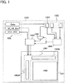
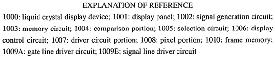
- FIG. 1 a block diagram of a display device and a stop sequence and a start sequence of an operation in a driver circuit are described.
- a block diagram of a display device is described using FIG. 1 .
- a liquid crystal display device 1000 described in Embodiment 1 includes a display panel 1001, a signal generation circuit 1002, a memory circuit 1003, a comparison circuit 1004, a selection circuit 1005, and a display control circuit 1006.
- the display panel 1001 includes, for example, a driver circuit portion 1007 and a pixel portion 1008.
- a gate line driver circuit 1009A and a signal line driver circuit 1009B are included, which are driver circuits for driving the pixel portion 1008 including a plurality of pixels.
- the gate line driver circuit 1009A, the signal line driver circuit 1009B, and the pixel portion 1008 may be formed using transistors formed over one substrate.
- the gate line driver circuit 1009A, the signal line driver circuit 1009B, and the pixel portion 1008 can be formed using n-channel transistors in each of which a semiconductor layer is formed using an oxide semiconductor.
- the gate line driver circuit 1009A and/or the signal line driver circuit 1009B may be formed over the same substrate as the pixel portion or a different substrate.
- a progressive method, an interlace method or the like can be employed.
- Color components controlled in the pixel at the time of color display are not limited to three colors of R, G, and B (R, G, and B correspond to red, green, and blue, respectively); for example, R, G, B, and W (W corresponds to white), or R, G, B, and one or more of yellow, cyan, magenta, and the like can be employed. Further, the size of a display region may be different depending on respective dots of the color components.
- the present invention is not limited to the application to a display device for color display but can also be applied to a display device for monochrome display.
- oxide semiconductor used in this embodiment hydrogen is contained at 1 ⁇ 10 16 /cm 3 or less in the oxide semiconductor, and hydrogen or an contained in the oxide semiconductor is removed.
- An oxide semiconductor film has a carrier density which is less than 1 ⁇ 10 14 /cm 3 , preferably equal to or less than 1 ⁇ 10 12 /cm 3 , and is used to form a channel region of a thin film transistor.
- an oxide semiconductor having a carrier density which is less than 1 ⁇ 10 12 /cm 3 is called an intrinsic (I-type) oxide semiconductor, and an oxide semiconductor having a carrier density equal to or greater than 1 ⁇ 10 12 /cm 3 but equal to or less than 1 ⁇ 10 14 /cm 3 is called a substantially-intrinsic oxide semiconductor.
- the concentration of hydrogen in the oxide semiconductor layer is measured by secondary ion mass spectrometry (SIMS).
- the number of carriers caused by thermal excitation is negligible in the case where the bandgap of an oxide semiconductor is 2 eV or more, preferably 2.5 eV or more, far preferably 3 eV or more. Therefore, impurities such as hydrogen which may serve as a donor are reduced as much as possible so that the carrier density is less than 1 ⁇ 10 14 /cm 3 , preferably equal to or less than 1 ⁇ 10 12 /cm 3 . That is, the carrier density of the oxide semiconductor layer is reduced as much as possible to be extremely close to zero.
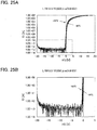
- Such an oxide semiconductor which is highly purified by removing hydrogen from the oxide semiconductor as much as possible is used for the channel formation region of the thin film transistor, whereby the drain current is equal to or less than 1 ⁇ 10 -13 A at a drain voltage in the range of 1 V to 10 V and a gate voltage in the range of -5 V to -20 V even when the channel width is 10 mm.
- the off-state current per micrometer of the channel width can be equal to or less than 10 aA/ ⁇ m (1 ⁇ 10 -17 A/ ⁇ m), and further can be equal to or less than 1 aA/ ⁇ m (1 ⁇ 10 -18 A/ ⁇ m).
- Such a transistor, whose off-state current is extremely small, is used as a transistor included in any of the gate line driver circuit 1009A, the signal line driver circuit 1009B, and the pixel portion 1008, whereby a holding time of an electrical signal such as a video signal can be increased.
- the holding time can be increased, for example, the holding time after the writing of a video signal is set to 10 seconds or more, preferably 30 seconds or more, far preferably one minute or more and less than ten minutes.
- the interval between writing timings can be increased, so that power consumption can be further suppressed.
- the resistance to flow of off-state current in a transistor can be referred to as the off-state resistivity.
- the off-state resistivity is the resistivity of a channel formation region when the transistor is off, which can be calculated from the off-state current.
- off-state resistance R the resistance when the transistor is off
- p the off-state resistivity
- ⁇ RA / L ( R is the off-state resistance)
- the length L of the channel formation region is the channel length L. In this manner, the off-state resistivity can be calculated from the off-state current.
- the off-state resistivity of the transistor including the oxide semiconductor layer in this embodiment is preferably 1 ⁇ 10 9 ⁇ m or more, far preferably 1 ⁇ 10 10 ⁇ m or more.
- the off-state current is about 1 ⁇ 10 -12 A/ ⁇ m. Therefore, in the transistor including the oxide semiconductor, the holding period of the voltage can be extended to a period about 10 5 times as long as that of the transistor using low-temperature polysilicon when the holding capacitances are equal to each other (about 0.1 pF). Further, in the case of a transistor using amorphous silicon, the off-state current per micrometer of the channel width is 1 ⁇ 10 -13 A/ ⁇ m or more.
- the holding period of the voltage can be extended to a period 10 4 times or more as long as that of the transistor using amorphous silicon when the holding capacitances are equal to each other (about 0.1 pF).
- image display is generally performed at 60 frames per second (for 16 msec per frame).
- the same can be applied to the case of still-image display, and this is because if the rate is decreased (the interval between writing timings is increased), the voltage of the pixel is decreased, which adversely affects the image display.
- the holding period per signal writing can be extended to 1600 seconds which is about 10 5 times as long as that of the transistor using low-temperature polysilicon since the off-state current is small.
- still image display can be performed on a display portion even by less frequent writing of image signals. Since the holding period can be extended, the frequency of performing writing of signals can be decreased particularly when a still image is displayed.
- the number of times of signal writing in a display period of one still image can be one or n ( n is greater than or equal to 2 and less than or equal to 10 3 ). Thus, low power consumption of a display device can be achieved.
- each pixel is provided with a storage capacitor formed by a pair of electrodes and an insulating layer provided as a dielectric between the pair of electrodes.
- the size of the storage capacitor can be set considering the off-state current of a transistor provided in each pixel, or the like.
- a storage capacitor having capacitance which is less than or equal to 1/3, preferably less than or equal to 1/5 with respect to the liquid crystal capacitance of each pixel is sufficient to be provided.
- the holding period can be long in the above-described transistor including the high-purity oxide semiconductor layer, the frequency of signal writing can be extremely decreased particularly when a still image is displayed. Therefore, the number of times of signal writing to pixels can be reduced in displaying, for example, a still image which involves less frequent switching of display, so that low power consumption can be achieved.
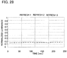
- refresh operation can be performed as appropriate considering the holding rate of the voltage applied to a liquid crystal element during the holding period.
- the refresh operation can be performed at the time when the voltage in the storage capacitor reaches a predetermined level with respect to a value (initial value) of a voltage which is just after the signal writing into a pixel electrode of the liquid crystal element. It is preferable to set the predetermined level of the voltage such that flicker is not sensed with respect to the initial value. Specifically, it is preferable to perform the refresh operation (rewriting) every time the voltage reaches a voltage which is less than the initial value by 10 %, far preferably 3 %.
- a counter electrode also called a common electrode
- a switch may be provided between a power source which supplies a common potential to the counter electrode and the counter electrode, the switch is turned on to supply the common potential from the power source to the counter electrode in a writing period, and then, the switch is turned off to make the counter electrode in the floating state in the holding period. It is preferable to use the transistor including the above-described high-purity oxide semiconductor layer as the switch.
- the signal generation circuit 1002 is a circuit for generating a signal for driving the gate line driver circuit 1009A and a signal for driving the signal line driver circuit 1009B.
- the signal generation circuit 1002 is also a circuit for outputting a signal for driving the driver circuit portion 1007 through a wiring, and is a circuit for outputting an image signal (also called a video voltage, a video signal, or video data) to the memory circuit 1003 through a wiring.
- the signal generation circuit 1002 is a circuit for generating and outputting a control signal for controlling the driver circuit portion 1007 and an image signal to be supplied to the pixel portion 1008.
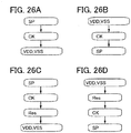
- the signal generation circuit 1002 supplies, as control signals, a high power supply potential VDD and a low power supply potential VSS to the gate line driver circuit 1009A and the signal line driver circuit 1009B, a start pulse SP and a clock pulse CK for the gate line driver circuit 1009A, and a start pulse SP and a clock pulse CK for the signal line driver circuit 1009B. Further, the signal generation circuit 1002 supplies an image signal Data for displaying a moving image or a still image to the memory circuit 1003.
- the moving image refers to an image which is recognized as a moving image with human eyes by rapid switch of a plurality of images which are time-divided into a plurality of frames.
- the moving image refers to a series of image signals which are recognized as a moving image with less flicker with human eyes by switching images at least 60 times (60 frames) per second.
- the still image refers to image signals which do not change in a series of frame periods, for example, in the n-th frame and (n+1)-th frame, unlike the moving image, though a plurality of images which are time-divided into a plurality of frame periods are switched rapidly.
- the signal generation circuit 1002 may further generates another signal such as an image signal or a latch signal.
- the signal generation circuit 1002 may output a reset signal Res for stopping the output of the pulse signal of each driver circuit, to the gate line driver circuit 1009A and/or the signal line driver circuit 1009B.
- Each signal may include a plurality of signals such as a first clock signal and a second clock signal.
- the high power supply potential VDD refers to a potential which is higher than a reference potential
- the low power supply potential VSS refers to a potential which is lower than or equal to the reference potential. It is preferable that the high power supply potential and the low power supply potential are potentials as high as potentials high enough for the transistor to operate.
- the voltage refers to a potential difference between a given potential and a reference potential (e.g., a ground potential) in many cases. Accordingly, the voltage, the potential, and the potential difference can also be referred to as a potential, a voltage, and a voltage difference, respectively.
- the analog signal may be converted into a digital signal through an A/D converter or the like to be output to the memory circuit 1003.
- the memory circuit 1003 includes a plurality of frame memories 1010 for storing image signals for a plurality of frames.
- the frame memory may be formed using a memory element such as Dynamic Random Access Memory (DRAM) or Static Random Access Memory (SRAM).
- DRAM Dynamic Random Access Memory
- SRAM Static Random Access Memory
- the number of frame memories 1010 is not particularly limited as long as an image signal can be stored for each frame period.
- the image signals of the frame memories 1010 are selectively read out by the comparison circuit 1004 and the selection circuit 1005.
- the comparison circuit 1004 is a circuit which selectively reads out image signals in a series of frame periods stored in the memory circuit 1003, compares the image signals, and detects a difference thereof.
- An image of the series of frame periods is determined as a moving image in the case where the difference is detected by the comparison of the image signals in the comparison circuit 1004, and is determined as a still image in the case where the difference is not detected by the comparison of the image signals in the comparison circuit 1004. That is, whether image signals in a series of frame periods are image signals for displaying a moving image or image signals for displaying a still image is determined by the detection of the difference in the comparison circuit 1004.
- the difference obtained by the comparison may be set so as to be determined as a difference to be detected when it is over a predetermined level.
- the selection circuit 1005 includes a plurality of switches such as thin film transistors, and is a circuit which selects, when image signals for displaying a moving image are determined by the difference detection in the comparison circuit 1004, the image signals from the frame memories 1010 in which the image signals are stored, and outputs to the display control circuit 1006.
- the selection circuit 1005 may output no signal of the image signal of the latter frame to the display control circuit 1006.
- the display control circuit 1006 is a circuit which switches supplying and stop of supplying of the image signal and the control signal such as the high power supply potential VDD, the low power supply potential VSS, the start pulse SP, the clock pulse CK, and the reset signal Res to the driver circuit portion 1007. Specifically, when an image is determined to be a moving image by the comparison circuit 1004, that is, a difference of image signals in a series of frames is detected, the image signals are supplied from the selection circuit 1005 to the driver circuit portion 1007 through the display control circuit 1006, and the control signals are supplied to the driver circuit portion 1007 through the display control circuit 1006.
- the stop of supplying of the image signals and the control signals is performed entirely in the period for holding an image signal in each pixel in the pixel portion 1008, and the image signals and the control signals which the display control circuit 1006 supplies before are supplied again, such that the image signal is supplied again after the holding period of each pixel.
- the supplying of any signal refers to supplying a predetermined potential to a wiring.
- the stop of supplying of any signal refers to stop of supplying of the predetermined potential to the wiring, and connection to a wiring to which a predetermined fixed potential is supplied, for example, a wiring to which the low power supply potential VSS is supplied.
- the stop of supplying of any signal also refers to cut of an electrical connection to a wiring to which a predetermined potential is supplied, to make a floating state.
- the off-state current can be reduced to less than or equal to 1 ⁇ 10 -12 A/ ⁇ m, so that the holding period can be extended. Accordingly, a synergistic effect is expected to be generated in reduction of power consumption when a still image is displayed in this embodiment.
- image signals are compared to determine whether an image thereof is a moving image or a still image, and supplying or stop of supplying of control signals such as a clock signal or a start pulse is selectively performed, whereby power consumption can be reduced.
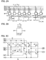
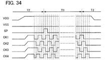
- FIGS. 2A to 2C An example of a structure of a shift register included in each of the gate line driver circuit 1009A and the signal line driver circuit 1009B of the driver circuit portion 1007 is described using FIGS. 2A to 2C .
- the shift register shown in FIG. 2A includes first to N-th pulse output circuits 10_1 to 10_N ( N is a natural number of 3 or more).
- a first clock signal CK1 from a first wiring 11, a second clock signal CK2 from a second wiring 12, a third clock signal CK3 from a third wiring 13, and a fourth clock signal CK4 from a fourth wiring 14 are supplied to the first to the N-th pulse output circuits 10_1 to 10_ N of the shift register shown in FIG. 2A .
- a start pulse SP1 (a first start pulse) from a fifth wiring 15 is input to the first pulse output circuit 10_1.
- a signal from the pulse output circuit in the previous stage (the signal called a previous stage signal OUT( n -1)) ( n is a natural number of more than or equal to 2 and lower than or equal to N ) is input to the N-th pulse output circuit 10 _N in the second or later stage.
- a signal from the third pulse output circuit 10_3 in the stage two stages after the first pulse output circuit 10_1 is input to the first pulse output circuit 10_1; similarly, a signal from the ( N +2)-th pulse output circuit 10_( n +2) in the stage two stages after the N-th pulse output circuit 10_ N (the signal called a subsequent-stage signal OUT( n +2)) is input to the N-th pulse output circuit.
- a first output signal (corresponding one of OUT(1)(SR) to OUT(N)(SR)) to be input to the pulse output circuit of the next stage and/or the two-stage-previous stage and a second output signal (corresponding one of OUT(1) to OUT(N)) which is input to another circuit or the like are output from each of the pulse output circuits.
- the subsequent-stage signal OUT( n +2) is not input to the last two stages of the shift register; therefore, as an example, a second start pulse SP2 may be input to one of the last two stages of the shift register and a third start pulse SP3 may be input to the other of the same.
- signals may be generated inside to be input thereto.
- a ( N +1)-th pulse output circuit 10 ( N +1) and a ( N +2)-th pulse output circuit 10( N +2 ) which do not contribute to output of pulses to the display portion may be provided, and signals corresponding to the second start pulse (SP2) and the third start pulse (SP3) may be generated in the dummy stages.
- the first to the fourth clock signals (CK1) to (CK4) each are a signal which oscillates between an H-level signal and an L-level signal at a constant cycle.
- the first to the fourth clock signals (CK1) to (CK4) are delayed by 1/4 period sequentially.
- control of driving of the pulse output circuit or the like is performed.
- the clock signal is also called GCK or SCK depending on a driver circuit to which the clock signal is input; however, description is made in this embodiment by using CK as the clock signal.
- connection relations are included without being limited to a predetermined connection relation, for example, the connection relation shown in the drawings and the texts.
- Each of the first to N-th pulse output circuits 10_1 to 10 _N includes a first input terminal 21, a second input terminal 22, a third input terminal 23, a fourth input terminal 24, a fifth input terminal 25, a first output terminal 26, and a second output terminal 27 (see FIG. 2B ).
- the first input terminal 21, the second input terminal 22, and the third input terminal 23 are electrically connected to any of the first to fourth wirings 11 to 14.
- the first input terminal 21 of the first pulse output circuit 10_1 is electrically connected to the first wiring 11
- the second input terminal 22 of the first pulse output circuit 10_1 is electrically connected to the second wiring 12
- the third input terminal 23 of the first pulse output circuit 10_1 is electrically connected to the third wiring 13.
- the first input terminal 21 of the second pulse output circuit 10_2 is electrically connected to the second wiring 12
- the second input terminal 22 of the second pulse output circuit 10_2 is electrically connected to the third wiring 13
- the third input terminal 23 of the second pulse output circuit 10_2 is electrically connected to the fourth wiring 14.
- the first start pulse SP1 is input to the fourth input terminal 24, a subsequent-stage signal OUT(3) is input to the fifth input terminal 25, the first output signal OUT(1)(SR) is output from the first output terminal 26, and the second output signal OUT(1) is output from the second output terminal 27.
- a first terminal of the first transistor 31 is electrically connected to the power supply line 51, a second terminal of the first transistor 31 is electrically connected to a first terminal of the ninth transistor 39, and a gate electrode of the first transistor 31 is electrically connected to the fourth input terminal 24.
- a first terminal of the second transistor 32 is electrically connected to the power supply line 52, a second terminal of the second transistor 32 is electrically connected to the first terminal of the ninth transistor 39, and a gate electrode of the second transistor 32 is electrically connected to a gate electrode of the fourth transistor 34.
- a first terminal of the third transistor 33 is electrically connected to the first input terminal 21, and a second terminal of the third transistor 33 is electrically connected to the first output terminal 26.
- a first terminal of the fourth transistor 34 is electrically connected to the power supply line 52, and a second terminal of the fourth transistor 34 is electrically connected to the first output terminal 26.
- a first terminal of the fifth transistor 35 is electrically connected to the power supply line 52, a second terminal of the fifth transistor 35 is electrically connected to the gate electrode of the second transistor 32 and the gate electrode of the fourth transistor 34, and a gate electrode of the fifth transistor 35 is electrically connected to the fourth input terminal 24.
- a first terminal of the sixth transistor 36 is electrically connected to the power supply line 51, a second terminal of the sixth transistor 36 is electrically connected to the gate electrode of the second transistor 32 and the gate electrode of the fourth transistor 34, and a gate electrode of the sixth transistor 36 is electrically connected to the fifth input terminal 25.
- a first terminal of the seventh transistor 37 is electrically connected to the power supply line 51, a second terminal of the seventh transistor 37 is electrically connected to a second terminal of the eighth transistor 38, and a gate electrode of the seventh transistor 37 is electrically connected to the third input terminal 23.
- a first terminal of the eighth transistor 38 is electrically connected to the gate electrode of the second transistor 32 and the gate electrode of the fourth transistor 34, and a gate electrode of the eighth transistor 38 is electrically connected to the second input terminal 22.
- the first terminal of the ninth transistor 39 is electrically connected to the second terminal of the first transistor 31 and the second terminal of the second transistor 32, a second terminal of the ninth transistor 39 is electrically connected to the gate electrode of the third transistor 33 and the gate electrode of the tenth transistor 40, and a gate electrode of the ninth transistor 39 is electrically connected to the power supply line 51.
- a first terminal of the tenth transistor 40 is electrically connected to the first input terminal 21, a second terminal of the tenth transistor 40 is electrically connected to the second output terminal 27, and the gate electrode of the tenth transistor 40 is electrically connected to the second terminal of the ninth transistor 39.
- a first terminal of the eleventh transistor 41 is electrically connected to the power supply line 52, a second terminal of the eleventh transistor 41 is electrically connected to the second output terminal 27, and a gate electrode of the eleventh transistor 41 is electrically connected to the gate electrode of the second transistor 32 and the gate electrode of the fourth transistor 34.
- a connection point of the gate electrode of the third transistor 33, the gate electrode of the tenth transistor 40, and the second terminal of the ninth transistor 39 is referred to as a node NA.
- a connection point of the gate electrode of the second transistor 32, the gate electrode of the fourth transistor 34, the second terminal of the fifth transistor 35, the second terminal of the sixth transistor 36, the first terminal of the eighth transistor 38, and the gate electrode of the eleventh transistor 41 is referred to as a node NB.
- the pulse output circuit in FIG. 2C is the first pulse output circuit 10_1
- the first clock signal CK1 is input to the first input terminal 21
- the second clock signal CK2 is input to the second input terminal 22
- the third clock signal CK3 is input to the third input terminal 23
- the start pulse SP is input to the fourth input terminal 24
- a subsequent-stage signal OUT(3) is input to the fifth input terminal 25
- the first output signal OUT(1)(SR) is output from the first output terminal 26
- the second output signal OUT(1) is output from the second output terminal 27.
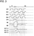
- FIG. 3 shows a timing chart of a shift register including the plurality of pulse output circuits shown in FIG. 2C .
- the shift register is a scan line driver circuit
- a period 61 in FIG. 3 is a vertical retrace period and a period 62 is a gate selection period.
- FIGS. 2A to 2C and FIG. 3 the reset signal Res is not supplied to the driver circuit.
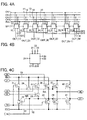
- a structure to which the reset signal Res is supplied is shown and described in FIGS. 4A to 4C .
- a shift register shown in FIG. 4A includes first to N-th pulse output circuits 10_1 to 10_ N (N is a natural number of 3 or more).
- a first clock signal CK1 from a first wiring 11, a second clock signal CK2 from a second wiring 12, a third clock signal CK3 from a third wiring 13, and a fourth clock signal CK4 from a fourth wiring 14 are supplied to the first to the N-th pulse output circuits 10_1 to 10_ N of the shift register shown in FIG. 4A .
- a start pulse SP1 (a first start pulse) from a fifth wiring 15 is input to the first pulse output circuit 10_1.
- a signal from the pulse output circuit in the previous stage (the signal called a previous stage signal OUT( n -1)) ( n is a natural number of more than or equal to 2 and less than or equal to N ) is input to the N-th pulse output circuit 10_ N in the second or later stage.
- a signal from the third pulse output circuit 10_3 in the stage two stages after the first pulse output circuit 10_1 is input to the first pulse output circuit 10_1; similarly, a signal from the ( N +2)-th pulse output circuit 10_( N +2) in the stage two stages after the N-th pulse output circuit 10 _N (the signal called a subsequent-stage signal OUT( n +2)) is input to the N-th pulse output circuit.
- a first output signal (corresponding one of OUT(1)(SR) to OUT(N)(SR)) to be input to the pulse output circuit of the next stage and/or the two-stage-previous stage and a second output signal (corresponding one of OUT(1) to OUT(N)) which is input to another circuit or the like are output from each of the pulse output circuits.
- a reset signal Res is supplied from a sixth wiring 16.
- the pulse output circuit shown in FIGS. 4A to 4C is different from the pulse output circuit shown in FIGS. 2A to 2C in that the sixth wiring 16 for supplying the reset signal Res is provided; the other portions is as described in FIGS. 2A to 2C .
- Each of the first to N-th pulse output circuits 10_1 to 10 _N includes a first input terminal 21, a second input terminal 22, a third input terminal 23, a fourth input terminal 24, a fifth input terminal 25, a first output terminal 26, a second output terminal 27, and a sixth output terminal 28 (see FIG. 4B ).
- the first input terminal 21, the second input terminal 22, and the third input terminal 23 are electrically connected to any of the first to fourth wirings 11 to 14.
- the first input terminal 21 of the first pulse output circuit 10_1 is electrically connected to the first wiring 11
- the second input terminal 22 of the first pulse output circuit 10_1 is electrically connected to the second wiring 12
- the third input terminal 23 of the first pulse output circuit 10_1 is electrically connected to the third wiring 13.
- the first input terminal 21 of the second pulse output circuit 10_2 is electrically connected to the second wiring 12
- the second input terminal 22 of the second pulse output circuit 10_2 is electrically connected to the third wiring 13
- the third input terminal 23 of the second pulse output circuit 10_2 is electrically connected to the fourth wiring 14.
- the first start pulse SP1 is input to the fourth input terminal 24
- the subsequent-stage signal OUT(3) is input to the fourth input terminal 25
- the first output signal OUT(1)(SR) is output from the first output terminal 26
- the second output signal OUT(1) is output from the second output terminal 27, and the reset signal Res is input from the sixth input terminal 28.
- a first terminal of the first transistor 31 is electrically connected to the power supply line 51, a second terminal of the first transistor 31 is electrically connected to a first terminal of the ninth transistor 39, and a gate electrode of the first transistor 31 is electrically connected to the fourth input terminal 24.
- a first terminal of the second transistor 32 is electrically connected to the power supply line 52, a second terminal of the second transistor 32 is electrically connected to the first terminal of the ninth transistor 39, and a gate electrode of the second transistor 32 is electrically connected to a gate electrode of the fourth transistor 34.
- a first terminal of the third transistor 33 is electrically connected to the first input terminal 21, and a second terminal of the third transistor 33 is electrically connected to the first output terminal 26.
- a first terminal of the fourth transistor 34 is electrically connected to the power supply line 52, and a second terminal of the fourth transistor 34 is electrically connected to the first output terminal 26.
- a first terminal of the fifth transistor 35 is electrically connected to the power supply line 52, a second terminal of the fifth transistor 35 is electrically connected to the gate electrode of the second transistor 32 and the gate electrode of the fourth transistor 34, and a gate electrode of the fifth transistor 35 is electrically connected to the fourth input terminal 24.
- a first terminal of the sixth transistor 36 is electrically connected to the power supply line 51, a second terminal of the sixth transistor 36 is electrically connected to the gate electrode of the second transistor 32 and the gate electrode of the fourth transistor 34, and a gate electrode of the sixth transistor 36 is electrically connected to the fifth input terminal 25.
- a first terminal of the seventh transistor 37 is electrically connected to the power supply line 51, a second terminal of the seventh transistor 37 is electrically connected to a second terminal of the eighth transistor 38, and a gate electrode of the seventh transistor 37 is electrically connected to the third input terminal 23.
- a first terminal of the eighth transistor 38 is electrically connected to the gate electrode of the second transistor 32 and the gate electrode of the fourth transistor 34, and a gate electrode of the eighth transistor 38 is electrically connected to the second input terminal 22.
- the first terminal of the ninth transistor 39 is electrically connected to the second terminal of the first transistor 31 and the second terminal of the second transistor 32, a second terminal of the ninth transistor 39 is electrically connected to the gate electrode of the third transistor 33 and the gate electrode of the tenth transistor 40, and a gate electrode of the ninth transistor 39 is electrically connected to the power supply line 51.
- a first terminal of the tenth transistor 40 is electrically connected to the first input terminal 21, a second terminal of the tenth transistor 40 is electrically connected to the second output terminal 27, and the gate electrode of the tenth transistor 40 is electrically connected to the second terminal of the ninth transistor 39.
- a first terminal of the eleventh transistor 41 is electrically connected to the power supply line 52, a second terminal of the eleventh transistor 41 is electrically connected to the second output terminal 27, and a gate electrode of the eleventh transistor 41 is electrically connected to the gate electrode of the second transistor 32 and the gate electrode of the fourth transistor 34.
- the gate electrode of the second transistor 32, the gate electrode of the fourth transistor 34, the second terminal of the fifth transistor 35, the second terminal of the sixth transistor 36, the first terminal of the eighth transistor 38, and the gate electrode of the eleventh transistor 41 are electrically connected to a wiring 53 for supplying the reset signal Res.
- the reset signal Res is a signal by which a signal with a high power supply potential level is supplied to the gate electrode of the second transistor 32, the gate electrode of the fourth transistor 34, the second terminal of the fifth transistor 35, the second terminal of the sixth transistor 36, the first terminal of the eighth transistor 38, and the gate electrode of the eleventh transistor 41 to reduce the output from the pulse output circuit to a signal with a low power supply potential level.
- a connection point of the gate electrode of the third transistor 33, the gate electrode of the tenth transistor 40, and the second terminal of the ninth transistor 39 is referred to as a node NA.
- a connection point of the gate electrode of the second transistor 32, the gate electrode of the fourth transistor 34, the second terminal of the fifth transistor 35, the second terminal of the sixth transistor 36, the first terminal of the eighth transistor 38, and the gate electrode of the eleventh transistor 41 is referred to as a node NB.
- the pulse output circuit in FIG. 4C is the first pulse output circuit 10_1
- the first clock signal CK1 is input to the first input terminal 21
- the second clock signal CK2 is input to the second input terminal 22
- the third clock signal CK3 is input to the third input terminal 23
- the start pulse SP is input to the fourth input terminal 24
- a subsequent-stage signal OUT(3) is input to the fifth input terminal 25
- the first output signal OUT(1)(SR) is output from the first output terminal 26
- the second output signal OUT(1) is output from the second output terminal 27, and the reset signal Res is input from the sixth input terminal 28.
- the timing chart of the shift register including a plurality of pulse output circuits shown in FIG. 4C is similar to that of FIG. 2C , shown in FIG. 3 .
- FIGS. 4A to 4C The structure as described in FIGS. 4A to 4C in which the reset signal is supplied in addition to the structure shown in FIGS. 2A to 2C and FIG. 3 is preferable because malfunction due to signal delay at the time of switching between a still image and a moving image or the like can be reduced.
- a common potential electrode provided over the thin film transistor included in the driver circuit portion may be cut off from a common potential line to be made in the floating state. Then, after the still-image mode, in the case where operation of the driver circuit is started again, the common potential electrode is connected to the common potential line. Accordingly, malfunction of the thin film transistor in the driver circuit portion can be prevented.
- FIG. 18A illustrates a display panel 1800 having such a structure
- FIG 18B is a view for describing the cross-sectional structure thereof.
- the display panel 1800 includes driver circuits 1802 and 1804 and a pixel portion 1806.
- a common potential electrode 1808 is provided so as to overlap the driver circuit 1802.
- a switch 1810 for controlling connection/non-connection between the common potential electrode 1808 and a common potential terminal 1812 is provided therebetween.
- the common potential electrode 1808 is provided over a TFT 1803 of the driver circuit as shown in FIG. 18B , thereby shielding the TFT 1803 from static electricity, so that a change of the threshold voltage or generation of a parasitic channel is prevented.
- the same structure as the TFT 1803 can be used as the switch 1810.
- Such an element in which the leakage current in the off-state is extremely small contributes to stabilization of operation of the display panel. That is, in the case where a still image is displayed, even when the switch 1803 is turned off to make the common potential electrode in the floating state, the potential can be kept constant.
- a period for holding voltage in a storage capacitor can be extended, and power consumption when a still image or the like is displayed can be decreased. Further, by stopping supplying a control signal in the case where a still image is displayed, power consumption can be further decreased. In addition, a still image and a moving image can be switched without malfunction.
- Embodiment 1 can be implemented in appropriate combination with any of the structures described in the other embodiments.
- FIGS. 5A and 5B and FIGS. 6A to 6E A thin film transistor of this embodiment and an embodiment of a method for manufacturing the thin film transistor are described using FIGS. 5A and 5B and FIGS. 6A to 6E .
- Embodiment 2 an example of a thin film transistor which can be applied to a liquid crystal display device described in this specification will be described.
- a thin film transistor 410 described in Embodiment 2 can be used as a thin film transistor in each pixel of the pixel portion 1008 described in Embodiment 1.
- FIG. 5A illustrates an example of a planar structure of the thin film transistor
- FIG. 5B illustrates an example of a cross-sectional structure thereof.
- the thin film transistor 410 shown in FIGS. 5A and 5B is a top-gate thin film transistor.
- FIG. 5A is a plane view of the top-gate thin film transistor 410 and FIG. 5B is a cross-sectional view along line C1-C2 in FIG. 5A .
- the thin film transistor 410 includes over a substrate 400 having an insulating surface, an insulating layer 407, an oxide semiconductor layer 412, a source and drain electrode layers 415a and 415b, a gate insulating layer 402, and a gate electrode layer 411. Wiring layers 414a and 414b are provided in contact with the source and drain electrode layers 415a and 415b, respectively to be electrically connected thereto.
- the thin film transistor 410 is described as a single-gate thin film transistor; a multi-gate thin film transistor including a plurality of channel formation regions can be formed when needed.
- a process for manufacturing the thin film transistor 410 over the substrate 400 is described below with reference to FIGS. 6A to 6E .
- a substrate which can be used as the substrate 400 having an insulating surface as long as the substrate has enough heat resistance to a heat treatment to be performed later.
- a glass substrate whose strain point is higher than or equal to 730 °C may be used when the temperature of the heat treatment performed later is high.
- a glass material such as aluminosilicate glass, aluminoborosilicate glass, or barium borosilicate glass is used, for example. Note that by containing a larger amount of barium oxide (BaO) than boron oxide, a heat-resistant glass substrate which is of more practical use can be formed. Therefore, it is preferable that a glass substrate containing a larger amount of BaO than B 2 O 3 be used.
- a substrate formed using an insulator such as a ceramic substrate, a quartz substrate, or a sapphire substrate may be used instead of the above-described glass substrate, as the substrate 400.
- a crystallized glass substrate or the like may be used.
- a plastic substrate or the like may be used.
- the insulating layer 407 which functions as a base film is formed over the substrate 400 having an insulating surface. It is preferable that an oxide insulating layer such as a silicon oxide layer, a silicon oxynitride layer, an aluminum oxide layer, or an aluminum oxynitride layer be used as the insulating layer 407 which is in contact with the oxide semiconductor layer.
- the insulating layer 407 can be formed by a plasma CVD method, a sputtering method, or the like. It is preferable to form the insulating layer 407 by a sputtering method in order not to contain hydrogen in the insulating layer 407.
- a silicon oxide layer is formed as the insulating layer 407 by a sputtering method.
- the substrate 400 is transferred into a chamber, a sputtering gas containing high-purity oxygen in which hydrogen and moisture are removed is introduced into the chamber, and a target is used, so that the silicon oxide layer is deposited on the substrate 400 as the insulating layer 407.
- the substrate 400 may be at room temperature or may be heated.
- the thickness of the silicon oxide film is 100 nm in this embodiment.
- a silicon target may be used instead of the quartz (preferably quart) to form the silicon oxide film.
- As a sputtering gas oxygen or a mixed gas of oxygen and argon is used in this embodiment.
- the insulating layer 407 it is preferable to remove residual moisture in the chamber in the deposition of the insulating layer 407. This is in order to prevent the insulating layer 407 from containing hydrogen, a hydroxyl group, or moisture.
- an adsorption-type vacuum pump is preferably used.
- a cryopump, an ion pump, or a titanium sublimation pump is preferably used.
- a turbo molecular pump to which a cold trap is added may be used.
- a hydrogen molecule, a compound including a hydrogen atom such as water (H 2 O), or the like, for example, is exhausted. Accordingly, the concentration of impurities included in the insulating layer 407 formed in the chamber can be reduced.
- a high-purity gas in which an impurity such as hydrogen, water, a hydroxyl group, or hydride is removed to 1 ppm or less, preferably 10 ppb or less be used as the sputtering gas for the deposition of the insulating layer 407.
- Examples of a sputtering method include an RF sputtering method in which a high-frequency power source is used as a sputtering power source, a DC sputtering method in which a DC power source is used, and a pulsed DC sputtering method in which a bias is applied in a pulsed manner.
- the RF sputtering method is mainly used in the case where an insulating film is formed
- the DC sputtering method is mainly used in the case where a metal film is formed.
- a multi-target sputtering apparatus in which a plurality of targets which are formed of different materials from each other can be set may be used.
- films of different materials can be stacked to be formed in the same chamber, or plural kinds of materials can be deposited by electric discharge at the same time in the same chamber.
- a sputtering apparatus provided with a magnet system inside the chamber and used for a magnetron sputtering method, or a sputtering apparatus used for an ECR sputtering method in which plasma generated with the use of microwaves is used without using glow discharge may be used.
- a reactive sputtering method in which a target substance and a sputtering gas component are chemically reacted with each other during deposition to form a thin compound film thereof, or a bias sputtering method in which a voltage is also applied to a substrate during deposition may be used.
- the insulating layer 407 may have a stacked-layer structure; for example, a stacked-layer structure in which a nitride insulating layer such as a silicon nitride layer, a silicon nitride oxide layer, an aluminum nitride layer, or an aluminum nitride oxide layer and the above-described oxide insulating layer are stacked in this order over the substrate 400 may be used.
- a nitride insulating layer such as a silicon nitride layer, a silicon nitride oxide layer, an aluminum nitride layer, or an aluminum nitride oxide layer and the above-described oxide insulating layer are stacked in this order over the substrate 400 may be used.
- a silicon nitride layer is formed between the silicon oxide layer and the substrate 400 by introducing a sputtering gas containing high-purity nitrogen in which hydrogen and moisture are removed and using a silicon target.
- a sputtering gas containing high-purity nitrogen in which hydrogen and moisture are removed and using a silicon target.
- the substrate may be heated at the time of the film deposition of the silicon nitride layer.
- the silicon nitride layer and the silicon oxide layer can be formed in the same chamber with the same silicon target.
- a sputtering gas containing nitrogen is introduced and a silicon target placed inside the chamber is used to form the silicon nitride layer, and then, the sputtering gas is switched to a sputtering gas containing oxygen and the same silicon target is used to form the silicon oxide layer. Since the silicon nitride layer and the silicon oxide layer can be formed in succession without exposure to the air, an impurity such as hydrogen or moisture can be prevented from being adsorbed on a surface of the silicon nitride layer.
- an oxide semiconductor film is formed to a thickness of greater than or equal to 2 nm and less than or equal to 200 nm over the insulating layer 407.
- the oxide semiconductor film In order for the oxide semiconductor film not to contain impurities such as hydrogen, a hydroxyl group, and moisture as much as possible, it is preferable to preheat the substrate 400 provided with the insulating layer 407 in a preheating chamber of the sputtering apparatus before the film formation so that an impurity such as hydrogen or moisture adsorbed on the substrate 400 is eliminated, and perform exhaustion.
- a cryopump As an exhaustion unit provided in the preheating chamber, a cryopump is preferable. This preheating step is not necessarily performed.
- the oxide semiconductor film is formed by a sputtering method
- the reverse sputtering is a method by which voltage is applied to a substrate side with a high-frequency power source in an argon atmosphere to generate plasma on the substrate side without applying voltage to a target side, so that a surface is modified.
- argon atmosphere a nitrogen atmosphere, a helium atmosphere, an oxygen atmosphere, or the like may be used.
- the oxide semiconductor film is formed by the sputtering method.
- the oxide semiconductor film is formed using an In-Ga-Zn-O-based oxide semiconductor film, an In-Sn-Zn-O-based oxide semiconductor film, an In-Al-Zn-O-based oxide semiconductor film, a Sn-Ga-Zn-O-based oxide semiconductor film, an Al-Ga-Zn-O-based oxide semiconductor film, a Sn-Al-Zn-O-based oxide semiconductor film, an In-Zn-O-based oxide semiconductor film, a Sn-Zn-O-based oxide semiconductor film, an Al-Zn-O-based oxide semiconductor film, an In-O-based oxide semiconductor film, a Sn-O-based oxide semiconductor film, or a Zn-O-based oxide semiconductor film.
- the oxide semiconductor film is formed by a sputtering method using an In-Ga-Zn-O-based oxide semiconductor target.
- the filling rate of the oxide semiconductor target is equal to or greater than 90 % and equal to or less than 100 %, preferably equal to or greater than 95 % and equal to or less than 99.9 %.
- the oxide semiconductor target having high filling rate the deposited oxide semiconductor film has high density.
- the atmosphere in the sputtering may be an atmosphere of a rare gas (typically argon), an atmosphere of oxygen, or a mixed atmosphere of a rare gas and oxygen.
- the target may contain SiO 2 at 2 wt% or more and 10 wt% or less.
- a high-purity gas in which an impurity such as hydrogen, water, a hydroxyl group, or hydride is removed to 1 ppm or less, preferably 10 ppb or less be used as the sputtering gas for the deposition of the oxide semiconductor film.
- the oxide semiconductor film is formed over the substrate 400 as follows: the substrate is held in the chamber with pressure reduced, residual moisture in the chamber is removed, a sputtering gas from which hydrogen and moisture are removed is introduced, and the above-described target is used.
- an adsorption-type vacuum pump For example, a cryopump, an ion pump, or a titanium sublimation pump is preferably used.
- a turbo molecular pump to which a cold trap is added may be used.
- a hydrogen molecule In the chamber in which exhaustion is performed using a cryopump, a hydrogen molecule, a compound including a hydrogen atom such as water (H 2 O) a compound including a carbon atom, or the like is exhausted. Accordingly, the concentration of impurities included in the oxide semiconductor film formed in the chamber can be reduced.
- the substrate may be heated at the time of the film deposition of the oxide semiconductor film.
- the temperature of the substrate is room temperature; the distance between the substrate and the target is 110 mm; the pressure is 0.4 Pa; the direct current (DC) power is 0.5 kW; and the atmosphere is oxygen and argon (the flow rate ratio of oxygen to argon is 15 sccm : 30 sccm).
- a pulsed direct current (DC) power supply be used because powder substances (also referred to as particles or dust) generated in the film deposition can be reduced and the film thickness can be made uniform.
- the oxide semiconductor film has a thickness greater than or equal to 2 nm and less than or equal to 200 nm, preferably greater than or equal to 5 nm and less than or equal to 30 nm. Note that appropriate thickness of the oxide semiconductor film varies depending on a material thereof; therefore, the thickness may be determined as appropriate depending on the material.
- a resist mask for forming the island-shaped oxide semiconductor layer 412 may be formed using an ink jet method. Formation of the resist mask by an inkjet method needs no photomask; thus, manufacturing cost can be reduced.
- etching of the oxide semiconductor film either one or both of wet etching and dry etching may be employed.
- etching gas for the dry etching a gas containing chlorine (chlorine-based gas such as chlorine (Cl 2 ), boron chloride (BCl 3 ), silicon chloride (SiCl 4 ), or carbon tetrachloride (CCl 4 )) is preferably used.
- a gas containing fluorine fluorine-based gas such as carbon tetrafluoride (CF 4 ), sulfur fluoride (SF 6 ), nitrogen fluoride (NF 3 ), or trifluoromethane (CHF 3 )); hydrogen bromide (HBr); oxygen (O 2 ); any of these gases to which a rare gas such as helium (He) or argon (Ar) is added; or the like can be used.
- fluorine-based gas such as carbon tetrafluoride (CF 4 ), sulfur fluoride (SF 6 ), nitrogen fluoride (NF 3 ), or trifluoromethane (CHF 3 )
- hydrogen bromide HBr
- oxygen O 2
- any of these gases to which a rare gas such as helium (He) or argon (Ar) is added; or the like can be used.
- a parallel-plate RIE (reactive ion etching) method or an ICP (inductively coupled plasma) etching method can be used.
- the etching conditions the amount of electric power applied to a coil-shaped electrode, the amount of electric power applied to an electrode on a substrate side, the temperature of the electrode on the substrate side, or the like.
- ITO07N produced by KANTO CHEMICAL CO., INC.
- the etchant is removed by cleaning together with the material which is etched off. Waste liquid of the etchant containing the removed material may be purified and the material contained in the waste liquid may be reused.
- the resources can be efficiently used and the cost can be reduced by collecting and reusing a material such as indium included in the oxide semiconductor from the waste liquid after the etching.
- the etching conditions (such as an etchant, etching time, or temperature) are appropriately adjusted depending on a material so that the material can be etched into a desired shape.
- the oxide semiconductor film is processed into the island-shaped oxide semiconductor layer 412 by a wet etching method using a solution obtained by mixing phosphoric acid, acetic acid, and nitric acid.
- a first heat treatment is performed on the oxide semiconductor layer 412.
- the temperature of the first heat treatment is higher than or equal to 400 °C and lower than or equal to 750 °C, and higher than or equal to 400 °C and lower than the strain point of the substrate 400 when the strain point of the substrate 400 is lower than or equal to 750 °C.
- the substrate is put in an electric furnace which is a kind of heat treatment apparatus and heat treatment is performed on the oxide semiconductor layer at 450 °C for one hour in a nitrogen atmosphere, and then, the temperature is reduced to room temperature and water or hydrogen is prevented from entering the oxide semiconductor layer, without exposure to the air; thus, an oxide semiconductor layer is obtained.
- the oxide semiconductor layer 412 can be dehydrated or dehydrogenated by the first heat treatment.
- the heat treatment apparatus is not limited to an electric furnace and may be provided with a device that heats an object to be processed by thermal conduction or thermal radiation from a heater such as a resistance heater or the like.
- a heater such as a resistance heater or the like.
- an RTA (rapid thermal annaling) apparatus such as a GRTA (gas rapid thermal annealing) apparatus or an LRTA (lamp rapid thermal annealing) apparatus can be used.
- the LRTA apparatus is an apparatus for heating an object to be processed by radiation of light (an electromagnetic wave) emitted from a lamp such as a halogen lamp, a metal halide lamp, a xenon arc lamp, a carbon arc lamp, a high pressure sodium lamp, or a high pressure mercury lamp.
- the GRTA apparatus is an apparatus for heat treatment using a high-temperature gas.
- the gas an inert gas which does not react with the object to be processed, by heat treatment, such as nitrogen or a rare gas such as arg
- GRTA may be performed as follows: the substrate is transferred into an inert gas heated to a high temperature of 650 °C to 700 °C, heated for several minutes, and transferred and taken out of the inert gas heated to the high temperature. GRTA enables a high-temperature heat treatment for a short time.
- water, hydrogen, or the like be not contained in nitrogen or a rare gas such as helium, neon, or argon. It is preferable that nitrogen or a rare gas such as helium, neon, or argon which is introduced into the heat treatment apparatus have a purity of 6N (99.9999 %) or more, far preferably 7N (99.99999 %) or more (that is, the concentration of impurities be 1 ppm or less, far preferably 0.1 ppm or less).
- the oxide semiconductor layer 412 might be crystallized to be a microcrystalline film or a polycrystalline film.
- the oxide semiconductor layer may be crystallized to be a microcrystalline oxide semiconductor film in which the degree of crystallization is greater than or equal to 90 % or greater than or equal to 80 %.
- the oxide semiconductor layer 412 may be an amorphous oxide semiconductor film which does not contain crystalline components.
- the oxide semiconductor layer may become an oxide semiconductor film in which a microcrystalline portion (with a grain diameter greater than or equal to 1 nm and greater than or less than 20 nm, typically greater than or equal to 2 nm and greater than or less than 4 nm) is mixed into an amorphous oxide semiconductor.
- the first heat treatment of the oxide semiconductor layer can also be performed on the oxide semiconductor film before being processed into the island-like oxide semiconductor layer 412.
- the substrate is taken out from the heat apparatus after the first heat treatment, and then a photolithography step is performed thereon.
- the heat treatment for dehydration and/or dehydrogenation on the oxide semiconductor layer is performed just after the formation of the oxide semiconductor layer 412 is described above.
- the heat treatment for dehydration and/or dehydrogenation may be performed after a source electrode and a drain electrode are stacked on the oxide semiconductor layer or after a gate insulating layer is formed over a source electrode and a drain electrode as long as it is performed after the deposition of the oxide semiconductor layer.
- a conductive film is formed over the insulating layer 407 and the oxide semiconductor layer 412.
- the conductive film may be formed by a sputtering method or a vacuum evaporation method.
- a material of the conductive film an element selected from Al, Cr, Cu, Ta, Ti, Mo, and W; an alloy containing any of these elements as a component; an alloy film containing any of these elements in combination; and the like can be given.
- one or more materials selected from manganese, magnesium, zirconium, beryllium, and yttrium may be used.
- the conductive film may have a single-layer structure or a stacked-layer structure of two or more layers.
- a single-layer structure of an aluminum film including silicon, a two-layer structure in which a titanium film is stacked over an aluminum film, a three-layer structure in which a titanium film, an aluminum film, and a titanium film are stacked in this order, and the like can be given.
- a film, an alloy film, or a nitride film which contains aluminum (Al) and one or a plurality of elements selected from titanium (Ti), tantalum (Ta), tungsten (W), molybdenum (Mo), chromium (Cr), neodymium (Nd), and scandium (Sc) may be used.
- a titanium film with a thickness of 150 nm is formed as the conductive film by a sputtering method.
- a resist mask is formed over the conductive film by a second photolithography step.
- the resist mask may be formed using an ink jet method. Formation of the resist mask by an inkjet method needs no photomask; thus, manufacturing cost can be reduced. After that, etching is selectively performed thereon, so that the source and drain electrode layers 415a and 415b are formed, and then, the resist mask is removed (see FIG. 6B ). It is preferable that an end portion of the each of the source and drain electrode layers have a tapered shape because coverage with a gate insulating layer stacked thereover is improved.
- each material and etching conditions are adjusted as appropriate so that the oxide semiconductor layer 412 is not removed by the etching of the conductive film and the insulating layer 407 under the oxide semiconductor layer 412 is not exposed.
- part of the oxide semiconductor layer 412 is etched, whereby an oxide semiconductor layer having a groove (a depression portion) may be formed.
- Light exposure at the time of the formation of the resist mask in the second photolithography step may be performed using ultraviolet light, KrF laser light, or ArF laser light.
- the channel length L of a thin film transistor to be formed is determined by a pitch between a lower end of the source electrode layer and a lower end of the drain electrode layer, which are adjacent to each other over the oxide semiconductor layer 412.
- the light exposure at the time of the formation of the resist mask in the second photolithography step is performed using extreme ultraviolet light having an extremely short wavelength of several nanometers to several tens of nanometers.
- the resolution is high and the focus depth is large. Accordingly, the channel length L of the thin film transistor can be made to be greater than or equal to 10 nm and less than or equal to 1000 nm, the operation rate of a circuit can be increased, and low power consumption can be achieved by extremely small off-state current.
- the gate insulating layer 402 is formed over the insulating layer 407, the oxide semiconductor layer 412, and the source and drain electrode layers 415a and 415b (see FIG. 6C ).
- the gate insulating layer 402 can be formed with a single-layer structure or a stacked-layer structure using one or more of a silicon oxide layer, a silicon nitride layer, a silicon oxynitride layer, a silicon nitride oxide layer, and an aluminum oxide layer by a plasma CVD method, a sputtering method, or the like. In order to prevent the gate insulating layer 402 from containing hydrogen as much as possible, it is preferable to form the gate insulating layer 402 by a sputtering method.
- a silicon target or a quartz target is used as a target, and oxygen or a mixed gas of oxygen and argon is used as a sputtering gas.
- the gate insulating layer 402 can have a structure in which a silicon oxide layer and a silicon nitride layer are stacked in this order.
- a gate insulating layer with a thickness of greater than or equal to 70 nm and less than or equal to 400 nm, for example, a thickness of 100 nm is formed in such a manner that a silicon oxide layer (SiO x (x > 0)) having a thickness of greater than or equal to 5 nm and less than or equal to 300 nm is formed by a sputtering method as a first gate insulating layer and then a silicon nitride layer (SiN y (y > 0)) having a thickness of greater than or equal to 50 nm and less than or equal to 200 nm is stacked as a second gate insulating layer over the first gate insulating layer.
- a resist mask is formed by a third photolithography step, and etching is selectively performed to remove parts of the gate insulating layer 402, so that openings 421a and 421b reaching the source and drain electrode layers 415a and 415b are formed (see FIG. 6D ).
- a conductive film is formed over the gate insulating layer 402 and the openings 421a and 421b.
- a titanium film with a thickness of 150 nm is formed by a sputtering method.
- a fourth photolithography step is performed thereon, so that the gate electrode layer 411 and the wiring layers 414a and 414b are formed.
- a resist mask may be formed by an inkjet method. Formation of the resist mask by an inkjet method needs no photomask; thus, manufacturing cost can be reduced.
- the gate electrode layer 411 and the wiring layers 414a and 414b can be formed each to have a single-layer or stacked-layer structure using a metal material such as molybdenum, titanium, chromium, tantalum, tungsten, aluminum, copper, neodymium, or scandium, or an alloy material which contains any of these materials as its main component.
- a metal material such as molybdenum, titanium, chromium, tantalum, tungsten, aluminum, copper, neodymium, or scandium, or an alloy material which contains any of these materials as its main component.
- any of the following structures is preferable: a two-layer structure of an aluminum layer and a molybdenum layer stacked thereover, a two-layer structure of a copper layer and a molybdenum layer stacked thereover, a two-layer structure of a copper layer and a titanium nitride layer or a tantalum nitride layer stacked thereover, and a two-layer structure of a titanium nitride layer and a molybdenum layer.
- a stack of a tungsten layer or a tungsten nitride layer, a layer of an alloy of aluminum and silicon or an alloy of aluminum and titanium, and a titanium nitride layer or a titanium layer is preferable.
- the gate electrode layer can be formed using a light-transmitting conductive film.
- a light-transmitting conductive oxide can be given as an example of a material of the light-transmitting conductive film.
- a second heat treatment (preferably at a temperature higher than or equal to 200 °C and lower than or equal to 400 °C, for example, at a temperature higher than or equal to 250 °C and lower than or equal to 350 °C) is performed in an inert gas atmosphere or an oxygen gas atmosphere.
- the second heat treatment is performed at 250 °C for one hour in a nitrogen atmosphere.
- the second heat treatment may be performed after a protective insulating layer or a planarization insulating layer is formed over the thin film transistor 410.
- heat treatment may be performed at a temperature higher than or equal to 100 °C and lower than or equal to 200 °C for one hour to 30 hours both inclusive in an air atmosphere.
- This heat treatment may be performed at a fixed heating temperature.
- the following change in the heating temperature may be conducted plural times repeatedly: the heating temperature is increased from room temperature to a temperature higher than or equal to 100 °C and lower than or equal to 200 °C and then decreased to room temperature.
- This heat treatment may be performed before the formation of the oxide insulating layer under a reduced pressure. Under the reduced pressure, the heat treatment time can be shortened.
- the thin film transistor 410 including the oxide semiconductor layer 412 in which the concentration of hydrogen, moisture, hydride, and hydroxide is reduced can be formed (see FIG. 6E ).
- the thin film transistor 410 can be used as the thin film transistor 105 described in Embodiment 1.
- a protective insulating layer or a planarization insulating layer for planarization may be provided over the thin film transistor 410.
- the protective insulating layer can be formed with a single-layer structure or a stacked-layer structure using one or more of a silicon oxide layer, a silicon nitride layer, a silicon oxynitride layer, a silicon nitride oxide layer, and an aluminum oxide layer.
- the planarization insulating layer can be formed using a heat-resistant organic material such as polyimide, acrylic, benzocyclobutene, polyamide, or epoxy. Other than such organic materials, it is possible to use a low-dielectric constant material (a low-k material), a siloxane-based resin, PSG (phosphosilicate glass), BPSG (borophosphosilicate glass), or the like.
- the planarization insulating layer may be formed by stacking a plurality of insulating films formed using these materials.
- the siloxane-based resin corresponds to a resin including a Si-O-Si bond formed using a siloxane-based material as a starting material.
- the siloxane-based resin may include as a substituent an organic group (e.g., an alkyl group or an aryl group) or a fluoro group.
- the organic group may include a fluoro group.
- the planarization insulating layer can be formed, depending on a material thereof, by a method such as a sputtering method, an SOG method, a spin coating method, a dipping method, a spray coating method, or a droplet discharge method (e.g., an inkjet method, screen printing, or offset printing), or with the use of a tool such as a doctor knife, a roll coater, a curtain coater, or a knife coater.
- a method for forming the planarization insulating layer can be formed, depending on a material thereof, by a method such as a sputtering method, an SOG method, a spin coating method, a dipping method, a spray coating method, or a droplet discharge method (e.g., an inkjet method, screen printing, or offset printing), or with the use of a tool such as a doctor knife, a roll coater, a curtain coater, or a knife coater.
- the concentration of hydrogen and hydride in the oxide semiconductor film can be reduced. Accordingly, the oxide semiconductor film can be stabilized.
- the leakage current from the pixel can be suppressed. Accordingly, a period for holding voltage in a storage capacitor can be increased, and the power consumption when a still image or the like is displayed in the liquid crystal display device can be decreased. Further, by stopping supplying a control signal in the case where a still image is displayed, power consumption can be further decreased. In addition, a still image and a moving image can be switched without malfunction.
- Embodiment 2 can be implemented in appropriate combination with any of the structures described in the other embodiments.
- Embodiment 3 another example of a thin film transistor which can be applied to a liquid crystal display device disclosed in this specification will be described. Note that Embodiment 2 can be applied to the same portions and the portions and steps having similar functions as/to Embodiment 2, and description thereof is not repeated. Further, a specific description for the same portions is omitted.
- a thin film transistor 460 described in this embodiment can be used as a thin film transistor in each pixel of the pixel portion 1008 described in Embodiment 1.
- FIGS. 7A and 7B and FIGS. 8A to 8E A thin film transistor of this embodiment and an embodiment of a method for manufacturing the thin film transistor are described using FIGS. 7A and 7B and FIGS. 8A to 8E .
- FIG. 7A illustrates an example of a planar structure of the thin film transistor
- FIG. 7B illustrates an example of a cross-sectional structure thereof.
- the thin film transistor 460 shown in FIGS. 7A and 7B is a top-gate thin film transistor.
- FIG. 7A is a plane view of the top-gate thin film transistor 460 and FIG. 7B is a cross-sectional view along line D1-D2 in FIG. 7A .
- the thin film transistor 460 includes over a substrate 450 having an insulating surface, an insulating layer 457, a source or drain electrode layer 465a (465a1 and 465a2), an oxide semiconductor layer 462, a source or drain electrode layer 465b, a wiring layer 468, a gate insulating layer 452, and a gate electrode layer 461 (461a and 461b).
- the source or drain electrode layer 465a (465a1 and 465a2) is electrically connected to a wiring layer 464 through the wiring layer 468. Further, not shown in the drawing, the source or drain electrode layer 465b is also electrically connected to the wiring layer in an opening formed in the gate insulating layer 452.
- a process for manufacturing the thin film transistor 460 over the substrate 450 is described below with reference to FIGS. 8A to 8E .
- the insulating layer 457 which functions as a base film is formed over the substrate 450 having an insulating surface.
- a silicon oxide layer is formed as the insulating layer 457 by a sputtering method.
- the substrate 450 is transferred into a chamber, a sputtering gas containing high-purity oxygen in which hydrogen and moisture are removed is introduced into the chamber, and a silicon target or quartz (preferably quart) is used, so that the silicon oxide layer is deposited on the substrate 450 as the insulating layer 457.
- oxygen or a mixed gas of oxygen and argon is used as the sputtering gas.
- the thickness of the silicon oxide film is 100 nm in this embodiment.
- a silicon target may be used instead of the quartz (preferably quart) to form the silicon oxide film.
- the insulating layer 457 it is preferable to remove residual moisture in the chamber in the deposition of the insulating layer 457. This is in order to prevent the insulating layer 457 from containing hydrogen, a hydroxyl group, and/or moisture.
- a high-purity gas in which an impurity such as hydrogen, water, a hydroxyl group, or hydride is removed to 1 ppm or less, preferably 10 ppb or less be used as the sputtering gas for the deposition of the insulating layer 457.
- the insulating layer 457 may have a stacked-layer structure; for example, a stacked-layer structure in which a nitride insulating layer such as a silicon nitride layer, a silicon nitride oxide layer, an aluminum nitride layer, or an aluminum nitride oxide layer and the above-described oxide insulating layer are stacked in this order over the substrate 450 may be used.
- a nitride insulating layer such as a silicon nitride layer, a silicon nitride oxide layer, an aluminum nitride layer, or an aluminum nitride oxide layer and the above-described oxide insulating layer are stacked in this order over the substrate 450 may be used.
- a silicon nitride layer is formed between the silicon oxide layer and the substrate 450 by introducing a sputtering gas containing high-purity nitrogen in which hydrogen and moisture are removed and using a silicon target.
- a sputtering gas containing high-purity nitrogen in which hydrogen and moisture are removed and using a silicon target.
- a conductive film is formed over the insulating layer 457.
- a material of the conductive film an element selected from Al, Cr, Cu, Ta, Ti, Mo, and W; an alloy containing any of these elements as a component; an alloy film containing any of these elements in combination; and the like can be given. Further, one or more materials selected from manganese, magnesium, zirconium, beryllium, and yttrium may be used. Further, the conductive film may have a single-layer structure or a stacked-layer structure of two or more layers.
- a single-layer structure of an aluminum film including silicon, a two-layer structure in which a titanium film is stacked over an aluminum film, a three-layer structure in which a titanium film, an aluminum film, and a titanium film are stacked in this order, and the like can be given.
- a film, an alloy film, or a nitride film which contains aluminum (A1) and one or a plurality of elements selected from titanium (Ti), tantalum (Ta), tungsten (W), molybdenum (Mo), chromium (Cr), neodymium (Nd), and scandium (Sc) may be used.
- a titanium film with a thickness of 150 nm is formed as the conductive film by a sputtering method.
- a resist mask is formed over the conductive film by a first photolithography step, etching is selectively thereon, so that the source and drain electrode layers 465a1 and 465a2 are formed, and then, the resist mask is removed (see FIG. 8A ).
- the source and drain electrode layers 465a1 and 465a2 which are shown as being cut in the cross-sectional view, are one film having a torus-shaped portion as shown in FIG. 7A . It is preferable that an end portion of the each of the source and drain electrode layers 465a1 and 465a2 have a tapered shape because coverage with a gate insulating layer stacked thereover is improved.
- an oxide semiconductor film with a thickness greater than or equal to 2 nm and less than or equal to 200 nm, for example, greater than or equal to 5 nm and less than or equal to 30 nm is formed.
- appropriate thickness of the oxide semiconductor film varies depending on a material thereof; therefore, the thickness may be determined as appropriate depending on the material.
- the oxide semiconductor film is formed by a sputtering method with the use of an In-Ga-Zn-O-based oxide semiconductor target.
- the oxide semiconductor film is formed over the substrate 450 as follows: the substrate is held in the chamber with pressure reduced, residual moisture in the chamber is removed, a sputtering gas from which hydrogen and moisture are removed is introduced, and a target is used.
- an adsorption-type vacuum pump For example, a cryopump, an ion pump, or a titanium sublimation pump is preferably used.
- a turbo molecular pump to which a cold trap is added may be used.
- a hydrogen molecule In the chamber in which exhaustion is performed using a cryopump, a hydrogen molecule, a compound including a hydrogen atom such as water (H 2 O), a compound including a carbon atom, or the like is exhausted. Accordingly, the concentration of impurities included in the oxide semiconductor film formed in the chamber can be reduced.
- the substrate may be heated at the time of the film deposition of the oxide semiconductor film.
- a high-purity gas in which an impurity such as hydrogen, water, a hydroxyl group, or hydride is removed to 1 ppm or less, preferably 10 ppb or less be used as the sputtering gas for the deposition of the oxide semiconductor film.
- the temperature of the substrate is room temperature; the distance between the substrate and the target is 110 mm; the pressure is 0.4 Pa; the direct current (DC) power supply is 0.5 kW; and the atmosphere is oxygen and argon (the flow rate ratio of oxygen to argon is 15 sccm : 30 sccm).
- the oxide semiconductor film is processed into an island-shaped oxide semiconductor layer 462 by a second photolithography step (see FIG. 8B ).
- the oxide semiconductor film is processed into the island-shaped oxide semiconductor layer 462 by a wet etching method using a solution obtained by mixing phosphoric acid, acetic acid, and nitric acid.
- a first heat treatment is performed on the oxide semiconductor layer 462.
- the temperature of the first heat treatment is higher than or equal to 400 °C and lower than or equal to 750 °C, and higher than or equal to 400 °C and lower than the strain point of the substrate 450 when the strain point of the substrate 450 is lower than or equal to 750 °C.
- the substrate is put in an electric furnace which is a kind of heat treatment apparatus and heat treatment is performed on the oxide semiconductor layer at 450 °C for one hour in a nitrogen atmosphere, and then, the temperature is reduced to room temperature without exposure to the air and water or hydrogen is prevented from entering the oxide semiconductor layer; thus, an oxide semiconductor layer is obtained.
- the oxide semiconductor layer 462 can be dehydrated or dehydrogenated by the first heat treatment.
- the heat treatment apparatus is not limited to an electric furnace and may be provided with a device that heats an object to be processed by thermal conduction or thermal radiation from a heater such as a resistance heater or the like.
- a heater such as a resistance heater or the like.
- an RTA (rapid thermal annaling) apparatus such as a GRTA (gas rapid thermal annealing) apparatus or an LRTA (lamp rapid thermal annealing) apparatus can be used.
- GRTA may be performed as follows: the substrate is transferred into an inert gas heated to a high temperature of 650 °C to 700 °C, heated for several minutes, and transferred and taken out of the inert gas heated to the high temperature.
- GRTA enables a high-temperature heat treatment for a short time.
- water, hydrogen, or the like be not contained in nitrogen or a rare gas such as helium, neon, or argon. It is preferable that nitrogen or a rare gas such as helium, neon, or argon which is introduced into the heat treatment apparatus have a purity of 6N (99.9999 %) or more, far preferably 7N (99.99999 %) or more (that is, the concentration of impurities be 1 ppm or less, far preferably 0.1 ppm or less).
- the oxide semiconductor layer 462 might be crystallized to be a microcrystalline film or a polycrystalline film.
- the first heat treatment of the oxide semiconductor layer can also be performed on the oxide semiconductor film before being processed into the island-like oxide semiconductor layer 462.
- the substrate is taken out from the heat apparatus after the first heat treatment, and then a photolithography step is performed thereon.
- the heat treatment for dehydration and/or dehydrogenation on the oxide semiconductor layer is performed just after the formation of the oxide semiconductor layer 462 is described above.
- the heat treatment for dehydration and/or dehydrogenation may be performed after the source or drain electrode layer 465b is stacked on the oxide semiconductor layer or after the gate insulating layer 452 is formed over the source or drain electrode layer 465b as long as it is performed after the deposition of the oxide semiconductor layer.
- a conductive film is formed over the insulating layer 457 and the oxide semiconductor layer 462.
- a resist mask is formed over the conductive film by a third photolithography step, the conductive film is selectively etched to form the source or drain electrode layer 465b and the wiring layer 468, and then, the resist mask is removed (see FIG. 8C ).
- the source or drain electrode layer 465b and the wiring layer 468 may be each formed by a similar material and a similar step to the material and the step of each of the source or drain electrode layers 465a1 and 465a2.
- a 150-nm-thick titanium film is formed as each of the source or drain electrode layer 465b and the wiring layer 468 by a sputtering method.
- the source or drain electrode layers 465a1 and 465a2 and the source or drain electrode layer 465b are the titanium films which are the same as each other, etching selectivity between the source or drain electrode layer 465b and each of the source or drain electrode layers 465a1 and 465a2 cannot be provided. Therefore, in order to prevent the source or drain electrode layers 465a1 and 465a2 from being etched when the source or drain electrode layer 465b is etched, the wiring layer 468 is provided over the source or drain electrode layer 465a2 which is not covered with the oxide semiconductor layer 462.
- the wiring layer 468 by which the source or drain electrode layer 465a2 is protected at the time of etching is not necessarily provided
- the oxide semiconductor layer 462 may be partly etched off by the etching of the conductive film. Materials and the etching conditions are controlled as appropriate so as not to remove the oxide semiconductor layer 462 beyond necessity.
- part of the oxide semiconductor layer 462 is etched, whereby an oxide semiconductor layer having a groove (a depression portion) may be formed.
- the resist mask used for forming the source or drain electrode layer 465b and the wiring layer 468 may be formed by an inkjet method. Formation of the resist mask by an inkjet method needs no photomask; thus, manufacturing cost can be reduced.
- the gate insulating layer 452 is formed over the insulating layer 457, the oxide semiconductor layer 462, the source or drain electrode layers 465a1 and 465a2, and the source or drain electrode layer 465b.
- the gate insulating layer 452 can be formed with a single-layer structure or a stacked-layer structure using one or more of a silicon oxide layer, a silicon nitride layer, a silicon oxynitride layer, a silicon nitride oxide layer, and an aluminum oxide layer by a plasma CVD method, a sputtering method, or the like.
- a sputtering method In order to prevent the gate insulating layer 452 from containing hydrogen as much as possible, it is preferable to form the gate insulating layer 452 by a sputtering method.
- a silicon oxide film by a sputtering method a silicon target or a quartz target is used as a target, and oxygen or a mixed gas of oxygen and argon is used as a sputtering gas.
- the gate insulating layer 452 may have a structure in which a silicon oxide layer and a silicon nitride layer are stacked in this order over the source or drain electrode layers 465a1 and 465a2 and the source or drain electrode layer 465b.
- a resist mask is formed by a fourth photolithography step, and etching is selectively performed to remove part of the gate insulating layer 452, so that an opening 423 reaching the wiring layer 438 is formed (see FIG. 8D ).
- An opening reaching the source or drain electrode layer 465b may be formed when the opening 423 is formed, though not shown.
- the opening reaching the source or drain electrode layer 465b is formed after stacking an interlayer insulating layer, and a wiring layer for electrical connection is formed in the opening.
- a conductive film is formed over the gate insulating layer 452 and the opening 423.
- a fifth photolithography step is performed thereon, so that the gate electrode layer 461 (461a and 461b) and the wiring layer 464 are formed.
- a resist mask may be formed by an inkjet method. Formation of the resist mask by an inkjet method needs no photomask; thus, manufacturing cost can be reduced.
- the gate electrode layer 461 (461a and 461b) and the wiring layer 464 can be formed each to have a single-layer or stacked-layer structure using a metal material such as molybdenum, titanium, chromium, tantalum, tungsten, aluminum, copper, neodymium, or scandium, or an alloy material which contains any of these materials as its main component.
- a metal material such as molybdenum, titanium, chromium, tantalum, tungsten, aluminum, copper, neodymium, or scandium, or an alloy material which contains any of these materials as its main component.
- a 150-nm-thick titanium film is formed as each of the gate electrode layer 461 (461a and 461b) and the wiring layer 464 by a sputtering method.
- the gate electrode layer 461 (461a and 461b) is shown as being divided in FIG. 8E , the gate electrode layer 461 (461a and 461b) is formed so as to overlap a torus-shaped void formed by the source or drain electrode layers 465a1 and 465a2 and the source or drain electrode layer 465b as shown in FIG. 7A .
- a second heat treatment (preferably at a temperature higher than or equal to 200 °C and lower than or equal to 400 °C, for example, at a temperature higher than or equal to 250 °C and lower than or equal to 350 °C) is performed in an inert gas atmosphere or an oxygen gas atmosphere.
- the second heat treatment is performed at 250 °C for one hour in a nitrogen atmosphere.
- the second heat treatment may be performed after a protective insulating layer or a planarization insulating layer is formed over the thin film transistor 460.
- heat treatment may be performed at a temperature higher than or equal to 100 °C and lower than or equal to 200 °C for one hour to 30 hours both inclusive in an air atmosphere.
- This heat treatment may be performed at a fixed heating temperature.
- the following change in the heating temperature may be conducted plural times repeatedly: the heating temperature is increased from room temperature to a temperature higher than or equal to 100 °C and lower than or equal to 200 °C and then decreased to room temperature.
- This heat treatment may be performed before the formation of the oxide insulating layer under a reduced pressure. Under the reduced pressure, the heat treatment time can be shortened.
- the thin film transistor 460 including the oxide semiconductor layer 462 in which the concentration of hydrogen, moisture, hydride, and hydroxide is reduced can be formed (see FIG. 8E ).
- the thin film transistor 460 can be used as the thin film transistor used in each pixel of the pixel portion 1008 described in Embodiment 1.
- a protective insulating layer or a planarization insulating layer for planarization may be provided over the thin film transistor 460.
- an opening reaching the source or drain electrode layer 465b is formed in the gate insulating layer 452 and the protective insulating layer and/or the planarization insulating layer, and a wiring layer which is electrically connected to the source or drain electrode layer 465b is formed in the opening.
- the concentration of hydrogen and hydride in the oxide semiconductor film can be reduced. Accordingly, the oxide semiconductor film can be stabilized.
- the off-state current can be suppressed. Accordingly, a period for holding voltage in a storage capacitor can be extended, and the power consumption when a still image or the like is displayed in the liquid crystal display device can be decreased. Further, by stopping supplying a control signal in the case where a still image is displayed, power consumption can be further decreased. In addition, a still image and a moving image can be switched without malfunction.
- the shape of a channel is circular and the source electrode layer and the drain electrode layer are formed using different layers, whereby the channel length can be decreased and the channel width can be increased. In this manner, a thin film transistor having a large channel width can be formed even in a relatively small area, which enables switching for large current. In addition, although the channel width is large, the off-state current is extremely small since the oxide semiconductor is highly purified.
- Embodiment 3 can be implemented in appropriate combination with any of the structures described in the other embodiments.
- Thin film transistors in this embodiment are described using FIGS. 9A and 9B .
- Embodiment 4 other examples of a thin film transistor which can be applied to a liquid crystal display device disclosed in this specification will be described.
- Embodiment 2 can be applied to the same portions and the portions and steps having similar functions as/to Embodiment 2, and description thereof is not repeated. Further, a specific description for the same portions is omitted.
- Thin film transistors 425 and 426 described in this embodiment each can be used as a thin film transistor in each pixel of the pixel portion 1008 described in Embodiment 1.
- FIGS. 9A and 9B illustrate examples of a cross-sectional structure of a thin film transistor.
- the thin film transistors 425 and 426 shown in FIGS. 9A and 9B each are a kind of thin film transistor having a structure in which an oxide semiconductor layer is interposed between a conductive layer and a gate electrode layer.
- a silicon substrate 420 is used, and the thin film transistors 425 and 426 are provided over an insulating layer 422 provided over the silicon substrate 420, respectively.
- a conductive layer 427 is provided between the insulating layer 422 provided over the silicon substrate 420 and an insulating layer 407 so as to overlap at least an oxide semiconductor layer 412 entirely.
- FIG. 9B is an example in which a conductive layer between the insulating layer 422 and the insulating layer 407 is processed by etching to be a conductive layer 424 and overlaps at least part including a channel region of the oxide semiconductor layer 412.
- the conductive layers 427 and 424 each are formed by a metal material which is resistant to the temperature of a heat treatment performed later.
- An element selected from titanium (Ti), tantalum (Ta), tungsten (W), molybdenum (Mo), chromium (Cr), neodymium (Nd), and scandium (Sc), an alloy including any of the above elements as its component, an alloy film including a combination of any of these elements, a nitride including any of the above elements as its component, or the like can be used.
- a single layer structure or a stacked-layer structure may be used; for example, a single layer of a tungsten layer, a stacked-layer structure of a tungsten nitride layer and a tungsten layer, or the like can be used.
- each of the conductive layers 427 and 424 may be equal to or different from the potential of the gate electrode layer 411 of each of the thin film transistors 425 and 426, respectively, and each of the conductive layers 427 and 424 may function as a second gate electrode layer.
- the potentials of the conductive layers 427 and 424 each may be a fixed potential such as GND or 0 V.
- Electric characteristics of the thin film transistors 425 and 426 can be controlled by the conductive layers 427 and 424, respectively.
- Embodiment 4 can be implemented in appropriate combination with any of the structures described in the other embodiments.
- Embodiment 5 an example of a thin film transistor which can be applied to a liquid crystal display device disclosed in this specification will be described.
- FIGS. 10A to 10E A thin film transistor of this embodiment and an embodiment of a method for manufacturing the thin film transistor are described using FIGS. 10A to 10E .
- FIGS. 10A to 10E illustrate an example of a cross-sectional structure of a thin film transistor.
- a thin film transistor 390 shown in FIGS. 10A to 10E is a kind of bottom-gate structure which is also referred to as an inverted staggered thin film transistor.
- the thin film transistor 390 is described using a single-gate thin film transistor, a multi-gate thin film transistor including a plurality of channel formation regions can be formed as necessary.
- FIGS. 10A to 10E a process for manufacturing the thin film transistor 390 over a substrate 394 is described using FIGS. 10A to 10E .
- a conductive film is formed over the substrate 394 having an insulating surface, and then, a first photolithography step is performed thereon, so that a gate electrode layer 391 is formed. It is preferable that an end portion of the gate electrode layer have a tapered shape because coverage with a gate insulating layer stacked thereover is improved.
- a resist mask may be formed by an ink-jet method. Formation of the resist mask by an inkjet method needs no photomask; thus, manufacturing cost can be reduced.
- the substrate 394 having an insulating surface it is necessary that the substrate 394 has at least heat resistance high enough to withstand heat treatment to be performed later.
- a glass substrate if the temperature of the heat treatment to be performed later is high, it is preferable to use a glass substrate whose strain point is 730 °C or higher.
- a glass material such as aluminosilicate glass, aluminoborosilicate glass, or barium borosilicate glass is used, for example. Note that by containing a larger amount of barium oxide (BaO) than boron oxide, a glass substrate is heat-resistant and of more practical use. Therefore, it is preferable that a glass substrate containing more BaO than B 2 O 3 be used.
- a substrate formed of an insulator such as a ceramic substrate, a quartz glass substrate, or a sapphire substrate may be used instead of the glass substrate as the substrate 394.
- a crystallized glass substrate or the like may be used.
- a plastic substrate or the like may be used as appropriate.
- An insulating film which functions as a base film may be provided between the substrate 394 and the gate electrode layer 391.
- the base film has a function of preventing diffusion of an impurity element from the substrate 394, and can be formed with a single-layer structure or a stacked-layer structure using one or more of a silicon nitride film, a silicon oxide film, a silicon nitride oxide film, and a silicon oxynitride film.
- the gate electrode layer 391 can be formed with a single-layer structure or a stacked-layer structure using a metal material such as molybdenum, titanium, chromium, tantalum, tungsten, aluminum, copper, neodymium, or scandium, or an alloy material containing any of these materials as a main component.
- a metal material such as molybdenum, titanium, chromium, tantalum, tungsten, aluminum, copper, neodymium, or scandium, or an alloy material containing any of these materials as a main component.
- any of the following structures is preferable: a two-layer structure of an aluminum layer and a molybdenum layer stacked thereover, a two-layer structure of a copper layer and a molybdenum layer stacked thereover, a two-layer structure of a copper layer and a titanium nitride layer or a tantalum nitride layer stacked thereover, a two-layer structure of a titanium nitride layer and a molybdenum layer, and a two-layer structure of a tungsten nitride layer and a tungsten layer.
- a stack of a tungsten layer or a tungsten nitride layer, a layer of an alloy of aluminum and silicon or an alloy of aluminum and titanium, and a titanium nitride layer or a titanium layer is preferable.
- the gate electrode layer may also be formed using a light-transmitting conductive film.
- a material of the light-transmitting conductive film a light-transmitting conductive oxide or the like can be given.
- a gate insulating layer 397 is formed over the gate electrode layer 391.
- the gate insulating layer 397 can be formed with a single-layer structure or a stacked-layer structure using one or more of a silicon oxide layer, a silicon nitride layer, a silicon oxynitride layer, a silicon nitride oxide layer, and an aluminum oxide layer by a plasma CVD method, a sputtering method, or the like.
- a sputtering method In order to prevent the gate insulating layer 397 from containing hydrogen as much as possible, it is preferable to form the gate insulating layer 397 by a sputtering method.
- a silicon oxide film by a sputtering method a silicon target or a quartz target is used as a target, and oxygen or a mixed gas of oxygen and argon is used as a sputtering gas.
- the gate insulating layer 397 can have a structure in which a silicon nitride layer and a silicon oxide layer are stacked in this order over the gate electrode layer 391.
- a 100-nm-thick gate insulating layer is formed in such a manner that a silicon nitride layer (SiN y (y > 0)) having a thickness of greater than or equal to 50 nm and less than or equal to 200 nm is formed by a sputtering method as a first gate insulating layer and then a silicon oxide layer (SiO x (x > 0)) having a thickness of greater than or equal to 5 nm and less than or equal to 300 nm is stacked as a second gate insulating layer over the first gate insulating layer.
- the oxide semiconductor film In order for the oxide semiconductor film not to contain hydrogen, a hydroxyl group, and moisture as much as possible in the gate insulating layer 397 and an oxide semiconductor film 393, it is preferable to preheat the substrate 394 provided with the gate electrode layer 391 or the substrate 394 provided with the gate electrode layer 391 and the gate insulating layer 397 in a preheating chamber of a sputtering apparatus before the film formation so that an impurity such as hydrogen or moisture adsorbed on the substrate 394 is eliminated, and perform exhaustion.
- the temperature of the preheating be higher than or equal to 100 °C and lower than or equal to 400 °C, preferably higher than or equal to 150 °C and lower than or equal to 300 °C.
- a cryopump is preferable as an exhaustion unit provided in the preheating chamber.
- This preheating step is not necessarily performed. This preheating step may be performed in a similar manner on the substrate 394 with which a source electrode layer 395a and a drain electrode layer 395b shown in FIG. 10C are provided before an oxide insulating layer 396 is formed.
- the oxide semiconductor film 393 is formed to a thickness greater than or equal to 2 nm and less than or equal to 200 nm, preferably greater than or equal to 5 nm and less than or equal to 30 nm by a sputtering method (see FIG. 10A ).
- the oxide semiconductor film 393 is formed by a sputtering method
- the reverse sputtering refers to a method in which, without application of a voltage to a target side, an RF power source is used for application of a voltage to a substrate side in an argon atmosphere to modify a surface.
- argon atmosphere a nitrogen atmosphere, a helium atmosphere, an oxygen atmosphere, or the like may be used.
- the oxide semiconductor film 393 is formed using an In-Ga-Zn-O-based oxide semiconductor film, an In-Sn-Zn-O-based oxide semiconductor film, an In-Al-Zn-O-based oxide semiconductor film, a Sn-Ga-Zn-O-based oxide semiconductor film, an Al-Ga-Zn-O-based oxide semiconductor film, a Sn-Al-Zn-O-based oxide semiconductor film, an In-Zn-O-based oxide semiconductor film, a Sn-Zn-O-based oxide semiconductor film, an Al-Zn-O-based oxide semiconductor film, an In-O-based oxide semiconductor film, a Sn-O-based oxide semiconductor film, or a Zn-O-based oxide semiconductor film.
- the oxide semiconductor film 393 is formed by a sputtering method using an In-Ga-Zn-O-based oxide semiconductor target.
- the filling rate of the oxide semiconductor target is equal to or greater than 90 % and equal to or less than 100 %, preferably equal to or greater than 95 % and equal to or less than 99.9 %.
- the deposited oxide semiconductor film has high density.
- the atmosphere in the sputtering of the oxide semiconductor film 393 may be an atmosphere of a rare gas (typically argon), an oxygen atmosphere, or a mixed atmosphere of a rare gas (typically argon) and oxygen.
- the target may contain SiO 2 at 2 wt% or more and 10 wt% or less.
- the oxide semiconductor film 393 is formed over the substrate 394 as follows: the substrate is held in the chamber with pressure reduced, and the substrate is heated to room temperature or a temperature lower than 400 °C; and residual moisture in the chamber is removed, a sputtering gas from which hydrogen and moisture are removed is introduced, and the above-described target is used.
- an adsorption-type vacuum pump For example, a cryopump, an ion pump, or a titanium sublimation pump is preferably used.
- a turbo molecular pump to which a cold trap is added may be used.
- a hydrogen molecule In the chamber in which exhaustion is performed using a cryopump, a hydrogen molecule, a compound including a hydrogen atom such as water (H 2 O), a compound including a carbon atom, or the like is exhausted. Accordingly, the concentration of impurities included in the oxide semiconductor film formed in the chamber can be reduced. Moisture left in the chamber is removed by a cryopump in the sputtering film deposition, the substrate temperature at the time of film deposition of the oxide semiconductor film 393 can have a temperature equal to or higher than room temperature and lower than 400 °C.
- the film deposition condition As an example of the film deposition condition, the following condition is employed: the distance between the substrate and the target is 100 mm; the pressure is 0.6 Pa; the direct current (DC) power supply is 0.5 kW; and the atmosphere is oxygen (the flow rate ratio of oxygen is 100 %). It is preferable that a pulsed direct current (DC) power supply be used because powder substances (also referred to as particles or dust) generated in the film deposition can be reduced and the film thickness can be made uniform.
- DC direct current
- Examples of a sputtering method include an RF sputtering method in which a high-frequency power source is used as a sputtering power source, a DC sputtering method in which a DC power source is used, and a pulsed DC sputtering method in which a bias is applied in a pulsed manner.
- the RF sputtering method is mainly used in the case where an insulating film is formed
- the DC sputtering method is mainly used in the case where a metal film is formed.
- a multi-target sputtering apparatus in which a plurality of targets which are formed of different materials from each other can be set may be used.
- films of different materials can be stacked to be formed in the same chamber, or plural kinds of materials can be deposited by electric discharge at the same time in the same chamber.
- a sputtering apparatus provided with a magnet system inside the chamber and used for a magnetron sputtering method, or a sputtering apparatus used for an ECR sputtering method in which plasma generated with the use of microwaves is used without using glow discharge may be used.
- a reactive sputtering method in which a target substance and a sputtering gas component are chemically reacted with each other during deposition to form a thin compound film thereof, or a bias sputtering method in which a voltage is also applied to a substrate during deposition may be used.
- the oxide semiconductor film is processed into an island-shaped oxide semiconductor layer 399 by a second photolithography step (see FIG. 10B ).
- a resist mask for forming the island-shaped oxide semiconductor layer 399 may be formed using an ink jet method. Formation of the resist mask by an inkjet method needs no photomask; thus, manufacturing cost can be reduced.
- a step thereof can be performed at the time of the formation of the oxide semiconductor layer 399.
- etching of the oxide semiconductor film 393 either one or both of wet etching and dry etching may be employed.
- etching gas for the dry etching a gas containing chlorine (chlorine-based gas such as chlorine (Cl 2 ), boron chloride (BCl 3 ), silicon chloride (SiCl 4 ), or carbon tetrachloride (CCl 4 )) is preferably used.
- a gas containing fluorine fluorine-based gas such as carbon tetrafluoride (CF 4 ), sulfur fluoride (SF 6 ), nitrogen fluoride (NF 3 ), or trifluoromethane (CHF 3 )); hydrogen bromide (HBr); oxygen (O 2 ); any of these gases to which a rare gas such as helium (He) or argon (Ar) is added; or the like can be used.
- fluorine-based gas such as carbon tetrafluoride (CF 4 ), sulfur fluoride (SF 6 ), nitrogen fluoride (NF 3 ), or trifluoromethane (CHF 3 )
- hydrogen bromide HBr
- oxygen O 2
- any of these gases to which a rare gas such as helium (He) or argon (Ar) is added; or the like can be used.
- a parallel-plate RIE (reactive ion etching) method or an ICP (inductively coupled plasma) etching method can be used.
- the etching conditions the amount of electric power applied to a coil-shaped electrode, the amount of electric power applied to an electrode on a substrate side, the temperature of the electrode on the substrate side, or the like.
- ITO07N (produced by KANTO CHEMICAL CO., INC.) may be used.
- the etchant is removed by cleaning together with the material which is etched off. Waste liquid of the etchant containing the removed material may be purified and the material contained in the waste liquid may be reused.
- the resources can be efficiently used and the cost can be reduced by collecting and reusing a material such as indium included in the oxide semiconductor from the waste liquid after the etching.
- the etching conditions (such as an etchant, etching time, or temperature) are appropriately adjusted depending on a material so that the material can be etched into a desired shape.
- the conductive film is formed by a sputtering method or a vacuum evaporation method.
- a material of the conductive film an element selected from Al, Cr, Cu, Ta, Ti, Mo, and W; an alloy containing any of these elements as a component; an alloy film containing any of these elements in combination; and the like can be given.
- one or more materials selected from manganese, magnesium, zirconium, beryllium, and yttrium may be used.
- the conductive film may have a single-layer structure or a stacked-layer structure of two or more layers.
- a single-layer structure of an aluminum film including silicon, a two-layer structure in which a titanium film is stacked over an aluminum film, a three-layer structure in which a titanium film, an aluminum film, and a titanium film are stacked in this order, and the like can be given.
- a film, an alloy film, or a nitride film which contains aluminum (Al) and one or a plurality of elements selected from titanium (Ti), tantalum (Ta), tungsten (W), molybdenum (Mo), chromium (Cr), neodymium (Nd), and scandium (Sc) may be used.
- a resist mask is formed over the conductive film by a third photolithography step. After that, etching is selectively thereon, so that the source and drain electrode layers 395a and 395b are formed, and then, the resist mask is removed (see FIG. 10C ).
- Light exposure at the time of the formation of the resist mask in the third photolithography step may be performed using ultraviolet light, KrF laser light, or ArF laser light.
- the channel length L of a thin film transistor to be formed is determined by a pitch between a lower end of the source electrode layer and a lower end of the drain electrode layer, which are adjacent to each other over the oxide semiconductor layer 399.
- the light exposure at the time of the formation of the resist mask in the third photolithography step is performed using extreme ultraviolet light having an extremely short wavelength of several nanometers to several tens of nanometers.
- the resolution is high and the focus depth is large. Accordingly, the channel length L of the thin film transistor can be made to be greater than or equal to 10 nm and less than or equal to 1000 nm, the operation rate of a circuit can be increased, and low power consumption can be achieved by extremely small off-state current.
- the oxide semiconductor layer 462 may be partly etched off by the etching of the conductive film. Materials and the etching conditions are controlled as appropriate so as not to remove the oxide semiconductor layer 399 at the time of etching of the conductive film.
- an ammonium hydroxide/hydrogen peroxide mixture (a mixture of ammonia, water, and a hydrogen peroxide solution) is used as an etchant.
- part of the oxide semiconductor layer 399 is etched, whereby an oxide semiconductor layer having a groove (a depression portion) may be formed.
- the resist mask used for forming the source and drain electrode layers 395a and 395b may be formed by an inkjet method. Formation of the resist mask by an inkjet method needs no photomask; thus, manufacturing cost can be reduced.
- etching may be performed with the use of a resist mask formed using a multi-tone mask which is a light-exposure mask through which light is transmitted so as to have a plurality of intensities. Since a resist mask formed using a multi-tone mask has a plurality of thicknesses and can be further changed in shape by performing etching, the resist mask can be used in a plurality of etching steps to provide different patterns. Therefore, a resist mask corresponding to at least two kinds of different patterns can be formed by using one multi-tone mask. Thus, the number of light-exposure masks can be reduced and the number of corresponding photolithography steps can also be reduced, whereby simplification of the manufacturing process can be realized.
- plasma treatment using a gas such as N 2 O, N 2 , or Ar may be performed to remove water or the like adsorbed on a surface of the oxide semiconductor layer 399 which is exposed.
- Plasma treatment may be performed using a mixed gas of oxygen and argon.
- the oxide insulating layer 396 is formed as an oxide insulating layer which functions as a protective insulating layer which is in contact with part of the oxide semiconductor layer (see FIG. 10D ).
- the oxide insulating layer 396 may be formed without exposure of the oxide semiconductor layer 399 to the air successively after the plasma treatment.
- the oxide semiconductor layer 399 is in contact with the oxide insulating layer 396 in a region where the oxide semiconductor layer 399 overlaps neither the source electrode layer 395a nor the drain electrode layer 395b.
- a silicon oxide layer including a defect is formed as follows: the substrate 394 over which the island-shaped oxide semiconductor layer 399, the source electrode layer 395a, and the drain electrode layer 395b are formed is heated at room temperature to a temperature lower than 100 °C; a sputtering gas containing high-purity oxygen from which hydrogen and moisture are removed is introduced; and a silicon semiconductor target is used.
- the silicon oxide film is formed in this embodiment as follows: a silicon target doped with boron (with a resistivity of 0.01 ⁇ cm) and which has a purity of 6N is used; the distance between the target and the substrate (T-S distance) is 89 mm; the pressure is 0.4 Pa; the direct current (DC) power source is 6 kW; the atmosphere is oxygen (flow rate ratio of oxygen is 100 %); and a pulsed DC sputtering method is used.
- the thickness of the silicon oxide film is 300 nm in this embodiment. Quartz (preferably quart) may be used instead of the silicon target to form the silicon oxide film.
- the oxide semiconductor layer 399 and the oxide insulating layer 396 it is preferable to remove residual moisture in the chamber in the deposition of the oxide insulating layer 396. This is in order to prevent the oxide semiconductor layer 399 and the oxide insulating layer 396 from containing hydrogen, a hydroxyl group, and/or moisture.
- an adsorption-type vacuum pump For example, a cryopump, an ion pump, or a titanium sublimation pump is preferably used.
- a turbo molecular pump to which a cold trap is added may be used.
- a hydrogen molecule, a compound including a hydrogen atom such as water (H 2 O), or the like is exhausted. Accordingly, the concentration of impurities included in the oxide insulating layer 396 formed in the chamber can be reduced.
- oxide insulating layer 396 instead of the silicon oxide layer, a silicon oxynitride layer, an aluminum oxide layer, an aluminum oxynitride layer, or the like can be used.
- heat treatment at 100 °C to 400 °C may be performed on the state where the oxide insulating layer 396 is in contact with the oxide semiconductor layer 399 after the formation of the oxide insulating layer 396. Since the oxide insulating layer 396 in this embodiment includes many defects, an impurity such as hydrogen, moisture, a hydroxyl group, or hydride included in the oxide semiconductor layer 399 is diffused into the oxide insulating layer 396 by this heat treatment, so that the impurity included in the oxide semiconductor layer 399 is further reduced.
- the thin film transistor 390 including an oxide semiconductor layer 392 in which the concentration of hydrogen, moisture, a hydroxyl group, and/or hydride is reduced can be formed (see FIG. 10E ).
- the concentration of hydrogen and hydride in the oxide semiconductor film can be reduced. Accordingly, the oxide semiconductor film can be stabilized.
- a protective insulating layer may be provided over the oxide insulating layer.
- a protective insulating layer 398 is formed over the oxide insulating layer 396.
- a silicon nitride film, a silicon nitride oxide film, an aluminum nitride film, or an aluminum nitride oxide film, or the like can be used as the protective insulating layer 398.
- the protective insulating layer 153 is formed using a silicon nitride film.
- a silicon nitride film is formed by heating the substrate 394 over which layers up to and including the oxide insulating layer 396 are formed, to a temperature of 100 °C to 400 °C, introducing a sputtering gas containing high-purity nitrogen from which hydrogen and moisture are removed, and using a target of silicon semiconductor. In that case also, it is preferable that residual moisture be removed from the treatment chamber in the formation of the protective insulating layer 398 as is the case of the oxide insulating layer 396.
- the substrate 394 is heated to a temperature of 100 °C to 400 °C at the time of the formation of the protective insulating layer 398, whereby hydrogen and/or moisture included in the oxide semiconductor layer can be diffused into the oxide insulating layer.
- heat treatment after the formation of the oxide insulating layer 396 is not necessarily performed.
- the silicon oxide layer and the silicon nitride layer can be formed in the same chamber using a common silicon target. First, an etching gas containing oxygen is introduced and a silicon target placed inside the chamber is used, so that a silicon oxide layer is formed; and then, the etching gas is switched to an etching gas containing nitrogen and the same silicon target is used, so that a silicon nitride layer is formed.
- the silicon oxide layer and the silicon nitride layer can be formed in succession without exposure to the air, an impurity such as hydrogen or moisture can be prevented from being adsorbed on a surface of the silicon oxide layer.
- an impurity such as hydrogen or moisture
- heat treatment at a temperature of 100 °C to 400 °C for diffusing hydrogen or moisture included in the oxide semiconductor layer into the oxide insulating layer may be performed.
- heat treatment may be performed at a temperature higher than or equal to 100 °C and lower than or equal to 200 °C in the air for 1 hour to 30 hours both inclusive.
- This heat treatment may be performed at a fixed heating temperature.
- the following change in the heating temperature may be conducted plural times repeatedly: the heating temperature is increased from room temperature to a temperature higher than or equal to 100 °C and lower than or equal to 200 °C and then decreased to room temperature.
- this heat treatment may be performed before the formation of the oxide insulating film under a reduced pressure. Under the reduced pressure, the heat treatment time can be shortened. With this heat treatment, a normally-off thin film transistor (threshold voltage thereof is positive in the case of an n-channel transistor) can be obtained. Therefore, reliability of the liquid crystal display device can be improved.
- the concentration of hydrogen or hydride in the oxide semiconductor layer can be reduced.
- the above-described process can be used for manufacturing a backplane (a substrate over which a thin film transistor is formed) of a liquid crystal display panel, an electroluminescent display panel, a display device using electronic ink, or the like. Since the above-described process is performed at a temperature lower than or equal to 400 °C, the process can be applied to a manufacturing process using a glass substrate having a side longer than or equal to one meter and a thickness less than or equal to one millimeter. Further, since the whole process can be performed at a treatment temperature of 400 °C or lower, a display panel can be manufactured without consuming too much energy.
- the off-state current can be reduced in the thin film transistor using an oxide semiconductor layer, manufactured as described above. Therefore, by using the thin film transistor in each of a plurality of pixels of a display portion of a liquid crystal display device, a period for holding voltage in a storage capacitor can be extended, and the power consumption when a still image or the like is displayed in the liquid crystal display device can be decreased. Further, by stopping supplying a control signal in the case where a still image is displayed, power consumption can be further decreased. In addition, a still image and a moving image can be switched without malfunction.
- Embodiment 5 can be implemented in appropriate combination with any of the structures described in the other embodiments.
- FIGS. 11A to 11E A thin film transistor of this embodiment and an embodiment of a method for manufacturing the thin film transistor are described using FIGS. 11A to 11E .
- Embodiment 6 another example of a thin film transistor which can be applied to a liquid crystal display device disclosed in this specification will be described.
- a thin film transistor 310 described in this embodiment can be used as a thin film transistor in each pixel of the pixel portion 1008 described in Embodiment 1.
- FIGS. 11A to 11E illustrate an example of a cross-sectional structure of a thin film transistor.
- the thin film transistor 310 shown in FIGS. 11A to 11E is a kind of bottom-gate structure which is also referred to as an inverted staggered thin film transistor.
- the thin film transistor 310 is described using a single-gate thin film transistor, a multi-gate thin film transistor including a plurality of channel formation regions can be formed as necessary.
- FIGS. 11A to HE a process for manufacturing the thin film transistor 310 over a substrate 300 is described using FIGS. 11A to HE.
- a conductive film is formed over the substrate 300 having an insulating surface, and then, a first photolithography step is performed thereon, so that a gate electrode layer 311 is formed.
- a resist mask may be formed by an ink-jet method. Formation of the resist mask by an inkjet method needs no photomask; thus, manufacturing cost can be reduced.
- the substrate 300 having an insulating surface
- the substrate 300 has at least heat resistance high enough to withstand heat treatment to be performed later.
- a glass substrate if the temperature of the heat treatment to be performed later is high, it is preferable to use a glass substrate whose strain point is 730 °C or higher.
- a glass material such as aluminosilicate glass, aluminoborosilicate glass, or barium borosilicate glass is used, for example. Note that by containing a larger amount of barium oxide (BaO) than boron oxide, a glass substrate is heat-resistant and of more practical use. Therefore, it is preferable that a glass substrate containing more BaO than B 2 O 3 be used.
- a substrate formed of an insulator such as a ceramic substrate, a quartz glass substrate, or a sapphire substrate may be used instead of the glass substrate as the substrate 300.
- a crystallized glass substrate or the like may be used.
- An insulating film which functions as a base film may be provided between the substrate 300 and the gate electrode layer 311.
- the base film has a function of preventing diffusion of an impurity element from the substrate 300, and can be formed with a single-layer structure or a stacked-layer structure using one or more of a silicon nitride film, a silicon oxide film, a silicon nitride oxide film, and a silicon oxynitride film.
- the gate electrode layer 311 can be formed with a single-layer structure or a stacked-layer structure using a metal material such as molybdenum, titanium, chromium, tantalum, tungsten, aluminum, copper, neodymium, or scandium, or an alloy material containing any of these materials as a main component.
- a metal material such as molybdenum, titanium, chromium, tantalum, tungsten, aluminum, copper, neodymium, or scandium, or an alloy material containing any of these materials as a main component.
- any of the following structures is preferable: a two-layer structure of an aluminum layer and a molybdenum layer stacked thereover, a two-layer structure of a copper layer and a molybdenum layer stacked thereover, a two-layer structure of a copper layer and a titanium nitride layer or a tantalum nitride layer stacked thereover, a two-layer structure of a titanium nitride layer and a molybdenum layer, and a two-layer structure of a tungsten nitride layer and a tungsten layer.
- a stack of a tungsten layer or a tungsten nitride layer, a layer of an alloy of aluminum and silicon or an alloy of aluminum and titanium, and a titanium nitride layer or a titanium layer is preferable.
- a gate insulating layer 302 is formed over the gate electrode layer 311.
- the gate insulating layer 302 can be formed to have a single layer of a silicon oxide layer, a silicon nitride layer, a silicon oxynitride layer, a silicon nitride oxide layer, or an aluminum oxide layer or a stacked layer thereof by a plasma CVD method, a sputtering method, or the like.
- a silicon oxynitride layer may be formed by a plasma CVD method using SiH 4 , oxygen, and nitrogen as a deposition gas.
- the thickness of the gate insulating layer 302 is greater than or equal to 100 nm and less than or equal to 500 nm.
- a first gate insulating layer with a thickness greater than or equal to 50 nm and less than or equal to 200 nm and a second gate insulating layer with a thickness greater than or equal to 5 nm and less than or equal to 300 nm are stacked on the first gate insulating layer.
- a silicon oxynitride layer having a thickness of 100 nm or less is formed by a plasma CVD method as the gate insulating layer 302.
- an oxide semiconductor film 330 is formed by a sputtering method to a thickness greater than or equal to 2 nm and less than or equal to 200 nm, preferably greater than or equal to 5 nm and less than or equal to 30 nm. Note that an appropriate thickness differs depending on an oxide semiconductor material, and the thickness may be set as appropriate depending on the material.
- a cross-sectional view in this step is FIG. 11A .
- the oxide semiconductor film 330 is formed by a sputtering method, it is preferable to perform reverse sputtering in which an argon gas is introduced and plasma is generated so that dust on a surface of the gate insulating layer 302 is removed.
- an argon gas instead of the argon atmosphere, a nitrogen atmosphere, a helium atmosphere, an oxygen atmosphere, or the like may be used.
- the oxide semiconductor film 330 is formed using an In-Ga-Zn-O-based oxide semiconductor film, an In-Sn-Zn-O-based oxide semiconductor film, an In-Al-Zn-O-based oxide semiconductor film, a Sn-Ga-Zn-O-based oxide semiconductor film, an Al-Ga-Zn-O-based oxide semiconductor film, a Sn-Al-Zn-O-based oxide semiconductor film, an In-Zn-O-based oxide semiconductor film, a Sn-Zn-O-based oxide semiconductor film, an Al-Zn-O-based oxide semiconductor film, an In-O-based oxide semiconductor film, a Sn-O-based oxide semiconductor film, or a Zn-O-based oxide semiconductor film.
- the oxide semiconductor film 330 is formed by a sputtering method using an In-Ga-Zn-O-based oxide semiconductor target.
- the filling rate of the oxide semiconductor target is equal to or greater than 90 % and equal to or less than 100 %, preferably equal to or greater than 95 % and equal to or less than 99.9 %.
- the deposited oxide semiconductor film has high density.
- the target may contain SiO 2 at 2 wt% or more and 10 wt% or less.
- the atmosphere in the sputtering of the oxide semiconductor film 330 may be an atmosphere of a rare gas (typically argon), an oxygen atmosphere, or a mixed atmosphere of a rare gas and oxygen.
- a high-purity gas in which an impurity such as hydrogen, water, a hydroxyl group, or hydride is removed to 1 ppm or less, preferably 10 ppb or less be used as the sputtering gas for the deposition of the oxide semiconductor film 330.
- the sputtering is performed by holding the substrate in the chamber with pressure reduced at a substrate temperature higher than or equal to 100 °C and lower than or equal to 600 °C, preferably higher than or equal to 200 °C and lower than or equal to 400 °C.
- a substrate temperature higher than or equal to 100 °C and lower than or equal to 600 °C, preferably higher than or equal to 200 °C and lower than or equal to 400 °C.
- the concentration of impurities contained in the oxide semiconductor film can be decreased. Further, damage by the sputtering can be suppressed.
- residual moisture in the chamber is removed, a sputtering gas from which hydrogen and moisture are removed is introduced, and the above-described target is used, so that the oxide semiconductor film 330 is formed over the substrate 300.
- a cryopump, an ion pump, or a titanium sublimation pump is preferably used.
- a turbo molecular pump to which a cold trap is added may be used.
- a hydrogen molecule, a compound including a hydrogen atom such as water (H 2 O), a compound including a carbon atom, or the like is exhausted. Accordingly, the concentration of impurities included in the oxide semiconductor film formed in the chamber can be reduced.
- the film deposition condition As an example of the film deposition condition, the following condition is employed: the distance between the substrate and the target is 100 mm; the pressure is 0.6 Pa; the direct current (DC) power supply is 0.5 kW; and the atmosphere is oxygen (the flow rate ratio of oxygen is 100 %). It is preferable that a pulsed direct current (DC) power supply be used because powder substances (also referred to as particles or dust) generated in the film deposition can be reduced and the film thickness can be made uniform.
- DC direct current
- the oxide semiconductor film 330 is processed into an island-shaped oxide semiconductor layer 331 by a second photolithography step.
- a resist mask for forming the island-shaped oxide semiconductor layer may be formed using an ink jet method. Formation of the resist mask by an inkjet method needs no photomask; thus, manufacturing cost can be reduced.
- the oxide semiconductor layer 331 can be dehydrated or dehydrogenated by the first heat treatment.
- the temperature of the first heat treatment is higher than or equal to 400 °C and lower than or equal to 750 °C, preferably higher than or equal to 400 °C and lower than the strain point of the substrate.
- the substrate is put in an electric furnace which is a kind of heat treatment apparatus and heat treatment is performed on the oxide semiconductor layer at 450 °C for one hour in a nitrogen atmosphere, and then, the temperature is reduced to room temperature without exposure to the air and water or hydrogen is prevented from entering the oxide semiconductor layer; thus, the oxide semiconductor layer 331 is obtained (see FIG. 11B ).
- the heat treatment apparatus is not limited to an electric furnace and may be provided with a device that heats an object to be processed by thermal conduction or thermal radiation from a heater such as a resistance heater or the like.
- a heater such as a resistance heater or the like.
- an RTA (rapid thermal annaling) apparatus such as a GRTA (gas rapid thermal annealing) apparatus or an LRTA (lamp rapid thermal annealing) apparatus can be used.
- the LRTA apparatus is an apparatus for heating an object to be processed by radiation of light (an electromagnetic wave) emitted from a lamp such as a halogen lamp, a metal halide lamp, a xenon arc lamp, a carbon arc lamp, a high pressure sodium lamp, or a high pressure mercury lamp.
- the GRTA apparatus is an apparatus for heat treatment using a high-temperature gas.
- the gas an inert gas which does not react with the object to be processed, by heat treatment, such as nitrogen or a rare gas such as arg
- GRTA may be performed as follows: the substrate is transferred into an inert gas heated to a high temperature of 650 °C to 700 °C, heated for several minutes, and transferred and taken out of the inert gas heated to the high temperature. GRTA enables a high-temperature heat treatment for a short time.
- water, hydrogen, or the like be not contained in nitrogen or a rare gas such as helium, neon, or argon. It is preferable that nitrogen or a rare gas such as helium, neon, or argon which is introduced into the heat treatment apparatus have a purity of 6N (99.9999 %) or more, far preferably 7N (99.99999 %) or more (that is, the concentration of impurities be 1 ppm or less, far preferably 0.1 ppm or less).
- the oxide semiconductor layer 331 By the first heat treatment, hydrogen and/or the like contained in the oxide semiconductor layer 331 can be removed and oxygen loss is generated, so that the oxide semiconductor layer 331 becomes an n-type semiconductor (a semiconductor with resistance reduced). Further, depending on the condition of the first heat treatment or a material of the oxide semiconductor layer 331, the oxide semiconductor layer 331 might be crystallized to be a microcrystalline film or a polycrystalline film. For example, the oxide semiconductor layer may be crystallized to be a microcrystalline oxide semiconductor film in which the degree of crystallization is greater than or equal to 90 % or greater than or equal to 80 %. Further, depending on the condition of the first heat treatment or the material of the oxide semiconductor layer 331, the oxide semiconductor layer 331 may be an amorphous oxide semiconductor film which does not contain crystalline components.
- the oxide semiconductor layer 331 may become an oxide semiconductor film in which a microcrystalline portion (with a grain diameter greater than or equal to 1 nm and greater than or less than 20 nm, typically greater than or equal to 2 nm and greater than or less than 4 nm) is mixed into an amorphous oxide semiconductor.
- the first heat treatment of the oxide semiconductor layer can also be performed on the oxide semiconductor film 330 before being processed into the island-like oxide semiconductor layer 331.
- the substrate is taken out from the heat apparatus after the first heat treatment, and then a photolithography step is performed thereon.
- the heat treatment for dehydration and/or dehydrogenation may be performed after a source electrode and a drain electrode are stacked on the oxide semiconductor layer or after a protective insulating film is formed over a source electrode and a drain electrode as long as it is performed after the deposition of the oxide semiconductor layer.
- a step thereof can be performed before or after the heat treatment for dehydration and/or dehydrogenation is performed on the oxide semiconductor film 330 or the oxide semiconductor layer 331.
- dry etching may be employed as well as wet etching.
- the etching conditions (such as an etchant, etching time, or temperature) are appropriately adjusted depending on a material so that the material can be etched into a desired shape.
- a conductive film is formed over the gate insulating layer 302 and the oxide semiconductor layer 331.
- the conductive film may be formed by a sputtering method or a vacuum evaporation method.
- a material of the conductive film an element selected from Al, Cr, Cu, Ta, Ti, Mo, and W; an alloy containing any of these elements as a component; an alloy film containing any of these elements in combination; and the like can be given.
- one or more materials selected from manganese, magnesium, zirconium, beryllium, and yttrium may be used.
- the conductive film may have a single-layer structure or a stacked-layer structure of two or more layers.
- a single-layer structure of an aluminum film including silicon, a two-layer structure in which a titanium film is stacked over an aluminum film, a three-layer structure in which a titanium film, an aluminum film, and a titanium film are stacked in this order, and the like can be given.
- a film, an alloy film, or a nitride film which contains aluminum (Al) and one or a plurality of elements selected from titanium (Ti), tantalum (Ta), tungsten (W), molybdenum (Mo), chromium (Cr), neodymium (Nd), and scandium (Sc) may be used.
- the conductive film In the case where heat treatment is performed after the deposition of the conductive film, it is preferable that the conductive film have heat resistance high enough to withstand the heat treatment.
- a resist mask is formed over the conductive film by a third photolithography step. After that, etching is selectively thereon, so that a source and drain electrode layers 315a and 315b are formed, and then, the resist mask is removed (see FIG. 11C ).
- Light exposure at the time of the formation of the resist mask in the third photolithography step may be performed using ultraviolet light, KrF laser light, or ArF laser light.
- the channel length L of a thin film transistor to be formed is determined by a pitch between a lower end of the source electrode layer and a lower end of the drain electrode layer, which are adjacent to each other over the oxide semiconductor layer 331.
- the light exposure at the time of the formation of the resist mask in the third photolithography step is performed using extreme ultraviolet light having an extremely short wavelength of several nanometers to several tens of nanometers. In the light exposure by extreme ultraviolet light, the resolution is high and the focus depth is large. Accordingly, the channel length L of the thin film transistor can be made to be greater than or equal to 10 nm and less than or equal to 1000 nm, the operation rate of a circuit can be increased, and low power consumption can be achieved by extremely small off-state current.
- Materials and the etching conditions are controlled as appropriate so as not to remove the oxide semiconductor layer 331 at the time of etching of the conductive film.
- an ammonium hydroxide/hydrogen peroxide mixture (a mixture of ammonia, water, and a hydrogen peroxide solution) is used as an etchant.
- part of the oxide semiconductor layer 331 is etched, whereby an oxide semiconductor layer having a groove (a depression portion) may be formed.
- the resist mask used for forming the source and drain electrode layers 315a and 315b may be formed by an inkjet method. Formation of the resist mask by an inkjet method needs no photomask; thus, manufacturing cost can be reduced.
- an oxide conductive layer may be formed between the oxide semiconductor layer and the source and drain electrode layers.
- the oxide conductive layer and the metal layer for forming the source and drain electrode layers can be formed successively.
- the oxide conductive layer can function as a source and drain regions.
- the oxide conductive layer as the source region and the drain region between the oxide semiconductor layer and the source and drain electrode layers, the resistance of the source region and the drain region can be decreased and the transistor can be operated at high speed.
- etching may be performed with the use of a resist mask formed using a multi-tone mask which is a light-exposure mask through which light is transmitted so as to have a plurality of intensities. Since a resist mask formed using a multi-tone mask has a plurality of thicknesses and can be further changed in shape by performing etching, the resist mask can be used in a plurality of etching steps to provide different patterns. Therefore, a resist mask corresponding to at least two kinds of different patterns can be formed by using one multi-tone mask. Thus, the number of light-exposure masks can be reduced and the number of corresponding photolithography steps can also be reduced, whereby simplification of the manufacturing process can be realized.
- Plasma treatment using a gas such as N 2 O, N 2 , or Ar may be performed to remove water or the like adsorbed on a surface of the oxide semiconductor layer which is exposed.
- Plasma treatment may be performed using a mixed gas of oxygen and argon.
- an oxide insulating layer 316 which functions as a protective insulating film and is in contact with part of the oxide semiconductor layer is formed without exposure to the air.
- the oxide insulating layer 316 can be formed to a thickness at least 1 nm by a method by which an impurity such as water or hydrogen does not enter the oxide insulating layer 316, such as a sputtering method as appropriate.
- a method by which an impurity such as water or hydrogen does not enter the oxide insulating layer 316, such as a sputtering method as appropriate.
- entry of the hydrogen to the oxide semiconductor layer or extraction of oxygen in the oxide semiconductor layer by hydrogen may be caused, thereby making the backchannel of the oxide semiconductor layer n-type (making the resistance thereof low), so that a parasitic channel may be formed. Therefore, it is important that a formation method in which hydrogen is used as little as possible is employed such that the oxide insulating layer 316 contains hydrogen as little as possible.
- a 200-nm-thick silicon oxide film is deposited as the oxide insulating layer 316 by a sputtering method.
- the substrate temperature at the time of film deposition may be higher than or equal to room temperature and lower than or equal to 300 °C and in this embodiment, is 100 °C.
- the silicon oxide film can be formed with a sputtering method in a rare gas (typically argon) atmosphere, an oxygen atmosphere, or a mixed atmosphere containing a rare gas and oxygen.
- a silicon oxide target or a silicon target may be used.
- silicon oxide can be deposited by a sputtering method under an atmosphere of oxygen and nitrogen.
- an inorganic insulating film which does not include impurities such as moisture, a hydrogen ion, and OH - and blocks entry of these from the outside is used.
- a silicon oxide film, a silicon oxynitride film, an aluminum oxide film, an aluminum oxynitride film, or the like is used.
- the oxide semiconductor layer 331 and the oxide insulating layer 316 are in order to prevent the oxide semiconductor layer 331 and the oxide insulating layer 316 from containing hydrogen, a hydroxyl group, or moisture.
- an adsorption-type vacuum pump is preferably used.
- a cryopump, an ion pump, or a titanium sublimation pump is preferably used.
- a turbo molecular pump to which a cold trap is added may be used.
- a hydrogen molecule, a compound including a hydrogen atom such as water (H 2 O), or the like, for example, is exhausted. Accordingly, the concentration of impurities included in the oxide insulating layer 316 formed in the chamber can be reduced.
- a high-purity gas in which an impurity such as hydrogen, water, a hydroxyl group, or hydride is removed to 1 ppm or less, preferably 10 ppb or less be used as the sputtering gas for the deposition of the oxide insulating layer 316.
- a second heat treatment (preferably at a temperature higher than or equal to 200 °C and lower than or equal to 400 °C, for example, at a temperature higher than or equal to 250 °C and lower than or equal to 350 °C) is performed in an inert gas atmosphere or an oxygen gas atmosphere.
- the second heat treatment is performed at 250 °C for one hour in a nitrogen atmosphere.
- heat is applied on the state where part of the oxide semiconductor layer (the channel formation region) is in contact with the oxide insulating layer 316.
- a channel formation region 313 overlapping the gate electrode layer 311 becomes i-type
- a high-resistance source region 314a which overlaps the source electrode layer 315a and is formed using a low-resistance oxide semiconductor
- a high-resistance drain region 314b which overlaps the drain electrode layer 315b and is formed using a low-resistance oxide semiconductor are formed in a self-aligned manner.
- the thin film transistor 310 is formed (see FIG. 11D ).
- heat treatment at a temperature higher than or equal to 100 °C and lower than or equal to 200 °C in the air for 1 hour to 30 hours both inclusive may be performed.
- heat treatment is performed at 150 °C for 10 hours.
- This heat treatment may be performed at a fixed heating temperature.
- the following change in the heating temperature may be conducted plural times repeatedly: the heating temperature is increased from room temperature to a temperature higher than or equal to 100 °C and lower than or equal to 200 °C and then decreased to room temperature.
- this heat treatment may be performed before the formation of the oxide insulating film under a reduced pressure. Under the reduced pressure, the heat treatment time can be shortened.
- the high-resistance drain region 314b (or the high-resistance source region 314a) is formed in a portion of the oxide semiconductor layer which overlaps the drain electrode layer 315b (or the source electrode layer 315a), so that the reliability of the thin film transistor can be increased. Specifically, with the formation of the high-resistance drain region 314b, the conductivity can be gradually varied from the drain electrode layer 315b to the high-resistance drain region 314b and the channel formation region 313 in the transistor.
- the high-resistance drain region serves as a buffer and a high electric field is not applied locally even if a high electric field is applied between the gate electrode layer 311 and the drain electrode layer 315b, so that the withstand voltage of the transistor can be improved.
- the high-resistance source region and the high-resistance drain region may be formed at all the depths in the film thickness direction in the oxide semiconductor layer in the case where the oxide semiconductor layer is as thin as 15 nm or less; whereas in the case where the oxide semiconductor layer is as thick as a thickness greater than or equal to 30 nm and less than or equal to 50 nm, parts of the oxide semiconductor layer, that is, regions of the oxide semiconductor layer, which are in contact with the source and drain electrode layers and the vicinity thereof may be reduced in the resistance, so that the high-resistance source region and the high-resistance drain region are formed and a region of the oxide semiconductor layer, near the gate insulating layer can be made to be i-type.
- a protective insulating layer may be formed over the oxide insulating layer 316.
- a silicon nitride film is formed by an RF sputtering method.
- An RF sputtering method is preferable as a method for forming a protective insulating layer because it has high productivity.
- the protective insulating layer an inorganic insulating film which does not contain impurities such as moisture, a hydrogen ion, and OH - and blocks entry of these from the outside is used; a silicon nitride film, an aluminum nitride film, a silicon nitride oxide film, an aluminum nitride oxide film, or the like is used.
- the protective insulating layer 303 is formed using a silicon nitride film as the protective insulating layer (see FIG. 11E ).
- a silicon nitride film is formed by heating the substrate 300 over which layers up to and including the oxide insulating layer 316 are formed, to a temperature of 100 °C to 400 °C, introducing a sputtering gas containing high-purity nitrogen from which hydrogen and moisture are removed, and using a target of silicon semiconductor. In that case also, it is preferable that residual moisture be removed from the treatment chamber in the formation of the protective insulating layer 303 as is the case of the oxide insulating layer 316.
- a planarization insulating layer for planarization may be provided over the protective insulating layer 303.
- the off-state current can be reduced in each of a plurality of pixels of a display portion of a liquid crystal display device using the thin film transistor using an oxide semiconductor layer as described above. Therefore, a period for holding voltage in a storage capacitor can be extended, and the power consumption when a still image or the like is displayed in the liquid crystal display device can be decreased. Further, by stopping supplying a control signal in the case where a still image is displayed, power consumption can be further decreased. In addition, a still image and a moving image can be switched without malfunction.
- Embodiment 6 can be implemented in appropriate combination with any of the structures described in the other embodiments.
- FIGS. 12A to 12D A thin film transistor of this embodiment and an embodiment of a method for manufacturing the thin film transistor are described using FIGS. 12A to 12D .
- Embodiment 7 another example of a thin film transistor which can be applied to a liquid crystal display device disclosed in this specification will be described.
- a thin film transistor 360 described in this embodiment can be used as a thin film transistor in each pixel of the pixel portion 1008 described in Embodiment 1.
- FIGS. 12A to 12D illustrate an example of a cross-sectional structure of a thin film transistor.
- the thin film transistor 360 shown in FIGS. 12A to 12D is a kind of bottom-gate structure called a channel-protective structure (also referred to as a channel-stop structure) and is also referred to as an inverted staggered thin film transistor.
- the thin film transistor 360 is described using a single-gate thin film transistor, a multi-gate thin film transistor including a plurality of channel formation regions can be formed as necessary.
- FIGS. 12A to 12D a process for manufacturing the thin film transistor 360 over a substrate 320 is described using FIGS. 12A to 12D .
- a conductive film is formed over the substrate 320 having an insulating surface, a first photolithography step is performed to form a resist mask, and the conductive film is selectively etched by using the resist mask, so that a gate electrode layer 361 is formed. After that, the resist mask is removed.
- the resist mask may be formed by an ink-jet method. Formation of the resist mask by an inkjet method needs no photomask; thus, manufacturing cost can be reduced.
- the gate electrode layer 361 can be formed with a single-layer structure or a stacked-layer structure using a metal material such as molybdenum, titanium, chromium, tantalum, tungsten, aluminum, copper, neodymium, or scandium, or an alloy material containing any of these materials as a main component.
- a metal material such as molybdenum, titanium, chromium, tantalum, tungsten, aluminum, copper, neodymium, or scandium, or an alloy material containing any of these materials as a main component.
- a gate insulating layer 322 is formed over the gate electrode layer 361.
- a silicon oxynitride layer having a thickness of 100 nm or less is formed by a plasma CVD method as the gate insulating layer 322.
- an oxide semiconductor film having a thickness greater than or equal to 2 nm and less than or equal to 200 nm is formed over the gate insulating layer 322, and is processed into an island-shaped oxide semiconductor layer 331 by a second photolithography step.
- the oxide semiconductor film is formed by a sputtering method using an In-Ga-Zn-O-based oxide semiconductor target.
- the oxide semiconductor film it is preferable to remove residual moisture in the chamber in the deposition of the oxide insulating film. This is in order to prevent the oxide semiconductor film from containing hydrogen, a hydroxyl group, or moisture.
- an adsorption-type vacuum pump is preferably used.
- a cryopump, an ion pump, or a titanium sublimation pump is preferably used.
- a turbo molecular pump to which a cold trap is added may be used.
- a hydrogen molecule, a compound including a hydrogen atom such as water (H 2 O), or the like, for example is exhausted. Accordingly, the concentration of impurities included in the oxide insulating film formed in the chamber can be reduced.
- a high-purity gas in which an impurity such as hydrogen, water, a hydroxyl group, or hydride is removed to 1 ppm or less, preferably 10 ppb or less be used as the sputtering gas for the deposition of the oxide insulating film.
- the temperature of the first heat treatment for dehydration and/or dehydrogenation is higher than or equal to 400 °C and lower than or equal to 750 °C, preferably higher than or equal to 400 °C and lower than the stain point of the substrate.
- the substrate is put in an electric furnace which is a kind of heat treatment apparatus and heat treatment is performed on the oxide semiconductor layer at 450 °C for one hour in a nitrogen atmosphere, and then, water or hydrogen is prevented from entering the oxide semiconductor layer, without exposure to the air; thus, an oxide semiconductor layer 332 is obtained (see FIG. 12A ).
- plasma treatment using a gas such as N 2 O, N 2 , or Ar is performed.
- This plasma treatment removes water or the like adsorbed on a surface of the oxide semiconductor layer which is exposed.
- plasma treatment may be performed using a mixed gas of oxygen and argon.
- an oxide insulating layer is formed over the gate insulating layer 322 and the oxide semiconductor layer 332.
- a resist mask is formed by a third photolithography step, and etching is performed selectively thereon, so that an oxide insulating layer 366 is formed. After that, the resist mask is removed.
- a 200-nm-thick silicon oxide film is deposited as the oxide insulating layer 366 by a sputtering method.
- the substrate temperature at the time of film deposition may be higher than or equal to room temperature and lower than or equal to 300 °C and in this embodiment, is 100 °C.
- the silicon oxide film can be formed with a sputtering method in a rare gas (typically argon) atmosphere, an oxygen atmosphere, or a mixed atmosphere containing a rare gas and oxygen.
- a silicon oxide target or a silicon target may be used.
- silicon oxide can be deposited by a sputtering method under an atmosphere of oxygen and nitrogen.
- an inorganic insulating film which does not include impurities such as moisture, a hydrogen ion, and OH - and blocks entry of these from the outside is used.
- a silicon oxide film, a silicon oxynitride film, an aluminum oxide film, an aluminum oxynitride film, or the like is used.
- the oxide semiconductor layer 322 and the oxide insulating layer 366 it is preferable to remove residual moisture in the chamber in the deposition of the oxide insulating layer 366. This is in order to prevent the oxide semiconductor layer 322 and the oxide insulating layer 366 from containing hydrogen, a hydroxyl group, or moisture.
- an adsorption-type vacuum pump is preferably used.
- a cryopump, an ion pump, or a titanium sublimation pump is preferably used.
- a turbo molecular pump to which a cold trap is added may be used.
- a hydrogen molecule, a compound including a hydrogen atom such as water (H 2 O), or the like, for example is exhausted. Accordingly, the concentration of impurities included in the oxide insulating layer 366 formed in the chamber can be reduced.
- a high-purity gas in which an impurity such as hydrogen, water, a hydroxyl group, or hydride is removed to 1 ppm or less, preferably 10 ppb or less be used as the sputtering gas for the deposition of the oxide insulating layer 366.
- a second heat treatment (preferably at a temperature higher than or equal to 200 °C and lower than or equal to 400 °C, for example, at a temperature higher than or equal to 250 °C and lower than or equal to 350 °C) is performed in an inert gas atmosphere or an oxygen gas atmosphere.
- the second heat treatment is performed at 250 °C for one hour in a nitrogen atmosphere.
- heat is applied on the state where part of the oxide semiconductor layer (the channel formation region) is in contact with the oxide insulating layer 366.
- the oxide semiconductor layer 332 which is provided with the oxide insulating layer 366 and is partly exposed is further subjected to heat treatment in a nitrogen atmosphere or an inert gas atmosphere or under a reduced pressure.
- heat treatment is performed at 250 °C in a nitrogen atmosphere for one hour.
- an oxide semiconductor layer 362 including regions with different resistances (indicated as a shaded region and a white region in FIG. 12B ) is formed.
- a conductive film is formed over the gate insulating layer 322, the oxide semiconductor layer 362, and the oxide insulating layer 366.
- a resist mask is formed by a fourth photolithography step, and selective etching is performed thereon, so that a source electrode layer 365a and a drain electrode layer 365b are formed.
- the resist mask is removed (see FIG. 12C ).
- the source electrode layer 365a and the drain electrode layer 365b each are formed by an element selected from Al, Cr, Cu, Ta, Ti, Mo, and W, an alloy including any of the above elements as its component, an alloy film including a combination of any of these elements, or the like can be used.
- a single layer structure or a stacked-layer structure including two or more layer may be used as the conductive film.
- a part of the oxide semiconductor film is selectively made to include excessive oxygen.
- a channel formation region 363 overlapping the gate electrode layer 361 becomes i-type, and a high-resistance source region 364a which overlaps the source electrode layer 365a and a high-resistance drain region 364b which overlaps the drain electrode layer 365b are formed in a self-aligned manner.
- the thin film transistor 360 is formed.
- heat treatment at a temperature higher than or equal to 100 °C and lower than or equal to 200 °C in the air for 1 hour to 30 hours both inclusive may be performed.
- heat treatment is performed at 150 °C for 10 hours.
- This heat treatment may be performed at a fixed heating temperature.
- the following change in the heating temperature may be conducted plural times repeatedly: the heating temperature is increased from room temperature to a temperature higher than or equal to 100 °C and lower than or equal to 200 °C and then decreased to room temperature.
- this heat treatment may be performed before the formation of the oxide insulating film under a reduced pressure. Under the reduced pressure, the heat treatment time can be shortened. With this heat treatment, hydrogen is introduced from the oxide semiconductor layer to the oxide insulating layer; thus, a normally-off thin film transistor can be obtained. Therefore, reliability of the liquid crystal display device can be improved.
- the high-resistance drain region 365b (or the high-resistance source region 365a) is formed in a portion of the oxide semiconductor layer which overlaps the drain electrode layer 365b (or the source electrode layer 365a), so that the reliability of the thin film transistor can be increased. Specifically, with the formation of the high-resistance drain region 364b, the conductivity can be gradually varied from the drain electrode layer 365b to the high-resistance drain region 364b and the channel formation region 363 in the transistor.
- the high-resistance drain region serves as a buffer and a high electric field is not applied locally even if a high electric field is applied between the gate electrode layer 361 and the drain electrode layer 365b, so that the withstand voltage of the transistor can be improved.
- a protective insulating layer 323 is formed over the source electrode layer 365a, the drain electrode layer 365b, and the oxide insulating layer 366.
- the protective insulating layer 323 is formed using a silicon nitride film (see FIG. 12D ).
- An oxide insulating layer may be formed over the source electrode layer 365a, the drain electrode layer 365b, and the oxide insulating layer 366, and the protective insulating layer 323 may be stacked over the oxide insulating layer.
- the off-state current can be reduced in each of a plurality of pixels of a display portion of a liquid crystal display device using the thin film transistor using an oxide semiconductor layer as described above. Therefore, a period for holding voltage in a storage capacitor can be extended, and the power consumption when a still image or the like is displayed in the liquid crystal display device can be decreased. Further, by stopping supplying a control signal in the case where a still image is displayed, power consumption can be further decreased. In addition, a still image and a moving image can be switched without malfunction.
- Embodiment 7 can be implemented in appropriate combination with any of the structures described in the other embodiments.
- Embodiment 8 another example of a thin film transistor which can be applied to a liquid crystal display device disclosed in this specification will be described.
- a thin film transistor 350 described in this embodiment can be used as a thin film transistor in each pixel of the pixel portion 1008 described in Embodiment 1.
- FIGS. 13A to 13D A thin film transistor of this embodiment and an embodiment of a method for manufacturing the thin film transistor are described using FIGS. 13A to 13D .
- the thin film transistor 350 is described using a single-gate thin film transistor, a multi-gate thin film transistor including a plurality of channel formation regions can be formed as necessary.
- FIGS. 13A to 13D a process for manufacturing the thin film transistor 350 over a substrate 340 is described using FIGS. 13A to 13D .
- a conductive film is formed over the substrate 340 having an insulating surface, and a first photolithography step is performed, so that a gate electrode layer 351 is formed.
- a 150-nm-thick tungsten film is formed by a sputtering method as the gate electrode layer 351.
- a gate insulating layer 342 is formed over the gate electrode layer 351.
- a silicon oxynitride layer having a thickness of 100 nm or less is formed by a plasma CVD method as the gate insulating layer 342.
- a conductive film is formed over the gate insulating layer 342, and a resist mask is formed over the conductive film by a second photolithography step, and selective etching is performed thereon, so that a source electrode layer 355a and a drain electrode layer 355b are formed. After that, the resist mask is removed (see FIG. 13A ).
- an oxide semiconductor film 345 is formed (see FIG. 13B ).
- the oxide semiconductor film 345 is formed by a sputtering method using an In-Ga-Zn-O-based oxide semiconductor target.
- the oxide semiconductor film 345 is processed into an island-shaped oxide semiconductor layer by a third photolithography step.
- the oxide semiconductor film 345 it is preferable to remove residual moisture in the chamber in the deposition of the oxide semiconductor film 345. This is in order to prevent the oxide semiconductor layer 345 from containing hydrogen, a hydroxyl group, or moisture.
- an adsorption-type vacuum pump is preferably used.
- a cryopump, an ion pump, or a titanium sublimation pump is preferably used.
- a turbo molecular pump to which a cold trap is added may be used.
- a hydrogen molecule, a compound including a hydrogen atom such as water (H 2 O), or the like, for example, is exhausted. Accordingly, the concentration of impurities included in the oxide insulating layer 345 formed in the chamber can be reduced.
- a high-purity gas in which an impurity such as hydrogen, water, a hydroxyl group, or hydride is removed to 1 ppm or less, preferably 10 ppb or less be used as the sputtering gas for the deposition of the oxide insulating layer 345.
- the temperature of the first heat treatment for dehydration and/or dehydrogenation is higher than or equal to 400 °C and lower than or equal to 750 °C, preferably higher than or equal to 400 °C and lower than the stain point of the substrate.
- the substrate is put in an electric furnace which is a kind of heat treatment apparatus and heat treatment is performed on the oxide semiconductor layer at 450 °C for one hour in a nitrogen atmosphere, and then, water or hydrogen is prevented from entering the oxide semiconductor layer, without exposure to the air; thus, an oxide semiconductor layer 346 is obtained (see FIG. 13C ).
- GRTA may be performed as follows: the substrate is transferred into an inert gas heated to a high temperature of 650 °C to 700 °C, heated for several minutes, and transferred and taken out of the inert gas heated to the high temperature. GRTA enables a high-temperature heat treatment for a short time.
- an oxide insulating layer 356 serving as a protective insulating film which is in contact with the oxide semiconductor layer 346 is formed.
- the oxide insulating layer 356 can be formed to a thickness at least 1 nm by a method by which an impurity such as water or hydrogen does not enter the oxide insulating layer 356, such as a sputtering method as appropriate.
- a method by which an impurity such as water or hydrogen does not enter the oxide insulating layer 356, such as a sputtering method as appropriate.
- entry of the hydrogen to the oxide semiconductor layer or extraction of oxygen in the oxide semiconductor layer by hydrogen may be caused, thereby making the backchannel of the oxide semiconductor layer n-type (making the resistance thereof low), so that a parasitic channel may be formed. Therefore, it is important that a formation method in which hydrogen is used as little as possible is employed such that the oxide insulating layer 356 contains hydrogen as little as possible.
- a 200-nm-thick silicon oxide film is deposited as the oxide insulating layer 356 by a sputtering method.
- the substrate temperature at the time of film deposition may be higher than or equal to room temperature and lower than or equal to 300 °C and in this embodiment, is 100 °C.
- the silicon oxide film can be formed with a sputtering method in a rare gas (typically argon) atmosphere, an oxygen atmosphere, or a mixed atmosphere containing a rare gas and oxygen.
- a silicon oxide target or a silicon target may be used.
- silicon oxide can be deposited by a sputtering method under an atmosphere of oxygen and nitrogen.
- an inorganic insulating film which does not include impurities such as moisture, a hydrogen ion, and OH - and blocks entry of these from the outside is used.
- a silicon oxide film, a silicon oxynitride film, an aluminum oxide film, an aluminum oxynitride film, or the like is used.
- the oxide semiconductor layer 346 and the oxide insulating layer 356 it is preferable to remove residual moisture in the chamber in the deposition of the oxide insulating layer 356. This is in order to prevent the oxide semiconductor layer 346 and the oxide insulating layer 356 from containing hydrogen, a hydroxyl group, or moisture.
- an adsorption-type vacuum pump is preferably used.
- a cryopump, an ion pump, or a titanium sublimation pump is preferably used.
- a turbo molecular pump to which a cold trap is added may be used.
- a hydrogen molecule, a compound including a hydrogen atom such as water (H 2 O), or the like, for example, is exhausted. Accordingly, the concentration of impurities included in the oxide insulating layer 356 formed in the chamber can be reduced.
- a high-purity gas in which an impurity such as hydrogen, water, a hydroxyl group, or hydride is removed to 1 ppm or less, preferably 10 ppb or less be used as the sputtering gas for the deposition of the oxide insulating layer 356.
- a second heat treatment (preferably at a temperature higher than or equal to 200 °C and lower than or equal to 400 °C, for example, at a temperature higher than or equal to 250 °C and lower than or equal to 350 °C) is performed in an inert gas atmosphere or an oxygen gas atmosphere.
- the second heat treatment is performed at 250 °C for one hour in a nitrogen atmosphere.
- heat is applied on the state where part of the oxide semiconductor layer (the channel formation region) is in contact with the oxide insulating layer 356.
- the oxide semiconductor film is selectively made to include excessive oxygen.
- an i-type oxide semiconductor layer 352 is formed.
- the thin film transistor 350 is formed.
- heat treatment at a temperature higher than or equal to 100 °C and lower than or equal to 200 °C in the air for 1 hour to 30 hours both inclusive may be performed.
- heat treatment is performed at 150 °C for 10 hours.
- This heat treatment may be performed at a fixed heating temperature.
- the following change in the heating temperature may be conducted plural times repeatedly: the heating temperature is increased from room temperature to a temperature higher than or equal to 100 °C and lower than or equal to 200 °C and then decreased to room temperature.
- this heat treatment may be performed before the formation of the oxide insulating film under a reduced pressure. Under the reduced pressure, the heat treatment time can be shortened. With this heat treatment, hydrogen is introduced from the oxide semiconductor layer to the oxide insulating layer; thus, a normally-off thin film transistor can be obtained. Therefore, reliability of the liquid crystal display device can be improved.
- a protective insulating layer may be formed over the oxide insulating layer 356.
- a silicon nitride film is formed by an RF sputtering method.
- a protective insulating layer 343 is formed using a silicon nitride film as the protective insulating layer (see FIG 13D ).
- a planarization insulating layer for planarization may be provided over the protective insulating layer 343.
- the off-state current can be reduced in the thin film transistor using an oxide semiconductor layer, manufactured as described above. Therefore, by using the thin film transistor in each of a plurality of pixels of a display portion of a liquid crystal display device, a period for holding voltage in a storage capacitor can be extended, and the power consumption when a still image or the like is displayed in the liquid crystal display device can be decreased. Further, by stopping supplying a control signal in the case where a still image is displayed, power consumption can be further decreased. In addition, a still image and a moving image can be switched without malfunction.
- Embodiment 8 can be implemented in appropriate combination with any of the structures described in the other embodiments.
- FIG. 14 is the same as FIGS. 11A to 11E except for part of the steps, the same reference numerals are used for the same portions, and detailed description of the same portions is not repeated.
- Embodiment 9 another example of a thin film transistor which can be applied to a liquid crystal display device disclosed in this specification will be described.
- a thin film transistor 380 described in this embodiment can be used as a thin film transistor in each pixel of the pixel portion 1008 described in Embodiment 1.
- a gate electrode layer 381 is formed over a substrate 370, and a first gate insulating layer 372a and a second gate insulating layer 372b are stacked.
- a gate insulating layer has a two-layer structure, in which a nitride insulating layer is used as the first gate insulating layer 372a and an oxide insulating layer is used as the second gate insulating layer 372b.
- oxide insulating layer a silicon oxide layer, a silicon oxynitride layer, an aluminum oxide layer, an aluminum oxynitride layer, or the like can be used.
- nitride insulating layer a silicon nitride layer, a silicon nitride oxide layer, an aluminum nitride layer, an aluminum nitride oxide layer, or the like can be used.
- the gate insulating layer has a structure in which a silicon nitride layer and a silicon oxide layer are stacked over the gate electrode layer 381.
- a 150-nm-thick gate insulating layer is formed in such a manner that a silicon nitride layer (SiN y (y > 0)) having a thickness of greater than or equal to 50 nm and less than or equal to 200 nm (50 nm in this embodiment) is formed by a sputtering method as the first gate insulating layer 372a and then a silicon oxide layer (SiO x (x > 0)) having a thickness of greater than or equal to 5 nm and less than or equal to 300 nm (100 nm in this embodiment) is stacked as the second gate insulating layer 372b over the first gate insulating layer 372a.
- SiN y (y > 0) silicon nitride layer having a thickness of greater than or equal to 50 nm and less than or
- an oxide semiconductor film is formed and is processed into an island-shaped oxide semiconductor layer by a photolithography step.
- the oxide semiconductor film is formed by a sputtering method using an In-Ga-Zn-O-based oxide semiconductor target.
- the oxide semiconductor film it is preferable to remove residual moisture in the chamber in the deposition of the oxide semiconductor film. This is in order to prevent the oxide semiconductor film from containing hydrogen, a hydroxyl group, or moisture.
- an adsorption-type vacuum pump is preferably used.
- a cryopump, an ion pump, or a titanium sublimation pump is preferably used.
- a turbo molecular pump to which a cold trap is added may be used.
- a hydrogen molecule, a compound including a hydrogen atom such as water (H 2 O), or the like, for example is exhausted. Accordingly, the concentration of impurities included in the oxide insulating film formed in the chamber can be reduced.
- a high-purity gas in which an impurity such as hydrogen, water, a hydroxyl group, or hydride is removed to 1 ppm or less, preferably 10 ppb or less be used as the sputtering gas for the deposition of the oxide insulating film.
- the temperature of the first heat treatment for dehydration and/or dehydrogenation is higher than or equal to 400 °C and lower than or equal to 750 °C, preferably higher than or equal to 425 °C.
- the heat treatment time is one hour or shorter at a temperature of higher than or equal to 425 °C and is longer than one hour at a temperature of lower than 425 °C.
- the substrate is put in an electric furnace which is a kind of heat treatment apparatus and heat treatment is performed on the oxide semiconductor layer in a nitrogen atmosphere, and then, water or hydrogen is prevented from entering the oxide semiconductor layer, without exposure to the air; thus, an oxide semiconductor layer is obtained.
- cooling is performed by introduction of a high-purity oxygen gas, a high-purity N 2 O gas, or ultra-dry air (having a dew point of -40 °C or lower, preferably -60 °C or lower) into the same furnace.
- the oxygen gas or the N 2 O gas do not contain water, hydrogen, or the like.
- the purity of an oxygen gas or an N 2 O gas which is introduced into the heat treatment apparatus is preferably 6N (99.9999 %) or higher, far preferably 7N (99.99999 %) or higher (that is, the impurity concentration of the oxygen gas or the N 2 O gas is 1 ppm or lower, preferably 0.1 ppm or lower).
- the heat treatment apparatus is not limited to an electric furnace.
- an RTA (rapid thermal annaling) apparatus such as a GRTA (gas rapid thermal annealing) apparatus or an LRTA (lamp rapid thermal annealing) apparatus can be used.
- the LRTA apparatus is an apparatus for heating an object to be processed by radiation of light (an electromagnetic wave) emitted from a lamp such as a halogen lamp, a metal halide lamp, a xenon arc lamp, a carbon arc lamp, a high pressure sodium lamp, or a high pressure mercury lamp.
- the LRTA apparatus may be provided with not only a lamp but also a device that heats an object to be processed by thermal conduction or thermal radiation from a heater such as a resistance heater or the like.
- the GRTA is a method for heat treatment using a high-temperature gas.
- a gas an inert gas which does not react with the object to be processed, by heat treatment, such as nitrogen or a rare gas such as argon is used.
- the heat treatment may be performed at 600 °C to 750 °C for several minutes by an RTA method.
- heat treatment may be performed at a temperature higher than or equal to 200 °C and lower than or equal to 400 °C, preferably higher than or equal to 200 °C and lower than or equal to 300 °C, in an oxygen gas atmosphere or a N 2 O gas atmosphere.
- the first heat treatment of the oxide semiconductor layer can also be performed on the oxide semiconductor film before being processed into the island-like oxide semiconductor layer.
- the substrate is taken out from the heat apparatus after the first heat treatment, and then a photolithography step is performed thereon.
- the entire oxide semiconductor film is made to contain an excess amount of oxygen through the above steps, whereby the oxide semiconductor film has higher resistance, that is, becomes i-type. Accordingly, an oxide semiconductor layer 382 whose entire region is i-type is formed.
- a resist mask is formed by a photolithography step over the oxide semiconductor layer 382, and is selectively etched to form a source electrode layer 385a and a drain electrode layer 385b, and then, an oxide insulating layer 386 is formed by a sputtering method.
- the oxide semiconductor layer 382 and the oxide insulating layer 386 it is preferable to remove residual moisture in the chamber in the deposition of the oxide insulating layer 386. This is in order to prevent the oxide semiconductor layer 382 and the oxide insulating layer 386 from containing hydrogen, a hydroxyl group, and/or moisture.
- an adsorption-type vacuum pump For example, a cryopump, an ion pump, or a titanium sublimation pump is preferably used.
- a turbo molecular pump to which a cold trap is added may be used.
- a hydrogen molecule, a compound including a hydrogen atom such as water (H 2 O), or the like is exhausted. Accordingly, the concentration of impurities included in the oxide insulating layer 386 formed in the chamber can be reduced.
- a high-purity gas in which an impurity such as hydrogen, water, a hydroxyl group, or hydride is removed to 1 ppm or less, preferably 10 ppb or less be used as the sputtering gas for the deposition of the oxide insulating layer 386.
- the thin film transistor 380 can be manufactured.
- heat treatment (preferably at a temperature higher than or equal to 150 °C and lower than 350 °C) may be performed in an inert gas atmosphere or a nitrogen gas atmosphere in order to suppress variation of electrical characteristics of the thin film transistor. For example, heat treatment is performed at 250 °C for one hour in a nitrogen atmosphere.
- heat treatment at a temperature higher than or equal to 100 °C and lower than or equal to 200 °C in the air for 1 hour to 30 hours both inclusive may be performed.
- heat treatment is performed at 150 °C for 10 hours.
- This heat treatment may be performed at a fixed heating temperature.
- the following change in the heating temperature may be conducted plural times repeatedly: the heating temperature is increased from room temperature to a temperature higher than or equal to 100 °C and lower than or equal to 200 °C and then decreased to room temperature.
- this heat treatment may be performed before the formation of the oxide insulating film under a reduced pressure. Under the reduced pressure, the heat treatment time can be shortened. With this heat treatment, hydrogen is introduced from the oxide semiconductor layer to the oxide insulating layer; thus, a normally-off thin film transistor can be obtained. Therefore, reliability of the liquid crystal display device can be improved.
- a protective insulating layer 373 is formed over the oxide insulating layer 386.
- a 100-nm-thick silicon nitride film is formed as the protective insulating layer 373 by a sputtering method.
- the protective insulating layer 373 and the first gate insulating layer 372a which are nitride insulating layers, do not contain impurities such as moisture, hydrogen, hydride, or hydroxide and blocks them from entering from the outside.
- the insulating layers provided between the protective insulating layer 373 which is a nitride insulating layer and the first gate insulating layer 372a may be removed to make the protective insulating layer 373 in contact with the first gate insulating layer 372a.
- impurities such as moisture, hydrogen, hydride, or hydroxide in the oxide semiconductor layer can be reduced and entry thereof is prevented, so that the concentration of impurities in the oxide semiconductor layer can be kept to be low.
- a planarization insulating layer for planarization may be provided over the protective insulating layer 373.
- the off-state current can be reduced in each of a plurality of pixels of a display portion of a liquid crystal display device using the thin film transistor using an oxide semiconductor layer as described above. Therefore, a period for holding voltage in a storage capacitor can be extended, and the power consumption when a still image or the like is displayed in the liquid crystal display device can be decreased. Further, by stopping supplying a control signal in the case where a still image is displayed, power consumption can be further decreased. In addition, a still image and a moving image can be switched without malfunction.
- Embodiment 9 can be implemented in appropriate combination with any of the structures described in the other embodiments.
- Embodiment 10 another example of a thin film transistor which can be applied to a liquid crystal display device disclosed in this specification will be described.
- a thin film transistor described in this embodiment can be used as the thin film transistor in any of Embodiments 2 to 8, which can be used as the thin film transistor 105 in Embodiment 1.
- Embodiment 10 an example of using a conductive material having a light-transmitting property as any of a gate electrode layer, a source electrode layer, and a drain electrode layer will be described. Note that the above embodiment can be applied to the same portions and the portions and steps having similar functions as/to the above embodiment, and description thereof is not repeated. Further, a specific description for the same portions is omitted.
- a conductive material that transmits visible light can be used as a material of any of a gate electrode layer, a source electrode layer, and a drain electrode layer.
- a conductive material that transmits visible light can be used.
- any of the following metal oxides can be used: an In-Sn-O-based metal oxide; an In-Sn-Zn-O-based metal oxide; an In-Al-Zn-O-based metal oxide; a Sn-Ga-Zn-O-based metal oxide; an Al-Ga-Zn-O-based metal oxide; a Sn-Al-Zn-O-based metal oxide; an In-Zn-O-based metal oxide; a Sn-Zn-O-based metal oxide; an Al-Zn-O-based metal oxide; an In-O-based metal oxide; a Sn-O-based metal oxide; and a Zn-O-based metal oxide.
- the thickness thereof is set in the range of greater than or equal to 50 nm and less than or equal to 300 nm as appropriate.
- a deposition method of the metal oxide used for any of the gate electrode layer, the source electrode layer, and the drain electrode layer a sputtering method, a vacuum evaporation method (an electron beam evaporation method or the like), an arc discharge ion plating method, or a spray method is used.
- deposition be performed using a target containing SiO 2 at 2 wt% to 10 wt% both inclusive and SiO x ( x > 0) which inhibits crystallization be contained in the light-transmitting conductive film so as to prevent crystallization at the time of the heat treatment in a later step.
- the unit of the percentage of components in the light-transmitting conductive film is atomic percent, and the percentage of components is evaluated by analysis using an electron probe X-ray microanalyzer (EPMA).
- EPMA electron probe X-ray microanalyzer
- a display device having high aperture ratio when a pixel electrode layer, another electrode layer (such as a capacitor electrode layer), or a wiring layer (such as a capacitor wiring layer) is formed using a conductive film that transmits visible light, a display device having high aperture ratio can be realized.
- a gate insulating layer, an oxide insulating layer, a protective insulating layer, and a planarization insulating layer in the pixel be also each formed using a film that transmits visible light.
- a film that transmits visible light means a film having such a thickness as to have transmittance of visible light of 75 % to 100 %.
- the film is also referred to as a transparent conductive film.
- a conductive film which is semi-transmissive with respect to visible light may be used as metal oxide applied to the gate electrode layer, the source electrode layer, the drain electrode layer, the pixel electrode layer, another electrode layer, or another wiring layer.
- the conductive film which is semi-transmissive with respect to visible light indicates a film having transmittance of visible light of 50 % to 75 %.
- the aperture ratio can be increased.
- a high aperture ratio can be achieved even when the size of pixels is decreased in order to realize higher resolution of display images by increasing the number of gate wirings, for example.
- a film having a light-transmitting property for components of a thin film transistor a high aperture ratio can be achieved even when one pixel is divided into a plurality of sub-pixels in order to realize a wide viewing angle. That is, a high aperture ratio can be maintained even when a group of high-density thin film transistors is provided, so that a sufficient area of a display region can be secured.
- an aperture ratio can be improved because the thin film transistor has a light-transmitting property.
- a storage capacitor may be formed using the same material by the same step as the component in the thin film transistor so that the storage capacitor can have a light-transmitting property, whereby the aperture ratio can be further improved.
- Embodiment 10 can be implemented in appropriate combination with any of the structures described in the other embodiments.
- FIGS. 15A and 15C are each a top view of a panel in which thin film transistors 4010 and 4011 and a liquid crystal element 4013, which are formed over a first substrate 4001, are sealed between the first substrate 4001 and a second substrate 4006 with a sealant 4505.
- FIG. 15B corresponds to a cross-sectional view of FIG. 15A or 15C along line M-N.
- the sealant 4005 is provided so as to surround a pixel portion 4002 and a scan line driver circuit 4004 which are provided over the first substrate 4001.
- the second substrate 4006 is provided over the pixel portion 4002 and the scan line driver circuit 4004. Therefore, the pixel portion 4002 and the scan line driver circuit 4004 are sealed together with a liquid crystal layer 4008, by the first substrate 4001, the sealant 4005, and the second substrate 4006.
- a signal line driver circuit 4003 that is formed using a single crystal semiconductor film or a polycrystalline semiconductor film over a substrate separately prepared is mounted in a region that is different from the region surrounded by the sealant 4005 over the first substrate 4001.
- FIG. 15A illustrates an example of mounting the signal line driver circuit 4003 by a COG method
- FIG. 15C illustrates an example of mounting the signal line driver circuit 4003 by a TAB method.
- the pixel portion 4002 and the scan line driver circuit 4004 provided over the first substrate 4001 each include a plurality of thin film transistors.
- FIG. 15B illustrates the thin film transistor 4010 included in the pixel portion 4002 and the thin film transistor 4011 included in the scan line driver circuit 4004. Over the thin film transistors 4010 and 4011, insulating layers 4041, 4042, 4020, and 4021 are provided.
- any one of the thin film transistors described in Embodiments 2 to 9 can be used as each of the thin film transistors 4010 and 4011 as appropriate, and can be formed using a similar process and a similar material.
- the oxide semiconductor layer of each of the thin film transistors 4010 and 4011 hydrogen or water is reduced.
- the thin film transistors 4010 and 4011 have high reliability.
- the thin film transistors 4010 and 4011 are n-channel thin film transistors.
- a conductive layer 4040 is provided over part of the insulating layer 4021, which overlaps a channel formation region of the oxide semiconductor layer in the thin film transistor 4011 for the drive circuit.
- the conductive layer 4040 is provided at the position overlapping the channel formation region of the oxide semiconductor layer, whereby the amount of change in the threshold voltage of the thin film transistor 4011 by a BT test can be reduced.
- a potential of the conductive layer 4040 may be the same as or different from that of a gate electrode layer of the thin film transistor 4011.
- the conductive layer 4040 can also function as a second gate electrode layer.
- the potential of the conductive layer 4040 may be GND or 0 V, or the conductive layer 4040 may be in a floating state.
- a pixel electrode layer 4030 included in the liquid crystal element 4013 is electrically connected to a source electrode layer or a drain electrode layer of the thin film transistor 4010.
- a counter electrode layer 4031 of the liquid crystal element 4013 is provided on the second substrate 4006.
- a portion where the pixel electrode layer 4030, the counter electrode layer 4031, and the liquid crystal layer 4008 overlap each other corresponds to the liquid crystal element 4013.
- the pixel electrode layer 4030 and the counter electrode layer 4031 are provided with an insulating layer 4032 and an insulating layer 4033 respectively which each function as an alignment film, and the liquid crystal layer 4008 is sandwiched between the pixel electrode layer 4030 and the counter electrode layer 4031 with the insulating layers 4032 and 4033 interposed therebetween.
- a light-transmitting substrate can be used; glass, ceramic, or plastic can be used.
- plastic a fiberglass-reinforced plastic (FRP) plate, a polyvinyl fluoride (PVF) film, a polyester film, or an acrylic resin film can be used.
- FRP fiberglass-reinforced plastic
- PVF polyvinyl fluoride
- a spacer 4035 is a columnar spacer obtained by selective etching of an insulating film and is provided in order to control the distance (a cell gap) between the pixel electrode layer 4030 and the counter electrode layer 4031.
- a spherical spacer may be used.
- the counter electrode layer 4031 is electrically connected to a common potential line formed over the same substrate as the thin film transistor 4010. With the use of a common connection portion, the counter electrode layer 4031 and the common potential line can be electrically connected to each other by conductive particles arranged between a pair of substrates. The conductive particles are included in the sealant 4005.
- thermotropic liquid crystal a low-molecular liquid crystal, a high-molecular liquid crystal, a polymer-dispersed liquid crystal, a ferroelectric liquid crystal, an anti-ferroelectric liquid crystal, or the like is used.
- a liquid crystal material exhibits a cholesteric phase, a smectic phase, a cubic phase, a chiral nematic phase, an isotropic phase, or the like depending on conditions.
- liquid crystal exhibiting a blue phase for which an alignment film is unnecessary may be used.
- a blue phase is one of liquid crystal phases, which is generated just before a cholesteric phase changes into an isotropic phase while temperature of cholesteric liquid crystal is increased. Since the blue phase is only generated within a narrow range of temperatures, a liquid crystal composition containing a chiral agent at greater than or equal to 5 wt% is used for the liquid crystal layer 4008 in order to widen the temperature range.
- the liquid crystal composition which includes a liquid crystal exhibiting a blue phase and a chiral agent has a short response time of less than or equal to 1 msec, has optical isotropy, which makes the alignment process unneeded, and has a small viewing angle dependence.
- a thin film transistor including an oxide semiconductor layer particularly has a possibility that electrical characteristics of the thin film transistor may significantly change and deviate from the designed range by the influence of static electricity. Therefore, it is more effective to use a blue phase liquid crystal material for a liquid crystal display device having a thin film transistor including an oxide semiconductor layer.
- the specific resistance of the liquid crystal material in this embodiment is 1 ⁇ 10 12 ⁇ cm or more, preferably 1 ⁇ 10 13 ⁇ cm or more, far preferably 1 ⁇ 10 14 ⁇ cm or more.
- the resistance in the case where a liquid crystal cell using the liquid crystal material is 1 ⁇ 10 11 ⁇ cm or more, in which an impurity from the alignment film or the sealant may enter, and is preferably over 1 ⁇ 10 12 ⁇ cm.
- the value of the specific resistance in this specification is measured at 20 °C.
- the specific resistance of the liquid crystal material increases, the amount of charge which leaks through the liquid crystal material can be decreased, so that a decrease over time of a voltage for holding the operation state of the liquid crystal element can be suppressed.
- the holding period can be extended, the frequency of signal writing can be decreased, and low power consumption of the display device can be achieved.
- This embodiment of the present invention can also be applied to either a semi-transmissive (transflective) or reflective liquid crystal display device as well as a transmissive liquid crystal display device.
- the display device of this embodiment is not limited to a liquid crystal display device, and may be an EL display device using a light-emitting element such as an electroluminescent element (also called an EL element) as a display element.
- a polarizing plate is provided on the outer surface of the substrate (on the viewer side) and a coloring layer and an electrode layer used for a display element are provided on the inner surface of the substrate in this order; however, the polarizing plate may be provided on the inner surface of the substrate.
- the stacked-layer structure of the polarizing plate and the coloring layer is not limited to that described in this embodiment and may be set as appropriate depending on materials of the polarizing plate and the coloring layer or conditions of the manufacturing process. Further, a light blocking film serving as a black matrix may be provided in a region other than a display portion.
- the insulating layer 4041 is formed in contact with the oxide semiconductor layers.
- the insulating layer 4041 may be formed using a similar material by a similar method to the oxide insulating layer 416 described in Embodiment 2.
- a silicon oxide layer is formed by a sputtering method, using Embodiment 2.
- the protective insulating layer 4042 is formed on and in contact with the insulating layer 4041.
- the protective insulating layer 4042 may be formed in a similar manner to the protective insulating layer 403 described in Embodiment 2; for example, a silicon nitride film can be used.
- the protective insulating layer 4042 is covered with the insulating layer 4021 functioning as a planarization insulating film.
- the insulating layer 4021 is formed as the planarization insulating film.
- an organic material having heat resistance such as polyimide, acrylic, benzocyclobutene, polyamide, or epoxy can be used.
- a low-dielectric constant material a low-k material
- a siloxane-based resin phosphosilicate glass (PSG), borophosphosilicate glass (BPSG), or the like.
- the insulating layer 4021 may be formed by stacking a plurality of insulating films formed using these materials.
- the insulating layer 4021 can be formed, depending on the material, by a method such as a sputtering method, an SOG method, a spin coating method, a dipping method, a spray coating method, or a droplet discharge method (e.g., an ink-jet method, screen printing, or offset printing), or a tool (equipment) such as a doctor knife, a roll coater, a curtain coater, or a knife coater.
- the baking step of the insulating layer 4021 also serves as annealing of the semiconductor layer, whereby a liquid crystal display device can be manufactured efficiently.
- the pixel electrode layer 4030 and the counter electrode layer 4031 can be formed using a light transmitting conductive material, such as indium tin oxide (ITO), indium zinc oxide (IZO) in which zinc oxide (ZnO) is mixed in indium oxide, a conductive material in which silicon oxide (SiO 2 ) is mixed in indium oxide, organoindium, organotin, indium oxide containing tungsten oxide, indium zinc oxide containing tungsten oxide, indium oxide containing titanium oxide, or indium tin oxide containing titanium oxide.
- ITO indium tin oxide
- IZO indium zinc oxide
- ZnO zinc oxide
- SiO 2 silicon oxide
- the pixel electrode layer 4030 or the counter electrode layer 4031 can be formed using one kind or plural kinds selected from metal such as tungsten (W), molybdenum (Mo), zirconium (Zr), hafnium (Hf), vanadium (V), niobium (Nb), tantalum (Ta), chromium (Cr), cobalt (Co), nickel (Ni), titanium (Ti), platinum (Pt), aluminum (Al), copper (Cu), or silver (Ag), an alloy thereof, and a nitride thereof.
- metal such as tungsten (W), molybdenum (Mo), zirconium (Zr), hafnium (Hf), vanadium (V), niobium (Nb), tantalum (Ta), chromium (Cr), cobalt (Co), nickel (Ni), titanium (Ti), platinum (Pt), aluminum (Al), copper (Cu), or silver (Ag), an alloy thereof, and a nitride thereof
- a conductive composition containing a conductive high molecule (also referred to as a conductive polymer) can be used for the pixel electrode layer 4030 and the counter electrode layer 4031.
- the pixel electrode formed using the conductive composition preferably has a sheet resistance of 10000 ohms per square or less and a transmittance of 70 % or more at a wavelength of 550 nm. Further, the resistivity of the conductive high molecule contained in the conductive composition is preferably 0.1 ⁇ cm or less.
- a so-called ⁇ -electron conjugated conductive polymer can be used as the conductive high molecule.
- a so-called ⁇ -electron conjugated conductive polymer can be used.
- polyaniline or a derivative thereof, polypyrrole or a derivative thereof, polythiophene or a derivative thereof, a copolymer of two or more kinds of them, and the like can be given.
- the signal line driver circuit 4003 which is formed separately, the scan line driver circuit 4004, or the pixel portion 4002 from an FPC 4018.
- a connection terminal electrode 4015 is formed from the same conductive film as the pixel electrode layer 4030 included in the liquid crystal element 4013, and a terminal electrode 4016 is formed from the same conductive film as the source and drain electrode layers of the thin film transistors 4010 and 4011.
- connection terminal electrode 4015 is electrically connected to a terminal included in the FPC 4018 via an anisotropic conductive film 4019.
- FIGS. 15A to 15C illustrate an example in which the signal line driver circuit 4003 is formed separately and mounted on the first substrate 4001; however, this embodiment is not limited to this structure.
- the scan line driver circuit may be separately formed and then mounted, or only part of the signal line driver circuit or part of the scan line driver circuit may be separately formed and then mounted.
- a black matrix (a light blocking layer), an optical member (an optical substrate) such as a polarizing member, a retardation member, or an anti-reflection member, and the like are provided as appropriate.
- an optical member such as a polarizing member, a retardation member, or an anti-reflection member, and the like are provided as appropriate.
- circular polarization may be employed by using a polarizing substrate and a retardation substrate.
- a backlight, a sidelight, or the like may be used as a light source.
- display patterns are formed on a screen by driving of pixel electrodes that are arranged in matrix. Specifically, voltage is applied between a selected pixel electrode and a counter electrode corresponding to the pixel electrode, and thus, a liquid crystal layer disposed between the pixel electrode and the counter electrode is optically modulated. This optical modulation is recognized as a display pattern by a viewer.
- a protective circuit is preferably provided over the same substrate as the pixel portion or the driver circuit portion.
- the protective circuit is preferably formed with a non-linear element including an oxide semiconductor layer.
- a protective circuit is provided between the pixel portion, and a scan line input terminal and a signal line input terminal.
- a plurality of protective circuits is provided so that the pixel transistor and the like are not damaged when surge voltage due to static electricity or the like is applied to the scan line, the signal line, or a capacitor bus line. Accordingly, the protective circuit is configured to release charges to a common wiring when surge voltage is applied to the protective circuit.
- the protective circuit includes non-linear elements which are arranged in parallel between the common wiring and the scan line, the signal line, or the capacitor bus line.
- Each of the non-linear elements includes a two-terminal element such as a diode or a three-terminal element such as a transistor.
- the non-linear element can be formed through the same steps as the thin film transistor of the pixel portion. For example, characteristics similar to those of a diode can be achieved by connecting a gate terminal to a drain terminal.
- a liquid crystal display module for a liquid crystal display module, a twisted nematic (TN) mode, an in-plane-switching (IPS) mode, a fringe field switching (FFS) mode, an axially symmetric aligned micro-cell (ASM) mode, an optical compensated birefringence (OCB) mode, a ferroelectric liquid crystal (FLC) mode, an antiferroelectric liquid crystal (AFLC) mode, or the like can be used.
- TN twisted nematic
- IPS in-plane-switching
- FFS fringe field switching
- ASM axially symmetric aligned micro-cell
- OBC optical compensated birefringence
- FLC ferroelectric liquid crystal
- AFLC antiferroelectric liquid crystal
- liquid crystal display device there is no particular limitation on the liquid crystal display device disclosed in this specification; a TN liquid crystal, an OCB liquid crystal, an STN liquid crystal, a VA liquid crystal, an ECB liquid crystal, a GH liquid crystal, a polymer dispersed liquid crystal, a discotic liquid crystal, or the like can be used.
- a normally black liquid crystal panel such as a transmissive liquid crystal display device utilizing a vertical alignment (VA) mode is preferable.
- VA vertical alignment
- a vertical alignment mode for example, a multi-domain vertical alignment (MVA) mode, a patterned vertical alignment (PVA) mode, an ASV mode, or the like can be employed.
- this embodiment can be applied to a VA liquid crystal display device.
- the VA liquid crystal display device has a kind of form in which alignment of liquid crystal molecules of a liquid crystal display panel is controlled.
- liquid crystal molecules are aligned in a vertical direction with respect to a panel surface when no voltage is applied.
- domain multiplication or multi-domain design in which a pixel is divided into some regions (subpixels) and molecules are aligned in different directions in their respective regions.
- Embodiment 11 can be implemented in appropriate combination with any of the structures described in the other embodiments.
- Embodiment 12 examples of electronic apparatuses including any of the liquid crystal display devices of the embodiments described above will be described.
- FIG. 16A illustrates a portable game machine, which can include a housing 9630, a display portion 9631, a speaker 9633, operation keys 9635, a connection terminal 9636, a recording medium reading portion 9672, and the like.
- the portable game machine illustrated in FIG. 16A can have a function of reading a program or data stored in a recording medium to display it on the display portion, a function of sharing information with another portable game machine by wireless communication, and the like.
- the portable game machine illustrated in FIG. 16A can have various functions besides those given above.
- FIG. 16B illustrates a digital camera, which can include a housing 9630, a display portion 9631, a speaker 9633, operation keys 9635, a connection terminal 9636, a shutter button 9676, an image receiving portion 9677, and the like.
- the digital camera having a television reception function in FIG. 16B can have a function of photographing a still image and/or a moving image, a function of automatically or manually correcting the photographed image, a function of obtaining various kinds of information from an antenna, a function of storing the photographed image or the information obtained from the antenna, and a function of displaying the photographed image or the information obtained from the antenna on the display portion.
- the digital camera having the television reception function in FIG. 16B can have various functions besides those given above.
- FIG. 16C illustrates a television set, which can include a housing 9630, a display portion 9631, a speaker 9633, operation keys 9635, a connection terminal 9636, and the like.
- the television set in FIG. 16C can have a function of processing and converting an electric wave for television into an image signal, a function of processing and converting the image signal into a signal suitable for display, a function of converting a frame frequency of the image signal, and the like.
- the television set in FIG. 16C can have various functions besides those given above.
- FIG. 17A illustrates a computer, which can include a housing 9630, a display portion 9631, a speaker 9633, operation keys 9635, a connection terminal 9636, a pointing device 9681, an external connection port 9680, and the like.
- the computer in FIG. 17A can have a function of displaying a variety of information (e.g., a still image, a moving image, and a text image) on the display portion, a function of controlling processing by a variety of software (programs), a communication function such as wireless communication or wired communication, a function of being connected to various computer networks with the communication function, a function of transmitting or receiving a variety of data with the communication function, and the like.
- the computer illustrated in FIG. 17A can have various functions besides those given above.
- FIG. 17B illustrates a mobile phone, which can include a housing 9630, a display portion 9631, a speaker 9633, operation keys 9635, a microphone 9638, and the like.
- the mobile phone in FIG. 17B can have a function of displaying a variety of information (e.g., a still image, a moving image, and a text image) on the display portion, a function of displaying a calendar, a date, the time, or the like on the display portion, a function of operating or editing the information displayed on the display portion, a function of controlling processing by various kinds of software (programs), and the like.
- the mobile phone in FIG. 17B can have various functions besides those given above.
- FIG. 17C illustrates electronic paper (also referred to as an e-book), which can include a housing 9630, a display portion 9631, operation key 9635, and the like.
- the electronic paper in FIG. 17C can have a function of displaying a variety of information (e.g., a still image, a moving image, and a text image) on the display portion, a function of displaying a calendar, a date, the time, and the like on the display portion, a function of operating or editing the information displayed on the display portion, a function of controlling processing by various kinds of software (programs), and the like.
- the electronic paper in FIG. 17C can have various functions besides those given above.
- the off-state current can be decreased in each of a plurality of pixels of a display portion of a liquid crystal display device. Accordingly, a period for holding voltage in a storage capacitor can be increased, and the electronic apparatuses in which the power consumption when a still image or the like is displayed in the liquid crystal display device can be decreased can be manufactured. Further, by stopping supplying a control signal in the case where a still image is displayed, power consumption can be further decreased. In addition, a still image and a moving image can be switched without malfunction.
- Embodiment 12 can be implemented in appropriate combination with any of the structures described in the other embodiments.
- Embodiment 13 a principle of operation of a bottom-gate transistor including an oxide semiconductor will be described.
- FIG. 19 is a cross-sectional view of an inverted-staggered insulated-gate transistor including an oxide semiconductor.
- An oxide semiconductor layer (OS) is provided over a gate electrode (GE1) with a first gate insulating film (GI1) interposed therebetween, and a source electrode (S) and a drain electrode (D) are provided thereover.
- a second gate insulating film (GI2) is provided over the source electrode (S) and the drain electrode (D), and a second gate electrode (G2) is provided thereover. G2 is maintained to ground potential.
- FIGS. 20A and 20B are energy band diagrams (schematic diagrams) along an A-A' section illustrated in FIG. 19 .
- FIG. 20B illustrates the case where a positive potential with respect to the source is applied to the drain (VD > 0).
- FIGS. 21A and 21B are energy band diagrams (schematic diagrams) along a B-B' section illustrated in FIG. 19 .
- FIG. 21A illustrates an on state in which a positive potential (+VG) is applied to the gate (G1) and carriers (electrons) flow between the source and the drain.
- FIG 21B illustrates an off state in which a negative potential (-VG) is applied to the gate (G1) and minority carriers do not flow.
- FIG. 22 illustrates the relationships between the vacuum level and the work function of a metal ( ⁇ M) and between the vacuum level and the electron affinity ( ⁇ ) of an oxide semiconductor.
- a conventional oxide semiconductor is typically an n-type semiconductor, in which case the Fermi level (Ef) is away from the intrinsic Fermi level (Ei) located in the middle of a band gap and is located closer to the conduction band.
- Ef Fermi level
- Ei intrinsic Fermi level
- an oxide semiconductor of the present invention is an intrinsic (i-type) or a substantially intrinsic oxide semiconductor which is obtained by removing hydrogen that is an n-type impurity from an oxide semiconductor and purifying the oxide semiconductor such that an impurity other than a main component of the oxide semiconductor is prevented from being contained therein as much as possible.
- a feature is that a purified i-type (intrinsic) semiconductor, or a semiconductor close thereto, is obtained not by adding an impurity but by removing an impurity such as hydrogen or water as much as possible. This enables the Fermi level (Ef) to be at the same level as the intrinsic Fermi level (Ei).
- the electron affinity ( ⁇ ) is said to be 4.3 eV.
- the work function of titanium (Ti) included in the source electrode and the drain electrode is substantially equal to the electron affinity ( ⁇ ) of the oxide semiconductor. In that case, a Schottky barrier for electrons is not formed at an interface between the metal and the oxide semiconductor.
- a black circle (•) represents an electron, and when a positive potential is applied to the gate and the drain, the electron is injected into the oxide semiconductor over the barrier (h) and flows toward the drain.
- the height of the barrier (h) changes depending on the gate voltage and the drain voltage; in the case where a positive drain voltage is applied, the height of the barrier (h) is smaller than the height of the barrier, in FIG. 20A where no voltage is applied, i.e., 1/2 of the band gap (Eg).
- FIG. 21B when a negative potential (reverse bias) is applied to the gate electrode (G1), the value of current is extremely close to zero because holes that are minority carriers are substantially zero.
- the off-state current is 10 -13 A or less and the subthreshold swing (S value) can be 0.1 V/dec (the thickness of the gate insulating film: 100 nm).
- the intrinsic carrier concentration of a silicon semiconductor is 1.45 ⁇ 10 10 /cm 3 (300 K) and carriers exist even at room temperature. This means that thermally excited carriers exist even at room temperature.
- a silicon wafer to which an impurity such as phosphorus or boron is added is practically used.
- impurities that cannot be controlled exist. Therefore, carriers exist in practice in a silicon semiconductor at 1 ⁇ 10 14 /cm 3 or more, which contributes to a conduction between the source and the drain.
- the band gap of a silicon semiconductor is 1.12 eV, and thus the off-state current of a transistor including a silicon semiconductor significantly changes depending on temperature.
- a technical idea of the present invention is that an impurity is not added to an oxide semiconductor and on the contrary the oxide semiconductor itself is purified by removing an impurity such as water or hydrogen which undesirably exists therein.
- a feature of an embodiment of the present invention is that an oxide semiconductor itself is purified by removing water or hydrogen which forms a donor level and further by sufficiently supplying oxygen to eliminate oxygen defects.
- One technical idea of the present invention is to purify an oxide semiconductor and obtain an electrically i-type (intrinsic) semiconductor by intentionally removing an impurity such as water or hydrogen which forms a donor level and further by adding oxygen (one of components of the oxide semiconductor), which decreases at the same time as removing water or hydrogen, to the oxide semiconductor.
- the amount of hydrogen be as small as possible, and it is also preferable that the number of carriers in the oxide semiconductor be as small as possible.
- the oxide semiconductor is a purified i-type (intrinsic) semiconductor from which carriers have been eliminated and to which a meaning as a path of carriers as a semiconductor is given, rather than intentionally including carriers as a semiconductor, when used for an insulated-gate transistor.
- the hydrogen concentration is 1 ⁇ 10 16 /cm 3 or less and the carrier concentration is less than 1 ⁇ 10 14 /cm 3 ,preferably 1 ⁇ 10 12 /cm 3 or less.
- the ideal hydrogen concentration and carrier concentration are zero or close to zero.
- the oxide semiconductor functions as a path
- the oxide semiconductor itself is an i-type (intrinsic) semiconductor which is purified so as to include no carriers or extremely few carriers, and carriers are supplied by an electrode on the source side.
- the degree of supply is determined by the barrier height that is obtained from the electron affinity ⁇ of the oxide semiconductor, the Fermi level, which ideally corresponds to the intrinsic Fermi level, and the work function of the source or drain electrode.
- off-state current be as small as possible, and a feature of an embodiment of the present invention is that in characteristics of an insulated-gate transistor to which a drain voltage of 1 V to 10 V is applied, the off-state current per micrometer of channel width is 100 aA/ ⁇ m or less, preferably 10 aA/ ⁇ m or less, far preferably 1 aA/ ⁇ m or less.
- test element group also referred to as a TEG
- a top view thereof is FIG. 24A and a partially enlarged top view thereof is FIG. 24B .
- a drain current or Id the changing characteristics of the source-drain current (hereinafter referred to as a drain current or Id), i.e., Vg-Id characteristics, were measured, under the conditions where the substrate temperature was set to room temperature, the voltage between source and drain (hereinafter, a drain voltage or Vd) was set to 10 V, and the voltage between source and gate (hereinafter, a gate voltage or Vg) was changed from -20 V to +20 V. Note that FIG. 23 shows Vg in the range of from -20 V to +5 V.
- the thin film transistor having a channel width W of 10000 ⁇ m has an off-state current of 1 ⁇ 10 -13 A or less at Vd of 1 V and 10 V, which is less than or equal to the resolution (100 fA) of a measurement device (a semiconductor parameter analyzer, Agilent 4156C manufactured by Agilent Technologies Inc.).
- a measurement device a semiconductor parameter analyzer, Agilent 4156C manufactured by Agilent Technologies Inc.
- a silicon nitride layer was formed as a base layer over a glass substrate by a CVD method, and a silicon oxynitride layer was formed over the silicon nitride layer.
- a tungsten layer was formed as a gate electrode layer over the silicon oxynitride layer by a sputtering method. In this embodiment, the tungsten layer was selectively etched into the gate electrode layer.
- a silicon oxynitride layer having a thickness of 100 nm was formed as a gate insulating layer over the gate electrode layer by a CVD method.
- the oxide semiconductor layer was selectively etched into an island-shaped oxide semiconductor layer.
- first heat treatment was performed on the oxide semiconductor layer in a nitrogen atmosphere in a clean oven at 450 °C for 1 hour.
- a titanium layer (having a thickness of 150 nm) was formed as a source electrode layer and a drain electrode layer over the oxide semiconductor layer by a sputtering method.
- a silicon oxide layer having a thickness of 300 nm was formed as a protective insulating layer in contact with the oxide semiconductor layer by a reactive sputtering method.
- the silicon oxide layer which is a protective layer was selectively etched to form opening portions over the gate electrode layer, the source electrode layer, and the drain electrode layer.
- second heat treatment was performed in a nitrogen atmosphere at 250 °C for 1 hour.
- the reason why the thin film transistor has an off-state current of about 1 ⁇ 10 -13 A as shown in FIG 23 is that the concentration of hydrogen in the oxide semiconductor layer could be sufficiently reduced in the above manufacturing process.
- the concentration of hydrogen in the oxide semiconductor layer is 1 ⁇ 10 16 /cm 3 or less. Note that the concentration of hydrogen in the oxide semiconductor layer was measured by secondary ion mass spectrometry (SIMS).
- an In-Ga-Zn-O-based oxide semiconductor such as an In-Sn-Zn-O-based oxide semiconductor, a Sn-Ga-Zn-O-based oxide semiconductor, an Al-Ga-Zn-O-based oxide semiconductor, a Sn-Al-Zn-O-based oxide semiconductor, an In-Zn-O-based oxide semiconductor, an In-Sn-O-based oxide semiconductor, a Sn-Zn-O-based oxide semiconductor, an Al-Zn-O-based oxide semiconductor, an In-O-based oxide semiconductor, a Sn-O-based oxide semiconductor, or a Zn-O-based oxide semiconductor, can also be used.
- an In-Sn-Zn-O-based oxide semiconductor such as an In-Sn-Zn-O-based oxide semiconductor, a Sn-Ga-Zn-O-based oxide semiconductor, an Al-Ga-Zn-O-based oxide semiconductor, a Sn-Al-Zn-O-based oxide semiconductor, an In-Zn
- an In-Al-Zn-O-based oxide semiconductor mixed with AlO x of 2.5 wt% to 10 wt% or an In-Zn-O-based oxide semiconductor mixed with SiO x of 2.5 wt% to 10 wt% can be used.
- the carrier concentration of the oxide semiconductor layer which is measured by a carrier measurement device is less than 1 ⁇ 10 14 /cm 3 , preferably 1 ⁇ 10 12 /cm 3 or less. In other words, the carrier concentration of the oxide semiconductor layer can be made as close to zero as possible.
- the thin film transistor can also have a channel length L of greater than or equal to 10 nm and less than or equal to 1000 nm, which enables an increase in circuit operation speed, and the off-state current is extremely small, which enables a further reduction in power consumption.
- the oxide semiconductor layer can be regarded as an insulator when the thin film transistor is in an off state.
- the Vg-Id characteristics were obtained using a constant-temperature chamber under the conditions where substrates provided with thin film transistors were kept at respective constant temperatures of -30 °C, 0 °C, 25 °C, 40 °C, 60 °C, 80 °C, 100 °C, and 120 °C, the drain voltage was set to 6 V, and the gate voltage was changed from -20 V to +20V.
- FIG. 25A shows Vg-Id characteristics measured at the above temperatures and superimposed on one another
- FIG. 25B shows an enlarged view of a range of off-state current enclosed by a dotted line in FIG. 25A
- the rightmost curve indicated by an arrow in the diagram is a curve obtained at -30 °C; the leftmost curve is a curve obtained at 120 °C; and curves obtained at the other temperatures are located therebetween.
- the temperature dependence of on-state currents can hardly be observed.
- FIG. 25A shows Vg-Id characteristics measured at the above temperatures and superimposed on one another
- FIG. 25B shows an enlarged view of a range of off-state current enclosed by a dotted line in FIG. 25A .
- the rightmost curve indicated by an arrow in the diagram is a curve obtained at -30 °C; the leftmost curve is a curve obtained at 120 °C; and curves obtained at the other temperatures are located therebetween.
- the temperature dependence of on-state currents can hardly be observed.
- the off-state currents are less than or equal to 1 ⁇ 10 -12 A, which is near the resolution of the measurement device, at all temperatures except in the vicinity of a gate voltage of -20 V, and the temperature dependence thereof is not observed.
- the off-state current is kept less than or equal to 1 ⁇ 10 -12 A, and given that the channel width W is 10000 ⁇ m, it can be seen that the off-state current is significantly small.
- a thin film transistor including a purified oxide semiconductor (purified OS) as described above shows almost no dependence of off-state current on temperature. It can be said that an oxide semiconductor does not show temperature dependence when purified because the conductivity type becomes extremely close to an intrinsic type and the Fermi level is located in the middle of the forbidden band, as illustrated in the band diagram of FIG. 19A . This also results from the fact that the oxide semiconductor has an energy gap of 3 eV or more and includes very few thermally excited carriers. In addition, the source region and the drain region are in a degenerated state, which is also a factor for showing no temperature dependence.
- the thin film transistor is mainly operated with carriers which are injected from the degenerated source region to the oxide semiconductor, and the above characteristics (independence of off-state current on temperature) can be explained by independence of carrier concentration on temperature.
- Example 1 the results of evaluation of image signal holding characteristics of the liquid crystal display device, which is described in the above embodiment, shown in FIG. 1 , and actually manufactured, at the time of displaying a still image will be described.
- FIG. 27 a photograph of elements such as thin film transistors formed over a substrate, which is taken from the rear side, is shown in FIG. 27 .
- FIG. 27 From the photograph of the pixels shown in FIG. 27 , it can be seen that rectangular pixels are provided and gate lines 2701 and signal lines 2702 are provided at right angles to each other. It can also be seen that capacitor lines 2703 are provided in a position parallel with the gate lines 2701. In a region where the gate line 2701 and the capacitor line 2703, and the signal line 2702 overlap each other, an insulating film is provided in order to reduce parasitic capacitance, and can be observed as a bump in FIG. 27 .
- the liquid crystal display device described in this example is a reflective liquid crystal display device, and a red (R) color filter 2704R, a green (G) color filter 2704G, and a blue (B) color filter 2704B are observed.
- R red
- G green
- B blue
- an In-Ga-Zn-O-based non-single-crystal film which is an oxide semiconductor is provided as a light-transmitting semiconductor layer, and a thin film transistor is formed.
- FIG. 28 shows a graph of changes in luminance over time, of each pixel shown in FIG. 27 at the time of displaying a still image according to the above embodiment.
- the image signal holding period is about 1 minute long. Therefore, at the time of displaying a still image, a constant luminance may be maintained by performing the operation to regularly supply the same image signal (in the diagram, "refresh"). As a result, the length of time to apply a voltage to a transistor included in a driver circuit portion can be drastically shortened. Furthermore, deterioration of a driver circuit over time can be drastically slowed down, which produces advantageous effects such as an improvement in reliability of a liquid crystal display device.
- Example 2 the results of evaluation of image signal holding characteristics of the liquid crystal display device, which is described in the above embodiment, shown in FIG. 1 , and actually manufactured to have a structure which is different from Example 1, at the time of displaying a still image will be described.
- FIG. 29 a photograph of elements such as thin film transistors formed over a substrate, which is taken from the rear side, is shown in FIG. 29 .
- FIG. 29 From the photograph of the pixels shown in FIG 29 , it can be seen that rectangular pixels are provided and gate lines 2901 and signal lines 2902 are provided at right angles to each other. It can also be seen that capacitor lines 2903 are provided in a position parallel with the gate lines 2901. In a region where the gate line 2901 and the capacitor line 2903, and the signal line 2902 overlap each other, an insulating film is provided in order to reduce parasitic capacitance, and can be observed as a bump in FIG. 29 .
- the liquid crystal display device described in this example is a reflective liquid crystal display device, and a reflective electrode 2904R overlapping a red (R) color filter, a reflective electrode 2904G overlapping a green (G) color filter, and a reflective electrode 2904B overlapping a blue (B) color filter are observed.
- a reflective electrode 2904R overlapping a red (R) color filter
- a reflective electrode 2904G overlapping a green (G) color filter
- a reflective electrode 2904B overlapping a blue (B) color filter are observed.
- FIG. 29 in a region controlled by the gate line 2901, an In-Ga-Zn-O-based non-single-crystal film which is an oxide semiconductor is provided as a light-transmitting semiconductor layer, and a thin film transistor is formed.
- FIG. 30 shows a graph of changes in luminance over time, of each pixel shown in FIG. 29 at the time of displaying a still image according to the above embodiment.
- the image signal holding period is about 1 minute long. Therefore, at the time of displaying a still image, a constant luminance may be maintained by performing the operation to regularly supply the same image signal (in the diagram, "refresh"). As a result, the length of time to apply a voltage to a transistor included in a driver circuit portion can be drastically shortened. Furthermore, deterioration of a driver circuit over time can be drastically slowed down, which produces advantageous effects such as an improvement in reliability of a liquid crystal display device.
- Example 3 the results of evaluation of image signal holding characteristics of the liquid crystal display device, which is described in the above embodiment, shown in FIG. 1 , and actually manufactured to have a structure which is different from Examples 1 and 2, at the time of displaying a still image will be described.
- FIG. 31 a photograph of elements such as thin film transistors formed over a substrate, which is taken from the rear side, is shown in FIG. 31 .
- the liquid crystal display device described in this example is a liquid crystal display device using a polymer dispersed liquid crystal, and a reflective electrode 3104 is observed.
- a polymer dispersed liquid crystal In FIG. 31 , it can be seen that rectangular pixels are provided and gate lines 3101 and signal lines 3102 are provided at right angles to each other. It can also be seen that capacitor lines 3103 are provided in a position parallel with the gate lines 3101. In a region where the gate line 3101 and the capacitor line 3103, and the signal line 3102 overlap each other, an insulating film is provided in order to reduce parasitic capacitance, and can be observed as a bump in FIG. 31 .
- the liquid crystal display device described in this example is a liquid crystal display device using a polymer dispersed liquid crystal, and a reflective electrode 3104 is observed. In FIG.
- an In-Ga-Zn-O-based non-single-crystal film which is an oxide semiconductor is provided as a light-transmitting semiconductor layer, and a thin film transistor is formed.
- FIG. 32 shows a graph of changes in luminance over time, of each pixel shown in FIG. 31 at the time of displaying a still image according to the above embodiment.
- the image signal holding period can be longer than that of any of Examples 1 and 2 since the polymer dispersed liquid crystal has a property of holding an image signal. Therefore, at the time of displaying a still image, the interval of operation of supplying the same image signal can be extended. As a result, the length of time to apply a voltage to a transistor included in a driver circuit portion can be drastically shortened. Furthermore, deterioration of a driver circuit over time can be drastically slowed down, which produces advantageous effects such as an improvement in reliability of a liquid crystal display device.
- Example 4 the results of evaluation of image signal holding characteristics of the liquid crystal display device, which is described in the above embodiment, shown in FIG. 1 , and actually manufactured to have a structure which is different from Examples 1 to 3, at the time of displaying a still image will be described. Particularly in this example, an example which is different from the upper-side layout diagram of a plurality of pixels described in any of Examples 1 to 3 will be described. A photograph of elements such as thin film transistors formed over a substrate, which is taken from the rear side, is shown in FIG. 33 .
- FIG. 33 From the photograph of the pixels shown in FIG. 33 , it can be seen that rectangular pixels are provided and gate lines 3301 and signal lines 3302 are provided at right angles to each other. Unlike the photograph of the pixels described any of Examples 1 to 3, an upper-side layout diagram in which a capacitor line is omitted I is described.
- the liquid crystal display device described in this example is a transmissive liquid crystal display device, and a pixel electrode 3304 is observed.
- an In-Ga-Zn-O-based non-single-crystal film which is an oxide semiconductor is provided as a light-transmitting semiconductor layer, and a thin film transistor is formed.
- Example 5 an example of operation method of the liquid crystal display device shown in FIG. 1 and described in the above embodiment will be described.
- VDD high power supply potential
- VSS low power supply potential
- SP start pulse
- CK1 to CK4 first to fourth clock signals
- the liquid crystal display device of this embodiment can display a still image without constantly operating the driver circuit portion. Therefore, as illustrated in FIG. 34 , there are a period in which control signals such as the high power supply potential (VDD), the first to fourth clock signals (CK1 to CK4), and the start pulse are supplied to a shift register and a period in which control signals are not supplied.
- control signals such as the high power supply potential (VDD), the first to fourth clock signals (CK1 to CK4), and the start pulse are supplied to a shift register and a period in which control signals are not supplied.
- the period T1 illustrated in FIG. 34 corresponds to the period in which control signals are supplied, in other words, a period in which a moving image is displayed and a period in which refresh operation is performed.
- the period T2 illustrated in FIG. 34 corresponds to the period in which control signals are not supplied, in other words, a period in which a still image is displayed.
- a period in which the high power supply potential (VDD) is supplied is provided not only in the period T1 but also in part of the period T2.
- a period in which the first to fourth clock signals (CK1 to CK4) are supplied is provided between the start of the supply of the high power supply potential (VDD) and the stop of the supply of the high power potential (VDD).
- the first to fourth clock signals may be set so as to start to oscillate at a constant frequency after being set to a high potential once before the period T1 begins and stop oscillating after being set to a low potential after the period T1 ends.
- the supply of control signals such as the high power supply potential (VDD), the first to fourth clock signals (CK1 to CK4), and the start pulse to the shift register is stopped in the period T2. Then, in the period in which the supply of control signals is stopped, whether each transistor is turned on or turned off is controlled and the output of a pulse signal from the shift register is also stopped. Therefore, power consumption of the shift register and power consumption of the pixel portion which is driven by the shift register can be reduced.
- the aforementioned refresh operation needs to be performed regularly because there is a possibility that the quality of a displayed still image may deteriorate.
- the aforementioned transistor including an oxide semiconductor is employed as a switching element for controlling a voltage to be applied to a liquid crystal element of each pixel. Accordingly, off-state current can be drastically decreased, and a change in voltage to be applied to the liquid crystal element of each pixel can be reduced.
- the deterioration of image quality can be suppressed. For example, even when the period is 3 minutes long, the quality of a displayed still image can be maintained. For example, if a liquid crystal display device in which rewrite is performed 60 times per second and a liquid crystal display device in which refresh operation is performed once in 3 minutes are compared with each other, power consumption can be reduced to about 1/10000.
- the stop of the supply of the high power supply potential is to set a potential equal to the low power supply potential (VSS) as illustrated in FIG. 34 .
- the stop of the supply of the high power supply potential may be to set the potential of a wiring, to which the high power supply potential is supplied, in a floating state.
- the potential of the wiring to which the high power supply potential (VDD) is supplied is increased, which means that the potential is increased from the low power supply potential (VSS) to the high power supply potential (VDD) before the period T1
- the potential of the wiring is controlled so as to change gradually. If the gradient of the change in potential of the wiring is steep, there is a possibility that the change in potential may become noise and an fault pulse may be output from the shift register.
- the fault pulse serves as a signal for turning on a transistor. Thus, there is a possibility that a voltage to be applied to a liquid crystal element may be changed by the fault pulse and the quality of a still image may be changed.
- FIG. 34 illustrates an example in which a rise in signal to the high power supply potential (VDD) is more gradual than a fall.
- VDD high power supply potential
Landscapes
- Engineering & Computer Science (AREA)
- Physics & Mathematics (AREA)
- General Physics & Mathematics (AREA)
- Power Engineering (AREA)
- Microelectronics & Electronic Packaging (AREA)
- Computer Hardware Design (AREA)
- Crystallography & Structural Chemistry (AREA)
- Chemical & Material Sciences (AREA)
- Condensed Matter Physics & Semiconductors (AREA)
- Theoretical Computer Science (AREA)
- Nonlinear Science (AREA)
- Ceramic Engineering (AREA)
- Mathematical Physics (AREA)
- Optics & Photonics (AREA)
- Control Of Indicators Other Than Cathode Ray Tubes (AREA)
- Liquid Crystal Display Device Control (AREA)
- Thin Film Transistor (AREA)
- Liquid Crystal (AREA)
- Shift Register Type Memory (AREA)
- Electroluminescent Light Sources (AREA)
- Devices For Indicating Variable Information By Combining Individual Elements (AREA)
Applications Claiming Priority (4)
| Application Number | Priority Date | Filing Date | Title |
|---|---|---|---|
| JP2009238916 | 2009-10-16 | ||
| JP2009273913 | 2009-12-01 | ||
| JP2009278999 | 2009-12-08 | ||
| EP10823300.8A EP2489032B1 (fr) | 2009-10-16 | 2010-09-28 | Dispositif d'affichage à cristaux liquides et appareil électronique comprenant celui-ci |
Related Parent Applications (1)
| Application Number | Title | Priority Date | Filing Date |
|---|---|---|---|
| EP10823300.8A Division EP2489032B1 (fr) | 2009-10-16 | 2010-09-28 | Dispositif d'affichage à cristaux liquides et appareil électronique comprenant celui-ci |
Publications (1)
| Publication Number | Publication Date |
|---|---|
| EP3244394A1 true EP3244394A1 (fr) | 2017-11-15 |
Family
ID=43876083
Family Applications (2)
| Application Number | Title | Priority Date | Filing Date |
|---|---|---|---|
| EP17173363.7A Withdrawn EP3244394A1 (fr) | 2009-10-16 | 2010-09-28 | Dispositif d'affichage à cristaux liquides et appareil électronique comprenant celui-ci |
| EP10823300.8A Not-in-force EP2489032B1 (fr) | 2009-10-16 | 2010-09-28 | Dispositif d'affichage à cristaux liquides et appareil électronique comprenant celui-ci |
Family Applications After (1)
| Application Number | Title | Priority Date | Filing Date |
|---|---|---|---|
| EP10823300.8A Not-in-force EP2489032B1 (fr) | 2009-10-16 | 2010-09-28 | Dispositif d'affichage à cristaux liquides et appareil électronique comprenant celui-ci |
Country Status (7)
| Country | Link |
|---|---|
| US (2) | US10061172B2 (fr) |
| EP (2) | EP3244394A1 (fr) |
| JP (11) | JP5882572B2 (fr) |
| KR (8) | KR101988819B1 (fr) |
| CN (6) | CN102576518A (fr) |
| TW (2) | TWI613637B (fr) |
| WO (1) | WO2011046032A1 (fr) |
Cited By (1)
| Publication number | Priority date | Publication date | Assignee | Title |
|---|---|---|---|---|
| US11749365B2 (en) | 2011-10-07 | 2023-09-05 | Semiconductor Energy Laboratory Co., Ltd. | Semiconductor device |
Families Citing this family (62)
| Publication number | Priority date | Publication date | Assignee | Title |
|---|---|---|---|---|
| KR101801538B1 (ko) | 2009-10-16 | 2017-11-27 | 가부시키가이샤 한도오따이 에네루기 켄큐쇼 | 논리 회로 및 반도체 장치 |
| KR20230174763A (ko) | 2009-11-13 | 2023-12-28 | 가부시키가이샤 한도오따이 에네루기 켄큐쇼 | 표시 장치 및 이 표시 장치를 구비한 전자 기기 |
| EP2507787A4 (fr) | 2009-11-30 | 2013-07-17 | Semiconductor Energy Lab | Dispositif d'affichage à cristaux liquides, son procédé de commande, dispositif électronique le comprenant |
| WO2011068106A1 (fr) * | 2009-12-04 | 2011-06-09 | Semiconductor Energy Laboratory Co., Ltd. | Dispositif d'affichage et dispositif électronique comprenant ce dernier |
| KR101900662B1 (ko) | 2009-12-18 | 2018-11-08 | 가부시키가이샤 한도오따이 에네루기 켄큐쇼 | 액정 표시 장치 및 그 구동 방법 |
| WO2011089843A1 (fr) * | 2010-01-20 | 2011-07-28 | Semiconductor Energy Laboratory Co., Ltd. | Procédé de pilotage de dispositif d'affichage |
| KR101750126B1 (ko) * | 2010-01-20 | 2017-06-22 | 가부시키가이샤 한도오따이 에네루기 켄큐쇼 | 표시 장치의 구동 방법 및 액정 표시 장치 |
| WO2011125688A1 (fr) | 2010-04-09 | 2011-10-13 | Semiconductor Energy Laboratory Co., Ltd. | Dispositif d'affichage à cristaux liquides et son procédé de commande |
| US9697788B2 (en) | 2010-04-28 | 2017-07-04 | Semiconductor Energy Laboratory Co., Ltd. | Liquid crystal display device |
| US9349325B2 (en) | 2010-04-28 | 2016-05-24 | Semiconductor Energy Laboratory Co., Ltd. | Liquid crystal display device and electronic device |
| PT2568806T (pt) | 2010-05-12 | 2016-08-05 | Radius Health Inc | Regimes terapêuticos |
| US8698852B2 (en) | 2010-05-20 | 2014-04-15 | Semiconductor Energy Laboratory Co., Ltd. | Display device and method for driving the same |
| JP5965909B2 (ja) | 2010-09-28 | 2016-08-10 | ラジウス ヘルス,インコーポレイテッド | 選択的アンドロゲン受容体モジュレーター |
| US9935622B2 (en) | 2011-04-28 | 2018-04-03 | Semiconductor Energy Laboratory Co., Ltd. | Comparator and semiconductor device including comparator |
| JP5719439B2 (ja) * | 2011-06-27 | 2015-05-20 | シャープ株式会社 | 液晶駆動装置及び液晶表示装置 |
| TWI567985B (zh) * | 2011-10-21 | 2017-01-21 | 半導體能源研究所股份有限公司 | 半導體裝置及其製造方法 |
| JP5974350B2 (ja) * | 2011-11-24 | 2016-08-23 | セイコーエプソン株式会社 | 表示装置、表示装置の制御方法及び制御装置 |
| US20130187150A1 (en) * | 2012-01-20 | 2013-07-25 | Semiconductor Energy Laboratory Co., Ltd. | Semiconductor device |
| WO2013179922A1 (fr) | 2012-05-31 | 2013-12-05 | Semiconductor Energy Laboratory Co., Ltd. | Dispositif à semi-conducteur et son procédé de fabrication |
| KR102388690B1 (ko) | 2012-05-31 | 2022-04-19 | 가부시키가이샤 한도오따이 에네루기 켄큐쇼 | 반도체 장치 |
| US9153699B2 (en) | 2012-06-15 | 2015-10-06 | Semiconductor Energy Laboratory Co., Ltd. | Thin film transistor with multiple oxide semiconductor layers |
| US9742378B2 (en) * | 2012-06-29 | 2017-08-22 | Semiconductor Energy Laboratory Co., Ltd. | Pulse output circuit and semiconductor device |
| KR102082794B1 (ko) | 2012-06-29 | 2020-02-28 | 가부시키가이샤 한도오따이 에네루기 켄큐쇼 | 표시 장치의 구동 방법, 및 표시 장치 |
| JP6134598B2 (ja) | 2012-08-02 | 2017-05-24 | 株式会社半導体エネルギー研究所 | 半導体装置 |
| US9984644B2 (en) * | 2012-08-08 | 2018-05-29 | Semiconductor Energy Laboratory Co., Ltd. | Liquid crystal display device and method for driving the same |
| JP6267902B2 (ja) * | 2012-09-21 | 2018-01-24 | 株式会社半導体エネルギー研究所 | 順序回路、表示装置 |
| WO2014077295A1 (fr) | 2012-11-15 | 2014-05-22 | Semiconductor Energy Laboratory Co., Ltd. | Dispositif d'affichage à cristaux liquides |
| JP6205249B2 (ja) | 2012-11-30 | 2017-09-27 | 株式会社半導体エネルギー研究所 | 情報処理装置の駆動方法 |
| JP2014130336A (ja) | 2012-11-30 | 2014-07-10 | Semiconductor Energy Lab Co Ltd | 表示装置 |
| US9391096B2 (en) | 2013-01-18 | 2016-07-12 | Semiconductor Energy Laboratory Co., Ltd. | Semiconductor device and method for manufacturing the same |
| TWI618252B (zh) | 2013-02-12 | 2018-03-11 | 半導體能源研究所股份有限公司 | 半導體裝置 |
| JP2014209209A (ja) | 2013-03-28 | 2014-11-06 | 株式会社半導体エネルギー研究所 | 表示装置 |
| DK3122426T3 (da) | 2014-03-28 | 2023-04-03 | Univ Duke | Behandling af brystcancer ved anvendelse af selektive østrogenreceptormodulatorer |
| US9421264B2 (en) | 2014-03-28 | 2016-08-23 | Duke University | Method of treating cancer using selective estrogen receptor modulators |
| JP6581825B2 (ja) * | 2014-07-18 | 2019-09-25 | 株式会社半導体エネルギー研究所 | 表示システム |
| JP2016066065A (ja) | 2014-09-05 | 2016-04-28 | 株式会社半導体エネルギー研究所 | 表示装置、および電子機器 |
| US10706790B2 (en) | 2014-12-01 | 2020-07-07 | Semiconductor Energy Laboratory Co., Ltd. | Display device, display module including the display device, and electronic device including the display device or the display module |
| US9633710B2 (en) | 2015-01-23 | 2017-04-25 | Semiconductor Energy Laboratory Co., Ltd. | Method for operating semiconductor device |
| JP6681780B2 (ja) | 2015-05-07 | 2020-04-15 | 株式会社半導体エネルギー研究所 | 表示システムおよび電子機器 |
| KR20160144314A (ko) | 2015-06-08 | 2016-12-16 | 가부시키가이샤 한도오따이 에네루기 켄큐쇼 | 촬상 장치 및 그 동작 방법, 및 전자 기기 |
| KR102553553B1 (ko) | 2015-06-12 | 2023-07-10 | 가부시키가이샤 한도오따이 에네루기 켄큐쇼 | 촬상 장치, 및 그 동작 방법 및 전자 기기 |
| KR102485165B1 (ko) * | 2015-08-21 | 2023-01-09 | 삼성디스플레이 주식회사 | 표시 장치 및 그 구동 방법 |
| KR102617041B1 (ko) | 2015-12-28 | 2023-12-26 | 가부시키가이샤 한도오따이 에네루기 켄큐쇼 | 장치, 텔레비전 시스템, 및 전자 기기 |
| US10027896B2 (en) | 2016-01-15 | 2018-07-17 | Semiconductor Energy Laboratory Co., Ltd. | Image display system, operation method of the same, and electronic device |
| JP6906978B2 (ja) | 2016-02-25 | 2021-07-21 | 株式会社半導体エネルギー研究所 | 半導体装置、半導体ウェハ、および電子機器 |
| JP2018013765A (ja) | 2016-04-28 | 2018-01-25 | 株式会社半導体エネルギー研究所 | 電子デバイス |
| US10504204B2 (en) | 2016-07-13 | 2019-12-10 | Semiconductor Energy Laboratory Co., Ltd. | Electronic device |
| CN108109592B (zh) | 2016-11-25 | 2022-01-25 | 株式会社半导体能源研究所 | 显示装置及其工作方法 |
| EP3565542B1 (fr) | 2017-01-05 | 2024-04-10 | Radius Pharmaceuticals, Inc. | Formes polymorphes de rad1901-2hcl |
| US10872565B2 (en) | 2017-01-16 | 2020-12-22 | Semiconductor Energy Laboratory Co., Ltd. | Display device |
| KR20190104394A (ko) | 2017-01-24 | 2019-09-09 | 가부시키가이샤 한도오따이 에네루기 켄큐쇼 | 표시 장치 및 전자 기기 |
| CN106842753B (zh) * | 2017-03-08 | 2020-11-10 | 上海交通大学 | 一种蓝相液晶器件及其制作方法 |
| KR20240015740A (ko) | 2017-06-02 | 2024-02-05 | 가부시키가이샤 한도오따이 에네루기 켄큐쇼 | 반도체 장치, 전자 부품, 및 전자 기기 |
| US10665604B2 (en) | 2017-07-21 | 2020-05-26 | Semiconductor Energy Laboratory Co., Ltd. | Semiconductor device, semiconductor wafer, memory device, and electronic device |
| KR102518628B1 (ko) * | 2018-01-08 | 2023-04-10 | 삼성디스플레이 주식회사 | 표시장치 |
| JP7084770B2 (ja) * | 2018-04-27 | 2022-06-15 | 株式会社ジャパンディスプレイ | 表示装置 |
| JPWO2020053701A1 (ja) * | 2018-09-12 | 2021-09-30 | 株式会社半導体エネルギー研究所 | 表示装置 |
| US10824216B2 (en) * | 2018-12-28 | 2020-11-03 | Intel Corporation | Apparatus and methods for reduced computing device power consumption |
| US20220140144A1 (en) * | 2019-03-01 | 2022-05-05 | Semiconductor Energy Laboratory Co., Ltd. | Semiconductor device |
| US11379231B2 (en) | 2019-10-25 | 2022-07-05 | Semiconductor Energy Laboratory Co., Ltd. | Data processing system and operation method of data processing system |
| TWI768714B (zh) * | 2021-02-17 | 2022-06-21 | 奇景光電股份有限公司 | 頻率鎖定錯誤偵測電路、頻率鎖定錯誤偵測方法和顯示驅動電路 |
| IL310998A (en) * | 2021-08-23 | 2024-04-01 | Lonnie G Johnson | Johnson ambient heat energy converter |
Citations (7)
| Publication number | Priority date | Publication date | Assignee | Title |
|---|---|---|---|---|
| JPH1010489A (ja) * | 1996-06-20 | 1998-01-16 | Casio Comput Co Ltd | 液晶表示装置 |
| US20020093473A1 (en) * | 2001-01-12 | 2002-07-18 | Kyoushi Tanaka | Display apparatus and driving method of same |
| JP2006165528A (ja) | 2004-11-10 | 2006-06-22 | Canon Inc | 画像表示装置 |
| US20090121998A1 (en) * | 2006-03-23 | 2009-05-14 | Hiroyuki Ohkawa | Display Apparatus and Method For Driving The Same |
| JP2009238916A (ja) | 2008-03-26 | 2009-10-15 | Dainippon Screen Mfg Co Ltd | 基板処理装置のスケジュール作成方法及びそのプログラム |
| JP2009273913A (ja) | 2002-03-08 | 2009-11-26 | Sanyo Product Co Ltd | 遊技機 |
| JP2009278999A (ja) | 2009-07-27 | 2009-12-03 | Fuji Seiki Co Ltd | 食材盛付装置 |
Family Cites Families (248)
| Publication number | Priority date | Publication date | Assignee | Title |
|---|---|---|---|---|
| JPS5713777A (en) | 1980-06-30 | 1982-01-23 | Shunpei Yamazaki | Semiconductor device and manufacture thereof |
| US5091334A (en) | 1980-03-03 | 1992-02-25 | Semiconductor Energy Laboratory Co., Ltd. | Semiconductor device |
| US5262350A (en) | 1980-06-30 | 1993-11-16 | Semiconductor Energy Laboratory Co., Ltd. | Forming a non single crystal semiconductor layer by using an electric current |
| US5859443A (en) | 1980-06-30 | 1999-01-12 | Semiconductor Energy Laboratory Co., Ltd. | Semiconductor device |
| JPS60198861A (ja) | 1984-03-23 | 1985-10-08 | Fujitsu Ltd | 薄膜トランジスタ |
| JPH0244256B2 (ja) | 1987-01-28 | 1990-10-03 | Kagaku Gijutsucho Mukizaishitsu Kenkyushocho | Ingazn2o5deshimesarerurotsuhoshokeinosojokozoojusurukagobutsuoyobisonoseizoho |
| JPS63210023A (ja) | 1987-02-24 | 1988-08-31 | Natl Inst For Res In Inorg Mater | InGaZn↓4O↓7で示される六方晶系の層状構造を有する化合物およびその製造法 |
| JPH0244258B2 (ja) | 1987-02-24 | 1990-10-03 | Kagaku Gijutsucho Mukizaishitsu Kenkyushocho | Ingazn3o6deshimesarerurotsuhoshokeinosojokozoojusurukagobutsuoyobisonoseizoho |
| JPH0244260B2 (ja) | 1987-02-24 | 1990-10-03 | Kagaku Gijutsucho Mukizaishitsu Kenkyushocho | Ingazn5o8deshimesarerurotsuhoshokeinosojokozoojusurukagobutsuoyobisonoseizoho |
| JPH0244262B2 (ja) | 1987-02-27 | 1990-10-03 | Kagaku Gijutsucho Mukizaishitsu Kenkyushocho | Ingazn6o9deshimesarerurotsuhoshokeinosojokozoojusurukagobutsuoyobisonoseizoho |
| JPH0244263B2 (ja) | 1987-04-22 | 1990-10-03 | Kagaku Gijutsucho Mukizaishitsu Kenkyushocho | Ingazn7o10deshimesarerurotsuhoshokeinosojokozoojusurukagobutsuoyobisonoseizoho |
| JPH01238073A (ja) | 1988-03-18 | 1989-09-22 | Toshiba Corp | 発光素子 |
| US5181131A (en) | 1988-11-11 | 1993-01-19 | Semiconductor Energy Laboratory Co., Ltd. | Power conserving driver circuit for liquid crystal displays |
| JP2816403B2 (ja) | 1988-11-11 | 1998-10-27 | 株式会社 半導体エネルギー研究所 | 液晶表示装置の駆動方法および液晶表示装置 |
| US5070409A (en) * | 1989-06-13 | 1991-12-03 | Asahi Kogaku Kogyo Kabushiki Kaisha | Liquid crystal display device with display holding device |
| US5849601A (en) | 1990-12-25 | 1998-12-15 | Semiconductor Energy Laboratory Co., Ltd. | Electro-optical device and method for manufacturing the same |
| JP2838318B2 (ja) | 1990-11-30 | 1998-12-16 | 株式会社半導体エネルギー研究所 | 感光装置及びその作製方法 |
| KR940008180B1 (ko) | 1990-12-27 | 1994-09-07 | 가부시끼가이샤 한도다이 에네르기 겐꾸쇼 | 액정 전기 광학 장치 및 그 구동 방법 |
| US5289030A (en) | 1991-03-06 | 1994-02-22 | Semiconductor Energy Laboratory Co., Ltd. | Semiconductor device with oxide layer |
| JPH05251705A (ja) | 1992-03-04 | 1993-09-28 | Fuji Xerox Co Ltd | 薄膜トランジスタ |
| JPH06268220A (ja) * | 1993-03-17 | 1994-09-22 | Fujitsu Ltd | 薄膜トランジスタ |
| JP3476241B2 (ja) | 1994-02-25 | 2003-12-10 | 株式会社半導体エネルギー研究所 | アクティブマトリクス型表示装置の表示方法 |
| JPH07297406A (ja) * | 1994-04-21 | 1995-11-10 | Tdk Corp | 縦型薄膜半導体装置 |
| JP3402400B2 (ja) | 1994-04-22 | 2003-05-06 | 株式会社半導体エネルギー研究所 | 半導体集積回路の作製方法 |
| US6747627B1 (en) | 1994-04-22 | 2004-06-08 | Semiconductor Energy Laboratory Co., Ltd. | Redundancy shift register circuit for driver circuit in active matrix type liquid crystal display device |
| TW283230B (fr) | 1994-08-16 | 1996-08-11 | Handotai Energy Kenkyusho Kk | |
| EP1280128A3 (fr) | 1994-11-17 | 2003-03-05 | Seiko Epson Corporation | Dispositif d'affichage, procédé de commande d'un dispositif d'affichage et appareil électronique |
| JP2894229B2 (ja) | 1995-01-13 | 1999-05-24 | 株式会社デンソー | マトリクス型液晶表示装置 |
| JP3479375B2 (ja) | 1995-03-27 | 2003-12-15 | 科学技術振興事業団 | 亜酸化銅等の金属酸化物半導体による薄膜トランジスタとpn接合を形成した金属酸化物半導体装置およびそれらの製造方法 |
| EP0820644B1 (fr) | 1995-08-03 | 2005-08-24 | Koninklijke Philips Electronics N.V. | Dispositif a semi-conducteur pourvu d'un element de commutation transparent |
| JP3625598B2 (ja) | 1995-12-30 | 2005-03-02 | 三星電子株式会社 | 液晶表示装置の製造方法 |
| JP3305946B2 (ja) | 1996-03-07 | 2002-07-24 | 株式会社東芝 | 液晶表示装置 |
| TW455725B (en) | 1996-11-08 | 2001-09-21 | Seiko Epson Corp | Driver of liquid crystal panel, liquid crystal device, and electronic equipment |
| JPH10154815A (ja) * | 1996-11-25 | 1998-06-09 | Furontetsuku:Kk | 薄膜トランジスタおよびその製造方法とそれを用いた液晶表示装置 |
| JP3496431B2 (ja) * | 1997-02-03 | 2004-02-09 | カシオ計算機株式会社 | 表示装置及びその駆動方法 |
| JP3883641B2 (ja) | 1997-03-27 | 2007-02-21 | 株式会社半導体エネルギー研究所 | コンタクト構造およびアクティブマトリクス型表示装置 |
| JPH1152340A (ja) | 1997-07-30 | 1999-02-26 | Toshiba Corp | 液晶表示装置 |
| KR100265767B1 (ko) | 1998-04-20 | 2000-09-15 | 윤종용 | 저전력 구동회로 및 구동방법 |
| JP4170454B2 (ja) | 1998-07-24 | 2008-10-22 | Hoya株式会社 | 透明導電性酸化物薄膜を有する物品及びその製造方法 |
| JP3846057B2 (ja) | 1998-09-03 | 2006-11-15 | セイコーエプソン株式会社 | 電気光学装置の駆動回路及び電気光学装置並びに電子機器 |
| JP2000150861A (ja) | 1998-11-16 | 2000-05-30 | Tdk Corp | 酸化物薄膜 |
| JP3276930B2 (ja) | 1998-11-17 | 2002-04-22 | 科学技術振興事業団 | トランジスタ及び半導体装置 |
| JP2000268969A (ja) | 1999-03-17 | 2000-09-29 | Tdk Corp | 有機el素子 |
| TW460731B (en) | 1999-09-03 | 2001-10-21 | Ind Tech Res Inst | Electrode structure and production method of wide viewing angle LCD |
| JP4727029B2 (ja) * | 1999-11-29 | 2011-07-20 | 株式会社半導体エネルギー研究所 | El表示装置、電気器具及びel表示装置用の半導体素子基板 |
| JP3767292B2 (ja) * | 1999-12-22 | 2006-04-19 | セイコーエプソン株式会社 | 表示装置の駆動方法 |
| JP4537526B2 (ja) | 2000-03-22 | 2010-09-01 | 東芝モバイルディスプレイ株式会社 | 液晶表示装置及びその駆動方法 |
| JP4754064B2 (ja) | 2000-12-06 | 2011-08-24 | エーユー オプトロニクス コーポレイション | 表示装置の駆動方法 |
| CN100507646C (zh) * | 2000-04-28 | 2009-07-01 | 夏普株式会社 | 显示器件、显示器件驱动方法和装有显示器件的电子设备 |
| US7321353B2 (en) | 2000-04-28 | 2008-01-22 | Sharp Kabushiki Kaisha | Display device method of driving same and electronic device mounting same |
| JP4137394B2 (ja) * | 2000-10-05 | 2008-08-20 | シャープ株式会社 | 表示装置の駆動方法、それを用いた表示装置、およびその表示装置を搭載した携帯機器 |
| JP3766926B2 (ja) | 2000-04-28 | 2006-04-19 | シャープ株式会社 | 表示装置の駆動方法およびそれを用いた表示装置ならびに携帯機器 |
| TWI282956B (en) | 2000-05-09 | 2007-06-21 | Sharp Kk | Data signal line drive circuit, and image display device incorporating the same |
| JP2002032048A (ja) | 2000-05-09 | 2002-01-31 | Sharp Corp | 画像表示装置およびそれを用いた電子機器 |
| JP2002014320A (ja) | 2000-06-30 | 2002-01-18 | Toshiba Corp | 液晶表示装置の駆動方法 |
| US6992652B2 (en) * | 2000-08-08 | 2006-01-31 | Semiconductor Energy Laboratory Co., Ltd. | Liquid crystal display device and driving method thereof |
| JP4212791B2 (ja) | 2000-08-09 | 2009-01-21 | シャープ株式会社 | 液晶表示装置ならびに携帯電子機器 |
| JP2002140036A (ja) | 2000-08-23 | 2002-05-17 | Semiconductor Energy Lab Co Ltd | 携帯情報装置及びその駆動方法 |
| JP2002140052A (ja) | 2000-08-23 | 2002-05-17 | Semiconductor Energy Lab Co Ltd | 携帯情報装置及びその駆動方法 |
| JP4089858B2 (ja) | 2000-09-01 | 2008-05-28 | 国立大学法人東北大学 | 半導体デバイス |
| US7053874B2 (en) | 2000-09-08 | 2006-05-30 | Semiconductor Energy Laboratory Co., Ltd. | Light emitting device and driving method thereof |
| JP5019668B2 (ja) | 2000-09-18 | 2012-09-05 | 三洋電機株式会社 | 表示装置及びその制御方法 |
| KR20020038482A (ko) | 2000-11-15 | 2002-05-23 | 모리시타 요이찌 | 박막 트랜지스터 어레이, 그 제조방법 및 그것을 이용한표시패널 |
| JP2002169499A (ja) | 2000-11-30 | 2002-06-14 | Sanyo Electric Co Ltd | 表示パネルの駆動方法及び表示パネルの駆動制御装置 |
| JP2002175049A (ja) * | 2000-12-06 | 2002-06-21 | Sony Corp | アクティブマトリクス型表示装置およびこれを用いた携帯端末 |
| TW529003B (en) | 2000-12-06 | 2003-04-21 | Sony Corp | Power voltage conversion circuit and its control method, display device and portable terminal apparatus |
| TW525216B (en) | 2000-12-11 | 2003-03-21 | Semiconductor Energy Lab | Semiconductor device, and manufacturing method thereof |
| JP2002207462A (ja) * | 2001-01-11 | 2002-07-26 | Toshiba Corp | 液晶表示素子の駆動方法 |
| JP3687550B2 (ja) * | 2001-02-19 | 2005-08-24 | セイコーエプソン株式会社 | 表示ドライバ、それを用いた表示ユニット及び電子機器 |
| JP3997731B2 (ja) | 2001-03-19 | 2007-10-24 | 富士ゼロックス株式会社 | 基材上に結晶性半導体薄膜を形成する方法 |
| JP2002289859A (ja) | 2001-03-23 | 2002-10-04 | Minolta Co Ltd | 薄膜トランジスタ |
| JP4197852B2 (ja) * | 2001-04-13 | 2008-12-17 | 三洋電機株式会社 | アクティブマトリクス型表示装置 |
| JP2002328661A (ja) | 2001-04-27 | 2002-11-15 | Toshiba Corp | 液晶表示装置の駆動方法及び液晶表示装置 |
| JP4869516B2 (ja) | 2001-08-10 | 2012-02-08 | 株式会社半導体エネルギー研究所 | 半導体装置 |
| JP3925839B2 (ja) | 2001-09-10 | 2007-06-06 | シャープ株式会社 | 半導体記憶装置およびその試験方法 |
| JP4090716B2 (ja) | 2001-09-10 | 2008-05-28 | 雅司 川崎 | 薄膜トランジスタおよびマトリクス表示装置 |
| CN100394265C (zh) * | 2001-09-18 | 2008-06-11 | 夏普株式会社 | 液晶显示器设备 |
| TW574529B (en) | 2001-09-28 | 2004-02-01 | Tokyo Shibaura Electric Co | Organic electro-luminescence display device |
| JP2003131633A (ja) | 2001-10-29 | 2003-05-09 | Sony Corp | 表示装置の駆動方法 |
| KR100806904B1 (ko) * | 2001-10-30 | 2008-02-22 | 삼성전자주식회사 | 액정표시장치의 구동 장치 |
| WO2003040441A1 (fr) | 2001-11-05 | 2003-05-15 | Japan Science And Technology Agency | Film mince monocristallin homologue a super-reseau naturel, procede de preparation et dispositif dans lequel est utilise ledit film mince monocristallin |
| JP4164562B2 (ja) | 2002-09-11 | 2008-10-15 | 独立行政法人科学技術振興機構 | ホモロガス薄膜を活性層として用いる透明薄膜電界効果型トランジスタ |
| JP4014895B2 (ja) * | 2001-11-28 | 2007-11-28 | 東芝松下ディスプレイテクノロジー株式会社 | 表示装置およびその駆動方法 |
| KR20040077813A (ko) | 2002-02-19 | 2004-09-06 | 호야 가부시키가이샤 | 전계효과트랜지스터형 발광소자 |
| JP4083486B2 (ja) | 2002-02-21 | 2008-04-30 | 独立行政法人科学技術振興機構 | LnCuO(S,Se,Te)単結晶薄膜の製造方法 |
| JP2003249656A (ja) * | 2002-02-22 | 2003-09-05 | Canon Inc | 有機薄膜トランジスタ素子とその製造方法 |
| US7109961B2 (en) | 2002-03-13 | 2006-09-19 | Semiconductor Energy Laboratory Co., Ltd. | Electric circuit, latch circuit, display apparatus and electronic equipment |
| US7049190B2 (en) | 2002-03-15 | 2006-05-23 | Sanyo Electric Co., Ltd. | Method for forming ZnO film, method for forming ZnO semiconductor layer, method for fabricating semiconductor device, and semiconductor device |
| JP3933591B2 (ja) | 2002-03-26 | 2007-06-20 | 淳二 城戸 | 有機エレクトロルミネッセント素子 |
| US7339187B2 (en) | 2002-05-21 | 2008-03-04 | State Of Oregon Acting By And Through The Oregon State Board Of Higher Education On Behalf Of Oregon State University | Transistor structures |
| JP2003344823A (ja) | 2002-05-23 | 2003-12-03 | Sharp Corp | 液晶表示装置および液晶表示駆動方法 |
| JP2004022625A (ja) | 2002-06-13 | 2004-01-22 | Murata Mfg Co Ltd | 半導体デバイス及び該半導体デバイスの製造方法 |
| US7105868B2 (en) | 2002-06-24 | 2006-09-12 | Cermet, Inc. | High-electron mobility transistor with zinc oxide |
| JP4638117B2 (ja) | 2002-08-22 | 2011-02-23 | シャープ株式会社 | 表示装置およびその駆動方法 |
| US7067843B2 (en) | 2002-10-11 | 2006-06-27 | E. I. Du Pont De Nemours And Company | Transparent oxide semiconductor thin film transistors |
| JP2003208111A (ja) | 2002-10-17 | 2003-07-25 | Matsushita Electric Ind Co Ltd | 有機el表示装置と液晶表示装置及び表示装置用半導体装置 |
| CN100411153C (zh) * | 2003-01-10 | 2008-08-13 | 统宝光电股份有限公司 | 薄膜晶体管阵列及其驱动电路的制造方法 |
| JP4306274B2 (ja) * | 2003-02-14 | 2009-07-29 | パナソニック株式会社 | 液晶表示装置 |
| JP4166105B2 (ja) | 2003-03-06 | 2008-10-15 | シャープ株式会社 | 半導体装置およびその製造方法 |
| JP2004273732A (ja) | 2003-03-07 | 2004-09-30 | Sharp Corp | アクティブマトリクス基板およびその製造方法 |
| KR100945577B1 (ko) * | 2003-03-11 | 2010-03-08 | 삼성전자주식회사 | 액정 표시 장치의 구동 장치 및 그 방법 |
| JP4108633B2 (ja) | 2003-06-20 | 2008-06-25 | シャープ株式会社 | 薄膜トランジスタおよびその製造方法ならびに電子デバイス |
| JP4393812B2 (ja) | 2003-07-18 | 2010-01-06 | 株式会社半導体エネルギー研究所 | 表示装置及び電子機器 |
| JP4480968B2 (ja) | 2003-07-18 | 2010-06-16 | 株式会社半導体エネルギー研究所 | 表示装置 |
| US7262463B2 (en) | 2003-07-25 | 2007-08-28 | Hewlett-Packard Development Company, L.P. | Transistor including a deposited channel region having a doped portion |
| US7291967B2 (en) | 2003-08-29 | 2007-11-06 | Semiconductor Energy Laboratory Co., Ltd. | Light emitting element including a barrier layer and a manufacturing method thereof |
| JP4265765B2 (ja) * | 2003-10-02 | 2009-05-20 | ローム株式会社 | 携帯通信機器 |
| JP4423925B2 (ja) | 2003-10-28 | 2010-03-03 | セイコーエプソン株式会社 | 電気光学装置、これを制御する装置および方法、ならびに電子機器 |
| JP2005167164A (ja) * | 2003-12-05 | 2005-06-23 | Mitsui Chemicals Inc | トランジスタ及びその作製方法 |
| JP2005190797A (ja) | 2003-12-25 | 2005-07-14 | Seiko Epson Corp | 有機el装置および電子機器 |
| US7282782B2 (en) | 2004-03-12 | 2007-10-16 | Hewlett-Packard Development Company, L.P. | Combined binary oxide semiconductor device |
| US7297977B2 (en) | 2004-03-12 | 2007-11-20 | Hewlett-Packard Development Company, L.P. | Semiconductor device |
| US7145174B2 (en) | 2004-03-12 | 2006-12-05 | Hewlett-Packard Development Company, Lp. | Semiconductor device |
| KR101078483B1 (ko) | 2004-03-12 | 2011-10-31 | 도꾸리쯔교세이호징 가가꾸 기쥬쯔 신꼬 기꼬 | Lcd 또는 유기 el 디스플레이의 스위칭 소자 |
| JP2005266178A (ja) | 2004-03-17 | 2005-09-29 | Sharp Corp | 表示装置の駆動装置、表示装置、及び表示装置の駆動方法 |
| US7211825B2 (en) | 2004-06-14 | 2007-05-01 | Yi-Chi Shih | Indium oxide-based thin film transistors and circuits |
| JP2006024610A (ja) * | 2004-07-06 | 2006-01-26 | Sony Corp | 薄膜トランジスタおよび表示装置 |
| JP2006100760A (ja) | 2004-09-02 | 2006-04-13 | Casio Comput Co Ltd | 薄膜トランジスタおよびその製造方法 |
| JP2006084758A (ja) | 2004-09-16 | 2006-03-30 | Seiko Epson Corp | 電気光学装置用駆動回路及び方法、電気光学装置、並びに電子機器 |
| US7285501B2 (en) | 2004-09-17 | 2007-10-23 | Hewlett-Packard Development Company, L.P. | Method of forming a solution processed device |
| US7298084B2 (en) | 2004-11-02 | 2007-11-20 | 3M Innovative Properties Company | Methods and displays utilizing integrated zinc oxide row and column drivers in conjunction with organic light emitting diodes |
| US7453065B2 (en) | 2004-11-10 | 2008-11-18 | Canon Kabushiki Kaisha | Sensor and image pickup device |
| US7791072B2 (en) * | 2004-11-10 | 2010-09-07 | Canon Kabushiki Kaisha | Display |
| US7829444B2 (en) | 2004-11-10 | 2010-11-09 | Canon Kabushiki Kaisha | Field effect transistor manufacturing method |
| JP5118812B2 (ja) | 2004-11-10 | 2013-01-16 | キヤノン株式会社 | 電界効果型トランジスタ |
| CA2585063C (fr) | 2004-11-10 | 2013-01-15 | Canon Kabushiki Kaisha | Dispositif electroluminescent |
| US7863611B2 (en) | 2004-11-10 | 2011-01-04 | Canon Kabushiki Kaisha | Integrated circuits utilizing amorphous oxides |
| KR100939998B1 (ko) | 2004-11-10 | 2010-02-03 | 캐논 가부시끼가이샤 | 비정질 산화물 및 전계 효과 트랜지스터 |
| US7579224B2 (en) | 2005-01-21 | 2009-08-25 | Semiconductor Energy Laboratory Co., Ltd. | Method for manufacturing a thin film semiconductor device |
| TWI505473B (zh) | 2005-01-28 | 2015-10-21 | Semiconductor Energy Lab | 半導體裝置,電子裝置,和半導體裝置的製造方法 |
| TWI390735B (zh) | 2005-01-28 | 2013-03-21 | Semiconductor Energy Lab | 半導體裝置,電子裝置,和半導體裝置的製造方法 |
| US7858451B2 (en) | 2005-02-03 | 2010-12-28 | Semiconductor Energy Laboratory Co., Ltd. | Electronic device, semiconductor device and manufacturing method thereof |
| US7948171B2 (en) | 2005-02-18 | 2011-05-24 | Semiconductor Energy Laboratory Co., Ltd. | Light emitting device |
| US20060197092A1 (en) | 2005-03-03 | 2006-09-07 | Randy Hoffman | System and method for forming conductive material on a substrate |
| US8681077B2 (en) | 2005-03-18 | 2014-03-25 | Semiconductor Energy Laboratory Co., Ltd. | Semiconductor device, and display device, driving method and electronic apparatus thereof |
| US7544967B2 (en) | 2005-03-28 | 2009-06-09 | Massachusetts Institute Of Technology | Low voltage flexible organic/transparent transistor for selective gas sensing, photodetecting and CMOS device applications |
| US7645478B2 (en) | 2005-03-31 | 2010-01-12 | 3M Innovative Properties Company | Methods of making displays |
| US8300031B2 (en) | 2005-04-20 | 2012-10-30 | Semiconductor Energy Laboratory Co., Ltd. | Semiconductor device comprising transistor having gate and drain connected through a current-voltage conversion element |
| JP5116251B2 (ja) * | 2005-05-20 | 2013-01-09 | 株式会社半導体エネルギー研究所 | 半導体装置の作製方法 |
| US8847861B2 (en) | 2005-05-20 | 2014-09-30 | Semiconductor Energy Laboratory Co., Ltd. | Active matrix display device, method for driving the same, and electronic device |
| US7537976B2 (en) | 2005-05-20 | 2009-05-26 | Semiconductor Energy Laboratory Co., Ltd. | Manufacturing method of thin film transistor |
| JP2006344849A (ja) | 2005-06-10 | 2006-12-21 | Casio Comput Co Ltd | 薄膜トランジスタ |
| US7691666B2 (en) | 2005-06-16 | 2010-04-06 | Eastman Kodak Company | Methods of making thin film transistors comprising zinc-oxide-based semiconductor materials and transistors made thereby |
| US7402506B2 (en) | 2005-06-16 | 2008-07-22 | Eastman Kodak Company | Methods of making thin film transistors comprising zinc-oxide-based semiconductor materials and transistors made thereby |
| US7507618B2 (en) | 2005-06-27 | 2009-03-24 | 3M Innovative Properties Company | Method for making electronic devices using metal oxide nanoparticles |
| KR100711890B1 (ko) | 2005-07-28 | 2007-04-25 | 삼성에스디아이 주식회사 | 유기 발광표시장치 및 그의 제조방법 |
| CN1731497A (zh) * | 2005-08-18 | 2006-02-08 | 广辉电子股份有限公司 | 薄膜晶体管液晶显示器省电的方法 |
| JP2007059128A (ja) | 2005-08-23 | 2007-03-08 | Canon Inc | 有機el表示装置およびその製造方法 |
| JP4560502B2 (ja) | 2005-09-06 | 2010-10-13 | キヤノン株式会社 | 電界効果型トランジスタ |
| JP4850457B2 (ja) | 2005-09-06 | 2012-01-11 | キヤノン株式会社 | 薄膜トランジスタ及び薄膜ダイオード |
| JP2007073705A (ja) | 2005-09-06 | 2007-03-22 | Canon Inc | 酸化物半導体チャネル薄膜トランジスタおよびその製造方法 |
| JP4280736B2 (ja) | 2005-09-06 | 2009-06-17 | キヤノン株式会社 | 半導体素子 |
| JP5116225B2 (ja) | 2005-09-06 | 2013-01-09 | キヤノン株式会社 | 酸化物半導体デバイスの製造方法 |
| EP1770788A3 (fr) | 2005-09-29 | 2011-09-21 | Semiconductor Energy Laboratory Co., Ltd. | Dispositif semi-conducteur à oxyde semi-conducteur et son procédé de fabrication |
| JP5064747B2 (ja) * | 2005-09-29 | 2012-10-31 | 株式会社半導体エネルギー研究所 | 半導体装置、電気泳動表示装置、表示モジュール、電子機器、及び半導体装置の作製方法 |
| JP5427340B2 (ja) * | 2005-10-14 | 2014-02-26 | 株式会社半導体エネルギー研究所 | 半導体装置 |
| EP1935027B1 (fr) | 2005-10-14 | 2017-06-28 | Semiconductor Energy Laboratory Co., Ltd. | Dispositif a semi-conducteurs et son procede de fabrication |
| JP5037808B2 (ja) | 2005-10-20 | 2012-10-03 | キヤノン株式会社 | アモルファス酸化物を用いた電界効果型トランジスタ、及び該トランジスタを用いた表示装置 |
| KR20070049742A (ko) * | 2005-11-09 | 2007-05-14 | 엘지.필립스 엘시디 주식회사 | 액정표시장치용 어레이기판과 그 제조방법 |
| CN101577293B (zh) | 2005-11-15 | 2012-09-19 | 株式会社半导体能源研究所 | 半导体器件及其制造方法 |
| JP5376750B2 (ja) * | 2005-11-18 | 2013-12-25 | 出光興産株式会社 | 半導体薄膜、及びその製造方法、並びに薄膜トランジスタ、アクティブマトリックス駆動表示パネル |
| US7998372B2 (en) | 2005-11-18 | 2011-08-16 | Idemitsu Kosan Co., Ltd. | Semiconductor thin film, method for manufacturing the same, thin film transistor, and active-matrix-driven display panel |
| JP5395994B2 (ja) | 2005-11-18 | 2014-01-22 | 出光興産株式会社 | 半導体薄膜、及びその製造方法、並びに薄膜トランジスタ |
| US7314801B2 (en) * | 2005-12-20 | 2008-01-01 | Palo Alto Research Center Incorporated | Semiconductor device having a surface conducting channel and method of forming |
| TWI292281B (en) | 2005-12-29 | 2008-01-01 | Ind Tech Res Inst | Pixel structure of active organic light emitting diode and method of fabricating the same |
| US7867636B2 (en) | 2006-01-11 | 2011-01-11 | Murata Manufacturing Co., Ltd. | Transparent conductive film and method for manufacturing the same |
| JP4977478B2 (ja) | 2006-01-21 | 2012-07-18 | 三星電子株式会社 | ZnOフィルム及びこれを用いたTFTの製造方法 |
| US7576394B2 (en) | 2006-02-02 | 2009-08-18 | Kochi Industrial Promotion Center | Thin film transistor including low resistance conductive thin films and manufacturing method thereof |
| JP2007206651A (ja) | 2006-02-06 | 2007-08-16 | Toshiba Corp | 画像表示装置及びその方法 |
| US7977169B2 (en) | 2006-02-15 | 2011-07-12 | Kochi Industrial Promotion Center | Semiconductor device including active layer made of zinc oxide with controlled orientations and manufacturing method thereof |
| JP2007250982A (ja) * | 2006-03-17 | 2007-09-27 | Canon Inc | 酸化物半導体を用いた薄膜トランジスタ及び表示装置 |
| JP5110803B2 (ja) | 2006-03-17 | 2012-12-26 | キヤノン株式会社 | 酸化物膜をチャネルに用いた電界効果型トランジスタ及びその製造方法 |
| US7616179B2 (en) | 2006-03-31 | 2009-11-10 | Canon Kabushiki Kaisha | Organic EL display apparatus and driving method therefor |
| JP4956030B2 (ja) | 2006-03-31 | 2012-06-20 | キヤノン株式会社 | 有機el表示装置およびその駆動方法 |
| KR20070101595A (ko) | 2006-04-11 | 2007-10-17 | 삼성전자주식회사 | ZnO TFT |
| US20070252928A1 (en) | 2006-04-28 | 2007-11-01 | Toppan Printing Co., Ltd. | Structure, transmission type liquid crystal display, reflection type display and manufacturing method thereof |
| JP4614148B2 (ja) | 2006-05-25 | 2011-01-19 | 富士電機ホールディングス株式会社 | 酸化物半導体及び薄膜トランジスタの製造方法 |
| US20070278493A1 (en) * | 2006-06-02 | 2007-12-06 | Semiconductor Energy Laboratory Co., Ltd. | Light-emitting element and display device |
| JP5028033B2 (ja) | 2006-06-13 | 2012-09-19 | キヤノン株式会社 | 酸化物半導体膜のドライエッチング方法 |
| JP2008033066A (ja) | 2006-07-28 | 2008-02-14 | Sony Corp | 表示動作制御装置、表示装置、電子機器、表示動作制御方法及びコンピュータプログラム |
| JP4609797B2 (ja) | 2006-08-09 | 2011-01-12 | Nec液晶テクノロジー株式会社 | 薄膜デバイス及びその製造方法 |
| JP4999400B2 (ja) | 2006-08-09 | 2012-08-15 | キヤノン株式会社 | 酸化物半導体膜のドライエッチング方法 |
| JP4946286B2 (ja) | 2006-09-11 | 2012-06-06 | 凸版印刷株式会社 | 薄膜トランジスタアレイ、それを用いた画像表示装置およびその駆動方法 |
| JP4332545B2 (ja) * | 2006-09-15 | 2009-09-16 | キヤノン株式会社 | 電界効果型トランジスタ及びその製造方法 |
| JP4274219B2 (ja) | 2006-09-27 | 2009-06-03 | セイコーエプソン株式会社 | 電子デバイス、有機エレクトロルミネッセンス装置、有機薄膜半導体装置 |
| JP5164357B2 (ja) | 2006-09-27 | 2013-03-21 | キヤノン株式会社 | 半導体装置及び半導体装置の製造方法 |
| JP5468196B2 (ja) * | 2006-09-29 | 2014-04-09 | 株式会社半導体エネルギー研究所 | 半導体装置、表示装置及び液晶表示装置 |
| US7622371B2 (en) | 2006-10-10 | 2009-11-24 | Hewlett-Packard Development Company, L.P. | Fused nanocrystal thin film semiconductor and method |
| US7772021B2 (en) | 2006-11-29 | 2010-08-10 | Samsung Electronics Co., Ltd. | Flat panel displays comprising a thin-film transistor having a semiconductive oxide in its channel and methods of fabricating the same for use in flat panel displays |
| JP2008140684A (ja) | 2006-12-04 | 2008-06-19 | Toppan Printing Co Ltd | カラーelディスプレイおよびその製造方法 |
| US8143115B2 (en) | 2006-12-05 | 2012-03-27 | Canon Kabushiki Kaisha | Method for manufacturing thin film transistor using oxide semiconductor and display apparatus |
| JP5105842B2 (ja) | 2006-12-05 | 2012-12-26 | キヤノン株式会社 | 酸化物半導体を用いた表示装置及びその製造方法 |
| JP5177999B2 (ja) * | 2006-12-05 | 2013-04-10 | 株式会社半導体エネルギー研究所 | 液晶表示装置 |
| WO2008069255A1 (fr) | 2006-12-05 | 2008-06-12 | Canon Kabushiki Kaisha | Procédé de fabrication de transistor à couche mince utilisant un semi-conducteur d'oxyde et un appareil d'affichage |
| JP5305630B2 (ja) | 2006-12-05 | 2013-10-02 | キヤノン株式会社 | ボトムゲート型薄膜トランジスタの製造方法及び表示装置の製造方法 |
| KR101303578B1 (ko) | 2007-01-05 | 2013-09-09 | 삼성전자주식회사 | 박막 식각 방법 |
| US8207063B2 (en) | 2007-01-26 | 2012-06-26 | Eastman Kodak Company | Process for atomic layer deposition |
| US8129714B2 (en) | 2007-02-16 | 2012-03-06 | Idemitsu Kosan Co., Ltd. | Semiconductor, semiconductor device, complementary transistor circuit device |
| JP4910779B2 (ja) | 2007-03-02 | 2012-04-04 | 凸版印刷株式会社 | 有機elディスプレイおよびその製造方法 |
| KR100851215B1 (ko) | 2007-03-14 | 2008-08-07 | 삼성에스디아이 주식회사 | 박막 트랜지스터 및 이를 이용한 유기 전계 발광표시장치 |
| JP4727684B2 (ja) | 2007-03-27 | 2011-07-20 | 富士フイルム株式会社 | 薄膜電界効果型トランジスタおよびそれを用いた表示装置 |
| US8552948B2 (en) * | 2007-04-05 | 2013-10-08 | Semiconductor Energy Laboratory Co., Ltd. | Display device comprising threshold control circuit |
| JP5197058B2 (ja) | 2007-04-09 | 2013-05-15 | キヤノン株式会社 | 発光装置とその作製方法 |
| WO2008126879A1 (fr) | 2007-04-09 | 2008-10-23 | Canon Kabushiki Kaisha | Appareil électroluminescent et son procédé de production |
| US7795613B2 (en) | 2007-04-17 | 2010-09-14 | Toppan Printing Co., Ltd. | Structure with transistor |
| KR101325053B1 (ko) | 2007-04-18 | 2013-11-05 | 삼성디스플레이 주식회사 | 박막 트랜지스터 기판 및 이의 제조 방법 |
| KR20080094300A (ko) | 2007-04-19 | 2008-10-23 | 삼성전자주식회사 | 박막 트랜지스터 및 그 제조 방법과 박막 트랜지스터를포함하는 평판 디스플레이 |
| KR101334181B1 (ko) | 2007-04-20 | 2013-11-28 | 삼성전자주식회사 | 선택적으로 결정화된 채널층을 갖는 박막 트랜지스터 및 그제조 방법 |
| WO2008133345A1 (fr) | 2007-04-25 | 2008-11-06 | Canon Kabushiki Kaisha | Semi-conducteur d'oxynitrure |
| JP5542297B2 (ja) | 2007-05-17 | 2014-07-09 | 株式会社半導体エネルギー研究所 | 液晶表示装置、表示モジュール及び電子機器 |
| JP5542296B2 (ja) * | 2007-05-17 | 2014-07-09 | 株式会社半導体エネルギー研究所 | 液晶表示装置、表示モジュール及び電子機器 |
| JP4989309B2 (ja) | 2007-05-18 | 2012-08-01 | 株式会社半導体エネルギー研究所 | 液晶表示装置 |
| US8803781B2 (en) * | 2007-05-18 | 2014-08-12 | Semiconductor Energy Laboratory Co., Ltd. | Semiconductor device and display device |
| US8325310B2 (en) | 2007-05-18 | 2012-12-04 | Semiconductor Energy Laboratory Co., Ltd. | Liquid crystal display device and manufacturing method thereof |
| KR101345376B1 (ko) | 2007-05-29 | 2013-12-24 | 삼성전자주식회사 | ZnO 계 박막 트랜지스터 및 그 제조방법 |
| JP2009031750A (ja) | 2007-06-28 | 2009-02-12 | Fujifilm Corp | 有機el表示装置およびその製造方法 |
| TWI575293B (zh) * | 2007-07-20 | 2017-03-21 | 半導體能源研究所股份有限公司 | 液晶顯示裝置 |
| JP2009031595A (ja) | 2007-07-27 | 2009-02-12 | Sharp Corp | 表示装置およびそれを備える電子機器ならびに表示装置の制御方法 |
| WO2009051050A1 (fr) | 2007-10-19 | 2009-04-23 | Semiconductor Energy Laboratory Co., Ltd. | Dispositif d'affichage et son procédé de commande |
| TW200949822A (en) | 2007-11-26 | 2009-12-01 | Tpo Displays Corp | Display system and method for reducing power consumption of same |
| JP2010103451A (ja) | 2007-11-26 | 2010-05-06 | Fujifilm Corp | 薄膜電界効果型トランジスタおよびそれを用いた電界発光装置 |
| US8202365B2 (en) | 2007-12-17 | 2012-06-19 | Fujifilm Corporation | Process for producing oriented inorganic crystalline film, and semiconductor device using the oriented inorganic crystalline film |
| WO2009084311A1 (fr) | 2007-12-27 | 2009-07-09 | Sharp Kabushiki Kaisha | Dispositif à semi-conducteur, substrat doté d'une couche mince semi-conductrice monocristalline et leurs procédés de fabrication |
| WO2009093625A1 (fr) | 2008-01-23 | 2009-07-30 | Idemitsu Kosan Co., Ltd. | Transistor à effet de champ, procédé de fabrication d'un transistor à effet de champ, dispositif d'affichage utilisant un transistor à effet de champ et dispositif semi-conducteur |
| KR100963003B1 (ko) | 2008-02-05 | 2010-06-10 | 삼성모바일디스플레이주식회사 | 박막 트랜지스터, 그의 제조 방법 및 박막 트랜지스터를구비하는 평판 표시 장치 |
| JP5305696B2 (ja) | 2008-03-06 | 2013-10-02 | キヤノン株式会社 | 半導体素子の処理方法 |
| JP5467728B2 (ja) | 2008-03-14 | 2014-04-09 | 富士フイルム株式会社 | 薄膜電界効果型トランジスタおよびその製造方法 |
| JP2009229817A (ja) * | 2008-03-24 | 2009-10-08 | Epson Imaging Devices Corp | 電気光学装置及び電子機器 |
| JP5325446B2 (ja) | 2008-04-16 | 2013-10-23 | 株式会社日立製作所 | 半導体装置及びその製造方法 |
| JP5305731B2 (ja) | 2008-05-12 | 2013-10-02 | キヤノン株式会社 | 半導体素子の閾値電圧の制御方法 |
| KR101496148B1 (ko) | 2008-05-15 | 2015-02-27 | 삼성전자주식회사 | 반도체소자 및 그 제조방법 |
| KR101533741B1 (ko) * | 2008-09-17 | 2015-07-03 | 삼성디스플레이 주식회사 | 표시패널의 구동방법 및 이를 이용한 표시장치 |
| JP4623179B2 (ja) | 2008-09-18 | 2011-02-02 | ソニー株式会社 | 薄膜トランジスタおよびその製造方法 |
| JP5451280B2 (ja) | 2008-10-09 | 2014-03-26 | キヤノン株式会社 | ウルツ鉱型結晶成長用基板およびその製造方法ならびに半導体装置 |
| KR101515468B1 (ko) | 2008-12-12 | 2015-05-06 | 삼성전자주식회사 | 표시장치 및 그 동작방법 |
| JP5606682B2 (ja) | 2009-01-29 | 2014-10-15 | 富士フイルム株式会社 | 薄膜トランジスタ、多結晶酸化物半導体薄膜の製造方法、及び薄膜トランジスタの製造方法 |
| CN101510411B (zh) * | 2009-03-05 | 2011-01-19 | 友达光电股份有限公司 | 显示装置及其修复方法 |
| CN101510443A (zh) * | 2009-04-08 | 2009-08-19 | 友达光电股份有限公司 | 能降低耦合效应的移位寄存器 |
| JP4571221B1 (ja) | 2009-06-22 | 2010-10-27 | 富士フイルム株式会社 | Igzo系酸化物材料及びigzo系酸化物材料の製造方法 |
| JP4415062B1 (ja) | 2009-06-22 | 2010-02-17 | 富士フイルム株式会社 | 薄膜トランジスタ及び薄膜トランジスタの製造方法 |
| KR101935752B1 (ko) | 2009-07-10 | 2019-01-04 | 가부시키가이샤 한도오따이 에네루기 켄큐쇼 | 반도체 장치의 제작 방법 |
| US9715845B2 (en) | 2009-09-16 | 2017-07-25 | Semiconductor Energy Laboratory Co., Ltd. | Semiconductor display device |
| KR102108943B1 (ko) | 2009-10-08 | 2020-05-12 | 가부시키가이샤 한도오따이 에네루기 켄큐쇼 | 반도체 장치 |
| KR101801540B1 (ko) | 2009-10-16 | 2017-11-27 | 가부시키가이샤 한도오따이 에네루기 켄큐쇼 | 액정 표시 장치 및 액정 표시 장치를 포함한 전자 기기 |
| CN102576172B (zh) | 2009-10-30 | 2016-01-27 | 株式会社半导体能源研究所 | 液晶显示设备、其驱动方法以及包括该液晶显示设备的电子电器 |
| KR20230174763A (ko) | 2009-11-13 | 2023-12-28 | 가부시키가이샤 한도오따이 에네루기 켄큐쇼 | 표시 장치 및 이 표시 장치를 구비한 전자 기기 |
| CN104765184B (zh) | 2015-02-13 | 2018-09-04 | 厦门天马微电子有限公司 | 液晶显示面板 |
| JP6379259B2 (ja) * | 2017-06-30 | 2018-08-22 | 株式会社半導体エネルギー研究所 | 表示装置、及び電子機器 |
-
2010
- 2010-09-28 KR KR1020187037080A patent/KR101988819B1/ko active IP Right Grant
- 2010-09-28 CN CN2010800469635A patent/CN102576518A/zh active Pending
- 2010-09-28 CN CN201911225746.1A patent/CN110908203A/zh active Pending
- 2010-09-28 EP EP17173363.7A patent/EP3244394A1/fr not_active Withdrawn
- 2010-09-28 KR KR1020207004991A patent/KR102143040B1/ko active IP Right Grant
- 2010-09-28 WO PCT/JP2010/067319 patent/WO2011046032A1/fr active Application Filing
- 2010-09-28 CN CN201911225794.0A patent/CN110824800B/zh active Active
- 2010-09-28 KR KR1020227008383A patent/KR102462145B1/ko active IP Right Grant
- 2010-09-28 KR KR1020217025445A patent/KR102375647B1/ko active IP Right Grant
- 2010-09-28 KR KR1020197015889A patent/KR102081795B1/ko active IP Right Grant
- 2010-09-28 KR KR1020127011035A patent/KR101844080B1/ko active IP Right Grant
- 2010-09-28 KR KR1020207022547A patent/KR102290831B1/ko active IP Right Grant
- 2010-09-28 CN CN202310739461.XA patent/CN116722019A/zh active Pending
- 2010-09-28 CN CN202310341421.XA patent/CN116343705A/zh active Pending
- 2010-09-28 KR KR1020187007593A patent/KR101933841B1/ko active IP Right Grant
- 2010-09-28 CN CN201610843907.3A patent/CN106200185A/zh active Pending
- 2010-09-28 EP EP10823300.8A patent/EP2489032B1/fr not_active Not-in-force
- 2010-10-12 JP JP2010229414A patent/JP5882572B2/ja active Active
- 2010-10-14 TW TW099135076A patent/TWI613637B/zh not_active IP Right Cessation
- 2010-10-14 US US12/904,634 patent/US10061172B2/en active Active
- 2010-10-14 TW TW104139926A patent/TWI604428B/zh not_active IP Right Cessation
-
2015
- 2015-02-10 JP JP2015023996A patent/JP6016957B2/ja active Active
-
2016
- 2016-09-27 JP JP2016187930A patent/JP2017021370A/ja not_active Withdrawn
-
2017
- 2017-04-21 JP JP2017084501A patent/JP6229088B2/ja active Active
- 2017-04-21 JP JP2017084503A patent/JP2017167546A/ja not_active Withdrawn
-
2018
- 2018-03-07 JP JP2018040725A patent/JP6553763B2/ja active Active
- 2018-08-23 US US16/109,886 patent/US10310348B2/en active Active
-
2019
- 2019-07-04 JP JP2019125276A patent/JP6846468B2/ja active Active
-
2021
- 2021-03-01 JP JP2021031894A patent/JP7065223B2/ja active Active
-
2022
- 2022-04-25 JP JP2022071263A patent/JP7214026B2/ja active Active
-
2023
- 2023-01-17 JP JP2023005036A patent/JP7441341B2/ja active Active
-
2024
- 2024-02-16 JP JP2024022113A patent/JP2024052778A/ja active Pending
Patent Citations (7)
| Publication number | Priority date | Publication date | Assignee | Title |
|---|---|---|---|---|
| JPH1010489A (ja) * | 1996-06-20 | 1998-01-16 | Casio Comput Co Ltd | 液晶表示装置 |
| US20020093473A1 (en) * | 2001-01-12 | 2002-07-18 | Kyoushi Tanaka | Display apparatus and driving method of same |
| JP2009273913A (ja) | 2002-03-08 | 2009-11-26 | Sanyo Product Co Ltd | 遊技機 |
| JP2006165528A (ja) | 2004-11-10 | 2006-06-22 | Canon Inc | 画像表示装置 |
| US20090121998A1 (en) * | 2006-03-23 | 2009-05-14 | Hiroyuki Ohkawa | Display Apparatus and Method For Driving The Same |
| JP2009238916A (ja) | 2008-03-26 | 2009-10-15 | Dainippon Screen Mfg Co Ltd | 基板処理装置のスケジュール作成方法及びそのプログラム |
| JP2009278999A (ja) | 2009-07-27 | 2009-12-03 | Fuji Seiki Co Ltd | 食材盛付装置 |
Non-Patent Citations (1)
| Title |
|---|
| CHI-SUN HWANG SANG-HEE KO PARK WOO-SEOK CHEONG JAEHEON SHIN SHINHYUK YANG CHUNWON BYUN MIN KI RYU DOO-HEE CHO SUNG MIN YOON SUNG M: "P-8: Effects of Active Thickness in Oxide Semiconductor TFTs", SID 2009, 2009 SID INTERNATIONAL SYMPO, SOCIETY FOR INFORMATION DISPLAY, LOS ANGELES, USA, vol. XXXX, 31 May 2009 (2009-05-31), pages 1107 - 1109, XP007017442, ISSN: 0009-966X * |
Cited By (1)
| Publication number | Priority date | Publication date | Assignee | Title |
|---|---|---|---|---|
| US11749365B2 (en) | 2011-10-07 | 2023-09-05 | Semiconductor Energy Laboratory Co., Ltd. | Semiconductor device |
Also Published As
Similar Documents
| Publication | Publication Date | Title |
|---|---|---|
| US10310348B2 (en) | Liquid crystal display device and electronic apparatus having the same | |
| KR101962603B1 (ko) | 액정 표시 장치 및 액정 표시 장치를 포함한 전자 기기 |
Legal Events
| Date | Code | Title | Description |
|---|---|---|---|
| PUAI | Public reference made under article 153(3) epc to a published international application that has entered the european phase |
Free format text: ORIGINAL CODE: 0009012 |
|
| STAA | Information on the status of an ep patent application or granted ep patent |
Free format text: STATUS: THE APPLICATION HAS BEEN PUBLISHED |
|
| AC | Divisional application: reference to earlier application |
Ref document number: 2489032 Country of ref document: EP Kind code of ref document: P |
|
| AK | Designated contracting states |
Kind code of ref document: A1 Designated state(s): AL AT BE BG CH CY CZ DE DK EE ES FI FR GB GR HR HU IE IS IT LI LT LU LV MC MK MT NL NO PL PT RO SE SI SK SM TR |
|
| STAA | Information on the status of an ep patent application or granted ep patent |
Free format text: STATUS: REQUEST FOR EXAMINATION WAS MADE |
|
| 17P | Request for examination filed |
Effective date: 20180511 |
|
| RBV | Designated contracting states (corrected) |
Designated state(s): AL AT BE BG CH CY CZ DE DK EE ES FI FR GB GR HR HU IE IS IT LI LT LU LV MC MK MT NL NO PL PT RO SE SI SK SM TR |
|
| STAA | Information on the status of an ep patent application or granted ep patent |
Free format text: STATUS: EXAMINATION IS IN PROGRESS |
|
| 17Q | First examination report despatched |
Effective date: 20181005 |
|
| STAA | Information on the status of an ep patent application or granted ep patent |
Free format text: STATUS: EXAMINATION IS IN PROGRESS |
|
| STAA | Information on the status of an ep patent application or granted ep patent |
Free format text: STATUS: THE APPLICATION IS DEEMED TO BE WITHDRAWN |
|
| 18D | Application deemed to be withdrawn |
Effective date: 20220401 |