EP2161621B1 - Cleanup method for optics in an immersion lithography apparatus, and corresponding immersion lithography apparatus - Google Patents
Cleanup method for optics in an immersion lithography apparatus, and corresponding immersion lithography apparatus Download PDFInfo
- Publication number
- EP2161621B1 EP2161621B1 EP09176911.7A EP09176911A EP2161621B1 EP 2161621 B1 EP2161621 B1 EP 2161621B1 EP 09176911 A EP09176911 A EP 09176911A EP 2161621 B1 EP2161621 B1 EP 2161621B1
- Authority
- EP
- European Patent Office
- Prior art keywords
- optical element
- liquid
- immersion
- workpiece
- immersion lithography
- Prior art date
- Legal status (The legal status is an assumption and is not a legal conclusion. Google has not performed a legal analysis and makes no representation as to the accuracy of the status listed.)
- Expired - Lifetime
Links
- 238000000034 method Methods 0.000 title claims abstract description 93
- 238000000671 immersion lithography Methods 0.000 title claims abstract description 55
- 239000007788 liquid Substances 0.000 claims abstract description 115
- 230000003287 optical effect Effects 0.000 claims abstract description 114
- 238000004140 cleaning Methods 0.000 claims abstract description 69
- 238000007654 immersion Methods 0.000 claims abstract description 47
- 230000008569 process Effects 0.000 claims abstract description 41
- 238000001459 lithography Methods 0.000 claims description 12
- 238000011084 recovery Methods 0.000 claims description 12
- 238000005286 illumination Methods 0.000 abstract description 4
- 230000005855 radiation Effects 0.000 abstract description 2
- 235000012431 wafers Nutrition 0.000 description 38
- XLYOFNOQVPJJNP-UHFFFAOYSA-N water Substances O XLYOFNOQVPJJNP-UHFFFAOYSA-N 0.000 description 13
- LFQSCWFLJHTTHZ-UHFFFAOYSA-N Ethanol Chemical compound CCO LFQSCWFLJHTTHZ-UHFFFAOYSA-N 0.000 description 10
- 239000000463 material Substances 0.000 description 8
- 229920002120 photoresistant polymer Polymers 0.000 description 6
- 239000004065 semiconductor Substances 0.000 description 5
- 238000012545 processing Methods 0.000 description 4
- 238000005530 etching Methods 0.000 description 3
- 238000010438 heat treatment Methods 0.000 description 3
- 238000012805 post-processing Methods 0.000 description 3
- 238000007781 pre-processing Methods 0.000 description 3
- 230000004075 alteration Effects 0.000 description 2
- 230000015572 biosynthetic process Effects 0.000 description 2
- 230000015556 catabolic process Effects 0.000 description 2
- 230000008859 change Effects 0.000 description 2
- 238000006731 degradation reaction Methods 0.000 description 2
- 230000007774 longterm Effects 0.000 description 2
- 238000012423 maintenance Methods 0.000 description 2
- 230000007246 mechanism Effects 0.000 description 2
- 238000012986 modification Methods 0.000 description 2
- 230000004048 modification Effects 0.000 description 2
- 238000005498 polishing Methods 0.000 description 2
- 230000000644 propagated effect Effects 0.000 description 2
- 230000001105 regulatory effect Effects 0.000 description 2
- 150000003839 salts Chemical class 0.000 description 2
- 239000000758 substrate Substances 0.000 description 2
- 238000012546 transfer Methods 0.000 description 2
- 238000013459 approach Methods 0.000 description 1
- WUKWITHWXAAZEY-UHFFFAOYSA-L calcium difluoride Chemical compound [F-].[F-].[Ca+2] WUKWITHWXAAZEY-UHFFFAOYSA-L 0.000 description 1
- 229910001634 calcium fluoride Inorganic materials 0.000 description 1
- 230000002925 chemical effect Effects 0.000 description 1
- 239000011248 coating agent Substances 0.000 description 1
- 238000000576 coating method Methods 0.000 description 1
- 230000006835 compression Effects 0.000 description 1
- 238000007906 compression Methods 0.000 description 1
- 230000001276 controlling effect Effects 0.000 description 1
- 238000001514 detection method Methods 0.000 description 1
- 238000010586 diagram Methods 0.000 description 1
- 238000005516 engineering process Methods 0.000 description 1
- 239000012530 fluid Substances 0.000 description 1
- 238000009413 insulation Methods 0.000 description 1
- 238000005468 ion implantation Methods 0.000 description 1
- 150000002500 ions Chemical class 0.000 description 1
- 230000033001 locomotion Effects 0.000 description 1
- QSHDDOUJBYECFT-UHFFFAOYSA-N mercury Chemical compound [Hg] QSHDDOUJBYECFT-UHFFFAOYSA-N 0.000 description 1
- 229910052753 mercury Inorganic materials 0.000 description 1
- 239000007769 metal material Substances 0.000 description 1
- 238000012544 monitoring process Methods 0.000 description 1
- 230000003647 oxidation Effects 0.000 description 1
- 238000007254 oxidation reaction Methods 0.000 description 1
- 238000012858 packaging process Methods 0.000 description 1
- 238000000059 patterning Methods 0.000 description 1
- 238000000206 photolithography Methods 0.000 description 1
- 230000009467 reduction Effects 0.000 description 1
- 239000002210 silicon-based material Substances 0.000 description 1
- 238000003756 stirring Methods 0.000 description 1
- 239000000126 substance Substances 0.000 description 1
- 238000002604 ultrasonography Methods 0.000 description 1
- 238000007740 vapor deposition Methods 0.000 description 1
Images


Classifications
-
- H—ELECTRICITY
- H01—ELECTRIC ELEMENTS
- H01L—SEMICONDUCTOR DEVICES NOT COVERED BY CLASS H10
- H01L21/00—Processes or apparatus adapted for the manufacture or treatment of semiconductor or solid state devices or of parts thereof
- H01L21/02—Manufacture or treatment of semiconductor devices or of parts thereof
- H01L21/027—Making masks on semiconductor bodies for further photolithographic processing not provided for in group H01L21/18 or H01L21/34
- H01L21/0271—Making masks on semiconductor bodies for further photolithographic processing not provided for in group H01L21/18 or H01L21/34 comprising organic layers
- H01L21/0273—Making masks on semiconductor bodies for further photolithographic processing not provided for in group H01L21/18 or H01L21/34 comprising organic layers characterised by the treatment of photoresist layers
- H01L21/0274—Photolithographic processes
-
- B—PERFORMING OPERATIONS; TRANSPORTING
- B08—CLEANING
- B08B—CLEANING IN GENERAL; PREVENTION OF FOULING IN GENERAL
- B08B3/00—Cleaning by methods involving the use or presence of liquid or steam
- B08B3/04—Cleaning involving contact with liquid
-
- B—PERFORMING OPERATIONS; TRANSPORTING
- B08—CLEANING
- B08B—CLEANING IN GENERAL; PREVENTION OF FOULING IN GENERAL
- B08B3/00—Cleaning by methods involving the use or presence of liquid or steam
- B08B3/04—Cleaning involving contact with liquid
- B08B3/10—Cleaning involving contact with liquid with additional treatment of the liquid or of the object being cleaned, e.g. by heat, by electricity or by vibration
- B08B3/12—Cleaning involving contact with liquid with additional treatment of the liquid or of the object being cleaned, e.g. by heat, by electricity or by vibration by sonic or ultrasonic vibrations
-
- G—PHYSICS
- G03—PHOTOGRAPHY; CINEMATOGRAPHY; ANALOGOUS TECHNIQUES USING WAVES OTHER THAN OPTICAL WAVES; ELECTROGRAPHY; HOLOGRAPHY
- G03F—PHOTOMECHANICAL PRODUCTION OF TEXTURED OR PATTERNED SURFACES, e.g. FOR PRINTING, FOR PROCESSING OF SEMICONDUCTOR DEVICES; MATERIALS THEREFOR; ORIGINALS THEREFOR; APPARATUS SPECIALLY ADAPTED THEREFOR
- G03F7/00—Photomechanical, e.g. photolithographic, production of textured or patterned surfaces, e.g. printing surfaces; Materials therefor, e.g. comprising photoresists; Apparatus specially adapted therefor
- G03F7/20—Exposure; Apparatus therefor
- G03F7/2041—Exposure; Apparatus therefor in the presence of a fluid, e.g. immersion; using fluid cooling means
-
- G—PHYSICS
- G03—PHOTOGRAPHY; CINEMATOGRAPHY; ANALOGOUS TECHNIQUES USING WAVES OTHER THAN OPTICAL WAVES; ELECTROGRAPHY; HOLOGRAPHY
- G03F—PHOTOMECHANICAL PRODUCTION OF TEXTURED OR PATTERNED SURFACES, e.g. FOR PRINTING, FOR PROCESSING OF SEMICONDUCTOR DEVICES; MATERIALS THEREFOR; ORIGINALS THEREFOR; APPARATUS SPECIALLY ADAPTED THEREFOR
- G03F7/00—Photomechanical, e.g. photolithographic, production of textured or patterned surfaces, e.g. printing surfaces; Materials therefor, e.g. comprising photoresists; Apparatus specially adapted therefor
- G03F7/70—Microphotolithographic exposure; Apparatus therefor
- G03F7/70216—Mask projection systems
- G03F7/70341—Details of immersion lithography aspects, e.g. exposure media or control of immersion liquid supply
-
- G—PHYSICS
- G03—PHOTOGRAPHY; CINEMATOGRAPHY; ANALOGOUS TECHNIQUES USING WAVES OTHER THAN OPTICAL WAVES; ELECTROGRAPHY; HOLOGRAPHY
- G03F—PHOTOMECHANICAL PRODUCTION OF TEXTURED OR PATTERNED SURFACES, e.g. FOR PRINTING, FOR PROCESSING OF SEMICONDUCTOR DEVICES; MATERIALS THEREFOR; ORIGINALS THEREFOR; APPARATUS SPECIALLY ADAPTED THEREFOR
- G03F7/00—Photomechanical, e.g. photolithographic, production of textured or patterned surfaces, e.g. printing surfaces; Materials therefor, e.g. comprising photoresists; Apparatus specially adapted therefor
- G03F7/70—Microphotolithographic exposure; Apparatus therefor
- G03F7/708—Construction of apparatus, e.g. environment aspects, hygiene aspects or materials
- G03F7/70858—Environment aspects, e.g. pressure of beam-path gas, temperature
- G03F7/70883—Environment aspects, e.g. pressure of beam-path gas, temperature of optical system
- G03F7/70891—Temperature
-
- G—PHYSICS
- G03—PHOTOGRAPHY; CINEMATOGRAPHY; ANALOGOUS TECHNIQUES USING WAVES OTHER THAN OPTICAL WAVES; ELECTROGRAPHY; HOLOGRAPHY
- G03F—PHOTOMECHANICAL PRODUCTION OF TEXTURED OR PATTERNED SURFACES, e.g. FOR PRINTING, FOR PROCESSING OF SEMICONDUCTOR DEVICES; MATERIALS THEREFOR; ORIGINALS THEREFOR; APPARATUS SPECIALLY ADAPTED THEREFOR
- G03F7/00—Photomechanical, e.g. photolithographic, production of textured or patterned surfaces, e.g. printing surfaces; Materials therefor, e.g. comprising photoresists; Apparatus specially adapted therefor
- G03F7/70—Microphotolithographic exposure; Apparatus therefor
- G03F7/708—Construction of apparatus, e.g. environment aspects, hygiene aspects or materials
- G03F7/70908—Hygiene, e.g. preventing apparatus pollution, mitigating effect of pollution or removing pollutants from apparatus
- G03F7/70916—Pollution mitigation, i.e. mitigating effect of contamination or debris, e.g. foil traps
-
- G—PHYSICS
- G03—PHOTOGRAPHY; CINEMATOGRAPHY; ANALOGOUS TECHNIQUES USING WAVES OTHER THAN OPTICAL WAVES; ELECTROGRAPHY; HOLOGRAPHY
- G03F—PHOTOMECHANICAL PRODUCTION OF TEXTURED OR PATTERNED SURFACES, e.g. FOR PRINTING, FOR PROCESSING OF SEMICONDUCTOR DEVICES; MATERIALS THEREFOR; ORIGINALS THEREFOR; APPARATUS SPECIALLY ADAPTED THEREFOR
- G03F7/00—Photomechanical, e.g. photolithographic, production of textured or patterned surfaces, e.g. printing surfaces; Materials therefor, e.g. comprising photoresists; Apparatus specially adapted therefor
- G03F7/70—Microphotolithographic exposure; Apparatus therefor
- G03F7/708—Construction of apparatus, e.g. environment aspects, hygiene aspects or materials
- G03F7/70908—Hygiene, e.g. preventing apparatus pollution, mitigating effect of pollution or removing pollutants from apparatus
- G03F7/70925—Cleaning, i.e. actively freeing apparatus from pollutants, e.g. using plasma cleaning
Definitions
- This invention relates to an immersion lithography system and more particularly to methods, as well as systems, for cleaning up the optical element that contacts and absorbs water in the process of immersion lithography.
- Immersion lithography systems such as disclosed in WO99/49504 which is describing the general background of the technology as well as some general considerations related thereto, are adapted to supply a liquid into the space between a workpiece such as a wafer and the last-stage optical element of an optical system for projecting the image of a reticle on the workpiece.
- the liquid thus supplied improves the performance of the optical system and the quality of the exposure.
- the liquid to be supplied may be water for light with wavelength of 193nm although different liquids may be necessary for light with other wavelengths, Because the last-stage optical element of the optical system is exposed to the liquid, there is a possibility that some of the liquid may be absorbed. This possibility is particularly high if the last-stage optical element of the optical system is a lens because calcium fluoride is a common lens material for lithography systems while it is a hygroscopic material, ready to absorb water from the surrounding environment.
- the absorbed water may cause several problems. Firstly, it may degrade the image projected by the lens by changing the refractive properties of the lens or by causing the lens to swell to thereby change the geometry of the lens. Secondly, it may cause long-term degradation of the lens due to chemical effects.
- Document US-B1-6496257 discloses a projection exposure apparatus and a method for transferring a pattern defined on a mask onto a substrate via a projection optical system.
- the pattern transfer onto a substrate is performed after cleaning the objective member disposed at a given position by a cleaning device.
- Elements of document EP-A1-1628329 form part of the state of the art according to Article 54(3) EPC depending on the relevant priority claims, said document disclosing an immersion lithography apparatus comprising a liquid removing mechanism.
- the invention provides an immersion lithography apparatus and a cleanup method as defined in the claims.
- cleaning will be used to mean both removing immersion liquid that has been absorbed into the optical element and removing dirt, debris, salts and the like.
- the aforementioned cleaning device may comprise a cleaning liquid having affinity to the immersion liquid to be contacted with the optical element. If the immersion liquid is water, ethanol may serve as the cleaning liquid.
- the cleaning device may include a heat-generating device for heating the optical element and/or a vacuum device for generating a vacuum condition on the optical element.
- Ultrasonic vibrations may be used for removing the absorbed liquid.
- An ultrasonic vibrator such as a piezoelectric transducer may be attached to the housing for the optical element or placed opposite the optical element such that the vibrations may be transmitted to the optical element through a liquid maintained in the gap.
- cavitating bubbles may be used for the removal of the absorbed liquid.
- a pad with fins may be used to generate cavitating bubbles in a liquid maintained in the gap between the pad and the optical element.
- the nozzles through which the immersion liquid is supplied into the gap between the workpiece and the optical element may be used to alternatively supply a cleaning liquid by providing a flow route-switching device such as a switch valve.
- the cleaning procedure becomes significantly easier and faster because there is no need to detach the optical element to be cleaned and the cleaning process improves the useful lifetime of the optical element
- Fig. 1 shows an immersion lithography apparatus 100 on which cleaning methods and systems of this invention may be applied.
- the immersion lithography apparatus 100 comprises an illuminator optical unit 1 including a light source such as an excimer laser unit, an optical integrator (or homogenizer) and a lens and serving to emit pulsed ultraviolet light IL with wavelength 248nm to be made incidence to a pattern on a reticle R.
- the pattern on the reticle R is projected on a wafer W coated with a photoresist at a specified magnification (such as 1/4 or 1/5) through a telecentric light projection unit PL.
- the pulsed light IL may alternatively be ArF excimer laser light with wavelength 193nm, F 2 laser light with wavelength 157nm or the i-line of a mercury lamp with wavelength 365nm.
- the coordinate system with X-, Y- and Z-axes as shown in Fig. 1 is referenced to explain the directions in describing the structure and functions of the lithography apparatus 100.
- the light projection unit PL is illustrated in Fig. 1 only by way of its last-stage optical element (such as a lens) 4 disposed opposite to the wafer W and a cylindrical housing 3 containing the rest of its components.
- the reticle R is supported on a reticle stage RST incorporating a mechanism for moving the reticle R in the X-direction, the Y-direction and the rotary direction around the Z-axis.
- the two-dimensional position and orientation of the reticle R on the reticle stage RST are detected by a laser interferometer (not shown) in real time and the positioning of the reticle R is effected by a main control unit 14 on the basis of the detection thus made.
- the wafer W is held by a wafer holder (not shown) on a Z-stage 9 for controlling the focusing position (along the Z-axis) and the tilting angle of the wafer W.
- the Z-stage 9 is affixed to an XY-stage 10 adapted to move in the XY-plane substantially parallel to the image-forming surface of the light projection unit PL.
- the XY-stage 10 is set on a base 11.
- the Z-stage 9 serves to match the wafer surface with the image surface of the light projection unit PL by adjusting the focusing position (along the Z-axis) and the tilting angle of the wafer W by the autofocusing and auto-leveling method
- the XY-stage 10 serves to adjust the position of the wafer W in the X-direction and the Y-direction.
- the two-dimensional position and orientation of the Z-stage 9 (and hence also of the wafer W) are monitored in real time by another laser interferometer 13 with reference to a mobile mirror 12 affixed to the Z-stage 9.
- Control data based on the results of this monitoring are transmitted from the main control unit 14 to a stage-driving unit 15 adapted to control the motions of the Z-stage 9 and the XY-stage 10 according to the received control data.
- the projection light is made to sequentially move from one to another of different exposure positions on the wafer W according to the pattern on the reticle R in a step-and-repeat routine or in a step-and-scan routine.
- the lithography apparatus 100 being described with reference to Fig. 1 is an immersion lithography apparatus and is hence adapted to have a liquid (or the "immersion liquid") 7 of a specified kind such as water filling the space (the "gap") between the surface of the wafer W and the lower surface of the last-stage optical element 4 of the light projection unit PL at least while the pattern image of the reticle R is being projected on the wafer W.
- a liquid (or the "immersion liquid" 7 of a specified kind such as water filling the space (the "gap") between the surface of the wafer W and the lower surface of the last-stage optical element 4 of the light projection unit PL at least while the pattern image of the reticle R is being projected on the wafer W.
- the last-stage optical element 4 of the light projection unit PL may be detachably affixed to the cylindrical housing 3 and is designed such that the liquid 7 will contact only the last-stage optical element 4 and not the cylindrical housing 3 because the housing 3 typically comprises a metallic material and is likely to become corroded.
- the liquid 7 is supplied from a liquid supply unit 5 that may comprise a tank, a pressure pump and a temperature regulator (not individually shown) to the space above the wafer W under a temperature-regulated condition and is collected by a liquid recovery unit 6.
- the temperature of the liquid 7 is regulated to be approximately the same as the temperature inside the chamber in which the lithography apparatus 100 itself is disposed.
- Numeral 21 indicates supply nozzles through which the liquid 7 is supplied from the supply unit 5.
- Numeral 23 indicates recovery nozzles through which the liquid 7 is collected into the recovery unit 6.
- the cleaning methods and devices of the present invention are applicable to immersion lithography apparatus of many different kinds.
- the numbers and arrangements of the supply and recovery nozzles 21 and 23 around the light projection unit PL may be designed in a variety of ways for establishing a smooth flow and quick recovery of the immersion liquid 7.
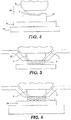
- a method of removing the portion of the liquid 7 such as water absorbed by the last-stage optical element 4 made of a hygroscopic material, as well as dirt, debris, etc., is explained next with reference to Figs. 1 and 4 .
- the liquid 7 is removed from underneath the light projection unit PL and a cleaning device 30 is brought into contact with the last-stage optical element 4 as shown in Fig. 4 .
- the cleaning device 30 may be placed on the Z-stage 9 or the aforementioned wafer holder thereon, as shown in Fig. 4 , in place of the wafer W.
- the cleaning device 30 maybe a container containing a liquid ("cleaning liquid") with a strong affinity to the immersion liquid 7 which is absorbed by the optical element 4.
- the immersion liquid 7 is water
- the cleaning device 30 may contain ethanol since ethanol has a strong affinity to water.
- Any cleaning liquid may be used provided it has a sufficiently strong affinity to the liquid to be removed and does not damage the optical element 4 or its coating.
- the bottom surface of the optical element 4 is soaked in the cleaning liquid for a period of time sufficiently long to reduce the level of the absorbed liquid. The cleaning device 30 is removed thereafter and the optical element 4 is ready to be exposed to the liquid 7 again.
- the cleaning device 30 may contain a heat-generating device and/or a vacuum device (not separately shown).
- the combination of heat and vacuum on the surface of the optical element 4 causes the absorbed liquid to undergo a phase change into vapor, or to evaporate from the surface.
- the reduction in liquid density on the surface of the optical element 4 draws the liquid 7 that is absorbed more deeply in the element 4 to the surface.
- Fig. 5 shows a third example wherein use is made of an ultrasonic transducer (or ultrasonic vibrator) 32 attached to the housing 3 of the light projection unit PL.
- the ultrasonic transducer 32 such as a piezoelectric transducer
- pressure waves are generated and propagated, serving to clean the surface of the optical element 4.
- the gap adjacent the optical element 4 is filled with the immersion liquid 7.
- the supply and recovery nozzles can continue to supply and collect the immersion liquid 7, or the supply and recovery nozzles can stop supplying and collecting the immersion liquid 7.
- the optical element 4 can face a surface of wafer W, a surface of the Z-stage 9, or a surface of another assembly.
- Fig. 6 is a fourth example using a vibratory tool 34 placed below the optical element 4 to be cleaned.
- the tool 34 may be shaped like the wafer W with thickness more or less equal to that of the wafer "W, or about 0.5-1mm, and may be made entirely of a piezoelectric material such that its thickness will fluctuate when activated.
- pressure waves are generated in the immersion liquid 7 to clean the optical element.
- the gap adjacent the optical element 4 is filled with the immersion liquid 7.
- the supply and recovery nozzles can continue to supply and collect the immersion liquid, or the supply and recovery nozzles can stop supplying and collecting the immersion liquid 7.
- the vibrator tool 34 may be a ultrasonic transducer attached to the wafer holder on a Z-stage 9, or another assembly.
- Fig. 7 shows another tool 36, structured alternatively, having a plurality of piezoelectric transducers 38 supported by a planar supporting member 39.
- Fig. 8 shows still another example of a cleaning device having two planar members 40 of a piezoelectric material attached in a face-to-face relationship and adapted to oscillate parallel to each other and out of phase by 180° with respect to each other.
- these members 40 attached to each other, will vibrate in the transverse directions, as shown in Fig. 8 in a very exaggerated manner.
- the vibration has node points at constant intervals where the members 40 are not displaced.
- the members 40 are supported at these node points on a supporting member 41.
- voltages are applied to these members 40 so as to cause the vibrations in the mode described above, ultrasonic pressure waves are thereby generated and propagated through the liquid 7, and the optical element 4 is cleaned, as desired.
- Fig. 9 shows still another example of a liquid removal system characterized as cleaning the optical element 4 by creating cavitating bubbles. Cavitating bubbles trapped and energized by ultrasound are high-temperature, high-pressure microreactors and intense energy released by the implosive compression of the bubbles is believed to rip molecules apart.
- the example shown in Fig. 9 is characterized as comprising a pad 43 with fins protruding upwards and rapidly moved horizontally as shown by an arrow below the optical element 4 with a bubble-generating liquid 17 filling the gap in between (means for moving the pad 43 not being shown). As the pad 43 is thus moved, the fins serve to stir the liquid 17 and to generate cavitating bubbles which in turn serve to clean the optical element.
- Fig. 10 shows a different approach to the problem of cleaning the last-stage optical element 4 by applying a cleaning liquid on its bottom surface by using the same source nozzles 21 used for supplying the immersion liquid 7.
- a switch valve 25 is inserted between the supply nozzle 21 and the liquid unit 5 such that the immersion liquid 7 and the cleaning liquid can be supplied selectively through the supply nozzle 21.
- a switch valve as described above need not necessarily be provided to each of the source nozzles but may be provided to a group of the source nozzles.
- This disclosure is advantageous because the same nozzles already present for supplying the immersion liquid can be utilized for the cleaning process.
- the pad 43 with fins shown in Fig. 9 may be used instead of the pad 18 of Fig. 10 .
- the examples described above are not intended to limit the scope of the invention and many modifications and variations are possible within the scope of this invention.
- a polishing pad similar to one used in chemical mechanical polishing may be used for this purpose.
- the cleanup procedure shown in Figs. 4-10 may be carried out with ultraviolet light.
- the light may irradiate the optical element 4.
- the light may be normal exposure light from the illuminator optical unit 1 or some other light of an appropriate wavelength for the purpose of the cleanup.
- the ultraviolet light for the purpose of the cleanup may be used without the cleanup procedure shown in Figs. 4-10 , and may be used under a condition in which the gap adjacent the optical element 4 is filled with the immersion liquid 7 from the liquid supply unit 5. All such modifications and variations that may be apparent to a person skilled in the art are intended to be within the scope of this invention.
- any of the above described cleaning methods for removing immersion fluid absorbed by the last-stage optical element as well as salts, deposits, dirt and debris that may have accumulated as well as salts, deposits, dirt and debris that may have accumulated.
- cleaning therefore refers to both of these phenomena herein.
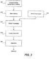
- Fig. 2 is referenced next to describe a process for fabricating a semiconductor device by using an immersion lithography apparatus incorporating a liquid jet and recovery system embodying this invention.
- step 301 the device's function and performance characteristics are designed.
- step 302 a mask (reticle) having a pattern is designed according to the previous designing step, and in a parallel step 303, a wafer is made from a silicon material.
- the mask pattern designed in step 302 is exposed onto the wafer from step 303 in step 304 by a photolithography system such as the systems described above.
- step 305 the semiconductor device is assembled (including the dicing process, bonding process and packaging process), then finally the device is inspected in step 306.
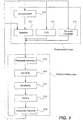
- Fig. 3 illustrates a detailed flowchart example of the above-mentioned step 304 in the case of fabricating semiconductor devices.
- step 311 oxidation step
- step 312 CVD step
- step 313 electrode formation step
- step 314 ion implantation step
- ions are implanted in the wafer.
- the aforementioned steps 311-314 form the preprocessing steps for wafers during wafer processing, and selection is made at each step according to processing requirements.
- step 315 photoresist formation step
- step 316 exposure step
- step 317 developer step
- step 318 etching step
- steps 319 photoresist removal step
Landscapes
- Health & Medical Sciences (AREA)
- Physics & Mathematics (AREA)
- Public Health (AREA)
- Epidemiology (AREA)
- General Physics & Mathematics (AREA)
- Engineering & Computer Science (AREA)
- Atmospheric Sciences (AREA)
- Life Sciences & Earth Sciences (AREA)
- Environmental & Geological Engineering (AREA)
- Toxicology (AREA)
- Plasma & Fusion (AREA)
- Power Engineering (AREA)
- Microelectronics & Electronic Packaging (AREA)
- Computer Hardware Design (AREA)
- Manufacturing & Machinery (AREA)
- Condensed Matter Physics & Semiconductors (AREA)
- Exposure And Positioning Against Photoresist Photosensitive Materials (AREA)
- Exposure Of Semiconductors, Excluding Electron Or Ion Beam Exposure (AREA)
- Crystals, And After-Treatments Of Crystals (AREA)
- Container, Conveyance, Adherence, Positioning, Of Wafer (AREA)
- Cleaning In General (AREA)
- Cleaning By Liquid Or Steam (AREA)
Applications Claiming Priority (4)
| Application Number | Priority Date | Filing Date | Title |
|---|---|---|---|
| US46255603P | 2003-04-11 | 2003-04-11 | |
| US48291303P | 2003-06-27 | 2003-06-27 | |
| PCT/US2004/010309 WO2004093130A2 (en) | 2003-04-11 | 2004-04-02 | Cleanup method for optics in immersion lithography |
| EP04759103A EP1614001B1 (en) | 2003-04-11 | 2004-04-02 | Cleanup method for optics in immersion lithography |
Related Parent Applications (2)
| Application Number | Title | Priority Date | Filing Date |
|---|---|---|---|
| EP04759103.7 Division | 2004-04-02 | ||
| EP04759103A Division EP1614001B1 (en) | 2003-04-11 | 2004-04-02 | Cleanup method for optics in immersion lithography |
Publications (2)
| Publication Number | Publication Date |
|---|---|
| EP2161621A1 EP2161621A1 (en) | 2010-03-10 |
| EP2161621B1 true EP2161621B1 (en) | 2018-10-24 |
Family
ID=33303091
Family Applications (6)
| Application Number | Title | Priority Date | Filing Date |
|---|---|---|---|
| EP09176911.7A Expired - Lifetime EP2161621B1 (en) | 2003-04-11 | 2004-04-02 | Cleanup method for optics in an immersion lithography apparatus, and corresponding immersion lithography apparatus |
| EP09176910A Withdrawn EP2161620A1 (en) | 2003-04-11 | 2004-04-02 | Cleanup method for optics in immersion lithography |
| EP09176913A Withdrawn EP2166413A1 (en) | 2003-04-11 | 2004-04-02 | Cleanup method for optics in immersion lithography |
| EP09176909.1A Expired - Lifetime EP2161619B8 (en) | 2003-04-11 | 2004-04-02 | Cleanup method and immersion lithography apparatus |
| EP09176912.5A Expired - Lifetime EP2172809B1 (en) | 2003-04-11 | 2004-04-02 | Cleanup method for optics in an immersion lithography apparatus, and corresponding immersion lithography apparatus |
| EP04759103A Expired - Lifetime EP1614001B1 (en) | 2003-04-11 | 2004-04-02 | Cleanup method for optics in immersion lithography |
Family Applications After (5)
| Application Number | Title | Priority Date | Filing Date |
|---|---|---|---|
| EP09176910A Withdrawn EP2161620A1 (en) | 2003-04-11 | 2004-04-02 | Cleanup method for optics in immersion lithography |
| EP09176913A Withdrawn EP2166413A1 (en) | 2003-04-11 | 2004-04-02 | Cleanup method for optics in immersion lithography |
| EP09176909.1A Expired - Lifetime EP2161619B8 (en) | 2003-04-11 | 2004-04-02 | Cleanup method and immersion lithography apparatus |
| EP09176912.5A Expired - Lifetime EP2172809B1 (en) | 2003-04-11 | 2004-04-02 | Cleanup method for optics in an immersion lithography apparatus, and corresponding immersion lithography apparatus |
| EP04759103A Expired - Lifetime EP1614001B1 (en) | 2003-04-11 | 2004-04-02 | Cleanup method for optics in immersion lithography |
Country Status (9)
| Country | Link |
|---|---|
| US (10) | US7522259B2 (enExample) |
| EP (6) | EP2161621B1 (enExample) |
| JP (10) | JP4837556B2 (enExample) |
| KR (11) | KR20170016014A (enExample) |
| CN (4) | CN103558736B (enExample) |
| AT (1) | ATE449982T1 (enExample) |
| DE (1) | DE602004024295D1 (enExample) |
| SG (5) | SG10201803122UA (enExample) |
| WO (1) | WO2004093130A2 (enExample) |
Families Citing this family (227)
| Publication number | Priority date | Publication date | Assignee | Title |
|---|---|---|---|---|
| US9482966B2 (en) | 2002-11-12 | 2016-11-01 | Asml Netherlands B.V. | Lithographic apparatus and device manufacturing method |
| EP1420299B1 (en) * | 2002-11-12 | 2011-01-05 | ASML Netherlands B.V. | Immersion lithographic apparatus and device manufacturing method |
| US10503084B2 (en) | 2002-11-12 | 2019-12-10 | Asml Netherlands B.V. | Lithographic apparatus and device manufacturing method |
| US7372541B2 (en) | 2002-11-12 | 2008-05-13 | Asml Netherlands B.V. | Lithographic apparatus and device manufacturing method |
| KR100588124B1 (ko) | 2002-11-12 | 2006-06-09 | 에이에스엠엘 네델란즈 비.브이. | 리소그래피장치 및 디바이스제조방법 |
| SG121818A1 (en) | 2002-11-12 | 2006-05-26 | Asml Netherlands Bv | Lithographic apparatus and device manufacturing method |
| DE60335595D1 (de) | 2002-11-12 | 2011-02-17 | Asml Netherlands Bv | Lithographischer Apparat mit Immersion und Verfahren zur Herstellung einer Vorrichtung |
| EP1571697A4 (en) | 2002-12-10 | 2007-07-04 | Nikon Corp | EXPOSURE SYSTEM AND DEVICE PRODUCTION METHOD |
| US7948604B2 (en) | 2002-12-10 | 2011-05-24 | Nikon Corporation | Exposure apparatus and method for producing device |
| KR101036114B1 (ko) | 2002-12-10 | 2011-05-23 | 가부시키가이샤 니콘 | 노광장치 및 노광방법, 디바이스 제조방법 |
| SG158745A1 (en) | 2002-12-10 | 2010-02-26 | Nikon Corp | Exposure apparatus and method for producing device |
| JP4352874B2 (ja) | 2002-12-10 | 2009-10-28 | 株式会社ニコン | 露光装置及びデバイス製造方法 |
| WO2004053952A1 (ja) | 2002-12-10 | 2004-06-24 | Nikon Corporation | 露光装置及びデバイス製造方法 |
| US7242455B2 (en) | 2002-12-10 | 2007-07-10 | Nikon Corporation | Exposure apparatus and method for producing device |
| DE10261775A1 (de) | 2002-12-20 | 2004-07-01 | Carl Zeiss Smt Ag | Vorrichtung zur optischen Vermessung eines Abbildungssystems |
| EP1598855B1 (en) | 2003-02-26 | 2015-04-22 | Nikon Corporation | Exposure apparatus and method, and method of producing apparatus |
| KR101345474B1 (ko) | 2003-03-25 | 2013-12-27 | 가부시키가이샤 니콘 | 노광 장치 및 디바이스 제조 방법 |
| WO2004090956A1 (ja) | 2003-04-07 | 2004-10-21 | Nikon Corporation | 露光装置及びデバイス製造方法 |
| JP4488004B2 (ja) | 2003-04-09 | 2010-06-23 | 株式会社ニコン | 液浸リソグラフィ流体制御システム |
| KR101323993B1 (ko) | 2003-04-10 | 2013-10-30 | 가부시키가이샤 니콘 | 액침 리소그래피 장치용 운반 영역을 포함하는 환경 시스템 |
| CN1771463A (zh) | 2003-04-10 | 2006-05-10 | 株式会社尼康 | 用于沉浸光刻装置收集液体的溢出通道 |
| CN101061429B (zh) | 2003-04-10 | 2015-02-04 | 株式会社尼康 | 包括用于沉浸光刻装置的真空清除的环境系统 |
| SG139733A1 (en) | 2003-04-11 | 2008-02-29 | Nikon Corp | Apparatus having an immersion fluid system configured to maintain immersion fluid in a gap adjacent an optical assembly |
| EP2161621B1 (en) | 2003-04-11 | 2018-10-24 | Nikon Corporation | Cleanup method for optics in an immersion lithography apparatus, and corresponding immersion lithography apparatus |
| WO2004092830A2 (en) | 2003-04-11 | 2004-10-28 | Nikon Corporation | Liquid jet and recovery system for immersion lithography |
| KR101369582B1 (ko) | 2003-04-17 | 2014-03-04 | 가부시키가이샤 니콘 | 액침 리소그래피에서 이용하기 위한 오토포커스 소자의 광학적 배열 |
| TWI295414B (en) | 2003-05-13 | 2008-04-01 | Asml Netherlands Bv | Lithographic apparatus and device manufacturing method |
| WO2004102646A1 (ja) | 2003-05-15 | 2004-11-25 | Nikon Corporation | 露光装置及びデバイス製造方法 |
| TWI424470B (zh) | 2003-05-23 | 2014-01-21 | 尼康股份有限公司 | A method of manufacturing an exposure apparatus and an element |
| TWI614794B (zh) | 2003-05-23 | 2018-02-11 | Nikon Corp | 曝光方法及曝光裝置以及元件製造方法 |
| EP2453465A3 (en) | 2003-05-28 | 2018-01-03 | Nikon Corporation | Exposure method, exposure apparatus, and method for producing a device |
| US7213963B2 (en) | 2003-06-09 | 2007-05-08 | Asml Netherlands B.V. | Lithographic apparatus and device manufacturing method |
| EP1486827B1 (en) | 2003-06-11 | 2011-11-02 | ASML Netherlands B.V. | Lithographic apparatus and device manufacturing method |
| US7317504B2 (en) | 2004-04-08 | 2008-01-08 | Asml Netherlands B.V. | Lithographic apparatus and device manufacturing method |
| KR101520591B1 (ko) | 2003-06-13 | 2015-05-14 | 가부시키가이샤 니콘 | 노광 방법, 기판 스테이지, 노광 장치, 및 디바이스 제조 방법 |
| TWI543235B (zh) | 2003-06-19 | 2016-07-21 | 尼康股份有限公司 | A method of manufacturing an exposure apparatus and an element |
| US6867844B2 (en) | 2003-06-19 | 2005-03-15 | Asml Holding N.V. | Immersion photolithography system and method using microchannel nozzles |
| US6809794B1 (en) | 2003-06-27 | 2004-10-26 | Asml Holding N.V. | Immersion photolithography system and method using inverted wafer-projection optics interface |
| DE60308161T2 (de) | 2003-06-27 | 2007-08-09 | Asml Netherlands B.V. | Lithographischer Apparat und Verfahren zur Herstellung eines Artikels |
| US7236232B2 (en) | 2003-07-01 | 2007-06-26 | Nikon Corporation | Using isotopically specified fluids as optical elements |
| JP4697138B2 (ja) | 2003-07-08 | 2011-06-08 | 株式会社ニコン | 液浸リソグラフィ装置、液浸リソグラフィ方法、デバイス製造方法 |
| EP2264531B1 (en) | 2003-07-09 | 2013-01-16 | Nikon Corporation | Exposure apparatus and device manufacturing method |
| KR101296501B1 (ko) | 2003-07-09 | 2013-08-13 | 가부시키가이샤 니콘 | 노광 장치 및 디바이스 제조 방법 |
| EP1643543B1 (en) | 2003-07-09 | 2010-11-24 | Nikon Corporation | Exposure apparatus and method for manufacturing device |
| EP1650787A4 (en) | 2003-07-25 | 2007-09-19 | Nikon Corp | INVESTIGATION METHOD AND INVESTIGATION DEVICE FOR AN OPTICAL PROJECTION SYSTEM AND METHOD OF MANUFACTURING AN OPTICAL PROJECTION SYSTEM |
| CN104122760B (zh) | 2003-07-28 | 2017-04-19 | 株式会社尼康 | 曝光装置、器件制造方法 |
| EP1503244A1 (en) | 2003-07-28 | 2005-02-02 | ASML Netherlands B.V. | Lithographic projection apparatus and device manufacturing method |
| US7175968B2 (en) | 2003-07-28 | 2007-02-13 | Asml Netherlands B.V. | Lithographic apparatus, device manufacturing method and a substrate |
| US7326522B2 (en) | 2004-02-11 | 2008-02-05 | Asml Netherlands B.V. | Device manufacturing method and a substrate |
| US7779781B2 (en) | 2003-07-31 | 2010-08-24 | Asml Netherlands B.V. | Lithographic apparatus and device manufacturing method |
| US7370659B2 (en) * | 2003-08-06 | 2008-05-13 | Micron Technology, Inc. | Photolithographic stepper and/or scanner machines including cleaning devices and methods of cleaning photolithographic stepper and/or scanner machines |
| TWI245163B (en) | 2003-08-29 | 2005-12-11 | Asml Netherlands Bv | Lithographic apparatus and device manufacturing method |
| TWI263859B (en) | 2003-08-29 | 2006-10-11 | Asml Netherlands Bv | Lithographic apparatus and device manufacturing method |
| SG145780A1 (en) * | 2003-08-29 | 2008-09-29 | Nikon Corp | Exposure apparatus and device fabricating method |
| KR20170070264A (ko) | 2003-09-03 | 2017-06-21 | 가부시키가이샤 니콘 | 액침 리소그래피용 유체를 제공하기 위한 장치 및 방법 |
| JP4444920B2 (ja) | 2003-09-19 | 2010-03-31 | 株式会社ニコン | 露光装置及びデバイス製造方法 |
| KR101238134B1 (ko) | 2003-09-26 | 2013-02-28 | 가부시키가이샤 니콘 | 투영노광장치 및 투영노광장치의 세정방법, 메인터넌스 방법 그리고 디바이스의 제조방법 |
| EP1670043B1 (en) | 2003-09-29 | 2013-02-27 | Nikon Corporation | Exposure apparatus, exposure method, and device manufacturing method |
| KR101111364B1 (ko) | 2003-10-08 | 2012-02-27 | 가부시키가이샤 자오 니콘 | 기판 반송 장치 및 기판 반송 방법, 노광 장치 및 노광방법, 디바이스 제조 방법 |
| WO2005036623A1 (ja) | 2003-10-08 | 2005-04-21 | Zao Nikon Co., Ltd. | 基板搬送装置及び基板搬送方法、露光装置及び露光方法、デバイス製造方法 |
| JP2005136364A (ja) | 2003-10-08 | 2005-05-26 | Zao Nikon Co Ltd | 基板搬送装置、露光装置、並びにデバイス製造方法 |
| TW201738932A (zh) | 2003-10-09 | 2017-11-01 | Nippon Kogaku Kk | 曝光裝置及曝光方法、元件製造方法 |
| US7411653B2 (en) | 2003-10-28 | 2008-08-12 | Asml Netherlands B.V. | Lithographic apparatus |
| US7352433B2 (en) | 2003-10-28 | 2008-04-01 | Asml Netherlands B.V. | Lithographic apparatus and device manufacturing method |
| EP1531362A3 (en) * | 2003-11-13 | 2007-07-25 | Matsushita Electric Industrial Co., Ltd. | Semiconductor manufacturing apparatus and pattern formation method |
| JP4295712B2 (ja) | 2003-11-14 | 2009-07-15 | エーエスエムエル ネザーランズ ビー.ブイ. | リソグラフィ装置及び装置製造方法 |
| EP3139214B1 (en) | 2003-12-03 | 2019-01-30 | Nikon Corporation | Exposure apparatus, exposure method, and device manufacturing method |
| DE602004030481D1 (de) | 2003-12-15 | 2011-01-20 | Nippon Kogaku Kk | Bühnensystem, belichtungsvorrichtung und belichtungsverfahren |
| JP4308638B2 (ja) | 2003-12-17 | 2009-08-05 | パナソニック株式会社 | パターン形成方法 |
| US7394521B2 (en) | 2003-12-23 | 2008-07-01 | Asml Netherlands B.V. | Lithographic apparatus and device manufacturing method |
| JP4371822B2 (ja) * | 2004-01-06 | 2009-11-25 | キヤノン株式会社 | 露光装置 |
| EP1706793B1 (en) | 2004-01-20 | 2010-03-03 | Carl Zeiss SMT AG | Exposure apparatus and measuring device for a projection lens |
| US7589822B2 (en) | 2004-02-02 | 2009-09-15 | Nikon Corporation | Stage drive method and stage unit, exposure apparatus, and device manufacturing method |
| WO2005076321A1 (ja) | 2004-02-03 | 2005-08-18 | Nikon Corporation | 露光装置及びデバイス製造方法 |
| US7050146B2 (en) | 2004-02-09 | 2006-05-23 | Asml Netherlands B.V. | Lithographic apparatus and device manufacturing method |
| JP4548341B2 (ja) * | 2004-02-10 | 2010-09-22 | 株式会社ニコン | 露光装置及びデバイス製造方法、メンテナンス方法及び露光方法 |
| US20050205108A1 (en) * | 2004-03-16 | 2005-09-22 | Taiwan Semiconductor Manufacturing Co., Ltd. | Method and system for immersion lithography lens cleaning |
| JP4525676B2 (ja) | 2004-03-25 | 2010-08-18 | 株式会社ニコン | 露光装置、露光方法、及びデバイス製造方法 |
| US7034917B2 (en) | 2004-04-01 | 2006-04-25 | Asml Netherlands B.V. | Lithographic apparatus, device manufacturing method and device manufactured thereby |
| US7898642B2 (en) | 2004-04-14 | 2011-03-01 | Asml Netherlands B.V. | Lithographic apparatus and device manufacturing method |
| US8054448B2 (en) | 2004-05-04 | 2011-11-08 | Nikon Corporation | Apparatus and method for providing fluid for immersion lithography |
| US7616383B2 (en) * | 2004-05-18 | 2009-11-10 | Asml Netherlands B.V. | Lithographic apparatus and device manufacturing method |
| WO2005119368A2 (en) | 2004-06-04 | 2005-12-15 | Carl Zeiss Smt Ag | System for measuring the image quality of an optical imaging system |
| WO2005122218A1 (ja) * | 2004-06-09 | 2005-12-22 | Nikon Corporation | 露光装置及びデバイス製造方法 |
| JP4677833B2 (ja) * | 2004-06-21 | 2011-04-27 | 株式会社ニコン | 露光装置、及びその部材の洗浄方法、露光装置のメンテナンス方法、メンテナンス機器、並びにデバイス製造方法 |
| US8698998B2 (en) | 2004-06-21 | 2014-04-15 | Nikon Corporation | Exposure apparatus, method for cleaning member thereof, maintenance method for exposure apparatus, maintenance device, and method for producing device |
| KR101245070B1 (ko) * | 2004-06-21 | 2013-03-18 | 가부시키가이샤 니콘 | 노광 장치 및 그 부재의 세정 방법, 노광 장치의 메인터넌스 방법, 메인터넌스 기기, 그리고 디바이스 제조 방법 |
| US20060001851A1 (en) | 2004-07-01 | 2006-01-05 | Grant Robert B | Immersion photolithography system |
| US7463330B2 (en) | 2004-07-07 | 2008-12-09 | Asml Netherlands B.V. | Lithographic apparatus and device manufacturing method |
| KR101342330B1 (ko) | 2004-07-12 | 2013-12-16 | 가부시키가이샤 니콘 | 노광 장치 및 디바이스 제조 방법 |
| JP2006032750A (ja) * | 2004-07-20 | 2006-02-02 | Canon Inc | 液浸型投影露光装置、及びデバイス製造方法 |
| US7224427B2 (en) | 2004-08-03 | 2007-05-29 | Taiwan Semiconductor Manufacturing Company, Ltd. | Megasonic immersion lithography exposure apparatus and method |
| JP4983257B2 (ja) | 2004-08-18 | 2012-07-25 | 株式会社ニコン | 露光装置、デバイス製造方法、計測部材、及び計測方法 |
| US7701550B2 (en) | 2004-08-19 | 2010-04-20 | Asml Netherlands B.V. | Lithographic apparatus and device manufacturing method |
| JP4772306B2 (ja) * | 2004-09-06 | 2011-09-14 | 株式会社東芝 | 液浸光学装置及び洗浄方法 |
| US7385670B2 (en) * | 2004-10-05 | 2008-06-10 | Asml Netherlands B.V. | Lithographic apparatus, cleaning system and cleaning method for in situ removing contamination from a component in a lithographic apparatus |
| EP1814144B1 (en) | 2004-10-26 | 2012-06-06 | Nikon Corporation | Substrate processing method and device production system |
| US7414699B2 (en) * | 2004-11-12 | 2008-08-19 | Asml Netherlands B.V. | Lithographic apparatus and device manufacturing method |
| US7411657B2 (en) | 2004-11-17 | 2008-08-12 | Asml Netherlands B.V. | Lithographic apparatus and device manufacturing method |
| KR101191056B1 (ko) | 2004-11-19 | 2012-10-15 | 가부시키가이샤 니콘 | 메인터넌스 방법, 노광 방법, 노광 장치 및 디바이스 제조 방법 |
| US7732123B2 (en) * | 2004-11-23 | 2010-06-08 | Taiwan Semiconductor Manufacturing Company, Ltd. | Immersion photolithography with megasonic rinse |
| US7446850B2 (en) | 2004-12-03 | 2008-11-04 | Asml Netherlands B.V. | Lithographic apparatus and device manufacturing method |
| WO2006062065A1 (ja) | 2004-12-06 | 2006-06-15 | Nikon Corporation | メンテナンス方法、メンテナンス機器、露光装置、及びデバイス製造方法 |
| US7196770B2 (en) | 2004-12-07 | 2007-03-27 | Asml Netherlands B.V. | Prewetting of substrate before immersion exposure |
| US7397533B2 (en) | 2004-12-07 | 2008-07-08 | Asml Netherlands B.V. | Lithographic apparatus and device manufacturing method |
| US7365827B2 (en) | 2004-12-08 | 2008-04-29 | Asml Netherlands B.V. | Lithographic apparatus and device manufacturing method |
| US7352440B2 (en) | 2004-12-10 | 2008-04-01 | Asml Netherlands B.V. | Substrate placement in immersion lithography |
| US7403261B2 (en) | 2004-12-15 | 2008-07-22 | Asml Netherlands B.V. | Lithographic apparatus and device manufacturing method |
| US7528931B2 (en) | 2004-12-20 | 2009-05-05 | Asml Netherlands B.V. | Lithographic apparatus and device manufacturing method |
| US7880860B2 (en) | 2004-12-20 | 2011-02-01 | Asml Netherlands B.V. | Lithographic apparatus and device manufacturing method |
| US7405805B2 (en) | 2004-12-28 | 2008-07-29 | Asml Netherlands B.V. | Lithographic apparatus and device manufacturing method |
| US7491661B2 (en) | 2004-12-28 | 2009-02-17 | Asml Netherlands B.V. | Device manufacturing method, top coat material and substrate |
| US7450217B2 (en) | 2005-01-12 | 2008-11-11 | Asml Netherlands B.V. | Exposure apparatus, coatings for exposure apparatus, lithographic apparatus, device manufacturing method, and device manufactured thereby |
| SG124359A1 (en) | 2005-01-14 | 2006-08-30 | Asml Netherlands Bv | Lithographic apparatus and device manufacturing method |
| KR20160135859A (ko) | 2005-01-31 | 2016-11-28 | 가부시키가이샤 니콘 | 노광 장치 및 디바이스 제조 방법 |
| US8692973B2 (en) | 2005-01-31 | 2014-04-08 | Nikon Corporation | Exposure apparatus and method for producing device |
| WO2006084641A2 (en) | 2005-02-10 | 2006-08-17 | Asml Netherlands B.V. | Immersion liquid, exposure apparatus, and exposure process |
| US7378025B2 (en) | 2005-02-22 | 2008-05-27 | Asml Netherlands B.V. | Fluid filtration method, fluid filtered thereby, lithographic apparatus and device manufacturing method |
| US7224431B2 (en) | 2005-02-22 | 2007-05-29 | Asml Netherlands B.V. | Lithographic apparatus and device manufacturing method |
| US8018573B2 (en) | 2005-02-22 | 2011-09-13 | Asml Netherlands B.V. | Lithographic apparatus and device manufacturing method |
| US7282701B2 (en) | 2005-02-28 | 2007-10-16 | Asml Netherlands B.V. | Sensor for use in a lithographic apparatus |
| US7428038B2 (en) | 2005-02-28 | 2008-09-23 | Asml Netherlands B.V. | Lithographic apparatus, device manufacturing method and apparatus for de-gassing a liquid |
| US7324185B2 (en) | 2005-03-04 | 2008-01-29 | Asml Netherlands B.V. | Lithographic apparatus and device manufacturing method |
| JP4072543B2 (ja) | 2005-03-18 | 2008-04-09 | キヤノン株式会社 | 液浸露光装置及びデバイス製造方法 |
| US7330238B2 (en) | 2005-03-28 | 2008-02-12 | Asml Netherlands, B.V. | Lithographic apparatus, immersion projection apparatus and device manufacturing method |
| US7411654B2 (en) | 2005-04-05 | 2008-08-12 | Asml Netherlands B.V. | Lithographic apparatus and device manufacturing method |
| USRE43576E1 (en) | 2005-04-08 | 2012-08-14 | Asml Netherlands B.V. | Dual stage lithographic apparatus and device manufacturing method |
| US7291850B2 (en) | 2005-04-08 | 2007-11-06 | Asml Netherlands B.V. | Lithographic apparatus and device manufacturing method |
| US20060232753A1 (en) | 2005-04-19 | 2006-10-19 | Asml Holding N.V. | Liquid immersion lithography system with tilted liquid flow |
| US7433016B2 (en) | 2005-05-03 | 2008-10-07 | Asml Netherlands B.V. | Lithographic apparatus and device manufacturing method |
| US8248577B2 (en) | 2005-05-03 | 2012-08-21 | Asml Netherlands B.V. | Lithographic apparatus and device manufacturing method |
| US20060250588A1 (en) * | 2005-05-03 | 2006-11-09 | Stefan Brandl | Immersion exposure tool cleaning system and method |
| US7317507B2 (en) | 2005-05-03 | 2008-01-08 | Asml Netherlands B.V. | Lithographic apparatus and device manufacturing method |
| WO2006137410A1 (ja) * | 2005-06-21 | 2006-12-28 | Nikon Corporation | 露光装置及び露光方法、メンテナンス方法、並びにデバイス製造方法 |
| US7652746B2 (en) | 2005-06-21 | 2010-01-26 | Asml Netherlands B.V. | Lithographic apparatus and device manufacturing method |
| US7474379B2 (en) | 2005-06-28 | 2009-01-06 | Asml Netherlands B.V. | Lithographic apparatus and device manufacturing method |
| US7834974B2 (en) | 2005-06-28 | 2010-11-16 | Asml Netherlands B.V. | Lithographic apparatus and device manufacturing method |
| US7468779B2 (en) | 2005-06-28 | 2008-12-23 | Asml Netherlands B.V. | Lithographic apparatus and device manufacturing method |
| WO2007004552A1 (ja) | 2005-06-30 | 2007-01-11 | Nikon Corporation | 露光装置及び方法、露光装置のメンテナンス方法、並びにデバイス製造方法 |
| US7262422B2 (en) * | 2005-07-01 | 2007-08-28 | Spansion Llc | Use of supercritical fluid to dry wafer and clean lens in immersion lithography |
| US7583358B2 (en) * | 2005-07-25 | 2009-09-01 | Micron Technology, Inc. | Systems and methods for retrieving residual liquid during immersion lens photolithography |
| US8054445B2 (en) | 2005-08-16 | 2011-11-08 | Asml Netherlands B.V. | Lithographic apparatus and device manufacturing method |
| US7456928B2 (en) * | 2005-08-29 | 2008-11-25 | Micron Technology, Inc. | Systems and methods for controlling ambient pressure during processing of microfeature workpieces, including during immersion lithography |
| US7411658B2 (en) | 2005-10-06 | 2008-08-12 | Asml Netherlands B.V. | Lithographic apparatus and device manufacturing method |
| US7986395B2 (en) * | 2005-10-24 | 2011-07-26 | Taiwan Semiconductor Manufacturing Company, Ltd. | Immersion lithography apparatus and methods |
| JP5036996B2 (ja) * | 2005-10-31 | 2012-09-26 | 東京応化工業株式会社 | 洗浄液および洗浄方法 |
| JP2007123775A (ja) * | 2005-10-31 | 2007-05-17 | Tokyo Ohka Kogyo Co Ltd | 洗浄液および洗浄方法 |
| US7804577B2 (en) | 2005-11-16 | 2010-09-28 | Asml Netherlands B.V. | Lithographic apparatus |
| US7864292B2 (en) | 2005-11-16 | 2011-01-04 | Asml Netherlands B.V. | Lithographic apparatus and device manufacturing method |
| JP2007142217A (ja) * | 2005-11-18 | 2007-06-07 | Taiwan Semiconductor Manufacturing Co Ltd | イマージョン式リソグラフィ露光装置およびその方法 |
| FR2893725B1 (fr) * | 2005-11-21 | 2009-05-29 | Taiwan Semiconductor Mfg | Dispositif et procede d'exposition de lithographie par immersion megasonique |
| TWI413155B (zh) | 2005-11-22 | 2013-10-21 | Tokyo Ohka Kogyo Co Ltd | 光微影蝕刻用洗淨液及使用其之曝光裝置之洗淨方法 |
| US7633073B2 (en) | 2005-11-23 | 2009-12-15 | Asml Netherlands B.V. | Lithographic apparatus and device manufacturing method |
| US7773195B2 (en) | 2005-11-29 | 2010-08-10 | Asml Holding N.V. | System and method to increase surface tension and contact angle in immersion lithography |
| JP2007150102A (ja) * | 2005-11-29 | 2007-06-14 | Fujitsu Ltd | 露光装置及び光学素子の洗浄方法 |
| US8125610B2 (en) | 2005-12-02 | 2012-02-28 | ASML Metherlands B.V. | Method for preventing or reducing contamination of an immersion type projection apparatus and an immersion type lithographic apparatus |
| US7420194B2 (en) | 2005-12-27 | 2008-09-02 | Asml Netherlands B.V. | Lithographic apparatus and substrate edge seal |
| US7649611B2 (en) | 2005-12-30 | 2010-01-19 | Asml Netherlands B.V. | Lithographic apparatus and device manufacturing method |
| US8472004B2 (en) * | 2006-01-18 | 2013-06-25 | Micron Technology, Inc. | Immersion photolithography scanner |
| KR20080114691A (ko) * | 2006-03-13 | 2008-12-31 | 가부시키가이샤 니콘 | 노광 장치, 메인터넌스 방법, 노광 방법 및 디바이스 제조 방법 |
| US8045134B2 (en) | 2006-03-13 | 2011-10-25 | Asml Netherlands B.V. | Lithographic apparatus, control system and device manufacturing method |
| CN101416076A (zh) | 2006-04-03 | 2009-04-22 | 株式会社尼康 | 对浸没液体为疏溶的入射表面和光学窗 |
| US9477158B2 (en) | 2006-04-14 | 2016-10-25 | Asml Netherlands B.V. | Lithographic apparatus and device manufacturing method |
| DE102006021797A1 (de) | 2006-05-09 | 2007-11-15 | Carl Zeiss Smt Ag | Optische Abbildungseinrichtung mit thermischer Dämpfung |
| SG175671A1 (en) | 2006-05-18 | 2011-11-28 | Nikon Corp | Exposure method and apparatus, maintenance method and device manufacturing method |
| US7969548B2 (en) * | 2006-05-22 | 2011-06-28 | Asml Netherlands B.V. | Lithographic apparatus and lithographic apparatus cleaning method |
| KR20090023331A (ko) * | 2006-05-23 | 2009-03-04 | 가부시키가이샤 니콘 | 메인터넌스 방법, 노광 방법 및 장치, 그리고 디바이스 제조 방법 |
| US20070280526A1 (en) * | 2006-05-30 | 2007-12-06 | Irfan Malik | Determining Information about Defects or Binning Defects Detected on a Wafer after an Immersion Lithography Process is Performed on the Wafer |
| US8564759B2 (en) | 2006-06-29 | 2013-10-22 | Taiwan Semiconductor Manufacturing Company, Ltd. | Apparatus and method for immersion lithography |
| US8570484B2 (en) | 2006-08-30 | 2013-10-29 | Nikon Corporation | Immersion exposure apparatus, device manufacturing method, cleaning method, and cleaning member to remove foreign substance using liquid |
| WO2008029884A1 (en) * | 2006-09-08 | 2008-03-13 | Nikon Corporation | Cleaning member, cleaning method and device manufacturing method |
| DE102006050835A1 (de) * | 2006-10-27 | 2008-05-08 | Carl Zeiss Smt Ag | Verfahren und Vorrichtung zum Austausch von Objetkivteilen |
| US8045135B2 (en) | 2006-11-22 | 2011-10-25 | Asml Netherlands B.V. | Lithographic apparatus with a fluid combining unit and related device manufacturing method |
| US8634053B2 (en) | 2006-12-07 | 2014-01-21 | Asml Netherlands B.V. | Lithographic apparatus and device manufacturing method |
| US9632425B2 (en) | 2006-12-07 | 2017-04-25 | Asml Holding N.V. | Lithographic apparatus, a dryer and a method of removing liquid from a surface |
| JP5099476B2 (ja) * | 2006-12-28 | 2012-12-19 | 株式会社ニコン | 清掃装置及び清掃システム、パターン形成装置、清掃方法及び露光方法、並びにデバイス製造方法 |
| US8817226B2 (en) * | 2007-02-15 | 2014-08-26 | Asml Holding N.V. | Systems and methods for insitu lens cleaning using ozone in immersion lithography |
| US8654305B2 (en) * | 2007-02-15 | 2014-02-18 | Asml Holding N.V. | Systems and methods for insitu lens cleaning in immersion lithography |
| US8237911B2 (en) | 2007-03-15 | 2012-08-07 | Nikon Corporation | Apparatus and methods for keeping immersion fluid adjacent to an optical assembly during wafer exchange in an immersion lithography machine |
| US7900641B2 (en) * | 2007-05-04 | 2011-03-08 | Asml Netherlands B.V. | Cleaning device and a lithographic apparatus cleaning method |
| US8011377B2 (en) | 2007-05-04 | 2011-09-06 | Asml Netherlands B.V. | Cleaning device and a lithographic apparatus cleaning method |
| US8947629B2 (en) | 2007-05-04 | 2015-02-03 | Asml Netherlands B.V. | Cleaning device, a lithographic apparatus and a lithographic apparatus cleaning method |
| US7866330B2 (en) | 2007-05-04 | 2011-01-11 | Asml Netherlands B.V. | Cleaning device, a lithographic apparatus and a lithographic apparatus cleaning method |
| JP2009033111A (ja) * | 2007-05-28 | 2009-02-12 | Nikon Corp | 露光装置、デバイス製造方法、洗浄装置、及びクリーニング方法並びに露光方法 |
| JP5018249B2 (ja) * | 2007-06-04 | 2012-09-05 | 株式会社ニコン | クリーニング装置、クリーニング方法、露光装置、及びデバイス製造方法 |
| US20090014030A1 (en) * | 2007-07-09 | 2009-01-15 | Asml Netherlands B.V. | Substrates and methods of using those substrates |
| US20090025753A1 (en) * | 2007-07-24 | 2009-01-29 | Asml Netherlands B.V. | Lithographic Apparatus And Contamination Removal Or Prevention Method |
| US7916269B2 (en) * | 2007-07-24 | 2011-03-29 | Asml Netherlands B.V. | Lithographic apparatus and contamination removal or prevention method |
| SG151198A1 (en) * | 2007-09-27 | 2009-04-30 | Asml Netherlands Bv | Methods relating to immersion lithography and an immersion lithographic apparatus |
| NL1035942A1 (nl) * | 2007-09-27 | 2009-03-30 | Asml Netherlands Bv | Lithographic Apparatus and Method of Cleaning a Lithographic Apparatus. |
| JP5017232B2 (ja) * | 2007-10-31 | 2012-09-05 | エーエスエムエル ネザーランズ ビー.ブイ. | クリーニング装置および液浸リソグラフィ装置 |
| NL1036273A1 (nl) * | 2007-12-18 | 2009-06-19 | Asml Netherlands Bv | Lithographic apparatus and method of cleaning a surface of an immersion lithographic apparatus. |
| NL1036306A1 (nl) | 2007-12-20 | 2009-06-23 | Asml Netherlands Bv | Lithographic apparatus and in-line cleaning apparatus. |
| US8451425B2 (en) * | 2007-12-28 | 2013-05-28 | Nikon Corporation | Exposure apparatus, exposure method, cleaning apparatus, and device manufacturing method |
| US8339572B2 (en) | 2008-01-25 | 2012-12-25 | Asml Netherlands B.V. | Lithographic apparatus and device manufacturing method |
| US20100039628A1 (en) * | 2008-03-19 | 2010-02-18 | Nikon Corporation | Cleaning tool, cleaning method, and device fabricating method |
| US8654306B2 (en) * | 2008-04-14 | 2014-02-18 | Nikon Corporation | Exposure apparatus, cleaning method, and device fabricating method |
| NL1036709A1 (nl) * | 2008-04-24 | 2009-10-27 | Asml Netherlands Bv | Lithographic apparatus and a method of operating the apparatus. |
| US9176393B2 (en) | 2008-05-28 | 2015-11-03 | Asml Netherlands B.V. | Lithographic apparatus and a method of operating the apparatus |
| US20100045949A1 (en) * | 2008-08-11 | 2010-02-25 | Nikon Corporation | Exposure apparatus, maintaining method and device fabricating method |
| NL2003363A (en) | 2008-09-10 | 2010-03-15 | Asml Netherlands Bv | Lithographic apparatus, method of manufacturing an article for a lithographic apparatus and device manufacturing method. |
| NL2003421A (en) * | 2008-10-21 | 2010-04-22 | Asml Netherlands Bv | Lithographic apparatus and a method of removing contamination. |
| US8477284B2 (en) * | 2008-10-22 | 2013-07-02 | Nikon Corporation | Apparatus and method to control vacuum at porous material using multiple porous materials |
| EP2391700A4 (en) | 2009-01-28 | 2016-08-31 | Entegris Inc | IN SITU CLEANING FORMULATIONS OF LITHOGRAPHIC APPARATUS |
| TW201102765A (en) * | 2009-07-01 | 2011-01-16 | Nikon Corp | Grinding device, grinding method, exposure device and production method of a device |
| NL2005207A (en) | 2009-09-28 | 2011-03-29 | Asml Netherlands Bv | Heat pipe, lithographic apparatus and device manufacturing method. |
| NL2005610A (en) | 2009-12-02 | 2011-06-06 | Asml Netherlands Bv | Lithographic apparatus and surface cleaning method. |
| US20110134400A1 (en) * | 2009-12-04 | 2011-06-09 | Nikon Corporation | Exposure apparatus, liquid immersion member, and device manufacturing method |
| MX2012007581A (es) * | 2009-12-28 | 2012-07-30 | Pioneer Hi Bred Int | Genotipos restauradores de la fertilidad de sorgo y metodos de seleccion asistida por marcadores. |
| US20110201888A1 (en) * | 2010-02-18 | 2011-08-18 | Verner Sarah N | Medical Devices and Methods |
| US20120062858A1 (en) * | 2010-04-02 | 2012-03-15 | Nikon Corporation | Cleaning method, device manufacturing method, exposure apparatus, and device manufacturing system |
| EP2381310B1 (en) | 2010-04-22 | 2015-05-06 | ASML Netherlands BV | Fluid handling structure and lithographic apparatus |
| US20120188521A1 (en) | 2010-12-27 | 2012-07-26 | Nikon Corporation | Cleaning method, liquid immersion member, immersion exposure apparatus, device fabricating method, program and storage medium |
| CN103987664B (zh) | 2011-12-06 | 2017-03-08 | 德尔塔阀门公司 | 龙头中的臭氧分配 |
| DE102013100473A1 (de) * | 2013-01-17 | 2014-07-17 | Seho Systemtechnik Gmbh | Verfahren und Vorrichtung zum Reinigen einer Lötdüse |
| JP2015185813A (ja) * | 2014-03-26 | 2015-10-22 | 株式会社Screenホールディングス | 基板洗浄方法および基板洗浄装置 |
| US9776218B2 (en) * | 2015-08-06 | 2017-10-03 | Asml Netherlands B.V. | Controlled fluid flow for cleaning an optical element |
| US10018113B2 (en) * | 2015-11-11 | 2018-07-10 | General Electric Company | Ultrasonic cleaning system and method |
| CN115093008B (zh) | 2015-12-21 | 2024-05-14 | 德尔塔阀门公司 | 包括消毒装置的流体输送系统 |
| CN107442518B (zh) * | 2016-05-31 | 2019-12-24 | 上海微电子装备(集团)股份有限公司 | 一种光刻机工件台自动清洁装置及方法 |
| US10962471B1 (en) * | 2018-07-09 | 2021-03-30 | Fazal Fazlin | Point of care system for quantifying components of blood |
| JP6650539B1 (ja) * | 2019-01-18 | 2020-02-19 | エヌ・ティ・ティ・アドバンステクノロジ株式会社 | 光コネクタ用清掃具 |
| CN111167803A (zh) * | 2019-12-14 | 2020-05-19 | 上海航翼高新技术发展研究院有限公司 | 一种激光湿清洗方法及装置 |
| CN113070273A (zh) * | 2020-01-03 | 2021-07-06 | 中国科学院上海硅酸盐研究所 | 一种提高氟化钙晶体光学元件激光损伤阈值的表面处理方法 |
| CN114518696B (zh) * | 2020-11-20 | 2025-01-10 | 长鑫存储技术有限公司 | 清洁系统、曝光机台及清洁方法 |
| CN112563166B (zh) * | 2020-12-01 | 2024-07-16 | 中国计量大学 | 一种真空脱泡装置 |
| CN119668046B (zh) * | 2024-12-19 | 2025-09-26 | 苏州励索精密装备科技有限公司 | 一种用于浸没式光刻机的浸没头检测装置及方法 |
Family Cites Families (295)
| Publication number | Priority date | Publication date | Assignee | Title |
|---|---|---|---|---|
| US3139101A (en) * | 1962-07-23 | 1964-06-30 | Gen Motors Corp | Sonic surface cleaner |
| GB1242527A (en) * | 1967-10-20 | 1971-08-11 | Kodak Ltd | Optical instruments |
| DE2963537D1 (en) * | 1979-07-27 | 1982-10-07 | Tabarelli Werner W | Optical lithographic method and apparatus for copying a pattern onto a semiconductor wafer |
| US4509852A (en) | 1980-10-06 | 1985-04-09 | Werner Tabarelli | Apparatus for the photolithographic manufacture of integrated circuit elements |
| US4346164A (en) | 1980-10-06 | 1982-08-24 | Werner Tabarelli | Photolithographic method for the manufacture of integrated circuits |
| JPS57117238A (en) | 1981-01-14 | 1982-07-21 | Nippon Kogaku Kk <Nikon> | Exposing and baking device for manufacturing integrated circuit with illuminometer |
| JPS57153433A (en) | 1981-03-18 | 1982-09-22 | Hitachi Ltd | Manufacturing device for semiconductor |
| JPS58202448A (ja) | 1982-05-21 | 1983-11-25 | Hitachi Ltd | 露光装置 |
| JPS5919912A (ja) | 1982-07-26 | 1984-02-01 | Hitachi Ltd | 液浸距離保持装置 |
| DD221563A1 (de) | 1983-09-14 | 1985-04-24 | Mikroelektronik Zt Forsch Tech | Immersionsobjektiv fuer die schrittweise projektionsabbildung einer maskenstruktur |
| DD224448A1 (de) | 1984-03-01 | 1985-07-03 | Zeiss Jena Veb Carl | Einrichtung zur fotolithografischen strukturuebertragung |
| JPS6197918A (ja) * | 1984-10-19 | 1986-05-16 | Hitachi Ltd | X線露光装置 |
| JPS6265326A (ja) | 1985-09-18 | 1987-03-24 | Hitachi Ltd | 露光装置 |
| JPH0782981B2 (ja) | 1986-02-07 | 1995-09-06 | 株式会社ニコン | 投影露光方法及び装置 |
| JPH0695511B2 (ja) | 1986-09-17 | 1994-11-24 | 大日本スクリ−ン製造株式会社 | 洗浄乾燥処理方法 |
| JPS63157419A (ja) | 1986-12-22 | 1988-06-30 | Toshiba Corp | 微細パタ−ン転写装置 |
| JPH0345522U (enExample) * | 1989-09-08 | 1991-04-26 | ||
| JP2897355B2 (ja) | 1990-07-05 | 1999-05-31 | 株式会社ニコン | アライメント方法,露光装置,並びに位置検出方法及び装置 |
| JPH04305915A (ja) | 1991-04-02 | 1992-10-28 | Nikon Corp | 密着型露光装置 |
| JPH04305917A (ja) | 1991-04-02 | 1992-10-28 | Nikon Corp | 密着型露光装置 |
| JPH0562877A (ja) | 1991-09-02 | 1993-03-12 | Yasuko Shinohara | 光によるlsi製造縮小投影露光装置の光学系 |
| JPH05100182A (ja) | 1991-10-11 | 1993-04-23 | Nikon Corp | レーザトラツプ集塵装置及び集塵方法 |
| JPH05304072A (ja) | 1992-04-08 | 1993-11-16 | Nec Corp | 半導体装置の製造方法 |
| JPH06459A (ja) * | 1992-06-19 | 1994-01-11 | T H I Syst Kk | 洗浄乾燥方法とその装置 |
| JP3246615B2 (ja) | 1992-07-27 | 2002-01-15 | 株式会社ニコン | 照明光学装置、露光装置、及び露光方法 |
| JPH06188169A (ja) | 1992-08-24 | 1994-07-08 | Canon Inc | 結像方法及び該方法を用いる露光装置及び該方法を用いるデバイス製造方法 |
| JPH06124873A (ja) | 1992-10-09 | 1994-05-06 | Canon Inc | 液浸式投影露光装置 |
| JP2753930B2 (ja) * | 1992-11-27 | 1998-05-20 | キヤノン株式会社 | 液浸式投影露光装置 |
| JPH06181157A (ja) | 1992-12-15 | 1994-06-28 | Nikon Corp | 低発塵性の装置 |
| JP2520833B2 (ja) | 1992-12-21 | 1996-07-31 | 東京エレクトロン株式会社 | 浸漬式の液処理装置 |
| JP3412704B2 (ja) | 1993-02-26 | 2003-06-03 | 株式会社ニコン | 投影露光方法及び装置、並びに露光装置 |
| JPH07220990A (ja) | 1994-01-28 | 1995-08-18 | Hitachi Ltd | パターン形成方法及びその露光装置 |
| US5874820A (en) * | 1995-04-04 | 1999-02-23 | Nikon Corporation | Window frame-guided stage mechanism |
| US5528118A (en) | 1994-04-01 | 1996-06-18 | Nikon Precision, Inc. | Guideless stage with isolated reaction stage |
| US7365513B1 (en) * | 1994-04-01 | 2008-04-29 | Nikon Corporation | Positioning device having dynamically isolated frame, and lithographic device provided with such a positioning device |
| US6989647B1 (en) * | 1994-04-01 | 2006-01-24 | Nikon Corporation | Positioning device having dynamically isolated frame, and lithographic device provided with such a positioning device |
| JP3555230B2 (ja) * | 1994-05-18 | 2004-08-18 | 株式会社ニコン | 投影露光装置 |
| JP3613288B2 (ja) | 1994-10-18 | 2005-01-26 | 株式会社ニコン | 露光装置用のクリーニング装置 |
| US5623853A (en) * | 1994-10-19 | 1997-04-29 | Nikon Precision Inc. | Precision motion stage with single guide beam and follower stage |
| JP3647100B2 (ja) | 1995-01-12 | 2005-05-11 | キヤノン株式会社 | 検査装置およびこれを用いた露光装置やデバイス生産方法 |
| JPH08195375A (ja) | 1995-01-17 | 1996-07-30 | Sony Corp | 回転乾燥方法および回転乾燥装置 |
| US6008500A (en) | 1995-04-04 | 1999-12-28 | Nikon Corporation | Exposure apparatus having dynamically isolated reaction frame |
| JPH08316124A (ja) | 1995-05-19 | 1996-11-29 | Hitachi Ltd | 投影露光方法及び露光装置 |
| JPH08316125A (ja) | 1995-05-19 | 1996-11-29 | Hitachi Ltd | 投影露光方法及び露光装置 |
| US6297871B1 (en) | 1995-09-12 | 2001-10-02 | Nikon Corporation | Exposure apparatus |
| US5798838A (en) | 1996-02-28 | 1998-08-25 | Nikon Corporation | Projection exposure apparatus having function of detecting intensity distribution of spatial image, and method of detecting the same |
| JP3349636B2 (ja) | 1996-10-04 | 2002-11-25 | 株式会社プレテック | 高周波洗浄装置 |
| US5825043A (en) | 1996-10-07 | 1998-10-20 | Nikon Precision Inc. | Focusing and tilting adjustment system for lithography aligner, manufacturing apparatus or inspection apparatus |
| JPH10116760A (ja) | 1996-10-08 | 1998-05-06 | Nikon Corp | 露光装置及び基板保持装置 |
| US6033478A (en) * | 1996-11-05 | 2000-03-07 | Applied Materials, Inc. | Wafer support with improved temperature control |
| CN1244018C (zh) * | 1996-11-28 | 2006-03-01 | 株式会社尼康 | 曝光方法和曝光装置 |
| JP4029183B2 (ja) | 1996-11-28 | 2008-01-09 | 株式会社ニコン | 投影露光装置及び投影露光方法 |
| JP4029182B2 (ja) | 1996-11-28 | 2008-01-09 | 株式会社ニコン | 露光方法 |
| DE69717975T2 (de) | 1996-12-24 | 2003-05-28 | Asml Netherlands B.V., Veldhoven | In zwei richtungen ausgewogenes positioniergerät, sowie lithographisches gerät mit einem solchen positioniergerät |
| US5815246A (en) | 1996-12-24 | 1998-09-29 | U.S. Philips Corporation | Two-dimensionally balanced positioning device, and lithographic device provided with such a positioning device |
| US6262796B1 (en) | 1997-03-10 | 2001-07-17 | Asm Lithography B.V. | Positioning device having two object holders |
| JPH10255319A (ja) * | 1997-03-12 | 1998-09-25 | Hitachi Maxell Ltd | 原盤露光装置及び方法 |
| EP0874283B1 (en) * | 1997-04-23 | 2003-09-03 | Nikon Corporation | Optical exposure apparatus and photo-cleaning method |
| JP3747566B2 (ja) * | 1997-04-23 | 2006-02-22 | 株式会社ニコン | 液浸型露光装置 |
| US6268904B1 (en) * | 1997-04-23 | 2001-07-31 | Nikon Corporation | Optical exposure apparatus and photo-cleaning method |
| JP3817836B2 (ja) * | 1997-06-10 | 2006-09-06 | 株式会社ニコン | 露光装置及びその製造方法並びに露光方法及びデバイス製造方法 |
| EP0991777A1 (en) * | 1997-06-18 | 2000-04-12 | Ulrich J. Krull | Nucleic acid biosensor diagnostics |
| JPH1116816A (ja) | 1997-06-25 | 1999-01-22 | Nikon Corp | 投影露光装置、該装置を用いた露光方法、及び該装置を用いた回路デバイスの製造方法 |
| US5980647A (en) * | 1997-07-15 | 1999-11-09 | International Business Machines Corporation | Metal removal cleaning process and apparatus |
| US6085764A (en) * | 1997-07-22 | 2000-07-11 | Tdk Corporation | Cleaning apparatus and method |
| JP3445120B2 (ja) | 1997-09-30 | 2003-09-08 | キヤノン株式会社 | 露光装置及びデバイスの製造方法 |
| JP4210871B2 (ja) | 1997-10-31 | 2009-01-21 | 株式会社ニコン | 露光装置 |
| WO1999027568A1 (en) * | 1997-11-21 | 1999-06-03 | Nikon Corporation | Projection aligner and projection exposure method |
| JPH11283903A (ja) * | 1998-03-30 | 1999-10-15 | Nikon Corp | 投影光学系検査装置及び同装置を備えた投影露光装置 |
| JPH11162831A (ja) * | 1997-11-21 | 1999-06-18 | Nikon Corp | 投影露光装置及び投影露光方法 |
| JPH11166990A (ja) | 1997-12-04 | 1999-06-22 | Nikon Corp | ステージ装置及び露光装置並びに走査型露光装置 |
| JPH11176727A (ja) | 1997-12-11 | 1999-07-02 | Nikon Corp | 投影露光装置 |
| US6208407B1 (en) * | 1997-12-22 | 2001-03-27 | Asm Lithography B.V. | Method and apparatus for repetitively projecting a mask pattern on a substrate, using a time-saving height measurement |
| JPH11191525A (ja) * | 1997-12-26 | 1999-07-13 | Nikon Corp | 投影露光装置 |
| DE19806284C2 (de) * | 1998-02-16 | 2000-02-24 | Inventa Ag | Wärmehärtbare Beschichtungsmassen, Verfahren zur Herstellung und deren Verwendung |
| JP4207240B2 (ja) | 1998-02-20 | 2009-01-14 | 株式会社ニコン | 露光装置用照度計、リソグラフィ・システム、照度計の較正方法およびマイクロデバイスの製造方法 |
| US5913981A (en) | 1998-03-05 | 1999-06-22 | Micron Technology, Inc. | Method of rinsing and drying semiconductor wafers in a chamber with a moveable side wall |
| AU2747999A (en) * | 1998-03-26 | 1999-10-18 | Nikon Corporation | Projection exposure method and system |
| US5958143A (en) | 1998-04-28 | 1999-09-28 | The Regents Of The University Of California | Cleaning process for EUV optical substrates |
| US6459472B1 (en) | 1998-05-15 | 2002-10-01 | Asml Netherlands B.V. | Lithographic device |
| JP2000058436A (ja) | 1998-08-11 | 2000-02-25 | Nikon Corp | 投影露光装置及び露光方法 |
| JP2000091207A (ja) * | 1998-09-14 | 2000-03-31 | Nikon Corp | 投影露光装置及び投影光学系の洗浄方法 |
| JP2000097616A (ja) | 1998-09-22 | 2000-04-07 | Nikon Corp | 干渉計 |
| JP2000311933A (ja) | 1999-04-27 | 2000-11-07 | Canon Inc | 基板保持装置、基板搬送システム、露光装置、塗布装置およびデバイス製造方法ならびに基板保持部クリーニング方法 |
| JP2000354835A (ja) | 1999-06-15 | 2000-12-26 | Toshiba Corp | 超音波洗浄処理方法及びその装置 |
| JP2001013677A (ja) * | 1999-06-28 | 2001-01-19 | Shin Etsu Chem Co Ltd | ペリクル収納容器の洗浄方法 |
| US6459672B1 (en) | 1999-09-28 | 2002-10-01 | Sony Corporation | Optical head and optical disc device |
| CN1260772C (zh) * | 1999-10-07 | 2006-06-21 | 株式会社尼康 | 载物台装置、载物台驱动方法和曝光装置及曝光方法 |
| WO2001035168A1 (en) | 1999-11-10 | 2001-05-17 | Massachusetts Institute Of Technology | Interference lithography utilizing phase-locked scanning beams |
| US7187503B2 (en) | 1999-12-29 | 2007-03-06 | Carl Zeiss Smt Ag | Refractive projection objective for immersion lithography |
| US6995930B2 (en) | 1999-12-29 | 2006-02-07 | Carl Zeiss Smt Ag | Catadioptric projection objective with geometric beam splitting |
| US6421932B2 (en) | 2000-02-14 | 2002-07-23 | Hitachi Electronics Engineering Co., Ltd. | Method and apparatus for drying substrate plates |
| HU225403B1 (en) * | 2000-03-13 | 2006-11-28 | Andras Dr Boerzsoenyi | Method and apparatus for calibration of flowmeter of liquid flowing in canal |
| JP3996730B2 (ja) | 2000-03-31 | 2007-10-24 | 株式会社日立製作所 | 半導体部品の製造方法 |
| US6466365B1 (en) | 2000-04-07 | 2002-10-15 | Corning Incorporated | Film coated optical lithography elements and method of making |
| JP2001291855A (ja) | 2000-04-08 | 2001-10-19 | Takashi Miura | 固体撮像素子 |
| JP3531914B2 (ja) | 2000-04-14 | 2004-05-31 | キヤノン株式会社 | 光学装置、露光装置及びデバイス製造方法 |
| JP2002014005A (ja) | 2000-04-25 | 2002-01-18 | Nikon Corp | 空間像計測方法、結像特性計測方法、空間像計測装置及び露光装置 |
| US20020041377A1 (en) * | 2000-04-25 | 2002-04-11 | Nikon Corporation | Aerial image measurement method and unit, optical properties measurement method and unit, adjustment method of projection optical system, exposure method and apparatus, making method of exposure apparatus, and device manufacturing method |
| DE10130999A1 (de) | 2000-06-29 | 2002-04-18 | D M S Co | Multifunktions-Reinigungsmodul einer Herstellungseinrichtung für Flachbildschirme und Reinigungsgerät mit Verwendung desselben |
| US6446365B1 (en) | 2000-09-15 | 2002-09-10 | Vermeer Manufacturing Company | Nozzle mount for soft excavation |
| JP3840388B2 (ja) | 2000-09-25 | 2006-11-01 | 東京エレクトロン株式会社 | 基板処理装置 |
| KR100798769B1 (ko) | 2000-09-25 | 2008-01-29 | 동경 엘렉트론 주식회사 | 기판 처리장치 |
| KR100866818B1 (ko) | 2000-12-11 | 2008-11-04 | 가부시키가이샤 니콘 | 투영광학계 및 이 투영광학계를 구비한 노광장치 |
| US6710850B2 (en) | 2000-12-22 | 2004-03-23 | Nikon Corporation | Exposure apparatus and exposure method |
| WO2002063664A1 (en) | 2001-02-06 | 2002-08-15 | Nikon Corporation | Exposure system and exposure method, and device production method |
| WO2002091078A1 (en) | 2001-05-07 | 2002-11-14 | Massachusetts Institute Of Technology | Methods and apparatus employing an index matching medium |
| DE10123027B4 (de) | 2001-05-11 | 2005-07-21 | Evotec Oai Ag | Vorrichtung zur Untersuchung chemischer und/oder biologischer Proben |
| JP2002336804A (ja) * | 2001-05-15 | 2002-11-26 | Nikon Corp | 光学部品の洗浄方法及び露光装置 |
| TW529172B (en) | 2001-07-24 | 2003-04-21 | Asml Netherlands Bv | Imaging apparatus |
| US7145671B2 (en) | 2001-08-16 | 2006-12-05 | Hewlett-Packard Development Company, L.P. | Image forming devices, methods of operating an image forming device, a method of providing consumable information, and a method of operating a printer |
| JP2003124089A (ja) * | 2001-10-09 | 2003-04-25 | Nikon Corp | 荷電粒子線露光装置及び露光方法 |
| US6801301B2 (en) | 2001-10-12 | 2004-10-05 | Canon Kabushiki Kaisha | Exposure apparatus |
| EP1313337A1 (de) * | 2001-11-15 | 2003-05-21 | Siemens Aktiengesellschaft | Verfahren zur Übertragung von Informationen in einem zellularen Funkkommunikationssystem mit Funksektoren |
| EP1329773A3 (en) | 2002-01-18 | 2006-08-30 | ASML Netherlands B.V. | Lithographic apparatus, apparatus cleaning method, and device manufacturing method |
| DE10229249A1 (de) * | 2002-03-01 | 2003-09-04 | Zeiss Carl Semiconductor Mfg | Refraktives Projektionsobjektiv mit einer Taille |
| US7190527B2 (en) * | 2002-03-01 | 2007-03-13 | Carl Zeiss Smt Ag | Refractive projection objective |
| US7154676B2 (en) * | 2002-03-01 | 2006-12-26 | Carl Zeiss Smt A.G. | Very-high aperture projection objective |
| DE10210899A1 (de) | 2002-03-08 | 2003-09-18 | Zeiss Carl Smt Ag | Refraktives Projektionsobjektiv für Immersions-Lithographie |
| US7092069B2 (en) | 2002-03-08 | 2006-08-15 | Carl Zeiss Smt Ag | Projection exposure method and projection exposure system |
| DE10229818A1 (de) | 2002-06-28 | 2004-01-15 | Carl Zeiss Smt Ag | Verfahren zur Fokusdetektion und Abbildungssystem mit Fokusdetektionssystem |
| US20030200996A1 (en) | 2002-04-30 | 2003-10-30 | Hiatt William Mark | Method and system for cleaning a wafer chuck |
| KR20040104691A (ko) * | 2002-05-03 | 2004-12-10 | 칼 짜이스 에스엠테 아게 | 높은 개구를 갖는 투영 대물렌즈 |
| US6853794B2 (en) * | 2002-07-02 | 2005-02-08 | Lightel Technologies Inc. | Apparatus for cleaning optical fiber connectors and fiber optic parts |
| US20040021061A1 (en) * | 2002-07-30 | 2004-02-05 | Frederik Bijkerk | Photodiode, charged-coupled device and method for the production |
| JP2004071855A (ja) | 2002-08-07 | 2004-03-04 | Tokyo Electron Ltd | 基板処理装置及び基板処理方法 |
| TWI249082B (en) | 2002-08-23 | 2006-02-11 | Nikon Corp | Projection optical system and method for photolithography and exposure apparatus and method using same |
| JP3922637B2 (ja) * | 2002-08-30 | 2007-05-30 | 本田技研工業株式会社 | サイドエアバッグシステム |
| US6954993B1 (en) | 2002-09-30 | 2005-10-18 | Lam Research Corporation | Concentric proximity processing head |
| US7093375B2 (en) | 2002-09-30 | 2006-08-22 | Lam Research Corporation | Apparatus and method for utilizing a meniscus in substrate processing |
| US6988326B2 (en) | 2002-09-30 | 2006-01-24 | Lam Research Corporation | Phobic barrier meniscus separation and containment |
| US7367345B1 (en) | 2002-09-30 | 2008-05-06 | Lam Research Corporation | Apparatus and method for providing a confined liquid for immersion lithography |
| US6788477B2 (en) * | 2002-10-22 | 2004-09-07 | Taiwan Semiconductor Manufacturing Co., Ltd. | Apparatus for method for immersion lithography |
| SG121818A1 (en) | 2002-11-12 | 2006-05-26 | Asml Netherlands Bv | Lithographic apparatus and device manufacturing method |
| DE60335595D1 (de) | 2002-11-12 | 2011-02-17 | Asml Netherlands Bv | Lithographischer Apparat mit Immersion und Verfahren zur Herstellung einer Vorrichtung |
| EP2495613B1 (en) | 2002-11-12 | 2013-07-31 | ASML Netherlands B.V. | Lithographic apparatus |
| EP1420299B1 (en) | 2002-11-12 | 2011-01-05 | ASML Netherlands B.V. | Immersion lithographic apparatus and device manufacturing method |
| CN101424881B (zh) | 2002-11-12 | 2011-11-30 | Asml荷兰有限公司 | 光刻投射装置 |
| EP1429188B1 (en) | 2002-11-12 | 2013-06-19 | ASML Netherlands B.V. | Lithographic projection apparatus |
| SG121822A1 (en) | 2002-11-12 | 2006-05-26 | Asml Netherlands Bv | Lithographic apparatus and device manufacturing method |
| US7110081B2 (en) | 2002-11-12 | 2006-09-19 | Asml Netherlands B.V. | Lithographic apparatus and device manufacturing method |
| KR100588124B1 (ko) | 2002-11-12 | 2006-06-09 | 에이에스엠엘 네델란즈 비.브이. | 리소그래피장치 및 디바이스제조방법 |
| SG131766A1 (en) | 2002-11-18 | 2007-05-28 | Asml Netherlands Bv | Lithographic apparatus and device manufacturing method |
| DE10253679A1 (de) | 2002-11-18 | 2004-06-03 | Infineon Technologies Ag | Optische Einrichtung zur Verwendung bei einem Lithographie-Verfahren, insbesondere zur Herstellung eines Halbleiter-Bauelements, sowie optisches Lithographieverfahren |
| JP3884371B2 (ja) | 2002-11-26 | 2007-02-21 | 株式会社東芝 | レチクル、露光モニタ方法、露光方法、及び半導体装置の製造方法 |
| TW200412617A (en) | 2002-12-03 | 2004-07-16 | Nikon Corp | Optical illumination device, method for adjusting optical illumination device, exposure device and exposure method |
| DE10258718A1 (de) | 2002-12-09 | 2004-06-24 | Carl Zeiss Smt Ag | Projektionsobjektiv, insbesondere für die Mikrolithographie, sowie Verfahren zur Abstimmung eines Projektionsobjektives |
| EP1571697A4 (en) | 2002-12-10 | 2007-07-04 | Nikon Corp | EXPOSURE SYSTEM AND DEVICE PRODUCTION METHOD |
| WO2004053952A1 (ja) | 2002-12-10 | 2004-06-24 | Nikon Corporation | 露光装置及びデバイス製造方法 |
| SG158745A1 (en) | 2002-12-10 | 2010-02-26 | Nikon Corp | Exposure apparatus and method for producing device |
| EP1429190B1 (en) | 2002-12-10 | 2012-05-09 | Canon Kabushiki Kaisha | Exposure apparatus and method |
| JP4525062B2 (ja) | 2002-12-10 | 2010-08-18 | 株式会社ニコン | 露光装置及びデバイス製造方法、露光システム |
| JP4352874B2 (ja) | 2002-12-10 | 2009-10-28 | 株式会社ニコン | 露光装置及びデバイス製造方法 |
| DE60326384D1 (de) | 2002-12-13 | 2009-04-09 | Koninkl Philips Electronics Nv | Flüssigkeitsentfernung in einem verfahren und einer einrichtung zum bestrahlen von flecken auf einer schicht |
| ATE335272T1 (de) | 2002-12-19 | 2006-08-15 | Koninkl Philips Electronics Nv | Verfahren und anordnung zum bestrahlen einer schicht mittels eines lichtpunkts |
| US7010958B2 (en) | 2002-12-19 | 2006-03-14 | Asml Holding N.V. | High-resolution gas gauge proximity sensor |
| AU2003295177A1 (en) | 2002-12-19 | 2004-07-14 | Koninklijke Philips Electronics N.V. | Method and device for irradiating spots on a layer |
| US6781670B2 (en) | 2002-12-30 | 2004-08-24 | Intel Corporation | Immersion lithography |
| JP2004007417A (ja) | 2003-02-10 | 2004-01-08 | Fujitsu Ltd | 情報提供システム |
| TWI247339B (en) | 2003-02-21 | 2006-01-11 | Asml Holding Nv | Lithographic printing with polarized light |
| US7206059B2 (en) | 2003-02-27 | 2007-04-17 | Asml Netherlands B.V. | Stationary and dynamic radial transverse electric polarizer for high numerical aperture systems |
| US6943941B2 (en) | 2003-02-27 | 2005-09-13 | Asml Netherlands B.V. | Stationary and dynamic radial transverse electric polarizer for high numerical aperture systems |
| US7029832B2 (en) | 2003-03-11 | 2006-04-18 | Samsung Electronics Co., Ltd. | Immersion lithography methods using carbon dioxide |
| WO2004081999A1 (ja) * | 2003-03-12 | 2004-09-23 | Nikon Corporation | 光学装置、露光装置、並びにデバイス製造方法 |
| GB0306176D0 (en) * | 2003-03-18 | 2003-04-23 | Imp College Innovations Ltd | Tubing |
| US20050164522A1 (en) | 2003-03-24 | 2005-07-28 | Kunz Roderick R. | Optical fluids, and systems and methods of making and using the same |
| JP4488004B2 (ja) | 2003-04-09 | 2010-06-23 | 株式会社ニコン | 液浸リソグラフィ流体制御システム |
| KR101323993B1 (ko) | 2003-04-10 | 2013-10-30 | 가부시키가이샤 니콘 | 액침 리소그래피 장치용 운반 영역을 포함하는 환경 시스템 |
| CN1771463A (zh) | 2003-04-10 | 2006-05-10 | 株式会社尼康 | 用于沉浸光刻装置收集液体的溢出通道 |
| CN101061429B (zh) | 2003-04-10 | 2015-02-04 | 株式会社尼康 | 包括用于沉浸光刻装置的真空清除的环境系统 |
| JP4656057B2 (ja) | 2003-04-10 | 2011-03-23 | 株式会社ニコン | 液浸リソグラフィ装置用電気浸透素子 |
| EP2161621B1 (en) | 2003-04-11 | 2018-10-24 | Nikon Corporation | Cleanup method for optics in an immersion lithography apparatus, and corresponding immersion lithography apparatus |
| SG139733A1 (en) | 2003-04-11 | 2008-02-29 | Nikon Corp | Apparatus having an immersion fluid system configured to maintain immersion fluid in a gap adjacent an optical assembly |
| WO2004092830A2 (en) | 2003-04-11 | 2004-10-28 | Nikon Corporation | Liquid jet and recovery system for immersion lithography |
| KR101369582B1 (ko) | 2003-04-17 | 2014-03-04 | 가부시키가이샤 니콘 | 액침 리소그래피에서 이용하기 위한 오토포커스 소자의 광학적 배열 |
| JP4025683B2 (ja) | 2003-05-09 | 2007-12-26 | 松下電器産業株式会社 | パターン形成方法及び露光装置 |
| JP4146755B2 (ja) | 2003-05-09 | 2008-09-10 | 松下電器産業株式会社 | パターン形成方法 |
| TWI295414B (en) * | 2003-05-13 | 2008-04-01 | Asml Netherlands Bv | Lithographic apparatus and device manufacturing method |
| WO2004102646A1 (ja) | 2003-05-15 | 2004-11-25 | Nikon Corporation | 露光装置及びデバイス製造方法 |
| TWI282487B (en) | 2003-05-23 | 2007-06-11 | Canon Kk | Projection optical system, exposure apparatus, and device manufacturing method |
| TWI424470B (zh) * | 2003-05-23 | 2014-01-21 | 尼康股份有限公司 | A method of manufacturing an exposure apparatus and an element |
| JP2005277363A (ja) | 2003-05-23 | 2005-10-06 | Nikon Corp | 露光装置及びデバイス製造方法 |
| TWI614794B (zh) * | 2003-05-23 | 2018-02-11 | Nikon Corp | 曝光方法及曝光裝置以及元件製造方法 |
| EP2453465A3 (en) * | 2003-05-28 | 2018-01-03 | Nikon Corporation | Exposure method, exposure apparatus, and method for producing a device |
| JP2004356356A (ja) | 2003-05-29 | 2004-12-16 | Oki Electric Ind Co Ltd | 洗浄終了判定方法および洗浄装置 |
| EP1486827B1 (en) * | 2003-06-11 | 2011-11-02 | ASML Netherlands B.V. | Lithographic apparatus and device manufacturing method |
| US7317504B2 (en) * | 2004-04-08 | 2008-01-08 | Asml Netherlands B.V. | Lithographic apparatus and device manufacturing method |
| JP4084710B2 (ja) | 2003-06-12 | 2008-04-30 | 松下電器産業株式会社 | パターン形成方法 |
| JP4054285B2 (ja) | 2003-06-12 | 2008-02-27 | 松下電器産業株式会社 | パターン形成方法 |
| US6867844B2 (en) | 2003-06-19 | 2005-03-15 | Asml Holding N.V. | Immersion photolithography system and method using microchannel nozzles |
| JP4029064B2 (ja) | 2003-06-23 | 2008-01-09 | 松下電器産業株式会社 | パターン形成方法 |
| JP4084712B2 (ja) | 2003-06-23 | 2008-04-30 | 松下電器産業株式会社 | パターン形成方法 |
| US6809794B1 (en) | 2003-06-27 | 2004-10-26 | Asml Holding N.V. | Immersion photolithography system and method using inverted wafer-projection optics interface |
| US7236232B2 (en) | 2003-07-01 | 2007-06-26 | Nikon Corporation | Using isotopically specified fluids as optical elements |
| KR101209540B1 (ko) | 2003-07-09 | 2012-12-07 | 가부시키가이샤 니콘 | 노광 장치 및 디바이스 제조 방법 |
| FR2857292B1 (fr) * | 2003-07-11 | 2007-04-20 | Oreal | Recipient comportant une piece de revetement et son procede de fabrication |
| US7153406B2 (en) * | 2003-07-15 | 2006-12-26 | E. I. Du Pont De Nemours And Company | Cathodic electrodeposition coating compositions and process for using same |
| US7384149B2 (en) | 2003-07-21 | 2008-06-10 | Asml Netherlands B.V. | Lithographic projection apparatus, gas purging method and device manufacturing method and purge gas supply system |
| US7006209B2 (en) | 2003-07-25 | 2006-02-28 | Advanced Micro Devices, Inc. | Method and apparatus for monitoring and controlling imaging in immersion lithography systems |
| US7326522B2 (en) | 2004-02-11 | 2008-02-05 | Asml Netherlands B.V. | Device manufacturing method and a substrate |
| CN104122760B (zh) | 2003-07-28 | 2017-04-19 | 株式会社尼康 | 曝光装置、器件制造方法 |
| US7175968B2 (en) | 2003-07-28 | 2007-02-13 | Asml Netherlands B.V. | Lithographic apparatus, device manufacturing method and a substrate |
| US7370659B2 (en) * | 2003-08-06 | 2008-05-13 | Micron Technology, Inc. | Photolithographic stepper and/or scanner machines including cleaning devices and methods of cleaning photolithographic stepper and/or scanner machines |
| US7061578B2 (en) | 2003-08-11 | 2006-06-13 | Advanced Micro Devices, Inc. | Method and apparatus for monitoring and controlling imaging in immersion lithography systems |
| US7700267B2 (en) | 2003-08-11 | 2010-04-20 | Taiwan Semiconductor Manufacturing Company, Ltd. | Immersion fluid for immersion lithography, and method of performing immersion lithography |
| US7579135B2 (en) | 2003-08-11 | 2009-08-25 | Taiwan Semiconductor Manufacturing Company, Ltd. | Lithography apparatus for manufacture of integrated circuits |
| US7085075B2 (en) | 2003-08-12 | 2006-08-01 | Carl Zeiss Smt Ag | Projection objectives including a plurality of mirrors with lenses ahead of mirror M3 |
| US6844206B1 (en) | 2003-08-21 | 2005-01-18 | Advanced Micro Devices, Llp | Refractive index system monitor and control for immersion lithography |
| JP2005072404A (ja) | 2003-08-27 | 2005-03-17 | Sony Corp | 露光装置および半導体装置の製造方法 |
| TWI245163B (en) | 2003-08-29 | 2005-12-11 | Asml Netherlands Bv | Lithographic apparatus and device manufacturing method |
| US6954256B2 (en) | 2003-08-29 | 2005-10-11 | Asml Netherlands B.V. | Gradient immersion lithography |
| US7070915B2 (en) | 2003-08-29 | 2006-07-04 | Tokyo Electron Limited | Method and system for drying a substrate |
| TWI475596B (zh) | 2003-08-29 | 2015-03-01 | 尼康股份有限公司 | A liquid recovery device, an exposure device, an exposure method, and an element manufacturing method |
| JP4305095B2 (ja) | 2003-08-29 | 2009-07-29 | 株式会社ニコン | 光学部品の洗浄機構を搭載した液浸投影露光装置及び液浸光学部品洗浄方法 |
| SG145780A1 (en) | 2003-08-29 | 2008-09-29 | Nikon Corp | Exposure apparatus and device fabricating method |
| US7014966B2 (en) | 2003-09-02 | 2006-03-21 | Advanced Micro Devices, Inc. | Method and apparatus for elimination of bubbles in immersion medium in immersion lithography systems |
| KR20170070264A (ko) | 2003-09-03 | 2017-06-21 | 가부시키가이샤 니콘 | 액침 리소그래피용 유체를 제공하기 위한 장치 및 방법 |
| KR101238134B1 (ko) | 2003-09-26 | 2013-02-28 | 가부시키가이샤 니콘 | 투영노광장치 및 투영노광장치의 세정방법, 메인터넌스 방법 그리고 디바이스의 제조방법 |
| US6961186B2 (en) | 2003-09-26 | 2005-11-01 | Takumi Technology Corp. | Contact printing using a magnified mask image |
| US7369217B2 (en) | 2003-10-03 | 2008-05-06 | Micronic Laser Systems Ab | Method and device for immersion lithography |
| JP2005136374A (ja) | 2003-10-06 | 2005-05-26 | Matsushita Electric Ind Co Ltd | 半導体製造装置及びそれを用いたパターン形成方法 |
| EP1524558A1 (en) * | 2003-10-15 | 2005-04-20 | ASML Netherlands B.V. | Lithographic apparatus and device manufacturing method |
| EP1524588A1 (en) | 2003-10-15 | 2005-04-20 | Sony Ericsson Mobile Communications AB | User input device for a portable electronic device |
| US7678527B2 (en) | 2003-10-16 | 2010-03-16 | Intel Corporation | Methods and compositions for providing photoresist with improved properties for contacting liquids |
| EP1685446A2 (en) | 2003-11-05 | 2006-08-02 | DSM IP Assets B.V. | A method and apparatus for producing microchips |
| US7924397B2 (en) | 2003-11-06 | 2011-04-12 | Taiwan Semiconductor Manufacturing Company, Ltd. | Anti-corrosion layer on objective lens for liquid immersion lithography applications |
| US8854602B2 (en) | 2003-11-24 | 2014-10-07 | Asml Netherlands B.V. | Holding device for an optical element in an objective |
| US7545481B2 (en) | 2003-11-24 | 2009-06-09 | Asml Netherlands B.V. | Lithographic apparatus and device manufacturing method |
| US7125652B2 (en) | 2003-12-03 | 2006-10-24 | Advanced Micro Devices, Inc. | Immersion lithographic process using a conforming immersion medium |
| DE602004030481D1 (de) | 2003-12-15 | 2011-01-20 | Nippon Kogaku Kk | Bühnensystem, belichtungsvorrichtung und belichtungsverfahren |
| EP1697798A2 (en) | 2003-12-15 | 2006-09-06 | Carl Zeiss SMT AG | Projection objective having a high aperture and a planar end surface |
| US7385764B2 (en) | 2003-12-15 | 2008-06-10 | Carl Zeiss Smt Ag | Objectives as a microlithography projection objective with at least one liquid lens |
| JP4323946B2 (ja) * | 2003-12-19 | 2009-09-02 | キヤノン株式会社 | 露光装置 |
| US7460206B2 (en) | 2003-12-19 | 2008-12-02 | Carl Zeiss Smt Ag | Projection objective for immersion lithography |
| WO2005059645A2 (en) | 2003-12-19 | 2005-06-30 | Carl Zeiss Smt Ag | Microlithography projection objective with crystal elements |
| US20050185269A1 (en) | 2003-12-19 | 2005-08-25 | Carl Zeiss Smt Ag | Catadioptric projection objective with geometric beam splitting |
| US7394521B2 (en) | 2003-12-23 | 2008-07-01 | Asml Netherlands B.V. | Lithographic apparatus and device manufacturing method |
| US7589818B2 (en) | 2003-12-23 | 2009-09-15 | Asml Netherlands B.V. | Lithographic apparatus, alignment apparatus, device manufacturing method, and a method of converting an apparatus |
| US7119884B2 (en) | 2003-12-24 | 2006-10-10 | Asml Netherlands B.V. | Lithographic apparatus and device manufacturing method |
| US20050147920A1 (en) | 2003-12-30 | 2005-07-07 | Chia-Hui Lin | Method and system for immersion lithography |
| US7088422B2 (en) | 2003-12-31 | 2006-08-08 | International Business Machines Corporation | Moving lens for immersion optical lithography |
| US7145641B2 (en) | 2003-12-31 | 2006-12-05 | Asml Netherlands, B.V. | Lithographic apparatus, device manufacturing method, and device manufactured thereby |
| ATE467902T1 (de) | 2004-01-05 | 2010-05-15 | Nikon Corp | Belichtungsvorrichtung, belichtungsverfahren und bauelementeherstellungsverfahren |
| JP4371822B2 (ja) | 2004-01-06 | 2009-11-25 | キヤノン株式会社 | 露光装置 |
| JP4429023B2 (ja) | 2004-01-07 | 2010-03-10 | キヤノン株式会社 | 露光装置及びデバイス製造方法 |
| US20050153424A1 (en) | 2004-01-08 | 2005-07-14 | Derek Coon | Fluid barrier with transparent areas for immersion lithography |
| KR101150037B1 (ko) | 2004-01-14 | 2012-07-02 | 칼 짜이스 에스엠티 게엠베하 | 반사굴절식 투영 대물렌즈 |
| CN101793993B (zh) | 2004-01-16 | 2013-04-03 | 卡尔蔡司Smt有限责任公司 | 光学元件、光学布置及系统 |
| WO2005069078A1 (en) | 2004-01-19 | 2005-07-28 | Carl Zeiss Smt Ag | Microlithographic projection exposure apparatus with immersion projection lens |
| EP1706793B1 (en) | 2004-01-20 | 2010-03-03 | Carl Zeiss SMT AG | Exposure apparatus and measuring device for a projection lens |
| US7026259B2 (en) | 2004-01-21 | 2006-04-11 | International Business Machines Corporation | Liquid-filled balloons for immersion lithography |
| US7391501B2 (en) | 2004-01-22 | 2008-06-24 | Intel Corporation | Immersion liquids with siloxane polymer for immersion lithography |
| JP2007520893A (ja) | 2004-02-03 | 2007-07-26 | ロチェスター インスティテュート オブ テクノロジー | 流体を使用したフォトリソグラフィ法及びそのシステム |
| EP1716454A1 (en) | 2004-02-09 | 2006-11-02 | Carl Zeiss SMT AG | Projection objective for a microlithographic projection exposure apparatus |
| US7050146B2 (en) | 2004-02-09 | 2006-05-23 | Asml Netherlands B.V. | Lithographic apparatus and device manufacturing method |
| JP4548341B2 (ja) | 2004-02-10 | 2010-09-22 | 株式会社ニコン | 露光装置及びデバイス製造方法、メンテナンス方法及び露光方法 |
| CN101727021A (zh) | 2004-02-13 | 2010-06-09 | 卡尔蔡司Smt股份公司 | 微平版印刷投影曝光装置的投影物镜 |
| JP2007523383A (ja) | 2004-02-18 | 2007-08-16 | コーニング インコーポレイテッド | 深紫外光による大開口数結像のための反射屈折結像光学系 |
| JP5076497B2 (ja) | 2004-02-20 | 2012-11-21 | 株式会社ニコン | 露光装置、液体の供給方法及び回収方法、露光方法、並びにデバイス製造方法 |
| US20050205108A1 (en) | 2004-03-16 | 2005-09-22 | Taiwan Semiconductor Manufacturing Co., Ltd. | Method and system for immersion lithography lens cleaning |
| US7027125B2 (en) | 2004-03-25 | 2006-04-11 | International Business Machines Corporation | System and apparatus for photolithography |
| US7084960B2 (en) | 2004-03-29 | 2006-08-01 | Intel Corporation | Lithography using controlled polarization |
| US7227619B2 (en) | 2004-04-01 | 2007-06-05 | Asml Netherlands B.V. | Lithographic apparatus and device manufacturing method |
| US7034917B2 (en) | 2004-04-01 | 2006-04-25 | Asml Netherlands B.V. | Lithographic apparatus, device manufacturing method and device manufactured thereby |
| US7295283B2 (en) | 2004-04-02 | 2007-11-13 | Asml Netherlands B.V. | Lithographic apparatus and device manufacturing method |
| US7712905B2 (en) | 2004-04-08 | 2010-05-11 | Carl Zeiss Smt Ag | Imaging system with mirror group |
| US7898642B2 (en) | 2004-04-14 | 2011-03-01 | Asml Netherlands B.V. | Lithographic apparatus and device manufacturing method |
| US7271878B2 (en) | 2004-04-22 | 2007-09-18 | International Business Machines Corporation | Wafer cell for immersion lithography |
| US7244665B2 (en) | 2004-04-29 | 2007-07-17 | Micron Technology, Inc. | Wafer edge ring structures and methods of formation |
| US7379159B2 (en) | 2004-05-03 | 2008-05-27 | Asml Netherlands B.V. | Lithographic apparatus and device manufacturing method |
| US20060244938A1 (en) | 2004-05-04 | 2006-11-02 | Karl-Heinz Schuster | Microlitographic projection exposure apparatus and immersion liquid therefore |
| US8054448B2 (en) | 2004-05-04 | 2011-11-08 | Nikon Corporation | Apparatus and method for providing fluid for immersion lithography |
| US7091502B2 (en) | 2004-05-12 | 2006-08-15 | Taiwan Semiconductor Manufacturing, Co., Ltd. | Apparatus and method for immersion lithography |
| KR20170129271A (ko) | 2004-05-17 | 2017-11-24 | 칼 짜이스 에스엠티 게엠베하 | 중간이미지를 갖는 카타디옵트릭 투사 대물렌즈 |
| US7616383B2 (en) | 2004-05-18 | 2009-11-10 | Asml Netherlands B.V. | Lithographic apparatus and device manufacturing method |
| US7486381B2 (en) | 2004-05-21 | 2009-02-03 | Asml Netherlands B.V. | Lithographic apparatus and device manufacturing method |
| WO2005119368A2 (en) | 2004-06-04 | 2005-12-15 | Carl Zeiss Smt Ag | System for measuring the image quality of an optical imaging system |
| WO2005122218A1 (ja) * | 2004-06-09 | 2005-12-22 | Nikon Corporation | 露光装置及びデバイス製造方法 |
| US7463330B2 (en) | 2004-07-07 | 2008-12-09 | Asml Netherlands B.V. | Lithographic apparatus and device manufacturing method |
| US7224427B2 (en) * | 2004-08-03 | 2007-05-29 | Taiwan Semiconductor Manufacturing Company, Ltd. | Megasonic immersion lithography exposure apparatus and method |
| US7304715B2 (en) | 2004-08-13 | 2007-12-04 | Asml Netherlands B.V. | Lithographic apparatus and device manufacturing method |
| US7446850B2 (en) | 2004-12-03 | 2008-11-04 | Asml Netherlands B.V. | Lithographic apparatus and device manufacturing method |
| WO2006062065A1 (ja) | 2004-12-06 | 2006-06-15 | Nikon Corporation | メンテナンス方法、メンテナンス機器、露光装置、及びデバイス製造方法 |
| US7248334B2 (en) | 2004-12-07 | 2007-07-24 | Asml Netherlands B.V. | Sensor shield |
| JP4752473B2 (ja) | 2004-12-09 | 2011-08-17 | 株式会社ニコン | 露光装置、露光方法及びデバイス製造方法 |
| US7880860B2 (en) * | 2004-12-20 | 2011-02-01 | Asml Netherlands B.V. | Lithographic apparatus and device manufacturing method |
| US7450217B2 (en) | 2005-01-12 | 2008-11-11 | Asml Netherlands B.V. | Exposure apparatus, coatings for exposure apparatus, lithographic apparatus, device manufacturing method, and device manufactured thereby |
| US7262422B2 (en) * | 2005-07-01 | 2007-08-28 | Spansion Llc | Use of supercritical fluid to dry wafer and clean lens in immersion lithography |
| US7921303B2 (en) * | 2005-11-18 | 2011-04-05 | Qualcomm Incorporated | Mobile security system and method |
| US8125610B2 (en) | 2005-12-02 | 2012-02-28 | ASML Metherlands B.V. | Method for preventing or reducing contamination of an immersion type projection apparatus and an immersion type lithographic apparatus |
| US7446859B2 (en) | 2006-01-27 | 2008-11-04 | International Business Machines Corporation | Apparatus and method for reducing contamination in immersion lithography |
| JP5304072B2 (ja) | 2007-07-18 | 2013-10-02 | ヤマハ株式会社 | 力覚制御装置、鍵盤楽器、力覚制御方法およびプログラム |
| US8033602B2 (en) * | 2007-07-20 | 2011-10-11 | Honda Motor Co., Ltd. | Vehicle seat |
| US20090025753A1 (en) * | 2007-07-24 | 2009-01-29 | Asml Netherlands B.V. | Lithographic Apparatus And Contamination Removal Or Prevention Method |
| NL2004305A (en) * | 2009-03-13 | 2010-09-14 | Asml Netherlands Bv | Substrate table, immersion lithographic apparatus and device manufacturing method. |
-
2004
- 2004-04-02 EP EP09176911.7A patent/EP2161621B1/en not_active Expired - Lifetime
- 2004-04-02 KR KR1020177002557A patent/KR20170016014A/ko not_active Ceased
- 2004-04-02 CN CN201310419409.2A patent/CN103558736B/zh not_active Expired - Fee Related
- 2004-04-02 AT AT04759103T patent/ATE449982T1/de not_active IP Right Cessation
- 2004-04-02 EP EP09176910A patent/EP2161620A1/en not_active Withdrawn
- 2004-04-02 KR KR1020127014420A patent/KR101289959B1/ko not_active Expired - Fee Related
- 2004-04-02 KR KR1020117024887A patent/KR101508810B1/ko not_active Expired - Fee Related
- 2004-04-02 CN CN201010113560XA patent/CN101825847B/zh not_active Expired - Fee Related
- 2004-04-02 EP EP09176913A patent/EP2166413A1/en not_active Withdrawn
- 2004-04-02 JP JP2006509667A patent/JP4837556B2/ja not_active Expired - Fee Related
- 2004-04-02 KR KR1020137013978A patent/KR101525335B1/ko not_active Expired - Fee Related
- 2004-04-02 SG SG10201803122UA patent/SG10201803122UA/en unknown
- 2004-04-02 KR KR1020147005470A patent/KR101597475B1/ko not_active Expired - Fee Related
- 2004-04-02 SG SG2014015135A patent/SG2014015135A/en unknown
- 2004-04-02 DE DE602004024295T patent/DE602004024295D1/de not_active Expired - Fee Related
- 2004-04-02 CN CN201610820643.XA patent/CN106444292A/zh active Pending
- 2004-04-02 SG SG2009027137A patent/SG185136A1/en unknown
- 2004-04-02 KR KR1020117018576A patent/KR101324818B1/ko not_active Expired - Fee Related
- 2004-04-02 SG SG2013077797A patent/SG2013077797A/en unknown
- 2004-04-02 KR KR1020127025016A patent/KR101318542B1/ko not_active Expired - Fee Related
- 2004-04-02 EP EP09176909.1A patent/EP2161619B8/en not_active Expired - Lifetime
- 2004-04-02 KR KR1020117022193A patent/KR101508809B1/ko not_active Expired - Fee Related
- 2004-04-02 EP EP09176912.5A patent/EP2172809B1/en not_active Expired - Lifetime
- 2004-04-02 KR KR1020197001257A patent/KR20190007532A/ko not_active Ceased
- 2004-04-02 SG SG2009027129A patent/SG189557A1/en unknown
- 2004-04-02 WO PCT/US2004/010309 patent/WO2004093130A2/en not_active Ceased
- 2004-04-02 CN CN2004800096916A patent/CN1867865B/zh not_active Expired - Fee Related
- 2004-04-02 EP EP04759103A patent/EP1614001B1/en not_active Expired - Lifetime
- 2004-04-02 KR KR1020157002109A patent/KR101753496B1/ko not_active Expired - Fee Related
-
2005
- 2005-09-29 US US11/237,651 patent/US7522259B2/en not_active Expired - Fee Related
- 2005-10-11 KR KR1020057019365A patent/KR101342824B1/ko not_active Expired - Fee Related
-
2007
- 2007-02-08 US US11/703,802 patent/US20070171390A1/en not_active Abandoned
- 2007-02-09 US US11/704,241 patent/US8085381B2/en not_active Expired - Fee Related
- 2007-06-22 US US11/812,924 patent/US20070247601A1/en not_active Abandoned
- 2007-12-19 US US12/003,038 patent/US8670103B2/en not_active Expired - Fee Related
-
2009
- 2009-02-13 US US12/379,171 patent/US8269946B2/en not_active Expired - Fee Related
- 2009-03-09 US US12/382,078 patent/US8493545B2/en not_active Expired - Fee Related
- 2009-03-10 US US12/382,162 patent/US8670104B2/en not_active Expired - Fee Related
-
2010
- 2010-01-25 JP JP2010013488A patent/JP4983933B2/ja not_active Expired - Fee Related
-
2011
- 2011-04-26 JP JP2011098570A patent/JP5582087B2/ja not_active Expired - Fee Related
-
2012
- 2012-03-30 JP JP2012083162A patent/JP5648650B2/ja not_active Expired - Fee Related
-
2013
- 2013-08-14 JP JP2013168656A patent/JP5799991B2/ja not_active Expired - Fee Related
-
2014
- 2014-01-22 US US14/161,072 patent/US9958786B2/en not_active Expired - Fee Related
- 2014-08-28 JP JP2014173449A patent/JP6020528B2/ja not_active Expired - Fee Related
-
2015
- 2015-10-19 JP JP2015205420A patent/JP6135737B2/ja not_active Expired - Fee Related
-
2016
- 2016-10-13 JP JP2016201391A patent/JP6319393B2/ja not_active Expired - Lifetime
-
2017
- 2017-10-11 JP JP2017197311A patent/JP2018025818A/ja active Pending
-
2018
- 2018-03-14 US US15/921,121 patent/US20180203366A1/en not_active Abandoned
- 2018-12-05 JP JP2018228345A patent/JP2019045873A/ja not_active Withdrawn
Non-Patent Citations (1)
| Title |
|---|
| None * |
Also Published As
Similar Documents
| Publication | Publication Date | Title |
|---|---|---|
| EP2161621B1 (en) | Cleanup method for optics in an immersion lithography apparatus, and corresponding immersion lithography apparatus | |
| HK1140834B (en) | Cleanup method for optics in an immersion lithography apparatus, and corresponding immersion lithography apparatus | |
| HK1140834A (en) | Cleanup method for optics in an immersion lithography apparatus, and corresponding immersion lithography apparatus | |
| HK1141595A (en) | Cleanup method for optics in immersion lithography | |
| HK1142964B (en) | Cleanup method and immersion lithography apparatus | |
| HK1142963A (en) | Cleanup method for optics in immersion lithography | |
| HK1141594A (en) | Cleanup method for optics in immersion lithography | |
| HK1087531B (en) | Cleanup method for optics in immersion lithography |
Legal Events
| Date | Code | Title | Description |
|---|---|---|---|
| PUAI | Public reference made under article 153(3) epc to a published international application that has entered the european phase |
Free format text: ORIGINAL CODE: 0009012 |
|
| 17P | Request for examination filed |
Effective date: 20091124 |
|
| AC | Divisional application: reference to earlier application |
Ref document number: 1614001 Country of ref document: EP Kind code of ref document: P |
|
| AK | Designated contracting states |
Kind code of ref document: A1 Designated state(s): AT BE BG CH CY CZ DE DK EE ES FI FR GB GR HU IE IT LI LU MC NL PL PT RO SE SI SK TR |
|
| RIN1 | Information on inventor provided before grant (corrected) |
Inventor name: KAWAI, HIDEMI Inventor name: WATSON, DOUGLAS C. Inventor name: HAZELTON, ANDREW J. |
|
| RAP1 | Party data changed (applicant data changed or rights of an application transferred) |
Owner name: NIKON CORPORATION |
|
| REG | Reference to a national code |
Ref country code: HK Ref legal event code: DE Ref document number: 1140834 Country of ref document: HK |
|
| 17Q | First examination report despatched |
Effective date: 20101108 |
|
| RAP1 | Party data changed (applicant data changed or rights of an application transferred) |
Owner name: NIKON CORPORATION |
|
| GRAP | Despatch of communication of intention to grant a patent |
Free format text: ORIGINAL CODE: EPIDOSNIGR1 |
|
| STAA | Information on the status of an ep patent application or granted ep patent |
Free format text: STATUS: GRANT OF PATENT IS INTENDED |
|
| RIC1 | Information provided on ipc code assigned before grant |
Ipc: B08B 3/04 20060101ALN20180418BHEP Ipc: G03F 7/20 20060101AFI20180418BHEP |
|
| INTG | Intention to grant announced |
Effective date: 20180503 |
|
| RIN1 | Information on inventor provided before grant (corrected) |
Inventor name: HAZELTON, ANDREW J. Inventor name: KAWAI, HIDEMI Inventor name: WATSON, DOUGLAS C. |
|
| GRAS | Grant fee paid |
Free format text: ORIGINAL CODE: EPIDOSNIGR3 |
|
| GRAA | (expected) grant |
Free format text: ORIGINAL CODE: 0009210 |
|
| STAA | Information on the status of an ep patent application or granted ep patent |
Free format text: STATUS: THE PATENT HAS BEEN GRANTED |
|
| AC | Divisional application: reference to earlier application |
Ref document number: 1614001 Country of ref document: EP Kind code of ref document: P |
|
| AK | Designated contracting states |
Kind code of ref document: B1 Designated state(s): AT BE BG CH CY CZ DE DK EE ES FI FR GB GR HU IE IT LI LU MC NL PL PT RO SE SI SK TR |
|
| REG | Reference to a national code |
Ref country code: GB Ref legal event code: FG4D |
|
| REG | Reference to a national code |
Ref country code: CH Ref legal event code: EP |
|
| REG | Reference to a national code |
Ref country code: IE Ref legal event code: FG4D |
|
| REG | Reference to a national code |
Ref country code: DE Ref legal event code: R096 Ref document number: 602004053341 Country of ref document: DE Ref country code: AT Ref legal event code: REF Ref document number: 1057396 Country of ref document: AT Kind code of ref document: T Effective date: 20181115 |
|
| REG | Reference to a national code |
Ref country code: NL Ref legal event code: FP |
|
| REG | Reference to a national code |
Ref country code: AT Ref legal event code: MK05 Ref document number: 1057396 Country of ref document: AT Kind code of ref document: T Effective date: 20181024 |
|
| PG25 | Lapsed in a contracting state [announced via postgrant information from national office to epo] |
Ref country code: FI Free format text: LAPSE BECAUSE OF FAILURE TO SUBMIT A TRANSLATION OF THE DESCRIPTION OR TO PAY THE FEE WITHIN THE PRESCRIBED TIME-LIMIT Effective date: 20181024 Ref country code: BG Free format text: LAPSE BECAUSE OF FAILURE TO SUBMIT A TRANSLATION OF THE DESCRIPTION OR TO PAY THE FEE WITHIN THE PRESCRIBED TIME-LIMIT Effective date: 20190124 Ref country code: PL Free format text: LAPSE BECAUSE OF FAILURE TO SUBMIT A TRANSLATION OF THE DESCRIPTION OR TO PAY THE FEE WITHIN THE PRESCRIBED TIME-LIMIT Effective date: 20181024 Ref country code: ES Free format text: LAPSE BECAUSE OF FAILURE TO SUBMIT A TRANSLATION OF THE DESCRIPTION OR TO PAY THE FEE WITHIN THE PRESCRIBED TIME-LIMIT Effective date: 20181024 Ref country code: AT Free format text: LAPSE BECAUSE OF FAILURE TO SUBMIT A TRANSLATION OF THE DESCRIPTION OR TO PAY THE FEE WITHIN THE PRESCRIBED TIME-LIMIT Effective date: 20181024 |
|
| PG25 | Lapsed in a contracting state [announced via postgrant information from national office to epo] |
Ref country code: SE Free format text: LAPSE BECAUSE OF FAILURE TO SUBMIT A TRANSLATION OF THE DESCRIPTION OR TO PAY THE FEE WITHIN THE PRESCRIBED TIME-LIMIT Effective date: 20181024 Ref country code: GR Free format text: LAPSE BECAUSE OF FAILURE TO SUBMIT A TRANSLATION OF THE DESCRIPTION OR TO PAY THE FEE WITHIN THE PRESCRIBED TIME-LIMIT Effective date: 20190125 Ref country code: PT Free format text: LAPSE BECAUSE OF FAILURE TO SUBMIT A TRANSLATION OF THE DESCRIPTION OR TO PAY THE FEE WITHIN THE PRESCRIBED TIME-LIMIT Effective date: 20190224 |
|
| PGFP | Annual fee paid to national office [announced via postgrant information from national office to epo] |
Ref country code: NL Payment date: 20190313 Year of fee payment: 16 |
|
| REG | Reference to a national code |
Ref country code: DE Ref legal event code: R097 Ref document number: 602004053341 Country of ref document: DE |
|
| PG25 | Lapsed in a contracting state [announced via postgrant information from national office to epo] |
Ref country code: IT Free format text: LAPSE BECAUSE OF FAILURE TO SUBMIT A TRANSLATION OF THE DESCRIPTION OR TO PAY THE FEE WITHIN THE PRESCRIBED TIME-LIMIT Effective date: 20181024 Ref country code: DK Free format text: LAPSE BECAUSE OF FAILURE TO SUBMIT A TRANSLATION OF THE DESCRIPTION OR TO PAY THE FEE WITHIN THE PRESCRIBED TIME-LIMIT Effective date: 20181024 Ref country code: CZ Free format text: LAPSE BECAUSE OF FAILURE TO SUBMIT A TRANSLATION OF THE DESCRIPTION OR TO PAY THE FEE WITHIN THE PRESCRIBED TIME-LIMIT Effective date: 20181024 |
|
| PGFP | Annual fee paid to national office [announced via postgrant information from national office to epo] |
Ref country code: IE Payment date: 20190410 Year of fee payment: 16 Ref country code: DE Payment date: 20190319 Year of fee payment: 16 |
|
| PG25 | Lapsed in a contracting state [announced via postgrant information from national office to epo] |
Ref country code: EE Free format text: LAPSE BECAUSE OF FAILURE TO SUBMIT A TRANSLATION OF THE DESCRIPTION OR TO PAY THE FEE WITHIN THE PRESCRIBED TIME-LIMIT Effective date: 20181024 Ref country code: RO Free format text: LAPSE BECAUSE OF FAILURE TO SUBMIT A TRANSLATION OF THE DESCRIPTION OR TO PAY THE FEE WITHIN THE PRESCRIBED TIME-LIMIT Effective date: 20181024 Ref country code: SK Free format text: LAPSE BECAUSE OF FAILURE TO SUBMIT A TRANSLATION OF THE DESCRIPTION OR TO PAY THE FEE WITHIN THE PRESCRIBED TIME-LIMIT Effective date: 20181024 |
|
| PLBE | No opposition filed within time limit |
Free format text: ORIGINAL CODE: 0009261 |
|
| STAA | Information on the status of an ep patent application or granted ep patent |
Free format text: STATUS: NO OPPOSITION FILED WITHIN TIME LIMIT |
|
| 26N | No opposition filed |
Effective date: 20190725 |
|
| PG25 | Lapsed in a contracting state [announced via postgrant information from national office to epo] |
Ref country code: SI Free format text: LAPSE BECAUSE OF FAILURE TO SUBMIT A TRANSLATION OF THE DESCRIPTION OR TO PAY THE FEE WITHIN THE PRESCRIBED TIME-LIMIT Effective date: 20181024 |
|
| REG | Reference to a national code |
Ref country code: CH Ref legal event code: PL |
|
| REG | Reference to a national code |
Ref country code: BE Ref legal event code: MM Effective date: 20190430 |
|
| GBPC | Gb: european patent ceased through non-payment of renewal fee |
Effective date: 20190402 |
|
| PG25 | Lapsed in a contracting state [announced via postgrant information from national office to epo] |
Ref country code: MC Free format text: LAPSE BECAUSE OF FAILURE TO SUBMIT A TRANSLATION OF THE DESCRIPTION OR TO PAY THE FEE WITHIN THE PRESCRIBED TIME-LIMIT Effective date: 20181024 Ref country code: LU Free format text: LAPSE BECAUSE OF NON-PAYMENT OF DUE FEES Effective date: 20190402 |
|
| PG25 | Lapsed in a contracting state [announced via postgrant information from national office to epo] |
Ref country code: LI Free format text: LAPSE BECAUSE OF NON-PAYMENT OF DUE FEES Effective date: 20190430 Ref country code: GB Free format text: LAPSE BECAUSE OF NON-PAYMENT OF DUE FEES Effective date: 20190402 Ref country code: CH Free format text: LAPSE BECAUSE OF NON-PAYMENT OF DUE FEES Effective date: 20190430 |
|
| PG25 | Lapsed in a contracting state [announced via postgrant information from national office to epo] |
Ref country code: BE Free format text: LAPSE BECAUSE OF NON-PAYMENT OF DUE FEES Effective date: 20190430 Ref country code: FR Free format text: LAPSE BECAUSE OF NON-PAYMENT OF DUE FEES Effective date: 20190430 |
|
| PG25 | Lapsed in a contracting state [announced via postgrant information from national office to epo] |
Ref country code: TR Free format text: LAPSE BECAUSE OF FAILURE TO SUBMIT A TRANSLATION OF THE DESCRIPTION OR TO PAY THE FEE WITHIN THE PRESCRIBED TIME-LIMIT Effective date: 20181024 |
|
| REG | Reference to a national code |
Ref country code: DE Ref legal event code: R119 Ref document number: 602004053341 Country of ref document: DE |
|
| REG | Reference to a national code |
Ref country code: NL Ref legal event code: MM Effective date: 20200501 |
|
| PG25 | Lapsed in a contracting state [announced via postgrant information from national office to epo] |
Ref country code: DE Free format text: LAPSE BECAUSE OF NON-PAYMENT OF DUE FEES Effective date: 20201103 |
|
| PG25 | Lapsed in a contracting state [announced via postgrant information from national office to epo] |
Ref country code: NL Free format text: LAPSE BECAUSE OF NON-PAYMENT OF DUE FEES Effective date: 20200501 |
|
| PG25 | Lapsed in a contracting state [announced via postgrant information from national office to epo] |
Ref country code: IE Free format text: LAPSE BECAUSE OF NON-PAYMENT OF DUE FEES Effective date: 20200402 |
|
| PG25 | Lapsed in a contracting state [announced via postgrant information from national office to epo] |
Ref country code: CY Free format text: LAPSE BECAUSE OF FAILURE TO SUBMIT A TRANSLATION OF THE DESCRIPTION OR TO PAY THE FEE WITHIN THE PRESCRIBED TIME-LIMIT Effective date: 20181024 |
|
| PG25 | Lapsed in a contracting state [announced via postgrant information from national office to epo] |
Ref country code: HU Free format text: LAPSE BECAUSE OF FAILURE TO SUBMIT A TRANSLATION OF THE DESCRIPTION OR TO PAY THE FEE WITHIN THE PRESCRIBED TIME-LIMIT; INVALID AB INITIO Effective date: 20040402 |