EP1286578B1 - Plaquette à circuit imprimé multicouche - Google Patents
Plaquette à circuit imprimé multicouche Download PDFInfo
- Publication number
- EP1286578B1 EP1286578B1 EP02026472A EP02026472A EP1286578B1 EP 1286578 B1 EP1286578 B1 EP 1286578B1 EP 02026472 A EP02026472 A EP 02026472A EP 02026472 A EP02026472 A EP 02026472A EP 1286578 B1 EP1286578 B1 EP 1286578B1
- Authority
- EP
- European Patent Office
- Prior art keywords
- layer
- substrate
- resin
- wiring board
- printed wiring
- Prior art date
- Legal status (The legal status is an assumption and is not a legal conclusion. Google has not performed a legal analysis and makes no representation as to the accuracy of the status listed.)
- Expired - Lifetime
Links
Images


Classifications
-
- H—ELECTRICITY
- H05—ELECTRIC TECHNIQUES NOT OTHERWISE PROVIDED FOR
- H05K—PRINTED CIRCUITS; CASINGS OR CONSTRUCTIONAL DETAILS OF ELECTRIC APPARATUS; MANUFACTURE OF ASSEMBLAGES OF ELECTRICAL COMPONENTS
- H05K3/00—Apparatus or processes for manufacturing printed circuits
- H05K3/0094—Filling or covering plated through-holes or blind plated vias, e.g. for masking or for mechanical reinforcement
-
- B—PERFORMING OPERATIONS; TRANSPORTING
- B32—LAYERED PRODUCTS
- B32B—LAYERED PRODUCTS, i.e. PRODUCTS BUILT-UP OF STRATA OF FLAT OR NON-FLAT, e.g. CELLULAR OR HONEYCOMB, FORM
- B32B3/00—Layered products comprising a layer with external or internal discontinuities or unevennesses, or a layer of non-planar form; Layered products having particular features of form
-
- H—ELECTRICITY
- H05—ELECTRIC TECHNIQUES NOT OTHERWISE PROVIDED FOR
- H05K—PRINTED CIRCUITS; CASINGS OR CONSTRUCTIONAL DETAILS OF ELECTRIC APPARATUS; MANUFACTURE OF ASSEMBLAGES OF ELECTRICAL COMPONENTS
- H05K3/00—Apparatus or processes for manufacturing printed circuits
- H05K3/46—Manufacturing multilayer circuits
- H05K3/4602—Manufacturing multilayer circuits characterized by a special circuit board as base or central core whereon additional circuit layers are built or additional circuit boards are laminated
-
- H—ELECTRICITY
- H05—ELECTRIC TECHNIQUES NOT OTHERWISE PROVIDED FOR
- H05K—PRINTED CIRCUITS; CASINGS OR CONSTRUCTIONAL DETAILS OF ELECTRIC APPARATUS; MANUFACTURE OF ASSEMBLAGES OF ELECTRICAL COMPONENTS
- H05K2201/00—Indexing scheme relating to printed circuits covered by H05K1/00
- H05K2201/02—Fillers; Particles; Fibers; Reinforcement materials
- H05K2201/0203—Fillers and particles
- H05K2201/0206—Materials
- H05K2201/0209—Inorganic, non-metallic particles
-
- H—ELECTRICITY
- H05—ELECTRIC TECHNIQUES NOT OTHERWISE PROVIDED FOR
- H05K—PRINTED CIRCUITS; CASINGS OR CONSTRUCTIONAL DETAILS OF ELECTRIC APPARATUS; MANUFACTURE OF ASSEMBLAGES OF ELECTRICAL COMPONENTS
- H05K2201/00—Indexing scheme relating to printed circuits covered by H05K1/00
- H05K2201/02—Fillers; Particles; Fibers; Reinforcement materials
- H05K2201/0203—Fillers and particles
- H05K2201/0206—Materials
- H05K2201/0212—Resin particles
-
- H—ELECTRICITY
- H05—ELECTRIC TECHNIQUES NOT OTHERWISE PROVIDED FOR
- H05K—PRINTED CIRCUITS; CASINGS OR CONSTRUCTIONAL DETAILS OF ELECTRIC APPARATUS; MANUFACTURE OF ASSEMBLAGES OF ELECTRICAL COMPONENTS
- H05K2201/00—Indexing scheme relating to printed circuits covered by H05K1/00
- H05K2201/02—Fillers; Particles; Fibers; Reinforcement materials
- H05K2201/0203—Fillers and particles
- H05K2201/0206—Materials
- H05K2201/0215—Metallic fillers
-
- H—ELECTRICITY
- H05—ELECTRIC TECHNIQUES NOT OTHERWISE PROVIDED FOR
- H05K—PRINTED CIRCUITS; CASINGS OR CONSTRUCTIONAL DETAILS OF ELECTRIC APPARATUS; MANUFACTURE OF ASSEMBLAGES OF ELECTRICAL COMPONENTS
- H05K2201/00—Indexing scheme relating to printed circuits covered by H05K1/00
- H05K2201/02—Fillers; Particles; Fibers; Reinforcement materials
- H05K2201/0203—Fillers and particles
- H05K2201/0242—Shape of an individual particle
- H05K2201/0257—Nanoparticles
-
- H—ELECTRICITY
- H05—ELECTRIC TECHNIQUES NOT OTHERWISE PROVIDED FOR
- H05K—PRINTED CIRCUITS; CASINGS OR CONSTRUCTIONAL DETAILS OF ELECTRIC APPARATUS; MANUFACTURE OF ASSEMBLAGES OF ELECTRICAL COMPONENTS
- H05K2201/00—Indexing scheme relating to printed circuits covered by H05K1/00
- H05K2201/03—Conductive materials
- H05K2201/0332—Structure of the conductor
- H05K2201/0335—Layered conductors or foils
- H05K2201/0347—Overplating, e.g. for reinforcing conductors or bumps; Plating over filled vias
-
- H—ELECTRICITY
- H05—ELECTRIC TECHNIQUES NOT OTHERWISE PROVIDED FOR
- H05K—PRINTED CIRCUITS; CASINGS OR CONSTRUCTIONAL DETAILS OF ELECTRIC APPARATUS; MANUFACTURE OF ASSEMBLAGES OF ELECTRICAL COMPONENTS
- H05K2201/00—Indexing scheme relating to printed circuits covered by H05K1/00
- H05K2201/09—Shape and layout
- H05K2201/09209—Shape and layout details of conductors
- H05K2201/095—Conductive through-holes or vias
- H05K2201/09536—Buried plated through-holes, i.e. plated through-holes formed in a core before lamination
-
- H—ELECTRICITY
- H05—ELECTRIC TECHNIQUES NOT OTHERWISE PROVIDED FOR
- H05K—PRINTED CIRCUITS; CASINGS OR CONSTRUCTIONAL DETAILS OF ELECTRIC APPARATUS; MANUFACTURE OF ASSEMBLAGES OF ELECTRICAL COMPONENTS
- H05K2201/00—Indexing scheme relating to printed circuits covered by H05K1/00
- H05K2201/09—Shape and layout
- H05K2201/09209—Shape and layout details of conductors
- H05K2201/095—Conductive through-holes or vias
- H05K2201/09563—Metal filled via
-
- H—ELECTRICITY
- H05—ELECTRIC TECHNIQUES NOT OTHERWISE PROVIDED FOR
- H05K—PRINTED CIRCUITS; CASINGS OR CONSTRUCTIONAL DETAILS OF ELECTRIC APPARATUS; MANUFACTURE OF ASSEMBLAGES OF ELECTRICAL COMPONENTS
- H05K2201/00—Indexing scheme relating to printed circuits covered by H05K1/00
- H05K2201/09—Shape and layout
- H05K2201/09209—Shape and layout details of conductors
- H05K2201/095—Conductive through-holes or vias
- H05K2201/0959—Plated through-holes or plated blind vias filled with insulating material
-
- H—ELECTRICITY
- H05—ELECTRIC TECHNIQUES NOT OTHERWISE PROVIDED FOR
- H05K—PRINTED CIRCUITS; CASINGS OR CONSTRUCTIONAL DETAILS OF ELECTRIC APPARATUS; MANUFACTURE OF ASSEMBLAGES OF ELECTRICAL COMPONENTS
- H05K2201/00—Indexing scheme relating to printed circuits covered by H05K1/00
- H05K2201/09—Shape and layout
- H05K2201/09209—Shape and layout details of conductors
- H05K2201/095—Conductive through-holes or vias
- H05K2201/096—Vertically aligned vias, holes or stacked vias
-
- H—ELECTRICITY
- H05—ELECTRIC TECHNIQUES NOT OTHERWISE PROVIDED FOR
- H05K—PRINTED CIRCUITS; CASINGS OR CONSTRUCTIONAL DETAILS OF ELECTRIC APPARATUS; MANUFACTURE OF ASSEMBLAGES OF ELECTRICAL COMPONENTS
- H05K3/00—Apparatus or processes for manufacturing printed circuits
- H05K3/38—Improvement of the adhesion between the insulating substrate and the metal
- H05K3/382—Improvement of the adhesion between the insulating substrate and the metal by special treatment of the metal
- H05K3/383—Improvement of the adhesion between the insulating substrate and the metal by special treatment of the metal by microetching
-
- H—ELECTRICITY
- H05—ELECTRIC TECHNIQUES NOT OTHERWISE PROVIDED FOR
- H05K—PRINTED CIRCUITS; CASINGS OR CONSTRUCTIONAL DETAILS OF ELECTRIC APPARATUS; MANUFACTURE OF ASSEMBLAGES OF ELECTRICAL COMPONENTS
- H05K3/00—Apparatus or processes for manufacturing printed circuits
- H05K3/38—Improvement of the adhesion between the insulating substrate and the metal
- H05K3/382—Improvement of the adhesion between the insulating substrate and the metal by special treatment of the metal
- H05K3/384—Improvement of the adhesion between the insulating substrate and the metal by special treatment of the metal by plating
-
- H—ELECTRICITY
- H05—ELECTRIC TECHNIQUES NOT OTHERWISE PROVIDED FOR
- H05K—PRINTED CIRCUITS; CASINGS OR CONSTRUCTIONAL DETAILS OF ELECTRIC APPARATUS; MANUFACTURE OF ASSEMBLAGES OF ELECTRICAL COMPONENTS
- H05K3/00—Apparatus or processes for manufacturing printed circuits
- H05K3/38—Improvement of the adhesion between the insulating substrate and the metal
- H05K3/382—Improvement of the adhesion between the insulating substrate and the metal by special treatment of the metal
- H05K3/385—Improvement of the adhesion between the insulating substrate and the metal by special treatment of the metal by conversion of the surface of the metal, e.g. by oxidation, whether or not followed by reaction or removal of the converted layer
-
- H—ELECTRICITY
- H05—ELECTRIC TECHNIQUES NOT OTHERWISE PROVIDED FOR
- H05K—PRINTED CIRCUITS; CASINGS OR CONSTRUCTIONAL DETAILS OF ELECTRIC APPARATUS; MANUFACTURE OF ASSEMBLAGES OF ELECTRICAL COMPONENTS
- H05K3/00—Apparatus or processes for manufacturing printed circuits
- H05K3/40—Forming printed elements for providing electric connections to or between printed circuits
- H05K3/4038—Through-connections; Vertical interconnect access [VIA] connections
- H05K3/4053—Through-connections; Vertical interconnect access [VIA] connections by thick-film techniques
- H05K3/4069—Through-connections; Vertical interconnect access [VIA] connections by thick-film techniques for via connections in organic insulating substrates
-
- Y—GENERAL TAGGING OF NEW TECHNOLOGICAL DEVELOPMENTS; GENERAL TAGGING OF CROSS-SECTIONAL TECHNOLOGIES SPANNING OVER SEVERAL SECTIONS OF THE IPC; TECHNICAL SUBJECTS COVERED BY FORMER USPC CROSS-REFERENCE ART COLLECTIONS [XRACs] AND DIGESTS
- Y10—TECHNICAL SUBJECTS COVERED BY FORMER USPC
- Y10S—TECHNICAL SUBJECTS COVERED BY FORMER USPC CROSS-REFERENCE ART COLLECTIONS [XRACs] AND DIGESTS
- Y10S428/00—Stock material or miscellaneous articles
- Y10S428/901—Printed circuit
-
- Y—GENERAL TAGGING OF NEW TECHNOLOGICAL DEVELOPMENTS; GENERAL TAGGING OF CROSS-SECTIONAL TECHNOLOGIES SPANNING OVER SEVERAL SECTIONS OF THE IPC; TECHNICAL SUBJECTS COVERED BY FORMER USPC CROSS-REFERENCE ART COLLECTIONS [XRACs] AND DIGESTS
- Y10—TECHNICAL SUBJECTS COVERED BY FORMER USPC
- Y10T—TECHNICAL SUBJECTS COVERED BY FORMER US CLASSIFICATION
- Y10T428/00—Stock material or miscellaneous articles
- Y10T428/24—Structurally defined web or sheet [e.g., overall dimension, etc.]
- Y10T428/24802—Discontinuous or differential coating, impregnation or bond [e.g., artwork, printing, retouched photograph, etc.]
- Y10T428/24917—Discontinuous or differential coating, impregnation or bond [e.g., artwork, printing, retouched photograph, etc.] including metal layer
Definitions
- This invention relates to a multilayer printed wiring board used as a package board for mounting an IC chip or the like and a process of producing the same, and more particularly to a multilayer printed wiring board capable of providing a high density wiring easily and of preventing the formation of cracks or the like in through-holes or in the neighborhood thereof when heat cycle occurs, for example.
- This invention also relates to a resist composition for filling through-hole of a multilayer printed wiring board, which is used for ensuring satisfactory electric connections between viaholes and through-holes even at high temperature and high humidity conditions or under such conditions as to cause heat cycle.
- through-holes are formed for electrically connecting the front surface to the back surface of a core substrate (hereinafter simply referred to as "substrate") of a both-sided multilayer printed wiring board.
- substrate a core substrate
- through-holes are, however, considered as dead spaces in designing of a circuit, and hence become one of the factors which prevent wiring from densifying.
- connection is generally made by forming a pad called as land protruding on the periphery of the through-hole and connecting the through-hole to viahole through the interposition of the pad.
- the pad is, however, frequently obstructive because it is formed protruding on the outer periphery of the through-hole and hence causes, for example, an increasing pitch between adjacent through-holes each other. This becomes an impediment to achieve a high density wiring or to narrower intervals between through-holes.
- Japanese Unexamined Patent Publication No. 6-275959 discloses a multilayer printed wiring board obtained by filling through-holes with a filler, forming a conductor layer thereonto, and forming viaholes on the conductor layer
- Japanese Unexamined Patent Publication No. 5-243728 discloses a process of filling through-holes with a conductive paste and curing the paste, polishing a substrate on its surface and then forming a conductor layer covering the through-holes, and mounting a surface mount part on the conductor layer.
- a surface mount part can be connected to through-holes so as to provide high density wiring or through-holes, but they have the following disadvantages.
- the present invention has been accomplished to solve the aforementioned problems inherent to the conventional techniques, and it is a main object of the invention to provide a multilayer printed wiring board which can easily ensure high density wiring and a production process thereof.
- a further object of the invention is to provide high density through-hole intervals and wiring in a build-up multilayer printed wiring board without reducing an electric connection reliability between through-holes and viaholes at high temperature and high humidity conditions.
- a yet further object of the invention is to provide a construction of a resin composition used for filling through-hole of the aforementioned multilayer printed wiring boards.
- JP 07283538 discloses the manufacture of multi-layered printed wiring boards.
- EP 0800336 discloses a resin filler and a multi-layered printed wiring board.
- EP 0804061 discloses a multi-layered printed wiring board and its manufacture.
- JP 01031874 discloses electroconductor resin paste for semiconductors and,
- US 5,243,142 discloses a printed wiring board and a process for producing the same.
- the present invention provides a multilayer printed wiring board as defined in claim 1.
- the multilayer printed wiring board according to the invention is characterized, as a first aspect, by forming a roughened layer on an internal surface conductor of the through-hole filled with a filler.
- a second aspect of the printed wiring board according to the present invention is that a through-hole-covering conductor layer is formed for covering an exposed surface of the filler filling the through-hole.
- the multilayer printed wiring board according to the invention is characterized, as a third aspect, by forming a viahole just above the through-hole-covering conductor layer which is formed just above the through-hole and by connecting the viahole to the conductor layer.
- the present invention is characterized, as a fourth feature, by proposing a resin composition for filling through-hole of the aforementioned multilayer printed wiring board.
- a roughened layer is formed on the internal surface of the through-hole in order to bring the filler into intimate contact with the through-hole via the roughened layer and to avoid the formation of voids. If a void is formed between the filler and the through-hole, a conductor layer formed just thereabove by electroplating becomes bumpy or air in the void expands by heat and causes cracks or delamination, whereas moisture accumulated in the void causes migration or cracks. The formation of a roughened layer can avoid such defects.
- wiring can be installed just above the through-hole and a viahole can be connected directly thereto, as described below.
- the through-hole-covering conductor layer plays a role of protecting a resin ingredient in the filler from erosion.
- the viahole which is directly connected via the through-hole-covering conductor layer formed just above the through-hole according to the third aspect of the invention precludes the formation of a land (internal layer pad) for wiring around the through-hole as in conventional equivalents.
- the shape of the land of through-hole can remain a perfect circle. Accordingly, intervals between through-holes formed in a substrate can be reduced so as to decrease dead spaces and increase the number of through-holes. In other words, this construction ensures intervals of adjacent through-holes to be as narrow as 700 ⁇ m or less.
- Such a construction ensures lines of a back build-up wiring layer of the substrate to connect to a front build-up wiring layer through a multitude of through-holes.
- wiring of the conductor circuit to the periphery of the substrate can be installed in both the front and back build-up layers.
- a plurality of wiring from plural bumps on the back surface are integrated and connected to bumps on the front surface in a multilayer printed wiring board.
- through-holes are formed in high density, wiring can be integrated in front and back build-up wiring layers in the same condition so that the numbers of build-up wiring layers can be the same between the front and back surfaces and, in addition, can be reduced.
- the pitch between through-holes may be set to equal to or less than 700 ⁇ m in order to obtain the aforementioned operations and advantages.
- the pitch of equal to or less than 700 ⁇ m increases the number of through-holes and ensures connection from the front to the back build-up layers.
- a roughened layer is formed on the internal surfaces of the through-holes and/or on the surface of the through-hole-covering conductor layer which covers the filler exposed from the through-hole.
- the latter roughened layer ensures a direct connection of a viahole to the through-hole-covering layer with a high reliability. Consequently, even when used at high temperature and high humidity conditions, high density wiring and through-holes in a build-up multilayer printed wiring board can easily be achieved without reducing electric connection reliability between the through-hole and viahole.
- the thickness of the roughened layer formed on the internal surface of through-holes or on the surface of the conductor layer should preferably fall in the range from 0.1 to 10 ⁇ m. This is because a thicker roughened layer causes a short circuit between layers, whereas a thinner roughened layer decreases adhesion of the roughened layer with respect to an adherend.
- These roughened layers may preferably be obtained by subjecting the conductor on the internal surface of through-holes or the surface of the through-hole-covering conductor layer to an oxidation (graphitization)-reduction treatment or a treatment with an aqueous mixture of an organic acid and a copper(II) complex, or a plating treatment with needle-formed alloy of a copper-nickel-phosphorus.
- the solution acts as follows in the coexistence of oxygen such as in spraying or bubbling and dissolves a metal foil such as copper as a conductor circuit: Cu + Cu II ⁇ A n ⁇ 2 ⁇ Cu I ⁇ A n / 2 2 ⁇ Cu I ⁇ A n / 2 + n / 4 ⁇ O 2 + nAH aeration ⁇ 2 ⁇ Cu II ⁇ A n + n / 2 ⁇ H 2 ⁇ O wherein A is a complexing agent (acting as a chelating agent) and n is a coordination number.
- the copper(II) complex used in this treatment is preferably a copper(II) complex of an azole.
- the copper(II) complex of an azole acts as an oxidizing agent for oxidizing a metallic copper or the like.
- the preferred azole includes diazoles, triazoles and tetrazoles. Among them, imidazole, 2-methylimidazole, 2-ethylimidazole, 2-ethyl-4-methylimidazole, 2-phenylimidazole and 2-undecylimidazole are preferred.
- the content of the copper(II) complex of an azole should preferably fall in the range from 1 to 15% by weight. Within this range, satisfactory solubility and stability can be obtained.
- the organic acid is incorporated for dissolving a copper oxide.
- At least one organic acid selected from formic acid, acetic acid, propionic acid, butyric acid, valeric acid, caproic acid, acrylic acid, crotonic acid, oxalic acid, malonic acid, succinic acid, glutaric acid, maleic acid, benzoic acid, glycolic acid, lactic acid, malic acid and sulfamic acid is desirable.
- the content of the organic acid may preferably fall in the range from 0.1 to 30% by weight. Within this range, solubility and dissolution stability of an oxidized copper can be maintained.
- the produced copper(I) complex is dissolved by a function of an acid and bonded with oxygen to form a copper(II) complex and thereby to contribute oxidation of copper again.
- Halogen ions such as fluorine ions, chlorine ions, bromine ions or the like may be added to the etchant comprising the organic acid-copper(II) complex for supplementing dissolution of copper or oxidation of an azole.
- the halogen ion can be supplied by adding hydrochloric acid, sodium chloride or the like to the solution.
- the content of the halogen ion may preferably fall in the range from 0.01 to 20% by weight. Within this range, the formed roughened layer has a satisfactory adherence with respect to the interlaminar insulating resin layer.
- the etchant comprising an organic acid-copper(II) complex may be prepared by dissolving a copper(II) complex of an azole and an organic acid (if necessary with halogen ion) in water.
- the plating treatment with a needle-formed alloy of copper-nickel-phosphorus may preferably be conducted using a plating bath containing 1 to 40 g/l of copper sulfate, 0.1 to 6.0 g/l of nickel sulfate, 10 to 20 g/l of citric acid, 10 to 100 g/l of a phosphinate, 10 to 40 g/l of boric acid, and 0.01 to 10 g/l of a surfactant.
- the first filler (A) used in the invention should preferably be composed of metal particles, a thermosetting resin and a curing agent, or of metal particles and a thermoplastic resin, whereas a solvent can be added as necessary.
- a solvent can be added as necessary.
- the metal particles there may be mentioned particles of copper, gold, silver, aluminium, nickel, titanium, chromium, tin/lead, palladium, platinum or others.
- the particle size of the metal particles may preferably fall in the range from 0.1 to 50 ⁇ m. When the particle size is less than 0.1 ⁇ m, surfaces of the metal particles are oxidized so as to reduce wettability of the filler with respect to the resin, whereas when it exceeds 50 ⁇ m, the print quality is deteriorated.
- the metal particles may preferably be incorporated in a ratio ranging from 30 to 90% by weight with respect to the total weight. When the ratio is less than 30% by weight, the adherence of the conductor layer covering an exposed filler from through-hole is deteriorated, whereas when it exceeds 90% by weight, the print quality is worsened.
- the resin examples include epoxy resins, phenolic resins, polyimide resins, polytetrafluoroethylene (PTFE) and other fluororesins, bismaleimide-triazine (BT) resins, FEP, PFA, PPS, PEN, PES, nylon, aramid resins, PEEK, PEKK, PET and others.
- the metal particles can be treated with a complexing agent or a modifier on their surfaces for improving their adherence with respect to the resin.
- a complexing agent or a modifier on their surfaces for improving their adherence with respect to the resin.
- any of imidazole-series, phenol-series or amine-series curing agents can be employed, and any of NMP (N-methylpyrrolidone), DMDG (diethylene glycol dimethyl ether), glycerin, water, 1-, 2- or 3-cyclohexanol, cyclohexanone, methyl cellosolve, methyl cellosolve acetate, methanol, ethanol, butanol, propanol, bisphenol A type epoxy and other solvents may be used.
- the filler preferably has, as an optimum composition, a combination of a mixture of Cu powder and bisphenol F type solvent-free epoxy (manufactured by Yuka Shell Co., Ltd., trade name: E-807) in a weight ratio of 6:4 to 9:1 and a curing agent, or a combination of Cu powder, PPS and NMP in a weight ratio of 8:2:3.
- such a filler (B) should be distinguished from the aforementioned filler (B), and it is essentially characterized by comprising a particulate substance, a resin and an ultrafine inorganic powder.
- the aforementioned resin composition for filling through-hole comprises an inorganic ultrafine powder having an average particle size preferably ranging from 1 to 1,000 nm (more preferably from 2 to 100 nm), and when it is charged in the through-hole, a meshwork formed as a function of an intermolecular force of the ultrafine inorganic powder traps the particulate substance so as to prevent isolation and precipitation of the particulate substance.
- the particulate substance can be engaged into the through-hole-covering conductor layer above the filler as an anchor, and in addition, crevices for anchoring can be formed by dissolving and removing the particulate substance to contribute to integration of the filler and the through-hole-covering conductor layer effectively.
- the particulate substance is a metal particle
- the metal particle is protruded from the surface of the filler so that the protruded metal particle and the through-hole-covering conductor layer covering the same are integrated to enhance the adherence therebetween.
- delamination between the filler and the through-hole conductor layer can be prevented, and hence delamination between the filler and the conductor layer covering the filler can be prevented even at high temperature and high humidity conditions.
- the particulate substance at least one member selected from metal particles, inorganic particles and resin particles is preferred.
- metal particles those used in the filler (A) may be employed.
- the inorganic particles include particles of silica, alumina, mullite, silicon carbide and the like.
- a surface-modifier such as a silane coupling agent can be added.
- resin particles at least one member selected from epoxy resins, benzoguanamine resins and amino resins is advantageously employed. These resins have satisfactory adherence with respect to the constitutive resin of the filler.
- the particulate substance preferably has an average particle size ranging from 0.1 to 30 ⁇ m. Such an average particle size enhances adherence with respect to the through-hole-covering conductor layer covering the filler.
- the content of the particle substance may preferably fall in the range from 30 to 90% by weight based upon the total solid contents of the resin composition. Within this range, satisfactory adherence and print quality can be obtained simultaneously.
- the constitutive resin (which should be distinguished from the aforementioned resin particle) of the resin composition for filling through-hole includes thermosetting resins and thermoplastic resins.
- thermosetting resin includes at least one member selected from epoxy resins, polyimide resins and phenolic resins.
- thermoplastic resin use may preferably made of at least one member selected from polytetrafluoroethylene (PTFE), tetrafluoroethylene-hexafluoropropylene copolymers (FEP), tetrafluoroethylene-perfluoroalcoxy copolymers (PFA) and other fluororesins, polyethylene terephthalates (PET), polysulfones (PSF), polyphenylene sulfides (PPS), thermoplastic polyphenylene ethers (PPE), polyether sulfones (PES), polyether imides (PEI), polyphenylene sulfones (PPES), polyethylene naphthalates (PEN), polyether ether ketones (PEEK), and polyolefin resins.
- PTFE polytetrafluoroethylene
- FEP tetrafluoroethylene-hexafluoropropylene copolymers
- PFA tetrafluoroethylene-perfluoroalc
- At least one member selected from bisphenol type epoxy resins and novolac type epoxy resins can advantageously be used as the resin for filling through-hole.
- the viscosity of a bisphenol type epoxy resin can be regulated by selecting from A-type resins, F-type resins or others suitably without the use of a diluent solvent.
- a novolac type epoxy resin has a high strength, excellent heat resistance and chemical resistance and is not disintegrated even in a strongly basic solution such as a plating solution and not degraded by heat.
- bisphenol type epoxy resin use is preferably made of at least one member selected from bisphenol A type epoxy resins and bisphenol F type epoxy resins.
- bisphenol F type epoxy resins can advantageously be employed as they can be used at a low viscosity without any solvent.
- At least one member selected from phenol novolac type epoxy resins and cresol novolac type epoxy resins may preferably be employed as the novolac type epoxy resin.
- the composition ratio thereof should preferably fall in the range from 1/1 to 1/100 by weight. Within this range, excessive increase of the viscosity can be prevented.
- the preferred curing agent used in the resin composition includes imidazole-series curing agents, acid anhydride-series curing agents and amine-series curing agents, since these curing agents exhibit a small shrinkage in curing. By preventing such shrinkage in curing, integration between the filler and the conductor layer covering the same can be enhanced and the adherence can be improved.
- the resin composition may be diluted with a solvent as necessary.
- a solvent there may be mentioned NMP (N-methylpyrrolidone), DMDG (diethylene glycol dimethyl ether), glycerin, water, 1-, 2- or 3-cyclohexanol, cyclohexanone, methyl cellosolve, methyl cellosolve acetate, methanol, ethanol, butanol, propanol and the like.
- Preferable ultrafine inorganic particle (which should be distinguished from the aforementioned inorganic particle) constituting the resin composition for filling through-hole includes silica, alumina, silicon carbide and mullite, among which silica is most desirable.
- the ultrafine inorganic particle should have an average particle size ranging from 1 to 1,000 nm and more preferably from 2 to 100 nm. Within this range, the particle size is fine and thus repletion of through-holes is not deteriorated, and meshwork bonds, which are estimated as hydrogen bonds, can be formed so as to trap the particulate substance.
- the content of the ultrafine inorganic particle should preferably fall in the range from 0.1 to 5% by weight relative to the total solid contents in the resin composition. This is because precipitation of the metal particle can be prevented without deteriorating repletion within this range.
- the filler being composed of the resin composition as mentioned above should be a nonconducting filler having a specific resistance of equal to or more than 10 6 ⁇ cm and more preferably equal to or more than 10 8 ⁇ cm.
- the filler is electroconductive, cuttings of the filler is formed in polishing of the resin composition after curing, and they adhere between the conductor circuit so as to cause a short circuit.
- the composition should be cured and shrunk. If such a shrinkage by curing is excessive, delamination between the filler and the through-hole-covering conductor layer covering the filler occurs.
- the interlaminar insulating resin layer according to the invention can be composed of an lower layer comprising a resin having excellent insulation properties and an upper layer comprising a resin having a satisfactory adherence, using any of thermosetting resins, thermoplastic resins or complexes of a thermosetting resin and a thermoplastic resin.
- thermosetting resin epoxy resins, polyimide resins, phenolic resins, thermosettable polyphenylene ethers (PPE) may be employed.
- thermoplastic resin examples include polytetrafluoroethylene (PTFE) and other fluororesins, polyethylene terephthalates (PET), polysulfones (PSF), polyphenylene sulfides (PPS), thermoplastic polyphenylene ethers (PPE), polyether sulfones (PES), polyether imides (PEI), polyphenylene sulfones (PPES), tetrafluoroethylene-hexafluoropropylene copolymers (FEP), tetrafluoroethyleneperfluoroalkoxy copolymers (PFA), polyethylene naphthalates (PEN), polyether ether ketones (PEEK) and polyolefin resins.
- the complex of a thermosetting resin and a thermoplastic resin includes an epoxy resin-PES, an epoxy resin-PSF, an epoxy resin-PPS, an epoxy resin-PPES and the like.
- a glass cloth-impregnated resin complex can be used as the interlaminar insulating resin layer.
- the glass cloth-impregnated resin complex includes a glass cloth-impregnated epoxy, a glass cloth-impregnated bismaleimide-triazine, a glass cloth-impregnated PTFE, a glass cloth-impregnated PPE, a glass cloth-impregnated polyimide and the like.
- An adhesive for electroless plating can also be used as the interlaminar insulating resin layer in the present invention.
- an adhesive formed by dispersing cured heat-resistant particles soluble in an acid or an oxidizing agent into an uncured heat-resistant resin hardly soluble in an acid or an oxidizing agent through curing treatment is most desirable.
- the heat-resistant resin particles are dissolved and removed by a treatment with an acid or an oxidizing agent so as to form a roughened layer composed of reverse- ⁇ -formed anchors on its surface.
- the cured heat-resistant resin particles in the adhesive for electroless plating particularly preferred is at least one member selected from 1 heat-resistant resin particles having an average particle size of equal to or less than 10 ⁇ m, 2 agglomerate particles obtained by aggregating heat-resistant resin powder having an average particle size of equal to or less than 2 ⁇ m, 3 a mixture of heat-resistant resin powder having an average particle size ranging from 2 to 10 ⁇ m and heat-resistant resin powder having an average particle size of equal to or less than 2 ⁇ m, 4 quasi-particles obtained by adhering at least one of heat-resistant resin powder or inorganic powder each having an average particle size of equal to or less than 2 ⁇ m to surfaces of heat-resistant resin powder having an average particle size ranging from 2 to 10 ⁇ m, 5 a mixture of heat-resistant resin powder having an average particle size ranging from 0.1 to 0.8 ⁇ m and heat-resistant resin powder having an average particle size more than 0.8 ⁇ m and less than 2 ⁇ m, and 6 heat-resistant resin powder having an average particle
- thermosetting resins thermoplastic resins and complexes of a thermosetting resin and a thermoplastic resin may be employed.
- the conductor circuit (inclusive of the through-hole-covering conductor layer) formed on the substrate and the conductor circuit formed on the interlaminar insulating resin layer can be connected to each other through a viahole.
- the viahole may be filled with a plated film or a filler.
- a process of producing the multilayer printed wiring board through a semi-additive process will be described below, whereas a full-additive process, a multilamination process and a pin lamination process can also be employed in the production process of the multilayer printed wiring board according to the invention.
- an oxidation bath containing NaOH (20 g/l), NaClO 2 (g/l) and Na 3 PO 4 (15.0 g/l) and a reduction bath containing NaOH (2.7 g/l) and NaBH 4 1.0 g/l) are preferably employed.
- the surface of copper is roughened as a function of oxidizing properties of divalent copper in the solution.
- a typical example of the solution includes CZ8100 solution manufactured by MEC Co., Ltd.
- the roughened layer may be covered with a layer of a metal or noble metal having an ionization tendency of more than copper but less than titanium.
- a metal or noble metal layer covering the roughened layer can prevent the dissolution of the conductor circuit due to a local electrode reaction created in the roughening of the interlaminar insulating resin layer.
- the thickness of this layer is preferably from 0.01 to 2 ⁇ m.
- the metal preferred is at least one metal selected from titanium, aluminium, zinc, iron, indium, thallium, cobalt, nickel, tin, lead and bismuth.
- the noble metal includes, for instance, gold, silver, platinum and palladium.
- tin is desirable, because it can form a thin layer through electroless substitution plating and can advantageously be followed to the roughened layer.
- a solution of tin borofluoride-thiourea or tin chloride-thiourea is used. In this case, Sn layer having a thickness ranging from 0.01 to 2 ⁇ m is formed through Cu-Sn substitution reaction.
- a noble metal sputtering method, vaporization method or the like is employed.
- the conductors are excellent in adherence with respect to the interlaminar insulating resin layer so that cracks starting from a boundary face between the side face of the conductor circuit and through-hole-covering conductor layer which covers the filler and the insulating resin layer can be prevented.
- the through-hole-covering conductor layer covering the filler can effectively contribute to improvement of adherence with respect to viaholes which are electrically connected thereto.
- the roughened layers may be formed according to any of the processes mentioned above, such as a graphitization (oxidation)-reduction treatment, a plating with a needle-formed alloy or an etching process.
- a resin is applied and charged between the conductor circuits and then cured in order to reduce unevenness due to the conductor layer formed on surface of the substrate.
- the surface of the resin should preferably be polished and smoothed so that the conductor is exposed.
- a resin composed of a bisphenol A type epoxy resin, bisphenol F type epoxy resin or other bisphenol type epoxy resin, an imidazole curing agent and inorganic particles is desirable.
- Such a bisphenol type epoxy resin has a low viscosity and a satisfactory applicability.
- a bisphenol F type epoxy resin can be applied without solvent, and hence is advantageous as to prevent the formation of cracks or delamination caused by volatilization of a solvent in heating and curing.
- a roughed layer is formed on surface of each of the conductors after polishing.
- a plating resist is formed onto the substrate after completion of the steps 1 and 2, and a non-resist-formed portion is subjected to an electroplating so as to form a conductor circuit and a through-hole-covering conductor layer portion.
- a solder plated film is then formed on these conductors using a solder electroplating solution composed of tin borofluoride, lead borofluoride, hydroborofluoric acid and peptone.
- the plating resist is then removed, and the electroless plating film and copper foil located beneath the plating resist are removed by etching, and then the solder plating film is dissolved and removed with an aqueous solution of borofluoric acid to form a conductor layer.
- an aqueous solution of a mixture of sulfuric acid and hydrogen peroxide an aqueous solution of a persulfate such as ammonium persulfate, sodium persulfate and potassium persulfate, an aqueous solution of iron chloride, copper chloride or the like is advantageously used.
- the viaholes are filled with an electrolytic plated metal to form so-called filled viaholes in order to ensure smoothness of the interlaminar insulating resin layer.
- Fig. 1 is a cross section view illustrating a multilayer printed wiring board according to an embodiment of the invention, which has a construction composed of a substrate 100, and build-up wiring layers 101A, 101B respectively formed on the front and back surfaces of the substrate 100.
- Each of the build-up layers 101A, 101B is composed of an interlaminar insulating resin layer 104 provided with a viahole 102 and a conductor circuit 103, and an interlaminar insulating resin layer 204 provided with a viahole 202 and a conductor circuit 203.
- a solder bump 105 is formed on the front surface for connecting to a bump of an IC chip (not shown), and a solder bump 106 is formed on the back surface for connecting to a bump of a mother board (not shown).
- a conductor circuit starting from the solder bump 105 connecting to the IC chip is routed in the peripheral direction of the substrate, and connected to the solder bump 106 connecting to the mother board.
- the front build-up layer 101A and the back build-up layer 101B are connected to each other through through-holes 107 formed on the substrate 100.
- the through-holes 107 are filled with a filler 108, and a through-hole-covering conductor layer 109 is so formed as to cover an exposed surface of the filler 108 from the through-holes 107.
- the upper-layer viahole 102 is connected to the conductor layer 109, and, the upper-layer viahole 202 is connected to the conductor circuit 103 connecting to the viahole 102.
- the solder bumps 105, 106 are formed on the viahole 202, or on the conductor circuit 203 connecting to the viahole 202.
- the through-hole-covering conductor layer 109 located above the filler 108 in the through-holes 107 is formed round, and the viahole 102 is connected directly to the conductor layer 109.
- the wiring board does not require addition of an internal layer pad for connecting from the through-holes 107 to the viahole 102 as in conventional equivalents, the land shape of the through-hole 107 can be set to round. As a result, the number of through-holes can be increased by densifying the through-holes 107 formed in the substrate 30.
- routing for dispersing the conductor circuits to the periphery of the substrate can be conducted on both the front and back build-up layers 101A, 101B.
- a multilayer printed wiring board a plurality of wiring from plural front bumps are connected to back bumps while being integrated, as described above.
- wiring can be integrated at the same pace between the front and back build-up wiring layers 101A, 101B.
- the numbers of the layers of the front and back build-up wiring layers 101A, 101B can be set to the same and can be reduced.
- a copper-clad laminate manufactured by Matsushita Electric Works, Ltd., trade name: R4737
- a substrate 1 of a polytetrafluoroethylene resin hereinafter briefly referred to as trade name: Teflon
- Teflon polytetrafluoroethylene resin
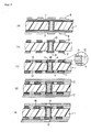
- the copper-clad laminate was drilled to form a hole and the internal surface of the hole was treated with a modifier (manufactured by Junkosha Co., Ltd., trade name: Tetraetch) composed of an organic metallic sodium to improve the wettability of the surface (see Fig. 2 (b) ).
- a modifier manufactured by Junkosha Co., Ltd., trade name: Tetraetch
- a palladium-tin colloid was then applied to substrate, and the substrate was immersed in an electroless plating solution having the following composition to form an electroless plated film of 2 ⁇ m in thickness all over the surface of the substrate.
- the substrate was subjected to an electrolytic copper plating under the following conditions to form an electrolytic copper plated film having a thickness of 15 ⁇ m (see Fig. 2 (c) ).
- Additive manufactured by Atotech Japan, trade name: Capalacid GL 1 ml/l
- the substrate provided with conductors (inclusive of through-holes 3) composed of the electroless plated copper film and electrolytic plated copper film was washed with water and dried.
- the substrate was then subjected to an oxidation-reduction treatment using an oxidation bath (graphitization bath) containing NaOH (10 g/l) NaClO 2 (40 g/l) and Na 3 PO 4 (6 g/l), and a reduction bath containing NaOH (10 g/l) and Na 4 or NaBH 4 (6 g/l) to form a roughed layer 4 all over the surfaces of the conductors inclusive of the through-holes 3 (see Fig. 2 (d) ).
- the roughened layer 4 located above the conductors and the filler 5 protruded from the through-holes 3 were removed by belt sander abrasion using a #600 belt abrasive paper (manufactured by Sankyo Rikagaku Co., Ltd.), and the substrate was further subjected to buffing for removing scratches caused by the belt sander abrasion to smooth the surface of the substrate (see Fig. 2 (e) ).
- a palladium catalyst (manufactured by Atotech) was applied to the surface of the substrate smoothed in the above step (3), and the substrate was then subjected to an electroless copper plating according to a conventional method to form an electroless copper plated film 6 having a thickness of 0.6 ⁇ m (see Fig. 2 (f) ).
- An electrolytic copper plated film 7 having a thickness of 15 ⁇ m was then formed on the substrate by an electrolytic copper plating under the following conditions to plate up portions to be conductor circuits and those to be through-hole-covering conductor layer covering the filler 5 charged in the through-holes 3.
- Additive manufactured by Atotech Japan, trade name: Capalacid GL 1 ml/l
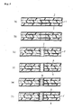
- a roughened layer 11 of a Cu-Ni-P alloy having a thickness of 2.5 ⁇ m was formed on the surfaces of the conductor circuits 9 and the through-hole-covering conductor layer 10 covering the filler 5, and a Sn layer having a thickness of 0.3 ⁇ m was formed on the surface of the roughened layer 11 (see Fig. 3 (c) , the Sn layer is not shown).
- the substrate was acidically degreased and soft-etched, followed by a treatment with a catalyst solution of palladium chloride and an organic acid to give a Pd catalyst.
- the substrate was immersed in an electroless plating solution of pH of 9 containing 8 g/l of copper sulfate, 0.6 g/l of nickel sulfate, 15 g/l of citric acid, 29 g/l of sodium hypophosphite, 31 g/l of boric acid and 0.1 g/l of a surfactant to form a roughened layer 11 of a Cu-Ni-P alloy on the surfaces of the conductor circuits 9 and the through-hole-covering conductor layer 10 covering the filler 5.
- the substrate was then subjected to a Cu-Sn substitution reaction at a temperature of 50°C and pH of 1.2 using an aqueous solution containing 0.1 mol/l of tin borofluoride and 1.0 mol/l of thiourea to form a Sn layer of 0.3 ⁇ m in thickness on the surface of the roughened layer 11 (the Sn layer is not shown).
- Teflon sheets manufactured by Du Pont Company, trade name: Teflon R FEP
- Teflon R FEP Teflon R FEP
- An opening 13 for the formation of viahole having a diameter of 25 ⁇ m was formed in the insulating Teflon resin layer 12 by an ultraviolet ray laser of 10.6 ⁇ m in wavelength (see Fig. 3 (e) ). Further, the surface of the insulating Teflon resin layer 12 was roughened by a plasma treatment. The plasma treatment was carried out at 500 W and a pressure of 500 mTorr for 10 minutes.
- a Pd nucleus was embedded into the surface of the insulating Teflon resin layer 12 by sputtering with the use of Pd as a target at an atmospheric pressure of 0.6 Pa, a temperature of 100°C and a power of 200 W for 1 minute.
- SV-4540 manufactured by Nihon Shinku Gijutstu K.K. was used as a device for sputtering.
- the amount of the sputtered Pd was set to equal to or less than 20 ⁇ g/cm 2 .
- the Pd amount was determined by immersing the substrate in a 6 N hydrochloric acid solution, measuring the total amount of eluted Pd and dividing the total Pd by the exposing area.
- An electrolytic plated film 15 having a thickness of 15 ⁇ m was formed on the substrate by electroplating described in the step (1) to plate up the portions of the conductor circuit 9 and to fill the portion of the viahole 17 with a plating (see Fig. 4 (c) ).
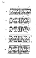
- a both-sided copper-clad laminate 1' of 0.5 mm in thickness was prepared, and provided with an etching resist on both surfaces, and subjected to an etching treatment with an aqueous solution of sulfuric acid and hydrogen peroxide to obtain a substrate provided with conductor circuits.
- a glass-epoxy prepreg and a copper foil 2 were in turn laminated onto both surfaces of the substrate, pressed at a temperature raging from 165 to 170°C and a pressure of 20 kg/cm 2 to give a multilayer core substrate 1' (see Fig. 5 (a) ).
- the multilayer core substrate 1' was then drilled to form through holes having a diameter of 300 ⁇ m (see Fig. 5 (b) ), applied with a palladium-tin colloid and then immersed in an electroless plating solution having the same composition as in Example 1 to form an electroless plated film of 2 ⁇ m in thickness all over the substrate.
- the substrate was then subjected to an electrolytic copper plating in the same condition as in Example 1 to form an electrolytic copper plated film 3 having a thickness of 15 ⁇ m (see Fig. 5 (c) ).
- a roughened layer 4 was formed all over the surface of the conductor 3 inclusive of through-holes in the same manner as in Example 1 (see Fig. 5 (d) ).
- a filler 5 (a nonconducting copper paste for filling, manufactured by Tatsuta Densen Co., Ltd., trade name: DD Paste) containing copper particles having an average particle size of 10 ⁇ m was charged into the through-hole 3, and the surface of the substrate was smoothed (see Fig. 5 (e) ).
- An electrolytic copper plated film 7 of 15 ⁇ m in thickness was formed by subjecting the substrate to an electrolytic copper plating according to the conditions of the step (2) in a similar manner to Example 1 to form portions to be a conductor circuits 9 and a through-hole-covering conductor layer 10 (to be a round through-hole land).
- An etching resist 8 was formed on both surfaces of the substrate provided with portions to be the conductor circuits 9 and the conductor layer 10 in the same manner as in Example 1 (see Fig. 6 (a) ).
- An adhesive composition A for upper-layer electroless plating was prepared by mixing the above mixtures 1 to 3.
- An insulating agent B for lower-layer electroless plating was prepared by admixing the above mixtures 1 to 3.
- the insulating agent B for electroless plating (viscosity: 1.5 Pa ⁇ s) prepared in the step (10) was applied onto both surfaces of the substrate with a roll coater and allowed to stand in a horizontal position for 20 minutes, and then dried at a temperature of 60°C for 30 minutes. Subsequently, the adhesive A for electroless plating (viscosity: 1.0 Pa ⁇ s) was applied to the substrate by a roll coater, allowed to stand in a horizontal position for 20 minutes, and then dried at a temperature of 60°C for 30 minutes to form an adhesive layer 12 (two-layer structure) having a thickness of 40 ⁇ m (see Fig. 6 (d) , the two-layer structure of the adhesive layer, however, is omitted in the view).
- a photomask film depicted with a full circle (black circle) of 85 ⁇ m in diameter was attached to both surfaces of the adhesive layers 12 formed on both surfaces of the substrate and exposed to a light irradiation at 500 mJ/cm 2 by an ultra-high pressure mercury lamp.
- the exposed substrate was developed by spraying a DMDG (diethylene glycol dimethyl ether) solution to form openings for viahole of 85 ⁇ m in diameter on the adhesive layer.
- DMDG diethylene glycol dimethyl ether
- the substrate was further exposed to a light irradiation at 3,000 mJ/cm 2 by an ultra-high pressure mercury lamp and heated at 100°C for 1 hour and subsequently at 150°C for 5 hours to form an interlaminar insulating material layer (adhesive layer) 12 of 35 ⁇ m in thickness provided with openings (openings 13 for the formation of viahole) having excellent dimensional precision corresponding to the photomask film (see Fig. 6 (e) ).
- the tin plated layer was partly exposed in the opening for the viahole.
- Catalyst nuclei were applied to the surfaces of the adhesive layer 12 and the openings 13 for the formation of viahole by giving a palladium catalyst (manufactured by Atotech Co., Ltd.) to the substrate having the roughened surface (roughened depth: 3.5 ⁇ m) of the adhesive layer.
- the substrate was immersed in an electroless copper plating bath having the same composition with the step (2) to form an electroless copper plated film 14 of 0.6 ⁇ m in thickness all over the roughened surface (see Fig. 7 (a) ).
- the electroless copper plated film 14 was thin, convexoconcave following the roughened surface of the adhesive layer 12 was observed on the surface of the electroless copper plated film 14.
- a commercially available photosensitive dry film was adhered to the electroless copper plated film 14, and a mask was placed onto the dry film, exposed to a light at 100 mJ/cm 2 and developed with a 0.8% sodium carbonate solution to form a plating resist 16 having a thickness of 15 ⁇ m (see Fig. 7 (b) ).
- the substrate was then subjected to an electrolytic copper plating under the same condition as in the step (6) to form an electrolytic copper plated film 15 having a thickness of 15 ⁇ m, and thereby to plate up the conductor circuits and the viaholes (see Fig. 7 (c) ).
- the electroless plated film 15 located beneath the plating resist 16 was dissolved and removed by etching with a mixed solution of sulfuric acid and hydrogen peroxide to form conductor circuits (inclusive of viaholes) each consisting of the electroless copper plated film 14 and the electrolytic copper plated film 15 and having a thickness of 16 ⁇ m, and thereby a multilayer printed wiring board having three layers on each side was obtained (see Fig. 7 (d) ).
- Pd remained in the roughened surface of the adhesive layer 12 was removed by immersing in chromic acid (800 g/l) for 1 to 10 minutes.
- the multilayer printed wiring board prepared by the above mentioned manner ensures through-holes each provided with a perfectly circular land, and it can provide a land pitch of about 600 ⁇ m and thereby through-holes can be formed in a high density so as to densify through-holes easily.
- the number of through-holes in the substrate can be increased, an electric connection with respect to conductor circuits in the multilayer core substrate can sufficiently be ensured through the through-holes.
- a multilayer printed wiring board was manufactured in the same manner as in Example 1, except that when through-holes were filled with a copper paste, a through-hole-covering conductor layer 10 for covering an exposed copper paste from the through-holes was not formed. According to this process, pits might be formed because the surface of the copper paste was frequently removed in the formation of openings on an insulating resin layer by a laser beam irradiation.
- a multilayer printed wiring board was obtained in a similar manner to Example 1, except that the following composition was employed as the filler.
- Bisphenol F type epoxy resin manufactured by Yuka Shell Co., Ltd., E-807
- Imidazole curing Ltd. 2E4MZ-CN
- Copper powder having a particle size of 15 ⁇ m or less manufactured by Fukuda Metal Foil and Powder Co., Ltd., SCR-Cu-15
- Aerosil #200
- Defoaming agent manufactured by Sannopko, Pernol S4
- example 1 The procedure of example 1 was repeated to produce a multilayer printed wiring board, except that a bisphenol F type epoxy resin containing no metal particle was used as the filler for filling the through-hole.
- a multilayer printed wiring board was produced in a similar manner to Example 1, except that through-holes were filled with the epoxy resin and the surfaces of the epoxy resin exposed from the through-holes were roughened with chromic acid and then covered with a conductor layer.
- a multilayer printed wiring board was obtained in the same manner as in Example 1, except that a roughened layer was not formed on the surface of the internal conductor on the through-holes.
- a heat cycle test of -55°C x 15 min., ambient temperature x 10 min. and 125°C x 15 min at 1,000 times was conducted with respect to the multilayer printed wiring boards according to the examples and comparative examples.
- viaholes could be formed just above the through-holes according to the multilayer printed wiring boards of Examples 1 to 4 of the present invention, and thus high density through-holes could easily be obtained.
- no peeling was observed between the filler and the internal surface conductor of the through-hole, or between the filler and the through-hole-covering conductor, and neither crack nor migration was found in the heat cycle test and PCT.
- a copper-clad laminate composed of a BT (bismaleimide-triazine) resin substrate 1 of 0.8 mm in thickness and a copper foil 2 of 18 ⁇ m in thickness having a single-sided roughened surface and laminated on the substrate 1 was used as a starting material (see Fig. 2 (a) ).
- the copper-clad laminate was drilled (see Fig. 2 (b) ), and applied with a palladium-tin colloid, and subjected to an electroless plating in the same composition and conditions as in Example 1.
- the substrate was subjected to an electrolytic copper plating in the same conditions as in Example 1 to form an electrolytic copper plated film having a thickness of 15 ⁇ m (see Fig. 2 (c) ).
- a resin composition (filler) 5 for filling through-hole was prepared by kneading, through three rolls, 3.5 parts by weight of a cresol novolac type epoxy resin (manufactured by Yuka Shell Co., Ltd., Epikote 152), 14.1 parts by weight of a bisphenol F type epoxy resin (manufactured by Yuka Shell Co., Ltd., Epikote 807), 1.0 part by weight of ultrafine silica particles (Aerosil R202) having an average particle size of 14 nm, 1.2 parts by weight of an imidazole curing agent (manufactured by Shikoku Kasei Co., Ltd., 2E4MZ-CN) and 100 parts by weight of copper powder having an average particle size of 15 ⁇ m, and adjusting the viscosity of the mixture to the range from 200 to 300 Pa ⁇ s at 22 ⁇ 1°C.
- a cresol novolac type epoxy resin manufactured by Yuka Shell Co., Ltd., Epikote 152
- the prepared filler 5 was charged in the through-holes 3 by screen printing, dried and then heated at 80°C, 100°C and 120°C for each 1 hour, and at 150°C for 1 hour to cure.
- the surface of the substrate was smoothed by removing the roughened surface positioned above the through-holes and the filler 5 protruded from the through-holes 3 by means of belt sander abrasion using a #400 belt abrasive paper (manufactured by Sankyo Rikagaku Co., Ltd.), and further buffing the substrate with alumina abrasive grains or SiC abrasive grains for removing scratches due to the belt sander abrasion (see Fig. 2 (e) ).
- a palladium catalyst (manufactured by Atotech Co., Ltd.) was applied to the surface of the substrate smoothed in the step (3), and the substrate was subjected to an electroless copper plating in the same conditions as in Example 1 to form an electroless copper plated film 6 having a thickness of 0.6 ⁇ m (see Fig. 2 (f) ).
- An electrolytic copper plated film 7 of 15 ⁇ m in thickness was formed by subjecting the substrate to an electrolytic copper plating according to the conditions of the step (1) to plate up portions to be conductor circuits 9 and to form a portion to be a conductor layer (to be a round through-hole land) 10 for covering the filler 5 charged in the through-hole 3.
- An etching resist 8 having a thickness of 15 ⁇ m was formed on both surfaces of the substrate provided with portions to be conductor circuits 9 and a conductor layer 10 in a similar manner to Example 1 (see Fig. 3 (a) ).
- the plating film positioned in a portion not provided with the etching resist 8 was dissolved and removed by etching with a solution containing a mixture of sulfuric acid and hydrogen peroxide, and the etching resist 8 was peeled off by a 5% KOH solution to form independent conductor circuits 9 and a though-hole-covering conductor layer 10 covering the filler 5 (see Fig. 3 (b) ).
- the surfaces of the conductors inclusive of side surfaces were roughened by an oxidation-reduction treatment in a similar manner to the step (2).
- An interlaminar insulating resin agent 12 was prepared by mixing the above ingredients 1 and 2.
- the prepared interlaminar insulating resin agent 12 was charged to gaps between the conductor circuits 9 or of the through-hole-covering conductor layer 10 by applying to one surface of the substrate through screen printing, dried at 70°C for 20 minutes. Similarly, the resin filler 12 was charged in gaps between the conductor circuits 9 or of the conductor layer 10 on the other surface of the substrate, dried at 70°C for 20 minutes. In other words, the interlaminar insulating resin agent 12 was charged between the internal layer copper patterns in this step.
- the interlaminar insulating resin agent 12 was cured by heating at 100°C for 1 hour, at 120°C for 3 hours, at 150°C for 1 hour and at 180°C for 7 hours.
- both surfaces of the substrate were smoothed by removing the surface areas of the interlaminar insulating resin agent 12 charged in gaps of the conductor circuits 9 or of the through-hole-covering conductor layer 10, and the roughened layer 11 positioned above the conductor circuits 9 or the through-hole-covering layer 10 to give a substrate in which the interlaminar insulating resin agent 12 and the conductor circuits 9 or a side surface of the through-hole-covering conductor layer 10 were firmly adhered to each other through the interposition of the roughened layer 11. That is, the surface of the interlaminar insulating resin agent 12 and those of the internal layer copper patterns could be aligned in the same plane by this step.
- the charged cured resin had a Tg point (glass transition point) of 155.6°C and a linear thermal expansion coefficient of 44.5 x 10 -6 /°C.
- a roughened layer 11 of a Cu-Ni-P alloy having a thickness of 2.5 ⁇ m was formed on the surfaces of the conductor circuits 9 and the through-hole-covering conductor layer 10 covering the filler 5, and a Sn layer having a thickness of 0.3 ⁇ m was formed on the surface of the roughened layer 11 (see Fig. 3 (c) , where the Sn layer is not shown).
- the substrate was acidically degreased and soft-etched, and then treated with a catalyst solution containing palladium chloride and an organic acid to apply a Pd catalyst. After activating the catalyst, the substrate was immersed in an electroless plating solution of pH of 9 containing 8 g/l of copper sulfate, 0.6 g/l of nickel sulfate, 15 g/l of citric acid, 29 g/l of sodium hypophosphite, 31 g/l of boric acid and 0.1 g/l of a surfactant to form a roughened layer 11 of a Cu-Ni-P alloy having a thickness of 2.5 ⁇ m on the surfaces of the copper conductor circuits.
- the substrate was then subjected to a Cu-Sn substitution reaction at a temperature of 50°C and pH of 1.2 by immersing in an electroless tin plating solution containing 0.1 mol/l of tin borofluoride and 1.0 mol/l of thiourea for 1 hour to form a Sn layer of 0.3 ⁇ m in thickness on the surface of the roughened layer (the Sn layer is not shown).
- Adhesives A and B for electroless plating were prepared in the following manner.
- An adhesive A for upper-layer electroless plating was prepared by mixing the above mixtures 1 to 3.
- An adhesive B for lower-layer electroless plating was prepared by admixing the above mixtures 1 to 3.
- the insulative adhesive B for electroless plating (viscosity: 1.5-3.2 Pa ⁇ s) and the adhesive A for electroless plating (viscosity: 5-20 Pa ⁇ s) each prepared in the step (11) were applied in turn to both surfaces of the substrate using a roll coater, allowed to stand in a horizontal position for 20 minutes and dried at 60°C for 30 minutes to form an adhesive layer 12 (two-layer structure) having a thickness of 40 ⁇ m (see Fig. 3 (d) ). Further, a polyethylene terephthalate film was applied onto the adhesive layer 12 through a pressure-sensitive adhesive.
- a photomask film printed with a full circle of 85 ⁇ m in diameter was closely adhered to the adhesive layer 12 formed on both surfaces of the substrate, and exposed to an irradiation at 500 mJ/cm 2 by an ultra-high pressure mercury lamp.
- the exposed substrate was developed by spraying a DMDG (diethylene glycol dimethyl ether) solution to form openings for viahole of 85 ⁇ m in diameter on the adhesive layer.
- DMDG diethylene glycol dimethyl ether
- the substrate was further exposed to an irradiation by an ultra-high pressure mercury lamp at 3,000 mJ/cm 2 and heated at 100°C for 1 hour and subsequently at 150°C for 5 hours to form an interlaminar insulating material layer (adhesive layer) 12 of 35 ⁇ m in thickness provided with openings (openings 13 for the formation of viahole) having an excellent dimensional precision corresponding to the photomask film (see Fig. 3 (e) ).
- the tin plated layer was partly exposed in the openings for viahole.
- Catalyst nuclei were applied to the surfaces of the adhesive layer 12 and the openings 13 for the formation of viahole by giving a palladium catalyst (manufactured by Atotech Co., Ltd.) to the substrate having the roughened surface (roughened depth: 3 ⁇ m) of the adhesive layer.
- a palladium catalyst manufactured by Atotech Co., Ltd.
- the substrate was immersed in an electroless copper plating bath having the same composition with the step (1) to form an electroless copper plated film of 0.6 ⁇ m in thickness all over the roughened surface (see Fig. 4 (a) ).
- a commercially available photosensitive resin film (dry film) was adhered to the electroless copper plated film 14, and a mask was closely placed onto the dry film, exposed to a light irradiation at 100 mJ/cm 2 and developed with a 0.8% sodium carbonate solution to form a plating resist 16 having a thickness of 15 ⁇ m (see Fig. 4 (b) ).
- the substrate was then subjected to an electrolytic copper plating under the same condition as the step (1) to form an electrolytic copper plated film 15 having a thickness of 15 ⁇ m and thereby to plate up the conductor circuit portions and viahole portions (see Fig. 4 (c) ).
- the electroless plated film 15 located beneath the plating resist 16 was dissolved and removed by etching with a mixed solution of sulfuric acid and hydrogen peroxide to form conductor circuits 9 (inclusive of viaholes 17) consisting of the electroless copper plated film 14 and the electrolytic copper plated film 15 and having a thickness of 16 ⁇ m (see Fig. 4 (d) ).
- the substrate provided with the conductor circuits 9 (inclusive of viaholes 17) in the step (19) was immersed in an electroless plating solution of pH of 9 containing 8 g/l of copper sulfate, 0.6 g/l of nickel sulfate, 15 g/l of citric acid, 29 g/l of sodium hypophosphite, 31 g/l of boric acid and 0.1 g/l of a surfactant to form a roughened layer 11 of copper-nickel-phosphorus having a thickness of 3 ⁇ m on the surface of the conductor circuits.
- the roughened layer 11 contained 98% by mole of Cu, 1.5% by mole of Ni and 0.5% by mole of P as analyzed by EPMA (electron probe microanalysis; fluorescent X-ray analysis).
- the substrate was washed with water and immersed in an electroless tin substitution plating bath containing 0.1 mol/l of tin borofluoride and 1.0 mol/l of thiourea at 50°C for 1 hour to form a tin substitution plated layer of 0.05 ⁇ m in thickness on the surface of the roughened layer 11 (where tin substituted layer is not shown).
- each one layer of an upper interlaminar insulating resin layer 12 and a conductor circuit 9 (inclusive of viahole 17) was laminated by repeating the steps (12) to (20) to obtain a multilayer circuit substrate (see Fig. 8 (a) ).
- a roughened layer 11 composed of copper-nickel-phosphorus was formed on the surface of the conductor circuit, but a tin substitution plated layer was not formed on the surface of the roughened layer 11.
- a solder resist composition was prepared by mixing 46.67 parts by weight of a photosensitized oligomer (molecular weight: 4,000) obtained by acrylating 50% of epoxy groups of a cresol novolac type epoxy resin (manufactured by Nippon Kayaku Co., Ltd.) as a 60% by weight solution in DMDG, 14.121 parts by weight of a bisphenol A type epoxy resin (manufactured by Yuka Shell Co., Ltd., trade name: Epikote 1001) as a 80% by weight solution in methyl ethyl ketone, 1.6 parts by weight of an imidazole curing agent (manufactured by Shikoku Kasei Co., Ltd., 2E4MZ-CN), 1.5 parts by weight of a polyvalent acrylic monomer (manufactured by Nippon Kayaku Co., Ltd., R604) as a photosensitive monomer, 3.0 parts by weight of a polyvalent acrylic monomer (manufactured by Ky
- the viscosity was measured by B-type viscometer (manufactured by Tokyo Keiki Co., Ltd., model: DVL-B) using a rotor No. 4 at 60 rpm and a rotor No. 3 at 6 rpm.
- the above solder resist composition was applied to both surfaces of the multilayer wiring substrate obtained in the step (21) at a thickness of 20 ⁇ m. Then it was dried at 70°C for 20 minutes and at 70°C for 30 minutes and thereafter a soda-lime glass substrate of 5 mm in thickness depicted with circle patterns (mask patterns) for solder resist openings through chromium layer was closely placed on the solder resist layer so as to face the chromium layer side thereto, exposed to an ultraviolet ray irradiation at 1,000 mJ/cm 2 and developed with DMTG.
- circle patterns mask patterns
- solder resist layer 18 was heated at 80°C for 1 hour, at 100°C for 1 hour, at 120°C for 1 hour and at 150°C for 3 hours to form a pattern of solder resist layer 18 (thickness: 20 ⁇ m) having an opening (opening size: 200 ⁇ m) in the solder pad.
- the substrate provided with the solder resist layer 18 was immersed for 20 minutes in an electroless nickel plating solution of pH of 5 containing 30 g/l of nickel chloride, 10 g/l of sodium hypophosphite and 10 g/l of sodium citrate to form a nickel plated layer 19 having a thickness of 5 ⁇ m in the opening.
- the substrate was then immersed in an electroless gold plating solution containing 2 g/l of potassium gold cyanide, 75 g/l of ammonium chloride, 50 g/l of sodium citrate and 10 g/l of sodium hypophosphite at 93°C for 23 seconds to form a gold plated layer 20 of 0.03 ⁇ m in thickness on the nickel plated layer 19.
- solder paste was printed on the opening of the solder resist layer and reflowed at 200°C to form a solder bump (solder body), thereby a multilayer printed wiring board having solder bumps was obtained (see Fig. 8 (b) ).
- solder tin-silver, tin-indium, tin-zinc, tin-bismuth or other solders can be employed as the solder.
- a multilayer printed wiring board was produced in a similar manner to Example 1, except that the following composition was used as the resin composition for filling through-hole.
- a resin composition for filling through-hole was prepared by kneading through three rolls 3.5 parts by weight of a cresol novolac type epoxy resin (manufactured by Yuka Shell Co., Ltd., Epikote 152), 14.1 parts by weight of a bisphenol F type epoxy resin (manufactured by Yuka Shell Co., Ltd., Epikote 807), 1.2 parts by weight of an imidazole curing agent (manufactured by Shikoku Kasei co., Ltd., 2E4MZ-CN) and 100 parts by weight of copper powder having an average particle size of 15 ⁇ m, and adjusting a viscosity to the range from 200 to 300 Pa ⁇ s at 22 ⁇ 1°C.
- a cresol novolac type epoxy resin manufactured by Yuka Shell Co., Ltd., Epikote 152
- 14.1 parts by weight of a bisphenol F type epoxy resin manufactured by Yuka Shell Co., Ltd., Epikote 807
- an imidazole curing agent manufactured
- Example 1 The procedure of Example 1 was repeated to give a multilayer printed wiring board, except that the following resin composition was employed as the resin composition for filling through-hole.
- a resin composition for filling through-hole was prepared by mixing 17.6 parts by weight of a bisphenol F type epoxy resin (manufactured by Yuka Shell Co., Ltd., Epikote 807), 1.0 part by weight of ultrafine silica particles (Aerosil R202) having an average particle size of 14 nm, 1.2 parts by weight of an imidazole curing agent (Shikoku Kasei Co., Ltd., 2E4MZ-CN) and 100 parts by weight of copper powder having an average particle size of 15 ⁇ m.
- a bisphenol F type epoxy resin manufactured by Yuka Shell Co., Ltd., Epikote 807
- ultrafine silica particles Aerosil R202 having an average particle size of 14 nm
- an imidazole curing agent Shikoku Kasei Co., Ltd., 2E4MZ-CN
- a multilayer printed wiring board was prepared in the same manner as in Example 1, except that the following resin composition was used as the resin composition for filling through-hole.
- a resin composition for filling through-hole was prepared by kneading, through three rolls, 3.5 parts by weight of a cresol novolac type epoxy resin (manufactured by Yuka Shell Co., Ltd., Epikote 152), 1.0 part by weight of ultrafine silica particles (Aerosil R202) having an average particle size of 14 nm, 14.1 parts by weight of a bisphenol F type epoxy resin (manufactured by Yuka Shell Co., Ltd., Epikote 807), 1.2 parts by weight of an imidazole curing agent (manufactured by Shikoku Kasei Co., Ltd., 2E4MZ-CN) and 100 parts by weight of silica particles having an average particle size of 10 ⁇ m, and adjusting a viscosity to the range from 200 to 300 Pa ⁇ s at 22 ⁇ 1°C.
- a cresol novolac type epoxy resin manufactured by Yuka Shell Co., Ltd., Epikote 152
- ultrafine silica particles
- a multilayer printed wiring board was produced in a similar manner to Example 1, except that the following resin composition for filling through-hole was used and that after polishing the surface of the filler, the epoxy resin exposed from the surface was removed by chromic acid.
- a resin composition for filling through-hole was prepared by kneading through three rolls 3.5 parts by weight of a cresol novolac type epoxy resin (manufactured by Yuka Shell Co., Ltd., Epikote 152), 14.1 parts by weight of a bisphenol F type epoxy resin (manufactured by Yuka Shell Co., Ltd., Epikote 807), 1.0 part by weight of ultrafine silica particles (Aerosil R202) having an average particle size of 14 nm, 1.2 parts by weight of an imidazole curing agent (manufactured by Shikoku Kasei Co., Ltd., 2E4MZ-CN) and 100 parts by weight of epoxy resin particles (manufactured by Sanyo Kasei Co., Ltd., Polymerpole) having an average particle size of 1 ⁇ m, and adjusting the viscosity of the mixture to the range from 200 to 300 Pa ⁇ s at 22 ⁇ 1°C.
- a cresol novolac type epoxy resin manufactured by
- Example 1 The procedure of Example 1 was repeated to give a multilayer printed wiring board, except that the following resin composition was employed as the resin composition for filling through-hole.
- a cresol novolac type epoxy resin manufactured by Yuka Shell Co., Ltd., Epikote 152
- 14.1 parts by weight of a bisphenol F type epoxy resin manufactured by Yuka Shell Co., Ltd., Epikote 807
- an imidazole curing agent manufactured by Shikoku Kasei Co., Ltd., 2E4MZ-CN
- the copper powder precipitated so as to cause the filler to peel from the conductor layer covering the filler, and thereby to invite a break between the through-hole and viahole.
- the printed wiring board according to the invention is useful for a multilayer wiring board which is used as a packaging substrate for packing IC chips, in particular for a multilayer printed wiring board obtained by a semi-additive process or a full-additive process.
Claims (10)
- Plaquette à circuit imprimé multicouche comprenant un substrat (100) pourvu de trous traversants (107), le substrat présentant au moins une couche isolante en résine interlaminaire (104) formée sur lui et au moins un circuit conducteur (103) formé sur la couche isolante en résine interlaminaire, les trous traversants (107) étant remplis d'une matière de remplissage (108),
étant précisé qu'une partie exposée de la matière de remplissage prévue dans les trous traversants est couverte avec une couche conductrice de recouvrement de trous traversants (109), ladite couche conductrice comprenant un film déposé sans courant et un film formé sur celui-ci par dépôt électrolytique,
qu'une couche rugueuse est formée sur la surface de la couche conductrice de recouvrement de trous traversants,
et que la matière de remplissage comprend des particules métalliques et une résine thermodurcissable ou une résine thermoplastique. - Plaquette à circuit imprimé multicouche selon la revendication 1, dans laquelle la matière de remplissage comprend des particules de métal, et une résine époxy bisphénol et/ou une résine époxy-novolac.
- Plaquette à circuit imprimé multicouche selon la revendication 1 ou 2, dans laquelle la matière de remplissage comprend par ailleurs une poudre anorganique ultrafine qui a une taille de particule moyenne de 1 à 1000 nm.
- Plaquette à circuit imprimé multicouche selon l'une quelconque des revendications 1 à 3, dans laquelle la matière de remplissage est une composition non conductrice qui contient des particules de métal.
- Plaquette à circuit imprimé multicouche selon l'une quelconque des revendications 1 à 4, dans laquelle le substrat est un substrat intérieur multicouche formé grâce à la stratification alternée d'au moins une couche conductrice et d'au moins un pré-imprégné.
- Plaquette à circuit imprimé multicouche selon l'une quelconque des revendications 1 à 5, dans laquelle les trous traversants formés sur le substrat ont un écartement égal ou inférieur à 700 µm.
- Plaquette à circuit imprimé multicouche selon l'une quelconque des revendications 1 à 6, comprenant la formation de couches de circuit (101A, 101B) comportant des trous de liaison (102, 202) prévus dans la couche isolante en résine interlaminaire, étant précisé que lesdites couches de circuit sont formées sur les deux surfaces du substrat et ont le même nombre de couches.
- Plaquette à circuit imprimé multicouche selon la revendication 7, dans laquelle les trous de liaison (102, 202) sont formés dans la couche en résine isolante interlaminaire juste au-dessus de la couche conductrice de recouvrement de trous traversants (109) et sont reliés à la couche conductrice de recouvrement de trous traversants.
- Plaquette à circuit imprimé multicouche selon la revendication 1, dans laquelle le film déposé sans courant a une épaisseur de 0,1 à 5 µm et le film formé par dépôt électrolytique a une épaisseur de 5 à 25 µm.
- Plaquette à circuit imprimé multicouche selon la revendication 1, dans laquelle les particules de métal qui dépassent de la surface de la matière de remplissage sont intégrées au film déposé sans courant qui constitue la couche conductrice de recouvrement de trous traversants.
Applications Claiming Priority (9)
| Application Number | Priority Date | Filing Date | Title |
|---|---|---|---|
| JP28049997 | 1997-10-14 | ||
| JP28049997 | 1997-10-14 | ||
| JP34018297A JP3564981B2 (ja) | 1997-10-14 | 1997-12-10 | 多層プリント配線板およびその製造方法 |
| JP34018097A JPH11186728A (ja) | 1997-10-14 | 1997-12-10 | 多層プリント配線板 |
| JP34018097 | 1997-12-10 | ||
| JP34018297 | 1997-12-10 | ||
| JP6706598 | 1998-03-17 | ||
| JP6706598A JP3408417B2 (ja) | 1998-03-17 | 1998-03-17 | スルーホール充填用樹脂組成物および多層プリント配線板 |
| EP98947819A EP1030544B1 (fr) | 1997-10-14 | 1998-10-12 | Plaquette a circuit imprime multicouche, son procede de fabrication et composition resineuse de remplissage de trous traversants |
Related Parent Applications (2)
| Application Number | Title | Priority Date | Filing Date |
|---|---|---|---|
| EP98947819.3 Division | 1998-10-12 | ||
| EP98947819A Division EP1030544B1 (fr) | 1997-10-14 | 1998-10-12 | Plaquette a circuit imprime multicouche, son procede de fabrication et composition resineuse de remplissage de trous traversants |
Publications (3)
| Publication Number | Publication Date |
|---|---|
| EP1286578A2 EP1286578A2 (fr) | 2003-02-26 |
| EP1286578A3 EP1286578A3 (fr) | 2006-03-22 |
| EP1286578B1 true EP1286578B1 (fr) | 2010-12-22 |
Family
ID=27464803
Family Applications (3)
| Application Number | Title | Priority Date | Filing Date |
|---|---|---|---|
| EP98947819A Expired - Lifetime EP1030544B1 (fr) | 1997-10-14 | 1998-10-12 | Plaquette a circuit imprime multicouche, son procede de fabrication et composition resineuse de remplissage de trous traversants |
| EP02026472A Expired - Lifetime EP1286578B1 (fr) | 1997-10-14 | 1998-10-12 | Plaquette à circuit imprimé multicouche |
| EP08018753A Expired - Lifetime EP2015624B1 (fr) | 1997-10-14 | 1998-10-12 | Carte de circuit imprimé multicouches |
Family Applications Before (1)
| Application Number | Title | Priority Date | Filing Date |
|---|---|---|---|
| EP98947819A Expired - Lifetime EP1030544B1 (fr) | 1997-10-14 | 1998-10-12 | Plaquette a circuit imprime multicouche, son procede de fabrication et composition resineuse de remplissage de trous traversants |
Family Applications After (1)
| Application Number | Title | Priority Date | Filing Date |
|---|---|---|---|
| EP08018753A Expired - Lifetime EP2015624B1 (fr) | 1997-10-14 | 1998-10-12 | Carte de circuit imprimé multicouches |
Country Status (6)
| Country | Link |
|---|---|
| US (3) | USRE40947E1 (fr) |
| EP (3) | EP1030544B1 (fr) |
| CN (3) | CN100418390C (fr) |
| DE (2) | DE69841424D1 (fr) |
| TW (3) | TW443084B (fr) |
| WO (1) | WO1999020090A1 (fr) |
Families Citing this family (111)
| Publication number | Priority date | Publication date | Assignee | Title |
|---|---|---|---|---|
| USRE40947E1 (en) | 1997-10-14 | 2009-10-27 | Ibiden Co., Ltd. | Multilayer printed wiring board and its manufacturing method, and resin composition for filling through-hole |
| DE69939221D1 (de) * | 1998-09-03 | 2008-09-11 | Ibiden Co Ltd | Mehrschichtige leiterplatte und verfahren zu deren herstellung |
| CN1318274A (zh) * | 1998-09-17 | 2001-10-17 | 伊比登株式会社 | 多层叠合电路板 |
| US6406750B1 (en) * | 1999-05-28 | 2002-06-18 | Osaka Municipal Government | Process of forming catalyst nuclei on substrate, process of electroless-plating substrate, and modified zinc oxide film |
| WO2000076281A1 (fr) | 1999-06-02 | 2000-12-14 | Ibiden Co., Ltd. | Carte a circuit imprime multicouche et procede de fabrication d'une telle carte |
| EP1207730B1 (fr) * | 1999-08-06 | 2009-09-16 | Ibiden Co., Ltd. | Solution de galvanoplastie, procede de fabrication d'une carte imprimee multicouche au moyen de ladite solution, et carte imprimee multicouche |
| CN100387103C (zh) * | 1999-08-12 | 2008-05-07 | Ibiden股份有限公司 | 多层印刷电路板和半导体器件 |
| CN1199536C (zh) * | 1999-10-26 | 2005-04-27 | 伊比登株式会社 | 多层印刷配线板及多层印刷配线板的制造方法 |
| JP2001144197A (ja) * | 1999-11-11 | 2001-05-25 | Fujitsu Ltd | 半導体装置、半導体装置の製造方法及び試験方法 |
| US20030178391A1 (en) * | 2000-06-16 | 2003-09-25 | Shipley Company, L.L.C. | Composition for producing metal surface topography |
| JP3527694B2 (ja) * | 2000-08-11 | 2004-05-17 | 新光電気工業株式会社 | 配線基板の製造方法 |
| JP3760771B2 (ja) * | 2001-01-16 | 2006-03-29 | 松下電器産業株式会社 | 回路形成基板および回路形成基板の製造方法 |
| EP1791410B1 (fr) * | 2001-03-14 | 2009-05-13 | Ibiden Co., Ltd. | Carte de circuit imprimé multicouche |
| JP2002299512A (ja) * | 2001-03-30 | 2002-10-11 | Nec Corp | 半導体装置及びその製造方法 |
| US6465084B1 (en) * | 2001-04-12 | 2002-10-15 | International Business Machines Corporation | Method and structure for producing Z-axis interconnection assembly of printed wiring board elements |
| JP2002324958A (ja) * | 2001-04-25 | 2002-11-08 | Sony Corp | プリント配線板と、その製造方法 |
| JP3530149B2 (ja) * | 2001-05-21 | 2004-05-24 | 新光電気工業株式会社 | 配線基板の製造方法及び半導体装置 |
| KR100598285B1 (ko) | 2001-06-21 | 2006-07-07 | 엘지전자 주식회사 | 멀티채널 스트림 기록장치 및 방법과, 그에 따른 기록매체 |
| KR20020097454A (ko) | 2001-06-21 | 2002-12-31 | 엘지전자 주식회사 | 멀티채널 스트림 기록장치 및 방법과, 그에 따른 기록매체 |
| US6729019B2 (en) * | 2001-07-11 | 2004-05-04 | Formfactor, Inc. | Method of manufacturing a probe card |
| US6649506B2 (en) * | 2001-07-27 | 2003-11-18 | Phoenix Precision Technology Corporation | Method of fabricating vias in solder pads of a ball grid array (BGA) substrate |
| US6861757B2 (en) * | 2001-09-03 | 2005-03-01 | Nec Corporation | Interconnecting substrate for carrying semiconductor device, method of producing thereof and package of semiconductor device |
| JP2003133727A (ja) * | 2001-10-22 | 2003-05-09 | Nec Toppan Circuit Solutions Inc | 樹脂穴埋め基板の製造方法およびそれを用いた多層プリント配線板の製造方法 |
| JP4062907B2 (ja) * | 2001-11-12 | 2008-03-19 | 松下電器産業株式会社 | 回路基板およびその製造方法 |
| JP2003234572A (ja) * | 2002-02-06 | 2003-08-22 | Nitto Denko Corp | 両面配線基板の製造方法 |
| JP4024563B2 (ja) * | 2002-03-15 | 2007-12-19 | 株式会社日立製作所 | 半導体装置 |
| CN1326155C (zh) * | 2002-05-31 | 2007-07-11 | 大自达电线股份有限公司 | 导电糊、使用其的多层基板及其制造方法 |
| JPWO2003103352A1 (ja) * | 2002-06-04 | 2005-10-06 | 住友電気工業株式会社 | プリント配線用基板、プリント配線板およびこれらの製造方法 |
| KR100550695B1 (ko) | 2002-06-24 | 2006-02-08 | 엘지전자 주식회사 | 다중 재생 경로 비디오 데이터의 재생을 관리하기 위한데이터 구조를 갖는 기록 매체와 그에 따른 기록 및 재생방법 및 장치 |
| KR20040000290A (ko) | 2002-06-24 | 2004-01-03 | 엘지전자 주식회사 | 고밀도 광디스크의 멀티 경로 데이터 스트림 관리방법 |
| CN101350215B (zh) | 2002-06-24 | 2012-08-29 | Lg电子株式会社 | 记录和再现用于视频数据的再现的数据结构的方法及装置 |
| AU2003243025B2 (en) | 2002-06-28 | 2009-02-19 | Lg Electronics Inc. | Recording medium having data structure for managing reproduction of multiple play-back path video data recorded thereon and recording and reproducing methods and apparatuses |
| US6807732B2 (en) * | 2002-07-24 | 2004-10-26 | Agilent Technologies, Inc. | Methods for modifying inner-layer circuit features of printed circuit boards |
| US6854179B2 (en) * | 2002-07-25 | 2005-02-15 | Agilent Technologies, Inc. | Modification of circuit features that are interior to a packaged integrated circuit |
| KR20040024381A (ko) * | 2002-09-14 | 2004-03-20 | 엘지전자 주식회사 | 인쇄회로기판의 도금방법 |
| US6822332B2 (en) * | 2002-09-23 | 2004-11-23 | International Business Machines Corporation | Fine line circuitization |
| WO2004042723A1 (fr) | 2002-11-08 | 2004-05-21 | Lg Electronics Inc. | Procede et appareil permettant d'enregistrer un flux a composants multiples et un support d'enregistrement a haute densite comprenant un flux a composants multiples enregistre et procede et appareil de reproduction dudit support d'enregistrement |
| US7720356B2 (en) | 2002-11-12 | 2010-05-18 | Lg Electronics Inc | Recording medium having data structure for managing reproduction of multiple reproduction path video data recorded thereon and recording and reproducing methods and apparatuses |
| US7664372B2 (en) | 2002-11-20 | 2010-02-16 | Lg Electronics Inc. | Recording medium having data structure for managing reproduction of multiple component data recorded thereon and recording and reproducing methods and apparatuses |
| US7783160B2 (en) | 2002-11-20 | 2010-08-24 | Lg Electronics Inc. | Recording medium having data structure for managing reproduction of interleaved multiple reproduction path video data recorded thereon and recording and reproducing methods and apparatuses |
| TW587322B (en) * | 2002-12-31 | 2004-05-11 | Phoenix Prec Technology Corp | Substrate with stacked via and fine circuit thereon, and method for fabricating the same |
| US6839965B2 (en) * | 2003-02-06 | 2005-01-11 | R-Tec Corporation | Method of manufacturing a resistor connector |
| US7809775B2 (en) | 2003-02-27 | 2010-10-05 | Lg Electronics, Inc. | Recording medium having data structure for managing playback control recorded thereon and recording and reproducing methods and apparatuses |
| WO2004077417A1 (fr) | 2003-02-28 | 2004-09-10 | Lg Electronics Inc. | Support d'enregistrement pourvu d'une structure a donnees pour la gestion de la reproduction aleatoire/melangee de donnees video enregistrees sur ce support, et procedes et dispositifs d'enregistrement et de reproduction |
| US7224664B2 (en) | 2003-03-25 | 2007-05-29 | Lg Electronics Inc. | Recording medium having data structure for managing reproduction of data streams recorded thereon and recording and reproducing methods and apparatuses |
| TWI268012B (en) * | 2003-08-07 | 2006-12-01 | Phoenix Prec Technology Corp | Electrically conductive structure formed between neighboring layers of circuit board and method for fabricating the same |
| JP4303563B2 (ja) * | 2003-11-12 | 2009-07-29 | 大日本印刷株式会社 | 電子装置および電子装置の製造方法 |
| TWI335195B (en) * | 2003-12-16 | 2010-12-21 | Ngk Spark Plug Co | Multilayer wiring board |
| AT500807B1 (de) * | 2004-01-23 | 2006-11-15 | Austria Tech & System Tech | Verfahren zum herstellen eines leiterplattenelements sowie leiterplattenelement |
| JP4855075B2 (ja) * | 2004-02-04 | 2012-01-18 | イビデン株式会社 | 多層プリント配線板 |
| JPWO2005081312A1 (ja) * | 2004-02-24 | 2008-01-17 | イビデン株式会社 | 半導体搭載用基板 |
| DE102004032706A1 (de) * | 2004-07-06 | 2006-02-02 | Epcos Ag | Verfahren zur Herstellung eines elektrischen Bauelements und das Bauelement |
| CN101027431B (zh) * | 2004-09-24 | 2011-04-13 | 揖斐电株式会社 | 电镀方法及电镀装置 |
| TWI301656B (en) * | 2004-11-26 | 2008-10-01 | Via Tech Inc | Circuit board and process thereof |
| CN101120623B (zh) * | 2005-01-27 | 2010-07-28 | 松下电器产业株式会社 | 多层电路基板的制造方法和多层电路基板 |
| TWI569441B (zh) | 2005-01-28 | 2017-02-01 | 半導體能源研究所股份有限公司 | 半導體裝置,電子裝置,和半導體裝置的製造方法 |
| JP4903723B2 (ja) * | 2006-01-30 | 2012-03-28 | 京セラ株式会社 | 配線基板、および電子装置 |
| JP2007258436A (ja) * | 2006-03-23 | 2007-10-04 | Alps Electric Co Ltd | 配線基板、及びその製造方法 |
| JP2008016630A (ja) * | 2006-07-06 | 2008-01-24 | Matsushita Electric Ind Co Ltd | プリント配線板およびその製造方法 |
| JPWO2008053833A1 (ja) * | 2006-11-03 | 2010-02-25 | イビデン株式会社 | 多層プリント配線板 |
| TWI332813B (en) * | 2007-05-11 | 2010-11-01 | Unimicron Technology Corp | Process of structure with embedded circuit |
| TW200906263A (en) * | 2007-05-29 | 2009-02-01 | Matsushita Electric Ind Co Ltd | Circuit board and method for manufacturing the same |
| US20080311285A1 (en) * | 2007-06-14 | 2008-12-18 | Seiko Epson Corporation | Contact hole forming method, conducting post forming method, wiring pattern forming method, multilayered wiring substrate producing method, electro-optical device producing method, and electronic apparatus producing method |
| KR101505623B1 (ko) * | 2007-09-19 | 2015-03-24 | 우에무라 고교 가부시키가이샤 | 빌드업 적층 기판의 제조 방법 |
| KR100867148B1 (ko) * | 2007-09-28 | 2008-11-06 | 삼성전기주식회사 | 인쇄회로기판 및 그 제조방법 |
| US7759787B2 (en) * | 2007-11-06 | 2010-07-20 | International Business Machines Corporation | Packaging substrate having pattern-matched metal layers |
| TW200926379A (en) * | 2007-12-05 | 2009-06-16 | Phoenix Prec Technology Corp | Package substrate having electrical connecting structure and method of fabricating the same |
| JP5362569B2 (ja) * | 2007-12-28 | 2013-12-11 | イビデン株式会社 | インターポーザー及びインターポーザーの製造方法 |
| US20090188710A1 (en) * | 2008-01-30 | 2009-07-30 | Cisco Technology, Inc. | System and method for forming filled vias and plated through holes |
| CN101527266B (zh) * | 2008-03-06 | 2012-03-07 | 钰桥半导体股份有限公司 | 增层线路板的制作方法 |
| TWI415528B (zh) * | 2008-04-24 | 2013-11-11 | Kinik Co | 高導熱性電路載板及其製作方法 |
| KR101056898B1 (ko) * | 2008-09-11 | 2011-08-12 | 주식회사 두산 | 다층 인쇄회로기판 및 그 제조방법 |
| CN101686620B (zh) * | 2008-09-24 | 2012-02-15 | 比亚迪股份有限公司 | 一种通孔防尘处理方法及采用该方法的电子产品壳体 |
| JP5142967B2 (ja) * | 2008-12-10 | 2013-02-13 | ルネサスエレクトロニクス株式会社 | 半導体装置 |
| US8686300B2 (en) * | 2008-12-24 | 2014-04-01 | Ibiden Co., Ltd. | Printed wiring board and method for manufacturing the same |
| TWI380423B (en) * | 2008-12-29 | 2012-12-21 | Advanced Semiconductor Eng | Substrate structure and manufacturing method thereof |
| US8410374B2 (en) * | 2009-02-27 | 2013-04-02 | Ibiden Co., Ltd. | Printed wiring board |
| JP4996653B2 (ja) * | 2009-07-10 | 2012-08-08 | 三共化成株式会社 | 成形回路部品の製造方法 |
| KR101060862B1 (ko) | 2009-09-14 | 2011-08-31 | 삼성전기주식회사 | 인터포저 및 그의 제조방법 |
| TWI418268B (zh) * | 2009-12-10 | 2013-12-01 | Unimicron Technology Corp | 內埋式線路板及其製造方法 |
| US9219206B2 (en) * | 2010-01-19 | 2015-12-22 | Lg Innotek Co., Ltd. | Package and manufacturing method of the same |
| US8530755B2 (en) * | 2010-03-31 | 2013-09-10 | Ibiden Co., Ltd. | Wiring board and method for manufacturing the same |
| KR20110113980A (ko) * | 2010-04-12 | 2011-10-19 | 삼성전자주식회사 | 필름을 포함한 다층 인쇄회로기판 및 그 제조 방법 |
| JP5209075B2 (ja) * | 2010-05-21 | 2013-06-12 | 有限会社 ナプラ | 電子デバイス及びその製造方法 |
| KR20120039925A (ko) * | 2010-10-18 | 2012-04-26 | 삼성전기주식회사 | 인쇄회로기판의 제조 방법 |
| US8643154B2 (en) | 2011-01-31 | 2014-02-04 | Ibiden Co., Ltd. | Semiconductor mounting device having multiple substrates connected via bumps |
| JP5047375B1 (ja) * | 2011-03-30 | 2012-10-10 | 日本写真印刷株式会社 | ワイヤレスアンテナモジュール及びその製造方法 |
| JP5118238B2 (ja) * | 2011-06-27 | 2013-01-16 | ファナック株式会社 | 耐食性と歩留まりを向上させたプリント基板 |
| US20130168132A1 (en) * | 2011-12-29 | 2013-07-04 | Sumsung Electro-Mechanics Co., Ltd. | Printed circuit board and method of manufacturing the same |
| JP6171829B2 (ja) * | 2013-01-30 | 2017-08-02 | 株式会社デンソー | Bga型部品実装用の多層基板の製造方法 |
| CN104066273A (zh) * | 2013-03-20 | 2014-09-24 | 深南电路有限公司 | 一种封装基板及其制作方法和基板组件 |
| CN104080274B (zh) * | 2013-03-29 | 2016-12-28 | 深南电路有限公司 | 一种封装基板及其制作方法和基板组件 |
| JP2014216375A (ja) * | 2013-04-23 | 2014-11-17 | イビデン株式会社 | プリント配線板及び多層コア基板の製造方法 |
| US9368183B2 (en) * | 2013-07-09 | 2016-06-14 | Nvidia Corporation | Method for forming an integrated circuit package |
| US9288917B2 (en) * | 2013-11-07 | 2016-03-15 | Unimicron Technology Corp. | Manufacturing method for multi-layer circuit board |
| US20150289372A1 (en) | 2014-04-03 | 2015-10-08 | Yikang Deng | Fluorescent conductive fill material for plated through hole structures and methods of defect inspection utilizing the same |
| US9756735B2 (en) * | 2014-10-17 | 2017-09-05 | Ibiden Co., Ltd. | Method for manufacturing printed wiring board |
| JP2016207893A (ja) * | 2015-04-24 | 2016-12-08 | イビデン株式会社 | プリント配線板およびその製造方法 |
| JP6816722B2 (ja) * | 2015-10-22 | 2021-01-20 | Agc株式会社 | 配線基板の製造方法 |
| US10283445B2 (en) * | 2016-10-26 | 2019-05-07 | Invensas Corporation | Bonding of laminates with electrical interconnects |
| CN108329654B (zh) * | 2017-01-19 | 2021-04-20 | 鹏鼎控股(深圳)股份有限公司 | 电阻材料、电路板及电路板的制作方法 |
| US10074919B1 (en) * | 2017-06-16 | 2018-09-11 | Intel Corporation | Board integrated interconnect |
| CN109673112B (zh) * | 2017-10-13 | 2021-08-20 | 鹏鼎控股(深圳)股份有限公司 | 柔性电路板以及柔性电路板的制作方法 |
| JP2019117911A (ja) * | 2017-12-27 | 2019-07-18 | イビデン株式会社 | 多層配線板 |
| JP6947708B2 (ja) * | 2018-08-29 | 2021-10-13 | 日本特殊陶業株式会社 | 配線基板 |
| JP2020161727A (ja) * | 2019-03-27 | 2020-10-01 | イビデン株式会社 | 配線基板 |
| KR20200137305A (ko) * | 2019-05-29 | 2020-12-09 | 삼성전기주식회사 | 인쇄회로기판 |
| JP2021027167A (ja) * | 2019-08-05 | 2021-02-22 | イビデン株式会社 | 配線基板 |
| JP2021036554A (ja) * | 2019-08-30 | 2021-03-04 | イビデン株式会社 | プリント配線板の製造方法 |
| CN110785017B (zh) * | 2019-11-08 | 2021-06-25 | 深南电路股份有限公司 | 印制电路板的制备方法 |
| KR20210121445A (ko) * | 2020-03-30 | 2021-10-08 | (주)포인트엔지니어링 | 양극산화막 구조체 |
Family Cites Families (72)
| Publication number | Priority date | Publication date | Assignee | Title |
|---|---|---|---|---|
| JPS6026669A (ja) * | 1983-07-25 | 1985-02-09 | Hitachi Condenser Co Ltd | 無電解めつき用レジストインク |
| JPS61100999A (ja) | 1984-10-23 | 1986-05-19 | 松下電器産業株式会社 | スル−ホ−ルプリント基板 |
| JPH07111496B2 (ja) | 1986-08-22 | 1995-11-29 | 株式会社タムロン | ズ−ムレンズの自動焦点調整機構における作動スイツチ装置 |
| JPS6366993A (ja) | 1986-09-08 | 1988-03-25 | 日本電気株式会社 | 多層配線基板 |
| JPH0676474B2 (ja) * | 1986-12-23 | 1994-09-28 | 住友ベークライト株式会社 | 半導体用絶縁樹脂ペ−スト |
| JPS63265488A (ja) | 1987-04-23 | 1988-11-01 | Matsushita Electric Ind Co Ltd | 印刷配線板 |
| JPS6431874A (en) * | 1987-07-29 | 1989-02-02 | Sumitomo Bakelite Co | Electroconductive resin paste for semiconductor |
| JPH078768Y2 (ja) | 1987-08-21 | 1995-03-06 | アスモ株式会社 | モ−タ駆動による開閉装置 |
| JPH01100996A (ja) | 1987-10-14 | 1989-04-19 | Canon Inc | 多層プリント配線基板 |
| JPH01143292A (ja) | 1987-11-27 | 1989-06-05 | Matsushita Electric Ind Co Ltd | プリント配線板の製造方法 |
| JPH02196494A (ja) | 1989-01-25 | 1990-08-03 | Elna Co Ltd | 表面実装用プリント配線板の製造方法 |
| JP2570866B2 (ja) | 1989-08-29 | 1997-01-16 | 日本電気株式会社 | パタン正規化装置 |
| JPH0427194A (ja) | 1990-05-22 | 1992-01-30 | Hitachi Chem Co Ltd | 高密度多層配線板およびその製造法 |
| US5243142A (en) | 1990-08-03 | 1993-09-07 | Hitachi Aic Inc. | Printed wiring board and process for producing the same |
| JP2653905B2 (ja) | 1990-08-08 | 1997-09-17 | 株式会社日立製作所 | プリント基板の製造方法と電子部品の実装方法 |
| JPH04223007A (ja) | 1990-12-25 | 1992-08-12 | Sumitomo Bakelite Co Ltd | 半導体用導電性樹脂ペースト |
| JPH04286389A (ja) | 1991-03-15 | 1992-10-12 | Citizen Watch Co Ltd | 回路基板の製造方法 |
| JP2603375B2 (ja) | 1991-03-29 | 1997-04-23 | 住友ベークライト株式会社 | 半導体用導電性樹脂ペースト |
| JP3323215B2 (ja) | 1991-09-09 | 2002-09-09 | 芝浦メカトロニクス株式会社 | ウェハリング供給方法 |
| JPH0575259A (ja) | 1991-09-11 | 1993-03-26 | Fujitsu Ltd | プリント配線板の製造方法 |
| JPH05110254A (ja) | 1991-10-18 | 1993-04-30 | Ibiden Co Ltd | 多層プリント配線板の製造方法 |
| JPH05243728A (ja) | 1991-12-27 | 1993-09-21 | Tokuyama Soda Co Ltd | 回路基板の製造方法 |
| JP2778323B2 (ja) | 1992-01-23 | 1998-07-23 | 株式会社日立製作所 | プリント配線基板およびその製造方法 |
| JPH05287582A (ja) | 1992-04-13 | 1993-11-02 | Okuno Chem Ind Co Ltd | 非導電性材料表面に電気メッキ層を直接形成する方法 |
| JPH06232560A (ja) | 1992-04-27 | 1994-08-19 | Tokuyama Soda Co Ltd | 多層回路基板及びその製造方法 |
| CA2086481A1 (fr) | 1992-04-30 | 1993-10-31 | James M. Kilton | Plateau d'emballage hermetique |
| JP2601128B2 (ja) * | 1992-05-06 | 1997-04-16 | 松下電器産業株式会社 | 回路形成用基板の製造方法および回路形成用基板 |
| JP3053970B2 (ja) | 1992-07-27 | 2000-06-19 | 住友ベークライト株式会社 | 多層印刷配線板の製造方法 |
| JP3204545B2 (ja) | 1992-08-20 | 2001-09-04 | イビデン株式会社 | 多層プリント配線板およびその製造方法 |
| JP3465272B2 (ja) | 1992-08-28 | 2003-11-10 | ソニー株式会社 | デジタルデータ記録装置および記録方法 |
| JPH06112640A (ja) | 1992-09-30 | 1994-04-22 | Sony Corp | 回路基板 |
| JP3069476B2 (ja) | 1993-01-26 | 2000-07-24 | イビデン株式会社 | 多層プリント配線板およびその製造方法 |
| US5766670A (en) | 1993-11-17 | 1998-06-16 | Ibm | Via fill compositions for direct attach of devices and methods for applying same |
| JPH06275959A (ja) | 1993-03-22 | 1994-09-30 | Hitachi Ltd | 多層配線基板とその製造方法および両面プリント配線板の製造方法 |
| JPH06302963A (ja) | 1993-04-13 | 1994-10-28 | Tokuyama Soda Co Ltd | 多層回路基板及びその製造方法 |
| JPH07226456A (ja) | 1993-04-23 | 1995-08-22 | Nippon Micron Kk | Icパッケージ及びその製造方法 |
| JPH06338218A (ja) | 1993-05-28 | 1994-12-06 | Hitachi Chem Co Ltd | 導電ペースト |
| JPH0779078A (ja) | 1993-09-08 | 1995-03-20 | Shinko Electric Ind Co Ltd | 多層配線基板及びその製造方法 |
| DE69412952T2 (de) * | 1993-09-21 | 1999-05-12 | Matsushita Electric Ind Co Ltd | Verbindungsteil eines Schaltungssubstrats und Verfahren zur Herstellung mehrschichtiger Schaltungssubstrate unter Verwendung dieses Teils |
| CN1044762C (zh) * | 1993-09-22 | 1999-08-18 | 松下电器产业株式会社 | 印刷电路板及其制造方法 |
| JPH07162158A (ja) | 1993-12-03 | 1995-06-23 | Nec Corp | プリント配線板の製造方法 |
| JP2694802B2 (ja) | 1993-12-28 | 1997-12-24 | 日本電気株式会社 | プリント配線板の製造方法 |
| JPH07283538A (ja) | 1994-04-14 | 1995-10-27 | Ibiden Co Ltd | 多層プリント配線板の製造方法 |
| JP3582111B2 (ja) | 1994-09-07 | 2004-10-27 | イビデン株式会社 | プリント配線板の製造方法 |
| JP3735873B2 (ja) | 1994-09-12 | 2006-01-18 | イビデン株式会社 | プリント配線板 |
| JPH08139452A (ja) | 1994-11-14 | 1996-05-31 | Hitachi Ltd | 多層配線基板の製造方法 |
| JP3101197B2 (ja) | 1994-12-01 | 2000-10-23 | イビデン株式会社 | 多層プリント配線板およびその製造方法 |
| JPH08181438A (ja) | 1994-12-22 | 1996-07-12 | Sumitomo Bakelite Co Ltd | 感光性アディティブ接着剤を用いた多層プリント配線板の製造方法 |
| JP3290041B2 (ja) | 1995-02-17 | 2002-06-10 | インターナショナル・ビジネス・マシーンズ・コーポレーション | 多層プリント基板、多層プリント基板の製造方法 |
| JPH08316602A (ja) | 1995-03-01 | 1996-11-29 | Tokuyama Corp | 回路基板 |
| JPH08279673A (ja) | 1995-04-07 | 1996-10-22 | Tokuyama Corp | 回路基板 |
| JPH098424A (ja) | 1995-06-16 | 1997-01-10 | Ibiden Co Ltd | プリント配線板及びその製造方法 |
| JP3181193B2 (ja) | 1995-06-19 | 2001-07-03 | イビデン株式会社 | 電子回路部品搭載用基板 |
| JPH0912937A (ja) | 1995-06-27 | 1997-01-14 | Sumitomo Bakelite Co Ltd | 導電性銅ペースト組成物 |
| JP3112059B2 (ja) | 1995-07-05 | 2000-11-27 | 株式会社日立製作所 | 薄膜多層配線基板及びその製法 |
| JPH09116273A (ja) | 1995-08-11 | 1997-05-02 | Shinko Electric Ind Co Ltd | 多層回路基板及びその製造方法 |
| JP3142465B2 (ja) | 1995-09-22 | 2001-03-07 | 住友ベークライト株式会社 | 導電性銅ペースト組成物 |
| JP3172456B2 (ja) | 1995-10-23 | 2001-06-04 | イビデン株式会社 | プリント配線板 |
| DE69637655D1 (de) | 1995-10-23 | 2008-10-02 | Ibiden Co Ltd | Aufgebaute mehrschichtige Leiterplatte |
| EP1720393A3 (fr) | 1995-11-10 | 2009-03-25 | Ibiden Co., Ltd. | Carte à circuits imprimés multicouche et sa fabrication |
| US6010768A (en) * | 1995-11-10 | 2000-01-04 | Ibiden Co., Ltd. | Multilayer printed circuit board, method of producing multilayer printed circuit board and resin filler |
| JP3440174B2 (ja) | 1995-11-24 | 2003-08-25 | 松下電器産業株式会社 | 多層プリント配線基板とその製造方法 |
| JPH09260849A (ja) | 1996-03-19 | 1997-10-03 | Matsushita Electric Works Ltd | 内層用回路板の製造方法、及び、多層プリント配線板の製造方法 |
| JPH1022611A (ja) | 1996-07-05 | 1998-01-23 | Hitachi Ltd | 配線平坦化方法と該方法を使用する多層配線基板の製造方法及びその多層配線基板 |
| JPH1027968A (ja) | 1996-07-09 | 1998-01-27 | Kyocera Corp | 多層配線基板 |
| JPH1070368A (ja) | 1997-08-04 | 1998-03-10 | Ibiden Co Ltd | 多層プリント配線板 |
| USRE40947E1 (en) | 1997-10-14 | 2009-10-27 | Ibiden Co., Ltd. | Multilayer printed wiring board and its manufacturing method, and resin composition for filling through-hole |
| JPH11266082A (ja) | 1998-03-17 | 1999-09-28 | Ibiden Co Ltd | 多層プリント配線板 |
| JP4159136B2 (ja) | 1998-04-16 | 2008-10-01 | イビデン株式会社 | 多層プリント配線板 |
| JP4486196B2 (ja) * | 1999-12-08 | 2010-06-23 | イビデン株式会社 | 多層プリント配線板用片面回路基板およびその製造方法 |
| US6753483B2 (en) * | 2000-06-14 | 2004-06-22 | Matsushita Electric Industrial Co., Ltd. | Printed circuit board and method of manufacturing the same |
| JP4275369B2 (ja) | 2002-08-26 | 2009-06-10 | イビデン株式会社 | 多層プリント配線板 |
-
1990
- 1990-10-12 US US10/829,479 patent/USRE40947E1/en not_active Expired - Lifetime
- 1990-10-12 US US09/341,689 patent/US6376049B1/en not_active Ceased
-
1998
- 1998-10-12 WO PCT/JP1998/004584 patent/WO1999020090A1/fr active IP Right Grant
- 1998-10-12 DE DE69841424T patent/DE69841424D1/de not_active Expired - Lifetime
- 1998-10-12 EP EP98947819A patent/EP1030544B1/fr not_active Expired - Lifetime
- 1998-10-12 EP EP02026472A patent/EP1286578B1/fr not_active Expired - Lifetime
- 1998-10-12 CN CNB200410057893XA patent/CN100418390C/zh not_active Expired - Lifetime
- 1998-10-12 EP EP08018753A patent/EP2015624B1/fr not_active Expired - Lifetime
- 1998-10-12 DE DE69842069T patent/DE69842069D1/de not_active Expired - Lifetime
- 1998-10-12 CN CNB021480109A patent/CN1237852C/zh not_active Expired - Lifetime
- 1998-10-12 CN CNB988095831A patent/CN1181717C/zh not_active Expired - Lifetime
- 1998-10-14 TW TW089114870A patent/TW443084B/zh not_active IP Right Cessation
- 1998-10-14 TW TW087117076A patent/TW520629B/zh not_active IP Right Cessation
- 1998-10-14 TW TW091124369A patent/TWI249979B/zh not_active IP Right Cessation
-
2000
- 2000-04-21 US US09/556,860 patent/US6376052B1/en not_active Expired - Lifetime
Also Published As
| Publication number | Publication date |
|---|---|
| CN1474642A (zh) | 2004-02-11 |
| CN1181717C (zh) | 2004-12-22 |
| CN100418390C (zh) | 2008-09-10 |
| EP2015624A2 (fr) | 2009-01-14 |
| CN1592554A (zh) | 2005-03-09 |
| EP2015624B1 (fr) | 2011-10-12 |
| US6376052B1 (en) | 2002-04-23 |
| TW443084B (en) | 2001-06-23 |
| US6376049B1 (en) | 2002-04-23 |
| TW520629B (en) | 2003-02-11 |
| EP1030544A4 (fr) | 2006-03-08 |
| TWI249979B (en) | 2006-02-21 |
| WO1999020090A1 (fr) | 1999-04-22 |
| DE69841424D1 (de) | 2010-02-11 |
| EP1286578A3 (fr) | 2006-03-22 |
| EP1030544B1 (fr) | 2009-12-30 |
| EP1286578A2 (fr) | 2003-02-26 |
| CN1237852C (zh) | 2006-01-18 |
| CN1272298A (zh) | 2000-11-01 |
| EP2015624A3 (fr) | 2010-03-03 |
| EP1030544A1 (fr) | 2000-08-23 |
| USRE40947E1 (en) | 2009-10-27 |
| DE69842069D1 (de) | 2011-02-03 |
Similar Documents
| Publication | Publication Date | Title |
|---|---|---|
| EP1286578B1 (fr) | Plaquette à circuit imprimé multicouche | |
| EP1893005B1 (fr) | Panneau à circuit imprimé et procédé de fabrication d'un panneau à circuit imprimé | |
| EP0952762B1 (fr) | Carte a circuit imprime et son procede de fabrication | |
| EP1903842B1 (fr) | Carte de circuit imprimé multicouche | |
| KR100673910B1 (ko) | 프린트 배선기판 및 그 제조방법 | |
| JPH11186729A (ja) | 多層プリント配線板 | |
| JP3311977B2 (ja) | 無電解めっき用接着剤および多層プリント配線板 | |
| EP1194025B1 (fr) | Carte imprimee multicouche | |
| JP4592929B2 (ja) | 多層回路基板 | |
| JP3408417B2 (ja) | スルーホール充填用樹脂組成物および多層プリント配線板 | |
| JP3220419B2 (ja) | 多層プリント配線板 | |
| JP4275369B2 (ja) | 多層プリント配線板 | |
| JPH11266082A (ja) | 多層プリント配線板 | |
| JP2003152319A (ja) | プリント配線板 | |
| JPH1117336A (ja) | 多層プリント配線板およびその製造方法 | |
| JPH10242622A (ja) | プリント配線板、多層プリント配線板およびその製造方法 | |
| JP2003060342A (ja) | 多層プリント配線板およびその製造方法 | |
| JP2000269652A (ja) | プリント配線板 |
Legal Events
| Date | Code | Title | Description |
|---|---|---|---|
| PUAI | Public reference made under article 153(3) epc to a published international application that has entered the european phase |
Free format text: ORIGINAL CODE: 0009012 |
|
| AC | Divisional application: reference to earlier application |
Ref document number: 1030544 Country of ref document: EP Kind code of ref document: P |
|
| AK | Designated contracting states |
Kind code of ref document: A2 Designated state(s): DE FI GB NL |
|
| 17P | Request for examination filed |
Effective date: 20030108 |
|
| PUAL | Search report despatched |
Free format text: ORIGINAL CODE: 0009013 |
|
| AK | Designated contracting states |
Kind code of ref document: A3 Designated state(s): DE FI GB NL |
|
| AKX | Designation fees paid |
Designated state(s): DE FI GB NL |
|
| 17Q | First examination report despatched |
Effective date: 20070103 |
|
| GRAP | Despatch of communication of intention to grant a patent |
Free format text: ORIGINAL CODE: EPIDOSNIGR1 |
|
| RTI1 | Title (correction) |
Free format text: MULTILAYER PRINTED WIRING BOARD |
|
| RIN1 | Information on inventor provided before grant (corrected) |
Inventor name: SEGAWA, HIROSHI,IBIDEN CO., LDT Inventor name: KAYRIYA, TAKASHI,IBIDEN CO., LDT Inventor name: SHIMADA, KENICHI,IBIDEN CO., LDT Inventor name: NODA, KOUTA,IBIDEN CO., LDT Inventor name: ASAI, MOTOO,IBIDEN CO., LDT |
|
| GRAS | Grant fee paid |
Free format text: ORIGINAL CODE: EPIDOSNIGR3 |
|
| GRAA | (expected) grant |
Free format text: ORIGINAL CODE: 0009210 |
|
| AC | Divisional application: reference to earlier application |
Ref document number: 1030544 Country of ref document: EP Kind code of ref document: P |
|
| AK | Designated contracting states |
Kind code of ref document: B1 Designated state(s): DE FI GB NL |
|
| REG | Reference to a national code |
Ref country code: GB Ref legal event code: FG4D |
|
| REF | Corresponds to: |
Ref document number: 69842069 Country of ref document: DE Date of ref document: 20110203 Kind code of ref document: P |
|
| REG | Reference to a national code |
Ref country code: DE Ref legal event code: R096 Ref document number: 69842069 Country of ref document: DE Effective date: 20110203 |
|
| REG | Reference to a national code |
Ref country code: NL Ref legal event code: VDEP Effective date: 20101222 |
|
| PG25 | Lapsed in a contracting state [announced via postgrant information from national office to epo] |
Ref country code: FI Free format text: LAPSE BECAUSE OF FAILURE TO SUBMIT A TRANSLATION OF THE DESCRIPTION OR TO PAY THE FEE WITHIN THE PRESCRIBED TIME-LIMIT Effective date: 20101222 |
|
| PG25 | Lapsed in a contracting state [announced via postgrant information from national office to epo] |
Ref country code: NL Free format text: LAPSE BECAUSE OF FAILURE TO SUBMIT A TRANSLATION OF THE DESCRIPTION OR TO PAY THE FEE WITHIN THE PRESCRIBED TIME-LIMIT Effective date: 20101222 |
|
| PLBE | No opposition filed within time limit |
Free format text: ORIGINAL CODE: 0009261 |
|
| STAA | Information on the status of an ep patent application or granted ep patent |
Free format text: STATUS: NO OPPOSITION FILED WITHIN TIME LIMIT |
|
| 26N | No opposition filed |
Effective date: 20110923 |
|
| REG | Reference to a national code |
Ref country code: DE Ref legal event code: R097 Ref document number: 69842069 Country of ref document: DE Effective date: 20110923 |
|
| PGFP | Annual fee paid to national office [announced via postgrant information from national office to epo] |
Ref country code: DE Payment date: 20171004 Year of fee payment: 20 |
|
| PGFP | Annual fee paid to national office [announced via postgrant information from national office to epo] |
Ref country code: GB Payment date: 20171011 Year of fee payment: 20 |
|
| REG | Reference to a national code |
Ref country code: DE Ref legal event code: R071 Ref document number: 69842069 Country of ref document: DE |
|
| REG | Reference to a national code |
Ref country code: GB Ref legal event code: PE20 Expiry date: 20181011 |
|
| PG25 | Lapsed in a contracting state [announced via postgrant information from national office to epo] |
Ref country code: GB Free format text: LAPSE BECAUSE OF EXPIRATION OF PROTECTION Effective date: 20181011 |