EP0928033B1 - Piezoelektrisches Dünnschichtelement, Verfahren zum Herstellen und dieses piezoelektrisches Dünnschichtelement verwendender Tintenstrahldruckkopf - Google Patents
Piezoelektrisches Dünnschichtelement, Verfahren zum Herstellen und dieses piezoelektrisches Dünnschichtelement verwendender Tintenstrahldruckkopf Download PDFInfo
- Publication number
- EP0928033B1 EP0928033B1 EP19990101630 EP99101630A EP0928033B1 EP 0928033 B1 EP0928033 B1 EP 0928033B1 EP 19990101630 EP19990101630 EP 19990101630 EP 99101630 A EP99101630 A EP 99101630A EP 0928033 B1 EP0928033 B1 EP 0928033B1
- Authority
- EP
- European Patent Office
- Prior art keywords
- film
- piezoelectric film
- thin
- pzt
- piezoelectric
- Prior art date
- Legal status (The legal status is an assumption and is not a legal conclusion. Google has not performed a legal analysis and makes no representation as to the accuracy of the status listed.)
- Expired - Lifetime
Links
- 229910052451 lead zirconate titanate Inorganic materials 0.000 claims description 122
- 239000000758 substrate Substances 0.000 claims description 48
- 239000011148 porous material Substances 0.000 claims description 42
- 239000000126 substance Substances 0.000 claims description 11
- ZBSCCQXBYNSKPV-UHFFFAOYSA-N oxolead;oxomagnesium;2,4,5-trioxa-1$l^{5},3$l^{5}-diniobabicyclo[1.1.1]pentane 1,3-dioxide Chemical group [Mg]=O.[Pb]=O.[Pb]=O.[Pb]=O.O1[Nb]2(=O)O[Nb]1(=O)O2 ZBSCCQXBYNSKPV-UHFFFAOYSA-N 0.000 claims description 9
- 238000007641 inkjet printing Methods 0.000 claims description 5
- HFGPZNIAWCZYJU-UHFFFAOYSA-N lead zirconate titanate Chemical compound [O-2].[O-2].[O-2].[O-2].[O-2].[Ti+4].[Zr+4].[Pb+2] HFGPZNIAWCZYJU-UHFFFAOYSA-N 0.000 claims description 5
- 238000007789 sealing Methods 0.000 claims description 4
- 239000010408 film Substances 0.000 description 312
- 239000013078 crystal Substances 0.000 description 56
- BASFCYQUMIYNBI-UHFFFAOYSA-N platinum Chemical compound [Pt] BASFCYQUMIYNBI-UHFFFAOYSA-N 0.000 description 40
- 239000000203 mixture Substances 0.000 description 37
- 238000010438 heat treatment Methods 0.000 description 35
- 229910052751 metal Inorganic materials 0.000 description 32
- 238000000034 method Methods 0.000 description 32
- 239000002184 metal Substances 0.000 description 31
- 238000001354 calcination Methods 0.000 description 26
- 238000002360 preparation method Methods 0.000 description 22
- 238000000137 annealing Methods 0.000 description 20
- 239000000463 material Substances 0.000 description 20
- 108010025899 gelatin film Proteins 0.000 description 19
- GWEVSGVZZGPLCZ-UHFFFAOYSA-N Titan oxide Chemical compound O=[Ti]=O GWEVSGVZZGPLCZ-UHFFFAOYSA-N 0.000 description 18
- 238000005336 cracking Methods 0.000 description 18
- 229910052697 platinum Inorganic materials 0.000 description 18
- OGIDPMRJRNCKJF-UHFFFAOYSA-N titanium oxide Inorganic materials [Ti]=O OGIDPMRJRNCKJF-UHFFFAOYSA-N 0.000 description 18
- 239000002243 precursor Substances 0.000 description 14
- 238000003980 solgel method Methods 0.000 description 14
- XUIMIQQOPSSXEZ-UHFFFAOYSA-N Silicon Chemical compound [Si] XUIMIQQOPSSXEZ-UHFFFAOYSA-N 0.000 description 13
- 150000001875 compounds Chemical class 0.000 description 13
- 229910052710 silicon Inorganic materials 0.000 description 13
- 239000010703 silicon Substances 0.000 description 13
- 238000004544 sputter deposition Methods 0.000 description 13
- 239000010936 titanium Substances 0.000 description 12
- 229910044991 metal oxide Inorganic materials 0.000 description 10
- 150000004706 metal oxides Chemical class 0.000 description 10
- 239000010409 thin film Substances 0.000 description 10
- VXUYXOFXAQZZMF-UHFFFAOYSA-N titanium(IV) isopropoxide Chemical compound CC(C)O[Ti](OC(C)C)(OC(C)C)OC(C)C VXUYXOFXAQZZMF-UHFFFAOYSA-N 0.000 description 10
- 238000002441 X-ray diffraction Methods 0.000 description 9
- QVGXLLKOCUKJST-UHFFFAOYSA-N atomic oxygen Chemical compound [O] QVGXLLKOCUKJST-UHFFFAOYSA-N 0.000 description 9
- 239000001301 oxygen Substances 0.000 description 9
- 229910052760 oxygen Inorganic materials 0.000 description 9
- 230000015572 biosynthetic process Effects 0.000 description 8
- 239000000919 ceramic Substances 0.000 description 8
- 230000005611 electricity Effects 0.000 description 8
- 239000010955 niobium Substances 0.000 description 8
- 238000012360 testing method Methods 0.000 description 8
- VYPSYNLAJGMNEJ-UHFFFAOYSA-N Silicium dioxide Chemical compound O=[Si]=O VYPSYNLAJGMNEJ-UHFFFAOYSA-N 0.000 description 7
- 238000004151 rapid thermal annealing Methods 0.000 description 7
- QTBSBXVTEAMEQO-UHFFFAOYSA-N Acetic acid Chemical compound CC(O)=O QTBSBXVTEAMEQO-UHFFFAOYSA-N 0.000 description 6
- 239000002202 Polyethylene glycol Substances 0.000 description 6
- 229920001223 polyethylene glycol Polymers 0.000 description 6
- YOBOXHGSEJBUPB-MTOQALJVSA-N (z)-4-hydroxypent-3-en-2-one;zirconium Chemical compound [Zr].C\C(O)=C\C(C)=O.C\C(O)=C\C(C)=O.C\C(O)=C\C(C)=O.C\C(O)=C\C(C)=O YOBOXHGSEJBUPB-MTOQALJVSA-N 0.000 description 5
- PXHVJJICTQNCMI-UHFFFAOYSA-N Nickel Chemical compound [Ni] PXHVJJICTQNCMI-UHFFFAOYSA-N 0.000 description 5
- 238000006073 displacement reaction Methods 0.000 description 5
- 229910052749 magnesium Inorganic materials 0.000 description 5
- 239000011777 magnesium Substances 0.000 description 5
- 229910052758 niobium Inorganic materials 0.000 description 5
- 229910052814 silicon oxide Inorganic materials 0.000 description 5
- 229910003781 PbTiO3 Inorganic materials 0.000 description 4
- 229910020698 PbZrO3 Inorganic materials 0.000 description 4
- YRKCREAYFQTBPV-UHFFFAOYSA-N acetylacetone Chemical compound CC(=O)CC(C)=O YRKCREAYFQTBPV-UHFFFAOYSA-N 0.000 description 4
- 229910052737 gold Inorganic materials 0.000 description 4
- 239000010931 gold Substances 0.000 description 4
- CPLXHLVBOLITMK-UHFFFAOYSA-N magnesium oxide Inorganic materials [Mg]=O CPLXHLVBOLITMK-UHFFFAOYSA-N 0.000 description 4
- 238000001755 magnetron sputter deposition Methods 0.000 description 4
- 229910052759 nickel Inorganic materials 0.000 description 4
- 238000007639 printing Methods 0.000 description 4
- 239000000243 solution Substances 0.000 description 4
- 229910019653 Mg1/3Nb2/3 Inorganic materials 0.000 description 3
- RTAQQCXQSZGOHL-UHFFFAOYSA-N Titanium Chemical compound [Ti] RTAQQCXQSZGOHL-UHFFFAOYSA-N 0.000 description 3
- 229910052787 antimony Inorganic materials 0.000 description 3
- 229910052788 barium Inorganic materials 0.000 description 3
- 238000000576 coating method Methods 0.000 description 3
- RKTYLMNFRDHKIL-UHFFFAOYSA-N copper;5,10,15,20-tetraphenylporphyrin-22,24-diide Chemical compound [Cu+2].C1=CC(C(=C2C=CC([N-]2)=C(C=2C=CC=CC=2)C=2C=CC(N=2)=C(C=2C=CC=CC=2)C2=CC=C3[N-]2)C=2C=CC=CC=2)=NC1=C3C1=CC=CC=C1 RKTYLMNFRDHKIL-UHFFFAOYSA-N 0.000 description 3
- 230000000694 effects Effects 0.000 description 3
- 230000005684 electric field Effects 0.000 description 3
- 239000000395 magnesium oxide Substances 0.000 description 3
- 229910052748 manganese Inorganic materials 0.000 description 3
- 238000004519 manufacturing process Methods 0.000 description 3
- 238000005259 measurement Methods 0.000 description 3
- 230000035882 stress Effects 0.000 description 3
- 229910052712 strontium Inorganic materials 0.000 description 3
- 229910052715 tantalum Inorganic materials 0.000 description 3
- 229910052719 titanium Inorganic materials 0.000 description 3
- 229910052721 tungsten Inorganic materials 0.000 description 3
- ZNQVEEAIQZEUHB-UHFFFAOYSA-N 2-ethoxyethanol Chemical compound CCOCCO ZNQVEEAIQZEUHB-UHFFFAOYSA-N 0.000 description 2
- QTBSBXVTEAMEQO-UHFFFAOYSA-M Acetate Chemical compound CC([O-])=O QTBSBXVTEAMEQO-UHFFFAOYSA-M 0.000 description 2
- XKRFYHLGVUSROY-UHFFFAOYSA-N Argon Chemical compound [Ar] XKRFYHLGVUSROY-UHFFFAOYSA-N 0.000 description 2
- 229920002153 Hydroxypropyl cellulose Polymers 0.000 description 2
- 229910052765 Lutetium Inorganic materials 0.000 description 2
- 229910020289 Pb(ZrxTi1-x)O3 Inorganic materials 0.000 description 2
- 229910020273 Pb(ZrxTi1−x)O3 Inorganic materials 0.000 description 2
- QAOWNCQODCNURD-UHFFFAOYSA-N Sulfuric acid Chemical compound OS(O)(=O)=O QAOWNCQODCNURD-UHFFFAOYSA-N 0.000 description 2
- 229910052769 Ytterbium Inorganic materials 0.000 description 2
- QCWXUUIWCKQGHC-UHFFFAOYSA-N Zirconium Chemical compound [Zr] QCWXUUIWCKQGHC-UHFFFAOYSA-N 0.000 description 2
- MCMNRKCIXSYSNV-UHFFFAOYSA-N Zirconium dioxide Chemical compound O=[Zr]=O MCMNRKCIXSYSNV-UHFFFAOYSA-N 0.000 description 2
- 239000002253 acid Substances 0.000 description 2
- 150000004703 alkoxides Chemical class 0.000 description 2
- 229910052782 aluminium Inorganic materials 0.000 description 2
- XAGFODPZIPBFFR-UHFFFAOYSA-N aluminium Chemical compound [Al] XAGFODPZIPBFFR-UHFFFAOYSA-N 0.000 description 2
- 238000013459 approach Methods 0.000 description 2
- 229910052786 argon Inorganic materials 0.000 description 2
- 229910002056 binary alloy Inorganic materials 0.000 description 2
- 229910052793 cadmium Inorganic materials 0.000 description 2
- 238000002425 crystallisation Methods 0.000 description 2
- 230000008025 crystallization Effects 0.000 description 2
- 239000007789 gas Substances 0.000 description 2
- 238000001879 gelation Methods 0.000 description 2
- PCHJSUWPFVWCPO-UHFFFAOYSA-N gold Chemical compound [Au] PCHJSUWPFVWCPO-UHFFFAOYSA-N 0.000 description 2
- 230000005484 gravity Effects 0.000 description 2
- 239000001863 hydroxypropyl cellulose Substances 0.000 description 2
- 235000010977 hydroxypropyl cellulose Nutrition 0.000 description 2
- 238000010348 incorporation Methods 0.000 description 2
- 229910052738 indium Inorganic materials 0.000 description 2
- 229910052742 iron Inorganic materials 0.000 description 2
- 229910052746 lanthanum Inorganic materials 0.000 description 2
- 229940046892 lead acetate Drugs 0.000 description 2
- 229910000464 lead oxide Inorganic materials 0.000 description 2
- UEGPKNKPLBYCNK-UHFFFAOYSA-L magnesium acetate Chemical compound [Mg+2].CC([O-])=O.CC([O-])=O UEGPKNKPLBYCNK-UHFFFAOYSA-L 0.000 description 2
- 235000011285 magnesium acetate Nutrition 0.000 description 2
- 239000011654 magnesium acetate Substances 0.000 description 2
- 229940069446 magnesium acetate Drugs 0.000 description 2
- AXZKOIWUVFPNLO-UHFFFAOYSA-N magnesium;oxygen(2-) Chemical compound [O-2].[Mg+2] AXZKOIWUVFPNLO-UHFFFAOYSA-N 0.000 description 2
- 229910000484 niobium oxide Inorganic materials 0.000 description 2
- URLJKFSTXLNXLG-UHFFFAOYSA-N niobium(5+);oxygen(2-) Chemical compound [O-2].[O-2].[O-2].[O-2].[O-2].[Nb+5].[Nb+5] URLJKFSTXLNXLG-UHFFFAOYSA-N 0.000 description 2
- ZTILUDNICMILKJ-UHFFFAOYSA-N niobium(v) ethoxide Chemical compound CCO[Nb](OCC)(OCC)(OCC)OCC ZTILUDNICMILKJ-UHFFFAOYSA-N 0.000 description 2
- YEXPOXQUZXUXJW-UHFFFAOYSA-N oxolead Chemical compound [Pb]=O YEXPOXQUZXUXJW-UHFFFAOYSA-N 0.000 description 2
- RVTZCBVAJQQJTK-UHFFFAOYSA-N oxygen(2-);zirconium(4+) Chemical compound [O-2].[O-2].[Zr+4] RVTZCBVAJQQJTK-UHFFFAOYSA-N 0.000 description 2
- 238000000059 patterning Methods 0.000 description 2
- 229920001451 polypropylene glycol Polymers 0.000 description 2
- 239000011118 polyvinyl acetate Substances 0.000 description 2
- 229920002689 polyvinyl acetate Polymers 0.000 description 2
- 230000000630 rising effect Effects 0.000 description 2
- 229910052706 scandium Inorganic materials 0.000 description 2
- 238000005477 sputtering target Methods 0.000 description 2
- 239000007858 starting material Substances 0.000 description 2
- 229910052714 tellurium Inorganic materials 0.000 description 2
- 229910052727 yttrium Inorganic materials 0.000 description 2
- 229910052725 zinc Inorganic materials 0.000 description 2
- 229910052726 zirconium Inorganic materials 0.000 description 2
- 229910001928 zirconium oxide Inorganic materials 0.000 description 2
- HMUNWXXNJPVALC-UHFFFAOYSA-N 1-[4-[2-(2,3-dihydro-1H-inden-2-ylamino)pyrimidin-5-yl]piperazin-1-yl]-2-(2,4,6,7-tetrahydrotriazolo[4,5-c]pyridin-5-yl)ethanone Chemical compound C1C(CC2=CC=CC=C12)NC1=NC=C(C=N1)N1CCN(CC1)C(CN1CC2=C(CC1)NN=N2)=O HMUNWXXNJPVALC-UHFFFAOYSA-N 0.000 description 1
- LDXJRKWFNNFDSA-UHFFFAOYSA-N 2-(2,4,6,7-tetrahydrotriazolo[4,5-c]pyridin-5-yl)-1-[4-[2-[[3-(trifluoromethoxy)phenyl]methylamino]pyrimidin-5-yl]piperazin-1-yl]ethanone Chemical compound C1CN(CC2=NNN=C21)CC(=O)N3CCN(CC3)C4=CN=C(N=C4)NCC5=CC(=CC=C5)OC(F)(F)F LDXJRKWFNNFDSA-UHFFFAOYSA-N 0.000 description 1
- XNWFRZJHXBZDAG-UHFFFAOYSA-N 2-METHOXYETHANOL Chemical compound COCCO XNWFRZJHXBZDAG-UHFFFAOYSA-N 0.000 description 1
- FGUUSXIOTUKUDN-IBGZPJMESA-N C1(=CC=CC=C1)N1C2=C(NC([C@H](C1)NC=1OC(=NN=1)C1=CC=CC=C1)=O)C=CC=C2 Chemical compound C1(=CC=CC=C1)N1C2=C(NC([C@H](C1)NC=1OC(=NN=1)C1=CC=CC=C1)=O)C=CC=C2 FGUUSXIOTUKUDN-IBGZPJMESA-N 0.000 description 1
- RYGMFSIKBFXOCR-UHFFFAOYSA-N Copper Chemical compound [Cu] RYGMFSIKBFXOCR-UHFFFAOYSA-N 0.000 description 1
- 229910052779 Neodymium Inorganic materials 0.000 description 1
- 239000004952 Polyamide Substances 0.000 description 1
- 239000004372 Polyvinyl alcohol Substances 0.000 description 1
- 229910002835 Pt–Ir Inorganic materials 0.000 description 1
- 229910002845 Pt–Ni Inorganic materials 0.000 description 1
- 229910018879 Pt—Pd Inorganic materials 0.000 description 1
- 229920002125 Sokalan® Polymers 0.000 description 1
- SMEGJBVQLJJKKX-HOTMZDKISA-N [(2R,3S,4S,5R,6R)-5-acetyloxy-3,4,6-trihydroxyoxan-2-yl]methyl acetate Chemical compound CC(=O)OC[C@@H]1[C@H]([C@@H]([C@H]([C@@H](O1)O)OC(=O)C)O)O SMEGJBVQLJJKKX-HOTMZDKISA-N 0.000 description 1
- KZNMRPQBBZBTSW-UHFFFAOYSA-N [Au]=O Chemical class [Au]=O KZNMRPQBBZBTSW-UHFFFAOYSA-N 0.000 description 1
- 238000005299 abrasion Methods 0.000 description 1
- 229940081735 acetylcellulose Drugs 0.000 description 1
- 239000000853 adhesive Substances 0.000 description 1
- 230000001070 adhesive effect Effects 0.000 description 1
- 230000005260 alpha ray Effects 0.000 description 1
- PNEYBMLMFCGWSK-UHFFFAOYSA-N aluminium oxide Inorganic materials [O-2].[O-2].[O-2].[Al+3].[Al+3] PNEYBMLMFCGWSK-UHFFFAOYSA-N 0.000 description 1
- 238000010420 art technique Methods 0.000 description 1
- 238000007611 bar coating method Methods 0.000 description 1
- FFBHFFJDDLITSX-UHFFFAOYSA-N benzyl N-[2-hydroxy-4-(3-oxomorpholin-4-yl)phenyl]carbamate Chemical compound OC1=C(NC(=O)OCC2=CC=CC=C2)C=CC(=C1)N1CCOCC1=O FFBHFFJDDLITSX-UHFFFAOYSA-N 0.000 description 1
- 229910052797 bismuth Inorganic materials 0.000 description 1
- 229920002301 cellulose acetate Polymers 0.000 description 1
- 238000005229 chemical vapour deposition Methods 0.000 description 1
- 229910052804 chromium Inorganic materials 0.000 description 1
- 239000011248 coating agent Substances 0.000 description 1
- 229910017052 cobalt Inorganic materials 0.000 description 1
- 239000010941 cobalt Substances 0.000 description 1
- GUTLYIVDDKVIGB-UHFFFAOYSA-N cobalt atom Chemical compound [Co] GUTLYIVDDKVIGB-UHFFFAOYSA-N 0.000 description 1
- 229910052681 coesite Inorganic materials 0.000 description 1
- 230000000052 comparative effect Effects 0.000 description 1
- 239000004020 conductor Substances 0.000 description 1
- 238000001816 cooling Methods 0.000 description 1
- 229920001577 copolymer Polymers 0.000 description 1
- 229910052802 copper Inorganic materials 0.000 description 1
- 239000010949 copper Substances 0.000 description 1
- 229910052906 cristobalite Inorganic materials 0.000 description 1
- 229910021419 crystalline silicon Inorganic materials 0.000 description 1
- 230000007423 decrease Effects 0.000 description 1
- 238000005238 degreasing Methods 0.000 description 1
- 238000010586 diagram Methods 0.000 description 1
- 238000009792 diffusion process Methods 0.000 description 1
- 238000003618 dip coating Methods 0.000 description 1
- 238000009826 distribution Methods 0.000 description 1
- 238000001035 drying Methods 0.000 description 1
- 238000001704 evaporation Methods 0.000 description 1
- 230000008020 evaporation Effects 0.000 description 1
- 238000007647 flexography Methods 0.000 description 1
- 229910001922 gold oxide Inorganic materials 0.000 description 1
- 230000003301 hydrolyzing effect Effects 0.000 description 1
- XLYOFNOQVPJJNP-UHFFFAOYSA-M hydroxide Chemical compound [OH-] XLYOFNOQVPJJNP-UHFFFAOYSA-M 0.000 description 1
- -1 i.e. Substances 0.000 description 1
- 239000012535 impurity Substances 0.000 description 1
- 239000011261 inert gas Substances 0.000 description 1
- 238000002347 injection Methods 0.000 description 1
- 239000007924 injection Substances 0.000 description 1
- 229910052809 inorganic oxide Inorganic materials 0.000 description 1
- 238000010030 laminating Methods 0.000 description 1
- 238000003475 lamination Methods 0.000 description 1
- FZLIPJUXYLNCLC-UHFFFAOYSA-N lanthanum atom Chemical compound [La] FZLIPJUXYLNCLC-UHFFFAOYSA-N 0.000 description 1
- HEPLMSKRHVKCAQ-UHFFFAOYSA-N lead nickel Chemical compound [Ni].[Pb] HEPLMSKRHVKCAQ-UHFFFAOYSA-N 0.000 description 1
- 239000005300 metallic glass Substances 0.000 description 1
- 150000002739 metals Chemical group 0.000 description 1
- 238000007645 offset printing Methods 0.000 description 1
- 239000011368 organic material Substances 0.000 description 1
- 230000003647 oxidation Effects 0.000 description 1
- 238000007254 oxidation reaction Methods 0.000 description 1
- 238000001259 photo etching Methods 0.000 description 1
- 239000004584 polyacrylic acid Substances 0.000 description 1
- 229920002647 polyamide Polymers 0.000 description 1
- 229920002451 polyvinyl alcohol Polymers 0.000 description 1
- 230000002035 prolonged effect Effects 0.000 description 1
- 238000007650 screen-printing Methods 0.000 description 1
- 239000000377 silicon dioxide Substances 0.000 description 1
- 238000005245 sintering Methods 0.000 description 1
- 238000004528 spin coating Methods 0.000 description 1
- 229910052682 stishovite Inorganic materials 0.000 description 1
- 230000008646 thermal stress Effects 0.000 description 1
- 230000007704 transition Effects 0.000 description 1
- 229910052905 tridymite Inorganic materials 0.000 description 1
- XLYOFNOQVPJJNP-UHFFFAOYSA-N water Chemical compound O XLYOFNOQVPJJNP-UHFFFAOYSA-N 0.000 description 1
Images


Classifications
-
- H—ELECTRICITY
- H10—SEMICONDUCTOR DEVICES; ELECTRIC SOLID-STATE DEVICES NOT OTHERWISE PROVIDED FOR
- H10N—ELECTRIC SOLID-STATE DEVICES NOT OTHERWISE PROVIDED FOR
- H10N30/00—Piezoelectric or electrostrictive devices
- H10N30/01—Manufacture or treatment
- H10N30/07—Forming of piezoelectric or electrostrictive parts or bodies on an electrical element or another base
- H10N30/074—Forming of piezoelectric or electrostrictive parts or bodies on an electrical element or another base by depositing piezoelectric or electrostrictive layers, e.g. aerosol or screen printing
- H10N30/077—Forming of piezoelectric or electrostrictive parts or bodies on an electrical element or another base by depositing piezoelectric or electrostrictive layers, e.g. aerosol or screen printing by liquid phase deposition
- H10N30/078—Forming of piezoelectric or electrostrictive parts or bodies on an electrical element or another base by depositing piezoelectric or electrostrictive layers, e.g. aerosol or screen printing by liquid phase deposition by sol-gel deposition
-
- B—PERFORMING OPERATIONS; TRANSPORTING
- B41—PRINTING; LINING MACHINES; TYPEWRITERS; STAMPS
- B41J—TYPEWRITERS; SELECTIVE PRINTING MECHANISMS, i.e. MECHANISMS PRINTING OTHERWISE THAN FROM A FORME; CORRECTION OF TYPOGRAPHICAL ERRORS
- B41J2/00—Typewriters or selective printing mechanisms characterised by the printing or marking process for which they are designed
- B41J2/005—Typewriters or selective printing mechanisms characterised by the printing or marking process for which they are designed characterised by bringing liquid or particles selectively into contact with a printing material
- B41J2/01—Ink jet
- B41J2/135—Nozzles
- B41J2/14—Structure thereof only for on-demand ink jet heads
- B41J2/14201—Structure of print heads with piezoelectric elements
- B41J2/14233—Structure of print heads with piezoelectric elements of film type, deformed by bending and disposed on a diaphragm
-
- C—CHEMISTRY; METALLURGY
- C04—CEMENTS; CONCRETE; ARTIFICIAL STONE; CERAMICS; REFRACTORIES
- C04B—LIME, MAGNESIA; SLAG; CEMENTS; COMPOSITIONS THEREOF, e.g. MORTARS, CONCRETE OR LIKE BUILDING MATERIALS; ARTIFICIAL STONE; CERAMICS; REFRACTORIES; TREATMENT OF NATURAL STONE
- C04B35/00—Shaped ceramic products characterised by their composition; Ceramics compositions; Processing powders of inorganic compounds preparatory to the manufacturing of ceramic products
- C04B35/01—Shaped ceramic products characterised by their composition; Ceramics compositions; Processing powders of inorganic compounds preparatory to the manufacturing of ceramic products based on oxide ceramics
- C04B35/48—Shaped ceramic products characterised by their composition; Ceramics compositions; Processing powders of inorganic compounds preparatory to the manufacturing of ceramic products based on oxide ceramics based on zirconium or hafnium oxides, zirconates, zircon or hafnates
- C04B35/49—Shaped ceramic products characterised by their composition; Ceramics compositions; Processing powders of inorganic compounds preparatory to the manufacturing of ceramic products based on oxide ceramics based on zirconium or hafnium oxides, zirconates, zircon or hafnates containing also titanium oxides or titanates
- C04B35/491—Shaped ceramic products characterised by their composition; Ceramics compositions; Processing powders of inorganic compounds preparatory to the manufacturing of ceramic products based on oxide ceramics based on zirconium or hafnium oxides, zirconates, zircon or hafnates containing also titanium oxides or titanates based on lead zirconates and lead titanates, e.g. PZT
- C04B35/493—Shaped ceramic products characterised by their composition; Ceramics compositions; Processing powders of inorganic compounds preparatory to the manufacturing of ceramic products based on oxide ceramics based on zirconium or hafnium oxides, zirconates, zircon or hafnates containing also titanium oxides or titanates based on lead zirconates and lead titanates, e.g. PZT containing also other lead compounds
-
- C—CHEMISTRY; METALLURGY
- C04—CEMENTS; CONCRETE; ARTIFICIAL STONE; CERAMICS; REFRACTORIES
- C04B—LIME, MAGNESIA; SLAG; CEMENTS; COMPOSITIONS THEREOF, e.g. MORTARS, CONCRETE OR LIKE BUILDING MATERIALS; ARTIFICIAL STONE; CERAMICS; REFRACTORIES; TREATMENT OF NATURAL STONE
- C04B35/00—Shaped ceramic products characterised by their composition; Ceramics compositions; Processing powders of inorganic compounds preparatory to the manufacturing of ceramic products
- C04B35/622—Forming processes; Processing powders of inorganic compounds preparatory to the manufacturing of ceramic products
- C04B35/626—Preparing or treating the powders individually or as batches ; preparing or treating macroscopic reinforcing agents for ceramic products, e.g. fibres; mechanical aspects section B
- C04B35/62605—Treating the starting powders individually or as mixtures
- C04B35/62625—Wet mixtures
- C04B35/6264—Mixing media, e.g. organic solvents
-
- H—ELECTRICITY
- H10—SEMICONDUCTOR DEVICES; ELECTRIC SOLID-STATE DEVICES NOT OTHERWISE PROVIDED FOR
- H10N—ELECTRIC SOLID-STATE DEVICES NOT OTHERWISE PROVIDED FOR
- H10N30/00—Piezoelectric or electrostrictive devices
- H10N30/01—Manufacture or treatment
- H10N30/07—Forming of piezoelectric or electrostrictive parts or bodies on an electrical element or another base
- H10N30/074—Forming of piezoelectric or electrostrictive parts or bodies on an electrical element or another base by depositing piezoelectric or electrostrictive layers, e.g. aerosol or screen printing
- H10N30/076—Forming of piezoelectric or electrostrictive parts or bodies on an electrical element or another base by depositing piezoelectric or electrostrictive layers, e.g. aerosol or screen printing by vapour phase deposition
-
- H—ELECTRICITY
- H10—SEMICONDUCTOR DEVICES; ELECTRIC SOLID-STATE DEVICES NOT OTHERWISE PROVIDED FOR
- H10N—ELECTRIC SOLID-STATE DEVICES NOT OTHERWISE PROVIDED FOR
- H10N30/00—Piezoelectric or electrostrictive devices
- H10N30/20—Piezoelectric or electrostrictive devices with electrical input and mechanical output, e.g. functioning as actuators or vibrators
- H10N30/204—Piezoelectric or electrostrictive devices with electrical input and mechanical output, e.g. functioning as actuators or vibrators using bending displacement, e.g. unimorph, bimorph or multimorph cantilever or membrane benders
- H10N30/2041—Beam type
- H10N30/2042—Cantilevers, i.e. having one fixed end
-
- H—ELECTRICITY
- H10—SEMICONDUCTOR DEVICES; ELECTRIC SOLID-STATE DEVICES NOT OTHERWISE PROVIDED FOR
- H10N—ELECTRIC SOLID-STATE DEVICES NOT OTHERWISE PROVIDED FOR
- H10N30/00—Piezoelectric or electrostrictive devices
- H10N30/20—Piezoelectric or electrostrictive devices with electrical input and mechanical output, e.g. functioning as actuators or vibrators
- H10N30/204—Piezoelectric or electrostrictive devices with electrical input and mechanical output, e.g. functioning as actuators or vibrators using bending displacement, e.g. unimorph, bimorph or multimorph cantilever or membrane benders
- H10N30/2047—Membrane type
-
- H10N30/704—
-
- H—ELECTRICITY
- H10—SEMICONDUCTOR DEVICES; ELECTRIC SOLID-STATE DEVICES NOT OTHERWISE PROVIDED FOR
- H10N—ELECTRIC SOLID-STATE DEVICES NOT OTHERWISE PROVIDED FOR
- H10N30/00—Piezoelectric or electrostrictive devices
- H10N30/80—Constructional details
- H10N30/85—Piezoelectric or electrostrictive active materials
- H10N30/853—Ceramic compositions
- H10N30/8548—Lead based oxides
- H10N30/8554—Lead zirconium titanate based
-
- B—PERFORMING OPERATIONS; TRANSPORTING
- B41—PRINTING; LINING MACHINES; TYPEWRITERS; STAMPS
- B41J—TYPEWRITERS; SELECTIVE PRINTING MECHANISMS, i.e. MECHANISMS PRINTING OTHERWISE THAN FROM A FORME; CORRECTION OF TYPOGRAPHICAL ERRORS
- B41J2/00—Typewriters or selective printing mechanisms characterised by the printing or marking process for which they are designed
- B41J2/005—Typewriters or selective printing mechanisms characterised by the printing or marking process for which they are designed characterised by bringing liquid or particles selectively into contact with a printing material
- B41J2/01—Ink jet
- B41J2/135—Nozzles
- B41J2/14—Structure thereof only for on-demand ink jet heads
- B41J2/14201—Structure of print heads with piezoelectric elements
- B41J2/14233—Structure of print heads with piezoelectric elements of film type, deformed by bending and disposed on a diaphragm
- B41J2002/14258—Multi layer thin film type piezoelectric element
-
- C—CHEMISTRY; METALLURGY
- C04—CEMENTS; CONCRETE; ARTIFICIAL STONE; CERAMICS; REFRACTORIES
- C04B—LIME, MAGNESIA; SLAG; CEMENTS; COMPOSITIONS THEREOF, e.g. MORTARS, CONCRETE OR LIKE BUILDING MATERIALS; ARTIFICIAL STONE; CERAMICS; REFRACTORIES; TREATMENT OF NATURAL STONE
- C04B2235/00—Aspects relating to ceramic starting mixtures or sintered ceramic products
- C04B2235/02—Composition of constituents of the starting material or of secondary phases of the final product
- C04B2235/30—Constituents and secondary phases not being of a fibrous nature
- C04B2235/32—Metal oxides, mixed metal oxides, or oxide-forming salts thereof, e.g. carbonates, nitrates, (oxy)hydroxides, chlorides
- C04B2235/3205—Alkaline earth oxides or oxide forming salts thereof, e.g. beryllium oxide
- C04B2235/3206—Magnesium oxides or oxide-forming salts thereof
-
- C—CHEMISTRY; METALLURGY
- C04—CEMENTS; CONCRETE; ARTIFICIAL STONE; CERAMICS; REFRACTORIES
- C04B—LIME, MAGNESIA; SLAG; CEMENTS; COMPOSITIONS THEREOF, e.g. MORTARS, CONCRETE OR LIKE BUILDING MATERIALS; ARTIFICIAL STONE; CERAMICS; REFRACTORIES; TREATMENT OF NATURAL STONE
- C04B2235/00—Aspects relating to ceramic starting mixtures or sintered ceramic products
- C04B2235/02—Composition of constituents of the starting material or of secondary phases of the final product
- C04B2235/30—Constituents and secondary phases not being of a fibrous nature
- C04B2235/32—Metal oxides, mixed metal oxides, or oxide-forming salts thereof, e.g. carbonates, nitrates, (oxy)hydroxides, chlorides
- C04B2235/3205—Alkaline earth oxides or oxide forming salts thereof, e.g. beryllium oxide
- C04B2235/3213—Strontium oxides or oxide-forming salts thereof
-
- C—CHEMISTRY; METALLURGY
- C04—CEMENTS; CONCRETE; ARTIFICIAL STONE; CERAMICS; REFRACTORIES
- C04B—LIME, MAGNESIA; SLAG; CEMENTS; COMPOSITIONS THEREOF, e.g. MORTARS, CONCRETE OR LIKE BUILDING MATERIALS; ARTIFICIAL STONE; CERAMICS; REFRACTORIES; TREATMENT OF NATURAL STONE
- C04B2235/00—Aspects relating to ceramic starting mixtures or sintered ceramic products
- C04B2235/02—Composition of constituents of the starting material or of secondary phases of the final product
- C04B2235/30—Constituents and secondary phases not being of a fibrous nature
- C04B2235/32—Metal oxides, mixed metal oxides, or oxide-forming salts thereof, e.g. carbonates, nitrates, (oxy)hydroxides, chlorides
- C04B2235/3205—Alkaline earth oxides or oxide forming salts thereof, e.g. beryllium oxide
- C04B2235/3215—Barium oxides or oxide-forming salts thereof
-
- C—CHEMISTRY; METALLURGY
- C04—CEMENTS; CONCRETE; ARTIFICIAL STONE; CERAMICS; REFRACTORIES
- C04B—LIME, MAGNESIA; SLAG; CEMENTS; COMPOSITIONS THEREOF, e.g. MORTARS, CONCRETE OR LIKE BUILDING MATERIALS; ARTIFICIAL STONE; CERAMICS; REFRACTORIES; TREATMENT OF NATURAL STONE
- C04B2235/00—Aspects relating to ceramic starting mixtures or sintered ceramic products
- C04B2235/02—Composition of constituents of the starting material or of secondary phases of the final product
- C04B2235/30—Constituents and secondary phases not being of a fibrous nature
- C04B2235/32—Metal oxides, mixed metal oxides, or oxide-forming salts thereof, e.g. carbonates, nitrates, (oxy)hydroxides, chlorides
- C04B2235/3224—Rare earth oxide or oxide forming salts thereof, e.g. scandium oxide
- C04B2235/3225—Yttrium oxide or oxide-forming salts thereof
-
- C—CHEMISTRY; METALLURGY
- C04—CEMENTS; CONCRETE; ARTIFICIAL STONE; CERAMICS; REFRACTORIES
- C04B—LIME, MAGNESIA; SLAG; CEMENTS; COMPOSITIONS THEREOF, e.g. MORTARS, CONCRETE OR LIKE BUILDING MATERIALS; ARTIFICIAL STONE; CERAMICS; REFRACTORIES; TREATMENT OF NATURAL STONE
- C04B2235/00—Aspects relating to ceramic starting mixtures or sintered ceramic products
- C04B2235/02—Composition of constituents of the starting material or of secondary phases of the final product
- C04B2235/30—Constituents and secondary phases not being of a fibrous nature
- C04B2235/32—Metal oxides, mixed metal oxides, or oxide-forming salts thereof, e.g. carbonates, nitrates, (oxy)hydroxides, chlorides
- C04B2235/3231—Refractory metal oxides, their mixed metal oxides, or oxide-forming salts thereof
- C04B2235/3241—Chromium oxides, chromates, or oxide-forming salts thereof
-
- C—CHEMISTRY; METALLURGY
- C04—CEMENTS; CONCRETE; ARTIFICIAL STONE; CERAMICS; REFRACTORIES
- C04B—LIME, MAGNESIA; SLAG; CEMENTS; COMPOSITIONS THEREOF, e.g. MORTARS, CONCRETE OR LIKE BUILDING MATERIALS; ARTIFICIAL STONE; CERAMICS; REFRACTORIES; TREATMENT OF NATURAL STONE
- C04B2235/00—Aspects relating to ceramic starting mixtures or sintered ceramic products
- C04B2235/02—Composition of constituents of the starting material or of secondary phases of the final product
- C04B2235/30—Constituents and secondary phases not being of a fibrous nature
- C04B2235/32—Metal oxides, mixed metal oxides, or oxide-forming salts thereof, e.g. carbonates, nitrates, (oxy)hydroxides, chlorides
- C04B2235/3231—Refractory metal oxides, their mixed metal oxides, or oxide-forming salts thereof
- C04B2235/3251—Niobium oxides, niobates, tantalum oxides, tantalates, or oxide-forming salts thereof
- C04B2235/3255—Niobates or tantalates, e.g. silver niobate
-
- C—CHEMISTRY; METALLURGY
- C04—CEMENTS; CONCRETE; ARTIFICIAL STONE; CERAMICS; REFRACTORIES
- C04B—LIME, MAGNESIA; SLAG; CEMENTS; COMPOSITIONS THEREOF, e.g. MORTARS, CONCRETE OR LIKE BUILDING MATERIALS; ARTIFICIAL STONE; CERAMICS; REFRACTORIES; TREATMENT OF NATURAL STONE
- C04B2235/00—Aspects relating to ceramic starting mixtures or sintered ceramic products
- C04B2235/02—Composition of constituents of the starting material or of secondary phases of the final product
- C04B2235/30—Constituents and secondary phases not being of a fibrous nature
- C04B2235/32—Metal oxides, mixed metal oxides, or oxide-forming salts thereof, e.g. carbonates, nitrates, (oxy)hydroxides, chlorides
- C04B2235/3231—Refractory metal oxides, their mixed metal oxides, or oxide-forming salts thereof
- C04B2235/3258—Tungsten oxides, tungstates, or oxide-forming salts thereof
-
- C—CHEMISTRY; METALLURGY
- C04—CEMENTS; CONCRETE; ARTIFICIAL STONE; CERAMICS; REFRACTORIES
- C04B—LIME, MAGNESIA; SLAG; CEMENTS; COMPOSITIONS THEREOF, e.g. MORTARS, CONCRETE OR LIKE BUILDING MATERIALS; ARTIFICIAL STONE; CERAMICS; REFRACTORIES; TREATMENT OF NATURAL STONE
- C04B2235/00—Aspects relating to ceramic starting mixtures or sintered ceramic products
- C04B2235/02—Composition of constituents of the starting material or of secondary phases of the final product
- C04B2235/30—Constituents and secondary phases not being of a fibrous nature
- C04B2235/32—Metal oxides, mixed metal oxides, or oxide-forming salts thereof, e.g. carbonates, nitrates, (oxy)hydroxides, chlorides
- C04B2235/3262—Manganese oxides, manganates, rhenium oxides or oxide-forming salts thereof, e.g. MnO
-
- C—CHEMISTRY; METALLURGY
- C04—CEMENTS; CONCRETE; ARTIFICIAL STONE; CERAMICS; REFRACTORIES
- C04B—LIME, MAGNESIA; SLAG; CEMENTS; COMPOSITIONS THEREOF, e.g. MORTARS, CONCRETE OR LIKE BUILDING MATERIALS; ARTIFICIAL STONE; CERAMICS; REFRACTORIES; TREATMENT OF NATURAL STONE
- C04B2235/00—Aspects relating to ceramic starting mixtures or sintered ceramic products
- C04B2235/02—Composition of constituents of the starting material or of secondary phases of the final product
- C04B2235/30—Constituents and secondary phases not being of a fibrous nature
- C04B2235/32—Metal oxides, mixed metal oxides, or oxide-forming salts thereof, e.g. carbonates, nitrates, (oxy)hydroxides, chlorides
- C04B2235/327—Iron group oxides, their mixed metal oxides, or oxide-forming salts thereof
- C04B2235/3272—Iron oxides or oxide forming salts thereof, e.g. hematite, magnetite
-
- C—CHEMISTRY; METALLURGY
- C04—CEMENTS; CONCRETE; ARTIFICIAL STONE; CERAMICS; REFRACTORIES
- C04B—LIME, MAGNESIA; SLAG; CEMENTS; COMPOSITIONS THEREOF, e.g. MORTARS, CONCRETE OR LIKE BUILDING MATERIALS; ARTIFICIAL STONE; CERAMICS; REFRACTORIES; TREATMENT OF NATURAL STONE
- C04B2235/00—Aspects relating to ceramic starting mixtures or sintered ceramic products
- C04B2235/02—Composition of constituents of the starting material or of secondary phases of the final product
- C04B2235/30—Constituents and secondary phases not being of a fibrous nature
- C04B2235/32—Metal oxides, mixed metal oxides, or oxide-forming salts thereof, e.g. carbonates, nitrates, (oxy)hydroxides, chlorides
- C04B2235/327—Iron group oxides, their mixed metal oxides, or oxide-forming salts thereof
- C04B2235/3275—Cobalt oxides, cobaltates or cobaltites or oxide forming salts thereof, e.g. bismuth cobaltate, zinc cobaltite
-
- C—CHEMISTRY; METALLURGY
- C04—CEMENTS; CONCRETE; ARTIFICIAL STONE; CERAMICS; REFRACTORIES
- C04B—LIME, MAGNESIA; SLAG; CEMENTS; COMPOSITIONS THEREOF, e.g. MORTARS, CONCRETE OR LIKE BUILDING MATERIALS; ARTIFICIAL STONE; CERAMICS; REFRACTORIES; TREATMENT OF NATURAL STONE
- C04B2235/00—Aspects relating to ceramic starting mixtures or sintered ceramic products
- C04B2235/02—Composition of constituents of the starting material or of secondary phases of the final product
- C04B2235/30—Constituents and secondary phases not being of a fibrous nature
- C04B2235/32—Metal oxides, mixed metal oxides, or oxide-forming salts thereof, e.g. carbonates, nitrates, (oxy)hydroxides, chlorides
- C04B2235/327—Iron group oxides, their mixed metal oxides, or oxide-forming salts thereof
- C04B2235/3279—Nickel oxides, nickalates, or oxide-forming salts thereof
-
- C—CHEMISTRY; METALLURGY
- C04—CEMENTS; CONCRETE; ARTIFICIAL STONE; CERAMICS; REFRACTORIES
- C04B—LIME, MAGNESIA; SLAG; CEMENTS; COMPOSITIONS THEREOF, e.g. MORTARS, CONCRETE OR LIKE BUILDING MATERIALS; ARTIFICIAL STONE; CERAMICS; REFRACTORIES; TREATMENT OF NATURAL STONE
- C04B2235/00—Aspects relating to ceramic starting mixtures or sintered ceramic products
- C04B2235/02—Composition of constituents of the starting material or of secondary phases of the final product
- C04B2235/30—Constituents and secondary phases not being of a fibrous nature
- C04B2235/32—Metal oxides, mixed metal oxides, or oxide-forming salts thereof, e.g. carbonates, nitrates, (oxy)hydroxides, chlorides
- C04B2235/3284—Zinc oxides, zincates, cadmium oxides, cadmiates, mercury oxides, mercurates or oxide forming salts thereof
-
- C—CHEMISTRY; METALLURGY
- C04—CEMENTS; CONCRETE; ARTIFICIAL STONE; CERAMICS; REFRACTORIES
- C04B—LIME, MAGNESIA; SLAG; CEMENTS; COMPOSITIONS THEREOF, e.g. MORTARS, CONCRETE OR LIKE BUILDING MATERIALS; ARTIFICIAL STONE; CERAMICS; REFRACTORIES; TREATMENT OF NATURAL STONE
- C04B2235/00—Aspects relating to ceramic starting mixtures or sintered ceramic products
- C04B2235/02—Composition of constituents of the starting material or of secondary phases of the final product
- C04B2235/30—Constituents and secondary phases not being of a fibrous nature
- C04B2235/32—Metal oxides, mixed metal oxides, or oxide-forming salts thereof, e.g. carbonates, nitrates, (oxy)hydroxides, chlorides
- C04B2235/3286—Gallium oxides, gallates, indium oxides, indates, thallium oxides, thallates or oxide forming salts thereof, e.g. zinc gallate
-
- C—CHEMISTRY; METALLURGY
- C04—CEMENTS; CONCRETE; ARTIFICIAL STONE; CERAMICS; REFRACTORIES
- C04B—LIME, MAGNESIA; SLAG; CEMENTS; COMPOSITIONS THEREOF, e.g. MORTARS, CONCRETE OR LIKE BUILDING MATERIALS; ARTIFICIAL STONE; CERAMICS; REFRACTORIES; TREATMENT OF NATURAL STONE
- C04B2235/00—Aspects relating to ceramic starting mixtures or sintered ceramic products
- C04B2235/02—Composition of constituents of the starting material or of secondary phases of the final product
- C04B2235/30—Constituents and secondary phases not being of a fibrous nature
- C04B2235/32—Metal oxides, mixed metal oxides, or oxide-forming salts thereof, e.g. carbonates, nitrates, (oxy)hydroxides, chlorides
- C04B2235/3294—Antimony oxides, antimonates, antimonites or oxide forming salts thereof, indium antimonate
-
- C—CHEMISTRY; METALLURGY
- C04—CEMENTS; CONCRETE; ARTIFICIAL STONE; CERAMICS; REFRACTORIES
- C04B—LIME, MAGNESIA; SLAG; CEMENTS; COMPOSITIONS THEREOF, e.g. MORTARS, CONCRETE OR LIKE BUILDING MATERIALS; ARTIFICIAL STONE; CERAMICS; REFRACTORIES; TREATMENT OF NATURAL STONE
- C04B2235/00—Aspects relating to ceramic starting mixtures or sintered ceramic products
- C04B2235/02—Composition of constituents of the starting material or of secondary phases of the final product
- C04B2235/30—Constituents and secondary phases not being of a fibrous nature
- C04B2235/32—Metal oxides, mixed metal oxides, or oxide-forming salts thereof, e.g. carbonates, nitrates, (oxy)hydroxides, chlorides
- C04B2235/3296—Lead oxides, plumbates or oxide forming salts thereof, e.g. silver plumbate
-
- C—CHEMISTRY; METALLURGY
- C04—CEMENTS; CONCRETE; ARTIFICIAL STONE; CERAMICS; REFRACTORIES
- C04B—LIME, MAGNESIA; SLAG; CEMENTS; COMPOSITIONS THEREOF, e.g. MORTARS, CONCRETE OR LIKE BUILDING MATERIALS; ARTIFICIAL STONE; CERAMICS; REFRACTORIES; TREATMENT OF NATURAL STONE
- C04B2235/00—Aspects relating to ceramic starting mixtures or sintered ceramic products
- C04B2235/02—Composition of constituents of the starting material or of secondary phases of the final product
- C04B2235/30—Constituents and secondary phases not being of a fibrous nature
- C04B2235/44—Metal salt constituents or additives chosen for the nature of the anions, e.g. hydrides or acetylacetonate
- C04B2235/441—Alkoxides, e.g. methoxide, tert-butoxide
-
- C—CHEMISTRY; METALLURGY
- C04—CEMENTS; CONCRETE; ARTIFICIAL STONE; CERAMICS; REFRACTORIES
- C04B—LIME, MAGNESIA; SLAG; CEMENTS; COMPOSITIONS THEREOF, e.g. MORTARS, CONCRETE OR LIKE BUILDING MATERIALS; ARTIFICIAL STONE; CERAMICS; REFRACTORIES; TREATMENT OF NATURAL STONE
- C04B2235/00—Aspects relating to ceramic starting mixtures or sintered ceramic products
- C04B2235/02—Composition of constituents of the starting material or of secondary phases of the final product
- C04B2235/30—Constituents and secondary phases not being of a fibrous nature
- C04B2235/44—Metal salt constituents or additives chosen for the nature of the anions, e.g. hydrides or acetylacetonate
- C04B2235/449—Organic acids, e.g. EDTA, citrate, acetate, oxalate
-
- C—CHEMISTRY; METALLURGY
- C04—CEMENTS; CONCRETE; ARTIFICIAL STONE; CERAMICS; REFRACTORIES
- C04B—LIME, MAGNESIA; SLAG; CEMENTS; COMPOSITIONS THEREOF, e.g. MORTARS, CONCRETE OR LIKE BUILDING MATERIALS; ARTIFICIAL STONE; CERAMICS; REFRACTORIES; TREATMENT OF NATURAL STONE
- C04B2235/00—Aspects relating to ceramic starting mixtures or sintered ceramic products
- C04B2235/65—Aspects relating to heat treatments of ceramic bodies such as green ceramics or pre-sintered ceramics, e.g. burning, sintering or melting processes
- C04B2235/656—Aspects relating to heat treatments of ceramic bodies such as green ceramics or pre-sintered ceramics, e.g. burning, sintering or melting processes characterised by specific heating conditions during heat treatment
-
- C—CHEMISTRY; METALLURGY
- C04—CEMENTS; CONCRETE; ARTIFICIAL STONE; CERAMICS; REFRACTORIES
- C04B—LIME, MAGNESIA; SLAG; CEMENTS; COMPOSITIONS THEREOF, e.g. MORTARS, CONCRETE OR LIKE BUILDING MATERIALS; ARTIFICIAL STONE; CERAMICS; REFRACTORIES; TREATMENT OF NATURAL STONE
- C04B2235/00—Aspects relating to ceramic starting mixtures or sintered ceramic products
- C04B2235/65—Aspects relating to heat treatments of ceramic bodies such as green ceramics or pre-sintered ceramics, e.g. burning, sintering or melting processes
- C04B2235/66—Specific sintering techniques, e.g. centrifugal sintering
- C04B2235/661—Multi-step sintering
-
- C—CHEMISTRY; METALLURGY
- C04—CEMENTS; CONCRETE; ARTIFICIAL STONE; CERAMICS; REFRACTORIES
- C04B—LIME, MAGNESIA; SLAG; CEMENTS; COMPOSITIONS THEREOF, e.g. MORTARS, CONCRETE OR LIKE BUILDING MATERIALS; ARTIFICIAL STONE; CERAMICS; REFRACTORIES; TREATMENT OF NATURAL STONE
- C04B2235/00—Aspects relating to ceramic starting mixtures or sintered ceramic products
- C04B2235/70—Aspects relating to sintered or melt-casted ceramic products
- C04B2235/74—Physical characteristics
- C04B2235/76—Crystal structural characteristics, e.g. symmetry
- C04B2235/765—Tetragonal symmetry
-
- C—CHEMISTRY; METALLURGY
- C04—CEMENTS; CONCRETE; ARTIFICIAL STONE; CERAMICS; REFRACTORIES
- C04B—LIME, MAGNESIA; SLAG; CEMENTS; COMPOSITIONS THEREOF, e.g. MORTARS, CONCRETE OR LIKE BUILDING MATERIALS; ARTIFICIAL STONE; CERAMICS; REFRACTORIES; TREATMENT OF NATURAL STONE
- C04B2235/00—Aspects relating to ceramic starting mixtures or sintered ceramic products
- C04B2235/70—Aspects relating to sintered or melt-casted ceramic products
- C04B2235/74—Physical characteristics
- C04B2235/76—Crystal structural characteristics, e.g. symmetry
- C04B2235/768—Perovskite structure ABO3
-
- C—CHEMISTRY; METALLURGY
- C04—CEMENTS; CONCRETE; ARTIFICIAL STONE; CERAMICS; REFRACTORIES
- C04B—LIME, MAGNESIA; SLAG; CEMENTS; COMPOSITIONS THEREOF, e.g. MORTARS, CONCRETE OR LIKE BUILDING MATERIALS; ARTIFICIAL STONE; CERAMICS; REFRACTORIES; TREATMENT OF NATURAL STONE
- C04B2235/00—Aspects relating to ceramic starting mixtures or sintered ceramic products
- C04B2235/70—Aspects relating to sintered or melt-casted ceramic products
- C04B2235/74—Physical characteristics
- C04B2235/78—Grain sizes and shapes, product microstructures, e.g. acicular grains, equiaxed grains, platelet-structures
- C04B2235/787—Oriented grains
-
- C—CHEMISTRY; METALLURGY
- C04—CEMENTS; CONCRETE; ARTIFICIAL STONE; CERAMICS; REFRACTORIES
- C04B—LIME, MAGNESIA; SLAG; CEMENTS; COMPOSITIONS THEREOF, e.g. MORTARS, CONCRETE OR LIKE BUILDING MATERIALS; ARTIFICIAL STONE; CERAMICS; REFRACTORIES; TREATMENT OF NATURAL STONE
- C04B2235/00—Aspects relating to ceramic starting mixtures or sintered ceramic products
- C04B2235/70—Aspects relating to sintered or melt-casted ceramic products
- C04B2235/80—Phases present in the sintered or melt-cast ceramic products other than the main phase
Definitions
- the present invention relates to a thin film type piezoelectric element which transduces electric energy to mechanical energy and vice versa.
- the piezoelectric element is used as a pressure sensor, temperature sensor, actuator for ink jet recording head or the like.
- the present invention also relates to such an ink jet recording head. More particularly, the present invention relates to a process for the preparation of the thin piezoelectric film element.
- the vibrator which acts as a driving source for injecting an ink is composed of a thin piezoelectric film element.
- This thin piezoelectric film element normally comprises a thin piezoelectric film made of a polycrystalline substance and an upper electrode and a lower electrode arranged with the thin piezoelectric film interposed therebetween.
- This thin piezoelectric film is normally made of a binary system having lead zirconate titanate (zircotitanate, hereinafter abbreviated as "PZT") as a main component or a tertiary system comprising the binary system having a third component incorporated therein.
- PZT lead zirconate titanate
- the thin piezoelectric film having such a composition may be formed, e.g., by sputtering method, sol-gel method, laser abrasion method, CVD method or the like.
- a ferroelectric material comprising a binary PZT is disclosed in "Allied Physics Letters", 1991, Vol. 58, No. 11, pages 1161 - 1163.
- JP-A-6-40035 (The term “JP-A” as used herein means an "unexamined published Japanese patent application") and "Journal of The American Ceramic Society", 1973, Vol. 56, No. 2, pages 91 - 96 disclose a piezoelectric material comprising a binary PZT.
- a thin piezoelectric film element In the case where a thin piezoelectric film element is applied to an ink jet recording head, it is preferred that a thin piezoelectric film (PZT film) having a thickness of from about 0.5 ⁇ m to 25 ⁇ m be used. This thin piezoelectric film must have a high piezoelectric strain constant.
- the PZT film be subjected to heat treatment at a temperature of 700°C or higher to allow the crystal grains in the thin piezoelectric film to grow in order to obtain a thin piezoelectric film having a high piezoelectric strain constant.
- an electrically-conductive material such as platinum, titanium, gold and nickel.
- JP-A-6-116095 describes crystal grains constituting a piezoelectric material.
- This patent discloses a process for the formation of a thin ferroelectric film which comprises applying a precursor solution of lead zircotitanate or lanthanum-containing lead zircotitanate to a platinum substrate which is oriented in (111) plane, characterized in that the application of the precursor solution is followed by heat treatment at a temperature of from 150°C to 550°C, where a desired crystalline orientation is attained, further followed by calcining at a temperature of from 550°C to 800°C for crystallization, whereby a specific crystal plane of the thin film is preferentially oriented along the surface of the substrate according to the heat treatment temperature.
- JP-A-50-145899 discloses an example of the application of a bulk piezoelectric ceramic in the generation of a high voltage as in gas apparatus.
- This patent describes that a piezoelectric ceramic having pores having a diameter of from 4 to 10 ⁇ m uniformly dispersed therein and having a specific gravity of from 90% to 93% based on the true specific gravity exhibits a percent discharge rate of 100%.
- a conventional ink jet recording head comprising a thin piezoelectric film element is proposed in, e.g., U.S. Patent 5,265,315.
- a thin piezoelectric film is formed on a metal film which has been formed as a lower electrode on a substrate.
- a problem arises that the heat treatment effected during the formation of this thin piezoelectric film causes the substrate to be warped or distorted. Further, it is necessary that a good adhesion be established between the lower electrode and the thin piezoelectric film.
- JP-A-50-145899 discloses a piezoelectric element comprising a bulk ceramic suitable for the generation of a high voltage. However, this differs in purpose from the present invention, which concerns a thin piezoelectric film element which can be applied to an ink jet recording head.
- U.S. Patent 5,265,315 discloses an ink jet recording head similarly to the present invention.
- this patent has no reference to the pores in PZT as piezoelectric film or the density thereof.
- the proposed process for the preparation of the piezoelectric film comprises the use of sol-gel method and thus requires the lamination of a plurality of layers and a heat treatment process. Therefore, this proposal is industrially unsuitable.
- the present invention can accomplish the foregoing objects and concerns a novel improved thin piezoelectric film element.
- the crystalline structure of the piezoelectric film is a rhombohedral system which is strongly oriented in either or both of (111) plane and (100) plane.
- the crystalline structure of the piezoelectric film may be a tetragonal system which is strongly oriented in (001) plane.
- a higher piezoelectric strain constant can be obtained by an arrangement such that the vertical width of the crystal grains is greater than the horizontal width of the crystal grains.
- the relationship between the vertical width and the horizontal width of the crystal grains is from not less than 1/10 to not more than 1/3 as calculated in terms of the ratio of horizontal width to vertical width.
- the lower electrode is made of a compound of platinum with an oxide of the metal element constituting the piezoelectric film.
- the adhesion between the piezoelectric film and the lower electrode can be enhanced.
- the foregoing oxide comprises at least one selected from the group consisting of titanium oxide, lead oxide, zirconium oxide, magnesium oxide and niobium oxide.
- the grain boundary of the crystalline constituting the lower electrode is formed almost perpendicular to the surface of the electrodes.
- the vertical width of the crystal grains of the crystalline constituting the lower electrode is greater than the horizontal width of the crystal grains.
- the relationship between the vertical width and the horizontal width of the crystal grains of the crystalline constituting the lower electrode is from not less than 1/10 to not more than 1/3 as calculated in terms of the ratio of horizontal width to vertical width. In this arrangement, the substrate can be prevented from being warped or bent when subjected to heat treatment during the formation of the piezoelectric film.
- the thin PZT film may be formed by sol-gel method or sputtering method.
- the piezoelectric film is made of a binary PZT or a tertiary PZT comprising the binary PZT having a third component incorporated therein.
- the third component of thin PZT film there may be used, e.g., lead magnesium niobate if sol-gel method is used.
- x in Pb(Mg 1/3 Nb 2/3 ) 0.2 Zr x Ti 0.5-x O 3 is preferably from 0.35 to 0.45.
- the present invention further provides a thin piezoelectric film element comprising a piezoelectric film made of a polycrystalline substance having a thickness of from 0.5 to 25 ⁇ m and two electrodes arranged with said piezoelectric film interposed therebetween, wherein said piezoelectric film has pores incorporated therein and said pores have an average diameter of not less than 0.01 ⁇ m and a surface density of not less than 0.3%, thereby preventing the thin piezoelectric film element from being cracked.
- the pores have an average diameter of not more than 0.1 ⁇ m and a surface density of not more than 5%.
- pores can be formed, e.g., when organic materials are evaporated away from the sol composition from which the thin PZT film is prepared during the gelation and heat treatment of the sol composition.
- these pores can be formed, e.g., by controlling the heating conditions described later and other conditions.
- the present invention further provides a process for the preparation of a piezoelectric film element which comprises forming a thin PZT film comprising lead zircotitanate having a third component incorporated therein on a substrate having a metal film formed thereon, characterized in that the heat treatment temperature of said thin PZT film is from 800°C to 1,000°C if sol-gel method is used.
- a PZT precursor is sputtered onto the metal film formed on the substrate in an atmosphere free of oxygen.
- a, b and c are present in a region surrounded by A', B', C', D', E' and F':
- the PZT film constituting the foregoing piezoelectric film is composed of the foregoing components.
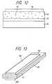
- the present invention further provides an ink jet recording head comprising a substrate having an ink chamber formed therein, a vibrating plate sealing one end of said ink chamber and having a deflection vibration mode thin piezoelectric film element fixed on the surface thereof and a nozzle plate sealing the other end of said ink chamber and having an ink jetting nozzle port formed therein, characterized in that said thin piezoelectric film element is made of a novel and useful thin piezoelectric film element mentioned above.
- the thin piezoelectric film element shown in Fig. 1 comprises a silicon (Si) substrate 10, a lower electrode (made of, e.g., Pt) 12, a piezoelectric film (e.g., binary PZT), and an upper electrode (made of, e.g., Pt) 16.
- Fig. 2 is a sectional view illustrating in more detail the structure of the thin piezoelectric film element.
- the thin piezoelectric film element is shown comprising a silicon substrate 10, a silicon oxide film 11 formed on the silicon substrate, a titanium oxide film 11A formed on the silicon oxide film, a lower electrode 12 formed on the titanium oxide film, a PZT film (piezoelectric film) formed on the lower electrode, and an upper electrode 16 formed on the PZT film.
- the lattice constant of the lower electrode can be close to that of the PZT film to enhance the adhesion of the lower electrode with the PZT film to be formed later.
- Example 1 platinum was sputtered onto a silicon substrate 10 as a lower electrode 12. Subsequently, a thin piezoelectric film 14 was formed on the lower electrode 12 by sol-gel method.
- the sol was prepared as follows. 0.105 mol of lead acetate, 0.045 mol of zirconium acetyl acetonate and 0.005 mol of magnesium acetate were dissolved in 30 ml of acetic acid at a temperature of 100°C.
- the sol was then allowed to cool to room temperature. To the sol was then added a solution of 0.040 mol of titanium tetraisopropoxide and 0.010 mol of pentaethoxy niobium in 50 ml of ethyl cellosolve. To the sol was then added 30 ml of acetyl acetone so that it was stabilized. To the sol was then added polyethylene glycol in an amount of 30% by weight based on the weight of the metal oxide in the sol. The mixture was then thoroughly stirred to make a homogeneous sol.
- the sol thus prepared was then applied to the substrate having a lower electrode formed thereon by means of a spin coater.
- the material was then calcined at a temperature of 400°C to form a thin amorphous porous gel film.
- the application of the sol and the calcining at a temperature of 400°C were then repeated twice to form a thin porous gel film.
- polyethylene glycol was evaporated from the sol to form pores.
- the material was heated to 650°C in an oxygen atmosphere in an RTA (Rapid Thermal Annealing) furnace in 5 seconds, and then remained at the same temperature for 1 minute so that is was pre-annealed to form a thin dense PZT film.
- RTA Rapid Thermal Annealing
- the sol was again applied to the material by means of a spin coater.
- the material was then calcined at a temperature of 400°C. This procedure was then repeated twice (thrice in total) to form a laminate of thin amorphous porous gel films.
- the material was pre-annealed at a temperature of 650°C in RTA, and then maintained at the same temperature for 1 minute to obtain a thin dense crystalline film.
- the pre-annealing temperature can be predetermined to a range of from 400°C to 800°C, preferably from 450°C to 750°C, more preferably from 550°C to 750°C to unite the laminated thin porous films in a body.
- the material was heated to various temperatures of 750°C, 800°C, 850°C, 900°C, 950°C, 1,000°C and 1,050°C in an oxygen atmosphere in RTA, and then maintained at the same temperatures for 1 minute so that it was annealed. As a result, a thin piezoelectric film 14 having a thickness of 1.0 ⁇ m was obtained.
- the thin PZT film thus obtained was then subjected to X-ray diffractometry.
- RINT-1400 available from Rigaku Denki Co., Ltd.
- the angle of incidence of X-ray from a copper valve tube was adjusted to 1°.
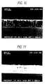
- Fig. 3 shows an X-ray diffraction pattern of the thin PZT film which had been annealed at a temperature of 900°C.
- Fig. 4 shows an X-ray diffraction pattern of the thin PZT film which had been annealed at a temperature of 750°C.
- peaks in the X-ray diffraction pattern shown in Figs. 3 and 4 are reflection peaks of PZT in the perovskite structure.
- This thin PZT film may be rhombohedral or tetragonal. Since the peaks corresponding to (100) plane, (110) plane, etc. are not separated from each other and together form one sharp peak, this thin PZT film is rhombohedral system crystalline structure.
- Table 1 shows the relationship of the annealing temperature with (100) orientation and piezoelectric constant d31.
- (200) plane is a crystalline plane equivalent to (100) plane and thus is not included in ⁇ I(hkl).
- ⁇ I(hkl) is the sum of the crystalline plane reflection intensities in (100), (110), (111), (210) and (211) planes.
- I(100) represents the crystalline plane reflection intensity of PZT in (100) plane. Annealing temp.
- the resulting thin piezoelectric film element can better act as an actuator.
- Gold was sputtered onto a silicon substrate as a lower electrode. Subsequently, a thin piezoelectric film element was formed on the lower electrode by sol-gel method.
- the sol was prepared as follows. In some detail, 0.105 mol of lead acetate, 0.030 mol of zirconium acetyl acetonate and 0.007 mol of magnesium acetate were dissolved in 30 ml of acetic acid at a temperature of 100°C.
- Example 2 shows the relationship of Zr/Ti with (100) orientation and piezoelectric constant d31.
- Zr/Ti P(100) Piezoelectric constant d31 30/50 27.4 % 46 pC/N 35/45 38.2 % 100 pC/N 40/40 66.7 % 128 pC/N 45/35 60.6 % 137 pC/N 50/30 25.3 % 51 pC/N
- the resulting thin piezoelectric film element can better act as an actuator.
- Examples 1 and 2 have been described with reference to the case where the lower electrode is made of Pt or Au.
- any other metal such as Au, Pt-Ir, Pt-Pd, Pt-Ni and Pt-Ti may be used so far as (100) orientation of thin PZT film is not less than 30%.
- Examples 1 and 2 have also been described with reference to the case where lead magnesium niobate is used as a third component.
- any other material such as lead nickel niobate and lead cobalt niobate may be used so far as (100) orientation of thin piezoelectric film element is not less than 30%.
- Nb, La, Mo, W, Ba, Sr, Bi, etc. may be contained as impurities.
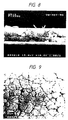
- FIG. 5(A) is a scanning electron microscope photograph (SEM) of a section of the PZT film constituting the thin piezoelectric film element.
- Fig. 5(B) is a scanning electron microscope photograph of the plane of the PZT film shown in Fig. 5(A).
- the PZT film shown in Figs. 1 and 2 is made of a polycrystalline substance.
- the grain boundary of the crystalline exists almost perpendicular to the plane of the upper and lower electrodes as shown in Fig. 5.
- Shown white in the central portion of Fig. 5 is a PZT film.
- the PZT film is shown comprising columnar crystal grains extending vertically as viewed on the paper.
- a lower electrode is shown as a white layer under the PZT film.
- SiO 2 is shown provided under the lower electrode.
- the grain boundary of crystalline is the border of adjacent crystal grains.
- the crystal grain is a crystal having a perovskite structure while the crystal grain boundary is composed of an amorphous material.
- the vertical width (Y direction in Fig. 5) of the crystal grains is greater than the horizontal width (X direction in Fig. 5) of the crystal grains.
- the relationship between the vertical width and the horizontal width of the crystal grains is from not less than 1/10 to not more than 1/3 as calculated in terms of the ratio of horizontal width to vertical width.
- the crystalline structure of the PZT film is a rhombohedron which is strongly oriented in (111) plane.
- orientation as used herein is defined as follows: I(XYZ)/(I(100) + I(110) + I(111) ⁇ wherein I(XYZ) represents the reflection intensity of (XYZ) plane of PZT as determined by wide angle XRD method.
- (111) orientation and piezoelectric strain constant is as follows: (111) orientation Piezoelectric strain constant 50% 80 pC/N 70% 120 pC/N 90% 150 pC/N
- the piezoelectric strain constant is proportional to the product of dielectric constant and piezoelectric output coefficient.
- the dielectric constant increases as the size of the crystal grains in the direction of electric field application (Y direction in Fig. 5) increases.
- the piezoelectric output coefficient increases as the size of the crystal grains increases in the horizontal direction (X direction in Fig. 5) and the width of the crystal grain boundary decreases. For this reason, the PZT film 15 having such a structure shows an enhanced piezoelectric strain constant.
- the ratio of the horizontal width of the crystal constituting the thin piezoelectric film to the vertical width of the crystal constituting the thin piezoelectric film is predetermined to a range of from not less than 1/10 to not more than 1/3, preferably from not less than 1/8 to not more than 3/10, more preferably from not less than 1/6 to not more than 3/11.
- the PZT film is preferably made of a binary PZT or a tertiary PZT comprising such a binary PZT having a third component incorporated therein as a main component.
- Specific preferred examples of the binary PZT include a compound having the composition represented by the following chemical formula: Pb(Zr x Ti 1-x )O 3 + YPbO wherein x is a number of from not less than 0.40 to not more than 0.6; and Y is a number of from not less than 0 to not more than 0.1.
- An example of the binary PZT film formed by sputtering is a compound having the composition represented by the following chemical formula: Pb(Zr x Ti 1-x )O 3 + YPbO wherein x is a number of from not less than 0.40 to not more than 0.6; and Y is a number of from not less than 0 to not more than 0.3.
- a specific preferred example of the tertiary PZT is lead magnesium niobate wherein A is Mg, B is Nb, g is 1/3, and h is 2/3.
- the PZT film comprising lead magnesium niobate incorporated therein as a third component, if sol-gel method is used, is represented, e.g., by the composition formula Pb(mg 1/3 Nb 2/3 ) 0.2 Zr x Ti 0.8-x O 3 wherein x represents a number of from 0.35 to 0.45.
- the PZT film may comprise a slight amount of Ba, Sr, La, Nd, Nb, Ta, Sb, Bi, W, Mo, Ca, etc. incorporated therein to have improved piezoelectric characteristics.
- the tertiary PZT preferably comprises Sr or Ba incorporated therein in an amount of not more than 0.10 mol-% to have improved piezoelectric characteristics.
- the tertiary PZT preferably comprises Mn or Ni incorporated therein in an amount of not more than 0.10 mol-% to have improved sinterability.
- the third component may be partly replaced by a fourth component. In this case, as the fourth component there may be used one of the foregoing third components.
- the PZT film may be strongly oriented in (100) plane or either (111) plane or (100) plane besides the foregoing planes.
- the crystalline structure of the PZT film is a tetragonal which is strongly oriented in (001) plane.
- Figs. 6 (a) to (c) are sectional views illustrating the various steps in the process for the preparation of the foregoing thin piezoelectric film element.
- a silicon substrate 10 is subjected to thermal oxidation to form a silicon oxide film 11 thereon to a thickness of from about 0.3 to 1.2 ⁇ m.
- a titanium oxide film 11A was formed on the silicon oxide film to a thickness of from about 0.005 to 0.04 ⁇ m by sputtering method.
- a lower electrode 12 made of platinum was formed on the titanium oxide film to a thickness of from about 0.2 to 0.8 ⁇ m.
- a PZT film 14 was formed on the lower electrode formed in the step shown in Fig. 6 (a) to a thickness of from about 0.5 to 3.0 ⁇ m. The process for the preparation of PZT film will be described with reference to sputtering method and sol-gel method.
- EXAMPLE 3-1 Preparation of PZT film by sputtering method
- a PZT precursor film made of amorphous or pyrochlore phase was formed on a substrate by RF magnetron sputtering method with a sintered PZT having a specific composition as a sputtering target at a substrate temperature of not higher than 200°C in a 100% Ar gas atmosphere.
- the precursor film was heated so that it was crystallized and sintered.
- the heating is preferably effected by two stages in an atmosphere of oxygen (e.g., oxygen or a mixture of oxygen and an inert gas such as argon).
- the amorphous precursor film was heated to a temperature of from 500°C to 700°C in an atmosphere of oxygen so that it was crystallized.
- the first heating step may be completed at the time when the precursor film is uniformly crystallized.
- the crystal grains thus produced were allowed to grow, and the sintering of the crystal grains to each other was accelerated.
- the precursor film which had been crystallized in the first heating step was heat to a temperature of from 750°C to 1,200°C. The heating was effected until the grain boundary of the crystalline is present almost perpendicular to the surface of the lower electrode 14 and the relationship between the vertical width and the horizontal width of the crystal grains is from not less than 1/10 to not more than 1/3 as calculated in terms of the ratio of horizontal width to vertical width.
- the first heating step may be immediately followed by the second heating step.
- the first heating step may be followed by cooling to room temperature which is in turn followed by the second heating step.
- any heating furnace may be used so far as the PZT film 15 is formed by the precursor film having the foregoing structure.
- a heating furnace having a great temperature rising rate is preferably used.
- a lamp annealing furnace is preferably used.
- the temperature rising rate is preferably not less than 50°C/sec., more preferably not less than 100°C/sec.
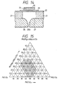
- Fig. 7 shows a preferred composition range of PZT film (or PZT target) in the case where a PZT precursor film is formed by sputtering method.
- the third component there is used Pb(Mg 1/3 Nb 2/3 )O 3 among those represented by the foregoing general formula (I): Pb(A g B h )O 3 .
- This composition range corresponds to the region surrounded by A, B, C, D, E and F in Fig. 7.
- a is from not less than 10 to not more than 50
- b is from not less than 20 to not more than 55
- c is from not less than 0 to not more than 50.
- This range is a preferred range included in the range defined with reference to the general formula (I).
- the border (D-E-F-A) shown left in Fig. 7 is defined to obtain a high piezoelectric strain constant (not less than 100 pC/N).
- the border (D-C) shown upper in Fig. 7 is defined to avoid a fear that the stability of the device may be deteriorated when the Curie temperature is close to room temperature. When the Curie temperature is exceeded, the piezoelectric element cannot fully exhibit its piezoelectric characteristics. Further, the region of the composition represented by the foregoing formula (1) is shown in Fig. 15.
- This preparation process comprises dehydrating a hydrated complex of a hydroxide of a metal component capable of forming a PZT film, i.e., sol to make a gel which is then calcined to prepare an inorganic oxide. Two such preparation processes will be described. These sol-gel methods are almost the same as Examples 1 and 2 but will be again described in detail.
- the sol of the metal component constituting the PZT film can be prepared by hydrolyzing an alkoxide or acetate of a metal capable of forming a PZT film with, e.g., an acid.
- the composition of the metals in the sol can be controlled to obtain the foregoing composition of the PZT film.
- an alkoxide or acetate of titanium, zirconium, lead or other metal components may be used as a starting material.
- the present example is advantageous in that the composition of the metal components constituting the PZT film is almost maintained until it is finally formed into a PZT film (thin piezoelectric film).
- a PZT film thin piezoelectric film.
- the composition of the metal components in the starting material coincides with that of the metal components in the PZT film finally obtained.
- the composition of the desired gel is determined depending on the piezoelectric film to be produced (PZT film in the present example).
- the sol contains the lead component in an amount of 20 mol-%, preferably 15 mol-% more than the value stoichiometrically required.
- the sol is preferably used in the form of a composition mixed with an organic high molecular compound.
- This organic high molecular compound absorbs residual stress of the thin film during drying and calcining to effectively prevent the thin film from being cracked.
- the use of a gel containing this organic high molecular compound makes it possible to form pores in the gelated thin film described later. It is thought that these pores absorb residual stress of the thin film during the pre-annealing step and annealing step described later.
- the incorporation of polyvinyl acetate makes it possible to form a thin porous gel film having many pores with a diameter of about 0.05 ⁇ m ⁇ formed therein. Further, the incorporation of hydroxypropyl cellulose makes it possible to form a thin porous gel film having pores with a size of not more than 0.1 ⁇ m and a wide distribution formed therein.
- polyethylene glycol there may be preferably used one having an average molecular weight of from about 285 to 420.
- polypropylene glycol there may be preferably used one having an average molecular weight of from about 300 to 800.
- this sol composition is applied to a lower electrode on which a PZT film is to be formed (see Fig. 6 (b)).
- the coating method is not specifically limited. Any common method such as spin coating method, dip coating method, roll coating method and bar coating method may be used. Alternatively, any printing method such as flexography, screen printing and offset printing may be used.
- the thickness of the film thus formed by coating is preferably controlled such that the thickness of the thin porous gel film formed in the gelation step described later reaches not less than 0.01 ⁇ m, more preferably from 0.1 to 1 ⁇ m, taking into account the subsequent steps.
- the sol composition thus applied is spontaneously dried or heated to a temperature of not higher than 200°C.
- the sol composition may be further applied to the film thus dried (heated) to add to the thickness of the film.
- the film to which the sol composition is further added is preferably dried at a temperature of not lower than 80°C.
- the film obtained in the foregoing step of forming a sol composition into a film is calcined to form a thin porous gel film made of an amorphous metal oxide substantially free of residual organic substances.
- the calcining is effected at a temperature high enough to gel the film of sol composition and remove organic substances from the film for a period of time long enough to do so.
- the calcining temperature is preferably from 300°C to 450°C, more preferably from 350°C to 400°C.
- the calcining time depends on the temperature and the type of the furnace used but preferably is from about 10 to 120 minutes, more preferably from about 15 to 60 minutes, if a degreasing furnace is used. Further, if a hot plate is used, the calcining time is preferably from about 1 to 60 minutes, more preferably from about 5 to 30 minutes. In this manner, a thin porous gel film was formed on the lower electrode.
- the thin porous gel film obtained in the foregoing step b is heated and calcined so that it is converted to a film made of a crystalline metal oxide.
- the calcining is effected at a temperature required to convert the thin porous gel film to a film made of a crystalline metal oxide.
- the calcining doesn't need to be effected until perovskite accounts for the majority of the crystal.
- the calcining may be completed at the time when the thin gel film is uniformly crystallized.
- the calcining temperature is preferably from 400°C to 800°C, more preferably from 550°C to 750°C.
- the calcining time depends on the calcining temperature and the type of the furnace used but preferably is from about 0.1 to 5 hours, more preferably from about 0.5 to 2 hours, if an annealing furnace is used. Further, if RTA (Rapid Thermal Annealing) furnace is used, the calcining time is preferably from 0.1 to 10 minutes, more preferably from 1 to 5 minutes.
- the pre-annealing step is effected by two stages.
- pre-annealing is effected at a temperature of from 400°C to 600°C at a first step, and then at a temperature of from 600°C to 800°C at a second step. More preferably, pre-annealing is effected at a temperature of from 450°C to 550°C at a first step, and then at a temperature of from 600°C to 750°C at a second step.
- the thin porous gel film was converted to a film made of a crystalline metal oxide.
- the foregoing steps a , b and c are repeated at least once to obtain a laminate of crystalline gold oxides.
- the thickness of the films obtained in this repeating step, the calcining temperature in this repeating step and the pre-annealing conditions used in this repeating step are the same as used in the formation of the first film on the lower electrode.
- the thickness of the laminate obtained in this repeating step may be properly determined taking into account the thickness of PZT film finally formed but is preferably such that no cracking occurs during the subsequent step described later (step e ).
- the substantially integrated film may or may not be free of discontinuous layer between laminated layers unlike the finally obtained PZT film 15 according to the present example. If the steps a , b and c are further repeated, a further new thin porous gel film is formed, followed by pre-annealing. As a result, the new thin porous gel film was substantially integrated with the laminate of crystalline films previously obtained.
- the patterning for forming a thin piezoelectric film element or the formation of the upper electrode is preferably effected at this step.
- the film obtained in the step d is annealed at a calcining temperature of from 600°C to 1,200°C, preferably from 800°C to 1,000°C.
- the calcining time depends on the calcining temperature or the type of the furnace used but preferably is from about 0.1 to 5 hours, more preferably from 0.5 to 2 hours, if an annealing furnace is used. Further, if RTA furnace is used, the calcining time is preferably from 0.1 to 10 minutes, more preferably from 0.5 to 3 minutes.
- This perovskite growth step i.e., annealing may be effected by two stages.
- annealing may be effected at a temperature of from about 600°C to 800°C at a first step, and then at a temperature of from about 800°C to 1,000°C at a second step. More preferably, annealing may be effected at a temperature of from about 600°C to 750°C at a first step, and then at a temperature of from about 800°C to 950°C at a second step.
- a PZT film 15 made of a polycrystalline substance the grain boundary is present almost perpendicular to the surface of the lower electrode 14, the vertical width of the crystal grains is greater than the horizontal width of the crystal grains, and the relationship between the vertical width and the horizontal width of the crystal grains is from not less than 1/10 to not more than 1/3 as calculated in terms of the ratio of horizontal width to vertical width.
- the foregoing steps a and b are repeated at least once to form a laminate of thin porous gel films.
- the thickness of the film formed in the steps a and b and the calcining temperature are proportionate to the foregoing preparation process (1).
- the thickness of the laminate is preferably determined to not more than 1 ⁇ m, more preferably not more than 0.5 ⁇ m.
- the definition of the thickness of the laminate to this range makes it possible to prevent the laminate from being cracked during pre-annealing at the subsequent step (step c' ). In this step, a laminate of a plurality of thin porous gel films was obtained.
- the laminate obtained at the step f is calcined to convert the laminate to a film made of a crystalline metal oxide.
- This calcining is effected at a temperature required to convert the laminate to a film made of a crystalline metal oxide.
- the calcining doesn't need to be effected until perovskite accounts for the majority of the crystal but may be completed at the time when the thin gel film is uniformly crystallized.
- the calcining temperature and time may be almost the same as the step c . Further, this calcining may be effected by two stages as in the step c . In this step, the laminate of a plurality of thin polycrystalline gel films was converted to a thin crystalline film.
- the steps f and c' are repeated at least once.
- the steps a and b are repeated at least once to form a laminate of thin porous gel films which is then calcined to convert it to a film made of a crystalline metal oxide.
- This step is further repeated once or more times. In this manner, a laminate of a plurality of crystalline metal oxide films is formed.
- the various conditions used in the repeated steps a , b and c' are the same as mentioned above.
- the thickness of the laminate obtained in this repeating step d' may be properly determined taking into account the thickness of PZT film 15 finally formed but is preferably such that no cracking occurs during the subsequent step described later (step e' ).
- a new thin porous gel film was formed on the film previously formed, and then pre-annealed.
- the newly formed thin porous gel film was substantially integrated with the film previously formed.
- the substantially integrated film is defined as mentioned above.
- the patterning for forming a thin piezoelectric film element or the formation of the upper electrode 16 is preferably effected at this step.
- the step c was effected.
- a PZT film made of a polycrystalline substance the grain boundary is present almost perpendicular to the surface of the lower electrode 14, the vertical width of the crystal grains is greater than the horizontal width of the crystal grains, and the relationship between the vertical width and the horizontal width of the crystal grains is from not less than 1/10 to not more than 1/3 as calculated in terms of the ratio of horizontal width to vertical width.
- step shown in Fig. 6 (c) aluminum is sputtered onto the PZT film obtained in the step shown in Fig. 6 (b) to form an upper electrode 16 to a thickness of from about 0.2 to 1.0 ⁇ m.
- a thin piezoelectric film element shown in Fig. 2 was obtained.
- the PZT film 14 thus obtained was found to have no cracking.
- the PZT film was also found to have no laminated discontinuous planes present in a section.
- the thin piezoelectric film element according to Example 3 (Invention 1) and a thin piezoelectric film element having the same structure as Invention 1 except that the grain boundary of the crystalline constituting the PZT film is not present almost perpendicular to the surface of the lower electrode (Comparison 1) were measured for piezoelectric strain constant (pC/N).
- the piezoelectric strain constant of Invention 1 was 150 pC/N.
- the piezoelectric strain constant of Comparison 1 was 100 pC/N.
- Invention 1 exhibits a higher piezoelectric strain constant than Comparison 1.
- the specimen (2 mm ⁇ dot pattern) was measured for dielectric constant by means of an impedance analyzer and for piezoelectric output coefficient (voltage generated on the dot pattern when the free end of a cantilever is under load).
- the piezoelectric strain constant was calculated by the product of dielectric constant and piezoelectric output coefficient.
- a SEM photograph illustrating a section of the PZT film in Comparison is shown in Fig. 8.
- a SEM photograph illustrating the plane of the PZT film of Fig. 8 is shown in Fig. 9.
- Invention 1 showed little warping or distortion and hence a good external appearance.
- Example 3 has been described with reference to the case where PZT film is prepared by sputtering method or sol-gel method. It goes without saying that the present invention is not limited to this case and other preparation processes may be used so far as a PZT film having such a structure that the grain boundary of the crystalline exists almost perpendicular to the surface of the lower electrode can be formed.
- Example 3 has been described with reference to the PZT film wherein the grain boundary of the crystalline is present almost perpendicular to the surface of the electrode, the vertical width of the crystal grains is greater than the horizontal width of the crystal grains and the relationship between the vertical width and the horizontal width of the crystal grains is from not less than 1/10 to not more than 1/3 as calculated in terms of the ratio of horizontal width to vertical width.
- any PZT film may be used so far as the grain boundary of the crystalline is present almost perpendicular to the surface of the electrode.
- Fig. 10 is a scanning electron microscope (SEM) photograph illustrating a section of a lower electrode constituting another embodiment of the thin piezoelectric film element. In the present example, the difference from Example 4 will be described. Like reference numerals are used and detailed description is omitted where the constitutions and steps are the same as those of Example 3.
- the thin piezoelectric film element according to the present example differs from that of Example 3 in the structure and preparation process of the lower electrode.
- the lower electrode of the thin piezoelectric film element according to the present example is made of a compound of platinum with titanium oxide (platinum: 99% by weight; titanium oxide: 1% by weight). Further, the lower electrode has such a structure that the grain boundary of the crystalline is present almost perpendicular to the surface of the substrate as shown in Fig. 10.
- the grain boundary is present almost perpendicular to the surface of the PZT film and the relationship between the vertical width and the horizontal width of the crystal grains is from not less than 1/10 to not more than 1/3 as calculated in terms of the ratio of horizontal width to vertical width.
- the lower electrode having such a structure can prevent the substrate from being warped or distorted during heat treatment in the formation of PZT film because titanium oxide can inhibit the shrinkage of platinum. Further, the lower electrode having such a structure can have an enhanced adhesion with the PZT film and titanium oxide film.
- a silicon oxide film 11 and a titanium oxide film 11A were formed on a silicon substrate 10 in the same manner as in the step shown in Fig. 6 (a). Subsequently, a lower electrode 12 was formed on the titanium oxide film by a multi-sputtering method comprising the simultaneous discharge of a platinum target and a titanium oxide target. In this manner, a lower electrode 12 made of a compound of platinum with titanium oxide (platinum: 99% by weight; titanium oxide: 1% by weight) was obtained wherein the grain boundary of the crystalline is present almost perpendicular to the surface of the substrate 10 and the relationship between the vertical width and the horizontal width of the crystal grains is from not less than 1/10 to not more than 1/3 as calculated in terms of the ratio of horizontal width to vertical width.
- Example 5 Thereafter, a PZT film 14 and an upper electrode 16 were formed on the lower electrode 12 in the same manner as in Example 4 to obtain a thin piezoelectric film element. It was confirmed that the thin piezoelectric film element according to Example 5, too, exhibits a high piezoelectric strain constant.
- Fig. 11 is a scanning electron microscope photograph illustrating a section of the lower electrode constituting Comparison 2.
- Fig. 11 is an example comparative to Fig. 10 and shows PZT having a non-columnar structure. This examination was carried out by measuring the warpage of the substrate on which the foregoing thin piezoelectric film element had been formed.
- Invention 2 showed little or no warpage or distortion. However, it was confirmed that Comparison 2 shows a greater warpage or distortion than Invention 2.
- Invention 2 and Comparison 2 were examined for the adhesion between the lower electrode 12 and the PZT film 14 and the adhesion between the lower electrode 12 and the titanium oxide film 11A. This examination was carried out by means of a scratch tester. As a result, it was confirmed that Invention 2 is excellent both in the adhesion between the lower electrode and the PZT film and the adhesion between the lower electrode and the titantum oxide film as compared with Comparison 2.
- the lower electrode was made of the foregoing composition.
- the platinum content may be from 90 to 99.5% by weight, and the titanium oxide content may be from 0.5 to 10% by weight.
- the present example has been described with reference to the lower electrode 14 wherein the grain boundary of the crystalline constituting the lower electrode is present almost perpendicular to the surface of the substrate 10 and the relationship between the vertical width and the horizontal width of the crystal grains is from not less than 1/10 to not more than 1/3 as calculated in terms of the ratio of horizontal width to vertical width.
- the present invention is not limited to this structure. Any lower electrode may be used so far as the grain boundary of the crystalline constituting the lower electrode is present almost perpendicular to the surface of the substrate 10.
- the present example has been described with reference to the case where the lower electrode is made of a compound of platinum with titanium oxide.
- the present invention is not limited to this constitution.
- the lower electrode may be made of a compound of platinum with an oxide of other metal elements constituting the PZT film.
- the oxide other than titanium oxide include lead oxide, zirconium oxide, magnesium oxide, and niobium oxide.
- FIG. 12 An embodiment of the present invention wherein the diameter of closed pores (pores) is controlled to inhibit the generation of cracking in the thin piezoelectric film.
- FIG. 12 An enlarged sectional view of the dotted area in Fig. 1 is shown in Fig. 12.
- the piezoelectric film 14 has pores 20 formed therein. These pores are round-cornered. These pores are sealed in crystal grains or between crystal grains (individual grains are not shown in the drawing). These pores have an average diameter of from 0.01 to 0.1 ⁇ m and a surface density of from 0.3 to 5%.
- the thickness of the piezoelectric film is preferably from about 0.5 to 25 ⁇ m, more preferably from about 1 to 5 ⁇ m. Further, the thickness of the other films may be properly determined.
- the thickness of the Si substrate is preferably from about 10 to 1,000 ⁇ m.
- the thickness of the thermally oxidized Si film is preferably from about 0.05 to 3 ⁇ m.
- the thickness of the upper electrode and the lower electrode are each preferably from about 0.05 to 2 ⁇ m.
- a Si substrate having a thickness of 400 ⁇ m and a diameter of 3 inch was washed with sulfuric acid, and then heated at a temperature of 1,000°C in an oxygen atmosphere containing water vapor for 4 hours so that it was wet-oxidized to form a thermally oxidized Si film having a thickness of 1 ⁇ m. Subsequently, a Ti film and a Pt film were continuously sputtered onto the thermally oxidized Si film to a thickness of 200 ⁇ and 2,000 ⁇ , respectively, by dc magnetron sputtering method.
- a piezoelectric precursor film was sputtered onto the Pt film to a thickness of 1 ⁇ m by RF magnetron sputtering method.
- the precursor film thus obtained was amorphous because it had been sputtered without being heated.
- the Si substrate on which the precursor film had been formed was then heated in an oxygen atmosphere in a diffusion furnace so that the precursor film was crystallized and sintered to form a piezoelectric film.
- the material was heated at a temperature of 600°C at a first heating step until it was crystallized, and then sintered at a temperature of 750°C at a second heating step.
- the average diameter and surface density of the pores in the piezoelectric film can be well adjusted by controlling the Pb composition ratio in the amorphous film, the temperature at the first heating step and the temperature at the second heating step. If the Pb content in the amorphous film is great, both the pore diameter and surface density tend to increase. If the temperature at the second heating step is high or the heating time is long, the pore diameter tends to increase.
- a Pt film was further sputtered onto the piezoelectric film to a thickness of 2,000 ⁇ by dc magnetron sputtering method. Finally, the material was processed as shown in Fig. 1 to give a piezoelectric element having a desired shape.
- Piezoelectric elements having different average pore diameters were prepared by changing the foregoing preparation conditions.
- the generation of cracking in the piezoelectric film and the leakage of electricity between the upper and lower electrodes were as set forth in Table 3.
- the surface density of the pores in the samples shown in Table 3 were predetermined to a range of from 1 to 2%.
- a sample having a circular upper electrode having a diameter of 2 mm formed thereon was used for the measurement of electricity leakage.
- a 100 V voltage was applied across the upper and lower electrodes. It is thought that cracked samples are liable to leakage of electricity at the cracked area.
- a piezoelectric material undergoes phase transition that changes the crystal structure at its Curie temperature.
- the heat treatment temperature at which crystallization occurs is higher than Curie temperature. Accordingly, when the temperature of the piezoelectric film, if it is too dense, cools to room temperature, it cannot absorb the resulting distortion and thus undergoes cracking.
- the thermal expansion coefficient of the piezoelectric material is relatively greater than that of the silicon substrate. Accordingly, if the piezoelectric film cannot absorb the thermal stress of the silicon substrate, it can undergo cracking.
- the piezoelectric material has some pores formed therein to absorb distortion and stress, making it possible to obtain a film that undergoes no cracking.
- the piezoelectric film is subject to the effective application of a greater electric field and thus can be destroyed due to leakage.
- the product was also subjected to accelerated durability test in the form of piezoelectric element.
- a 30 V pulse voltage having a duty of 10% and a frequency of 10 KHz was applied across the upper and lower electrodes.
- the change in the displacement of the tip of the piezoelectric element was determined.
- the piezoelectric element showed a repeated durability of not less than 2 x 10 9 times if its average pore diameter was not more than 0.05 ⁇ m. If the average pore diameter was from more than 0.05 ⁇ m to not more than 0.1 ⁇ m, the displacement showed a drop by the time when the repeated durability reached 2 x 10 9 times.
- Example 6 The procedure of Example 6 was followed to prepare an actuator except that the surface density of pores was changed.
- the generation of cracking in the piezoelectric film and the leakage of electricity between the upper and lower electrodes were as shown in Table 4.
- Pore surface density (%) Cracking Electricity leakage 0.2 presence presence 0.5 absence absence 1.0 absence absence 2.5 absence absence 3.5 absence presence 5.0 absence presence
- the average diameter of pores in the samples set forth in Table 4 were predetermined to a range of from 0.03 to 0.07 ⁇ m. As a result, it was found that an actuator having a pore surface density of from 0.3 to 3% which undergoes neither cracking nor leakage of electricity can be obtained. If the pore surface density exceeds the above defined range, the piezoelectric film is subject to the effective application of a greater electric field and thus can be destroyed due to leakage.
- the product was also subjected to accelerated durability test in the form of piezoelectric element.
- the test conditions were the same as used in Example 1.
- the piezoelectric element showed a repeated durability of not less than 2 x 10 9 times if its pore surface density was not more than 1%. If the pore surface density was from more than 1% to not more than 5%, the displacement showed a drop by the time when the repeated durability reached 2 x 10 9 times.
- Examples 6 and 7 a Si substrate was used as a substrate. However, a ceramic substrate made of magnesia, alumina, zirconia or the like may be used. These examples have been described with reference to the case where a binary PZT is used as a piezoelectric film. However, it is of course desirable that the material of the piezoelectric film is changed depending on the purpose.
- the piezoelectric film is preferably made of a tertiary PZT having a Curie point of not lower than 200°C that can provide a high piezoelectric strain constant d31, more preferably a tertiary PZT comprising lead magnesium niobate incorporated therein as a third component.
- Fig. 1 has been illustrated with reference to a unimorph type actuator. However, as shown in Fig. 13, the present invention can be also applied to a bimorph type actuator.
- This bimorph type actuator is symmetrical about the lower electrode 12. Shown at reference numerals 101 and 201 are piezoelectric films. Shown at reference numerals 103 and 203 are upper electrodes.
- FIG. 14 shows one of ink reservoirs of an ink jet recording head comprising a thin piezoelectric film element of the present invention as a vibrator.
- the ink jet recording head comprises a silicon substrate 21 having an ink reservoir formed therein, a vibrating plate 22 formed on the silicon substrate 21, a lower electrode 23 formed on the vibrating plate 22 at a desired position, a thin piezoelectric film 24 formed on the lower electrode 23 at a position corresponding to the ink reservoir 27, an upper electrode 25 formed on the thin piezoelectric film 24, and a second substrate 26 bonded to the lower surface of the silicon substrate 21.
- the substrate 26 has an ink jetting nozzle 26A connected to the ink reservoir 27.
- the lower electrode 23 has the structure described in the foregoing examples. So is the thin piezoelectric film 24.
- an ink is supplied into the ink reservoir 27 through an ink passage (not shown).
- the piezoelectric film 24 deforms to raise the pressure in the ink reservoir 27 and hence press the ink.
- the rise in the pressure causes the ink to be jetted through a nozzle (not shown).
- ink jet recording is conducted.
- the ink jet recording head comprises the foregoing thin piezoelectric film element having excellent piezoelectric characteristics as a vibrator and thus can jet an ink at a high pressure.
- the piezoelectric film was photoetched to have a pattern having a width of 0.2 mm and a length of 4 mm.
- the silicon substrate was anisotropically etched to form a groove having a width of 0.3 mm.
- the piezoelectric film and a glass-made second substrate are joined to form an ink passage.
- the piezoelectric film was cut together with the substrate to assemble an ink jet head.
- the ink jet head was then subjected to ink jetting test. As a result, it was found that the ink jet head has a sufficient injection power.
- the ink jet head was then mounted in an ink jet recording apparatus. When printing was effected, a good print quality was obtained.
- the recording head comprises a single-crystalline silicon substrate chip having a thin piezoelectric film element composed of a lower electrode, a piezoelectric film and an upper electrode integrally formed by a thin film process on a thermally oxidized Si film as a vibrating plate and a cavity (in reservoir) formed therein, and a stainless nozzle plate (second substrate) having a nozzle for jetting an ink, bonded to each other with an adhesive.
- the piezoelectric film was made of a tertiary PZT having lead magnesium niobate as a third component as a material having a high piezoelectric strain constant d31.
- the thickness of the piezoelectric film was 2 ⁇ m.
- a piezoelectric film having in its section pores having an average diameter of from 0.01 to 0.1 ⁇ m and a surface density of from 0.3% to 5% exhibits a reliability of 5 years when used with an actual ink jet recording head.
- the piezoelectric film was then subjected to durability test.
- a piezoelectric film formed by photoetching can provide a high precision printing. Further, since such a substrate can form many elements per sheet, the cost can be reduced. Moreover, the production stability and reproducibility of characteristics are excellent. In other words, the use of the thin piezoelectric film element of the present invention makes it possible to prepare an ink jet recording head that can provide high density recording in a high yield at a simple production process.
- the thin piezoelectric film element of the present invention can find wide application because of its good characteristics.
- it may be used as a vibrating plate for ink jet recording head as mentioned above.
- the thin piezoelectric film element of the present invention comprises a thin PZT film having an optimum crystal orientation and thus can exhibit improved piezoelectric characteristics.
- the grain boundary of the crystalline constituting the thin piezoelectric film element is present almost perpendicular to the surface of the electrode.
- the thin piezoelectric film element can exhibit an enhanced piezoelectric strain constant without causing cracking.
- a thin piezoelectric film element having a high reliability and a high performance can be provided.
- this effect can be enhanced by making the vertical width of the crystal grains greater than the horizontal width of the crystal grains. This effect can be even further enhanced by predetermining the relationship between the vertical width and the horizontal width of the crystal grains within the foregoing range.
- the lower electrode can be made of a compound of platinum with an oxide of the metal element constituting the piezoelectric film to prevent the substrate from being warped or distorted during heat treatment in the formation of the piezoelectric film.
- the adhesion of the lower electrode with the piezoelectric film and substrate can be enhanced.
- this effect can be enhanced by arranging the grain boundary of the crystalline constituting the lower electrode present almost perpendicular to the surface of the piezoelectric film. This affect can be even further enhanced by making the vertical width of the crystal grains constituting the lower electrode greater than the horizontal width of the crystal grains.
- the thin piezoelectric film element of the present invention can be easily produced without being cracked even its thickness is as relatively great as not less than 0.5 ⁇ m.
- the thin piezoelectric film element of the present invention can provide a high density ink jet recording head in a high yield.
- the thin piezoelectric film element of the present invention exhibits a good reproducibility.
- the ink jet recording head of the present invention comprises the foregoing thin piezoelectric film element as a vibrator and thus can inject an ink at a high pressure.
Claims (5)
- Element mit dünnem, piezoelektrischem Film, das einen piezoelektrischen Film (14, 24, 101, 201) aufweist, hergestellt aus einer polykristallinen Substanz, die eine Dicke von 0,5 bis 25 µm und zwei Elektroden (12, 16, 23, 25, 103, 203), angeordnet mit dem piezoelektrischen Film dazwischengefügt, besitzt, wobei der piezoelektrische Film Poren (20) besitzt, die darin eingeschlossen sind, und wobei die Poren (20) einen durchschnittlichen Durchmesser nicht geringer als 0,01 µm und eine Oberflächendichte von nicht weniger als 0,3% haben.
- Element mit dünnem, piezoelektrischem Film gemäß Anspruch 1,
dadurch gekennzeichnet, dass
die Poren (20) einen durchschnittlichen Durchmesser von nicht mehr als 0,1 µm und eine Oberflächendichte von nicht mehr als 5% haben. - Element mit dünnem, piezoelektrischem Film nach Anspruch 2,
dadurch gekennzeichnet, dass
der piezoelektrische Film (14, 24, 101, 201) aus einem binären PZT (Bleizirkontitanat) oder einem tertiären PZT, aufweisend das binäre PZT mit einer zusätzlichen dritten Komponenten, hergestellt ist. - Element mit dünnem, piezoelektrischem Film nach Anspruch 3,
dadurch gekennzeichnet, dass
die dritte Komponente Bleimagnesiumniobat ist. - Tintenstrahlaufzeichnungskopf, der ein Substrat (21) mit einer Farbkammer (27) darin gebildet, eine Vibrationsplatte (22), die ein Ende der Farbkammer (27) abdichtet, und ein dünnes, piezoelektrisches Filmelement (23, 24, 25) mit einem Auslenkungsvibrationsmode, befestigt auf der Oberfläche davon, besitzt, und eine Düsenplatte (26), die das andere Ende der Farbkammer (27) abdichtet und eine Farbausstoßdüsenöffnung (26A), gebildet darin, besitzt, wobei das dünne, piezoelektrische Filmelement (23, 24, 25) aus einem Element mit dünnem, piezoelektrischem Film nach einem der Ansprüche 1 bis 4 hergestellt ist.
Applications Claiming Priority (9)
| Application Number | Priority Date | Filing Date | Title |
|---|---|---|---|
| JP24037295 | 1995-09-19 | ||
| JP24037295 | 1995-09-19 | ||
| JP32267095 | 1995-12-12 | ||
| JP32267095 | 1995-12-12 | ||
| JP19084896 | 1996-07-19 | ||
| JP19084896 | 1996-07-19 | ||
| JP24535396 | 1996-09-17 | ||
| JP24535396A JP3890634B2 (ja) | 1995-09-19 | 1996-09-17 | 圧電体薄膜素子及びインクジェット式記録ヘッド |
| EP19960114974 EP0764992B8 (de) | 1995-09-19 | 1996-09-18 | Piezoelektrisches Dünnschichtelement, Verfahren zum Herstellen und dieses piezoelektrisches Dünnschichtelement verwendender Tintenstrahldruckkopf |
Related Parent Applications (1)
| Application Number | Title | Priority Date | Filing Date |
|---|---|---|---|
| EP19960114974 Division EP0764992B8 (de) | 1995-09-19 | 1996-09-18 | Piezoelektrisches Dünnschichtelement, Verfahren zum Herstellen und dieses piezoelektrisches Dünnschichtelement verwendender Tintenstrahldruckkopf |
Publications (4)
| Publication Number | Publication Date |
|---|---|
| EP0928033A2 EP0928033A2 (de) | 1999-07-07 |
| EP0928033A3 EP0928033A3 (de) | 1999-08-04 |
| EP0928033B1 true EP0928033B1 (de) | 2002-08-28 |
| EP0928033B8 EP0928033B8 (de) | 2003-05-28 |
Family
ID=27475505
Family Applications (3)
| Application Number | Title | Priority Date | Filing Date |
|---|---|---|---|
| EP19990101630 Expired - Lifetime EP0928033B8 (de) | 1995-09-19 | 1996-09-18 | Piezoelektrisches Dünnschichtelement, Verfahren zum Herstellen und dieses piezoelektrisches Dünnschichtelement verwendender Tintenstrahldruckkopf |
| EP19960114974 Expired - Lifetime EP0764992B8 (de) | 1995-09-19 | 1996-09-18 | Piezoelektrisches Dünnschichtelement, Verfahren zum Herstellen und dieses piezoelektrisches Dünnschichtelement verwendender Tintenstrahldruckkopf |
| EP19990101631 Expired - Lifetime EP0928034B8 (de) | 1995-09-19 | 1996-09-18 | Piezoelektrisches Dünnschichtelement, Verfahren zum Herstellen und dieses piezoelektrisches Dünnschichtelement verwendender Tintenstrahldruckkopf |
Family Applications After (2)
| Application Number | Title | Priority Date | Filing Date |
|---|---|---|---|
| EP19960114974 Expired - Lifetime EP0764992B8 (de) | 1995-09-19 | 1996-09-18 | Piezoelektrisches Dünnschichtelement, Verfahren zum Herstellen und dieses piezoelektrisches Dünnschichtelement verwendender Tintenstrahldruckkopf |
| EP19990101631 Expired - Lifetime EP0928034B8 (de) | 1995-09-19 | 1996-09-18 | Piezoelektrisches Dünnschichtelement, Verfahren zum Herstellen und dieses piezoelektrisches Dünnschichtelement verwendender Tintenstrahldruckkopf |
Country Status (4)
| Country | Link |
|---|---|
| US (3) | US6097133A (de) |
| EP (3) | EP0928033B8 (de) |
| JP (6) | JP3890634B2 (de) |
| DE (3) | DE69625713T2 (de) |
Families Citing this family (127)
| Publication number | Priority date | Publication date | Assignee | Title |
|---|---|---|---|---|
| JP3438509B2 (ja) * | 1997-02-04 | 2003-08-18 | セイコーエプソン株式会社 | セラミックス薄膜及びその製造方法 |
| EP0867952B8 (de) * | 1997-03-27 | 2003-05-28 | Seiko Epson Corporation | Verfahren zur Herstellung eines piezoelektrischen Elements |
| EP0932210B1 (de) * | 1998-01-22 | 2007-05-16 | Seiko Epson Corporation | Piezoelektrisches Schichtelement und Tintenstrahldruckkopf, der dieses benutzt |
| JP3520403B2 (ja) | 1998-01-23 | 2004-04-19 | セイコーエプソン株式会社 | 圧電体薄膜素子、アクチュエータ、インクジェット式記録ヘッド、及びインクジェット式記録装置 |
| JP4122564B2 (ja) | 1998-04-24 | 2008-07-23 | セイコーエプソン株式会社 | 圧電体素子、インクジェット式記録ヘッドおよびそれらの製造方法 |
| US6402304B1 (en) * | 1998-08-12 | 2002-06-11 | Seiko Epson Corporation | Piezoelectric actuator, ink jet printing head, printer, method for manufacturing piezoelectric actuator, and method for manufacturing ink jet printing head |
| JP3517876B2 (ja) | 1998-10-14 | 2004-04-12 | セイコーエプソン株式会社 | 強誘電体薄膜素子の製造方法、インクジェット式記録ヘッド及びインクジェットプリンタ |
| US6594875B2 (en) * | 1998-10-14 | 2003-07-22 | Samsung Electro-Mechanics Co. | Method for producing a piezoelectric/electrostrictive actuator |
| JP2000243931A (ja) * | 1998-12-22 | 2000-09-08 | Toshiba Corp | 半導体装置及びその製造方法 |
| US6265139B1 (en) * | 1998-12-30 | 2001-07-24 | Samsung Electro-Mechanics Co., Ltd. | Method for fabricating piezoelectric/electrostrictive ceramic micro actuator using photolithography |
| GB2345379B (en) * | 1998-12-30 | 2000-12-06 | Samsung Electro Mech | Method for fabricating piezoelectric/electrostrictive thick film using seeding layer |
| JP2000357826A (ja) † | 1999-04-13 | 2000-12-26 | Seiko Epson Corp | 圧電体素子の製造方法、圧電体素子、インクジェット式記録ヘッドおよびプリンタ |
| JP4327942B2 (ja) * | 1999-05-20 | 2009-09-09 | Tdk株式会社 | 薄膜圧電素子 |
| JP2000332313A (ja) | 1999-05-21 | 2000-11-30 | Matsushita Electric Ind Co Ltd | 薄膜圧電型バイモルフ素子及びその応用 |
| US6688729B1 (en) | 1999-06-04 | 2004-02-10 | Canon Kabushiki Kaisha | Liquid discharge head substrate, liquid discharge head, liquid discharge apparatus having these elements, manufacturing method of liquid discharge head, and driving method of the same |
| JP3845544B2 (ja) * | 1999-10-01 | 2006-11-15 | 日本碍子株式会社 | 圧電/電歪デバイス及びその製造方法 |
| US6494567B2 (en) * | 2000-03-24 | 2002-12-17 | Seiko Epson Corporation | Piezoelectric element and manufacturing method and manufacturing device thereof |
| CN1239734C (zh) * | 2000-10-03 | 2006-02-01 | 松下电器产业株式会社 | 压电薄膜以及其制造方法、以及具备该压电薄膜的压电元件、以及使用该压电元件的喷墨头、以及具备该喷墨头的喷墨式记录装置 |
| EP1199171A3 (de) | 2000-10-16 | 2003-04-09 | Seiko Epson Corporation | Tintenstrahlaufzeichnungskopf und Tintenstrahlaufzeichnungsapparat |
| JP3491688B2 (ja) | 2000-10-16 | 2004-01-26 | セイコーエプソン株式会社 | インクジェット式記録ヘッド |
| KR100398363B1 (ko) * | 2000-12-05 | 2003-09-19 | 삼성전기주식회사 | Fbar 소자 및 그 제조방법 |
| JP4282245B2 (ja) * | 2001-01-31 | 2009-06-17 | 富士通株式会社 | 容量素子及びその製造方法並びに半導体装置 |
| US6705708B2 (en) | 2001-02-09 | 2004-03-16 | Seiko Espon Corporation | Piezoelectric thin-film element, ink-jet head using the same, and method for manufacture thereof |
| JP4925516B2 (ja) * | 2001-03-30 | 2012-04-25 | 京セラ株式会社 | 積層型圧電アクチュエータ及び噴射装置 |
| JP4182329B2 (ja) * | 2001-09-28 | 2008-11-19 | セイコーエプソン株式会社 | 圧電体薄膜素子およびその製造方法、ならびにこれを用いた液体吐出ヘッド及び液体吐出装置 |
| EP1454346B1 (de) * | 2001-10-18 | 2012-01-04 | Chul Soo Byun | Verfahren und vorrichtung zur chemischen aufdampfung mit der fähigkeit zur verhinderung einer verschmutzung und zur verbesserung der filmwachstumsrate |
| JP2003133604A (ja) * | 2001-10-26 | 2003-05-09 | Seiko Epson Corp | 圧電体薄膜素子およびその製造方法、ならびにこれを用いたインクジェット記録ヘッド及びインクジェットプリンタ |
| JP3971598B2 (ja) * | 2001-11-01 | 2007-09-05 | 富士通株式会社 | 強誘電体キャパシタおよび半導体装置 |
| US6620237B2 (en) | 2001-11-15 | 2003-09-16 | Spectra, Inc. | Oriented piezoelectric film |
| US7033001B2 (en) | 2001-12-18 | 2006-04-25 | Matsushita Electric Industrial Co., Ltd. | Piezoelectric element, ink jet head, angular velocity sensor, manufacturing method thereof, and ink jet type recording apparatus |
| JP4530615B2 (ja) | 2002-01-22 | 2010-08-25 | セイコーエプソン株式会社 | 圧電体素子および液体吐出ヘッド |
| US6960911B2 (en) * | 2002-01-29 | 2005-11-01 | Kabushiki Kaisha Toshiba | Strain sensor |
| JP3956134B2 (ja) | 2002-01-29 | 2007-08-08 | セイコーエプソン株式会社 | 圧電体素子の製造方法、及び液体吐出ヘッドの製造方法 |
| US6969157B2 (en) | 2002-05-31 | 2005-11-29 | Matsushita Electric Industrial Co., Ltd. | Piezoelectric element, ink jet head, angular velocity sensor, method for manufacturing the same, and ink jet recording apparatus |
| US7083270B2 (en) * | 2002-06-20 | 2006-08-01 | Matsushita Electric Industrial Co., Ltd. | Piezoelectric element, ink jet head, angular velocity sensor, method for manufacturing the same, and ink jet recording apparatus |
| JP4298232B2 (ja) * | 2002-07-25 | 2009-07-15 | 株式会社村田製作所 | 圧電磁器組成物、及び圧電素子 |
| JP2004059369A (ja) * | 2002-07-29 | 2004-02-26 | Brother Ind Ltd | 圧電磁器組成物及びこれを用いたインクジェットヘッド用圧電アクチュエータ |
| US6944922B2 (en) * | 2002-08-13 | 2005-09-20 | Trikon Technologies Limited | Method of forming an acoustic resonator |
| CN100363179C (zh) * | 2002-10-17 | 2008-01-23 | 京瓷株式会社 | 促动器以及打印头 |
| DE10348346A1 (de) * | 2002-10-17 | 2004-05-27 | Kyocera Corp. | Aktuator, Herstellungsverfahren und Druckkopf |
| JP3999156B2 (ja) * | 2003-03-31 | 2007-10-31 | 日本碍子株式会社 | 圧電/電歪膜型素子及び圧電/電歪磁器組成物 |
| US7009328B2 (en) * | 2003-06-20 | 2006-03-07 | Ngk Insulators, Ltd. | Piezoelectric/electrostrictive device made of piezoelectric/electrostrictive film and manufacturing method |
| JP3965579B2 (ja) * | 2003-07-03 | 2007-08-29 | セイコーエプソン株式会社 | 圧電体層の形成方法 |
| WO2005011009A1 (ja) * | 2003-07-28 | 2005-02-03 | Kyocera Corporation | 積層型電子部品とその製造方法及び積層型圧電素子 |
| US7411339B2 (en) * | 2003-11-28 | 2008-08-12 | Seiko Epson Corporation | Manufacturing method of actuator device and liquid jet apparatus provided with actuator device formed by manufacturing method of the same |
| JP4463766B2 (ja) * | 2003-09-25 | 2010-05-19 | パナソニック株式会社 | 圧電素子及びそれを備えたインクジェットヘッド並びにそれらの製造方法 |
| JP2005103771A (ja) | 2003-09-26 | 2005-04-21 | Fuji Photo Film Co Ltd | インクジェットヘッドとその製造方法及びインクジェット記録装置 |
| JP4920867B2 (ja) * | 2003-11-18 | 2012-04-18 | キヤノン株式会社 | アクチュエータおよびインクジェットヘッド |
| US7399067B2 (en) * | 2004-02-27 | 2008-07-15 | Canon Kabushiki Kaisha | Piezoelectric thin film, method of manufacturing piezoelectric thin film, piezoelectric element, and ink jet recording head |
| EP1744377B1 (de) * | 2004-03-05 | 2011-04-20 | Panasonic Corporation | Piezoelektrisches element, inkjet-kopf, winkelgeschwindigkeitssensor, herstellungsverfahren dafür und inkjet-aufzeichnungseinrichtung |
| JP4737375B2 (ja) * | 2004-03-11 | 2011-07-27 | セイコーエプソン株式会社 | アクチュエータ装置の製造方法及び液体噴射ヘッドの製造方法並びに液体噴射装置の製造方法 |
| US7312558B2 (en) | 2004-04-02 | 2007-12-25 | Matsushita Electric Industrial Co., Ltd. | Piezoelectric element, ink jet head, angular velocity sensor, and ink jet recording apparatus |
| JP3891190B2 (ja) * | 2004-05-21 | 2007-03-14 | ソニー株式会社 | 圧電素子、圧電装置および角速度センサ |
| JP4782413B2 (ja) * | 2004-12-24 | 2011-09-28 | 日本碍子株式会社 | 圧電/電歪体、圧電/電歪積層体、及び圧電/電歪膜型アクチュエータ |
| EP1693907B1 (de) * | 2005-02-21 | 2010-10-13 | Brother Kogyo Kabushiki Kaisha | Verfahren zur Herstellung eines piezoelektrischen Aktors |
| JP4453830B2 (ja) * | 2005-03-25 | 2010-04-21 | セイコーエプソン株式会社 | 圧電素子およびその製造方法、インクジェット式記録ヘッド、並びに、インクジェットプリンタ |
| JP2006278489A (ja) * | 2005-03-28 | 2006-10-12 | Seiko Epson Corp | 圧電素子及びアクチュエータ装置並びに液体噴射ヘッド及び液体噴射装置 |
| JP5297576B2 (ja) † | 2005-03-28 | 2013-09-25 | セイコーエプソン株式会社 | 圧電素子及びアクチュエータ装置並びに液体噴射ヘッド及び液体噴射装置 |
| JP4984018B2 (ja) | 2005-03-30 | 2012-07-25 | セイコーエプソン株式会社 | 圧電素子及び液体噴射ヘッド並びに液体噴射装置 |
| JP5019020B2 (ja) * | 2005-03-31 | 2012-09-05 | セイコーエプソン株式会社 | 誘電体膜の製造方法及び圧電体素子の製造方法並びに液体噴射ヘッドの製造方法 |
| JP4793568B2 (ja) | 2005-07-08 | 2011-10-12 | セイコーエプソン株式会社 | アクチュエータ装置、液体噴射ヘッド及び液体噴射装置 |
| US7673976B2 (en) | 2005-09-16 | 2010-03-09 | Eastman Kodak Company | Continuous ink jet apparatus and method using a plurality of break-off times |
| US7273270B2 (en) | 2005-09-16 | 2007-09-25 | Eastman Kodak Company | Ink jet printing device with improved drop selection control |
| US7364276B2 (en) * | 2005-09-16 | 2008-04-29 | Eastman Kodak Company | Continuous ink jet apparatus with integrated drop action devices and control circuitry |
| JP2007152912A (ja) * | 2005-12-08 | 2007-06-21 | Seiko Epson Corp | 圧電素子の製造方法及び圧電素子並びに液体噴射ヘッド |
| DE102005061528B8 (de) | 2005-12-22 | 2010-06-10 | Siemens Ag | Piezokeramisches Bauteil mit Bleizirkonattitanat mit Eisen-Wolfram-Dotierung, Verfahren zum Herstellen des piezokeramischen Bauteils und seine Verwendung |
| JP5105040B2 (ja) * | 2005-12-22 | 2012-12-19 | セイコーエプソン株式会社 | 圧電素子の製造方法及び液体噴射ヘッドの製造方法 |
| JP5398131B2 (ja) * | 2006-07-14 | 2014-01-29 | キヤノン株式会社 | 圧電体素子、圧電体の製造方法及び液体噴射ヘッド |
| JP5354876B2 (ja) * | 2006-07-14 | 2013-11-27 | キヤノン株式会社 | 圧電体の製造方法、圧電体素子及び液体吐出ヘッド |
| JP5311775B2 (ja) * | 2006-07-14 | 2013-10-09 | キヤノン株式会社 | 圧電体素子、インクジェットヘッド及び圧電体素子の製造方法 |
| JP5251031B2 (ja) * | 2006-09-08 | 2013-07-31 | セイコーエプソン株式会社 | 圧電素子、液体噴射ヘッド、液体噴射装置、センサー |
| JP5083496B2 (ja) * | 2006-09-21 | 2012-11-28 | セイコーエプソン株式会社 | アクチュエータ装置及び液体噴射ヘッド並びに画像記録装置 |
| JP5024518B2 (ja) * | 2006-09-21 | 2012-09-12 | セイコーエプソン株式会社 | アクチュエータ装置及び液体噴射ヘッド並びに画像記録装置 |
| US7777395B2 (en) * | 2006-10-12 | 2010-08-17 | Eastman Kodak Company | Continuous drop emitter with reduced stimulation crosstalk |
| JP2008171858A (ja) * | 2007-01-09 | 2008-07-24 | Seiko Epson Corp | 圧電素子、圧電体の製造方法及び熱処理装置 |
| JP5196104B2 (ja) * | 2007-01-23 | 2013-05-15 | セイコーエプソン株式会社 | 圧電素子の製造方法、インクジェット式記録ヘッドの製造方法、およびインクジェットプリンターの製造方法 |
| EP1953840A3 (de) | 2007-01-31 | 2012-04-11 | Panasonic Corporation | Piezoelektrische Dünnfilmvorrichtung und Verfahren zur Herstellung einer piezoelektrischen Dünnfilmvorrichtung und Tintenstrahlkopf und Tintenstrahlaufzeichnungsvorrichtung |
| US8089031B2 (en) * | 2007-02-27 | 2012-01-03 | Tokyo Electron Limited | Heating apparatus for heating objects to be heated, heating method for heating the objects to be heated, and storage medium in which computer-readable program is stored |
| JP4761071B2 (ja) * | 2007-03-05 | 2011-08-31 | セイコーエプソン株式会社 | 圧電素子、インクジェット式記録ヘッド、およびインクジェットプリンター |
| US7758171B2 (en) * | 2007-03-19 | 2010-07-20 | Eastman Kodak Company | Aerodynamic error reduction for liquid drop emitters |
| JP5277696B2 (ja) * | 2008-04-07 | 2013-08-28 | パナソニック株式会社 | 圧電デバイスの製造方法 |
| EP2144309B1 (de) * | 2007-04-24 | 2014-06-04 | Panasonic Corporation | Piezoelektrische vorrichtung und herstellungsverfahren dafür |
| JP4505492B2 (ja) * | 2007-11-06 | 2010-07-21 | 富士フイルム株式会社 | ペロブスカイト型酸化物、強誘電体膜、強誘電体素子、及び液体吐出装置 |
| JP4737185B2 (ja) * | 2007-11-15 | 2011-07-27 | ソニー株式会社 | 圧電素子、角速度センサ、及び圧電素子の製造方法 |
| JP2008153674A (ja) * | 2007-12-25 | 2008-07-03 | Seiko Epson Corp | インクジェット式記録ヘッド及び圧電体素子 |
| JP2010018510A (ja) * | 2007-12-27 | 2010-01-28 | Ngk Insulators Ltd | 結晶配向セラミックス |
| JP2010021512A (ja) * | 2008-01-30 | 2010-01-28 | Ngk Insulators Ltd | 圧電/電歪膜型素子及びその製造方法 |
| JP5475272B2 (ja) * | 2008-03-21 | 2014-04-16 | 日本碍子株式会社 | 圧電/電歪膜型素子 |
| JP4551949B2 (ja) | 2008-05-30 | 2010-09-29 | 株式会社東芝 | 電子機器 |
| JP5319211B2 (ja) * | 2008-09-01 | 2013-10-16 | 本田技研工業株式会社 | 圧電セラミック材料及びアクチュエータ |
| JP5475415B2 (ja) * | 2008-12-01 | 2014-04-16 | 日本碍子株式会社 | 新規な誘電体ナノポア材料及びその製法 |
| JP2010167570A (ja) * | 2009-01-20 | 2010-08-05 | Seiko Epson Corp | 液体噴射ヘッドの製造方法、アクチュエーター装置の製造方法、液体噴射ヘッド及び液体噴射装置 |
| US8540851B2 (en) * | 2009-02-19 | 2013-09-24 | Fujifilm Corporation | Physical vapor deposition with impedance matching network |
| US8557088B2 (en) * | 2009-02-19 | 2013-10-15 | Fujifilm Corporation | Physical vapor deposition with phase shift |
| EP2243585B1 (de) * | 2009-04-22 | 2018-08-08 | KUKA Deutschland GmbH | Verfahren und Vorrichtung zur Steuerung einer Positioniervorrichtung zum Schweißen |
| JP2011014820A (ja) * | 2009-07-06 | 2011-01-20 | Seiko Epson Corp | 圧電体薄膜、液体噴射ヘッドおよび液体噴射装置の製造方法 |
| JP2011037149A (ja) * | 2009-08-12 | 2011-02-24 | Seiko Epson Corp | 液体噴射ヘッド及びそれを用いた液体噴射装置 |
| JP2009293130A (ja) * | 2009-08-26 | 2009-12-17 | Fujifilm Corp | ペロブスカイト型酸化物、強誘電体膜、強誘電体素子、及び液体吐出装置 |
| JP5523167B2 (ja) | 2010-03-30 | 2014-06-18 | 日本碍子株式会社 | セラミックス及び圧電/電歪素子 |
| JP5132728B2 (ja) * | 2010-07-12 | 2013-01-30 | 京セラ株式会社 | アクチュエータ用圧電部材 |
| JP5582948B2 (ja) * | 2010-09-29 | 2014-09-03 | 富士フイルム株式会社 | 内視鏡装置 |
| CN103493510B (zh) * | 2011-02-15 | 2016-09-14 | 富士胶卷迪马蒂克斯股份有限公司 | 使用微圆顶阵列的压电式换能器 |
| US9689748B2 (en) | 2011-08-08 | 2017-06-27 | Panasonic Corporation | Infrared detection element |
| WO2013021614A1 (ja) * | 2011-08-08 | 2013-02-14 | パナソニック株式会社 | 圧電体素子 |
| US8727504B2 (en) | 2011-11-11 | 2014-05-20 | Stmicroelectronics, Inc. | Microfluidic jetting device with piezoelectric actuator and method for making the same |
| US8956325B2 (en) | 2011-12-07 | 2015-02-17 | Stmicroelectronics, Inc. | Piezoelectric microfluidic pumping device and method for using the same |
| WO2013094171A1 (ja) * | 2011-12-22 | 2013-06-27 | キヤノンアネルバ株式会社 | SrRuO3膜の成膜方法 |
| JP5904591B2 (ja) * | 2012-03-15 | 2016-04-13 | 太陽誘電株式会社 | 弾性波デバイス |
| JP2013197522A (ja) | 2012-03-22 | 2013-09-30 | Ricoh Co Ltd | 圧電体薄膜素子とその製造方法、該圧電体薄膜素子を用いた液滴吐出ヘッドおよびインクジェット記録装置 |
| TW201416140A (zh) * | 2012-10-31 | 2014-05-01 | Ind Tech Res Inst | 可撓式超音波致動裝置 |
| US9168740B2 (en) | 2013-04-11 | 2015-10-27 | Eastman Kodak Company | Printhead including acoustic dampening structure |
| US9162454B2 (en) | 2013-04-11 | 2015-10-20 | Eastman Kodak Company | Printhead including acoustic dampening structure |
| JP6567970B2 (ja) * | 2013-07-25 | 2019-08-28 | 日本碍子株式会社 | 複合基板の製法 |
| US9437806B2 (en) | 2013-12-02 | 2016-09-06 | Canon Kabushiki Kaisha | Piezoelectric thin film, method of manufacturing the same, piezoelectric thin film manufacturing apparatus and liquid ejection head |
| US10411183B2 (en) | 2014-03-27 | 2019-09-10 | Mitsubishi Materials Corporation | Composition for forming Mn-doped PZT-based piezoelectric film and Mn-doped PZT-based piezoelectric film |
| JP6264447B2 (ja) * | 2014-03-28 | 2018-01-24 | 三菱マテリアル株式会社 | Mn及びNbドープのPZT系圧電体膜形成用液組成物 |
| JP5894222B2 (ja) * | 2014-06-12 | 2016-03-23 | 京セラ株式会社 | 積層型電子部品およびその製法 |
| US9199462B1 (en) | 2014-09-19 | 2015-12-01 | Eastman Kodak Company | Printhead with print artifact supressing cavity |
| JP6460387B2 (ja) | 2015-01-26 | 2019-01-30 | Tdk株式会社 | 圧電薄膜素子、圧電アクチュエータ、圧電センサ、並びにハードディスクドライブ、及びインクジェットプリンタ装置 |
| JP6428345B2 (ja) | 2015-02-16 | 2018-11-28 | 三菱マテリアル株式会社 | Ptzt圧電体膜及びその圧電体膜形成用液組成物の製造方法 |
| WO2017085924A1 (ja) | 2015-11-16 | 2017-05-26 | 富士フイルム株式会社 | 圧電体膜、圧電素子、および液体吐出装置 |
| US10865311B2 (en) | 2016-05-18 | 2020-12-15 | Canon Kabushiki Kaisha | Coating liquid for forming piezoelectric thin film, method of producing coating liquid for forming piezoelectric thin film, piezoelectric thin film, method of manufacturing piezoelectric thin film, and liquid ejection head |
| US10618285B2 (en) | 2016-06-17 | 2020-04-14 | Canon Kabushiki Kaisha | Piezoelectric substrate and method of manufacturing the piezoelectric substrate, and liquid ejection head |
| JP6992239B2 (ja) * | 2017-09-14 | 2022-01-13 | 株式会社アルバック | 車載用pzt薄膜積層体の製造方法 |
| JP7176329B2 (ja) * | 2018-09-28 | 2022-11-22 | 株式会社リコー | 強誘電体薄膜の形成方法ならびに圧電素子および液体吐出ヘッドの製造方法 |
| TW202112670A (zh) * | 2019-05-31 | 2021-04-01 | 日商三菱綜合材料股份有限公司 | 壓電體膜之製造方法、壓電體膜及壓電元件 |
| CN112853286A (zh) * | 2019-11-12 | 2021-05-28 | 应用材料公司 | 压电膜的物理气相沉积 |
Family Cites Families (31)
| Publication number | Priority date | Publication date | Assignee | Title |
|---|---|---|---|---|
| JPS50145899A (de) * | 1974-05-07 | 1975-11-22 | ||
| JPS5787188A (en) * | 1980-11-20 | 1982-05-31 | Matsushita Electric Ind Co Ltd | Manufacture of piezoelectric ceramics |
| JPH062614B2 (ja) * | 1984-10-31 | 1994-01-12 | 三菱マテリアル株式会社 | セラミックス材料 |
| US5198269A (en) * | 1989-04-24 | 1993-03-30 | Battelle Memorial Institute | Process for making sol-gel deposited ferroelectric thin films insensitive to their substrates |
| DE69026765T2 (de) * | 1989-07-11 | 1996-10-24 | Ngk Insulators Ltd | Einen piezoelektrischen/elektrostriktiven Film enthaltende piezoelektrischer/elektrostriktiver Antrieb |
| JPH03232755A (ja) * | 1990-02-08 | 1991-10-16 | Matsushita Electric Ind Co Ltd | 圧電磁器の製造方法 |
| JPH045874A (ja) * | 1990-04-21 | 1992-01-09 | Matsushita Electric Ind Co Ltd | 強誘電体薄膜およびその製造方法 |
| JPH04149078A (ja) * | 1990-10-08 | 1992-05-22 | Japan Radio Co Ltd | 圧電振動子、超音波送受波器及び超音波送受波器用圧電材料の製造方法 |
| US5265315A (en) * | 1990-11-20 | 1993-11-30 | Spectra, Inc. | Method of making a thin-film transducer ink jet head |
| JP3021930B2 (ja) * | 1991-02-13 | 2000-03-15 | 三菱マテリアル株式会社 | 強誘電体薄膜の結晶配向性制御方法 |
| JP3048072B2 (ja) * | 1991-05-25 | 2000-06-05 | ローム株式会社 | 酸化膜の成膜方法及びその装置 |
| JP2834355B2 (ja) * | 1991-11-25 | 1998-12-09 | 松下電器産業株式会社 | 強誘電体薄膜構成体の製造方法 |
| JPH05257103A (ja) * | 1992-03-11 | 1993-10-08 | Ricoh Co Ltd | 強誘電体薄膜及びその作製方法 |
| JP3218406B2 (ja) * | 1992-04-23 | 2001-10-15 | キヤノン株式会社 | カンチレバー型変位素子、及びこれを用いたカンチレバー型プローブ、及びこのカンチレバー型プローブを用いた走査型トンネル顕微鏡、情報処理装置 |
| WO1993022140A1 (en) * | 1992-04-23 | 1993-11-11 | Seiko Epson Corporation | Liquid jet head and production thereof |
| JP3144948B2 (ja) * | 1992-05-27 | 2001-03-12 | 日本碍子株式会社 | インクジェットプリントヘッド |
| JP3144949B2 (ja) * | 1992-05-27 | 2001-03-12 | 日本碍子株式会社 | 圧電/電歪アクチュエータ |
| JP3244311B2 (ja) * | 1992-09-28 | 2002-01-07 | ローム株式会社 | 半導体装置の製造方法 |
| JP3212159B2 (ja) * | 1992-09-28 | 2001-09-25 | ローム株式会社 | 結晶性薄膜製造方法 |
| JPH06168624A (ja) * | 1992-11-27 | 1994-06-14 | Murata Mfg Co Ltd | 強誘電体薄膜素子 |
| JP3207315B2 (ja) * | 1993-03-12 | 2001-09-10 | 日本碍子株式会社 | 圧電/電歪膜型素子 |
| US5504388A (en) * | 1993-03-12 | 1996-04-02 | Ngk Insulators, Ltd. | Piezoelectric/electrostrictive element having electrode film(s) with specified surface roughness |
| JP3232755B2 (ja) | 1993-03-24 | 2001-11-26 | ダイキン工業株式会社 | 空気調和装置 |
| JP3341357B2 (ja) * | 1993-06-08 | 2002-11-05 | セイコーエプソン株式会社 | 圧電体薄膜素子 |
| JPH0794600A (ja) * | 1993-06-29 | 1995-04-07 | Mitsubishi Electric Corp | 半導体装置およびその製造方法 |
| JP3521499B2 (ja) * | 1993-11-26 | 2004-04-19 | 日本碍子株式会社 | 圧電/電歪膜型素子 |
| JP3282085B2 (ja) * | 1993-12-28 | 2002-05-13 | 日本碍子株式会社 | 圧電/電歪膜型素子の製造方法 |
| JP3461398B2 (ja) * | 1994-01-13 | 2003-10-27 | ローム株式会社 | 誘電体キャパシタおよびその製造方法 |
| JP3162584B2 (ja) * | 1994-02-14 | 2001-05-08 | 日本碍子株式会社 | 圧電/電歪膜型素子及びその製造方法 |
| JP3837712B2 (ja) * | 1996-02-16 | 2006-10-25 | 日本テキサス・インスツルメンツ株式会社 | 強誘電体キャパシタ及びその製造方法 |
| JP3209082B2 (ja) * | 1996-03-06 | 2001-09-17 | セイコーエプソン株式会社 | 圧電体薄膜素子及びその製造方法、並びにこれを用いたインクジェット式記録ヘッド |
-
1996
- 1996-09-17 JP JP24535396A patent/JP3890634B2/ja not_active Expired - Lifetime
- 1996-09-18 DE DE1996625713 patent/DE69625713T2/de not_active Expired - Lifetime
- 1996-09-18 DE DE1996623349 patent/DE69623349T2/de not_active Expired - Lifetime
- 1996-09-18 EP EP19990101630 patent/EP0928033B8/de not_active Expired - Lifetime
- 1996-09-18 DE DE1996609915 patent/DE69609915T2/de not_active Expired - Lifetime
- 1996-09-18 EP EP19960114974 patent/EP0764992B8/de not_active Expired - Lifetime
- 1996-09-18 EP EP19990101631 patent/EP0928034B8/de not_active Expired - Lifetime
- 1996-09-19 US US08/716,610 patent/US6097133A/en not_active Expired - Lifetime
-
1998
- 1998-09-15 US US09/153,037 patent/US6387225B1/en not_active Expired - Lifetime
-
1999
- 1999-11-01 US US09/431,088 patent/US6294860B1/en not_active Expired - Lifetime
-
2006
- 2006-06-15 JP JP2006166231A patent/JP4618196B2/ja not_active Expired - Lifetime
- 2006-06-15 JP JP2006166228A patent/JP4424333B2/ja not_active Expired - Lifetime
- 2006-06-15 JP JP2006166229A patent/JP4921863B2/ja not_active Expired - Lifetime
- 2006-06-15 JP JP2006166227A patent/JP4424332B2/ja not_active Expired - Lifetime
- 2006-06-15 JP JP2006166230A patent/JP4572346B2/ja not_active Expired - Lifetime
Also Published As
| Publication number | Publication date |
|---|---|
| JP4572346B2 (ja) | 2010-11-04 |
| EP0764992B1 (de) | 2000-08-23 |
| EP0928033A3 (de) | 1999-08-04 |
| EP0928034B8 (de) | 2003-05-28 |
| JP2006287254A (ja) | 2006-10-19 |
| JP2006324681A (ja) | 2006-11-30 |
| US6387225B1 (en) | 2002-05-14 |
| JP4424332B2 (ja) | 2010-03-03 |
| EP0764992A1 (de) | 1997-03-26 |
| JP2006339663A (ja) | 2006-12-14 |
| JPH1081016A (ja) | 1998-03-31 |
| DE69623349D1 (de) | 2002-10-02 |
| US6097133A (en) | 2000-08-01 |
| EP0928034A2 (de) | 1999-07-07 |
| JP2006287255A (ja) | 2006-10-19 |
| EP0928033A2 (de) | 1999-07-07 |
| DE69625713D1 (de) | 2003-02-13 |
| EP0928034B1 (de) | 2003-01-08 |
| JP2006310877A (ja) | 2006-11-09 |
| EP0764992B8 (de) | 2003-07-02 |
| US6294860B1 (en) | 2001-09-25 |
| JP4921863B2 (ja) | 2012-04-25 |
| EP0928033B8 (de) | 2003-05-28 |
| EP0928034A3 (de) | 1999-08-04 |
| JP4618196B2 (ja) | 2011-01-26 |
| JP3890634B2 (ja) | 2007-03-07 |
| JP4424333B2 (ja) | 2010-03-03 |
| DE69609915T2 (de) | 2000-12-21 |
| DE69623349T2 (de) | 2002-12-19 |
| DE69609915D1 (de) | 2000-09-28 |
| DE69625713T2 (de) | 2003-08-07 |
Similar Documents
| Publication | Publication Date | Title |
|---|---|---|
| EP0928033B1 (de) | Piezoelektrisches Dünnschichtelement, Verfahren zum Herstellen und dieses piezoelektrisches Dünnschichtelement verwendender Tintenstrahldruckkopf | |
| US6511161B2 (en) | Piezoelectric thin film component, inkjet type recording head and inkjet printer using this [piezoelectric thin film component], and method of manufacturing piezoelectric thin film component | |
| EP0691693B1 (de) | Piezoelektrische Dünnschicht Anordnung und eine diese enthaltender Farbstrahlaufzeichekopf | |
| US6140746A (en) | Piezoelectric thin film, method for producing the same, and ink jet recording head using the thin film | |
| US7759846B2 (en) | Piezoelectric device, process for driving for driving the piezoelectric device, and piezoelectric actuator | |
| EP1588437B1 (de) | Piezoelektrisches element | |
| JP5370346B2 (ja) | 圧電体素子およびインクジェット式記録ヘッド | |
| US20080012909A1 (en) | Manufacturing method for piezoelectric body, piezoelectric element, and liquid discharge head | |
| JP3903474B2 (ja) | アクチュエータ、及びインクジェット式記録ヘッド、並びに圧電体薄膜素子の製造方法 | |
| JP5398131B2 (ja) | 圧電体素子、圧電体の製造方法及び液体噴射ヘッド | |
| JP5010132B2 (ja) | 圧電体膜及びその製造方法 | |
| JP5354876B2 (ja) | 圧電体の製造方法、圧電体素子及び液体吐出ヘッド | |
| JPH0992897A (ja) | 圧電体薄膜素子及びその製造方法、及び圧電体薄膜素子を用いたインクジェット記録ヘッド | |
| JP2019121702A (ja) | 圧電薄膜、圧電薄膜素子、圧電アクチュエータ、圧電センサ、ヘッドアセンブリ、ヘッドスタックアセンブリ、ハードディスクドライブ、プリンタヘッド、及びインクジェットプリンタ装置 | |
| JP2020140976A (ja) | 圧電薄膜、圧電薄膜素子、圧電アクチュエータ、圧電センサ、ヘッドアセンブリ、ヘッドスタックアセンブリ、ハードディスクドライブ、プリンタヘッド、及びインクジェットプリンタ装置 | |
| JPH0878748A (ja) | 薄膜圧電体素子およびそれを用いたインクジェット記録ヘッド |
Legal Events
| Date | Code | Title | Description |
|---|---|---|---|
| PUAI | Public reference made under article 153(3) epc to a published international application that has entered the european phase |
Free format text: ORIGINAL CODE: 0009012 |
|
| PUAL | Search report despatched |
Free format text: ORIGINAL CODE: 0009013 |
|
| AC | Divisional application: reference to earlier application |
Ref document number: 764992 Country of ref document: EP |
|
| AK | Designated contracting states |
Kind code of ref document: A2 Designated state(s): DE FR GB IT |
|
| AK | Designated contracting states |
Kind code of ref document: A3 Designated state(s): DE FR GB IT |
|
| RIC1 | Information provided on ipc code assigned before grant |
Free format text: 6H 01L 41/09 A, 6H 01L 41/24 B, 6B 41J 2/045 B |
|
| 17P | Request for examination filed |
Effective date: 19990917 |
|
| GRAG | Despatch of communication of intention to grant |
Free format text: ORIGINAL CODE: EPIDOS AGRA |
|
| 17Q | First examination report despatched |
Effective date: 20011123 |
|
| GRAG | Despatch of communication of intention to grant |
Free format text: ORIGINAL CODE: EPIDOS AGRA |
|
| GRAH | Despatch of communication of intention to grant a patent |
Free format text: ORIGINAL CODE: EPIDOS IGRA |
|
| GRAH | Despatch of communication of intention to grant a patent |
Free format text: ORIGINAL CODE: EPIDOS IGRA |
|
| GRAA | (expected) grant |
Free format text: ORIGINAL CODE: 0009210 |
|
| AC | Divisional application: reference to earlier application |
Ref document number: 764992 Country of ref document: EP |
|
| AK | Designated contracting states |
Kind code of ref document: B1 Designated state(s): DE FR GB IT |
|
| PG25 | Lapsed in a contracting state [announced via postgrant information from national office to epo] |
Ref country code: IT Free format text: LAPSE BECAUSE OF FAILURE TO SUBMIT A TRANSLATION OF THE DESCRIPTION OR TO PAY THE FEE WITHIN THE PRESCRIBED TIME-LIMIT;WARNING: LAPSES OF ITALIAN PATENTS WITH EFFECTIVE DATE BEFORE 2007 MAY HAVE OCCURRED AT ANY TIME BEFORE 2007. THE CORRECT EFFECTIVE DATE MAY BE DIFFERENT FROM THE ONE RECORDED. Effective date: 20020828 |
|
| REG | Reference to a national code |
Ref country code: GB Ref legal event code: FG4D |
|
| REF | Corresponds to: |
Ref document number: 69623349 Country of ref document: DE Date of ref document: 20021002 |
|
| ET | Fr: translation filed | ||
| RIN2 | Information on inventor provided after grant (corrected) |
Inventor name: QIU, HONG Inventor name: KAMEI, HIROYUKI Inventor name: TAKAHASHI, TETSUSHI Inventor name: SHIMADA, MASATO |
|
| PLBE | No opposition filed within time limit |
Free format text: ORIGINAL CODE: 0009261 |
|
| STAA | Information on the status of an ep patent application or granted ep patent |
Free format text: STATUS: NO OPPOSITION FILED WITHIN TIME LIMIT |
|
| 26N | No opposition filed |
Effective date: 20030530 |
|
| REG | Reference to a national code |
Ref country code: FR Ref legal event code: PLFP Year of fee payment: 20 |
|
| PGFP | Annual fee paid to national office [announced via postgrant information from national office to epo] |
Ref country code: GB Payment date: 20150916 Year of fee payment: 20 Ref country code: DE Payment date: 20150916 Year of fee payment: 20 |
|
| PGFP | Annual fee paid to national office [announced via postgrant information from national office to epo] |
Ref country code: FR Payment date: 20150811 Year of fee payment: 20 |
|
| REG | Reference to a national code |
Ref country code: DE Ref legal event code: R071 Ref document number: 69623349 Country of ref document: DE |
|
| REG | Reference to a national code |
Ref country code: GB Ref legal event code: PE20 Expiry date: 20160917 |
|
| PG25 | Lapsed in a contracting state [announced via postgrant information from national office to epo] |
Ref country code: GB Free format text: LAPSE BECAUSE OF EXPIRATION OF PROTECTION Effective date: 20160917 |