WO2017126534A1 - 静電チャック装置 - Google Patents
静電チャック装置 Download PDFInfo
- Publication number
- WO2017126534A1 WO2017126534A1 PCT/JP2017/001507 JP2017001507W WO2017126534A1 WO 2017126534 A1 WO2017126534 A1 WO 2017126534A1 JP 2017001507 W JP2017001507 W JP 2017001507W WO 2017126534 A1 WO2017126534 A1 WO 2017126534A1
- Authority
- WO
- WIPO (PCT)
- Prior art keywords
- electrostatic chuck
- insulator
- hole
- chuck portion
- base portion
- Prior art date
- Legal status (The legal status is an assumption and is not a legal conclusion. Google has not performed a legal analysis and makes no representation as to the accuracy of the status listed.)
- Ceased
Links
Images




Classifications
-
- H—ELECTRICITY
- H10—SEMICONDUCTOR DEVICES; ELECTRIC SOLID-STATE DEVICES NOT OTHERWISE PROVIDED FOR
- H10P—GENERIC PROCESSES OR APPARATUS FOR THE MANUFACTURE OR TREATMENT OF DEVICES COVERED BY CLASS H10
- H10P72/00—Handling or holding of wafers, substrates or devices during manufacture or treatment thereof
- H10P72/70—Handling or holding of wafers, substrates or devices during manufacture or treatment thereof for supporting or gripping
- H10P72/72—Handling or holding of wafers, substrates or devices during manufacture or treatment thereof for supporting or gripping using electrostatic chucks
- H10P72/722—Details of electrostatic chucks
-
- H—ELECTRICITY
- H02—GENERATION; CONVERSION OR DISTRIBUTION OF ELECTRIC POWER
- H02N—ELECTRIC MACHINES NOT OTHERWISE PROVIDED FOR
- H02N13/00—Clutches or holding devices using electrostatic attraction, e.g. using Johnson-Rahbek effect
-
- H—ELECTRICITY
- H10—SEMICONDUCTOR DEVICES; ELECTRIC SOLID-STATE DEVICES NOT OTHERWISE PROVIDED FOR
- H10P—GENERIC PROCESSES OR APPARATUS FOR THE MANUFACTURE OR TREATMENT OF DEVICES COVERED BY CLASS H10
- H10P72/00—Handling or holding of wafers, substrates or devices during manufacture or treatment thereof
- H10P72/04—Apparatus for manufacture or treatment
- H10P72/0431—Apparatus for thermal treatment
- H10P72/0432—Apparatus for thermal treatment mainly by conduction
-
- H—ELECTRICITY
- H10—SEMICONDUCTOR DEVICES; ELECTRIC SOLID-STATE DEVICES NOT OTHERWISE PROVIDED FOR
- H10P—GENERIC PROCESSES OR APPARATUS FOR THE MANUFACTURE OR TREATMENT OF DEVICES COVERED BY CLASS H10
- H10P72/00—Handling or holding of wafers, substrates or devices during manufacture or treatment thereof
- H10P72/04—Apparatus for manufacture or treatment
- H10P72/0431—Apparatus for thermal treatment
- H10P72/0434—Apparatus for thermal treatment mainly by convection
-
- H—ELECTRICITY
- H10—SEMICONDUCTOR DEVICES; ELECTRIC SOLID-STATE DEVICES NOT OTHERWISE PROVIDED FOR
- H10P—GENERIC PROCESSES OR APPARATUS FOR THE MANUFACTURE OR TREATMENT OF DEVICES COVERED BY CLASS H10
- H10P72/00—Handling or holding of wafers, substrates or devices during manufacture or treatment thereof
- H10P72/04—Apparatus for manufacture or treatment
- H10P72/0441—Apparatus for sealing, encapsulating, glassing, decapsulating or the like
-
- H—ELECTRICITY
- H10—SEMICONDUCTOR DEVICES; ELECTRIC SOLID-STATE DEVICES NOT OTHERWISE PROVIDED FOR
- H10P—GENERIC PROCESSES OR APPARATUS FOR THE MANUFACTURE OR TREATMENT OF DEVICES COVERED BY CLASS H10
- H10P72/00—Handling or holding of wafers, substrates or devices during manufacture or treatment thereof
- H10P72/04—Apparatus for manufacture or treatment
- H10P72/0442—Apparatus for placing on an insulating substrate, e.g. tape
-
- H—ELECTRICITY
- H10—SEMICONDUCTOR DEVICES; ELECTRIC SOLID-STATE DEVICES NOT OTHERWISE PROVIDED FOR
- H10P—GENERIC PROCESSES OR APPARATUS FOR THE MANUFACTURE OR TREATMENT OF DEVICES COVERED BY CLASS H10
- H10P72/00—Handling or holding of wafers, substrates or devices during manufacture or treatment thereof
- H10P72/06—Apparatus for monitoring, sorting, marking, testing or measuring
- H10P72/0602—Temperature monitoring
-
- H—ELECTRICITY
- H10—SEMICONDUCTOR DEVICES; ELECTRIC SOLID-STATE DEVICES NOT OTHERWISE PROVIDED FOR
- H10P—GENERIC PROCESSES OR APPARATUS FOR THE MANUFACTURE OR TREATMENT OF DEVICES COVERED BY CLASS H10
- H10P72/00—Handling or holding of wafers, substrates or devices during manufacture or treatment thereof
- H10P72/70—Handling or holding of wafers, substrates or devices during manufacture or treatment thereof for supporting or gripping
- H10P72/76—Handling or holding of wafers, substrates or devices during manufacture or treatment thereof for supporting or gripping using mechanical means, e.g. clamps or pinches
- H10P72/7604—Handling or holding of wafers, substrates or devices during manufacture or treatment thereof for supporting or gripping using mechanical means, e.g. clamps or pinches the wafers being placed on a susceptor, stage or support
- H10P72/7614—Handling or holding of wafers, substrates or devices during manufacture or treatment thereof for supporting or gripping using mechanical means, e.g. clamps or pinches the wafers being placed on a susceptor, stage or support characterised by a plurality of individual support members, e.g. support posts or protrusions
-
- H—ELECTRICITY
- H10—SEMICONDUCTOR DEVICES; ELECTRIC SOLID-STATE DEVICES NOT OTHERWISE PROVIDED FOR
- H10P—GENERIC PROCESSES OR APPARATUS FOR THE MANUFACTURE OR TREATMENT OF DEVICES COVERED BY CLASS H10
- H10P72/00—Handling or holding of wafers, substrates or devices during manufacture or treatment thereof
- H10P72/70—Handling or holding of wafers, substrates or devices during manufacture or treatment thereof for supporting or gripping
- H10P72/76—Handling or holding of wafers, substrates or devices during manufacture or treatment thereof for supporting or gripping using mechanical means, e.g. clamps or pinches
- H10P72/7604—Handling or holding of wafers, substrates or devices during manufacture or treatment thereof for supporting or gripping using mechanical means, e.g. clamps or pinches the wafers being placed on a susceptor, stage or support
- H10P72/7616—Handling or holding of wafers, substrates or devices during manufacture or treatment thereof for supporting or gripping using mechanical means, e.g. clamps or pinches the wafers being placed on a susceptor, stage or support characterised by a coating, a hardness or a material
-
- H—ELECTRICITY
- H10—SEMICONDUCTOR DEVICES; ELECTRIC SOLID-STATE DEVICES NOT OTHERWISE PROVIDED FOR
- H10P—GENERIC PROCESSES OR APPARATUS FOR THE MANUFACTURE OR TREATMENT OF DEVICES COVERED BY CLASS H10
- H10P72/00—Handling or holding of wafers, substrates or devices during manufacture or treatment thereof
- H10P72/70—Handling or holding of wafers, substrates or devices during manufacture or treatment thereof for supporting or gripping
- H10P72/76—Handling or holding of wafers, substrates or devices during manufacture or treatment thereof for supporting or gripping using mechanical means, e.g. clamps or pinches
- H10P72/7604—Handling or holding of wafers, substrates or devices during manufacture or treatment thereof for supporting or gripping using mechanical means, e.g. clamps or pinches the wafers being placed on a susceptor, stage or support
- H10P72/7624—Handling or holding of wafers, substrates or devices during manufacture or treatment thereof for supporting or gripping using mechanical means, e.g. clamps or pinches the wafers being placed on a susceptor, stage or support characterised by the mechanical construction of the susceptor, stage or support
Definitions
- the present invention relates to an electrostatic chuck device.
- This application claims priority based on Japanese Patent Application No. 2016-007861 filed in Japan on January 19, 2016, and Japanese Patent Application No. 2016-007862 filed on January 19, 2016 in Japan. , The contents of which are incorporated herein.
- an electrostatic chuck apparatus that fixes a plate-like sample such as a wafer or a glass substrate to a chuck surface.
- the electrostatic chuck device includes an electrostatic chuck portion having an electrostatic chucking mechanism, a base portion that cools the electrostatic chuck portion, and an adhesive layer that bonds the electrostatic chuck portion and the base portion.
- Such an electrostatic chuck device is provided with a through hole for detaching the plate-like sample from the chuck surface or for introducing a cooling gas.
- insulating sleeves are arranged to increase the withstand voltage of the electrostatic chuck device (for example, Patent Document 1).
- the adhesive layer has a function of fixing the electrostatic chuck portion and the base portion in a state where insulation is ensured, and uniformly conducting heat conduction between the electrostatic chuck portion and the cooling base portion. For this reason, the erosion of the adhesive layer around the through hole due to the plasma not only decreases the withstand voltage and shortens the life of the electrostatic chuck device, but also causes a change in temperature around the through hole.
- the present invention has been made in view of such circumstances, and an object of the present invention is to provide a highly reliable electrostatic chuck device capable of realizing a long life by suppressing the erosion of the adhesive layer by plasma. .
- the present invention comprises an electrostatic chuck portion having a mounting surface on which a plate-like sample is mounted and incorporating an internal electrode for electrostatic adsorption; A base portion for cooling the electrostatic chuck portion; An adhesive layer that bonds and integrates the electrostatic chuck portion and the base portion, and the electrostatic chuck portion is provided with a first through hole, The base portion is provided with a second through hole communicating with the first through hole, A cylindrical insulator is fixed in the second through hole, An annular seal member is sandwiched between the electrostatic chuck portion side tip surface of the insulator and the electrostatic chuck portion, and Provided is an electrostatic chuck device having at least one of the following (a) to (c).
- a cylindrical insulating wall member is located on the radially inner side of the seal member.
- a counterbore hole is provided in the opening of the second through hole on the electrostatic chuck portion side, and an end portion of the insulator on the electrostatic chuck portion side is provided on an inner peripheral surface of the counterbore hole.
- An insulating ring is fixed so as to surround from the outside in the radial direction.
- the tip surface on the electrostatic chuck portion side of the insulator is higher on the inner diameter side than on the outer diameter side.
- the electrostatic chuck device includes an electrostatic chuck portion having a placement surface on which a plate-like sample is placed and an internal electrode for electrostatic adsorption, and the electrostatic chuck portion.
- the electrostatic chuck portion is provided with a first through hole, and the base portion Is provided with a second through hole communicating with the first through hole, and a cylindrical insulator is fixed in the second through hole, and the insulator side of the insulator is on the electrostatic chuck portion side.
- an annular seal member is sandwiched between the front end surface of the electrode and the electrostatic chuck portion, and a cylindrical insulating wall member is positioned radially inside the seal member.
- the apparatus of the first aspect preferably has the following characteristics. These features may be used in combination with each other.
- the insulating wall member is integrally formed on the tip surface of the insulator.
- the insulating wall member is a separate member from the insulator, and at least a part of the insulating wall member is located on the radially inner side of the insulator.
- the insulating wall member and the insulator may be made of materials having different corrosion resistance, thermal conductivity, electrical resistance, and insulation resistance.
- a cylindrical outer insulating wall member is further located on the radially outer side of the seal member.
- the height of the insulating wall member is smaller than the thickness of the sealing member before being sandwiched.
- the insulating wall member is in contact with the electrostatic chuck portion at the end surface on the electrostatic chuck portion side.
- a counterbore hole is provided in the opening of the second through hole on the electrostatic chuck portion side, and an end portion of the insulator on the electrostatic chuck portion side is radially formed on the inner peripheral surface of the counterbore hole.
- An insulating ring surrounding from the outside is fixed.
- the insulator has a fixing portion that is detachably fixed to the base portion.
- a heater is provided in any of the inside of the electrostatic chuck portion, the inside of the base portion, and between the electrostatic chuck portion and the base portion.
- An electrostatic chuck apparatus cools the electrostatic chuck portion having a placement surface on which a plate-like sample is placed and incorporating an internal electrode for electrostatic adsorption, and the electrostatic chuck portion.
- the electrostatic chuck portion is provided with a first through hole, and the base portion A second through-hole communicating with the first through-hole is provided, and a cylindrical insulator is fixed in the second through-hole, and the tip of the insulator on the electrostatic chuck portion side An annular seal member is sandwiched between the surface and the electrostatic chuck portion, and a counterbore hole is provided in the opening of the second through hole on the electrostatic chuck portion side.
- the peripheral surface surrounds the end on the electrostatic chuck portion side of the insulator from the outside in the radial direction. Ring is fixed, an electrostatic chuck device.
- the apparatus of the second aspect preferably has the following characteristics. These features may be used in combination with each other.
- the insulator has a fixing portion that is detachably fixed to the base portion.
- a heater is provided in any of the inside of the electrostatic chuck portion, the inside of the base portion, and between the electrostatic chuck portion and the base portion.
- the tip surface on the electrostatic chuck portion side of the insulator is higher on the inner diameter side than on the outer diameter side.
- An electrostatic chuck device includes an electrostatic chuck portion having a placement surface on which a plate-like sample is placed and incorporating an internal electrode for electrostatic adsorption, and the electrostatic chuck portion.
- the electrostatic chuck portion is provided with a first through hole, and the base portion Is provided with a second through hole communicating with the first through hole, and a cylindrical insulator is fixed in the second through hole, and the insulator side of the insulator is on the electrostatic chuck portion side.
- An annular seal member is sandwiched between the tip surface of the insulator and the electrostatic chuck portion, and the tip surface on the electrostatic chuck portion side of the insulator is an electrostatic chuck device whose inner diameter side is higher than the outer diameter side. is there.
- Sectional drawing of the electrostatic chuck apparatus of 1st Embodiment The enlarged view of the area
- Sectional drawing of the electrostatic chuck apparatus of 4th Embodiment Sectional drawing of the electrostatic chuck apparatus of 4th Embodiment.
- Embodiments 1 to 5 as preferred examples of the present invention will be described below with reference to the drawings.
- the drawings used in the following description in order to make the features easy to understand, there are cases where the portions that become the features are enlarged for the sake of convenience, and the dimensional ratios of the respective components are not always the same as the actual ones. Absent.
- the following examples are specifically described for better understanding of the gist of the invention, and do not limit the present invention unless otherwise specified. Changes, omissions, and additions of numbers, positions, sizes, and numerical values can be made without departing from the invention.
- the first, second, and third aspects can be combined with each other, and preferred examples, as long as there is no particular problem.
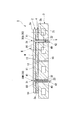
- FIG. 1 is a cross-sectional view of the electrostatic chuck device 1 of the first embodiment.
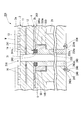
- FIG. 2 is an enlarged view of region II in FIG.
- the electrostatic chuck device 1 has a placement surface 2a on which the plate-like sample W is placed, and cools the electrostatic chuck portion 2 from the lower side, and the electrostatic chuck portion 2 containing the internal electrode 13 for electrostatic adsorption. And a base layer 3, and an adhesive layer 4 for bonding the electrostatic chuck unit 2 and the base unit 3 together.
- the relative position of each component will be described with the mounting surface 2a side as the upper side of the electrostatic chuck device 1 and the base portion 3 side as the lower side of the electrostatic chuck device 1.
- the posture of the electric chuck device 1 is not limited to this direction.
- the electrostatic chuck portion 2 has a structure in which a mounting plate 11, an electrostatic adsorption internal electrode 13, an insulating material layer 14 surrounding the peripheral portion of the internal electrode 13, and a support plate 12 are laminated in order from the upper side.
- the electrostatic chuck portion 2 has a power supply terminal 15 that passes through the adhesive layer 4 and the base portion 3 and applies a voltage to the electrostatic adsorption internal electrode 13.
- the electrostatic chuck portion 2 is disposed opposite to a circular mounting plate 11 having an upper surface as a mounting surface 2a for mounting a plate-like sample W such as a semiconductor wafer, and a lower surface side of the mounting plate 11. And a circular support plate 12.
- the electrostatic chuck portion 2 is further sandwiched between the mounting plate 11 and the support plate 12 and has a circular electrostatic chucking internal electrode 13 having a smaller diameter than the mounting plate 11 and the support plate 12, and the internal electrode. 13 and a power feeding terminal 15 connected to the lower surface of 13 for applying a DC voltage.
- the mounting plate 11 and the support plate 12 are an aluminum oxide-silicon carbide (Al 2 O 3 —SiC) composite sintered body, an aluminum oxide (Al 2 O 3 ) sintered body, an aluminum nitride (AlN) sintered body, and an oxidized body. It is preferably made of an insulating ceramic sintered body having mechanical strength and having durability against corrosive gas and its plasma, such as an yttrium (Y 2 O 3 ) sintered body.
- the mounting plate 11 since the mounting plate 11 has the mounting surface 2a on the upper side, the mounting plate 11 is a material having a particularly high dielectric constant and does not become an impurity with respect to the plate-like sample W that is electrostatically attracted, that is, is not determined as an impurity. It is preferable that it is comprised from a material. From such a viewpoint, it is preferable to employ a silicon carbide-aluminum oxide composite sintered body that contains silicon carbide in an amount of 4 wt% to 20 wt% with the balance being aluminum oxide as a constituent material of the mounting plate 11. .
- a plurality of protrusions 16 having a diameter smaller than the thickness of the plate-like sample W are formed on the placement surface 2 a of the placement plate 11. These protrusions 16 support the plate-like sample W.
- the mounting plate 11 has a mounting surface 2a on the upper side and is made of a material that has a particularly high dielectric constant and that does not become an impurity with respect to the plate-like sample W that is electrostatically attracted.
- the internal electrode 13 for electrostatic attraction is located below the mounting plate 11.
- the internal electrode 13 is used as an electrode for an electrostatic chuck for generating a charge and fixing the plate-like sample W with an electrostatic attraction force.
- the shape and size of the internal electrode 13 can be appropriately adjusted depending on the application.
- the electrostatic adsorption internal electrode 13 can be provided as an electrode having a predetermined pattern in a layer where the internal electrode 13 is formed.
- the internal electrode 13 for electrostatic attraction may be provided as a so-called solid electrode having no pattern, and preferably functions.
- the internal electrode 13 for electrostatic adsorption can be formed by any method.
- the internal electrode can be formed by forming a metal foil on the support plate 12 by sputtering or vapor deposition.
- it can be formed by applying a composite material of a conductive material, which is a material for forming the internal electrode 13 for electrostatic adsorption, and an organic substance, using a coating method such as screen printing.
- the internal electrode 13 for electrostatic attraction can be formed from a material selected arbitrarily.
- the internal electrode 13 for electrostatic adsorption can also be formed of copper (Cu), aluminum (Al), and / or carbon (C).
- the thickness of the internal electrode 13 for electrostatic adsorption can be arbitrarily selected and is not particularly limited, but is preferably 0.1 ⁇ m or more and 50 ⁇ m or less.
- the insulating material layer 14 is a layer for bonding and integrating the mounting plate 11 and the support plate 12 and protecting the electrostatic adsorption internal electrode 13 from plasma.
- the material which comprises this insulating material layer 14 can be selected arbitrarily, for example, the insulating material whose principal component is the same as the mounting board 11 and the support plate 12 is preferable.
- the material is preferably aluminum oxide (Al 2 O 3 ).
- the power feeding terminal 15 is a rod-shaped terminal provided for applying a DC voltage to the electrostatic adsorption internal electrode 13.
- the material for forming the power supply terminal 15 can be arbitrarily selected as long as it is a conductive material having excellent heat resistance, and is not particularly limited. A metal material or a conductive organic material can be preferably selected and used.
- the power supply terminal 15 is insulated from the base portion 3.
- the base unit 3 is provided below the electrostatic chuck unit 2 and controls the temperature of the electrostatic chuck unit 2 to a desired temperature. Moreover, the base part 3 has the function of the electrode for high frequency generation. A flow path 21 for circulating a cooling medium such as water or an organic solvent is formed inside the base portion 3. With this structure, the electrostatic chuck portion 2 is cooled, and the temperature of the plate-like sample W placed on the placement surface 2a is maintained at a desired temperature.
- the base portion 3 is preferably made of aluminum (Al) or an aluminum alloy. It is preferable that at least the surface of the base portion 3 exposed to plasma is anodized or an insulating film such as alumina is formed.
- the base part 3 is not limited in its material as long as it is a metal material having good thermal conductivity.
- copper (Cu), a copper alloy, and / or stainless steel (SUS) may be employed.
- the adhesive layer 4 is interposed between the lower surface 2 b of the electrostatic chuck portion 2 and the upper surface 3 a of the base portion 3.
- the adhesive layer 4 bonds and integrates the electrostatic chuck portion 2 and the base portion 3 together.
- the adhesive layer 4 can be composed of an arbitrarily selected material, but is preferably formed of an adhesive having heat resistance in a temperature range of ⁇ 20 ° C. to 150 ° C.
- As the adhesive layer for example, an acrylic resin, a silicon resin, and an epoxy resin are suitable. In particular, when oxygen-based plasma is used, it is preferable to use a silicon-based resin that is excellent in plasma resistance against oxygen-based plasma.
- the shape of the adhesive layer 4 can be arbitrarily selected. For example, a sheet-like or film-like adhesive of any shape cured by heating a coating film obtained by applying a liquid thermosetting adhesive was cured by a method such as thermocompression bonding, It may be a cured film.
- the electrostatic chuck part 2, the base part 3, and the adhesive layer 4 are provided with a plurality of cooling gas introduction holes 30A and pin insertion holes 30B penetrating vertically therethrough.
- the cooling gas introduction hole 30 ⁇ / b> A is provided for supplying a cooling gas G such as helium (He) toward the plate-like sample W placed on the electrostatic chuck portion 2.
- a cooling gas G such as helium (He)
- lift pins 22 that assist in the detachment of the plate-like sample W adsorbed on the placement surface 2a are inserted into the pin insertion holes 30B.
- a drive unit (not shown) is connected to the lower end of the lift pin 22 and drives the lift pin 22 up and down along the penetration direction of the pin insertion hole 30B.
- the cooling gas introduction hole 30A and the pin insertion hole 30B have the same configuration.
- the cooling gas introduction hole 30 ⁇ / b> A and the pin insertion hole 30 ⁇ / b> B are simply referred to as the through hole 30.
- the through hole 30 includes a first through hole 31 that is a portion that penetrates the electrostatic chuck portion 2, and a second through hole 32 that is a portion that penetrates the base portion 3. That is, the electrostatic chuck portion 2 is provided with a first through hole 31, the base portion 3 is provided with a second through hole 32, and the first and second through holes 31, 32 communicate with each other.
- the through hole 30 is configured.
- the first through hole 31 and the second through hole 32 have the same center axis.
- a cylindrical insulator 40 is fixed to the inner peripheral surface 32 a of the second through hole 32 by an adhesive 49.
- the inner diameter of the second through-hole 32 is larger than the inner diameter of the first through-hole 31 by the thick portion due to the insulator 40.
- An O-ring 50 which is an annular seal member, is sandwiched between the tip surface 41 a on the electrostatic chuck portion 2 side (ie, the upper side) of the insulator 40 and the electrostatic chuck portion 2.
- a cylindrical insulating wall member 43 is provided inside the O-ring 50 in the radial direction. The insulating wall member 43 is formed integrally with the distal end surface 41 a of the insulator 40.
- the insulator 40 is made of, for example, ceramic.
- the insulator 40 has durability against plasma. Ceramics constituting the insulator 40 can be arbitrarily selected. For example, selected from aluminum nitride (AlN), aluminum oxide (Al 2 O 3 ), silicon nitride (Si 3 N 4 ), zirconium oxide (ZrO 2 ), sialon, boron nitride (BN), and silicon carbide (SiC) Further, it is possible to employ a single type ceramic or a composite ceramic containing two or more types.
- the insulator 40 has a first end portion 41 (upper end portion) located on the electrostatic chuck portion 2 side and a second end portion 42 (lower end portion) located on the opposite side.
- the inner diameter of the insulator 40 is substantially equal to the inner diameter of the first through hole 31. It is preferable that the inner peripheral surface 31a of the first through hole 31 and the inner peripheral surface 40a of the insulator 40 are continuous without a step. However, when the through hole 30 is the cooling gas introduction hole 30 ⁇ / b> A, the inner diameter of the insulator 40 may be larger than that of the first through hole 31.
- An adhesive 49 is interposed between the outer peripheral surface 40b of the insulator 40 and the inner peripheral surface 32a of the second through hole 32, and these are bonded and fixed.
- the adhesive 49 is preferably an organic resin that exhibits durability against plasma and has flexibility. It is also preferable that the adhesive 49 is in contact with the adhesive layer 4.
- a cylindrical insulating wall member 43 is integrally formed on the distal end surface 41 a (upper end surface 1) of the insulator 40.
- the central axis of the insulating wall member 43 coincides with the central axis of the insulator 40.
- the inner diameter of the insulating wall member 43 coincides with the inner diameter of the insulator 40.
- the outer diameter of the insulating wall member 43 is smaller than the outer diameter of the insulating wall member 43.
- the end surface 41 b (upper end surface 2) of the insulating wall member 43 is in contact with the lower surface 2 b of the electrostatic chuck portion 2. However, the end surface 41 b may be separated from the lower surface 2 b of the electrostatic chuck portion 2.
- the tip surface 41a of the insulator may be a flat surface or an inclined surface, or may be a curved surface having an arc or swelled upward as shown as an example in the sixth embodiment. May be. These may have protrusions (cylindrical insulating wall members).
- the O-ring (seal member) 50 is sandwiched between the tip surface 41 a of the insulator 40 and the electrostatic chuck portion 2.
- the O-ring 50 prevents the plasma from wrapping around the outer periphery of the insulator 40, and as a result, suppresses the erosion of the adhesive layer 4 and the adhesive 49 by the plasma.
- the O-ring 50 is in contact with the front end surface 41 a of the insulator 40 and the lower surface 2 b of the electrostatic chuck portion 2.
- the O-ring 50 may be in contact with the outer peripheral surface 43 b of the insulating wall member 43, or may be in contact with the inner peripheral surface 32 a of the second through hole 32 of the base portion 3 through the adhesive 49.
- the O-ring 50 is an annular or tubular sealing member made of an arbitrarily selected material, for example, an elastic body such as rubber or elastomer resin.
- the size may be selected as necessary.
- the cross-sectional shape of O-ring used for this invention is not limited to this shape.
- the shape of the cross section may be a square or an ellipse.
- the cross-sectional shape of the space in which the seal member is accommodated is rectangular, by using a packing having a rectangular cross section, the contact area is increased and plasma intrusion is achieved. You may suppress more effectively.
- the O-ring 50 is sandwiched between the tip surface 41a and the lower surface 2b of the electrostatic chuck portion 2 and compressed up and down as shown in the figure.
- the O-ring 50 makes an annular contact with the lower surface 2b of the electrostatic chuck portion 2 at the upper contact P1, and makes an annular contact with the tip surface 41a of the insulator 40 at the lower contact P2.
- the O-ring 50 seals the inner diameter side and the outer diameter side of the insulator 40 by the upper contact P1 and the lower contact P2.
- the thickness (size in the vertical direction) of the O-ring 50 before compression is arbitrarily selected, but is larger than the height H of the insulating wall member 43.
- the height H of the insulating wall member 43 is smaller than the thickness of the seal member (before compression). Accordingly, the O-ring 50 can be reliably compressed by bringing the end surface 41b of the insulating wall member into contact with the lower surface 2b of the electrostatic chuck portion 2.
- the O-ring 50 is preferably compressed so that the thickness after compression is not less than 0.5 times and not more than 0.8 times that before compression. Thereby, in the upper contact P1 and the lower contact P2, the reliability of the seal between the inner peripheral side and the outer peripheral side of the insulator 40, that is, the reliability of sealing, can be increased by the O-ring 50.
- the end surface 41b of the insulating wall member 43 is in contact with the lower surface 2b of the electrostatic chuck portion 2.
- the height H of the insulating wall member 43 is the thickness of the O-ring 50 after compression. Therefore, the compression rate of the O-ring 50 can be made to depend on the processing accuracy of the height H of the insulating wall member 43, and the reliability of the seal can be improved without adjusting the crushing margin of the O-ring when the insulator 40 is fixed. Can be increased.
- the O-ring 50 may be compressed in the radial direction or may not be compressed.
- the O-ring 50 is sandwiched between the outer peripheral surface 43 b of the insulating wall member 43 and the inner peripheral surface 32 a of the second through hole 32.
- the plasma intrusion path can be narrowed to effectively suppress the plasma intrusion.
- the O-ring 50 is not compressed in the radial direction, the O-ring 50 is compressed only in the vertical direction, so that an unreasonable load such as twisting is not easily applied. Therefore, the reliability of the seal by the O-ring 50 can be enhanced.
- the radial distance width W1 between the outer peripheral surface of the insulating wall member 43 and the outer peripheral surface of the insulator 40 is 0.8 times or more and 1.2 times or less than the radial width of the O-ring 50 before compression. It is preferable. As a result, the O-ring 50 can be interposed between the tip surface 41a of the insulator 40 and the electrostatic chuck portion 2 without causing excessive stress such as twisting.
- the O-ring 50 is interposed between the lower surface 2 b of the electrostatic chuck portion 2 and the tip surface 41 a of the insulator 40, so that plasma is generated on the outer periphery of the insulator 40. You can block the sneaking to the side. With this configuration, the adhesive layer 4 and the adhesive 49 can be prevented from being eroded by plasma, and the life of the electrostatic chuck device 1 can be extended. Further, according to the present embodiment, since the plasma exposure of the adhesive layer 4 and the adhesive 49 is suppressed, the plasma resistance required as a material for the adhesive layer 4 and the adhesive 49 can be lowered.
- the degree of freedom in material selection can be increased.
- a material having excellent thermoelasticity is adopted to reduce the difference in thermal expansion between the electrostatic chuck portion 2 and the base portion 3. be able to.
- the insulating wall member 43 that restricts the exposure of the O-ring 50 is provided inside the O-ring 50 in the radial direction.
- the insulating wall member 43 prevents the O-ring 50 from protruding to the inner peripheral side of the insulator 40. That is, by providing the insulating wall member 43, the posture of the O-ring 50 can be maintained, and the reliability of sealing by the O-ring 50 can be improved.
- the withstand voltage of the electrostatic chuck device 1 can be increased by providing the insulating wall member 43.
- the withstand voltage can be increased by closing the discharge path. Further, even when the end surface 41 b of the insulating wall member 43 is not in contact with the lower surface 2 b of the electrostatic chuck portion 2, the discharge path can be narrowed by the insulating wall member 43. Thereby, the withstand voltage of the electrostatic chuck apparatus 1 can be increased by lengthening the path leading to the discharge.
- the insulator 40 brings the end surface 41b of the insulating wall member 43 into contact with the lower surface 2b of the electrostatic chuck portion 2, and the tip surface 41a of the insulator 40 and the electrostatic chuck portion 2 are in contact with each other.
- the adhesive 49 is cured to be fixed.
- the insulator 40 cures the adhesive 49 while adjusting the crushing margin of the O-ring 50 on the front end surface 41a with a dial gauge or the like. It is fixed with.
- the electrostatic chuck device 1 of the first embodiment may have a heater element 9 as shown by a two-dot chain line in FIG.
- the heater element 9 is fixed to the lower surface 2b of the electrostatic chuck portion 2 with an adhesive (not shown).
- the heater element 9 is embedded in the adhesive layer 4 between the lower surface 2 b of the electrostatic chuck portion 2 and the upper surface 3 a of the base portion 3.
- the heater element 9 can be made of an arbitrarily selected shape or material.
- the heater element 9 is made of a conductive member made by meandering a narrow band-shaped metal material.
- the heater element 9 may be connected to power supply terminals at both ends, generate heat when a current flows, and control the temperature of the electrostatic chuck portion 2.
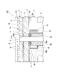
- FIG. 3 is an enlarged cross-sectional view of an electrostatic chuck device 1A according to Modification 1 of the first embodiment.
- symbol is attached
- the electrostatic chuck device 1A of this modification compared to the electrostatic chuck device 1 of the first embodiment, the insulator 40A and the insulating wall member 43A are separate members, and an insulating wall is provided inside the insulator 40A. The main difference is that the members 43A are nested.
- the insulating wall member 43A has a cylindrical shape.
- the insulating wall member 43A (at least a part thereof) is located on the radially inner side of the insulator 40A.
- the insulating wall member 43A is bonded and fixed to the inner peripheral surface of the insulator 40A.
- the outer diameter of the insulating wall member 43A is slightly smaller than the inner diameter of the insulator 40A. It is slightly longer than the insulator 40A.
- the upper end portion 43a of the insulating wall member 43A protrudes upward from the tip surface 41a of the insulator 40A.
- the upper end portion 43a is located on the radially inner side.
- the insulator 40A and the insulating wall member 43A are separate members.
- the insulator 40A and the insulating wall member 43A can be made of different materials.
- the insulating wall member 43A is made of a material having high plasma resistance (for example, ceramics), and the insulator 40A is made of a material having low thermal conductivity (for example, resin), thereby improving the plasma resistance and surrounding the through hole 30. From the heat to the base portion 3 can be reduced.
- the insulating wall member 43A is bonded and fixed to the insulator 40A, but may have other configurations.
- an insulating wall member 43A is provided by providing a convex portion extending radially inward at the lower end of the insulator 40A and sandwiching the insulating wall member 43A between the convex portion and the lower surface 2b of the electrostatic chuck portion 2 in the vertical direction. May be fixed.
- the insulating wall member 43A is made of ceramics and the insulator 40A is made of a resin member, these may be fixed to each other by integral molding.
- the insulator 40A may be made of a heat-shrinkable resin material, and the insulator wall member 43A and the insulator 40A may be fixed to each other by heating in contact with the insulator wall member 43A.
- FIG. 4 is an enlarged cross-sectional view of an electrostatic chuck device 1B according to Modification 2 of the first embodiment.
- the electrostatic chuck device 1B of the present modified example has a cylindrical outer insulating wall (outer insulating wall member) 44B integrally formed on the tip surface 41a of the insulator 40B. Is formed. That is, according to the present modification, the cylindrical outer insulating wall 44 that is a part of the insulator 40B is located outside the O-ring 50 in the radial direction.
- the electrostatic chuck device 1B of this modification the upper end portion 43a of the insulating wall member 43A is located on the inner side in the radial direction of the O-ring 50, and the outer insulating wall 44 is provided on the outer side in the radial direction.
- the electrostatic chuck device 1B can further increase the withstand voltage by further extending the discharge path, that is, the plasma intrusion path.
- FIG. 5 is an enlarged cross-sectional view of the electrostatic chuck device 101 of the second embodiment.
- the electrostatic chuck device 101 of the second embodiment is mainly different from the first embodiment in that it has an insulating ring 145 that surrounds the first end 41 of the insulator 40 from the outside in the radial direction.
- symbol is attached
- the electrostatic chuck device 101 includes an electrostatic chuck portion 2, a base portion 103, and an adhesive layer 4.
- the electrostatic chuck portion 2, the base portion 103, and the adhesive layer 4 are provided with a plurality of through holes 130 penetrating them vertically.
- the through hole 130 is used for introducing a cooling gas or inserting a lift pin.
- the through hole 130 includes a first through hole 31 that is a portion that penetrates the electrostatic chuck portion 2, and a second through hole 132 that is a portion that penetrates the base portion 103.
- the insulator 40 is fixed to the inner peripheral surface 132a of the second through hole 132 by an adhesive 149.
- a counterbore hole 133 is provided in the opening of the second through-hole 132 on the electrostatic chuck portion 2 side (upper side).
- the counterbore hole 133 has a larger diameter than the second through hole 132 and has a concentric circular shape.
- An insulating ring 145 is fixed to the inner peripheral surface 133 a of the counterbore hole 133.
- the insulating ring 145 is made of an insulating member formed in an annular shape.
- the insulating ring 145 can be made of an arbitrarily selected material, and can be made of the same material (for example, ceramics) as the insulator 40 or can be made of a different material (for example, resin material).
- the outer diameter of the insulating ring 145 is slightly smaller than the inner diameter of the counterbore hole 133.
- An adhesive 149 is interposed between the outer peripheral surface 145b of the insulating ring 145 and the inner peripheral surface 133a of the counterbore hole 133, and these are bonded and fixed to each other.
- the inner diameter of the insulating ring 145 is slightly smaller than the inner diameter of the second through hole 132 and is substantially the same as the outer diameter of the insulator 40.
- An inner peripheral surface 145 a of the insulating ring 145 contacts the outer peripheral surface 40 b of the insulator 40.
- the insulating ring 145 surrounds the first end 41 of the insulator 40 from the outside in the radial direction.
- an insulating wall member 43 having an outer diameter smaller than that of the insulator 40 is integrally formed on the tip surface 41a of the insulator 40.
- An O-ring 50 is sandwiched between the tip surface 41 a of the insulator 40 and the lower surface 2 b of the electrostatic chuck portion 2.
- the insulating wall member 43 is located inside the O-ring 50 in the radial direction.
- the end surface 41 b of the insulating wall member 43 is in contact with the lower surface 2 b of the electrostatic chuck portion 2.
- the electrostatic chuck device 101 of this embodiment has a double insulation structure including the insulator 40 and the insulation ring 145. Thereby, the withstand voltage of the electrostatic chuck device 101 can be increased.
- the electrostatic chuck device 101 of the second embodiment may have a heater element 9 as in the first embodiment.
- the temperature of the electrostatic chuck portion 2 tends to increase because the cooling from the base portion 103 is not performed in the vicinity of the through hole 130.
- the inner surface of the through hole 130 is protected in a heat-insulated state by the double-structured insulator 40 and the insulating ring 145. Thereby, it becomes difficult to be affected by the heat generated by the heater element 9 in the vicinity of the through hole 130, the temperature rise in the vicinity of the through hole 130 can be suppressed, and the electrostatic chuck portion 2 can be soaked.
- the thermal conductivity of the insulating ring 145 depending on the material and dimensions is preferably set according to the presence / absence of the heater element 9 and its heat generation performance.
- the electrostatic chuck device 101 includes the heater element 9, it is preferable to reduce the thermal conductivity of the insulating ring 145. Thereby, the heat insulation performance of an insulating ring can be improved and soaking
- the electrostatic chuck device 101 does not have the heater element 9, it is preferable to increase the thermal conductivity of the insulating ring 145. As a result, it is possible to efficiently release heat from the vicinity of the through-hole 130 where cooling is likely to be insufficient compared to other regions, and the soaking of the electrostatic chuck portion 2 can be promoted.
- FIG. 6 is an enlarged cross-sectional view of the electrostatic chuck device 201 of the third embodiment.
- the electrostatic chuck device 201 of the third embodiment is mainly different from the second embodiment in the fixing method of the insulator 240.
- symbol is attached
- the electrostatic chuck device 201 includes an electrostatic chuck portion 2, a base portion 203, and an adhesive layer 4. Further, in the electrostatic chuck device 201, the electrostatic chuck portion 2, the base portion 203, and the adhesive layer 4 are provided with a plurality of through holes 230 penetrating them vertically.
- the through hole 230 is used for introducing a cooling gas or inserting a lift pin.
- the through hole 230 includes a first through hole 31 that is a portion that penetrates the electrostatic chuck portion 2, and a second through hole 232 that is a portion that penetrates the base portion 203.
- the insulator 240 is inserted in the inner peripheral surface 232a of the second through hole 232.
- a counterbore hole 233 is provided in the opening of the second through hole 232 on the electrostatic chuck portion 2 side (upper side), and an insulating ring is formed on the inner peripheral surface 233a of the counterbore hole 233. 145 is fixed.
- a lower counterbore hole 234 is provided in an opening on the opposite side (lower side) of the second through hole 232 to the electrostatic chuck portion 2.
- the lower counterbore hole 234 is provided with a fixing surface 234a facing downward.
- a screw hole 234b into which a screw 246 for fixing the insulator 240 is inserted is formed in the fixing surface 234a.
- the insulator 240 has a first end portion 241 located on the electrostatic chuck portion 2 side and a second end portion 242 located on the opposite side.
- an insulating wall member 243 having an outer diameter smaller than that of the insulator 240 is integrally formed on the distal end surface 241a located at the first end 241 of the insulator 240.
- An O-ring 50 is sandwiched between the front end surface 241 a of the insulator 240 and the lower surface 2 b of the electrostatic chuck portion 2.
- the insulating wall member 243 is located inside the O-ring 50 in the radial direction.
- the end surface 241 b of the insulating wall member 243 is in contact with the lower surface 2 b of the electrostatic chuck portion 2.
- the second end portion 242 of the insulator 240 is provided with a flange portion 242a extending outward in the radial direction.
- a through hole 242b penetrating in the vertical direction is formed in the flange portion 242a.
- the flange portion 242a is accommodated in the lower counterbore hole 234.
- the operator can fix the insulator 240 to the base portion 203 by inserting the screw 246 into the through hole 242b of the flange portion 242a and fastening the screw 246 to the screw hole 234b of the base portion 203.
- the flange portion 242a and the screw 246 constitute a fixing portion 248 of the insulator 240. That is, the insulator 240 is detachably fixed to the base portion 203 by the fixing portion 248.
- the insulator 240 is mechanically fixed to the base portion 203 and is detachable.
- the O-ring 50 sandwiched between the first end 241 of the insulator 240 and the electrostatic chuck portion 2 can be easily replaced.
- the O-ring 50 is easily eroded by the plasma in order to seal between the insulator 240 and the electrostatic chuck portion 2 to prevent the plasma from entering.
- the service life of the electrostatic chuck device 201 can be further extended.
- the insulator 240 is fixed to the base portion 203 with screws 246 at the flange portion 242a.
- the method of fixing the insulator 240 is not limited to this.
- the insulator 240 may be fixed by forming a male screw on the outer peripheral surface of the flange portion 242a, forming a female screw on the inner peripheral surface of the lower counterbore hole 234 of the base portion 203, and screwing them together.
- the flange portion 242a and the insulator 240 may be separated.
- the insulator and the insulating wall member are integrated members, but they may be separate members.
- the electrostatic chuck device of the second aspect does not have the cylindrical insulating wall member described in the first aspect as an essential member as compared with the electrostatic chuck device of the first aspect, and The main difference is that an insulating ring provided in a counterbore provided in the opening of the second through hole on the electrostatic chuck portion side is an essential member.
- the device of the second aspect may have the characteristics described in the first and third aspects.
- the second and third embodiments and the sixth embodiment to be described later may be considered to be included in the electrostatic chuck device of the second aspect when the insulating ring is included. Below, the preferable example of the electrostatic chuck apparatus of a 2nd aspect is demonstrated.
- FIG. 7 is a cross-sectional view of the electrostatic chuck device 1 of the fourth embodiment.
- FIG. 8 is an enlarged view of region II in FIG.
- the electrostatic chuck device 1 has a placement surface 2a on which the plate-like sample W is placed, and cools the electrostatic chuck portion 2 from the lower side, and the electrostatic chuck portion 2 containing the internal electrode 13 for electrostatic adsorption. And a base layer 3, and an adhesive layer 4 for bonding the electrostatic chuck unit 2 and the base unit 3 together.
- the electrostatic chuck portion 2, the base portion 3, and the adhesive layer 4 are provided with a plurality of through holes that vertically penetrate these.
- the through hole is used for introducing a cooling gas or inserting a lift pin.
- the through-hole has a first through-hole 31 that is a portion that penetrates the electrostatic chuck portion 2 and a second through-hole 32 that is a portion that penetrates the base portion 3.
- electrostatic chuck unit 2 is basically the same as the electrostatic chuck unit 2 described in the first embodiment, the same reference numerals are given and description thereof is omitted.
- base part 3 is basically the same as the base part 3 described in the first embodiment except for the point relating to the second through-hole, the same reference numerals are given and description thereof is omitted.
- adhesive layer 4 is basically the same as the adhesive layer 4 described in the first embodiment, the same reference numerals are given and description thereof is omitted.
- the electrostatic chuck part 2, the base part 3 and the adhesive layer 4 are provided with a plurality of cooling gas introduction holes 30A and pin insertion holes 30B penetrating them vertically.
- the cooling gas introduction hole 30A and the pin insertion hole 30B are basically the same as the cooling gas introduction hole 30A and the pin insertion hole 30B described in the first and third embodiments, and the description of the same parts is omitted. To do.
- a cylindrical insulator 40 is fixed to the inner peripheral surface 32 a of the second through hole 32 by an adhesive 49.
- the inner diameter of the second through-hole 32 is larger than the inner diameter of the first through-hole 31 by the thick portion of the insulator 40.
- An O-ring 50 which is an annular seal member, is sandwiched between the tip surface 41 a on the electrostatic chuck portion 2 side (ie, the upper side) of the insulator 40 and the electrostatic chuck portion 2.
- a counterbore hole 33 is provided in the opening of the second through hole 32 on the electrostatic chuck portion 2 side (upper side).
- the counterbore hole 33 has a larger diameter than the second through hole 32 and has a concentric circular shape.
- An insulating ring 45 is fixed to the inner peripheral surface 33 a of the counterbore hole 33.
- the insulator 40 can be formed of the same material as the insulator 40 described in the first embodiment.
- the insulator 40 has a first end 41 located on the electrostatic chuck portion 2 side and a second end 42 located on the opposite side.
- the inner diameter of the insulator 40 is substantially equal to the inner diameter of the first through hole 31. It is preferable that the inner peripheral surface 31a of the first through hole 31 and the inner peripheral surface 40a of the insulator 40 are continuous without a step. However, when the through hole 30 is the cooling gas introduction hole 30 ⁇ / b> A, the inner diameter of the insulator 40 may be larger than that of the first through hole 31.
- An adhesive 49 is interposed between the outer peripheral surface 40b of the insulator 40 and the inner peripheral surface 32a of the second through hole 32, and these are bonded and fixed.
- the adhesive 49 is preferably an organic resin that is durable and resistant to plasma.
- the insulating ring 45 is made of an insulating member formed in an annular shape.
- the insulating ring 45 may be made of the same material (for example, ceramics) as the insulator 40 or may be made of a different material (for example, resin material).
- the outer diameter of the insulating ring 45 is slightly smaller than the inner diameter of the counterbore hole 33.
- An adhesive 49 is interposed between the outer peripheral surface 45b of the insulating ring 45 and the inner peripheral surface 33a of the counterbore hole 33, and these are bonded and fixed to each other.
- the inner diameter of the insulating ring 45 is slightly smaller than the inner diameter of the second through hole 32 and is substantially the same as the outer diameter of the insulator 40.
- the inner peripheral surface 45 a of the insulating ring 45 is in contact with the outer peripheral surface 40 b of the insulator 40.
- the insulating ring 45 surrounds the first end 41 of the insulator 40 from the outside in the radial direction.
- the O-ring (seal member) 50 is sandwiched between the tip surface 41 a of the insulator 40 and the electrostatic chuck portion 2.
- the O-ring 50 prevents the plasma from flowing to the outer peripheral side of the insulator 40 on the outer peripheral side of the insulator 40 and suppresses the erosion of the adhesive layer 4 and the adhesive 49 by the plasma.
- the O-ring 50 is in contact with the front end surface 41 a of the insulator 40 and the lower surface 2 b of the electrostatic chuck portion 2.
- the O-ring 50 can be formed of any material, and is a tubular or annular sealing member made of an elastic body such as rubber or elastomer resin.
- a cross-sectional shape is not limited to this. It may be a square or an ellipse.
- a packing having a rectangular cross section may be used as the seal member.
- the O-ring 50 is sandwiched between the front end surface 41a and the lower surface 2b of the electrostatic chuck portion 2 and compressed vertically.
- the O-ring 50 makes an annular contact with the lower surface 2b of the electrostatic chuck portion 2 at the upper contact P1, and makes an annular contact with the tip surface 41a of the insulator 40 at the lower contact P2.
- the O-ring 50 seals the inner diameter side and the outer diameter side of the insulator 40 at the upper contact P1 and the lower contact P2.
- the O-ring 50 is preferably compressed so that the thickness after compression is not less than 0.5 times and not more than 0.8 times that before compression. Thereby, in the upper contact P1 and the lower contact P2, the reliability of the seal between the inner peripheral side and the outer peripheral side of the insulator 40 can be enhanced by the O-ring 50.
- the O-ring 50 is interposed between the lower surface 2 b of the electrostatic chuck portion 2 and the tip surface 41 a of the insulator 40, so that plasma is generated on the outer periphery of the insulator 40. You can block the sneaking to the side. As a result, the adhesive layer 4 and the adhesive 49 can be prevented from being eroded by plasma, and the life of the electrostatic chuck device 1 can be extended. Further, according to the present embodiment, since the plasma exposure of the adhesive layer 4 and the adhesive 49 is suppressed, the plasma resistance required as a material for the adhesive layer 4 and the adhesive 49 can be lowered.
- the degree of freedom in material selection can be increased.
- a material having excellent thermoelasticity is adopted to reduce the difference in thermal expansion between the electrostatic chuck portion 2 and the base portion 3. be able to.
- the electrostatic chuck device 1 has a double insulation structure composed of the insulator 40 and the insulation ring 45.
- the insulating layer 40 and the insulating ring 45 having a double insulating structure can protect the adhesive layer 4 and the adhesive 49 from plasma.
- the double insulation structure of the insulator 40 and the insulating ring 45 can lengthen the discharge path to the base portion 3 and increase the withstand voltage of the electrostatic chuck device 1.
- the insulator 40 is fixed by curing the adhesive 49 while adjusting the crushing margin of the O-ring 50 on the tip surface 41a with a dial gauge or the like.
- the electrostatic chuck device 1 of the fourth embodiment may have a heater element 9 as shown by a two-dot chain line in FIG.
- the heater element 9 can be configured as described in the first embodiment.
- the temperature in the vicinity of the through hole 30 tends to be low.
- the temperature decrease in the vicinity of the through hole 30 can be suppressed, and the electrostatic chuck portion 2 can be soaked.
- the thermal conductivity of the insulating ring 45 depending on the material and dimensions is preferably set according to the presence / absence of the heater element 9 and its heat generation performance.
- the electrostatic chuck device 1 includes the heater element 9, it is preferable to reduce the thermal conductivity of the insulating ring 45. Thereby, the heat insulation performance of an insulating ring can be improved and soaking
- the electrostatic chuck device 1 does not have the heater element 9, it is preferable to increase the thermal conductivity of the insulating ring 45. As a result, it is possible to efficiently release heat from the vicinity of the through-hole 30 where cooling is likely to be insufficient compared to other regions, and the soaking of the electrostatic chuck portion 2 can be promoted.
- FIG. 9 is an enlarged cross-sectional view of the electrostatic chuck device 101 of the fifth embodiment.
- the electrostatic chuck apparatus 101 of the fifth embodiment is mainly different from the fourth embodiment in the fixing method of the insulator 140.
- symbol is attached
- the fifth embodiment is similar to the third embodiment, but differs in that there is no cylindrical insulating wall member.
- the electrostatic chuck device 101 includes an electrostatic chuck portion 2, a base portion 103, and an adhesive layer 4.
- the electrostatic chuck portion 2, the base portion 103, and the adhesive layer 4 are provided with a plurality of through holes 130 penetrating them vertically.
- the through hole 130 is used for introducing a cooling gas or inserting a lift pin.
- the through hole 130 includes a first through hole 31 that is a portion that penetrates the electrostatic chuck portion 2, and a second through hole 132 that is a portion that penetrates the base portion 103.
- the insulator 140 is inserted into the inner peripheral surface 132a of the second through hole 132.
- a counterbore hole 133 is provided in the opening of the second through-hole 132 on the electrostatic chuck portion 2 side (upper side), and an insulating ring is formed on the inner peripheral surface 133a of the counterbore hole 133. 45 is fixed.
- a lower counterbore hole 134 is provided in an opening on the opposite side (lower side) of the second through-hole 132 to the electrostatic chuck portion 2.
- the lower counterbore hole 134 is provided with a fixing surface 134a facing downward.
- a screw hole 134b into which a screw 146 for fixing the insulator 140 is inserted is formed in the fixing surface 134a.
- the insulator 140 has a first end portion 141 located on the electrostatic chuck portion 2 side and a second end portion 142 located on the opposite side thereof.
- An O-ring 50 is sandwiched between the front end surface 141 a of the insulator 140 and the lower surface 2 b of the electrostatic chuck portion 2.
- the second end portion 142 of the insulator 140 is provided with a flange portion 142a extending outward in the radial direction.
- a through hole 142b penetrating in the vertical direction is formed in the flange portion 142a.
- the flange portion 142 a is accommodated in the lower counterbore hole 134.
- the operator can fix the insulator 140 to the base portion 103 by inserting the screw 246 into the through hole 142 b of the flange portion 142 a and fastening the screw 246 to the screw hole 134 b of the base portion 103.
- the flange portion 142a and the screw 146 constitute a fixing portion 148 of the insulator 140. That is, the insulator 140 is fixed to the base portion 103 so as to be detachable by the fixing portion 148.
- the insulator 140 is mechanically fixed to the base portion 103 and is detachable. Accordingly, the O-ring 50 sandwiched between the first end 141 of the insulator 140 and the electrostatic chuck portion 2 can be easily replaced. The O-ring 50 is easily eroded by the plasma in order to seal between the insulator 140 and the electrostatic chuck portion 2 to prevent plasma from entering. By configuring the O-ring 50 to be replaceable, the service life of the electrostatic chuck device 101 can be further extended.
- the insulator 140 is fixed to the base portion 103 with a screw 146 at the flange portion 142a.
- the fixing method of the insulator 140 is not limited to this.
- the insulator 140 may be fixed by forming a male screw on the outer peripheral surface of the flange portion 142a, forming a female screw on the inner peripheral surface of the lower counterbore hole 134 of the base portion 103, and screwing them together. In this case, the flange portion 142a and the insulator 140 may be separated.
- FIG. 10 is an enlarged cross-sectional view of an electrostatic chuck device 201 according to the sixth embodiment of the present invention.
- the electrostatic chuck device 201 of the sixth embodiment is mainly different from the fourth embodiment or the second embodiment in the configuration of the insulator 240.
- symbol is attached
- the apparatus of the third aspect may have the characteristics described in the first and second aspects.
- An O-ring 50 that is an annular seal member is sandwiched between the electrostatic chuck portion 2 side (that is, the upper side) front end surface 241 a of the insulator 240 and the electrostatic chuck portion 2.
- the front end surface 241a of the insulator 240 is inclined downward from the radially inner side to the radially outer side. Therefore, the front end surface 241a of the insulator 240 is higher on the inner diameter side than on the outer diameter side.
- the shape of the distal end surface 241a can be arbitrarily selected as long as the inner diameter side is higher than the outer diameter side.
- the inner diameter side and the outer diameter side may be understood as the inner diameter side end and the outer diameter side end.
- the front end surface 241a may be a curved surface that protrudes upward, and the end on the radially inner side may be higher than the end on the radially outer side.
- the cross section may draw an arc or a circular arc, and the end on the radially inner side may be a surface at a position higher than the end on the radially outer side.
- the distal end surface 241a may be a flat flat surface (slope) having an inclination in which the inner diameter side end is higher than the outer diameter side end.
- the inner diameter side of the tip surface 241a is higher than the outer diameter side, so that the insulation of the electrostatic chuck device of the third aspect It may be included in the range of the tip surface of the insulator.
- the compressed O-ring 50 is arranged on the outer peripheral side of the insulator 240 by making the distal end surface of the insulator 40 have a structure in which the inner diameter side is higher than the outer diameter side. Pressed. This can suppress the compressed O-ring 50 from protruding into the through hole 30. That is, the attitude of the O-ring 50 can be maintained and the reliability of the seal by the O-ring 50 can be increased.
- the electrostatic chuck device 201 is provided with an insulating ring 45 that surrounds the end of the insulator 240 on the electrostatic chuck portion 2 side from the outside in the radial direction.
- the above-described effect due to the fact that the inner diameter side of the front end surface 241a is higher than the outer diameter side can be achieved regardless of the presence or absence of the insulating ring 45.
- the electrostatic chuck device has been described as including the heater element 9 embedded in the adhesive layer 4 between the electrostatic chuck portion and the base portion.
- the heater element may be located inside the electrostatic chuck portion or inside the base portion.
- Electrostatic chuck apparatus 1 Electrostatic chuck part 2a Mounting surface 2b Lower surface 3, 103, 203 Base part 3a, 103a Upper surface 4 Adhesive layer 9 Heater element 11 Mounting plate 12 Support plate 13 Electrostatic adsorption internal electrode 14 Insulating material layer 15 Power feeding terminal 16 Protrusion 21 Channel 22 Lift pins 30, 130, 142b, 230, 242b Through hole 30A Cooling gas introduction hole 30B Pin insertion hole 31 First through holes 31a, 32a, 33a, 40a, 45a, 132a, 133a, 145a, 232a, 132a, 233a Inner peripheral surfaces 32, 132, 232 Second through holes 33, 133, 233 Sagre holes 40, 40A, 40B, 140, 240 Insulator 40a Insulator inner peripheral surface 40b Insulator outer peripheral surface 41, 141, 241 End 41a, 141a, 241a tip surface 41b, 241b end surface 42, 242
Landscapes
- Container, Conveyance, Adherence, Positioning, Of Wafer (AREA)
- Jigs For Machine Tools (AREA)
Abstract
Description
本願は、2016年1月19日に、日本に出願された特願2016-007861号、及び2016年1月19日に、日本に出願された特願2016-007862号に基づき優先権を主張し、その内容をここに援用する。
前記静電チャック部を冷却するベース部と、
前記静電チャック部と前記ベース部とを接着して一体化する接着層と、を備え、前記静電チャック部には、第1の貫通孔が設けられ、
前記ベース部には、前記第1の貫通孔と連通する第2の貫通孔が設けれ、
前記第2の貫通孔内には、筒状の絶縁碍子が固定され、
前記絶縁碍子の前記静電チャック部側の先端面と前記静電チャック部との間には、環状のシール部材が挟み込まれ、かつ、
以下の(a)~(c)の少なくとも1つを有する、静電チャック装置を提供する。
(a)前記シール部材の径方向内側には、筒状の絶縁壁部材が位置する。
(b)前記第2の貫通孔の前記静電チャック部側の開口には、ザグリ穴が設けられ、前記ザグリ穴の内周面には、前記絶縁碍子の前記静電チャック部側の端部を径方向外側から囲む絶縁リングが固定されている。
(c)前記絶縁碍子の前記静電チャック部側の先端面が、内径側が外径側より高い。
すなわち、本発明の第一の態様の静電チャック装置は、板状試料を載置する載置面を有するとともに静電吸着用内部電極を内蔵する静電チャック部と、前記静電チャック部を冷却するベース部と、前記静電チャック部と前記ベース部とを接着して一体化する接着層と、を備え、前記静電チャック部には、第1の貫通孔が設けられ、前記ベース部には、前記第1の貫通孔と連通する第2の貫通孔が設けれ、前記第2の貫通孔内には、筒状の絶縁碍子が固定され、前記絶縁碍子の前記静電チャック部側の先端面と前記静電チャック部との間には、環状のシール部材が挟み込まれ、前記シール部材の径方向内側には、筒状の絶縁壁部材が位置する、静電チャック装置である。
前記絶縁壁部材が、前記絶縁碍子の先端面に一体的に形成されている。
前記絶縁碍子が、前記ベース部に着脱可能に固定する固定部を有する。
また以下の例は、発明の趣旨をより良く理解させるために具体的に説明するものであり、特に指定のない限り、本発明を限定するものではない。発明を逸脱しない範囲で、数や位置や大きさや数値などの変更や省略や追加をする事ができる。また第一、二及び三の態様は、互いの特徴や、好ましい例を、特に問題の無い限り、互いに組み合わせることができる。
<第1実施形態>
図1は、第1実施形態の静電チャック装置1の断面図である。また、図2は、図1の領域IIの拡大図である。静電チャック装置1は、板状試料Wを載置する載置面2aを有するとともに静電吸着用内部電極13を内蔵する静電チャック部2と、静電チャック部2を下側から冷却するベース部3と、静電チャック部2とベース部3とを接着して一体化する接着層4と、を備える。
なお、本明細書において、載置面2a側を静電チャック装置1の上側とし、ベース部3側を静電チャック装置1の下側として各構成の相対位置を説明するが、使用時の静電チャック装置1の姿勢は、この向きに限定されない。
静電チャック部2は、上側から順に、載置板11と、静電吸着用内部電極13および前記内部電極13の周縁部を囲む絶縁材層14と、支持板12と、が積層された構造を有する。また、静電チャック部2は、接着層4およびベース部3を貫通して、静電吸着用内部電極13に電圧を印加する給電用端子15を有する。
特に、載置板11は、上側に載置面2aを有することから、特に誘電率が高い材質であって、静電吸着する板状試料Wに対して不純物とならない、すなわち不純物と判断されない、材料から構成されることが好ましい。このような観点から、載置板11の構成材料として、炭化ケイ素を4重量%以上かつ20重量%以下含み、残部を酸化アルミニウムとする炭化ケイ素-酸化アルミニウム複合焼結体を採用することが好ましい。
載置板11は、上側に載置面2aを有し、特に誘電率が高い材質であって、静電吸着する板状試料Wに対して不純物とならない材料から構成される。
この絶縁材層14を構成する材料は任意に選択でき、例えば、載置板11及び支持板12と主成分が同一の絶縁性材料が好ましい。例えば、載置板11及び支持板12が炭化ケイ素-酸化アルミニウム複合焼結体により構成されている場合には、材料を酸化アルミニウム(Al2O3)とすることが好ましい。
ベース部3は、静電チャック部2の下側に設けられて、この静電チャック部2の温度を所望の温度に制御する。また、ベース部3は、高周波発生用電極の機能を兼ね備えている。ベース部3の内部には、水や有機溶媒等の冷却用媒体を循環させる流路21が形成されている。この構造により、静電チャック部2を冷却し、載置面2aに載置される板状試料Wの温度を所望の温度に維持する。ベース部3は、アルミニウム(Al)又はアルミニウム合金からなることが好ましい。ベース部3の少なくともプラズマに曝される面は、アルマイト処理が施されているか、あるいはアルミナ等の絶縁膜が成膜されていることが好ましい。このような構造により、耐プラズマ性が向上する他、異常放電が防止され、したがって、耐プラズマ安定性が向上した構成となる。また、表面に傷が付き難くなるので、傷の発生を防止することができる。なお、ベース部3は、熱伝導性のよい金属材料であればその材質が限定されることはない。例えば、銅(Cu)、銅合金、及び/又はステンレス鋼(SUS) 等を採用しもよい。
接着層4は、静電チャック部2の下面2bと、ベース部3の上面3aとの間に介在する。接着層4は、静電チャック部2とベース部3とを接着一体化する。接着層4は、任意に選択される材料から構成できるが、-20℃~150℃の温度範囲で耐熱性を有する接着剤から形成されることが好ましい。接着層としては、例えば、アクリル系樹脂、シリコン系樹脂、及びエポキシ系樹脂等が好適である。特に、酸素系プラズマを用いる場合には、酸素系プラズマに対して耐プラズマ性に優れているシリコン系樹脂の使用が好ましい。
この接着層4の形状は任意に選択できる。例えば、液状の熱硬化性接着剤を塗布して得られた塗膜を加熱することにより硬化させた、任意の形状のシート状またはフィルム状の接着剤を、熱圧着等の方法により硬化した、硬化膜であってもよい。
静電チャック部2、ベース部3および接着層4には、これらを上下に貫通する冷却ガス導入孔30Aと、ピン挿通孔30Bとが、それぞれ複数設けられている。冷却ガス導入孔30Aは、静電チャック部2に載置された板状試料Wに向かってヘリウム(He)等の冷却ガスGを供給するために設けられている。また、ピン挿通孔30Bには、載置面2aに吸着された板状試料Wの離脱を補助するリフトピン22が挿通される。リフトピン22の下端には、図示略の駆動部が接続され、ピン挿通孔30Bの貫通方向に沿って、リフトピン22を上下に駆動する。
貫通孔30は、静電チャック部2を貫通する部分である第1の貫通孔31と、ベース部3を貫通する部分である第2の貫通孔32と、を有する。すなわち、静電チャック部2には第1の貫通孔31が設けられ、ベース部3には第2の貫通孔32が設けられ、第1および第2の貫通孔31、32は、互いに連通して貫通孔30を構成する。
絶縁碍子40の静電チャック部2側(すなわち上側)の先端面41aと静電チャック部2との間には、環状のシール部材であるオーリング50が挟み込まれている。オーリング50の径方向内側には、筒状の絶縁壁部材43が設けられている。絶縁壁部材43は、絶縁碍子40の先端面41aに一体的に形成されている。
絶縁碍子40は、例えばセラミックからなる。絶縁碍子40は、プラズマに対する耐久性を有する。絶縁碍子40を構成するセラミックスは任意に選択できる。例えば、窒化アルミニウム(AlN)、酸化アルミニウム(Al2O3)、窒化ケイ素(Si3N4)、酸化ジルコニウム(ZrO2)、サイアロン、窒化ホウ素(BN)、及び炭化ケイ素(SiC)から選択された1種からなるセラミックス、あるいは2種以上を含む複合セラミックスを採用できる。
絶縁碍子40の内径は、第1の貫通孔31の内径と略等しい。第1の貫通孔31の内周面31aと絶縁碍子40の内周面40aとは、段差なく連なることが好ましい。しかしながら、貫通孔30が冷却ガス導入孔30Aである場合は、絶縁碍子40の内径が第1の貫通孔31より大きくてもよい。
絶縁壁部材43の中心軸と絶縁碍子40の中心軸とは、一致している。絶縁壁部材43の内径は、絶縁碍子40の内径と一致している。また、絶縁壁部材43の外径は、絶縁壁部材43の外径より小さい。本実施形態において、絶縁壁部材43の端面41b(上端面2)は、静電チャック部2の下面2bと接触する。しかしながら、端面41bは、静電チャック部2の下面2bに対して離間していてもよい。
本発明において、絶縁碍子の先端面41aは、平面や斜面であってもよく、又は、第六実施形態に例として示したような、断面が弧を描いていたり、上に膨らんだ曲面であってもよい。これらは、突出部(筒状の絶縁壁部材)を有してもよい。
オーリング(シール部材)50は、絶縁碍子40の先端面41aと静電チャック部2の間に挟み込まれている。オーリング50は、プラズマが絶縁碍子40の外周側に回り込むことを遮り、その結果、プラズマによる接着層4および接着剤49の侵食を抑制する。オーリング50は、絶縁碍子40の先端面41aおよび静電チャック部2の下面2bと接触する。また、オーリング50は、絶縁壁部材43の外周面43bと接触してもよく、ベース部3の第2の貫通孔32の内周面32aと接着剤49を介して接触してもよい。
オーリング50が径方向に圧縮される場合、オーリング50は、絶縁壁部材43の外周面43bと第2の貫通孔32の内周面32aとの間に挟み込まれる。これにより、プラズマの侵入経路を狭めてプラズマの侵入を効果的に抑制できる。
一方で、オーリング50が径方向に圧縮されない場合、オーリング50は、上下方向のみから圧縮されるため、捻れなどの無理な負荷が加わりにくい。したがってオーリング50によるシールの信頼性を高めることができる。絶縁壁部材43の外周面と絶縁碍子40の外周面の、径方向距離幅W1は、圧縮前のオーリング50の径方向の幅に対して、0.8倍以上1.2倍以下とすることが好ましい。これにより、捻れなどの無理な応力を生じさせることなく、オーリング50を絶縁碍子40の先端面41aと静電チャック部2との間に介在させることができる。
また本実施形態によれば、接着層4および接着剤49のプラズマ暴露が抑制されるため、接着層4および接着剤49の材料として求められる耐プラズマ性を低くすることができる。すなわち、本実施形態によれば、プラズマに対する耐性を考慮して接着層4および接着剤49の材料を選択する必要がなく材料選定の自由度を高めることができる。一例として、接着層4および接着剤49としてプラズマに対する耐性の有無を問わず、熱弾性に優れた材料を採用し、静電チャック部2とベース部3の熱膨張の差を緩和する構成とすることができる。
また、絶縁壁部材43は、オーリング50が絶縁碍子40の内周側にはみ出すことを抑制する。すなわち、絶縁壁部材43が設けられることで、オーリング50の姿勢を維持させ、オーリング50によるシールの確実性を高めることができる。
また、絶縁壁部材43を設けることで、静電チャック装置1の耐電圧を高めることができる。絶縁壁部材43の端面41bが、静電チャック部2の下面2bと接触する場合には、放電経路を塞いで耐電圧を高めることができる。また、絶縁壁部材43の端面41bが、静電チャック部2の下面2bと接触しない場合であっても、絶縁壁部材43により放電経路を狭めることができる。これにより、放電に至るための経路を長くして静電チャック装置1の耐電圧を高めることができる。
図3は、第1実施形態の変形例1の静電チャック装置1Aの拡大断面図である。なお、上述の実施形態と同一態様の構成要素については、同一符号を付し、その説明を省略する。本変形例の静電チャック装置1Aは、第1実施形態の静電チャック装置1と比較して、絶縁碍子40Aおよび絶縁壁部材43Aは、別部材であり、絶縁碍子40Aの内側に、絶縁壁部材43Aが入れ子状に配されている点が主に異なる。
図4は、第1実施形態の変形例2の静電チャック装置1Bの拡大断面図である。なお、上述の実施形態および変形例1と同一態様の構成要素については、同一符号を付し、その説明を省略する。本変形例の静電チャック装置1Bは、変形例1の静電チャック装置1Aと比較して、絶縁碍子40Bの先端面41aに筒状の外側絶縁壁(外側絶縁壁部材)44Bが一体的に形成されている。すなわち、本変形例によれば、オーリング50の径方向外側には、絶縁碍子40Bの一部である、筒状の外側絶縁壁44が位置する。
図5は、第2実施形態の静電チャック装置101の断面拡大図である。第2実施形態の静電チャック装置101は、第1実施形態と比較して、絶縁碍子40の第1の端部41を径方向外側から囲む絶縁リング145を有する点が主に異なる。
なお、上述の実施形態と同一態様の構成要素については、同一符号を付し、その説明を省略する。
なお、静電チャック装置101において、材質および寸法に依存する絶縁リング145の熱伝導性は、ヒータエレメント9の有無およびその発熱性能に応じて設定することが好ましい。静電チャック装置101がヒータエレメント9を有する場合、絶縁リング145の熱伝導性を小さくすることが好ましい。これにより、絶縁リングの断熱性能を高めることができ、静電チャック部2の均熱化を促進できる。一方で、静電チャック装置101がヒータエレメント9を有しない場合、絶縁リング145の熱伝導性を大きくすることが好ましい。これにより、他の領域と比較して冷却が不十分となりやすい貫通孔130の近傍から効率的に熱を逃がすことが可能となり、静電チャック部2の均熱化を促進できる。
図6は、第3実施形態の静電チャック装置201の断面拡大図である。第3実施形態の静電チャック装置201は、第2実施形態と比較して、絶縁碍子240の固定方法が主に異なる。なお、上述の実施形態と同一態様の構成要素については、同一符号を付し、その説明を省略する。
なお、本実施形態において絶縁碍子240は、フランジ部242aにおいて、ベース部203にネジ246によって固定されている。しかしながら、絶縁碍子240の固定方法は、これに限られない。例えばフランジ部242aの外周面にオネジを形成し、ベース部203の下側ザグリ穴234の内周面にメネジを形成し、これらを螺合することで絶縁碍子240を固定してもよい。この場合、フランジ部242aと絶縁碍子240とは、別体としてもよい。
第二の態様の静電チャック装置は、第一の態様の静電チャック装置と比較して、第一の態様で述べられた筒状の絶縁壁部材を必須の部材としては有しない点、及び、第2の貫通孔の静電チャック部側の開口に設けられたザグリ穴中に設けられる絶縁リングを必須の部材として有する点が、主に異なる。
問題のない限り、第二の態様の装置は、第一や第三の態様で述べられる特徴を有していても良い。第2及び3実施形態や、後述する第6実施形態は、前記絶縁リングを有する場合、第二の態様の静電チャック装置に含まれると考えても良い。
以下に、第二の態様の静電チャック装置の好ましい例を説明する。
上述の第一の態様の第1の実施形態と同一態様の構成要素については、同一符号を付し、その説明を省略する。
<第4実施形態>
図7は、第4実施形態の静電チャック装置1の断面図である。また、図8は、図7の領域IIの拡大図である。静電チャック装置1は、板状試料Wを載置する載置面2aを有するとともに静電吸着用内部電極13を内蔵する静電チャック部2と、静電チャック部2を下側から冷却するベース部3と、静電チャック部2とベース部3とを接着して一体化する接着層4と、を備える。
静電チャック装置1において、静電チャック部2、ベース部3および接着層4には、これらを上下に貫通する複数の貫通孔が設けられている。貫通孔は、冷却ガス導入又はリフトピンの挿通に用いられる。貫通孔は、静電チャック部2を貫通する部分である第1の貫通孔31と、ベース部3を貫通する部分である第2の貫通孔32と、を有する。
静電チャック部2は、第1の実施形態で述べた静電チャック部2と基本的に同じであるので、同一符号を付し、その説明を省略する。 ベース部3は、第2の貫通孔に関する点以外は、第1の実施形態で述べたベース部3と基本的に同じであるので、同一符号を付し、その説明を省略する。
接着層4は、第1の実施形態で述べた接着層4と基本的に同じであるので、同一符号を付し、その説明を省略する。
図7に示すように、静電チャック部2、ベース部3および接着層4には、これらを上下に貫通する冷却ガス導入孔30Aとピン挿通孔30Bとがそれぞれ複数設けられている。冷却ガス導入孔30Aとピン挿通孔30Bは、第1や3の実施形態で述べた冷却ガス導入孔30Aとピン挿通孔30Bと基本的に同じであり、同じである箇所についてはその説明を省略する。
絶縁碍子40の静電チャック部2側(すなわち上側)の先端面41aと静電チャック部2との間には、環状のシール部材であるオーリング50が挟み込まれている。
図8に示すように、第2の貫通孔32の静電チャック部2側(上側)の開口には、ザグリ穴33が設けられている。ザグリ穴33は、第2の貫通孔32より大径であり同心の円形状である。ザグリ穴33の内周面33aには、絶縁リング45が固定されている。
絶縁碍子40は、第1の実施形態で述べた絶縁碍子40と、同じ材料から形成されることができる。
絶縁リング45は、環状に形成された絶縁部材からなる。絶縁リング45は、絶縁碍子40と同材料(例えばセラミックス)からなっていても異なる材料(例えば樹脂材料)から構成されていてもよい。絶縁リング45の外径は、ザグリ穴33の内径より若干小さい。絶縁リング45の外周面45bとザグリ穴33の内周面33aとの間には、接着剤49が介在しこれらを互いに接着固定している。
図8に示すように、オーリング(シール部材)50は、絶縁碍子40の先端面41aと静電チャック部2の間に挟み込まれている。オーリング50は、絶縁碍子40の外周側にプラズマが絶縁碍子40の外周側に回り込むことを遮り、プラズマによる接着層4および接着剤49の侵食を抑制する。オーリング50は、絶縁碍子40の先端面41aおよび静電チャック部2の下面2bと接触する。
また本実施形態によれば、接着層4および接着剤49のプラズマ暴露が抑制されるため、接着層4および接着剤49の材料として求められる耐プラズマ性を低くすることができる。すなわち、本実施形態によれば、プラズマに対する耐性を考慮して接着層4および接着剤49の材料を選択する必要がなく材料選定の自由度を高めることができる。一例として、接着層4および接着剤49としてプラズマに対する耐性の有無を問わず、熱弾性に優れた材料を採用し、静電チャック部2とベース部3の熱膨張の差を緩和する構成とすることができる。
一般的に、ヒータエレメント9を備えた静電チャック装置1によれば、貫通孔30の周辺にはヒータを配することができないため、貫通孔30の近傍の温度は低くなりやすいが、2重構造の絶縁碍子40および絶縁リング45により冷却ベースへの熱逃げを抑えることで貫通孔30の近傍の温度低下を抑制し、静電チャック部2を均熱化することができる。
なお、静電チャック装置1において、材質および寸法に依存する絶縁リング45の熱伝導性は、ヒータエレメント9の有無およびその発熱性能に応じて設定することが好ましい。静電チャック装置1がヒータエレメント9を有する場合、絶縁リング45の熱伝導性を小さくすることが好ましい。これにより、絶縁リングの断熱性能を高めることができ、静電チャック部2の均熱化を促進できる。一方で、静電チャック装置1がヒータエレメント9を有さない場合、絶縁リング45の熱伝導性を大きくすることが好ましい。これにより、他の領域と比較して冷却が不十分となりやすい貫通孔30の近傍から効率的に熱を逃がすことが可能となり、静電チャック部2の均熱化を促進できる。
図9は、第5実施形態の静電チャック装置101の断面拡大図である。第5実施形態の静電チャック装置101は、第4実施形態と比較して、絶縁碍子140の固定方法が主に異なる。なお、上述の実施形態と同一態様の構成要素については、同一符号を付し、その説明を省略する。なお第5実施形態は、第3実施形態にも類似するが、筒状の絶縁壁部材が無い点で異なる。
なお、本実施形態において絶縁碍子140は、フランジ部142aにおいてベース部103にネジ146によって固定されている。しかしながら、絶縁碍子140の固定方法は、これに限られない。例えばフランジ部142aの外周面にオネジを形成し、ベース部103の下側ザグリ穴134の内周面にメネジを形成し、これらを螺合することで絶縁碍子140を固定してもよい。この場合、フランジ部142aと絶縁碍子140とは、別体としてもよい。
<第6実施形態>
図10は、本発明の第6実施形態の静電チャック装置201の断面拡大図である。第6実施形態の静電チャック装置201は、第4実施形態や第2実施形態と比較して、絶縁碍子240の構成が主に異なる。なお、上述の実施形態と同一態様の構成要素については、同一符号を付し、その説明を省略する。なお問題のない限り、第三の態様の装置は、第一や第二の態様で述べられる特徴を有しても良い。
先端面241aは、内径側が外径側より高ければ、形状は任意に選択できる。内径側や外径側とは、内径側端部や外径側端部と理解しても良い。例えば、先端面241aは、上側に突出した曲面であり、径方向内側の端部が、径方向外側の端部より高い位置にある面であっても良い。断面が弧や円弧を描き、径方向内側の端部が、径方向外側の端部より高い位置にある面であっても良い。先端面241aは、内径側端部が外径側端部より高い位置にある、傾斜を有する平らな平面(斜面)であっても良い。第1実施形態において、絶縁壁部材が、絶縁碍子の先端面に一体的に形成されている場合、先端面241aの内径側が外径側より高いので、第三の態様の静電チャック装置の絶縁碍子の先端面の範囲に含まれ得る。
なお、本実施形態において、静電チャック装置201には、絶縁碍子240の静電チャック部2側の端部を径方向外側から囲む絶縁リング45が設けられている。しかしながら、先端面241aの内径側が外径側より高いことによる上述の効果は、絶縁リング45の有無に関わらず奏することができる。
例えば、上述した実施形態で、静電チャック装置は、静電チャック部とベース部の間の接着層4に埋め込まれたヒータエレメント9を備えた例を説明した。しかしながら、ヒータエレメントは、静電チャック部の内部又はベース部の内部に位置していてもよい。
2 静電チャック部
2a 載置面
2b 静電チャック部の下面
3、103、203 ベース部
3a、103a ベース部の上面
4 接着層
9 ヒータエレメント
11 載置板
12 支持板13 静電吸着用内部電極
14 絶縁材層
15 給電用端子
16 突起部
21 流路
22 リフトピン
30、130、142b、230、242b 貫通孔
30A 冷却ガス導入孔
30B ピン挿通孔
31 第1の貫通孔
31a、32a,33a、40a,45a、132a、133a、145a、232a、132a、233a 内周面
32、132、232 第2の貫通孔
33、133、233 サグリ穴
40、40A、40B、140、240 絶縁碍子
40a 絶縁碍子の内周面
40b 絶縁碍子の外周面
41、141、241 第1の端部
41a、141a、241a 先端面
41b、241b 端面
42、242 第2の端部、
43、43A、243 絶縁壁部材
43a 絶縁壁部材の上端部
43b 絶縁壁部材の外周面
44B 外側絶縁壁(外側絶縁壁部材)
45、145 絶縁リング
49 接着剤
50 オーリング(シール部材)
45a、145a 絶縁リングの内周面
45b、145b 絶縁リングの外周面
134、234 下側ザグリ穴
134a、234a 固定面
134b、234b ネジ孔
142 第2の端部
142a、242a フランジ部
142b 貫通孔
146、246 ネジ
148、248 絶縁碍子の固定部
148 固定部
G 冷却ガス
P1 上側接点
P2 下側接点
W 板状試料
Claims (17)
- 板状試料を載置する載置面を有するとともに静電吸着用内部電極を内蔵する静電チャック部と、
前記静電チャック部を冷却するベース部と、
前記静電チャック部と前記ベース部とを接着して一体化する接着層と、を備え、
前記静電チャック部には、第1の貫通孔が設けられ、
前記ベース部には、前記第1の貫通孔と連通する第2の貫通孔が設けれ、
前記第2の貫通孔内には、筒状の絶縁碍子が固定され、
前記絶縁碍子の前記静電チャック部側の先端面と前記静電チャック部との間には、環状のシール部材が挟み込まれ、
前記シール部材の径方向内側には、筒状の絶縁壁部材が位置する、静電チャック装置。 - 前記絶縁壁部材が、前記絶縁碍子の先端面に一体的に形成されている、請求項1に記載の静電チャック装置。
- 前記絶縁壁部材が、前記絶縁碍子と別部材であり、前記絶縁壁部材の少なくとも一部が、前記絶縁碍子の径方向内側に位置する、請求項1に記載の静電チャック装置。
- 前記シール部材の径方向外側には、筒状の外側絶縁壁部材が位置する、請求項1に記載の静電チャック装置。
- 前記絶縁壁部材の高さは、前記シール部材の厚さより小さい、請求項1に記載の静電チャック装置。
- 前記絶縁壁部材は、前記静電チャック部側の端面で前記静電チャック部と接触する、請求項1に記載の静電チャック装置。
- 前記第2の貫通孔の前記静電チャック部側の開口には、ザグリ穴が設けられ、
前記ザグリ穴の内周面には、前記絶縁碍子の前記静電チャック部側の端部を径方向外側から囲む絶縁リングが固定されている、請求項1に記載の静電チャック装置。 - 前記絶縁碍子が、前記ベース部に着脱可能に固定する固定部を有する、請求項1に記載の静電チャック装置。
- 前記静電チャック部の内部、前記ベース部の内部、および前記静電チャック部と前記ベース部の間のうち何れかに位置するヒータを備えた、請求項1に記載の静電チャック装置。
- 板状試料を載置する載置面を有するとともに静電吸着用内部電極を内蔵する静電チャック部と、
前記静電チャック部を冷却するベース部と、
前記静電チャック部と前記ベース部とを接着して一体化する接着層と、を備え、
前記静電チャック部には、第1の貫通孔が設けられ、
前記ベース部には、前記第1の貫通孔と連通する第2の貫通孔が設けれ、
前記第2の貫通孔内には、筒状の絶縁碍子が固定され、
前記絶縁碍子の前記静電チャック部側の先端面と前記静電チャック部との間には、環状のシール部材が挟み込まれ、
前記第2の貫通孔の前記静電チャック部側の開口には、ザグリ穴が設けられ、
前記ザグリ穴の内周面には、前記絶縁碍子の前記静電チャック部側の端部を径方向外側から囲む絶縁リングが固定されている、静電チャック装置。 - 前記絶縁碍子が、前記ベース部に着脱可能に固定する固定部を有する、請求項10に記載の静電チャック装置。
- 前記静電チャック部の内部、前記ベース部の内部、および前記静電チャック部と前記ベース部の間のうち何れかに位置するヒータを備えた、請求項1又は2に記載の静電チャック装置。
- 前記絶縁碍子の前記静電チャック部側の先端面が、内径側が外径側より高い、請求項10に記載の静電チャック装置。
- 前記シール部材の径方向内側には、筒状の絶縁壁部材が位置する、請求項10に記載の静電チャック装置。
- 板状試料を載置する載置面を有するとともに静電吸着用内部電極を内蔵する静電チャック部と、
前記静電チャック部を冷却するベース部と、
前記静電チャック部と前記ベース部とを接着して一体化する接着層と、を備え、
前記静電チャック部には、第1の貫通孔が設けられ、
前記ベース部には、前記第1の貫通孔と連通する第2の貫通孔が設けれ、
前記第2の貫通孔内には、筒状の絶縁碍子が固定され、
前記絶縁碍子の前記静電チャック部側の先端面と前記静電チャック部との間には、環状のシール部材が挟み込まれ、
前記絶縁碍子の前記静電チャック部側の先端面が、内径側が外径側より高い、静電チャック装置。 - 前記絶縁碍子が、前記ベース部に着脱可能に固定する固定部を有する、請求項15に記載の静電チャック装置。
- 前記第2の貫通孔の前記静電チャック部側の開口には、ザグリ穴が設けられ、
前記ザグリ穴の内周面には、前記絶縁碍子の前記静電チャック部側の端部を径方向外側から囲む絶縁リングが固定されている、請求項15に記載の静電チャック装置。
Priority Applications (4)
| Application Number | Priority Date | Filing Date | Title |
|---|---|---|---|
| JP2017513153A JP6493518B2 (ja) | 2016-01-19 | 2017-01-18 | 静電チャック装置 |
| CN201780007201.6A CN108475658B (zh) | 2016-01-19 | 2017-01-18 | 静电卡盘装置 |
| US16/070,478 US10923381B2 (en) | 2016-01-19 | 2017-01-18 | Electrostatic chuck device |
| KR1020187020695A KR102684670B1 (ko) | 2016-01-19 | 2017-01-18 | 정전 척 장치 |
Applications Claiming Priority (4)
| Application Number | Priority Date | Filing Date | Title |
|---|---|---|---|
| JP2016007861 | 2016-01-19 | ||
| JP2016007862 | 2016-01-19 | ||
| JP2016-007862 | 2016-01-19 | ||
| JP2016-007861 | 2016-01-19 |
Publications (1)
| Publication Number | Publication Date |
|---|---|
| WO2017126534A1 true WO2017126534A1 (ja) | 2017-07-27 |
Family
ID=59361805
Family Applications (1)
| Application Number | Title | Priority Date | Filing Date |
|---|---|---|---|
| PCT/JP2017/001507 Ceased WO2017126534A1 (ja) | 2016-01-19 | 2017-01-18 | 静電チャック装置 |
Country Status (5)
| Country | Link |
|---|---|
| US (1) | US10923381B2 (ja) |
| JP (1) | JP6493518B2 (ja) |
| KR (1) | KR102684670B1 (ja) |
| CN (1) | CN108475658B (ja) |
| WO (1) | WO2017126534A1 (ja) |
Cited By (24)
| Publication number | Priority date | Publication date | Assignee | Title |
|---|---|---|---|---|
| WO2019131115A1 (ja) * | 2017-12-28 | 2019-07-04 | 住友大阪セメント株式会社 | 静電チャック装置 |
| CN110120329A (zh) * | 2018-02-05 | 2019-08-13 | 株式会社日立高新技术 | 等离子体处理装置 |
| JP2019176064A (ja) * | 2018-03-29 | 2019-10-10 | 住友大阪セメント株式会社 | 静電チャック装置 |
| JP2019212910A (ja) * | 2018-06-04 | 2019-12-12 | アプライド マテリアルズ インコーポレイテッドApplied Materials,Incorporated | 基板支持台座 |
| US20200083087A1 (en) * | 2018-09-12 | 2020-03-12 | Advanced Micro-Fabrication Equipment Inc. China | Lift pin assembly, an electrostatic chuck and a processing apparatus where the electrostatic chuck is located |
| JP2020072176A (ja) * | 2018-10-31 | 2020-05-07 | 京セラ株式会社 | 試料保持具 |
| KR20200115196A (ko) | 2019-03-29 | 2020-10-07 | 도쿄엘렉트론가부시키가이샤 | 배치대의 코팅 방법 및 배치대 |
| JP2021028958A (ja) * | 2019-08-09 | 2021-02-25 | 東京エレクトロン株式会社 | 載置台及び基板処理装置 |
| JP2021044303A (ja) * | 2019-09-09 | 2021-03-18 | 日本特殊陶業株式会社 | 保持装置 |
| JP2021052040A (ja) * | 2019-09-24 | 2021-04-01 | 日本特殊陶業株式会社 | 保持装置 |
| JP2021132177A (ja) * | 2020-02-21 | 2021-09-09 | 株式会社巴川製紙所 | 静電チャック装置 |
| JP2021158242A (ja) * | 2020-03-27 | 2021-10-07 | 住友大阪セメント株式会社 | 静電チャック装置 |
| JPWO2020153449A1 (ja) * | 2019-01-24 | 2021-11-25 | 京セラ株式会社 | 静電チャック |
| JP2021197502A (ja) * | 2020-06-17 | 2021-12-27 | 日本特殊陶業株式会社 | 保持装置 |
| JP2022024328A (ja) * | 2020-07-16 | 2022-02-09 | 日本特殊陶業株式会社 | 保持装置 |
| US20220415629A1 (en) * | 2021-06-28 | 2022-12-29 | Tokyo Electron Limited | Substrate support, substrate support assembly, and plasma processing apparatus |
| JP2023046804A (ja) * | 2021-09-24 | 2023-04-05 | 日本特殊陶業株式会社 | 保持装置 |
| JP2023105892A (ja) * | 2022-01-20 | 2023-08-01 | 新光電気工業株式会社 | 基板固定装置 |
| US20230321968A1 (en) * | 2020-09-30 | 2023-10-12 | Sumitomo Osaka Cement Co., Ltd. | Method for repairing electrostatic chuck device |
| JP2023172147A (ja) * | 2022-05-23 | 2023-12-06 | 住友大阪セメント株式会社 | 静電チャック装置、および静電チャック装置の製造方法 |
| JP2024005747A (ja) * | 2022-06-30 | 2024-01-17 | 日本特殊陶業株式会社 | 保持装置 |
| JP7494973B1 (ja) | 2023-03-27 | 2024-06-04 | Toto株式会社 | 静電チャック |
| JP2024543128A (ja) * | 2021-11-29 | 2024-11-19 | アプライド マテリアルズ インコーポレイテッド | 静電チャックのガス供給用多孔質プラグ |
| WO2025089271A1 (ja) * | 2023-10-26 | 2025-05-01 | 東京エレクトロン株式会社 | 基板支持器及びプラズマ処理装置 |
Families Citing this family (259)
| Publication number | Priority date | Publication date | Assignee | Title |
|---|---|---|---|---|
| US20130023129A1 (en) | 2011-07-20 | 2013-01-24 | Asm America, Inc. | Pressure transmitter for a semiconductor processing environment |
| US20160376700A1 (en) | 2013-02-01 | 2016-12-29 | Asm Ip Holding B.V. | System for treatment of deposition reactor |
| US10858737B2 (en) | 2014-07-28 | 2020-12-08 | Asm Ip Holding B.V. | Showerhead assembly and components thereof |
| US10941490B2 (en) | 2014-10-07 | 2021-03-09 | Asm Ip Holding B.V. | Multiple temperature range susceptor, assembly, reactor and system including the susceptor, and methods of using the same |
| US10276355B2 (en) | 2015-03-12 | 2019-04-30 | Asm Ip Holding B.V. | Multi-zone reactor, system including the reactor, and method of using the same |
| US11139308B2 (en) | 2015-12-29 | 2021-10-05 | Asm Ip Holding B.V. | Atomic layer deposition of III-V compounds to form V-NAND devices |
| US10529554B2 (en) | 2016-02-19 | 2020-01-07 | Asm Ip Holding B.V. | Method for forming silicon nitride film selectively on sidewalls or flat surfaces of trenches |
| US10343920B2 (en) | 2016-03-18 | 2019-07-09 | Asm Ip Holding B.V. | Aligned carbon nanotubes |
| US11453943B2 (en) | 2016-05-25 | 2022-09-27 | Asm Ip Holding B.V. | Method for forming carbon-containing silicon/metal oxide or nitride film by ALD using silicon precursor and hydrocarbon precursor |
| US9859151B1 (en) | 2016-07-08 | 2018-01-02 | Asm Ip Holding B.V. | Selective film deposition method to form air gaps |
| US10612137B2 (en) | 2016-07-08 | 2020-04-07 | Asm Ip Holdings B.V. | Organic reactants for atomic layer deposition |
| US9812320B1 (en) | 2016-07-28 | 2017-11-07 | Asm Ip Holding B.V. | Method and apparatus for filling a gap |
| US9887082B1 (en) | 2016-07-28 | 2018-02-06 | Asm Ip Holding B.V. | Method and apparatus for filling a gap |
| US11532757B2 (en) | 2016-10-27 | 2022-12-20 | Asm Ip Holding B.V. | Deposition of charge trapping layers |
| US10714350B2 (en) | 2016-11-01 | 2020-07-14 | ASM IP Holdings, B.V. | Methods for forming a transition metal niobium nitride film on a substrate by atomic layer deposition and related semiconductor device structures |
| KR102546317B1 (ko) | 2016-11-15 | 2023-06-21 | 에이에스엠 아이피 홀딩 비.브이. | 기체 공급 유닛 및 이를 포함하는 기판 처리 장치 |
| US11581186B2 (en) | 2016-12-15 | 2023-02-14 | Asm Ip Holding B.V. | Sequential infiltration synthesis apparatus |
| US11447861B2 (en) | 2016-12-15 | 2022-09-20 | Asm Ip Holding B.V. | Sequential infiltration synthesis apparatus and a method of forming a patterned structure |
| US11390950B2 (en) | 2017-01-10 | 2022-07-19 | Asm Ip Holding B.V. | Reactor system and method to reduce residue buildup during a film deposition process |
| US10468261B2 (en) | 2017-02-15 | 2019-11-05 | Asm Ip Holding B.V. | Methods for forming a metallic film on a substrate by cyclical deposition and related semiconductor device structures |
| US10770286B2 (en) | 2017-05-08 | 2020-09-08 | Asm Ip Holdings B.V. | Methods for selectively forming a silicon nitride film on a substrate and related semiconductor device structures |
| KR102445612B1 (ko) * | 2017-05-25 | 2022-09-20 | 엔지케이 인슐레이터 엘티디 | 웨이퍼용 서셉터 |
| US12040200B2 (en) | 2017-06-20 | 2024-07-16 | Asm Ip Holding B.V. | Semiconductor processing apparatus and methods for calibrating a semiconductor processing apparatus |
| US11306395B2 (en) | 2017-06-28 | 2022-04-19 | Asm Ip Holding B.V. | Methods for depositing a transition metal nitride film on a substrate by atomic layer deposition and related deposition apparatus |
| KR20190009245A (ko) | 2017-07-18 | 2019-01-28 | 에이에스엠 아이피 홀딩 비.브이. | 반도체 소자 구조물 형성 방법 및 관련된 반도체 소자 구조물 |
| US11374112B2 (en) | 2017-07-19 | 2022-06-28 | Asm Ip Holding B.V. | Method for depositing a group IV semiconductor and related semiconductor device structures |
| US10590535B2 (en) | 2017-07-26 | 2020-03-17 | Asm Ip Holdings B.V. | Chemical treatment, deposition and/or infiltration apparatus and method for using the same |
| TWI815813B (zh) | 2017-08-04 | 2023-09-21 | 荷蘭商Asm智慧財產控股公司 | 用於分配反應腔內氣體的噴頭總成 |
| US10692741B2 (en) | 2017-08-08 | 2020-06-23 | Asm Ip Holdings B.V. | Radiation shield |
| US10770336B2 (en) | 2017-08-08 | 2020-09-08 | Asm Ip Holding B.V. | Substrate lift mechanism and reactor including same |
| US11769682B2 (en) | 2017-08-09 | 2023-09-26 | Asm Ip Holding B.V. | Storage apparatus for storing cassettes for substrates and processing apparatus equipped therewith |
| US11830730B2 (en) | 2017-08-29 | 2023-11-28 | Asm Ip Holding B.V. | Layer forming method and apparatus |
| US11295980B2 (en) | 2017-08-30 | 2022-04-05 | Asm Ip Holding B.V. | Methods for depositing a molybdenum metal film over a dielectric surface of a substrate by a cyclical deposition process and related semiconductor device structures |
| US10658205B2 (en) | 2017-09-28 | 2020-05-19 | Asm Ip Holdings B.V. | Chemical dispensing apparatus and methods for dispensing a chemical to a reaction chamber |
| US10403504B2 (en) | 2017-10-05 | 2019-09-03 | Asm Ip Holding B.V. | Method for selectively depositing a metallic film on a substrate |
| US10923344B2 (en) | 2017-10-30 | 2021-02-16 | Asm Ip Holding B.V. | Methods for forming a semiconductor structure and related semiconductor structures |
| JP7214724B2 (ja) | 2017-11-27 | 2023-01-30 | エーエスエム アイピー ホールディング ビー.ブイ. | バッチ炉で利用されるウェハカセットを収納するための収納装置 |
| TWI791689B (zh) | 2017-11-27 | 2023-02-11 | 荷蘭商Asm智慧財產控股私人有限公司 | 包括潔淨迷你環境之裝置 |
| US10872771B2 (en) | 2018-01-16 | 2020-12-22 | Asm Ip Holding B. V. | Method for depositing a material film on a substrate within a reaction chamber by a cyclical deposition process and related device structures |
| KR102695659B1 (ko) | 2018-01-19 | 2024-08-14 | 에이에스엠 아이피 홀딩 비.브이. | 플라즈마 보조 증착에 의해 갭 충진 층을 증착하는 방법 |
| TWI799494B (zh) | 2018-01-19 | 2023-04-21 | 荷蘭商Asm 智慧財產控股公司 | 沈積方法 |
| US11081345B2 (en) | 2018-02-06 | 2021-08-03 | Asm Ip Holding B.V. | Method of post-deposition treatment for silicon oxide film |
| US11685991B2 (en) | 2018-02-14 | 2023-06-27 | Asm Ip Holding B.V. | Method for depositing a ruthenium-containing film on a substrate by a cyclical deposition process |
| US10896820B2 (en) | 2018-02-14 | 2021-01-19 | Asm Ip Holding B.V. | Method for depositing a ruthenium-containing film on a substrate by a cyclical deposition process |
| US10731249B2 (en) | 2018-02-15 | 2020-08-04 | Asm Ip Holding B.V. | Method of forming a transition metal containing film on a substrate by a cyclical deposition process, a method for supplying a transition metal halide compound to a reaction chamber, and related vapor deposition apparatus |
| KR102636427B1 (ko) | 2018-02-20 | 2024-02-13 | 에이에스엠 아이피 홀딩 비.브이. | 기판 처리 방법 및 장치 |
| US10975470B2 (en) | 2018-02-23 | 2021-04-13 | Asm Ip Holding B.V. | Apparatus for detecting or monitoring for a chemical precursor in a high temperature environment |
| US11473195B2 (en) | 2018-03-01 | 2022-10-18 | Asm Ip Holding B.V. | Semiconductor processing apparatus and a method for processing a substrate |
| KR102646467B1 (ko) | 2018-03-27 | 2024-03-11 | 에이에스엠 아이피 홀딩 비.브이. | 기판 상에 전극을 형성하는 방법 및 전극을 포함하는 반도체 소자 구조 |
| KR102600229B1 (ko) | 2018-04-09 | 2023-11-10 | 에이에스엠 아이피 홀딩 비.브이. | 기판 지지 장치, 이를 포함하는 기판 처리 장치 및 기판 처리 방법 |
| US12025484B2 (en) | 2018-05-08 | 2024-07-02 | Asm Ip Holding B.V. | Thin film forming method |
| US12272527B2 (en) | 2018-05-09 | 2025-04-08 | Asm Ip Holding B.V. | Apparatus for use with hydrogen radicals and method of using same |
| KR102596988B1 (ko) | 2018-05-28 | 2023-10-31 | 에이에스엠 아이피 홀딩 비.브이. | 기판 처리 방법 및 그에 의해 제조된 장치 |
| US11718913B2 (en) | 2018-06-04 | 2023-08-08 | Asm Ip Holding B.V. | Gas distribution system and reactor system including same |
| JP7090481B2 (ja) * | 2018-06-15 | 2022-06-24 | 新光電気工業株式会社 | 静電チャック及びその製造方法 |
| KR102568797B1 (ko) | 2018-06-21 | 2023-08-21 | 에이에스엠 아이피 홀딩 비.브이. | 기판 처리 시스템 |
| US10797133B2 (en) | 2018-06-21 | 2020-10-06 | Asm Ip Holding B.V. | Method for depositing a phosphorus doped silicon arsenide film and related semiconductor device structures |
| TWI871083B (zh) | 2018-06-27 | 2025-01-21 | 荷蘭商Asm Ip私人控股有限公司 | 用於形成含金屬材料之循環沉積製程 |
| US11499222B2 (en) | 2018-06-27 | 2022-11-15 | Asm Ip Holding B.V. | Cyclic deposition methods for forming metal-containing material and films and structures including the metal-containing material |
| US10755922B2 (en) | 2018-07-03 | 2020-08-25 | Asm Ip Holding B.V. | Method for depositing silicon-free carbon-containing film as gap-fill layer by pulse plasma-assisted deposition |
| US10388513B1 (en) | 2018-07-03 | 2019-08-20 | Asm Ip Holding B.V. | Method for depositing silicon-free carbon-containing film as gap-fill layer by pulse plasma-assisted deposition |
| US11053591B2 (en) | 2018-08-06 | 2021-07-06 | Asm Ip Holding B.V. | Multi-port gas injection system and reactor system including same |
| US11430674B2 (en) | 2018-08-22 | 2022-08-30 | Asm Ip Holding B.V. | Sensor array, apparatus for dispensing a vapor phase reactant to a reaction chamber and related methods |
| KR102707956B1 (ko) | 2018-09-11 | 2024-09-19 | 에이에스엠 아이피 홀딩 비.브이. | 박막 증착 방법 |
| US11024523B2 (en) | 2018-09-11 | 2021-06-01 | Asm Ip Holding B.V. | Substrate processing apparatus and method |
| JP7403215B2 (ja) * | 2018-09-14 | 2023-12-22 | 東京エレクトロン株式会社 | 基板支持体及び基板処理装置 |
| CN110970344B (zh) | 2018-10-01 | 2024-10-25 | Asmip控股有限公司 | 衬底保持设备、包含所述设备的系统及其使用方法 |
| KR102592699B1 (ko) | 2018-10-08 | 2023-10-23 | 에이에스엠 아이피 홀딩 비.브이. | 기판 지지 유닛 및 이를 포함하는 박막 증착 장치와 기판 처리 장치 |
| KR102546322B1 (ko) | 2018-10-19 | 2023-06-21 | 에이에스엠 아이피 홀딩 비.브이. | 기판 처리 장치 및 기판 처리 방법 |
| US12378665B2 (en) | 2018-10-26 | 2025-08-05 | Asm Ip Holding B.V. | High temperature coatings for a preclean and etch apparatus and related methods |
| US11087997B2 (en) | 2018-10-31 | 2021-08-10 | Asm Ip Holding B.V. | Substrate processing apparatus for processing substrates |
| KR102748291B1 (ko) * | 2018-11-02 | 2024-12-31 | 에이에스엠 아이피 홀딩 비.브이. | 기판 지지 유닛 및 이를 포함하는 기판 처리 장치 |
| US11572620B2 (en) | 2018-11-06 | 2023-02-07 | Asm Ip Holding B.V. | Methods for selectively depositing an amorphous silicon film on a substrate |
| US10818758B2 (en) | 2018-11-16 | 2020-10-27 | Asm Ip Holding B.V. | Methods for forming a metal silicate film on a substrate in a reaction chamber and related semiconductor device structures |
| US12040199B2 (en) | 2018-11-28 | 2024-07-16 | Asm Ip Holding B.V. | Substrate processing apparatus for processing substrates |
| WO2020111194A1 (ja) * | 2018-11-30 | 2020-06-04 | 京セラ株式会社 | 試料保持具 |
| US11217444B2 (en) | 2018-11-30 | 2022-01-04 | Asm Ip Holding B.V. | Method for forming an ultraviolet radiation responsive metal oxide-containing film |
| KR102636428B1 (ko) | 2018-12-04 | 2024-02-13 | 에이에스엠 아이피 홀딩 비.브이. | 기판 처리 장치를 세정하는 방법 |
| US11158513B2 (en) | 2018-12-13 | 2021-10-26 | Asm Ip Holding B.V. | Methods for forming a rhenium-containing film on a substrate by a cyclical deposition process and related semiconductor device structures |
| JP7504584B2 (ja) | 2018-12-14 | 2024-06-24 | エーエスエム・アイピー・ホールディング・ベー・フェー | 窒化ガリウムの選択的堆積を用いてデバイス構造体を形成する方法及びそのためのシステム |
| TWI866480B (zh) | 2019-01-17 | 2024-12-11 | 荷蘭商Asm Ip 私人控股有限公司 | 藉由循環沈積製程於基板上形成含過渡金屬膜之方法 |
| TWI684241B (zh) * | 2019-01-31 | 2020-02-01 | 台灣積體電路製造股份有限公司 | 靜電吸盤及其製造方法 |
| CN111508883B (zh) * | 2019-01-31 | 2024-02-13 | 台湾积体电路制造股份有限公司 | 静电吸盘及其制造方法 |
| TWI873122B (zh) | 2019-02-20 | 2025-02-21 | 荷蘭商Asm Ip私人控股有限公司 | 填充一基板之一表面內所形成的一凹槽的方法、根據其所形成之半導體結構、及半導體處理設備 |
| TWI845607B (zh) | 2019-02-20 | 2024-06-21 | 荷蘭商Asm Ip私人控股有限公司 | 用來填充形成於基材表面內之凹部的循環沉積方法及設備 |
| KR20200102357A (ko) | 2019-02-20 | 2020-08-31 | 에이에스엠 아이피 홀딩 비.브이. | 3-d nand 응용의 플러그 충진체 증착용 장치 및 방법 |
| TWI842826B (zh) | 2019-02-22 | 2024-05-21 | 荷蘭商Asm Ip私人控股有限公司 | 基材處理設備及處理基材之方法 |
| KR102858005B1 (ko) | 2019-03-08 | 2025-09-09 | 에이에스엠 아이피 홀딩 비.브이. | 실리콘 질화물 층을 선택적으로 증착하는 방법, 및 선택적으로 증착된 실리콘 질화물 층을 포함하는 구조체 |
| KR102762833B1 (ko) | 2019-03-08 | 2025-02-04 | 에이에스엠 아이피 홀딩 비.브이. | SiOCN 층을 포함한 구조체 및 이의 형성 방법 |
| JP2020167398A (ja) | 2019-03-28 | 2020-10-08 | エーエスエム・アイピー・ホールディング・ベー・フェー | ドアオープナーおよびドアオープナーが提供される基材処理装置 |
| KR102809999B1 (ko) | 2019-04-01 | 2025-05-19 | 에이에스엠 아이피 홀딩 비.브이. | 반도체 소자를 제조하는 방법 |
| KR102897355B1 (ko) | 2019-04-19 | 2025-12-08 | 에이에스엠 아이피 홀딩 비.브이. | 층 형성 방법 및 장치 |
| KR20200125453A (ko) | 2019-04-24 | 2020-11-04 | 에이에스엠 아이피 홀딩 비.브이. | 기상 반응기 시스템 및 이를 사용하는 방법 |
| US11056372B2 (en) * | 2019-04-30 | 2021-07-06 | Applied Materials, Inc. | Low temperature biasable substrate support |
| KR102929471B1 (ko) | 2019-05-07 | 2026-02-20 | 에이에스엠 아이피 홀딩 비.브이. | 딥 튜브가 있는 화학물질 공급원 용기 |
| KR102929472B1 (ko) | 2019-05-10 | 2026-02-20 | 에이에스엠 아이피 홀딩 비.브이. | 표면 상에 재료를 증착하는 방법 및 본 방법에 따라 형성된 구조 |
| JP7598201B2 (ja) | 2019-05-16 | 2024-12-11 | エーエスエム・アイピー・ホールディング・ベー・フェー | ウェハボートハンドリング装置、縦型バッチ炉および方法 |
| JP7612342B2 (ja) | 2019-05-16 | 2025-01-14 | エーエスエム・アイピー・ホールディング・ベー・フェー | ウェハボートハンドリング装置、縦型バッチ炉および方法 |
| USD947913S1 (en) | 2019-05-17 | 2022-04-05 | Asm Ip Holding B.V. | Susceptor shaft |
| USD975665S1 (en) | 2019-05-17 | 2023-01-17 | Asm Ip Holding B.V. | Susceptor shaft |
| JP7387764B2 (ja) * | 2019-05-24 | 2023-11-28 | アプライド マテリアルズ インコーポレイテッド | 結合層の保護が改善された基板支持キャリア |
| KR20200141002A (ko) | 2019-06-06 | 2020-12-17 | 에이에스엠 아이피 홀딩 비.브이. | 배기 가스 분석을 포함한 기상 반응기 시스템을 사용하는 방법 |
| KR102918757B1 (ko) | 2019-06-10 | 2026-01-28 | 에이에스엠 아이피 홀딩 비.브이. | 석영 에피택셜 챔버를 세정하는 방법 |
| KR20200143254A (ko) | 2019-06-11 | 2020-12-23 | 에이에스엠 아이피 홀딩 비.브이. | 개질 가스를 사용하여 전자 구조를 형성하는 방법, 상기 방법을 수행하기 위한 시스템, 및 상기 방법을 사용하여 형성되는 구조 |
| WO2020261992A1 (ja) * | 2019-06-28 | 2020-12-30 | 日本碍子株式会社 | ウエハ載置台 |
| KR102911421B1 (ko) | 2019-07-03 | 2026-01-12 | 에이에스엠 아이피 홀딩 비.브이. | 기판 처리 장치용 온도 제어 조립체 및 이를 사용하는 방법 |
| JP7499079B2 (ja) | 2019-07-09 | 2024-06-13 | エーエスエム・アイピー・ホールディング・ベー・フェー | 同軸導波管を用いたプラズマ装置、基板処理方法 |
| CN112216646B (zh) | 2019-07-10 | 2026-02-10 | Asmip私人控股有限公司 | 基板支撑组件及包括其的基板处理装置 |
| KR102895115B1 (ko) | 2019-07-16 | 2025-12-03 | 에이에스엠 아이피 홀딩 비.브이. | 기판 처리 장치 |
| TWI826704B (zh) | 2019-07-17 | 2023-12-21 | 荷蘭商Asm Ip私人控股有限公司 | 自由基輔助引燃電漿系統和方法 |
| KR102860110B1 (ko) | 2019-07-17 | 2025-09-16 | 에이에스엠 아이피 홀딩 비.브이. | 실리콘 게르마늄 구조를 형성하는 방법 |
| US11643724B2 (en) | 2019-07-18 | 2023-05-09 | Asm Ip Holding B.V. | Method of forming structures using a neutral beam |
| KR102903090B1 (ko) | 2019-07-19 | 2025-12-19 | 에이에스엠 아이피 홀딩 비.브이. | 토폴로지-제어된 비정질 탄소 중합체 막을 형성하는 방법 |
| CN112309843B (zh) | 2019-07-29 | 2026-01-23 | Asmip私人控股有限公司 | 实现高掺杂剂掺入的选择性沉积方法 |
| KR20210015655A (ko) | 2019-07-30 | 2021-02-10 | 에이에스엠 아이피 홀딩 비.브이. | 기판 처리 장치 및 방법 |
| CN112309899B (zh) | 2019-07-30 | 2025-11-14 | Asmip私人控股有限公司 | 基板处理设备 |
| CN112309900B (zh) | 2019-07-30 | 2025-11-04 | Asmip私人控股有限公司 | 基板处理设备 |
| US11587814B2 (en) | 2019-07-31 | 2023-02-21 | Asm Ip Holding B.V. | Vertical batch furnace assembly |
| US11587815B2 (en) | 2019-07-31 | 2023-02-21 | Asm Ip Holding B.V. | Vertical batch furnace assembly |
| US11227782B2 (en) | 2019-07-31 | 2022-01-18 | Asm Ip Holding B.V. | Vertical batch furnace assembly |
| KR20210018759A (ko) | 2019-08-05 | 2021-02-18 | 에이에스엠 아이피 홀딩 비.브이. | 화학물질 공급원 용기를 위한 액체 레벨 센서 |
| KR20210018761A (ko) | 2019-08-09 | 2021-02-18 | 에이에스엠 아이피 홀딩 비.브이. | 냉각 장치를 포함한 히터 어셈블리 및 이를 사용하는 방법 |
| USD965524S1 (en) | 2019-08-19 | 2022-10-04 | Asm Ip Holding B.V. | Susceptor support |
| USD965044S1 (en) | 2019-08-19 | 2022-09-27 | Asm Ip Holding B.V. | Susceptor shaft |
| JP7810514B2 (ja) | 2019-08-21 | 2026-02-03 | エーエスエム・アイピー・ホールディング・ベー・フェー | 成膜原料混合ガス生成装置及び成膜装置 |
| USD979506S1 (en) | 2019-08-22 | 2023-02-28 | Asm Ip Holding B.V. | Insulator |
| KR20210024423A (ko) | 2019-08-22 | 2021-03-05 | 에이에스엠 아이피 홀딩 비.브이. | 홀을 구비한 구조체를 형성하기 위한 방법 |
| US11286558B2 (en) | 2019-08-23 | 2022-03-29 | Asm Ip Holding B.V. | Methods for depositing a molybdenum nitride film on a surface of a substrate by a cyclical deposition process and related semiconductor device structures including a molybdenum nitride film |
| KR102928101B1 (ko) | 2019-08-23 | 2026-02-13 | 에이에스엠 아이피 홀딩 비.브이. | 비스(디에틸아미노)실란을 사용하여 peald에 의해 개선된 품질을 갖는 실리콘 산화물 막을 증착하기 위한 방법 |
| KR102868968B1 (ko) | 2019-09-03 | 2025-10-10 | 에이에스엠 아이피 홀딩 비.브이. | 칼코지나이드 막 및 상기 막을 포함한 구조체를 증착하기 위한 방법 및 장치 |
| KR102806450B1 (ko) | 2019-09-04 | 2025-05-12 | 에이에스엠 아이피 홀딩 비.브이. | 희생 캡핑 층을 이용한 선택적 증착 방법 |
| KR102733104B1 (ko) | 2019-09-05 | 2024-11-22 | 에이에스엠 아이피 홀딩 비.브이. | 기판 처리 장치 |
| US12469693B2 (en) | 2019-09-17 | 2025-11-11 | Asm Ip Holding B.V. | Method of forming a carbon-containing layer and structure including the layer |
| US11562901B2 (en) | 2019-09-25 | 2023-01-24 | Asm Ip Holding B.V. | Substrate processing method |
| CN112593212B (zh) | 2019-10-02 | 2023-12-22 | Asm Ip私人控股有限公司 | 通过循环等离子体增强沉积工艺形成拓扑选择性氧化硅膜的方法 |
| TW202128273A (zh) | 2019-10-08 | 2021-08-01 | 荷蘭商Asm Ip私人控股有限公司 | 氣體注入系統、及將材料沉積於反應室內之基板表面上的方法 |
| KR102948143B1 (ko) | 2019-10-08 | 2026-04-07 | 에이에스엠 아이피 홀딩 비.브이. | 활성 종을 이용하기 위한 가스 분배 어셈블리를 포함한 반응기 시스템 및 이를 사용하는 방법 |
| TWI846953B (zh) | 2019-10-08 | 2024-07-01 | 荷蘭商Asm Ip私人控股有限公司 | 基板處理裝置 |
| TWI846966B (zh) | 2019-10-10 | 2024-07-01 | 荷蘭商Asm Ip私人控股有限公司 | 形成光阻底層之方法及包括光阻底層之結構 |
| US12009241B2 (en) | 2019-10-14 | 2024-06-11 | Asm Ip Holding B.V. | Vertical batch furnace assembly with detector to detect cassette |
| TWI834919B (zh) | 2019-10-16 | 2024-03-11 | 荷蘭商Asm Ip私人控股有限公司 | 氧化矽之拓撲選擇性膜形成之方法 |
| US11637014B2 (en) | 2019-10-17 | 2023-04-25 | Asm Ip Holding B.V. | Methods for selective deposition of doped semiconductor material |
| KR102845724B1 (ko) | 2019-10-21 | 2025-08-13 | 에이에스엠 아이피 홀딩 비.브이. | 막을 선택적으로 에칭하기 위한 장치 및 방법 |
| US11996292B2 (en) | 2019-10-25 | 2024-05-28 | Asm Ip Holding B.V. | Methods for filling a gap feature on a substrate surface and related semiconductor structures |
| US11646205B2 (en) | 2019-10-29 | 2023-05-09 | Asm Ip Holding B.V. | Methods of selectively forming n-type doped material on a surface, systems for selectively forming n-type doped material, and structures formed using same |
| KR102890638B1 (ko) | 2019-11-05 | 2025-11-25 | 에이에스엠 아이피 홀딩 비.브이. | 도핑된 반도체 층을 갖는 구조체 및 이를 형성하기 위한 방법 및 시스템 |
| US11501968B2 (en) | 2019-11-15 | 2022-11-15 | Asm Ip Holding B.V. | Method for providing a semiconductor device with silicon filled gaps |
| KR102861314B1 (ko) | 2019-11-20 | 2025-09-17 | 에이에스엠 아이피 홀딩 비.브이. | 기판의 표면 상에 탄소 함유 물질을 증착하는 방법, 상기 방법을 사용하여 형성된 구조물, 및 상기 구조물을 형성하기 위한 시스템 |
| JP7370228B2 (ja) * | 2019-11-22 | 2023-10-27 | 東京エレクトロン株式会社 | プラズマ処理装置 |
| CN112951697B (zh) | 2019-11-26 | 2025-07-29 | Asmip私人控股有限公司 | 基板处理设备 |
| KR20210065848A (ko) | 2019-11-26 | 2021-06-04 | 에이에스엠 아이피 홀딩 비.브이. | 제1 유전체 표면과 제2 금속성 표면을 포함한 기판 상에 타겟 막을 선택적으로 형성하기 위한 방법 |
| CN120432376A (zh) | 2019-11-29 | 2025-08-05 | Asm Ip私人控股有限公司 | 基板处理设备 |
| CN112885692B (zh) | 2019-11-29 | 2025-08-15 | Asmip私人控股有限公司 | 基板处理设备 |
| JP7527928B2 (ja) | 2019-12-02 | 2024-08-05 | エーエスエム・アイピー・ホールディング・ベー・フェー | 基板処理装置、基板処理方法 |
| KR20210070898A (ko) | 2019-12-04 | 2021-06-15 | 에이에스엠 아이피 홀딩 비.브이. | 기판 처리 장치 |
| US11885013B2 (en) | 2019-12-17 | 2024-01-30 | Asm Ip Holding B.V. | Method of forming vanadium nitride layer and structure including the vanadium nitride layer |
| KR102943768B1 (ko) | 2019-12-19 | 2026-03-26 | 에이에스엠 아이피 홀딩 비.브이. | 기판 상의 갭 피처를 충진하는 방법 및 이와 관련된 반도체 소자 구조 |
| TWI887322B (zh) | 2020-01-06 | 2025-06-21 | 荷蘭商Asm Ip私人控股有限公司 | 反應器系統、抬升銷、及處理方法 |
| JP7730637B2 (ja) | 2020-01-06 | 2025-08-28 | エーエスエム・アイピー・ホールディング・ベー・フェー | ガス供給アセンブリ、その構成要素、およびこれを含む反応器システム |
| US11993847B2 (en) | 2020-01-08 | 2024-05-28 | Asm Ip Holding B.V. | Injector |
| KR102882467B1 (ko) | 2020-01-16 | 2025-11-05 | 에이에스엠 아이피 홀딩 비.브이. | 고 종횡비 피처를 형성하는 방법 |
| KR102675856B1 (ko) | 2020-01-20 | 2024-06-17 | 에이에스엠 아이피 홀딩 비.브이. | 박막 형성 방법 및 박막 표면 개질 방법 |
| TWI889744B (zh) | 2020-01-29 | 2025-07-11 | 荷蘭商Asm Ip私人控股有限公司 | 污染物捕集系統、及擋板堆疊 |
| TW202513845A (zh) | 2020-02-03 | 2025-04-01 | 荷蘭商Asm Ip私人控股有限公司 | 半導體裝置結構及其形成方法 |
| KR20210100010A (ko) | 2020-02-04 | 2021-08-13 | 에이에스엠 아이피 홀딩 비.브이. | 대형 물품의 투과율 측정을 위한 방법 및 장치 |
| US11776846B2 (en) | 2020-02-07 | 2023-10-03 | Asm Ip Holding B.V. | Methods for depositing gap filling fluids and related systems and devices |
| KR20210103953A (ko) | 2020-02-13 | 2021-08-24 | 에이에스엠 아이피 홀딩 비.브이. | 가스 분배 어셈블리 및 이를 사용하는 방법 |
| KR102916725B1 (ko) | 2020-02-13 | 2026-01-23 | 에이에스엠 아이피 홀딩 비.브이. | 수광 장치를 포함하는 기판 처리 장치 및 수광 장치의 교정 방법 |
| US11781243B2 (en) | 2020-02-17 | 2023-10-10 | Asm Ip Holding B.V. | Method for depositing low temperature phosphorous-doped silicon |
| TWI895326B (zh) | 2020-02-28 | 2025-09-01 | 荷蘭商Asm Ip私人控股有限公司 | 專用於零件清潔的系統 |
| KR102943116B1 (ko) | 2020-03-04 | 2026-03-23 | 에이에스엠 아이피 홀딩 비.브이. | 반응기 시스템용 정렬 고정구 |
| KR20210116240A (ko) | 2020-03-11 | 2021-09-27 | 에이에스엠 아이피 홀딩 비.브이. | 조절성 접합부를 갖는 기판 핸들링 장치 |
| US11876356B2 (en) | 2020-03-11 | 2024-01-16 | Asm Ip Holding B.V. | Lockout tagout assembly and system and method of using same |
| KR102775390B1 (ko) | 2020-03-12 | 2025-02-28 | 에이에스엠 아이피 홀딩 비.브이. | 타겟 토폴로지 프로파일을 갖는 층 구조를 제조하기 위한 방법 |
| US12173404B2 (en) | 2020-03-17 | 2024-12-24 | Asm Ip Holding B.V. | Method of depositing epitaxial material, structure formed using the method, and system for performing the method |
| US11646183B2 (en) * | 2020-03-20 | 2023-05-09 | Applied Materials, Inc. | Substrate support assembly with arc resistant coolant conduit |
| KR102755229B1 (ko) | 2020-04-02 | 2025-01-14 | 에이에스엠 아이피 홀딩 비.브이. | 박막 형성 방법 |
| TWI887376B (zh) | 2020-04-03 | 2025-06-21 | 荷蘭商Asm Ip私人控股有限公司 | 半導體裝置的製造方法 |
| TWI888525B (zh) | 2020-04-08 | 2025-07-01 | 荷蘭商Asm Ip私人控股有限公司 | 用於選擇性蝕刻氧化矽膜之設備及方法 |
| KR20210127620A (ko) | 2020-04-13 | 2021-10-22 | 에이에스엠 아이피 홀딩 비.브이. | 질소 함유 탄소 막을 형성하는 방법 및 이를 수행하기 위한 시스템 |
| KR20210128343A (ko) | 2020-04-15 | 2021-10-26 | 에이에스엠 아이피 홀딩 비.브이. | 크롬 나이트라이드 층을 형성하는 방법 및 크롬 나이트라이드 층을 포함하는 구조 |
| US11821078B2 (en) | 2020-04-15 | 2023-11-21 | Asm Ip Holding B.V. | Method for forming precoat film and method for forming silicon-containing film |
| US11996289B2 (en) | 2020-04-16 | 2024-05-28 | Asm Ip Holding B.V. | Methods of forming structures including silicon germanium and silicon layers, devices formed using the methods, and systems for performing the methods |
| KR102901748B1 (ko) | 2020-04-21 | 2025-12-17 | 에이에스엠 아이피 홀딩 비.브이. | 기판을 처리하기 위한 방법 |
| KR102866804B1 (ko) | 2020-04-24 | 2025-09-30 | 에이에스엠 아이피 홀딩 비.브이. | 냉각 가스 공급부를 포함한 수직형 배치 퍼니스 어셈블리 |
| KR102934380B1 (ko) | 2020-04-24 | 2026-03-05 | 에이에스엠 아이피 홀딩 비.브이. | 바나듐 보라이드 및 바나듐 포스파이드 층을 포함한 구조체를 형성하는 방법 |
| CN113555279A (zh) | 2020-04-24 | 2021-10-26 | Asm Ip私人控股有限公司 | 形成含氮化钒的层的方法及包含其的结构 |
| KR20210132600A (ko) | 2020-04-24 | 2021-11-04 | 에이에스엠 아이피 홀딩 비.브이. | 바나듐, 질소 및 추가 원소를 포함한 층을 증착하기 위한 방법 및 시스템 |
| TW202539998A (zh) | 2020-04-24 | 2025-10-16 | 荷蘭商Asm Ip私人控股有限公司 | 包含釩化合物之組成物與容器及用於穩定釩化合物之方法及系統 |
| KR102783898B1 (ko) | 2020-04-29 | 2025-03-18 | 에이에스엠 아이피 홀딩 비.브이. | 고체 소스 전구체 용기 |
| KR20210134869A (ko) | 2020-05-01 | 2021-11-11 | 에이에스엠 아이피 홀딩 비.브이. | Foup 핸들러를 이용한 foup의 빠른 교환 |
| JP7726664B2 (ja) | 2020-05-04 | 2025-08-20 | エーエスエム・アイピー・ホールディング・ベー・フェー | 基板を処理するための基板処理システム |
| JP7736446B2 (ja) | 2020-05-07 | 2025-09-09 | エーエスエム・アイピー・ホールディング・ベー・フェー | 同調回路を備える反応器システム |
| KR20210137395A (ko) | 2020-05-07 | 2021-11-17 | 에이에스엠 아이피 홀딩 비.브이. | 불소계 라디칼을 이용하여 반응 챔버의 인시츄 식각을 수행하기 위한 장치 및 방법 |
| KR102788543B1 (ko) | 2020-05-13 | 2025-03-27 | 에이에스엠 아이피 홀딩 비.브이. | 반응기 시스템용 레이저 정렬 고정구 |
| KR102936676B1 (ko) | 2020-05-15 | 2026-03-10 | 에이에스엠 아이피 홀딩 비.브이. | 다중 전구체를 사용하여 실리콘 게르마늄 균일도를 제어하기 위한 방법 |
| KR102905441B1 (ko) | 2020-05-19 | 2025-12-30 | 에이에스엠 아이피 홀딩 비.브이. | 기판 처리 장치 |
| KR102795476B1 (ko) | 2020-05-21 | 2025-04-11 | 에이에스엠 아이피 홀딩 비.브이. | 다수의 탄소 층을 포함한 구조체 및 이를 형성하고 사용하는 방법 |
| KR20210145079A (ko) | 2020-05-21 | 2021-12-01 | 에이에스엠 아이피 홀딩 비.브이. | 기판을 처리하기 위한 플랜지 및 장치 |
| TWI873343B (zh) | 2020-05-22 | 2025-02-21 | 荷蘭商Asm Ip私人控股有限公司 | 用於在基材上形成薄膜之反應系統 |
| KR20210146802A (ko) | 2020-05-26 | 2021-12-06 | 에이에스엠 아이피 홀딩 비.브이. | 붕소 및 갈륨을 함유한 실리콘 게르마늄 층을 증착하는 방법 |
| TWI876048B (zh) | 2020-05-29 | 2025-03-11 | 荷蘭商Asm Ip私人控股有限公司 | 基板處理方法 |
| TW202212620A (zh) | 2020-06-02 | 2022-04-01 | 荷蘭商Asm Ip私人控股有限公司 | 處理基板之設備、形成膜之方法、及控制用於處理基板之設備之方法 |
| KR20210156219A (ko) | 2020-06-16 | 2021-12-24 | 에이에스엠 아이피 홀딩 비.브이. | 붕소를 함유한 실리콘 게르마늄 층을 증착하는 방법 |
| TWI908816B (zh) | 2020-06-24 | 2025-12-21 | 荷蘭商Asm Ip私人控股有限公司 | 形成含矽層之方法 |
| TWI873359B (zh) | 2020-06-30 | 2025-02-21 | 荷蘭商Asm Ip私人控股有限公司 | 基板處理方法 |
| KR102707957B1 (ko) | 2020-07-08 | 2024-09-19 | 에이에스엠 아이피 홀딩 비.브이. | 기판 처리 방법 |
| KR20220010438A (ko) | 2020-07-17 | 2022-01-25 | 에이에스엠 아이피 홀딩 비.브이. | 포토리소그래피에 사용하기 위한 구조체 및 방법 |
| KR20220011092A (ko) | 2020-07-20 | 2022-01-27 | 에이에스엠 아이피 홀딩 비.브이. | 전이 금속층을 포함하는 구조체를 형성하기 위한 방법 및 시스템 |
| TWI878570B (zh) | 2020-07-20 | 2025-04-01 | 荷蘭商Asm Ip私人控股有限公司 | 用於沉積鉬層之方法及系統 |
| TW202219303A (zh) | 2020-07-27 | 2022-05-16 | 荷蘭商Asm Ip私人控股有限公司 | 薄膜沉積製程 |
| KR20220020210A (ko) | 2020-08-11 | 2022-02-18 | 에이에스엠 아이피 홀딩 비.브이. | 기판 상에 티타늄 알루미늄 카바이드 막 구조체 및 관련 반도체 구조체를 증착하는 방법 |
| KR102915124B1 (ko) | 2020-08-14 | 2026-01-19 | 에이에스엠 아이피 홀딩 비.브이. | 기판 처리 방법 |
| US12040177B2 (en) | 2020-08-18 | 2024-07-16 | Asm Ip Holding B.V. | Methods for forming a laminate film by cyclical plasma-enhanced deposition processes |
| TWI911263B (zh) | 2020-08-25 | 2026-01-11 | 荷蘭商Asm Ip私人控股有限公司 | 清潔基板的方法、選擇性沉積的方法、及反應器系統 |
| TW202534193A (zh) | 2020-08-26 | 2025-09-01 | 荷蘭商Asm Ip私人控股有限公司 | 形成金屬氧化矽層及金屬氮氧化矽層的方法 |
| TWI911265B (zh) | 2020-08-27 | 2026-01-11 | 荷蘭商Asm Ip私人控股有限公司 | 形成圖案化結構的方法、操控機械特性的方法、及裝置結構 |
| USD990534S1 (en) | 2020-09-11 | 2023-06-27 | Asm Ip Holding B.V. | Weighted lift pin |
| KR20220036866A (ko) | 2020-09-16 | 2022-03-23 | 에이에스엠 아이피 홀딩 비.브이. | 실리콘 산화물 증착 방법 |
| USD1012873S1 (en) | 2020-09-24 | 2024-01-30 | Asm Ip Holding B.V. | Electrode for semiconductor processing apparatus |
| TWI889903B (zh) | 2020-09-25 | 2025-07-11 | 荷蘭商Asm Ip私人控股有限公司 | 基板處理方法 |
| US12009224B2 (en) | 2020-09-29 | 2024-06-11 | Asm Ip Holding B.V. | Apparatus and method for etching metal nitrides |
| TW202229612A (zh) | 2020-10-06 | 2022-08-01 | 荷蘭商Asm Ip私人控股有限公司 | 在部件的側壁上形成氮化矽的方法及系統 |
| KR20220045900A (ko) | 2020-10-06 | 2022-04-13 | 에이에스엠 아이피 홀딩 비.브이. | 실리콘 함유 재료를 증착하기 위한 증착 방법 및 장치 |
| CN114293174A (zh) | 2020-10-07 | 2022-04-08 | Asm Ip私人控股有限公司 | 气体供应单元和包括气体供应单元的衬底处理设备 |
| CN112234015B (zh) | 2020-10-12 | 2022-05-13 | 烟台睿瓷新材料技术有限公司 | 一种同心圆结构的静电吸盘电极图形结构 |
| KR102855834B1 (ko) | 2020-10-14 | 2025-09-04 | 에이에스엠 아이피 홀딩 비.브이. | 단차형 구조 상에 재료를 증착하는 방법 |
| KR102873665B1 (ko) | 2020-10-15 | 2025-10-17 | 에이에스엠 아이피 홀딩 비.브이. | 반도체 소자의 제조 방법, 및 ether-cat을 사용하는 기판 처리 장치 |
| TW202217037A (zh) | 2020-10-22 | 2022-05-01 | 荷蘭商Asm Ip私人控股有限公司 | 沉積釩金屬的方法、結構、裝置及沉積總成 |
| TW202223136A (zh) | 2020-10-28 | 2022-06-16 | 荷蘭商Asm Ip私人控股有限公司 | 用於在基板上形成層之方法、及半導體處理系統 |
| TW202229620A (zh) | 2020-11-12 | 2022-08-01 | 特文特大學 | 沉積系統、用於控制反應條件之方法、沉積方法 |
| TW202229795A (zh) | 2020-11-23 | 2022-08-01 | 荷蘭商Asm Ip私人控股有限公司 | 具注入器之基板處理設備 |
| TW202235649A (zh) | 2020-11-24 | 2022-09-16 | 荷蘭商Asm Ip私人控股有限公司 | 填充間隙之方法與相關之系統及裝置 |
| TW202235675A (zh) | 2020-11-30 | 2022-09-16 | 荷蘭商Asm Ip私人控股有限公司 | 注入器、及基板處理設備 |
| KR20220077875A (ko) | 2020-12-02 | 2022-06-09 | 에이에스엠 아이피 홀딩 비.브이. | 샤워헤드 어셈블리용 세정 고정구 |
| US12255053B2 (en) | 2020-12-10 | 2025-03-18 | Asm Ip Holding B.V. | Methods and systems for depositing a layer |
| US12159788B2 (en) | 2020-12-14 | 2024-12-03 | Asm Ip Holding B.V. | Method of forming structures for threshold voltage control |
| CN114639631A (zh) | 2020-12-16 | 2022-06-17 | Asm Ip私人控股有限公司 | 跳动和摆动测量固定装置 |
| TW202232639A (zh) | 2020-12-18 | 2022-08-16 | 荷蘭商Asm Ip私人控股有限公司 | 具有可旋轉台的晶圓處理設備 |
| TW202226899A (zh) | 2020-12-22 | 2022-07-01 | 荷蘭商Asm Ip私人控股有限公司 | 具匹配器的電漿處理裝置 |
| KR20220090438A (ko) | 2020-12-22 | 2022-06-29 | 에이에스엠 아이피 홀딩 비.브이. | 전이금속 증착 방법 |
| KR20220090435A (ko) | 2020-12-22 | 2022-06-29 | 에이에스엠 아이피 홀딩 비.브이. | 전구체 캡슐, 용기 및 방법 |
| USD980814S1 (en) | 2021-05-11 | 2023-03-14 | Asm Ip Holding B.V. | Gas distributor for substrate processing apparatus |
| USD981973S1 (en) | 2021-05-11 | 2023-03-28 | Asm Ip Holding B.V. | Reactor wall for substrate processing apparatus |
| USD1023959S1 (en) | 2021-05-11 | 2024-04-23 | Asm Ip Holding B.V. | Electrode for substrate processing apparatus |
| USD980813S1 (en) | 2021-05-11 | 2023-03-14 | Asm Ip Holding B.V. | Gas flow control plate for substrate processing apparatus |
| KR102615217B1 (ko) * | 2021-08-24 | 2023-12-15 | 세메스 주식회사 | 정전 척을 포함하는 기판 처리 장치와 기판 처리 방법 및 정전 척 제조 방법 |
| KR102485430B1 (ko) * | 2021-09-07 | 2023-01-06 | 주식회사 동탄이엔지 | 코팅 취약부 개선을 위한 정전척 및 정전척의 제조 방법 |
| USD990441S1 (en) | 2021-09-07 | 2023-06-27 | Asm Ip Holding B.V. | Gas flow control plate |
| KR102909316B1 (ko) * | 2021-10-13 | 2026-01-08 | 주식회사 케이씨텍 | 기판 고정 장치 |
| USD1099184S1 (en) | 2021-11-29 | 2025-10-21 | Asm Ip Holding B.V. | Weighted lift pin |
| USD1060598S1 (en) | 2021-12-03 | 2025-02-04 | Asm Ip Holding B.V. | Split showerhead cover |
| JP7514815B2 (ja) * | 2021-12-22 | 2024-07-11 | 日本碍子株式会社 | 半導体製造装置用部材 |
| KR102750081B1 (ko) * | 2022-05-23 | 2025-01-03 | 세메스 주식회사 | 기판 처리 장치 |
| KR102700261B1 (ko) * | 2022-06-28 | 2024-08-28 | 엔지케이 인슐레이터 엘티디 | 웨이퍼 배치대 |
| KR102694098B1 (ko) * | 2022-07-26 | 2024-08-09 | 엔지케이 인슐레이터 엘티디 | 반도체 제조 장치용 부재 |
| JP2024051933A (ja) * | 2022-09-30 | 2024-04-11 | 日本発條株式会社 | ステージ |
| KR102636727B1 (ko) * | 2023-06-07 | 2024-02-15 | 주식회사 미코세라믹스 | 세라믹 서셉터 및 그 제조 방법 |
| WO2025188090A1 (ko) * | 2024-03-06 | 2025-09-12 | 주식회사 미코세라믹스 | 서셉터 제조 방법 및 그 방법에 의해 제조된 서셉터 |
Citations (4)
| Publication number | Priority date | Publication date | Assignee | Title |
|---|---|---|---|---|
| JPH04147643A (ja) * | 1990-10-09 | 1992-05-21 | Nippon Telegr & Teleph Corp <Ntt> | 放電防止接点内蔵真空継ぎ手、パレット及びパレットへの給電方法 |
| JP2004031665A (ja) * | 2002-06-26 | 2004-01-29 | Ngk Spark Plug Co Ltd | 静電チャック |
| JP2008270721A (ja) * | 2007-03-27 | 2008-11-06 | Tokyo Electron Ltd | 基板載置台及び基板処理装置 |
| WO2013118781A1 (ja) * | 2012-02-08 | 2013-08-15 | 東京エレクトロン株式会社 | 静電チャック装置 |
Family Cites Families (11)
| Publication number | Priority date | Publication date | Assignee | Title |
|---|---|---|---|---|
| JP4744015B2 (ja) * | 2001-06-28 | 2011-08-10 | 京セラ株式会社 | ウエハ支持部材 |
| EP1458019A3 (de) * | 2003-03-13 | 2005-12-28 | VenTec Gesellschaft für Venturekapital und Unternehmensberatung | Mobiler transportabler elektrostatischer Substrathalter |
| KR101132632B1 (ko) * | 2004-12-07 | 2012-04-02 | 주성엔지니어링(주) | 정전척 |
| JP4783213B2 (ja) | 2005-06-09 | 2011-09-28 | 日本碍子株式会社 | 静電チャック |
| JP5222442B2 (ja) * | 2008-02-06 | 2013-06-26 | 東京エレクトロン株式会社 | 基板載置台、基板処理装置及び被処理基板の温度制御方法 |
| US20110164955A1 (en) * | 2009-07-15 | 2011-07-07 | Applied Materials,Inc. | Processing chamber with translating wear plate for lift pin |
| US9330953B2 (en) * | 2011-03-23 | 2016-05-03 | Sumitomo Osaka Cement Co., Ltd. | Electrostatic chuck device |
| JP5829509B2 (ja) | 2011-12-20 | 2015-12-09 | 東京エレクトロン株式会社 | 載置台及びプラズマ処理装置 |
| JP5936361B2 (ja) * | 2012-01-12 | 2016-06-22 | 株式会社日立ハイテクノロジーズ | プラズマ処理装置 |
| US9685356B2 (en) * | 2012-12-11 | 2017-06-20 | Applied Materials, Inc. | Substrate support assembly having metal bonded protective layer |
| JP6119430B2 (ja) * | 2013-05-31 | 2017-04-26 | 住友大阪セメント株式会社 | 静電チャック装置 |
-
2017
- 2017-01-18 CN CN201780007201.6A patent/CN108475658B/zh active Active
- 2017-01-18 US US16/070,478 patent/US10923381B2/en active Active
- 2017-01-18 KR KR1020187020695A patent/KR102684670B1/ko active Active
- 2017-01-18 JP JP2017513153A patent/JP6493518B2/ja active Active
- 2017-01-18 WO PCT/JP2017/001507 patent/WO2017126534A1/ja not_active Ceased
Patent Citations (4)
| Publication number | Priority date | Publication date | Assignee | Title |
|---|---|---|---|---|
| JPH04147643A (ja) * | 1990-10-09 | 1992-05-21 | Nippon Telegr & Teleph Corp <Ntt> | 放電防止接点内蔵真空継ぎ手、パレット及びパレットへの給電方法 |
| JP2004031665A (ja) * | 2002-06-26 | 2004-01-29 | Ngk Spark Plug Co Ltd | 静電チャック |
| JP2008270721A (ja) * | 2007-03-27 | 2008-11-06 | Tokyo Electron Ltd | 基板載置台及び基板処理装置 |
| WO2013118781A1 (ja) * | 2012-02-08 | 2013-08-15 | 東京エレクトロン株式会社 | 静電チャック装置 |
Cited By (57)
| Publication number | Priority date | Publication date | Assignee | Title |
|---|---|---|---|---|
| KR20200099529A (ko) * | 2017-12-28 | 2020-08-24 | 스미토모 오사카 세멘토 가부시키가이샤 | 정전 척 장치 |
| TWI788497B (zh) * | 2017-12-28 | 2023-01-01 | 日商住友大阪水泥股份有限公司 | 靜電吸盤裝置 |
| JP7259765B2 (ja) | 2017-12-28 | 2023-04-18 | 住友大阪セメント株式会社 | 静電チャック装置 |
| US11348819B2 (en) | 2017-12-28 | 2022-05-31 | Sumitomo Osaka Cement Co., Ltd. | Electrostatic chuck device |
| KR102667316B1 (ko) * | 2017-12-28 | 2024-05-21 | 스미토모 오사카 세멘토 가부시키가이샤 | 정전 척 장치 |
| WO2019131115A1 (ja) * | 2017-12-28 | 2019-07-04 | 住友大阪セメント株式会社 | 静電チャック装置 |
| JPWO2019131115A1 (ja) * | 2017-12-28 | 2021-01-07 | 住友大阪セメント株式会社 | 静電チャック装置 |
| KR102092623B1 (ko) * | 2018-02-05 | 2020-03-24 | 주식회사 히타치하이테크 | 플라스마 처리 장치 |
| CN110120329B (zh) * | 2018-02-05 | 2021-07-09 | 株式会社日立高新技术 | 等离子体处理装置 |
| TWI694750B (zh) * | 2018-02-05 | 2020-05-21 | 日商日立全球先端科技股份有限公司 | 電漿處理裝置 |
| CN110120329A (zh) * | 2018-02-05 | 2019-08-13 | 株式会社日立高新技术 | 等离子体处理装置 |
| KR20190095075A (ko) * | 2018-02-05 | 2019-08-14 | 가부시키가이샤 히다치 하이테크놀로지즈 | 플라스마 처리 장치 |
| JP2019176064A (ja) * | 2018-03-29 | 2019-10-10 | 住友大阪セメント株式会社 | 静電チャック装置 |
| JP7020238B2 (ja) | 2018-03-29 | 2022-02-16 | 住友大阪セメント株式会社 | 静電チャック装置 |
| JP2019212910A (ja) * | 2018-06-04 | 2019-12-12 | アプライド マテリアルズ インコーポレイテッドApplied Materials,Incorporated | 基板支持台座 |
| JP7549446B2 (ja) | 2018-06-04 | 2024-09-11 | アプライド マテリアルズ インコーポレイテッド | 基板支持台座 |
| CN110896045A (zh) * | 2018-09-12 | 2020-03-20 | 中微半导体设备(上海)股份有限公司 | 一种升举顶针组件,静电夹盘及其所在的处理装置 |
| US20200083087A1 (en) * | 2018-09-12 | 2020-03-12 | Advanced Micro-Fabrication Equipment Inc. China | Lift pin assembly, an electrostatic chuck and a processing apparatus where the electrostatic chuck is located |
| US11626314B2 (en) * | 2018-09-12 | 2023-04-11 | Advanced Micro-Fabrication Equipment Inc. China | Lift pin assembly, an electrostatic chuck and a processing apparatus where the electrostatic chuck is located |
| CN110896045B (zh) * | 2018-09-12 | 2022-12-30 | 中微半导体设备(上海)股份有限公司 | 一种升举顶针组件,静电夹盘及其所在的处理装置 |
| JP2020072176A (ja) * | 2018-10-31 | 2020-05-07 | 京セラ株式会社 | 試料保持具 |
| JP7083923B2 (ja) | 2019-01-24 | 2022-06-13 | 京セラ株式会社 | 静電チャック |
| JPWO2020153449A1 (ja) * | 2019-01-24 | 2021-11-25 | 京セラ株式会社 | 静電チャック |
| KR20200115196A (ko) | 2019-03-29 | 2020-10-07 | 도쿄엘렉트론가부시키가이샤 | 배치대의 코팅 방법 및 배치대 |
| JP2021028958A (ja) * | 2019-08-09 | 2021-02-25 | 東京エレクトロン株式会社 | 載置台及び基板処理装置 |
| JP7339062B2 (ja) | 2019-08-09 | 2023-09-05 | 東京エレクトロン株式会社 | 載置台及び基板処理装置 |
| JP7586617B2 (ja) | 2019-08-09 | 2024-11-19 | 東京エレクトロン株式会社 | 載置台 |
| JP2023164442A (ja) * | 2019-08-09 | 2023-11-10 | 東京エレクトロン株式会社 | 載置台 |
| JP2021044303A (ja) * | 2019-09-09 | 2021-03-18 | 日本特殊陶業株式会社 | 保持装置 |
| JP7349855B2 (ja) | 2019-09-09 | 2023-09-25 | 日本特殊陶業株式会社 | 保持装置 |
| JP7319153B2 (ja) | 2019-09-24 | 2023-08-01 | 日本特殊陶業株式会社 | 保持装置 |
| JP2021052040A (ja) * | 2019-09-24 | 2021-04-01 | 日本特殊陶業株式会社 | 保持装置 |
| US12176237B2 (en) | 2020-02-21 | 2024-12-24 | Tomoegawa Corporation | Electrostatic chuck device |
| JP2021132177A (ja) * | 2020-02-21 | 2021-09-09 | 株式会社巴川製紙所 | 静電チャック装置 |
| JP7521903B2 (ja) | 2020-02-21 | 2024-07-24 | 株式会社巴川コーポレーション | 静電チャック装置 |
| JP7415732B2 (ja) | 2020-03-27 | 2024-01-17 | 住友大阪セメント株式会社 | 静電チャック装置 |
| JP2021158242A (ja) * | 2020-03-27 | 2021-10-07 | 住友大阪セメント株式会社 | 静電チャック装置 |
| JP2021197502A (ja) * | 2020-06-17 | 2021-12-27 | 日本特殊陶業株式会社 | 保持装置 |
| JP7509586B2 (ja) | 2020-06-17 | 2024-07-02 | 日本特殊陶業株式会社 | 保持装置 |
| JP7667638B2 (ja) | 2020-07-16 | 2025-04-23 | 日本特殊陶業株式会社 | 保持装置 |
| JP2022024328A (ja) * | 2020-07-16 | 2022-02-09 | 日本特殊陶業株式会社 | 保持装置 |
| US12280578B2 (en) | 2020-09-30 | 2025-04-22 | Sumitomo Osaka Cement Co., Ltd. | Method for repairing electrostatic chuck device |
| US20230321968A1 (en) * | 2020-09-30 | 2023-10-12 | Sumitomo Osaka Cement Co., Ltd. | Method for repairing electrostatic chuck device |
| US20220415629A1 (en) * | 2021-06-28 | 2022-12-29 | Tokyo Electron Limited | Substrate support, substrate support assembly, and plasma processing apparatus |
| JP2023046804A (ja) * | 2021-09-24 | 2023-04-05 | 日本特殊陶業株式会社 | 保持装置 |
| JP7698542B2 (ja) | 2021-09-24 | 2025-06-25 | 日本特殊陶業株式会社 | 保持装置 |
| JP2024543128A (ja) * | 2021-11-29 | 2024-11-19 | アプライド マテリアルズ インコーポレイテッド | 静電チャックのガス供給用多孔質プラグ |
| JP7787313B2 (ja) | 2021-11-29 | 2025-12-16 | アプライド マテリアルズ インコーポレイテッド | 静電チャックのガス供給用多孔質プラグ |
| US12488966B2 (en) | 2022-01-20 | 2025-12-02 | Shinko Electric Industries Co., Ltd. | Substrate fixing device |
| JP7791723B2 (ja) | 2022-01-20 | 2025-12-24 | 新光電気工業株式会社 | 基板固定装置 |
| JP2023105892A (ja) * | 2022-01-20 | 2023-08-01 | 新光電気工業株式会社 | 基板固定装置 |
| JP2023172147A (ja) * | 2022-05-23 | 2023-12-06 | 住友大阪セメント株式会社 | 静電チャック装置、および静電チャック装置の製造方法 |
| JP2024005747A (ja) * | 2022-06-30 | 2024-01-17 | 日本特殊陶業株式会社 | 保持装置 |
| JP7734117B2 (ja) | 2022-06-30 | 2025-09-04 | 日本特殊陶業株式会社 | 保持装置 |
| JP2024138919A (ja) * | 2023-03-27 | 2024-10-09 | Toto株式会社 | 静電チャック |
| JP7494973B1 (ja) | 2023-03-27 | 2024-06-04 | Toto株式会社 | 静電チャック |
| WO2025089271A1 (ja) * | 2023-10-26 | 2025-05-01 | 東京エレクトロン株式会社 | 基板支持器及びプラズマ処理装置 |
Also Published As
| Publication number | Publication date |
|---|---|
| US20190019714A1 (en) | 2019-01-17 |
| CN108475658B (zh) | 2023-12-22 |
| KR102684670B1 (ko) | 2024-07-15 |
| KR20180103912A (ko) | 2018-09-19 |
| JP6493518B2 (ja) | 2019-04-03 |
| US10923381B2 (en) | 2021-02-16 |
| CN108475658A (zh) | 2018-08-31 |
| JPWO2017126534A1 (ja) | 2018-09-20 |
Similar Documents
| Publication | Publication Date | Title |
|---|---|---|
| JP6493518B2 (ja) | 静電チャック装置 | |
| JP6604239B2 (ja) | 静電チャック装置 | |
| JP6123952B1 (ja) | 静電チャック装置 | |
| US10153192B2 (en) | Electrostatic chuck device | |
| JP6047506B2 (ja) | 静電チャック装置 | |
| JP7259765B2 (ja) | 静電チャック装置 | |
| JP7052847B1 (ja) | 静電チャック装置の補修方法 | |
| KR102636538B1 (ko) | 정전 척 장치 | |
| JP2004104113A (ja) | サセプタ装置 | |
| US20250014933A1 (en) | Electrostatic chuck device | |
| KR20200089584A (ko) | 정전 척 및 정전 척 장치 | |
| KR20250119600A (ko) | 정전 척 장치 | |
| CN115605988A (zh) | 晶片支承装置 | |
| JP7830774B1 (ja) | ウエハ載置台 | |
| KR102810844B1 (ko) | 서셉터 | |
| US20260052947A1 (en) | Electrostatic chuck | |
| JP2024169200A (ja) | 静電チャック | |
| WO2025063032A1 (ja) | 静電チャック部材および静電チャック装置 |
Legal Events
| Date | Code | Title | Description |
|---|---|---|---|
| ENP | Entry into the national phase |
Ref document number: 2017513153 Country of ref document: JP Kind code of ref document: A |
|
| 121 | Ep: the epo has been informed by wipo that ep was designated in this application |
Ref document number: 17741411 Country of ref document: EP Kind code of ref document: A1 |
|
| ENP | Entry into the national phase |
Ref document number: 20187020695 Country of ref document: KR Kind code of ref document: A |
|
| WWE | Wipo information: entry into national phase |
Ref document number: 201780007201.6 Country of ref document: CN |
|
| NENP | Non-entry into the national phase |
Ref country code: DE |
|
| 122 | Ep: pct application non-entry in european phase |
Ref document number: 17741411 Country of ref document: EP Kind code of ref document: A1 |