KR20120106766A - Method for manufacturing semiconductor device - Google Patents
Method for manufacturing semiconductor device Download PDFInfo
- Publication number
- KR20120106766A KR20120106766A KR1020127015830A KR20127015830A KR20120106766A KR 20120106766 A KR20120106766 A KR 20120106766A KR 1020127015830 A KR1020127015830 A KR 1020127015830A KR 20127015830 A KR20127015830 A KR 20127015830A KR 20120106766 A KR20120106766 A KR 20120106766A
- Authority
- KR
- South Korea
- Prior art keywords
- oxide semiconductor
- layer
- insulating layer
- semiconductor layer
- oxygen
- Prior art date
Links
- 239000004065 semiconductor Substances 0.000 title claims abstract description 547
- 238000000034 method Methods 0.000 title claims description 172
- 238000004519 manufacturing process Methods 0.000 title claims description 35
- 229910052760 oxygen Inorganic materials 0.000 claims abstract description 206
- 239000001301 oxygen Substances 0.000 claims abstract description 205
- 239000012298 atmosphere Substances 0.000 claims abstract description 181
- 238000010438 heat treatment Methods 0.000 claims abstract description 153
- 239000007789 gas Substances 0.000 claims abstract description 134
- 239000012299 nitrogen atmosphere Substances 0.000 claims abstract description 102
- 238000006356 dehydrogenation reaction Methods 0.000 claims abstract description 62
- 230000018044 dehydration Effects 0.000 claims abstract description 61
- 238000006297 dehydration reaction Methods 0.000 claims abstract description 61
- 238000001816 cooling Methods 0.000 claims abstract description 32
- QVGXLLKOCUKJST-UHFFFAOYSA-N atomic oxygen Chemical compound [O] QVGXLLKOCUKJST-UHFFFAOYSA-N 0.000 claims abstract 9
- 239000000758 substrate Substances 0.000 claims description 229
- 239000001257 hydrogen Substances 0.000 claims description 89
- 229910052739 hydrogen Inorganic materials 0.000 claims description 89
- 230000008569 process Effects 0.000 claims description 86
- 238000004544 sputter deposition Methods 0.000 claims description 78
- 238000012545 processing Methods 0.000 claims description 77
- 208000005156 Dehydration Diseases 0.000 claims description 60
- 230000001681 protective effect Effects 0.000 claims description 49
- UFHFLCQGNIYNRP-UHFFFAOYSA-N Hydrogen Chemical compound [H][H] UFHFLCQGNIYNRP-UHFFFAOYSA-N 0.000 claims description 47
- XLYOFNOQVPJJNP-UHFFFAOYSA-N water Substances O XLYOFNOQVPJJNP-UHFFFAOYSA-N 0.000 claims description 43
- 229910044991 metal oxide Inorganic materials 0.000 claims description 28
- 150000004706 metal oxides Chemical class 0.000 claims description 28
- 229910052733 gallium Inorganic materials 0.000 claims description 12
- 239000011701 zinc Substances 0.000 claims description 11
- 229910052738 indium Inorganic materials 0.000 claims description 7
- 229910052725 zinc Inorganic materials 0.000 claims description 6
- APFVFJFRJDLVQX-UHFFFAOYSA-N indium atom Chemical compound [In] APFVFJFRJDLVQX-UHFFFAOYSA-N 0.000 claims description 5
- GYHNNYVSQQEPJS-UHFFFAOYSA-N Gallium Chemical compound [Ga] GYHNNYVSQQEPJS-UHFFFAOYSA-N 0.000 claims description 4
- HCHKCACWOHOZIP-UHFFFAOYSA-N Zinc Chemical compound [Zn] HCHKCACWOHOZIP-UHFFFAOYSA-N 0.000 claims description 4
- 239000010409 thin film Substances 0.000 abstract description 251
- XKRFYHLGVUSROY-UHFFFAOYSA-N Argon Chemical compound [Ar] XKRFYHLGVUSROY-UHFFFAOYSA-N 0.000 abstract description 86
- 239000011261 inert gas Substances 0.000 abstract description 44
- 229910052786 argon Inorganic materials 0.000 abstract description 43
- 229910052734 helium Inorganic materials 0.000 abstract description 25
- 239000001307 helium Substances 0.000 abstract description 25
- SWQJXJOGLNCZEY-UHFFFAOYSA-N helium atom Chemical compound [He] SWQJXJOGLNCZEY-UHFFFAOYSA-N 0.000 abstract description 25
- 239000010410 layer Substances 0.000 description 993
- 239000010408 film Substances 0.000 description 383
- MYMOFIZGZYHOMD-UHFFFAOYSA-N Dioxygen Chemical compound O=O MYMOFIZGZYHOMD-UHFFFAOYSA-N 0.000 description 203
- 239000012535 impurity Substances 0.000 description 82
- 239000000463 material Substances 0.000 description 70
- 239000004973 liquid crystal related substance Substances 0.000 description 66
- IJGRMHOSHXDMSA-UHFFFAOYSA-N Atomic nitrogen Chemical compound N#N IJGRMHOSHXDMSA-UHFFFAOYSA-N 0.000 description 62
- 230000015572 biosynthetic process Effects 0.000 description 56
- 229910007541 Zn O Inorganic materials 0.000 description 53
- 238000012360 testing method Methods 0.000 description 48
- 230000006870 function Effects 0.000 description 47
- 150000002431 hydrogen Chemical class 0.000 description 37
- VYPSYNLAJGMNEJ-UHFFFAOYSA-N silicon dioxide Inorganic materials O=[Si]=O VYPSYNLAJGMNEJ-UHFFFAOYSA-N 0.000 description 37
- 125000002887 hydroxy group Chemical group [H]O* 0.000 description 35
- 229910052814 silicon oxide Inorganic materials 0.000 description 35
- 238000005530 etching Methods 0.000 description 32
- 229910052757 nitrogen Inorganic materials 0.000 description 30
- 239000010936 titanium Substances 0.000 description 29
- XLOMVQKBTHCTTD-UHFFFAOYSA-N Zinc monoxide Chemical compound [Zn]=O XLOMVQKBTHCTTD-UHFFFAOYSA-N 0.000 description 28
- 150000004678 hydrides Chemical class 0.000 description 28
- 229910052782 aluminium Inorganic materials 0.000 description 26
- 229910052710 silicon Inorganic materials 0.000 description 25
- XUIMIQQOPSSXEZ-UHFFFAOYSA-N Silicon Chemical compound [Si] XUIMIQQOPSSXEZ-UHFFFAOYSA-N 0.000 description 24
- 239000010703 silicon Substances 0.000 description 24
- 229910052719 titanium Inorganic materials 0.000 description 24
- 229910052581 Si3N4 Inorganic materials 0.000 description 23
- HQVNEWCFYHHQES-UHFFFAOYSA-N silicon nitride Chemical compound N12[Si]34N5[Si]62N3[Si]51N64 HQVNEWCFYHHQES-UHFFFAOYSA-N 0.000 description 23
- RTAQQCXQSZGOHL-UHFFFAOYSA-N Titanium Chemical compound [Ti] RTAQQCXQSZGOHL-UHFFFAOYSA-N 0.000 description 21
- 238000000206 photolithography Methods 0.000 description 21
- XAGFODPZIPBFFR-UHFFFAOYSA-N aluminium Chemical compound [Al] XAGFODPZIPBFFR-UHFFFAOYSA-N 0.000 description 19
- 239000011521 glass Substances 0.000 description 19
- 239000003990 capacitor Substances 0.000 description 17
- 230000008859 change Effects 0.000 description 17
- 238000010586 diagram Methods 0.000 description 17
- 239000011159 matrix material Substances 0.000 description 17
- 150000004767 nitrides Chemical class 0.000 description 17
- 230000005684 electric field Effects 0.000 description 16
- 239000000123 paper Substances 0.000 description 16
- 239000002245 particle Substances 0.000 description 16
- -1 for example Substances 0.000 description 14
- 238000005259 measurement Methods 0.000 description 14
- 229910052751 metal Inorganic materials 0.000 description 14
- 239000011241 protective layer Substances 0.000 description 14
- 239000011787 zinc oxide Substances 0.000 description 14
- 239000000969 carrier Substances 0.000 description 13
- 239000002184 metal Substances 0.000 description 13
- 239000000956 alloy Substances 0.000 description 12
- 125000004435 hydrogen atom Chemical group [H]* 0.000 description 12
- QTBSBXVTEAMEQO-UHFFFAOYSA-N acetic acid Substances CC(O)=O QTBSBXVTEAMEQO-UHFFFAOYSA-N 0.000 description 11
- 229910045601 alloy Inorganic materials 0.000 description 11
- 239000000203 mixture Substances 0.000 description 10
- 229920005989 resin Polymers 0.000 description 10
- 239000011347 resin Substances 0.000 description 10
- 239000002356 single layer Substances 0.000 description 10
- QGZKDVFQNNGYKY-UHFFFAOYSA-N Ammonia Chemical compound N QGZKDVFQNNGYKY-UHFFFAOYSA-N 0.000 description 9
- 229910019092 Mg-O Inorganic materials 0.000 description 9
- 229910019395 Mg—O Inorganic materials 0.000 description 9
- 239000004020 conductor Substances 0.000 description 9
- AMGQUBHHOARCQH-UHFFFAOYSA-N indium;oxotin Chemical compound [In].[Sn]=O AMGQUBHHOARCQH-UHFFFAOYSA-N 0.000 description 9
- 239000003094 microcapsule Substances 0.000 description 9
- 229910052750 molybdenum Inorganic materials 0.000 description 9
- 238000001039 wet etching Methods 0.000 description 9
- 150000001875 compounds Chemical class 0.000 description 8
- 229910003437 indium oxide Inorganic materials 0.000 description 8
- PJXISJQVUVHSOJ-UHFFFAOYSA-N indium(iii) oxide Chemical compound [O-2].[O-2].[O-2].[In+3].[In+3] PJXISJQVUVHSOJ-UHFFFAOYSA-N 0.000 description 8
- 239000007788 liquid Substances 0.000 description 8
- 238000001552 radio frequency sputter deposition Methods 0.000 description 8
- 229910052721 tungsten Inorganic materials 0.000 description 8
- 108010083687 Ion Pumps Proteins 0.000 description 7
- 238000004891 communication Methods 0.000 description 7
- 238000007667 floating Methods 0.000 description 7
- ZOKXTWBITQBERF-UHFFFAOYSA-N Molybdenum Chemical compound [Mo] ZOKXTWBITQBERF-UHFFFAOYSA-N 0.000 description 6
- NBIIXXVUZAFLBC-UHFFFAOYSA-N Phosphoric acid Chemical compound OP(O)(O)=O NBIIXXVUZAFLBC-UHFFFAOYSA-N 0.000 description 6
- 239000000872 buffer Substances 0.000 description 6
- 239000011651 chromium Substances 0.000 description 6
- 238000000151 deposition Methods 0.000 description 6
- 230000008021 deposition Effects 0.000 description 6
- 238000003795 desorption Methods 0.000 description 6
- 229910001882 dioxygen Inorganic materials 0.000 description 6
- 238000001312 dry etching Methods 0.000 description 6
- 230000005611 electricity Effects 0.000 description 6
- 239000000945 filler Substances 0.000 description 6
- 239000012528 membrane Substances 0.000 description 6
- 239000011733 molybdenum Substances 0.000 description 6
- TWNQGVIAIRXVLR-UHFFFAOYSA-N oxo(oxoalumanyloxy)alumane Chemical compound O=[Al]O[Al]=O TWNQGVIAIRXVLR-UHFFFAOYSA-N 0.000 description 6
- 239000003566 sealing material Substances 0.000 description 6
- 238000001179 sorption measurement Methods 0.000 description 6
- 239000012798 spherical particle Substances 0.000 description 6
- 230000003068 static effect Effects 0.000 description 6
- 239000010937 tungsten Substances 0.000 description 6
- OKTJSMMVPCPJKN-UHFFFAOYSA-N Carbon Chemical compound [C] OKTJSMMVPCPJKN-UHFFFAOYSA-N 0.000 description 5
- QVQLCTNNEUAWMS-UHFFFAOYSA-N barium oxide Chemical compound [Ba]=O QVQLCTNNEUAWMS-UHFFFAOYSA-N 0.000 description 5
- 230000015556 catabolic process Effects 0.000 description 5
- 229910052804 chromium Inorganic materials 0.000 description 5
- 229920001940 conductive polymer Polymers 0.000 description 5
- 229910052802 copper Inorganic materials 0.000 description 5
- 239000010949 copper Substances 0.000 description 5
- PMHQVHHXPFUNSP-UHFFFAOYSA-M copper(1+);methylsulfanylmethane;bromide Chemical compound Br[Cu].CSC PMHQVHHXPFUNSP-UHFFFAOYSA-M 0.000 description 5
- 230000002950 deficient Effects 0.000 description 5
- 230000000694 effects Effects 0.000 description 5
- 238000002347 injection Methods 0.000 description 5
- 239000007924 injection Substances 0.000 description 5
- 238000003780 insertion Methods 0.000 description 5
- 230000037431 insertion Effects 0.000 description 5
- 229920003023 plastic Polymers 0.000 description 5
- 239000004033 plastic Substances 0.000 description 5
- 230000000630 rising effect Effects 0.000 description 5
- 239000000243 solution Substances 0.000 description 5
- 229910052715 tantalum Inorganic materials 0.000 description 5
- WFKWXMTUELFFGS-UHFFFAOYSA-N tungsten Chemical compound [W] WFKWXMTUELFFGS-UHFFFAOYSA-N 0.000 description 5
- 210000000707 wrist Anatomy 0.000 description 5
- MHAJPDPJQMAIIY-UHFFFAOYSA-N Hydrogen peroxide Chemical compound OO MHAJPDPJQMAIIY-UHFFFAOYSA-N 0.000 description 4
- 229910020923 Sn-O Inorganic materials 0.000 description 4
- 229910006404 SnO 2 Inorganic materials 0.000 description 4
- GWEVSGVZZGPLCZ-UHFFFAOYSA-N Titan oxide Chemical compound O=[Ti]=O GWEVSGVZZGPLCZ-UHFFFAOYSA-N 0.000 description 4
- 239000000460 chlorine Substances 0.000 description 4
- 230000001276 controlling effect Effects 0.000 description 4
- 230000007423 decrease Effects 0.000 description 4
- 230000006866 deterioration Effects 0.000 description 4
- 229910001873 dinitrogen Inorganic materials 0.000 description 4
- 239000010419 fine particle Substances 0.000 description 4
- 238000011068 loading method Methods 0.000 description 4
- 229910052748 manganese Inorganic materials 0.000 description 4
- 230000007246 mechanism Effects 0.000 description 4
- 229910052754 neon Inorganic materials 0.000 description 4
- GKAOGPIIYCISHV-UHFFFAOYSA-N neon atom Chemical compound [Ne] GKAOGPIIYCISHV-UHFFFAOYSA-N 0.000 description 4
- QGLKJKCYBOYXKC-UHFFFAOYSA-N nonaoxidotritungsten Chemical compound O=[W]1(=O)O[W](=O)(=O)O[W](=O)(=O)O1 QGLKJKCYBOYXKC-UHFFFAOYSA-N 0.000 description 4
- 230000003287 optical effect Effects 0.000 description 4
- 150000002894 organic compounds Chemical class 0.000 description 4
- 238000007254 oxidation reaction Methods 0.000 description 4
- 230000009467 reduction Effects 0.000 description 4
- 230000001105 regulatory effect Effects 0.000 description 4
- 238000003860 storage Methods 0.000 description 4
- OGIDPMRJRNCKJF-UHFFFAOYSA-N titanium oxide Inorganic materials [Ti]=O OGIDPMRJRNCKJF-UHFFFAOYSA-N 0.000 description 4
- 229910001930 tungsten oxide Inorganic materials 0.000 description 4
- YVTHLONGBIQYBO-UHFFFAOYSA-N zinc indium(3+) oxygen(2-) Chemical compound [O--].[Zn++].[In+3] YVTHLONGBIQYBO-UHFFFAOYSA-N 0.000 description 4
- VHUUQVKOLVNVRT-UHFFFAOYSA-N Ammonium hydroxide Chemical compound [NH4+].[OH-] VHUUQVKOLVNVRT-UHFFFAOYSA-N 0.000 description 3
- ZAMOUSCENKQFHK-UHFFFAOYSA-N Chlorine atom Chemical compound [Cl] ZAMOUSCENKQFHK-UHFFFAOYSA-N 0.000 description 3
- RYGMFSIKBFXOCR-UHFFFAOYSA-N Copper Chemical compound [Cu] RYGMFSIKBFXOCR-UHFFFAOYSA-N 0.000 description 3
- 229910052779 Neodymium Inorganic materials 0.000 description 3
- GRYLNZFGIOXLOG-UHFFFAOYSA-N Nitric acid Chemical compound O[N+]([O-])=O GRYLNZFGIOXLOG-UHFFFAOYSA-N 0.000 description 3
- 229910004298 SiO 2 Inorganic materials 0.000 description 3
- NRTOMJZYCJJWKI-UHFFFAOYSA-N Titanium nitride Chemical compound [Ti]#N NRTOMJZYCJJWKI-UHFFFAOYSA-N 0.000 description 3
- NIXOWILDQLNWCW-UHFFFAOYSA-N acrylic acid group Chemical group C(C=C)(=O)O NIXOWILDQLNWCW-UHFFFAOYSA-N 0.000 description 3
- 229910000147 aluminium phosphate Inorganic materials 0.000 description 3
- 239000005407 aluminoborosilicate glass Substances 0.000 description 3
- 229910021529 ammonia Inorganic materials 0.000 description 3
- 229910052788 barium Inorganic materials 0.000 description 3
- DSAJWYNOEDNPEQ-UHFFFAOYSA-N barium atom Chemical compound [Ba] DSAJWYNOEDNPEQ-UHFFFAOYSA-N 0.000 description 3
- 239000005388 borosilicate glass Substances 0.000 description 3
- 238000004364 calculation method Methods 0.000 description 3
- 238000006243 chemical reaction Methods 0.000 description 3
- 229910052801 chlorine Inorganic materials 0.000 description 3
- 238000004140 cleaning Methods 0.000 description 3
- 239000013078 crystal Substances 0.000 description 3
- 230000007547 defect Effects 0.000 description 3
- 238000006731 degradation reaction Methods 0.000 description 3
- 238000013461 design Methods 0.000 description 3
- 238000005401 electroluminescence Methods 0.000 description 3
- 238000000605 extraction Methods 0.000 description 3
- 238000011049 filling Methods 0.000 description 3
- 150000002483 hydrogen compounds Chemical class 0.000 description 3
- 230000007774 longterm Effects 0.000 description 3
- 229910017604 nitric acid Inorganic materials 0.000 description 3
- 230000003071 parasitic effect Effects 0.000 description 3
- 238000005192 partition Methods 0.000 description 3
- 230000005855 radiation Effects 0.000 description 3
- 230000004044 response Effects 0.000 description 3
- 230000002441 reversible effect Effects 0.000 description 3
- 229910052706 scandium Inorganic materials 0.000 description 3
- 238000010583 slow cooling Methods 0.000 description 3
- 239000000126 substance Substances 0.000 description 3
- UWCWUCKPEYNDNV-LBPRGKRZSA-N 2,6-dimethyl-n-[[(2s)-pyrrolidin-2-yl]methyl]aniline Chemical compound CC1=CC=CC(C)=C1NC[C@H]1NCCC1 UWCWUCKPEYNDNV-LBPRGKRZSA-N 0.000 description 2
- CURLTUGMZLYLDI-UHFFFAOYSA-N Carbon dioxide Chemical compound O=C=O CURLTUGMZLYLDI-UHFFFAOYSA-N 0.000 description 2
- VYZAMTAEIAYCRO-UHFFFAOYSA-N Chromium Chemical compound [Cr] VYZAMTAEIAYCRO-UHFFFAOYSA-N 0.000 description 2
- YCKRFDGAMUMZLT-UHFFFAOYSA-N Fluorine atom Chemical compound [F] YCKRFDGAMUMZLT-UHFFFAOYSA-N 0.000 description 2
- XPDWGBQVDMORPB-UHFFFAOYSA-N Fluoroform Chemical compound FC(F)F XPDWGBQVDMORPB-UHFFFAOYSA-N 0.000 description 2
- 229910005191 Ga 2 O 3 Inorganic materials 0.000 description 2
- 230000005355 Hall effect Effects 0.000 description 2
- 239000004642 Polyimide Substances 0.000 description 2
- 239000012300 argon atmosphere Substances 0.000 description 2
- 230000008901 benefit Effects 0.000 description 2
- 239000005380 borophosphosilicate glass Substances 0.000 description 2
- DQXBYHZEEUGOBF-UHFFFAOYSA-N but-3-enoic acid;ethene Chemical compound C=C.OC(=O)CC=C DQXBYHZEEUGOBF-UHFFFAOYSA-N 0.000 description 2
- 229910052799 carbon Inorganic materials 0.000 description 2
- 239000000919 ceramic Substances 0.000 description 2
- 239000003086 colorant Substances 0.000 description 2
- 238000010924 continuous production Methods 0.000 description 2
- 238000009792 diffusion process Methods 0.000 description 2
- 230000009977 dual effect Effects 0.000 description 2
- 239000000428 dust Substances 0.000 description 2
- 239000005038 ethylene vinyl acetate Substances 0.000 description 2
- 239000005262 ferroelectric liquid crystals (FLCs) Substances 0.000 description 2
- 239000011152 fibreglass Substances 0.000 description 2
- 230000005669 field effect Effects 0.000 description 2
- 229910052731 fluorine Inorganic materials 0.000 description 2
- 239000011737 fluorine Substances 0.000 description 2
- 229910000449 hafnium oxide Inorganic materials 0.000 description 2
- WIHZLLGSGQNAGK-UHFFFAOYSA-N hafnium(4+);oxygen(2-) Chemical compound [O-2].[O-2].[Hf+4] WIHZLLGSGQNAGK-UHFFFAOYSA-N 0.000 description 2
- 229930195733 hydrocarbon Natural products 0.000 description 2
- 150000002430 hydrocarbons Chemical class 0.000 description 2
- 238000003384 imaging method Methods 0.000 description 2
- 230000006872 improvement Effects 0.000 description 2
- 239000012212 insulator Substances 0.000 description 2
- 238000010030 laminating Methods 0.000 description 2
- 230000007257 malfunction Effects 0.000 description 2
- 239000007769 metal material Substances 0.000 description 2
- QEFYFXOXNSNQGX-UHFFFAOYSA-N neodymium atom Chemical compound [Nd] QEFYFXOXNSNQGX-UHFFFAOYSA-N 0.000 description 2
- 239000011368 organic material Substances 0.000 description 2
- 239000012466 permeate Substances 0.000 description 2
- 239000005360 phosphosilicate glass Substances 0.000 description 2
- 239000000049 pigment Substances 0.000 description 2
- 238000005268 plasma chemical vapour deposition Methods 0.000 description 2
- 238000001020 plasma etching Methods 0.000 description 2
- 238000009832 plasma treatment Methods 0.000 description 2
- 229920001200 poly(ethylene-vinyl acetate) Polymers 0.000 description 2
- 229920002037 poly(vinyl butyral) polymer Polymers 0.000 description 2
- 229920006267 polyester film Polymers 0.000 description 2
- 229920001721 polyimide Polymers 0.000 description 2
- 229920000915 polyvinyl chloride Polymers 0.000 description 2
- 239000004800 polyvinyl chloride Substances 0.000 description 2
- 229920002620 polyvinyl fluoride Polymers 0.000 description 2
- 238000005036 potential barrier Methods 0.000 description 2
- 238000007639 printing Methods 0.000 description 2
- 238000000746 purification Methods 0.000 description 2
- 239000010453 quartz Substances 0.000 description 2
- 238000005215 recombination Methods 0.000 description 2
- 230000006798 recombination Effects 0.000 description 2
- SIXSYDAISGFNSX-UHFFFAOYSA-N scandium atom Chemical compound [Sc] SIXSYDAISGFNSX-UHFFFAOYSA-N 0.000 description 2
- 238000007650 screen-printing Methods 0.000 description 2
- 238000001004 secondary ion mass spectrometry Methods 0.000 description 2
- 239000002904 solvent Substances 0.000 description 2
- 125000006850 spacer group Chemical group 0.000 description 2
- GUVRBAGPIYLISA-UHFFFAOYSA-N tantalum atom Chemical compound [Ta] GUVRBAGPIYLISA-UHFFFAOYSA-N 0.000 description 2
- VZGDMQKNWNREIO-UHFFFAOYSA-N tetrachloromethane Chemical compound ClC(Cl)(Cl)Cl VZGDMQKNWNREIO-UHFFFAOYSA-N 0.000 description 2
- 229920001187 thermosetting polymer Polymers 0.000 description 2
- XOLBLPGZBRYERU-UHFFFAOYSA-N tin dioxide Chemical compound O=[Sn]=O XOLBLPGZBRYERU-UHFFFAOYSA-N 0.000 description 2
- 229910001887 tin oxide Inorganic materials 0.000 description 2
- 239000002699 waste material Substances 0.000 description 2
- 239000004925 Acrylic resin Substances 0.000 description 1
- 229920000178 Acrylic resin Polymers 0.000 description 1
- 229910000838 Al alloy Inorganic materials 0.000 description 1
- 229910017073 AlLi Inorganic materials 0.000 description 1
- 101100392125 Caenorhabditis elegans gck-1 gene Proteins 0.000 description 1
- 239000004215 Carbon black (E152) Substances 0.000 description 1
- 239000004986 Cholesteric liquid crystals (ChLC) Substances 0.000 description 1
- 239000004985 Discotic Liquid Crystal Substance Substances 0.000 description 1
- 108091006149 Electron carriers Proteins 0.000 description 1
- 239000004593 Epoxy Substances 0.000 description 1
- 102100022887 GTP-binding nuclear protein Ran Human genes 0.000 description 1
- 101000774835 Heteractis crispa PI-stichotoxin-Hcr2o Proteins 0.000 description 1
- 101000620756 Homo sapiens GTP-binding nuclear protein Ran Proteins 0.000 description 1
- CPELXLSAUQHCOX-UHFFFAOYSA-N Hydrogen bromide Chemical compound Br CPELXLSAUQHCOX-UHFFFAOYSA-N 0.000 description 1
- DGAQECJNVWCQMB-PUAWFVPOSA-M Ilexoside XXIX Chemical compound C[C@@H]1CC[C@@]2(CC[C@@]3(C(=CC[C@H]4[C@]3(CC[C@@H]5[C@@]4(CC[C@@H](C5(C)C)OS(=O)(=O)[O-])C)C)[C@@H]2[C@]1(C)O)C)C(=O)O[C@H]6[C@@H]([C@H]([C@@H]([C@H](O6)CO)O)O)O.[Na+] DGAQECJNVWCQMB-PUAWFVPOSA-M 0.000 description 1
- 239000004952 Polyamide Substances 0.000 description 1
- 229910018503 SF6 Inorganic materials 0.000 description 1
- 101100393821 Saccharomyces cerevisiae (strain ATCC 204508 / S288c) GSP2 gene Proteins 0.000 description 1
- 229910020994 Sn-Zn Inorganic materials 0.000 description 1
- 229910009069 Sn—Zn Inorganic materials 0.000 description 1
- 206010047571 Visual impairment Diseases 0.000 description 1
- 230000001133 acceleration Effects 0.000 description 1
- 230000009471 action Effects 0.000 description 1
- 230000004913 activation Effects 0.000 description 1
- 239000003570 air Substances 0.000 description 1
- 239000005354 aluminosilicate glass Substances 0.000 description 1
- 229910021417 amorphous silicon Inorganic materials 0.000 description 1
- 238000000137 annealing Methods 0.000 description 1
- 230000004888 barrier function Effects 0.000 description 1
- UMIVXZPTRXBADB-UHFFFAOYSA-N benzocyclobutene Chemical compound C1=CC=C2CCC2=C1 UMIVXZPTRXBADB-UHFFFAOYSA-N 0.000 description 1
- 239000011230 binding agent Substances 0.000 description 1
- 238000009529 body temperature measurement Methods 0.000 description 1
- 229910052810 boron oxide Inorganic materials 0.000 description 1
- 150000001721 carbon Chemical group 0.000 description 1
- 239000001569 carbon dioxide Substances 0.000 description 1
- 229910002092 carbon dioxide Inorganic materials 0.000 description 1
- 230000001413 cellular effect Effects 0.000 description 1
- 238000005229 chemical vapour deposition Methods 0.000 description 1
- 230000003098 cholesteric effect Effects 0.000 description 1
- 239000011248 coating agent Substances 0.000 description 1
- 238000000576 coating method Methods 0.000 description 1
- 230000000052 comparative effect Effects 0.000 description 1
- 239000002131 composite material Substances 0.000 description 1
- 229920001577 copolymer Polymers 0.000 description 1
- 238000000354 decomposition reaction Methods 0.000 description 1
- 238000007872 degassing Methods 0.000 description 1
- 230000003111 delayed effect Effects 0.000 description 1
- JKWMSGQKBLHBQQ-UHFFFAOYSA-N diboron trioxide Chemical compound O=BOB=O JKWMSGQKBLHBQQ-UHFFFAOYSA-N 0.000 description 1
- 238000007598 dipping method Methods 0.000 description 1
- KPUWHANPEXNPJT-UHFFFAOYSA-N disiloxane Chemical class [SiH3]O[SiH3] KPUWHANPEXNPJT-UHFFFAOYSA-N 0.000 description 1
- 239000006185 dispersion Substances 0.000 description 1
- 239000004815 dispersion polymer Substances 0.000 description 1
- 238000006073 displacement reaction Methods 0.000 description 1
- 239000012789 electroconductive film Substances 0.000 description 1
- 230000005686 electrostatic field Effects 0.000 description 1
- 239000003822 epoxy resin Substances 0.000 description 1
- 238000011156 evaluation Methods 0.000 description 1
- 230000005284 excitation Effects 0.000 description 1
- 230000005281 excited state Effects 0.000 description 1
- 230000001747 exhibiting effect Effects 0.000 description 1
- 239000004744 fabric Substances 0.000 description 1
- 230000004313 glare Effects 0.000 description 1
- 230000005283 ground state Effects 0.000 description 1
- 229910052736 halogen Inorganic materials 0.000 description 1
- 150000002367 halogens Chemical class 0.000 description 1
- QOSATHPSBFQAML-UHFFFAOYSA-N hydrogen peroxide;hydrate Chemical compound O.OO QOSATHPSBFQAML-UHFFFAOYSA-N 0.000 description 1
- 238000011065 in-situ storage Methods 0.000 description 1
- 238000009616 inductively coupled plasma Methods 0.000 description 1
- 150000002484 inorganic compounds Chemical class 0.000 description 1
- 229910010272 inorganic material Inorganic materials 0.000 description 1
- 239000011810 insulating material Substances 0.000 description 1
- 238000003475 lamination Methods 0.000 description 1
- 239000000696 magnetic material Substances 0.000 description 1
- 230000005389 magnetism Effects 0.000 description 1
- 238000001755 magnetron sputter deposition Methods 0.000 description 1
- QSHDDOUJBYECFT-UHFFFAOYSA-N mercury Chemical compound [Hg] QSHDDOUJBYECFT-UHFFFAOYSA-N 0.000 description 1
- 229910052753 mercury Inorganic materials 0.000 description 1
- 229910001507 metal halide Inorganic materials 0.000 description 1
- 150000005309 metal halides Chemical class 0.000 description 1
- 229910021645 metal ion Inorganic materials 0.000 description 1
- QKCGXXHCELUCKW-UHFFFAOYSA-N n-[4-[4-(dinaphthalen-2-ylamino)phenyl]phenyl]-n-naphthalen-2-ylnaphthalen-2-amine Chemical compound C1=CC=CC2=CC(N(C=3C=CC(=CC=3)C=3C=CC(=CC=3)N(C=3C=C4C=CC=CC4=CC=3)C=3C=C4C=CC=CC4=CC=3)C3=CC4=CC=CC=C4C=C3)=CC=C21 QKCGXXHCELUCKW-UHFFFAOYSA-N 0.000 description 1
- 239000012788 optical film Substances 0.000 description 1
- AHLBNYSZXLDEJQ-FWEHEUNISA-N orlistat Chemical compound CCCCCCCCCCC[C@H](OC(=O)[C@H](CC(C)C)NC=O)C[C@@H]1OC(=O)[C@H]1CCCCCC AHLBNYSZXLDEJQ-FWEHEUNISA-N 0.000 description 1
- 230000000149 penetrating effect Effects 0.000 description 1
- 230000002093 peripheral effect Effects 0.000 description 1
- 229910001392 phosphorus oxide Inorganic materials 0.000 description 1
- 238000002294 plasma sputter deposition Methods 0.000 description 1
- 229920002647 polyamide Polymers 0.000 description 1
- 229920000767 polyaniline Polymers 0.000 description 1
- 229920000647 polyepoxide Polymers 0.000 description 1
- 229920000128 polypyrrole Polymers 0.000 description 1
- 229920001296 polysiloxane Polymers 0.000 description 1
- 229920000123 polythiophene Polymers 0.000 description 1
- 238000005381 potential energy Methods 0.000 description 1
- 239000000047 product Substances 0.000 description 1
- 238000005546 reactive sputtering Methods 0.000 description 1
- 238000011084 recovery Methods 0.000 description 1
- 239000003870 refractory metal Substances 0.000 description 1
- 229910052594 sapphire Inorganic materials 0.000 description 1
- 239000010980 sapphire Substances 0.000 description 1
- 238000007789 sealing Methods 0.000 description 1
- LIVNPJMFVYWSIS-UHFFFAOYSA-N silicon monoxide Chemical compound [Si-]#[O+] LIVNPJMFVYWSIS-UHFFFAOYSA-N 0.000 description 1
- FDNAPBUWERUEDA-UHFFFAOYSA-N silicon tetrachloride Chemical compound Cl[Si](Cl)(Cl)Cl FDNAPBUWERUEDA-UHFFFAOYSA-N 0.000 description 1
- 229920002050 silicone resin Polymers 0.000 description 1
- 239000011734 sodium Substances 0.000 description 1
- 229910052708 sodium Inorganic materials 0.000 description 1
- 238000004611 spectroscopical analysis Methods 0.000 description 1
- 238000004528 spin coating Methods 0.000 description 1
- 238000005507 spraying Methods 0.000 description 1
- SFZCNBIFKDRMGX-UHFFFAOYSA-N sulfur hexafluoride Chemical compound FS(F)(F)(F)(F)F SFZCNBIFKDRMGX-UHFFFAOYSA-N 0.000 description 1
- 229960000909 sulfur hexafluoride Drugs 0.000 description 1
- 230000001360 synchronised effect Effects 0.000 description 1
- MZLGASXMSKOWSE-UHFFFAOYSA-N tantalum nitride Chemical compound [Ta]#N MZLGASXMSKOWSE-UHFFFAOYSA-N 0.000 description 1
- 239000013077 target material Substances 0.000 description 1
- OFIYHXOOOISSDN-UHFFFAOYSA-N tellanylidenegallium Chemical compound [Te]=[Ga] OFIYHXOOOISSDN-UHFFFAOYSA-N 0.000 description 1
- TXEYQDLBPFQVAA-UHFFFAOYSA-N tetrafluoromethane Chemical compound FC(F)(F)F TXEYQDLBPFQVAA-UHFFFAOYSA-N 0.000 description 1
- VSAISIQCTGDGPU-UHFFFAOYSA-N tetraphosphorus hexaoxide Chemical compound O1P(O2)OP3OP1OP2O3 VSAISIQCTGDGPU-UHFFFAOYSA-N 0.000 description 1
- 238000012546 transfer Methods 0.000 description 1
- 230000007704 transition Effects 0.000 description 1
- 238000002834 transmittance Methods 0.000 description 1
- FAQYAMRNWDIXMY-UHFFFAOYSA-N trichloroborane Chemical compound ClB(Cl)Cl FAQYAMRNWDIXMY-UHFFFAOYSA-N 0.000 description 1
- 238000001771 vacuum deposition Methods 0.000 description 1
- 238000007738 vacuum evaporation Methods 0.000 description 1
- 229910052724 xenon Inorganic materials 0.000 description 1
- FHNFHKCVQCLJFQ-UHFFFAOYSA-N xenon atom Chemical compound [Xe] FHNFHKCVQCLJFQ-UHFFFAOYSA-N 0.000 description 1
- 229910052727 yttrium Inorganic materials 0.000 description 1
Images


Classifications
-
- H—ELECTRICITY
- H01—ELECTRIC ELEMENTS
- H01L—SEMICONDUCTOR DEVICES NOT COVERED BY CLASS H10
- H01L29/00—Semiconductor devices specially adapted for rectifying, amplifying, oscillating or switching and having potential barriers; Capacitors or resistors having potential barriers, e.g. a PN-junction depletion layer or carrier concentration layer; Details of semiconductor bodies or of electrodes thereof ; Multistep manufacturing processes therefor
- H01L29/66—Types of semiconductor device ; Multistep manufacturing processes therefor
- H01L29/66007—Multistep manufacturing processes
- H01L29/66075—Multistep manufacturing processes of devices having semiconductor bodies comprising group 14 or group 13/15 materials
- H01L29/66227—Multistep manufacturing processes of devices having semiconductor bodies comprising group 14 or group 13/15 materials the devices being controllable only by the electric current supplied or the electric potential applied, to an electrode which does not carry the current to be rectified, amplified or switched, e.g. three-terminal devices
- H01L29/66409—Unipolar field-effect transistors
- H01L29/66477—Unipolar field-effect transistors with an insulated gate, i.e. MISFET
- H01L29/66742—Thin film unipolar transistors
-
- H—ELECTRICITY
- H01—ELECTRIC ELEMENTS
- H01L—SEMICONDUCTOR DEVICES NOT COVERED BY CLASS H10
- H01L21/00—Processes or apparatus adapted for the manufacture or treatment of semiconductor or solid state devices or of parts thereof
- H01L21/02—Manufacture or treatment of semiconductor devices or of parts thereof
- H01L21/02104—Forming layers
- H01L21/02107—Forming insulating materials on a substrate
- H01L21/02225—Forming insulating materials on a substrate characterised by the process for the formation of the insulating layer
- H01L21/0226—Forming insulating materials on a substrate characterised by the process for the formation of the insulating layer formation by a deposition process
- H01L21/02263—Forming insulating materials on a substrate characterised by the process for the formation of the insulating layer formation by a deposition process deposition from the gas or vapour phase
- H01L21/02266—Forming insulating materials on a substrate characterised by the process for the formation of the insulating layer formation by a deposition process deposition from the gas or vapour phase deposition by physical ablation of a target, e.g. sputtering, reactive sputtering, physical vapour deposition or pulsed laser deposition
-
- H—ELECTRICITY
- H01—ELECTRIC ELEMENTS
- H01L—SEMICONDUCTOR DEVICES NOT COVERED BY CLASS H10
- H01L21/00—Processes or apparatus adapted for the manufacture or treatment of semiconductor or solid state devices or of parts thereof
- H01L21/02—Manufacture or treatment of semiconductor devices or of parts thereof
- H01L21/02104—Forming layers
- H01L21/02365—Forming inorganic semiconducting materials on a substrate
- H01L21/02518—Deposited layers
- H01L21/02521—Materials
- H01L21/02551—Group 12/16 materials
- H01L21/02554—Oxides
-
- H—ELECTRICITY
- H01—ELECTRIC ELEMENTS
- H01L—SEMICONDUCTOR DEVICES NOT COVERED BY CLASS H10
- H01L21/00—Processes or apparatus adapted for the manufacture or treatment of semiconductor or solid state devices or of parts thereof
- H01L21/02—Manufacture or treatment of semiconductor devices or of parts thereof
- H01L21/02104—Forming layers
- H01L21/02365—Forming inorganic semiconducting materials on a substrate
- H01L21/02518—Deposited layers
- H01L21/02521—Materials
- H01L21/02565—Oxide semiconducting materials not being Group 12/16 materials, e.g. ternary compounds
-
- H—ELECTRICITY
- H01—ELECTRIC ELEMENTS
- H01L—SEMICONDUCTOR DEVICES NOT COVERED BY CLASS H10
- H01L21/00—Processes or apparatus adapted for the manufacture or treatment of semiconductor or solid state devices or of parts thereof
- H01L21/02—Manufacture or treatment of semiconductor devices or of parts thereof
- H01L21/02104—Forming layers
- H01L21/02365—Forming inorganic semiconducting materials on a substrate
- H01L21/02612—Formation types
- H01L21/02617—Deposition types
- H01L21/02631—Physical deposition at reduced pressure, e.g. MBE, sputtering, evaporation
-
- H—ELECTRICITY
- H01—ELECTRIC ELEMENTS
- H01L—SEMICONDUCTOR DEVICES NOT COVERED BY CLASS H10
- H01L21/00—Processes or apparatus adapted for the manufacture or treatment of semiconductor or solid state devices or of parts thereof
- H01L21/02—Manufacture or treatment of semiconductor devices or of parts thereof
- H01L21/02104—Forming layers
- H01L21/02365—Forming inorganic semiconducting materials on a substrate
- H01L21/02656—Special treatments
- H01L21/02664—Aftertreatments
- H01L21/02667—Crystallisation or recrystallisation of non-monocrystalline semiconductor materials, e.g. regrowth
- H01L21/02672—Crystallisation or recrystallisation of non-monocrystalline semiconductor materials, e.g. regrowth using crystallisation enhancing elements
-
- H—ELECTRICITY
- H01—ELECTRIC ELEMENTS
- H01L—SEMICONDUCTOR DEVICES NOT COVERED BY CLASS H10
- H01L21/00—Processes or apparatus adapted for the manufacture or treatment of semiconductor or solid state devices or of parts thereof
- H01L21/02—Manufacture or treatment of semiconductor devices or of parts thereof
- H01L21/04—Manufacture or treatment of semiconductor devices or of parts thereof the devices having potential barriers, e.g. a PN junction, depletion layer or carrier concentration layer
- H01L21/18—Manufacture or treatment of semiconductor devices or of parts thereof the devices having potential barriers, e.g. a PN junction, depletion layer or carrier concentration layer the devices having semiconductor bodies comprising elements of Group IV of the Periodic Table or AIIIBV compounds with or without impurities, e.g. doping materials
- H01L21/30—Treatment of semiconductor bodies using processes or apparatus not provided for in groups H01L21/20 - H01L21/26
- H01L21/324—Thermal treatment for modifying the properties of semiconductor bodies, e.g. annealing, sintering
-
- H—ELECTRICITY
- H01—ELECTRIC ELEMENTS
- H01L—SEMICONDUCTOR DEVICES NOT COVERED BY CLASS H10
- H01L21/00—Processes or apparatus adapted for the manufacture or treatment of semiconductor or solid state devices or of parts thereof
- H01L21/02—Manufacture or treatment of semiconductor devices or of parts thereof
- H01L21/04—Manufacture or treatment of semiconductor devices or of parts thereof the devices having potential barriers, e.g. a PN junction, depletion layer or carrier concentration layer
- H01L21/34—Manufacture or treatment of semiconductor devices or of parts thereof the devices having potential barriers, e.g. a PN junction, depletion layer or carrier concentration layer the devices having semiconductor bodies not provided for in groups H01L21/0405, H01L21/0445, H01L21/06, H01L21/16 and H01L21/18 with or without impurities, e.g. doping materials
- H01L21/46—Treatment of semiconductor bodies using processes or apparatus not provided for in groups H01L21/428
- H01L21/477—Thermal treatment for modifying the properties of semiconductor bodies, e.g. annealing, sintering
-
- H—ELECTRICITY
- H01—ELECTRIC ELEMENTS
- H01L—SEMICONDUCTOR DEVICES NOT COVERED BY CLASS H10
- H01L21/00—Processes or apparatus adapted for the manufacture or treatment of semiconductor or solid state devices or of parts thereof
- H01L21/67—Apparatus specially adapted for handling semiconductor or electric solid state devices during manufacture or treatment thereof; Apparatus specially adapted for handling wafers during manufacture or treatment of semiconductor or electric solid state devices or components ; Apparatus not specifically provided for elsewhere
- H01L21/67005—Apparatus not specifically provided for elsewhere
- H01L21/67011—Apparatus for manufacture or treatment
- H01L21/67098—Apparatus for thermal treatment
- H01L21/67115—Apparatus for thermal treatment mainly by radiation
-
- H—ELECTRICITY
- H01—ELECTRIC ELEMENTS
- H01L—SEMICONDUCTOR DEVICES NOT COVERED BY CLASS H10
- H01L27/00—Devices consisting of a plurality of semiconductor or other solid-state components formed in or on a common substrate
- H01L27/02—Devices consisting of a plurality of semiconductor or other solid-state components formed in or on a common substrate including semiconductor components specially adapted for rectifying, oscillating, amplifying or switching and having potential barriers; including integrated passive circuit elements having potential barriers
- H01L27/12—Devices consisting of a plurality of semiconductor or other solid-state components formed in or on a common substrate including semiconductor components specially adapted for rectifying, oscillating, amplifying or switching and having potential barriers; including integrated passive circuit elements having potential barriers the substrate being other than a semiconductor body, e.g. an insulating body
- H01L27/1214—Devices consisting of a plurality of semiconductor or other solid-state components formed in or on a common substrate including semiconductor components specially adapted for rectifying, oscillating, amplifying or switching and having potential barriers; including integrated passive circuit elements having potential barriers the substrate being other than a semiconductor body, e.g. an insulating body comprising a plurality of TFTs formed on a non-semiconducting substrate, e.g. driving circuits for AMLCDs
- H01L27/1222—Devices consisting of a plurality of semiconductor or other solid-state components formed in or on a common substrate including semiconductor components specially adapted for rectifying, oscillating, amplifying or switching and having potential barriers; including integrated passive circuit elements having potential barriers the substrate being other than a semiconductor body, e.g. an insulating body comprising a plurality of TFTs formed on a non-semiconducting substrate, e.g. driving circuits for AMLCDs with a particular composition, shape or crystalline structure of the active layer
- H01L27/1225—Devices consisting of a plurality of semiconductor or other solid-state components formed in or on a common substrate including semiconductor components specially adapted for rectifying, oscillating, amplifying or switching and having potential barriers; including integrated passive circuit elements having potential barriers the substrate being other than a semiconductor body, e.g. an insulating body comprising a plurality of TFTs formed on a non-semiconducting substrate, e.g. driving circuits for AMLCDs with a particular composition, shape or crystalline structure of the active layer with semiconductor materials not belonging to the group IV of the periodic table, e.g. InGaZnO
-
- H—ELECTRICITY
- H01—ELECTRIC ELEMENTS
- H01L—SEMICONDUCTOR DEVICES NOT COVERED BY CLASS H10
- H01L27/00—Devices consisting of a plurality of semiconductor or other solid-state components formed in or on a common substrate
- H01L27/02—Devices consisting of a plurality of semiconductor or other solid-state components formed in or on a common substrate including semiconductor components specially adapted for rectifying, oscillating, amplifying or switching and having potential barriers; including integrated passive circuit elements having potential barriers
- H01L27/12—Devices consisting of a plurality of semiconductor or other solid-state components formed in or on a common substrate including semiconductor components specially adapted for rectifying, oscillating, amplifying or switching and having potential barriers; including integrated passive circuit elements having potential barriers the substrate being other than a semiconductor body, e.g. an insulating body
- H01L27/1214—Devices consisting of a plurality of semiconductor or other solid-state components formed in or on a common substrate including semiconductor components specially adapted for rectifying, oscillating, amplifying or switching and having potential barriers; including integrated passive circuit elements having potential barriers the substrate being other than a semiconductor body, e.g. an insulating body comprising a plurality of TFTs formed on a non-semiconducting substrate, e.g. driving circuits for AMLCDs
- H01L27/1259—Multistep manufacturing methods
- H01L27/127—Multistep manufacturing methods with a particular formation, treatment or patterning of the active layer specially adapted to the circuit arrangement
-
- H—ELECTRICITY
- H01—ELECTRIC ELEMENTS
- H01L—SEMICONDUCTOR DEVICES NOT COVERED BY CLASS H10
- H01L29/00—Semiconductor devices specially adapted for rectifying, amplifying, oscillating or switching and having potential barriers; Capacitors or resistors having potential barriers, e.g. a PN-junction depletion layer or carrier concentration layer; Details of semiconductor bodies or of electrodes thereof ; Multistep manufacturing processes therefor
- H01L29/40—Electrodes ; Multistep manufacturing processes therefor
- H01L29/43—Electrodes ; Multistep manufacturing processes therefor characterised by the materials of which they are formed
- H01L29/49—Metal-insulator-semiconductor electrodes, e.g. gates of MOSFET
- H01L29/4908—Metal-insulator-semiconductor electrodes, e.g. gates of MOSFET for thin film semiconductor, e.g. gate of TFT
-
- H—ELECTRICITY
- H01—ELECTRIC ELEMENTS
- H01L—SEMICONDUCTOR DEVICES NOT COVERED BY CLASS H10
- H01L29/00—Semiconductor devices specially adapted for rectifying, amplifying, oscillating or switching and having potential barriers; Capacitors or resistors having potential barriers, e.g. a PN-junction depletion layer or carrier concentration layer; Details of semiconductor bodies or of electrodes thereof ; Multistep manufacturing processes therefor
- H01L29/66—Types of semiconductor device ; Multistep manufacturing processes therefor
- H01L29/66007—Multistep manufacturing processes
- H01L29/66969—Multistep manufacturing processes of devices having semiconductor bodies not comprising group 14 or group 13/15 materials
-
- H—ELECTRICITY
- H01—ELECTRIC ELEMENTS
- H01L—SEMICONDUCTOR DEVICES NOT COVERED BY CLASS H10
- H01L29/00—Semiconductor devices specially adapted for rectifying, amplifying, oscillating or switching and having potential barriers; Capacitors or resistors having potential barriers, e.g. a PN-junction depletion layer or carrier concentration layer; Details of semiconductor bodies or of electrodes thereof ; Multistep manufacturing processes therefor
- H01L29/66—Types of semiconductor device ; Multistep manufacturing processes therefor
- H01L29/68—Types of semiconductor device ; Multistep manufacturing processes therefor controllable by only the electric current supplied, or only the electric potential applied, to an electrode which does not carry the current to be rectified, amplified or switched
- H01L29/76—Unipolar devices, e.g. field effect transistors
- H01L29/772—Field effect transistors
- H01L29/78—Field effect transistors with field effect produced by an insulated gate
- H01L29/786—Thin film transistors, i.e. transistors with a channel being at least partly a thin film
- H01L29/7869—Thin film transistors, i.e. transistors with a channel being at least partly a thin film having a semiconductor body comprising an oxide semiconductor material, e.g. zinc oxide, copper aluminium oxide, cadmium stannate
-
- H—ELECTRICITY
- H01—ELECTRIC ELEMENTS
- H01L—SEMICONDUCTOR DEVICES NOT COVERED BY CLASS H10
- H01L29/00—Semiconductor devices specially adapted for rectifying, amplifying, oscillating or switching and having potential barriers; Capacitors or resistors having potential barriers, e.g. a PN-junction depletion layer or carrier concentration layer; Details of semiconductor bodies or of electrodes thereof ; Multistep manufacturing processes therefor
- H01L29/66—Types of semiconductor device ; Multistep manufacturing processes therefor
- H01L29/68—Types of semiconductor device ; Multistep manufacturing processes therefor controllable by only the electric current supplied, or only the electric potential applied, to an electrode which does not carry the current to be rectified, amplified or switched
- H01L29/76—Unipolar devices, e.g. field effect transistors
- H01L29/772—Field effect transistors
- H01L29/78—Field effect transistors with field effect produced by an insulated gate
- H01L29/786—Thin film transistors, i.e. transistors with a channel being at least partly a thin film
- H01L29/78696—Thin film transistors, i.e. transistors with a channel being at least partly a thin film characterised by the structure of the channel, e.g. multichannel, transverse or longitudinal shape, length or width, doping structure, or the overlap or alignment between the channel and the gate, the source or the drain, or the contacting structure of the channel
-
- G—PHYSICS
- G02—OPTICS
- G02F—OPTICAL DEVICES OR ARRANGEMENTS FOR THE CONTROL OF LIGHT BY MODIFICATION OF THE OPTICAL PROPERTIES OF THE MEDIA OF THE ELEMENTS INVOLVED THEREIN; NON-LINEAR OPTICS; FREQUENCY-CHANGING OF LIGHT; OPTICAL LOGIC ELEMENTS; OPTICAL ANALOGUE/DIGITAL CONVERTERS
- G02F1/00—Devices or arrangements for the control of the intensity, colour, phase, polarisation or direction of light arriving from an independent light source, e.g. switching, gating or modulating; Non-linear optics
- G02F1/01—Devices or arrangements for the control of the intensity, colour, phase, polarisation or direction of light arriving from an independent light source, e.g. switching, gating or modulating; Non-linear optics for the control of the intensity, phase, polarisation or colour
- G02F1/13—Devices or arrangements for the control of the intensity, colour, phase, polarisation or direction of light arriving from an independent light source, e.g. switching, gating or modulating; Non-linear optics for the control of the intensity, phase, polarisation or colour based on liquid crystals, e.g. single liquid crystal display cells
- G02F1/133—Constructional arrangements; Operation of liquid crystal cells; Circuit arrangements
- G02F1/1333—Constructional arrangements; Manufacturing methods
- G02F1/133302—Rigid substrates, e.g. inorganic substrates
-
- G—PHYSICS
- G02—OPTICS
- G02F—OPTICAL DEVICES OR ARRANGEMENTS FOR THE CONTROL OF LIGHT BY MODIFICATION OF THE OPTICAL PROPERTIES OF THE MEDIA OF THE ELEMENTS INVOLVED THEREIN; NON-LINEAR OPTICS; FREQUENCY-CHANGING OF LIGHT; OPTICAL LOGIC ELEMENTS; OPTICAL ANALOGUE/DIGITAL CONVERTERS
- G02F1/00—Devices or arrangements for the control of the intensity, colour, phase, polarisation or direction of light arriving from an independent light source, e.g. switching, gating or modulating; Non-linear optics
- G02F1/01—Devices or arrangements for the control of the intensity, colour, phase, polarisation or direction of light arriving from an independent light source, e.g. switching, gating or modulating; Non-linear optics for the control of the intensity, phase, polarisation or colour
- G02F1/13—Devices or arrangements for the control of the intensity, colour, phase, polarisation or direction of light arriving from an independent light source, e.g. switching, gating or modulating; Non-linear optics for the control of the intensity, phase, polarisation or colour based on liquid crystals, e.g. single liquid crystal display cells
- G02F1/133—Constructional arrangements; Operation of liquid crystal cells; Circuit arrangements
- G02F1/1333—Constructional arrangements; Manufacturing methods
- G02F1/1335—Structural association of cells with optical devices, e.g. polarisers or reflectors
- G02F1/133528—Polarisers
- G02F1/133531—Polarisers characterised by the arrangement of polariser or analyser axes
-
- G—PHYSICS
- G02—OPTICS
- G02F—OPTICAL DEVICES OR ARRANGEMENTS FOR THE CONTROL OF LIGHT BY MODIFICATION OF THE OPTICAL PROPERTIES OF THE MEDIA OF THE ELEMENTS INVOLVED THEREIN; NON-LINEAR OPTICS; FREQUENCY-CHANGING OF LIGHT; OPTICAL LOGIC ELEMENTS; OPTICAL ANALOGUE/DIGITAL CONVERTERS
- G02F1/00—Devices or arrangements for the control of the intensity, colour, phase, polarisation or direction of light arriving from an independent light source, e.g. switching, gating or modulating; Non-linear optics
- G02F1/01—Devices or arrangements for the control of the intensity, colour, phase, polarisation or direction of light arriving from an independent light source, e.g. switching, gating or modulating; Non-linear optics for the control of the intensity, phase, polarisation or colour
- G02F1/13—Devices or arrangements for the control of the intensity, colour, phase, polarisation or direction of light arriving from an independent light source, e.g. switching, gating or modulating; Non-linear optics for the control of the intensity, phase, polarisation or colour based on liquid crystals, e.g. single liquid crystal display cells
- G02F1/133—Constructional arrangements; Operation of liquid crystal cells; Circuit arrangements
- G02F1/1333—Constructional arrangements; Manufacturing methods
- G02F1/1339—Gaskets; Spacers; Sealing of cells
-
- G—PHYSICS
- G02—OPTICS
- G02F—OPTICAL DEVICES OR ARRANGEMENTS FOR THE CONTROL OF LIGHT BY MODIFICATION OF THE OPTICAL PROPERTIES OF THE MEDIA OF THE ELEMENTS INVOLVED THEREIN; NON-LINEAR OPTICS; FREQUENCY-CHANGING OF LIGHT; OPTICAL LOGIC ELEMENTS; OPTICAL ANALOGUE/DIGITAL CONVERTERS
- G02F1/00—Devices or arrangements for the control of the intensity, colour, phase, polarisation or direction of light arriving from an independent light source, e.g. switching, gating or modulating; Non-linear optics
- G02F1/01—Devices or arrangements for the control of the intensity, colour, phase, polarisation or direction of light arriving from an independent light source, e.g. switching, gating or modulating; Non-linear optics for the control of the intensity, phase, polarisation or colour
- G02F1/13—Devices or arrangements for the control of the intensity, colour, phase, polarisation or direction of light arriving from an independent light source, e.g. switching, gating or modulating; Non-linear optics for the control of the intensity, phase, polarisation or colour based on liquid crystals, e.g. single liquid crystal display cells
- G02F1/133—Constructional arrangements; Operation of liquid crystal cells; Circuit arrangements
- G02F1/1333—Constructional arrangements; Manufacturing methods
- G02F1/1343—Electrodes
- G02F1/134309—Electrodes characterised by their geometrical arrangement
- G02F1/134336—Matrix
-
- G—PHYSICS
- G02—OPTICS
- G02F—OPTICAL DEVICES OR ARRANGEMENTS FOR THE CONTROL OF LIGHT BY MODIFICATION OF THE OPTICAL PROPERTIES OF THE MEDIA OF THE ELEMENTS INVOLVED THEREIN; NON-LINEAR OPTICS; FREQUENCY-CHANGING OF LIGHT; OPTICAL LOGIC ELEMENTS; OPTICAL ANALOGUE/DIGITAL CONVERTERS
- G02F1/00—Devices or arrangements for the control of the intensity, colour, phase, polarisation or direction of light arriving from an independent light source, e.g. switching, gating or modulating; Non-linear optics
- G02F1/01—Devices or arrangements for the control of the intensity, colour, phase, polarisation or direction of light arriving from an independent light source, e.g. switching, gating or modulating; Non-linear optics for the control of the intensity, phase, polarisation or colour
- G02F1/13—Devices or arrangements for the control of the intensity, colour, phase, polarisation or direction of light arriving from an independent light source, e.g. switching, gating or modulating; Non-linear optics for the control of the intensity, phase, polarisation or colour based on liquid crystals, e.g. single liquid crystal display cells
- G02F1/133—Constructional arrangements; Operation of liquid crystal cells; Circuit arrangements
- G02F1/136—Liquid crystal cells structurally associated with a semi-conducting layer or substrate, e.g. cells forming part of an integrated circuit
- G02F1/1362—Active matrix addressed cells
- G02F1/136286—Wiring, e.g. gate line, drain line
-
- G—PHYSICS
- G02—OPTICS
- G02F—OPTICAL DEVICES OR ARRANGEMENTS FOR THE CONTROL OF LIGHT BY MODIFICATION OF THE OPTICAL PROPERTIES OF THE MEDIA OF THE ELEMENTS INVOLVED THEREIN; NON-LINEAR OPTICS; FREQUENCY-CHANGING OF LIGHT; OPTICAL LOGIC ELEMENTS; OPTICAL ANALOGUE/DIGITAL CONVERTERS
- G02F1/00—Devices or arrangements for the control of the intensity, colour, phase, polarisation or direction of light arriving from an independent light source, e.g. switching, gating or modulating; Non-linear optics
- G02F1/01—Devices or arrangements for the control of the intensity, colour, phase, polarisation or direction of light arriving from an independent light source, e.g. switching, gating or modulating; Non-linear optics for the control of the intensity, phase, polarisation or colour
- G02F1/13—Devices or arrangements for the control of the intensity, colour, phase, polarisation or direction of light arriving from an independent light source, e.g. switching, gating or modulating; Non-linear optics for the control of the intensity, phase, polarisation or colour based on liquid crystals, e.g. single liquid crystal display cells
- G02F1/133—Constructional arrangements; Operation of liquid crystal cells; Circuit arrangements
- G02F1/136—Liquid crystal cells structurally associated with a semi-conducting layer or substrate, e.g. cells forming part of an integrated circuit
- G02F1/1362—Active matrix addressed cells
- G02F1/1368—Active matrix addressed cells in which the switching element is a three-electrode device
-
- G—PHYSICS
- G02—OPTICS
- G02F—OPTICAL DEVICES OR ARRANGEMENTS FOR THE CONTROL OF LIGHT BY MODIFICATION OF THE OPTICAL PROPERTIES OF THE MEDIA OF THE ELEMENTS INVOLVED THEREIN; NON-LINEAR OPTICS; FREQUENCY-CHANGING OF LIGHT; OPTICAL LOGIC ELEMENTS; OPTICAL ANALOGUE/DIGITAL CONVERTERS
- G02F2201/00—Constructional arrangements not provided for in groups G02F1/00 - G02F7/00
- G02F2201/12—Constructional arrangements not provided for in groups G02F1/00 - G02F7/00 electrode
- G02F2201/121—Constructional arrangements not provided for in groups G02F1/00 - G02F7/00 electrode common or background
-
- G—PHYSICS
- G02—OPTICS
- G02F—OPTICAL DEVICES OR ARRANGEMENTS FOR THE CONTROL OF LIGHT BY MODIFICATION OF THE OPTICAL PROPERTIES OF THE MEDIA OF THE ELEMENTS INVOLVED THEREIN; NON-LINEAR OPTICS; FREQUENCY-CHANGING OF LIGHT; OPTICAL LOGIC ELEMENTS; OPTICAL ANALOGUE/DIGITAL CONVERTERS
- G02F2201/00—Constructional arrangements not provided for in groups G02F1/00 - G02F7/00
- G02F2201/12—Constructional arrangements not provided for in groups G02F1/00 - G02F7/00 electrode
- G02F2201/123—Constructional arrangements not provided for in groups G02F1/00 - G02F7/00 electrode pixel
-
- G—PHYSICS
- G09—EDUCATION; CRYPTOGRAPHY; DISPLAY; ADVERTISING; SEALS
- G09G—ARRANGEMENTS OR CIRCUITS FOR CONTROL OF INDICATING DEVICES USING STATIC MEANS TO PRESENT VARIABLE INFORMATION
- G09G2310/00—Command of the display device
- G09G2310/02—Addressing, scanning or driving the display screen or processing steps related thereto
- G09G2310/0264—Details of driving circuits
- G09G2310/0286—Details of a shift registers arranged for use in a driving circuit
-
- G—PHYSICS
- G09—EDUCATION; CRYPTOGRAPHY; DISPLAY; ADVERTISING; SEALS
- G09G—ARRANGEMENTS OR CIRCUITS FOR CONTROL OF INDICATING DEVICES USING STATIC MEANS TO PRESENT VARIABLE INFORMATION
- G09G2310/00—Command of the display device
- G09G2310/08—Details of timing specific for flat panels, other than clock recovery
-
- G—PHYSICS
- G09—EDUCATION; CRYPTOGRAPHY; DISPLAY; ADVERTISING; SEALS
- G09G—ARRANGEMENTS OR CIRCUITS FOR CONTROL OF INDICATING DEVICES USING STATIC MEANS TO PRESENT VARIABLE INFORMATION
- G09G3/00—Control arrangements or circuits, of interest only in connection with visual indicators other than cathode-ray tubes
- G09G3/20—Control arrangements or circuits, of interest only in connection with visual indicators other than cathode-ray tubes for presentation of an assembly of a number of characters, e.g. a page, by composing the assembly by combination of individual elements arranged in a matrix no fixed position being assigned to or needed to be assigned to the individual characters or partial characters
- G09G3/34—Control arrangements or circuits, of interest only in connection with visual indicators other than cathode-ray tubes for presentation of an assembly of a number of characters, e.g. a page, by composing the assembly by combination of individual elements arranged in a matrix no fixed position being assigned to or needed to be assigned to the individual characters or partial characters by control of light from an independent source
- G09G3/36—Control arrangements or circuits, of interest only in connection with visual indicators other than cathode-ray tubes for presentation of an assembly of a number of characters, e.g. a page, by composing the assembly by combination of individual elements arranged in a matrix no fixed position being assigned to or needed to be assigned to the individual characters or partial characters by control of light from an independent source using liquid crystals
- G09G3/3611—Control of matrices with row and column drivers
- G09G3/3674—Details of drivers for scan electrodes
- G09G3/3677—Details of drivers for scan electrodes suitable for active matrices only
-
- H—ELECTRICITY
- H10—SEMICONDUCTOR DEVICES; ELECTRIC SOLID-STATE DEVICES NOT OTHERWISE PROVIDED FOR
- H10K—ORGANIC ELECTRIC SOLID-STATE DEVICES
- H10K59/00—Integrated devices, or assemblies of multiple devices, comprising at least one organic light-emitting element covered by group H10K50/00
- H10K59/10—OLED displays
- H10K59/12—Active-matrix OLED [AMOLED] displays
- H10K59/121—Active-matrix OLED [AMOLED] displays characterised by the geometry or disposition of pixel elements
- H10K59/1213—Active-matrix OLED [AMOLED] displays characterised by the geometry or disposition of pixel elements the pixel elements being TFTs
Landscapes
- Engineering & Computer Science (AREA)
- Power Engineering (AREA)
- Microelectronics & Electronic Packaging (AREA)
- Physics & Mathematics (AREA)
- Condensed Matter Physics & Semiconductors (AREA)
- General Physics & Mathematics (AREA)
- Computer Hardware Design (AREA)
- Manufacturing & Machinery (AREA)
- Ceramic Engineering (AREA)
- Crystallography & Structural Chemistry (AREA)
- Chemical & Material Sciences (AREA)
- Health & Medical Sciences (AREA)
- Toxicology (AREA)
- Optics & Photonics (AREA)
- Thin Film Transistor (AREA)
- Physical Deposition Of Substances That Are Components Of Semiconductor Devices (AREA)
- Physical Vapour Deposition (AREA)
- Formation Of Insulating Films (AREA)
- Liquid Crystal (AREA)
- Shift Register Type Memory (AREA)
- Dram (AREA)
- Electrochromic Elements, Electrophoresis, Or Variable Reflection Or Absorption Elements (AREA)
- Electroluminescent Light Sources (AREA)
Abstract
본 발명의 목적은 산화물 반도체가 이용되는, 안정한 전기적 특성을 갖는 반도체 장치를 제공하는 것이다. 산화물 반도체층은 탈수화 또는 탈수소화 처리를 위해, 질소 분위기 또는 희가스(예를 들면, 아르곤 또는 헬륨)와 같은 불활성 기체 분위기하 또는 감압하에서의 가열 처리가 수행되고, 산소 공급 처리를 위해, 산소 분위기, 산소 및 질소 분위기, 또는 대기(바람직하게는 노점 -40℃ 이하, 보다 바람직하게는 -50℃ 이하의 노점을 가짐) 분위기하에서 냉각 단계를 거친다. 따라서, 산화물 반도체층은 고순도화되어, i형의 산화물 반도체층이 형성된다. 산화물 반도체층을 갖는 박막 트랜지스터를 포함하는 반도체 장치가 제작된다.It is an object of the present invention to provide a semiconductor device having stable electrical characteristics in which an oxide semiconductor is used. The oxide semiconductor layer is subjected to a heat treatment under an inert gas atmosphere such as nitrogen atmosphere or a rare gas (for example, argon or helium) or under reduced pressure for dehydration or dehydrogenation treatment, and for oxygen supply treatment, an oxygen atmosphere, The cooling step is carried out in an oxygen and nitrogen atmosphere or in an atmosphere (preferably with a dew point of -40 DEG C or lower, more preferably -50 DEG C or lower). Therefore, the oxide semiconductor layer is highly purified, thereby forming an i-type oxide semiconductor layer. A semiconductor device including a thin film transistor having an oxide semiconductor layer is produced.
Description
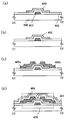
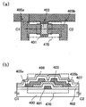
본 발명은 산화물 반도체를 포함하는 반도체 장치 및 반도체 장치를 제작하기 위한 방법에 관한 것이다.The present invention relates to a semiconductor device comprising an oxide semiconductor and a method for manufacturing a semiconductor device.
본 명세서에서, 반도체 장치는 일반적으로 반도체 특성을 이용함으로써 기능할 수 있는 장치를 의미하고, 전기 광학 장치, 반도체 회로 및 전자 기기는 모두 반도체 장치이다.In the present specification, the semiconductor device generally means a device that can function by utilizing semiconductor characteristics, and the electro-optical device, the semiconductor circuit, and the electronic device are all semiconductor devices.
절연 표면을 갖는 기판 위에 형성된 반도체 박막을 이용해서 박막 트랜지스터(TFT)를 형성하기 위한 기술이 주목받고 있다. 박막 트랜지스터는 액정 텔레비전으로 대표되는 표시 장치에 이용된다. 박막 트랜지스터에 적용가능한 반도체 박막에 대한 재료로서 실리콘계 반도체 재료가 알려져 있다. 다른 재료로서, 산화물 반도체가 주목받고 있다.A technique for forming a thin film transistor (TFT) using a semiconductor thin film formed on a substrate having an insulating surface has attracted attention. Thin film transistors are used in display devices typified by liquid crystal televisions. Silicon-based semiconductor materials are known as materials for semiconductor thin films applicable to thin film transistors. As other materials, attention has been paid to oxide semiconductors.
산화물 반도체의 재료로서는, 산화아연 또는 산화 아연을 그 성분으로 함유하는 재료가 알려져 있다. 또한, 전자 캐리어 농도가 1018/cm3 미만인 비정질 산화물(산화물 반도체)을 이용하여 형성된 박막 트랜지스터가 개시되어 있다(특허 문헌 1 내지 3 참조).As the material of the oxide semiconductor, a material containing zinc oxide or zinc oxide as its component is known. Further, a thin film transistor formed using an amorphous oxide (oxide semiconductor) having an electron carrier concentration of less than 10 18 / cm 3 is disclosed (see
그러나, 산화물 반도체 내의 화학양론적 조성으로부터의 차이가 박막 형성 공정에서 발생한다. 예를 들면, 산소의 과부족으로 인해 산화물 반도체의 전기 전도도가 변한다. 또한, 박막 형성 중에 산화물 반도체에 혼입하는 수소나 수분이 O-H(산소-수소) 결합을 형성해서 전자 공여체로서의 역할을 하고, 이는 전기 전도도를 변화시키는 요인이다. 또한, O-H 결합은 극성 분자이므로, 이는 산화물 반도체를 이용하여 제작되는 박막 트랜지스터와 같은 능동 디바이스의 특성 변동의 요인으로서의 역할을 한다.However, a difference from the stoichiometric composition in the oxide semiconductor occurs in the thin film formation process. For example, the lack of oxygen changes the electrical conductivity of the oxide semiconductor. In addition, hydrogen or moisture mixed into the oxide semiconductor during the thin film formation form O-H (oxygen-hydrogen) bonds to serve as electron donors, which is a factor that changes the electrical conductivity. In addition, since the O-H bond is a polar molecule, it serves as a factor of variation in characteristics of active devices such as thin film transistors fabricated using oxide semiconductors.
이러한 문제의 관점에서, 본 발명의 실시형태의 목적은, 산화물 반도체가 이용되는, 안정된 전기적 특성을 갖는 반도체 장치를 제공하는 것이다.In view of such a problem, it is an object of embodiments of the present invention to provide a semiconductor device having stable electrical characteristics in which an oxide semiconductor is used.
산화물 반도체층을 포함하는 박막 트랜지스터의 전기적 특성의 변동을 억제하기 위해서, 변동을 유발하는 수소, 수분, 수산기 또는 수소화물(수소 화합물이라고도 칭함)과 같은 불순물이 산화물 반도체층으로부터 의도적으로 제거된다. 또한, 불순물 제거 공정에서 감소되고 산화물 반도체의 주성분인 산소가 공급된다. 따라서, 산화물 반도체층이 고순도화되어, 전기적으로 i형(진성)인 산화물 반도체층이 얻어진다.In order to suppress fluctuations in electrical characteristics of the thin film transistor including the oxide semiconductor layer, impurities such as hydrogen, moisture, hydroxyl groups or hydrides (also referred to as hydrogen compounds) causing the fluctuations are intentionally removed from the oxide semiconductor layer. In addition, oxygen is reduced in the impurity removal process and is supplied as a main component of the oxide semiconductor. Thus, the oxide semiconductor layer is highly purified, thereby obtaining an electrically conductive i-type (intrinsic) oxide semiconductor layer.
따라서, 산화물 반도체 중의 수소는 가능한 적은 것이 바람직하다. 산화물 반도체에 함유되는 수소의 농도는 바람직하게는 1×10¹⁶/cm3 이하로 설정되어, 산화물 반도체에 함유되는 수소가 가능한 한 제로에 근접하게 제거된다.Therefore, as few hydrogen as possible in the oxide semiconductor is preferable. The concentration of hydrogen contained in the oxide semiconductor is preferably set to 1 × 10 16 / cm 3 or less, so that hydrogen contained in the oxide semiconductor is removed as close to zero as possible.
또한, 고순도 산화물 반도체 중의 캐리어 개수는 매우 적으며(제로에 근접), 캐리어 농도는 1×10¹⁴/cm3 미만, 바람직하게는 1×10¹²/cm3 미만, 더욱 바람직하게는 1×10¹¹/cm3 이하이다. 산화물 반도체 중의 캐리어 개수가 매우 적기 때문에, 박막 트랜지스터에서는, 오프 상태 전류가 감소될 수 있다. 오프 상태 전류량이 적을수록 더 바람직하다. 오프 상태 전류(리크 전류라고도 칭함)는, -1V 내지 -10V 사이의 소정의 게이트 전압을 인가했을 경우의 박막 트랜지스터의 소스와 드레인 사이에 흐르는 전류이다. 본 명세서에 개시되는 산화물 반도체를 포함하는 박막 트랜지스터의 채널 폭(w) 1㎛ 당 전류값이 100aA/㎛ 이하, 바람직하게는 10aA/㎛ 이하, 더욱 바람직하게는 1aA/㎛ 이하이다. 또한, 박막 트랜지스터가 pn 접합을 갖지 않고, 핫 캐리어에 의해 열화되지 않으므로, 박막 트랜지스터의 전기적 특성이 pn 접합과 열화에 의해 영향을 받지 않는다.In addition, the number of carriers in the high purity oxide semiconductor is very small (close to zero), and the carrier concentration is less than 1 × 10 14 / cm 3 , preferably less than 1 × 10 12 / cm 3 , more preferably 1 × 10 11. / cm 3 or less. Since the number of carriers in the oxide semiconductor is very small, in the thin film transistor, the off state current can be reduced. The smaller the off-state current amount, the more preferable. The off-state current (also called the leak current) is a current flowing between the source and the drain of the thin film transistor when a predetermined gate voltage between -1V and -10V is applied. The current value per μm of the channel width w of the thin film transistor including the oxide semiconductor disclosed herein is 100aA / μm or less, preferably 10aA / μm or less, more preferably 1aA / μm or less. In addition, since the thin film transistor does not have a pn junction and is not degraded by hot carriers, the electrical properties of the thin film transistor are not affected by the pn junction and the degradation.
상술한 수소의 농도 범위는, 2차 이온 질량 분석(SIMS: secondary ion mass spectrometry) 또는 SIMS의 데이터에 기초해서 얻어질 수 있다. 또한, 캐리어 농도는 홀(Hall) 효과 측정에 의해 측정될 수 있다. 홀 효과 측정에 이용되는 기기의 일례로서, 비저항/홀 측정 시스템 ResiTest 8310(TOYO Corporation 제작)을 들 수 있다. 비저항/홀 측정 시스템 ResiTest8310으로, 자기장의 방향과 크기가 일정한 주기로 변화되고, 그와 동기해서 샘플에서 발생되는 홀 기전압만이 검출되어 AC(교류) 홀 측정이 수행될 수 있다. 낮은 이동도와 높은 저항율을 갖는 재료의 경우에도, 홀 기전압을 검출할 수 있다.The above-described concentration range of hydrogen can be obtained based on secondary ion mass spectrometry (SIMS) or data of SIMS. In addition, carrier concentration can be measured by Hall effect measurement. As an example of the apparatus used for hall effect measurement, the specific resistance / hall measurement system ResiTest 8310 (made by TOYO Corporation) is mentioned. With the resistivity / hole measurement system ResiTest8310, the direction and magnitude of the magnetic field are changed at regular intervals, and only the hole voltage generated in the sample is detected in synchronization with it, so that AC (AC) hall measurement can be performed. Even in the case of a material having low mobility and high resistivity, the hole voltage can be detected.
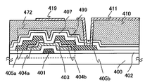
산화물 반도체막에 존재하는 수분과 같은 불순물 외에도, 게이트 절연층 내에 존재하는 수분과 같은 불순물과, 이와 접촉하여 제공되는 상부 및 하부 막들과 산화물 반도체막의 계면에 있는 불순물이 감소된다.In addition to impurities such as moisture present in the oxide semiconductor film, impurities such as moisture present in the gate insulating layer and impurities at the interface between the oxide semiconductor film and the upper and lower films provided in contact with the oxide semiconductor film are reduced.
수소, 수분, 수산기 또는 수소화물과 같은 불순물을 저감시키기 위해서, 산화물 반도체막을 형성한 후, 산화물 반도체막이 노출된 상태에서, 질소 분위기 또는 희가스(예를 들어, 아르곤 또는 헬륨)와 같은 불활성 기체 분위기하, 또는 감압하에서 200℃ 내지 700℃, 바람직하게는 350℃ 내지 700℃, 보다 바람직하게는 450℃ 내지 700℃에서 가열 처리(탈수화 또는 탈수소화를 위한 가열 처리)를 행한다. 따라서, 산화물 반도체막에 함유된 수분을 저감시킨다. 다음으로, 산소 분위기, 산소 및 질소 분위기, 또는 대기(초건조 에어)(바람직하게는 노점 -40℃ 이하, 보다 바람직하게는 -50℃ 이하) 분위기 내에서 서냉(slow cooling)이 수행된다.In order to reduce impurities such as hydrogen, moisture, hydroxyl groups or hydrides, after forming the oxide semiconductor film, the oxide semiconductor film is exposed, under an inert gas atmosphere such as nitrogen atmosphere or a rare gas (for example, argon or helium). Or heat treatment (heat treatment for dehydration or dehydrogenation) at 200 ° C to 700 ° C, preferably 350 ° C to 700 ° C, more preferably 450 ° C to 700 ° C under reduced pressure. Therefore, the moisture contained in the oxide semiconductor film is reduced. Next, slow cooling is carried out in an oxygen atmosphere, an oxygen and nitrogen atmosphere, or an atmosphere (super-dry air) (preferably dew point −40 ° C. or lower, more preferably −50 ° C. or lower).
탈수화 또는 탈수소화 처리로서, 질소 분위기 또는 불활성 기체 분위기하 또는 감압하에서의 가열 처리가 수행되어 산화물 반도체막 내에 함유된 수분이 저감된다. 그 후, 산소 공급 처리로서, 산소 분위기, 산소 및 질소 분위기, 또는 대기(초건조 에어)(바람직하게는 노점 -40℃ 이하, 보다 바람직하게는 -50℃ 이하의 노점을 가짐) 분위기하에서 냉각이 산화물 반도체막에 대해 수행된다. 이렇게 얻어진 산화물 반도체막을 이용하여, 박막 트랜지스터의 전기 특성이 향상된다. 또한, 양산될 수 있는, 고성능의 박막 트랜지스터가 달성될 수 있다.As the dehydration or dehydrogenation treatment, heat treatment is carried out in a nitrogen atmosphere or an inert gas atmosphere or under reduced pressure to reduce the moisture contained in the oxide semiconductor film. Thereafter, as the oxygen supply treatment, cooling is performed under an atmosphere of oxygen, oxygen and nitrogen, or atmosphere (super-dry air) (preferably having a dew point of -40 ° C or lower, more preferably -50 ° C or lower). It is performed on the oxide semiconductor film. By using the oxide semiconductor film thus obtained, the electrical characteristics of the thin film transistor are improved. In addition, a high performance thin film transistor that can be mass produced can be achieved.
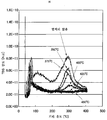
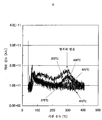
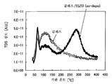
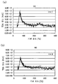
질소 분위기하에서 복수의 시료에 온도 램프(ramp)가 인가된다. 이러한 복수의 시료는 온도 탈리 분석(TDS: Thermal Desorption Spectroscopy) 장치로 측정되었다. 측정한 결과를 도 4, 도 5, 도 6 및 도 7에 나타낸다.A temperature ramp is applied to the plurality of samples under a nitrogen atmosphere. These multiple samples were measured with a Thermal Desorption Spectroscopy (TDS) device. The measured result is shown to FIG. 4, FIG. 5, FIG. 6, and FIG.
온도 탈리 분석 장치는, 시료를 고진공에서 가열하여 그 온도가 승온될 때 시료로부터 탈리 및 발생되는 가스 성분을 4중극 질량 분석계로 검출 및 식별하기 위해 이용되므로, 시료의 표면 및 내부로부터 탈리하는 가스 및 분자를 관찰할 수 있다. ESCO Ltd.에 의해 제작된 온도 탈리 분석 장치(제품명:EMD-WA1000S)를 이용하여, 측정은, 승온은 약 10℃/분; 측정 개시시의 압력은 1×10⁻⁸(Pa); 측정 중 압력은 약 1×10⁻⁷(Pa)의 진공도인 조건 하에서 수행되었다.The temperature detachment analyzer is used to detect and identify a gas component which is released and generated from the sample by a quadrupole mass spectrometer when the sample is heated in a high vacuum and the temperature thereof is elevated. The molecule can be observed. Using the temperature desorption analyzer (product name: EMD-WA1000S) manufactured by ESCO Ltd., the temperature measurement was about 10 ° C./min; The pressure at the start of the measurement was 1 × 10 −8 (Pa); The pressure during the measurement was performed under conditions that were at a vacuum degree of about 1 × 10 −7 (Pa).
도 37은, 글래스 기판만을 포함하는 시료(비교 시료)와, 글래스 기판 위에 스퍼터링법에 의해 두께 50nm의 In-Ga-Zn-O계 막이 성막된 시료(시료 1) 사이에 비교한 TDS의 결과를 나타내는 그래프이다. 도 37은 H2O를 측정하여 얻어진 결과를 나타낸다. In-Ga-Zn-O계 막으로부터 수분(H2O)과 같은 불순물의 탈리는 300℃ 부근의 피크로부터 확인할 수 있다.37 shows the results of TDS compared between a sample (comparative sample) containing only a glass substrate and a sample (sample 1) on which a 50 nm thick In—Ga—Zn—O based film was formed by sputtering on a glass substrate. It is a graph. 37 shows the results obtained by measuring H 2 O. FIG. Desorption of impurities such as moisture (H 2 O) from the In—Ga—Zn—O-based film can be confirmed from the peak around 300 ° C.
비교는 이하의 시료에 대해 수행되었다: 글래스 기판 위로 스퍼터링법에 의해 두께 50nm의 In-Ga-Zn-O계 막이 성막된 시료(시료 1); 시료 1의 구성물이 질소 분위기하에서의 가열 온도 350℃로 해서 1시간의 가열 처리를 받은 시료(시료 2); 시료 1의 구성물이 질소 분위기하에서의 가열 온도를 375℃로 해서 1시간의 가열 처리를 받은 시료(시료 3); 시료 1의 구성물이 질소 분위기하에서의 가열 온도를 400℃로 해서 1시간의 가열 처리를 받은 시료(시료 4); 시료 1의 구성물이 질소 분위기하에서 가열 온도를 425℃로 해서 1시간의 가열 처리를 받은 시료(시료 5); 및 시료 1의 구성물이 질소 분위기하에서 가열 온도를 450℃로 해서 1시간의 가열 처리를 받은 시료(시료 6).A comparison was made for the following samples: a sample in which an In—Ga—Zn—O based film having a thickness of 50 nm was formed by sputtering on a glass substrate (Sample 1); A sample subjected to heat treatment for 1 hour at a heating temperature of 350 ° C. under a nitrogen atmosphere (sample 2); The sample (Sample 3) which the structure of the
도 4는 H2O의 TDS 결과를 나타낸다. 도 5는 OH에 대한 TDS 결과를 나타낸다. 도 6은 H에 대한 TDS 결과를 나타낸다. 도 7은 O에 대한 TDS 결과를 나타낸다. 또한, 상술한 가열 처리의 조건하에서, 질소 분위기 중의 산소 농도는 20ppm 이하이다.4 shows the TDS results of H 2 O. 5 shows the TDS results for OH. 6 shows the TDS results for H. 7 shows the TDS results for O. In addition, under the conditions of the above-mentioned heat processing, the oxygen concentration in nitrogen atmosphere is 20 ppm or less.
도 4, 도 5 및 도 6에 나타낸 결과로부터, 질소 분위기에서의 가열 온도가 높을수록, In-Ga-Zn-O계 막으로부터 탈리되는 수분(H2O), OH, H와 같은 불순물의 양이 저감되는 것을 알았다.From the results shown in Figs. 4, 5 and 6, the higher the heating temperature in the nitrogen atmosphere, the more the amount of impurities such as water (H 2 O), OH, H detached from the In-Ga-Zn-O-based film. It was found that this was reduced.
또한, 도 7에 나타낸 바와 같이, 질소 분위기에서의 가열 처리에 의해 산소의 피크도 감소된다.In addition, as shown in FIG. 7, the peak of oxygen is also reduced by heat processing in nitrogen atmosphere.
이상의 결과는, In-Ga-Zn-O계 막의 가열 처리를 행함으로써, 주로 수분이 방출되는 것을 나타낸다. 즉, 가열 처리는 In-Ga-Zn-O계 막으로부터 주로 수분(H2O)의 탈리를 유발시킨다. 도 5에서 나타내는 H, 도 6에서 나타내는 OH 및 도 7에서 나타내는 O의 TDS의 측정값은 물 분자의 분해에 의해 얻어진 물질에 의해 영향을 받는다.The above results indicate that water is mainly released by heat treatment of the In—Ga—Zn—O-based film. That is, the heat treatment mainly causes desorption of moisture (H 2 O) from the In—Ga—Zn—O based film. The measured values of TDS of H shown in FIG. 5, OH shown in FIG. 6 and O shown in FIG. 7 are influenced by the substance obtained by decomposition | disassembly of water molecules.
질소 분위기하에서 수행된 가열 처리와, 산소 분위기하에서 수행된 냉각에 의해 얻어진 시료 7이 TDS 측정된다. 글래스 기판 위로, In-Ga-Zn-O계의 산화물 반도체 성막용 타깃(In:Ga:Zn=1:1:1 [원자비])을 이용하여, 기판과 타깃 사이의 거리를 60mm, 압력이 0.4Pa, RF 전원이 0.5kW인 조건하에서 아르곤 및 산소(아르곤:산소=30sccm:15sccm) 분위기하에서 두께 50nm의 In-Ga-Zn-O계 막이 형성된다. 이렇게 얻어진 막의 온도는 질소 분위기하에서, 1시간 30분 동안 승온되고, 그 막은 450℃로 1시간 가열된다. 그 후, 산소 분위기 하에서 그 막이 약 5시간 냉각된다. 이렇게 시료 7을 형성한다. 한편, 그 막과 마찬가지의 방식으로 성막되고, 질소 분위기하에서 가열한 후, 산소 분위기하가 아니라 질소 분위기하에서 냉각된다. 따라서, 시료 8이 형성되었다.Sample 7 obtained by heat treatment carried out in a nitrogen atmosphere and cooling carried out in an oxygen atmosphere is measured for TDS. The In-Ga-Zn-O-based oxide semiconductor film formation target (In: Ga: Zn = 1: 1: 1 [atomic ratio]) on the glass substrate was used to measure a distance of 60 mm and a pressure between the substrate and the target. Under argon and oxygen (argon: oxygen = 30sccm: 15sccm) atmosphere under the conditions of 0.4 Pa and an RF power supply of 0.5 kW, an In—Ga—Zn—O based film having a thickness of 50 nm is formed. The temperature of the film thus obtained is raised for 1 hour and 30 minutes in a nitrogen atmosphere, and the film is heated to 450 ° C. for 1 hour. Thereafter, the film is cooled for about 5 hours under an oxygen atmosphere. Thus, sample 7 was formed. On the other hand, the film is formed in the same manner as the film, and is heated in a nitrogen atmosphere, and then cooled in a nitrogen atmosphere instead of an oxygen atmosphere. Thus, Sample 8 was formed.
도 44a는 시료 7의 산소(O)에 대한 TDS 결과를 나타내고, 도 44b는 시료 8의 산소(O)에 대한 TDS 결과를 나타낸다. 도 44a에서 산소 분위기하에서 냉각되는 시료 7의 산소의 피크는 도 44b에서 산소 분위기하에서 냉각되지 않는 시료 8의 산소의 피크보다 더 높다. 이러한 결과로부터, 시료 7의 막에 산소가 공급된 것을 확인할 수 있다.FIG. 44A shows the TDS results for the oxygen (O) of Sample 7, and FIG. 44B shows the TDS results for the oxygen (O) of Sample 8. The peak of oxygen of Sample 7 cooled under oxygen atmosphere in FIG. 44A is higher than the peak of oxygen of Sample 8 not cooled under oxygen atmosphere in FIG. 44B. From these results, it was confirmed that oxygen was supplied to the membrane of Sample 7.
도 44a 및 도 44b는, 산소 분위기, 산소 및 질소 분위기, 또는 대기(바람직하게는 노점 -40℃ 이하, 보다 바람직하게는 -50℃ 이하의 노점을 가짐) 분위기하에서 산화물 반도체층을 냉각함으로써, 산화물 반도체층에 산소가 공급될 수 있어, 산소 배출로 인한 산소 결손이 채워질 수 있다는 것을 나타낸다. 따라서, 전기적으로 i형(진성)인 고순도 산화물 반도체층이 얻어질 수 있다.44A and 44B show oxides by cooling the oxide semiconductor layer in an oxygen atmosphere, an oxygen and nitrogen atmosphere, or an atmosphere (preferably having a dew point of -40 ° C or lower, more preferably -50 ° C or lower). Oxygen can be supplied to the semiconductor layer, indicating that oxygen vacancies due to oxygen emissions can be filled. Thus, an electrically i-type (intrinsic) high purity oxide semiconductor layer can be obtained.
본 명세서에서는, 질소 분위기, 또는 희가스(예를 들어, 아르곤, 헬륨)와 같은 불활성 기체 분위기하, 또는 감압하에서의 가열 처리가 탈수화 또는 탈수소화를 위한 가열 처리로 칭해진다. 본 명세서에서는, 편의를 위해, 탈수화 또는 탈수소화는 H2의 탈리만을 지칭하는 것이 아니라 H, OH 등의 탈리도 지칭한다.In this specification, the heat treatment under a nitrogen atmosphere or an inert gas atmosphere such as a rare gas (for example, argon, helium) or under reduced pressure is referred to as a heat treatment for dehydration or dehydrogenation. In this specification, for convenience, dehydration or dehydrogenation does not only refer to the desorption of H 2 but also desorption of H, OH, and the like.
산화물 반도체층에 탈수화 또는 탈수소화를 위한 가열 처리가 행해져서, 산화물 반도체층이 산소 결핍형으로서 변화되어, n형(n-형, n+형 등) 산화물 반도체층이 얻어진다. 그 후, 얻어진 산화물 반도체층은 산소 분위기, 산소 및 질소 분위기, 또는 대기(바람직하게는 노점 -40℃ 이하, 보다 바람직하게는 -50℃ 이하의 노점을 가짐) 분위기하에서 냉각됨으로써 산화물 반도체층에 산소가 공급된다. 따라서 산화물 반도체층이 고순도화되어, i형 산화물 반도체층이 얻어진다. 이렇게 얻어진 i형 산화물 반도체층의 사용으로, 우수한 전기 특성을 갖는 신뢰성이 높은 박막 트랜지스터를 갖는 반도체 장치가 제작 및 제공될 수 있다.The oxide semiconductor layer is subjected to heat treatment for dehydration or dehydrogenation, so that the oxide semiconductor layer is changed to an oxygen deficient type to obtain an n-type (n − , n + , etc.) oxide semiconductor layer. Thereafter, the obtained oxide semiconductor layer is cooled in an oxygen atmosphere, an oxygen and nitrogen atmosphere, or an atmosphere (preferably having a dew point of -40 ° C or lower, more preferably -50 ° C or lower). Is supplied. Therefore, the oxide semiconductor layer is highly purified, thereby obtaining an i-type oxide semiconductor layer. By using the i-type oxide semiconductor layer thus obtained, a semiconductor device having a highly reliable thin film transistor having excellent electrical characteristics can be manufactured and provided.
본 명세서에서 개시되는 본 발명의 구성의 일 실시형태에 따르면, 게이트 전극층 및 게이트 전극층을 덮는 게이트 절연층이 형성되고; 게이트 전극층 및 게이트 절연층이 감압으로 유지된 처리실에 도입되고, 처리실로부터 잔류 수분을 동시에 제거하면서 수소 및 수분이 제거된 스퍼터링 가스를 도입함으로써, 처리실에 장착된 금속 산화물 타깃을 이용해서 게이트 절연층 위에 산화물 반도체층이 형성되고, 산화물 반도체층에 대해 질소 분위기 또는 희가스 분위기하에서의 가열 처리에 의해 탈수화 또는 탈수소화가 수행된 후, 산소 분위기하에서의 냉각 처리에 의해 산소가 산화물 반도체층에 공급되고; 탈수화 또는 탈수소화 처리되고 산소가 공급된 산화물 반도체층 위에 소스 전극층 및 드레인 전극층이 형성되고; 게이트 절연층, 산화물 반도체층, 소스 전극층 및 드레인 전극층 위에 스퍼터링법에 의해 절연층이 형성된다.According to one embodiment of the configuration of the present invention disclosed herein, a gate electrode layer and a gate insulating layer covering the gate electrode layer are formed; The gate electrode layer and the gate insulating layer are introduced into the process chamber maintained at a reduced pressure, and a sputtering gas from which hydrogen and moisture are removed while introducing residual moisture from the process chamber is introduced to the upper portion of the gate insulating layer using a metal oxide target mounted in the process chamber. An oxide semiconductor layer is formed, dehydration or dehydrogenation is performed on the oxide semiconductor layer by heat treatment in a nitrogen atmosphere or a rare gas atmosphere, and then oxygen is supplied to the oxide semiconductor layer by cooling treatment in an oxygen atmosphere; A source electrode layer and a drain electrode layer are formed on the oxide semiconductor layer subjected to dehydration or dehydrogenation and supplied with oxygen; An insulating layer is formed on the gate insulating layer, the oxide semiconductor layer, the source electrode layer, and the drain electrode layer by the sputtering method.
본 명세서에서 개시하는 본 발명의 구성의 일 실시형태에 따르면, 게이트 전극층 및 게이트 전극층을 덮는 게이트 절연층이 그 위에 형성된 후, 게이트 전극층 및 게이트 절연층을 감압 상태로 유지된 처리실에 도입하고, 처리실 내의 잔류 수분을 제거하면서 수소 및 수분이 제거된 스퍼터링 가스를 도입하고, 처리실 내에 장착된 금속 산화물의 타깃을 이용해서 게이트 절연층 상에 산화물 반도체층을 형성하고, 산화물 반도체층을 질소 분위기, 또는 희가스 분위기하에서의 가열 처리에 의해 탈수화 또는 탈수소화한 후, 산소 및 질소, 또는 노점 -40℃ 이하의 대기분위기하에서의 냉각 처리에 의해 산소를 공급하고, 탈수화 또는 탈수소화시켜, 산소를 공급한 산화물 반도체층 위에 소스 전극층 및 드레인 전극층을 형성하고, 게이트 절연층, 산화물 반도체층, 소스 전극층, 및 드레인 전극층 위에 스퍼터링법에 의해 절연층을 형성한다.According to one embodiment of the configuration of the present invention disclosed herein, after the gate electrode layer and the gate insulating layer covering the gate electrode layer are formed thereon, the gate electrode layer and the gate insulating layer are introduced into the processing chamber maintained at a reduced pressure, and the processing chamber A sputtering gas from which hydrogen and water have been removed while introducing residual moisture therein is introduced, and an oxide semiconductor layer is formed on the gate insulating layer using a target of a metal oxide mounted in the process chamber, and the oxide semiconductor layer is nitrogen atmosphere or rare gas. Oxide semiconductors which are dehydrated or dehydrogenated by heat treatment in an atmosphere, and then oxygen is supplied by oxygen and nitrogen or by a cooling treatment in an air atmosphere at a dew point of −40 ° C. or lower, followed by dehydration or dehydrogenation, to supply oxygen. A source electrode layer and a drain electrode layer are formed on the layer; An insulating layer is formed on the body layer, the source electrode layer, and the drain electrode layer by sputtering.
반도체 장치의 제작 방법에 있어서, 산화물 반도체층, 또는 절연층은, 크라이오 펌프와 같은 흡착형의 진공 펌프를 이용해서 배기해서 불순물 농도가 저감된 성막실(처리실) 내에서 성막하는 것이 바람직하다. 흡착형의 진공 펌프로서는, 예를 들면, 크라이오 펌프, 이온 펌프, 티타늄 서블리메이션 펌프를 이용하는 것이 바람직하다. 흡착형의 진공 펌프는, 산화물 반도체층 또는 절연층에 포함되는 수소, 물, 수산기 또는 수소화물의 양을 저감시키도록 기능한다.In the method for manufacturing a semiconductor device, the oxide semiconductor layer or the insulating layer is preferably exhausted using an adsorption type vacuum pump such as a cryo pump to form a film in a film formation chamber (process chamber) in which impurity concentration is reduced. As a suction type vacuum pump, it is preferable to use a cryopump, an ion pump, and a titanium servation pump, for example. The suction type vacuum pump functions to reduce the amount of hydrogen, water, hydroxyl groups or hydrides contained in the oxide semiconductor layer or the insulating layer.
산화물 반도체층 또는 절연층을 성막할 때에 이용하는 스퍼터링 가스로서, 수소, 물, 수산기 또는 수소화물 등의 불순물이, 불순물 농도 레벨이 "ppm" 또는 "ppb" 단위로 표현되는 정도까지 감소된 고순도 가스를 이용하는 것이 바람직하다.As a sputtering gas used for forming an oxide semiconductor layer or an insulating layer, impurities such as hydrogen, water, hydroxyl groups, or hydrides have a high purity gas in which an impurity concentration level is expressed in units of "ppm" or "ppb". It is preferable to use.
또한, 반도체 장치의 제작 방법에 있어서, 산화물 반도체막을 성막하기 위한 타깃으로서, 산화아연을 주성분으로서 포함하는 타깃을 이용할 수 있다. 대안적으로, 타깃으로서, 인듐, 갈륨, 및 아연을 포함하는 금속 산화물을 이용할 수 있다.Moreover, in the manufacturing method of a semiconductor device, the target containing zinc oxide as a main component can be used as a target for forming an oxide semiconductor film. Alternatively, metal oxides including indium, gallium, and zinc can be used as targets.
본 발명의 특징은, 산화물 반도체층에 대하여, 질소 분위기, 또는 희가스(예를 들면, 아르곤, 헬륨)와 같은 불활성 기체 분위기하, 또는 감압하에서 탈수화 또는 탈수소화 처리를 위한 가열 처리가 행해지고, 산소 분위기, 산소 및 질소 분위기, 또는 대기(바람직하게는 노점 -40℃ 이하, 보다 바람직하게는 -50℃ 이하의 노점을 가짐) 분위기하에서 산소 공급 처리를 위한 냉각 공정이 행해지는 것이다.A feature of the present invention is that the oxide semiconductor layer is subjected to a heat treatment for dehydration or dehydrogenation treatment under a nitrogen atmosphere or an inert gas atmosphere such as rare gas (for example, argon, helium) or under reduced pressure, and oxygen The cooling process for oxygen supply treatment is performed in an atmosphere, oxygen and nitrogen atmosphere, or an atmosphere (preferably having a dew point of -40 ° C or lower, more preferably -50 ° C or lower).
탈수화 또는 탈수소화 처리 및 산소 공급 처리에서, 산화물 반도체층(및 기판)의 온도 상태는, 승온 상태, 항온 상태, 강온 상태이다. 질소 또는 희가스(예를 들면, 아르곤, 헬륨)와 같은 불활성 기체로부터 산소 분위기, 산소 및 질소 분위기, 또는 대기(바람직하게는 노점 -40℃ 이하, 보다 바람직하게는 -50℃ 이하의 노점을 가짐)로 가스(분위기)가 이하의 타이밍 중 임의의 타이밍에서 전환될 수 있다: 산화물 반도체층의 온도가 항온 상태인 시간, 산화물 반도체층의 강온이 개시되는 시간, 및 산화물 반도체층의 온도가 강온 상태인 시간.In the dehydration or dehydrogenation treatment and the oxygen supply treatment, the temperature state of the oxide semiconductor layer (and the substrate) is a temperature rising state, a constant temperature state, and a temperature lowering state. From an inert gas such as nitrogen or a rare gas (e.g. argon, helium), an oxygen atmosphere, an oxygen and nitrogen atmosphere, or an atmosphere (preferably a dew point of -40 ° C or lower, more preferably -50 ° C or lower). The furnace gas (atmosphere) can be switched at any of the following timings: the time when the temperature of the oxide semiconductor layer is in a constant temperature, the time when the temperature of the oxide semiconductor layer is started, and the temperature of the oxide semiconductor layer is in a cold state. time.
이러한 구성으로, 적어도 하나의 문제점을 해결할 수 있다.With this configuration, at least one problem can be solved.
본 명세서에서 이용하는 산화물 반도체막으로서는, 4원계 금속 산화물인 In-Sn-Ga-Zn-O막이나, 3원계 금속 산화물인 In-Ga-Zn-O막, In-Sn-Zn-O막, In-Al-Zn-O막, Sn-Ga-Zn-O막, Al-Ga-Zn-O막, Sn-Al-Zn-O계나, 2원계 금속 산화물인 In-Zn-O막, Sn-Zn-O막, Al-Zn-O막, Zn-Mg-O막, Sn-Mg-O막, In-Mg-O막이나, In-O막, Sn-O막, Zn-O막 등의 산화물 반도체막을 이용할 수 있다. 또한, 상기 산화물 반도체막에 SiO2를 포함할 수 있다.As the oxide semiconductor film used in the present specification, an In—Sn—Ga—Zn—O film that is a quaternary metal oxide, an In—Ga—Zn—O film, an In—Sn—Zn—O film, or In that is a ternary metal oxide -Al-Zn-O film, Sn-Ga-Zn-O film, Al-Ga-Zn-O film, Sn-Al-Zn-O-based or binary metal oxide In-Zn-O film, Sn-Zn Oxides such as -O films, Al-Zn-O films, Zn-Mg-O films, Sn-Mg-O films, In-Mg-O films, In-O films, Sn-O films, and Zn-O films A semiconductor film can be used. In addition, SiO 2 may be included in the oxide semiconductor film.
또한, 산화물 반도체막은, InMO3(ZnO)m(m>0)로 표기되는 박막을 이용할 수 있다. 여기에서, M은, Ga, Al, Mn 및 Co로부터 선택된 하나 이상의 금속 원소를 나타낸다. 예를 들면 M으로서, Ga, Ga 및 Al, Ga 및 Mn, 또는 Ga 및 Co 등일 수 있다. 구조식이 InMO3(ZnO)m(m>0)로 표기되는 산화물 반도체막에서, M으로서 적어도 Ga가 포함되는 구조의 산화물 반도체를, 상술한 In-Ga-Zn-O 산화물 반도체라 칭하고, 그 박막을 In-Ga-Zn-O막이라도 칭한다.As the oxide semiconductor film, a thin film expressed by InMO 3 (ZnO) m (m> 0) can be used. Here, M represents at least one metal element selected from Ga, Al, Mn and Co. For example, M may be Ga, Ga and Al, Ga and Mn, or Ga and Co. In the oxide semiconductor film whose structural formula is represented by InMO 3 (ZnO) m (m> 0), the oxide semiconductor having a structure containing at least Ga as M is referred to as the In-Ga-Zn-O oxide semiconductor described above, and the thin film This may be referred to as an In-Ga-Zn-O film.
박막 트랜지스터는 정전기 등에 의해 파괴되기 쉽기 때문에, 게이트선 또는 소스선에 대해 동일한 기판 위에 구동 회로 보호용 회로를 설치하는 것이 바람직하다. 보호 회로는 산화물 반도체를 포함하는 비선형 소자로 구성하는 것이 바람직하다.Since the thin film transistor is easily broken by static electricity or the like, it is preferable to provide a driving circuit protection circuit on the same substrate as the gate line or the source line. It is preferable to comprise a protection circuit with the nonlinear element containing an oxide semiconductor.
게이트 절연층 및 산화물 반도체막이 대기에 접촉하지 않게 연속적으로 처리(연속 처리, 인시츄(in situ) 공정, 연속 성막이라고도 칭함)될 수 있다. 대기에 접촉하지 않게 연속 처리함으로써, 게이트 절연층과 산화물 반도체막 사이의 계면이, 물이나 하이드로 카본과 같은 대기 성분이나 대기 중에 부유하는 불순물에 오염되지 않고 형성될 수 있다. 따라서, 박막 트랜지스터 특성의 변동을 저감시킬 수 있다.The gate insulating layer and the oxide semiconductor film may be continuously processed (also referred to as a continuous treatment, an in situ process, or a continuous film formation) so as not to contact the atmosphere. By continuous processing without contact with the atmosphere, the interface between the gate insulating layer and the oxide semiconductor film can be formed without being contaminated with atmospheric components such as water or hydrocarbon or impurities floating in the atmosphere. Thus, variations in thin film transistor characteristics can be reduced.
또한, 본 명세서에서 "연속 처리"는, PCVD법 또는 스퍼터링법으로 행하는 제 1 처리 공정으로부터 PCVD법 또는 스퍼터링법으로 행하는 제 2 처리 공정까지의 프로세스 중, 피처리 기판이 놓여 있는 분위기가 대기와 같은 오염 분위기에 접촉하지 않고, 항상 진공 중에서 제어되고, 불활성 가스 분위기(질소 분위기 또는 희가스 분위기), 산소 가스, 산소 및 질소를 포함하는 가스(예를 들면 N2O 가스), 또는 초건조 에어(바람직하게는 노점이 -40℃ 이하, 더욱 바람직하게는 -50℃ 이하의 노점을 가짐)로 제어되어 있는 것을 말한다. 연속 처리를 행함으로써, 청정화된 피처리 기판의 수분 등의 재부착을 회피해서 성막될 수 있다.In addition, in this specification, "continuous process" is the process from the 1st process process performed by PCVD method or sputtering method to the 2nd process process performed by PCVD method or sputtering method, The atmosphere in which a to-be-processed board | substrate puts is like air | atmosphere. Controlled in vacuum at all times without contacting the contaminating atmosphere, inert gas atmosphere (nitrogen atmosphere or rare gas atmosphere), oxygen gas, gas containing oxygen and nitrogen (eg N 2 O gas), or ultra-dry air (preferably Preferably, the dew point is controlled to have a dew point of −40 ° C. or less, more preferably −50 ° C. or less). By performing a continuous process, it can form into a film, avoiding reattachment of the moisture etc. of the cleaned to-be-processed substrate.
동일 챔버내에서 제 1 처리 공정으로부터 제 2 처리 공정까지의 프로세스를 행하는 것은 본 명세서에 있어서의 연속 처리의 범위에 있는 것으로 한다.It is assumed that performing the process from the first processing step to the second processing step in the same chamber is in the range of continuous processing in the present specification.
또한, 다른 챔버에서 제 1 처리 공정으로부터 제 2 처리 공정까지의 프로세스를 행할 경우, 제 1 처리 공정을 끝낸 후, 수소, 수분, 수산기 또는 수소화물 등의 불순물을 포함하는 대기에 접촉하지 않고 챔버 사이에 기판을 반송해서 제 2 처리를 실시하는 것도 본 명세서에 있어서의 연속 처리의 범위에 있는 것으로 한다.In addition, when performing a process from the first processing step to the second processing step in another chamber, after the first processing step is completed, the chamber is not contacted with an atmosphere containing impurities such as hydrogen, moisture, hydroxyl groups, or hydrides. It is also assumed that the substrate is conveyed to the substrate and the second treatment is in the range of continuous processing in the present specification.
또한, 제 1 처리 공정과 제 2 처리 공정의 사이에, 기판 반송 공정, 얼라인먼트 공정, 서냉 공정, 또는 제 2 공정에 필요한 온도로 하기 위해서 기판을 가열 또는 냉각하는 공정 등도, 본 명세서에 있어서의 연속 처리의 범위에 있는 것으로 한다.Moreover, the process of heating or cooling a board | substrate in order to make temperature required for a board | substrate conveyance process, an alignment process, a slow cooling process, or a 2nd process between a 1st processing process and a 2nd processing process, etc. is also continuous in this specification. It is assumed that it is in the range of processing.
하지만, 세정 공정, 습식 에칭, 또는 레지스트 형성 공정과 같은 액체가 이용되는 공정이 제 1 처리 공정과 제 2 처리 공정의 사이에 있을 경우, 본 명세서에서의 연속 처리의 범위 내에 있지 않은 것으로 한다.However, when a process in which a liquid is used, such as a cleaning process, a wet etching, or a resist formation process, is between the first processing process and the second processing process, it is assumed that the process is not within the scope of continuous processing in the present specification.
안정된 전기 특성을 갖는 박막 트랜지스터를 제공할 수 있다. 또한, 우수한 전기적 특성과 높은 신뢰성을 갖는 박막 트랜지스터를 갖는 반도체 장치를 제공할 수 있다.A thin film transistor having stable electrical characteristics can be provided. In addition, a semiconductor device having a thin film transistor having excellent electrical characteristics and high reliability can be provided.
도 1a 내지 도 1d는 본 발명의 일 실시형태의 제작 공정을 나타내는 단면도.
도 2a 및 도 2b는 본 발명의 일 실시형태의 반도체 장치를 설명하는 도면.
도 3은 본 발명의 일 실시형태에 이용하는 전기로의 단면도.
도 4는 TDS 측정 결과를 나타내는 그래프.
도 5는 TDS 측정 결과를 나타내는 그래프.
도 6은 TDS 측정 결과를 나타내는 그래프.
도 7은 TDS 측정 결과를 나타내는 그래프.
도 8a 내지 도 8d는 본 발명의 일 실시형태의 제작 공정을 나타내는 단면도.
도 9a 및 도 9b는 본 발명의 일 실시형태의 반도체 장치를 설명하는 도면.
도 10a 내지 도 10d는 본 발명의 일 실시형태의 제작 공정을 나타내는 단면도.
도 11a 내지 도 11c는 본 발명의 일 실시형태의 제작 공정을 나타내는 단면도.
도 12는 본 발명의 일 실시형태의 반도체 장치를 설명하는 도면.
도 13a1, 도 13a2, 도 13b1 및 도 13b2는 본 발명의 일 실시형태의 반도체 장치를 설명하는 도면.
도 14는 반도체 장치를 설명하는 도면.
도 15a 내지 도 15c는 반도체 장치를 설명하는 도면.
도 16a 및 도 16b는 반도체 장치를 설명하는 도면.
도 17은 반도체 장치의 화소의 등가 회로도.
도 18a 내지 도 18c는 반도체 장치를 설명하는 도면.
도 19a 및 도 19b는 반도체 장치를 설명하는 블록도.
도 20a 및 도 20b는 신호선 구동 회로의 구성을 설명하는 도면.
도 21a 내지 도 21d는 시프트 레지스터의 구성을 나타내는 회로도.
도 22a 및 도 22b는 시프트 레지스터의 동작을 설명하는 회로도 및 타이밍 차트.
도 23은 반도체 장치를 설명하는 도면.
도 24는 박막 트랜지스터의 전기 특성의 평가 결과를 나타내는 그래프.
도 25는 반도체 장치를 설명하는 도면.
도 26은 전자 기기를 나타내는 도면.
도 27은 전자 기기를 나타내는 도면.
도 28a 및 도 28b는 전자 기기를 나타내는 도면.
도 29a 및 도 29b는 전자 기기를 나타내는 도면.
도 30a 및 도 30b는 전자 기기를 나타내는 도면.
도 31a 내지 도 31d는 본 발명의 일 실시형태의 제작 공정을 설명하는 단면도.
도 32는 본 발명의 일 실시형태의 반도체 장치를 설명하는 도면.
도 33은 본 발명의 일 실시형태의 반도체 장치를 설명하는 도면.
도 34a 내지 도 34c는 본 발명의 일 실시형태의 반도체 장치를 설명하는 도면.
도 35a 및 도 35b는 본 발명의 일 실시형태의 반도체 장치를 설명하는 도면.
도 36은 본 발명의 일 실시형태의 반도체 장치를 설명하는 도면.
도 37은 TDS 측정 결과를 나타내는 그래프.
도 38은 본 발명의 일 실시형태에 이용되는 열처리 장치를 설명하는 도면.
도 39는 본 발명의 일 실시형태에 이용되는 열처리 장치를 설명하는 도면.
도 40은 산화물 반도체가 이용되는 역스태거형의 박막 트랜지스터의 종단면도.
도 41은 도 40에 나타내는 A-A' 단면에 따른 에너지 밴드도(개략도).
도 42a는 게이트(GE1)에 플러스의 전위(+VG)가 인가된 상태를 나타내는 도면이고, 도 42b는 게이트(GE1)에 마이너스의 전위(-VG)가 인가된 상태를 나타내는 도면.
도 43은 진공 준위와 금속의 일함수(φM) 사이의 관계와, 진공 준위와 산화물 반도체의 전자 친화력(χ) 사이의 관계를 나타내는 에너지 밴드도.
도 44a 및 도 44b는 TDS 측정 결과를 나타내는 그래프.1A to 1D are cross-sectional views illustrating a fabrication process in one embodiment of the present invention.
2A and 2B illustrate a semiconductor device of one embodiment of the present invention.
3 is a cross-sectional view of an electric furnace used in one embodiment of the present invention.
4 is a graph showing the results of TDS measurement.
5 is a graph showing the results of TDS measurement.
6 is a graph showing the results of TDS measurement.
7 is a graph showing the results of TDS measurement.
8A to 8D are cross-sectional views illustrating a fabrication process in one embodiment of the present invention.
9A and 9B illustrate a semiconductor device of one embodiment of the present invention.
10A to 10D are cross-sectional views showing the fabrication process of one embodiment of the present invention.
11A to 11C are cross-sectional views illustrating the fabrication process in one embodiment of the present invention.
12 illustrates a semiconductor device of one embodiment of the present invention.
13A1, 13A2, 13B1, and 13B2 illustrate a semiconductor device of one embodiment of the present invention.
14 illustrates a semiconductor device.
15A to 15C are diagrams for describing a semiconductor device.
16A and 16B illustrate a semiconductor device.
17 is an equivalent circuit diagram of pixels of a semiconductor device.
18A to 18C illustrate a semiconductor device.
19A and 19B are block diagrams illustrating a semiconductor device.
20A and 20B illustrate the structure of a signal line driver circuit.
21A to 21D are circuit diagrams showing a configuration of a shift register.
22A and 22B are a circuit diagram and a timing chart for explaining the operation of the shift register.
23 illustrates a semiconductor device.
24 is a graph showing the evaluation results of electrical properties of a thin film transistor.
25 illustrates a semiconductor device.
26 illustrates an electronic device.
27 illustrates an electronic device.
28A and 28B illustrate an electronic device.
29A and 29B illustrate an electronic device.
30A and 30B illustrate an electronic device.
31A to 31D are cross-sectional views illustrating the manufacturing process of one embodiment of the present invention.
32 illustrates a semiconductor device of one embodiment of the present invention.
33A to 33D illustrate a semiconductor device of one embodiment of the present invention.
34A to 34C illustrate a semiconductor device of one embodiment of the present invention.
35A and 35B illustrate a semiconductor device of one embodiment of the present invention.
36 illustrates a semiconductor device of one embodiment of the present invention.
37 is a graph showing the results of TDS measurement.
The figure explaining the heat treatment apparatus used for one Embodiment of this invention.
39 A diagram for describing the heat treatment apparatus used in one embodiment of the present invention.
Fig. 40 is a longitudinal sectional view of an inverted staggered thin film transistor in which an oxide semiconductor is used.
FIG. 41 is an energy band diagram (schematic diagram) taken along a line AA ′ shown in FIG. 40. FIG.
FIG. 42A is a diagram illustrating a state in which a positive potential (+ V G ) is applied to the gate GE1, and FIG. 42B is a diagram illustrating a state in which a negative potential (-V G ) is applied to the gate GE1.
Fig. 43 is an energy band diagram showing the relationship between the vacuum level and the work function φ M of the metal and the relationship between the vacuum level and the electron affinity χ of the oxide semiconductor.
44A and 44B are graphs showing TDS measurement results.
이하에서는, 본 발명의 실시형태에 대해서 도면을 참조해서 상세하게 설명한다. 단, 본 발명은 이하의 설명에 한정되지 않고, 본 발명의 사상 및 범위를 벗어나지 않고 본 명세서에 개시된 모드와 상세 사항이 다양한 방식으로 변경될 수 있다는 것이 본 기술 분야의 당업자에게 용이하게 이해될 것이다. 따라서, 본 발명은 실시형태의 기재 내용에 한정되는 것으로 해석되지 않는다.EMBODIMENT OF THE INVENTION Hereinafter, embodiment of this invention is described in detail with reference to drawings. However, the present invention is not limited to the following description, and it will be easily understood by those skilled in the art that the modes and details disclosed herein can be changed in various ways without departing from the spirit and scope of the present invention. . Therefore, this invention is not interpreted as being limited to the description of embodiment.
(실시형태 1)(Embodiment 1)
반도체 장치 및 반도체 장치의 제작 방법을 도 1a 내지 도 1d, 도 2a 및 도 2b를 참조하여 설명한다.The semiconductor device and the manufacturing method of the semiconductor device will be described with reference to FIGS. 1A to 1D, 2A, and 2B.
도 2a는 반도체 장치에 포함되는 박막 트랜지스터(470)의 평면도이며, 도 2b는 도 2a의 선 C1-C2에 따라 취한 단면도이다. 박막 트랜지스터(470)는 역스태거형의 박막 트랜지스터이며, 절연 표면을 갖는 기판인 기판(400) 위로, 게이트 전극층(401), 게이트 절연층(402), 산화물 반도체층(403), 소스 전극층(405a) 및 드레인 전극층(405b)을 포함한다. 박막 트랜지스터(470)는 산화물 반도체층(403)에 접하는 절연층(407)으로 덮여진다. 절연층(407) 위로 보호 절연층(499)이 적층된다.FIG. 2A is a plan view of the
박막 트랜지스터(470)의 전기적 특성 변동을 억제하기 위해서, 변동을 야기하는 수소, 수분, 수산기 또는 수소화물(수소 화합물이라고도 칭함)과 같은 불순물이 산화물 반도체층으로부터 의도적으로 제거된다. 또한, 불순물 제거 공정에서 감소되고 산화물 반도체의 주성분인 산소가 공급된다. 따라서, 전기적으로 i형(진성)인 고순도화된 산화물 반도체층이 얻어진다. 이러한 방식으로, 산화물 반도체층(403)이 형성된다.In order to suppress the variation in electrical characteristics of the
따라서, 산화물 반도체층(403) 중의 수소는 가능한 한 적을수록 바람직하다. 산화물 반도체층(403)에 포함되는 수소 농도는 바람직하게는 1×10¹⁶/cm3 이하로 설정되어, 산화물 반도체층(403)에 함유되는 수소가 가능한 한 제로에 근접하게 제거된다.Therefore, as few hydrogen as possible in the
또한, 고순도 산화물 반도체층(403)의 캐리어 개수는 매우 적고(제로에 근접함), 캐리어 농도는 1×10¹⁴/cm3 미만, 바람직하게는 1×10¹²/cm3 미만, 더욱 바람직하게는 1×10¹¹/cm3 이하이다. 산화물 반도체층(403)의 캐리어 개수가 매우 적기 때문에, 박막 트랜지스터(470)에서는, 오프 상태 전류가 감소될 수 있다. 오프 상태 전류의 양이 적을수록 더 바람직하다. 박막 트랜지스터(470)의 채널 폭(w)에서 1㎛ 당 전류값이 100aA/㎛ 이하이고, 바람직하게는 10aA/㎛ 이하, 더욱 바람직하게는 1aA/㎛ 이하이다. 또한, 박막 트랜지스터(470)는 pn 접합을 가지지 않고, 핫 캐리어에 의해 열화되지 않으므로, 박막 트랜지스터(470)의 전기적 특성이 pn 접합 및 열화로 인해 영향을 받지 않는다.In addition, the number of carriers of the high purity
수소, 수분, 수산기 또는 수소화물과 같은 불순물을 저감시키기 위해서, 산화물 반도체층을 형성한 후, 산화물 반도체층이 노출된 상태에서 질소 분위기, 또는 희가스(예를 들면, 아르곤, 헬륨)와 같은 불활성 기체 분위기하, 또는 감압하에서 200℃ 내지 700℃, 바람직하게는 350℃ 내지 700℃, 보다 바람직하게는 450℃ 내지 700℃에서 가열 처리(탈수화 또는 탈수소화를 위한 가열 처리)가 행해진다. 산화물 반도체층에 함유된 수분이 저감된다. 다음으로, 산소 분위기, 산소 및 질소 분위기, 또는 대기(초건조 에어)(바람직하게는 노점 -40℃ 이하, 보다 바람직하게는 -50℃ 이하의 노점을 가짐) 분위기 하에서 냉각이 수행된다.In order to reduce impurities such as hydrogen, moisture, hydroxyl groups or hydrides, after forming the oxide semiconductor layer, an inert gas such as nitrogen atmosphere or a rare gas (for example, argon, helium) in the state where the oxide semiconductor layer is exposed Heat treatment (heat treatment for dehydration or dehydrogenation) is performed at 200 ° C to 700 ° C, preferably 350 ° C to 700 ° C, more preferably 450 ° C to 700 ° C under an atmosphere or under reduced pressure. Moisture contained in the oxide semiconductor layer is reduced. Next, cooling is carried out in an oxygen atmosphere, an oxygen and nitrogen atmosphere, or an atmosphere (super-dry air) (preferably having a dew point of -40 ° C or lower, more preferably -50 ° C or lower).
탈수화 또는 탈수소화 처리로서, 질소 분위기, 또는 불활성 기체 분위기, 또는 감압하에서의 가열 처리에 의해 막에 함유된 수분이 저감된다. 그 후, 산소 공급을 위한 처리로서, 산소 분위기, 산소 및 질소 분위기, 또는 대기(초건조 에어)(바람직하게는 노점 -40℃ 이하, 보다 바람직하게는 -50℃ 이하의 노점을 가짐) 분위기하에서 냉각이 수행된다. 이렇게 얻어진 산화물 반도체층(403)을 이용하여, 박막 트랜지스터(470)의 전기 특성이 향상된다. 또한, 양산될 수 있는 고성능의 박막 트랜지스터가 얻어질 수 있다.As the dehydration or dehydrogenation treatment, the moisture contained in the membrane is reduced by heat treatment under nitrogen atmosphere, inert gas atmosphere, or reduced pressure. Thereafter, as a treatment for oxygen supply, under an oxygen atmosphere, an oxygen and nitrogen atmosphere, or an atmosphere (super-dry air) (preferably a dew point of -40 ° C or lower, more preferably -50 ° C or lower). Cooling is performed. By using the
또한, 산화물 반도체층(403) 내 뿐만 아니라, 게이트 절연층(402) 내 및 접하게 설치되는 상부 및 하부 막들과 산화물 반도체층(403) 사이의 계면, 구체적으로는 게이트 절연층(402)과 산화물 반도체층(403) 사이의 계면 및 절연층(407)과 산화물 반도체층(403) 사이의 계면에 존재하는 수분과 같은 불순물이 저감된다.In addition, not only the
따라서, 게이트 절연층(402) 및 절연층(407)의 성막시에 수소, 수산기 및 수분이 가능한 한 적게 포함되도록 수소 또는 수분과 같은 불순물이 탈리되어 배기되는 것이 바람직하다. 또한, 기판(400)에 흡착되는 수소 또는 수분과 같은 불순물이 탈리 및 배기되도록, 게이트 절연층(402), 산화물 반도체층(403) 및 절연층(407)의 성막 전에 예비 가열을 행하는 것이 바람직하다.Therefore, it is preferable that impurities such as hydrogen or moisture are detached and exhausted so that hydrogen, hydroxyl groups, and moisture are included as little as possible when the
채널 형성 영역을 포함하는 산화물 반도체층(403)은 반도체 특성을 갖는 산화물 재료를 이용하여 형성되는 것이 바람직하다. 산화물 반도체층으로서는, 이하의 산화물 반도체막들 중 임의의 것이 사용될 수 있다: 4원계 금속 산화물인 In-Sn-Ga-Zn-O막; 3원계 금속 산화물인 In-Ga-Zn-O막, In-Sn-Zn-O막, In-Al-Zn-O막, Sn-Ga-Zn-O막, Al-Ga-Zn-O막, Sn-Al-Zn-O막; 2원계 금속 산화물인 In-Zn-O막, Sn-Zn-O막, Al-Zn-O막, Zn-Mg-O막, Sn-Mg-O막 또는 In-Mg-O막; In-O막; Sn-O막; Zn-O막 등이 사용될 수 있다. 산화물 반도체막은 SiO2을 포함할 수 있다.The
산화물 반도체층으로서, InMO3(ZnO)m(m>0)으로 표기되는 박막을 이용할 수 있다. 여기에서, M은, Ga, Al, Mn 또는 Co로부터 선택된 하나 이상의 금속 원소를 나타낸다. 예를 들면, M은 Ga, Ga 및 Al, Ga 및 Mn, Ga 및 Co 등일 수 있다. 그 조성식이 InMO3(ZnO)m(m>0)로 표기되는 산화물 반도체막에서, M으로서 적어도 Ga가 포함되는 산화물 반도체막이 상술한 In-Ga-Zn-O 산화물 반도체라 칭해지고, 그 박막이 In-Ga-Zn-O막이라 또한 칭해진다.As the oxide semiconductor layer, a thin film expressed by InMO 3 (ZnO) m (m> 0) can be used. Here, M represents one or more metal elements selected from Ga, Al, Mn or Co. For example, M may be Ga, Ga and Al, Ga and Mn, Ga and Co and the like. In the oxide semiconductor film whose composition formula is represented by InMO 3 (ZnO) m (m> 0), the oxide semiconductor film containing at least Ga as M is referred to as the In-Ga-Zn-O oxide semiconductor described above, and the thin film is It is also called an In-Ga-Zn-O film.
도 40은, 산화물 반도체를 이용한 백 게이트 전극을 갖는 듀얼 게이트형의 박막 트랜지스터의 종단면도이다. 게이트 전극(GE1) 위로 게이트 절연막(GI)을 사이에 개재하여 산화물 반도체층(OS)이 설치되고, 그 위에 소스 전극(S) 및 드레인 전극(D)이 설치된다. 소스 전극(S) 및 드레인 전극(D)을 덮도록 절연층이 설치된다. 절연층 위에 게이트 전극(GE1)과 중첩하는 영역에 백 게이트 전극(GE2)이 설치된다.40 is a longitudinal cross-sectional view of a dual gate type thin film transistor having a back gate electrode using an oxide semiconductor. An oxide semiconductor layer OS is provided over the gate electrode GE1 with a gate insulating film GI interposed therebetween, and a source electrode S and a drain electrode D are provided thereon. An insulating layer is provided to cover the source electrode S and the drain electrode D. FIG. The back gate electrode GE2 is provided in an area overlapping the gate electrode GE1 on the insulating layer.
도 41은, 도 40에 나타낸 A-A' 단면에 따른 에너지 밴드도(개략도)를 나타낸다. 도 41에서 검은 도트(●)는 전자를 나타내고, 흰 원은 정공을 나타낸다. 도 41은 드레인 전극에 플러스의 전압(VD>0)이 인가되고, 게이트 전극에 전압이 인가되지 않을 경우(VG=0)(파선으로 나타냄)와, 드레인 전극에 플러스의 전압(VD>0)이 인가되고, 게이트 전극에 플러스의 전압(VG>0)이 인가되는 경우(실선으로 나타냄)를 나타낸다. 게이트 전극에 전압을 인가하지 않는 경우에는 높은 포텐셜 장벽 때문에 전극으로부터 산화물 반도체측에 캐리어(전자)가 주입되지 않고, 이는 전류가 흐르지 않는 오프 상태로 귀결된다. 반대로, 게이트에 플러스의 전압이 인가되면 포텐셜 장벽이 저하되어, 전류가 흐르는 온 상태로 귀결된다.FIG. 41: shows the energy band diagram (schematic diagram) along AA 'cross section shown in FIG. In FIG. 41, a black dot (●) represents an electron and a white circle represents a hole. 41 shows a positive voltage (V D > 0) applied to the drain electrode and no voltage applied to the gate electrode (V G = 0) (indicated by a broken line), and a positive voltage (V D ) on the drain electrode. > 0) is applied, and a positive voltage (V G > 0) is applied to the gate electrode (indicated by the solid line). When no voltage is applied to the gate electrode, carriers (electrons) are not injected from the electrode to the oxide semiconductor side due to the high potential barrier, which results in an off state in which no current flows. On the contrary, when a positive voltage is applied to the gate, the potential barrier is lowered, resulting in an on state in which current flows.
도 42a 및 42b는, 도 40에 나타낸 B-B' 단면에 따른 에너지 밴드도(개략도)이다. 도 42a는, 게이트 전극(GE1)에 플러스의 전위(+VG)가 인가된 상태, 즉 박막 트랜지스터가 소스 전극과 드레인 전극 사이에 캐리어(전자)가 흐르는 온 상태에 있는 상태를 나타내고 있다. 도 42b는, 게이트 전극(GE1)에 마이너스의 전위(-VG)가 인가된 상태, 즉 박막 트랜지스터가 오프 상태(소수 캐리어는 흐르지 않는 상태)인 상태를 나타낸다.42A and 42B are energy band diagrams (schematic diagrams) along the BB 'cross-section shown in FIG. 40. FIG. 42A shows a state in which a positive potential (+ V G ) is applied to the gate electrode GE1, that is, a state in which the thin film transistor is in an on state in which carriers (electrons) flow between the source electrode and the drain electrode. FIG. 42B shows a state in which a negative potential (-V G ) is applied to the gate electrode GE1, that is, a state in which the thin film transistor is in an off state (a state in which minority carriers do not flow).
도 43은, 진공 준위와 금속의 일함수(φM) 사이의 관계와, 진공 준위와 산화물 반도체의 전자 친화력(χ) 사이의 관계를 나타낸다.Fig. 43 shows the relationship between the vacuum level and the work function φ M of the metal, and the relationship between the vacuum level and the electron affinity χ of the oxide semiconductor.
상온에 있어서, 금속 중의 전자는 축퇴되고, 페르미(Fermi) 준위는 전도대 내에 위치한다. 종래의 산화물 반도체는 n형이며, 그 페르미 준위(EF)는, 밴드갭 중앙의 진성 페르미 준위(Ei)로부터 떨어져서, 전도대에 더욱 근접하게 위치하고 있다. 또한, 산화물 반도체에 있어서 수소의 일부는 도너이고 산화물 반도체를 n형 반도체화시키는 하나의 요인인 것이 알려져 있다.At room temperature, the electrons in the metal degenerate, and the Fermi level is located in the conduction band. The conventional oxide semiconductor is n-type, and its Fermi level (E F ) is located closer to the conduction band, away from the intrinsic Fermi level (E i ) at the center of the band gap. It is also known that a part of hydrogen in the oxide semiconductor is a donor and is one factor for converting the oxide semiconductor into an n-type semiconductor.
반대로, 본 발명에 따른 산화물 반도체는, n형 불순물인 수소를 산화물 반도체로부터 제거하고, 산화물 반도체의 주성분 이외의 불순물이 가능한 한 포함되지 않도록 고순도화하는 것에 의해 얻어진 진성(i형) 또는 실질적으로 진성인 산화물 반도체막이다. 즉, 본 발명에 따른 산화물 반도체는 불순물을 첨가하는 것이 아니라 수소, 물, 수산기 또는 수소화물과 같은 불순물을 가능한 한 제거함으로써 얻어진 고순도화된 진성 산화물 반도체막에 가까운 산화물 반도체막 또는 고순도화된 진성(i형) 산화물 반도체막이다. 이러한 방식으로, 페르미 준위(EF)는 진성 페르미 준위(Ei)와 같은 준위에 있을 수 있다.In contrast, the oxide semiconductor according to the present invention is intrinsic (type i) or substantially intrinsic obtained by removing hydrogen, which is an n-type impurity, from an oxide semiconductor and making it highly purified so that impurities other than the main component of the oxide semiconductor are contained as much as possible. Phosphorus oxide semiconductor film. That is, the oxide semiconductor according to the present invention is an oxide semiconductor film or a highly purified intrinsic (close to the highly purified intrinsic oxide semiconductor film obtained by removing impurities such as hydrogen, water, hydroxyl groups or hydrides as much as possible without adding impurities). i-type) oxide semiconductor film. In this way, the Fermi level (E F ) can be at the same level as the intrinsic Fermi level (Ei).
그 밴드갭(Eg)이 3.15eV인 경우에 산화물 반도체의 전자 친화력(χ)은 4.3eV라 한다. 소스 전극 및 드레인 전극에 함유되는 티타늄(Ti)의 일함수는, 산화물 반도체의 전자 친화력(χ)과 실질적으로 동일하다. 이 경우, 금속 및 산화물 반도체 사이의 계면에, 전자에 대한 쇼트키형 장벽은 형성되지 않는다.When the band gap E g is 3.15 eV, the electron affinity χ of the oxide semiconductor is 4.3 eV. The work function of titanium (Ti) contained in the source electrode and the drain electrode is substantially the same as the electron affinity χ of the oxide semiconductor. In this case, at the interface between the metal and the oxide semiconductor, no Schottky barrier for electrons is formed.
이 경우에, 전자는, 도 42a에서 나타낸 바와 같이, 게이트 절연막과 고순도 산화물 반도체 사이의 계면에서 산화물 반도체측의 에너지적으로 안정된 최저부를 따라 이동한다.In this case, as shown in Fig. 42A, the electrons move along the energy stable lowermost portion on the oxide semiconductor side at the interface between the gate insulating film and the high purity oxide semiconductor.
도 42b에서, 게이트 전극(GE1)에 마이너스의 전위가 인가되면, 소수 캐리어인 정공의 개수는 실질적으로 제로이기 때문에; 전류값은 가능한 한 제로에 근접한 값이 된다.In FIG. 42B, when a negative potential is applied to the gate electrode GE1, the number of holes which are minority carriers is substantially zero; The current value is as close to zero as possible.
예를 들면, 박막 트랜지스터가 채널 폭 W가 1×10⁴ ㎛, 채널 길이가 3㎛인 채널을 갖는 경우에도, 오프 상태 전류가 10-13A 이하이며, 0.1V/dec.(게이트 절연막 두께: 100nm)의 서브임계값(subthreshold value)(S 값)이 얻어질 수 있다.For example, even when the thin film transistor has a channel having a channel width W of 1 × 10 4 μm and a channel length of 3 μm, the off-state current is 10 −13 A or less, and 0.1 V / dec. A subthreshold value (S value) of 100 nm can be obtained.
상술한 바와 같이, 산화물 반도체의 주성분 이외의 불순물이 가능한 한 적게 포함되도록 산화물 반도체가 고순도화되어, 박막 트랜지스터의 양호한 동작이 달성될 수 있다.As described above, the oxide semiconductor is high purity so that impurities other than the main component of the oxide semiconductor are contained as much as possible, so that good operation of the thin film transistor can be achieved.
박막 트랜지스터(470)로서 단일 게이트 박막 트랜지스터를 이용하여 설명되었지만, 필요에 따라 채널 형성 영역을 복수개 갖는 멀티 게이트 박막 트랜지스터가 형성될 수 있다.Although described using a single gate thin film transistor as the
본 실시형태에서는, 산화물 반도체층(403)으로서, In-Ga-Zn-O를 포함하는 반도체막을 이용한다.In this embodiment, a semiconductor film containing In—Ga—Zn—O is used as the
도 1a 내지 도 1d는, 도 2a 및 도 2b에 나타내는 박막 트랜지스터(470)의 제작 공정을 나타내는 단면도이다.1A to 1D are cross-sectional views illustrating a manufacturing process of the
도 1a에 있어서, 절연 표면을 갖는 기판인 기판(400) 위로 게이트 전극층(401)을 설치한다. 형성된 게이트 전극층의 단부는, 그 위에 적층되는 게이트 절연층과의 피복성이 향상될 수 있으므로 테이퍼 형상을 갖는다. 또한, 레지스트 마스크가 잉크젯법으로 형성될 수도 있다. 레지스트 마스크를 잉크젯법으로 형성하는 것은 포토마스크를 필요로 하지 않으므로, 제작 비용을 절감할 수 있다.In Fig. 1A, a
절연 표면을 갖는 기판(400)으로서 사용할 수 있는 기판에 특별한 제한은 없지만, 적어도 후에 수행되는 가열 처리에 견디기에 충분한 내열성을 갖고 있는 것이 필요하다. 예를 들어, 바륨보로실리케이트 글래스, 알루미노보로실리케이트 글래스 등을 이용하여 형성된 글래스 기판을 이용할 수 있다.There is no particular limitation on the substrate that can be used as the
글래스 기판이 사용되고, 후에 수행되는 가열 처리의 온도가 높을 경우에는, 그 변형점(strain point)이 730℃ 이상인 글래스 기판을 이용하는 것이 바람직하다. 글래스 기판으로서, 예를 들면, 알루미노실리케이트 글래스, 알루미노보로실리케이트 글래스, 바륨보로실리케이트 글래스와 같은 글래스 재료가 이용된다. 또한, 산화붕소와 비교해서 산화바륨(BaO)을 많이 함유시키는 것으로, 보다 실용적인 내열 글래스 기판이 얻어진다. 이 때문에, B2O3보다 BaO의 양이 많도록 B2O3 및 BaO를 함유하는 글래스 기판을 이용하는 것이 바람직하다.When a glass substrate is used and the temperature of the heat treatment performed later is high, it is preferable to use the glass substrate whose strain point is 730 degreeC or more. As the glass substrate, for example, glass materials such as aluminosilicate glass, aluminoborosilicate glass, barium borosilicate glass, and the like are used. In addition, a more practical heat-resistant glass substrate is obtained by containing more barium oxide (BaO) than boron oxide. For this reason, it is preferred to use a glass substrate containing a B 2 O 3 and BaO so that the amount of BaO more than the B 2 O 3.
또한, 상술한 글래스 기판으로서, 세라믹 기판, 석영 기판 또는 사파이어 기판과 같은 절연체를 이용하여 형성된 기판을 이용할 수 있다. 대안적으로, 결정화된 글래스 등을 이용할 수 있다. 또한 대안적으로, 플라스틱 기판 등도 적절히 이용할 수 있다.As the glass substrate described above, a substrate formed using an insulator such as a ceramic substrate, a quartz substrate, or a sapphire substrate can be used. Alternatively, crystallized glass or the like can be used. Alternatively, a plastic substrate or the like may also be appropriately used.
하지막으로서의 역할을 하는 절연막이 기판(400)과 게이트 전극층(401) 사이에 설치될 수 있다. 하지막은, 기판(400)으로부터의 불순물 원소의 확산을 방지하는 기능을 갖고, 질화실리콘막, 산화실리콘막, 질화산화실리콘막, 및 산화질화실리콘막 중 하나 이상을 이용하여 단일층 구조 또는 적층 구조로 형성될 수 있다.An insulating film serving as a base film may be provided between the
게이트 전극층(401)은, 몰리브덴, 티타늄, 크롬, 탄탈, 텅스텐, 알루미늄, 구리, 네오디뮴, 스칸듐과 같은 금속 재료 또는 이들 재료 중 임의의 것을 주성분으로 포함하는 합금 재료를 이용하여 단층 또는 적층으로 형성할 수 있다.The
예를 들면, 게이트 전극층(401)의 2층의 구조로서, 이하의 구조가 바람직하다: 알루미늄층 위에 몰리브덴층이 적층된 2층 구조, 구리층 위에 몰리브덴층을 적층한 2층 구조, 구리층 위에 질화티타늄층 또는 질화탄탈층을 적층한 2층 구조, 및 질화티타늄층과 몰리브덴층의 2층 구조. 3층의 구조로서는, 텅스텐층 또는 질화텅스텐층과, 알루미늄과 실리콘의 합금 또는 알루미늄과 티타늄의 합금층과, 질화티타늄층 또는 티타늄층을 적층한 구조가 바람직하다. 또한, 투광성을 갖는 도전막을 이용해서 게이트 전극층을 형성할 수 있다. 투광성을 갖는 도전막의 예로서는, 투광성 도전성 산화물 등을 들 수 있다.For example, as a two-layer structure of the
다음으로, 게이트 전극층(401) 위에 게이트 절연층(402)을 형성한다.Next, a
게이트 절연층(402)은, 플라즈마 CVD법 또는 스퍼터링법 등에 의해, 산화실리콘층, 질화실리콘층, 산화질화실리콘층, 질화산화실리콘층, 산화알루미늄층, 질화알루미늄층, 산화질화알루미늄층, 질화산화알루미늄층, 및 산화하프늄층 중 임의의 것을 단층 구조 또는 적층 구조로 형성할 수 있다. 게이트 절연층(402) 중에 수소가 다량으로 함유되지 않도록 하는 것이 바람직하다. 스퍼터링법에 의해 산화실리콘막을 성막하는 경우에는, 타깃으로서 실리콘 타깃 또는 석영 타깃을 이용하고, 스퍼터링 가스로서 산소 또는, 산소 및 아르곤의 혼합 가스를 이용한다.The
게이트 절연층(402)은, 게이트 전극층(401)측으로부터 질화실리콘층과 산화실리콘층을 적층한 구조를 가질 수도 있다. 예를 들면, 제 1 게이트 절연층으로서 스퍼터링법에 의해 두께 50nm 이상 200nm 이하의 질화실리콘층(SiNy(y>0))을 형성하고, 제 1 게이트 절연층 위에 제 2 게이트 절연층으로서 두께 5nm 이상 300nm 이하의 산화실리콘층(SiOx(x>0))을 적층하여, 두께 100nm의 게이트 절연층이 형성된다. 게이트 절연층(402)의 두께는, 박막 트랜지스터에 요구되는 특성에 따라 적절히 설정될 수 있으며, 대략 350nm 내지 400nm일 수 있다.The
또한, 게이트 절연층(402), 산화물 반도체막에 수소, 수산기 및 수분이 가능한 한 적게 포함되도록, 성막의 전처리로서, 스퍼터링 장치의 예비 가열실에서 게이트 전극층(401)이 형성된 기판(400), 또는 게이트 절연층(402)까지 적층된 기판(400)이 예비 가열되어, 기판(400)에 부착된 수소 및 수분과 같은 불순물이 탈리되어 배기되는 것이 바람직하다. 또한, 배기 수단으로서, 크라이오 펌프가 예비 가열실에 설치되는 것이 바람직하다. 또한, 이 예비 가열 처리는 몇몇 경우에 생략할 수도 있다. 또한, 이 예비 가열은, 절연층(407)의 성막 전에, 소스 전극층(405a) 및 드레인 전극층(405b)까지 적층된 기판(400)에도 마찬가지로 행할 수 있다.Further, the
다음으로, 게이트 절연층(402) 위에, 두께 2nm 이상 200nm 이하의 산화물 반도체막을 형성한다.Next, an oxide semiconductor film having a thickness of 2 nm or more and 200 nm or less is formed on the
또한, 산화물 반도체막을 스퍼터링법에 의해 성막하기 전에, 아르곤 가스를 도입해서 플라즈마를 발생시키는 역 스퍼터링에 의해 게이트 절연층(402)의 표면의 먼지를 제거하는 것이 바람직하다. 역 스퍼터링은, 타깃측에 전압을 인가하지 않고, 아르곤 분위기하에서 기판측에 RF 전원을 이용해서 전압을 인가해서 기판 부근에 플라즈마가 생성되어 표면을 개질하는 방법을 지칭한다. 또한, 아르곤 분위기 대신에, 질소 분위기, 헬륨 분위기, 산소 분위기 등을 이용할 수 있다.In addition, it is preferable to remove dust on the surface of the
산화물 반도체막은 스퍼터링법에 의해 성막된다. 산화물 반도체막으로서 이하의 산화물 반도체막 중 임의의 것이 이용될 수 있다: 4원계 금속 산화물인 In-Sn-Ga-Zn-O막; 3원계 금속 산화물인 In-Ga-Zn-O막, In-Sn-Zn-O막, In-Al-Zn-O막, Sn-Ga-Zn-O막, Al-Ga-Zn-O막, Sn-Al-Zn-O계; 이원계 금속 산화물인 In-Zn-O막, Sn-Zn-O막, Al-Zn-O막, Zn-Mg-O막, Sn-Mg-O막, In-Mg-O막; In-O막; Sn-O막; Zn-O막 등. 본 실시형태에서는, 산화물 반도체막을 In-Ga-Zn-O계의 산화물 반도체 성막용 타깃을 이용해서 스퍼터링법에 의해 성막한다. 산화물 반도체막은, 희가스(대표적으로는 아르곤) 분위기하, 산소 분위기하, 또는 희가스(대표적으로는 아르곤) 및 산소 분위기하에서 스퍼터링법에 의해 형성될 수 있다. 스퍼터링법을 이용할 경우, SiO2를 2중량% 이상 10중량% 이하 포함하는 타깃이 성막에 이용될 수 있다.An oxide semiconductor film is formed by sputtering. As the oxide semiconductor film, any of the following oxide semiconductor films can be used: an In—Sn—Ga—Zn—O film which is a quaternary metal oxide; In-Ga-Zn-O film, In-Sn-Zn-O film, In-Al-Zn-O film, Sn-Ga-Zn-O film, Al-Ga-Zn-O film, which are ternary metal oxides, Sn-Al-Zn-O system; In-Zn-O films, Sn-Zn-O films, Al-Zn-O films, Zn-Mg-O films, Sn-Mg-O films, In-Mg-O films which are binary metal oxides; In-O film; Sn-O film; Zn-O film and the like. In this embodiment, an oxide semiconductor film is formed by sputtering using an In-Ga-Zn-O-based oxide semiconductor film formation target. The oxide semiconductor film can be formed by sputtering under a rare gas (typically argon) atmosphere, an oxygen atmosphere, or a rare gas (typically argon) and oxygen atmosphere. When using a sputtering method, a target containing not more than 2 wt.% SiO 2 more than 10% by weight it can be used for film formation.
산화물 반도체막을 성막할 때에 이용되는 스퍼터링 가스는 수소, 물, 수산기 또는 수소화물과 같은 불순물이, 단위 "ppm" 또는 "ppb"로 불순물 농도 레벨이 나타내어지는 정도까지 감소된 고순도 가스를 이용하는 것이 바람직하다.As the sputtering gas used for forming the oxide semiconductor film, it is preferable to use a high purity gas in which impurities such as hydrogen, water, hydroxyl groups or hydrides are reduced to such an extent that impurity concentration levels are expressed in units of "ppm" or "ppb". .
산화물 반도체막을 스퍼터링법으로 형성하기 위한 타깃으로서, 산화아연을 주성분으로 함유하는 금속 산화물의 타깃을 이용할 수 있다. 금속 산화물의 타깃의 다른 예로서는, In, Ga, 및 Zn을 함유하는 산화물 반도체 성막용 타깃(조성비로서, In2O3:Ga2O3:ZnO=1:1:1 [몰비], In:Ga:Zn=1:1:0.5 [원자비])을 이용할 수 있다. In, Ga, 및 Zn을 함유하는 산화물 반도체 성막용 타깃으로서, In:Ga:Zn=1:1:1 [원자비] 또는 In:Ga:Zn=1:1:2 [원자비]의 조성비를 갖는 타깃을 이용할 수 있다. 산화물 반도체 성막용 타깃의 충전율은 90% 이상 100% 이하, 바람직하게는 95% 이상 99.9% 이하이다. 충전율이 높은 산화물 반도체 성막용 타깃을 이용함으로써, 성막된 산화물 반도체막은 치밀한 막으로 된다.As a target for forming an oxide semiconductor film by the sputtering method, the target of the metal oxide containing zinc oxide as a main component can be used. As another example of the target of the metal oxide, an oxide semiconductor film formation target containing In, Ga, and Zn (as a composition ratio, In 2 O 3 : Ga 2 O 3 : ZnO = 1: 1: 1 [molar ratio], In: Ga) : Zn = 1: 1: 0.5 [atomic ratio]) can be used. As an oxide semiconductor film formation target containing In, Ga, and Zn, a composition ratio of In: Ga: Zn = 1: 1: 1 [atomic ratio] or In: Ga: Zn = 1: 1: 2 [atomic ratio] The target which has is used. The filling rate of the oxide semiconductor film forming target is 90% or more and 100% or less, preferably 95% or more and 99.9% or less. The oxide semiconductor film formed into a film becomes a dense film by using the oxide semiconductor film formation target with a high filling rate.
감압 상태로 유지된 처리실 내에 기판이 유지되고, 기판 온도를 100℃ 이상 600℃ 이하, 바람직하게는 200℃ 이상 400℃ 이하로 설정한다. 기판을 가열하면서 성막하는 것에 의해, 성막된 산화물 반도체막에 함유되는 불순물 농도를 저감시킬 수 있다. 또한, 스퍼터링에 의한 손상이 경감될 수 있다. 처리실 내의 잔류 수분을 제거하면서 수소 및 수분이 제거된 스퍼터링 가스를 도입하고, 금속 산화물을 타깃으로서 이용하여 기판(400) 위에 산화물 반도체막을 성막한다. 처리실 내의 잔류 수분을 제거하기 위해서는, 흡착형의 진공 펌프를 이용하는 것이 바람직하다. 예를 들면, 크라이오 펌프, 이온 펌프, 또는 티타늄 서블리메이션 펌프를 이용하는 것이 바람직하다. 또한, 배기 수단은 콜드 트랩에 제공된 터보 펌프일 수 있다. 크라이오 펌프를 이용해서 배기된 성막실로부터, 예를 들면, 수소 원자, 물(H2O)과 같은 수소 원자를 함유하는 화합물(보다 바람직하게는, 탄소 원자도 함유하는 화합물) 등이 배기되어; 성막실에서 성막된 산화물 반도체막에 함유되는 불순물의 농도를 저감시킬 수 있다.The board | substrate is hold | maintained in the process chamber hold | maintained in the pressure reduction state, and board | substrate temperature is set to 100 to 600 degreeC, Preferably it is set to 200 to 400 degreeC. By forming a film while heating the substrate, the impurity concentration contained in the formed oxide semiconductor film can be reduced. In addition, damage due to sputtering can be reduced. A sputtering gas from which hydrogen and water have been removed is introduced while removing residual moisture in the processing chamber, and an oxide semiconductor film is formed on the
산화물 반도체막을 성막하는 경우, (산화물 반도체막을 성막하는 처리실은 물론 포함하고) 산화물 반도체막에 접하는 막, 및 산화물 반도체막의 성막 전후의 공정에 있어서, 처리실 내에 잔류하는 수분이 불순물로서 혼입되는 것을 방지하도록, 크라이오 펌프와 같은 배기 수단을 이용하는 것이 바람직하다.In the case of forming the oxide semiconductor film, in the steps before and after forming the oxide semiconductor film (including the processing chamber for forming the oxide semiconductor film) and the oxide semiconductor film, the moisture remaining in the processing chamber is prevented from being mixed as impurities. It is preferable to use exhaust means such as a cryopump.
성막 조건의 일례로서, 기판과 타깃 사이의 거리를 100mm, 압력 0.6Pa, 직류(DC) 전원 0.5kW, 산소(산소 유량비율 100%) 분위기하의 조건을 들 수 있다. 펄스 직류(DC) 전원을 이용하면, 분말형 물질(입자 또는 먼지라고도 칭함)이 경감될 수 있고, 막두께가 균일하게 될 수 있으므로 바람직하다. 산화물 반도체막은 바람직하게는 5nm 이상 30nm 이하의 두께이다. 적절한 두께는 이용되는 산화물 반도체 재료에 따르므로, 두께는 재료에 따라서 적절히 결정될 수 있다.As an example of film-forming conditions, the distance between a board | substrate and a target is 100 mm, the pressure 0.6 Pa, the conditions of 0.5 kW of direct current (DC) power supplies, and oxygen (100% of oxygen flow rate ratio) atmosphere. The use of a pulsed direct current (DC) power supply is preferable because the powdery substance (also referred to as particles or dust) can be reduced and the film thickness can be made uniform. The oxide semiconductor film is preferably 5 nm or more and 30 nm or less in thickness. Since the suitable thickness depends on the oxide semiconductor material used, the thickness can be appropriately determined depending on the material.
스퍼터링법의 예들은 스퍼터링용 전원에 고주파 전원을 이용하는 RF 스퍼터링법, DC 스퍼터링법, 및 펄스 방식으로 바이어스를 부여하는 펄스 DC 스퍼터링법을 포함한다. RF 스퍼터링법은 주로 절연막을 성막하는 경우에 이용되고, DC 스퍼터링법은 주로 금속막을 성막하는 경우에 이용된다.Examples of the sputtering method include an RF sputtering method using a high frequency power supply to a sputtering power supply, a DC sputtering method, and a pulsed DC sputtering method of biasing in a pulsed manner. The RF sputtering method is mainly used for forming an insulating film, and the DC sputtering method is mainly used for forming a metal film.
또한, 재료가 다른 타깃을 복수개 설치할 수 있는 다원 스퍼터링 장치도 있다. 다원 스퍼터링 장치는, 동일 챔버에서 다른 재료의 막을 형성 및 적층할 수 있거나, 동일 챔버에서 복수 종류의 재료의 막이 동시에 방전되어 성막될 수도 있다.There is also a multiple sputtering device capable of providing a plurality of targets having different materials. The multiple sputtering apparatus may form and stack films of different materials in the same chamber, or films of plural kinds of materials may be simultaneously discharged and deposited in the same chamber.
대안적으로, 챔버 내부에 자석 기구를 구비한 마그네트론 스퍼터링법을 이용하는 스퍼터링 장치나, 글로우 방전을 사용하지 않고 마이크로파를 이용해서 발생시킨 플라즈마를 이용하는 ECR 스퍼터링법을 이용하는 스퍼터링 장치가 이용될 수 있다.Alternatively, a sputtering apparatus using a magnetron sputtering method having a magnet mechanism inside the chamber, or a sputtering apparatus using an ECR sputtering method using plasma generated using microwaves without using glow discharge can be used.
또한, 스퍼터링법을 이용하는 성막 방법으로서, 성막 중에 타깃 물질과 스퍼터링 가스 성분을 서로 화학 반응시켜 그들의 화합물 박막을 형성하는 반응성 스퍼터링법이나, 성막 중에 기판에도 전압을 인가하는 바이어스 스퍼터링법이 이용될 수 있다.As the film forming method using the sputtering method, a reactive sputtering method which chemically reacts a target material and a sputtering gas component with each other during film formation to form their compound thin film, or a bias sputtering method that applies a voltage to a substrate during film formation may be used. .
다음으로, 산화물 반도체막을 포토리소그래피 공정에 의해 섬 형상의 산화물 반도체층(430)으로 가공한다(도 1a 참조). 섬 형상의 산화물 반도체층(430)을 형성하기 위한 레지스트 마스크를 잉크젯법을 이용하여 형성할 수 있다. 레지스트 마스크를 잉크젯법으로 형성하는 것은 포토마스크를 필요로 하지 않으므로 제작 비용을 절감할 수 있다.Next, the oxide semiconductor film is processed into an island-shaped
또한, 산화물 반도체막의 에칭은, 습식 에칭에 한정되지 않고 건식 에칭일 수도 있다.The etching of the oxide semiconductor film is not limited to wet etching, but may be dry etching.
원하는 형상으로 재료가 에칭될 수 있도록, 재료에 따른 에칭 조건(에칭액, 에칭 시간, 온도 등)을 적절히 조절한다.The etching conditions (etching liquid, etching time, temperature, etc.) according to the material are appropriately adjusted so that the material can be etched into a desired shape.
게이트 절연층(402)에 콘택트 홀을 형성하는 경우, 그 공정은 산화물 반도체층(430)의 형성시에 행할 수 있다.When forming a contact hole in the
다음으로, 수소, 수분, 수산기 또는 수소화물과 같은 불순물을 저감시키기 위해서, 산화물 반도체층(430)에 질소 분위기, 또는 희가스(예를 들면, 아르곤, 헬륨)와 같은 불활성 기체 분위기하, 또는 감압하에서의 200℃ 내지 700℃(또는, 기판의 변형점), 바람직하게는 350℃ 내지 700℃, 보다 바람직하게는 450℃ 내지 700℃의 가열 처리(탈수화 또는 탈수소화를 위한 가열 처리이며, 제 1 가열 처리라고도 칭함)를 행한다. 따라서, 산화물 반도체층에 함유된 수분을 저감시킨다.Next, in order to reduce impurities such as hydrogen, moisture, hydroxyl groups, or hydrides, the
다음으로, 산화물 반도체층을 산소 분위기, 산소 및 질소 분위기, 또는 대기(바람직하게는 노점 -40℃ 이하, 보다 바람직하게는 -50℃ 이하의 노점을 가짐) 분위기하에서 냉각한다. 이러한 방식으로, 고순도화된 i형(진성) 산화물 반도체층이 얻어진다. 따라서, 전기적으로 i형(진성)인 고순도화된 산화물 반도체막이 얻어진다. 이러한 방식으로, 산화물 반도체층(403)을 형성한다(도 1b 참조).Next, the oxide semiconductor layer is cooled in an oxygen atmosphere, an oxygen and nitrogen atmosphere, or an atmosphere (preferably having a dew point of -40 ° C or lower, more preferably -50 ° C or lower). In this way, a highly purified i-type (intrinsic) oxide semiconductor layer is obtained. Thus, an electrically i-type (intrinsic) highly purified oxide semiconductor film is obtained. In this manner, the
제 1 원리 계산에 의해 산화물 반도체(IGZO) 표면에 대한 산소의 흡착 에너지가 계산된다. 또한, 제 1 원리 계산을 위해 Accelrys Software Inc.에서 제작된 제 1 원리 계산 소프트웨어인 CASTEP를 이용했다. 흡착 에너지(Ead)는, O2과 IGZO의 내부 에너지(E(O2)+E(IGZO))의 합으로부터 O2가 흡착된 IGZO의 내부에너지를 감산함으로써 결정되며, 즉, 흡착 에너지(Ead)는 Ead=(E(O2)+E(IGZO))-E(O2가 흡착한 IGZO)로 정의된다. 계산의 결과는, 산소의 흡착은 발열 반응이며, 그 발열 에너지는 1.46eV인 것을 나타낸다.The adsorption energy of oxygen to the oxide semiconductor (IGZO) surface is calculated by the first principle calculation. We also used CASTEP, the first principles calculation software from Accelrys Software Inc. for the first principles calculation. Adsorption energy (E ad ) is determined by subtracting the internal energy of O 2 adsorbed IGZO from the sum of O 2 and IGZO internal energy (E (O 2 ) + E (IGZO)), that is, adsorption energy ( E ad ) is defined as E ad = (E (O 2 ) + E (IGZO))-E (IGZO adsorbed by O 2 ). The calculation result indicates that the adsorption of oxygen is an exothermic reaction, and the exothermic energy is 1.46 eV.
수소 분자가 존재하면, 산소 분자와 수소 분자 사이의 산화 반응, 즉 "2H2+O2->2H2O"로 표현되는 산화 반응이 탈수화 또는 탈수소화를 위한 가열 처리에 의해 발생할 수 있다. 산소의 흡착에 의해 얻어진 에너지가 산화 반응에 이용되어, 산화 반응이 발생하면, H2는 IGZO에서 나올 수 없고 IGZO 내에 남을 수 있다. 따라서, IGZO에 대하여 충분한 탈수화 또는 탈수소화 처리를 행할 수 없다.If the hydrogen molecule is present, an oxidation reaction between the oxygen molecule and the hydrogen molecule, that is, an oxidation reaction represented by "2H 2 + O 2- > 2H 2 O" may occur by heat treatment for dehydration or dehydrogenation. If the energy obtained by adsorption of oxygen is used for the oxidation reaction and the oxidation reaction occurs, H 2 may not be released from IGZO and may remain in IGZO. Therefore, sufficient dehydration or dehydrogenation treatment cannot be performed on IGZO.
따라서, 물을 생성하는 반응을 방지하기 위해, 질소 분위기, 또는 희가스(예를 들면, 아르곤, 헬륨)와 같은 불활성 기체 분위기하, 또는 감압하에서의 가열 처리를 행함으로써 산화물 반도체층의 탈수화 또는 탈수소화 처리를 행하고, 산소, 또는 대기(바람직하게는 노점 -40℃ 이하, 바람직하게는 -50℃ 이하의 노점을 가짐) 분위기하에서 냉각하고, 산화물 반도체의 주성분인 산소를 공급함으로써, 전기적으로 i형인 고순도화된 산화물 반도체층이 이와 같은 절차를 통해 형성되는 것이 바람직하다.Therefore, in order to prevent the reaction to generate water, dehydration or dehydrogenation of the oxide semiconductor layer is performed by performing a heat treatment under a nitrogen atmosphere or an inert gas atmosphere such as rare gas (for example, argon or helium) or under reduced pressure. The treatment is carried out, and is cooled under oxygen or in an atmosphere (preferably having a dew point of -40 ° C. or lower, preferably -50 ° C. or lower) and supplying oxygen, which is a main component of the oxide semiconductor, to electrically conduct i-type high purity. Preferably, the oxidized oxide semiconductor layer is formed through this procedure.
본 실시형태에서는, 가열 처리 장치의 일종인 전기로에 기판을 도입하고, 산화물 반도체층에 대하여 질소 분위기하에서 450℃에서 1시간의 가열 처리를 행하고, 산소 분위기하에서 냉각을 행한다.In this embodiment, a substrate is introduced into an electric furnace, which is a kind of heat treatment apparatus, and the oxide semiconductor layer is subjected to heat treatment at 450 ° C. for 1 hour under nitrogen atmosphere, and cooled under oxygen atmosphere.
본 발명의 특징은 산화물 반도체층에 대하여, 질소 분위기, 또는 희가스(예를 들면, 아르곤, 헬륨)와 같은 불활성 기체 분위기하, 또는 감압하에서 탈수화 또는 탈수소화 처리를 위한 가열 처리를 행하고, 산소 분위기, 산소 및 질소 분위기, 또는 대기(바람직하게는 노점 -40℃ 이하, 보다 바람직하게는 -50℃ 이하의 노점을 가짐) 분위기하에서 산소를 공급하기 위한 냉각 공정을 행하는 것이다.A feature of the present invention is that the oxide semiconductor layer is subjected to a heat treatment for dehydration or dehydrogenation treatment under a nitrogen atmosphere or an inert gas atmosphere such as rare gas (for example, argon, helium) or under reduced pressure, and an oxygen atmosphere. And a cooling step for supplying oxygen in an oxygen and nitrogen atmosphere or an atmosphere (preferably having a dew point of -40 ° C or lower, more preferably -50 ° C or lower).
탈수화 또는 탈수소화 처리 및 산소 공급 처리에서, 산화물 반도체층(및 기판)의 온도 상태는, 승온 상태, 항온 상태, 강온 상태이다. 질소, 또는 희가스(예를 들면, 아르곤, 헬륨)와 같은 불활성 기체로부터 산소, 산소 및 질소, 또는 대기(바람직하게는 노점 -40℃ 이하, 보다 바람직하게는 -50℃ 이하의 노점을 가짐)로의 가스(분위기)의 전환은 이하의 타이밍 중 임의의 것에서 전환될 수 있다: 산화물 반도체층의 온도가 일정 상태인 시간, 산화물 반도체층의 온도 하강이 개시되는 시간, 및 산화물 반도체층의 온도가 하강 상태인 시간.In the dehydration or dehydrogenation treatment and the oxygen supply treatment, the temperature state of the oxide semiconductor layer (and the substrate) is a temperature rising state, a constant temperature state, and a temperature lowering state. From an inert gas such as nitrogen, or a rare gas (eg, argon, helium) to oxygen, oxygen and nitrogen, or to the atmosphere (preferably having a dew point of -40 ° C. or lower, more preferably -50 ° C. or lower). The switching of the gas (atmosphere) can be switched at any of the following timings: the time when the temperature of the oxide semiconductor layer is constant, the time when the temperature drop of the oxide semiconductor layer starts, and the temperature of the oxide semiconductor layer is in a falling state. Time.
또한, 가열 처리 장치는 전기로에 한정되지 않고, 저항 발열체와 같은 발열체로부터의 열전도 또는 열복사에 의해, 피처리물을 가열하는 장치를 포함할 수 있다. 예를 들면, GRTA(Gas Rapid Thermal Anneal) 장치 또는 LRTA(Lamp Rapid Thermal Anneal) 장치와 같은 RTA(Rapid Thermal Anneal) 장치를 이용할 수 있다. LRTA 장치는, 할로겐 램프, 메탈 할라이드 램프, 크세논 아크 램프, 카본 아크 램프, 고압 나트륨 램프 또는 고압 수은 램프와 같은 램프로부터 발하는 광(전자파)의 복사에 의해 피처리물을 가열하는 장치이다. GRTA 장치는 고온의 가스를 이용해서 가열 처리하는 장치이다. 기체로서, 아르곤과 같은 희가스, 또는 질소와 같은, 가열 처리에 의해 피처리물과 반응하지 않는 불활성 기체가 이용된다.In addition, the heat treatment apparatus is not limited to an electric furnace, and may include an apparatus for heating a workpiece by heat conduction or heat radiation from a heat generator such as a resistive heat generator. For example, a Rapid Thermal Anneal (RTA) device such as a Gas Rapid Thermal Anneal (GRTA) device or a Lamp Rapid Thermal Anneal (LRTA) device may be used. The LRTA apparatus is an apparatus for heating a workpiece by radiation of light (electromagnetic waves) emitted from a lamp such as a halogen lamp, metal halide lamp, xenon arc lamp, carbon arc lamp, high pressure sodium lamp or high pressure mercury lamp. GRTA apparatus is an apparatus which heat-processes using hot gas. As the gas, a rare gas such as argon, or an inert gas such as nitrogen, which does not react with the object to be processed by heat treatment is used.
예를 들면, 탈수화 또는 탈수소화를 위한 가열 처리는, 650℃ 내지 700℃의 고온으로 가열한 불활성 가스 중에 기판을 이동시키고, 거기에서 몇분간 가열한 후, 기판을 이동시켜서 고온으로 가열한 불활성 가스로부터 빼내는 GRTA를 채용할 수 있다. GRTA를 이용하면, 단시간에 고온 가열 처리를 달성할 수 있다.For example, in the heat treatment for dehydration or dehydrogenation, the substrate is moved in an inert gas heated to a high temperature of 650 ° C to 700 ° C, heated there for a few minutes, and then the substrate is moved and heated to a high temperature. GRTA taking out from gas can be adopted. With GRTA, high temperature heat treatment can be achieved in a short time.
또한, 탈수화 또는 탈수소화 처리를 위한 가열 처리에서, 질소, 또는 헬륨, 네온, 아르곤과 같은 불활성 기체에, 수소, 수분, 수산기 또는 수소화물과 같은 불순물이 함유되지 않는 것이 바람직하다. 가열 처리 장치에 도입되는 질소, 또는 헬륨, 네온, 아르곤과 같은 희가스의 순도를, 6N(99.9999%) 이상, 바람직하게는 7N(99.99999%) 이상(즉, 불순물 농도를 1ppm 이하, 바람직하게는 0.1ppm 이하)으로 하는 것이 바람직하다.In addition, in the heat treatment for dehydration or dehydrogenation treatment, it is preferable that nitrogen, or an inert gas such as helium, neon, argon, contain no impurities such as hydrogen, moisture, hydroxyl groups or hydrides. The purity of nitrogen introduced into the heat treatment device or rare gas such as helium, neon, argon is 6N (99.9999%) or more, preferably 7N (99.99999%) or more (ie impurity concentration is 1 ppm or less, preferably 0.1). ppm or less).
여기에서, 산화물 반도체층(430)의 가열 처리의 일 형태로서, 전기로(601)를 이용한 가열 방법에 대해 도 3을 참조하여 설명한다.Here, as one form of the heat treatment of the
도 3은, 전기로(601)의 개략도이다. 챔버(602)의 외측에는 히터(603)가 설치되어 있고, 챔버(602)를 가열한다. 챔버(602) 내에는, 기판(604)을 탑재하는 발열체(605)가 설치되어 있다. 챔버(602)로/로부터 기판(604)이 반입/반출된다. 또한, 챔버(602)에는 가스 공급 수단(606) 및 배기 수단(607)이 설치되어 있다. 가스 공급 수단(606)에 의해, 챔버(602)에 가스를 도입한다. 배기 수단(607)은 챔버(602) 내를 배기하거나 챔버(602) 내를 감압한다. 또한, 전기로(601)의 승온 특성은 0.1℃/min 이상 20℃/min 이하로 설정하는 것이 바람직하다. 전기로(601)의 강온 특성은 0.1℃/min 이상 15℃/min 이하로 설정하는 것이 바람직하다.3 is a schematic diagram of an
가스 공급 수단(606)은, 가스 공급원(611a), 가스 공급원(611b), 압력 조정 밸브(612a), 압력 조정 밸브(612b), 정제기(613a), 정제기(613b), 매스 플로우 컨트롤러(614a), 매스 플로우 컨트롤러(614b), 스톱 밸브(615a) 및 스톱 밸브(615b)를 갖는다. 본 실시형태에서는, 가스 공급원(611a, 611b)과 챔버(602) 사이에 정제기(613a, 613b)를 설치하는 것이 바람직하다. 정제기(613a) 및 정제기(613b)로, 가스 공급원(611a) 및 가스 공급원(611b)으로부터 챔버(602) 내에 도입되는 가스에서, 수소, 수분, 수산기 또는 수소화물과 같은 불순물이 정제기(613a) 및 정제기(613b)에 의해 제거되어, 챔버(602) 내로 수소, 수분, 수산기 또는 수소화물과 같은 불순물의 침입이 억제될 수 있다.The gas supply means 606 includes a
본 실시형태에서는, 가스 공급원(611a) 및 가스 공급원(611b)으로부터, 질소 또는 희가스를 챔버(602)에 도입하여, 챔버 내를 질소 또는 희가스 분위기로 설정한다. 200℃ 내지 700℃(또는, 기판(604)의 변형점), 바람직하게는 350℃ 내지 700℃, 보다 바람직하게는 450℃ 내지 700℃로 가열된 챔버(602)에 있어서, 기판(604) 위에 형성된 산화물 반도체층(430)을 가열함으로써, 산화물 반도체층(430)이 탈수화 또는 탈수소화될 수 있다.In this embodiment, nitrogen or a rare gas is introduced into the
대안적으로, 배기 수단에 의해 감압된 챔버(602)에 있어서, 200℃ 내지 700℃(또는 기판(604)의 변형점), 바람직하게는 350℃ 내지 700℃, 보다 바람직하게는 450℃ 내지 700℃로 가열된다. 이러한 챔버(602)에서, 기판(604) 위에 형성된 산화물 반도체층(430)을 가열함으로써, 산화물 반도체층(430)이 탈수화 또는 탈수소화될 수 있다.Alternatively, in the
다음으로, 가스 공급원(611a)으로부터, 질소 또는 희가스를 챔버(602)에 도입하는 것을 멈추고, 히터를 오프 상태로 한다. 다음으로, 가스 공급원(611b)으로부터 산소, 또는 산소 및 질소 양자를 챔버(602) 내에 도입하고, 가열 장치의 챔버(602)를 서서히 냉각한다. 즉, 챔버(602) 내를 산소 분위기로 설정해서 기판(604)을 서서히 냉각한다. 여기에서는, 가스 공급원(611b)으로부터 챔버(602) 내에 도입하는 산소가 물 및 수소와 같은 불순물을 함유하지 않는 것이 바람직하다. 또한, 가스 공급원(611b)으로부터 챔버(602) 내에 도입하는 산소의 순도를 6N(99.9999%) 이하, 바람직하게는 7N(99.99999%)(즉, 산소 중의 불순물 농도를 1ppm, 바람직하게는 0.1ppm) 이하로 하는 것이 바람직하다.Next, introduction of nitrogen or rare gas into the
산소 분위기, 또는 산소 및 질소 분위기 대신에, 대기 분위기하에서 산화물 반도체층에 대해 냉각을 행할 수 있지만, 챔버(602) 내에 도입되는 대기에는, 물, 수소와 같은 불순물이 함유되지 않는 것이 바람직하며, 바람직하게는 노점 -40℃ 이하, 보다 바람직하게는 -50℃ 이하의 노점을 갖는 초건조 에어가 사용된다.Cooling may be performed on the oxide semiconductor layer in an atmospheric atmosphere instead of an oxygen atmosphere or an oxygen and nitrogen atmosphere, but it is preferable that impurities introduced such as water and hydrogen are not contained in the atmosphere introduced into the
탈수화 또는 탈수소화하기 위해서 산화물 반도체층이 가열되고, 가열된 산화물 반도체층이 산소 분위기, 산소 및 질소 분위기, 또는 대기(바람직하게는 노점 -40℃ 이하, 보다 바람직하게는 -50℃ 이하의 노점을 가짐) 분위기 하에서 냉각된다. 따라서, 전기적으로 i형(진성)인 고순도화된 산화물 반도체층이 얻어진다. 이러한 방식으로, 산화물 반도체층(403)이 형성될 수 있다.The oxide semiconductor layer is heated for dehydration or dehydrogenation, and the heated oxide semiconductor layer is heated in an oxygen atmosphere, an oxygen and nitrogen atmosphere, or an atmosphere (preferably dew point -40 ° C. or lower, more preferably -50 ° C. or lower). Is cooled under an atmosphere. Thus, an electrically i-type (intrinsic) highly purified oxide semiconductor layer is obtained. In this manner, the
또한, 챔버(602)를 가열하기 위한 히터를 오프하는 타이밍은, 질소 또는 희가스와, 산소 분위기, 산소 및 질소 분위기, 또는 대기 분위기 사이에서 전환하는 타이밍과 동일할 수 있다. 전환이 탈수화 또는 탈수소화 처리 후에 행해지는 한, 히터를 오프하는 타이밍보다, 질소 또는 희가스와, 산소 분위기, 산소 및 질소 분위기, 또는 대기 분위기 사이에서 전환하는 타이밍이 빠를 수도 있고 느릴 수도 있다.In addition, the timing for turning off the heater for heating the
그 결과, 나중에 완성되는 박막 트랜지스터의 신뢰성을 높일 수 있다.As a result, the reliability of the thin film transistor to be completed later can be improved.
또한, 감압하에서 가열 처리를 행하는 경우에는, 가열 처리 후에 챔버(602)에 산소 분위기, 산소 및 질소 분위기, 또는 대기(초건조 에어) 분위기가 도입될 수 있고, 압력이 대기압으로 되돌아가서, 냉각이 행해질 수 있다.In addition, in the case of performing the heat treatment under reduced pressure, an oxygen atmosphere, an oxygen and nitrogen atmosphere, or an atmospheric (ultra-dry air) atmosphere may be introduced into the
또한, 가스 공급원(611b)으로부터 산소를 챔버(602)에 도입할 때, 헬륨, 네온, 또는 아르곤과 같은 희가스 또는 질소의 한쪽 또는 양쪽을 챔버(602) 내에 도입할 수 있다.In addition, when introducing oxygen from the
가열 장치가 멀티 챔버 구조를 갖는 경우, 가열 처리와 냉각 처리를 다른 챔버에서 행할 수 있다. 대표적으로는, 질소 또는 희가스로 충전되고, 200℃ 내지 700℃(또는 기판(604)의 변형점), 바람직하게는 350℃ 내지 700℃, 보다 바람직하게는 450℃ 내지 700℃로 가열된 제 1 챔버에 있어서, 기판 위의 산화물 반도체층을 가열한다. 다음으로, 질소 또는 희가스가 도입된 반송실을 거쳐, 산소, 산소 및 질소, 또는 대기(초건조 에어)로 충전된 제 2 챔버에, 가열 처리된 기판을 이동시키고, 냉각 처리를 행한다. 이상의 공정에 의해, 스루풋을 향상시킬 수 있다.When the heating apparatus has a multi-chamber structure, heat treatment and cooling treatment can be performed in different chambers. Typically, a first filled with nitrogen or a rare gas and heated to 200 ° C to 700 ° C (or strain point of the substrate 604), preferably 350 ° C to 700 ° C, more preferably 450 ° C to 700 ° C. In the chamber, the oxide semiconductor layer on the substrate is heated. Next, the heat treated substrate is moved to a second chamber filled with oxygen, oxygen and nitrogen, or air (super-dry air) through a transfer chamber into which nitrogen or rare gas is introduced, and a cooling treatment is performed. Through the above steps, throughput can be improved.
또한, 산화물 반도체층의 탈수화 또는 탈수소화 처리를 위한 가열 처리 및 산소 공급 처리는, 섬 형상의 산화물 반도체층으로 가공하기 전의 산화물 반도체막에 행할 수도 있다. 그 경우에는, 탈수화 또는 탈수소화 처리를 위한 가열 처리, 및 산소 공급 처리 후에, 처리 장치로부터 기판을 취출하고, 포토리소그래피 공정을 행한다.The heat treatment and oxygen supply treatment for dehydration or dehydrogenation of the oxide semiconductor layer can also be performed on the oxide semiconductor film before processing into an island-shaped oxide semiconductor layer. In that case, the substrate is taken out from the processing apparatus after the heat treatment for the dehydration or dehydrogenation treatment and the oxygen supply treatment, and the photolithography step is performed.
산화물 반도체층에 대한 탈수화, 탈수소화의 효과를 갖는 가열 처리는, 이하의 타이밍 중 어느 것에서 수행될 수 있다: 산화물 반도체층 성막 후; 산화물 반도체층 위에 소스 전극 및 드레인 전극을 적층시킨 후.The heat treatment having the effects of dehydration and dehydrogenation on the oxide semiconductor layer can be performed at any of the following timings: after oxide semiconductor layer film formation; After laminating the source electrode and the drain electrode on the oxide semiconductor layer.
또한, 게이트 절연층(402)에 콘택트 홀을 형성하는 경우, 그 공정은 산화물 반도체층(430)에 탈수화 또는 탈수소화 처리를 행하기 전에 행할 수도 있고, 행한 후에 행할 수도 있다.In the case where the contact hole is formed in the
다음으로, 게이트 절연층(402) 및 산화물 반도체층(403) 위에, 소스 전극층 및 드레인 전극층(소스 전극층과 드레인 전극층과 동일한 층에서 형성되는 배선을 포함)이 되는 도전막을 형성한다. 도전막을 스퍼터링법이나 진공 증착법으로 형성할 수 있다. 소스 전극층 및 드레인 전극층(소스 전극층과 드레인 전극층과 동일한 층에서 형성되는 배선을 포함)이 되는 도전막의 재료로서는, Al, Cr, Cu, Ta, Ti, Mo, W로부터 선택된 원소, 또는 상술한 원소를 성분으로 함유하는 합금, 상술한 원소 중 임의의 것을 함유하는 합금막 등을 들 수 있다. 또한, Al 또는 Cu와 같은 금속층의 한쪽 또는 양쪽에 Cr, Ta, Ti, Mo, W와 같은 내화성 금속층(refractory metal)을 적층시킬 수 있다. 또한, Si, Ti, Ta, W, Mo, Cr, Nd, Sc, Y와 같은 Al막에 발생되는 힐록(hillock)이나 위스커(whisker)의 발생을 방지하는 원소가 첨가되어 있는 Al 재료를 이용될 수 있어 내열성을 향상시킨다.Next, on the
도전막은, 단층 구조를 가질 수도 있고 2층 이상의 적층 구조일 수도 있다. 예를 들면, 실리콘을 함유하는 알루미늄막의 단층 구조, 알루미늄막 위에 티타늄막을 적층하는 2층 구조, 티타늄막과, 알루미늄막과, 티타늄막이 그 순서대로 적층되는 3층 구조 등을 들 수 있다.The conductive film may have a single layer structure or a laminated structure of two or more layers. For example, a single layer structure of an aluminum film containing silicon, a two-layer structure in which a titanium film is laminated on an aluminum film, a titanium film, and a three-layer structure in which an aluminum film and a titanium film are stacked in that order may be mentioned.
대안적으로, 소스 전극층 및 드레인 전극층(소스 전극층 및 드레인 전극층과 동일한 층에서 형성되는 배선을 포함)이 되는 도전막이 도전성의 금속 산화물을 이용하여 형성될 수 있다. 도전성의 금속 산화물로서, 산화인듐(In2O3), 산화주석(SnO2), 산화아연(ZnO), 산화인듐산화주석합금(In2O3-SnO2, ITO라 약칭함), 산화인듐산화아연합금(In2O3-ZnO) 또는 실리콘 또는 산화실리콘을 함유하는 상기 금속 산화물 재료를 이용할 수 있다.Alternatively, a conductive film that becomes a source electrode layer and a drain electrode layer (including a wiring formed in the same layer as the source electrode layer and the drain electrode layer) may be formed using a conductive metal oxide. Conductive metal oxides include indium oxide (In 2 O 3 ), tin oxide (SnO 2 ), zinc oxide (ZnO), indium tin oxide alloy (In 2 O 3 -SnO 2 , abbreviated ITO), indium oxide The metal oxide material containing zinc oxide alloy (In 2 O 3 -ZnO) or silicon or silicon oxide can be used.
도전막 성막 후에 가열 처리를 행할 경우에는, 이 가열 처리에 견디는 내열성을 도전막이 갖는 것이 바람직하다.When heat-processing after electroconductive film film forming, it is preferable that a conductive film has heat resistance which withstands this heat processing.
포토리소그래피 공정에 의해 도전막 위에 레지스트 마스크를 형성한다. 선택적으로 에칭을 행해서 소스 전극층(405a) 및 드레인 전극층(405b)을 형성한다. 그 후, 레지스트 마스크를 제거한다(도 1c 참조).A resist mask is formed on the conductive film by a photolithography process. Etching is performed selectively to form the
포토리소그래피 공정에서의 레지스트 마스크 형성시의 노광에는, 자외선, KrF 레이저광이나 ArF 레이저광을 이용한다. 산화물 반도체층(403) 위에 서로 인접하는 소스 전극층의 하단부와 드레인 전극층의 하단부 사이의 간격 폭에 따라 후에 형성되는 박막 트랜지스터의 채널 길이 L이 결정된다. 또한, 채널 길이 L이 25nm 미만인 경우에 노광을 행할 경우에는, 수 nm 내지 수십 nm의 극도로 파장이 짧은 초자외선이 포토리소그래피 공정에서의 레지스트 마스크 형성시의 노광에 사용된다. 초자외선에 의한 노광은, 해상도가 높고 초점 심도가 크다. 따라서, 후에 형성되는 박막 트랜지스터의 채널 길이 L을 10nm 이상 1000nm 이하로 설정할 수 있다. 따라서, 회로의 동작 속도를 증가시킬 수 있고, 또한 오프 상태 전류가 상당히 작으므로, 저전력 소비를 달성할 수 있다.Ultraviolet light, KrF laser light or ArF laser light are used for exposure at the time of forming a resist mask in a photolithography process. The channel length L of the thin film transistor to be formed later is determined according to the gap width between the lower end of the source electrode layer and the lower end of the drain electrode layer adjacent to each other on the
또한, 도전막의 에칭시에, 산화물 반도체층(403)은 제거되지 않도록 각각의 재료 및 에칭 조건을 적절히 조절한다.In addition, during the etching of the conductive film, the respective materials and etching conditions are appropriately adjusted so that the
본 실시형태에서는, 도전막으로서 Ti막을 이용하고; 산화물 반도체층(403)에는 In-Ga-Zn-O계 산화물 반도체를 이용하고; 에칭액으로서 암모니아 과수(31중량% 과산화수소수: 28중량% 암모니아수: 물=5:2:2)을 이용한다.In this embodiment, a Ti film is used as the conductive film; In—Ga—Zn—O based oxide semiconductors are used for the
또한, 포토리소그래피 공정에서는, 몇몇 경우에, 산화물 반도체층(403)의 일부가 에칭되어, 홈부(오목부)를 갖는 산화물 반도체층이 형성될 수 있다. 또한, 소스 전극층(405a) 및 드레인 전극층(405b)을 형성하는 데 이용되는 레지스트 마스크를 잉크젯법으로 형성할 수 있다. 레지스트 마스크를 잉크젯법으로 형성하는 것은 포토마스크를 필요로 하지 않으므로, 제작 비용을 절감할 수 있다.Further, in the photolithography process, in some cases, a portion of the
또한, 산화물 반도체층과 소스 전극층 및 드레인 전극층의 사이에, 산화물 도전층을 형성할 수 있다. 산화물 도전층과 소스 전극층 및 드레인 전극층을 형성하기 위한 금속층은, 연속적으로 형성될 수 있다. 산화물 도전층은 소스 영역 및 드레인 영역으로서 기능할 수 있다.In addition, an oxide conductive layer can be formed between the oxide semiconductor layer, the source electrode layer, and the drain electrode layer. The metal layer for forming an oxide conductive layer, a source electrode layer, and a drain electrode layer can be formed continuously. The oxide conductive layer can function as a source region and a drain region.
소스 영역 및 드레인 영역으로서, 산화물 도전층을 산화물 반도체층과 소스 전극층 및 드레인 전극층 사이에 설치함으로써, 소스 영역 및 드레인 영역이 더 낮은 저항을 가질 수 있고, 트랜지스터가 고속 동작할 수 있다.As the source region and the drain region, by providing the oxide conductive layer between the oxide semiconductor layer, the source electrode layer, and the drain electrode layer, the source region and the drain region can have a lower resistance, and the transistor can operate at high speed.
또한, 포토리소그래피 공정에서 이용하는 포토마스크의 수 및 포토리소그래피 공정의 수를 감소시키기 위해서, 광이 투과되어 복수의 강도를 갖는 노광 마스크인 다계조 마스크를 이용하여 에칭 공정을 행할 수 있다. 다계조 마스크를 이용해서 형성된 레지스트 마스크는 복수의 두께를 갖고, 에칭에 의해 추가적으로 형상을 변형할 수 있으므로, 다른 패턴으로 가공하는 복수의 에칭 공정에 레지스트 마스크가 이용될 수 있다. 따라서, 한 장의 다계조 마스크에 의해, 적어도 2종류 이상의 다른 패턴에 대응하는 레지스트 마스크를 형성할 수 있다. 따라서, 노광 마스크의 수를 감소시킬 수 있어, 대응하는 포토리소그래피 공정의 수도 감소시킬 수 있으므로, 공정의 간략화가 실현될 수 있다.In addition, in order to reduce the number of photomasks and the number of photolithography steps used in the photolithography step, the etching step can be performed using a multi-gradation mask that is an exposure mask through which light is transmitted and has a plurality of intensities. Since the resist mask formed using the multi gradation mask has a plurality of thicknesses and can be further modified in shape by etching, the resist mask can be used in a plurality of etching processes for processing into different patterns. Therefore, a resist mask corresponding to at least two or more types of different patterns can be formed by one multi-tone mask. Therefore, the number of exposure masks can be reduced, and the number of corresponding photolithography processes can be reduced, so that the process can be simplified.
N2O, N2 또는 Ar과 같은 가스를 이용한 플라즈마 처리를 행하여 산화물 반도체층의 노출된 부분의 표면에 흡착된 물을 제거할 수 있다. 산소와 아르곤의 혼합 가스를 이용해서 플라즈마 처리를 행할 수도 있다.Plasma treatment using a gas such as N 2 O, N 2 or Ar may be performed to remove water adsorbed on the surface of the exposed portion of the oxide semiconductor layer. Plasma treatment may be performed using a mixed gas of oxygen and argon.
다음으로, 산화물 반도체층(403)의 일부에 접하여 보호 절연막으로서의 역할을 하는 절연층(407)을 형성한다.Next, an insulating
절연층(407)은, 적어도 1nm의 두께로 해서 스퍼터링법과 같이, 절연층(407)에 물 또는 수소와 같은 불순물을 혼입시키지 않는 방법을 적절히 이용해서 형성할 수 있다. 절연층(407)에 수소가 포함되면, 산화물 반도체층에의 수소의 침입, 또는 수소에 의한 산화물 반도체층 중의 산소의 추출이 발생되어, 산화물 반도체층의 백 채널이 저저항화(n형 도전성을 가짐)되어, 기생 채널이 형성될 수 있다. 따라서, 절연층(407)이 가능한 한 수소를 적게 포함하도록, 수소가 이용되지 않는 성막 방법이 채용되는 것이 중요하다.The insulating
본 실시형태에서는, 절연층(407)으로서 두께 200nm의 산화실리콘막을 스퍼터링법을 이용해서 성막한다. 성막시의 기판 온도는, 실온 이상 300℃ 이하일 수 있으며, 본 실시형태에서는 100℃로 한다. 산화실리콘막의 스퍼터링법에 의한 성막은, 희가스(대표적으로는 아르곤) 분위기하, 산소 분위기하, 또는 희가스(대표적으로는 아르곤) 및 산소 분위기하에서 행할 수 있다. 타깃으로서 산화실리콘 타깃 또는 실리콘 타깃을 이용할 수 있다. 예를 들면, 실리콘 타깃을 이용하여, 산소 및 질소 분위기하에서 스퍼터링법에 의해 산화실리콘을 형성할 수 있다. 절연층(407)으로서는, 수분, 수소 이온, OH-와 같은 불순물을 함유하지 않는 무기 절연막을 이용한다. 대표적으로는 산화실리콘막, 산화질화실리콘막, 산화알루미늄막, 또는 산화질화알루미늄막 등을 이용한다.In this embodiment, a silicon oxide film having a thickness of 200 nm is formed as the insulating
이 경우에, 처리실 내의 잔류 수분을 제거하면서 절연층(407)을 성막하는 것이 바람직하다. 이는, 산화물 반도체층(403) 및 절연층(407)에 수소, 수산기 또는 수분이 함유되는 것을 방지하기 위해서이다.In this case, it is preferable to form the insulating
처리실 내의 잔류 수분을 제거하기 위해서는, 흡착형의 진공 펌프를 이용하는 것이 바람직하다. 예를 들면, 크라이오 펌프, 이온 펌프, 티타늄 서블리메이션 펌프를 이용하는 것이 바람직하다. 또한, 배기 수단은 콜드 트랩이 설치된 터보 펌프일 수 있다. 크라이오 펌프를 이용해서 배기가 수행된 성막실로부터, 수소 원자나, 물(H2O)과 같이 수소 원자를 함유하는 화합물 등이 배기되므로, 성막실에서 성막된 절연층(407)에 함유되는 불순물의 농도를 저감시킬 수 있다.In order to remove the residual water in a process chamber, it is preferable to use a suction type vacuum pump. For example, it is preferable to use a cryopump, an ion pump, and a titanium servation pump. The exhaust means may also be a turbo pump provided with a cold trap. Cry it from the film forming chamber exhaust is performed using the five pumps, hydrogen atoms, water, so the like compounds containing hydrogen atoms such as (H 2 O) exhaust, contained in the insulating
절연층(407)을 성막할 때에 이용되는 스퍼터링 가스로서는, 수소, 물, 수산기 또는 수소화물과 같은 불순물이, 불순물 농도 레벨이 "ppm" 또는 "ppb" 단위로 나타내어지는 정도까지 제거된 고순도 가스를 이용하는 것이 바람직하다.As the sputtering gas used when forming the insulating
다음으로, 불활성 가스 분위기하, 또는 산소 가스 분위기하에서 가열 처리(제 2 가열 처리)(바람직하게는 200℃ 이상 400℃ 이하, 예를 들면 250℃ 이상 350℃ 이하)를 행할 수 있다. 예를 들면, 질소 분위기하에서 250℃, 1시간의 가열 처리를 행한다. 이 가열 처리는, 산화물 반도체층의 일부(채널 형성 영역)가 절연층(407)에 접한 상태에서 가열된다.Next, heat treatment (second heat treatment) (preferably 200 ° C. or more and 400 ° C. or less, for example, 250 ° C. or more and 350 ° C. or less) can be performed in an inert gas atmosphere or an oxygen gas atmosphere. For example, heat treatment is performed at 250 ° C. for 1 hour in a nitrogen atmosphere. This heat treatment is heated in a state where a part (channel formation region) of the oxide semiconductor layer is in contact with the insulating
이상의 공정을 거치는 것에 의해, 탈수화 또는 탈수소화 처리로서, 질소 분위기하, 또는 불활성 기체 분위기하, 또는 감압하에서의 가열 처리를 행하고, 막 내의 수소, 수분, 수산기 또는 수소화물과 같은 불순물을 저감시킨 후, 산소 공급 처리로서, 산소 분위기, 산소 및 질소 분위기, 또는 대기(바람직하게는 노점 -40℃ 이하, 보다 바람직하게는 -50℃ 이하의 노점을 가짐) 분위기 하에서 냉각된 산화물 반도체층(403)을 포함하는 박막 트랜지스터(470)가 형성된다.Through the above steps, as a dehydration or dehydrogenation treatment, a heat treatment is performed under a nitrogen atmosphere, an inert gas atmosphere, or a reduced pressure, and after reducing impurities such as hydrogen, moisture, hydroxyl groups, or hydrides in the film, As the oxygen supply process, the
절연층으로서 결함을 많이 포함하는 산화실리콘층을 이용하면, 산화실리콘층 형성 후의 가열 처리에 의해 산화물 반도체층 중에 함유되는 수소, 수분, 수산기 또는 수소화물과 같은 불순물을 절연층으로 확산시켜, 산화물 반도체층 중의 불순물을 더욱 저감시킬 수 있다.When a silicon oxide layer containing a large number of defects is used as the insulating layer, impurities such as hydrogen, moisture, hydroxyl groups or hydrides contained in the oxide semiconductor layer are diffused into the insulating layer by heat treatment after the silicon oxide layer is formed. Impurities in the layer can be further reduced.
절연층(407) 위에 보호 절연층이 형성될 수 있다. 예를 들면, RF 스퍼터링법을 이용해서 질화실리콘막을 형성한다. RF 스퍼터링법은 양산성이 높기 때문에, 보호 절연층의 성막 방법으로서 바람직하게 이용된다. 보호 절연층으로서, 수분, 수소 이온, 및 OH-와 같은 불순물을 포함하지 않고, 이들 불순물이 외부로부터 침입하는 것을 차단하는 무기 절연막을 이용하고, 질화실리콘막, 질화알루미늄막, 질화산화실리콘막, 질화산화알루미늄막 등을 이용한다. 본 실시형태에서는, 보호 절연층으로서 보호 절연층(499)을 질화실리콘막을 이용해서 형성한다(도 1d 참조).A protective insulating layer may be formed on the insulating
본 실시형태에서는, 보호 절연층(499)으로서, 절연층(407)까지 적층된 기판(400)을 100℃?400℃의 온도로 가열하고, 수소 및 수분이 제거된 고순도 질소를 함유하는 스퍼터링 가스를 도입해 실리콘 반도체의 타깃을 이용해서 질화실리콘막을 성막한다. 이 경우에, 절연층(407)과 마찬가지로, 처리실 내의 잔류 수분을 제거하면서 보호 절연층(499)을 성막하는 것이 바람직하다.In this embodiment, as the protective insulating
보호 절연층의 형성 후, 대기 중에서, 100℃ 이상 200℃ 이하, 1시간 이상 30시간 이하로 가열 처리를 추가적으로 행할 수 있다. 이 가열 처리는 일정한 가열 온도에서 행해질 수 있다. 대안적으로, 실온으로부터, 100℃ 내지 200℃의 온도로 가열 온도가 승온된 후에 실온으로 강온하는 가열 온도에서의 변화가 복수회 반복적으로 수행될 수 있다. 또한, 이 가열 처리를, 절연층의 형성 전에, 감압하에서 행할 수 있다. 감압하에서, 가열 처리 시간을 단축할 수 있다.After formation of the protective insulating layer, heat treatment may be further performed in the atmosphere at 100 ° C or more and 200 ° C or less and for 1 hour or more and 30 hours or less. This heat treatment can be performed at a constant heating temperature. Alternatively, a change in the heating temperature of lowering to room temperature after the heating temperature is elevated from room temperature to a temperature of 100 ° C. to 200 ° C. may be repeatedly performed a plurality of times. In addition, this heat processing can be performed under reduced pressure before formation of an insulating layer. Under reduced pressure, the heat treatment time can be shortened.
산화물 반도체층에 탈수화 또는 탈수소화를 위한 가열 처리를 행함으로써 산화물 반도체층을 산소 결핍형으로서 변화시켜, n형(n-형, n+1형 등) 산화물 반도체층이 얻어진다. 그 후, 산소 분위기, 산소 및 질소 분위기, 또는 대기(바람직하게는 노점 -40℃ 이하, 보다 바람직하게는 -50℃ 이하의 노점을 가짐) 분위기 하에서 냉각함으로써 산화물 반도체층에 산소를 공급한다. 따라서, 산화물 반도체층이 고순도화되어 i형 산화물 반도체층이 얻어진다. 이렇게 얻어진 i형 산화물 반도체층을 이용하여, 양호한 전기 특성을 갖는 신뢰성이 높은 박막 트랜지스터를 갖는 반도체 장치를 제작하고, 제공할 수 있다.By heating the oxide semiconductor layer for dehydration or dehydrogenation, the oxide semiconductor layer is changed to an oxygen deficient type to obtain an n-type (n - type, n + 1 type, etc.) oxide semiconductor layer. Thereafter, oxygen is supplied to the oxide semiconductor layer by cooling in an oxygen atmosphere, an oxygen and nitrogen atmosphere, or an atmosphere (preferably having a dew point of -40 ° C or lower, more preferably -50 ° C or lower). Thus, the oxide semiconductor layer is highly purified to obtain an i-type oxide semiconductor layer. Using the i-type oxide semiconductor layer thus obtained, a semiconductor device having a highly reliable thin film transistor having good electrical characteristics can be manufactured and provided.
(실시형태 2)(Embodiment 2)
반도체 장치 및 반도체 장치의 제작 방법을 도 8a 내지 도 8d 및 도 9a 및 도 9b를 참조하여 설명한다. 실시형태 1에 기재된 것과 동일 부분 또는 동일한 기능을 갖는 부분은, 실시형태 1에 기재된 것과 마찬가지로 행할 수 있고, 실시형태 1의 공정과 동일한 공정도 실시형태 1에 기재된 것과 동일한 방식으로 수행될 수 있으므로, 반복 설명은 생략한다.The semiconductor device and the manufacturing method of the semiconductor device will be described with reference to FIGS. 8A to 8D and FIGS. 9A and 9B. Since the same parts or the same functions as those described in
도 9a는 반도체 장치에 포함되는 박막 트랜지스터(460)의 평면도이며, 도 9b는 도 9a의 선 D1-D2에 따른 단면도이다. 박막 트랜지스터(460)는 보텀 게이트형의 박막 트랜지스터이며, 절연 표면을 갖는 기판인 기판(450) 위에, 게이트 전극층(451), 게이트 절연층(452), 소스 전극층 또는 드레인 전극층(455a, 455b) 및 산화물 반도체층(453)을 포함한다. 또한, 박막 트랜지스터(460)는 산화물 반도체층(453)에 접하는 절연층(457)으로 덮여진다. 산화물 반도체층(453)으로는 In-Ga-Zn-O계 막을 이용한다.9A is a plan view of the
박막 트랜지스터(460)에서, 박막 트랜지스터(460)를 포함하는 영역 전반에 있어서 게이트 절연층(452)이 존재하고, 게이트 전극층(451)이 절연 표면을 갖는 기판인 기판(450)과 게이트 절연층(452) 사이에 설치되어 있다. 게이트 절연층(452) 위에 소스 전극층 또는 드레인 전극층(455a, 455b)이 설치되어 있다. 그리고, 게이트 절연층(452) 및 소스 전극층 또는 드레인 전극층(455a, 455b) 위에 산화물 반도체층(453)이 설치되어 있다. 본 실시형태에서는, 소스 전극층 또는 드레인 전극층(455a, 455b)은 산화물 반도체층(453)의 외주보다 외측에 연장하고 있다.In the
박막 트랜지스터(460)의 전기적 특성 변동을 억제하기 위해서, 변동을 야기하는 수소, 수분, 수산기 또는 수소화물(수소 화합물이라고도 칭함)과 같은 불순물이 산화물 반도체층으로부터 의도적으로 제거된다. 또한, 불순물의 제거 공정에서 감소되는 산화물 반도체의 주성분인 산소가 공급된다. 따라서, 전기적으로 i형(진성)인 고순도화된 산화물 반도체층이 얻어진다. 이러한 방식으로, 산화물 반도체층(453)이 형성된다.In order to suppress the variations in electrical characteristics of the
따라서, 산화물 반도체층(453) 중의 수소는 가능한 적을수록 바람직하다. 산화물 반도체층(453)에 포함되는 수소 농도는 바람직하게는 1×10¹⁶/cm3 이하여서, 산화물 반도체층(453)에 함유되는 수소는 가능한 한 제로에 근접되도록 제거된다.Therefore, as few hydrogen as possible in the
또한, 고순도화된 산화물 반도체층(453) 중의 캐리어 개수는 매우 적어(제로에 근접함), 캐리어 농도는 1×10¹⁴/cm3 미만, 바람직하게는 1×10¹²/cm3 미만, 더욱 바람직하게는 1×10¹¹/cm3 이하이다. 산화물 반도체층(453) 중에 캐리어 수가 매우 적기 때문에, 박막 트랜지스터(460)에서는, 오프 상태 전류를 적게 할 수 있다. 오프 상태 전류는 적을수록 바람직하다. 박막 트랜지스터(460)의 채널 폭(w) 1㎛ 당 전류값이 100aA/㎛, 바람직하게는 10aA/㎛, 더욱 바람직하게는 1aA/㎛이다. 또한, 박막 트랜지스터(460)는 pn 접합이 없고, 핫 캐리어에 의해 열화되지 않으므로, 박막 트랜지스터(460)의 전기적 특성이 pn 접합과 이러한 열화에 의해 영향을 받지 않는다.In addition, the number of carriers in the highly purified
수소, 수분, 수산기 또는 수소화물과 같은 불순물을 저감시키기 위해서, 산화물 반도체층을 형성한 후, 산화물 반도체층이 노출된 상태에서 질소 분위기, 또는 희가스(예를 들면, 아르곤, 헬륨)와 같은 불활성 기체 분위기하, 또는 감압하에서의 200℃ 내지 700℃, 바람직하게는 350℃ 내지 700℃, 보다 바람직하게는 450℃ 내지 700℃의 가열 처리(탈수화 또는 탈수소화를 위한 가열 처리)를 행한다. 따라서, 산화물 반도체층에 함유된 수분을 저감시킨다. 다음으로, 산소 분위기, 산소 및 질소 분위기, 또는 대기(초건조 에어)(바람직하게는 노점 -40℃ 이하, 보다 바람직하게는 -50℃ 이하의 노점을 가짐) 분위기 하에서 냉각이 수행된다.In order to reduce impurities such as hydrogen, moisture, hydroxyl groups or hydrides, after forming the oxide semiconductor layer, an inert gas such as nitrogen atmosphere or a rare gas (for example, argon, helium) in the state where the oxide semiconductor layer is exposed Heat treatment (heat treatment for dehydration or dehydrogenation) is performed at 200 ° C to 700 ° C, preferably 350 ° C to 700 ° C, more preferably 450 ° C to 700 ° C under an atmosphere or under reduced pressure. Therefore, the moisture contained in the oxide semiconductor layer is reduced. Next, cooling is carried out in an oxygen atmosphere, an oxygen and nitrogen atmosphere, or an atmosphere (super-dry air) (preferably having a dew point of -40 ° C or lower, more preferably -50 ° C or lower).
탈수화 또는 탈수소화 처리로서, 질소 분위기, 또는 불활성 기체 분위기하, 또는 감압하에서의 가열 처리에 의해 막 내의 함유 수분을 저감시킨다. 그 후, 산소 공급 처리로서, 산소 분위기, 산소 및 질소 분위기, 또는 대기(바람직하게는 노점 -40℃ 이하, 보다 바람직하게는 -50℃ 이하의 노점을 가짐) 분위기 하에서 냉각이 수행된다. 이렇게 얻어진 산화물 반도체층(453)을 이용하여, 박막 트랜지스터(460)의 전기 특성을 향상시킨다. 또한, 양산성을 갖는 고성능의 박막 트랜지스터를 실현할 수 있다.As the dehydration or dehydrogenation treatment, the moisture contained in the membrane is reduced by heat treatment under a nitrogen atmosphere, an inert gas atmosphere, or under reduced pressure. Thereafter, as the oxygen supply treatment, cooling is performed in an oxygen atmosphere, an oxygen and nitrogen atmosphere, or an atmosphere (preferably having a dew point of -40 DEG C or lower, more preferably -50 DEG C or lower). The
또한, 산화물 반도체층(453)내 뿐만 아니라, 게이트 절연층(452) 내, 및 접해서 설치되는 상부 및 하부막과 산화물 반도체층(453)의 계면, 구체적으로는 게이트 절연층(452)과 산화물 반도체층(453) 사이의 계면, 및 절연층(457)과 산화물 반도체층(453) 사이의 계면에 존재하는 수분과 같은 불순물을 저감시킨다.In addition, not only in the
도 8a 내지 도 8d는, 도 9a 및 도 9b에 나타내는 박막 트랜지스터(460)의 제작 공정을 나타내는 단면도이다.8A to 8D are sectional views showing the manufacturing process of the
절연 표면을 갖는 기판인 기판(450) 위에 게이트 전극층(451)을 설치한다. 하지막으로서의 역할을 하는 절연막을 기판(450)과 게이트 전극층(451) 사이에 설치할 수 있다. 게이트 전극층(451)은 실시형태 1에서 설명한 게이트 전극층(401)의 재료와 마찬가지의 재료를 이용하여 형성할 수 있다.The
게이트 전극층(451) 위에 게이트 절연층(452)을 형성한다. 게이트 절연층(452)은, 실시형태 1에 설명한 게이트 절연층(402)과 마찬가지로 형성할 수 있다.A
게이트 절연층(452) 위에 도전막을 형성하고, 포토리소그래피 공정에 의해 섬 형상의 소스 전극층 또는 드레인 전극층(455a, 455b)으로 가공한다(도 8a 참조). 소스 전극층 또는 드레인 전극층(455a, 455b)은 실시형태 1에 설명한 소스 전극층(405a) 및 드레인 전극층(405b)과 마찬가지로 형성할 수 있다.A conductive film is formed on the
다음으로, 게이트 절연층(452) 및 소스 전극층 또는 드레인 전극층(455a, 455b) 위에 산화물 반도체막을 형성한다. 본 실시형태에서는, 산화물 반도체막이 In-Ga-Zn-O계의 산화물 반도체 성막용 타깃을 이용해서 스퍼터링법에 의해 성막된다. 산화물 반도체막은 포토리소그래피 공정에 의해 섬 형상의 산화물 반도체층(483)으로 패터닝된다(도 8b 참조).Next, an oxide semiconductor film is formed over the
이 경우에, 처리실 내의 잔류 수분을 제거하면서 산화물 반도체막을 성막하는 것이 바람직하다. 이는, 산화물 반도체막에 수소, 수산기 또는 수분이 포함되는 것을 방지하기 위해서이다.In this case, it is preferable to form an oxide semiconductor film while removing residual moisture in the processing chamber. This is to prevent hydrogen, hydroxyl groups or moisture from being included in the oxide semiconductor film.
처리실 내의 잔류 수분을 제거하기 위해서는, 흡착형의 진공 펌프를 이용하는 것이 바람직하다. 예를 들면, 크라이오 펌프, 이온 펌프, 티타늄 서블리메이션 펌프를 이용하는 것이 바람직하다. 배기 수단은 콜드 트랩이 설치된 터보 펌프일 수 있다. 크라이오 펌프를 이용해서 배기된 성막실로부터, 수소 원자나, 물(H2O)과 같은 수소 원자를 포함하는 화합물 등이 배기되므로, 성막실에서 성막된 산화물 반도체막에 함유되는 불순물의 농도를 저감시킬 수 있다.In order to remove the residual water in a process chamber, it is preferable to use a suction type vacuum pump. For example, it is preferable to use a cryopump, an ion pump, and a titanium servation pump. The exhaust means may be a turbopump equipped with a cold trap. From to exhaust the deposition chamber using a cryopump, hydrogen atoms, since such a compound containing a hydrogen atom such as water (H 2 O) exhaust, the concentration of impurities contained in the oxide semiconductor film formed in the deposition chamber Can be reduced.
산화물 반도체막을, 성막할 때에 이용하는 스퍼터링 가스로서는, 수소, 물, 수산기 또는 수소화물과 같은 불순물이, 불순물 농도 레벨이 "ppm" 또는 "ppb" 단위로 표현되는 정도까지 제거된 고순도 가스를 이용하는 것이 바람직하다.As the sputtering gas used for forming the oxide semiconductor film, it is preferable to use a high-purity gas in which impurities such as hydrogen, water, hydroxyl groups, or hydrides are removed to an extent where an impurity concentration level is expressed in units of "ppm" or "ppb". Do.
다음으로, 수소, 수분, 수산기 또는 수소화물과 같은 불순물을 저감시키기 위해서, 산화물 반도체층(483)에 질소 분위기, 또는 희가스(예를 들면, 아르곤, 헬륨)와 같은 불활성 기체 분위기하, 또는 감압하에서의 200℃ 내지 700℃, 바람직하게는 350℃ 내지 700℃, 보다 바람직하게는 450℃ 내지 700℃의 가열 처리를 행한다. 따라서, 산화물 반도체층의 함유 수분을 저감시킨다.Next, in order to reduce impurities such as hydrogen, moisture, hydroxyl groups, or hydrides, the
다음으로, 가열된 산화물 반도체층을 산소 분위기, 산소 및 질소 분위기, 또는 대기(바람직하게는 노점 -40℃ 이하, 보다 바람직하게는 -50℃ 이하의 노점을 가짐) 분위기 하에서 냉각한다. 따라서, 전기적으로 i형(진성)인 고순도화된 산화물 반도체층을 얻는다. 이러한 방식으로 산화물 반도체층(453)을 형성한다(도 8c 참조).Next, the heated oxide semiconductor layer is cooled in an oxygen atmosphere, an oxygen and nitrogen atmosphere, or an atmosphere (preferably having a dew point of -40 ° C or lower, more preferably -50 ° C or lower). Thus, an electrically purified i-type (intrinsic) highly purified oxide semiconductor layer is obtained. In this manner, an
본 실시형태에서는, 가열 처리 장치의 하나인 전기로에 기판을 도입하고, 산화물 반도체층에 대하여 질소 분위기하에서 450℃에서 1시간의 가열 처리를 행하고, 산소 분위기하에서 냉각을 행한다.In this embodiment, a substrate is introduced into an electric furnace which is one of the heat treatment apparatuses, and the oxide semiconductor layer is subjected to heat treatment at 450 ° C. for 1 hour in a nitrogen atmosphere, and cooled in an oxygen atmosphere.
본 발명의 특징은 산화물 반도체층에 대하여, 질소 분위기, 또는 희가스(예를 들면, 아르곤, 헬륨)와 같은 불활성 기체 분위기하, 또는 감압하에서 탈수화 또는 탈수소화 처리를 위한 가열 처리를 행하고, 산소 분위기, 산소 및 질소 분위기, 또는 대기(바람직하게는 노점 -40℃ 이하, 보다 바람직하게는 -50℃ 이하의 노점을 가짐) 분위기하에서 산소를 공급하기 위한 냉각 공정을 행하는 것이다.A feature of the present invention is that the oxide semiconductor layer is subjected to a heat treatment for dehydration or dehydrogenation treatment under a nitrogen atmosphere or an inert gas atmosphere such as rare gas (for example, argon, helium) or under reduced pressure, and an oxygen atmosphere. And a cooling step for supplying oxygen in an oxygen and nitrogen atmosphere or an atmosphere (preferably having a dew point of -40 ° C or lower, more preferably -50 ° C or lower).
탈수화 또는 탈수소화 처리 및 산소 공급 처리에서, 산화물 반도체층(및 기판)의 온도 상태는 승온 상태, 항온 상태 및 강온 상태이다. 질소, 또는 희가스(예를 들면, 아르곤, 헬륨)와 같은 불활성 기체로부터 산소, 산소 및 질소 분위기, 또는 대기(바람직하게는 노점 -40℃ 이하, 보다 바람직하게는 -50℃ 이하의 노점을 가짐)에의 가스(분위기)는 이하의 타이밍 중 어느 것에서 전환될 수 있다: 산화물 반도체층의 온도가 항온 상태인 시간, 산화물 반도체층의 강온이 개시되는 시간, 및 산화물 반도체층의 온도가 강온 상태에 있는 시간.In the dehydration or dehydrogenation treatment and the oxygen supply treatment, the temperature states of the oxide semiconductor layer (and the substrate) are a temperature rising state, a constant temperature state, and a temperature lowering state. From an inert gas such as nitrogen, or a rare gas (e.g. argon, helium), oxygen, oxygen and nitrogen atmosphere, or atmosphere (preferably having a dew point of -40 ° C or lower, more preferably -50 ° C or lower). The gas (atmosphere) can be switched at any of the following timings: the time when the temperature of the oxide semiconductor layer is in a constant temperature, the time when the temperature of the oxide semiconductor layer is started, and the time when the temperature of the oxide semiconductor layer is in the cold state. .
다음으로, 산화물 반도체층(453)에 접하여 보호 절연막으로서의 역할을 하는 절연층(457)을 형성한다.Next, an insulating
절연층(457)은, 적어도 1nm의 두께로 해서 스퍼터링법과 같이, 절연층(457)에 물 또는 수소와 같은 불순물을 혼입되지 않는 방법을 적절히 이용해서 형성할 수 있다. 절연층(457)에 수소가 함유되면, 그 수소의 산화물 반도체층에의 침입, 또는 수소에 의한 산화물 반도체층 중의 산소의 추출이 유발되어, 산화물 반도체층의 백 채널을 저저항화(n형 도전성을 가짐)시켜, 기생 채널이 형성될 수 있다. 따라서, 절연층(457)이 가능한 한 수소를 적게 함유하도록 형성하기 위하여, 수소가 사용되지 않는 성막 방법을 채용하는 것이 중요하다.The insulating
본 실시형태에서는, 절연층(457)으로서 두께 200nm의 산화실리콘막을 스퍼터링법에 의해 성막한다. 성막시의 기판 온도는, 실온 이상 300℃ 이하일 수 있고, 본 실시형태에서는 100℃로 한다. 산화실리콘막의 스퍼터링법에 의한 성막은, 희가스(대표적으로는 아르곤) 분위기하, 산소 분위기하, 또는 희가스(대표적으로는 아르곤) 및 산소 분위기하에서 행할 수 있다. 또한, 타깃으로서 산화실리콘 타깃 또는 실리콘 타깃을 이용할 수 있다. 예를 들면, 실리콘 타깃을 이용하여, 산소 및 질소 분위기하에서 스퍼터링법에 의해 산화실리콘을 형성할 수 있다. 절연층(457)으로서, 수분, 수소 이온, OH-와 같은 불순물을 함유하지 않는 무기 절연막을 이용한다. 대표적으로는, 산화실리콘막, 산화질화실리콘막, 산화알루미늄막, 산화질화알루미늄막 등을 이용한다.In this embodiment, a silicon oxide film having a thickness of 200 nm is formed as the insulating
이 경우에, 처리실 내의 잔류 수분을 제거하면서 절연층(457)을 성막하는 것이 바람직하다. 이는, 산화물 반도체층(453) 및 절연층(457)에 수소, 수산기 또는 수분이 함유되는 것을 방지하기 위해서이다.In this case, it is preferable to form the insulating
처리실 내의 잔류 수분을 제거하기 위해서는, 흡착형의 진공 펌프를 이용하는 것이 바람직하다. 예를 들면, 크라이오 펌프, 이온 펌프, 또는 티타늄 서블리메이션 펌프를 이용하는 것이 바람직하다. 또한, 배기 수단은 콜드 트랩이 설치된 터보 펌프일 수 있다. 크라이오 펌프를 이용해서 배기된 성막실로부터, 수소 원자나, 물(H2O)과 같은 수소 원자를 포함하는 화합물 등이 배기되어, 성막실에서 성막된 절연층(457)에 함유되는 불순물의 농도를 저감시킬 수 있다.In order to remove the residual water in a process chamber, it is preferable to use a suction type vacuum pump. For example, it is preferable to use a cryopump, an ion pump, or a titanium servation pump. The exhaust means may also be a turbo pump provided with a cold trap. From the film formation chamber exhausted using a cryopump, a hydrogen atom, a compound containing a hydrogen atom such as water (H 2 O), etc. are exhausted, and the impurities contained in the insulating
절연층(457)을 성막할 때에 이용하는 스퍼터링 가스로서는, 수소, 물, 수산기 또는 수소화물과 같은 불순물이, 불순물 농도가 "ppm" 또는 "ppb" 단위로 나타내어지는 레벨까지 감소되는 고순도 가스를 이용하는 것이 바람직하다.As the sputtering gas used for forming the insulating
다음으로, 불활성 가스 분위기하, 또는 산소 가스 분위기하에서 가열 처리(제 2 가열 처리)(바람직하게는 200℃ 이상 400℃ 이하, 예를 들면 250℃ 이상 350℃ 이하)를 행할 수 있다. 예를 들면, 질소 분위기하에서 250℃, 1시간의 가열 처리를 행한다. 이 가열 처리에서, 산화물 반도체층이 절연층(457)에 접한 상태에서 가열된다.Next, heat treatment (second heat treatment) (preferably 200 ° C. or more and 400 ° C. or less, for example, 250 ° C. or more and 350 ° C. or less) can be performed in an inert gas atmosphere or an oxygen gas atmosphere. For example, heat treatment is performed at 250 ° C. for 1 hour in a nitrogen atmosphere. In this heat treatment, the oxide semiconductor layer is heated in contact with the insulating
이상의 공정을 거치는 것에 의해, 탈수화 또는 탈수소화 처리로서, 질소 분위기하, 또는 불활성 기체 분위기하, 또는 감압하에서의 가열 처리를 행하고, 막 내의 수소, 수분, 수산기 또는 수소화물과 같은 불순물을 저감시킨 후, 산소 공급 처리로서, 산소 분위기, 산소 및 질소 분위기, 또는 대기(바람직하게는 노점 -40℃ 이하, 보다 바람직하게는 -50℃ 이하의 노점을 가짐) 분위기하에서 냉각된 산화물 반도체층(453)을 포함하는 박막 트랜지스터(460)가 형성된다(도 8d 참조).Through the above steps, as a dehydration or dehydrogenation treatment, a heat treatment is performed under a nitrogen atmosphere, an inert gas atmosphere, or a reduced pressure, and after reducing impurities such as hydrogen, moisture, hydroxyl groups, or hydrides in the film, As the oxygen supply process, the
절연층(457) 위에 보호 절연층을 형성할 수 있다. 예를 들면, RF 스퍼터링법에 의해 질화실리콘막을 형성한다. RF 스퍼터링법은, 높은 양산성을 허용하므로, 보호 절연층의 성막 방법으로서 이용하는 것이 바람직하다. 보호 절연층으로서, 수분, 수소 이온, OH-와 같은 불순물을 함유하지 않고, 이들 불순물이 외부로부터 침입하는 것을 차단하는 무기 절연막을 이용하고, 질화실리콘막, 질화알루미늄막, 질화산화실리콘막, 질화산화알루미늄막 등을 이용한다.A protective insulating layer may be formed on the insulating
절연층(457)의 형성 후(또는 보호 절연층의 형성 후), 대기 중에서, 100℃ 이상 200℃ 이하, 1시간 이상 30시간 이하의 가열 처리를 추가로 행할 수 있다. 이 가열 처리는 일정한 가열 온도에서 행해질 수 있다. 대안적으로, 실온으로부터, 100℃ 내지 200℃의 가열 온도로 승온되고, 그 후에 실온으로 강온하는 가열 온도의 변화가 복수회 반복하여 수행될 수 있다. 또한, 이 가열 처리를, 절연층의 형성 전에, 감압하에서 행할 수 있다. 감압하에서는, 가열 시간을 단축할 수 있다.After formation of the insulating layer 457 (or after formation of the protective insulating layer), heat treatment may be further performed in the atmosphere at 100 ° C. or more and 200 ° C. or less, for 1 hour or more and 30 hours or less. This heat treatment can be performed at a constant heating temperature. Alternatively, a change in the heating temperature from room temperature to a heating temperature of from 100 ° C. to 200 ° C., after which the temperature is lowered to room temperature, can be carried out repeatedly. In addition, this heat processing can be performed under reduced pressure before formation of an insulating layer. Under reduced pressure, the heating time can be shortened.
산화물 반도체층에 탈수화 또는 탈수소화를 위한 가열 처리를 행함으로써, 산화물 반도체층이 산소 결핍형으로서 변화되어, n형(n-형, n+형 등) 산화물 반도체층이 얻어진다. 이렇게 얻어진 산화물 반도체층은 그 후, 산소 분위기, 산소 및 질소 분위기, 또는 대기(바람직하게는 노점 -40℃ 이하, 보다 바람직하게는 -50℃ 이하의 노점을 가짐) 분위기 하에서 냉각됨으로써 산화물 반도체층에 산소를 공급한다. 따라서, 산화물 반도체층이 고순도화되어, i형 산화물 반도체층이 얻어진다. 이렇게 얻어진 i형 산화물 반도체층을 이용하여, 우수한 전기적 특성을 갖는 신뢰성이 높은 박막 트랜지스터를 포함하는 반도체 장치가 제공될 수 있다.By subjecting the oxide semiconductor layer to heat treatment for dehydration or dehydrogenation, the oxide semiconductor layer is changed to an oxygen deficient type to obtain an n-type (n − , n + , etc.) oxide semiconductor layer. The oxide semiconductor layer thus obtained is then cooled to an oxide semiconductor layer by cooling in an oxygen atmosphere, an oxygen and nitrogen atmosphere, or an atmosphere (preferably having a dew point of -40 ° C or lower, more preferably -50 ° C or lower). Supply oxygen. Therefore, the oxide semiconductor layer is highly purified, thereby obtaining an i-type oxide semiconductor layer. By using the i-type oxide semiconductor layer thus obtained, a semiconductor device including a highly reliable thin film transistor having excellent electrical characteristics can be provided.
본 실시형태는 실시형태 1과 자유롭게 조합될 수 있다.This embodiment can be freely combined with the first embodiment.
(실시형태 3)(Embodiment 3)
본 실시형태에서는, 채널 스톱형의 박막 트랜지스터의 일례에 대해 도 34a, 도 34b 및 도 34c를 이용하여 설명한다. 도 34c는 박막 트랜지스터의 상면도의 일례이며, Z1-Z2의 쇄선에 따른 단면도가 도 34b에 대응한다. 실시형태 1에 설명된 것과 동일 부분 또는 동일 기능을 갖는 부분은 제 1 실시에에 기재된 것과 마찬가지로 행해질 수 있으며, 또한 실시형태 1의 공정과 동일한 공정도 실시형태 1에 설명된 것과 마찬가지로 행해질 수 있으므로, 반복 설명은 생략한다.In this embodiment, an example of a channel stop type thin film transistor will be described with reference to FIGS. 34A, 34B, and 34C. 34C is an example of the top view of a thin film transistor, and sectional drawing along the dashed line of Z1-Z2 corresponds to FIG. 34B. Since the same portions or portions having the same functions as those described in
도 34a에 있어서, 기판(1400) 위에 게이트 전극층(1401)을 형성한다. 다음으로, 게이트 전극층(1401)을 덮는 게이트 절연층(1402) 위에, 산화물 반도체층을 형성한다.In FIG. 34A, a
본 실시형태에서는, 산화물 반도체층(1403)으로서 스퍼터링법에 의해 형성된 Sn-Zn-O계의 산화물 반도체를 이용한다.In this embodiment, a Sn-Zn-O-based oxide semiconductor formed by sputtering is used as the
산화물 반도체막의 성막 직후, 또는 산화물 반도체막의 섬 형상으로의 가공 후에 탈수화 또는 탈수소화를 위한 가열 처리를 행한다.Heat treatment for dehydration or dehydrogenation is performed immediately after the formation of the oxide semiconductor film or after the oxide semiconductor film is processed into an island shape.
수소, 수분, 수산기 또는 수소화물과 같은 불순물을 저감시키기 위해서, 산화물 반도체층이 노출된 상태에서 질소 분위기, 또는 희가스(예를 들면, 아르곤, 헬륨)와 같은 불활성 기체 분위기하, 또는 감압하에서의 200℃ 내지 700℃, 바람직하게는 350℃ 내지 700℃, 보다 바람직하게는 450℃ 내지 700℃의 가열 처리(탈수화 또는 탈수소화를 위한 가열 처리)를 행한다. 따라서, 산화물 반도체막의 함유 수분을 저감시킨다. 다음으로, 산소 분위기, 산소 및 질소 분위기, 또는 대기(초건조 에어)(바람직하게는 노점 -40℃ 이하, 보다 바람직하게는 -50℃ 이하의 노점을 가짐) 분위기하에서 냉각을 수행한다. 따라서, 전기적으로 i형(진성)인 고순도화된 산화물 반도체막이 얻어진다. 이러한 방식으로, 산화물 반도체층(1403)을 형성한다(도 34a 참조).In order to reduce impurities such as hydrogen, moisture, hydroxyl groups or hydrides, 200 ° C under a nitrogen atmosphere or an inert gas atmosphere such as a rare gas (for example, argon and helium) or under reduced pressure while the oxide semiconductor layer is exposed. To 700 DEG C, preferably 350 DEG C to 700 DEG C, more preferably 450 DEG C to 700 DEG C (heat treatment for dehydration or dehydrogenation). Therefore, the moisture content of an oxide semiconductor film is reduced. Next, cooling is performed in an oxygen atmosphere, an oxygen and nitrogen atmosphere, or an atmosphere (super dry air) (preferably with a dew point of -40 ° C or lower, more preferably -50 ° C or lower). Thus, an electrically i-type (intrinsic) highly purified oxide semiconductor film is obtained. In this manner, an
탈수화 또는 탈수소화 처리로서, 질소 분위기, 또는 불활성 기체 분위기하, 또는 감압하에서의 가열 처리를 행하여, 막 내의 수소, 수분, 수산기 또는 수소화물과 같은 불순물을 저감시킨다. 그 후, 산소 공급 처리로서, 산소 분위기, 산소 및 질소 분위기, 또는 대기(바람직하게는 노점 -40℃ 이하, 보다 바람직하게는 -50℃ 이하의 노점을 가짐) 분위기하에서 냉각이 수행된다. 이렇게 얻어진 산화물 반도체층을 이용하여, 박막 트랜지스터의 전기 특성을 향상시킨다. 또한, 양산성이 있고 고성능인 박막 트랜지스터를 실현한다.As the dehydration or dehydrogenation treatment, heat treatment is carried out in a nitrogen atmosphere, an inert gas atmosphere, or under reduced pressure to reduce impurities such as hydrogen, water, hydroxyl groups or hydrides in the film. Thereafter, as the oxygen supply treatment, cooling is performed in an oxygen atmosphere, an oxygen and nitrogen atmosphere, or an atmosphere (preferably having a dew point of -40 ° C or lower, more preferably -50 ° C or lower). The oxide semiconductor layer thus obtained is used to improve the electrical characteristics of the thin film transistor. In addition, a mass-produced, high-performance thin film transistor is realized.
다음으로, 산화물 반도체층(1403)에 접하여 채널 보호층(1418)을 설치한다. 산화물 반도체층(1403) 위의 채널 보호층(1418)은, 후에 소스 영역 또는 드레인 영역 형성 공정시에 있어서의 손상(예를 들면, 에칭시의 플라즈마나 에칭액에 의한 두께 감소)을 방지할 수 있다. 따라서 박막 트랜지스터(1430)의 신뢰성을 향상시킬 수 있다.Next, a channel
또한, 탈수화 또는 탈수소화 후에, 대기에 접촉하지 않고 연속적으로 채널 보호층(1418)을 형성할 수 있다. 대기에 접촉하지 않는 연속적인 성막은, 물이나 하이드로카본과 같은 대기 성분이나 대기 중에 부유하는 불순물 원소에 의해 오염되지 않고 적층된 층들 사이의 계면을 얻는 것을 가능하게 한다. 따라서, 박막 트랜지스터의 특성의 변동을 저감시킬 수 있다.Further, after dehydration or dehydrogenation, the channel
채널 보호층(1418)은, (산화실리콘, 산화질화실리콘, 질화산화실리콘과 같은) 산화물 절연 재료를 이용하여 형성될 수 있다. 채널 보호층(1418)을 형성하는 방법으로서는, 스퍼터링법을 이용할 수 있다. 채널 보호층(1418)은 성막 후에 에칭에 의해 가공된다. 본 실시형태에서는, 스퍼터링법에 의해 산화실리콘막을 형성하고, 그 후, 포토리소그래피에 의해 마스크를 이용해서 에칭됨으로써 채널 보호층(1418)을 형성한다.The channel
다음으로, 채널 보호층(1418) 및 산화물 반도체층(1403) 위에 소스 전극층(1405a) 및 드레인 전극층(1405b)을 형성해서, 박막 트랜지스터(1430)를 제작한다(도 34b 참조). 소스 전극층(1405a) 및 드레인 전극층(1405b)은, 실시형태 1에서 설명한 소스 전극층(405a) 및 드레인 전극층(405b)과 마찬가지로 형성할 수 있다.Next, the
또한, 채널 보호층(1418)을 형성한 후, 질소 분위기하, 또는 대기 분위기하(대기 중)에 있어서 박막 트랜지스터(1430)에 가열 처리(바람직하게는 150℃ 이상 350℃ 미만)를 행한다. 예를 들면, 질소 분위기하에서 250℃, 1시간의 가열 처리를 행한다. 이러한 가열 처리에서, 산화물 반도체층(1403)이 채널 보호층(1418)에 접한 상태에서 가열되고, 박막 트랜지스터(1430)의 전기적 특성의 변동을 경감시킬 수 있다. 가열 처리(바람직하게는 150℃ 이상 350℃ 미만)는, 채널 보호층(1418)의 형성 후에 수행되는 한, 그 타이밍에 특별히 한정되지 않는다. 가열 처리가 평탄화막으로서 기능하는 절연층을 형성할 때의 가열 처리나, 투명 도전막을 저저항화시키기 위한 가열 처리와 같은 다른 공정으로서의 역할도 하면, 공정 수를 증가시키지 않는다.After the channel
산화물 반도체층에 탈수화 또는 탈수소화를 위한 가열 처리를 행함으로써 산화물 반도체층이 산소 결핍형으로 변형되어, n형(n-형, n+형 등) 산화물 반도체층이 얻어진다. 그 후, 얻어진 산화물 반도체층은 산소 분위기, 산소 및 질소 분위기, 또는 대기(바람직하게는 노점 -40℃ 이하, 보다 바람직하게는 -50℃ 이하의 노점을 가짐) 분위기하에서 냉각되어, 산화물 반도체층에 산소를 공급한다. 따라서, 산화물 반도체층이 고순도화되어 i형 산화물 반도체층이 얻어진다. 이렇게 얻어진 i형 산화물 반도체층을 이용하여, 우수한 전기 특성을 갖고 신뢰성이 높은 박막 트랜지스터를 포함하는 반도체 장치가 제작 및 제공될 수 있다.By heating the oxide semiconductor layer for dehydration or dehydrogenation, the oxide semiconductor layer is deformed into an oxygen deficient type to obtain an n-type (n - type, n + type, etc.) oxide semiconductor layer. Thereafter, the obtained oxide semiconductor layer is cooled in an oxygen atmosphere, an oxygen and nitrogen atmosphere, or an atmosphere (preferably having a dew point of -40 ° C. or lower, more preferably -50 ° C. or lower), to the oxide semiconductor layer. Supply oxygen. Thus, the oxide semiconductor layer is highly purified to obtain an i-type oxide semiconductor layer. By using the i-type oxide semiconductor layer thus obtained, a semiconductor device including a thin film transistor having excellent electrical characteristics and high reliability can be manufactured and provided.
본 실시형태는, 다른 실시형태에 설명한 구성 중 임의의 것과 적절히 조합해서 실현될 수 있다.This embodiment can be implemented in appropriate combination with any of the configurations described in the other embodiments.
(실시형태 4)(Fourth Embodiment)
박막 트랜지스터를 포함하는 반도체 장치의 제작 공정에 대해서, 도 10a 내지 도 10d, 도 11a 내지 도 11c, 도 12, 도 13a1, 도 13a2, 도 13b1 및 도 13b2를 참조하여 설명한다.A manufacturing process of a semiconductor device including a thin film transistor will be described with reference to FIGS. 10A to 10D, 11A to 11C, 12, 13A1, 13A2, 13B1, and 13B2.
도 10a에 있어서, 투광성을 갖는 기판(100)으로서, 바륨보로실리케이트 글래스나 알루미노보로실리케이트 글래스 등의 글래스 기판을 이용할 수 있다.In FIG. 10A, glass substrates, such as barium borosilicate glass and aluminoborosilicate glass, can be used as the
다음으로, 도전층을 기판(100) 전체면 위에 형성한 후, 제 1 포토리소그래피 공정을 행하여 레지스트 마스크를 형성한다. 그 후, 에칭에 의해 불필요한 부분을 제거해서 배선 및 전극(게이트 전극층(101)을 포함하는 게이트 배선, 용량 배선(108) 및 제 1 단자(121))을 형성한다. 이 때, 적어도 게이트 전극층(101)의 단부가 테이퍼 형상을 갖도록 에칭이 수행된다.Next, after forming a conductive layer on the whole surface of the board |
게이트 전극층(101)을 포함하는 게이트 배선과, 용량 배선(108), 단자부의 제 1 단자(121)는, 실시형태 1에서 설명한 게이트 전극층(401)에 이용되는 동일한 재료를 사용하여 적절히 형성될 수 있다. 게이트 전극층(101)을 내열성 도전성 재료를 이용하여 형성하는 경우에는, 티타늄(Ti), 탄탈(Ta), 텅스텐(W), 몰리브덴(Mo), 크롬(Cr), Nd(네오디뮴), 스칸듐(Sc)으로부터 선택된 원소, 전술한 원소 중 임의의 것을 성분으로 함유하는 합금, 전술한 원소를 조합하여 함유하는 합금, 또는 전술한 원소 중 임의의 것을 성분으로 함유하는 질화물 중 임의의 것이 사용될 수 있다.The gate wiring including the
다음으로, 게이트 전극층(101)의 전체면 위에 게이트 절연층(102)을 형성한다.Next, the
예를 들면, 게이트 절연층(102)으로서, 스퍼터링법에 의해 산화규소막이 100nm의 두께로 형성된다. 물론, 게이트 절연층(102)은 이러한 산화규소막에 한정되는 것이 아니고, 산화질화규소막, 질화규소막, 산화알루미늄막, 산화하프늄막과 같은 다른 절연막을 이용하여, 단층 구조 또는 적층 구조를 갖도록 형성될 수 있다.For example, as the
다음으로, 게이트 절연층(102) 위에, 2nm 이상 200nm 이하의 두께의 산화물 반도체막을 형성한다. 본 실시형태에서는, 산화물 반도체막이 In-Ga-Zn-O계의 산화물 반도체 성막용 타깃을 이용해서 스퍼터링법에 의해 성막된다.Next, an oxide semiconductor film having a thickness of 2 nm or more and 200 nm or less is formed on the
이 경우에, 처리실 내의 잔류 수분을 제거하면서 산화물 반도체막을 성막하는 것이 바람직하다. 이는, 산화물 반도체막에 수소, 수산기 또는 수분이 함유되는 것을 방지하기 위해서이다.In this case, it is preferable to form an oxide semiconductor film while removing residual moisture in the processing chamber. This is to prevent hydrogen, hydroxyl groups or moisture from being contained in the oxide semiconductor film.
처리실 내의 잔류 수분을 제거하기 위해서는, 흡착형의 진공 펌프를 이용하는 것이 바람직하다. 예를 들면, 크라이오 펌프, 이온 펌프, 티타늄 서블리메이션 펌프를 이용하는 것이 바람직하다. 배기 수단은 콜드 트랩이 설치된 터보 펌프일 수 있다. 크라이오 펌프를 이용해서 배기된 성막실로부터, 수소 원자나, 물(H2O)과 같은 수소 원자를 포함하는 화합물 등이 배기되므로, 성막실에서 성막된 산화물 반도체막에 함유되는 불순물의 농도를 저감시킬 수 있다.In order to remove the residual water in a process chamber, it is preferable to use a suction type vacuum pump. For example, it is preferable to use a cryopump, an ion pump, and a titanium servation pump. The exhaust means may be a turbopump equipped with a cold trap. From to exhaust the deposition chamber using a cryopump, hydrogen atoms, since such a compound containing a hydrogen atom such as water (H 2 O) exhaust, the concentration of impurities contained in the oxide semiconductor film formed in the deposition chamber Can be reduced.
산화물 반도체막을 성막할 때에 이용되는 스퍼터링 가스로서, 수소, 물, 수산기 또는 수소화물과 같은 불순물이, 불순물 농도 레벨이 "ppm" 또는 "ppb" 단위로 표현되는 정도까지 감소된 고순도 가스를 이용하는 것이 바람직하다.As the sputtering gas used for forming the oxide semiconductor film, it is preferable to use a high purity gas in which impurities such as hydrogen, water, hydroxyl groups or hydrides are reduced to an extent where impurity concentration levels are expressed in units of "ppm" or "ppb". Do.
다음으로, 산화물 반도체막을 제 2 포토리소그래피 공정에서 섬 형상의 산화물 반도체층(133)으로 가공한다. 예를 들면 인산과 아세트산과 질산을 섞은 용액을 이용한 습식 에칭에 의해, 불필요한 부분을 제거해서 산화물 반도체층(133)을 형성한다(도 10a 참조). 또한, 여기에서의 에칭은 습식 에칭에 한정되지 않고 건식 에칭도 수행할 수 있다.Next, the oxide semiconductor film is processed into an island-shaped
건식 에칭에 이용되는 에칭 가스로서는, 염소 함유 가스(염소(Cl2), 염화붕소(BCl3), 염화규소(SiCl4), 사염화탄소(CCl4)와 같은 염소계 가스)가 바람직하게 이용된다.As an etching gas used for dry etching, chlorine-containing gas (chlorine-based gas such as chlorine (Cl 2 ), boron chloride (BCl 3 ), silicon chloride (SiCl 4 ), and carbon tetrachloride (CCl 4 )) is preferably used.
대안적으로, 건식 에칭에 이용되는 에칭 가스로서, 불소 함유 가스(사불화탄소(CF4), 육불화유황(SF6), 삼불화질소(NF3) 또는 트리플루오로메탄(CHF3)와 같은 불소계 가스), 브롬화수소(HBr), 산소(O2), 이들 가스 중 임의의 것에 헬륨(He)이나 아르곤(Ar)과 같은 희가스가 첨가된 가스 등을 이용할 수 있다.Alternatively, as an etching gas used for dry etching, such as fluorine-containing gas (carbon tetrafluoride (CF 4 ), sulfur hexafluoride (SF 6 ), nitrogen trifluoride (NF 3 ) or trifluoromethane (CHF 3 ) Fluorine-based gas), hydrogen bromide (HBr), oxygen (O 2 ), or a gas in which a rare gas such as helium (He) or argon (Ar) is added to any of these gases.
건식 에칭법으로서는, 평행 평판형 RIE(Reactive Ion Etching)법 및 ICP(Inductively Coupled Plasma) 에칭법 등을 이용할 수 있다. 원하는 형상으로 막을 에칭할 수 있도록, 에칭 조건(코일형의 전극에 인가되는 전력량, 기판측의 전극에 인가되는 전력량, 기판측의 전극 온도 등)을 적절히 조절한다.As the dry etching method, a parallel plate-type reactive ion etching (RIE) method, an inductively coupled plasma (ICP) etching method, or the like can be used. Etching conditions (the amount of power applied to the coil-shaped electrode, the amount of power applied to the electrode on the substrate side, the electrode temperature on the substrate side, etc.) are appropriately adjusted so that the film can be etched in a desired shape.
습식 에칭에 이용되는 에칭액으로서는, 인산과 아세트산과 질산을 섞은 용액, 암모니아 과수(31중량% 과산화수소수: 28중량% 암모니아수: 물=5:2:2) 등을 이용할 수 있다. 또한,ITO07N(KANTO CHEMICAL CO., INC 제작)도 이용할 수 있다.As an etchant used for wet etching, a solution in which phosphoric acid, acetic acid and nitric acid are mixed, ammonia perwater (31% by weight hydrogen peroxide: 28% by weight aqueous ammonia: water = 5: 2: 2) and the like can be used. Moreover, ITO07N (made by KANTO CHEMICAL CO., INC) can also be used.
습식 에칭 후의 사용된 에칭액은 에칭된 재료와 함께 세정에 의해 제거된다. 에칭액과 에칭된 재료를 포함하는 폐액은 정제될 수 있고, 재료가 재사용될 수 있다. 에칭 후의 폐액으로부터 산화물 반도체층에 함유되는 인듐과 같은 재료를 회수해서 재이용하면, 자원을 효과적으로 이용할 수 있고 비용이 절감될 수 있다.The used etchant after wet etching is removed by cleaning together with the etched material. The waste liquid comprising the etchant and the etched material can be purified and the material can be reused. By recovering and reusing a material such as indium contained in the oxide semiconductor layer from the waste liquid after etching, resources can be effectively used and costs can be reduced.
원하는 형상으로 재료가 에칭될 수 있도록, 재료에 따른 에칭 조건(에칭액, 에칭 시간, 온도와 같은)을 적절히 조절한다.The etching conditions (such as etchant, etching time, temperature) according to the material are appropriately adjusted so that the material can be etched into the desired shape.
다음으로, 수소, 수분, 수산기 또는 수소화물과 같은 불순물을 저감시키기 위해서, 산화물 반도체층(133)에 질소 분위기, 또는 희가스(예를 들면, 아르곤, 헬륨)와 같은 불활성 기체 분위기하, 또는 감압하에서의 200℃ 내지 700℃, 바람직하게는 350℃ 내지 700℃, 보다 바람직하게는 450℃ 내지 700℃의 가열 처리(탈수화 또는 탈수소화를 위한 가열 처리)를 행한다. 따라서, 산화물 반도체층의 함유 수분을 저감시킨다.Next, in order to reduce impurities such as hydrogen, moisture, hydroxyl groups, or hydrides, the
다음으로, 가열된 산화물 반도체층을 산소 분위기, 산소 및 질소 분위기, 또는 대기(바람직하게는 노점 -40℃ 이하, 보다 바람직하게는 -50℃ 이하의 노점을 가짐) 분위기하에서 냉각한다. 따라서, 전기적으로 i형(진성)인 고순도화된 산화물 반도체층을 얻는다. 이러한 방식으로, 산화물 반도체층(103)을 형성한다(도 10b 참조).Next, the heated oxide semiconductor layer is cooled in an oxygen atmosphere, an oxygen and nitrogen atmosphere, or an atmosphere (preferably having a dew point of -40 ° C or lower, more preferably -50 ° C or lower). Thus, an electrically purified i-type (intrinsic) highly purified oxide semiconductor layer is obtained. In this manner, the
본 실시형태에서는, 가열 처리 장치의 하나인 전기로에 기판을 도입하고, 산화물 반도체층에 대하여 질소 분위기하 450℃에 있어서 1시간의 가열 처리를 행하고, 산소 분위기하에서 냉각을 행한다.In this embodiment, a substrate is introduced into an electric furnace which is one of the heat treatment apparatuses, and the oxide semiconductor layer is subjected to heat treatment for 1 hour at 450 ° C. under nitrogen atmosphere, and cooled under oxygen atmosphere.
본 발명의 특징은 산화물 반도체층에 대하여, 질소 분위기, 또는 희가스(예를 들면, 아르곤, 헬륨)와 같은 불활성 기체 분위기하, 또는 감압하에서 탈수화 또는 탈수소화 처리를 위한 가열 처리를 행하고, 산소 분위기, 산소 및 질소 분위기, 또는 대기(바람직하게는 노점 -40℃ 이하, 보다 바람직하게는 -50℃ 이하의 노점을 가짐) 분위기하에서 산소를 공급하기 위한 냉각 공정을 행하는 것이다.A feature of the present invention is that the oxide semiconductor layer is subjected to a heat treatment for dehydration or dehydrogenation treatment under a nitrogen atmosphere or an inert gas atmosphere such as rare gas (for example, argon, helium) or under reduced pressure, and an oxygen atmosphere. And a cooling step for supplying oxygen in an oxygen and nitrogen atmosphere or an atmosphere (preferably having a dew point of -40 ° C or lower, more preferably -50 ° C or lower).
탈수화 또는 탈수소화 처리 및 산소 공급 처리에서, 산화물 반도체층(및 기판)의 온도 상태는 승온 상태, 항온 상태 및 강온 상태이다. 질소, 또는 희가스(예를 들면, 아르곤, 헬륨)와 같은 불활성 기체로부터 산소, 산소 및 질소 분위기, 또는 대기(바람직하게는 노점 -40℃ 이하, 보다 바람직하게는 -50℃ 이하의 노점을 가짐)에의 가스(분위기)는 이하의 타이밍 중 어느 것에서 전환될 수 있다: 산화물 반도체층의 온도가 항온 상태인 시간, 산화물 반도체층의 강온이 개시되는 시간, 및 산화물 반도체층의 온도가 강온 상태에 있는 시간.In the dehydration or dehydrogenation treatment and the oxygen supply treatment, the temperature states of the oxide semiconductor layer (and the substrate) are a temperature rising state, a constant temperature state, and a temperature lowering state. From an inert gas such as nitrogen, or a rare gas (e.g. argon, helium), oxygen, oxygen and nitrogen atmosphere, or atmosphere (preferably having a dew point of -40 ° C or lower, more preferably -50 ° C or lower). The gas (atmosphere) can be switched at any of the following timings: the time when the temperature of the oxide semiconductor layer is in a constant temperature, the time when the temperature of the oxide semiconductor layer is started, and the time when the temperature of the oxide semiconductor layer is in the cold state. .
다음으로, 산화물 반도체층(103) 위에 금속 재료를 이용하여 도전막(132)을 스퍼터링법이나 진공 증착법을 이용하여 형성한다(도 10c 참조).Next, the
도전막(132)의 재료로서는, 실시형태 1에 설명한 소스 전극층(405a), 드레인 전극층(405b)과 동일한 재료를 적절히 이용할 수 있다.As the material of the
도전막(132) 성막 후에 가열 처리를 행할 경우에는, 이 가열 처리에 견디는 충분히 높은 내열성을 도전막에 갖게 하는 것이 바람직하다.In the case of performing the heat treatment after the formation of the
다음으로, 제 3 포토리소그래피 공정을 행한다. 레지스트 마스크를 형성하고, 에칭에 의해 불필요한 부분을 제거해서 소스 전극층 또는 드레인 전극층(105a, 105b) 및 제 2 단자(122)를 형성한다(도 10d 참조). 이 때의 에칭 방법으로서 습식 에칭 또는 건식 에칭을 채용한다. 예를 들면, 도전막(132)으로서 알루미늄막, 또는 알루미늄 합금막을 이용하는 경우에는, 인산과 아세트산과 질산을 섞은 용액을 이용한 습식 에칭을 행할 수 있다. 또한, 암모니아 과수(31중량% 과산화수소수: 28중량% 암모니아수: 물=5:2:2)을 이용한 습식 에칭에 의해, 도전막(132)을 에칭해서 소스 전극층 및 드레인 전극층(105a, 105b)을 형성할 수 있다. 이 에칭 공정에서, 산화물 반도체층(103)의 노출 영역도 일부 에칭되어, 오목부를 갖는 산화물 반도체층이 형성될 수 있다.Next, a third photolithography step is performed. A resist mask is formed, and unnecessary portions are removed by etching to form the source electrode layer or the
제 3 포토리소그래피 공정에 있어서, 소스 전극층 및 드레인 전극층(105a, 105b)과 동일한 재료를 이용하여 형성되는 제 2 단자(122)를 단자부에 남긴다. 또한, 제 2 단자(122)는 소스 배선(소스 전극층 또는 드레인 전극층(105a, 105b)을 포함하는 소스 배선)에 전기적으로 접속되어 있다.In the third photolithography step, the
또한, 다계조 마스크를 이용하여 형성한 복수(대표적으로는 2개의 상이한 두께)의 두께의 영역을 갖는 레지스트 마스크를 이용하면, 레지스트 마스크의 수를 줄일 수 있어, 공정 간략화 및 저비용화로 귀결된다.In addition, the use of a resist mask having a plurality of thickness regions (typically two different thicknesses) formed by using a multi-gradation mask can reduce the number of resist masks, resulting in process simplification and cost reduction.
다음으로, 레지스트 마스크를 제거하고, 게이트 절연층(102), 산화물 반도체층(103), 소스 전극층 또는 드레인 전극층(105a, 105b)을 덮도록 절연층(107)을 형성한다.Next, the resist mask is removed and the insulating
절연층(107)은, 적어도 1nm의 두께로 스퍼터링법과 같이, 절연층(107)에 물 또는 수소와 같은 불순물이 혼입되지 않는 방법을 적절히 이용해서 형성할 수 있다. 절연층(107)에 수소가 함유되면, 수소의 산화물 반도체층에의 침입, 또는 수소에 의한 산화물 반도체층 중의 산소의 추출이 발생하여 산화물 반도체층의 백 채널이 저저항화(n형 도전성을 가짐)시켜, 기생 채널이 형성될 수 있다. 따라서, 절연층(107)이 가능한 한 수소를 적게 함유하도록 형성하기 위해서 수소가 사용되지 않는 성막 방법을 채용하는 것이 중요하다.The insulating
본 실시형태에서는, 절연층(107)으로서 두께 200nm의 산화실리콘막을 스퍼터링법에 의해 성막한다. 성막시의 기판 온도는, 실온 이상 300℃ 이하일 수 있으며, 본 실시형태에서는 100℃로 한다. 산화실리콘막의 스퍼터링법에 의한 성막은, 희가스(대표적으로는 아르곤) 분위기하, 산소 분위기하, 또는 희가스(대표적으로는 아르곤) 및 산소 분위기하에서 행할 수 있다. 또한, 타깃으로서 산화실리콘 타깃 또는 실리콘 타깃을 이용할 수 있다. 예를 들면, 실리콘 타깃을 이용하여, 산소 및 질소 분위기하에서 스퍼터링법에 의해 산화실리콘을 형성할 수 있다. 절연층(107)으로서, 수분, 수소 이온, OH-와 같은 불순물을 포함하지 않는 무기 절연막을 이용한다. 대표적으로는 산화실리콘막, 산화질화실리콘막, 산화알루미늄막, 산화질화알루미늄막 등을 이용한다.In this embodiment, a silicon oxide film having a thickness of 200 nm is formed as the insulating
이 경우에, 처리실 내의 잔류 수분을 제거하면서 절연층(107)을 성막하는 것이 바람직하다. 이는, 산화물 반도체층(103) 및 절연층(107)에 수소, 수산기 또는 수분이 함유되는 것을 방지하기 위해서이다.In this case, it is preferable to form the insulating
처리실 내의 잔류 수분을 제거하기 위해서는, 흡착형의 진공 펌프를 이용하는 것이 바람직하다. 예를 들면, 크라이오 펌프, 이온 펌프, 티타늄 서블리메이션 펌프를 이용하는 것이 바람직하다. 또한, 배기 수단은, 콜드 트랩이 설치된 터보 펌프일 수 있다. 크라이오 펌프를 이용해서 배기된 성막실로부터, 수소 원자나, 물(H2O)과 같은 수소 원자를 포함하는 화합물 등이 배기되므로, 성막실에서 성막된 절연층(107)에 포함되는 불순물의 농도를 저감시킬 수 있다.In order to remove the residual water in a process chamber, it is preferable to use a suction type vacuum pump. For example, it is preferable to use a cryopump, an ion pump, and a titanium servation pump. In addition, the exhaust means may be a turbo pump provided with a cold trap. Since a hydrogen atom, a compound containing a hydrogen atom such as water (H 2 O), and the like are exhausted from the film formation chamber exhausted using the cryopump, the impurities contained in the insulating
절연층(107)을 성막할 때에 이용되는 스퍼터링 가스로서는 수소, 물, 수산기 또는 수소화물과 같은 불순물이, 불순물 농도 레벨이 "ppm" 또는 "ppb" 단위로 표현되는 정도까지 감소된 고순도 가스를 이용하는 것이 바람직하다.As the sputtering gas used for forming the insulating
다음으로, 절연층(107)을 형성한 후, 가열 처리를 행할 수 있다. 불활성 가스 분위기하, 또는 산소 가스 분위기하에서 가열 처리(제 2 가열 처리)(바람직하게는 200℃ 이상 400℃ 이하, 예를 들면 250℃ 이상 350℃ 이하)를 행할 수 있다. 예를 들면, 질소 분위기하에서 250℃, 1시간의 가열 처리를 행한다. 가열 처리는, 산화물 반도체층이 절연층(107)에 접한 상태에서 가열을 수행한다.Next, after forming the insulating
이상의 공정을 통해, 박막 트랜지스터(170)를 제작할 수 있다(도 11a 참조).Through the above steps, the
다음으로, 제 4 포토리소그래피 공정을 행하여 레지스트 마스크를 형성한다. 절연층(107)은 에칭되어 드레인 전극층(105b)에 도달하는 콘택트 홀(125)을 형성한다. 또한, 에칭 공정에서 제 2 단자(122)에 도달하는 콘택트 홀(127), 및 제 1 단자(121)에 도달하는 콘택트 홀(126)도 형성된다. 이 단계에서의 단면도를 도 11b에 도시한다.Next, a fourth photolithography step is performed to form a resist mask. The insulating
다음으로, 레지스트 마스크를 제거한 후, 투광성 도전막을 성막한다. 투광성 도전막의 재료로서는, 산화인듐(In2O3), 산화주석(SnO2), 산화아연(ZnO), 산화인듐산화주석합금(In2O3-SnO2, ITO라 약칭함), 산화인듐산화아연합금(In2O3-ZnO) 또는 실리콘 또는 산화실리콘을 함유하는 금속 산화물 재료 중 임의의 것을 이용할 수 있다.Next, after removing a resist mask, a transparent conductive film is formed into a film. Examples of the material of the transparent conductive film include indium oxide (In 2 O 3 ), tin oxide (SnO 2 ), zinc oxide (ZnO), indium tin oxide alloy (abbreviated as In 2 O 3 -SnO 2 , ITO), and indium oxide Any of zinc oxide alloy (In 2 O 3 -ZnO) or a metal oxide material containing silicon or silicon oxide can be used.
다음으로, 제 5 포토리소그래피 공정을 행하여 레지스트 마스크를 형성한다. 그 후, 불필요한 부분이 에칭으로 제거되어, 화소 전극층(110)을 형성한다.Next, a fifth photolithography step is performed to form a resist mask. Thereafter, unnecessary portions are removed by etching to form the
이 제 5 포토리소그래피 공정에 있어서, 용량부에 있어서의 게이트 절연층(102) 및 절연층(107)을 유전체로서 이용하는, 용량 배선(108)과 화소 전극층(110)으로 유지 용량 소자가 형성된다.In the fifth photolithography step, the storage capacitor is formed of the
또한, 제 5 포토리소그래피 공정에 있어서, 제 1 단자(121) 및 제 2 단자(122)를 레지스트 마스크로 덮어 단자부에 투명 도전막(128, 129)을 남긴다. 투명 도전막(128, 129)은 FPC와 접속되는 전극 또는 배선으로서의 기능을 한다. 제 1 단자(121) 위에 형성된 투명 도전막(128)은, 게이트 배선의 입력 단자로서 역할을 하는 접속용의 단자 전극이다. 제 2 단자(122) 위에 형성된 투명 도전막(129)은, 소스 배선의 입력 단자로서 기능하는 접속용의 단자 전극이다.In the fifth photolithography step, the first and
다음으로, 레지스트 마스크를 제거한다. 이 단계에서의 단면도를 도 11c에 도시한다. 또한, 이 단계에서의 평면도가 도 12에 대응한다.Next, the resist mask is removed. A cross-sectional view at this stage is shown in Fig. 11C. In addition, the top view in this step corresponds to FIG.
도 13a1 및 도 13a2는 이 단계에서의 게이트 배선 단자부의 평면도 및 단면도를 각각 도시하고 있다. 도 13a1은 도 13a2의 E1-E2 선을 따른 단면도에 대응한다. 도 13a1에 있어서, 보호 절연막(154) 위에 형성되는 투명 도전막(155)은 입력 단자로서 기능하는 접속용의 단자 전극이다. 또한, 도 13a1의 단자부에서는, 게이트 배선과 동일한 재료를 이용하여 형성되는 제 1 단자(151)와, 소스 배선과 동일한 재료를 이용하여 형성되는 접속 전극층(153)이 게이트 절연층(152)을 그 사이에 개재하여 서로 겹치고, 투명 도전막(155)을 통해 서로 전기적으로 접속된다. 또한, 도 11c에 도시한 투명 도전막(128)이 제 1 단자(121)가 접촉하고 있는 부분이, 도 13a1의 투명 도전막(155)이 제 1 단자(151)와 접촉하고 있는 부분에 대응한다.13A and 13A2 show a plan view and a cross-sectional view of the gate wiring terminal section at this stage, respectively. FIG. 13A1 corresponds to a cross sectional view along the E1-E2 line in FIG. 13A2. In FIG. 13A1, the transparent
도 13b1 및 도 13b2는, 각각 도 11c에 도시하는 것과는 다른 소스 배선 단자부의 평면도 및 단면도이다. 도 13b1은 도 13b2의 F1-F2 선을 따른 단면도에 대응한다. 도 13b1에 있어서, 보호 절연막(154) 위에 형성되는 투명 도전막(155)은, 입력 단자로서 역할을 하는 접속용의 단자 전극이다. 또한, 도 13b1에 있어서, 단자부에서는, 게이트 배선과 동일한 재료를 이용하여 형성되는 전극층(156)이 소스 배선과 전기적으로 접속되는 제 2 단자(150)의 아래쪽에 위치하고 게이트 절연층(152)을 그 사이에 개재하여 겹친다. 전극층(156)은 제 2 단자(150)에 전기적으로 접속되지 않고, 전극층(156)의 전위를 플로팅, GND 또는 0V와 같은, 제 2 단자(150)와 다른 전위로 설정하면, 노이즈 또는 정전기를 방지하기 위한 용량을 형성할 수 있다. 제 2 단자(150)는, 보호 절연막(154)을 그 사이에 개재하여 투명 도전막(155)과 전기적으로 접속된다.13B1 and 13B2 are plan views and cross-sectional views of a source wiring terminal portion different from those shown in FIG. 11C, respectively. FIG. 13B1 corresponds to a cross-sectional view along the F1-F2 line in FIG. 13B2. In FIG. 13B1, the transparent
복수의 게이트 배선, 소스 배선, 및 용량 배선은 화소 밀도에 따라서 설치된다. 또한, 단자부에서는, 게이트 배선과 동전위의 제 1 단자, 소스 배선과 동전위의 제 2 단자, 용량 배선과 동전위의 제 3 단자 등이 복수로 각각 배열된다. 각각의 단자의 수는 임의의 수일 수 있고, 단자의 수는 실시자에 의해 적절히 결정될 수 있다.The plurality of gate wirings, source wirings, and capacitor wirings are provided in accordance with the pixel density. In the terminal portion, a plurality of gate wirings and a first terminal on the coin, a second terminal on the source wiring and the coin, and a third terminal on the capacitor wiring and the coin are arranged respectively. The number of each terminal may be any number, and the number of terminals may be appropriately determined by the implementer.
이러한 5회의 포토리소그래피 공정에 의해, 5매의 포토마스크를 사용하여, 보텀 게이트형의 스태거 박막 트랜지스터인 박막 트랜지스터(170)를 갖는 화소 박막 트랜지스터부 및 유지 용량 소자를 완성시킬 수 있다. 화소가 매트릭스 형태로 배열되는 화소부의 각각의 화소에 박막 트랜지스터 및 유지 용량 소자를 배치해서, 액티브 매트릭스형의 표시 장치를 제작하기 위한 한 쪽의 기판을 얻을 수 있다. 본 명세서에서는, 편의상 이러한 기판을 액티브 매트릭스 기판이라 칭한다.By these five photolithography processes, the pixel thin film transistor section and the storage capacitor element having the
액티브 매트릭스형의 액정 표시 장치를 제작하는 경우에는, 액티브 매트릭스 기판과, 대향 전극이 설치된 대향 기판이 그 사이에 액정층을 개재하여 서로 결합된다. 또한, 대향 기판 상의 대향 전극과 전기적으로 접속하는 공통 전극을 액티브 매트릭스 기판 위에 설치하고, 공통 전극과 전기적으로 접속하는 제 4 단자를 단자부에 설치한다. 제 4 단자는, 공통 전극을 GND 또는 0V와 같은 고정 전위로 설정하기 위하여 설치된다.When manufacturing an active matrix liquid crystal display device, an active matrix substrate and an opposing substrate provided with opposing electrodes are coupled to each other via a liquid crystal layer therebetween. Further, a common electrode electrically connected to the opposite electrode on the opposite substrate is provided on the active matrix substrate, and a fourth terminal electrically connected to the common electrode is provided in the terminal portion. The fourth terminal is provided for setting the common electrode to a fixed potential such as GND or 0V.
대안적으로, 용량 배선을 설치하지 않고, 화소 전극은 인접하는 화소의 게이트 배선과 보호 절연막 및 게이트 절연층을 그 사이에 개재하여 중첩하여 유지 용량 소자를 형성할 수 있다.Alternatively, without providing the capacitor wiring, the pixel electrode can overlap the gate wiring of the adjacent pixel with the protective insulating film and the gate insulating layer interposed therebetween to form the storage capacitor.
본 명세서에 개시하는 박막 트랜지스터는, 채널 형성 영역에 이용되는 산화물 반도체막을 포함하고, 양호한 동적 특성을 가져, 이들 구동 방법과 조합될 수 있다.The thin film transistor disclosed herein includes an oxide semiconductor film used in the channel formation region, has good dynamic characteristics, and can be combined with these driving methods.
발광 표시 장치를 제작하는 경우, 유기 발광 소자의 한 쪽의 전극(캐소드라고도 칭함)은, GND 또는 0V와 같은 저전원 전위로 설정되어, 단자부에, 캐소드를 GND 또는 0V와 같은 저전원 전위로 설정하기 위한 제 4 단자가 설치된다. 또한, 발광 표시 장치를 제작하는 경우에는, 소스 배선 및 게이트 배선 외에 전원 공급선을 설치한다. 따라서, 단자부에는, 전원 공급선과 전기적으로 접속하는 제 5 단자를 설치한다.When fabricating a light emitting display device, one electrode (also referred to as a cathode) of an organic light emitting element is set to a low power supply potential such as GND or 0V, and the cathode is set to a low power supply potential such as GND or 0V in the terminal portion. A fourth terminal for installing is provided. When a light emitting display device is manufactured, a power supply line is provided in addition to the source wiring and the gate wiring. Therefore, the 5th terminal electrically connected with a power supply line is provided in a terminal part.
산화물 반도체층에 탈수화 또는 탈수소화의 가열 처리를 행함으로써 산화물 반도체층을 산소 결핍형으로서 변화시켜, n형(n-형, n+형 등) 산화물 반도체층을 얻는다. 그 후, 산소 분위기, 산소 및 질소 분위기, 또는 대기(바람직하게는 노점 -40℃ 이하, 보다 바람직하게는 -50℃ 이하의 노점을 가짐) 분위기 하에서 얻어진 산화물 반도체층이 냉각됨으로써 산화물 반도체층에 산소를 공급한다. 따라서, 산화물 반도체층이 고순도화되어, i형 산화물 반도체층을 얻는다. 이렇게 얻어진 i형 산화물 반도체층을 이용하여, 우수한 전기 특성을 갖는 신뢰성이 높은 박막 트랜지스터를 갖는 반도체 장치를 제공할 수 있다.The oxide semiconductor layer is changed to an oxygen deficient type by performing dehydration or dehydrogenation heat treatment on the oxide semiconductor layer to obtain an n-type (n - type, n + type, etc.) oxide semiconductor layer. Thereafter, the oxide semiconductor layer is cooled by cooling the oxide semiconductor layer obtained under an oxygen atmosphere, an oxygen and nitrogen atmosphere, or an atmosphere (preferably having a dew point of -40 ° C or lower, more preferably -50 ° C or lower). To supply. Therefore, the oxide semiconductor layer is highly purified to obtain an i-type oxide semiconductor layer. By using the i-type oxide semiconductor layer thus obtained, a semiconductor device having a highly reliable thin film transistor having excellent electrical characteristics can be provided.
본 실시형태는, 다른 실시형태에 기재된 구성 중 임의의 것과 적절히 조합해서 실현할 수 있다.This embodiment can be implemented in appropriate combination with any of the configurations described in the other embodiments.
(실시형태 5)(Embodiment 5)
본 실시형태에서는, 반도체 장치의 제작 방법의 다른 예를 설명한다.In this embodiment, another example of the manufacturing method of the semiconductor device will be described.
도 38은 산화물 반도체의 탈수화, 탈수소화와 산소 공급 처리를 행하기 위한 열처리 장치의 일례를 나타낸다. 열처리 장치는, 산화물 반도체막이 형성된 기판(250)을 유지하는 기판 카세트(260a)가 출입되는 로드실(251)과, 기판 카세트(260b)가 출입되는 언로드(unload)실(254) 사이에, 탈수, 탈수소화 처리를 행하는 처리실(252), 산소 공급 처리를 행하는 처리실(253)을 포함한다. 또한, 처리실(252)에는 가열 수단으로서 램프 광원(258)이 설치되어 있다.38 shows an example of a heat treatment apparatus for performing dehydration, dehydrogenation and oxygen supply treatment of an oxide semiconductor. The heat treatment apparatus is dewatered between the
로드실(251), 처리실(252), 처리실(253)에는 진공 배기 수단(259)이 접속되어 있어, 배기관을 통해 로드실(251), 처리실(252), 처리실(253) 내의 기체가 배기된다. 로드실(251), 처리실(252), 처리실(253)의 선택은 밸브를 개폐해서 전환하는 것으로 이루어진다. 로드실(251), 처리실(252), 처리실(253), 언로드실(254)에는 급기관을 통해, 가스 공급 수단으로부터 수소 및 수분이, 농도 레벨이 "ppb" 단위로 표현되는 정도까지 저감된 고순도의 가스가 공급된다.Vacuum exhaust means 259 is connected to the
로드실(251)과 처리실(252) 사이에는 셔터(256a)가 설치되고, 처리실(252)과 처리실(253) 사이에는 셔터(256b)가 설치되고 처리실(253)과 언로드실(254) 사이에는 셔터(256c)가 설치되어 있다. 셔터는 챔버로/로부터의 기판(250)의 반출입에 따라 개폐한다.A
기판을 유지한 기판 카세트(260a)를 로드실(251)에 반입한다. 로드실(251)을 진공 배기 장치(259)로 배기하여, 압력을 내린다. 그 후, 질소 가스 또는 불활성 가스를 로드실(251)에 공급한다. 마찬가지로, 처리실(252)이 진공 배기 장치(259)로 배기하여 압력을 내린다. 그 후, 처리실(252)에 질소 가스 또는 불활성 가스를 공급한다.The
기판 카세트(260a)로부터 기판(250)을 취출하고, 셔터(256a)를 열어서 질소 분위기 또는 불활성 가스 분위기하의 처리실(252)에 반송한다. 램프 광원(258)을 이용해서 질소 분위기, 또는 불활성 기체 분위기하에서의 200℃ 내지 700℃, 바람직하게는 350℃ 내지 700℃, 보다 바람직하게는 450℃ 내지 700℃의 가열 처리(탈수화 또는 탈수소화를 위한 가열 처리)를 행한다. 이렇게 산화물 반도체막의 함유 수분과 같은 불순물을 저감시킨다. 또한, 탈수화 또는 탈수소화를 위한 가열 처리는 감압하에서 행할 수 있다.The board |
다음으로, 처리실(253)을 진공 배기 장치(259)로 배기하고, 압력을 내린다. 그 후, 처리실(253)에 산소 가스, 산소 및 질소를 포함하는 가스(예를 들면, N2O 가스), 또는 초건조 에어(노점이 -40℃ 이하, 바람직하게는 -50℃ 이하의 노점을 가짐)를 공급한다. 다음으로, 셔터(256a)를 열어, 가열 처리된 기판(250)을, 산소 분위기, 산소 및 질소 분위기, 또는 초건조 에어 분위기하의 처리실(253)에 반송하고, 산소 분위기, 산소 및 질소 분위기, 또는 초건조 에어 분위기하에서 냉각한다. 산소 분위기, 산소 및 질소 분위기, 또는 초건조 에어 분위기하에서 냉각함으로써, 산화물 반도체막에 산소를 공급한다. 이렇게, 전기적으로 i형(진성)인 고순도 산화물 반도체막을 얻을 수 있다.Next, the
다음으로, 산소 공급 처리를 행한 기판(250)은 셔터(256c)가 개방된 후에 언로드실(254)에 반송된다. 기판(250)은 기판 카세트(260b)에 유지된다. 언로드실(254)에도 처리실(253)과 마찬가지로 산소 및 질소를 포함하는 가스(예를 들면, N2O가스) 또는 초건조 에어(노점이 -40℃ 이하, 바람직하게는 -50℃ 이하의 노점을 가짐)가 공급되는, 산소, 산소 및 질소, 또는 초건조 에어 분위기하에 둔다.Next, the board |
이러한 방식으로, 도 38에 도시된 열처리 장치를 이용하여, 산화물 반도체층의 탈수, 탈수소화를 위한 가열 처리 및 산소 공급 처리를 행할 수 있다.In this manner, heat treatment and oxygen supply treatment for dehydration and dehydrogenation of the oxide semiconductor layer can be performed using the heat treatment apparatus shown in FIG.
이렇게 고순도화된 산화물 반도체막을 이용하는 것으로, 안정된 전기 특성을 갖고 높은 신뢰성의 반도체 장치를 제공할 수 있다.By using this highly purified oxide semiconductor film, it is possible to provide a semiconductor device with stable electrical characteristics and high reliability.
본 실시형태는, 다른 실시형태에 기재된 구성 중 임의의 것과 적절히 조합해서 실시하는 것이 가능하다.This embodiment can be implemented in appropriate combination with any of the configurations described in the other embodiments.
(실시형태 6)(Embodiment 6)
본 실시형태는 반도체 장치의 제작 방법의 다른 예를 설명한다.This embodiment explains another example of the manufacturing method of a semiconductor device.
도 39에는, 산화물 반도체의 탈수화, 탈수소화와 산소 공급 처리를 행하기 위한 열처리 장치의 일례를 나타낸다. 열처리 장치는, 카세트 반출입실(200)과 열처리실(201)을 포함한다. 산화물 반도체막이 설치된 기판(208)을 유지하는 기판 카세트(206)는 챔버로/로부터 반출입된다. 열처리실(201)에는 복수매의 기판(208)이 유지된 기판 카세트(206)에 저장된 상태에서 청정화된 기체가 도입되어 열처리를 행한다.39 shows an example of a heat treatment apparatus for performing dehydration, dehydrogenation and oxygen supply treatment of an oxide semiconductor. The heat treatment apparatus includes a cassette loading /
카세트 반출입실(200)에는 진공 배기 장치(214)가 접속되고 있어, 배기관(210)을 통해 카세트 반출입실(200) 내의 기체가 배기된다. 카세트 반출입실(200)에는 급기관(212)을 통해, 가스 공급 수단(1)(216)으로부터 질소 가스 또는 불활성 가스가 공급된다.The
카세트 반출입실(200)과 열처리실(201) 사이에는 게이트 밸브(204)가 설치되어 있다. 챔버로/로부터의 기판 카세트(206)의 반출입에 따라 슬루스(sluice) 밸브가 개폐된다. 열처리실(201)에 반송된 기판 카세트(206)는, 크린 조(202) 내에 유지된다.A
열처리실(201)에는 급기관(220)이 접속되어, 가스 공급 수단(1)(216)으로부터 질소 가스 또는 불활성 가스가 공급되고, 가스 공급 수단(2)(218)으로부터 산소 가스가 공급된다. 가스 공급 수단(1)(216) 및 가스 공급 수단(2)(218)으로부터 수소 및 수분이, 농도 레벨이 "ppb" 단위로 표현되는 정도까지 저감된 고순도 가스가 공급된다.The
열처리실(201)에 공급된 가스는, 히터(222)로 가열되어, 송풍기(224)에 의해 크린 조(202)에 보내진다. 크린 조(202)에 유입되는 가스 내의 미립자는 필터(226)에 의해 제거된다.The gas supplied to the
열처리실(201)은 내부에서 가스가 순환하도록 설계되어 있지만, 가스 일부가 배기관(228)을 통해 열처리실(201)로부터 배기된다. 배기되는 가스의 량은 배기관(228)에 부착되어 있는 덕트(232)의 개방도에 따라 제어된다. 배기된 가스 내의 수분과 같은 불순물은 가스 정제 장치(230)에 의해, 다시 제거되어, 급기관(220)으로 복귀된다. 또한, 일부의 가스는 배기 수단(234)에 의해 배출된다.Although the
도 39에 도시된 열처리 장치를 이용하여, 산화물 반도체층의 탈수, 탈수소화를 위한 가열 처리 및 산소 공급 처리를 행할 수 있다.Using the heat treatment apparatus shown in FIG. 39, heat treatment and oxygen supply treatment for dehydration and dehydrogenation of the oxide semiconductor layer can be performed.
이렇게 고순도화된 산화물 반도체막을 이용하는 것으로, 안정된 전기 특성을 갖고 신뢰성이 높은 반도체 장치를 제공할 수 있다.By using this highly purified oxide semiconductor film, it is possible to provide a semiconductor device having stable electrical characteristics and high reliability.
본 실시형태는, 다른 실시형태에 기재된 임의의 구성과 적절히 조합해서 실현하는 것이 가능하다.This embodiment can be implemented in appropriate combination with any configuration described in the other embodiments.
(실시형태 7)(Seventh Embodiment)
본 실시형태에서는, 실시형태 1과 일부 공정이 다른 일례를 나타낸다. 본 실시형태는, 소스 전극층(405a), 드레인 전극층(405b)의 형성 후에 탈수화 또는 탈수소화의 가열 처리를 행하는 예를 도 31a 내지 도 31d에 나타낸다. 또한, 도 1a 내지 도 1d와 동일한 부분에는 같은 참조 부호로 표기한다.In this embodiment, an example in which some steps are different from
실시형태 1과 마찬가지로, 절연 표면을 갖는 기판(400) 위에 게이트 전극층(401), 게이트 절연층(402), 산화물 반도체층(430)을 형성한다(도 31a 참조).As in the first embodiment, a
산화물 반도체층(430) 위에 소스 전극층(405a), 드레인 전극층(405b)을 형성한다(도 31b 참조).The
다음에, 산화물 반도체층(430) 및 소스 전극층(405a), 드레인 전극층(405b)에 대하여 불활성 가스 분위기(질소, 헬륨, 네온, 아르곤과 같은)하 또는 감압하에서 탈수화 처리 또는 탈수소화 처리로서 가열 처리를 행한다. 이 가열 처리는, 산화물 반도체층(430)을 저저항화시키고, 저저항 산화물 반도체층을 얻는다. 그 후, 가열된 산화물 반도체층에 산소 공급 처리로서 산소 분위기, 산소 및 질소 분위기, 또는 대기(바람직하게는 노점 -40℃ 이하, 보다 바람직하게는 -50℃ 이하의 노점을 가짐) 분위기하에서 서냉(徐冷)을 행한다. 산소 공급 처리는 산화물 반도체층의 노출 영역에 행해지므로, 반도체층(495)의 일부가 산소 과잉 상태로 된다. 그 결과, 게이트 전극층(401)과 겹치는 채널 형성 영역(496)은 i형이 되고, 소스 전극층(405a)과 겹치는 고저항 소스 영역(497a)과, 드레인 전극층(405b)과 겹치는 고저항 드레인 영역(497b)이 자기 정합적으로 형성된다(도 31c 참조).Next, the
또한, 소스 전극층(405a), 드레인 전극층(405b)의 재료는, 텅스텐 또는 몰리브덴과 같이 가열 처리에 견디기에 충분한 내열성을 갖는 재료를 이용하는 것이 바람직하다.In addition, it is preferable to use the material of the
다음으로, 반도체층(495)에 접해서 스퍼터링법 또는 PCVD법에 의해 절연층(407)이 형성된다. 보호 절연층(499)이 절연층(407) 위에 적층된다. 본 실시형태에서는, 절연층(407)으로서 스퍼터링법에 의해 산화실리콘층을 형성하고, 보호 절연층(499)으로서 스퍼터링법에 의해 질화실리콘층을 형성한다.Next, the insulating
이상의 공정에서 박막 트랜지스터(494)가 형성된다(도 31d 참조).In the above process, a
드레인 전극층(405b)(및 소스 전극층(405a))과 중첩된 산화물 반도체층에 있어서 고저항 드레인 영역(497b)(또는 고저항 소스 영역(497a))을 형성하는 것에 의해, 박막 트랜지스터의 신뢰성을 향상시킬 수 있다. 구체적으로는, 고저항 드레인 영역(497b)을 형성하는 것으로, 드레인 전극층(405b)으로부터 고저항 드레인 영역(497b), 채널 형성 영역(496)에 걸쳐, 도전성을 단계적으로 변화시킬 수 있다. 그 때문에, 드레인 전극층(405b)에 고전원 전위 VDD를 공급하는 배선에 접속해서 동작시킬 경우, 게이트 전극층(401)과 드레인 전극층(405b) 사이에 고전계가 인가되어도 고저항 드레인 영역이 버퍼로서의 역할을 하여 국소적으로 고전계가 인가되지 않고, 트랜지스터의 내압을 향상시킬 수 있다.In the oxide semiconductor layer overlapping the
이렇게 고순도화된 산화물 반도체층을 이용하는 것으로, 안정된 전기 특성을 갖고 신뢰성이 높은 반도체 장치를 제공할 수 있다.By using this highly purified oxide semiconductor layer, it is possible to provide a semiconductor device having stable electrical characteristics and high reliability.
본 실시형태는, 다른 실시형태 중 임의의 것과 적절히 조합해서 실시하는 것이 가능하다.This embodiment can be implemented in appropriate combination with any of the other embodiments.
(실시형태 8)(Embodiment 8)
반도체 장치 및 반도체 장치의 제작 방법을, 도 32를 이용하여 설명한다. 실시형태 1과 동일 부분 또는 동일 기능을 갖는 부분은, 실시형태 1과 마찬가지로 행할 수 있으며, 실시형태 1과 동일한 공정도 실시형태 1과 마찬가지로 행할 수 있으므로, 반복 설명은 생략한다.The manufacturing method of a semiconductor device and a semiconductor device is demonstrated using FIG. Since the same part or the same function as
도 32에 나타내는 박막 트랜지스터(471)는 게이트 전극층(401) 및 산화물 반도체층(403)의 채널 영역에 중첩되도록 절연막을 그 사이에 개재하여 도전층(409)을 설치하는 예이다.The
도 32는 반도체 장치에 포함되는 박막 트랜지스터(471)의 단면도이다. 박막 트랜지스터(471)는 보텀 게이트형의 박막 트랜지스터이며, 절연 표면을 갖는 기판인 기판(400) 위에, 게이트 전극층(401), 게이트 절연층(402), 산화물 반도체층(403), 소스 전극층(405a), 드레인 전극층(405b), 절연층(407), 보호 절연층(499) 및 도전층(409)을 포함한다. 도전층(409)은, 게이트 전극층(401)과 중첩되도록, 보호 절연층(499) 위에 설치되어 있다.32 is a cross-sectional view of the
도전층(409)은, 게이트 전극층(401), 소스 전극층(405a), 드레인 전극층(405b)과 마찬가지인 재료와 마찬가지의 방법을 이용해서 형성할 수 있다. 화소 전극층을 설치하는 경우에는, 화소 전극층과 마찬가지인 재료와 마찬가지의 방법을 이용해서 형성할 수 있다. 본 실시형태에서는, 도전층(409)은 티타늄막, 알루미늄막 및 티타늄막의 적층을 이용하여 형성된다.The
도전층(409)은, 게이트 전극층(401)과 동일한 전위를 가질 수도 있고, 게이트 전극층(401)의 전위와 다른 전위를 가질 수도 있고, 제 2 게이트 전극층으로서 기능시킬 수도 있다. 또한, 도전층(409)이 플로팅 상태일 수도 있다.The
도전층(409)을 산화물 반도체층(403)과 겹치는 위치에 설치함으로써, 박막 트랜지스터의 신뢰성을 조사하기 위한 바이어스-열 스트레스 시험(BT 시험)에 있어서, BT 시험 전후 사이에 있어서의 박막 트랜지스터(471)의 임계값 전압의 변화량을 저감시킬 수 있다. 특히, 기판 온도를 150℃까지 상승시킨 후에 게이트에 인가하는 전압을 -20V로 한 마이너스 BT 시험에 있어서, 임계값 전압의 변화를 억제할 수 있다.By providing the
본 실시형태는, 다른 실시형태와 적절히 조합해서 실시하는 것이 가능하다.This embodiment can be implemented in appropriate combination with any of the other embodiments.
(실시형태 9)(Embodiment 9)
반도체 장치 및 반도체 장치의 제작 방법을, 도 33을 이용하여 설명한다. 실시형태 1과 동일 부분 또는 동일 기능을 갖는 부분은, 실시형태 1과 마찬가지로 행할 수 있으며, 실시형태 1과 동일한 공정도 실시형태 1과 마찬가지로 행할 수 있으므로, 반복 설명은 생략한다.The manufacturing method of a semiconductor device and a semiconductor device is demonstrated using FIG. Since the same part or the same function as
도 33에 나타내는 박막 트랜지스터(472)는, 게이트 전극층(401) 및 산화물 반도체층(403)의 채널 영역에 중첩되도록, 절연층(407), 보호 절연층(499) 및 절연층(410)을 사이에 개재하여 도전층(419)이 설치된다.The
도 33은, 반도체 장치에 포함되는 박막 트랜지스터(472)의 단면도이다. 박막 트랜지스터(472)는 보텀 게이트형의 박막 트랜지스터이며, 절연 표면을 갖는 기판인 기판(400) 위에, 게이트 전극층(401), 게이트 절연층(402), 산화물 반도체층(403), 소스 전극층(405a), 드레인 전극층(405b), 절연층(407), 절연층(410) 및 도전층(419)을 포함한다. 도전층(419)은, 게이트 전극층(401)과 중첩되도록, 절연층(410) 위에 설치되어 있다.33 is a cross-sectional view of the
본 실시형태의 박막 트랜지스터에서는, 보호 절연층(499) 위에 평탄화 막으로서 역할을 하는 절연층(410)을 적층하고, 절연층(407), 보호 절연층(499) 및 절연층(410)에 형성된 드레인 전극층(405b)에 도달하는 개구에 도전막을 형성하고, 원하는 형상으로 에칭해서 도전층(419) 및 화소 전극층(411)을 형성한다. 이렇게, 화소 전극층(411)을 형성하는 공정에서, 도전층(419)을 형성할 수 있다. 본 실시형태에서는, 화소 전극층(411), 도전층(419)으로서 산화규소를 포함하는 산화인듐산화주석 합금(산화규소를 포함하는 In-Sn-O계 산화물)을 이용한다.In the thin film transistor of this embodiment, an insulating
대안적으로, 도전층(419)은, 게이트 전극층(401), 소스 전극층(405a), 드레인 전극층(405b)과 마찬가지인 재료 및 제작 방법을 이용해서 형성할 수 있다.Alternatively, the
도전층(419)은, 게이트 전극층(401)과 동일한 전위를 가질 수도 있고, 게이트 전극층(401)과 상이한 전위를 가질 수도 있다. 대안적으로, 도전층(419), 및 401은 상이한 전위를 가질 수도 있다. 도전층(419)은 제 2 게이트 전극층으로서 기능할 수 있다. 또한, 도전층(419)이 플로팅 상태일 수도 있다.The
또한, 도전층(419)을 산화물 반도체층(403)과 겹치는 위치에 설치함으로써, 박막 트랜지스터의 신뢰성을 조사하기 위한 바이어스-열 스트레스 시험에 있어서, BT 시험 전후 사이에 있어서의 박막 트랜지스터(472)의 임계값 전압의 변화량을 저감시킬 수 있다.In addition, by providing the
본 실시형태는, 다른 실시형태 중 임의의 것과 적절히 조합해서 실시하는 것이 가능하다.This embodiment can be implemented in appropriate combination with any of the other embodiments.
(실시형태 10)(Embodiment 10)
반도체 장치 및 반도체 장치의 제작 방법을, 도 35a 및 도 35b를 이용하여 설명한다. 실시형태 3과 동일 부분 또는 동일 기능을 갖는 부분은, 실시형태 3과 마찬가지로 행할 수 있고, 실시형태 3과 동일한 공정도 실시형태 3과 마찬가지로 행할 수 있으므로, 반복 설명은 생략한다.The manufacturing method of a semiconductor device and a semiconductor device is demonstrated using FIG. 35A and 35B. Since the same part or the same function as
도 35a 도시하는 박막 트랜지스터(1431)는 게이트 전극층(1401) 및 산화물 반도체층(1403)의 채널 영역에 중첩되도록 채널 보호층(1418) 및 절연층(1407)을 사이에 개재해서 도전층(1409)을 설치하는 구성을 갖는 예이다.The
도 35a는 반도체 장치에 포함되는 박막 트랜지스터(1431)의 단면도이다. 박막 트랜지스터(1431)는 보텀 게이트형의 박막 트랜지스터이며, 절연 표면을 갖는 기판인 기판(1400) 위에, 게이트 전극층(1401), 게이트 절연층(1402), 산화물 반도체층(1403) 및 소스 전극층(1405a), 드레인 전극층(1405b), 절연층(1407), 도전층(1409)을 포함한다. 도전층(1409)은, 게이트 전극층(1401)과 중첩되도록, 절연층(1407)을 사이에 개재하여 설치되어 있다.35A is a cross-sectional view of the
도전층(1409)은, 게이트 전극층(1401), 소스 전극층(1405a), 드레인 전극층(1405b)과 마찬가지인 재료 및 방법을 이용해서 형성할 수 있다. 화소 전극층을 설치하는 경우에는, 화소 전극층과 마찬가지인 재료 및 방법을 이용해서 도전층(1409)을 형성할 수 있다. 본 실시형태에서는, 도전층(1409)으로서 티타늄막, 알루미늄막 및 티타늄막의 적층을 이용한다.The
도전층(1409)은, 게이트 전극층(1401)과 같은 전위를 가질 수 있거나, 게이트 전극층(1401)과 다른 전위를 가질 수 있거나 제 2 게이트 전극층으로서 기능할 수 있다. 또한, 도전층(1409)이 플로팅 상태일 수도 있다.The
또한, 도전층(1409)을 산화물 반도체층(1403)과 겹치는 위치에 설치함으로써, 박막 트랜지스터의 신뢰성을 조사하기 위한 바이어스-열 스트레스 시험(이하, BT 시험이라 칭함)에 있어서, BT 시험 전후 사이에 있어서의 박막 트랜지스터(1431)의 임계값 전압의 변화량을 저감시킬 수 있다.Further, by providing the
도 35b는 도 35a와 일부 다른 예를 나타낸다. 도 35a와 동일 부분 또는 동일 기능을 갖는 부분은, 도 35a와 마찬가지로 행할 수 있으므로, 반복 설명은 생략한다.35B shows some other examples than FIG. 35A. Since the same part or the same function as FIG. 35A can be performed similarly to FIG. 35A, repeated description is abbreviate | omitted.
도 35b에 도시하는 박막 트랜지스터(1432)는 게이트 전극층(1401) 및 산화물 반도체층(1403)의 채널 영역에 중첩되도록 채널 보호층(1418), 절연층(1407) 및 절연층(1408)을 사이에 개재하여 도전층(1409)을 설치하는 구성을 갖는 예이다.The
도 35b에서는, 절연층(1407) 위에 평탄화 막으로서 기능하는 절연층(1408)을 적층한다.In FIG. 35B, an insulating
도 35a와 마찬가지로, 도 35b의 구조에 있어서도, 도전층(1409)을 산화물 반도체층(1403)과 겹치는 위치에 설치함으로써, 박막 트랜지스터의 신뢰성을 조사하기 위한 BT 시험에 있어서, BT 시험 전후 사이에 있어서의 박막 트랜지스터(1432)의 임계값 전압의 변화량을 저감시킬 수 있다.Similarly to FIG. 35A, also in the structure of FIG. 35B, the
본 실시형태는, 다른 실시형태에 기재한 구성 중 임의의 것과 적절히 조합해서 실시하는 것이 가능하다.This embodiment can be implemented in appropriate combination with any of the configurations described in the other embodiments.
(실시형태 11)(Embodiment 11)
본 실시형태에서는, 실시형태 1과 구조가 일부 다른 예를 도 36에 나타낸다. 실시형태 1과 동일 부분 또는 동일 기능을 갖는 부분은, 실시형태 1과 마찬가지로 행할 수 있고, 실시형태 1과 동일한 공정도 실시형태 1과 마찬가지로 행할 수 있으므로, 반복 설명은 생략한다.36 shows another example of the structure different from that of the first embodiment. Since the same part or the same function as
도 36의 구조에 있어서, 산화물 반도체층(403)과 소스 전극층의 사이에 소스 영역(N+층, 또는 버퍼층이라고도 칭함)을, 산화물 반도체층과 드레인 전극층 사이에 드레인 영역(N+층, 또는 버퍼층이라고도 칭함)을 설치하는 예를 설명한다. 예를 들면, 소스 영역 및 드레인 영역에, n형의 도전형을 갖는 산화물 반도체층을 이용한다. 본 실시형태에서는, 소스 영역 또는 드레인 영역(404a, 404b)이 In-Ga-Zn-O계 막을 이용하여 형성된다.In the structure of FIG. 36, a source region (also referred to as an N + layer or a buffer layer) is formed between the
또한, 박막 트랜지스터(473)의 소스 영역 또는 드레인 영역(404a, 404b)으로서, 산화물 반도체층을 이용하는 경우에는, 채널 형성 영역으로서 이용하는 산화물 반도체층(403)의 두께보다도 얇고, 보다 높은 도전율(전기 전도도)을 갖는 것이 바람직하다.In addition, when the oxide semiconductor layer is used as the source region or the
또한, 소스 영역 또는 드레인 영역으로서, 산화물 반도체층과 소스 전극층 및 드레인 전극층의 사이에, 산화물 도전층을 형성할 수 있다. 산화물 도전층과 소스 전극 및 드레인 전극을 형성하기 위한 금속층은 연속하여 성막될 수 있다.In addition, an oxide conductive layer can be formed between the oxide semiconductor layer, the source electrode layer, and the drain electrode layer as a source region or a drain region. The oxide conductive layer and the metal layer for forming the source electrode and the drain electrode can be formed successively.
소스 영역 및 드레인 영역으로서, 산화물 도전층을 산화물 반도체층과 소스 전극층 및 드레인 전극층 사이에 설치하면, 소스 영역 및 드레인 영역이 저저항화되어, 트랜지스터가 고속 동작할 수 있다. 소스 영역 및 드레인 영역으로서 산화물 도전층을 이용하는 것은, 주변 회로(구동 회로)의 주파수 특성을 향상시키기 위해서 유효하다. 이는, 금속 전극(예를 들면, Ti)과 산화물 반도체층 사이의 접촉에 비해, 금속 전극(예를 들면, Ti)과 산화물 도전층 사이의 접촉은, 접촉 저항을 감소시킬 수 있기 때문이다.When the oxide conductive layer is provided between the oxide semiconductor layer, the source electrode layer, and the drain electrode layer as the source region and the drain region, the source region and the drain region are reduced in resistance, and the transistor can operate at high speed. Use of the oxide conductive layer as the source region and the drain region is effective for improving the frequency characteristics of the peripheral circuit (drive circuit). This is because the contact between the metal electrode (eg Ti) and the oxide conductive layer can reduce the contact resistance as compared with the contact between the metal electrode (eg Ti) and the oxide semiconductor layer.
본 실시형태에서는, 섬 형상의 산화물 반도체층으로 산화물 반도체층을 가공한 후에, 산화물 반도체층에 질소 분위기, 또는 희가스(예를 들면, 아르곤, 헬륨)와 같은 불활성 기체 분위기하, 또는 감압하에서 200℃ 내지 700℃, 바람직하게는 350℃ 내지 700℃, 보다 바람직하게는 450℃ 내지 700℃의 가열 처리를 행한다. 그 후, 산소 분위기, 산소 및 질소 분위기, 또는 대기(바람직하게는 노점 -40℃ 이하, 보다 바람직하게는 -50℃ 이하의 노점을 가짐) 분위기하에서 냉각을 행한다. 산화물 반도체층을 상기 분위기하에서 가열 처리 및 냉각함으로써, 산화물 반도체층의 탈수화 또는 탈수소화 처리, 및 산소 공급 처리를 행할 수 있다. 따라서, 전기적으로 i형(진성)인 고순도 산화물 반도체층(403)을 얻을 수 있다. 이러한 방식으로, 산화물 반도체층(403)을 형성할 수 있다.In the present embodiment, after the oxide semiconductor layer is processed into an island-shaped oxide semiconductor layer, the oxide semiconductor layer is 200 ° C. under a nitrogen atmosphere or an inert gas atmosphere such as rare gas (for example, argon or helium) or under reduced pressure. To 700 ° C, preferably 350 ° C to 700 ° C, and more preferably 450 ° C to 700 ° C. Thereafter, cooling is performed in an oxygen atmosphere, an oxygen and nitrogen atmosphere, or an atmosphere (preferably having a dew point of -40 ° C or lower, more preferably -50 ° C or lower). By heat-processing and cooling an oxide semiconductor layer in the said atmosphere, dehydration or dehydrogenation process, and oxygen supply process of an oxide semiconductor layer can be performed. Thus, an i-type (intrinsic) highly pure
또한, 절연층(407)을 형성한 후, 질소 분위기하, 또는 대기 분위기하(대기 중)에서 박막 트랜지스터(473)에 가열 처리(바람직하게는 150℃ 이상 350℃ 미만)를 행할 수 있다. 예를 들면, 질소 분위기하에서 250℃, 1시간의 가열 처리를 행한다. 가열 처리에 의해, 산화물 반도체층(403)이 절연층(407)에 접한 상태에서 가열된다. 따라서, 박막 트랜지스터(470)의 전기적 특성의 변동을 경감시킬 수 있다.After the insulating
본 실시형태는, 다른 실시형태에 기재된 구성 중 임의의 것과 적절히 조합해서 실시하는 것이 가능하다.This embodiment can be implemented in appropriate combination with any of the configurations described in the other embodiments.
(실시형태 12)(Twelfth Embodiment)
본 실시형태에서는, 단면으로부터 보아서 산화물 반도체층을 질화물 절연층으로 둘러싸는 예를 도 23을 참조하여 설명한다. 도 23에 도시된 박막 트랜지스터는, 실시형태 1에 나타낸 박막 트랜지스터와 산화물 절연층의 상면 형상 및 단부의 위치, 게이트 절연층의 구성 이외에는 동일하다. 따라서, 실시형태 1과 동일 부분 또는 동일 기능을 갖는 부분은, 실시형태 1과 마찬가지로 행할 수 있고, 실시형태 1과 동일 공정도 실시형태 1과 마찬가지로 행할 수 있으므로, 반복 설명은 생략한다.In this embodiment, an example of enclosing the oxide semiconductor layer with the nitride insulating layer from the cross section will be described with reference to FIG. 23. The thin film transistor shown in FIG. 23 is the same except for the top surface shape of the thin film transistor shown in
도 23에 나타내는 박막 트랜지스터(650)는 보텀 게이트형의 박막 트랜지스터이며, 절연 표면을 갖는 기판(394) 위에, 게이트 전극층(391), 질화물 절연층을 이용한 게이트 절연층(652a), 산화물 절연층을 이용한 게이트 절연층(652b), 산화물 반도체층(392), 소스 전극층(395a) 및 드레인 전극층(395b)을 포함한다. 또한, 박막 트랜지스터(650)는, 산화물 반도체층(392)에 접하여 산화물 절연층(656)으로 덮여진다. 산화물 절연층(656) 위에는 질화물 절연층을 이용한 보호 절연층(653)이 추가적으로 설치되어 있다. 보호 절연층(653)은 질화물 절연층을 이용하여 형성된 게이트 절연층(652a)에 접한다.The
본 실시형태에서의 박막 트랜지스터(650)에 있어서, 게이트 절연층은, 게이트 전극층 위에 질화물 절연층과 산화물 절연층이 적층되는 적층 구조를 갖는다. 또한, 질화물 절연층을 이용하여 형성된 보호 절연층(653)의 형성 전에, 산화물 절연층(656)과, 게이트 절연층(652b)을 선택적으로 제거하여, 질화물 절연층을 이용하여 형성된 게이트 절연층(652a)을 노출시킨다.In the
적어도 산화물 절연층(656), 게이트 절연층(652b)의 상면 면적은, 산화물 반도체층(392)의 상면 면적보다도 넓고, 산화물 절연층(656), 게이트 절연층(652b)의 상면은 박막 트랜지스터(650)를 덮는 것이 바람직하다.At least the upper surface area of the
또한, 질화물 절연층인 보호 절연층(653)은, 산화물 절연층(656)의 상면과, 산화물 절연층(656) 및 게이트 절연층(652b)의 측면을 덮고, 질화물 절연층을 이용하여 형성된 게이트 절연층(652a)에 접한다.The protective
질화물 절연층을 이용하여 각각 형성된 보호 절연층(653) 및 게이트 절연층(652a)으로서는, 스퍼터링법이나 플라즈마 CVD법으로 얻어지는, 예를 들어, 질화실리콘막, 산화질화실리콘막, 질화알루미늄막, 또는 산화질화알루미늄막과의 수분, 수소 이온, OH-와 같은 불순물을 포함하지 않고, 불순물이 외부로부터 침입하는 것을 차단하는 무기 절연막을 이용한다.As the protective insulating
본 실시형태에서는, 질화물 절연층을 이용하여 형성된 보호 절연층(653)으로서, 산화물 반도체층(392)의 하면, 상면 및 측면을 둘러싸도록 RF 스퍼터링법을 이용하여, 두께 100nm의 질화실리콘층을 형성한다.In this embodiment, as the protective insulating
도 23에 나타내는 구조로 함으로써, 산화물 반도체층에 접해서 둘러싸도록 설치되는 게이트 절연층(652b) 및 산화물 절연층(656)에 의해, 산화물 반도체층 내의 수소, 수분, 수산기 또는 수소화물과 같은 불순물은 저감되어, 질화물 절연층을 이용하여 각각 형성된 게이트 절연층(652a) 및 보호 절연층(653)에 의해 산화물 반도체층이 둘러싸여져 있으므로, 보호 절연층(653)의 형성 후의 제조 프로세스에 있어서, 외부로부터의 수분의 침입을 방지할 수 있다. 또한, 터치 패널, 예를 들면 표시 장치로서 디바이스가 완성된 후에도 장기적으로, 외부로부터의 수분의 침입을 방지할 수 있어 디바이스의 장기간 신뢰성을 향상시킬 수 있다.By using the structure shown in FIG. 23, impurities such as hydrogen, moisture, hydroxyl groups, or hydrides in the oxide semiconductor layer are formed by the
본 실시형태에서는, 하나의 박막 트랜지스터를 질화물 절연층으로 둘러싸는 구성을 설명했지만, 본 발명의 일 실시형태는 이 구성에 한정되지 않는다. 복수의 박막 트랜지스터를 질화물 절연층으로 둘러쌀 수도 있고, 화소부의 복수의 박막 트랜지스터를 통합해서 질화물 절연층으로 둘러쌀 수도 있다. 적어도 액티브 매트릭스 기판의 화소부의 주변을 둘러싸도록 보호 절연층(653)과 게이트 절연층(652a)이 서로 접하는 영역을 형성할 수도 있다.In this embodiment, a configuration in which one thin film transistor is surrounded by a nitride insulating layer has been described, but one embodiment of the present invention is not limited to this configuration. A plurality of thin film transistors may be surrounded by a nitride insulating layer, or a plurality of thin film transistors of the pixel portion may be integrated and surrounded by a nitride insulating layer. A region where the protective insulating
본 실시형태는, 다른 실시형태 중 임의의 것과 적절히 조합해서 실시하는 것이 가능하다.This embodiment can be implemented in appropriate combination with any of the other embodiments.
(실시형태 13)(Embodiment 13)
본 실시형태에서는, 하나의 기판 위에 적어도 구동 회로의 일부와, 화소부에 배치되는 박막 트랜지스터를 형성하는 예에 대해서 후술한다.In this embodiment, an example of forming at least a part of the driving circuit and the thin film transistor arranged in the pixel portion on one substrate will be described later.
화소부에 배치되는 박막 트랜지스터는, 실시형태 1 내지 실시형태 4에 따라서 형성할 수 있다. 또한, 실시형태 1 내지 실시형태 10 중 임의의 것에 나타내는 박막 트랜지스터는 n채널형 TFT이다. 따라서, 구동 회로 중, n채널형 TFT를 이용하여 형성될 수 있는 구동 회로의 일부를 화소부의 박막 트랜지스터와 동일 기판 위에 형성한다.The thin film transistors arranged in the pixel portion can be formed in accordance with the first to fourth embodiments. In addition, the thin film transistor shown in any of Embodiment 1-10 is an n-channel TFT. Therefore, a part of the driving circuit which can be formed using the n-channel TFT among the driving circuits is formed on the same substrate as the thin film transistor of the pixel portion.
액티브 매트릭스형 표시 장치의 블록도의 일례를 도 19a에 도시한다. 표시 장치의 기판(5300) 위에는, 화소부(5301), 제 1 주사선 구동 회로(5302), 제 2 주사선 구동 회로(5303), 신호선 구동 회로(5304)가 형성된다. 화소부(5301)에는, 복수의 신호선이 신호선 구동 회로(5304)로부터 연장해서 배치되고, 복수의 주사선이 제 1 주사선 구동 회로(5302) 및 제 2 주사선 구동 회로(5303)로부터 연장해서 배치되어 있다. 또한, 주사선과 신호선이 서로 교차하는 각각의 영역에는, 표시 소자를 갖는 화소가 매트릭스 형상으로 배치되어 있다. 또한, 표시 장치의 기판(5300)은 FPC(Flexible Printed Circuit)와 같은 접속부를 통하여, 타이밍 제어 회로(5305)(컨트롤러, 또는 컨트롤러 IC라고도 칭함)에 접속되어 있다.An example of a block diagram of an active matrix display device is shown in FIG. 19A. On the
도 19a에서는, 제 1 주사선 구동 회로(5302), 제 2 주사선 구동 회로(5303) 및 신호선 구동 회로(5304)는, 화소부(5301)와 같은 기판(5300) 위에 형성된다. 그 때문에, 외부에 설치되는 구동 회로 등의 부품의 수가 감소하므로, 비용의 저감을 달성할 수 있다. 또한, 기판(5300) 외부에 구동 회로를 설치했을 경우, 배선을 연장시킬 필요가 생기고, 배선 접속수가 증가할 것이지만, 기판(5300) 위에 구동 회로를 설치했을 경우, 그 배선 접속수를 줄일 수 있다. 따라서, 신뢰성의 향상 및 수율의 향상을 달성할 수 있다.In FIG. 19A, the first scan
또한, 타이밍 제어 회로(5305)는, 제 1 주사선 구동 회로(5302)에 대하여, 일례로서, 제 1 주사선 구동 회로용 스타트 신호(GSP1), 주사선 구동 회로용 클럭 신호(GCK1)를 공급한다. 타이밍 제어 회로(5305)는, 제 2 주사선 구동 회로(5303)에 대하여, 일례로서, 제 2 주사선 구동 회로용 스타트 신호(GSP2)(스타트 펄스라고도 칭함), 주사선 구동 회로용 클럭 신호(GCK2)를 공급한다. 또한, 타이밍 제어 회로(5305)는, 신호선 구동 회로용 스타트 신호(SSP), 신호선 구동 회로용 클럭 신호(SCK), 비디오 신호용 데이터(DATA)(간단히 비디오 신호라고도 칭함), 래치 신호(LAT)를 신호선 구동 회로(5304)에 공급한다. 또한, 각 클럭 신호는, 주기가 상이한 복수의 클럭 신호일 수도 있고, 클럭 신호를 반전시킨 신호(CKB)와 함께 공급될 수도 있다. 또한, 제 1 주사선 구동 회로(5302)와 제 2 주사선 구동 회로(5303) 중 한 쪽을 생략하는 것이 가능하다.The
도 19b에서는, 구동 주파수가 낮은 회로(예를 들면, 제 1 주사선 구동 회로(5302), 제 2 주사선 구동 회로(5303))를 화소부(5301)에 설치된 기판(5300) 위에 형성하고, 신호선 구동 회로(5304)를 화소부(5301)가 설치된 기판과 다른 기판 위에 형성하는 구성에 대해서 나타내고 있다. 이 구성에 의해, 단결정 반도체를 이용하여 형성된 트랜지스터와 비교하면 전계 효과 이동도가 낮은 박막 트랜지스터를 이용하여 기판(5300) 위에 형성되는 구동 회로를 구성할 수 있다. 따라서, 표시 장치의 대형화, 공정수의 삭감, 비용의 저감, 또는 수율의 향상 등을 달성할 수 있다.In FIG. 19B, a circuit having a low driving frequency (for example, a first scan
실시형태 1 내지 실시형태 10에 나타내는 박막 트랜지스터는 n채널형 TFT이다. 도 20a 및 도 20b에서는, n채널형 TFT를 이용하여 형성된 신호선 구동 회로의 구성 및 동작의 일례를 설명한다.The thin film transistors shown in
신호선 구동 회로는, 시프트 레지스터(5601) 및 스위칭 회로(5602)를 갖는다. 스위칭 회로(5602)는, 복수의 스위칭 회로(5602_1?5602_N)(N은 자연수)를 갖는다. 스위칭 회로(5602_1?5602_N)는 각각 복수의 박막 트랜지스터(5603_1?5603_k)(k는 자연수)를 갖는다. 박막 트랜지스터(5603_1?5603_k)가 n채널형 TFT인 경우를 설명한다.The signal line driver circuit has a
신호선 구동 회로의 접속 관계에 대해서, 스위칭 회로(5602_1)를 예로 들어 설명한다. 박막 트랜지스터(5603_1?5603_k)의 제 1 단자는, 각각 배선(5604_1?5604_k)과 접속된다. 박막 트랜지스터(5603_1?5603_k)의 제 2 단자는, 각각 신호선 S1?Sk와 접속된다. 박막 트랜지스터(5603_1?5603_k)의 게이트는 배선(5604_1)에 접속된다.The connection relationship between the signal line driver circuits will be described taking the switching circuit 5602_1 as an example. The first terminals of the thin film transistors 5603_1 to 5603_k are connected to the wirings 5560_1 to 5604_k, respectively. The second terminals of the thin film transistors 5603_1 to 5603_k are connected to the signal lines S1 to Sk, respectively. Gates of the thin film transistors 5603_1 to 5603_k are connected to the wiring 5404_1.
시프트 레지스터(5601)는, 배선(5605_1?5605_N)에 순서대로 H 레벨 신호(H 신호, 또는 고전원 전위 레벨이라고도 칭함)를 출력하고, 스위칭 회로(5602_1?5602_N)를 순서대로 선택하는 기능을 갖는다.The
스위칭 회로(5602_1)는, 배선(5604_1?5604_k)과 신호선 S1?Sk와의 전기적 도통 상태(제 1 단자와 제 2 단자 사이의 전기적 도통)를 제어하는 기능, 즉 배선(5604_1?5604_k)의 전위를 신호선 S1?Sk에 공급할지 여부를 제어하는 기능을 갖는다. 이렇게, 스위칭 회로(5602_1)는 셀렉터로서 기능한다. 또한, 박막 트랜지스터(5603_1?5603_k)는 각각 배선(5604_1?5604_k)과 그 각각의 신호선 S1?Sk와의 전기적 도통을 제어하는 기능, 즉 배선(5604_1?5604_k)의 전위를 신호선 S1?Sk에 공급하는 기능을 갖는다. 이렇게, 박막 트랜지스터(5603_1?5603_k)는 각각 스위치로서의 기능한다.The switching circuit 5602_1 has a function of controlling the electrical conduction state (electrical conduction between the first terminal and the second terminal) between the wirings 5560_1 to 5604_k and the signal lines S1 to Sk, that is, the potential of the wirings 5560_1 to 5604_k. It has a function to control whether to supply the signal lines S1 to Sk. In this way, the switching circuit 5602_1 functions as a selector. Further, the thin film transistors 5603_1 to 5603_k respectively control the electrical conduction between the wirings 5604_1 to 5604_k and the respective signal lines S1 to Sk, that is, to supply the potentials of the wirings 5604_1 to 5604_k to the signal lines S1 to Sk. Has the function. Thus, the thin film transistors 5603_1 to 5603_k each function as a switch.
또한, 배선(5604_1?5604_k)에는, 각각 비디오 신호용 데이터(DATA)가 입력된다. 비디오 신호용 데이터(DATA)는 화상 데이터 또는 화상 신호에 대응하는 아날로그 신호일 경우가 많다.Video data DATA is input to the wirings 5560_1 to 5604_k, respectively. The video signal data DATA is often an image signal or an analog signal corresponding to the image signal.
다음으로, 도 20a의 신호선 구동 회로의 동작에 대해서, 도 20b의 타이밍 차트를 참조하여 설명한다. 도 20b에는, 신호 Sout_1?Sout_N, 및 신호 Vdata_1?Vdata_k의 예들을 나타낸다. 신호 Sout_1?Sout_N은, 시프트 레지스터(5601)의 출력 신호의 예들이며, 신호 Vdata_1?Vdata_k는, 배선(5604_1?5604_k)에 입력되는 신호의 예들이다. 또한, 신호선 구동 회로의 일 동작 기간은, 표시 장치에 있어서의 일 게이트 선택 기간에 대응한다. 일 게이트 선택 기간은, 일례로서, 기간 T1?기간 TN으로 분할된다. 기간 T1?TN은, 선택된 행에 속하는 화소에 비디오 신호용 데이터(DATA)를 기입하기 위한 기간이다.Next, the operation of the signal line driver circuit of FIG. 20A will be described with reference to the timing chart of FIG. 20B. 20B shows examples of the signals Sout_1? Sout_N and the signals Vdata_1? Vdata_k. The signals Sout_1 to Sout_N are examples of output signals of the
기간 T1?기간 TN에 있어서, 시프트 레지스터(5601)는, H 레벨의 신호를 배선(5605_1?5605_N)에 순차적으로 출력한다. 예를 들면, 기간 T1에 있어서, 시프트 레지스터(5601)는, H 레벨의 신호를 배선(5605_1)에 출력한다. 그러면, 박막 트랜지스터(5603_1?5603_k)는 온이 되므로, 배선(5604_1?5604_k)과, 신호선 S1?Sk가 전기적으로 도통된다. 이 경우에, 배선(5604_1?5604_k)에는, Data(S1)?Data(Sk)가 각각 입력된다. Data(S1)?Data(Sk)는 각각 박막 트랜지스터(5603_1?5603_k)를 통하여, 선택되는 행에 속하는 화소 중, 1열째?k열째의 화소에 입력된다. 이렇게 해서, 기간 T1?TN에 있어서, 선택된 행에 속하는 화소에, k열씩 순서대로 비디오 신호용 데이터(DATA)가 기입된다.In the period T1-period TN, the
비디오 신호용 데이터(DATA)를 복수의 열씩 화소에 기입되는 것에 의해, 비디오 신호용 데이터(DATA)의 수 또는 배선의 수를 줄일 수 있다. 따라서, 외부 회로와의 접속을 줄일 수 있다. 비디오 신호를 복수의 열씩 화소에 기입하는 것에 의해, 기입 시간을 연장할 수 있고, 비디오 신호의 기입 부족을 방지할 수 있다.By writing the video signal data DATA to the pixels in a plurality of columns, the number of video data data DATA or the number of wirings can be reduced. Therefore, connection with an external circuit can be reduced. By writing the video signal to the pixels in a plurality of columns, the writing time can be extended, and the lack of writing of the video signal can be prevented.
또한, 시프트 레지스터(5601) 및 스위칭 회로(5602)로서는, 실시형태 1 내지 실시형태 10에 나타낸 박막 트랜지스터를 포함하는 회로를 이용하는 것이 가능하다. 이 경우, 시프트 레지스터(5601)에 포함된 모든 트랜지스터가 N채널형 또는 P채널형 중 어느 한쪽만을 갖도록 형성될 수 있다.As the
다음으로, 주사선 구동 회로의 구성에 대해서 설명한다. 주사선 구동 회로는, 시프트 레지스터를 갖는다. 또한, 몇몇 경우에 레벨 시프터, 버퍼 등을 가질 수 있다. 주사선 구동 회로에 있어서, 시프트 레지스터에 클럭 신호(CLK) 및 스타트 펄스 신호(SP)가 입력되면, 선택 신호가 생성된다. 생성된 선택 신호는 버퍼에 의해 완충되고 증폭되어, 대응하는 주사선에 공급된다. 주사선에는, 1라인의 화소의 트랜지스터의 게이트 전극이 접속되어 있다. 1라인의 화소의 트랜지스터를 일제히 온으로 하여야 하므로, 큰 전류를 공급할 수 있는 버퍼가 사용된다.Next, the configuration of the scan line driver circuit will be described. The scan line driver circuit has a shift register. It may also have level shifters, buffers, etc. in some cases. In the scan line driver circuit, when the clock signal CLK and the start pulse signal SP are input to the shift register, a selection signal is generated. The generated selection signal is buffered and amplified by the buffer and supplied to the corresponding scan line. Gate electrodes of transistors of pixels of one line are connected to the scanning line. Since the transistors of one line of pixels must all be turned on at the same time, a buffer capable of supplying a large current is used.
주사선 구동 회로 및/또는 신호선 구동 회로의 일부에 이용되는 시프트 레지스터의 실시형태에 대해서 도 21a 내지 도 21c 및 도 22a 및 도 22b를 참조하여 설명한다.Embodiments of a shift register used for a part of the scan line driver circuit and / or the signal line driver circuit will be described with reference to FIGS. 21A to 21C and 22A and 22B.
주사선 구동 회로 및/또는 신호선 구동 회로의 시프트 레지스터에 대해서, 도 21a 내지 도 21d 및 도 22a 및 도 22b를 참조하여 설명한다. 시프트 레지스터는, 제 1 펄스 출력 회로(10_1) 내지 제 n 펄스 출력 회로(10_N)(N은 3이상 자연수)를 갖는다(도 21a 참조). 도 21a에 도시하는 시프트 레지스터의 제 1 펄스 출력 회로(10_1) 내지 제 n 펄스 출력 회로(10_N)에는, 제 1 배선(11)으로부터 제 1 클럭 신호 CK1, 제 2 배선(12)으로부터 제 2 클럭 신호 CK2, 제 3 배선(13)으로부터 제 3 클럭 신호 CK3, 제 4 배선(14)으로부터 제 4 클럭 신호 CK4가 공급된다. 또한, 제 1 펄스 출력 회로(10_1)에서는, 제 5 배선(15)으로부터의 스타트 펄스 SP1(제 1 스타트 펄스)이 입력된다. 2단째 이후의 제 n 펄스 출력 회로(10_n)(n은, 2이상 N 이하의 자연수)에서는, 또한 전단의 펄스 출력 회로로부터의 신호(전단 신호 OUT(n-1)이라 칭해지는 신호와 같음)(n은 2 이상의 자연수)가 입력된다. 제 1 펄스 출력 회로(10_1)에는, 2단 후단의 제 3 펄스 출력 회로(10_3)로부터의 신호가 입력된다. 마찬가지로, 2단째 이후의 제 n 펄스 출력 회로(10_n)에는, 다음 단에 후속하는 단의 제 n+2의 펄스 출력 회로(10_n+2)로부터의 신호(후단 신호 OUT(n+2)라 칭해지는 신호와 같음)가 입력된다. 따라서, 각 단의 펄스 출력 회로는, 후단 및/또는 이전 단 전의 단의 펄스 출력 회로의 각각에 입력하기 위한 제 1 출력 신호(OUT(1)(SR)?OUT(N)(SR)), 다른 배선 등에 전기적으로 접속되는 제 2 출력 신호(OUT(1)?OUT(N))가 출력된다. 또한, 도 21a에 도시한 바와 같이, 시프트 레지스터의 최종 2개의 단에는, 후단 신호 OUT(n+2)이 입력되지 않지만, 일례로서는, 추가적으로 제 6 배선(16) 및 제 7 배선(17)으로부터 제 2 스타트 펄스 SP2, 및 제 3 스타트 펄스 SP3을 각각 입력할 수도 있다. 대안적으로, 추가적으로 시프트 레지스터의 내부에서 생성된 신호가 사용될 수 있다. 예를 들면, 화소부에의 펄스 출력에 기여하지 않는 제 n+1의 펄스 출력 회로(10_n+1), 제 n+2의 펄스 출력 회로(10_n+2)를 설치해(더미 단이라고도 칭하는 회로임), 해당 더미 단에서 제 2 스타트 펄스 SP2 및 제 3 스타트 펄스 SP3에 대응하는 신호를 생성될 수 있다.The shift register of the scan line driver circuit and / or the signal line driver circuit will be described with reference to Figs. 21A to 21D and 22A and 22B. The shift register has first pulse output circuits 10_1 to nth pulse output circuits 10_N (N is a natural number of 3 or more) (see FIG. 21A). In the first pulse output circuits 10_1 to n-th pulse output circuits 10_N of the shift register shown in FIG. 21A, the first clock signal CK1 from the
또한, 클럭 신호(CK)는, 일정한 간격에서 H 레벨과 L 레벨(L 신호, 또는 저전원 전위 레벨이라고도 칭함)을 반복하는 신호이다. 제 1 클럭 신호(CK1)?제 4 클럭 신호(CK4)는 순서대로 1/4주기만큼 지연된다(즉, 서로 90°만큼 위상이 어긋남). 본 실시형태에서는, 제 1 클럭 신호(CK1)?제 4 클럭 신호(CK4)를 이용하여, 펄스 출력 회로의 구동의 제어 등을 행한다. 또한, 클럭 신호는, 클럭 신호가 입력되는 구동 회로에 따라서, GCLK 또는 SCLK라 칭하기도 하지만, 클럭 신호로서 CK를 이용하여 설명한다. 본 실시형태에서는 제 1(CK1) 내지 제 4 클럭 신호(CK4)를 이용하여 펄스 출력 회로의 구동의 제어 등을 수행한다. 클럭 신호는 클럭 신호가 입력되는 구동 회로에 따라서 GCK 또는 SCK로서 이용되지만, 여기에서는 클럭 신호가 CK로서 설명된다. The clock signal CK is a signal which repeats the H level and the L level (also referred to as an L signal or a low power supply potential level) at regular intervals. The first clock signal CK1 and the fourth clock signal CK4 are delayed by a quarter cycle in order (that is, out of phase with each other by 90 °). In the present embodiment, the driving of the pulse output circuit is controlled using the first clock signal CK1 to the fourth clock signal CK4. In addition, although a clock signal is called GCLK or SCLK according to the drive circuit into which a clock signal is input, it demonstrates using CK as a clock signal. In this embodiment, control of driving of the pulse output circuit is performed using the first CK1 to fourth clock signals CK4. The clock signal is used as GCK or SCK depending on the drive circuit to which the clock signal is input, but the clock signal is described as CK here.
제 1 입력 단자(21), 제 2 입력 단자(22) 및 제 3 입력 단자(23)는 제 1 배선(11)?제 4 배선(14) 중 어느 하나와 전기적으로 접속된다. 예를 들면, 도 21a에 있어서, 제 1 펄스 출력 회로(10_1)의 제 1 입력 단자(21)가 제 1 배선(11)과 전기적으로 접속되고, 제 1 펄스 출력 회로(10_1)의 제 2 입력 단자(22)가 제 2 배선(12)과 전기적으로 접속되고, 제 1 펄스 출력 회로(10_1)의 제 3 입력 단자(23)가 제 3 배선(13)과 전기적으로 접속되어 있다. 제 2 펄스 출력 회로(10_2)의 제 1 입력 단자(21)가 제 2 배선(12)과 전기적으로 접속되고, 제 2 펄스 출력 회로(10_2)의 제 2 입력 단자(22)가 제 3 배선(13)과 전기적으로 접속되고, 제 2 펄스 출력 회로(10_2)의 제 3 입력 단자(23)가 제 4 배선(14)과 전기적으로 접속된다.The
제 1 펄스 출력 회로(10_1)?제 n 펄스 출력 회로(10_N) 각각은, 제 1 입력 단자(21), 제 2 입력 단자(22), 제 3 입력 단자(23), 제 4 입력 단자(24), 제 5 입력 단자(25), 제 1 출력 단자(26), 제 2 출력 단자(27)를 갖는다(도 21b 참조). 제 1 펄스 출력 회로(10_1)에 있어서, 제 1 입력 단자(21)에 제 1 클럭 신호 CK1이 입력되고, 제 2 입력 단자(22)에 제 2 클럭 신호 CK2가 입력되고, 제 3 입력 단자(23)에 제 3 클럭 신호 CK3이 입력되고, 제 4 입력 단자(24)에 스타트 펄스가 입력되고, 제 5 입력 단자(25)에 후단 신호 OUT(3)이 입력되고, 제 1 출력 단자(26)로부터 제 1 출력 신호 OUT(1)(SR)이 출력되고, 제 2 출력 단자(27)로부터 제 2 출력 신호 OUT(1)이 출력된다.Each of the first pulse output circuit 10_1 to the n th pulse output circuit 10_N includes a
다음으로, 펄스 출력 회로의 구체적인 회로 구성의 일례에 대해서, 도 21c를 참조하여 설명한다.Next, an example of the specific circuit structure of a pulse output circuit is demonstrated with reference to FIG. 21C.
제 1 펄스 출력 회로(10_1)는, 제 1 트랜지스터(31)?제 11 트랜지스터(41)를 갖는다(도 21c 참조). 전술한 제 1 입력 단자(21)?제 5 입력 단자(25), 및 제 1 출력 단자(26), 제 2 출력 단자(27) 외에 제 1 고전원 전위 VDD가 공급되는 전원선(51), 제 2 고전원 전위 VCC가 공급되는 전원선(52), 저전원 전위 VSS가 공급되는 전원선(53)으로부터, 제 1 트랜지스터(31)?제 11 트랜지스터(41)에 신호 또는 전원 전위가 공급된다. 도 21c의 전원선의 전원 전위의 관계는, 이하와 같다: 제 1 고전원 전위 VDD > 제 2 고전원 전위 VCC > 저전원 전위 VSS로 한다. 또한, 제 1 클럭 신호(CK1)?제 4 클럭 신호(CK4)는 각각 일정한 간격에서 H 레벨과 L 레벨 사이에서 반복하는 신호이지만, H 레벨일 때 클럭 신호는 VDD이고, L 레벨일 때 클럭 신호는 VSS이다. 또한, 전원선(52)의 전위 VCC를, 전원선(51)의 전위 VDD보다 낮게 설정하면, 동작에 영향을 주지 않고, 트랜지스터의 게이트 전극에 인가되는 전위를 감소시킬 수 있으므로, 트랜지스터의 임계값의 변화를 저감시킬 수 있고, 열화를 억제할 수 있다.The first pulse output circuit 10_1 includes a
도 21c에 있어서, 제 1 트랜지스터(31)의 제 1 단자가 전원선(51)에 전기적으로 접속되고, 제 1 트랜지스터(31)의 제 2 단자가 제 9 트랜지스터(39)의 제 1 단자에 전기적으로 접속되고, 제 1 트랜지스터(31)의 게이트 전극이 제 4 입력 단자(24)에 전기적으로 접속된다. 제 2 트랜지스터(32)의 제 1 단자가 전원선(53)에 전기적으로 접속되고, 제 2 트랜지스터(32)의 제 2 단자가 제 9 트랜지스터(39)의 제 1 단자에 전기적으로 접속되고, 제 2 트랜지스터(32)의 게이트 전극이 제 4 트랜지스터(34)의 게이트 전극에 전기적으로 접속되어 있다. 제 3 트랜지스터(33)의 제 1 단자가 제 1 입력 단자(21)에 전기적으로 접속되고, 제 3 트랜지스터(33)의 제 2 단자가 제 1 출력 단자(26)에 전기적으로 접속되어 있다. 제 4 트랜지스터(34)의 제 1 단자가 전원선(53)에 전기적으로 접속되고, 제 4 트랜지스터(34)의 제 2 단자가 제 1 출력 단자(26)에 전기적으로 접속되어 있다. 제 5 트랜지스터(35)의 제 1 단자가 전원선(53)에 전기적으로 접속되고, 제 5 트랜지스터(35)의 제 2 단자가 제 2 트랜지스터(32)의 게이트 전극 및 제 4 트랜지스터(34)의 게이트 전극에 전기적으로 접속되고, 제 5 트랜지스터(35)의 게이트 전극이 제 4 입력 단자(24)에 전기적으로 접속되어 있다. 제 6 트랜지스터(36)의 제 1 단자가 전원선(52)에 전기적으로 접속되고, 제 6 트랜지스터(36)의 제 2 단자가 제 2 트랜지스터(32)의 게이트 전극 및 제 4 트랜지스터(34)의 게이트 전극에 전기적으로 접속되고, 제 6 트랜지스터(36)의 게이트 전극이 제 5 입력 단자(25)에 전기적으로 접속되어 있다. 제 7 트랜지스터(37)의 제 1 단자가 전원선(52)에 전기적으로 접속되고, 제 7 트랜지스터(37)의 제 2 단자가 제 8 트랜지스터(38)의 제 2 단자에 전기적으로 접속되고, 제 7 트랜지스터(37)의 게이트 전극이 제 3 입력 단자(23)에 전기적으로 접속되어 있다. 제 8 트랜지스터(38)의 제 1 단자가 제 2 트랜지스터(32)의 게이트 전극 및 제 4 트랜지스터(34)의 게이트 전극에 전기적으로 접속되고, 제 8 트랜지스터(38)의 게이트 전극이 제 2 입력 단자(22)에 전기적으로 접속되어 있다. 제 9 트랜지스터(39)의 제 1 단자가 제 1 트랜지스터(31)의 제 2 단자 및 제 2 트랜지스터(32)의 제 2 단자에 전기적으로 접속되고, 제 9 트랜지스터(39)의 제 2 단자가 제 3 트랜지스터(33)의 게이트 전극 및 제 10 트랜지스터(40)의 게이트 전극에 전기적으로 접속되고, 제 9 트랜지스터(39)의 게이트 전극이 전원선(52)에 전기적으로 접속되어 있다. 제 10 트랜지스터(40)의 제 1 단자가 제 1 입력 단자(21)에 전기적으로 접속되고, 제 10 트랜지스터(40)의 제 2 단자가 제 2 출력 단자(27)에 전기적으로 접속되고, 제 10 트랜지스터(40)의 게이트 전극이 제 9 트랜지스터(39)의 제 2 단자에 전기적으로 접속되어 있다. 제 11 트랜지스터(41)의 제 1 단자가 전원선(53)에 전기적으로 접속되고, 제 11 트랜지스터(41)의 제 2 단자가 제 2 출력 단자(27)에 전기적으로 접속되고, 제 11 트랜지스터(41)의 게이트 전극이 제 2 트랜지스터(32)의 게이트 전극 및 제 4 트랜지스터(34)의 게이트 전극에 전기적으로 접속되어 있다.In FIG. 21C, the first terminal of the
도 21c에 있어서, 제 3 트랜지스터(33)의 게이트 전극, 제 10 트랜지스터(40)의 게이트 전극 및 제 9 트랜지스터(39)의 제 2 단자가 접속되는 부분을 노드 A라 칭한다. 또한, 제 2 트랜지스터(32)의 게이트 전극, 제 4 트랜지스터(34)의 게이트 전극, 제 5 트랜지스터(35)의 제 2 단자, 제 6 트랜지스터(36)의 제 2 단자, 제 8 트랜지스터(38)의 제 1 단자 및 제 11 트랜지스터(41)의 게이트 전극이 접속하는 부분을 노드 B라 칭한다(도 22a 참조).In FIG. 21C, the portion where the gate electrode of the
도 22a에서, 도 21d에서 설명한 펄스 출력 회로가 제 1 펄스 출력 회로(10_1)에 적용되는 경우에, 제 1 입력 단자(21) 내지 제 5 입력 단자(25)와 제 1 출력 단자(26) 및 제 2 출력 단자(27)에 입력 또는 출력되는 신호를 나타내고 있다.In FIG. 22A, when the pulse output circuit described in FIG. 21D is applied to the first pulse output circuit 10_1, the
구체적으로는, 제 1 입력 단자(21)에 제 1 클럭 신호 CK1이 입력되고, 제 2 입력 단자(22)에 제 2 클럭 신호 CK2가 입력되고, 제 3 입력 단자(23)에 제 3 클럭 신호 CK3이 입력되고, 제 4 입력 단자(24)에 스타트 펄스가 입력되고, 제 5 입력 단자(25)에 후단 신호 OUT(3)이 입력되고, 제 1 출력 단자(26)로부터 제 1 출력 신호 OUT(1)(SR)이 출력되고, 제 2 출력 단자(27)로부터 제 2 출력 신호 OUT(1)이 출력된다.Specifically, the first clock signal CK1 is input to the
또한, 박막 트랜지스터는, 게이트와 드레인과 소스의 적어도 세개의 단자를 갖는 소자이다. 박막 트랜지스터는 게이트와 중첩된 영역에 채널 영역이 형성되는 반도체를 갖고 있어, 게이트의 전위를 제어하는 것으로, 채널 영역을 통해서 드레인과 소스 사이에 흐르는 전류를 제어할 수 있다. 여기에서, 박막 트랜지스터의 소스와 드레인은, 박막 트랜지스터의 구조, 동작 조건 등에 따라 변하므로, 어느 쪽이 소스이고 어느 쪽이 드레인인지 판정하는 것이 곤란하다. 따라서, 소스 또는 드레인으로서 기능하는 영역을, 몇몇 경우에 소스 또는 드레인이라 칭하지 않는다. 그 경우, 예를 들어, 이러한 영역은 제 1 단자 및 제 2 단자로 칭해질 수 있다.The thin film transistor is an element having at least three terminals of a gate, a drain, and a source. The thin film transistor has a semiconductor in which a channel region is formed in a region overlapping with the gate, and thus, the potential of the gate is controlled to control the current flowing between the drain and the source through the channel region. Here, since the source and the drain of the thin film transistor change depending on the structure, the operating conditions, and the like of the thin film transistor, it is difficult to determine which is the source and which is the drain. Thus, a region that functions as a source or drain is not referred to in some cases as a source or drain. In that case, for example, such an area may be referred to as a first terminal and a second terminal.
여기에서, 도 22a에 도시한 복수의 펄스 출력 회로를 포함하는 시프트 레지스터의 타이밍 차트를 도 22b에 도시한다. 또한, 시프트 레지스터가 주사선 구동 회로에 포함되는 경우, 도 22b의 기간(61) 및 기간(62)은 각각 수직 귀선 기간 및 게이트 선택 기간에 대응한다.Here, the timing chart of the shift register including the plurality of pulse output circuits shown in FIG. 22A is shown in FIG. 22B. In addition, when the shift register is included in the scanning line driver circuit, the
또한, 도 22a에 도시한 바와 같이, 게이트에 제 2 전원 전위 VCC가 인가되는 제 9 트랜지스터(39)를 설치하는 것에 의해, 부트스트랩 동작의 전후에 있어서, 이하와 같은 이점이 얻어진다.In addition, as shown in FIG. 22A, by providing the
게이트 전극에 제 2 전원 전위 VCC가 인가되는 제 9 트랜지스터(39)가 없을 경우, 부트스트랩 동작에 의해 노드 A의 전위가 상승하면, 제 1 트랜지스터(31)의 제 2 단자인 소스의 전위가 상승해서, 제 1 전원 전위 VDD보다 커진다. 그리고, 제 1 트랜지스터(31)의 소스가 제 1 단자, 즉 전원선(51)측의 단자로 전환된다. 그 때문에, 제 1 트랜지스터(31)에서는, 게이트와 소스 사이, 게이트와 드레인 사이에 큰 바이어스 전압이 인가되어 상당한 스트레스가 걸리고, 이는 트랜지스터의 열화를 야기할 수 있다. 게이트 전극에 제 2 전원 전위 VCC가 인가되는 제 9 트랜지스터(39)를 설치하는 것에 의해, 부트스트랩 동작에 의해 노드 A의 전위는 상승하지만, 제 1 트랜지스터(31)의 제 2 단자의 전위의 상승은 방지될 수 있다. 즉, 제 9 트랜지스터(39)를 설치함으로써, 제 1 트랜지스터(31)의 게이트와 소스 사이에 인가되는 부 바이어스 전압을 감소시킬 수 있다. 따라서, 본 실시형태의 회로 구성으로, 제 1 트랜지스터(31)의 게이트와 소스 사이에 인가되는 부 바이어스 전압이 감소될 수 있어, 스트레스에 의한 제 1 트랜지스터(31)의 열화를 추가적으로 억제할 수 있다.When there is no
또한, 제 9 트랜지스터(39)는, 제 1 트랜지스터(31)의 제 2 단자와 제 3 트랜지스터(33)의 게이트 사이에 제 1 단자와 제 2 단자를 통해서 접속되도록 설치된다. 본 실시형태에서 설명한 복수의 펄스 출력 회로를 구비하는 시프트 레지스터가 사용되는 경우, 주사선 구동 회로보다 단수가 많은 신호선 구동 회로에서는, 제 9 트랜지스터(39)를 생략할 수 있고, 이는 트랜지스터 수를 감소시키는 점에서 유리하다.In addition, the
제 1 트랜지스터(31) 내지 제 11 트랜지스터(41)의 반도체층에 산화물 반도체가 사용되면, 박막 트랜지스터의 오프 전류를 저감시킬 수 있고, 온 전류 및 전계 효과 이동도를 높일 수 있고, 열화의 정도를 저감시킬 수 있으므로, 회로 내의 오동작을 저감시킬 수 있다. 산화물 반도체를 이용하여 형성된 트랜지스터는, 비정질 실리콘을 이용하여 형성된 트랜지스터에 비해, 게이트 전극에 고전위가 인가되는 것에 의한 트랜지스터의 열화의 정도가 작다. 그 때문에, 제 2 전원 전위 VCC를 공급하는 전원선에, 제 1 전원 전위 VDD를 공급할 때에도 마찬가지의 동작이 수행될 수 있고, 회로에 설치되는 전원선의 수를 저감시킬 수 있으므로, 회로가 소형화될 수 있다.When an oxide semiconductor is used for the semiconductor layers of the
또한, 제 7 트랜지스터(37)의 게이트 전극에 제 3 입력 단자(23)에 의해 공급되는 클럭 신호, 제 8 트랜지스터(38)의 게이트 전극에 제 2 입력 단자(22)에 의해 공급되는 클럭 신호는 제 7 트랜지스터(37)의 게이트 전극에 제 2 입력 단자(22)에 의해 공급되는 클럭 신호, 제 8 트랜지스터(38)의 게이트 전극에 제 3 입력 단자(23)에 의해 공급되는 클럭 신호가 되도록, 배선 접속이 변해도 마찬가지의 효과를 얻을 수 있다. 또한, 도 22a에 도시하는 시프트 레지스터에 있어서, 제 7 트랜지스터(37) 및 제 8 트랜지스터(38)가 모두 온으로 된 후에, 제 7 트랜지스터(37)가 오프되고, 제 8 트랜지스터(38)는 여전히 온이고, 다음으로 제 7 트랜지스터(37)가 여전히 오프이고, 제 8 트랜지스터(38)가 오프된다. 따라서, 제 2 입력 단자(22) 및 제 3 입력 단자(23)의 전위가 저하하는 것으로 생기는, 노드 B의 전위의 저하가 제 7 트랜지스터(37)의 게이트 전극의 전위의 저하 및 제 8 트랜지스터(38)의 게이트 전극의 전위의 저하에 기인해서 2회 발생된다. 한편, 도 22a에 도시하는 시프트 레지스터에 있어서, 제 7 트랜지스터(37) 및 제 8 트랜지스터(38)의 상태가 변하여 제 7 트랜지스터(37) 및 제 8 트랜지스터(38) 모두가 온이고, 그 후, 제 7 트랜지스터(37)가 온, 제 8 트랜지스터(38)가 오프, 다음으로, 제 7 트랜지스터(37) 및 제 8 트랜지스터(38)가 오프로 됨으로써, 제 2 입력 단자(22) 및 제 3 입력 단자(23)의 전위가 저하하는 것으로 생기는 노드 B의 전위의 저하의 수가 1회로 감소될 수 있으며, 이는 제 8 트랜지스터(38)의 게이트 전극의 전위의 저하에 의해 유발된 것이다. 따라서, 제 7 트랜지스터(37)의 게이트 전극에 제 3 입력 단자(23)로부터 클럭 신호 CK3이 공급되고, 제 8 트랜지스터(38)의 게이트 전극에 제 2 입력 단자(22)로부터 클럭 신호 CK2가 공급되는 접속 관계가 바람직하다. 이는, 노드 B의 전위의 변동 횟수가 저감될 수 있어, 노이즈를 저감시킬 수 있기 때문이다.In addition, a clock signal supplied by the
이렇게, 제 1 출력 단자(26) 및 제 2 출력 단자(27)의 전위를 L 레벨로 유지하는 기간에, 노드 B에 정기적으로 H 레벨의 신호가 공급되어, 펄스 출력 회로의 오동작을 억제할 수 있다.In this manner, in the period in which the potentials of the
이상의 공정에 의해, 반도체 장치로서 신뢰성이 높은 표시 장치를 제작할 수 있다.Through the above steps, a highly reliable display device can be manufactured as a semiconductor device.
본 실시형태는, 다른 실시형태에 설명한 구성 중 임의의 것과 적절히 조합해서 실시하는 것이 가능하다.This embodiment can be implemented in appropriate combination with any of the configurations described in the other embodiments.
(실시형태 14)(Embodiment 14)
박막 트랜지스터를 제작하고, 박막 트랜지스터를 화소부에서, 또한 구동 회로에서 이용해서 표시 기능을 갖는 반도체 장치(표시 장치라고도 칭함)를 제작할 수 있다. 또한, 박막 트랜지스터를 이용하여, 구동 회로의 일부 또는 전체를, 화소부와 같은 기판 위에 형성할 수 있어, 시스템-온-패널을 달성할 수 있다.A thin film transistor can be fabricated, and a semiconductor device (also referred to as a display device) having a display function can be fabricated by using the thin film transistor in the pixel portion and the driving circuit. In addition, by using the thin film transistor, part or all of the driving circuit can be formed on a substrate such as a pixel portion, thereby achieving a system-on-panel.
표시 장치는 표시 소자를 포함한다. 표시 소자로서는, 액정 소자(액정 표시 소자라고도 칭함), 발광 소자(발광 표시 소자라고도 칭함)를 이용할 수 있다. 발광 소자는, 전류 또는 전압에 의해 휘도가 제어되는 소자를 그 범주에 포함하고, 구체적으로는 무기 EL(electroluminescence), 유기 EL 등을 포함한다. 또한, 전자 잉크와 같은 전기적 작용에 의해 콘트라스트가 변하는 표시 매체가 사용될 수 있다.The display device includes a display element. As the display element, a liquid crystal element (also called a liquid crystal display element) and a light emitting element (also called a light emitting display element) can be used. The light emitting element includes, in its category, an element whose luminance is controlled by current or voltage, and specifically includes an inorganic EL (electroluminescence), an organic EL and the like. In addition, a display medium whose contrast is changed by an electrical action such as an electronic ink can be used.
또한, 표시 장치는, 표시 소자가 밀봉된 패널과, 컨트롤러를 포함하는 IC 등이 패널에 실장된 모듈을 포함한다. 표시 장치를 제작하는 과정에 있어서의, 표시 소자가 완성되지 않은 일 실시형태에 대응하는 소자 기판에는, 전류를 표시 소자에 공급하기 위한 수단을 복수의 각 화소에 구비한다. 소자 기판은, 구체적으로는, 표시 소자의 화소 전극만이 형성된 상태일 수도 있고, 화소 전극이 되는 도전막을 성막한 후이며, 도전막이 에칭되어 화소 전극을 형성하기 전의 상태일 수도 있고, 임의의 다른 상태일 수도 있다.The display device also includes a panel in which the display element is sealed, and a module in which an IC including a controller is mounted on the panel. In the process of manufacturing a display apparatus, the element substrate corresponding to the embodiment in which the display element is not completed is provided with a plurality of pixels for supplying current to the display element. Specifically, the element substrate may be in a state in which only a pixel electrode of the display element is formed, or after forming a conductive film to be a pixel electrode, and may be in a state before the conductive film is etched to form a pixel electrode. It may be in a state.
또한, 본 명세서에 있어서의 표시 장치는, 화상 표시 장치, 표시 장치, 또는 광원(조명 장치 포함)을 의미한다. 또한, 표시 장치는 그 범주 내에 이하의 모듈 중 임의의 것을 포함한다: FPC(Flexible Printed Circuit), TAB(Tape Automated Bonding) 테이프 또는 TCP(Tape Carrier Package)와 같은 커넥터가 부착되는 모듈; 그 단부에 인쇄 배선 보드가 설치되는 TAB 테이프나 TCP를 갖는 모듈; 및 표시 소자에 COG(Chip On Glass) 방식에 의해 직접 실장될 수 있는 IC(집적 회로)를 갖는 모듈.In addition, the display apparatus in this specification means an image display apparatus, a display apparatus, or a light source (including a lighting apparatus). The display device also includes any of the following modules within its scope: a module to which a connector such as a flexible printed circuit (FPC), a tape automated bonding (TAB) tape, or a tape carrier package (TCP) is attached; A module having a TAB tape or TCP on which a printed wiring board is installed; And an integrated circuit (IC) that can be directly mounted on a display element by a chip on glass (COG) method.
반도체 장치의 일 실시형태인 액정 표시 패널의 외관 및 단면에 대해서, 도 15a 내지 도 15c를 참조하여 설명한다. 도 15a 및 도 15c는, 박막 트랜지스터(4010, 4011) 및 액정 소자(4013)를, 제 1 기판(4001)과 제 2 기판(4006) 사이에 씰재(4005)에 의해 각각 밀봉한 패널의 평면도이다. 도 15b는, 도 15a 또는 도 15c의 M-N 선에 따른 단면도이다.The external appearance and cross section of a liquid crystal display panel which is one embodiment of a semiconductor device will be described with reference to FIGS. 15A to 15C. 15A and 15C are plan views of panels in which the
제 1 기판(4001) 위에 설치된 화소부(4002)와, 주사선 구동 회로(4004)를 둘러싸도록, 씰재(4005)가 설치되어 있다. 화소부(4002)와 주사선 구동 회로(4004) 위에 제 2 기판(4006)이 설치되어 있다. 따라서, 화소부(4002)와 주사선 구동 회로(4004)는, 제 1 기판(4001)과 씰재(4005)와 제 2 기판(4006)에 의해, 액정층(4008)과 함께 밀봉되어 있다. 제 1 기판(4001) 위의 씰재(4005)에 의해 둘러싸여져 있는 영역과는 상이한 영역에, 별도로 준비된 기판 위에 단결정 반도체막 또는 다결정 반도체막을 이용하여 형성된 신호선 구동 회로(4003)가 실장되어 있다.A
또한, 별도로 형성된 구동 회로의 접속 방법은, 특별히 한정되는 것이 아니라, COG 방법, 와이어 본딩 방법, TAB 방법 등을 이용할 수 있다. 도 15a는, COG 방법에 의해 신호선 구동 회로(4003)를 실장하는 예이며, 도 15c는, TAB 방법에 의해 신호선 구동 회로(4003)를 실장하는 예를 나타낸다.In addition, the connection method of the drive circuit formed separately is not specifically limited, A COG method, a wire bonding method, a TAB method, etc. can be used. FIG. 15A shows an example of mounting the signal
제 1 기판(4001) 위에 설치된 화소부(4002)와 주사선 구동 회로(4004)는, 각각 복수의 박막 트랜지스터를 갖고 있어, 도 15b에서는, 화소부(4002)에 포함되는 박막 트랜지스터(4010)와, 주사선 구동 회로(4004)에 포함되는 박막 트랜지스터(4011)를 예시하고 있다. 박막 트랜지스터(4010, 4011) 위에는 절연층(4041, 4042, 4021)이 설치되어 있다.The
박막 트랜지스터(4010, 4011)는, 실시형태 1 내지 실시형태 10의 어느 하나의 박막 트랜지스터를 적절히 이용할 수 있고, 실시형태 1 내지 실시형태 10의 박막 트랜지스터와 동일한 공정 및 재료를 이용하여 형성할 수 있다. 탈수화 또는 탈수소화 처리로서, 질소 분위기하 또는 불활성 기체 분위기하, 또는 감압하에서의 가열 처리가 수행되어 막 내의 함유 수분을 저감시킨다. 그 후, 산소 공급 처리로서, 산소 분위기, 산소 및 질소 분위기, 또는 대기(바람직하게는 노점 -40℃ 이하, 보다 바람직하게는 -50℃ 이하의 노점을 가짐) 분위기하에서 냉각이 행해진다. 이렇게 얻어진 산화물 반도체막을 박막 트랜지스터(4010, 4011)에 이용하고 있다. 따라서, 박막 트랜지스터(4010, 4011)는 안정된 전기적 특성을 갖는 신뢰성이 높은 박막 트랜지스터이다.The
절연층(4021) 위에, 구동 회로용의 박막 트랜지스터(4011)의 산화물 반도체층의 채널 형성 영역과 겹치도록 도전층(4040)이 설치되어 있다. 도전층(4040)을 산화물 반도체층의 채널 형성 영역과 겹치도록 설치함으로써, BT 시험 전후 사이에 있어서의 박막 트랜지스터(4011)의 임계값 전압의 변화량을 저감시킬 수 있다. 또한, 도전층(4040)의 전위는 박막 트랜지스터(4011)의 게이트 전극층의 전위와 같거나 상이할 수 있다. 또한, 도전층(4040)은 제 2 게이트 전극층으로서 기능할 수도 있다. 대안적으로, 도전층(4040)의 전위가 GND 또는 0V일 수 있거나, 도전층(4040)이 플로팅 상태일 수 있다.On the insulating layer 4021, a
또한, 액정 소자(4013)의 화소 전극층(4030)은, 박막 트랜지스터(4010)의 소스 전극층 또는 드레인 전극층과 전기적으로 접속되어 있다. 액정 소자(4013)의 대향 전극층(4031)은 제 2 기판(4006) 상에 형성되어 있다. 화소 전극층(4030)과 대향 전극층(4031)과 액정층(4008)이 서로 겹치고 있는 부분은 액정 소자(4013)에 대응한다. 또한, 화소 전극층(4030), 대향 전극층(4031)에는 배향막으로서 기능하는 절연층(4032)과 절연층(4033)이 설치되고, 액정층(4008)은 절연층(4032, 4033)을 사이에 두고 화소 전극층(4030)과 대향 전극층(4031) 사이에 협지된다.The
또한, 제 1 기판(4001) 및 제 2 기판(4006)으로서는, 투광성 기판을 이용할 수 있고, 글래스, 세라믹스 또는 플라스틱을 이용할 수 있다. 플라스틱으로서는, FRP(Fiberglass-Reinforced Plastics)판, PVF(polyvinyl fluoride)막, 폴리에스테르막 또는 아크릴수지막을 이용할 수 있다.As the
참조 부호 4035는 절연막을 선택적으로 에칭하는 것으로 얻어지는 주상의 스페이서를 나타내며, 화소 전극층(4030)과 대향 전극층(4031) 사이의 거리(셀 갭)를 제어하기 위해서 설치되어 있다. 대안적으로, 구형의 스페이서를 이용할 수도 있다. 또한, 대향 전극층(4031)은, 박막 트랜지스터(4010)와 동일 기판 위에 형성되는 공통 전위선과 전기적으로 접속된다. 공통 접속부를 이용하여, 한쌍의 기판 사이에 배치되는 도전성 입자를 통해서 대향 전극층(4031)과 공통 전위선을 서로 전기적으로 접속할 수 있다. 또한, 도전성 입자는 씰재(4005)에 함유된다.
대안적으로, 배향막이 불필요한 블루 상을 나타내는 액정을 이용할 수 있다. 블루 상은 액정 상의 하나이며, 이는 콜레스테릭 액정을 승온하면서, 콜레스테릭 상으로부터 등방상으로 전이하기 직전에 생성되는 상이다. 블루 상은 좁은 온도 범위에서 생성되므로, 온도 범위를 개선하기 위해서 5중량% 이상의 키랄제를 함유하는 액정 조성물을 액정층(4008)에 이용한다. 블루 상을 나타내는 액정과 키랄제를 포함하는 액정 조성물은, 응답 시간이 1msec 이하로 짧고, 광학적 등방성을 갖는다. 따라서, 배향 처리가 불필요하고 시야각 의존성이 작다. 또한, 배향막을 설치할 필요가 없으므로 러빙 처리도 불필요해진다. 따라서, 러빙 처리에 의해 야기되는 정전 파괴를 방지할 수 있고, 제작 공정 중에서 액정 표시 장치의 불량이나 손상을 경감시킬 수 있다. 따라서, 액정 표시 장치의 생산성을 향상시키는 것이 가능하게 된다. 특히, 산화물 반도체층을 이용하는 박막 트랜지스터는, 정전기의 영향에 의해 박막 트랜지스터의 전기적인 특성이 현저하게 변동해서 설계 범위를 벗어날 수 있다. 따라서, 산화물 반도체층을 이용하는 박막 트랜지스터를 갖는 액정 표시 장치에 블루 상을 나타내는 액정 재료를 이용하는 것은 보다 효과적이다.Alternatively, a liquid crystal exhibiting a blue phase in which an alignment film is unnecessary can be used. The blue phase is one of the liquid crystal phases, which is a phase generated just before transitioning from the cholesteric phase to the isotropic phase while raising the cholesteric liquid crystal. Since a blue phase is produced in a narrow temperature range, in order to improve a temperature range, the liquid crystal composition containing 5 weight% or more of a chiral agent is used for the
또한, 투과형 액정 표시 장치의 이외에, 반투과형 액정 표시 장치에도 본 실시형태를 적용할 수 있다.In addition to the transmissive liquid crystal display device, the present embodiment can also be applied to a transflective liquid crystal display device.
액정 표시 장치의 예들은, 기판의 외측(뷰어측)에 편광판을 설치하고, 기판의 내측에 착색층, 및 표시 소자에 이용하는 전극층을 설치하는 것으로 설명하였지만, 편광판은 기판의 내측에 설치될 수 있다. 편광판과 착색층의 적층 구조도 본 실시형태에 한정되지 않고, 편광판 및 착색층의 재료나 제작 공정의 조건에 따라 적절히 설정될 수 있다. 또한, 표시부 이외의 부분에 블랙 매트릭스로서 역할을 하는 차광막을 설치할 수 있다.Although examples of the liquid crystal display device have been described as providing a polarizing plate on the outside (viewer side) of the substrate, and providing a colored layer and an electrode layer used for the display element inside the substrate, the polarizing plate may be provided inside the substrate. . The laminated structure of a polarizing plate and a colored layer is also not limited to this embodiment, According to the material of a polarizing plate and a colored layer, or the conditions of a manufacturing process, it can set suitably. In addition, the light shielding film which functions as a black matrix can be provided in parts other than a display part.
박막 트랜지스터(4011, 4010) 위에는, 산화물 반도체층에 접해서 절연층(4041)이 형성되어 있다. 절연층(4041)은, 실시형태 1에서 나타낸 절연층(407)과 마찬가지인 재료 및 방법으로 형성될 수 있다. 본 실시형태에서는, 절연층(4041)으로서, 실시형태 1를 참조하여 스퍼터링법에 의해 산화실리콘층을 형성한다. 절연층(4041)과 접해서 보호 절연층(4042)이 그 위에 형성된다. 보호 절연층(4042)은 실시형태 1에서 나타낸 보호 절연층(499)과 마찬가지로 형성할 수 있고, 예를 들면, 질화실리콘층을 이용할 수 있다. 또한, 박막 트랜지스터로 인한 표면 요철을 저감시키기 위해서, 보호 절연층(4042)이 평탄화 절연막으로서 기능하는 절연층(4021)으로 덮인다.On the
평탄화 절연막으로서 절연층(4021)이 형성된다. 절연층(4021)으로서는, 폴리이미드, 아크릴, 벤조시클로부텐, 폴리아미드, 또는 에폭시와 같은 내열성을 갖는 유기 재료를 이용할 수 있다. 또한, 이러한 유기 재료 이외에, 저유전율 재료(low-k 재료), 실록산계 수지, PSG(phosphosilicate glass), BPSG(borophosphosilicate glass) 등을 이용할 수 있다. 또한, 이들 재료로 이용하여 형성되는 복수의 절연막을 적층시킴으로써, 절연층(4021)을 형성할 수 있다.An insulating layer 4021 is formed as a planarization insulating film. As the insulating layer 4021, an organic material having heat resistance such as polyimide, acrylic, benzocyclobutene, polyamide, or epoxy can be used. In addition to these organic materials, low dielectric constant materials (low-k materials), siloxane resins, PSG (phosphosilicate glass), BPSG (borophosphosilicate glass), and the like can be used. In addition, the insulating layer 4021 can be formed by stacking a plurality of insulating films formed using these materials.
절연층(4021)의 형성법은, 특별히 한정되지 않고, 그 재료에 따라서, 스퍼터링법, SOG법, 스핀 코트, 디핑, 스프레이 도포, 또는 액적 토출법(예를 들어, 잉크젯법, 스크린 인쇄, 또는 오프셋 인쇄), 또는 닥터 나이프, 롤 코터(coater), 커튼 코터, 또는 나이프 코터와 같은 툴을 이용하여 형성될 수 있다. 또한, 절연층(4021)의 소성 공정은 반도체층의 어닐링으로서의 역할도 하므로, 효율적으로 반도체 장치를 제작할 수 있다.The formation method of the insulating layer 4021 is not specifically limited, According to the material, sputtering method, SOG method, spin coating, dipping, spray coating, or droplet ejection method (for example, inkjet method, screen printing, or offset) Printing), or a tool such as a doctor knife, roll coater, curtain coater, or knife coater. Moreover, since the baking process of the insulating layer 4021 also plays a role as annealing of a semiconductor layer, a semiconductor device can be manufactured efficiently.
화소 전극층(4030) 및 대향 전극층(4031)은, 산화텅스텐을 함유하는 인듐산화물, 산화텅스텐을 함유하는 인듐아연산화물, 산화티타늄을 함유하는 인듐산화물, 산화티타늄을 함유하는 인듐주석산화물, 인듐주석산화물(이하, ITO라 칭함), 인듐아연산화물, 또는 산화규소를 첨가한 인듐주석산화물과 같은 투광성의 도전성 재료를 이용하여 형성될 수 있다.The
화소 전극층(4030) 및 대향 전극층(4031)으로서, 도전성 고분자(도전성 폴리머라고도 칭함)를 포함하는 도전성 조성물을 이용할 수 있다. 도전성 조성물을 이용해서 형성한 화소 전극은, 시트 저항이 10000Ω/□ 이하, 파장 550nm에 있어서의 투광율이 70% 이상인 것이 바람직하다. 또한, 도전성 조성물에 포함되는 도전성 고분자의 저항율이 0.1Ω?cm 이하인 것이 바람직하다.As the
도전성 고분자로서는, 소위 π-전자 공액계 도전성 고분자가 이용될 수 있다. 예를 들면, 폴리아닐린 또는 그 유도체, 폴리피롤 또는 그 유도체, 폴리티오펜 또는 그 유도체, 이들의 2종 이상의 공중합체 등을 들 수 있다.As the conductive polymer, a so-called π-electron conjugated conductive polymer can be used. For example, polyaniline or its derivative (s), polypyrrole or its derivative (s), polythiophene or its derivative (s), two or more types of these copolymers, etc. are mentioned.
또한, 별도로 형성된 신호선 구동 회로(4003)와, 주사선 구동 회로(4004) 또는 화소부(4002)에 공급되는 각종 신호 및 전위는, FPC(4018)로부터 공급된다.In addition, various signals and potentials supplied to the separately formed signal
접속 단자 전극(4015)이, 액정 소자(4013)에 포함된 화소 전극층(4030)과 같은 도전막을 이용하여 형성되고, 단자 전극(4016)은, 박막 트랜지스터(4010, 4011)에 포함된 소스 전극층 및 드레인 전극층과 같은 도전막을 이용하여 형성된다.The
접속 단자 전극(4015)은, FPC(4018)에 포함된 단자와, 이방성 도전막(4019)을 통해서 전기적으로 접속되어 있다.The
또한, 도 15a 내지 도 15c에서는, 신호선 구동 회로(4003)를 별도로 형성하고, 제 1 기판(4001) 위에 실장하고 있는 예를 나타내고 있지만 구성은 이에 한정되지 않는다. 주사선 구동 회로는 별도로 형성되어 실장될 수도 있고, 신호선 구동 회로의 일부 또는 주사선 구동 회로의 일부만이 별도로 형성되어 실장될 수도 있다.15A to 15C show an example in which the signal
블랙 매트릭스(차광층), 편광 부재, 위상차 부재, 반사 방지 부재와 같은 광학 부재(광학 기판) 등은 적절히 설치된다. 예를 들면, 편광 기판 및 위상차 기판을 이용하여 원편광이 채용될 수 있다. 또한, 광원으로서 백라이트, 사이드 라이트 등을 이용할 수 있다.An optical member (optical substrate) such as a black matrix (light shielding layer), a polarizing member, a retardation member, an antireflection member, or the like is appropriately provided. For example, circularly polarized light may be employed using a polarizing substrate and a retardation substrate. Moreover, a backlight, a side light, etc. can be used as a light source.
액티브 매트릭스형의 액정 표시 장치에서는, 매트릭스 형상으로 배치된 화소 전극을 구동하여, 화면 상에 표시 패턴이 형성된다. 상세하게는, 선택된 화소 전극과 화소 전극에 대응하는 대향 전극 사이에 전압이 인가됨으로써, 화소 전극과 대향 전극 사이에 배치된 액정층의 광학 변조되고, 이 광학 변조가 표시 패턴으로서 관찰자에게 인식된다.In an active matrix liquid crystal display device, a pixel electrode arranged in a matrix is driven to form a display pattern on a screen. Specifically, a voltage is applied between the selected pixel electrode and the counter electrode corresponding to the pixel electrode, thereby optically modulating the liquid crystal layer disposed between the pixel electrode and the counter electrode, and the optical modulation is recognized by the viewer as a display pattern.
동화상 표시에 있어서, 액정 표시 장치는 액정 분자 자체의 긴 응답 시간이 잔상이나 동화상의 흐려짐을 야기하는 문제가 있다. 액정 표시 장치의 동화상 특성을 개선하기 위해서, 일 프레임 기간 걸러 전체 화면 상에 흑이 표시되는 소위, 흑 삽입이라 칭하는 구동 기술이 채용된다.In moving picture display, the liquid crystal display device has a problem that long response time of the liquid crystal molecules themselves causes afterimage or moving picture blurring. In order to improve the moving picture characteristics of the liquid crystal display device, a so-called black insertion driving technique is employed in which black is displayed on the entire screen every one frame period.
또한, 수직 동기 주파수를 통상적인 수직 동기 주파수보다 1.5배 이상 또는 2배 이상으로 함으로써 응답 속도를 증가시키는, 소위, 배속 구동이라 칭하는 구동 기술이 있다.There is also a driving technique called double speed driving which increases the response speed by making the vertical synchronizing frequency 1.5 times or more than the normal vertical synchronizing frequency.
또한, 대안적으로, 액정 표시 장치의 동화상 특성을 개선하기 위해서, 백라이트로서 복수의 LED(발광 다이오드) 광원 또는 복수의 EL 광원 등을 이용해서 면광원을 구성하고, 면광원의 각 광원을 독립해서 일 프레임 기간 내에 펄스 방식으로 구동하는 구동 기술을 채용할 수 있다. 면광원으로서, 3종류 이상의 LED를 이용할 수 있고, 백색 발광의 LED도 이용할 수 있다. 독립해서 복수의 LED를 제어할 수 있으므로, 액정층이 광학적으로 변조되는 타이밍에 LED의 발광 타이밍을 동기시킬 수도 있다. 이 구동 기술에 따르면, LED를 부분적으로 오프시킬 수 있으므로, 특히 흑색이 표시되는 많은 부분을 갖는 화상을 표시하는 경우에, 소비 전력의 저감 효과를 얻을 수 있다.Alternatively, in order to improve the moving picture characteristics of the liquid crystal display device, a surface light source is formed using a plurality of LED (light emitting diode) light sources, a plurality of EL light sources, or the like as a backlight, and each light source of the surface light source is independently A driving technique for driving in a pulse manner within one frame period can be employed. As the surface light source, three or more kinds of LEDs can be used, and white light emitting LEDs can also be used. Since a plurality of LEDs can be controlled independently, the light emission timing of the LEDs can be synchronized with the timing at which the liquid crystal layer is optically modulated. According to this driving technique, the LED can be partially turned off, so that the effect of reducing power consumption can be obtained, particularly when displaying an image having a large portion where black is displayed.
이들 구동 기술을 조합하는 것에 의해, 액정 표시 장치의 동화상 특성과 같은 표시 특성을 종래의 액정 표시 장치에 비해 개선할 수 있다.By combining these driving techniques, display characteristics such as moving image characteristics of the liquid crystal display can be improved as compared with the conventional liquid crystal display.
박막 트랜지스터는 정전기 등에 의해 파괴되기 쉽기 때문에, 화소부 또는 구동 회로와 동일 기판 위에 추가적으로 보호 회로를 설치하는 것이 바람직하다. 보호 회로는, 산화물 반도체층을 포함하는 비선형 소자를 이용해서 형성하는 것이 바람직하다. 예를 들면, 보호 회로는 화소부와, 주사선 입력 단자 사이 및 화소부와 신호선 입력 단자 사이에 설치되어 있다. 본 실시형태에서는 주사선, 신호선 및 용량 버스선에 정전기 등에 의해 서지 전압이 인가될 때, 화소 트랜지스터 등이 파괴되는 것을 방지하도록, 복수의 보호 회로를 설치한다. 그 때문에, 보호 회로에 서지 전압이 인가되었을 때에, 공통 배선에 전하를 방출하도록 보호 회로가 형성된다. 또한, 보호 회로는, 그 사이에서 주사선에 대하여 서로 병렬로 배치된 비선형 소자를 포함한다. 비선형 소자는, 다이오드와 같은 2단자 소자 또는 트랜지스터와 같은 3단자 소자를 포함한다. 예를 들면, 화소부에 설치된 박막 트랜지스터와 같은 공정을 통해 비선형 소자가 형성될 수 있으며, 비선형 소자의 게이트 단자와 드레인 단자를 접속하는 것에 의해 다이오드와 마찬가지의 특성을 갖게 할 수 있다.Since the thin film transistor is easily broken by static electricity or the like, it is preferable to provide a protection circuit additionally on the same substrate as the pixel portion or the driving circuit. It is preferable to form a protection circuit using the nonlinear element containing an oxide semiconductor layer. For example, the protection circuit is provided between the pixel portion and the scan line input terminal and between the pixel portion and the signal line input terminal. In this embodiment, a plurality of protection circuits are provided to prevent the pixel transistors and the like from being destroyed when a surge voltage is applied to the scan lines, the signal lines, and the capacitor bus lines by static electricity or the like. Therefore, when the surge voltage is applied to the protection circuit, the protection circuit is formed so as to discharge charges to the common wiring. In addition, the protection circuit includes nonlinear elements arranged in parallel with each other with respect to the scanning line therebetween. Nonlinear elements include two-terminal elements such as diodes or three-terminal elements such as transistors. For example, a nonlinear element can be formed through a process such as a thin film transistor provided in the pixel portion, and by connecting the gate terminal and the drain terminal of the nonlinear element, it can have the same characteristics as the diode.
도 25는 본 명세서에 개시하는 제작 방법에 의해 제작되는 TFT 기판(2600)을 이용해서 반도체 장치로서 액정 표시 모듈을 형성하는 일례를 나타내고 있다.FIG. 25 shows an example in which a liquid crystal display module is formed as a semiconductor device using the
도 25는 액정 표시 모듈의 일례이며, 여기에서, TFT 기판(2600)과 대향 기판(2601)이 씰재(2602)에 의해 서로 고착되어, TFT 등을 포함하는 화소부(2603), 액정층을 포함하는 표시 소자(2604), 착색층(2605)이 기판 사이에 설치되어 표시 영역을 형성한다. 또한, TFT 기판(2600) 및 대향 기판(2601)은 편광판(2606) 및 편광판(2607)을 각각 구비하고 있다. 착색층(2605)은 컬러 표시를 행할 경우에 필요하다. RGB 방식의 경우에는, 적, 녹, 청의 색에 대응한 착색층이 화소에 설치된다. TFT 기판(2600)과 대향 기판(2601)의 외측에는 편광판(2606, 2607) 및 확산판(2613)이 설치되어 있다. 광원은 냉음극관(2610)과 반사판(2611)을 포함하고, 회로 기판(2612)은, 플렉시블 배선 기판(2609)에 의해 TFT 기판(2600)의 배선 회로부(2608)와 접속되어, 컨트롤 회로나 전원 회로와 같은 외부 회로를 포함한다. 편광판과 액정층은 그 사이에 위상차판을 갖는 상태에서 적층될 수 있다.25 is an example of a liquid crystal display module, in which a
액정 표시 모듈에는, TN(Twisted Nematic) 모드, IPS(In-Plane-Switching) 모드, FFS(Fringe Field Switching) 모드, ASM(Axially Symmetric Aligned Micro-cell) 모드, OCB(Optical Compensated Birefringence) 모드, FLC(Ferroelectric Liquid Crystal) 모드, AFLC(Antiferroelectric Liquid Crystal) 모드 등을 이용할 수 있다.The liquid crystal display module includes twisted nematic (TN) mode, in-plane-switching (IPS) mode, fringe field switching (FSF) mode, axially symmetric aligned micro-cell (ASM) mode, optically compensated birefringence (OCB) mode, and FLC. (Ferroelectric Liquid Crystal) mode, AFLC (Antiferroelectric Liquid Crystal) mode, and the like can be used.
이렇게, 본 명세서에 개시되는 반도체 장치는 특별히 한정되지 않고, TN 액정, OCB 액정, STN 액정, VA 액정, ECB형 액정, GH 액정, 고분자 분산형 액정, 디스코틱 액정 등을 이용할 수 있다. 그 중에서도 수직 배향(VA) 모드를 채용한 투과형의 액정 표시 장치와 같은 노멀리 블랙형의 액정 패널이 바람직하다. 수직 배향 모드로서는, 몇 예를 들 수 있다. 예를 들면, MVA(Multi-Domain Vertical Alignment) 모드, PVA(Patterned Vertical Alignment) 모드, ASV(Advanced Super View) 모드 등을 이용할 수 있다.Thus, the semiconductor device disclosed in this specification is not specifically limited, TN liquid crystal, OCB liquid crystal, STN liquid crystal, VA liquid crystal, ECB type liquid crystal, GH liquid crystal, a polymer dispersion liquid crystal, a discotic liquid crystal, etc. can be used. Especially, the normally black liquid crystal panel like the transmissive liquid crystal display device which employ | adopted a vertical alignment (VA) mode is preferable. Some examples are listed as the vertical alignment mode. For example, a multi-domain vertical alignment (MVA) mode, a patterned vertical alignment (PVA) mode, an advanced super view (ASV) mode, or the like may be used.
또한, VA형 액정 표시 장치에도 본 발명을 적용할 수 있다. VA형의 액정 표시 장치는, 액정 표시 패널의 액정 분자의 배열을 제어하는 형태의 일종이다. VA형의 액정 표시 장치에서는, 전압이 인가되지 않고 있을 때에 패널면에 대하여 액정 분자가 수직 방향으로 배향된다. 또한, 화소를 몇개의 영역(서브픽셀)으로 나누고, 각 영역에서 액정 분자가 다른 방향으로 배향되는 멀티 도메인화 또는 멀티 도메인 설계라 칭해지는 방법을 이용할 수 있다.Moreover, this invention can be applied also to VA type liquid crystal display device. The VA type liquid crystal display device is a kind of form which controls the arrangement of liquid crystal molecules of a liquid crystal display panel. In the VA type liquid crystal display device, liquid crystal molecules are oriented in the vertical direction with respect to the panel surface when no voltage is applied. In addition, a method called a multi-domain or multi-domain design in which the pixel is divided into several regions (subpixels) and the liquid crystal molecules are oriented in different directions in each region can be used.
상술한 구성으로, 반도체 장치로서 신뢰성이 높은 액정 표시 패널을 제작할 수 있다.With the above structure, a highly reliable liquid crystal display panel can be manufactured as a semiconductor device.
본 실시형태는, 다른 실시형태에 기재된 구성 중 임의의 것과 적절히 조합해서 실시하는 것이 가능하다.This embodiment can be implemented in appropriate combination with any of the configurations described in the other embodiments.
(실시형태 15)(Embodiment 15)
반도체 장치로서 전자 페이퍼의 예를 나타낸다.An example of electronic paper is shown as a semiconductor device.
반도체 장치는 스위칭 소자와 전기적으로 접속하는 소자에 의해 전자 잉크를 구동시키는 전자 페이퍼에 이용할 수 있다. 전자 페이퍼는, 전기 영동 표시 장치(전기 영동 디스플레이)라고도 칭해지고, 일반 종이와 같은 읽기 용이함의 레벨을 갖고, 다른 표시 장치에 비교해 저소비 전력을 갖고, 얇고 가볍게 만들 수 있는 이점을 갖고 있다.A semiconductor device can be used for the electronic paper which drives an electronic ink by the element electrically connected with a switching element. Electronic paper is also referred to as an electrophoretic display (electrophoretic display), has the same level of readability as ordinary paper, and has the advantage of making it thinner and lighter with lower power consumption than other display devices.
전기 영동 디스플레이는, 다양한 모드를 가질 수 있다. 전기 영동 디스플레이는 플러스로 대전된 제 1 입자와, 마이너스로 대전된 제 2 입자를 포함하는 복수의 각 마이크로 캡슐이 용매 또는 용질에 분산된 것을 포함한다. 마이크로 캡슐에 전계를 인가함으로써, 마이크로 캡슐 중의 입자를 서로 반대 방향으로 이동시켜 한측에 집합한 입자의 색만을 표시한다. 또한, 제 1 입자 및 제 2 입자는 각각 염료를 포함하고, 전계가 없는 경우에 이동하지 않는다. 또한, 제 1 입자와 제 2 입자는 다른 색을 갖는다(무색일 수도 있음).The electrophoretic display can have various modes. The electrophoretic display includes a plurality of microcapsules each including a positively charged first particle and a negatively charged second particle dispersed in a solvent or solute. By applying an electric field to the microcapsules, the particles in the microcapsules are moved in opposite directions to display only the color of the particles collected on one side. Further, the first particles and the second particles each contain a dye and do not move when there is no electric field. Further, the first particles and the second particles have different colors (may be colorless).
이렇게, 전기 영동 디스플레이는, 유전 상수가 높은 물질이 높은 전계 영역으로 이동하는, 소위 유전 영동적 효과를 이용한 디스플레이이다. 전기 영동 디스플레이는 액정 표시 장치에 필요한 편광판 및 대향 기판도 필요없다.Thus, an electrophoretic display is a display using a so-called dielectric electrophoretic effect, in which a material having a high dielectric constant moves to a high electric field region. The electrophoretic display also does not require a polarizing plate and an opposing substrate required for the liquid crystal display device.
상술한 마이크로 캡슐이 용매 중에 분산되는 용액이 전자 잉크라 칭해진다. 이 전자 잉크는 글래스, 플라스틱, 천, 종이 등의 표면에 인쇄될 수 있다. 또한, 컬러 필터나 색소를 갖는 입자를 이용함으로써 컬러 표시도 가능하다.The solution in which the above-mentioned microcapsules are dispersed in a solvent is called an electronic ink. This electronic ink can be printed on the surface of glass, plastic, cloth, paper, and the like. Moreover, color display is also possible by using the particle | grains which have a color filter or a pigment | dye.
또한, 액티브 매트릭스 기판 위에 적절히, 두개의 전극의 사이에 끼워져 있도록 복수의 마이크로 캡슐을 배치하면, 액티브 매트릭스형의 표시 장치가 완성될 수 있고, 마이크로 캡슐에 전계를 인가하면 표시를 행할 수 있다. 예를 들면, 실시형태 1 내지 실시형태 4에 기재된 박막 트랜지스터에 의해 얻어지는 액티브 매트릭스 기판을 이용할 수 있다.Further, by arranging a plurality of microcapsules so as to be sandwiched between two electrodes as appropriate on the active matrix substrate, an active matrix display device can be completed, and display can be performed by applying an electric field to the microcapsules. For example, an active matrix substrate obtained by the thin film transistors according to the first to fourth embodiments can be used.
또한, 마이크로 캡슐 중의 제 1 입자 및 제 2 입자는, 도전체 재료, 절연체, 반도체 재료, 자성 재료, 액정 재료, 강유전성 재료, 전계발광 재료, 일렉트로크로믹 재료, 및 자기 영동 재료로부터 선택된 단일 재료, 또는 이들 재료 중 임의의 것의 복합 재료를 이용하여 형성될 수 있다.Further, the first particles and the second particles in the microcapsules may be a single material selected from a conductor material, an insulator, a semiconductor material, a magnetic material, a liquid crystal material, a ferroelectric material, an electroluminescent material, an electrochromic material, and a magnetophoretic material, Or composite materials of any of these materials.
도 14는, 반도체 장치의 예로서 액티브 매트릭스형의 전자 페이퍼를 나타낸다. 반도체 장치에 이용되는 박막 트랜지스터(581)는, 실시형태 1에서 나타낸 박막 트랜지스터와 마찬가지로 제작할 수 있다. 또한, 실시형태 2 내지 실시형태 4 중 임의의 것에 나타낸 박막 트랜지스터도 본 실시형태의 박막 트랜지스터(581)로서 이용될 수 있다.14 shows an active matrix electronic paper as an example of a semiconductor device. The
탈수화 또는 탈수소화 처리로서, 질소 분위기 또는 불활성 기체 분위기하, 또는 감압하에서의 가열 처리에 의해 막 내의 함유 수분을 저감시킨다. 그 후, 산소 공급 처리로서, 산소 분위기, 산소 및 질소 분위기, 또는 대기(바람직하게는 노점 -40℃ 이하, 보다 바람직하게는 -50℃ 이하의 노점을 가짐) 분위기 하에서 냉각된다. 이렇게 얻어진 산화물 반도체층이 박막 트랜지스터(581)에 이용된다. 따라서, 박막 트랜지스터(581)는 전기적 특성이 안정되고 신뢰성이 높은 박막 트랜지스터이다.As the dehydration or dehydrogenation treatment, the moisture contained in the membrane is reduced by heat treatment under a nitrogen atmosphere or an inert gas atmosphere or under reduced pressure. Then, as an oxygen supply process, it cools under oxygen atmosphere, oxygen and nitrogen atmosphere, or atmosphere (preferably dew point of -40 degrees C or less, more preferably -50 degrees C or less) atmosphere. The oxide semiconductor layer thus obtained is used for the
도 14의 전자 페이퍼는, 트위스트 볼 표시 방식을 이용한 표시 장치의 예이다. 트위스트 볼 표시 방식은, 각각 백과 흑으로 착색된 구형 입자를 표시 소자에 이용하는 전극층인 제 1 전극층 및 제 2 전극층의 사이에 배치하고, 제 1 전극층 및 제 2 전극층 사이에 전위차를 발생시켜 구형 입자의 방향을 제어함으로써, 표시를 행하는 방법이다.The electronic paper in FIG. 14 is an example of a display device using a twist ball display system. The twisted ball display system is arranged between the first electrode layer and the second electrode layer, which are electrode layers used for display elements, respectively, of the spherical particles colored in white and black, and generates a potential difference between the first electrode layer and the second electrode layer to produce spherical particles. It is a method of displaying by controlling a direction.
기판(580) 위에 설치된 박막 트랜지스터(581)는 보텀 게이트형 박막 트랜지스터이며, 산화물 반도체층에 접하는 절연막(583)으로 덮어져 있다. 박막 트랜지스터(581)의 소스 전극층 또는 드레인 전극층은 제 1 전극층(587)과, 절연층(585)에 형성되는 개구를 통해 접하고 있어, 박막 트랜지스터(581)가 제 1 전극층(587)에 전기적으로 접속하고 있다. 제 1 전극층(587)과 제 2 전극층(588) 사이에는 구형 입자(589)가 제공된다. 각 구형 입자(589)는 흑색 영역(590a) 및 백색 영역(590b)과, 흑색 영역(590a) 및 백색 영역(590b) 주위에 액체로 채워져 있는 캐비티(594)를 포함한다. 구형 입자(589)의 주위에는 수지와 같은 충전재(595)로 충전되어 있다(도 14 참조). 제 1 전극층(587)은 화소 전극에 대응하고, 제 2 전극층(588)은 공통 전극에 대응한다. 제 2 전극층(588)은, 박막 트랜지스터(581)와 동일 기판 위에 설치되는 공통 전위선과 전기적으로 접속된다. 공통 접속부를 이용하여, 한쌍의 기판 간에 배치되는 도전성 입자를 통해서 제 2 전극층(588)이 공통 전위선에 전기적으로 접속될 수 있다.The
또한, 트위스트 볼 대신에, 전기 영동 소자를 이용하는 것도 가능하다. 투명한 액체와 양으로 대전된 흰 미립자와 마이너스로 대전된 검은 미립자를 봉입한 직경 10㎛?200㎛의 마이크로 캡슐을 이용한다. 제 1 전극층과 제 2 전극층 사이에 설치되는 마이크로 캡슐은, 제 1 전극층과 제 2 전극층에 의해 전계가 공급되면, 흰 미립자와, 검은 미립자가 역방향으로 이동하여, 백 또는 흑을 표시할 수 있다. 이 원리를 이용한 표시 소자가 전기 영동 표시 소자이며, 일반적으로 전자 페이퍼라 칭해진다. 전기 영동 표시 소자는, 액정 표시 소자에 비교해서 반사율이 높기 때문에, 보조 라이트는 불필요하고, 소비 전력이 작고, 어두운 장소에서도 표시부를 인식하는 것이 가능하다. 또한, 표시부에 전원이 공급되지 않는 경우에도, 한번 표시한 상을 유지하는 것이 가능하다. 따라서, 전파원으로부터 표시 기능을 갖는 반도체 장치(간단히 표시 장치, 또는 표시 장치를 구비하는 반도체 장치라고 칭함)가 멀리 있는 경우에도, 표시된 상을 저장할 수 있다.It is also possible to use electrophoretic elements instead of twist balls. 10 micrometers-200 micrometers in diameter microcapsules containing a transparent liquid, positively charged white fine particles and negatively charged black fine particles are used. In the microcapsule provided between the first electrode layer and the second electrode layer, when the electric field is supplied by the first electrode layer and the second electrode layer, the white fine particles and the black fine particles move in the reverse direction to display white or black. A display element using this principle is an electrophoretic display element and is generally called electronic paper. Since the electrophoretic display element has a higher reflectance compared to the liquid crystal display element, the auxiliary light is unnecessary, the power consumption is small, and the display portion can be recognized even in a dark place. In addition, even when power is not supplied to the display unit, it is possible to maintain the image once displayed. Therefore, even when a semiconductor device having a display function (simply referred to as a display device or a semiconductor device having a display device) is far from the radio wave source, the displayed image can be stored.
이상의 공정에 의해, 반도체 장치로서 신뢰성이 높은 전자 페이퍼를 제작할 수 있다.Through the above steps, highly reliable electronic paper can be produced as a semiconductor device.
본 실시형태는, 다른 실시형태에 기재된 구성 중 임의의 것과 적절히 조합해서 실시하는 것이 가능하다.This embodiment can be implemented in appropriate combination with any of the configurations described in the other embodiments.
(실시형태 16)Embodiment 16
반도체 장치로서 발광 표시 장치의 예를 나타낸다. 표시 장치에 포함되는 표시 소자로서, 여기에서는 전계발광을 이용하는 발광 소자를 설명한다. 전계발광을 이용하는 발광 소자는, 발광 재료가 유기 화합물인지, 무기 화합물인지에 의해 분류된다. 일반적으로, 전자는 유기 EL 소자, 후자는 무기 EL 소자로 칭해진다.An example of a light emitting display device is shown as a semiconductor device. As a display element included in the display device, a light emitting element using electroluminescence will be described here. Light emitting elements using electroluminescence are classified according to whether the light emitting material is an organic compound or an inorganic compound. Generally, the former is called an organic EL element, and the latter is called an inorganic EL element.
유기 EL 소자에서는, 발광 소자에 전압을 인가하는 것에 의해, 한쌍의 전극으로부터 전자 및 정공이 별도로 발광성 유기 화합물을 포함하는 층에 주입되어, 전류가 흐른다. 캐리어(전자 및 정공)가 재결합하는 것에 의해, 발광성의 유기 화합물이 여기된다. 발광 유기 화합물은 여기 상태에서 기저 상태로 되돌아갈 때에 발광한다. 이러한 메카니즘에 의해, 이러한 발광 소자를 전류 여기형의 발광 소자라 칭한다.In the organic EL device, by applying a voltage to the light emitting device, electrons and holes are separately injected from the pair of electrodes into the layer containing the light emitting organic compound, and a current flows. By recombination of carriers (electrons and holes), luminescent organic compounds are excited. The light emitting organic compound emits light when it returns from the excited state to the ground state. By this mechanism, such a light emitting element is called a current excitation type light emitting element.
무기 EL 소자는, 그 소자 구성에 따라, 분산형 무기 EL 소자와 박막형 무기 EL 소자로 분류된다. 분산형 무기 EL 소자는, 발광 재료의 입자를 바인더 중에 분산되게 한 발광층을 갖고, 그 발광 메카니즘은 도너 준위와 억셉터 준위를 이용하는 도너-억셉터 재결합형 발광이다. 박막형 무기 EL 소자는, 발광층을 유전체층 사이에 끼우고, 또한 전극들 사이에 끼운 구조이며, 그 발광 메카니즘은 금속 이온의 내각 전자 천이를 이용하는 국재형 발광이다. 또한, 여기에서는, 발광 소자로서 유기 EL 소자를 이용하여 설명한다.The inorganic EL element is classified into a dispersion type inorganic EL element and a thin film inorganic EL element according to the element structure. A dispersed inorganic EL device has a light emitting layer in which particles of a light emitting material are dispersed in a binder, and its light emitting mechanism is donor-acceptor recombination type light emission using a donor level and an acceptor level. The thin-film inorganic EL device has a structure in which a light emitting layer is sandwiched between dielectric layers and sandwiched between electrodes, and its light emitting mechanism is localized light emission utilizing internal electron transitions of metal ions. Here, an organic EL element is used as a light emitting element.
도 17은, 반도체 장치의 예로서 디지털 시간 계조 구동이 적용가능한 화소 구성의 일례를 도시한다.17 shows an example of a pixel configuration to which digital time gray scale driving is applicable as an example of a semiconductor device.
디지털 시간 계조 구동이 적용가능한 화소의 구성 및 화소의 동작에 대해서 설명한다. 여기에서는 산화물 반도체층을 채널 형성 영역에 이용하는 2개의 n채널형 트랜지스터를 1개의 화소에 이용하는 예를 나타낸다.The configuration and operation of the pixel to which the digital time gray scale driving is applicable will be described. Here, an example in which two n-channel transistors using an oxide semiconductor layer for a channel formation region is used for one pixel is shown.
화소(6400)는, 스위칭용 트랜지스터(6401), 구동용 트랜지스터(6402), 발광 소자(6404) 및 용량 소자(6403)를 갖고 있다. 스위칭용 트랜지스터(6401)의 게이트가 주사선(6406)에 접속되어, 스위칭 트랜지스터(6401)의 제 1 전극(소스 전극 및 드레인 전극의 한 쪽)이 신호선(6405)에 접속되고, 스위칭 트랜지스터(6401)의 제 2 전극(소스 전극 및 드레인 전극의 다른 쪽)이 구동용 트랜지스터(6402)의 게이트에 접속되어 있다. 구동용 트랜지스터(6402)의 게이트가 용량 소자(6403)를 통해서 전원선(6407)에 접속되고, 구동용 트랜지스터(6402)의 제 1 전극이 전원선(6407)에 접속되고, 구동용 트랜지스터(6402)의 제 2 전극이 발광 소자(6404)의 제 1 전극(화소 전극)에 접속되어 있다. 발광 소자(6404)의 제 2 전극은 공통 전극(6408)에 대응한다. 공통 전극(6408)은, 공통 전극(6408)과 동일한 기판 위에 형성되는 공통 전위선과 전기적으로 접속된다.The
발광 소자(6404)의 제 2 전극(공통 전극(6408))에는 저전원 전위가 설정되어 있다. 또한, 저전원 전위는, 전원선(6407)에 설정되는 고전원 전위를 기준으로 하여 저전원 전위 < 고전원 전위를 만족하는 전위이다. 저전원 전위로서는, 예를 들면 GND, 0V 등이 채용될 수 있다. 고전원 전위와 저전원 전위 사이의 전위차를 발광 소자(6404)에 인가하고, 발광 소자(6404)에 전류가 공급되어, 발광 소자(6404)를 발광시킨다. 여기에서, 발광 소자(6404)를 발광시키기 위해서, 고전원 전위와 저전원 전위 사이의 전위차가 발광 소자(6404)의 순방향 임계값 전압 이상으로 되도록 각각의 전위를 설정한다.The low power supply potential is set at the second electrode (common electrode 6408) of the
또한, 구동용 트랜지스터(6402)의 게이트 용량이 용량 소자(6403)를 대체하여 이용될 수 있으므로, 용량 소자(6403)를 생략할 수 있다. 구동용 트랜지스터(6402)의 게이트 용량은 채널 영역과 게이트 전극 사이에서 형성될 수 있다.In addition, since the gate capacitance of the driving
전압 입력 전압 구동 방식의 경우에는, 구동용 트랜지스터(6402)의 게이트에, 구동용 트랜지스터(6402)가 충분히 온 되거나, 오프되는 두개의 상태 중 어느 하나로 되도록 비디오 신호가 입력된다. 즉, 구동용 트랜지스터(6402)는 선형 영역에서 동작시킨다. 구동용 트랜지스터(6402)는 선형 영역에서 동작하므로, 전원선(6407)의 전압보다도 높은 전압을 구동용 트랜지스터(6402)의 게이트에 인가한다. 또한, 신호선(6405)에는, 전원선 전압 + 구동용 트랜지스터(6402)의 Vth 이상의 전압을 인가한다.In the case of the voltage input voltage driving system, the video signal is input to the gate of the driving
디지털 시간 계조 구동 대신에, 아날로그 계조 구동을 행할 경우, 신호 입력을 변화시킴으로써, 도 17과 같은 화소 구성을 이용할 수 있다.When analog grayscale driving is performed instead of digital time grayscale driving, the pixel configuration as shown in Fig. 17 can be used by changing the signal input.
아날로그 계조 구동을 행할 경우, 구동용 트랜지스터(6402)의 게이트에 발광 소자(6404)의 순방향 전압 + 구동용 트랜지스터(6402)의 Vth 이상의 전압을 인가한다. 발광 소자(6404)의 순방향 전압은, 원하는 휘도가 얻어지는 전압을 가리키고, 적어도 순방향 임계값 전압을 포함한다. 구동용 트랜지스터(6402)가 포화 영역에서 동작할 수 있도록 비디오 신호를 입력하는 것으로, 발광 소자(6404)에 전류를 공급할 수 있다. 구동용 트랜지스터(6402)를 포화 영역에서 동작시키기 위해서, 전원선(6407)의 전위는, 구동용 트랜지스터(6402)의 게이트 전위보다도 높게 설정된다. 아날로그 비디오 신호를 이용하면, 발광 소자(6404)에 비디오 신호에 따른 전류를 공급하고, 아날로그 계조 구동을 행할 수 있다.When analog gradation driving is performed, a forward voltage of the
또한, 도 17에 나타내는 화소 구성은 이에 한정되지 않는다. 예를 들면, 도 17에 나타내는 화소에 스위치, 저항 소자, 용량 소자, 트랜지스터, 논리 회로 등을 추가할 수 있다.In addition, the pixel structure shown in FIG. 17 is not limited to this. For example, a switch, a resistor, a capacitor, a transistor, a logic circuit, or the like can be added to the pixel shown in FIG. 17.
다음으로, 발광 소자의 구성에 대해서, 도 18a 내지 도 18c를 참조하여 설명한다. 여기에서는, n채널 구동용 TFT를 예로 들어, 화소의 단면 구조에 대해서 설명한다. 도 18a 내지 도 18c에 나타낸 반도체 장치에 이용되는 구동용 TFT(7001, 7011, 7021)는, 실시형태 1에서 나타낸 박막 트랜지스터와 마찬가지로 제작될 수 있다. 대안적으로, 실시형태 2 내지 실시형태 4에서 나타낸 박막 트랜지스터 중 임의의 것을 TFT(7001, 7011, 7021)로서 채용할 수도 있다.Next, the structure of a light emitting element is demonstrated with reference to FIGS. 18A-18C. Here, the cross-sectional structure of the pixel will be described taking n-channel driving TFT as an example. The driving
탈수화 또는 탈수소화 처리로서, 질소 분위기, 또는 불활성 기체 분위기하, 또는 감압하에서의 가열 처리에 의해 막 내의 함유 수분을 저감시킨다. 그 후, 산소 공급 처리로서, 산소 분위기, 산소 및 질소 분위기, 또는 대기(바람직하게는 노점 -40℃ 이하, 보다 바람직하게는 -50℃ 이하의 노점을 가짐) 분위기 하에서 냉각된다. 이렇게 얻어진 산화물 반도체층을 TFT(7001, 7011, 7021)로서 이용한다. 따라서, TFT(7001, 7011, 7021)는 전기적 특성이 안정되고 신뢰성이 높은 박막 트랜지스터이다.As the dehydration or dehydrogenation treatment, the moisture contained in the membrane is reduced by heat treatment under a nitrogen atmosphere, an inert gas atmosphere, or under reduced pressure. Then, as an oxygen supply process, it cools under oxygen atmosphere, oxygen and nitrogen atmosphere, or atmosphere (preferably dew point of -40 degrees C or less, more preferably -50 degrees C or less) atmosphere. The oxide semiconductor layer thus obtained is used as the
발광 소자의 발광을 취출하기 위해서 적어도 애노드 및 캐소드의 한 쪽이 투명할 필요가 있다. 기판 위에 박막 트랜지스터 및 발광 소자를 형성한다. 발광 소자는, 기판과는 반대측의 면을 통해 발광을 취출하는 상면 사출 구조, 기판측의 면을 통해 발광을 취출하는 하면 사출 구조, 또는 기판측 및 기판과는 반대측의 면을 통해 발광을 취출하는 양면 사출 구조를 가질 수 있다. 화소 구성은 어느 사출 구조의 발광 소자에도 적용할 수 있다.In order to take out light emission of the light emitting element, at least one of the anode and the cathode needs to be transparent. A thin film transistor and a light emitting device are formed on the substrate. The light emitting device has a top emission structure that emits light through the surface opposite to the substrate, a bottom emission structure that emits light through the surface on the substrate side, or a light emission element through the surfaces opposite to the substrate and the substrate. It may have a double-sided injection structure. The pixel configuration can be applied to light emitting elements having any injection structure.
상면 사출 구조를 갖는 발광 소자에 대해서 도 18a를 참조하여 설명한다.A light emitting device having a top emitting structure will be described with reference to FIG. 18A.
도 18a에는, 구동용 TFT인 TFT(7001)가 n채널형이고, 발광 소자(7002)로부터 애노드(7005)측으로 광이 발광되는 경우의, 화소의 단면도를 나타낸다. 도 18a에서는, 발광 소자(7002)의 캐소드(7003)가 구동용 TFT(7001)에 전기적으로 접속되어 있고, 캐소드(7003) 위에 발광층(7004)과 애노드(7005)가 순서대로 적층되어 있다. 캐소드(7003)가 일함수가 작고, 광을 반사하는 도전막이면 다양한 도전성 재료를 이용하여 형성될 수 있다. 예를 들면, Ca, Al, MgAg, AlLi 등이 바람직하게 이용된다. 발광층(7004)은, 단수의 층으로 형성될 수도 있고, 복수의 층으로 형성될 수도 있다. 발광층(7004)이 복수의 층으로 형성되어 있을 경우, 캐소드(7003) 위에 전자 주입층, 전자 수송층, 발광층, 홀 수송층, 홀 주입층이 순서대로 적층됨으로써 발광층(7004)이 형성된다. 이들 층을 모두 형성할 필요는 없다. 애노드(7005)는 산화텅스텐을 포함하는 인듐산화물, 산화텅스텐을 포함하는 인듐아연산화물, 산화티타늄을 포함하는 인듐산화물, 산화티타늄을 포함하는 인듐주석산화물, 인듐주석산화물(이하, ITO라 칭함), 인듐아연산화물, 산화규소를 첨가한 인듐주석산화물과 같은 투광성을 갖는 도전성 재료를 이용해서 형성된다.18A is a sectional view of a pixel in the case where the
캐소드(7003) 및 애노드(7005) 사이에 발광층(7004)을 끼우고 있는 영역에 발광 소자(7002)가 대응한다. 도 18a에 도시한 화소의 경우, 발광 소자(7002)로부터 발광된 광은, 화살표로 나타낸 바와 같이 애노드(7005)측으로 향한다.The
다음으로, 하면 사출 구조의 발광 소자에 대해서 도 18b를 참조하여 설명한다. 도 18b는 구동용 TFT(7011)가 n채널형이고, 광이 발광 소자(7012)로부터 캐소드(70013)측으로 발광되는 경우의, 화소의 단면도이다. 도 18b에서는, 구동용 TFT(7011)와 전기적으로 접속된 투광성의 도전막(7017) 위에, 발광 소자(7012)의 캐소드(7013)가 형성되고, 캐소드(7013) 위에 발광층(7014) 및 애노드(7015)가 이 순서대로 적층되어 있다. 애노드(7015)가 투광성을 가질 경우, 애노드를 피복하도록, 광을 반사 또는 차폐하기 위한 차광막(7016)이 형성될 수 있다. 도 18a의 경우에서와 같이, 캐소드(7013)가 일함수가 작은 도전성 재료를 이용하여 형성되면, 다양한 재료가 음극(7013)에 대해 이용될 수 있다. 캐소드(7013)는 광을 투과시킬 수 있는 두께(바람직하게는, 5nm?30nm 정도)를 갖도록 형성된다. 예를 들면, 20nm 두께의 알루미늄막을 캐소드(7013)로서 이용할 수 있다. 도 18a와 마찬가지로, 발광층(7014)은, 단수의 층으로 구성될 수도 있고, 복수의 층으로 적층되어 구성될 수도 있다. 애노드(7015)는 광을 투과시킬 필요는 없지만, 도 18a의 경우와 마찬가지로, 투광성을 갖는 도전성 재료를 이용해서 형성할 수 있다. 차광막(7016)은, 예를 들면 광을 반사하는 금속 등을 이용할 수 있지만, 금속막에 한정되지는 않는다. 예를 들면, 흑의 안료를 첨가한 수지 등을 이용할 수도 있다.Next, the light emitting element of the lower surface injection structure is demonstrated with reference to FIG. 18B. 18B is a cross-sectional view of the pixel when the driving
캐소드(7013) 및 애노드(7015) 사이에 발광층(7014)을 끼우고 있는 영역에, 발광 소자(7012)가 대응한다. 도 18b에 도시한 화소의 경우, 광이 발광 소자(7012)로부터 화살표로 나타낸 바와 같이 캐소드(7013)측으로 발광된다.The
다음으로, 듀얼 발광 구조의 발광 소자에 대해서, 도 18c를 참조하여 설명한다. 도 18c에서는, 구동용 TFT(7021)와 전기적으로 접속된 투광성을 갖는 도전막(7027) 위에, 발광 소자(7022)의 캐소드(7023)가 성막되고, 캐소드(7023) 위에 발광층(7024) 및 애노드(7025)가 이 순서대로 적층되어 있다. 캐소드(7023)는, 도 18a의 경우와 마찬가지로, 캐소드(7023)가 일함수가 작은 도전성 재료이면 다양한 재료를 이용할 수 있다. 캐소드(7023)는 광을 투과시킬 수 있는 두께를 갖도록 형성된다. 예를 들면, 20nm의 두께를 갖는 알루미늄막을 캐소드(7023)로서 이용할 수 있다. 또한, 발광층(7024)은, 도 18a의 경우와 마찬가지로, 단수의 층으로 구성될 수도 있고, 복수의 층이 적층되도록 구성될 수도 있다. 애노드(7025)는, 도 18a의 경우와 마찬가지로, 투광성을 갖는 도전성 재료를 이용해서 형성할 수 있다.Next, the light emitting element of the dual light emitting structure is demonstrated with reference to FIG. 18C. In FIG. 18C, a cathode 7043 of the light emitting element 7702 is formed on the light transmissive
캐소드(7023)와, 발광층(7024)과, 애노드(7025)가 서로 겹치고 있는 영역에, 발광 소자(7022)가 대응한다. 도 18c에 도시한 화소의 경우, 광이 발광 소자(7022)로부터 화살표로 나타낸 바와 같이 애노드(7025)측과 캐소드(7023)측 모두로 발광된다.The light emitting element 7702 corresponds to a region where the cathode 7043, the
또한, 여기에서는, 발광 소자로서 유기 EL 소자에 대해서 설명했지만, 발광 소자로서 무기 EL 소자를 설치하는 것도 가능하다.In addition, although the organic electroluminescent element was demonstrated here as a light emitting element, it is also possible to provide an inorganic electroluminescent element as a light emitting element.
또한, 발광 소자의 구동을 제어하는 박막 트랜지스터(구동용 TFT)와 발광 소자가 접속되어 있는 예를 나타냈지만, 구동용 TFT와 발광 소자 사이에 전류 제어용 TFT가 접속되어 있는 구성을 채용할 수도 있다.Although the example in which the thin film transistor (driving TFT) for controlling the driving of the light emitting element is connected to the light emitting element has been shown, a configuration in which a current controlling TFT is connected between the driving TFT and the light emitting element may be adopted.
또한, 반도체 장치의 구성은, 도 18에 나타낸 구성에 한정되는 것이 아니라, 본 명세서에 개시하는 기술에 기초하는 다양하게 변형될 수 있다.In addition, the structure of a semiconductor device is not limited to the structure shown in FIG. 18, It can be variously modified based on the technique disclosed by this specification.
다음으로, 발광 표시 패널(발광 패널이라고도 칭함)의 외관 및 단면에 대해서, 도 16a 및 도 16b를 참조하여 설명한다. 도 16a는, 제 1 기판 위에 형성된 박막 트랜지스터 및 발광 소자를, 제 1 기판과 제 2 기판 사이에서 씰재에 의해 밀봉한 패널의 평면도이다. 도 16b는 도 16a의 H-I선에 따른 단면도이다.Next, the appearance and cross section of a light emitting display panel (also called a light emitting panel) will be described with reference to FIGS. 16A and 16B. 16A is a plan view of a panel in which a thin film transistor and a light emitting element formed on a first substrate are sealed with a sealing material between the first substrate and the second substrate. 16B is a cross-sectional view taken along the line H-I of FIG. 16A.
제 1 기판(4501) 위에 설치된 화소부(4502), 신호선 구동 회로(4503a, 4503b) 및 주사선 구동 회로(4504a, 4504b)를 둘러싸도록 하고, 씰재(4505)가 설치되어 있다. 또한, 화소부(4502), 신호선 구동 회로(4503a, 4503b) 및 주사선 구동 회로(4504a, 4504b) 위에 제 2 기판(4506)이 설치되어 있다. 따라서, 화소부(4502), 신호선 구동 회로(4503a, 4503b) 및 주사선 구동 회로(4504a, 4504b)는 제 1 기판(4501)과 씰재(4505)와 제 2 기판(4506)에 의해, 충전재(4507)와 함께 밀봉되어 있다. 이렇게, 패널이 외부 대기에 노출되지 않도록, 기밀성이 높고, 탈가스가 적은 보호 필름(접합 필름, 또는 자외선 경화 수지 필름과 같음) 또는 커버재로 패널을 패키징(봉입)하는 것이 바람직하다.The sealing
제 1 기판(4501) 위에 설치된 화소부(4502), 신호선 구동 회로(4503a, 4503b) 및 주사선 구동 회로(4504a, 4504b)는 각각 박막 트랜지스터를 복수개 갖고 있어, 도 16b의 예에서는, 화소부(4502)에 포함되는 박막 트랜지스터(4510)와, 신호선 구동 회로(4503a)에 포함되는 박막 트랜지스터(4509)를 예시하고 있다.The
박막 트랜지스터(4509, 4510)로서, 실시형태 1 내지 실시형태 10 중 어느 하나의 박막 트랜지스터를 적절히 이용할 수 있고, 실시형태 1 내지 실시형태 10의 박막 트랜지스터와 마찬가지인 공정 및 재료를 이용하여 형성할 수 있다. 탈수화 또는 탈수소화 처리로서, 질소 분위기하, 또는 불활성 기체 분위기하, 또는 감압하에서의 가열 처리에 의해 막 내의 함유 수분을 저감시킨다. 그 후, 산소 공급 처리로서, 산소 분위기, 산소 및 질소 분위기, 또는 대기(바람직하게는 노점 -40℃ 이하, 보다 바람직하게는 -50℃ 이하의 노점을 가짐) 분위기 하에서 냉각된다. 이렇게 얻어진 산화물 반도체막을 박막 트랜지스터(4509, 4510)에 이용한다. 따라서, 박막 트랜지스터(4509, 4510)는 전기적 특성이 안정되고 신뢰성이 높은 박막 트랜지스터이다.As the
또한, 구동 회로용의 박막 트랜지스터(4509)는, 박막 트랜지스터의 산화물 반도체층의 채널 형성 영역과 겹치는 위치에 도전층을 설치한 구조를 갖는다. 본 실시형태에 있어서, 박막 트랜지스터(4509, 4510)는 n채널형 박막 트랜지스터이다.Further, the
구동 회로용의 박막 트랜지스터(4509)의 산화물 반도체층의 채널 형성 영역과 겹치도록 절연층(4542) 위에 도전층(4540)이 설치되어 있다. 산화물 반도체층의 채널 형성 영역과 겹치도록 도전층(4540)을 설치함으로써, BT 시험 전후 사이에 있어서 박막 트랜지스터(4509)의 임계값 전압의 변화량을 저감시킬 수 있다. 또한, 도전층(4540)의 전위는 박막 트랜지스터(4509)의 게이트 전극층의 전위와 같을 수도 있고, 상이할 수도 있다. 도전층(4540)은 제 2 게이트 전극층으로서 기능할 수도 있다. 대안적으로, 도전층(4540)의 전위가 GND 또는 0V일 수 있고, 도전층(4540)이 플로팅 상태일 수도 있다.A
또한, 도전층(4540)은 외부의 전계를 차폐하도록 기능(특히 정전기 차폐)하여, 외부의 전계가 내부(박막 트랜지스터를 포함하는 회로부)에 영향을 주지 않도록 한다. 도전층의(4540)의 차폐 기능에 의해, 정전기와 같은 외부의 전계의 영향에 의해 박막 트랜지스터의 전기적인 특성이 변동하는 것을 방지할 수 있다.In addition, the
또한, 박막 트랜지스터(4510)의 산화물 반도체층을 덮도록 절연층(4542)이 형성되어 있다. 박막 트랜지스터(4510)의 소스 전극층 또는 드레인 전극층은 박막 트랜지스터 위에 설치된 절연층(4542) 및 절연층(4551)에 형성된 개구에 있어서 배선층(4550)과 전기적으로 접속되어 있다. 배선층(4550)은 제 1 전극(4517)에 접해서 형성되고, 박막 트랜지스터(4510)는 제 1 전극(4517)에 배선층(4550)을 통해 전기적으로 접속되어 있다.The insulating layer 4452 is formed to cover the oxide semiconductor layer of the
절연층(4542)은, 실시형태 1에서 나타낸 절연층(407)과 마찬가지인 재료 및 방법으로 형성할 수 있다.The insulating layer 4452 can be formed of the same material and method as those of the insulating
발광 소자(4511)의 발광 영역과 중첩되도록 컬러 필터층(4545)이 절연층(4551) 위에 형성된다.The color filter layer 4451 is formed on the insulating layer 4451 so as to overlap the light emitting region of the
또한, 컬러 필터층(4545)의 표면 요철을 저감시키기 위해서, 평탄화 절연막으로서 기능하는 오버코트층(4543)으로 컬러 필터층(4545)이 덮인다.In order to reduce the surface irregularities of the color filter layer 4545, the color filter layer 4451 is covered with the overcoat layer 4543 serving as the planarization insulating film.
또한, 오버코트층(4543) 위에 절연층(4544)이 형성되어 있다. 절연층(4544)은, 실시형태 1에서 나타낸 보호 절연층(499)과 마찬가지로 형성할 수 있고, 예를 들면 질화실리콘막을 스퍼터링법으로 형성할 수 있다.The insulating
참조부호 4511은 발광 소자를 나타내고, 발광 소자(4511)에 포함된 화소 전극인 제 1 전극(4517)은, 박막 트랜지스터(4510)의 소스 전극층 또는 드레인 전극층과 배선층(4550)을 통해서 전기적으로 접속되어 있다. 또한, 발광 소자(4511)는 제 1 전극(4517), 전계 발광층(4512), 제 2 전극(4513)의 적층 구조에 한정되지 않는다. 발광 소자(4511)로부터 광이 취출되는 방향 등에 따라, 발광 소자(4511)의 구성은 적절히 변경될 수 있다.
격벽(4520)은, 유기 수지막, 무기 절연막 또는 유기 폴리실록산을 이용해서 형성한다. 특히, 감광성의 재료를 이용하여, 제 1 전극(4517) 위에 개구부를 갖도록 격벽(4520)을 형성하여, 개구부의 측벽이 연속한 곡률을 갖는 경사면이 되도록 형성하는 것이 바람직하다.The
전계발광층(4512)은, 단수의 층으로 구성될 수도 있고, 복수의 층으로 적층되어 구성될 수도 있다.The electroluminescent layer 4512 may be composed of a single layer, or may be laminated in a plurality of layers.
발광 소자(4511)에 산소, 수소, 수분, 이산화탄소 등이 침입하는 것을 방지하도록, 제 2 전극(4513) 및 격벽(4520) 위에 보호막을 형성할 수 있다. 보호막으로서는, 질화실리콘막, 질화산화실리콘막, DLC막 등을 형성할 수 있다.In order to prevent oxygen, hydrogen, moisture, carbon dioxide, or the like from penetrating into the
또한, 신호선 구동 회로(4503a, 4503b), 주사선 구동 회로(4504a, 4504b), 또는 화소부(4502)에, FPC(4518a, 4518b)로부터 각종 신호 및 전위가 공급된다.In addition, various signals and potentials are supplied from the
접속 단자 전극(4515)은, 발광 소자(4511)에 포함된 제 1전극(4517)과 같은 도전막을 이용하여 형성되고, 단자 전극(4516)은, 박막 트랜지스터(4509)의 소스 전극층 및 드레인 전극층과 같은 도전막을 이용하여 형성된다.The
접속 단자 전극(4515)은, FPC(4518a)에 포함된 단자와, 이방성 도전막(4519)을 통해서 전기적으로 접속되어 있다.The
발광 소자(4511)로부터의 광의 취출되는 방향에 위치하는 경우에, 제 1 기판(4501) 및 제 2 기판(4506)은 투광성을 가질 필요가 있다. 그 경우에는, 글래스판, 플라스틱판, 폴리에스테르 필름 또는 아크릴 필름과 같은 투광성 재료가 제 1 기판(4501) 및 제 2 기판(4506)에 이용된다.In the case where the light from the
충전재(4507)로서는 질소나 아르곤과 같은 불활성 가스 외에, 자외선 경화 수지 또는 열경화 수지를 이용할 수 있다. 예를 들면, PVC(폴리비닐 클로라이드), 아크릴, 폴리이미드, 에폭시 수지, 실리콘 수지, PVB(폴리비닐 부티랄) 또는 EVA(에틸렌 비닐 아세테이트)를 이용할 수 있다. 예를 들면, 충전재로서 질소를 이용할 수 있다.As the
또한, 필요에 따라, 발광 소자의 발광면에 편광판, 원 편광판(타원 편광판을 포함), 위상차판(λ/4 판, λ/2 판)과 같은 광학 필름을 적절히 설치할 수 있다. 또한, 편광판 또는 원 편광판에 반사 방지막을 설치할 수 있다. 예를 들면, 표면의 요철에 의해 반사광을 확산하여 눈부심을 감소시킬 수 있는 안티글래어 처리를 실시할 수 있다.If necessary, optical films such as polarizing plates, circular polarizing plates (including elliptical polarizing plates) and retardation plates (λ / 4 plate and λ / 2 plates) can be appropriately provided on the light emitting surface of the light emitting element. Moreover, an antireflection film can be provided in a polarizing plate or a circular polarizing plate. For example, antiglare treatment can be performed in which reflected light is diffused by surface irregularities to reduce glare.
씰재는, 스크린 인쇄법, 잉크젯 장치 또는 디스펜스 장치를 이용해서 형성할 수 있다. 씰재로서는, 대표적으로 가시광 경화성 수지, 자외선 경화성 수지 또는 열경화성의 수지를 포함하는 재료를 이용할 수 있다. 또한, 충전재가 포함될 수 있다.The seal member can be formed using a screen printing method, an inkjet device, or a dispensing device. As a sealing material, the material typically containing visible-light curable resin, ultraviolet curable resin, or thermosetting resin can be used. Fillers may also be included.
신호선 구동 회로(4503a, 4503b) 및 주사선 구동 회로(4504a, 4504b)는 별도로 준비된 기판 위에 단결정 반도체막 또는 다결정 반도체막을 이용하여 형성된 구동 회로로서 실장될 수도 있다. 대안적으로, 신호선 구동 회로, 또는 그 일부, 또는 주사선 구동 회로, 또는 그 일부만을 별도로 형성해서 실장할 수도 있다. 본 실시형태는 도 16a 및 도 16b에 나타낸 구성에 한정되지 않는다.The signal
이상의 공정에 의해, 반도체 장치로서 신뢰성이 높은 발광 표시 장치(표시 패널)를 제작할 수 있다.Through the above steps, a highly reliable light emitting display device (display panel) can be manufactured as a semiconductor device.
본 실시형태는, 다른 실시형태에 기재된 임의의 구성과 적절히 조합해서 실시하는 것이 가능하다.This embodiment can be implemented in appropriate combination with any of the configurations described in the other embodiments.
(실시형태 17)(Embodiment 17)
본 명세서에 개시되는 반도체 장치는, 전자 페이퍼에 적용될 수 있다. 전자 페이퍼는, 데이터를 표시하는 것이면 다양한 분야의 전자 기기에 이용하는 것이 가능하다. 예를 들면, 전자 페이퍼는 전자 서적(전자 북), 포스터, 기차와 같은 차량의 광고, 신용 카드와 같은 각종 카드에 있어서의 표시에 적용될 수 있다. 전자 기기의 일례를 도 26 및 도 27에 도시한다.The semiconductor device disclosed in the present specification can be applied to electronic paper. The electronic paper can be used for electronic equipment in various fields as long as it displays data. For example, electronic paper can be applied to electronic books (electronic books), posters, advertisements of vehicles such as trains, and displays on various cards such as credit cards. An example of an electronic device is shown in FIG. 26 and FIG.
도 26은, 전자 페이퍼를 이용하여 형성된 포스터(2631)를 나타내고 있다. 광고 매체가 인쇄 용지인 경우에는, 광고가 수작업으로 교체되지만, 본 명세서에 개시되는 전자 페이퍼를 이용하면 단시간에 광고의 표시를 바꿀 수 있다. 또한, 표시도 결함 없이 안정된 화상을 얻을 수 있다. 또한, 포스터는 무선으로 데이터를 송신 및 수신할 수 있다.Fig. 26 shows a poster 2651 formed using electronic paper. When the advertising medium is a printing paper, the advertisement is manually replaced, but the display of the advertisement can be changed in a short time by using the electronic paper disclosed herein. In addition, it is possible to obtain a stable image without defects in display. The poster can also transmit and receive data wirelessly.
도 27은, 전자 서적의 일례인 전자 서적(2700)을 나타내고 있다. 예를 들면, 전자 서적(2700)은, 2개의 하우징, 즉 하우징(2701) 및 하우징(2703)을 포함한다. 하우징(2701) 및 하우징(2703)은 축부(hinge)(2711)에 의해 결합되어, 전자 서적 (2700)이 축부(2711)를 축으로서 개폐될 수 있다. 이러한 구성에 의해, 전자 서적(2700)은 종이 서적과 같이 동작할 수 있다.27 illustrates an
하우징(2701) 및 하우징(2703)에는 각각 표시부(2705) 및 표시부(2707)가 내장된다. 표시부(2705) 및 표시부(2707)는 하나의 화상 또는 다른 화상들을 표시할 수 있다. 표시부(2705) 및 표시부(2707)가 다른 화상을 표시하는 경우에, 예를 들면, 우측의 표시부(도 27에서는 표시부(2705))는 텍스트를 표시할 수 있고, 좌측의 표시부(도 27에서는 표시부(2707))는 그래픽을 표시할 수 있다.A
도 27에서는, 하우징(2701)에 조작부 등이 구비된 예를 나타내고 있다. 예를 들면, 하우징(2701)에는, 전원 스위치(2721), 조작 키(2723), 스피커(2725) 등이 구비된다. 조작 키(2723)에 의해 페이지를 넘길 수 있다. 또한, 키보드, 포인팅 디바이스 등이 표시부가 설치되는 하우징의 면에 설치될 수도 있다. 또한, 하우징의 이면이나 측면에, 외부 접속용 단자(이어폰 단자, USB 단자, AC 어댑터 및 USB 케이블 등과 같은 각종 케이블과 접속가능한 단자 등), 기록 매체 삽입부 등을 구비할 수 있다. 또한, 전자 서적 리더(2700)는 전자 사전의 기능을 가질 수도 있다.In FIG. 27, the
전자 서적 리더(2700)는 무선으로 데이터를 송수신할 수 있다. 무선 통신에 의해, 전자 서적 서버로부터, 원하는 서적 데이터 등을 구입하거나 다운로드할 수 있다.The
(실시형태 18)(Embodiment 18)
본 명세서에 개시되는 반도체 장치는, 다양한 전자 기기(게임 머신 포함)에 적용할 수 있다. 전자 기기로서는, 예를 들면, 텔레비전 셋(텔레비전 또는 텔레비전 수신기라고도 칭함), 컴퓨터 등의 모니터, 디지털 카메라 또는 디지털 비디오 카메라와 같은 카메라, 디지털 포토 프레임, 휴대 전화 핸드셋(휴대 전화, 또는 휴대 전화 장치라고도 칭함), 휴대형 게임 콘솔, 휴대 정보 단말기, 음향 재생 장치, 빠찡꼬 머신과 같은 대형 게임 머신 등을 들 수 있다.The semiconductor device disclosed in the present specification can be applied to various electronic devices (including game machines). As the electronic device, for example, a television set (also called a television or television receiver), a monitor such as a computer, a camera such as a digital camera or a digital video camera, a digital photo frame, a mobile phone handset (also referred to as a mobile phone or a mobile phone device). And a large game machine such as a portable game console, a portable information terminal, a sound reproducing apparatus, and a pachinko machine.
도 28a는 텔레비전 셋의 일례를 나타내고 있다. 텔레비전 셋(9600)에서, 하우징(9601)에 표시부(9603)가 내장된다. 표시부(9603)는 화상을 표시할 수 있다. 여기에서는, 스탠드(9605)에 의해 하우징(9601)이 지지된다.28A shows an example of a television set. In the
텔레비전 셋(9600)은, 하우징(9601)의 조작 스위치나, 별도의 원격 제어기(9610)로 조작될 수 있다. 원격 제어기(9610)의 조작 키(9609)에 의해, 채널 및 볼륨이 제어될 수 있어, 표시부(9603)에 표시되는 화상이 제어될 수 있다. 또한, 원격 제어기(9610)에는, 원격 제어기(9610)로부터 출력되는 데이터를 표시하기 위한 표시부(9607)가 설치될 수 있다.The
또한, 텔레비전 셋(9600)에는, 수신기, 모뎀 등이 설치된다. 수신기의 사용으로, 일반의 텔레비전 방송을 수신할 수 있다. 또한, 모뎀을 통해서 유선 또는 무선으로 텔레비젼 셋(9600)이 통신 네트워크에 접속될 때, 한방향(송신자에게서 수신자) 또는 쌍방향(송신자와 수신자간 또는 수신자간) 정보 통신을 수행할 수 있다.In the
도 28b는, 디지털 포토 프레임의 일례를 나타내고 있다. 예를 들면, 디지털 포토 프레임(9700)에서, 하우징(9701)에 표시부(9703)가 내장된다. 표시부(9703)는 각종 화상을 표시할 수 있다. 예를 들면, 표시부(9703)는 디지털 카메라 등으로 촬영한 화상 데이터를 표시할 수 있고, 통상적인 포토 프레임으로서 기능할 수 있다.28B shows an example of a digital photo frame. For example, in the
또한, 디지털 포토 프레임(9700)에는, 조작부, 외부 접속용 단자(USB 단자, USB 케이블과 같은 각종 케이블과 접속 가능한 단자 등), 기록 매체 삽입부 등이 구비된다. 이들 부품은 표시부가 설치되는 표면 상에 설치될 수 있지만, 디지털 포토 프레임(9700)의 디자인을 위해 측면이나 이면에 구비되는 것이 바람직하다. 예를 들면, 디지털 포토 프레임의 기록 매체 삽입부에, 디지털 카메라로 촬영한 화상 데이터를 기억한 메모리가 삽입되어 화상 데이터가 전달될 수 있고, 그 후 표시부(9703)에 표시될 수 있다.The
디지털 포토 프레임(9700)은, 무선으로 데이터를 송수신할 수 있는 구성으로 할 수도 있다. 무선으로 원하는 화상 데이터를 전달받아 표시하는 구성을 채용할 수도 있다.The
도 29a는 휴대형 게임 머신이며, 하우징(9881)과 하우징(9891)의 2개의 하우징을 포함하며, 연결부(9893)에 의해, 휴대형 게임 머신이 개폐 가능하게 연결되어 있다. 표시부(9882) 및 표시부(9883)는 하우징(9881)과 하우징(9891)에 각각 내장되어 있다. 또한, 도 29a에 도시하는 휴대형 게임 머신에는, 스피커부(9884), 기록 매체 삽입부(9886), LED 램프(9890), 입력 수단(조작 키(9885), 접속 단자(9887), 센서(9888)(힘, 변위, 위치, 속도, 가속도, 각속도, 회전수, 거리, 광, 액체, 자기, 온도, 화학 물질, 음성, 시간, 경도, 전계, 전류, 전압, 전력, 방사선, 유량, 습도, 기울기, 진동, 냄새나 적외선을 측정하는 기능을 포함), 및 마이크로폰(9889)) 등을 구비하고 있다. 물론, 휴대형 게임 머신 구성은 전술한 것에 한정되지 않고, 적어도 본 명세서에 개시되는 반도체 장치를 구비한 구성이 채용될 수 있다. 휴대용 게임 머신은 다른 부속 설비를 적절히 포함할 수 있다. 도 29a에 도시하는 휴대형 게임 머신은 기록 매체에 저장된 프로그램 또는 데이터를 읽어내서 표시부에 이를 표시하는 기능과, 다른 휴대형 게임 머신과 무선 통신을 행해서 정보를 서로 공유하는 기능을 갖는다. 또한, 도 29a에 도시하는 휴대형 게임 머신의 기능은 상술한 것에 한정되지 않고, 휴대용 게임 머신은 다양한 기능을 가질 수 있다.FIG. 29A is a portable game machine, which includes two housings, a
도 29b는 대형 게임 머신인 슬롯 머신의 일례를 나타내고 있다. 슬롯 머신(9900)에서, 하우징(9901)에 표시부(9903)가 내장된다. 또한, 슬롯 머신(9900)은, 스타트 레버나 스톱 스위치와 같은 조작 수단, 코인 투입구, 스피커 등을 구비하고 있다. 물론, 슬롯 머신(9900)의 구성은 전술한 것에 한정되지 않고, 적어도 본 명세서에 개시되는 반도체 장치를 구비한 구성이 채용될 수 있다. 슬롯 머신(9900)은 다른 부속 설비를 적절히 포함할 수 있다.29B shows an example of a slot machine which is a large game machine. In the
도 30a는 휴대형의 컴퓨터의 일례를 나타내는 사시도이다.30A is a perspective view illustrating an example of a portable computer.
도 30a의 휴대형의 컴퓨터에서, 상부 하우징(9301)과 하부 하우징(9302)을 접속하는 축부 수단을 폐쇄 상태로서 표시부(9303)를 갖는 상부 하우징(9301)과, 키보드(9304)를 갖는 하부 하우징(9302)이 서로 겹칠 수 있다. 따라서, 도 30a에 나타낸 휴대용 컴퓨터는 편리하게 운반된다. 또한, 데이터를 입력하기 위해 키보드를 사용하는 경우에는, 축부 수단이 개방되어, 사용자가 표시부(9303)를 보고 데이터를 입력할 수 있다.In the portable computer of Fig. 30A, the
하부 하우징(9302)은 키보드(9304) 이외에 입력이 수행될 수 있는 포인팅 디바이스(9306)를 갖는다. 또한, 표시부(9303)가 터치 입력 패널이면, 표시부의 일부에 접촉하는 것으로 입력을 행할 수 있다. 하부 하우징(9302)은 CPU나 하드 디스크와 같은 연산 기능부를 갖고 있다. 또한, 하부 하우징(9302)은 다른 장치가 USB의 통신 규격에 준거한 통신 케이블이 삽입되는 외부 접속 포트(9305)를 갖는다.The
상부 하우징(9301)은 추가적으로 상부 하우징(9301) 내부에 슬라이드시켜 저장가능한 표시부(9307)를 갖는다. 따라서, 넓은 표시 화면을 실현할 수 있다. 또한, 저장가능한 표시부(9307)의 화면의 방향을 사용자가 조절할 수 있다. 저장가능한 표시부(9307)가 터치 입력 패널인 경우, 저장가능한 표시부의 일부에 접촉하는 것으로 입력을 행할 수 있다.The
표시부(9303) 또는 저장가능한 표시부(9307)는, 액정 표시 패널, 유기 발광 소자 또는 무기 발광 소자를 이용한 발광 표시 패널 등의 영상 표시 장치를 이용하여 구성된다.The
또한, 도 30a의 휴대형의 컴퓨터는, 수신기 등을 구비할 수 있어, 텔레비전 방송을 수신해서 화상을 표시부에 표시할 수 있다. 상부 하우징(9301)과 하부 하우징(9302)을 접속하는 축부 수단을 폐쇄 상태로 한 채, 표시부(9307)를 슬라이드시켜서 화면 전체면을 노출시켜, 그 각도를 조절해서 사용자가 텔레비전 방송을 볼 수 있다. 이 경우에는, 축부 수단이 개방되지 않고, 표시부(9303)에 표시가 수행되지 않는다. 또한, 텔레비전 방송을 표시하기 위한 회로의 기동만이 행해진다. 따라서, 전력이 최소한으로 소비될 수 있으며, 이는 배터리 용량이 한정되어 있는 휴대형 컴퓨터에 있어서 유용하다.In addition, the portable computer of FIG. 30A can be provided with a receiver or the like, and can receive a television broadcast and display an image on a display unit. With the shaft means connecting the
도 30b는, 손목 시계와 같이 사용자가 손목에 장착가능한 휴대 전화의 일례를 나타내는 사시도이다.30B is a perspective view showing an example of a mobile phone that a user can attach to a wrist, such as a wrist watch.
이 휴대 전화는, 적어도 전화 기능을 갖는 통신 장치 및 배터리를 갖는 본체, 본체를 손목에 장착하기 위한 밴드부, 손목에 대해 밴드부를 맞도록 조절하는 조절부(9205), 표시부(9201), 스피커(9207) 및 마이크(9208)로 구성되어 있다.This mobile phone includes a main body having at least a communication device and a battery having a telephone function, a band unit for attaching the main body to the wrist, an
또한, 본체는 조작 스위치(9203)를 갖는다. 조작 스위치(9203)는 전원 입력 스위치나, 표시 전환 스위치나, 촬상 개시 지시 스위치 등 외에 예를 들면 스위치를 누르면 인터넷용의 프로그램이 기동되는 버튼으로서의 역할을 하고, 각 기능에 대응되도록 이용될 수 있다.The main body also has an
사용자는, 표시부(9201)에 손가락이나 입력 펜 등으로 접촉하는 것, 조작 스위치(9203)의 조작, 또는 마이크(9208)로의 음성 입력에 의해 휴대 전화에 데이터를 입력할 수 있다. 또한, 도 30b에서는, 표시부(9201)에 표시된 표시 버튼(9202)을 도시하고 있다. 손가락 등으로 표시 버튼(9202)에 접촉하는 것에 의해 입력을 행할 수 있다.The user can input data to the cellular phone by contacting the
또한, 본체는, 카메라 렌즈를 통해 형성되는 피사체의 화상을 전자 화상 신호로 변환하는 기능을 갖는 촬상 수단을 갖는 카메라부(9206)를 갖는다. 또한, 카메라부는 반드시 설치되지는 않는다.The main body also has a
도 30b에 도시하는 휴대 전화에는, 텔레비전 방송의 수신기 등이 구비되고, 텔레비전 방송을 수신해서 화상을 표시부(9201)에 표시할 수 있다. 또한, 도 30b에 도시한 휴대 전화에는, 메모리와 같은 메모리 장치 등이 구비되고, 텔레비전 방송을 메모리에 녹화할 수 있다. 도 30b에 도시하는 휴대 전화는, GPS와 같은 위치 정보를 수집하는 기능을 가질 수 있다.The mobile telephone shown in FIG. 30B is provided with a receiver of a television broadcast, and can receive a television broadcast and display an image on the
표시부(9201)로서는, 액정 표시 패널, 유기 발광 소자 또는 무기 발광 소자를 이용한 발광 표시 패널 등의 화상 표시 장치를 이용한다. 도 30b에 도시하는 휴대 전화는, 소형이고 경량이므로 배터리 용량이 한정되어 있다. 따라서, 표시부(9201)에 이용하는 표시 장치로서 저소비 전력으로 구동할 수 있는 패널을 이용하는 것이 바람직하다.As the
또한, 도 30b에서는 "손목"에 장착하는 전자 기기를 도시했지만, 본 실시형태는, 휴대할 수 있는 형상을 채용하는 한 이에 한정되지 않는다.In addition, although the electronic device attached to "wrist" was shown in FIG. 30B, this embodiment is not limited to this, as long as a portable shape is employ | adopted.
(실시예 1)(Example 1)
본 실시예에서는, 본 발명의 일 실시형태인 박막 트랜지스터를 제작하고, 그 특성을 평가한 결과를 나타낸다.In the present Example, the thin film transistor which is one Embodiment of this invention is produced, and the result which evaluated the characteristic is shown.
본 실시예의 박막 트랜지스터의 제작 방법을 설명한다. 글래스 기판 위에 하지막으로서, CVD법에 의해 두께 150nm의 산화질화실리콘막을 형성한다. 산화질화실리콘막 위에 게이트 전극층으로서 스퍼터링법에 의해 두께 150nm의 텅스텐막을 형성한다. 게이트 전극층 위에 게이트 절연층으로서 CVD법에 의해 두께 100nm의 산화질화실리콘막을 형성한다.The manufacturing method of the thin film transistor of this embodiment is explained. As a base film on the glass substrate, a silicon oxynitride film having a thickness of 150 nm is formed by the CVD method. A tungsten film having a thickness of 150 nm is formed on the silicon oxynitride film as a gate electrode layer by sputtering. A silicon oxynitride film having a thickness of 100 nm is formed as a gate insulating layer on the gate electrode layer by CVD.
게이트 절연층 위에, In-Ga-Zn-O계의 산화물 반도체 성막용 타깃(In2O3:Ga2O3:ZnO=1:1:1 [몰비], In:Ga:Zn=1:1:0.5 [원자비])을 이용하여, 기판과 타깃 사이의 거리를 60mm, 압력을 0.4Pa, RF 전원을 0.5kW로 하고, 아르곤 및 산소(아르곤:산소=30sccm:15sccm) 분위기하에서 두께 50nm의 반도체막을 성막한다. 에칭을 행해서 섬 형상의 반도체층을 형성한다.In-Ga-Zn-O-based oxide semiconductor film formation target (In 2 O 3 : Ga 2 O 3 : ZnO = 1: 1: 1 [molar ratio], In: Ga: Zn = 1: 1 on the gate insulating layer) : 0.5 [atomic ratio]), the distance between the substrate and the target was 60 mm, the pressure was 0.4 Pa, the RF power was 0.5 kW, and the thickness was 50 nm under the atmosphere of argon and oxygen (argon: oxygen = 30 sccm: 15 sccm). A semiconductor film is formed. Etching is performed to form an island-like semiconductor layer.
반도체층의 온도를 질소 분위기하에서, 1시간 30분 승온하고, 450℃로 1시간 가열한다. 그 후, 대기 분위기하에서 냉각을 수행한다.The temperature of the semiconductor layer is raised in a nitrogen atmosphere for 1 hour and 30 minutes and heated to 450 ° C for 1 hour. Thereafter, cooling is performed under an atmospheric atmosphere.
반도체층 위에 소스 전극층 및 드레인 전극층으로서 티타늄막(두께 50nm), 알루미늄막(두께 200nm) 및 티타늄막(두께 50nm)이 스퍼터링법에 의해 적층된다.A titanium film (
반도체층, 소스 전극층 및 드레인 전극층 위에, 기판과 타깃 사이의 거리를 60mm, 압력이 0.4Pa, RF 전원이 1.5kW인 조건 하에서, 아르곤 및 산소(아르곤:산소=40sccm:10sccm) 분위기하에서 두께 300nm의 산화실리콘막을 절연층으로서 성막한다.On the semiconductor layer, the source electrode layer, and the drain electrode layer, a thickness of 300 nm in an argon and oxygen (argon: oxygen = 40 sccm: 10 sccm) atmosphere under a condition that the distance between the substrate and the target is 60 mm, the pressure is 0.4 Pa, and the RF power is 1.5 kW. A silicon oxide film is formed as an insulating layer.
다음으로, 질소 분위기하에서, 250℃로 1시간 가열한다.Next, it heats at 250 degreeC for 1 hour in nitrogen atmosphere.
이상의 공정을 통해, 본 실시예의 박막 트랜지스터를 형성했다. 또한, 박막 트랜지스터에 포함된 반도체층의 채널 길이(L)는 3㎛이고, 채널폭(W)은 50㎛이다.Through the above steps, the thin film transistor of this embodiment was formed. In addition, the channel length L of the semiconductor layer included in the thin film transistor is 3 μm, and the channel width W is 50 μm.
박막 트랜지스터의 신뢰성을 조사하기 위한 방법으로, 바이어스-열 스트레스 시험(이하, BT 시험이라고 칭함)이 있다. BT 시험은 가속 시험의 일종이며, 장기간 사용에 의해 일어나는 박막 트랜지스터의 특성 변화를, 이 방법에 의해 단시간에 평가할 수 있다. 특히, BT 시험 전후 사이에 있어서의 박막 트랜지스터의 임계값 전압의 변화량은, 신뢰성을 조사하기 위한 중요한 지표이다. BT 시험 전후 사이에 있어서, 임계값 전압의 차이가 적을수록, 박막 트랜지스터가 높은 신뢰성을 갖는다.As a method for examining the reliability of the thin film transistor, there is a bias-thermal stress test (hereinafter referred to as BT test). The BT test is a kind of accelerated test, and the change in characteristics of the thin film transistor caused by long-term use can be evaluated in a short time by this method. In particular, the amount of change in the threshold voltage of the thin film transistor between before and after the BT test is an important index for investigating the reliability. Between before and after the BT test, the smaller the difference in the threshold voltage is, the higher the reliability of the thin film transistor is.
구체적으로는, 박막 트랜지스터가 형성되어 있는 기판의 온도(기판 온도)를 일정한 값으로 유지하고, 박막 트랜지스터의 소스 및 드레인을 동일 전위로 설정해서 박막 트랜지스터의 게이트에 소스 및 드레인과는 다른 전위를 일정 기간 인가한다. 기판 온도는 시험 목적에 따라 적절히 결정될 수 있다. 게이트에 인가되는 전위가 소스 및 드레인의 전위보다도 높을 경우의 BT 시험을 +BT 시험이라고 하고, 게이트에 인가되는 전위가 소스 및 드레인의 전위보다도 낮을 경우의 BT 시험을 -BT 시험이라고 한다.Specifically, the temperature (substrate temperature) of the substrate on which the thin film transistor is formed is maintained at a constant value, the source and the drain of the thin film transistor are set to the same potential, and a potential different from the source and the drain is constant at the gate of the thin film transistor. Period is authorized. The substrate temperature may be appropriately determined depending on the test purpose. The BT test when the potential applied to the gate is higher than the potentials of the source and the drain is called the + BT test, and the BT test when the potential applied to the gate is lower than the potential of the source and the drain is called the -BT test.
BT 시험의 시험 강도는, 기판 온도, 게이트 절연막에 가해지는 전계 강도, 및 전계 인가 시간에 따라 결정될 수 있다. 게이트 절연막에 가해지는 전계 강도는, 게이트와, 소스 및 드레인의 전위차를 게이트 절연막의 두께로 나누어서 얻어지는 값에 따라 결정된다. 예를 들면, 두께가 100nm인 게이트 절연막에 인가되는 전계 강도가 2MV/cm이면, 전위차는 20V로 설정된다.The test strength of the BT test can be determined according to the substrate temperature, the electric field strength applied to the gate insulating film, and the electric field application time. The electric field strength applied to the gate insulating film is determined according to a value obtained by dividing the potential difference between the gate, the source, and the drain by the thickness of the gate insulating film. For example, if the electric field strength applied to the gate insulating film having a thickness of 100 nm is 2 MV / cm, the potential difference is set to 20V.
본 실시예의 박막 트랜지스터의 BT 시험 결과를 설명한다.The BT test result of the thin film transistor of a present Example is demonstrated.
또한, 전압은 2점의 전위 사이의 차를 말하며, 전위는 소정의 한 점에 있어서의 정전장 중에 있는 단위 전하의 정전 에너지(전기적인 위치 에너지)를 말한다. 또한, 일반적으로, 한 점의 전위와 기준 전위(예를 들면, 접지 전위) 사이의 차이를 간단히 전위 또는 전압이라 칭하고, 전위와 전압이 동의어로서 사용될 때가 많다. 이 때문에, 본 명세서에서는, 특히 지정하지 않으면, 전위를 전압이라 고쳐 읽을 수도 있고, 전압을 전위라 고쳐 읽을 수도 있다.In addition, the voltage refers to the difference between the potentials of two points, and the potential refers to the electrostatic energy (electric potential energy) of the unit charge in the electrostatic field at a predetermined point. Also, in general, the difference between a potential of one point and a reference potential (for example, ground potential) is simply referred to as a potential or a voltage, and the potential and the voltage are often used as synonyms. For this reason, in this specification, unless specifically indicated, a potential may be read as a voltage and a voltage may be read as a potential.
BT 시험에서, 기판 온도를 150℃, 게이트 절연막에 인가되는 전계 강도를 2MV/cm, 인가 시간을 1시간으로 한 조건에서 -BT 시험을 행하였다.In the BT test, the -BT test was performed under conditions in which the substrate temperature was 150 ° C, the electric field strength applied to the gate insulating film was 2 MV / cm, and the application time was 1 hour.
우선, -BT 시험에 대해서 설명한다. BT 시험 대상으로 되는 박막 트랜지스터의 초기 특성을 측정하기 위해서, 기판 온도를 40℃로 하고 소스와 드레인간 전압(이하, 드레인 전압(Vd))을 1V와 10V로 하고 소스와 게이트간 전압(이하, 게이트 전압)을 -20V?+20V 범위로 변화시키는 조건에서의 소스-드레인 전류(이하, 드레인 전류(Id)라 칭함)의 변화 특성을 측정하였다. 즉, Vg-Id 특성을 측정했다. 하지만, 특별한 문제가 없으면, 실온(25℃)에서 측정할 수도 있다.First, the -BT test will be described. In order to measure the initial characteristics of the thin film transistor to be subjected to the BT test, the substrate temperature is set to 40 ° C, the source-drain voltage (hereinafter referred to as the drain voltage (V d )) is set to 1V and 10V, and the voltage between the source and gate (hereinafter referred to as , The change characteristic of the source-drain current (hereinafter, referred to as drain current I d ) under the condition of changing the gate voltage) to -20V? + 20V range was measured. That is, the V g -I d characteristic was measured. However, it can also be measured at room temperature (25 ° C.) without any particular problem.
다음으로, 기판 온도를 150℃까지 상승시킨 후, 박막 트랜지스터의 소스 및 드레인의 전위를 0V로 설정했다. 다음에, 게이트 절연막에 인가되는 전계 강도가 2MV/cm로 되도록 전압을 인가했다. 박막 트랜지스터의 게이트 절연층의 두께가 100nm이기 때문에, 게이트에 인가되는 전압 -20V를 1시간동안 인가했다. 전압 인가 시간을 1시간으로 했지만, 목적에 따라 적절히 시간을 결정할 수 있다.Next, after raising the substrate temperature to 150 ° C, the potentials of the source and the drain of the thin film transistor were set to 0V. Next, a voltage was applied so that the electric field strength applied to the gate insulating film became 2 MV / cm. Since the thickness of the gate insulating layer of the thin film transistor was 100 nm, a voltage of -20 V applied to the gate was applied for 1 hour. Although voltage application time was made into 1 hour, time can be suitably determined according to the objective.
다음으로, 게이트, 소스 및 드레인 사이에 전압을 인가한 채, 기판 온도를 40℃까지 내렸다. 이 때, 기판 온도가 완전히 내려가기 전에 전압의 인가를 중단하면, 여열로 인해 BT 시험에서 박막 트랜지스터에 생긴 손상이 회복되므로, 전압을 인가한 채 기판 온도를 내려야 한다. 기판 온도가 40℃까지 내린 후, 전압의 인가를 종료시켰다. 엄밀하게는, 강온 시간이 전압 인가 시간에 더해질 필요가 있지만, 실제로는 몇분 동안에 온도를 40℃까지 내릴 수 있기 때문에, 이는 오차 범위 내로 생각되고, 강온 시간은 인가 시간에 더해지지 않는다.Next, the substrate temperature was lowered to 40 ° C while applying a voltage between the gate, the source, and the drain. At this time, if the application of the voltage is stopped before the temperature of the substrate is completely lowered, the damage caused to the thin film transistor in the BT test due to the heat recovery is recovered. After the substrate temperature had dropped to 40 ° C., the application of voltage was terminated. Strictly, the temperature fall time needs to be added to the voltage application time, but since it can actually lower the temperature to 40 ° C. for several minutes, this is considered to be within the error range, and the temperature fall time is not added to the application time.
다음으로, 초기 특성의 측정과 같은 조건에서 Vg-Id 특성을 측정하고, -BT 시험 후의 Vg-Id 특성을 얻었다.Next, measuring the V g -I d characteristics under the same conditions as the measurement of the initial characteristics, to obtain the V g -I d characteristics after -BT test.
또한, BT 시험에서는, 아직 BT 시험을 행하지 않는 박막 트랜지스터에 대해 BT 시험을 행하는 것이 중요하다. 예를 들면, +BT 시험을 행한 박막 트랜지스터에 대해 -BT 시험을 행하면, 먼저 행해진 +BT 시험에 의해, -BT 시험 결과를 올바르게 평가할 수 없다. 또한, +BT 시험을 행한 박막 트랜지스터에 대해 +BT 시험을 행한 경우에도 동일하게 적용된다. 단, 이들 영향을 고려하여, 의도적으로 BT 시험이 반복되는 경우는 동일 사항이 적용되지 않는다.In the BT test, it is important to perform the BT test on the thin film transistor which has not yet been tested. For example, if a -BT test is performed on a thin film transistor that has been subjected to a + BT test, the -BT test result cannot be correctly evaluated by the + BT test performed earlier. The same applies to the case where the + BT test is performed on the thin film transistor that has undergone the + BT test. However, in consideration of these effects, the same applies when the BT test is intentionally repeated.
도 24는, BT 시험 전후에 있어서의 박막 트랜지스터의 Vg-Id 특성을 나타낸다. 도 24에 있어서, 횡축은 로그 스케일로 도시된 게이트 전압(Vg)을 나타내고, 종축은 로그 스케일로 도시된 드레인 전류(Id)를 나타내고 있다.24 shows the V g -I d characteristics of the thin film transistors before and after the BT test. In FIG. 24, the horizontal axis represents the gate voltage V g shown in logarithmic scale, and the vertical axis represents the drain current I d shown in logarithmic scale.
도 24는, -BT 시험 전후에 있어서의 박막 트랜지스터의 Vg-Id 특성을 나타내고 있다. 초기 특성(Vd=1V, 10V)은, -BT 시험 전의 박막 트랜지스터의 Vg-Id 특성이며, -BT(Vd=1V, 10V)는, -BT 시험 후의 박막 트랜지스터의 Vg-Id 특성을 나타낸다.Fig. 24 shows the V g -I d characteristics of the thin film transistors before and after the -BT test. Initial characteristics (V d = 1 V, 10 V) are the V g -I d characteristics of the thin film transistor before the -BT test, and -BT (V d = 1 V, 10 V) are the V g -I of the thin film transistor after the -BT test. d Characteristic.
도 24는 -BT(Vd=1V, 10V)에서의 임계값 전압의 변화가 초기 특성(Vd=1V, 10V)에서의 임계값 전압의 변화에 비해 거의 관측되지 않는다. 따라서, BT 시험에 있어서 임계값 전압의 변화가 거의 관측되지 않으므로, 본 실시예의 박막 트랜지스터는, BT 시험에 있어서 신뢰성이 높은 박막 트랜지스터인 것을 확인할 수 있었다.In Fig. 24, the change in the threshold voltage at -BT (V d = 1 V, 10 V) is hardly observed compared to the change in the threshold voltage at the initial characteristic (V d = 1 V, 10 V). Therefore, since the change of the threshold voltage was hardly observed in the BT test, it was confirmed that the thin film transistor of this embodiment is a highly reliable thin film transistor in the BT test.
본 출원은 참조로서 본 명세서에 그 전체가 통합되는, 2009년 11월 20일자로 일본 특허청에 출원된 일본 특허 출원 제 2009-264768호를 우선권 주장한다.This application claims priority to Japanese Patent Application No. 2009-264768 filed with the Japan Patent Office on November 20, 2009, which is hereby incorporated by reference in its entirety.
10: 펄스 출력 회로 11~17: 배선
21~25: 입력 단자 26, 27: 출력 단자
31~41: 트랜지스터 51~53: 전원선
61, 62: 기간 100: 기판
101: 게이트 전극층 102: 게이트 절연층
103: 산화물 반도체층
105a, 105b: 소스 전극층 또는 드레인 전극층
107: 절연층 108: 용량 배선
110: 화소 전극층 121, 122: 단자
125~127: 콘택트 홀 128, 129: 투명 도전막
132: 도전막 133, 134: 산화물 반도체층
150, 151: 단자 152: 게이트 절연층
153: 접속 전극층 154: 보호 절연층
155: 투명 도전막 156: 전극층
170: 박막 트랜지스터 200: 기판 카세트 반출입실
201: 열 처리실 202: 크리닝 조
204: 게이트 밸브 206: 기판 카세트
208: 기판 210: 배기관
212: 급기관 214: 진공 배기 수단
220: 급기관 222: 히터
224: 송풍기 226: 필터
228: 배기관 230: 가스 정제 장치
232: 덕트 234: 배기 수단
250: 기판 251: 로드실
252, 253: 처리실 254: 언로드실
256a, 256b, 256c: 셔터 258: 램프 광원
259: 진공 배기 수단 260a, 260b: 기판 카세트
300: 기판 330: 산화물 반도체막
331: 산화물 반도체층 391: 게이트 전극층
392: 산화물 반도체층 394: 기판
395a: 소스 전극층 395b: 드레인 전극층
400: 기판 401: 게이트 전극층
402: 게이트 절연층 403: 산화물 반도체층
404a, 404b: 소스 또는 드레인 영역 405a: 소스 전극층
405b: 드레인 전극층 407: 절연층
409: 도전층 410: 절연층
411: 화소 전극층 419: 도전층
430: 산화물 반도체층 450: 기판
451: 게이트 전극층 452: 게이트 절연층
453: 산화물 반도체층
455a, 455b: 소스 전극층 또는 드레인 전극층
457: 절연층 460, 470~473: 박막 트랜지스터
483: 산화물 반도체층 494: 박막 트랜지스터
495: 반도체층 496: 채널 형성 영역
497a: 고저항 소스 영역 497b: 고저항 드레인 영역
499: 보호 절연층 580: 기판
581: 박막 트랜지스터 583: 절연막
585: 절연층 587: 전극층
588: 전극층 589: 구형 입자
590a: 흑색 영역 590b: 백색 영역
594: 캐비티 595: 충전재
601: 전기로 602: 챔버
603: 히터 604: 기판
605: 발열체 606: 가스 공급 수단
607: 배기 수단 611a: 가스 공급원
611b: 가스 공급원 612a: 압력 조절 밸브
612b: 압력 조절 밸브 613a: 정제기
613b: 정제기 614a: 매스 플로우 컨트롤러
614b: 매스 플로우 컨트롤러 615a: 스톱 밸브
615b: 스톱 밸브 650: 박막 트랜지스터
653: 보호 절연층 656: 산화물 반도체층
1400: 기판 1401: 게이트 전극층
1402: 게이트 절연층 1403: 산화물 반도체층
1405a: 소스 전극층 1405b: 드레인 전극층
1407, 1408: 절연층 1409: 도전층
1418: 채널 보호층 1430~1432, 1470: 박막 트랜지스터
2600: TFT 기판 2601: 대향 기판
2602: 씰재 2603: 화소부
2604: 표시 소자 2605: 착색층
2606: 편광판 2607: 편광판
2608: 배선 회로부 2609: 플렉시블 배선 기판
2610: 냉음극관 2611: 반사판
2612: 회로 기판 2613: 확산판
2631: 포스터 2700: 전자 서적 리더
2701, 2703: 하우징 2705, 2705: 표시부
2711: 축부 2721: 전원 스위치
2723: 조작 키 2725: 스피커
4001: 기판 4002: 화소부
4003: 신호선 구동 회로 4004: 주사선 구동 회로
4005: 씰재 4006: 기판
4008: 액정층 4010, 4011: 박막 트랜지스터
4013: 액정 소자 4015: 접속 단자 전극
4016: 단자 전극 4018: FPC
4019: 이방성 도전막 4021: 절연층
4030: 화소 전극층 4031: 대향 전극층
4032: 절연층 4040: 도전층
4041: 절연층 4042: 보호 절연층
4501: 기판 4502: 화소부
4503a, 4503b: 신호선 구동 회로 4504a, 4504b: 주사선 구동 회로
4505: 씰재 4506: 기판
4507: 충전재 4509, 4510: 박막 트랜지스터
4511: 발광 소자 4512: 전계 발광층
4513: 전극 4515: 발광 소자
4512: 전계 발광층 4513: 전극
4515: 접속 단자 전극 4516: 단자 전극
4517: 전극 4518a, 4518b: FPC
4519: 이방성 도전막 4520: 격벽
4540: 도전층 4542: 절연층
4543: 오버코트층 4544: 절연층
4545: 컬러 필터층 4550: 배선층
4551: 절연층 5300: 기판
5301: 화소부 5302, 5303: 주사선 구동 회로
5304: 신호선 구동 회로 5305: 타이밍 제어 회로
5601: 시프트 레지스터 5602: 스위칭 회로
5603: 박막 트랜지스터 5604, 5605: 배선
6400: 화소 6401: 스위칭 트랜지스터
6402: 구동 트랜지스터 6403: 용량 소자
6404: 발광 소자 6405: 신호선
6406: 주사선 6407: 전원선
6408: 공통 전극 652a, 652b: 게이트 절연층
7001: TFT 7002: 발광 소자
7003: 캐소드 7004: 발광층
7005: 애노드 7011: 구동 TFT
7012: 발광 소자 7013: 캐소드
7014: 발광층 7015: 애노드
7016: 차광막 7017: 도전막
7021: 구동 TFT 7022: 발광 소자
7023: 캐소드 7024: 발광층
7025: 애노드 7027: 도전막
9201: 표시부 9202: 표시된 버튼
9203: 조작 스위치 9205: 조절부
9206: 카메라부 9207: 스피커
9208: 마이크로폰 9301: 상부 하우징
9302: 하부 하우징 9303: 표시부
9304: 키보드 9305: 외부 접속부
9306: 포인팅 장치 9307: 표시부
9600: 텔레비젼 셋 9601: 하우징
9603: 표시부 9605: 스탠드
9607: 표시부 9609: 조작 키
9610: 원격 컨트롤러 9700: 디지털 포토 프레임
9701: 하우징 9703: 표시부
9881: 하우징 9882: 표시부
9883: 표시부 9884: 스피커부
9885: 조작 키 9886: 기록 매체 삽입부
9887: 접속 단자 9888: 센서
9889: 마이크로폰 9890: LED 램프
9891: 하우징 9893: 연결부
9900: 슬롯 머신 9901: 하우징
9903: 표시부 10: pulse output circuit 11-17: wiring
21 to 25:
31 to 41:
61, 62: period 100: substrate
101: gate electrode layer 102: gate insulating layer
103: oxide semiconductor layer
105a, 105b: source electrode layer or drain electrode layer
107: insulating layer 108: capacitive wiring
110: pixel electrode layers 121, 122: terminals
125 to 127: contact holes 128 and 129: transparent conductive film
132:
150, 151: Terminal 152: Gate insulating layer
153: connection electrode layer 154: protective insulating layer
155: transparent conductive film 156: electrode layer
170: thin film transistor 200: substrate cassette loading and unloading chamber
201: heat treatment chamber 202: cleaning tank
204: gate valve 206: substrate cassette
208: substrate 210: exhaust pipe
212: supply pipe 214: vacuum exhaust means
220: air supply line 222: heater
224: blower 226: filter
228: exhaust pipe 230: gas purification device
232: duct 234: exhaust means
250: substrate 251: load chamber
252, 253: processing chamber 254: unloading chamber
256a, 256b, 256c: Shutter 258: Lamp light source
259: vacuum exhaust means 260a, 260b: substrate cassette
300: substrate 330: oxide semiconductor film
331: oxide semiconductor layer 391: gate electrode layer
392: oxide semiconductor layer 394: substrate
395a:
400: substrate 401: gate electrode layer
402: gate insulating layer 403: oxide semiconductor layer
404a, 404b: source or drain
405b: drain electrode layer 407: insulating layer
409: conductive layer 410: insulating layer
411: pixel electrode layer 419: conductive layer
430: oxide semiconductor layer 450: substrate
451: gate electrode layer 452: gate insulating layer
453: oxide semiconductor layer
455a and 455b: source electrode layer or drain electrode layer
457: insulating
483: oxide semiconductor layer 494: thin film transistor
495
497a: high
499: protective insulating layer 580: substrate
581: thin film transistor 583: insulating film
585: insulating layer 587: electrode layer
588: electrode layer 589: spherical particles
590a:
594: cavity 595: filling
601: electric furnace 602: chamber
603: heater 604: substrate
605: heating element 606: gas supply means
607: exhaust means 611a: gas supply source
611b:
612b:
613b:
614b:
615b: stop valve 650: thin film transistor
653: protective insulating layer 656: oxide semiconductor layer
1400: substrate 1401: gate electrode layer
1402: gate insulating layer 1403: oxide semiconductor layer
1405a:
1407 and 1408 insulating
1418: channel
2600
2602: seal member 2603: pixel portion
2604
2606 polarizer 2607 polarizer
2608: wiring circuit section 2609: flexible wiring board
2610: cold cathode tube 2611: reflector
2612: circuit board 2613: diffusion plate
2631: Poster 2700: eBook Reader
2701, 2703:
2711: shaft portion 2721: power switch
2723: Operation Key 2725: Speaker
4001: substrate 4002: pixel portion
4003: signal line driver circuit 4004: scan line driver circuit
4005: Sealing material 4006: Substrate
4008:
4013: liquid crystal element 4015: connection terminal electrode
4016: Terminal electrode 4018: FPC
4019: anisotropic conductive film 4021: insulating layer
4030: pixel electrode layer 4031: counter electrode layer
4032: insulating layer 4040: conductive layer
4041: insulating layer 4042: protective insulating layer
4501: substrate 4502: pixel portion
4503a and 4503b: signal
4505: sealing material 4506: substrate
4507:
4511 light emitting element 4512 electroluminescent layer
4513: electrode 4515: light emitting element
4512: EL layer 4513: electrode
4515: connection terminal electrode 4516: terminal electrode
4517:
4519: anisotropic conductive film 4520: bulkhead
4540: conductive layer 4542: insulating layer
4543: overcoat layer 4544: insulating layer
4545: color filter layer 4550: wiring layer
4551: insulating layer 5300: substrate
5301:
5304: signal line driver circuit 5305: timing control circuit
5601: shift register 5602: switching circuit
5603: thin film transistors 5604, 5605: wiring
6400: pixel 6401: switching transistor
6402: driving transistor 6403: capacitive element
6404: Light emitting element 6405: Signal line
6406: scanning line 6407: power line
6408:
7001: TFT 7002: light emitting element
7003: cathode 7004: light emitting layer
7005: anode 7011: driving TFT
7012: Light emitting element 7013: cathode
7014: Light emitting layer 7015: Anode
7016: Light shielding film 7017: Conductive film
7021: driving TFT 7022: light emitting element
7023: cathode 7024: light emitting layer
7025: Anode 7027: conductive film
9201: Display portion 9202: Displayed button
9203: operation switch 9205: control unit
9206: camera unit 9207: speaker
9208: microphone 9301: upper housing
9302: lower housing 9303: display portion
9304: keyboard 9305: external connection
9306: pointing device 9307: display unit
9600: TV set 9601: Housing
9603: Display portion 9605: Stand
9607: Display portion 9609: Operation keys
9610: Remote Controller 9700: Digital Photo Frame
9701: Housing 9703: Display
9881: housing 9882: display portion
9883: display portion 9884: speaker portion
9885: operation key 9886: recording medium insertion unit
9887: connecting terminal 9888: sensor
9889: microphone 9890: LED lamp
9891: housing 9893: connection
9900: slot machine 9901: housing
9903: display unit
Claims (20)
기판 위에 제 1 절연층을 형성하는 단계;
감압 하에서 유지되는 처리실 내에 상기 제 1 절연층을 갖는 상기 기판을 도입하는 단계;
상기 처리실로부터 잔류 수분을 제거하면서 수소 및 수분이 제거된 스퍼터링 가스의 도입에 의해 상기 처리실에 장착된 금속 산화물 타깃을 이용하여 상기 제 1 절연층 위에 산화물 반도체층을 형성하는 단계;
질소 분위기 또는 희가스 분위기에서 열처리에 의해 상기 산화물 반도체층의 탈수화 처리 또는 탈수소화 처리를 수행한 후, 산소 분위기에서의 냉각 처리에 의해 상기 산화물 반도체층에 산소를 공급하는 단계; 및
스퍼터링 방법에 의해 상기 산화물 반도체층 위에 제 2 절연층을 형성하는 단계를 포함하는, 반도체 장치 제작 방법.In the method of manufacturing a semiconductor device,
Forming a first insulating layer over the substrate;
Introducing the substrate with the first insulating layer into a process chamber maintained under reduced pressure;
Forming an oxide semiconductor layer on the first insulating layer by using a metal oxide target mounted to the processing chamber by introducing a sputtering gas from which hydrogen and moisture have been removed while removing residual moisture from the processing chamber;
Deoxidizing or dehydrogenating the oxide semiconductor layer by heat treatment in a nitrogen atmosphere or a rare gas atmosphere, and then supplying oxygen to the oxide semiconductor layer by cooling treatment in an oxygen atmosphere; And
Forming a second insulating layer over said oxide semiconductor layer by a sputtering method.
상기 가열 처리에 의해 상기 산화물 반도체층의 탈수화 처리 또는 탈수소화 처리를 수행하는 단계는 감압하에서 수행되는, 반도체 장치의 제작 방법.The method of claim 1,
And dehydrating or dehydrogenating the oxide semiconductor layer by the heat treatment is performed under reduced pressure.
상기 탈수화 처리 또는 상기 탈수소화 처리는 200℃ 내지 700℃의 가열 처리에 의해 수행되는, 반도체 장치의 제작 방법.The method of claim 1,
The dehydration treatment or the dehydrogenation treatment is performed by a heat treatment of 200 ° C to 700 ° C.
상기 산화물 반도체층이 형성되는 상기 처리실로부터, 잔류 수분은 크라이오 펌프(cryopump)를 이용한 배기에 의해 제거되는, 반도체 장치의 제작 방법.The method of claim 1,
From the process chamber in which the oxide semiconductor layer is formed, residual moisture is removed by exhaust using a cryopump.
상기 제 2 절연층이 형성되는 상기 처리실로부터, 잔류 수분은 크라이오 펌프를 이용한 배기에 의해 제거되는, 반도체 장치의 제작 방법.The method of claim 1,
The residual water is removed from the processing chamber in which the second insulating layer is formed by exhaust using a cryopump.
상기 금속 산화물 타깃은 인듐, 갈륨 또는 아연을 포함하는 금속 산화물인, 반도체 장치의 제작 방법.The method of claim 1,
And said metal oxide target is a metal oxide containing indium, gallium or zinc.
기판 위에 게이트 전극층을 형성하는 단계;
상기 게이트 전극층 위에 게이트 절연층을 형성하는 단계;
감압 하에서 유지되는 처리실 내에 상기 게이트 전극층 및 상기 게이트 절연층을 갖는 상기 기판을 도입하는 단계;
상기 처리실로부터 잔류 수분을 제거하면서 수소 및 수분이 제거된 스퍼터링 가스의 도입에 의해 상기 처리실에 장착된 금속 산화물 타깃을 이용하여 상기 게이트 절연층 위에 산화물 반도체층을 형성하는 단계;
질소 분위기 또는 희가스 분위기에서 열처리에 의해 상기 산화물 반도체층의 탈수화 처리 또는 탈수소화 처리를 수행한 후, 산소 분위기에서의 냉각 처리에 의해 상기 산화물 반도체층에 산소를 공급하는 단계; 및
산소가 공급된 탈수화 또는 탈수소화된 산화물 반도체층 위에 소스 전극층 및 드레인 전극층을 형성하는 단계; 및
스퍼터링 방법에 의해 상기 게이트 절연층, 상기 산화물 반도체층, 상기 소스 전극층, 및 상기 드레인 전극층 위에 절연층을 형성하는 단계를 포함하는, 반도체 장치 제작 방법.In the method of manufacturing a semiconductor device,
Forming a gate electrode layer over the substrate;
Forming a gate insulating layer on the gate electrode layer;
Introducing the substrate having the gate electrode layer and the gate insulating layer into a processing chamber maintained under reduced pressure;
Forming an oxide semiconductor layer on the gate insulating layer using a metal oxide target mounted to the processing chamber by introducing a sputtering gas from which hydrogen and moisture have been removed while removing residual moisture from the processing chamber;
Deoxidizing or dehydrogenating the oxide semiconductor layer by heat treatment in a nitrogen atmosphere or a rare gas atmosphere, and then supplying oxygen to the oxide semiconductor layer by cooling treatment in an oxygen atmosphere; And
Forming a source electrode layer and a drain electrode layer on the oxygen-dehydrated or dehydrogenated oxide semiconductor layer; And
And forming an insulating layer on the gate insulating layer, the oxide semiconductor layer, the source electrode layer, and the drain electrode layer by a sputtering method.
상기 가열 처리에 의해 상기 산화물 반도체층의 탈수화 처리 또는 탈수소화 처리를 수행하는 단계는 감압하에서 수행되는, 반도체 장치의 제작 방법.The method of claim 7, wherein
And dehydrating or dehydrogenating the oxide semiconductor layer by the heat treatment is performed under reduced pressure.
상기 탈수화 처리 또는 상기 탈수소화 처리는 200℃ 내지 700℃의 가열 처리에 의해 수행되는, 반도체 장치의 제작 방법.The method of claim 7, wherein
The dehydration treatment or the dehydrogenation treatment is performed by a heat treatment of 200 ° C to 700 ° C.
상기 산화물 반도체층이 형성되는 상기 처리실로부터, 잔류 수분은 크라이오 펌프를 이용한 배기에 의해 제거되는, 반도체 장치의 제작 방법.The method of claim 7, wherein
The residual water is removed from the processing chamber in which the oxide semiconductor layer is formed by exhaust using a cryopump.
상기 절연층이 형성되는 상기 처리실로부터, 잔류 수분은 크라이오 펌프를 이용한 배기에 의해 제거되는, 반도체 장치의 제작 방법.The method of claim 7, wherein
Residual moisture is removed from the processing chamber in which the insulating layer is formed by exhaust using a cryopump.
보호 절연층이 상기 절연층 위에 형성되는, 반도체 장치의 제작 방법.The method of claim 7, wherein
The protective insulating layer is formed on the said insulating layer, The manufacturing method of a semiconductor device.
상기 금속 산화물 타깃은 인듐, 갈륨 또는 아연을 포함하는 금속 산화물인, 반도체 장치의 제작 방법.The method of claim 7, wherein
And said metal oxide target is a metal oxide containing indium, gallium or zinc.
기판 위에 게이트 전극층을 형성하는 단계;
상기 게이트 전극층 위에 게이트 절연층을 형성하는 단계;
감압 하에서 유지되는 처리실 내에 상기 게이트 전극층 및 상기 게이트 절연층을 갖는 상기 기판을 도입하는 단계;
상기 처리실로부터 잔류 수분을 제거하면서 수소 및 수분이 제거된 스퍼터링 가스의 도입에 의해 상기 처리실에 장착된 금속 산화물 타깃을 이용하여 상기 게이트 절연층 위에 산화물 반도체층을 형성하는 단계;
질소 분위기 또는 희가스 분위기에서 열처리에 의해 상기 산화물 반도체층의 탈수화 처리 또는 탈수소화 처리를 수행한 후, 산소 및 질소 분위기 또는 -40℃ 이하의 노점(dew point)을 갖는 대기 분위기에서의 냉각 처리에 의해 상기 산화물 반도체층에 산소를 공급하는 단계;
산소가 공급된 탈수화 또는 탈수소화된 산화물 반도체층 위에 소스 전극층 및 드레인 전극층을 형성하는 단계; 및
스퍼터링 방법에 의해 상기 게이트 절연층, 상기 산화물 반도체층, 상기 소스 전극층, 및 상기 드레인 전극층 위에 절연층을 형성하는 단계를 포함하는, 반도체 장치 제작 방법.In the method of manufacturing a semiconductor device,
Forming a gate electrode layer over the substrate;
Forming a gate insulating layer on the gate electrode layer;
Introducing the substrate having the gate electrode layer and the gate insulating layer into a processing chamber maintained under reduced pressure;
Forming an oxide semiconductor layer on the gate insulating layer using a metal oxide target mounted to the processing chamber by introducing a sputtering gas from which hydrogen and moisture have been removed while removing residual moisture from the processing chamber;
After the dehydration treatment or dehydrogenation treatment of the oxide semiconductor layer is carried out by heat treatment in a nitrogen atmosphere or a rare gas atmosphere, the cooling treatment in an atmospheric atmosphere having an oxygen and nitrogen atmosphere or a dew point of −40 ° C. or lower. Supplying oxygen to the oxide semiconductor layer by;
Forming a source electrode layer and a drain electrode layer on the oxygen-dehydrated or dehydrogenated oxide semiconductor layer; And
And forming an insulating layer on the gate insulating layer, the oxide semiconductor layer, the source electrode layer, and the drain electrode layer by a sputtering method.
상기 가열 처리에 의해 상기 산화물 반도체층의 탈수화 처리 또는 탈수소화 처리를 수행하는 단계는 감압하에서 수행되는, 반도체 장치의 제작 방법.15. The method of claim 14,
And dehydrating or dehydrogenating the oxide semiconductor layer by the heat treatment is performed under reduced pressure.
상기 탈수화 처리 또는 상기 탈수소화 처리는 200℃ 내지 700℃의 가열 처리에 의해 수행되는, 반도체 장치의 제작 방법.15. The method of claim 14,
The dehydration treatment or the dehydrogenation treatment is performed by a heat treatment of 200 ° C to 700 ° C.
상기 산화물 반도체층이 형성되는 상기 처리실로부터, 잔류 수분은 크라이오 펌프를 이용한 배기에 의해 제거되는, 반도체 장치의 제작 방법.15. The method of claim 14,
The residual water is removed from the processing chamber in which the oxide semiconductor layer is formed by exhaust using a cryopump.
상기 절연층이 형성되는 상기 처리실로부터, 잔류 수분은 크라이오 펌프를 이용한 배기에 의해 제거되는, 반도체 장치의 제작 방법.15. The method of claim 14,
Residual moisture is removed from the processing chamber in which the insulating layer is formed by exhaust using a cryopump.
보호 절연층이 상기 절연층 위에 형성되는, 반도체 장치의 제작 방법.15. The method of claim 14,
The protective insulating layer is formed on the said insulating layer, The manufacturing method of a semiconductor device.
상기 금속 산화물 타깃은 인듐, 갈륨 또는 아연을 포함하는 금속 산화물인, 반도체 장치의 제작 방법.15. The method of claim 14,
And said metal oxide target is a metal oxide containing indium, gallium or zinc.
Applications Claiming Priority (2)
| Application Number | Priority Date | Filing Date | Title |
|---|---|---|---|
| JPJP-P-2009-264768 | 2009-11-20 | ||
| JP2009264768 | 2009-11-20 |
Related Child Applications (2)
| Application Number | Title | Priority Date | Filing Date |
|---|---|---|---|
| KR1020137003025A Division KR101370301B1 (en) | 2009-11-20 | 2010-10-25 | Method for manufacturing semiconductor device |
| KR1020177037836A Division KR101995704B1 (en) | 2009-11-20 | 2010-10-25 | Method for manufacturing semiconductor device |
Publications (1)
| Publication Number | Publication Date |
|---|---|
| KR20120106766A true KR20120106766A (en) | 2012-09-26 |
Family
ID=44059526
Family Applications (3)
| Application Number | Title | Priority Date | Filing Date |
|---|---|---|---|
| KR1020177037836A KR101995704B1 (en) | 2009-11-20 | 2010-10-25 | Method for manufacturing semiconductor device |
| KR1020137003025A KR101370301B1 (en) | 2009-11-20 | 2010-10-25 | Method for manufacturing semiconductor device |
| KR1020127015830A KR20120106766A (en) | 2009-11-20 | 2010-10-25 | Method for manufacturing semiconductor device |
Family Applications Before (2)
| Application Number | Title | Priority Date | Filing Date |
|---|---|---|---|
| KR1020177037836A KR101995704B1 (en) | 2009-11-20 | 2010-10-25 | Method for manufacturing semiconductor device |
| KR1020137003025A KR101370301B1 (en) | 2009-11-20 | 2010-10-25 | Method for manufacturing semiconductor device |
Country Status (6)
| Country | Link |
|---|---|
| US (5) | US8193031B2 (en) |
| JP (9) | JP5656326B2 (en) |
| KR (3) | KR101995704B1 (en) |
| CN (2) | CN103151266B (en) |
| TW (5) | TWI578406B (en) |
| WO (1) | WO2011062043A1 (en) |
Families Citing this family (109)
| Publication number | Priority date | Publication date | Assignee | Title |
|---|---|---|---|---|
| US10434804B2 (en) | 2008-06-13 | 2019-10-08 | Kateeva, Inc. | Low particle gas enclosure systems and methods |
| US12064979B2 (en) | 2008-06-13 | 2024-08-20 | Kateeva, Inc. | Low-particle gas enclosure systems and methods |
| US11975546B2 (en) | 2008-06-13 | 2024-05-07 | Kateeva, Inc. | Gas enclosure assembly and system |
| US12018857B2 (en) | 2008-06-13 | 2024-06-25 | Kateeva, Inc. | Gas enclosure assembly and system |
| WO2011001880A1 (en) | 2009-06-30 | 2011-01-06 | Semiconductor Energy Laboratory Co., Ltd. | Method for manufacturing semiconductor device |
| KR101810699B1 (en) | 2009-06-30 | 2018-01-25 | 가부시키가이샤 한도오따이 에네루기 켄큐쇼 | Method for manufacturing semiconductor device |
| WO2011004723A1 (en) | 2009-07-10 | 2011-01-13 | Semiconductor Energy Laboratory Co., Ltd. | Semiconductor device and manufacturing method the same |
| KR101847656B1 (en) * | 2009-10-21 | 2018-05-24 | 가부시키가이샤 한도오따이 에네루기 켄큐쇼 | Semiconductor device and method for manufacturing the same |
| CN103151266B (en) * | 2009-11-20 | 2016-08-03 | 株式会社半导体能源研究所 | The method being used for producing the semiconductor devices |
| KR102117506B1 (en) | 2009-12-04 | 2020-06-01 | 가부시키가이샤 한도오따이 에네루기 켄큐쇼 | Semiconductor device and manufacturing method thereof |
| CN104795323B (en) * | 2009-12-04 | 2017-12-29 | 株式会社半导体能源研究所 | Semiconductor device and its manufacture method |
| WO2011070892A1 (en) | 2009-12-08 | 2011-06-16 | Semiconductor Energy Laboratory Co., Ltd. | Semiconductor device and manufacturing method thereof |
| KR20130008037A (en) * | 2010-03-05 | 2013-01-21 | 가부시키가이샤 한도오따이 에네루기 켄큐쇼 | Method for manufacturing semiconductor device |
| KR101748404B1 (en) * | 2010-04-23 | 2017-06-16 | 가부시키가이샤 한도오따이 에네루기 켄큐쇼 | Semiconductor device and manufacturing method thereof |
| WO2011145634A1 (en) | 2010-05-21 | 2011-11-24 | Semiconductor Energy Laboratory Co., Ltd. | Semiconductor device |
| WO2011145632A1 (en) * | 2010-05-21 | 2011-11-24 | Semiconductor Energy Laboratory Co., Ltd. | Semiconductor device and method of manufacturing the same |
| KR101808198B1 (en) | 2010-05-21 | 2017-12-12 | 가부시키가이샤 한도오따이 에네루기 켄큐쇼 | Method for manufacturing semiconductor device |
| US8642380B2 (en) | 2010-07-02 | 2014-02-04 | Semiconductor Energy Laboratory Co., Ltd. | Manufacturing method of semiconductor device |
| WO2012029596A1 (en) * | 2010-09-03 | 2012-03-08 | Semiconductor Energy Laboratory Co., Ltd. | Method for manufacturing semiconductor device |
| KR102181898B1 (en) | 2010-12-17 | 2020-11-23 | 가부시키가이샤 한도오따이 에네루기 켄큐쇼 | Oxde material and semiconductor device |
| JP6023453B2 (en) * | 2011-04-15 | 2016-11-09 | 株式会社半導体エネルギー研究所 | Storage device |
| US8643008B2 (en) * | 2011-07-22 | 2014-02-04 | Semiconductor Energy Laboratory Co., Ltd. | Semiconductor device |
| JP6116149B2 (en) * | 2011-08-24 | 2017-04-19 | 株式会社半導体エネルギー研究所 | Semiconductor device |
| JP5832399B2 (en) | 2011-09-16 | 2015-12-16 | 株式会社半導体エネルギー研究所 | Light emitting device |
| JP2013084333A (en) | 2011-09-28 | 2013-05-09 | Semiconductor Energy Lab Co Ltd | Shift register circuit |
| JP2013087962A (en) * | 2011-10-13 | 2013-05-13 | Panasonic Corp | Heating cooker |
| KR20130043063A (en) | 2011-10-19 | 2013-04-29 | 가부시키가이샤 한도오따이 에네루기 켄큐쇼 | Semiconductor device and manufacturing method thereof |
| KR101935464B1 (en) * | 2011-10-26 | 2019-01-07 | 삼성디스플레이 주식회사 | Color filter and color filter array panel |
| US8829528B2 (en) * | 2011-11-25 | 2014-09-09 | Semiconductor Energy Laboratory Co., Ltd. | Semiconductor device including groove portion extending beyond pixel electrode |
| JP6259575B2 (en) * | 2012-02-23 | 2018-01-10 | 株式会社半導体エネルギー研究所 | Method for manufacturing semiconductor device |
| JP6257900B2 (en) * | 2012-02-23 | 2018-01-10 | 株式会社半導体エネルギー研究所 | Method for manufacturing semiconductor device |
| JP5538637B2 (en) * | 2012-03-30 | 2014-07-02 | Hoya株式会社 | Mask blank substrate, substrate with multilayer reflective film, transmissive mask blank, reflective mask blank, transmissive mask, reflective mask, and method for manufacturing semiconductor device |
| US9099578B2 (en) | 2012-06-04 | 2015-08-04 | Nusola, Inc. | Structure for creating ohmic contact in semiconductor devices and methods for manufacture |
| US8999773B2 (en) * | 2012-04-05 | 2015-04-07 | Semiconductor Energy Laboratory Co., Ltd. | Processing method of stacked-layer film and manufacturing method of semiconductor device |
| JP6035195B2 (en) | 2012-05-01 | 2016-11-30 | 株式会社半導体エネルギー研究所 | Method for manufacturing semiconductor device |
| CN104285302B (en) * | 2012-05-10 | 2017-08-22 | 株式会社半导体能源研究所 | Semiconductor device |
| KR20230104756A (en) * | 2012-05-10 | 2023-07-10 | 가부시키가이샤 한도오따이 에네루기 켄큐쇼 | Semiconductor device |
| CN104380474B (en) * | 2012-06-22 | 2017-06-13 | 夏普株式会社 | Semiconductor device and its manufacture method |
| JP2014041344A (en) * | 2012-07-27 | 2014-03-06 | Semiconductor Energy Lab Co Ltd | Method for driving liquid crystal display device |
| KR20140026257A (en) * | 2012-08-23 | 2014-03-05 | 가부시키가이샤 한도오따이 에네루기 켄큐쇼 | Display device |
| KR102331652B1 (en) * | 2012-09-13 | 2021-12-01 | 가부시키가이샤 한도오따이 에네루기 켄큐쇼 | Display device |
| JP6317059B2 (en) * | 2012-11-16 | 2018-04-25 | 株式会社半導体エネルギー研究所 | Semiconductor device and display device |
| JP6121149B2 (en) * | 2012-11-28 | 2017-04-26 | 富士フイルム株式会社 | Oxide semiconductor element, manufacturing method of oxide semiconductor element, display device, and image sensor |
| CN103177970A (en) * | 2013-02-26 | 2013-06-26 | 上海大学 | Method for manufacturing oxide thin-film transistor |
| TWI493370B (en) * | 2013-03-05 | 2015-07-21 | Univ Nat Chiao Tung | Eco hold time fixing method |
| JP2014175503A (en) | 2013-03-08 | 2014-09-22 | Kobe Steel Ltd | Oxide for semiconductor layer of thin film transistor, thin film transistor, and display apparatus |
| WO2014145300A2 (en) * | 2013-03-15 | 2014-09-18 | Nusola Inc. | Pin photovoltaic cell and process of manufacture |
| TWI809225B (en) * | 2013-05-16 | 2023-07-21 | 日商半導體能源研究所股份有限公司 | Semiconductor device |
| US9035301B2 (en) | 2013-06-19 | 2015-05-19 | Semiconductor Energy Laboratory Co., Ltd. | Imaging device |
| JP6326270B2 (en) * | 2013-06-28 | 2018-05-16 | 株式会社神戸製鋼所 | Thin film transistor and manufacturing method thereof |
| CN104282567B (en) * | 2013-07-05 | 2017-05-03 | 上海和辉光电有限公司 | Method for manufacturing IGZO layer and TFT |
| JP5454727B1 (en) * | 2013-07-10 | 2014-03-26 | 日新電機株式会社 | Method for manufacturing thin film transistor |
| JP6410496B2 (en) * | 2013-07-31 | 2018-10-24 | 株式会社半導体エネルギー研究所 | Multi-gate transistor |
| TWI635750B (en) | 2013-08-02 | 2018-09-11 | 半導體能源研究所股份有限公司 | Imaging device and operation method thereof |
| JP6345544B2 (en) * | 2013-09-05 | 2018-06-20 | 株式会社半導体エネルギー研究所 | Method for manufacturing semiconductor device |
| JP6433757B2 (en) * | 2013-10-31 | 2018-12-05 | 株式会社半導体エネルギー研究所 | Semiconductor devices, display devices, electronic equipment |
| WO2015098906A1 (en) * | 2013-12-24 | 2015-07-02 | 富士フイルム株式会社 | Optical sheet member and display device |
| KR101878084B1 (en) | 2013-12-26 | 2018-07-12 | 카티바, 인크. | Apparatus and techniques for thermal treatment of electronic devices |
| KR102307190B1 (en) | 2014-01-21 | 2021-09-30 | 카티바, 인크. | Apparatus and techniques for electronic device encapsulation |
| KR102390045B1 (en) | 2014-04-30 | 2022-04-22 | 카티바, 인크. | Gas cushion apparatus and techniques for substrate coating |
| US9722090B2 (en) * | 2014-06-23 | 2017-08-01 | Semiconductor Energy Laboratory Co., Ltd. | Semiconductor device including first gate oxide semiconductor film, and second gate |
| KR102295874B1 (en) * | 2014-07-24 | 2021-08-31 | 엘지디스플레이 주식회사 | Display device |
| CN106573831B (en) * | 2014-08-12 | 2020-04-21 | 康宁股份有限公司 | Organic surface treatment for reducing electrostatic discharge of display glass |
| CN104319279B (en) * | 2014-11-10 | 2017-11-14 | 京东方科技集团股份有限公司 | Array base palte and its manufacture method, display device |
| US20160181431A1 (en) * | 2014-12-18 | 2016-06-23 | Semiconductor Energy Laboratory Co., Ltd. | Manufacturing Method of Crystalline Semiconductor Film and Semiconductor Device |
| KR20170101233A (en) * | 2014-12-26 | 2017-09-05 | 가부시키가이샤 한도오따이 에네루기 켄큐쇼 | Method for producing sputtering target |
| JP6539464B2 (en) * | 2015-03-19 | 2019-07-03 | 国立大学法人東北大学 | Semiconductor device manufacturing method |
| KR102391347B1 (en) * | 2015-04-09 | 2022-04-28 | 삼성디스플레이 주식회사 | Thin film transistor array substrate and display apparatus using the same |
| CN104992951A (en) * | 2015-06-19 | 2015-10-21 | 深圳市华星光电技术有限公司 | Array substrate, manufacturing method thereof and display panel |
| CN105097668A (en) * | 2015-06-30 | 2015-11-25 | 京东方科技集团股份有限公司 | Display substrate and manufacturing method thereof and display device |
| EP3125296B1 (en) | 2015-07-30 | 2020-06-10 | Ricoh Company, Ltd. | Field-effect transistor, display element, image display device, and system |
| KR102473677B1 (en) * | 2015-08-17 | 2022-12-02 | 삼성디스플레이 주식회사 | Liquid crystal display |
| KR20180037238A (en) * | 2015-08-28 | 2018-04-11 | 히타치가세이가부시끼가이샤 | Semiconductor device and manufacturing method thereof |
| CN105137660A (en) * | 2015-09-25 | 2015-12-09 | 京东方科技集团股份有限公司 | Device and method for removing impurities in optical alignment film |
| CN105204216A (en) * | 2015-10-29 | 2015-12-30 | 深圳市华星光电技术有限公司 | PDLC (polymer dispersed liquid crystal) display panel and production method thereof and liquid crystal display unit |
| WO2017087337A1 (en) | 2015-11-16 | 2017-05-26 | Kateeva, Inc. | Systems and methods for thermal processing of a substrate |
| JP6640759B2 (en) * | 2017-01-11 | 2020-02-05 | 株式会社アルバック | Vacuum processing equipment |
| US10224224B2 (en) | 2017-03-10 | 2019-03-05 | Micromaterials, LLC | High pressure wafer processing systems and related methods |
| CN106646982B (en) * | 2017-03-21 | 2019-09-17 | 京东方科技集团股份有限公司 | Display panel and its manufacturing method and display device |
| US10622214B2 (en) | 2017-05-25 | 2020-04-14 | Applied Materials, Inc. | Tungsten defluorination by high pressure treatment |
| US10847360B2 (en) | 2017-05-25 | 2020-11-24 | Applied Materials, Inc. | High pressure treatment of silicon nitride film |
| KR102574914B1 (en) | 2017-06-02 | 2023-09-04 | 어플라이드 머티어리얼스, 인코포레이티드 | Dry Stripping of Boron Carbide Hardmasks |
| US10276411B2 (en) | 2017-08-18 | 2019-04-30 | Applied Materials, Inc. | High pressure and high temperature anneal chamber |
| JP6947914B2 (en) | 2017-08-18 | 2021-10-13 | アプライド マテリアルズ インコーポレイテッドApplied Materials,Incorporated | Annealing chamber under high pressure and high temperature |
| US10714400B2 (en) * | 2017-08-30 | 2020-07-14 | Micron Technology, Inc. | Methods of forming semiconductor structures comprising thin film transistors including oxide semiconductors |
| WO2019055415A1 (en) | 2017-09-12 | 2019-03-21 | Applied Materials, Inc. | Apparatus and methods for manufacturing semiconductor structures using protective barrier layer |
| US10643867B2 (en) | 2017-11-03 | 2020-05-05 | Applied Materials, Inc. | Annealing system and method |
| KR102585074B1 (en) * | 2017-11-11 | 2023-10-04 | 마이크로머티어리얼즈 엘엘씨 | Gas delivery system for high pressure processing chamber |
| KR102622303B1 (en) | 2017-11-16 | 2024-01-05 | 어플라이드 머티어리얼스, 인코포레이티드 | High pressure steam annealing processing equipment |
| JP2021503714A (en) | 2017-11-17 | 2021-02-12 | アプライド マテリアルズ インコーポレイテッドApplied Materials,Incorporated | Capacitor system for high pressure processing system |
| CN111699549A (en) | 2018-01-24 | 2020-09-22 | 应用材料公司 | Seam closure using high pressure annealing |
| SG11202008256WA (en) | 2018-03-09 | 2020-09-29 | Applied Materials Inc | High pressure annealing process for metal containing materials |
| US10714331B2 (en) | 2018-04-04 | 2020-07-14 | Applied Materials, Inc. | Method to fabricate thermally stable low K-FinFET spacer |
| US10950429B2 (en) | 2018-05-08 | 2021-03-16 | Applied Materials, Inc. | Methods of forming amorphous carbon hard mask layers and hard mask layers formed therefrom |
| US10566188B2 (en) | 2018-05-17 | 2020-02-18 | Applied Materials, Inc. | Method to improve film stability |
| US10704141B2 (en) | 2018-06-01 | 2020-07-07 | Applied Materials, Inc. | In-situ CVD and ALD coating of chamber to control metal contamination |
| US10748783B2 (en) | 2018-07-25 | 2020-08-18 | Applied Materials, Inc. | Gas delivery module |
| US10675581B2 (en) | 2018-08-06 | 2020-06-09 | Applied Materials, Inc. | Gas abatement apparatus |
| CN111101142B (en) * | 2018-10-26 | 2021-05-18 | 中国科学院金属研究所 | Construction method of graphical integrated high-efficiency photocatalytic decomposition water system |
| WO2020092002A1 (en) | 2018-10-30 | 2020-05-07 | Applied Materials, Inc. | Methods for etching a structure for semiconductor applications |
| JP7153533B2 (en) * | 2018-10-30 | 2022-10-14 | 株式会社ジャパンディスプレイ | Display device |
| KR20210077779A (en) | 2018-11-16 | 2021-06-25 | 어플라이드 머티어리얼스, 인코포레이티드 | Film Deposition Using Enhanced Diffusion Process |
| WO2020117462A1 (en) | 2018-12-07 | 2020-06-11 | Applied Materials, Inc. | Semiconductor processing system |
| JP7213787B2 (en) * | 2018-12-18 | 2023-01-27 | 芝浦メカトロニクス株式会社 | Deposition equipment |
| TW202038326A (en) | 2019-01-11 | 2020-10-16 | 日商索尼半導體解決方案公司 | Method for etching oxide semiconductor film |
| US11901222B2 (en) | 2020-02-17 | 2024-02-13 | Applied Materials, Inc. | Multi-step process for flowable gap-fill film |
| JPWO2022113793A1 (en) | 2020-11-25 | 2022-06-02 | ||
| US20230031333A1 (en) * | 2021-07-30 | 2023-02-02 | Taiwan Semiconductor Manufacturing Company, Ltd. | Device level thermal dissipation |
| CN114035711B (en) * | 2021-10-22 | 2023-08-08 | 上海交通大学 | External trigger touch sensing array and preparation method thereof |
Family Cites Families (202)
| Publication number | Priority date | Publication date | Assignee | Title |
|---|---|---|---|---|
| JPS60198861A (en) | 1984-03-23 | 1985-10-08 | Fujitsu Ltd | Thin film transistor |
| JPH0244256B2 (en) | 1987-01-28 | 1990-10-03 | Kagaku Gijutsucho Mukizaishitsu Kenkyushocho | INGAZN2O5DESHIMESARERUROTSUHOSHOKEINOSOJOKOZOOJUSURUKAGOBUTSUOYOBISONOSEIZOHO |
| JPS63210023A (en) | 1987-02-24 | 1988-08-31 | Natl Inst For Res In Inorg Mater | Compound having laminar structure of hexagonal crystal system expressed by ingazn4o7 and its production |
| JPH0244260B2 (en) | 1987-02-24 | 1990-10-03 | Kagaku Gijutsucho Mukizaishitsu Kenkyushocho | INGAZN5O8DESHIMESARERUROTSUHOSHOKEINOSOJOKOZOOJUSURUKAGOBUTSUOYOBISONOSEIZOHO |
| JPH0244258B2 (en) | 1987-02-24 | 1990-10-03 | Kagaku Gijutsucho Mukizaishitsu Kenkyushocho | INGAZN3O6DESHIMESARERUROTSUHOSHOKEINOSOJOKOZOOJUSURUKAGOBUTSUOYOBISONOSEIZOHO |
| JPH0244262B2 (en) | 1987-02-27 | 1990-10-03 | Kagaku Gijutsucho Mukizaishitsu Kenkyushocho | INGAZN6O9DESHIMESARERUROTSUHOSHOKEINOSOJOKOZOOJUSURUKAGOBUTSUOYOBISONOSEIZOHO |
| JPH0244263B2 (en) | 1987-04-22 | 1990-10-03 | Kagaku Gijutsucho Mukizaishitsu Kenkyushocho | INGAZN7O10DESHIMESARERUROTSUHOSHOKEINOSOJOKOZOOJUSURUKAGOBUTSUOYOBISONOSEIZOHO |
| JPH0669919B2 (en) | 1989-03-28 | 1994-09-07 | 住友セメント株式会社 | Manufacturing method of superconducting ceramic thin film |
| JPH05251705A (en) | 1992-03-04 | 1993-09-28 | Fuji Xerox Co Ltd | Thin-film transistor |
| JP3479375B2 (en) | 1995-03-27 | 2003-12-15 | 科学技術振興事業団 | Metal oxide semiconductor device in which a pn junction is formed with a thin film transistor made of a metal oxide semiconductor such as cuprous oxide, and methods for manufacturing the same |
| JP3605932B2 (en) | 1995-03-31 | 2004-12-22 | セイコーエプソン株式会社 | Method for manufacturing MIM type nonlinear element |
| JPH11505377A (en) | 1995-08-03 | 1999-05-18 | フィリップス エレクトロニクス ネムローゼ フェンノートシャップ | Semiconductor device |
| JP3625598B2 (en) | 1995-12-30 | 2005-03-02 | 三星電子株式会社 | Manufacturing method of liquid crystal display device |
| JPH09283464A (en) * | 1996-04-09 | 1997-10-31 | Mitsubishi Electric Corp | Manufacture of semiconductor device |
| JP3372028B2 (en) | 1998-06-15 | 2003-01-27 | 松下電器産業株式会社 | Plasma display panel, manufacturing method and manufacturing apparatus |
| JP4170454B2 (en) | 1998-07-24 | 2008-10-22 | Hoya株式会社 | Article having transparent conductive oxide thin film and method for producing the same |
| JP2000114479A (en) * | 1998-10-01 | 2000-04-21 | Toshiba Corp | Method of forming conductive film and method of forming capacitor using the same |
| JP2000150861A (en) | 1998-11-16 | 2000-05-30 | Tdk Corp | Oxide thin film |
| JP3276930B2 (en) | 1998-11-17 | 2002-04-22 | 科学技術振興事業団 | Transistor and semiconductor device |
| JP2000173945A (en) | 1998-12-02 | 2000-06-23 | Sharp Corp | Vertical heat treating device for semiconductor substrate |
| JP2000357586A (en) | 1999-06-15 | 2000-12-26 | Sharp Corp | Manufacture of thin film el element and thin film el element |
| TW460731B (en) | 1999-09-03 | 2001-10-21 | Ind Tech Res Inst | Electrode structure and production method of wide viewing angle LCD |
| JP3460649B2 (en) * | 1999-11-19 | 2003-10-27 | 住友金属工業株式会社 | Method for manufacturing semiconductor device |
| JP2001308335A (en) * | 2000-04-24 | 2001-11-02 | Matsushita Electric Ind Co Ltd | Method of manufacturing thin film transistor, and display device |
| JP4089858B2 (en) | 2000-09-01 | 2008-05-28 | 国立大学法人東北大学 | Semiconductor device |
| JP4540201B2 (en) | 2000-09-13 | 2010-09-08 | 独立行政法人産業技術総合研究所 | Method for manufacturing semiconductor device having ZnO-based oxide semiconductor layer |
| KR20020038482A (en) | 2000-11-15 | 2002-05-23 | 모리시타 요이찌 | Thin film transistor array, method for producing the same, and display panel using the same |
| JP3997731B2 (en) | 2001-03-19 | 2007-10-24 | 富士ゼロックス株式会社 | Method for forming a crystalline semiconductor thin film on a substrate |
| JP2002289859A (en) | 2001-03-23 | 2002-10-04 | Minolta Co Ltd | Thin-film transistor |
| JP3925839B2 (en) | 2001-09-10 | 2007-06-06 | シャープ株式会社 | Semiconductor memory device and test method thereof |
| JP4090716B2 (en) | 2001-09-10 | 2008-05-28 | 雅司 川崎 | Thin film transistor and matrix display device |
| JP4164562B2 (en) | 2002-09-11 | 2008-10-15 | 独立行政法人科学技術振興機構 | Transparent thin film field effect transistor using homologous thin film as active layer |
| US7061014B2 (en) | 2001-11-05 | 2006-06-13 | Japan Science And Technology Agency | Natural-superlattice homologous single crystal thin film, method for preparation thereof, and device using said single crystal thin film |
| JP4083486B2 (en) | 2002-02-21 | 2008-04-30 | 独立行政法人科学技術振興機構 | Method for producing LnCuO (S, Se, Te) single crystal thin film |
| US7049190B2 (en) | 2002-03-15 | 2006-05-23 | Sanyo Electric Co., Ltd. | Method for forming ZnO film, method for forming ZnO semiconductor layer, method for fabricating semiconductor device, and semiconductor device |
| JP3819793B2 (en) * | 2002-03-15 | 2006-09-13 | 三洋電機株式会社 | Film-forming method and semiconductor device manufacturing method |
| JP3933591B2 (en) | 2002-03-26 | 2007-06-20 | 淳二 城戸 | Organic electroluminescent device |
| JP3695416B2 (en) * | 2002-04-11 | 2005-09-14 | 昭和電工株式会社 | Boron phosphide-based semiconductor layer, manufacturing method thereof, and boron phosphide-based semiconductor element |
| US7339187B2 (en) * | 2002-05-21 | 2008-03-04 | State Of Oregon Acting By And Through The Oregon State Board Of Higher Education On Behalf Of Oregon State University | Transistor structures |
| US7189992B2 (en) | 2002-05-21 | 2007-03-13 | State Of Oregon Acting By And Through The Oregon State Board Of Higher Education On Behalf Of Oregon State University | Transistor structures having a transparent channel |
| JP2004022625A (en) | 2002-06-13 | 2004-01-22 | Murata Mfg Co Ltd | Manufacturing method of semiconductor device and its manufacturing method |
| US7105868B2 (en) | 2002-06-24 | 2006-09-12 | Cermet, Inc. | High-electron mobility transistor with zinc oxide |
| US7067843B2 (en) | 2002-10-11 | 2006-06-27 | E. I. Du Pont De Nemours And Company | Transparent oxide semiconductor thin film transistors |
| US20040112735A1 (en) * | 2002-12-17 | 2004-06-17 | Applied Materials, Inc. | Pulsed magnetron for sputter deposition |
| JP2004235180A (en) * | 2003-01-28 | 2004-08-19 | Sanyo Electric Co Ltd | Semiconductor device and its manufacturing method |
| JP4166105B2 (en) | 2003-03-06 | 2008-10-15 | シャープ株式会社 | Semiconductor device and manufacturing method thereof |
| JP2004273732A (en) | 2003-03-07 | 2004-09-30 | Sharp Corp | Active matrix substrate and its producing process |
| JP2004311965A (en) | 2003-03-26 | 2004-11-04 | Canon Inc | Fabrication method of photovoltaic device |
| JP4526776B2 (en) * | 2003-04-02 | 2010-08-18 | 株式会社半導体エネルギー研究所 | LIGHT EMITTING DEVICE AND ELECTRONIC DEVICE |
| JP4108633B2 (en) | 2003-06-20 | 2008-06-25 | シャープ株式会社 | THIN FILM TRANSISTOR, MANUFACTURING METHOD THEREOF, AND ELECTRONIC DEVICE |
| US7262463B2 (en) | 2003-07-25 | 2007-08-28 | Hewlett-Packard Development Company, L.P. | Transistor including a deposited channel region having a doped portion |
| US7824498B2 (en) | 2004-02-24 | 2010-11-02 | Applied Materials, Inc. | Coating for reducing contamination of substrates during processing |
| US7145174B2 (en) | 2004-03-12 | 2006-12-05 | Hewlett-Packard Development Company, Lp. | Semiconductor device |
| US7297977B2 (en) | 2004-03-12 | 2007-11-20 | Hewlett-Packard Development Company, L.P. | Semiconductor device |
| US20070194379A1 (en) | 2004-03-12 | 2007-08-23 | Japan Science And Technology Agency | Amorphous Oxide And Thin Film Transistor |
| US7282782B2 (en) | 2004-03-12 | 2007-10-16 | Hewlett-Packard Development Company, L.P. | Combined binary oxide semiconductor device |
| JP2005268724A (en) * | 2004-03-22 | 2005-09-29 | Sony Corp | Electronic element and method for manufacturing same |
| TW200541079A (en) | 2004-06-04 | 2005-12-16 | Adv Lcd Tech Dev Ct Co Ltd | Crystallizing method, thin-film transistor manufacturing method, thin-film transistor, and display device |
| US7211825B2 (en) | 2004-06-14 | 2007-05-01 | Yi-Chi Shih | Indium oxide-based thin film transistors and circuits |
| JP2006100760A (en) | 2004-09-02 | 2006-04-13 | Casio Comput Co Ltd | Thin-film transistor and its manufacturing method |
| US7285501B2 (en) | 2004-09-17 | 2007-10-23 | Hewlett-Packard Development Company, L.P. | Method of forming a solution processed device |
| US7382421B2 (en) | 2004-10-12 | 2008-06-03 | Hewlett-Packard Development Company, L.P. | Thin film transistor with a passivation layer |
| US7298084B2 (en) | 2004-11-02 | 2007-11-20 | 3M Innovative Properties Company | Methods and displays utilizing integrated zinc oxide row and column drivers in conjunction with organic light emitting diodes |
| EP2453480A2 (en) | 2004-11-10 | 2012-05-16 | Canon Kabushiki Kaisha | Amorphous oxide and field effect transistor |
| US7872259B2 (en) | 2004-11-10 | 2011-01-18 | Canon Kabushiki Kaisha | Light-emitting device |
| US7453065B2 (en) | 2004-11-10 | 2008-11-18 | Canon Kabushiki Kaisha | Sensor and image pickup device |
| US7791072B2 (en) | 2004-11-10 | 2010-09-07 | Canon Kabushiki Kaisha | Display |
| WO2006051995A1 (en) | 2004-11-10 | 2006-05-18 | Canon Kabushiki Kaisha | Field effect transistor employing an amorphous oxide |
| JP5118810B2 (en) | 2004-11-10 | 2013-01-16 | キヤノン株式会社 | Field effect transistor |
| JP5126729B2 (en) | 2004-11-10 | 2013-01-23 | キヤノン株式会社 | Image display device |
| US7863611B2 (en) | 2004-11-10 | 2011-01-04 | Canon Kabushiki Kaisha | Integrated circuits utilizing amorphous oxides |
| JP5138163B2 (en) | 2004-11-10 | 2013-02-06 | キヤノン株式会社 | Field effect transistor |
| US7829444B2 (en) | 2004-11-10 | 2010-11-09 | Canon Kabushiki Kaisha | Field effect transistor manufacturing method |
| JP5126730B2 (en) * | 2004-11-10 | 2013-01-23 | キヤノン株式会社 | Method for manufacturing field effect transistor |
| JP5094019B2 (en) | 2005-01-21 | 2012-12-12 | 株式会社半導体エネルギー研究所 | Method for manufacturing semiconductor device |
| US7579224B2 (en) | 2005-01-21 | 2009-08-25 | Semiconductor Energy Laboratory Co., Ltd. | Method for manufacturing a thin film semiconductor device |
| TWI390735B (en) | 2005-01-28 | 2013-03-21 | Semiconductor Energy Lab | Semiconductor device, electronic device, and method of manufacturing semiconductor device |
| TWI412138B (en) | 2005-01-28 | 2013-10-11 | Semiconductor Energy Lab | Semiconductor device, electronic device, and method of manufacturing semiconductor device |
| US7858451B2 (en) | 2005-02-03 | 2010-12-28 | Semiconductor Energy Laboratory Co., Ltd. | Electronic device, semiconductor device and manufacturing method thereof |
| US7948171B2 (en) | 2005-02-18 | 2011-05-24 | Semiconductor Energy Laboratory Co., Ltd. | Light emitting device |
| US20060197092A1 (en) | 2005-03-03 | 2006-09-07 | Randy Hoffman | System and method for forming conductive material on a substrate |
| US8681077B2 (en) | 2005-03-18 | 2014-03-25 | Semiconductor Energy Laboratory Co., Ltd. | Semiconductor device, and display device, driving method and electronic apparatus thereof |
| WO2006105077A2 (en) | 2005-03-28 | 2006-10-05 | Massachusetts Institute Of Technology | Low voltage thin film transistor with high-k dielectric material |
| US7645478B2 (en) | 2005-03-31 | 2010-01-12 | 3M Innovative Properties Company | Methods of making displays |
| US8300031B2 (en) | 2005-04-20 | 2012-10-30 | Semiconductor Energy Laboratory Co., Ltd. | Semiconductor device comprising transistor having gate and drain connected through a current-voltage conversion element |
| JP2006302679A (en) * | 2005-04-21 | 2006-11-02 | Seiko Epson Corp | Formation method of conductive film and manufacturing method of electronic apparatus |
| JP2006344849A (en) | 2005-06-10 | 2006-12-21 | Casio Comput Co Ltd | Thin film transistor |
| US7691666B2 (en) | 2005-06-16 | 2010-04-06 | Eastman Kodak Company | Methods of making thin film transistors comprising zinc-oxide-based semiconductor materials and transistors made thereby |
| US7402506B2 (en) | 2005-06-16 | 2008-07-22 | Eastman Kodak Company | Methods of making thin film transistors comprising zinc-oxide-based semiconductor materials and transistors made thereby |
| US7507618B2 (en) | 2005-06-27 | 2009-03-24 | 3M Innovative Properties Company | Method for making electronic devices using metal oxide nanoparticles |
| KR100711890B1 (en) | 2005-07-28 | 2007-04-25 | 삼성에스디아이 주식회사 | Organic Light Emitting Display and Fabrication Method for the same |
| JP2007041260A (en) | 2005-08-03 | 2007-02-15 | Fujifilm Holdings Corp | Liquid crystal display element |
| JP2007059128A (en) | 2005-08-23 | 2007-03-08 | Canon Inc | Organic electroluminescent display device and manufacturing method thereof |
| JP4870404B2 (en) * | 2005-09-02 | 2012-02-08 | 財団法人高知県産業振興センター | Thin film transistor manufacturing method |
| JP4870403B2 (en) * | 2005-09-02 | 2012-02-08 | 財団法人高知県産業振興センター | Thin film transistor manufacturing method |
| JP5116225B2 (en) | 2005-09-06 | 2013-01-09 | キヤノン株式会社 | Manufacturing method of oxide semiconductor device |
| JP2007073705A (en) | 2005-09-06 | 2007-03-22 | Canon Inc | Oxide-semiconductor channel film transistor and its method of manufacturing same |
| JP4560502B2 (en) | 2005-09-06 | 2010-10-13 | キヤノン株式会社 | Field effect transistor |
| JP4280736B2 (en) | 2005-09-06 | 2009-06-17 | キヤノン株式会社 | Semiconductor element |
| JP4850457B2 (en) | 2005-09-06 | 2012-01-11 | キヤノン株式会社 | Thin film transistor and thin film diode |
| JP5078246B2 (en) | 2005-09-29 | 2012-11-21 | 株式会社半導体エネルギー研究所 | Semiconductor device and manufacturing method of semiconductor device |
| JP5064747B2 (en) | 2005-09-29 | 2012-10-31 | 株式会社半導体エネルギー研究所 | Semiconductor device, electrophoretic display device, display module, electronic device, and method for manufacturing semiconductor device |
| EP1998373A3 (en) | 2005-09-29 | 2012-10-31 | Semiconductor Energy Laboratory Co, Ltd. | Semiconductor device having oxide semiconductor layer and manufacturing method thereof |
| JP2007115808A (en) * | 2005-10-19 | 2007-05-10 | Toppan Printing Co Ltd | Transistor |
| JP5037808B2 (en) | 2005-10-20 | 2012-10-03 | キヤノン株式会社 | Field effect transistor using amorphous oxide, and display device using the transistor |
| KR101103374B1 (en) | 2005-11-15 | 2012-01-05 | 가부시키가이샤 한도오따이 에네루기 켄큐쇼 | Semiconductor Device |
| JP5250929B2 (en) | 2005-11-30 | 2013-07-31 | 凸版印刷株式会社 | Transistor and manufacturing method thereof |
| TWI292281B (en) | 2005-12-29 | 2008-01-01 | Ind Tech Res Inst | Pixel structure of active organic light emitting diode and method of fabricating the same |
| US7867636B2 (en) | 2006-01-11 | 2011-01-11 | Murata Manufacturing Co., Ltd. | Transparent conductive film and method for manufacturing the same |
| JP4977478B2 (en) | 2006-01-21 | 2012-07-18 | 三星電子株式会社 | ZnO film and method of manufacturing TFT using the same |
| US7576394B2 (en) | 2006-02-02 | 2009-08-18 | Kochi Industrial Promotion Center | Thin film transistor including low resistance conductive thin films and manufacturing method thereof |
| US7977169B2 (en) | 2006-02-15 | 2011-07-12 | Kochi Industrial Promotion Center | Semiconductor device including active layer made of zinc oxide with controlled orientations and manufacturing method thereof |
| KR20070101595A (en) | 2006-04-11 | 2007-10-17 | 삼성전자주식회사 | Zno thin film transistor |
| KR100785038B1 (en) | 2006-04-17 | 2007-12-12 | 삼성전자주식회사 | Amorphous ZnO based Thin Film Transistor |
| US20070252928A1 (en) | 2006-04-28 | 2007-11-01 | Toppan Printing Co., Ltd. | Structure, transmission type liquid crystal display, reflection type display and manufacturing method thereof |
| JP2007311404A (en) * | 2006-05-16 | 2007-11-29 | Fuji Electric Holdings Co Ltd | Process for fabricating thin film transistor |
| JP5028033B2 (en) | 2006-06-13 | 2012-09-19 | キヤノン株式会社 | Oxide semiconductor film dry etching method |
| JP4609797B2 (en) | 2006-08-09 | 2011-01-12 | Nec液晶テクノロジー株式会社 | Thin film device and manufacturing method thereof |
| JP4999400B2 (en) | 2006-08-09 | 2012-08-15 | キヤノン株式会社 | Oxide semiconductor film dry etching method |
| JP5127183B2 (en) * | 2006-08-23 | 2013-01-23 | キヤノン株式会社 | Thin film transistor manufacturing method using amorphous oxide semiconductor film |
| JP5128792B2 (en) | 2006-08-31 | 2013-01-23 | 財団法人高知県産業振興センター | Thin film transistor manufacturing method |
| JP4332545B2 (en) | 2006-09-15 | 2009-09-16 | キヤノン株式会社 | Field effect transistor and manufacturing method thereof |
| JP4274219B2 (en) | 2006-09-27 | 2009-06-03 | セイコーエプソン株式会社 | Electronic devices, organic electroluminescence devices, organic thin film semiconductor devices |
| JP5164357B2 (en) | 2006-09-27 | 2013-03-21 | キヤノン株式会社 | Semiconductor device and manufacturing method of semiconductor device |
| US7622371B2 (en) | 2006-10-10 | 2009-11-24 | Hewlett-Packard Development Company, L.P. | Fused nanocrystal thin film semiconductor and method |
| US7511343B2 (en) * | 2006-10-12 | 2009-03-31 | Xerox Corporation | Thin film transistor |
| JP4741453B2 (en) | 2006-11-22 | 2011-08-03 | 本田技研工業株式会社 | Body floor structure |
| US7772021B2 (en) | 2006-11-29 | 2010-08-10 | Samsung Electronics Co., Ltd. | Flat panel displays comprising a thin-film transistor having a semiconductive oxide in its channel and methods of fabricating the same for use in flat panel displays |
| JP2008140684A (en) | 2006-12-04 | 2008-06-19 | Toppan Printing Co Ltd | Color el display, and its manufacturing method |
| US8120114B2 (en) * | 2006-12-27 | 2012-02-21 | Intel Corporation | Transistor having an etch stop layer including a metal compound that is selectively formed over a metal gate |
| KR101303578B1 (en) | 2007-01-05 | 2013-09-09 | 삼성전자주식회사 | Etching method of thin film |
| US8207063B2 (en) | 2007-01-26 | 2012-06-26 | Eastman Kodak Company | Process for atomic layer deposition |
| KR101312259B1 (en) | 2007-02-09 | 2013-09-25 | 삼성전자주식회사 | Thin film transistor and method for forming the same |
| TWI478347B (en) | 2007-02-09 | 2015-03-21 | Idemitsu Kosan Co | A thin film transistor, a thin film transistor substrate, and an image display device, and an image display device, and a semiconductor device |
| KR101410926B1 (en) * | 2007-02-16 | 2014-06-24 | 삼성전자주식회사 | Thin film transistor and method for forming the same |
| US8436349B2 (en) | 2007-02-20 | 2013-05-07 | Canon Kabushiki Kaisha | Thin-film transistor fabrication process and display device |
| JP5196870B2 (en) | 2007-05-23 | 2013-05-15 | キヤノン株式会社 | Electronic device using oxide semiconductor and method for manufacturing the same |
| WO2008105347A1 (en) * | 2007-02-20 | 2008-09-04 | Canon Kabushiki Kaisha | Thin-film transistor fabrication process and display device |
| JP2008235871A (en) * | 2007-02-20 | 2008-10-02 | Canon Inc | Method for forming thin film transistor and display unit |
| JP5121254B2 (en) * | 2007-02-28 | 2013-01-16 | キヤノン株式会社 | Thin film transistor and display device |
| KR100851215B1 (en) | 2007-03-14 | 2008-08-07 | 삼성에스디아이 주식회사 | Thin film transistor and organic light-emitting dislplay device having the thin film transistor |
| CN102593161B (en) * | 2007-03-20 | 2014-11-05 | 出光兴产株式会社 | Semiconductor device with a plurality of transistors |
| JP5466939B2 (en) * | 2007-03-23 | 2014-04-09 | 出光興産株式会社 | Semiconductor device, polycrystalline semiconductor thin film, method for manufacturing polycrystalline semiconductor thin film, field effect transistor, and method for manufacturing field effect transistor |
| JP5244331B2 (en) | 2007-03-26 | 2013-07-24 | 出光興産株式会社 | Amorphous oxide semiconductor thin film, manufacturing method thereof, thin film transistor manufacturing method, field effect transistor, light emitting device, display device, and sputtering target |
| WO2008126879A1 (en) * | 2007-04-09 | 2008-10-23 | Canon Kabushiki Kaisha | Light-emitting apparatus and production method thereof |
| JP5197058B2 (en) * | 2007-04-09 | 2013-05-15 | キヤノン株式会社 | Light emitting device and manufacturing method thereof |
| US7795613B2 (en) | 2007-04-17 | 2010-09-14 | Toppan Printing Co., Ltd. | Structure with transistor |
| KR101325053B1 (en) | 2007-04-18 | 2013-11-05 | 삼성디스플레이 주식회사 | Thin film transistor substrate and manufacturing method thereof |
| KR20080094300A (en) | 2007-04-19 | 2008-10-23 | 삼성전자주식회사 | Thin film transistor and method of manufacturing the same and flat panel display comprising the same |
| KR101334181B1 (en) | 2007-04-20 | 2013-11-28 | 삼성전자주식회사 | Thin Film Transistor having selectively crystallized channel layer and method of manufacturing the same |
| KR100982395B1 (en) * | 2007-04-25 | 2010-09-14 | 주식회사 엘지화학 | Thin film transistor and method for preparing the same |
| WO2008133345A1 (en) | 2007-04-25 | 2008-11-06 | Canon Kabushiki Kaisha | Oxynitride semiconductor |
| JP5408842B2 (en) * | 2007-04-27 | 2014-02-05 | キヤノン株式会社 | Light emitting device and manufacturing method thereof |
| KR20080099084A (en) * | 2007-05-08 | 2008-11-12 | 삼성전자주식회사 | Thin film transistor and manufacturing method for the same |
| JP5215589B2 (en) | 2007-05-11 | 2013-06-19 | キヤノン株式会社 | Insulated gate transistor and display device |
| JP5294651B2 (en) | 2007-05-18 | 2013-09-18 | キヤノン株式会社 | Inverter manufacturing method and inverter |
| KR101345376B1 (en) | 2007-05-29 | 2013-12-24 | 삼성전자주식회사 | Fabrication method of ZnO family Thin film transistor |
| ATE490560T1 (en) | 2007-05-31 | 2010-12-15 | Canon Kk | METHOD FOR PRODUCING A THIN FILM TRANSISTOR WITH AN OXIDE SEMICONDUCTOR |
| JP5242083B2 (en) | 2007-06-13 | 2013-07-24 | 出光興産株式会社 | Crystalline oxide semiconductor and thin film transistor using the same |
| KR20080111693A (en) | 2007-06-19 | 2008-12-24 | 삼성모바일디스플레이주식회사 | Fabricating method of polycrystalline silicon, tft fabricated using the same, fabricating method of the tft, and organic lighting emitting diode(oled) display device comprising the same |
| US7682882B2 (en) * | 2007-06-20 | 2010-03-23 | Samsung Electronics Co., Ltd. | Method of manufacturing ZnO-based thin film transistor |
| US20090001881A1 (en) | 2007-06-28 | 2009-01-01 | Masaya Nakayama | Organic el display and manufacturing method thereof |
| JP2009031750A (en) | 2007-06-28 | 2009-02-12 | Fujifilm Corp | Organic el display device and manufacturing method thereof |
| JP2009041713A (en) | 2007-08-10 | 2009-02-26 | Nissan Motor Co Ltd | Vehicle air conditioning clutch control device |
| KR101576813B1 (en) | 2007-08-17 | 2015-12-11 | 가부시키가이샤 한도오따이 에네루기 켄큐쇼 | Display device |
| JPWO2009034953A1 (en) * | 2007-09-10 | 2010-12-24 | 出光興産株式会社 | Thin film transistor |
| JP5354999B2 (en) | 2007-09-26 | 2013-11-27 | キヤノン株式会社 | Method for manufacturing field effect transistor |
| JP4759598B2 (en) | 2007-09-28 | 2011-08-31 | キヤノン株式会社 | THIN FILM TRANSISTOR, MANUFACTURING METHOD THEREOF, AND DISPLAY DEVICE USING THE SAME |
| JP2009099847A (en) | 2007-10-18 | 2009-05-07 | Canon Inc | Thin-film transistor, its manufacturing method, and display device |
| JP2009134274A (en) | 2007-10-30 | 2009-06-18 | Semiconductor Energy Lab Co Ltd | Liquid crystal display and method for manufacturing the same |
| JP2009128761A (en) | 2007-11-27 | 2009-06-11 | Sharp Corp | Substrate device and method for manufacturing the same, and display device |
| KR101270174B1 (en) | 2007-12-03 | 2013-05-31 | 삼성전자주식회사 | Method of manufacturing oxide semiconductor thin film transistor |
| JP5213422B2 (en) * | 2007-12-04 | 2013-06-19 | キヤノン株式会社 | Oxide semiconductor element having insulating layer and display device using the same |
| KR101518091B1 (en) | 2007-12-13 | 2015-05-06 | 이데미쓰 고산 가부시키가이샤 | Field effect transistor using oxide semiconductor and method for manufacturing the same |
| JP5215158B2 (en) | 2007-12-17 | 2013-06-19 | 富士フイルム株式会社 | Inorganic crystalline alignment film, method for manufacturing the same, and semiconductor device |
| CN101911303B (en) | 2007-12-25 | 2013-03-27 | 出光兴产株式会社 | Oxide semiconductor field effect transistor and method for manufacturing the same |
| WO2009084537A1 (en) * | 2007-12-27 | 2009-07-09 | Nippon Mining & Metals Co., Ltd. | Process for producing thin film of a-igzo oxide |
| WO2009093625A1 (en) * | 2008-01-23 | 2009-07-30 | Idemitsu Kosan Co., Ltd. | Field-effect transistor, method for manufacturing field-effect transistor, display device using field-effect transistor, and semiconductor device |
| JP5217564B2 (en) | 2008-03-28 | 2013-06-19 | カシオ計算機株式会社 | Method for manufacturing light emitting device |
| JP5325446B2 (en) | 2008-04-16 | 2013-10-23 | 株式会社日立製作所 | Semiconductor device and manufacturing method thereof |
| KR100963104B1 (en) | 2008-07-08 | 2010-06-14 | 삼성모바일디스플레이주식회사 | Thin film transistor, method of manufacturing the thin film transistor and flat panel display device having the thin film transistor |
| US7812346B2 (en) | 2008-07-16 | 2010-10-12 | Cbrite, Inc. | Metal oxide TFT with improved carrier mobility |
| TWI577027B (en) | 2008-07-31 | 2017-04-01 | 半導體能源研究所股份有限公司 | Semiconductor device and method for manufacturing the same |
| TWI500160B (en) | 2008-08-08 | 2015-09-11 | Semiconductor Energy Lab | Semiconductor device and method for manufacturing the same |
| US8129718B2 (en) | 2008-08-28 | 2012-03-06 | Canon Kabushiki Kaisha | Amorphous oxide semiconductor and thin film transistor using the same |
| US9082857B2 (en) | 2008-09-01 | 2015-07-14 | Semiconductor Energy Laboratory Co., Ltd. | Semiconductor device comprising an oxide semiconductor layer |
| JP4623179B2 (en) | 2008-09-18 | 2011-02-02 | ソニー株式会社 | Thin film transistor and manufacturing method thereof |
| JP5451280B2 (en) | 2008-10-09 | 2014-03-26 | キヤノン株式会社 | Wurtzite crystal growth substrate, manufacturing method thereof, and semiconductor device |
| EP2184783B1 (en) | 2008-11-07 | 2012-10-03 | Semiconductor Energy Laboratory Co, Ltd. | Semiconductor device and method for manufacturing the same |
| KR101609727B1 (en) | 2008-12-17 | 2016-04-07 | 삼성디스플레이 주식회사 | Thin film transistor substrate and method of fabricating thereof |
| TWI431130B (en) * | 2008-12-19 | 2014-03-21 | Applied Materials Inc | Copper delafossite transparent p-type semiconductor: methods of manufacture and applications |
| TWI489628B (en) | 2009-04-02 | 2015-06-21 | Semiconductor Energy Lab | Semiconductor device and method for manufacturing the same |
| WO2011001880A1 (en) | 2009-06-30 | 2011-01-06 | Semiconductor Energy Laboratory Co., Ltd. | Method for manufacturing semiconductor device |
| KR101810699B1 (en) | 2009-06-30 | 2018-01-25 | 가부시키가이샤 한도오따이 에네루기 켄큐쇼 | Method for manufacturing semiconductor device |
| KR101420025B1 (en) | 2009-06-30 | 2014-07-15 | 가부시키가이샤 한도오따이 에네루기 켄큐쇼 | Method for manufacturing semiconductor device |
| KR101968855B1 (en) | 2009-06-30 | 2019-04-12 | 가부시키가이샤 한도오따이 에네루기 켄큐쇼 | Method for manufacturing semiconductor device |
| KR101476817B1 (en) | 2009-07-03 | 2014-12-26 | 가부시키가이샤 한도오따이 에네루기 켄큐쇼 | Display device including transistor and manufacturing method thereof |
| KR102365458B1 (en) | 2009-07-03 | 2022-02-23 | 가부시키가이샤 한도오따이 에네루기 켄큐쇼 | Method for manufacturing semiconductor device |
| JP5663214B2 (en) | 2009-07-03 | 2015-02-04 | 株式会社半導体エネルギー研究所 | Method for manufacturing semiconductor device |
| KR101857405B1 (en) | 2009-07-10 | 2018-05-11 | 가부시키가이샤 한도오따이 에네루기 켄큐쇼 | Semiconductor device and method for manufacturing the same |
| CN103151266B (en) * | 2009-11-20 | 2016-08-03 | 株式会社半导体能源研究所 | The method being used for producing the semiconductor devices |
| KR101808198B1 (en) * | 2010-05-21 | 2017-12-12 | 가부시키가이샤 한도오따이 에네루기 켄큐쇼 | Method for manufacturing semiconductor device |
-
2010
- 2010-10-25 CN CN201310055161.6A patent/CN103151266B/en active Active
- 2010-10-25 CN CN201080052375.2A patent/CN102598285B/en active Active
- 2010-10-25 KR KR1020177037836A patent/KR101995704B1/en active IP Right Grant
- 2010-10-25 KR KR1020137003025A patent/KR101370301B1/en active IP Right Grant
- 2010-10-25 WO PCT/JP2010/069244 patent/WO2011062043A1/en active Application Filing
- 2010-10-25 KR KR1020127015830A patent/KR20120106766A/en not_active Application Discontinuation
- 2010-11-16 JP JP2010255472A patent/JP5656326B2/en active Active
- 2010-11-17 US US12/948,222 patent/US8193031B2/en active Active
- 2010-11-18 TW TW104112848A patent/TWI578406B/en active
- 2010-11-18 TW TW099139774A patent/TWI492314B/en active
- 2010-11-18 TW TW106127130A patent/TWI642114B/en active
- 2010-11-18 TW TW101126953A patent/TWI492316B/en active
- 2010-11-18 TW TW106100741A patent/TWI609433B/en active
-
2012
- 2012-05-09 US US13/467,408 patent/US8592251B2/en active Active
- 2012-10-22 JP JP2012232537A patent/JP5674745B2/en active Active
-
2013
- 2013-11-19 US US14/083,485 patent/US9093262B2/en active Active
-
2014
- 2014-12-22 JP JP2014258434A patent/JP6008932B2/en active Active
-
2015
- 2015-07-22 US US14/805,599 patent/US9461181B2/en active Active
-
2016
- 2016-09-13 JP JP2016178502A patent/JP6163242B2/en not_active Expired - Fee Related
- 2016-09-15 US US15/265,936 patent/US10186619B2/en active Active
-
2017
- 2017-06-16 JP JP2017118353A patent/JP6391773B2/en active Active
-
2018
- 2018-08-21 JP JP2018154621A patent/JP6561185B2/en active Active
-
2019
- 2019-07-22 JP JP2019134504A patent/JP6739600B2/en active Active
-
2020
- 2020-07-21 JP JP2020124341A patent/JP6999757B2/en active Active
-
2021
- 2021-12-22 JP JP2021208112A patent/JP7289904B2/en active Active
Also Published As
Similar Documents
| Publication | Publication Date | Title |
|---|---|---|
| JP6999757B2 (en) | Manufacturing method of semiconductor device | |
| JP7505059B2 (en) | Method for manufacturing a semiconductor device | |
| JP7475382B2 (en) | Semiconductor Device | |
| KR102202400B1 (en) | Semiconductor device, display device, and electronic equipment | |
| JP6417440B2 (en) | Method for manufacturing semiconductor device | |
| KR102319490B1 (en) | Method for manufacturing liquid crystal display device |
Legal Events
| Date | Code | Title | Description |
|---|---|---|---|
| A107 | Divisional application of patent | ||
| A201 | Request for examination | ||
| E902 | Notification of reason for refusal | ||
| E601 | Decision to refuse application |