JP5325446B2 - Semiconductor device and manufacturing method thereof - Google Patents
Semiconductor device and manufacturing method thereof Download PDFInfo
- Publication number
- JP5325446B2 JP5325446B2 JP2008106586A JP2008106586A JP5325446B2 JP 5325446 B2 JP5325446 B2 JP 5325446B2 JP 2008106586 A JP2008106586 A JP 2008106586A JP 2008106586 A JP2008106586 A JP 2008106586A JP 5325446 B2 JP5325446 B2 JP 5325446B2
- Authority
- JP
- Japan
- Prior art keywords
- electrode
- region
- metal oxide
- semiconductor device
- drain
- Prior art date
- Legal status (The legal status is an assumption and is not a legal conclusion. Google has not performed a legal analysis and makes no representation as to the accuracy of the status listed.)
- Expired - Fee Related
Links
- 239000004065 semiconductor Substances 0.000 title claims description 73
- 238000004519 manufacturing process Methods 0.000 title claims description 48
- 239000010408 film Substances 0.000 claims description 120
- 229910044991 metal oxide Inorganic materials 0.000 claims description 66
- 150000004706 metal oxides Chemical class 0.000 claims description 66
- QVGXLLKOCUKJST-UHFFFAOYSA-N atomic oxygen Chemical compound [O] QVGXLLKOCUKJST-UHFFFAOYSA-N 0.000 claims description 61
- 239000001301 oxygen Substances 0.000 claims description 61
- 229910052760 oxygen Inorganic materials 0.000 claims description 61
- 239000000758 substrate Substances 0.000 claims description 38
- 238000000034 method Methods 0.000 claims description 30
- 230000001681 protective effect Effects 0.000 claims description 8
- 239000010409 thin film Substances 0.000 claims description 5
- 238000000137 annealing Methods 0.000 claims description 3
- 230000003647 oxidation Effects 0.000 claims description 3
- 238000007254 oxidation reaction Methods 0.000 claims description 3
- 230000003071 parasitic effect Effects 0.000 description 14
- 230000008569 process Effects 0.000 description 12
- 230000015572 biosynthetic process Effects 0.000 description 7
- 230000000694 effects Effects 0.000 description 7
- 230000007423 decrease Effects 0.000 description 6
- UFHFLCQGNIYNRP-UHFFFAOYSA-N Hydrogen Chemical compound [H][H] UFHFLCQGNIYNRP-UHFFFAOYSA-N 0.000 description 5
- 238000012937 correction Methods 0.000 description 5
- 238000013461 design Methods 0.000 description 5
- 229910052739 hydrogen Inorganic materials 0.000 description 5
- 239000001257 hydrogen Substances 0.000 description 5
- 229910052751 metal Inorganic materials 0.000 description 5
- 239000002184 metal Substances 0.000 description 5
- 229920002120 photoresistant polymer Polymers 0.000 description 5
- 101100214488 Solanum lycopersicum TFT2 gene Proteins 0.000 description 4
- 238000010586 diagram Methods 0.000 description 4
- 239000000463 material Substances 0.000 description 4
- 238000000926 separation method Methods 0.000 description 4
- 102100036464 Activated RNA polymerase II transcriptional coactivator p15 Human genes 0.000 description 3
- 101000713904 Homo sapiens Activated RNA polymerase II transcriptional coactivator p15 Proteins 0.000 description 3
- 229910004444 SUB1 Inorganic materials 0.000 description 3
- 230000008901 benefit Effects 0.000 description 3
- 239000004973 liquid crystal related substance Substances 0.000 description 3
- 239000003960 organic solvent Substances 0.000 description 3
- 239000002985 plastic film Substances 0.000 description 3
- 229920006255 plastic film Polymers 0.000 description 3
- VYPSYNLAJGMNEJ-UHFFFAOYSA-N silicon dioxide Inorganic materials O=[Si]=O VYPSYNLAJGMNEJ-UHFFFAOYSA-N 0.000 description 3
- PXHVJJICTQNCMI-UHFFFAOYSA-N Nickel Chemical compound [Ni] PXHVJJICTQNCMI-UHFFFAOYSA-N 0.000 description 2
- 101100489584 Solanum lycopersicum TFT1 gene Proteins 0.000 description 2
- 229910007717 ZnSnO Inorganic materials 0.000 description 2
- 230000005669 field effect Effects 0.000 description 2
- 230000006872 improvement Effects 0.000 description 2
- 239000012535 impurity Substances 0.000 description 2
- 239000012212 insulator Substances 0.000 description 2
- 235000012239 silicon dioxide Nutrition 0.000 description 2
- VYZAMTAEIAYCRO-UHFFFAOYSA-N Chromium Chemical compound [Cr] VYZAMTAEIAYCRO-UHFFFAOYSA-N 0.000 description 1
- RYGMFSIKBFXOCR-UHFFFAOYSA-N Copper Chemical compound [Cu] RYGMFSIKBFXOCR-UHFFFAOYSA-N 0.000 description 1
- YZCKVEUIGOORGS-OUBTZVSYSA-N Deuterium Chemical compound [2H] YZCKVEUIGOORGS-OUBTZVSYSA-N 0.000 description 1
- 206010021143 Hypoxia Diseases 0.000 description 1
- ZOKXTWBITQBERF-UHFFFAOYSA-N Molybdenum Chemical compound [Mo] ZOKXTWBITQBERF-UHFFFAOYSA-N 0.000 description 1
- 229910004541 SiN Inorganic materials 0.000 description 1
- XUIMIQQOPSSXEZ-UHFFFAOYSA-N Silicon Chemical compound [Si] XUIMIQQOPSSXEZ-UHFFFAOYSA-N 0.000 description 1
- BQCADISMDOOEFD-UHFFFAOYSA-N Silver Chemical compound [Ag] BQCADISMDOOEFD-UHFFFAOYSA-N 0.000 description 1
- RTAQQCXQSZGOHL-UHFFFAOYSA-N Titanium Chemical compound [Ti] RTAQQCXQSZGOHL-UHFFFAOYSA-N 0.000 description 1
- HCHKCACWOHOZIP-UHFFFAOYSA-N Zinc Chemical compound [Zn] HCHKCACWOHOZIP-UHFFFAOYSA-N 0.000 description 1
- 229910045601 alloy Inorganic materials 0.000 description 1
- 239000000956 alloy Substances 0.000 description 1
- 229910052782 aluminium Inorganic materials 0.000 description 1
- XAGFODPZIPBFFR-UHFFFAOYSA-N aluminium Chemical compound [Al] XAGFODPZIPBFFR-UHFFFAOYSA-N 0.000 description 1
- PNEYBMLMFCGWSK-UHFFFAOYSA-N aluminium oxide Inorganic materials [O-2].[O-2].[O-2].[Al+3].[Al+3] PNEYBMLMFCGWSK-UHFFFAOYSA-N 0.000 description 1
- 229910021417 amorphous silicon Inorganic materials 0.000 description 1
- 230000008859 change Effects 0.000 description 1
- 238000006243 chemical reaction Methods 0.000 description 1
- 229910052804 chromium Inorganic materials 0.000 description 1
- 239000011651 chromium Substances 0.000 description 1
- 229910052681 coesite Inorganic materials 0.000 description 1
- 229910052802 copper Inorganic materials 0.000 description 1
- 239000010949 copper Substances 0.000 description 1
- 229910052593 corundum Inorganic materials 0.000 description 1
- 229910052906 cristobalite Inorganic materials 0.000 description 1
- 230000006866 deterioration Effects 0.000 description 1
- 229910052805 deuterium Inorganic materials 0.000 description 1
- 239000006185 dispersion Substances 0.000 description 1
- 230000001747 exhibiting effect Effects 0.000 description 1
- 230000002349 favourable effect Effects 0.000 description 1
- -1 for example Substances 0.000 description 1
- 239000011521 glass Substances 0.000 description 1
- AMGQUBHHOARCQH-UHFFFAOYSA-N indium;oxotin Chemical compound [In].[Sn]=O AMGQUBHHOARCQH-UHFFFAOYSA-N 0.000 description 1
- 230000001678 irradiating effect Effects 0.000 description 1
- 239000011159 matrix material Substances 0.000 description 1
- 229910052750 molybdenum Inorganic materials 0.000 description 1
- 239000011733 molybdenum Substances 0.000 description 1
- 229910052759 nickel Inorganic materials 0.000 description 1
- 230000001151 other effect Effects 0.000 description 1
- 239000002245 particle Substances 0.000 description 1
- 230000002093 peripheral effect Effects 0.000 description 1
- 229910021420 polycrystalline silicon Inorganic materials 0.000 description 1
- 239000010453 quartz Substances 0.000 description 1
- 230000009467 reduction Effects 0.000 description 1
- 238000012827 research and development Methods 0.000 description 1
- 229910052710 silicon Inorganic materials 0.000 description 1
- 239000010703 silicon Substances 0.000 description 1
- 239000000377 silicon dioxide Substances 0.000 description 1
- 229910052709 silver Inorganic materials 0.000 description 1
- 239000004332 silver Substances 0.000 description 1
- 229910052682 stishovite Inorganic materials 0.000 description 1
- 229910052715 tantalum Inorganic materials 0.000 description 1
- GUVRBAGPIYLISA-UHFFFAOYSA-N tantalum atom Chemical compound [Ta] GUVRBAGPIYLISA-UHFFFAOYSA-N 0.000 description 1
- 239000010936 titanium Substances 0.000 description 1
- 229910052719 titanium Inorganic materials 0.000 description 1
- 229910052905 tridymite Inorganic materials 0.000 description 1
- WFKWXMTUELFFGS-UHFFFAOYSA-N tungsten Chemical compound [W] WFKWXMTUELFFGS-UHFFFAOYSA-N 0.000 description 1
- 229910052721 tungsten Inorganic materials 0.000 description 1
- 239000010937 tungsten Substances 0.000 description 1
- 229910001845 yogo sapphire Inorganic materials 0.000 description 1
- 229910052725 zinc Inorganic materials 0.000 description 1
- 239000011701 zinc Substances 0.000 description 1
Images


Classifications
-
- H—ELECTRICITY
- H01—ELECTRIC ELEMENTS
- H01L—SEMICONDUCTOR DEVICES NOT COVERED BY CLASS H10
- H01L27/00—Devices consisting of a plurality of semiconductor or other solid-state components formed in or on a common substrate
- H01L27/02—Devices consisting of a plurality of semiconductor or other solid-state components formed in or on a common substrate including semiconductor components specially adapted for rectifying, oscillating, amplifying or switching and having at least one potential-jump barrier or surface barrier; including integrated passive circuit elements with at least one potential-jump barrier or surface barrier
- H01L27/12—Devices consisting of a plurality of semiconductor or other solid-state components formed in or on a common substrate including semiconductor components specially adapted for rectifying, oscillating, amplifying or switching and having at least one potential-jump barrier or surface barrier; including integrated passive circuit elements with at least one potential-jump barrier or surface barrier the substrate being other than a semiconductor body, e.g. an insulating body
- H01L27/1214—Devices consisting of a plurality of semiconductor or other solid-state components formed in or on a common substrate including semiconductor components specially adapted for rectifying, oscillating, amplifying or switching and having at least one potential-jump barrier or surface barrier; including integrated passive circuit elements with at least one potential-jump barrier or surface barrier the substrate being other than a semiconductor body, e.g. an insulating body comprising a plurality of TFTs formed on a non-semiconducting substrate, e.g. driving circuits for AMLCDs
- H01L27/1222—Devices consisting of a plurality of semiconductor or other solid-state components formed in or on a common substrate including semiconductor components specially adapted for rectifying, oscillating, amplifying or switching and having at least one potential-jump barrier or surface barrier; including integrated passive circuit elements with at least one potential-jump barrier or surface barrier the substrate being other than a semiconductor body, e.g. an insulating body comprising a plurality of TFTs formed on a non-semiconducting substrate, e.g. driving circuits for AMLCDs with a particular composition, shape or crystalline structure of the active layer
- H01L27/1225—Devices consisting of a plurality of semiconductor or other solid-state components formed in or on a common substrate including semiconductor components specially adapted for rectifying, oscillating, amplifying or switching and having at least one potential-jump barrier or surface barrier; including integrated passive circuit elements with at least one potential-jump barrier or surface barrier the substrate being other than a semiconductor body, e.g. an insulating body comprising a plurality of TFTs formed on a non-semiconducting substrate, e.g. driving circuits for AMLCDs with a particular composition, shape or crystalline structure of the active layer with semiconductor materials not belonging to the group IV of the periodic table, e.g. InGaZnO
-
- H—ELECTRICITY
- H01—ELECTRIC ELEMENTS
- H01L—SEMICONDUCTOR DEVICES NOT COVERED BY CLASS H10
- H01L27/00—Devices consisting of a plurality of semiconductor or other solid-state components formed in or on a common substrate
- H01L27/02—Devices consisting of a plurality of semiconductor or other solid-state components formed in or on a common substrate including semiconductor components specially adapted for rectifying, oscillating, amplifying or switching and having at least one potential-jump barrier or surface barrier; including integrated passive circuit elements with at least one potential-jump barrier or surface barrier
- H01L27/12—Devices consisting of a plurality of semiconductor or other solid-state components formed in or on a common substrate including semiconductor components specially adapted for rectifying, oscillating, amplifying or switching and having at least one potential-jump barrier or surface barrier; including integrated passive circuit elements with at least one potential-jump barrier or surface barrier the substrate being other than a semiconductor body, e.g. an insulating body
- H01L27/1214—Devices consisting of a plurality of semiconductor or other solid-state components formed in or on a common substrate including semiconductor components specially adapted for rectifying, oscillating, amplifying or switching and having at least one potential-jump barrier or surface barrier; including integrated passive circuit elements with at least one potential-jump barrier or surface barrier the substrate being other than a semiconductor body, e.g. an insulating body comprising a plurality of TFTs formed on a non-semiconducting substrate, e.g. driving circuits for AMLCDs
- H01L27/1259—Multistep manufacturing methods
- H01L27/127—Multistep manufacturing methods with a particular formation, treatment or patterning of the active layer specially adapted to the circuit arrangement
-
- H—ELECTRICITY
- H01—ELECTRIC ELEMENTS
- H01L—SEMICONDUCTOR DEVICES NOT COVERED BY CLASS H10
- H01L29/00—Semiconductor devices adapted for rectifying, amplifying, oscillating or switching, or capacitors or resistors with at least one potential-jump barrier or surface barrier, e.g. PN junction depletion layer or carrier concentration layer; Details of semiconductor bodies or of electrodes thereof ; Multistep manufacturing processes therefor
- H01L29/66—Types of semiconductor device ; Multistep manufacturing processes therefor
- H01L29/68—Types of semiconductor device ; Multistep manufacturing processes therefor controllable by only the electric current supplied, or only the electric potential applied, to an electrode which does not carry the current to be rectified, amplified or switched
- H01L29/76—Unipolar devices, e.g. field effect transistors
- H01L29/772—Field effect transistors
- H01L29/78—Field effect transistors with field effect produced by an insulated gate
- H01L29/786—Thin film transistors, i.e. transistors with a channel being at least partly a thin film
- H01L29/7869—Thin film transistors, i.e. transistors with a channel being at least partly a thin film having a semiconductor body comprising an oxide semiconductor material, e.g. zinc oxide, copper aluminium oxide, cadmium stannate
Description
本発明は半導体装置及びその製造方法に係り、特に、金属酸化物膜をチャネルに用いる電界効果型トランジスタ及びその製造方法に関する。 The present invention relates to a semiconductor device and a manufacturing method thereof, and more particularly to a field effect transistor using a metal oxide film for a channel and a manufacturing method thereof.
近年、金属酸化物膜をチャネル層に用いて電界効果型トランジスタ(Field Effect Transistor :以下、この明細書では単に FETと称する場合がある)を形成しようとする試みが行なわれている。特に、ZnO、InGaZnO、ZnSnOなどをチャネル層に用いた薄膜トランジスタ(Thin Film Transistor : 以下、この明細書では単にTFTと称する場合がある)の開発が行なわれているが、その主な原動力は、製造工程が低温でかつ簡易であることにある。この低温、簡易という特長を活かし、プラスチックフィルムなどのいわゆるフレキシブル基板上に直接TFTを形成する研究開発も活発に進められている。 In recent years, attempts have been made to form a field effect transistor (hereinafter, simply referred to as an FET in this specification) using a metal oxide film as a channel layer. In particular, thin film transistors (Thin Film Transistor: hereinafter referred to simply as “TFT” in this specification) using ZnO, InGaZnO, ZnSnO or the like as a channel layer have been developed. The process is low in temperature and simple. Taking advantage of this low temperature and simplicity, research and development for directly forming TFTs on a so-called flexible substrate such as a plastic film is being actively promoted.
現在最も広く使われているTFTは、アモルファスまたは多結晶シリコンをチャネル層に用いたものである。しかしながら、シリコンTFTはデバイス作製に高温プロセスが不可欠で、フレキシブル基板上への作製に不向きという問題がある。 Currently, the most widely used TFT uses amorphous or polycrystalline silicon for the channel layer. However, silicon TFT requires a high-temperature process for device fabrication, and has a problem that it is not suitable for fabrication on a flexible substrate.
酸化物TFTでは、通常、金属やITO(Indium Tin Oxide)などチャネル層とは異なる材料からなる導電膜をチャネル層に直付けすることで、ソース電極及びドレイン電極を形成する。そのため、半導体である金属酸化物膜と導電膜との間のコンタクト抵抗や、チャネル領域とソース電極あるいはドレイン電極との間の寄生抵抗がTFT特性の向上を妨げる原因になっている。また、コンタクト抵抗や寄生抵抗が大きいと、そのばらつきはTFT特性ばらつきの大きな要因になり、回路や表示装置などを形成した際の性能向上を妨げる原因となる。特に、TFTをアナログ的に用いる有機LED(Organic Light Emitting Diode : OLED)表示装置では、TFTのばらつきが画質を大きく劣化させる。 In an oxide TFT, a source electrode and a drain electrode are usually formed by directly attaching a conductive film made of a material different from a channel layer, such as metal or ITO (Indium Tin Oxide), to the channel layer. For this reason, contact resistance between a metal oxide film, which is a semiconductor, and a conductive film, and parasitic resistance between a channel region and a source electrode or a drain electrode are factors that hinder improvement in TFT characteristics. Further, when the contact resistance and the parasitic resistance are large, the variation causes a large variation in TFT characteristics, and hinders improvement in performance when a circuit or a display device is formed. Particularly, in an organic LED (Organic Light Emitting Diode: OLED) display device using TFTs in an analog manner, variations in TFTs greatly deteriorate image quality.
これらの理由より、酸化物TFTでは、コンタクト抵抗及び寄生抵抗を低減すること、並びにそれらのばらつきを低減することが求められている。 For these reasons, oxide TFTs are required to reduce contact resistance and parasitic resistance and to reduce variations thereof.
上記課題を解決するため、特許文献1及び特許文献2では、金属酸化物膜中の所望の領域の導電性を高めてソース領域及びドレイン領域を形成することで、コンタクト抵抗及びそのばらつきを低減する方法が開示されている。同時に、自己整合的にソース領域及びドレイン領域を形成し、寄生抵抗及びそのばらつきも低減する方法が開示されている。 In order to solve the above problem, in Patent Document 1 and Patent Document 2, contact resistance and variations thereof are reduced by forming a source region and a drain region by increasing the conductivity of a desired region in a metal oxide film. A method is disclosed. At the same time, a method is disclosed in which a source region and a drain region are formed in a self-aligning manner to reduce parasitic resistance and variations thereof.
金属酸化物膜の導電性は膜中の酸素濃度や不純物水素の濃度で制御可能なことが知られており、上記特許文献1及び特許文献2ではこれを応用している。金属酸化物膜中では、酸素欠損あるいは不純物水素がn型ドナーとして作用し膜中にキャリア電子を生成するため、酸素濃度が低いほど、あるいは水素濃度が高いほど、導電性が高まり膜の抵抗が低くなる。
特許文献1では、金属酸化物膜中の所望の領域に短波長光または高エネルギーの粒子を照射して酸素欠損を生じさせることでソース領域及びドレイン領域を形成し、コンタクト抵抗及びそのばらつきを低減する方法が開示されている。開示されているトップゲート型TFTの製造方法によれば、ゲート電極に対して自己整合的にソース領域及びドレイン領域が形成されるため、寄生抵抗及びそのばらつきも低減することができる。 In Patent Document 1, a source region and a drain region are formed by irradiating a desired region in a metal oxide film with short-wavelength light or high energy particles to generate oxygen vacancies, thereby reducing contact resistance and variations thereof. A method is disclosed. According to the disclosed method for manufacturing a top gate TFT, the source region and the drain region are formed in a self-aligned manner with respect to the gate electrode, so that parasitic resistance and variations thereof can be reduced.
しかし、特許文献1に開示の方法では、金属酸化物膜成膜時にチャネル領域のキャリア濃度が決まるため、その後の工程、たとえばソース領域及びドレイン領域、あるいはソース電極及びドレイン電極を形成した後に、TFTの閾値電圧(Vth)を調整することができないという問題がある。そのため、TFT量産時に歩留りの低下を起こしやすいという問題や、たとえばTFTを適用する製品種が変わったときのプロセス修正が困難という問題がある。また、同一基板上に閾値電圧(Vth)の異なるTFTを作り分けることができず、回路設計の自由度が低いという問題もある。さらに、一般的にボトムゲート型TFTの方が製造が容易で量産には適しているが、開示されている方法ではボトムゲート型TFTを製造することができないという問題もある。 However, in the method disclosed in Patent Document 1, since the carrier concentration of the channel region is determined at the time of forming the metal oxide film, the TFT is formed after the subsequent steps, for example, the source region and the drain region or the source electrode and the drain electrode are formed. There is a problem that the threshold voltage (Vth) cannot be adjusted. For this reason, there is a problem that the yield is likely to decrease during mass production of TFTs, and a problem that process correction is difficult when, for example, a product type to which TFTs are applied is changed. Another problem is that TFTs having different threshold voltages (Vth) cannot be formed on the same substrate, and the degree of freedom in circuit design is low. Furthermore, although the bottom gate type TFT is generally easier to manufacture and suitable for mass production, there is also a problem that the bottom gate type TFT cannot be manufactured by the disclosed method.
一方、特許文献2では、金属酸化物膜中の所望の領域に水素または重水素を導入することでソース領域及びドレイン領域を形成し、コンタクト抵抗及びそのばらつきを低減する方法が開示されている。開示されているトップゲート型TFTの製造方法の場合、ゲート電極に対して自己整合的にソース領域及びドレイン領域が形成され、またボトムゲート型TFTの場合、ソース電極及びドレイン電極に対して自己整合的にソース領域及びドレイン領域が形成されるため、寄生抵抗及びそのばらつきも低減することができる。 On the other hand, Patent Document 2 discloses a method in which a source region and a drain region are formed by introducing hydrogen or deuterium into a desired region in a metal oxide film to reduce contact resistance and variations thereof. In the case of the disclosed manufacturing method of the top gate TFT, the source region and the drain region are formed in a self-aligned manner with respect to the gate electrode, and in the case of the bottom gate type TFT, the self-aligned with respect to the source electrode and the drain electrode In addition, since the source region and the drain region are formed, parasitic resistance and variations thereof can be reduced.
しかし、特許文献2に開示の方法でも、金属酸化物膜成膜時にチャネル領域のキャリア濃度が決まるため、その後の工程、たとえばソース領域及びドレイン領域、あるいはソース電極及びドレイン電極を形成した後に、TFTの閾値電圧(Vth)を調整することができないという問題がある。そのため、TFT量産時に歩留りの低下を起こしやすいという問題や、たとえばTFTを適用する製品種が変わったときのプロセス修正が困難という問題もある。また、トップゲート型、ボトムゲート型いずれの構造においても、同一基板上にVthの異なるTFTを作り分けることができず、回路設計の自由度が低いという問題もある。さらに、開示されているボトムゲート型TFTの場合、リフトオフ工程においてチャネル領域が有機溶媒にさらされるため、特性の劣化やばらつきの増大を免れないものとなっている。特に、有機溶媒との化学反応によりチャネル領域表面から酸素が引き抜かれたり、有機溶媒中の水素がチャネル領域に侵入したりすることによる、バックチャネルの形成が懸念される。バックチャネルとは、チャネル領域内のゲート電極とは反対側の面に形成される電流経路のことで、オフリーク電流増大の原因になる。 However, even in the method disclosed in Patent Document 2, since the carrier concentration of the channel region is determined when the metal oxide film is formed, after the subsequent steps, for example, the source region and the drain region, or the source electrode and the drain electrode are formed, the TFT There is a problem that the threshold voltage (Vth) cannot be adjusted. For this reason, there is a problem that the yield is liable to decrease during the mass production of TFTs, and there is a problem that process correction is difficult when the product type to which the TFTs are applied changes, for example. Further, in both the top gate type and the bottom gate type structures, TFTs having different Vth cannot be formed on the same substrate, and there is a problem that the degree of freedom in circuit design is low. Furthermore, in the case of the disclosed bottom gate type TFT, the channel region is exposed to an organic solvent in the lift-off process, so that deterioration of characteristics and increase in dispersion cannot be avoided. In particular, there is a concern about the formation of a back channel due to oxygen being extracted from the surface of the channel region by a chemical reaction with the organic solvent or hydrogen in the organic solvent entering the channel region. The back channel is a current path formed on the surface of the channel region opposite to the gate electrode, and causes an increase in off-leakage current.
本発明は、このような事情に基づいてなされたものであり、その目的は、次に示すようになっている。 The present invention has been made based on such circumstances, and the object thereof is as follows.
本発明の第1の目的は、コンタクト抵抗と寄生抵抗、並びにそれらのばらつきが小さい半導体装置及びその製造方法を提供することにある。 A first object of the present invention is to provide a semiconductor device having a small contact resistance and parasitic resistance, and variations thereof, and a manufacturing method thereof.
本発明の第2の目的は、ソース領域及びドレイン領域、あるいはソース電極及びドレイン電極を形成した後に、Vthを調整することができる半導体装置及びその製造方法を提供することにある。 A second object of the present invention is to provide a semiconductor device capable of adjusting Vth after forming a source region and a drain region, or a source electrode and a drain electrode, and a manufacturing method thereof.
本発明の第3の目的は、同一基板上にVthの異なる酸化物FETを作り分けることができる半導体装置及びその製造方法を提供することにある。 A third object of the present invention is to provide a semiconductor device and a method of manufacturing the same that can make different oxide FETs having different Vths on the same substrate.
本発明の第4の目的は、バックチャネルの形成を抑制し得る半導体装置及びその製造方法を提供することにある。 A fourth object of the present invention is to provide a semiconductor device capable of suppressing the formation of a back channel and a method for manufacturing the same.
本願において開示される発明のうち、代表的なものの概要を簡単に説明すれば、以下のとおりである。 Of the inventions disclosed in this application, the outline of typical ones will be briefly described as follows.
(1)本発明による半導体装置は、たとえば、金属酸化物膜をチャネルに用いる半導体装置が同一の基板上に複数形成され、
しきい値電圧の高い第1群の半導体装置としきい値電圧の低い第2群の半導体装置を備え、
前記第1群の半導体装置および前記第2群の半導体装置は、基板上に、ゲート電極、ゲート絶縁膜、前記金属酸化物膜が順次形成され、その上にソース電極及びドレイン電極が形成されたボトムゲート型薄膜トランジスタであって、
前記第1群の半導体装置および前記第2群の半導体装置における前記金属酸化物膜中に、前記ソース電極を重畳する領域とするソース領域と、前記ドレイン電極を重畳する領域とするドレイン電極と、前記ドレイン領域と前記ソース領域の間の領域とするチャンネル領域と、を有し、
少なくとも前記第1群の半導体装置において、前記チャンネル領域は、半導体性を示し、かつ表面から深さが増すにつれて酸素濃度が低くなっており、
少なくとも前記第1群の半導体装置において、前記ソース領域および前記ドレイン領域は、前記チャネル領域に比べて酸素濃度が低く導電性の高いものであり、前記表面からの深さ方向に対して酸素濃度が一定となっており、
前記第2群の半導体装置におけるチャンネル領域上には、さらに、保護膜が形成されていることを特徴とする。
(1) In the semiconductor device according to the present invention, for example, a plurality of semiconductor devices using a metal oxide film as a channel are formed on the same substrate,
A first group of semiconductor devices having a high threshold voltage and a second group of semiconductor devices having a low threshold voltage;
In the first group of semiconductor devices and the second group of semiconductor devices, a gate electrode, a gate insulating film, and the metal oxide film are sequentially formed on a substrate, and a source electrode and a drain electrode are formed thereon. A bottom gate type thin film transistor,
In the metal oxide film in the first group semiconductor device and the second group semiconductor device, a source region that overlaps the source electrode, and a drain electrode that overlaps the drain electrode, A channel region as a region between the drain region and the source region,
In the semiconductor device of at least the first group, the channel region, the oxygen concentration has become lower as shows a semiconductor property and depth increases from the surface,
In at least the first group of semiconductor devices, the source region and the drain region have a lower oxygen concentration and higher conductivity than the channel region, and the oxygen concentration is higher than the depth direction from the surface. Is constant ,
Wherein on the channel region in the semiconductor device of the second group, further characterized that you have protective film is formed.
(2)本発明による表示装置は、(1)に記載の半導体装置が基板に形成されていることを特徴とする。
( 2 ) A display device according to the present invention is characterized in that the semiconductor device according to (1 ) is formed on a substrate.
(3)本発明による記憶装置は、(1)または(2)に記載の半導体装置が基板に形成されていることを特徴とする。
( 3 ) A memory device according to the present invention is characterized in that the semiconductor device according to (1) or ( 2) is formed on a substrate.
(4)本発明による半導体装置の製造方法は、しきい値電圧の高い第1群の半導体装置としきい値電圧の低い第2群の半導体装置を同一基板上に形成させた請求項1に記載の半導体装置の製造方法であって、
基板上に第1および第2のゲート電極を形成する工程と、
前記第1および前記第2のゲート電極と前記基板の表面とを覆うようにゲート絶縁膜を形成する工程と、
前記ゲート絶縁膜上に前記第1および前記第2のゲート電極を跨るように第1および第2の金属酸化物膜を形成する工程と、
前記第1の金属酸化物膜上に第1のソース電極と第1のドレイン電極を形成し、前記第2の金属酸化膜上に第2のソース電極と第2のドレイン電極を形成する工程と、
前記第2のソース電極と前記第2のドレイン電極の間の前記第2の金属酸化物膜上に保護膜を形成する工程と、
前記第1のソース電極及び前記第1のドレイン電極をマスクにして、前記第1のソース電極と前記第1のドレイン電極の間の前記第1の金属酸化物膜に酸素を導入する工程と、
を有することを特徴とする。
( 4 ) In the method of manufacturing a semiconductor device according to the present invention, the first group of semiconductor devices having a high threshold voltage and the second group of semiconductor devices having a low threshold voltage are formed on the same substrate. A method of manufacturing a semiconductor device, comprising:
Forming first and second gate electrodes on a substrate;
Forming a gate insulating film so as to cover the first and the second gate electrode and the substrate surface,
Forming a first and second metal oxide film so as to straddle said first and said second gate electrode on the gate insulating film,
Forming a first forming the source electrode and the first drain electrode, a second source electrode and second drain electrode on the second metal oxide film on the first metal oxide film ,
Forming a protective film on the second metal oxide film between the second source electrode and the second drain electrode;
And the first source electrode and the first drain electrode as a mask, a step of introducing the oxygen into the first metal oxide film between the first source electrode and the first drain electrode,
It is characterized by having.
(5)本発明による半導体装置の製造方法は、(4)の半導体装置の製造方法にあって、前記酸素導入は、酸素プラズマ照射、酸素雰囲気アニール、ラジカル酸化のうちいずれかを用いて行うことを特徴とする。
( 5 ) A method for manufacturing a semiconductor device according to the present invention is the method for manufacturing a semiconductor device according to ( 4) , wherein the oxygen introduction is performed using any one of oxygen plasma irradiation, oxygen atmosphere annealing, and radical oxidation. It is characterized by.
(6)本発明による半導体装置の製造方法は、前記第1および前記第2のソース電極と前記第1および前記第2のドレイン電極とを形成する工程の後であり、前記保護膜を形成する工程の前において、
前記第1および前記第2のソース電極と前記第1および前記第2のドレイン電極とをマスクにして、前記第1のソース電極と前記第1のドレイン電極の間の前記第1の金属酸化物膜および前記第2のソース電極と前記第2のドレイン電極の間の前記第2の金属酸化物膜のそれぞれに対して酸素を導入する工程と、
をさらに有する(4)または(5)に記載されていることを特徴とする。
( 6 ) The method of manufacturing a semiconductor device according to the present invention is after the step of forming the first and second source electrodes and the first and second drain electrodes, and forms the protective film. Before the process,
The first metal oxide between the first source electrode and the first drain electrode using the first and second source electrodes and the first and second drain electrodes as a mask. Introducing oxygen into the film and each of the second metal oxide film between the second source electrode and the second drain electrode;
It is further described in (4) or (5) .
なお、本発明は以上の構成に限定されず、本発明の技術思想を逸脱しない範囲で種々の変更が可能である。 In addition, this invention is not limited to the above structure, A various change is possible in the range which does not deviate from the technical idea of this invention.
このような半導体装置及びその製造方法によれば、コンタクト抵抗と寄生抵抗、並びにそれらのばらつきの低減することで、酸化物FETの特性向上とばらつき低減を図ることができる。 According to such a semiconductor device and a manufacturing method thereof, it is possible to improve the characteristics of the oxide FET and reduce variations by reducing contact resistance and parasitic resistance and variations thereof.
また、ソース領域及びドレイン領域、あるいはソース電極及びドレイン電極を形成した後にVthを調整することで、TFT量産時の歩留り低下を抑制したり、プロセス修正を容易化したりすることができる。 Further, by adjusting Vth after forming the source region and the drain region, or the source electrode and the drain electrode, it is possible to suppress a decrease in yield at the time of mass production of TFTs and facilitate process correction.
また、同一基板上にVthの異なる酸化物FETを作り分けることで、回路設計の自由度を高めることができる。 In addition, by making different oxide FETs having different Vths on the same substrate, the degree of freedom in circuit design can be increased.
さらには、ボトムゲート型酸化物TFTのバックチャネルの形成を抑制しオフリーク電流を低減することで、半導体装置の消費電流を低減することができる。 Furthermore, the current consumption of the semiconductor device can be reduced by suppressing the formation of the back channel of the bottom-gate oxide TFT and reducing the off-leakage current.
なお、本発明によるその他の効果については、明細書全体の記載から明らかにされるようになる。 The other effects of the present invention will become clear from the description of the entire specification.
以下、本発明による半導体装置及びその製造方法の実施例について図面を用いて説明をする。 Embodiments of a semiconductor device and a manufacturing method thereof according to the present invention will be described below with reference to the drawings.
〈実施例1〉
(構成及び製造方法)
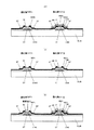
図1(A)は、本発明による半導体装置の実施例1を示した構成図である。半導体装置としていわゆるボトムゲート型酸化物TFTを揚げている。図1(A)に示すように、基板SUB上にゲート電極GTが形成されている。そして、該基板SUBの上面に前記ゲート電極GTをも被ってゲート絶縁膜GIが形成されている。また、前記ゲート絶縁膜GI上に少なくとも前記ゲート電極GTを跨るようにして金属酸化物膜MOXが形成されている。さらに、前記金属酸化物膜MOXに直接に接触させてソース電極ST及びドレイン電極DTが形成されている。前記ソース電極STとドレイン電極DTは、少なくともゲート電極GTの直上で分離され、この分離部を間にして対向するように形成されている。ここで、前記金属酸化物膜MOXは、前記ソース電極STとドレイン電極DTの間の領域においてチャネル領域CHNを構成し、このチャネル領域CHNには半導体性を示し、かつ表面から深さが増すにつれて酸素濃度が低くなるように構成されている。
<Example 1>
(Configuration and manufacturing method)
FIG. 1A is a configuration diagram showing a first embodiment of a semiconductor device according to the present invention. A so-called bottom gate type oxide TFT is used as a semiconductor device. As shown in FIG. 1A, the gate electrode GT is formed over the substrate SUB. A gate insulating film GI is formed on the upper surface of the substrate SUB so as to cover the gate electrode GT. A metal oxide film MOX is formed on the gate insulating film GI so as to straddle at least the gate electrode GT. Further, a source electrode ST and a drain electrode DT are formed in direct contact with the metal oxide film MOX. The source electrode ST and the drain electrode DT are separated at least immediately above the gate electrode GT, and are formed so as to face each other with the separation portion therebetween. Here, the metal oxide film MOX forms a channel region CHN in a region between the source electrode ST and the drain electrode DT, and the channel region CHN exhibits semiconductivity and increases in depth from the surface. The oxygen concentration is configured to be low.
図1(a)、(b)は、図1(A)に示した半導体装置の製造方法の実施例1を示した説明図である。まず、一般的な製造プロセスを用いて図1(a)に示す構造を作製する。すなわち、基板SUB上にゲート電極GTを形成する。そして、該基板SUBの上面に前記ゲート電極GTをも被ってゲート絶縁膜GIを形成する。その後、前記ゲート絶縁膜GI上に少なくとも前記ゲート電極GTを跨るようにして金属酸化物膜MOXを形成する。さらに、前記金属酸化物膜MOXに直接に接触させてソース電極ST及びドレイン電極DTを形成する。前記ソース電極STとドレイン電極DTは、少なくともゲート電極GTの直上で分離され、この分離部を間にして対向するように形成されている。これにより、金属酸化物膜MOXは、前記ソース電極STとドレイン電極DTの分離部において、外部に露出された状態になっている。 FIGS. 1A and 1B are explanatory views showing Example 1 of the method for manufacturing the semiconductor device shown in FIG. First, the structure shown in FIG. 1A is manufactured using a general manufacturing process. That is, the gate electrode GT is formed on the substrate SUB. Then, a gate insulating film GI is formed on the upper surface of the substrate SUB so as to cover the gate electrode GT. Thereafter, a metal oxide film MOX is formed on the gate insulating film GI so as to straddle at least the gate electrode GT. Further, the source electrode ST and the drain electrode DT are formed in direct contact with the metal oxide film MOX. The source electrode ST and the drain electrode DT are separated at least immediately above the gate electrode GT, and are formed so as to face each other with the separation portion therebetween. As a result, the metal oxide film MOX is exposed to the outside at the separation part of the source electrode ST and the drain electrode DT.
次に、図1(b)に示すように、ソース電極ST、ドレイン電極DTの前記分離部を通して金属酸化物膜MOXの一部に酸素を導入する。この場合、前記ソース電極STおよびドレイン電極DTはマスクとなり、該ソース電極STとドレイン電極DTの間の前記金属酸化物膜MOXにはチャネル領域CHNが形成されるようになる。酸素を導入する方法としては、たとえば、酸素プラズマ照射、酸素雰囲気アニール、ラジカル酸化などが挙げられるが、その他の方法を用いてもよい。酸素を導入することで、金属酸化物膜MOX内の外部に露出された領域は、より酸素濃度の高い状態に変わる。金属酸化物膜中では、酸素欠損がn型ドナーとして作用し、膜中にキャリア電子を生成するようになり導電性は低くなる。こうして形成された酸素濃度の高い領域が半導体性を示し、酸化物TFTのチャネル領域として機能できる。前記チャネル領域CHNを除く金属酸化物膜MOX内の領域は、前記ソース電極STと接続されるソース領域SR、前記ドレイン電極DTと接続されるドレイン領域DRとして形成される。 Next, as shown in FIG. 1B, oxygen is introduced into a part of the metal oxide film MOX through the separation part of the source electrode ST and the drain electrode DT. In this case, the source electrode ST and the drain electrode DT serve as a mask, and a channel region CHN is formed in the metal oxide film MOX between the source electrode ST and the drain electrode DT. Examples of the method for introducing oxygen include oxygen plasma irradiation, oxygen atmosphere annealing, radical oxidation, and the like, but other methods may be used. By introducing oxygen, the region exposed to the outside in the metal oxide film MOX changes to a state with a higher oxygen concentration. In the metal oxide film, oxygen vacancies act as n-type donors, and carrier electrons are generated in the film, resulting in low conductivity. The region having a high oxygen concentration formed in this manner exhibits semiconductor properties and can function as a channel region of the oxide TFT. The regions in the metal oxide film MOX excluding the channel region CHN are formed as a source region SR connected to the source electrode ST and a drain region DR connected to the drain electrode DT.
なお、上述のように金属酸化物膜MOX内にチャネル領域CHNを形成する場合、該金属酸化物膜MOXの外側(上側)から酸素を導入するようにしていることから、前記チャネル領域CHNの拡大図である図1(c)に示すように、外部に露出されている側で相対的に酸素濃度が高く、ゲート絶縁膜GI側にいくにつれて酸素濃度が低くなる。なお、図1(c)では、金属酸化物膜MOXの深さ方向に沿って酸素濃度の変化していく過程を便宜上段差的に描画しているが、実際には滑らかな勾配を有して変化している。TFT動作の際にはゲート絶縁膜GIとチャネル領域CHNとの界面がチャネルの主要部分になり、主にここで電流が流れる。このため、本実施例のTFTでは界面の酸素濃度を最適化できるようになる。この場合、界面より上方では必然的に酸素濃度がより高くなる。金属酸化物膜MOXの膜厚や成膜条件などにもよるが、酸素濃度が最も高い領域(チャネル領域CHNの上層)では、界面に比べて2倍以上酸素濃度が高いことが望ましい。また、ソース領域SR及びドレイン領域DRに比べても2倍以上酸素濃度が高いことが望ましい。さらには、界面での酸素濃度はソース領域SR及びドレイン領域DRでの酸素濃度の10倍以上、したがって、チャネル領域CHNの上層での酸素濃度はソース領域SR及びドレイン領域DRでの酸素濃度の20倍以上であるようにすることがより望ましい。 Note that when the channel region CHN is formed in the metal oxide film MOX as described above, oxygen is introduced from the outside (upper side) of the metal oxide film MOX. As shown in FIG. 1C, the oxygen concentration is relatively high on the side exposed to the outside, and the oxygen concentration decreases toward the gate insulating film GI side. In FIG. 1C, the process of changing the oxygen concentration along the depth direction of the metal oxide film MOX is depicted stepwise for convenience, but actually has a smooth gradient. It has changed. During the TFT operation, the interface between the gate insulating film GI and the channel region CHN becomes the main part of the channel, and a current mainly flows here. For this reason, in the TFT of this embodiment, the oxygen concentration at the interface can be optimized. In this case, the oxygen concentration inevitably becomes higher above the interface. Although depending on the thickness of the metal oxide film MOX and the film formation conditions, it is desirable that the oxygen concentration in the region with the highest oxygen concentration (the upper layer of the channel region CHN) be at least twice as high as the interface. Further, it is desirable that the oxygen concentration is twice or more higher than that of the source region SR and the drain region DR. Furthermore, the oxygen concentration at the interface is 10 times or more of the oxygen concentration in the source region SR and the drain region DR. Therefore, the oxygen concentration in the upper layer of the channel region CHN is 20 times the oxygen concentration in the source region SR and the drain region DR. It is more desirable to make it more than twice.
本実施例における基板SUBは、たとえば、ガラス、石英、プラスチックフィルムなどの絶縁体からなり、必要に応じてゲート電極GTが形成される側の表面に絶縁体膜のコーティングがなされている。ゲート電極GT、ソース電極ST、ドレイン電極DTは、たとえば、モリブデン、クロム、タングステン、アルミ、銅、チタン、ニッケル、タンタル、銀、亜鉛、あるいはその他の金属の単膜、それらの合金膜、それらの積層膜、あるいはITOなどの金属酸化物導電膜、あるいは前述の金属と金属酸化物導電膜の積層膜によって形成されている。ゲート電極GT、ソース電極ST、ドレイン電極DTは、同一の材料から形成されても良いし、異なる材料から形成されても良い。絶縁膜GIは、たとえば、SiO2、SiN、Al2O3、あるいはその他の絶縁膜によって形成されている。金属酸化物膜MOXは、たとえば、ZnO、InGaZnO、ZnInO、ZnSnO、あるいは導電性を示すその他の金属酸化物によって形成されている。 The substrate SUB in this embodiment is made of an insulator such as glass, quartz, or a plastic film, and an insulator film is coated on the surface on which the gate electrode GT is formed as necessary. The gate electrode GT, the source electrode ST, and the drain electrode DT are, for example, molybdenum, chromium, tungsten, aluminum, copper, titanium, nickel, tantalum, silver, zinc, or other metal single films, their alloy films, their It is formed of a laminated film, a metal oxide conductive film such as ITO, or a laminated film of the aforementioned metal and metal oxide conductive film. The gate electrode GT, the source electrode ST, and the drain electrode DT may be formed from the same material or different materials. The insulating film GI is made of, for example, SiO2, SiN, Al2O3, or other insulating films. The metal oxide film MOX is made of, for example, ZnO, InGaZnO, ZnInO, ZnSnO, or other metal oxide exhibiting conductivity.
本実施例のTFTは、たとえば図2に示すように、アクティブマトリクス型液晶表示装置のスイッチングトランジスタとして用いられる。図中x方向に延在するゲート線GLに走査信号が供給されるとTFTがオンし、このオンされたTFTを通して、図中y方向に延在するデータ線DLからの映像信号が画素電極PTに供給される。なお、ゲート線GLは図中y方向に並設され、データ線DLは図中x方向に並設され、隣接する一対のゲート線GLと隣接する一対のドレイン線DLで囲まれる領域(画素領域)に前記画素電極PTが配置されている。この場合、たとえばデータ線DLがソース電極STと電気的に接続され、画素電極PTがドレイン電極DTと電気的に接続される。あるいは、データ線DLがソース電極STを兼ね、画素電極PTがドレイン電極DTを兼ねても良い。また、液晶表示装置に限らずOLED表示装置などの画素回路を構成するトランジスタとして用いても良い。 The TFT of this embodiment is used as a switching transistor of an active matrix liquid crystal display device, for example, as shown in FIG. When a scanning signal is supplied to the gate line GL extending in the x direction in the drawing, the TFT is turned on, and the video signal from the data line DL extending in the y direction in the drawing is passed through the turned on TFT to the pixel electrode PT. To be supplied. Note that the gate lines GL are juxtaposed in the y direction in the drawing, the data lines DL are juxtaposed in the x direction in the drawing, and a region (pixel region) surrounded by a pair of adjacent drain lines DL and a pair of adjacent gate lines GL. ) Is arranged with the pixel electrode PT. In this case, for example, the data line DL is electrically connected to the source electrode ST, and the pixel electrode PT is electrically connected to the drain electrode DT. Alternatively, the data line DL may also serve as the source electrode ST, and the pixel electrode PT may also serve as the drain electrode DT. Further, not only the liquid crystal display device but also a transistor constituting a pixel circuit such as an OLED display device may be used.
また、図3に示すように、基板SUB1上に形成される表示装置や記憶装置などにおいて、その素子がアレイ状に複数配置されている場合、各素子のスイッチングや駆動用のトランジスタに前記酸化物TFTを用いるのはもちろん、該酸化物TFTのゲート電極GTにつながるゲート線GLに信号を送るゲート線駆動回路GDCや、該酸化物TFTのソース電極STにつながるデータ線DLに信号を送るデータ線駆動回路DDCを構成するトランジスタに用いても良い。この場合、各素子の酸化物TFTと前記ゲート線駆動回路GDCあるいは前記データ線駆動回路DDC内の酸化物TFTを並行して形成することができる。 In addition, as shown in FIG. 3, in a display device or a storage device formed on the substrate SUB1, when the elements are arranged in an array, the oxide is used as a transistor for switching or driving each element. Of course, the TFT uses a gate line driving circuit GDC that sends a signal to the gate line GL connected to the gate electrode GT of the oxide TFT, and a data line that sends a signal to the data line DL connected to the source electrode ST of the oxide TFT. You may use for the transistor which comprises the drive circuit DDC. In this case, the oxide TFT of each element and the oxide TFT in the gate line driving circuit GDC or the data line driving circuit DDC can be formed in parallel.
また、上述した酸化膜TFTを、たとえば図4に示す構成、すなわち、アンテナ共振回路AR、整流器RCT、変調器MOD、デジタル回路DGC、からなる無線タグを構成する各トランジスタに用いても良い。なお、無線タグはリーダRDまたはライタWRと無線で通信を行うことができるようになっている。 酸化物TFTが低温で形成できることを活かして表示装置や記憶装置、無線タグなどをプラスチックフィルムなどのいわゆるフレキシブル基板上に形成した構成においても適用できる。 Further, the above-described oxide film TFT may be used for each transistor constituting the wireless tag including the configuration shown in FIG. 4, for example, the antenna resonance circuit AR, the rectifier RCT, the modulator MOD, and the digital circuit DGC. Note that the wireless tag can wirelessly communicate with the reader RD or the writer WR. Taking advantage of the fact that oxide TFTs can be formed at low temperatures, the present invention can also be applied to a structure in which a display device, a memory device, a wireless tag, or the like is formed on a so-called flexible substrate such as a plastic film.
(効果)
本実施例において、たとえば、金属酸化物膜MOXをあらかじめ導電性の高い膜として成膜しておけば、ソース領域SR及びドレイン領域DRでの寄生抵抗、並びにソース領域SRとソース電極ST、ドレイン領域DRとドレイン電極DTとの間のコンタクト抵抗を低くすることができる。これにより、良好な電気接続が得られ、酸化物FETの特性を向上することができる。
(effect)
In this embodiment, for example, if the metal oxide film MOX is formed in advance as a highly conductive film, the parasitic resistance in the source region SR and the drain region DR, the source region SR, the source electrode ST, and the drain region are formed. The contact resistance between DR and the drain electrode DT can be lowered. Thereby, a favorable electrical connection can be obtained and the characteristics of the oxide FET can be improved.
また、ソース電極ST及びドレイン電極DTに対して、ソース領域SR、チャネル領域CHN、ドレイン領域DRが自己整合的に形成されるため、コンタクト抵抗と寄生抵抗のばらつきを低減し、ひいてはTFTのばらつきを低減することができる。 In addition, since the source region SR, the channel region CHN, and the drain region DR are formed in a self-aligned manner with respect to the source electrode ST and the drain electrode DT, variation in contact resistance and parasitic resistance is reduced, and thus variation in TFT is reduced. Can be reduced.
また、ソース領域SR及びドレイン領域DR、並びにソース電極ST及びドレイン電極DTを形成した後に、チャネル領域CHNの形成、及びVth調整を行なうことができる。このため、TFT量産時の歩留り低下を抑制したり、プロセス修正を容易化したりすることができる。 Further, after forming the source region SR and the drain region DR, and the source electrode ST and the drain electrode DT, the channel region CHN can be formed and the Vth adjustment can be performed. For this reason, it is possible to suppress a decrease in yield during mass production of TFTs and facilitate process correction.
さらに、ゲート絶縁膜GIとチャネル領域CHNとの界面で酸素濃度が最適化され、それより上方では酸素濃度はより高くなっているため、いわゆるバックチャネルの形成を抑制し、オフリーク電流を低減することができる。したがって、半導体装置の消費電流を低減することができる。 Furthermore, since the oxygen concentration is optimized at the interface between the gate insulating film GI and the channel region CHN and the oxygen concentration is higher above that, so-called back channel formation is suppressed and off-leakage current is reduced. Can do. Therefore, current consumption of the semiconductor device can be reduced.
〈実施例2〉
(構成及び製造方法)
図5(A)は、本発明による半導体装置の実施例2を示す断面図である。図5(A)は、同一基板上にVthの異なる2種のボトムゲート型酸化物TFTを形成することを示した図となっている。
<Example 2>
(Configuration and manufacturing method)
FIG. 5A is a sectional view showing a second embodiment of the semiconductor device according to the present invention. FIG. 5A shows that two types of bottom-gate oxide TFTs having different Vths are formed on the same substrate.
すなわち、基板SUB1の上面に酸化物TFT1および酸化物TFT2が形成されている。これら酸化物TFT1および酸化物TFT2は、それらを構成する材料層の積層構造がほぼ同じとなっており、前記酸化物TFT1においてそのVthが高く形成され、前記酸化物TFT2においてそのVthが低く形成されている。すなわち、前記酸化物TFT1は、そのチャネル領域CHNにおいて、ソース領域SR、ドレイン領域DRに比べて酸素濃度が高く導入され、前記酸化物TFT2は、そのチャネル領域CHNにおいて、ソース領域SR、ドレイン領域DRに比べて酸素濃度差がなく構成されている。 That is, the oxide TFT1 and the oxide TFT2 are formed on the upper surface of the substrate SUB1. The oxide TFT 1 and the oxide TFT 2 have substantially the same laminated structure of the material layers constituting them, and the oxide TFT 1 is formed with a high Vth and the oxide TFT 2 is formed with a low Vth. ing. That is, the oxide TFT 1 is introduced with a higher oxygen concentration in the channel region CHN than the source region SR and drain region DR, and the oxide TFT 2 is introduced in the source region SR and drain region DR in the channel region CHN. Compared to this, there is no difference in oxygen concentration.
図5(a)、(b)は、図5(A)に示した半導体装置の製造方法の実施例1を示した説明図である。まず、一般的な製造プロセスを用いて、前記酸化物TFT1および酸化物TFT2を図5(a)に示した構造に形成する。この段階では、まだ、前記酸化物TFT1および酸化物TFT2の各チャネル領域に酸素が導入されていないものとなっている。次に、図5(b)に示すように、酸化物TFT2の金属酸化物膜MOXの少なくともチャネル形成領域上に保護膜PROを被って形成する。そして、酸化物TFT1において、その金属酸化物MOXに酸素を導入する。これにより、酸化物TFT1は、そのチャネル領域CHNにおいてソース領域SRおよびドレイン領域DRに比べて酸素濃度が高く、Vthが高い特性として得られ、酸化物TFT2は、ソース領域、チャネル領域、およびドレイン領域間で酸素濃度の差がほとんどなく、Vthが低い特性として得られるようになる。 5A and 5B are explanatory views showing Example 1 of the method for manufacturing the semiconductor device shown in FIG. First, the oxide TFT 1 and the oxide TFT 2 are formed in the structure shown in FIG. 5A using a general manufacturing process. At this stage, oxygen is not yet introduced into each channel region of the oxide TFT 1 and the oxide TFT 2. Next, as shown in FIG. 5B, a protective film PRO is formed on at least the channel formation region of the metal oxide film MOX of the oxide TFT2. In the oxide TFT 1, oxygen is introduced into the metal oxide MOX. As a result, the oxide TFT 1 is obtained in the channel region CHN as having characteristics of higher oxygen concentration and higher Vth than the source region SR and the drain region DR, and the oxide TFT 2 includes the source region, the channel region, and the drain region. There is almost no difference in oxygen concentration between them, and a characteristic with low Vth can be obtained.
なお、図5(A)においては、基板SUB1において、酸化物TFT1と酸化物TFT2からなる2個の酸化物TFTを示したものである。しかし、前記酸化物TFT1と同一のVthを有するようにする複数の酸化物TFT群、前記酸化物TFT2と同一のVthを有するようにする複数の酸化物TFT群を備え、これら群ごとに上述した工程を得る製造を行うようにしてもよい。このような製造は実施例3以降の実施例においても同様に適用できる。 Note that FIG. 5A shows two oxide TFTs including an oxide TFT 1 and an oxide TFT 2 in the substrate SUB1. However, a plurality of oxide TFT groups that have the same Vth as that of the oxide TFT 1 and a plurality of oxide TFT groups that have the same Vth as that of the oxide TFT 2 are provided. You may make it perform manufacture which obtains a process. Such manufacturing can be similarly applied to the third and subsequent embodiments.
(効果)
実施例2においては、同一基板上にVthの異なる酸化物TFTを作り分けることができ、回路設計の自由度を高めることができる。また、Vthの高い酸化物TFT1では実施例1に示した効果も得られる。
(effect)
In the second embodiment, oxide TFTs having different Vth can be formed on the same substrate, and the degree of freedom in circuit design can be increased. In addition, the oxide TFT 1 having a high Vth can achieve the effects shown in the first embodiment.
〈実施例3〉
(構成及び製造方法)
図6(A)は、本発明による半導体装置の実施例3を示す断面図で、図5(A)と対応した図となっている。図6(A)は、図5(A)の場合と同様、同一基板上にVthの異なる2種のボトムゲート型酸化物TFTを形成していることを示した図である。図5(A)の場合と比較して異なる構成は、酸化物TFT2においても、そのチャネル領域CHNに酸素が導入され、その濃度は、酸化物TFT1のチャネル領域CHNの酸素濃度よりも低く構成されていることにある。
<Example 3>
(Configuration and manufacturing method)
FIG. 6A is a sectional view showing a third embodiment of the semiconductor device according to the present invention and corresponds to FIG. FIG. 6A shows that two types of bottom-gate oxide TFTs having different Vths are formed on the same substrate as in the case of FIG. 5A. 5A is different from the case of FIG. 5A in that oxygen is introduced into the channel region CHN of the oxide TFT 2 and the concentration thereof is lower than the oxygen concentration of the channel region CHN of the oxide TFT 1. There is in being.
図6(a)、(b)は、図6(A)に示した半導体装置の製造方法の実施例を示した説明図である。まず、一般的な製造プロセスおよび本明細書に開示の製造プロセスを用いて、前記酸化物TFT1および酸化物TFT2を図6(a)に示した構造に形成する。この段階では、前記酸化物TFT1および酸化物TFT2の各チャネル領域に同量の酸素が導入されているものとする。次に、図6(b)に示すように、酸化物TFT2の金属酸化物膜MOXの少なくともチャネル形成領域上に保護膜PROを被って形成する。そして、酸化物TFT1において、その金属酸化物MOXに酸素を導入する。これにより、酸化物TFT1のチャネル領域は、ソース領域SR、ドレイン領域DRに比べて酸素濃度を高くでき、酸化物TFT2のチャネル領域も、ソース領域SR、ドレイン領域DRに比べて酸素濃度を高くできる。そして、酸化物TFT1のチャネル領域CHNは、酸化物TFT2のチャネル領域CHNに比べて酸素濃度を高くできる。 6A and 6B are explanatory views showing an embodiment of a method for manufacturing the semiconductor device shown in FIG. First, by using a general manufacturing process and manufacturing process disclosed herein, the oxide TFT1 and oxides TFT2 you formed to the structure shown in Figure 6 (a). At this stage, it is assumed that the same amount of oxygen is introduced into each channel region of the oxide TFT 1 and the oxide TFT 2. Next, as shown in FIG. 6B, a protective film PRO is formed to cover at least the channel formation region of the metal oxide film MOX of the oxide TFT2. In the oxide TFT 1, oxygen is introduced into the metal oxide MOX. Thereby, the channel region of the oxide TFT 1 can have a higher oxygen concentration than the source region SR and the drain region DR, and the channel region of the oxide TFT 2 can also have a higher oxygen concentration than the source region SR and the drain region DR. . The channel region CHN of the oxide TFT 1 can have a higher oxygen concentration than the channel region CHN of the oxide TFT 2.
(効果)
本実施例においては、同一基板上にVthの異なる酸化物TFTを作り分けることができ、回路設計の自由度を高めることができる。また、実施例2に比べ、酸化物TFT1、酸化物TFT2のいずれにおいても、実施例1に示した効果が得られるという利点がある。
(effect)
In this embodiment, oxide TFTs having different Vth can be formed on the same substrate, and the degree of freedom in circuit design can be increased. Further, as compared with the second embodiment, both the oxide TFT 1 and the oxide TFT 2 have an advantage that the effects shown in the first embodiment can be obtained.
〈実施例4〉
(構成及び製造方法)
図7(A)は、本発明による半導体装置の実施例4を示す断面図である。図7(A)は、トップゲート型酸化物TFTを示している。図7(A)において、基板SUBがあり、その上面に金属酸化物膜MOXが形成されている。該金属酸化物膜MOXはたとえば導電性の高い膜として成膜され、そのチャネル領域CHNには酸素が導入されている。該チャネル領域CHNの両脇に形成されるソース領域およびドレイン領域には、それぞれ、ソース電極STおよびドレイン電極DTが重畳されて形成されている。そして、前記チャネル領域CHN、ソース電極ST、およびドレイン電極DTをも被ってゲート絶縁膜GIが形成され、このゲート絶縁膜GIの上面には少なくとも前記チャネル領域CHNに重畳するようにしてゲート電極GTが形成されている。
<Example 4>
(Configuration and manufacturing method)
FIG. 7A is a sectional view showing a fourth embodiment of the semiconductor device according to the present invention. FIG. 7A shows a top gate type oxide TFT. In FIG. 7A, there is a substrate SUB, and a metal oxide film MOX is formed on the upper surface thereof. The metal oxide film MOX is formed as a highly conductive film, for example, and oxygen is introduced into the channel region CHN. In the source region and the drain region formed on both sides of the channel region CHN, the source electrode ST and the drain electrode DT are formed so as to overlap each other. A gate insulating film GI is formed so as to cover the channel region CHN, the source electrode ST, and the drain electrode DT, and the gate electrode GT is overlaid on at least the channel region CHN on the upper surface of the gate insulating film GI. Is formed.
このように構成された半導体装置はたとえば次のようにして製造される。図7(a)に示すように、基板SUBの上面に金属酸化物膜MOXを形成する。次に、図7(b)に示すように、前記金属酸化物膜MOXの上面に金属膜を形成し、この金属膜をパターン化することによって、ソース電極ST、ドレイン電極DTを形成する。そして、前記ソース電極STと前記ドレイン電極DTをマスクとし、前記ソース電極STと前記ドレイン電極DTの間のチャネル領域CHNに酸素を導入する。次に、図7(c)に示すように、前記チャネル領域CHN、ソース電極ST、およびドレイン電極DTをも被ってゲート絶縁膜GIを形成し、前記ゲート絶縁膜GIの上面に前記チャネル領域CHNに重畳するようにしてゲート電極GTを形成する。 The semiconductor device configured as described above is manufactured, for example, as follows. As shown in FIG. 7A, a metal oxide film MOX is formed on the upper surface of the substrate SUB. Next, as shown in FIG. 7B, a metal film is formed on the upper surface of the metal oxide film MOX, and the metal film is patterned to form the source electrode ST and the drain electrode DT. Then, oxygen is introduced into the channel region CHN between the source electrode ST and the drain electrode DT using the source electrode ST and the drain electrode DT as a mask. Next, as shown in FIG. 7C, a gate insulating film GI is formed covering the channel region CHN, the source electrode ST, and the drain electrode DT, and the channel region CHN is formed on the upper surface of the gate insulating film GI. A gate electrode GT is formed so as to overlap with.
(効果)
実施例4においては、たとえば、金属酸化物膜MOXをあらかじめ導電性の高い膜として成膜しておけば、ソース領域SR及びドレイン領域DRでの寄生抵抗、並びにソース領域SRとソース電極ST、ドレイン領域DRとドレイン電極DTとの間のコンタクト抵抗を低くすることができる。したがって、良好な電気接続が得られ、酸化物FETの特性を向上させることができる。また、ソース電極ST及びドレイン電極DTに対して、ソース領域SR、チャネル領域CHN、ドレイン領域DRを自己整合的に形成できるため、コンタクト抵抗と寄生抵抗のばらつきを低減し、ひいてはTFTのばらつきを低減することができる。さらに、ソース領域SR及びドレイン領域DR、並びにソース電極ST及びドレイン電極DTを形成した後に、チャネル領域CHNの形成、及びVth調整を行なうことができる。これにより、TFT量産時の歩留り低下を抑制でき、プロセス修正を容易にできる。
(effect)
In the fourth embodiment, for example, if the metal oxide film MOX is formed in advance as a highly conductive film, the parasitic resistance in the source region SR and the drain region DR, the source region SR, the source electrode ST, and the drain are formed. The contact resistance between the region DR and the drain electrode DT can be reduced. Therefore, good electrical connection can be obtained and the characteristics of the oxide FET can be improved. In addition, since the source region SR, the channel region CHN, and the drain region DR can be formed in a self-aligned manner with respect to the source electrode ST and the drain electrode DT, variation in contact resistance and parasitic resistance is reduced, and thus variation in TFT is reduced. can do. Furthermore, after forming the source region SR and the drain region DR, and the source electrode ST and the drain electrode DT, the channel region CHN and the Vth adjustment can be performed. As a result, the yield reduction during mass production of TFTs can be suppressed, and the process can be easily corrected.
〈実施例5〉
(構成及び製造方法)
図8(A)は、本発明による半導体装置の実施例5を示す断面図である。図8(A)は、トップゲート型酸化物TFTを示している。図8(A)において、基板SUBがあり、その上面にソース電極STおよびドレイン電極DTが形成されている。そして、前記ソース電極STおよびドレイン電極DTを被い前記ソース電極STおよびドレイン電極DTの間の領域に金属酸化物膜MOXが形成されている。該金属酸化物膜MOXはたとえば導電性の高い膜として成膜され、前記ソース電極STおよびドレイン電極DTの間の領域の一部にチャネル領域CHNが形成されている。該チャネル領域CHNには酸素が導入されている。そして、前記チャネル領域CHN、ソース電極ST、およびドレイン電極DTをも被ってゲート絶縁膜GIが形成され、このゲート絶縁膜GIの上面には少なくとも前記チャネル領域CHNに重畳するようにしてゲート電極GTが形成されている。
<Example 5>
(Configuration and manufacturing method)
FIG. 8A is a cross-sectional view showing a fifth embodiment of the semiconductor device according to the present invention. FIG. 8A shows a top gate type oxide TFT. In FIG. 8A, there is a substrate SUB, and a source electrode ST and a drain electrode DT are formed on the upper surface thereof. A metal oxide film MOX is formed in a region covering the source electrode ST and the drain electrode DT and between the source electrode ST and the drain electrode DT. The metal oxide film MOX is formed, for example, as a highly conductive film, and a channel region CHN is formed in a part of the region between the source electrode ST and the drain electrode DT. Oxygen is introduced into the channel region CHN. A gate insulating film GI is formed so as to cover the channel region CHN, the source electrode ST, and the drain electrode DT, and the gate electrode GT is overlaid on at least the channel region CHN on the upper surface of the gate insulating film GI. Is formed.
このように構成された半導体装置はたとえば次のようにして製造される。図8(a)に示すように、基板SUBの上面にソース電極ST、ドレイン電極DTを形成する。次に、図8(b)に示すように、ソース電極ST、ドレイン電極DTを被い、該ソース電極STおよびドレイン電極DTの間の領域に金属酸化物膜MOXを成膜する。次に、図7(c)に示すように、フォトレジスト膜REGを形成する。このフォトレジスト膜REGは、前記金属酸化物膜MOXのチャネル領域CHNに相当する領域を露出させる開口を有する。そして、前記開口を通して前記金属酸化物膜MOXに酸素を導入し、チャネル領域CHNを形成する。その後、図8(d)に示すように、前記フォトレジスト膜REGを除去し、ゲート絶縁膜GI及びゲート電極GTを順次形成して完了する。なお、図8(d)では、前記フォトレジスト膜REGを除去した場合を示しているが、前記フォトレジスト膜REGは、必ずしも除去する必要はなく、残したままにしてもよい。絶縁膜として機能させることができるからである。 The semiconductor device configured as described above is manufactured, for example, as follows. As shown in FIG. 8A, the source electrode ST and the drain electrode DT are formed on the upper surface of the substrate SUB. Next, as shown in FIG. 8B, the source electrode ST and the drain electrode DT are covered, and a metal oxide film MOX is formed in a region between the source electrode ST and the drain electrode DT. Next, as shown in FIG. 7C, a photoresist film REG is formed. The photoresist film REG has an opening exposing a region corresponding to the channel region CHN of the metal oxide film MOX. Then, oxygen is introduced into the metal oxide film MOX through the opening to form a channel region CHN. Thereafter, as shown in FIG. 8D, the photoresist film REG is removed, and a gate insulating film GI and a gate electrode GT are sequentially formed and completed. FIG. 8D shows the case where the photoresist film REG is removed. However, the photoresist film REG is not necessarily removed and may be left. This is because it can function as an insulating film.
(効果)
実施例5においては、たとえば、金属酸化物膜MOXをあらかじめ導電性の高い膜として成膜しておけば、ソース領域SR及びドレイン領域DRでの寄生抵抗、並びにソース領域SRとソース電極ST、ドレイン領域DRとドレイン電極DTとの間のコンタクト抵抗を低くすることができる。したがって、良好な電気接続が得られ、酸化物FETの特性を向上することができる。
(effect)
In the fifth embodiment, for example, if the metal oxide film MOX is formed in advance as a highly conductive film, the parasitic resistance in the source region SR and the drain region DR, the source region SR, the source electrode ST, and the drain are formed. The contact resistance between the region DR and the drain electrode DT can be reduced. Therefore, a good electrical connection can be obtained and the characteristics of the oxide FET can be improved.
また、ソース電極ST及びドレイン電極DTに対して、ソース領域SR、チャネル領域CHN、ドレイン領域DRが自己整合的に形成されるため、コンタクト抵抗と寄生抵抗のばらつきを低減し、ひいてはTFTのばらつきを低減することができる。 In addition, since the source region SR, the channel region CHN, and the drain region DR are formed in a self-aligned manner with respect to the source electrode ST and the drain electrode DT, variation in contact resistance and parasitic resistance is reduced, and thus variation in TFT is reduced. Can be reduced.
また、ソース領域SR及びドレイン領域DR、並びにソース電極ST及びドレイン電極DTを形成した後に、チャネル領域CHNの形成、及びVth調整を行なうことができる。したがって、TFT量産時の歩留り低下を抑制したり、プロセス修正を容易化したりすることができる。 Further, after forming the source region SR and the drain region DR, and the source electrode ST and the drain electrode DT, the channel region CHN can be formed and the Vth adjustment can be performed. Therefore, it is possible to suppress a decrease in yield during mass production of TFTs and facilitate process correction.
以上、実施例を用いて本発明を説明してきたが、これまでの各実施例で説明した構成はあくまで一例であり、本発明は、技術思想を逸脱しない範囲内で適宜変更が可能である。また、それぞれの実施例で説明した構成は、互いに矛盾しない限り、組み合わせて用いてもよい。 As described above, the present invention has been described with reference to the embodiments. However, the configuration described in each of the embodiments so far is only an example, and the present invention can be appropriately changed without departing from the technical idea. Further, the configurations described in the respective embodiments may be used in combination as long as they do not contradict each other.
上述した各実施例の半導体装置及びその製造方法は、透過型、反射型、半透過型の各液晶表示装置、並びにOLED表示装置などの各画素を駆動するトランジスタや周辺回路に適用できる。また、記憶素子アレイ、無線タグなどにも適用できる。 The semiconductor devices and manufacturing methods thereof according to the above-described embodiments can be applied to transistors and peripheral circuits that drive pixels such as transmissive, reflective, and transflective liquid crystal display devices, and OLED display devices. Further, it can be applied to a storage element array, a wireless tag, and the like.
SUB・・・・・・基板、MOX・・・・・・金属酸化物膜、CHN・・・・・・チャネル領域、SR・・・・・・ソース領域、DR・・・・・・ドレイン領域、ST・・・・・・ソース電極、DT・・・・・・ドレイン電極、GT・・・・・・ゲート電極、GI・・・・・・ゲート絶縁膜、TFT・・・・・・薄膜トランジスタ、DL・・・・・・データ線、GL・・・・・・ゲート線、DDC・・・・・・データ線駆動回路、GDC・・・・・・ゲート線駆動回路、RD・・・・・・リーダ、WR・・・・・・ライタ、AR・・・・・・アンテナ共振回路、RCT・・・・・・整流器、MOD・・・・・・変調器、DGC・・・・・・デジタル回路。 SUB ... substrate, MOX ... metal oxide film, CHN ... channel region, SR ... source region, DR ... drain region , ST ... Source electrode, DT ... Drain electrode, GT ... Gate electrode, GI ... Gate insulating film, TFT ... Thin film transistor , DL ... Data line, GL ... Gate line, DDC ... Data line drive circuit, GDC ... Gate line drive circuit, RD ... ··· Reader, WR ··· Writer, AR ··· Antenna resonance circuit, RCT ··· Rectifier, MOD ··· Modulator, DGC ··· Digital circuit.
Claims (6)
しきい値電圧の高い第1群の半導体装置としきい値電圧の低い第2群の半導体装置を備え、
前記第1群の半導体装置および前記第2群の半導体装置は、基板上に、ゲート電極、ゲート絶縁膜、前記金属酸化物膜が順次形成され、その上にソース電極及びドレイン電極が形成されたボトムゲート型薄膜トランジスタであって、
前記第1群の半導体装置および前記第2群の半導体装置における前記金属酸化物膜中に、前記ソース電極を重畳する領域とするソース領域と、前記ドレイン電極を重畳する領域とするドレイン電極と、前記ドレイン領域と前記ソース領域の間の領域とするチャンネル領域と、を有し、
少なくとも前記第1群の半導体装置において、前記チャンネル領域は、半導体性を示し、かつ表面から深さが増すにつれて酸素濃度が低くなっており、
少なくとも前記第1群の半導体装置において、前記ソース領域および前記ドレイン領域は、前記チャネル領域に比べて酸素濃度が低く導電性の高いものであり、前記表面からの深さ方向に対して酸素濃度が一定となっており、
前記第2群の半導体装置におけるチャンネル領域上には、さらに、保護膜が形成されている
ことを特徴とする半導体装置。 A plurality of semiconductor devices using a metal oxide film for a channel are formed over the same substrate,
A first group of semiconductor devices having a high threshold voltage and a second group of semiconductor devices having a low threshold voltage;
In the first group of semiconductor devices and the second group of semiconductor devices, a gate electrode, a gate insulating film, and the metal oxide film are sequentially formed on a substrate, and a source electrode and a drain electrode are formed thereon. A bottom gate type thin film transistor,
In the metal oxide film in the first group semiconductor device and the second group semiconductor device, a source region that overlaps the source electrode, and a drain electrode that overlaps the drain electrode, A channel region as a region between the drain region and the source region,
In the semiconductor device of at least the first group, the channel region, the oxygen concentration has become lower as shows a semiconductor property and depth increases from the surface,
In at least the first group of semiconductor devices, the source region and the drain region have a lower oxygen concentration and higher conductivity than the channel region, and the oxygen concentration is higher than the depth direction from the surface. Is constant ,
Wherein on the channel region in the semiconductor device of the second group, further, the semiconductor device according to claim Rukoto protective film has not been formed.
基板上に第1および第2のゲート電極を形成する工程と、
前記第1および前記第2のゲート電極と前記基板の表面とを覆うようにゲート絶縁膜を形成する工程と、
前記ゲート絶縁膜上に前記第1および前記第2のゲート電極を跨るように第1および第2の金属酸化物膜を形成する工程と、
前記第1の金属酸化物膜上に第1のソース電極と第1のドレイン電極を形成し、前記第2の金属酸化膜上に第2のソース電極と第2のドレイン電極を形成する工程と、
前記第2のソース電極と前記第2のドレイン電極の間の前記第2の金属酸化物膜上に保護膜を形成する工程と、
前記第1のソース電極及び前記第1のドレイン電極をマスクにして、前記第1のソース電極と前記第1のドレイン電極の間の前記第1の金属酸化物膜に酸素を導入する工程と、
を有することを特徴とする半導体装置の製造方法。 2. The method of manufacturing a semiconductor device according to claim 1, wherein the first group of semiconductor devices having a high threshold voltage and the second group of semiconductor devices having a low threshold voltage are formed on the same substrate.
Forming first and second gate electrodes on a substrate;
Forming a gate insulating film so as to cover the first and the second gate electrode and the substrate surface,
Forming a first and second metal oxide film so as to straddle said first and said second gate electrode on the gate insulating film,
Forming a first forming the source electrode and the first drain electrode, a second source electrode and second drain electrode on the second metal oxide film on the first metal oxide film ,
Forming a protective film on the second metal oxide film between the second source electrode and the second drain electrode;
And the first source electrode and the first drain electrode as a mask, a step of introducing the oxygen into the first metal oxide film between the first source electrode and the first drain electrode,
A method for manufacturing a semiconductor device, comprising:
ことを特徴とする請求項4に記載の半導体装置の製造方法。 The method for manufacturing a semiconductor device according to claim 4 , wherein the oxygen introduction is performed using any one of oxygen plasma irradiation, oxygen atmosphere annealing, and radical oxidation.
前記第1および前記第2のソース電極と前記第1および前記第2のドレイン電極とをマスクにして、前記第1のソース電極と前記第1のドレイン電極の間の前記第1の金属酸化物膜および前記第2のソース電極と前記第2のドレイン電極の間の前記第2の金属酸化物膜のそれぞれに対して酸素を導入する工程と、The first metal oxide between the first source electrode and the first drain electrode using the first and second source electrodes and the first and second drain electrodes as a mask. Introducing oxygen into the film and each of the second metal oxide film between the second source electrode and the second drain electrode;
をさらに有することを特徴とする請求項4または5に記載の半導体装置の製造方法。The method of manufacturing a semiconductor device according to claim 4, further comprising:
Priority Applications (2)
| Application Number | Priority Date | Filing Date | Title |
|---|---|---|---|
| JP2008106586A JP5325446B2 (en) | 2008-04-16 | 2008-04-16 | Semiconductor device and manufacturing method thereof |
| US12/423,053 US7977675B2 (en) | 2008-04-16 | 2009-04-14 | Semiconductor device and method for manufacturing the same |
Applications Claiming Priority (1)
| Application Number | Priority Date | Filing Date | Title |
|---|---|---|---|
| JP2008106586A JP5325446B2 (en) | 2008-04-16 | 2008-04-16 | Semiconductor device and manufacturing method thereof |
Publications (3)
| Publication Number | Publication Date |
|---|---|
| JP2009260002A JP2009260002A (en) | 2009-11-05 |
| JP2009260002A5 JP2009260002A5 (en) | 2011-03-24 |
| JP5325446B2 true JP5325446B2 (en) | 2013-10-23 |
Family
ID=41200356
Family Applications (1)
| Application Number | Title | Priority Date | Filing Date |
|---|---|---|---|
| JP2008106586A Expired - Fee Related JP5325446B2 (en) | 2008-04-16 | 2008-04-16 | Semiconductor device and manufacturing method thereof |
Country Status (2)
| Country | Link |
|---|---|
| US (1) | US7977675B2 (en) |
| JP (1) | JP5325446B2 (en) |
Cited By (1)
| Publication number | Priority date | Publication date | Assignee | Title |
|---|---|---|---|---|
| US11349033B2 (en) | 2020-03-24 | 2022-05-31 | Kioxia Corporation | Semiconductor device and semiconductor memory device |
Families Citing this family (109)
| Publication number | Priority date | Publication date | Assignee | Title |
|---|---|---|---|---|
| JP4609797B2 (en) | 2006-08-09 | 2011-01-12 | Nec液晶テクノロジー株式会社 | Thin film device and manufacturing method thereof |
| CN103545342B (en) | 2008-09-19 | 2018-01-26 | 株式会社半导体能源研究所 | Semiconductor device |
| KR101622981B1 (en) | 2008-09-19 | 2016-05-20 | 가부시키가이샤 한도오따이 에네루기 켄큐쇼 | Display device and manufacturing method of the same |
| KR101889287B1 (en) | 2008-09-19 | 2018-08-20 | 가부시키가이샤 한도오따이 에네루기 켄큐쇼 | Semiconductor device |
| KR101634411B1 (en) * | 2008-10-31 | 2016-06-28 | 가부시키가이샤 한도오따이 에네루기 켄큐쇼 | Driver circuit, display device and electronic device |
| JP2010140919A (en) * | 2008-12-09 | 2010-06-24 | Hitachi Ltd | Oxide semiconductor device, manufacturing method thereof, and active matrix substrate |
| JP5104814B2 (en) * | 2009-05-18 | 2012-12-19 | 富士通株式会社 | Design support program, design support apparatus, and design support method |
| JP5564331B2 (en) * | 2009-05-29 | 2014-07-30 | 株式会社半導体エネルギー研究所 | Method for manufacturing semiconductor device |
| KR101610606B1 (en) | 2009-07-03 | 2016-04-07 | 가부시키가이샤 한도오따이 에네루기 켄큐쇼 | Method for manufacturing semiconductor device |
| KR20210131462A (en) | 2009-07-10 | 2021-11-02 | 가부시키가이샤 한도오따이 에네루기 켄큐쇼 | Method for manufacturing liquid crystal display device |
| TWI396314B (en) * | 2009-07-27 | 2013-05-11 | Au Optronics Corp | Pixel structure, organic electro-luminescence display unit, and faricating method thereof |
| KR102462145B1 (en) | 2009-10-16 | 2022-11-03 | 가부시키가이샤 한도오따이 에네루기 켄큐쇼 | Liquid crystal display device and electronic apparatus having the same |
| KR101962603B1 (en) | 2009-10-16 | 2019-03-28 | 가부시키가이샤 한도오따이 에네루기 켄큐쇼 | Liquid crystal display device and electronic device including the liquid crystal display device |
| KR102162746B1 (en) | 2009-10-21 | 2020-10-07 | 가부시키가이샤 한도오따이 에네루기 켄큐쇼 | Analog circuit and semiconductor device |
| KR101801959B1 (en) | 2009-10-21 | 2017-11-27 | 가부시키가이샤 한도오따이 에네루기 켄큐쇼 | Liquid crystal display device and electronic device including the same |
| KR101293261B1 (en) | 2009-10-21 | 2013-08-09 | 가부시키가이샤 한도오따이 에네루기 켄큐쇼 | Display device and electronic device including display device |
| JP5730529B2 (en) | 2009-10-21 | 2015-06-10 | 株式会社半導体エネルギー研究所 | Semiconductor device |
| KR101835155B1 (en) * | 2009-10-30 | 2018-03-06 | 가부시키가이샤 한도오따이 에네루기 켄큐쇼 | Liquid crystal display device, driving method of the same, and electronic appliance including the same |
| EP2494601A4 (en) * | 2009-10-30 | 2016-09-07 | Semiconductor Energy Lab | Semiconductor device and method for manufacturing the same |
| KR101818265B1 (en) | 2009-11-06 | 2018-01-12 | 가부시키가이샤 한도오따이 에네루기 켄큐쇼 | Semiconductor device |
| CN104465318B (en) | 2009-11-06 | 2018-04-24 | 株式会社半导体能源研究所 | The method for manufacturing semiconductor devices |
| KR101930230B1 (en) | 2009-11-06 | 2018-12-18 | 가부시키가이샤 한도오따이 에네루기 켄큐쇼 | Method for manufacturing semiconductor device |
| KR101652790B1 (en) * | 2009-11-09 | 2016-08-31 | 삼성전자주식회사 | Transistor, method of manufacturing the same and electronic device comprising transistor |
| KR101113370B1 (en) * | 2009-11-11 | 2012-02-29 | 삼성모바일디스플레이주식회사 | Thin Film Transistor and Organic Light Emitting Display device using thereof |
| KR20230107711A (en) * | 2009-11-13 | 2023-07-17 | 가부시키가이샤 한도오따이 에네루기 켄큐쇼 | Display device and electronic device including the same |
| KR101895561B1 (en) | 2009-11-13 | 2018-09-07 | 가부시키가이샤 한도오따이 에네루기 켄큐쇼 | Semiconductor device and manufacturing method thereof |
| KR101995704B1 (en) | 2009-11-20 | 2019-07-03 | 가부시키가이샤 한도오따이 에네루기 켄큐쇼 | Method for manufacturing semiconductor device |
| KR101911382B1 (en) * | 2009-11-27 | 2018-10-24 | 가부시키가이샤 한도오따이 에네루기 켄큐쇼 | Semiconductor device |
| EP2507787A4 (en) | 2009-11-30 | 2013-07-17 | Semiconductor Energy Lab | Liquid crystal display device, method for driving the same, and electronic device including the same |
| WO2011068037A1 (en) | 2009-12-04 | 2011-06-09 | Semiconductor Energy Laboratory Co., Ltd. | Semiconductor device and manufacturing method thereof |
| KR101470303B1 (en) * | 2009-12-08 | 2014-12-09 | 가부시키가이샤 한도오따이 에네루기 켄큐쇼 | Semiconductor device |
| EP2513894B1 (en) | 2009-12-18 | 2018-08-01 | Semiconductor Energy Laboratory Co., Ltd. | Method for driving liquid crystal display device |
| WO2011074379A1 (en) | 2009-12-18 | 2011-06-23 | Semiconductor Energy Laboratory Co., Ltd. | Liquid crystal display device and driving method thereof |
| KR20170142998A (en) * | 2009-12-25 | 2017-12-28 | 가부시키가이샤 한도오따이 에네루기 켄큐쇼 | Method for manufacturing semiconductor device |
| CN104716139B (en) | 2009-12-25 | 2018-03-30 | 株式会社半导体能源研究所 | Semiconductor device |
| WO2011077946A1 (en) | 2009-12-25 | 2011-06-30 | Semiconductor Energy Laboratory Co., Ltd. | Semiconductor device |
| KR101436120B1 (en) | 2009-12-28 | 2014-09-01 | 가부시키가이샤 한도오따이 에네루기 켄큐쇼 | Method for manufacturing semiconductor device |
| WO2011089843A1 (en) | 2010-01-20 | 2011-07-28 | Semiconductor Energy Laboratory Co., Ltd. | Method for driving display device |
| CN105761688B (en) | 2010-01-20 | 2019-01-01 | 株式会社半导体能源研究所 | The driving method of liquid crystal display |
| WO2011089853A1 (en) * | 2010-01-24 | 2011-07-28 | Semiconductor Energy Laboratory Co., Ltd. | Display device |
| KR101805378B1 (en) | 2010-01-24 | 2017-12-06 | 가부시키가이샤 한도오따이 에네루기 켄큐쇼 | Display device and manufacturing method thereof |
| CN102714001B (en) | 2010-01-29 | 2015-11-25 | 株式会社半导体能源研究所 | Semiconductor device and the electronic installation comprising semiconductor device |
| CN102725842B (en) * | 2010-02-05 | 2014-12-03 | 株式会社半导体能源研究所 | Semiconductor device |
| KR101733765B1 (en) | 2010-02-26 | 2017-05-08 | 가부시키가이샤 한도오따이 에네루기 켄큐쇼 | Display device and driving method thereof |
| KR101950364B1 (en) | 2010-02-26 | 2019-02-20 | 가부시키가이샤 한도오따이 에네루기 켄큐쇼 | Liquid crystal display device |
| WO2011108475A1 (en) * | 2010-03-04 | 2011-09-09 | Semiconductor Energy Laboratory Co., Ltd. | Semiconductor memory device and semiconductor device |
| DE112011100840T5 (en) * | 2010-03-08 | 2013-01-17 | Semiconductor Energy Laboratory Co., Ltd. | display device |
| WO2011118741A1 (en) | 2010-03-26 | 2011-09-29 | Semiconductor Energy Laboratory Co., Ltd. | Method for manufacturing semiconductor device |
| WO2011125432A1 (en) * | 2010-04-07 | 2011-10-13 | Semiconductor Energy Laboratory Co., Ltd. | Semiconductor memory device |
| WO2011129037A1 (en) * | 2010-04-16 | 2011-10-20 | シャープ株式会社 | Thin film transistor substrate, method for producing same, and display device |
| CN103367167B (en) * | 2010-04-23 | 2020-04-10 | 株式会社半导体能源研究所 | Method for manufacturing semiconductor device |
| CN106057907B (en) * | 2010-04-23 | 2019-10-22 | 株式会社半导体能源研究所 | The manufacturing method of semiconductor device |
| US9349325B2 (en) | 2010-04-28 | 2016-05-24 | Semiconductor Energy Laboratory Co., Ltd. | Liquid crystal display device and electronic device |
| US9697788B2 (en) | 2010-04-28 | 2017-07-04 | Semiconductor Energy Laboratory Co., Ltd. | Liquid crystal display device |
| KR101879570B1 (en) | 2010-04-28 | 2018-07-20 | 가부시키가이샤 한도오따이 에네루기 켄큐쇼 | Liquid crystal display device and manufacturing method the same |
| WO2011135987A1 (en) | 2010-04-28 | 2011-11-03 | Semiconductor Energy Laboratory Co., Ltd. | Method for manufacturing semiconductor device |
| KR101806271B1 (en) * | 2010-05-14 | 2017-12-07 | 가부시키가이샤 한도오따이 에네루기 켄큐쇼 | Method for manufacturing semiconductor device |
| CN105957802A (en) * | 2010-05-21 | 2016-09-21 | 株式会社半导体能源研究所 | Semiconductor device and manufacturing method thereof |
| WO2011158703A1 (en) | 2010-06-18 | 2011-12-22 | Semiconductor Energy Laboratory Co., Ltd. | Semiconductor device |
| US8605059B2 (en) | 2010-07-02 | 2013-12-10 | Semiconductor Energy Laboratory Co., Ltd. | Input/output device and driving method thereof |
| WO2012008080A1 (en) * | 2010-07-14 | 2012-01-19 | シャープ株式会社 | Thin-film transistor substrate |
| JP5848912B2 (en) | 2010-08-16 | 2016-01-27 | 株式会社半導体エネルギー研究所 | Control circuit for liquid crystal display device, liquid crystal display device, and electronic apparatus including the liquid crystal display device |
| KR102334169B1 (en) * | 2010-08-27 | 2021-12-01 | 가부시키가이샤 한도오따이 에네루기 켄큐쇼 | Memory device and semiconductor device |
| US8728860B2 (en) | 2010-09-03 | 2014-05-20 | Semiconductor Energy Laboratory Co., Ltd. | Method for manufacturing semiconductor device |
| JP2012256012A (en) * | 2010-09-15 | 2012-12-27 | Semiconductor Energy Lab Co Ltd | Display device |
| US8816425B2 (en) * | 2010-11-30 | 2014-08-26 | Semiconductor Energy Laboratory Co., Ltd. | Semiconductor device and method for manufacturing the same |
| TWI401797B (en) * | 2010-12-28 | 2013-07-11 | Ind Tech Res Inst | Methods of manufacturing active device array and manufacturing organic ligth emitting diode array |
| JP5685989B2 (en) * | 2011-02-28 | 2015-03-18 | ソニー株式会社 | Display device and electronic device |
| JP5766467B2 (en) * | 2011-03-02 | 2015-08-19 | 株式会社東芝 | THIN FILM TRANSISTOR, MANUFACTURING METHOD THEREOF, AND DISPLAY DEVICE |
| CN102760697B (en) | 2011-04-27 | 2016-08-03 | 株式会社半导体能源研究所 | The manufacture method of semiconductor device |
| US9412623B2 (en) * | 2011-06-08 | 2016-08-09 | Cbrite Inc. | Metal oxide TFT with improved source/drain contacts and reliability |
| KR20190039345A (en) | 2011-06-17 | 2019-04-10 | 가부시키가이샤 한도오따이 에네루기 켄큐쇼 | Semiconductor device and method for manufacturing the same |
| US9214474B2 (en) | 2011-07-08 | 2015-12-15 | Semiconductor Energy Laboratory Co., Ltd. | Semiconductor device and method for manufacturing semiconductor device |
| US8952377B2 (en) | 2011-07-08 | 2015-02-10 | Semiconductor Energy Laboratory Co., Ltd. | Semiconductor device and manufacturing method thereof |
| US8748886B2 (en) * | 2011-07-08 | 2014-06-10 | Semiconductor Energy Laboratory Co., Ltd. | Semiconductor device and method for manufacturing semiconductor device |
| US8643008B2 (en) * | 2011-07-22 | 2014-02-04 | Semiconductor Energy Laboratory Co., Ltd. | Semiconductor device |
| JP6019330B2 (en) * | 2012-02-09 | 2016-11-02 | 株式会社Joled | THIN FILM TRANSISTOR, METHOD FOR PRODUCING THIN FILM TRANSISTOR, DISPLAY DEVICE, AND ELECTRONIC DEVICE |
| KR20210078571A (en) | 2012-03-13 | 2021-06-28 | 가부시키가이샤 한도오따이 에네루기 켄큐쇼 | Light-emitting device and method for driving the same |
| TW201340329A (en) * | 2012-03-28 | 2013-10-01 | Wintek Corp | Thin film transistor and manufacturing method thereof |
| KR20230004930A (en) | 2012-04-13 | 2023-01-06 | 가부시키가이샤 한도오따이 에네루기 켄큐쇼 | Semiconductor device |
| KR102082794B1 (en) | 2012-06-29 | 2020-02-28 | 가부시키가이샤 한도오따이 에네루기 켄큐쇼 | Method of driving display device, and display device |
| TWI478344B (en) * | 2012-07-04 | 2015-03-21 | E Ink Holdings Inc | Transistor and manufacturing method thereof |
| US20140027762A1 (en) * | 2012-07-27 | 2014-01-30 | Semiconductor Energy Laboratory Co. Ltd. | Semiconductor device |
| WO2014034617A1 (en) * | 2012-08-30 | 2014-03-06 | シャープ株式会社 | Circuit board and display device |
| KR102201963B1 (en) | 2012-09-24 | 2021-01-11 | 가부시키가이샤 한도오따이 에네루기 켄큐쇼 | Method and program for driving information processing device |
| TWI538220B (en) | 2012-11-21 | 2016-06-11 | 元太科技工業股份有限公司 | Thin film transistor and fabrication method thereof |
| US10304859B2 (en) | 2013-04-12 | 2019-05-28 | Semiconductor Energy Laboratory Co., Ltd. | Semiconductor device having an oxide film on an oxide semiconductor film |
| TWI618058B (en) | 2013-05-16 | 2018-03-11 | 半導體能源研究所股份有限公司 | Semiconductor device |
| US9356156B2 (en) * | 2013-05-24 | 2016-05-31 | Cbrite Inc. | Stable high mobility MOTFT and fabrication at low temperature |
| JP2015149414A (en) * | 2014-02-06 | 2015-08-20 | 株式会社東芝 | Semiconductor device and imaging apparatus |
| JP6607681B2 (en) | 2014-03-07 | 2019-11-20 | 株式会社半導体エネルギー研究所 | Semiconductor device |
| TWI695375B (en) | 2014-04-10 | 2020-06-01 | 日商半導體能源研究所股份有限公司 | Memory device and semiconductor device |
| WO2015170220A1 (en) | 2014-05-09 | 2015-11-12 | Semiconductor Energy Laboratory Co., Ltd. | Memory device and electronic device |
| DE102014111140B4 (en) * | 2014-08-05 | 2019-08-14 | Infineon Technologies Austria Ag | Semiconductor device with field effect structures with different gate materials and method for the production thereof |
| JP5940124B2 (en) * | 2014-09-04 | 2016-06-29 | 株式会社半導体エネルギー研究所 | Method for manufacturing transistor |
| KR20160084923A (en) * | 2015-01-06 | 2016-07-15 | 삼성디스플레이 주식회사 | Thin film transistor panel and manufacturing method thereof |
| US9905700B2 (en) | 2015-03-13 | 2018-02-27 | Semiconductor Energy Laboratory Co., Ltd. | Semiconductor device or memory device and driving method thereof |
| JP6736321B2 (en) * | 2015-03-27 | 2020-08-05 | 株式会社半導体エネルギー研究所 | Method of manufacturing semiconductor device |
| CN105140271B (en) * | 2015-07-16 | 2019-03-26 | 深圳市华星光电技术有限公司 | The manufacturing method and display device of thin film transistor (TFT), thin film transistor (TFT) |
| US9741400B2 (en) | 2015-11-05 | 2017-08-22 | Semiconductor Energy Laboratory Co., Ltd. | Semiconductor device, memory device, electronic device, and method for operating the semiconductor device |
| KR102617041B1 (en) | 2015-12-28 | 2023-12-26 | 가부시키가이샤 한도오따이 에네루기 켄큐쇼 | devices, television systems, and electronic devices |
| CN105576038A (en) * | 2016-01-12 | 2016-05-11 | 京东方科技集团股份有限公司 | Thin film transistor and fabrication method thereof, display substrate and display device |
| US9887010B2 (en) | 2016-01-21 | 2018-02-06 | Semiconductor Energy Laboratory Co., Ltd. | Semiconductor device, memory device, and driving method thereof |
| US10043917B2 (en) | 2016-03-03 | 2018-08-07 | United Microelectronics Corp. | Oxide semiconductor device and method of manufacturing the same |
| SG10201701689UA (en) | 2016-03-18 | 2017-10-30 | Semiconductor Energy Lab | Semiconductor device, semiconductor wafer, and electronic device |
| CN108109592B (en) | 2016-11-25 | 2022-01-25 | 株式会社半导体能源研究所 | Display device and working method thereof |
| US10991725B2 (en) | 2017-03-09 | 2021-04-27 | Sharp Kabushiki Kaisha | Active matrix substrate and method for producing same |
| JP6782211B2 (en) * | 2017-09-08 | 2020-11-11 | 株式会社東芝 | Transparent electrodes, devices using them, and methods for manufacturing devices |
| CN108766972B (en) * | 2018-05-11 | 2021-10-22 | 京东方科技集团股份有限公司 | Thin film transistor, manufacturing method thereof and display substrate |
Family Cites Families (8)
| Publication number | Priority date | Publication date | Assignee | Title |
|---|---|---|---|---|
| JP2005268724A (en) * | 2004-03-22 | 2005-09-29 | Sony Corp | Electronic element and method for manufacturing same |
| JP5116225B2 (en) | 2005-09-06 | 2013-01-09 | キヤノン株式会社 | Manufacturing method of oxide semiconductor device |
| JP5110803B2 (en) | 2006-03-17 | 2012-12-26 | キヤノン株式会社 | FIELD EFFECT TRANSISTOR USING OXIDE FILM FOR CHANNEL AND METHOD FOR MANUFACTURING THE SAME |
| JP4609797B2 (en) * | 2006-08-09 | 2011-01-12 | Nec液晶テクノロジー株式会社 | Thin film device and manufacturing method thereof |
| JP5127183B2 (en) * | 2006-08-23 | 2013-01-23 | キヤノン株式会社 | Thin film transistor manufacturing method using amorphous oxide semiconductor film |
| JP5164357B2 (en) * | 2006-09-27 | 2013-03-21 | キヤノン株式会社 | Semiconductor device and manufacturing method of semiconductor device |
| KR101410926B1 (en) * | 2007-02-16 | 2014-06-24 | 삼성전자주식회사 | Thin film transistor and method for forming the same |
| KR20090069806A (en) * | 2007-12-26 | 2009-07-01 | 삼성전자주식회사 | Display substrate, display device comprising the same and method of manufacturing a display substrate |
-
2008
- 2008-04-16 JP JP2008106586A patent/JP5325446B2/en not_active Expired - Fee Related
-
2009
- 2009-04-14 US US12/423,053 patent/US7977675B2/en not_active Expired - Fee Related
Cited By (1)
| Publication number | Priority date | Publication date | Assignee | Title |
|---|---|---|---|---|
| US11349033B2 (en) | 2020-03-24 | 2022-05-31 | Kioxia Corporation | Semiconductor device and semiconductor memory device |
Also Published As
| Publication number | Publication date |
|---|---|
| US7977675B2 (en) | 2011-07-12 |
| US20090261325A1 (en) | 2009-10-22 |
| JP2009260002A (en) | 2009-11-05 |
Similar Documents
| Publication | Publication Date | Title |
|---|---|---|
| JP5325446B2 (en) | Semiconductor device and manufacturing method thereof | |
| US10895774B2 (en) | Array substrate, manufacturing method, display panel and display device | |
| US10367073B2 (en) | Thin film transistor (TFT) with structured gate insulator | |
| US8878181B2 (en) | Oxide thin film transistor and method of fabricating the same | |
| JP5354999B2 (en) | Method for manufacturing field effect transistor | |
| KR101270172B1 (en) | Oxide thin film transistor and manufacturing method for the same | |
| JP5193161B2 (en) | Method for manufacturing oxide thin film transistor | |
| JP6021770B2 (en) | Oxide thin film transistor and method for manufacturing the same | |
| US10297694B2 (en) | Semiconductor device and method for manufacturing same | |
| TWI567995B (en) | Thin film transistor and fabricating method thereof | |
| US20100044708A1 (en) | Thin film transistor, pixel structure and fabrication methods thereof | |
| US20200249511A1 (en) | Display device | |
| JP5554832B2 (en) | Thin film transistor and manufacturing method thereof | |
| JP2011044575A (en) | Semiconductor device and method of manufacturing the same | |
| JP5285024B2 (en) | Thin film transistor and organic light emitting display device having the same | |
| TW201310646A (en) | Semiconductor device and manufacturing method thereof | |
| US20100252833A1 (en) | Thin film transistor devices having transistors with different electrical characteristics and method for fabricating the same | |
| US8842229B2 (en) | Thin film transistor substrate, method for producing same, and display device | |
| CN110993697B (en) | Thin film transistor, manufacturing method thereof and display panel | |
| WO2019186924A1 (en) | Display device and production method for display device | |
| US20180315860A1 (en) | Vertical thin-film transistor with multiple-junction channel | |
| TWI464881B (en) | Thin film transistor, method of manufacturing the thin film transistor and organic light emitting display device having the thin film transistor | |
| CN110190071B (en) | Display substrate, preparation method thereof and display device | |
| KR20130129674A (en) | Thin film transistor and thin film transistor array panel including the same | |
| JP7437359B2 (en) | Active matrix substrate and its manufacturing method |
Legal Events
| Date | Code | Title | Description |
|---|---|---|---|
| A521 | Request for written amendment filed |
Free format text: JAPANESE INTERMEDIATE CODE: A523 Effective date: 20110204 |
|
| A621 | Written request for application examination |
Free format text: JAPANESE INTERMEDIATE CODE: A621 Effective date: 20110204 |
|
| A977 | Report on retrieval |
Free format text: JAPANESE INTERMEDIATE CODE: A971007 Effective date: 20130221 |
|
| A131 | Notification of reasons for refusal |
Free format text: JAPANESE INTERMEDIATE CODE: A131 Effective date: 20130305 |
|
| A521 | Request for written amendment filed |
Free format text: JAPANESE INTERMEDIATE CODE: A523 Effective date: 20130424 |
|
| TRDD | Decision of grant or rejection written | ||
| A01 | Written decision to grant a patent or to grant a registration (utility model) |
Free format text: JAPANESE INTERMEDIATE CODE: A01 Effective date: 20130625 |
|
| A61 | First payment of annual fees (during grant procedure) |
Free format text: JAPANESE INTERMEDIATE CODE: A61 Effective date: 20130722 |
|
| R150 | Certificate of patent or registration of utility model |
Free format text: JAPANESE INTERMEDIATE CODE: R150 |
|
| LAPS | Cancellation because of no payment of annual fees |