Technisches GebietTechnical area
Die vorliegende Erfindung betrifft eine Anzeigevorrichtung. Insbesondere betrifft die vorliegende Erfindung eine Aktivmatrix-Anzeigevorrichtung.The present invention relates to a display device. In particular, the present invention relates to an active matrix display device.
Stand der TechnikState of the art
Aktivmatrix-Anzeigevorrichtungen, bei denen eine Vielzahl von Bildpunkten in einer Matrix angeordnet sind, werden in weiter Verbreitung verwendet. Allgemein umfasst jeder Bildpunkt einen Transistor, eine Abtastleitung, die elektrisch mit einem Gate des Transistors verbunden ist, und eine Signalleitung, die elektrisch mit einer Source oder einem Drain des Transistors verbunden ist. Die Anzeigevorrichtung umfasst weiterhin eine Steuereinrichtung zum Steuern des Potentials der Abtastleitung und des Potentials der Signalleitung, wobei ein zu jedem Bildpunkt zugeführtes Datensignal durch die Steuereinrichtung gesteuert wird.Active matrix display devices in which a plurality of pixels are arranged in a matrix are widely used. Generally, each pixel includes a transistor, a scan line electrically connected to a gate of the transistor, and a signal line electrically connected to a source or a drain of the transistor. The display device further comprises a control device for controlling the potential of the scanning line and the potential of the signal line, wherein a data signal supplied to each pixel is controlled by the control device.
In den letzten Jahren hat man sich aus Umweltschutzgründen um die Entwicklung von Anzeigevorrichtungen mit einem geringen Stromverbrauch bemüht. Das Patentdokument 1 gibt eine Technik zum Reduzieren des Stromverbrauchs einer Anzeigevorrichtung durch das Reduzieren der Neuschreibungsfrequenz an. Der in dem Patentdokument 1 angegebene Aufbau der Anzeigevorrichtung wird im Folgenden näher erläutert.For environmental reasons, efforts have been made in recent years to develop display devices with low power consumption. Patent Document 1 discloses a technique for reducing the power consumption of a display device by reducing the rewriting frequency. The structure of the display device specified in Patent Document 1 will be explained in more detail below.
In der Anzeigevorrichtung des Patentdokuments 1 sind eine Abtastperiode zum Abtasten eines Bildschirms und eine Pausenperiode, die auf die Abtastperiode folgt und länger als die Abtastperiode ist, festgesetzt. Gemäß der Technik des Patentdokuments 1 wird während der Pausenperiode das Potential einer Abtastleitung bei dem Potential eines nicht-Auswahlsignals fixiert, während (1) das Potential einer Signalleitung bei einem vorbestimmten Potential fixiert ist, (2) das Potential einer Signalleitung bei einem vorbestimmten Potential fixiert ist und dann zu einem Schwebezustand gebracht wird oder (3) ein Wechselstrom-Treibersignal mit einer Frequenz, die niedriger oder gleich derjenigen eines Datensignals ist, zu einer Signalleitung geführt wird. Dadurch kann der Stromverbrauch reduziert werden, wenn das Potential der Signalleitung während der Pausenperiode variiert.In the display device of Patent Document 1, a scanning period for scanning a screen and a pause period following the scanning period and longer than the scanning period are set. According to the technique of Patent Document 1, during the pause period, the potential of a scanning line is fixed at the potential of a non-selection signal, (1) the potential of a signal line is fixed at a predetermined potential, (2) the potential of a signal line is fixed at a predetermined potential and then brought to a floating state or (3) an AC drive signal having a frequency lower or equal to that of a data signal is fed to a signal line. Thereby, the power consumption can be reduced when the potential of the signal line varies during the pause period.
[Referenz][Reference]
-
[Patentdokument 1] Veröffentlichte japanische Patentanmeldung Nr. 2002-182619 [Patent Document 1] Published Japanese Patent Application No. 2002-182619
Offenbarung der ErfindungDisclosure of the invention
In der Anzeigevorrichtung des Patentdokuments 1 wird ein Datensignal mit derselben Frequenz in allen aus der Vielzahl von in einer Matrix angeordneten Bildpunkten neu geschrieben. Deshalb ist die Anzeigevorrichtung des Patentdokuments 1 nicht für das Anzeigen eines Bilds geeignet, das einen spezifischen, sich häufig ändernden Bereich enthält. Um ein hochqualitatives Bild in dem sich häufig ändernden Bereich anzuzeigen, muss die oben genannte Pausenperiode verkürzt werden, sodass das Datensignal häufig neu geschrieben wird. In diesem Fall wird jedoch auch das Datensignal in dem anderen (sich nicht so häufig ändernden) Bereich häufig neu geschrieben. Dies vermindert den Vorteil der Anzeigevorrichtung des Patentdokuments 1 gegenüber herkömmlichen Anzeigevorrichtungen (die Reduktion des Stromverbrauchs).In the display device of Patent Document 1, a data signal having the same frequency is rewritten in all of the plurality of pixels arranged in a matrix. Therefore, the display device of Patent Document 1 is not suitable for displaying an image containing a specific, frequently changing area. To display a high quality image in the frequently changing area, the above pause period must be shortened so that the data signal is rewritten frequently. In this case, however, the data signal is also frequently rewritten in the other (less frequently changing) area. This reduces the advantage of the display device of Patent Document 1 over conventional display devices (the reduction of power consumption).
Es ist deshalb eine Aufgabe der vorliegenden Erfindung, eine Anzeigevorrichtung anzugeben, die ein hochqualitatives Bild mit einem reduzierten Stromverbrauch auch dann anzeigen kann, wenn ein Bild mit einem spezifischen, sich häufig ändernden Bereich angezeigt wird.It is therefore an object of the present invention to provide a display device which can display a high-quality image with a reduced power consumption even if an image having a specific, frequently changing area is displayed.
Das vorstehend geschilderte Problem kann gelöst werden, indem die Neuschreibungsfrequenz eines Datensignals in jedem spezifischen Bereich (z. B. in jedem Bildpunkt) gesteuert wird.The above-described problem can be solved by controlling the rewriting frequency of a data signal in each specific area (for example, in each pixel).
Gemäß einer Ausführungsform der vorliegenden Erfindung wird eine Anzeigevorrichtung angegeben, die umfasst: eine Steuereinrichtung, die Datensignale für das Bilden von Bildern zweier aufeinanderfolgender Rahmen vergleicht, eine Differenz in jedem aus der Vielzahl von in einer Matrix angeordneten Bildpunkten erfasst und ein Reihenneuschreibungs-Steuersignal ausgibt, das angibt, ob die Differenz in wenigstens einem ersten bis n-ten Bildpunkt (n ist eine natürliche Zahl von zwei oder mehr) in derselben Reihe erfasst wird, und weiterhin ein Spaltenneuschreibungs-Steuersignal ausgibt, das angibt, ob die Differenz in einem k-ten Bildpunkt (k ist eine natürliche Zahl größer oder gleich eins und kleiner oder gleich n) erfasst wird; eine erste Abtastleitung, die elektrisch mit den ersten bis n-ten Bildpunkten verbunden ist und zu der ein Auswahlsignal in Übereinstimmung mit dem Reihenneuschreibungs-Steuersignal zugeführt wird; eine zweite Abtastleitung, die elektrisch mit allen aus der Vielzahl von Bildpunkten in derselben Spalte wie der k-te Bildpunkt verbunden ist und zu der ein Auswahlsignal in Übereinstimmung mit dem Spaltenneuschreibungs-Steuersignal zugeführt wird; und eine Signalleitung, die elektrisch mit allen aus der Vielzahl von Bildpunkten in derselben Spalte wie der k-te Bildpunkt verbunden ist und zu der das Datensignal in Übereinstimmung mit dem Spaltenneuschreibungs-Steuersignal zugeführt wird. Der k-te Bildpunkt umfasst: einen ersten Transistor, dessen Gate elektrisch mit der ersten Abtastleitung verbunden ist und dessen Source oder Drain elektrisch mit der Signalleitung verbunden ist; und einen zweiten Transistor, dessen Gate elektrisch mit der zweiten Abtastleitung verbunden ist und dessen Source oder Drain elektrisch mit entsprechend dem Drain oder der Source des ersten Transistors verbunden ist.According to an embodiment of the present invention, there is provided a display device comprising: a controller that compares data signals for forming images of two consecutive frames, detects a difference in each of the plurality of pixels arranged in a matrix, and outputs a row rewrite control signal; that indicates whether the difference in at least one of first through nth pixels (n is a natural number of two or more) in the same row is detected, and further outputs a column rewrite control signal indicating whether the difference is in one k th pixel (k is a natural number greater than or equal to one and less than or equal to n) is detected; a first scanning line electrically connected to the first through n-th pixels and supplied with a selection signal in accordance with the row rewrite control signal; a second scanning line electrically connected to all of the plurality of pixels in the same column as the k-th pixel, to which a selection signal in accordance with the column rewrite control signal is supplied; and a signal line that is electrically connected to all of the plurality of pixels in the same column as the k-th pixel and to which the data signal is supplied in accordance with the column rewrite control signal. Of the k-th pixel comprises: a first transistor whose gate is electrically connected to the first scanning line and whose source or drain is electrically connected to the signal line; and a second transistor whose gate is electrically connected to the second scanning line and whose source or drain is electrically connected to the drain or source of the first transistor.
Die Anzeigevorrichtung enthält gemäß einer Ausführungsform der vorliegenden Erfindung die Steuereinrichtung, die das Reihenneuschreibungs-Steuersignal, das Spaltenneuschreibungs-Steuersignal und das Datensignal ausgibt. Es ist zu beachten, dass das Reihenneuschreibungs-Steuersignal ein Signal ist, das wählt, ob ein Auswahlsignal zu der ersten Abtastleitung geführt wird, und dass das Spaltenneuschreibungs-Steuersignal ein Signal ist, das wählt, ob ein Auswahlsignal und ein Datensignal zu jeweils der zweiten Abtastleitung und der Signalleitung geführt werden. Das Reihenneuschreibungs-Steuersignal und das Spaltenneuschreibungs-Steuersignal werden also von der Steuereinrichtung ausgegeben, sodass gewählt werden kann, ob ein Datensignal in jedem aus der Vielzahl von in einer Matrix angeordneten Bildpunkten neu geschrieben wird. Folglich kann auch dann, wenn ein Bild mit einem spezifischen, sich häufig ändernden Bereich angezeigt wird, ein hochqualitatives Bild mit einem reduzierten Stromverbrauch angezeigt werden.The display device according to an embodiment of the present invention includes the controller that outputs the row rewrite control signal, the column rewrite control signal, and the data signal. It should be noted that the row rewrite control signal is a signal that selects whether a select signal is fed to the first scan line, and that the column rewrite control signal is a signal that selects one select signal and one data signal for each second scan signal Scanning line and the signal line are performed. The row rewrite control signal and the column rewrite control signal are thus output from the controller so that it can be selected whether a data signal is rewritten in each of the plurality of pixels arranged in a matrix. Consequently, even if an image having a specific, frequently changing area is displayed, a high-quality image with a reduced power consumption can be displayed.
Kurzbeschreibung der ZeichnungenBrief description of the drawings
In den folgenden Zeichnungen:In the following drawings:
1A ist eine schematische Ansicht, die ein Beispiel für eine Anzeigevorrichtung zeigt, und 1B ist ein Schaltungsdiagramm, das ein Beispiel für einen Bildpunkt zeigt. 1A FIG. 12 is a schematic view showing an example of a display device; and FIG 1B Fig. 10 is a circuit diagram showing an example of a pixel.
2A ist eine schematische Ansicht, die ein Beispiel für eine Erste-Abtastleitung-Treiberschaltung zeigt, und 2A FIG. 12 is a schematic view showing an example of a first-scan line driver circuit; and FIG
2B ist eine schematische Ansicht, die ein Beispiel für eine Signalleitung/Zweite-Abtastleitung-Treiberschaltung zeigt. 2 B Fig. 10 is a schematic view showing an example of a signal line / second scanning line driving circuit.
3 ist eine schematische Ansicht, die ein Beispiel für den Betrieb einer Erste-Abtastleitung-Treiberschaltung zeigt. 3 Fig. 10 is a schematic view showing an example of the operation of a first-scan line driver circuit.
4 ist eine schematische Ansicht, die ein Beispiel für den Betrieb einer Signalleitung/Zweite-Abtastleitung-Treiberschaltung zeigt. 4 Fig. 10 is a schematic view showing an example of the operation of a signal line / second scanning line driving circuit.
5 ist eine schematische Ansicht, die ein Beispiel für eine Steuereinrichtung zeigt. 5 Fig. 10 is a schematic view showing an example of a control device.
6 ist eine schematische Ansicht, die ein Beispiel für den Betrieb einer Steuereinrichtung zeigt. 6 Fig. 10 is a schematic view showing an example of the operation of a controller.
7A ist eine schematische Ansicht, die ein Beispiel für eine Erste-Abtastleitung-Treiberschaltung zeigt, und 7A FIG. 12 is a schematic view showing an example of a first-scan line driver circuit; and FIG
7B ist eine schematische Ansicht, die ein Beispiel für eine Signalleitung/Zweite-Abtastleitung-Treiberschaltung zeigt. 7B Fig. 10 is a schematic view showing an example of a signal line / second scanning line driving circuit.
8A ist eine schematische Ansicht, die ein Beispiel für eine Anzeigevorrichtung zeigt, 8B ist eine schematische Ansicht, die ein Beispiel für eine Signalleitung-Treiberschaltung zeigt, und 8C ist ein Diagramm, das ein Beispiel für eine Zweite-Abtastleitung-Treiberschaltung zeigt. 8A Fig. 10 is a schematic view showing an example of a display device; 8B FIG. 12 is a schematic view showing an example of a signal line driving circuit; and FIG 8C Fig. 10 is a diagram showing an example of a second scanning line driving circuit.
9 ist eine Querschnittansicht, die ein Beispiel für einen Transistor zeigt. 9 FIG. 12 is a cross-sectional view showing an example of a transistor. FIG.
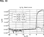
10 ist ein Kurvendiagramm, das die Eigenschaften eines Transistors wiedergibt. 10 is a graph showing the characteristics of a transistor.
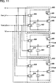
11 ist eine schematische Ansicht einer Schaltung zum Bewerten der Eigenschaften eines Transistors. 11 Fig. 10 is a schematic view of a circuit for evaluating the characteristics of a transistor.
12 ist ein Zeitdiagramm zum Bewerten der Eigenschaften eines Transistors. 12 is a timing chart for evaluating the characteristics of a transistor.
13 ist ein Kurvendiagramm, das die Eigenschaften eines Transistors wiedergibt. 13 is a graph showing the characteristics of a transistor.
14 ist ein Kurvendiagramm, das die Eigenschaften eines Transistors wiedergibt. 14 is a graph showing the characteristics of a transistor.
15 ist ein Kurvendiagramm, das die Eigenschaften eines Transistors wiedergibt. 15 is a graph showing the characteristics of a transistor.
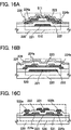
16A bis 16C sind Querschnittansichten, die jeweils ein Beispiel für einen Transistor zeigen. 16A to 16C FIG. 15 are cross-sectional views each showing an example of a transistor. FIG.
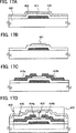
17A bis 17D sind Querschnittansichten, die ein Beispiel für einen Herstellungsprozess für einen Transistor zeigen. 17A to 17D FIG. 15 are cross-sectional views showing an example of a manufacturing process for a transistor. FIG.
18A bis 18F sind Ansichten, die jeweils ein Beispiel für eine elektronische Vorrichtung zeigen. 18A to 18F Figs. 3 are views each showing an example of an electronic device.
Bevorzugte Ausführungsform der ErfindungPreferred embodiment of the invention
Im Folgenden wird die vorliegende Erfindung im Detail mit Bezug auf die Zeichnungen beschrieben. Es ist zu beachten, dass die vorliegende Erfindung nicht auf die folgende Beschreibung beschränkt ist, wobei dem Fachmann deutlich sein sollte, dass die Modi und Details auf verschiedene Weise modifiziert werden können, ohne dass deshalb der Erfindungsumfang verlassen wird. Die vorliegende Erfindung ist also nicht auf die hier beschriebenen Ausführungsformen beschränkt.In the following, the present invention will be described in detail with reference to the drawings. It should be noted that the present invention is not limited to the following description, it should be apparent to those skilled in the art that the modes and details in various ways can be modified without, therefore, the scope of the invention is abandoned. The present invention is therefore not limited to the embodiments described here.
(Beispiel für eine Aktivmatrix-Anzeigevorrichtung)Example of an Active Matrix Display Device
Zuerst wird im Folgenden ein Beispiel für eine Aktivmatrix-Anzeigevorrichtung mit Bezug auf 1A und 1B beschrieben.First, an example of an active matrix display device will be described below with reference to FIG 1A and 1B described.
1A ist eine schematische Ansicht, die ein Beispiel für die Konfiguration der Aktivmatrix-Anzeigevorrichtung zeigt. Die Anzeigevorrichtung von 1A umfasst: einen Bildpunktteil 10; eine Erste-Abtastleitung-Treiberschaltung 11; eine Signalleitung/Zweite-Abtastleitung-Treiberschaltung 12; eine Steuereinrichtung 13; eine Vielzahl von ersten Abtastleitungen 14, die parallel oder im Wesentlichen parallel zueinander angeordnet sind und deren Potential durch die Erste-Abtastleitung-Treiberschaltung 11 gesteuert wird; eine Vielzahl von Signalleitungen 15, die parallel oder im Wesentlichen parallel zueinander angeordnet sind und deren Potential durch die Signalleitung/Zweite-Abtastleitung-Treiberschaltung 12 gesteuert wird; und eine Vielzahl von zweiten Abtastleitungen 16, die parallel oder im Wesentlichen parallel zueinander angeordnet sind und deren Potential durch die Signalleitung/Zweite-Abtastleitung-Treiberschaltung 12 gesteuert wird. Weiterhin umfasst der Bildpunktteil 10 eine Vielzahl von in einer Matrix angeordneten Bildpunkten 17. Es ist zu beachten, dass jede aus der Vielzahl von ersten Abtastleitungen 14 elektrisch mit einer Vielzahl von in einer Reihe angeordneten Bildpunkten 17 aus der Vielzahl von in einer Matrix angeordneten Bildpunkten 17 verbunden ist. Jede aus der Vielzahl von Signalleitungen 15 und jede aus der Vielzahl von zweiten Abtastleitungen 16 ist elektrisch mit einer Vielzahl von in einer Spalte angeordneten Bildpunkten 17 aus der Vielzahl von in einer Matrix angeordneten Bildpunkten 17 verbunden. Von der Steuereinrichtung 13 werden Signale wie etwa ein Startsignal zum Treiben der ersten Abtastleitung, ein Taktsignal zum Treiben der ersten Abtastleitung und ein Reihenneuschreibungs-Steuersignal sowie weiterhin eine Treiberleistung wie etwa eine Hochpotential-Stromversorgung (Vdd) und eine Niederpotential-Stromversorgung (Vss) in die Erste-Abtastleitung-Treiberschaltung 11 eingegeben. Weiterhin werden von der Steuereinrichtung 13 Signale wie etwa ein Startsignal zum Treiben der Signalleitung und der zweiten Abtastleitung, ein Taktsignal zum Treiben der Signalleitung und der zweiten Abtastleitung, ein Spaltenneuschreibungs-Steuersignal und ein Datensignal sowie weiterhin eine Treiberleistung wie etwa eine Hochpotential-Stromversorgung (Vdd) und eine Niederpotential-Stromversorgung (Vss) in die Signalleitung/Zweite-Abtastleitung-Treiberschaltung 12 eingegeben. 1A Fig. 12 is a schematic view showing an example of the configuration of the active matrix display device. The display device of 1A comprises: a pixel part 10 ; a first scan line driver circuit 11 ; a signal line / second scan line driver circuit 12 ; a control device 13 ; a plurality of first scan lines 14 which are arranged in parallel or substantially parallel to each other and their potential through the first scan line driver circuit 11 is controlled; a variety of signal lines 15 which are arranged in parallel or substantially parallel to each other and their potential through the signal line / second scanning line driver circuit 12 is controlled; and a plurality of second scanning lines 16 which are arranged in parallel or substantially parallel to each other and their potential through the signal line / second scanning line driver circuit 12 is controlled. Furthermore, the pixel part comprises 10 a plurality of pixels arranged in a matrix 17 , It should be noted that each of the plurality of first scan lines 14 electrically with a plurality of pixels arranged in a row 17 from the plurality of pixels arranged in a matrix 17 connected is. Each of the multitude of signal lines 15 and each of the plurality of second scan lines 16 is electrical with a plurality of pixels arranged in a column 17 from the plurality of pixels arranged in a matrix 17 connected. From the controller 13 In addition, signals such as a start signal for driving the first scan line, a clock signal for driving the first scan line, and a row rewrite control signal, and further a drive power such as a high potential power supply (Vdd) and a low potential power supply (Vss) are input to the first scan line driver circuit 11 entered. Furthermore, by the control device 13 Signals such as a start signal for driving the signal line and the second scan line, a clock signal for driving the signal line and the second scan line, a column rewrite control signal and a data signal, and further a drive power such as a high potential power supply (Vdd) and a low potential power supply (Vss) into the signal line / second scan line driver circuit 12 entered.
1B ist ein Schaltdiagramm, das ein Beispiel für den Bildpunkt 17 in der Anzeigevorrichtung von 1A zeigt. Der in 1B gezeigte Bildpunkt umfasst: einen Transistor 20, dessen Gate elektrisch mit der ersten Abtastleitung 14 verbunden ist und dessen Source oder Drain elektrisch mit der Signalleitung 15 verbunden ist; einen Transistor 21, dessen Gate elektrisch mit der zweiten Abtastleitung 16 verbunden ist und dessen Source oder Drain elektrisch mit entsprechend dem Drain oder der Source des Transistors 20 verbunden ist; einen Kondensator 22, dessen eine Elektrode elektrisch mit entsprechend dem Drain oder der Source des Transistors 21 verbunden ist und dessen andere Elektrode elektrisch mit einer Verdrahtung verbunden ist, die ein gemeinsames Potential (Vcom) zuführt (auch als gemeinsame Potentialleitung bezeichnet); und ein Flüssigkristallelement 23, dessen eine Elektrode (auch als Bildpunktelektrode bezeichnet) elektrisch mit entsprechend dem Drain oder der Source des Transistors 21 und der einen Elektrode des Kondensators 22 verbunden ist und dessen andere Elektrode (auch als Gegenelektrode bezeichnet) elektrisch mit eine Verdrahtung verbunden ist, die ein Gegenpotential zuführt. Es ist zu beachten, dass der Transistor 20 und der Transistor 21 n-Kanal-Transistoren sind. Das gemeinsame Potential (Vcom) und das Gegenpotential weisen dasselbe Potential auf. 1B is a circuit diagram showing an example of the pixel 17 in the display device of 1A shows. The in 1B shown pixel includes: a transistor 20 whose gate is electrically connected to the first scanning line 14 is connected and whose source or drain is electrically connected to the signal line 15 connected is; a transistor 21 whose gate is electrically connected to the second scanning line 16 is connected and whose source or drain is electrically connected to the drain or the source of the transistor 20 connected is; a capacitor 22 whose one electrode is electrically connected to the drain or the source of the transistor 21 is connected and whose other electrode is electrically connected to a wiring which supplies a common potential (Vcom) (also referred to as a common potential line); and a liquid crystal element 23 of which one electrode (also referred to as a pixel electrode) is electrically connected to the drain or the source of the transistor 21 and the one electrode of the capacitor 22 is connected and whose other electrode (also referred to as counter electrode) is electrically connected to a wiring which supplies a counter potential. It should be noted that the transistor 20 and the transistor 21 n-channel transistors are. The common potential (Vcom) and the counterpotential have the same potential.
(Beispiel für den Betrieb der Aktivmatrix-Anzeigevorrichtung)(Example of Operation of Active Matrix Display Device)
Im Folgenden wird ein Beispiel für den Betrieb der oben beschriebenen Anzeigevorrichtung beschrieben.Hereinafter, an example of the operation of the above-described display device will be described.
Zuerst werden Datensignale zum Bilden eines Bilds an dem Bildpunktteil 10 aufeinander folgend in die Steuereinrichtung 13 eingegeben. Die Steuereinrichtung 13 vergleicht einige der eingegebenen Datensignale, die Bilder von zwei aufeinander folgenden Rahmen bilden, und erfasst eine Differenz in jedem aus der Vielzahl von in einer Matrix angeordneten Bildpunkten 17. Weiterhin erzeugt die Steuereinrichtung 13 ein Reihenneuschreibungs-Steuersignal und ein Spaltenneuschreibungs-Steuersignal auf der Basis der erfassten Differenz.First, data signals are formed to form an image at the pixel part 10 consecutively into the control device 13 entered. The control device 13 compares some of the input data signals forming images of two consecutive frames, and detects a difference in each of the plurality of pixels arranged in a matrix 17 , Furthermore, the control device generates 13 a row rewrite control signal and a column rewrite control signal based on the detected difference.
Das Reihenneuschreibungs-Steuersignal ist ein Signal, das angibt, ob eine Differenz in wenigstens einem aus der Vielzahl von in derselben Reihe angeordneten Bildpunkten in dem Bildpunktteil 10 erfasst wird. Das Spaltenneuschreibungs-Steuersignal ist ein Signal, das angibt, ob eine Differenz in jedem der Bildpunkte 17 erfasst wird. Das Reihenneuschreibungs-Steuersignal und das Spaltenneuschreibungs-Steuersignal sind also jeweils ein Binärsignal. Die Frequenz des Spaltenneuschreibungs-Steuersignals ist höher als diejenige des Reihenneuschreibungs-Steuersignals. Insbesondere kann das Reihenneuschreibungs-Steuersignal in jeder horizontalen Abtastperiode (auch als Gate-Wahlperiode bezeichnet) gewechselt werden und kann das Spaltenneuschreibungs-Steuersignal in jeder Periode in der horizontalen Abtastperiode, während welcher die Signalleitung 15 gewählt wird (während welcher ein Datensignal in den Bildpunkt 17 eingegeben wird), gewechselt werden. Es ist zu beachten, dass in der folgenden Beschreibung der Einfachheit halber das Reihenneuschreibungs-Steuersignal für den Fall, dass „eine Differenz in wenigstens einem aus der Vielzahl von in derselben Reihe angeordneten Bildpunkten 17 erfasst wird”, als ein Signal mit einem hohen Pegel bezeichnet wird, und dass das Reihenneuschreibungs-Steuersignal für den Fall, dass „keine Differenz in wenigstens einem aus der Vielzahl von in derselben Reihe angeordneten Bildpunkten 17 erfasst wird”, als ein Signal mit einem niedrigen Pegel bezeichnet wird. Entsprechend wird das Spaltenneuschreibungs-Steuersignal für den Fall, dass „eine Differenz in jedem aus der Vielzahl von Bildpunkten 17 erfasst wird” als ein Signal mit einem hohen Pegel bezeichnet, und wird das Spaltenneuschreibungs-Steuersignal für den Fall, dass „keine Differenz in jedem aus der Vielzahl von Bildpunkten 17 erfasst wird” als ein Signal mit einem niedrigen Pegel bezeichnet.The row rewrite control signal is a signal indicating whether there is a difference in at least one of the plurality of pixels arranged in the same row in the pixel part 10 is detected. The column rewrite control signal is a signal indicating whether there is a difference in each of the pixels 17 is detected. Thus, the row rewrite control signal and the column rewrite control signal are each a binary signal. The frequency of the column rewrite control signal is higher than that of the row rewrite control signal. In particular, that can The rewriting control signal in each horizontal scanning period (also referred to as a gate selecting period) and may change the column rewriting control signal in each period in the horizontal scanning period during which the signal line 15 is selected (during which a data signal in the pixel 17 is entered). It is to be noted that, in the following description, for the sake of convenience, the row rewrite control signal in the case of "a difference in at least one of the plurality of pixels arranged in the same row 17 is detected "as a signal having a high level, and that the row rewrite control signal in the case where" no difference in at least one of the plurality of pixels arranged in the same row 17 is detected ", as a signal with a low level is called. Accordingly, the column rewrite control signal becomes "a difference in each of the plurality of pixels 17 is detected as a signal having a high level, and the column rewrite control signal in the case where there is no difference in each of the plurality of pixels 17 is detected as a signal having a low level.
Die Erste-Abtastleitung-Treiberschaltung 11 weist eine Funktion zum sequentiellen Zuführen von Auswahlsignalen zu der Vielzahl von ersten Abtastleitungen 14 auf. Es ist zu beachten, dass das Reihenneuschreibungs-Steuersignal in die Erste-Abtastleitung-Treiberschaltung 11 eingegeben wird. Das Reihenneuschreibungs-Steuersignal ist ein Signal, das wählt, ob ein Auswahlsignal zu den ersten Abtastleitungen 14 von der Erste-Abtastleitung-Treiberschaltung 11 zugeführt wird. Insbesondere wird in der Periode, während welcher die ersten Abtastleitungen 14 gewählt werden (einer horizontalen Abtastperiode), ein Auswahlsignal zu den ersten Abtastleitungen 14 zugeführt, wenn das Reihenneuschreibungs-Steuersignal ein Signal mit einem hohen Pegel ist, und wird ein nicht-Auswahlsignal zu der Vielzahl von ersten Abtastleitungen 14 zugeführt, wenn das Reihenneuschreibungs-Steuersignal ein Signal mit einem niedrigen Pegel ist. Dabei ist das Auswahlsignal ein Signal zum Einschalten des Transistors 20 und ist das nicht-Auswahlsignal ein Signal zum Ausschalten des Transistors 20.The first scan line driver circuit 11 has a function of sequentially supplying select signals to the plurality of first scan lines 14 on. It should be noted that the row rewrite control signal in the first scan line driver circuit 11 is entered. The row rewrite control signal is a signal that selects whether a selection signal is to the first scanning lines 14 from the first scan line driver circuit 11 is supplied. In particular, in the period during which the first scanning lines 14 are selected (a horizontal scanning period), a selection signal to the first scanning lines 14 is supplied when the row rewrite control signal is a high level signal, and becomes a non-selection signal to the plurality of first scan lines 14 when the row rewrite control signal is a low level signal. In this case, the selection signal is a signal for turning on the transistor 20 and the non-selection signal is a signal for turning off the transistor 20 ,
Die Signalleitung/Zweite-Abtastleitung-Treiberschaltung 12 weist eine Funktion zum sequentiellen Zuführen von Datensignalen zu der Vielzahl von Signalleitungen 15 und zum sequentiellen Zuführen von Auswahlsignalen zu der Vielzahl von zweiten Abtastleitungen 16 auf. Es ist zu beachten, dass das Spaltenneuschreibungs-Steuersignal in die Signalleitung/Zweite-Abtastleitung-Treiberschaltung 12 eingegeben wird. Das Spaltenneuschreibungs-Steuersignal ist ein Signal, das wählt, ob ein Datensignal und ein Auswahlsignal jeweils in die Signalleitungen 15 und die zweiten Abtastleitungen 16 von der Signalleitung/Zweite-Abtastleitung-Treiberschaltung 12 eingegeben werden. Insbesondere wird in der Periode, während welcher die Signalleitungen 15 und die zweiten Abtastleitungen 16 gewählt werden, ein Datensignal zu den Signalleitungen 15 zugeführt und wird ein Auswahlsignal zu den zweiten Abtastleitungen 16 zugeführt, wenn das Spaltenneuschreibungs-Steuersignal ein Signal mit einem hohen Pegel ist. Wenn dagegen das Spaltenneuschreibungs-Steuersignal ein Signal mit einem niedrigen Pegel ist, wird kein Datensignal zu den Signalleitungen 15 zugeführt und wird ein nicht-Auswahlsignal zu den zweiten Abtastleitungen 16 zugeführt. Wenn hier gesagt wird, dass „kein Datensignal zu den Signalleitungen 15 zugeführt wird”, bedeutet dies, dass ein fixes Potential oder eine vorbestimmte Wechselspannung zu den Signalleitungen 15 geführt wird oder dass die Signalleitungen 15 in einen Schwebezustand gebracht werden.The signal line / second scan line driver circuit 12 has a function of sequentially supplying data signals to the plurality of signal lines 15 and sequentially supplying select signals to the plurality of second scan lines 16 on. It should be noted that the column rewrite control signal enters the signal line / second scan line driver circuit 12 is entered. The column rewrite control signal is a signal that selects whether a data signal and a select signal are respectively input to the signal lines 15 and the second scanning lines 16 from the signal line / second scan line driver circuit 12 be entered. In particular, in the period during which the signal lines 15 and the second scanning lines 16 be selected, a data signal to the signal lines 15 is supplied and a selection signal to the second scanning lines 16 when the column rewrite control signal is a high level signal. On the other hand, if the column rewrite control signal is a low level signal, no data signal becomes the signal lines 15 and outputs a non-selection signal to the second scanning lines 16 fed. If it is said here that "no data signal to the signal lines 15 is fed, "this means that a fixed potential or a predetermined AC voltage to the signal lines 15 is guided or that the signal lines 15 be put in a state of limbo.
Wie oben beschrieben werden in der oben beschriebenen Anzeigevorrichtung das Reihenneuschreibungs-Steuersignal und das Spaltenneuschreibungs-Steuersignal von der Steuereinrichtung 13 ausgegeben, sodass gewählt werden kann, ob ein Datensignal in jedem aus der Vielzahl von in einer Matrix angeordneten Bildpunkten 17 neu geschrieben wird. Also auch dann, wenn ein Bild mit einem spezifischen, sich häufig ändernden Bereich angezeigt wird, kann ein hochqualitatives Bild mit einem reduzierten Stromverbrauch angezeigt werden.As described above, in the above-described display device, the row rewrite control signal and the column rewrite control signal are received from the controller 13 outputted so that it can be selected whether a data signal in each of the plurality of pixels arranged in a matrix 17 is rewritten. So even if an image is displayed with a specific, frequently changing area, a high quality image can be displayed with reduced power consumption.
(Beispiel für die Konfiguration der Erste-Abtastleitung-Treiberschaltung 11)(Example of Configuration of First Scanning Line Driver Circuit 11 )
Im Folgenden wird ein Beispiel für die Konfiguration der Erste-Abtastleitung-Treiberschaltung 11 in der oben genannten Anzeigevorrichtung mit Bezug auf 2A beschrieben. Die Erste-Abtastleitung-Treiberschaltung 11 von 2A umfasst: ein Schieberegister 110 mit einer Vielzahl von Ausgangsanschlüssen; einen Latch 111, dessen Eingangsanschluss elektrisch mit einer Verdrahtung, die ein Reihenneuschreibungs-Steuersignal zuführt, verbunden ist; einen Latch 112, dessen Eingangsanschluss elektrisch mit einem Ausgangsanschluss des Latchs 111 verbunden ist; und einen Puffer 113, dessen Eingangsanschluss elektrisch mit einem aus einer Vielzahl von Ausgangsanschlüssen des Schieberegisters 110 verbunden ist und dessen Ausgangsanschluss elektrisch mit einem aus der Vielzahl von ersten Abtastleitungen 14 verbunden ist.The following is an example of the configuration of the first scan line driver circuit 11 in the above display device with reference to 2A described. The first scan line driver circuit 11 from 2A includes: a shift register 110 with a plurality of output terminals; a latch 111 whose input terminal is electrically connected to a wiring supplying a row rewrite control signal; a latch 112 , whose input terminal is electrically connected to an output terminal of the latch 111 connected is; and a buffer 113 , whose input terminal is electrically connected to one of a plurality of output terminals of the shift register 110 and its output terminal is electrically connected to one of the plurality of first scan lines 14 connected is.
Das Schieberegister 110 weist eine Funktion zum sequentiellen Zuführen von Auswahlsignalen von der Vielzahl von Ausgangsanschlüssen auf, wenn ein Startsignal zum Treiben der ersten Abtastleitung von außen eingegeben wird.The shift register 110 has a function of sequentially supplying select signals from the plurality of output terminals when a start signal for driving the first scan line is externally input.
Der Latch 111 ist elektrisch mit einem aus der Vielzahl von Ausgangsanschlüssen des Schieberegisters 110 verbunden. Der Latch 111 weist eine Funktion zum Halten eines Reihenneuschreibungs-Steuersignals (eines Binärsignals: eines Signals mit einem hohen Pegel oder mit einem niedrigen Pegel) in einer Periode, während welcher ein Auswahlsignal von den Ausgangsanschlüssen zugeführt wird, und zum Ausgeben des Reihenneuschreibungs-Steuersignals auf. The latch 111 is electrically connected to one of the plurality of output terminals of the shift register 110 connected. The latch 111 has a function for holding a row rewrite control signal (a binary signal: a high-level signal or a low-level signal) in a period during which a selection signal is supplied from the output terminals and outputting the row rewrite control signal.
Der Latch 112 ist elektrisch mit einer Verdrahtung, die ein Gate-Latchsignal zuführt, verbunden. Der Latch 112 weist eine Funktion zum Halten eines Ausgabesignals des Latchs 111 (eines Binärsignals: eines Signals mit einem hohen Pegel oder einem niedrigen Pegel) in einer Periode, während welcher ein Transfersignal von dem Gate-Latchsignal zugeführt wird, und zum Ausgeben des Signals auf. Es ist zu beachten, dass das Gate-Latchsignal ein Signal ist, das angibt, ob das durch den Latch 111 gehaltene Signal zu dem Latch 112 transferiert wird. Das Gate-Latchsignal ist also ein Binärsignal (ein Transfersignal oder ein nicht-Transfersignal). Das Gate-Latchsignal gibt ein nicht-Transfersignal in einer Periode an, während welcher das Schieberegister 110 sequentiell Auswahlsignale zuführt (während einer Abtastperiode), und gibt ein Transfersignal in einer Periode zwischen zwei aufeinander folgenden Abtastperioden (während einer Vertikalrücksprungperiode) an.The latch 112 is electrically connected to a wiring supplying a gate latch signal. The latch 112 has a function for holding an output signal of the latch 111 (a binary signal: a signal having a high level or a low level) in a period during which a transfer signal is supplied from the gate latch signal and outputting the signal. It should be noted that the gate latch signal is a signal indicating whether that is due to the latch 111 held signal to the latch 112 is transferred. The gate latch signal is thus a binary signal (a transfer signal or a non-transfer signal). The gate latch signal indicates a non-transfer signal in a period during which the shift register 110 sequentially feeds selection signals (during one sampling period), and indicates a transfer signal in one period between two consecutive sampling periods (during one vertical retrace period).
Der Puffer 113 weist eine Funktion auf, mit der als das zu der ersten Abtastleitung 14 zugeführte Signal entweder das Ausgabesignal des Schieberegisters 110 oder ein nicht-Auswahlsignal gewählt werden kann. Insbesondere wird das Ausgabesignal des Schieberegisters 110 zu der ersten Abtastleitung 14 geführt, wenn das Ausgabesignal des Latchs 112 ein Signal mit einem hohen Pegel ist, und wird ein nicht-Auswahlsignal zu der ersten Abtastleitung 14 geführt, wenn das Ausgabesignal des Latchs 112 ein Signal mit einem niedrigen Pegel ist.The buffer 113 has a function of that to the first scanning line 14 supplied signal either the output signal of the shift register 110 or a non-selection signal can be selected. In particular, the output signal of the shift register becomes 110 to the first scanning line 14 guided when the output signal of the latch 112 is a signal of a high level, and becomes a non-selection signal to the first scanning line 14 guided when the output signal of the latch 112 is a signal with a low level.
(Beispiel für den Betrieb der Erste-Abtastleitung-Treiberschaltung 11)(Example of Operation of First Scanning Line Driver Circuit 11 )
Im Folgenden wird ein Beispiel für den Betrieb der oben beschriebenen Erste-Abtastleitung-Treiberschaltung 11 mit Bezug auf 3 beschrieben.The following is an example of the operation of the above-described first scan line driver circuit 11 regarding 3 described.
Zuerst werden in einer Abtastperiode (T1) Auswahlsignale sequentiell von der Vielzahl von Ausgangsanschlüssen des Schieberegisters 110 ausgegeben. Der Latch 111, der elektrisch mit dem Ausgangsanschluss verbunden ist, von dem das Auswahlsignal in einer Periode t1 ausgegeben wird, hält ein Reihenneuschreibungs-Steuersignal in der Periode t1 und gibt das Reihenneuschreibungs-Steuersignal aus. Dabei ist das Reihenneuschreibungs-Steuersignal in der Periode t1 ein Signal mit einem hohen Pegel.First, in one sampling period (T1), selection signals are sequentially generated from the plurality of output terminals of the shift register 110 output. The latch 111 which is electrically connected to the output terminal from which the selection signal is output in a period t1 holds a row rewrite control signal in the period t1 and outputs the row rewrite control signal. At this time, the row rewrite control signal in the period t1 is a signal of a high level.
Im Folgenden wird in einer Vertikalrücksprungperiode (T2) ein Transfersignal in den Latch 112 eingegeben. Dann hält der Latch 112 das Ausgabesignal des Latchs 111 (das Reihenneuschreibungs-Steuersignal in der Periode t1 = ein Signal mit einem hohen Pegel) und gibt das Signal aus. Weiterhin wird das Ausgabesignal des Latchs 112 in den Puffer 113 eingegeben, sodass das Ausgabesignal des Puffers 113 gleich einem Ausgabesignal des Ausgangsanschlusses wird, von dem das Auswahlsignal in der Periode t1 ausgegeben wird.Hereinafter, in a vertical retrace period (T2), a transfer signal is latched 112 entered. Then the latch stops 112 the output signal of the latch 111 (the row rewrite control signal in the period t1 = a high level signal) and outputs the signal. Furthermore, the output signal of the latch becomes 112 in the buffer 113 input, so that the output signal of the buffer 113 becomes equal to an output signal of the output terminal from which the selection signal is output in the period t1.
Im Folgenden werden in einer Abtastperiode (T3) Auswahlsignale sequentiell von der Vielzahl von Ausgangsanschlüssen des Schieberegisters 110 wie in der Abtastperiode T1 ausgegeben. Dabei wird in einer Periode t2 das Auswahlsignal in den oben genannten Latch 111 eingegeben (in den Latch 111, der elektrisch mit dem Ausgangsanschluss verbunden ist, von dem das Auswahlsignal in der Periode t1 ausgegeben wird). Dementsprechend hält der Latch 111 ein Reihenneuschreibungs-Steuersignal in der Periode t2 und gibt das Reihenneuschreibungs-Steuersignal aus. Dabei ist das Reihenneuschreibungs-Steuersignal in der Periode t2 ein Signal mit einem niedrigen Pegel. In der Abtastperiode (T3) hält der Latch 112 das Ausgabesignal in der Vertikalrücksprungsperiode (T2), sodass das Ausgabesignal des Puffers 113 in der Abtastperiode (T3) gleich einem Ausgabesignal des Ausgangsanschlusses wird, von dem das Auswahlsignal in der Periode t1 und der Periode t2 ausgegeben wird. Der Puffer 113 führt das Auswahlsignal zu der ersten Abtastleitung 14 in der Periode t2.Hereinafter, in one sampling period (T3), selection signals are sequentially sent from the plurality of output terminals of the shift register 110 as output in the sampling period T1. In this case, in a period t2, the selection signal in the above-mentioned latch 111 entered (in the Latch 111 electrically connected to the output terminal from which the selection signal is output in the period t1). Accordingly, the latch stops 111 a row rewrite control signal in the period t2 and outputs the row rewrite control signal. At this time, the row rewrite control signal in the period t2 is a low level signal. In the sampling period (T3), the latch holds 112 the output signal in the vertical retrace period (T2), so that the output signal of the buffer 113 in the sampling period (T3) becomes equal to an output signal of the output terminal from which the selection signal is output in the period t1 and the period t2. The buffer 113 leads the selection signal to the first scan line 14 in the period t2.
Dann wird in einer Vertikalrücksprungsperiode (T4) ein Transfersignal in den Latch 112 wie in der Vertikalrücksprungsperiode (T2) eingegeben. Der Latch 112 hält also das Ausgabesignal des Latchs 111 (das Reihenneuschreibungs-Steuersignal in der Periode t2 = ein Signal mit einem niedrigen Pegel) und gibt das Signal aus. Weiterhin wird das Ausgabesignal des Latchs 112 in den Puffer 113 eingegeben, sodass das Ausgabesignal des Puffers 113 ein nicht-Auswahlsignal wird.Then, in a vertical retrace period (T4), a transfer signal is latched 112 as entered in the vertical retrace period (T2). The latch 112 So holds the output signal of the latch 111 (the row rewrite control signal in the period t2 = a low level signal) and outputs the signal. Furthermore, the output signal of the latch becomes 112 in the buffer 113 input, so that the output signal of the buffer 113 becomes a non-selection signal.
Dann werden in einer Abtastperiode (T5) Auswahlsignale sequentiell von der Vielzahl von Ausgangsanschlüssen des Schieberegisters 110 wie in der Abtastperiode (T1) und der Abtastperiode (T3) ausgegeben. Dabei wird in einer Periode t3 das Auswahlsignal in den oben genannten Latch 111 eingegeben (der Latch 111 ist elektrisch mit dem Ausgangsanschluss verbunden, von dem das Auswahlsignal in der Periode t1 und der Periode t2 ausgegeben wird). Dementsprechend hält der Latch 111 ein Reihenneuschreibungs-Steuersignal in der Periode t3 und gibt das Reihenneuschreibungs-Steuersignal aus. Dabei ist das Reihenneuschreibungs-Steuersignal in der Periode t3 ein Signal mit einem hohen Pegel. In der Abtastperiode (T5) hält der Latch 112 das Ausgabesignal in der Vertikalrücksprungperiode (T4), sodass das Ausgabesignal des Puffers 113 in der Abtastperiode (T5) zu einem nicht-Auswahlsignal wird. Das heißt, dass der Puffer 113 ein nicht-Auswahlsignal zu der ersten Abtastleitung 14 in der Abtastperiode (T5) zuführt.Then, in one sampling period (T5), selection signals are sequentially generated from the plurality of output terminals of the shift register 110 as in the sampling period (T1) and the sampling period (T3). In this case, in a period t3, the selection signal in the above-mentioned latch 111 entered (the latch 111 is electrically connected to the output terminal from which the selection signal is output in the period t1 and the period t2). Accordingly, the latch stops 111 a row rewrite control signal in the period t3 and outputs the row rewrite control signal. At this time, the row rewrite control signal in the period t3 is a signal of a high level. In the sampling period (T5), the latch holds 112 the output signal in the vertical retrace period (T4), so that the output signal of the buffer 113 becomes a non-selection signal in the sampling period (T5). That is, the buffer 113 a non-selection signal to the first scanning line 14 in the sampling period (T5).
Durch die vorstehend beschriebene Operation kann die Erste-Abtastleitung-Treiberschaltung 11 in Übereinstimmung mit einem Reihenneuschreibungs-Steuersignal wählen, ob ein Auswahlsignal zu der ersten Abtastleitung 14 zugeführt wird. Es ist zu beachten, dass in dem oben beschriebenen Betrieb der Anzeigevorrichtung jede der Perioden t1, t2 und t3 eine horizontale Abtastperiode ist und dass die Vertikalrücksprungperiode und die folgende Abtastperiode eine Rahmenperiode ausmachen.By the above-described operation, the first scan line driver circuit 11 in accordance with a row rewrite control signal, select whether a selection signal is to the first scanning line 14 is supplied. It should be noted that in the above-described operation of the display device, each of the periods t1, t2 and t3 is a horizontal scanning period, and the vertical retrace period and the following scanning period make up one frame period.
(Beispiel für die Konfiguration Signalleitung/Zweite-Abtastleitung-Treiberschaltung 12)(Example of Configuration Signal Line / Second Scan Line Driver Circuit 12 )
Im Folgenden wird ein Beispiel für die Konfiguration der Signalleitung/Zweite-Abtastleitung-Treiberschaltung 12 in der oben beschriebenen Anzeigevorrichtung mit Bezug auf 2B beschrieben. Die Signalleitung/Zweite-Abtastleitung-Treiberschaltung 12 von 2B umfasst: ein Schieberegister 120 mit einer Vielzahl von Ausgangsanschlüssen; einen Latch 121, dessen Eingangsanschluss elektrisch mit einer Verdrahtung verbunden ist, die ein Spaltenneuschreibungs-Steuersignal zuführt; einen Latch 122, dessen Eingangsanschluss elektrisch mit einem Ausgangsanschluss des Latchs 121 verbunden ist und dessen Ausgangsanschluss elektrisch mit einer aus der Vielzahl von zweiten Abtastleitungen 16 verbunden ist; einen Latch 123, dessen Eingangsanschluss elektrisch mit einer Verdrahtung verbunden ist, die ein Datensignal zuführt; einen Latch 124, dessen Eingangsanschluss elektrisch mit einem Ausgangsanschluss des Latchs 123 verbunden ist; eine Digital-zu-Analog-Wandlerschaltung (DAW) 125, deren Eingangsanschluss elektrisch mit einem Ausgangsanschluss des Latchs 124 verbunden ist; und einen analogen Puffer 126, dessen Eingangsanschluss elektrisch mit einem Ausgangsanschluss der Digital-zu-Analog-Wandlerschaltung (DAW) 125 verbunden ist und dessen Ausgangsanschluss elektrisch mit einer aus der Vielzahl von Signalleitungen 15 verbunden ist.The following is an example of the configuration of the signal line / second scan line driver circuit 12 in the above-described display device with reference to 2 B described. The signal line / second scan line driver circuit 12 from 2 B includes: a shift register 120 with a plurality of output terminals; a latch 121 whose input terminal is electrically connected to a wiring supplying a column rewrite control signal; a latch 122 , whose input terminal is electrically connected to an output terminal of the latch 121 and its output terminal is electrically connected to one of the plurality of second scan lines 16 connected is; a latch 123 whose input terminal is electrically connected to a wiring supplying a data signal; a latch 124 , whose input terminal is electrically connected to an output terminal of the latch 123 connected is; a digital-to-analog converter circuit (DAW) 125 , whose input terminal is electrically connected to an output terminal of the latch 124 connected is; and an analog buffer 126 , whose input terminal is electrically connected to an output terminal of the digital-to-analog converter circuit (DAW) 125 and its output terminal is electrically connected to one of the plurality of signal lines 15 connected is.
Das Schieberegister 120 weist eine Funktion zum sequentiellen Zuführen von Auswahlsignalen von der Vielzahl von Ausgangsanschlüssen auf, wenn ein Startsignal zum Treiben der Signalleitung und der zweiten Abtastleitung von außen eingegeben wird.The shift register 120 has a function of sequentially supplying select signals from the plurality of output terminals when a start signal for driving the signal line and the second scan line is externally input.
Der Latch 121 ist elektrisch mit einem aus der Vielzahl von Ausgangsanschlüssen des Schieberegisters 120 verbunden. Der Latch 121 weist eine Funktion zum Halten eines Spaltenneuschreibungs-Steuersignals (eines Binärsignals mit einem hohen Pegel oder mit einem niedrigen Pegel) in einer Periode, während welcher ein Auswahlsignal von den Ausgangsanschlüssen zugeführt wird, und zum Ausgeben des Spaltenneuschreibungs-Steuersignals auf.The latch 121 is electrically connected to one of the plurality of output terminals of the shift register 120 connected. The latch 121 has a function of holding a column rewrite control signal (a binary signal having a high level or a low level) in a period during which a selection signal is supplied from the output terminals, and outputting the column rewrite control signal.
Der Latch 122 ist elektrisch mit einer Verdrahtung verbunden, die ein Source-Latchsignal zuführt. Der Latch 122 weist eine Funktion zum Halten eines Ausgabesignals des Latchs 121 (eines Binärsignals mit einem hohen Pegel oder einem niedrigen Pegel) in einer Periode, während welcher ein Transfersignal von dem Source-Latchsignal zugeführt wird, und zum Ausgeben des Signals auf. Es ist zu beachten, dass das Source-Latchsignal ein Signal ist, das angibt, ob das durch den Latch 121 gehaltene Signal zu dem Latch 122 transferiert wird. Das heißt, das Source-Latchsignal ist ein Binärsignal (ein Transfersignal oder ein nicht-Transfersignal). Dabei gibt das Source-Latchsignal ein nicht-Transfersignal in einer Periode an, während welcher das Schieberegister 120 sequentiell Auswahlsignale zuführt (Abtastperiode), und gibt das Source-Latchsignal ein Transfersignal in einer Periode zwischen zwei aufeinanderfolgenden Abtastperioden an (Horizontalrücksprungperiode). Ein Ausgabesignal des Latchs 122 wird zu dem Gate des Transistors 21 in dem Bildpunkt 17 über eine aus der Vielzahl von zweiten Abtastleitungen 16 zugeführt, sodass der Latch 122 ein Signal zum Einschalten des Transistors 21 (ein Auswahlsignal) ausgeben muss, wenn ein Signal mit einem hohen Pegel von dem Latch 121 in einer Horizontalrücksprungperiode eingegeben wird, und ein Signal zum Ausschalten des Transistors 21 (ein nicht-Auswahlsignal) ausgeben muss, wenn ein Signal mit einem niedrigen Pegel von dem Latch 121 in einer Horizontalrücksprungperiode eingegeben wird.The latch 122 is electrically connected to a wiring which supplies a source latch signal. The latch 122 has a function for holding an output signal of the latch 121 (a binary signal having a high level or a low level) in a period during which a transfer signal is supplied from the source latch signal and outputting the signal. It should be noted that the source latch signal is a signal indicating whether that is due to the latch 121 held signal to the latch 122 is transferred. That is, the source latch signal is a binary signal (a transfer signal or a non-transfer signal). Here, the source latch signal indicates a non-transfer signal in a period during which the shift register 120 sequentially supplies selection signals (sampling period), and the source latch signal indicates a transfer signal in a period between two consecutive sampling periods (horizontal retrace period). An output signal of the latch 122 becomes the gate of the transistor 21 in the pixel 17 via one of the plurality of second scan lines 16 fed, so the latch 122 a signal to turn on the transistor 21 (a select signal) must output when a high-level signal from the latch 121 in a horizontal retrace period, and a signal to turn off the transistor 21 (a non-selection signal) must output when a signal with a low level from the latch 121 is input in a horizontal retrace period.
Der Latch 123 ist elektrisch mit einem aus der Vielzahl von Ausgangsanschlüssen des Schieberegisters 120 verbunden. Der Latch 123 weist eine Funktion zum Halten eines Datensignals in einer Periode, während welcher ein Auswahlsignal von dem Ausgabeanschluss zugeführt wird, und zum Ausgeben des Datensignals auf. Es ist zu beachten, dass das Datensignal ein Mehr-Bit-Digitalsignal ist.The latch 123 is electrically connected to one of the plurality of output terminals of the shift register 120 connected. The latch 123 has a function of holding a data signal in a period during which a selection signal is supplied from the output terminal and outputting the data signal. It should be noted that the data signal is a multi-bit digital signal.
Der Latch 124 ist elektrisch mit einer Verdrahtung verbunden, die ein Source-Latchsignal zuführt. Der Latch 124 weist eine Funktion zum Halten eines Ausgabesignals des Latchs 123 (eines Mehr-Bit-Signals) in einer Periode, während welcher ein Transfersignal von dem Source-Latchsignal zugeführt wird, und zum Ausgeben des Signals auf.The latch 124 is electrically connected to a wiring which supplies a source latch signal. The latch 124 has a function for holding an output signal of the latch 123 (a multi-bit signal) in a period during which a Transfer signal from the source latch signal is supplied, and for outputting the signal.
Die Digital-zu-Analog-Wandlerschaltung (DAW) 125 weist eine Funktion zum Wandeln eines von dem Latch 124 eingegebenen digitalen Datensignals zu einem analogen Signal und zum Ausgeben des analogen Signals auf.The digital-to-analog converter circuit (DAW) 125 has a function of converting one of the latches 124 input digital data signal to an analog signal and outputting the analog signal.
Der analoge Puffer 126 weist eine Funktion zum Wählen, ob ein Datensignal (ein analoges Datensignal) zu der Signalleitung 15 zugeführt wird, in Übereinstimmung mit dem Ausgabesignal des Latchs 122 (eines Binärsignals mit einem hohen Pegel oder einem niedrigen Pegel) auf. Insbesondere führt der analoge Puffer 126 ein Datensignal (ein analoges Datensignal) zu der Signalleitung 15 zu, wenn das Ausgabesignal des Latchs 122 ein Signal mit einem hohen Pegel ist, und führt kein Datensignal (analoges Datensignal) zu der Signalleitung 15 zu, wenn das Ausgabesignal des Latchs 122 ein Signal mit einem niedrigen Pegel ist.The analog buffer 126 has a function of selecting whether a data signal (an analog data signal) to the signal line 15 is supplied in accordance with the output signal of the latch 122 (a binary signal of a high level or a low level). In particular, the analog buffer performs 126 a data signal (an analog data signal) to the signal line 15 to when the output signal of the latch 122 is a signal of a high level, and does not supply a data signal (analog data signal) to the signal line 15 to when the output signal of the latch 122 is a signal with a low level.
(Beispiel für den Betrieb der Signalleitung/Zweite-Abtastleitung-Treiberschaltung 12)(Example of Operation of Signal Line / Second Scanning Line Driver Circuit 12 )
Ein Beispiel für den Betrieb der oben beschriebenen Signalleitung/Zweite-Abtastleitung-Treiberschaltung 12 wird im Folgenden mit Bezug auf 4 beschrieben.An example of the operation of the above-described signal line / second scanning line driving circuit 12 will be referred to below with reference to 4 described.
Zuerst werden in einer Abtastperiode (Ta) Auswahlsignale sequentiell von der Vielzahl von Ausgangsanschlüssen des Schieberegisters 120 ausgegeben. Der Latch 121, der elektrisch mit dem Ausgangsanschluss verbunden ist, von dem das Auswahlsignal in einer Periode ta ausgegeben wird, erhält ein Spaltenneuschreibungs-Steuersignal in der Periode ta aufrecht und gibt das Spaltenneuschreibungs-Steuersignal aus. Dabei ist das Spaltenneuschreibungs-Steuersignal in der Periode ta ein Signal mit einem hohen Pegel. Der Latch 123, der elektrisch mit dem Ausgangsanschluss verbunden ist, von dem das Auswahlsignal in der Periode ta ausgegeben wird, hält ein spezifisches Datensignal (data(D)-1) in der Periode ta in einem Mehr-Bit-Datensignal (DATA(D)-1) aufrecht und gibt das Datensignal (data(D)-1) aus.First, in one sampling period (Ta), selection signals are sequentially generated from the plurality of output terminals of the shift register 120 output. The latch 121 , which is electrically connected to the output terminal from which the selection signal is output in a period ta, maintains a column rewrite control signal in the period ta and outputs the column rewrite control signal. At this time, the column rewrite control signal in the period ta is a signal of a high level. The latch 123 , which is electrically connected to the output terminal from which the selection signal is output in the period ta, holds a specific data signal (data (D) -1) in the period ta in a multi-bit data signal (DATA (D) -1 ) and outputs the data signal (data (D) -1).
Dann wird in einer Horizontalrücksprungperiode (Tb) ein Transfersignal zu dem Latch 122 und dem Latch 124 eingegeben. Dann hält der Latch 122 das Ausgabesignal des Latchs 121 (das Spaltenneuschreibungs-Steuersignal in der Periode ta = ein Signal mit einem hohen Pegel) aufrecht und gibt das Signal aus. Das Ausgabesignal des Latchs 122 wird zu dem Gate des Transistors 21 in dem Bildpunkt 17 über eine aus der Vielzahl von zweiten Abtastleitungen 16 zugeführt, sodass der Transistor 21 eingeschaltet wird. Der Latch 124 hält das Ausgabesignal des Latchs 123 (das Datensignal (data(D)-1) in der Periode ta) und gibt das Signal aus. Das Ausgabesignal des Latchs 124 wird in die Digital-zu-Analog-Wandlerschaltung (DAW) 125 eingegeben, sodass die Digital-zu-Analog-Wandlerschaltung (DAW) 125 ein analoges Datensignal (data(A)-1) ausgibt. Das Ausgabesignal der Digital-zu-Analog-Wandlerschaltung (DAW) 125 wird in den analogen Puffer 126 eingegeben. Weiterhin wird das Ausgabesignal des Latchs 122 (das Spaltenneuschreibungs-Steuersignal in der Periode ta = ein Signal mit einem hohen Pegel) in den analogen Puffer 126 eingegeben. So wird das Ausgabesignal des analogen Puffers 126 zu einem analogen Datensignal (data(A)-1).Then, in a horizontal retrace period (Tb), a transfer signal to the latch 122 and the latch 124 entered. Then the latch stops 122 the output signal of the latch 121 (the column rewrite control signal in the period ta = a signal of a high level) and outputs the signal. The output signal of the latch 122 becomes the gate of the transistor 21 in the pixel 17 via one of the plurality of second scan lines 16 fed, so the transistor 21 is turned on. The latch 124 holds the output signal of the latch 123 (the data signal (data (D) -1) in the period ta) and outputs the signal. The output signal of the latch 124 is transferred to the digital-to-analog converter circuit (DAW) 125 input so that the digital-to-analog converter circuit (DAW) 125 an analog data signal (data (A) -1) outputs. The output signal of the digital-to-analog converter circuit (DAW) 125 gets into the analog buffer 126 entered. Furthermore, the output signal of the latch becomes 122 (the column rewrite control signal in the period ta = a signal of a high level) in the analog buffer 126 entered. This becomes the output signal of the analog buffer 126 to an analog data signal (data (A) -1).
Dann werden in einer Abtastperiode (Tc) Auswahlsignale sequentiell von der Vielzahl von Ausgangsanschlüssen des Schieberegisters 120 wie in der Abtastperiode (Ta) ausgegeben. Dabei hält der oben genannte Latch 121 (der Latch 121, der elektrisch mit dem Ausgangsanschluss verbunden ist, von dem das Auswahlsignal in der Periode ta ausgegeben wird) ein Spaltenneuschreibungs-Steuersignal in der Periode tb und gibt das Spaltenneuschreibungs-Steuersignal aus. Dabei ist das Spaltenneuschreibungs-Steuersignal in der Periode tb ein Signal mit einem niedrigen Pegel. Weiterhin hält in der Abtastperiode (Tc) der oben genannte Latch 123 (der Latch 123, der elektrisch mit dem Ausgangsanschluss verbunden ist, von dem das Auswahlsignal in der Periode ta ausgegeben wird), ein Datensignal (data(D)-2) in der Periode tb in einem Mehr-Bit-Datensignal (DATA(D)-2) und gibt das Datensignal (data(D)-2) aus. In der Abtastperiode (Tc) halten der Latch 122 und der Latch 124 das Ausgabesignal in einer Horizontalrücksprungperiode (Tb), sodass der oben genannte Transistor 21 (der Transistor 21, zu dessen Gate das Ausgabesignal des Latchs 122 geführt wird) in einem Ein-Zustand in der Abtastperiode (Tc) gehalten wird, während das analoge Datensignal (data(A)-1) als das Ausgabesignal des analogen Puffers 126 gehalten wird. Mit anderen Worten führt der analoge Puffer 126 das analoge Datensignal (data(A)-1) in der Abtastperiode (Tc) zu.Then, in one sampling period (Tc), selection signals are sequentially generated from the plurality of output terminals of the shift register 120 as output in the sampling period (Ta). The above mentioned latch stops 121 (the latch 121 electrically connected to the output terminal from which the selection signal is output in the period ta), a column rewrite control signal in the period tb, and outputs the column rewrite control signal. Here, the column rewrite control signal in the period tb is a low level signal. Further, in the sampling period (Tc), the above-mentioned latch holds 123 (the latch 123 electrically connected to the output terminal from which the selection signal is output in the period ta), a data signal (data (D) -2) in the period tb in a multi-bit data signal (DATA (D) -2) and outputs the data signal (data (D) -2). In the sampling period (Tc) hold the latch 122 and the latch 124 the output signal in a horizontal retrace period (Tb), so that the above-mentioned transistor 21 (the transistor 21 , to the gate of which the output signal of the latch 122 is held) in an on state in the sampling period (Tc) while the analog data signal (data (A) -1) is held as the output signal of the analog buffer 126 is held. In other words, the analog buffer performs 126 the analog data signal (data (A) -1) in the sampling period (Tc).
Dann wird in einer Horizontalrücksprungperiode (Td) ein Transfersignal in den Latch 122 und den Latch 124 wie in der Horizontalrücksprungperiode (Tb) eingegeben. Dann hält der Latch 122 das Ausgabesignal des Latchs 121 (das Spaltenneuschreibungs-Steuersignal in der Periode tb = ein Signal mit einem niedrigen Pegel) und gibt das Signal aus. Das Ausgabesignal des Latchs 122 wird zu dem Gate des Transistors 21 in dem Bildpunkt 17 über eine aus der Vielzahl von zweiten Abtastleitungen 16 zugeführt, sodass der Transistor 21 ausgeschaltet wird. Der Latch 124 hält das Ausgabesignal des Latchs 123 (das Datensignal (data(D)-2) in der Periode tb) und gibt das Signal aus. Das Ausgabesignal des Latchs 124 wird in die Digital-zu-Analog-Wandlerschaltung (DAW) 125 eingegeben, sodass die Digital-zu-Analog-Wandlerschaltung (DAW) 125 ein analoges Datensignal (data(A)-2) ausgibt. Das Ausgabesignal der Digital-zu-Analog-Wandlerschaltung (DAW) 125 wird in den analogen Puffer 126 eingegeben. Es ist zu beachten, dass das Ausgabesignal des Latchs 122 (das Spaltenneuschreibungs-Steuersignal in der Periode ta = ein Signal mit einem niedrigen Pegel) in den analogen Puffer 126 eingegeben wird. Das analoge Datensignal (data(A)-2) wird also nicht zu der Signalleitung 15 geführt.Then, in a horizontal retrace period (Td), a transfer signal is latched 122 and the latch 124 as entered in the horizontal retrace period (Tb). Then the latch stops 122 the output signal of the latch 121 (the column rewrite control signal in the period tb = a low-level signal) and outputs the signal. The output signal of the latch 122 becomes the gate of the transistor 21 in the pixel 17 via one of the plurality of second scan lines 16 fed, so the transistor 21 is turned off. The latch 124 holds the output signal of the latch 123 (the data signal (data (D) -2) in the period tb) and outputs the signal. The output signal of the latch 124 goes into the digital-to-analog converter circuit (DAW) 125 input so that the digital-to-analog converter circuit (DAW) 125 an analog data signal (data (A) -2) outputs. The output signal of the digital-to-analog converter circuit (DAW) 125 gets into the analog buffer 126 entered. It should be noted that the output signal of the latch 122 (the column rewrite control signal in the period ta = a signal of a low level) in the analog buffer 126 is entered. The analog data signal (data (A) -2) does not become the signal line 15 guided.
Dann werden in einer Abtastperiode (Te) Auswahlsignale sequentiell von der Vielzahl von Ausgabeanschlüssen des Schieberegisters 120 wie in den Abtastperioden (Ta) und (Tc) ausgegeben. Dabei wird in einer Periode tc das Auswahlsignal in den oben genannten Latch 121 (den Latch 121, der elektrisch mit dem Ausgangsanschluss verbunden ist, von dem das Auswahlsignal in der Perioden ta und tb ausgegeben wird) eingegeben. Dementsprechend hält der Latch 121 ein Spaltenneuschreibungs-Steuersignal in der Periode tc und gibt das Spaltenneuschreibungs-Steuersignal aus. Dabei ist das Spaltenneuschreibungs-Steuersignal in der Periode tc ein Signal mit einem hohen Pegel. Weiterhin hält in der Abtastperiode (Te) der oben genannte Latch 123 (der Latch 123, der elektrisch mit dem Ausgangsanschluss verbunden ist, von dem das Auswahlsignal in den Perioden ta und tb ausgegeben wird) ein Datensignal (data(D)-3) in der Periode tc in einem Mehr-Bit-Datensignal (DATA(D)-3) und gibt das Datensignal (data(D)-3) aus. In der Abtastperiode (Te) halten der Latch 122 und der Latch 124 das Ausgabesignal in der Horizontalrücksprungperiode (Td), sodass der oben genannte Transistor 21 (der Transistor 21, zu dessen Gate das Ausgabesignal des Latch 122 geführt wird) in einem Aus-Zustand in der Abtastperiode (Te) gehalten wird und das analoge Datensignal (data(A)-2) nicht zu der Signalleitung 15 geführt wird.Then, in one sampling period (Te), selection signals are sequentially generated from the plurality of output terminals of the shift register 120 as in the sampling periods (Ta) and (Tc). In this case, in a period tc, the selection signal in the above-mentioned latch 121 (the latch 121 which is electrically connected to the output terminal from which the selection signal is output in the periods ta and tb). Accordingly, the latch stops 121 a column rewriting control signal in the period tc and outputs the column rewrite control signal. At this time, the column rewrite control signal in the period tc is a signal of a high level. Furthermore, in the sampling period (Te), the above-mentioned latch holds 123 (the latch 123 electrically connected to the output terminal from which the selection signal is output in the periods ta and tb), a data signal (data (D) -3) in the period tc in a multi-bit data signal (DATA (D) -3 ) and outputs the data signal (data (D) -3). In the sampling period (Te) hold the latch 122 and the latch 124 the output signal in the horizontal retrace period (Td), so that the above-mentioned transistor 21 (the transistor 21 , to whose gate the output signal of the latch 122 is held) in an off-state in the sampling period (Te), and the analog data signal (data (A) -2) is not held to the signal line 15 to be led.
Durch den oben genannten Betrieb kann die Signalleitung/Zweite-Abtastleitung-Treiberschaltung 12 in Übereinstimmung mit einem Spaltenneuschreibungs-Steuersignal wählen, ob ein Datensignal zu der Signalleitung 15 geführt wird und ob ein Auswahlsignal zu der zweiten Abtastleitung 16 geführt wird. Es ist zu beachten, dass in dem oben genannten Betrieb der Anzeigevorrichtung eine Horizontalrücksprungperiode und die folgende Abtastperiode eine horizontale Abtastperiode ausmachen.By the above-mentioned operation, the signal line / second scanning line driving circuit can 12 in accordance with a column rewrite control signal, select whether a data signal is to the signal line 15 is guided and whether a selection signal to the second scanning line 16 to be led. It should be noted that in the above-mentioned operation of the display device, one horizontal retrace period and the following sampling period make one horizontal scanning period.
(Beispiel für die Konfiguration der Steuereinrichtung 13)(Example of the configuration of the controller 13 )
Im Folgenden wird ein Beispiel für die Konfiguration der Steuereinrichtung 13 in der oben genannten Anzeigevorrichtung mit Bezug auf 5 beschrieben. Die in 5 gezeigte Steuereinrichtung 13 umfasst: einen Rahmenspeicher 131, der Datensignale speichert, die von außen eingegeben werden und Bilder einer Vielzahl von Rahmen bilden; eine Vergleicherschaltung 132, die die Datensignale vergleicht, die in dem Rahmenspeicher 131 gespeichert sind und Bilder von zwei aufeinanderfolgenden Rahmen bilden, und eine Differenz erfasst; einen Koordinatenspeicher 133, der die Koordinaten eines Bildpunkts speichert, in dem eine Differenz durch die Vergleicherschaltung 132 erfasst wurde; eine Datensignal-Leseschaltung 134, die ein Datensignal aus dem Rahmenspeicher 131 liest und das Datensignal zu der Signalleitung/Zweite-Abtastleitung-Treiberschaltung 12 ausgibt; und eine Neuschreibsignal-Erzeugungsschaltung 135, die ein Spaltenneuschreibungs-Steuersignal und ein Reihenneuschreibungs-Steuersignal auf der Basis der in dem Koordinatenspeicher 133 gespeicherten Koordinatendaten erzeugt und das Spaltenneuschreibungs-Steuersignal und das Reihenneuschreibungs-Steuersignal jeweils zu der Signalleitung/Zweite-Abtastleitung-Treiberschaltung 12 und der Erste-Abtastleitung-Treiberschaltung 11 ausgibt.The following is an example of the configuration of the controller 13 in the above display device with reference to 5 described. In the 5 shown control device 13 includes: a frame memory 131 storing data signals input from outside and forming images of a plurality of frames; a comparator circuit 132 which compares the data signals stored in the frame memory 131 are stored and form images of two consecutive frames, and detect a difference; a coordinate memory 133 which stores the coordinates of a pixel in which a difference by the comparator circuit 132 was recorded; a data signal read circuit 134 which is a data signal from the frame memory 131 reads and the data signal to the signal line / second scan line driver circuit 12 outputs; and a rewrite signal generation circuit 135 including a column rewrite control signal and a row rewrite control signal on the basis of the in the co-ordinate memory 133 stored coordinate data and the column rewrite control signal and the rewrite control signal respectively to the signal line / second scan line driver circuit 12 and the first scan line driver circuit 11 outputs.
(Beispiel für den Betrieb der Steuereinrichtung 13)(Example of operation of the controller 13 )
Im Folgenden wird ein Beispiel für den Betrieb der oben genannten Steuereinrichtung 13 mit Bezug auf 6 beschrieben.The following is an example of the operation of the above control device 13 regarding 6 described.
In einer ersten Rahmenperiode, während welcher ein Datensignal zum Bilden eines Bilds eines ersten Rahmens von außen in die Steuereinrichtung 13 eingegeben wird, speichert der Rahmenspeicher 131 das Datensignal zum Bilden des Bilds des ersten Rahmens.In a first frame period, during which a data signal for forming an image of a first frame from outside into the control device 13 is input, the frame memory stores 131 the data signal for forming the image of the first frame.
In einer zweiten Rahmenperiode, während welcher ein Datensignal zum Bilden eines Bilds eines zweiten Rahmens von außen in die Steuereinrichtung 13 eingegeben wird, speichert der Rahmenspeicher 131 das Datensignal zum Bilden des Bilds des zweiten Rahmens.In a second frame period during which a data signal for forming an image of a second frame from the outside into the control device 13 is input, the frame memory stores 131 the data signal for forming the image of the second frame.
In einer dritten Rahmenperiode, während welcher ein Datensignal zum Bilden eines Bilds eines dritten Rahmens von außen in die Steuereinrichtung 13 eingegeben wird, speichert der Rahmenspeicher 131 das Datensignal zum Bilden des Bilds des dritten Rahmens. Die Vergleicherschaltung 132 vergleicht die in dem Rahmenspeicher 131 gespeicherten Datensignale, die das Bild des ersten Rahmens und das Bild des zweiten Rahmens bilden, und erfasst eine Differenz. Weiterhin speichert der Koordinatenspeicher 133 die Koordinaten eines Bildpunkts, in dem eine Differenz zwischen dem Datensignal zum Bilden des Bilds des ersten Rahmens und dem Datensignal zum Bilden des Bilds des zweiten Rahmens erfasst wurde.In a third frame period, during which a data signal for forming an image of a third frame from outside into the control device 13 is input, the frame memory stores 131 the data signal for forming the image of the third frame. The comparator circuit 132 compares those in the frame store 131 stored data signals forming the image of the first frame and the image of the second frame, and detects a difference. Furthermore, the coordinate memory stores 133 the coordinates of a pixel in which a difference between the data signal for forming the image of the first frame and the data signal for forming the image of the second frame has been detected.
Dann speichert in einer vierten Rahmenperiode, während welcher ein Datensignal zum Bilden eines Bilds eines vierten Rahmens von außen in die Steuereinrichtung 13 eingegeben wird, der Rahmenspeicher 131 das Datensignal zum Bilden des Bilds des vierten Rahmens. Die Vergleicherschaltung 132 vergleicht die in dem Rahmenspeicher 131 gespeicherten Datensignale, die das Bild des zweiten Rahmens und das Bild des dritten Rahmens bilden, und erfasst eine Differenz. Weiterhin speichert der Koordinatenspeicher 133 die Koordinaten eines Bildpunkts, in dem eine Differenz zwischen dem Datensignal zum Bilden des Bilds des zweiten Rahmens und dem Datensignal zum Bilden des Bilds des dritten Rahmens erfasst wurde. Die Datensignal-Leseeinheit 134 liest das in dem Rahmenspeicher 131 gespeicherte Datensignal, das das Bild des ersten Rahmens bildet, und gibt dann das Datensignal zum Bilden des Bilds des ersten Rahmens zu der Signalleitung/Zweite-Abtastleitung-Treiberschaltung 12 aus. Weiterhin erzeugt die Neuschreibungssignal-Erzeugungsschaltung 135 auf der Basis der in dem Koordinatenspeicher 133 gespeicherten Koordinatendaten ein Reihenneuschreibungs-Steuersignal zum Neuschreiben des Bilds des ersten Rahmens und des Bilds des zweiten Rahmens. Dann gibt die Neuschreibungssignal-Erzeugungsschaltung 135 das Reihenneuschreibungs-Steuersignal zu der Erste-Abtastleitung-Treiberschaltung 11 aus. Es ist zu beachten, dass in dieser Periode das Bild des ersten Rahmens auf dem Bildpunktteil 10 angezeigt wird. Then, in a fourth frame period during which a data signal for forming an image of a fourth frame is externally stored in the controller 13 is entered, the frame memory 131 the data signal for forming the image of the fourth frame. The comparator circuit 132 compares those in the frame store 131 stored data signals forming the image of the second frame and the image of the third frame, and detects a difference. Furthermore, the coordinate memory stores 133 the coordinates of a pixel in which a difference between the data signal for forming the image of the second frame and the data signal for forming the image of the third frame has been detected. The data signal reading unit 134 read this in the frame memory 131 stored data signal forming the image of the first frame, and then outputs the data signal for forming the image of the first frame to the signal line / second scanning line driver circuit 12 out. Furthermore, the rewrite signal generation circuit generates 135 based on the in the coordinate memory 133 stored coordinate data, a row rewrite control signal for rewriting the image of the first frame and the image of the second frame. Then, the rewrite signal generating circuit outputs 135 the row rewrite control signal to the first scan line driver circuit 11 out. It should be noted that in this period the image of the first frame on the pixel part 10 is shown.
Dann speichert in einer fünften Rahmenperiode, während welcher ein Datensignal zum Bilden eines Bilds eines fünften Rahmens von außen in die Steuereinrichtung 13 eingegeben wird, der Rahmenspeicher 131 das Datensignal zum Bilden des Bildes des fünften Rahmens. Die Vergleicherschaltung 132 vergleicht die in dem Rahmenspeicher 131 gespeicherten Datensignale, die das Bild des dritten Rahmens und das Bild des vierten Rahmens bilden, und erfasst eine Differenz. Weiterhin speichert der Koordinatenspeicher 133 die Koordinaten eines Bildpunkts, in dem eine Differenz zwischen dem Datensignal zum Bilden des Bilds des dritten Rahmens und dem Datensignal zum Bilden des Bilds des vierten Rahmens erfasst wurde. Die Datensignal-Leseschaltung 134 liest das in dem Rahmenspeicher 131 gespeicherte Datensignal, das das Bild des zweiten Rahmens bildet, und gibt dann das Datensignal zum Bilden des Bilds des zweiten Rahmens zu der Signalleitung/Zweite-Abtastleitung-Treiberschaltung 12 aus. Weiterhin erzeugt die Neuschreibungssignal-Erzeugungsschaltung 135 auf der Basis der in dem Koordinatenspeicher 133 gespeicherten Koordinatendaten ein Reihenneuschreibungs-Steuersignal zum Neuschreiben des Bildes des zweiten Rahmens und des Bildes des dritten Rahmens und ein Spaltenneuschreibungs-Steuersignal zum Neuschreiben des Bilds des ersten Rahmens und des Bilds des zweiten Rahmens. Dann gibt die Neuschreibungssignal-Erzeugungsschaltung 135 das Reihenneuschreibungs-Steuersignal und das Spaltenneuschreibungs-Steuersignal jeweils zu der Erste-Abtastleitung-Treiberschaltung 11 und zu der Signalleitung/Zweite-Abtastleitung-Treiberschaltung 12 aus. Es ist zu beachten, dass in dieser Periode das Bild des zweiten Rahmens auf dem Bildpunktteil 10 angezeigt wird.Then, in a fifth frame period during which a data signal for forming an image of a fifth frame is externally stored in the controller 13 is entered, the frame memory 131 the data signal for forming the image of the fifth frame. The comparator circuit 132 compares those in the frame store 131 stored data signals forming the image of the third frame and the image of the fourth frame, and detects a difference. Furthermore, the coordinate memory stores 133 the coordinates of a pixel in which a difference between the data signal for forming the image of the third frame and the data signal for forming the image of the fourth frame has been detected. The data signal read circuit 134 read this in the frame memory 131 stored data signal forming the image of the second frame, and then outputs the data signal for forming the image of the second frame to the signal line / second scanning line driver circuit 12 out. Furthermore, the rewrite signal generation circuit generates 135 based on the in the coordinate memory 133 stored coordinate data, a row rewrite control signal for rewriting the image of the second frame and the image of the third frame and a column rewrite control signal for rewriting the image of the first frame and the image of the second frame. Then, the rewrite signal generating circuit outputs 135 the row rewrite control signal and the column rewrite control signal to the first scan line driver circuit, respectively 11 and to the signal line / second scan line driver circuit 12 out. It should be noted that in this period the image of the second frame on the pixel part 10 is shown.
Danach wird der vorstehend beschriebene Betrieb sequentiell durchgeführt, sodass Bilder in einer Sequenz auf dem Bildpunktteil 10 angezeigt werden können.Thereafter, the above-described operation is sequentially performed so that images in a sequence on the pixel part 10 can be displayed.
Wie oben beschrieben werden in der oben genannten Anzeigevorrichtung das Reihenneuschreibungs-Steuersignal und das Spaltenneuschreibungs-Steuersignal aus der Steuereinrichtung 13 ausgegeben, sodass gewählt werden kann, ob ein Datensignal in jedem aus der Vielzahl von in einer Matrix angeordneten Bildpunkten 17 neu geschrieben wird. Also auch wenn ein Bild mit einem spezifischen, sich häufig ändernden Bereich angezeigt wird, kann ein hochqualitatives Bild mit einem reduzierten Stromverbrauch angezeigt werden.As described above, in the above-mentioned display device, the row rewrite control signal and the column rewrite control signal are outputted from the controller 13 outputted so that it can be selected whether a data signal in each of the plurality of pixels arranged in a matrix 17 is rewritten. So even if a picture is displayed with a specific, frequently changing area, a high quality picture with a reduced power consumption can be displayed.
(Modifiziertes Beispiel für eine Aktivmatrix-Anzeigevorrichtung)Modified Example of Active Matrix Display Device
Die Anzeigevorrichtung mit der oben beschriebenen Konfiguration stellt eine Ausführungsform der vorliegenden Erfindung dar, wobei die Erfindung aber auch Anzeigevorrichtungen mit einigen Unterschieden zu der oben beschriebenen Anzeigevorrichtung umfasst.The display device having the configuration described above constitutes an embodiment of the present invention, but the invention also includes display devices having some differences from the above-described display device.
Während zum Beispiel die oben genannte Anzeigevorrichtung eine Konfiguration aufweist, in welcher die Erste-Abtastleitung-Treiberschaltung 11 das Schieberegister 110, den Latch 111, den Latch 112 und den Puffer 113 umfasst (siehe 2A), kann auch eine andere Konfiguration verwendet werden in der die Erste-Abtastleitung-Treiberschaltung 11 das Schieberegister 110 und ein UND-Gatter 115 umfasst, dessen erster Eingangsanschluss elektrisch mit einem aus der Vielzahl von Ausgangsanschlüssen des Schieberegisters 110 verbunden ist, dessen zweiter Eingangsanschluss elektrisch mit einer Verdrahtung verbunden ist, die ein Reihenneuschreibungs-Steuersignal zuführt, und dessen Ausgangsanschluss elektrisch mit einem aus der Vielzahl von ersten Abtastleitungen 14 verbunden ist (siehe 7A). In der Erste-Abtastleitung-Treiberschaltung 11 von 7A kann gewählt werden ob ein Auswahlsignal zu der ersten Abtastleitung 14 zugeführt wird, indem der Zeitablauf des Ausgabesignals des Schieberegisters 110 mit dem Zeitablauf des Reihenneuschreibungs-Steuersignals synchronisiert wird. Es ist zu beachten, dass in der Anzeigevorrichtung mit der Erste-Abtastleitung-Treiberschaltung 11 von 7A der Zeitablauf der Bildanzeige an dem Bildpunktteil 10 eine Rahmenperiode früher erfolgen muss als der in 6 gezeigte Zeitablauf oder der Zeitablauf der Eingabe eines Reihenneuschreibungs-Steuersignals in die Erste-Abtastleitung-Treiberschaltung 11 eine Rahmenperiode später erfolgen muss als der in 6 gezeigte Zeitablauf. Damit in dem ersten Fall der Zeitablauf der Anzeige auf dem Bildpunktteil 10 eine Rahmenperiode früher erfolgt, müssen auch der Zeitablauf der Ausgabe eines Datensignals aus der Datensignal-Leseschaltung 134 und der Zeitablauf der Ausgabe eines Spaltenneuschreibungs-Steuersignals aus der Neuschreibungssignal-Erzeugungsschaltung 135 eine Rahmenperiode früher erfolgen. Der spezifische Betrieb in dem ersten Fall ist wie folgt. Das Datensignal des ersten Rahmens von 6 muss in die Signalleitung/Zweite-Abtastleitung-Treiberschaltung 12 in der dritten Rahmenperiode eingegeben werden, und das Spaltenneuschreibungs-Steuersignal zum Neuschreiben des Bilds auf der Basis des Datensignals des ersten Rahmens und des Bilds auf der Basis des Datensignals des zweiten Rahmens müssen in die Signalleitung/Zweite-Abtastleitung-Treiberschaltung 12 in der vierten Rahmenperiode eingegeben werden. Entsprechend ist der spezifische Betrieb in dem zweiten Fall wie folgt. Das Reihenneuschreibungs-Steuersignal zum Neuschreiben des Bilds auf der Basis des Datensignals des ersten Rahmens und des Bilds auf der Basis des Datensignals des zweiten Rahmens von 6 muss in die Erste-Abtastleitung-Treiberschaltung 11 in der fünften Rahmenperiode eingegeben werden.For example, while the above-mentioned display device has a configuration in which the first scan line driver circuit 11 the shift register 110 , the latch 111 , the latch 112 and the buffer 113 includes (see 2A ), another configuration may be used in the first scan line driver circuit 11 the shift register 110 and an AND gate 115 whose first input terminal is electrically connected to one of the plurality of output terminals of the shift register 110 whose second input terminal is electrically connected to a wiring supplying a row rewrite control signal and whose output terminal is electrically connected to one of the plurality of first scan lines 14 is connected (see 7A ). In the first scan line driver circuit 11 from 7A can be selected whether a selection signal to the first scanning line 14 is supplied by the timing of the output signal of the shift register 110 is synchronized with the timing of the row rewrite control signal. It should be noted that in the display device having the first scan line driver circuit 11 from 7A the timing of image display at the pixel part 10 a frame period must be earlier than the period in 6 or the timing of inputting a row rewrite control signal into the first scan line driver circuit 11 a frame period must be later than the one in 6 shown timing. Thus, in the first case, the timing of the display on the pixel part 10 a frame period earlier, the timing of the output of a data signal from the data signal read circuit must also be timed 134 and the timing of outputting a column rewrite control signal from the rewrite signal generation circuit 135 a frame period earlier. The specific operation in the first case is as follows. The data signal of the first frame of 6 must be in the signal line / second scan line driver circuit 12 in the third frame period, and the column rewrite control signal for rewriting the image based on the data signal of the first frame and the image on the basis of the data signal of the second frame must be input to the signal line / second scan line driver circuit 12 in the fourth frame period. Accordingly, the specific operation in the second case is as follows. The row rewrite control signal for rewriting the image on the basis of the data frame of the first frame and the frame based on the data signal of the second frame of 6 must be in the first scan line driver circuit 11 in the fifth frame period.
Die oben genannte Anzeigevorrichtung weist eine Konfiguration auf, in der die Signalleitung/Zweite-Abtastleitung-Treiberschaltung 12 das Schieberegister 120, die Latches 121, 122, 123 und 124, die Digital-zu-Analog-Wandlerschaltung (DAW) 125 und den analogen Puffer 126 umfasst (siehe 2B). Es kann aber auch eine andere Konfiguration verwendet werden, in der die Signalleitung/Zweite-Abtastleitung-Treiberschaltung 12 umfasst: das Schieberegister 120; ein UND-Gatter 127, dessen erster Eingangsanschluss elektrisch mit einem aus der Vielzahl von Ausgangsanschlüssen des Schieberegisters 120 verbunden ist, dessen zweiter Eingangsanschluss elektrisch mit einer Verdrahtung verbunden ist, die ein Spaltenneuschreibungs-Steuersignal zuführt, und dessen Ausgangsanschluss elektrisch mit einer aus der Vielzahl von zweiten Abtastleitungen 16 verbunden ist; einen Latch 128, dessen Eingangsanschluss elektrisch mit einer Verdrahtung verbunden ist, die ein Datensignal zuführt; eine Digital-zu-Analog-Wandlerschaltung (DAW) 129, deren Eingangsanschluss elektrisch mit einem Ausgangsanschluss des Latchs 128 verbunden ist; und einen analogen Puffer 130, dessen Eingangsanschluss elektrisch mit einem Ausgangsanschluss der Digital-zu-Analog-Wandlerschaltung (DAW) 129 verbunden ist und dessen Ausgangsanschluss elektrisch mit einer aus der Vielzahl von Signalleitungen 15 verbunden ist (siehe 7B). Es ist zu beachten, dass in der Signalleitung/Zweite-Abtastleitung-Treiberschaltung 12 von 7B der Latch 128 elektrisch mit einem aus der Vielzahl von Ausgangsanschlüssen des Schieberegisters 120 verbunden ist. Der Latch 128 weist eine Funktion zum Halten eines Datensignals in einer Periode, während welcher ein Auswahlsignal von dem Ausgangsanschluss zugeführt wird, und zum Ausgeben des Datensignals auf. Die Digital-zu-Analog-Wandlerschaltung (DAW) 129 weist eine Funktion zum Wandeln eines aus dem Latch 128 eingegebenen digitalen Datensignals zu einem analogen Signal und zum Ausgeben des analogen Signals auf. Der analoge Puffer 130 weist eine Funktion zum Wählen, ob ein Datensignal (ein analoges Datensignal) zu der Signalleitung 15 zugeführt wird, in Übereinstimmung mit dem Ausgabesignal des UND-Gatters 127 (einem Binärsignal mit einem hohen Pegel oder einem niedrigen Pegel) auf. Insbesondere führt der analoge Puffer 130 ein Datensignal (ein analoges Datensignal) zu der Signalleitung 15 zu, wenn das Ausgabesignal des UND-Gatters 127 ein Signal mit einem hohen Pegel ist, und führt kein Datensignal (analoges Datensignal) zu der Signalleitung 15 zu, wenn das Ausgabesignal des UND-Gatters 127 ein Signal mit einem niedrigen Pegel ist.The above-mentioned display device has a configuration in which the signal line / second scanning line driving circuit 12 the shift register 120 , the latches 121 . 122 . 123 and 124 , the digital-to-analog converter circuit (DAW) 125 and the analog buffer 126 includes (see 2 B ). However, another configuration may be used in which the signal line / second scan line driver circuit 12 includes: the shift register 120 ; an AND gate 127 , whose first input terminal is electrically connected to one of the plurality of output terminals of the shift register 120 whose second input terminal is electrically connected to a wiring supplying a column rewriting control signal, and whose output terminal is electrically connected to one of the plurality of second scanning lines 16 connected is; a latch 128 whose input terminal is electrically connected to a wiring supplying a data signal; a digital-to-analog converter circuit (DAW) 129 , whose input terminal is electrically connected to an output terminal of the latch 128 connected is; and an analog buffer 130 , whose input terminal is electrically connected to an output terminal of the digital-to-analog converter circuit (DAW) 129 and its output terminal is electrically connected to one of the plurality of signal lines 15 is connected (see 7B ). It should be noted that in the signal line / second scan line driver circuit 12 from 7B the latch 128 electrically to one of the plurality of output terminals of the shift register 120 connected is. The latch 128 has a function of holding a data signal in a period during which a selection signal is supplied from the output terminal and outputting the data signal. The digital-to-analog converter circuit (DAW) 129 has a function to convert one out of the latch 128 input digital data signal to an analog signal and outputting the analog signal. The analog buffer 130 has a function of selecting whether a data signal (an analog data signal) to the signal line 15 is supplied in accordance with the output signal of the AND gate 127 (a binary signal of a high level or a low level). In particular, the analog buffer performs 130 a data signal (an analog data signal) to the signal line 15 to when the output signal of the AND gate 127 is a signal of a high level, and does not supply a data signal (analog data signal) to the signal line 15 to when the output signal of the AND gate 127 is a signal with a low level.
Während die oben genannte Anzeigevorrichtung eine Konfiguration aufweist, in der die Vielzahl von Signalleitungen 15 und die Vielzahl von zweiten Abtastleitungen 16 durch die Signalleitung/Zweite-Abtastleitung-Treiberschaltung 12 getrieben werden (siehe 1A und 2B), kann auch eine andere Konfiguration verwendet werden, in der die Vielzahl von Signalleitungen 15 und die Vielzahl von zweiten Abtastleitungen 16 durch verschiedene Treiberschaltungen getrieben werden (siehe 8A). In der Anzeigevorrichtung von 8A werden eine Signalleitung-Treiberschaltung 18 und eine Zweite-Abtastleitung-Treiberschaltung 19 anstelle der Signalleitung/Zweite-Abtastleitung-Treiberschaltung 12 der Anzeigevorrichtung von 1A verwendet. Zum Beispiel kann die in 8A gezeigte Signalleitung-Treiberschaltung 18 den Latch 123, den Latch 124, die Digital-zu-Analog-Wandlerschaltung (DAW) 125, den analogen Puffer 126 und ein Schieberegister zum Treiben der Signalleitung 180 mit einer Vielzahl von Ausgangsanschlüssen umfassen (siehe 8B). Die Zweite-Abtastleitung-Treiberschaltung 19 kann den Latch 121 und den Latch 122 sowie ein Schieberegister zum Treiben der zweiten Abtastleitung 190 mit einer Vielzahl von Ausgangsanschlüssen umfassen (siehe 8C). Es ist zu beachten, dass das Schieberegister zum Treiben der Signalleitung 180 eine Funktion zum sequentiellen Zuführen von Auswahlsignalen von der Vielzahl von Ausgangsanschlüssen bei Eingabe eines Startsignals zum Treiben der Signalleitung von außen aufweist. Das Schieberegister zum Treiben der zweiten Abtastleitung 190 weist eine Funktion zum sequentiellen Zuführen von Auswahlsignalen von der Vielzahl von Ausgangsanschlüssen bei der Eingabe eines Startsignals zum Treiben der zweiten Abtastleitung von außen auf.While the above-mentioned display device has a configuration in which the plurality of signal lines 15 and the plurality of second scan lines 16 through the signal line / second scan line driver circuit 12 be driven (see 1A and 2 B ), another configuration may be used in which the plurality of signal lines 15 and the plurality of second scan lines 16 be driven by different driver circuits (see 8A ). In the display device of 8A become a signal line driver circuit 18 and a second scanning line driving circuit 19 instead of the signal line / second scan line driver circuit 12 the display device of 1A used. For example, the in 8A shown signal line driver circuit 18 the latch 123 , the latch 124 , the digital-to-analog converter circuit (DAW) 125 , the analog buffer 126 and a shift register for driving the signal line 180 comprising a plurality of output terminals (see 8B ). The second scan line driver circuit 19 can the latch 121 and the latch 122 and a shift register for driving the second scanning line 190 comprising a plurality of output terminals (see 8C ). It should be noted that the shift register is used to drive the signal line 180 a A function for sequentially supplying selection signals from the plurality of output terminals upon input of a start signal for driving the signal line from the outside. The shift register for driving the second scanning line 190 has a function of sequentially supplying select signals from the plurality of output terminals upon input of a start signal to drive the second scan line from the outside.
(Beispiel für die Transistoren 20 und 21 in dem Bildpunkt 17)(Example of the transistors 20 and 21 in the pixel 17 )
Im Folgenden wird ein Beispiel für die Transistoren 20 und 21 in jedem Bildpunkt der oben genannten Anzeigevorrichtung mit Bezug auf 9 beschrieben. Insbesondere wird ein Transistor mit einer Oxidhalbleiterschicht beschrieben. Die Oxidhalbleiterschicht des Transistors ist stark gereinigt, sodass der Aus-Strom des Transistors extrem reduziert werden kann (dies wird weiter unten detailliert beschrieben). Deshalb wird ein derartiger Transistor vorzugsweise für die Transistoren 20 und 21 in jedem Bildpunkt der Anzeigevorrichtung der vorliegenden Erfindung verwendet, bei dem unter Umständen für eine lange Zeitdauer kein Datensignal in einen spezifischen Bildpunkt eingegeben wird.The following is an example of the transistors 20 and 21 in each pixel of the above display device with reference to 9 described. In particular, a transistor having an oxide semiconductor layer will be described. The oxide semiconductor layer of the transistor is heavily cleaned, so that the off-current of the transistor can be extremely reduced (this will be described in detail later). Therefore, such a transistor is preferable for the transistors 20 and 21 in each pixel of the display device of the present invention, which may not input a data signal into a specific pixel for a long period of time.
Der Transistor 211 von 9 enthält eine Gate-Schicht 221, die über einem Substrat 220 mit einer isolierenden Fläche vorgesehen ist, eine Gate-Isolationsschicht 222, die über der Gate-Schicht 221 vorgesehen ist, eine Oxidhalbleiterschicht 223, die über der Gate-Isolationsschicht 222 vorgesehen ist, und eine Source-Schicht 224a und eine Drain-Schicht 224b, die über der Oxidhalbleiterschicht 223 vorgesehen sind. Weiterhin ist in dem Transistor 211 von 9 eine den Transistor 211 bedeckende Isolationsschicht 225 in Kontakt mit der Oxidhalbleiterschicht 223 ausgebildet und ist eine schützende, Isolationsschicht 226 über der Isolationsschicht 225 ausgebildet.The transistor 211 from 9 contains a gate layer 221 that over a substrate 220 is provided with an insulating surface, a gate insulation layer 222 that over the gate layer 221 is provided, an oxide semiconductor layer 223 that over the gate insulation layer 222 is provided, and a source layer 224a and a drain layer 224b that over the oxide semiconductor layer 223 are provided. Furthermore, in the transistor 211 from 9 one the transistor 211 covering insulation layer 225 in contact with the oxide semiconductor layer 223 trained and is a protective, insulating layer 226 over the insulation layer 225 educated.
Wie oben beschrieben, enthält der Transistor 211 von 9 die Oxidhalbleiterschicht 223 als eine Halbleiterschicht. Als Oxidhalbleiter für die Oxidhalbleiterschicht 223 kann Folgendes verwendet werden: ein In-Sn-Ga-Zn-O-basierter Oxidhalbleiter, der ein Vier-Komponenten-Metalloxid ist; ein In-Ga-Zn-O-basierter Oxidhalbleiter, ein In-Sn-Zn-O-basierter Oxidhalbleiter, ein In-Al-Zn-O-basierter Oxidhalbleiter, ein Sn-Ga-Zn-O-basierter Oxidhalbleiter, ein Al-Ga-Zn-O-basierter Oxidhalbleiter und ein Sn-Al-Zn-O-basierter Oxidhalbleiter, die Drei-Komponenten-Metalloxide sind; ein In-Zn-O-basierter Oxidhalbleiter, ein Sn-Zn-O-basierter Oxidhalbleiter, ein Al-Zn-O-basierter Oxidhalbleiter, ein Zn-Mg-O-basierter Oxidhalbleiter, ein Sn-Mg-O-basierter Oxidhalbleiter und ein In-Mg-O-basierter Oxidhalbleiter, die Zwei-Komponenten-Metalloxide sind; und ein In-O-basierter Oxidhalbleiter, ein Sn-O-basierter Oxidhalbleiter und ein Zn-O-basierter Oxidhalbleiter, die Ein-Komponenten-Metalloxide sind. Weiterhin kann SiO2 in dem oben genannten Oxidhalbleiter enthalten sein. Zum Beispiel ist der In-Ga-Zn-O-basierte Oxidhalbleiter ein Oxid, das wenigstens In, Ga und Zn enthält, wobei das Zusammensetzungsverhältnis der Elemente nicht näher eingeschränkt ist. Der In-Ga-Zn-O-basierte Oxidhalbleiter kann auch ein anderes Element als In, Ga und Zn enthalten.As described above, the transistor contains 211 from 9 the oxide semiconductor layer 223 as a semiconductor layer. As an oxide semiconductor for the oxide semiconductor layer 223 the following may be used: an In-Sn-Ga-Zn-O-based oxide semiconductor which is a four-component metal oxide; an In-Ga-Zn-O-based oxide semiconductor, an In-Sn-Zn-O-based oxide semiconductor, an In-Al-Zn-O-based oxide semiconductor, an Sn-Ga-Zn-O-based oxide semiconductor, an Al Ga-Zn-O-based oxide semiconductor and Sn-Al-Zn-O-based oxide semiconductor which are three-component metal oxides; an In-Zn-O-based oxide semiconductor, an Sn-Zn-O-based oxide semiconductor, an Al-Zn-O-based oxide semiconductor, a Zn-Mg-O-based oxide semiconductor, an Sn-Mg-O-based oxide semiconductor, and an In-Mg-O-based oxide semiconductor which are two-component metal oxides; and an In-O based oxide semiconductor, an Sn-O based oxide semiconductor, and a Zn-O based oxide semiconductor which are one-component metal oxides. Furthermore, SiO 2 may be contained in the above-mentioned oxide semiconductor. For example, the In-Ga-Zn-O based oxide semiconductor is an oxide containing at least In, Ga and Zn, and the composition ratio of the elements is not restricted more. The In-Ga-Zn-O based oxide semiconductor may also contain an element other than In, Ga and Zn.
Für die Oxidhalbleiterschicht 223 kann ein durch die chemische Formel InMO3(ZnO)m (m > 0) wiedergegebener Dünnfilm verwendet werden. Dabei gibt M ein oder mehrere Metallelemente an, die aus Ga, Al, Mn und Co gewählt werden. Zum Beispiel kann M jeweils Ga, Ga und Al, Ga und Mn oder Ga und Co sein.For the oxide semiconductor layer 223 For example, a thin film represented by the chemical formula InMO 3 (ZnO) m (m> 0) can be used. M indicates one or more metal elements selected from Ga, Al, Mn and Co. For example, M may each be Ga, Ga and Al, Ga and Mn or Ga and Co.
Um eine Variation in den elektrischen Eigenschaften des oben genannten Oxidhalbleiters zu verhindern, kann eine die Variation verursachende Verunreinigung wie etwa Wasserstoff, Feuchtigkeit, eine Hydroxylgruppe oder ein Hydrid (auch als Wasserstoffverbindung bezeichnet) absichtlich entfernt werden, sodass ein stark gereinigter, elektrisch intrinsischer (i-Typ) Oxidhalbleiter Typs erhalten werden kann.In order to prevent variation in the electrical properties of the above-mentioned oxide semiconductor, a variation-causing impurity such as hydrogen, moisture, a hydroxyl group or a hydride (also referred to as hydrogen compound) may be purposely removed, so that a highly purified, electrically intrinsic (i Type) oxide semiconductor type can be obtained.
Deshalb enthält der Oxidhalbleiter vorzugsweise so wenig Wasserstoff wie möglich. Weiterhin weist der stark gereinigte Oxidhalbleiter sehr wenige (beinahe null) Träger auf, die aus Wasserstoff, Sauerstoffmangel und ähnlichem abgeleitet werden, wobei die Trägerdichte weniger als 1 × 10¹²/cm3 und vorzugsweise weniger als 1 × 10¹¹/cm3 beträgt. Mit anderen Worten wird die Dichte der aus Wasserstoff, Sauerstoffmangel und ähnlichem abgeleiteten Träger in der Oxidhalbleiterschicht so weit wie möglich bei Null gehalten.Therefore, the oxide semiconductor preferably contains as little hydrogen as possible. Furthermore, the highly purified oxide semiconductor has very few (nearly zero) carriers derived from hydrogen, oxygen deficiency, and the like, the carrier density being less than 1 × 10 12 / cm 3, and preferably less than 1 × 10 11 / cm 3 . In other words, the density of the hydrogen, oxygen-deficient, and the like derived carriers in the oxide semiconductor layer is kept zero as much as possible.
Weil die Oxidhalbleiterschicht sehr wenige aus Wasserstoff, Sauerstoffmangel und ähnlichem abgeleitete Träger aufweist, kann die Größe des Leckstroms bei ausgeschaltetem Transistor (Aus-Strom) reduziert werden. Außerdem gestattet ein aus Wasserstoff, Sauerstoffmangel und ähnlichem abgeleiteter niedriger Verunreinigungsgrad eine Reduktion der Variation und Verschlechterung von elektrischen Eigenschaften aufgrund einer einwirkenden Lichteinstrahlung, Temperaturänderung, Vorspannung oder ähnlichem. Vorzugsweise sollte der Aus-Strom so klein wie möglich sein. Ein Transistor, der den oben genannten Oxidhalbleiter als Halbleiterschicht verwendet, weist einen Stromwert pro Mikrometer der Kanalbreite (W) von 100 zA (Zeptoampere) oder weniger, vorzugsweise von 10 zA oder weniger und noch besser von 1 zA oder weniger auf. Und weil kein pn-Übergang und keine Heißträgerdegradation vorhanden sind, werden die elektrischen Eigenschaften des Transistors nicht negativ beeinträchtigt.Because the oxide semiconductor layer has very few carriers derived from hydrogen, oxygen deficiency, and the like, the magnitude of the leakage current when the transistor is off (off-current) can be reduced. In addition, a low impurity level derived from hydrogen, oxygen deficiency, and the like permits reduction of variation and deterioration of electrical properties due to an applied light irradiation, temperature change, bias, or the like. Preferably, the off-current should be as small as possible. A transistor using the above-mentioned oxide semiconductor as a semiconductor layer has a current value per micron of the channel width (W) of 100 zA (Zeptoampere) or less, preferably 10 zA or less, and more preferably 1 zA or less. And because there is no pn junction and no hot carrier degradation, the electrical properties of the transistor are not adversely affected.
Wenn ein Kanalbildungsbereich eines Transistors einen derartigen Oxidhalbleiter verwendet, der stark gereinigt ist, indem in der Oxidhalbleiterschicht enthaltener Wasserstoff weitgehend entfernt wird, kann der Aus-Strom des Transistors extrem reduziert werden. Mit anderen Worten kann die Schaltung derart entworfen werden, dass die Oxidhalbleiterschicht als ein Isolator betrachtet wird, wenn sich der Transistor in einem nicht leitenden Zustand befindet. Wenn sich der Transistor dagegen in einem leitenden Zustand befindet, ist zu erwarten, dass die Stromzufuhrfähigkeit der Oxidhalbleiterschicht höher ist als diejenige einer Halbleiterschicht aus amorphem Silicium.When a channel formation region of a transistor uses such an oxide semiconductor which is highly purified by being in the Oxide semiconductor layer is largely removed, the out-current of the transistor can be extremely reduced. In other words, the circuit can be designed such that the oxide semiconductor layer is considered to be an insulator when the transistor is in a non-conductive state. On the other hand, when the transistor is in a conductive state, it is expected that the current-supplying ability of the oxide semiconductor layer is higher than that of an amorphous-silicon semiconductor layer.
Es sind keine besonderen Beschränkungen für das Substrat vorgegeben, das als das Substrat 220 mit einer isolierenden Fläche verwendet wird. Zum Beispiel kann ein Glassubstrat aus Bariumborsilikatglas oder Aluminiumborsilikatglas verwendet werden.There are no particular limitations imposed on the substrate as the substrate 220 is used with an insulating surface. For example, a glass substrate of barium borosilicate glass or aluminum borosilicate glass may be used.
In dem Transistor 211 kann ein als Basisfilm dienender Isolationsfilm zwischen dem Substrat 220 und der Gate-Schicht 221 vorgesehen sein. Der Basisfilm weist eine Funktion zum Verhindern einer Diffusion eines Verunreinigungselements von dem Substrat auf und kann derart ausgebildet sein, dass er einen einschichtigen oder mehrschichtigen Aufbau mit einem Siliciumnitridfilm, einem Siliciumoxidfilm, einem Siliciumnitridoxidfilm und/oder einem Siliciumoxynitridfilm aufweist.In the transistor 211 For example, an insulating film serving as a base film may be interposed between the substrate 220 and the gate layer 221 be provided. The base film has a function of preventing diffusion of an impurity element from the substrate, and may be formed to have a single-layered or multi-layered structure including a silicon nitride film, a silicon oxide film, a silicon nitride oxide film, and / or a silicon oxynitride film.
Die Gate-Schicht 221 kann als eine einzelne Schicht oder ein Schichtstapel mit einem Metallmaterial wie etwa Molybdän, Titan, Chrom, Tantal, Wolfram, Aluminium, Kupfer, Neodym oder Scandium oder mit einem Legierungsmaterial, das eines dieser Materialien als Hauptkomponente enthält, ausgebildet sein.The gate layer 221 may be formed as a single layer or a layer stack with a metal material such as molybdenum, titanium, chromium, tantalum, tungsten, aluminum, copper, neodymium or scandium or with an alloy material containing one of these materials as a main component.
Die Gate-Isolationsschicht 222 kann durch Plasma-CVD, Zerstäubung oder ähnliches als eine einzelne Schicht oder ein Schichtstapel mit einer Siliciumoxidschicht, einer Siliciumnitridschicht, einer Siliciumoxynitridschicht, einer Siliciumnitridoxidschicht, einer Aluminiumoxidschicht, einer Aluminiumnitridschicht, einer Aluminiumoxynitridschicht, einer Aluminiumnitridoxidschicht oder einer Hafniumoxidschicht ausgebildet werden. Zum Beispiel wird eine Siliciumnitridschicht (SiNy (y > 0)) mit einer Dicke von 50 nm bis 200 nm durch Plasma-CVD als eine erste Gate-Isolationsschicht ausgebildet und wird eine Siliciumoxidschicht (SiOx (x > 40)) mit einer Dicke von 5 nm bis 300 nm als eine zweite Gate-Isolationsschicht über der ersten Gate-Isolationsschicht ausgebildet.The gate insulation layer 222 For example, it can be formed by plasma CVD, sputtering or the like as a single layer or a layer stack comprising a silicon oxide layer, silicon nitride layer, silicon oxynitride layer, silicon nitride oxide layer, aluminum oxide layer, aluminum nitride layer, aluminum oxynitride layer, aluminum nitride oxide layer or hafnium oxide layer. For example, a silicon nitride film (SiN y (y> 0)) is formed as a first gate insulation layer having a thickness of 50 nm to 200 nm by plasma CVD and a silicon oxide (SiO x (x> 40)) having a thickness from 5 nm to 300 nm as a second gate insulating layer is formed over the first gate insulating layer.
Ein leitender Film für die Source-Schicht 224a und die Drain-Schicht 224b kann unter Verwendung eines Elements aus Al, Cr, Cu, Ta, Ti, Mo und W, einer Legierung, die ein beliebiges dieser Elemente als eine Komponente enthält, eines Legierungsfilms, der eine Kombination beliebiger dieser Elemente enthält, oder ähnlichem ausgebildet werden. Der leitende Film kann einen Aufbau aufweisen, in dem eine Schicht aus einem Metall mit einer hohen Schmelztemperatur wie etwa Ti, Mo, W oder ähnliches über und/oder unter einer Metallschicht aus Al, Cu oder ähnlichem gestapelt ist. Die Wärmebeständigkeit kann unter Verwendung eines Al-Materials erhöht werden, zu dem ein Element (z. B. Si, Nd oder Sc), das die Erzeugung von Buckeln oder Fäden in einem Al-Film verhindert, zugesetzt ist.A conductive film for the source layer 224a and the drain layer 224b can be formed by using an element of Al, Cr, Cu, Ta, Ti, Mo and W, an alloy containing any of these elements as a component, an alloy film containing a combination of any of these elements, or the like. The conductive film may have a structure in which a layer of a metal having a high melting temperature such as Ti, Mo, W or the like is stacked above and / or under a metal layer of Al, Cu or the like. The heat resistance can be increased by using an Al material to which an element (e.g., Si, Nd, or Sc) which prevents generation of bumps or filaments in an Al film is added.
Alternativ hierzu können der leitende Film, der für die Source-Schicht 224a und die Drain-Schicht 224b verwendet wird (einschließlich einer Verdrahtungsschicht, die unter Verwendung derselben Schicht wie die Source-Schicht 224a und die Drain-Schicht 224b gebildet wird) aus einem leitenden Metalloxid ausgebildet werden. Als leitendes Metalloxid kann Indiumoxid (In2O3), Zinnoxid (SnO2), Zinkoxid (ZnO), eine Indiumoxid-Zinnoxid-Legierung (In2O3-SnO2: abgekürzt als ITO), eine Indiumoxid-Zinkoxid-Legierung (In2O3-ZnO) oder eines dieser Metalloxidmaterialien mit einem darin enthaltenen Siliciumoxid verwendet werden.Alternatively, the conductive film used for the source layer 224a and the drain layer 224b is used (including a wiring layer using the same layer as the source layer 224a and the drain layer 224b is formed) are formed of a conductive metal oxide. Indium oxide (In 2 O 3 ), tin oxide (SnO 2 ), zinc oxide (ZnO), an indium oxide-tin oxide alloy (In 2 O 3 -SnO 2 : abbreviated as ITO), an indium oxide-zinc oxide alloy ( In 2 O 3 -ZnO) or one of these metal oxide materials having a silica contained therein.
Für die Isolationsschicht 225 kann gewöhnlich ein anorganischer Isolationsfilm wie etwa ein Siliciumoxidfilm, ein Siliciumoxynitridfilm, ein Aluminiumoxidfilm oder ein Aluminiumoxynitridfilm verwendet werden.For the insulation layer 225 For example, an inorganic insulating film such as a silicon oxide film, a silicon oxynitride film, an aluminum oxide film or an aluminum oxynitride film may usually be used.
Für die schützende Isolationsschicht 226 kann ein anorganischer Isolationsfilm wie etwa ein Siliciumnitridfilm, ein Aluminiumnitridfilm, ein Siliciumnitridoxidfilm oder ein Aluminiumnitridoxidfilm verwendet werden.For the protective insulation layer 226 For example, an inorganic insulating film such as a silicon nitride film, an aluminum nitride film, a silicon nitride oxide film or an aluminum nitride oxide film may be used.
Ein Planarisierungs-Isolationsfilm kann über der schützenden Isolationsschicht 226 ausgebildet werden, um die durch den Transistor verursachte Oberflächenrauheit zu reduzieren. Der Planarisierungs-Isolationsfilm kann aus einem organischen Material wie etwa Polyimid, Acryl oder Benzocyclobuten ausgebildet werden. Neben derartigen organischen Materialien kann auch ein Material mit einer kleinen dielektrischen Konstante oder ähnliches verwendet werden. Es ist zu beachten, dass der Planarisierungs-Isolationsfilm durch das Stapeln einer Vielzahl von aus diesen Materialien ausgebildeten Isolationsfilmen gebildet werden kann.A planarization insulating film may over the protective insulating layer 226 are formed to reduce the surface roughness caused by the transistor. The planarization insulating film may be formed of an organic material such as polyimide, acrylic or benzocyclobutene. Besides such organic materials, a material having a small dielectric constant or the like may be used. It should be noted that the planarization insulating film may be formed by stacking a plurality of insulating films formed of these materials.
(Aus-Strom des Transistors)(Off-current of the transistor)
Im Folgenden werden die Ergebnisse beschrieben, die durch Messungen des Aus-Stroms eines Transistors mit einer stark gereinigten Oxidhalbleiterschicht erhaltenen werden.The following describes the results obtained by measuring the off-current of a transistor having a highly-purified oxide semiconductor layer.
Zuerst wurde unter Berücksichtigung der Tatsache, dass der Aus-Strom eines Transistors mit einer stark gereinigten Oxidhalbleiterschicht extrem klein ist, ein Transistor mit einer Kanalbreite W von 1 m vorbereitet, wobei dann der Aus-Strom gemessen wurde. 10 zeigt die Ergebnisse der Messungen des Aus-Stroms des Transistors mit einer Kanalbreite W von 1 m. In 10 gibt die horizontale Achse eine Gate-Spannung VG wieder und gibt die vertikale Achse einen Drain-Strom ID wieder. Wenn die Drain-Spannung VD bei +1 V oder +10 V liegt und die Gate-Spannung VG im Bereich zwischen –5 V und –20 V liegt, war der Aus-Strom des Transistors kleiner oder gleich 1 × 10–12 A und lag damit bei der Bestimmungsgrenze. Es hat sich herausgestellt, dass der Aus-Strom des Transistors (pro Mikrometer der Kanalbreite) kleiner oder gleich 1 aA/μm (1 × 10 10–18 A/μm) ist. First, considering the fact that the off-current of a transistor having a highly-purified oxide semiconductor layer is extremely small, a transistor having a channel width W of 1 m was prepared, and then the off-current was measured. 10 shows the results of measurements of the off-current of the transistor with a channel width W of 1 m. In 10 the horizontal axis represents a gate voltage VG and the vertical axis represents a drain current ID. When the drain voltage VD is at +1 V or +10 V and the gate voltage VG is in the range between -5 V and -20 V, the off-current of the transistor was less than or equal to 1 × 10 -12 A and was thus at the limit of quantification. It has been found that the transistor off-current (per micron of channel width) is less than or equal to 1 aA / μm (1 x 10 10 -18 A / μm).
Im Folgenden werden die Ergebnisse beschrieben, die durch eine genauere Messung des Aus-Stroms des Transistors mit einer stark gereinigten Oxidhalbleiterschicht erhalten werden. Wie oben genannt, wurde ein Aus-Strom des Transistors mit einer stark gereinigten Oxidhalbleiterschicht von kleiner gleich 1 × 10–12 A festgestellt, was der Bestimmungsgrenze der Messeinrichtungen entsprach. Deshalb wurde ein Element für eine Kennlinienmessung hergestellt, um einen genaueren Aus-Stromwert (einen Wert kleiner oder gleich der Bestimmungsgrenze der Messeinrichtungen in der vorstehend beschriebenen Messung) zu messen. Die dadurch erhaltenen Ergebnisse werden im Folgenden genannt.In the following there will be described the results obtained by a more accurate measurement of the off-current of the transistor having a highly purified oxide semiconductor layer. As mentioned above, an off-current of the transistor having a heavily-cleaned oxide semiconductor layer smaller than or equal to 1 × 10 -12 A was detected, which was the limit of detection of the measuring devices. Therefore, an element for characteristic measurement was fabricated to measure a more accurate off-current value (a value less than or equal to the detection limit of the measuring devices in the above-described measurement). The results obtained thereby are mentioned below.
Zuerst wird das Element für eine Kennlinienmessung, das in einem Verfahren zum Messen des Stroms verwendet wurde, mit Bezug auf 11 beschrieben.First, the characteristic measurement element used in a current measuring method will be described with reference to FIG 11 described.
In dem Element für eine Kennlinienmessung von 11 sind drei Messsysteme 800 parallel miteinander verbunden. Das Messsystem 800 umfasst einen Kondensator 802, einen Transistor 804, einen Transistor 805, einen Transistor 806 und einen Transistor 808. Die Transistoren 804 und 808 enthalten eine stark gereinigte Oxidhalbleiterschicht.In the element for a characteristic measurement of 11 are three measuring systems 800 connected in parallel. The measuring system 800 includes a capacitor 802 , a transistor 804 , a transistor 805 , a transistor 806 and a transistor 808 , The transistors 804 and 808 contain a highly purified oxide semiconductor layer.
In dem Messsystem 800 sind die Source oder der Drain des Transistors 804, ein Anschluss des Kondensators 802 und die Source oder der Drain des Transistors 805 mit einer Stromquelle (einer Stromquelle zum Zuführen von V2) verbunden.In the measuring system 800 are the source or the drain of the transistor 804 , a connection of the capacitor 802 and the source or drain of the transistor 805 connected to a power source (a power source for supplying V2).
Weiterhin sind entsprechend der Drain oder die Source des Transistors 804, die Source oder der Drain des Transistors 808, der andere Anschluss des Kondensators 802 und das Gate des Transistors 805 elektrisch miteinander verbunden. Weiterhin sind entsprechend der Drain oder die Source des Transistors 808, die Source oder der Drain des Transistors 806 und das Gate des Transistors 806 elektrisch mit einer Stromquelle (einer Stromquelle zum Zuführen von V1) verbunden. Weiterhin sind entsprechend der Drain oder die Source des Transistors 805 und der Drain oder die Source des Transistors 806 elektrisch mit einem Ausgangsanschluss verbunden.Furthermore, corresponding to the drain or the source of the transistor 804 , the source or the drain of the transistor 808 , the other terminal of the capacitor 802 and the gate of the transistor 805 electrically connected to each other. Furthermore, corresponding to the drain or the source of the transistor 808 , the source or the drain of the transistor 806 and the gate of the transistor 806 electrically connected to a power source (a power source for supplying V1). Furthermore, corresponding to the drain or the source of the transistor 805 and the drain or source of the transistor 806 electrically connected to an output terminal.
Ein Potential Vext_b2 zum Steuern eines Ein-Zustands und eines Aus-Zustands des Transistors 804 wird zu einem Gate des Transistors 804 zugeführt, und ein Potential Vext_b1 zum Steuern eines Ein-Zustands und eines Aus-Zustands des Transistors 808 wird zu einem Gate des Transistors 808 zugeführt. Ein Potential Vout wird von dem Ausgabeanschluss ausgegeben.A potential Vext_b2 for controlling an on-state and an off-state of the transistor 804 becomes a gate of the transistor 804 and a potential Vext_b1 for controlling an on-state and an off-state of the transistor 808 becomes a gate of the transistor 808 fed. A potential Vout is output from the output terminal.
Im Folgenden wird ein Verfahren zum Messen des Stroms unter Verwendung des vorstehend beschriebenen Elements für eine Kennlinienmessung beschrieben.Hereinafter, a method for measuring the current using the above-described element for characteristic measurement will be described.
Zuerst wird eine Einleitungsperiode, in der eine Potentialdifferenz zum Messen des Aus-Stroms angelegt wird, kurz beschrieben. In der Einleitungsperiode wird das Potential Vext_b1 zum Einschalten des Transistors 808 in das Gate des Transistors 808 eingegeben und wird ein Potential V1 an einem Knoten A angelegt, der ein elektrisch mit entsprechend dem Drain oder der Source des Transistors 804 verbundener Knoten ist (d. h. der Knoten, der elektrisch mit der Source oder dem Drain des Transistors 808, dem anderen Anschluss des Kondensators 802 und dem Gate des Transistors 805 verbunden ist). Dabei ist das Potential V1 zum Beispiel ein hohes Potential und ist der Transistor 804 aus.First, an initiation period in which a potential difference for measuring the off-current is applied will be briefly described. In the lead-in period, the potential Vext_b1 becomes to turn on the transistor 808 in the gate of the transistor 808 and a potential V1 is applied to a node A which is electrically connected to the drain or the source of the transistor 804 connected node (ie the node which is electrically connected to the source or the drain of the transistor 808 , the other terminal of the capacitor 802 and the gate of the transistor 805 connected is). In this case, the potential V1 is, for example, a high potential and is the transistor 804 out.
Danach wird das Potential Vext_b1 zum Ausschalten des Transistors 808 in das Gate des Transistors 808 eingegeben, sodass der Transistor 808 ausgeschaltet wird. Nachdem der Transistor 808 ausgeschaltet wurde, wird das Potential V1 auf ein niedriges Potential gesetzt. Der Transistor 804 ist zu dieser Zeit weiterhin aus. Das Potential V2 ist gleich dem Potential V1. Dadurch wird die Einleitungsperiode abgeschlossen. Wenn die Einleitungsperiode abgeschlossen ist, wird eine Potentialdifferenz zwischen dem Knoten A und der Source oder dem Drain des Transistors 804 erzeugt. Eine Potentialdifferenz wird auch zwischen dem Knoten A und entsprechend dem Drain oder der Source des Transistors 808 erzeugt. Dementsprechend fließt eine kleine Menge elektrischer Ladung durch den Transistor 804 und den Transistor 808. Es wird also der Aus-Strom erzeugt.Thereafter, the potential Vext_b1 turns off the transistor 808 in the gate of the transistor 808 entered so that the transistor 808 is turned off. After the transistor 808 has been turned off, the potential V1 is set to a low potential. The transistor 804 is still out at this time. The potential V2 is equal to the potential V1. This completes the induction period. When the initiation period is completed, a potential difference between the node A and the source or drain of the transistor becomes 804 generated. A potential difference also becomes between the node A and corresponding to the drain or the source of the transistor 808 generated. Accordingly, a small amount of electric charge flows through the transistor 804 and the transistor 808 , Thus, the off-current is generated.
Im Folgenden wird eine Messperiode des Aus-Stroms kurz beschrieben. In der Messperiode werden das Potential der Source und des Drains des Transistors 804 (V2) und das Potential entsprechend des Drains oder der Source des Transistors 808 (V1) jeweils auf ein niedriges Potential fixiert. Dagegen wird das Potential des Knotens A in der Messperiode nicht fixiert (zu einem Schwebezustand versetzt). Folglich fließt elektrische Ladung durch die Transistoren 804 und 808, wobei die an dem Knoten A gehaltene Ladungsmenge sich mit der Zeit ändert. Das Potential des Knotens A ändert sich in Abhängigkeit von einer Änderung in der an dem Knoten A gehaltenen Ladungsmenge. Das heißt, dass auch das Ausgangspotential Vout des Ausgangsanschlusses variiert.In the following, a measurement period of the off-current will be briefly described. In the measurement period, the potential of the source and the drain of the transistor 804 (V2) and the potential accordingly the drain or the source of the transistor 808 (V1) each fixed to a low potential. In contrast, the potential of the node A is not fixed in the measurement period (offset to a floating state). Consequently, electric charge flows through the transistors 804 and 808 wherein the amount of charge held at the node A changes with time. The potential of the node A changes depending on a change in the amount of charge held at the node A. This means that the output potential Vout of the output terminal also varies.
12 zeigt Details (Zeitdiagramm) zu der Beziehung zwischen den Potentialen in der Einleitungsperiode, in welcher die Potentialdifferenz angelegt wird, und in der folgenden Messperiode. 12 shows details (timing chart) of the relationship between the potentials in the lead-in period in which the potential difference is applied and in the following measurement period.
In der Einleitungsperiode wird zuerst das Potential Vext_b2 auf ein Potential gesetzt, bei dem der Transistor 804 eingeschaltet wird (hohes Potential). Dadurch geht das Potential des Knotens A zu V2 und damit zu einem niedrigen Potential (VSS). Es ist zu beachten, dass nicht notwendigerweise ein niedriges Potential (VSS) an dem Knoten A angelegt wird. Danach wird das Potential Vext_b2 auf ein Potential gesetzt, bei dem der Transistor 804 ausgeschaltet wird (niedriges Potential), sodass der Transistor 804 ausgeschaltet wird. Dann wird das Potential Vext_b1 auf ein Potential gesetzt, bei dem der Transistor 808 eingeschaltet wird (hohes Potential). Dadurch geht das Potential des Knotens A zu V1 und damit zu einem hohen Potential (VDD). Danach wird das Potential Vext_b1 auf ein Potential gesetzt, bei dem der Transistor 808 ausgeschaltet wird. Folglich wird der Knoten A zu einem Schwebezustand versetzt und wird die Einleitungsperiode abgeschlossen.In the lead-in period, first the potential Vext_b2 is set to a potential at which the transistor 804 is switched on (high potential). As a result, the potential of the node A goes to V2 and thus to a low potential (VSS). It should be noted that a low potential (VSS) is not necessarily applied to the node A. Thereafter, the potential Vext_b2 is set to a potential at which the transistor 804 is turned off (low potential), so that the transistor 804 is turned off. Then, the potential Vext_b1 is set to a potential at which the transistor 808 is switched on (high potential). As a result, the potential of the node A goes to V1 and thus to a high potential (VDD). Thereafter, the potential Vext_b1 is set to a potential at which the transistor 808 is turned off. As a result, the node A is placed in a floating state, and the introduction period is completed.
In der folgenden Messperiode werden das Potential V1 und das Potential V2 auf ein Potential gesetzt, bei dem die Ladung zu oder von dem Knoten A fließt. Dabei werden das Potential V1 und das Potential V2 auf ein niedriges Potential (VSS) gesetzt. Es ist zu beachten, dass während des Messens des Ausgangspotentials Vout eine Ausgabeschaltung betrieben werden muss, sodass das Potential V1 in einigen Fällen vorübergehend auf ein hohes Potential (VDD) gesetzt werden muss. Die Periode, während der das Potential V1 auf ein hohes Potential (VDD) gesetzt wird, wird ausreichend kurz vorgesehen, um die Messung nicht zu beeinflussen.In the following measurement period, the potential V1 and the potential V2 are set to a potential at which the charge flows to or from the node A. The potential V1 and the potential V2 are set to a low potential (VSS). It should be noted that while measuring the output potential Vout, an output circuit must be operated, so that the potential V1 must be temporarily set to a high potential (VDD) in some cases. The period during which the potential V1 is set to a high potential (VDD) is made sufficiently short so as not to affect the measurement.
Wenn die Potentialdifferenz wie oben beschrieben erzeugt wird und die Messperiode gestartet wird, ändert sich die an dem Knoten A gehaltene Ladungsmenge mit der Zeit, wobei sich das Potential des Knotens A entsprechend ändert. Das bedeutet, dass das Potential des Gates des Transistors 805 variiert, sodass auch das Ausgangspotential Vout des Ausgangsanschlusses mit der Zeit variiert.When the potential difference is generated as described above and the measurement period is started, the amount of charge held at the node A changes with time, and the potential of the node A changes correspondingly. This means that the potential of the gate of the transistor 805 varies, so that the output potential Vout of the output terminal varies with time.
Im Folgenden wird ein Verfahren zum Berechnen des Aus-Stroms auf der Basis des erhaltenen Ausgangspotentials Vout beschrieben.Hereinafter, a method of calculating the off-current based on the obtained output potential Vout will be described.
Die Beziehung zwischen dem Potential VA des Knotens A und dem Ausgangspotential Vout wird erhalten, bevor der Aus-Strom berechnet wird. Auf diese Weise kann das Potential VA des Knotens A aus dem Ausgangspotential Vout erhalten werden. In Übereinstimmung mit der oben genannten Beziehung kann das Potential VA des Knotens A durch die folgende Gleichung als eine Funktion des Ausgangspotentials Vout ausgedrückt werden.The relationship between the potential VA of the node A and the output potential Vout is obtained before the off-current is calculated. In this way, the potential VA of the node A can be obtained from the output potential Vout. In accordance with the above relationship, the potential VA of the node A can be expressed by the following equation as a function of the output potential Vout.
[Formel 1][Formula 1]
-
VA = F(Vout)V A = F (Vout)
Die elektrische Ladung QA des Knotens A kann durch die folgende Gleichung unter Verwendung des Potentials VA des Knotens A, die mit dem Knoten A verbundene Kapazität CA und eine Konstante (const) ausgedrückt werden. Dabei ist die mit dem Knoten A verbundene Kapazität CA die Summe aus der Kapazität des Kondensators 802 und einer anderen Kapazität.The electric charge QA of the node A can be expressed by the following equation using the potential VA of the node A, the capacitance CA connected to the node A, and a constant (const). Here, the capacitance CA connected to the node A is the sum of the capacitance of the capacitor 802 and another capacity.
[Formel 2][Formula 2]
-
QA = CAVA + constQ A = C A V A + const
Weil ein Strom IA des Knotens A erhalten wird, indem die zu dem Knoten A fließende elektrische Ladung (oder eine von dem Knoten A fließende elektrische Ladung) in Bezug auf die Zeit differenziert wird, wird der Strom IA des Knotens A durch die folgende Gleichung ausgedrückt: [Formel 3] Since a current IA of the node A is obtained by differentiating the electric charge flowing to the node A (or an electric charge flowing from the node A) with respect to time, the current IA of the node A is expressed by the following equation : [Formula 3]
Auf diese Weise kann der Strom IA des Knotens A aus der mit dem Knoten A verbundenen Kapazität CA und dem Ausgangspotential Vout des Ausgangsanschlusses erhalten werden.In this way, the current IA of the node A can be obtained from the capacitor CA connected to the node A and the output potential Vout of the output terminal.
Durch das oben beschriebene Verfahren kann der Leckstrom (der Aus-Strom), der zwischen einer Source und einem Drain eines Transistors in einem Aus-Zustand fließt, gemessen werden.By the method described above, the leakage current (the off-current) flowing between a source and a drain of a transistor in an off-state can be measured.
Es wurden hier der Transistor 804 und der Transistor 808 hergestellt, die jeweils eine Kanallänge L von 10 μm und eine Kanalbreite W von 50 μm aufweisen und eine stark gereinigte Oxidhalbleiterschicht enthalten. In den parallel angeordneten Messsystemen 800 betrugen die Kapazitätswerte der Kondensatoren 802 jeweils 100 fF, 1 pF und 3 pF.It became the transistor here 804 and the transistor 808 each having a channel length L of 10 μm and a channel width W of 50 μm, and containing a highly purified oxide semiconductor layer. In the arranged in parallel measuring systems 800 were the capacitance values of the capacitors 802 100 fF, 1 pF and 3 pF each.
Es ist zu beachten, dass in der vorstehenden Messung VDD bei 5 V lag und Vss bei 0 V lag. In der Messperiode wurde das Potential V1 grundsätzlich auf VSS gesetzt und nur in einer Periode von 100 ms nach jeweils 10 s bis 300 s auf VDD gesetzt, wobei Vout gemessen wurde. Das für die Berechnung des durch das Element fließenden Stroms I verwendete Δt betrug ungefähr 30000 s.It should be noted that in the above measurement, VDD was 5V and Vss was 0V. In the measurement period, the potential V1 was always set to VSS and set to VDD only in a period of 100 ms every 10 seconds to 300 seconds, with Vout being measured. The Δt used to calculate the current I flowing through the element was about 30,000 s.
13 zeigt die Beziehung zwischen der abgelaufenen Zeit und dem Ausgangspotential Vout in der oben beschriebenen Strommessung. 13 zeigt, dass das Potential mit der Zeit variiert. 13 shows the relationship between the elapsed time and the output potential Vout in the above-described current measurement. 13 shows that the potential varies with time.
14 zeigt den Aus-Strom bei Raumtemperatur (25°C), der auf der Basis der oben beschriebenen Strommessung berechnet wird. Es ist zu beachten, dass 14 die Beziehung zwischen einer Source-Drain-Spannung V und einem Aus-Strom I des Transistors 804 oder des Transistors 808 zeigt. 14 zeigt, dass der Aus-Strom ungefähr 40 zA/μm betrug, wenn die Source-Drain-Spannung bei 4 V lag. Wenn die Source-Drain-Spannung bei 3,1 V lag, war der Aus-Strom kleiner oder gleich 10 zA/μm. Es ist zu beachten, dass 1 zA gleich 10–21 A ist. 14 shows the off-current at room temperature (25 ° C) calculated on the basis of the current measurement described above. It should be noted that 14 the relationship between a source-drain voltage V and an off-current I of the transistor 804 or the transistor 808 shows. 14 indicates that the off-current was about 40 zA / μm when the source-drain voltage was 4V. When the source-drain voltage was 3.1 V, the off-current was less than or equal to 10 zA / μm. Note that 1 zA equal to 10 -21 is A.
Weiterhin zeigt 15 den Aus-Strom in einer Temperaturumgebung von 85°C, was in der oben beschriebenen Strommessung berechnet wurde. 15 zeigt die Beziehung zwischen einer Source-Drain-Spannung V und einem Aus-Strom I des Transistors 804 oder des Transistors 808 in einer Temperaturumgebung von 85°C. 15 zeigt, dass der Aus-Strom kleiner oder gleich 100 zA/μm betrug, wenn die Source-Drain-Spannung bei 3,1 V lag.Further shows 15 the off-current in a temperature environment of 85 ° C, which was calculated in the current measurement described above. 15 shows the relationship between a source-drain voltage V and an off-current I of the transistor 804 or the transistor 808 in a temperature environment of 85 ° C. 15 shows that the off-current was less than or equal to 100 zA / μm when the source-drain voltage was 3.1V.
Wie oben beschrieben, konnte bestätigt werden, dass ein Transistor mit einer stark gereinigten Oxidhalbleiterschicht einen ausreichend kleinen Aus-Strom aufwies.As described above, it could be confirmed that a transistor having a highly purified oxide semiconductor layer had a sufficiently small off-current.
(Modifiziertes Beispiel der Transistoren 20 und 21 in dem Bildpunkt 17)(Modified example of the transistors 20 and 21 in the pixel 17 )
In der oben genannten Anzeigevorrichtung wird ein als kanalgeätzter Transistor bezeichnete Bottom-Gate-Transistor 211 für die Transistoren 20 und 21 in jedem Bildpunkt verwendet (siehe 9), wobei der Aufbau der Transistoren 20 und 21 jedoch nicht hierauf beschränkt ist. Zum Beispiel können auch die in 16A bis 16C gezeigten Transistoren verwendet werden.In the above display device, a bottom-gate transistor called a channel-etched transistor is used 211 for the transistors 20 and 21 used in every pixel (see 9 ), where the structure of the transistors 20 and 21 but not limited thereto. For example, the in 16A to 16C shown transistors are used.
Der in 16A gezeigte Transistor 510 ist ein als Kanalschutztyp-Transistor (oder Kanalstopptyp-Transistor) bezeichneter Bottom-Gate-Transistor.The in 16A shown transistor 510 is a bottom-channel transistor called a channel protection type transistor (or channel stop-type transistor).
Der Transistor 510 umfasst über dem mit einer Isolationsfläche versehenen Substrat 220 die Gate-Schicht 221, die Gate-Isolationsschicht 222, die Oxidhalbleiterschicht 223, eine Isolationsschicht 511, die als eine Kanalschutzschicht dient, die einen Kanalbildungsbereich der Oxidhalbleiterschicht 223 bedeckt, die Source-Schicht 224a und die Drain-Schicht 224b. Weiterhin ist die Schutzisolationsschicht 226 ausgebildet, um die Source-Schicht 224a, die Drain-Schicht 224b und die Isolationsschicht 511 zu bedecken.The transistor 510 includes over the provided with an insulating surface substrate 220 the gate layer 221 , the gate insulation layer 222 , the oxide semiconductor layer 223 , an insulation layer 511 serving as a channel protection layer, which includes a channel formation region of the oxide semiconductor layer 223 covered, the source layer 224a and the drain layer 224b , Furthermore, the protective insulation layer 226 formed to the source layer 224a , the drain layer 224b and the insulation layer 511 to cover.
Ein in 16B gezeigter Transistor 520 ist ein Bottom-Gate-Transistor. Der Transistor 520 umfasst über dem mit einer Isolationsfläche versehenen Substrat 220 die Gate-Schicht 221, die Gate-Isolationsschicht 222, die Source-Schicht 224a, die Drain-Schicht 224b und die Oxidhalbleiterschicht 223. Weiterhin ist die Isolationsschicht 225, die die Source-Schicht 224a und die Drain-Schicht 224b bedeckt, in Kontakt mit der Oxidhalbleiterschicht 223 vorgesehen. Die Schutzisolationsschicht 226 ist weiterhin über der Isolationsschicht 225 vorgesehen.An in 16B shown transistor 520 is a bottom-gate transistor. The transistor 520 includes over the provided with an insulating surface substrate 220 the gate layer 221 , the gate insulation layer 222 , the source layer 224a , the drain layer 224b and the oxide semiconductor layer 223 , Furthermore, the insulation layer 225 that the source layer 224a and the drain layer 224b covered in contact with the oxide semiconductor layer 223 intended. The protective insulation layer 226 is still above the insulation layer 225 intended.
In dem Transistor 520 ist die Gate-Isolationsschicht 222 auf und in Kontakt mit dem Substrat 220 und der Gate-Schicht 221 vorgesehen und sind die Source-Schicht 224a und die Drain-Schicht 224b auf und in Kontakt mit der Gate-Isolationsschicht 222 vorgesehen. Die Oxidhalbleiterschicht 223 ist über der Gate-Isolationsschicht 222, der Source-Schicht 224a und der Drain-Schicht 224b vorgesehen.In the transistor 520 is the gate insulation layer 222 on and in contact with the substrate 220 and the gate layer 221 provided and are the source layer 224a and the drain layer 224b on and in contact with the gate insulation layer 222 intended. The oxide semiconductor layer 223 is above the gate insulation layer 222 , the source layer 224a and the drain layer 224b intended.
Der in 16C gezeigte Transistor 530 ist ein Top-Gate-Transistor. Der Transistor 530 umfasst über dem mit einer Isolationsfläche versehenen Substrat 220 eine Isolationsschicht 531, die Oxidhalbleiterschicht 223, die Source-Schicht 224a, die Drain-Schicht 224b, die Gate-Isolationsschicht 222 und die Gate-Schicht 221. Eine Verdrahtungsschicht 532a und eine Verdrahtungsschicht 532b sind in Kontakt und elektrisch verbunden mit jeweils der Source-Schicht 224a und der Drain-Schicht 224b vorgesehen.The in 16C shown transistor 530 is a top-gate transistor. The transistor 530 includes over the provided with an insulating surface substrate 220 an insulation layer 531 , the oxide semiconductor layer 223 , the source layer 224a , the drain layer 224b , the gate insulation layer 222 and the gate layer 221 , A wiring layer 532a and a wiring layer 532b are in contact and electrically connected to the source layer, respectively 224a and the drain layer 224b intended.
Für die Isolationsschichten 511 und 531 kann gewöhnlich ein anorganischer Isolationsfilm wie etwa ein Siliciumoxidfilm, ein Siliciumoxynitridfilm, ein Aluminiumoxidfilm oder ein Aluminiumoxynitridfilm verwendet werden. Als ein für die Verdrahtungsschicht 532a und die Verdrahtungsschicht 532b verwendeter leitender Film kann ein Element, das aus Al, Cr, Cu, Ta, Ti, Mo und W gewählt ist, eine Legierung, das eines dieser Elemente als eine Komponente enthält, ein Legierungsfilm der eine Kombination aus beliebigen dieser Elemente enthält, oder ähnliches verwendet werden. Der leitende Film kann einen Aufbau aufweisen, in dem eine Metallschicht mit einer hohen Schmelztemperatur aus Ti, Mo, W oder ähnlichem über und/oder unter einer Metallschicht aus Al, Cu oder ähnlichem gestapelt ist. Die Wärmebeständigkeit kann unter Verwendung eines Al-Materials erhöht werden, zu der ein Element (z. B. Si, Nd oder Sc), das die Erzeugung von Buckeln und Fäden in einem Al-Film verhindert, zugesetzt ist.For the insulation layers 511 and 531 For example, an inorganic insulating film such as a silicon oxide film, a silicon oxynitride film, an aluminum oxide film or an aluminum oxynitride film may usually be used. As one for the wiring layer 532a and the wiring layer 532b The conductive film used may include an element selected from Al, Cr, Cu, Ta, Ti, Mo, and W, an alloy containing one of these elements as a component, an alloy film containing a combination of any of these elements, or the like be used. The conductive film may have a structure in which a metal layer having a high melting temperature of Ti, Mo, W or the like above and / or below a metal layer of Al, Cu or the like is stacked. The heat resistance can be increased by using an Al material to which an element (e.g., Si, Nd, or Sc) which prevents generation of bumps and filaments in an Al film is added.
(Beispiel für den Herstellungsprozess der Transistoren 20 und 21 in dem Bildpunkt 17)(Example of the manufacturing process of the transistors 20 and 21 in the pixel 17 )
Im Folgenden wird ein Beispiel für den Herstellungsprozess der Transistoren 20 und 21 in jedem Bildpunkt der Anzeigevorrichtung gemäß der Erfindung beschrieben. Insbesondere wird ein Herstellungsprozess für einen kanalgeätzten Transistor 410 als einem Typ von Bottom-Gate-Transistor mit Bezug auf 17A bis 17D beschrieben. In 17D ist ein Single-Gate-Transistor gezeigt, wobei aber auch ein Multi-Gate-Transistor mit einer Vielzahl von Kanalbildungsbereichen verwendet werden könnte.The following is an example of the manufacturing process of the transistors 20 and 21 in each pixel of the display device according to the invention. In particular, a manufacturing process for a channel etched transistor 410 as a type of bottom-gate transistor with respect to 17A to 17D described. In 17D For example, a single-gate transistor is shown, but a multi-gate transistor having a plurality of channel-forming regions could also be used.
Im Folgenden wird ein Prozess zum Herstellen des Transistors 410 über einem Substrat 400 mit Bezug auf 17A bis 17D beschrieben.The following is a process for manufacturing the transistor 410 over a substrate 400 regarding 17A to 17D described.
Zuerst wird ein leitender Film über dem mit einer Isolationsfläche versehenen Substrat 400 ausgebildet, wobei dann eine Gate-Schicht 411 in einem ersten Fotolithographieschritt ausgebildet wird. Es ist zu beachten, dass eine in diesem Schritt verwendete Resistmaske durch ein Tintenstrahlverfahren ausgebildet werden kann. Indem eine Resistmaske durch ein Tintenstrahlverfahren ausgebildet wird, können die Herstellungskosten reduziert werden, weil keine Fotomaske verwendet wird.First, a conductive film is formed over the substrate provided with an insulating surface 400 formed, in which case a gate layer 411 is formed in a first photolithography step. It should be noted that a resist mask used in this step may be formed by an ink jet method. By forming a resist mask by an ink jet method, the manufacturing cost can be reduced because no photomask is used.
Es sind keine besonderen Beschränkungen für das Substrat vorgegeben, das als das mit einer Isolationsfläche versehene Substrat 400 verwendet wird, wobei das Substrat jedoch eine ausreichende Wärmebeständigkeit aufweisen muss, damit es später einer Wärmebehandlung unterzogen werden kann. Zum Beispiel kann ein Glassubstrat aus Bariumborsilikatglas oder Aluminiumborsilikatglas verwendet werden. Wenn die spätere Wärmebehandlung mit einer hohen Temperatur durchgeführt wird, wird vorzugsweise ein Glassubstrat mit einem Kühlpunkt von 730°C oder höher verwendet.There are no particular limitations imposed on the substrate than the substrate provided with an insulating surface 400 however, the substrate must have sufficient heat resistance for later heat treatment. For example, a glass substrate of barium borosilicate glass or aluminum borosilicate glass may be used. When the later heat treatment is performed at a high temperature, it is preferable to use a glass substrate having a cooling point of 730 ° C or higher.
Eine als Basisschicht funktionierende Isolationsschicht kann zwischen dem Substrat 400 und der Gate-Schicht 411 vorgesehen werden. Die Basisschicht weist die Funktion auf, eine Diffusion eines Verunreinigungselements von dem Substrat 400 zu verhindern, und kann mit einem einschichtigen oder mehrschichtigen Aufbau unter Verwendung eines Siliciumnitridfilms, eines Siliciumoxidfilms, eines Siliciumnitridoxidfilms und/oder eines Siliciumoxynitridfilms ausgebildet werden.An insulating layer functioning as a base layer may be interposed between the substrate 400 and the gate layer 411 be provided. The base layer has the function of diffusing an impurity element from the substrate 400 and can be formed with a single-layer or multi-layer structure using a silicon nitride film, a silicon oxide film, a silicon nitride oxide film, and / or a silicon oxynitride film.
Die Gate-Schicht 411 kann als eine einfache Schicht oder als ein Schichtstapel unter Verwendung eines Metallmaterials wie etwa Molybdän, Titan, Chrom, Tantal, Wolfram, Aluminium, Kupfer, Neodym oder Scandium oder eines Legierungsmaterials, das eines dieser Materialien als Hauptkomponente enthält, ausgebildet werden.The gate layer 411 can be formed as a simple layer or as a layer stack using a metal material such as molybdenum, titanium, chromium, tantalum, tungsten, aluminum, copper, neodymium or scandium or an alloy material containing any of these materials as a main component.
Als ein zweischichtiger Aufbau der Gate-Schicht 411 wird vorzugsweise zum Beispiel einer der folgenden zweischichtigen Aufbauten verwendet: ein Aufbau, in dem eine Molybdänschicht über eine Aluminiumschicht gelagert ist; ein Aufbau, in dem eine Molybdänschicht über eine Kupferschicht gelagert ist; ein Aufbau, in dem eine Titannitridschicht oder eine Tantalnitridschicht über eine Kupferschicht gelagert ist; und ein Aufbau, in dem eine Titannitridschicht und eine Molybdänschicht übereinander gelagert sind. Als dreischichtiger Aufbau können vorzugsweise eine Wolframschicht oder eine Wolframnitridschicht, eine Schicht aus einer Legierung aus Aluminium und Silicium oder einer Legierung aus Aluminium und Titan sowie eine Titannitridschicht oder eine Titanschicht übereinander gestapelt werden.As a two-layered structure of the gate layer 411 For example, one of the following two-layered structures is preferably used: a structure in which a molybdenum layer is supported over an aluminum layer; a structure in which a molybdenum layer is supported via a copper layer; a structure in which a titanium nitride layer or a tantalum nitride layer is supported via a copper layer; and a structure in which a titanium nitride layer and a molybdenum layer are superimposed. As a three-layered structure, preferably, a tungsten layer or a tungsten nitride layer, a layer of an alloy of aluminum and silicon or an alloy of aluminum and titanium, and a titanium nitride layer or a titanium layer may be stacked on top of each other.
Dann wird eine Gate-Isolationsschicht 402 über der Gate-Schicht 411 ausgebildet.Then a gate insulation layer 402 over the gate layer 411 educated.
Die Gate-Isolationsschicht 402 kann durch Plasma-CVD, Zerstäubung oder ähnliches als eine einfache Schicht oder ein Schichtstapel unter Verwendung einer Siliciumoxidschicht, einer Siliciumnitridschicht, einer Siliciumoxynitridschicht, einer Siliciumnitridoxidschicht oder einer Aluminiumoxidschicht ausgebildet werden. Zum Beispiel kann eine Siliciumoxynitridschicht durch Plasma-CVD unter Verwendung eines Beschichtungsgases einschließlich von Silan (SiH4), Sauerstoff und Stickstoff ausgebildet werden. Weiterhin kann ein Material mit einer großen dielektrischen Konstante wie etwa Hafniumoxid (HfOx) oder Tantaloxid (TaOx) für die Gate-Isolationsschicht 402 verwendet werden. Die Gate-Isolationsschicht 402 weist eine Dicke von 100 nm bis 500 nm auf. Wenn die Gate-Isolationsschicht 402 einen mehrschichtigen Aufbau aufweist, werden zum Beispiel eine erste Gate-Isolationsschicht mit einer Dicke von 50 nm bis 200 nm und eine zweite Gate-Isolationsschicht mit einer Dicke von 5 nm bis 300 nm übereinander gestapelt.The gate insulation layer 402 For example, it may be formed by plasma CVD, sputtering or the like as a simple layer or a layer stack using a silicon oxide layer, a silicon nitride layer, a silicon oxynitride layer, a silicon nitride oxide layer or an aluminum oxide layer. For example, a silicon oxynitride layer may be formed by plasma CVD using a coating gas including silane (SiH 4 ), oxygen and nitrogen. Further, a material having a large dielectric constant such as hafnium oxide (HfO x ) or tantalum oxide (TaO x ) may be used for the gate insulating film 402 be used. The gate insulation layer 402 has a thickness of 100 nm to 500 nm. When the gate insulation layer 402 has a multi-layer structure, for example, a first gate insulating layer having a thickness of 50 nm to 200 nm and a second gate insulating layer having a thickness of 5 nm to 300 nm are stacked one above the other.
Dabei wird eine Siliciumoxynitridschicht mit einer Dicke von 100 nm oder weniger als Gate-Isolationsschicht 402 durch Plasma-CVD ausgebildet.At this time, a silicon oxynitride layer having a thickness of 100 nm or less becomes a gate insulating layer 402 formed by plasma CVD.
Als die Gate-Isolationsschicht 402 kann eine Siliciumoxynitridschicht durch eine Hochdichteplasma-Vorrichtung mit einer hohen Dichte ausgebildet werden. Unter einer Hochdichteplasma-Vorrichtung ist eine Vorrichtung zu verstehen, die eine Plasmadichte von 1 × 10¹¹/cm3 oder mehr realisieren kann. Zum Beispiel wird ein Plasma durch die Anlegung einer Mikrowellenleistung von 3 kW bis 6 kW erzeugt und wird eine Isolationsschicht ausgebildet.As the gate insulation layer 402 For example, a silicon oxynitride layer may be formed by a high-density plasma high-density device. By a high density plasma device is meant an apparatus capable of realizing a plasma density of 1 × 10 11 / cm 3 or more. For example, a plasma is generated by applying a microwave power of 3 kW to 6 kW, and an insulation layer is formed.
Ein Silangas (SiH4), Stickstoffoxid (N2O) und ein Edelgas werden als ein Quellengas in eine Kammer eingeführt, um ein Hochdichteplasma mit einem Druck von 10 Pa bis 30 Pa zu erzeugen, wobei die Isolationsschicht über dem mit einer Isolationsfläche versehenen Substrat wie etwa einem Glassubstrat ausgebildet wird. Danach wird die Zufuhr von Silan (SiH4) gestoppt und kann eine Plasmabehandlung auf einer Fläche der Isolationsschicht durchgeführt werden, indem Stickstoffoxid (N2O) und ein Edelgas eingeführt werden und keine Aussetzung an die Luft stattfindet. Die auf der Fläche der Isolationsschicht durch die Einführung von wenigstens Stickstoffoxid (N2O) und eines Edelgases durchgeführte Plasmabehandlung wird vorgenommen, nachdem die Isolationsschicht ausgebildet wurde. Die durch den oben beschriebenen Prozess ausgebildete Isolationsschicht weist eine kleine Dicke auf, wobei es sich um eine Isolationsschicht handelt, deren Zuverlässigkeit auch dann sichergestellt werden kann, wenn sie eine Dicke von weniger als 100 nm aufweist.Silane gas (SiH 4 ), nitrogen oxide (N 2 O) and a noble gas are introduced as a source gas into a chamber to produce a high-density plasma at a pressure of 10 Pa to 30 Pa, the insulating layer over the insulating surface provided substrate such as a glass substrate is formed. Thereafter, the supply of silane (SiH 4 ) is stopped, and a plasma treatment can be performed on a surface of the insulating layer by introducing nitrogen oxide (N 2 O) and a rare gas and not exposed to the air. The plasma treatment performed on the surface of the insulating layer by the introduction of at least nitrogen oxide (N 2 O) and a noble gas is performed after the insulating layer is formed. The insulating layer formed by the above-described process has a small thickness, which is an insulating layer, the reliability of which can be ensured even if it has a thickness of less than 100 nm.
Beim Ausbilden der Gate-Isolationsschicht 402 liegt das Flussratenverhältnis zwischen dem Silan (SiH4) und dem Stickstoffoxid (N2O), die in die Kammer eingeführt werden, im Bereich von 1:10 bis 1:200. Als das in die Kammer eingeführte Edelgas kann Helium, Argon, Krypton, Xenon oder ähnliches verwendet werden. Insbesondere wird vorzugsweise das kostengünstige Argon verwendet.When forming the gate insulation layer 402 For example, the flow rate ratio between the silane (SiH 4 ) and the nitrogen oxide (N 2 O) introduced into the chamber is in the range of 1:10 to 1: 200. As the rare gas introduced into the chamber, helium, argon, krypton, xenon or the like can be used. In particular, the inexpensive argon is preferably used.
Und weil die unter Verwendung der Hochdichteplasma-Vorrichtung ausgebildete Isolationsschicht eine gleichmäßige Dicke aufweisen kann, weist die Isolationsschicht eine hervorragende Stufendeckung auf. Weiterhin kann unter Verwendung der Hochdichteplasma-Vorrichtung die Dicke einer dünnen Isolationsschicht präzise gesteuert werden.And because the insulating layer formed by using the high-density plasma device can have a uniform thickness, the insulating layer has excellent step coverage. Furthermore, by using the high-density plasma device, the thickness of a thin insulating layer can be precisely controlled.
Die durch den oben beschriebenen Prozess ausgebildete Isolationsschicht unterscheidet sich stark von einer unter Verwendung einer herkömmlichen Parallelplattenplasma-CVD-Vorrichtung ausgebildeten Isolationsschicht. Die Ätzrate der durch den oben beschriebenen Prozess ausgebildeten Isolationsschicht ist um 10% oder bis mehr oder auch 20% oder mehr niedriger als diejenige der durch die herkömmliche Parallelplattenplasma-CVD-Vorrichtung ausgebildeten Isolationsschicht, wenn Ätzraten mit demselben Ätzmittel miteinander verglichen werden. Es kann also gesagt werden, dass die unter Verwendung der Hochdichteplasma-Vorrichtung ausgebildete Isolationsschicht ein dichter Film ist.The insulating layer formed by the above-described process is very different from an insulating layer formed using a conventional parallel-plate plasma CVD device. The etching rate of the insulating layer formed by the above-described process is 10% or more or even 20% or more lower than that of the insulating layer formed by the conventional parallel-plate plasma CVD device when etching rates are compared with the same etchant. That is, it can be said that the insulating layer formed using the high-density plasma device is a dense film.
Es ist zu beachten, dass der Oxidhalbleiter, der in einem späteren Schritt zu einem Oxidhalbleiter des i-Typs oder im Wesentlichen des i-Typs wird (stark gereinigter Oxidhalbleiter), extrem empfindlich in Bezug auf die Zustandsdichte oder die elektrische Ladung an der Grenzfläche ist, sodass die Grenzfläche mit der Gate-Isolationsschicht wichtig ist. Aus diesem Grund muss die Gate-Isolationsschicht, die in Kontakt mit dem stark gereinigten Oxidhalbleiter kommt, eine hohe Qualität aufweisen. Es wird vorzugsweise eine mit Mikrowellen (2,45 GHz) arbeitende Hochdichteplasma-CVD-Vorrichtung verwendet, weil ein dichter und hochqualitativer Isolationsfilm mit einer großen Spannungsfestigkeit ausgebildet werden kann. Wenn der stark gereinigte Oxidhalbleiter und die hochqualitative Gate-Isolationsschicht in einem engen Kontakt miteinander sind, kann die Grenzflächenzustandsdichte reduziert werden und können vorteilhafte Grenzflächeneigenschaften erhalten werden. Es ist wichtig, dass die Gate-Isolationsschicht nicht nur eine vorteilhafte Filmqualität als Gate-Isolationsschicht aufweist, sondern auch eine niedrigere Grenzflächen-Zustandsdichte mit einem Oxidhalbleiter, um eine vorteilhafte Grenzfläche zu bilden.It should be noted that the oxide semiconductor which becomes an i-type or substantially i-type oxide semiconductor (strongly-purified oxide semiconductor) in a later step is extremely sensitive to the state density or the electric charge at the interface so that the interface with the gate insulation layer is important. For this reason, the gate insulating layer which comes into contact with the highly purified oxide semiconductor must be of high quality. It is preferable to use a high density plasma CVD apparatus operating with microwaves (2.45 GHz) because a dense and high quality insulation film having a large withstand voltage can be formed. When the highly purified oxide semiconductor and the high-quality gate insulating layer are in close contact with each other, the interface state density can be reduced and advantageous interface properties can be obtained. It is important that the gate insulating film not only has a favorable film quality as a gate insulating film, but also a lower interfacial density of states with an oxide semiconductor to form a favorable interface.
Dann wird ein Oxidhalbleiterfilm 430 mit einer Dicke von 2 nm bis 200 nm über der Gate-Isolationsschicht 402 ausgebildet. Es ist zu beachten, dass vor dem Ausbilden des Oxidhalbleiterfilms 430 durch eine Zerstäubung pulverförmige Substanzen (auch als Partikeln oder Staub bezeichnet), die an einer Fläche der Gate-Isolationsschicht 402 haften, vorzugsweise durch ein umgekehrtes Zerstäuben entfernt werden, bei dem ein Argongas eingeführt und ein Plasma erzeugt wird. Das umgekehrte Zerstäuben stellt ein Verfahren dar, bei dem ohne Anlegung einer Spannung an einer Targetseite eine Hochfrequenz-Stromquelle für das Anlegen einer Spannung an einer Substratseite in einer Argonatmosphäre verwendet wird, um ein Plasma in der Nachbarschaft zu dem Substrat für ein Modifizieren einer Fläche zu erzeugen. Es ist zu beachten, dass anstelle eine Argon-Atmosphäre auch eine Stickstoff-Atmosphäre, eine Helium-Atmosphäre, eine Sauerstoff-Atmosphäre oder ähnliches verwendet werden kann.Then, an oxide semiconductor film 430 with a thickness of 2 nm to 200 nm over the gate insulation layer 402 educated. It should be noted that prior to forming the oxide semiconductor film 430 by atomization powdery substances (also referred to as particles or dust), which on a surface of the gate insulation layer 402 be removed, preferably by reverse sputtering, in which an argon gas is introduced and a plasma is generated. The reverse sputtering is a method in which, without applying a voltage to a target side, a high-frequency power source for applying a voltage to a substrate side in an argon atmosphere is used to plasma in the vicinity of the substrate for modifying a surface produce. It should be noted that instead of an argon atmosphere, a nitrogen atmosphere, a helium atmosphere, an oxygen atmosphere or the like may be used.
Als Oxidhalbleiterfilm 430 wird ein In-Ga-Zn-O-basierter Oxidhalbleiterfilm, ein In-Sn-O-basierter Oxidhalbleiterfilm, ein In-Sn-Zn-O-basierter Oxidhalbleiterfilm, ein In-Al-Zn-O-basierter Oxidhalbleiterfilm, ein Sn-Ga-Zn-O-basierter Oxidhalbleiterfilm, ein Al-Ga-Zn-O-basierter Oxidhalbleiterfilm, ein Sn-Al-Zn-O-basierter Oxidhalbleiterfilm, ein In-Zn-O-basierer Oxidhalbleiterfilm, ein Sn-Zn-O-basierer Oxidhalbleiterfilm, ein Al-Zn-O-basierter Oxidhalbleiterfilm, ein In-O-basierter Oxidhalbleiterfilm, ein Sn-O-basierter Oxidhalbleiterfilm oder ein Zn-O-basierter Oxidhalbleiterfilm verwendet. Dabei wird der Oxidhalbleiterfilm 430 durch Zerstäubung unter Verwendung eines In-Ga-Zn-O-basierten Metalloxidtargets ausgebildet. Eine Querschnittansicht dieses Schrittes ist in 17A gezeigt. Alternativ hierzu kann der Oxidhalbleiterfilm 430 durch Zerstäuben in einer Edelgasatmosphäre (gewöhnlich Argon), einer Sauerstoffatmosphäre oder einer gemischten Atmosphäre, die ein Edelgas (gewöhnlich Argon) und Sauerstoff enthält, ausgebildet werden. Es ist zu beachten, dass bei der Verwendung eines Zerstäubungsverfahrens eine Deposition unter Verwendung eines Targets durchgeführt werden kann, das SiO2 mit zwischen 2 Gewichtsprozent und 10 Gewichtsprozent durchgeführt werden kann, sodass SiOx (x > 0), das eine Kristallisation verhindert, in dem Oxidhalbleiterfilm 430 enthalten ist, wodurch eine Kristallisation in einem späteren Schritt der Wärmebehandlung für eine Dehydrierung verhindert werden kann.As oxide semiconductor film 430 is an In-Ga-Zn-O-based oxide semiconductor film, an In-Sn-O-based oxide semiconductor film, an In-Sn-Zn-O-based oxide semiconductor film, an In-Al-Zn-O-based oxide semiconductor film, an Sn Ga-Zn-O-based oxide semiconductor film, an Al-Ga-Zn-O-based oxide semiconductor film, an Sn-Al-Zn-O-based oxide semiconductor film, an In-Zn-O based oxide semiconductor film, an Sn-Zn-O oxide semiconductor film, an Al-Zn-O based oxide semiconductor film, an In-O based oxide semiconductor film, a Sn-O based oxide semiconductor film or a Zn-O based oxide semiconductor film. At this time, the oxide semiconductor film becomes 430 formed by sputtering using an In-Ga-Zn-O based metal oxide target. A cross-sectional view of this Step is in 17A shown. Alternatively, the oxide semiconductor film 430 by sputtering in a noble gas atmosphere (usually argon), an oxygen atmosphere or a mixed atmosphere containing a noble gas (usually argon) and oxygen. It should be noted that, when using a sputtering method, deposition can be performed by using a target that can carry out SiO 2 at between 2% by weight and 10% by weight so that SiO x (x> 0) preventing crystallization the oxide semiconductor film 430 whereby crystallization in a later step of the heat treatment for dehydration can be prevented.
Wenn ein In-Zn-O-basiertes Material als Oxidhalbleiter verwendet wird, weist ein verwendetes Target ein Zusammensetzungsverhältnis von In:Zn = 50:1 bis 1:2 in einem atomaren Verhältnis (In2O3:ZnO = 25:1 bis 1:4 in einem molaren Verhältnis), von vorzugsweise In:Zn = 20:1 bis 1:1 in einem atomaren Verhältnis (In2O3:ZnO = 10:1 bis 1:2 in einem molaren Verhältnis) und von noch besser In:Zn = 15:1 bis 1,5:1 (In2O3:ZnO = 15:2 bis 3:4 in einem molaren Verhältnis) auf. Zum Beispiel wird in einem Target, das für die Ausbildung eines In-Zn-O-basierten Oxidhalbleiters, der ein atomares Verhältnis von In:Zn:O = X:Y:Z aufweist, die Beziehung Z > 1,5X + Y erfüllt.When an In-Zn-O-based material is used as the oxide semiconductor, a target used has a composition ratio of In: Zn = 50: 1 to 1: 2 in an atomic ratio (In 2 O 3 : ZnO = 25: 1 to 1 : 4 in a molar ratio), preferably In: Zn = 20: 1 to 1: 1 in an atomic ratio (In 2 O 3 : ZnO = 10: 1 to 1: 2 in a molar ratio), and more preferably In Zn = 15: 1 to 1.5: 1 (In 2 O 3 : ZnO = 15: 2 to 3: 4 in a molar ratio). For example, in a target having an atomic ratio of In: Zn: O = X: Y: Z for the formation of an In-Zn-O based oxide semiconductor, the relation Z> 1.5X + Y is satisfied.
Dabei wird eine Deposition unter Verwendung eines Metalloxidtargets durchgeführt, das In, Ga und Zn (In2O3:Ga2O3:ZnO = 1:1:1 [mol] und In:Ga:Zn = 1:1:0,5 [atom]) enthält. Die Depositionsbedingungen sind wie folgt: die Distanz zwischen dem Substrat und dem Target beträgt 100 mm; der Druck beträgt 0,2 Pa; die Gleichstromleistung beträgt 0,5 kW; und die Atmosphäre enthält Argon und Sauerstoff (Argon:Sauerstoff = 30 sccm:20 sccm, wobei das Flussratenverhältnis von Sauerstoff 40% beträgt). Es ist zu beachten, dass vorzugsweise eine gepulste Gleichstromleistung verwendet wird, weil die während der Deposition erzeugten Pulversubstanzen reduziert werden können und die Filmdicke gleichmäßig vorgesehen werden kann. Als Oxidhalbleiterfilm wird hier ein 20 nm dicker In-Ga-Zn-O-basierter Film durch Zerstäuben unter Verwendung eines In-Ga-Zn-O-basierten Metalloxidtargets ausgebildet. Als Metalloxidtarget, das In, Ga und Zn enthält, kann auch ein Metalloxidtarget mit einem Zusammensetzungsverhältnis von In:Ga:Zn = 1:1:1 [atom] oder In:Ga:Zn = 1:1:2 [atom] verwendet werden.Deposition is carried out using a metal oxide target comprising In, Ga and Zn (In 2 O 3 : Ga 2 O 3 : ZnO = 1: 1: 1 [mol] and In: Ga: Zn = 1: 1: 0, 5 [atom]). The deposition conditions are as follows: the distance between the substrate and the target is 100 mm; the pressure is 0.2 Pa; the DC power is 0.5 kW; and the atmosphere contains argon and oxygen (argon: oxygen = 30 sccm: 20 sccm, with the flow rate ratio of oxygen being 40%). It is to be noted that preferably a pulsed DC power is used because the powder substances generated during the deposition can be reduced and the film thickness can be uniformly provided. As the oxide semiconductor film, a 20 nm-thick In-Ga-Zn-O-based film is formed by sputtering using an In-Ga-Zn-O-based metal oxide target. As a metal oxide target containing In, Ga and Zn, a metal oxide target having a composition ratio of In: Ga: Zn = 1: 1: 1 [atom] or In: Ga: Zn = 1: 1: 2 [atom] can also be used ,
Beispiele für ein Zerstäubungsverfahren sind eine Hochfrequenz-Zerstäubung, in der eine Hochfrequenzenergie als Zerstäubungsstromquelle verwendet wird, eine Gleichstrom-Zerstäubung und eine gepulste Gleichstrom-Zerstäubung, in der eine Vorspannung gepulst angelegt wird. Die HF-Zerstäubung wird vor allem zum Ausbilden eines Isolationsfilms verwendet, während die DC-Zerstäubung vor allem zum Ausbilden eines Metallfilms verwendet wird.Examples of a sputtering method are high-frequency sputtering in which a high-frequency power is used as a sputtering power source, a DC sputtering, and a pulsed DC sputtering in which a bias voltage is applied in a pulsed manner. The RF sputtering is used mainly for forming an insulating film, while the DC sputtering is used mainly for forming a metal film.
Es gibt auch eine Mehr-Quellen-Zerstäubungsvorrichtung, in der eine Vielzahl von Targets aus verschiedenen Materialien vorgesehen werden kann. Bei der Mehr-Quellen-Zerstäubungsvorrichtung können Filme aus verschiedenen Materialien in derselben Kammer gestapelt werden oder kann ein Film aus verschiedenen Materialien durch eine elektrische Entladung gleichzeitig in derselben Kammer ausgebildet werden.There is also a multi-source sputtering apparatus in which a plurality of targets of different materials can be provided. In the multi-source sputtering apparatus, films of different materials may be stacked in the same chamber, or a film of different materials may be formed by an electric discharge simultaneously in the same chamber.
Außerdem gibt es eine Zerstäubungsvorrichtung, die mit einem Magnetsystem in der Kammer versehen ist und für eine Magnetron-Zerstäubung verwendet wird, und eine Zerstäubungsvorrichtung für eine ECR-Zerstäubung, in der ein unter Verwendung von Mikrowellen erzeugtes Plasma ohne Glühentladung verwendet wird.In addition, there is a sputtering apparatus provided with a magnet system in the chamber and used for magnetron sputtering, and a sputtering apparatus for ECR sputtering in which a plasma generated using microwaves is used without glow discharge.
Weiterhin können als Depositionsverfahren mit einer Zerstäubung ein reaktives Zerstäuben, in dem eine Targetsubstanz und eine Zerstäubungsgaskomponente während der Deposition chemisch miteinander reagieren, um eine Dünnfilmkomponente zu bilden, und ein Vorspannungs-Zerstäuben, in dem während der Deposition weiterhin eine Spannung an einem Substrat angelegt wird, verwendet werden.Further, as a sputter deposition method, reactive sputtering in which a target substance and a sputtering gas component chemically react with each other during deposition to form a thin film component and bias sputtering in which a voltage is further applied to a substrate during deposition , be used.
Dann wird der Oxidhalbleiterfilm 430 in einem zweiten Fotolithographieschritt zu einer inselförmigen Oxidhalbleiterschicht verarbeitet. Eine in diesem Schritt verwendete Resistmaske kann durch ein Tintenstrahlverfahren ausgebildet werden. Indem die Resistmaske durch ein Tintenstrahlverfahren ausgebildet wird, können die Herstellungskosten reduziert werden, weil keine Fotomaske verwendet wird.Then, the oxide semiconductor film becomes 430 processed in a second photolithography step to an insular oxide semiconductor layer. A resist mask used in this step may be formed by an ink jet method. By forming the resist mask by an ink jet method, the manufacturing cost can be reduced because no photomask is used.
Es ist zu beachten, dass das Ätzen des Oxidhalbleiterfilms 430 nicht auf ein Nassätzen beschränkt ist und auch ein Trockenätzen verwendet werden kann.It should be noted that the etching of the oxide semiconductor film 430 is not limited to wet etching and dry etching can also be used.
Als Ätzgas für das Trockenätzen wird vorzugsweise ein Chlor enthaltendes Gas (ein Chlor-basiertes Gas wie etwa Chlor (Cl2), Bortrichlorid (BCl3), Siliciumtetrachlorid (SiCl4) oder Carbontetrachlorid (CCl4) verwendet.As the etching gas for the dry etching, a chlorine-containing gas (a chlorine-based gas such as chlorine (Cl 2 ), boron trichloride (BCl 3 ), silicon tetrachloride (SiCl 4 ) or carbon tetrachloride (CCl 4 ) is preferably used.
Alternativ hierzu kann ein Fluor enthaltendes Gas (ein Fluor-basiertes Gas wie etwa Carbontetrafluorid (CF4), ein Schwefelhexafluorid (SF6), Stickstofftrifluorid (NF3) oder Trifluormethan (CHF3)); Wasserstoffbromid (HBr); Sauerstoff (O2); eines dieser Gase, zu dem ein Edelgas wie etwa Helium (He) oder Argon (Ar) zugesetzt ist; oder ähnliches verwendet werden.Alternatively, a fluorine-containing gas (a fluorine-based gas such as carbon tetrafluoride (CF 4 ), a sulfur hexafluoride (SF 6 ), nitrogen trifluoride (NF 3 ) or trifluoromethane (CHF 3 )); Hydrogen bromide (HBr); Oxygen (O 2 ); one of these gases, to which a noble gas such as helium (He) or argon (Ar) is added; or the like can be used.
Für das Trockenätzen kann ein Parallelplatten-RIE (reaktives Ionenätzen) oder ICP (induktiv gekoppeltes Plasma)-Ätzen verwendet werden. Um den Film zu einer gewünschten Form zu ätzen, werden die Ätzbedingungen (die Größe der an einer spiralförmigen Elektrode angelegten elektrischen Leistung, die Größe der an einer Elektrode auf einer Substratseite angelegten Leistung, die Temperatur der Elektrode auf der Substratseite oder ähnliches) entsprechend eingestellt. For dry etching, a parallel plate RIE (reactive ion etching) or ICP (inductively coupled plasma) etching may be used. In order to etch the film to a desired shape, the etching conditions (the size of the electric power applied to a spiral electrode, the magnitude of power applied to an electrode on a substrate side, the temperature of the electrode on the substrate side, or the like) are adjusted accordingly.
Nach dem Nassätzen wird das Ätzmittel zusammen mit den geätzten Materialien durch eine Reinigung entfernt. Die Abfallflüssigkeit einschließlich des Ätzmittels und der geätzten Materialien kann gereinigt werden, sodass die Materialien wiederverwendet werden können. Wenn ein Material wie etwa ein in der Oxidhalbleiterschicht enthaltenes Indium nach dem Ätzen aus der Abfallflüssigkeit gesammelt und wiederverwendet wird, können die Ressourcen effizient genutzt werden und können dementsprechend die Kosten reduziert werden.After wet etching, the etchant is removed along with the etched materials by cleaning. The waste liquid including the etchant and the etched materials can be cleaned so that the materials can be reused. When a material such as indium contained in the oxide semiconductor layer is collected and reused from the waste liquid after the etching, the resources can be used efficiently, and accordingly the cost can be reduced.
Die Ätzbedingungen (wie etwa das Ätzmittel, die Ätzzeit und die Temperatur) werden entsprechend in Abhängigkeit von dem Material eingestellt, sodass ein Film zu einer gewünschten Form geätzt werden kann.The etching conditions (such as the etchant, the etching time and the temperature) are adjusted accordingly depending on the material, so that a film can be etched to a desired shape.
Dann wird eine Dehydrierung der Oxidhalbleiterschicht durchgeführt. Die Temperatur der ersten Wärmebehandlung für eine Dehydrierung ist höher oder gleich 400°C und niedriger oder gleich 750°C, vorzugsweise höher oder gleich 400°C und niedriger als der Kühlpunkt des Substrats. Dabei wird das Substrat in einen elektrischen Ofen eingeführt, der eine Art von Wärmebehandlungsvorrichtung ist, wird eine Wärmebehandlung auf der Oxidhalbleiterschicht in einer Stickstoffatmosphäre bei 450°C für eine Stunde durchgeführt und wird die Oxidhalbleiterschicht dann nicht der Luft ausgesetzt, sodass ein Eindringen von Wasser und Stickstoff in die Oxidhalbleiterschicht verhindert wird. Auf diese Weise wird eine Oxidhalbleiterschicht 431 erhalten (siehe 17B).Then, dehydration of the oxide semiconductor layer is performed. The temperature of the first heat treatment for dehydration is higher than or equal to 400 ° C and lower than or equal to 750 ° C, preferably higher than or equal to 400 ° C and lower than the cooling point of the substrate. At this time, the substrate is introduced into an electric furnace, which is a kind of heat treatment apparatus, a heat treatment is performed on the oxide semiconductor layer in a nitrogen atmosphere at 450 ° C for one hour, and then the oxide semiconductor layer is not exposed to the air, so that water and water penetration Nitrogen is prevented in the oxide semiconductor layer. In this way, an oxide semiconductor layer 431 received (see 17B ).
Es ist zu beachten, dass die Wärmebehandlungsvorrichtung nicht auf einen elektrischen Ofen beschränkt ist, sondern eine beliebige Vorrichtung zum Heizen eines zu verarbeitenden Objekts mittels von einem Heizelement wie etwa einem Widerstandsheizelement ausgehenden einer Wärmeleitung oder Wärmestrahlung sein kann. Zum Beispiel kann eine RTA(Thermofixierungs)-Vorrichtung wie etwa eine GRTA(Gas-Thermofixierungs)-Vorrichtung oder eine LRTA(Lampen-Thermofixierungs)-Vorrichtung verwendet werden. Die LRTA-Vorrichtung ist eine Vorrichtung zum Heizen eines zu verarbeitenden Objekts durch Lichtstrahlen (einer elektromagnetischen Welle), die von einer Lampe wie etwa einer Halogenlampe, einer Metallhalogenlampe, einer Xenonbogenlampe, einer Kohlebogenlampe, einer Hochdrucksodiumlampe oder einer Hochdruckquecksilberlampe emittiert werden. Die GRTA-Vorrichtung ist eine Vorrichtung für eine Wärmebehandlung, die ein Gas mit einer hohen Temperatur verwendet. Als Gas kann ein Edelgas, das nicht mit einem durch die Wärmebehandlung zu verarbeitenden Objekt reagiert, wie etwa Stickstoff oder Argon verwendet werden.It should be noted that the heat treatment apparatus is not limited to an electric furnace but may be any means for heating an object to be processed by means of heat conduction or heat radiation from a heating element such as a resistance heating element. For example, an RTA (heat-setting) device such as a GRTA (gas-heatsetting) device or an LRTA (lamp-heat-setting) device may be used. The LRTA device is a device for heating an object to be processed by light rays (electromagnetic wave) emitted from a lamp such as a halogen lamp, a metal halide lamp, a xenon arc lamp, a carbon arc lamp, a high pressure sodium lamp or a high pressure mercury lamp. The GRTA device is a device for a heat treatment using a high-temperature gas. As the gas, a rare gas which does not react with an object to be processed by the heat treatment, such as nitrogen or argon, may be used.
Zum Beispiel kann als erste Wärmebehandlung eine GRTA durchgeführt werden, bei der das Substrat in ein Edelgas bewegt wird, das auf eine Temperatur von 650°C bis 700°C erhitzt ist, dort für mehrere Minuten erhitzt wird und dann aus dem auf die hohe Temperatur erhitzten Edelgas herausbewegt wird. Eine GRTA ermöglicht eine Wärmebehandlung mit einer hohen Temperatur und einer kurzen Zeitdauer.For example, as the first heat treatment, a GRTA may be performed in which the substrate is moved into a noble gas heated to a temperature of 650 ° C to 700 ° C, heated there for several minutes, and then from the high temperature heated noble gas is moved out. A GRTA enables a heat treatment with a high temperature and a short duration of time.
Es ist zu beachten, dass in der ersten Wärmebehandlung vorzugsweise kein Wasser, Wasserstoff und ähnliches in der Stickstoffatmosphäre oder in dem Edelgas wie etwa Helium, Neon oder Argon enthalten sind. Vorzugsweise ist die Reinheit des Stickstoffs oder des Edelgases wie etwa Helium, Neon oder Argon, der bzw. das in die Wärmebehandlungsvorrichtung eingeführt wird, auf 6 N (99,9999%) oder höher oder noch besser auf 7 N (99,99999%) oder höher gesetzt (das heißt, die Verunreinigungskonzentration ist niedriger oder gleich 1 ppm bzw. niedriger oder gleich 0,1 ppm).It is to be noted that in the first heat treatment, preferably, no water, hydrogen and the like are contained in the nitrogen atmosphere or in the inert gas such as helium, neon or argon. Preferably, the purity of the nitrogen or noble gas such as helium, neon or argon introduced into the heat treatment apparatus is 6N (99.9999%) or higher, or more preferably 7N (99.99999%). or higher (that is, the impurity concentration is less than or equal to 1 ppm, or less than or equal to 0.1 ppm).
Die erste Wärmebehandlung der Oxidhalbleiterschicht kann auf dem Oxidhalbleiterfilm 430 durchgeführt werden, bevor dieser zu der inselförmigen Oxidhalbleiterschicht verarbeitet wird. In diesem Fall wird das Substrat nach der ersten Wärmebehandlung aus der Wärmebehandlungsvorrichtung entnommen, wobei dann der zweite Fotolithographieschritt durchgeführt wird.The first heat treatment of the oxide semiconductor layer may be performed on the oxide semiconductor film 430 be performed before it is processed into the insular oxide semiconductor layer. In this case, the substrate is removed from the heat treatment apparatus after the first heat treatment, and then the second photolithography step is performed.
Die Wärmebehandlung für eine Dehydrierung der Oxidhalbleiterschicht kann zu einem der folgenden Zeitpunkte durchgeführt werden: nachdem die Oxidhalbleiterschicht ausgebildet wurde; nachdem eine Source-Elektrodenschicht und eine Drain-Elektrodenschicht über der Oxidhalbleiterschicht ausgebildet wurden; und nachdem ein Schutzisolationsfilm über der Source-Elektrodenschicht und der Drain-Elektrodenschicht ausgebildet wurden.The heat treatment for dehydrogenating the oxide semiconductor layer may be performed at one of the following timings: after the oxide semiconductor layer is formed; after a source electrode layer and a drain electrode layer have been formed over the oxide semiconductor layer; and after a protective insulating film has been formed over the source electrode layer and the drain electrode layer.
Wenn ein Öffnungsteil in der Gate-Isolationsschicht 402 ausgebildet wird, kann der Schritt zum Ausbilden des Öffnungsteils durchgeführt werden, bevor oder nachdem der Oxidhalbleiterfilm 430 der Dehydrierungsbehandlung unterworfen wurde.When an opening part in the gate insulation layer 402 is formed, the step of forming the opening portion may be performed before or after the oxide semiconductor film 430 was subjected to the dehydration treatment.
Dann wird ein Metallleitungsfilm über der Gate-Isolationsschicht 402 und der Oxidhalbleiterschicht 431 ausgebildet. Der Metallleitungsfilm kann durch eine Zerstäubung oder eine Vakuumverdampfung ausgebildet werden. Der Metallleitungsfilm kann ausgebildet werden: aus einem Element, das aus Aluminium (Al), Chrom (Cr), Kupfer (Cu), Tantal (Ta), Titan (Ti), Molybdän (Mo) und Wolfram (W) gewählt ist; aus einer Legierung, die eines dieser Elemente als eine Komponente enthält; aus einer Legierung, die eine Kombination aus beliebigen dieser Elemente enthält; und aus ähnlichem. Alternativ hierzu können ein oder mehrere Materialien verwendet werden, die aus Mangan (Mn), Magnesium (Mg), Zirconium (Zr), Beryllium (Be) oder Yttrium (Y) gewählt werden. Der Metallleitungsfilm kann einen einschichtigen Aufbau oder einen mehrschichtigen Aufbau aus zwei oder mehr Schichten aufweisen. Zum Beispiel können die folgenden Aufbauten vorgesehen werden: ein einschichtiger Aufbau aus einem Aluminiumfilm, der Silicium enthält; ein einschichtiger Aufbau aus einem Kupferfilm oder einem Film, der Kupfer als Hauptkomponente enthält; ein zweischichtiger Film, in dem ein Titanfilm über einem Aluminiumfilm gelagert ist; ein zweischichtiger Aufbau, in dem ein Kupferfilm über einem Tantalnitridfilm oder einem Kupfernitridfilm gelagert ist; und ein dreischichtiger Aufbau, in dem ein Aluminiumfilm über einem Titanfilm gelagert ist, und ein weiterer Titanfilm über dem Aluminiumfilm gelagert ist. Es kann auch ein Film, ein Legierungsfilm oder ein Nitridfilm verwendet werden, der Aluminium (Al) und ein oder mehrere Elemente enthält, die aus Titan (Ti), Tantal (Ta), Wolfram (W), Molybdän (Mo), Chrom (Cr), Neodym (Nd) und Scandium (Sc) gewählt sind.Then, a metal line film is formed over the gate insulating layer 402 and the oxide semiconductor 431 educated. The metal line film may be formed by sputtering or vacuum evaporation. The metal line film may be formed of: an element selected from among aluminum (Al), chromium (Cr), copper (Cu), tantalum (Ta), titanium (Ti), molybdenum (Mo), and tungsten (W); an alloy containing one of these elements as a component; an alloy containing a combination of any of these elements; and similar. Alternatively, one or more materials selected from manganese (Mn), magnesium (Mg), zirconium (Zr), beryllium (Be) or yttrium (Y) may be used. The metal line film may have a single-layered structure or a multi-layered structure of two or more layers. For example, the following constructions may be provided: a single-layered structure of an aluminum film containing silicon; a single-layered structure of a copper film or a film containing copper as a main component; a two-layered film in which a titanium film is supported over an aluminum film; a two-layered structure in which a copper film is supported over a tantalum nitride film or a copper nitride film; and a three-layered structure in which an aluminum film is supported over a titanium film, and another titanium film is supported over the aluminum film. Also, a film, an alloy film or a nitride film containing aluminum (Al) and one or more elements composed of titanium (Ti), tantalum (Ta), tungsten (W), molybdenum (Mo), chromium ( Cr), neodymium (Nd) and scandium (Sc) are selected.
Wenn eine Wärmebehandlung nach der Ausbildung des Metallleitungsfilms durchgeführt wird, weist der Metallleitungsfilm vorzugsweise eine ausreichende Wärmebeständigkeit auf, um der Wärmebehandlung standzuhalten.When a heat treatment is performed after the formation of the metal line film, the metal line film preferably has sufficient heat resistance to withstand the heat treatment.
Eine Resistmaske wird durch einen dritten Lithographieschritt über dem Metallleitungsfilm ausgebildet und es wird ein selektives Ätzen durchgeführt, wodurch eine Source-Schicht 415a und eine Drain-Schicht 415b ausgebildet werden. Dann wird die Resistmaske entfernt (siehe 17C).A resist mask is formed over the metal line film by a third lithography step, and selective etching is performed, thereby forming a source layer 415a and a drain layer 415b be formed. Then the resist mask is removed (see 17C ).
Es ist zu beachten, dass die Materialien und Ätzbedingungen entsprechend eingestellt werden, sodass die Oxidhalbleiterschicht 431 nicht während des Ätzens des Metallleitungsfilms entfernt wird.It should be noted that the materials and etching conditions are adjusted accordingly so that the oxide semiconductor layer 431 is not removed during the etching of the metal line film.
Dabei wird ein Titanfilm für den Metallleitungsfilm verwendet. Weil ein In-Ga-Zn-O-basiertes Oxid für die Oxidhalbleiterschicht 431 verwendet wird, wird eine Ammoniakwasserstoffperoxid-Mischung (eine Mischlösung aus Ammoniak, Wasser und Wasserstoffperoxid) als Ätzmittel verwendet, um die Ätzselektivität der Oxidhalbleiterschicht 431 und des Metallleitungsfilms zu berücksichtigen.In this case, a titanium film is used for the metal line film. Because an In-Ga-Zn-O-based oxide for the oxide semiconductor layer 431 is used, an ammonia hydrogen peroxide mixture (a mixed solution of ammonia, water and hydrogen peroxide) is used as an etchant to enhance the etch selectivity of the oxide semiconductor layer 431 and the metal line film.
Es ist zu beachten, dass in dem dritten Fotolithographieschritt in einigen Fällen ein Teil der Oxidhalbleiterschicht 431 geätzt wird, wodurch eine Rille (ein vertiefter Teil) in der Oxidhalbleiterschicht ausgebildet wird. Die in diesem Schritt verwendete Resistmaske kann durch ein Tintenstrahlverfahren ausgebildet werden. Indem die Resistmaske durch ein Tintenstrahlverfahren ausgebildet wird, können die Herstellungskosten reduziert werden, weil keine Fotomaske verwendet wird.It should be noted that in the third photolithography step, in some cases, a part of the oxide semiconductor layer 431 is etched, whereby a groove (a recessed part) is formed in the oxide semiconductor layer. The resist mask used in this step may be formed by an ink jet method. By forming the resist mask by an ink jet method, the manufacturing cost can be reduced because no photomask is used.
Um die Anzahl der in einem Fotolithographieprozess verwendeten Fotomasken und die Anzahl der Fotolithographieschritte zu reduzieren, kann ein Ätzschritt unter Verwendung einer Mehrtonmaske durchgeführt werden, die eine Belichtungsmaske ist, durch die Licht mit einer Vielzahl von Intensitäten durchgelassen wird. Weil eine unter Verwendung einer Mehrtonmaske ausgebildete Resistmaske eine Vielzahl von Dicken aufweist und durch eine Veraschung weiter in ihrer Form verändert werden kann, kann die Resistmaske in einer Vielzahl von Ätzschritten verwendet werden, um verschiedene Muster vorzusehen. Folglich kann eine Resistmaske in Entsprechung zu zwei oder mehr verschiedenen Arten von Mustern mittels einer Mehrtonmaske ausgebildet werden. Dadurch kann die Anzahl der Belichtungsmasken und der entsprechenden Fotolithographieschritte reduziert werden, wodurch der Prozess vereinfacht wird.In order to reduce the number of photomasks used in a photolithography process and the number of photolithographic steps, an etching step may be performed by using a multi-tone mask which is an exposure mask through which light having a plurality of intensities is transmitted. Because a resist mask formed using a multi-tone mask has a plurality of thicknesses and can be further changed in shape by ashing, the resist mask can be used in a variety of etching steps to provide various patterns. Consequently, a resist mask corresponding to two or more different types of patterns can be formed by means of a multi-tone mask. Thereby, the number of exposure masks and the corresponding photolithography steps can be reduced, thereby simplifying the process.
Dann wird eine Plasmabehandlung unter Verwendung eines Gases wie etwa Stickstoffoxid (N2O), Stickstoff (N2) oder Argon (Ar) durchgeführt. Diese Plasmabehandlung entfernt absorbiertes Wasser und ähnliches, die an einer freiliegenden Fläche der Oxidhalbleiterschicht haften. Die Plasmabehandlung kann unter Verwendung eines Mischgases aus Sauerstoff und Argon durchgeführt werden.Then, a plasma treatment is performed by using a gas such as nitrogen oxide (N 2 O), nitrogen (N 2 ) or argon (Ar). This plasma treatment removes absorbed water and the like adhering to an exposed surface of the oxide semiconductor layer. The plasma treatment may be carried out using a mixed gas of oxygen and argon.
Nach der Plasmabehandlung wird eine Oxidisolationsschicht 416, die als ein Schutzisolationsfilm dient und in Kontakt mit einem Teil der Oxidhalbleiterschicht ist, ohne Aussetzung an die Luft ausgebildet.After the plasma treatment becomes an oxide insulating layer 416 which serves as a protective insulating film and is in contact with a part of the oxide semiconductor layer, without exposure to the air.
Die Oxidisolationsschicht 416, die eine Dicke von wenigstens 1 nm oder mehr aufweist, kann entsprechend unter Verwendung eines Verfahrens wie etwa einer Zerstäubung ausgebildet werden, bei dem keine Verunreinigungen wie etwa Wasser und Wasserstoff in die Oxidisolationsschicht 416 gemischt werden. Wenn Wasserstoff in der Oxidisolationsschicht 416 enthalten ist, tritt der Wasserstoff in die Oxidhalbleiterschicht ein, sodass ein Rückkanal der Oxidhalbleiterschicht 431 einen niedrigeren Widerstand (n-Typ) aufweist und somit unter Umständen ein parasitärer Kanal ausgebildet wird. Deshalb ist es wichtig, dass die Oxidisolationsschicht 416 durch ein Verfahren ausgebildet wird, das keinen Wasserstoff verwendet, damit die Oxidisolationsschicht 416 so wenig Wasserstoff wie möglich enthält.The oxide insulation layer 416 having a thickness of at least 1 nm or more can be appropriately formed by using a method such as sputtering, in which no impurities such as water and hydrogen are introduced into the oxide insulating layer 416 be mixed. When hydrogen in the oxide insulation layer 416 is contained, the hydrogen enters the oxide semiconductor layer, so that a return channel of the oxide semiconductor layer 431 has a lower resistance (n-type) and thus possibly a parasitic channel is formed. That is why it is important that the oxide insulation layer 416 is formed by a method that does not Hydrogen used so that the oxide insulation layer 416 contains as little hydrogen as possible.
Dabei wird ein 200 nm dicker Siliciumoxidfilm als Oxidisolationsschicht 416 durch eine Zerstäubung ausgebildet. Die Substrattemperatur bei der Deposition kann höher oder gleich der Raumtemperatur und niedriger oder gleich 300°C sein, wobei sie in dieser Ausführungsform bei 100°C liegt. Der Siliciumoxidfilm kann durch eine Zerstäubung in einer Edelgasatmosphäre (gewöhnlich Argon), einer Sauerstoffatmosphäre oder einer Atmosphäre aus einem Edelgas (gewöhnlich Argon) und Sauerstoff ausgebildet werden. Als Target kann ein Siliciumoxidtarget oder ein Siliciumtarget verwendet werden. Zum Beispiel kann der Siliciumoxidfilm durch eine Zerstäubung unter Verwendung eines Siliciumtargets in einer Atmosphäre aus Sauerstoff und Stickstoff ausgebildet werden.In this case, a 200 nm thick silicon oxide film is used as the oxide insulating layer 416 formed by atomization. The substrate temperature at the time of deposition may be higher than or equal to room temperature and lower than or equal to 300 ° C, being 100 ° C in this embodiment. The silicon oxide film may be formed by sputtering in a rare gas atmosphere (usually argon), an oxygen atmosphere or an atmosphere of a noble gas (usually argon) and oxygen. As the target, a silica target or a silicon target can be used. For example, the silicon oxide film may be formed by sputtering using a silicon target in an atmosphere of oxygen and nitrogen.
Dann wird eine zweite Wärmebehandlung (vorzugsweise bei 200°C bis 400°C, z. B. bei 250°C bis 350°C) in einer Edelgasatmosphäre oder einer Sauerstoffgasatmosphäre durchgeführt. Zum Beispiel wird die zweite Wärmebehandlung in einer Stickstoffatmosphäre bei 250°C für eine Stunde durchgeführt. Durch die zweite Wärmebehandlung wird ein Teil der Oxidhalbleiterschicht (ein Kanalbildungsbereich) erhitzt, während er in Kontakt mit der Oxidisolationsschicht 416 ist. Dann wird Sauerstoff zu dem Teil der Oxidhalbleiterschicht (dem Kanalbildungsbereich) zugeführt.Then, a second heat treatment (preferably at 200 ° C to 400 ° C, eg, at 250 ° C to 350 ° C) is performed in a noble gas atmosphere or an oxygen gas atmosphere. For example, the second heat treatment is performed in a nitrogen atmosphere at 250 ° C for one hour. By the second heat treatment, a part of the oxide semiconductor layer (a channel formation region) is heated while being in contact with the oxide insulating layer 416 is. Then, oxygen is supplied to the part of the oxide semiconductor layer (the channel formation region).
Durch die oben genannten Schritte können ein Bereich mit einem extrem großen Widerstand und ein Bereich mit einem relativ kleinen Widerstand in der Oxidhalbleiterschicht selbstausrichtend ausgebildet werden. Wenn die Wärmebehandlung (die erste Wärmebehandlung) für eine Dehydrierung auf der Oxidhalbleiterschicht wie oben beschrieben durchgeführt wird, wird ein Sauerstoffmangel verursacht, der die Leitfähigkeit der Oxidhalbleiterschicht erhöht. Danach werden die Source-Schicht 415a und die Drain-Schicht 415b ausgebildet und wird weiterhin die Oxidisolationsschicht 416 ausgebildet. Dann wird die zweite Wärmebehandlung durchgeführt, wodurch Sauerstoff zu dem Teil der Oxidhalbleiterschicht zugeführt wird, der in Kontakt mit der Oxidisolationsschicht 416 (einem Kanalbildungsbereich 413) ist, sodass der Sauerstoffmangel entfernt wird und eine Oxidhalbleiterschicht eines i-Typs oder im Wesentlichen eines i-Typs erhalten wird. Außerdem wird kein Sauerstoff zu den anderen Teilen der Oxidhalbleiterschicht zugeführt, die in Kontakt mit der Source-Schicht 415a und der Drain-Schicht 415b ist, sodass der Sauerstoffmangel nicht entfernt wird und ein relativ kleiner Widerstand aufrechterhalten wird. Diese Teile der Oxidhalbleiterschicht dienen als ein Source-Bereich und ein Drain-Bereich in dem Transistor. Es werden also ein mit der Source-Schicht 415a überlappender Source-Bereich 414a und ein mit der Drain-Schicht 415b überlappender Drain-Bereich 414b selbstausrichtend ausgebildet. Durch die vorstehend beschriebenen Schritte wird der Transistor 410 ausgebildet.By the above steps, a region having an extremely large resistance and a region having a relatively small resistance can be self-aligned in the oxide semiconductor layer. When the heat treatment (the first heat treatment) for dehydration is performed on the oxide semiconductor layer as described above, an oxygen deficiency causing the conductivity of the oxide semiconductor layer is caused. After that, the source layer 415a and the drain layer 415b is formed and continues to be the oxide insulating layer 416 educated. Then, the second heat treatment is performed, whereby oxygen is supplied to the part of the oxide semiconductor layer which is in contact with the oxide insulating layer 416 (a channel formation area 413 ), so that the oxygen deficiency is removed and an oxide semiconductor layer of i-type or substantially i-type is obtained. In addition, no oxygen is supplied to the other parts of the oxide semiconductor layer in contact with the source layer 415a and the drain layer 415b is so that the lack of oxygen is not removed and a relatively small resistance is maintained. These parts of the oxide semiconductor layer serve as a source region and a drain region in the transistor. So there will be one with the source layer 415a overlapping source area 414a and one with the drain layer 415b overlapping drain area 414b Self-aligning trained. Through the steps described above, the transistor 410 educated.
Wenn in einem Gate-Vorspannung-Temperatur-Belastungstest (BT-Test) bei 85°C mit 2 × 10⁶ V/cm für 12 Stunden eine Verunreinigung (wie etwa Wasserstoff) in einem Oxidhalbleiter vorgesehen wurde, wird die Bindung zwischen der Verunreinigung und der Hauptkomponente des Oxidhalbleiters durch ein hohes elektrisches Feld (B: Vorspannung) und die hohe Temperatur (T: Temperatur) gebrochen, sodass eine dadurch erzeugte hängende Bindung eine Verschiebung in der Schwellwertspannung (Vth) verursacht. Andererseits werden Verunreinigungen in einem Oxidhalbleiter, insbesondere Wasserstoff oder Wasser, möglichst weitgehend entfernt, sodass ein dichter und hochqualitativer Isolationsfilm mit einer hohen Spannungsfestigkeit und guten Grenzflächeneigenschaften mit einem Oxidhalbleiter durch die Hochdichteplasma-CVD-Vorrichtung wie oben beschrieben ausgebildet wird. Dann kann ein Transistor erhalten werden, der auch in dem BT-Test stabil ist.When an impurity (such as hydrogen) was provided in an oxide semiconductor in a gate bias temperature stress test (BT test) at 85 ° C at 2 × 10 6 V / cm for 12 hours, the bond between the impurity and of the main component of the oxide semiconductor is broken by a high electric field (B: bias) and the high temperature (T: temperature), so that a hanging bond produced thereby causes a shift in the threshold voltage (Vth). On the other hand, impurities in an oxide semiconductor, particularly hydrogen or water, are removed as much as possible, so that a dense and high-quality insulation film having a high withstand voltage and good interfacial properties with an oxide semiconductor is formed by the high-density plasma CVD apparatus as described above. Then, a transistor can be obtained which is stable even in the BT test.
Weiterhin kann eine Wärmebehandlung in der Luft bei 100°C bis 200°C für eine Stunde bis 30 Stunden durchgeführt werden. Hier wird eine Wärmebehandlung bei 150°C für 10 Stunden durchgeführt. Diese Wärmebehandlung kann mit einer fixierten Heiztemperatur durchgeführt werden. Alternativ hierzu kann die folgende Änderung in der Heiztemperatur wiederholt vorgenommen werden: die Heiztemperatur wird von der Raumtemperatur zu einer Temperatur von 100°C bis 200°C erhöht und dann auf die Raumtemperatur vermindert. Diese Wärmebehandlung kann unter einem reduzierten Druck durchgeführt werden, bevor der Oxidisolationsfilm ausgebildet wird. Die Wärmebehandlungszeit kann unter dem reduzierten Druck verkürzt werden. Durch diese Wärmebehandlung kann Wasserstoff in der Oxidisolationsschicht aus der Oxidhalbleiterschicht entnommen werden.Further, a heat treatment in the air at 100 ° C to 200 ° C for one hour to 30 hours can be performed. Here, a heat treatment is carried out at 150 ° C for 10 hours. This heat treatment can be carried out with a fixed heating temperature. Alternatively, the following change in the heating temperature may be repeatedly made: the heating temperature is raised from the room temperature to a temperature of 100 ° C to 200 ° C, and then lowered to the room temperature. This heat treatment may be performed under a reduced pressure before the oxide insulating film is formed. The heat treatment time can be shortened under the reduced pressure. By this heat treatment, hydrogen in the oxide insulating layer can be taken out of the oxide semiconductor layer.
Es ist zu beachten, dass die Zuverlässigkeit des Transistors verbessert werden kann, indem der Drain-Bereich 414b in dem Teil der Oxidhalbleiterschicht ausgebildet wird, der mit der Drain-Schicht 415b überlappt. Insbesondere indem der Drain-Bereich 414b ausgebildet wird, kann die Leitfähigkeit allmählich von der Drain-Schicht 415b, dem Drain-Bereich 414b und zu dem Kanalbildungsbereich 413 geändert werden.It should be noted that the reliability of the transistor can be improved by changing the drain region 414b is formed in the part of the oxide semiconductor layer which is connected to the drain layer 415b overlaps. In particular, by the drain area 414b is formed, the conductivity can gradually from the drain layer 415b , the drain area 414b and to the channel formation area 413 be changed.
Der Source-Bereich oder der Drain-Bereich in der Oxidhalbleiterschicht wird in der gesamten Dickenrichtung ausgebildet, wenn die Dicke der Oxidhalbleiterschicht nur 15 nm oder weniger beträgt. Wenn die Dicke der Oxidhalbleiterschicht 30 nm bis 50 nm beträgt, wird der Widerstand in einem Teil der Oxidhalbleiterschicht reduziert, nämlich in dem Bereich der Oxidhalbleiterschicht, der in Kontakt mit der Source-Schicht oder der Drain-Schicht ist, sowie in der Nachbarschaft dazu, wobei der Source-Bereich oder der Drain-Bereich ausgebildet wird, während ein anderer Bereich in der Oxidhalbleiterschicht in der Nähe der Gate-Isolationsschicht als i-Typ vorgesehen werden kann.The source region or the drain region in the oxide semiconductor layer is formed in the entire thickness direction when the thickness of the oxide semiconductor layer is only 15 nm or less. When the thickness of the oxide semiconductor layer is 30 nm to 50 nm, the resistance is reduced in a part of the oxide semiconductor layer, namely, in the region of the oxide semiconductor layer which is in contact with the source layer or the drain layer, and in the vicinity thereof; wherein the source region or the drain region is formed, while another region may be provided in the oxide semiconductor layer in the vicinity of the gate insulating layer as an i-type.
Eine Schutzisolationsschicht kann weiterhin über der Oxidisolationsschicht 416 ausgebildet werden. Zum Beispiel wird ein Siliciumnitridfilm durch eine HF-Zerstäubung ausgebildet. Die HF-Zerstäubung wird vorzugsweise für das Ausbilden der Schutzisolationsschicht verwendet, weil dadurch eine hohe Produktivität erzielt wird. Die Schutzisolationsschicht wird unter Verwendung eines anorganischen Isolationsfilms ausgebildet, der keine Verunreinigungen wie etwa Feuchtigkeit, Wasserstoffionen oder OH– enthält, und blockiert das Eindringen dieser Verunreinigungen von außen. Zum Beispiel wird ein Siliciumnitridfilm, ein Aluminiumnitridfilm, ein Siliciumnitridoxidfilm oder ein Aluminiumoxynitridfilm verwendet. Dabei wird als Schutzisolationsschicht eine Schutzisolationsschicht 403 unter Verwendung eines Siliciumnitridfilms ausgebildet (siehe 17D).A protective insulating layer may further over the oxide insulating layer 416 be formed. For example, a silicon nitride film is formed by RF sputtering. The RF sputtering is preferably used for forming the protective insulating layer because it achieves high productivity. The protective insulating layer is formed by using an inorganic insulating film containing no impurities such as moisture, hydrogen ions or OH - and blocking the penetration of these impurities from the outside. For example, a silicon nitride film, an aluminum nitride film, a silicon nitride oxide film or an aluminum oxynitride film is used. As a protective insulating layer, a protective insulating layer is used 403 formed using a silicon nitride film (see 17D ).
(Verschiedene elektronische Geräte mit einer Anzeigevorrichtung)(Various electronic devices with a display device)
Beispiele für elektronische Geräte, die die Anzeigevorrichtung gemäß der Erfindung enthalten, werden im Folgenden mit Bezug auf 18A bis 18F beschrieben.Examples of electronic devices incorporating the display device according to the invention will be described below with reference to FIG 18A to 18F described.
18A zeigt einen Laptop-Computer, der einen Hauptkörper 2201, ein Gehäuse 2202, einen Anzeigeteil 2203, eine Tastatur 2204 und ähnliches enthält. 18A Shows a laptop computer holding a main body 2201 , a housing 2202 , a display part 2203 , a keyboard 2204 and the like.
18B zeigt einen PDA, der einen Hauptkörper 2211 mit einem Anzeigeteil 2213, einer externen Schnittstelle 2215, einer Betätigungstaste 2214 und ähnlichem umfasst. Ein Eingabestift 2212 ist als Zubehör für den Betrieb vorgesehen. 18B shows a PDA that has a main body 2211 with a display part 2213 , an external interface 2215 , an operation button 2214 and the like. A stylus 2212 is intended as an accessory for operation.
18C zeigt einen E-Book-Reader 2220 als ein Beispiel für ein elektronisches Papier. Der E-Book-Reader 2220 umfasst zwei Gehäuse, nämlich ein Gehäuse 2221 und ein Gehäuse 2223. Die Gehäuse 2221 und 2223 sind durch einen Achsenteil 2237 miteinander verbunden, entlang dessen der E-Book-Reader 2220 geöffnet und geschlossen werden kann. Mit diesem Aufbau kann der E-Book-Reader 2220 wie ein Papierbuch verwendet werden. 18C shows an e-book reader 2220 as an example of an electronic paper. The e-book reader 2220 comprises two housings, namely a housing 2221 and a housing 2223 , The housing 2221 and 2223 are by an axis part 2237 connected together, along which the e-book reader 2220 can be opened and closed. With this structure, the e-book reader 2220 how to use a paper book.
Ein Anzeigeteil 2225 ist in dem Gehäuse 2221 integriert, und ein Anzeigeteil 2227 ist in dem Gehäuse 2223 integriert. Der Anzeigeteil 2225 und der Anzeigeteil 2227 können das gleiche Bild oder verschiedene Bilder anzeigen. Wenn der E-Book-Reader 2220 einen Aufbau aufweist, in dem jeweils verschiedene Bilder auf den Anzeigeteilen angezeigt werden, kann zum Beispiel ein Text auf dem rechten Anzeigeteil (dem Anzeigeteil 2225 in 18C) angezeigt werden und können Bilder auf dem linken Anzeigeteil (dem Anzeigeteil 2227 in 18C) angezeigt werden.A display part 2225 is in the case 2221 integrated, and a display part 2227 is in the case 2223 integrated. The display part 2225 and the display part 2227 can display the same picture or different pictures. If the e-book reader 2220 has a structure in which different images are displayed on the display parts, for example, a text on the right display part (the display part 2225 in 18C ) and can display images on the left display part (the display part 2227 in 18C ) are displayed.
Weiterhin ist das Gehäuse 2221 wie in 18C gezeigt mit einem Betätigungsteil oder ähnlichem versehen. Zum Beispiel enthält das Gehäuse 2221 eine Ein/Aus-Taste 2231, eine Betätigungstaste 2233 und einen Lautsprecher 2235. Unter Verwendung der Betätigungstaste 2233 kann geblättert werden. Es ist zu beachten, dass eine Zeigeeinrichtung oder ähnliches an der Oberfläche des Gehäuses, an welcher der Anzeigeteil vorgesehen ist, vorgesehen sein kann. Weiterhin können ein externer Verbindungsanschluss (ein Kopfhöreranschluss, ein USB-Anschluss, ein Anschluss für die Verbindung mit verschiedenen Kabeln wie etwa einem Netzgerätkabel, einem USB-Kabel oder ähnlichem), ein Aufzeichnungsmedium-Einsteckteil oder ähnliches an der Rückfläche oder Seitenfläche des Gehäuses vorgesehen sein. Der E-Book-Reader 2220 kann auch eine Funktion für ein elektronisches Wörterbuch aufweisen.Furthermore, the housing 2221 as in 18C shown provided with an actuating part or the like. For example, the housing contains 2221 an on / off button 2231 , an operation button 2233 and a speaker 2235 , Using the operation button 2233 can be browsed. It should be noted that a pointing device or the like may be provided on the surface of the housing on which the display part is provided. Further, an external connection terminal (a headphone terminal, a USB terminal, a terminal for connection to various cables such as a power supply cable, a USB cable or the like), a recording medium insertion part or the like may be provided on the rear surface or side surface of the housing , The e-book reader 2220 may also have a function for an electronic dictionary.
Der E-Book-Reader 2220 kann konfiguriert sein, um Daten drahtlos zu senden und zu empfangen. Über die drahtlose Kommunikation können gewünschte Buchdaten oder ähnliches erworben und von einem E-Book-Server heruntergeladen werden.The e-book reader 2220 can be configured to send and receive data wirelessly. Via wireless communication, desired book data or the like can be purchased and downloaded from an e-book server.
Es ist zu beachten, dass das elektronische Papier auf verschiedene Informationsanzeigegeräte angewendet werden kann. Zum Beispiel kann das elektronische Papier nicht nur auf E-Book-Reader, sondern auch für Poster, Werbung in Fahrzeugen wie etwa Zügen und für die Anzeige an verschiedenen Karten wie etwa Kreditkarten verwendet werden.It should be noted that the electronic paper can be applied to various information display devices. For example, the electronic paper can be used not only on e-book readers but also for posters, advertisement in vehicles such as trains, and for display on various cards such as credit cards.
18D zeigt ein Mobiltelefon, das zwei Gehäuse umfasst: ein Gehäuse 2240 und ein Gehäuse 2241. Das Gehäuse 2241 ist mit einem Anzeigepaneel 2242, einem Lautsprecher 2243, einem Mikrofon 2244, einer Zeigeeinrichtung 2246, einer Kameralinse 2247, einem externen Verbindungsanschluss 2248 und ähnlichem versehen. Das Gehäuse 2240 ist mit einer Solarzelle 2249, die das Mobiltelefon auflädt, einem externen Speicherschlitz 2250 und ähnlichem versehen. Eine Antenne ist in dem Gehäuse 2241 integriert. 18D shows a mobile phone comprising two housings: a housing 2240 and a housing 2241 , The housing 2241 is with a display panel 2242 , a speaker 2243 , a microphone 2244 , a pointing device 2246 , a camera lens 2247 , an external connection port 2248 and the like provided. The housing 2240 is with a solar cell 2249 charging the mobile phone, an external memory slot 2250 and the like provided. An antenna is in the housing 2241 integrated.
Das Anzeigepaneel 2242 weist eine Berührungspaneelfunktion auf. Eine Vielzahl von Betätigungstasten 2245, die als Bilder angezeigt werden, ist durch die Strichlinien von 18D wiedergegeben. Es ist zu beachten, dass das Mobiltelefon eine Verstärkerschaltung zum Erhöhen der Spannungsausgabe aus der Solarzelle 2249 zu einer für die Schaltungen erforderlichen Spannung enthält. Das Mobiltelefon kann auch einen kontaktlosen IC-Chip, eine kleine Aufzeichnungseinrichtung oder ähnliches zusätzlich zu dem oben genannten Aufbau enthalten.The display panel 2242 has a touch panel function. A variety of operation buttons 2245 that are displayed as pictures, is through the dashed lines of 18D played. It should be noted that the mobile phone has an amplifier circuit for increasing the voltage output from the solar cell 2249 to a voltage required for the circuits contains. The mobile phone may also include a non-contact IC chip, a small recording device or the like in addition to the above-mentioned structure.
Die Anzeigeausrichtung des Anzeigepaneels 2242 ändert sich entsprechend in Übereinstimmung mit dem Anwendungsmodus. Weiterhin ist die Kameralinse 2247 auf derselben Fläche vorgesehen wie das Anzeigepaneel 2242, sodass das Mobiltelefon als Videotelefon verwendet werden kann. Der Lautsprecher 2243 und das Mikrofon 2224 können für Videotelefonanrufe, für eine Aufzeichnung, für die Wiedergabe von Klängen und für Sprachanrufe verwendet werden. Weiterhin können die wie in 18D gezeigt ausgebildeten Gehäuse 2240 und 2241 verschoben werden, sodass die Gehäuse einander überlappen, wodurch die Größe des Mobiltelefons reduziert wird, sodass es besser getragen werden kann.The display orientation of the display panel 2242 changes accordingly in accordance with the application mode. Furthermore, the camera lens 2247 provided on the same surface as the display panel 2242 so that the mobile phone can be used as a video phone. The speaker 2243 and the microphone 2224 can be used for video phone calls, for recording, for playing back sounds, and for voice calls. Furthermore, as in 18D shown trained housing 2240 and 2241 be moved so that the cases overlap each other, which reduces the size of the mobile phone, so that it can be worn better.
Der externe Verbindungsanschluss 2248 kann mit einem Netzgerät oder verschiedenen Kabeln wie etwa einem USB-Kabel verbunden werden, um ein Aufladen des Mobiltelefons und eine Datenkommunikation zu ermöglichen. Wenn ein Aufzeichnungsmedium in den externen Speicherschlitz 2250 eingesteckt wird, kann eine größere Datenmenge gespeichert und verschoben werden. Zusätzlich zu den vorstehend genannten Funktionen können eine Infrarotkommunikationsfunktion, eine Fernsehempfangsfunktion oder ähnliches vorgesehen sein.The external connection port 2248 can be connected to a power adapter or various cables, such as a USB cable, to allow charging of the mobile phone and data communication. When a recording medium enters the external memory slot 2250 is plugged in, a larger amount of data can be stored and moved. In addition to the above-mentioned functions, an infrared communication function, a television reception function or the like may be provided.
18E zeigt eine digitale Kamera, die einen Hauptkörper 2261, einen Anzeigeteil (A) 2267, ein Okular 2263, einen Betätigungsschalter 2264, einen Anzeigeteil (B) 2265, eine Batterie 2266 und ähnliches umfasst. 18E shows a digital camera that has a main body 2261 , a display part (A) 2267 , an eyepiece 2263 , an operating switch 2264 , a display part (B) 2265 , a battery 2266 and the like.
18F zeigt ein Fernsehgerät 2270, in dem ein Anzeigeteil 2273 in einem Gehäuse 2271 integriert ist. Bilder können auf dem Anzeigeteil 2273 angezeigt werden. Dabei wird das Gehäuse 2271 durch einen Ständer 2275 gehalten. 18F shows a TV 2270 in which a display part 2273 in a housing 2271 is integrated. Pictures can be on the display part 2273 are displayed. This is the case 2271 through a stand 2275 held.
Das Fernsehgerät 2270 kann über einen Betätigungsschalter an dem Gehäuse 2271 oder eine separate Fernbedienung 2280 bedient werden. Die Fernsehsender und die Lautstärke können durch eine Betätigungstaste 2279 der Fernbedienung 2280 gesteuert werden, sodass ein auf dem Anzeigeteil 2273 angezeigtes Bild gesteuert werden kann. Die Fernbedienung 2280 kann einen Anzeigeteil 2227 aufweisen, auf dem die aus der Fernbedienung 2280 ausgegebenen Informationen angezeigt werden können.The television 2270 can via an operating switch on the housing 2271 or a separate remote control 2280 to be served. The TV channels and the volume can be controlled by an operation button 2279 the remote control 2280 be controlled so that one on the display part 2273 displayed image can be controlled. The remote control 2280 can have a display part 2227 exhibit on which the remote control 2280 output information can be displayed.
Es ist zu beachten, dass das Fernsehgerät 2270 vorzugsweise mit einem Empfänger, einem Modem und ähnlichem ausgestattet ist. Mit dem Empfänger kann ein Fernsehsignal empfangen werden. Weiterhin ist das Fernsehgerät drahtgebunden oder drahtlos über das Modem mit einem Kommunikationsnetzwerk verbunden, sodass eine unidirektionale (von einem Sender zu einem Empfänger) oder eine bidirektionale (zwischen einem Sender und einem Empfänger oder zwischen Empfängern) Datenkommunikation durchgeführt werden kann.It should be noted that the TV 2270 preferably equipped with a receiver, a modem and the like. The receiver can receive a TV signal. Furthermore, the television is wired or wirelessly connected to a communication network via the modem, so that a unidirectional (from a transmitter to a receiver) or a bidirectional (between a transmitter and a receiver or between receivers) data communication can be performed.
Die vorliegende Anmeldung beruht auf der japanischen Patentanmeldung mit der Seriennummer 2010-050869 , die am 8. März 2010 am japanischen Patentamt eingereicht wurde und deren vollständiger Inhalt hier unter Bezugnahme eingeschlossen ist.The present application is based on the Japanese patent application with the serial number 2010-050869 , filed on Mar. 8, 2010, at the Japan Patent Office, the entire contents of which are incorporated herein by reference.
Liste der BezugszeichenList of reference numbers
-
10: Bildpunktteil; 11: Erste-Abtastleitung-Treiberschaltung; 12: Signalleitung/Zweite-Abtastleitung-Treiberschaltung; 13: Steuereinrichtung; 14: erste Abtastleitung; 15: Signalleitung; 16: zweite Abtastleitung; 17: Bildpunkt; 18: Signalleitung-Treiberschaltung; 19: Zweite-Abtastleitung-Treiberschaltung; 20: Transistor; 21: Transistor; 22: Kondensator; 23: Flüssigkristallelement; 110: Schieberegister; 111: Latch; 112: Latch; 113: Puffer; 115: UND-Gatter; 120: Schieberegister; 121: Latch; 122: Latch; 123: Latch; 124: Latch; 125: Digital-zu-Analog-Wandlerschaltung (DAW); 126: analoger Puffer; 127: UND-Gatter; 128: Latch; 129: Digital-zu-Analog-Wandlerschaltung (DAW); 130: analoger Puffer; 131: Rahmenspeicher; 132: Vergleicherschaltung; 133: Koordinatenspeicher; 134: Datensignal-Leseschaltung; 135: Neuschreibungssignal-Erzeugungsschaltung; 180: Schieberegister zum Treiben der Signalleitung; 190: Schieberegister zum Treiben der zweiten Abtastleitung; 211: Transistor; 220: Substrat; 221: Gate-Schicht; 222: Gate-Isolationsschicht; 223: Oxidhalbleiterschicht; 224a: Source-Schicht; 224b: Drain-Schicht; 225: Isolationsschicht; 226: Schutzisolationsschicht; 400: Substrat; 402: Gate-Isolationsschicht; 403: Schutzisolationsschicht; 410: Transistor; 411: Gate-Schicht; 413: Kanalbildungsbereich; 414a: Source-Bereich; 414b: Drain-Bereich; 415a: Source-Schicht; 415b: Drain-Schicht; 416: Oxidisolationsschicht; 430: Oxidhalbleiterfilm; 431: Oxidhalbleiterschicht; 510: Transistor; 511: Isolationsschicht; 520: Transistor; 530: Transistor; 531: Isolationsschicht; 532a: Verdrahtungsschicht; 532b: Verdrahtungsschicht; 800: Messsystem; 802: Kondensator; 804: Transistor; 805: Transistor; 806: Transistor; 808: Transistor; 2201: Hauptkörper; 2202: Gehäuse; 2203: Anzeigeteil; 2204: Tastatur; 2211: Hauptkörper; 2212: Eingabestift; 2213: Anzeigeteil; 2214: Betätigungstaste; 2215: externe Grenzfläche; 2220: E-Book-Reader; 2221: Gehäuse; 2223: Gehäuse; 2225: Anzeigeteil; 2227: Anzeigeteil; 2231: Ein/Aus-Taste; 2233: Betätigungstaste; 2235: Lautsprecher; 2237: Achsenteil; 2240: Gehäuse; 2241: Gehäuse; 2242: Anzeigepaneel; 2243: Lautsprecher; 2244: Mikrofon; 2245: Betätigungstaste; 2246: Zeigeeinrichtung; 2247: Kameralinse; 2248: externer Verbindungsanschluss; 2249: Solarzelle; 2250: externer Speicherschlitz; 2261: Hauptkörper; 2263: Okular; 2264: Betätigungsschalter; 2265: Anzeigeteil (B); 2266: Batterie; 2267: Anzeigeteil (A); 2270: Fernsehgerät; 2271: Gehäuse; 2273: Anzeigeteil; 2275: Ständer; 2277: Anzeigeteil; 2279; Betätigungstaste; 2280: Fernbedienung 10 : Pixel part; 11 : First scan line driver circuit; 12 : Signal line / second scan line driver circuit; 13 : Control device; 14 : first scan line; 15 : Signal line; 16 : second scanning line; 17 : Pixel; 18 : Signal line driver circuit; 19 : Second scan line driver circuit; 20 : Transistor; 21 : Transistor; 22 : Capacitor; 23 : Liquid crystal element; 110 : Shift register; 111 : Latch; 112 : Latch; 113 : Buffer; 115 : AND gates; 120 : Shift register; 121 : Latch; 122 : Latch; 123 : Latch; 124 : Latch; 125 : Digital to analog converter circuit (DAW); 126 : analog buffer; 127 : AND gates; 128 : Latch; 129 : Digital to analog converter circuit (DAW); 130 : analog buffer; 131 : Frame memory; 132 : Comparator circuit; 133 : Coordinate memory; 134 : Data signal read circuit; 135 : Rewrite signal generation circuit; 180 : Shift register for driving the signal line; 190 : Shift registers for driving the second scanning line; 211 : Transistor; 220 : Substrate; 221 : Gate layer; 222 : Gate insulation layer; 223 : Oxide semiconductor layer; 224a : Source layer; 224b : Drain layer; 225 : Insulation layer; 226 : Protective insulation layer; 400 : Substrate; 402 : Gate insulation layer; 403 : Protective insulation layer; 410 : Transistor; 411 : Gate layer; 413 : Channel formation area; 414a : Source area; 414b : Drain area; 415a : Source layer; 415b : Drain layer; 416 : Oxide insulation layer; 430 : Oxide semiconductor film; 431 : Oxide semiconductor layer; 510 : Transistor; 511 : Insulation layer; 520 : Transistor; 530 : Transistor; 531 : Insulation layer; 532a : Wiring layer; 532b : Wiring layer; 800 : Measuring system; 802 : Capacitor; 804 : Transistor; 805 : Transistor; 806 : Transistor; 808 : Transistor; 2201 : Main body; 2202 : Casing; 2203 : Display part; 2204 : Keyboard; 2211 : Main body; 2212 : Stylus; 2213 : Display part; 2214 : Operation button; 2215 : external interface; 2220 : E-book Reader; 2221 : Casing; 2223 : Casing; 2225 : Display part; 2227 : Display part; 2231 : On / off button; 2233 : Operation button; 2235 : Speaker; 2237 : Axle part; 2240 : Casing; 2241 : Casing; 2242 : Display panel; 2243 : Speaker; 2244 : Microphone; 2245 : Operation button; 2246 : Pointing device; 2247 : Camera lens; 2248 : external connection port; 2249 : Solar cell; 2250 : external memory slot; 2261 : Main body; 2263 : Eyepiece; 2264 : Operation switch; 2265 : Display part (B); 2266 : Battery; 2267 : Display part (A); 2270 : TV; 2271 : Casing; 2273 : Display part; 2275 : Stand; 2277 : Display part; 2279 ; Actuating button; 2280 : Remote control
ZITATE ENTHALTEN IN DER BESCHREIBUNG QUOTES INCLUDE IN THE DESCRIPTION
Diese Liste der vom Anmelder aufgeführten Dokumente wurde automatisiert erzeugt und ist ausschließlich zur besseren Information des Lesers aufgenommen. Die Liste ist nicht Bestandteil der deutschen Patent- bzw. Gebrauchsmusteranmeldung. Das DPMA übernimmt keinerlei Haftung für etwaige Fehler oder Auslassungen.This list of the documents listed by the applicant has been generated automatically and is included solely for the better information of the reader. The list is not part of the German patent or utility model application. The DPMA assumes no liability for any errors or omissions.
Zitierte PatentliteraturCited patent literature
-
JP 2010-050869 [0206] JP 2010-050869 [0206]