EP2513894B1 - Method for driving liquid crystal display device - Google Patents
Method for driving liquid crystal display device Download PDFInfo
- Publication number
- EP2513894B1 EP2513894B1 EP10837422.4A EP10837422A EP2513894B1 EP 2513894 B1 EP2513894 B1 EP 2513894B1 EP 10837422 A EP10837422 A EP 10837422A EP 2513894 B1 EP2513894 B1 EP 2513894B1
- Authority
- EP
- European Patent Office
- Prior art keywords
- transistor
- liquid crystal
- driver circuit
- terminal
- potential
- Prior art date
- Legal status (The legal status is an assumption and is not a legal conclusion. Google has not performed a legal analysis and makes no representation as to the accuracy of the status listed.)
- Not-in-force
Links
- 239000004973 liquid crystal related substance Substances 0.000 title claims description 90
- 238000000034 method Methods 0.000 title claims description 22
- 239000000758 substrate Substances 0.000 claims description 90
- 239000004065 semiconductor Substances 0.000 claims description 46
- 230000015654 memory Effects 0.000 claims description 31
- 238000007667 floating Methods 0.000 claims description 17
- 239000010409 thin film Substances 0.000 description 41
- 230000006870 function Effects 0.000 description 40
- 239000010410 layer Substances 0.000 description 39
- 239000010408 film Substances 0.000 description 36
- 239000003566 sealing material Substances 0.000 description 17
- 229920005989 resin Polymers 0.000 description 16
- 239000011347 resin Substances 0.000 description 16
- 125000006850 spacer group Chemical group 0.000 description 15
- 229910007541 Zn O Inorganic materials 0.000 description 14
- 239000002245 particle Substances 0.000 description 14
- XLOMVQKBTHCTTD-UHFFFAOYSA-N Zinc monoxide Chemical compound [Zn]=O XLOMVQKBTHCTTD-UHFFFAOYSA-N 0.000 description 9
- 238000010586 diagram Methods 0.000 description 9
- 239000003990 capacitor Substances 0.000 description 8
- 229920001940 conductive polymer Polymers 0.000 description 8
- 239000000463 material Substances 0.000 description 8
- 239000011159 matrix material Substances 0.000 description 8
- 230000003287 optical effect Effects 0.000 description 7
- 238000004891 communication Methods 0.000 description 6
- 230000006866 deterioration Effects 0.000 description 6
- 229910052751 metal Inorganic materials 0.000 description 6
- 230000009467 reduction Effects 0.000 description 6
- VYPSYNLAJGMNEJ-UHFFFAOYSA-N Silicium dioxide Chemical compound O=[Si]=O VYPSYNLAJGMNEJ-UHFFFAOYSA-N 0.000 description 5
- 239000003822 epoxy resin Substances 0.000 description 5
- 239000002184 metal Substances 0.000 description 5
- 239000000203 mixture Substances 0.000 description 5
- 229920000647 polyepoxide Polymers 0.000 description 5
- 238000012545 processing Methods 0.000 description 5
- PXHVJJICTQNCMI-UHFFFAOYSA-N Nickel Chemical compound [Ni] PXHVJJICTQNCMI-UHFFFAOYSA-N 0.000 description 4
- IISBACLAFKSPIT-UHFFFAOYSA-N bisphenol A Chemical compound C=1C=C(O)C=CC=1C(C)(C)C1=CC=C(O)C=C1 IISBACLAFKSPIT-UHFFFAOYSA-N 0.000 description 4
- 239000011521 glass Substances 0.000 description 4
- 239000012535 impurity Substances 0.000 description 4
- 230000007257 malfunction Effects 0.000 description 4
- 239000011787 zinc oxide Substances 0.000 description 4
- 229910019092 Mg-O Inorganic materials 0.000 description 3
- 229910019395 Mg—O Inorganic materials 0.000 description 3
- 229910052782 aluminium Inorganic materials 0.000 description 3
- 230000003247 decreasing effect Effects 0.000 description 3
- 230000002349 favourable effect Effects 0.000 description 3
- 229910052733 gallium Inorganic materials 0.000 description 3
- -1 glycidyl ester Chemical class 0.000 description 3
- PCHJSUWPFVWCPO-UHFFFAOYSA-N gold Chemical compound [Au] PCHJSUWPFVWCPO-UHFFFAOYSA-N 0.000 description 3
- 229910052737 gold Inorganic materials 0.000 description 3
- 239000010931 gold Substances 0.000 description 3
- 238000010438 heat treatment Methods 0.000 description 3
- 239000012212 insulator Substances 0.000 description 3
- 229910044991 metal oxide Inorganic materials 0.000 description 3
- 150000004706 metal oxides Chemical class 0.000 description 3
- 229920000642 polymer Polymers 0.000 description 3
- UFHFLCQGNIYNRP-UHFFFAOYSA-N Hydrogen Chemical compound [H][H] UFHFLCQGNIYNRP-UHFFFAOYSA-N 0.000 description 2
- KDLHZDBZIXYQEI-UHFFFAOYSA-N Palladium Chemical compound [Pd] KDLHZDBZIXYQEI-UHFFFAOYSA-N 0.000 description 2
- 229920001609 Poly(3,4-ethylenedioxythiophene) Polymers 0.000 description 2
- NIXOWILDQLNWCW-UHFFFAOYSA-N acrylic acid group Chemical group C(C=C)(=O)O NIXOWILDQLNWCW-UHFFFAOYSA-N 0.000 description 2
- 239000003513 alkali Substances 0.000 description 2
- 239000005407 aluminoborosilicate glass Substances 0.000 description 2
- 239000005354 aluminosilicate glass Substances 0.000 description 2
- 229910021417 amorphous silicon Inorganic materials 0.000 description 2
- 208000003464 asthenopia Diseases 0.000 description 2
- QVGXLLKOCUKJST-UHFFFAOYSA-N atomic oxygen Chemical compound [O] QVGXLLKOCUKJST-UHFFFAOYSA-N 0.000 description 2
- 229910052788 barium Inorganic materials 0.000 description 2
- DSAJWYNOEDNPEQ-UHFFFAOYSA-N barium atom Chemical compound [Ba] DSAJWYNOEDNPEQ-UHFFFAOYSA-N 0.000 description 2
- PXKLMJQFEQBVLD-UHFFFAOYSA-N bisphenol F Chemical compound C1=CC(O)=CC=C1CC1=CC=C(O)C=C1 PXKLMJQFEQBVLD-UHFFFAOYSA-N 0.000 description 2
- 229940106691 bisphenol a Drugs 0.000 description 2
- 239000005388 borosilicate glass Substances 0.000 description 2
- 239000000969 carrier Substances 0.000 description 2
- 239000000919 ceramic Substances 0.000 description 2
- 238000001514 detection method Methods 0.000 description 2
- 239000005262 ferroelectric liquid crystals (FLCs) Substances 0.000 description 2
- 229910052739 hydrogen Inorganic materials 0.000 description 2
- 239000001257 hydrogen Substances 0.000 description 2
- 239000011810 insulating material Substances 0.000 description 2
- 229910052748 manganese Inorganic materials 0.000 description 2
- 229910052759 nickel Inorganic materials 0.000 description 2
- 239000004033 plastic Substances 0.000 description 2
- 229920003023 plastic Polymers 0.000 description 2
- 229920000172 poly(styrenesulfonic acid) Polymers 0.000 description 2
- 229920000767 polyaniline Polymers 0.000 description 2
- 229920000128 polypyrrole Polymers 0.000 description 2
- 229920000123 polythiophene Polymers 0.000 description 2
- 239000010453 quartz Substances 0.000 description 2
- 238000002310 reflectometry Methods 0.000 description 2
- 229910052709 silver Inorganic materials 0.000 description 2
- 239000004332 silver Substances 0.000 description 2
- QTWJRLJHJPIABL-UHFFFAOYSA-N 2-methylphenol;3-methylphenol;4-methylphenol Chemical compound CC1=CC=C(O)C=C1.CC1=CC=CC(O)=C1.CC1=CC=CC=C1O QTWJRLJHJPIABL-UHFFFAOYSA-N 0.000 description 1
- WKBOTKDWSSQWDR-UHFFFAOYSA-N Bromine atom Chemical compound [Br] WKBOTKDWSSQWDR-UHFFFAOYSA-N 0.000 description 1
- HBBGRARXTFLTSG-UHFFFAOYSA-N Lithium ion Chemical compound [Li+] HBBGRARXTFLTSG-UHFFFAOYSA-N 0.000 description 1
- 241000237509 Patinopecten sp. Species 0.000 description 1
- 239000004983 Polymer Dispersed Liquid Crystal Substances 0.000 description 1
- BUGBHKTXTAQXES-UHFFFAOYSA-N Selenium Chemical compound [Se] BUGBHKTXTAQXES-UHFFFAOYSA-N 0.000 description 1
- XUIMIQQOPSSXEZ-UHFFFAOYSA-N Silicon Chemical compound [Si] XUIMIQQOPSSXEZ-UHFFFAOYSA-N 0.000 description 1
- BQCADISMDOOEFD-UHFFFAOYSA-N Silver Chemical compound [Ag] BQCADISMDOOEFD-UHFFFAOYSA-N 0.000 description 1
- 239000004990 Smectic liquid crystal Substances 0.000 description 1
- 229910020923 Sn-O Inorganic materials 0.000 description 1
- NINIDFKCEFEMDL-UHFFFAOYSA-N Sulfur Chemical compound [S] NINIDFKCEFEMDL-UHFFFAOYSA-N 0.000 description 1
- 239000004974 Thermotropic liquid crystal Substances 0.000 description 1
- XAGFODPZIPBFFR-UHFFFAOYSA-N aluminium Chemical compound [Al] XAGFODPZIPBFFR-UHFFFAOYSA-N 0.000 description 1
- 239000002585 base Substances 0.000 description 1
- GDTBXPJZTBHREO-UHFFFAOYSA-N bromine Substances BrBr GDTBXPJZTBHREO-UHFFFAOYSA-N 0.000 description 1
- 229910052794 bromium Inorganic materials 0.000 description 1
- 230000003098 cholesteric effect Effects 0.000 description 1
- 229910052681 coesite Inorganic materials 0.000 description 1
- 150000001875 compounds Chemical class 0.000 description 1
- 229920001577 copolymer Polymers 0.000 description 1
- 229930003836 cresol Natural products 0.000 description 1
- 229910052906 cristobalite Inorganic materials 0.000 description 1
- 239000011353 cycloaliphatic epoxy resin Substances 0.000 description 1
- 230000006378 damage Effects 0.000 description 1
- 230000007547 defect Effects 0.000 description 1
- 230000003111 delayed effect Effects 0.000 description 1
- 238000013461 design Methods 0.000 description 1
- 238000011161 development Methods 0.000 description 1
- 238000007599 discharging Methods 0.000 description 1
- 208000037265 diseases, disorders, signs and symptoms Diseases 0.000 description 1
- 230000000694 effects Effects 0.000 description 1
- 239000000945 filler Substances 0.000 description 1
- 229920002457 flexible plastic Polymers 0.000 description 1
- 125000000623 heterocyclic group Chemical group 0.000 description 1
- 230000006872 improvement Effects 0.000 description 1
- AMGQUBHHOARCQH-UHFFFAOYSA-N indium;oxotin Chemical compound [In].[Sn]=O AMGQUBHHOARCQH-UHFFFAOYSA-N 0.000 description 1
- 238000002347 injection Methods 0.000 description 1
- 239000007924 injection Substances 0.000 description 1
- 239000007788 liquid Substances 0.000 description 1
- 229910001416 lithium ion Inorganic materials 0.000 description 1
- 238000004519 manufacturing process Methods 0.000 description 1
- 229920003986 novolac Polymers 0.000 description 1
- AFEQENGXSMURHA-UHFFFAOYSA-N oxiran-2-ylmethanamine Chemical compound NCC1CO1 AFEQENGXSMURHA-UHFFFAOYSA-N 0.000 description 1
- 229910052760 oxygen Inorganic materials 0.000 description 1
- 239000001301 oxygen Substances 0.000 description 1
- 229910052763 palladium Inorganic materials 0.000 description 1
- 230000008447 perception Effects 0.000 description 1
- 239000005011 phenolic resin Substances 0.000 description 1
- 238000000206 photolithography Methods 0.000 description 1
- 230000010287 polarization Effects 0.000 description 1
- 238000010248 power generation Methods 0.000 description 1
- 230000008569 process Effects 0.000 description 1
- 230000001681 protective effect Effects 0.000 description 1
- 239000011241 protective layer Substances 0.000 description 1
- 235000020637 scallop Nutrition 0.000 description 1
- 238000007650 screen-printing Methods 0.000 description 1
- 229910052711 selenium Inorganic materials 0.000 description 1
- 239000011669 selenium Substances 0.000 description 1
- 229910052710 silicon Inorganic materials 0.000 description 1
- 239000010703 silicon Substances 0.000 description 1
- 239000000377 silicon dioxide Substances 0.000 description 1
- 239000002356 single layer Substances 0.000 description 1
- 239000007787 solid Substances 0.000 description 1
- 238000004528 spin coating Methods 0.000 description 1
- 230000007480 spreading Effects 0.000 description 1
- 238000003892 spreading Methods 0.000 description 1
- 230000003068 static effect Effects 0.000 description 1
- 229910052682 stishovite Inorganic materials 0.000 description 1
- 238000003860 storage Methods 0.000 description 1
- 229910052717 sulfur Inorganic materials 0.000 description 1
- 239000011593 sulfur Substances 0.000 description 1
- 230000001629 suppression Effects 0.000 description 1
- 238000004381 surface treatment Methods 0.000 description 1
- 229920001187 thermosetting polymer Polymers 0.000 description 1
- 238000002834 transmittance Methods 0.000 description 1
- 229910052905 tridymite Inorganic materials 0.000 description 1
- XLYOFNOQVPJJNP-UHFFFAOYSA-N water Substances O XLYOFNOQVPJJNP-UHFFFAOYSA-N 0.000 description 1
- YVTHLONGBIQYBO-UHFFFAOYSA-N zinc indium(3+) oxygen(2-) Chemical compound [O--].[Zn++].[In+3] YVTHLONGBIQYBO-UHFFFAOYSA-N 0.000 description 1
Images


Classifications
-
- G—PHYSICS
- G09—EDUCATION; CRYPTOGRAPHY; DISPLAY; ADVERTISING; SEALS
- G09G—ARRANGEMENTS OR CIRCUITS FOR CONTROL OF INDICATING DEVICES USING STATIC MEANS TO PRESENT VARIABLE INFORMATION
- G09G3/00—Control arrangements or circuits, of interest only in connection with visual indicators other than cathode-ray tubes
- G09G3/20—Control arrangements or circuits, of interest only in connection with visual indicators other than cathode-ray tubes for presentation of an assembly of a number of characters, e.g. a page, by composing the assembly by combination of individual elements arranged in a matrix no fixed position being assigned to or needed to be assigned to the individual characters or partial characters
- G09G3/34—Control arrangements or circuits, of interest only in connection with visual indicators other than cathode-ray tubes for presentation of an assembly of a number of characters, e.g. a page, by composing the assembly by combination of individual elements arranged in a matrix no fixed position being assigned to or needed to be assigned to the individual characters or partial characters by control of light from an independent source
- G09G3/36—Control arrangements or circuits, of interest only in connection with visual indicators other than cathode-ray tubes for presentation of an assembly of a number of characters, e.g. a page, by composing the assembly by combination of individual elements arranged in a matrix no fixed position being assigned to or needed to be assigned to the individual characters or partial characters by control of light from an independent source using liquid crystals
- G09G3/3611—Control of matrices with row and column drivers
- G09G3/3648—Control of matrices with row and column drivers using an active matrix
- G09G3/3655—Details of drivers for counter electrodes, e.g. common electrodes for pixel capacitors or supplementary storage capacitors
-
- G—PHYSICS
- G09—EDUCATION; CRYPTOGRAPHY; DISPLAY; ADVERTISING; SEALS
- G09G—ARRANGEMENTS OR CIRCUITS FOR CONTROL OF INDICATING DEVICES USING STATIC MEANS TO PRESENT VARIABLE INFORMATION
- G09G3/00—Control arrangements or circuits, of interest only in connection with visual indicators other than cathode-ray tubes
- G09G3/20—Control arrangements or circuits, of interest only in connection with visual indicators other than cathode-ray tubes for presentation of an assembly of a number of characters, e.g. a page, by composing the assembly by combination of individual elements arranged in a matrix no fixed position being assigned to or needed to be assigned to the individual characters or partial characters
- G09G3/34—Control arrangements or circuits, of interest only in connection with visual indicators other than cathode-ray tubes for presentation of an assembly of a number of characters, e.g. a page, by composing the assembly by combination of individual elements arranged in a matrix no fixed position being assigned to or needed to be assigned to the individual characters or partial characters by control of light from an independent source
- G09G3/36—Control arrangements or circuits, of interest only in connection with visual indicators other than cathode-ray tubes for presentation of an assembly of a number of characters, e.g. a page, by composing the assembly by combination of individual elements arranged in a matrix no fixed position being assigned to or needed to be assigned to the individual characters or partial characters by control of light from an independent source using liquid crystals
- G09G3/3611—Control of matrices with row and column drivers
- G09G3/3618—Control of matrices with row and column drivers with automatic refresh of the display panel using sense/write circuits
-
- G—PHYSICS
- G02—OPTICS
- G02F—OPTICAL DEVICES OR ARRANGEMENTS FOR THE CONTROL OF LIGHT BY MODIFICATION OF THE OPTICAL PROPERTIES OF THE MEDIA OF THE ELEMENTS INVOLVED THEREIN; NON-LINEAR OPTICS; FREQUENCY-CHANGING OF LIGHT; OPTICAL LOGIC ELEMENTS; OPTICAL ANALOGUE/DIGITAL CONVERTERS
- G02F1/00—Devices or arrangements for the control of the intensity, colour, phase, polarisation or direction of light arriving from an independent light source, e.g. switching, gating or modulating; Non-linear optics
- G02F1/01—Devices or arrangements for the control of the intensity, colour, phase, polarisation or direction of light arriving from an independent light source, e.g. switching, gating or modulating; Non-linear optics for the control of the intensity, phase, polarisation or colour
- G02F1/13—Devices or arrangements for the control of the intensity, colour, phase, polarisation or direction of light arriving from an independent light source, e.g. switching, gating or modulating; Non-linear optics for the control of the intensity, phase, polarisation or colour based on liquid crystals, e.g. single liquid crystal display cells
- G02F1/133—Constructional arrangements; Operation of liquid crystal cells; Circuit arrangements
- G02F1/13306—Circuit arrangements or driving methods for the control of single liquid crystal cells
-
- G—PHYSICS
- G06—COMPUTING; CALCULATING OR COUNTING
- G06F—ELECTRIC DIGITAL DATA PROCESSING
- G06F3/00—Input arrangements for transferring data to be processed into a form capable of being handled by the computer; Output arrangements for transferring data from processing unit to output unit, e.g. interface arrangements
- G06F3/01—Input arrangements or combined input and output arrangements for interaction between user and computer
- G06F3/03—Arrangements for converting the position or the displacement of a member into a coded form
- G06F3/041—Digitisers, e.g. for touch screens or touch pads, characterised by the transducing means
- G06F3/042—Digitisers, e.g. for touch screens or touch pads, characterised by the transducing means by opto-electronic means
- G06F3/0421—Digitisers, e.g. for touch screens or touch pads, characterised by the transducing means by opto-electronic means by interrupting or reflecting a light beam, e.g. optical touch-screen
-
- G—PHYSICS
- G09—EDUCATION; CRYPTOGRAPHY; DISPLAY; ADVERTISING; SEALS
- G09G—ARRANGEMENTS OR CIRCUITS FOR CONTROL OF INDICATING DEVICES USING STATIC MEANS TO PRESENT VARIABLE INFORMATION
- G09G3/00—Control arrangements or circuits, of interest only in connection with visual indicators other than cathode-ray tubes
- G09G3/20—Control arrangements or circuits, of interest only in connection with visual indicators other than cathode-ray tubes for presentation of an assembly of a number of characters, e.g. a page, by composing the assembly by combination of individual elements arranged in a matrix no fixed position being assigned to or needed to be assigned to the individual characters or partial characters
- G09G3/34—Control arrangements or circuits, of interest only in connection with visual indicators other than cathode-ray tubes for presentation of an assembly of a number of characters, e.g. a page, by composing the assembly by combination of individual elements arranged in a matrix no fixed position being assigned to or needed to be assigned to the individual characters or partial characters by control of light from an independent source
- G09G3/36—Control arrangements or circuits, of interest only in connection with visual indicators other than cathode-ray tubes for presentation of an assembly of a number of characters, e.g. a page, by composing the assembly by combination of individual elements arranged in a matrix no fixed position being assigned to or needed to be assigned to the individual characters or partial characters by control of light from an independent source using liquid crystals
- G09G3/3611—Control of matrices with row and column drivers
- G09G3/3648—Control of matrices with row and column drivers using an active matrix
-
- G—PHYSICS
- G09—EDUCATION; CRYPTOGRAPHY; DISPLAY; ADVERTISING; SEALS
- G09G—ARRANGEMENTS OR CIRCUITS FOR CONTROL OF INDICATING DEVICES USING STATIC MEANS TO PRESENT VARIABLE INFORMATION
- G09G3/00—Control arrangements or circuits, of interest only in connection with visual indicators other than cathode-ray tubes
- G09G3/20—Control arrangements or circuits, of interest only in connection with visual indicators other than cathode-ray tubes for presentation of an assembly of a number of characters, e.g. a page, by composing the assembly by combination of individual elements arranged in a matrix no fixed position being assigned to or needed to be assigned to the individual characters or partial characters
- G09G3/34—Control arrangements or circuits, of interest only in connection with visual indicators other than cathode-ray tubes for presentation of an assembly of a number of characters, e.g. a page, by composing the assembly by combination of individual elements arranged in a matrix no fixed position being assigned to or needed to be assigned to the individual characters or partial characters by control of light from an independent source
- G09G3/36—Control arrangements or circuits, of interest only in connection with visual indicators other than cathode-ray tubes for presentation of an assembly of a number of characters, e.g. a page, by composing the assembly by combination of individual elements arranged in a matrix no fixed position being assigned to or needed to be assigned to the individual characters or partial characters by control of light from an independent source using liquid crystals
- G09G3/3611—Control of matrices with row and column drivers
- G09G3/3674—Details of drivers for scan electrodes
- G09G3/3677—Details of drivers for scan electrodes suitable for active matrices only
-
- G—PHYSICS
- G09—EDUCATION; CRYPTOGRAPHY; DISPLAY; ADVERTISING; SEALS
- G09G—ARRANGEMENTS OR CIRCUITS FOR CONTROL OF INDICATING DEVICES USING STATIC MEANS TO PRESENT VARIABLE INFORMATION
- G09G3/00—Control arrangements or circuits, of interest only in connection with visual indicators other than cathode-ray tubes
- G09G3/20—Control arrangements or circuits, of interest only in connection with visual indicators other than cathode-ray tubes for presentation of an assembly of a number of characters, e.g. a page, by composing the assembly by combination of individual elements arranged in a matrix no fixed position being assigned to or needed to be assigned to the individual characters or partial characters
- G09G3/34—Control arrangements or circuits, of interest only in connection with visual indicators other than cathode-ray tubes for presentation of an assembly of a number of characters, e.g. a page, by composing the assembly by combination of individual elements arranged in a matrix no fixed position being assigned to or needed to be assigned to the individual characters or partial characters by control of light from an independent source
- G09G3/36—Control arrangements or circuits, of interest only in connection with visual indicators other than cathode-ray tubes for presentation of an assembly of a number of characters, e.g. a page, by composing the assembly by combination of individual elements arranged in a matrix no fixed position being assigned to or needed to be assigned to the individual characters or partial characters by control of light from an independent source using liquid crystals
- G09G3/3611—Control of matrices with row and column drivers
- G09G3/3696—Generation of voltages supplied to electrode drivers
-
- G—PHYSICS
- G02—OPTICS
- G02F—OPTICAL DEVICES OR ARRANGEMENTS FOR THE CONTROL OF LIGHT BY MODIFICATION OF THE OPTICAL PROPERTIES OF THE MEDIA OF THE ELEMENTS INVOLVED THEREIN; NON-LINEAR OPTICS; FREQUENCY-CHANGING OF LIGHT; OPTICAL LOGIC ELEMENTS; OPTICAL ANALOGUE/DIGITAL CONVERTERS
- G02F1/00—Devices or arrangements for the control of the intensity, colour, phase, polarisation or direction of light arriving from an independent light source, e.g. switching, gating or modulating; Non-linear optics
- G02F1/01—Devices or arrangements for the control of the intensity, colour, phase, polarisation or direction of light arriving from an independent light source, e.g. switching, gating or modulating; Non-linear optics for the control of the intensity, phase, polarisation or colour
- G02F1/13—Devices or arrangements for the control of the intensity, colour, phase, polarisation or direction of light arriving from an independent light source, e.g. switching, gating or modulating; Non-linear optics for the control of the intensity, phase, polarisation or colour based on liquid crystals, e.g. single liquid crystal display cells
- G02F1/133—Constructional arrangements; Operation of liquid crystal cells; Circuit arrangements
- G02F1/1333—Constructional arrangements; Manufacturing methods
- G02F1/1345—Conductors connecting electrodes to cell terminals
-
- G—PHYSICS
- G06—COMPUTING; CALCULATING OR COUNTING
- G06F—ELECTRIC DIGITAL DATA PROCESSING
- G06F3/00—Input arrangements for transferring data to be processed into a form capable of being handled by the computer; Output arrangements for transferring data from processing unit to output unit, e.g. interface arrangements
- G06F3/01—Input arrangements or combined input and output arrangements for interaction between user and computer
- G06F3/03—Arrangements for converting the position or the displacement of a member into a coded form
- G06F3/041—Digitisers, e.g. for touch screens or touch pads, characterised by the transducing means
- G06F3/044—Digitisers, e.g. for touch screens or touch pads, characterised by the transducing means by capacitive means
-
- G—PHYSICS
- G09—EDUCATION; CRYPTOGRAPHY; DISPLAY; ADVERTISING; SEALS
- G09G—ARRANGEMENTS OR CIRCUITS FOR CONTROL OF INDICATING DEVICES USING STATIC MEANS TO PRESENT VARIABLE INFORMATION
- G09G2300/00—Aspects of the constitution of display devices
- G09G2300/08—Active matrix structure, i.e. with use of active elements, inclusive of non-linear two terminal elements, in the pixels together with light emitting or modulating elements
- G09G2300/0809—Several active elements per pixel in active matrix panels
-
- G—PHYSICS
- G09—EDUCATION; CRYPTOGRAPHY; DISPLAY; ADVERTISING; SEALS
- G09G—ARRANGEMENTS OR CIRCUITS FOR CONTROL OF INDICATING DEVICES USING STATIC MEANS TO PRESENT VARIABLE INFORMATION
- G09G2310/00—Command of the display device
- G09G2310/04—Partial updating of the display screen
-
- G—PHYSICS
- G09—EDUCATION; CRYPTOGRAPHY; DISPLAY; ADVERTISING; SEALS
- G09G—ARRANGEMENTS OR CIRCUITS FOR CONTROL OF INDICATING DEVICES USING STATIC MEANS TO PRESENT VARIABLE INFORMATION
- G09G2310/00—Command of the display device
- G09G2310/06—Details of flat display driving waveforms
- G09G2310/061—Details of flat display driving waveforms for resetting or blanking
-
- G—PHYSICS
- G09—EDUCATION; CRYPTOGRAPHY; DISPLAY; ADVERTISING; SEALS
- G09G—ARRANGEMENTS OR CIRCUITS FOR CONTROL OF INDICATING DEVICES USING STATIC MEANS TO PRESENT VARIABLE INFORMATION
- G09G2310/00—Command of the display device
- G09G2310/08—Details of timing specific for flat panels, other than clock recovery
-
- G—PHYSICS
- G09—EDUCATION; CRYPTOGRAPHY; DISPLAY; ADVERTISING; SEALS
- G09G—ARRANGEMENTS OR CIRCUITS FOR CONTROL OF INDICATING DEVICES USING STATIC MEANS TO PRESENT VARIABLE INFORMATION
- G09G2320/00—Control of display operating conditions
- G09G2320/02—Improving the quality of display appearance
- G09G2320/0209—Crosstalk reduction, i.e. to reduce direct or indirect influences of signals directed to a certain pixel of the displayed image on other pixels of said image, inclusive of influences affecting pixels in different frames or fields or sub-images which constitute a same image, e.g. left and right images of a stereoscopic display
-
- G—PHYSICS
- G09—EDUCATION; CRYPTOGRAPHY; DISPLAY; ADVERTISING; SEALS
- G09G—ARRANGEMENTS OR CIRCUITS FOR CONTROL OF INDICATING DEVICES USING STATIC MEANS TO PRESENT VARIABLE INFORMATION
- G09G2320/00—Control of display operating conditions
- G09G2320/02—Improving the quality of display appearance
- G09G2320/0219—Reducing feedthrough effects in active matrix panels, i.e. voltage changes on the scan electrode influencing the pixel voltage due to capacitive coupling
-
- G—PHYSICS
- G09—EDUCATION; CRYPTOGRAPHY; DISPLAY; ADVERTISING; SEALS
- G09G—ARRANGEMENTS OR CIRCUITS FOR CONTROL OF INDICATING DEVICES USING STATIC MEANS TO PRESENT VARIABLE INFORMATION
- G09G2320/00—Control of display operating conditions
- G09G2320/04—Maintaining the quality of display appearance
- G09G2320/043—Preventing or counteracting the effects of ageing
-
- G—PHYSICS
- G09—EDUCATION; CRYPTOGRAPHY; DISPLAY; ADVERTISING; SEALS
- G09G—ARRANGEMENTS OR CIRCUITS FOR CONTROL OF INDICATING DEVICES USING STATIC MEANS TO PRESENT VARIABLE INFORMATION
- G09G2320/00—Control of display operating conditions
- G09G2320/10—Special adaptations of display systems for operation with variable images
- G09G2320/103—Detection of image changes, e.g. determination of an index representative of the image change
-
- G—PHYSICS
- G09—EDUCATION; CRYPTOGRAPHY; DISPLAY; ADVERTISING; SEALS
- G09G—ARRANGEMENTS OR CIRCUITS FOR CONTROL OF INDICATING DEVICES USING STATIC MEANS TO PRESENT VARIABLE INFORMATION
- G09G2330/00—Aspects of power supply; Aspects of display protection and defect management
- G09G2330/02—Details of power systems and of start or stop of display operation
- G09G2330/021—Power management, e.g. power saving
-
- G—PHYSICS
- G09—EDUCATION; CRYPTOGRAPHY; DISPLAY; ADVERTISING; SEALS
- G09G—ARRANGEMENTS OR CIRCUITS FOR CONTROL OF INDICATING DEVICES USING STATIC MEANS TO PRESENT VARIABLE INFORMATION
- G09G2340/00—Aspects of display data processing
- G09G2340/04—Changes in size, position or resolution of an image
- G09G2340/0407—Resolution change, inclusive of the use of different resolutions for different screen areas
- G09G2340/0435—Change or adaptation of the frame rate of the video stream
-
- G—PHYSICS
- G09—EDUCATION; CRYPTOGRAPHY; DISPLAY; ADVERTISING; SEALS
- G09G—ARRANGEMENTS OR CIRCUITS FOR CONTROL OF INDICATING DEVICES USING STATIC MEANS TO PRESENT VARIABLE INFORMATION
- G09G2340/00—Aspects of display data processing
- G09G2340/16—Determination of a pixel data signal depending on the signal applied in the previous frame
-
- G—PHYSICS
- G09—EDUCATION; CRYPTOGRAPHY; DISPLAY; ADVERTISING; SEALS
- G09G—ARRANGEMENTS OR CIRCUITS FOR CONTROL OF INDICATING DEVICES USING STATIC MEANS TO PRESENT VARIABLE INFORMATION
- G09G2354/00—Aspects of interface with display user
Definitions
- the present invention relates to a method for driving a liquid crystal display device.
- Liquid crystal display devices ranging from a large display device such as a television receiver to a small display device such as a mobile phone have been spreading. From now on, products with higher added values will be needed and are being developed. In recent years, in view of increase in concern about global environment and improvement in convenience of mobile equipment, development of liquid crystal display devices with low power consumption has attracted attention.
- Patent Document 1 discloses a structure of a liquid crystal display device where all data signal lines are electrically isolated from a data signal driver, which results in a high impedance state, in order to maintain constant potentials of data signal lines in an idle period during which all gate lines and all the signal lines are not selected. This structure allows reduction in power consumption of the liquid crystal display device.
- Non-Patent Document 1 discloses a structure of a liquid crystal display device where refresh rates differ between the case of moving image display and the case of still image display for reduction in power consumption of the liquid crystal display device.
- Non-Patent Document 1 also discloses a structure where AC signals with the same phase are supplied to a signal line and a common electrode also in an idle period so that fluctuation in drain-common voltage can be prevented, in order to prevent perception of flickers due to the fluctuation in drain-common voltage, which is caused by switch of signals between the idle period and a scan period in the case of still image display.
- US 2005/140632 A1 discloses a liquid crystal panel including scanning signal lines for supplying scanning signals to gate electrodes of TFTs, and data signal lines for supplying data signals to data electrodes of TFTs.
- the liquid crystal panel further includes auxiliary capacitive electrode pads for use in forming auxiliary capacitance and an auxiliary capacitive lines so as not to generate a capacitive bond with the scanning signal lines.
- US 2009/166616 A1 discloses that oxygen defects formed at the boundary between the zinc oxide type oxide semiconductor and the gate insulator are terminated by a surface treatment using sulfur or selenium as an oxygen group element or a compound thereof to attain the suppression of the threshold potential shift and the leak current in the characteristics of a thin film transistor.
- Patent Document 1 Japanese Published Patent Application No. 2001-312253
- Non-Patent Document 1 Kazuhiko Tsuda et al., IDW'02, pp. 295-298
- the refresh rate in the case of still image display needs to be significantly decreased to further reduce power consumption of a liquid crystal display device.
- the refresh rate in the case of still image display is significantly decreased, images displayed in a period during which image signals are held are deteriorated due to the following problem(s): leakage of charge to be held in a pixel electrode from a pixel transistor and/or disorder of an image signal between a pixel electrode and a common electrode due to noise or the like.
- an object of an embodiment of the present invention is to suppress deterioration of images displayed in a liquid crystal display device by reducing the refresh rate in the case of still image display, without complex operation of a driver circuit.
- An embodiment of the present invention is a method for driving a liquid crystal display device according to claim 1.
- the method for driving a liquid crystal display device may be a method for driving a liquid crystal display device including a memory circuit which stores image signals; a comparator circuit which compares the image signals in each pixel and calculates a difference; and a display control circuit which controls the driver circuit and reads out the image signals.
- the comparator circuit the image signals stored in the memory circuit in successive frame periods are read out and compared in each pixel to compare a difference, so that whether a moving image or a still image is displayed is determined.
- the method for driving a liquid crystal display device may be a method in which a conduction state or a non-conduction state between the common electrode and the terminal portion to which the common potential is supplied is controlled by the switching transistor in accordance with a signal supplied from the display control circuit to a gate terminal of the switching transistor.
- the driving method of a liquid crystal display device may be a method in which the switching transistor has an off current per micrometer in channel width of 10 zA/ ⁇ m or less at room temperature, and a conduction state or a non-conduction state between the common electrode and the terminal portion to which the common potential is supplied is controlled by the switching transistor.
- N is a natural number
- FIG. 1 is a block diagram of a liquid crystal display device, which illustrates components of the liquid crystal display device of this specification.
- a liquid crystal display device 100 in FIG. 1 includes a display panel 101, a memory circuit 102, a comparator circuit 103, a display control circuit 104, and a selection circuit 109.
- the display panel 101 includes, for example, a driver circuit portion 105, a pixel circuit portion 106, a common electrode portion 110, and a switching transistor 111.
- the driver circuit portion 105 includes a gate line driver circuit 107A and a signal line driver circuit 107B.
- the gate line driver circuit 107A and the signal line driver circuit 107B are driver circuits for driving the pixel circuit portion 106 including a plurality of pixels.
- the gate line driver circuit 107A and the signal line driver circuit 107B each include a shift register circuit.
- the gate line driver circuit 107A, the signal line driver circuit 107B, the pixel circuit portion 106, and the switching transistor 111 are formed using thin film transistors formed over one substrate. Note that the gate line driver circuit 107A and the signal line driver circuit 107B, and the pixel circuit portion 106 and the switching transistor 111 may be formed over different substrates.
- a high power supply potential Vdd, a low power supply potential Vss, a start pulse SP, a clock signal CK, and an image signal Data are supplied to the driver circuit portion 105 by control of the display control circuit 104.
- a common potential Vcom is supplied to the common electrode portion 110 through the switching transistor 111 by control of the display control circuit 104.
- a high power supply potential Vdd refers to a potential which is higher than a reference potential
- a low power supply potential refers to a potential which is lower than or equal to the reference potential. It is desirable that each of the high power supply potential and the low power supply potential be a potential at which a thin film transistor can operate.
- a potential difference between the high power supply potential Vdd and the low power supply potential Vss is referred to as a power supply voltage in some cases.
- a voltage refers to a potential difference between a given potential and a reference potential (e.g., a ground potential) in many cases. Accordingly, a voltage can also be referred to as a potential.
- a common potential Vcom may be any potential as long as it serves as reference with respect to a potential of an image signal Data supplied to a pixel electrode.
- the common potential Vcom may be a ground potential.
- the image signal Data may be appropriately inverted in accordance with dot inversion driving, source line inversion driving, gate line inversion driving, frame inversion driving, or the like to be input to the display panel 101.
- an image signal for displaying a moving image or a still image which is supplied to the memory circuit 102 is an analog signal
- the image signal may be converted into a digital signal through an A/D converter or the like to be supplied to the memory circuit 102.
- the image signal is converted into a digital signal in advance, whereby detection of a difference between image signals that is to be performed later can be easily performed, which is preferable.
- the memory circuit 102 includes a plurality of frame memories 108 for storing image signals for a plurality of frames.
- the number of frame memories 108 included in the memory circuit 102 is not particularly limited and the memory circuit 102 may be an element that can store image signals of a plurality of frames.
- the frame memory 108 may be formed using a memory element such as a dynamic random access memory (DRAM) or a static random access memory (SRAM).
- DRAM dynamic random access memory
- SRAM static random access memory
- the number of the frame memories 108 is not particularly limited as long as an image signal can be stored for each frame period.
- the image signals of the frame memories 108 are selectively read out by the comparator circuit 103 and the selection circuit 109.
- a switching transistor is an element formed of a thin film transistor in which conduction or non-conduction between two terminals, i.e., a source terminal and a drain terminal, is selected in accordance with a voltage applied to a gate to realize switching operation.
- an oxide semiconductor is used for a semiconductor layer of a thin film transistor included in each of the pixel circuit portion 106 and the switching transistor 111.
- the oxide semiconductor is an oxide semiconductor made to be an intrinsic (i-type) or substantially intrinsic by removal of hydrogen that is an n-type impurity to be highly purified so that impurities that are not main components of the oxide semiconductor are contained as little as possible. That is, a feature is that a highly purified i-type (intrinsic) semiconductor or a substantially i-type semiconductor is obtained not by adding an impurity but by reducing an impurity such as hydrogen or water as much as possible. Thus, an oxide semiconductor layer included in a thin film transistor is highly purified to become electrically i-type (intrinsic).
- a highly purified oxide semiconductor includes extremely few carriers (close to zero), and the carrier concentration thereof is lower than 1 ⁇ 10 14 /cm 3 , preferably lower than 1 ⁇ 10 12 /cm 3 , more preferably 1 ⁇ 10 11 /cm 3 .
- the off current can be reduced in a transistor.
- the off current per micrometer in channel width can be less than or equal to 10 aA/ ⁇ m (1 ⁇ 10 -17 A/ ⁇ m), preferably less than or can be equal to 1 aA/ ⁇ m (1 ⁇ 10 -18 A/ ⁇ m), more preferably 10 zA/ ⁇ m (1 ⁇ 10 -20 A/ ⁇ m). That is to say, in circuit design, the oxide semiconductor layer can be regarded as an insulator when the thin film transistor is off.
- the current supply capability of the thin film transistor including an oxide semiconductor layer is expected to be higher than that of a thin film transistor including a semiconductor layer formed of amorphous silicon.
- a pixel electrode When a thin film transistor having a significantly low off current is used for the pixel circuit portion 106, a pixel electrode can be electrically isolated from signal lines which may cause fluctuation in potential of the pixel electrode of each pixel. Thus, fluctuation in potential of the pixel electrode due to fluctuation in potential of the signal line can be suppressed. Further, a thin film transistor having a significantly low off current is used for the switching transistor 111, whereby the common electrode portion can be isolated from an external terminal portion to which the common potential Vcom is supplied, and the common electrode portion can be brought into an electrically floating state. Thus, fluctuation in voltage applied to both electrodes of a liquid crystal element, due to noise or the like, can be suppressed.
- the refresh rate is reduced, so that a period during which the gate line driver circuit and the signal line driver circuit do not operate in a period during which a still image is displayed is significantly extended, and display of a pixel can be maintained as it is. Consequently, without complex operations of the driver circuits, supply of a signal for driving the gate line driver circuit and the signal line driver circuit can be stopped for a longer time and power consumption can be reduced. Note that there is absolutely no problem when a potential of a pixel electrode of each pixel is refreshed approximately every minute or longer in the case of using a thin film transistor including an oxide semiconductor having an extremely low off current.
- both electrodes of the liquid crystal element can be in a floating state, and thus deterioration of displayed images due to noise or the like can be suppressed.
- a four-component metal oxide film such as an In-Sn-Ga-Zn-O-based film; a three-component metal oxide film such as an In-Ga-Zn-O-based film, an In-Sn-Zn-O-based film, an In-Al-Zn-O-based film, a Sn-Ga-Zn-O-based film, an Al-Ga-Zn-O-based film, or a Sn-Al-Zn-O-based film; or a two-component metal oxide film such as an In-Zn-O-based film, a Sn-Zn-O-based film, an Al-Zn-O-based film, a Zn-Mg-O-based film, a Sn-Mg-O-based film, or an In-Mg-O-based film; an In-O-based film, a Sn-O-based film, or a Zn-O-based film can be used.
- a thin film represented by InMO 3 (ZnO) m ( m > 0) can be used.
- M represents one or more metal elements selected from Ga, Al, Mn, and Co.
- M can be Ga, Ga and Al, Ga and Mn, Ga and Co, or the like.
- An oxide semiconductor whose composition formula is represented by InMO 3 (ZnO) m ( m > 0), which includes Ga as M, is referred to as the In-Ga-Zn-O-based oxide semiconductor described above, and a thin film of the In-Ga-Zn-O-based oxide semiconductor is also referred to as an In-Ga-Zn-O-based film.
- the thin film transistor including an oxide semiconductor layer In a thin film transistor including an oxide semiconductor layer, the temperature dependence of an on current can hardly be observed and an off current remains significantly low; thus, the thin film transistor including an oxide semiconductor layer is preferably used at high temperature.
- the comparator circuit 103 is a circuit which selectively reads out image signals in successive frame periods stored in the memory circuit 102, compares the image signals in the successive frame periods in each pixel, and detects a difference thereof. Depending on whether a difference is detected, operations in the display control circuit 104 and the selection circuit 109 are determined. When a difference is detected in any of the pixels by comparing the image signals in the comparator circuit 103, a series of frame periods during which the difference is detected are judged as periods during which a moving image is displayed. On the other hand, when a difference is not detected in all the pixels by comparing the image signals in the comparator circuit 103, a series of frame periods during which no difference is detected are judged as periods during which a still image is displayed.
- the comparator circuit 103 depending on whether a difference is detected by the comparator circuit 103, whether the image signals in the successive frame periods are image signals for displaying a moving image or image signals for displaying a still image is determined.
- the difference obtained by the comparison may be set so as to be determined as a difference to be detected when it is over a predetermined level.
- the comparator circuit 103 may be set so as to judge detection of a difference in accordance with the absolute value of the difference regardless of the value of the difference.
- whether a still image or a moving image is displayed is determined by detecting a difference between image signals in successive frame periods with the comparator circuit 103; however, a signal for determining whether a moving image or a still image is displayed may be supplied by externally supplying a signal for switching between a still image and a moving image.
- the moving image refers to an image which is recognized as a moving image with human eyes by rapid switch of a plurality of images which are time-divided into a plurality of frames. Specifically, by switching images at least 60 times (60 frames) per second, a moving image with less flicker is perceived by human eyes.
- a still image refers to image signals which are the same in a series of frame periods, for example, in the n-th frame and ( n +1)-th frame, unlike the moving image, although a plurality of images which are time-divided into a plurality of frames are switched at high speed.
- the selection circuit 109 is a circuit for selecting image signals from the frame memory 108 where the image signals for displaying a moving image are stored and outputting the image signals to the display control circuit 104 when a difference is detected by calculation with the comparator circuit 103, that is, when images displayed in successive frame periods are moving images. Note that the selection circuit 109 does not output the image signals to the display control circuit 104 when a difference between the image signals is not detected by calculation with the comparator circuit 103, that is, when images displayed in successive frame periods are still images. When a still image is displayed, the selection circuit 109 does not output image signals from the frame memory 108 to the display control circuit 104, resulting in a reduction in power consumption.
- the selection circuit 109 may include a plurality of switches, for example, switches formed of transistors.
- the display control circuit 104 is a circuit for controlling supply of an image signal to the driver circuit portion 105, which is selected by the selection circuit 109 when a difference is detected in the comparator circuit 103 and supply or stop of supply of a control signal for controlling the driver circuit portion 105, such as the high power supply potential Vdd, the low power supply potential Vss, the start pulse SP, or the clock signal CK, to the driver circuit portion 105.
- a control signal for controlling the driver circuit portion 105 such as the high power supply potential Vdd, the low power supply potential Vss, the start pulse SP, or the clock signal CK, to the driver circuit portion 105.
- the display control circuit 104 turns on the switching transistor 111 when a difference is detected by calculation with the comparator circuit 103, whereas the display control circuit 104 turns off the switching transistor 111 when a difference is not detected by calculation with the comparator circuit 103.
- the supply of any signal refers to supply of a predetermined potential to a wiring.
- the stop of supply of any signal refers to stop of supply of a predetermined potential to the wiring, and connection to a wiring to which a predetermined fixed potential is supplied, for example, a wiring to which the low power supply potential Vss is supplied, or disconnection from a wiring to which a predetermined potential is supplied, which results in a floating state.
- the supply of the image signals and the control signals be stopped for a period during which the image signal can be held in each pixel in the pixel circuit portion 106. Therefore, the image signals and the control signals supplied from the display control circuit 104 in the previous period may be periodically supplied so that the image signals are supplied again after the holding period of image signals in each pixel. Note that an oxide semiconductor is used for the semiconductor layer of the thin film transistor included in the pixel circuit portion 106; thus, image signals can be held for a longer time.
- a circuit for sequentially outputting pulses such as a clock signal, an inverted clock signal, and a start pulse from an output terminal of a first stage may be used.
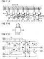
- FIGS. 11A to 11C illustrate an example of a shift register included in each of the gate line driver circuit 107A and the signal line driver circuit 107B.
- the shift register in FIG. 11A includes a first to N -th pulse output circuits 10_1 to 10_ N ( N is a natural number greater than or equal to 3).
- a first clock signal CK1, a second clock signal CK2, a third clock signal CK3, and a fourth clock signal CK4 are supplied from a first wiring 11, a second wiring 12, a third wiring 13, and a fourth wiring 14, respectively, to the first to N -th pulse output circuits 10_1 to 10_ N .
- a start pulse SP1 (a first start pulse) is input from a fifth wiring 15 to the first pulse output circuit 10_1.
- n is a natural number greater than or equal to 2 and less than or equal to N
- a signal from the pulse output circuit of the previous stage (such a signal is referred to as a previous-stage signal OUT( n -1)) ( n is a natural number greater than or equal to 2) is input.
- a signal from the third pulse output circuit 10_3 of the stage following the next stage is input.
- a signal from the ( n +2)-th pulse output circuit 10_( n +2) of the stage following the next stage (such a signal is referred to as a subsequent-stage signal OUT( n +2)) is input.
- the pulse output circuits of the respective stages output first output signals (OUT(1)(SR) to OUT(N)(SR)) to be input to the pulse output circuits of the subsequent stages and/or the pulse output circuits of the stages before the preceding stages and second output signals (OUT(1) to OUT(N)) to be input to different circuits or the like.
- a second start pulse SP2 and a third start pulse SP3 may be additionally input to the stage before the last stage and the last stage from a sixth wiring 17 and a seventh wiring 18, respectively, for example.
- a signal which is additionally generated in the shift register may be input.
- an ( N +1)-th pulse output circuit 10_( N +1) and an ( N +2)-th pulse output circuit 10_( N +2) which do not contribute to output of pulses to the pixel portion may be provided so that signals corresponding to the second start pulse (SP2) and the third start pulse (SP3) are generated in the dummy stages.
- a first clock signal (CK1) to a fourth clock signal (CK4) are signals each of which alternates between an H-level and an L-level at regular intervals. Further, the first clock signal (CK1) to the fourth clock signal (CK4) are delayed by 1/4 cycle sequentially. In this embodiment, driving of the pulse output circuit is controlled with the first to fourth clock signals (CK1) to (CK4).
- the clock signal CK is also referred to as GCK or SCK in some cases depending on a driver circuit to which the clock signal is input; the clock signal is referred to as CK in the following description.
- connection relation other than that shown in drawings and texts is also included without limitation to a predetermined connection relation, for example, the connection relation shown in the drawings and the texts.
- Each of the first to N -th pulse output circuits 10_1 to 10 _N is assumed to include the first input terminal 21, the second input terminal 22, the third input terminal 23, a fourth input terminal 24, a fifth input terminal 25, a first output terminal 26, and a second output terminal 27 (see FIG. 11B ).
- a first input terminal 21, a second input terminal 22, and a third input terminal 23 are electrically connected to any of the first to fourth wirings 11 to 14.
- the first input terminal 21 is connected to the first wiring 11; the second input terminal 22 is connected to the second wiring 12; and the third input terminal 23 is connected to the third wiring 13.
- the second pulse output circuit 10_2 the first input terminal 21 is connected to the second wiring 12, the second input terminal 22 is connected to the third wiring 13, and the third input terminal 23 is connected to the fourth wiring 14.
- a start pulse is input to the fourth input terminal 24; a subsequent-stage signal OUT(3) is input to the fifth input terminal 25; the first output signal OUT(1)(SR) is output from the first output terminal 26; and the second output signal OUT(1) is output from the second output terminal 27.
- a first terminal of the first transistor 31 is connected to the power supply line 51, a second terminal of the first transistor 31 is connected to a first terminal of the ninth transistor 39, and a gate electrode of the first transistor 31 is connected to the fourth input terminal 24.
- a first terminal of the second transistor 32 is connected to the power supply line 52, a second terminal of the second transistor 32 is connected to the first terminal of the ninth transistor 39, and a gate electrode of the second transistor 32 is connected to a gate electrode of the fourth transistor 34.
- a first terminal of the third transistor 33 is connected to the first input terminal 21, and a second terminal of the third transistor 33 is connected to the first output terminal 26.
- a first terminal of the fourth transistor 34 is connected to the power supply line 52, and a second terminal of the fourth transistor 34 is connected to the first output terminal 26.
- a first terminal of the fifth transistor 35 is connected to the power supply line 52, a second terminal of the fifth transistor 35 is connected to the gate electrode of the second transistor 32 and the gate electrode of the fourth transistor 34, and a gate electrode of the fifth transistor 35 is connected to the fourth input terminal 24.
- a first terminal of the sixth transistor 36 is connected to the power supply line 51, a second terminal of the sixth transistor 36 is connected to the gate electrode of the second transistor 32 and the gate electrode of the fourth transistor 34, and a gate electrode of the sixth transistor 36 is connected to the fifth input terminal 25.
- a first terminal of the seventh transistor 37 is connected to the power supply line 51, a second terminal of the seventh transistor 37 is connected to a second terminal of the eighth transistor 38, and a gate electrode of the seventh transistor 37 is connected to the third input terminal 23.
- a first terminal of the eighth transistor 38 is connected to the gate electrode of the second transistor 32 and the gate electrode of the fourth transistor 34, and a gate electrode of the eighth transistor 38 is connected to the second input terminal 22.
- the first terminal of the ninth transistor 39 is connected to the second terminal of the first transistor 31 and the second terminal of the second transistor 32, a second terminal of the ninth transistor 39 is connected to a gate electrode of the third transistor 33 and a gate electrode of the tenth transistor 40, and a gate electrode of the ninth transistor 39 is connected to the power supply line 51.
- a first terminal of the tenth transistor 40 is connected to the first input terminal 21, a second terminal of the tenth transistor 40 is connected to the second output terminal 27, and the gate electrode of the tenth transistor 40 is connected to the second terminal of the ninth transistor 39.
- a first terminal of the eleventh transistor 41 is connected to the power supply line 52, a second terminal of the eleventh transistor 41 is connected to the second output terminal 27, and a gate electrode of the eleventh transistor 41 is connected to the gate electrode of the second transistor 32 and the gate electrode of the fourth transistor 34.
- a portion where the gate electrode of the third transistor 33, the gate electrode of the tenth transistor 40, and the second terminal of the ninth transistor 39 are connected is referred to as a node NA.
- a portion where the gate electrode of the second transistor 32, the gate electrode of the fourth transistor 34, the second terminal of the fifth transistor 35, the second terminal of the sixth transistor 36, the first terminal of the eighth transistor 38, and the gate electrode of the eleventh transistor 41 are connected is referred to as a node NB.
- the pulse output circuit in FIG. 11C is the first pulse output circuit 10_1
- the first clock signal CK1 is input to the first input terminal 21
- the second clock signal CK2 is input to the second input terminal 22
- the third clock signal CK3 is input to the third input terminal 23
- the start pulse SP is input to the fourth input terminal 24
- a subsequent-stage signal OUT(3) is input to the fifth input terminal 25
- the first output signal OUT(1)(SR) is output from the first output terminal 26
- the second output signal OUT(1) is output from the second output terminal 27.
- FIG. 12 illustrates a timing chart of a shift register including a plurality of pulse output circuits illustrated in FIG. 11C . Note that when the shift register is the one of a gate line driver circuit, a period 61 in FIG. 12 corresponds to a vertical retrace period and a period 62 corresponds to a gate selection period.
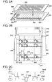
- FIGS. 2A to 2C a circuit such as a display control circuit (not illustrated) is provided outside the display panel, and a predetermined signal (the high power supply potential Vdd, the low power supply potential Vss, the start pulse SP, the clock signal CK, the image signal Data, the common potential Vcom, or the like) is input from the outside through a terminal portion.
- a predetermined signal the high power supply potential Vdd, the low power supply potential Vss, the start pulse SP, the clock signal CK, the image signal Data, the common potential Vcom, or the like
- a display panel in FIG. 2A includes a first substrate 201 and a second substrate 202.
- the first substrate 201 includes a pixel circuit portion 203, a gate line driver circuit 204, a signal line driver circuit 205, a terminal portion 206, and a switching transistor 207.
- the second substrate 202 includes a common connection portion 208 (also referred to as a common contact) and a common electrode 209 (also referred to as a counter electrode).
- the common electrode 209 is provided over the second substrate 202 with the common connection portion 208 therebetween in this embodiment; however, the common electrode 209 may be provided on the first substrate side.
- the first substrate 201 and the second substrate 202 have light-transmitting properties and heat resistance high enough to withstand heat treatment to be performed later.
- any glass substrate used in the electronics industry also called a non-alkali glass substrate
- any glass substrate used in the electronics industry such as an aluminosilicate glass substrate, an aluminoborosilicate glass substrate, or a barium borosilicate glass substrate, a quartz substrate, a ceramic substrate, a plastic substrate, or the like can be used.
- the pixel circuit portion 203, the gate line driver circuit 204, the signal line driver circuit 205, and the switching transistor 207 in FIG. 2A may be formed using thin film transistors formed over the first substrate 201.
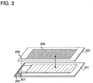
- the gate line driver circuit 204 and the signal line driver circuit 205 are not necessarily formed using thin film transistors formed over the first substrate 201 and may be formed over another substrate outside the first substrate 201, or the like as illustrated in FIG. 3 .
- a plurality of gate lines and a plurality of signal lines are extended from the gate line driver circuit 204 and the signal line driver circuit 205, and a plurality of pixels are provided so that the pixels are surrounded by the gate lines and the signal lines.
- a signal controlled by the display control circuit 104 in FIG. 1 is supplied from the terminal portion 206. That is, a predetermined signal (the high power supply potential Vdd, the low power supply potential Vss, the start pulse SP, the clock signal CK, the image signal Data, the common potential Vcom, or the like) for outputting a pulse signal for performing display in the pixel circuit portion 203 is supplied from the outside through the terminal portion 206.
- a predetermined signal the high power supply potential Vdd, the low power supply potential Vss, the start pulse SP, the clock signal CK, the image signal Data, the common potential Vcom, or the like
- the common connection portion 208 is provided for achieving electrical connection between the second terminal of the switching transistor 207 in the first substrate 201 and the common electrode 209 in the second substrate 202.
- the common potential is supplied from the terminal portion 206 to the common electrode 209 through the switching transistor 207 and the common connection portion 208.
- a conductive particle in which an insulating sphere is coated with a thin metal film may be used, so that electrical connection is made.
- two or more common connection portions 208 may be provided between the first substrate 201 and the second substrate 202.
- the common electrode 209 overlap with a pixel electrode included in the pixel circuit portion 203. Further, the common electrode 209 and the pixel electrode included in the pixel circuit portion 203 may have a variety of opening patterns.
- FIG. 2B is a circuit diagram in which the structure of the pixel circuit portion 203 in the schematic view of the display panel of FIG. 2A is particularly illustrated in detail.
- the liquid crystal display device illustrated in FIG. 2B includes the first substrate 201 and the second substrate 202 as in FIG. 2A .
- the first substrate 201 includes the pixel circuit portion 203, the gate line driver circuit 204, the signal line driver circuit 205, the terminal portion 206, and the switching transistor 207.
- the second substrate 202 includes the common connection portion 208 and the common electrode 209.
- a plurality of gate lines 211 and a plurality of signal lines 212 are arranged in matrix, and pixels 213 each including a thin film transistor (hereinafter referred to as a pixel transistor 214); a liquid crystal element 215 in which a liquid crystal is interposed between a first electrode and a second electrode; and a capacitor 210 are provided.
- a pixel transistor 214 one of a source terminal and a drain terminal of the pixel transistor 214 is referred to as a first terminal, and the other of the source terminal and the drain terminal is referred to as a second terminal.
- the first terminal is connected to the signal line 212, a gate terminal is connected to the gate line 211, and the second terminal is connected to the first electrode of the liquid crystal element 215.
- one of electrodes of the capacitor 210 is connected to the first electrode of the liquid crystal element 215, and the other electrode is connected to another wiring.
- the first electrode of the liquid crystal element 215 corresponds to the pixel electrode
- the second electrode of the liquid crystal element 215 corresponds to the common electrode 209.
- the pixel 213 is provided with the capacitor 210 in FIG. 2B , the capacitor is not necessarily provided.
- FIG. 2C is a circuit diagram of one pixel of pixels including pixel electrodes.
- the circuit diagram in FIG. 2C focuses on the pixel transistor 214 and the switching transistor 207.
- a gate terminal of the pixel transistor 214 is connected to the gate line 211
- the first terminal of the pixel transistor 214 is connected to the signal line 212
- the second terminal of the pixel transistor 214 is connected to the pixel electrode 221.
- the gate terminal of the switching transistor 207 is connected to a terminal 206A of the terminal portion 206
- the first terminal of the switching transistor 207 is connected to a terminal 206B of the terminal portion 206
- the second terminal of the switching transistor 207 is electrically connected to a common electrode 222 through the common connection portion 208.
- a liquid crystal 223 is interposed between the pixel electrode 221 and the common electrode 222.
- the pixel electrode 221, the common electrode 222, and the liquid crystal 223 may be collectively referred to as a liquid crystal element.
- FIG. 4 is a timing chart illustrating the state of signals supplied to the terminals, the gate line driver circuit 204, and the signal line driver circuit 205 in the circuit diagram in FIG. 2C .
- a period 401 in FIG 4 corresponds to a moving image writing period
- a period 402 in FIG. 4 corresponds to a still image display period.
- the period in FIG. 4 may be determined to be either the moving image writing period or the still image display period in accordance with the result of the determination of whether an image is a moving image or a still image.
- FIG. 4 is a timing chart illustrating the state of signals supplied to the terminals, the gate line driver circuit 204, and the signal line driver circuit 205 in the circuit diagram in FIG. 2C .
- a period 401 in FIG 4 corresponds to a moving image writing period
- a period 402 in FIG. 4 corresponds to a still image display period.
- the period in FIG. 4 may be determined to be either the moving image writing period or the still image display period in accordance with
- FIG. 4 also shows a potential of the signal line 212, a potential of the pixel electrode 221, a potential of the terminal 206A, a potential of the terminal 206B, and a potential of the common electrode 222.
- the period 401 corresponds to a period during which image signals for displaying a moving image are written.
- the period 402 corresponds to a period during which a still image is displayed.
- operation is performed so that the image signals and the common potential are supplied to the pixels in the pixel circuit portion 203 and the common electrode.
- the period 402 the supply of the image signals and the common potential to the pixels in the pixel circuit portion 203 and the common electrode is stopped. Note that each signal is supplied in the period 402 so that operation of the driver circuit portion is stopped in FIG. 4 ; however, it is preferable to prevent deterioration of a still image by writing image signals periodically in accordance with the length of the period 402.
- a clock signal GCK is supplied at all times as illustrated in FIG. 4 ; a start pulse GSP is supplied in accordance with a vertical synchronizing frequency as illustrated in FIG. 4 ; a clock signal SCK is supplied at all times as illustrated in FIG. 4 ; and a start pulse SSP is supplied in accordance with one gate selection period as illustrated in FIG. 4 .
- an image signal Data which is to be supplied to the pixel of each row, is supplied to the signal line 212, and the potential of the signal line 212 is supplied to the pixel electrode 221 in the pixel in accordance with the potential of the gate line 211, as illustrated in FIG. 4 .
- the terminal 206A corresponding to the gate terminal of the switching transistor 207 is given a potential at which the switching transistor 207 is turned on, so that the common potential, which is the potential of the terminal 206B, is supplied to the common electrode 222, as illustrated in FIG. 1 and FIGS. 2A to 2C .
- the supply of both the clock signal GCK and the start pulse GSP is stopped as illustrated in FIG. 4 ; the supply of both the clock signal SCK and the start pulse SSP is also stopped as illustrated in FIG. 4 ; and the supply of the image signal Data, which has been supplied to the signal line 212, is also stopped as illustrated in FIG. 4 .
- the supply of both the clock signal GCK and the start pulse GSP is stopped as illustrated in FIG 4 , so that the pixel transistor 214 is turned off, the supply of the image signal Data is stopped, and the pixel electrode 221 is brought into a floating state.
- the terminal 206A corresponding to the gate terminal of the switching transistor 207 is given a potential at which the switching transistor 207 is turned off; thus, the supply of the common potential, which is the potential of the terminal 206B, is stopped. Consequently, the common electrode 222 is brought into a floating state.
- both electrodes of the liquid crystal 223, i.e., the pixel electrode 221 and the common electrode 222, can be brought into a floating state; thus, a still image can be displayed without supply of another potential.
- the supply of a clock signal and a start pulse to the gate line driver circuit 204 and the signal line driver circuit 205 is stopped, whereby low power consumption can be achieved.
- the off current can be reduced when two terminals of a liquid crystal element are in a non-conduction state.
- the pixel transistor 214 and the switching transistor 207 each of which is formed using such a thin film transistor can reduce a current which flows through the liquid crystal element.
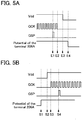
- FIGS. 5A and 5B show timing charts of the high power supply potential Vdd, the clock signal (here, GCK), the start pulse signal (here, GSP), and the potential of the terminal 206A, which are signals from the display control circuit 104, in a period during which the period 401 is switched to the period 402 in the timing chart of FIG. 4 , namely, a period during which a moving image is switched to a still image (a period 403 in FIG. 4 ), and a period during which the period 402 is switched to the period 401, namely, a period during which a still image is switched to a moving image (a period 404 in FIG. 4 ).
- the display control circuit 104 stops the supply of the start pulse GSP in a period during which a moving image is switched to a still image (E1 in FIG. 5A , a first step).
- supply of a plurality of clock signals GCK is stopped after pulse output reaches the last stage of the shift register (E2 in FIG. 5A , a second step).
- the high power supply potential Vdd of a power supply voltage is changed to the low power supply potential Vss (E3 in FIG. 5A , a third step).
- the potential of the terminal 206A is changed to a potential at which the switching transistor 111 is turned off (E4 in FIG. 5A , a fourth step).
- the supply of signals to the driver circuit portion 105 can be stopped without malfunction of the driver circuit portion 105.
- a voltage applied to a liquid crystal is held by holding charge in a pixel electrode; therefore, by operating the driver circuit portion 105 without generating noise due to malfunction, a method for driving a liquid crystal display device capable of displaying a still image which is not deteriorated so much can be provided.
- the potential of the terminal 206A is changed to a potential at which the switching transistor 111 is turned on in a period during which a still image is switched to a moving image (S1 in FIG. 5B , a first step). Then, a power supply voltage is changed from the low power supply potential Vss to the high power supply potential Vdd (S2 in FIG. 5B , a second step). After that, a plurality of clock signals GCK are supplied (S3 in FIG. 5B , a third step). Next, the start pulse signal GSP is supplied (S4 in FIG. 5B , a fourth step).
- the supply of the signals to the driver circuit portion 105 can be restarted without malfunction of the driver circuit portion 105.
- Potentials of the wirings are sequentially changed back to those at the time of displaying a moving image, whereby the driver circuit portion can be driven without malfunction.
- FIG. 6 is a chart schematically showing, for example, in frame periods, the frequency of writing of image signals in a period 601 during which a moving image is displayed and a period 602 during which a still image is displayed, where the horizontal axis shows time.
- "W” indicates a period during which an image signal is written
- "H” indicates a period during which the image signal is held.
- a period 603 is one frame period in FIG. 6 ; however, the period 603 may be a different period.
- an image signal to be supplied to a pixel is written only in a period during which switching of image signals is performed (the period 604 in FIG. 6 ).
- the other periods in the period 602 are periods during which the image signal supplied in the period 604 is held.
- the frequency of operations such as writing of an image signal can be reduced.
- the human eyes recognize images switched a plurality of times, which might lead to eyestrain.
- eyestrain can be alleviated.
- thin film transistors including oxide semiconductors are provided in pixels in this embodiment, so that the off current of the thin film transistors can be reduced. Therefore, it is possible to provide a liquid crystal display device in which a voltage can be held in a storage capacitor for a longer time and power consumption at the time when a still image is displayed can be reduced.
- This embodiment can be implemented in appropriate combination with any of the structures described in the other embodiments.
- a structure of a display panel in the liquid crystal display device in Embodiment 1 will be described with reference to a specific top view and specific cross-sectional views in FIGS. 7A to 7C .
- FIG. 7A is a top view of a display panel.
- FIG. 7A is a top view of the display panel in which an FPC has not been attached to a first substrate 1210.
- FIG. 7B is a cross-sectional view taken along line G-H of FIG 7A , which illustrates a connection region of a conductive particle and a connection wiring.
- FIG. 7C is a cross-sectional view taken along line E-F of FIG. 7A , which illustrates a connection region of a pixel circuit and a connection wiring.
- the first substrate 1210 which is provided with pixel electrodes and serves as an active matrix substrate and a second substrate 1204 provided with a common electrode 1291 are attached to each other with a sealing material 1205, and the interior space surrounded by the sealing material 1205 is filled with liquid crystal 1280.
- a signal line driver circuit 1200, a gate line driver circuit 1201, and a pixel circuit 1202 in which the pixel electrodes are formed in matrix are formed over the first substrate 1210.
- thermotropic liquid crystal low-molecular liquid crystal, high-molecular liquid crystal, polymer-dispersed liquid crystal, ferroelectric liquid crystal, anti-ferroelectric liquid crystal, or the like is used.
- a liquid crystal material exhibits a cholesteric phase, a smectic phase, a cubic phase, a chiral nematic phase, an isotropic phase, or the like depending on conditions.
- the common electrode 1291 is electrically connected to a terminal portion 1240 through a connection wiring 1208 extended from the terminal portion 1240, a switching transistor 1261, and a resin layer 1235 which is provided with conductive particles interposed between the pair of substrates.
- the number of the connections is four in FIG. 7A as an example and may be at least one.
- FIG. 7C illustrates the signal line driver circuit 1200 provided with a circuit including a driver circuit thin film transistor 1223 over the first substrate 1210, as a driver circuit portion. Further, the gate line driver circuit 1201 including a driver circuit thin film transistor is provided over the first substrate, as a driver circuit portion.
- the pixel circuit 1202 includes a pixel transistor 1211. Further, a pixel electrode 1250 connected to the pixel transistor 1211 is formed over and in an insulating layer 1214.
- the pixel transistor 1211, the driver circuit thin film transistor 1223, and the switching transistor 1261 are each formed using an oxide semiconductor layer, a gate insulating layer, and a gate electrode layer.
- the structure of the transistor is not limited to the above structure; the transistor can have any of various structures.
- the transistor may have a multi-gate structure including two or more gate electrodes.
- the transistor can have the structure where a gate electrode is provided above a channel region, the structure where a gate electrode is provided below a channel region, a staggered structure, an inverted staggered structure, or the structure where a channel region is divided into a plurality of regions.
- a channel protective structure, a channel etched structure, or the like can be employed.
- a conductive layer 1293 overlapping with the gate electrode layer and the oxide semiconductor layer with the insulating layer 1214 interposed therebetween is provided over the driver circuit thin film transistor 1223 in FIG. 7C .
- the oxide semiconductor layer is interposed between the gate electrode layer and the conductive layer 1293.
- variation in threshold voltage of the driver circuit thin film transistor 1223 can be reduced, so that a display panel provided with the driver circuit thin film transistor 1223, which has stable electric characteristics, can be provided.
- the conductive layer 1293 may be at the same potential as the gate electrode layer or may be at a floating potential or a fixed potential such as a GND potential or 0 V. By supplying an appropriate potential to the conductive layer 1293, the threshold voltage of the driver circuit thin film transistor 1223 can be controlled.
- the switching transistor 1261 in FIG. 7B is electrically connected to the common electrode 1291 through a conductive particle 1270 in the resin layer 1235.
- the switching transistor 1261 is on an outer side than the sealing material 1205 in FIG. 7A
- the switching transistor may be on an inner side than the sealing material 1205.
- the switching transistor may be provided in a region where the signal line driver circuit 1200 is formed.
- the switching transistor 1261 on an inner side than the sealing material 1205 can be protected against an impact from an external source, and the like. Thus, the lifetime of the switching transistor 1261 can be made long.
- any glass substrate used in the electronics industry such as an aluminosilicate glass substrate, an aluminoborosilicate glass substrate, or a barium borosilicate glass substrate, a quartz substrate, a ceramic substrate, a plastic substrate, or the like can be used as appropriate.
- a flexible plastic substrate as each of the first substrate 1210 and the second substrate 1204, a flexible display device can be manufactured.
- the sealing material 1205 is applied to the first substrate or the second substrate by a screen printing method, or with an ink-jet apparatus or a dispensing apparatus.
- a material containing a visible light curable resin, an ultraviolet curable resin, or a thermosetting resin can be used.
- an epoxy resin such as a liquid bisphenol-A resin, a solid bisphenol-A resin, a bromine-containing epoxy resin, a bisphenol-F resin, a bisphenol-AD resin, a phenol resin, a cresol resin, a novolac resin, a cycloaliphatic epoxy resin, an Epi-Bis type epoxy resin, a glycidyl ester resin, a glycidyl amine resin, a heterocyclic epoxy resin, or a modified epoxy resin can be used.
- the sealing material 1205 a material having a viscosity of 40 Pa ⁇ s to 400 Pa ⁇ s is used. Further, the sealing material 1205 may contain a filler (1 ⁇ m to 24 ⁇ m in diameter). Note that it is preferable to select as the sealing material, a sealing material which is insoluble in liquid crystal which is in contact with the sealing material later.
- a conductive particle in which an insulating sphere is covered with a thin metal film can be used.
- the insulating sphere is formed using silica glass, a hard resin, or the like.
- the thin metal film can be formed using a single layer or a stack of any of gold, silver, palladium, nickel, ITO, and IZO.
- a thin gold film, a stack of a thin nickel film and a thin gold film, or the like can be used.
- the kinds of the pixel electrode 1250 differ between a transmissive display panel and a reflective display panel.
- the pixel electrode 1250 is formed using a light-transmitting material.
- the light-transmitting material indium tin oxide (ITO), zinc oxide (ZnO), indium zinc oxide (IZO), gallium-doped zinc oxide (GZO), and the like can be given.
- the pixel electrode 1250 may be formed using a conductive composition containing a conductive high polymer.
- the pixel electrode formed using the conductive composition preferably has a sheet resistance of 10000 ⁇ /square or less and a transmittance of to 70 % or higher at a wavelength of 550 nm. Further, the resistivity of the conductive high polymer contained in the conductive composition is preferably 0.1 ⁇ cm or less.
- a so-called ⁇ -electron conjugated conductive polymer can be used.
- polyaniline or a derivative thereof, polypyrrole or a derivative thereof, polythiophene or a derivative thereof, a copolymer of two or more kinds of them, and the like can be given.
- a metal electrode having high reflectivity is used as the pixel electrode. Specifically, aluminum, silver, or the like is used. Further, the reflectivity is increased by making the surface of the pixel electrode rough. Therefore, a base film of the pixel electrode may be made rough.
- a transmissive material and a reflective material are used for the pixel electrode.
- a terminal portion 1240 is formed in an end portion of the first substrate 1210.
- a connection terminal 1241 is formed over the connection wiring 1208.
- FIG. 7B is a cross-sectional view of a region where the conductive particle 1270 and the connection terminal are connected to each other.
- the connection wiring 1208 and the switching transistor 1261 are formed over the first substrate 1210.
- the connection terminal 1241 formed at the same time as the pixel electrode 1250 is formed over the connection wiring 1208.
- the connection terminal 1241 is electrically connected to the common electrode 1291 through the connection wiring 1208, the switching transistor 1261, and the conductive particle 1270. Further, the connection terminal 1241 is connected to an FPC (not illustrated).
- the conductive particle 1270 is fixed by the resin layer 1235 (not illustrated).
- the resin layer 1235 can be formed using an organic resin material like that used for the sealing material 1205.
- FIG. 7C is a cross-sectional view of a region where the pixel electrode and the connection terminal are connected to each other.
- a connection wiring 1242 formed at the same time as source and drain electrode layers of the thin film transistor is formed over the first substrate 1210.
- a connection terminal 1243 formed at the same time as the pixel electrode 1250 is formed over the connection wiring 1242.
- the connection terminal 1243 is electrically connected to the pixel electrode 1250 through the connection wiring 1242. Note that, since an active matrix display panel is used in this embodiment, the pixel electrode 1250 and the connection wiring 1242 are not directly connected but are connected through the pixel transistor 1211 or the signal line driver circuit 1200.
- An alignment film 1206 is provided over the pixel electrode 1250, and rubbing treatment is performed thereon.
- the alignment film 1206 and rubbing treatment are not necessarily required, which depends on the mode of liquid crystal.
- a black matrix may be provided at a position overlapping with the signal line driver circuit 1200, and a color filter, a protective layer, and the like may be provided at a position overlapping with the pixel circuit 1202.
- the common electrode 1291 is formed, and an alignment film 1207 is provided on the common electrode 1291, and rubbing is performed thereon.
- an alignment film and rubbing treatment are not necessarily required, which depends on the mode of liquid crystal.
- the second substrate 1204 provided with the common electrode 1291 or the first substrate 1210 provided with the pixel electrode 1250 is provided with a pillar spacer 1255.
- the pillar spacer 1255 is provided to keep a distance between the first substrate 1210 and the second substrate 1204.
- an example is described in which the pillar spacer 1255 is provided on the second substrate 1204 side.
- the pillar spacer is also called a photolitho spacer, a post spacer, a scallop spacer, or a column spacer.
- a spherical spacer may be used.
- a pillar spacer is used.
- an organic insulating material such as photosensitive acrylic is applied to an entire surface of the substrate by a spin coating method, and a photolithography process is performed, so that photosensitive acrylic which remains over the substrate serves as the spacer.
- a place where a spacer is desired to be disposed can be exposed in accordance with a mask pattern at the time of exposure; therefore, by disposing the pillar spacer at a portion where the liquid crystal does not drive, the distance between the upper and lower substrates is maintained and in addition, light of the liquid crystal can be prevented from leaking.
- the pillar spacer 1255 can be formed by discharging a composition containing an organic insulating material by an ink-jet method and baking it.
- the space around the conductive particle 1270 may be filled with a conductive polymer.
- a conductive polymer conductive polyaniline, conductive polypyrrole, conductive polythiophene, a complex of polyethylenedioxythiophene (PEDOT) and poly(styrenesulfonic acid) (PSS), and the like can be given.
- PEDOT polyethylenedioxythiophene
- PSS poly(styrenesulfonic acid)
- the conductive polymer is formed by applying the conductive polymer with an ink-jet apparatus, a dispensing apparatus, or the like. When the conductive polymer is in contact with the common electrode or the connection wiring, the conductive particle 1270 and the conductive polymer are in contact with the common electrode and the connection wiring, so that connection resistance between the common electrode and the connection wiring can be reduced.
- connection wiring 1208 and the common electrode 1291 formed on the second substrate 1204 are electrically connected to each other through the conductive particle 1270.
- the sealing material 1205 and the conductive particle 1270 are discharged over the first substrate 1210 or the second substrate 1204, and then liquid crystal is discharged in a space surrounded by the sealing material 1205.
- the first substrate 1210 and the second substrate 1204 are attached to each other in reduced pressure, UV light irradiation is performed to cure the sealing material 1205, and then heating is performed to further harden the sealing material 1205, so that the first substrate 1210 and the second substrate 1204 are firmly attached to each other.
- the orientation of the liquid crystal is made uniform by the heating.
- first substrate 1210 and the second substrate 1204 can be attached to each other.
- first substrate 1210 and the second substrate 1204 are cut to have a panel shape. Furthermore, in order to improve the contrast, a first polarizing plate 1290 and a second polarizing plate 1295 are provided outside the first substrate 1210 and the second substrate 1204, respectively. Note that the first polarizing plate 1290 is not necessarily provided in the case of a reflective display device.
- a black matrix (a light-blocking layer), an optical member (an optical substrate) such as a polarizing member, a retardation member, or an anti-reflection member, and the like are provided as appropriate.
- an optical member such as a polarizing member, a retardation member, or an anti-reflection member, and the like
- circular polarization may be obtained using a polarizing substrate and a retardation substrate.
- a backlight, a side light, or the like may be used as a light source.
- display patterns are formed on a screen by driving pixel electrodes that are arranged in matrix. Specifically, when a voltage is applied between a selected pixel electrode and a common electrode that corresponds to the selected pixel electrode, optical modulation of a liquid crystal layer disposed between the pixel electrode and the common electrode is performed, and this optical modulation is recognized as a display pattern by observers.
- This embodiment can be implemented in appropriate combination with any of the structures described in the other embodiments.
- liquid crystal display device described in the above embodiment which additionally has a touch panel function, will be described with reference to FIGS. 8A and 8B .
- FIG. 8A is a schematic view of the liquid crystal display device according to this embodiment.
- FIG. 8A illustrates a structure where a liquid crystal display panel 801 which is the liquid crystal display device according to the above embodiment and a touch panel unit 802 are provided so as to overlap with each other and attached to each other in a housing (case) 803.
- a resistive type, a surface capacitive type, a projected capacitive type, or the like can be used as appropriate.
- the liquid crystal display panel 801 and the touch panel unit 802 are separately fabricated and overlapped with each other, whereby the cost for manufacture of the liquid crystal display device additionally having a touch panel function can be reduced.
- FIG. 8B illustrates a structure of a liquid crystal display device additionally having a touch panel function which is different from that of the liquid crystal display device in FIG. 8A .
- a liquid crystal display device 804 illustrated in FIG. 8B includes a plurality of pixels 805 each provided with an optical sensor 806 and a liquid crystal element 807.
- a gate line driver circuit 808, a signal line driver circuit 809, and an optical sensor driver circuit 810 are formed over a substrate over which the pixels 805 are provided, whereby the liquid crystal display device can be reduced in size.
- the optical sensor 806 may be formed using amorphous silicon or the like so as to overlap with a thin film transistor including an oxide semiconductor.
- a thin film transistor including an oxide semiconductor is used for a liquid crystal display device having a touch panel function, whereby an image holding property at the time of displaying a still image can be improved. Further, operation of a driver circuit portion during a still image is displayed is stopped, whereby low power consumption can be achieved.
- a memory element provided with a thin film transistor formed using an oxide semiconductor which is the same as that used for a pixel circuit may be provided over each of the display panels in FIGS. 8A and 8B .
- the memory element provided over the display panel for example, a touch panel may store data such as a threshold value of an electric signal of a touch portion.
- FIG. 13 illustrates a structure where the display panel in FIG. 8B is additionally provided with a memory element 811.
- FIG. 13 illustrates a structure of a basic memory element. Note that a transistor including an oxide semiconductor is denoted by a symbol "OS" in a circuit diagram of FIG. 13 .
- a gate electrode of a transistor 160 and one of a source electrode and a drain electrode of the transistor 162 are electrically connected to each other.
- a first wiring (a 1st line, also referred to as a source line) is electrically connected to a source electrode of the transistor 160.
- a second wiring (a 2nd line, also referred to as a bit line) is electrically connected to a drain electrode of the transistor 160.
- a third wiring (a 3rd line, also referred to as a first signal line) is electrically connected to the other of the source electrode and the drain electrode of the transistor 162.
- a fourth wiring (a 4th line, also referred to as a second signal line) is electrically connected to a gate electrode of the transistor 162.
- the gate electrode of the transistor 160 and one of the source electrode and the drain electrode of the transistor 162 are electrically connected to one of electrodes of a capacitor 164.
- a fifth wiring (a 5th line, also referred to as a word line) is electrically connected to the other of the electrodes of the capacitor 164.
- An off current is extremely low in the transistor 160 and the transistor 162 each including an oxide semiconductor. For that reason, a potential of the gate electrode of the transistor 160 can be held for an extremely long time by turning off the transistor 162. Provision of the capacitor 164 facilitates holding of charge given to the gate electrode of the transistor 160 and reading of stored data.
- the memory element described in this embodiment makes use of a characteristic in which the potential of the gate electrode of the transistor 160 can be held, thereby writing, storing, and reading data as follows.
- a potential of the fourth wiring is set to a potential at which the transistor 162 is turned on, so that the transistor 162 is turned on.
- a potential of the third wiring is supplied to the gate electrode of the transistor 160. That is, predetermined charge is given to the gate electrode of the transistor 160 (writing).
- the potential of the fourth wiring is set to a potential at which the transistor 162 is turned off, so that the transistor 162 is turned off.
- the charge given to the gate electrode of the transistor 160 is held (storing).
- a potential at which the transistor 160 is turned on is supplied to the gate electrode of the transistor 160 while a reading potential is supplied to the fifth wiring, whereby an on state of the transistor 160 is kept for a long time.
- a potential at which the transistor 160 is turned off is supplied to the gate electrode of the transistor 160, whereby an off state of the transistor 160 is kept for a long time.
- a reading potential refers to a potential of the fifth wiring, at which the transistor 160 is turned on or off depending on charges held in the gate electrode.
- a reading potential is supplied to the fifth wiring, and a given potential (a low potential) is applied to the first wiring, a value of a potential of the second wiring varies depending on whether the transistor 160 is on or off. For example, when the transistor 160 is on, the potential of the second wiring is lower than the potential of the first wiring. In contrast, when the transistor 160 is off, the potential of the second wiring is not changed.
- a potential at which the transistor 160 is turned off (or on) regardless of charge held in the gate electrode may be supplied to the fifth wiring.
- Data rewriting is performed similarly to the writing or storing of data. That is, the potential of the fourth line is set to a potential at which the transistor 162 is turned on, whereby the transistor 162 is turned on. Accordingly, the potential of the third line (potential related to new data) is supplied to the gate electrode of the transistor 160. After that, the potential of the fourth line is set to a potential at which the transistor 162 is turned off, whereby the transistor 162 is turned off. Consequently, new data is stored.
- data can be directly rewritten by another writing of data as described above. For that reason, erasing operation which is necessary for a flash memory or the like is not needed, so that a reduction in operation speed because of erasing operation can be prevented. That is, high-speed operation of the memory element can be achieved.
- the source electrode or the drain electrode of the transistor 162 is electrically connected to the gate electrode of the transistor 160, thereby having an effect similar to that of a floating gate of a floating gate transistor used for a nonvolatile memory element. Therefore, a portion in the drawing where the source electrode or the drain electrode of the transistor 162 is electrically connected to the gate electrode of the transistor 160 is called a floating gate portion FG in some cases.
- the floating gate portion FG can be regarded as being embedded in an insulator and thus charge is held in the floating gate portion FG.
- the amount of off current of the transistor 162 including an oxide semiconductor is lower than or equal to one hundred thousandth of the amount of off current of a transistor including a silicon semiconductor; thus, lost of the charge accumulated in the floating gate portion FG due to a leakage current of the transistor 162 is negligible.
- FIG. 9A illustrates a portable game machine which can include a housing 9630, a display portion 9631, speakers 9633, operation keys 9635, a connection terminal 9636, a recording medium reading portion 9672, and the like.
- the portable game machine illustrated in FIG. 9A can have a function of reading a program or data stored in a recording medium to display it on the display portion; a function of sharing data by wireless communication with another portable game machine; and the like.
- the portable game machine in FIG. 9A can have various functions without limitation to the above.
- FIG. 9B illustrates a digital camera which can include a housing 9630, a display portion 9631, speakers 9633, operation keys 9635, a connection terminal 9636, a shutter button 9676, an image receiving portion 9677, and the like.
- the digital camera illustrated in FIG. 9B can have various functions such as a function of shooting a still image; a function of shooting a moving image; a function of automatically or manually adjusting the shot image; a function of obtaining various kinds of data from an antenna; a function of storing the shot image or the data obtained from the antenna; and a function of displaying the shot image or the data obtained from the antenna on the display portion.
- the functions of the digital camera illustrated in FIG. 9B are not limited to those, and the digital camera can have other various functions.
- FIG. 9C illustrates a television set which can include a housing 9630, a display portion 9631, speakers 9633, operation keys 9635, a connection terminal 9636, and the like.
- the television set shown in FIG. 9C has a function of processing electric waves for television and converting the electric waves into an image signal, a function of processing the image signal and converting the image signal into a signal suitable for display, a function of converting a frame frequency of the image signal, and the like.
- the television set illustrated in FIG. 9C can have a variety of functions without limitation to the above.
- FIG. 9D illustrates a monitor for an electronic computer (personal computer), which can include a housing 9630, a display portion 9631, and the like.
- a window-type display portion 9653 is in the display portion 9631.
- the window-type display portion 9653 is provided in the display portion 9631 for illustration, a different symbol such as an icon or an image may be employed.
- an image signal is rewritten only at the time of inputting in many cases, which is favorable when the method for driving a liquid crystal display device, according to any of the above embodiments, is applied.
- the monitor illustrated in FIG. 9D can have various functions without limitation to the above.
- FIG. 10A illustrates a computer which can include a housing 9630, a display portion 9631, a speaker 9633, operation keys 9635, a connection terminal 9636, a pointing device 9681, an external connecting port 9680, and the like.
- the computer illustrated in FIG. 10A can include a housing 9630, a display portion 9631, a speaker 9633, operation keys 9635, a connection terminal 9636, a pointing device 9681, an external connecting port 9680, and the like.
- 10A can have a function of displaying a variety of kinds of data (e.g., a still image, a moving image, and a text image) on the display portion; a function of controlling processing by a variety of kinds of software (programs); a communication function such as wireless communication or wire communication; a function of connecting to various computer networks with the use of the communication function; a function of transmitting or receiving a variety of kinds of data with the use of the communication function; and the like.
- the functions of the computer illustrated in FIG. 10A are not limited to those, and the computer can have other various functions.
- FIG. 10B illustrates a mobile phone which can include a housing 9630, a display portion 9631, a speaker 9633, operation keys 9635, a microphone 9638, and the like.
- the mobile phone illustrated in FIG 10B can have a function of displaying a variety of kinds of data (e.g., a still image, a moving image, and a text image) on the display portion; a function of displaying a calendar, a date, the time, and the like on the display portion; a function of operating or editing the data displayed on the display portion; a function of controlling processing by various kinds of software (programs); and the like.
- the mobile phone illustrated in FIG. 10B can have other various functions without limitation to the above.
- FIG. 10C illustrates electronic paper (also referred to as an eBook or an e-book reader) that can include a housing 9630, a display portion 9631, operation keys 9632, and the like.
- the electronic paper in FIG. 10C can have a function of displaying a variety of kinds of data (e.g., a still image, a moving image, and a text image) on the display portion; a function of displaying a calendar, a date, the time, and the like on the display portion; a function of operating or editing the data displayed on the display portion; a function of controlling processing with the use of various kinds of software (programs); and the like.
- the electronic paper in FIG. 10C can have other various functions without limitation to the above.
- FIG. 10C can have other various functions without limitation to the above.
- FIG. 10D illustrates another electronic paper.
- the electronic paper in FIG. 10D includes a solar cell 9651 and a battery 9652 in addition to components of the electronic paper in FIG. 10C .
- the reflective liquid crystal display device is expected to be used when ambient light is relatively bright, and power generation by the solar cell 9651 and charge of the battery 9652 are efficiently performed, which is favorable.
- low power consumption can be achieved in displaying a still image.
- This embodiment can be implemented in appropriate combination with any of the structures described in the other embodiments.
Landscapes
- Engineering & Computer Science (AREA)
- Physics & Mathematics (AREA)
- General Physics & Mathematics (AREA)
- Theoretical Computer Science (AREA)
- Chemical & Material Sciences (AREA)
- Crystallography & Structural Chemistry (AREA)
- Computer Hardware Design (AREA)
- Nonlinear Science (AREA)
- General Engineering & Computer Science (AREA)
- Power Engineering (AREA)
- Mathematical Physics (AREA)
- Optics & Photonics (AREA)
- Human Computer Interaction (AREA)
- Control Of Indicators Other Than Cathode Ray Tubes (AREA)
- Liquid Crystal Display Device Control (AREA)
- Liquid Crystal (AREA)
- Thin Film Transistor (AREA)
- Shift Register Type Memory (AREA)
- Devices For Indicating Variable Information By Combining Individual Elements (AREA)
Description
- The present invention relates to a method for driving a liquid crystal display device.
- Liquid crystal display devices ranging from a large display device such as a television receiver to a small display device such as a mobile phone have been spreading. From now on, products with higher added values will be needed and are being developed. In recent years, in view of increase in concern about global environment and improvement in convenience of mobile equipment, development of liquid crystal display devices with low power consumption has attracted attention.
-
Patent Document 1 discloses a structure of a liquid crystal display device where all data signal lines are electrically isolated from a data signal driver, which results in a high impedance state, in order to maintain constant potentials of data signal lines in an idle period during which all gate lines and all the signal lines are not selected. This structure allows reduction in power consumption of the liquid crystal display device. - Non-Patent
Document 1 discloses a structure of a liquid crystal display device where refresh rates differ between the case of moving image display and the case of still image display for reduction in power consumption of the liquid crystal display device.Non-Patent Document 1 also discloses a structure where AC signals with the same phase are supplied to a signal line and a common electrode also in an idle period so that fluctuation in drain-common voltage can be prevented, in order to prevent perception of flickers due to the fluctuation in drain-common voltage, which is caused by switch of signals between the idle period and a scan period in the case of still image display. -
US 2005/140632 A1 discloses a liquid crystal panel including scanning signal lines for supplying scanning signals to gate electrodes of TFTs, and data signal lines for supplying data signals to data electrodes of TFTs. The liquid crystal panel further includes auxiliary capacitive electrode pads for use in forming auxiliary capacitance and an auxiliary capacitive lines so as not to generate a capacitive bond with the scanning signal lines. -
US 2009/166616 A1 discloses that oxygen defects formed at the boundary between the zinc oxide type oxide semiconductor and the gate insulator are terminated by a surface treatment using sulfur or selenium as an oxygen group element or a compound thereof to attain the suppression of the threshold potential shift and the leak current in the characteristics of a thin film transistor. - [Patent Document 1] Japanese Published Patent Application No.
2001-312253 - [Non-Patent Document 1] Kazuhiko Tsuda et al., IDW'02, pp. 295-298
- When complex driving is performed in a liquid crystal display device as in the structures of
Patent Document 1 andNon-Patent Document 1, the structure and operation of a driver circuit which supplies signals to gate lines and signal lines are complicated and thus power consumption of the liquid crystal display device cannot be reduced sufficiently. - In the case where refresh rates differ between the case of moving image display and the case of still image display as in the structure of Non-Patent
Document 1, the refresh rate in the case of still image display needs to be significantly decreased to further reduce power consumption of a liquid crystal display device. However, when the refresh rate in the case of still image display is significantly decreased, images displayed in a period during which image signals are held are deteriorated due to the following problem(s): leakage of charge to be held in a pixel electrode from a pixel transistor and/or disorder of an image signal between a pixel electrode and a common electrode due to noise or the like. - In view of the above problems, an object of an embodiment of the present invention is to suppress deterioration of images displayed in a liquid crystal display device by reducing the refresh rate in the case of still image display, without complex operation of a driver circuit.
- An embodiment of the present invention is a method for driving a liquid crystal display device according to
claim 1. - According to one of the embodiments of the present invention, the method for driving a liquid crystal display device may be a method for driving a liquid crystal display device including a memory circuit which stores image signals; a comparator circuit which compares the image signals in each pixel and calculates a difference; and a display control circuit which controls the driver circuit and reads out the image signals. In the comparator circuit, the image signals stored in the memory circuit in successive frame periods are read out and compared in each pixel to compare a difference, so that whether a moving image or a still image is displayed is determined.
- According to one of the embodiments of the present invention, the method for driving a liquid crystal display device may be a method in which a conduction state or a non-conduction state between the common electrode and the terminal portion to which the common potential is supplied is controlled by the switching transistor in accordance with a signal supplied from the display control circuit to a gate terminal of the switching transistor.
- According to one of the embodiments of the present invention, the driving method of a liquid crystal display device may be a method in which the switching transistor has an off current per micrometer in channel width of 10 zA/µm or less at room temperature, and a conduction state or a non-conduction state between the common electrode and the terminal portion to which the common potential is supplied is controlled by the switching transistor.
- According to one of the embodiments of the present invention, even if a refresh rate in the case of still image display is decreased, deterioration of displayed images can be suppressed.
-
-
FIG. 1 illustrates a liquid crystal display device according to an embodiment of the present invention. -
FIGS. 2A to 2C illustrate a liquid crystal display device according to an embodiment of the present invention. -
FIG. 3 illustrates a liquid crystal display device according to an embodiment of the present invention. -
FIG. 4 illustrates a liquid crystal display device according to an embodiment of the present invention. -
FIGS. 5A and 5B each illustrate a liquid crystal display device according to an embodiment of the present invention. -
FIG. 6 illustrates a liquid crystal display device according to an embodiment of the present invention. -
FIGS. 7A to 7C illustrate a liquid crystal display device according to an embodiment of the present invention. -
FIGS. 8A and 8B each illustrate a liquid crystal display device according to an embodiment of the present invention. -
FIGS. 9A to 9D each illustrate electronic equipment according to an embodiment of the present invention. -
FIGS. 10A to 10D each illustrate electronic equipment according to an embodiment of the present invention. -
FIGS. 11A to 11C illustrate a liquid crystal display device according to an embodiment of the present invention. -
FIG. 12 illustrates a liquid crystal display device according to an embodiment of the present invention. -
FIG. 13 illustrates a liquid crystal display device according to an embodiment of the present invention. - Hereinafter, embodiments of the present invention will be described with reference to the accompanying drawings. However, the present invention can be carried out in many different modes, and it is easily understood by those skilled in the art that modes and details of the present invention can be modified in various ways without departing from the purpose and the scope of the present invention. Therefore, the present invention should not be construed as being limited to the following description of the embodiments. Note that in structures of the present invention described below, identical portions are denoted by the same reference numerals in different drawings.
- Note that the size, the thickness of a layer, or distortion of the waveform of a signal of each of structures illustrated in the drawings and the like in the embodiments is exaggerated for simplicity in some cases. Therefore, embodiments of the present invention are not limited to such scales.
- Note that in this specification, terms such as "first", "second", "third", and "N-th" (N is a natural number) are used in order to avoid confusion among components and do not limit the number of the components.
- In this embodiment, block diagrams, timing charts, and the like of liquid crystal display devices will be described.
- First,
FIG. 1 is a block diagram of a liquid crystal display device, which illustrates components of the liquid crystal display device of this specification. - A liquid
crystal display device 100 inFIG. 1 includes adisplay panel 101, amemory circuit 102, acomparator circuit 103, adisplay control circuit 104, and aselection circuit 109. - The
display panel 101 includes, for example, adriver circuit portion 105, apixel circuit portion 106, acommon electrode portion 110, and aswitching transistor 111. Thedriver circuit portion 105 includes a gateline driver circuit 107A and a signalline driver circuit 107B. - The gate
line driver circuit 107A and the signalline driver circuit 107B are driver circuits for driving thepixel circuit portion 106 including a plurality of pixels. The gateline driver circuit 107A and the signalline driver circuit 107B each include a shift register circuit. The gateline driver circuit 107A, the signalline driver circuit 107B, thepixel circuit portion 106, and theswitching transistor 111 are formed using thin film transistors formed over one substrate. Note that the gateline driver circuit 107A and the signalline driver circuit 107B, and thepixel circuit portion 106 and the switchingtransistor 111 may be formed over different substrates. - A high power supply potential Vdd, a low power supply potential Vss, a start pulse SP, a clock signal CK, and an image signal Data are supplied to the
driver circuit portion 105 by control of thedisplay control circuit 104. A common potential Vcom is supplied to thecommon electrode portion 110 through the switchingtransistor 111 by control of thedisplay control circuit 104. - Note that a high power supply potential Vdd refers to a potential which is higher than a reference potential, and a low power supply potential refers to a potential which is lower than or equal to the reference potential. It is desirable that each of the high power supply potential and the low power supply potential be a potential at which a thin film transistor can operate. A potential difference between the high power supply potential Vdd and the low power supply potential Vss is referred to as a power supply voltage in some cases.
- Note that a voltage refers to a potential difference between a given potential and a reference potential (e.g., a ground potential) in many cases. Accordingly, a voltage can also be referred to as a potential.
- A common potential Vcom may be any potential as long as it serves as reference with respect to a potential of an image signal Data supplied to a pixel electrode. For example, the common potential Vcom may be a ground potential. Note that the image signal Data may be appropriately inverted in accordance with dot inversion driving, source line inversion driving, gate line inversion driving, frame inversion driving, or the like to be input to the
display panel 101. - Note that in the case where an image signal for displaying a moving image or a still image which is supplied to the
memory circuit 102 is an analog signal, the image signal may be converted into a digital signal through an A/D converter or the like to be supplied to thememory circuit 102. The image signal is converted into a digital signal in advance, whereby detection of a difference between image signals that is to be performed later can be easily performed, which is preferable. - The
memory circuit 102 includes a plurality offrame memories 108 for storing image signals for a plurality of frames. The number offrame memories 108 included in thememory circuit 102 is not particularly limited and thememory circuit 102 may be an element that can store image signals of a plurality of frames. Note that theframe memory 108 may be formed using a memory element such as a dynamic random access memory (DRAM) or a static random access memory (SRAM). - The number of the
frame memories 108 is not particularly limited as long as an image signal can be stored for each frame period. The image signals of theframe memories 108 are selectively read out by thecomparator circuit 103 and theselection circuit 109. - Note that a switching transistor is an element formed of a thin film transistor in which conduction or non-conduction between two terminals, i.e., a source terminal and a drain terminal, is selected in accordance with a voltage applied to a gate to realize switching operation.
- In the structure according to this embodiment, an oxide semiconductor is used for a semiconductor layer of a thin film transistor included in each of the
pixel circuit portion 106 and the switchingtransistor 111. The oxide semiconductor is an oxide semiconductor made to be an intrinsic (i-type) or substantially intrinsic by removal of hydrogen that is an n-type impurity to be highly purified so that impurities that are not main components of the oxide semiconductor are contained as little as possible. That is, a feature is that a highly purified i-type (intrinsic) semiconductor or a substantially i-type semiconductor is obtained not by adding an impurity but by reducing an impurity such as hydrogen or water as much as possible. Thus, an oxide semiconductor layer included in a thin film transistor is highly purified to become electrically i-type (intrinsic). - In addition, a highly purified oxide semiconductor includes extremely few carriers (close to zero), and the carrier concentration thereof is lower than 1 × 10¹⁴/cm3, preferably lower than 1 × 10¹²/cm3, more preferably 1 × 10¹¹/cm3.
- Since the oxide semiconductor includes extremely few carriers, the off current can be reduced in a transistor. Specifically, in a thin film transistor including the above oxide semiconductor layer, the off current per micrometer in channel width can be less than or equal to 10 aA/µm (1 × 10-17 A/µm), preferably less than or can be equal to 1 aA/µm (1 × 10-18 A/µm), more preferably 10 zA/µm (1 × 10-20 A/µm). That is to say, in circuit design, the oxide semiconductor layer can be regarded as an insulator when the thin film transistor is off. On the other hand, when a thin film transistor including an oxide semiconductor layer is on, the current supply capability of the thin film transistor including an oxide semiconductor layer is expected to be higher than that of a thin film transistor including a semiconductor layer formed of amorphous silicon.
- When a thin film transistor having a significantly low off current is used for the
pixel circuit portion 106, a pixel electrode can be electrically isolated from signal lines which may cause fluctuation in potential of the pixel electrode of each pixel. Thus, fluctuation in potential of the pixel electrode due to fluctuation in potential of the signal line can be suppressed. Further, a thin film transistor having a significantly low off current is used for the switchingtransistor 111, whereby the common electrode portion can be isolated from an external terminal portion to which the common potential Vcom is supplied, and the common electrode portion can be brought into an electrically floating state. Thus, fluctuation in voltage applied to both electrodes of a liquid crystal element, due to noise or the like, can be suppressed. - When an oxide semiconductor is used for a semiconductor layer of a thin film transistor included in each of the
pixel circuit portion 106 and the switchingtransistor 111, the refresh rate is reduced, so that a period during which the gate line driver circuit and the signal line driver circuit do not operate in a period during which a still image is displayed is significantly extended, and display of a pixel can be maintained as it is. Consequently, without complex operations of the driver circuits, supply of a signal for driving the gate line driver circuit and the signal line driver circuit can be stopped for a longer time and power consumption can be reduced. Note that there is absolutely no problem when a potential of a pixel electrode of each pixel is refreshed approximately every minute or longer in the case of using a thin film transistor including an oxide semiconductor having an extremely low off current. Further, when an oxide semiconductor is used for the semiconductor layer of the thin film transistor included in each of thepixel circuit portion 106 and the switchingtransistor 111, both electrodes of the liquid crystal element can be in a floating state, and thus deterioration of displayed images due to noise or the like can be suppressed. - As the oxide semiconductor layer, a four-component metal oxide film such as an In-Sn-Ga-Zn-O-based film; a three-component metal oxide film such as an In-Ga-Zn-O-based film, an In-Sn-Zn-O-based film, an In-Al-Zn-O-based film, a Sn-Ga-Zn-O-based film, an Al-Ga-Zn-O-based film, or a Sn-Al-Zn-O-based film; or a two-component metal oxide film such as an In-Zn-O-based film, a Sn-Zn-O-based film, an Al-Zn-O-based film, a Zn-Mg-O-based film, a Sn-Mg-O-based film, or an In-Mg-O-based film; an In-O-based film, a Sn-O-based film, or a Zn-O-based film can be used. Further, SiO2 may be contained in the above oxide semiconductor layer.
- As the oxide semiconductor, a thin film represented by InMO3 (ZnO) m (m > 0) can be used. Here, M represents one or more metal elements selected from Ga, Al, Mn, and Co. For example, M can be Ga, Ga and Al, Ga and Mn, Ga and Co, or the like. An oxide semiconductor whose composition formula is represented by InMO3 (ZnO) m (m > 0), which includes Ga as M, is referred to as the In-Ga-Zn-O-based oxide semiconductor described above, and a thin film of the In-Ga-Zn-O-based oxide semiconductor is also referred to as an In-Ga-Zn-O-based film.
- In a thin film transistor including an oxide semiconductor layer, the temperature dependence of an on current can hardly be observed and an off current remains significantly low; thus, the thin film transistor including an oxide semiconductor layer is preferably used at high temperature.
- The
comparator circuit 103 is a circuit which selectively reads out image signals in successive frame periods stored in thememory circuit 102, compares the image signals in the successive frame periods in each pixel, and detects a difference thereof. Depending on whether a difference is detected, operations in thedisplay control circuit 104 and theselection circuit 109 are determined. When a difference is detected in any of the pixels by comparing the image signals in thecomparator circuit 103, a series of frame periods during which the difference is detected are judged as periods during which a moving image is displayed. On the other hand, when a difference is not detected in all the pixels by comparing the image signals in thecomparator circuit 103, a series of frame periods during which no difference is detected are judged as periods during which a still image is displayed. In other words, depending on whether a difference is detected by thecomparator circuit 103, whether the image signals in the successive frame periods are image signals for displaying a moving image or image signals for displaying a still image is determined. The difference obtained by the comparison may be set so as to be determined as a difference to be detected when it is over a predetermined level. Thecomparator circuit 103 may be set so as to judge detection of a difference in accordance with the absolute value of the difference regardless of the value of the difference. - Note that in this embodiment, whether a still image or a moving image is displayed is determined by detecting a difference between image signals in successive frame periods with the
comparator circuit 103; however, a signal for determining whether a moving image or a still image is displayed may be supplied by externally supplying a signal for switching between a still image and a moving image. - Note that the moving image refers to an image which is recognized as a moving image with human eyes by rapid switch of a plurality of images which are time-divided into a plurality of frames. Specifically, by switching images at least 60 times (60 frames) per second, a moving image with less flicker is perceived by human eyes. In contrast, a still image refers to image signals which are the same in a series of frame periods, for example, in the n-th frame and (n+1)-th frame, unlike the moving image, although a plurality of images which are time-divided into a plurality of frames are switched at high speed.
- The
selection circuit 109 is a circuit for selecting image signals from theframe memory 108 where the image signals for displaying a moving image are stored and outputting the image signals to thedisplay control circuit 104 when a difference is detected by calculation with thecomparator circuit 103, that is, when images displayed in successive frame periods are moving images. Note that theselection circuit 109 does not output the image signals to thedisplay control circuit 104 when a difference between the image signals is not detected by calculation with thecomparator circuit 103, that is, when images displayed in successive frame periods are still images. When a still image is displayed, theselection circuit 109 does not output image signals from theframe memory 108 to thedisplay control circuit 104, resulting in a reduction in power consumption. Theselection circuit 109 may include a plurality of switches, for example, switches formed of transistors. - The
display control circuit 104 is a circuit for controlling supply of an image signal to thedriver circuit portion 105, which is selected by theselection circuit 109 when a difference is detected in thecomparator circuit 103 and supply or stop of supply of a control signal for controlling thedriver circuit portion 105, such as the high power supply potential Vdd, the low power supply potential Vss, the start pulse SP, or the clock signal CK, to thedriver circuit portion 105. Specifically, when thecomparator circuit 103 determines that a moving image is displayed, an image signal is read out from thememory circuit 102 through theselection circuit 109 and supplied to thedriver circuit portion 105 from thedisplay control circuit 104, and a control signal is supplied to thedriver circuit portion 105 from thedisplay control circuit 104. On the other hand, when thecomparator circuit 103 determines that a still image is displayed, an image signal is not supplied to thedisplay control circuit 104 from theselection circuit 109; therefore, the image signal is not supplied to thedriver circuit portion 105 and supply of each control signal to thedriver circuit portion 105 is stopped. - Note that the
display control circuit 104 turns on the switchingtransistor 111 when a difference is detected by calculation with thecomparator circuit 103, whereas thedisplay control circuit 104 turns off the switchingtransistor 111 when a difference is not detected by calculation with thecomparator circuit 103. - The supply of any signal refers to supply of a predetermined potential to a wiring. The stop of supply of any signal refers to stop of supply of a predetermined potential to the wiring, and connection to a wiring to which a predetermined fixed potential is supplied, for example, a wiring to which the low power supply potential Vss is supplied, or disconnection from a wiring to which a predetermined potential is supplied, which results in a floating state.
- Note that in the case where an image is determined to be a still image, when the period during which the image is assumed to be the still image is short, stop of supply of the high power supply potential Vdd and the low power supply potential Vss among the control signals is not necessarily performed. This is because an increase in power consumption due to repetition of stop and start of supply of the high power supply potential Vdd and the low power supply potential Vss can be reduced, which is favorable.
- It is desirable that the supply of the image signals and the control signals be stopped for a period during which the image signal can be held in each pixel in the
pixel circuit portion 106. Therefore, the image signals and the control signals supplied from thedisplay control circuit 104 in the previous period may be periodically supplied so that the image signals are supplied again after the holding period of image signals in each pixel. Note that an oxide semiconductor is used for the semiconductor layer of the thin film transistor included in thepixel circuit portion 106; thus, image signals can be held for a longer time. - For a shift register included in each of the gate
line driver circuit 107A and the signalline driver circuit 107B of thedriver circuit portion 105, a circuit for sequentially outputting pulses such as a clock signal, an inverted clock signal, and a start pulse from an output terminal of a first stage may be used. - Here,
FIGS. 11A to 11C illustrate an example of a shift register included in each of the gateline driver circuit 107A and the signalline driver circuit 107B. - The shift register in
FIG. 11A includes a first to N-th pulse output circuits 10_1 to 10_N (N is a natural number greater than or equal to 3). In the shift register illustrated inFIG. 11A , a first clock signal CK1, a second clock signal CK2, a third clock signal CK3, and a fourth clock signal CK4 are supplied from afirst wiring 11, asecond wiring 12, athird wiring 13, and afourth wiring 14, respectively, to the first to N-th pulse output circuits 10_1 to 10_N. A start pulse SP1 (a first start pulse) is input from afifth wiring 15 to the first pulse output circuit 10_1. To the n-th pulse output circuit 10_n of the second or subsequent stage (n is a natural number greater than or equal to 2 and less than or equal to N), a signal from the pulse output circuit of the previous stage (such a signal is referred to as a previous-stage signal OUT(n-1)) (n is a natural number greater than or equal to 2) is input. To the first pulse output circuit 10_1, a signal from the third pulse output circuit 10_3 of the stage following the next stage is input. In a similar manner, to the n-th pulse output circuit 10_n of the second or subsequent stage, a signal from the (n+2)-th pulse output circuit 10_(n+2) of the stage following the next stage (such a signal is referred to as a subsequent-stage signal OUT(n+2)) is input. Thus, the pulse output circuits of the respective stages output first output signals (OUT(1)(SR) to OUT(N)(SR)) to be input to the pulse output circuits of the subsequent stages and/or the pulse output circuits of the stages before the preceding stages and second output signals (OUT(1) to OUT(N)) to be input to different circuits or the like. Note that the subsequent-stage signal OUT(n+2) is not input to the last two stages of the shift register as illustrated inFIG. 11A , and thus, a second start pulse SP2 and a third start pulse SP3 may be additionally input to the stage before the last stage and the last stage from asixth wiring 17 and aseventh wiring 18, respectively, for example. Alternatively, a signal which is additionally generated in the shift register may be input. For example, an (N+1)-th pulse output circuit 10_(N+1) and an (N+2)-th pulse output circuit 10_(N+2) which do not contribute to output of pulses to the pixel portion (such circuits are also referred to as dummy stages) may be provided so that signals corresponding to the second start pulse (SP2) and the third start pulse (SP3) are generated in the dummy stages. - Note that a first clock signal (CK1) to a fourth clock signal (CK4) are signals each of which alternates between an H-level and an L-level at regular intervals. Further, the first clock signal (CK1) to the fourth clock signal (CK4) are delayed by 1/4 cycle sequentially. In this embodiment, driving of the pulse output circuit is controlled with the first to fourth clock signals (CK1) to (CK4). Note that the clock signal CK is also referred to as GCK or SCK in some cases depending on a driver circuit to which the clock signal is input; the clock signal is referred to as CK in the following description.
- Note that when it is explicitly described that "A and B are connected," the case where A and B are electrically connected, the case where A and B are functionally connected, and the case where A and B are directly connected are included therein. Here, each of A and B corresponds to an object (e.g., a device, an element, a circuit, a wiring, an electrode, a terminal, a conductive film, or a layer). Thus, connection relation other than that shown in drawings and texts is also included without limitation to a predetermined connection relation, for example, the connection relation shown in the drawings and the texts.
- Each of the first to N-th pulse output circuits 10_1 to 10_N is assumed to include the
first input terminal 21, thesecond input terminal 22, thethird input terminal 23, afourth input terminal 24, afifth input terminal 25, afirst output terminal 26, and a second output terminal 27 (seeFIG. 11B ). - A
first input terminal 21, asecond input terminal 22, and athird input terminal 23 are electrically connected to any of the first tofourth wirings 11 to 14. For example, in the first pulse output circuit 10_1 inFIGS. 11A and 11B , thefirst input terminal 21 is connected to thefirst wiring 11; thesecond input terminal 22 is connected to thesecond wiring 12; and thethird input terminal 23 is connected to thethird wiring 13. In the second pulse output circuit 10_2, thefirst input terminal 21 is connected to thesecond wiring 12, thesecond input terminal 22 is connected to thethird wiring 13, and thethird input terminal 23 is connected to thefourth wiring 14. - In the first pulse output circuit 10_1 in
FIGS. 11A and 11B , a start pulse is input to thefourth input terminal 24; a subsequent-stage signal OUT(3) is input to thefifth input terminal 25; the first output signal OUT(1)(SR) is output from thefirst output terminal 26; and the second output signal OUT(1) is output from thesecond output terminal 27. - Next, an example of a specific circuit configuration of the pulse output circuit will be described with reference to
FIG. 11C . - In
FIG. 11C , a first terminal of thefirst transistor 31 is connected to thepower supply line 51, a second terminal of thefirst transistor 31 is connected to a first terminal of theninth transistor 39, and a gate electrode of thefirst transistor 31 is connected to thefourth input terminal 24. A first terminal of thesecond transistor 32 is connected to thepower supply line 52, a second terminal of thesecond transistor 32 is connected to the first terminal of theninth transistor 39, and a gate electrode of thesecond transistor 32 is connected to a gate electrode of thefourth transistor 34. A first terminal of thethird transistor 33 is connected to thefirst input terminal 21, and a second terminal of thethird transistor 33 is connected to thefirst output terminal 26. A first terminal of thefourth transistor 34 is connected to thepower supply line 52, and a second terminal of thefourth transistor 34 is connected to thefirst output terminal 26. A first terminal of thefifth transistor 35 is connected to thepower supply line 52, a second terminal of thefifth transistor 35 is connected to the gate electrode of thesecond transistor 32 and the gate electrode of thefourth transistor 34, and a gate electrode of thefifth transistor 35 is connected to thefourth input terminal 24. A first terminal of thesixth transistor 36 is connected to thepower supply line 51, a second terminal of thesixth transistor 36 is connected to the gate electrode of thesecond transistor 32 and the gate electrode of thefourth transistor 34, and a gate electrode of thesixth transistor 36 is connected to thefifth input terminal 25. A first terminal of theseventh transistor 37 is connected to thepower supply line 51, a second terminal of theseventh transistor 37 is connected to a second terminal of the eighth transistor 38, and a gate electrode of theseventh transistor 37 is connected to thethird input terminal 23. A first terminal of the eighth transistor 38 is connected to the gate electrode of thesecond transistor 32 and the gate electrode of thefourth transistor 34, and a gate electrode of the eighth transistor 38 is connected to thesecond input terminal 22. The first terminal of theninth transistor 39 is connected to the second terminal of thefirst transistor 31 and the second terminal of thesecond transistor 32, a second terminal of theninth transistor 39 is connected to a gate electrode of thethird transistor 33 and a gate electrode of thetenth transistor 40, and a gate electrode of theninth transistor 39 is connected to thepower supply line 51. A first terminal of thetenth transistor 40 is connected to thefirst input terminal 21, a second terminal of thetenth transistor 40 is connected to thesecond output terminal 27, and the gate electrode of thetenth transistor 40 is connected to the second terminal of theninth transistor 39. A first terminal of theeleventh transistor 41 is connected to thepower supply line 52, a second terminal of theeleventh transistor 41 is connected to thesecond output terminal 27, and a gate electrode of theeleventh transistor 41 is connected to the gate electrode of thesecond transistor 32 and the gate electrode of thefourth transistor 34. - In
FIG. 11C , a portion where the gate electrode of thethird transistor 33, the gate electrode of thetenth transistor 40, and the second terminal of theninth transistor 39 are connected is referred to as a node NA. Moreover, a portion where the gate electrode of thesecond transistor 32, the gate electrode of thefourth transistor 34, the second terminal of thefifth transistor 35, the second terminal of thesixth transistor 36, the first terminal of the eighth transistor 38, and the gate electrode of theeleventh transistor 41 are connected is referred to as a node NB. - In the case where the pulse output circuit in
FIG. 11C is the first pulse output circuit 10_1, the first clock signal CK1 is input to thefirst input terminal 21; the second clock signal CK2 is input to thesecond input terminal 22; the third clock signal CK3 is input to thethird input terminal 23; the start pulse SP is input to thefourth input terminal 24; a subsequent-stage signal OUT(3) is input to thefifth input terminal 25; the first output signal OUT(1)(SR) is output from thefirst output terminal 26; and the second output signal OUT(1) is output from thesecond output terminal 27. -
FIG. 12 illustrates a timing chart of a shift register including a plurality of pulse output circuits illustrated inFIG. 11C . Note that when the shift register is the one of a gate line driver circuit, aperiod 61 inFIG. 12 corresponds to a vertical retrace period and aperiod 62 corresponds to a gate selection period. - Next, advantages of providing the switching
transistor 111 connected to thecommon electrode portion 110 in thedisplay panel 101 illustrated inFIG. 1 will be described with reference to a schematic diagram, a circuit diagram, and the like inFIGS. 2A to 2C . InFIGS. 2A to 2C , a circuit such as a display control circuit (not illustrated) is provided outside the display panel, and a predetermined signal (the high power supply potential Vdd, the low power supply potential Vss, the start pulse SP, the clock signal CK, the image signal Data, the common potential Vcom, or the like) is input from the outside through a terminal portion. - A display panel in
FIG. 2A includes afirst substrate 201 and asecond substrate 202. Thefirst substrate 201 includes apixel circuit portion 203, a gateline driver circuit 204, a signalline driver circuit 205, aterminal portion 206, and a switchingtransistor 207. Thesecond substrate 202 includes a common connection portion 208 (also referred to as a common contact) and a common electrode 209 (also referred to as a counter electrode). - Note that the
common electrode 209 is provided over thesecond substrate 202 with thecommon connection portion 208 therebetween in this embodiment; however, thecommon electrode 209 may be provided on the first substrate side. - It is necessary that the
first substrate 201 and thesecond substrate 202 have light-transmitting properties and heat resistance high enough to withstand heat treatment to be performed later. As thefirst substrate 201 and thesecond substrate 202, any glass substrate used in the electronics industry (also called a non-alkali glass substrate) such as an aluminosilicate glass substrate, an aluminoborosilicate glass substrate, or a barium borosilicate glass substrate, a quartz substrate, a ceramic substrate, a plastic substrate, or the like can be used. - Note that the
pixel circuit portion 203, the gateline driver circuit 204, the signalline driver circuit 205, and the switchingtransistor 207 inFIG. 2A may be formed using thin film transistors formed over thefirst substrate 201. Note that the gateline driver circuit 204 and the signalline driver circuit 205 are not necessarily formed using thin film transistors formed over thefirst substrate 201 and may be formed over another substrate outside thefirst substrate 201, or the like as illustrated inFIG. 3 . - Note that in the
pixel circuit portion 203, a plurality of gate lines and a plurality of signal lines are extended from the gateline driver circuit 204 and the signalline driver circuit 205, and a plurality of pixels are provided so that the pixels are surrounded by the gate lines and the signal lines. - A signal controlled by the
display control circuit 104 inFIG. 1 is supplied from theterminal portion 206. That is, a predetermined signal (the high power supply potential Vdd, the low power supply potential Vss, the start pulse SP, the clock signal CK, the image signal Data, the common potential Vcom, or the like) for outputting a pulse signal for performing display in thepixel circuit portion 203 is supplied from the outside through theterminal portion 206. - The
common connection portion 208 is provided for achieving electrical connection between the second terminal of the switchingtransistor 207 in thefirst substrate 201 and thecommon electrode 209 in thesecond substrate 202. The common potential is supplied from theterminal portion 206 to thecommon electrode 209 through the switchingtransistor 207 and thecommon connection portion 208. As a specific example of thecommon connection portion 208, a conductive particle in which an insulating sphere is coated with a thin metal film may be used, so that electrical connection is made. Note that two or morecommon connection portions 208 may be provided between thefirst substrate 201 and thesecond substrate 202. - It is preferable that the
common electrode 209 overlap with a pixel electrode included in thepixel circuit portion 203. Further, thecommon electrode 209 and the pixel electrode included in thepixel circuit portion 203 may have a variety of opening patterns. -
FIG. 2B is a circuit diagram in which the structure of thepixel circuit portion 203 in the schematic view of the display panel ofFIG. 2A is particularly illustrated in detail. - The liquid crystal display device illustrated in
FIG. 2B includes thefirst substrate 201 and thesecond substrate 202 as inFIG. 2A . Thefirst substrate 201 includes thepixel circuit portion 203, the gateline driver circuit 204, the signalline driver circuit 205, theterminal portion 206, and the switchingtransistor 207. Thesecond substrate 202 includes thecommon connection portion 208 and thecommon electrode 209. - In
FIG. 2B , in thepixel circuit portion 203, a plurality ofgate lines 211 and a plurality ofsignal lines 212 are arranged in matrix, andpixels 213 each including a thin film transistor (hereinafter referred to as a pixel transistor 214); aliquid crystal element 215 in which a liquid crystal is interposed between a first electrode and a second electrode; and acapacitor 210 are provided. InFIG. 2B , one of a source terminal and a drain terminal of thepixel transistor 214 is referred to as a first terminal, and the other of the source terminal and the drain terminal is referred to as a second terminal. The first terminal is connected to thesignal line 212, a gate terminal is connected to thegate line 211, and the second terminal is connected to the first electrode of theliquid crystal element 215. InFIG. 2B , one of electrodes of thecapacitor 210 is connected to the first electrode of theliquid crystal element 215, and the other electrode is connected to another wiring. Note that the first electrode of theliquid crystal element 215 corresponds to the pixel electrode, and the second electrode of theliquid crystal element 215 corresponds to thecommon electrode 209. - Note that although the
pixel 213 is provided with thecapacitor 210 inFIG. 2B , the capacitor is not necessarily provided. - Next,
FIG. 2C is a circuit diagram of one pixel of pixels including pixel electrodes. The circuit diagram inFIG. 2C focuses on thepixel transistor 214 and the switchingtransistor 207. A gate terminal of thepixel transistor 214 is connected to thegate line 211, the first terminal of thepixel transistor 214 is connected to thesignal line 212, and the second terminal of thepixel transistor 214 is connected to thepixel electrode 221. The gate terminal of the switchingtransistor 207 is connected to a terminal 206A of theterminal portion 206, the first terminal of the switchingtransistor 207 is connected to a terminal 206B of theterminal portion 206, and the second terminal of the switchingtransistor 207 is electrically connected to acommon electrode 222 through thecommon connection portion 208. Note that aliquid crystal 223 is interposed between thepixel electrode 221 and thecommon electrode 222. Thepixel electrode 221, thecommon electrode 222, and theliquid crystal 223 may be collectively referred to as a liquid crystal element. -
FIG. 4 is a timing chart illustrating the state of signals supplied to the terminals, the gateline driver circuit 204, and the signalline driver circuit 205 in the circuit diagram inFIG. 2C . Note that as an example of the timing chart, aperiod 401 inFIG 4 corresponds to a moving image writing period and aperiod 402 inFIG. 4 corresponds to a still image display period. The period inFIG. 4 may be determined to be either the moving image writing period or the still image display period in accordance with the result of the determination of whether an image is a moving image or a still image. InFIG. 4 , GCK refers to a clock signal supplied to the gateline driver circuit 204; GSP refers to a start pulse supplied to the gateline driver circuit 204; SCK refers to a clock signal supplied to the signalline driver circuit 205; and SSP refers to a start pulse supplied to the signalline driver circuit 205. In addition,FIG. 4 also shows a potential of thesignal line 212, a potential of thepixel electrode 221, a potential of the terminal 206A, a potential of the terminal 206B, and a potential of thecommon electrode 222. For the structure of a shift register in a driver circuit portion to which GCK which is a clock signal, GSP which is a start pulse, SCK which is a clock signal, and GSP which is a start pulse are supplied, the structure of the circuit described inFIGS. 11A to 11C andFIG. 12 may be used practically. - Note that the
period 401 corresponds to a period during which image signals for displaying a moving image are written. Further, theperiod 402 corresponds to a period during which a still image is displayed. Thus, in theperiod 401, operation is performed so that the image signals and the common potential are supplied to the pixels in thepixel circuit portion 203 and the common electrode. On the other hand, in theperiod 402, the supply of the image signals and the common potential to the pixels in thepixel circuit portion 203 and the common electrode is stopped. Note that each signal is supplied in theperiod 402 so that operation of the driver circuit portion is stopped inFIG. 4 ; however, it is preferable to prevent deterioration of a still image by writing image signals periodically in accordance with the length of theperiod 402. - In the
period 401, a clock signal GCK is supplied at all times as illustrated inFIG. 4 ; a start pulse GSP is supplied in accordance with a vertical synchronizing frequency as illustrated inFIG. 4 ; a clock signal SCK is supplied at all times as illustrated inFIG. 4 ; and a start pulse SSP is supplied in accordance with one gate selection period as illustrated inFIG. 4 . In theperiod 401, an image signal Data, which is to be supplied to the pixel of each row, is supplied to thesignal line 212, and the potential of thesignal line 212 is supplied to thepixel electrode 221 in the pixel in accordance with the potential of thegate line 211, as illustrated inFIG. 4 . Further, from thedisplay control circuit 104, theterminal 206A corresponding to the gate terminal of the switchingtransistor 207 is given a potential at which the switchingtransistor 207 is turned on, so that the common potential, which is the potential of the terminal 206B, is supplied to thecommon electrode 222, as illustrated inFIG. 1 andFIGS. 2A to 2C . - In the
period 402, the supply of both the clock signal GCK and the start pulse GSP is stopped as illustrated inFIG. 4 ; the supply of both the clock signal SCK and the start pulse SSP is also stopped as illustrated inFIG. 4 ; and the supply of the image signal Data, which has been supplied to thesignal line 212, is also stopped as illustrated inFIG. 4 . In theperiod 402, the supply of both the clock signal GCK and the start pulse GSP is stopped as illustrated inFIG 4 , so that thepixel transistor 214 is turned off, the supply of the image signal Data is stopped, and thepixel electrode 221 is brought into a floating state. Furthermore, theterminal 206A corresponding to the gate terminal of the switchingtransistor 207 is given a potential at which the switchingtransistor 207 is turned off; thus, the supply of the common potential, which is the potential of the terminal 206B, is stopped. Consequently, thecommon electrode 222 is brought into a floating state. - That is, in the
period 402, both electrodes of theliquid crystal 223, i.e., thepixel electrode 221 and thecommon electrode 222, can be brought into a floating state; thus, a still image can be displayed without supply of another potential. The supply of a clock signal and a start pulse to the gateline driver circuit 204 and the signalline driver circuit 205 is stopped, whereby low power consumption can be achieved. With the use of a thin film transistor including an oxide semiconductor layer, the off current can be reduced when two terminals of a liquid crystal element are in a non-conduction state. Thepixel transistor 214 and the switchingtransistor 207 each of which is formed using such a thin film transistor can reduce a current which flows through the liquid crystal element. - Next,
FIGS. 5A and 5B show timing charts of the high power supply potential Vdd, the clock signal (here, GCK), the start pulse signal (here, GSP), and the potential of the terminal 206A, which are signals from thedisplay control circuit 104, in a period during which theperiod 401 is switched to theperiod 402 in the timing chart ofFIG. 4 , namely, a period during which a moving image is switched to a still image (aperiod 403 inFIG. 4 ), and a period during which theperiod 402 is switched to theperiod 401, namely, a period during which a still image is switched to a moving image (aperiod 404 inFIG. 4 ). - As illustrated in
FIG. 5A , thedisplay control circuit 104 stops the supply of the start pulse GSP in a period during which a moving image is switched to a still image (E1 inFIG. 5A , a first step). Next, supply of a plurality of clock signals GCK is stopped after pulse output reaches the last stage of the shift register (E2 inFIG. 5A , a second step). Then, the high power supply potential Vdd of a power supply voltage is changed to the low power supply potential Vss (E3 inFIG. 5A , a third step). After that, the potential of the terminal 206A is changed to a potential at which the switchingtransistor 111 is turned off (E4 inFIG. 5A , a fourth step). - Through the above steps, the supply of signals to the
driver circuit portion 105 can be stopped without malfunction of thedriver circuit portion 105. In the case of still image display, a voltage applied to a liquid crystal is held by holding charge in a pixel electrode; therefore, by operating thedriver circuit portion 105 without generating noise due to malfunction, a method for driving a liquid crystal display device capable of displaying a still image which is not deteriorated so much can be provided. - As illustrated in
FIG. 5B , with thedisplay control circuit 104, the potential of the terminal 206A is changed to a potential at which the switchingtransistor 111 is turned on in a period during which a still image is switched to a moving image (S1 inFIG. 5B , a first step). Then, a power supply voltage is changed from the low power supply potential Vss to the high power supply potential Vdd (S2 inFIG. 5B , a second step). After that, a plurality of clock signals GCK are supplied (S3 inFIG. 5B , a third step). Next, the start pulse signal GSP is supplied (S4 inFIG. 5B , a fourth step). - Through the above steps, the supply of the signals to the
driver circuit portion 105 can be restarted without malfunction of thedriver circuit portion 105. Potentials of the wirings are sequentially changed back to those at the time of displaying a moving image, whereby the driver circuit portion can be driven without malfunction. -
FIG. 6 is a chart schematically showing, for example, in frame periods, the frequency of writing of image signals in aperiod 601 during which a moving image is displayed and aperiod 602 during which a still image is displayed, where the horizontal axis shows time. InFIG. 6 , "W" indicates a period during which an image signal is written, and "H" indicates a period during which the image signal is held. In addition, aperiod 603 is one frame period inFIG. 6 ; however, theperiod 603 may be a different period. - As shown in
FIG. 6 , in the structure of the liquid crystal display device according to this embodiment, in the case where a difference is not detected between image signals of successive frames by a comparator circuit, that is, in theperiod 602 during which a still image is displayed, an image signal to be supplied to a pixel is written only in a period during which switching of image signals is performed (theperiod 604 inFIG. 6 ). The other periods in theperiod 602 are periods during which the image signal supplied in theperiod 604 is held. - As described above, in the structure of this embodiment, in the period during which a still image is displayed, the frequency of operations such as writing of an image signal can be reduced. When seeing an image formed by writing image signals a plurality of times, the human eyes recognize images switched a plurality of times, which might lead to eyestrain. With a structure where the frequency of writing of image signals is reduced as described in this embodiment, eyestrain can be alleviated.
- Further, thin film transistors including oxide semiconductors are provided in pixels in this embodiment, so that the off current of the thin film transistors can be reduced. Therefore, it is possible to provide a liquid crystal display device in which a voltage can be held in a storage capacitor for a longer time and power consumption at the time when a still image is displayed can be reduced.
- This embodiment can be implemented in appropriate combination with any of the structures described in the other embodiments.
- A structure of a display panel in the liquid crystal display device in
Embodiment 1 will be described with reference to a specific top view and specific cross-sectional views inFIGS. 7A to 7C . -
FIG. 7A is a top view of a display panel.FIG. 7A is a top view of the display panel in which an FPC has not been attached to afirst substrate 1210.FIG. 7B is a cross-sectional view taken along line G-H ofFIG 7A , which illustrates a connection region of a conductive particle and a connection wiring.FIG. 7C is a cross-sectional view taken along line E-F ofFIG. 7A , which illustrates a connection region of a pixel circuit and a connection wiring. - In
FIGS. 7A to 7C , thefirst substrate 1210 which is provided with pixel electrodes and serves as an active matrix substrate and asecond substrate 1204 provided with acommon electrode 1291 are attached to each other with a sealingmaterial 1205, and the interior space surrounded by the sealingmaterial 1205 is filled withliquid crystal 1280. A signalline driver circuit 1200, a gateline driver circuit 1201, and apixel circuit 1202 in which the pixel electrodes are formed in matrix are formed over thefirst substrate 1210. - As the
liquid crystal 1280, thermotropic liquid crystal, low-molecular liquid crystal, high-molecular liquid crystal, polymer-dispersed liquid crystal, ferroelectric liquid crystal, anti-ferroelectric liquid crystal, or the like is used. Such a liquid crystal material exhibits a cholesteric phase, a smectic phase, a cubic phase, a chiral nematic phase, an isotropic phase, or the like depending on conditions. - In
FIG. 7B , thecommon electrode 1291 is electrically connected to aterminal portion 1240 through aconnection wiring 1208 extended from theterminal portion 1240, aswitching transistor 1261, and aresin layer 1235 which is provided with conductive particles interposed between the pair of substrates. The number of the connections is four inFIG. 7A as an example and may be at least one. -
FIG. 7C illustrates the signalline driver circuit 1200 provided with a circuit including a driver circuitthin film transistor 1223 over thefirst substrate 1210, as a driver circuit portion. Further, the gateline driver circuit 1201 including a driver circuit thin film transistor is provided over the first substrate, as a driver circuit portion. - In
FIG. 7C , thepixel circuit 1202 includes apixel transistor 1211. Further, apixel electrode 1250 connected to thepixel transistor 1211 is formed over and in an insulatinglayer 1214. - In
FIGS. 7A to 7C , thepixel transistor 1211, the driver circuitthin film transistor 1223, and theswitching transistor 1261 are each formed using an oxide semiconductor layer, a gate insulating layer, and a gate electrode layer. - The above is the description of one example of the structure of the transistor. However, the structure of the transistor is not limited to the above structure; the transistor can have any of various structures. For example, the transistor may have a multi-gate structure including two or more gate electrodes. Alternatively, the transistor can have the structure where a gate electrode is provided above a channel region, the structure where a gate electrode is provided below a channel region, a staggered structure, an inverted staggered structure, or the structure where a channel region is divided into a plurality of regions. In the case of an inverted staggered structure, a channel protective structure, a channel etched structure, or the like can be employed.
- A
conductive layer 1293 overlapping with the gate electrode layer and the oxide semiconductor layer with the insulatinglayer 1214 interposed therebetween is provided over the driver circuitthin film transistor 1223 inFIG. 7C . - In the driver circuit
thin film transistor 1223, the oxide semiconductor layer is interposed between the gate electrode layer and theconductive layer 1293. With such a structure, variation in threshold voltage of the driver circuitthin film transistor 1223 can be reduced, so that a display panel provided with the driver circuitthin film transistor 1223, which has stable electric characteristics, can be provided. Theconductive layer 1293 may be at the same potential as the gate electrode layer or may be at a floating potential or a fixed potential such as a GND potential or 0 V. By supplying an appropriate potential to theconductive layer 1293, the threshold voltage of the driver circuitthin film transistor 1223 can be controlled. - The switching
transistor 1261 inFIG. 7B is electrically connected to thecommon electrode 1291 through aconductive particle 1270 in theresin layer 1235. - Although the
switching transistor 1261 is on an outer side than the sealingmaterial 1205 inFIG. 7A , the switching transistor may be on an inner side than the sealingmaterial 1205. For example, the switching transistor may be provided in a region where the signalline driver circuit 1200 is formed. The switchingtransistor 1261 on an inner side than the sealingmaterial 1205 can be protected against an impact from an external source, and the like. Thus, the lifetime of theswitching transistor 1261 can be made long. - In
FIGS. 7A to 7C , as each of thefirst substrate 1210 and thesecond substrate 1204, any glass substrate used in the electronics industry (also called a non-alkali glass substrate) such as an aluminosilicate glass substrate, an aluminoborosilicate glass substrate, or a barium borosilicate glass substrate, a quartz substrate, a ceramic substrate, a plastic substrate, or the like can be used as appropriate. With the use of a flexible plastic substrate as each of thefirst substrate 1210 and thesecond substrate 1204, a flexible display device can be manufactured. - In
FIGS. 7A to 7C , the sealingmaterial 1205 is applied to the first substrate or the second substrate by a screen printing method, or with an ink-jet apparatus or a dispensing apparatus. As the sealingmaterial 1205, typically, a material containing a visible light curable resin, an ultraviolet curable resin, or a thermosetting resin can be used. For example, an epoxy resin such as a liquid bisphenol-A resin, a solid bisphenol-A resin, a bromine-containing epoxy resin, a bisphenol-F resin, a bisphenol-AD resin, a phenol resin, a cresol resin, a novolac resin, a cycloaliphatic epoxy resin, an Epi-Bis type epoxy resin, a glycidyl ester resin, a glycidyl amine resin, a heterocyclic epoxy resin, or a modified epoxy resin can be used. As the sealingmaterial 1205, a material having a viscosity of 40 Pa·s to 400 Pa·s is used. Further, the sealingmaterial 1205 may contain a filler (1 µm to 24 µm in diameter). Note that it is preferable to select as the sealing material, a sealing material which is insoluble in liquid crystal which is in contact with the sealing material later. - As the
conductive particle 1270, a conductive particle in which an insulating sphere is covered with a thin metal film can be used. The insulating sphere is formed using silica glass, a hard resin, or the like. The thin metal film can be formed using a single layer or a stack of any of gold, silver, palladium, nickel, ITO, and IZO. For example, as the thin metal film, a thin gold film, a stack of a thin nickel film and a thin gold film, or the like can be used. With the use of the conductive particle in which the insulating sphere is contained at the center, elasticity can be increased so that destruction due to pressure from an external source can be suppressed. - The kinds of the
pixel electrode 1250 differ between a transmissive display panel and a reflective display panel. In the case of a transmissive display panel, thepixel electrode 1250 is formed using a light-transmitting material. As examples of the light-transmitting material, indium tin oxide (ITO), zinc oxide (ZnO), indium zinc oxide (IZO), gallium-doped zinc oxide (GZO), and the like can be given. - Alternatively, the
pixel electrode 1250 may be formed using a conductive composition containing a conductive high polymer. The pixel electrode formed using the conductive composition preferably has a sheet resistance of 10000 Ω/square or less and a transmittance of to 70 % or higher at a wavelength of 550 nm. Further, the resistivity of the conductive high polymer contained in the conductive composition is preferably 0.1 Ω·cm or less. - As the conductive high polymer, a so-called π-electron conjugated conductive polymer can be used. For example, polyaniline or a derivative thereof, polypyrrole or a derivative thereof, polythiophene or a derivative thereof, a copolymer of two or more kinds of them, and the like can be given.
- On the other hand, in the case of a reflective display panel, a metal electrode having high reflectivity is used as the pixel electrode. Specifically, aluminum, silver, or the like is used. Further, the reflectivity is increased by making the surface of the pixel electrode rough. Therefore, a base film of the pixel electrode may be made rough.
- In the case of a transflective display panel, a transmissive material and a reflective material are used for the pixel electrode.
- Further, a
terminal portion 1240 is formed in an end portion of thefirst substrate 1210. In theterminal portion 1240, aconnection terminal 1241 is formed over theconnection wiring 1208. -
FIG. 7B is a cross-sectional view of a region where theconductive particle 1270 and the connection terminal are connected to each other. Theconnection wiring 1208 and theswitching transistor 1261 are formed over thefirst substrate 1210. Theconnection terminal 1241 formed at the same time as thepixel electrode 1250 is formed over theconnection wiring 1208. Theconnection terminal 1241 is electrically connected to thecommon electrode 1291 through theconnection wiring 1208, the switchingtransistor 1261, and theconductive particle 1270. Further, theconnection terminal 1241 is connected to an FPC (not illustrated). Note that inFIG. 7B , theconductive particle 1270 is fixed by the resin layer 1235 (not illustrated). Theresin layer 1235 can be formed using an organic resin material like that used for the sealingmaterial 1205. -
FIG. 7C is a cross-sectional view of a region where the pixel electrode and the connection terminal are connected to each other. Aconnection wiring 1242 formed at the same time as source and drain electrode layers of the thin film transistor is formed over thefirst substrate 1210. Aconnection terminal 1243 formed at the same time as thepixel electrode 1250 is formed over theconnection wiring 1242. Theconnection terminal 1243 is electrically connected to thepixel electrode 1250 through theconnection wiring 1242. Note that, since an active matrix display panel is used in this embodiment, thepixel electrode 1250 and theconnection wiring 1242 are not directly connected but are connected through thepixel transistor 1211 or the signalline driver circuit 1200. - An
alignment film 1206 is provided over thepixel electrode 1250, and rubbing treatment is performed thereon. Thealignment film 1206 and rubbing treatment are not necessarily required, which depends on the mode of liquid crystal. - For the
second substrate 1204 which serves as a counter substrate, a black matrix may be provided at a position overlapping with the signalline driver circuit 1200, and a color filter, a protective layer, and the like may be provided at a position overlapping with thepixel circuit 1202. Thecommon electrode 1291 is formed, and analignment film 1207 is provided on thecommon electrode 1291, and rubbing is performed thereon. Similarly to the case of thefirst substrate 1210, as for thesecond substrate 1204, an alignment film and rubbing treatment are not necessarily required, which depends on the mode of liquid crystal. - The
second substrate 1204 provided with thecommon electrode 1291 or thefirst substrate 1210 provided with thepixel electrode 1250 is provided with apillar spacer 1255. The pillar spacer 1255 is provided to keep a distance between thefirst substrate 1210 and thesecond substrate 1204. In this embodiment, an example is described in which thepillar spacer 1255 is provided on thesecond substrate 1204 side. The pillar spacer is also called a photolitho spacer, a post spacer, a scallop spacer, or a column spacer. Alternatively, a spherical spacer may be used. In this embodiment, a pillar spacer is used. As for a method for forming thepillar spacer 1255, an organic insulating material such as photosensitive acrylic is applied to an entire surface of the substrate by a spin coating method, and a photolithography process is performed, so that photosensitive acrylic which remains over the substrate serves as the spacer. With this method, a place where a spacer is desired to be disposed can be exposed in accordance with a mask pattern at the time of exposure; therefore, by disposing the pillar spacer at a portion where the liquid crystal does not drive, the distance between the upper and lower substrates is maintained and in addition, light of the liquid crystal can be prevented from leaking. Further, thepillar spacer 1255 can be formed by discharging a composition containing an organic insulating material by an ink-jet method and baking it. - The space around the
conductive particle 1270 may be filled with a conductive polymer. As typical examples of the conductive polymer, conductive polyaniline, conductive polypyrrole, conductive polythiophene, a complex of polyethylenedioxythiophene (PEDOT) and poly(styrenesulfonic acid) (PSS), and the like can be given. Further, any of the afore-mentioned examples of the conductive polymer which can be used for thepixel electrode 1250 can be used as appropriate. The conductive polymer is formed by applying the conductive polymer with an ink-jet apparatus, a dispensing apparatus, or the like. When the conductive polymer is in contact with the common electrode or the connection wiring, theconductive particle 1270 and the conductive polymer are in contact with the common electrode and the connection wiring, so that connection resistance between the common electrode and the connection wiring can be reduced. - Note that the
connection wiring 1208 and thecommon electrode 1291 formed on thesecond substrate 1204 are electrically connected to each other through theconductive particle 1270. - The sealing
material 1205 and theconductive particle 1270 are discharged over thefirst substrate 1210 or thesecond substrate 1204, and then liquid crystal is discharged in a space surrounded by the sealingmaterial 1205. After that, thefirst substrate 1210 and thesecond substrate 1204 are attached to each other in reduced pressure, UV light irradiation is performed to cure thesealing material 1205, and then heating is performed to further harden the sealingmaterial 1205, so that thefirst substrate 1210 and thesecond substrate 1204 are firmly attached to each other. In addition, the orientation of the liquid crystal is made uniform by the heating. - Consequently, the
first substrate 1210 and thesecond substrate 1204 can be attached to each other. - Then, the
first substrate 1210 and thesecond substrate 1204 are cut to have a panel shape. Furthermore, in order to improve the contrast, a firstpolarizing plate 1290 and a secondpolarizing plate 1295 are provided outside thefirst substrate 1210 and thesecond substrate 1204, respectively. Note that the firstpolarizing plate 1290 is not necessarily provided in the case of a reflective display device. - Although not illustrated in this embodiment, a black matrix (a light-blocking layer), an optical member (an optical substrate) such as a polarizing member, a retardation member, or an anti-reflection member, and the like are provided as appropriate. For example, circular polarization may be obtained using a polarizing substrate and a retardation substrate. In addition, a backlight, a side light, or the like may be used as a light source.
- In an active matrix display panel, display patterns are formed on a screen by driving pixel electrodes that are arranged in matrix. Specifically, when a voltage is applied between a selected pixel electrode and a common electrode that corresponds to the selected pixel electrode, optical modulation of a liquid crystal layer disposed between the pixel electrode and the common electrode is performed, and this optical modulation is recognized as a display pattern by observers.
- In the structure of a display panel including a thin film transistor including an oxide semiconductor layer, which is described above, low power consumption can be achieved in displaying a still image as in
Embodiment 1. - This embodiment can be implemented in appropriate combination with any of the structures described in the other embodiments.
- In this embodiment, the liquid crystal display device described in the above embodiment, which additionally has a touch panel function, will be described with reference to
FIGS. 8A and 8B . -
FIG. 8A is a schematic view of the liquid crystal display device according to this embodiment.FIG. 8A illustrates a structure where a liquidcrystal display panel 801 which is the liquid crystal display device according to the above embodiment and atouch panel unit 802 are provided so as to overlap with each other and attached to each other in a housing (case) 803. For thetouch panel unit 802, a resistive type, a surface capacitive type, a projected capacitive type, or the like can be used as appropriate. - As illustrated in
FIG. 8A , the liquidcrystal display panel 801 and thetouch panel unit 802 are separately fabricated and overlapped with each other, whereby the cost for manufacture of the liquid crystal display device additionally having a touch panel function can be reduced. -
FIG. 8B illustrates a structure of a liquid crystal display device additionally having a touch panel function which is different from that of the liquid crystal display device inFIG. 8A . A liquidcrystal display device 804 illustrated inFIG. 8B includes a plurality ofpixels 805 each provided with anoptical sensor 806 and aliquid crystal element 807. Thus, it is not necessary to form thetouch panel unit 802 so as to overlap with the liquidcrystal display device 804 unlike in the structure ofFIG. 8A , which leads to reduction in thickness of the liquid crystal display device. A gateline driver circuit 808, a signalline driver circuit 809, and an opticalsensor driver circuit 810 are formed over a substrate over which thepixels 805 are provided, whereby the liquid crystal display device can be reduced in size. Note that theoptical sensor 806 may be formed using amorphous silicon or the like so as to overlap with a thin film transistor including an oxide semiconductor. - According to this embodiment, a thin film transistor including an oxide semiconductor is used for a liquid crystal display device having a touch panel function, whereby an image holding property at the time of displaying a still image can be improved. Further, operation of a driver circuit portion during a still image is displayed is stopped, whereby low power consumption can be achieved.
- Alternatively, a memory element provided with a thin film transistor formed using an oxide semiconductor which is the same as that used for a pixel circuit may be provided over each of the display panels in
FIGS. 8A and 8B . The memory element provided over the display panel, for example, a touch panel may store data such as a threshold value of an electric signal of a touch portion. As an example,FIG. 13 illustrates a structure where the display panel inFIG. 8B is additionally provided with amemory element 811.FIG. 13 illustrates a structure of a basic memory element. Note that a transistor including an oxide semiconductor is denoted by a symbol "OS" in a circuit diagram ofFIG. 13 . - In the memory element illustrated in
FIG. 13 , a gate electrode of atransistor 160 and one of a source electrode and a drain electrode of thetransistor 162 are electrically connected to each other. A first wiring (a 1st line, also referred to as a source line) is electrically connected to a source electrode of thetransistor 160. A second wiring (a 2nd line, also referred to as a bit line) is electrically connected to a drain electrode of thetransistor 160. A third wiring (a 3rd line, also referred to as a first signal line) is electrically connected to the other of the source electrode and the drain electrode of thetransistor 162. A fourth wiring (a 4th line, also referred to as a second signal line) is electrically connected to a gate electrode of thetransistor 162. The gate electrode of thetransistor 160 and one of the source electrode and the drain electrode of thetransistor 162 are electrically connected to one of electrodes of acapacitor 164. A fifth wiring (a 5th line, also referred to as a word line) is electrically connected to the other of the electrodes of thecapacitor 164. - An off current is extremely low in the
transistor 160 and thetransistor 162 each including an oxide semiconductor. For that reason, a potential of the gate electrode of thetransistor 160 can be held for an extremely long time by turning off thetransistor 162. Provision of thecapacitor 164 facilitates holding of charge given to the gate electrode of thetransistor 160 and reading of stored data. - The memory element described in this embodiment makes use of a characteristic in which the potential of the gate electrode of the
transistor 160 can be held, thereby writing, storing, and reading data as follows. - Firstly, writing and holding of data will be described. First, a potential of the fourth wiring is set to a potential at which the
transistor 162 is turned on, so that thetransistor 162 is turned on. Thus, a potential of the third wiring is supplied to the gate electrode of thetransistor 160. That is, predetermined charge is given to the gate electrode of the transistor 160 (writing). After that, the potential of the fourth wiring is set to a potential at which thetransistor 162 is turned off, so that thetransistor 162 is turned off. Thus, the charge given to the gate electrode of thetransistor 160 is held (storing). - Since the off current of the
transistor 162 is significantly low, the charge of the gate electrode of thetransistor 160 is held for a long time. For example, a potential at which thetransistor 160 is turned on is supplied to the gate electrode of thetransistor 160 while a reading potential is supplied to the fifth wiring, whereby an on state of thetransistor 160 is kept for a long time. In a similar manner, a potential at which thetransistor 160 is turned off is supplied to the gate electrode of thetransistor 160, whereby an off state of thetransistor 160 is kept for a long time. Here, a reading potential refers to a potential of the fifth wiring, at which thetransistor 160 is turned on or off depending on charges held in the gate electrode. - Secondly, reading of data will be described. When an on state or an off state of the
transistor 160 is kept as described above, a reading potential is supplied to the fifth wiring, and a given potential (a low potential) is applied to the first wiring, a value of a potential of the second wiring varies depending on whether thetransistor 160 is on or off. For example, when thetransistor 160 is on, the potential of the second wiring is lower than the potential of the first wiring. In contrast, when thetransistor 160 is off, the potential of the second wiring is not changed. - In this manner, by comparing the potential of the first wiring with the potential of the second wiring in a state where data is stored, the data can be read out.
- In the case where data is not read out, a potential at which the
transistor 160 is turned off (or on) regardless of charge held in the gate electrode may be supplied to the fifth wiring. - Next, rewriting of data will be described. Data rewriting is performed similarly to the writing or storing of data. That is, the potential of the fourth line is set to a potential at which the
transistor 162 is turned on, whereby thetransistor 162 is turned on. Accordingly, the potential of the third line (potential related to new data) is supplied to the gate electrode of thetransistor 160. After that, the potential of the fourth line is set to a potential at which thetransistor 162 is turned off, whereby thetransistor 162 is turned off. Consequently, new data is stored. - In the memory element illustrated in
FIG. 13 , data can be directly rewritten by another writing of data as described above. For that reason, erasing operation which is necessary for a flash memory or the like is not needed, so that a reduction in operation speed because of erasing operation can be prevented. That is, high-speed operation of the memory element can be achieved. - Note that the source electrode or the drain electrode of the
transistor 162 is electrically connected to the gate electrode of thetransistor 160, thereby having an effect similar to that of a floating gate of a floating gate transistor used for a nonvolatile memory element. Therefore, a portion in the drawing where the source electrode or the drain electrode of thetransistor 162 is electrically connected to the gate electrode of thetransistor 160 is called a floating gate portion FG in some cases. When thetransistor 162 is off, the floating gate portion FG can be regarded as being embedded in an insulator and thus charge is held in the floating gate portion FG. The amount of off current of thetransistor 162 including an oxide semiconductor is lower than or equal to one hundred thousandth of the amount of off current of a transistor including a silicon semiconductor; thus, lost of the charge accumulated in the floating gate portion FG due to a leakage current of thetransistor 162 is negligible. - With such a structure, the problem of deterioration of a gate insulating film (tunnel insulating film), which is pointed out in a conventional floating gate transistor, can be avoided. That is to say, the problem of deterioration of a gate insulating film due to injection of an electron into a floating gate, which has been a concern, can be solved. Thus, in the memory element illustrated in
FIG. 13 , there is no limit on the number of times of writing in principle. - This embodiment can be combined with any of the other embodiments as appropriate.
- In this embodiment, examples of electronic equipment including the liquid crystal display device described in any of the embodiments will be described.
-
FIG. 9A illustrates a portable game machine which can include ahousing 9630, adisplay portion 9631,speakers 9633,operation keys 9635, aconnection terminal 9636, a recordingmedium reading portion 9672, and the like. The portable game machine illustrated inFIG. 9A can have a function of reading a program or data stored in a recording medium to display it on the display portion; a function of sharing data by wireless communication with another portable game machine; and the like. The portable game machine inFIG. 9A can have various functions without limitation to the above. -
FIG. 9B illustrates a digital camera which can include ahousing 9630, adisplay portion 9631,speakers 9633,operation keys 9635, aconnection terminal 9636, ashutter button 9676, animage receiving portion 9677, and the like. The digital camera illustrated inFIG. 9B can have various functions such as a function of shooting a still image; a function of shooting a moving image; a function of automatically or manually adjusting the shot image; a function of obtaining various kinds of data from an antenna; a function of storing the shot image or the data obtained from the antenna; and a function of displaying the shot image or the data obtained from the antenna on the display portion. Note that the functions of the digital camera illustrated inFIG. 9B are not limited to those, and the digital camera can have other various functions. -
FIG. 9C illustrates a television set which can include ahousing 9630, adisplay portion 9631,speakers 9633,operation keys 9635, aconnection terminal 9636, and the like. The television set shown inFIG. 9C has a function of processing electric waves for television and converting the electric waves into an image signal, a function of processing the image signal and converting the image signal into a signal suitable for display, a function of converting a frame frequency of the image signal, and the like. Note that the television set illustrated inFIG. 9C can have a variety of functions without limitation to the above. -
FIG. 9D illustrates a monitor for an electronic computer (personal computer), which can include ahousing 9630, adisplay portion 9631, and the like. As for the monitor illustrated inFIG. 9D , a window-type display portion 9653 is in thedisplay portion 9631. Note that although the window-type display portion 9653 is provided in thedisplay portion 9631 for illustration, a different symbol such as an icon or an image may be employed. In the case of a monitor for a personal computer, an image signal is rewritten only at the time of inputting in many cases, which is favorable when the method for driving a liquid crystal display device, according to any of the above embodiments, is applied. Note that the monitor illustrated inFIG. 9D can have various functions without limitation to the above. -
FIG. 10A illustrates a computer which can include ahousing 9630, adisplay portion 9631, aspeaker 9633,operation keys 9635, aconnection terminal 9636, apointing device 9681, an external connectingport 9680, and the like. The computer illustrated inFIG. 10A can have a function of displaying a variety of kinds of data (e.g., a still image, a moving image, and a text image) on the display portion; a function of controlling processing by a variety of kinds of software (programs); a communication function such as wireless communication or wire communication; a function of connecting to various computer networks with the use of the communication function; a function of transmitting or receiving a variety of kinds of data with the use of the communication function; and the like. Note that the functions of the computer illustrated inFIG. 10A are not limited to those, and the computer can have other various functions. -
FIG. 10B illustrates a mobile phone which can include ahousing 9630, adisplay portion 9631, aspeaker 9633,operation keys 9635, amicrophone 9638, and the like. The mobile phone illustrated inFIG 10B can have a function of displaying a variety of kinds of data (e.g., a still image, a moving image, and a text image) on the display portion; a function of displaying a calendar, a date, the time, and the like on the display portion; a function of operating or editing the data displayed on the display portion; a function of controlling processing by various kinds of software (programs); and the like. Note that the mobile phone illustrated inFIG. 10B can have other various functions without limitation to the above. -
FIG. 10C illustrates electronic paper (also referred to as an eBook or an e-book reader) that can include ahousing 9630, adisplay portion 9631,operation keys 9632, and the like. The electronic paper inFIG. 10C can have a function of displaying a variety of kinds of data (e.g., a still image, a moving image, and a text image) on the display portion; a function of displaying a calendar, a date, the time, and the like on the display portion; a function of operating or editing the data displayed on the display portion; a function of controlling processing with the use of various kinds of software (programs); and the like. Note that the electronic paper inFIG. 10C can have other various functions without limitation to the above.FIG. 10D illustrates another electronic paper. The electronic paper inFIG. 10D includes asolar cell 9651 and abattery 9652 in addition to components of the electronic paper inFIG. 10C . In the case of using a reflective liquid crystal display device as thedisplay portion 9631, the reflective liquid crystal display device is expected to be used when ambient light is relatively bright, and power generation by thesolar cell 9651 and charge of thebattery 9652 are efficiently performed, which is favorable. Note that it is advantageous to use a lithium ion battery as thebattery 9652 because reduction in size can be achieved, for example. - In the electronic equipment described in this embodiment, low power consumption can be achieved in displaying a still image.
- This embodiment can be implemented in appropriate combination with any of the structures described in the other embodiments.
Claims (4)
- A method for driving a liquid crystal display device including a plurality of pixel transistors and a plurality of pixel electrodes, the method comprising:comparing image signals in successive frame periods to determine whether a moving image or a still image is displayed and performing one of the following steps in accordance with the result of the determination:- switch from a moving image display period to a still image display period;- switch from a still image display period to a moving image display period;- continue a moving image display period; and- continue a still image display period,wherein, in a moving image display period, the following steps are performed:for each frame, the pixel transistors including an oxide semiconductor layer which is electrically connected to a driver circuit portion formed over a first substrate are turned on, so that an image signal is supplied to the pixel electrodes; anda switching transistor including an oxide semiconductor layer which is electrically connected to a terminal portion formed over the first substrate is turned on, so that a common potential is supplied to a common electrode which is electrically connected to the terminal portion through the switching transistor and which is formed over a second substrate,wherein, in a still image display period, the following steps are performed:the pixel transistors are turned off so that the pixel electrodes are in an electrically floating state; andthe switching transistor is turned off so that the common electrode is in an electrically floating state,wherein, in a period during which a still image display period is switched to a moving image display period, the following steps are performed:a first step of supplying the common potential to the common electrode;a second step of supplying a power supply voltage to the driver circuit portion;a third step of supplying a clock signal to the driver circuit portion; anda fourth step of supplying a start pulse signal to the driver circuit portion, andwherein, in a period during which a moving image display period is switched to a still image display period, the following steps are performed:a first step of stopping supply of a start pulse signal to the driver circuit portion;a second step of stopping supply of a clock signal to the driver circuit portion;a third step of stopping supply of a power supply voltage to the driver circuit portion; anda fourth step of stopping supply of the common potential to the common electrode.
- The method for driving a liquid crystal display device, according to claim 1,
wherein the liquid crystal display device comprises:a memory circuit which stores the image signals;a comparator circuit which compares the image signals in each of pixels and calculates a difference; anda display control circuit which controls the driver circuit and reads out the image signals, andwherein in the comparator circuit, the image signals stored in the memory circuit in successive frame periods are read out and compared in each of the pixels to compare a difference, so that whether a moving image or a still image is displayed is determined. - The method for driving a liquid crystal display device, according to claim 2,
wherein a conduction state or a non-conduction state between the common electrode and the terminal portion to which the common potential is supplied is controlled by the switching transistor in accordance with a signal supplied from the display control circuit to a gate terminal of the switching transistor. - The method for driving a liquid crystal display device, according to claim 2,
wherein the switching transistor has an off current per micrometer in channel width of 10 zA/µm or less at room temperature, and
wherein a conduction state or a non-conduction state between the common electrode and the terminal portion to which the common potential is supplied is controlled by the switching transistor.
Applications Claiming Priority (2)
| Application Number | Priority Date | Filing Date | Title |
|---|---|---|---|
| JP2009287957 | 2009-12-18 | ||
| PCT/JP2010/071204 WO2011074393A1 (en) | 2009-12-18 | 2010-11-22 | Method for driving liquid crystal display device |
Publications (3)
| Publication Number | Publication Date |
|---|---|
| EP2513894A1 EP2513894A1 (en) | 2012-10-24 |
| EP2513894A4 EP2513894A4 (en) | 2014-12-17 |
| EP2513894B1 true EP2513894B1 (en) | 2018-08-01 |
Family
ID=44150350
Family Applications (1)
| Application Number | Title | Priority Date | Filing Date |
|---|---|---|---|
| EP10837422.4A Not-in-force EP2513894B1 (en) | 2009-12-18 | 2010-11-22 | Method for driving liquid crystal display device |
Country Status (7)
| Country | Link |
|---|---|
| US (6) | US8599177B2 (en) |
| EP (1) | EP2513894B1 (en) |
| JP (10) | JP5031086B2 (en) |
| KR (11) | KR20240118180A (en) |
| CN (3) | CN105390110B (en) |
| TW (5) | TWI549114B (en) |
| WO (1) | WO2011074393A1 (en) |
Families Citing this family (69)
| Publication number | Priority date | Publication date | Assignee | Title |
|---|---|---|---|---|
| KR101751908B1 (en) | 2009-10-21 | 2017-06-28 | 가부시키가이샤 한도오따이 에네루기 켄큐쇼 | Voltage regulator circuit |
| KR20240118180A (en) | 2009-12-18 | 2024-08-02 | 가부시키가이샤 한도오따이 에네루기 켄큐쇼 | Liquid crystal display device |
| KR101282383B1 (en) * | 2009-12-18 | 2013-07-04 | 가부시키가이샤 한도오따이 에네루기 켄큐쇼 | Liquid crystal display device and electronic device |
| KR20210138135A (en) | 2009-12-25 | 2021-11-18 | 가부시키가이샤 한도오따이 에네루기 켄큐쇼 | Semiconductor device |
| WO2011081041A1 (en) | 2009-12-28 | 2011-07-07 | Semiconductor Energy Laboratory Co., Ltd. | Semiconductor device and method for manufacturing the semiconductor device |
| CN102714029B (en) * | 2010-01-20 | 2016-03-23 | 株式会社半导体能源研究所 | The display packing of display device |
| WO2011089843A1 (en) * | 2010-01-20 | 2011-07-28 | Semiconductor Energy Laboratory Co., Ltd. | Method for driving display device |
| WO2011089842A1 (en) | 2010-01-20 | 2011-07-28 | Semiconductor Energy Laboratory Co., Ltd. | Driving method of liquid crystal display device |
| KR20190093706A (en) | 2010-01-24 | 2019-08-09 | 가부시키가이샤 한도오따이 에네루기 켄큐쇼 | Display device and manufacturing method thereof |
| TWI525377B (en) * | 2010-01-24 | 2016-03-11 | 半導體能源研究所股份有限公司 | Display device |
| KR101873730B1 (en) | 2010-01-24 | 2018-07-04 | 가부시키가이샤 한도오따이 에네루기 켄큐쇼 | Display device |
| WO2011102248A1 (en) * | 2010-02-19 | 2011-08-25 | Semiconductor Energy Laboratory Co., Ltd. | Liquid crystal display device and electronic device |
| KR101686089B1 (en) | 2010-02-19 | 2016-12-28 | 가부시키가이샤 한도오따이 에네루기 켄큐쇼 | Semiconductor device |
| WO2011105218A1 (en) * | 2010-02-26 | 2011-09-01 | Semiconductor Energy Laboratory Co., Ltd. | Display device and e-book reader provided therewith |
| CN102834861B (en) | 2010-04-09 | 2016-02-10 | 株式会社半导体能源研究所 | The method of liquid crystal display and this liquid crystal display of driving |
| US8698852B2 (en) | 2010-05-20 | 2014-04-15 | Semiconductor Energy Laboratory Co., Ltd. | Display device and method for driving the same |
| WO2011145537A1 (en) | 2010-05-21 | 2011-11-24 | Semiconductor Energy Laboratory Co., Ltd. | Liquid crystal display device |
| US9030837B2 (en) | 2011-06-10 | 2015-05-12 | Scott Moncrieff | Injection molded control panel with in-molded decorated plastic film that includes an internal connector |
| WO2013021846A1 (en) * | 2011-08-05 | 2013-02-14 | シャープ株式会社 | Display device and method for controlling same |
| JP6046413B2 (en) | 2011-08-08 | 2016-12-14 | 三星ディスプレイ株式會社Samsung Display Co.,Ltd. | Display device and driving method thereof |
| US9019188B2 (en) | 2011-08-08 | 2015-04-28 | Samsung Display Co., Ltd. | Display device for varying different scan ratios for displaying moving and still images and a driving method thereof |
| US20140333563A1 (en) * | 2011-09-21 | 2014-11-13 | Sharp Kabushiki Kaisha | Display device and display system |
| US9299301B2 (en) * | 2011-11-04 | 2016-03-29 | Samsung Display Co., Ltd. | Display device and method for driving the display device |
| US9208736B2 (en) * | 2011-11-28 | 2015-12-08 | Samsung Display Co., Ltd. | Display device and driving method thereof |
| TWI639150B (en) | 2011-11-30 | 2018-10-21 | 日商半導體能源研究所股份有限公司 | Semiconductor display device |
| CN104115216B (en) * | 2012-02-20 | 2016-12-14 | 夏普株式会社 | Driving means and display device |
| MY167325A (en) * | 2012-02-20 | 2018-08-16 | Sharp Kk | Drive device and display device |
| US9129572B2 (en) | 2012-02-21 | 2015-09-08 | Samsung Display Co., Ltd. | Display device and related method |
| CN104170001B (en) | 2012-03-13 | 2017-03-01 | 株式会社半导体能源研究所 | Light-emitting device and its driving method |
| JP2013235083A (en) * | 2012-05-08 | 2013-11-21 | Sharp Corp | Display device |
| JP6032794B2 (en) * | 2012-06-08 | 2016-11-30 | 株式会社ジャパンディスプレイ | Liquid crystal display |
| KR102082794B1 (en) | 2012-06-29 | 2020-02-28 | 가부시키가이샤 한도오따이 에네루기 켄큐쇼 | Method of driving display device, and display device |
| CN102810294A (en) * | 2012-08-01 | 2012-12-05 | 京东方科技集团股份有限公司 | Displaying method, displaying device and displaying system |
| CN103677458B (en) * | 2012-09-17 | 2016-08-17 | 凌巨科技股份有限公司 | Touch-control system and inducing method thereof |
| KR20150085035A (en) | 2012-11-15 | 2015-07-22 | 가부시키가이샤 한도오따이 에네루기 켄큐쇼 | Liquid crystal display device |
| JP6054418B2 (en) * | 2012-11-22 | 2016-12-27 | シャープ株式会社 | Display device and electronic device |
| US20140152685A1 (en) * | 2012-11-30 | 2014-06-05 | Semiconductor Energy Laboratory Co., Ltd. | Semiconductor device and program |
| KR102015771B1 (en) * | 2013-01-24 | 2019-08-30 | 삼성디스플레이 주식회사 | Display appatatus and method of driving the same |
| KR102060627B1 (en) * | 2013-04-22 | 2019-12-31 | 삼성디스플레이 주식회사 | Display device and driving method thereof |
| KR102049736B1 (en) * | 2013-06-25 | 2019-11-28 | 엘지디스플레이 주식회사 | Display Device Including Timing Controller |
| JP6426402B2 (en) * | 2013-08-30 | 2018-11-21 | 株式会社半導体エネルギー研究所 | Display device |
| US9806098B2 (en) | 2013-12-10 | 2017-10-31 | Semiconductor Energy Laboratory Co., Ltd. | Light-emitting device |
| JP6180318B2 (en) * | 2013-12-27 | 2017-08-16 | ソニーセミコンダクタソリューションズ株式会社 | Comparator circuit |
| JP6491821B2 (en) * | 2014-04-07 | 2019-03-27 | 株式会社ジャパンディスプレイ | Display device |
| CN104020595B (en) * | 2014-06-13 | 2017-02-15 | 昆山龙腾光电有限公司 | Touch display panel and touch display device |
| JP2016066065A (en) | 2014-09-05 | 2016-04-28 | 株式会社半導体エネルギー研究所 | Display device and electronic device |
| KR102360783B1 (en) | 2014-09-16 | 2022-02-10 | 삼성디스플레이 주식회사 | display device |
| CN104199586B (en) * | 2014-09-16 | 2018-04-13 | 重庆京东方光电科技有限公司 | A kind of array base palte, In-cell touch panel and touch control display apparatus |
| TWI533273B (en) | 2014-10-24 | 2016-05-11 | 友達光電股份有限公司 | Power management method and power management device |
| KR20170091139A (en) | 2014-12-01 | 2017-08-08 | 가부시키가이샤 한도오따이 에네루기 켄큐쇼 | Display device, display module having said display device, and electronic device having said display device or said display module |
| US10262604B2 (en) * | 2014-12-08 | 2019-04-16 | Sharp Kabushiki Kaisha | Control device, display device, and control method for display device |
| TW201627977A (en) * | 2015-01-21 | 2016-08-01 | 中華映管股份有限公司 | Display and touch display |
| TWI534793B (en) * | 2015-05-21 | 2016-05-21 | 友達光電股份有限公司 | Liquid crstal display |
| CN106328075B (en) * | 2015-06-25 | 2019-05-31 | 群创光电股份有限公司 | Image display system and gate driving circuit |
| KR102290613B1 (en) * | 2015-06-30 | 2021-08-19 | 엘지디스플레이 주식회사 | Organic Light Emitting Display And Driving Method Thereof |
| CN105138179B (en) * | 2015-09-15 | 2018-06-15 | 深圳市华星光电技术有限公司 | Full-embedded type touch screen and mobile device |
| KR102493542B1 (en) * | 2015-12-30 | 2023-02-01 | 삼성디스플레이 주식회사 | Display apparatus and method of driving the same |
| CN108476025B (en) * | 2016-01-07 | 2022-03-18 | 索尼公司 | Comparator, analog-to-digital converter, solid-state imaging device, and imaging apparatus |
| KR102617273B1 (en) * | 2016-10-31 | 2023-12-21 | 엘지디스플레이 주식회사 | In-cell touch display device |
| KR20180066327A (en) | 2016-12-07 | 2018-06-19 | 삼성디스플레이 주식회사 | Display device and driving method thereof |
| KR20180082692A (en) * | 2017-01-10 | 2018-07-19 | 삼성디스플레이 주식회사 | Display device and driving method thereof |
| US10796642B2 (en) | 2017-01-11 | 2020-10-06 | Samsung Display Co., Ltd. | Display device |
| US20220178692A1 (en) * | 2017-12-21 | 2022-06-09 | Mindmaze Holding Sa | System, method and apparatus of a motion sensing stack with a camera system |
| DE102020002836A1 (en) | 2020-05-12 | 2021-11-18 | Conrad Leuthaeuser | Pharmaceutical and therapeutic use of S-acetylglutathione and its enzymes against viruses and the coronavirus (Covid 19) |
| CN111583866B (en) * | 2020-06-30 | 2021-12-17 | 武汉天马微电子有限公司 | Output control unit, output control circuit, display panel and display device |
| CN114078407A (en) * | 2020-08-11 | 2022-02-22 | 上海和辉光电股份有限公司 | Driving method and device of display panel |
| KR20220068326A (en) * | 2020-11-18 | 2022-05-26 | 삼성디스플레이 주식회사 | Scan driver and display device having the same |
| CN113009741B (en) * | 2021-03-09 | 2022-07-08 | 北海惠科光电技术有限公司 | Array substrate, display panel and manufacturing method thereof |
| JP2022160815A (en) * | 2021-04-07 | 2022-10-20 | シャープ株式会社 | Display device |
Family Cites Families (234)
| Publication number | Priority date | Publication date | Assignee | Title |
|---|---|---|---|---|
| JPS5211255U (en) | 1975-07-12 | 1977-01-26 | ||
| JPS60198861A (en) | 1984-03-23 | 1985-10-08 | Fujitsu Ltd | Thin film transistor |
| JPS62135338A (en) | 1985-12-09 | 1987-06-18 | Diafoil Co Ltd | Monoaxially high-orientated film of polyethylene-naphthalate for liquid crystal panel substrate |
| JPH0244256B2 (en) | 1987-01-28 | 1990-10-03 | Kagaku Gijutsucho Mukizaishitsu Kenkyushocho | INGAZN2O5DESHIMESARERUROTSUHOSHOKEINOSOJOKOZOOJUSURUKAGOBUTSUOYOBISONOSEIZOHO |
| JPH0244258B2 (en) | 1987-02-24 | 1990-10-03 | Kagaku Gijutsucho Mukizaishitsu Kenkyushocho | INGAZN3O6DESHIMESARERUROTSUHOSHOKEINOSOJOKOZOOJUSURUKAGOBUTSUOYOBISONOSEIZOHO |
| JPH0244260B2 (en) | 1987-02-24 | 1990-10-03 | Kagaku Gijutsucho Mukizaishitsu Kenkyushocho | INGAZN5O8DESHIMESARERUROTSUHOSHOKEINOSOJOKOZOOJUSURUKAGOBUTSUOYOBISONOSEIZOHO |
| JPS63210023A (en) | 1987-02-24 | 1988-08-31 | Natl Inst For Res In Inorg Mater | Compound having laminar structure of hexagonal crystal system expressed by ingazn4o7 and its production |
| JPH0244262B2 (en) | 1987-02-27 | 1990-10-03 | Kagaku Gijutsucho Mukizaishitsu Kenkyushocho | INGAZN6O9DESHIMESARERUROTSUHOSHOKEINOSOJOKOZOOJUSURUKAGOBUTSUOYOBISONOSEIZOHO |
| JPH0244263B2 (en) | 1987-04-22 | 1990-10-03 | Kagaku Gijutsucho Mukizaishitsu Kenkyushocho | INGAZN7O10DESHIMESARERUROTSUHOSHOKEINOSOJOKOZOOJUSURUKAGOBUTSUOYOBISONOSEIZOHO |
| JP2568659B2 (en) | 1988-12-12 | 1997-01-08 | 松下電器産業株式会社 | Driving method of display device |
| US5070409A (en) | 1989-06-13 | 1991-12-03 | Asahi Kogaku Kogyo Kabushiki Kaisha | Liquid crystal display device with display holding device |
| JPH03226090A (en) | 1990-01-30 | 1991-10-07 | Sanyo Electric Co Ltd | Digital convergence circuit |
| KR940008180B1 (en) * | 1990-12-27 | 1994-09-07 | 가부시끼가이샤 한도다이 에네르기 겐꾸쇼 | Liquid crystal electro-optical device |
| JPH05211255A (en) | 1992-01-21 | 1993-08-20 | Nec Corp | Semiconductor device case |
| JPH05224626A (en) | 1992-02-14 | 1993-09-03 | Fujitsu Ltd | Liquid crystal display device |
| JPH05251705A (en) | 1992-03-04 | 1993-09-28 | Fuji Xerox Co Ltd | Thin-film transistor |
| JPH0667795A (en) | 1992-08-21 | 1994-03-11 | Sharp Corp | Input decision method for touch type input device |
| JPH08166599A (en) | 1994-12-13 | 1996-06-25 | Fujitsu Ltd | Liquid crystal display device |
| JPH08263021A (en) | 1995-03-23 | 1996-10-11 | Sony Corp | Liquid crystal display device |
| JP3479375B2 (en) | 1995-03-27 | 2003-12-15 | 科学技術振興事業団 | Metal oxide semiconductor device in which a pn junction is formed with a thin film transistor made of a metal oxide semiconductor such as cuprous oxide, and methods for manufacturing the same |
| DE69635107D1 (en) * | 1995-08-03 | 2005-09-29 | Koninkl Philips Electronics Nv | SEMICONDUCTOR ARRANGEMENT WITH A TRANSPARENT CIRCUIT ELEMENT |
| JP3485229B2 (en) * | 1995-11-30 | 2004-01-13 | 株式会社東芝 | Display device |
| JP3224505B2 (en) | 1995-11-30 | 2001-10-29 | 株式会社ピーエフユー | Liquid crystal control device and liquid crystal display device |
| US5945972A (en) | 1995-11-30 | 1999-08-31 | Kabushiki Kaisha Toshiba | Display device |
| JP3625598B2 (en) * | 1995-12-30 | 2005-03-02 | 三星電子株式会社 | Manufacturing method of liquid crystal display device |
| KR0170735B1 (en) * | 1996-01-29 | 1999-03-20 | 김광호 | Jpeg |
| JP3226090B2 (en) * | 1997-01-30 | 2001-11-05 | 日本ビクター株式会社 | Liquid crystal display |
| JP3883641B2 (en) | 1997-03-27 | 2007-02-21 | 株式会社半導体エネルギー研究所 | Contact structure and active matrix display device |
| JP4170454B2 (en) | 1998-07-24 | 2008-10-22 | Hoya株式会社 | Article having transparent conductive oxide thin film and method for producing the same |
| JP3362672B2 (en) | 1998-07-30 | 2003-01-07 | 日本電気株式会社 | ASK modulation device and ASK modulation method |
| US6340994B1 (en) * | 1998-08-12 | 2002-01-22 | Pixonics, Llc | System and method for using temporal gamma and reverse super-resolution to process images for use in digital display systems |
| JP2000150861A (en) * | 1998-11-16 | 2000-05-30 | Tdk Corp | Oxide thin film |
| JP3276930B2 (en) | 1998-11-17 | 2002-04-22 | 科学技術振興事業団 | Transistor and semiconductor device |
| JP2000267066A (en) * | 1999-03-15 | 2000-09-29 | Canon Inc | Liquid crystal device |
| TW460731B (en) | 1999-09-03 | 2001-10-21 | Ind Tech Res Inst | Electrode structure and production method of wide viewing angle LCD |
| TW494382B (en) * | 2000-03-22 | 2002-07-11 | Toshiba Corp | Display apparatus and driving method of display apparatus |
| TW488154B (en) * | 2000-04-26 | 2002-05-21 | Winbond Electronics Corp | Digital moving and static picture capturing adapter of moving picture camera |
| JP3766926B2 (en) | 2000-04-28 | 2006-04-19 | シャープ株式会社 | Display device driving method, display device using the same, and portable device |
| WO2001084226A1 (en) * | 2000-04-28 | 2001-11-08 | Sharp Kabushiki Kaisha | Display unit, drive method for display unit, electronic apparatus mounting display unit thereon |
| JP4212791B2 (en) | 2000-08-09 | 2009-01-21 | シャープ株式会社 | Liquid crystal display device and portable electronic device |
| US6987496B2 (en) | 2000-08-18 | 2006-01-17 | Semiconductor Energy Laboratory Co., Ltd. | Electronic device and method of driving the same |
| TW518552B (en) * | 2000-08-18 | 2003-01-21 | Semiconductor Energy Lab | Liquid crystal display device, method of driving the same, and method of driving a portable information device having the liquid crystal display device |
| JP4954400B2 (en) | 2000-08-18 | 2012-06-13 | 株式会社半導体エネルギー研究所 | Semiconductor device |
| TW514854B (en) * | 2000-08-23 | 2002-12-21 | Semiconductor Energy Lab | Portable information apparatus and method of driving the same |
| JP4089858B2 (en) | 2000-09-01 | 2008-05-28 | 国立大学法人東北大学 | Semiconductor device |
| JP5019668B2 (en) * | 2000-09-18 | 2012-09-05 | 三洋電機株式会社 | Display device and control method thereof |
| JP2002175062A (en) | 2000-09-29 | 2002-06-21 | Sanyo Electric Co Ltd | Drive device for display device |
| TWI221595B (en) | 2000-09-29 | 2004-10-01 | Sanyo Electric Co | Driving apparatus for display device |
| JP2008233925A (en) | 2000-10-05 | 2008-10-02 | Sharp Corp | Method for driving display device, display device using same and portable device mounted with display device |
| US6594677B2 (en) | 2000-12-22 | 2003-07-15 | Simdesk Technologies, Inc. | Virtual tape storage system and method |
| MXPA03004238A (en) | 2000-11-14 | 2004-12-03 | Simdesk Technologies Inc | Remote printing. |
| US20020059489A1 (en) | 2000-11-14 | 2002-05-16 | Davis Ray Charles | Remote printing |
| KR20020038482A (en) * | 2000-11-15 | 2002-05-23 | 모리시타 요이찌 | Thin film transistor array, method for producing the same, and display panel using the same |
| JP2002162938A (en) * | 2000-11-22 | 2002-06-07 | Toshiba Corp | Liquid crystal display device |
| JP2002229532A (en) * | 2000-11-30 | 2002-08-16 | Toshiba Corp | Liquid crystal display and its driving method |
| JP2002169499A (en) * | 2000-11-30 | 2002-06-14 | Sanyo Electric Co Ltd | Driving method of display panel and driving controller of display panel |
| JP4696353B2 (en) * | 2000-12-07 | 2011-06-08 | ソニー株式会社 | Active matrix display device and portable terminal using the same |
| JP3730159B2 (en) * | 2001-01-12 | 2005-12-21 | シャープ株式会社 | Display device driving method and display device |
| CA2438581C (en) * | 2001-02-16 | 2005-11-29 | Ignis Innovation Inc. | Organic light emitting diode display having shield electrodes |
| JP3997731B2 (en) * | 2001-03-19 | 2007-10-24 | 富士ゼロックス株式会社 | Method for forming a crystalline semiconductor thin film on a substrate |
| JP2002289859A (en) | 2001-03-23 | 2002-10-04 | Minolta Co Ltd | Thin-film transistor |
| JP3925839B2 (en) | 2001-09-10 | 2007-06-06 | シャープ株式会社 | Semiconductor memory device and test method thereof |
| JP4090716B2 (en) | 2001-09-10 | 2008-05-28 | 雅司 川崎 | Thin film transistor and matrix display device |
| JP4164562B2 (en) | 2002-09-11 | 2008-10-15 | 独立行政法人科学技術振興機構 | Transparent thin film field effect transistor using homologous thin film as active layer |
| US7061014B2 (en) * | 2001-11-05 | 2006-06-13 | Japan Science And Technology Agency | Natural-superlattice homologous single crystal thin film, method for preparation thereof, and device using said single crystal thin film |
| JP4083486B2 (en) * | 2002-02-21 | 2008-04-30 | 独立行政法人科学技術振興機構 | Method for producing LnCuO (S, Se, Te) single crystal thin film |
| CN1445821A (en) * | 2002-03-15 | 2003-10-01 | 三洋电机株式会社 | Forming method of ZnO film and ZnO semiconductor layer, semiconductor element and manufacturing method thereof |
| JP3933591B2 (en) * | 2002-03-26 | 2007-06-20 | 淳二 城戸 | Organic electroluminescent device |
| US7339187B2 (en) | 2002-05-21 | 2008-03-04 | State Of Oregon Acting By And Through The Oregon State Board Of Higher Education On Behalf Of Oregon State University | Transistor structures |
| JP2003344823A (en) | 2002-05-23 | 2003-12-03 | Sharp Corp | Liquid crystal display device and method for driving liquid crystal display |
| JP2004022625A (en) * | 2002-06-13 | 2004-01-22 | Murata Mfg Co Ltd | Manufacturing method of semiconductor device and its manufacturing method |
| US7105868B2 (en) * | 2002-06-24 | 2006-09-12 | Cermet, Inc. | High-electron mobility transistor with zinc oxide |
| JP2004045520A (en) * | 2002-07-09 | 2004-02-12 | Toshiba Corp | Driving method for plane display device |
| JP4638117B2 (en) | 2002-08-22 | 2011-02-23 | シャープ株式会社 | Display device and driving method thereof |
| US7067843B2 (en) * | 2002-10-11 | 2006-06-27 | E. I. Du Pont De Nemours And Company | Transparent oxide semiconductor thin film transistors |
| JP2004151222A (en) * | 2002-10-29 | 2004-05-27 | Sharp Corp | Liquid crystal display control unit and liquid crystal display device |
| KR100915234B1 (en) | 2002-12-17 | 2009-09-02 | 삼성전자주식회사 | Driving apparatus of liquid crystal display for varying limits selecting gray voltages and method thereof |
| JP4166105B2 (en) | 2003-03-06 | 2008-10-15 | シャープ株式会社 | Semiconductor device and manufacturing method thereof |
| JP2004273732A (en) | 2003-03-07 | 2004-09-30 | Sharp Corp | Active matrix substrate and its producing process |
| JP4074207B2 (en) | 2003-03-10 | 2008-04-09 | 株式会社 日立ディスプレイズ | Liquid crystal display |
| KR100945577B1 (en) * | 2003-03-11 | 2010-03-08 | 삼성전자주식회사 | Driving device of liquid crystal display and method thereof |
| JP4108633B2 (en) | 2003-06-20 | 2008-06-25 | シャープ株式会社 | THIN FILM TRANSISTOR, MANUFACTURING METHOD THEREOF, AND ELECTRONIC DEVICE |
| US7262463B2 (en) * | 2003-07-25 | 2007-08-28 | Hewlett-Packard Development Company, L.P. | Transistor including a deposited channel region having a doped portion |
| JP4299622B2 (en) * | 2003-09-24 | 2009-07-22 | Nec液晶テクノロジー株式会社 | Liquid crystal display device and driving method used for the liquid crystal display device |
| CN100452135C (en) * | 2004-02-27 | 2009-01-14 | 佳能株式会社 | Image display apparatus |
| JP4194567B2 (en) | 2004-02-27 | 2008-12-10 | キヤノン株式会社 | Image display device |
| US7297977B2 (en) | 2004-03-12 | 2007-11-20 | Hewlett-Packard Development Company, L.P. | Semiconductor device |
| US7145174B2 (en) * | 2004-03-12 | 2006-12-05 | Hewlett-Packard Development Company, Lp. | Semiconductor device |
| EP1737044B1 (en) | 2004-03-12 | 2014-12-10 | Japan Science and Technology Agency | Amorphous oxide and thin film transistor |
| US7282782B2 (en) * | 2004-03-12 | 2007-10-16 | Hewlett-Packard Development Company, L.P. | Combined binary oxide semiconductor device |
| JP4494050B2 (en) * | 2004-03-17 | 2010-06-30 | シャープ株式会社 | Display device drive device and display device |
| JP2005300948A (en) * | 2004-04-13 | 2005-10-27 | Hitachi Displays Ltd | Display device and driving method therefor |
| US7211825B2 (en) * | 2004-06-14 | 2007-05-01 | Yi-Chi Shih | Indium oxide-based thin film transistors and circuits |
| JP4015157B2 (en) * | 2004-07-20 | 2007-11-28 | シャープ株式会社 | Drive device for liquid crystal display device, program and recording medium, and liquid crystal display device |
| KR101056013B1 (en) * | 2004-08-03 | 2011-08-10 | 엘지디스플레이 주식회사 | Manufacturing method of array substrate for liquid crystal display device |
| JP2006100760A (en) * | 2004-09-02 | 2006-04-13 | Casio Comput Co Ltd | Thin-film transistor and its manufacturing method |
| US7285501B2 (en) * | 2004-09-17 | 2007-10-23 | Hewlett-Packard Development Company, L.P. | Method of forming a solution processed device |
| US7298084B2 (en) * | 2004-11-02 | 2007-11-20 | 3M Innovative Properties Company | Methods and displays utilizing integrated zinc oxide row and column drivers in conjunction with organic light emitting diodes |
| US7791072B2 (en) * | 2004-11-10 | 2010-09-07 | Canon Kabushiki Kaisha | Display |
| JP5126729B2 (en) | 2004-11-10 | 2013-01-23 | キヤノン株式会社 | Image display device |
| RU2358355C2 (en) * | 2004-11-10 | 2009-06-10 | Кэнон Кабусики Кайся | Field transistor |
| US7863611B2 (en) * | 2004-11-10 | 2011-01-04 | Canon Kabushiki Kaisha | Integrated circuits utilizing amorphous oxides |
| CA2585063C (en) * | 2004-11-10 | 2013-01-15 | Canon Kabushiki Kaisha | Light-emitting device |
| US7829444B2 (en) * | 2004-11-10 | 2010-11-09 | Canon Kabushiki Kaisha | Field effect transistor manufacturing method |
| BRPI0517568B8 (en) * | 2004-11-10 | 2022-03-03 | Canon Kk | field effect transistor |
| US7453065B2 (en) * | 2004-11-10 | 2008-11-18 | Canon Kabushiki Kaisha | Sensor and image pickup device |
| JP2006189661A (en) * | 2005-01-06 | 2006-07-20 | Toshiba Corp | Image display apparatus and method thereof |
| US7579224B2 (en) * | 2005-01-21 | 2009-08-25 | Semiconductor Energy Laboratory Co., Ltd. | Method for manufacturing a thin film semiconductor device |
| US7608531B2 (en) * | 2005-01-28 | 2009-10-27 | Semiconductor Energy Laboratory Co., Ltd. | Semiconductor device, electronic device, and method of manufacturing semiconductor device |
| TWI505473B (en) * | 2005-01-28 | 2015-10-21 | Semiconductor Energy Lab | Semiconductor device, electronic device, and method of manufacturing semiconductor device |
| US7858451B2 (en) * | 2005-02-03 | 2010-12-28 | Semiconductor Energy Laboratory Co., Ltd. | Electronic device, semiconductor device and manufacturing method thereof |
| US20060182425A1 (en) * | 2005-02-11 | 2006-08-17 | Paul Boerger | Converting a still image to a plurality of video frame images |
| US7948171B2 (en) * | 2005-02-18 | 2011-05-24 | Semiconductor Energy Laboratory Co., Ltd. | Light emitting device |
| US20060197092A1 (en) * | 2005-03-03 | 2006-09-07 | Randy Hoffman | System and method for forming conductive material on a substrate |
| US8681077B2 (en) * | 2005-03-18 | 2014-03-25 | Semiconductor Energy Laboratory Co., Ltd. | Semiconductor device, and display device, driving method and electronic apparatus thereof |
| WO2006105077A2 (en) * | 2005-03-28 | 2006-10-05 | Massachusetts Institute Of Technology | Low voltage thin film transistor with high-k dielectric material |
| TWI467702B (en) | 2005-03-28 | 2015-01-01 | Semiconductor Energy Lab | Memory device and manufacturing method the same |
| WO2006112108A1 (en) * | 2005-03-31 | 2006-10-26 | Sharp Kabushiki Kaisha | Driving method for liquid crystal display unit |
| US7645478B2 (en) * | 2005-03-31 | 2010-01-12 | 3M Innovative Properties Company | Methods of making displays |
| US8300031B2 (en) * | 2005-04-20 | 2012-10-30 | Semiconductor Energy Laboratory Co., Ltd. | Semiconductor device comprising transistor having gate and drain connected through a current-voltage conversion element |
| WO2006115291A1 (en) | 2005-04-26 | 2006-11-02 | Semiconductor Energy Laboratory Co., Ltd. | Light emitting device and method for driving thereof |
| TW200641780A (en) * | 2005-05-26 | 2006-12-01 | Quanta Display Inc | Low power consumption method for thin film transistor liquid crystal display |
| JP2006344849A (en) | 2005-06-10 | 2006-12-21 | Casio Comput Co Ltd | Thin film transistor |
| US7691666B2 (en) | 2005-06-16 | 2010-04-06 | Eastman Kodak Company | Methods of making thin film transistors comprising zinc-oxide-based semiconductor materials and transistors made thereby |
| US7402506B2 (en) * | 2005-06-16 | 2008-07-22 | Eastman Kodak Company | Methods of making thin film transistors comprising zinc-oxide-based semiconductor materials and transistors made thereby |
| US7507618B2 (en) | 2005-06-27 | 2009-03-24 | 3M Innovative Properties Company | Method for making electronic devices using metal oxide nanoparticles |
| TW200703112A (en) * | 2005-07-14 | 2007-01-16 | Tatung Co Ltd | Cstomizing an uanimated welcome screen by means of static pictures for personal digital assistant ( PDA) |
| KR100711890B1 (en) * | 2005-07-28 | 2007-04-25 | 삼성에스디아이 주식회사 | Organic Light Emitting Display and Fabrication Method for the same |
| JP2007059128A (en) * | 2005-08-23 | 2007-03-08 | Canon Inc | Organic electroluminescent display device and manufacturing method thereof |
| JP4850457B2 (en) | 2005-09-06 | 2012-01-11 | キヤノン株式会社 | Thin film transistor and thin film diode |
| JP4560502B2 (en) * | 2005-09-06 | 2010-10-13 | キヤノン株式会社 | Field effect transistor |
| JP4280736B2 (en) * | 2005-09-06 | 2009-06-17 | キヤノン株式会社 | Semiconductor element |
| JP2007073705A (en) * | 2005-09-06 | 2007-03-22 | Canon Inc | Oxide-semiconductor channel film transistor and its method of manufacturing same |
| JP5116225B2 (en) * | 2005-09-06 | 2013-01-09 | キヤノン株式会社 | Manufacturing method of oxide semiconductor device |
| EP1938458B1 (en) | 2005-09-21 | 2015-06-03 | Semiconductor Energy Laboratory Co., Ltd. | Cyclic redundancy check circuit and devices having the cyclic redundancy check circuit |
| EP1998373A3 (en) * | 2005-09-29 | 2012-10-31 | Semiconductor Energy Laboratory Co, Ltd. | Semiconductor device having oxide semiconductor layer and manufacturing method thereof |
| JP2007094158A (en) * | 2005-09-29 | 2007-04-12 | Toshiba Matsushita Display Technology Co Ltd | Liquid crystal display device |
| JP5037808B2 (en) * | 2005-10-20 | 2012-10-03 | キヤノン株式会社 | Field effect transistor using amorphous oxide, and display device using the transistor |
| TWI275058B (en) | 2005-11-10 | 2007-03-01 | Ind Tech Res Inst | Display apparatus with dynamic scanning backlight and control method and device thereof |
| JP2007134482A (en) | 2005-11-10 | 2007-05-31 | Toppan Printing Co Ltd | Thin film transistor device, its manufacturing method, thin film transistor array using the same and thin film transistor display |
| JP2007139817A (en) * | 2005-11-14 | 2007-06-07 | Sharp Corp | Display apparatus with touch panel, and apparatus and method for driving display apparatus |
| CN101577281B (en) * | 2005-11-15 | 2012-01-11 | 株式会社半导体能源研究所 | Active matrix display and TV comprising the display |
| JP5395994B2 (en) | 2005-11-18 | 2014-01-22 | 出光興産株式会社 | Semiconductor thin film, manufacturing method thereof, and thin film transistor |
| JP2007163891A (en) | 2005-12-14 | 2007-06-28 | Sony Corp | Display apparatus |
| TWI292281B (en) * | 2005-12-29 | 2008-01-01 | Ind Tech Res Inst | Pixel structure of active organic light emitting diode and method of fabricating the same |
| US7867636B2 (en) * | 2006-01-11 | 2011-01-11 | Murata Manufacturing Co., Ltd. | Transparent conductive film and method for manufacturing the same |
| JP4977478B2 (en) * | 2006-01-21 | 2012-07-18 | 三星電子株式会社 | ZnO film and method of manufacturing TFT using the same |
| US7576394B2 (en) * | 2006-02-02 | 2009-08-18 | Kochi Industrial Promotion Center | Thin film transistor including low resistance conductive thin films and manufacturing method thereof |
| US7977169B2 (en) * | 2006-02-15 | 2011-07-12 | Kochi Industrial Promotion Center | Semiconductor device including active layer made of zinc oxide with controlled orientations and manufacturing method thereof |
| JP5224702B2 (en) | 2006-03-13 | 2013-07-03 | キヤノン株式会社 | Pixel circuit and image display device having the pixel circuit |
| KR20070101595A (en) | 2006-04-11 | 2007-10-17 | 삼성전자주식회사 | Zno thin film transistor |
| US20070252928A1 (en) | 2006-04-28 | 2007-11-01 | Toppan Printing Co., Ltd. | Structure, transmission type liquid crystal display, reflection type display and manufacturing method thereof |
| TWI349259B (en) * | 2006-05-23 | 2011-09-21 | Au Optronics Corp | A panel module and power saving method thereof |
| JP2007316431A (en) | 2006-05-26 | 2007-12-06 | Seiko Epson Corp | Display driver, electrooptical device, and electronic apparatus |
| JP5028033B2 (en) | 2006-06-13 | 2012-09-19 | キヤノン株式会社 | Oxide semiconductor film dry etching method |
| JP4241858B2 (en) | 2006-07-03 | 2009-03-18 | エプソンイメージングデバイス株式会社 | Liquid crystal device and electronic device |
| JP4241850B2 (en) | 2006-07-03 | 2009-03-18 | エプソンイメージングデバイス株式会社 | Liquid crystal device, driving method of liquid crystal device, and electronic apparatus |
| US8692822B2 (en) * | 2006-07-31 | 2014-04-08 | Sharp Kabushiki Kaisha | Display controller, display device, display system, and method for controlling display device |
| JP4999400B2 (en) * | 2006-08-09 | 2012-08-15 | キヤノン株式会社 | Oxide semiconductor film dry etching method |
| JP4609797B2 (en) * | 2006-08-09 | 2011-01-12 | Nec液晶テクノロジー株式会社 | Thin film device and manufacturing method thereof |
| JP4946286B2 (en) * | 2006-09-11 | 2012-06-06 | 凸版印刷株式会社 | Thin film transistor array, image display device using the same, and driving method thereof |
| JP4332545B2 (en) * | 2006-09-15 | 2009-09-16 | キヤノン株式会社 | Field effect transistor and manufacturing method thereof |
| JP5164357B2 (en) * | 2006-09-27 | 2013-03-21 | キヤノン株式会社 | Semiconductor device and manufacturing method of semiconductor device |
| JP4274219B2 (en) * | 2006-09-27 | 2009-06-03 | セイコーエプソン株式会社 | Electronic devices, organic electroluminescence devices, organic thin film semiconductor devices |
| TWI675358B (en) | 2006-09-29 | 2019-10-21 | 日商半導體能源研究所股份有限公司 | Display device and electronic device |
| JP4932415B2 (en) * | 2006-09-29 | 2012-05-16 | 株式会社半導体エネルギー研究所 | Semiconductor device |
| JP5468196B2 (en) | 2006-09-29 | 2014-04-09 | 株式会社半導体エネルギー研究所 | Semiconductor device, display device, and liquid crystal display device |
| US7622371B2 (en) * | 2006-10-10 | 2009-11-24 | Hewlett-Packard Development Company, L.P. | Fused nanocrystal thin film semiconductor and method |
| TWI356364B (en) * | 2006-10-17 | 2012-01-11 | Chimei Innolux Corp | Liquid crystal display device and image display me |
| TWI511116B (en) * | 2006-10-17 | 2015-12-01 | Semiconductor Energy Lab | Pulse output circuit, shift register, and display device |
| JP5216204B2 (en) * | 2006-10-31 | 2013-06-19 | 株式会社半導体エネルギー研究所 | Liquid crystal display device and manufacturing method thereof |
| US7772021B2 (en) * | 2006-11-29 | 2010-08-10 | Samsung Electronics Co., Ltd. | Flat panel displays comprising a thin-film transistor having a semiconductive oxide in its channel and methods of fabricating the same for use in flat panel displays |
| JP2008140684A (en) * | 2006-12-04 | 2008-06-19 | Toppan Printing Co Ltd | Color el display, and its manufacturing method |
| KR101146574B1 (en) * | 2006-12-05 | 2012-05-16 | 캐논 가부시끼가이샤 | Method for manufacturing thin film transistor using oxide semiconductor and display apparatus |
| JP5665256B2 (en) * | 2006-12-20 | 2015-02-04 | キヤノン株式会社 | Luminescent display device |
| KR101349096B1 (en) | 2006-12-27 | 2014-01-09 | 삼성디스플레이 주식회사 | Display device |
| JP5570679B2 (en) * | 2006-12-27 | 2014-08-13 | エルジー ディスプレイ カンパニー リミテッド | Touch panel device |
| KR20080061655A (en) * | 2006-12-28 | 2008-07-03 | 삼성전자주식회사 | Image processing apparatus and control method thereof |
| US8514165B2 (en) * | 2006-12-28 | 2013-08-20 | Semiconductor Energy Laboratory Co., Ltd. | Semiconductor device |
| US20080158217A1 (en) | 2006-12-28 | 2008-07-03 | Semiconductor Energy Laboratory Co., Ltd. | Display device |
| TW200830104A (en) * | 2007-01-05 | 2008-07-16 | Chroma Ate Inc | A displayer and a method for displaying frame |
| KR101303578B1 (en) * | 2007-01-05 | 2013-09-09 | 삼성전자주식회사 | Etching method of thin film |
| JP5508662B2 (en) * | 2007-01-12 | 2014-06-04 | 株式会社半導体エネルギー研究所 | Display device |
| US8207063B2 (en) * | 2007-01-26 | 2012-06-26 | Eastman Kodak Company | Process for atomic layer deposition |
| TWI336874B (en) | 2007-03-12 | 2011-02-01 | Au Optronics Corp | Drive circuit, display apparatus, and method for adjusting screen refresh rate |
| KR100851215B1 (en) * | 2007-03-14 | 2008-08-07 | 삼성에스디아이 주식회사 | Thin film transistor and organic light-emitting dislplay device having the thin film transistor |
| TWI453711B (en) * | 2007-03-21 | 2014-09-21 | Semiconductor Energy Lab | Display device |
| EP1976001A3 (en) | 2007-03-26 | 2012-08-22 | Semiconductor Energy Laboratory Co., Ltd. | Method for manufacturing semiconductor device |
| US8552948B2 (en) * | 2007-04-05 | 2013-10-08 | Semiconductor Energy Laboratory Co., Ltd. | Display device comprising threshold control circuit |
| US7795613B2 (en) * | 2007-04-17 | 2010-09-14 | Toppan Printing Co., Ltd. | Structure with transistor |
| KR101325053B1 (en) * | 2007-04-18 | 2013-11-05 | 삼성디스플레이 주식회사 | Thin film transistor substrate and manufacturing method thereof |
| KR20080094300A (en) * | 2007-04-19 | 2008-10-23 | 삼성전자주식회사 | Thin film transistor and method of manufacturing the same and flat panel display comprising the same |
| KR101334181B1 (en) * | 2007-04-20 | 2013-11-28 | 삼성전자주식회사 | Thin Film Transistor having selectively crystallized channel layer and method of manufacturing the same |
| WO2008133345A1 (en) * | 2007-04-25 | 2008-11-06 | Canon Kabushiki Kaisha | Oxynitride semiconductor |
| US20080284785A1 (en) * | 2007-05-16 | 2008-11-20 | Kestrelink | Dynamic data rate display |
| JP2009003437A (en) | 2007-05-18 | 2009-01-08 | Semiconductor Energy Lab Co Ltd | Liquid crystal display and manufacturing method therefor |
| US8803781B2 (en) * | 2007-05-18 | 2014-08-12 | Semiconductor Energy Laboratory Co., Ltd. | Semiconductor device and display device |
| KR101345376B1 (en) | 2007-05-29 | 2013-12-24 | 삼성전자주식회사 | Fabrication method of ZnO family Thin film transistor |
| KR101415561B1 (en) * | 2007-06-14 | 2014-08-07 | 삼성디스플레이 주식회사 | Thin film transistor array panel and manufacturing method thereof |
| KR100968720B1 (en) | 2007-06-29 | 2010-07-08 | 소니 주식회사 | Liquid crystal device and electronic apparatus |
| KR20090002841A (en) * | 2007-07-04 | 2009-01-09 | 삼성전자주식회사 | Oxide semiconductor, thin film transistor comprising the same and manufacturing method |
| JP5050691B2 (en) * | 2007-07-05 | 2012-10-17 | ソニー株式会社 | Image processing apparatus, image processing method, and computer program |
| KR101563692B1 (en) | 2007-10-19 | 2015-10-27 | 가부시키가이샤 한도오따이 에네루기 켄큐쇼 | Display device and method for driving thereof |
| JP2009128503A (en) * | 2007-11-21 | 2009-06-11 | Canon Inc | Thin-film transistor circuit, driving method thereof and light emitting display device |
| JPWO2009075281A1 (en) | 2007-12-13 | 2011-04-28 | 出光興産株式会社 | Field effect transistor using oxide semiconductor and method for manufacturing the same |
| JP5215158B2 (en) | 2007-12-17 | 2013-06-19 | 富士フイルム株式会社 | Inorganic crystalline alignment film, method for manufacturing the same, and semiconductor device |
| JP5291928B2 (en) * | 2007-12-26 | 2013-09-18 | 株式会社日立製作所 | Oxide semiconductor device and manufacturing method thereof |
| US8586979B2 (en) * | 2008-02-01 | 2013-11-19 | Samsung Electronics Co., Ltd. | Oxide semiconductor transistor and method of manufacturing the same |
| JP2009237558A (en) | 2008-03-05 | 2009-10-15 | Semiconductor Energy Lab Co Ltd | Driving method for semiconductor device |
| JP5305696B2 (en) | 2008-03-06 | 2013-10-02 | キヤノン株式会社 | Semiconductor device processing method |
| JP2009224595A (en) * | 2008-03-17 | 2009-10-01 | Fujifilm Corp | Organic electroluminescent display device and method of producing the same |
| JP2009238769A (en) | 2008-03-25 | 2009-10-15 | Toshiba Corp | Thin-film photodiode and display device |
| JP2009259203A (en) * | 2008-03-25 | 2009-11-05 | Epson Imaging Devices Corp | Capacitive input device, display device with input function, and electronic apparatus |
| GB2458958B (en) * | 2008-04-04 | 2010-07-07 | Sony Corp | Driving circuit for a liquid crystal display |
| JP5325446B2 (en) | 2008-04-16 | 2013-10-23 | 株式会社日立製作所 | Semiconductor device and manufacturing method thereof |
| TW200945067A (en) * | 2008-04-17 | 2009-11-01 | Inventec Corp | System for searching a static data transformed from a dynamic data and a method thereof |
| JP5464819B2 (en) * | 2008-04-30 | 2014-04-09 | キヤノン株式会社 | Moving image processing apparatus and method, and program |
| JP5305731B2 (en) | 2008-05-12 | 2013-10-02 | キヤノン株式会社 | Method for controlling threshold voltage of semiconductor device |
| JP5527647B2 (en) * | 2008-05-26 | 2014-06-18 | Nltテクノロジー株式会社 | Shift register |
| JP2009288562A (en) | 2008-05-29 | 2009-12-10 | Casio Comput Co Ltd | Drive control circuit, electronic equipment, and driving method of the drive control circuit |
| KR101468591B1 (en) * | 2008-05-29 | 2014-12-04 | 삼성전자주식회사 | Oxide semiconductor and thin film transistor comprising the same |
| JP5304478B2 (en) * | 2008-08-07 | 2013-10-02 | 株式会社リコー | Image forming apparatus, operation screen updating method and program |
| TWI389016B (en) * | 2008-08-26 | 2013-03-11 | Acer Inc | Integrated pixel structure, integrated touch panel lcd device and method of controlling the same |
| JP4623179B2 (en) * | 2008-09-18 | 2011-02-02 | ソニー株式会社 | Thin film transistor and manufacturing method thereof |
| JP5451280B2 (en) * | 2008-10-09 | 2014-03-26 | キヤノン株式会社 | Wurtzite crystal growth substrate, manufacturing method thereof, and semiconductor device |
| KR101515468B1 (en) * | 2008-12-12 | 2015-05-06 | 삼성전자주식회사 | Display apparatus and method of operating the same |
| KR20100069842A (en) * | 2008-12-17 | 2010-06-25 | 삼성전자주식회사 | Electronic apparatus implementing user interface and method thereof |
| US8009459B2 (en) * | 2008-12-30 | 2011-08-30 | Taiwan Semiconductor Manufacturing Company, Ltd. | Circuit for high speed dynamic memory |
| TWM370130U (en) * | 2009-04-06 | 2009-12-01 | Chunghwa Picture Tubes Ltd | Piezoelectric sensor and touch panel |
| WO2011039853A1 (en) | 2009-09-30 | 2011-04-07 | キヤノン株式会社 | Thin-film transistor |
| KR101915251B1 (en) | 2009-10-16 | 2018-11-06 | 가부시키가이샤 한도오따이 에네루기 켄큐쇼 | Semiconductor device |
| JP5762723B2 (en) | 2009-11-20 | 2015-08-12 | 株式会社半導体エネルギー研究所 | Modulation circuit and semiconductor device having the same |
| KR20240118180A (en) | 2009-12-18 | 2024-08-02 | 가부시키가이샤 한도오따이 에네루기 켄큐쇼 | Liquid crystal display device |
| JP3226090U (en) | 2020-02-17 | 2020-04-30 | 依美ジャパン株式会社 | Cold feeling knit fabric and clothing |
-
2010
- 2010-11-22 KR KR1020247024377A patent/KR20240118180A/en active IP Right Grant
- 2010-11-22 CN CN201510906424.9A patent/CN105390110B/en active Active
- 2010-11-22 CN CN201080057193.4A patent/CN102656625B/en active Active
- 2010-11-22 KR KR1020227038802A patent/KR20220153688A/en not_active Application Discontinuation
- 2010-11-22 KR KR1020217037537A patent/KR102465279B1/en active IP Right Grant
- 2010-11-22 KR KR1020187001531A patent/KR101871654B1/en active IP Right Grant
- 2010-11-22 KR KR1020127016207A patent/KR101761957B1/en active IP Right Grant
- 2010-11-22 KR KR1020137012096A patent/KR101300963B1/en active IP Right Grant
- 2010-11-22 KR KR1020187017342A patent/KR102067919B1/en active IP Right Grant
- 2010-11-22 KR KR1020157032801A patent/KR101763508B1/en active IP Right Grant
- 2010-11-22 KR KR1020217015533A patent/KR102329671B1/en active IP Right Grant
- 2010-11-22 KR KR1020177020686A patent/KR101822353B1/en active IP Right Grant
- 2010-11-22 WO PCT/JP2010/071204 patent/WO2011074393A1/en active Application Filing
- 2010-11-22 KR KR1020207000842A patent/KR102257564B1/en active IP Right Grant
- 2010-11-22 EP EP10837422.4A patent/EP2513894B1/en not_active Not-in-force
- 2010-11-22 CN CN201610428393.5A patent/CN105957481B/en not_active Expired - Fee Related
- 2010-12-08 TW TW104125928A patent/TWI549114B/en active
- 2010-12-08 TW TW105117621A patent/TWI570701B/en active
- 2010-12-08 TW TW099142810A patent/TWI505253B/en active
- 2010-12-08 TW TW105136661A patent/TWI619109B/en active
- 2010-12-08 TW TW106146569A patent/TWI650747B/en active
- 2010-12-13 JP JP2010277004A patent/JP5031086B2/en active Active
- 2010-12-15 US US12/968,329 patent/US8599177B2/en not_active Expired - Fee Related
-
2012
- 2012-06-25 JP JP2012141964A patent/JP5211255B2/en active Active
-
2013
- 2013-02-22 JP JP2013032734A patent/JP2013137565A/en not_active Withdrawn
- 2013-11-25 US US14/089,025 patent/US8922537B2/en active Active
-
2014
- 2014-03-14 JP JP2014051046A patent/JP2014142656A/en not_active Withdrawn
- 2014-11-20 US US14/548,966 patent/US9251748B2/en active Active
- 2014-12-05 JP JP2014246668A patent/JP2015092255A/en not_active Withdrawn
-
2016
- 2016-01-27 US US15/007,999 patent/US9898979B2/en active Active
- 2016-04-18 JP JP2016082613A patent/JP2016191920A/en not_active Withdrawn
-
2017
- 2017-08-24 US US15/685,273 patent/US11170726B2/en active Active
- 2017-12-19 JP JP2017242405A patent/JP2018081313A/en not_active Withdrawn
-
2020
- 2020-04-27 JP JP2020078239A patent/JP2020129129A/en not_active Withdrawn
-
2021
- 2021-06-04 US US17/338,739 patent/US12046211B2/en active Active
- 2021-12-09 JP JP2021200297A patent/JP2022043140A/en not_active Withdrawn
-
2023
- 2023-06-13 JP JP2023097125A patent/JP2023130354A/en active Pending
Non-Patent Citations (1)
| Title |
|---|
| None * |
Also Published As
Similar Documents
| Publication | Publication Date | Title |
|---|---|---|
| US20210295793A1 (en) | Method for driving liquid crystal display device |
Legal Events
| Date | Code | Title | Description |
|---|---|---|---|
| PUAI | Public reference made under article 153(3) epc to a published international application that has entered the european phase |
Free format text: ORIGINAL CODE: 0009012 |
|
| 17P | Request for examination filed |
Effective date: 20120718 |
|
| AK | Designated contracting states |
Kind code of ref document: A1 Designated state(s): AL AT BE BG CH CY CZ DE DK EE ES FI FR GB GR HR HU IE IS IT LI LT LU LV MC MK MT NL NO PL PT RO RS SE SI SK SM TR |
|
| DAX | Request for extension of the european patent (deleted) | ||
| A4 | Supplementary search report drawn up and despatched |
Effective date: 20141114 |
|
| RIC1 | Information provided on ipc code assigned before grant |
Ipc: G09G 3/36 20060101AFI20141110BHEP Ipc: G02F 1/133 20060101ALI20141110BHEP Ipc: G09G 3/20 20060101ALI20141110BHEP |
|
| 17Q | First examination report despatched |
Effective date: 20160202 |
|
| GRAP | Despatch of communication of intention to grant a patent |
Free format text: ORIGINAL CODE: EPIDOSNIGR1 |
|
| INTG | Intention to grant announced |
Effective date: 20180221 |
|
| RAP1 | Party data changed (applicant data changed or rights of an application transferred) |
Owner name: SEMICONDUCTOR ENERGY LABORATORY CO., LTD. |
|
| GRAS | Grant fee paid |
Free format text: ORIGINAL CODE: EPIDOSNIGR3 |
|
| GRAA | (expected) grant |
Free format text: ORIGINAL CODE: 0009210 |
|
| AK | Designated contracting states |
Kind code of ref document: B1 Designated state(s): AL AT BE BG CH CY CZ DE DK EE ES FI FR GB GR HR HU IE IS IT LI LT LU LV MC MK MT NL NO PL PT RO RS SE SI SK SM TR |
|
| REG | Reference to a national code |
Ref country code: GB Ref legal event code: FG4D |
|
| REG | Reference to a national code |
Ref country code: CH Ref legal event code: EP Ref country code: AT Ref legal event code: REF Ref document number: 1025232 Country of ref document: AT Kind code of ref document: T Effective date: 20180815 |
|
| REG | Reference to a national code |
Ref country code: IE Ref legal event code: FG4D |
|
| REG | Reference to a national code |
Ref country code: DE Ref legal event code: R096 Ref document number: 602010052407 Country of ref document: DE |
|
| REG | Reference to a national code |
Ref country code: NL Ref legal event code: MP Effective date: 20180801 |
|
| REG | Reference to a national code |
Ref country code: LT Ref legal event code: MG4D |
|
| REG | Reference to a national code |
Ref country code: AT Ref legal event code: MK05 Ref document number: 1025232 Country of ref document: AT Kind code of ref document: T Effective date: 20180801 |
|
| PG25 | Lapsed in a contracting state [announced via postgrant information from national office to epo] |
Ref country code: SE Free format text: LAPSE BECAUSE OF FAILURE TO SUBMIT A TRANSLATION OF THE DESCRIPTION OR TO PAY THE FEE WITHIN THE PRESCRIBED TIME-LIMIT Effective date: 20180801 Ref country code: BG Free format text: LAPSE BECAUSE OF FAILURE TO SUBMIT A TRANSLATION OF THE DESCRIPTION OR TO PAY THE FEE WITHIN THE PRESCRIBED TIME-LIMIT Effective date: 20181101 Ref country code: NL Free format text: LAPSE BECAUSE OF FAILURE TO SUBMIT A TRANSLATION OF THE DESCRIPTION OR TO PAY THE FEE WITHIN THE PRESCRIBED TIME-LIMIT Effective date: 20180801 Ref country code: LT Free format text: LAPSE BECAUSE OF FAILURE TO SUBMIT A TRANSLATION OF THE DESCRIPTION OR TO PAY THE FEE WITHIN THE PRESCRIBED TIME-LIMIT Effective date: 20180801 Ref country code: PL Free format text: LAPSE BECAUSE OF FAILURE TO SUBMIT A TRANSLATION OF THE DESCRIPTION OR TO PAY THE FEE WITHIN THE PRESCRIBED TIME-LIMIT Effective date: 20180801 Ref country code: FI Free format text: LAPSE BECAUSE OF FAILURE TO SUBMIT A TRANSLATION OF THE DESCRIPTION OR TO PAY THE FEE WITHIN THE PRESCRIBED TIME-LIMIT Effective date: 20180801 Ref country code: AT Free format text: LAPSE BECAUSE OF FAILURE TO SUBMIT A TRANSLATION OF THE DESCRIPTION OR TO PAY THE FEE WITHIN THE PRESCRIBED TIME-LIMIT Effective date: 20180801 Ref country code: RS Free format text: LAPSE BECAUSE OF FAILURE TO SUBMIT A TRANSLATION OF THE DESCRIPTION OR TO PAY THE FEE WITHIN THE PRESCRIBED TIME-LIMIT Effective date: 20180801 Ref country code: GR Free format text: LAPSE BECAUSE OF FAILURE TO SUBMIT A TRANSLATION OF THE DESCRIPTION OR TO PAY THE FEE WITHIN THE PRESCRIBED TIME-LIMIT Effective date: 20181102 Ref country code: IS Free format text: LAPSE BECAUSE OF FAILURE TO SUBMIT A TRANSLATION OF THE DESCRIPTION OR TO PAY THE FEE WITHIN THE PRESCRIBED TIME-LIMIT Effective date: 20181201 Ref country code: NO Free format text: LAPSE BECAUSE OF FAILURE TO SUBMIT A TRANSLATION OF THE DESCRIPTION OR TO PAY THE FEE WITHIN THE PRESCRIBED TIME-LIMIT Effective date: 20181101 |
|
| PG25 | Lapsed in a contracting state [announced via postgrant information from national office to epo] |
Ref country code: AL Free format text: LAPSE BECAUSE OF FAILURE TO SUBMIT A TRANSLATION OF THE DESCRIPTION OR TO PAY THE FEE WITHIN THE PRESCRIBED TIME-LIMIT Effective date: 20180801 Ref country code: HR Free format text: LAPSE BECAUSE OF FAILURE TO SUBMIT A TRANSLATION OF THE DESCRIPTION OR TO PAY THE FEE WITHIN THE PRESCRIBED TIME-LIMIT Effective date: 20180801 Ref country code: LV Free format text: LAPSE BECAUSE OF FAILURE TO SUBMIT A TRANSLATION OF THE DESCRIPTION OR TO PAY THE FEE WITHIN THE PRESCRIBED TIME-LIMIT Effective date: 20180801 |
|
| PG25 | Lapsed in a contracting state [announced via postgrant information from national office to epo] |
Ref country code: EE Free format text: LAPSE BECAUSE OF FAILURE TO SUBMIT A TRANSLATION OF THE DESCRIPTION OR TO PAY THE FEE WITHIN THE PRESCRIBED TIME-LIMIT Effective date: 20180801 Ref country code: RO Free format text: LAPSE BECAUSE OF FAILURE TO SUBMIT A TRANSLATION OF THE DESCRIPTION OR TO PAY THE FEE WITHIN THE PRESCRIBED TIME-LIMIT Effective date: 20180801 Ref country code: IT Free format text: LAPSE BECAUSE OF FAILURE TO SUBMIT A TRANSLATION OF THE DESCRIPTION OR TO PAY THE FEE WITHIN THE PRESCRIBED TIME-LIMIT Effective date: 20180801 Ref country code: CZ Free format text: LAPSE BECAUSE OF FAILURE TO SUBMIT A TRANSLATION OF THE DESCRIPTION OR TO PAY THE FEE WITHIN THE PRESCRIBED TIME-LIMIT Effective date: 20180801 Ref country code: ES Free format text: LAPSE BECAUSE OF FAILURE TO SUBMIT A TRANSLATION OF THE DESCRIPTION OR TO PAY THE FEE WITHIN THE PRESCRIBED TIME-LIMIT Effective date: 20180801 |
|
| REG | Reference to a national code |
Ref country code: DE Ref legal event code: R097 Ref document number: 602010052407 Country of ref document: DE |
|
| PG25 | Lapsed in a contracting state [announced via postgrant information from national office to epo] |
Ref country code: SK Free format text: LAPSE BECAUSE OF FAILURE TO SUBMIT A TRANSLATION OF THE DESCRIPTION OR TO PAY THE FEE WITHIN THE PRESCRIBED TIME-LIMIT Effective date: 20180801 Ref country code: DK Free format text: LAPSE BECAUSE OF FAILURE TO SUBMIT A TRANSLATION OF THE DESCRIPTION OR TO PAY THE FEE WITHIN THE PRESCRIBED TIME-LIMIT Effective date: 20180801 Ref country code: SM Free format text: LAPSE BECAUSE OF FAILURE TO SUBMIT A TRANSLATION OF THE DESCRIPTION OR TO PAY THE FEE WITHIN THE PRESCRIBED TIME-LIMIT Effective date: 20180801 |
|
| PLBE | No opposition filed within time limit |
Free format text: ORIGINAL CODE: 0009261 |
|
| STAA | Information on the status of an ep patent application or granted ep patent |
Free format text: STATUS: NO OPPOSITION FILED WITHIN TIME LIMIT |
|
| REG | Reference to a national code |
Ref country code: CH Ref legal event code: PL |
|
| 26N | No opposition filed |
Effective date: 20190503 |
|
| GBPC | Gb: european patent ceased through non-payment of renewal fee |
Effective date: 20181122 |
|
| PG25 | Lapsed in a contracting state [announced via postgrant information from national office to epo] |
Ref country code: LU Free format text: LAPSE BECAUSE OF NON-PAYMENT OF DUE FEES Effective date: 20181122 Ref country code: MC Free format text: LAPSE BECAUSE OF FAILURE TO SUBMIT A TRANSLATION OF THE DESCRIPTION OR TO PAY THE FEE WITHIN THE PRESCRIBED TIME-LIMIT Effective date: 20180801 |
|
| REG | Reference to a national code |
Ref country code: BE Ref legal event code: MM Effective date: 20181130 |
|
| REG | Reference to a national code |
Ref country code: IE Ref legal event code: MM4A |
|
| PG25 | Lapsed in a contracting state [announced via postgrant information from national office to epo] |
Ref country code: CH Free format text: LAPSE BECAUSE OF NON-PAYMENT OF DUE FEES Effective date: 20181130 Ref country code: SI Free format text: LAPSE BECAUSE OF FAILURE TO SUBMIT A TRANSLATION OF THE DESCRIPTION OR TO PAY THE FEE WITHIN THE PRESCRIBED TIME-LIMIT Effective date: 20180801 Ref country code: LI Free format text: LAPSE BECAUSE OF NON-PAYMENT OF DUE FEES Effective date: 20181130 |
|
| PG25 | Lapsed in a contracting state [announced via postgrant information from national office to epo] |
Ref country code: FR Free format text: LAPSE BECAUSE OF NON-PAYMENT OF DUE FEES Effective date: 20181130 Ref country code: IE Free format text: LAPSE BECAUSE OF NON-PAYMENT OF DUE FEES Effective date: 20181122 |
|
| PG25 | Lapsed in a contracting state [announced via postgrant information from national office to epo] |
Ref country code: BE Free format text: LAPSE BECAUSE OF NON-PAYMENT OF DUE FEES Effective date: 20181130 |
|
| PG25 | Lapsed in a contracting state [announced via postgrant information from national office to epo] |
Ref country code: GB Free format text: LAPSE BECAUSE OF NON-PAYMENT OF DUE FEES Effective date: 20181122 |
|
| PG25 | Lapsed in a contracting state [announced via postgrant information from national office to epo] |
Ref country code: MT Free format text: LAPSE BECAUSE OF NON-PAYMENT OF DUE FEES Effective date: 20181122 |
|
| PG25 | Lapsed in a contracting state [announced via postgrant information from national office to epo] |
Ref country code: TR Free format text: LAPSE BECAUSE OF FAILURE TO SUBMIT A TRANSLATION OF THE DESCRIPTION OR TO PAY THE FEE WITHIN THE PRESCRIBED TIME-LIMIT Effective date: 20180801 |
|
| PG25 | Lapsed in a contracting state [announced via postgrant information from national office to epo] |
Ref country code: PT Free format text: LAPSE BECAUSE OF FAILURE TO SUBMIT A TRANSLATION OF THE DESCRIPTION OR TO PAY THE FEE WITHIN THE PRESCRIBED TIME-LIMIT Effective date: 20180801 |
|
| PG25 | Lapsed in a contracting state [announced via postgrant information from national office to epo] |
Ref country code: CY Free format text: LAPSE BECAUSE OF FAILURE TO SUBMIT A TRANSLATION OF THE DESCRIPTION OR TO PAY THE FEE WITHIN THE PRESCRIBED TIME-LIMIT Effective date: 20180801 Ref country code: HU Free format text: LAPSE BECAUSE OF FAILURE TO SUBMIT A TRANSLATION OF THE DESCRIPTION OR TO PAY THE FEE WITHIN THE PRESCRIBED TIME-LIMIT; INVALID AB INITIO Effective date: 20101122 Ref country code: MK Free format text: LAPSE BECAUSE OF NON-PAYMENT OF DUE FEES Effective date: 20180801 |
|
| PGFP | Annual fee paid to national office [announced via postgrant information from national office to epo] |
Ref country code: DE Payment date: 20201110 Year of fee payment: 11 |
|
| REG | Reference to a national code |
Ref country code: DE Ref legal event code: R119 Ref document number: 602010052407 Country of ref document: DE |
|
| PG25 | Lapsed in a contracting state [announced via postgrant information from national office to epo] |
Ref country code: DE Free format text: LAPSE BECAUSE OF NON-PAYMENT OF DUE FEES Effective date: 20220601 |