KR20130008037A - Method for manufacturing semiconductor device - Google Patents
Method for manufacturing semiconductor device Download PDFInfo
- Publication number
- KR20130008037A KR20130008037A KR1020127026043A KR20127026043A KR20130008037A KR 20130008037 A KR20130008037 A KR 20130008037A KR 1020127026043 A KR1020127026043 A KR 1020127026043A KR 20127026043 A KR20127026043 A KR 20127026043A KR 20130008037 A KR20130008037 A KR 20130008037A
- Authority
- KR
- South Korea
- Prior art keywords
- oxide semiconductor
- semiconductor layer
- transistor
- insulating layer
- electrode
- Prior art date
Links
- 239000004065 semiconductor Substances 0.000 title claims abstract description 611
- 238000000034 method Methods 0.000 title claims description 135
- 238000004519 manufacturing process Methods 0.000 title claims description 52
- 239000000463 material Substances 0.000 claims abstract description 126
- 230000015572 biosynthetic process Effects 0.000 claims abstract description 91
- 229910052736 halogen Inorganic materials 0.000 claims abstract description 63
- 150000002367 halogens Chemical class 0.000 claims abstract description 59
- 125000004429 atom Chemical group 0.000 claims abstract description 34
- 238000010438 heat treatment Methods 0.000 claims description 128
- 239000000758 substrate Substances 0.000 claims description 121
- 239000007789 gas Substances 0.000 claims description 86
- 229910052739 hydrogen Inorganic materials 0.000 claims description 72
- 239000001257 hydrogen Substances 0.000 claims description 72
- 229910052760 oxygen Inorganic materials 0.000 claims description 62
- QVGXLLKOCUKJST-UHFFFAOYSA-N atomic oxygen Chemical compound [O] QVGXLLKOCUKJST-UHFFFAOYSA-N 0.000 claims description 60
- 239000001301 oxygen Substances 0.000 claims description 60
- UFHFLCQGNIYNRP-UHFFFAOYSA-N Hydrogen Chemical compound [H][H] UFHFLCQGNIYNRP-UHFFFAOYSA-N 0.000 claims description 50
- IJGRMHOSHXDMSA-UHFFFAOYSA-N Atomic nitrogen Chemical compound N#N IJGRMHOSHXDMSA-UHFFFAOYSA-N 0.000 claims description 48
- 238000004544 sputter deposition Methods 0.000 claims description 44
- 239000012298 atmosphere Substances 0.000 claims description 40
- XLYOFNOQVPJJNP-UHFFFAOYSA-N water Substances O XLYOFNOQVPJJNP-UHFFFAOYSA-N 0.000 claims description 40
- 229910001868 water Inorganic materials 0.000 claims description 40
- 229910052731 fluorine Inorganic materials 0.000 claims description 31
- 125000001153 fluoro group Chemical group F* 0.000 claims description 31
- 229910052757 nitrogen Inorganic materials 0.000 claims description 26
- 238000010583 slow cooling Methods 0.000 claims description 9
- 229910052801 chlorine Inorganic materials 0.000 claims description 7
- 125000001309 chloro group Chemical group Cl* 0.000 claims description 2
- 239000012535 impurity Substances 0.000 abstract description 94
- 125000004435 hydrogen atom Chemical group [H]* 0.000 abstract description 69
- 229910052751 metal Inorganic materials 0.000 abstract description 47
- 239000002184 metal Substances 0.000 abstract description 46
- 239000000126 substance Substances 0.000 abstract description 28
- 239000010410 layer Substances 0.000 description 541
- 239000010408 film Substances 0.000 description 281
- 239000004973 liquid crystal related substance Substances 0.000 description 75
- 230000002829 reductive effect Effects 0.000 description 72
- 230000015654 memory Effects 0.000 description 55
- 239000003990 capacitor Substances 0.000 description 46
- 238000006243 chemical reaction Methods 0.000 description 37
- XUIMIQQOPSSXEZ-UHFFFAOYSA-N Silicon Chemical compound [Si] XUIMIQQOPSSXEZ-UHFFFAOYSA-N 0.000 description 33
- 229910052710 silicon Inorganic materials 0.000 description 33
- 239000010703 silicon Substances 0.000 description 33
- 238000005530 etching Methods 0.000 description 32
- 230000006870 function Effects 0.000 description 32
- XKRFYHLGVUSROY-UHFFFAOYSA-N Argon Chemical compound [Ar] XKRFYHLGVUSROY-UHFFFAOYSA-N 0.000 description 30
- VYPSYNLAJGMNEJ-UHFFFAOYSA-N Silicium dioxide Chemical compound O=[Si]=O VYPSYNLAJGMNEJ-UHFFFAOYSA-N 0.000 description 27
- 229910052814 silicon oxide Inorganic materials 0.000 description 27
- XLOMVQKBTHCTTD-UHFFFAOYSA-N Zinc monoxide Chemical compound [Zn]=O XLOMVQKBTHCTTD-UHFFFAOYSA-N 0.000 description 22
- 230000008569 process Effects 0.000 description 22
- 230000001681 protective effect Effects 0.000 description 22
- 239000010936 titanium Substances 0.000 description 22
- 229910052719 titanium Inorganic materials 0.000 description 21
- 238000010586 diagram Methods 0.000 description 20
- 229910052581 Si3N4 Inorganic materials 0.000 description 19
- 239000013078 crystal Substances 0.000 description 19
- HQVNEWCFYHHQES-UHFFFAOYSA-N silicon nitride Chemical compound N12[Si]34N5[Si]62N3[Si]51N64 HQVNEWCFYHHQES-UHFFFAOYSA-N 0.000 description 19
- 229910052782 aluminium Inorganic materials 0.000 description 18
- YCKRFDGAMUMZLT-UHFFFAOYSA-N Fluorine atom Chemical compound [F] YCKRFDGAMUMZLT-UHFFFAOYSA-N 0.000 description 17
- RTAQQCXQSZGOHL-UHFFFAOYSA-N Titanium Chemical compound [Ti] RTAQQCXQSZGOHL-UHFFFAOYSA-N 0.000 description 17
- 229910007541 Zn O Inorganic materials 0.000 description 17
- 229910052786 argon Inorganic materials 0.000 description 16
- KRHYYFGTRYWZRS-UHFFFAOYSA-N Fluorane Chemical compound F KRHYYFGTRYWZRS-UHFFFAOYSA-N 0.000 description 15
- 150000002431 hydrogen Chemical class 0.000 description 15
- 229910000040 hydrogen fluoride Inorganic materials 0.000 description 15
- -1 hydrogen halides Chemical class 0.000 description 15
- 229910052721 tungsten Inorganic materials 0.000 description 15
- 125000002887 hydroxy group Chemical group [H]O* 0.000 description 14
- 238000000206 photolithography Methods 0.000 description 14
- 150000002736 metal compounds Chemical group 0.000 description 13
- XAGFODPZIPBFFR-UHFFFAOYSA-N aluminium Chemical compound [Al] XAGFODPZIPBFFR-UHFFFAOYSA-N 0.000 description 12
- 229910052802 copper Inorganic materials 0.000 description 12
- 239000010949 copper Substances 0.000 description 12
- 239000011521 glass Substances 0.000 description 12
- 229910044991 metal oxide Inorganic materials 0.000 description 12
- 150000004706 metal oxides Chemical class 0.000 description 12
- 239000010937 tungsten Substances 0.000 description 12
- 238000001312 dry etching Methods 0.000 description 11
- 239000011737 fluorine Substances 0.000 description 11
- 125000004430 oxygen atom Chemical group O* 0.000 description 11
- 230000000717 retained effect Effects 0.000 description 11
- 238000011282 treatment Methods 0.000 description 11
- 239000011787 zinc oxide Substances 0.000 description 11
- 239000002585 base Substances 0.000 description 10
- 230000005684 electric field Effects 0.000 description 10
- 230000001965 increasing effect Effects 0.000 description 10
- 239000007769 metal material Substances 0.000 description 10
- 239000002356 single layer Substances 0.000 description 10
- NRTOMJZYCJJWKI-UHFFFAOYSA-N Titanium nitride Chemical compound [Ti]#N NRTOMJZYCJJWKI-UHFFFAOYSA-N 0.000 description 9
- 230000008859 change Effects 0.000 description 9
- 230000010354 integration Effects 0.000 description 9
- 239000000203 mixture Substances 0.000 description 9
- 238000009832 plasma treatment Methods 0.000 description 9
- 229910052715 tantalum Inorganic materials 0.000 description 9
- 238000001039 wet etching Methods 0.000 description 9
- RYGMFSIKBFXOCR-UHFFFAOYSA-N Copper Chemical compound [Cu] RYGMFSIKBFXOCR-UHFFFAOYSA-N 0.000 description 8
- MYMOFIZGZYHOMD-UHFFFAOYSA-N Dioxygen Chemical compound O=O MYMOFIZGZYHOMD-UHFFFAOYSA-N 0.000 description 8
- 229910052783 alkali metal Inorganic materials 0.000 description 8
- 150000001340 alkali metals Chemical class 0.000 description 8
- 229910001882 dioxygen Inorganic materials 0.000 description 8
- 229910052734 helium Inorganic materials 0.000 description 8
- 150000004678 hydrides Chemical class 0.000 description 8
- 239000011810 insulating material Substances 0.000 description 8
- 238000005498 polishing Methods 0.000 description 8
- 239000011734 sodium Substances 0.000 description 8
- WFKWXMTUELFFGS-UHFFFAOYSA-N tungsten Chemical compound [W] WFKWXMTUELFFGS-UHFFFAOYSA-N 0.000 description 8
- 206010021143 Hypoxia Diseases 0.000 description 7
- 230000004913 activation Effects 0.000 description 7
- 239000000969 carrier Substances 0.000 description 7
- 239000000460 chlorine Substances 0.000 description 7
- 239000004020 conductor Substances 0.000 description 7
- 229910052733 gallium Inorganic materials 0.000 description 7
- 239000001307 helium Substances 0.000 description 7
- SWQJXJOGLNCZEY-UHFFFAOYSA-N helium atom Chemical compound [He] SWQJXJOGLNCZEY-UHFFFAOYSA-N 0.000 description 7
- 229910052750 molybdenum Inorganic materials 0.000 description 7
- TWNQGVIAIRXVLR-UHFFFAOYSA-N oxo(oxoalumanyloxy)alumane Chemical compound O=[Al]O[Al]=O TWNQGVIAIRXVLR-UHFFFAOYSA-N 0.000 description 7
- QTBSBXVTEAMEQO-UHFFFAOYSA-N Acetic acid Chemical compound CC(O)=O QTBSBXVTEAMEQO-UHFFFAOYSA-N 0.000 description 6
- 238000002425 crystallisation Methods 0.000 description 6
- 230000008025 crystallization Effects 0.000 description 6
- 230000006866 deterioration Effects 0.000 description 6
- 230000000694 effects Effects 0.000 description 6
- 239000005262 ferroelectric liquid crystals (FLCs) Substances 0.000 description 6
- 238000002955 isolation Methods 0.000 description 6
- 150000004767 nitrides Chemical class 0.000 description 6
- 239000011241 protective layer Substances 0.000 description 6
- ZAMOUSCENKQFHK-UHFFFAOYSA-N Chlorine atom Chemical compound [Cl] ZAMOUSCENKQFHK-UHFFFAOYSA-N 0.000 description 5
- 229910052779 Neodymium Inorganic materials 0.000 description 5
- 230000005540 biological transmission Effects 0.000 description 5
- 238000004364 calculation method Methods 0.000 description 5
- 229910052804 chromium Inorganic materials 0.000 description 5
- 239000011651 chromium Substances 0.000 description 5
- TUJKJAMUKRIRHC-UHFFFAOYSA-N hydroxyl Chemical compound [OH] TUJKJAMUKRIRHC-UHFFFAOYSA-N 0.000 description 5
- 239000011261 inert gas Substances 0.000 description 5
- 238000002347 injection Methods 0.000 description 5
- 239000007924 injection Substances 0.000 description 5
- 230000003993 interaction Effects 0.000 description 5
- 230000007257 malfunction Effects 0.000 description 5
- 239000012299 nitrogen atmosphere Substances 0.000 description 5
- 239000002245 particle Substances 0.000 description 5
- 230000002441 reversible effect Effects 0.000 description 5
- 229910052706 scandium Inorganic materials 0.000 description 5
- 229910052708 sodium Inorganic materials 0.000 description 5
- GUVRBAGPIYLISA-UHFFFAOYSA-N tantalum atom Chemical compound [Ta] GUVRBAGPIYLISA-UHFFFAOYSA-N 0.000 description 5
- 239000011701 zinc Substances 0.000 description 5
- QGZKDVFQNNGYKY-UHFFFAOYSA-N Ammonia Chemical compound N QGZKDVFQNNGYKY-UHFFFAOYSA-N 0.000 description 4
- NBIIXXVUZAFLBC-UHFFFAOYSA-N Phosphoric acid Chemical compound OP(O)(O)=O NBIIXXVUZAFLBC-UHFFFAOYSA-N 0.000 description 4
- 239000004983 Polymer Dispersed Liquid Crystal Substances 0.000 description 4
- 229910052784 alkaline earth metal Inorganic materials 0.000 description 4
- 150000001342 alkaline earth metals Chemical class 0.000 description 4
- 239000000956 alloy Substances 0.000 description 4
- 239000012300 argon atmosphere Substances 0.000 description 4
- GPBUGPUPKAGMDK-UHFFFAOYSA-N azanylidynemolybdenum Chemical compound [Mo]#N GPBUGPUPKAGMDK-UHFFFAOYSA-N 0.000 description 4
- 230000015556 catabolic process Effects 0.000 description 4
- 238000005229 chemical vapour deposition Methods 0.000 description 4
- 150000001875 compounds Chemical class 0.000 description 4
- PMHQVHHXPFUNSP-UHFFFAOYSA-M copper(1+);methylsulfanylmethane;bromide Chemical compound Br[Cu].CSC PMHQVHHXPFUNSP-UHFFFAOYSA-M 0.000 description 4
- 239000000428 dust Substances 0.000 description 4
- 239000000284 extract Substances 0.000 description 4
- 230000005669 field effect Effects 0.000 description 4
- 229910000449 hafnium oxide Inorganic materials 0.000 description 4
- WIHZLLGSGQNAGK-UHFFFAOYSA-N hafnium(4+);oxygen(2-) Chemical compound [O-2].[O-2].[Hf+4] WIHZLLGSGQNAGK-UHFFFAOYSA-N 0.000 description 4
- 229910052744 lithium Inorganic materials 0.000 description 4
- 230000014759 maintenance of location Effects 0.000 description 4
- 229910021421 monocrystalline silicon Inorganic materials 0.000 description 4
- 229910021420 polycrystalline silicon Inorganic materials 0.000 description 4
- 238000001552 radio frequency sputter deposition Methods 0.000 description 4
- 238000003860 storage Methods 0.000 description 4
- VZGDMQKNWNREIO-UHFFFAOYSA-N tetrachloromethane Chemical compound ClC(Cl)(Cl)Cl VZGDMQKNWNREIO-UHFFFAOYSA-N 0.000 description 4
- 238000003775 Density Functional Theory Methods 0.000 description 3
- 229910005191 Ga 2 O 3 Inorganic materials 0.000 description 3
- 229910019092 Mg-O Inorganic materials 0.000 description 3
- 229910019395 Mg—O Inorganic materials 0.000 description 3
- ZOKXTWBITQBERF-UHFFFAOYSA-N Molybdenum Chemical compound [Mo] ZOKXTWBITQBERF-UHFFFAOYSA-N 0.000 description 3
- OAICVXFJPJFONN-UHFFFAOYSA-N Phosphorus Chemical compound [P] OAICVXFJPJFONN-UHFFFAOYSA-N 0.000 description 3
- 229910000577 Silicon-germanium Inorganic materials 0.000 description 3
- LEVVHYCKPQWKOP-UHFFFAOYSA-N [Si].[Ge] Chemical compound [Si].[Ge] LEVVHYCKPQWKOP-UHFFFAOYSA-N 0.000 description 3
- 230000009471 action Effects 0.000 description 3
- 229910052785 arsenic Inorganic materials 0.000 description 3
- RQNWIZPPADIBDY-UHFFFAOYSA-N arsenic atom Chemical compound [As] RQNWIZPPADIBDY-UHFFFAOYSA-N 0.000 description 3
- 208000003464 asthenopia Diseases 0.000 description 3
- 230000004888 barrier function Effects 0.000 description 3
- 238000006731 degradation reaction Methods 0.000 description 3
- 230000018044 dehydration Effects 0.000 description 3
- 238000006297 dehydration reaction Methods 0.000 description 3
- 238000006356 dehydrogenation reaction Methods 0.000 description 3
- 238000009792 diffusion process Methods 0.000 description 3
- 238000011049 filling Methods 0.000 description 3
- 229910052735 hafnium Inorganic materials 0.000 description 3
- 229910052738 indium Inorganic materials 0.000 description 3
- PJXISJQVUVHSOJ-UHFFFAOYSA-N indium(iii) oxide Chemical compound [O-2].[O-2].[O-2].[In+3].[In+3] PJXISJQVUVHSOJ-UHFFFAOYSA-N 0.000 description 3
- UNRFQJSWBQGLDR-UHFFFAOYSA-N methane trihydrofluoride Chemical compound C.F.F.F UNRFQJSWBQGLDR-UHFFFAOYSA-N 0.000 description 3
- 239000011733 molybdenum Substances 0.000 description 3
- QEFYFXOXNSNQGX-UHFFFAOYSA-N neodymium atom Chemical compound [Nd] QEFYFXOXNSNQGX-UHFFFAOYSA-N 0.000 description 3
- MWUXSHHQAYIFBG-UHFFFAOYSA-N nitrogen oxide Inorganic materials O=[N] MWUXSHHQAYIFBG-UHFFFAOYSA-N 0.000 description 3
- 230000003287 optical effect Effects 0.000 description 3
- 229910052698 phosphorus Inorganic materials 0.000 description 3
- 239000011574 phosphorus Substances 0.000 description 3
- 238000005240 physical vapour deposition Methods 0.000 description 3
- 238000005268 plasma chemical vapour deposition Methods 0.000 description 3
- 230000009467 reduction Effects 0.000 description 3
- SIXSYDAISGFNSX-UHFFFAOYSA-N scandium atom Chemical compound [Sc] SIXSYDAISGFNSX-UHFFFAOYSA-N 0.000 description 3
- 238000001004 secondary ion mass spectrometry Methods 0.000 description 3
- HBMJWWWQQXIZIP-UHFFFAOYSA-N silicon carbide Chemical compound [Si+]#[C-] HBMJWWWQQXIZIP-UHFFFAOYSA-N 0.000 description 3
- 229910010271 silicon carbide Inorganic materials 0.000 description 3
- 238000001179 sorption measurement Methods 0.000 description 3
- 239000010409 thin film Substances 0.000 description 3
- 230000005641 tunneling Effects 0.000 description 3
- VXEGSRKPIUDPQT-UHFFFAOYSA-N 4-[4-(4-methoxyphenyl)piperazin-1-yl]aniline Chemical compound C1=CC(OC)=CC=C1N1CCN(C=2C=CC(N)=CC=2)CC1 VXEGSRKPIUDPQT-UHFFFAOYSA-N 0.000 description 2
- JBRZTFJDHDCESZ-UHFFFAOYSA-N AsGa Chemical compound [As]#[Ga] JBRZTFJDHDCESZ-UHFFFAOYSA-N 0.000 description 2
- ZOXJGFHDIHLPTG-UHFFFAOYSA-N Boron Chemical compound [B] ZOXJGFHDIHLPTG-UHFFFAOYSA-N 0.000 description 2
- 102100026735 Coagulation factor VIII Human genes 0.000 description 2
- GYHNNYVSQQEPJS-UHFFFAOYSA-N Gallium Chemical compound [Ga] GYHNNYVSQQEPJS-UHFFFAOYSA-N 0.000 description 2
- 229910001218 Gallium arsenide Inorganic materials 0.000 description 2
- 101000911390 Homo sapiens Coagulation factor VIII Proteins 0.000 description 2
- 229910000846 In alloy Inorganic materials 0.000 description 2
- 229910003023 Mg-Al Inorganic materials 0.000 description 2
- PXHVJJICTQNCMI-UHFFFAOYSA-N Nickel Chemical compound [Ni] PXHVJJICTQNCMI-UHFFFAOYSA-N 0.000 description 2
- GRYLNZFGIOXLOG-UHFFFAOYSA-N Nitric acid Chemical compound O[N+]([O-])=O GRYLNZFGIOXLOG-UHFFFAOYSA-N 0.000 description 2
- BPQQTUXANYXVAA-UHFFFAOYSA-N Orthosilicate Chemical compound [O-][Si]([O-])([O-])[O-] BPQQTUXANYXVAA-UHFFFAOYSA-N 0.000 description 2
- 229910018503 SF6 Inorganic materials 0.000 description 2
- 229910003902 SiCl 4 Inorganic materials 0.000 description 2
- 230000002411 adverse Effects 0.000 description 2
- 229910045601 alloy Inorganic materials 0.000 description 2
- 229910000147 aluminium phosphate Inorganic materials 0.000 description 2
- 229910021529 ammonia Inorganic materials 0.000 description 2
- 229910021417 amorphous silicon Inorganic materials 0.000 description 2
- 230000008901 benefit Effects 0.000 description 2
- 229910052796 boron Inorganic materials 0.000 description 2
- 229910052799 carbon Inorganic materials 0.000 description 2
- 239000000470 constituent Substances 0.000 description 2
- 230000007797 corrosion Effects 0.000 description 2
- 238000005260 corrosion Methods 0.000 description 2
- 230000007547 defect Effects 0.000 description 2
- 238000010494 dissociation reaction Methods 0.000 description 2
- 230000005593 dissociations Effects 0.000 description 2
- 238000000605 extraction Methods 0.000 description 2
- 229910052732 germanium Inorganic materials 0.000 description 2
- GNPVGFCGXDBREM-UHFFFAOYSA-N germanium atom Chemical compound [Ge] GNPVGFCGXDBREM-UHFFFAOYSA-N 0.000 description 2
- VBJZVLUMGGDVMO-UHFFFAOYSA-N hafnium atom Chemical compound [Hf] VBJZVLUMGGDVMO-UHFFFAOYSA-N 0.000 description 2
- 229910052748 manganese Inorganic materials 0.000 description 2
- 238000002844 melting Methods 0.000 description 2
- 230000008018 melting Effects 0.000 description 2
- 239000011259 mixed solution Substances 0.000 description 2
- 238000002156 mixing Methods 0.000 description 2
- QKCGXXHCELUCKW-UHFFFAOYSA-N n-[4-[4-(dinaphthalen-2-ylamino)phenyl]phenyl]-n-naphthalen-2-ylnaphthalen-2-amine Chemical compound C1=CC=CC2=CC(N(C=3C=CC(=CC=3)C=3C=CC(=CC=3)N(C=3C=C4C=CC=CC4=CC=3)C=3C=C4C=CC=CC4=CC=3)C3=CC4=CC=CC=C4C=C3)=CC=C21 QKCGXXHCELUCKW-UHFFFAOYSA-N 0.000 description 2
- 229910052754 neon Inorganic materials 0.000 description 2
- GKAOGPIIYCISHV-UHFFFAOYSA-N neon atom Chemical compound [Ne] GKAOGPIIYCISHV-UHFFFAOYSA-N 0.000 description 2
- 229910017604 nitric acid Inorganic materials 0.000 description 2
- 230000003071 parasitic effect Effects 0.000 description 2
- 238000001020 plasma etching Methods 0.000 description 2
- BASFCYQUMIYNBI-UHFFFAOYSA-N platinum Chemical compound [Pt] BASFCYQUMIYNBI-UHFFFAOYSA-N 0.000 description 2
- 238000005381 potential energy Methods 0.000 description 2
- 239000000843 powder Substances 0.000 description 2
- 230000002035 prolonged effect Effects 0.000 description 2
- 230000005855 radiation Effects 0.000 description 2
- 239000003870 refractory metal Substances 0.000 description 2
- 239000005049 silicon tetrachloride Substances 0.000 description 2
- 238000004528 spin coating Methods 0.000 description 2
- SFZCNBIFKDRMGX-UHFFFAOYSA-N sulfur hexafluoride Chemical compound FS(F)(F)(F)(F)F SFZCNBIFKDRMGX-UHFFFAOYSA-N 0.000 description 2
- 229960000909 sulfur hexafluoride Drugs 0.000 description 2
- TXEYQDLBPFQVAA-UHFFFAOYSA-N tetrafluoromethane Chemical compound FC(F)(F)F TXEYQDLBPFQVAA-UHFFFAOYSA-N 0.000 description 2
- XOLBLPGZBRYERU-UHFFFAOYSA-N tin dioxide Chemical compound O=[Sn]=O XOLBLPGZBRYERU-UHFFFAOYSA-N 0.000 description 2
- 229910001887 tin oxide Inorganic materials 0.000 description 2
- 230000007704 transition Effects 0.000 description 2
- FAQYAMRNWDIXMY-UHFFFAOYSA-N trichloroborane Chemical compound ClB(Cl)Cl FAQYAMRNWDIXMY-UHFFFAOYSA-N 0.000 description 2
- 229910052727 yttrium Inorganic materials 0.000 description 2
- OKTJSMMVPCPJKN-UHFFFAOYSA-N Carbon Chemical compound [C] OKTJSMMVPCPJKN-UHFFFAOYSA-N 0.000 description 1
- 239000004986 Cholesteric liquid crystals (ChLC) Substances 0.000 description 1
- VYZAMTAEIAYCRO-UHFFFAOYSA-N Chromium Chemical compound [Cr] VYZAMTAEIAYCRO-UHFFFAOYSA-N 0.000 description 1
- 238000004057 DFT-B3LYP calculation Methods 0.000 description 1
- 239000004985 Discotic Liquid Crystal Substance Substances 0.000 description 1
- 108091006149 Electron carriers Proteins 0.000 description 1
- CPELXLSAUQHCOX-UHFFFAOYSA-N Hydrogen bromide Chemical compound Br CPELXLSAUQHCOX-UHFFFAOYSA-N 0.000 description 1
- MHAJPDPJQMAIIY-UHFFFAOYSA-N Hydrogen peroxide Chemical compound OO MHAJPDPJQMAIIY-UHFFFAOYSA-N 0.000 description 1
- DGAQECJNVWCQMB-PUAWFVPOSA-M Ilexoside XXIX Chemical compound C[C@@H]1CC[C@@]2(CC[C@@]3(C(=CC[C@H]4[C@]3(CC[C@@H]5[C@@]4(CC[C@@H](C5(C)C)OS(=O)(=O)[O-])C)C)[C@@H]2[C@]1(C)O)C)C(=O)O[C@H]6[C@@H]([C@H]([C@@H]([C@H](O6)CO)O)O)O.[Na+] DGAQECJNVWCQMB-PUAWFVPOSA-M 0.000 description 1
- 108010083687 Ion Pumps Proteins 0.000 description 1
- 240000005561 Musa balbisiana Species 0.000 description 1
- 235000018290 Musa x paradisiaca Nutrition 0.000 description 1
- 239000004988 Nematic liquid crystal Substances 0.000 description 1
- 229910004298 SiO 2 Inorganic materials 0.000 description 1
- 239000004990 Smectic liquid crystal Substances 0.000 description 1
- 229910020923 Sn-O Inorganic materials 0.000 description 1
- 239000004974 Thermotropic liquid crystal Substances 0.000 description 1
- AFCIMSXHQSIHQW-UHFFFAOYSA-N [O].[P] Chemical compound [O].[P] AFCIMSXHQSIHQW-UHFFFAOYSA-N 0.000 description 1
- 239000000654 additive Substances 0.000 description 1
- 230000000996 additive effect Effects 0.000 description 1
- SWXQKHHHCFXQJF-UHFFFAOYSA-N azane;hydrogen peroxide Chemical compound [NH4+].[O-]O SWXQKHHHCFXQJF-UHFFFAOYSA-N 0.000 description 1
- 238000005513 bias potential Methods 0.000 description 1
- 150000001721 carbon Chemical group 0.000 description 1
- 238000000180 cavity ring-down spectroscopy Methods 0.000 description 1
- 238000004140 cleaning Methods 0.000 description 1
- 229910017052 cobalt Inorganic materials 0.000 description 1
- 239000010941 cobalt Substances 0.000 description 1
- GUTLYIVDDKVIGB-UHFFFAOYSA-N cobalt atom Chemical compound [Co] GUTLYIVDDKVIGB-UHFFFAOYSA-N 0.000 description 1
- 239000012141 concentrate Substances 0.000 description 1
- 238000011109 contamination Methods 0.000 description 1
- 230000006378 damage Effects 0.000 description 1
- 230000001419 dependent effect Effects 0.000 description 1
- AJNVQOSZGJRYEI-UHFFFAOYSA-N digallium;oxygen(2-) Chemical compound [O-2].[O-2].[O-2].[Ga+3].[Ga+3] AJNVQOSZGJRYEI-UHFFFAOYSA-N 0.000 description 1
- 230000002708 enhancing effect Effects 0.000 description 1
- 229910001195 gallium oxide Inorganic materials 0.000 description 1
- 238000010574 gas phase reaction Methods 0.000 description 1
- 150000004820 halides Chemical class 0.000 description 1
- 125000005843 halogen group Chemical group 0.000 description 1
- 150000002483 hydrogen compounds Chemical class 0.000 description 1
- 229910000039 hydrogen halide Inorganic materials 0.000 description 1
- 239000012433 hydrogen halide Substances 0.000 description 1
- 230000006872 improvement Effects 0.000 description 1
- APFVFJFRJDLVQX-UHFFFAOYSA-N indium atom Chemical compound [In] APFVFJFRJDLVQX-UHFFFAOYSA-N 0.000 description 1
- 229910003437 indium oxide Inorganic materials 0.000 description 1
- 238000009616 inductively coupled plasma Methods 0.000 description 1
- 230000002401 inhibitory effect Effects 0.000 description 1
- 239000012212 insulator Substances 0.000 description 1
- 229910052743 krypton Inorganic materials 0.000 description 1
- 238000005224 laser annealing Methods 0.000 description 1
- 238000001307 laser spectroscopy Methods 0.000 description 1
- 238000012423 maintenance Methods 0.000 description 1
- 239000011159 matrix material Substances 0.000 description 1
- 238000005259 measurement Methods 0.000 description 1
- QSHDDOUJBYECFT-UHFFFAOYSA-N mercury Chemical compound [Hg] QSHDDOUJBYECFT-UHFFFAOYSA-N 0.000 description 1
- 229910052753 mercury Inorganic materials 0.000 description 1
- 229910001507 metal halide Inorganic materials 0.000 description 1
- 150000005309 metal halides Chemical class 0.000 description 1
- 150000002739 metals Chemical class 0.000 description 1
- 229910052759 nickel Inorganic materials 0.000 description 1
- 238000005121 nitriding Methods 0.000 description 1
- 239000012788 optical film Substances 0.000 description 1
- 230000003647 oxidation Effects 0.000 description 1
- 238000007254 oxidation reaction Methods 0.000 description 1
- SIWVEOZUMHYXCS-UHFFFAOYSA-N oxo(oxoyttriooxy)yttrium Chemical compound O=[Y]O[Y]=O SIWVEOZUMHYXCS-UHFFFAOYSA-N 0.000 description 1
- BPUBBGLMJRNUCC-UHFFFAOYSA-N oxygen(2-);tantalum(5+) Chemical compound [O-2].[O-2].[O-2].[O-2].[O-2].[Ta+5].[Ta+5] BPUBBGLMJRNUCC-UHFFFAOYSA-N 0.000 description 1
- 230000002093 peripheral effect Effects 0.000 description 1
- 238000002294 plasma sputter deposition Methods 0.000 description 1
- 229910052697 platinum Inorganic materials 0.000 description 1
- 230000010287 polarization Effects 0.000 description 1
- 229920000642 polymer Polymers 0.000 description 1
- 229910052700 potassium Inorganic materials 0.000 description 1
- 239000011347 resin Substances 0.000 description 1
- 229920005989 resin Polymers 0.000 description 1
- 239000005266 side chain polymer Substances 0.000 description 1
- LIVNPJMFVYWSIS-UHFFFAOYSA-N silicon monoxide Chemical compound [Si-]#[O+] LIVNPJMFVYWSIS-UHFFFAOYSA-N 0.000 description 1
- 238000000859 sublimation Methods 0.000 description 1
- 230000008022 sublimation Effects 0.000 description 1
- 229910001936 tantalum oxide Inorganic materials 0.000 description 1
- JBQYATWDVHIOAR-UHFFFAOYSA-N tellanylidenegermanium Chemical compound [Te]=[Ge] JBQYATWDVHIOAR-UHFFFAOYSA-N 0.000 description 1
- 230000036962 time dependent Effects 0.000 description 1
- 238000001771 vacuum deposition Methods 0.000 description 1
- 229910052720 vanadium Inorganic materials 0.000 description 1
- 238000007740 vapor deposition Methods 0.000 description 1
- 230000016776 visual perception Effects 0.000 description 1
- 229910052724 xenon Inorganic materials 0.000 description 1
- FHNFHKCVQCLJFQ-UHFFFAOYSA-N xenon atom Chemical compound [Xe] FHNFHKCVQCLJFQ-UHFFFAOYSA-N 0.000 description 1
- 229910052725 zinc Inorganic materials 0.000 description 1
Images


Classifications
-
- H—ELECTRICITY
- H01—ELECTRIC ELEMENTS
- H01L—SEMICONDUCTOR DEVICES NOT COVERED BY CLASS H10
- H01L29/00—Semiconductor devices adapted for rectifying, amplifying, oscillating or switching, or capacitors or resistors with at least one potential-jump barrier or surface barrier, e.g. PN junction depletion layer or carrier concentration layer; Details of semiconductor bodies or of electrodes thereof ; Multistep manufacturing processes therefor
- H01L29/66—Types of semiconductor device ; Multistep manufacturing processes therefor
- H01L29/68—Types of semiconductor device ; Multistep manufacturing processes therefor controllable by only the electric current supplied, or only the electric potential applied, to an electrode which does not carry the current to be rectified, amplified or switched
- H01L29/76—Unipolar devices, e.g. field effect transistors
- H01L29/772—Field effect transistors
- H01L29/78—Field effect transistors with field effect produced by an insulated gate
- H01L29/786—Thin film transistors, i.e. transistors with a channel being at least partly a thin film
- H01L29/7869—Thin film transistors, i.e. transistors with a channel being at least partly a thin film having a semiconductor body comprising an oxide semiconductor material, e.g. zinc oxide, copper aluminium oxide, cadmium stannate
-
- H—ELECTRICITY
- H01—ELECTRIC ELEMENTS
- H01L—SEMICONDUCTOR DEVICES NOT COVERED BY CLASS H10
- H01L21/00—Processes or apparatus adapted for the manufacture or treatment of semiconductor or solid state devices or of parts thereof
- H01L21/02—Manufacture or treatment of semiconductor devices or of parts thereof
- H01L21/02104—Forming layers
- H01L21/02365—Forming inorganic semiconducting materials on a substrate
- H01L21/02518—Deposited layers
- H01L21/02521—Materials
- H01L21/02551—Group 12/16 materials
- H01L21/02554—Oxides
-
- H—ELECTRICITY
- H01—ELECTRIC ELEMENTS
- H01L—SEMICONDUCTOR DEVICES NOT COVERED BY CLASS H10
- H01L21/00—Processes or apparatus adapted for the manufacture or treatment of semiconductor or solid state devices or of parts thereof
- H01L21/02—Manufacture or treatment of semiconductor devices or of parts thereof
- H01L21/02104—Forming layers
- H01L21/02365—Forming inorganic semiconducting materials on a substrate
- H01L21/02518—Deposited layers
- H01L21/02521—Materials
- H01L21/02565—Oxide semiconducting materials not being Group 12/16 materials, e.g. ternary compounds
-
- H—ELECTRICITY
- H01—ELECTRIC ELEMENTS
- H01L—SEMICONDUCTOR DEVICES NOT COVERED BY CLASS H10
- H01L21/00—Processes or apparatus adapted for the manufacture or treatment of semiconductor or solid state devices or of parts thereof
- H01L21/02—Manufacture or treatment of semiconductor devices or of parts thereof
- H01L21/02104—Forming layers
- H01L21/02365—Forming inorganic semiconducting materials on a substrate
- H01L21/02612—Formation types
- H01L21/02617—Deposition types
- H01L21/02631—Physical deposition at reduced pressure, e.g. MBE, sputtering, evaporation
-
- H—ELECTRICITY
- H01—ELECTRIC ELEMENTS
- H01L—SEMICONDUCTOR DEVICES NOT COVERED BY CLASS H10
- H01L21/00—Processes or apparatus adapted for the manufacture or treatment of semiconductor or solid state devices or of parts thereof
- H01L21/02—Manufacture or treatment of semiconductor devices or of parts thereof
- H01L21/02104—Forming layers
- H01L21/02365—Forming inorganic semiconducting materials on a substrate
- H01L21/02656—Special treatments
- H01L21/02664—Aftertreatments
- H01L21/02667—Crystallisation or recrystallisation of non-monocrystalline semiconductor materials, e.g. regrowth
-
- H—ELECTRICITY
- H01—ELECTRIC ELEMENTS
- H01L—SEMICONDUCTOR DEVICES NOT COVERED BY CLASS H10
- H01L21/00—Processes or apparatus adapted for the manufacture or treatment of semiconductor or solid state devices or of parts thereof
- H01L21/02—Manufacture or treatment of semiconductor devices or of parts thereof
- H01L21/04—Manufacture or treatment of semiconductor devices or of parts thereof the devices having at least one potential-jump barrier or surface barrier, e.g. PN junction, depletion layer or carrier concentration layer
- H01L21/18—Manufacture or treatment of semiconductor devices or of parts thereof the devices having at least one potential-jump barrier or surface barrier, e.g. PN junction, depletion layer or carrier concentration layer the devices having semiconductor bodies comprising elements of Group IV of the Periodic System or AIIIBV compounds with or without impurities, e.g. doping materials
- H01L21/30—Treatment of semiconductor bodies using processes or apparatus not provided for in groups H01L21/20 - H01L21/26
- H01L21/322—Treatment of semiconductor bodies using processes or apparatus not provided for in groups H01L21/20 - H01L21/26 to modify their internal properties, e.g. to produce internal imperfections
- H01L21/3228—Treatment of semiconductor bodies using processes or apparatus not provided for in groups H01L21/20 - H01L21/26 to modify their internal properties, e.g. to produce internal imperfections of AIIIBV compounds, e.g. to make them semi-insulating
-
- H—ELECTRICITY
- H01—ELECTRIC ELEMENTS
- H01L—SEMICONDUCTOR DEVICES NOT COVERED BY CLASS H10
- H01L27/00—Devices consisting of a plurality of semiconductor or other solid-state components formed in or on a common substrate
- H01L27/02—Devices consisting of a plurality of semiconductor or other solid-state components formed in or on a common substrate including semiconductor components specially adapted for rectifying, oscillating, amplifying or switching and having at least one potential-jump barrier or surface barrier; including integrated passive circuit elements with at least one potential-jump barrier or surface barrier
- H01L27/12—Devices consisting of a plurality of semiconductor or other solid-state components formed in or on a common substrate including semiconductor components specially adapted for rectifying, oscillating, amplifying or switching and having at least one potential-jump barrier or surface barrier; including integrated passive circuit elements with at least one potential-jump barrier or surface barrier the substrate being other than a semiconductor body, e.g. an insulating body
- H01L27/1203—Devices consisting of a plurality of semiconductor or other solid-state components formed in or on a common substrate including semiconductor components specially adapted for rectifying, oscillating, amplifying or switching and having at least one potential-jump barrier or surface barrier; including integrated passive circuit elements with at least one potential-jump barrier or surface barrier the substrate being other than a semiconductor body, e.g. an insulating body the substrate comprising an insulating body on a semiconductor body, e.g. SOI
-
- H—ELECTRICITY
- H01—ELECTRIC ELEMENTS
- H01L—SEMICONDUCTOR DEVICES NOT COVERED BY CLASS H10
- H01L27/00—Devices consisting of a plurality of semiconductor or other solid-state components formed in or on a common substrate
- H01L27/02—Devices consisting of a plurality of semiconductor or other solid-state components formed in or on a common substrate including semiconductor components specially adapted for rectifying, oscillating, amplifying or switching and having at least one potential-jump barrier or surface barrier; including integrated passive circuit elements with at least one potential-jump barrier or surface barrier
- H01L27/12—Devices consisting of a plurality of semiconductor or other solid-state components formed in or on a common substrate including semiconductor components specially adapted for rectifying, oscillating, amplifying or switching and having at least one potential-jump barrier or surface barrier; including integrated passive circuit elements with at least one potential-jump barrier or surface barrier the substrate being other than a semiconductor body, e.g. an insulating body
- H01L27/1214—Devices consisting of a plurality of semiconductor or other solid-state components formed in or on a common substrate including semiconductor components specially adapted for rectifying, oscillating, amplifying or switching and having at least one potential-jump barrier or surface barrier; including integrated passive circuit elements with at least one potential-jump barrier or surface barrier the substrate being other than a semiconductor body, e.g. an insulating body comprising a plurality of TFTs formed on a non-semiconducting substrate, e.g. driving circuits for AMLCDs
- H01L27/1222—Devices consisting of a plurality of semiconductor or other solid-state components formed in or on a common substrate including semiconductor components specially adapted for rectifying, oscillating, amplifying or switching and having at least one potential-jump barrier or surface barrier; including integrated passive circuit elements with at least one potential-jump barrier or surface barrier the substrate being other than a semiconductor body, e.g. an insulating body comprising a plurality of TFTs formed on a non-semiconducting substrate, e.g. driving circuits for AMLCDs with a particular composition, shape or crystalline structure of the active layer
- H01L27/1225—Devices consisting of a plurality of semiconductor or other solid-state components formed in or on a common substrate including semiconductor components specially adapted for rectifying, oscillating, amplifying or switching and having at least one potential-jump barrier or surface barrier; including integrated passive circuit elements with at least one potential-jump barrier or surface barrier the substrate being other than a semiconductor body, e.g. an insulating body comprising a plurality of TFTs formed on a non-semiconducting substrate, e.g. driving circuits for AMLCDs with a particular composition, shape or crystalline structure of the active layer with semiconductor materials not belonging to the group IV of the periodic table, e.g. InGaZnO
-
- H—ELECTRICITY
- H01—ELECTRIC ELEMENTS
- H01L—SEMICONDUCTOR DEVICES NOT COVERED BY CLASS H10
- H01L29/00—Semiconductor devices adapted for rectifying, amplifying, oscillating or switching, or capacitors or resistors with at least one potential-jump barrier or surface barrier, e.g. PN junction depletion layer or carrier concentration layer; Details of semiconductor bodies or of electrodes thereof ; Multistep manufacturing processes therefor
- H01L29/66—Types of semiconductor device ; Multistep manufacturing processes therefor
- H01L29/66007—Multistep manufacturing processes
- H01L29/66075—Multistep manufacturing processes of devices having semiconductor bodies comprising group 14 or group 13/15 materials
- H01L29/66227—Multistep manufacturing processes of devices having semiconductor bodies comprising group 14 or group 13/15 materials the devices being controllable only by the electric current supplied or the electric potential applied, to an electrode which does not carry the current to be rectified, amplified or switched, e.g. three-terminal devices
- H01L29/66409—Unipolar field-effect transistors
- H01L29/66477—Unipolar field-effect transistors with an insulated gate, i.e. MISFET
- H01L29/66742—Thin film unipolar transistors
-
- H—ELECTRICITY
- H10—SEMICONDUCTOR DEVICES; ELECTRIC SOLID-STATE DEVICES NOT OTHERWISE PROVIDED FOR
- H10B—ELECTRONIC MEMORY DEVICES
- H10B41/00—Electrically erasable-and-programmable ROM [EEPROM] devices comprising floating gates
- H10B41/30—Electrically erasable-and-programmable ROM [EEPROM] devices comprising floating gates characterised by the memory core region
-
- H—ELECTRICITY
- H10—SEMICONDUCTOR DEVICES; ELECTRIC SOLID-STATE DEVICES NOT OTHERWISE PROVIDED FOR
- H10B—ELECTRONIC MEMORY DEVICES
- H10B41/00—Electrically erasable-and-programmable ROM [EEPROM] devices comprising floating gates
- H10B41/70—Electrically erasable-and-programmable ROM [EEPROM] devices comprising floating gates the floating gate being an electrode shared by two or more components
Landscapes
- Engineering & Computer Science (AREA)
- Power Engineering (AREA)
- Microelectronics & Electronic Packaging (AREA)
- Physics & Mathematics (AREA)
- Condensed Matter Physics & Semiconductors (AREA)
- General Physics & Mathematics (AREA)
- Computer Hardware Design (AREA)
- Manufacturing & Machinery (AREA)
- Chemical & Material Sciences (AREA)
- Crystallography & Structural Chemistry (AREA)
- Ceramic Engineering (AREA)
- Liquid Crystal (AREA)
- Thin Film Transistor (AREA)
- Semiconductor Memories (AREA)
- Non-Volatile Memory (AREA)
- Physical Deposition Of Substances That Are Components Of Semiconductor Devices (AREA)
- Metal-Oxide And Bipolar Metal-Oxide Semiconductor Integrated Circuits (AREA)
- Dram (AREA)
Abstract
막 형성동안 수소 원자를 함유하는 불순물과 강하게 결합하는 물질이 막 형성 챔버로 주입되고, 물질이 막 형성 챔버에 남아있는 수소 원자를 함유하는 불순물과 반응되어, 물질이 수소 원자를 함유하는 안정한 물질로 변화되는 방식으로 매우 정제된 산화물 반도체층이 형성된다. 수소 원자를 함유하는 안정한 물질은 산화물 반도체층의 금속 원자에 수소 원자를 제공하지 않고 배기되며; 따라서, 수소 원자 등이 산화물 반도체층으로 들어가는 현상이 방지될 수 있다. 수소 원자를 함유하는 불순물에 강하게 결합하는 물질로서, 예를 들면, 할로겐 원소를 함유하는 물질이 바람직하다.During film formation, a substance that strongly bonds with an impurity containing hydrogen atoms is injected into the film forming chamber, and the material reacts with impurities containing hydrogen atoms remaining in the film forming chamber, so that the material becomes a stable material containing hydrogen atoms. In a modified manner, a highly purified oxide semiconductor layer is formed. Stable materials containing hydrogen atoms are evacuated without providing hydrogen atoms to the metal atoms of the oxide semiconductor layer; Therefore, a phenomenon in which hydrogen atoms or the like enters the oxide semiconductor layer can be prevented. As a substance strongly bound to an impurity containing a hydrogen atom, for example, a substance containing a halogen element is preferable.

Description
본 발명은 산화물 반도체를 포함하는 반도체 장치에 관한 것이며, 상기 반도체 장치를 제작하는 방법에 관한 것이다. 여기서, 반도체 장치들은 반도체 특성들을 사용하여 기능하는 일반적인 소자들과 장치들을 나타낸다는 것에 주의한다.TECHNICAL FIELD This invention relates to the semiconductor device containing an oxide semiconductor. It is related with the method of manufacturing the said semiconductor device. It is noted here that semiconductor devices represent generic devices and devices that function using semiconductor characteristics.
절연 표면을 갖는 기판 위에 형성된 반도체층을 이용하여 트랜지스터가 형성되는 기술이 공지되어 있다. 예를 들면, 트랜지스터가 실리콘계 반도체 재료를 함유하는 박막을 이용하여 유리 기판 위에 형성되고 액정 표시 장치 등에 적용되는 기술이 공지되어 있다.Techniques for forming a transistor using a semiconductor layer formed on a substrate having an insulating surface are known. For example, a technique is known in which a transistor is formed on a glass substrate using a thin film containing a silicon-based semiconductor material and applied to a liquid crystal display device or the like.
액정 표시 장치에 이용되는 트랜지스터는 일반적으로 비정질 실리콘 또는 다결정 실리콘과 같은 반도체 재료를 이용하여 형성된다. 비정질 실리콘을 포함하는 트랜지스터들은 낮은 전계 효과 이동도를 가지나, 그들이 더 큰 유리 기판 위에 형성될 수 있다. 한편, 다결정 실리콘을 이용하여 형성된 트랜지스터들은 높은 전계 효과 이동도를 가지나, 그들은 레이저 어닐링과 같은 결정화 단계를 거쳐야 할 필요가 있고 따라서 더 큰 유리 기판들에 대해 항상 적절하지는 않다.Transistors used in liquid crystal displays are generally formed using semiconductor materials such as amorphous silicon or polycrystalline silicon. Transistors containing amorphous silicon have low field effect mobility, but they can be formed on larger glass substrates. On the other hand, transistors formed using polycrystalline silicon have high field effect mobility, but they need to undergo a crystallization step such as laser annealing and are therefore not always suitable for larger glass substrates.
산화물 반도체들이 대안의 재료들로서 관심을 끌고 있다. 상기 산화물 반도체의 재료로서, 산화 아연 또는 산화 아연을 함유하는 물질이 공지되어 있다. 각각이 1018/cm3보다 낮은 전자 캐리어 농도를 갖는 비정질 산화물(산화물 반도체)을 이용하여 형성되는 박막 트랜지스터들이 개시된다(특허 문서들 1 내지 3).Oxide semiconductors are of interest as alternative materials. As a material of the said oxide semiconductor, the substance containing zinc oxide or zinc oxide is known. Thin film transistors are disclosed, each formed using an amorphous oxide (oxide semiconductor) having an electron carrier concentration lower than 10 18 / cm 3 (
[참조][Reference]
[특허 문서][Patent Document]
[특허 문서 1] 일본 특허 공개 공보 2006-165527[Patent Document 1] Japanese Patent Laid-Open Publication 2006-165527
[특허 문서 2] 일본 특허 공개 공보 2006-165528[Patent Document 2] Japanese Patent Laid-Open Publication 2006-165528
[특허 문서 3] 일본 특허 공개 공보 2006-165529[Patent Document 3] Japanese Patent Laid-Open Publication 2006-165529
반도체 특성들을 사용하는 트랜지스터에서, 시간에 따른 열화(time degradation)에 의해 유발된 임계 전압에서의 편차가 작은 것이 바람직하다. 이는 시간 열화로 인해 그의 임계 전압에서의 편차가 큰 트랜지스터가 반도체 장치로 이용될 때, 상기 반도체 장치의 신뢰성이 낮아지기 때문이다. 또한, 반도체 특성들을 사용하는 트랜지스터에서, 오프 상태 전류는 낮은 것이 바람직하다. 그의 오프 상태 전류가 높은 트랜지스터가 반도체 장치로 이용될 때, 상기 반도체 장치의 상기 전력 소비가 증가된다. In transistors using semiconductor characteristics, it is desirable that the deviation in the threshold voltage caused by time degradation is small. This is because when the transistor having a large deviation in its threshold voltage due to time deterioration is used as the semiconductor device, the reliability of the semiconductor device is lowered. Also, in transistors using semiconductor characteristics, it is desirable that the off state current is low. When a transistor having a high off state current thereof is used as the semiconductor device, the power consumption of the semiconductor device is increased.
매우 신뢰할 수 있는 반도체 장치를 제작하는 방법을 제공하는 것이 본 발명의 목적이다.It is an object of the present invention to provide a method for manufacturing a highly reliable semiconductor device.
낮은 전력 소비를 갖는 반도체 장치를 제작하는 방법을 제공하는 것이 본 발명의 다른 목적이다. It is another object of the present invention to provide a method of manufacturing a semiconductor device having low power consumption.
상기 목적들을 성취하기 위하여, 본 발명가들은 산화물 반도체가 반도체층으로 이용되는 반도체 장치에서, 산화물 반도체층에 함유된 불순물들의 농도가 임계 전압의 편차와 오프 상태 전류의 증가에 영향을 끼친다는 사실에 주목하였다. 불순물들의 예들은 수소와, 물과 같은 수소 원자를 함유하는 물질이다. 수소 원자를 함유하는 불순물이 산화물 반도체층의 금속 원자에 수소 원자를 제공하여; 이와 같이, 불순물 준위(level)가 형성된다. In order to achieve the above objects, the inventors pay attention to the fact that in the semiconductor device in which the oxide semiconductor is used as the semiconductor layer, the concentration of impurities contained in the oxide semiconductor layer affects the variation of the threshold voltage and the increase in the off state current. It was. Examples of impurities are materials containing hydrogen and hydrogen atoms such as water. An impurity containing a hydrogen atom provides a hydrogen atom to a metal atom of the oxide semiconductor layer; In this way, an impurity level is formed.
산화물 반도체에 함유된 수소 원자를 함유하는 상기 불순물들은 상기 산화물 반도체가 형성된 후 수행되는 상대적으로 고온(예를 들면, 600℃)에서의 제 1 열 처리에 의해 실질적으로 제거될 수 있다. 그러나, 상기 산화물 반도체에 함유된 금속에 강하게 결합되는 불순물들(수소와 수산기와 같은)은 강한 결합력으로 인해 반도체층에 남아있다. 잔류 불순물들을 포함하는 산화물 반도체가 반도체층으로 이용될 때, 장시간 이용 또는 광으로의 노출로 인해 반도체 장치의 임계 전압이 변화한다. 또한, 오프 상태 전류의 증가 등과 같은 문제점들이 발생한다. The impurities containing hydrogen atoms contained in the oxide semiconductor can be substantially removed by the first heat treatment at a relatively high temperature (eg, 600 ° C.) performed after the oxide semiconductor is formed. However, impurities (such as hydrogen and hydroxyl groups) strongly bound to the metal contained in the oxide semiconductor remain in the semiconductor layer due to the strong bonding force. When an oxide semiconductor containing residual impurities is used as the semiconductor layer, the threshold voltage of the semiconductor device changes due to prolonged use or exposure to light. In addition, problems such as an increase in off-state current occur.
따라서, 상기 문제들을 해결하기 위하여, 수소 원자를 함유하는 불순물들이 막 형성 챔버로부터 완전히 제거될 수 있고, 따라서 매우 정제된 산화물 반도체층이 형성된다. 구체적으로, 상기 매우 정제된 산화물 반도체층은 다음 방식으로 형성된다: 막 형성 동안 수소 원자를 함유하는 불순물과 강하게 결합하는 물질이 상기 막 형성 챔버로 주입되고; 상기 물질은 상기 막 형성 챔버에 남아있는 수소 원자를 함유하는 불순물과 반응하여; 상기 물질이 수소 원자를 함유하는 안정한 물질로 변화된다. 수소 원자를 함유하는 상기 안정한 물질은 산화물 반도체층의 금속 원자에 수소 원자를 제공하지 않고 배기되며; 따라서, 수소 원자 등이 산화물 반도체층으로 가는 현상이 방지될 수 있다. 수소 원자를 함유하는 상기 불순물에 강하게 결합하는 물질로서, 예를 들면, 할로겐 원소를 함유하는 물질이 바람직하다. 이는 할로겐 원소를 함유하는 물질이 플라즈마로 할로겐 라디칼(halogen radical)을 생성하여 수소 원자를 함유하는 불순물로부터 수소 원자를 가져오기 때문이다. 또한, 할로겐 원소를 함유하는 물질들 중에서, 특히, 플루오르(fluorine) 라디칼을 생성하는 플루오르 원자를 함유하는 물질이 바람직하다. 이는 플루오르 원자와 수소 원자 사이의 결합 에너지가 다른 할로겐 원소들 중 임의의 것과 수소 원자 사이의 결합 에너지보다 높기 때문이다. 또한, 이는 플루오르 원자와 수소 원자 사이의 결합이 다른 할로겐 원소들 중 임의의 것과 수소 원자 사이의 결합보다 더욱 안정하기 때문이다. Thus, in order to solve the above problems, impurities containing hydrogen atoms can be completely removed from the film formation chamber, thus forming a highly purified oxide semiconductor layer. Specifically, the highly purified oxide semiconductor layer is formed in the following manner: during the film formation, a substance that strongly bonds with an impurity containing hydrogen atoms is injected into the film formation chamber; The material reacts with impurities containing hydrogen atoms remaining in the film forming chamber; The material is changed to a stable material containing hydrogen atoms. The stable material containing hydrogen atoms is evacuated without providing hydrogen atoms to the metal atoms of the oxide semiconductor layer; Therefore, a phenomenon in which hydrogen atoms and the like go to the oxide semiconductor layer can be prevented. As a substance which strongly binds to the said impurity containing a hydrogen atom, the substance containing a halogen element is preferable, for example. This is because a material containing a halogen element generates halogen radicals into the plasma to take hydrogen atoms from impurities containing hydrogen atoms. Also preferred among the materials containing halogen elements are, in particular, materials containing fluorine atoms which produce fluorine radicals. This is because the bond energy between the fluorine atom and the hydrogen atom is higher than the bond energy between any of the other halogen elements and the hydrogen atom. This is also because the bond between the fluorine atom and the hydrogen atom is more stable than the bond between any of the other halogen elements and the hydrogen atom.
또한, 상기 반도체층에 포함된 산화물 반도체의 말단에서의 금속 원자는 산소를 통해 다른 금속 원자와 결합되는 것이 바람직하다. 그러나, 제작 공정동안 금속 원자와 산소 사이의 결합이 없어질 때, 일부 경우들에서 상기 금속 원자의 댕글링 결합(dangling bond)이 생성된다. 또한, 수소 원자를 함유하는 불순물의 존재 하에서 금속 원자와 산소 사이의 결합이 없어질 때, 일부 경우들에서 수소와 금속 원자 사이의 결합 또는 수산기와 금속 원자 사이의 결합이 생성된다. 금속 원자의 댕글링 결합은 캐리어 밀도를 증가시키고, 수소와 금속 원자 사이의 결합과 수산기와 금속 원자 사이의 결합은 불순물 준위를 형성한다. 높은 캐리어 밀도를 갖는 산화물 반도체층을 포함하는 반도체 장치에서, 임계 전압이 노멀리 온(normally on)이 되는 경향이 있으므로, 장시간 이용 또는 광으로의 노출로 인해 임계 전압이 변화할 수 있다. 또한, 불순물 준위가 형성되는 산화물 반도체층을 포함하는 반도체 장치에서, 오프 상태 전류의 증가와 같은 문제점이 발생할 수 있다.In addition, the metal atom at the terminal of the oxide semiconductor included in the semiconductor layer is preferably bonded to other metal atoms through oxygen. However, when the bond between the metal atom and oxygen is lost during the fabrication process, in some cases a dangling bond of the metal atom is created. In addition, when there is no bond between metal atoms and oxygen in the presence of impurities containing hydrogen atoms, in some cases a bond between hydrogen and a metal atom or a bond between a hydroxyl group and a metal atom is produced. Dangling bonds of metal atoms increase carrier density, and bonds between hydrogen and metal atoms and bonds between hydroxyl and metal atoms form impurity levels. In a semiconductor device including an oxide semiconductor layer having a high carrier density, since the threshold voltage tends to be normally on, the threshold voltage may change due to prolonged use or exposure to light. In addition, in a semiconductor device including an oxide semiconductor layer in which an impurity level is formed, a problem such as an increase in an off state current may occur.
상기 문제들을 해결하기 위해, 제작 공정동안 생성되는 금속 원자의 댕글링 결합을 보정하는 물질이 첨가될 수 있다. 구체적으로, 할로겐 원소의 공급원이 막 형성 챔버로 주입될 수 있다. 할로겐 원소는 산화물 반도체층에 함유된 금속 원자의 댕글링 결합과 결합하여 이를 종결시키므로, 상기 할로겐 원소가 캐리어들 또는 불순물 준위의 생성을 억제할 수 있다.To solve the above problems, a substance may be added that corrects dangling bonds of metal atoms generated during the fabrication process. Specifically, a source of halogen element can be injected into the film forming chamber. Since the halogen element binds to and terminates dangling bonds of metal atoms contained in the oxide semiconductor layer, the halogen element can suppress the formation of carriers or impurity levels.
다시 말해, 본 발명의 일 실시예에 따라, 반도체 장치를 제작하는 방법은, 절연 표면을 갖는 기판 위에 게이트 전극을 형성하고; 상기 게이트 전극 위에 게이트 절연층을 형성하고; 상기 게이트 전극과 중첩하고 상기 게이트 절연층과 접하는 산화물 반도체층을, 할로겐 원소를 함유하는 물질이 가스 상태로 주입되는 막 형성 챔버에서 형성하고; 상기 산화물 반도체층 상에서 열 처리를 수행하고; 열 처리가 수행된 산화물 반도체층과 접하고 단부들이 상기 게이트 전극과 중첩하는 소스 전극 및 드레인 전극을 형성하고; 산화물 반도체층의 채널 형성 영역과 중첩하고 산화물 반도체층의 표면과 접하는 제 1 절연층을 형성하는 단계들을 포함한다. In other words, according to one embodiment of the present invention, a method of manufacturing a semiconductor device includes forming a gate electrode on a substrate having an insulating surface; Forming a gate insulating layer on the gate electrode; An oxide semiconductor layer overlapping the gate electrode and in contact with the gate insulating layer is formed in a film formation chamber in which a material containing a halogen element is injected in a gas state; Performing heat treatment on the oxide semiconductor layer; Forming a source electrode and a drain electrode in contact with the oxide semiconductor layer subjected to heat treatment and whose ends overlap the gate electrode; Forming a first insulating layer overlapping the channel forming region of the oxide semiconductor layer and in contact with the surface of the oxide semiconductor layer.
본 발명의 다른 실시예에 따라, 상기 반도체 장치를 제작하는 방법은, 질소, 산소, 또는 질소와 산소의 혼합 가스에서, 250℃보다 크거나 같고 700℃보다 작거나 같은 온도에서 상기 산화물 반도체층을 가열하는 단계를 더 포함하며, 여기서 수소 또는 물의 함유량은 10ppm보다 작거나 같다.According to another embodiment of the present invention, the method of manufacturing the semiconductor device, in the nitrogen, oxygen, or a mixed gas of nitrogen and oxygen, the oxide semiconductor layer at a temperature greater than or equal to 250 ℃ and less than or equal to 700 ℃ Further comprising heating, wherein the content of hydrogen or water is less than or equal to 10 ppm.
본 발명의 다른 실시예에 따라, 반도체 장치를 제작하는 방법은, 가열된 산화물 반도체층 상에서 200℃보다 작거나 같은 온도로 느린 냉각을 수행하는 단계를 더 포함한다.According to another embodiment of the present invention, the method of manufacturing a semiconductor device further includes performing slow cooling to a temperature less than or equal to 200 ° C on the heated oxide semiconductor layer.
본 발명의 다른 실시예에 따라, 상기 반도체 장치를 제작하는 방법은, 플루오르 원자를 함유하는 물질을 가스 상태로 막 형성 챔버로 주입하는 단계를 더 포함한다.According to another embodiment of the present invention, the method of manufacturing the semiconductor device further includes injecting a substance containing fluorine atoms into the film forming chamber in a gaseous state.
본 발명의 다른 실시예에 따라, 상기 반도체 장치를 제작하는 방법은, 절연 표면을 갖는 기판 위에 소스 전극 및 드레인 전극을 형성하고; 할로겐 원소를 함유하는 물질이 가스 상태로 주입되는 막 형성 챔버에서 소스 전극과 드레인 전극의 단부들을 덮는 산화물 반도체층을 형성하고; 산화물 반도체층 상에서 열 처리를 수행하고; 열 처리가 수행되는 산화물 반도체층과 접하고 소스 전극과 드레인 전극의 단부들과 중첩하는 게이트 절연층을 형성하고; 상기 게이트 절연층과 접하여 상기 소스 전극과 상기 드레인 전극의 단부들과 중첩하는 게이트 전극을 형성하는 단계들을 포함한다. According to another embodiment of the present invention, a method of manufacturing the semiconductor device comprises: forming a source electrode and a drain electrode on a substrate having an insulating surface; Forming an oxide semiconductor layer covering ends of the source electrode and the drain electrode in a film formation chamber in which a material containing a halogen element is injected in a gas state; Performing heat treatment on the oxide semiconductor layer; Forming a gate insulating layer in contact with the oxide semiconductor layer to be subjected to the heat treatment and overlapping the ends of the source electrode and the drain electrode; Forming a gate electrode in contact with the gate insulating layer and overlapping ends of the source electrode and the drain electrode.
본 발명의 다른 실시예에 따라, 상기 반도체 장치를 제작하는 방법은 질소, 산소, 또는 질소와 산소의 혼합 가스에서 250℃보다 크거나 같고 700℃보다 작거나 같은 온도에서 산화물 반도체층을 가열하는 단계를 더 포함하며, 여기서 수소 또는 물의 함유량은 10ppm보다 작거나 같다. According to another embodiment of the present invention, the method of manufacturing the semiconductor device comprises heating the oxide semiconductor layer at a temperature greater than or equal to 250 ° C. and less than or equal to 700 ° C. in nitrogen, oxygen, or a mixture of nitrogen and oxygen. It further comprises, wherein the content of hydrogen or water is less than or equal to 10ppm.
본 발명의 다른 실시예에 따라, 상기 반도체 장치를 제작하는 방법은 가열된 산화물 반도체층 상에 200℃보다 작거나 같은 온도의 느린 냉각을 수행하는 단계를 더 포함한다.According to another embodiment of the present invention, the method of manufacturing the semiconductor device further includes performing a slow cooling on the heated oxide semiconductor layer at a temperature less than or equal to 200 ° C.
본 발명의 다른 실시예에 따라, 상기 반도체 장치를 제작하는 방법은 플루오르 원자를 함유하는 물질을 가스 상태로 막 형성 챔버로 주입하는 단계를 더 포함한다. According to another embodiment of the present invention, the method of manufacturing the semiconductor device further includes injecting a substance containing fluorine atoms into the film forming chamber in a gaseous state.
본 명세서의 "제 1" 및 "제 2"와 같은 서수들은 편의를 위해 이용되며 단계들의 순서 또는 층들의 적층 순서를 나타내는 것이 아님에 주의한다. 또한, 본 명세서의 서수들은 본 발명을 규정하는 특별한 이름들을 나타내지 않는다. Note that ordinal numbers such as "first" and "second" herein are used for convenience and do not represent an order of steps or an order of stacking of layers. Also, the ordinal numbers of this specification do not represent special names that define the invention.
본 발명의 반도체 장치를 제작하는 방법에 따라, 할로겐 원소를 함유하는 물질이 막 형성 챔버로 주입되고 막 형성동안 생성되는 할로겐 라디칼이 막 형성 챔버에 남아있는 수소 원자를 함유하는 불순물과 반응하여, 수소 원자를 함유하는 안정한 할로겐화물이 형성되고 배기되는 방식으로 매우 정제된 산화물 반도체막이 형성될 수 있다. 또한, 반도체층에 남아있는 불순물들이 반도체층을 가열하는 것에 의해 감소될 수 있다. 남아있는 불순물들이 감소되는 산화물 반도체층을 포함하는 반도체 장치에서, 임계 전압의 편차가 억제되며; 따라서, 신뢰성이 높아진다.According to the method for fabricating the semiconductor device of the present invention, a substance containing a halogen element is injected into a film forming chamber, and halogen radicals generated during film formation react with impurities containing hydrogen atoms remaining in the film forming chamber, thereby producing hydrogen. A highly purified oxide semiconductor film can be formed in such a way that stable halides containing atoms are formed and evacuated. Also, impurities remaining in the semiconductor layer can be reduced by heating the semiconductor layer. In a semiconductor device including an oxide semiconductor layer in which residual impurities are reduced, variation in threshold voltage is suppressed; Therefore, the reliability becomes high.
따라서, 매우 신뢰할 수 있는 반도체 장치를 제작하는 방법이 제공될 수 있다. Thus, a method of manufacturing a highly reliable semiconductor device can be provided.
본 발명의 반도체 장치를 제작하는 방법에 따라, 산화물 반도체층에 남아있는 불순물들이 감소될 수 있다. 남아있는 불순물들이 감소되는 산화물 반도체층을 포함하는 반도체 장치에서, 오프 상태 전류가 감소되고, 반도체 장치의 전력 소비가 낮아진다.According to the method of manufacturing the semiconductor device of the present invention, impurities remaining in the oxide semiconductor layer can be reduced. In a semiconductor device including an oxide semiconductor layer in which residual impurities are reduced, the off state current is reduced, and the power consumption of the semiconductor device is lowered.
따라서, 낮은 전력 소비를 갖는 반도체 장치를 제작하는 방법이 제공될 수 있다.Thus, a method of manufacturing a semiconductor device having low power consumption can be provided.
본 발명의 반도체 장치를 제작하는 방법에 따라, 산화물 반도체층에 남아있는 불순물들이 감소될 수 있다. 남아있는 불순물들이 감소되는 산화물 반도체층을 포함하는 반도체 장치에서, 반도체 특성들의 변화가 작고, 상기 반도체 장치의 대량 생산성이 높다.According to the method of manufacturing the semiconductor device of the present invention, impurities remaining in the oxide semiconductor layer can be reduced. In a semiconductor device including an oxide semiconductor layer in which residual impurities are reduced, the change in semiconductor characteristics is small, and the mass productivity of the semiconductor device is high.
따라서, 높은 대량 생산성을 갖는 반도체 장치를 제작하는 방법이 제공될 수 있다.Thus, a method of manufacturing a semiconductor device having high mass productivity can be provided.
도 1a 및 도 1b는 본 발명의 일 실시예에 따른 반도체 장치의 구조를 도시한 도면.
도 2a 내지 도 2d는 본 발명의 일 실시예에 따른 반도체 장치를 제작하는 방법을 도시한 도면.
도 3a 및 도 3b는 본 발명의 일 실시예에 따른 반도체 장치의 구조를 도시한 도면.
도 4a 내지 도 4d는 본 발명의 일 실시예에 따른 반도체 장치를 제작하는 방법을 도시한 도면.
도 5a 및 도 5b는 본 발명의 일 실시예에 따른 반도체 장치의 구조를 도시한 도면.
도 6a 내지 도 6d는 본 발명의 일 실시예에 따른 반도체 장치를 제작하는 방법을 도시한 도면.
도 7a 내지 도 7c는 본 발명의 일 실시예에 따른 반도체 장치를 제작하는 방법을 도시한 도면.
도 8a 내지 도 8d는 본 발명의 일 실시예에 따른 반도체 장치를 제작하는 방법을 도시한 도면.
도 9a 내지 도 9c는 본 발명의 일 실시예에 따른 반도체 장치를 제작하는 방법을 도시한 도면.
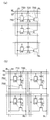
도 10a1, 도 10a2, 및 도 10b는 본 발명의 일 실시예에 따른 반도체 장치들의 회로도들.
도 11a 및 도 11b는 본 발명의 일 실시예에 따른 반도체 장치들의 회로도들.
도 12a 내지 도 12c는 본 발명의 일 실시예에 따른 반도체 장치들의 회로도들.
도 13a 내지 도 13f는 각각 본 발명의 일 실시예에 따른 반도체 장치를 이용하는 전자 기기를 도시한 도면.
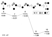
도 14는 본 발명의 일 실시예에 따른 반응 경로와 각 상태들의 에너지의 에너지도.
도 15는 본 발명의 일 실시예에 따른 반응 경로와 각 상태들의 에너지의 에너지도.
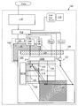
도 16은 본 발명의 일 실시예에 따른 액정 표시 장치의 각 구성성분을 도시하는 블록도.
도 17은 본 발명의 일 실시예에 따른 액정 표시 장치의 구동 회로와 화소의 구조를 도시한 도면.
도 18은 본 발명의 일 실시예에 따른 액정 표시 장치의 동작을 도시하는 타이밍도.
도 19a 및 도 19b는 본 발명의 일 실시예에 따른 액정 표시 장치의 표시 제어 회로의 동작들을 도시하는 타이밍도들.
도 20은 본 발명의 일 실시예에 따른 움직이는 이미지들을 표시하는 기간과 정지 이미지들을 표시하는 기간의 프레임 기간들에서 이미지 신호들을 기록하는 빈도를 개략적으로 도시한 도면.1A and 1B illustrate a structure of a semiconductor device according to an embodiment of the present invention.
2A to 2D illustrate a method of fabricating a semiconductor device in accordance with an embodiment of the present invention.
3A and 3B illustrate a structure of a semiconductor device according to an embodiment of the present invention.
4A-4D illustrate a method of fabricating a semiconductor device in accordance with one embodiment of the present invention.
5A and 5B illustrate a structure of a semiconductor device according to an embodiment of the present invention.
6A-6D illustrate a method of fabricating a semiconductor device in accordance with an embodiment of the present invention.
7A-7C illustrate a method of fabricating a semiconductor device in accordance with an embodiment of the present invention.
8A-8D illustrate a method of fabricating a semiconductor device in accordance with an embodiment of the present invention.
9A-9C illustrate a method of fabricating a semiconductor device in accordance with an embodiment of the present invention.
10A1, 10A2, and 10B are circuit diagrams of semiconductor devices according to an embodiment of the present invention.
11A and 11B are circuit diagrams of semiconductor devices according to an embodiment of the present invention.
12A-12C are circuit diagrams of semiconductor devices in accordance with an embodiment of the present invention.
13A to 13F each show an electronic device using a semiconductor device according to one embodiment of the present invention.
14 is an energy diagram of the energy of each reaction path and states in accordance with one embodiment of the present invention.
Figure 15 is an energy diagram of the energy of the reaction path and each state according to an embodiment of the present invention.
FIG. 16 is a block diagram illustrating components of a liquid crystal display according to an exemplary embodiment of the present invention. FIG.
17 is a diagram illustrating a driving circuit and a pixel structure of a liquid crystal display according to an exemplary embodiment of the present invention.
18 is a timing diagram illustrating an operation of a liquid crystal display according to an exemplary embodiment of the present invention.
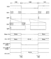
19A and 19B are timing diagrams showing operations of a display control circuit of a liquid crystal display according to an embodiment of the present invention.
20 is a diagram schematically showing the frequency of recording image signals in frame periods of a period for displaying moving images and a period for displaying still images according to an embodiment of the present invention.
본 발명의 실시예들이 첨부 도면들을 참조하여 상세하게 설명된다. 본 발명은 이하의 설명에 제한되지 않으며, 여기서 개시된 모드들 및 상세한 설명들은 본 발명의 정신과 범주로부터 벗어남이 없이 다양한 방법들로 변경될 수 있다는 것이 당업자에 의해 쉽게 이해된다는 것에 주의한다. 따라서, 본 발명은 다음 실시예들의 설명으로 제한되는 것으로 이해되어서는 안된다. 이하로 설명된 본 발명의 구조들에서, 동일한 부분들 또는 유사한 기능들을 갖는 부분들은 상이한 도면들에서 동일한 참조 번호들로 표시되며, 이러한 부분들의 설명은 반복되지 않는다는 것에 주의한다. Embodiments of the present invention are described in detail with reference to the accompanying drawings. It is noted that the present invention is not limited to the following description, and it is readily understood by those skilled in the art that the modes and details disclosed herein can be modified in various ways without departing from the spirit and scope of the invention. Therefore, the present invention should not be understood as being limited to the description of the following embodiments. Note that in the structures of the present invention described below, parts having the same parts or similar functions are denoted by the same reference numerals in different drawings, and the description of these parts is not repeated.
[실시예 1]Example 1
본 실시예에서, 할로겐 원소를 함유하는 물질이 막 형성 챔버로 가스 상태로 주입되는 동안 산화물 반도체층이 형성되고 매우 정제된 산화물 반도체층을 형성하기 위해 나중에 열 처리를 거치게 되는 방법에 의해 제작되는 보텀 게이트형 트랜지스터와, 상기 보텀 게이트형 트랜지스터를 제작하는 방법이 도 1a 및 도 1b와 도 2a 내지 도 2d를 참조하여 설명될 것이다.In this embodiment, a bottom is produced by a method in which an oxide semiconductor layer is formed while a material containing a halogen element is injected in a gaseous state into a film forming chamber and later subjected to heat treatment to form a highly purified oxide semiconductor layer. A gate transistor and a method of fabricating the bottom gate transistor will be described with reference to FIGS. 1A and 1B and FIGS. 2A to 2D.
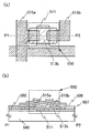
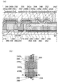
도 1a 및 도 1b는 본 실시예에서 제작되는 보텀 게이트형 트랜지스터(550)의 구조를 도시한다. 도 1a는 상기 트랜지스터(550)의 평면도이고, 도 1b는 상기 트랜지스터(550)의 단면도이다. 도 1b는 도 1a의 하나의 선(P1-P2)을 따라 얻어진 단면도에 대응한다는 것에 주의한다.1A and 1B show the structure of the
트랜지스터(550)에서, 게이트 전극(511)과 상기 게이트 전극(511)을 덮는 게이트 절연층(502)이 절연 표면을 갖는 기판(500) 위에 제공된다. 게이트 전극(511)과 중첩하는 매우 정제된 산화물 반도체층(513b)이 상기 게이트 절연층(502) 위에 제공된다. 또한, 상기 산화물 반도체층(513b)과 접하고, 각각이 소스 또는 드레인 전극이 되며, 게이트 전극(511)과 중첩하는 단부들을 갖는 제 1 전극(515a) 및 제 2 전극(515b)이 제공된다. 또한, 상기 산화물 반도체층(513b)과 접하고 그의 채널 형성 영역과 중첩하는 절연층(507), 및 상기 트랜지스터(550)를 덮는 보호 절연층(508)이 제공된다.In the
본 실시예에서 반도체층으로 이용된 산화물 반도체는 i-형(진성) 또는 실질적으로 i-형 산화물 반도체이다. 상기 i-형(진성) 또는 실질적으로 i-형 산화물 반도체는 n-형 불순물로 기능하는 수소가 제거되고, 산화물 반도체가 매우 정제되어 산화물 반도체의 주성분들이 아닌 불순물들을 가능한 한 거의 함유하지 않도록 하는 방식으로 얻어진다.The oxide semiconductor used as the semiconductor layer in this embodiment is an i-type (intrinsic) or substantially i-type oxide semiconductor. The i-type (intrinsic) or substantially i-type oxide semiconductor is a method of removing hydrogen that functions as an n-type impurity, and the oxide semiconductor is highly purified so that it contains as few impurities as possible that are not main components of the oxide semiconductor. Obtained.
매우 정제된 산화물 반도체는 극히 적은 캐리어들을 포함하고, 그의 캐리어 농도는 1 x 10¹⁴/cm3보다 낮고, 바람직하게는 1 x 10¹²/cm3보다 낮고, 또는 더욱 바람직하게는 1 x 10¹¹/cm3보다 낮다는 것에 주의한다. 이러한 적은 캐리어들은 오프 상태에 있는 전류(오프 상태 전류)가 충분히 낮아지도록 할 수 있다. Highly purified oxide semiconductors contain very few carriers and their carrier concentration is lower than 1 × 10 14 / cm 3 , preferably lower than 1 × 10 12 / cm 3 , or more preferably 1 × 10 11 / Note that it is lower than cm 3 . These small carriers can cause the current in the off state (off state current) to be sufficiently low.
구체적으로, 상기 산화물 반도체층을 포함하는 상기 트랜지스터에서, 오프 상태의 소스와 드레인 사이의 채널 폭의 마이크로미터 당 누설 전류 밀도(오프 상태 전류 밀도)는 3.5V의 소스-드레인 전압과 트랜지스터가 이용될 때의 온도(예를 들면, 25℃)에서 100zA/㎛(1 x 10-19A/㎛)보다 작거나 같아질 수 있고, 바람직하게는 10zA/㎛(1 x 10-20A/㎛)보다 작거나 같아질 수 있고, 또는 더욱 바람직하게는 1zA/㎛(1 x 10-21A/㎛)보다 작거나 같아질 수 있다.Specifically, in the transistor including the oxide semiconductor layer, the leakage current density per micrometer (off state current density) of the channel width between the source and the drain in the off state is a source-drain voltage of 3.5V and the transistor is used. At a temperature of time (for example 25 ° C.) may be less than or equal to 100 zA / μm (1 × 10 −19 A / μm), preferably 10 zA / μm (1 × 10 −20 A / μm) It may be smaller or equal, or more preferably less than or equal to 1zA / μm (1 × 10 −21 A / μm).
또한, 상기 매우 정제된 산화물 반도체층을 포함하는 상기 트랜지스터에서, 오프 상태 전류의 온도 의존성은 거의 관찰되지 않으며, 오프 상태 전류는 고온 상태 하에서도 극히 낮게 남아 있다.Further, in the transistor including the highly purified oxide semiconductor layer, the temperature dependence of the off state current is hardly observed, and the off state current remains extremely low even under a high temperature state.
트랜지스터(550)의 산화물 반도체층(513b)이 할로겐 원소를 함유하는 물질이 가스 상태로 주입되는 막 형성 챔버에서 형성된다. 게다가, 일부 경우들에서, 상기 트랜지스터(550)의 상기 산화물 반도체층(513b)은 할로겐 원소를 함유한다. 상기 산화물 반도체층(513b)에 함유된 할로겐 원소의 농도는 1015 atoms/cm3 내지 1018 atoms/cm3 이다. 상기 산화물 반도체층(513b)의 할로겐 원소는 반도체 장치의 제작 공정 동안 생성되는 금속 원자의 댕글링 결합과 결합하고 이를 종결시키고; 따라서, 캐리어들 또는 불순물 준위의 생성이 억제된다.The
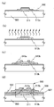
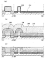
다음, 상기 기판(500) 위에 상기 트랜지스터(550)를 제작하는 방법이 도 2a 내지 도 2d를 참조하여 설명될 것이다.Next, a method of fabricating the
먼저, 도전막이 절연 표면을 갖는 상기 기판(500) 위에 형성된 후, 게이트 전극(511)을 포함하는 배선층이 제 1 포토리소그래피 단계에 의해 형성된다. 잉크젯 방법에 의해 레지스트 마스크가 형성될 수 있다는 것에 주의한다. 잉크젯 방법에 의한 레지스트 마스크의 형성은 포토마스크를 필요로 하지 않으며; 따라서, 제작 비용이 감소될 수 있다. First, after a conductive film is formed on the
본 실시예에서, 유리 기판이 절연 표면을 갖는 상기 기판(500)으로 이용된다.In this embodiment, a glass substrate is used as the
기저막이 되는 절연막이 상기 기판(500)과 상기 게이트 전극(511) 사이에 제공될 수 있다. 상기 기저막은 상기 기판(500)으로부터 불순물 원소(예를 들면, Li 또는 Na과 같은 알칼리 금속 및 Ca과 같은 알칼리 토금속)의 확산을 방지하는 기능을 가지며, 질화 실리콘막, 산화 실리콘막, 질화산화 실리콘막, 및 산화질화 실리콘막의 하나 또는 그 이상을 포함하는 단층 구조 또는 적층 구조를 갖도록 형성될 수 있다.An insulating layer serving as a base layer may be provided between the
상기 게이트 전극(511)이 몰리브덴, 티타늄, 탄탈, 텅스텐, 네오디뮴, 또는 스칸듐과 같은 금속 재료, 또는 그의 주요 구성성분으로서 이러한 금속 재료들 중 임의의 것을 함유하는 합금 재료를 포함하는 단층 구조 또는 적층 구조를 갖도록 형성될 수 있다. Single layer structure or laminated structure wherein the
나중 공정에서 수행될 열 처리의 온도를 견딜 수 있다면, 알루미늄 또는 구리가 이러한 금속 재료로 또한 이용될 수 있다는 것에 주의한다. 알루미늄 또는 구리는 내화 금속(refractory metal) 재료와 조합되어 내열성 문제 및 부식성(corrosive) 문제를 방지하도록 하는 것이 바람직하다. 내화 금속 재료로서, 몰리브덴, 티타늄, 크롬, 탄탈, 텅스텐, 네오디뮴, 스칸듐, 등이 이용될 수 있다. Note that aluminum or copper may also be used as this metal material if it can withstand the temperature of the heat treatment to be performed in a later process. Aluminum or copper is preferably combined with refractory metal materials to prevent heat and corrosive problems. As the refractory metal material, molybdenum, titanium, chromium, tantalum, tungsten, neodymium, scandium, and the like can be used.
구리를 이용하는 경우에, Cu-Mg-Al 합금이 기저가 되는 층에 제공되고 그 위에 구리가 형성되는 구조가 바람직하다. Cu-Mg-Al 합금의 제공은 구리와 산화물막과 같은 기저(base) 사이의 부착성을 강화시키는 효과를 갖는다.In the case of using copper, a structure in which a Cu—Mg—Al alloy is provided in the underlying layer and copper is formed thereon is preferable. Provision of a Cu-Mg-Al alloy has the effect of enhancing adhesion between a base such as copper and an oxide film.
다음, 게이트 절연층(502)이 게이트 전극(511) 위에 형성된다. 게이트 절연층(502)은 플라즈마 CVD법, 스퍼터링법, 등에 의해 산화 실리콘층, 질화 실리콘층, 산화질화 실리콘층, 질화산화 실리콘층, 산화 알루미늄층, 질화 알루미늄층, 산화질화 알루미늄층, 질화산화 알루미늄층, 또는 산화 하프늄층을 포함하는 단층 구조 또는 적층 구조를 갖도록 형성될 수 있다.Next, a
본 실시예의 산화물 반도체로서, i-형 또는 실질적으로 i-형 산화물 반도체가 이용된다. 상기 i-형 또는 실질적으로 i-형 산화물 반도체는 할로겐 원소를 함유하는 물질이 가스 상태로 막 형성 챔버로 주입되는 동안 산화물 반도체의 막 형성이 수행되고 산화물 반도체가 나중에 불순물들을 제거하기 위한 열 처리를 거치게 되는 방식으로 얻어진다. 이러한 매우 정제된 산화물 반도체는 계면 상태 밀도(interface state density)와 계면 전하에 극히 민감하며; 따라서, 산화물 반도체층과 게이트 절연층 사이의 계면이 중요하다. 그러한 이유로, 매우 정제된 산화물 반도체와 접하는 상기 게이트 절연층은 고품질을 가질 필요가 있다.As the oxide semiconductor of this embodiment, an i-type or substantially i-type oxide semiconductor is used. The i-type or substantially i-type oxide semiconductor is a film formation of the oxide semiconductor is carried out while a material containing a halogen element is injected into the film formation chamber in a gaseous state, the oxide semiconductor is subjected to a heat treatment to later remove impurities It is obtained in such a way that it goes through. Such highly purified oxide semiconductors are extremely sensitive to interface state density and interface charge; Therefore, the interface between the oxide semiconductor layer and the gate insulating layer is important. For that reason, the gate insulating layer in contact with the highly purified oxide semiconductor needs to have high quality.
예를 들어, 절연층이 조밀해질 수 있고, 높은 항복 전압(breakdown voltage)과 고품질을 가질 수 있기 때문에, 마이크로파들(예를 들면, 2.45GHz의 주파수)을 이용하는 고밀도 플라즈마 CVD법이 채용되는 것이 바람직하다. 매우 정제된 산화물 반도체와 고품질 게이트 절연층은 서로 가까이 접하며, 따라서 양호한 계면 특성들을 얻도록 계면 상태 밀도가 감소될 수 있다.For example, it is preferable to employ a high density plasma CVD method using microwaves (for example, a frequency of 2.45 GHz) because the insulating layer can be dense and have a high breakdown voltage and high quality. Do. The highly purified oxide semiconductor and the high quality gate insulating layer are in close contact with each other, so the interface state density can be reduced to obtain good interface properties.
말할 필요도 없이, 방법이 상기 게이트 절연층으로서 고품질 절연층의 형성을 가능하게 한다면, 스퍼터링법 또는 플라즈마 CVD법과 같은 다른 막 형성 방법이 채용될 수 있다. 또한, 그의 막 품질과, 절연층과 산화물 반도체 사이의 계면의 특성이 절연층의 형성 후에 수행되는 열 처리에 의해 개선되는 절연층이 게이트 절연층으로서 형성될 수 있다. 임의의 경우에, 절연층이 절연층과 산화물 반도체 사이의 계면의 계면 상태 밀도를 감소시킬 수 있고 상기 게이트 절연층으로서 양호한 막 품질을 가질 뿐만 아니라 양호한 계면을 형성할 수 있는 한, 임의의 절연층이 이용될 수 있다.Needless to say, if the method enables formation of a high quality insulating layer as the gate insulating layer, another film forming method such as sputtering method or plasma CVD method can be employed. In addition, an insulating layer whose film quality and characteristics of the interface between the insulating layer and the oxide semiconductor are improved by heat treatment performed after the formation of the insulating layer can be formed as the gate insulating layer. In any case, any insulating layer as long as the insulating layer can reduce the interface state density of the interface between the insulating layer and the oxide semiconductor and can form a good interface as well as have good film quality as the gate insulating layer. This can be used.
게이트 절연층(502)은 나중에 형성될 산화물 반도체층과 접한다는 것에 주의한다. 수소가 산화물 반도체층에서 확산할 때, 반도체 특성들이 열화되고; 따라서, 상기 게이트 절연층(502)은 수소, 수산기, 및 수분을 함유하지 않는 것이 바람직하다. 상기 게이트 절연층(502)과 산화물 반도체막이 가능한 한 적게 수소, 수산기, 및 수분을 함유하기 위하여, 산화물 반도체막의 막 형성의 전처리(pretreatment)로서, 게이트 전극(511)이 형성되는 기판(500) 또는 게이트 절연층(502)까지 층들이 형성되는 기판(500)이 스퍼터링 장치의 예열(preheating) 챔버에서 예열되어 형성되어, 기판(500)에 흡수된 수소 또는 수분과 같은 불순물들이 제거되고 배기되는 것이 바람직하다. 예열 챔버에 제공된 배기 유닛으로서, 크라이오펌프(cryopump)가 바람직하다. 이러한 예열 처리는 생략될 수 있다는 것에 주의한다. 또한, 상기 예열은 제 1 전극(515a)과 제 2 전극(515b)이 그 위에 형성되었으나 절연층(507)은 아직 형성되지 않은 상태의 기판(500) 상에서 유사한 방식으로 수행될 수 있다. Note that the
다음, 2nm 내지 200nm의, 바람직하게는 5nm 내지 30nm의 두께를 갖는 산화물 반도체막이 상기 게이트 절연층(502) 위에 형성된다.Next, an oxide semiconductor film having a thickness of 2 nm to 200 nm, preferably 5 nm to 30 nm is formed on the
산화물 반도체막은 금속 산화물 타겟을 이용하여 스퍼터링법에 의해 형성된다. 또한, 산화물 반도체막은 희가스(예를 들면, 아르곤) 분위기, 산소 분위기, 또는 희가스(예를 들면, 아르곤)와 산소를 함유하는 혼합 분위기 하에서 스퍼터링법에 의해 형성될 수 있다.An oxide semiconductor film is formed by sputtering method using a metal oxide target. Further, the oxide semiconductor film may be formed by sputtering under a rare gas (for example, argon) atmosphere, an oxygen atmosphere, or a mixed atmosphere containing rare gas (for example, argon) and oxygen.
스퍼터링법에 의해 산화물 반도체막이 형성되기 전에, 상기 게이트 절연층(502)의 표면에 부착되는 가루 물질들(또한 입자들 또는 먼지로 불림)이 아르곤 가스가 주입되고 플라즈마가 생성되는 역 스퍼터링(reverse sputtering)에 의해 제거되는 것이 바람직하다는 것에 주의한다. 역 스퍼터링은 타겟 측으로의 전압의 인가없이, 표면을 변경시키기 위해 기판의 근처에 플라즈마를 발생시키기 위하여 아르곤 분위기 하에서 기판 측으로의 전압의 인가를 위해 RF 전원이 이용되는 방법을 말한다. 아르곤 분위기 대신, 질소 분위기, 헬륨 분위기, 산소 분위기, 등이 이용될 수 있다는 것에 주의한다.Prior to the formation of the oxide semiconductor film by the sputtering method, reverse sputtering in which argon gas is injected and plasma is generated is a powder material (also called particles or dust) adhering to the surface of the
산화물 반도체막으로 이용된 산화물 반도체로서, 다음 금속 산화물: In-Sn-Ga-Zn-O계 산화물 반도체와 같은 4원계 금속 산화물; In-Ga-Zn-O계 산화물 반도체, In-Sn-Zn-O계 산화물 반도체, In-Al-Zn-O계 산화물 반도체, Sn-Ga-Zn-O계 산화물 반도체, Al-Ga-Zn-O계 산화물 반도체, 또는 Sn-Al-Zn-O계 산화물 반도체와 같은 3원계 금속 산화물; In-Zn-O계 산화물 반도체, Sn-Zn-O계 산화물 반도체, Al-Zn-O계 산화물 반도체, Zn-Mg-O계 산화물 반도체, Sn-Mg-O계 산화물 반도체, In-Mg-O계 산화물 반도체, 또는 In-Ga-O계 산화물 반도체와 같은 2원계 금속 산화물; In-O계 산화물 반도체, Sn-O계 산화물 반도체, 또는 Zn-O계 산화물 반도체와 같은 1원계 금속 산화물; 등이 이용될 수 있다. 또한, SiO2가 상기 산화물 반도체에 함유될 수 있다. 산화물 반도체막으로의 결정화를 방해하는 산화 실리콘(SiOx(x>0))의 첨가는 제작 공정에서 산화물 반도체막의 형성 후에 열 처리가 수행될 때 산화물 반도체막의 결정화를 억제할 수 있다. 여기서, 예를 들어, In-Ga-Zn-O계 산화물 반도체는 인듐(In), 갈륨(Ga), 및 아연(Zn)을 함유하는 산화물막을 의미하며, 그의 구성 비율에 특별한 제한은 없다. In-Ga-Zn-O계 산화물 반도체는 In, Ga, 및 Zn 이외의 원소를 함유할 수 있다.As the oxide semiconductor used as the oxide semiconductor film, the following metal oxides: quaternary metal oxides such as In—Sn—Ga—Zn—O-based oxide semiconductors; In-Ga-Zn-O-based oxide semiconductor, In-Sn-Zn-O-based oxide semiconductor, In-Al-Zn-O-based oxide semiconductor, Sn-Ga-Zn-O-based oxide semiconductor, Al-Ga-Zn- Ternary metal oxides such as O-based oxide semiconductors or Sn-Al-Zn-O-based oxide semiconductors; In-Zn-O-based oxide semiconductor, Sn-Zn-O-based oxide semiconductor, Al-Zn-O-based oxide semiconductor, Zn-Mg-O-based oxide semiconductor, Sn-Mg-O-based oxide semiconductor, In-Mg-O Binary metal oxides such as oxide based semiconductors or In—Ga—O based oxide semiconductors; Primary metal oxides such as In-O-based oxide semiconductors, Sn-O-based oxide semiconductors, or Zn-O-based oxide semiconductors; And the like can be used. SiO 2 may also be contained in the oxide semiconductor. The addition of silicon oxide (SiO x (x> 0)) which hinders crystallization into the oxide semiconductor film can suppress the crystallization of the oxide semiconductor film when the heat treatment is performed after the formation of the oxide semiconductor film in the production process. Here, for example, an In—Ga—Zn—O based oxide semiconductor means an oxide film containing indium (In), gallium (Ga), and zinc (Zn), and the composition ratio thereof is not particularly limited. The In—Ga—Zn—O based oxide semiconductor may contain elements other than In, Ga, and Zn.
산화물 반도체막으로서, InMO3(ZnO)m(m>0, m은 자연수가 아니다)의 화학식에 의해 표현된 박막이 이용될 수 있다. 여기서, M은 Ga, Al, Mn, 및 Co로부터 선택된 하나 이상의 금속 원소들을 나타낸다. 예를 들어, M은 Ga, Ga 및 Al, Ga 및 Mn, Ga 및 Co, 등일 수 있다. As the oxide semiconductor film, a thin film represented by the chemical formula of InMO 3 (ZnO) m (m> 0, m is not a natural number) can be used. Here, M represents one or more metal elements selected from Ga, Al, Mn, and Co. For example, M can be Ga, Ga and Al, Ga and Mn, Ga and Co, and the like.
In-Zn-O계 재료가 산화물 반도체로 이용되는 경우에, 타겟은 따라서 원자비(atomic ratio)로 In:Zn = 50:1 내지 1:2(몰 비(molar ratio)로 In2O3: ZnO = 25:1 내지 1:4), 바람직하게는, 원자비로 In:Zn = 20:1 내지 1:1(몰 비로 In2O3: ZnO = 10:1 내지 1:2), 더욱 바람직하게는, 원자비로 In:Zn = 15:1 내지 1.5:1(몰 비로 In2O3: ZnO = 15:2 내지 3:4)의 조성비를 갖는다. 예를 들어, In:Zn:O = X:Y:Z의 원자비를 갖는 In-Zn-O계 산화물 반도체의 형성에 이용된 타겟에서, Z > 1.5X+Y의 관계가 만족된다.In case In-Zn-O based materials are used as the oxide semiconductor, the target is thus in the atomic ratio In: Zn = 50: 1 to 1: 2 (in the molar ratio In 2 O 3 : ZnO = 25: 1 to 1: 4), preferably In: Zn = 20: 1 to 1: 1 (in molar ratio In 2 O 3 : ZnO = 10: 1 to 1: 2), more preferably in atomic ratio Preferably, it has a composition ratio of In: Zn = 15: 1 to 1.5: 1 (In 2 O 3 : ZnO = 15: 2 to 3: 4 in molar ratio) in an atomic ratio. For example, in a target used for forming an In—Zn—O based oxide semiconductor having an atomic ratio of In: Zn: O = X: Y: Z, the relationship of Z> 1.5X + Y is satisfied.
산화물 반도체는 In을 함유하는 산화물 반도체인 것이 바람직하고, In과 Ga를 함유하는 산화물 반도체인 것이 더욱 바람직하다. I-형 (진성) 산화물 반도체를 얻기 위하여, 탈수화(dehydration) 또는 탈수소화(dehydrogenation)가 효과적이다. 본 실시예에서, 스퍼터링법에 의해 In-Ga-Zn-O계 산화물 타겟을 이용하여 산화물 반도체막이 형성된다.The oxide semiconductor is preferably an oxide semiconductor containing In, more preferably an oxide semiconductor containing In and Ga. In order to obtain an I-type (intrinsic) oxide semiconductor, dehydration or dehydrogenation is effective. In this embodiment, an oxide semiconductor film is formed using an In—Ga—Zn—O-based oxide target by sputtering.
스퍼터링법에 의해 산화물 반도체막을 형성하기 위한 타겟으로서, 예를 들면, 1:1:1[몰 비]의 조성비로 In2O3, Ga2O3, 및 ZnO를 함유하는 산화물 타겟이 In-Ga-Zn-O 막을 형성하기 위해 이용된다. 타겟의 재료와 조성에는 제한이 없으며, 예를 들어, 1:1:2[몰 비]의 조성비로 In2O3, Ga2O3, 및 ZnO를 함유하는 금속 산화물 타겟 또는 1:1:4[몰 비]의 조성비로 In2O3, Ga2O3, 및 ZnO를 함유하는 금속 산화물 타겟이 이용될 수 있다.As a target for forming an oxide semiconductor film by the sputtering method, for example, an oxide target containing In 2 O 3 , Ga 2 O 3 , and ZnO in a composition ratio of 1: 1: 1 [molar ratio] is In-Ga. It is used to form a -Zn-O film. There is no restriction on the material and composition of the target, for example, a metal oxide target or 1: 1: 4 containing In 2 O 3 , Ga 2 O 3 , and ZnO in a composition ratio of 1: 1: 2 [molar ratio]. A metal oxide target containing In 2 O 3 , Ga 2 O 3 , and ZnO as the composition ratio of [molar ratio] can be used.
산화물 타겟의 충전률은 90% 내지 100%이며, 바람직하게는 95% 내지 99.9%이다. 높은 충전률을 갖는 금속 산화물 타겟의 이용으로, 조밀한 산화물 반도체막이 형성될 수 있다. 또한, 타겟의 순도는 99.99%보다 크거나 같은 것이 바람직하며, 여기서 불순물들, 예를 들면, Li 또는 Na와 같은 알칼리 금속과 Ca와 같은 알칼리 토금속이 특히 감소되는 것이 바람직하다.The filling rate of the oxide target is 90% to 100%, preferably 95% to 99.9%. By using a metal oxide target having a high filling rate, a dense oxide semiconductor film can be formed. It is also preferred that the purity of the target is greater than or equal to 99.99%, where impurities, for example alkali metals such as Li or Na and alkaline earth metals such as Ca, are particularly reduced.
산화물 반도체막의 형성시 이용된 스퍼터링 가스(가스 상태로 이용되는 할로겐 원소를 함유하는 물질을 포함)로서, 수소, 물, 수산기, 또는 수소화물(hydride)과 같은 불순물들이 제거되는 고순도 가스가 이용된다. 예를 들어, 이러한 불순물들이 10ppm보다 낮거나 같은, 바람직하게는 1ppm보다 낮거나 같은 농도로 제거되는 고순도 가스를 이용하는 것이 바람직하다. 구체적으로, 이슬점이 -60℃보다 작거나 같은 고순도 가스가 바람직하다. As the sputtering gas (including a substance containing a halogen element used in the gas state) used in the formation of the oxide semiconductor film, a high purity gas in which impurities such as hydrogen, water, hydroxyl groups, or hydrides are removed is used. For example, it is desirable to use a high purity gas in which such impurities are removed at concentrations lower than or equal to 10 ppm, preferably lower than or equal to 1 ppm. Specifically, high purity gases with a dew point less than or equal to -60 ° C are preferred.
막 형성 챔버로 주입되는, 할로겐 원소를 함유하는 물질로서, 플루오르 원자를 함유하는 가스(사불화탄소(CF4), 육불화황(SF6), 삼불화질소(NF3), 또는 삼불화메탄(CHF3)과 같은 플루오르계 가스), 염소 원자를 함유하는 가스(염소(Cl2), 삼염화붕소(BCl3), 사염화실리콘(SiCl4), 또는 사염화탄소(CCl4)와 같은 염소계 가스), 등이 적절하게 이용될 수 있다. 특히 플루오르 라디칼이 플라즈마로 생성되므로 플루오르 원자를 함유하는 가스를 이용하는 것이 바람직하다. 플루오르 원자와 수소 원자 사이의 결합 에너지가 다른 할로겐 원소들 중 임의의 것과 수소 원자 사이의 결합 에너지보다 높다. 또한, 이는 플루오르 원자와 수소 원자 사이의 결합이 다른 할로겐 원소들 중 임의의 것과 수소 원자 사이의 결합보다 더 안정하기 때문이다. As a material containing a halogen element, which is injected into the film formation chamber, a gas containing a fluorine atom (carbon tetrafluoride (CF 4 ), sulfur hexafluoride (SF 6 ), nitrogen trifluoride (NF 3 ), or methane trifluoride ( Fluorine-based gas such as CHF 3 ), gas containing a chlorine atom (chlorine (Cl 2 ), boron trichloride (BCl 3 ), silicon tetrachloride (SiCl 4 ), or chlorine-based gas such as carbon tetrachloride (CCl 4 )), and the like. This can be used as appropriate. In particular, since fluorine radicals are generated in the plasma, it is preferable to use a gas containing fluorine atoms. The bond energy between the fluorine atom and the hydrogen atom is higher than the bond energy between any of the other halogen elements and the hydrogen atom. This is also because the bond between the fluorine atom and the hydrogen atom is more stable than the bond between any of the other halogen elements and the hydrogen atom.
또한, 할로겐 원소의 공급원을 막 형성 챔버로 주입하는 방법으로서, 할로겐 원소를 함유하는 가스가 막 형성 가스로 첨가되는 방법이 편리하고 바람직하다. 막 형성을 위한 처리 챔버 상의 세정 처리를 위해 상술된 NF3와 같은 할로겐 원소를 함유하는 가스의 이용으로, 산화물 반도체막이 막 형성동안 처리 챔버에 남아있는 플루오르와 같은 할로겐 원소를 함유하도록 형성될 수 있다.In addition, as a method of injecting a source of halogen element into the film forming chamber, a method in which a gas containing halogen element is added as the film forming gas is convenient and preferred. With the use of a gas containing a halogen element such as NF 3 described above for the cleaning process on the process chamber for film formation, the oxide semiconductor film can be formed to contain a halogen element such as fluorine remaining in the process chamber during film formation. .
감압하의 막 형성 챔버에 기판이 위치되고, 기판 온도가 100℃보다 크거나 같고 600℃보다 작거나 같은, 바람직하게는 200℃보다 크거나 같고 400℃보다 작거나 같은 온도로 설정된다. 기판이 가열되는 상태에서 산화물 반도체막을 형성하는 것에 의해, 형성된 산화물 반도체막에 함유된 불순물들의 농도가 감소될 수 있다. 게다가, 스퍼터링에 의한 손상도 감소될 수 있다. 이후, 배기 펌프를 이용하여 막 형성 챔버의 잔류 수분이 제거되는 동안, 수소와 수분이 제거되고 할로겐 원소를 함유하는 물질이 가스 상태로 첨가되는 스퍼터링 가스가 주입되고, 상기 타겟을 이용하여 상기 기판(500) 위에 산화물 반도체막이 형성된다. 막 형성 챔버의 잔류 수분과 막 형성 챔버의 외부로부터 진입한 수소와 수분(누설로 인해 진입한 수소와 수분)을 제거하기 위하여, 흡착 진공 펌프(entrapment vacuum pump), 예를 들면, 크라이오펌프, 이온 펌프, 또는 티타늄 승화 펌프가 이용되는 것이 바람직하다. 배기 유닛은 콜드 트랩이 제공된 터보 펌프일 수 있다. 크라이오펌프로 배기되는 막 형성 챔버에서, 예를 들면, 수소 원자, 및 물(H2O)과 같은 수소 원자를 함유하는 화합물(바람직하게는, 탄소 원자를 함유하는 화합물)이 제거되어, 막 형성 챔버에서 형성된 산화물 반도체막에 함유된 불순물들의 농도가 감소될 수 있다. The substrate is placed in the film forming chamber under reduced pressure and the substrate temperature is set to a temperature greater than or equal to 100 ° C and less than or equal to 600 ° C, preferably greater than or equal to 200 ° C and less than or equal to 400 ° C. By forming the oxide semiconductor film while the substrate is heated, the concentration of impurities contained in the formed oxide semiconductor film can be reduced. In addition, damage by sputtering can also be reduced. Subsequently, while the residual moisture of the film formation chamber is removed using the exhaust pump, a sputtering gas into which hydrogen and moisture are removed and a substance containing a halogen element is added in a gaseous state is injected, and the substrate ( An oxide semiconductor film is formed over 500. In order to remove residual water in the film forming chamber and hydrogen and water (hydrogen and water entered due to leakage) from the outside of the film forming chamber, an entrapment vacuum pump, for example, a cryopump, It is preferable to use an ion pump or a titanium sublimation pump. The exhaust unit may be a turbo pump provided with a cold trap. In the film formation chamber exhausted by the cryopump, for example, a compound containing a hydrogen atom and a hydrogen atom such as water (H 2 O) (preferably, a compound containing a carbon atom) is removed, and the film is removed. The concentration of impurities contained in the oxide semiconductor film formed in the formation chamber can be reduced.
스퍼터링이 수행되는 상기 분위기는 할로겐 원소를 함유하는 물질이 가스 상태로 첨가되는 희가스(전형적으로, 아르곤) 분위기, 할로겐 원소를 함유하는 물질이 가스 상태로 첨가되는 산소 분위기, 또는 할로겐 원소를 함유하는 물질이 가스 상태로 첨가되는 희가스와 산소를 함유하는 혼합 분위기일 수 있다는 것에 주의한다. The atmosphere in which sputtering is performed is a rare gas (typically argon) atmosphere in which a substance containing a halogen element is added in a gas state, an oxygen atmosphere in which a substance containing a halogen element is added in a gas state, or a substance containing a halogen element. Note that it may be a mixed atmosphere containing rare gas and oxygen added in this gas state.
막 형성 챔버로 주입되는 할로겐 원소를 함유하는 물질은 플라즈마에 의해 분해되어 할로겐 라디칼을 생성한다. 생성된 할로겐 라디칼은 막 형성 챔버의 잔류 수분 및 누설로 인해 막 형성 챔버의 외부로부터 진입하는 수분과 반응하여, 할로겐 원자를 함유하는 안정한 물질(예로서 수소 할로겐화물)이 생성된다. 예를 들어, 산화물 반도체막이 플루오르 원자를 함유하는 물질(예로서 NF3)을 함유하는 분위기 하에서 형성될 때, 플루오르 라디칼이 막 형성 챔버의 수분과 반응하고; 따라서, 수소 플루오르화물이 생성된다. 수소 플루오르화물 분자의 수소 원자와 플루오르 원자 사이의 해리 에너지가 물 분자의 수소 원자와 산소 원자 사이의 해리 에너지보다 높기 때문에, 수소 플루오르화물 분자가 물 분자보다 더 안정하다고 말할 수 있다는 것에 주의한다.The material containing the halogen element injected into the film forming chamber is decomposed by the plasma to generate halogen radicals. The resulting halogen radicals react with moisture entering from outside of the film forming chamber due to residual moisture and leakage in the film forming chamber, producing a stable material containing halogen atoms (eg hydrogen halides). For example, when an oxide semiconductor film is formed under an atmosphere containing a material containing a fluorine atom (eg NF 3 ), the fluorine radicals react with moisture in the film forming chamber; Thus, hydrogen fluoride is produced. Note that since the dissociation energy between the hydrogen and fluorine atoms of the hydrogen fluoride molecule is higher than the dissociation energy between the hydrogen and oxygen atoms of the water molecule, it can be said that the hydrogen fluoride molecule is more stable than the water molecule.
막 형성 챔버의 수분은 수소 플루오르화물이 된 후에 막 형성 챔버로부터 배기되고; 따라서, 산화물 반도체층이 수분에 의해 거의 오염되지 않는다.Moisture in the film forming chamber is evacuated from the film forming chamber after it becomes hydrogen fluoride; Therefore, the oxide semiconductor layer is hardly contaminated by moisture.
막 형성 조건들의 예로서, 기판과 타겟의 거리는 100mm, 압력은 0.6Pa, 직류(DC) 전원은 0.5kW이고, 분위기는 산소 분위기(산소 유량비는 100%)이다. 막 형성동안 생성된 가루 물질들(또한 입자들 또는 먼지로도 불림)이 감소될 수 있고 막 두께가 균일하게 될 수 있으므로 펄스-직류 전원이 바람직하다는 것에 주의한다.As an example of film formation conditions, the distance between the substrate and the target is 100 mm, the pressure is 0.6 Pa, the direct current (DC) power supply is 0.5 kW, and the atmosphere is an oxygen atmosphere (oxygen flow rate ratio is 100%). Note that a pulsed-DC power supply is desirable because the powdery materials (also called particles or dust) generated during film formation can be reduced and the film thickness can be made uniform.
또한, 스퍼터링 장치의 처리 챔버의 누설율(leakage rate)이 1 x 10⁻¹⁰Paㆍm3/초 보다 작거나 같게 설정될 때, 스퍼터링법에 의한 형성 하에서 알칼리 금속 또는 수소화물과 같은 불순물들의 산화물 반도체막으로의 진입이 감소될 수 있다.In addition, when the leakage rate of the processing chamber of the sputtering apparatus is set to be less than or equal to 1 x 10 -10 Pa · m 3 / sec, oxides of impurities such as alkali metals or hydrides under formation by sputtering methods Entry into the semiconductor film can be reduced.
또한, 배기 시스템으로서 흡착 진공 펌프의 이용으로, 배기 시스템으로부터 알칼리 금속, 수소 원자, 수소 분자, 물, 수산기, 또는 수소화물과 같은 불순물들의 역류(counter flow)가 감소될 수 있다.In addition, with the use of an adsorption vacuum pump as the exhaust system, the counter flow of impurities such as alkali metals, hydrogen atoms, hydrogen molecules, water, hydroxyl groups, or hydrides from the exhaust system can be reduced.
산화물 반도체층에 함유된 불순물들, 예를 들어, Li 또는 Na와 같은 알칼리 금속과 Ca와 같은 알칼리 토금속이 감소되는 것이 바람직하다는 것에 주의한다. 구체적으로, SIMS의 이용으로 산화물 반도체층에 함유된 Li, Na, 및 K와 같은 불순물들의 농도들은 각각 5 x 1015cm-3보다 낮거나 같고, 바람직하게는 1 x 1015cm-3보다 낮거나 같다.It is noted that impurities contained in the oxide semiconductor layer, for example, alkali metals such as Li or Na and alkaline earth metals such as Ca are preferably reduced. Specifically, the concentrations of impurities such as Li, Na, and K contained in the oxide semiconductor layer by the use of SIMS are respectively lower than or equal to 5 x 10 15 cm -3 , preferably lower than 1 x 10 15 cm -3. Or the same.
알칼리 금속과 알칼리 토금속은 산화물 반도체에 대한 악성(adverse) 불순물들이며 거의 함유되지 않는 것이 바람직하다. 산화물 반도체와 접하는 절연막이 산화물일 때, 알칼리 금속, 특히, Na이 산화물에 확산되어 Na+가 된다. 또한, Na는 금속과 산소 사이의 결합을 끊거나 산화물 반도체의 결합으로 들어간다. 결과적으로, 트랜지스터 특성들의 열화(예를 들면, 임계 값의 네거티브(negative) 측으로의 전환(트랜지스터가 노멀리 온(normally on)이 되게 함) 또는 이동도의 감소)가 유발된다. 부가적으로, 이는 또한 특성들의 변동을 유발한다. 이러한 문제는 특히 산화물 반도체의 수소 농도가 충분히 낮은 경우에 심각하다). 따라서, 알칼리 금속의 농도는 산화물 반도체에 함유된 수소의 농도가 5 x 1019cm-3보다 낮거나 같은 경우에, 특히 5 x 1018cm-3보다 낮거나 같은 경우에, 상기 범위에서 설정되도록 강력하게 요구된다.Alkali metals and alkaline earth metals are adverse impurities to the oxide semiconductor and are preferably rarely contained. When the insulating film in contact with the oxide semiconductor is an oxide, an alkali metal, in particular, Na diffuses into the oxide and becomes Na + . In addition, Na breaks the bond between the metal and oxygen or enters the bond of the oxide semiconductor. As a result, degradation of transistor characteristics (e.g., switching the threshold to the negative side (which causes the transistor to be normally on) or reduction in mobility) is caused. In addition, this also causes variations in the characteristics. This problem is especially serious when the hydrogen concentration of the oxide semiconductor is low enough). Therefore, the concentration of the alkali metal is set in the above range when the concentration of hydrogen contained in the oxide semiconductor is lower than or equal to 5 x 10 19 cm -3 , particularly lower than or equal to 5 x 10 18 cm -3. Strongly required.
다음, 산화물 반도체막이 제 2 포토리소그래피 단계에 의해 섬형 산화물 반도체층(513a)으로 처리된다. 섬형 산화물 반도체층을 형성하기 위한 레지스트 마스크가 잉크젯 방법에 의해 형성될 수 있다. 잉크젯 방법에 의한 레지스트 마스크의 형성은 포토마스크를 필요로 하지 않으며; 따라서, 제작 비용이 감소될 수 있다.Next, an oxide semiconductor film is processed into island type
콘택트 홀이 게이트 절연층(502)에 형성되는 경우에, 콘택트 홀을 형성하는 단계가 산화물 반도체막의 처리와 동시에 수행될 수 있다. In the case where the contact hole is formed in the
산화물 반도체막의 에칭은 건식 에칭, 습식 에칭, 또는 건식 에칭과 습식 에칭 모두일 수 있다는 것에 주의한다. 산화물 반도체막을 위한 습식 에칭을 위해 이용된 에천트(etchant)로서, 예를 들면, 인산, 아세트산, 및 질산의 혼합 용액, 등이 이용될 수 있다. 또한, ITO07N(KANTO CHEMICAL CO., INC.에 의해 제조)이 또한 이용될 수 있다. 도 2a는 본 단계의 상기 단면도임에 주의한다.Note that the etching of the oxide semiconductor film may be dry etching, wet etching, or both dry etching and wet etching. As an etchant used for wet etching for oxide semiconductor films, for example, a mixed solution of phosphoric acid, acetic acid, and nitric acid, and the like can be used. In addition, ITO07N (manufactured by KANTO CHEMICAL CO., INC.) May also be used. 2A is the cross-sectional view of this step.
건식 에칭을 위해 이용된 에칭 가스로서, 염소를 함유하는 가스(염소(Cl2), 삼염화붕소(BCl3), 사염화실리콘(SiCl4), 또는 사염화탄소(CCl4)와 같은 염소계 가스)가 이용되는 것이 바람직하다. 대안적으로, 플루오르 원자를 함유하는 물질(사불화탄소(CF4), 육불화황(SF6), 삼불화질소(NF3), 또는 삼불화메탄(CHF3)과 같은 플루오르계 가스); 브롬화수소(HBr); 산소(O2); 헬륨(He) 또는 아르곤(Ar)과 같은 희가스가 첨가되는 이러한 가스들 중 임의의 가스; 등이 이용될 수 있다.As an etching gas used for dry etching, a gas containing chlorine (chlorine-based gas such as chlorine (Cl 2 ), boron trichloride (BCl 3 ), silicon tetrachloride (SiCl 4 ), or carbon tetrachloride (CCl 4 )) is used. It is preferable. Alternatively, a substance containing a fluorine atom (carbon tetrafluoride (CF 4 ), sulfur hexafluoride (SF 6 ), nitrogen trifluoride (NF 3 ), or a fluorine-based gas such as methane trifluoride (CHF 3 )); Hydrogen bromide (HBr); Oxygen (O 2 ); Any of these gases to which a rare gas such as helium (He) or argon (Ar) is added; And the like can be used.
건식 에칭 방법으로서, 평행 평판 RIE(reactive ion etching)법 또는 ICP(inductively coupled plasma) 에칭법이 이용될 수 있다. 막들을 원하는 모양들로 에칭할 수 있도록 하기 위하여, 에칭 조건(코일형 전극에 인가된 전력량, 기판 측 상의 전극에 인가된 전력량, 기판 측 상의 전극의 온도, 등)이 적절하게 조절된다.As a dry etching method, a parallel plate reactive ion etching (RIE) method or an inductively coupled plasma (ICP) etching method may be used. In order to be able to etch the films into the desired shapes, the etching conditions (the amount of power applied to the coiled electrode, the amount of power applied to the electrode on the substrate side, the temperature of the electrode on the substrate side, etc.) are appropriately adjusted.
다음, 제 1 열 처리가 산화물 반도체층(513a) 상에서 수행된다. 이러한 제 1 열 처리에 의해, 불순물들이 산화물 반도체층으로부터 제거될 수 있다. 예를 들어, 산화물 반도체층으로 들어간 수소 할로겐화물이 제거될 수 있다. 생성된 수소 할로겐화물이 가열에 의해 제거되는 방법은 상기 금속에 강하게 결합된 수소 또는 수산기가 직접 제거되는 방법보다 쉽다.Next, a first heat treatment is performed on the
제 1 열 처리의 온도는 250℃보다 크거나 같고 750℃보다 작거나 같으며, 바람직하게는 400℃보다 크고 상기 기판의 변형점보다 작다. 예를 들어, 500℃에서 약 3분 내지 6분 동안 열 처리가 수행될 수 있다. 열 처리를 위해 RTA(rapid thermal anneal) 방법으로, 탈수화 또는 탈수소화가 단시간에 수행될 수 있고; 따라서, 유리 기판의 변형점보다 높은 온도에서라도 처리가 수행될 수 있다. 대략 제 4 세대 유리 기판들만큼 큰 기판들이 250℃보다 크거나 같고 750℃보다 작거나 같은 범위의 온도에서 열 처리를 거칠 수 있고, 대략 제 6 세대 내지 제 10 세대 유리 기판들만큼 큰 기판들이 250℃보다 크거나 같고 450℃보다 작거나 같은 범위의 온도에서 열처리를 거치는 것이 바람직하다.The temperature of the first heat treatment is greater than or equal to 250 ° C. and less than or equal to 750 ° C., preferably greater than 400 ° C. and less than the strain point of the substrate. For example, heat treatment may be performed at 500 ° C. for about 3 to 6 minutes. By rapid thermal anneal (RTA) method for heat treatment, dehydration or dehydrogenation can be performed in a short time; Therefore, the treatment can be performed even at a temperature higher than the strain point of the glass substrate. Substrates approximately as large as fourth generation glass substrates may undergo heat treatment at a temperature in the range of greater than or equal to 250 ° C. and less than or equal to 750 ° C., and substrates as large as approximately sixth through tenth generation glass substrates are 250 It is preferred to undergo heat treatment at a temperature greater than or equal to < RTI ID = 0.0 >
여기서, 기판이 열 처리 장치들 중 하나인 전기노(electric furnace)로 들어가고, 질소 분위기 하의 600℃에서 산화물 반도체층 상에서 열 처리가 수행되고, 이후, 공기로의 노출 없이 산화물 반도체층 상에서 200℃보다 작거나 같은 온도로 느린 냉각이 수행되어, 산화물 반도체층으로의 물 및 수소의 진입이 방지된다. 따라서, 산화물 반도체층(513b)이 얻어진다(도 2b 참조). 200℃보다 작거나 같은 온도로 산화물 반도체층 상에서 느린 냉각을 수행하는 것에 의해, 고온의 산화물 반도체층이 공기의 물 또는 수분과 접하는 것이 방지될 수 있다. 일부 경우들에서, 고온의 산화물 반도체층이 대기중의 물 또는 수분과 접할 때, 산화물 반도체는 수소 원자를 함유하는 불순물로 오염될 수 있다.Here, the substrate enters an electric furnace, one of the heat treatment apparatuses, and heat treatment is performed on the oxide semiconductor layer at 600 ° C. under a nitrogen atmosphere, and then on the oxide semiconductor layer without exposure to air than 200 ° C. Slow cooling to a temperature equal to or less than is performed to prevent water and hydrogen from entering the oxide semiconductor layer. Thus, an
열 처리 장치는 전기노로 제한되지 않으며, 저항 히터(resistance heater)와 같은 히터로부터의 열 전도 또는 열 복사에 의해 물체를 가열하는 장치가 이용될 수 있다는 것에 주의한다. 예를 들어, GRTA(gas rapid thermal anneal) 장치 또는 LRTA(lamp rapid thermal anneal) 장치와 같은 RTA(rapid thermal anneal) 장치가 이용될 수 있다. LRTA 장치는 할로겐 램프, 금속 할로겐화물 램프, 제논 아크 램프, 탄소 아크 램프, 고압 나트륨 램프, 또는 고압 수은 램프와 같은 램프로부터 방출된 빛(전자기파)의 복사에 의해 물체를 가열하는 장치이다. GRTA는 고온 가스를 이용한 열 처리를 위한 장치이다. 고온 가스로서, 질소, 또는 아르곤과 같은 희가스와 같은, 열 처리에 의해 물체와 반응하지 않는 불활성 가스가 이용된다. Note that the heat treatment apparatus is not limited to an electric furnace, and an apparatus for heating an object by heat conduction or heat radiation from a heater such as a resistance heater may be used. For example, rapid thermal anneal (RTA) devices such as gas rapid thermal anneal (GRTA) devices or lamp rapid thermal anneal (LRTA) devices may be used. LRTA devices are devices that heat objects by radiation of light (electromagnetic waves) emitted from such lamps as halogen lamps, metal halide lamps, xenon arc lamps, carbon arc lamps, high pressure sodium lamps, or high pressure mercury lamps. GRTA is a device for heat treatment using hot gases. As the hot gas, an inert gas that does not react with the object by heat treatment, such as nitrogen or a rare gas such as argon, is used.
예를 들어, 제 1 열 처리로서, 상기 기판이 650℃ 내지 700℃의 고온으로 가열된 불활성 가스로 움직이고, 몇 분간 가열되며, 고온으로 가열된 불활성 가스로부터 나오는 GRTA가 수행될 수 있다.For example, as a first heat treatment, the substrate may be moved to an inert gas heated to a high temperature of 650 ° C. to 700 ° C., heated for several minutes, and GRTA coming from the inert gas heated to a high temperature may be performed.
제 1 열 처리에서, 물, 수소, 등이 질소 또는 헬륨, 네온, 또는 아르곤과 같은 희가스의 분위기에 함유되지 않는 것이 바람직하다는 것에 주의한다. 열 처리 장치로 주입되는 질소 또는 헬륨, 네온, 또는 아르곤과 같은 희가스의 순도는 5N(99.999%) 또는 그 이상이 바람직하며, 6N(99.9999%) 또는 그 이상이 바람직하다(즉, 불순물 농도는 10ppm보다 작거나 같고, 바람직하게는 1ppm보다 작거나 같다). Note that in the first heat treatment, water, hydrogen, and the like are preferably not contained in an atmosphere of nitrogen or a rare gas such as helium, neon, or argon. The purity of nitrogen or rare gases such as helium, neon, or argon injected into the heat treatment device is preferably 5N (99.999%) or higher, and 6N (99.9999%) or higher (
게다가, 산화물 반도체층이 제 1 열 처리에 의해 가열된 후, 고순도 산소 가스, 고순도 N2O 가스, 또는 초건조(ultra dry) 공기(캐비티 링 다운 레이저 분광법(cavity ring down laser spectroscopy;CRDS) 시스템의 이슬점 측정기의 이용으로 측정이 수행되는 경우에, 수분량은 20ppm(이슬점으로 환산하면 -55℃)보다 적거나 같고, 바람직하게는 1ppm보다 적거나 같고, 또는 더욱 바람직하게는 10ppb보다 적거나 같다)가 동일한 노(furnace)로 주입될 수 있다. 산소 가스와 N2O 가스는 물, 수소, 등을 포함하지 않는 것이 바람직하다. 열 처리 장치로 주입되는 산소 가스 또는 N2O 가스의 순도는 5N보다 크거나 같은 것이 바람직하며, 더욱 바람직하게는 6N보다 크거나 같다(즉, 산소 가스 또는 N2O 가스의 불순물들의 농도는 바람직하게는 10ppm보다 작거나 같은게 바람직하고, 더욱 바람직하게는 1ppm보다 작거나 같다). 산소 가스 또는 N2O 가스의 반응에 의해, 산화물 반도체에 포함된 주성분들 중 하나이고 탈수화 또는 탈수소화에 의한 불순물들의 제거 단계와 동시에 감소되었던 산소가 공급되어, 산화물 반도체층이 매우 정제되고 전기적으로 i-형(진성)인 산화물 반도체가 될 수 있다. In addition, after the oxide semiconductor layer is heated by the first heat treatment, high purity oxygen gas, high purity N 2 O gas, or ultra dry air (cavity ring down laser spectroscopy; CRDS) system When the measurement is carried out using a dew point meter of, the moisture content is less than or equal to 20 ppm (-55 ° C. in terms of dew point), preferably less than or equal to 1 ppm, or more preferably less than or equal to 10 ppm) Can be injected into the same furnace. The oxygen gas and the N 2 O gas preferably do not contain water, hydrogen, or the like. The purity of the oxygen gas or N 2 O gas injected into the heat treatment device is preferably greater than or equal to 5N, more preferably greater than or equal to 6N (ie, the concentration of impurities in the oxygen gas or N 2 O gas is preferred). Preferably less than or equal to 10 ppm, more preferably less than or equal to 1 ppm). By the reaction of oxygen gas or N 2 O gas, oxygen is supplied, which is one of the main components included in the oxide semiconductor and reduced simultaneously with the removal of impurities by dehydration or dehydrogenation, so that the oxide semiconductor layer is highly purified and electrically It can be an oxide semiconductor that is i-type (intrinsic).
또한, 상기 산화물 반도체층의 제 1 열처리는 상기 섬형 산화물 반도체층으로 아직 처리되지 않은 상기 산화물 반도체막 상에서 또한 수행될 수 있다. 그러한 경우에, 기판이 제 1 열 처리 후에 가열 장치로부터 꺼내지며, 이후 포토리소그래피 단계가 수행된다. Further, the first heat treatment of the oxide semiconductor layer may also be performed on the oxide semiconductor film that has not yet been treated with the island-type oxide semiconductor layer. In such a case, the substrate is taken out of the heating apparatus after the first heat treatment, and then a photolithography step is performed.
제 1 열 처리는 그것이 상기 산화물 반도체막의 상기 막 형성 후에 수행되는 한 상기 타이밍에 부가하여 다음 타이밍들 중 임의의 것에 수행될 수 있다는 것에 주의한다: 상기 소스 전극 및 상기 드레인 전극이 산화물 반도체층 위에 적층된 후 및 상기 절연층이 상기 소스 전극과 상기 드레인 전극 위에 형성된 후.Note that the first heat treatment may be performed at any of the following timings in addition to the timing as long as it is performed after the film formation of the oxide semiconductor film: the source electrode and the drain electrode are stacked on the oxide semiconductor layer. And after the insulating layer is formed on the source electrode and the drain electrode.
콘택트 홀이 게이트 절연층(502)에 형성되는 경우에, 콘택트 홀을 형성하는 단계는 제 1 열 처리가 상기 산화물 반도체막 상에서 수행되기 전 또는 후에 수행될 수 있다. In the case where the contact hole is formed in the
상기 단계들을 통해, 섬형 산화물 반도체층의 수소의 농도가 감소될 수 있으며 섬형 산화물 반도체층이 매우 정제될 수 있다. 따라서, 산화물 반도체층이 안정화될 수 있다. 또한, 유리 기판의 변형점보다 작거나 같은 온도에서의 열 처리는 캐리어 밀도가 극히 낮은 넓은 밴드 갭(band gap)을 갖는 산화물 반도체막을 형성하는 것을 가능하게 한다. 따라서, 트랜지스터가 대형 크기의 기판을 이용하여 제작될 수 있고, 생산성이 증가될 수 있다. 게다가, 수소 농도가 감소되는 매우 정제된 산화물 반도체막을 이용하는 것에 의해, 높은 내전압과 극히 낮은 오프 상태 전류를 갖는 트랜지스터를 제작하는 것이 가능하다. 상기 열 처리는 그것이 산화물 반도체층(513a)이 형성된 후에 수행되는 한, 어떠한 때라도 수행될 수 있다.Through the above steps, the concentration of hydrogen in the island oxide semiconductor layer can be reduced and the island oxide semiconductor layer can be very purified. Thus, the oxide semiconductor layer can be stabilized. In addition, heat treatment at a temperature less than or equal to the strain point of the glass substrate makes it possible to form an oxide semiconductor film having a wide band gap with an extremely low carrier density. Thus, the transistor can be manufactured using a large sized substrate, and productivity can be increased. In addition, by using a highly purified oxide semiconductor film whose hydrogen concentration is reduced, it is possible to fabricate a transistor having a high withstand voltage and an extremely low off-state current. The heat treatment may be performed at any time, as long as it is performed after the
상기 산화물 반도체막이 가열되는 경우에, 상기 산화물 반도체막의 재료 또는 가열 조건들에 의존하긴 하지만, 일부 경우들에서, 상기 판형(plate-shaped) 결정들이 상기 산화물 반도체막의 표면에서 형성된다는 것에 주의한다. 판형 결정은 상기 산화물 반도체막의 표면과 실질적으로 수직인 방향의 c-축 배향된 판형 결정인 것이 바람직하다. When the oxide semiconductor film is heated, depending on the material or heating conditions of the oxide semiconductor film, it is noted that in some cases, the plate-shaped crystals are formed on the surface of the oxide semiconductor film. The plate crystal is preferably a c-axis oriented plate crystal in a direction substantially perpendicular to the surface of the oxide semiconductor film.
또한, 먼저 형성되는 산화물 반도체층(513a)과 접하는 하지 부재의 재료로 산화물, 질화물, 금속, 등 중 임의의 것이 이용될 때에라도, 산화물 반도체층으로서, 큰 두께를 갖는 결정 영역, 즉, 막의 표면에 수직으로 c-축 배향되는 결정 영역을 갖는 산화물 반도체층이 할로겐 원소를 함유하는 가스에서 막 형성을 두 번, 열 처리를 두 번 수행하는 것에 의해 형성될 수 있다. 예를 들어, 3nm 내지 15nm의 두께를 갖는 제 1 산화물 반도체막이 형성된 후에, 450℃보다 크거나 같고 850℃보다 작거나 같은, 바람직하게는 550℃보다 크거나 같고 750℃보다 작거나 같은 온도에서, 질소, 산소, 희가스, 또는 건조 공기 분위기 하에서 결정화를 위한 제 1 열 처리가 수행되어, 표면을 포함하는 영역에 결정 영역(판형 결정을 포함)을 갖는 제 1 산화물 반도체막이 형성된다. 이후, 상기 제 1 산화물 반도체막보다 큰 두께를 갖는 제 2 산화물 반도체막이 할로겐 원소를 함유하는 가스에서 형성된 후에, 450℃보다 크거나 같고 850℃보다 작거나 같은, 바람직하게는 600℃보다 크거나 같고 700℃보다 작거나 같은 온도에서 결정화를 위한 제 2 열 처리가 수행되어, 결정 성장의 시드(seed)로서 상기 제 1 산화물 반도체막의 이용으로 결정 성장이 윗방향으로 진행하고 전체적인 제 2 산화물 반도체막이 결정화된다. 이러한 방식으로, 큰 두께를 갖는 결정 영역을 갖는 산화물 반도체층이 형성될 수 있다. 결정화를 위한 열 처리는 또한 산화물 반도체층으로부터 불순물들(예를 들면, 수소 할로겐화물)을 제거하기 위한 열 처리가 된다는 것에 주의한다.Further, even when any one of oxide, nitride, metal, and the like is used as the material of the base member in contact with the
또한, 막의 표면에 수직으로 c-축 배향되는 결정 영역을 갖는 산화물 반도체층이 산화물 반도체가 c-축 배향되는 온도로 기판이 가열되면서 산화물 반도체층을 형성하는 것에 의해 형성될 수 있다. 이러한 막 형성 방법으로, 단계들의 수가 감소될 수 있다. 기판을 가열하는 온도는 막 형성 장치에 따라 달라지는 다른 막 형성 조건들에 따라 적절하게 설정될 수 있으며; 예를 들어, 막 형성이 스퍼터링 장치로 수행될 때, 기판 온도는 250℃보다 크거나 같은 온도로 설정될 수 있다.Further, an oxide semiconductor layer having a crystal region that is c-axis oriented perpendicular to the surface of the film can be formed by forming an oxide semiconductor layer while the substrate is heated to a temperature at which the oxide semiconductor is c-axis oriented. With this film formation method, the number of steps can be reduced. The temperature at which the substrate is heated can be appropriately set in accordance with other film forming conditions that depend on the film forming apparatus; For example, when film formation is performed with a sputtering apparatus, the substrate temperature may be set to a temperature greater than or equal to 250 ° C.
다음, 소스 전극 및 드레인 전극이 되는 도전막(소스 전극 및 드레인 전극과 동일한 층에 형성된 배선을 포함하는)이 게이트 절연층(502)과 산화물 반도체층(513b) 위에 형성된다. 소스 전극과 드레인 전극으로 이용된 도전막으로서, 예를 들면, Al, Cr, Cu, Ta, Ti, Mo, 또는 W로부터 선택된 원소를 함유하는 금속막, 또는 그의 구성성분으로서 상기 원소들 중 임의의 것을 함유하는 금속 질화물막(질화 티타늄막, 질화 몰리브덴막, 또는 질화 텅스텐막)이 이용될 수 있다. Al, Cu, 등의 금속막을 채용하는 경우에, 내열성 및 부식성의 문제들을 방지하기 위하여, Ti, Mo, W, Cr, Ta, Nd, Sc, Y, 등의 높은 녹는점을 갖는 금속막 또는 이들 원소들 중 임의의 것의 금속 질화물막(질화 티타늄막, 질화 몰리브덴막, 또는 질화 텅스텐막)이 금속막의 하부측 및 상부측 중 하나 또는 모두 상에 적층될 수 있다.Next, a conductive film (including a wiring formed on the same layer as the source electrode and the drain electrode) to be the source electrode and the drain electrode is formed on the
또한, 도전막은 단층 구조 또는 둘 또는 그 이상의 층들을 포함하는 적층 구조를 가질 수 있다. 예를 들어, 실리콘을 함유하는 알루미늄막의 단층 구조; 알루미늄막과 그 위에 적층된 티타늄막의 2층 구조; 티타늄막, 알루미늄막, 및 티타늄막이 이러한 순서로 적층되는 3층 구조; 등이 주어질 수 있다. In addition, the conductive film may have a single layer structure or a laminated structure including two or more layers. For example, the single layer structure of the aluminum film containing silicon; A two-layer structure of an aluminum film and a titanium film stacked thereon; A three layer structure in which a titanium film, an aluminum film, and a titanium film are laminated in this order; And the like can be given.
대안적으로, 도전막은 도전성 금속 산화물을 이용하여 형성될 수 있다. 도전성 금속 산화물로서, 산화 인듐, 산화 주석, 산화 아연, 산화 인듐과 산화 주석의 합금, 산화 인듐과 산화 아연의 합금, 또는 실리콘이나 산화 실리콘을 함유하는 금속 산화물 재료들 중 임의의 것이 사용될 수 있다. Alternatively, the conductive film may be formed using a conductive metal oxide. As the conductive metal oxide, any of indium oxide, tin oxide, zinc oxide, an alloy of indium oxide and tin oxide, an alloy of indium oxide and zinc oxide, or metal oxide materials containing silicon or silicon oxide can be used.
상기 도전막이 형성된 후 열 처리가 수행되는 경우에, 상기 도전막은 열 처리를 견디기에 충분히 높은 내열성을 갖는 것이 바람직하다는 것에 주의한다. Note that in the case where heat treatment is performed after the conductive film is formed, it is preferable that the conductive film has a heat resistance high enough to withstand the heat treatment.
다음, 레지스트 마스크가 제 3 포토리소그래피 단계에 의해 상기 도전막 위에 형성되고, 각각이 소스 또는 드레인 전극으로 기능하는 상기 제 1 전극(515a)과 상기 제 2 전극(515b)이 선택적인 에칭에 의해 형성되며, 이후 상기 레지스트 마스크가 제거된다(도 2c 참조).Next, a resist mask is formed on the conductive film by a third photolithography step, and the
제 3 포토리소그래피 단계에서 상기 레지스트 마스크 형성시 자외선 광, KrF 레이저 광, 또는 ArF 레이저 광을 이용하여 광 노출이 수행될 수 있다. 나중에 형성될 트랜지스터의 채널 길이(L)는, 산화물 반도체층(513b) 위에서 서로 인접한 제 1 전극과 제 2 전극의 하단부들(bottom end portions) 사이의 거리에 의해 결정된다. 25nm보다 작은 채널 길이(L)에 대해 광 노출이 수행되는 경우에, 상기 제 3 포토리소그래피 단계에서 상기 레지스트 마스크 형성시에 몇 나노미터 내지 몇십 나노미터의 극히 짧은 파장을 갖는 초자외선 광을 이용하여 광 노출이 수행될 수 있다. 초자외선 광에 의한 광 노출시, 해상도가 높고 초점의 심도(depth of focus)가 크다. 따라서, 나중에 형성될 트랜지스터의 채널 길이(L)는 10nm 내지 1000nm가 될 수 있고, 따라서 회로의 동작 속도가 증가될 수 있다. When the resist mask is formed in the third photolithography step, light exposure may be performed using ultraviolet light, KrF laser light, or ArF laser light. The channel length L of the transistor to be formed later is determined by the distance between the bottom end portions of the first electrode and the second electrode adjacent to each other on the
포토리소그래피 단계에서 이용된 포토마스크들의 수를 감소시키고 포토리소그래피 단계들의 수를 감소시키기 위하여, 광이 이를 통해 다양한 강도들을 갖도록 투과되는 광노출 마스크인 멀티톤(multi-tone) 마스크를 이용하여 형성된 레지스트 마스크의 사용으로 에칭 단계가 수행될 수 있다. 상기 멀티톤 마스크의 이용으로 형성된 레지스트 마스크는 복수의 두께들을 갖고 또한 에칭에 의해 모양이 변화될 수 있으며; 따라서, 레지스트 마스크가 상이한 패턴들로의 처리를 위한 복수의 에칭 단계들에서 사용될 수 있다. 따라서, 적어도 두 종류들의 상이한 패턴들에 대응하는 레지스트 마스크가 하나의 멀티톤 마스크에 의해 형성될 수 있다. 그러므로, 광 노출 마스크들의 수가 감소될 수 있고 대응하는 포토리소그래피 단계들의 수가 또한 감소될 수 있으며, 따라서 절차의 간단화가 구현될 수 있다.In order to reduce the number of photomasks used in the photolithography step and reduce the number of photolithography steps, a resist formed using a multi-tone mask, which is a light exposure mask through which light is transmitted to have various intensities The etching step can be performed with the use of a mask. The resist mask formed by the use of the multitone mask has a plurality of thicknesses and can be changed in shape by etching; Thus, a resist mask can be used in a plurality of etching steps for processing into different patterns. Thus, a resist mask corresponding to at least two kinds of different patterns can be formed by one multitone mask. Therefore, the number of light exposure masks can be reduced and the number of corresponding photolithography steps can also be reduced, thus simplifying the procedure can be implemented.
도전막이 에칭될 때 상기 산화물 반도체층(513b)을 에칭하거나 분할하지 않도록 에칭 조건들이 최적화되는 것이 바람직하다는 것에 주의한다. 그러나, 단지 도전막 만이 에칭되고 산화물 반도체층(513b)은 전혀 에칭되지 않는 에칭 조건들을 얻는 것은 힘들다. 일부 경우들에서, 상기 도전막이 에칭될 때, 산화물 반도체층(513b)의 일부만이 에칭되어 홈(groove) 부분(오목한 부분)을 갖는 산화물 반도체층(513b)이 된다.Note that the etching conditions are preferably optimized so as not to etch or divide the
본 실시예에서, Ti막이 도전막으로 이용되고 In-Ga-Zn-O계 산화물 반도체가 상기 산화물 반도체층(513b)으로 이용되고; 따라서, 암모늄 과산화수소수 혼합물(암모니아, 물, 및 과산화수소수 용액의 혼합액)이 에천트로 이용되어, 도전막이 선택적으로 에칭될 수 있다. In this embodiment, a Ti film is used as the conductive film and an In—Ga—Zn—O based oxide semiconductor is used as the
다음, 산화물 반도체층의 노출부의 표면으로 흡수된 물 등이 N2O, N2, 또는 Ar과 같은 가스를 이용하여 플라즈마 처리에 의해 제거될 수 있다. 대안적으로, 플라즈마 처리는 산소와 아르곤의 혼합 가스를 이용하여 수행될 수 있다. 플라즈마 처리가 수행되는 경우에, 산화물 반도체층의 일부와 접하는 보호 절연막이 되는 절연층(507)이 공기로의 노출없이 플라즈마 처리 후에 형성된다.Next, water and the like absorbed onto the surface of the exposed portion of the oxide semiconductor layer may be removed by plasma treatment using a gas such as N 2 O, N 2 , or Ar. Alternatively, the plasma treatment may be performed using a mixed gas of oxygen and argon. In the case where the plasma treatment is performed, an insulating
절연층(507)은 수분, 수소, 및 산소와 같은 불순물들을 가능한 한 거의 함유하지 않는 것이 바람직하며, 단층의 절연막 또는 복수의 적층된 절연막들을 이용하여 형성될 수 있다.The insulating
절연층(507)은 물과 수소와 같은 불순물들이 상기 절연층(507)으로 진입하지 않는, 스퍼터링법과 같은 적절한 방법에 의해 적어도 1nm의 두께로 형성될 수 있다. 수소가 상기 절연층(507)에 함유될 때, 산화물 반도체층으로의 수소의 진입 또는 수소에 의한 산화물 반도체층에서의 산소의 추출이 유발되고, 따라서 산화물 반도체층의 백채널(backchannel)은 n-형(더 낮은 저항을 갖는)이 되며; 따라서, 기생 채널이 형성될 수 있다. 따라서, 가능한 한 거의 수소 원자를 함유하지 않는 상기 절연층(507)을 형성하기 위해 수소가 이용되지 않는 막 형성 방법이 채용되는 것이 중요하다. The insulating
예를 들어, 스퍼터링법에 의해 형성된 100nm의 두께를 갖는 산화 알루미늄막이 스퍼터링법에 의해 형성된 200nm의 두께를 갖는 산화 갈륨막 위에 적층되는 구조를 갖는 절연막이 형성될 수 있다. 막 형성 동안의 기판 온도는 실온보다 크거나 같고 300℃보다 작거나 같은 범위 내에 있을 수 있다. 또한, 절연막은 화학량론비를 초과하는 더 많은 산소를 함유하는 것이 바람직하며, 화학량론비의 1배보다 크고 2배보다 작은 비율인 것이 바람직하다. 상기 절연막이 이러한 방식으로 과잉 산소를 함유하여, 산소가 섬형 산화물 반도체막과의 계면으로 공급되어; 따라서, 산소 결손이 감소될 수 있다.For example, an insulating film having a structure in which an aluminum oxide film having a thickness of 100 nm formed by the sputtering method is laminated on a gallium oxide film having a thickness of 200 nm formed by the sputtering method can be formed. The substrate temperature during film formation may be in the range greater than or equal to room temperature and less than or equal to 300 ° C. In addition, the insulating film preferably contains more oxygen in excess of the stoichiometric ratio, and is preferably in a ratio of more than 1 times and less than 2 times the stoichiometric ratio. The insulating film contains excess oxygen in this manner, so that oxygen is supplied to the interface with the island-type oxide semiconductor film; Thus, oxygen deficiency can be reduced.
본 실시예에서, 스퍼터링법에 의해 절연층(507)으로서 산화 실리콘막이 200nm의 두께로 형성된다. 막 형성 동안의 기판 온도는 실온보다 크거나 같고 300℃보다 작거나 같은 범위에 있을 수 있으며 본 실시예에서는 100℃로 설정된다. 산화 실리콘막이 희가스(전형적으로, 아르곤) 분위기, 산소 분위기, 또는 희가스와 산소를 함유하는 혼합 분위기 하에서 스퍼터링법에 의해 형성될 수 있다. 타겟으로서, 산화 실리콘 타겟 또는 실리콘 타겟이 이용될 수 있다. 예를 들어, 산소를 함유하는 분위기 하에서 스퍼터링법에 의해 실리콘 타겟을 이용하여 산화 실리콘막이 형성될 수 있다. 상기 산화물 반도체층과 접하여 형성되는 상기 절연층(507)으로서, 수분, 수소 이온, 및 OH-와 같은 불순물들을 포함하지 않고 외부로부터 이들의 진입을 막는 무기 절연막이 이용된다. 전형적으로, 산화 실리콘막, 산화질화 실리콘막, 산화 알루미늄막, 산화질화 알루미늄막, 등이 이용된다. In this embodiment, a silicon oxide film is formed to a thickness of 200 nm as the insulating
산화물 반도체막의 막 형성과 동시에 절연층(507)의 막 형성 챔버의 잔류 수분을 제거하기 위하여, 흡착 진공 펌프(크라이오펌프와 같은)가 이용되는 것이 바람직하다. 크라이오펌프를 이용하여 배기된 막 형성 챔버에서 절연층(507)이 형성될 때, 절연층(507)에 함유된 불순물의 농도가 감소될 수 있다. 게다가, 절연층(507)의 막 형성 챔버의 잔류 수분을 제거하기 위한 배기 유닛으로서, 콜드 트랩이 제공된 터보 펌프가 이용될 수 있다. In order to remove residual moisture in the film forming chamber of the insulating
수소, 물, 수산기, 또는 수소화물과 같은 불순물들이 제거된 고순도 가스가 상기 절연층(507)의 막 형성을 위한 스퍼터링 가스로 이용되는 것이 바람직하다. A high purity gas from which impurities such as hydrogen, water, hydroxyl, or hydride are removed is preferably used as a sputtering gas for forming the film of the insulating
상기 절연층(507)이 형성된 후에, 제 2 열 처리(산화물 반도체층의 막 형성 및 열 처리가 각각 두번씩 수행되는 경우에는 제 3 열 처리)가 수행될 수 있다는 것에 주의한다. 열 처리는 질소, 초건조 공기, 또는 희가스(아르곤, 헬륨, 등)의 분위기 하에서 바람직하게는 200℃보다 크거나 같고 400℃보다 작거나 같은, 예를 들면, 250℃보다 크거나 같고 350℃보다 작거나 같은 온도에서 수행된다. 가스에서의 물의 함유량은 20ppm보다 작거나 같은 것이, 바람직하게는 1ppm보다 작거나 같은 것이, 또는 더욱 바람직하게는 10ppb보다 작거나 같은 것이 바람직하다. 대안적으로, RTA 처리가 제 1 열 처리로서 단시간동안 고온에서 수행될 수 있다. 제 1 열 처리에 의해 섬형 산화물 반도체층에서 산소 결손이 생성되는 때에라도, 산소를 함유한 절연층(507)이 제공된 후에 열 처리를 수행하는 것에 의해, 절연층(507)으로부터 섬형 산화물 반도체층으로 산소가 공급된다. 이후, 산소를 상기 섬형 산화물 반도체층으로 공급하는 것에 의해, 도너(donor)가 되는 산소 결손이 상기 섬형 산화물 반도체층에서 감소되고 화학량론비가 만족될 수 있다. 결과적으로, 상기 섬형 산화물 반도체층이 실질적으로 i-형이 되도록 만들어질 수 있으며 산소 결손으로 인한 트랜지스터의 전기적 특성들의 변동이 감소될 수 있고, 이는 전기적 특성들의 개선을 가져온다. 이러한 제 2 열 처리의 타이밍은 그것이 절연층(507)의 형성 후인 한 특별히 제한되지 않으며, 이러한 제 2 열 처리는 수지막의 형성을 위한 열 처리 또는 광전송 도전막의 저항의 감소를 위한 열 처리와 같은 다른 단계와의 더블링(doubling)에 의해 단계들의 수를 증가시키지 않고도 수행될 수 있어서, 상기 섬형 산화물 반도체층이 실질적으로 i-형이 되도록 만들어질 수 있다.Note that after the insulating
또한, 산소 분위기 하에서 섬형 산화물 반도체층이 열 처리를 거치도록 하는 것에 의해 섬형 산화물 반도체층에서 도너가 되는 산소 결손이 감소될 수 있으며 산소가 산화물 반도체로 첨가된다. 열 처리는, 예를 들면, 100℃보다 크거나 같고 350℃보다 작은, 바람직하게는 150℃보다 크거나 같고 250℃보다 작은 온도에서 수행된다. 산소 분위기 하에서 열 처리를 위해 이용된 산소 가스는 물, 수소, 등을 포함하지 않는 것이 바람직하다. 대안적으로, 열 처리 장치로 주입되는 산소 가스의 순도는 6N(99.9999%)보다 크거나 같은 것이, 바람직하게는 7N(99.99999%)보다 크거나 같은 것이 바람직하다(즉, 산소의 불순물 농도는 1ppm보다 작거나 같고, 바람직하게는 0.1ppm보다 작거나 같다).In addition, by allowing the island-type oxide semiconductor layer to undergo heat treatment in an oxygen atmosphere, oxygen deficiency that becomes a donor in the island-type oxide semiconductor layer can be reduced, and oxygen is added to the oxide semiconductor. The heat treatment is carried out, for example, at a temperature greater than or equal to 100 ° C and less than 350 ° C, preferably greater than or equal to 150 ° C and less than 250 ° C. The oxygen gas used for the heat treatment under the oxygen atmosphere preferably does not contain water, hydrogen, or the like. Alternatively, the purity of the oxygen gas injected into the heat treatment device is preferably greater than or equal to 6N (99.9999%), preferably greater than or equal to 7N (99.99999%) (ie, the impurity concentration of oxygen is 1 ppm). Less than or equal to, preferably less than or equal to 0.1 ppm).
본 실시예에서, 제 2 열 처리(바람직하게 200℃보다 크거나 같고 400℃보다 작거나 같은 온도에서)가 불활성 가스 분위기 또는 산소 가스 분위기 하에서 수행된다. 예를 들어, 제 2 열 처리가 질소 분위기 하에서 1시간 동안 250℃에서 수행된다. 제 2 열 처리에서, 산화물 반도체층(채널 형성 영역)의 일부가 절연층(507)과 접하는 동안 열이 가해진다.In this embodiment, the second heat treatment (preferably at temperatures greater than or equal to 200 ° C. and less than or equal to 400 ° C.) is performed under an inert gas atmosphere or an oxygen gas atmosphere. For example, the second heat treatment is performed at 250 ° C. for 1 hour under a nitrogen atmosphere. In the second heat treatment, heat is applied while a portion of the oxide semiconductor layer (channel formation region) is in contact with the insulating
제 2 열 처리는 다음 효과를 갖는다. 상기 제 1 열 처리에 의해, 일부 경우들에서, 수소, 수분, 수산기, 또는 수소화물(또한 수소 화합물로도 불림)과 같은 불순물이 산화물 반도체층으로부터 의도적으로 제거되고, 산화물 반도체의 주성분들 중 하나인 산소가 감소된다. 상기 제 2 열 처리가 상기 제 1 열 처리를 거친 산화물 반도체층으로 산소를 공급하기 때문에, 상기 산화물 반도체층이 전기적으로 i-형(진성) 반도체가 되도록 매우 정제된다.The second heat treatment has the following effects. By the first heat treatment, in some cases, impurities such as hydrogen, moisture, hydroxyl groups, or hydrides (also called hydrogen compounds) are intentionally removed from the oxide semiconductor layer, and one of the main components of the oxide semiconductor Phosphorus oxygen is reduced. Since the second heat treatment supplies oxygen to the oxide semiconductor layer subjected to the first heat treatment, the oxide semiconductor layer is highly purified to be an electrically i-type (intrinsic) semiconductor.
할로겐 원소를 함유하는 물질이 가스 상태로 막 형성 챔버로 주입되는 동안 산화물 반도체층을 형성하고 이후 산화물 반도체층이 열 처리를 거치게 하는 상기 단계들을 통해, 수소, 수분, 수산기, 또는 수소화물(또한 수소 화합물로도 불림)과 같은 불순물이 산화물 반도체층으로부터 의도적으로 제거될 수 있다. 따라서, 산화물 반도체층이 전기적으로 i-형(진성) 또는 실질적으로 i-형이 되도록 매우 정제된다. 상기 단계들을 통해, 트랜지스터(550)가 형성된다.Hydrogen, moisture, hydroxyl, or hydride (also hydrogen) is formed through the above steps of forming an oxide semiconductor layer while a material containing a halogen element is injected into the film formation chamber in a gaseous state and then subjecting the oxide semiconductor layer to heat treatment. Impurities such as compounds) may be intentionally removed from the oxide semiconductor layer. Thus, the oxide semiconductor layer is highly purified to be electrically i-type (intrinsic) or substantially i-type. Through the above steps,
많은 결함(defect)들을 갖는 산화 실리콘층이 절연층(507)으로 이용될 때, 산화 실리콘층의 형성 후의 열 처리는 산화물 반도체층에 함유된 수소, 수분, 수산기, 또는 수소화물과 같은 불순물들을 산화 실리콘층으로 확산시키는 효과를 가져서, 산화물 반도체층에 함유된 불순물이 더욱 감소될 수 있다.When a silicon oxide layer having many defects is used as the insulating
과잉 산소를 포함하는 산화 실리콘층이 절연층(507)으로 이용되는 경우에, 상기 절연층(507)의 형성 후에 수행되는 열 처리는 상기 절연층(507)의 산소를 상기 산화물 반도체층(513b)으로 이동시키고, 상기 산화물 반도체층(513b)의 산소 농도를 개선시키며 상기 산화물 반도체층(513b)을 매우 정제하는 효과를 갖는다.When a silicon oxide layer containing excess oxygen is used as the insulating
보호 절연층(508)이 절연층(507) 위에 부가적으로 형성될 수 있다. 상기 보호 절연층(508)은 예를 들면, RF 스퍼터링법에 의해 형성된다. RF 스퍼터링법은 높은 대량 생산성을 가지므로, 상기 보호 절연층의 막 형성 방법으로 이용되는 것이 바람직하다. 상기 보호 절연층으로서, 수분과 같은 불순물들을 함유하지 않고 외부로부터 불순물들의 진입을 막는 무기 절연막이 이용되고; 예를 들면, 질화 실리콘막 또는 질화 알루미늄막이 이용된다. 본 실시예에서, 상기 보호 절연층(508)은 질화 실리콘막을 이용하여 형성된다(도 2d 참조).A protective insulating
본 실시예에서, 보호 절연층(508)으로서, 절연층(507)까지 층들이 형성된 기판(500)을 100℃ 내지 400℃의 온도로 가열하고, 수소와 수분이 제거된 고순도 질소를 함유하는 스퍼터링 가스를 주입하고, 실리콘 반도체의 타겟을 이용하는 것에 의해 질화 실리콘막이 형성된다. 이러한 경우에 또한, 절연층(507)의 것과 유사한 방식으로 보호 절연층(508)의 형성에서 처리 챔버의 잔류 수분이 제거되는 것이 바람직하다.In this embodiment, as the protective insulating
보호 절연층의 형성 후에, 공기에서 100℃보다 크거나 같고 200℃보다 작거나 같은 온도로 1시간 내지 30시간 동안 열 처리가 또한 수행될 수 있다. 이러한 열 처리는 고정된 가열 온도에서 수행될 수 있다. 대안적으로, 가열 온도의 다음 변화가 복수회 반복적으로 수행될 수 있다: 가열 온도가 실온에서 100℃보다 크거나 같고 200℃보다 작거나 같은 온도로 증가되고 이후 실온으로 감소된다.After the formation of the protective insulating layer, heat treatment may also be performed for 1 hour to 30 hours in air at a temperature greater than or equal to 100 ° C and less than or equal to 200 ° C. This heat treatment can be carried out at a fixed heating temperature. Alternatively, the following change in the heating temperature can be carried out repeatedly several times: The heating temperature is increased from room temperature to greater than or equal to 100 ° C. and less than or equal to 200 ° C. and then to room temperature.
본 실시예에서, 본 방법은, 할로겐 원소를 함유하는 물질이 막 형성 동안 가스 상태로 막 형성 챔버로 주입되고, 막 형성 챔버에 남아있는 수소 원자를 함유하는 불순물과 반응하여, 수소 원자를 함유하는 안정한 물질로 변화되고, 이후 배기되는, 예로써 설명된다. 상기 방법으로, 상기 수소 원자를 함유하는 안정한 물질이 산화물 반도체층의 금속 원자에 수소 원자를 제공하지 않고 배기되며; 따라서, 수소 원자 등이 산화물 반도체층으로 가는 현상이 방지될 수 있다. 결과적으로, 매우 정제된 산화물 반도체층이 형성될 수 있다. In the present embodiment, the method includes a hydrogen atom containing a hydrogen atom in which a substance containing a halogen element is injected into the film formation chamber in a gaseous state during film formation, and reacts with impurities containing hydrogen atoms remaining in the film formation chamber. It is illustrated by way of example, which is changed to a stable material and then exhausted. In this way, a stable material containing the hydrogen atoms is evacuated without providing hydrogen atoms to the metal atoms of the oxide semiconductor layer; Therefore, a phenomenon in which hydrogen atoms and the like go to the oxide semiconductor layer can be prevented. As a result, a highly purified oxide semiconductor layer can be formed.
본 실시예에서 예로 설명된 상기 트랜지스터는 매우 정제된 산화물 반도체층과 임계 전압의 작은 편차를 갖는다. 따라서, 본 실시예에서 예로 설명되는 반도체 장치를 제작하는 방법을 이용하는 것에 의해, 매우 신뢰할 수 있는 반도체 장치가 제공될 수 있다. 또한, 높은 대량 생산성을 갖는 반도체 장치가 제공될 수 있다.The transistor described as an example in this embodiment has a small deviation of a highly refined oxide semiconductor layer and a threshold voltage. Therefore, by using the method of manufacturing the semiconductor device described as an example in this embodiment, a highly reliable semiconductor device can be provided. In addition, a semiconductor device having a high mass productivity can be provided.
또한, 오프 상태 전류가 감소될 수 있기 때문에 낮은 전력 소비를 갖는 반도체 장치가 제공될 수 있다.In addition, a semiconductor device with low power consumption can be provided because the off-state current can be reduced.
산화물 반도체층을 포함하는 트랜지스터는 높은 전계 효과 이동도를 얻을 수 있으므로, 고속 구동이 가능하다는 것에 주의한다. 따라서, 상기 산화물 반도체층을 포함하는 상기 트랜지스터가 액정 표시 장치의 화소부에 이용될 때, 고품질 이미지가 제공될 수 있다. 또한, 상기 산화물 반도체층을 포함하는 상기 트랜지스터들을 이용하는 것에 의해, 구동 회로부와 화소부가 하나의 기판 위에 형성되고; 따라서, 액정 표시 장치의 구성성분들의 수가 감소될 수 있다. Note that the transistor including the oxide semiconductor layer can obtain a high field effect mobility, so that high speed driving is possible. Therefore, when the transistor including the oxide semiconductor layer is used in the pixel portion of the liquid crystal display device, a high quality image can be provided. Further, by using the transistors including the oxide semiconductor layer, a driving circuit portion and a pixel portion are formed on one substrate; Thus, the number of components of the liquid crystal display device can be reduced.
본 실시예 모드는 본 명세서에서 설명된 다른 실시예들 중 임의의 것과 적절하게 조합될 수 있다. This embodiment mode may be appropriately combined with any of the other embodiments described herein.
[실시예 2][Example 2]
본 실시예에서, 할로겐 원소를 함유하는 물질이 막 형성 챔버로 가스 상태로 주입되는 동안 산화물 반도체층이 형성되고 매우 정제된 산화물 반도체층을 형성하기 위해 나중에 열 처리를 거치게 하는 방법에 의해 제작되는 탑 게이트형 트랜지스터와, 상기 탑 게이트형 트랜지스터를 제작하는 방법이 도 3a 및 도 3b와 도 4a 내지 도 4d를 참조하여 설명될 것이다.In this embodiment, a tower fabricated by a method in which an oxide semiconductor layer is formed while a material containing a halogen element is injected into the film forming chamber in a gaseous state and later subjected to heat treatment to form a highly purified oxide semiconductor layer. A gate transistor and a method of fabricating the top gate transistor will be described with reference to FIGS. 3A and 3B and FIGS. 4A to 4D.
도 3a 및 도 3b는 본 실시예에서 제작되는 탑 게이트형 트랜지스터(650)의 구조를 도시한다. 도 3a는 상기 트랜지스터(650)의 평면도이고, 도 3b는 상기 트랜지스터(650)의 단면도이다. 도 3b는 도 3a의 선(Q1-Q2)에 따라 얻어진 단면도에 대응한다는 것에 주의한다. 3A and 3B show the structure of the
상기 트랜지스터(650)에서, 절연 표면을 갖는 기판(600) 위에, 각각이 소스 또는 드레인 전극이 되는 제 1 전극(615a)과 제 2 전극(615b)이 제공된다. 상기 제 1 전극(615a)과 상기 제 2 전극(615b)의 단부들을 덮는 매우 정제된 산화물 반도체층(613b)과, 산화물 반도체층(613b)을 덮는 게이트 절연층(602)이 제공된다. 게다가, 게이트 절연층(602)과 접하고 상기 제 1 전극(615a) 및 상기 제 2 전극(615b)의 단부들과 중첩하는 상기 게이트 전극(611)과, 상기 게이트 전극(611)과 접하고 상기 트랜지스터(650)를 덮는 보호 절연층(608)이 제공된다. In the
트랜지스터(650)의 산화물 반도체층(613b)은 할로겐 원소를 함유하는 물질이 가스 상태로 주입되는 막 형성 챔버에서 형성된다. 또한, 일부 경우들에서, 상기 트랜지스터(650)의 상기 산화물 반도체층(613b)은 할로겐 원소를 함유한다. 상기 산화물 반도체층(613b)에 함유된 할로겐 원소의 농도는 1015 atoms/cm3 내지 1018 atoms/cm3이다. 상기 산화물 반도체층(613b)의 할로겐 원소는 반도체 장치의 제작 공정동안 생성되는 금속 원자의 댕글링 결합과 결합하고 이를 종결시키며; 따라서, 캐리어들 또는 불순물 준위의 생성이 억제된다. The
다음, 기판(600) 위에 트랜지스터(650)를 제작하는 방법이 도 4a 내지 도 4d를 참조하여 설명될 것이다. Next, a method of fabricating the
다음, 소스 전극 및 드레인 전극이 되는 도전막(상기 소스 전극 및 상기 드레인 전극과 동일한 층에 형성된 배선을 포함하는)이 절연 표면을 갖는 기판(600) 위에 형성된다. 소스 전극과 드레인 전극으로 이용된 도전막으로서, 예를 들면, Al, Cr, Cu, Ta, Ti, Mo, 및 W로부터 선택된 원소를 함유하는 금속막 또는 그의 구성성분으로서 상기 원소들 중 임의의 것을 함유하는 금속 질화물막(질화 티타늄막, 질화 몰리브덴막, 또는 질화 텅스텐막)이 이용될 수 있다. 내열성과 부식성의 문제들을 방지하기 위하여 Al, Cu, 등의 금속막을 채용하는 경우에, Ti, Mo, W, Cr, Ta, Nd, Sc, Y, 등의 높은 녹는점을 갖는 금속막 또는 이들 원소들 중 임의의 것의 금속 질화물막(질화 티타늄막, 질화 몰리브덴막, 또는 질화 텅스텐막)이 금속막의 하부측 및 상부측 중 하나 또는 모두 상에 적층될 수 있다. 특히, 산화물 반도체층과 접하는 측 상에 티타늄을 함유하는 도전막을 제공하는 것이 바람직하다. Next, a conductive film (including a wiring formed in the same layer as the source electrode and the drain electrode) to be a source electrode and a drain electrode is formed on the
레지스트 마스크가 제 1 포토리소그래피 단계에 의해 도전막 위에 형성되고, 각각이 소스 또는 드레인 전극으로 기능하는 제 1 전극(615a)과 제 2 전극(615b)이 선택적인 에칭에 의해 형성되며, 이후 레지스트 마스크가 제거된다. 레지스트 마스크는 잉크젯 방법에 의해 형성될 수 있다는 것에 주의한다. 잉크젯 방법에 의한 레지스트 마스크의 형성은 포토마스크를 필요로 하지 않으며; 따라서, 제작 비용이 감소될 수 있다. A resist mask is formed over the conductive film by a first photolithography step, and a
본 실시예에서, 유리 기판이 절연 표면을 갖는 기판(600)으로 이용된다. In this embodiment, a glass substrate is used as the
기저막이 되는 절연막이 기판(600)과 제 1 전극(615a) 및 제 2 전극(615b) 사이에 제공될 수 있다. 상기 기저막은 상기 기판(600)으로부터 불순물 원소의 확산을 방지하는 기능을 가지며, 질화 실리콘막, 산화 실리콘막, 질화산화 실리콘막, 및 산화질화 실리콘막의 하나 또는 그 이상을 포함하는 단층 구조 또는 적층 구조를 갖도록 형성될 수 있다. An insulating film serving as a base film may be provided between the
다음, 2nm 내지 200nm의, 바람직하게는 5nm 내지 30nm의 두께를 갖는 산화물 반도체막이 각각이 소스 또는 드레인 전극이 되는 제 1 전극(615a) 및 제 2 전극(615b) 위에 형성된다. Next, an oxide semiconductor film having a thickness of 2 nm to 200 nm, preferably 5 nm to 30 nm, is formed on the
스퍼터링법에 의해 산화물 반도체막이 형성되기 전에, 제 1 전극(615a) 및 제 2 전극(615b)의 표면들과, 기판(600)의 노출부의 절연 표면 상에 부착되는 가루 물질들(또한 입자들 또는 먼지로 불림)이 아르곤 가스가 주입되고 플라즈마가 생성되는 역 스퍼터링에 의해 제거되는 것이 바람직하다는 것에 주의한다. 역 스퍼터링은 표면을 변화시키기 위하여 기판의 근처에 플라즈마를 생성시키기 위해 아르곤 분위기 하에서 기판 측으로의 전압의 인가를 위해 RF 전원이 이용되는 방법을 말한다. 아르곤 분위기 대신, 질소 분위기, 헬륨 분위기, 산소 분위기, 등이 이용될 수 있다는 것에 주의한다. Before the oxide semiconductor film is formed by the sputtering method, powder materials (also particles or particles) adhered to the surfaces of the
본 실시예에서 설명된 산화물 반도체막이 실시예 1에서 설명된 산화물 반도체막의 것과 유사한 재료, 방법, 및 조건들을 이용하여 형성될 수 있다. 구체적으로, 산화물 반도체막을 위해 이용된 산화물 반도체, 막 형성 방법, 타겟 구성, 타겟 충전률, 스퍼터링 가스의 순도, 막 형성 챔버로 주입된 할로겐 가스, 막 형성 동안의 기판 온도, 스퍼터링 장치의 배기 유닛, 스퍼터링 가스의 구성, 등이 실시예 1의 것과 유사할 수 있다. 따라서, 실시예 1이 상세한 설명들을 위해 참조될 것이다. The oxide semiconductor film described in this embodiment can be formed using materials, methods, and conditions similar to those of the oxide semiconductor film described in Example 1. Specifically, the oxide semiconductor used for the oxide semiconductor film, the film formation method, the target configuration, the target filling rate, the purity of the sputtering gas, the halogen gas injected into the film formation chamber, the substrate temperature during film formation, the exhaust unit of the sputtering device, The configuration of the sputtering gas, etc. may be similar to that of Example 1. Therefore, Example 1 will be referred to for detailed descriptions.
다음, 산화물 반도체막이 제 2 포토리소그래피 단계에 의해 섬형 산화물 반도체층(613a)으로 처리된다. 섬형 산화물 반도체층을 형성하기 위한 레지스트 마스크는 잉크젯 방법에 의해 형성될 수 있다. 잉크젯 방법에 의한 레지스트 마스크의 형성은 포토마스크를 필요로 하지 않으며; 따라서, 제작 비용이 감소될 수 있다. Next, an oxide semiconductor film is processed into island type
산화물 반도체막의 에칭은 건식 에칭, 습식 에칭, 또는 건식 에칭과 습식 에칭 모두일 수 있다는 것에 주의한다. 산화물 반도체막의 습식 에칭을 위해 이용된 에천트로서, 예를 들면, 인산, 아세트산, 및 질산의 혼합 용액, 등이 이용될 수 있다. 또한, ITO07N(KANTO CHEMICAL CO., INC.에 의해 제조)이 또한 이용될 수 있다. 도 4a는 본 단계의 단면도임에 주의한다.Note that the etching of the oxide semiconductor film may be dry etching, wet etching, or both dry etching and wet etching. As the etchant used for the wet etching of the oxide semiconductor film, for example, a mixed solution of phosphoric acid, acetic acid, nitric acid, and the like can be used. In addition, ITO07N (manufactured by KANTO CHEMICAL CO., INC.) May also be used. 4A is a cross-sectional view of this step.
다음, 제 1 열 처리가 산화물 반도체층(613a) 상에서 수행된다. 이러한 제 1 열 처리에 의해, 불순물들이 산화물 반도체층으로부터 제거될 수 있다. 예를 들어, 상기 산화물 반도체층으로 들어간 수소 할로겐화물이 제거될 수 있다. 가열에 의해 생성된 수소 할로겐화물이 제거되는 방법은 상기 금속에 강하게 결합된 수소 또는 수산기가 직접 제거되는 방법보다 쉽다.Next, a first heat treatment is performed on the
제 1 열 처리의 온도는 250℃보다 크거나 같고 700℃보다 작거나 같으며, 바람직하게는 250℃보다 크거나 같고 450℃보다 작거나 같거나 또는 250℃보다 크고 기판의 변형점보다 작다. 대략 제 4 세대 유리 기판들만큼 큰 기판들이 250℃보다 크거나 같고 700℃보다 작거나 같은 범위의 온도에서 열 처리를 거칠 수 있으며, 대략 제 6 세대 내지 제 10 세대 유리 기판들만큼 큰 기판들이 250℃보다 크거가 같고 450℃보다 작거나 같은 범위의 온도에서 열 처리를 거치는 것이 바람직하다.The temperature of the first heat treatment is greater than or equal to 250 ° C. and less than or equal to 700 ° C., preferably greater than or equal to 250 ° C. and less than or equal to 450 ° C. or greater than 250 ° C. and less than the strain point of the substrate. Substrates approximately as large as fourth generation glass substrates may be heat treated at a temperature in the range of greater than or equal to 250 ° C. and less than or equal to 700 ° C., and substrates as large as approximately sixth through tenth generation glass substrates It is preferred to undergo heat treatment at a temperature greater than or equal to < RTI ID = 0.0 >
여기서, 기판은 열 처리 장치들 중 하나인 전기노로 들어가고, 열 처리가 질소 분위기 하의 600℃에서 산화물 반도체층 상에서 수행되고, 이후, 대기로의 노출 없이 200℃보다 작거나 같은 온도로 산화물 반도체층 상에서 느린 냉각이 수행되어, 산화물 반도체층으로의 물과 수소의 진입이 방지된다. 따라서, 산화물 반도체층(613b)이 얻어진다(도 4b 참조). 200℃보다 작거나 같은 온도로 산화물 반도체층 상에서 느린 냉각을 수행하는 것에 의해, 고온의 산화물 반도체층이 대기중의 물 또는 수분과 접하는 것이 방지될 수 있다. 고온의 산화물 반도체층이 대기중의 물 또는 수분과 접할 때, 일부 경우들에서, 산화물 반도체가 수소 원자를 함유하는 불순물로 오염된다. Here, the substrate enters an electric furnace, one of the heat treatment apparatuses, and the heat treatment is performed on the oxide semiconductor layer at 600 ° C. under a nitrogen atmosphere, and then on the oxide semiconductor layer at a temperature less than or equal to 200 ° C. without exposure to the atmosphere. Slow cooling is performed to prevent the ingress of water and hydrogen into the oxide semiconductor layer. Thus, the
열 처리 장치는 전기노로 제한되지 않으며, 실시예 1에서 설명된 가열 유닛, 가열 방법, 및 가열 조건들이 이용될 수 있다는 것에 주의한다. 구체적으로, 열 처리 장치, 가열 온도, 및 가열을 위해 이용된 가스의 종류, 순도, 등이 실시예 1의 것과 유사할 수 있다. 따라서, 실시예 1이 상세한 설명들을 위해 참조될 수 있다.Note that the heat treatment apparatus is not limited to the electric furnace, and the heating unit, the heating method, and the heating conditions described in
게다가, 상기 제 1 열처리는 또한 상기 섬형 산화물 반도체층으로 아직 처리되지 않은 산화물 반도체막 상에서 수행될 수 있다. 그러한 경우에, 상기 제 1 열 처리 후에 상기 기판이 가열 장치로부터 꺼내지고, 이후 포토리소그래피 단계가 수행된다. In addition, the first heat treatment may also be performed on an oxide semiconductor film that has not yet been treated with the island-type oxide semiconductor layer. In such a case, the substrate is taken out of the heating apparatus after the first heat treatment, and then a photolithography step is performed.
제 1 열 처리는 그것이 산화물 반도체막의 막 형성 후에 수행되는 한, 상기 타이밍에 부가적으로 다음 타이밍들 중 임의의 것에서 수행될 수 있다는 것에 주의한다: 상기 게이트 절연층이 상기 산화물 반도체층 위에 적층된 후 및 상기 게이트 전극이 상기 게이트 절연층 위에 형성된 후. Note that the first heat treatment may be performed at any of the following timings in addition to the timing as long as it is performed after film formation of the oxide semiconductor film: after the gate insulating layer is deposited over the oxide semiconductor layer And after the gate electrode is formed over the gate insulating layer.
게다가, 산화물 반도체층으로서, 산화물, 질화물, 금속, 등 중 임의의 것이 먼저 형성되는 산화물 반도체층(613a)과 접하는 하지 부재의 재료로 이용되는 때에라도, 큰 두께를 갖는 결정 영역, 즉, 막의 표면에 수직하게 c-축 배향되는 결정 영역을 갖는 산화물 반도체층이 할로겐 원소를 함유하는 가스에서 두번의 막 형성과 두번의 열 처리를 수행하는 것에 의해 형성될 수 있다. 실시예 1에서 설명된 막 형성 조건들이 결정 영역을 포함하는 산화물 반도체층을 형성하는데 이용될 수 있다는 것에 주의한다. 따라서, 상세한 설명들을 위하여 실시예 1이 참조될 수 있다. Moreover, even when any of oxides, nitrides, metals, and the like is used as the material of the base member in contact with the
다음, 산화물 반도체층의 노출부의 표면으로 흡수된 물 등이 N2O, N2, 또는 Ar과 같은 가스를 이용하여 플라즈마 처리에 의해 제거될 수 있다. 플라즈마 처리가 수행되는 경우에, 상기 산화물 반도체층과 접하는 상기 게이트 절연층(602)이 플라즈마 처리 후에 대기로의 노출 없이 형성된다. Next, water and the like absorbed onto the surface of the exposed portion of the oxide semiconductor layer may be removed by plasma treatment using a gas such as N 2 O, N 2 , or Ar. In the case where a plasma treatment is performed, the
본 실시예의 산화물 반도체로서, 불순물들이 제거된 i-형 또는 실질적으로 i-형 산화물 반도체가 이용된다. 이러한 매우 정제된 산화물 반도체는 계면 상태 밀도와 계면 전하에 극히 민감하고; 따라서, 산화물 반도체층과 게이트 절연층 사이의 계면이 중요하다. 그러한 이유로, 매우 정제된 산화물 반도체와 접하는 게이트 절연층은 고품질을 가질 필요가 있다.As the oxide semiconductor of this embodiment, an i-type or substantially i-type oxide semiconductor from which impurities are removed is used. Such highly purified oxide semiconductors are extremely sensitive to interfacial state density and interfacial charge; Therefore, the interface between the oxide semiconductor layer and the gate insulating layer is important. For that reason, the gate insulating layer in contact with the highly purified oxide semiconductor needs to have high quality.
게이트 절연층(602)이 물과 수소와 같은 불순물들이 게이트 절연층(602)으로 진입하지 않는, 스퍼터링법과 같은, 적절한 방법에 의해 1nm 이상의 두께로 형성될 수 있다. 수소가 게이트 절연층(602)에 함유될 때, 산화물 반도체층으로의 수소의 진입 또는 수소에 의한 산화물 반도체층에서의 산소의 추출이 유발되고, 따라서 산화물 반도체층의 채널이 n-형(더 낮은 저항을 가짐)이 되며; 따라서, 기생 채널이 형성될 수 있다. 그러므로, 가능한 한 거의 수소 원자를 함유하지 않는 게이트 절연층(602)을 형성하기 위하여 수소가 이용되지 않는 막 형성 방법이 이용되는 것이 중요하다. The
본 실시예에서, 스퍼터링법에 의해 게이트 절연층(602)으로서 산화 실리콘막이 형성된다. 막 형성 동안의 기판 온도는 실온보다 크거나 같고 300℃보다 작거나 같은 범위에 있을 수 있으며 본 실시예에서는 100℃로 설정된다. 산화 실리콘막이 희가스(전형적으로, 아르곤) 분위기, 산소 분위기, 또는 희가스와 산소를 함유하는 혼합 분위기 하에서 스퍼터링법에 의해 형성될 수 있다. 타겟으로서, 산화 실리콘 타겟 또는 실리콘 타겟이 이용될 수 있다. 예를 들어, 산소를 함유하는 분위기 하에서 스퍼터링법에 의해 실리콘 타겟을 이용하여 산화 실리콘막이 형성될 수 있다. 산화물 반도체층과 접하여 형성되는 게이트 절연층(602)으로서, 수분, 수소 이온, 및 OH-와 같은 불순물들을 포함하지 않고 외부로부터 이러한 불순물들의 진입을 막는 무기 절연막이 이용된다. 전형적으로, 산화 실리콘막, 산화질화 실리콘막, 산화 알루미늄막, 산화질화 알루미늄막, 등이 이용된다. In this embodiment, a silicon oxide film is formed as the
산화물 반도체막의 막 형성과 동시에 게이트 절연층(602)의 막 형성 챔버에서 잔류 수분을 제거하기 위하여, 흡착 진공 펌프(크라이오펌프와 같은)가 이용되는 것이 바람직하다. 크라이오펌프를 이용하여 배기된 막 형성 챔버에서 게이트 절연층(602)이 형성될 때, 게이트 절연층(602)에 함유된 불순물의 농도가 감소될 수 있다. 게다가, 게이트 절연층(602)의 막 형성 챔버의 잔류 수분을 제거하기 위한 배기 유닛으로서, 콜드 트랩이 제공된 터보 펌프가 이용될 수 있다. In order to remove residual moisture in the film forming chamber of the
수소, 물, 수산기, 또는 수소화물과 같은 불순물들이 제거되는 고순도 가스가 게이트 절연층(602)의 막 형성을 위한 스퍼터링 가스로 이용되는 것이 바람직하다. 도 4c는 본 단계의 단면도임에 주의한다. A high purity gas from which impurities such as hydrogen, water, hydroxyl, or hydride are removed is preferably used as the sputtering gas for film formation of the
게이트 절연층(602)에 콘택트 홀을 형성될 때, 상기 콘택트 홀이 제 3 포토리소그래피 단계에 의해 게이트 절연층(602)에 형성된다. 콘택트 홀은 도 4d에 도시되지 않는다는 것에 주의한다. When a contact hole is formed in the
다음, 도전막이 게이트 절연층(602) 위에 형성된 후에, 게이트 전극(611)을 포함하는 배선층이 제 4 포토리소그래피 단계에 의해 형성된다. 레지스트 마스크가 잉크젯 방법에 의해 형성될 수 있다는 것에 주의한다. 잉크젯 방법에 의한 레지스트 마스크의 형성은 포토마스크를 필요로 하지 않으며; 따라서, 제작 비용이 감소될 수 있다. Next, after the conductive film is formed over the
게이트 전극(611)이 몰리브덴, 티타늄, 탄탈, 텅스텐, 알루미늄, 구리, 네오디뮴, 또는 스칸듐과 같은 금속 재료, 또는 그의 주성분으로서 이러한 금속 재료들 중 임의의 것을 함유하는 합금 재료를 포함하는 단층 구조 또는 적층 구조를 갖도록 형성될 수 있다. Single layer structure or stack wherein
보호 절연층(608)이 게이트 전극(611) 위에 형성될 수 있다. 상기 보호 절연층(608)이, 예를 들면, RF 스퍼터링법에 의해 형성된다. RF 스퍼터링법은 높은 대량 생산성을 가지므로, 이는 보호 절연층의 막 형성 방법으로 이용되는 것이 바람직하다. 보호 절연층으로서, 수분과 같은 불순물들을 함유하지 않고 외부로부터 불순물들의 진입을 막는 무기 절연막이 이용되고; 예를 들면, 질화 실리콘막 또는 질화 알루미늄막이 이용된다. 본 실시예에서, 보호 절연층(608)이 질화 실리콘막을 이용하여 형성된다. 도 4d는 본 단계의 상기 단면도임에 주의한다. The protective
본 실시예에서, 보호 절연층(608)으로서, 게이트 전극(611)까지 층들이 형성된 기판(600)을 100℃ 내지 400℃의 온도로 가열하고, 수소와 수분이 제거된 고순도 질소를 함유하는 스퍼터링 가스를 주입하고, 실리콘 반도체의 타겟을 이용하는 것에 의해 질화 실리콘막이 형성된다. 이러한 경우에 또한, 게이트 절연층(602)의 것과 유사한 방식으로 보호 절연층(608)의 형성에서 처리 챔버의 잔류 수분이 제거되는 것이 바람직하다. In this embodiment, as the protective insulating
보호 절연층의 형성 후에, 대기중에서 100℃보다 크거나 같고 200℃보다 작거나 같은 온도로 1시간 내지 30시간 동안 열 처리가 또한 수행될 수 있다. 이러한 열 처리는 고정된 가열 온도에서 수행될 수 있다. 대안적으로, 가열 온도의 다음 변화가 복수회 반복적으로 수행될 수 있다: 가열 온도가 실온으로부터 100℃보다 크거나 같고 200℃보다 작거나 같은 온도로 증가되고 이후 실온으로 감소된다.After formation of the protective insulating layer, heat treatment may also be carried out for 1 to 30 hours in the atmosphere at a temperature greater than or equal to 100 ° C and less than or equal to 200 ° C. This heat treatment can be carried out at a fixed heating temperature. Alternatively, the following change in the heating temperature may be carried out repeatedly several times: The heating temperature is increased from room temperature to greater than or equal to 100 ° C. and less than or equal to 200 ° C. and then to room temperature.
본 실시예에서, 본 발명이, 할로겐 원소를 함유하는 물질이 막 형성동안 가스 상태로 막 형성 챔버로 주입되고, 막 형성 챔버에 남아있는 수소 원자를 함유하는 불순물과 반응하여, 수소 원자를 함유하는 안정한 물질로 변화되어, 배기되는, 예로써 설명된다. 상기 방법으로, 상기 수소 원자를 함유하는 안정한 물질이 상기 산화물 반도체층의 금속 원자에 수소 원자를 제공하지 않고 배기되며; 따라서, 수소 원자 등이 상기 산화물 반도체층으로 들어가는 현상이 방지될 수 있다. 결과적으로, 매우 정제된 산화물 반도체층이 형성될 수 있다.In the present embodiment, the present invention includes a substance containing a hydrogen atom in which a substance containing a halogen element is injected into the film forming chamber in a gas state during film formation, and reacts with impurities containing hydrogen atoms remaining in the film forming chamber. It is illustrated by way of example, which is transformed into a stable material and exhausted. In this way, a stable material containing the hydrogen atoms is evacuated without providing hydrogen atoms to the metal atoms of the oxide semiconductor layer; Therefore, a phenomenon in which hydrogen atoms or the like enters the oxide semiconductor layer can be prevented. As a result, a highly purified oxide semiconductor layer can be formed.
본 실시예에서 예로 설명된 상기 트랜지스터는 매우 정제된 산화물 반도체층과 임계 전압에서 작은 편차를 갖는다. 따라서, 본 실시예에서 예로 설명되는 반도체 장치를 제작하는 방법을 이용하는 것에 의해 매우 신뢰할 수 있는 반도체 장치가 제공될 수 있다. 또한, 높은 대량 생산성을 가진 반도체 장치가 제공될 수 있다. The transistor described as an example in this embodiment has a small deviation in the threshold voltage and the highly purified oxide semiconductor layer. Therefore, a highly reliable semiconductor device can be provided by using the method of manufacturing the semiconductor device described as an example in this embodiment. In addition, a semiconductor device with high mass productivity can be provided.
또한, 오프 상태 전류가 감소될 수 있기 때문에 낮은 전력 소비를 갖는 반도체 장치가 제공될 수 있다. In addition, a semiconductor device with low power consumption can be provided because the off-state current can be reduced.
산화물 반도체층을 포함하는 트랜지스터가 높은 전계 효과 이동도를 얻을 수 있기 때문에, 고속 구동이 가능하다는 것을 주의한다. 따라서, 산화물 반도체층을 포함하는 트랜지스터가 액정 표시 장치의 화소부에 이용될 때, 고품질의 이미지가 제공될 수 있다. 또한, 산화물 반도체층을 포함하는 트랜지스터들을 이용하는 것에 의해, 하나의 기판 위에 구동 회로부와 화소부가 형성되고; 따라서, 액정 표시 장치의 구성성분들의 수가 감소될 수 있다. Note that a high speed drive is possible because the transistor including the oxide semiconductor layer can obtain high field effect mobility. Therefore, when the transistor including the oxide semiconductor layer is used in the pixel portion of the liquid crystal display device, a high quality image can be provided. In addition, by using transistors including an oxide semiconductor layer, a driving circuit portion and a pixel portion are formed on one substrate; Thus, the number of components of the liquid crystal display device can be reduced.
본 실시예 모드는 본 명세서에서 설명된 다른 실시예들 중 임의의 것과 적절하게 조합될 수 있다. This embodiment mode may be appropriately combined with any of the other embodiments described herein.
[실시예 3][Example 3]
본 실시예에서, 본 발명의 일 실시예에 따른 반도체 장치의 구조 및 제작 방법이 도 5a 및 도 5b, 도 6a 내지 도 6d, 도 7a 내지 도 7c, 도 8a 내지 도 8d, 및 도 9a 내지 도 9c를 참조하여 설명될 것이다. 본 실시예에서 예로 설명된 반도체 장치는 메모리 장치로 이용될 수 있다는 것에 주의한다.In this embodiment, the structure and fabrication method of the semiconductor device according to one embodiment of the present invention are illustrated in FIGS. 5A and 5B, 6A to 6D, 7A to 7C, 8A to 8D, and 9A to 9A. This will be described with reference to 9c. Note that the semiconductor device described as an example in this embodiment can be used as a memory device.
본 실시예의 예로 설명된 반도체 장치의 구조가 도 5a 및 도 5b에 도시된다. 도 5a는 반도체 장치의 단면도이고, 도 5b는 반도체 장치의 평면도이다. 도 5a는 도 5b의 선 A1-A2와 선 B1-B2를 따라 얻어진 단면도라는 것에 주의한다. The structure of the semiconductor device described as an example of this embodiment is shown in Figs. 5A and 5B. 5A is a cross-sectional view of the semiconductor device, and FIG. 5B is a plan view of the semiconductor device. 5A is a cross-sectional view taken along lines A1-A2 and B1-B2 of FIG. 5B.
예로 설명된 반도체 장치는 하부에 제 1 반도체 재료를 포함하는 트랜지스터(260)와, 상부에 제 2 반도체 재료를 포함하는 트랜지스터(262)와, 커패시터(264)를 포함한다. 트랜지스터(260)의 게이트 전극(210)은 트랜지스터(262)의 제 1 전극(242a)에 직접 접속된다. The semiconductor device described as an example includes a
트랜지스터(262)와 커패시터(264)가 제공되어 트랜지스터(260)와 중첩하는 경우에, 고집적화(high integration)가 성취될 수 있다. 예를 들어, 최소 피처(feature) 크기가 F라고 주어지면, 배선과 전극 사이의 접속을 고안하는 것에 의해 메모리 셀에 의해 점유된 영역은 15F2 내지 25F2가 될 수 있다. In the case where
트랜지스터(260)에 포함된 제 1 반도체 재료와 트랜지스터(262)에 포함된 제 2 반도체 재료는 상이할 수 있다. 예를 들어, 단결정 반도체가 제 1 반도체 재료로 이용될 수 있으며 따라서 트랜지스터(260)가 고속으로 구동될 수 있고, 산화물 반도체가 제 2 반도체 재료로 이용될 수 있으며 따라서 상기 트랜지스터(262)의 오프 상태 전류가 충분히 감소될 수 있고 전하가 장시간 보유될 수 있다. The first semiconductor material included in the
제 1 반도체 재료 및 제 2 반도체 재료로서, 예를 들면, 산화물 반도체 또는 산화물 반도체 이외의 반도체 재료가 이용될 수 있다. 산화물 반도체 이외의 반도체 재료로서, 실리콘, 게르마늄, 실리콘 게르마늄, 탄화 실리콘, 갈륨 비소, 등이 이용될 수 있다. 대안적으로, 유기 반도체 재료 등이 이용될 수 있다.As the first semiconductor material and the second semiconductor material, for example, an oxide semiconductor or a semiconductor material other than the oxide semiconductor can be used. As the semiconductor material other than the oxide semiconductor, silicon, germanium, silicon germanium, silicon carbide, gallium arsenide, and the like can be used. Alternatively, organic semiconductor materials and the like can be used.
본 실시예에서, 단결정 실리콘이 제 1 반도체 재료로 사용되어 트랜지스터(260)가 고속으로 구동될 수 있고 산화물 반도체가 제 2 반도체 재료로 사용되어 그의 오프 상태 전류가 감소되는 트랜지스터(262)가 형성되는 상기 경우가 설명될 것이다.In this embodiment, a single crystal silicon is used as the first semiconductor material so that the
트랜지스터(260)의 게이트 전극(210)이 트랜지스터(262)의 제 1 전극(242a)에 접속되는 구조를 갖는 반도체 장치가 메모리 장치로 양호하다. 트랜지스터(262)가 오프 상태에 있을 때, 트랜지스터(260)의 게이트 전극(210)의 포텐셜은 극히 장시간 동안 유지될 수 있다. 커패시터(264)가 제공될 때, 트랜지스터(260)의 게이트 전극(210)으로 공급된 전하가 쉽게 유지될 수 있으며 유지된 데이터의 판독이 쉽게 수행될 수 있다. 또한, 고속의 동작이 가능한 이러한 반도체 재료를 포함하는 트랜지스터(260)로, 데이터가 고속으로 판독될 수 있다. A semiconductor device having a structure in which the
본 실시예에서 예로 설명된 반도체 장치에 포함된 모든 트랜지스터들은 여기서 n-채널형 트랜지스터들이지만, p-채널형 트랜지스터들이 이용될 수 있다는 것은 말할 필요가 없다. 여기서 개시된 본 발명의 기술적 특징은 그의 오프 상태 전류가 충분히 감소되는 산화물 반도체를 포함하는 트랜지스터와 충분히 고속 동작이 가능한 산화물 반도체 이외의 산화물 재료를 포함하는 트랜지스터가 함께 제공된다는 것이다. 따라서, 반도체 장치를 위해 이용된 재료 또는 반도체 장치의 구조와 같은, 특정 조건들을 여기서 설명된 조건들로 제한할 필요는 없다. All the transistors included in the semiconductor device described as an example in this embodiment are n-channel transistors here, but needless to say that p-channel transistors can be used. It is a technical feature of the invention disclosed herein that a transistor comprising an oxide semiconductor whose off-state current is sufficiently reduced and a transistor comprising an oxide material other than an oxide semiconductor capable of sufficiently high speed operation are provided together. Thus, there is no need to limit certain conditions to the conditions described herein, such as the material used for the semiconductor device or the structure of the semiconductor device.
트랜지스터(260)는 제 1 반도체 재료를 포함하는 기판(200)에 제공된 채널 형성 영역(216)과, 채널 형성 영역(216)을 그 사이에 개재하는 불순물 영역들(220)을 포함한다. 또한, 트랜지스터(260)는 불순물 영역들(220)과 접하는 금속 화합물 영역들(224)과, 채널 형성 영역(216) 위에 제공된 게이트 절연층(208)과, 게이트 절연층(208) 위에 제공된 게이트 전극(210)을 포함한다. 일부 경우들에서, 그의 소스 및 드레인 전극들이 도면에 명확하게 도시되지 않은 트랜지스터가 편의를 위해 트랜지스터로 불려질 수 있다는 것에 주의한다. 또한, 이러한 경우에, 트랜지스터들 사이의 접속의 설명에서, 소스 영역 및 드레인 영역은 일부 경우들에서, 소스 전극 및 드레인 전극으로 각각 불려질 수 있다. 다시 말해, 본 명세서에서, "소스 전극"이라는 용어는 소스 영역을 포함할 수 있으며, "드레인 전극"이라는 용어는 드레인 영역을 포함할 수 있다. The
또한, 소자 분리 절연층(206)이 기판(200) 위에 제공되어 트랜지스터(260)를 둘러싸고, 절연층(228)과 절연층(230)이 트랜지스터(260) 위에 제공된다. 도시되지 않았으나, 트랜지스터(260)의 금속 화합물 영역들(224)의 일부가 소스 또는 드레인 전극으로 기능하는 전극을 통해 배선(256) 또는 다른 배선과 접속된다. 일부 경우들에서, 그의 소스 및 드레인 전극들이 도면에 명확하게 도시되지 않은 트랜지스터가 편의를 위해 트랜지스터로 불릴 수 있다는 것에 주의한다. In addition, an
고집적화를 얻기 위하여, 트랜지스터(260)는 도 5a 및 도 5b에 도시된 바와 같이 측벽(sidewall) 절연층을 갖지 않는 것이 바람직하다. 한편, 상기 트랜지스터(260)의 특성들이 강조되는 경우에, 측벽 절연층이 게이트 전극(210)의 측 표면 상에 제공될 수 있고, 불순물 영역들(220)이 불순물 영역들(220)과 상이한 불순물 농도를 가지며 측벽 절연층과 중첩하는 영역에 제공되는 불순물 영역을 포함할 수 있다. In order to achieve high integration, the
본 실시예에서, 제 1 반도체 재료를 포함하는 기판(200)으로 단결정 실리콘 기판이 이용된다. 실리콘 등의 단결정 반도체 기판을 이용하는 경우에, 반도체 장치의 판독 동작이 더 고속으로 수행될 수 있다. In this embodiment, a single crystal silicon substrate is used as the
트랜지스터(262)는 제 2 반도체 재료로서 매우 정제된 산화물 반도체층을 포함한다. 트랜지스터(262)는 절연층(230) 위에 소스 전극 및 드레인 전극으로 기능하는 제 1 전극(242a) 및 제 2 전극(242b)을 포함하고, 상기 제 1 전극 및 상기 제 2 전극과 전기적으로 접속된 산화물 반도체층(244)을 포함한다. 또한, 상기 트랜지스터(262)는 상기 산화물 반도체층(244)을 덮는 게이트 절연층(246)과, 상기 게이트 절연층(246) 위에 위치되고 산화물 반도체층(244)과 중첩하는 게이트 전극(248a)을 포함한다. 게다가, 절연층(243a)이 제 1 전극(242a)과 산화물 반도체층(244) 사이에 제공되어 게이트 전극(248a)과 중첩하고, 절연층(243b)이 상기 제 2 전극(242b)과 상기 산화물 반도체층(244) 사이에 제공되어 상기 게이트 전극(248a)과 중첩한다.
절연층(243a)과 절연층(243b)은 게이트 전극과 소스 또는 드레인 전극 사이에서 생성된 커패시턴스를 감소시킨다. 그러나, 절연층(243a)과 절연층(243b)이 없는 구조가 또한 채용될 수 있다. The insulating
여기서, 산화물 반도체층(244)은 그로부터 수소와 같은 불순물을 충분히 제거하고 그에게 충분한 양의 산소를 공급하는 것에 의해 매우 정제되는 산화물 반도체층인 것이 바람직하다. 구체적으로, 산화물 반도체층(244)의 수소의 농도는 예를 들면, 5 × 10¹⁹ atoms/cm3보다 낮거나 같고, 바람직하게는 5 × 10¹⁸ atoms/cm3보다 낮거나 같고, 또는 더욱 바람직하게는 5 × 10¹⁷ atoms/cm3보다 낮거나 같다. 상기 산화물 반도체층(244)의 수소의 상기 농도는 2차 이온 질량 분석법(secondary ion mass spectroscopy;SIMS)에 의해 측정된다는 것에 주의한다. 수소의 농도를 충분히 감소시키는 것에 의해 매우 정제되고 산소 결손으로 인한 에너지 갭의 결함 준위들이 충분한 양의 산소를 공급하는 것에 의해 감소되는 산화물 반도체층(244)에서, 수소, 산소 결손, 등으로부터 결과된 캐리어 농도는 1 x 10¹² /cm3보다 작고, 바람직하게는 1 x 10¹¹ /cm3보다 작고, 또는 더욱 바람직하게는 1.45 x 10¹⁰ /cm3보다 작다. Here, the
오프 상태 전류는 산화물 반도체층(244)을 포함하는 트랜지스터에서 충분히 감소될 수 있다. 예를 들어, 상기 산화물 반도체층(244)이 30nm의 두께와 2㎛의 채널 길이를 갖는 트랜지스터에서, 실온(25℃)에서 1㎛의 채널 길이당 오프 상태 전류(게이트 바이어스: -3V)는 100zA(1zA(젭토암페어;zeptoampere)는 1 x 10-21A와 같다)보다 작거나 같고, 바람직하게는 10zA보다 작거나 같다. The off state current can be sufficiently reduced in the transistor including the
본 실시예에서, 할로겐 원소를 함유하는 물질이 막 형성 챔버로 가스 상태로 주입되는 동안 산화물 반도체층이 형성된 후 산화물 반도체층이 열 처리를 거치게 되는 방법을 채용하는 것에 의해, 매우 정제된 산화물 반도체층이 형성된다. 이러한 방식으로 매우 정제된 산화물 반도체를 이용하는 것에 의해, 탁월한 오프 상태 전류 특성들을 갖는 트랜지스터(262)가 얻어질 수 있다. 실시예 2가 산화물 반도체층(244)의 구조와 제작 방법의 상세한 설명들을 위해 참조될 수 있다. In this embodiment, the oxide semiconductor layer is highly purified by adopting a method in which the oxide semiconductor layer is subjected to heat treatment after the oxide semiconductor layer is formed while the material containing the halogen element is injected into the film formation chamber in the gas state. Is formed. By using a highly purified oxide semiconductor in this manner, a
섬형을 갖도록 처리되는 산화물 반도체층(244)이 미세화(miniaturization)로 인한 소자들 사이의 누설 전류를 억제하기 위하여 도 5a 및 도 5b의 트랜지스터(262)에서 사용되지만, 섬형을 갖도록 처리되지 않은 상기 산화물 반도체층(244)을 포함하는 구조가 채용될 수 있다. 산화물 반도체층이 섬형을 갖도록 처리되지 않는 경우에, 공정에서의 에칭으로 인한 상기 산화물 반도체층(244)의 오염이 방지될 수 있다. Although the
예로서 도 5a 및 도 5b에 도시된 반도체 장치에서, 트랜지스터(260)의 게이트 전극(210)의 상부 표면이 절연층(230)에 의해 덮이지 않고, 트랜지스터(262)의 소스 또는 드레인 전극으로 기능하는 제 1 전극(242a)에 직접 접속된다. 상기 게이트 전극(210)은 접촉을 위해 부가적으로 제공되는 개구부(opening)와 전극을 통해 상기 제 1 전극(242a)과 접속될 수 있다. 그러나, 직접 접속의 경우에, 접촉 면적이 감소될 수 있고 반도체 장치의 고집적화가 성취될 수 있다. For example, in the semiconductor device shown in FIGS. 5A and 5B, the upper surface of the
예를 들어, 메모리 장치로서 본 실시예의 반도체 장치가 이용되는 경우에, 단위 면적당 저장 커패시티의 증가를 위해 고집적화가 중요하다. 게다가, 접촉을 위해 부가적으로 형성되는 개구부와 전극을 형성하기 위해 필요한 단계는 생략될 수 있으며; 따라서, 반도체 장치를 제작하기 위한 공정이 간략화될 수 있다.For example, when the semiconductor device of this embodiment is used as a memory device, high integration is important for increasing storage capacity per unit area. In addition, the steps necessary to form openings and electrodes additionally formed for contacting can be omitted; Therefore, the process for manufacturing a semiconductor device can be simplified.
도 5a 및 도 5b의 커패시터(264)는 소스 또는 드레인 전극으로 기능하는 제 1 전극(242a)과, 산화물 반도체층(244)과, 게이트 절연층(246)과, 전극(248b)을 포함한다. 즉, 상기 제 1 전극(242a)은 커패시터(264)의 전극들 중 하나로 기능하고, 전극(248b)은 커패시터(264)의 전극들 중 다른 하나로 기능한다. The
예로 도 5a 및 도 5b에 도시된 커패시터(264)에서, 산화물 반도체층(244)과 게이트 절연층(246)이 제 1 전극(242a)과 전극(248b) 사이에 개재되지만; 단지 게이트 절연층(246) 만이 더 큰 용량을 위해 개재될 수 있다. 또한, 커패시터(264)는 절연층(243a)의 것과 유사한 방식으로 형성된 절연층을 포함하는 구조를 가질 수 있다. 커패시터가 필요하지 않은 경우에, 상기 커패시터(264)가 없는 구조를 채용하는 것이 가능하다. For example, in the
또한, 절연층(250)이 트랜지스터(262)와 커패시터(264) 위에 제공되고, 절연층(252)이 상기 절연층(250) 위에 제공된다. 게이트 절연층(246), 절연층(250), 절연층(252), 등에 형성된 개구부에서, 상기 전극(254)이 제공된다. 배선(256)이 상기 절연층(252) 위에 제공되어, 전극(254)을 통해 제 2 전극(242b)으로 전기적으로 접속된다. 상기 배선(256)은 상기 제 2 전극(242b)과 직접 접하도록 구성될 수 있다는 것에 주의한다. In addition, an insulating
게다가, 금속 화합물 영역(224)에 접속된 전극(도시되지 않음)이 제 2 전극(242b)에 접속될 수 있다. 이러한 경우에, 전극(254)과 금속 화합물 영역(224)에 접속된 전극이 배치되어 서로 중첩하게 될 때, 반도체 장치의 고집적화가 성취될 수 있다.In addition, an electrode (not shown) connected to the
<반도체 장치를 제작하는 방법><How to manufacture a semiconductor device>
다음, 반도체 장치를 제작하는 방법의 예가 설명될 것이다. 먼저, 하부 트랜지스터(260)를 제작하는 방법이 도 6a 내지 도 6d와 도 7a 내지 도 7c를 참조하여 이하로 설명되고, 이후 상부 트랜지스터(262)와 커패시터(264)를 제작하는 방법이 도 8a 내지 도 8d와 도 9a 내지 도 9c를 참조하여 설명될 것이다. Next, an example of a method of manufacturing a semiconductor device will be described. First, a method of manufacturing the
<하부 트랜지스터를 제작하는 방법><How to make a lower transistor>
먼저, 반도체 재료를 포함하는 기판(200)이 준비된다(도 6a 참조). 반도체 재료를 포함하는 상기 기판(200)으로서, 실리콘, 탄화 실리콘, 등의 단결정 반도체 기판 또는 다결정 반도체 기판; 실리콘 게르마늄 등의 화합물 반도체 기판; SOI 기판; 등이 이용될 수 있다. 여기서, 단결정 실리콘 기판이 반도체 재료를 포함하는 상기 기판(200)으로 이용되는 경우의 예가 설명될 것이다. First, a
일반적으로, "SOI 기판"이라는 용어는 실리콘 반도체층이 절연 표면 상에 제공되는 기판을 의미한다. 본 명세서 등에서, 상기 "SOI 기판"이라는 용어는 그의 카테고리에 또한 실리콘 이외의 재료를 이용하여 형성된 반도체층이 절연 표면 위에 제공되는 기판을 포함한다. 즉, 상기 "SOI 기판"에 포함된 반도체층은 실리콘 반도체층에 제한되지 않는다. 또한, 상기 SOI 기판은 반도체층이 절연층을 사이에 개재하여 유리 기판과 같은 절연 기판 위에 제공되는 구조를 갖는 기판을 또한 포함한다. In general, the term "SOI substrate" means a substrate on which a silicon semiconductor layer is provided on an insulating surface. In this specification and the like, the term " SOI substrate " includes in its category a substrate in which a semiconductor layer formed using a material other than silicon is provided over an insulating surface. That is, the semiconductor layer included in the "SOI substrate" is not limited to the silicon semiconductor layer. The SOI substrate also includes a substrate having a structure in which a semiconductor layer is provided over an insulating substrate such as a glass substrate with an insulating layer interposed therebetween.
트랜지스터(260)가 더 고속에서 동작할 수 있으므로 반도체 재료를 포함하는 기판(200)으로서 단결정 실리콘 기판과 같은 단결정 반도체 기판을 이용하는 것이 바람직하다. Since the
소자 분리 절연층들을 형성하기 위한 마스크가 되는 보호층(202)이 기판(200) 위에 형성된다(도 6a 참조). 상기 보호층(202)으로서, 예를 들면, 산화 실리콘, 질화 실리콘, 또는 산화질화 실리콘과 같은 재료를 포함하는 절연층이 이용될 수 있다. 이러한 단계 전 및 후에, 트랜지스터의 임계 전압을 제어하기 위하여 n-형 도전성을 부여하는 불순물 원자 또는 p-형 도전성을 부여하는 불순물 원자가 상기 기판(200)에 첨가될 수 있다는 것에 주의한다. 상기 기판(200)에 포함된 상기 반도체 재료가 실리콘일 때, 예를 들면, 인, 비소, 등이 n-형 도전성을 부여하는 불순물로 이용될 수 있고, 붕소, 알루미늄, 갈륨, 등이 p-형 도전성을 부여하는 불순물로 이용될 수 있다.A
다음, 마스크로서 보호층(202)을 이용하여 에칭에 의해 상기 보호층(202)으로 덮이지 않은 영역(즉, 노출된 영역)의 기판(200)의 일부가 제거된다. 따라서, 다른 반도체 영역으로부터 떨어진 반도체 영역(204)이 형성된다(도 6b 참조). 에칭으로서, 건식 에칭이 채용되는 것이 바람직하지만, 습식 에칭이 채용될 수 있다. 에칭 가스와 에천트는 에칭될 층의 재료에 따라 적절하게 선택될 수 있다. Next, a portion of the
이후, 절연층이 형성되어 반도체 영역(204)을 덮고, 상기 반도체 영역(204)과 중첩하는 영역의 절연층이 선택적으로 제거되어, 소자 분리 절연층(206)이 형성된다(도 6c 참조). 절연층은 산화 실리콘, 질화 실리콘, 산화질화 실리콘 등을 이용하여 형성된다. 절연층을 제거하는 방법으로서, 화학적 기계적 폴리싱(CMP), 에칭 처리, 등과 같은 폴리싱 처리가 주어질 수 있으며, 상기 처리들 중 임의의 것이 홀로 또는 함께 이용될 수 있다. 상기 보호층(202)은 상기 반도체 영역(204)의 형성 후 또는 상기 소자 분리 절연층(206)의 형성 후 제거된다는 것에 주의한다. Thereafter, an insulating layer is formed to cover the
소자 분리 절연층(206)의 형성 방법으로서, 절연층이 선택적으로 제거되는 방법 뿐만 아니라 산소 등의 주입에 의해 절연 영역이 형성되는 방법이 이용될 수 있다는 것에 주의한다. Note that, as the method of forming the element
다음, 절연층이 반도체 영역(204)의 표면 상에 형성되고, 도전성 재료를 포함하는 층이 상기 절연층 위에 형성된다. Next, an insulating layer is formed on the surface of the
절연층이 나중에 게이트 절연층이 되고, 예를 들면, 반도체 영역(204)의 표면 상에서 열 처리(열 산화(thermal oxidation) 처리 또는 열 질화 처리)에 의해 형성될 수 있다. 고밀도 플라즈마 처리가 열 처리 대신 채용될 수 있다. 고밀도 플라즈마 처리는 예를 들면, He, Ar, Kr, 또는 Xe와 같은 희가스와 산소, 산화 질소, 암모니아, 질소, 및 수소 중 임의의 것의 혼합 가스를 이용하여 수행될 수 있다. 말할 필요도 없이, 상기 절연층은 CVD 방법, 스퍼터링법, 등에 의해 형성될 수 있다. 절연층은 산화 실리콘, 산화질화 실리콘, 질화 실리콘, 산화 하프늄, 산화 알루미늄, 산화 탄탈, 산화 이트륨, 하프늄 실리케이트(HfSixOy(x>0, y>0)), 질소가 첨가되는 하프늄 실리케이트(HfSixOy(x>0, y>0)), 질소가 첨가되는 하프늄 알루미네이트(HfAlxOy(x>0, y>0)), 등 중 임의의 것을 함유하는 막을 포함하는 단층 구조 또는 적층 구조를 갖는 것이 바람직하다. 상기 절연층은 예를 들면, 1nm 내지 100nm, 바람직하게는 10nm 내지 50nm의 두께를 가질 수 있다. The insulating layer later becomes the gate insulating layer and may be formed by, for example, heat treatment (thermal oxidation treatment or thermal nitriding treatment) on the surface of the
도전성 재료를 포함하는 층이 알루미늄, 구리, 티타늄, 탄탈, 또는 텅스텐과 같은 금속 재료를 이용하여 형성될 수 있다. 도전성 재료를 포함하는 층이 다결정 실리콘과 같은 반도체 재료를 이용하여 형성될 수 있다. 도전성 재료를 포함하는 층의 형성 방법에는 특별한 제한은 없으며, 증착법, CVD 방법, 스퍼터링법, 또는 스핀 코팅법과 같은 다양한 막 형성 방법들이 채용될 수 있다. 본 실시예는 도전성 재료를 포함하는 층이 금속 재료를 이용하여 형성되는 경우의 예를 보여준다는 것에 주의한다. The layer comprising the conductive material may be formed using a metal material such as aluminum, copper, titanium, tantalum, or tungsten. The layer comprising the conductive material may be formed using a semiconductor material such as polycrystalline silicon. There is no particular limitation on the method of forming the layer including the conductive material, and various film forming methods such as a vapor deposition method, a CVD method, a sputtering method, or a spin coating method can be employed. Note that this embodiment shows an example in which a layer containing a conductive material is formed using a metal material.
그 후, 절연층과 도전성 재료를 포함하는 층이 선택적으로 에칭되어, 게이트 절연층(208)과 게이트 전극(210)이 형성된다(도 6c 참조).Thereafter, the layer including the insulating layer and the conductive material is selectively etched to form the
다음, 인(P), 비소(As), 등이 반도체 영역(204)에 첨가되어, 채널 형성 영역(216) 및 불순물 영역들(220)이 형성된다(도 6d 참조). n-채널형 트랜지스터를 형성하기 위하여 인 또는 비소가 여기에 첨가되고; 붕소(B) 또는 알루미늄(Al)과 같은 불순물 원소가 p-채널형 트랜지스터가 형성되는 경우에 첨가될 수 있다는 것에 주의한다. 여기서, 첨가된 불순물의 농도는 적절하게 설정될 수 있으며; 반도체 소자의 크기가 극히 감소될 때에는 농도는 높게 설정되는 것이 바람직하다. Phosphorus (P), arsenic (As), and the like are then added to the
측벽 절연층이 게이트 전극(210)의 주변에 형성될 수 있어서 불순물 원소가 상이한 농도로 포함되는 불순물 영역이 형성될 수 있다는 것에 주의한다. Note that the sidewall insulating layer may be formed around the
다음, 금속층(222)이 형성되어 게이트 전극(210), 불순물 영역들(220), 등을 덮는다(도 7a 참조). 진공 증착법, 스퍼터링법, 및 스핀 코팅법과 같은 다양한 막 형성 방법들 중 임의의 것이 금속층(222)의 형성 방법으로 적용가능하다. 금속층(222)은 반도체 영역(204)에 포함된 반도체 재료와의 반응에 의하여 낮은 저항의 금속 화합물이 되는 금속 재료를 이용하여 형성되는 것이 바람직하다. 이러한 금속 재료로서, 예를 들면, 티타늄, 탄탈, 텅스텐, 니켈, 코발트, 백금, 등이 이용될 수 있다.Next, a
다음, 열 처리가 수행되어, 금속층(222)이 반도체 재료와 반응한다. 따라서, 불순물 영역들(220)과 접하는 금속 화합물 영역들(224)이 형성된다(도 7a 참조). 다결정 실리콘 등을 이용하여 게이트 전극(210)이 형성되는 경우에, 금속 화합물 영역이 또한 상기 금속층(222)과 접하는 상기 게이트 전극(210)의 영역에 형성된다는 것에 주의한다.Next, heat treatment is performed to cause the
열 처리로서, 예를 들면, 플래시 램프(flash lamp)의 조사(irradiation)가 채용될 수 있다. 다른 열 처리 방법이 이용될 수 있다는 것은 말할 필요도 없지만, 금속 화합물의 형성시 화학적 반응의 제어가능성을 개선시키기 위하여 열 처리가 극히 단시간에 완성될 수 있는 방법이 이용되는 것이 바람직하다. 금속 화합물 영역들은 금속 재료와 반도체 재료의 반응에 의해 형성되고 충분히 높은 도전성을 갖는다는 것에 주의한다. 금속 화합물 영역들의 형성은 전기 저항을 충분히 감소시키고 소자 특성들을 개선시킬 수 있다. 금속 화합물 영역들(224)의 형성 후에 금속층(222)은 제거된다는 것에 주의한다. As the heat treatment, for example, irradiation of a flash lamp can be employed. It goes without saying that other heat treatment methods may be used, but it is preferable to use a method in which the heat treatment can be completed in a very short time in order to improve the controllability of the chemical reaction in the formation of the metal compound. Note that the metal compound regions are formed by the reaction of the metal material with the semiconductor material and have sufficiently high conductivity. Formation of metal compound regions can sufficiently reduce electrical resistance and improve device properties. Note that the
이후, 상기 단계들에서 형성된 구성성분들을 덮도록 절연층(228)과 절연층(230)이 형성된다(도 7b 참조). 절연층(228)과 절연층(230)은 산화 실리콘, 산화질화 실리콘, 또는 산화 알루미늄과 같은 무기 절연 재료를 포함하는 재료를 이용하여 형성될 수 있다. 특히, 낮은 유전 상수(낮은-k) 재료를 이용하여 절연층(228)과 절연층(230)이 형성되는 것이 바람직하며, 그에 의해, 전극들 또는 배선들의 중첩에 의해 유발된 커패시턴스가 충분히 감소될 수 있다. 이러한 재료들 중 임의의 것을 포함하는 다공성 절연층이 상기 절연층(228)과 상기 절연층(230)을 위해 이용될 수 있다는 것에 주의한다. 다공성 절연층은 고밀도를 갖는 절연층보다 낮은 유전 상수를 갖고; 따라서, 전극들 또는 배선들로 인한 커패시턴스가 더욱 감소될 수 있다.Thereafter, an insulating
게다가, 질화산화 실리콘 또는 질화 실리콘과 같은, 대량의 질소를 함유하는 무기 절연 재료를 포함하는 층이 절연층(228) 또는 절연층(230)에 포함될 수 있다. 따라서, 하부 트랜지스터(260)에 포함된 재료에 함유된 물 또는 수소와 같은 불순물의 나중에 형성되는 상부 트랜지스터(262)의 산화물 반도체층(244)으로의 진입이 방지될 수 있다. 이러한 경우에, 나중 단계에서 수행된 CMP 처리에 의해서만 대량의 질소를 함유하는 무기 절연 재료를 포함하는 층을 제거하는 것은 어려우며; 따라서, CMP 처리와 에칭 처리가 함께 이용되는 것이 바람직하다는 것에 주의한다. In addition, a layer comprising an inorganic insulating material containing a large amount of nitrogen, such as silicon nitride oxide or silicon nitride, may be included in the insulating
예를 들어, 산화질화 실리콘 및 산화 실리콘이 각각 절연층(228)과 절연층(230)을 형성하기 위해 이용될 수 있다. 이러한 방식으로, 산화질화 실리콘 또는 산화 실리콘과 같은, 대량의 산소를 함유하는 무기 절연 재료만이 상기 절연층(228)과 상기 절연층(230)을 형성하기 위해 이용될 때, 나중 단계에서 절연층(228)과 절연층(230) 상에서 CMP 처리가 쉽게 수행될 수 있다. For example, silicon oxynitride and silicon oxide may be used to form the insulating
절연층(228)과 절연층(230)의 적층 구조가 여기서 채용되었으나; 여기서 개시된 본 발명의 일 실시예는 그에 제한되지 않는다는 것에 주의한다. 단층 구조 또는 셋 또는 그 이상의 층들을 포함하는 적층 구조가 또한 이용될 수 있다. 예를 들어, 다음 구조가 채용될 수 있다: 산화질화 실리콘 및 산화 실리콘이 상기 절연층(228)과 상기 절연층(230)을 위해 각각 이용되고, 질화산화 실리콘막이 상기 절연층(228)과 상기 절연층(230) 사이에 형성된다. A laminated structure of the insulating
그 후에, 트랜지스터(262)의 형성 전의 처리로서, CMP 처리가 절연층(228)과 절연층(230) 상에서 수행되어, 상기 절연층(228)과 상기 절연층(230)의 표면들이 평탄화되고 게이트 전극(210)의 상부 표면이 노출된다(도 7c 참조).Thereafter, as a process before the formation of the
CMP 처리는 한번 또는 복수회 수행될 수 있다. CMP 처리가 복수회 수행될 때, 제 1 폴리싱이 높은 폴리싱 속도로 수행되고, 뒤이어 낮은 폴리싱 속도의 마지막 폴리싱이 수행되는 것이 바람직하다. 상이한 폴리싱 속도들을 갖는 폴리싱을 조합하는 것에 의해, 상기 절연층(228)과 상기 절연층(230)의 표면들의 평탄화가 더욱 개선될 수 있다.CMP processing may be performed once or multiple times. When the CMP process is performed a plurality of times, it is preferable that the first polishing is performed at a high polishing rate, followed by the last polishing at a low polishing rate. By combining polishing with different polishing rates, the planarization of the surfaces of the insulating
대량의 질소를 함유하는 무기 절연 재료가 절연층(228)과 절연층(230)의 적층 구조에 포함되는 경우에, CMP 처리에 의해서만 무기 절연 재료를 제거하는 것은 어려우며; 따라서, CMP 처리와 에칭 처리가 함께 사용되는 것이 바람직하다. 대량의 질소를 함유하는 무기 절연 재료를 위한 에칭 처리로서, 건식 에칭 또는 습식 에칭이 이용될 수 있다. 그러나, 소자들의 미세화의 관점에서, 건식 에칭이 이용되는 것이 바람직하다. 게다가, 에칭 조건들(에칭 가스, 에천트, 에칭 시간, 온도, 등)이 적절하게 설정되어 각각의 절연층들의 에칭 속도들이 균일해지고 게이트 전극(210)으로의 높은 에칭 선택도(selectivity)가 얻어질 수 있는 것이 바람직하다. 또한, 건식 에칭을 위한 에칭 가스로서, 예를 들어, 플루오르 원자를 함유하는 물질(삼불화메탄(CHF3) 등), 헬륨(He) 또는 아르곤(Ar)과 같은 희가스가 첨가되는 플루오르 원자를 함유하는 물질, 등이 이용될 수 있다.When an inorganic insulating material containing a large amount of nitrogen is included in the laminated structure of the insulating
게이트 전극(210)의 상부 표면이 절연층(230)으로부터 노출될 때, 상기 게이트 전극(210)의 상부 표면과 상기 절연층(230)의 표면이 하나의 표면에 제공되는 것이 바람직하다.When the upper surface of the
전극, 배선, 반도체층, 절연층, 등이 상기 단계들 전 및 후에 또한 형성될 수 있다는 것에 주의한다. 예를 들어, 금속 화합물 영역들(224)의 일부와 접속되고 트랜지스터(260)의 소스 또는 드레인 전극으로 기능하는 전극이 형성될 수 있다. 게다가, 절연층과 도전층이 적층되는 다층 배선 구조가 배선 구조로 채용될 수 있으며, 따라서 고집적화된 반도체 장치가 실현될 수 있다. Note that electrodes, wiring, semiconductor layers, insulating layers, and the like may also be formed before and after the above steps. For example, an electrode may be formed that is connected to a portion of the
<상부 트랜지스터를 제작하는 방법><How to manufacture upper transistor>
이후, 도전층이 게이트 전극(210), 절연층(228), 절연층(230), 등의 위에 형성되고, 상기 도전층이 선택적으로 에칭되어, 소스 또는 드레인 전극으로 기능하는 제 1 전극(242a)과 소스 또는 드레인 전극으로 기능하는 제 2 전극(242b)이 형성된다(도 8a 참조). 상기 제 1 전극(242a)과 상기 제 2 전극(242b)은 실시예 2에서 설명된 소스 및 드레인 전극들로 기능하는 전극들의 것과 유사한 재료 및 방법을 이용하여 형성될 수 있다. 따라서, 상세한 설명들을 위하여 실시예 2가 참조될 수 있다. Thereafter, a conductive layer is formed over the
이 때, 에칭이 수행되어 제 1 전극(242a)과 제 2 전극(242b)의 단부들이 테이퍼 형상들(tapered shapes)을 갖는다. 상기 제 1 전극(242a)과 상기 제 2 전극(242b)의 단부들이 테이퍼 형상들을 갖는 경우에, 단부들은 나중에 형성될 산화물 반도체층에 의해 쉽게 덮여질 수 있고 상기 산화물 반도체층의 단절(disconnection)이 방지될 수 있다. 또한, 나중에 형성될 게이트 절연층의 커버리지(coverage)가 개선되고 게이트 절연층의 단절이 방지될 수 있다.At this time, etching is performed so that the ends of the
여기서, 테이퍼각(taper angle)은, 예를 들면, 30˚내지 60˚이다. 층이 단면에 수직한 방향(기판의 표면과 수직한 평면)으로부터 관찰되는 경우에 테이퍼각은 테이퍼드 모양을 갖는 층(예를 들면, 제 1 전극(242a))의 측 표면과 하부 표면에 의해 형성된 틸트각(tilt angle)이라는 것에 주의한다. Here, the taper angle is 30 degrees-60 degrees, for example. When the layer is observed from the direction perpendicular to the cross section (a plane perpendicular to the surface of the substrate), the taper angle is determined by the side surface and the bottom surface of the layer having a tapered shape (for example, the
상부 트랜지스터의 채널 길이(L)는 제 1 전극(242a)의 하부 에지부와 제 2 전극(242b)의 하부 에지부 사이의 거리에 의해 결정된다. 25nm보다 작은 채널 길이(L)를 갖는 트랜지스터가 형성되는 경우에 사용된 마스크를 형성하기 위한 광 노출을 위하여, 그의 파장이 몇 나노미터 내지 몇십 나노미터만큼 짧은 초자외선 광을 이용하는 것이 바람직하다는 것에 주의한다. 초자외선 광에 의한 광 노출에서, 해상도는 높고 초점 심도는 크다. 따라서, 나중에 형성될 트랜지스터의 채널 길이(L)는 10nm 내지 1000nm(1㎛)일 수 있고, 그에 의해 회로의 동작 속도가 증가될 수 있다. 또한, 미세화가 반도체 장치의 낮은 전력 소비를 이끌 수 있다. The channel length L of the upper transistor is determined by the distance between the lower edge portion of the
여기서, 트랜지스터(262)의 제 1 전극(242a)과 트랜지스터(260)의 게이트 전극(210)은 서로 직접 접속된다(도 8a 참조).Here, the
다음, 절연층(243a)과 절연층(243b)이 제 1 전극(242a)과 제 2 전극(242b) 위에 각각 형성된다(도 8b 참조). 상기 절연층(243a)과 상기 절연층(243b)이 다음 방식으로 형성된다: 제 1 전극(242a)과 제 2 전극(242b)을 덮는 절연층이 형성되고 선택적으로 에칭된다. 상기 절연층(243a)과 상기 절연층(243b)은 나중에 형성된 게이트 전극의 일부와 중첩하도록 형성된다. 이러한 절연층이 제공될 때, 게이트 전극과 소스 또는 드레인 전극 사이의 커패시턴스가 감소될 수 있다. Next, an insulating
절연층(243a)과 절연층(243b)이 산화 실리콘, 산화질화 실리콘, 질화 실리콘, 또는 산화 알루미늄과 같은 무기 절연 재료를 포함하는 재료를 이용하여 형성될 수 있다. 특히, 게이트 전극과 소스 또는 드레인 전극 사이의 커패시턴스가 충분히 감소될 수 있기 때문에 낮은 유전 상수를 갖는 재료(낮은-k 재료)가 상기 절연층(243a)과 상기 절연층(243b)을 형성하는데 사용되는 것이 바람직하다. 이러한 재료를 이용하여 형성된 다공성 절연층이 상기 절연층(243a)과 상기 절연층(243b)으로 이용될 수 있다는 것에 주의한다. 다공성 절연층은 고밀도를 갖는 절연층보다 낮은 유전 상수를 가지며; 따라서, 게이트 전극과 소스 또는 드레인 전극 사이의 커패시턴스가 더욱 감소될 수 있다. The insulating
게이트 전극과 소스 또는 드레인 전극 사이의 커패시턴스의 감소의 관점에서, 절연층(243a)과 절연층(243b)이 형성되는 것이 바람직하지만; 상기 절연층(243a)과 상기 절연층(243b)이 없는 구조가 채용될 수 있다는 것에 주의한다. In view of the reduction in capacitance between the gate electrode and the source or drain electrode, it is preferable that the insulating
다음, 제 1 전극(242a)과 제 2 전극(242b)을 덮도록 산화물 반도체층이 형성되고, 이후 산화물 반도체층이 선택적으로 에칭되어, 산화물 반도체층(244)이 형성된다(도 8c 참조). 상기 산화물 반도체층(244)이 실시예 2에서 설명된 산화물 반도체층의 것과 유사한 재료 및 방법을 이용하여 형성될 수 있다. 따라서, 상세한 설명들을 위하여 실시예 2가 참조될 수 있다. Next, an oxide semiconductor layer is formed to cover the
실시예 2에서 설명된 것과 같이, 산화물 반도체층이 스퍼터링법에 의해 형성되기 전에, 주입된 아르곤 가스로 플라즈마가 생성되는 역 스퍼터링이 수행되는 것이 바람직하고, 따라서 산화물 반도체층이 형성될 표면(예를 들면, 절연층(230)의 표면)에 부착된 먼지가 제거된다는 것에 주의한다.As described in Example 2, before the oxide semiconductor layer is formed by the sputtering method, it is preferable that reverse sputtering in which plasma is generated with the injected argon gas is performed, and thus the surface on which the oxide semiconductor layer is to be formed (for example, For example, it is noted that dust adhering to the surface of the insulating
열 처리(제 1 열 처리)가 형성된 산화물 반도체층 상에 수행된다. 열 처리(제 1 열 처리)의 방법으로, 실시예 2에서 설명된 장치들 및 방법들 중 임의의 것이 적용될 수 있다. 따라서, 상세한 설명들을 위하여 실시예 2가 참조될 수 있다.Heat treatment (first heat treatment) is performed on the formed oxide semiconductor layer. As a method of heat treatment (first heat treatment), any of the apparatuses and methods described in
할로겐 원소를 함유하는 물질이 막 형성 동안 가스 상태로 막 형성 챔버로 주입되고, 막 형성 챔버에 남아있는 수소 원자를 함유하는 불순물과 반응하여, 상기 수소 원자를 함유하는 안정한 물질로 변화되고, 이후 배기되는 방법에 따라, 수소 원자를 함유하는 안정한 물질이 산화물 반도체층의 금속 원자에 수소 원자를 제공하지 않고 배기된다. 따라서, 수소 원자 등이 상기 산화물 반도체층으로 들어가는 현상이 방지될 수 있다. 결과적으로, 매우 정제된 산화물 반도체층이 형성될 수 있다. 상기 잔류 불순물들이 감소되는 i-형(진성) 또는 실질적으로 i-형 산화물 반도체층을 포함하는 트랜지스터에서, 임계 전압의 편차가 억제될 수 있고 상기 오프 상태 전류가 감소될 수 있는데, 즉, 탁월한 특성들이 성취될 수 있다.A material containing a halogen element is injected into the film forming chamber in gaseous state during film formation, reacts with impurities containing hydrogen atoms remaining in the film forming chamber, and is changed into a stable material containing the hydrogen atoms, and then evacuated According to the method, a stable material containing hydrogen atoms is exhausted without providing hydrogen atoms to the metal atoms of the oxide semiconductor layer. Therefore, a phenomenon in which hydrogen atoms or the like enters the oxide semiconductor layer can be prevented. As a result, a highly purified oxide semiconductor layer can be formed. In a transistor including an i-type (intrinsic) or substantially i-type oxide semiconductor layer in which the residual impurities are reduced, variations in threshold voltage can be suppressed and the off-state current can be reduced, i.e. excellent characteristics Can be achieved.
산화물 반도체층의 에칭은 열 처리(제 1 열 처리) 전 또는 후에 수행될 수 있다는 것에 주의한다. 건식 에칭이 소자의 미세화의 관점에서 바람직하지만, 습식 에칭이 또한 이용될 수 있다. 에칭 가스와 에천트는 에칭될 층의 재료에 따라 적절하게 선택될 수 있다. 소자의 누출이 문제가 아닌 경우에, 산화물 반도체층은 섬형 산화물 반도체층으로 처리될 필요가 없다는 것에 주의한다.Note that the etching of the oxide semiconductor layer may be performed before or after the heat treatment (first heat treatment). While dry etching is preferred in view of miniaturization of the device, wet etching can also be used. The etching gas and etchant may be appropriately selected depending on the material of the layer to be etched. Note that when the leakage of the device is not a problem, the oxide semiconductor layer does not need to be treated with an island type oxide semiconductor layer.
다음, 산화물 반도체층(244)과 접하는 게이트 절연층(246)이 형성되고, 이후 게이트 전극(248a)과 전극(248b)이 각각 게이트 절연층(246) 위의 산화물 반도체층(244)과 중첩하는 영역과 제 1 전극(242a)과 중첩하는 영역에서 형성된다(도 8d 참조). 게이트 절연층(246)은 실시예 2에서 설명된 게이트 절연층의 것과 유사한 재료 및 방법을 이용하여 형성될 수 있다.Next, a
형성된 게이트 절연층(246)은 불활성 가스 분위기 또는 산소 분위기 하에서 제 2 열 처리를 거치게 되는 것이 바람직하다. 상기 제 2 열 처리는 실시예 2에서 설명된 것과 유사한 방식으로 수행될 수 있다. 상기 제 2 열 처리는 트랜지스터의 전기적 특성들의 변동을 감소시킬 수 있다. 또한, 상기 게이트 절연층(246)이 산소를 함유하는 경우에, 산소가 산화물 반도체층(244)의 산소 결손들을 감소시키도록 산화물 반도체층(244)으로 공급될 수 있으며, 따라서 i-형(진성) 또는 실질적으로 i-형 산화물 반도체층이 형성될 수 있다. The formed
본 실시예에서, 게이트 절연층(246)의 형성 후에 제 2 열 처리가 수행되고; 상기 제 2 열 처리의 타이밍은 이에 제한되지 않는다는 것에 주의한다. 예를 들어, 상기 제 2 열 처리가 게이트 전극의 형성 후에 형성될 수 있다. 대안적으로, 상기 제 2 열 처리에 제 1 열 처리를 겸할(doubling as)될 수 있다.In this embodiment, the second heat treatment is performed after the formation of the
실시예 2에서 설명된 게이트 전극(611)의 것과 유사한 재료 및 방법을 이용하여 게이트 전극(248a)이 형성될 수 있다. 게다가, 게이트 전극(248a)의 형성과 동시에, 전극(248b)이 도전층을 선택적으로 에칭하는 것에 의해 형성될 수 있다. 상세한 설명들을 위해 실시예 2가 참조될 수 있다.
다음, 절연층(250)과 절연층(252)이 게이트 절연층(246), 게이트 전극(248a), 및 전극(248b) 위에 형성된다(도 9a 참조). 절연층(250)과 절연층(252)은 실시예 1에서 설명된 절연층(507)과 보호 절연층(508)의 것과 유사한 재료들 및 방법들을 이용하여 형성될 수 있다. 따라서, 상세한 설명들을 위하여 실시예 1이 참조될 수 있다. Next, an insulating
다음, 제 2 전극(242b)에 도달하는 개구부가 게이트 절연층(246), 절연층(250), 및 절연층(252)에 형성된다(도 9b 참조). 개구부는 마스크 등을 이용한 선택적 에칭에 의해 형성된다. Next, an opening reaching the
이후, 전극(254)이 개구부에 형성되고, 전극(254)과 접하는 배선(256)이 절연층(252) 위에 형성된다(도 9c 참조). Thereafter, an
예를 들어, 전극(254)이 다음 방식으로 형성될 수 있다: 도전층이 PVD법, CVD법, 등에 의해 개구부를 포함하는 영역에 형성되고, 이후, 도전층이 에칭 처리, CMP, 등에 의해 부분적으로 제거된다.For example, the
보다 구체적으로, PVD법에 의해 개구부들을 포함하는 영역에 얇은 티타늄막이 형성되고 CVD법에 의해 얇은 질화 티타늄막이 형성되며, 이후 텅스텐막이 형성되어 개구부로 매립되는(embedded) 방법을 채용하는 것이 바람직하다. 여기서, PVD 법에 의해 형성된 티타늄막은, 하부 전극(여기서, 제 2 전극(242b)) 등과의 접촉 저항을 감소시키기 위하여, 티타늄막이 형성되는 표면 상에서 형성된 산화물막(예를 들면, 자연 산화물막)을 감소시키는 기능을 갖는다. 티타늄막의 형성 후에 형성된 질화 티타늄막은 도전성 재료의 확산을 막는 배리어 기능을 갖는다. 배리어막이 티타늄, 질화 티타늄, 등을 이용하여 형성된 후, 구리막이 평탄화에 의해 형성될 수 있다. More specifically, it is preferable to employ a method in which a thin titanium film is formed in a region including the openings by the PVD method, a thin titanium nitride film is formed by the CVD method, and then a tungsten film is formed and embedded into the openings. In this case, the titanium film formed by the PVD method is formed of an oxide film (for example, a natural oxide film) formed on the surface on which the titanium film is formed in order to reduce contact resistance with the lower electrode (here, the
전극(254)이 도전층의 일부를 제거하는 것에 의해 형성되는 경우에, 도전층의 표면이 처리되어 평탄해지는 것이 바람직하다는 것에 주의한다. 예를 들어, 얇은 티타늄막 또는 얇은 질화 티타늄막이 개구부들을 포함하는 영역에 형성되고 이후 텅스텐막이 개구부에 매립되도록 형성될 때, 과잉 텅스텐, 티타늄, 질화 티타늄, 등이 제거될 수 있으며 표면의 평탄화가 다음 CMP 처리에 의해 개선될 수 있다. 전극(254)의 표면을 포함하는 표면이 이러한 방식으로 평탄화되는 경우에, 전극, 배선, 절연층, 반도체층, 등이 나중 단계들에서 양호하게 형성될 수 있다. Note that when the
실시예 2에서 설명된 게이트 전극(611)을 포함하는 배선의 것과 유사한 재료 및 방법을 이용하여 배선(256)이 형성될 수 있다. 상세한 설명들을 위해 실시예 2가 참조될 수 있다. The
상기 단계들을 통하여, 매우 정제된 산화물 반도체층(244)을 포함하는 트랜지스터(262)와 커패시터(264)가 완성된다.Through the above steps, the
매우 정제된 진성 산화물 반도체층(244)의 사용으로, 트랜지스터의 오프 상태 전류가 충분히 감소될 수 있다. 이후, 이러한 트랜지스터를 이용하는 것에 의해, 극히 장시간 동안 메모리 데이터가 저장될 수 있는 반도체 장치가 얻어질 수 있다. With the use of the highly purified intrinsic
예로서 상술된 본 실시예의 방법을 이용하여, 산화물 반도체 이외의 반도체 재료를 포함하는 하부 트랜지스터와 산화물 반도체를 포함하는 트랜지스터를 포함하는 상부 반도체 장치가 제작될 수 있다.By way of example, using the method of the present embodiment described above, an upper semiconductor device including a lower transistor including a semiconductor material other than an oxide semiconductor and a transistor including an oxide semiconductor can be fabricated.
게이트 전극(210)과 제 1 전극(242a)이 서로 직접 접속될 때, 접촉 면적이 감소될 수 있으므로, 반도체 장치의 더 높은 집적화가 성취될 수 있다. 따라서, 메모리 장치로 이용될 수 있는 반도체 장치의 단위 면적당 저장 용량이 증가될 수 있다.When the
본 실시예에서 설명된 구조들, 방법들, 등은 다른 실시예들에서 설명된 구조들, 방법들, 등의 임의의 것과 적절하게 조합될 수 있다. The structures, methods, and the like described in this embodiment may be appropriately combined with any of the structures, methods, and the like described in the other embodiments.
[실시예 4]Example 4
본 실시예에서, 여기서 개시된 본 발명의 일 실시예에 따른 반도체 장치의 응용 예들이 도 10a1, 도 10a2, 및 도 10b를 참조하여 설명될 것이다. 여기서, 메모리 장치의 예들이 설명될 것이다. 회로도에서, 트랜지스터가 산화물 반도체를 포함한다는 것을 나타내기 위하여 "OS"가 트랜지스터 옆에 기록된다. In this embodiment, application examples of the semiconductor device according to the embodiment of the present invention disclosed herein will be described with reference to FIGS. 10A1, 10A2, and 10B. Here, examples of the memory device will be described. In the schematic, "OS" is written next to the transistor to indicate that the transistor includes an oxide semiconductor.
도 10a1에 도시된 반도체 장치에서, 제 1 배선(제 1 라인)이 트랜지스터(700)의 소스 전극으로 전기적으로 접속되고, 제 2 배선(제 2 라인)이 트랜지스터(700)의 드레인 전극으로 전기적으로 접속된다. 제 3 배선(제 3 라인)이 트랜지스터(710)의 소스 전극과 드레인 전극 중 하나로 전기적으로 접속되고, 제 4 배선(제 4 라인)이 상기 트랜지스터(710)의 게이트 전극으로 전기적으로 접속된다. 제 5 배선(제 5 라인)이 커패시터(720)의 전극들 중 하나로 전기적으로 접속된다. 상기 트랜지스터(700)의 게이트 전극과 상기 트랜지스터(710)의 소스 전극 및 드레인 전극 중 다른 하나가 커패시터(720)의 전극들 중 다른 하나로 전기적으로 접속된다.In the semiconductor device shown in FIG. 10A1, the first wiring (first line) is electrically connected to the source electrode of the
여기서, 산화물 반도체를 포함하는 트랜지스터가 트랜지스터(710)로 이용된다. 여기서, 산화물 반도체를 포함하는 트랜지스터로서, 예를 들면, 상기 실시예에서 설명된 트랜지스터(262)가 이용될 수 있다. 산화물 반도체를 포함하는 트랜지스터는 상당히 낮은 오프 상태 전류의 특성을 갖는다. 따라서, 트랜지스터(710)가 꺼질 때, 상기 트랜지스터(700)의 게이트 전극의 포텐셜이 극히 장시간 동안 유지될 수 있다. 커패시터(720)를 제공하는 것에 의해, 트랜지스터(700)의 게이트 전극에 주어진 전하의 유지와 유지된 데이터의 판독이 쉽게 수행될 수 있다. 여기서, 커패시터(720)로서, 예를 들어, 상기 실시예에서 설명된 커패시터(264)가 이용될 수 있다.Here, a transistor including an oxide semiconductor is used as the
게다가, 산화물 반도체 이외의 반도체 재료를 포함하는 트랜지스터가 트랜지스터(700)로 이용된다. 산화물 반도체 이외의 반도체 재료로서, 예를 들면, 실리콘, 게르마늄, 실리콘 게르마늄, 탄화 실리콘, 갈륨 비소, 등이 이용될 수 있고, 단결정 반도체가 사용되는 것이 바람직하다. 대안적으로, 유기 반도체 재료 등이 이용될 수 있다. 이러한 반도체 재료를 포함하는 트랜지스터는 고속으로 쉽게 동작할 수 있다. 여기서, 산화물 반도체 이외의 반도체 재료를 포함하는 트랜지스터로서, 예를 들면, 상기 실시예에서 설명된 트랜지스터(260)가 이용될 수 있다. In addition, a transistor including a semiconductor material other than an oxide semiconductor is used for the
대안적으로, 도 10b에 도시된 바와 같은 커패시터(720)가 없는 구조가 채용될 수 있다.Alternatively, a structure without the
도 10a1에 도시된 반도체 장치는 트랜지스터(700)의 게이트 전극의 포텐셜이 유지될 수 있는 장점이 사용되는 이러한 방식으로 데이터를 기록, 유지 및 판독할 수 있다.The semiconductor device shown in FIG. 10A1 can write, hold, and read data in this manner, in which the advantage that the potential of the gate electrode of
먼저, 데이터의 기록과 유지가 설명될 것이다. 먼저, 제 4 배선의 포텐셜이 트랜지스터(710)가 온(on)이 되는 포텐셜로 설정되어, 트랜지스터(710)가 온이 된다. 따라서, 제 3 배선의 포텐셜이 트랜지스터(700)의 게이트 전극과 커패시터(720)로 공급된다. 즉, 미리 정해진 전하가 상기 트랜지스터(700)의 게이트 전극으로 주어진다(기록). 여기서, 상이한 포텐셜들을 공급하는 두 전하들(이후로, 낮은 포텐셜을 공급하는 전하는 전하(QL)로 불리고 높은 포텐셜을 공급하는 전하는 전하(QH)로 불린다) 중 하나가 상기 트랜지스터(700)의 게이트 전극으로 주어진다. 셋 또는 그 이상의 상이한 포텐셜들을 주는 전하들이 저장 커패시티를 개선시키기 위해 인가될 수 있다는 것에 주의한다. 그 후, 제 4 배선의 포텐셜이 상기 트랜지스터(710)가 오프(off)되는 포텐셜로 설정되어, 상기 트랜지스터(710)가 턴 오프된다. 따라서, 상기 트랜지스터(700)의 게이트 전극으로 주어진 전하가 보유된다(보유).First, recording and retention of data will be described. First, the potential of the fourth wiring is set to the potential at which the
트랜지스터(710)의 오프 상태 전류가 상당히 낮기 때문에, 트랜지스터(700)의 게이트 전극의 전하가 장시간 동안 보유된다. Since the off-state current of
둘째로, 데이터의 판독이 설명될 것이다. 미리 정해진 포텐셜(일정한 포텐셜)이 제 1 배선으로 공급되는 동안 적절한 포텐셜(판독 포텐셜)을 제 5 배선으로 공급할 때, 제 2 배선의 포텐셜은 트랜지스터(700)의 게이트 전극에서 유지된 전하의 양에 따라 변화한다. 이는 일반적으로, 트랜지스터(700)가 n-채널형 트랜지스터일 때, QH가 상기 트랜지스터(700)의 상기 게이트 전극으로 주어진 경우의 명백한 임계 전압(Vth _H)이 QL이 상기 트랜지스터(700)의 상기 게이트 전극으로 주어지는 경우의 명백한 임계 전압(Vth _L)보다 낮기 때문이다. 여기서, 명백한 임계 전압이란 상기 트랜지스터(700)를 턴 온하기 위해 필요한, 제 5 배선의 포텐셜을 의미한다. 따라서, 제 5 배선의 포텐셜이 Vth _H와 Vth _L사이의 중간 포텐셜인 포텐셜(V0)로 설정될 때, 상기 트랜지스터(700)의 게이트 전극으로 주어진 전하가 결정될 수 있다. 예를 들어, QH가 기록에 주어지는 경우에, 제 5 배선의 포텐셜이 V0(>Vth _H)으로 설정될 때, 상기 트랜지스터(700)가 턴 온된다. QL이 기록에 주어지는 경우에, 제 5 배선의 포텐셜이 V0(<Vth _L)로 설정되는 때에라도, 트랜지스터(700)는 오프 상태에 머무른다. 따라서, 유지된 데이터가 제 2 배선의 포텐셜로부터 판독될 수 있다.Second, the reading of the data will be explained. When a suitable potential (read potential) is supplied to the fifth wiring while a predetermined potential (constant potential) is supplied to the first wiring, the potential of the second wiring is dependent on the amount of charge held at the gate electrode of the
메모리 셀들이 이용되도록 배열되는 경우에, 의도된 메모리 셀로부터만 데이터를 판독하는 것이 필요하다는 것에 주의한다. 따라서, 미리 정해진 메모리 셀의 데이터가 판독되고 다른 메모리 셀들의 데이터가 판독되지 않기 위하여, 트랜지스터들(700)이 메모리 셀들 중에 병렬로 접속되는 경우에, 게이트 전극의 상태에 상관없이 트랜지스터(700)가 오프되는 포텐셜, 즉, Vth _H보다 낮은 포텐셜이 그의 데이터가 판독되지 않은 메모리 셀들의 제 5 배선들로 공급될 수 있다. 트랜지스터들(700)이 메모리 셀들 사이에서 직렬로 접속되는 경우에, 게이트 전극의 상태에 상관없이 상기 트랜지스터(700)가 온되는 포텐셜, 즉, Vth _L보다 높은 포텐셜이 그의 데이터가 판독되지 않은 메모리 셀들의 제 5 배선들로 공급될 수 있다. Note that when memory cells are arranged for use, it is necessary to read data only from the intended memory cell. Therefore, when the
세번째로, 데이터의 재기록이 설명될 것이다. 데이터의 재기록은 상기 데이터의 기록 및 보유의 것과 유사한 방식으로 수행된다. 즉, 제 4 배선의 포텐셜이 트랜지스터(710)가 온이 되는 포텐셜로 설정되어, 트랜지스터(710)가 온된다. 따라서, 제 3 배선의 포텐셜(새로운 데이터와 관련된 포텐셜)이 상기 트랜지스터(700)의 게이트 전극과 상기 커패시터(720)로 공급된다. 그 후에, 제 4 기록의 포텐셜이 트랜지스터(710)가 오프가 되는 포텐셜로 설정되어, 트랜지스터(710)가 턴 오프된다. 따라서, 새로운 데이터와 관련된 전하가 상기 트랜지스터(700)의 상기 게이트 전극으로 주어진다.Third, rewriting of data will be explained. Rewriting of data is performed in a manner similar to that of recording and retaining the data. That is, the potential of the fourth wiring is set to the potential at which the
여기서 개시된 본 발명에 따른 반도체 장치에서, 상술된 바와 같이 데이터의 다른 기록에 의해 데이터가 직접 재기록될 수 있다. 따라서, 플래시 메모리 등에서 요구된 높은 전압의 이용으로 플로팅 게이트로부터 전하를 추출하는 것은 불필요하고; 따라서, 소거 동작으로 인한 동작 속도의 감소가 억제될 수 있다. 다시 말하면, 반도체 장치의 고속 동작이 구현될 수 있다. In the semiconductor device according to the present invention disclosed herein, data can be directly rewritten by other writing of data as described above. Therefore, it is unnecessary to extract charges from the floating gate by using the high voltage required in the flash memory or the like; Therefore, the decrease in the operation speed due to the erase operation can be suppressed. In other words, a high speed operation of the semiconductor device can be implemented.
트랜지스터(710)의 소스 전극 또는 드레인 전극이 트랜지스터(700)의 게이트 전극에 전기적으로 접속되어, 비휘발성 메모리 소자로 이용되는 플로팅 게이트 트랜지스터의 플로팅 게이트의 것과 유사한 기능을 갖게 된다는 것에 주의한다. 따라서, 상기 트랜지스터(710)의 소스 전극 또는 드레인 전극이 트랜지스터(700)의 게이트 전극으로 전기적으로 접속되는 도면의 일부가 일부 경우들에서 플로팅 게이트부(FG)라고 불린다. 상기 트랜지스터(710)가 오프일 때, 플로팅 게이트부(FG)는 절연체에 매립되는 것으로 여겨질 수 있고 따라서 플로팅 게이트부(FG)에서 전하가 보유된다. 산화물 반도체를 포함하는 상기 트랜지스터(710)의 오프 상태 전류의 양은 실리콘 반도체 등을 포함하는 트랜지스터의 오프 상태 전류의 양의 십만분의 일보다 낮거나 같고; 따라서 상기 트랜지스터(710)로부터의 누설 전류로 인해 플로팅 게이트부(FG)에 누적된 전하의 손실은 무시할만 하다. 즉, 산화물 반도체를 포함하는 트랜지스터(710)로, 전력이 공급되지 않고 데이터를 유지할 수 있는 비휘발성 메모리 장치가 구현될 수 있다. Note that the source electrode or the drain electrode of the
예를 들어, 트랜지스터(710)의 오프 상태 전류가 실온에서 10zA(1 zA(젭토암페어)는 1 x 10-21A)보다 낮거나 같고 커패시터(720)의 커패시턴스는 약 10fF일 때, 데이터는 104초 또는 그보다 길게 유지될 수 있다. 말할 필요도 없이, 보유 시간은 트랜지스터 특성들과 커패시턴스 값에 의존한다. For example, when the capacitance of the transistor (710) 10zA off-state current at room temperature of (1 zA (jepto amps) is 1 x 10 -21 A) is lower than or equal to the
또한, 그러한 경우에, 종래의 플로팅 게이트 트랜지스터에서 주목받지 못한, 게이트 절연막(터널 절연막)의 열화 문제가 일어나지 않는다. 즉, 종래에는 문제라고 여겨졌던, 플로팅 게이트로의 전자의 주입으로 인한 게이트 절연막의 열화가 해결될 수 있다. 이는 이론적으로 기록 횟수에 제한이 없다는 것을 의미한다. 또한, 종래 플로팅 게이트 트랜지스터에서 기록 또는 소거를 위해 필요한 고전압이 필요하지 않다.Further, in such a case, the problem of deterioration of the gate insulating film (tunnel insulating film), which is not noticed in the conventional floating gate transistor, does not occur. That is, the deterioration of the gate insulating film due to the injection of electrons into the floating gate, which has conventionally been considered a problem, can be solved. This theoretically means that there is no limit on the number of recordings. Also, the high voltage required for writing or erasing in conventional floating gate transistors is not necessary.
도 10a1의 반도체 장치의 트랜지스터들과 같은 구성성분들은 도 10a2에 도시된 바와 같은 저항 및 커패시터를 포함하는 것으로 여겨질 수 있다. 즉, 도 10a2에서, 트랜지스터(700)와 커패시터(720)는 각각 저항과 커패시터를 포함하는 것으로 여겨진다. R1과 C1은 각각 커패시터(720)의 저항 값과 커패시턴스 값을 나타낸다는 것에 주의한다. 저항 값(R1)은 커패시터(720)에 포함된 절연층의 저항 값에 대응한다. 또한, R2와 C2는 각각 상기 트랜지스터(700)의 저항 값과 커패시턴스 값을 나타낸다. 저항 값(R2)은 상기 트랜지스터(700)가 온일 때 게이트 절연층의 저항 값에 대응한다. 상기 커패시턴스 값(C2)은 소위 게이트 커패시턴스(게이트 전극과 소스 전극 및 드레인 전극의 각각의 사이에서 형성된 커패시턴스 및 게이트 전극과 채널 형성 영역 사이에서 형성된 커패시턴스)의 커패시턴스 값에 대응한다.Components such as transistors of the semiconductor device of FIG. 10A1 may be considered to include a resistor and a capacitor as shown in FIG. 10A2. That is, in FIG. 10A2,
트랜지스터(710)가 오프인 경우에 소스 전극과 드레인 전극 사이의 저항 값(또한 유효 저항이라고도 불림)은 ROS에 의해 표기된다. 상기 트랜지스터(710)의 게이트 누설이 상당히 작은 조건 하에서 R1과 R2가 R1≥ROS 및 R2≥ROS의 관계들을 만족할 때, 전하를 보유하는 기간(또한 데이터 보유(retention) 기간이라고도 불림)이 상기 트랜지스터(710)의 오프 상태 전류에 의해 주로 결정된다. When the
한편, 상기 관계들이 만족되지 않을 때, 상기 트랜지스터(710)의 오프 상태 전류가 충분히 낮을 때라도 충분한 보유 기간을 확보하는 것은 어렵다. 이는 상기 트랜지스터(710)의 오프 상태 전류 이외의 누설 전류(예를 들면, 소스 전극과 게이트 전극 사이에서 생성된 누설 전류)가 높기 때문이다. 따라서, 본 실시예에서 개시된 반도체 장치가 상기 관계들을 만족하는 것이 바람직하다. On the other hand, when the relationships are not satisfied, it is difficult to ensure a sufficient retention period even when the off state current of the
또한, C1과 C2는 C1 ≥ C2의 관계를 만족하는 것이 바람직하다. 이는, C1이 크다면, 제 5 배선에 의해 플로팅 게이트부(FG)의 포텐셜을 제어할 때 제 5 배선의 포텐셜이 플로팅 게이트부(FG)로 효율적으로 공급될 있기 때문이며, 따라서 제 5 배선으로 공급된 포텐셜들 사이(예를 들면, 판독 포텐셜과 비-판독 포텐셜)의 차이가 작게 억제될 수 있다. In addition, it is preferable that C1 and C2 satisfy the relationship of C1? C2. This is because, if C1 is large, the potential of the fifth wiring can be efficiently supplied to the floating gate portion FG when the potential of the floating gate portion FG is controlled by the fifth wiring, so that it is supplied to the fifth wiring. The difference between the potentials (eg, read potential and non-read potential) can be suppressed small.
상기 관계가 만족될 때, 보다 양호한 반도체 장치가 구현될 수 있다. R1과 R2는 트랜지스터(700)의 게이트 절연층과 커패시터(720)의 절연층에 의해 제어된다는 것에 주의한다. C1과 C2에 대해서도 동일하게 말할 수 있다. 따라서, 게이트 절연층의 재료, 두께, 등이 상기 관계들을 만족하도록 적절하게 설정되는 것이 바람직하다. When the above relationship is satisfied, a better semiconductor device can be implemented. Note that R1 and R2 are controlled by the gate insulating layer of
본 실시예의 반도체 장치에서, 플로팅 게이트부(FG)는 플래시 메모리 등의 플로팅 게이트 트랜지스터의 플로팅 게이트의 것과 동등한 기능을 갖지만, 본 실시예의 플로팅 게이트부(FG)는 플래시 메모리 등의 플로팅 게이트의 것과 본질적으로 상이한 특성을 갖는다. 플래시 메모리에서, 게이트를 제어하기 위해 인가된 전압이 높기 때문에, 포텐셜이 인근 셀의 플로팅 게이트에 악영향을 끼치는 것을 방지하기 위하여 셀들 사이에 적절한 거리를 유지할 필요가 있다. 이는 반도체 장치들의 고집적화를 저해하는 요소들 중 하나이다. 이러한 요소는 터널링 전류가 높은 전계의 인가에 의해 생성되는, 플래시 메모리의 기본 원리에 기인한다.In the semiconductor device of this embodiment, the floating gate portion FG has a function equivalent to that of the floating gate of a floating gate transistor such as a flash memory, but the floating gate portion FG of this embodiment is essentially that of a floating gate such as a flash memory. Has different characteristics. In flash memory, since the voltage applied to control the gate is high, it is necessary to maintain an appropriate distance between the cells to prevent the potential from adversely affecting the floating gate of the neighboring cell. This is one of the factors that hinder the high integration of semiconductor devices. This factor is due to the basic principle of flash memory, which is generated by the application of an electric field with a high tunneling current.
또한, 플래시 메모리의 상기 원리 때문에, 절연막의 열화가 진행되고 따라서 재기록 횟수들(대략 104 내지 105 회) 상의 제한의 다른 문제가 발생한다.Also, because of the above principle of the flash memory, deterioration of the insulating film proceeds and thus another problem of the limitation on the number of rewrites (approximately 10 4 to 10 5 times) occurs.
여기서 개시된 본 발명에 따른 반도체 장치는 산화물 반도체를 포함하는 트랜지스터의 스위칭에 의해 동작하며 터널링 전류에 의한 전하 주입의 상기 원리를 이용하지 않는다. 즉, 플래시 메모리와 달리, 전하의 주입을 위한 높은 전계는 필요하지 않다. 따라서, 고집적화를 용이하게 하는, 인근 셀 상의 제어 게이트로부터의 높은 전계의 영향을 고려할 필요가 없다. The semiconductor device according to the present invention disclosed herein operates by switching a transistor including an oxide semiconductor and does not use the above principle of charge injection by tunneling current. In other words, unlike a flash memory, a high electric field for the injection of charge is not necessary. Thus, there is no need to consider the effect of high electric fields from control gates on adjacent cells, which facilitates high integration.
또한, 터널링 전류에 의한 전하 주입이 사용되지 않기 때문에, 메모리 셀의 열화의 원인이 존재하지 않는다. 다시 말해, 여기서 개시된 본 발명에 따른 반도체 장치는 플래시 메모리보다 높은 내구성과 신뢰성을 갖는다. In addition, since charge injection by tunneling current is not used, there is no cause of deterioration of the memory cell. In other words, the semiconductor device according to the present invention disclosed herein has higher durability and reliability than flash memory.
게다가, 본 발명에 따른 반도체 장치는 높은 전계가 필요하지 않고 (부스터 회로(booster circuit)와 같은) 큰 주변 회로가 필요하지 않은 플래시 메모리에 대한 장점들을 갖는다.In addition, the semiconductor device according to the present invention has advantages over flash memory that does not require a high electric field and does not need a large peripheral circuit (such as a booster circuit).
커패시터(720)에 포함된 절연층의 유전 상수(εr1)가 트랜지스터(700)에 포함된 절연층의 유전 상수(εr2)와 다른 경우에, 2ㆍS2≥S1(바람직하게, S2≥S1)이 만족되면서 C1≥C2를 만족시키는 것은 쉽고, 여기서 S1은 상기 커패시터(720)에 포함된 절연층의 면적이고 S2는 트랜지스터(700)의 게이트 커패시턴스를 형성하는 절연층의 면적이다. 즉, 상기 커패시터(720)에 포함된 상기 절연층의 면적이 작다는 것이 만족되면서 C1≥C2를 만족시키는 것은 쉽다. 구체적으로, 예를 들어, 산화 하프늄과 같은 높은-k 재료로 형성된 막 또는 산화 하프늄과 같은 높은 k-재료로 형성된 막과 산화물 반도체로 형성된 막을 포함하는 적층이 커패시터(720)에 포함된 절연층을 위해 이용되어 εr1이 10 또는 그 이상, 바람직하게는 15 또는 그 이상으로 설정될 수 있고, 산화 실리콘이 게이트 커패시턴스를 형성하는 절연층으로 이용되어 εr2가 3 내지 4로 설정될 수 있다.When the dielectric constant ε r1 of the insulating layer included in the
이러한 구조들의 조합은 여기서 개시된 본 발명에 따른 반도체 장치의 더 높은 집적화를 가능하게 한다.The combination of these structures allows for higher integration of the semiconductor device according to the invention disclosed herein.
전자들이 다수 캐리어들인 n-채널형 트랜지스터가 상기 서술에서 이용되며; 정공들이 다수 캐리어들인 p-채널형 트랜지스터가 n-채널형 트랜지스터 대신 이용될 수 있다는 것은 말할 필요가 없다는 것에 주의한다.An n-channel transistor in which electrons are majority carriers is used in the above description; Note that a p-channel transistor in which holes are multiple carriers can be used instead of an n-channel transistor.
상술된 바와 같이, 여기서 개시된 본 발명의 일 실시예에 따른 반도체 장치는 오프 상태에서 소스 및 드레인 사이의 누설 전류(오프 상태 전류)가 작은 기록 트랜지스터와, 상기 기록 트랜지스터의 것과는 상이한 반도체 재료를 포함하는 판독 트랜지스터와, 커패시터를 포함하는 비휘발성 메모리 셀을 갖는다. As described above, the semiconductor device according to one embodiment of the present invention disclosed herein includes a write transistor having a small leakage current (off-state current) between a source and a drain in an off state, and a semiconductor material different from that of the write transistor. And a nonvolatile memory cell comprising a read transistor and a capacitor.
기록 트랜지스터의 오프 상태 전류는 바람직하게는 주위 온도(예를 들면, 25℃)에서 바람직하게는 100zA(1 x 10-19 A)보다 낮거나 같고, 더 바람직하게는 10 zA(1 x 10-20 A)보다 작거나 같고, 더욱 더 바람직하게는 1 zA(1 x 10-21 A)보다 작거나 같다. 일반적인 실리콘 반도체의 경우에, 이러한 낮은 오프 상태 전류를 성취하는 것은 어렵다. 그러나, 적절한 조건 하에서 산화물 반도체를 처리하는 것에 의해 얻어진 트랜지스터에서, 낮은 오프 상태 전류가 성취될 수 있다. 따라서, 산화물 반도체를 포함하는 트랜지스터가 기록 트랜지스터로 이용되는 것이 바람직하다.The off-state current of the write transistor is preferably lower than or equal to 100 zA (1 x 10 -19 A), preferably at ambient temperature (e.g. 25 ° C), more preferably 10 zA (1 x 10 -20). Less than or equal to A), even more preferably less than or equal to 1 zA (1 × 10 −21 A). In the case of a typical silicon semiconductor, it is difficult to achieve such a low off-state current. However, in a transistor obtained by processing an oxide semiconductor under appropriate conditions, low off state current can be achieved. Therefore, it is preferable that a transistor including an oxide semiconductor is used as the write transistor.
게다가, 산화물 반도체를 포함하는 트랜지스터는 작은 서브임계 스윙(subthreshold swing)(S 값)을 갖고, 따라서 이동도가 비교적 낮을 때에라도 스위칭 속도가 충분히 높을 수 있다. 따라서, 기록 트랜지스터로서 상기 트랜지스터를 이용하는 것에 의해, 플로팅 게이트부(FG)로 주어진 기록 펄스의 상승은 매우 가파르게 될 수 있다. 또한, 오프 상태 전류가 낮기 때문에, 플로팅 게이트부(FG)에서 보유된 전하의 양이 감소될 수 있다. 즉, 상기 기록 트랜지스터로서 산화물 반도체를 포함하는 트랜지스터를 이용하는 것에 의해, 데이터의 재기록이 고속으로 수행될 수 있다. In addition, the transistor including the oxide semiconductor has a small subthreshold swing (S value), and thus the switching speed can be sufficiently high even when the mobility is relatively low. Therefore, by using the transistor as the write transistor, the rise of the write pulse given to the floating gate portion FG can be very steep. In addition, since the off-state current is low, the amount of charge retained in the floating gate portion FG can be reduced. That is, by using a transistor including an oxide semiconductor as the write transistor, rewriting of data can be performed at high speed.
판독 트랜지스터의 오프 상태 전류에는 제한이 없지만, 판독 속도를 증가시키기 위하여 고속으로 동작하는 트랜지스터가 판독 트랜지스터로 이용되는 것이 바람직하다. 예를 들어, 1 나노초 또는 그보다 낮은 스위칭 속도를 갖는 트랜지스터가 판독 트랜지스터로 이용되는 것이 바람직하다. There is no limitation on the off-state current of the read transistor, but it is preferable that a transistor operating at a high speed is used as the read transistor in order to increase the read speed. For example, a transistor having a switching speed of 1 nanosecond or less is preferably used as the read transistor.
이러한 방식으로, 산화물 반도체를 포함하는 트랜지스터가 기록 트랜지스터로 이용되고, 산화물 반도체 이외의 반도체 재료를 포함하는 트랜지스터가 판독 트랜지스터로 이용될 때, 메모리 장치로 이용될 수 있는, 장시간 데이터를 유지하고 고속으로 데이터를 판독하는 것이 가능한 반도체 장치가 얻어질 수 있다. In this manner, when a transistor including an oxide semiconductor is used as a write transistor, and a transistor including a semiconductor material other than an oxide semiconductor is used as a read transistor, it is possible to maintain a long time data and use it at high speed, which can be used as a memory device. A semiconductor device capable of reading data can be obtained.
본 실시예에서 설명된 구조들, 방법들, 등이 다른 실시예들에서 설명된 구조들, 방법들, 등 중 임의의 것과 적절하게 조합될 수 있다. The structures, methods, and the like described in this embodiment may be appropriately combined with any of the structures, methods, and the like described in the other embodiments.
[실시예 5][Example 5]
본 실시예에서, 여기서 개시된 본 발명의 일 실시예에 따른 반도체 장치의 적용 예들이 도 11a 및 도 11b 및 도 12a 내지 도 12c를 참조하여 설명될 것이다. In this embodiment, application examples of the semiconductor device according to the embodiment of the present invention disclosed herein will be described with reference to FIGS. 11A and 11B and FIGS. 12A to 12C.
도 11a 및 도 11b는 각각 도 10a1에 도시된 복수의 반도체 장치들(이후로 또한 메모리 셀들(750)로 불림)을 포함하는 반도체 장치들의 회로도들의 예들이다. 도 11a는 상기 메모리 셀들(750)이 직렬로 접속되는 소위 NAND 반도체 장치의 회로도이고, 도 11b는 상기 메모리 셀들(750)이 병렬로 접속되는 소위 NOR 반도체 장치의 회로도이다.11A and 11B are examples of circuit diagrams of semiconductor devices each including a plurality of semiconductor devices (hereinafter also referred to as memory cells 750) shown in FIG. 10A1. FIG. 11A is a circuit diagram of a so-called NAND semiconductor device in which the
도 11a의 반도체 장치는 소스 라인(SL), 비트 라인(BL), 제 1 신호 라인(S1), 복수의 제 2 신호 라인들(S2), 복수의 워드 라인들(WL), 및 복수의 메모리 셀들(750)을 포함한다. 도 11a에서, 하나의 소스 라인(SL)과 하나의 비트 라인(BL)이 제공되었으나; 본 실시예는 이러한 구조에 제한되지 않는다. 복수의 소스 라인들(SL)과 복수의 비트 라인들(BL)이 제공될 수 있다.The semiconductor device of FIG. 11A includes a source line SL, a bit line BL, a first signal line S1, a plurality of second signal lines S2, a plurality of word lines WL, and a plurality of memories.
메모리 셀들(750)의 각각에서, 트랜지스터(700)의 게이트 전극, 트랜지스터(710)의 소스 전극 및 드레인 전극 중 다른 하나, 및 커패시터(720)의 전극들 중 다른 하나가 서로 전기적으로 접속된다. 제 1 신호 라인(S1)과 트랜지스터(710)의 소스 전극 및 드레인 전극 중 하나가 서로 전기적으로 접속되며, 제 2 신호 라인(S2)과 상기 트랜지스터(710)의 게이트 전극이 서로 전기적으로 접속된다. 워드 라인(WL)과 상기 커패시터(720)의 전극들 중 하나가 서로 전기적으로 접속된다.In each of the
또한, 메모리 셀(750)에 포함된 트랜지스터(700)의 소스 전극이 인접한 메모리 셀(750)의 트랜지스터(700)의 드레인 전극에 전기적으로 접속된다. 메모리 셀(750)에 포함된 트랜지스터(700)의 드레인 전극은 인접한 메모리 셀(750)의 트랜지스터(700)의 소스 전극에 전기적으로 접속된다. 직렬로 접속된 복수의 메모리 셀들 중 한 단부의 메모리 셀(750)에 포함된 트랜지스터(700)의 드레인 전극은 비트 라인에 전기적으로 접속된다는 것에 주의한다. 직렬로 접속된 복수의 메모리 셀들 중 다른 단부의 메모리 셀(750)에 포함된 트랜지스터(700)의 소스 전극은 소스 라인에 전기적으로 접속된다. In addition, the source electrode of the
도 11a에 도시된 반도체 장치에서, 기록 동작과 판독 동작이 행마다 수행된다. 상기 기록 동작은 다음과 같이 수행된다. 트랜지스터(710)가 온이 되는 포텐셜이 기록이 수행될 행의 제 2 신호 라인(S2)으로 인가되어, 기록이 수행될 행의 트랜지스터(710)가 턴 온된다. 따라서, 제 1 신호 라인(S1)의 포텐셜이 특정 행의 트랜지스터(700)의 게이트 전극으로 공급되고, 미리 정해진 전하가 게이트 전극으로 주어진다. 이러한 방식으로, 데이터가 특정 행의 메모리 셀로 기록될 수 있다.In the semiconductor device shown in Fig. 11A, write operations and read operations are performed row by row. The write operation is performed as follows. The potential at which the
또한, 판독 동작이 다음과 같이 수행된다. 먼저, 그의 게이트 전극으로 주어진 전하에 상관없이 트랜지스터(700)가 온이 되는 포텐셜이 판독이 수행될 행 이외의 행들의 워드 라인들(WL)로 공급되어, 판독이 수행될 행 이외의 행들의 트랜지스터들(700)이 턴 온된다. 이후, 트랜지스터(700)의 온 상태 또는 오프 상태가 트랜지스터(700)의 게이트 전극의 전하에 따라 결정되는 포텐셜(판독 포텐셜)이 판독이 수행될 행의 워드 라인(WL)으로 공급된다. 그 후, 일정한 포텐셜이 소스 라인(SL)으로 공급되어 비트 라인(BL)으로 접속된 판독 회로(도시되지 않음)가 동작한다. 여기서, 판독이 수행될 행의 트랜지스터(700)를 제외한 소스 라인(SL)과 비트 라인(BL) 사이의 복수의 트랜지스터들(700)이 온이 되고; 따라서, 소스 라인(SL)과 비트 라인(BL) 사이의 전도도(conductance)가 판독이 수행될 행의 트랜지스터(700)의 상태(온 상태 또는 오프 상태)에 의해 결정된다. 판독이 수행되는 행의 상기 트랜지스터(700)의 전도도는 그의 게이트 전극의 전하에 따라 변화한다. 그러므로, 비트 라인(BL)의 전계가 따라서 변화한다. 판독 회로로 비트 라인의 포텐셜을 판독하는 것에 의해, 특정 행의 메모리 셀로부터 데이터가 판독될 수 있다. Also, the read operation is performed as follows. First, the potential at which the
도 11b에 도시된 반도체 장치는 복수의 소스 라인들(SL), 복수의 비트 라인들(BL), 복수의 제 1 신호 라인들(S1), 복수의 제 2 신호 라인들(S2), 복수의 워드 라인들(WL), 및 복수의 메모리 셀들(750)을 포함한다. 각 메모리 셀에서, 트랜지스터(700)의 게이트 전극, 트랜지스터(710)의 소스 전극 및 드레인 전극 중 다른 하나, 및 커패시터(720)의 전극들 중 다른 하나가 서로 전기적으로 접속된다. 소스 라인(SL)과 트랜지스터(700)의 소스 전극은 서로 전기적으로 접속된다. 비트 라인(BL)과 트랜지스터(700)의 드레인 전극은 서로 전기적으로 접속된다. 제 1 신호 라인(S1)과 트랜지스터(710)의 소스 전극 및 드레인 전극 중 하나가 서로 전기적으로 접속되고, 제 2 신호 라인(S2)과 트랜지스터(710)의 게이트 전극이 전기적으로 서로 접속된다. 워드 라인(WL)과 커패시터(720)의 전극들 중 하나가 서로 전기적으로 접속된다. The semiconductor device illustrated in FIG. 11B includes a plurality of source lines SL, a plurality of bit lines BL, a plurality of first signal lines S1, a plurality of second signal lines S2, and a plurality of Word lines WL and a plurality of
도 11b에 도시된 반도체 장치에서, 기록 동작과 판독 동작이 행마다 수행된다. 기록 동작은 도 11a의 반도체 장치의 것과 유사한 방식으로 수행된다. 판독 동작이 다음과 같이 수행된다. 먼저, 트랜지스터(700)의 게이트 전극에 주어진 전하에 상관없이 트랜지스터(700)가 오프가 되는 포텐셜이 판독이 수행될 행 이외의 행들의 워드 라인들(WL)로 공급되어, 판독이 수행될 행 이외의 행들의 트랜지스터들(700)이 턴 오프된다. 이후, 트랜지스터(700)의 온 상태 또는 오프 상태가 트랜지스터(700)의 게이트 전극의 전하에 따라 결정되는 포텐셜(판독 포텐셜)이 판독이 수행될 행의 워드 라인(WL)으로 공급된다. 그 후에, 일정한 포텐셜이 소스 라인들(SL)로 공급되어 비트 라인들(BL)로 접속된 판독 회로(도시되지 않음)가 동작한다. 여기서, 소스 라인들(SL)과 비트 라인들(BL) 사이의 전도도가 판독이 수행되는 행의 트랜지스터들(700)의 상태(온 상태 또는 오프 상태)에 의해 결정된다. 즉, 비트 라인들(BL)의 포텐셜이 판독이 수행되는 행의 트랜지스터들(700)의 게이트 전극들에서의 전하에 따라 변화한다. 판독 회로로 비트 라인들의 포텐셜을 판독하는 것에 의해, 특정 행의 메모리 셀들로부터 데이터가 판독될 수 있다.In the semiconductor device shown in Fig. 11B, write operations and read operations are performed row by row. The write operation is performed in a manner similar to that of the semiconductor device of Fig. 11A. The read operation is performed as follows. First, regardless of the charge given to the gate electrode of the
메모리 셀들(750)의 각각에서 보유될 수 있는 데이터의 양은 상기 설명에서 1 비트이지만, 본 실시예의 메모리 장치의 구조는 그에 제한되지 않는다. 메모리 셀들(750)의 각각에서 보유되는 데이터의 양은 트랜지스터(700)의 게이트 전극으로 공급된 포텐셜들의 셋 또는 그 이상의 레벨들을 설정하는 것에 의해 증가될 수 있다. 예를 들어, 포텐셜들의 4개의 레벨들이 상기 트랜지스터(700)의 게이트 전극으로 공급되는 경우에, 2 비트들의 데이터가 메모리 셀들의 각각에 저장될 수 있다. The amount of data that can be held in each of the
다음, 도 11a 및 도 11b의 반도체 장치들 등을 위해 이용될 수 있는 판독 회로의 예들이 도 12a 내지 도 12c를 참조하여 설명될 것이다. Next, examples of readout circuits that can be used for the semiconductor devices of FIGS. 11A and 11B and the like will be described with reference to FIGS. 12A to 12C.
도 12a는 판독 회로를 개략적으로 도시한다. 상기 판독 회로는 트랜지스터와 감지(sense) 증폭기 회로를 포함한다.12A schematically shows a read circuit. The read circuit includes a transistor and a sense amplifier circuit.
데이터의 판독시, 단자(A)이 데이터가 판독되는 메모리 셀이 접속되는 비트 라인으로 접속된다. 또한, 바이어스 포텐셜(Vbias)이 트랜지스터의 게이트 전극으로 인가되어 단자(A)의 포텐셜이 제어된다.In reading data, the terminal A is connected to a bit line to which a memory cell to which data is read is connected. In addition, a bias potential V bias is applied to the gate electrode of the transistor to control the potential of the terminal A. FIG.
메모리 셀(750)의 저항은 저장된 데이터에 따라 변화한다. 구체적으로, 선택된 메모리 셀(750)의 트랜지스터(700)가 온일 때, 메모리 셀은 낮은 저항을 갖고; 반면에 선택된 메모리 셀(750)의 트랜지스터(700)가 오프일 때, 메모리 셀은 높은 저항을 갖는다.The resistance of the
메모리 셀이 높은 저항을 가질 때, 단자(A)의 포텐셜은 기준 포텐셜(Vref)보다 높고 감지 증폭기 회로는 단자(A)의 포텐셜에 대응하는 포텐셜을 출력한다. 한편, 메모리 셀이 낮은 저항을 가질 때, 단자(A)의 포텐셜은 기준 포텐셜(Vref)보다 낮고 감지 증폭기 회로는 단자(A)의 포텐셜에 대응하는 포텐셜을 출력한다. When the memory cell has a high resistance, the potential of the terminal A is higher than the reference potential V ref and the sense amplifier circuit outputs a potential corresponding to that of the terminal A. On the other hand, when the memory cell has a low resistance, the potential of the terminal A is lower than the reference potential V ref and the sense amplifier circuit outputs a potential corresponding to the potential of the terminal A.
따라서, 판독 회로를 이용하는 것에 의해, 데이터가 메모리 셀로부터 판독될 수 있다. 본 실시예의 판독 회로는 예들 중 하나라는 것에 주의한다. 다른 회로가 이용될 수 있다. 판독 회로는 또한 프리차지(precharge) 회로를 포함할 수 있다. 기준 포텐셜(Vref)의 설정 대신, 기준 비트 라인이 감지 증폭기 회로에 접속될 수 있다.Thus, by using the read circuit, data can be read from the memory cell. Note that the read circuit of this embodiment is one of the examples. Other circuits can be used. The read circuit may also include a precharge circuit. Instead of setting the reference potential V ref , a reference bit line can be connected to the sense amplifier circuit.
도 12b는 감지 증폭기 회로들의 예인 차동 감지 증폭기를 도시한다. 차동 감지 증폭기는 입력 단자들(Vin(+)와 Vin(-)), 및 출력 단자(Vout)을 갖고, Vin(+)와 Vin(-)사이의 차이를 증폭시킨다. Vout은 Vin(+)>Vin(-)일 때 대략적으로 높은 출력이며, Vin(+)<Vin(-)일 때는 대략적으로 낮은 출력이다. 차동 감지 증폭기가 판독 회로로 이용되는 경우에, Vin(+)와 Vin(-) 중 하나가 입력 단자(A)에 접속되고, 기준 포텐셜(Vref)가 Vin(+)와 Vin(-) 중 다른 하나로 공급된다.12B shows a differential sense amplifier that is an example of sense amplifier circuits. The differential sense amplifier has input terminals (V in (+) and V in (−)), and an output terminal (V out ) and amplifies the difference between V in (+) and V in (−). V out is V in (+)> V in - is approximately the high output when, V in (+) <V in () (-) when the output is approximately the lowest. When a differential sense amplifier is used as the readout circuit, one of V in (+) and V in (-) is connected to the input terminal A, and the reference potential V ref is V in (+) and V in. Supplied to the other of the negatives.
도 12c는 감지 증폭기 회로들의 예인 래치(latch) 감지 증폭기를 도시한다. 래치 감지 증폭기는 입력-출력 단자들(V1 및 V2)과 제어 신호들(Sp 및 Sn)의 입력 단자들을 갖는다. 먼저, 제어 신호들(Sp 및 Sn)이 신호(High)와 신호(Low)로 각각 설정되고, 전원 포텐셜(Vdd)이 차단된다. 이후, 비교될 포텐셜들이 V1과 V2로 인가된다. 그 후에, 제어 신호들(Sp 및 Sn)이 신호(Low) 및 신호(High)로 각각 설정되고, 전원 포텐셜(Vdd)이 공급된다. 비교를 위한 포텐셜들(V1in 및 V2in)에 대해 관계(V1in > V2in)가 만족되면, V1으로부터의 출력은 신호(High)이고 V2로부터의 출력은 신호(Low)이며, 관계(V1in < V2in)가 만족되면, V1으로부터의 출력은 신호(Low)이고 V2로부터의 출력은 신호(High)이다. 이러한 관계들을 사용하는 것에 의해, V1in과 V2in 사이의 차이가 증폭될 수 있다. 래치 감지 증폭기가 판독 회로를 위해 이용되는 경우에, V1 과 V2 중 하나가 스위치를 통해 단자(A)와 출력 단자로 접속되고, 기준 포텐셜(Vref)이 V1 과 V2 중 다른 하나로 공급된다. 12C shows a latch sense amplifier that is an example of sense amplifier circuits. The latch sense amplifier has input-output terminals V1 and V2 and input terminals of control signals Sp and Sn. First, the control signals Sp and Sn are set to the signal High and the signal Low, respectively, and the power supply potential V dd is cut off. The potentials to be compared are then applied to V 1 and V 2 . After that, the control signals Sp and Sn are set to the signal Low and the signal High, respectively, and the power supply potential V dd is supplied. If the relationship V 1in > V 2in is satisfied for the potentials V 1in and V 2in for comparison, then the output from V 1 is the signal High and the output from V 2 is the signal Low, If (V 1 in <V 2in ) is satisfied, the output from V 1 is the signal Low and the output from V 2 is the signal High. By using these relationships, V 1in and V 2in The difference between can be amplified. If a latch sense amplifier is used for the read circuit, V 1 and V 2 One of them is connected to terminal A and the output terminal via a switch, and the reference potentials V ref are V 1 and V 2 Supplied to one of the other.
본 실시예에서 설명된 구조들, 방법들, 등이 다른 실시예들에서 설명된 구조들, 방법들, 등 중 임의의 것과 적절하게 조합될 수 있다.The structures, methods, and the like described in this embodiment may be appropriately combined with any of the structures, methods, and the like described in the other embodiments.
[실시예 6][Example 6]
본 실시예에서, 상기 실시예들 중 임의의 것에서 설명된 반도체 장치의 전자 기기로의 응용이 도 13a 내지 도 13f를 참조하여 설명될 것이다. 본 실시예에서, 상기 반도체 장치가 컴퓨터, 이동 전화(또한 이동 전화기 또는 이동 전화기 장치로도 불림), 휴대용 정보 단말(휴대용 게임 머신, 오디오 재생 디바이스, 등을 포함), 디지털 카메라 또는 디지털 비디오 카메라와 같은 카메라, 전자 페이퍼, 또는 텔레비전 장치(또한 텔레비전 또는 텔레비전 수신기로도 불림)와 같은 전자 기기들로 적용되는 경우들이 설명될 것이다.In this embodiment, the application of the semiconductor device described in any of the above embodiments to an electronic device will be described with reference to Figs. 13A to 13F. In this embodiment, the semiconductor device includes a computer, a mobile phone (also called a mobile phone or a mobile phone device), a portable information terminal (including a portable game machine, an audio playback device, etc.), a digital camera or a digital video camera. Cases that apply to electronic devices such as cameras, electronic paper, or television devices (also called televisions or television receivers) will be described.
도 13a는 하우징(601), 하우징(605), 표시부(603), 키보드(604), 등을 포함하는 랩탑 개인용 컴퓨터를 도시한다. 하우징(601)과 하우징(605)에, 산화물 반도체를 포함하는 트랜지스터와 산화물 반도체 이외의 반도체 재료를 포함하는 트랜지스터의 조합을 포함하는 상기 실시예들 중 임의의 것의 반도체 장치가 제공된다. 따라서, 장시간동안 데이터를 보유할 수 있고 고속으로 데이터를 판독할 수 있는 랩탑 개인용 컴퓨터가 얻어질 수 있다.FIG. 13A shows a laptop personal computer including a
도 13b는 표시부(613), 외부 인터페이스(615), 동작 버튼들(614), 등이 제공된 본체(610)를 포함하는 휴대용 정보 단말(개인 디지털 보조장치(PDA))을 도시한다. 또한, 휴대용 정보 단말을 제어하는 스타일러스(stylus;612) 등이 제공된다. 본체(610)에서, 산화물 반도체를 포함하는 트랜지스터와 산화물 반도체 이외의 반도체 재료를 포함하는 트랜지스터의 조합을 포함하는 상기 실시예들 중 임의의 반도체 장치가 제공된다. 따라서, 장시간동안 데이터를 보유할 수 있고 고속으로 데이터를 판독할 수 있는 휴대용 정보 단말이 얻어질 수 있다.FIG. 13B illustrates a portable information terminal (PDA) including a
도 13c는 전자 페이퍼가 탑재되고 두개의 하우징들, 하우징(621)과 하우징(623)을 포함하는, 전자 서적 판독기(620)를 도시한다. 상기 하우징(621)과 상기 하우징(623)에는 각각 표시부(625)와 표시부(627)가 제공된다. 상기 하우징(621)은 힌지(637)에 의해 상기 하우징(623)에 접속되어, 전자 서적 판독기(620)가 축으로서 힌지(637)를 이용하여 열리고 닫힐 수 있다. 상기 하우징(621)에는 전원 버튼(631), 동작 키들(633), 스피커(635), 등이 제공된다. 상기 하우징(621)과 상기 하우징(623) 중 적어도 하나에, 산화물 반도체를 포함하는 트랜지스터와 산화물 반도체 이외의 반도체 재료를 포함하는 트랜지스터의 조합을 포함하는 상기 실시예들 중 임의의 것의 반도체 장치가 제공된다. 따라서, 장시간 동안 데이터를 보유할 수 있고 고속으로 데이터를 판독할 수 있는 전자 서적 판독기가 얻어질 수 있다.FIG. 13C shows an
도 13d는 두개의 하우징들, 하우징(640)과 하우징(641)을 포함하는 이동 전화를 도시한다. 또한, 도 13d에 도시된 바와 같이 전개된 하우징(640)과 하우징(641)은 슬라이드될 수 있어서 하나가 다른 것 위로 래핑(lapped)된다. 따라서, 이동 전화의 크기가 감소될 수 있고, 이는 이동 전화를 들고 돌아다니기에 적절하게 한다. 상기 하우징(641)은 표시 패널(642), 스피커(643), 마이크로폰(644), 포인팅 디바이스(646), 카메라 렌즈(647), 외부 접속 단자(648), 등을 포함한다. 하우징(640)은 이동 전화를 충전하기 위한 태양 전지 셀(649), 외부 메모리 슬롯(651), 등을 포함한다. 상기 표시 패널(642)에 터치 패널 기능이 제공된다. 이미지들로서 표시되는 복수의 동작 키들(645)이 도 13d에 점선들에 의해 도시된다. 또한, 안테나가 상기 하우징(641)에 통합된다. 하우징(640)과 하우징(641) 중 적어도 하나에, 산화물 반도체를 포함하는 트랜지스터와 산화물 반도체 이외의 반도체 재료를 포함하는 트랜지스터의 조합을 포함하는 상기 실시예들 중 임의의 것의 반도체 장치가 제공된다. 따라서, 장시간 동안 데이터를 보유할 수 있고 고속으로 데이터를 판독할 수 있는 이동 전화가 얻어질 수 있다.13D shows a mobile phone comprising two housings, a
도 13e는 본체(661), 표시부(667), 접안부(663), 동작 스위치(664), 표시부(665), 배터리(666), 등을 포함하는 디지털 카메라를 도시한다. 상기 본체(661)에, 산화물 반도체를 포함하는 트랜지스터와 산화물 반도체 이외의 반도체 재료를 포함하는 트랜지스터의 조합을 포함하는 상기 실시예들 중 임의의 것의 반도체 장치가 제공된다. 따라서, 장시간 동안 데이터를 보유할 수 있고 고속으로 데이터를 판독할 수 있는 디지털 카메라가 얻어질 수 있다.FIG. 13E shows a digital camera including a
도 13f는 하우징(671), 표시부(673), 스탠드(675), 등을 포함하는 텔레비전 장치(670)을 도시한다. 상기 텔레비전 장치(670)는 상기 하우징(671)의 동작 스위치 또는 원격 제어기(680)로 동작될 수 있다. 상기 하우징(671)과 상기 원격 제어기(680)에, 산화물 반도체를 포함하는 트랜지스터와 산화물 반도체 이외의 반도체 재료를 포함하는 트랜지스터의 조합을 포함하는 상기 실시예들 중 임의의 것의 반도체 장치가 제공된다. 따라서, 장시간 동안 데이터를 보유할 수 있고 고속으로 데이터를 판독할 수 있는 텔레비전 장치가 얻어질 수 있다.FIG. 13F shows a
상술된 바와 같이, 본 실시예에서 설명된 전자 기기들에 각각 상기 실시예들 중 임의의 것에 따른 반도체 장치가 탑재된다. 이러한 방식으로, 작은 크기, 고속 동작, 및 낮은 전력 소비의 특성들을 갖는 전자 기기들이 구현될 수 있다.As described above, each of the electronic devices described in this embodiment is equipped with a semiconductor device according to any of the above embodiments. In this way, electronic devices having characteristics of small size, high speed operation, and low power consumption can be implemented.
[실시예 7][Example 7]
본 실시예에서, 플루오르 원자를 함유하는 물질이 가스 상태로 막 형성 챔버로 주입되고, 막 형성 챔버에 남아있는 수분과 반응하여, 수소 원자를 함유하는 안정한 물질로 변화되는 공정의 확률이 양자 화학 계산에 의해 확인된다.In this embodiment, the probability of a process in which a material containing fluorine atoms is injected into the film forming chamber in a gaseous state and reacts with the moisture remaining in the film forming chamber to change it into a stable material containing hydrogen atoms is calculated. Is confirmed by.
본 실시예는 막 형성 챔버에서 플라즈마에 노출되는 플루오르 원자를 함유하는 물질로부터 생성되는 플루오르 라디칼과 물 분자의 가스 위상 반응에 집중한다. 구체적으로, 수소 플루오르화물을 생성하기 위하여 플루오르 라디칼과 물 분자가 서로 반응되는 공정이 분석되었다. 본 실시예에서, 활성화 에너지는 양자 화학 계산을 이용하여 얻어졌으며, 반응의 확률은 활성화 에너지를 이용하여 평가되었다는 것에 주의한다. 플루오르 라디칼(F˙)과 물 분자(H2O) 사이의 반응으로서, 이하로 설명된 제 1 반응, 제 2 반응, 및 제 3 반응이 가정되었다.This embodiment concentrates on the gas phase reaction of water molecules with fluorine radicals generated from materials containing fluorine atoms exposed to plasma in the film forming chamber. Specifically, a process in which fluorine radicals and water molecules react with each other to produce hydrogen fluoride was analyzed. Note that in this example, the activation energy was obtained using quantum chemistry calculations, and the probability of the reaction was evaluated using the activation energy. As the reaction between the fluorine radical (F ′) and the water molecule (H 2 O), the first reaction, the second reaction, and the third reaction described below have been assumed.
상기 제 1 반응이 반응식 1에 도시된다. 상기 제 1 반응은 수산기 라디칼(˙OH)과 플루오르화 수소 분자(HF)를 생성하기 위하여 플루오르 라디칼과 물 분자가 서로 반응되는 반응이다.The first reaction is shown in
[화학식 1][Formula 1]
H2O + F˙ → ˙OH + HFH 2 O + F˙ → ˙OH + HF
상기 제 2 반응이 반응식 2에 도시된다. 상기 제 2 반응은 수소 원자가 결합된 산소 원자와 플루오르 원자를 결합시키기 위하여 플루오르 라디칼과 수산기 라디칼(˙OH)이 서로 반응되는 반응이다.The second reaction is shown in
[화학식 2][Formula 2]
˙OH + F˙ → HOF˙OH + F˙ → HOF
상기 제 3 반응이 반응식 3에 도시된다. 상기 제 3 반응은 플루오르 원자와 산소 원자가 서로 결합되는 라디칼(FO˙)과 플루오르화 수소 분자(HF)를 생성하기 위하여, 플루오르 라디칼과, 수소 원자와 플루오르 원자가 산소 원자에 결합되는 물질(HOF)이 서로 반응되는 반응이다. The third reaction is shown in
[화학식 3] (3)
HOF + F˙ → FO˙ + HFHOF + F˙ → FO˙ + HF
가우스 기저(Gaussian basis)를 이용하는 밀도 함수 이론(DFT)이 계산을 위해 채용되었다는 것에 주의한다. DFT에서 또한, 고속의 고정밀 계산들을 가능하게 하기 위하여 전자 밀도로 표현된 하나의 전자 포텐셜의 함수(즉, 다른 함수의 함수)에 의해 교환-상관(exchange-correlation) 상호작용이 근사된다. 여기서, 혼합 함수인 B3LYP가 교환-상관 에너지와 관련된 각 파라미터의 가중을 규정하는데 이용되었다. 또한, 기본 함수로서, 6-311G(각 밸런스 오비탈에 대해 세개의 단축 함수들을 이용하는 트리플-스플릿 밸런스(triple-split valence) 기본 세트의 기본 함수)이 모든 원자들에 적용된다. 상기 기본 함수에 의해, 예를 들어, 1s 내지 3s의 오비탈들이 수소 원자들의 경우에 고려되며, 1s 내지 4s와 2p 내지 4p의 오비탈들이 산소 원자들의 경우에 고려된다. 또한, 계산의 정밀성을 개선시키기 위하여, 분극 기본 세트들로서 p 함수와 d 함수가 수소 원자들과 수소 원자들 이외의 원자들에 상대적으로 부가되었다. Note that density function theory (DFT) using a Gaussian basis was employed for the calculation. In the DFT, the exchange-correlation interaction is approximated by a function of one electron potential (ie, a function of another) expressed in electron density to enable fast, high precision calculations. Here, a mixing function, B3LYP, was used to define the weighting of each parameter related to exchange-correlation energy. Also, as the base function, 6-311G (the base function of the triple-split valence base set using three uniaxial functions for each balance orbital) is applied to all atoms. By this basic function, for example, 1s to 3s orbitals are considered in the case of hydrogen atoms, and 1s to 4s and 2p to 4p orbitals are considered in the case of oxygen atoms. In addition, to improve the precision of the calculations, the p and d functions were added relative to hydrogen atoms and atoms other than hydrogen atoms as polarization basic sets.
양자 화학 계산 프로그램으로 Gaussian 09가 이용되었다는 것에 주의한다. 고성능의 컴퓨터(SGI Japan, Ltd.에 의해 제작된 Altix 4700)가 계산들을 위해 이용되었다.Note that Gaussian 09 was used as the quantum chemistry calculation program. A high performance computer (Altix 4700 manufactured by SGI Japan, Ltd.) was used for the calculations.
상기 제 1 반응에 대하여, 도 14의 에너지도는 제 2 상태(2), 제 3 상태(3), 및 제 4 상태(4)를 통하는 제 1 상태(1) 내지 제 5 상태(5)의 반응 경로를 도시하며, 각각의 상태들의 에너지의 결과들이 계산되었다.For the first reaction, the energy diagram of FIG. 14 shows the first state through the
상기 제 1 상태(1)에서, 물 분자(H2O)와 플루오르 라디칼(F˙)이 서로 무한대로 떨어져 있다. 상기 제 1 상태(1)의 에너지가 에너지도에서 기준으로 이용된다는 것에 주의한다.In the first state (1), the water molecules (H 2 O) and the fluorine radicals (F˙) are infinitely separated from each other. Note that the energy of the
상기 제 2 상태(2)에서, 물 분자(H2O)와 플루오르 라디칼(F˙)이 서로 가까워 올 때 중간체가 형성된다. 이러한 상태에서, 포텐셜 에너지는 상기 제 1 상태(1)와 상기 제 2 상태(2) 사이의 상호작용으로 인해 약 0.63eV만큼 상기 제 1 상태(1)의 것보다 낮아진다.In the second state (2), an intermediate is formed when the water molecules (H 2 O) and the fluorine radicals (F˙) come close to each other. In this state, the potential energy is lower than that of the
제 3 상태(3)는 물 분자(H20)의 수소 원자가 플루오르 라디칼(F˙)에 의해 끌려가는 전이 상태이며, 수소를 끌어당기는 반응의 활성화 에너지는 0.15eV로 계산되었다. The third state (3) is a transition state in which the hydrogen atoms of the water molecule (H 2 0) are attracted by the fluorine radical (F '), and the activation energy of the reaction that attracts hydrogen is calculated to be 0.15 eV.
상기 제 4 상태(4)에서, 생성된 수산기 라디칼(˙OH)과 플루오르화 수소 분자(HF) 사이의 상호작용에 의해 중간체가 형성된다. In the fourth state (4), an intermediate is formed by the interaction between the resulting hydroxyl radical (˙OH) and the hydrogen fluoride molecule (HF).
상기 제 5 상태(5)에서, 수산기 라디칼(˙OH)과 플루오르화 수소 분자(HF)가 서로 무한대로 떨어져 있다. In the fifth state (5), the hydroxyl radical (OH) and the hydrogen fluoride molecule (HF) are infinitely separated from each other.
상기 제 1 반응에서, 상기 제 3 상태(3)의 활성화 에너지는 0.15eV로 낮으며, 이는 플루오르 라디칼(F˙)에 의해 수소를 끌어당기는 반응이 쉽게 일어나는 확률이 높다는 것을 나타낸다. 또한, 전체적인 제 1 반응은 발열 반응이며, 이는 자발적으로 진행하는 경향이 있다. In the first reaction, the activation energy of the third state (3) is as low as 0.15 eV, indicating that the reaction of attracting hydrogen by the fluorine radical (FV) is likely to occur easily. In addition, the overall first reaction is an exothermic reaction, which tends to proceed spontaneously.
상기 제 2 반응에서, 플루오르 라디칼(F˙)과 수산기 라디칼(˙OH)이 활성화 배리어를 형성하지 않고 서로 결합된다. 플루오르 원자와 산소 원자 사이의 결합 에너지는 2.11eV로 계산되었다. In the second reaction, the fluorine radical (F ') and the hydroxyl radical (' OH ') are bonded to each other without forming an activation barrier. The binding energy between the fluorine atom and the oxygen atom was calculated to be 2.11 eV.
상기 제 3 반응에 대하여, 도 15는 제 7 상태(7), 제 8 상태(8), 및 제 9 상태(9)를 통하는 제 6 상태(6) 내지 제 10 상태(10)의 반응 경로를 도시하며, 에너지도의 결과들을 분석한다.For the third reaction, FIG. 15 shows the reaction path of the sixth state (6) to the tenth state (10) through the seventh state (7), the eighth state (8), and the ninth state (9). And analyze the results of the energy plot.
상기 제 3 반응의 상기 제 6 상태(6)에서, 수소 원자와 플루오르 원자가 산소 원자에 결합되는 물질(HOF)과 플루오르 라디칼(F˙)이 서로 무한대로 떨어져 있다. 상기 제 6 상태(6)의 에너지가 에너지도에서 기준으로 이용된다는 것에 주의한다.In the
상기 제 7 상태(7)에서, 수소 원자와 플루오르 원자가 산소 원자에 결합되는 물질(HOF)과 플루오르 라디칼(F˙)이 서로 가까워질 때 중간체가 형성된다. 이러한 상태에서, 포텐셜 에너지는 수소 원자와 플루오르 원자가 산소 원자에 결합되는 물질(HOF)과 플루오르 라디칼(F˙) 사이의 상호작용으로 인하여 대략 0.21eV만큼 상기 제 6 상태(6)의 것보다 낮아진다. In the seventh state (7), an intermediate is formed when the substance (HOF) and the fluorine radical (FV) in which the hydrogen atom and the fluorine atom are bonded to the oxygen atom are close to each other. In this state, the potential energy is lower than that of the sixth state (6) by approximately 0.21 eV due to the interaction between the substance (HOF) and the fluorine radical (FVIII) in which the hydrogen and fluorine atoms are bonded to the oxygen atom.
상기 제 8 상태(8)는 수소 원자와 플루오르 원자가 산소 원자로 결합되는 물질(HOF)의 수소 원자가 플루오르 라디칼(F˙)에 의해 끌려가는 전이 상태이며, 산소를 끌어당기는 반응의 활성화 에너지는 0.16eV로 계산되었다. The eighth state (8) is a transition state in which hydrogen atoms of a substance (HOF) in which a hydrogen atom and a fluorine atom are bonded to an oxygen atom are attracted by a fluorine radical (F˙), and an activation energy of an oxygen attraction reaction is 0.16 eV. Was calculated.
상기 제 9 상태(9)에서, 생성되는 산소 원자와 플루오르 원자가 서로 결합되는 라디칼(FO˙)과 플루오르화 수소 분자(HF) 사이의 상호작용에 의해 중간체가 형성된다.In the ninth state (9), an intermediate is formed by the interaction between the radicals (FO ') and the hydrogen fluoride molecules (HF) to which the generated oxygen and fluorine atoms are bonded to each other.
상기 제 10 상태(10)에서, 산소 원자와 플루오르 원자가 서로 결합되는 라디칼(FO˙)과 플루오르화 수소 분자(HF)가 서로 무한대로 떨어져 있다.In the
상기 제 3 반응에서, 상기 제 8 상태(8)의 활성화 에너지는 0.16eV 만큼 낮으며, 이는 플루오르 라디칼(F˙)로 인해 수소를 끌어당기는 반응이 쉽게 일어나는 확률이 높다는 것을 나타낸다. 또한, 전체적인 제 3 반응은 발열 반응이며, 이는 자발적으로 진행하는 경향이 있다.In the third reaction, the activation energy of the
상기 반응에서 생성되는 플루오르화 수소 분자(HF)의 수소 원자와 플루오르 원자 사이의 결합 에너지는 5.82eV라는 것에 주의한다. 따라서, 플루오르화 수소 분자(HF)는 거의 분해되지 않을 것이다.Note that the binding energy between the hydrogen atom and the fluorine atom of the hydrogen fluoride molecule (HF) produced in the reaction is 5.82 eV. Thus, hydrogen fluoride molecules (HF) will hardly degrade.
상술된 바와 같이, 플루오르 라디칼(F˙)은 물 분자(H2O)로부터 쉽게 수소 원자를 끌어내어 플루오르화 수소 분자(HF)를 형성한다. 생성된 플루오르화 수소 분자(HF)는 거의 분해되지 않을 것이며, 수소 원자가 지지되기(supported) 때문에 산화물 반도체막으로의 수소의 진입을 억제하는 효과를 갖는다. As described above, the fluorine radical (F ′) readily draws hydrogen atoms from water molecules (H 2 O) to form hydrogen fluoride molecules (HF). The resulting hydrogen fluoride molecules (HF) will hardly decompose and have the effect of inhibiting the entry of hydrogen into the oxide semiconductor film since the hydrogen atoms are supported.
따라서, 수소 또는 수분으로부터 나온 수소 원자의 막으로의 진입이 할로겐 원소를 함유하는 물질이 막 형성 챔버로 가스 상태로 주입되는 동안 산화물 반도체막을 형성하는 것에 의해 억제될 수 있다. Therefore, the entry of hydrogen or hydrogen atoms from the moisture into the film can be suppressed by forming the oxide semiconductor film while the material containing the halogen element is injected into the film forming chamber in the gas state.
본 실시예는 본 명세서에서 설명된 다른 실시예들 중 임의의 것과 적절하게 조합될 수 있다. This embodiment may be combined as appropriate with any of the other embodiments described herein.
[실시예 8][Example 8]
본 실시예에서, 낮은 전력 소비를 성취할 수 있는 액정 표시 장치와 그의 구동 방법의 일 실시예가 도 16, 도 17, 도 18, 도 19a 및 도 19b, 및 도 20을 참조하여 설명될 것이다. 본 실시예에 적용된 트랜지스터는 할로겐 원소를 함유한 물질이 막 형성 챔버로 가스 상태로 주입되는 동안 산화물 반도체층이 형성되며 매우 정제된 산화물 반도체층을 형성하기 위해 나중에 열 처리를 거치게 되는 방법에 의해 제작된다. In this embodiment, one embodiment of a liquid crystal display device and a driving method thereof that can achieve low power consumption will be described with reference to FIGS. 16, 17, 18, 19A and 19B, and 20. The transistor applied in this embodiment is fabricated by a method in which an oxide semiconductor layer is formed while a material containing a halogen element is injected into a film formation chamber in a gaseous state and later subjected to heat treatment to form a highly purified oxide semiconductor layer. do.
도 16의 블록도는 본 실시예에서 설명된 액정 표시 장치(100)의 구성성분들을 도시한다. 액정 표시 장치(100)는 이미지 처리 회로(110), 전원(116), 표시 제어 회로(113), 및 표시 패널(120)을 포함한다. 액정 표시 장치(100)가 투과형 액정 표시 장치 또는 반투과형 액정 표시 장치인 경우에, 백라이트 유닛(130)이 광원으로 제공된다. The block diagram of FIG. 16 shows components of the liquid
이미지 신호(이미지 신호(Data))가 그에 접속된 외부 디바이스로부터 액정 표시 장치(100)로 공급된다. 전원(116)이 켜질 때 전원 포텐셜들(높은 전원 포텐셜(Vdd), 낮은 전원 포텐셜(Vss), 및 공통 포텐셜(Vcom))이 표시 제어 회로(113)로 공급된다. 제어 신호들(시작 펄스(SP) 및 클록 신호(CK))가 표시 제어 회로(113)에 의해 공급된다.An image signal (image signal Data) is supplied to the liquid
높은 전원 포텐셜(Vdd)은 기준 포텐셜보다 높은 포텐셜이고, 낮은 전원 포텐셜(Vss)은 기준 포텐셜보다 낮거나 같은 포텐셜이라는 것에 주의한다. 높은 전원 포텐셜(Vdd)와 낮은 전원 포텐셜(Vss) 모두는 트랜지스터가 동작할 수 있는 포텐셜들인 것이 바람직하다. 높은 전원 포텐셜(Vdd)과 낮은 전원 포텐셜(Vss)는 일부 경우들에서 전원 전압으로 총괄하여 불릴 수 있다는 것에 주의한다.Note that the high power supply potential V dd is higher than the reference potential, and the low power supply potential V ss is lower than or equal to the reference potential. Both high power supply potential (V dd ) and low power supply potential (V ss ) are preferably potentials for the transistor to operate. Note that the high power supply potential (V dd ) and low power supply potential (V ss ) may be collectively called the power supply voltage in some cases.
공통 포텐셜(Vcom)은 그것이 화소 전극으로 공급된 이미지 신호의 포텐셜에 대해 기준이 되는 고정된 포텐셜인 한 어떠한 포텐셜도 될 수 있다. 예를 들어, 공통 포텐셜(Vcom)는 접지(ground) 포텐셜일 수 있다.The common potential V com can be any potential as long as it is a fixed potential that is a reference to the potential of the image signal supplied to the pixel electrode. For example, the common potential V com may be a ground potential.
이미지 신호(Data)는 도트 인버전(dot inversion) 구동, 소스 라인 인버전 구동, 게이트 라인 인버전 구동, 프레임 인버전 구동, 등에 따라 적절하게 인버트되어 액정 표시 장치(100)로 입력될 수 있다. 이미지 신호(Data)가 아날로그 신호인 경우에, 이미지 신호가 A/D 변환기 등에 의해 디지털 신호로 변환되고 액정 표시 장치(100)로 공급되는 이러한 구조가 채용되는 것이 바람직하다.The image signal Data may be appropriately inverted according to dot inversion driving, source line inversion driving, gate line inversion driving, frame inversion driving, or the like, and may be input to the
본 실시예에서, 고정된 포텐셜인 공통 포텐셜(Vcom)이 표시 제어 회로(113)를 통하여 전원(116)으로부터 공통 전극(128)과 커패시터(211)의 전극들 중 하나로 공급된다. In this embodiment, the common potential V com , which is a fixed potential, is supplied from the
표시 제어 회로(113)는 이미지 처리 회로(110)에서 처리된 이미지 신호, 제어 신호들(구체적으로, 시작 펄스(SP)와 클록 신호(CK)와 같은, 제어 신호의 공급과 정지 사이의 스위칭을 제어하기 위한 신호들), 전원 포텐셜들(높은 전원 포텐셜(Vdd), 낮은 전원 포텐셜(Vss), 및 공통 포텐셜(Vcom))을 표시 패널(120)로 공급하고, 또한 백라이트 제어 신호(구체적으로, 백라이트 제어 회로(131)가 백라이트(132)의 온과 오프를 제어하는 신호)를 백라이트 유닛(130)으로 공급하는 회로이다.The
이미지 처리 회로(110)는 입력 이미지 신호(이미지 신호(Data))를 분석, 계산, 및/또는 처리하고 처리된 이미지 신호를 제어 신호와 함께 표시 제어 회로(113)로 출력한다.The
예를 들어, 이미지 처리 회로(110)는 입력된 이미지 신호(Data)를 분석하여 신호가 움직이는 이미지(moving image)를 위한 것인지 또는 정지 이미지(still image)를 위한 것인지를 결정하고, 결정 결과를 포함하는 제어 신호를 표시 제어 회로(113)로 출력한다. 또한, 상기 이미지 처리 회로(110)는 정지 이미지를 위한 데이터를 포함하는 이미지 신호(Data)로부터 하나의 프레임의 정지 이미지를 위한 데이터를 추출하고, 추출된 데이터를 추출된 데이터가 정지 이미지를 위한 것임을 나타내는 제어 신호와 함께 상기 표시 제어 회로(113)로 출력할 수 있다. 또한, 상기 이미지 처리 회로(110)는 움직이는 이미지를 위한 데이터를 포함하는 이미지 신호(Data)로부터 움직이는 이미지를 위한 데이터를 감지하고, 연속적인 프레임들을 위한 데이터를 감지된 데이터가 움직이는 이미지를 위한 것임을 나타내는 제어 신호와 함께 상기 표시 제어 회로(113)로 출력할 수 있다.For example, the
이미지 처리 회로(110)는 입력 이미지 신호(Data)에 따라 상이한 방식으로 본 실시예의 액정 표시 장치가 동작하도록 만든다. 본 실시예에서, 이미지 처리 회로(110)가 이미지를 정지 이미지로 결정할 때 수행된 동작 모드는 정지 이미지 표시 모드이며, 이미지 처리 회로(110)가 이미지를 움직이는 이미지로 결정할 때 수행된 동작 모드는 움직이는 이미지 표시 모드이다. 본 명세서에서, 정지 이미지 표시 모드로 표시된 이미지는 정지 이미지로 불린다.The
본 실시예의 예로 설명된 이미지 처리 회로(110)는 표시 모드를 스위칭하는 기능을 가질 수 있다. 표시 모드를 스위칭하는 기능은 사용자가 손으로 또는 외부 접속 디바이스를 이용하는 것에 의해 액정 표시 장치의 동작 모드를 선택하는 방식으로 이미지 처리 회로(110)에 의한 판단 없이 움직이는 이미지 표시 모드와 정지 이미지 표시 모드 사이에서 표시 모드를 스위칭하는 기능이다. The
상기 기능은 이미지 처리 회로(110)가 갖는 기능들 중 하나의 예이며, 다양한 이미지 처리 기능들이 표시 장치의 사용에 따라 선택될 수 있다는 것에 주의한다. Note that the above function is an example of one of the functions of the
디지털 신호로 변환되는 이미지 신호는 쉽게 계산되므로(예를 들면, 이미지 신호들 사이의 차이가 검출됨), 입력 이미지 신호(이미지 신호(Data))가 아날로그 신호인 경우에, A/D 변환기 등이 이미지 처리 회로(110)에 제공될 수 있다는 것에 주의한다.The image signal converted to a digital signal is easily calculated (e.g., a difference between the image signals is detected), so that when the input image signal (image signal Data) is an analog signal, an A / D converter or the like is used. Note that it may be provided to the
표시 패널(120)은 한 쌍의 기판들(제 1 기판과 제 2 기판)을 포함한다. 액정층이 한 쌍의 기판들 사이에 개재되어, 액정 소자(215)가 형성된다. 제 1 기판 위에, 구동 회로부(121), 화소부(122), 단자부(126), 및 스위칭 소자(127)가 제공된다. 제 2 기판 상에, 공통 전극(128)(또한 공통 전극 또는 카운터 전극이라고 불림)이 제공된다. 본 실시예에서, 공통 접속부(또한 공통 콘택트(common contact)라고도 불림)가 상기 제 1 기판 또는 상기 제 2 기판에 제공되어 상기 제 1 기판 위의 접속부가 상기 제 2 기판 상의 공통 전극(128)과 접속될 수 있다. The
복수의 게이트 라인들(124)(스캔 라인들) 및 복수의 소스 라인들(125)(신호 라인들)이 화소부(122)에 제공되고 복수의 화소들(123)이 매트릭스로 제공되어 화소들이 게이트 라인들(124)과 소스 라인들(125)에 의해 둘러싸인다. 본 실시예에서 예로 설명된 표시 패널에서, 상기 게이트 라인들(124)이 게이트 라인 구동 회로(121A)로부터 연장되고, 소스 라인들(125)이 소스 라인 구동 회로(121B)로부터 연장된다는 것에 주의한다. A plurality of gate lines 124 (scan lines) and a plurality of source lines 125 (signal lines) are provided to the
화소들(123)은 각각 스위칭 소자로서의 트랜지스터(214)와, 상기 트랜지스터(214)에 접속되는 커패시터(211)와 액정 소자(215)를 포함한다(도 17 참조).The
트랜지스터(214)에서, 게이트 전극이 화소부(122)에 제공된 복수의 게이트 라인들(124) 중 하나에 접속되고, 소스 전극 및 드레인 전극 중 하나가 복수의 소스 라인들(125) 중 하나에 접속되고, 소스 전극 및 드레인 전극 중 다른 하나가 커패시터(211)의 전극들 중 하나와 액정 소자(215)의 전극들 중 하나(화소 전극)에 접속된다. In the
트랜지스터(214)로서, 그의 오프 상태 전류가 감소되는 트랜지스터가 이용되는 것이 바람직하며; 실시예 1 및 실시예 2에서 설명된 트랜지스터들 중 임의의 것이 바람직하다. 트랜지스터(214)의 오프 상태 전류가 감소될 때, 전하가 오프 상태의 액정 소자(215)와 커패시터(211)에서 안정적으로 유지될 수 있다. 그의 오프 상태 전류가 충분히 감소되는 트랜지스터(214)의 경우에, 화소(123)이 또한 커패시터(211) 없이 형성될 수 있다. As the
이러한 구성으로, 화소(123)가 트랜지스터(214)가 턴 오프되기 전에 기록된 데이터의 상태를 장시간 유지할 수 있고, 따라서 전력 소비가 감소될 수 있다.With this configuration, the
상기 액정 소자(215)는 액정의 광 변조 작용을 사용하여 광의 전송과 비전송을 제어하는 소자이다. 액정의 광학적 변조 작용은 액정에 인가된 전계에 의해 제어된다. 액정에 인가된 전계의 방향은 액정 재료, 구동 방법, 및 전극 구조에 의존하여 적절하게 선택될 수 있다. 예를 들어, 전계가 액정의 두께의 방향(소위 수직 방향)으로 인가되는 구동 방법이 이용되는 경우에, 화소 전극과 공통 전극이 제 1 기판과 제 2 기판 상에 각각 제공되어, 액정이 제 1 기판과 제 2 기판 사이에 개재된다. 전계가 기판의 면내 방향(in-plane direction)(소위 수평 방향)으로 액정에 인가되는 구동 방법이 이용되는 경우에, 화소 전극과 공통 전극은 액정에 대해 동일측 상에 제공될 수 있다. 화소 전극과 공통 전극은 다양한 개구 패턴들을 가질 수 있다. The
액정 소자에 인가된 액정의 예들로서, 다음이 주어질 수 있다: 네마틱(nematic) 액정, 콜레스테릭 액정, 스멕틱(smectic) 액정, 디스코틱(discotic) 액정, 서모트로픽(thermotropic) 액정, 리오트로픽(lyotropic) 액정, 저분자 액정, 고분자 분산형 액정(PDLC), 강유전성 액정, 반-강유전성 액정, 주쇄형(main-chain) 액정, 측쇄형(side-chain) 고분자 액정, 바나나형 액정, 등.As examples of the liquid crystal applied to the liquid crystal element, the following may be given: nematic liquid crystal, cholesteric liquid crystal, smectic liquid crystal, discotic liquid crystal, thermotropic liquid crystal, rio Tropic liquid crystals, low molecular liquid crystals, polymer dispersed liquid crystals (PDLC), ferroelectric liquid crystals, semi-ferroelectric liquid crystals, main-chain liquid crystals, side-chain polymer liquid crystals, banana liquid crystals, and the like.
게다가, 다음 중 임의의 것이 액정의 구동 모드로 이용될 수 있다: TN(twisted nematic) 모드, STN(super twisted nematic) 모드, OCB(optically compensated birefringence) 모드, ECB(electrically controlled birefringence) 모드, FLC(ferroelectric liquid crystal) 모드, AFLC(anti-ferroelectric liquid crystal) 모드, PDLC(polymer dispersed liquid crystal) 모드, PNLC(polymer network liquid crystal) 모드, 게스트-호스트 모드, 등. 대안적으로, IPS(in-plane switching) 모드, FFS(fringe field switching) 모드, MVA(multi-domain vertical alignment) 모드, PVA(patterned vertical alignment) 모드, ASM(axially symmetric aligned micro-cell) 모드, 등이 이용될 수 있다. 말할 필요도 없이, 액정 소자가 광학적 변조 작용에 의해 광의 전송과 비전송을 제어하는 한 본 실시예의 액정 재료, 구동 방법, 및 전극 구조에 특별한 제한은 없다. In addition, any of the following may be used as the driving mode of the liquid crystal: twisted nematic (TN) mode, super twisted nematic (STN) mode, optically compensated birefringence (OCB) mode, electrically controlled birefringence (ECB) mode, FLC (FLC) mode. ferroelectric liquid crystal mode, anti-ferroelectric liquid crystal (AFLC) mode, polymer dispersed liquid crystal (PDLC) mode, polymer network liquid crystal (PNLC) mode, guest-host mode, and the like. Alternatively, in-plane switching (IPS) mode, fringe field switching (FFS) mode, multi-domain vertical alignment (MVA) mode, patterned vertical alignment (PVA) mode, axially symmetric aligned micro-cell (ASM) mode, And the like can be used. Needless to say, there is no particular limitation on the liquid crystal material, the driving method, and the electrode structure of this embodiment as long as the liquid crystal element controls the transmission and non-transmission of light by the optical modulation action.
본 실시예에서 예로 설명된 액정 소자에서, 액정의 배향(orientation)은 제 1 기판측 상에 제공된 화소 전극과 제 2 기판측 상에 제공된 공통 전극 사이에서 생성되고 화소 전극과 대면하는 수직 방향의 전계에 의해 제어된다.In the liquid crystal element described as an example in this embodiment, the orientation of the liquid crystal is generated between the pixel electrode provided on the first substrate side and the common electrode provided on the second substrate side and is a vertical electric field facing the pixel electrode. Controlled by
단자부(126)는 표시 제어 회로(113)로부터 출력되는 미리 정해진 신호들(높은 전원 포텐셜(Vdd), 낮은 전원 포텐셜(Vss), 시작 펄스(SP), 클록 신호(CK), 이미지 신호(Data), 공통 포텐셜(Vcom), 등)을 구동 회로부(121)로 공급하는 입력 단자가다.The
구동 회로부(121)는 게이트 라인 구동 회로(121A)와 소스 라인 구동 회로(121B)를 포함한다. 상기 게이트 라인 구동 회로(121A)와 상기 소스 라인 구동 회로(121B)는 복수의 화소들을 포함하는 화소부(122)를 구동하기 위한 구동 회로들이며 각각이 시프트 레지스터 회로(또한 시프트 레지스터라고도 불림)를 포함한다.The driving
게이트 라인 구동 회로(121A)와 소스 라인 구동 회로(121B)는 화소부(122)와 동일한 기판 위에 형성될 수 있거나 다른 기판 위에 형성될 수 있다는 것에 주의한다.Note that the gate
표시 제어 회로(113)에 의해 제어되는 높은 전원 포텐셜(Vdd), 낮은 전원 포텐셜(Vss), 시작 펄스(SP), 클록 신호(CK), 및 이미지 신호(Data)가 구동 회로부(121)로 공급된다.The high power supply potential V dd , the low power supply potential V ss , the start pulse SP, the clock signal CK, and the image signal Data controlled by the
트랜지스터가 스위칭 소자(127)로서 이용될 수 있다. 상기 스위칭 소자(127)의 게이트 전극이 단자(126A)로 접속되고, 상기 스위칭 소자(127)는 표시 제어 회로(113)로부터 출력되는 제어 신호에 따라 공통 포텐셜(Vcom)를 공통 전극(128)으로 공급한다. 스위칭 소자(127)의 소스 전극 및 드레인 전극 중 하나가 단자(126B)에 접속될 수 있고, 상기 소스 전극 및 상기 드레인 전극 중 다른 하나가 공통 전극(128)에 접속될 수 있어서, 공통 포텐셜(Vcom)가 표시 제어 회로(113)로부터 공통 전극(128)으로 공급된다. 상기 스위칭 소자(127)는 구동 회로부(121) 또는 화소부(122)와 동일한 기판 위에 형성될 수 있거나 다른 기판 위에 형성될 수 있다.The transistor can be used as the switching
또한, 스위칭 소자(127)로서 실시예 1 및 실시예 2에서 설명된 그의 오프 상태 전류가 감소되는 트랜지스터들 중 임의의 것을 이용하는 것에 의해, 액정 소자(215)의 양 단자들로 인가된 전압의 시간에 따른 감소가 억제될 수 있다.Also, by using any of the transistors whose off-state currents described in
공통 전극(128)은 공통 접속부를 통해 표시 제어 회로(113)에 의해 제어된 공통 포텐셜(Vcom)를 공급하는 공통 포텐셜 라인으로 전기적으로 접속된다.The
공통 접속부의 특정 예로써, 절연구(insulating sphere)가 얇은 금속막으로 덮이는 도전성 입자가 공통 전극(128)과 공통 포텐셜 라인 사이에 개재되고, 따라서 공통 전극(128)과 공통 포텐셜 라인이 서로 전기적으로 접속될 수 있다. 복수의 공통 접속부들이 표시 패널(120)에 제공될 수 있다는 것에 주의한다.As a specific example of the common connection portion, conductive particles whose insulating spheres are covered with a thin metal film are interposed between the
액정 표시 장치는 측광(photometric) 회로를 포함할 수 있다. 측광 회로가 제공된 액정 표시 장치는 액정 표시 장치가 위치되는 환경의 밝기를 검출할 수 있다. 측광 회로가 액정 표시가 어두운 환경에서 이용된다는 것을 검출할 때, 표시 제어 회로(113)는 더 높은 강도를 갖도록 백라이트(132)로부터의 광을 제어하여 표시 화면의 가시성이 확보된다. 반대로, 측광 회로가 액정 표시 장치가 극히 밝은 외부 광 하에서(예를 들면, 외부의 직접적인 태양광 하에서) 이용된다는 것을 검출할 때, 표시 제어 회로(113)는 더 낮은 강도를 갖도록 백라이트(132)로부터의 광을 제어하여 백라이트(132)의 전력 소비가 감소된다. 따라서, 표시 제어 회로(113)는 측광 회로로부터 입력된 신호에 따라 백라이트 또는 사이드라이트(sidelight)와 같은 광원의 구동 방법을 제어할 수 있다.The liquid crystal display may include a photometric circuit. The liquid crystal display device provided with the photometric circuit can detect the brightness of the environment in which the liquid crystal display device is located. When the photometric circuit detects that the liquid crystal display is used in a dark environment, the
백라이트 유닛(130)은 백라이트 제어 회로(131)와 백라이트(132)를 포함한다. 상기 백라이트(132)는 액정 표시 장치(100)의 이용에 따라 선택되고 조합될 수 있다. 상기 백라이트(132)를 위하여, 발광 다이오드(LED) 등이 이용될 수 있다. 예를 들어, 백색 광을 방출하는 발광 소자(예를 들면, LED)가 상기 백라이트(132)에 제공될 수 있다. 백라이트를 제어하는 백라이트 신호와 전원 포텐셜이 표시 제어 회로(113)로부터 상기 백라이트 제어 회로(131)로 공급된다.The
필요하다면, 광학 필름(편광 필름, 위상차(retardation) 필름, 또는 반사 방지 필름)이 적절하게 조합하여 이용될 수 있다. 반투과형 액정 표시 장치에서 이용되는 백라이트와 같은 광원이 액정 표시 장치(100)의 이용에 따라 선택되고 조합될 수 있으며, 냉음극관, 발광 다이오드(LED), 등이 이용될 수 있다. 또한, 복수의 LED 광원들, 복수의 일렉트로루미네선스(EL) 광원들, 등을 이용하여 면 광원이 형성될 수 있다. 면 광원으로서, 셋 또는 그 이상의 종류들의 LED들이 이용될 수 있으며 백색 광을 방출하는 LED가 이용될 수 있다. RGB의 발광 다이오드들 등이 백라이트에 배치되어 컬러 표시가 시간 분할에 의해 수행되는 계시가법혼색법(successive additive color mixing method)(field sequential method; 필드 시퀀셜 방법)이 채용되는 경우에는 컬러 필터가 항상 제공되지는 않는다는 것에 주의한다.If necessary, an optical film (polarizing film, retardation film, or antireflection film) can be used in appropriate combination. Light sources such as a backlight used in the transflective liquid crystal display may be selected and combined according to the use of the
다음, 도 16에 도시된 액정 표시 장치(100)의 구동 방법이 도 17, 도 18, 도 19a 및 도 19b, 및 도 20를 참조하여 설명될 것이다. 본 실시예에서 설명된 액정 표시 장치의 구동 방법은 표시 이미지의 특성들에 따라 표시 패널의 기록 빈도가 변화하는 표시 방법이다. 구체적으로, 연속적인 프레임들의 이미지 신호들이 서로 상이한(즉, 움직이는 이미지가 표시되는) 경우에, 각 프레임 기간에서 이미지 신호가 기록되는 표시 모드가 이용된다. 한편, 연속적인 프레임들의 이미지 신호들이 동일한 이미지를 갖는(즉, 정지 이미지가 표시되는) 경우에, 동일한 이미지가 표시되는 기간에서 이미지 신호들의 기록이 수행되지 않거나 또는 기록 빈도가 극히 감소되는 표시 모드가 이용되고; 액정 소자로 인가된 전압은 전압을 액정 소자로 인가하는 화소 전극과 공통 전극의 포텐셜들을 플로팅 상태로 설정하는 것에 의해 유지되며; 따라서 포텐셜의 부가적인 공급 없이도 정지 이미지가 표시된다. Next, a driving method of the
액정 표시 장치는 움직이는 이미지와 정지 이미지를 조합하며 이미지들을 스크린 상에 표시한다. 움직이는 이미지는 복수의 프레임들로 시간 분할에 의해 얻어지는 복수의 상이한 이미지들을 빠르게 스위칭하는 것에 의해 사람 눈들에 의해 움직이는 이미지로 인식되는 이미지를 말한다. 구체적으로, 적어도 초당 60 회(60 프레임들)로 이미지들을 스위칭하는 것에 의해, 이미지는 사람 눈들에 의해 거의 깜빡임이 없는 움직이는 이미지로 인식된다. 반대로, 움직이는 이미지 및 부분적으로 움직이는 이미지와 달리, 정지 이미지는 복수의 프레임 기간들로 시간 분할되는 복수의 이미지들이 고속으로 스위치되어도 연속적인 프레임 기간들, 예를 들면, 제 n 프레임과 제 (n+1) 프레임 사이에서 변하지 않는 이미지를 말한다.The liquid crystal display combines a moving image and a still image and displays the images on a screen. A moving image refers to an image perceived as a moving image by human eyes by quickly switching a plurality of different images obtained by time division into a plurality of frames. Specifically, by switching images at least 60 times per second (60 frames), the image is perceived by the human eyes as a moving image with almost no flicker. Conversely, unlike a moving image and a partially moving image, a still image is characterized by successive frame periods, e.g., nth frame and (n +) even if a plurality of images time-divided into a plurality of frame periods are switched at high speed. 1) An image that does not change between frames.
먼저, 액정 표시 장치의 전원(116)을 켜는 것에 의해 전원이 공급된다. 표시 제어 회로(113)는 전원 포텐셜들(높은 전원 포텐셜(Vdd), 낮은 전원 포텐셜(Vss), 및 공통 포텐셜(Vcom))과 제어 신호들(시작 펄스(SP)와 클록 신호(CK))을 표시 패널(120)로 공급한다.First, power is supplied by turning on the
이미지 신호(이미지 신호(Data))가 그에 접속된 외부 디바이스로부터 액정 표시 장치(100)로 공급된다. 액정 표시 장치(100)의 이미지 처리 회로(110)는 그에게 입력되는 이미지 신호를 분석한다. 여기서, 이미지 신호가 움직이는 이미지를 위한 것인지 또는 정지 이미지를 위한 것인지가 판단되고 이미지 신호가 움직이는 이미지를 위한 것인지 또는 정지 이미지를 위한 것인지에 따라 상이한 신호가 출력되는 상기 경우가 설명될 것이다.An image signal (image signal Data) is supplied to the liquid
예를 들어, 입력 이미지 신호(이미지 신호(Data))가 움직이는 이미지 신호에서 정지 이미지 신호로 스위치될 때, 이미지 처리 회로(110)는 입력된 이미지 신호로부터 정지 이미지를 위한 데이터를 추출하고, 추출된 데이터를 추출된 데이터가 정지 이미지를 위한 것임을 나타내는 제어 신호와 함께 표시 제어 회로(113)로 출력한다. 또한, 상기 입력된 이미지 신호(이미지 신호(Data))가 정지 이미지 신호로부터 움직이는 이미지 신호로 스위치될 때, 이미지 처리 회로(110)는 움직이는 이미지를 위한 데이터를 포함하는 이미지 신호를 이미지 신호가 움직이는 이미지를 위한 것임을 나타내는 제어 신호와 함께 표시 제어 회로(113)로 출력한다. For example, when the input image signal (image signal Data) is switched from a moving image signal to a still image signal, the
다음, 화소들로 공급된 신호들이 도 17에 도시된 액정 표시 장치의 동등 회로도와 도 18에 도시된 타이밍도를 참조하여 설명될 것이다.Next, signals supplied to the pixels will be described with reference to the equivalent circuit diagram of the liquid crystal display device shown in FIG. 17 and the timing diagram shown in FIG. 18.
도 18에, 표시 제어 회로(113)가 게이트 라인 구동 회로(121A)로 공급하는 클록 신호(GCK)와 시작 펄스(GSP)가 도시된다. 게다가, 상기 표시 제어 회로(113)가 소스 라인 구동 회로(121B)로 공급하는 클록 신호(SCK)와 시작 펄스(SSP)가 도 18에 도시된다. 클록 신호들의 출력 타이밍을 설명하기 위하여, 도 18에서 클록 신호들의 파형들이 단순한 사각파들로 표시된다.18, the clock signal GCK and the start pulse GSP supplied by the
도 18에, 소스 라인(125)의 포텐셜, 화소 전극의 포텐셜, 단자(126A)의 포텐셜, 단자(126B)의 포텐셜, 및 공통 전극의 포텐셜이 도시된다.18 shows the potential of the
도 18에서, 기간(1401)은 움직이는 이미지를 표시하기 위한 이미지 신호들이 기록되는 기간에 대응한다. 기간(1401)에서, 이미지 신호들과 공통 포텐셜이 화소부(122)의 각 화소과 공통 전극으로 공급된다. In Fig. 18, the
또한, 기간(1402)은 정지 이미지가 표시되는 기간에 대응한다. 기간(1402)에서, 화소부(122)의 각 화소로의 이미지 신호들의 공급과 공통 전극으로의 공통 포텐셜의 공급이 정지된다. 도 18은 신호들의 공급이 수행되어 구동 회로부가 기간(1402) 동안 동작을 정지하는 구조를 도시하지만; 이미지 신호들이 기간(1402)의 길이와 리프레시 속도(refresh rate)에 의존하여 규칙적으로 기록되는 구조가 채용되어 정지 이미지의 열화를 방지하는 것이 바람직하다는 것에 주의한다. Also, the
먼저, 움직이는 이미지를 표시하기 위해 이미지 신호들이 기록되는 기간(1401)에서의 타이밍도가 설명될 것이다. 상기 기간(1401)에서, 클록 신호가 클록 신호(GCK)로서 항상 공급되고 수직 동기화 주파수에 대응하는 펄스가 시작 펄스(GSP)로서 공급된다. 또한, 기간(1401)에서, 클록 신호가 클록 신호(SCK)로서 항상 공급되고 하나의 게이트 선택 기간에 대응하는 펄스가 시작 펄스(SSP)로서 공급된다.First, a timing diagram in the
이미지 신호(Data)가 소스 라인(125)을 통해 각 행의 화소들로 공급되고 소스 라인(125)의 포텐셜이 게이트 라인(124)의 포텐셜에 따라 화소 전극으로 공급된다. The image signal Data is supplied to the pixels in each row through the
표시 제어 회로(113)는 스위칭 소자(127)가 도통 상태가 되도록 하는 포텐셜을 스위칭 소자(127)의 단자(126A)로 공급하고, 또한 단자(126B)를 통해 공통 전극으로 공통 포텐셜을 공급한다.The
다음, 정지 이미지가 표시되는 기간(1402)에서의 타이밍도가 설명될 것이다. 기간(1402)에서, 클록 신호(GCK), 시작 펄스(GSP), 클록 신호(SCK), 및 시작 펄스(SSP)의 공급이 정지된다. 또한, 기간(1402)에서, 이미지 신호(Data)의 소스 라인(125)으로의 공급이 정지된다. 클록 신호(GCK)와 시작 펄스(GSP)의 공급이 정지되는 기간(1402)에서, 트랜지스터(214)가 오프되고, 화소 전극의 포텐셜은 플로팅 상태에 있게 된다.Next, a timing diagram in the
게다가, 표시 제어 회로(113)은 스위칭 소자(127)가 비도통 상태가 되도록 하는 포텐셜을 스위칭 소자(127)의 단자(126A)로 공급하여, 공통 전극의 포텐셜이 플로팅 상태가 되게 된다.In addition, the
기간(1402)에서, 액정 소자(215)의 두 전극들 모두, 즉, 화소 전극과 공통 전극이 플로팅 상태에 있게 되고; 따라서, 정지 이미지가 포텐셜의 부가적인 공급 없이 표시될 수 있다.In the
클럭 신호와 시작 펄스의 게이트 라인 구동 회로(121A)와 소스 라인 구동 회로(121B)로의 공급의 정지는 낮은 전력 소비를 가능하게 한다. The stopping of the supply of the clock signal and the start pulse to the gate
특히, 그의 오프 상태 전류가 감소되는 트랜지스터가 트랜지스터(214)와 스위칭 소자(127)에 이용되는 경우에, 액정 소자(215)의 양 단자들로 인가된 전압의 시간에 따른 감소가 억제될 수 있다. In particular, in the case where a transistor in which its off state current is reduced is used in the
다음, 표시된 이미지가 움직이는 이미지로부터 정지 이미지로 스위치되는 기간(도 18의 기간(1403))과 표시된 이미지가 정지 이미지로부터 움직이는 이미지로 스위치되는 기간(도 18의 기간(1404))에서의 표시 제어 회로의 동작들이 도 19a 및 도 19b를 참조하여 설명될 것이다. 도 19a 및 도 19b에서, 표시 제어 회로로부터 출력되는 높은 전원 포텐셜(Vdd), 클록 신호(여기서, GCK), 시작 펄스 신호(여기서, GSP), 및 단자(126A)의 포텐셜이 도시된다.Next, the display control circuit in the period in which the displayed image is switched from the moving image to the still image (
표시된 이미지가 움직이는 이미지로부터 정지 이미지로 스위치되는 기간(1403)에서의 표시 제어 회로의 동작이 도 19a에 도시된다. 표시 제어 회로는 시작 펄스(GSP)의 공급을 정지한다(도 19a의 E1, 제 1 단계). 이후, 시작 펄스(GSP)의 공급이 정지된 후 펄스 출력이 시프트 레지스터의 마지막 스테이지에 도달하고, 이후 복수의 클록 신호들(GCK)의 공급이 정지된다(도 19a의 E2, 제 2 단계). 이후, 전원 전압이 높은 전원 포텐셜(Vdd)에서 낮은 전원 포텐셜(Vss)로 변화된다(도 19a의 E3, 제 3 단계). 다음, 단자(126A)의 포텐셜이 스위칭 소자(127)가 비도통 상태로 되도록 하는 포텐셜로 변화된다(도 19a의 E4, 제 4 단계).The operation of the display control circuit in the
상기 절차들을 통해, 구동 회로부(121)로의 신호들의 공급이 구동 회로부(121)의 오작동을 유발시키지 않고 정지될 수 있다. 표시된 이미지가 움직이는 이미지로부터 정지 이미지로 스위치될 때 생성된 오작동이 노이즈를 유발하고 노이즈는 정지 이미지로서 유지되기 때문에, 거의 오작동들이 없는 표시 제어 회로를 탑재한 액정 표시 장치가 이미지 열화가 거의 없는 정지 이미지를 표시할 수 있다.Through the above procedures, the supply of signals to the
다음, 표시된 이미지가 정지 이미지로부터 움직이는 이미지로 스위치되는 기간(1404)에서의 표시 제어 회로의 동작이 도 19b에 도시된다. 표시 제어 회로는 단자(126A)의 포텐셜을 스위칭 소자(127)가 전기 전도가 되도록 하는 포텐셜로 변화시킨다(도 19b의 S1, 제 1 단계). 다음, 전원 전압이 낮은 전원 포텐셜(Vss)로부터 높은 전원 포텐셜(Vdd)로 변화된다(도 19b의 S2, 제 2 단계). 이후, 나중에 공급된 정상 클록 신호(GCK)보다 더 긴 펄스 폭을 갖는 펄스 신호의 높은 포텐셜이 클록 신호(GCK)로서 인가되고, 이후 복수의 정상 클록 신호들(GCK)이 공급된다(도 19b의 S3, 제 3 단계). 다음, 시작 펄스 신호(GSP)가 공급된다(도 19b의 S4, 제 4 단계).Next, the operation of the display control circuit in the
상기 절차들을 통해, 구동 회로부(121)로의 구동 신호들의 공급이 구동 회로부(121)의 오작동을 유발하지 않고 재시작될 수 있다. 배선들의 포텐셜들은 움직이는 이미지의 표시시의 것들로 다시 순차적으로 변화되고, 따라서 구동 회로부가 오작동을 유발하지 않고 구동될 수 있다.Through the above procedures, the supply of the driving signals to the
도 20는 움직이는 이미지가 표시되는 동안의 기간(1601) 또는 정지 이미지가 표시되는 동안의 기간(1602)의 각 프레임 기간에서 이미지 신호들의 기록 빈도를 개략적으로 도시한다. 도 20에서, "W"는 이미지 신호가 기록되는 기간을 나타내며, "H"는 이미지 신호가 유지되는 기간을 나타낸다. 또한, 도 20의 기간(1603)은 하나의 프레임 기간을 나타내지만; 기간(1603)은 상이한 기간일 수 있다. 20 schematically shows the recording frequency of image signals in each frame period of a
본 실시예의 액정 표시 장치의 구조에서, 기간(1602)에서 표시된 정지 이미지의 이미지 신호가 기간(1604)에서 기록되고, 기간(1604)에서 기록된 이미지 신호가 기간(1602)의 다른 기간에서 유지된다.In the structure of the liquid crystal display of this embodiment, the image signal of the still image displayed in the
본 실시예에서 예로 설명된 액정 표시 장치에서, 정지 이미지가 표시되는 기간에서 이미지 신호를 기록하는 빈도가 감소될 수 있다. 결과적으로, 정지 이미지를 표시할 때 저소비전력화가 성취될 수 있다. In the liquid crystal display device described as an example in this embodiment, the frequency of recording the image signal in the period in which the still image is displayed can be reduced. As a result, low power consumption can be achieved when displaying still images.
정지 이미지를 표시하기 위해 동일한 이미지들이 복수번 기록되는 경우에, 이미지들 사이의 스위칭의 시각적 인식이 눈의 피로를 유발할 수 있다. 본 실시예의 액정 표시 장치에서, 이미지 신호들을 기록하는 빈도가 감소되고, 따라서 눈의 피로를 덜 심각하게 만드는 효과가 있다.In the case where the same images are recorded multiple times to display a still image, visual perception of switching between the images may cause eye fatigue. In the liquid crystal display of the present embodiment, the frequency of recording image signals is reduced, and therefore, there is an effect of making eye fatigue less severe.
구체적으로, 각 화소과 공통 전극의 스위칭 소자에 대하여, 할로겐 원소를 함유하는 물질이 가스 상태로 막 형성 챔버로 주입되는 동안 산화물 반도체층이 형성되고 매우 정제된 산화물 반도체층을 형성하기 위하여 나중에 열 처리를 거치게 되는 방법에 의해 제작되는, 그의 오프 상태 전류가 감소되는 트랜지스터들 중 임의의 것을 이용하는 것에 의해, 본 실시예의 액정 표시 장치는 저장 커패시터에서 전압을 유지하는 긴 기간(시간)을 가질 수 있다. 결과적으로, 이미지 신호들을 기록하는 빈도가 현저히 감소될 수 있고, 따라서 정지 이미지를 표시할 때 소비된 전력이 상당히 감소될 수 있으며 눈의 피로가 덜 심각해질 수 있다.Specifically, for the switching elements of each pixel and the common electrode, an oxide semiconductor layer is formed while a material containing a halogen element is injected into the film formation chamber in a gas state, and later heat treatment is performed to form a highly purified oxide semiconductor layer. By using any of the transistors whose off-state current is reduced, which is fabricated by the method to be subjected, the liquid crystal display of the present embodiment can have a long period (time) of maintaining a voltage in the storage capacitor. As a result, the frequency of recording image signals can be significantly reduced, so that the power consumed when displaying still images can be significantly reduced and eye fatigue can be less severe.
본 실시예는 본 명세서에서 설명된 다른 실시예들 중 임의의 것과 적절하게 조합될 수 있다.This embodiment may be combined as appropriate with any of the other embodiments described herein.
본 출원은 전체가 본 명세서에 참조로 포함되는, 2010년 3월 5일 일본 특허청에 출원된 일본 특허 출원 일련 번호 제 2010-049602 호에 기초한다.This application is based on Japanese Patent Application Serial No. 2010-049602 filed with the Japan Patent Office on March 5, 2010, which is hereby incorporated by reference in its entirety.
1 : 제 1 상태 2 : 제 2 상태
3 : 제 3 상태 4 : 제 4 상태
5 : 제 5 상태 6 : 제 6 상태
7 : 제 7 상태 8 : 제 8 상태
9 : 제 9 상태 10 : 제 10 상태
100 : 액정 표시 장치 110 : 이미지 처리 회로
113 : 표시 제어 회로 116 : 전원
120 : 표시 패널 121 : 구동 회로부
121A : 게이트 라인 구동 회로 121B : 소스 라인 구동 회로
122 : 화소부 123 : 화소
124 : 게이트 라인 125 : 소스 라인
126 : 단자부 126A : 단자
126B : 단자 127 : 스위칭 소자
128 : 공통 전극 130 : 백라이트 유닛
131 : 백라이트 제어 회로 132 : 백라이트
200 : 기판 202 : 보호층
204 : 반도체 영역 206 : 소자 분리 절연층
208 : 게이트 절연층 210 : 게이트 전극
211 : 커패시터 214 : 트랜지스터
215 : 액정 소자 216 : 채널 형성 영역
220 : 불순물 영역 222 : 금속층
224 : 금속 화합물 영역 228 : 절연층
230 : 절연층 242a : 전극
242b : 전극 243a : 절연층
243b : 절연층 244 : 산화물 반도체층
246 : 게이트 절연층 248a : 게이트 전극
248b : 전극 250 : 절연층
252 : 절연층 254 : 전극
256 : 배선 260 : 트랜지스터
262 : 트랜지스터 264 : 커패시터 소자
500 : 기판 502 : 게이트 절연층
507 : 절연층 508 : 보호 절연층
511 : 게이트 전극 513a : 산화물 반도체층
513b : 산화물 반도체층 515a : 전극
515b : 전극 550 : 트랜지스터
600 : 기판 601 : 하우징
602 : 게이트 절연층 603 : 표시부
604 : 키보드 605 : 하우징
608 : 보호 절연층 610 : 본체
611 : 게이트 전극 612 : 스타일러스
613 : 표시부 613a : 산화물 반도체층
613b : 산화물 반도체층 614 : 동작 버튼
615 : 외부 인터페이스 615a : 전극
615b : 전극 620 : 전자 서적 판독기
621 : 하우징 623 : 하우징
625 : 표시부 627 : 표시부
631 : 전원 버튼 633 : 동작 키
635 : 스피커 637 : 힌지
640 : 하우징 641 : 하우징
642 : 표시 패널 643 : 스피커
644 : 마이크로폰 645 : 동작 키
646 : 포인팅 디바이스 647 : 카메라 렌즈
648 : 외부 접속 단자 649 : 태양 전지 셀
650 : 트랜지스터 651 : 외부 메모리 슬롯
661 : 본체 663 : 접안부
664 : 동작 스위치 665 : 표시부
666 : 배터리 667 : 표시부
670 : 텔레비전 장치 671 : 하우징
673 : 표시부 675 : 스탠드
680 : 원격 제어기 700 : 트랜지스터
710 : 트랜지스터 720 : 커패시터 소자
750 : 메모리 셀 1401 : 기간
1402 : 기간 1403 : 기간
1404 : 기간 1601 : 기간
1602 : 기간 1603 : 기간
1604 : 기간1: 1st state 2: 2nd state
3: third state 4: fourth state
5: 5th state 6: 6th state
7: 7th state 8: 8th state
9: 9th state 10: 10th state
100: liquid crystal display 110: image processing circuit
113: display control circuit 116: power supply
120: display panel 121: driving circuit portion
121A: gate
122: pixel portion 123: pixel
124: gate line 125: source line
126: terminal 126A: terminal
126B: terminal 127: switching element
128: common electrode 130: backlight unit
131: backlight control circuit 132: backlight
200: substrate 202: protective layer
204
208: gate insulating layer 210: gate electrode
211
215: liquid crystal element 216: channel formation region
220
224: metal compound region 228: insulating layer
230: insulating
242b: electrode 243a: insulating layer
243b: insulating layer 244: oxide semiconductor layer
246:
248b: electrode 250: insulating layer
252: insulating layer 254: electrode
256: wiring 260: transistor
262
500
507: insulating layer 508: protective insulating layer
511:
513b:
515b: electrode 550: transistor
600: substrate 601: housing
602: gate insulating layer 603: display unit
604: keyboard 605: housing
608: protective insulating layer 610: main body
611
613:
613b: oxide semiconductor layer 614: operation button
615:
615b: Electrode 620: electronic book reader
621: housing 623: housing
625: display unit 627: display unit
631: power button 633: operation keys
635
640: housing 641: housing
642: display panel 643: speaker
644: microphone 645: operation keys
646: pointing device 647: camera lens
648: external connection terminal 649: solar cell
650
661: main body 663: eyepiece
664: operation switch 665: display unit
666: battery 667: display unit
670: television device 671: housing
673: display unit 675: stand
680: remote controller 700: transistor
710: transistor 720: capacitor element
750: memory cell 1401: period
1402: period 1403: period
1404: period 1601: period
1602: period 1603: period
1604: period
Claims (22)
할로겐 원소를 함유하는 물질이 가스 상태로 주입되는 막 형성 챔버에서 트랜지스터의 채널 형성 영역을 위한 산화물 반도체층을 형성하는 단계를 포함하는, 반도체 장치 제작 방법.In the method of manufacturing a semiconductor device,
Forming an oxide semiconductor layer for a channel formation region of a transistor in a film formation chamber in which a material containing a halogen element is injected in a gas state.
상기 산화물 반도체층 상에서 열 처리를 수행하는 단계를 더 포함하는, 반도체 장치 제작 방법.The method of claim 1,
And performing heat treatment on the oxide semiconductor layer.
상기 산화물 반도체층은 250℃ 이상 700℃ 이하의 온도에서 가열되며,
상기 산화물 반도체층은 수소 또는 물의 함유량이 10ppm 이하인 질소, 산소, 또는 질소와 산소의 혼합 가스 분위기에서 가열되는, 반도체 장치 제작 방법.The method of claim 2,
The oxide semiconductor layer is heated at a temperature of 250 ° C or more and 700 ° C or less,
And the oxide semiconductor layer is heated in nitrogen, oxygen, or a mixed gas atmosphere of nitrogen and oxygen, wherein the content of hydrogen or water is 10 ppm or less.
상기 가열된 산화물 반도체층 상에 200℃ 이하의 온도로 느린 냉각을 수행하는 단계를 더 포함하는, 반도체 장치 제작 방법.The method of claim 2,
And performing slow cooling on the heated oxide semiconductor layer to a temperature of 200 ° C. or less.
상기 할로겐 원소를 함유하는 물질은 플루오르 원자(fluorine atom)를 포함하는, 반도체 장치 제작 방법.The method of claim 1,
The material containing the halogen element includes a fluorine atom.
상기 산화물 반도체층은 스퍼터링법에 의해 형성되는, 반도체 장치 제작 방법.The method of claim 1,
The oxide semiconductor layer is formed by a sputtering method.
기판 위에 게이트 전극을 형성하는 단계와;
상기 게이트 전극 위에 게이트 절연층을 형성하는 단계와;
할로겐 원소를 함유하는 물질이 가스 상태로 주입되는 막 형성 챔버에서 상기 게이트 절연층 위에 산화물 반도체층을 형성하는 단계와;
상기 산화물 반도체층 위에 소스 전극 및 드레인 전극을 형성하는 단계를 포함하는, 반도체 장치 제작 방법.In the method of manufacturing a semiconductor device:
Forming a gate electrode on the substrate;
Forming a gate insulating layer on the gate electrode;
Forming an oxide semiconductor layer on the gate insulating layer in a film formation chamber in which a material containing a halogen element is injected in a gas state;
Forming a source electrode and a drain electrode on the oxide semiconductor layer.
상기 산화물 반도체층 상에 열 처리를 수행하는 단계를 더 포함하는, 반도체 장치 제작 방법.The method of claim 7, wherein
And performing a heat treatment on the oxide semiconductor layer.
상기 산화물 반도체층은 250℃ 이상 700℃ 이하의 온도에서 가열되며,
상기 산화물 반도체층은 수소 또는 물의 함유량이 10ppm 이하의 질소, 산소, 또는 질소와 산소의 혼합 가스 분위기에서 가열되는, 반도체 장치 제작 방법.The method of claim 8,
The oxide semiconductor layer is heated at a temperature of 250 ° C or more and 700 ° C or less,
The said oxide semiconductor layer is a semiconductor device manufacturing method heated with nitrogen or oxygen of 10 ppm or less of content of hydrogen or water, or the mixed gas atmosphere of nitrogen and oxygen.
상기 가열된 산화물 반도체층 상에서 200℃ 이하의 온도로 느린 냉각을 수행하는 단계를 더 포함하는, 반도체 장치 제작 방법.The method of claim 8,
And performing slow cooling to a temperature below 200 ° C. on the heated oxide semiconductor layer.
상기 할로겐 원소를 함유하는 물질은 플루오르 원자를 포함하는, 반도체 장치 제작 방법.The method of claim 7, wherein
The material containing the halogen element includes a fluorine atom.
상기 산화물 반도체층의 채널 형성 영역과 중첩하고 상기 산화물 반도체층의 표면과 접하는 제 1 절연층을 형성하는 단계를 더 포함하는, 반도체 장치 제작 방법.The method of claim 7, wherein
And forming a first insulating layer overlapping the channel forming region of the oxide semiconductor layer and in contact with the surface of the oxide semiconductor layer.
상기 산화물 반도체층은 스퍼터링법에 의해 형성되는, 반도체 장치 제작 방법.The method of claim 7, wherein
The oxide semiconductor layer is formed by a sputtering method.
기판 위에 소스 전극 및 드레인 전극을 형성하는 단계와;
할로겐 원소를 함유하는 물질이 가스 상태로 주입되는 막 형성 챔버에서 상기 소스 전극 및 상기 드레인 전극 위에 산화물 반도체층을 형성하는 단계와;
상기 산화물 반도체층 위에 게이트 절연층을 형성하는 단계와;
상기 게이트 절연층 위에 게이트 전극을 형성하는 단계를 포함하는, 반도체 장치 제작 방법.In the method of manufacturing a semiconductor device:
Forming a source electrode and a drain electrode on the substrate;
Forming an oxide semiconductor layer over said source electrode and said drain electrode in a film formation chamber in which a material containing a halogen element is injected in a gas state;
Forming a gate insulating layer on the oxide semiconductor layer;
Forming a gate electrode over said gate insulating layer.
상기 산화물 반도체층 상에 열 처리를 수행하는 단계를 더 포함하는, 반도체 장치 제작 방법.15. The method of claim 14,
And performing a heat treatment on the oxide semiconductor layer.
상기 산화물 반도체층은 250℃ 이상 700℃ 이하의 온도에서 가열되며,
상기 산화물 반도체층은 수소 또는 물의 함유량이 10ppm 이하의 질소, 산소, 또는 질소와 산소의 혼합 가스 분위기에서 가열되는, 반도체 장치 제작 방법.The method of claim 15,
The oxide semiconductor layer is heated at a temperature of 250 ° C or more and 700 ° C or less,
The said oxide semiconductor layer is a semiconductor device manufacturing method heated with nitrogen or oxygen of 10 ppm or less of content of hydrogen or water, or the mixed gas atmosphere of nitrogen and oxygen.
상기 가열된 산화물 반도체층 상에 200℃ 이하의 온도로 느린 냉각을 수행하는 단계를 더 포함하는, 반도체 장치 제작 방법.The method of claim 15,
And performing slow cooling on the heated oxide semiconductor layer to a temperature of 200 ° C. or less.
상기 할로겐 원소를 함유하는 물질은 플루오르 원자를 포함하는, 반도체 장치 제작 방법.15. The method of claim 14,
The material containing the halogen element includes a fluorine atom.
상기 산화물 반도체층은 스퍼터링법에 의해 형성되는, 반도체 장치 제작 방법.15. The method of claim 14,
The oxide semiconductor layer is formed by a sputtering method.
트랜지스터의 채널 형성 영역을 포함하는 산화물 반도체층을 포함하며,
상기 산화물 반도체층은 할로겐 원소를 포함하고,
상기 할로겐 원소의 농도는 1015 atoms/cm3 내지 1018 atoms/cm3 인, 반도체 장치.In a semiconductor device,
An oxide semiconductor layer comprising a channel formation region of the transistor,
The oxide semiconductor layer contains a halogen element,
The concentration of the halogen element is 10 15 atoms / cm 3 to 10 18 atoms / cm 3 .
상기 할로겐 원소는 플루오르 원자인, 반도체 장치.21. The method of claim 20,
And the halogen element is a fluorine atom.
상기 할로겐 원소는 염소 원자인, 반도체 장치.21. The method of claim 20,
And said halogen element is a chlorine atom.
Applications Claiming Priority (3)
| Application Number | Priority Date | Filing Date | Title |
|---|---|---|---|
| JPJP-P-2010-049602 | 2010-03-05 | ||
| JP2010049602 | 2010-03-05 | ||
| PCT/JP2011/053617 WO2011108382A1 (en) | 2010-03-05 | 2011-02-15 | Method for manufacturing semiconductor device |
Publications (1)
| Publication Number | Publication Date |
|---|---|
| KR20130008037A true KR20130008037A (en) | 2013-01-21 |
Family
ID=44530521
Family Applications (1)
| Application Number | Title | Priority Date | Filing Date |
|---|---|---|---|
| KR1020127026043A KR20130008037A (en) | 2010-03-05 | 2011-02-15 | Method for manufacturing semiconductor device |
Country Status (5)
| Country | Link |
|---|---|
| US (1) | US20110215325A1 (en) |
| JP (3) | JP5185404B2 (en) |
| KR (1) | KR20130008037A (en) |
| TW (1) | TWI597782B (en) |
| WO (1) | WO2011108382A1 (en) |
Cited By (3)
| Publication number | Priority date | Publication date | Assignee | Title |
|---|---|---|---|---|
| JP2019165238A (en) * | 2011-10-19 | 2019-09-26 | 株式会社半導体エネルギー研究所 | Semiconductor device |
| JP2020014018A (en) * | 2011-11-30 | 2020-01-23 | 株式会社半導体エネルギー研究所 | Semiconductor device |
| KR20200085437A (en) * | 2019-01-07 | 2020-07-15 | 한양대학교 산학협력단 | Thin film transistors and a method for fabricating the same |
Families Citing this family (40)
| Publication number | Priority date | Publication date | Assignee | Title |
|---|---|---|---|---|
| US8970403B2 (en) | 2008-01-04 | 2015-03-03 | Tactus Technology, Inc. | Method for actuating a tactile interface layer |
| US9557915B2 (en) | 2008-01-04 | 2017-01-31 | Tactus Technology, Inc. | Dynamic tactile interface |
| US9063627B2 (en) | 2008-01-04 | 2015-06-23 | Tactus Technology, Inc. | User interface and methods |
| US9720501B2 (en) | 2008-01-04 | 2017-08-01 | Tactus Technology, Inc. | Dynamic tactile interface |
| US9372565B2 (en) | 2008-01-04 | 2016-06-21 | Tactus Technology, Inc. | Dynamic tactile interface |
| US9588683B2 (en) | 2008-01-04 | 2017-03-07 | Tactus Technology, Inc. | Dynamic tactile interface |
| US9760172B2 (en) | 2008-01-04 | 2017-09-12 | Tactus Technology, Inc. | Dynamic tactile interface |
| US9274612B2 (en) | 2008-01-04 | 2016-03-01 | Tactus Technology, Inc. | User interface system |
| US9588684B2 (en) | 2009-01-05 | 2017-03-07 | Tactus Technology, Inc. | Tactile interface for a computing device |
| KR20120031026A (en) * | 2009-06-30 | 2012-03-29 | 가부시키가이샤 한도오따이 에네루기 켄큐쇼 | Method for manufacturing semiconductor device |
| US8617920B2 (en) * | 2010-02-12 | 2013-12-31 | Semiconductor Energy Laboratory Co., Ltd. | Semiconductor device and manufacturing method thereof |
| US9496405B2 (en) | 2010-05-20 | 2016-11-15 | Semiconductor Energy Laboratory Co., Ltd. | Method for manufacturing semiconductor device including step of adding cation to oxide semiconductor layer |
| US8642380B2 (en) | 2010-07-02 | 2014-02-04 | Semiconductor Energy Laboratory Co., Ltd. | Manufacturing method of semiconductor device |
| KR20140043697A (en) | 2010-10-20 | 2014-04-10 | 택투스 테크놀로지, 아이엔씨. | User interface system and method |
| TWI602249B (en) * | 2011-03-11 | 2017-10-11 | 半導體能源研究所股份有限公司 | Method of manufacturing semiconductor device |
| JP6023994B2 (en) * | 2011-08-15 | 2016-11-09 | Nltテクノロジー株式会社 | Thin film device and manufacturing method thereof |
| WO2013058226A1 (en) * | 2011-10-21 | 2013-04-25 | シャープ株式会社 | Semiconductor device and method for producing same |
| KR101976212B1 (en) * | 2011-10-24 | 2019-05-07 | 가부시키가이샤 한도오따이 에네루기 켄큐쇼 | Semiconductor device and method for manufacturing the same |
| JP6045285B2 (en) * | 2011-10-24 | 2016-12-14 | 株式会社半導体エネルギー研究所 | Method for manufacturing semiconductor device |
| JP5933895B2 (en) * | 2011-11-10 | 2016-06-15 | 株式会社半導体エネルギー研究所 | Semiconductor device and manufacturing method of semiconductor device |
| TWI621185B (en) * | 2011-12-01 | 2018-04-11 | 半導體能源研究所股份有限公司 | Semiconductor device and method for manufacturing the same |
| KR102084274B1 (en) | 2011-12-15 | 2020-03-03 | 가부시키가이샤 한도오따이 에네루기 켄큐쇼 | Semiconductor device and method for manufacturing the same |
| JP6053490B2 (en) * | 2011-12-23 | 2016-12-27 | 株式会社半導体エネルギー研究所 | Method for manufacturing semiconductor device |
| TWI580047B (en) * | 2011-12-23 | 2017-04-21 | 半導體能源研究所股份有限公司 | Semiconductor device |
| US9312257B2 (en) * | 2012-02-29 | 2016-04-12 | Semiconductor Energy Laboratory Co., Ltd. | Semiconductor device |
| JP6220597B2 (en) * | 2012-08-10 | 2017-10-25 | 株式会社半導体エネルギー研究所 | Semiconductor device |
| US9405417B2 (en) | 2012-09-24 | 2016-08-02 | Tactus Technology, Inc. | Dynamic tactile interface and methods |
| TWI522714B (en) * | 2013-11-15 | 2016-02-21 | 群創光電股份有限公司 | Display panel and display device |
| KR102283814B1 (en) * | 2013-12-25 | 2021-07-29 | 가부시키가이샤 한도오따이 에네루기 켄큐쇼 | Semiconductor device |
| US20170162713A1 (en) * | 2014-06-20 | 2017-06-08 | Joled Inc. | Thin film transistor, method for manufacturing thin film transistor, and organic el display device |
| US10008611B2 (en) * | 2014-06-26 | 2018-06-26 | Joled Inc. | Thin film transistor and organic EL display device |
| WO2016063159A1 (en) | 2014-10-20 | 2016-04-28 | Semiconductor Energy Laboratory Co., Ltd. | Semiconductor device and manufacturing method thereof, module, and electronic device |
| JP6358596B2 (en) * | 2014-11-27 | 2018-07-18 | 株式会社Joled | Method for manufacturing thin film transistor substrate |
| US10186614B2 (en) * | 2015-02-06 | 2019-01-22 | Semiconductor Energy Laboratory Co., Ltd. | Semiconductor device and manufacturing method thereof |
| US10192995B2 (en) | 2015-04-28 | 2019-01-29 | Semiconductor Energy Laboratory Co., Ltd. | Semiconductor device and manufacturing method thereof |
| WO2017013691A1 (en) * | 2015-07-17 | 2017-01-26 | 株式会社Joled | Thin film transistor and method for manufacturing thin film transistor |
| US20180219097A1 (en) * | 2015-07-27 | 2018-08-02 | Sharp Kabushiki Kaisha | Semiconductor device and method for manufacturing same |
| KR102367216B1 (en) * | 2015-09-25 | 2022-02-25 | 엘지디스플레이 주식회사 | Display Device and Method of Driving the same |
| KR102453950B1 (en) * | 2015-09-30 | 2022-10-17 | 엘지디스플레이 주식회사 | Display Device and Method of Driving the same |
| CN108418575A (en) * | 2018-06-08 | 2018-08-17 | 上海科世达-华阳汽车电器有限公司 | A kind of touch-control pressure sensor and touch-control pressure switch |
Family Cites Families (137)
| Publication number | Priority date | Publication date | Assignee | Title |
|---|---|---|---|---|
| US5171710A (en) * | 1985-08-02 | 1992-12-15 | Semiconductor Energy Laboratory Co., Ltd. | Method for photo annealing non-single crystalline semiconductor films |
| JP2506961B2 (en) * | 1988-07-25 | 1996-06-12 | 松下電器産業株式会社 | Method for manufacturing thin film transistor |
| TW237562B (en) * | 1990-11-09 | 1995-01-01 | Semiconductor Energy Res Co Ltd | |
| US5124180A (en) * | 1991-03-11 | 1992-06-23 | Btu Engineering Corporation | Method for the formation of fluorine doped metal oxide films |
| JP3071851B2 (en) * | 1991-03-25 | 2000-07-31 | 株式会社半導体エネルギー研究所 | Electro-optical device |
| JP3168655B2 (en) * | 1992-01-07 | 2001-05-21 | 富士通株式会社 | Method for manufacturing polycrystalline silicon thin film |
| KR0143873B1 (en) * | 1993-02-19 | 1998-08-17 | 순페이 야마자끼 | Fabrication insulation film and semiconductor device |
| US5316697A (en) * | 1993-03-24 | 1994-05-31 | Kerr-Mcgee Corporation | Conductive, particulate, fluorine-doped zinc oxide |
| TW529773U (en) * | 1995-06-01 | 2003-04-21 | Semiconductor Energy L B | Semiconductor device |
| DE69635107D1 (en) * | 1995-08-03 | 2005-09-29 | Koninkl Philips Electronics Nv | SEMICONDUCTOR ARRANGEMENT WITH A TRANSPARENT CIRCUIT ELEMENT |
| JP3625598B2 (en) * | 1995-12-30 | 2005-03-02 | 三星電子株式会社 | Manufacturing method of liquid crystal display device |
| US6100562A (en) * | 1996-03-17 | 2000-08-08 | Semiconductor Energy Laboratory Co., Ltd. | Method of manufacturing a semiconductor device |
| US6071561A (en) * | 1997-08-13 | 2000-06-06 | President And Fellows Of Harvard College | Chemical vapor deposition of fluorine-doped zinc oxide |
| US5983667A (en) * | 1997-10-31 | 1999-11-16 | Praxair Technology, Inc. | Cryogenic system for producing ultra-high purity nitrogen |
| JP2000150861A (en) * | 1998-11-16 | 2000-05-30 | Tdk Corp | Oxide thin film |
| JP3276930B2 (en) * | 1998-11-17 | 2002-04-22 | 科学技術振興事業団 | Transistor and semiconductor device |
| TW469465B (en) * | 1998-12-10 | 2001-12-21 | Mitsubishi Materials Corp | Protective film for FPD and manufacture thereof, and FPD using the same |
| FR2787940B1 (en) * | 1998-12-24 | 2001-01-26 | Air Liquide | GAS FILLING METHOD FOR GAS INSULATED ELECTRIC CURRENT TRANSPORT LINES AND METHOD FOR MANUFACTURING LINES INCLUDING SUCH A FILL METHOD |
| JP2001326175A (en) * | 2000-05-12 | 2001-11-22 | Semiconductor Energy Lab Co Ltd | Method for manufacturing semiconductor device |
| US6940223B2 (en) * | 2000-07-10 | 2005-09-06 | Semiconductor Energy Laboratory Co., Ltd. | Film forming apparatus and method of manufacturing light emitting device |
| KR20020038482A (en) * | 2000-11-15 | 2002-05-23 | 모리시타 요이찌 | Thin film transistor array, method for producing the same, and display panel using the same |
| KR100633872B1 (en) * | 2001-06-29 | 2006-10-16 | 쇼와 덴코 가부시키가이샤 | A method for analyzing trace impurities in high-purity fluorine gas |
| US20030015220A1 (en) * | 2001-07-18 | 2003-01-23 | Pennington Michael A. | Gas dilution method and apparatus |
| JP4090716B2 (en) * | 2001-09-10 | 2008-05-28 | 雅司 川崎 | Thin film transistor and matrix display device |
| US7061014B2 (en) * | 2001-11-05 | 2006-06-13 | Japan Science And Technology Agency | Natural-superlattice homologous single crystal thin film, method for preparation thereof, and device using said single crystal thin film |
| JP4050503B2 (en) * | 2001-11-29 | 2008-02-20 | 株式会社日立製作所 | Display device |
| JP4310984B2 (en) * | 2002-02-06 | 2009-08-12 | 株式会社日立製作所 | Organic light emitting display |
| JP4083486B2 (en) * | 2002-02-21 | 2008-04-30 | 独立行政法人科学技術振興機構 | Method for producing LnCuO (S, Se, Te) single crystal thin film |
| CN1445821A (en) * | 2002-03-15 | 2003-10-01 | 三洋电机株式会社 | Forming method of ZnO film and ZnO semiconductor layer, semiconductor element and manufacturing method thereof |
| JP3933591B2 (en) * | 2002-03-26 | 2007-06-20 | 淳二 城戸 | Organic electroluminescent device |
| US7339187B2 (en) * | 2002-05-21 | 2008-03-04 | State Of Oregon Acting By And Through The Oregon State Board Of Higher Education On Behalf Of Oregon State University | Transistor structures |
| JP2004022625A (en) * | 2002-06-13 | 2004-01-22 | Murata Mfg Co Ltd | Manufacturing method of semiconductor device and its manufacturing method |
| US7067843B2 (en) * | 2002-10-11 | 2006-06-27 | E. I. Du Pont De Nemours And Company | Transparent oxide semiconductor thin film transistors |
| JP2003297753A (en) * | 2003-02-14 | 2003-10-17 | Semiconductor Energy Lab Co Ltd | Method for forming semiconductor film |
| CN1791559B (en) * | 2003-05-19 | 2010-05-12 | 住友电气工业株式会社 | Optical fiber and method of producing the same |
| JP4108633B2 (en) * | 2003-06-20 | 2008-06-25 | シャープ株式会社 | THIN FILM TRANSISTOR, MANUFACTURING METHOD THEREOF, AND ELECTRONIC DEVICE |
| US7262463B2 (en) * | 2003-07-25 | 2007-08-28 | Hewlett-Packard Development Company, L.P. | Transistor including a deposited channel region having a doped portion |
| JP4479381B2 (en) * | 2003-09-24 | 2010-06-09 | セイコーエプソン株式会社 | Electro-optical device, method of manufacturing electro-optical device, and electronic apparatus |
| WO2005048222A1 (en) * | 2003-11-14 | 2005-05-26 | Semiconductor Energy Laboratory Co., Ltd. | Light emitting display device, method for manufacturing the same, and tv set |
| US7145174B2 (en) * | 2004-03-12 | 2006-12-05 | Hewlett-Packard Development Company, Lp. | Semiconductor device |
| CN102856390B (en) * | 2004-03-12 | 2015-11-25 | 独立行政法人科学技术振兴机构 | Comprise the LCD of thin-film transistor or the transition components of OLED display |
| US7297977B2 (en) * | 2004-03-12 | 2007-11-20 | Hewlett-Packard Development Company, L.P. | Semiconductor device |
| US7282782B2 (en) * | 2004-03-12 | 2007-10-16 | Hewlett-Packard Development Company, L.P. | Combined binary oxide semiconductor device |
| CN100573833C (en) * | 2004-03-25 | 2009-12-23 | 株式会社半导体能源研究所 | Be used to make the method for thin-film transistor |
| US7211825B2 (en) * | 2004-06-14 | 2007-05-01 | Yi-Chi Shih | Indium oxide-based thin film transistors and circuits |
| US8158517B2 (en) * | 2004-06-28 | 2012-04-17 | Semiconductor Energy Laboratory Co., Ltd. | Method for manufacturing wiring substrate, thin film transistor, display device and television device |
| JP2006100760A (en) * | 2004-09-02 | 2006-04-13 | Casio Comput Co Ltd | Thin-film transistor and its manufacturing method |
| US7453065B2 (en) * | 2004-11-10 | 2008-11-18 | Canon Kabushiki Kaisha | Sensor and image pickup device |
| US7829444B2 (en) * | 2004-11-10 | 2010-11-09 | Canon Kabushiki Kaisha | Field effect transistor manufacturing method |
| US7863611B2 (en) * | 2004-11-10 | 2011-01-04 | Canon Kabushiki Kaisha | Integrated circuits utilizing amorphous oxides |
| EP1812969B1 (en) * | 2004-11-10 | 2015-05-06 | Canon Kabushiki Kaisha | Field effect transistor comprising an amorphous oxide |
| WO2006051994A2 (en) * | 2004-11-10 | 2006-05-18 | Canon Kabushiki Kaisha | Light-emitting device |
| BRPI0517560B8 (en) * | 2004-11-10 | 2018-12-11 | Canon Kk | field effect transistor |
| US7791072B2 (en) * | 2004-11-10 | 2010-09-07 | Canon Kabushiki Kaisha | Display |
| US7579224B2 (en) * | 2005-01-21 | 2009-08-25 | Semiconductor Energy Laboratory Co., Ltd. | Method for manufacturing a thin film semiconductor device |
| TWI569441B (en) * | 2005-01-28 | 2017-02-01 | 半導體能源研究所股份有限公司 | Semiconductor device, electronic device, and method of manufacturing semiconductor device |
| TWI472037B (en) * | 2005-01-28 | 2015-02-01 | Semiconductor Energy Lab | Semiconductor device, electronic device, and method of manufacturing semiconductor device |
| US7948171B2 (en) * | 2005-02-18 | 2011-05-24 | Semiconductor Energy Laboratory Co., Ltd. | Light emitting device |
| US8681077B2 (en) * | 2005-03-18 | 2014-03-25 | Semiconductor Energy Laboratory Co., Ltd. | Semiconductor device, and display device, driving method and electronic apparatus thereof |
| US7544967B2 (en) * | 2005-03-28 | 2009-06-09 | Massachusetts Institute Of Technology | Low voltage flexible organic/transparent transistor for selective gas sensing, photodetecting and CMOS device applications |
| US8300031B2 (en) * | 2005-04-20 | 2012-10-30 | Semiconductor Energy Laboratory Co., Ltd. | Semiconductor device comprising transistor having gate and drain connected through a current-voltage conversion element |
| JP2006344849A (en) * | 2005-06-10 | 2006-12-21 | Casio Comput Co Ltd | Thin film transistor |
| US7691666B2 (en) * | 2005-06-16 | 2010-04-06 | Eastman Kodak Company | Methods of making thin film transistors comprising zinc-oxide-based semiconductor materials and transistors made thereby |
| US7507618B2 (en) * | 2005-06-27 | 2009-03-24 | 3M Innovative Properties Company | Method for making electronic devices using metal oxide nanoparticles |
| KR100711890B1 (en) * | 2005-07-28 | 2007-04-25 | 삼성에스디아이 주식회사 | Organic Light Emitting Display and Fabrication Method for the same |
| JP2007059128A (en) * | 2005-08-23 | 2007-03-08 | Canon Inc | Organic electroluminescent display device and manufacturing method thereof |
| JP5116225B2 (en) * | 2005-09-06 | 2013-01-09 | キヤノン株式会社 | Manufacturing method of oxide semiconductor device |
| JP2007073705A (en) * | 2005-09-06 | 2007-03-22 | Canon Inc | Oxide-semiconductor channel film transistor and its method of manufacturing same |
| EP1770788A3 (en) * | 2005-09-29 | 2011-09-21 | Semiconductor Energy Laboratory Co., Ltd. | Semiconductor device having oxide semiconductor layer and manufacturing method thereof |
| JP5037808B2 (en) * | 2005-10-20 | 2012-10-03 | キヤノン株式会社 | Field effect transistor using amorphous oxide, and display device using the transistor |
| KR101112655B1 (en) * | 2005-11-15 | 2012-02-16 | 가부시키가이샤 한도오따이 에네루기 켄큐쇼 | Active Matrix Display Device and a Television Receiver Including the Same |
| US8197914B2 (en) * | 2005-11-21 | 2012-06-12 | Air Products And Chemicals, Inc. | Method for depositing zinc oxide at low temperatures and products formed thereby |
| TWI292281B (en) * | 2005-12-29 | 2008-01-01 | Ind Tech Res Inst | Pixel structure of active organic light emitting diode and method of fabricating the same |
| US7867636B2 (en) * | 2006-01-11 | 2011-01-11 | Murata Manufacturing Co., Ltd. | Transparent conductive film and method for manufacturing the same |
| JP4977478B2 (en) * | 2006-01-21 | 2012-07-18 | 三星電子株式会社 | ZnO film and method of manufacturing TFT using the same |
| US7576394B2 (en) * | 2006-02-02 | 2009-08-18 | Kochi Industrial Promotion Center | Thin film transistor including low resistance conductive thin films and manufacturing method thereof |
| US7977169B2 (en) * | 2006-02-15 | 2011-07-12 | Kochi Industrial Promotion Center | Semiconductor device including active layer made of zinc oxide with controlled orientations and manufacturing method thereof |
| JP2007250982A (en) * | 2006-03-17 | 2007-09-27 | Canon Inc | Thin-film transistor employing nitride semiconductor, and display |
| KR20070101595A (en) * | 2006-04-11 | 2007-10-17 | 삼성전자주식회사 | Zno thin film transistor |
| JP4153961B2 (en) * | 2006-04-25 | 2008-09-24 | 積水化学工業株式会社 | Etching method of silicon |
| US20070252928A1 (en) * | 2006-04-28 | 2007-11-01 | Toppan Printing Co., Ltd. | Structure, transmission type liquid crystal display, reflection type display and manufacturing method thereof |
| WO2007142167A1 (en) * | 2006-06-02 | 2007-12-13 | Kochi Industrial Promotion Center | Semiconductor device including an oxide semiconductor thin film layer of zinc oxide and manufacturing method thereof |
| JP5028033B2 (en) * | 2006-06-13 | 2012-09-19 | キヤノン株式会社 | Oxide semiconductor film dry etching method |
| JP4999400B2 (en) * | 2006-08-09 | 2012-08-15 | キヤノン株式会社 | Oxide semiconductor film dry etching method |
| JP4609797B2 (en) * | 2006-08-09 | 2011-01-12 | Nec液晶テクノロジー株式会社 | Thin film device and manufacturing method thereof |
| JP4274219B2 (en) * | 2006-09-27 | 2009-06-03 | セイコーエプソン株式会社 | Electronic devices, organic electroluminescence devices, organic thin film semiconductor devices |
| JP5164357B2 (en) * | 2006-09-27 | 2013-03-21 | キヤノン株式会社 | Semiconductor device and manufacturing method of semiconductor device |
| US7622371B2 (en) * | 2006-10-10 | 2009-11-24 | Hewlett-Packard Development Company, L.P. | Fused nanocrystal thin film semiconductor and method |
| JP5116290B2 (en) * | 2006-11-21 | 2013-01-09 | キヤノン株式会社 | Thin film transistor manufacturing method |
| US7772021B2 (en) * | 2006-11-29 | 2010-08-10 | Samsung Electronics Co., Ltd. | Flat panel displays comprising a thin-film transistor having a semiconductive oxide in its channel and methods of fabricating the same for use in flat panel displays |
| JP2008140684A (en) * | 2006-12-04 | 2008-06-19 | Toppan Printing Co Ltd | Color el display, and its manufacturing method |
| KR101303578B1 (en) * | 2007-01-05 | 2013-09-09 | 삼성전자주식회사 | Etching method of thin film |
| JP4950673B2 (en) * | 2007-01-10 | 2012-06-13 | キヤノン株式会社 | Organic EL display device |
| US8207063B2 (en) * | 2007-01-26 | 2012-06-26 | Eastman Kodak Company | Process for atomic layer deposition |
| WO2008097117A1 (en) * | 2007-02-05 | 2008-08-14 | Universidade Nova De Lisboa | ELECTRONIC SEMICONDUCTOR DEVICE BASED ON COPPER NICKEL AND GALLIUM-TIN-ZINC-COPPER-TITANIUM p AND n-TYPE OXIDES, THEIR APPLICATIONS AND CORRESPONDING MANUFACTURE PROCESS |
| TWI478347B (en) * | 2007-02-09 | 2015-03-21 | Idemitsu Kosan Co | A thin film transistor, a thin film transistor substrate, and an image display device, and an image display device, and a semiconductor device |
| JP4947051B2 (en) * | 2007-02-26 | 2012-06-06 | 株式会社村田製作所 | Conductive film and method for producing conductive film |
| KR100851215B1 (en) * | 2007-03-14 | 2008-08-07 | 삼성에스디아이 주식회사 | Thin film transistor and organic light-emitting dislplay device having the thin film transistor |
| WO2008133345A1 (en) * | 2007-04-25 | 2008-11-06 | Canon Kabushiki Kaisha | Oxynitride semiconductor |
| KR100982395B1 (en) * | 2007-04-25 | 2010-09-14 | 주식회사 엘지화학 | Thin film transistor and method for preparing the same |
| US8381587B2 (en) * | 2007-05-08 | 2013-02-26 | Ideal Star Inc. | Gas sensor, gas measuring system using the gas sensor, and gas detection module for the gas sensor |
| US7897482B2 (en) * | 2007-05-31 | 2011-03-01 | Semiconductor Energy Laboratory Co., Ltd. | Semiconductor device and manufacturing method thereof |
| JP2008311385A (en) * | 2007-06-14 | 2008-12-25 | Hitachi High-Technologies Corp | Substrate processing apparatus |
| US7682882B2 (en) * | 2007-06-20 | 2010-03-23 | Samsung Electronics Co., Ltd. | Method of manufacturing ZnO-based thin film transistor |
| WO2009031423A1 (en) * | 2007-09-03 | 2009-03-12 | Konica Minolta Holdings, Inc. | Method for producing metal oxide semiconductor thin film and thin film transistor using the same |
| JP2009123957A (en) * | 2007-11-15 | 2009-06-04 | Sumitomo Chemical Co Ltd | Oxide semiconductor material and manufacturing method therefor, electronic device, and field-effect transistor |
| JP5430846B2 (en) * | 2007-12-03 | 2014-03-05 | 株式会社半導体エネルギー研究所 | Method for manufacturing semiconductor device |
| JP5377940B2 (en) * | 2007-12-03 | 2013-12-25 | 株式会社半導体エネルギー研究所 | Semiconductor device |
| JP5213422B2 (en) * | 2007-12-04 | 2013-06-19 | キヤノン株式会社 | Oxide semiconductor element having insulating layer and display device using the same |
| JP5215158B2 (en) * | 2007-12-17 | 2013-06-19 | 富士フイルム株式会社 | Inorganic crystalline alignment film, method for manufacturing the same, and semiconductor device |
| GB0803702D0 (en) * | 2008-02-28 | 2008-04-09 | Isis Innovation | Transparent conducting oxides |
| JP2009231664A (en) * | 2008-03-25 | 2009-10-08 | Idemitsu Kosan Co Ltd | Field-effect transistor, and manufacturing method thereof |
| JP2009253204A (en) * | 2008-04-10 | 2009-10-29 | Idemitsu Kosan Co Ltd | Field-effect transistor using oxide semiconductor, and its manufacturing method |
| US9041202B2 (en) * | 2008-05-16 | 2015-05-26 | Semiconductor Energy Laboratory Co., Ltd. | Semiconductor device and manufacturing method of the same |
| US8536611B2 (en) * | 2008-06-17 | 2013-09-17 | Hitachi, Ltd. | Organic light-emitting element, method for manufacturing the organic light-emitting element, apparatus for manufacturing the organic light-emitting element, and organic light-emitting device using the organic light-emitting element |
| JP5510767B2 (en) * | 2008-06-19 | 2014-06-04 | 出光興産株式会社 | Thin film transistor and manufacturing method thereof |
| US8822263B2 (en) * | 2008-06-30 | 2014-09-02 | National University Corporation Tokyo University Of Agriculture And Technology | Epitaxial growth method of a zinc oxide based semiconductor layer, epitaxial crystal structure, epitaxial crystal growth apparatus, and semiconductor device |
| TWI476921B (en) * | 2008-07-31 | 2015-03-11 | Semiconductor Energy Lab | Semiconductor device and method for manufacturing the same |
| TWI450399B (en) * | 2008-07-31 | 2014-08-21 | Semiconductor Energy Lab | Semiconductor device and method for manufacturing the same |
| TWI642113B (en) * | 2008-08-08 | 2018-11-21 | 半導體能源研究所股份有限公司 | Method for manufacturing semiconductor device |
| JP5627071B2 (en) * | 2008-09-01 | 2014-11-19 | 株式会社半導体エネルギー研究所 | Method for manufacturing semiconductor device |
| JP4623179B2 (en) * | 2008-09-18 | 2011-02-02 | ソニー株式会社 | Thin film transistor and manufacturing method thereof |
| CN101714546B (en) * | 2008-10-03 | 2014-05-14 | 株式会社半导体能源研究所 | Display device and method for producing same |
| JP5451280B2 (en) * | 2008-10-09 | 2014-03-26 | キヤノン株式会社 | Wurtzite crystal growth substrate, manufacturing method thereof, and semiconductor device |
| JP5615540B2 (en) * | 2008-12-19 | 2014-10-29 | 株式会社半導体エネルギー研究所 | Method for manufacturing semiconductor device |
| KR100993416B1 (en) * | 2009-01-20 | 2010-11-09 | 삼성모바일디스플레이주식회사 | Thin film transistor, method of manufacturing the thin film transistor and flat panel display device having the thin film transistor |
| KR101608887B1 (en) * | 2009-04-17 | 2016-04-05 | 삼성전자주식회사 | Inverter, method of manufacturing the same and logic circuit comprising inverter |
| TWI397184B (en) * | 2009-04-29 | 2013-05-21 | Ind Tech Res Inst | Oxide semiconductor thin-film transistor |
| JP4415062B1 (en) * | 2009-06-22 | 2010-02-17 | 富士フイルム株式会社 | THIN FILM TRANSISTOR AND METHOD FOR PRODUCING THIN FILM TRANSISTOR |
| WO2011010541A1 (en) * | 2009-07-18 | 2011-01-27 | Semiconductor Energy Laboratory Co., Ltd. | Semiconductor device and method for manufacturing the same |
| KR101672072B1 (en) * | 2009-09-04 | 2016-11-02 | 가부시키가이샤 한도오따이 에네루기 켄큐쇼 | Manufacturing method of semiconductor device |
| CN102598278B (en) * | 2009-10-09 | 2015-04-08 | 株式会社半导体能源研究所 | Semiconductor device |
| WO2011048959A1 (en) * | 2009-10-21 | 2011-04-28 | Semiconductor Energy Laboratory Co., Ltd. | Semiconductor device and method for manufacturing the same |
| KR101995704B1 (en) * | 2009-11-20 | 2019-07-03 | 가부시키가이샤 한도오따이 에네루기 켄큐쇼 | Method for manufacturing semiconductor device |
| JP5731244B2 (en) * | 2010-03-26 | 2015-06-10 | 株式会社半導体エネルギー研究所 | Method for manufacturing semiconductor device |
| US8207025B2 (en) * | 2010-04-09 | 2012-06-26 | Semiconductor Energy Laboratory Co., Ltd. | Manufacturing method of semiconductor device |
| TWI521612B (en) * | 2011-03-11 | 2016-02-11 | 半導體能源研究所股份有限公司 | Method of manufacturing semiconductor device |
-
2011
- 2011-02-15 WO PCT/JP2011/053617 patent/WO2011108382A1/en active Application Filing
- 2011-02-15 KR KR1020127026043A patent/KR20130008037A/en not_active Application Discontinuation
- 2011-02-25 US US13/034,727 patent/US20110215325A1/en not_active Abandoned
- 2011-02-25 TW TW100106422A patent/TWI597782B/en not_active IP Right Cessation
- 2011-02-28 JP JP2011041618A patent/JP5185404B2/en active Active
-
2013
- 2013-01-17 JP JP2013005977A patent/JP5730337B2/en active Active
-
2015
- 2015-04-07 JP JP2015078462A patent/JP6007278B2/en not_active Expired - Fee Related
Cited By (6)
| Publication number | Priority date | Publication date | Assignee | Title |
|---|---|---|---|---|
| JP2019165238A (en) * | 2011-10-19 | 2019-09-26 | 株式会社半導体エネルギー研究所 | Semiconductor device |
| US11271115B2 (en) | 2011-10-19 | 2022-03-08 | Semiconductor Energy Laboratory Co., Ltd. | Semiconductor device |
| US11817505B2 (en) | 2011-10-19 | 2023-11-14 | Semiconductor Energy Laboratory Co., Ltd. | Semiconductor device |
| JP2020014018A (en) * | 2011-11-30 | 2020-01-23 | 株式会社半導体エネルギー研究所 | Semiconductor device |
| KR20200085437A (en) * | 2019-01-07 | 2020-07-15 | 한양대학교 산학협력단 | Thin film transistors and a method for fabricating the same |
| US11183596B2 (en) | 2019-01-07 | 2021-11-23 | Iucf-Hyu (Industry-University Cooperation Foundation Hanyang University) | Thin film transistor and method for fabricating same |
Also Published As
| Publication number | Publication date |
|---|---|
| JP5730337B2 (en) | 2015-06-10 |
| JP2013123064A (en) | 2013-06-20 |
| US20110215325A1 (en) | 2011-09-08 |
| WO2011108382A1 (en) | 2011-09-09 |
| JP6007278B2 (en) | 2016-10-12 |
| JP2015156504A (en) | 2015-08-27 |
| TW201203381A (en) | 2012-01-16 |
| TWI597782B (en) | 2017-09-01 |
| JP2011205078A (en) | 2011-10-13 |
| JP5185404B2 (en) | 2013-04-17 |
Similar Documents
| Publication | Publication Date | Title |
|---|---|---|
| JP7364760B2 (en) | semiconductor equipment | |
| JP6007278B2 (en) | Method for manufacturing semiconductor device | |
| KR20200125562A (en) | Semiconductor device and method of manufacturing semiconductor device | |
| KR20210035159A (en) | Semiconductor device and manufacturing method thereof | |
| TWI529812B (en) | Method for manufacturing semiconductor device | |
| US8718224B2 (en) | Pulse signal output circuit and shift register |
Legal Events
| Date | Code | Title | Description |
|---|---|---|---|
| E902 | Notification of reason for refusal | ||
| E601 | Decision to refuse application |