US8822263B2 - Epitaxial growth method of a zinc oxide based semiconductor layer, epitaxial crystal structure, epitaxial crystal growth apparatus, and semiconductor device - Google Patents
Epitaxial growth method of a zinc oxide based semiconductor layer, epitaxial crystal structure, epitaxial crystal growth apparatus, and semiconductor device Download PDFInfo
- Publication number
- US8822263B2 US8822263B2 US12/493,765 US49376509A US8822263B2 US 8822263 B2 US8822263 B2 US 8822263B2 US 49376509 A US49376509 A US 49376509A US 8822263 B2 US8822263 B2 US 8822263B2
- Authority
- US
- United States
- Prior art keywords
- zno
- growth
- based semiconductor
- substrate
- crystal
- Prior art date
- Legal status (The legal status is an assumption and is not a legal conclusion. Google has not performed a legal analysis and makes no representation as to the accuracy of the status listed.)
- Expired - Fee Related, expires
Links
Images


Classifications
-
- C—CHEMISTRY; METALLURGY
- C23—COATING METALLIC MATERIAL; COATING MATERIAL WITH METALLIC MATERIAL; CHEMICAL SURFACE TREATMENT; DIFFUSION TREATMENT OF METALLIC MATERIAL; COATING BY VACUUM EVAPORATION, BY SPUTTERING, BY ION IMPLANTATION OR BY CHEMICAL VAPOUR DEPOSITION, IN GENERAL; INHIBITING CORROSION OF METALLIC MATERIAL OR INCRUSTATION IN GENERAL
- C23C—COATING METALLIC MATERIAL; COATING MATERIAL WITH METALLIC MATERIAL; SURFACE TREATMENT OF METALLIC MATERIAL BY DIFFUSION INTO THE SURFACE, BY CHEMICAL CONVERSION OR SUBSTITUTION; COATING BY VACUUM EVAPORATION, BY SPUTTERING, BY ION IMPLANTATION OR BY CHEMICAL VAPOUR DEPOSITION, IN GENERAL
- C23C16/00—Chemical coating by decomposition of gaseous compounds, without leaving reaction products of surface material in the coating, i.e. chemical vapour deposition [CVD] processes
- C23C16/22—Chemical coating by decomposition of gaseous compounds, without leaving reaction products of surface material in the coating, i.e. chemical vapour deposition [CVD] processes characterised by the deposition of inorganic material, other than metallic material
- C23C16/30—Deposition of compounds, mixtures or solid solutions, e.g. borides, carbides, nitrides
- C23C16/40—Oxides
- C23C16/407—Oxides of zinc, germanium, cadmium, indium, tin, thallium or bismuth
-
- C—CHEMISTRY; METALLURGY
- C23—COATING METALLIC MATERIAL; COATING MATERIAL WITH METALLIC MATERIAL; CHEMICAL SURFACE TREATMENT; DIFFUSION TREATMENT OF METALLIC MATERIAL; COATING BY VACUUM EVAPORATION, BY SPUTTERING, BY ION IMPLANTATION OR BY CHEMICAL VAPOUR DEPOSITION, IN GENERAL; INHIBITING CORROSION OF METALLIC MATERIAL OR INCRUSTATION IN GENERAL
- C23C—COATING METALLIC MATERIAL; COATING MATERIAL WITH METALLIC MATERIAL; SURFACE TREATMENT OF METALLIC MATERIAL BY DIFFUSION INTO THE SURFACE, BY CHEMICAL CONVERSION OR SUBSTITUTION; COATING BY VACUUM EVAPORATION, BY SPUTTERING, BY ION IMPLANTATION OR BY CHEMICAL VAPOUR DEPOSITION, IN GENERAL
- C23C16/00—Chemical coating by decomposition of gaseous compounds, without leaving reaction products of surface material in the coating, i.e. chemical vapour deposition [CVD] processes
- C23C16/02—Pretreatment of the material to be coated
- C23C16/0272—Deposition of sub-layers, e.g. to promote the adhesion of the main coating
-
- C—CHEMISTRY; METALLURGY
- C30—CRYSTAL GROWTH
- C30B—SINGLE-CRYSTAL GROWTH; UNIDIRECTIONAL SOLIDIFICATION OF EUTECTIC MATERIAL OR UNIDIRECTIONAL DEMIXING OF EUTECTOID MATERIAL; REFINING BY ZONE-MELTING OF MATERIAL; PRODUCTION OF A HOMOGENEOUS POLYCRYSTALLINE MATERIAL WITH DEFINED STRUCTURE; SINGLE CRYSTALS OR HOMOGENEOUS POLYCRYSTALLINE MATERIAL WITH DEFINED STRUCTURE; AFTER-TREATMENT OF SINGLE CRYSTALS OR A HOMOGENEOUS POLYCRYSTALLINE MATERIAL WITH DEFINED STRUCTURE; APPARATUS THEREFOR
- C30B25/00—Single-crystal growth by chemical reaction of reactive gases, e.g. chemical vapour-deposition growth
- C30B25/02—Epitaxial-layer growth
- C30B25/18—Epitaxial-layer growth characterised by the substrate
- C30B25/183—Epitaxial-layer growth characterised by the substrate being provided with a buffer layer, e.g. a lattice matching layer
-
- C—CHEMISTRY; METALLURGY
- C30—CRYSTAL GROWTH
- C30B—SINGLE-CRYSTAL GROWTH; UNIDIRECTIONAL SOLIDIFICATION OF EUTECTIC MATERIAL OR UNIDIRECTIONAL DEMIXING OF EUTECTOID MATERIAL; REFINING BY ZONE-MELTING OF MATERIAL; PRODUCTION OF A HOMOGENEOUS POLYCRYSTALLINE MATERIAL WITH DEFINED STRUCTURE; SINGLE CRYSTALS OR HOMOGENEOUS POLYCRYSTALLINE MATERIAL WITH DEFINED STRUCTURE; AFTER-TREATMENT OF SINGLE CRYSTALS OR A HOMOGENEOUS POLYCRYSTALLINE MATERIAL WITH DEFINED STRUCTURE; APPARATUS THEREFOR
- C30B25/00—Single-crystal growth by chemical reaction of reactive gases, e.g. chemical vapour-deposition growth
- C30B25/02—Epitaxial-layer growth
- C30B25/18—Epitaxial-layer growth characterised by the substrate
- C30B25/20—Epitaxial-layer growth characterised by the substrate the substrate being of the same materials as the epitaxial layer
-
- C—CHEMISTRY; METALLURGY
- C30—CRYSTAL GROWTH
- C30B—SINGLE-CRYSTAL GROWTH; UNIDIRECTIONAL SOLIDIFICATION OF EUTECTIC MATERIAL OR UNIDIRECTIONAL DEMIXING OF EUTECTOID MATERIAL; REFINING BY ZONE-MELTING OF MATERIAL; PRODUCTION OF A HOMOGENEOUS POLYCRYSTALLINE MATERIAL WITH DEFINED STRUCTURE; SINGLE CRYSTALS OR HOMOGENEOUS POLYCRYSTALLINE MATERIAL WITH DEFINED STRUCTURE; AFTER-TREATMENT OF SINGLE CRYSTALS OR A HOMOGENEOUS POLYCRYSTALLINE MATERIAL WITH DEFINED STRUCTURE; APPARATUS THEREFOR
- C30B29/00—Single crystals or homogeneous polycrystalline material with defined structure characterised by the material or by their shape
- C30B29/10—Inorganic compounds or compositions
- C30B29/16—Oxides
-
- H—ELECTRICITY
- H10—SEMICONDUCTOR DEVICES; ELECTRIC SOLID-STATE DEVICES NOT OTHERWISE PROVIDED FOR
- H10P—GENERIC PROCESSES OR APPARATUS FOR THE MANUFACTURE OR TREATMENT OF DEVICES COVERED BY CLASS H10
- H10P14/00—Formation of materials, e.g. in the shape of layers or pillars
- H10P14/20—Formation of materials, e.g. in the shape of layers or pillars of semiconductor materials
- H10P14/24—Formation of materials, e.g. in the shape of layers or pillars of semiconductor materials using chemical vapour deposition [CVD]
-
- H—ELECTRICITY
- H10—SEMICONDUCTOR DEVICES; ELECTRIC SOLID-STATE DEVICES NOT OTHERWISE PROVIDED FOR
- H10P—GENERIC PROCESSES OR APPARATUS FOR THE MANUFACTURE OR TREATMENT OF DEVICES COVERED BY CLASS H10
- H10P14/00—Formation of materials, e.g. in the shape of layers or pillars
- H10P14/20—Formation of materials, e.g. in the shape of layers or pillars of semiconductor materials
- H10P14/29—Formation of materials, e.g. in the shape of layers or pillars of semiconductor materials characterised by the substrates
- H10P14/2901—Materials
- H10P14/2921—Materials being crystalline insulating materials
-
- H—ELECTRICITY
- H10—SEMICONDUCTOR DEVICES; ELECTRIC SOLID-STATE DEVICES NOT OTHERWISE PROVIDED FOR
- H10P—GENERIC PROCESSES OR APPARATUS FOR THE MANUFACTURE OR TREATMENT OF DEVICES COVERED BY CLASS H10
- H10P14/00—Formation of materials, e.g. in the shape of layers or pillars
- H10P14/20—Formation of materials, e.g. in the shape of layers or pillars of semiconductor materials
- H10P14/32—Formation of materials, e.g. in the shape of layers or pillars of semiconductor materials characterised by intermediate layers between substrates and deposited layers
- H10P14/3202—Materials thereof
- H10P14/3224—Materials thereof being Group IIB-VIA semiconductors
- H10P14/3226—Oxides
-
- H—ELECTRICITY
- H10—SEMICONDUCTOR DEVICES; ELECTRIC SOLID-STATE DEVICES NOT OTHERWISE PROVIDED FOR
- H10P—GENERIC PROCESSES OR APPARATUS FOR THE MANUFACTURE OR TREATMENT OF DEVICES COVERED BY CLASS H10
- H10P14/00—Formation of materials, e.g. in the shape of layers or pillars
- H10P14/20—Formation of materials, e.g. in the shape of layers or pillars of semiconductor materials
- H10P14/32—Formation of materials, e.g. in the shape of layers or pillars of semiconductor materials characterised by intermediate layers between substrates and deposited layers
- H10P14/3202—Materials thereof
- H10P14/3234—Materials thereof being oxide semiconducting materials
-
- H—ELECTRICITY
- H10—SEMICONDUCTOR DEVICES; ELECTRIC SOLID-STATE DEVICES NOT OTHERWISE PROVIDED FOR
- H10P—GENERIC PROCESSES OR APPARATUS FOR THE MANUFACTURE OR TREATMENT OF DEVICES COVERED BY CLASS H10
- H10P14/00—Formation of materials, e.g. in the shape of layers or pillars
- H10P14/20—Formation of materials, e.g. in the shape of layers or pillars of semiconductor materials
- H10P14/34—Deposited materials, e.g. layers
- H10P14/3402—Deposited materials, e.g. layers characterised by the chemical composition
- H10P14/3424—Deposited materials, e.g. layers characterised by the chemical composition being Group IIB-VIA materials
- H10P14/3426—Oxides
-
- H—ELECTRICITY
- H10—SEMICONDUCTOR DEVICES; ELECTRIC SOLID-STATE DEVICES NOT OTHERWISE PROVIDED FOR
- H10D—INORGANIC ELECTRIC SEMICONDUCTOR DEVICES
- H10D62/00—Semiconductor bodies, or regions thereof, of devices having potential barriers
- H10D62/80—Semiconductor bodies, or regions thereof, of devices having potential barriers characterised by the materials
- H10D62/86—Semiconductor bodies, or regions thereof, of devices having potential barriers characterised by the materials being Group II-VI materials, e.g. ZnO
Definitions
- the present invention relates to an epitaxial growth method, an epitaxial crystal structure, an epitaxial crystal growth apparatus, and a semiconductor device. More specifically, the present invention relates to an epitaxial growth method, an epitaxial crystal structure, an epitaxial crystal growth apparatus, and a semiconductor device of zinc oxide (hereinafter, it is referred to ZnO) based compound semiconductor crystal of high quality, and a group V element doped ZnO based semiconductor, and a fabrication method and a fabricating apparatus for the ZnO based semiconductor.
- ZnO zinc oxide
- a ZnO crystal is a direct transition semiconductor whose bandgap is about 3.37 eV, its bound energy of the exciton which electrons and holes combined within the solid is as large as 60 meV, and it exists stably also at room temperature, the ZnO crystal is an affordable price, and its environmental load is also small. Therefore, the ZnO crystal is expected as a light-emitting device from a blue light wavelength region to an ultraviolet light wavelength region.
- the ZnO crystal of a use is wide except a light-emitting device, and therefore the application to a light-detecting element, a piezoelectric element, a transistor, a transparent electrode, etc. is also expected.
- the establishment of ZnO crystal growth technology of high quality excellent in mass production nature is very important, and the doping technology for controlling the conductivity of a semiconductor is also important.
- the following methods are known as a method of fabricating a ZnO based semiconductor of high quality.
- the ZnO based semiconductor of high quality is grown up by supplying molecular beam of the zinc and the oxygen radical (plasma), and reacting the supplied zinc and oxygen on a growth substrate.
- the ZnO based semiconductor of high quality is grown up by illuminating the sintered body and crystal of the ZnO based semiconductor with a laser beam, and depositing an evaporated ZnO based semiconductor on a growth substrate.
- the method of growing up the ZnO based semiconductor by the MOCVD (Metal Organic Chemical Vapor Deposition) method widely used for the crystal growth of a group III-V semiconductor is known as a fabrication method of the ZnO based semiconductor which does not need a high vacuum.
- MOCVD Metal Organic Chemical Vapor Deposition
- an organic metal including the zinc is decomposed near the substrate or on the substrate, finally the oxygen material reacts to the metallic elements, and thereby the ZnO based semiconductor is grown up.
- the method using a zinc chloride and oxygen material as the alternative method in the case of growing up the ZnO based semiconductor by the VPE method is disclosed (for example, refer to Non Patent Literature 1).
- the ZnO based semiconductor is grown up by installing the powder of zinc chloride in a reaction tube, carrying the zinc chloride which became steam by annealing by using carrier gas, and reacting the zinc chloride to oxygen.
- the above-mentioned method is called an HVPE (Halide/Hydride Vapor Phase Epitaxy) method using halogenated group II metal as a group II material.
- the HVPE method is known as a fabrication method for the group III-V semiconductor which fabricates a gallium nitride substrate etc. industrially by using a halogenide (chloride) for group III material, and using a hydride for group V material.
- the hot wall method which makes high temperature not only the growth substrate and its circumference but also a quartz tube, is generally used.
- Non Patent Literature 1 the fabrication method of the ZnO based semiconductor uses zinc chloride as zinc material and the zinc chloride is deliquescent. Furthermore, since the purity of the zinc chloride which can be obtained easily is as low as about 99.9% and the zinc chloride with high purity is expensive, the ZnO based semiconductor of high quality cannot be fabricated easily.
- the substrate for the ZnO crystal is produced with the hydrothermal synthesis method of the same method as the production of quartz crystal.
- the impurity control of the high level required in the semiconductor field is needed etc., and development of the hetero growth technology for growing up on a heterogeneous substrate is also needed.
- nitride based semiconductor When the nitride based semiconductor is used for the use of a LED (Light Emitting Diode) of which cost reduction is required in particular, a sapphire substrate, a silicon carbide substrate, a silicon substrate, etc. are used instead of using the expensive substrate for homo epitaxial crystal growth.
- LED Light Emitting Diode
- the crystal grows at high temperature without via a buffer layer.
- a method of growing up via a buffer layer is usually used for the epitaxial growth on the heterogeneous substrate.
- the GaN on the sapphire substrate it has succeeded in obtaining the GaN crystal in which the crystallinity is effective and the surface flatness is excellent by forming the buffer layer comprising AlN or GaN at low temperature, and then growing up at high temperature (for example, refer to Patent Literature 1 and Non Patent Literature 2).
- the technology of forming the buffer layer is proposed in the case of the ZnO based semiconductor crystal as well as the case of the GaN based semiconductor crystal (for example, refer to Patent Literature 2 and Non Patent Literature 3).
- the ZnO growth is performed at the temperature lower than 800 degrees C.
- it is premised on the MBE technique and the growth temperature of high temperature growth is limited at about 800 degrees C.
- a method of using a Zn single material or an organic metal material as a Zn material source there was a problem that raw material efficiency decreased sharply in accordance that the high temperature growth is performed, because of the high vapor pressure of Zn.
- the dislocation density of its film is as much as not less than 10 8 cm ⁇ 2 grade, and it is a level of dislocation density which cannot expect the usual device operation in any semiconductor layers except the GaN based, in particular an InGaN film.
- the ZnO substrate produced by the hydrothermal synthesis method and the chemical vapor transport method are available, and in order to grow up the ZnO based semiconductor layer with fewer crystal defects, it is preferable to homo epitaxially grow by using the ZnO substrate. Since not only the lattice constant of growth film and the ZnO substrate are matched, but also the coefficient of thermal expansion of the ZnO substrate and the growth film is the same, the homo epitaxial crystal grown method is a method very excellent as film formation of the semiconductor layer with fewer crystal defects.
- the ZnO substrate produced with the hydrothermal synthesis method has a problem in respect of an impurity control, the crystallinity measured from X-ray diffraction is high enough also as a semiconductor use, and since the ZnO film which grows homo epitaxial crystal layer performing lattice matching on the ZnO substrate may inherit the satisfactory crystallinity of the substrate, the growth of the ZnO based semiconductor layer with high internal quantum efficiency is expected.
- the homo epitaxial growth on the ZnO substrate is reported with the PLD method, the MBE method, the MOCVD method, etc.
- the vapor phase epitaxial crystal growth such as the MOCVD method also among the above-mentioned methods is more fit for the mass production since an ultra-high vacuum is unnecessary, and the crystal growth is controllable by the gas supply volume which is easy to control. Therefore, the establishment of a vapor growth method in which the satisfactory homo epitaxial growth suitable for the mass production also with the ZnO based semiconductor is possible, and the development of a vapor phase epitaxial crystal growth apparatus are desired.
- the reactivity of organic metal, such as DMZn (dimethyl zinc) and DEZn (diethyl zinc), and oxygen material is high, and in growth by the pressure of about several 100 Torr adopted by usual MOCVD for group III-V semiconductor, the oxygen material reacts to the organic metal easily in the vapor phase before gas reaches a substrate (premature reaction). As a result, it becomes a cause of a jam of a source outlet unit and particle of a materials outlet unit.
- Non Patent Literature 4 it is growing homo epitaxially on the ZnO substrate using DMZn and O 2 gas. There is a report that the surface where an atomic step appears by combining a high VI/II ratio and the substrate temperature of 1000 degrees C. is obtained. According to the result of an image of the AFM (Atomic Force Microscope) in Non Patent Literature 4, the direction of step is not match such as the ZnO substrate. Furthermore, a result that the height of step is also higher compared with a monolayer step is obtained. Moreover, an abnormality part of hexagonal prism shape with the size of about 50 nm appears, and further improvement is required for the homo epitaxial growth of high quality, as described in Non Patent Literature 2.
- AFM Anamic Force Microscope
- the growth rate reduces as the high temperature growth is performed, and if the material partial pressure is increased in order to avoid the reduction of the growth rate, the material utilization efficiency is reduced by the above-mentioned premature reactions. As a result, there is a problem that realistic material utilization efficiency is not obtained.
- the matter for which the ZnO is applied as p type becomes a great barrier of ZnO device development, and many organizations are concentrating on applying ZnO as p type even currently.
- a method of displacing an oxygen atom to a group V element is examined by many organizations, and N (nitrogen), As (arsenic), P (phosphorus), Sb (antimony), etc. are mentioned to a candidate.
- N nitrogen
- As arsenic
- P phosphorus
- Sb antimony
- Mg gallium nitride having a bandgap of the same extent as ZnO
- the activation rate in the room temperature of Mg which is a p type dopant is as low as several percent, and in order to achieve carrier concentration (the concentration exceeding 1 ⁇ 10 17 cm ⁇ 3 is needed) used with optical devices, Mg more than 10 19 cm ⁇ 3 grade is doped usually.
- Patent Literature 3 it is proposed the method of: forming a ZnO layer doped with high-concentration N at the low temperature which is about 300 degrees C. which nitrogen can dope mostly; and repeating the sequence which anneals at high temperature of about 800 degrees C. and forms a low concentration N doping layer.
- the PLD method for annealing the substrate by laser is adopted, and it is a method in which rapid temperature increasing and rapid temperature decreasing are possible in a short time of several minutes, the step for growing ZnO is included also in the temperature increasing and temperature decreasing of a sample, and in particular, therefore it is difficult to control temperature with sufficient reproducibility during the temperature decreasing which is self-cooling.
- N plasma using a radical cell for N doping source is used in many cases.
- the apparatus using the radical cell if plasma power is raised in order that a radical element is increased, there is a fault that sputtering of the internal wall of the cell is performed and an internal wall material is doped in ZnO.
- the internal wall material is doped in ZnO, it will also become a pollution source in many cases. As a result, there was a problem that it is not only difficult to obtain desired composition and p type doping, but also the controllability of ion concentration is difficult by introducing an impurity which is not aimed.
- the heterogeneous substrate such as a sapphire substrate
- the halogenide of Zn is applied as materials
- the wettability of ZnO toward the heterogeneous substrate is low when high temperature growth is performed, a crystalline nucleus grows sparsely without the ZnO on the heterogeneous substrate becoming a film, and it cannot become continuous membrane easily.
- the purpose of the present invention is to provide a hetero epitaxial growth method that it can grow up a ZnO based semiconductor crystal on a heterogeneous substrate, such as a sapphire substrate, at a temperature higher than 800 degrees C.
- the purpose of the present invention is to provide a hetero epitaxial crystal structure and a semiconductor device which are formed by using the above-mentioned hetero epitaxial growth method.
- the purpose of the present invention is to provide a hetero epitaxial crystal growth apparatus in order to grow up a ZnO based semiconductor crystal on a heterogeneous substrate, such as a sapphire substrate, at a temperature higher than 800 degrees C.
- High temperature growth is indispensable on the crystal quality of the semiconductor layer which grows.
- the melting point of 1975 degrees C. of ZnO is taken into consideration, growth of about 1000 degrees C. is desired as well as GaN.
- the present inventors found out that a ZnO based semiconductor layer of satisfactory crystal quality could be grown up by supplying halogenide of zinc and/or magnesium and oxygen containing material on the ZnO substrate set as not less than 1000 degrees C. Moreover, the present inventors found out that a clear atomic step appears on the surface of a growth film by setting the material partial pressure of the halogenide of zinc and/or magnesium as not more than 1 ⁇ 10 ⁇ 4 atm (preferably not more than 3 ⁇ 10 ⁇ 5 atm).
- the purpose of the present invention is to provide a homo epitaxial growth method which can grow the ZnO based semiconductor crystal on the ZnO substrate at a temperature higher than 1000 degrees C.
- the purpose of the present invention is to provide a homo epitaxial crystal structure and a semiconductor device which are formed by using the above-mentioned homo epitaxial growth method.
- the purpose of the present invention is to provide a homo epitaxial crystal growth apparatus in order to grow up the ZnO based semiconductor crystal on the ZnO substrate at a temperature higher than 1000 degrees C.
- the HVPE method since it is growing up in atmospheric pressure or the state near atmospheric pressure, plasma used by the MBE method or the PLD method cannot be used for applying the nitrogen doping of a group V element as a p type impurity by the HVPE method. Moreover, if it uses in the state of N 2 gas, the triple bond of N is strong and it is not function as nitrogen doping gas in the growth temperature which is degree 1000 degrees C. On the other hand, as a nitrogen source, the gas which can become a nitrogen source exists even if it is plasma-less gas, such as N 2 O and NO 2 gas.
- the premature reaction in which a reaction occurs before material gas reaches to the substrate is prevented by growing up by the small system of an equilibrium constant using H 2 O gas and a halogenide. Then, introducing the gas having oxidizing power, such as N 2 O and NO 2 gas, in its state causes the premature reaction, and it may cause occurring of particle and deterioration of raw material efficiency.
- the gas having oxidizing power such as N 2 O and NO 2 gas
- the present inventors found out that enough nitrogen can be doped for even if the growth temperature is set up highly by reacting p type impurity material gas as hydride gas of group V material to the halide gas including Zn. Furthermore, it has verified that the crystallinity is improved when ZnO doped with the p type impurity is grown up by the above-mentioned HVPE method, even if it is a growth temperature region to which the crystallinity reduces by undoped ZnO etc. conventionally.
- the purpose of the present invention is to provide a ZnO based semiconductor which can prevent mixing of the impurity which is not aimed and can dope a p type impurity enough also at high temperature, and a fabrication method and a fabricating apparatus for the ZnO based semiconductor.
- a hetero epitaxial growth method comprises forming a buffer layer on a heterogeneous substrate; and performing crystal growth of a zinc oxide based semiconductor layer on the buffer layer using a halogenated group II metal and an oxygen material.
- a hetero epitaxial crystal structure comprises a heterogeneous substrate; a buffer layer disposed on the heterogeneous substrate; and a zinc oxide based semiconductor layer disposed on the buffer layer and formed by crystal growth using a halogenated group II metal and an oxygen material.
- a semiconductor device comprises a heterogeneous substrate; a buffer layer disposed on the heterogeneous substrate; a n type zinc oxide based semiconductor layer disposed on the buffer layer and impurity-doped with a n type impurity; a zinc oxide based semiconductor active layer disposed on the n type zinc oxide based semiconductor layer; and a p type zinc oxide based semiconductor layer disposed on the active layer and impurity-doped with a p type impurity.
- a hetero epitaxial growth apparatus comprises a first source zone for holding a first group II metallic material including a zinc single metal substance; a second source zone for holding a second group II metallic material including a group II single metal substance except zinc; a first halogen gas supplying unit for supplying first halogen gas to the first source zone; a second halogen gas supplying unit for supplying second halogen gas to the second source zone; an oxygen material supplying unit for supplying an oxygen material including oxygen; a first doping gas supplying unit for supplying n type doping gas for impurity-doping a n type impurity; a second doping gas supplying unit for supplying p type doping gas for impurity-doping a p type impurity; and a growth zone for reacting the halogenated gas of the first and second group II metal generated from the group II metallic material, the oxygen material, the n type and p type doping gas.
- a homo epitaxial growth method comprises introducing reactant gas mixing zinc containing gas and oxygen containing gas on a zinc oxide substrate; and performing crystal growth of a zinc oxide based semiconductor layer on the zinc oxide substrate.
- a homo epitaxial crystal structure comprises a zinc oxide substrate; and a zinc oxide based semiconductor layer disposed on the zinc oxide substrate and formed by crystal growth using a halogenated group II metal and an oxygen material.
- a semiconductor device comprises a zinc oxide substrate; a n type zinc oxide based semiconductor layer disposed on the zinc oxide substrate and impurity-doped with an type impurity; a zinc oxide based semiconductor active layer disposed on the n type zinc oxide based semiconductor layer; and a p type zinc oxide based semiconductor layer disposed on the active layer and impurity-doped with a p type impurity.
- a homo epitaxial growth apparatus comprises a first source zone for holding a first group II metallic material including a zinc single metal substance; a second source zone for holding a second group II metallic material including a group II single metal substance except zinc; a first halogen gas supplying unit for supplying first halogen gas to the first source zone; a second halogen gas supplying unit for supplying second halogen gas to the second source zone; an oxygen material supplying unit for supplying an oxygen material including oxygen; a first doping gas supplying unit for supplying n type doping gas for impurity-doping a n type impurity; a second doping gas supplying unit for supplying p type doping gas for impurity-doping a p type impurity; and a growth zone for reacting the halogenated gas of the first and second group II metal generated from the group II metallic material, the oxygen material, the n type and p type doping gas.
- a fabrication method for a ZnO based semiconductor comprises introducing reactant gas mixing halogenated group II metallic gas including zinc and oxygen containing gas on one of a substrate and a semiconductor layer; and introducing hydride gas of group V as p type impurity material gas on one of the substrate and the semiconductor layer, wherein crystal growth of the zinc oxide based semiconductor layer doped with a p type impurity is performed on one of the substrate and the semiconductor layer.
- an apparatus for fabricating a ZnO based semiconductor comprises a source zone for holding a group II metallic material including a zinc single metal substance; a halogen gas supplying unit for supplying halogen gas to the source zone; an oxygen material supplying unit for supplying an oxygen material including oxygen; a hydride gas supplying unit for supplying hydride gas of group V for impurity-doping a p type impurity; and a growth zone for reacting the hydride gas of the group V, the halogenated group II metallic gas generated from the group II metallic material, and the oxygen material, wherein a gas supply line connected to the hydride gas supplying unit is disposed by extending to the growth zone, and a gas supplying outlet port of the aforesaid gas supply line is disposed the upper side of the substrate or the semiconductor.
- the hetero epitaxial growth method that the ZnO based semiconductor crystal can be grown up on the heterogeneous substrate, such as a sapphire substrate, at a temperature higher than 800 degrees C. can be provided.
- the hetero epitaxial crystal structure and the semiconductor device which are formed by using the above-mentioned hetero epitaxial growth method can be provided.
- the hetero epitaxial crystal growth apparatus in order to grow up the ZnO based semiconductor crystal on the heterogeneous substrate, such as a sapphire substrate, at a temperature higher than 800 degrees C. can be provided.
- the homo epitaxial growth method which can grow up the ZnO based semiconductor crystal on the ZnO substrate at a temperature higher than 1000 degrees C. can be provided.
- the homo epitaxial crystal structure and the semiconductor device which are formed by using the above-mentioned homo epitaxial growth method can be provided.
- the homo epitaxial crystal growth apparatus in order to grow up the ZnO based semiconductor crystal on the ZnO substrate at a temperature higher than 1000 degrees C. can be provided.
- the step of introducing the hydride gas of group V material as p type impurity material gas in addition to the step of introducing the reactant gas which mixed the halogenated group II metallic gas which includes zinc at least and oxygen containing gas, on the substrate or the semiconductor layer is provided, the premature reaction can be prevented and the p type impurity can fully be doped also at high growth temperature. Moreover, the crystal quality of the ZnO based semiconductor can also be improved by applying high growth temperature. Moreover, since plasma is not used, mixing of the impurity which is not aimed can be prevented.
- FIG. 1A shows a hetero epitaxial growth method of a hetero epitaxial crystal structure according to a first embodiment of the present invention, and is a schematic cross-sectional configuration diagram showing a buffer layer formation process.
- FIG. 1B shows the hetero epitaxial growth method of the hetero epitaxial crystal structure according to the first embodiment of the present invention, and is a schematic cross-sectional configuration diagram showing a formation process of the ZnO facet by halogenide vapor phase epitaxy.
- FIG. 1C shows the hetero epitaxial growth method of the hetero epitaxial crystal structure according to the first embodiment of the present invention, and is a schematic cross-sectional configuration diagram showing a formation process of the ZnO layer by halogenide vapor phase epitaxy.
- FIG. 2 is a schematic bird's-eye view structural drawing of a hetero epitaxial crystal structure in the formation process of the ZnO layer by halogenide vapor phase epitaxy, in the hetero epitaxial growth method according to the first embodiment of the present invention.
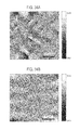
- FIG. 3A shows the hetero epitaxial crystal structure formed by the hetero epitaxial growth method according to the first embodiment of the present invention, and is an optical microscope photograph of the surface of the ZnO layer.
- FIG. 3B shows the hetero epitaxial crystal structure formed by the hetero epitaxial growth method according to the first embodiment of the present invention, and is a bird's-eye view SEM photograph of the ZnO layer.
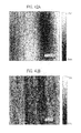
- FIG. 4A shows a hetero epitaxial crystal structure formed by a hetero epitaxial growth method according to a comparative example of the present invention, and is an optical microscope photograph on the surface of the ZnO layer.
- FIG. 4B shows the hetero epitaxial crystal structure formed by the hetero epitaxial growth method according to the comparative example of the present invention, and is a bird's-eye view SEM photograph of the ZnO layer.
- FIG. 6A shows the hetero epitaxial crystal structure formed by the hetero epitaxial growth method (example of 20 minutes of growth period) according to the first embodiment of the present invention, and is an optical microscope photograph on the surface of the ZnO layer.
- FIG. 6B shows the hetero epitaxial crystal structure formed by the hetero epitaxial growth method (example of 20 minutes of growth period) according to the first embodiment of the present invention, and is a bird's-eye view SEM photograph of the ZnO layer.
- FIG. 7A shows the hetero epitaxial crystal structure formed by the hetero epitaxial growth method (example of 60 minutes of growth period) according to the first embodiment of the present invention, and is an optical microscope photograph on the surface of the ZnO layer.
- FIG. 7B shows the hetero epitaxial crystal structure formed by the hetero epitaxial growth method (example of 60 minutes of growth period) according to the first embodiment of the present invention, and is a bird's-eye view SEM photograph of the ZnO layer.
- FIG. 8A shows the hetero epitaxial crystal structure formed by the hetero epitaxial growth method (example of 180 minutes of growth period) according to the first embodiment of the present invention, and is an optical microscope photograph on the surface of the ZnO layer.
- FIG. 8B shows the hetero epitaxial crystal structure formed by the hetero epitaxial growth method (example of 180 minutes of growth period) according to the first embodiment of the present invention, and is a bird's-eye view SEM photograph of the ZnO layer.
- FIG. 9A shows the hetero epitaxial crystal structure formed by the hetero epitaxial growth method (example of 360 minutes of growth period) according to the first embodiment of the present invention, and is an optical microscope photograph on the surface of the ZnO layer.
- FIG. 9B shows the hetero epitaxial crystal structure formed by the hetero epitaxial growth method (example of 360 minutes of growth period) according to the first embodiment of the present invention, and is a bird's-eye view SEM photograph of the ZnO layer.
- FIG. 10 shows the X-ray rocking curve of the ZnO crystal of the hetero epitaxial crystal structure formed by the hetero epitaxial growth method (example of ZnO (002) plane) according to the first embodiment of the present invention.
- FIG. 11 shows the X-ray rocking curve of the ZnO crystal of the hetero epitaxial crystal structure formed by the hetero epitaxial growth method (example of ZnO (101) plane) according to the first embodiment of the present invention.
- FIG. 12 is a drawing showing the relation between full width at half maximum FWHM (arc sec.) and crystal growth period (min.) of the X-ray rocking curve of the ZnO crystal of the hetero epitaxial crystal structure formed by the hetero epitaxial growth method according to the first embodiment of the present invention (example of ZnO (002) plane, and example of ZnO (101) plane).
- FIG. 13 is a schematic diagram of an epitaxial crystal growth apparatus applying to the hetero epitaxial growth method according to the first embodiment of the present invention.
- FIG. 14A shows an optical microscope photograph of the surface of a ZnO buffer layer formed by reacting a zinc metal to water, in the hetero epitaxial growth method according to the first embodiment of the present invention.
- FIG. 14B shows an optical microscope photograph of the surface of a ZnO buffer layer formed by reacting zinc chloride to water, in the hetero epitaxial growth method according to the first embodiment of the present invention.
- FIG. 15A shows a bird's-eye view SEM photograph of the surface of the ZnO buffer layer which formed by reacting the zinc metal to the water, in the hetero epitaxial growth method according to the first embodiment of the present invention (Step 1 ).
- FIG. 15B shows a bird's-eye view SEM photograph of the surface of the ZnO buffer layer annealed with nitrogen gas in a steam atmosphere, in the hetero epitaxial growth method related to the first embodiment of the present invention (Step 2 ).
- FIG. 15C shows a bird's-eye view SEM photograph of the surface of the ZnO layer formed by reacting the zinc chloride and the water continuously, in the hetero epitaxial growth method according to the first embodiment of the present invention (Step 3 ).
- FIG. 16 shows an example of a result of a measurement of the X-ray diffraction measurement (2 theta-omega method) for explaining an orientation of a crystal of the ZnO layer corresponding to each step of FIG. 15 , in the hetero epitaxial growth method according to the first embodiment of the present invention.
- FIG. 17A shows the X-ray rocking curve for explaining the crystallinity of the ZnO layer corresponding to each step of FIG. 15 (example of ZnO (002) plane), in the hetero epitaxial growth method according to the first embodiment of the present invention.
- FIG. 17B shows the X-ray rocking curve for explaining the crystallinity of the ZnO layer corresponding to each step of FIG. 15 (example of ZnO (101) plane), in the hetero epitaxial growth method according to the first embodiment of the present invention.
- FIG. 18 is a drawing showing the relation between the growth temperature and growth period in order to investigate the thickness dependency of a buffer layer, in the hetero epitaxial growth method according to the first embodiment of the present invention.
- FIG. 19A shows an optical microscope photograph in the case of setting the growth period of the buffer layer to 0 minute, in the hetero epitaxial growth method according to the first embodiment of the present invention.
- FIG. 19B shows a bird's-eye view SEM photograph corresponding to FIG. 19A .
- FIG. 19C shows an optical microscope photograph in the case of setting the growth period of the buffer layer to 10 minutes, in the hetero epitaxial growth method according to the first embodiment of the present invention.
- FIG. 19D shows a bird's-eye view SEM photograph corresponding to FIG. 19C .
- FIG. 19E shows an optical microscope photograph in the case of setting the growth period of the buffer layer to 30 minutes, in the hetero epitaxial growth method according to the first embodiment of the present invention.
- FIG. 19F shows a bird's-eye view SEM photograph corresponding to FIG. 19E .
- FIG. 19G shows an optical microscope photograph in the case of setting the growth period of the buffer layer to 60 minutes, in the hetero epitaxial growth method according to the first embodiment of the present invention.
- FIG. 19H shows a bird's-eye view SEM photograph corresponding to FIG. 19G .
- FIG. 20A shows a bird's-eye view SEM photograph in the case of setting growth period of the buffer layer to 20 minutes and setting growth period of the ZnO layer to 20 minutes, on an a-plane sapphire substrate, in the hetero epitaxial growth method according to the first embodiment of the present invention.
- FIG. 20B shows a bird's-eye view SEM photograph at a high magnifiction corresponding to FIG. 20A .
- FIG. 20C shows a bird's-eye view SEM photograph in the case of setting growth period of the buffer layer to 60 minutes and setting growth period of the ZnO layer to 20 minutes, on the a-plane sapphire substrate, in the hetero epitaxial growth method according to the first embodiment of the present invention.
- FIG. 20D shows a expansion bird's-eye view SEM photograph at a high magnifiction corresponding to FIG. 20C .
- FIG. 21 is an example of the result of a measurement of the X-ray diffraction measurement (2 theta-omega method) after performing crystal growth of the ZnO layer by the HVPE method during 60 minutes after performing formation of the buffer layer during 10 minutes, on the a-plane sapphire substrate, in the hetero epitaxial growth method according to the first embodiment of the present invention.
- FIG. 22 is an example of the result of a measurement of the X-ray diffraction measurement (2 theta-omega method) after performing crystal growth of the ZnO layer by the HVPE method during 60 minutes after performing formation of the buffer layer during 30 minutes, on the a-plane sapphire substrate, in the hetero epitaxial growth method according to the first embodiment of the present invention.
- FIG. 23 is an example of the result of a measurement of the X-ray diffraction measurement (2 theta-omega method) after performing crystal growth of the ZnO layer by the HVPE method during 60 minutes after performing formation of the buffer layer during 60 minutes, on the a-plane sapphire substrate, in the hetero epitaxial growth method according to the first embodiment of the present invention.
- FIG. 24A shows an example of the X-ray rocking curve after performing crystal growth of the ZnO layer by the HVPE method during 60 minutes after performing formation of the buffer layer during 30 minutes and 60 minutes, respectively, on the a-plane sapphire substrate, in the hetero epitaxial growth method according to the first embodiment of the present invention (ZnO (002) plane).
- FIG. 24B shows an example of the X-ray rocking curve in the case of the ZnO (101) plane which grows the ZnO layer on the same conditions, in the hetero epitaxial growth method according to the first embodiment of the present invention.
- FIG. 25 is an explanatory diagram of a X-ray phi scan of the ZnO layer formed on the a-plane sapphire substrate, in the hetero epitaxial growth method according to the first embodiment of the present invention.
- FIG. 26 shows a result of a measurement of the X-ray phi scan of the ZnO (101) plane based on the existence or nonexistence of the buffer layer formed on the a-plane sapphire substrate, in the hetero epitaxial growth method according to the first embodiment of the present invention.
- FIG. 27A is a schematic cross-sectional configuration diagram of the ZnO layer performed the crystal growth on a r-plane sapphire substrate without forming the buffer layer, in the hetero epitaxial growth method according to the first embodiment of the present invention.
- FIG. 27B shows a surface bird's-eye view SEM photograph after performing crystal growth of the ZnO layer by the HVPE method during 60 minutes on the r-plane sapphire substrate without forming the buffer layer, in the hetero epitaxial growth method according to the first embodiment of the present invention.
- FIG. 28A is a schematic cross-sectional configuration diagram of the ZnO layer performed the crystal growth after forming the buffer layer on the r-plane sapphire substrate, in the hetero epitaxial growth method according to the first embodiment of the present invention.
- FIG. 28B shows a surface bird's-eye view SEM photograph after performing the crystal growth of the ZnO layer by the HVPE method during 60 minutes after forming the buffer layer on the r-plane sapphire substrate, in the hetero epitaxial growth method according to the first embodiment of the present invention.
- FIG. 29A shows a surface bird's-eye view SEM photograph performed the crystal growth of the buffer layer at 400 degrees C. during 60 minutes on the r-plane sapphire substrate, in the hetero epitaxial growth method according to the first embodiment of the present invention.
- FIG. 29B shows a surface bird's-eye view SEM photograph of the ZnO layer performed the crystal growth further at 1000 degrees C. during 60 minutes, in the hetero epitaxial growth method according to the first embodiment of the present invention.
- FIG. 30 shows an example of a result of a measurement of X-ray diffraction measurement (2 theta-omega method) of the ZnO layer formed as shown in FIG. 29 .
- FIG. 31 is a schematic cross-sectional configuration diagram of a semiconductor device having the hetero epitaxial crystal structure formed by the hetero epitaxial growth method according to the first embodiment of the present invention.
- FIG. 32A shows a homo epitaxial growth method of a homo epitaxial crystal structure according to a second embodiment of the present invention, and is a schematic cross-sectional configuration diagram showing a process for which a ZnO substrate is prepared.
- FIG. 32B shows the homo epitaxial growth method of the homo epitaxial crystal structure according to the second embodiment of the present invention, and is a schematic cross-sectional configuration diagram showing a formation process of the ZnO based semiconductor layer by halogenide vapor phase epitaxy.
- FIG. 43 shows an AFM photograph showing the surface morphology of 1 ML step of +c-plane ZnO based semiconductor layer surface in alignment with m-axial direction ⁇ 1-10> and a-axial direction ⁇ 110>, in the homo epitaxial crystal structure formed by the homo epitaxial growth method according to the second embodiment of the present invention.
- FIG. 44A is an enlarged drawing of an AFM photograph showing the surface morphology of 1 ML step of +c-plane ZnO based semiconductor layer surface in alignment with m-axial direction ⁇ 1-10> and a-axial direction ⁇ 110>, in the homo epitaxial crystal structure formed by the homo epitaxial growth method according to the second embodiment of the present invention.
- FIG. 44B is a schematic planar structure diagram of the step morphology of 1 ML step corresponding to FIG. 44A .
- FIG. 44C is a schematic cross-sectional configuration diagram of the step morphology between A-B corresponding to FIG. 44B .
- FIG. 44D is an explanatory diagram of the m-axial direction ⁇ 1-10> and the a-axial direction ⁇ 110> in hexagonal shape.
- FIG. 45 shows the X-ray rocking curve of the ZnO crystal of the homo epitaxial crystal structure formed by the homo epitaxial growth method according to the second embodiment of the present invention (example of ZnO (002) plane).
- FIG. 46 shows the X-ray rocking curve of the ZnO crystal of the homo epitaxial crystal structure formed by the homo epitaxial growth method according to the second embodiment of the present invention (example of ZnO (101) plane).
- FIG. 47 shows a SIMS analysis result of the ZnO crystal of the homo epitaxial crystal structure formed by the homo epitaxial growth method according to the second embodiment of the present invention (polarity of detected ion: ⁇ ).
- FIG. 48 shows a SIMS analysis result of the ZnO crystal of the homo epitaxial crystal structure formed by the homo epitaxial growth method according to the second embodiment of the present invention (polarity of detected ion: +).
- FIG. 49 shows a SIMS analysis result showing the depth direction dependence of the chlorine concentration of the ZnO crystal of the homo epitaxial crystal structure formed by the homo epitaxial growth method according to the second embodiment of the present invention.
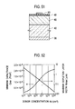
- FIG. 50 shows a result of a measurement of the electrical characteristics of the ZnO film of the homo epitaxial crystal structure formed by the homo epitaxial growth method according to the second embodiment of the present invention, and is C-V characteristics of the MOS structure.
- FIG. 51 is a schematic cross-sectional configuration diagram of the sample applying to C-V measurement of FIG. 50 .
- FIG. 52 is a relationship diagram of the minimum capacitance C min (F/cm 2 ) and the maximum depletion layer width W max ( ⁇ m) toward donor concentration N D (cm ⁇ 3 ).
- FIG. 53 is a schematic cross-sectional configuration diagram of a semiconductor device having the homo epitaxial crystal structure formed by the homo epitaxial growth method according to the second embodiment of the present invention.
- FIG. 54 is a drawing showing an AFM image of 20 ⁇ m square of an undoped ZnO based semiconductor layer surface formed by the HVPE method.
- FIG. 55 is a drawing showing an AFM image of 20 ⁇ m square of a nitrogen doped ZnO based semiconductor layer surface formed by a fabrication method for a ZnO based semiconductor according to a third embodiment of the present invention.
- FIG. 56A is a drawing showing the relation of crystal growth driving force and growth temperature by the thermodynamic analysis in the case of changing the VI/II ratio.
- FIG. 56B is a drawing showing the comparison with the case where there is no supply of ammonia gas, in the relation of the crystal growth driving force and the growth temperature by the thermodynamic analysis in the case of changing the VI/II ratio.
- FIG. 57 is a drawing showing the relation between the growth rate and the growth temperature of a nitrogen doped ZnO layer for every ammonia gas partial pressure.
- FIG. 58 is a drawing which classifies whether the nitrogen doped ZnO layer is growing or etching, based on the data of FIG. 57 .
- FIG. 59 is a drawing showing that the nitrogen concentration of the nitrogen doped ZnO changes in accordance with growth temperature.
- FIG. 60 is a drawing showing a secondary ion mass analytical measurement result in the representative case of the nitrogen doped ZnO layer fabricated by the fabrication method of the ZnO based semiconductor of the present invention.
- FIG. 61 is a drawing showing a schematic configuration example of a fabricating apparatus applying the fabrication method of the ZnO based semiconductor according to the third embodiment of the present invention.
- FIG. 62 is a drawing showing a configuration example applying a p type ZnO based semiconductor layer as a multilayer film in a ZnO based semiconductor element fabricated by the fabrication method of the ZnO based semiconductor according to the third embodiment of the present invention.
- the “ZnO based compound semiconductor” as used in the following explanation means the group II oxide semiconductor containing the group II element Zn.
- a hetero epitaxial growth method of a hetero epitaxial crystal structure according to a first embodiment of the present invention will be explained with reference to FIG. 1 .
- a buffer layer formation process is expressed as shown in FIG. 1A .
- a formation process of a ZnO facet 44 by halogenide vapor phase epitaxy is expressed as shown in FIG. 1B .
- a formation process of a ZnO layer by halogenide vapor phase epitaxy is expressed as shown in FIG. 1C .
- a ZnO template is formed by a laser ablation method on a heterogeneous substrate 40 , using an a-plane sapphire substrate for example as the heterogeneous substrate 40 .
- the ZnO template is composed of a buffer layer 42 .
- the buffer layer 42 can also be formed with the orienting film of an oxide, or the orienting film of nitride. More specifically, for example, the orienting film of the oxide composed of ZnO or MgO, or the orienting film of the nitride composed of AlN or GaN is applicable.
- the temperature for forming the ZnO template is about 500 degrees C., for example.
- the thickness of the buffer layer 42 is about 0.3 ⁇ m, for example.
- a sputtering method, a pulse laser method, a MBE method, a HVPE method, etc. can be used, for example.
- a VPE method, etc. for merely reacting steam of Zn to water vapor are also applicable.
- not less than 400 degrees C. of growth temperature is preferable, for example. It is because the performance of an underlying crystal substrate can be reflected to the ZnO template the more satisfactory, the more it becomes high temperature.
- the VPE method for merely reacting steam of Zn to vapor is later described with reference to FIG. 14 to FIG. 30 .
- the HVPE method, the VPE method, etc. achievable in the same growth furnace are preferable.
- the orientation of the buffer layer 42 can be improved and the crystallinity of a subsequent high temperature grown film also improves by heating the heterogeneous substrate 40 to the moderate temperature level (to 500 degrees C.).
- a thickness of the film is also not specified in particular, since the orientation and surface flatness of the buffer layer 42 may deteriorate with the method for film deposition of the buffer layer 42 if the film thickness is too thick, and it will not become continuous membrane if the film thickness is too thin, the film thickness of about 0.02 ⁇ m to about 0.5 ⁇ m is preferable, for example.
- the c-plane oriented in the c-axial direction is obtained.
- a silicon substrate, a SiC substrate, a GaAs substrate, a GaP substrate, a GaN based substrate, etc. are applicable as the heterogeneous substrate 40 except the above-mentioned a-plane sapphire substrate.
- a ZnO facet 44 is formed on the buffer layer 42 by the HVPE method. More specifically, the halogenide vapor phase epitaxy using zinc chloride (ZnCl 2 ) and water (H 2 O) is applied.
- the partial pressure PZnCl 2 of ZnCl 2 is set as about 2.2 ⁇ 10 ⁇ 5 atm against total pressure 1 atm, for example, the VI/II ratio which is a supply ratio between oxygen which is a group VI element and Zn which is group II elements is set to about 20 to 200, for example, the crystal growth temperature T g is set as about 1000 degrees C., for example, and the crystal growth period is set up in about 1 hour, for example.
- partial pressure PZnCl 2 of ZnCl 2 2.2 ⁇ 10 ⁇ 5 atm
- VI/II ratio 20 to 200
- it will be set to partial pressure PH 2 O of H 2 O 4.4 ⁇ 10 ⁇ 4 to 4.4 ⁇ 10 ⁇ 3 atm.
- the temperature T g of crystal growth is enforcing the high temperature growth method higher than 800 degrees C. If the melting point of 1975 degrees C. of the ZnO crystal is taken into consideration, 1 ⁇ 3 to about 1 ⁇ 2 of the melting point is needed, and the more the temperature T g of crystal growth is high, the more the satisfactory crystal of quality can be obtained. Therefore, in the above-mentioned example, the growth of about 1000 degrees C. same as GaN is performed.
- a ZnO layer 46 of desired thickness is formed by performing lateral growth and vertical growth further for the ZnO facet 44 formed on the buffer layer 42 by using the HVPE method, setting up the crystal growth period still longer, as shown in FIG. 1C . More specifically, the halogenide vapor phase epitaxy using zinc chloride (ZnCl 2 ), water (H 2 O), and N 2 which is carrier gas is applied as well as the formation of the ZnO facet 44 .
- the partial pressure PZnCl 2 of ZnCl 2 is set as about 2.2 ⁇ 10 ⁇ 5 atm, for example, the VI/II ratio which is a supply ratio between the oxygen which is a group VI element and the Zn which is group II elements is set as about 20 to about 200, for example, the crystal growth temperature T g is set as about 1000 degrees C., for example, and the crystal growth period is set up in about 1 hour to about 6 hours, for example.
- the hetero epitaxial growth method is characterized by obtaining the single crystal of ZnO by depositing the buffer layer of ZnO at low temperature on the heterogeneous substrate, and then mixing Zn material composed of a halogenide of Zn and oxygen material in the vapor phase with high temperature at not less than 800 degrees C.
- the wettability of ZnO can be improved by forming the buffer layer 42 to improve the wettability of ZnO on the heterogeneous substrate 40 , such as ZnO, before the high temperature growth using Zn material composed of halogenide.
- a schematic bird's-eye view structure of the hetero epitaxial crystal structure in a formation process of the ZnO layer by the HVPE method is expressed as shown in FIG. 2 .
- An aspect that the lateral growth (GL) and vertical growth (GV) of the ZnO facet 44 are performed on a surface 40 a of the heterogeneous substrate 40 is shown schematically.
- FIG. 3A an example of the optical microscope photograph on the surface of the ZnO layer is expressed as shown in FIG. 3A .
- a bird's-eye view SEM photograph of the ZnO layer corresponding to FIG. 3A is expressed as shown in FIG. 3B .
- FIG. 3A and FIG. 3B corresponds to the structure of FIG. 1B and FIG. 2 . That is, it is an example which forms the ZnO facet 44 on the buffer layer 42 formed on the a-plane sapphire substrate using the a-plane sapphire substrate as the heterogeneous substrate 40 .
- partial pressure P ZnCl2 of ZnCl 2 is set as 2.2 ⁇ 10 ⁇ 5 atm
- the VI/II ratio is set as 20
- the crystal growth temperature T g is set as 1000 degrees C.
- the crystal growth period is set up in 1 hour.
- FIG. 4A an example of the optical microscope photograph on the surface of the ZnO layer is expressed as shown in FIG. 4A .
- a bird's-eye view SEM photograph of the ZnO layer corresponding to FIG. 4A is expressed as shown in FIG. 4B .
- the example of FIG. 4A and FIG. 4B corresponds to the example which forms the ZnO crystal directly on the a-plane sapphire substrate not using the buffer layer 42 in the structure of FIG. 1B .
- the partial pressure P ZnCl2 of ZnCl 2 is set 2.2 ⁇ 10 ⁇ 5 atm
- the VI/II ratio is set as 600
- the crystal growth temperature T g is set as 1000 degrees C.
- the crystal growth period is set up in 1 hour.
- a SEM photograph of the ZnO layer corresponding to FIG. 3A is expressed as shown in FIG. 3B
- a bird's-eye view SEM photograph of the ZnO layer corresponding to FIG. 5A is expressed as shown in FIG. 5B .
- the partial pressure PZnCl 2 of ZnCl 2 is set as 2.2 ⁇ 10 ⁇ 5 atm
- the crystal growth temperature T g is set as 1000 degrees C.
- the crystal growth period is set up in 1 hour.
- the partial pressure PH 2 O of H 2 O is set to 4.4 ⁇ 10 ⁇ 3 atm, the more the partial pressure PH 2 O of H 2 O is high, the more the surface migration of ZnCl 2 molecules is suppressed, and the result that the lateral growth (GL) does not occur easily although the vertical growth (GV) is occurred is obtained.
- the VI/II ratio is effective to apply not more than 100.
- the VI/II ratio is effective to apply more than 1.
- the VI/II ratio may be set as value of more than 1 to not more than 100 (for example, 20) until the continuous membrane is made because the facet combines, for example, and then the VI/II ratio may be set as value of more than 100 (for example, 200).
- an optical microscope photograph on the surface of the ZnO layer in the case that the growth period is 20 minutes is expressed as shown in FIG. 6A
- a bird's-eye view SEM photograph of the ZnO layer corresponding to FIG. 6A is expressed as shown in FIG. 6B
- an optical microscope photograph on the surface of the ZnO layer in the case that the growth period is 60 minutes is expressed as shown in FIG. 7A
- a bird's-eye view SEM photograph of the ZnO layer corresponding to FIG. 7A is expressed as shown in FIG.
- FIG. 8A an optical microscope photograph on the surface of the ZnO layer in the case that the growth period is 180 minutes is expressed as shown in FIG. 8A
- a bird's-eye view SEM photograph of the ZnO layer corresponding to FIG. 8A is expressed as shown in FIG. 8B
- an optical microscope photograph on the surface of the ZnO layer in the case that the growth period is 360 minutes is expressed as shown in FIG. 9A
- a bird's-eye view SEM photograph of the ZnO layer corresponding to FIG. 9A is expressed as shown in FIG. 9B .
- the partial pressure P ZnCl2 of ZnCl 2 is set as 2.2 ⁇ 10 ⁇ 5 (atm), the VI/II ratio is set as 20, and the crystal growth temperature T g is set as 1000 degrees C.
- the hetero epitaxial growth method as for the high temperature ZnO layer, it proves an aspect that the lateral crystal growth (GL) progresses with the passage of time of crystal growth, the vertical crystal growth (GV) progresses further, and the epitaxial layer grows.
- the high temperature growth using the halogenide can reduce the crystalline nucleus on the buffer layer 42 as compared with the MBE method or the MOCVD method. Moreover, the buffer layer 42 improves the wettability of ZnO. Accordingly, the high temperature growth using the halogenide follows the growth process which forms the film by the great crystalline nucleus on the buffer layer 42 being linked with a lateral direction, as well as the high temperature GaN on the buffer layer by the MOCVD method.
- the crystalline nucleus can be combined at an early stage, and flattening of the high temperature grown film can be possible.
- the reactivity of the halogenide of Zn and oxygen material is not as high as Zn and oxygen material. Accordingly, the high temperature growth using the halogenide of Zn has few reactions in the vapor phase, and there is little occurrence of particle.
- a X-ray rocking curve of the (002) plane of ZnO is expressed as shown in FIG. 10 .
- each curve expresses an example whose the crystal growth periods are 0 minute, 20 minutes, 60 minutes, 180 minutes, and 360 minutes, as a parameter.
- the (002) plane is a plane vertical to a c-axis
- the X-ray rocking curve shown in FIG. 10 expresses a tilt profile which is fluctuation of the c-axial direction which is a growth direction.
- a X-ray rocking curve of (101) plane of ZnO is expressed as shown in FIG. 11 .
- Each curve expresses an example whose the crystal growth periods are 0 minute, 20 minutes, 60 minutes, 180 minutes, and 360 minutes, as a parameter, same as that of FIG. 10 .
- the (101) plane is a semi-polar plane
- the X-ray rocking curve shown in FIG. 11 expresses a twist profile and a tilt profile which are fluctuation of a direction vertical to the semi-polar plane.
- the relation between the full width at half maximum FWHM (arcsec) of the X-ray rocking curve of the ZnO crystal and the crystal growth period (min.) is expressed as shown in FIG. 12 .
- An example of the ZnO (002) plane and an example of the ZnO (101) plane are shown in FIG. 12 .
- the full width at half maximum FWHM becomes not more than 0.1 (degree) in the crystal (002) and (101) planes.
- the (101) plane is measured as an example of the semi-polar plane according to the first embodiment, it does not limit to the example. Of course about other semi-polar planes, transition of same full width at half maximum FWHM is obtained.
- a schematic configuration of an epitaxial crystal growth apparatus 20 applying to the hetero epitaxial growth method according to the first embodiment includes a gaseous chlorine supplying unit 2 , a carrier gas supplying unit 3 , a source zone 4 , an heating unit 5 , a water supplying unit 6 , a carrier gas supplying unit 7 , a growth zone 8 , an heating unit 9 , and a substrate holding unit 10 .
- a configuration for applying to the hetero epitaxial growth method of a MgZnO semiconductor (ZnO based semiconductor) is also disposed in the epitaxial crystal growth apparatus 20 applying to the hetero epitaxial growth method. That is, as shown in FIG. 13 , the epitaxial crystal growth apparatus 20 includes a gaseous chlorine supplying unit 12 , a carrier gas supplying unit 13 , and a source zone 14 by which group II metallic material 25 including the single metal substance of magnesium is held.
- the apparatus configuration for performing impurity doping of a n type impurity or a p type impurity is also disposed on the epitaxial crystal growth apparatus 20 . That is, as shown in FIG. 13 , the epitaxial crystal growth apparatus 20 includes a first doping gas supplying unit 22 for supplying a n type doping gas for performing impurity doping of the n type impurity, and a second doping gas supplying unit 24 for supplying a p type doping gas for performing impurity doping of the p type impurity.
- the source zone 4 is for holding a group II metallic material 15 consisting of a zinc single metal substance. Moreover, the source zone 4 is a zone for generating zinc chloride gas by reacting the gaseous chlorine, which are supplied from the gaseous chlorine supplying unit 2 , and zinc. A source zone 14 is for holding magnesium of single substance instead of the zinc held by the source zone 4 .
- the growth zone 8 is a zone for growing up the ZnO semiconductor on a growth substrate 16 held on a substrate holding unit 10 by reacting the zinc chloride gas supplied from the source zone 4 connected by a supplying pipe, and the water (vapor) supplied from the water supplying unit 6 as an oxygen material.
- each supplying pipe for connecting the source zone 4 , the growth zone 8 and each gas supplying unit, and the growth zone 8 is composed by quartz glass.
- the heating unit 5 is for heating the source zones 4 and 14 and the supply route of water.
- the heating unit 9 is for annealing the growth zone 8 .
- the hetero epitaxial crystal growth apparatus 20 achieves a hot wall method by the heating units 5 and 9 .
- the heating unit 5 is not limited to the illustrated configuration.
- a heating unit 5 a heats the source zone 14
- a heating unit 5 b anneals the source zone 4
- a heating unit 5 c heats the quartz tube of water supplying unit 6 and the carrier gas supplying unit 7
- a heating unit 5 d heats the quartz tube of n type doping gas supplying unit 22 and a p type doping gas supplying unit 24 , by using the heating units 5 a , 5 b , 5 c , and 5 d which are not illustrated.
- the nitrogen gas supplied from the carrier gas supplying units 3 , 7 , and 13 is for carrying the zinc chloride gas generated by the source zone 4 , the water supplied from the water supplying unit 6 , and the magnesium chloride gas generated by the source zone 14 to the growth zone 8 .
- the gaseous chlorine and the nitrogen gas are carried to the source zone 4 , respectively from the gaseous chlorine supplying unit 2 and the carrier gas supplying unit 3 .
- the reaction by the following reaction formula (1) occurs by the group II metallic material 15 consisting of the single metal substance of the zinc currently held, and the supplied gaseous chlorine, and the zinc chloride gas is generated.
- Zn( s,l )+Cl 2 ( g ) ⁇ >ZnCl 2 ( g ) (1)
- the single metal substance of the zinc held at the source zone 4 it is preferred that it is a single metal substance with high purity, for example, not less than 99.99999% of its single metal substance is effective.
- (s), (l), and (g) in the reaction formula show a solid, a fluid, and gas, respectively.
- the source zone 4 becomes the structure which enlarges surface area of the group II metallic material 15 consisting of the zinc single metal substance and a suitable temperature so that most reactions in the reaction formula (1) are advanced to the right-hand side, and the flow rate of zinc chloride gas can be controlled by the amount of supply of gaseous chlorine.
- the suitable temperature about 300 degrees C. to about 450 degrees C. are preferable.
- the temperature of the source zone 4 is set as not more than about 500 degrees C., in order to suppress that the zinc gas with extremely high vapor pressure also in metal is carried to the growth zone 8 . Then, the zinc chloride gas generated by the above-mentioned reaction formula (1) is carried to the growth zone 8 by the nitrogen gas supplied from the carrier gas supplying unit 3 .
- the water (vapor) supplied from the water supplying unit 6 is carried to the growth zone 8 as an oxygen material through other paths by the nitrogen gas supplied from the carrier gas supplying unit 7 .
- the temperature of the growth zone 8 is set as high temperature rather than the temperature of the source zone 4 so that the zinc chloride gas may not deposit in the intermediate path to the growth zone 8 . More specifically, the temperature of the growth zone 8 is set as about 500 degrees C. to about 1100 degrees C.
- the gaseous chlorine is carried to the source zone 14 with carrier gas, and the magnesium chloride gas is generated in the source zone 14 .
- the MgZnO semiconductor can be grown up on the growth substrate 16 by carrying the magnesium chloride gas to the growth zone 8 by the nitrogen gas supplied from the carrier gas supplying unit 13 , and reacting the zinc chloride gas, the magnesium chloride gas and the water in the growth zone 8 .
- the hetero epitaxial growth method of the ZnO based semiconductor (ZnO, MgZnO) it can perform impurity doping of a desired n type impurity or p type impurity toward the growth layer by using the n type doping gas supplying unit 22 and the p type doping gas supplying unit 24 .
- the epitaxial crystal growth apparatus 20 since the single metal substance of the zinc with high purity instead of zinc chloride is adopted as the group II metallic material 15 , the ZnO based semiconductor of high quality can be fabricated easily.
- the zinc chloride gas generated by the source zone 4 deposits during being carried to the growth zone 8 by setting the temperature of the source zone 4 lower than the growth temperature of the growth zone 8 .
- reaction formula (2) can be proceeded to the right-hand side in the state where it is more stabilized thermodynamically.
- the single metal substance of cadmium may be adopted instead of the single metal substance of magnesium, as the group II metallic material.
- oxygen gas may be adopted instead of the water as the oxygen material.
- bromine gas may be adopted instead of the gaseous chlorine as the halogen gas.
- the kind of group II metallic material may not be limited to two kinds, and it may use more than three kinds of group II metallic materials.
- the VPE method for merely reacting steam of Zn with vapor will be explained hereinafter.
- the formation method not less than 400 degrees C. of the growth temperature is preferable, for example, and the more growth temperature becomes high temperature, the more it can reflect the performance of an underlying crystal substrate in the ZnO template satisfactory.
- the configuration shown in FIG. 13 can be used for the crystal growth apparatus 20 also about the VPE method for merely reacting steam of Zn with the vapor, as the formation method for the ZnO template.
- an optical microscope photograph of the ZnO buffer layer surface formed by reacting the zinc metal to the water is expressed as shown in FIG. 14A
- an optical microscope photograph of the ZnO buffer layer surface formed by reacting the zinc chloride to the water is expressed as shown in FIG. 14B .
- the growth temperature is about 400 degrees C.
- the growth period is about 60 minutes.
- the partial pressure PH 2 O of H 2 O is 2.2 ⁇ 10 ⁇ 2 atm in FIG. 14A
- the partial pressure PH 2 O of H 2 O is 1.32 ⁇ 10 ⁇ 2 atm in FIG. 14B .
- the method for growing up the thin film of the ZnO semiconductor on the growth substrate 16 by the HVPE method after forming the ZnO buffer layer formed by reacting zinc metal with water is expressed as follows.
- Step 1 nitrogen gas is carried to the source zone 4 from the carrier gas supplying unit 3 , as Step 1 . Then, in the source zone 4 , the group II metallic material 15 consisting of the single metal substance of the zinc currently held is evaporated, and is introduced in the growth zone 8 . On the other hand, the evaporated zinc reacts with the vapor introduced in the growth zone 8 from the water supplying unit 6 , and then the thin film of the ZnO semiconductor grows on the growth substrate 16 according to the reaction according to the following formula (3).
- the crystal growth temperature of the ZnO buffer layer 42 is not less than about 400 degrees C., for example, and the thickness is not more than about 0.3 micrometer, for example.
- Step 2 it anneals with the nitrogen gas in the atmosphere of the vapor H 2 O(g), as Step 2 .
- the annealing temperature is about 1000 degrees C., for example. By annealing in the manner, the crystallinity and the surface flatness of the ZnO buffer layer 42 can be improved.
- Step 3 the gaseous chlorine is carried to the source zone 4 from the gaseous chlorine supplying unit 2 , and the nitrogen gas is simultaneously carried to the source zone 4 from the carrier gas supplying unit 3 .
- the reaction according to the reaction formula (1) occurs by the group II metallic material 15 consisting of the single metal substance of the zinc currently held, and the supplied gaseous chlorine, and the zinc chloride gas is generated.
- the zinc chloride gas generated according to the reaction formula (1) is carried to the growth zone 8 by the nitrogen gas supplied from the carrier gas supplying unit 3 .
- the water (vapor) supplied from the water supplying unit 6 is carried to the growth zone 8 as an oxygen material through other paths by the nitrogen gas supplied from the carrier gas supplying unit 7 .
- the thin film of the ZnO semiconductor grows on the growth substrate 16 with the zinc chloride gas and the water which are carried, when the reaction of the reaction formula (2) proceeds to the right-hand side.
- the crystal growth temperature is about 1000 degrees C., for example.
- a SEM photograph of the ZnO buffer layer surface formed by reacting zinc metal with water (Step 1 ) is expressed as shown, for example in FIG. 15A
- a SEM photograph of the ZnO buffer layer surface annealed with the nitrogen gas in the steam atmosphere (Step 2 ) is expressed as shown, for example in FIG. 15 ( b )
- a SEM photograph on the surface of the ZnO layer formed by reacting zinc chloride with water (Step 3 ) is expressed as shown, for example in FIG. 15C .
- the growth temperature is about 400 degrees C.
- the growth period is about 60 minutes
- the partial pressure P H2O of H 2 O is about 2.2 ⁇ 10 ⁇ 2 atm.
- the annealing temperature is about 1000 degrees C.
- the heat treating time is about 60 minutes
- the partial pressure P H2O of H 2 O is about 4.4 ⁇ 10 ⁇ 3 atm.
- the growth temperature is about 1000 degrees C.
- the growth period is about 60 minutes
- the partial pressure PH 2 O of H 2 O is about 4.4 ⁇ 10 ⁇ 4 atm
- the VI/II ratio is about 20.
- an aspect that the crystallinity becomes satisfactory is observed in accordance with Steps 1 - 3 .
- FIG. 16 an example of a result of a measurement of a X-ray diffraction measurement (2 theta-omega method) for explaining the orientation of the ZnO crystal corresponding to each step of FIG. 15 is expressed as shown in FIG. 16 .
- a vertical axis expresses XRD intensity (a.u.)
- a horizontal axis expresses 2 ⁇ . It is observed that the ZnO (002) plane orients toward the a-plane sapphire substrate, and the peak intensity of ZnO (002) increases and the orientation of the crystal is improving in accordance with shifting to Step 1 to Step 3 .
- a X-ray rocking curve (example of the ZnO (002) plane) for explaining the crystallinity of the ZnO crystal corresponding to each step of FIG. 15 is expressed as shown, for example in FIG. 17A
- a X-ray rocking curve (example of the ZnO (101) plane) for explaining the crystallinity of the ZnO buffer layer corresponding to each step of FIG. 15 is expressed as shown, for example in FIG. 17B .
- the value of full width at half maximum FWHM (arcsec) of the rocking curve of the (002) plane of ZnO is about 1209 (arcsec) at Step 1 , is about 460 (arcsec) at Step 2 , and is about 327 (arcsec) at Step 3 .
- the value of full width at half maximum FWHM (arcsec) of the rocking curve of the (101) plane of ZnO is about 1458 (arcsec) at Step 1 , is about 702 (arcsec) at Step 2 , and is about 493 (arcsec) at Step 3 .
- the relation between the crystal growth temperature and the growth period is expressed as shown in FIG. 18 .
- the case where the growth period of the buffer layer is 0 (minute) is correspond to the case where there is no buffer layer.
- the a-plane sapphire substrate surface is cleaned by performing thermal cleaning (T. C.) in H 2 at high temperature of 1000 degrees C., in the time t 1 to t 2 .
- Step 2 the carrier gas is switched to N 2 and the buffer layer is grown up, in the time t 3 to t 4 , as Step 1 .
- the crystal growth period of the buffer layer is changed to 0 (minute) to 60 (minutes).
- the growth temperature of the buffer layer is about 400 degrees C.
- the partial pressure P Zn of Zn(g) is about 4 ⁇ 10 ⁇ 5 atm
- the partial pressure PH 2 O of H 2 O is about 4.4 ⁇ 10 ⁇ 3 atm.
- the annealing treatment is performed, as Step 2 , in the time t 5 to t 6 .
- the annealing temperature in this case is about 1000 degrees C., the annealing time is about 10 (minutes), and the partial pressure PH 2 O of H 2 O is about 4.4 ⁇ 10 ⁇ 3 atm.
- the crystal growth of the ZnO layer is performed by the HVPE method, as Step 3 , in the time t 6 to t 7 .
- the crystal growth temperature in this case is about 1000 degrees C., the crystal growth period is about 60 (minutes), the supplied partial pressure P ZnCl2 of ZnCl 2 is about 2.2 ⁇ 10 ⁇ 5 atm, and the VI/II ratio is about 20.
- FIG. 19 A result obtained by the growing condition shown in FIG. 18 is expressed as shown in FIG. 19 .
- FIG. 19A shows an optical microscope photograph of the ZnO crystal surface in the case of setting the growth period of the buffer layer to 0 (minute)
- FIG. 19B shows a bird's-eye view SEM photograph corresponding to FIG. 19A
- FIG. 19C shows an optical microscope photograph of the ZnO crystal surface in the case of setting the growth period t 3 to t 4 of the buffer layer to 10 (minutes)
- FIG. 19D shows a bird's-eye view SEM photograph corresponding to FIG. 19C .
- FIG. 19E shows an optical microscope photograph of the ZnO crystal surface in the case of setting the growth period t 3 to t 4 of the buffer layer to 30 (minutes), and
- FIG. 19F shows a bird's-eye view SEM photograph corresponding to FIG. 19E .
- FIG. 19G shows an optical microscope photograph of the ZnO crystal surface in the case of setting the growth period t 3 to t 4 of the buffer layer to 60 (minutes), and FIG. 19H shows a bird's-eye view SEM photograph corresponding to FIG. 19G .
- the state of the crystal surface of the ZnO layer which grows by the HVPE method on the buffer layer by changing the thick film (growth period) of the buffer layer formed by low-temperature growth of about 400 degrees C. As clearly from FIG. 19A to FIG. 19H , the state of the crystal surface of the ZnO layer is as satisfactory as the film thickness of the buffer layer being thick (growth period being long). It is considered because the two-dimensional growth of the ZnO layer by the HVPE method is as accelerated as the film thickness of the buffer layer being thick (growth period being long).
- FIG. 20A A SEM photograph of the crystal surface of the ZnO layer in the case of setting the growth period of the buffer layer on the a-plane sapphire substrate to 20 minutes and setting the growth period of the ZnO layer to 20 minutes is expressed as shown in FIG. 20A
- FIG. 20B an expansion bird's-eye view SEM photograph corresponding to FIG. 20A is expressed as shown in FIG. 20B
- FIG. 20C a SEM photograph of the crystal surface of the ZnO layer in the case of setting the growth period of the buffer layer on the a-plane sapphire substrate to 60 minutes and setting the growth period of the ZnO layer to 20 minutes
- FIG. 20C an expansion bird's-eye view SEM photograph corresponding to FIG. 20C is expressed as shown in FIG. 20D .
- a growth mode by which a hexagon-shaped growth nucleus is generated on the crystal surface of the ZnO layer formed on the buffer layer formed at low temperature, the growth nucleus of the shape of the hexagon combines with each other, and flattening is performed, is achieved. Moreover, the lateral growth of the ZnO layer formed by the HVPE method on the buffer layer is as accelerated as the thickness of the buffer layer formed at low temperature being thick.
- a result of a measurement of X-ray diffraction measurement (2 theta-omega method) of the crystal of the ZnO layer after performing the crystal growth of the ZnO layer by the HVPE method for 60 minutes after formation of the buffer layer on the a-plane sapphire substrate for 10 minutes is expressed as shown, for example in FIG. 21 .
- a X-ray diffraction result of a measurement after performing the crystal growth of the ZnO layer by the HVPE method for 60 minutes after the formation of the buffer layer for 30 minutes is expressed as shown, for example in FIG. 22 .
- a X-ray diffraction result of a measurement after performing the crystal growth of the ZnO layer by the HVPE method for 60 minutes after the formation of the buffer layer for 60 minutes is expressed as shown, for example in FIG. 23 .
- the result of FIG. 21 corresponds to FIG. 19C and FIG. 19D
- the result of FIG. 22 corresponds to FIG. 19E and FIG. 19F
- the result of FIG. 23 corresponds to FIG. 19G and FIG. 19H .
- examples of the X-ray rocking curve after performing the crystal growth of the ZnO layer (ZnO (002) plane) by the HVPE method on the buffer layer for 60 minutes after performing the formation of the buffer layer on the a-plane sapphire substrate for 30 minutes and 60 minutes, respectively, are expressed as shown in FIG. 24A in the (002) plane and expressed as shown in FIG. 24B in the (101) plane.
- the values of full width at half maximum FWHM (arcsec) of the rocking curve of the (002) plane of ZnO are 396 (arcsec) and 327 (arcsec), respectively, when the buffer layer is grown for 30 minutes and 60 minutes.
- the values of full width at half maximum FWHM (arcsec) of the rocking curve of the (101) plane of ZnO are 504 (arcsec) and 493 (arcsec), respectively, when the buffer layer is grown for 30 minutes and 60 minutes.
- the full width at half maximum FWHM (arcsec) of the XRD rocking curve of the ZnO layer which became a film is as satisfactory as not more than 500 (arcsec) by accelerating two dimensional crystal growth as shown in FIG. 24A and FIG. 24B , and the reduction of the value of the full width at half maximum of the rocking curve can be expected with the further increase in the film growth thickness as well as FIG. 12 .
- a X-ray phi scan of the c-axis oriented ZnO layer formed on the a-plane sapphire substrate 40 is performed by setting incident X ray and a X-ray detector, and rotating centering on a c-axial direction, so that the ZnO (101) plane may be detected, as shown in FIG. 25 .
- a result of a measurement of the X-ray phi scan of a ZnO layer 46 by the existence or nonexistence of a buffer layer 42 formed on an a-plane sapphire substrate 40 is expressed as shown in FIG. 26 .
- FIG. 26 When there is no buffer layer 42 (WITHOUT LT-Buffer), as the dashed line A in FIG.
- a schematic cross-section structure of ZnO layer 47 performed the crystal growth, without forming the buffer layer, on the r-plane sapphire substrate 41 is expressed as shown in FIG. 27A .
- a surface bird's-eye view SEM photograph after performing the crystal growth of ZnO layer 47 by the HVPE method for 60 minutes, without forming the buffer layer, on the r-plane sapphire substrate 41 is expressed as shown in FIG. 27B .
- the hexagonal pillar crystal is observed.
- a schematic cross-section structure of ZnO layer 47 performed the crystal growth, after forming the buffer layer 43 , on the r-plane sapphire substrate 41 is expressed as shown in FIG. 28A .
- a surface bird's-eye view SEM photograph after performing the crystal growth of ZnO layer 47 by the HVPE method for 60 minutes after forming the buffer layer 43 on the r-plane sapphire substrate 41 is expressed as shown in FIG. 28B .
- a surface bird's-eye view SEM photograph performed the crystal growth of the buffer layer 43 at 400 degrees C. for 60 minutes on the r-plane sapphire substrate 41 is expressed as shown in FIG. 29A
- a surface bird's-eye view SEM photograph of the ZnO layer further performed the crystal growth at 1000 degrees C. for 60 minutes is expressed as shown in FIG. 29B .
- an effect is found in planarizing formation of ZnO layer 47 by the HVPE method deposited on the buffer layer by the ZnO buffer layer 43 also on the r-plane sapphire substrate 41 .
- a result of a measurement of X-ray diffraction measurement (2 theta-omega method) of the ZnO layer formed in FIG. 29 is expressed as shown, for example in FIG. 30 . Since the peak of ZnO (110) is observed as shown in FIG. 30 , the ZnO layer 47 which performs a-axis oriented is formed on the r-plane sapphire substrate 41 .
- an example of schematic cross-section structure of a semiconductor device having the hetero epitaxial crystal structure formed by the hetero epitaxial growth method according to the first embodiment includes: a heterogeneous substrate 40 ; a buffer layer 42 disposed on the heterogeneous substrate 40 ; a n type ZnO based semiconductor layer 52 disposed on the buffer layer 42 and impurity-doped with the n type impurity; a ZnO based semiconductor active layer 54 disposed on the n type ZnO based semiconductor layer 52 ; and a p type ZnO based semiconductor layer 56 disposed on the ZnO based semiconductor active layer 54 and impurity-doped with the p type impurity.
- Each of the n type ZnO based semiconductor layer 52 , the ZnO based semiconductor active layer 54 , and the p type ZnO based semiconductor layer 56 are formed by the above-mentioned hetero epitaxial crystal growth apparatus 20 , and the hetero epitaxial growth method used for the above-mentioned halogenation group II metal and oxygen material.
- a p side electrode 60 is disposed on the p type ZnO based semiconductor layer 56
- a n side electrode 70 is disposed on the surface of the n type ZnO based semiconductor layer 52 exposed by mesa etching.
- the layered structure of a Ni layer and an Au layer is adoptable, for example.
- the layered structure of a Ti layer and an Au layer is adoptable, for example.
- any one of B, Ga, Al, In or Tl is applicable, for example.
- any one of N, P, As, Sb, Bi, Li, or Cu is applicable, for example.
- the ZnO based semiconductor active layer 54 includes a MQW (Multi-Quantum Well) structure where a barrier layer composed of Mg x Zn 1-x O (where 0 ⁇ x ⁇ 1) and a well layer composed of ZnO are deposited, for example.
- MQW Multi-Quantum Well
- the ZnO based semiconductor active layer 54 may include a MQW structure where a well layer composed of Cd y Zn 1-y O (where 0 ⁇ y ⁇ 1) and a barrier layer composed of ZnO is deposited.
- the number of pairs of the quantum well is decided from the transit distance of electrons and holes. That is, it determines by the number of pairs of MQW corresponding to the predetermined thickness of the ZnO based semiconductor active layer 54 from which the recombination radiation efficiency of electrons and holes becomes the most satisfactory.
- the bandgap energy of MgO is 7.8 eV in contrast to the bandgap energy of ZnO is 3.37 eV
- a MQW structure by which a barrier layer composed of Mg x Zn 1-x O, and a well layer composed of ZnO are deposited can be formed, by adjusting the composition ratio x of Mg x Zn 1-x O.
- the heterogeneous substrate 40 is composed of a sapphire substrate, for example.
- a silicon substrate, a SiC substrate, a GaAs substrate, a GaP substrate, a GaN based substrate, or a ScAlMgO 4 substrate may be applied.
- an orienting film of an oxide or an orienting film of nitride is applicable.
- the orienting film of the oxide ZnO or MgO can be used, for example.
- AlN or GaN can be used, for example.
- the light-emitting (h ⁇ ) from the above-mentioned semiconductor device can be extracted from the direction of a top surface and a back side, as shown in FIG. 31 .
- a final device structure it is effective also as a configuration by which the light-emitting (h ⁇ ) is mainly extracted from the back side 40 b of the heterogeneous substrate 40 , for example by making it as a flip-chip mounting structure.
- the ZnO based semiconductor crystal can be formed on the heterogeneous substrate, such as a sapphire substrate, at the temperature higher than 800 degrees C.
- the hetero epitaxial crystal structure and the semiconductor device which are formed by using the above-mentioned hetero epitaxial growth method, can be provided.
- the ZnO based semiconductor crystal can be grown up on the heterogeneous substrate, such as a sapphire substrate, at the temperature higher than 800 degrees C.
- a homo epitaxial growth method of a homo epitaxial crystal structure according to a second embodiment of the present invention will be explained with reference to FIG. 32 .
- FIG. 32A A schematic cross-section structure showing a process for preparing a ZnO substrate 40 is expressed as shown in FIG. 32A .
- FIG. 32B A schematic cross-section structure showing a formation process of a ZnO based semiconductor layer 46 by halogenide vapor phase epitaxy is expressed as shown in FIG. 32B .
- +c-plane (001) substrate is prepared as the ZnO substrate 40 , for example.
- a crystal plane is provided with the plane where the c-axis fine-inclined about 0.5 degree in the m-axial direction ⁇ 1-10>, for example.
- the ZnO substrate 40 is heated to the high temperature of not less than about 1000 degrees C., and the ZnO based semiconductor layer 46 is formed on the ZnO substrate 40 by the HVPE method. More specifically, the reactant gas mixing zinc containing gas and oxygen containing gas is introduced on the ZnO substrate 40 , and the crystal growth of the ZnO based semiconductor layer 46 is performed on the ZnO substrate 40 .
- the halogenide vapor phase epitaxy using zinc chloride (ZnCl 2 ) and water (H 2 O) is applied.
- the partial pressure P ZnCl2 of ZnCl 2 is set to about not more than 1 ⁇ 10 ⁇ 4 atm, for example, the VI/II ratio which is a supply ratio of oxygen which is group VI element and Zn which is group II element is set to not more than about 100, for example, the crystal growth temperature T g is set to about 1000 degrees C., for example, and the crystal growth period is set to about 1 to 6 hours, for example.
- the VI/II ratio which is the supply ratio of oxygen which is group VI element and Zn which is group II element it is preferable that it is more than 1 and not more than about 100, for example.
- the temperature T g of the crystal growth is enforcing the high temperature growth method higher than 1000 degrees C. If the melting point of 1975 degrees C. of the ZnO crystal is taken into consideration, about 1 ⁇ 3 to 1 ⁇ 2 of the melting point is needed, and more the temperature T g of crystal growth is high, the more the satisfactory crystal of quality can be obtained. Therefore, in the above-mentioned example, the same growth of degree 1000 degrees C. as GaN is performed.
- the reactant gas may further include magnesium containing gas.
- the partial pressure of magnesium containing gas is not more than about 1 ⁇ 10 ⁇ 4 atm, for example.
- the crystal growth temperature is not less than 1000 degrees C.
- the process of the crystal growth of the ZnO based semiconductor layer 46 may further include a process of supplying the impurity gas composed of a halogenide of gallium or aluminum.
- the n type semiconductor layer in which the ZnO based semiconductor layer 46 has the carrier concentration not less than about 1 ⁇ 10 16 cm ⁇ 1 may be formed.
- crystal growth temperature T g 700 degrees C.
- an AFM photograph of the surface of the ZnO based semiconductor layer of a part of 2 ⁇ m ⁇ 2 ⁇ m is expressed as shown in FIG. 33A
- an AFM photograph of the ZnO based semiconductor layer of a wide range part of 20 ⁇ m ⁇ 20 ⁇ m is expressed as shown in FIG. 33B .
- the halogenide of zinc and/or magnesium is not decomposed into zinc and/or magnesium and gaseous chlorine at degree 1000 degrees C. high temperature, but the halogenide of zinc and/or magnesium and oxygen material are directly reacted on the ZnO substrate.
- the raw material efficiency of the high temperature region is also higher than the MOCVD method, without particle occurring on the ZnO substrate.
- an AFM photograph of the surface of the ZnO based semiconductor layer of a part of 2 ⁇ m ⁇ 2 ⁇ m is expressed as shown in FIG. 37A
- an AFM photograph of the ZnO based semiconductor layer of a wide range part of 20 ⁇ m ⁇ 20 ⁇ m is expressed as shown in FIG. 37B .
- the partial pressure P ZnCl2 of ZnCl 2 is set to 2.2 ⁇ 10 ⁇ 5 atm
- the crystal growth temperature T g is 1000 degrees C.
- the VI/II ratio is changed to 20 to 1000.
- the mol supply ratio (VI/II ratio) of the oxygen materials and the halogenide of zinc and/or magnesium is also an important growth parameter.
- the VI/II ratio By setting the VI/II ratio to not more than 100, the migration on the substrate surface of halide materials is accelerated, and it is effective in reducing the occurrence of the abnormality part (a pit or a projection) of crystal growth, etc.
- the VI/II ratio is effective to apply more than 1.
- an AFM photograph of the surface of the ZnO based semiconductor layer of a part of 2 ⁇ m ⁇ 2 ⁇ m is expressed as shown in FIG. 40A
- an AFM photograph of the ZnO based semiconductor layer of a wide range part of 20 ⁇ m ⁇ 20 ⁇ m is expressed as shown in FIG. 40B .
- the partial pressure P ZnCl2 of ZnCl 2 is set to 2.2 ⁇ 10 ⁇ 5 atm, the VI/II ratio is set to 20, the crystal growth temperature T g is 1000 degrees C., and the crystal growth period is changed to 1 hour to 6 hours.
- the film growth thickness of the ZnO based semiconductor layer 46 is about 0.42 ⁇ m, for example in 1 hour of crystal growth periods, is about 0.73 ⁇ m, for example in 2 hours of crystal growth periods, and is about 2.27 ⁇ m, for example in 6 hours of crystal growth periods.
- the vapor phase epitaxial crystal growth using the halogenide is known as a method in which the high-speed growth which is several tens to several hundred ⁇ m per hour is possible, the growth becomes possible with the growth rate of not more than about 1 ⁇ m per hour by reducing the material partial pressure to the usual MOCVD method level, and it prevents forming excessive nucleus formation and excessive polycrystalline film by reducing the material partial pressure.
- the value of the not more than about 1 ⁇ m per hour is a growth rate permissible as a thin-film formation rate of compound semiconductor, and is fully usable for a method as the formation method of the ZnO based semiconductor layer.
- an AFM photograph showing the surface morphology having a step of 1 ML (Mono Layer) height of the surface of the ZnO based semiconductor layer 46 having +c-plane in alignment with a m-axial direction ⁇ 1-10> and an a-axial direction ⁇ 110> is expressed as shown in FIG. 43 .
- an enlarged drawing of an AFM photograph showing the surface morphology having a step of 1 ML height of the surface of the ZnO based semiconductor layer 46 having +c-plane in alignment with the m-axial direction ⁇ 1-10> and the a-axial direction ⁇ 110> is expressed as shown in FIG. 44A .
- a schematic planar structure of the step shape of 1 ML step corresponding to FIG. 44A is expressed as shown in FIG. 44B .
- a schematic cross-section structure of the step shape between point A and point B corresponding to FIG. 44B can be schematically expressed as shown in FIG. 44C .
- the surface of the ZnO based semiconductor layer inclines about 0.5 degree to the m-axial direction ⁇ 1-10>. Furthermore, a drawing showing the m-axial direction ⁇ 1-10> and a-axial direction ⁇ 110> which assumed the hexagonal shape on the ZnO based semiconductor layer surface corresponding to FIG. 44A is expressed as shown in FIG. 44D .
- the surface performing a step flow in a wide area is obtained by setting the growth temperature to not less than 1000 degrees C., setting the supplied partial pressure of the zinc halogenide to not more than 1 ⁇ 10 ⁇ 4 atm and setting the VI/II ratio to not more than 100, and the surface of 1 ML step (half of the lattice constant of the c-axis of ZnO) is obtained when further grown up at 1000 degrees C.
- a X-ray rocking curve of the ZnO crystal having the (002) plane is expressed as shown in FIG. 45 .
- each curve expresses the ZnO substrate 40 and the ZnO based semiconductor layer 46 as a parameter.
- the (002) plane is a plane perpendicular to the c-axis
- the X-ray rocking curve shown in FIG. 45 expresses the tilt profile which is fluctuation of the c-axial direction.
- the X-ray rocking curve of the ZnO crystal having the (101) plane is expressed as shown in FIG. 46 .
- Each curve expresses the ZnO substrate 40 and the ZnO based semiconductor layer 46 as a parameter as well as FIG. 45 .
- the (101) plane is a semi-polar plane and the X-ray rocking curve shown in FIG. 46 expresses the twist profile and tilt profile which is fluctuation of a direction vertical to the semi-polar plane.
- a SIMS (Secondary Ion-microprobe Mass Spectrometry) result (polarity of detected ion: ⁇ ) of the ZnO crystal of the homo epitaxial crystal structure formed by the homo epitaxial growth method according to the second embodiment is expressed as shown in FIG. 47 .
- a SIMS analysis result (polarity of detected ion: +) of the ZnO crystal is expressed as shown in FIG. 48 .
- a vertical axis shows secondary ion strength (count), and a horizontal axis shows mass (AMU).
- the detected ion of FIG. 47 is an example for irradiating O 2 ⁇ ion as irradiated ion
- the detected ion of FIG. 48 is an example for detecting Cs + ion as irradiated ion.
- FIG. 49 A SIMS analysis result showing the depth direction dependence of the chlorine concentration of the ZnO crystal of the homo epitaxial crystal structure formed by the homo epitaxial growth method according to the second embodiment is expressed as shown in FIG. 49 .
- a vertical axis expresses the chlorine concentration (cm ⁇ 3 ) and a horizontal axis expresses the depth ( ⁇ m).
- the chloride concentration is on the detection limit level of chlorine substantially.
- the homo epitaxial growth method according to the second embodiment is suitable for fabrication of the ZnO semiconductor film enough by not having detected the halogenide in particular.
- FIG. 50 a schematic cross-section structure of a sample applying to C-V measurement of FIG. 50 includes: a ZnO substrate 40 ; a ZnO based semiconductor layer 46 disposed on the ZnO substrate 40 ; an insulating film 48 disposed on the ZnO based semiconductor layer 46 ; a MOS electrode 50 disposed on the insulating film 48 ; and a substrate electrode 38 electrically connected with the ZnO substrate 40 .
- the thickness of the ZnO based semiconductor layer 46 is 2.3 ⁇ m, and the thickness of the insulating film 48 is 0.2 ⁇ m.
- the material of the MOS electrode 50 is composed of layered structure of Ti/Au, and the diameter is 100 ⁇ m.
- the vertical axis expresses the capacitance value of MOS capacitors (F/cm 2 ), and the horizontal axis expresses the voltage (V) for applying to a forward direction and an opposite direction.
- the small signal frequency at the time of the measurement is 100 kHz.
- the residual carrier concentration can be obtained as follows.
- the maximum depletion layer width W max ( ⁇ m) is expressed such as the following formula as a one-dimensional model.
- W max ⁇ 4 ⁇ s k Tl n ( N D /n i )/( q 2 N D ) ⁇ 1/2 (5)
- the minimum capacitance C min (F/cm 2 ) is expressed such as the following formula:
- the residual donor concentration is about 1 ⁇ 10 15 cm ⁇ 3 , is low enough as the residual donor concentration of the compound semiconductor, and the carrier concentration not less than 1 ⁇ 10 15 cm ⁇ 3 can be controlled by doping the impurity doping gas. Since the halogenide is used for main materials, it is possible to control the doping quantity stable when the halogenide, in particular halogenide of gallium or halogenide of aluminum when doping the n type impurity, is supplied also to the doping gas.
- a schematic configuration of an epitaxial crystal growth apparatus 20 applying to the homo epitaxial growth method according to the second embodiment is similarly expressed as FIG. 13 , and includes a gaseous chlorine supplying unit 2 , a carrier gas supplying unit 3 , a source zone 4 , an heating unit 5 , a water supplying unit 6 , a carrier gas supplying unit 7 , a growth zone 8 , an heating unit 9 , and a substrate holding unit 10 .
- a configuration for applying to the homo epitaxial growth method of the MgZnO semiconductor (ZnO based semiconductor) is also disposed at the epitaxial crystal growth apparatus 20 applying to the homo epitaxial growth method. That is, as shown in FIG. 13 , the epitaxial crystal growth apparatus 20 includes a gaseous chlorine supplying unit 12 , a carrier gas supplying unit 13 , and a source zone 14 by which the group II metallic material 25 including the single metal substance of magnesium is held.
- the epitaxial crystal growth apparatus 20 includes a first doping gas supplying unit 22 for supplying the n type doping gas for impurity-doping the n type impurity, and a second doping gas supplying unit 24 for supplying the p type doping gas for impurity-doping the p type impurity.
- the source zone 4 is for holding a group II metallic material 15 consisting of a zinc metal single substance. Moreover, the source zone 4 is a zone for generating zinc chloride gas by reacting the gaseous chlorine which are supplied from the gaseous chlorine supplying unit 2 and zinc.
- the growth zone 8 is a zone for growing up the ZnO semiconductor on a growth substrate 16 held on a substrate holding unit 10 by reacting the zinc chloride gas supplied from the source zone 4 connected by the supplying pipe, and the water (vapor) supplied from the water supplying unit 6 as an oxygen material.
- hydrogen for adjusting the driving force of crystal growth is supplied to the growth zone 8 from a hydrogen supplying unit (not shown). Since the hydrogen supplied from the hydrogen supplying unit reacts to gaseous chlorine easily, the hydrogen is supplied to the growth zone 8 in a supplying path different from the supplying path of gaseous chlorine.
- each supplying pipe for connecting the source zone 4 , the growth zone 8 , and each gas supplying unit and the growth zone 8 is composed by quartz glass.
- the heating unit 5 is for heating the source zones 4 and 14 and the supplying path of water.
- the heating unit 9 is for heating the growth zone 8 .
- the homo epitaxial crystal growth apparatus 20 achieves a hot wall method by the heating units 5 and 9 .
- the heating units 5 may be individually provided to the source zones 4 and 14 . Moreover, the heating units 5 may be individually disposed by heater wires etc. also to each gas supplying path.
- the nitrogen gas supplied from the carrier gas supplying units 3 , 7 , and 13 is for carrying the zinc chloride gas generated by the source zone 4 , the water supplied from the water supplying unit 6 , and the magnesium chloride gas generated by the source zone 14 to the growth zone 8 .
- the growth zone 8 may be formed with a hot wall type reactor.
- the second group II metallic material includes magnesium, for example.
- the n type doping gas As the n type doping gas, it is effective to supply the halogenide of gallium or aluminum.
- the gaseous chlorine and the nitrogen gas are carried to the source zone 4 , respectively from the gaseous chlorine supplying unit 2 and the carrier gas supplying unit 3 .
- the reaction by the following reaction formula (7) occurs by the group II metallic material 15 consisting of the single metal substance of the zinc currently held, and the supplied gaseous chlorine, and the zinc chloride gas is generated.
- Zn( s,l )+Cl 2 ( g ) ⁇ >ZnCl 2 ( g ) (7)
- the single metal substance of the zinc held at the source zone 4 it is preferred that it is a single metal substance with high purity, for example, not less than 99.99999% of its single metal substance is effective.
- (s), (l), and (g) in the reaction formula show a solid, a liquid, and gas, respectively.
- the source zone 4 becomes the structure enlarging the surface area of the group II metallic material 15 composed of zinc single metal substance, and a suitable temperature, so that most reactions in the reaction formula (7) may be proceeded to the right-hand side and the flow rate of zinc chloride gas can be controlled by the amount of supply of gaseous chlorine.
- the suitable temperature about 300 degrees C. to about 450 degrees C. are preferable.
- the temperature of the source zone 4 is set as not more than about 500 degrees C., in order to suppress that the zinc gas with extremely high vapor pressure also in metal is carried to the growth zone 8 . Then, the zinc chloride gas generated by the above-mentioned reaction formula (7) is carried to the growth zone 8 by the nitrogen gas supplied from the carrier gas supplying unit 3 .
- the water (vapor) supplied from the water supplying unit 6 is carried to the growth zone 8 as an oxygen material through other paths by the nitrogen gas supplied from the carrier gas supplying unit 7 .
- the temperature of the growth zone 8 is set as high temperature rather than the temperature of the source zone 4 , so that the zinc chloride gas may not deposit in a halfway of the path to the growth zone 8 . More specifically, the temperature of the growth zone 8 is set as about 500 degrees C. to about 1100 degrees C.
- the gaseous chlorine is carried to the source zone 14 with carrier gas, and the magnesium chloride gas is generated in the source zone 14 .
- the MgZnO semiconductor can be grown up on the growth substrate 16 by the nitrogen gas supplied from the carrier gas supplying unit 13 carrying magnesium chloride gas to the growth zone 8 , and reacting the zinc chloride gas, the magnesium chloride gas and the water in the growth zone 8 .
- the ZnO based semiconductor ZnO, MgZnO
- it can perform impurity doping of a desired n type impurity or p type impurity toward the growth layer by using the n type doping gas supplying unit 22 and the p type doping gas supplying unit 24 .
- thermodynamic analyzing that it is possible to proceed the reaction of the reaction formula (8) to the right-hand side also at high temperature (for example, not less than about 1000 degrees C.).
- the ZnO based semiconductor of high quality can be fabricated easily.
- it can suppress depositing by the time the zinc chloride gas generated in the source zone 4 is carried to the growth zone 8 by setting the temperature of the source zone 4 lower than the growth temperature of the growth zone 8 .
- reaction formula (8) can be proceeded to the right-hand side in the state where it is more stabilized thermodynamically.
- the single metal substance of cadmium may be adopted instead of the single metal substance of magnesium, as the group II metallic material.
- oxygen gas may be adopted instead of the water as the oxygen material.
- bromine gas may be adopted instead of the gaseous chlorine as the halogen gas.
- the kind of group II metallic material may not be limited to two kinds, and it may use more than three kinds of group II metallic materials.
- an example of a schematic cross-section structure of a semiconductor device having the homo epitaxial crystal structure formed by the homo epitaxial growth method according to the second embodiment includes: a ZnO substrate 40 ; a n type ZnO based semiconductor layer 52 disposed on the ZnO substrate 40 and impurity-doped with the n type impurity; a ZnO based semiconductor active layer 54 disposed on the n type ZnO based semiconductor layer 52 ; and a p type ZnO based semiconductor layer 56 disposed on the ZnO based semiconductor active layer 54 and impurity-doped with the p type impurity.
- Each of the n type ZnO based semiconductor layer 52 , the ZnO based semiconductor active layer 54 , and the p type ZnO based semiconductor layer 56 are formed by the above-mentioned homo epitaxial crystal growth apparatus 20 , and the homo epitaxial growth method used for the above-mentioned halogenation group II metal and oxygen material.
- a p side electrode 60 is disposed on the p type ZnO based semiconductor layer 56 , and a n side electrode 70 is disposed at the back side of the conductive ZnO substrate 40 .
- the layered structure of a Ni layer and a Au layer is adoptable, for example.
- the n side electrode 70 the layered structure of a Ti layer and a Au layer is adoptable, for example.
- any one of B, Ga, Al, In, or T 1 is applicable, for example.
- any one of N, P, As, Sb, Bi, Li, or Cu is applicable, for example.
- the ZnO based semiconductor active layer 54 includes a MQW structure by which a barrier layer composed of Mg x Zn 1-x O (where 0 ⁇ x ⁇ 1), and a well layer composed of ZnO are deposited, for example.
- the ZnO based semiconductor active layer 54 may include a MQW structure by which a well layer composed of Cd y Zn 1-y O (where 0 ⁇ y ⁇ 1), and a barrier layer composed of ZnO are deposited.
- the number of pairs of the quantum well is decided from the transit distance of electrons and holes. That is, it determines by the number of pairs of MQW corresponding to the predetermined thickness of the ZnO based semiconductor active layer 54 from which the recombination radiation efficiency of electrons and holes becomes the most satisfactory.
- the MQW structure by which the barrier layer composed of Mg x Zn 1-x O, and the well layer composed of ZnO are deposited can be formed, by adjusting the composition ratio x of Mg x Zn 1-x O.
- the MQW structure by which the well layer composed of Cd y Zn 1-y O, and the barrier layer composed of ZnO are deposited can also be formed, by adjusting the composition ratio y of Cd y Zn 1-y O.
- the light-emitting (h ⁇ ) from the above-mentioned semiconductor device can be extracted from the direction of a top surface, as shown in FIG. 53 .
- a final device structure it is effective also as a configuration by which the light-emitting (h ⁇ ) is mainly extracted from the back side of the ZnO substrate 40 , for example by making it as a flip-chip mounting structure.
- the ZnO based semiconductor crystal can be formed on the ZnO substrate at the temperature higher than 1000 degrees C.
- the homo epitaxial crystal structure and the semiconductor device which are formed by using the above-mentioned homo epitaxial growth method can be provided.
- the ZnO based semiconductor crystal can be grown up on the ZnO substrate at the temperature higher than 1000 degrees C.
- a fabrication method of a ZnO based semiconductor according to a third embodiment of the present invention will explained with reference to FIG. 32 since it is expressed same as FIG. 32 .
- a ZnO substrate in which the surface having +c-plane (001) is prepared as a substrate 40 for example.
- a crystal plane is provided with the plane where the c-axis fine-inclined about 0.5 degree in the m-axial direction ⁇ 1-10>, for example.
- the ZnO substrate 40 is heated to high temperature at about 700 degrees C. to about 1000 degrees C., and a ZnO based semiconductor layer 46 by which the p type impurity (acceptor element) is doped is formed on the ZnO substrate 40 by the HVPE method.
- the reactant gas mixing the halide gas which zinc contained, and the oxygen containing gas is introduced, and the hydride gas of the group V (nitrogen group) acting as p type impurity material gas is also introduced.
- the crystal growth of the p type ZnO based semiconductor layer 46 is performed on the ZnO substrate 40 .
- ammonia (NH 3 ) is used for the p type impurity material gas when applying the p type impurity as nitrogen.
- halogenide vapor phase epitaxy is performed by using zinc chloride (ZnCl 2 ) and water (H 2 O) for the reactant gas.
- AsH 3 or PH 3 etc. acting as the hydride gas such as As, P, etc. which are group V elements can be used for group V hydride gas.
- the partial pressure P ZnCl2 of ZnCl 2 is set to not more than about 1 ⁇ 10 ⁇ 4 atm, for example, the VI/II ratio which is a supply ratio (partial pressure ratio) between the gas containing oxygen which is group VI element, and the halide gas containing Zn which is group II element is set to not more than about 100, for example, the crystal growth temperature T g is set to about 1000 degrees C., for example, and the crystal growth period is set to about 1 to 6 hours, for example.
- the value of the VI/II ratio which is the supply ratio between oxygen which is group VI element and Zn which is group II element it is preferable that it is more than 1 and not more than about 100, for example.
- the present inventors found out that enough nitrogen could be doped by making the p type impurity material gas into a hydride gas of group V material and reacting to halide gas including Zn, even if the growth temperature is set to high. Furthermore, it has verified that the crystallinity improved when the ZnO of the p type impurity doping is grown up by the above-mentioned HVPE method, even if it is a growth temperature region to which the crystallinity reduces by undoped ZnO etc. conventionally.
- FIG. 54 An AFM image of the surface in the case of performing the crystal growth of the undoped ZnO layer by the HVPE method on the ZnO substrate in the range whose growth temperature is 800 degrees C. to 900 degrees C. is shown in FIG. 54 . As shown in FIG. 54 , hexagonal pyramid-shaped pits occur.
- a typical surface AFM image of a nitrogen doped ZnO layer sample is shown in FIG. 55 as the ZnO based semiconductor formed by using the fabrication method of the ZnO based semiconductor according to the third embodiment. More specifically, on the ZnO substrate 40 , ZnCl 2 is introduced as halide gas, H 2 O is introduced as oxygen containing gas, NH 3 is introduced as hydride gas of the group V acting as the p type impurity material gas, and then the nitrogen doped ZnO based semiconductor is formed. That is, the crystal growth of the p type ZnO based semiconductor layer 46 is performed on the ZnO substrate 40 .
- the growth temperature of halogenide vapor phase epitaxy is set to 800 degrees C.
- the partial pressure P ZnCl2 of ZnCl 2 is set to 2.2 ⁇ 10 ⁇ 5 atm
- the partial pressure P H2O of H 2 O is set to 4.4 ⁇ 10 ⁇ 4 atm
- the partial pressure P NH3 of NH 3 is set to 4.4 ⁇ 10 ⁇ 4 atm.
- step bunching occurred by introducing NH 3 and then the pits have disappeared. That is, even if it is the growth temperature which the pit occurs on the undoped ZnO layer grown up on the ZnO substrate, it proves that the crystallinity improves if the nitrogen doped ZnO layer is applied, and it becomes usable.
- the NH 3 gas is effective as the nitrogen source of the plasma less in the vapor phase epitaxy, and in order to increase the nitrogen doped quantity, it is considered that what is necessary is just to usually increase the flow rate of NH 3 gas, i.e., to increase the partial pressure PNH 3 of NH 3 .
- the following inconvenience occurs in other side. Since NH 3 gas includes hydrogen, the hydrogen occurred by decomposition of a part of NH 3 such as the following reaction formula (9) reduces the growth driving force of ZnO. This is because the hydrogen reduces ZnO.
- FIG. 56A shows the relation between the crystal growth driving force and the growth temperature in the case of changing the VI/II ratio which is a partial pressure ratio (supply ratio) between the H 2 O containing oxygen of the group VI, and the halide gas ZnCl 2 of Zn of group II based on a thermodynamic analysis result.
- a vertical axis shows the crystal growth driving force (atm), and a horizontal axis shows the growth temperature (degrees C.).
- the partial pressure P ZnCl2 of ZnCl 2 is set to 2.2 ⁇ 10 ⁇ 5 atm.
- the V/II ratio which is the partial pressure ratio between the NH 3 which is hydride gas of group V and the halide gas ZnCl 2 of Zn of group II is set to 20.
- the decomposition rate of NH 3 on the substrate is set to 3%.
- FIG. 56B is a drawing for extracting two greatly different curves whose VI/II ratios are 1000 and 10 among FIG. 56A , and is enlarged and displayed with the dashed lines.
- each the V/II ratio of two above-mentioned curves extracted from FIG. 56A are 20, full lines shows the curve as the curve A and the curve B in the case of setting the flow rate of NH 3 to 0 and setting the V/II ratio to 0.
- the crystal growth driving force is not reduced even if raising the growth temperature.
- FIG. 57 shows how the crystal growth driving force actually changes according to the partial pressure P NH3 of NH 3 gas which is hydride gas of group V.
- the partial pressure P ZnCl2 of halide gas ZnCl 2 of Zn of group II is set to 2.2 ⁇ 10 ⁇ 5 atm
- the partial pressure P H2O of H 2 O containing oxygen of group VI is set to 4.4 ⁇ 10 ⁇ 4 atm, in the halogenide vapor phase epitaxy.
- Partial pressure P NH3 of NH 3 is changed to 4.4 ⁇ 10 ⁇ 3 atm, 4.4 ⁇ 10 ⁇ 4 atm, and 4.4 ⁇ 10 ⁇ 5 atm.
- the growth temperature is changed to 700 degrees C., 800 degrees C., 900 degrees C., and 1000 degrees C.
- the vertical axis shows the growth rate of the ZnO crystal ( ⁇ m/h), and the horizontal axis shows the growth temperature (degrees C.).
- FIG. 58 is a drawing showing whether the plus growth is performed or it is etched (minus growth), about each point of measurement of the growth temperature is 700 degrees C., 800 degrees C., 900 degrees C., and 1000 degrees C., regarding to the curve of three kinds of partial pressure of NH3 of FIG. 57 . It is made intelligible by describing “ ⁇ ” to the plus growth and describing “x” to the minus growth (etching).
- the growth temperature by which the etching is started is reduced in accordance that the partial pressure of NH3 becomes large.
- FIG. 59 shows the analysis result of the depth direction of the nitrogen (N) concentration by the SIMS measurement of the nitrogen doped ZnO layer 46 which sets the partial pressure P ZnCl2 of ZnCl 2 to 2.2 ⁇ 10 ⁇ 5 atm, sets the partial pressure P H2O of H 2 O to 4.4 ⁇ 10 ⁇ 4 atm, and sets the partial pressure P NH3 of NH 3 gas to 4.4 ⁇ 10 ⁇ 5 atm, changes the growth temperature in the range of 700 degrees C. to 900 degrees C., and performs the crystal growth on the ZnO substrate 40 , by the HVPE method.
- the horizontal axis shows the depth ( ⁇ m) from the surface of the nitrogen doped ZnO layer 46
- the vertical axis shows N (nitrogen) concentration (cm ⁇ 3 ).
- the plus growth is performed in the growth temperature of 700 degrees C. to 900 degrees C.
- the N concentration becomes the highest in the nitrogen doped ZnO layer 46 at highest 900 degrees C. of the growth temperature, and the N concentration also decreases sequentially in accordance that the growth temperature decrease to 800 degrees C. and to 700 degrees C.
- the nitrogen doped ZnO based semiconductor is fabricated by the fabrication method of the ZnO based semiconductor according to the third embodiment, it proves that there is positive temperature correlation that the nitrogen concentration increases in accordance with the growth temperature rise.
- the nitrogen doping concentration becomes high and the activation of nitrogen becomes easy to be performed in the case of high temperature growth in the condition that the partial pressure P NH3 of NH 3 is fixed, it is extremely preferable for applying the p type.
- the crystalline improvement is further expectable by performing the high temperature growth.
- the reduction effect for the ZnO in the side where the partial pressure PNH 3 of NH 3 is higher becomes strong, the reduction effect for the ZnO appears in the more low temperature side if the partial pressure P NH3 of NH 3 becomes high.
- the reduction effect for the ZnO can be reduced in addition to improvement in the nitrogen doping concentration, crystalline improvement, improvement in the nitrogen activation, etc. if the partial pressure P NH3 of NH 3 is decreased, it is extremely preferable.
- FIG. 60 shows the concentration of the depth direction of N (nitrogen) and H (hydrogen) by the SIMS measurement of the nitrogen doped ZnO layer 46 grown up on the ZnO substrate 40 .
- the nitrogen doped ZnO layer 46 was formed by setting the growth temperature to 800 degrees C., setting the partial pressure P ZnCl2 of ZnCl 2 to 2.2 ⁇ 10 ⁇ 5 atm, setting the partial pressure P H2O of H 2 O to 4.4 ⁇ 10 ⁇ 4 atm, and setting the partial pressure P NH3 of NH 3 gas to 4.4 ⁇ 10 ⁇ 4 atm, by the HVPE method.
- the horizontal axis shows the depth ( ⁇ m) from the surface of the nitrogen doped ZnO layer 46
- the vertical axis shows the concentration (cm ⁇ 3 ) of N (nitrogen) or H (hydrogen).
- the limiting temperature at the side of the high temperature of plus growth of partial pressure P NH3 of NH 3 gas of 4.4 ⁇ 10 ⁇ 4 atm is 800 degrees C.
- high nitrogen concentration can be obtained in the nitrogen doped ZnO based semiconductor by applying the limiting temperature at the side of the high temperature of the plus growth under the predetermined partial pressure P NH3 of NH 3 gas.
- the nitrogen doped ZnO based semiconductor formed by the fabrication method of the ZnO based semiconductor according to the third embodiment is fabricated in the temperature range TW where the plus crystal growth is performed.
- the limiting temperature Th becomes high in accordance that the V/II ratio becomes small.
- the nitrogen doping concentration becomes larger in accordance that the growth temperature becomes high in the temperature span TW where the plus crystal growth is performed, under the fixed V/II ratio.
- the growth temperature of a first nitrogen doped ZnO based thin film in the temperature range TW of plus growth is set to T 1 .
- the growth temperature of a second nitrogen doped ZnO film fabricated in the temperature range TW of plus growth is set to T 2 (T 1 ⁇ T 2 ).
- the multilayer film in which the nitrogen concentration differs can be formed.
- the multilayer film in which the p type impurity concentration (nitrogen) has an inclination can be composed by whether each growth temperature from the growth temperature T 1 of the first nitrogen doped ZnO based thin film to the growth temperature TN of the N th nitrogen doped ZnO based thin film is raised sequentially, or each growth temperature is reduced sequentially.
- FIG. 61 shows a schematic configuration of a fabricating apparatus used for the fabrication method of the ZnO based semiconductor according to the third embodiment of the present invention.
- the configuration of FIG. 61 is substantially equivalent as the epitaxial crystal growth apparatus according to the first embodiment of the present invention, detailed structure is disclosed in FIG. 61 . As shown in FIG. 61 .
- the fabricating apparatus in order to form the ZnO semiconductor of the p type impurity doping, includes a gaseous chlorine supplying unit 17 , a steam gas supplying unit 11 , an ammonia gas supplying unit 23 , a source zone 4 , gas supply lines 32 , 34 , 36 , 18 a , and 18 b , an heating unit 5 , a growth zone 8 , an heating unit 9 , and a substrate holding unit 10 , etc.
- N 2 (nitrogen gas) as carrier gas is mixed in the steam gas supplying unit 11 , the gaseous chlorine supplying unit 17 , and the ammonia gas supplying unit 23 , as shown in FIG. 61 .
- a group II metallic material 15 composed of single metal substance of the zinc of group II is held in the source zone 4 .
- the fabricating apparatus of the ZnO based semiconductor For example, when performing the crystal growth of MgZnO semiconductor, as shown in FIG. 61 , it adds the configuration of a gaseous chlorine supplying unit 21 , a source zone 14 , and gas supply lines 22 a and 22 b , etc.
- a group II metallic material 25 including the single metal substance of magnesium is held in the source zone 14 .
- n type impurity material gas supply unit 13 in order to fabricate the n type ZnO based semiconductor layer.
- the halogenide of Ga or Al can be used for the n type impurity material gas supply unit 13 , for example, as shown in FIG. 61 , it can be applied to GaCl 3 .
- the N 2 gas is mixed as carrier gas also in the n type impurity material gas supply unit 13 .
- the source zone 4 is a zone for generating zinc chloride gas by reacting the zinc disposed inside and the gaseous chlorine supplied through the gas supply line 18 a from the gaseous chlorine supplying unit 17 , and for supplying the zinc chloride gas to the growth zone 8 through the gas supply line 18 b.
- the growth zone 8 is a zone for growing up the ZnO based semiconductor on a growth substrate 16 held on the substrate holding unit 10 by reacting the zinc chloride gas supplied from the source zone 4 connected to the gas supply line 18 b and the water (vapor) supplied through the gas supply line 32 from the steam gas supplying unit 11 as an oxygen material.
- being held on the substrate holding unit 10 also has the case of a semiconductor instead of the growth substrate.
- the layered structure by which the n type ZnO based semiconductor layer is formed on the substrate may be held.
- all the gas supply lines 32 , 34 , 36 , 18 a , 18 b , 22 a , and 22 b connecting each the gas supplying unit, the growth zone 8 , and the source zones 4 and 14 mutually are composed by quartz glass.
- the nonmetallic quartz glass is used for the gas supply lines and the halogenide including Zn in the metallic material of the ZnO based semiconductor is used, the metal for functioning as a catalyst of the NH 3 decomposition which is a hydride of group V does not exist around the growth substrate 16 or the semiconductor on the substrate holding unit 10 .
- the heating unit 5 is for heating the source zones 4 and 14 , the gas supply lines 32 , 34 , 36 , 18 a , 18 b , 22 a , and 22 b , etc.
- the heating unit 9 is for heating the growth zone 8 .
- the fabricating apparatus of the ZnO based semiconductor achieves the hot wall method by the heating units 5 and 9 .
- the heating unit 5 may be individually disposed toward the source zones 4 and 14 and each gas supply path.
- the single metal substance of the zinc held at the source zone 15 it is preferred that it is a single metal substance with high purity, for example, not less than 99.99999% of its single metal substance is effective.
- (s), (l), and (g) in the reaction formula show a solid, a liquid, and gas, respectively.
- the source zone 4 becomes the structure enlarging the surface area of the group II metallic material 15 composed of zinc single metal substance, and a suitable temperature, so that most reactions in the reaction formula (10) may be proceeded to the right-hand side and the flow rate of zinc chloride gas can be controlled by the amount of supply of gaseous chlorine.
- the suitable temperature about 300 degrees C. to about 450 degrees C. are preferable.
- the temperature of the source zone 4 is set as not more than about 500 degrees C., in order to suppress that the zinc gas with extremely high vapor pressure also in metal is carried to the growth zone 8 . Then, the zinc chloride gas generated by the above-mentioned reaction formula (10) is carried to the growth zone 8 through the supplying pipe 18 b.
- the water (vapor) supplied from the steam gas supplying unit 11 is carried to the growth zone 8 as the oxygen material through the gas supply line 32 .
- the ammonia gas supplied through the gas supply line 36 from the ammonia gas supplying unit 23 is carried to the growth zone 8 as the nitrogen material acting as a p type impurity.
- the nitrogen doped ZnO semiconductor layer is formed.
- the gas supply lines 32 , 34 , and 36 are formed to the inner side of the growth zone 8 , and each gas supplying outlet port 32 a , 34 a , and 36 a is composed as disposed just above the growth substrate 16 or the semiconductor.
- ammonia gas which is a kind of the hydride gas of group V
- decomposition to nitrogen and hydrogen may occur from thermodynamic analysis at least about 400 degrees C.
- the decomposition occurs and then the ammonia gas is became to N 2 and H 2 , it will not function as a nitrogen source in the case of the p type impurity doping.
- the nonmetallic quartz glass is used for the material of the gas supply line 36 for carrying the ammonia gas at least, the gas supply line 36 crosses the inside of the growth zone 8 , and the gas supplying outlet port 36 a is provided just above the growth substrate 16 . Accordingly, since the ammonia gas does not degrade because of being not contacted to the metal until the ammonia gas reaches on the growth substrate 16 , and the ammonia gas can be contributed to the reaction just above the growth substrate 16 , the sufficient nitrogen doping concentration can be obtained.
- the gas supplying outlet port 32 a of the gas supply line 32 for carrying the oxygen containing gas is provided just above the growth substrate 16 , and the halogenide including Zn in the metallic material for crystal growth is used and the halogenide and oxygen containing gas react just above the growth substrate 16 . Accordingly, the Zn material can be supplied on the substrate very efficiently.
- the temperature of the growth zone 8 is set as high temperature rather than the temperature of the source zones 4 and 14 , so that the zinc chloride gas may not deposit in a halfway of the path to the growth zone 8 . More specifically, the temperature of the growth zone 8 is set as about 700 degrees C. to about 1000 degrees C.
- the ZnO thin film can be formed in the state where it is stabilized more thermodynamically.
- the hydride gas of group V either of AsH 3 or PH 3 can be used instead of NH 3 , for example.
- bromine gas may be adopted instead of the gaseous chlorine as the halogen gas.
- the kind of group II metallic material may not be limited to two kinds, and it may use more than three kinds of group II metallic materials.
- the reactant gas may further include magnesium containing gas.
- the partial pressure of magnesium containing gas is not more than about 1 ⁇ 10 ⁇ 4 atm, for example.
- the halogenide of zinc and/or magnesium is not resolved into the zinc and/or magnesium and the gaseous chlorine at the temperature of about 1000 degrees C., but the direct reaction occurs with the halogenide of zinc and/or magnesium and the oxygen material on the ZnO substrate.
- the raw material efficiency of the high temperature region of the halogenide of zinc and/or magnesium and the oxygen material is also higher than the MOCVD method, without particle occurring on the ZnO substrate, since the premature reaction does not occur like the main organic metals and oxygen material.
- the mol supply ratio (VI/II ratio) of the oxygen materials and the halogenide of zinc and/or magnesium is an important growth parameter.
- the VI/II ratio is effective to apply more than 1, for example.
- the growth rate of about 0.5 ⁇ m/h is obtained.
- the value of the about 0.5 ⁇ m/h is a growth rate permissible as the thin-film formation speed of the compound semiconductor, and can fully be used as the formation method of the ZnO based semiconductor layer.
- FIG. 53 an example of schematic cross-section structure of the semiconductor element formed by using the fabrication method and the fabricating apparatus of the above-mentioned ZnO based semiconductor is similarly expressed as FIG. 53 , and includes: a ZnO substrate 40 ; a n type ZnO based semiconductor layer 52 disposed on the ZnO substrate 40 and doped with the n type impurity; a ZnO based semiconductor active layer 54 disposed on the n type ZnO based semiconductor layer 52 ; and a p type ZnO based semiconductor layer 56 disposed on the ZnO based semiconductor active layer 54 , and doped with the p type impurity.
- Each of the n type ZnO based semiconductor layer 52 , the ZnO based semiconductor active layer 54 , and the p type ZnO based semiconductor layer 56 are formed by the fabrication method using the above-mentioned fabricating apparatus, and using the above-mentioned halogenation group II metal and oxygen materials of the ZnO based semiconductor.
- a p side electrode 60 is disposed on the p type ZnO based semiconductor layer 56 , and a n side electrode 70 is disposed at the back side of the conductive ZnO substrate 40 .
- the layered structure of a Ni layer and a Au layer is adoptable, for example.
- the n side electrode 70 the layered structure of a Ti layer and a Au layer is adoptable, for example.
- any one of B, Ga, Al, In or Tl is applicable, for example.
- the group V element can be used, for example, N, P, or As etc. can be applied.
- the ZnO based semiconductor active layer 54 includes a MQW structure by which the barrier layer composed of Mg x Zn 1-x O (where 0 ⁇ x ⁇ 1), and the well layer composed of ZnO(s) are deposited, for example.
- the ZnO based semiconductor active layer 54 may include a MQW structure by which a well layer composed of Cd y Zn 1-y O (where 0 ⁇ y ⁇ 1), and a barrier layer composed of ZnO are deposited.
- the number of pairs of the quantum well is decided from the transit distance of electrons and holes. That is, it determines by the number of pairs of MQW corresponding to the predetermined thickness of the ZnO based semiconductor active layer 54 from which the recombination radiation efficiency of electrons and holes becomes the most satisfactory.
- the MQW structure by which the barrier layer composed of Mg x Zn 1-x O, and the well layer composed of ZnO are deposited can be formed, by adjusting the composition ratio x of Mg x Zn 1-x O.
- the MQW structure by which the well layer composed of Cd y Zn 1-y O, and the barrier layer composed of ZnO are deposited can also be formed, by adjusting the composition ratio y of Cd y Zn 1-y O.
- the light-emitting (h ⁇ ) from the above-mentioned semiconductor device can be extracted from the direction of a top surface, as shown in FIG. 53 .
- the p type ZnO based semiconductor layer 56 of the ZnO based semiconductor element of FIG. 53 can also be applied as a multilayer film, as shown in FIG. 62 , without applying a single layer.
- the p type ZnO based semiconductor layer 56 is composed of a p type ZnO based semiconductor layer 561 , a p type ZnO based semiconductor layer 562 . . . , a p type ZnO based semiconductor layer 56 ( n ⁇ 1), and a p type ZnO based semiconductor layer 56 n .
- n is 1 or more integers.
- the group V element which is the p type impurity may be doped by fixed concentration
- the p type ZnO based semiconductor layer 561 to the p type ZnO based semiconductor layer 56 n can also be doped by different concentration.
- the multilayer film in which the concentration of the group V element which is the p type impurity differs can be formed by fixing the V/II ratio which is a ratio between the partial pressure of the hydride gas of group V and the partial pressure of the halogenation group II metallic gas including zinc, and changing the growth temperature one after another for every semiconductor layer in the temperature span of the crystal growth of plus of the p type ZnO based semiconductor layer. Moreover, if the growth temperature is raised or reduced sequentially from the p type ZnO based semiconductor layer 561 , the p type ZnO based semiconductor layer 56 with the inclination of p type impurity concentration can be composed.
- the epitaxial growth method, the epitaxial crystal structure and the semiconductor device, the ZnO based semiconductor, and the fabrication method and fabricating apparatus of the ZnO based semiconductor according to the present invention are applicable to wide fields, such as: light-emitting devices, such as LEDs or LDs (Laser Diodes) from a blue light wavelength region to an ultraviolet light wavelength region; a light-detecting element; a piezoelectric element; HEMT (High Electron Mobility Transistor); HBT (Hetero-junction Bipolar Transistor); and a transparent electrode.
Landscapes
- Chemical & Material Sciences (AREA)
- Engineering & Computer Science (AREA)
- Materials Engineering (AREA)
- Metallurgy (AREA)
- Organic Chemistry (AREA)
- Chemical Kinetics & Catalysis (AREA)
- General Chemical & Material Sciences (AREA)
- Crystallography & Structural Chemistry (AREA)
- Inorganic Chemistry (AREA)
- Mechanical Engineering (AREA)
- Crystals, And After-Treatments Of Crystals (AREA)
- Led Devices (AREA)
Abstract
Description
- Patent Literature 1: Japanese Patent No. 3257344
- Patent Literature 2: Japanese Patent No. 3424814
- Patent Literature 3: Japanese Patent Application Laying-Open Publication No. 2005-223219
- Non Patent Literature 1: N. Takahashi, et al. “Atmospheric pressure vapor-phase growth of ZnO using chloride source”, Journal of Crystal Growth. 209 (2000), 822
- Non Patent Literature 2: H. Amano, N. Sawaki and I. Akasaki, “Metalorganic vapor phase epitaxy growth of a high quality GaN film using an AlN buffer layer”, Appl. Phys. Lett. 48(5), 3 February 1986, 353
- Non Patent Literature 3: H. KATO, M. SANO, K. MIYAMOTO, and T. YAO, “Effect of O/Zn Flux Ratio on Crystalline Quality of ZnO Films Grown by Plasma-Assisted Molecular Beam Epitaxy”, Jpn. J. Appl. Phys. Vol. 42 (2003), 2241
- Non Patent Literature 4: S. Heinze, et al. “Homo epitaxial growth of ZnO by metalorganic vapor phase epitaxy in two-dimensional growth mode”, Jounal of Crystal Growth 308 (2007) 170
Zn(s,l)+Cl2(g)<=>ZnCl2(g) (1)
In this case, as for the single metal substance of the zinc held at the
ZnCl2(g)+H2O(g)<=>ZnO(s)+2HCl(g) (2)
In this case, the temperature of the
Zn(g)+H2O(g)<=>ZnO(s)+H2(g) (3)
(b) Next, it anneals with the nitrogen gas in the atmosphere of the vapor H2O(g), as
(c) Next, as
(c) Next, the annealing treatment is performed, as
(d) Next, the crystal growth of the ZnO layer is performed by the HVPE method, as
w=h/tan θ (4)
where h is the lattice constant of the c-axial direction of the ZnO crystal, and θ expresses the angle to which the c-axis of the substrate inclined from the normal line of the substrate to the m-axial direction. In an example of
W max={4∈s kTln(N D /n i)/(q 2 N D)}1/2 (5)
where, k expresses the Boltzmann's constant, and T expresses the absolute temperature. As the relative dielectric constant of ZnO ∈s=8.5, the relative dielectric constant of the insulating
Zn(s,l)+Cl2(g)<=>ZnCl2(g) (7)
In this case, as for the single metal substance of the zinc held at the
ZnCl2(g)+H2O(g)<=>ZnO(s)+2HCl(g) (8)
NH3→(N2/2)+(3H2/2) (9)
Zn(s,l)+Cl2(g)<=>ZnCl2(g) (10)
ZnCl2(g)+H2O(g)<=>ZnO(s)+2HCl(g) (11)
ZnO(s)+H2(g)<=>Zn(g)+H2O(g) (12)
- 2, 12: Gaseous chlorine supplying unit;
- 3, 13: Carrier gas supplying unit;
- 4, 14: Source zone;
- 5, 9: Heating unit;
- 6: Water supplying unit;
- 7: Carrier gas supplying unit;
- 8: Growth zone;
- 10: Substrate holding unit;
- 11: Steam gas supplying unit;
- 13: n type impurity material gas supply unit;
- 15, 25: Group II metallic material;
- 16: Growth substrate;
- 17, 21: Gaseous chlorine supplying unit;
- 18 a, 18 b: Gas supply line;
- 20: Epitaxial crystal growth apparatus;
- 22: First doping gas supplying unit;
- 22 a, 22 b: Gas supply line;
- 23: p type impurity material gas supply unit;
- 24: Second doping gas supplying unit;
- 40, 41: Substrate (sapphire, ZnO);
- 40 a: Surface of substrate;
- 40 b: Back side of substrate;
- 42, 43: Buffer layer;
- 44: ZnO facet;
- 46, 47: ZnO layer (ZnO based semiconductor layer);
- 52: n type ZnO based semiconductor layer;
- 54: ZnO based semiconductor active layer;
- 56: p type ZnO based semiconductor layer;
- 60: p side electrode; and
- 70: n side electrode.
Claims (3)
Applications Claiming Priority (15)
| Application Number | Priority Date | Filing Date | Title |
|---|---|---|---|
| JP2008171610A JP5177523B2 (en) | 2008-06-30 | 2008-06-30 | Homoepitaxial growth method |
| JP2008-171610 | 2008-06-30 | ||
| JPP2008-171610 | 2008-06-30 | ||
| JPP2008-171575 | 2008-06-30 | ||
| JP2008171575 | 2008-06-30 | ||
| JP2008-171575 | 2008-06-30 | ||
| JPP2008-334213 | 2008-12-26 | ||
| JP2008334213A JP2010157574A (en) | 2008-12-26 | 2008-12-26 | Zinc oxide-based semiconductor, and method and device for manufacturing same |
| JP2008-334213 | 2008-12-26 | ||
| JPP2009-048527 | 2009-03-02 | ||
| JP2009048527 | 2009-03-02 | ||
| JP2009-048527 | 2009-03-02 | ||
| JP2009123102A JP5392708B2 (en) | 2008-06-30 | 2009-05-21 | Heteroepitaxial growth method |
| JPP2009-123102 | 2009-05-21 | ||
| JP2009-123102 | 2009-05-21 |
Publications (2)
| Publication Number | Publication Date |
|---|---|
| US20100006836A1 US20100006836A1 (en) | 2010-01-14 |
| US8822263B2 true US8822263B2 (en) | 2014-09-02 |
Family
ID=41504322
Family Applications (1)
| Application Number | Title | Priority Date | Filing Date |
|---|---|---|---|
| US12/493,765 Expired - Fee Related US8822263B2 (en) | 2008-06-30 | 2009-06-29 | Epitaxial growth method of a zinc oxide based semiconductor layer, epitaxial crystal structure, epitaxial crystal growth apparatus, and semiconductor device |
Country Status (1)
| Country | Link |
|---|---|
| US (1) | US8822263B2 (en) |
Cited By (4)
| Publication number | Priority date | Publication date | Assignee | Title |
|---|---|---|---|---|
| US20110215325A1 (en) * | 2010-03-05 | 2011-09-08 | Semiconductor Energy Laboratory Co., Ltd. | Method for manufacturing semiconductor device |
| US20140353679A1 (en) * | 2011-12-14 | 2014-12-04 | Seoul Viosys Co., Ltd. | Semiconductor device and method of fabricating the same |
| US10538862B2 (en) | 2015-03-20 | 2020-01-21 | Tamura Corporation | Crystal laminate structure |
| US10644164B2 (en) | 2011-04-13 | 2020-05-05 | Semiconductor Energy Laboratory Co., Ltd. | Oxide semiconductor film and semiconductor device |
Families Citing this family (13)
| Publication number | Priority date | Publication date | Assignee | Title |
|---|---|---|---|---|
| JP2010118647A (en) * | 2008-10-17 | 2010-05-27 | Sumitomo Electric Ind Ltd | Nitride-based semiconductor light emitting element, method of manufacturing nitride-based semiconductor light emitting element, and light emitting device |
| KR20100064657A (en) * | 2008-12-05 | 2010-06-15 | 엘지디스플레이 주식회사 | Tft array substrate and method for fabricating of the same |
| US20130118400A1 (en) * | 2010-06-03 | 2013-05-16 | Kia Liang Gregory Goh | Method of forming epitaxial zinc oxide films |
| KR101995082B1 (en) | 2010-12-03 | 2019-07-02 | 가부시키가이샤 한도오따이 에네루기 켄큐쇼 | Oxide semiconductor film and semiconductor device |
| CN102304700B (en) * | 2011-09-23 | 2013-01-30 | 中国科学院微电子研究所 | Preparation method of nitrogen-doped zinc oxide film |
| JP5943345B2 (en) * | 2012-07-27 | 2016-07-05 | 東京エレクトロン株式会社 | ZnO film manufacturing apparatus and method |
| US9171810B2 (en) * | 2013-11-21 | 2015-10-27 | Nxp B.V. | Electronic device incorporating a randomized interconnection layer having a randomized conduction pattern |
| US20180216244A1 (en) * | 2015-07-24 | 2018-08-02 | Panasonic intellectual property Management co., Ltd | Photoelectrode, method for producing same and photoelectrochemical cell |
| KR102564830B1 (en) * | 2016-11-07 | 2023-08-07 | 가부시키가이샤 플로스피아 | Crystalline oxide semiconductor film and semiconductor device |
| CN110364592B (en) * | 2018-04-10 | 2021-09-17 | Tcl科技集团股份有限公司 | Zinc oxide homojunction and preparation method thereof |
| CN112334606A (en) * | 2018-06-26 | 2021-02-05 | 株式会社Flosfia | Crystalline oxide film |
| CN112368429A (en) | 2018-06-26 | 2021-02-12 | 株式会社Flosfia | Film forming method and crystalline layered structure |
| US12402381B2 (en) | 2022-07-12 | 2025-08-26 | Flosfia, Inc. | Semiconductor device |
Citations (15)
| Publication number | Priority date | Publication date | Assignee | Title |
|---|---|---|---|---|
| US4751149A (en) * | 1985-06-04 | 1988-06-14 | Atlantic Richfield Company | Chemical vapor deposition of zinc oxide films and products |
| JPH03253570A (en) | 1990-03-02 | 1991-11-12 | Toto Ltd | Production of metal oxide by chemical vapor deposition method |
| US5352300A (en) * | 1991-09-26 | 1994-10-04 | Canon Kabushiki Kaisha | Solar cell |
| JPH07312350A (en) | 1995-05-25 | 1995-11-28 | Nichia Chem Ind Ltd | Crystal growth method for gallium nitride-based compound semiconductor |
| JP2001068485A (en) | 1999-08-31 | 2001-03-16 | Stanley Electric Co Ltd | ZnO crystal growth method, ZnO crystal structure, and semiconductor device using the same |
| JP2001270799A (en) | 2000-03-27 | 2001-10-02 | Toyo Ink Mfg Co Ltd | Zinc oxide thin film and method for producing the same |
| JP2003324070A (en) | 2002-04-30 | 2003-11-14 | Suzuki Motor Corp | Method and apparatus for manufacturing thin film |
| JP2004103847A (en) | 2002-09-10 | 2004-04-02 | Sharp Corp | Oxide semiconductor light emitting device |
| JP2004193206A (en) | 2002-12-09 | 2004-07-08 | Sharp Corp | Oxide semiconductor light emitting device |
| JP2004193271A (en) | 2002-12-10 | 2004-07-08 | Sharp Corp | Oxide semiconductor light emitting device |
| US6838308B2 (en) * | 2000-08-18 | 2005-01-04 | Tohoku Techno Arch Co., Ltd. | Semiconductor polysilicon component and method of manufacture thereof |
| JP2005223219A (en) | 2004-02-06 | 2005-08-18 | Tohoku Univ | Thin film and p-type zinc oxide thin film manufacturing method and semiconductor device |
| JP2005302940A (en) | 2004-04-09 | 2005-10-27 | Stanley Electric Co Ltd | Compound semiconductor manufacturing apparatus and method |
| JP2007246331A (en) | 2006-03-15 | 2007-09-27 | Hitachi Cable Ltd | III-V nitride semiconductor substrate and method for manufacturing the same |
| JP2008243987A (en) | 2007-03-26 | 2008-10-09 | Tokyo Univ Of Agriculture & Technology | Zinc oxide based semiconductor manufacturing method and zinc oxide based semiconductor manufacturing apparatus |
-
2009
- 2009-06-29 US US12/493,765 patent/US8822263B2/en not_active Expired - Fee Related
Patent Citations (15)
| Publication number | Priority date | Publication date | Assignee | Title |
|---|---|---|---|---|
| US4751149A (en) * | 1985-06-04 | 1988-06-14 | Atlantic Richfield Company | Chemical vapor deposition of zinc oxide films and products |
| JPH03253570A (en) | 1990-03-02 | 1991-11-12 | Toto Ltd | Production of metal oxide by chemical vapor deposition method |
| US5352300A (en) * | 1991-09-26 | 1994-10-04 | Canon Kabushiki Kaisha | Solar cell |
| JPH07312350A (en) | 1995-05-25 | 1995-11-28 | Nichia Chem Ind Ltd | Crystal growth method for gallium nitride-based compound semiconductor |
| JP2001068485A (en) | 1999-08-31 | 2001-03-16 | Stanley Electric Co Ltd | ZnO crystal growth method, ZnO crystal structure, and semiconductor device using the same |
| JP2001270799A (en) | 2000-03-27 | 2001-10-02 | Toyo Ink Mfg Co Ltd | Zinc oxide thin film and method for producing the same |
| US6838308B2 (en) * | 2000-08-18 | 2005-01-04 | Tohoku Techno Arch Co., Ltd. | Semiconductor polysilicon component and method of manufacture thereof |
| JP2003324070A (en) | 2002-04-30 | 2003-11-14 | Suzuki Motor Corp | Method and apparatus for manufacturing thin film |
| JP2004103847A (en) | 2002-09-10 | 2004-04-02 | Sharp Corp | Oxide semiconductor light emitting device |
| JP2004193206A (en) | 2002-12-09 | 2004-07-08 | Sharp Corp | Oxide semiconductor light emitting device |
| JP2004193271A (en) | 2002-12-10 | 2004-07-08 | Sharp Corp | Oxide semiconductor light emitting device |
| JP2005223219A (en) | 2004-02-06 | 2005-08-18 | Tohoku Univ | Thin film and p-type zinc oxide thin film manufacturing method and semiconductor device |
| JP2005302940A (en) | 2004-04-09 | 2005-10-27 | Stanley Electric Co Ltd | Compound semiconductor manufacturing apparatus and method |
| JP2007246331A (en) | 2006-03-15 | 2007-09-27 | Hitachi Cable Ltd | III-V nitride semiconductor substrate and method for manufacturing the same |
| JP2008243987A (en) | 2007-03-26 | 2008-10-09 | Tokyo Univ Of Agriculture & Technology | Zinc oxide based semiconductor manufacturing method and zinc oxide based semiconductor manufacturing apparatus |
Non-Patent Citations (5)
| Title |
|---|
| Amano, H. et al., "Metarlorganic vapor phase epitaxial growth of a high quality GaN film using an AIN bugger layer", Applied Phys. Lett. 48(5), Feb. 3, 1986, pp. 353-355. |
| Heinze, S., "homoepitaxial growth of ZnO by metalorganic vapor phase epitaxy in two-dimenional growth mode", Journal of Crystal Growth, 308, 2007, pp. 170-175. |
| Kato, H. et al., "Effect of O/Zn Flux Ration on Crystalline Quality of ZnO Films Grown by Plasma-Assisted Molecular Beam Epitaxy", Jpn. J. Appl. Phys. vol. 42, 2003, pp. 2241-2244. |
| Nakada et al., "Effect of Water Vapor on the Growth of Textured ZnO-Based Films for Solar Cells by DC-Magnetron Sputtering", Japanese Journal of Applied Physics 30 (1991) pp. 3344-3348. * |
| Takahashi, N. et al., "Atmospheric pressure vapor-phase growth of ZnO using a chloride source", Journal of Crystal Growth, 209 (2000), pp. 822-827. |
Cited By (9)
| Publication number | Priority date | Publication date | Assignee | Title |
|---|---|---|---|---|
| US20110215325A1 (en) * | 2010-03-05 | 2011-09-08 | Semiconductor Energy Laboratory Co., Ltd. | Method for manufacturing semiconductor device |
| US10644164B2 (en) | 2011-04-13 | 2020-05-05 | Semiconductor Energy Laboratory Co., Ltd. | Oxide semiconductor film and semiconductor device |
| US10998449B2 (en) | 2011-04-13 | 2021-05-04 | Semiconductor Energy Laboratory Co., Ltd. | Oxide semiconductor film and semiconductor device |
| US11799033B2 (en) | 2011-04-13 | 2023-10-24 | Semiconductor Energy Laboratory Co., Ltd. | Oxide semiconductor film and semiconductor device |
| US12206023B2 (en) | 2011-04-13 | 2025-01-21 | Semiconductor Energy Laboratory Co., Ltd. | Oxide semiconductor film and semiconductor device |
| US20140353679A1 (en) * | 2011-12-14 | 2014-12-04 | Seoul Viosys Co., Ltd. | Semiconductor device and method of fabricating the same |
| US9209358B2 (en) * | 2011-12-14 | 2015-12-08 | Seoul Viosys Co., Ltd. | Semiconductor device and method of fabricating the same |
| US10538862B2 (en) | 2015-03-20 | 2020-01-21 | Tamura Corporation | Crystal laminate structure |
| US11047067B2 (en) | 2015-03-20 | 2021-06-29 | Tamura Corporation | Crystal laminate structure |
Also Published As
| Publication number | Publication date |
|---|---|
| US20100006836A1 (en) | 2010-01-14 |
Similar Documents
| Publication | Publication Date | Title |
|---|---|---|
| US8822263B2 (en) | Epitaxial growth method of a zinc oxide based semiconductor layer, epitaxial crystal structure, epitaxial crystal growth apparatus, and semiconductor device | |
| US7102173B2 (en) | Nitride semiconductor device and method of manufacturing the same | |
| KR101151167B1 (en) | Ⅲ nitride compound semiconductor element and method for manufacturing the same, ⅲ nitride compound semiconductor light emitting element and method for manufacturing the same, and lamp | |
| US5432808A (en) | Compound semicondutor light-emitting device | |
| JP5180189B2 (en) | Method of zinc oxide film growth on epitaxial laterally abnormally grown gallium nitride templates | |
| CN101438429B (en) | III nitride compound semiconductor laminated structure | |
| CN107534062B (en) | High-voltage-resistant Schottky barrier diode | |
| US8530272B2 (en) | Method for growing zinc-oxide-based semiconductor device and method for manufacturing semiconductor light emitting device | |
| EP2684988A1 (en) | Base, substrate with gallium nitride crystal layer, and process for producing same | |
| JP5392708B2 (en) | Heteroepitaxial growth method | |
| JP2012066983A (en) | METHOD FOR GROWING GaN CRYSTAL AND GaN CRYSTAL SUBSTRATE | |
| JPWO2009011394A1 (en) | Method for fabricating electronic device, method for fabricating epitaxial substrate, group III nitride semiconductor device, and gallium nitride epitaxial substrate | |
| JP3279528B2 (en) | Method for producing nitride III-V compound semiconductor | |
| CN101988213A (en) | Method of obtaining bulk mono-crystalline gallium-containing nitride, bulk mono-crystalline gallium-containing nitride, substrates manufactured thereof and devices manufactured on such substrates | |
| US8148241B2 (en) | Indium surfactant assisted HVPE of high quality gallium nitride and gallium nitride alloy films | |
| JP3700283B2 (en) | Nitride compound semiconductor device | |
| CN107227490B (en) | Group III nitride semiconductor and method for producing the same | |
| US20070215901A1 (en) | Group III-V nitride-based semiconductor substrate and method of fabricating the same | |
| WO2023081540A1 (en) | Reactive gas modulation for group iii/iv compound deposition systems | |
| US10297721B2 (en) | Multistep deposition of zinc oxide on gallium nitride | |
| Chuang et al. | Chlorine-assisted growth of epitaxial InGaN and AlGaN crystals at low temperatures using plasma-enhanced chemical vapor deposition | |
| JP5177523B2 (en) | Homoepitaxial growth method | |
| JP2010157574A (en) | Zinc oxide-based semiconductor, and method and device for manufacturing same | |
| JPH08335555A (en) | Epitaxial wafer manufacturing method | |
| JP6066530B2 (en) | Method for producing nitride semiconductor crystal |
Legal Events
| Date | Code | Title | Description |
|---|---|---|---|
| AS | Assignment |
Owner name: NATIONAL UNIVERSITY CORPORATION TOKYO UNIVERSITY O Free format text: ASSIGNMENT OF ASSIGNORS INTEREST;ASSIGNORS:KOUKITU, AKINORI;KUMAGAI, YOSHINAO;FUJII, TETSUO;AND OTHERS;REEL/FRAME:023325/0298 Effective date: 20090910 Owner name: ROHM CO., LTD., JAPAN Free format text: ASSIGNMENT OF ASSIGNORS INTEREST;ASSIGNORS:KOUKITU, AKINORI;KUMAGAI, YOSHINAO;FUJII, TETSUO;AND OTHERS;REEL/FRAME:023325/0298 Effective date: 20090910 Owner name: TOKYO ELECTRON LIMITED, JAPAN Free format text: ASSIGNMENT OF ASSIGNORS INTEREST;ASSIGNORS:KOUKITU, AKINORI;KUMAGAI, YOSHINAO;FUJII, TETSUO;AND OTHERS;REEL/FRAME:023325/0298 Effective date: 20090910 |
|
| AS | Assignment |
Owner name: ROHM CO., LTD., JAPAN Free format text: ASSIGNMENT OF ASSIGNORS INTEREST;ASSIGNOR:TOKYO ELECTRON LIMITED;REEL/FRAME:039997/0971 Effective date: 20161008 Owner name: NATIONAL UNIVERSITY CORPORATION TOKYO UNIVERSITY O Free format text: ASSIGNMENT OF ASSIGNORS INTEREST;ASSIGNOR:TOKYO ELECTRON LIMITED;REEL/FRAME:039997/0971 Effective date: 20161008 |
|
| FEPP | Fee payment procedure |
Free format text: MAINTENANCE FEE REMINDER MAILED (ORIGINAL EVENT CODE: REM.) |
|
| LAPS | Lapse for failure to pay maintenance fees |
Free format text: PATENT EXPIRED FOR FAILURE TO PAY MAINTENANCE FEES (ORIGINAL EVENT CODE: EXP.); ENTITY STATUS OF PATENT OWNER: LARGE ENTITY |
|
| STCH | Information on status: patent discontinuation |
Free format text: PATENT EXPIRED DUE TO NONPAYMENT OF MAINTENANCE FEES UNDER 37 CFR 1.362 |
|
| FP | Lapsed due to failure to pay maintenance fee |
Effective date: 20180902 |