JP5933895B2 - Semiconductor device and manufacturing method of semiconductor device - Google Patents
Semiconductor device and manufacturing method of semiconductor device Download PDFInfo
- Publication number
- JP5933895B2 JP5933895B2 JP2011246328A JP2011246328A JP5933895B2 JP 5933895 B2 JP5933895 B2 JP 5933895B2 JP 2011246328 A JP2011246328 A JP 2011246328A JP 2011246328 A JP2011246328 A JP 2011246328A JP 5933895 B2 JP5933895 B2 JP 5933895B2
- Authority
- JP
- Japan
- Prior art keywords
- pair
- oxide semiconductor
- electrodes
- semiconductor film
- film
- Prior art date
- Legal status (The legal status is an assumption and is not a legal conclusion. Google has not performed a legal analysis and makes no representation as to the accuracy of the status listed.)
- Active
Links
- 239000004065 semiconductor Substances 0.000 title claims description 171
- 238000004519 manufacturing process Methods 0.000 title claims description 18
- 238000000034 method Methods 0.000 claims description 57
- IJGRMHOSHXDMSA-UHFFFAOYSA-N Atomic nitrogen Chemical compound N#N IJGRMHOSHXDMSA-UHFFFAOYSA-N 0.000 claims description 20
- 239000013078 crystal Substances 0.000 claims description 19
- 230000026030 halogenation Effects 0.000 claims description 19
- 238000005658 halogenation reaction Methods 0.000 claims description 19
- 229910052736 halogen Inorganic materials 0.000 claims description 17
- 150000002367 halogens Chemical class 0.000 claims description 17
- 239000001257 hydrogen Substances 0.000 claims description 10
- 229910052739 hydrogen Inorganic materials 0.000 claims description 10
- 229910052757 nitrogen Inorganic materials 0.000 claims description 10
- 229910052731 fluorine Inorganic materials 0.000 claims description 8
- 239000011737 fluorine Substances 0.000 claims description 8
- PXGOKWXKJXAPGV-UHFFFAOYSA-N Fluorine Chemical compound FF PXGOKWXKJXAPGV-UHFFFAOYSA-N 0.000 claims description 7
- XKRFYHLGVUSROY-UHFFFAOYSA-N Argon Chemical compound [Ar] XKRFYHLGVUSROY-UHFFFAOYSA-N 0.000 claims description 6
- 229910052782 aluminium Inorganic materials 0.000 claims description 6
- 229910052738 indium Inorganic materials 0.000 claims description 6
- XAGFODPZIPBFFR-UHFFFAOYSA-N aluminium Chemical compound [Al] XAGFODPZIPBFFR-UHFFFAOYSA-N 0.000 claims description 5
- 229910052718 tin Inorganic materials 0.000 claims description 5
- ATJFFYVFTNAWJD-UHFFFAOYSA-N Tin Chemical compound [Sn] ATJFFYVFTNAWJD-UHFFFAOYSA-N 0.000 claims description 4
- 238000001312 dry etching Methods 0.000 claims description 4
- 150000002431 hydrogen Chemical class 0.000 claims description 4
- APFVFJFRJDLVQX-UHFFFAOYSA-N indium atom Chemical compound [In] APFVFJFRJDLVQX-UHFFFAOYSA-N 0.000 claims description 4
- ZOXJGFHDIHLPTG-UHFFFAOYSA-N Boron Chemical compound [B] ZOXJGFHDIHLPTG-UHFFFAOYSA-N 0.000 claims description 3
- OAICVXFJPJFONN-UHFFFAOYSA-N Phosphorus Chemical compound [P] OAICVXFJPJFONN-UHFFFAOYSA-N 0.000 claims description 3
- 229910052787 antimony Inorganic materials 0.000 claims description 3
- WATWJIUSRGPENY-UHFFFAOYSA-N antimony atom Chemical compound [Sb] WATWJIUSRGPENY-UHFFFAOYSA-N 0.000 claims description 3
- 229910052786 argon Inorganic materials 0.000 claims description 3
- 229910052785 arsenic Inorganic materials 0.000 claims description 3
- RQNWIZPPADIBDY-UHFFFAOYSA-N arsenic atom Chemical compound [As] RQNWIZPPADIBDY-UHFFFAOYSA-N 0.000 claims description 3
- 229910052796 boron Inorganic materials 0.000 claims description 3
- 229910052734 helium Inorganic materials 0.000 claims description 3
- 239000001307 helium Substances 0.000 claims description 3
- SWQJXJOGLNCZEY-UHFFFAOYSA-N helium atom Chemical compound [He] SWQJXJOGLNCZEY-UHFFFAOYSA-N 0.000 claims description 3
- 229910052743 krypton Inorganic materials 0.000 claims description 3
- DNNSSWSSYDEUBZ-UHFFFAOYSA-N krypton atom Chemical compound [Kr] DNNSSWSSYDEUBZ-UHFFFAOYSA-N 0.000 claims description 3
- 229910052754 neon Inorganic materials 0.000 claims description 3
- GKAOGPIIYCISHV-UHFFFAOYSA-N neon atom Chemical compound [Ne] GKAOGPIIYCISHV-UHFFFAOYSA-N 0.000 claims description 3
- 229910052698 phosphorus Inorganic materials 0.000 claims description 3
- 239000011574 phosphorus Substances 0.000 claims description 3
- 238000005268 plasma chemical vapour deposition Methods 0.000 claims description 3
- 229910052724 xenon Inorganic materials 0.000 claims description 3
- FHNFHKCVQCLJFQ-UHFFFAOYSA-N xenon atom Chemical compound [Xe] FHNFHKCVQCLJFQ-UHFFFAOYSA-N 0.000 claims description 3
- 239000010408 film Substances 0.000 description 233
- QVGXLLKOCUKJST-UHFFFAOYSA-N atomic oxygen Chemical compound [O] QVGXLLKOCUKJST-UHFFFAOYSA-N 0.000 description 35
- 239000001301 oxygen Substances 0.000 description 35
- 229910052760 oxygen Inorganic materials 0.000 description 35
- 239000000758 substrate Substances 0.000 description 35
- 238000010438 heat treatment Methods 0.000 description 24
- 229910052751 metal Inorganic materials 0.000 description 21
- 239000002184 metal Substances 0.000 description 21
- 238000004544 sputter deposition Methods 0.000 description 21
- 239000011701 zinc Substances 0.000 description 21
- 239000011229 interlayer Substances 0.000 description 19
- 239000012535 impurity Substances 0.000 description 16
- 230000015572 biosynthetic process Effects 0.000 description 15
- 239000007789 gas Substances 0.000 description 13
- 238000005229 chemical vapour deposition Methods 0.000 description 12
- 239000003990 capacitor Substances 0.000 description 11
- 239000010410 layer Substances 0.000 description 11
- 230000001590 oxidative effect Effects 0.000 description 11
- 238000004458 analytical method Methods 0.000 description 10
- 125000004429 atom Chemical group 0.000 description 10
- 239000000463 material Substances 0.000 description 10
- 125000004430 oxygen atom Chemical group O* 0.000 description 10
- 238000009832 plasma treatment Methods 0.000 description 10
- 238000004549 pulsed laser deposition Methods 0.000 description 10
- 229910052710 silicon Inorganic materials 0.000 description 10
- XUIMIQQOPSSXEZ-UHFFFAOYSA-N Silicon Chemical compound [Si] XUIMIQQOPSSXEZ-UHFFFAOYSA-N 0.000 description 9
- 238000001451 molecular beam epitaxy Methods 0.000 description 9
- 239000010703 silicon Substances 0.000 description 9
- 238000010586 diagram Methods 0.000 description 8
- UFHFLCQGNIYNRP-UHFFFAOYSA-N Hydrogen Chemical compound [H][H] UFHFLCQGNIYNRP-UHFFFAOYSA-N 0.000 description 6
- 229910044991 metal oxide Inorganic materials 0.000 description 6
- 150000004706 metal oxides Chemical class 0.000 description 6
- 238000001228 spectrum Methods 0.000 description 6
- 229910018137 Al-Zn Inorganic materials 0.000 description 4
- 229910018573 Al—Zn Inorganic materials 0.000 description 4
- GQPLMRYTRLFLPF-UHFFFAOYSA-N Nitrous Oxide Chemical compound [O-][N+]#N GQPLMRYTRLFLPF-UHFFFAOYSA-N 0.000 description 4
- 229910021417 amorphous silicon Inorganic materials 0.000 description 4
- 229910052581 Si3N4 Inorganic materials 0.000 description 3
- 238000006243 chemical reaction Methods 0.000 description 3
- 230000007547 defect Effects 0.000 description 3
- 238000009792 diffusion process Methods 0.000 description 3
- 238000005530 etching Methods 0.000 description 3
- 230000005669 field effect Effects 0.000 description 3
- -1 for example Chemical compound 0.000 description 3
- 230000006870 function Effects 0.000 description 3
- 239000011521 glass Substances 0.000 description 3
- 238000005468 ion implantation Methods 0.000 description 3
- 239000000203 mixture Substances 0.000 description 3
- QKCGXXHCELUCKW-UHFFFAOYSA-N n-[4-[4-(dinaphthalen-2-ylamino)phenyl]phenyl]-n-naphthalen-2-ylnaphthalen-2-amine Chemical compound C1=CC=CC2=CC(N(C=3C=CC(=CC=3)C=3C=CC(=CC=3)N(C=3C=C4C=CC=CC4=CC=3)C=3C=C4C=CC=CC4=CC=3)C3=CC4=CC=CC=C4C=C3)=CC=C21 QKCGXXHCELUCKW-UHFFFAOYSA-N 0.000 description 3
- 239000011347 resin Substances 0.000 description 3
- 229920005989 resin Polymers 0.000 description 3
- VYPSYNLAJGMNEJ-UHFFFAOYSA-N silicon dioxide Inorganic materials O=[Si]=O VYPSYNLAJGMNEJ-UHFFFAOYSA-N 0.000 description 3
- HQVNEWCFYHHQES-UHFFFAOYSA-N silicon nitride Chemical compound N12[Si]34N5[Si]62N3[Si]51N64 HQVNEWCFYHHQES-UHFFFAOYSA-N 0.000 description 3
- 239000003381 stabilizer Substances 0.000 description 3
- 239000010936 titanium Substances 0.000 description 3
- 229910018120 Al-Ga-Zn Inorganic materials 0.000 description 2
- ZAMOUSCENKQFHK-UHFFFAOYSA-N Chlorine atom Chemical compound [Cl] ZAMOUSCENKQFHK-UHFFFAOYSA-N 0.000 description 2
- 102100040844 Dual specificity protein kinase CLK2 Human genes 0.000 description 2
- 101000749291 Homo sapiens Dual specificity protein kinase CLK2 Proteins 0.000 description 2
- CBENFWSGALASAD-UHFFFAOYSA-N Ozone Chemical compound [O-][O+]=O CBENFWSGALASAD-UHFFFAOYSA-N 0.000 description 2
- 229910020868 Sn-Ga-Zn Inorganic materials 0.000 description 2
- 229910020994 Sn-Zn Inorganic materials 0.000 description 2
- 229910009069 Sn—Zn Inorganic materials 0.000 description 2
- XLOMVQKBTHCTTD-UHFFFAOYSA-N Zinc monoxide Chemical compound [Zn]=O XLOMVQKBTHCTTD-UHFFFAOYSA-N 0.000 description 2
- 229910045601 alloy Inorganic materials 0.000 description 2
- 239000000956 alloy Substances 0.000 description 2
- 239000000969 carrier Substances 0.000 description 2
- 239000000460 chlorine Substances 0.000 description 2
- 229910052801 chlorine Inorganic materials 0.000 description 2
- 238000001678 elastic recoil detection analysis Methods 0.000 description 2
- 238000007654 immersion Methods 0.000 description 2
- 238000009616 inductively coupled plasma Methods 0.000 description 2
- 239000011261 inert gas Substances 0.000 description 2
- MRELNEQAGSRDBK-UHFFFAOYSA-N lanthanum(3+);oxygen(2-) Chemical compound [O-2].[O-2].[O-2].[La+3].[La+3] MRELNEQAGSRDBK-UHFFFAOYSA-N 0.000 description 2
- 239000007788 liquid Substances 0.000 description 2
- 238000005259 measurement Methods 0.000 description 2
- 150000002739 metals Chemical class 0.000 description 2
- 239000001272 nitrous oxide Substances 0.000 description 2
- TWNQGVIAIRXVLR-UHFFFAOYSA-N oxo(oxoalumanyloxy)alumane Chemical compound O=[Al]O[Al]=O TWNQGVIAIRXVLR-UHFFFAOYSA-N 0.000 description 2
- 238000000206 photolithography Methods 0.000 description 2
- 238000005001 rutherford backscattering spectroscopy Methods 0.000 description 2
- 229910052814 silicon oxide Inorganic materials 0.000 description 2
- 239000002356 single layer Substances 0.000 description 2
- 238000004528 spin coating Methods 0.000 description 2
- 229910052719 titanium Inorganic materials 0.000 description 2
- 229910052725 zinc Inorganic materials 0.000 description 2
- 238000012935 Averaging Methods 0.000 description 1
- 229910052684 Cerium Inorganic materials 0.000 description 1
- 102100040862 Dual specificity protein kinase CLK1 Human genes 0.000 description 1
- 229910052692 Dysprosium Inorganic materials 0.000 description 1
- 229910052691 Erbium Inorganic materials 0.000 description 1
- 229910052693 Europium Inorganic materials 0.000 description 1
- 229910052688 Gadolinium Inorganic materials 0.000 description 1
- GYHNNYVSQQEPJS-UHFFFAOYSA-N Gallium Chemical compound [Ga] GYHNNYVSQQEPJS-UHFFFAOYSA-N 0.000 description 1
- 229910052689 Holmium Inorganic materials 0.000 description 1
- 101000749294 Homo sapiens Dual specificity protein kinase CLK1 Proteins 0.000 description 1
- 206010021143 Hypoxia Diseases 0.000 description 1
- 229910052765 Lutetium Inorganic materials 0.000 description 1
- 229910052779 Neodymium Inorganic materials 0.000 description 1
- 229910052777 Praseodymium Inorganic materials 0.000 description 1
- 229910052772 Samarium Inorganic materials 0.000 description 1
- 241001591005 Siga Species 0.000 description 1
- 229910000577 Silicon-germanium Inorganic materials 0.000 description 1
- 229910020833 Sn-Al-Zn Inorganic materials 0.000 description 1
- 229910020944 Sn-Mg Inorganic materials 0.000 description 1
- 229910052771 Terbium Inorganic materials 0.000 description 1
- 229910052775 Thulium Inorganic materials 0.000 description 1
- RTAQQCXQSZGOHL-UHFFFAOYSA-N Titanium Chemical compound [Ti] RTAQQCXQSZGOHL-UHFFFAOYSA-N 0.000 description 1
- 229910052769 Ytterbium Inorganic materials 0.000 description 1
- 229910009369 Zn Mg Inorganic materials 0.000 description 1
- 229910007573 Zn-Mg Inorganic materials 0.000 description 1
- LEVVHYCKPQWKOP-UHFFFAOYSA-N [Si].[Ge] Chemical compound [Si].[Ge] LEVVHYCKPQWKOP-UHFFFAOYSA-N 0.000 description 1
- 238000009825 accumulation Methods 0.000 description 1
- 230000005540 biological transmission Effects 0.000 description 1
- KOPBYBDAPCDYFK-UHFFFAOYSA-N caesium oxide Chemical compound [O-2].[Cs+].[Cs+] KOPBYBDAPCDYFK-UHFFFAOYSA-N 0.000 description 1
- 229910001942 caesium oxide Inorganic materials 0.000 description 1
- 239000000919 ceramic Substances 0.000 description 1
- GWXLDORMOJMVQZ-UHFFFAOYSA-N cerium Chemical compound [Ce] GWXLDORMOJMVQZ-UHFFFAOYSA-N 0.000 description 1
- 229910052804 chromium Inorganic materials 0.000 description 1
- 150000001875 compounds Chemical class 0.000 description 1
- 239000000470 constituent Substances 0.000 description 1
- 229910052802 copper Inorganic materials 0.000 description 1
- PMHQVHHXPFUNSP-UHFFFAOYSA-M copper(1+);methylsulfanylmethane;bromide Chemical compound Br[Cu].CSC PMHQVHHXPFUNSP-UHFFFAOYSA-M 0.000 description 1
- 238000002425 crystallisation Methods 0.000 description 1
- 230000008025 crystallization Effects 0.000 description 1
- 230000007423 decrease Effects 0.000 description 1
- 238000003795 desorption Methods 0.000 description 1
- 230000006866 deterioration Effects 0.000 description 1
- AJNVQOSZGJRYEI-UHFFFAOYSA-N digallium;oxygen(2-) Chemical compound [O-2].[O-2].[O-2].[Ga+3].[Ga+3] AJNVQOSZGJRYEI-UHFFFAOYSA-N 0.000 description 1
- 238000009826 distribution Methods 0.000 description 1
- KBQHZAAAGSGFKK-UHFFFAOYSA-N dysprosium atom Chemical compound [Dy] KBQHZAAAGSGFKK-UHFFFAOYSA-N 0.000 description 1
- 230000000694 effects Effects 0.000 description 1
- 238000005516 engineering process Methods 0.000 description 1
- UYAHIZSMUZPPFV-UHFFFAOYSA-N erbium Chemical compound [Er] UYAHIZSMUZPPFV-UHFFFAOYSA-N 0.000 description 1
- OGPBJKLSAFTDLK-UHFFFAOYSA-N europium atom Chemical compound [Eu] OGPBJKLSAFTDLK-UHFFFAOYSA-N 0.000 description 1
- UIWYJDYFSGRHKR-UHFFFAOYSA-N gadolinium atom Chemical compound [Gd] UIWYJDYFSGRHKR-UHFFFAOYSA-N 0.000 description 1
- 229910052733 gallium Inorganic materials 0.000 description 1
- 229910001195 gallium oxide Inorganic materials 0.000 description 1
- 229910052732 germanium Inorganic materials 0.000 description 1
- 229910052735 hafnium Inorganic materials 0.000 description 1
- VBJZVLUMGGDVMO-UHFFFAOYSA-N hafnium atom Chemical compound [Hf] VBJZVLUMGGDVMO-UHFFFAOYSA-N 0.000 description 1
- 229910000449 hafnium oxide Inorganic materials 0.000 description 1
- WIHZLLGSGQNAGK-UHFFFAOYSA-N hafnium(4+);oxygen(2-) Chemical compound [O-2].[O-2].[Hf+4] WIHZLLGSGQNAGK-UHFFFAOYSA-N 0.000 description 1
- KJZYNXUDTRRSPN-UHFFFAOYSA-N holmium atom Chemical compound [Ho] KJZYNXUDTRRSPN-UHFFFAOYSA-N 0.000 description 1
- 125000004435 hydrogen atom Chemical group [H]* 0.000 description 1
- 229910003437 indium oxide Inorganic materials 0.000 description 1
- PJXISJQVUVHSOJ-UHFFFAOYSA-N indium(iii) oxide Chemical compound [O-2].[O-2].[O-2].[In+3].[In+3] PJXISJQVUVHSOJ-UHFFFAOYSA-N 0.000 description 1
- 239000012212 insulator Substances 0.000 description 1
- 230000010354 integration Effects 0.000 description 1
- 150000002500 ions Chemical class 0.000 description 1
- 229910052747 lanthanoid Inorganic materials 0.000 description 1
- 150000002602 lanthanoids Chemical class 0.000 description 1
- 229910052746 lanthanum Inorganic materials 0.000 description 1
- FZLIPJUXYLNCLC-UHFFFAOYSA-N lanthanum atom Chemical compound [La] FZLIPJUXYLNCLC-UHFFFAOYSA-N 0.000 description 1
- 230000007774 longterm Effects 0.000 description 1
- OHSVLFRHMCKCQY-UHFFFAOYSA-N lutetium atom Chemical compound [Lu] OHSVLFRHMCKCQY-UHFFFAOYSA-N 0.000 description 1
- 239000011777 magnesium Substances 0.000 description 1
- CPLXHLVBOLITMK-UHFFFAOYSA-N magnesium oxide Inorganic materials [Mg]=O CPLXHLVBOLITMK-UHFFFAOYSA-N 0.000 description 1
- 239000000395 magnesium oxide Substances 0.000 description 1
- AXZKOIWUVFPNLO-UHFFFAOYSA-N magnesium;oxygen(2-) Chemical compound [O-2].[Mg+2] AXZKOIWUVFPNLO-UHFFFAOYSA-N 0.000 description 1
- 229910052750 molybdenum Inorganic materials 0.000 description 1
- 229910021421 monocrystalline silicon Inorganic materials 0.000 description 1
- QEFYFXOXNSNQGX-UHFFFAOYSA-N neodymium atom Chemical compound [Nd] QEFYFXOXNSNQGX-UHFFFAOYSA-N 0.000 description 1
- 229910052759 nickel Inorganic materials 0.000 description 1
- 150000004767 nitrides Chemical class 0.000 description 1
- SIWVEOZUMHYXCS-UHFFFAOYSA-N oxo(oxoyttriooxy)yttrium Chemical compound O=[Y]O[Y]=O SIWVEOZUMHYXCS-UHFFFAOYSA-N 0.000 description 1
- BPUBBGLMJRNUCC-UHFFFAOYSA-N oxygen(2-);tantalum(5+) Chemical compound [O-2].[O-2].[O-2].[O-2].[O-2].[Ta+5].[Ta+5] BPUBBGLMJRNUCC-UHFFFAOYSA-N 0.000 description 1
- RVTZCBVAJQQJTK-UHFFFAOYSA-N oxygen(2-);zirconium(4+) Chemical compound [O-2].[O-2].[Zr+4] RVTZCBVAJQQJTK-UHFFFAOYSA-N 0.000 description 1
- 230000002093 peripheral effect Effects 0.000 description 1
- 238000005498 polishing Methods 0.000 description 1
- PUDIUYLPXJFUGB-UHFFFAOYSA-N praseodymium atom Chemical compound [Pr] PUDIUYLPXJFUGB-UHFFFAOYSA-N 0.000 description 1
- 239000010453 quartz Substances 0.000 description 1
- 230000000717 retained effect Effects 0.000 description 1
- KZUNJOHGWZRPMI-UHFFFAOYSA-N samarium atom Chemical compound [Sm] KZUNJOHGWZRPMI-UHFFFAOYSA-N 0.000 description 1
- 229910052594 sapphire Inorganic materials 0.000 description 1
- 239000010980 sapphire Substances 0.000 description 1
- VSZWPYCFIRKVQL-UHFFFAOYSA-N selanylidenegallium;selenium Chemical compound [Se].[Se]=[Ga].[Se]=[Ga] VSZWPYCFIRKVQL-UHFFFAOYSA-N 0.000 description 1
- 238000000926 separation method Methods 0.000 description 1
- HBMJWWWQQXIZIP-UHFFFAOYSA-N silicon carbide Chemical compound [Si+]#[C-] HBMJWWWQQXIZIP-UHFFFAOYSA-N 0.000 description 1
- 229910010271 silicon carbide Inorganic materials 0.000 description 1
- 229910052709 silver Inorganic materials 0.000 description 1
- 230000003595 spectral effect Effects 0.000 description 1
- 230000003068 static effect Effects 0.000 description 1
- 238000003860 storage Methods 0.000 description 1
- 239000000126 substance Substances 0.000 description 1
- 230000003746 surface roughness Effects 0.000 description 1
- 229910001936 tantalum oxide Inorganic materials 0.000 description 1
- JBQYATWDVHIOAR-UHFFFAOYSA-N tellanylidenegermanium Chemical compound [Te]=[Ge] JBQYATWDVHIOAR-UHFFFAOYSA-N 0.000 description 1
- GZCRRIHWUXGPOV-UHFFFAOYSA-N terbium atom Chemical compound [Tb] GZCRRIHWUXGPOV-UHFFFAOYSA-N 0.000 description 1
- 239000010409 thin film Substances 0.000 description 1
- FRNOGLGSGLTDKL-UHFFFAOYSA-N thulium atom Chemical compound [Tm] FRNOGLGSGLTDKL-UHFFFAOYSA-N 0.000 description 1
- XOLBLPGZBRYERU-UHFFFAOYSA-N tin dioxide Chemical compound O=[Sn]=O XOLBLPGZBRYERU-UHFFFAOYSA-N 0.000 description 1
- 229910001887 tin oxide Inorganic materials 0.000 description 1
- XLYOFNOQVPJJNP-UHFFFAOYSA-N water Substances O XLYOFNOQVPJJNP-UHFFFAOYSA-N 0.000 description 1
- NAWDYIZEMPQZHO-UHFFFAOYSA-N ytterbium Chemical compound [Yb] NAWDYIZEMPQZHO-UHFFFAOYSA-N 0.000 description 1
- 229910052727 yttrium Inorganic materials 0.000 description 1
- 239000011787 zinc oxide Substances 0.000 description 1
- 229910052726 zirconium Inorganic materials 0.000 description 1
- 229910001928 zirconium oxide Inorganic materials 0.000 description 1
Images


Classifications
-
- H—ELECTRICITY
- H01—ELECTRIC ELEMENTS
- H01L—SEMICONDUCTOR DEVICES NOT COVERED BY CLASS H10
- H01L29/00—Semiconductor devices adapted for rectifying, amplifying, oscillating or switching, or capacitors or resistors with at least one potential-jump barrier or surface barrier, e.g. PN junction depletion layer or carrier concentration layer; Details of semiconductor bodies or of electrodes thereof ; Multistep manufacturing processes therefor
- H01L29/40—Electrodes ; Multistep manufacturing processes therefor
- H01L29/41—Electrodes ; Multistep manufacturing processes therefor characterised by their shape, relative sizes or dispositions
- H01L29/417—Electrodes ; Multistep manufacturing processes therefor characterised by their shape, relative sizes or dispositions carrying the current to be rectified, amplified or switched
- H01L29/41725—Source or drain electrodes for field effect devices
- H01L29/41733—Source or drain electrodes for field effect devices for thin film transistors with insulated gate
-
- H—ELECTRICITY
- H01—ELECTRIC ELEMENTS
- H01L—SEMICONDUCTOR DEVICES NOT COVERED BY CLASS H10
- H01L29/00—Semiconductor devices adapted for rectifying, amplifying, oscillating or switching, or capacitors or resistors with at least one potential-jump barrier or surface barrier, e.g. PN junction depletion layer or carrier concentration layer; Details of semiconductor bodies or of electrodes thereof ; Multistep manufacturing processes therefor
- H01L29/40—Electrodes ; Multistep manufacturing processes therefor
- H01L29/43—Electrodes ; Multistep manufacturing processes therefor characterised by the materials of which they are formed
- H01L29/45—Ohmic electrodes
-
- H—ELECTRICITY
- H01—ELECTRIC ELEMENTS
- H01L—SEMICONDUCTOR DEVICES NOT COVERED BY CLASS H10
- H01L29/00—Semiconductor devices adapted for rectifying, amplifying, oscillating or switching, or capacitors or resistors with at least one potential-jump barrier or surface barrier, e.g. PN junction depletion layer or carrier concentration layer; Details of semiconductor bodies or of electrodes thereof ; Multistep manufacturing processes therefor
- H01L29/66—Types of semiconductor device ; Multistep manufacturing processes therefor
- H01L29/66007—Multistep manufacturing processes
- H01L29/66969—Multistep manufacturing processes of devices having semiconductor bodies not comprising group 14 or group 13/15 materials
-
- H—ELECTRICITY
- H01—ELECTRIC ELEMENTS
- H01L—SEMICONDUCTOR DEVICES NOT COVERED BY CLASS H10
- H01L29/00—Semiconductor devices adapted for rectifying, amplifying, oscillating or switching, or capacitors or resistors with at least one potential-jump barrier or surface barrier, e.g. PN junction depletion layer or carrier concentration layer; Details of semiconductor bodies or of electrodes thereof ; Multistep manufacturing processes therefor
- H01L29/66—Types of semiconductor device ; Multistep manufacturing processes therefor
- H01L29/68—Types of semiconductor device ; Multistep manufacturing processes therefor controllable by only the electric current supplied, or only the electric potential applied, to an electrode which does not carry the current to be rectified, amplified or switched
- H01L29/76—Unipolar devices, e.g. field effect transistors
- H01L29/772—Field effect transistors
- H01L29/78—Field effect transistors with field effect produced by an insulated gate
- H01L29/786—Thin film transistors, i.e. transistors with a channel being at least partly a thin film
- H01L29/78603—Thin film transistors, i.e. transistors with a channel being at least partly a thin film characterised by the insulating substrate or support
-
- H—ELECTRICITY
- H01—ELECTRIC ELEMENTS
- H01L—SEMICONDUCTOR DEVICES NOT COVERED BY CLASS H10
- H01L29/00—Semiconductor devices adapted for rectifying, amplifying, oscillating or switching, or capacitors or resistors with at least one potential-jump barrier or surface barrier, e.g. PN junction depletion layer or carrier concentration layer; Details of semiconductor bodies or of electrodes thereof ; Multistep manufacturing processes therefor
- H01L29/66—Types of semiconductor device ; Multistep manufacturing processes therefor
- H01L29/68—Types of semiconductor device ; Multistep manufacturing processes therefor controllable by only the electric current supplied, or only the electric potential applied, to an electrode which does not carry the current to be rectified, amplified or switched
- H01L29/76—Unipolar devices, e.g. field effect transistors
- H01L29/772—Field effect transistors
- H01L29/78—Field effect transistors with field effect produced by an insulated gate
- H01L29/786—Thin film transistors, i.e. transistors with a channel being at least partly a thin film
- H01L29/78606—Thin film transistors, i.e. transistors with a channel being at least partly a thin film with supplementary region or layer in the thin film or in the insulated bulk substrate supporting it for controlling or increasing the safety of the device
- H01L29/78618—Thin film transistors, i.e. transistors with a channel being at least partly a thin film with supplementary region or layer in the thin film or in the insulated bulk substrate supporting it for controlling or increasing the safety of the device characterised by the drain or the source properties, e.g. the doping structure, the composition, the sectional shape or the contact structure
-
- H—ELECTRICITY
- H01—ELECTRIC ELEMENTS
- H01L—SEMICONDUCTOR DEVICES NOT COVERED BY CLASS H10
- H01L29/00—Semiconductor devices adapted for rectifying, amplifying, oscillating or switching, or capacitors or resistors with at least one potential-jump barrier or surface barrier, e.g. PN junction depletion layer or carrier concentration layer; Details of semiconductor bodies or of electrodes thereof ; Multistep manufacturing processes therefor
- H01L29/66—Types of semiconductor device ; Multistep manufacturing processes therefor
- H01L29/68—Types of semiconductor device ; Multistep manufacturing processes therefor controllable by only the electric current supplied, or only the electric potential applied, to an electrode which does not carry the current to be rectified, amplified or switched
- H01L29/76—Unipolar devices, e.g. field effect transistors
- H01L29/772—Field effect transistors
- H01L29/78—Field effect transistors with field effect produced by an insulated gate
- H01L29/786—Thin film transistors, i.e. transistors with a channel being at least partly a thin film
- H01L29/78606—Thin film transistors, i.e. transistors with a channel being at least partly a thin film with supplementary region or layer in the thin film or in the insulated bulk substrate supporting it for controlling or increasing the safety of the device
- H01L29/78636—Thin film transistors, i.e. transistors with a channel being at least partly a thin film with supplementary region or layer in the thin film or in the insulated bulk substrate supporting it for controlling or increasing the safety of the device with supplementary region or layer for improving the flatness of the device
-
- H—ELECTRICITY
- H01—ELECTRIC ELEMENTS
- H01L—SEMICONDUCTOR DEVICES NOT COVERED BY CLASS H10
- H01L29/00—Semiconductor devices adapted for rectifying, amplifying, oscillating or switching, or capacitors or resistors with at least one potential-jump barrier or surface barrier, e.g. PN junction depletion layer or carrier concentration layer; Details of semiconductor bodies or of electrodes thereof ; Multistep manufacturing processes therefor
- H01L29/66—Types of semiconductor device ; Multistep manufacturing processes therefor
- H01L29/68—Types of semiconductor device ; Multistep manufacturing processes therefor controllable by only the electric current supplied, or only the electric potential applied, to an electrode which does not carry the current to be rectified, amplified or switched
- H01L29/76—Unipolar devices, e.g. field effect transistors
- H01L29/772—Field effect transistors
- H01L29/78—Field effect transistors with field effect produced by an insulated gate
- H01L29/786—Thin film transistors, i.e. transistors with a channel being at least partly a thin film
- H01L29/7869—Thin film transistors, i.e. transistors with a channel being at least partly a thin film having a semiconductor body comprising an oxide semiconductor material, e.g. zinc oxide, copper aluminium oxide, cadmium stannate
Landscapes
- Engineering & Computer Science (AREA)
- Microelectronics & Electronic Packaging (AREA)
- Power Engineering (AREA)
- Condensed Matter Physics & Semiconductors (AREA)
- General Physics & Mathematics (AREA)
- Physics & Mathematics (AREA)
- Ceramic Engineering (AREA)
- Computer Hardware Design (AREA)
- Manufacturing & Machinery (AREA)
- Thin Film Transistor (AREA)
- Electrodes Of Semiconductors (AREA)
- Semiconductor Memories (AREA)
- Non-Volatile Memory (AREA)
Description
半導体装置および半導体装置の作製方法に関する。 The present invention relates to a semiconductor device and a method for manufacturing the semiconductor device.
なお、本明細書中において半導体装置とは、半導体特性を利用することで機能し得る装置全般をいい、電気光学装置、半導体回路および電子機器は全て半導体装置である。 Note that in this specification, a semiconductor device refers to all devices that can function by utilizing semiconductor characteristics, and an electro-optical device, a semiconductor circuit, and an electronic device are all semiconductor devices.
トランジスタに適用可能な半導体薄膜の材料としてシリコン系半導体材料が広く知られているが、その他の材料として酸化物半導体が注目されている。 A silicon-based semiconductor material is widely known as a material for a semiconductor thin film applicable to a transistor, but an oxide semiconductor has attracted attention as another material.
表示装置には、製造技術の確立されている非晶質シリコンを用いたトランジスタを利用することが多いが、非晶質シリコンを用いたトランジスタは電界効果移動度が低く、表示装置の高精細化および低消費電力化などに課題がある。 Transistors using amorphous silicon, which has established manufacturing technology, are often used for display devices. However, transistors using amorphous silicon have low field-effect mobility and high-definition display devices. In addition, there are problems in reducing power consumption.
また、非晶質シリコンを用いたトランジスタは、温度変化や繰り返しの動作に伴う電気特性の劣化が著しい(信頼性が低い)といった問題もある。 In addition, a transistor using amorphous silicon also has a problem that electrical characteristics are significantly deteriorated (reliability is low) due to temperature change and repeated operation.
また、高い電界効果移動度を有する単結晶シリコンを用いたトランジスタを利用する半導体装置(半導体記憶装置など)は、スケーリング則に沿った高集積化や回路の複雑化に伴い、消費電力の増大が問題となっている。 In addition, semiconductor devices (such as semiconductor memory devices) that use transistors using single crystal silicon having high field-effect mobility have increased power consumption due to high integration and circuit complexity in accordance with scaling rules. It is a problem.
酸化物半導体を用いたトランジスタは、非晶質シリコンを用いたトランジスタと比較して、高い電界効果移動度を有することが知られている。また、スパッタリング法などにより、大面積であるマザーガラスへの成膜が容易であるため、表示装置への応用の検討が盛んになっている。 A transistor using an oxide semiconductor is known to have higher field-effect mobility than a transistor using amorphous silicon. Further, since it is easy to form a film on a mother glass having a large area by sputtering or the like, application to a display device has been actively studied.
一方で、酸化物半導体とアルミニウム系合金配線とを直接接続すると、高抵抗のアルミニウム酸化物が生成し、接触抵抗が増大することが指摘されている(特許文献1参照。)。 On the other hand, it is pointed out that when an oxide semiconductor and an aluminum-based alloy wiring are directly connected, a high-resistance aluminum oxide is generated and contact resistance is increased (see Patent Document 1).
また、比較的酸化しにくい金属や酸化物が導電性を有する金属を用いた場合にも、後の工程における加熱処理などにより酸化物半導体との界面に高抵抗の金属酸化物が形成され、少なからず接触抵抗が増大することがある。 In addition, even when a metal that is relatively difficult to oxidize or a metal that has conductivity as an oxide is used, a high-resistance metal oxide is formed at the interface with the oxide semiconductor due to heat treatment in a later process, and so on. The contact resistance may increase.
このように、金属と酸化物半導体との接触抵抗が高いことで、トランジスタのオン特性が低下してしまうことが問題となっている。 As described above, there is a problem that the on-characteristics of the transistor are deteriorated due to the high contact resistance between the metal and the oxide semiconductor.
また、接触抵抗を低減させるために、酸化物半導体と金属との間に低抵抗のバッファ層を設ける技術が開示されている。また、バッファ層として窒素を含む酸化物半導体が開示されている(特許文献2参照。)。 In addition, a technique is disclosed in which a low-resistance buffer layer is provided between an oxide semiconductor and a metal in order to reduce contact resistance. In addition, an oxide semiconductor containing nitrogen is disclosed as a buffer layer (see Patent Document 2).
上記のように、酸化物半導体膜を用いたトランジスタにおいて、金属膜および酸化物半導体膜間の接触抵抗によってトランジスタのオン特性の低下が起こるため、当該トランジスタを用いた半導体装置の性能を十分に引き出すことができなくなる可能性がある。 As described above, in a transistor including an oxide semiconductor film, the on-state characteristics of the transistor are deteriorated due to contact resistance between the metal film and the oxide semiconductor film. Therefore, the performance of the semiconductor device including the transistor is sufficiently extracted. May not be possible.
つまり、キャリアの移動を阻害する要因によって、本来得られるはずのトランジスタのオン特性に対し、30%から70%程度、場合によっては10%以下までトランジスタのオン特性が低下することがある。 In other words, the on-characteristics of the transistor may be reduced to about 30% to 70%, or in some cases, 10% or less of the on-characteristic of the transistor that is supposed to be obtained due to factors that hinder carrier movement.
このように、酸化物半導体膜を用いたトランジスタにおいて、オン特性を低下させる要因となる、酸化物半導体膜と金属膜との接触抵抗を低減することが望まれている。 As described above, in a transistor including an oxide semiconductor film, it is desired to reduce the contact resistance between the oxide semiconductor film and the metal film, which is a factor that decreases the on-state characteristics.
本発明の一態様では、酸化物半導体膜と金属膜との接触抵抗を低減することを課題の一とする。 An object of one embodiment of the present invention is to reduce contact resistance between an oxide semiconductor film and a metal film.
また本発明の一態様では、オン特性の優れた酸化物半導体膜を用いたトランジスタを提供することを課題の一とする。 Another object of one embodiment of the present invention is to provide a transistor including an oxide semiconductor film with excellent on-state characteristics.
本発明の一態様は、絶縁表面上の一対の電極と、一対の電極と接して設けられる酸化物半導体膜と、酸化物半導体膜上のゲート絶縁膜と、ゲート絶縁膜を介して酸化物半導体膜と重畳するゲート電極と、を有し、一対の電極において、酸化物半導体膜と接する領域にハロゲン元素を含むことを特徴とする半導体装置である。 One embodiment of the present invention is a pair of electrodes over an insulating surface, an oxide semiconductor film provided in contact with the pair of electrodes, a gate insulating film over the oxide semiconductor film, and the oxide semiconductor with the gate insulating film interposed therebetween. The semiconductor device includes a gate electrode overlapping with the film, and a halogen element is included in a region in contact with the oxide semiconductor film in the pair of electrodes.
本発明の一態様は、絶縁表面上のゲート電極と、ゲート電極上のゲート絶縁膜と、ゲート絶縁膜上の一対の電極と、一対の電極と接して設けられる酸化物半導体膜と、を有し、一対の電極において、酸化物半導体膜と接する領域にハロゲン元素を含むことを特徴とする半導体装置である。 One embodiment of the present invention includes a gate electrode over an insulating surface, a gate insulating film over the gate electrode, a pair of electrodes over the gate insulating film, and an oxide semiconductor film provided in contact with the pair of electrodes. In the pair of electrodes, the semiconductor device is characterized by containing a halogen element in a region in contact with the oxide semiconductor film.
本発明の一態様は、絶縁表面上に一対の電極を形成し、一対の電極に対してハロゲン化処理を行った後、一対の電極と接する酸化物半導体膜を形成し、酸化物半導体膜上にゲート絶縁膜を形成し、ゲート絶縁膜を介して酸化物半導体膜と重畳するゲート電極を形成することを特徴とする半導体装置の作製方法である。 In one embodiment of the present invention, a pair of electrodes is formed over an insulating surface, a halogenation treatment is performed on the pair of electrodes, an oxide semiconductor film in contact with the pair of electrodes is formed, and the oxide semiconductor film is formed A method for manufacturing a semiconductor device is characterized in that a gate insulating film is formed and a gate electrode is formed so as to overlap with the oxide semiconductor film with the gate insulating film interposed therebetween.
本発明の一態様は、絶縁表面上にゲート電極を形成し、ゲート電極上にゲート絶縁膜を形成し、ゲート絶縁膜上に一対の電極を形成し、一対の電極に対してハロゲン化処理を行った後、一対の電極と接する酸化物半導体膜を形成することを特徴とする半導体装置の作製方法である。 In one embodiment of the present invention, a gate electrode is formed over an insulating surface, a gate insulating film is formed over the gate electrode, a pair of electrodes is formed over the gate insulating film, and the pair of electrodes are subjected to halogenation treatment. After the step, an oxide semiconductor film in contact with the pair of electrodes is formed.
本発明の一態様は、上記ハロゲン化処理は、フッ素を含む雰囲気におけるプラズマ処理であることを特徴とする半導体装置の作製方法である。フッ素を含む雰囲気として、例えば三フッ化窒素ガスなどを用いることができる。プラズマ処理は、ICP(Inductively Coupled Plasma:誘導結合型プラズマ)装置などを用いることができる。また、高密度プラズマ装置を用いると、被処理物へのプラズマによるダメージが低減されるため好ましい。 One embodiment of the present invention is a method for manufacturing a semiconductor device, in which the halogenation treatment is plasma treatment in an atmosphere containing fluorine. As the atmosphere containing fluorine, for example, nitrogen trifluoride gas or the like can be used. For the plasma treatment, an ICP (Inductively Coupled Plasma) apparatus or the like can be used. In addition, it is preferable to use a high-density plasma apparatus because damage to the object to be processed due to plasma is reduced.
また、上記ハロゲン化処理はプラズマ処理である必要は無く、ハロゲン元素を含む雰囲気に、被処理物を曝すことによっても行うことができる。その際、被処理物を加熱すると、ハロゲン化処理が促進されるため好ましい。また、ハロゲン元素を含む液体中に浸漬させてもよい。 Further, the halogenation treatment does not need to be a plasma treatment, and can be performed by exposing an object to be treated to an atmosphere containing a halogen element. At that time, it is preferable to heat the object to be processed because the halogenation treatment is accelerated. Moreover, you may immerse in the liquid containing a halogen element.
本発明の一態様における半導体装置は、ソース電極およびドレイン電極として機能する一対の電極の上面において、酸化物半導体膜と接している、所謂ボトムコンタクト型のトランジスタ構造である。このような構造を用いることによって、一対の電極をドライエッチングなどによって加工する際に、酸化物半導体膜がエッチングされるなどの影響が無いため、酸化物半導体膜の膜厚制御が容易であり、また加工によるダメージなども無いため、トランジスタの信頼性が向上する。以上の効果は、トップゲート型およびボトムゲート型のどちらのいずれの構造においても同様である。 The semiconductor device according to one embodiment of the present invention has a so-called bottom contact transistor structure in which an upper surface of a pair of electrodes functioning as a source electrode and a drain electrode is in contact with an oxide semiconductor film. By using such a structure, when the pair of electrodes is processed by dry etching or the like, there is no influence such as etching of the oxide semiconductor film, so that the thickness control of the oxide semiconductor film is easy. Further, since there is no damage due to processing, the reliability of the transistor is improved. The above effects are the same in both the top gate type and bottom gate type structures.
金属膜上への酸化物半導体膜の形成時、または金属膜と酸化物半導体膜が接触した状態における加熱処理によって、酸化物半導体膜からの酸素によって金属膜が酸化され、それにより金属膜および酸化物半導体膜の界面に金属酸化膜が形成される。そのため金属膜と酸化物半導体膜における接触抵抗が増加する。 During the formation of the oxide semiconductor film over the metal film or by heat treatment in a state where the metal film and the oxide semiconductor film are in contact with each other, the metal film is oxidized by oxygen from the oxide semiconductor film, whereby the metal film and the oxide film are oxidized. A metal oxide film is formed at the interface of the physical semiconductor film. Therefore, contact resistance between the metal film and the oxide semiconductor film increases.
そこで、酸化物半導体膜を形成する前に、金属膜の表面にハロゲン元素による結合(ハロゲン元素による終端化)を作ることによって、金属膜と酸化物半導体膜との反応を抑制し、金属酸化膜の形成を抑えることが可能となる。それにより、金属膜および酸化物半導体膜における接触抵抗の増加を抑制できる。また同時に、酸化物半導体から金属膜への酸素の拡散も防ぐことができる。そのため、酸化物半導体膜中の酸素欠損の形成を抑制することができる。 Therefore, before forming the oxide semiconductor film, the reaction between the metal film and the oxide semiconductor film is suppressed by forming a bond with a halogen element (termination with a halogen element) on the surface of the metal film, thereby reducing the metal oxide film. It is possible to suppress the formation of. Thereby, an increase in contact resistance in the metal film and the oxide semiconductor film can be suppressed. At the same time, diffusion of oxygen from the oxide semiconductor to the metal film can be prevented. Therefore, formation of oxygen vacancies in the oxide semiconductor film can be suppressed.
本発明の一態様により、酸化物半導体膜と金属膜との接触抵抗を低減することができる。 According to one embodiment of the present invention, contact resistance between an oxide semiconductor film and a metal film can be reduced.
また本発明の一態様により、オン特性の優れた酸化物半導体膜を用いたトランジスタを提供することができる。 According to one embodiment of the present invention, a transistor including an oxide semiconductor film with excellent on-state characteristics can be provided.
(実施の形態1)
本実施の形態では、本発明の一態様に係る半導体装置であるトランジスタおよびその作製方法について図1乃至図4を用いて説明する。
(Embodiment 1)
In this embodiment, a transistor which is a semiconductor device according to one embodiment of the present invention and a manufacturing method thereof will be described with reference to FIGS.
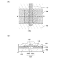
図1は、本発明の一態様に係る半導体装置であるトランジスタの上面図および断面図である。図1(A)に示すトランジスタの上面図に示す一点鎖線A−Bに対応するA−B断面を図1(B)に示す。なお、図1(A)は、煩雑になるのを防ぐため、層間絶縁膜112およびゲート絶縁膜108などを省略して示す。
1A to 1C are a top view and cross-sectional views of a transistor which is a semiconductor device according to one embodiment of the present invention. FIG. 1B illustrates a cross section taken along a dashed line AB in the top view of the transistor illustrated in FIG. Note that FIG. 1A omits the
図1(B)に示すトランジスタは、基板100と、基板100上に設けられた下地絶縁膜102と、下地絶縁膜102上に設けられた一対の電極104と、一対の電極104と接して設けられる酸化物半導体膜106と、酸化物半導体膜106上のゲート絶縁膜108と、ゲート絶縁膜108を介して酸化物半導体膜106と重畳するゲート電極110と、ゲート電極110およびゲート絶縁膜108上に設けられる層間絶縁膜112と、を有する。なお、下地絶縁膜102を設けない構造としても構わない。
The transistor illustrated in FIG. 1B is provided in contact with the
一対の電極104は、Si、Ge、Al、Ti、Cr、Co、Ni、Cu、Y、Zr、Mo、Ag、Ru、Ta、SnまたはW、それらの窒化物、酸化物ならびに合金から一種以上選択し、単層でまたは積層で用いればよい。または、少なくともInおよびZnを含む酸化物または酸窒化物を用いても構わない。例えば、In−Ga−Zn−O−N系材料などを用いればよい。なお、一対の電極104は、トランジスタのソース電極およびドレイン電極として機能し、さらに配線としても用いることができる。
The pair of
一対の電極104において、酸化物半導体膜106と接触する領域にハロゲン元素を含む。例えば、フッ素または塩素を含む。このように、一対の電極104の表面にハロゲン元素による結合(ハロゲン元素による終端化)を作ることによって、一対の電極104と酸化物半導体膜106との反応を抑制し、金属酸化膜の形成を抑えることが可能となる。そのため、金属酸化膜の形成による抵抗成分の発生を抑制でき、一対の電極104と酸化物半導体膜106との接触抵抗を低減させることができる。また同時に、酸化物半導体膜106から一対の電極104への酸素の拡散も防ぐことができる。そのため、酸化物半導体膜106中の酸素欠損の形成を抑制することができる。
In the pair of
酸化物半導体膜106は、低抵抗領域106bおよび高抵抗領域106aを含む。
The
低抵抗領域106bは、酸化物半導体膜を低抵抗化する不純物を含む領域である。例えば、低抵抗領域106bは、水素、ヘリウム、ホウ素、窒素、フッ素、ネオン、アルミニウム、リン、アルゴン、ヒ素、クリプトン、インジウム、スズ、アンチモンおよびキセノンから選ばれた一種以上を含む領域である。
The
低抵抗領域106bを形成することによって、酸化物半導体膜106を用いたトランジスタのオン特性の低下を抑制できる。低抵抗領域106bは、シート抵抗が30kΩ/sq以下、好ましくは10kΩ/sq以下、さらに好ましくは1kΩ/sq以下、さらに好ましくは0.7kΩ/sq以下である。
By forming the low-
高抵抗領域106aは、酸化物半導体膜の主成分以外の成分、即ち不純物の濃度が低い領域である。例えば、高抵抗領域106aは、不純物濃度が1×10²⁰atoms/cm3以下、好ましくは5×1019atoms/cm3以下、さらに好ましくは1×1019atoms/cm3以下の領域である。ただし、主成分と不純物を厳密に分けることは困難であるため、本明細書では1原子%以上含まれる元素を主成分とする。
The high-
高抵抗領域106aは、不純物濃度が低く、かつ欠陥密度が低い領域であり、図1(B)に示すトランジスタは、高抵抗領域106aにチャネル領域が形成されるため、電気特性および信頼性に優れる。また、トランジスタのオフ電流値は低くなる。例えば、チャネル幅1μmあたりのオフ電流値が1×10⁻¹⁸A以下、好ましくは1×10⁻²¹A以下、さらに好ましくは1×10⁻²⁴A以下であるトランジスタとすることができる。
The
酸化物半導体膜106に用いる材料としては、少なくともインジウム(In)あるいは亜鉛(Zn)を含むことが好ましい。特にInとZnを含むことが好ましい。また、該酸化物半導体を用いたトランジスタの電気特性のばらつきを減らすためのスタビライザーとして、それらに加えてガリウム(Ga)を有することが好ましい。また、スタビライザーとしてスズ(Sn)、ハフニウム(Hf)、アルミニウム(Al)、チタン(Ti)またはジルコニウム(Zr)を有することが好ましい。
A material used for the
また、他のスタビライザーとして、ランタノイドである、ランタン(La)、セリウム(Ce)、プラセオジム(Pr)、ネオジム(Nd)、サマリウム(Sm)、ユウロピウム(Eu)、ガドリニウム(Gd)、テルビウム(Tb)、ジスプロシウム(Dy)、ホルミウム(Ho)、エルビウム(Er)、ツリウム(Tm)、イッテルビウム(Yb)、ルテチウム(Lu)のいずれか一種あるいは複数種を有してもよい。 Other stabilizers include lanthanoids such as lanthanum (La), cerium (Ce), praseodymium (Pr), neodymium (Nd), samarium (Sm), europium (Eu), gadolinium (Gd), and terbium (Tb). , Dysprosium (Dy), holmium (Ho), erbium (Er), thulium (Tm), ytterbium (Yb), or lutetium (Lu).
例えば、酸化物半導体として、酸化インジウム、酸化スズ、酸化亜鉛、二元系金属の酸化物であるIn−Zn系酸化物、Sn−Zn系酸化物、Al−Zn系酸化物、Zn−Mg系酸化物、Sn−Mg系酸化物、In−Mg系酸化物、In−Ga系酸化物、三元系金属の酸化物であるIn−Ga−Zn系酸化物(IGZOとも表記する)、In−Al−Zn系酸化物、In−Sn−Zn系酸化物、Sn−Ga−Zn系酸化物、Al−Ga−Zn系酸化物、Sn−Al−Zn系酸化物、In−Hf−Zn系酸化物、In−La−Zn系酸化物、In−Ce−Zn系酸化物、In−Pr−Zn系酸化物、In−Nd−Zn系酸化物、In−Sm−Zn系酸化物、In−Eu−Zn系酸化物、In−Gd−Zn系酸化物、In−Tb−Zn系酸化物、In−Dy−Zn系酸化物、In−Ho−Zn系酸化物、In−Er−Zn系酸化物、In−Tm−Zn系酸化物、In−Yb−Zn系酸化物、In−Lu−Zn系酸化物、四元系金属の酸化物であるIn−Sn−Ga−Zn系酸化物、In−Hf−Ga−Zn系酸化物、In−Al−Ga−Zn系酸化物、In−Sn−Al−Zn系酸化物、In−Sn−Hf−Zn系酸化物、In−Hf−Al−Zn系酸化物を用いることができる。 For example, as an oxide semiconductor, indium oxide, tin oxide, zinc oxide, binary metal oxides such as In—Zn oxide, Sn—Zn oxide, Al—Zn oxide, Zn—Mg oxide Oxides, Sn—Mg oxides, In—Mg oxides, In—Ga oxides, In—Ga—Zn oxides (also referred to as IGZO) which are oxides of ternary metals, In— Al-Zn oxide, In-Sn-Zn oxide, Sn-Ga-Zn oxide, Al-Ga-Zn oxide, Sn-Al-Zn oxide, In-Hf-Zn oxide In-La-Zn-based oxide, In-Ce-Zn-based oxide, In-Pr-Zn-based oxide, In-Nd-Zn-based oxide, In-Sm-Zn-based oxide, In-Eu -Zn oxide, In-Gd-Zn oxide, In-Tb-Zn oxide, n-Dy-Zn-based oxide, In-Ho-Zn-based oxide, In-Er-Zn-based oxide, In-Tm-Zn-based oxide, In-Yb-Zn-based oxide, In-Lu-Zn -Based oxides, In-Sn-Ga-Zn-based oxides that are oxides of quaternary metals, In-Hf-Ga-Zn-based oxides, In-Al-Ga-Zn-based oxides, In-Sn- An Al—Zn-based oxide, an In—Sn—Hf—Zn-based oxide, or an In—Hf—Al—Zn-based oxide can be used.
酸化物半導体膜106は、単結晶、多結晶(ポリクリスタルともいう。)または非晶質などの状態をとる。
The
好ましくは、酸化物半導体膜106は、CAAC−OS(C Axis Aligned Crystalline Oxide Semiconductor)膜とする。
The
CAAC−OS膜は、完全な単結晶ではなく、完全な非晶質でもない。CAAC−OS膜は、非晶質相に結晶部を有する結晶−非晶質混相構造の酸化物半導体膜である。なお、当該結晶部は、一辺が100nm未満の立方体内に収まる大きさであることが多い。また、透過型電子顕微鏡(TEM:Transmission Electron Microscope)による観察像では、CAAC−OS膜に含まれる非晶質部と結晶部との境界は明確ではない。また、TEMによってCAAC−OS膜には粒界(グレインバウンダリーともいう。)は確認できない。そのため、CAAC−OS膜は、粒界に起因する電子移動度の低下が抑制される。 The CAAC-OS film is not completely single crystal nor completely amorphous. The CAAC-OS film is an oxide semiconductor film with a crystal-amorphous mixed phase structure where crystal parts are included in an amorphous phase. Note that the crystal part is often large enough to fit in a cube whose one side is less than 100 nm. Further, in the observation image obtained by a transmission electron microscope (TEM), the boundary between the amorphous part and the crystal part included in the CAAC-OS film is not clear. Further, a grain boundary (also referred to as a grain boundary) cannot be confirmed in the CAAC-OS film by TEM. Therefore, in the CAAC-OS film, reduction in electron mobility due to grain boundaries is suppressed.
CAAC−OS膜に含まれる結晶部は、c軸がCAAC−OS膜の被形成面の法線ベクトルまたは表面の法線ベクトルに平行な方向に揃い、かつab面に垂直な方向から見て三角形状または六角形状の原子配列を有し、c軸に垂直な方向から見て金属原子が層状または金属原子と酸素原子とが層状に配列している。なお、異なる結晶部間で、それぞれa軸およびb軸の向きが異なっていてもよい。本明細書において、単に垂直と記載する場合、85°以上95°以下の範囲も含まれることとする。また、単に平行と記載する場合、−5°以上5°以下の範囲も含まれることとする。 In the crystal part included in the CAAC-OS film, the c-axis is aligned in a direction parallel to the normal vector of the formation surface of the CAAC-OS film or the normal vector of the surface, and triangular when viewed from the direction perpendicular to the ab plane. It has a shape or hexagonal atomic arrangement, and metal atoms are arranged in layers or metal atoms and oxygen atoms are arranged in layers as viewed from the direction perpendicular to the c-axis. Note that the directions of the a-axis and the b-axis may be different between different crystal parts. In this specification, a simple term “perpendicular” includes a range from 85 ° to 95 °. In addition, a simple term “parallel” includes a range from −5 ° to 5 °.
なお、CAAC−OS膜において、結晶部の分布が一様でなくてもよい。例えば、CAAC−OS膜の形成過程において、酸化物半導体膜の表面側から結晶成長させる場合、被形成面の近傍に対し表面の近傍では結晶部の占める割合が高くなることがある。また、CAAC−OS膜へ不純物を添加することにより、当該不純物添加領域において結晶部が非晶質化することもある。 Note that the distribution of crystal parts in the CAAC-OS film is not necessarily uniform. For example, in the formation process of the CAAC-OS film, when crystal growth is performed from the surface side of the oxide semiconductor film, the ratio of crystal parts in the vicinity of the surface of the oxide semiconductor film is higher in the vicinity of the surface. In addition, when an impurity is added to the CAAC-OS film, the crystal part in a region to which the impurity is added becomes amorphous in some cases.
CAAC−OS膜に含まれる結晶部のc軸は、CAAC−OS膜の被形成面の法線ベクトルまたは表面の法線ベクトルに平行な方向に揃うため、CAAC−OS膜の形状(被形成面の断面形状または表面の断面形状)によっては互いに異なる方向を向くことがある。なお、結晶部のc軸の方向は、CAAC−OS膜が形成されたときの被形成面の法線ベクトルまたは表面の法線ベクトルに平行な方向となる。結晶部は、成膜することにより、または成膜後に加熱処理などの結晶化処理を行うことにより形成される。 Since the c-axis of the crystal part included in the CAAC-OS film is aligned in a direction parallel to the normal vector of the formation surface of the CAAC-OS film or the normal vector of the surface, the shape of the CAAC-OS film (formation surface) Depending on the cross-sectional shape of the surface or the cross-sectional shape of the surface). Note that the c-axis direction of the crystal part is parallel to the normal vector of the surface where the CAAC-OS film is formed or the normal vector of the surface. The crystal part is formed by film formation or by performing crystallization treatment such as heat treatment after film formation.
CAAC−OS膜を用いたトランジスタは、可視光や紫外光の照射による電気特性の変動を低減することが可能である。よって、当該トランジスタは、信頼性が高い。 A transistor including a CAAC-OS film can reduce variation in electrical characteristics due to irradiation with visible light or ultraviolet light. Therefore, the transistor has high reliability.
基板100に大きな制限はないが、少なくとも、後の熱処理に耐えうる程度の耐熱性を有している必要がある。例えば、ガラス基板、セラミック基板、石英基板、サファイア基板などを、基板100として用いてもよい。また、シリコンや炭化シリコンなどの単結晶半導体基板、多結晶半導体基板、シリコンゲルマニウムなどの化合物半導体基板、SOI(Silicon On Insulator)基板などを適用することも可能であり、これらの基板上に半導体素子が設けられたものを、基板100として用いると好ましい。
There is no particular limitation on the
また、基板100として、可とう性基板を用いてもよい。なお、可とう性基板上にトランジスタを設ける方法としては、非可とう性の基板上にトランジスタを作製した後、トランジスタを剥離し、可とう性基板である基板100に転置する方法もある。その場合には、非可とう性基板とトランジスタとの間に剥離層を設けるとよい。
Further, a flexible substrate may be used as the
下地絶縁膜102は、酸化シリコン、酸化窒化シリコン、窒化酸化シリコン、窒化シリコン、酸化アルミニウム、窒化アルミニウム、酸化ハフニウム、酸化ジルコニウム、酸化イットリウム、酸化ガリウム、酸化ランタン、酸化セシウム、酸化タンタルおよび酸化マグネシウムの一種以上を選択して、単層または積層で用いればよい。
The base
また、下地絶縁膜102は十分な平坦性を有することが好ましい。具体的には、平均面粗さ(Ra)が1nm以下、好ましくは0.3nm以下、さらに好ましくは0.1nm以下となるように下地となる膜を設ける。上述の数値以下のRaとすることで、酸化物半導体膜106に結晶領域が形成されやすくなる。なお、Raは、JIS B0601で定義されている中心線平均粗さを面に対して適用できるよう三次元に拡張したものであり、「基準面から指定面までの偏差の絶対値を平均した値」と表現でき、数式1にて定義される。
The base

なお、数式1において、S0は、測定面(座標(x1,y1)(x1,y2)(x2,y1)(x2,y2)で表される4点によって囲まれる長方形の領域)の面積を指し、Z0は測定面の平均高さを指す。Raは原子間力顕微鏡(AFM:Atomic Force Microscope)にて評価可能である。 In Equation 1, S 0 represents the area of the measurement surface (rectangular region surrounded by four points represented by coordinates (x1, y1) (x1, y2) (x2, y1) (x2, y2)). Z 0 indicates the average height of the measurement surface. Ra can be evaluated with an atomic force microscope (AFM).
酸化窒化シリコンとは、その組成において、窒素よりも酸素の含有量が多いものを示し、例えば、酸素が50原子%以上70原子%以下、窒素が0.5原子%以上15原子%以下、シリコンが25原子%以上35原子%以下、水素が0原子%以上10原子%以下の範囲で含まれるものをいう。また、窒化酸化シリコンとは、その組成において、酸素よりも窒素の含有量が多いものを示し、例えば、酸素が5原子%以上30原子%以下、窒素が20原子%以上55原子%以下、シリコンが25原子%以上35原子%以下、水素が10原子%以上25原子%以下の範囲で含まれるものをいう。但し、上記範囲は、ラザフォード後方散乱法(RBS:Rutherford Backscattering Spectrometry)や、水素前方散乱法(HFS:Hydrogen Forward scattering Spectrometry)を用いて測定した場合のものである。また、構成元素の組成は、その合計が100原子%を超えない値をとる。 Silicon oxynitride indicates a composition having a higher oxygen content than nitrogen. For example, oxygen is 50 atomic% to 70 atomic%, nitrogen is 0.5 atomic% to 15 atomic%, silicon In the range of 25 atomic% to 35 atomic% and hydrogen in the range of 0 atomic% to 10 atomic%. In addition, silicon nitride oxide indicates a composition having a nitrogen content higher than that of oxygen. For example, oxygen is 5 atomic% to 30 atomic%, nitrogen is 20 atomic% to 55 atomic%, silicon In the range of 25 atomic% to 35 atomic% and hydrogen in the range of 10 atomic% to 25 atomic%. However, the above ranges are those measured using Rutherford Backscattering Spectrometry (RBS) or Hydrogen Forward Scattering Spectrometer (HFS). Further, the composition of the constituent elements takes a value that the total does not exceed 100 atomic%.
また、下地絶縁膜102は、加熱処理により酸素を放出する絶縁膜を用いると好ましい。
The base
「加熱処理により酸素を放出する」とは、TDS分析にて、酸素原子に換算しての酸素の放出量が1.0×10¹⁸atoms/cm3以上、好ましくは3.0×1020atoms/cm3以上であることをいう。 “Release oxygen by heat treatment” means that the amount of released oxygen converted to oxygen atoms is 1.0 × 10 18 atoms / cm 3 or more, preferably 3.0 × 10 20 atoms in TDS analysis. / Cm 3 or more.
ここで、TDS分析にて、酸素原子に換算しての酸素の放出量の測定方法について、以下に説明する。 Here, a method for measuring the amount of released oxygen converted into oxygen atoms in TDS analysis will be described below.
TDS分析したときの気体の放出量は、スペクトルの積分値に比例する。このため、測定したスペクトルの積分値と標準試料の基準値との比により、気体の放出量を計算することができる。標準試料の基準値は、所定の原子を含む試料の、スペクトルの積分値に対する原子の密度の割合である。 The amount of gas released when TDS analysis is performed is proportional to the integral value of the spectrum. For this reason, the amount of gas emission can be calculated from the ratio between the measured integral value of the spectrum and the reference value of the standard sample. The reference value of the standard sample is a ratio of the density of atoms to the integral value of the spectrum of a sample containing a predetermined atom.
例えば、標準試料である所定の密度の水素を含むシリコンウェハのTDS分析結果、および絶縁膜のTDS分析結果から、絶縁膜の酸素分子の放出量(NO2)は、数式2で求めることができる。ここで、TDS分析で得られる質量数32で検出されるスペクトルの全てが酸素分子由来と仮定する。質量数32のものとしてほかにCH3OHがあるが、存在する可能性が低いものとしてここでは考慮しない。また、酸素原子の同位体である質量数17の酸素原子および質量数18の酸素原子を含む酸素分子についても、自然界における存在比率が極微量であるため考慮しない。 For example, the release amount (N O2 ) of oxygen molecules in the insulating film can be obtained from Equation 2 from the TDS analysis result of a silicon wafer containing hydrogen of a predetermined density as a standard sample and the TDS analysis result of the insulating film. . Here, it is assumed that all the spectra detected by the mass number 32 obtained by the TDS analysis are derived from oxygen molecules. There is CH 3 OH in addition to those having a mass number of 32, but these are not considered here because they are unlikely to exist. In addition, oxygen molecules containing oxygen atoms with a mass number of 17 and oxygen atoms with a mass number of 18 which are isotopes of oxygen atoms are not considered because the existence ratio in nature is extremely small.
NH2は、標準試料から脱離した水素分子を密度で換算した値である。SH2は、標準試料をTDS分析したときのスペクトルの積分値である。ここで、標準試料の基準値を、NH2/SH2とする。SO2は、絶縁膜をTDS分析したときのスペクトルの積分値である。αは、TDS分析におけるスペクトル強度に影響する係数である。数式2の詳細に関しては、特開平6−275697公報を参照する。なお、上記絶縁膜の酸素の放出量は、電子科学株式会社製の昇温脱離分析装置EMD−WA1000S/Wを用い、標準試料として1×1016atoms/cm3の水素原子を含むシリコンウェハを用いて測定する。 N H2 is a value obtained by converting hydrogen molecules desorbed from the standard sample by density. SH2 is an integral value of a spectrum when a standard sample is subjected to TDS analysis. Here, the reference value of the standard sample is N H2 / SH 2 . S O2 is an integral value of a spectrum when the insulating film is subjected to TDS analysis. α is a coefficient that affects the spectral intensity in the TDS analysis. For details of Equation 2, refer to Japanese Patent Laid-Open No. Hei 6-275697. The oxygen release amount of the insulating film is a silicon wafer containing 1 × 10 16 atoms / cm 3 hydrogen atoms as a standard sample using a temperature programmed desorption analyzer EMD-WA1000S / W manufactured by Electronic Science Co., Ltd. Use to measure.
また、TDS分析において、酸素の一部は酸素原子として検出される。酸素分子と酸素原子の比率は、酸素分子のイオン化率から算出することができる。なお、上述のαは酸素分子のイオン化率を含むため、酸素分子の放出量を評価することで、酸素原子の放出量についても見積もることができる。 In TDS analysis, part of oxygen is detected as oxygen atoms. The ratio of oxygen molecules to oxygen atoms can be calculated from the ionization rate of oxygen molecules. Note that since the above α includes the ionization rate of oxygen molecules, the amount of released oxygen atoms can be estimated by evaluating the amount of released oxygen molecules.
なお、NO2は酸素分子の放出量である。酸素原子に換算したときの放出量は、酸素分子の放出量の2倍となる。 Note that N 2 O 2 is the amount of released oxygen molecules. The amount of release when converted to oxygen atoms is twice the amount of release of oxygen molecules.
下地絶縁膜102から酸化物半導体膜106に酸素が供給されることで、酸化物半導体膜106と下地絶縁膜102との界面準位密度を低減できる。この結果、トランジスタの動作などに起因して、酸化物半導体膜106と下地絶縁膜102との界面にキャリアが捕獲されることを抑制することができ、信頼性の高いトランジスタを得ることができる。
By supplying oxygen from the
さらに、酸化物半導体膜106の酸素欠損に起因して電荷が生じる場合がある。一般に酸化物半導体膜106の酸素欠損は、一部がドナーとなりキャリアである電子を放出する。この結果、トランジスタのしきい値電圧がマイナス方向にシフトしてしまう。そこで、下地絶縁膜102から酸化物半導体膜106に酸素が十分に供給され、好ましくは酸化物半導体膜106に酸素が過剰に含まれていることにより、しきい値電圧がマイナス方向へシフトする要因である、酸化物半導体膜106の酸素欠損密度を低減することができる。
Further, charge may be generated due to oxygen vacancies in the
ゲート絶縁膜108は、下地絶縁膜102と同様の方法および同様の材料によって形成すればよい。
The
ゲート電極110は、一対の電極104と同様の方法および同様の材料によって形成すればよい。
The
また、図1に示すトランジスタは、ゲート電極110と一対の電極104が重畳せず、酸化物半導体膜106に、オフセット領域が形成される構造を示していが、これに限定されるものではない。例えば、ゲート電極110と一つの電極104が重畳する構造であってもよい。
1 illustrates a structure in which the
層間絶縁膜112は、下地絶縁膜102と同様の方法および同様の材料により形成する。
The
層間絶縁膜112は、比誘電率が小さく、かつ十分な厚さを有すると好ましい。例えば、比誘電率が3.8程度である酸化シリコン膜を用い、300nm以上1000nm以下の厚さとすればよい。層間絶縁膜112の表面は、大気成分などの影響でわずかに固定電荷を有し、その影響により、トランジスタのしきい値電圧が変動することがある。そのため、層間絶縁膜112は、表面に生じる電荷の影響が十分に小さくなるような範囲の比誘電率および厚さとすることが好ましい。同様の理由で、層間絶縁膜112上に樹脂膜を形成することで、表面に生じる電荷の影響を低減しても構わない。
The
また、図1に示したトランジスタ構造は、一対の電極および下地絶縁膜の表面が概略一致して平坦となっている。そのため、酸化物半導体膜が平坦に形成されたプレーナ構造となっている。しかし、このような構造に限定されるものではなく、図2に示すような構造であってもよい。図2に示すトランジスタ構造は、平坦な下地絶縁膜202上に一対の電極204を形成し、その上に酸化物半導体膜206が形成されている。また、図2において、図1に示す酸化物半導体膜106と同様に、酸化物半導体膜206は、低抵抗領域206bおよび高抵抗領域206aを含む構造を示している。しかし、このような構造に限定されるものではなく、酸化物半導体膜において低抵抗領域および高抵抗領域を形成しなくても構わない。図1に示す構造は、化学機械研磨(CMP:Chemical Mechanical Polishing)などによる平坦化処理が必要であるが、図2に示す構造は平坦化処理が不要であるため、プロセスが容易となる。
In the transistor structure shown in FIG. 1, the surfaces of the pair of electrodes and the base insulating film are approximately the same and are flat. Therefore, it has a planar structure in which the oxide semiconductor film is formed flat. However, it is not limited to such a structure, and a structure as shown in FIG. 2 may be used. In the transistor structure illustrated in FIG. 2, a pair of
次に、図1(B)に示したトランジスタの作製方法について図3および図4を用いて説明する。 Next, a method for manufacturing the transistor illustrated in FIG. 1B will be described with reference to FIGS.
まず、基板100上に下地絶縁膜102を成膜する。下地絶縁膜102は、化学気相成長(CVD:Chemical Vapor Deposition)法、スパッタリング法、分子線エピタキシー(MBE:Molecular Beam Epitaxy)法またはパルスレーザ堆積(PLD:Pulsed Laser Deposition)法で成膜すればよく、スパッタリング法を用いると好ましい。なお、基板100によっては、下地絶縁膜102を設けなくても構わない。
First, the
次に、下地絶縁膜102上に導電膜を成膜する。導電膜の成膜は、スパッタリング法を用いると好ましい。
Next, a conductive film is formed over the
次に、導電膜を加工して一対の電極104を形成する(図3(A)参照。)。なお、「加工する」とは、特に断りがない限り、フォトリソグラフィ法によって形成したレジストマスクを用い、エッチング処理を行って、所望の形状の膜を得ることをいう。 Next, the conductive film is processed to form the pair of electrodes 104 (see FIG. 3A). Note that “processing” means that a film having a desired shape is obtained by performing etching using a resist mask formed by a photolithography method, unless otherwise specified.
次に、一対の電極104を覆って、絶縁膜を成膜する。該絶縁膜は、下地絶縁膜と同様の材料および方法によって形成する。
Next, an insulating film is formed so as to cover the pair of
その後、CMP処理などによる平坦化処理を行って、一対の電極104が露出するまで絶縁膜を研磨する。(図3(B)参照。)。
After that, planarization treatment such as CMP treatment is performed, and the insulating film is polished until the pair of
次に、露出した一対の電極104に対して、ハロゲン化処理を行う。ハロゲン化処理は、ハロゲン元素を含む雰囲気におけるプラズマ処理によって行うことができる。例えば、三フッ化窒素ガスを含む雰囲気にて、ドライエッチング装置またはプラズマCVD装置などを用いてプラズマ処理を行えばよい。また、上記ハロゲン化処理はプラズマ処理である必要は無く、ハロゲン元素を含む雰囲気に、被処理物を曝すことによっても行うことができる。その際、被処理物を加熱すると、ハロゲン化処理が促進されるため好ましい。また、ハロゲン元素を含む液体に浸漬させて行ってもよい。
Next, a halogenation process is performed on the exposed pair of
一対の電極104に対してハロゲン化処理を行った後、酸化物半導体膜を成膜する。酸化物半導体膜は、CVD法、スパッタリング法、MBE法またはPLD法で成膜すればよく、スパッタリング法を用いると好ましい。
After the halogenation treatment is performed on the pair of
該酸化物半導体膜を成膜後、加熱処理を行ってもよい。該加熱処理を行うと、酸化物半導体膜の結晶化度が高まる。また、酸化物半導体膜中の不純物(水素および水分など)の濃度を低減し、欠陥密度を低減することができる。 Heat treatment may be performed after the oxide semiconductor film is formed. When the heat treatment is performed, the degree of crystallinity of the oxide semiconductor film is increased. In addition, the concentration of impurities (such as hydrogen and moisture) in the oxide semiconductor film can be reduced and the defect density can be reduced.
加熱処理は、酸化性雰囲気、不活性雰囲気、減圧雰囲気および乾燥空気雰囲気を1種、または2種以上組み合わせて行えばよい。好ましくは、不活性雰囲気または減圧雰囲気にて加熱処理を行い、その後酸化性雰囲気または乾燥空気雰囲気にて加熱処理を行う。加熱処理の温度は、150℃以上650℃以下、好ましくは250℃以上500℃以下、さらに好ましくは300℃以上450℃以下の温度で行えばよい。加熱処理は、抵抗加熱方式、ランプヒータ方式、加熱ガス方式などを適用すればよい。 The heat treatment may be performed by combining one or two or more oxidizing atmospheres, inert atmospheres, reduced pressure atmospheres, and dry air atmospheres. Preferably, heat treatment is performed in an inert atmosphere or a reduced pressure atmosphere, and then heat treatment is performed in an oxidizing atmosphere or a dry air atmosphere. The temperature of the heat treatment may be 150 ° C. or higher and 650 ° C. or lower, preferably 250 ° C. or higher and 500 ° C. or lower, more preferably 300 ° C. or higher and 450 ° C. or lower. For the heat treatment, a resistance heating method, a lamp heater method, a heating gas method, or the like may be applied.
酸化性雰囲気とは、酸化性ガスを含む雰囲気をいう。酸化性ガスとは、酸素、オゾンまたは亜酸化窒素などであって、水、水素などが含まれないことが好ましい。例えば、熱処理装置に導入する酸素、オゾン、亜酸化窒素の純度を、8N(99.999999%)以上、好ましくは9N(99.9999999%)以上とする。酸化性雰囲気には、酸化性ガスと不活性ガスが混合されていてもよい。その場合、酸化性ガスが少なくとも10ppm以上含まれる雰囲気とする。酸化性雰囲気で加熱処理を行うことで、酸化物半導体膜の酸素欠損密度を低減することができる。 An oxidizing atmosphere refers to an atmosphere containing an oxidizing gas. The oxidizing gas is oxygen, ozone, nitrous oxide, or the like, and preferably does not contain water, hydrogen, or the like. For example, the purity of oxygen, ozone, and nitrous oxide introduced into the heat treatment apparatus is 8N (99.99999999%) or higher, preferably 9N (99.9999999%) or higher. An oxidizing gas and an inert gas may be mixed in the oxidizing atmosphere. In that case, an atmosphere containing at least 10 ppm of oxidizing gas is used. By performing heat treatment in an oxidizing atmosphere, the density of oxygen vacancies in the oxide semiconductor film can be reduced.
不活性雰囲気とは、窒素、希ガスなどの不活性ガスを主成分とする雰囲気をいう。具体的には、酸化性ガスなどの反応性ガスが10ppm未満である雰囲気とする。不活性雰囲気で加熱処理を行うことで、酸化物半導体膜に含まれる不純物濃度を低減することができる。 The inert atmosphere refers to an atmosphere containing an inert gas such as nitrogen or a rare gas as a main component. Specifically, an atmosphere in which a reactive gas such as an oxidizing gas is less than 10 ppm is used. By performing heat treatment in an inert atmosphere, the concentration of impurities contained in the oxide semiconductor film can be reduced.
減圧雰囲気とは、処理室の圧力が10Pa以下の雰囲気をいう。減圧雰囲気で加熱処理を行うことで、不活性雰囲気よりもさらに酸化物半導体膜に含まれる不純物濃度を低減することができる。 The reduced pressure atmosphere refers to an atmosphere in which the pressure in the processing chamber is 10 Pa or less. By performing heat treatment in a reduced-pressure atmosphere, the concentration of impurities contained in the oxide semiconductor film can be further reduced than in an inert atmosphere.
乾燥空気雰囲気とは、露点−40℃以下、好ましくは露点−50℃以下の酸素20%程度および窒素80%程度含まれる雰囲気をいう。酸化性雰囲気の一種であるが、比較的低コストであるため量産に適している。 The dry air atmosphere refers to an atmosphere containing about 20% oxygen and about 80% nitrogen with a dew point of −40 ° C. or lower, preferably a dew point of −50 ° C. or lower. Although it is a kind of oxidizing atmosphere, it is suitable for mass production because of its relatively low cost.
次に、酸化物半導体膜を加工して酸化物半導体膜106を形成する(図3(C)参照。)。 Next, the oxide semiconductor film is processed to form the oxide semiconductor film 106 (see FIG. 3C).
次に、ゲート絶縁膜108を成膜する。ゲート絶縁膜108は、CVD法、スパッタリング法、MBE法、PLD法で成膜すればよく、特にスパッタリング法を用いると好ましい。
Next, a
次に、導電膜を成膜する。導電膜は、CVD法、スパッタリング法、MBE法またはPLD法で成膜すればよく、特にスパッタリング法を用いると好ましい。 Next, a conductive film is formed. The conductive film may be formed by a CVD method, a sputtering method, an MBE method, or a PLD method, and it is particularly preferable to use a sputtering method.
次に、導電膜を加工してゲート電極110を形成する(図4(A)参照。)。 Next, the conductive film is processed to form the gate electrode 110 (see FIG. 4A).
次に、ゲート電極110をマスクとして、酸化物半導体膜106に酸化物半導体膜を低抵抗化する不純物を添加し、低抵抗領域106bを形成する(図4(B)参照。)。なお、酸化物半導体膜を低抵抗化する不純物の添加されない領域は高抵抗領域106aとなる。
Next, using the
酸化物半導体膜を低抵抗化する不純物として、水素、ヘリウム、ホウ素、窒素、フッ素、ネオン、アルミニウム、リン、アルゴン、ヒ素、クリプトン、インジウム、スズ、アンチモンおよびキセノンから選ばれた一種以上を添加すればよい。なお、その方法は、イオン注入法、イオンドーピング法で行えばよい。または、酸化物半導体膜を低抵抗化する不純物を含む雰囲気でのプラズマ処理もしくは加熱処理を行えばよい。好ましくはイオン注入法を用いる。なお、イオン注入法にて酸化物半導体膜を低抵抗化する不純物を添加した後に、不活性雰囲気または減圧雰囲気にて加熱処理を行ってもよい。 As an impurity for reducing the resistance of the oxide semiconductor film, one or more selected from hydrogen, helium, boron, nitrogen, fluorine, neon, aluminum, phosphorus, argon, arsenic, krypton, indium, tin, antimony, and xenon are added. That's fine. Note that this method may be performed by an ion implantation method or an ion doping method. Alternatively, plasma treatment or heat treatment may be performed in an atmosphere containing an impurity that reduces resistance of the oxide semiconductor film. An ion implantation method is preferably used. Note that heat treatment may be performed in an inert atmosphere or a reduced-pressure atmosphere after an impurity that reduces resistance of the oxide semiconductor film is added by an ion implantation method.
次に、層間絶縁膜112を成膜する(図4(C)参照。)。層間絶縁膜112は、CVD法、スパッタリング法、MBE法、PLD法またはスピンコート法で成膜すればよく、CVD法またはスパッタリング法を用いると好ましい。
Next, an
また、特に図示しないが、層間絶縁膜112およびゲート絶縁膜108を加工して一対の電極104を露出させ、一対の電極104と接続する配線を設けてもよい。また、層間絶縁膜112上に樹脂膜を設けても構わない。
Although not particularly illustrated, the
以上のような工程によって、酸化物半導体膜と一対の電極との接触抵抗を低減することができる。それによって、オン特性の優れたトランジスタを提供することができる。 Through the above steps, the contact resistance between the oxide semiconductor film and the pair of electrodes can be reduced. Accordingly, a transistor with excellent on characteristics can be provided.
(実施の形態2)
本実施の形態では、実施の形態1で示したトランジスタと異なる構造のトランジスタおよびその作製方法について図5および図6を用いて説明する。
(Embodiment 2)
In this embodiment, a transistor having a structure different from that of the transistor described in Embodiment 1 and a manufacturing method thereof will be described with reference to FIGS.
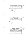
図5は、本発明の一態様に係る半導体装置であるトランジスタの上面図および断面図である。図5(A)に示すトランジスタの上面図に示す一点鎖線A−Bに対応するA−B断面を図5(B)に示す。なお、図5(A)は、煩雑になるのを防ぐため、層間絶縁膜212およびゲート絶縁膜208などを省略して示す。
5A and 5B are a top view and a cross-sectional view of a transistor which is a semiconductor device according to one embodiment of the present invention. FIG. 5B illustrates a cross section taken along a dashed line AB in the top view of the transistor illustrated in FIG. Note that FIG. 5A omits the
図5(B)に示すトランジスタは、基板100と、基板100上に設けられた下地絶縁膜202と、下地絶縁膜202上に設けられたゲート電極210と、ゲート電極210上に設けられたゲート絶縁膜208と、ゲート絶縁膜208上に設けられた一対の電極204と、ゲート絶縁膜208を介してゲート電極210と重畳する酸化物半導体膜206と、酸化物半導体膜206および一対の電極上に設けられた層間絶縁膜212と、を有する。なお、下地絶縁膜202を設けない構造としても構わない。
A transistor illustrated in FIG. 5B includes a
一対の電極204において、一対の電極204および酸化物半導体膜206の界面近傍にハロゲン元素を含む。例えば、フッ素または塩素を含む。このように、一対の電極204の表面を強い結合(金属−フッ素結合など)とすることによって、一対の電極204と酸化物半導体膜206との反応を抑制し、異層の形成を抑えることが可能となる。そのため、異層の形成による抵抗成分の発生を抑制でき、一対の電極204と酸化物半導体膜206との接触抵抗を低減させることができる。また同時に、酸化物半導体膜206から一対の電極204への酸素の拡散も防ぐことができる。そのため、酸化物半導体膜206中の酸素欠損の形成を抑制することができる。
In the pair of
なお、各層の材料は、実施の形態1と同様にすることができる。 Note that the material of each layer can be the same as that in the first embodiment.
次に、図5(B)に示したトランジスタの作製方法について図6を用いて説明する。 Next, a method for manufacturing the transistor illustrated in FIG. 5B will be described with reference to FIGS.
まず、基板100上に下地絶縁膜202を成膜する。なお、基板100によっては、下地絶縁膜202を設けなくても構わない。
First, the
次に、下地絶縁膜202上に導電膜を成膜する。導電膜の成膜は、スパッタリング法を用いると好ましい。
Next, a conductive film is formed over the
次に、導電膜を加工してゲート電極210を形成する。なお、「加工する」とは、特に断りがない限り、フォトリソグラフィ法によって形成したレジストマスクを用い、エッチング処理を行って、所望の形状の膜を得ることをいう。
Next, the conductive film is processed to form the
次に、ゲート絶縁膜208を成膜する。ゲート絶縁膜208は、CVD法、スパッタリング法、MBE法、PLD法で成膜すればよく、特にスパッタリング法を用いると好ましい(図6(A)参照。)。
Next, a
次に、ゲート絶縁膜208上に導電膜を成膜する。導電膜は、CVD法、スパッタリング法、MBE法またはPLD法で成膜すればよく、特にスパッタリング法を用いると好ましい。
Next, a conductive film is formed over the
次に、導電膜を加工して一対の電極204を形成する(図6(B)参照。)。 Next, the conductive film is processed to form a pair of electrodes 204 (see FIG. 6B).
次に、一対の電極204に対して、ハロゲン化処理を行う。ハロゲン化処理は、ハロゲン元素を含む雰囲気におけるプラズマ処理によって行うことができる。例えば、三フッ化窒素ガスを含む雰囲気にて、ドライエッチング装置またはプラズマCVD装置などを用いてプラズマ処理を行えばよい。また、上記ハロゲン化処理はプラズマ処理である必要は無く、ハロゲン元素を含む雰囲気に、被処理物を曝すことによっても行うことができる。その際、被処理物を加熱すると、ハロゲン化処理が促進されるため好ましい。
Next, halogenation treatment is performed on the pair of
一対の電極204に対してハロゲン化処理を行った後、酸化物半導体膜を成膜する。酸化物半導体膜は、CVD法、スパッタリング法、MBE法またはPLD法で成膜すればよく、スパッタリング法を用いると好ましい。
After the halogenation treatment is performed on the pair of
該酸化物半導体膜を成膜後、加熱処理を行ってもよい。該加熱処理を行うと、酸化物半導体膜の結晶化度が高まる。また、酸化物半導体膜中の不純物(水素および水分など)の濃度を低減し、欠陥密度を低減することができる。加熱処理は、実施の形態1と同様に行うことができる。 Heat treatment may be performed after the oxide semiconductor film is formed. When the heat treatment is performed, the degree of crystallinity of the oxide semiconductor film is increased. In addition, the concentration of impurities (such as hydrogen and moisture) in the oxide semiconductor film can be reduced and the defect density can be reduced. The heat treatment can be performed in a manner similar to that in Embodiment 1.
次に、酸化物半導体膜を加工して酸化物半導体膜206を形成する。
Next, the oxide semiconductor film is processed to form the
次に、層間絶縁膜212を成膜する(図6(C)参照。)。層間絶縁膜212は、CVD法、スパッタリング法、MBE法、PLD法またはスピンコート法で成膜すればよく、CVD法またはスパッタリング法を用いると好ましい。
Next, an
また、特に図示しないが、層間絶縁膜212を加工して一対の電極204を露出させ、一対の電極204と接続する配線を設けてもよい。また、層間絶縁膜212上に樹脂膜を設けても構わない。
Although not particularly illustrated, the
以上のような工程によって、酸化物半導体膜と一対の電極との接触抵抗を低減することができる。それによって、オン特性の優れたトランジスタを提供することができる。 Through the above steps, the contact resistance between the oxide semiconductor film and the pair of electrodes can be reduced. Accordingly, a transistor with excellent on characteristics can be provided.
(実施の形態3)
本実施の形態では、実施の形態1または実施の形態2で示したトランジスタを用いて、半導体記憶装置を作製する例について説明する。
(Embodiment 3)
In this embodiment, an example of manufacturing a semiconductor memory device using the transistor described in Embodiment 1 or 2 will be described.
揮発性半導体記憶装置の代表的な例としては、記憶素子を構成するトランジスタを選択してキャパシタに電荷を蓄積することで、情報を記憶するDRAM(Dynamic Random Access Memory)、フリップフロップなどの回路を用いて記憶内容を保持するSRAM(Static Random Access Memory)がある。 As a typical example of a volatile semiconductor memory device, a circuit such as a DRAM (Dynamic Random Access Memory) or a flip-flop that stores information by selecting a transistor constituting a memory element and accumulating electric charge in a capacitor is used. There is an SRAM (Static Random Access Memory) that uses and holds stored contents.
不揮発性半導体記憶装置の代表例としては、トランジスタのゲートとチャネル領域との間にノードを有し、当該ノードに電荷を保持することで記憶を行うフラッシュメモリがある。 As a typical example of a nonvolatile semiconductor memory device, there is a flash memory which has a node between a gate and a channel region of a transistor and stores data by holding electric charge in the node.
上述した半導体記憶装置に含まれるトランジスタの一部に実施の形態1または実施の形態2で示したトランジスタを適用することができる。 The transistor described in Embodiment 1 or 2 can be applied to part of the transistors included in the semiconductor memory device described above.
まずは、実施の形態1または実施の形態2で示したトランジスタを適用した揮発性メモリについて図7を用いて説明する。 First, a volatile memory to which the transistor described in Embodiment 1 or 2 is applied is described with reference to FIGS.
メモリセルは、ビット線BLと、ワード線WLと、センスアンプSAmpと、トランジスタTrと、キャパシタCと、を有する(図7(A)参照。)。 The memory cell includes a bit line BL, a word line WL, a sense amplifier SAmp, a transistor Tr, and a capacitor C (see FIG. 7A).
キャパシタCに保持された電圧の時間変化は、トランジスタTrのオフ電流によって図7(B)に示すように徐々に低減していくことが知られている。当初V0からV1まで充電された電圧は、時間が経過するとdata1を読み出す限界点であるVAまで低減する。この期間を保持期間T_1とする。即ち、2値のメモリセルの場合、保持期間T_1の間にリフレッシュをする必要がある。 It is known that the time change of the voltage held in the capacitor C is gradually reduced as shown in FIG. 7B by the off-state current of the transistor Tr. The voltage initially charged from V0 to V1 is reduced to VA, which is a limit point for reading data1 over time. This period is a holding period T_1. That is, in the case of a binary memory cell, it is necessary to refresh during the holding period T_1.
ここで、トランジスタTrに実施の形態1または実施の形態2で示したトランジスタを適用すると、オフ電流が小さいため、保持期間T_1を長くすることができる。即ち、リフレッシュ期間を長くとることが可能となるため、消費電力を低減することができる。例えば、オフ電流が1×10⁻²¹A以下、好ましくは1×10⁻²⁴A以下となった酸化物半導体膜を用いたトランジスタをDRAMに適用すると、電力を供給せずに数日間から数十年間に渡ってデータを保持することが可能となる。 Here, when the transistor described in Embodiment 1 or 2 is applied to the transistor Tr, the off-state current is small, so that the holding period T_1 can be extended. In other words, since the refresh period can be extended, power consumption can be reduced. For example, when a transistor including an oxide semiconductor film with an off-state current of 1 × 10 −21 A or less, preferably 1 × 10 −24 A or less is applied to a DRAM, power is not supplied for several days to several tens of days. Data can be retained for a year.
以上のように、本発明の一態様によって、信頼性が高く、消費電力の小さい揮発性メモリを得ることができる。 As described above, according to one embodiment of the present invention, a volatile memory with high reliability and low power consumption can be obtained.
また、実施の形態1または実施の形態2で示したオン特性の優れたトランジスタを適用することで、キャパシタCへの電荷の蓄積が速やかに行われ、高速動作が可能な半導体記憶装置を得ることができる。 In addition, by applying the transistor having excellent on-state characteristics described in Embodiment 1 or Embodiment 2, charge accumulation in the capacitor C is quickly performed, and a semiconductor memory device capable of high-speed operation is obtained. Can do.
次に、実施の形態1または実施の形態2で示したトランジスタを適用した不揮発性メモリについて図8を用いて説明する。 Next, a nonvolatile memory to which the transistor described in Embodiment 1 or 2 is applied is described with reference to FIGS.
図8(A)は、不揮発性メモリの回路図である。不揮発性メモリは、トランジスタTr_1と、トランジスタTr_1のゲートと接続するワード線WL_1と、トランジスタTr_1のソースと接続するソース配線SL_1と、トランジスタTr_2と、トランジスタTr_2のソースと接続するソース配線SL_2と、トランジスタTr_2のドレインと接続するドレイン配線DL_2と、キャパシタCと、キャパシタCの一端と接続する容量配線CLと、キャパシタCの他端、トランジスタTr_1のドレインおよびトランジスタTr_2のゲートと接続するノードNと、を有する。 FIG. 8A is a circuit diagram of a nonvolatile memory. The nonvolatile memory includes a transistor Tr_1, a word line WL_1 connected to the gate of the transistor Tr_1, a source wiring SL_1 connected to the source of the transistor Tr_1, a transistor Tr_2, a source wiring SL_2 connected to the source of the transistor Tr_2, and a transistor. A drain wiring DL_2 connected to the drain of Tr_2, a capacitor C, a capacitance wiring CL connected to one end of the capacitor C, a node N connected to the other end of the capacitor C, the drain of the transistor Tr_1 and the gate of the transistor Tr_2. Have.
なお、本実施の形態に示す不揮発性メモリは、ノードNの電位に応じて、トランジスタTr_2のしきい値電圧が変動することを利用したものである。例えば、図8(B)は容量配線CLの電圧VCLと、トランジスタTr_2を流れるドレイン電流Id_2との関係を説明する図である。 Note that the nonvolatile memory described in this embodiment is based on the fact that the threshold voltage of the transistor Tr_2 varies depending on the potential of the node N. For example, FIG. 8B illustrates a relationship between the voltage V CL of the capacitor wiring CL and the drain current I d _2 flowing through the transistor Tr_2.
ここで、ノードNは、トランジスタTr_1を介して電圧を調整することができる。例えば、SL_1の電位をVDDとする。このとき、WL_1の電位をTr_1のしきい値電圧VthにVDDを加えた電位以上とすることで、ノードNの電圧をHIGHにすることができる。また、WL_1の電位をTr_1のしきい値電圧Vth以下とすることで、ノードNの電位をLOWにすることができる。 Here, the voltage of the node N can be adjusted through the transistor Tr_1. For example, the potential of SL_1 is set to VDD. At this time, by setting the potential of WL_1 to be equal to or higher than the potential obtained by adding VDD to the threshold voltage Vth of Tr_1, the voltage of the node N can be HIGH. In addition, by setting the potential of WL_1 to be equal to or lower than the threshold voltage Vth of Tr_1, the potential of the node N can be set to LOW.
そのため、N=LOWで示したVCL−Id_2カーブと、N=HIGHで示したVCL−Id_2カーブのいずれかを得ることができる。即ち、N=LOWでは、VCL=0VにてId_2が小さいため、データ0となる。また、N=HIGHでは、VCL=0VにてId_2が大きいため、データ1となる。このようにして、データを記憶することができる。
Therefore, it is possible to obtain a V CL -I d _2 curve indicated by N = LOW, one of V CL -I d _2 curve indicated by N = HIGH. That is, when N = LOW, since I d — 2 is small at V CL = 0V,
ここで、トランジスタTr_1に実施の形態1または実施の形態2で示したトランジスタを適用すると、該トランジスタはオフ電流を極めて小さくすることができるため、ノードNに蓄積された電荷がトランジスタTr_1のソースおよびドレイン間を意図せずにリークすることを抑制できる。そのため、長期間に渡ってデータを保持することができる。また、本発明の一態様を用いることでトランジスタTr_1のしきい値電圧が調整されるため、書き込みに必要な電圧を低減することが可能となり、フラッシュメモリなどと比較して消費電力を低減することができる。 Here, when the transistor described in Embodiment 1 or 2 is applied to the transistor Tr_1, the off-state current of the transistor can be extremely small; thus, the charge accumulated in the node N is supplied to the source of the transistor Tr_1 and It is possible to suppress unintentional leakage between the drains. Therefore, data can be held for a long time. In addition, since the threshold voltage of the transistor Tr_1 is adjusted by using one embodiment of the present invention, the voltage necessary for writing can be reduced and power consumption can be reduced compared to a flash memory or the like. Can do.
なお、トランジスタTr_2に、実施の形態1または実施の形態2で示したトランジスタを適用しても構わない。該トランジスタは、オン特性に優れる。そのため、該トランジスタを用いた半導体記憶装置は高速動作が可能となる。 Note that the transistor described in Embodiment 1 or 2 may be used as the transistor Tr_2. The transistor has excellent on characteristics. Therefore, a semiconductor memory device using the transistor can operate at high speed.
以上のように、本発明の一態様によって、長期間の信頼性が高く、消費電力の小さく、高速動作が可能な半導体記憶装置を得ることができる。 As described above, according to one embodiment of the present invention, a semiconductor memory device with high long-term reliability, low power consumption, and high-speed operation can be obtained.
本実施の形態は、他の実施の形態と適宜組み合わせて用いることができる。 This embodiment can be combined with any of the other embodiments as appropriate.
(実施の形態4)
実施の形態1または実施の形態2で示したトランジスタまたは実施の形態3に示した半導体記憶装置を少なくとも一部に用いてCPU(Central Processing Unit)を構成することができる。
(Embodiment 4)
A CPU (Central Processing Unit) can be formed using at least part of the transistor described in Embodiment 1 or 2 or the semiconductor memory device in Embodiment 3.
図9(A)は、CPUの具体的な構成を示すブロック図である。図9(A)に示すCPUは、基板1190上に、演算回路(ALU:Arithmetic logic unit)1191、ALUコントローラ1192、インストラクションデコーダ1193、インタラプトコントローラ1194、タイミングコントローラ1195、レジスタ1196、レジスタコントローラ1197、バスインターフェース(Bus I/F)1198、書き換え可能なROM1199、およびROMインターフェース(ROM I/F)1189を有している。基板1190は、半導体基板、SOI基板、ガラス基板などを用いる。ROM1199およびROMインターフェース1189は、別チップに設けてもよい。もちろん、図9(A)に示すCPUは、その構成を簡略化して示した一例にすぎず、実際のCPUはその用途によって多種多様な構成を有している。
FIG. 9A is a block diagram illustrating a specific structure of the CPU. 9A includes an arithmetic circuit (ALU) 1191, an
バスインターフェース1198を介してCPUに入力された命令は、インストラクションデコーダ1193に入力され、デコードされた後、ALUコントローラ1192、インタラプトコントローラ1194、レジスタコントローラ1197、タイミングコントローラ1195に入力される。
Instructions input to the CPU via the
ALUコントローラ1192、インタラプトコントローラ1194、レジスタコントローラ1197、タイミングコントローラ1195は、デコードされた命令に基づき、各種制御を行なう。具体的にALUコントローラ1192は、ALU1191の動作を制御するための信号を生成する。また、インタラプトコントローラ1194は、CPUのプログラム実行中に、外部の入出力装置や、周辺回路からの割り込み要求を、その優先度やマスク状態から判断し、処理する。レジスタコントローラ1197は、レジスタ1196のアドレスを生成し、CPUの状態に応じてレジスタ1196の読み出しや書き込みを行なう。
The
また、タイミングコントローラ1195は、ALU1191、ALUコントローラ1192、インストラクションデコーダ1193、インタラプトコントローラ1194、およびレジスタコントローラ1197の動作のタイミングを制御する信号を生成する。例えばタイミングコントローラ1195は、基準クロック信号CLK1を元に、内部クロック信号CLK2を生成する内部クロック生成部を備えており、クロック信号CLK2を上記各種回路に供給する。
In addition, the
図9(A)に示すCPUでは、レジスタ1196に、記憶素子が設けられている。レジスタ1196の記憶素子には、実施の形態3に示す半導体記憶装置を用いることができる。
In the CPU illustrated in FIG. 9A, a memory element is provided in the
図9(A)に示すCPUにおいて、レジスタコントローラ1197は、ALU1191からの指示に従い、レジスタ1196における保持動作を行う。即ち、レジスタ1196が有する記憶素子において、位相反転素子によるデータの保持を行うか、キャパシタによるデータの保持を行う。位相反転素子によってデータが保持されている場合、レジスタ1196内の記憶素子への、電源電圧の供給が行われる。キャパシタによってデータが保持されている場合、キャパシタへのデータの書き換えが行われ、レジスタ1196内の記憶素子への電源電圧の供給を停止することができる。
In the CPU illustrated in FIG. 9A, the
電源停止に関しては、図9(B)または図9(C)に示すように、記憶素子群と、電源電位VDDまたは電源電位VSSの与えられているノード間に、スイッチング素子を設けることにより行うことができる。以下に図9(B)および図9(C)の回路の説明を行う。 The power supply is stopped by providing a switching element between the memory element group and the node to which the power supply potential VDD or the power supply potential VSS is applied, as shown in FIG. 9B or 9C. Can do. The circuits in FIGS. 9B and 9C will be described below.
図9(B)および図9(C)では、記憶素子への電源電位の供給を制御するスイッチング素子に実施の形態1または実施の形態2に示すトランジスタ用いた構成の一例を示す。 9B and 9C illustrate an example of a structure in which the transistor described in Embodiment 1 or 2 is used for a switching element that controls supply of a power supply potential to a memory element.
図9(B)に示す記憶装置は、スイッチング素子1141と、記憶素子1142を複数有する記憶素子群1143とを有している。具体的に、それぞれの記憶素子1142には、実施の形態3に示す記憶素子を用いることができる。記憶素子群1143が有するそれぞれの記憶素子1142には、スイッチング素子1141を介して、ハイレベルの電源電位VDDが供給されている。さらに、記憶素子群1143が有するそれぞれの記憶素子1142には、信号INの電位と、ローレベルの電源電位VSSの電位が与えられている。
A memory device illustrated in FIG. 9B includes a
図9(B)では、スイッチング素子1141として、酸化物半導体などのバンドギャップの大きい半導体を活性層に有するトランジスタを用いており、該トランジスタは、そのゲートに与えられる信号SigAによりスイッチングが制御される。
In FIG. 9B, a transistor having a semiconductor with a large band gap such as an oxide semiconductor in an active layer is used as the
なお、図9(B)では、スイッチング素子1141がトランジスタを一つだけ有する構成を示しているが、これに限定されず、トランジスタを複数有していてもよい。スイッチング素子1141が、スイッチング素子として機能するトランジスタを複数有している場合、上記複数のトランジスタは並列に接続されていてもよいし、直列に接続されていてもよいし、直列と並列が組み合わされて接続されていてもよい。
Note that FIG. 9B illustrates a structure in which the
また、図9(C)には、記憶素子群1143が有するそれぞれの記憶素子1142に、スイッチング素子1141を介して、ローレベルの電源電位VSSが供給されている、記憶装置の一例を示す。スイッチング素子1141により、記憶素子群1143が有するそれぞれの記憶素子1142への、ローレベルの電源電位VSSの供給を制御することができる。
FIG. 9C illustrates an example of a memory device in which a low-level power supply potential VSS is supplied to each
記憶素子群と、電源電位VDDまたは電源電位VSSの与えられているノード間に、スイッチング素子を設け、一時的にCPUの動作を停止し、電源電圧の供給を停止した場合においてもデータを保持することが可能であり、消費電力の低減を行うことができる。例えば、パーソナルコンピュータのユーザーが、キーボードなどの入力装置への情報の入力を停止している間でも、CPUの動作を停止することができ、それにより消費電力を低減することができる。 A switching element is provided between the memory element group and a node to which the power supply potential VDD or the power supply potential VSS is applied, temporarily stopping the operation of the CPU and retaining data even when the supply of the power supply voltage is stopped. It is possible to reduce power consumption. For example, even when the user of the personal computer stops inputting information to an input device such as a keyboard, the operation of the CPU can be stopped, thereby reducing power consumption.
ここでは、CPUを例に挙げて説明したが、DSP(Degital Signal Processor)、カスタムLSI、FPGA(Field Programmable Gate Array)などのLSIにも応用可能である。 Here, the CPU has been described as an example, but the present invention can also be applied to LSIs such as a DSP (Digital Signal Processor), a custom LSI, and an FPGA (Field Programmable Gate Array).
本実施の形態は、上記実施の形態と適宜組み合わせて実施することが可能である。 This embodiment can be implemented in combination with any of the above embodiments as appropriate.
(実施の形態5)
本実施の形態では、実施の形態1乃至実施の形態4に示すトランジスタ、半導体記憶装置およびCPUの一種以上を含む電子機器の例について説明する。
(Embodiment 5)
In this embodiment, examples of electronic devices including one or more of the transistors, semiconductor memory devices, and CPUs described in Embodiments 1 to 4 will be described.
図10(A)は携帯型情報端末である。図10(A)に示す携帯型情報端末は、筐体9300と、ボタン9301と、マイクロフォン9302と、表示部9303と、スピーカ9304と、カメラ9305と、を具備し、携帯型電話機としての機能を有する。
FIG. 10A illustrates a portable information terminal. A portable information terminal illustrated in FIG. 10A includes a
図10(B)は、ディスプレイである。図10(B)に示すディスプレイは、筐体9310と、表示部9311と、を具備する。
FIG. 10B shows a display. A display illustrated in FIG. 10B includes a
図10(C)は、デジタルスチルカメラである。図10(C)に示すデジタルスチルカメラは、筐体9320と、ボタン9321と、マイクロフォン9322と、表示部9323と、を具備する。
FIG. 10C illustrates a digital still camera. A digital still camera illustrated in FIG. 10C includes a
図10(D)は2つ折り可能な携帯情報端末である。図10(D)に示す2つ折り可能な携帯情報端末は、筐体9630、表示部9631a、表示部9631b、留め具9633、操作スイッチ9638、を有する。
FIG. 10D illustrates a portable information terminal that can be folded. A portable information terminal that can be folded in FIG. 10D includes a
表示部9631aまたは/および表示部9631bは、一部または全部をタッチパネルとすることができ、表示された操作キーに触れることでデータ入力などを行うことができる。
Part or all of the
本発明の一態様を用いることで、電子機器の性能を高めることができる。 By using one embodiment of the present invention, the performance of an electronic device can be improved.
本実施の形態は、他の実施の形態と適宜組み合わせて用いることができる。 This embodiment can be combined with any of the other embodiments as appropriate.
100 基板
102 下地絶縁膜
104 一対の電極
106 酸化物半導体膜
106a 高抵抗領域
106b 低抵抗領域
108 ゲート絶縁膜
110 ゲート電極
112 層間絶縁膜
202 下地絶縁膜
204 一対の電極
206 酸化物半導体膜
206a 高抵抗領域
206b 低抵抗領域
208 ゲート絶縁膜
210 ゲート電極
212 層間絶縁膜
1141 スイッチング素子
1142 記憶素子
1143 記憶素子群
1189 ROMインターフェース
1190 基板
1191 ALU
1192 ALUコントローラ
1193 インストラクションデコーダ
1194 インタラプトコントローラ
1195 タイミングコントローラ
1196 レジスタ
1197 レジスタコントローラ
1198 バスインターフェース
1199 ROM
9300 筐体
9301 ボタン
9302 マイクロフォン
9303 表示部
9304 スピーカ
9305 カメラ
9310 筐体
9311 表示部
9320 筐体
9321 ボタン
9322 マイクロフォン
9323 表示部
9630 筐体
9631a 表示部
9631b 表示部
9633 留め具
9638 操作スイッチ
100
1192
9300
Claims (8)
前記一対の電極と接する酸化物半導体膜と、
前記酸化物半導体膜上のゲート絶縁膜と、
前記ゲート絶縁膜上のゲート電極と、
を有し、
前記酸化物半導体膜は、高抵抗領域と、一対の低抵抗領域と、を有し、
前記高抵抗領域は、前記ゲート電極と重なる領域を有し、
前記一対の低抵抗領域は、前記ゲート電極と重ならない領域を有し、
前記一対の電極は、ハロゲン元素を含むことを特徴とする半導体装置。 A pair of electrodes on an insulating surface;
An oxide semiconductor film in contact with the pair of electrodes;
A gate insulating film on the oxide semiconductor film;
A gate electrode on the gate insulating film ;
Have
The oxide semiconductor film has a high resistance region and a pair of low resistance regions,
The high resistance region has a region overlapping the gate electrode,
The pair of low resistance regions has a region that does not overlap the gate electrode,
The pair of electrodes includes a halogen element.
前記一対の電極と接する酸化物半導体膜と、An oxide semiconductor film in contact with the pair of electrodes;
前記酸化物半導体膜上のゲート絶縁膜と、A gate insulating film on the oxide semiconductor film;
前記ゲート絶縁膜上のゲート電極と、A gate electrode on the gate insulating film;
を有し、Have
前記酸化物半導体膜は、高抵抗領域と、一対の低抵抗領域と、を有し、The oxide semiconductor film has a high resistance region and a pair of low resistance regions,
前記高抵抗領域は、前記ゲート電極と重なる領域を有し、The high resistance region has a region overlapping the gate electrode,
前記一対の低抵抗領域は、前記ゲート電極と重ならない領域を有し、The pair of low resistance regions has a region that does not overlap the gate electrode,
前記ゲート電極と重ならない領域は、前記一対の電極に接する領域と、前記一対の電極に接していない領域と、を有し、The region that does not overlap with the gate electrode has a region that is in contact with the pair of electrodes and a region that is not in contact with the pair of electrodes,
前記一対の電極は、ハロゲン元素を含むことを特徴とする半導体装置。The pair of electrodes includes a halogen element.
前記一対の低抵抗領域は、水素、ヘリウム、ホウ素、窒素、フッ素、ネオン、アルミニウム、リン、アルゴン、ヒ素、クリプトン、インジウム、スズ、アンチモン、及びキセノンから選択された一種以上を含むことを特徴とする半導体装置。The pair of low resistance regions include one or more selected from hydrogen, helium, boron, nitrogen, fluorine, neon, aluminum, phosphorus, argon, arsenic, krypton, indium, tin, antimony, and xenon. Semiconductor device.
前記酸化物半導体膜は、前記酸化物半導体膜の表面に垂直な方向に沿ってc軸が配向した結晶部を有することを特徴とする半導体装置。The semiconductor device, wherein the oxide semiconductor film includes a crystal part in which a c-axis is aligned along a direction perpendicular to a surface of the oxide semiconductor film.
前記一対の電極に対してハロゲン化処理を行った後、前記一対の電極と接する酸化物半導体膜を形成し、
前記酸化物半導体膜上にゲート絶縁膜を形成し、
前記ゲート絶縁膜上にゲート電極を形成し、
前記酸化物半導体膜は、高抵抗領域と、一対の低抵抗領域と、を有し、
前記高抵抗領域は、前記ゲート電極と重なる領域を有し、
前記一対の低抵抗領域は、前記ゲート電極と重ならない領域を有することを特徴とする半導体装置の作製方法。 Forming a pair of electrodes on an insulating surface;
After performing the halogenation treatment on the pair of electrodes, an oxide semiconductor film in contact with the pair of electrodes is formed,
Forming a gate insulating film on the oxide semiconductor film;
Forming a gate electrode on the gate insulating film ;
The oxide semiconductor film has a high resistance region and a pair of low resistance regions,
The high resistance region has a region overlapping the gate electrode,
The pair of low-resistance region, a method for manufacturing a semiconductor device characterized by have a region which does not overlap with the gate electrode.
前記一対の電極に対してハロゲン化処理を行った後、前記一対の電極と接する酸化物半導体膜を形成し、After performing the halogenation treatment on the pair of electrodes, an oxide semiconductor film in contact with the pair of electrodes is formed,
前記酸化物半導体膜上にゲート絶縁膜を形成し、Forming a gate insulating film on the oxide semiconductor film;
前記ゲート絶縁膜上にゲート電極を形成し、Forming a gate electrode on the gate insulating film;
前記酸化物半導体膜は、高抵抗領域と、一対の低抵抗領域と、を有し、The oxide semiconductor film has a high resistance region and a pair of low resistance regions,
前記高抵抗領域は、前記ゲート電極と重なる領域を有し、The high resistance region has a region overlapping the gate electrode,
前記一対の低抵抗領域は、前記ゲート電極と重ならない領域を有し、The pair of low resistance regions has a region that does not overlap the gate electrode,
前記ゲート電極と重ならない領域は、前記一対の電極に接する領域と、前記一対の電極に接していない領域と、を有することを特徴とする半導体装置の作製方法。The method for manufacturing a semiconductor device, wherein the region that does not overlap with the gate electrode includes a region that is in contact with the pair of electrodes and a region that is not in contact with the pair of electrodes.
前記一対の電極を形成した後、前記一対の電極上及び前記絶縁表面上に絶縁膜を形成し、After forming the pair of electrodes, an insulating film is formed on the pair of electrodes and the insulating surface,
前記絶縁膜に平坦化処理を行うことで前記一対の電極を露出させた後、前記一対の電極に対して前記ハロゲン化処理を行い、After exposing the pair of electrodes by performing a planarization process on the insulating film, performing the halogenation process on the pair of electrodes,
前記ハロゲン化処理は、ドライエッチング装置またはプラズマCVD装置を用いることを特徴とする半導体装置の作製方法。The method for manufacturing a semiconductor device, wherein the halogenation treatment uses a dry etching apparatus or a plasma CVD apparatus.
前記酸化物半導体膜は、前記酸化物半導体膜の表面に垂直な方向に沿ってc軸が配向した結晶部を有することを特徴とする半導体装置の作製方法。The method for manufacturing a semiconductor device, wherein the oxide semiconductor film includes a crystal part in which a c-axis is aligned along a direction perpendicular to a surface of the oxide semiconductor film.
Priority Applications (2)
| Application Number | Priority Date | Filing Date | Title |
|---|---|---|---|
| JP2011246328A JP5933895B2 (en) | 2011-11-10 | 2011-11-10 | Semiconductor device and manufacturing method of semiconductor device |
| US13/668,454 US9123692B2 (en) | 2011-11-10 | 2012-11-05 | Semiconductor device and method of manufacturing semiconductor device |
Applications Claiming Priority (1)
| Application Number | Priority Date | Filing Date | Title |
|---|---|---|---|
| JP2011246328A JP5933895B2 (en) | 2011-11-10 | 2011-11-10 | Semiconductor device and manufacturing method of semiconductor device |
Related Child Applications (1)
| Application Number | Title | Priority Date | Filing Date |
|---|---|---|---|
| JP2016092886A Division JP6246260B2 (en) | 2016-05-05 | 2016-05-05 | Semiconductor device |
Publications (3)
| Publication Number | Publication Date |
|---|---|
| JP2013105763A JP2013105763A (en) | 2013-05-30 |
| JP2013105763A5 JP2013105763A5 (en) | 2014-12-04 |
| JP5933895B2 true JP5933895B2 (en) | 2016-06-15 |
Family
ID=48279732
Family Applications (1)
| Application Number | Title | Priority Date | Filing Date |
|---|---|---|---|
| JP2011246328A Active JP5933895B2 (en) | 2011-11-10 | 2011-11-10 | Semiconductor device and manufacturing method of semiconductor device |
Country Status (2)
| Country | Link |
|---|---|
| US (1) | US9123692B2 (en) |
| JP (1) | JP5933895B2 (en) |
Families Citing this family (5)
| Publication number | Priority date | Publication date | Assignee | Title |
|---|---|---|---|---|
| CN103367165A (en) * | 2013-07-01 | 2013-10-23 | 北京京东方光电科技有限公司 | Thin film transistor, manufacturing method thereof, array substrate and display |
| JP6235426B2 (en) * | 2014-07-10 | 2017-11-22 | 株式会社東芝 | Semiconductor device and manufacturing method thereof |
| US10192995B2 (en) | 2015-04-28 | 2019-01-29 | Semiconductor Energy Laboratory Co., Ltd. | Semiconductor device and manufacturing method thereof |
| JP6561366B2 (en) | 2016-03-16 | 2019-08-21 | 株式会社Joled | Semiconductor device and manufacturing method thereof |
| CN106356306A (en) * | 2016-11-14 | 2017-01-25 | 深圳市华星光电技术有限公司 | Top gate type thin film transistor and production method thereof |
Family Cites Families (122)
| Publication number | Priority date | Publication date | Assignee | Title |
|---|---|---|---|---|
| JPS60198861A (en) | 1984-03-23 | 1985-10-08 | Fujitsu Ltd | Thin film transistor |
| JPH0244256B2 (en) | 1987-01-28 | 1990-10-03 | Kagaku Gijutsucho Mukizaishitsu Kenkyushocho | INGAZN2O5DESHIMESARERUROTSUHOSHOKEINOSOJOKOZOOJUSURUKAGOBUTSUOYOBISONOSEIZOHO |
| JPH0244258B2 (en) | 1987-02-24 | 1990-10-03 | Kagaku Gijutsucho Mukizaishitsu Kenkyushocho | INGAZN3O6DESHIMESARERUROTSUHOSHOKEINOSOJOKOZOOJUSURUKAGOBUTSUOYOBISONOSEIZOHO |
| JPS63210023A (en) | 1987-02-24 | 1988-08-31 | Natl Inst For Res In Inorg Mater | Compound having laminar structure of hexagonal crystal system expressed by ingazn4o7 and its production |
| JPH0244260B2 (en) | 1987-02-24 | 1990-10-03 | Kagaku Gijutsucho Mukizaishitsu Kenkyushocho | INGAZN5O8DESHIMESARERUROTSUHOSHOKEINOSOJOKOZOOJUSURUKAGOBUTSUOYOBISONOSEIZOHO |
| JPH0244262B2 (en) | 1987-02-27 | 1990-10-03 | Kagaku Gijutsucho Mukizaishitsu Kenkyushocho | INGAZN6O9DESHIMESARERUROTSUHOSHOKEINOSOJOKOZOOJUSURUKAGOBUTSUOYOBISONOSEIZOHO |
| JPH0244263B2 (en) | 1987-04-22 | 1990-10-03 | Kagaku Gijutsucho Mukizaishitsu Kenkyushocho | INGAZN7O10DESHIMESARERUROTSUHOSHOKEINOSOJOKOZOOJUSURUKAGOBUTSUOYOBISONOSEIZOHO |
| JPH05251705A (en) | 1992-03-04 | 1993-09-28 | Fuji Xerox Co Ltd | Thin-film transistor |
| JP3298974B2 (en) | 1993-03-23 | 2002-07-08 | 電子科学株式会社 | Thermal desorption gas analyzer |
| JP3479375B2 (en) | 1995-03-27 | 2003-12-15 | 科学技術振興事業団 | Metal oxide semiconductor device in which a pn junction is formed with a thin film transistor made of a metal oxide semiconductor such as cuprous oxide, and methods for manufacturing the same |
| DE69635107D1 (en) | 1995-08-03 | 2005-09-29 | Koninkl Philips Electronics Nv | SEMICONDUCTOR ARRANGEMENT WITH A TRANSPARENT CIRCUIT ELEMENT |
| JP3625598B2 (en) | 1995-12-30 | 2005-03-02 | 三星電子株式会社 | Manufacturing method of liquid crystal display device |
| JP4170454B2 (en) | 1998-07-24 | 2008-10-22 | Hoya株式会社 | Article having transparent conductive oxide thin film and method for producing the same |
| JP2000150861A (en) | 1998-11-16 | 2000-05-30 | Tdk Corp | Oxide thin film |
| JP3276930B2 (en) | 1998-11-17 | 2002-04-22 | 科学技術振興事業団 | Transistor and semiconductor device |
| TW460731B (en) | 1999-09-03 | 2001-10-21 | Ind Tech Res Inst | Electrode structure and production method of wide viewing angle LCD |
| JP4089858B2 (en) | 2000-09-01 | 2008-05-28 | 国立大学法人東北大学 | Semiconductor device |
| KR20020038482A (en) | 2000-11-15 | 2002-05-23 | 모리시타 요이찌 | Thin film transistor array, method for producing the same, and display panel using the same |
| JP3997731B2 (en) | 2001-03-19 | 2007-10-24 | 富士ゼロックス株式会社 | Method for forming a crystalline semiconductor thin film on a substrate |
| JP2002289859A (en) | 2001-03-23 | 2002-10-04 | Minolta Co Ltd | Thin-film transistor |
| JP3925839B2 (en) | 2001-09-10 | 2007-06-06 | シャープ株式会社 | Semiconductor memory device and test method thereof |
| JP4090716B2 (en) | 2001-09-10 | 2008-05-28 | 雅司 川崎 | Thin film transistor and matrix display device |
| JP4164562B2 (en) | 2002-09-11 | 2008-10-15 | 独立行政法人科学技術振興機構 | Transparent thin film field effect transistor using homologous thin film as active layer |
| US7061014B2 (en) | 2001-11-05 | 2006-06-13 | Japan Science And Technology Agency | Natural-superlattice homologous single crystal thin film, method for preparation thereof, and device using said single crystal thin film |
| JP4083486B2 (en) | 2002-02-21 | 2008-04-30 | 独立行政法人科学技術振興機構 | Method for producing LnCuO (S, Se, Te) single crystal thin film |
| CN1445821A (en) | 2002-03-15 | 2003-10-01 | 三洋电机株式会社 | Forming method of ZnO film and ZnO semiconductor layer, semiconductor element and manufacturing method thereof |
| JP3933591B2 (en) | 2002-03-26 | 2007-06-20 | 淳二 城戸 | Organic electroluminescent device |
| US7339187B2 (en) | 2002-05-21 | 2008-03-04 | State Of Oregon Acting By And Through The Oregon State Board Of Higher Education On Behalf Of Oregon State University | Transistor structures |
| JP2004022625A (en) | 2002-06-13 | 2004-01-22 | Murata Mfg Co Ltd | Manufacturing method of semiconductor device and its manufacturing method |
| US7105868B2 (en) | 2002-06-24 | 2006-09-12 | Cermet, Inc. | High-electron mobility transistor with zinc oxide |
| JP4036707B2 (en) | 2002-08-12 | 2008-01-23 | 三洋電機株式会社 | Dielectric element and method for manufacturing dielectric element |
| US7067843B2 (en) | 2002-10-11 | 2006-06-27 | E. I. Du Pont De Nemours And Company | Transparent oxide semiconductor thin film transistors |
| JP4166105B2 (en) | 2003-03-06 | 2008-10-15 | シャープ株式会社 | Semiconductor device and manufacturing method thereof |
| JP2004273732A (en) | 2003-03-07 | 2004-09-30 | Sharp Corp | Active matrix substrate and its producing process |
| JP4108633B2 (en) | 2003-06-20 | 2008-06-25 | シャープ株式会社 | THIN FILM TRANSISTOR, MANUFACTURING METHOD THEREOF, AND ELECTRONIC DEVICE |
| US7262463B2 (en) | 2003-07-25 | 2007-08-28 | Hewlett-Packard Development Company, L.P. | Transistor including a deposited channel region having a doped portion |
| US7282782B2 (en) | 2004-03-12 | 2007-10-16 | Hewlett-Packard Development Company, L.P. | Combined binary oxide semiconductor device |
| US7297977B2 (en) | 2004-03-12 | 2007-11-20 | Hewlett-Packard Development Company, L.P. | Semiconductor device |
| US7145174B2 (en) | 2004-03-12 | 2006-12-05 | Hewlett-Packard Development Company, Lp. | Semiconductor device |
| CN102856390B (en) | 2004-03-12 | 2015-11-25 | 独立行政法人科学技术振兴机构 | Comprise the LCD of thin-film transistor or the transition components of OLED display |
| JP2005268724A (en) * | 2004-03-22 | 2005-09-29 | Sony Corp | Electronic element and method for manufacturing same |
| US7211825B2 (en) | 2004-06-14 | 2007-05-01 | Yi-Chi Shih | Indium oxide-based thin film transistors and circuits |
| JP2006100760A (en) | 2004-09-02 | 2006-04-13 | Casio Comput Co Ltd | Thin-film transistor and its manufacturing method |
| US7285501B2 (en) | 2004-09-17 | 2007-10-23 | Hewlett-Packard Development Company, L.P. | Method of forming a solution processed device |
| US7298084B2 (en) | 2004-11-02 | 2007-11-20 | 3M Innovative Properties Company | Methods and displays utilizing integrated zinc oxide row and column drivers in conjunction with organic light emitting diodes |
| BRPI0517560B8 (en) | 2004-11-10 | 2018-12-11 | Canon Kk | field effect transistor |
| WO2006051994A2 (en) | 2004-11-10 | 2006-05-18 | Canon Kabushiki Kaisha | Light-emitting device |
| US7453065B2 (en) | 2004-11-10 | 2008-11-18 | Canon Kabushiki Kaisha | Sensor and image pickup device |
| US7863611B2 (en) | 2004-11-10 | 2011-01-04 | Canon Kabushiki Kaisha | Integrated circuits utilizing amorphous oxides |
| US7791072B2 (en) | 2004-11-10 | 2010-09-07 | Canon Kabushiki Kaisha | Display |
| US7829444B2 (en) | 2004-11-10 | 2010-11-09 | Canon Kabushiki Kaisha | Field effect transistor manufacturing method |
| EP1812969B1 (en) | 2004-11-10 | 2015-05-06 | Canon Kabushiki Kaisha | Field effect transistor comprising an amorphous oxide |
| US7579224B2 (en) | 2005-01-21 | 2009-08-25 | Semiconductor Energy Laboratory Co., Ltd. | Method for manufacturing a thin film semiconductor device |
| TWI569441B (en) | 2005-01-28 | 2017-02-01 | 半導體能源研究所股份有限公司 | Semiconductor device, electronic device, and method of manufacturing semiconductor device |
| TWI472037B (en) | 2005-01-28 | 2015-02-01 | Semiconductor Energy Lab | Semiconductor device, electronic device, and method of manufacturing semiconductor device |
| US7858451B2 (en) | 2005-02-03 | 2010-12-28 | Semiconductor Energy Laboratory Co., Ltd. | Electronic device, semiconductor device and manufacturing method thereof |
| US7948171B2 (en) | 2005-02-18 | 2011-05-24 | Semiconductor Energy Laboratory Co., Ltd. | Light emitting device |
| US20060197092A1 (en) | 2005-03-03 | 2006-09-07 | Randy Hoffman | System and method for forming conductive material on a substrate |
| US8681077B2 (en) | 2005-03-18 | 2014-03-25 | Semiconductor Energy Laboratory Co., Ltd. | Semiconductor device, and display device, driving method and electronic apparatus thereof |
| US7544967B2 (en) | 2005-03-28 | 2009-06-09 | Massachusetts Institute Of Technology | Low voltage flexible organic/transparent transistor for selective gas sensing, photodetecting and CMOS device applications |
| US7645478B2 (en) | 2005-03-31 | 2010-01-12 | 3M Innovative Properties Company | Methods of making displays |
| US8300031B2 (en) | 2005-04-20 | 2012-10-30 | Semiconductor Energy Laboratory Co., Ltd. | Semiconductor device comprising transistor having gate and drain connected through a current-voltage conversion element |
| JP2006344849A (en) | 2005-06-10 | 2006-12-21 | Casio Comput Co Ltd | Thin film transistor |
| US7402506B2 (en) | 2005-06-16 | 2008-07-22 | Eastman Kodak Company | Methods of making thin film transistors comprising zinc-oxide-based semiconductor materials and transistors made thereby |
| US7691666B2 (en) | 2005-06-16 | 2010-04-06 | Eastman Kodak Company | Methods of making thin film transistors comprising zinc-oxide-based semiconductor materials and transistors made thereby |
| US7507618B2 (en) | 2005-06-27 | 2009-03-24 | 3M Innovative Properties Company | Method for making electronic devices using metal oxide nanoparticles |
| KR100711890B1 (en) | 2005-07-28 | 2007-04-25 | 삼성에스디아이 주식회사 | Organic Light Emitting Display and Fabrication Method for the same |
| JP2007059128A (en) | 2005-08-23 | 2007-03-08 | Canon Inc | Organic electroluminescent display device and manufacturing method thereof |
| JP2007073705A (en) | 2005-09-06 | 2007-03-22 | Canon Inc | Oxide-semiconductor channel film transistor and its method of manufacturing same |
| JP4850457B2 (en) | 2005-09-06 | 2012-01-11 | キヤノン株式会社 | Thin film transistor and thin film diode |
| JP4280736B2 (en) | 2005-09-06 | 2009-06-17 | キヤノン株式会社 | Semiconductor element |
| JP5116225B2 (en) | 2005-09-06 | 2013-01-09 | キヤノン株式会社 | Manufacturing method of oxide semiconductor device |
| EP1770788A3 (en) | 2005-09-29 | 2011-09-21 | Semiconductor Energy Laboratory Co., Ltd. | Semiconductor device having oxide semiconductor layer and manufacturing method thereof |
| JP5037808B2 (en) | 2005-10-20 | 2012-10-03 | キヤノン株式会社 | Field effect transistor using amorphous oxide, and display device using the transistor |
| JP5089139B2 (en) * | 2005-11-15 | 2012-12-05 | 株式会社半導体エネルギー研究所 | Method for manufacturing semiconductor device |
| KR101112655B1 (en) * | 2005-11-15 | 2012-02-16 | 가부시키가이샤 한도오따이 에네루기 켄큐쇼 | Active Matrix Display Device and a Television Receiver Including the Same |
| TWI292281B (en) | 2005-12-29 | 2008-01-01 | Ind Tech Res Inst | Pixel structure of active organic light emitting diode and method of fabricating the same |
| US7867636B2 (en) | 2006-01-11 | 2011-01-11 | Murata Manufacturing Co., Ltd. | Transparent conductive film and method for manufacturing the same |
| JP4977478B2 (en) | 2006-01-21 | 2012-07-18 | 三星電子株式会社 | ZnO film and method of manufacturing TFT using the same |
| US7576394B2 (en) | 2006-02-02 | 2009-08-18 | Kochi Industrial Promotion Center | Thin film transistor including low resistance conductive thin films and manufacturing method thereof |
| US7977169B2 (en) | 2006-02-15 | 2011-07-12 | Kochi Industrial Promotion Center | Semiconductor device including active layer made of zinc oxide with controlled orientations and manufacturing method thereof |
| KR20070101595A (en) | 2006-04-11 | 2007-10-17 | 삼성전자주식회사 | Zno thin film transistor |
| US20070252928A1 (en) | 2006-04-28 | 2007-11-01 | Toppan Printing Co., Ltd. | Structure, transmission type liquid crystal display, reflection type display and manufacturing method thereof |
| JP5028033B2 (en) | 2006-06-13 | 2012-09-19 | キヤノン株式会社 | Oxide semiconductor film dry etching method |
| JP4999400B2 (en) | 2006-08-09 | 2012-08-15 | キヤノン株式会社 | Oxide semiconductor film dry etching method |
| JP4609797B2 (en) | 2006-08-09 | 2011-01-12 | Nec液晶テクノロジー株式会社 | Thin film device and manufacturing method thereof |
| JP4332545B2 (en) | 2006-09-15 | 2009-09-16 | キヤノン株式会社 | Field effect transistor and manufacturing method thereof |
| JP5164357B2 (en) | 2006-09-27 | 2013-03-21 | キヤノン株式会社 | Semiconductor device and manufacturing method of semiconductor device |
| JP4274219B2 (en) | 2006-09-27 | 2009-06-03 | セイコーエプソン株式会社 | Electronic devices, organic electroluminescence devices, organic thin film semiconductor devices |
| US7622371B2 (en) | 2006-10-10 | 2009-11-24 | Hewlett-Packard Development Company, L.P. | Fused nanocrystal thin film semiconductor and method |
| US7772021B2 (en) | 2006-11-29 | 2010-08-10 | Samsung Electronics Co., Ltd. | Flat panel displays comprising a thin-film transistor having a semiconductive oxide in its channel and methods of fabricating the same for use in flat panel displays |
| JP2008140684A (en) | 2006-12-04 | 2008-06-19 | Toppan Printing Co Ltd | Color el display, and its manufacturing method |
| KR101303578B1 (en) | 2007-01-05 | 2013-09-09 | 삼성전자주식회사 | Etching method of thin film |
| US8207063B2 (en) | 2007-01-26 | 2012-06-26 | Eastman Kodak Company | Process for atomic layer deposition |
| KR100851215B1 (en) | 2007-03-14 | 2008-08-07 | 삼성에스디아이 주식회사 | Thin film transistor and organic light-emitting dislplay device having the thin film transistor |
| US7795613B2 (en) | 2007-04-17 | 2010-09-14 | Toppan Printing Co., Ltd. | Structure with transistor |
| KR101325053B1 (en) | 2007-04-18 | 2013-11-05 | 삼성디스플레이 주식회사 | Thin film transistor substrate and manufacturing method thereof |
| KR20080094300A (en) | 2007-04-19 | 2008-10-23 | 삼성전자주식회사 | Thin film transistor and method of manufacturing the same and flat panel display comprising the same |
| KR101334181B1 (en) | 2007-04-20 | 2013-11-28 | 삼성전자주식회사 | Thin Film Transistor having selectively crystallized channel layer and method of manufacturing the same |
| WO2008133345A1 (en) | 2007-04-25 | 2008-11-06 | Canon Kabushiki Kaisha | Oxynitride semiconductor |
| KR101345376B1 (en) | 2007-05-29 | 2013-12-24 | 삼성전자주식회사 | Fabrication method of ZnO family Thin film transistor |
| US7851380B2 (en) * | 2007-09-26 | 2010-12-14 | Eastman Kodak Company | Process for atomic layer deposition |
| JP5215158B2 (en) | 2007-12-17 | 2013-06-19 | 富士フイルム株式会社 | Inorganic crystalline alignment film, method for manufacturing the same, and semiconductor device |
| JP2010056541A (en) | 2008-07-31 | 2010-03-11 | Semiconductor Energy Lab Co Ltd | Semiconductor device and manufacturing method thereof |
| TWI476921B (en) | 2008-07-31 | 2015-03-11 | Semiconductor Energy Lab | Semiconductor device and method for manufacturing the same |
| JP4623179B2 (en) | 2008-09-18 | 2011-02-02 | ソニー株式会社 | Thin film transistor and manufacturing method thereof |
| JP5451280B2 (en) | 2008-10-09 | 2014-03-26 | キヤノン株式会社 | Wurtzite crystal growth substrate, manufacturing method thereof, and semiconductor device |
| CN101740631B (en) * | 2008-11-07 | 2014-07-16 | 株式会社半导体能源研究所 | Semiconductor device and method for manufacturing the semiconductor device |
| US20110220895A1 (en) * | 2008-11-27 | 2011-09-15 | Konica Minolta Holdings, Inc. | Thin film transistor and method of manufacturing thin film transistor |
| JP5655277B2 (en) * | 2009-04-24 | 2015-01-21 | 凸版印刷株式会社 | Thin film transistor and active matrix display |
| JP5564331B2 (en) | 2009-05-29 | 2014-07-30 | 株式会社半導体エネルギー研究所 | Method for manufacturing semiconductor device |
| WO2011007682A1 (en) * | 2009-07-17 | 2011-01-20 | Semiconductor Energy Laboratory Co., Ltd. | Method of manufacturing semiconductor device |
| JP2011049542A (en) | 2009-07-27 | 2011-03-10 | Kobe Steel Ltd | Wiring structure, method for manufacturing the same and display device with the wiring structure |
| WO2011048959A1 (en) | 2009-10-21 | 2011-04-28 | Semiconductor Energy Laboratory Co., Ltd. | Semiconductor device and method for manufacturing the same |
| WO2011108382A1 (en) * | 2010-03-05 | 2011-09-09 | Semiconductor Energy Laboratory Co., Ltd. | Method for manufacturing semiconductor device |
| KR102268217B1 (en) * | 2010-03-05 | 2021-06-24 | 가부시키가이샤 한도오따이 에네루기 켄큐쇼 | Display device |
| KR102220018B1 (en) * | 2010-03-08 | 2021-02-26 | 가부시키가이샤 한도오따이 에네루기 켄큐쇼 | Semiconductor device and method for manufacturing semiconductor device |
| JP5731244B2 (en) * | 2010-03-26 | 2015-06-10 | 株式会社半導体エネルギー研究所 | Method for manufacturing semiconductor device |
| US8642380B2 (en) | 2010-07-02 | 2014-02-04 | Semiconductor Energy Laboratory Co., Ltd. | Manufacturing method of semiconductor device |
| US8664097B2 (en) | 2010-09-13 | 2014-03-04 | Semiconductor Energy Laboratory Co., Ltd. | Manufacturing method of semiconductor device |
| US20120298998A1 (en) * | 2011-05-25 | 2012-11-29 | Semiconductor Energy Laboratory Co., Ltd. | Method for forming oxide semiconductor film, semiconductor device, and method for manufacturing semiconductor device |
| KR20130043063A (en) | 2011-10-19 | 2013-04-29 | 가부시키가이샤 한도오따이 에네루기 켄큐쇼 | Semiconductor device and manufacturing method thereof |
-
2011
- 2011-11-10 JP JP2011246328A patent/JP5933895B2/en active Active
-
2012
- 2012-11-05 US US13/668,454 patent/US9123692B2/en active Active
Also Published As
| Publication number | Publication date |
|---|---|
| US20130119377A1 (en) | 2013-05-16 |
| JP2013105763A (en) | 2013-05-30 |
| US9123692B2 (en) | 2015-09-01 |
Similar Documents
| Publication | Publication Date | Title |
|---|---|---|
| JP7291821B2 (en) | semiconductor equipment | |
| JP7257563B2 (en) | semiconductor equipment | |
| JP6268264B2 (en) | Method for manufacturing semiconductor device | |
| JP6012427B2 (en) | Method for manufacturing semiconductor device | |
| JP6013676B2 (en) | Semiconductor device and manufacturing method of semiconductor device | |
| JP5933895B2 (en) | Semiconductor device and manufacturing method of semiconductor device | |
| JP6356305B2 (en) | Method for manufacturing semiconductor device | |
| JP5829477B2 (en) | Semiconductor device | |
| JP5881388B2 (en) | Semiconductor device and manufacturing method of semiconductor device | |
| JP5912444B2 (en) | Method for manufacturing semiconductor device | |
| JP6039150B2 (en) | Method for manufacturing semiconductor device and semiconductor device | |
| JP7209043B2 (en) | semiconductor equipment | |
| JP6268248B2 (en) | Method for manufacturing transistor | |
| JP6542329B2 (en) | Semiconductor device | |
| JP6896020B2 (en) | Semiconductor device | |
| JP6246260B2 (en) | Semiconductor device | |
| JP6194147B2 (en) | Semiconductor device |
Legal Events
| Date | Code | Title | Description |
|---|---|---|---|
| A521 | Request for written amendment filed |
Free format text: JAPANESE INTERMEDIATE CODE: A523 Effective date: 20141020 |
|
| A621 | Written request for application examination |
Free format text: JAPANESE INTERMEDIATE CODE: A621 Effective date: 20141020 |
|
| A131 | Notification of reasons for refusal |
Free format text: JAPANESE INTERMEDIATE CODE: A131 Effective date: 20151027 |
|
| A977 | Report on retrieval |
Free format text: JAPANESE INTERMEDIATE CODE: A971007 Effective date: 20151030 |
|
| A521 | Request for written amendment filed |
Free format text: JAPANESE INTERMEDIATE CODE: A523 Effective date: 20151203 |
|
| TRDD | Decision of grant or rejection written | ||
| A01 | Written decision to grant a patent or to grant a registration (utility model) |
Free format text: JAPANESE INTERMEDIATE CODE: A01 Effective date: 20160412 |
|
| A61 | First payment of annual fees (during grant procedure) |
Free format text: JAPANESE INTERMEDIATE CODE: A61 Effective date: 20160505 |
|
| R150 | Certificate of patent or registration of utility model |
Ref document number: 5933895 Country of ref document: JP Free format text: JAPANESE INTERMEDIATE CODE: R150 |
|
| R250 | Receipt of annual fees |
Free format text: JAPANESE INTERMEDIATE CODE: R250 |
|
| R250 | Receipt of annual fees |
Free format text: JAPANESE INTERMEDIATE CODE: R250 |
|
| R250 | Receipt of annual fees |
Free format text: JAPANESE INTERMEDIATE CODE: R250 |
|
| R250 | Receipt of annual fees |
Free format text: JAPANESE INTERMEDIATE CODE: R250 |
|
| R250 | Receipt of annual fees |
Free format text: JAPANESE INTERMEDIATE CODE: R250 |
|
| R250 | Receipt of annual fees |
Free format text: JAPANESE INTERMEDIATE CODE: R250 |