JP5078246B2 - Semiconductor device and manufacturing method of semiconductor device - Google Patents
Semiconductor device and manufacturing method of semiconductor device Download PDFInfo
- Publication number
- JP5078246B2 JP5078246B2 JP2005284538A JP2005284538A JP5078246B2 JP 5078246 B2 JP5078246 B2 JP 5078246B2 JP 2005284538 A JP2005284538 A JP 2005284538A JP 2005284538 A JP2005284538 A JP 2005284538A JP 5078246 B2 JP5078246 B2 JP 5078246B2
- Authority
- JP
- Japan
- Prior art keywords
- layer
- electrode layer
- semiconductor
- oxide
- drain electrode
- Prior art date
- Legal status (The legal status is an assumption and is not a legal conclusion. Google has not performed a legal analysis and makes no representation as to the accuracy of the status listed.)
- Active
Links
- 239000004065 semiconductor Substances 0.000 title claims description 724
- 238000004519 manufacturing process Methods 0.000 title claims description 55
- 239000000463 material Substances 0.000 claims description 242
- 238000000034 method Methods 0.000 claims description 225
- 150000002894 organic compounds Chemical class 0.000 claims description 163
- 229910010272 inorganic material Inorganic materials 0.000 claims description 132
- 150000002484 inorganic compounds Chemical class 0.000 claims description 130
- XLOMVQKBTHCTTD-UHFFFAOYSA-N Zinc monoxide Chemical compound [Zn]=O XLOMVQKBTHCTTD-UHFFFAOYSA-N 0.000 claims description 108
- 150000001875 compounds Chemical class 0.000 claims description 48
- 239000011787 zinc oxide Substances 0.000 claims description 44
- 229910052782 aluminium Inorganic materials 0.000 claims description 30
- 229910003437 indium oxide Inorganic materials 0.000 claims description 30
- PJXISJQVUVHSOJ-UHFFFAOYSA-N indium(iii) oxide Chemical compound [O-2].[O-2].[O-2].[In+3].[In+3] PJXISJQVUVHSOJ-UHFFFAOYSA-N 0.000 claims description 30
- XAGFODPZIPBFFR-UHFFFAOYSA-N aluminium Chemical compound [Al] XAGFODPZIPBFFR-UHFFFAOYSA-N 0.000 claims description 24
- GYHNNYVSQQEPJS-UHFFFAOYSA-N Gallium Chemical compound [Ga] GYHNNYVSQQEPJS-UHFFFAOYSA-N 0.000 claims description 21
- 229910052733 gallium Inorganic materials 0.000 claims description 21
- AJNVQOSZGJRYEI-UHFFFAOYSA-N digallium;oxygen(2-) Chemical compound [O-2].[O-2].[O-2].[Ga+3].[Ga+3] AJNVQOSZGJRYEI-UHFFFAOYSA-N 0.000 claims description 10
- 229910001195 gallium oxide Inorganic materials 0.000 claims description 2
- 229940126062 Compound A Drugs 0.000 claims 1
- NLDMNSXOCDLTTB-UHFFFAOYSA-N Heterophylliin A Natural products O1C2COC(=O)C3=CC(O)=C(O)C(O)=C3C3=C(O)C(O)=C(O)C=C3C(=O)OC2C(OC(=O)C=2C=C(O)C(O)=C(O)C=2)C(O)C1OC(=O)C1=CC(O)=C(O)C(O)=C1 NLDMNSXOCDLTTB-UHFFFAOYSA-N 0.000 claims 1
- 239000010410 layer Substances 0.000 description 1416
- 239000000872 buffer Substances 0.000 description 239
- 239000010409 thin film Substances 0.000 description 166
- 239000010408 film Substances 0.000 description 150
- 239000000758 substrate Substances 0.000 description 144
- 108091006146 Channels Proteins 0.000 description 52
- 239000004973 liquid crystal related substance Substances 0.000 description 43
- 238000005530 etching Methods 0.000 description 41
- 229920005989 resin Polymers 0.000 description 40
- 239000011347 resin Substances 0.000 description 40
- -1 4 -Diphenylaminophenyl Chemical group 0.000 description 39
- 238000004544 sputter deposition Methods 0.000 description 38
- 239000000203 mixture Substances 0.000 description 35
- 238000007639 printing Methods 0.000 description 34
- 239000012535 impurity Substances 0.000 description 33
- 230000006870 function Effects 0.000 description 32
- 229910052710 silicon Inorganic materials 0.000 description 31
- 239000007789 gas Substances 0.000 description 28
- XUIMIQQOPSSXEZ-UHFFFAOYSA-N Silicon Chemical compound [Si] XUIMIQQOPSSXEZ-UHFFFAOYSA-N 0.000 description 27
- 238000010438 heat treatment Methods 0.000 description 27
- 239000010703 silicon Substances 0.000 description 27
- 125000004432 carbon atom Chemical group C* 0.000 description 26
- 229910052751 metal Inorganic materials 0.000 description 23
- 239000002184 metal Substances 0.000 description 23
- 238000007789 sealing Methods 0.000 description 23
- 230000015572 biosynthetic process Effects 0.000 description 22
- 238000005229 chemical vapour deposition Methods 0.000 description 22
- 239000011368 organic material Substances 0.000 description 22
- 230000008569 process Effects 0.000 description 22
- 230000002829 reductive effect Effects 0.000 description 22
- AMGQUBHHOARCQH-UHFFFAOYSA-N indium;oxotin Chemical compound [In].[Sn]=O AMGQUBHHOARCQH-UHFFFAOYSA-N 0.000 description 21
- QGLKJKCYBOYXKC-UHFFFAOYSA-N nonaoxidotritungsten Chemical compound O=[W]1(=O)O[W](=O)(=O)O[W](=O)(=O)O1 QGLKJKCYBOYXKC-UHFFFAOYSA-N 0.000 description 21
- 229910001930 tungsten oxide Inorganic materials 0.000 description 21
- VYPSYNLAJGMNEJ-UHFFFAOYSA-N Silicium dioxide Chemical compound O=[Si]=O VYPSYNLAJGMNEJ-UHFFFAOYSA-N 0.000 description 20
- 238000012545 processing Methods 0.000 description 20
- GWEVSGVZZGPLCZ-UHFFFAOYSA-N Titan oxide Chemical compound O=[Ti]=O GWEVSGVZZGPLCZ-UHFFFAOYSA-N 0.000 description 19
- 239000004020 conductor Substances 0.000 description 19
- 239000011241 protective layer Substances 0.000 description 19
- 229910052814 silicon oxide Inorganic materials 0.000 description 19
- YVTHLONGBIQYBO-UHFFFAOYSA-N zinc indium(3+) oxygen(2-) Chemical compound [O--].[Zn++].[In+3] YVTHLONGBIQYBO-UHFFFAOYSA-N 0.000 description 19
- IJGRMHOSHXDMSA-UHFFFAOYSA-N Atomic nitrogen Chemical compound N#N IJGRMHOSHXDMSA-UHFFFAOYSA-N 0.000 description 18
- 239000000969 carrier Substances 0.000 description 18
- 150000004767 nitrides Chemical class 0.000 description 17
- 229910052709 silver Inorganic materials 0.000 description 17
- 239000002904 solvent Substances 0.000 description 17
- OGIDPMRJRNCKJF-UHFFFAOYSA-N titanium oxide Inorganic materials [Ti]=O OGIDPMRJRNCKJF-UHFFFAOYSA-N 0.000 description 17
- 229910052581 Si3N4 Inorganic materials 0.000 description 16
- QVGXLLKOCUKJST-UHFFFAOYSA-N atomic oxygen Chemical compound [O] QVGXLLKOCUKJST-UHFFFAOYSA-N 0.000 description 16
- 229910052757 nitrogen Inorganic materials 0.000 description 16
- 239000001301 oxygen Substances 0.000 description 16
- 229910052760 oxygen Inorganic materials 0.000 description 16
- HQVNEWCFYHHQES-UHFFFAOYSA-N silicon nitride Chemical compound N12[Si]34N5[Si]62N3[Si]51N64 HQVNEWCFYHHQES-UHFFFAOYSA-N 0.000 description 16
- 229910052721 tungsten Inorganic materials 0.000 description 16
- XOLBLPGZBRYERU-UHFFFAOYSA-N tin dioxide Chemical compound O=[Sn]=O XOLBLPGZBRYERU-UHFFFAOYSA-N 0.000 description 15
- 229910001887 tin oxide Inorganic materials 0.000 description 15
- 239000011701 zinc Substances 0.000 description 15
- 238000004380 ashing Methods 0.000 description 14
- 239000000460 chlorine Substances 0.000 description 14
- 239000010949 copper Substances 0.000 description 14
- 239000004642 Polyimide Substances 0.000 description 13
- 229910052802 copper Inorganic materials 0.000 description 13
- 230000000694 effects Effects 0.000 description 13
- 238000001704 evaporation Methods 0.000 description 13
- 239000011521 glass Substances 0.000 description 13
- 239000010931 gold Substances 0.000 description 13
- 229920001721 polyimide Polymers 0.000 description 13
- 238000007740 vapor deposition Methods 0.000 description 13
- 125000003118 aryl group Chemical group 0.000 description 12
- 229910052799 carbon Chemical group 0.000 description 12
- 229910052737 gold Inorganic materials 0.000 description 12
- 239000001257 hydrogen Substances 0.000 description 12
- 229910052739 hydrogen Inorganic materials 0.000 description 12
- 239000002356 single layer Substances 0.000 description 12
- 238000000576 coating method Methods 0.000 description 11
- 239000011777 magnesium Substances 0.000 description 11
- 229910044991 metal oxide Inorganic materials 0.000 description 11
- 150000004706 metal oxides Chemical class 0.000 description 11
- 239000004332 silver Substances 0.000 description 11
- 238000004528 spin coating Methods 0.000 description 11
- XKRFYHLGVUSROY-UHFFFAOYSA-N Argon Chemical compound [Ar] XKRFYHLGVUSROY-UHFFFAOYSA-N 0.000 description 10
- BQCADISMDOOEFD-UHFFFAOYSA-N Silver Chemical compound [Ag] BQCADISMDOOEFD-UHFFFAOYSA-N 0.000 description 10
- 229910006404 SnO 2 Inorganic materials 0.000 description 10
- 239000000956 alloy Substances 0.000 description 10
- 238000010549 co-Evaporation Methods 0.000 description 10
- 238000010586 diagram Methods 0.000 description 10
- 238000001312 dry etching Methods 0.000 description 10
- 229910052741 iridium Inorganic materials 0.000 description 10
- PXHVJJICTQNCMI-UHFFFAOYSA-N nickel Substances [Ni] PXHVJJICTQNCMI-UHFFFAOYSA-N 0.000 description 10
- BASFCYQUMIYNBI-UHFFFAOYSA-N platinum Substances [Pt] BASFCYQUMIYNBI-UHFFFAOYSA-N 0.000 description 10
- 230000032900 absorption of visible light Effects 0.000 description 9
- 125000000217 alkyl group Chemical group 0.000 description 9
- 239000003990 capacitor Substances 0.000 description 9
- 238000007599 discharging Methods 0.000 description 9
- 238000001035 drying Methods 0.000 description 9
- 125000004435 hydrogen atom Chemical class [H]* 0.000 description 9
- 229910052738 indium Inorganic materials 0.000 description 9
- 239000011159 matrix material Substances 0.000 description 9
- 238000002156 mixing Methods 0.000 description 9
- 238000009832 plasma treatment Methods 0.000 description 9
- 239000010936 titanium Substances 0.000 description 9
- 239000010937 tungsten Substances 0.000 description 9
- OKTJSMMVPCPJKN-UHFFFAOYSA-N Carbon Chemical group [C] OKTJSMMVPCPJKN-UHFFFAOYSA-N 0.000 description 8
- KRHYYFGTRYWZRS-UHFFFAOYSA-N Fluorane Chemical compound F KRHYYFGTRYWZRS-UHFFFAOYSA-N 0.000 description 8
- QVQLCTNNEUAWMS-UHFFFAOYSA-N barium oxide Chemical compound [Ba]=O QVQLCTNNEUAWMS-UHFFFAOYSA-N 0.000 description 8
- 238000000151 deposition Methods 0.000 description 8
- KPUWHANPEXNPJT-UHFFFAOYSA-N disiloxane Chemical class [SiH3]O[SiH3] KPUWHANPEXNPJT-UHFFFAOYSA-N 0.000 description 8
- APFVFJFRJDLVQX-UHFFFAOYSA-N indium atom Chemical compound [In] APFVFJFRJDLVQX-UHFFFAOYSA-N 0.000 description 8
- 229910052759 nickel Inorganic materials 0.000 description 8
- 239000002245 particle Substances 0.000 description 8
- 238000005268 plasma chemical vapour deposition Methods 0.000 description 8
- 229910052697 platinum Inorganic materials 0.000 description 8
- 229920000642 polymer Polymers 0.000 description 8
- 229910052719 titanium Inorganic materials 0.000 description 8
- SPDPTFAJSFKAMT-UHFFFAOYSA-N 1-n-[4-[4-(n-[4-(3-methyl-n-(3-methylphenyl)anilino)phenyl]anilino)phenyl]phenyl]-4-n,4-n-bis(3-methylphenyl)-1-n-phenylbenzene-1,4-diamine Chemical group CC1=CC=CC(N(C=2C=CC(=CC=2)N(C=2C=CC=CC=2)C=2C=CC(=CC=2)C=2C=CC(=CC=2)N(C=2C=CC=CC=2)C=2C=CC(=CC=2)N(C=2C=C(C)C=CC=2)C=2C=C(C)C=CC=2)C=2C=C(C)C=CC=2)=C1 SPDPTFAJSFKAMT-UHFFFAOYSA-N 0.000 description 7
- ZAMOUSCENKQFHK-UHFFFAOYSA-N Chlorine atom Chemical compound [Cl] ZAMOUSCENKQFHK-UHFFFAOYSA-N 0.000 description 7
- RYGMFSIKBFXOCR-UHFFFAOYSA-N Copper Chemical compound [Cu] RYGMFSIKBFXOCR-UHFFFAOYSA-N 0.000 description 7
- YCKRFDGAMUMZLT-UHFFFAOYSA-N Fluorine atom Chemical compound [F] YCKRFDGAMUMZLT-UHFFFAOYSA-N 0.000 description 7
- 229910045601 alloy Inorganic materials 0.000 description 7
- 229910052786 argon Inorganic materials 0.000 description 7
- 239000012298 atmosphere Substances 0.000 description 7
- 239000002585 base Substances 0.000 description 7
- 229910052791 calcium Inorganic materials 0.000 description 7
- 239000011575 calcium Substances 0.000 description 7
- 229910052801 chlorine Inorganic materials 0.000 description 7
- 239000002131 composite material Substances 0.000 description 7
- 238000002425 crystallisation Methods 0.000 description 7
- 230000008025 crystallization Effects 0.000 description 7
- 230000006378 damage Effects 0.000 description 7
- 230000005284 excitation Effects 0.000 description 7
- 239000005262 ferroelectric liquid crystals (FLCs) Substances 0.000 description 7
- 229910052731 fluorine Inorganic materials 0.000 description 7
- 239000011737 fluorine Substances 0.000 description 7
- 229910052736 halogen Inorganic materials 0.000 description 7
- 238000002347 injection Methods 0.000 description 7
- 239000007924 injection Substances 0.000 description 7
- 239000011229 interlayer Substances 0.000 description 7
- 229910052744 lithium Inorganic materials 0.000 description 7
- 229910052749 magnesium Inorganic materials 0.000 description 7
- PNHVEGMHOXTHMW-UHFFFAOYSA-N magnesium;zinc;oxygen(2-) Chemical compound [O-2].[O-2].[Mg+2].[Zn+2] PNHVEGMHOXTHMW-UHFFFAOYSA-N 0.000 description 7
- 230000003647 oxidation Effects 0.000 description 7
- 238000007254 oxidation reaction Methods 0.000 description 7
- 238000005192 partition Methods 0.000 description 7
- 229920003023 plastic Polymers 0.000 description 7
- 239000004033 plastic Substances 0.000 description 7
- 239000003566 sealing material Substances 0.000 description 7
- 239000011734 sodium Substances 0.000 description 7
- 125000006850 spacer group Chemical group 0.000 description 7
- 229910052718 tin Inorganic materials 0.000 description 7
- 239000011135 tin Substances 0.000 description 7
- WFKWXMTUELFFGS-UHFFFAOYSA-N tungsten Chemical compound [W] WFKWXMTUELFFGS-UHFFFAOYSA-N 0.000 description 7
- 229910052725 zinc Inorganic materials 0.000 description 7
- IYZMXHQDXZKNCY-UHFFFAOYSA-N 1-n,1-n-diphenyl-4-n,4-n-bis[4-(n-phenylanilino)phenyl]benzene-1,4-diamine Chemical compound C1=CC=CC=C1N(C=1C=CC(=CC=1)N(C=1C=CC(=CC=1)N(C=1C=CC=CC=1)C=1C=CC=CC=1)C=1C=CC(=CC=1)N(C=1C=CC=CC=1)C=1C=CC=CC=1)C1=CC=CC=C1 IYZMXHQDXZKNCY-UHFFFAOYSA-N 0.000 description 6
- DHDHJYNTEFLIHY-UHFFFAOYSA-N 4,7-diphenyl-1,10-phenanthroline Chemical compound C1=CC=CC=C1C1=CC=NC2=C1C=CC1=C(C=3C=CC=CC=3)C=CN=C21 DHDHJYNTEFLIHY-UHFFFAOYSA-N 0.000 description 6
- WHXSMMKQMYFTQS-UHFFFAOYSA-N Lithium Chemical compound [Li] WHXSMMKQMYFTQS-UHFFFAOYSA-N 0.000 description 6
- ZMXDDKWLCZADIW-UHFFFAOYSA-N N,N-Dimethylformamide Chemical compound CN(C)C=O ZMXDDKWLCZADIW-UHFFFAOYSA-N 0.000 description 6
- ATJFFYVFTNAWJD-UHFFFAOYSA-N Tin Chemical compound [Sn] ATJFFYVFTNAWJD-UHFFFAOYSA-N 0.000 description 6
- 230000004888 barrier function Effects 0.000 description 6
- 229910052795 boron group element Inorganic materials 0.000 description 6
- 239000011248 coating agent Substances 0.000 description 6
- 238000010304 firing Methods 0.000 description 6
- 229910052732 germanium Inorganic materials 0.000 description 6
- PCHJSUWPFVWCPO-UHFFFAOYSA-N gold Chemical compound [Au] PCHJSUWPFVWCPO-UHFFFAOYSA-N 0.000 description 6
- 238000005468 ion implantation Methods 0.000 description 6
- 229920003986 novolac Polymers 0.000 description 6
- 238000007645 offset printing Methods 0.000 description 6
- 238000007747 plating Methods 0.000 description 6
- 229910052696 pnictogen Inorganic materials 0.000 description 6
- 229920000123 polythiophene Polymers 0.000 description 6
- 230000009467 reduction Effects 0.000 description 6
- 238000007650 screen-printing Methods 0.000 description 6
- 239000000565 sealant Substances 0.000 description 6
- 239000010944 silver (metal) Substances 0.000 description 6
- FQJQNLKWTRGIEB-UHFFFAOYSA-N 2-(4-tert-butylphenyl)-5-[3-[5-(4-tert-butylphenyl)-1,3,4-oxadiazol-2-yl]phenyl]-1,3,4-oxadiazole Chemical compound C1=CC(C(C)(C)C)=CC=C1C1=NN=C(C=2C=C(C=CC=2)C=2OC(=NN=2)C=2C=CC(=CC=2)C(C)(C)C)O1 FQJQNLKWTRGIEB-UHFFFAOYSA-N 0.000 description 5
- ZVFQEOPUXVPSLB-UHFFFAOYSA-N 3-(4-tert-butylphenyl)-4-phenyl-5-(4-phenylphenyl)-1,2,4-triazole Chemical compound C1=CC(C(C)(C)C)=CC=C1C(N1C=2C=CC=CC=2)=NN=C1C1=CC=C(C=2C=CC=CC=2)C=C1 ZVFQEOPUXVPSLB-UHFFFAOYSA-N 0.000 description 5
- OAICVXFJPJFONN-UHFFFAOYSA-N Phosphorus Chemical compound [P] OAICVXFJPJFONN-UHFFFAOYSA-N 0.000 description 5
- 229920000265 Polyparaphenylene Polymers 0.000 description 5
- 239000007983 Tris buffer Substances 0.000 description 5
- NIXOWILDQLNWCW-UHFFFAOYSA-N acrylic acid group Chemical group C(C=C)(=O)O NIXOWILDQLNWCW-UHFFFAOYSA-N 0.000 description 5
- 229910052788 barium Inorganic materials 0.000 description 5
- 230000008021 deposition Effects 0.000 description 5
- 230000006866 deterioration Effects 0.000 description 5
- 239000003814 drug Substances 0.000 description 5
- 238000010894 electron beam technology Methods 0.000 description 5
- 239000000945 filler Substances 0.000 description 5
- 235000013305 food Nutrition 0.000 description 5
- 230000005525 hole transport Effects 0.000 description 5
- 239000011261 inert gas Substances 0.000 description 5
- GKOZUEZYRPOHIO-UHFFFAOYSA-N iridium atom Chemical compound [Ir] GKOZUEZYRPOHIO-UHFFFAOYSA-N 0.000 description 5
- 229910052750 molybdenum Inorganic materials 0.000 description 5
- 229910000476 molybdenum oxide Inorganic materials 0.000 description 5
- TWNQGVIAIRXVLR-UHFFFAOYSA-N oxo(oxoalumanyloxy)alumane Chemical compound O=[Al]O[Al]=O TWNQGVIAIRXVLR-UHFFFAOYSA-N 0.000 description 5
- PQQKPALAQIIWST-UHFFFAOYSA-N oxomolybdenum Chemical compound [Mo]=O PQQKPALAQIIWST-UHFFFAOYSA-N 0.000 description 5
- 229910052763 palladium Inorganic materials 0.000 description 5
- KDLHZDBZIXYQEI-UHFFFAOYSA-N palladium Substances [Pd] KDLHZDBZIXYQEI-UHFFFAOYSA-N 0.000 description 5
- 229910052698 phosphorus Inorganic materials 0.000 description 5
- 239000011574 phosphorus Substances 0.000 description 5
- 229920002098 polyfluorene Polymers 0.000 description 5
- 230000001681 protective effect Effects 0.000 description 5
- 230000005855 radiation Effects 0.000 description 5
- 229910052703 rhodium Inorganic materials 0.000 description 5
- 239000000126 substance Substances 0.000 description 5
- 229910052715 tantalum Inorganic materials 0.000 description 5
- 229920001187 thermosetting polymer Polymers 0.000 description 5
- 238000001039 wet etching Methods 0.000 description 5
- POILWHVDKZOXJZ-ARJAWSKDSA-M (z)-4-oxopent-2-en-2-olate Chemical compound C\C([O-])=C\C(C)=O POILWHVDKZOXJZ-ARJAWSKDSA-M 0.000 description 4
- UOCMXZLNHQBBOS-UHFFFAOYSA-N 2-(1,3-benzoxazol-2-yl)phenol zinc Chemical compound [Zn].Oc1ccccc1-c1nc2ccccc2o1.Oc1ccccc1-c1nc2ccccc2o1 UOCMXZLNHQBBOS-UHFFFAOYSA-N 0.000 description 4
- ZWEHNKRNPOVVGH-UHFFFAOYSA-N 2-Butanone Chemical compound CCC(C)=O ZWEHNKRNPOVVGH-UHFFFAOYSA-N 0.000 description 4
- AWXGSYPUMWKTBR-UHFFFAOYSA-N 4-carbazol-9-yl-n,n-bis(4-carbazol-9-ylphenyl)aniline Chemical compound C12=CC=CC=C2C2=CC=CC=C2N1C1=CC=C(N(C=2C=CC(=CC=2)N2C3=CC=CC=C3C3=CC=CC=C32)C=2C=CC(=CC=2)N2C3=CC=CC=C3C3=CC=CC=C32)C=C1 AWXGSYPUMWKTBR-UHFFFAOYSA-N 0.000 description 4
- 101000837344 Homo sapiens T-cell leukemia translocation-altered gene protein Proteins 0.000 description 4
- UFHFLCQGNIYNRP-UHFFFAOYSA-N Hydrogen Chemical compound [H][H] UFHFLCQGNIYNRP-UHFFFAOYSA-N 0.000 description 4
- DGAQECJNVWCQMB-PUAWFVPOSA-M Ilexoside XXIX Chemical compound C[C@@H]1CC[C@@]2(CC[C@@]3(C(=CC[C@H]4[C@]3(CC[C@@H]5[C@@]4(CC[C@@H](C5(C)C)OS(=O)(=O)[O-])C)C)[C@@H]2[C@]1(C)O)C)C(=O)O[C@H]6[C@@H]([C@H]([C@@H]([C@H](O6)CO)O)O)O.[Na+] DGAQECJNVWCQMB-PUAWFVPOSA-M 0.000 description 4
- 229920000877 Melamine resin Polymers 0.000 description 4
- ZLMJMSJWJFRBEC-UHFFFAOYSA-N Potassium Chemical compound [K] ZLMJMSJWJFRBEC-UHFFFAOYSA-N 0.000 description 4
- 102100028692 T-cell leukemia translocation-altered gene protein Human genes 0.000 description 4
- 239000000853 adhesive Substances 0.000 description 4
- 230000001070 adhesive effect Effects 0.000 description 4
- 125000002029 aromatic hydrocarbon group Chemical group 0.000 description 4
- 230000008901 benefit Effects 0.000 description 4
- UMIVXZPTRXBADB-UHFFFAOYSA-N benzocyclobutene Chemical compound C1=CC=C2CCC2=C1 UMIVXZPTRXBADB-UHFFFAOYSA-N 0.000 description 4
- UFVXQDWNSAGPHN-UHFFFAOYSA-K bis[(2-methylquinolin-8-yl)oxy]-(4-phenylphenoxy)alumane Chemical compound [Al+3].C1=CC=C([O-])C2=NC(C)=CC=C21.C1=CC=C([O-])C2=NC(C)=CC=C21.C1=CC([O-])=CC=C1C1=CC=CC=C1 UFVXQDWNSAGPHN-UHFFFAOYSA-K 0.000 description 4
- 229910052796 boron Inorganic materials 0.000 description 4
- 229910052792 caesium Inorganic materials 0.000 description 4
- TVFDJXOCXUVLDH-UHFFFAOYSA-N caesium atom Chemical compound [Cs] TVFDJXOCXUVLDH-UHFFFAOYSA-N 0.000 description 4
- 239000013078 crystal Substances 0.000 description 4
- 239000002274 desiccant Substances 0.000 description 4
- 238000007598 dipping method Methods 0.000 description 4
- 239000002270 dispersing agent Substances 0.000 description 4
- 238000000313 electron-beam-induced deposition Methods 0.000 description 4
- 239000003822 epoxy resin Substances 0.000 description 4
- 230000002349 favourable effect Effects 0.000 description 4
- 230000036541 health Effects 0.000 description 4
- 125000001072 heteroaryl group Chemical group 0.000 description 4
- 238000009616 inductively coupled plasma Methods 0.000 description 4
- 239000007788 liquid Substances 0.000 description 4
- 239000002105 nanoparticle Substances 0.000 description 4
- YRZZLAGRKZIJJI-UHFFFAOYSA-N oxyvanadium phthalocyanine Chemical compound [V+2]=O.C12=CC=CC=C2C(N=C2[N-]C(C3=CC=CC=C32)=N2)=NC1=NC([C]1C=CC=CC1=1)=NC=1N=C1[C]3C=CC=CC3=C2[N-]1 YRZZLAGRKZIJJI-UHFFFAOYSA-N 0.000 description 4
- 239000005011 phenolic resin Substances 0.000 description 4
- 239000003504 photosensitizing agent Substances 0.000 description 4
- 238000005498 polishing Methods 0.000 description 4
- 229920000553 poly(phenylenevinylene) Polymers 0.000 description 4
- 229920000647 polyepoxide Polymers 0.000 description 4
- 239000002861 polymer material Substances 0.000 description 4
- 229910052700 potassium Inorganic materials 0.000 description 4
- 239000011591 potassium Substances 0.000 description 4
- 238000003825 pressing Methods 0.000 description 4
- 239000012495 reaction gas Substances 0.000 description 4
- 230000004044 response Effects 0.000 description 4
- 229910052708 sodium Inorganic materials 0.000 description 4
- 230000005236 sound signal Effects 0.000 description 4
- 125000001424 substituent group Chemical group 0.000 description 4
- 125000000391 vinyl group Chemical group [H]C([*])=C([H])[H] 0.000 description 4
- XLYOFNOQVPJJNP-UHFFFAOYSA-N water Substances O XLYOFNOQVPJJNP-UHFFFAOYSA-N 0.000 description 4
- UHXOHPVVEHBKKT-UHFFFAOYSA-N 1-(2,2-diphenylethenyl)-4-[4-(2,2-diphenylethenyl)phenyl]benzene Chemical group C=1C=C(C=2C=CC(C=C(C=3C=CC=CC=3)C=3C=CC=CC=3)=CC=2)C=CC=1C=C(C=1C=CC=CC=1)C1=CC=CC=C1 UHXOHPVVEHBKKT-UHFFFAOYSA-N 0.000 description 3
- GEQBRULPNIVQPP-UHFFFAOYSA-N 2-[3,5-bis(1-phenylbenzimidazol-2-yl)phenyl]-1-phenylbenzimidazole Chemical compound C1=CC=CC=C1N1C2=CC=CC=C2N=C1C1=CC(C=2N(C3=CC=CC=C3N=2)C=2C=CC=CC=2)=CC(C=2N(C3=CC=CC=C3N=2)C=2C=CC=CC=2)=C1 GEQBRULPNIVQPP-UHFFFAOYSA-N 0.000 description 3
- ZCYVEMRRCGMTRW-UHFFFAOYSA-N 7553-56-2 Chemical compound [I] ZCYVEMRRCGMTRW-UHFFFAOYSA-N 0.000 description 3
- VFUDMQLBKNMONU-UHFFFAOYSA-N 9-[4-(4-carbazol-9-ylphenyl)phenyl]carbazole Chemical compound C12=CC=CC=C2C2=CC=CC=C2N1C1=CC=C(C=2C=CC(=CC=2)N2C3=CC=CC=C3C3=CC=CC=C32)C=C1 VFUDMQLBKNMONU-UHFFFAOYSA-N 0.000 description 3
- 239000004925 Acrylic resin Substances 0.000 description 3
- 229920000178 Acrylic resin Polymers 0.000 description 3
- UHOVQNZJYSORNB-UHFFFAOYSA-N Benzene Chemical compound C1=CC=CC=C1 UHOVQNZJYSORNB-UHFFFAOYSA-N 0.000 description 3
- ZOXJGFHDIHLPTG-UHFFFAOYSA-N Boron Chemical compound [B] ZOXJGFHDIHLPTG-UHFFFAOYSA-N 0.000 description 3
- WKBOTKDWSSQWDR-UHFFFAOYSA-N Bromine atom Chemical compound [Br] WKBOTKDWSSQWDR-UHFFFAOYSA-N 0.000 description 3
- OYPRJOBELJOOCE-UHFFFAOYSA-N Calcium Chemical compound [Ca] OYPRJOBELJOOCE-UHFFFAOYSA-N 0.000 description 3
- YMWUJEATGCHHMB-UHFFFAOYSA-N Dichloromethane Chemical compound ClCCl YMWUJEATGCHHMB-UHFFFAOYSA-N 0.000 description 3
- 108091006149 Electron carriers Proteins 0.000 description 3
- XEKOWRVHYACXOJ-UHFFFAOYSA-N Ethyl acetate Chemical compound CCOC(C)=O XEKOWRVHYACXOJ-UHFFFAOYSA-N 0.000 description 3
- 229910001218 Gallium arsenide Inorganic materials 0.000 description 3
- KFZMGEQAYNKOFK-UHFFFAOYSA-N Isopropanol Chemical compound CC(C)O KFZMGEQAYNKOFK-UHFFFAOYSA-N 0.000 description 3
- FYYHWMGAXLPEAU-UHFFFAOYSA-N Magnesium Chemical compound [Mg] FYYHWMGAXLPEAU-UHFFFAOYSA-N 0.000 description 3
- 239000004640 Melamine resin Substances 0.000 description 3
- ZOKXTWBITQBERF-UHFFFAOYSA-N Molybdenum Chemical compound [Mo] ZOKXTWBITQBERF-UHFFFAOYSA-N 0.000 description 3
- 239000004952 Polyamide Substances 0.000 description 3
- 229910000577 Silicon-germanium Inorganic materials 0.000 description 3
- RTAQQCXQSZGOHL-UHFFFAOYSA-N Titanium Chemical compound [Ti] RTAQQCXQSZGOHL-UHFFFAOYSA-N 0.000 description 3
- NRTOMJZYCJJWKI-UHFFFAOYSA-N Titanium nitride Chemical compound [Ti]#N NRTOMJZYCJJWKI-UHFFFAOYSA-N 0.000 description 3
- YXFVVABEGXRONW-UHFFFAOYSA-N Toluene Chemical compound CC1=CC=CC=C1 YXFVVABEGXRONW-UHFFFAOYSA-N 0.000 description 3
- HCHKCACWOHOZIP-UHFFFAOYSA-N Zinc Chemical compound [Zn] HCHKCACWOHOZIP-UHFFFAOYSA-N 0.000 description 3
- XHCLAFWTIXFWPH-UHFFFAOYSA-N [O-2].[O-2].[O-2].[O-2].[O-2].[V+5].[V+5] Chemical compound [O-2].[O-2].[O-2].[O-2].[O-2].[V+5].[V+5] XHCLAFWTIXFWPH-UHFFFAOYSA-N 0.000 description 3
- CUJRVFIICFDLGR-UHFFFAOYSA-N acetylacetonate Chemical compound CC(=O)[CH-]C(C)=O CUJRVFIICFDLGR-UHFFFAOYSA-N 0.000 description 3
- 239000002253 acid Substances 0.000 description 3
- 229910052787 antimony Inorganic materials 0.000 description 3
- WATWJIUSRGPENY-UHFFFAOYSA-N antimony atom Chemical compound [Sb] WATWJIUSRGPENY-UHFFFAOYSA-N 0.000 description 3
- 229910052785 arsenic Inorganic materials 0.000 description 3
- RQNWIZPPADIBDY-UHFFFAOYSA-N arsenic atom Chemical compound [As] RQNWIZPPADIBDY-UHFFFAOYSA-N 0.000 description 3
- 239000011230 binding agent Substances 0.000 description 3
- 229910052797 bismuth Inorganic materials 0.000 description 3
- JCXGWMGPZLAOME-UHFFFAOYSA-N bismuth atom Chemical compound [Bi] JCXGWMGPZLAOME-UHFFFAOYSA-N 0.000 description 3
- GDTBXPJZTBHREO-UHFFFAOYSA-N bromine Substances BrBr GDTBXPJZTBHREO-UHFFFAOYSA-N 0.000 description 3
- 229910052794 bromium Inorganic materials 0.000 description 3
- 230000015556 catabolic process Effects 0.000 description 3
- 230000008859 change Effects 0.000 description 3
- 238000006243 chemical reaction Methods 0.000 description 3
- 239000003086 colorant Substances 0.000 description 3
- 150000004696 coordination complex Chemical class 0.000 description 3
- 229920001577 copolymer Polymers 0.000 description 3
- 238000013461 design Methods 0.000 description 3
- ZUOUZKKEUPVFJK-UHFFFAOYSA-N diphenyl Chemical compound C1=CC=CC=C1C1=CC=CC=C1 ZUOUZKKEUPVFJK-UHFFFAOYSA-N 0.000 description 3
- 238000009826 distribution Methods 0.000 description 3
- 229940079593 drug Drugs 0.000 description 3
- 238000009713 electroplating Methods 0.000 description 3
- GNPVGFCGXDBREM-UHFFFAOYSA-N germanium atom Chemical compound [Ge] GNPVGFCGXDBREM-UHFFFAOYSA-N 0.000 description 3
- 229920001519 homopolymer Polymers 0.000 description 3
- 230000006872 improvement Effects 0.000 description 3
- 239000011810 insulating material Substances 0.000 description 3
- 230000010354 integration Effects 0.000 description 3
- 229910052740 iodine Inorganic materials 0.000 description 3
- 239000011630 iodine Substances 0.000 description 3
- 229910052742 iron Inorganic materials 0.000 description 3
- XEEYBQQBJWHFJM-UHFFFAOYSA-N iron Substances [Fe] XEEYBQQBJWHFJM-UHFFFAOYSA-N 0.000 description 3
- 238000007644 letterpress printing Methods 0.000 description 3
- FUJCRWPEOMXPAD-UHFFFAOYSA-N lithium oxide Chemical compound [Li+].[Li+].[O-2] FUJCRWPEOMXPAD-UHFFFAOYSA-N 0.000 description 3
- 229910001947 lithium oxide Inorganic materials 0.000 description 3
- 239000011733 molybdenum Substances 0.000 description 3
- DYIZHKNUQPHNJY-UHFFFAOYSA-N oxorhenium Chemical compound [Re]=O DYIZHKNUQPHNJY-UHFFFAOYSA-N 0.000 description 3
- 238000004806 packaging method and process Methods 0.000 description 3
- 238000002161 passivation Methods 0.000 description 3
- 230000002093 peripheral effect Effects 0.000 description 3
- 238000005240 physical vapour deposition Methods 0.000 description 3
- 238000001020 plasma etching Methods 0.000 description 3
- 229920000052 poly(p-xylylene) Polymers 0.000 description 3
- 229920002647 polyamide Polymers 0.000 description 3
- 229910021420 polycrystalline silicon Inorganic materials 0.000 description 3
- 238000010791 quenching Methods 0.000 description 3
- 230000003252 repetitive effect Effects 0.000 description 3
- 230000002441 reversible effect Effects 0.000 description 3
- 229910003449 rhenium oxide Inorganic materials 0.000 description 3
- 229910052701 rubidium Inorganic materials 0.000 description 3
- IGLNJRXAVVLDKE-UHFFFAOYSA-N rubidium atom Chemical compound [Rb] IGLNJRXAVVLDKE-UHFFFAOYSA-N 0.000 description 3
- SBIBMFFZSBJNJF-UHFFFAOYSA-N selenium;zinc Chemical compound [Se]=[Zn] SBIBMFFZSBJNJF-UHFFFAOYSA-N 0.000 description 3
- 239000000243 solution Substances 0.000 description 3
- 229920003002 synthetic resin Polymers 0.000 description 3
- 239000000057 synthetic resin Substances 0.000 description 3
- 229910052716 thallium Inorganic materials 0.000 description 3
- BKVIYDNLLOSFOA-UHFFFAOYSA-N thallium Chemical compound [Tl] BKVIYDNLLOSFOA-UHFFFAOYSA-N 0.000 description 3
- 229920002803 thermoplastic polyurethane Polymers 0.000 description 3
- 229910001935 vanadium oxide Inorganic materials 0.000 description 3
- 229920002554 vinyl polymer Polymers 0.000 description 3
- 229910052726 zirconium Inorganic materials 0.000 description 3
- RTSZQXSYCGBHMO-UHFFFAOYSA-N 1,2,4-trichloro-3-prop-1-ynoxybenzene Chemical compound CC#COC1=C(Cl)C=CC(Cl)=C1Cl RTSZQXSYCGBHMO-UHFFFAOYSA-N 0.000 description 2
- OBMPIWRNYHXYBC-UHFFFAOYSA-N 1-n,1-n,3-n,3-n,5-n,5-n-hexakis(3-methylphenyl)benzene-1,3,5-triamine Chemical compound CC1=CC=CC(N(C=2C=C(C)C=CC=2)C=2C=C(C=C(C=2)N(C=2C=C(C)C=CC=2)C=2C=C(C)C=CC=2)N(C=2C=C(C)C=CC=2)C=2C=C(C)C=CC=2)=C1 OBMPIWRNYHXYBC-UHFFFAOYSA-N 0.000 description 2
- STTGYIUESPWXOW-UHFFFAOYSA-N 2,9-dimethyl-4,7-diphenyl-1,10-phenanthroline Chemical compound C=12C=CC3=C(C=4C=CC=CC=4)C=C(C)N=C3C2=NC(C)=CC=1C1=CC=CC=C1 STTGYIUESPWXOW-UHFFFAOYSA-N 0.000 description 2
- SMZOUWXMTYCWNB-UHFFFAOYSA-N 2-(2-methoxy-5-methylphenyl)ethanamine Chemical compound COC1=CC=C(C)C=C1CCN SMZOUWXMTYCWNB-UHFFFAOYSA-N 0.000 description 2
- POXIZPBFFUKMEQ-UHFFFAOYSA-N 2-cyanoethenylideneazanide Chemical group [N-]=C=[C+]C#N POXIZPBFFUKMEQ-UHFFFAOYSA-N 0.000 description 2
- HONWGFNQCPRRFM-UHFFFAOYSA-N 2-n-(3-methylphenyl)-1-n,1-n,2-n-triphenylbenzene-1,2-diamine Chemical compound CC1=CC=CC(N(C=2C=CC=CC=2)C=2C(=CC=CC=2)N(C=2C=CC=CC=2)C=2C=CC=CC=2)=C1 HONWGFNQCPRRFM-UHFFFAOYSA-N 0.000 description 2
- OBAJPWYDYFEBTF-UHFFFAOYSA-N 2-tert-butyl-9,10-dinaphthalen-2-ylanthracene Chemical compound C1=CC=CC2=CC(C3=C4C=CC=CC4=C(C=4C=C5C=CC=CC5=CC=4)C4=CC=C(C=C43)C(C)(C)C)=CC=C21 OBAJPWYDYFEBTF-UHFFFAOYSA-N 0.000 description 2
- FCNCGHJSNVOIKE-UHFFFAOYSA-N 9,10-diphenylanthracene Chemical compound C1=CC=CC=C1C(C1=CC=CC=C11)=C(C=CC=C2)C2=C1C1=CC=CC=C1 FCNCGHJSNVOIKE-UHFFFAOYSA-N 0.000 description 2
- XCICDYGIJBPNPC-UHFFFAOYSA-N 9-[4-[3,5-bis(4-carbazol-9-ylphenyl)phenyl]phenyl]carbazole Chemical compound C12=CC=CC=C2C2=CC=CC=C2N1C1=CC=C(C=2C=C(C=C(C=2)C=2C=CC(=CC=2)N2C3=CC=CC=C3C3=CC=CC=C32)C=2C=CC(=CC=2)N2C3=CC=CC=C3C3=CC=CC=C32)C=C1 XCICDYGIJBPNPC-UHFFFAOYSA-N 0.000 description 2
- CSCPPACGZOOCGX-UHFFFAOYSA-N Acetone Chemical compound CC(C)=O CSCPPACGZOOCGX-UHFFFAOYSA-N 0.000 description 2
- 229910018072 Al 2 O 3 Inorganic materials 0.000 description 2
- HEDRZPFGACZZDS-UHFFFAOYSA-N Chloroform Chemical compound ClC(Cl)Cl HEDRZPFGACZZDS-UHFFFAOYSA-N 0.000 description 2
- MYMOFIZGZYHOMD-UHFFFAOYSA-N Dioxygen Chemical compound O=O MYMOFIZGZYHOMD-UHFFFAOYSA-N 0.000 description 2
- LFQSCWFLJHTTHZ-UHFFFAOYSA-N Ethanol Chemical compound CCO LFQSCWFLJHTTHZ-UHFFFAOYSA-N 0.000 description 2
- CERQOIWHTDAKMF-UHFFFAOYSA-N Methacrylic acid Chemical compound CC(=C)C(O)=O CERQOIWHTDAKMF-UHFFFAOYSA-N 0.000 description 2
- 239000004988 Nematic liquid crystal Substances 0.000 description 2
- 229920000282 Poly(3-cyclohexylthiophene) Polymers 0.000 description 2
- 229920000291 Poly(9,9-dioctylfluorene) Polymers 0.000 description 2
- 239000004693 Polybenzimidazole Substances 0.000 description 2
- 239000004372 Polyvinyl alcohol Substances 0.000 description 2
- 229910003902 SiCl 4 Inorganic materials 0.000 description 2
- 239000004990 Smectic liquid crystal Substances 0.000 description 2
- PPBRXRYQALVLMV-UHFFFAOYSA-N Styrene Chemical compound C=CC1=CC=CC=C1 PPBRXRYQALVLMV-UHFFFAOYSA-N 0.000 description 2
- 229910008484 TiSi Inorganic materials 0.000 description 2
- QXCPKOVYHBLWCU-UHFFFAOYSA-N [O-2].[Ti+4].[Sn+2]=O.[In+3] Chemical compound [O-2].[Ti+4].[Sn+2]=O.[In+3] QXCPKOVYHBLWCU-UHFFFAOYSA-N 0.000 description 2
- 238000010306 acid treatment Methods 0.000 description 2
- 239000012790 adhesive layer Substances 0.000 description 2
- 229910052783 alkali metal Inorganic materials 0.000 description 2
- 229910052784 alkaline earth metal Inorganic materials 0.000 description 2
- HSFWRNGVRCDJHI-UHFFFAOYSA-N alpha-acetylene Natural products C#C HSFWRNGVRCDJHI-UHFFFAOYSA-N 0.000 description 2
- RDOXTESZEPMUJZ-UHFFFAOYSA-N anisole Chemical compound COC1=CC=CC=C1 RDOXTESZEPMUJZ-UHFFFAOYSA-N 0.000 description 2
- MWPLVEDNUUSJAV-UHFFFAOYSA-N anthracene Chemical compound C1=CC=CC2=CC3=CC=CC=C3C=C21 MWPLVEDNUUSJAV-UHFFFAOYSA-N 0.000 description 2
- 150000004945 aromatic hydrocarbons Chemical class 0.000 description 2
- 125000003710 aryl alkyl group Chemical group 0.000 description 2
- DSAJWYNOEDNPEQ-UHFFFAOYSA-N barium atom Chemical compound [Ba] DSAJWYNOEDNPEQ-UHFFFAOYSA-N 0.000 description 2
- GQVWHWAWLPCBHB-UHFFFAOYSA-L beryllium;benzo[h]quinolin-10-olate Chemical compound [Be+2].C1=CC=NC2=C3C([O-])=CC=CC3=CC=C21.C1=CC=NC2=C3C([O-])=CC=CC3=CC=C21 GQVWHWAWLPCBHB-UHFFFAOYSA-L 0.000 description 2
- 235000010290 biphenyl Nutrition 0.000 description 2
- 239000004305 biphenyl Substances 0.000 description 2
- 230000000903 blocking effect Effects 0.000 description 2
- QDWJUBJKEHXSMT-UHFFFAOYSA-N boranylidynenickel Chemical compound [Ni]#B QDWJUBJKEHXSMT-UHFFFAOYSA-N 0.000 description 2
- 239000006229 carbon black Substances 0.000 description 2
- 239000013522 chelant Substances 0.000 description 2
- MVPPADPHJFYWMZ-UHFFFAOYSA-N chlorobenzene Chemical compound ClC1=CC=CC=C1 MVPPADPHJFYWMZ-UHFFFAOYSA-N 0.000 description 2
- 229910052804 chromium Inorganic materials 0.000 description 2
- 238000004891 communication Methods 0.000 description 2
- PMHQVHHXPFUNSP-UHFFFAOYSA-M copper(1+);methylsulfanylmethane;bromide Chemical compound Br[Cu].CSC PMHQVHHXPFUNSP-UHFFFAOYSA-M 0.000 description 2
- XCJYREBRNVKWGJ-UHFFFAOYSA-N copper(II) phthalocyanine Chemical compound [Cu+2].C12=CC=CC=C2C(N=C2[N-]C(C3=CC=CC=C32)=N2)=NC1=NC([C]1C=CC=CC1=1)=NC=1N=C1[C]3C=CC=CC3=C2[N-]1 XCJYREBRNVKWGJ-UHFFFAOYSA-N 0.000 description 2
- JHIVVAPYMSGYDF-UHFFFAOYSA-N cyclohexanone Chemical compound O=C1CCCCC1 JHIVVAPYMSGYDF-UHFFFAOYSA-N 0.000 description 2
- 238000006731 degradation reaction Methods 0.000 description 2
- 238000011161 development Methods 0.000 description 2
- OLLFKUHHDPMQFR-UHFFFAOYSA-N dihydroxy(diphenyl)silane Chemical compound C=1C=CC=CC=1[Si](O)(O)C1=CC=CC=C1 OLLFKUHHDPMQFR-UHFFFAOYSA-N 0.000 description 2
- 125000002147 dimethylamino group Chemical group [H]C([H])([H])N(*)C([H])([H])[H] 0.000 description 2
- 229910001882 dioxygen Inorganic materials 0.000 description 2
- 230000009977 dual effect Effects 0.000 description 2
- 239000000428 dust Substances 0.000 description 2
- 238000005566 electron beam evaporation Methods 0.000 description 2
- VQCBHWLJZDBHOS-UHFFFAOYSA-N erbium(iii) oxide Chemical compound O=[Er]O[Er]=O VQCBHWLJZDBHOS-UHFFFAOYSA-N 0.000 description 2
- 235000019441 ethanol Nutrition 0.000 description 2
- 125000005678 ethenylene group Chemical group [H]C([*:1])=C([H])[*:2] 0.000 description 2
- 230000008020 evaporation Effects 0.000 description 2
- 230000005281 excited state Effects 0.000 description 2
- 230000001747 exhibiting effect Effects 0.000 description 2
- 239000010419 fine particle Substances 0.000 description 2
- 125000001153 fluoro group Chemical group F* 0.000 description 2
- 230000004927 fusion Effects 0.000 description 2
- 230000005283 ground state Effects 0.000 description 2
- RBTKNAXYKSUFRK-UHFFFAOYSA-N heliogen blue Chemical compound [Cu].[N-]1C2=C(C=CC=C3)C3=C1N=C([N-]1)C3=CC=CC=C3C1=NC([N-]1)=C(C=CC=C3)C3=C1N=C([N-]1)C3=CC=CC=C3C1=N2 RBTKNAXYKSUFRK-UHFFFAOYSA-N 0.000 description 2
- 229930195733 hydrocarbon Natural products 0.000 description 2
- 150000002430 hydrocarbons Chemical class 0.000 description 2
- 230000001771 impaired effect Effects 0.000 description 2
- 239000011147 inorganic material Substances 0.000 description 2
- 230000003993 interaction Effects 0.000 description 2
- 239000003446 ligand Substances 0.000 description 2
- 230000031700 light absorption Effects 0.000 description 2
- IDBFBDSKYCUNPW-UHFFFAOYSA-N lithium nitride Chemical compound [Li]N([Li])[Li] IDBFBDSKYCUNPW-UHFFFAOYSA-N 0.000 description 2
- 239000011259 mixed solution Substances 0.000 description 2
- IBHBKWKFFTZAHE-UHFFFAOYSA-N n-[4-[4-(n-naphthalen-1-ylanilino)phenyl]phenyl]-n-phenylnaphthalen-1-amine Chemical group C1=CC=CC=C1N(C=1C2=CC=CC=C2C=CC=1)C1=CC=C(C=2C=CC(=CC=2)N(C=2C=CC=CC=2)C=2C3=CC=CC=C3C=CC=2)C=C1 IBHBKWKFFTZAHE-UHFFFAOYSA-N 0.000 description 2
- QJGQUHMNIGDVPM-UHFFFAOYSA-N nitrogen group Chemical group [N] QJGQUHMNIGDVPM-UHFFFAOYSA-N 0.000 description 2
- 125000000962 organic group Chemical group 0.000 description 2
- 230000010355 oscillation Effects 0.000 description 2
- SIWVEOZUMHYXCS-UHFFFAOYSA-N oxo(oxoyttriooxy)yttrium Chemical compound O=[Y]O[Y]=O SIWVEOZUMHYXCS-UHFFFAOYSA-N 0.000 description 2
- SLIUAWYAILUBJU-UHFFFAOYSA-N pentacene Chemical compound C1=CC=CC2=CC3=CC4=CC5=CC=CC=C5C=C4C=C3C=C21 SLIUAWYAILUBJU-UHFFFAOYSA-N 0.000 description 2
- 230000000737 periodic effect Effects 0.000 description 2
- 239000012071 phase Substances 0.000 description 2
- 125000001997 phenyl group Chemical group [H]C1=C([H])C([H])=C(*)C([H])=C1[H] 0.000 description 2
- 229920002120 photoresistant polymer Polymers 0.000 description 2
- IEQIEDJGQAUEQZ-UHFFFAOYSA-N phthalocyanine Chemical compound N1C(N=C2C3=CC=CC=C3C(N=C3C4=CC=CC=C4C(=N4)N3)=N2)=C(C=CC=C2)C2=C1N=C1C2=CC=CC=C2C4=N1 IEQIEDJGQAUEQZ-UHFFFAOYSA-N 0.000 description 2
- 239000000049 pigment Substances 0.000 description 2
- 229920000301 poly(3-hexylthiophene-2,5-diyl) polymer Polymers 0.000 description 2
- 229920001197 polyacetylene Polymers 0.000 description 2
- 229920002480 polybenzimidazole Polymers 0.000 description 2
- 229920000728 polyester Polymers 0.000 description 2
- 238000006116 polymerization reaction Methods 0.000 description 2
- 229920002451 polyvinyl alcohol Polymers 0.000 description 2
- 239000002243 precursor Substances 0.000 description 2
- XSCHRSMBECNVNS-UHFFFAOYSA-N quinoxaline Chemical compound N1=CC=NC2=CC=CC=C21 XSCHRSMBECNVNS-UHFFFAOYSA-N 0.000 description 2
- YYMBJDOZVAITBP-UHFFFAOYSA-N rubrene Chemical compound C1=CC=CC=C1C(C1=C(C=2C=CC=CC=2)C2=CC=CC=C2C(C=2C=CC=CC=2)=C11)=C(C=CC=C2)C2=C1C1=CC=CC=C1 YYMBJDOZVAITBP-UHFFFAOYSA-N 0.000 description 2
- 229910001925 ruthenium oxide Inorganic materials 0.000 description 2
- WOCIAKWEIIZHES-UHFFFAOYSA-N ruthenium(iv) oxide Chemical compound O=[Ru]=O WOCIAKWEIIZHES-UHFFFAOYSA-N 0.000 description 2
- 238000003980 solgel method Methods 0.000 description 2
- IATRAKWUXMZMIY-UHFFFAOYSA-N strontium oxide Chemical compound [O-2].[Sr+2] IATRAKWUXMZMIY-UHFFFAOYSA-N 0.000 description 2
- 125000005504 styryl group Chemical group 0.000 description 2
- 239000004094 surface-active agent Substances 0.000 description 2
- 229910000314 transition metal oxide Inorganic materials 0.000 description 2
- TVIVIEFSHFOWTE-UHFFFAOYSA-K tri(quinolin-8-yloxy)alumane Chemical compound [Al+3].C1=CN=C2C([O-])=CC=CC2=C1.C1=CN=C2C([O-])=CC=CC2=C1.C1=CN=C2C([O-])=CC=CC2=C1 TVIVIEFSHFOWTE-UHFFFAOYSA-K 0.000 description 2
- 125000004178 (C1-C4) alkyl group Chemical group 0.000 description 1
- IWZZBBJTIUYDPZ-DVACKJPTSA-N (z)-4-hydroxypent-3-en-2-one;iridium;2-phenylpyridine Chemical compound [Ir].C\C(O)=C\C(C)=O.[C-]1=CC=CC=C1C1=CC=CC=N1.[C-]1=CC=CC=C1C1=CC=CC=N1 IWZZBBJTIUYDPZ-DVACKJPTSA-N 0.000 description 1
- RYHBNJHYFVUHQT-UHFFFAOYSA-N 1,4-Dioxane Chemical compound C1COCCO1 RYHBNJHYFVUHQT-UHFFFAOYSA-N 0.000 description 1
- OCJBOOLMMGQPQU-UHFFFAOYSA-N 1,4-dichlorobenzene Chemical compound ClC1=CC=C(Cl)C=C1 OCJBOOLMMGQPQU-UHFFFAOYSA-N 0.000 description 1
- 125000001637 1-naphthyl group Chemical group [H]C1=C([H])C([H])=C2C(*)=C([H])C([H])=C([H])C2=C1[H] 0.000 description 1
- VEUMBMHMMCOFAG-UHFFFAOYSA-N 2,3-dihydrooxadiazole Chemical compound N1NC=CO1 VEUMBMHMMCOFAG-UHFFFAOYSA-N 0.000 description 1
- BFTIPCRZWILUIY-UHFFFAOYSA-N 2,5,8,11-tetratert-butylperylene Chemical group CC(C)(C)C1=CC(C2=CC(C(C)(C)C)=CC=3C2=C2C=C(C=3)C(C)(C)C)=C3C2=CC(C(C)(C)C)=CC3=C1 BFTIPCRZWILUIY-UHFFFAOYSA-N 0.000 description 1
- YLYPIBBGWLKELC-RMKNXTFCSA-N 2-[2-[(e)-2-[4-(dimethylamino)phenyl]ethenyl]-6-methylpyran-4-ylidene]propanedinitrile Chemical compound C1=CC(N(C)C)=CC=C1\C=C\C1=CC(=C(C#N)C#N)C=C(C)O1 YLYPIBBGWLKELC-RMKNXTFCSA-N 0.000 description 1
- POAOYUHQDCAZBD-UHFFFAOYSA-N 2-butoxyethanol Chemical compound CCCCOCCO POAOYUHQDCAZBD-UHFFFAOYSA-N 0.000 description 1
- WMAXWOOEPJQXEB-UHFFFAOYSA-N 2-phenyl-5-(4-phenylphenyl)-1,3,4-oxadiazole Chemical compound C1=CC=CC=C1C1=NN=C(C=2C=CC(=CC=2)C=2C=CC=CC=2)O1 WMAXWOOEPJQXEB-UHFFFAOYSA-N 0.000 description 1
- VQGHOUODWALEFC-UHFFFAOYSA-N 2-phenylpyridine Chemical compound C1=CC=CC=C1C1=CC=CC=N1 VQGHOUODWALEFC-UHFFFAOYSA-N 0.000 description 1
- LNILPZLJSRHNPD-UHFFFAOYSA-N 3,4-dicyclohexylthiophene Chemical compound C1CCCCC1C1=CSC=C1C1CCCCC1 LNILPZLJSRHNPD-UHFFFAOYSA-N 0.000 description 1
- YEWTUGLUENRXFN-UHFFFAOYSA-N 3-(4-octylphenyl)-2-thiophen-2-ylthiophene Chemical compound C1=CC(CCCCCCCC)=CC=C1C1=C(C=2SC=CC=2)SC=C1 YEWTUGLUENRXFN-UHFFFAOYSA-N 0.000 description 1
- CHMILGIDWWDNMF-UHFFFAOYSA-N 3-(4-octylphenyl)thiophene Chemical compound C1=CC(CCCCCCCC)=CC=C1C1=CSC=C1 CHMILGIDWWDNMF-UHFFFAOYSA-N 0.000 description 1
- PZLZJGZGJHZQAU-UHFFFAOYSA-N 3-(4-tert-butylphenyl)-4-(4-ethylphenyl)-5-(4-phenylphenyl)-1,2,4-triazole Chemical compound C1=CC(CC)=CC=C1N1C(C=2C=CC(=CC=2)C(C)(C)C)=NN=C1C1=CC=C(C=2C=CC=CC=2)C=C1 PZLZJGZGJHZQAU-UHFFFAOYSA-N 0.000 description 1
- TVMBOHMLKCZFFW-UHFFFAOYSA-N 3-N,6-N,9-triphenyl-3-N,6-N-bis(9-phenylcarbazol-3-yl)carbazole-3,6-diamine Chemical compound C1=CC=CC=C1N(C=1C=C2C3=CC(=CC=C3N(C=3C=CC=CC=3)C2=CC=1)N(C=1C=CC=CC=1)C=1C=C2C3=CC=CC=C3N(C=3C=CC=CC=3)C2=CC=1)C1=CC=C(N(C=2C=CC=CC=2)C=2C3=CC=CC=2)C3=C1 TVMBOHMLKCZFFW-UHFFFAOYSA-N 0.000 description 1
- OGGKVJMNFFSDEV-UHFFFAOYSA-N 3-methyl-n-[4-[4-(n-(3-methylphenyl)anilino)phenyl]phenyl]-n-phenylaniline Chemical compound CC1=CC=CC(N(C=2C=CC=CC=2)C=2C=CC(=CC=2)C=2C=CC(=CC=2)N(C=2C=CC=CC=2)C=2C=C(C)C=CC=2)=C1 OGGKVJMNFFSDEV-UHFFFAOYSA-N 0.000 description 1
- ZNJRONVKWRHYBF-VOTSOKGWSA-N 4-(dicyanomethylene)-2-methyl-6-julolidyl-9-enyl-4h-pyran Chemical compound O1C(C)=CC(=C(C#N)C#N)C=C1\C=C\C1=CC(CCCN2CCC3)=C2C3=C1 ZNJRONVKWRHYBF-VOTSOKGWSA-N 0.000 description 1
- 125000004860 4-ethylphenyl group Chemical group [H]C1=C([H])C(=C([H])C([H])=C1*)C([H])([H])C([H])([H])[H] 0.000 description 1
- DWSKWYAKBATHET-UHFFFAOYSA-N 5,12-diphenyltetracene Chemical compound C1=CC=CC=C1C(C1=CC2=CC=CC=C2C=C11)=C(C=CC=C2)C2=C1C1=CC=CC=C1 DWSKWYAKBATHET-UHFFFAOYSA-N 0.000 description 1
- VIZUPBYFLORCRA-UHFFFAOYSA-N 9,10-dinaphthalen-2-ylanthracene Chemical compound C12=CC=CC=C2C(C2=CC3=CC=CC=C3C=C2)=C(C=CC=C2)C2=C1C1=CC=C(C=CC=C2)C2=C1 VIZUPBYFLORCRA-UHFFFAOYSA-N 0.000 description 1
- RMPHBWPIGTZESV-UHFFFAOYSA-N 9-[4-[10-(4-carbazol-9-ylphenyl)anthracen-9-yl]phenyl]carbazole Chemical compound C12=CC=CC=C2C2=CC=CC=C2N1C1=CC=C(C=2C3=CC=CC=C3C(C=3C=CC(=CC=3)N3C4=CC=CC=C4C4=CC=CC=C43)=C3C=CC=CC3=2)C=C1 RMPHBWPIGTZESV-UHFFFAOYSA-N 0.000 description 1
- YSYNOMJFEQNMOZ-UHFFFAOYSA-N 9-[4-[3-(4-carbazol-9-ylphenyl)-5-phenylphenyl]phenyl]carbazole Chemical group C1=CC=CC=C1C1=CC(C=2C=CC(=CC=2)N2C3=CC=CC=C3C3=CC=CC=C32)=CC(C=2C=CC(=CC=2)N2C3=CC=CC=C3C3=CC=CC=C32)=C1 YSYNOMJFEQNMOZ-UHFFFAOYSA-N 0.000 description 1
- WNLRSJKFQUCYQP-UHFFFAOYSA-N 9-naphthalen-2-ylcarbazole Chemical compound C12=CC=CC=C2C2=CC=CC=C2N1C1=CC=C(C=CC=C2)C2=C1 WNLRSJKFQUCYQP-UHFFFAOYSA-N 0.000 description 1
- 229910000838 Al alloy Inorganic materials 0.000 description 1
- PIGFYZPCRLYGLF-UHFFFAOYSA-N Aluminum nitride Chemical compound [Al]#N PIGFYZPCRLYGLF-UHFFFAOYSA-N 0.000 description 1
- 229910018575 Al—Ti Inorganic materials 0.000 description 1
- DKPFZGUDAPQIHT-UHFFFAOYSA-N Butyl acetate Natural products CCCCOC(C)=O DKPFZGUDAPQIHT-UHFFFAOYSA-N 0.000 description 1
- WYZWJLZUSHFFOR-UHFFFAOYSA-N C1=CC=C2SC(C3=CC=4C=C5CCCN6CCCC(=C56)C=4OC3=O)=NC2=C1 Chemical compound C1=CC=C2SC(C3=CC=4C=C5CCCN6CCCC(=C56)C=4OC3=O)=NC2=C1 WYZWJLZUSHFFOR-UHFFFAOYSA-N 0.000 description 1
- MSDMPJCOOXURQD-UHFFFAOYSA-N C545T Chemical compound C1=CC=C2SC(C3=CC=4C=C5C6=C(C=4OC3=O)C(C)(C)CCN6CCC5(C)C)=NC2=C1 MSDMPJCOOXURQD-UHFFFAOYSA-N 0.000 description 1
- 239000004215 Carbon black (E152) Substances 0.000 description 1
- XDTMQSROBMDMFD-UHFFFAOYSA-N Cyclohexane Chemical compound C1CCCCC1 XDTMQSROBMDMFD-UHFFFAOYSA-N 0.000 description 1
- 239000004641 Diallyl-phthalate Substances 0.000 description 1
- 239000004593 Epoxy Substances 0.000 description 1
- VEXZGXHMUGYJMC-UHFFFAOYSA-N Hydrochloric acid Chemical compound Cl VEXZGXHMUGYJMC-UHFFFAOYSA-N 0.000 description 1
- 108090000699 N-Type Calcium Channels Proteins 0.000 description 1
- 102000004129 N-Type Calcium Channels Human genes 0.000 description 1
- 229910019794 NbN Inorganic materials 0.000 description 1
- 229910052779 Neodymium Inorganic materials 0.000 description 1
- CTQNGGLPUBDAKN-UHFFFAOYSA-N O-Xylene Chemical compound CC1=CC=CC=C1C CTQNGGLPUBDAKN-UHFFFAOYSA-N 0.000 description 1
- 240000007594 Oryza sativa Species 0.000 description 1
- 235000007164 Oryza sativa Nutrition 0.000 description 1
- ZCQWOFVYLHDMMC-UHFFFAOYSA-N Oxazole Chemical compound C1=COC=N1 ZCQWOFVYLHDMMC-UHFFFAOYSA-N 0.000 description 1
- 108010075750 P-Type Calcium Channels Proteins 0.000 description 1
- 239000004743 Polypropylene Substances 0.000 description 1
- 229910000676 Si alloy Inorganic materials 0.000 description 1
- 229910004298 SiO 2 Inorganic materials 0.000 description 1
- 229910002808 Si–O–Si Inorganic materials 0.000 description 1
- XBDYBAVJXHJMNQ-UHFFFAOYSA-N Tetrahydroanthracene Natural products C1=CC=C2C=C(CCCC3)C3=CC2=C1 XBDYBAVJXHJMNQ-UHFFFAOYSA-N 0.000 description 1
- WYURNTSHIVDZCO-UHFFFAOYSA-N Tetrahydrofuran Chemical compound C1CCOC1 WYURNTSHIVDZCO-UHFFFAOYSA-N 0.000 description 1
- FZWLAAWBMGSTSO-UHFFFAOYSA-N Thiazole Chemical compound C1=CSC=N1 FZWLAAWBMGSTSO-UHFFFAOYSA-N 0.000 description 1
- 229910001069 Ti alloy Inorganic materials 0.000 description 1
- BZHJMEDXRYGGRV-UHFFFAOYSA-N Vinyl chloride Chemical compound ClC=C BZHJMEDXRYGGRV-UHFFFAOYSA-N 0.000 description 1
- 229910008812 WSi Inorganic materials 0.000 description 1
- DGEZNRSVGBDHLK-UHFFFAOYSA-N [1,10]phenanthroline Chemical group C1=CN=C2C3=NC=CC=C3C=CC2=C1 DGEZNRSVGBDHLK-UHFFFAOYSA-N 0.000 description 1
- WIHRQSPNTXGILI-UHFFFAOYSA-N [O-2].[In+3].[W+2]=O Chemical compound [O-2].[In+3].[W+2]=O WIHRQSPNTXGILI-UHFFFAOYSA-N 0.000 description 1
- 239000011358 absorbing material Substances 0.000 description 1
- 238000010521 absorption reaction Methods 0.000 description 1
- 125000002252 acyl group Chemical group 0.000 description 1
- 239000004840 adhesive resin Substances 0.000 description 1
- 229920006223 adhesive resin Polymers 0.000 description 1
- 239000003905 agrochemical Substances 0.000 description 1
- 150000001298 alcohols Chemical class 0.000 description 1
- 150000001340 alkali metals Chemical class 0.000 description 1
- 229910000287 alkaline earth metal oxide Inorganic materials 0.000 description 1
- 150000001342 alkaline earth metals Chemical class 0.000 description 1
- 229920000109 alkoxy-substituted poly(p-phenylene vinylene) Polymers 0.000 description 1
- 239000005407 aluminoborosilicate glass Substances 0.000 description 1
- 150000001408 amides Chemical class 0.000 description 1
- 230000003321 amplification Effects 0.000 description 1
- 238000000137 annealing Methods 0.000 description 1
- 239000004760 aramid Substances 0.000 description 1
- 229920003235 aromatic polyamide Polymers 0.000 description 1
- 125000001769 aryl amino group Chemical group 0.000 description 1
- QCLQZCOGUCNIOC-UHFFFAOYSA-N azanylidynelanthanum Chemical compound [La]#N QCLQZCOGUCNIOC-UHFFFAOYSA-N 0.000 description 1
- AJXBBNUQVRZRCZ-UHFFFAOYSA-N azanylidyneyttrium Chemical compound [Y]#N AJXBBNUQVRZRCZ-UHFFFAOYSA-N 0.000 description 1
- 230000003796 beauty Effects 0.000 description 1
- 230000006399 behavior Effects 0.000 description 1
- WZJYKHNJTSNBHV-UHFFFAOYSA-N benzo[h]quinoline Chemical group C1=CN=C2C3=CC=CC=C3C=CC2=C1 WZJYKHNJTSNBHV-UHFFFAOYSA-N 0.000 description 1
- 235000013361 beverage Nutrition 0.000 description 1
- 230000002457 bidirectional effect Effects 0.000 description 1
- QUDWYFHPNIMBFC-UHFFFAOYSA-N bis(prop-2-enyl) benzene-1,2-dicarboxylate Chemical compound C=CCOC(=O)C1=CC=CC=C1C(=O)OCC=C QUDWYFHPNIMBFC-UHFFFAOYSA-N 0.000 description 1
- 239000005388 borosilicate glass Substances 0.000 description 1
- XZCJVWCMJYNSQO-UHFFFAOYSA-N butyl pbd Chemical compound C1=CC(C(C)(C)C)=CC=C1C1=NN=C(C=2C=CC(=CC=2)C=2C=CC=CC=2)O1 XZCJVWCMJYNSQO-UHFFFAOYSA-N 0.000 description 1
- QHIWVLPBUQWDMQ-UHFFFAOYSA-N butyl prop-2-enoate;methyl 2-methylprop-2-enoate;prop-2-enoic acid Chemical compound OC(=O)C=C.COC(=O)C(C)=C.CCCCOC(=O)C=C QHIWVLPBUQWDMQ-UHFFFAOYSA-N 0.000 description 1
- 229910052793 cadmium Inorganic materials 0.000 description 1
- 239000000919 ceramic Substances 0.000 description 1
- 239000007809 chemical reaction catalyst Substances 0.000 description 1
- 239000011651 chromium Substances 0.000 description 1
- 238000004140 cleaning Methods 0.000 description 1
- 238000002485 combustion reaction Methods 0.000 description 1
- 229920001940 conductive polymer Polymers 0.000 description 1
- 229920000547 conjugated polymer Polymers 0.000 description 1
- 239000000356 contaminant Substances 0.000 description 1
- JRUYYVYCSJCVMP-UHFFFAOYSA-N coumarin 30 Chemical compound C1=CC=C2N(C)C(C=3C4=CC=C(C=C4OC(=O)C=3)N(CC)CC)=NC2=C1 JRUYYVYCSJCVMP-UHFFFAOYSA-N 0.000 description 1
- VBVAVBCYMYWNOU-UHFFFAOYSA-N coumarin 6 Chemical compound C1=CC=C2SC(C3=CC4=CC=C(C=C4OC3=O)N(CC)CC)=NC2=C1 VBVAVBCYMYWNOU-UHFFFAOYSA-N 0.000 description 1
- 230000007423 decrease Effects 0.000 description 1
- 230000003247 decreasing effect Effects 0.000 description 1
- 230000007547 defect Effects 0.000 description 1
- 230000003111 delayed effect Effects 0.000 description 1
- 229940117389 dichlorobenzene Drugs 0.000 description 1
- BKMIWBZIQAAZBD-UHFFFAOYSA-N diindenoperylene Chemical compound C12=C3C4=CC=C2C2=CC=CC=C2C1=CC=C3C1=CC=C2C3=CC=CC=C3C3=CC=C4C1=C32 BKMIWBZIQAAZBD-UHFFFAOYSA-N 0.000 description 1
- 230000005611 electricity Effects 0.000 description 1
- 238000005401 electroluminescence Methods 0.000 description 1
- 238000000295 emission spectrum Methods 0.000 description 1
- 150000002148 esters Chemical class 0.000 description 1
- 239000000835 fiber Substances 0.000 description 1
- 239000002657 fibrous material Substances 0.000 description 1
- 230000005669 field effect Effects 0.000 description 1
- 238000011049 filling Methods 0.000 description 1
- 239000007849 furan resin Substances 0.000 description 1
- YBMRDBCBODYGJE-UHFFFAOYSA-N germanium oxide Inorganic materials O=[Ge]=O YBMRDBCBODYGJE-UHFFFAOYSA-N 0.000 description 1
- 229910002804 graphite Inorganic materials 0.000 description 1
- 239000010439 graphite Substances 0.000 description 1
- 150000002367 halogens Chemical class 0.000 description 1
- LNEPOXFFQSENCJ-UHFFFAOYSA-N haloperidol Chemical compound C1CC(O)(C=2C=CC(Cl)=CC=2)CCN1CCCC(=O)C1=CC=C(F)C=C1 LNEPOXFFQSENCJ-UHFFFAOYSA-N 0.000 description 1
- FUZZWVXGSFPDMH-UHFFFAOYSA-M hexanoate Chemical compound CCCCCC([O-])=O FUZZWVXGSFPDMH-UHFFFAOYSA-M 0.000 description 1
- 238000004050 hot filament vapor deposition Methods 0.000 description 1
- IXCSERBJSXMMFS-UHFFFAOYSA-N hydrogen chloride Substances Cl.Cl IXCSERBJSXMMFS-UHFFFAOYSA-N 0.000 description 1
- 229910000041 hydrogen chloride Inorganic materials 0.000 description 1
- 238000007689 inspection Methods 0.000 description 1
- 238000009434 installation Methods 0.000 description 1
- 239000012212 insulator Substances 0.000 description 1
- 238000010884 ion-beam technique Methods 0.000 description 1
- 150000002500 ions Chemical class 0.000 description 1
- AOZVYCYMTUWJHJ-UHFFFAOYSA-K iridium(3+) pyridine-2-carboxylate Chemical compound [Ir+3].[O-]C(=O)C1=CC=CC=N1.[O-]C(=O)C1=CC=CC=N1.[O-]C(=O)C1=CC=CC=N1 AOZVYCYMTUWJHJ-UHFFFAOYSA-K 0.000 description 1
- 239000011344 liquid material Substances 0.000 description 1
- 238000004518 low pressure chemical vapour deposition Methods 0.000 description 1
- 238000004020 luminiscence type Methods 0.000 description 1
- 238000007726 management method Methods 0.000 description 1
- 239000002923 metal particle Substances 0.000 description 1
- 229910052976 metal sulfide Inorganic materials 0.000 description 1
- 150000002739 metals Chemical class 0.000 description 1
- UZKWTJUDCOPSNM-UHFFFAOYSA-N methoxybenzene Substances CCCCOC=C UZKWTJUDCOPSNM-UHFFFAOYSA-N 0.000 description 1
- 238000012986 modification Methods 0.000 description 1
- 230000004048 modification Effects 0.000 description 1
- SFSWXKUCNTZAPG-UHFFFAOYSA-N n,n-diphenyl-4-[3-[4-(n-phenylanilino)phenyl]quinoxalin-2-yl]aniline Chemical compound C1=CC=CC=C1N(C=1C=CC(=CC=1)C=1C(=NC2=CC=CC=C2N=1)C=1C=CC(=CC=1)N(C=1C=CC=CC=1)C=1C=CC=CC=1)C1=CC=CC=C1 SFSWXKUCNTZAPG-UHFFFAOYSA-N 0.000 description 1
- WQGTYCVOVMYEQV-UHFFFAOYSA-N n-(3-methylphenyl)-n,2-diphenylaniline Chemical group CC1=CC=CC(N(C=2C=CC=CC=2)C=2C(=CC=CC=2)C=2C=CC=CC=2)=C1 WQGTYCVOVMYEQV-UHFFFAOYSA-N 0.000 description 1
- 238000005121 nitriding Methods 0.000 description 1
- 238000003199 nucleic acid amplification method Methods 0.000 description 1
- 230000003287 optical effect Effects 0.000 description 1
- 239000003960 organic solvent Substances 0.000 description 1
- WCPAKWJPBJAGKN-UHFFFAOYSA-N oxadiazole Chemical group C1=CON=N1 WCPAKWJPBJAGKN-UHFFFAOYSA-N 0.000 description 1
- 230000001590 oxidative effect Effects 0.000 description 1
- PVADDRMAFCOOPC-UHFFFAOYSA-N oxogermanium Chemical compound [Ge]=O PVADDRMAFCOOPC-UHFFFAOYSA-N 0.000 description 1
- BPUBBGLMJRNUCC-UHFFFAOYSA-N oxygen(2-);tantalum(5+) Chemical compound [O-2].[O-2].[O-2].[O-2].[O-2].[Ta+5].[Ta+5] BPUBBGLMJRNUCC-UHFFFAOYSA-N 0.000 description 1
- RVTZCBVAJQQJTK-UHFFFAOYSA-N oxygen(2-);zirconium(4+) Chemical compound [O-2].[O-2].[Zr+4] RVTZCBVAJQQJTK-UHFFFAOYSA-N 0.000 description 1
- 125000002080 perylenyl group Chemical group C1(=CC=C2C=CC=C3C4=CC=CC5=CC=CC(C1=C23)=C45)* 0.000 description 1
- CSHWQDPOILHKBI-UHFFFAOYSA-N peryrene Natural products C1=CC(C2=CC=CC=3C2=C2C=CC=3)=C3C2=CC=CC3=C1 CSHWQDPOILHKBI-UHFFFAOYSA-N 0.000 description 1
- 229920002037 poly(vinyl butyral) polymer Polymers 0.000 description 1
- 229920000412 polyarylene Polymers 0.000 description 1
- 229920001155 polypropylene Polymers 0.000 description 1
- 229920002620 polyvinyl fluoride Polymers 0.000 description 1
- 125000002924 primary amino group Chemical group [H]N([H])* 0.000 description 1
- 238000005086 pumping Methods 0.000 description 1
- 239000010453 quartz Substances 0.000 description 1
- 230000000171 quenching effect Effects 0.000 description 1
- 125000002943 quinolinyl group Chemical group N1=C(C=CC2=CC=CC=C12)* 0.000 description 1
- 230000000191 radiation effect Effects 0.000 description 1
- 238000004151 rapid thermal annealing Methods 0.000 description 1
- 229910052761 rare earth metal Inorganic materials 0.000 description 1
- 229910001404 rare earth metal oxide Inorganic materials 0.000 description 1
- 235000009566 rice Nutrition 0.000 description 1
- 239000007921 spray Substances 0.000 description 1
- 238000005507 spraying Methods 0.000 description 1
- 230000003068 static effect Effects 0.000 description 1
- 229910052712 strontium Inorganic materials 0.000 description 1
- CIOAGBVUUVVLOB-UHFFFAOYSA-N strontium atom Chemical compound [Sr] CIOAGBVUUVVLOB-UHFFFAOYSA-N 0.000 description 1
- 229910001936 tantalum oxide Inorganic materials 0.000 description 1
- IFLREYGFSNHWGE-UHFFFAOYSA-N tetracene Chemical compound C1=CC=CC2=CC3=CC4=CC=CC=C4C=C3C=C21 IFLREYGFSNHWGE-UHFFFAOYSA-N 0.000 description 1
- 238000002230 thermal chemical vapour deposition Methods 0.000 description 1
- 230000008646 thermal stress Effects 0.000 description 1
- 239000002341 toxic gas Substances 0.000 description 1
- 229910052723 transition metal Inorganic materials 0.000 description 1
- 150000003624 transition metals Chemical class 0.000 description 1
- 125000002023 trifluoromethyl group Chemical group FC(F)(F)* 0.000 description 1
- 238000001771 vacuum deposition Methods 0.000 description 1
- 238000001947 vapour-phase growth Methods 0.000 description 1
- 238000005406 washing Methods 0.000 description 1
- 239000008096 xylene Substances 0.000 description 1
- GWDUZCIBPDVBJM-UHFFFAOYSA-L zinc;2-(2-hydroxyphenyl)-3h-1,3-benzothiazole-2-carboxylate Chemical compound [Zn+2].OC1=CC=CC=C1C1(C([O-])=O)SC2=CC=CC=C2N1.OC1=CC=CC=C1C1(C([O-])=O)SC2=CC=CC=C2N1 GWDUZCIBPDVBJM-UHFFFAOYSA-L 0.000 description 1
- QEPMORHSGFRDLW-UHFFFAOYSA-L zinc;2-(2-hydroxyphenyl)-3h-1,3-benzoxazole-2-carboxylate Chemical compound [Zn+2].OC1=CC=CC=C1C1(C([O-])=O)OC2=CC=CC=C2N1.OC1=CC=CC=C1C1(C([O-])=O)OC2=CC=CC=C2N1 QEPMORHSGFRDLW-UHFFFAOYSA-L 0.000 description 1
- 229910001928 zirconium oxide Inorganic materials 0.000 description 1
Images


Description
本発明は、酸化物半導体を用いた半導体装置、半導体装置の作製方法に関する。 The present invention relates to a semiconductor device using an oxide semiconductor and a method for manufacturing the semiconductor device.
半導体装置、表示装置等に用いられる薄膜トランジスタ(TFT:Thin film transistor)には、半導体材料よりなる半導体膜が用いられる。半導体材料として、シリコンや有機半導体材料などが用いられているが、酸化物半導体を用いる例も報告されている(例えば、特許文献1参照。)。
しかし、酸化物半導体を用いた薄膜トランジスタにおいては、多結晶シリコンを用いた薄膜トランジスタと比較して、電界効果移動度が低く、電気的特性の向上が求められている。 However, in a thin film transistor using an oxide semiconductor, field effect mobility is low as compared with a thin film transistor using polycrystalline silicon, and improvement in electrical characteristics is required.
本発明は、このような状況に鑑みて、酸化物半導体を用いた薄膜トランジスタを有する、高性能、かつ高信頼性の半導体装置、及びその作製方法を提供することを目的とする。また、本発明は、低コストで生産性よく半導体装置を作製できる技術を提供することも目的とする。 In view of such circumstances, an object of the present invention is to provide a high-performance and high-reliability semiconductor device having a thin film transistor using an oxide semiconductor and a manufacturing method thereof. Another object of the present invention is to provide a technique capable of manufacturing a semiconductor device at low cost and high productivity.
本発明では、半導体層として化合物半導体材料を用い、半導体層とソース電極層及びドレイン電極層との間に、それぞれ導電性のバッファ層を形成する。バッファ層は有機化合物及び無機化合物を含む層として形成される。化合物半導体材料を用いた半導体層とソース電極層及びドレイン電極層との間に介在するバッファ層によって、半導体層とソース電極層及びドレイン電極層との導電性は向上し、電気的に良好な接続を行うことができる。従って薄膜トランジスタの電気的特性が向上し、高性能の半導体装置、表示装置を作製することができる。 In the present invention, a compound semiconductor material is used as the semiconductor layer, and a conductive buffer layer is formed between the semiconductor layer and the source and drain electrode layers. The buffer layer is formed as a layer containing an organic compound and an inorganic compound. The buffer layer interposed between the semiconductor layer using the compound semiconductor material and the source electrode layer and the drain electrode layer improves the conductivity between the semiconductor layer and the source electrode layer and the drain electrode layer. It can be performed. Accordingly, the electrical characteristics of the thin film transistor are improved, and a high-performance semiconductor device or display device can be manufactured.
半導体層を形成する化合物半導体としては、例えば酸化物半導体が挙げられる。酸化物半導体としては、酸化亜鉛(ZnO)、酸化マグネシウム亜鉛(MgxZn1-xO)、酸化スズ(SnO2)、インジウム酸化物(In2O3)、酸化ガリウム(Ga2O3)などの金属酸化物が挙げられる。また、上記酸化物半導体の複数より構成される酸化物半導体でもよく、酸化亜鉛(ZnO)とインジウム酸化物(In2O3)と酸化ガリウム(Ga2O3)とから構成されるInGaO3(ZnO)m(mは1以上50未満の整数であり、代表的にはInGaO3(ZnO)5なども用いることができる。半導体材料はn型を有する半導体であっても、p型を有する半導体であってもよく、他の不純物元素(アルミニウム、ガリウムなど)を含んで形成してもよい。不純物元素を含む酸化物半導体をターゲットとして用いたスパッタ法や、CVD法などにより形成することができる。また、不純物元素を導入(ドーピング法、イオン注入法などによる添加)して、酸化物半導体に不純物元素を有する様にしてもよい。 As a compound semiconductor that forms the semiconductor layer, for example, an oxide semiconductor can be given. Examples of the oxide semiconductor include zinc oxide (ZnO), magnesium zinc oxide (Mg x Zn 1-x O), tin oxide (SnO 2 ), indium oxide (In 2 O 3 ), and gallium oxide (Ga 2 O 3 ). And metal oxides. Alternatively, an oxide semiconductor composed of a plurality of the above oxide semiconductors may be used, and InGaO 3 (comprising zinc oxide (ZnO), indium oxide (In 2 O 3 ), and gallium oxide (Ga 2 O 3 ). ZnO) m (m is an integer greater than or equal to 1 and less than 50, typically InGaO 3 (ZnO) 5 can also be used. Even if the semiconductor material is an n-type semiconductor, a p-type semiconductor It may be formed by containing other impurity elements (aluminum, gallium, etc.), and can be formed by a sputtering method using an oxide semiconductor containing the impurity element as a target, a CVD method, or the like. Alternatively, an impurity element may be introduced (added by a doping method, an ion implantation method, or the like) so that the oxide semiconductor includes the impurity element.
また、酸化亜鉛などの酸化物半導体は、可視光を透過するため透明である。このような透光性(可視光領域の光を透過する)の半導体材料を用いた半導体層は、可視光の吸収が少ないため、半導体層のチャネル部分に光が入射しても不要な光励起キャリアが発生しない、耐光性の優れた信頼性の高い薄膜トランジスタとすることができる。なお、他の化合物半導体として、窒化物半導体、炭化物半導体等を用いてもよい。 An oxide semiconductor such as zinc oxide is transparent because it transmits visible light. A semiconductor layer using such a light-transmitting semiconductor material (transmitting light in the visible light region) absorbs less visible light, so unnecessary photoexcited carriers even when light enters the channel portion of the semiconductor layer. Thus, a highly reliable thin film transistor with excellent light resistance can be obtained. Note that a nitride semiconductor, a carbide semiconductor, or the like may be used as another compound semiconductor.
酸化物半導体のような化合物半導体は、他のシリコンや有機半導体材料などの半導体材料と比較して、材料が安価であり作製工程も複雑化しないため、低コストで半導体装置を作製することができる。 Compared with other semiconductor materials such as silicon and organic semiconductor materials, a compound semiconductor such as an oxide semiconductor is less expensive and does not complicate the manufacturing process, so that a semiconductor device can be manufactured at low cost. .
なお、本明細書中において半導体装置とは、半導体特性を利用することで機能しうる装置を指す。本発明を用いて多層配線層や、プロセッサ回路を有するチップ(以下プロセッサチップともいう)などの半導体装置を作製することができる。 Note that in this specification, a semiconductor device refers to a device that can function by utilizing semiconductor characteristics. By using the present invention, a semiconductor device such as a multilayer wiring layer or a chip having a processor circuit (hereinafter also referred to as a processor chip) can be manufactured.
本発明は表示機能を有する装置である表示装置にも用いることができ、本発明を用いる表示装置には、エレクトロルミネセンス(以下「EL」ともいう。)と呼ばれる発光を発現する有機物、若しくは有機物と無機物の混合物を含む層を、電極間に介在させた発光素子とTFTとが接続された発光表示装置や、液晶材料を有する液晶素子を表示素子として用いる液晶表示装置などがある。 The present invention can also be used for a display device that has a display function. The display device using the present invention includes an organic substance that emits light called electroluminescence (hereinafter also referred to as “EL”), or an organic substance. And a liquid crystal display device using a liquid crystal element having a liquid crystal material as a display element, and the like.
本発明の半導体装置の一は、酸化物半導体層と、導電層と、半導体層と導電層との間に設けられた有機化合物及び無機化合物を含む層を有する。有機化合物及び無機化合物を含む層が、酸化物半導体層及び導電層と接して設けられればよいので、薄膜トランジスタの構造によって、酸化物半導体層、有機化合物及び無機化合物を含む層、導電層の積層順は設けられる基板に対して変化する。また、薄膜トランジスタの構造によっては、半導体層、有機化合物及び無機化合物を含む層、及び導電層が基板上に隣接して設けられる場合もある。 One embodiment of the semiconductor device of the present invention includes an oxide semiconductor layer, a conductive layer, and a layer containing an organic compound and an inorganic compound provided between the semiconductor layer and the conductive layer. Since the layer containing an organic compound and an inorganic compound only needs to be provided in contact with the oxide semiconductor layer and the conductive layer, the stacking order of the oxide semiconductor layer, the layer containing the organic compound and the inorganic compound, and the conductive layer depends on the structure of the thin film transistor. Varies with the substrate provided. Further, depending on the structure of the thin film transistor, a semiconductor layer, a layer containing an organic compound and an inorganic compound, and a conductive layer may be provided adjacent to each other on the substrate.
本発明の半導体装置の一は、酸化物半導体層と、ソース電極層と、ドレイン電極層と、半導体層とソース電極層との間に設けられた第1の有機化合物及び無機化合物を含む層と、半導体層とドレイン電極層との間に設けられた第2の有機化合物及び無機化合物を含む層とを有する。 One embodiment of a semiconductor device of the present invention includes an oxide semiconductor layer, a source electrode layer, a drain electrode layer, and a layer including a first organic compound and an inorganic compound provided between the semiconductor layer and the source electrode layer. And a layer containing a second organic compound and an inorganic compound provided between the semiconductor layer and the drain electrode layer.
本発明の半導体装置の一は、ゲート電極層と、ゲート絶縁層と、酸化物半導体層と、ソース電極層と、ドレイン電極層と、半導体層とソース電極層との間に設けられた第1の有機化合物及び無機化合物を含む層と、半導体層とドレイン電極層との間に設けられた第2の有機化合物及び無機化合物を含む層とを有する。 One embodiment of the semiconductor device of the present invention includes a gate electrode layer, a gate insulating layer, an oxide semiconductor layer, a source electrode layer, a drain electrode layer, and a first electrode provided between the semiconductor layer and the source electrode layer. A layer containing an organic compound and an inorganic compound, and a layer containing a second organic compound and an inorganic compound provided between the semiconductor layer and the drain electrode layer.
本発明の半導体装置の一は、ゲート電極層と、ゲート電極層上にゲート絶縁層と、ゲート絶縁層上にソース電極層及びドレイン電極層と、ソース電極層及びドレイン電極層上に酸化物半導体層と、酸化物半導体層上に有機材料を含む半導体層とを有する。 One embodiment of the semiconductor device of the present invention includes a gate electrode layer, a gate insulating layer over the gate electrode layer, a source electrode layer and a drain electrode layer over the gate insulating layer, and an oxide semiconductor over the source electrode layer and the drain electrode layer. And a semiconductor layer including an organic material over the oxide semiconductor layer.
本発明の半導体装置の作製方法の一は、酸化物半導体層を形成し、半導体層に接して有機化合物及び無機化合物を含む層を形成し、有機化合物及び無機化合物を含む層に接して導電層を形成する。 According to one method for manufacturing a semiconductor device of the present invention, an oxide semiconductor layer is formed, a layer containing an organic compound and an inorganic compound is formed in contact with the semiconductor layer, and a conductive layer is contacted with the layer containing the organic compound and the inorganic compound. Form.
本発明の半導体装置の作製方法の一は、酸化物半導体層を形成し、半導体層上に、第1の有機化合物及び無機化合物を含む層と第2の有機化合物及び無機化合物を含む層とを形成し、第1の有機化合物及び無機化合物を含む層上にソース電極層を、第2の有機化合物及び無機化合物を含む層上にドレイン電極層を形成する。 In one embodiment of the method for manufacturing a semiconductor device of the present invention, an oxide semiconductor layer is formed, and a layer containing a first organic compound and an inorganic compound and a layer containing a second organic compound and an inorganic compound are formed over the semiconductor layer. The source electrode layer is formed on the layer containing the first organic compound and the inorganic compound, and the drain electrode layer is formed on the layer containing the second organic compound and the inorganic compound.
本発明の半導体装置の作製方法の一は、ゲート電極層を形成し、ゲート電極層上にゲート絶縁層を形成し、ゲート絶縁層上に酸化物半導体層を形成し、半導体層上に、第1の有機化合物及び無機化合物を含む層と第2の有機化合物及び無機化合物を含む層とを形成し、第1の有機化合物及び無機化合物を含む層上にソース電極層を、第2の有機化合物及び無機化合物を含む層上にドレイン電極層を形成する。 According to one method for manufacturing a semiconductor device of the present invention, a gate electrode layer is formed, a gate insulating layer is formed over the gate electrode layer, an oxide semiconductor layer is formed over the gate insulating layer, Forming a layer containing a first organic compound and an inorganic compound and a layer containing a second organic compound and an inorganic compound, and forming a source electrode layer on the layer containing the first organic compound and the inorganic compound; A drain electrode layer is formed on the layer containing the inorganic compound.
本発明の半導体装置の作製方法の一は、ゲート電極層を形成し、ゲート電極層上にゲート絶縁層を形成し、ゲート絶縁層上にソース電極層及びドレイン電極層を形成し、ソース電極層上に第1の有機化合物及び無機化合物を含む層を、ドレイン電極層上に第2の有機化合物及び無機化合物を含む層を形成し、第1の有機化合物及び無機化合物を含む層と第2の有機化合物と無機化合物を含む層との上に酸化物半導体層を形成する。 In one embodiment of the method for manufacturing a semiconductor device of the present invention, a gate electrode layer is formed, a gate insulating layer is formed over the gate electrode layer, a source electrode layer and a drain electrode layer are formed over the gate insulating layer, and a source electrode layer is formed. A layer containing a first organic compound and an inorganic compound is formed on the drain electrode layer, a layer containing a second organic compound and an inorganic compound is formed on the drain electrode layer; An oxide semiconductor layer is formed over the layer containing an organic compound and an inorganic compound.
本発明の半導体装置の作製方法の一は、酸化物半導体層を形成し、半導体層上に第1の有機化合物及び無機化合物を含む層と第2の有機化合物及び無機化合物を含む層とを形成し、第1の有機化合物及び無機化合物を含む層上にソース電極層を、第2の有機化合物及び無機化合物を含む層上にドレイン電極層を形成し、ソース電極層、ドレイン電極層及び半導体層上にゲート絶縁層を形成し、ゲート絶縁層上にゲート電極層を形成する。 In one embodiment of the method for manufacturing a semiconductor device of the present invention, an oxide semiconductor layer is formed, and a layer containing a first organic compound and an inorganic compound and a layer containing a second organic compound and an inorganic compound are formed over the semiconductor layer. The source electrode layer is formed on the layer containing the first organic compound and the inorganic compound, the drain electrode layer is formed on the layer containing the second organic compound and the inorganic compound, and the source electrode layer, the drain electrode layer, and the semiconductor layer are formed. A gate insulating layer is formed thereon, and a gate electrode layer is formed on the gate insulating layer.
本発明の半導体装置の作製方法の一は、ゲート電極層を形成し、ゲート電極層上にゲート絶縁層を形成し、ゲート絶縁層上にソース電極層及びドレイン電極層を形成し、ソース電極層及びドレイン電極層上に酸化物半導体層を形成し、酸化物半導体層上に有機材料を含む半導体層を形成する。 In one embodiment of the method for manufacturing a semiconductor device of the present invention, a gate electrode layer is formed, a gate insulating layer is formed over the gate electrode layer, a source electrode layer and a drain electrode layer are formed over the gate insulating layer, and a source electrode layer is formed. An oxide semiconductor layer is formed over the drain electrode layer, and a semiconductor layer containing an organic material is formed over the oxide semiconductor layer.
本発明では、酸化物半導体層とソース電極層及びドレイン電極層との間に介在するバッファ層によって、酸化物半導体層とソース電極層及びドレイン電極層との導電性は向上し、電気的に良好な接続を行うことができる。従って薄膜トランジスタの電気的特性が向上し、高性能の半導体装置、表示装置を作製することができる。 In the present invention, the conductivity between the oxide semiconductor layer, the source electrode layer, and the drain electrode layer is improved by the buffer layer interposed between the oxide semiconductor layer, the source electrode layer, and the drain electrode layer. Connection can be made. Accordingly, the electrical characteristics of the thin film transistor are improved, and a high-performance semiconductor device or display device can be manufactured.
酸化物半導体は、他のシリコンや有機半導体材料などの半導体材料と比較して、材料が安価であり作製工程も複雑化しないため、低コストで半導体装置を作製することができる。また、酸化物半導体は可視光の吸収が少ないため、半導体層のチャネル部分に光が入射しても不要な光励起キャリアが発生しない、耐光性の優れた薄膜トランジスタとすることができる。従って、高速動作を行うことができる高性能、かつ高信頼性の半導体装置、表示装置を作製することもできる。 An oxide semiconductor is less expensive and does not complicate a manufacturing process than a semiconductor material such as silicon or an organic semiconductor material; thus, a semiconductor device can be manufactured at low cost. In addition, since an oxide semiconductor has little absorption of visible light, a thin film transistor with excellent light resistance can be obtained in which unnecessary photoexcited carriers are not generated even when light enters a channel portion of a semiconductor layer. Therefore, a high-performance and high-reliability semiconductor device or display device that can operate at high speed can be manufactured.
本発明の実施の形態について、図面を用いて詳細に説明する。但し、本発明は以下の説明に限定されず、本発明の趣旨及びその範囲から逸脱することなくその形態及び詳細を様々に変更し得ることは当業者であれば容易に理解される。従って、本発明は以下に示す実施の形態の記載内容に限定して解釈されるものではない。なお、以下に説明する本発明の構成において、同一部分又は同様な機能を有する部分には同一の符号を異なる図面間で共通して用い、その繰り返しの説明は省略する。 Embodiments of the present invention will be described in detail with reference to the drawings. However, the present invention is not limited to the following description, and it is easily understood by those skilled in the art that modes and details can be variously changed without departing from the spirit and scope of the present invention. Therefore, the present invention should not be construed as being limited to the description of the embodiments below. Note that in structures of the present invention described below, the same portions or portions having similar functions are denoted by the same reference numerals in different drawings, and description thereof is not repeated.
(実施の形態1)
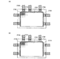
本発明の実施の形態について、図1を用いて説明する。図1(A)(B)(C)に示すトランジスタは、ボトムゲート構造のコプラナー型の薄膜トランジスタである。
(Embodiment 1)
An embodiment of the present invention will be described with reference to FIG. The transistors illustrated in FIGS. 1A, 1B, and 1C are coplanar thin film transistors with a bottom gate structure.
本実施の形態では、半導体層として化合物半導体材料を用い、半導体層とソース電極層及びドレイン電極層との間に、それぞれ導電性のバッファ層を形成する。バッファ層は有機化合物及び無機化合物を含む層として形成される。化合物半導体材料を用いた半導体層とソース電極層及びドレイン電極層との間に介在するバッファ層によって、半導体層とソース電極層及びドレイン電極層との導電性は向上し、電気的に良好な接続を行うことができる。 In this embodiment, a compound semiconductor material is used for the semiconductor layer, and a conductive buffer layer is formed between the semiconductor layer and the source and drain electrode layers. The buffer layer is formed as a layer containing an organic compound and an inorganic compound. The buffer layer interposed between the semiconductor layer using the compound semiconductor material and the source electrode layer and the drain electrode layer improves the conductivity between the semiconductor layer and the source electrode layer and the drain electrode layer. It can be performed.
図1(A)で示すように、基板50上に、ゲート電極層51が設けられ、ゲート電極層51上にゲート絶縁層52、ゲート絶縁層52上にソース電極層又はドレイン電極層53a及びソース電極層又はドレイン電極層53bが形成されている。ソース電極層又はドレイン電極層53a及びソース電極層又はドレイン電極層53b上には半導体層55が形成されており、ソース電極層又はドレイン電極層53aと半導体層55との間にはバッファ層54bが、ソース電極層又はドレイン電極層53bと半導体層55との間にはバッファ層54bが設けられている。
As shown in FIG. 1A, a
バッファ層54a及びバッファ層54bは、導電性を有し、有機化合物及び無機化合物を含む層より形成されている。このバッファ層54a及びバッファ層54bにより、ソース電極層又はドレイン電極層53aと半導体層55と、ソース電極層又はドレイン電極層53bと半導体層55との接触抵抗が低下し、電気的接続を良好にすることができる。
The
半導体層に用いる材料とソース電極層及びドレイン電極層に用いる材料の組み合わせによっては、導通できない、また高抵抗となるなどの電気的特性が低下する場合がある。よって、半導体層に用いる材料とソース電極層及びドレイン電極層に用いる材料は適宜選択する必要がある。本実施の形態では、ソース電極層及びドレイン電極層と酸化物半導体層とをバッファ層を介して積層し電気的に接続するため、上記のような電気的特性の低下を防ぎ、かつ材料の自由に選択することができる。そのため、必要とされる特性(電気的特性、信頼性に関する特性(材料の積層状態(密着性など)))を満たすような半導体装置を作製することができる。 Depending on the combination of the material used for the semiconductor layer and the material used for the source electrode layer and the drain electrode layer, electrical characteristics such as inability to conduct and high resistance may be deteriorated. Therefore, the material used for the semiconductor layer and the material used for the source and drain electrode layers need to be selected as appropriate. In this embodiment, the source electrode layer, the drain electrode layer, and the oxide semiconductor layer are stacked and electrically connected to each other through the buffer layer, so that the above-described deterioration in electrical characteristics is prevented and the freedom of materials is reduced. Can be selected. Therefore, a semiconductor device that satisfies required characteristics (electric characteristics, characteristics related to reliability (a stacked state of materials (adhesion), etc.)) can be manufactured.
バッファ層に用いることのできる有機化合物は、正孔輸送性を有する有機化合物でも電子輸送性を有する有機化合物でも用いることができる。正孔輸送性を有する有機化合物はp型を有する半導体層とソース電極層及びドレイン電極層との間に設ける方が好ましく、電子輸送性を有する有機化合物はn型を有する半導体層とソース電極層及びドレイン電極層との間に設ける方が好ましい。 As the organic compound that can be used for the buffer layer, an organic compound having a hole transporting property or an organic compound having an electron transporting property can be used. The organic compound having a hole transporting property is preferably provided between the p-type semiconductor layer and the source and drain electrode layers, and the organic compound having an electron transporting property is an n-type semiconductor layer and the source electrode layer. And between the drain electrode layer and the drain electrode layer.
バッファ層に用いることのできる正孔輸送性を有する有機化合物は、4,4’−ビス[N−(1−ナフチル)−N−フェニルアミノ]ビフェニル(略称:NPB)、4,4’−ビス[N−(3−メチルフェニル)−N−フェニルアミノ]ビフェニル(略称:TPD)、4,4’,4’’−トリス(N,N−ジフェニルアミノ)トリフェニルアミン(略称:TDATA)、4,4’,4’’−トリス[N−(3−メチルフェニル)−N−フェニルアミノ]トリフェニルアミン(略称:MTDATA)、4,4’−ビス{N−[4−(N,N−ジ−m−トリルアミノ)フェニル]−N−フェニルアミノ}ビフェニル(略称:DNTPD)、1,3,5−トリス[N,N−ジ(m−トリル)アミノ]ベンゼン(略称:m−MTDAB)、4,4’,4’’−トリス(N−カルバゾリル)トリフェニルアミン(略称:TCTA)、2,3−ビス(4−ジフェニルアミノフェニル)キノキサリン(略称:TPAQn)、2,2’,3,3’−テトラキス(4−ジフェニルアミノフェニル)−6,6’−ビスキノキサリン(略称:D−TriPhAQn)、2,3−ビス{4−[N−(1−ナフチル)−N−フェニルアミノ]フェニル}−ジベンゾ[f,h]キノキサリン(略称:NPADiBzQn)等のアリールアミノ基を有する有機材料や、フタロシアニン(略称:H2Pc)、銅フタロシアニン(略称:CuPc)、バナジルフタロシアニン(略称:VOPc)等も用いることができる。 An organic compound having a hole-transport property that can be used for the buffer layer is 4,4′-bis [N- (1-naphthyl) -N-phenylamino] biphenyl (abbreviation: NPB), 4,4′-bis. [N- (3-methylphenyl) -N-phenylamino] biphenyl (abbreviation: TPD), 4,4 ′, 4 ″ -tris (N, N-diphenylamino) triphenylamine (abbreviation: TDATA), 4 , 4 ′, 4 ″ -tris [N- (3-methylphenyl) -N-phenylamino] triphenylamine (abbreviation: MTDATA), 4,4′-bis {N- [4- (N, N— Di-m-tolylamino) phenyl] -N-phenylamino} biphenyl (abbreviation: DNTPD), 1,3,5-tris [N, N-di (m-tolyl) amino] benzene (abbreviation: m-MTDAB), 4,4 ', ″ -Tris (N-carbazolyl) triphenylamine (abbreviation: TCTA), 2,3-bis (4-diphenylaminophenyl) quinoxaline (abbreviation: TPAQn), 2,2 ′, 3,3′-tetrakis (4 -Diphenylaminophenyl) -6,6'-biskinoxaline (abbreviation: D-TriPhAQn), 2,3-bis {4- [N- (1-naphthyl) -N-phenylamino] phenyl} -dibenzo [f, h] Organic materials having an arylamino group such as quinoxaline (abbreviation: NPDiBzQn), phthalocyanine (abbreviation: H2Pc), copper phthalocyanine (abbreviation: CuPc), vanadyl phthalocyanine (abbreviation: VOPc), and the like can also be used.
また、下記一般式(1)で表されるような有機材料も正孔輸送性を有する有機化合物として好適に用いることができ、その具体例としては3−[N−(9−フェニルカルバゾール−3−イル)−N−フェニルアミノ]−9−フェニルカルバゾール(略称:PCzPCA1)、3,6−ビス[N−(9−フェニルカルバゾール−3−イル)−N−フェニルアミノ]−9−フェニルカルバゾール(略称:PCzPCA2)等を挙げることができる。この構造を有する有機化合物を用いた第1の複合材料は熱的安定性に優れ、信頼性が良い。 In addition, an organic material represented by the following general formula (1) can also be suitably used as the organic compound having a hole transporting property, and specific examples thereof include 3- [N- (9-phenylcarbazole-3]. -Yl) -N-phenylamino] -9-phenylcarbazole (abbreviation: PCzPCA1), 3,6-bis [N- (9-phenylcarbazol-3-yl) -N-phenylamino] -9-phenylcarbazole ( Abbreviations: PCzPCA2) and the like. The first composite material using an organic compound having this structure has excellent thermal stability and good reliability.

また、下記一般式(3)乃至(6)のいずれかで示されるような有機材料も好適に用いることができる。下記一般式(3)乃至(6)のいずれかで表される有機化合物の具体例としては、N−(2−ナフチル)カルバゾール(略称:NCz)、4,4’−ジ(N−カルバゾリル)ビフェニル(略称:CBP)、9,10−ビス[4−(N−カルバゾリル)フェニル]アントラセン(略称:BCPA)、3,5−ビス[4−(N−カルバゾリル)フェニル]ビフェニル(略称:BCPBi)、1,3,5−トリス[4−(N−カルバゾリル)フェニル]ベンゼン(略称:TCPB)等を挙げることができる。 An organic material represented by any one of the following general formulas (3) to (6) can also be suitably used. Specific examples of the organic compound represented by any one of the following general formulas (3) to (6) include N- (2-naphthyl) carbazole (abbreviation: NCz), 4,4′-di (N-carbazolyl). Biphenyl (abbreviation: CBP), 9,10-bis [4- (N-carbazolyl) phenyl] anthracene (abbreviation: BCPA), 3,5-bis [4- (N-carbazolyl) phenyl] biphenyl (abbreviation: BCPBi) 1,3,5-tris [4- (N-carbazolyl) phenyl] benzene (abbreviation: TCPB) and the like.
さらに、アントラセン、9,10−ジフェニルアントラセン(略称:DPA)、2−tert−ブチル−9,10−ジ(2−ナフチル)アントラセン(略称:t−BuDNA)、テトラセン、ルブレン、ペンタセン等の芳香族炭化水素も用いることができる。 Furthermore, aromatics such as anthracene, 9,10-diphenylanthracene (abbreviation: DPA), 2-tert-butyl-9,10-di (2-naphthyl) anthracene (abbreviation: t-BuDNA), tetracene, rubrene, pentacene, etc. Hydrocarbons can also be used.
バッファ層に用いることのできる電子輸送性を有する有機化合物は、例えば、トリス(8−キノリノラト)アルミニウム(略称:Alq3)、トリス(4−メチル−8−キノリノラト)アルミニウム(略称:Almq3)、ビス(10−ヒドロキシベンゾ[h]−キノリナト)ベリリウム(略称:BeBq2)、ビス(2−メチル−8−キノリノラト)−4−フェニルフェノラト−アルミニウム(略称:BAlq)等キノリン骨格またはベンゾキノリン骨格を有する金属錯体等からなる材料を用いることができる。また、この他、ビス[2−(2−ヒドロキシフェニル)ベンゾオキサゾラト]亜鉛(略称:Zn(BOX)2)、ビス[2−(2−ヒドロキシフェニル)ベンゾチアゾラト]亜鉛(略称:Zn(BTZ)2)などのオキサゾール系、チアゾール系配位子を有する金属錯体などの材料も用いることができる。さらに、金属錯体以外にも、2−(4−ビフェニリル)−5−(4−tert−ブチルフェニル)−1,3,4−オキサジアゾール(略称:PBD)、1,3−ビス[5−(p−tert−ブチルフェニル)−1,3,4−オキサジアゾール−2−イル]ベンゼン(略称:OXD−7)、3−(4−tert−ブチルフェニル)−4−フェニル−5−(4−ビフェニリル)−1,2,4−トリアゾール(略称:TAZ)、3−(4−tert−ブチルフェニル)−4−(4−エチルフェニル)−5−(4−ビフェニリル)−1,2,4−トリアゾール(略称:p−EtTAZ)、バソフェナントロリン(略称:BPhen)、バソキュプロイン(略称:BCP)等を用いることができる。 Examples of the organic compound having an electron transporting property that can be used for the buffer layer include tris (8-quinolinolato) aluminum (abbreviation: Alq 3 ), tris (4-methyl-8-quinolinolato) aluminum (abbreviation: Almq 3 ), Bis (10-hydroxybenzo [h] -quinolinato) beryllium (abbreviation: BeBq 2 ), bis (2-methyl-8-quinolinolato) -4-phenylphenolato-aluminum (abbreviation: BAlq) quinoline skeleton or benzoquinoline skeleton A material made of a metal complex or the like can be used. In addition, bis [2- (2-hydroxyphenyl) benzoxazolate] zinc (abbreviation: Zn (BOX) 2 ), bis [2- (2-hydroxyphenyl) benzothiazolate] zinc (abbreviation: Zn (BTZ) 2 ) and other materials such as metal complexes having an oxazole-based or thiazole-based ligand can also be used. In addition to metal complexes, 2- (4-biphenylyl) -5- (4-tert-butylphenyl) -1,3,4-oxadiazole (abbreviation: PBD), 1,3-bis [5- (P-tert-butylphenyl) -1,3,4-oxadiazol-2-yl] benzene (abbreviation: OXD-7), 3- (4-tert-butylphenyl) -4-phenyl-5- ( 4-biphenylyl) -1,2,4-triazole (abbreviation: TAZ), 3- (4-tert-butylphenyl) -4- (4-ethylphenyl) -5- (4-biphenylyl) -1,2, 4-triazole (abbreviation: p-EtTAZ), bathophenanthroline (abbreviation: BPhen), bathocuproin (abbreviation: BCP), and the like can be used.
バッファ層に用いることのできる無機化合物は、遷移金属の酸化物や窒化物が望ましく、4〜8属に属する金属の酸化物もしくは窒化物がさらに望ましい。その中でもバナジウム酸化物、タンタル酸化物、モリブデン酸化物、タングステン酸化物、レニウム酸化物及びルテニウム酸化物は好適である。上記無機化合物は、正孔輸送性を有する有機化合物と混合した複合材料として、p型を有する半導体層とソース電極層及びドレイン電極層との間に設けることが好ましい。 The inorganic compound that can be used for the buffer layer is preferably an oxide or nitride of a transition metal, more preferably an oxide or nitride of a metal belonging to Group 4-8. Among these, vanadium oxide, tantalum oxide, molybdenum oxide, tungsten oxide, rhenium oxide, and ruthenium oxide are preferable. The inorganic compound is preferably provided as a composite material mixed with an organic compound having a hole-transport property between the p-type semiconductor layer and the source and drain electrode layers.
バッファ層に用いることのできる他の無機化合物は、アルカリ金属及びアルカリ土類金属、もしくはそれらを含む酸化物や窒化物が望ましく、具体的には、リチウム、ナトリウム、カリウム、セシウム、マグネシウム、カルシウム、ストロンチウム、バリウム、リチウム酸化物、マグネシウム窒化物、カルシウム窒化物であることが好ましい。上記無機化合物はドナー性を有しており、電子輸送性を有する有機化合物と混合した複合材料として、n型を有する半導体層とソース電極層及びドレイン電極層との間に設けることが好ましい。 Other inorganic compounds that can be used for the buffer layer are preferably alkali metals and alkaline earth metals, or oxides or nitrides containing them, specifically lithium, sodium, potassium, cesium, magnesium, calcium, Strontium, barium, lithium oxide, magnesium nitride, and calcium nitride are preferable. The inorganic compound has a donor property, and is preferably provided as a composite material mixed with an organic compound having an electron transport property between the n-type semiconductor layer and the source and drain electrode layers.
以上、上記有機化合物の少なくとも一種と、上記無機化合物の少なくとの一種を含んでバッファ層である有機化合物及び無機化合物を含む層を形成することができる。もちろん有機化合物及び無機化合物は複数種用いて形成してもよい。 As described above, a layer containing an organic compound and an inorganic compound which are buffer layers containing at least one of the organic compounds and at least one of the inorganic compounds can be formed. Of course, a plurality of organic compounds and inorganic compounds may be used.
バッファ層である有機化合物及び無機化合物を含む層は、電子ビーム蒸着法、共蒸着などの蒸着法、スパッタリング法、CVD法や、混合溶液を用いたスピンコート法など塗布法、ゾル−ゲル法を用いることができる。バッファ層は各々の材料を同時に成膜することにより形成することができ、抵抗加熱蒸着同士による共蒸着法、電子ビーム蒸着同士による共蒸着法、抵抗加熱蒸着と電子ビーム蒸着による共蒸着法、抵抗加熱蒸着とスパッタリングによる成膜、電子ビーム蒸着とスパッタリングによる成膜など、同種、異種の方法を組み合わせて形成することができる。また、特定の目的に調合された組成物の液滴を選択的に吐出(噴出)して所定のパターンに形成することが可能な、液滴吐出(噴出)法(その方式によっては、インクジェット法とも呼ばれる。)、物体が所望のパターンに転写、または描写できる方法、例えば各種印刷法(スクリーン(孔版)印刷、オフセット(平版)印刷、凸版印刷やグラビア(凹版)印刷など所望なパターンで形成される方法)、ディスペンサ法なども用いることができる。また、同時に形成するのではなく、どちらか一方(有機化合物層又は無機化合物層)を形成した後に、イオン注入法やドーピング法などによって他の片方(有機化合物又は無機化合物)を導入し、バッファ層を形成してもよい。 The buffer layer containing an organic compound and an inorganic compound is formed by an electron beam evaporation method, a vapor deposition method such as co-evaporation, a sputtering method, a CVD method, a coating method such as a spin coating method using a mixed solution, or a sol-gel method. Can be used. The buffer layer can be formed by depositing each material at the same time, co-evaporation method by resistance heating deposition, co-evaporation method by electron beam deposition, co-evaporation method by resistance heating deposition and electron beam deposition, resistance It can be formed by combining the same or different methods such as film formation by heating vapor deposition and sputtering and film formation by electron beam vapor deposition and sputtering. In addition, a droplet discharge (ejection) method (an ink jet method depending on the method) that can selectively eject (eject) droplets of a composition prepared for a specific purpose to form a predetermined pattern. ), A method by which an object can be transferred or drawn in a desired pattern, such as various printing methods (screen (stencil) printing, offset (lithographic) printing, relief printing or gravure (intaglio printing), etc. A dispenser method or the like. In addition, after forming either one (organic compound layer or inorganic compound layer) instead of forming at the same time, the other one (organic compound or inorganic compound) is introduced by an ion implantation method or a doping method, and the buffer layer May be formed.
半導体層を形成する化合物半導体としては、例えば酸化物半導体が挙げられる。酸化物半導体としては、酸化亜鉛(ZnO)、酸化マグネシウム亜鉛(MgxZn1-xO)、酸化スズ(SnO2)、インジウム酸化物(In2O3)、酸化ガリウム(Ga2O3)などの金属酸化物が挙げられる。また、上記酸化物半導体の複数より構成される酸化物半導体でもよく、酸化亜鉛(ZnO)とインジウム酸化物(In2O3)と酸化ガリウム(Ga2O3)とから構成されるInGaO3(ZnO)m(mは1以上50未満の整数であり、代表的にはInGaO3(ZnO)5なども用いることができる。上記半導体は、非晶質、微結晶性、または結晶性のどの構成を有するものであってもよい。半導体材料はn型を有する半導体であっても、p型を有する半導体であってもよく、他の不純物元素(アルミニウム、ガリウムなど)を含んで形成してもよい。不純物元素を含む酸化物半導体をターゲットとして用いたスパッタ法や、CVD法などにより形成することができる。また、不純物元素を導入(ドーピング法、イオン注入法などによる添加)して、酸化物半導体に不純物元素を有する様にしてもよい。半導体層は、蒸着法、CVD法、プラズマCVD法、スパッタリング法等の方法により単層又は積層して形成することができる。また、液滴吐出法や、印刷法(スクリーン印刷、オフセット印刷、凸版印刷やグラビア(凹版)印刷法など)、スピンコート法などの塗布法、ディッピング法などを用いることもできる。 As a compound semiconductor that forms the semiconductor layer, for example, an oxide semiconductor can be given. Examples of the oxide semiconductor include zinc oxide (ZnO), magnesium zinc oxide (Mg x Zn 1-x O), tin oxide (SnO 2 ), indium oxide (In 2 O 3 ), and gallium oxide (Ga 2 O 3 ). And metal oxides. Alternatively, an oxide semiconductor composed of a plurality of the above oxide semiconductors may be used, and InGaO 3 (comprising zinc oxide (ZnO), indium oxide (In 2 O 3 ), and gallium oxide (Ga 2 O 3 ). ZnO) m (m is an integer greater than or equal to 1 and less than 50, typically InGaO 3 (ZnO) 5 or the like can be used. Any structure of the semiconductor can be amorphous, microcrystalline, or crystalline. The semiconductor material may be an n-type semiconductor, a p-type semiconductor, or may include other impurity elements (aluminum, gallium, etc.). It can be formed by a sputtering method using an oxide semiconductor containing an impurity element as a target, a CVD method, etc. In addition, an impurity element is introduced (by a doping method, an ion implantation method, or the like). The semiconductor layer may be formed as a single layer or a stacked layer by a method such as an evaporation method, a CVD method, a plasma CVD method, or a sputtering method. In addition, a droplet discharge method, a printing method (screen printing, offset printing, relief printing, gravure (intaglio printing), etc.), a coating method such as a spin coating method, a dipping method, or the like can also be used.
また、酸化亜鉛などの酸化物半導体は、可視光を透過するため透明である。このような透光性(可視光領域の光を透過する)の半導体材料を用いた半導体層は、可視光の吸収が少ないため、半導体層のチャネル部分に光が入射しても不要な光励起キャリアが発生しない、耐光性の優れた信頼性の高い薄膜トランジスタとすることができる。なお、他の化合物半導体として、窒化物半導体、炭化物半導体等を用いてもよい。 An oxide semiconductor such as zinc oxide is transparent because it transmits visible light. A semiconductor layer using such a light-transmitting semiconductor material (transmitting light in the visible light region) absorbs less visible light, so unnecessary photoexcited carriers even when light enters the channel portion of the semiconductor layer. Thus, a highly reliable thin film transistor with excellent light resistance can be obtained. Note that a nitride semiconductor, a carbide semiconductor, or the like may be used as another compound semiconductor.
酸化物半導体のような化合物半導体は、他のシリコンや有機半導体材料などの半導体材料と比較して、材料が安価であり作製工程も複雑化しないため、低コストで半導体装置を作製することができる。 Compared with other semiconductor materials such as silicon and organic semiconductor materials, a compound semiconductor such as an oxide semiconductor is less expensive and does not complicate the manufacturing process, so that a semiconductor device can be manufactured at low cost. .
また半導体層に不純物元素を含ませて形成し、一導電型(n型又はp型)を有する半導体層を形成することができる。半導体層に添加する(含むように形成する)不純物元素としては、13族元素(ボロン(B))、ガリウム(Ga)、インジウム(In)、タリウム(Tl))、17族元素(フッ素(F)、塩素(Cl)、臭素(Br)、ヨウ素(I))、1族元素(リチウム(Li)、ナトリウム(Na)、カリウム(K)、ルビジウム(Rb)、セシウム(Cs))、15族元素(窒素(N)、リン(P)、ヒ素(As)、アンチモン(Sb)、ビスマス(Bi))等を用いることができ、上記元素のうち一種、又は複数種を用いることができる。 In addition, a semiconductor layer having one conductivity type (n-type or p-type) can be formed by including an impurity element in a semiconductor layer. As an impurity element added (formed to include) to the semiconductor layer, a group 13 element (boron (B)), gallium (Ga), indium (In), thallium (Tl)), a group 17 element (fluorine (F ), Chlorine (Cl), bromine (Br), iodine (I)), group 1 elements (lithium (Li), sodium (Na), potassium (K), rubidium (Rb), cesium (Cs)), group 15 Elements (nitrogen (N), phosphorus (P), arsenic (As), antimony (Sb), bismuth (Bi)) and the like can be used, and one or more of the above elements can be used.
不純物元素の添加は、半導体層の一部でもよいし、全体に添加しても良く、その添加量は、薄膜トランジスタ素子の寸法、厚さ、集積度、必要とされる性能(電気的特性など)によって適宜、設定すれば良く、半導体層にわたって均一な濃度としても良いし、濃度勾配を有していても良い。 The impurity element may be added to a part of the semiconductor layer or may be added to the entire semiconductor layer. The addition amount depends on the size, thickness, integration degree, required performance (electrical characteristics, etc.) of the thin film transistor element. The concentration may be set appropriately according to the above, and the concentration may be uniform over the semiconductor layer or may have a concentration gradient.
また、半導体層を積層構造としてもよい。図25(A)(B)に、半導体層を積層構造とした例を示す。図25(A)(B)は、酸化物半導体層の他に有機材料を含む半導体層である有機半導体層を用いた半導体層を形成する例である。 Further, the semiconductor layer may have a stacked structure. FIGS. 25A and 25B illustrate an example in which a semiconductor layer has a stacked structure. 25A and 25B illustrate an example of forming a semiconductor layer using an organic semiconductor layer which is a semiconductor layer containing an organic material in addition to an oxide semiconductor layer.
図25(A)は、コプラナー型の薄膜トランジスタであり、基板420上にゲート電極層421、ゲート電極層421上にゲート絶縁層422が形成され、ゲート絶縁層422上にソース電極層又はドレイン電極層423a及びソース電極層又はドレイン電極層423bが形成されている。ソース電極層又はドレイン電極層423a及びソース電極層又はドレイン電極層423bには、酸化物半導体層である半導体層425と有機材料を含む半導体層426からなる2層積層の半導体層が形成されている。さらに、ソース電極層又はドレイン電極層423aと半導体層425との間には有機化合物及び無機化合物を含む層であるバッファ層424aが設けられ、ソース電極層又はドレイン電極層423bと半導体層425との間には有機化合物及び無機化合物を含む層であるバッファ層424bが設けられている。
FIG. 25A illustrates a coplanar thin film transistor in which a
有機材料を含む半導体層426は酸化物半導体層である半導体層425を保護する機能を有する。所望の形状に整形するために形成時にエッチングによる加工を行う場合、特に有機材料を含む半導体層426は半導体層425を保護する効果をもたらす。このような構造であると、酸化物半導体層である半導体層425がエッチングされやすく、エッチャントやエッチングガスに対する耐性が弱くても、酸化物半導体層である半導体層425は保護されエッチングされることはないので、高い信頼性を有する薄膜トランジスタを作製することができる。
The
また、バッファ層をソース側、ドレイン側、どちらか片方のみ設ける構造としてもよい。バッファ層をソース側あるいはドレイン側どちらか一方のみ設ける構造を図25(B)に示す。図25(B)は、コプラナー型の薄膜トランジスタであり、基板430上にゲート電極層431、ゲート電極層431上にゲート絶縁層432が形成され、ゲート絶縁層432上にソース電極層又はドレイン電極層433a及びソース電極層又はドレイン電極層433bが形成されている。ソース電極層又はドレイン電極層433a及びソース電極層又はドレイン電極層433bには、酸化物半導体層である第1の半導体層435と有機材料を含む第2の半導体層436からなる2層積層の半導体層が形成されている。さらに、ソース電極層又はドレイン電極層433aと酸化物半導体層である第1の半導体層425との間には有機化合物及び無機化合物を含む層であるバッファ層434が設けられている。
Alternatively, a structure in which only one of the buffer layer and the drain side is provided may be employed. FIG. 25B shows a structure in which the buffer layer is provided only on the source side or the drain side. FIG. 25B illustrates a coplanar thin film transistor in which a
図25(B)において、バッファ層434とソース電極層又はドレイン電極層433aとは別々に形成されているので、バッファ層434とソース電極層又はドレイン電極層433aとの端部は一致していない断面図の例となっている。このように、バッファ層、ソース電極層、ドレイン電極層、酸化物半導体層、有機材料を含む半導体層は、同工程で同形状に加工してもよいし、それぞれ別工程別形状で形成してもよい。
In FIG. 25B, since the
第1の半導体層上に積層する第2の半導体層として、有機材料を含む半導体層の他に、他の酸化物を含む半導体層を積層してもよい。第2の半導体層に導電型を有する半導体層を用いれば、酸化物半導体層である第1の半導体層の導電性(n型、p型などの導電型)をより制御することができる。ソース電極層及びドレイン電極層側の第1の半導体層より、積層する第2の半導体層の方が導電性が低い場合は、第2の半導体層とソース電極層及びドレイン電極層とは接する構造でもよい。第1の半導体層より第2の半導体層の導電性が高い場合、第2の半導体層はソース電極層及びドレイン電極層と接しない構造とする方が好ましい。 As the second semiconductor layer stacked over the first semiconductor layer, in addition to the semiconductor layer including an organic material, a semiconductor layer including another oxide may be stacked. When a semiconductor layer having a conductivity type is used for the second semiconductor layer, the conductivity (conductivity type such as n-type or p-type) of the first semiconductor layer that is an oxide semiconductor layer can be further controlled. When the second semiconductor layer to be stacked has lower conductivity than the first semiconductor layer on the source electrode layer and drain electrode layer side, the second semiconductor layer is in contact with the source electrode layer and the drain electrode layer. But you can. In the case where the conductivity of the second semiconductor layer is higher than that of the first semiconductor layer, it is preferable that the second semiconductor layer have a structure that is not in contact with the source electrode layer and the drain electrode layer.
有機材料を含む半導体層426は、半導体として、有機半導体材料を用い、印刷法、スプレー法、スピン塗布法、液滴吐出法などで形成することができる。選択的に半導体層を形成できる印刷法や液滴吐出法などを用いると、エッチング工程が必要ないため、工程数を削減することが可能である。有機半導体としては、低分子材料、高分子材料などが用いられ、有機色素、導電性高分子材料などの材料も用いることができる。本発明に用いる有機半導体材料としては、その骨格が共役二重結合から構成されるπ電子共役系の高分子材料が望ましい。代表的には、ポリチオフェン、ポリフルオレン、ポリ(3−アルキルチオフェン)、ポリチオフェン誘導体、ペンタセン等の可溶性の高分子材料を用いることができる。
The
その他にも用いることができる有機半導体材料としては、可溶性の前駆体を成膜した後で処理することにより半導体層を形成することができる材料がある。なお、このような有機半導体材料としては、ポリチエニレンビニレン、ポリ(2,5−チエニレンビニレン)、ポリアセチレン、ポリアセチレン誘導体、ポリアリレンビニレンなどがある。 As another organic semiconductor material that can be used, there is a material that can form a semiconductor layer by processing after forming a soluble precursor. Examples of such an organic semiconductor material include polythienylene vinylene, poly (2,5-thienylene vinylene), polyacetylene, a polyacetylene derivative, and polyarylene vinylene.
前駆体を有機半導体に変換する際には、加熱処理だけではなく塩化水素ガスなどの反応触媒を添加することがなされる。また、これらの可溶性有機半導体材料を溶解させる代表的な溶媒としては、トルエン、キシレン、クロロベンゼン、ジクロロベンゼン、アニソール、クロロフォルム、ジクロロメタン、γブチルラクトン、ブチルセルソルブ、シクロヘキサン、NMP(N−メチル−2−ピロリドン)、シクロヘキサノン、2−ブタノン、ジオキサン、ジメチルホルムアミド(DMF)または、THF(テトラヒドロフラン)などを適用することができる。 When converting the precursor into an organic semiconductor, a reaction catalyst such as hydrogen chloride gas is added as well as heat treatment. Typical solvents for dissolving these soluble organic semiconductor materials include toluene, xylene, chlorobenzene, dichlorobenzene, anisole, chloroform, dichloromethane, γ-butyllactone, butyl cellosolve, cyclohexane, NMP (N-methyl-2) -Pyrrolidone), cyclohexanone, 2-butanone, dioxane, dimethylformamide (DMF), THF (tetrahydrofuran), or the like can be applied.
バッファ層424a及びバッファ層424bは、導電性を有し、有機化合物及び無機化合物を含む層より形成されている。このバッファ層424a及びバッファ層424bにより、ソース電極層又はドレイン電極層423aと酸化物半導体層である半導体層425と、ソース電極層又はドレイン電極層423bと酸化物半導体層である半導体層425との接触抵抗が低下し、電気的接続を良好にすることができる。
The
図1(B)で示すように、基板60上に、ゲート電極層61が設けられ、ゲート電極層61上にゲート絶縁層62、ゲート絶縁層62上にソース電極層又はドレイン電極層63a及びソース電極層又はドレイン電極層63bが形成されている。ソース電極層又はドレイン電極層63a及びソース電極層又はドレイン電極層63b上には半導体層65が形成されており、ソース電極層又はドレイン電極層63aと半導体層65との間にはバッファ層64bが、ソース電極層又はドレイン電極層63bと半導体層65との間にはバッファ層64bが設けられている。
As shown in FIG. 1B, a
図1(B)の薄膜トランジスタにおいて、バッファ層64a及びバッファ層64bとは同様のものではなく、異なる材料を用いた有機化合物と無機化合物を含む層である。また、バッファ層64a及びバッファ層64bに同材料を用いる場合でも、含まれる有機化合物と無機化合物の混合比、混合状態などを異ならせて、異なる特性(性質)を有するようにしてもよい。
In the thin film transistor in FIG. 1B, the
バッファ層64a及びバッファ層64bは、導電性を有し、有機化合物及び無機化合物を含む層より形成されている。このバッファ層64a及びバッファ層64bにより、ソース電極層又はドレイン電極層63aと半導体層65と、ソース電極層又はドレイン電極層63bと半導体層65との接触抵抗が低下し、電気的接続を良好にすることができる。
The
図1(A)の薄膜トランジスタは、バッファ層54a及びバッファ層54bに同材料を用いており、ソース領域もドレイン領域も同材料、同構造の例となっている。このように、ソース側、ドレイン側に同材料からなるバッファ層を用いてもよいし、図1(B)で示すように異なる材料からなるバッファ層(異なる性質を有するバッファ層)を用いてもよい。また、バッファ層をソース側、ドレイン側、どちらか片方のみ設ける構造としてもよい。
The thin film transistor in FIG. 1A uses the same material for the
バッファ層によって、薄膜トランジスタの電気特性をさらに精密に制御することができるので、半導体装置の電気的設計の自由度が増し、より必要とされる特性を付与された、高機能、高性能で有用な半導体装置を作製することができる。 The buffer layer allows the electrical characteristics of the thin film transistor to be controlled more precisely, increasing the degree of freedom in electrical design of the semiconductor device, and providing high-performance, high-performance, and more useful characteristics. A semiconductor device can be manufactured.
また、バッファ層とソース電極層及びドレイン電極層との間に、一導電型を有する半導体層を設ける構造としてもよい。一導電型を有する半導体層とバッファ層の導電性によってはバッファ層と半導体層との間に一導電型を有する半導体層を形成しても良い。 Alternatively, a semiconductor layer having one conductivity type may be provided between the buffer layer and the source and drain electrode layers. Depending on the conductivity of the semiconductor layer having one conductivity type and the buffer layer, a semiconductor layer having one conductivity type may be formed between the buffer layer and the semiconductor layer.
図1(C)で示すように、基板70上に、ゲート電極層71が設けられ、ゲート電極層71上にゲート絶縁層72、ゲート絶縁層72上にソース電極層又はドレイン電極層73a及びソース電極層又はドレイン電極層73bが形成されている。ソース電極層又はドレイン電極層73a及びソース電極層又はドレイン電極層73b上には半導体層75が形成されており、ソース電極層又はドレイン電極層73aと半導体層75との間にはバッファ層74bが、ソース電極層又はドレイン電極層73bと半導体層75との間にはバッファ層74bが設けられている。さらに、ソース電極層又はドレイン電極層73aとバッファ層74aとの間には一導電型を有する半導体層76aが、ソース電極層又はドレイン電極層73bとバッファ層74bとの間には一導電型を有する半導体層76bが設けられている。
As shown in FIG. 1C, a
一導電型を有する半導体層としては、半導体材料に一導電型を付与する不純物元素を含ませた半導体層を用いることができる。半導体材料としては、前述の酸化物半導体材料(酸化亜鉛、酸化マグネシウム亜鉛、酸化スズ)、シリコン(Si)、ゲルマニウム(Ge)、有機半導体材料を用いてもよい。上記半導体材料に不純物元素(13族元素、17族元素、1族元素、15族元素)等を、添加した半導体層を用いることができる。例えば、一導電型を有する半導体層として、酸化亜鉛にアルミニウムやガリウムを添加した、アルミニウムを含む酸化亜鉛やガリウムを含む酸化亜鉛などを用いるとよい。また、他の化合物半導体(GaAs、InP、SiC、ZnSe、GaN、SiGeなど)を用いることもできる。半導体層は、結晶性を有していてもいなくても良く、非晶質半導体、微結晶半導体、結晶性半導体どれであってもよい。非晶質半導体を光エネルギーや熱エネルギーを利用して結晶化させ、結晶性半導体を形成することができる。また成膜直後の結晶性を有する半導体層を用いてもよいし、非晶質半導体層と同様に結晶化し、結晶性を向上させてもよい。非晶質半導体層及び結晶性を有する半導体層の結晶化は、熱処理とレーザ光照射による結晶化を組み合わせてもよく、熱処理やレーザ光照射を単独で、複数回行っても良い。 As the semiconductor layer having one conductivity type, a semiconductor layer in which an impurity element imparting one conductivity type is added to a semiconductor material can be used. As the semiconductor material, the above-described oxide semiconductor materials (zinc oxide, magnesium zinc oxide, tin oxide), silicon (Si), germanium (Ge), and organic semiconductor materials may be used. A semiconductor layer in which an impurity element (Group 13 element, Group 17 element, Group 1 element, Group 15 element) or the like is added to the semiconductor material can be used. For example, as the semiconductor layer having one conductivity type, zinc oxide containing aluminum, zinc oxide containing gallium, or the like obtained by adding aluminum or gallium to zinc oxide may be used. Also, other compound semiconductors (GaAs, InP, SiC, ZnSe, GaN, SiGe, etc.) can be used. The semiconductor layer may or may not have crystallinity, and may be any of an amorphous semiconductor, a microcrystalline semiconductor, and a crystalline semiconductor. A crystalline semiconductor can be formed by crystallizing an amorphous semiconductor using light energy or thermal energy. Alternatively, a crystalline semiconductor layer immediately after film formation may be used, or crystallization may be performed in the same manner as the amorphous semiconductor layer to improve crystallinity. Crystallization of the amorphous semiconductor layer and the semiconductor layer having crystallinity may be a combination of heat treatment and crystallization by laser light irradiation, or the heat treatment and laser light irradiation may be performed several times independently.
半導体層はスパッタ法、蒸着法、PVD法、CVD法(LPCVD法、プラズマCVD法)、塗布法(スピンコート法、ディップ法)、液滴吐出法、ディスペンサ法、印刷法などを用いて成膜することができる。 The semiconductor layer is formed using a sputtering method, a vapor deposition method, a PVD method, a CVD method (LPCVD method, a plasma CVD method), a coating method (spin coating method, a dip method), a droplet discharge method, a dispenser method, a printing method, or the like. can do.
バッファ層74a及びバッファ層74bは、有機化合物及び無機化合物を含む層より形成されている。このバッファ層74a及びバッファ層74bにより、一導電型を有する半導体層76aと半導体層75と、一導電型を有する半導体層76bと半導体層75との接触抵抗が低下し、ソース電極層又はドレイン電極層73aと半導体層75と、ソース電極層又はドレイン電極層73bと半導体層75との電気的接続を良好にすることができる。
The
本実施の形態では、酸化物半導体層とソース電極層及びドレイン電極層との間に介在するバッファ層によって、半導体層とソース電極層及びドレイン電極層との導電性は向上し、電気的に良好な接続を行うことができる。従って薄膜トランジスタの電気的特性が向上し、高性能の半導体装置、表示装置を作製することができる。 In this embodiment, the buffer layer interposed between the oxide semiconductor layer and the source and drain electrode layers improves conductivity between the semiconductor layer and the source and drain electrode layers, which is electrically favorable. Connection can be made. Accordingly, the electrical characteristics of the thin film transistor are improved, and a high-performance semiconductor device or display device can be manufactured.
酸化物半導体は、他のシリコンや有機半導体材料などの半導体材料と比較して、材料が安価であり作製工程も複雑化しないため、低コストで半導体装置を作製することができる。また、酸化物半導体のような透明な半導体材料は可視光の吸収が少ないため、半導体層のチャネル部分に光が入射しても不要な光励起キャリアが発生しない、耐光性の優れた薄膜トランジスタとすることができる。従って、高速動作を行うことができる高性能、かつ高信頼性の半導体装置、表示装置を作製することもできる。 An oxide semiconductor is less expensive and does not complicate a manufacturing process than a semiconductor material such as silicon or an organic semiconductor material; thus, a semiconductor device can be manufactured at low cost. In addition, since a transparent semiconductor material such as an oxide semiconductor has little absorption of visible light, a thin film transistor with excellent light resistance in which unnecessary photoexcited carriers are not generated even when light enters the channel portion of the semiconductor layer. Can do. Therefore, a high-performance and high-reliability semiconductor device or display device that can operate at high speed can be manufactured.
(実施の形態2)
本発明の実施の形態について、図2(A)(B)を用いて説明する。本実施の形態は、本発明を用いた逆スタガ型薄膜トランジスタの例である。よって、実施の形態1と、同一部分又は同様な機能を有する部分の繰り返しの説明は省略する。
(Embodiment 2)
Embodiment modes of the present invention will be described with reference to FIGS. This embodiment is an example of an inverted staggered thin film transistor using the present invention. Therefore, repetitive description of the same portion as in Embodiment 1 or a portion having a similar function is omitted.
本実施の形態では、半導体層として酸化物半導体材料を用い、半導体層とソース電極層及びドレイン電極層との間に、それぞれ導電性のバッファ層を形成する。バッファ層は有機化合物及び無機化合物を含む層として形成される。酸化物半導体材料を用いた半導体層とソース電極層及びドレイン電極層との間に介在するバッファ層によって、半導体層とソース電極層及びドレイン電極層との導電性は向上し、電気的に良好な接続を行うことができる。 In this embodiment, an oxide semiconductor material is used for the semiconductor layer, and a conductive buffer layer is formed between the semiconductor layer and the source and drain electrode layers. The buffer layer is formed as a layer containing an organic compound and an inorganic compound. The buffer layer interposed between the semiconductor layer using the oxide semiconductor material and the source electrode layer and the drain electrode layer improves conductivity between the semiconductor layer, the source electrode layer, and the drain electrode layer. Connection can be made.
図2(A)で示すように、基板80上に、ゲート電極層81a及びゲート電極層81bが設けられ、ゲート電極層81a及びゲート電極層81b上にゲート絶縁層82、ゲート電極層81aと重なるゲート絶縁層82上に酸化物半導体層である半導体層85a、ゲート電極層81bと重なるゲート絶縁層82上に酸化物半導体層である半導体層85bが形成されている。半導体層85a上にソース電極層又はドレイン電極層83a及びソース電極層又はドレイン電極層83bが、半導体層85b上にソース電極層又はドレイン電極層83b及びソース電極層又はドレイン電極層83cが形成されている。ソース電極層又はドレイン電極層83aと半導体層85aとの間にはバッファ層84bが、ソース電極層又はドレイン電極層83bと半導体層85aとの間にはバッファ層84bが設けられている。同様にソース電極層又はドレイン電極層83bと半導体層85bとの間にはバッファ層84bが、ソース電極層又はドレイン電極層83cと半導体層85bとの間にはバッファ層84cが設けられている。薄膜トランジスタ89aと薄膜トランジスタ89bとは、ソース電極層又はドレイン電極層83b及び導電性を有するバッファ層84bにより電気的に接続されている。
As shown in FIG. 2A, a
バッファ層84a、バッファ層84b及びバッファ層84cは、導電性を有し、有機化合物及び無機化合物を含む層より形成されている。このバッファ層84a及びバッファ層84bにより、ソース電極層又はドレイン電極層83aと半導体層85aと、ソース電極層又はドレイン電極層83bと半導体層85aとの接触抵抗が低下し、電気的接続を良好にすることができる。同様に、バッファ層84b及びバッファ層84cにより、ソース電極層又はドレイン電極層83bと半導体層85bと、ソース電極層又はドレイン電極層83cと半導体層85bとの接触抵抗が低下し、電気的接続を良好にすることができる。よって、薄膜トランジスタ89aと薄膜トランジスタ89bとの電気的接続も良好となる。
The
本実施の形態では、薄膜トランジスタ89a及び薄膜トランジスタ89bは同じ導電型を有する(n型を有する、又はp型を有する)薄膜トランジスタの例を示すが、片方をn型チャネル型薄膜トランジスタ、もう一方をp型チャネル型薄膜トランジスタとし、電気的に接続することによってCMOS構造を形成することもできる。
In this embodiment mode, the
図2(A)に示す薄膜トランジスタは、実施の形態1において図1(A)で示した薄膜トランジスタと同様に、同じ性質を有する同材料からなるバッファ層84a、バッファ層84b及びバッファ層84cを用いている。また、薄膜トランジスタ89aと薄膜トランジスタ89bとを接続する、ソース電極層又はドレイン電極層83b及びバッファ層84bは、同じマスクで同形状に加工されているため、積層構造となっている。勿論、ソース電極層又はドレイン電極層とバッファ層とは個別に形状加工を行ってもよい。また、液滴吐出法などを用いて、エッチング加工を行わず、選択的に導電層、絶縁層などを形成してもよい。液滴吐出法を用いて薄膜トランジスタを形成する例を図2(B)において示す。
The thin film transistor illustrated in FIG. 2A uses the
図2(B)で示すように、基板90上に、ゲート電極層91a及びゲート電極層91bが設けられ、ゲート電極層91a及びゲート電極層91b上にゲート絶縁層92、ゲート電極層91aと重なるゲート絶縁層92上に酸化物半導体層である半導体層95a、ゲート電極層91bと重なるゲート絶縁層92上に酸化物半導体層である半導体層95bが形成されている。半導体層95a上にソース電極層又はドレイン電極層93a及びソース電極層又はドレイン電極層93bが、半導体層95b上にソース電極層又はドレイン電極層93b及びソース電極層又はドレイン電極層93cが形成されている。ソース電極層又はドレイン電極層93aと半導体層95aとの間にはバッファ層94bが、ソース電極層又はドレイン電極層93bと半導体層95aとの間にはバッファ層94bが設けられている。同様にソース電極層又はドレイン電極層93bと半導体層95bとの間にはバッファ層97aが、ソース電極層又はドレイン電極層93cと半導体層95bとの間にはバッファ層97bが設けられている。薄膜トランジスタ99aと薄膜トランジスタ99bとは、ソース電極層又はドレイン電極層93bにより電気的に接続されている。
As shown in FIG. 2B, a
バッファ層94a、バッファ層94b、バッファ層97a及びバッファ層97bは、導電性を有し、有機化合物及び無機化合物を含む層より形成されている。このバッファ層94a、バッファ層94bにより、ソース電極層又はドレイン電極層93aと半導体層85aと、ソース電極層又はドレイン電極層93bと半導体層95aとの接触抵抗が低下し、電気的接続を良好にすることができる。同様に、バッファ層97a及びバッファ層97bにより、ソース電極層又はドレイン電極層93bと半導体層95bと、ソース電極層又はドレイン電極層93cと半導体層95bとの接触抵抗が低下し、電気的接続を良好にすることができる。よって、薄膜トランジスタ99aと薄膜トランジスタ99bとの電気的接続も良好となる。
The
本実施の形態において図2(B)では、薄膜トランジスタ99a及び薄膜トランジスタ99bは異なる導電型を有する(n型を有する、又はp型を有する)薄膜トランジスタの例を示す。図2(B)において、薄膜トランジスタ99aはnチャネル型薄膜トランジスタであり、薄膜トランジスタ99bはpチャネル型薄膜トランジスタとし、電気的に接続することによってCMOS構造を形成している。
In this embodiment, FIG. 2B illustrates an example of a thin film transistor in which the
図2(B)に示す薄膜トランジスタは、異なる導電型を有する薄膜トランジスタであり、用いられるバッファ層も薄膜トランジスタ99aと薄膜トランジスタ99bとで異なった性質を有する異なる材料を含んで形成される例である。よって、バッファ層94a及びバッファ層94bと、バッファ層97a及びバッファ層97bとは異なる材料を含んで形成されている。このように、薄膜トランジスタの導電型や、その必要とされる特性に応じて、有機化合物及び無機化合物を含む層であるバッファ層に含まれる材料や形成方法を適宜設定することができる。
The thin film transistor illustrated in FIG. 2B is a thin film transistor having different conductivity types, and the buffer layer used is an example in which the
本実施の形態の図2(B)においては、薄膜トランジスタの作製に液滴吐出法を用いている。液滴吐出法を用いて膜(絶縁膜、又は導電膜など)を形成する場合、粒子状に加工された膜材料を含む組成物を吐出し、焼成によって融合や融着接合させ固化することで膜を形成する。このように導電性材料を含む組成物を吐出し、焼成することによって形成された膜においては、スパッタ法などで形成した膜が、多くは柱状構造を示すのに対し、多くの粒界を有する多結晶状態を示すことが多い。また、流動性を有する液状の状態で被形成領域に付着させるため、液状状態の形状を反映し、表面がなだらかで曲率を有する様な形状となる場合がある。 In FIG. 2B of this embodiment mode, a droplet discharge method is used for manufacturing a thin film transistor. When forming a film (insulating film, conductive film, or the like) using a droplet discharge method, a composition containing a film material processed into particles is discharged, and is fused and fused and solidified by firing. A film is formed. In a film formed by discharging and baking a composition containing a conductive material in this manner, a film formed by a sputtering method or the like often has a columnar structure, but has many grain boundaries. Often exhibits a polycrystalline state. In addition, since it adheres to the formation region in a liquid state having fluidity, the shape of the liquid state may be reflected and the surface may have a gentle curvature.
液滴吐出法に用いる液滴吐出手段とは、組成物の吐出口を有するノズルや、1つ又は複数のノズルを具備したヘッド等の液滴を吐出する手段を有するものの総称とする。液滴吐出手段が具備するノズルの径は、0.02〜100μm(好適には30μm以下)に設定し、該ノズルから吐出される組成物の吐出量は0.001pl〜100pl(好適には0.1pl以上40pl以下、より好ましくは10pl以下)に設定する。吐出量は、ノズルの径の大きさに比例して増加する。また、被処理物とノズルの吐出口との距離は、所望の箇所に滴下するために、出来る限り近づけておくことが好ましく、好適には0.1〜3mm(好適には1mm以下)程度に設定する。 The droplet discharge means used in the droplet discharge method is a general term for a device having means for discharging droplets such as a nozzle having a composition discharge port and a head having one or a plurality of nozzles. The diameter of the nozzle provided in the droplet discharge means is set to 0.02 to 100 μm (preferably 30 μm or less), and the discharge amount of the composition discharged from the nozzle is 0.001 pl to 100 pl (preferably 0). .1pl or more and 40pl or less, more preferably 10pl or less). The discharge amount increases in proportion to the size of the nozzle diameter. In addition, the distance between the object to be processed and the nozzle outlet is preferably as close as possible in order to drop it at a desired location, preferably about 0.1 to 3 mm (preferably about 1 mm or less). Set.
吐出口から吐出する組成物は、導電性材料を溶媒に溶解又は分散させたものを用いる。導電性材料とは、Ag、Au、Cu、Ni、Pt、Pd、Ir、Rh、W、Al等の金属の微粒子又は分散性ナノ粒子に相当し、Cd、Znの金属硫化物、Fe、Ti、Si、Ge、Si、Zr、Baなどの酸化物、ハロゲン化銀等の微粒子又は分散性ナノ粒子も混合してもよい。前記導電性材料も混合して用いてもよい。また、透明導電膜として、インジウム錫酸化物(ITO)、酸化珪素を含むインジウム錫酸化物(ITSO)、有機インジウム、有機スズ、酸化亜鉛、窒化チタン等を用いることができる。また、酸化亜鉛(ZnO)を含むインジウム亜鉛酸化物(IZO(indium zinc oxide))、酸化亜鉛(ZnO)、ZnOにガリウム(Ga)をドープしたもの、酸化スズ(SnO2)、酸化タングステンを含むインジウム酸化物、酸化タングステンを含むインジウム亜鉛酸化物、酸化チタンを含むインジウム酸化物、酸化チタンを含むインジウム錫酸化物なども用いてもよい。但し、吐出口から吐出する組成物は、比抵抗値を考慮して、金、銀、銅のいずれかの材料を溶媒に溶解又は分散させたものを用いることが好適であり、より好適には、低抵抗な銀、銅を用いるとよい。但し、銀、銅を用いる場合には、不純物対策のため、合わせてバリア膜を設けるとよい。バリア膜としては、窒化珪素膜やニッケルボロン(NiB)を用いるとことができる。 A composition in which a conductive material is dissolved or dispersed in a solvent is used as the composition discharged from the discharge port. The conductive material corresponds to fine particles or dispersible nanoparticles of metals such as Ag, Au, Cu, Ni, Pt, Pd, Ir, Rh, W, and Al, and includes metal sulfides of Cd and Zn, Fe, Ti , Si, Ge, Si, Zr, Ba and other oxides, silver halide fine particles or dispersible nanoparticles may also be mixed. The conductive material may also be used as a mixture. As the transparent conductive film, indium tin oxide (ITO), indium tin oxide containing silicon oxide (ITSO), organic indium, organic tin, zinc oxide, titanium nitride, or the like can be used. Further, indium zinc oxide (IZO) containing zinc oxide (ZnO), zinc oxide (ZnO), ZnO doped with gallium (Ga), tin oxide (SnO 2 ), and tungsten oxide are included. Indium oxide, indium zinc oxide containing tungsten oxide, indium oxide containing titanium oxide, indium tin oxide containing titanium oxide, or the like may also be used. However, it is preferable to use a composition in which any of gold, silver and copper is dissolved or dispersed in a solvent in consideration of the specific resistance value, more preferably the composition discharged from the discharge port. It is preferable to use low resistance silver or copper. However, when silver or copper is used, a barrier film may be provided as a countermeasure against impurities. As the barrier film, a silicon nitride film or nickel boron (NiB) can be used.
吐出する組成物は、導電性材料を溶媒に溶解又は分散させたものであるが、他にも分散剤や、バインダーと呼ばれる熱硬化性樹脂が含まれている。特にバインダーに関しては、焼成時にクラックや不均一な焼きムラが発生するのを防止する働きを持つ。よって、形成される導電層には、有機材料が含まれることがある。含まれる有機材料は、加熱温度、雰囲気、時間により異なる。この有機材料は、金属粒子のバインダー、溶媒、分散剤、及び被覆剤として機能する有機樹脂などであり、代表的には、ポリイミド、アクリル、ノボラック樹脂、メラミン樹脂、フェノール樹脂、エポキシ樹脂、珪素樹脂、フラン樹脂、ジアリルフタレート樹脂等が挙げられる。 The composition to be discharged is obtained by dissolving or dispersing a conductive material in a solvent, but additionally contains a dispersant and a thermosetting resin called a binder. In particular, the binder has a function of preventing occurrence of cracks and uneven baking during firing. Thus, the formed conductive layer may contain an organic material. The organic material contained varies depending on the heating temperature, atmosphere, and time. This organic material is a metal particle binder, a solvent, a dispersant, an organic resin that functions as a coating agent, etc., and typically, polyimide, acrylic, novolac resin, melamine resin, phenol resin, epoxy resin, silicon resin , Furan resin, diallyl phthalate resin and the like.
また、導電性材料の周りに他の導電性材料がコーティングされ、複数の層になっている粒子でも良い。例えば、銅の周りにニッケルボロン(NiB)がコーティングされ、その周囲に銀がコーティングされている3層構造の粒子などを用いても良い。溶媒は、酢酸ブチル、酢酸エチル等のエステル類、イソプロピルアルコール、エチルアルコール等のアルコール類、メチルエチルケトン、アセトン等の有機溶剤等、又は水を用いる。組成物の粘度は20mPa・s(cp)以下が好適であり、これは、乾燥が起こることを防止したり、吐出口から組成物を円滑に吐出できるようにしたりするためである。また、組成物の表面張力は、40mN/m以下が好適である。但し、用いる溶媒や、用途に合わせて、組成物の粘度等は適宜調整するとよい。一例として、ITOや、有機インジウム、有機スズを溶媒に溶解又は分散させた組成物の粘度は5〜20mPa・s、銀を溶媒に溶解又は分散させた組成物の粘度は5〜20mPa・s、金を溶媒に溶解又は分散させた組成物の粘度は5〜20mPa・sに設定するとよい。 Alternatively, particles in which a conductive material is coated with another conductive material to form a plurality of layers may be used. For example, particles having a three-layer structure in which nickel boron (NiB) is coated around copper and silver is coated around it may be used. As the solvent, esters such as butyl acetate and ethyl acetate, alcohols such as isopropyl alcohol and ethyl alcohol, organic solvents such as methyl ethyl ketone and acetone, and water are used. The viscosity of the composition is preferably 20 mPa · s (cp) or less, in order to prevent the drying from occurring or to smoothly discharge the composition from the discharge port. The surface tension of the composition is preferably 40 mN / m or less. However, the viscosity and the like of the composition may be appropriately adjusted according to the solvent to be used and the application. As an example, the viscosity of a composition in which ITO, organic indium, or organic tin is dissolved or dispersed in a solvent is 5 to 20 mPa · s, the viscosity of a composition in which silver is dissolved or dispersed in a solvent is 5 to 20 mPa · s, The viscosity of the composition in which gold is dissolved or dispersed in a solvent is preferably set to 5 to 20 mPa · s.
また、導電層は、複数の導電性材料を積層しても良い。また、始めに導電性材料として銀を用いて、液滴吐出法で導電層を形成した後、銅などでめっきを行ってもよい。めっきは電気めっきや化学(無電界)めっき法で行えばよい。めっきは、めっきの材料を有する溶液を満たした容器に基板表面を浸してもよいが、基板を斜め(または垂直)に立てて設置し、めっきする材料を有する溶液を、基板表面に流すように塗布してもよい。基板を立てて溶液を塗布するようにめっきを行うと、工程装置が小型化する利点がある。 The conductive layer may be a stack of a plurality of conductive materials. Alternatively, first, silver may be used as a conductive material, and a conductive layer may be formed by a droplet discharge method, followed by plating with copper or the like. Plating may be performed by electroplating or chemical (electroless) plating. For plating, the substrate surface may be immersed in a container filled with a solution having a plating material, but the substrate is placed at an angle (or vertically) so that the solution having the material to be plated flows on the substrate surface. It may be applied. When plating is performed so that the solution is applied while standing the substrate, there is an advantage that the process apparatus is reduced in size.
各ノズルの径や所望のパターン形状などに依存するが、ノズルの目詰まり防止や高精細なパターンの作製のため、導電体の粒子の径はなるべく小さい方が好ましく、好適には粒径0.1μm以下の粒子サイズが好ましい。組成物は、電解法、アトマイズ法又は湿式還元法等の方法で形成されるものであり、その粒子サイズは、一般的に約0.01〜10μmである。但し、ガス中蒸発法で形成すると、分散剤で保護されたナノ分子は約7nmと微細であり、またこのナノ粒子は、被覆剤を用いて各粒子の表面を覆うと、溶剤中に凝集がなく、室温で安定に分散し、液体とほぼ同じ挙動を示す。従って、被覆剤を用いることが好ましい。 Although depending on the diameter of each nozzle and the desired pattern shape, the diameter of the conductor particles is preferably as small as possible for preventing nozzle clogging and producing a high-definition pattern. A particle size of 1 μm or less is preferred. The composition is formed by a method such as an electrolytic method, an atomizing method, or a wet reduction method, and its particle size is generally about 0.01 to 10 μm. However, when formed in a gas evaporation method, the nanomolecules protected with the dispersant are as fine as about 7 nm. When the surface of each particle is covered with a coating agent, the nanoparticles are aggregated in the solvent. And stably disperse at room temperature and shows almost the same behavior as liquid. Therefore, it is preferable to use a coating agent.
また、組成物を吐出する工程は、減圧下で行ってもよい。減圧下で行うと、導電層の表面に酸化膜などが形成されないため好ましい。組成物を吐出後、乾燥と焼成の一方又は両方の工程を行う。乾燥と焼成の工程は、両工程とも加熱処理の工程であるが、例えば、乾燥は100度で3分間、焼成は200〜350度で15分間〜60分間で行うもので、その目的、温度と時間が異なるものである。乾燥の工程、焼成の工程は、常圧下又は減圧下で、レーザ光の照射や瞬間熱アニール、加熱炉などにより行う。なお、この加熱処理を行うタイミングは特に限定されない。乾燥と焼成の工程を良好に行うためには、基板を加熱しておいてもよく、そのときの温度は、基板等の材質に依存するが、一般的には100〜800度(好ましくは200〜350度)とする。本工程により、組成物中の溶媒の揮発、又は化学的に分散剤を除去するとともに、周囲の樹脂が硬化収縮することで、ナノ粒子間を接触させ、融合と融着を加速する。 The step of discharging the composition may be performed under reduced pressure. It is preferable to perform under reduced pressure because an oxide film or the like is not formed on the surface of the conductive layer. After discharging the composition, one or both steps of drying and baking are performed. The drying and firing steps are both heat treatment steps. For example, drying is performed at 100 degrees for 3 minutes, and firing is performed at 200 to 350 degrees for 15 minutes to 60 minutes. Time is different. The drying process and the firing process are performed under normal pressure or reduced pressure by laser light irradiation, rapid thermal annealing, a heating furnace, or the like. In addition, the timing which performs this heat processing is not specifically limited. In order to satisfactorily perform the drying and firing steps, the substrate may be heated, and the temperature at that time depends on the material of the substrate or the like, but is generally 100 to 800 degrees (preferably 200). ~ 350 degrees). By this step, the solvent in the composition is volatilized or the dispersant is chemically removed, and the surrounding resin is cured and contracted to bring the nanoparticles into contact with each other, thereby accelerating fusion and fusion.
レーザ光の照射は、連続発振またはパルス発振の気体レーザ又は固体レーザを用いれば良い。前者の気体レーザとしては、エキシマレーザ、YAGレーザ等が挙げられ、後者の固体レーザとしては、Cr、Nd等がドーピングされたYAG、YVO4、GdVO4等の結晶を使ったレーザ等が挙げられる。なお、レーザ光の吸収率の関係から、連続発振のレーザを用いることが好ましい。また、パルス発振と連続発振を組み合わせたレーザ照射方法を用いてもよい。但し、基板100の耐熱性に依っては、レーザ光の照射による加熱処理は、該基板100を破壊しないように、数マイクロ秒から数十秒の間で瞬間的に行うとよい。瞬間熱アニール(RTA)は、不活性ガスの雰囲気下で、紫外光乃至赤外光を照射する赤外ランプやハロゲンランプなどを用いて、急激に温度を上昇させ、数分〜数マイクロ秒の間で瞬間的に熱を加えて行う。この処理は瞬間的に行うために、実質的に最表面の薄膜のみを加熱することができ、下層の膜には影響を与えない。つまり、プラスチック基板等の耐熱性が弱い基板にも影響を与えない。
For the laser light irradiation, a continuous wave or pulsed gas laser or solid-state laser may be used. Examples of the former gas laser include an excimer laser and a YAG laser, and examples of the latter solid-state laser include a laser using a crystal such as YAG, YVO 4 or GdVO 4 doped with Cr, Nd, or the like. . Note that it is preferable to use a continuous wave laser because of the absorption rate of the laser light. Further, a laser irradiation method combining pulse oscillation and continuous oscillation may be used. However, depending on the heat resistance of the
また、液滴吐出法により、液状の組成物を吐出し、被形成物を形成した後、その平坦性を高めるために表面を圧力によってプレスして平坦化してもよい。プレスの方法としては、ローラー状のものを表面に走査することによって、凹凸をならすように軽減したり、平坦な板状な物で表面を垂直にプレスしてもよい。プレスする時に、加熱工程を行っても良い。また溶剤等によって表面を軟化、または融解させエアナイフで表面の凹凸部を除去しても良い。また、CMP法を用いて研磨しても良い。この工程は、液滴吐出法によって凹凸が生じる場合に、その表面の平坦化する場合適用することができる。 Further, after a liquid composition is discharged by a droplet discharge method to form an object to be formed, the surface may be flattened by pressing with pressure in order to improve the flatness. As a pressing method, unevenness may be reduced by scanning a roller-like object on the surface, or the surface may be pressed vertically with a flat plate-like object. A heating step may be performed when pressing. Alternatively, the surface may be softened or melted with a solvent or the like, and the surface irregularities may be removed with an air knife. Further, polishing may be performed using a CMP method. This step can be applied when the surface is flattened when unevenness is generated by the droplet discharge method.
上記液滴吐出法による膜の形成方法を、導電層を例として説明したが、吐出、乾燥、焼成、溶媒等の条件、及び詳細な説明は、本実施の形態で形成する絶縁層にも適用することができる。液滴吐出法を組み合わせることで、スピンコート法などによる全面塗布形成に比べ、コストダウンが可能になる。 Although the method for forming a film by the droplet discharge method has been described using a conductive layer as an example, conditions such as discharge, drying, baking, and solvent, and detailed description also apply to the insulating layer formed in this embodiment. can do. By combining the droplet discharge method, the cost can be reduced as compared with the entire surface coating formation by a spin coating method or the like.
薄膜トランジスタ99a及び薄膜トランジスタ99bはそれぞれチャネル保護層96a、チャネル保護層96bを有するチャネル保護型の逆スタガ薄膜トランジスタである。チャネル保護層96a、チャネル保護層96bによって酸化物半導体層である半導体層95a、半導体層95bは保護されるため、他の工程時による表面の損傷を防ぐことができる。本実施の形態の図2(B)においては、液滴吐出法を用いて選択的にソース電極層又はドレイン電極層93a、ソース電極層又はドレイン電極層93b、及びソース電極層又はドレイン電極層93cを形成するが、所望の形状に整形するために形成時にエッチングによる加工を行う場合、特にチャネル保護層は半導体層を保護する効果をもたらす。このような構造であると、酸化物半導体層である半導体層95a及び酸化物半導体層である半導体層95bがエッチングされやすく、エッチャントやエッチングガスに対する耐性が弱くても、半導体層のチャネル部分は保護されエッチングされることはないので、高い信頼性を有する薄膜トランジスタを作製することができる。
The
チャネル保護層96a及びチャネル保護層96bとしては、無機材料(酸化珪素、窒化珪素、酸化窒化珪素、窒化酸化珪素など)、感光性または非感光性の有機材料(有機樹脂材料)(ポリイミド、アクリル、ポリアミド、ポリイミドアミド、レジスト、ベンゾシクロブテンなど)の一種、もしくは複数種からなる膜、またはこれらの膜の積層などを用いることができる。また、シロキサン樹脂を用いてもよい。なお、シロキサン樹脂とは、Si−O−Si結合を含む樹脂に相当する。シロキサンは、シリコン(Si)と酸素(O)との結合で骨格構造が構成される。置換基として、少なくとも水素を含む有機基(例えばアルキル基、芳香族炭化水素)が用いられる。置換基として、フルオロ基を用いてもよい。または置換基として、少なくとも水素を含む有機基と、フルオロ基とを用いてもよい。作製法としては、プラズマCVD法や熱CVD法などの気相成長法、スパッタリング法、蒸着法を用いることができる。また、液滴吐出法や、印刷法(スクリーン印刷やオフセット印刷、凸版印刷やグラビア(凹版)印刷法など)を用いることもできる。塗布法で得られる塗布膜なども用いることができる。
As the channel
本実施の形態では、酸化物半導体材料を用いた半導体層とソース電極層及びドレイン電極層との間に介在するバッファ層によって、半導体層とソース電極層及びドレイン電極層との導電性は向上し、電気的に良好な接続を行うことができる。従って薄膜トランジスタの電気的特性が向上し、高性能の半導体装置、表示装置を作製することができる。 In this embodiment, conductivity between the semiconductor layer, the source electrode layer, and the drain electrode layer is improved by the buffer layer interposed between the semiconductor layer using the oxide semiconductor material and the source electrode layer and the drain electrode layer. Electrically good connection can be made. Accordingly, the electrical characteristics of the thin film transistor are improved, and a high-performance semiconductor device or display device can be manufactured.
酸化物半導体のような化合物半導体は、他のシリコンや有機半導体材料などの半導体材料と比較して、材料が安価であり作製工程も複雑化しないため、低コストで半導体装置を作製することができる。また、酸化物半導体のような透明な半導体材料は可視光の吸収が少ないため、半導体層のチャネル部分に光が入射しても不要な光励起キャリアが発生しない、耐光性の優れた薄膜トランジスタとすることができる。従って、高速動作を行うことができる高性能、かつ高信頼性の半導体装置、表示装置を作製することもできる。 Compared with other semiconductor materials such as silicon and organic semiconductor materials, a compound semiconductor such as an oxide semiconductor is less expensive and does not complicate the manufacturing process, so that a semiconductor device can be manufactured at low cost. . In addition, since a transparent semiconductor material such as an oxide semiconductor has little absorption of visible light, a thin film transistor with excellent light resistance in which unnecessary photoexcited carriers are not generated even when light enters the channel portion of the semiconductor layer. Can do. Therefore, a high-performance and high-reliability semiconductor device or display device that can operate at high speed can be manufactured.
(実施の形態3)
本発明の実施の形態について、図3(A)(B)を用いて説明する。本実施の形態は、本発明を用いたトップゲート構造の薄膜トランジスタの例である。よって、実施の形態1と、同一部分又は同様な機能を有する部分の繰り返しの説明は省略する。
(Embodiment 3)
Embodiment modes of the present invention will be described with reference to FIGS. This embodiment is an example of a top-gate thin film transistor using the present invention. Therefore, repetitive description of the same portion as in Embodiment 1 or a portion having a similar function is omitted.
本実施の形態では、半導体層として酸化物半導体材料を用い、半導体層とソース電極層及びドレイン電極層との間に、それぞれ導電性のバッファ層を形成する。バッファ層は有機化合物及び無機化合物を含む層として形成される。酸化物半導体材料を用いた半導体層とソース電極層及びドレイン電極層との間に介在するバッファ層によって、半導体層とソース電極層及びドレイン電極層との導電性は向上し、電気的に良好な接続を行うことができる。ゲート電極層、酸化物半導体材料を含む半導体層、ソース電極層又はドレイン電極層などの材料、作製方法は実施の形態1と同様な材料を用いて行うことができる。 In this embodiment, an oxide semiconductor material is used for the semiconductor layer, and a conductive buffer layer is formed between the semiconductor layer and the source and drain electrode layers. The buffer layer is formed as a layer containing an organic compound and an inorganic compound. The buffer layer interposed between the semiconductor layer using the oxide semiconductor material and the source electrode layer and the drain electrode layer improves conductivity between the semiconductor layer, the source electrode layer, and the drain electrode layer. Connection can be made. A material and a manufacturing method of the gate electrode layer, the semiconductor layer containing an oxide semiconductor material, the source electrode layer, the drain electrode layer, and the like can be performed using the same materials as in Embodiment 1.
図3(A)は、トップゲート構造であるプレーナ型薄膜トランジスタである。下地膜として絶縁層407が設けられた基板400上に、酸化物半導体である半導体層405が形成され、半導体層405のチャネル形成領域を覆うチャネル保護層406が形成されている。酸化物半導体である半導体層405のソース領域及びドレイン領域上に、ソース電極層又はドレイン電極層403a及びソース電極層又はドレイン電極層403bが形成されている。ソース電極層又はドレイン電極層403aと半導体層405の間にはバッファ層404aが設けられており、ソース電極層又はドレイン電極層403bと半導体層405の間にはバッファ層404bが設けられている。
FIG. 3A illustrates a planar thin film transistor having a top gate structure. A
半導体層405、チャネル保護層406、バッファ層404a、バッファ層404b、ソース電極層又はドレイン電極層403a、及びソース電極層又はドレイン電極層403b上にゲート絶縁層402が設けられ、半導体層405のチャネル形成領域と重なるゲート絶縁層402上にゲート電極層401が形成されている。
A
バッファ層404a及びバッファ層404bは、導電性を有し、有機化合物及び無機化合物を含む層より形成されている。このバッファ層404a及びバッファ層404bにより、ソース電極層又はドレイン電極層403aと半導体層405と、ソース電極層又はドレイン電極層403bと半導体層405との接触抵抗が低下し、電気的接続を良好にすることができる。
The
図3(A)に示す薄膜トランジスタはチャネル保護層406を有するチャネル保護型の薄膜トランジスタである。チャネル保護層406によって酸化物半導体層である半導体層405のチャネル形成領域は覆われるため、他の工程時による表面の損傷を防ぐことができる。よって、ソース電極層又はドレイン電極層403a、ソース電極層又はドレイン電極層403bを所望の形状に加工するために行うエッチング工程において、特にチャネル保護層は半導体層を保護する効果をもたらす。このような構造であると、酸化物半導体層である半導体層405がエッチングされやすく、エッチャントやエッチングガスに対する耐性が弱くても、半導体層のチャネル部分は保護されエッチングされることはないので、高い信頼性を有する薄膜トランジスタを作製することができる。
The thin film transistor illustrated in FIG. 3A is a channel protective thin film transistor including a channel
勿論、本発明を適用して、チャネル保護層を形成しない、いわゆるチャネルエッチ型の薄膜トランジスタも作製することができる。酸化物半導体層である半導体層と、ソース電極層及びドレイン電極層とのエッチング加工における選択比が高い場合や、エッチング加工を行わず選択的に電極層を形成する液滴吐出法や印刷法などを用いる場合などに適している。チャネルエッチ型であると、工程が簡略化するため、低コスト化、生産性の向上などの利点がある。 Needless to say, by applying the present invention, a so-called channel-etched thin film transistor in which a channel protective layer is not formed can be manufactured. Droplet discharge method or printing method that selectively forms an electrode layer without performing etching processing when the etching ratio between a semiconductor layer that is an oxide semiconductor layer and a source electrode layer and a drain electrode layer is high Suitable when using The channel etch type has advantages such as cost reduction and productivity improvement because the process is simplified.
図3(B)は、順スタガ型薄膜トランジスタである。下地膜として絶縁膜417が設けられた基板410上に、ソース電極層又はドレイン電極層413a及びソース電極層又はドレイン電極層413bが形成され、酸化物半導体層である半導体層415が形成されている。ソース電極層又はドレイン電極層413aと半導体層415の間にはバッファ層414aが設けられており、ソース電極層又はドレイン電極層413bと半導体層415の間にはバッファ層414bが設けられている。
FIG. 3B illustrates a forward staggered thin film transistor. A source or drain
半導体層415、バッファ層414a、バッファ層414b、ソース電極層又はドレイン電極層413a、及びソース電極層又はドレイン電極層413b上にゲート絶縁層412が設けられ、半導体層415のチャネル形成領域と重なるゲート絶縁層412上にゲート電極層411が形成されている。
A
バッファ層414a及びバッファ層414bは、導電性を有し、有機化合物及び無機化合物を含む層より形成されている。このバッファ層414a及びバッファ層414bにより、ソース電極層又はドレイン電極層413aと半導体層415と、ソース電極層又はドレイン電極層413bと半導体層415との接触抵抗が低下し、電気的接続を良好にすることができる。
The
図3(A)(B)の薄膜トランジスタは、バッファ層404a、バッファ層404b、バッファ層414a、及びバッファ層414bに同材料を用いており、ソース領域もドレイン領域も同材料、同構造の例となっている。このように、ソース側、ドレイン側に同材料からなるバッファ層を用いてもよいし、異なる材料からなるバッファ層(異なる性質を有するバッファ層)を用いてもよい。また、バッファ層をソース側、ドレイン側、どちらか片方のみ設ける構造としてもよい。
3A and 3B uses the same material for the
バッファ層によって、薄膜トランジスタの電気特性をさらに精密に制御することができるので、半導体装置の電気的設計の自由度が増し、より必要とされる特性を付与された、高機能、高性能で有用な半導体装置を作製することができる。 The buffer layer allows the electrical characteristics of the thin film transistor to be controlled more precisely, increasing the degree of freedom in electrical design of the semiconductor device, and providing high-performance, high-performance, and more useful characteristics. A semiconductor device can be manufactured.
また、バッファ層とソース電極層及びドレイン電極層との間に、一導電型を有する半導体層を設ける構造としてもよい。一導電型を有する半導体層とバッファ層の導電性によってはバッファ層と半導体層との間に一導電型を有する半導体層を形成しても良い。 Alternatively, a semiconductor layer having one conductivity type may be provided between the buffer layer and the source and drain electrode layers. Depending on the conductivity of the semiconductor layer having one conductivity type and the buffer layer, a semiconductor layer having one conductivity type may be formed between the buffer layer and the semiconductor layer.
また、半導体層として、酸化物半導体層のような化合物半導体層の他に有機半導体層を用いた半導体層を形成し、半導体層を積層構造としてもよい。例えば、有機化合物及び無機化合物を含む層であるバッファ層と酸化物半導体層との間に有機半導体材料を用いた有機半導体層を設ける構造とすればよい。酸化物半導体層とバッファ層とに密着性のよい有機半導体層を設ければ、酸化物半導体層とバッファ層とが安定して積層され、より半導体装置の信頼性を向上することができる。 Further, as the semiconductor layer, a semiconductor layer using an organic semiconductor layer in addition to a compound semiconductor layer such as an oxide semiconductor layer may be formed, and the semiconductor layer may have a stacked structure. For example, an organic semiconductor layer using an organic semiconductor material may be provided between a buffer layer that is a layer containing an organic compound and an inorganic compound and an oxide semiconductor layer. When an organic semiconductor layer with good adhesion is provided between the oxide semiconductor layer and the buffer layer, the oxide semiconductor layer and the buffer layer are stably stacked, and the reliability of the semiconductor device can be further improved.
本実施の形態では、酸化物半導体材料を用いた半導体層とソース電極層及びドレイン電極層との間に介在するバッファ層によって、半導体層とソース電極層及びドレイン電極層との導電性は向上し、電気的に良好な接続を行うことができる。従って薄膜トランジスタの電気的特性が向上し、高性能の半導体装置、表示装置を作製することができる。 In this embodiment, conductivity between the semiconductor layer, the source electrode layer, and the drain electrode layer is improved by the buffer layer interposed between the semiconductor layer using the oxide semiconductor material and the source electrode layer and the drain electrode layer. Electrically good connection can be made. Accordingly, the electrical characteristics of the thin film transistor are improved, and a high-performance semiconductor device or display device can be manufactured.
酸化物半導体のような化合物半導体は、他のシリコンや有機半導体材料などの半導体材料と比較して、材料が安価であり作製工程も複雑化しないため、低コストで半導体装置を作製することができる。また、酸化物半導体のような透明な半導体材料は可視光の吸収が少ないため、半導体層のチャネル部分に光が入射しても不要な光励起キャリアが発生しない、耐光性の優れた薄膜トランジスタとすることができる。従って、高速動作を行うことができる高性能、かつ高信頼性の半導体装置、表示装置を作製することもできる。 Compared with other semiconductor materials such as silicon and organic semiconductor materials, a compound semiconductor such as an oxide semiconductor is less expensive and does not complicate the manufacturing process, so that a semiconductor device can be manufactured at low cost. . In addition, since a transparent semiconductor material such as an oxide semiconductor has little absorption of visible light, a thin film transistor with excellent light resistance in which unnecessary photoexcited carriers are not generated even when light enters the channel portion of the semiconductor layer. Can do. Therefore, a high-performance and high-reliability semiconductor device or display device that can operate at high speed can be manufactured.
(実施の形態4)
図17(A)は本発明に係る表示パネルの構成を示す上面図であり、絶縁表面を有する基板2700上に画素2702をマトリクス上に配列させた画素部2701、走査線側入力端子2703、信号線側入力端子2704が形成されている。画素数は種々の規格に従って設ければ良く、XGAであってRGBを用いたフルカラー表示であれば1024×768×3(RGB)、UXGAであってRGBを用いたフルカラー表示であれば1600×1200×3(RGB)、フルスペックハイビジョンに対応させ、RGBを用いたフルカラー表示であれば1920×1080×3(RGB)とすれば良い。
(Embodiment 4)
FIG. 17A is a top view illustrating a structure of a display panel according to the present invention. A
画素2702は、走査線側入力端子2703から延在する走査線と、信号線側入力端子2704から延在する信号線とが交差することで、マトリクス状に配設される。画素2702のそれぞれには、スイッチング素子とそれに接続する画素電極が備えられている。スイッチング素子の代表的な一例はTFTであり、TFTのゲート電極側が走査線と、ソース若しくはドレイン側が信号線と接続されることにより、個々の画素を外部から入力する信号によって独立して制御可能としている。
The
図17(A)は、走査線及び信号線へ入力する信号を、外付けの駆動回路により制御する表示パネルの構成を示しているが、図18(A)に示すように、COG(Chip on Glass)方式によりドライバIC2751を基板2700上に実装しても良い。また他の実装形態として、図18(B)に示すようなTAB(Tape Automated Bonding)方式を用いてもよい。ドライバICは単結晶半導体基板に形成されたものでも良いし、ガラス基板上にTFTで回路を形成したものであっても良い。図18において、ドライバIC2751は、FPC2750と接続している。
FIG. 17A shows the structure of a display panel in which signals input to the scanning lines and signal lines are controlled by an external driver circuit. As shown in FIG. 18A, as shown in FIG. The
また、画素に設けるTFTを、結晶性が高い多結晶(微結晶)半導体で形成する場合には、図17(B)に示すように走査線側駆動回路3702を基板3700上に形成することもできる。図18(B)において、3701は画素部であり、信号線側駆動回路は、図17(A)と同様に外付けの駆動回路により制御する。本発明で形成するTFTのように、画素に設けるTFTを移動度の高い、多結晶(微結晶)半導体、単結晶半導体などで形成する場合は、図17(C)は、走査線駆動回路4702と、信号線駆動回路4704を基板4700上に一体形成することもできる。
In the case where a TFT provided for a pixel is formed using a polycrystalline (microcrystalline) semiconductor with high crystallinity, a scan
本実施の形態について、図4乃至図8を用いて説明する。より詳しくは、本発明を適用した、ボトムゲート構造のコプラナー型の薄膜トランジスタを有する表示装置の作製方法について説明する。図4乃至図6の(A)は表示装置画素部の上面図であり、図4乃至図6の(B)は、図4乃至図6の(A)における線A−Cによる断面図、(C)は線B−Dによる断面図である。図7は表示装置の断面図であり、図8(A)は上面図である。図8(B)は、図8(A)における線L−B(線I−Jを含む)による断面図である。 This embodiment will be described with reference to FIGS. In more detail, a method for manufacturing a display device having a coplanar thin film transistor with a bottom gate structure to which the present invention is applied will be described. 4A to 6A are top views of a display device pixel portion, and FIG. 4B to FIG. 6B are cross-sectional views taken along line A-C in FIG. 4A to FIG. C) is a sectional view taken along line BD. 7 is a cross-sectional view of the display device, and FIG. 8A is a top view. FIG. 8B is a cross-sectional view taken along line LB (including line I-J) in FIG.
基板100は、バリウムホウケイ酸ガラス、アルミノホウケイ酸ガラス等からなるガラス基板、石英基板、金属基板、又は本実施の形態作製工程の処理温度に耐えうる耐熱性を有するプラスチック基板を用いる。また、基板100の表面が平坦化されるようにCMP法などによって、研磨しても良い。
As the
なお、基板100上に、実施の形態3で示した絶縁層407及び絶縁層408のように、下地膜となる絶縁層を形成してもよい。絶縁層は、CVD法、プラズマCVD法、スパッタリング法、スピンコート法等の方法により、珪素を含む酸化物材料、窒化物材料を用いて、単層又は積層して形成される。又はアクリル酸、メタクリル酸及びこれらの誘導体、又はポリイミド(polyimide)、芳香族ポリアミド、ポリベンゾイミダゾール(polybenzimidazole)などの耐熱性高分子、又はシロキサン樹脂を用いてもよい。また、ポリビニルアルコール、ポリビニルブチラールなどのビニル樹脂、エポキシ樹脂、フェノール樹脂、ノボラック樹脂、アクリル樹脂、メラミン樹脂、ウレタン樹脂等の樹脂材料を用いてもよい。また、ベンゾシクロブテン、パリレン、ポリイミドなどの有機材料、水溶性ホモポリマーと水溶性共重合体を含む組成物材料等を用いてもよい。また、液滴吐出法や、印刷法(スクリーン印刷、オフセット印刷、凸版印刷やグラビア(凹版)印刷法など)、スピンコート法などの塗布法、ディッピング法などを用いることもできる。この絶縁層は、形成しなくても良いが、基板100からの汚染物質などを遮断する効果がある。
Note that an insulating layer serving as a base film may be formed over the
基板100上に、ゲート電極層103及びゲート電極層104を形成する。ゲート電極層103及びゲート電極層104は、CVD法やスパッタ法、液滴吐出法などを用いて形成することができる。ゲート電極層103及びゲート電極層104は、Ag、Au、Ni、Pt、Pd、Ir、Rh、Ta、W、Ti、Mo、Al、Cuから選ばれた元素、又は前記元素を主成分とする合金材料もしくは化合物材料で形成すればよい。また、リン等の不純物元素をドーピングした多結晶シリコン膜に代表される半導体膜や、AgPdCu合金を用いてもよい。また、単層構造でも複数層の構造でもよく、例えば、窒化タングステン膜とモリブデン膜との2層構造としてもよいし、膜厚50nmのタングステン膜、膜厚500nmのアルミニウムとシリコンの合金(Al−Si)膜、膜厚30nmの窒化チタン膜を順次積層した3層構造としてもよい。また、3層構造とする場合、第1の導電膜のタングステンに代えて窒化タングステンを用いてもよいし、第2の導電膜のアルミニウムとシリコンの合金(Al−Si)膜に代えてアルミニウムとチタンの合金膜(Al−Ti)を用いてもよいし、第3の導電膜の窒化チタン膜に代えてチタン膜を用いてもよい。
A
ゲート電極層103及びゲート電極層104に可視光に対して透光性を有する透光性の材料を用いることもできる。透光性の導電材料としては、インジウム錫酸化物(ITO)、酸化珪素を含むインジウム錫酸化物(ITSO)、有機インジウム、有機スズ、酸化亜鉛等を用いることができる。また、酸化亜鉛(ZnO)を含むインジウム亜鉛酸化物(IZO(indium zinc oxide))、酸化亜鉛(ZnO)、ZnOにガリウム(Ga)をドープしたもの、酸化スズ(SnO2)、酸化タングステンを含むインジウム酸化物、酸化タングステンを含むインジウム亜鉛酸化物、酸化チタンを含むインジウム酸化物、酸化チタンを含むインジウム錫酸化物なども用いてもよい。
A light-transmitting material having a property of transmitting visible light can be used for the
ゲート電極層103及びゲート電極層104を形成するのにエッチングにより加工が必要な場合、マスクを形成し、ドライエッチングまたはドライエッチングにより加工すればよい。ICP(Inductively Coupled Plasma:誘導結合型プラズマ)エッチング法を用い、エッチング条件(コイル型の電極に印加される電力量、基板側の電極に印加される電力量、基板側の電極温度等)を適宜調節することにより、電極層をテーパー形状にエッチングすることができる。なお、エッチング用ガスとしては、Cl2、BCl3、SiCl4もしくはCCl4などを代表とする塩素系ガス、CF4、SF6もしくはNF3などを代表とするフッ素系ガス又はO2を適宜用いることができる。
In the case where etching is required to form the
マスクは組成物を選択的に吐出して形成することができる。このように選択的にマスクを形成するとマスクの形状を加工する工程が簡略化する効果がある。マスクは、エポキシ樹脂、アクリル樹脂、フェノール樹脂、ノボラック樹脂、メラミン樹脂、ウレタン樹脂等の樹脂材料を用いる。また、ベンゾシクロブテン、パリレン、フレア、透過性を有するポリイミドなどの有機材料、シロキサン系ポリマー等の重合によってできた化合物材料、水溶性ホモポリマーと水溶性共重合体を含む組成物材料等を用いて液滴吐出法で形成する。或いは、感光剤を含む市販のレジスト材料を用いてもよく、例えば、代表的なポジ型レジストである、ノボラック樹脂と感光剤であるナフトキノンジアジド化合物、ネガ型レジストであるベース樹脂、ジフェニルシランジオール及び酸発生剤などを用いてもよい。いずれの材料を用いるとしても、その表面張力と粘度は、溶媒の濃度を調整したり、界面活性剤等を加えたりして適宜調整する。 The mask can be formed by selectively discharging a composition. When the mask is selectively formed in this way, there is an effect that the process of processing the shape of the mask is simplified. For the mask, a resin material such as an epoxy resin, an acrylic resin, a phenol resin, a novolac resin, a melamine resin, or a urethane resin is used. Also, using organic materials such as benzocyclobutene, parylene, flare, permeable polyimide, compound materials made by polymerization of siloxane polymers, composition materials containing water-soluble homopolymers and water-soluble copolymers, etc. And formed by a droplet discharge method. Alternatively, a commercially available resist material containing a photosensitizer may be used. For example, a novolak resin that is a typical positive resist and a naphthoquinonediazide compound that is a photosensitizer, a base resin that is a negative resist, diphenylsilanediol, and An acid generator or the like may be used. Whichever material is used, the surface tension and viscosity are appropriately adjusted by adjusting the concentration of the solvent or adding a surfactant or the like.
また、本実施の形態で、マスクを液滴吐出法によって形成する際、前処理として、被形成領域及びその近傍のぬれ性を制御する処理を行ってもよい。本発明において、液滴吐出法により液滴を吐出して導電層、又は絶縁層を形成する際、導電層、又は絶縁層の被形成領域及びその周囲のぬれ性を制御して、導電層、又は絶縁層の形状を制御することができる。この処理によって、制御性よく導電層、又は絶縁層を形成することができる。ぬれ性の制御は、形成する導電層、又は絶縁層の形状に合わせて行えばよく、均一なぬれ性としてもよいし、ぬれ性に高低を設け被形成領域にぬれ性の異なる複数の領域を形成してもよい。この工程は、液状材料を用いる場合、あらゆる導電層、又は絶縁層形成の前処理として適用することができる。 In this embodiment mode, when the mask is formed by a droplet discharge method, a process for controlling wettability of a formation region and its vicinity may be performed as a pretreatment. In the present invention, when a conductive layer or an insulating layer is formed by discharging droplets by a droplet discharge method, the conductive layer or the formation region of the insulating layer and the wettability around the conductive layer are controlled, Alternatively, the shape of the insulating layer can be controlled. By this treatment, the conductive layer or the insulating layer can be formed with high controllability. The wettability may be controlled in accordance with the shape of the conductive layer or insulating layer to be formed, and may be uniform wettability, or a plurality of regions having different wettability may be formed in the formation region by providing high and low wettability. It may be formed. This step can be applied as a pretreatment for forming any conductive layer or insulating layer when a liquid material is used.
本明細書において形成される膜は、その形成条件によっては非常に薄膜である場合があり、非連続的な島状構造であるなど、膜として形態を保っていなくてもよい。 The film formed in this specification may be a very thin film depending on the formation conditions, and may not have a form as a film, such as a discontinuous island structure.
次に、ゲート電極層103、ゲート電極層104の上にゲート絶縁層105を形成する。ゲート絶縁層105としては、珪素の酸化物材料又は窒化物材料等の材料、酸化イットリウム(Y2O3)、酸化アルミニウム(Al2O3)、酸化チタン(TiO2)、それらの積層などを用いて形成することができ、積層でも単層でもよい。本実施の形態では、窒素を含む酸化珪素膜を、CVD法によって膜厚115nm形成する。また、窒素を含む酸化珪素膜、酸素を含む窒化珪素膜、窒化珪素膜、酸化珪素膜の単層、それらの積層でも良い。なお、アルゴンなどの希ガス元素を反応ガスに含ませ、形成される絶縁層中に混入させても良い。
Next, the
また、基板、絶縁層、半導体層、ゲート絶縁層、層間絶縁層、その他表示装置、半導体装置を構成する絶縁層、導電層などを形成した後、プラズマ処理を用いて酸化または窒化を行うことにより前記基板、絶縁層、半導体層、ゲート絶縁層、層間絶縁層表面を酸化または窒化してもよい。プラズマ処理を用いて半導体層や絶縁層を酸化または窒化すると、当該半導体層や絶縁層の表面が改質され、CVD法やスパッタ法により形成した絶縁層と比較してより緻密な絶縁層とすることができる。よって、ピンホール等の欠陥を抑制し半導体装置の特性等を向上させることが可能となる。また上記の様なプラズマ処理は、ゲート電極層、ソース配線層、ドレイン配線層などの導電層などにも行うことができ、窒化又は酸化(又は窒化及び酸化両方)を行うことによって表面に窒化、又は酸化することができる。 In addition, after forming a substrate, an insulating layer, a semiconductor layer, a gate insulating layer, an interlayer insulating layer, other display devices, an insulating layer constituting a semiconductor device, a conductive layer, etc., oxidation or nitridation is performed using plasma treatment. The surface of the substrate, insulating layer, semiconductor layer, gate insulating layer, or interlayer insulating layer may be oxidized or nitrided. When a semiconductor layer or an insulating layer is oxidized or nitrided using plasma treatment, the surface of the semiconductor layer or the insulating layer is modified, so that the insulating layer becomes denser than an insulating layer formed by a CVD method or a sputtering method. be able to. Therefore, defects such as pinholes can be suppressed and the characteristics of the semiconductor device can be improved. The plasma treatment as described above can also be performed on a conductive layer such as a gate electrode layer, a source wiring layer, and a drain wiring layer, and nitridation or oxidation (or both nitridation and oxidation) is performed on the surface. Or it can be oxidized.
また、プラズマ処理は、上記ガスの雰囲気中において、電子密度が1×1011cm-3以上であり、プラズマの電子温度が1.5eV以下で行う。より詳しくいうと、電子密度が1×1011cm-3以上1×1013cm-3以下で、プラズマの電子温度が0.5eV以上1.5eV以下で行う。プラズマの電子密度が高密度であり、基板上に形成された被処理物付近での電子温度が低いため、被処理物に対するプラズマによる損傷を防止することができる。また、プラズマの電子密度が1×1011cm-3以上と高密度であるため、プラズマ処理を用いて、被照射物を酸化または窒化することよって形成される酸化膜または窒化膜は、CVD法やスパッタ法等により形成された膜と比較して膜厚等が均一性に優れ、且つ緻密な膜を形成することができる。また、プラズマの電子温度が1.5eV以下と低いため、従来のプラズマ処理や熱酸化法と比較して低温度で酸化または窒化処理を行うことができる。たとえば、ガラス基板の歪点よりも100度以上低い温度でプラズマ処理を行っても十分に酸化または窒化処理を行うことができる。なお、プラズマを形成するための周波数としては、マイクロ波(2.45GHz)等の高周波を用いることができる。なお、以下に特に断らない場合は、プラズマ処理として上記条件を用いて行うものとする。 Further, the plasma treatment is performed in an atmosphere of the gas at an electron density of 1 × 10 11 cm −3 or more and an electron temperature of plasma of 1.5 eV or less. More specifically, the electron density is 1 × 10 11 cm −3 to 1 × 10 13 cm −3 and the plasma electron temperature is 0.5 eV to 1.5 eV. Since the electron density of the plasma is high and the electron temperature in the vicinity of the object to be processed formed on the substrate is low, damage to the object to be processed by the plasma can be prevented. Further, since the electron density of plasma is as high as 1 × 10 11 cm −3 or more, an oxide film or a nitride film formed by oxidizing or nitriding an irradiation object using plasma treatment is a CVD method. Compared with a film formed by sputtering or the like, a film having excellent uniformity in film thickness and the like and a dense film can be formed. In addition, since the electron temperature of plasma is as low as 1.5 eV or less, oxidation or nitridation can be performed at a lower temperature than conventional plasma treatment or thermal oxidation. For example, even if the plasma treatment is performed at a temperature lower by 100 degrees or more than the strain point of the glass substrate, the oxidation or nitridation treatment can be sufficiently performed. Note that a high frequency such as a microwave (2.45 GHz) can be used as a frequency for forming plasma. Note that the plasma treatment is performed using the above conditions unless otherwise specified.
レジストやポリイミド等の絶縁材料からなるマスクを液滴吐出法を用いて形成し、そのマスクを用いて、エッチング加工によりゲート絶縁層105の一部に開口125を形成して、その下層側に配置されているゲート電極層104の一部を露出させる。エッチング加工はプラズマエッチング(ドライエッチング)又はウェットエッチングのどちらを採用しても良いが、大面積基板を処理するにはプラズマエッチングが適している。エッチングガスとしては、CF4、NF3などのフッ素の系ガス、Cl2、BCl3などの塩素系のガスを用い、HeやArなどの不活性ガスを適宜加えても良い。また、大気圧放電のエッチング加工を適用すれば、局所的な放電加工も可能であり、基板の全面にマスク層を形成する必要はない。
A mask made of an insulating material such as resist or polyimide is formed by a droplet discharge method, and an
開口125を形成するためのエッチングに用いるマスクも組成物を選択的に吐出して形成することができる。このように選択的にマスクを形成すると開口形成の工程が簡略化する効果がある。マスクは、エポキシ樹脂、フェノール樹脂、ノボラック樹脂、アクリル樹脂、メラミン樹脂、ウレタン樹脂等の樹脂材料を用いる。また、ベンゾシクロブテン、パリレン、透過性を有するポリイミドなどの有機材料、シロキサンポリマー等の重合によってできた化合物材料、水溶性ホモポリマーと水溶性共重合体を含む組成物材料等を用いて液滴吐出法で形成する。或いは、感光剤を含む市販のレジスト材料を用いてもよく、例えば、代表的なポジ型レジストである、ノボラック樹脂と感光剤であるナフトキノンジアジド化合物、ネガ型レジストであるベース樹脂、ジフェニルシランジオール及び酸発生剤などを用いてもよい。いずれの材料を用いるとしても、その表面張力と粘度は、溶媒の濃度を調整したり、界面活性剤等を加えたりして適宜調整する。
A mask used for etching for forming the
ゲート絶縁層105上に、ソース電極層又はドレイン電極層111、ソース電極層又はドレイン電極層112、ソース電極層又はドレイン電極層113、ソース電極層又はドレイン電極層114を形成する(図4参照。)。ソース電極層又はドレイン電極層111は、ゲート絶縁層105に形成した開口125において、ゲート電極層104に接して形成され電気的に接続する。ソース電極層又はドレイン電極層113は、電源線としても機能する(図4参照。)。ソース電極層又はドレイン電極層113、ゲート絶縁層105、及びゲート電極層104の積層領域において容量も形成される。
A source or drain
ソース電極層又はドレイン電極層111、ソース電極層又はドレイン電極層112、ソース電極層又はドレイン電極層113、ソース電極層又はドレイン電極層114は、PVD法、CVD法、蒸着法等により導電膜を成膜した後、所望の形状にエッチングして形成することができる。また、印刷法、電界メッキ法等により、所定の場所に選択的にソース電極層又はドレイン電極層を形成することができる。更にはリフロー法、ダマシン法を用いても良い。ソース電極層又はドレイン電極層の材料は、Ag、Au、Cu、Ni、Pt、Pd、Ir、Rh、W、Al、Ta、Mo、Cd、Zn、Fe、Ti、Si、Ge、Zr、Ba等の金属又はその合金、若しくはその金属窒化物を用いて形成すればよい。また透光性の材料も用いることができる。
The source or drain
また、透光性の導電性材料であれば、インジウム錫酸化物(ITO)、酸化珪素を含むインジウム錫酸化物(ITSO)、酸化亜鉛(ZnO)を含むインジウム亜鉛酸化物(IZO(indium zinc oxide))、酸化亜鉛(ZnO)、ZnOにガリウム(Ga)をドープしたもの、酸化スズ(SnO2)、酸化タングステンを含むインジウム酸化物、酸化タングステンを含むインジウム亜鉛酸化物、酸化チタンを含むインジウム酸化物、酸化チタンを含むインジウム錫酸化物などを用いることができる。 Further, in the case of a light-transmitting conductive material, indium tin oxide (ITO), indium tin oxide containing silicon oxide (ITSO), indium zinc oxide containing zinc oxide (ZnO) (IZO (indium zinc oxide) )), Zinc oxide (ZnO), ZnO doped with gallium (Ga), tin oxide (SnO 2 ), indium oxide containing tungsten oxide, indium zinc oxide containing tungsten oxide, indium oxide containing titanium oxide Indium tin oxide containing titanium oxide or the like can be used.
次にソース電極層又はドレイン電極層111上にバッファ層109aを、ソース電極層又はドレイン電極層112にバッファ層109bを、ソース電極層又はドレイン電極層113上にバッファ層110bを、ソース電極層又はドレイン電極層114上にバッファ層110aをそれぞれ形成する。
Next, the
バッファ層109a、バッファ層109b、バッファ層110a及びバッファ層110bは、導電性を有し、有機化合物及び無機化合物を含む層より形成されている(図5参照。)。
The
バッファ層である有機化合物及び無機化合物を含む層は、電子ビーム蒸着法、共蒸着などの蒸着法、スパッタリング法、CVD法や、混合溶液を用いたスピンコート法など塗布法、ゾル−ゲル法を用いることができる。バッファ層は各々の材料を同時に成膜することにより形成することができ、抵抗加熱蒸着同士による共蒸着法、電子ビーム蒸着同士による共蒸着法、抵抗加熱蒸着と電子ビーム蒸着による共蒸着法、抵抗加熱蒸着とスパッタリングによる成膜、電子ビーム蒸着とスパッタリングによる成膜など、同種、異種の方法を組み合わせて形成することができる。また、特定の目的に調合された組成物の液滴を選択的に吐出(噴出)して所定のパターンに形成することが可能な、液滴吐出(噴出)法(その方式によっては、インクジェット法とも呼ばれる。)、物体が所望のパターンに転写、または描写できる方法、例えば各種印刷法(スクリーン(孔版)印刷、オフセット(平版)印刷、凸版印刷やグラビア(凹版)印刷など所望なパターンで形成される方法)、ディスペンサ法なども用いることができる。また、同時に形成するのではなく、どちらか一方(有機化合物層又は無機化合物層)を形成した後に、イオン注入法やドーピング法などによって他の片方(有機化合物又は無機化合物)を導入し、バッファ層を形成してもよい。 The buffer layer containing an organic compound and an inorganic compound is formed by an electron beam evaporation method, a vapor deposition method such as co-evaporation, a sputtering method, a CVD method, a coating method such as a spin coating method using a mixed solution, or a sol-gel method. Can be used. The buffer layer can be formed by depositing each material at the same time, co-evaporation method by resistance heating deposition, co-evaporation method by electron beam deposition, co-evaporation method by resistance heating deposition and electron beam deposition, resistance It can be formed by combining the same or different methods such as film formation by heating vapor deposition and sputtering and film formation by electron beam vapor deposition and sputtering. In addition, a droplet discharge (ejection) method (an ink jet method depending on the method) that can selectively eject (eject) droplets of a composition prepared for a specific purpose to form a predetermined pattern. ), A method by which an object can be transferred or drawn in a desired pattern, such as various printing methods (screen (stencil) printing, offset (lithographic) printing, relief printing or gravure (intaglio printing), etc. A dispenser method or the like. In addition, after forming either one (organic compound layer or inorganic compound layer) instead of forming at the same time, the other one (organic compound or inorganic compound) is introduced by an ion implantation method or a doping method, and the buffer layer May be formed.
本実施の形態では、バッファ層109a、バッファ層109b、バッファ層110a及びバッファ層110bに同材料を用いており、ソース領域もドレイン領域も同材料、同構造の例となっている。このように、ソース側、ドレイン側に同材料からなるバッファ層を用いてもよいし、異なる材料からなるバッファ層(異なる性質を有するバッファ層)を用いてもよい。また、バッファ層をソース側、ドレイン側、どちらか片方のみ設ける構造としてもよい。また、薄膜トランジスタごとに用いるバッファ層を異なる材料で形成し、異なる特性を有するようにしてもよく、例えばバッファ層109a及びバッファ層109bを第1の有機化合物及び無機化合物を含む層で形成し、バッファ層110a及びバッファ層110bを第1の有機化合物及び無機化合物を含む層と異なる材料を含む第2の有機化合物及び無機化合物を含む層としてもよい。
In this embodiment, the same material is used for the
バッファ層109a及びバッファ層109b上に酸化物半導体層である半導体層107を形成し、バッファ層110a及びバッファ層110b上に酸化物半導体層である半導体層108を形成する(図6参照。)。
The
このバッファ層109a及びバッファ層109bにより、ソース電極層又はドレイン電極層111と半導体層107と、ソース電極層又はドレイン電極層112と半導体層107との接触抵抗が低下し、電気的接続を良好にすることができる。同様に、バッファ層110a及びバッファ層110bにより、ソース電極層又はドレイン電極層114と半導体層108と、ソース電極層又はドレイン電極層113と半導体層108との接触抵抗が低下し、電気的接続を良好にすることができる。
The
半導体層に用いる材料とソース電極層及びドレイン電極層に用いる材料の組み合わせによっては、導通できない、また高抵抗となるなどの電気的特性が低下する場合がある。よって、半導体層に用いる材料とソース電極層及びドレイン電極層に用いる材料は適宜選択する必要がある。本発明では、ソース電極層及びドレイン電極層と酸化物半導体層である半導体層とをバッファ層を介して積層し電気的に接続するため、上記のような電気的特性の低下を防ぎ、かつ材料の自由に選択することができる。そのため、必要とされる特性(電気的特性、信頼性に関する特性(材料の積層状態(密着性など)))を満たすような半導体装置を作製することができる。 Depending on the combination of the material used for the semiconductor layer and the material used for the source electrode layer and the drain electrode layer, electrical characteristics such as inability to conduct and high resistance may be deteriorated. Therefore, the material used for the semiconductor layer and the material used for the source and drain electrode layers need to be selected as appropriate. In the present invention, since the source and drain electrode layers and the semiconductor layer which is an oxide semiconductor layer are stacked and electrically connected via the buffer layer, the above-described deterioration in electrical characteristics is prevented, and the material You can choose freely. Therefore, a semiconductor device that satisfies required characteristics (electric characteristics, characteristics related to reliability (a stacked state of materials (adhesion), etc.)) can be manufactured.
このようにバッファ層によって、薄膜トランジスタの電気特性をさらに精密に制御することができるので、半導体装置の電気的設計の自由度が増し、より必要とされる特性を付与された、高機能、高性能で有用な半導体装置を作製することができる。 As described above, since the buffer layer can control the electrical characteristics of the thin film transistor more precisely, the degree of freedom in the electrical design of the semiconductor device is increased, and the high performance and high performance provided with more required characteristics. A useful semiconductor device can be manufactured.
半導体層を形成する化合物半導体としては、例えば酸化物半導体が挙げられる。酸化物半導体としては、酸化亜鉛(ZnO)、酸化マグネシウム亜鉛(MgxZn1-xO)、酸化スズ(SnO2)、インジウム酸化物(In2O3)、酸化ガリウム(Ga2O3)などの金属酸化物が挙げられる。また、上記酸化物半導体の複数より構成される酸化物半導体でもよく、酸化亜鉛(ZnO)とインジウム酸化物(In2O3)と酸化ガリウム(Ga2O3)とから構成されるInGaO3(ZnO)m(mは1以上50未満の整数であり、代表的にはInGaO3(ZnO)5なども用いることができる。半導体材料はn型を有する半導体であっても、p型を有する半導体であってもよく、他の不純物元素(アルミニウム、ガリウムなど)を含んで形成してもよい。不純物元素を含む酸化物半導体をターゲットとして用いたスパッタ法や、CVD法などにより形成することができる。また、不純物元素を導入(ドーピング法、イオン注入法などによる添加)して、酸化物半導体に不純物元素を有する様にしてもよい。半導体層は、蒸着法、CVD法、プラズマCVD法、スパッタリング法等の方法により単層又は積層して形成することができる。また、液滴吐出法や、印刷法(スクリーン印刷、オフセット印刷、凸版印刷やグラビア(凹版)印刷法など)、スピンコート法などの塗布法、ディッピング法などを用いることもできる。 As a compound semiconductor that forms the semiconductor layer, for example, an oxide semiconductor can be given. Examples of the oxide semiconductor include zinc oxide (ZnO), magnesium zinc oxide (Mg x Zn 1-x O), tin oxide (SnO 2 ), indium oxide (In 2 O 3 ), and gallium oxide (Ga 2 O 3 ). And metal oxides. Alternatively, an oxide semiconductor composed of a plurality of the above oxide semiconductors may be used, and InGaO 3 (comprising zinc oxide (ZnO), indium oxide (In 2 O 3 ), and gallium oxide (Ga 2 O 3 ). ZnO) m (m is an integer greater than or equal to 1 and less than 50, typically InGaO 3 (ZnO) 5 can also be used. Even if the semiconductor material is an n-type semiconductor, a p-type semiconductor It may be formed by containing other impurity elements (aluminum, gallium, etc.), and can be formed by a sputtering method using an oxide semiconductor containing the impurity element as a target, a CVD method, or the like. Alternatively, an impurity element may be introduced (added by a doping method, an ion implantation method, or the like) so that the oxide semiconductor includes the impurity element. It can be formed as a single layer or stacked by a method such as VD method, plasma CVD method, sputtering method, etc. Also, droplet discharge method, printing method (screen printing, offset printing, letterpress printing, gravure (intaglio) printing) Or the like, a coating method such as a spin coating method, a dipping method, or the like can also be used.
また、酸化亜鉛などの酸化物半導体は、可視光を透過するため透明である。このような透光性(可視光領域の光を透過する)の半導体材料を用いた半導体層は、可視光の吸収が少ないため、半導体層のチャネル部分に光が入射しても不要な光励起キャリアが発生しない、耐光性の優れた信頼性の高い薄膜トランジスタとすることができる。なお、他の化合物半導体として、窒化物半導体、炭化物半導体等を用いてもよい。 An oxide semiconductor such as zinc oxide is transparent because it transmits visible light. A semiconductor layer using such a light-transmitting semiconductor material (transmitting light in the visible light region) absorbs less visible light, so unnecessary photoexcited carriers even when light enters the channel portion of the semiconductor layer. Thus, a highly reliable thin film transistor with excellent light resistance can be obtained. Note that a nitride semiconductor, a carbide semiconductor, or the like may be used as another compound semiconductor.
酸化物半導体のような化合物半導体は、他のシリコンや有機半導体材料などの半導体材料と比較して、材料が安価であり作製工程も複雑化しないため、低コストで半導体装置を作製することができる。 Compared with other semiconductor materials such as silicon and organic semiconductor materials, a compound semiconductor such as an oxide semiconductor is less expensive and does not complicate the manufacturing process, so that a semiconductor device can be manufactured at low cost. .
また半導体層に不純物元素を含ませて形成し、一導電型(n型又はp型)を有する半導体層を形成することができる。半導体層に添加する(含むように形成する)不純物元素としては、13族元素(ボロン(B))、ガリウム(Ga)、インジウム(In)、タリウム(Tl))、17族元素(フッ素(F)、塩素(Cl)、臭素(Br)、ヨウ素(I))、1族元素(リチウム(Li)、ナトリウム(Na)、カリウム(K)、ルビジウム(Rb)、セシウム(Cs))、15族元素(窒素(N)、リン(P)、ヒ素(As)、アンチモン(Sb)、ビスマス(Bi))等を用いることができ、上記元素のうち一種、又は複数種を用いることができる。 In addition, a semiconductor layer having one conductivity type (n-type or p-type) can be formed by including an impurity element in a semiconductor layer. As an impurity element added (formed to include) to the semiconductor layer, a group 13 element (boron (B)), gallium (Ga), indium (In), thallium (Tl)), a group 17 element (fluorine (F ), Chlorine (Cl), bromine (Br), iodine (I)), group 1 elements (lithium (Li), sodium (Na), potassium (K), rubidium (Rb), cesium (Cs)), group 15 Elements (nitrogen (N), phosphorus (P), arsenic (As), antimony (Sb), bismuth (Bi)) and the like can be used, and one or more of the above elements can be used.
不純物元素の添加は、半導体層の一部でもよいし、全体に添加しても良く、その添加量は、薄膜トランジスタ素子の寸法、厚さ、集積度、必要とされる性能(電気的特性など)によって適宜、設定すれば良く、半導体層にわたって均一な濃度としても良いし、濃度勾配を有していても良い。 The impurity element may be added to a part of the semiconductor layer or may be added to the entire semiconductor layer. The addition amount depends on the size, thickness, integration degree, required performance (electrical characteristics, etc.) of the thin film transistor element. The concentration may be set appropriately according to the above, and the concentration may be uniform over the semiconductor layer or may have a concentration gradient.
また、半導体層として、酸化物半導体層のような化合物半導体層の他に有機半導体層を用いた半導体層を形成し、半導体層を積層構造としてもよい。 Further, as the semiconductor layer, a semiconductor layer using an organic semiconductor layer in addition to a compound semiconductor layer such as an oxide semiconductor layer may be formed, and the semiconductor layer may have a stacked structure.
また、バッファ層とソース電極層及びドレイン電極層との間に、一導電型を有する半導体層を設ける構造としてもよい。一導電型を有する半導体層とバッファ層の導電性によってはバッファ層と半導体層との間に一導電型を有する半導体層を形成しても良い。 Alternatively, a semiconductor layer having one conductivity type may be provided between the buffer layer and the source and drain electrode layers. Depending on the conductivity of the semiconductor layer having one conductivity type and the buffer layer, a semiconductor layer having one conductivity type may be formed between the buffer layer and the semiconductor layer.
一導電型を有する半導体層としては、半導体材料に一導電型を付与する不純物元素を含ませた半導体層を用いることができる。半導体材料としては、前述の酸化物半導体材料(酸化亜鉛、酸化マグネシウム亜鉛、酸化スズ)、シリコン(Si)、ゲルマニウム(Ge)、有機半導体材料を用いてもよい。上記半導体材料に不純物元素(13族元素、17族元素、1族元素、15族元素)等を、添加した半導体層を用いることができる。例えば、一導電型を有する半導体層として、酸化亜鉛にアルミニウムやガリウムを添加した、アルミニウムを含む酸化亜鉛やガリウムを含む酸化亜鉛などを用いるとよい。また、他の化合物半導体(GaAs、InP、SiC、ZnSe、GaN、SiGeなど)を用いることもできる。半導体層は、結晶性を有していてもいなくても良く、非晶質半導体、微結晶半導体、結晶性半導体どれであってもよい。非晶質半導体を光エネルギーや熱エネルギーを利用して結晶化させ、結晶性半導体を形成することができる。非晶質半導体層の結晶化は、熱処理とレーザ光照射による結晶化を組み合わせてもよく、熱処理やレーザ光照射を単独で、複数回行っても良い。 As the semiconductor layer having one conductivity type, a semiconductor layer in which an impurity element imparting one conductivity type is added to a semiconductor material can be used. As the semiconductor material, the above-described oxide semiconductor materials (zinc oxide, magnesium zinc oxide, tin oxide), silicon (Si), germanium (Ge), and organic semiconductor materials may be used. A semiconductor layer in which an impurity element (Group 13 element, Group 17 element, Group 1 element, Group 15 element) or the like is added to the semiconductor material can be used. For example, as the semiconductor layer having one conductivity type, zinc oxide containing aluminum, zinc oxide containing gallium, or the like obtained by adding aluminum or gallium to zinc oxide may be used. Also, other compound semiconductors (GaAs, InP, SiC, ZnSe, GaN, SiGe, etc.) can be used. The semiconductor layer may or may not have crystallinity, and may be any of an amorphous semiconductor, a microcrystalline semiconductor, and a crystalline semiconductor. A crystalline semiconductor can be formed by crystallizing an amorphous semiconductor using light energy or thermal energy. The crystallization of the amorphous semiconductor layer may be a combination of heat treatment and crystallization by laser light irradiation, or may be performed multiple times by heat treatment or laser light irradiation alone.
上記工程において、本実施の形態におけるコプラナー型の薄膜トランジスタ130、薄膜トランジスタ131を作製することができる(図6参照。)。
Through the above steps, the coplanar
続いて、ゲート絶縁層105上に、第1の電極層117を形成する(図6参照。)。第1の電極層117は、基板100側から光を放射する場合には、インジウム錫酸化物(ITO)、酸化珪素を含むインジウム錫酸化物(ITSO)、酸化亜鉛(ZnO)を含むインジウム亜鉛酸化物(IZO(indium zinc oxide))、酸化亜鉛(ZnO)、ZnOにガリウム(Ga)をドープしたもの、酸化スズ(SnO2)、酸化タングステンを含むインジウム酸化物、酸化タングステンを含むインジウム亜鉛酸化物、酸化チタンを含むインジウム酸化物、酸化チタンを含むインジウム錫酸化物などを用いて形成することができる。本実施の形態では、酸化タングステンを含むインジウム亜鉛酸化物を用いてスパッタリング法によって第1の電極層117を形成する。
Subsequently, a
各透光性を有する導電性材料の、組成比例を述べる。酸化タングステンを含むインジウム酸化物の組成比は、酸化タングステン1.0wt%、インジウム酸化物99.0wt%とすればよい。酸化タングステンを含むインジウム亜鉛酸化物の組成比は、酸化タングステン1.0wt%、酸化亜鉛0.5wt%、インジウム酸化物98.5wt%とすればよい。酸化チタンを含むインジウム酸化物は、酸化チタン1.0wt%〜5.0wt%、インジウム酸化物99.0wt%〜95.0wt%とすればよい。インジウム錫酸化物(ITO)の組成比は、酸化錫10.0wt%、インジウム酸化物90.0wt%とすればよい。インジウム亜鉛酸化物(IZO)の組成比は、酸化亜鉛10.7wt%、インジウム酸化物89.3wt%とすればよい。酸化チタンを含むインジウム錫酸化物の組成比は、酸化チタン5.0wt%、酸化錫10.0wt%、インジウム酸化物85.0wt%とすればよい。上記組成比は例であり、適宜その組成比の割合は設定すればよい。 The composition ratio of each light-transmitting conductive material will be described. The composition ratio of indium oxide containing tungsten oxide may be 1.0 wt% tungsten oxide and 99.0 wt% indium oxide. The composition ratio of indium zinc oxide containing tungsten oxide may be 1.0 wt% tungsten oxide, 0.5 wt% zinc oxide, and 98.5 wt% indium oxide. The indium oxide containing titanium oxide may be 1.0 wt% to 5.0 wt% titanium oxide and 99.0 wt% to 95.0 wt% indium oxide. The composition ratio of indium tin oxide (ITO) may be 10.0 wt% tin oxide and 90.0 wt% indium oxide. The composition ratio of indium zinc oxide (IZO) may be 10.7 wt% zinc oxide and 89.3 wt% indium oxide. The composition ratio of indium tin oxide containing titanium oxide may be 5.0 wt% titanium oxide, 10.0 wt% tin oxide, and 85.0 wt% indium oxide. The above composition ratio is an example, and the ratio of the composition ratio may be set as appropriate.
また、金属膜のような材料であっても膜厚を薄く(好ましくは、5nm〜30nm程度の厚さ)して光を透過可能な状態としておくことで、第1の電極層117から光を放射することが可能となる。第1の電極層117に用いることのできる金属薄膜としては、チタン、タングステン、ニッケル、金、白金、銀、アルミニウム、マグネシウム、カルシウム、リチウム、亜鉛、およびそれらの合金からなる導電膜、またはTiN、TiSiXNY、WSiX、WNX、WSiXNY、NbNなどの前記元素を主成分とする化合物材料からなる膜を用いることができる。
Further, even when a material such as a metal film is used, light is transmitted from the
第1の電極層117は、ソース電極層又はドレイン電極層114と電気的に接続すればよいので、その接続構造は本実施の形態に限定されない。ソース電極層又はドレイン電極層114上に層間絶縁層となる絶縁層を形成し、配線層によって、第1の電極層117と電気的に接続する構造を用いてもよい。
The
また、発光した光を基板100側とは反対側に放射させる構造とする場合には、Ag(銀)、Au(金)、Cu(銅)、W(タングステン)、Al(アルミニウム)等の金属を用いることができる。他の方法としては、スパッタリング法により透明導電膜若しくは光反射性の導電膜を形成して、液滴吐出法によりマスクパターンを形成し、エッチング加工を組み合わせて第1の電極層117を形成しても良い。
In the case where the emitted light is emitted to the side opposite to the
第1の電極層117は、その表面が平坦化されるように、CMP法、ポリビニルアルコール系の多孔質体で拭浄し、研磨しても良い。またCMP法を用いた研磨後に、第1の電極層117の表面に紫外線照射、酸素プラズマ処理などを行ってもよい。
The
以上の工程により、基板100上にコプラナー型の薄膜トランジスタ131、薄膜トランジスタ130と第1の電極層117が接続された表示パネル用のTFT基板が完成する。
Through the above steps, a TFT substrate for a display panel in which the coplanar
次に、絶縁層121(隔壁とも呼ばれる)を選択的に形成する。絶縁層121は、第1の電極層117上に開口を有するように形成する。本実施の形態では、絶縁層121を全面に形成し、レジスト等のマスクによって、エッチングし加工する。絶縁層121を、直接選択的に形成できる液滴吐出法や印刷法などを用いて形成する場合は、エッチングによる加工は必ずしも必要はない。
Next, an insulating layer 121 (also referred to as a partition wall) is selectively formed. The insulating
絶縁層121は、酸化珪素、窒化珪素、酸化窒化珪素、酸化アルミニウム、窒化アルミニウム、酸窒化アルミニウムその他の無機絶縁性材料、又はアクリル酸、メタクリル酸及びこれらの誘導体、又はポリイミド(polyimide)、芳香族ポリアミド、ポリベンゾイミダゾール(polybenzimidazole)などの耐熱性高分子、又はシロキサン樹脂材料を用いることができる。アクリル、ポリイミド等の感光性、非感光性の材料を用いて形成してもよい。絶縁層121は曲率半径が連続的に変化する形状が好ましく、上に形成される電界発光層122、第2の電極層123の被覆性が向上する。
The insulating
また、液滴吐出法により、絶縁層121を組成物を吐出し形成した後、その平坦性を高めるために表面を圧力によってプレスして平坦化してもよい。プレスの方法としては、ローラー状のものを表面に走査することによって、凹凸をならすように軽減したり、平坦な板状な物で表面を垂直にプレスしてもよい。また溶剤等によって表面を軟化、または融解させエアナイフで表面の凹凸部を除去しても良い。また、CMP法を用いて研磨しても良い。この工程は、液滴吐出法によって凹凸が生じる場合に、その表面の平坦化する場合適用することができる。この工程により平坦性が向上すると、表示パネルの表示ムラなどを防止することができ、高繊細な画像を表示することができる。
Alternatively, after the insulating
表示パネル用のTFT基板である基板100の上に、発光素子を形成する(図7参照。)。
A light emitting element is formed over a
電界発光層122を形成する前に、大気圧中で200℃の熱処理を行い第1の電極層117、絶縁層121中若しくはその表面に吸着している水分を除去する。また、減圧下で200〜400℃、好ましくは250〜350℃に熱処理を行い、そのまま大気に晒さずに電界発光層122を真空蒸着法や、減圧下の液滴吐出法で形成することが好ましい。
Before forming the
電界発光層122として、赤色(R)、緑色(G)、青色(B)の発光を示す材料を、それぞれ蒸着マスクを用いた蒸着法等によって選択的に形成する。赤色(R)、緑色(G)、青色(B)の発光を示す材料はカラーフィルタ同様、液滴吐出法により形成することもでき(低分子または高分子材料など)、この場合マスクを用いずとも、RGBの塗り分けを行うことができるため好ましい。電界発光層122上に第2の電極層123を積層形成して、発光素子を用いた表示機能を有する表示装置が完成する。
As the
図示しないが、第2の電極層123を覆うようにしてパッシベーション膜を設けることは有効である。表示装置を構成する際に設ける保護膜は、単層構造でも多層構造でもよい。パッシベーション膜としては、窒化珪素(SiN)、酸化珪素(SiO2)、酸化窒化珪素(SiON)、窒化酸化珪素(SiNO)、窒化アルミニウム(AlN)、酸化窒化アルミニウム(AlON)、窒素含有量が酸素含有量よりも多い窒化酸化アルミニウム(AlNO)または酸化アルミニウム、ダイアモンドライクカーボン(DLC)、窒素含有炭素膜(CNX)を含む絶縁膜からなり、該絶縁膜を単層もしくは組み合わせた積層を用いることができる。例えば窒素含有炭素膜(CNX)、窒化珪素(SiN)のような積層、また有機材料を用いることも出来、スチレンポリマーなど高分子の積層でもよい。また、シロキサン材料を用いてもよい。
Although not shown, it is effective to provide a passivation film so as to cover the
この際、カバレッジの良い膜をパッシベーション膜として用いることが好ましく、炭素膜、特にDLC膜を用いることは有効である。DLC膜は室温から100℃以下の温度範囲で成膜可能であるため、耐熱性の低い電界発光層の上方にも容易に成膜することができる。DLC膜は、プラズマCVD法(代表的には、RFプラズマCVD法、マイクロ波CVD法、電子サイクロトロン共鳴(ECR)CVD法、熱フィラメントCVD法など)、燃焼炎法、スパッタ法、イオンビーム蒸着法、レーザ蒸着法などで形成することができる。成膜に用いる反応ガスは、水素ガスと、炭化水素系のガス(例えばCH4、C2H2、C6H6など)とを用い、グロー放電によりイオン化し、負の自己バイアスがかかったカソードにイオンを加速衝突させて成膜する。また、CN膜は反応ガスとしてC2H4ガスとN2ガスとを用いて形成すればよい。DLC膜は酸素に対するブロッキング効果が高く、電界発光層の酸化を抑制することが可能である。そのため、この後に続く封止工程を行う間に電界発光層が酸化するといった問題を防止できる。 At this time, it is preferable to use a film with good coverage as the passivation film, and it is effective to use a carbon film, particularly a DLC film. Since the DLC film can be formed in a temperature range from room temperature to 100 ° C., it can be easily formed over the electroluminescent layer having low heat resistance. The DLC film is formed by a plasma CVD method (typically, an RF plasma CVD method, a microwave CVD method, an electron cyclotron resonance (ECR) CVD method, a hot filament CVD method, etc.), a combustion flame method, a sputtering method, or an ion beam evaporation method. It can be formed by laser vapor deposition. The reaction gas used for film formation was hydrogen gas and a hydrocarbon gas (for example, CH 4 , C 2 H 2 , C 6 H 6, etc.), ionized by glow discharge, and negative self-bias was applied. Films are formed by accelerated collision of ions with the cathode. The CN film may be formed using C 2 H 4 gas and N 2 gas as the reaction gas. The DLC film has a high blocking effect against oxygen and can suppress oxidation of the electroluminescent layer. Therefore, the problem that the electroluminescent layer is oxidized during the subsequent sealing process can be prevented.
図8(B)に示すように、シール材136を形成し、封止基板140を用いて封止する。その後、ゲート電極層103と電気的に接続して形成されるゲート配線層に、フレキシブル配線基板を接続し、外部との電気的な接続をしても良い。これは、ソース電極層又はドレイン電極層111と電気的に接続して形成されるソース配線層も同様である。
As shown in FIG. 8B, a
素子を有する基板100と封止基板145の間には充填剤135を封入して封止する。充填剤の封入には、滴下法を用いることもできる。充填剤135の代わりに、窒素などの不活性ガスを充填してもよい。また、乾燥剤を表示装置内に設置することによって、発光素子の水分による劣化を防止することができる。乾燥剤の設置場所は、封止基板140側でも、素子を有する基板100側でもよく、シール材136が形成される領域に基板に凹部を形成して設置してもよい。また、封止基板140の駆動回路領域や配線領域など表示に寄与しない領域に対応する場所に設置すると、乾燥剤が不透明な物質であっても開口率を低下させることがない。充填剤135に吸湿性の材料を含むように形成し、乾燥剤の機能を持たせても良い。以上により、発光素子を用いた表示機能を有する表示装置が完成する(図8参照。)。
A
また、表示装置内部と外部を電気的に接続するための端子電極層137に、異方性導電膜138によってFPC139が接着され、端子電極層137と電気的に接続する。
Further, an
図8(A)に、表示装置の上面図を示す。図8(A)で示すように、画素領域150、走査線駆動領域151a、走査線駆動領域151b、接続領域153が、シール材136によって、基板100と封止基板140との間に封止され、基板100上にICドライバによって形成された信号線駆動回路152が設けられている。駆動回路領域には、薄膜トランジスタ133、薄膜トランジスタ134、画素領域には、薄膜トランジスタ131、薄膜トランジスタ130がそれぞれ設けられている。駆動回路領域に設けられた薄膜トランジスタ133及び薄膜トランジスタ134は実施の形態2で示したように形成することができる。図8においては、nチャネル型の薄膜トランジスタである薄膜トランジスタ133及びpチャネル型薄膜トランジスタである薄膜トランジスタ134とは電気的に接続しておりCMOS構造となっている例を示すが、駆動回路領域に形成される薄膜トランジスタは同チャネル型(nチャネル型又はpチャネル型)の薄膜トランジスタより形成されてもよい。薄膜トランジスタ133と薄膜トランジスタ134とは、必要とされる特性に対応して、異なる材料を含む有機化合物及び無機化合物を含むバッファ層を有している。
FIG. 8A shows a top view of the display device. As shown in FIG. 8A, the
なお、本実施の形態では、ガラス基板で発光素子を封止した場合を示すが、封止の処理とは、発光素子を水分から保護するための処理であり、カバー材で機械的に封入する方法、熱硬化性樹脂又は紫外光硬化性樹脂で封入する方法、金属酸化物や窒化物等のバリア能力が高い薄膜により封止する方法のいずれかを用いる。カバー材としては、ガラス、セラミックス、プラスチックもしくは金属を用いることができるが、カバー材側に光を放射させる場合は透光性でなければならない。また、カバー材と上記発光素子が形成された基板とは熱硬化性樹脂又は紫外光硬化性樹脂等のシール材を用いて貼り合わせられ、熱処理又は紫外光照射処理によって樹脂を硬化させて密閉空間を形成する。この密閉空間の中に酸化バリウムに代表される吸湿材を設けることも有効である。この吸湿材は、シール材の上に接して設けても良いし、発光素子よりの光を妨げないような、隔壁の上や周辺部に設けても良い。さらに、カバー材と発光素子の形成された基板との空間を熱硬化性樹脂若しくは紫外光硬化性樹脂で充填することも可能である。この場合、熱硬化性樹脂若しくは紫外光硬化性樹脂の中に酸化バリウムに代表される吸湿材を添加しておくことは有効である。 Note that in this embodiment mode, a case where a light-emitting element is sealed with a glass substrate is shown; however, the sealing process is a process for protecting the light-emitting element from moisture and is mechanically sealed with a cover material. Either a method, a method of encapsulating with a thermosetting resin or an ultraviolet light curable resin, or a method of encapsulating with a thin film having a high barrier ability such as a metal oxide or a nitride is used. As the cover material, glass, ceramics, plastic, or metal can be used. However, when light is emitted to the cover material side, it must be translucent. In addition, the cover material and the substrate on which the light emitting element is formed are bonded together using a sealing material such as a thermosetting resin or an ultraviolet light curable resin, and the resin is cured by heat treatment or ultraviolet light irradiation treatment to form a sealed space. Form. It is also effective to provide a hygroscopic material typified by barium oxide in this sealed space. This hygroscopic material may be provided in contact with the sealing material, or may be provided on the partition wall or in the peripheral portion so as not to block light from the light emitting element. Further, the space between the cover material and the substrate on which the light emitting element is formed can be filled with a thermosetting resin or an ultraviolet light curable resin. In this case, it is effective to add a moisture absorbing material typified by barium oxide in the thermosetting resin or the ultraviolet light curable resin.
本実施の形態では、スイッチングTFTはシングルゲート構造を詳細に説明したが、ダブルゲート構造などのマルチゲート構造でもよい。この場合、半導体層の上方、下方にゲート電極層を設ける構造でも良く、半導体層の片側(上方又は下方)にのみ複数ゲート電極層を設ける構造でもよい。 In the present embodiment, the switching TFT has been described in detail for a single gate structure, but a multi-gate structure such as a double gate structure may be used. In this case, a gate electrode layer may be provided above and below the semiconductor layer, or a plurality of gate electrode layers may be provided only on one side (above or below) of the semiconductor layer.
本実施の形態では、酸化物半導体材料を用いた半導体層とソース電極層及びドレイン電極層との間に介在するバッファ層によって、半導体層とソース電極層及びドレイン電極層との導電性は向上し、電気的に良好な接続を行うことができる。従って薄膜トランジスタの電気的特性が向上し、高性能の半導体装置、表示装置を作製することができる。 In this embodiment, conductivity between the semiconductor layer, the source electrode layer, and the drain electrode layer is improved by the buffer layer interposed between the semiconductor layer using the oxide semiconductor material and the source electrode layer and the drain electrode layer. Electrically good connection can be made. Accordingly, the electrical characteristics of the thin film transistor are improved, and a high-performance semiconductor device or display device can be manufactured.
酸化物半導体のような化合物半導体は、他のシリコンや有機半導体材料などの半導体材料と比較して、材料が安価であり作製工程も複雑化しないため、低コストで半導体装置を作製することができる。さらに酸化物半導体は、可視光に対して透光性であり、透明な薄膜トランジスタを形成することができる。また、酸化物半導体のような透明な半導体は可視光の吸収が少ないため、半導体層のチャネル部分に光が入射しても不要な光励起キャリアが発生しない、耐光性の優れた薄膜トランジスタとすることができる。従って、高速動作を行うことができる高性能、かつ高信頼性の半導体装置、表示装置を作製することもできる。 Compared with other semiconductor materials such as silicon and organic semiconductor materials, a compound semiconductor such as an oxide semiconductor is less expensive and does not complicate the manufacturing process, so that a semiconductor device can be manufactured at low cost. . Further, the oxide semiconductor is light-transmitting to visible light and can form a transparent thin film transistor. In addition, since a transparent semiconductor such as an oxide semiconductor has little absorption of visible light, a thin film transistor with excellent light resistance in which unnecessary photoexcited carriers are not generated even when light enters the channel portion of the semiconductor layer. it can. Therefore, a high-performance and high-reliability semiconductor device or display device that can operate at high speed can be manufactured.
本実施の形態は、実施の形態1乃至3とそれぞれ組み合わせ用いることが可能である。 This embodiment mode can be used in combination with each of Embodiment Modes 1 to 3.
(実施の形態5)
本発明の実施の形態について、図13乃至図15を用いて説明する。より詳しくは、本発明を適用した、実施の形態3で示したトップゲート構造のプレナー型薄膜トランジスタを有する表示装置の作製方法について説明する。図14(A)は表示装置画素部の上面図であり、図13及び図14(B)は、図14(A)を形製する各工程における線E−Fによる断面図である。図15(A)も表示装置の上面図であり、図15(B)は、図15(A)における線O−P(線U−Wを含む)による断面図である。なお表示素子として液晶材料を用いた液晶表示装置の例を示す。よって、同一部分又は同様な機能を有する部分の繰り返しの説明は省略する。
(Embodiment 5)
An embodiment of the present invention will be described with reference to FIGS. More specifically, a method for manufacturing a display device having a planar thin film transistor with a top-gate structure described in Embodiment Mode 3 to which the present invention is applied will be described. FIG. 14A is a top view of a display device pixel portion, and FIGS. 13 and 14B are cross-sectional views taken along line EF in each step of forming FIG. 14A. FIG. 15A is also a top view of the display device, and FIG. 15B is a cross-sectional view taken along line OP (including line U-W) in FIG. Note that an example of a liquid crystal display device using a liquid crystal material as a display element is shown. Therefore, repetitive description of the same portion or a portion having a similar function is omitted.
本実施の形態では、半導体層として酸化物半導体のような化合物半導体材料を用い、半導体層とソース電極層及びドレイン電極層との間に、それぞれ導電性のバッファ層を形成する。バッファ層は有機化合物及び無機化合物を含む層として形成される。半導体層とソース電極層及びドレイン電極層との間に介在するバッファ層によって、半導体層とソース電極層及びドレイン電極層との導電性は向上し、電気的に良好な接続を行うことができる。ゲート電極層、半導体層、ソース電極層又はドレイン電極層などの材料、作製方法は実施の形態1乃至4と同様な材料を用いて行うことができる。 In this embodiment, a compound semiconductor material such as an oxide semiconductor is used as a semiconductor layer, and a conductive buffer layer is formed between the semiconductor layer and the source and drain electrode layers. The buffer layer is formed as a layer containing an organic compound and an inorganic compound. The buffer layer interposed between the semiconductor layer, the source electrode layer, and the drain electrode layer improves the conductivity between the semiconductor layer, the source electrode layer, and the drain electrode layer, so that an excellent electrical connection can be made. A material such as a gate electrode layer, a semiconductor layer, a source electrode layer, or a drain electrode layer and a manufacturing method thereof can be performed using the same materials as in Embodiments 1 to 4.
基板200上に絶縁層201を形成し、酸化物半導体層である半導体層211を形成する。半導体層211のチャネル形成領域上に後工程のエッチング等より半導体層を保護するチャネル保護層202を形成する(図13(A)参照。)。
An insulating
半導体層211に用いることができる化合物半導体としては、例えば酸化物半導体が挙げられる。酸化物半導体としては、酸化亜鉛(ZnO)、酸化マグネシウム亜鉛(MgxZn1-xO)、酸化スズ(SnO2)、インジウム酸化物(In2O3)、酸化ガリウム(Ga2O3)などの金属酸化物が挙げられる。また、上記酸化物半導体の複数より構成される酸化物半導体でもよく、酸化亜鉛(ZnO)とインジウム酸化物(In2O3)と酸化ガリウム(Ga2O3)とから構成されるInGaO3(ZnO)m(mは1以上50未満の整数であり、代表的にはInGaO3(ZnO)5なども用いることができる。半導体材料はn型を有する半導体であっても、p型を有する半導体であってもよく、他の不純物元素(アルミニウム、ガリウムなど)を含んで形成してもよい。不純物元素を含む酸化物半導体をターゲットとして用いたスパッタ法や、CVD法などにより形成することができる。また、不純物元素を導入(ドーピング法、イオン注入法などによる添加)して、酸化物半導体に不純物元素を有する様にしてもよい。半導体層は、蒸着法、CVD法、プラズマCVD法、スパッタリング法等の方法により単層又は積層して形成することができる。また、液滴吐出法や、印刷法(スクリーン印刷、オフセット印刷、凸版印刷やグラビア(凹版)印刷法など)、スピンコート法などの塗布法、ディッピング法などを用いることもできる。
As a compound semiconductor that can be used for the
また、酸化亜鉛などの酸化物半導体は、可視光を透過するため透明である。このような透光性(可視光領域の光を透過する)の半導体材料を用いた半導体層は、可視光の吸収が少ないため、半導体層のチャネル部分に光が入射しても不要な光励起キャリアが発生しない、耐光性の優れた信頼性の高い薄膜トランジスタとすることができる。なお、他の化合物半導体として、窒化物半導体、炭化物半導体等を用いてもよい。 An oxide semiconductor such as zinc oxide is transparent because it transmits visible light. A semiconductor layer using such a light-transmitting semiconductor material (transmitting light in the visible light region) absorbs less visible light, so unnecessary photoexcited carriers even when light enters the channel portion of the semiconductor layer. Thus, a highly reliable thin film transistor with excellent light resistance can be obtained. Note that a nitride semiconductor, a carbide semiconductor, or the like may be used as another compound semiconductor.
酸化物半導体のような化合物半導体は、他のシリコンや有機半導体材料などの半導体材料と比較して、材料が安価であり作製工程も複雑化しないため、低コストで半導体装置を作製することができる。 Compared with other semiconductor materials such as silicon and organic semiconductor materials, a compound semiconductor such as an oxide semiconductor is less expensive and does not complicate the manufacturing process, so that a semiconductor device can be manufactured at low cost. .
また半導体層に不純物元素を含ませて形成し、一導電型(n型又はp型)を有する半導体層を形成することができる。半導体層に添加する(含むように形成する)不純物元素としては、13族元素(ボロン(B))、ガリウム(Ga)、インジウム(In)、タリウム(Tl))、17族元素(フッ素(F)、塩素(Cl)、臭素(Br)、ヨウ素(I))、1族元素(リチウム(Li)、ナトリウム(Na)、カリウム(K)、ルビジウム(Rb)、セシウム(Cs))、15族元素(窒素(N)、リン(P)、ヒ素(As)、アンチモン(Sb)、ビスマス(Bi))等を用いることができ、上記元素のうち一種、又は複数種を用いることができる。 In addition, a semiconductor layer having one conductivity type (n-type or p-type) can be formed by including an impurity element in a semiconductor layer. As an impurity element added (formed to include) to the semiconductor layer, a group 13 element (boron (B)), gallium (Ga), indium (In), thallium (Tl)), a group 17 element (fluorine (F ), Chlorine (Cl), bromine (Br), iodine (I)), group 1 elements (lithium (Li), sodium (Na), potassium (K), rubidium (Rb), cesium (Cs)), group 15 Elements (nitrogen (N), phosphorus (P), arsenic (As), antimony (Sb), bismuth (Bi)) and the like can be used, and one or more of the above elements can be used.
不純物元素の添加は、半導体層の一部でもよいし、全体に添加しても良く、その添加量は、薄膜トランジスタ素子の寸法、厚さ、集積度、必要とされる性能(電気的特性など)によって適宜、設定すれば良く、半導体層にわたって均一な濃度としても良いし、濃度勾配を有していても良い。 The impurity element may be added to a part of the semiconductor layer or may be added to the entire semiconductor layer. The addition amount depends on the size, thickness, integration degree, required performance (electrical characteristics, etc.) of the thin film transistor element. The concentration may be set appropriately according to the above, and the concentration may be uniform over the semiconductor layer or may have a concentration gradient.
また、半導体層として、酸化物半導体層の他に有機半導体層を用いた半導体層を形成し、半導体層を積層構造としてもよい。 Further, as the semiconductor layer, a semiconductor layer using an organic semiconductor layer in addition to the oxide semiconductor layer may be formed, and the semiconductor layer may have a stacked structure.
また、バッファ層とソース電極層及びドレイン電極層との間に、一導電型を有する半導体層を設ける構造としてもよい。 Alternatively, a semiconductor layer having one conductivity type may be provided between the buffer layer and the source and drain electrode layers.
一導電型を有する半導体層としては、半導体材料に一導電型を付与する不純物元素を含ませた半導体層を用いることができる。半導体材料としては、前述の酸化物半導体材料(酸化亜鉛、酸化マグネシウム亜鉛、酸化スズ)、シリコン(Si)、ゲルマニウム(Ge)、有機半導体材料を用いてもよい。上記半導体材料に不純物元素(13族元素、17族元素、1族元素、15族元素)等を、添加した半導体層を用いることができる。例えば、一導電型を有する半導体層として、酸化亜鉛にアルミニウムやガリウムを添加した、アルミニウムを含む酸化亜鉛やガリウムを含む酸化亜鉛などを用いるとよい。また、他の化合物半導体(GaAs、InP、SiC、ZnSe、GaN、SiGeなど)を用いることもできる。半導体層は、結晶性を有していてもいなくても良く、非晶質半導体、微結晶半導体、結晶性半導体どれであってもよい。非晶質半導体を光エネルギーや熱エネルギーを利用して結晶化させ、結晶性半導体を形成することができる。非晶質半導体層の結晶化は、熱処理とレーザ光照射による結晶化を組み合わせてもよく、熱処理やレーザ光照射を単独で、複数回行っても良い。 As the semiconductor layer having one conductivity type, a semiconductor layer in which an impurity element imparting one conductivity type is added to a semiconductor material can be used. As the semiconductor material, the above-described oxide semiconductor materials (zinc oxide, magnesium zinc oxide, tin oxide), silicon (Si), germanium (Ge), and organic semiconductor materials may be used. A semiconductor layer in which an impurity element (Group 13 element, Group 17 element, Group 1 element, Group 15 element) or the like is added to the semiconductor material can be used. For example, as the semiconductor layer having one conductivity type, zinc oxide containing aluminum, zinc oxide containing gallium, or the like obtained by adding aluminum or gallium to zinc oxide may be used. Also, other compound semiconductors (GaAs, InP, SiC, ZnSe, GaN, SiGe, etc.) can be used. The semiconductor layer may or may not have crystallinity, and may be any of an amorphous semiconductor, a microcrystalline semiconductor, and a crystalline semiconductor. A crystalline semiconductor can be formed by crystallizing an amorphous semiconductor using light energy or thermal energy. The crystallization of the amorphous semiconductor layer may be a combination of heat treatment and crystallization by laser light irradiation, or may be performed multiple times by heat treatment or laser light irradiation alone.
半導体層211のソース領域及びドレイン領域となる領域に接してバッファ層210a及びバッファ層210bを形成する。バッファ層210a及びバッファ層210bは、導電性を有し、有機化合物及び無機化合物を含む層である。バッファ層を構成する無機化合物及び有機化合物は実施の形態1で示す材料、作製方法で形成すればよい。
A
バッファ層210a上にソース電極層又はドレイン電極層209aを、バッファ層210b上にソース電極層又はドレイン電極層209bをそれぞれ形成する。バッファ層210a及びバッファ層210bにより、ソース電極層又はドレイン電極層209aと半導体層211と、ソース電極層又はドレイン電極層209bと半導体層211との接触抵抗が低下し、電気的接続を良好にすることができる。
A source or drain
半導体層に用いる材料とソース電極層及びドレイン電極層に用いる材料の組み合わせによっては、導通できない、また高抵抗となるなどの電気的特性が低下する場合がある。よって、半導体層に用いる材料とソース電極層及びドレイン電極層に用いる材料は適宜選択する必要がある。本発明では、ソース電極層及びドレイン電極層と半導体層とをバッファ層を介して積層し電気的に接続するため、上記のような電気的特性の低下を防ぎ、かつ材料の自由に選択することができる。そのため、必要とされる特性(電気的特性、信頼性に関する特性(材料の積層状態(密着性など)))を満たすような半導体装置を作製することができる。 Depending on the combination of the material used for the semiconductor layer and the material used for the source electrode layer and the drain electrode layer, electrical characteristics such as inability to conduct and high resistance may be deteriorated. Therefore, the material used for the semiconductor layer and the material used for the source and drain electrode layers need to be selected as appropriate. In the present invention, since the source and drain electrode layers and the semiconductor layer are stacked and electrically connected via the buffer layer, the above-described deterioration of the electrical characteristics can be prevented and the material can be freely selected. Can do. Therefore, a semiconductor device that satisfies required characteristics (electric characteristics, characteristics related to reliability (a stacked state of materials (adhesion), etc.)) can be manufactured.
ソース電極層又はドレイン電極層209a及びソース電極層又はドレイン電極層209bは、PVD法、CVD法、蒸着法等により導電膜を成膜した後、所望の形状にエッチングして形成することができる。また、液滴吐出法、印刷法、電界メッキ法等により、所定の場所に選択的に形成することができる。更にはリフロー法、ダマシン法を用いても良い。ソース電極層又はドレイン電極層の材料は、Ag、Au、Cu、Ni、Pt、Pd、Ir、Rh、W、Al、Ta、Mo、Cd、Zn、Fe、Ti、Si、Ge、Zr、Ba等の金属又はその合金、若しくはその金属窒化物を用いて形成すればよい。また透光性の材料も用いることができる。
The source or drain
また、透光性の導電性材料であれば、インジウム錫酸化物(ITO)、酸化珪素を含むインジウム錫酸化物(ITSO)、酸化亜鉛(ZnO)を含むインジウム亜鉛酸化物(IZO(indium zinc oxide))、酸化亜鉛(ZnO)、ZnOにガリウム(Ga)をドープしたもの、酸化スズ(SnO2)、酸化タングステンを含むインジウム酸化物、酸化タングステンを含むインジウム亜鉛酸化物、酸化チタンを含むインジウム酸化物、酸化チタンを含むインジウム錫酸化物などを用いることができる。 Further, in the case of a light-transmitting conductive material, indium tin oxide (ITO), indium tin oxide containing silicon oxide (ITSO), indium zinc oxide containing zinc oxide (ZnO) (IZO (indium zinc oxide) )), Zinc oxide (ZnO), ZnO doped with gallium (Ga), tin oxide (SnO 2 ), indium oxide containing tungsten oxide, indium zinc oxide containing tungsten oxide, indium oxide containing titanium oxide Indium tin oxide containing titanium oxide or the like can be used.
次に、半導体層211、バッファ層210a、バッファ層210b、ソース電極層又はドレイン電極層209a、ソース電極層又はドレイン電極層209b上にゲート絶縁層212を形成する。ゲート絶縁層212としては、珪素の酸化物材料又は窒化物材料等の材料、酸化イットリウム(Y2O3)、酸化アルミニウム(Al2O3)、酸化チタン(TiO2)、それらの積層などを用いて形成することができ、積層でも単層でもよい。また、窒素を含む酸化珪素膜、酸素を含む窒化珪素膜、窒化珪素膜、酸化珪素膜の単層、それらの積層でも良い。なお、アルゴンなどの希ガス元素を反応ガスに含ませ、形成される絶縁層中に混入させても良い。
Next, the
ゲート絶縁層212上に、ゲート電極層215を形成し、薄膜トランジスタ250作製する。ゲート電極層215は、CVD法やスパッタ法、液滴吐出法などを用いて形成することができる。ゲート電極層215は、Ag、Au、Ni、Pt、Pd、Ir、Rh、Ta、W、Ti、Mo、Al、Cuから選ばれた元素、又は前記元素を主成分とする合金材料もしくは化合物材料で形成すればよい。また、リン等の不純物元素をドーピングした多結晶シリコン膜に代表される半導体膜や、AgPdCu合金を用いてもよい。また、単層構造でも複数層の構造でもよい。
A
ゲート電極層215に可視光に対して透光性を有する透光性の材料を用いることもできる。透光性の導電材料としては、インジウム錫酸化物(ITO)、酸化珪素を含むインジウム錫酸化物(ITSO)、有機インジウム、有機スズ、酸化亜鉛等を用いることができる。また、酸化亜鉛(ZnO)を含むインジウム亜鉛酸化物(IZO(indium zinc oxide))、酸化亜鉛(ZnO)、ZnOにガリウム(Ga)をドープしたもの、酸化スズ(SnO2)、酸化タングステンを含むインジウム酸化物、酸化タングステンを含むインジウム亜鉛酸化物、酸化チタンを含むインジウム酸化物、酸化チタンを含むインジウム錫酸化物なども用いてもよい。
A light-transmitting material having a light-transmitting property with respect to visible light can be used for the
ゲート電極層215を形成するのにエッチングにより加工が必要な場合、マスクを形成し、ドライエッチングまたはドライエッチングにより加工すればよい。ICP(Inductively Coupled Plasma:誘導結合型プラズマ)エッチング法を用い、エッチング条件(コイル型の電極に印加される電力量、基板側の電極に印加される電力量、基板側の電極温度等)を適宜調節することにより、電極層をテーパー形状にエッチングすることができる。なお、エッチング用ガスとしては、Cl2、BCl3、SiCl4もしくはCCl4などを代表とする塩素系ガス、CF4、SF6もしくはNF3などを代表とするフッ素系ガス又はO2を適宜用いることができる。
In the case where processing is necessary by etching to form the
レジストやポリイミド等の絶縁材料からなるマスクを形成し、そのマスクを用いて、エッチング加工によりゲート絶縁層212の一部に開口213を形成して、その下層側に配置されているソース電極層又はドレイン電極層209bの一部を露出させる。エッチング加工はプラズマエッチング(ドライエッチング)又はウエットエッチングのどちらを採用しても良い。エッチングガスとしては、CF4、NF3などのフッ素系のガス、Cl2、BCl3などの塩素系のガスを用い、HeやArなどの不活性ガスを適宜加えても良い。また、大気圧放電のエッチング加工を適用すれば、局所的な放電加工も可能であり、基板の全面にマスク層を形成する必要はない。
A mask made of an insulating material such as resist or polyimide is formed, an
ゲート絶縁層212上に画素電極層255を、開口213において、ソース電極層又はドレイン電極層209bと接するように形成する(図13(D)参照。)。画素電極層255は、前述した第1の電極層117と同様な材料を用いることができ、透過型の液晶表示パネルを作製する場合には、酸化タングステンを含むインジウム酸化物、酸化タングステンを含むインジウム亜鉛酸化物、酸化チタンを含むインジウム酸化物、酸化チタンを含むインジウム錫酸化物などを用いることができる。勿論、インジウム錫酸化物(ITO)、インジウム亜鉛酸化物(IZO)、酸化ケイ素を添加したインジウム錫酸化物(ITSO)なども用いることができる。また、反射性を有する金属薄膜としては、チタン、タングステン、ニッケル、金、白金、銀、アルミニウム、マグネシウム、カルシウム、リチウム、およびそれらの合金からなる導電膜などを用いることができる。
A
画素電極層255は、蒸着法、スパッタ法、CVD法、印刷法または液滴吐出法などを用いて形成することができる。
The
次に、画素電極層255、ゲート絶縁層212、及びゲート電極層215を覆うように、印刷法やスピンコート法により、配向膜と呼ばれる絶縁層261を形成する。なお、絶縁層261は、スクリーン印刷法、オフセット印刷法、凸版印刷やグラビア(凹版)印刷法を用いれば、選択的に形成することができる。その後、ラビングを行う。続いて、シール材282を液滴吐出法により画素を形成した周辺の領域に形成する。
Next, an insulating
その後、配向膜として機能する絶縁層263、対向電極として機能する導電層265、カラーフィルタとして機能する着色層264、偏光板267が設けられた対向基板266と、TFT基板である基板200とをスペーサ281を介して貼り合わせ、その空隙に液晶層262を設けることにより液晶表示パネルを作製することができる(図14及び図15参照。)。基板200の素子を有する面と反対側にも偏光板268が設けられている。シール材にはフィラーが混入されていても良く、さらに対向基板266には、遮蔽膜(ブラックマトリクス)などが形成されていても良い。なお、液晶層を形成する方法として、ディスペンサ式(滴下式)や、素子を有する基板200と対向基板266とを貼り合わせてから毛細管現象を用いて液晶を注入するディップ式(汲み上げ式)を用いることができる。滴下される。滴下法を用いる場合、シール材と液晶とが反応することを防ぐため、バリア層を設けてもよい。またTFT基板側にシール材を形成し、液晶を滴下してもよい。
After that, an insulating
スペーサは数μmの粒子を散布して設ける方法でも良いが、本実施の形態では基板全面に樹脂膜を形成した後これをエッチング加工して形成する方法を採用した。このようなスペーサの材料を、スピナーで塗布した後、露光と現像処理によって所定のパターンに形成する。さらにクリーンオーブンなどで150〜200℃で加熱して硬化させる。このようにして作製されるスペーサは露光と現像処理の条件によって形状を異ならせることができるが、好ましくは、スペーサの形状は柱状で頂部が平坦な形状となるようにすると、対向側の基板を合わせたときに液晶表示装置としての機械的な強度を確保することができる。形状は円錐状、角錐状などを用いることができ、特別な限定はない。 The spacer may be provided by spraying particles of several μm, but in this embodiment, a method of forming a resin film on the entire surface of the substrate and then etching it is employed. After applying such a spacer material with a spinner, it is formed into a predetermined pattern by exposure and development processing. Further, it is cured by heating at 150 to 200 ° C. in a clean oven or the like. The spacers produced in this way can have different shapes depending on the conditions of exposure and development processing, but preferably, the spacers are columnar and the top is flat, so that the opposite substrate is When combined, the mechanical strength of the liquid crystal display device can be ensured. The shape can be a conical shape, a pyramid shape, or the like, and there is no particular limitation.
以上の工程で形成された表示装置内部と外部の配線基板を接続するために接続部を形成する。大気圧又は大気圧近傍下で、酸素ガスを用いたアッシング処理により、接続部の絶縁体層を除去する。この処理は、酸素ガスと、水素、CF4、NF3、H2O、CHF3から選択された一つ又は複数とを用いて行う。本工程では、静電気による損傷や破壊を防止するために、対向基板を用いて封止した後に、アッシング処理を行っているが、静電気による影響が少ない場合には、どのタイミングで行っても構わない。 A connection portion is formed to connect the inside of the display device formed by the above steps and an external wiring board. The insulator layer in the connection portion is removed by ashing using oxygen gas at or near atmospheric pressure. This treatment is performed using oxygen gas and one or more selected from hydrogen, CF 4 , NF 3 , H 2 O, and CHF 3 . In this step, in order to prevent damage and destruction due to static electricity, ashing is performed after sealing using the counter substrate. .
続いて、画素部と電気的に接続されている端子電極層287を、異方性導電体層285を介して、接続用の配線基板であるFPC286を設ける。FPC286は、外部からの信号や電位を伝達する役目を担う。上記工程を経て、表示機能を有する液晶表示装置を作製することができる。
Subsequently, the
本実施の形態における図14では、薄膜トランジスタ250と接続する顔電極層255をゲート絶縁層212上に形成する例を示すが、画素電極層を薄膜トランジスタ上に形成する層間絶縁層上に形成する例を図27に示す。図27において、薄膜トランジスタ250上に、絶縁層273、絶縁層270が積層され、絶縁層270上に画素電極層271が形成されている。画素電極層271は、ゲート絶縁層212、絶縁層273、及び絶縁層270に設けられたソース電極層又はドレイン電極層209bに達する開口において、ソース電極層又はドレイン電極層209bと接しており、薄膜トランジスタ250と電気的に接続している。画素電極層271上には配向膜として機能する絶縁層272が形成されている。
FIG. 14 in this embodiment shows an example in which the
図27において、画素電極層271は、薄膜トランジスタ250を構成する半導体層211、チャネル保護層202、バッファ層210a、バッファ層210b、ソース電極層又はドレイン電極層209a、ソース電極層又はドレイン電極層209b、ゲート絶縁層212、ゲート電極層215と絶縁層273及び絶縁層270を介して重なるように形成されている。本実施の形態では、バッファ層210a、バッファ層210b、チャネル保護層202、ゲート絶縁層212、絶縁層273、絶縁層270は透光性を有する。さらに本発明で用いる化合物半導体である酸化物半導体は透光性を有しており、可視光を透過する。図27において、ソース電極層又はドレイン電極層209a、ソース電極層又はドレイン電極層209b、ゲート電極層215に前述したような透光性の導電性材料を用いれば、画素電極層272を透過して放射される光を薄膜トランジスタ250が遮断しないので、画素において開口率を向上させることができる。このように、本発明で用いる透光性の半導体材料、電極層に透光性の導電性材料を用いれば、画素領域において開口率を向上することができる。これは、実施の形態4において、示す発光素子を有する表示装置においても同様であり、開口率の高い表示装置を作製することができる。
In FIG. 27, the
図15(A)に、液晶表示装置の上面図を示す。図15(A)で示すように、画素領域290、走査線駆動領域291a、走査線駆動領域291bが、シール材282によって、基板200と対向基板266との間に封止され、基板200上にICドライバによって形成された信号線駆動回路292が設けられている。駆動領域には薄膜トランジスタ283及び薄膜トランジスタ284を有する駆動回路が設けられている。
FIG. 15A shows a top view of a liquid crystal display device. As shown in FIG. 15A, the
本実施の形態における周辺駆動回路は薄膜トランジスタ283及び薄膜トランジスタ284は、nチャネル型薄膜トランジスタであるので、薄膜トランジスタ283及び薄膜トランジスタ284で構成されるNMOSの回路が設けられている。
Since the
本実施の形態では、駆動回路領域において、NMOS構成を用いてインバーターとして機能させている。このようにPMOSのみ、NMOSの構成の場合においては、一部のTFTのゲート電極層とソース電極層又はドレイン電極層とを接続させる。 In this embodiment mode, an NMOS configuration is used in the drive circuit region to function as an inverter. As described above, in the case of the configuration of only PMOS and NMOS, the gate electrode layer and the source electrode layer or the drain electrode layer of some TFTs are connected.
本実施の形態では、スイッチングTFTはシングルゲート構造としたが、ダブルゲート構造でもよく、マルチゲート構造でもよい。 In this embodiment mode, the switching TFT has a single gate structure, but may have a double gate structure or a multi-gate structure.
本実施の形態では、化合物半導体である酸化物半導体材料を用いた半導体層とソース電極層及びドレイン電極層との間に介在するバッファ層によって、半導体層とソース電極層及びドレイン電極層との導電性は向上し、電気的に良好な接続を行うことができる。従って薄膜トランジスタの電気的特性が向上し、高性能の半導体装置、表示装置を作製することができる。 In this embodiment, the semiconductor layer, the source electrode layer, and the drain electrode layer are electrically connected to each other by the buffer layer interposed between the semiconductor layer using an oxide semiconductor material that is a compound semiconductor and the source electrode layer and the drain electrode layer. The characteristics are improved, and a good electrical connection can be made. Accordingly, the electrical characteristics of the thin film transistor are improved, and a high-performance semiconductor device or display device can be manufactured.
酸化物半導体のような化合物半導体は、他のシリコンや有機半導体材料などの半導体材料と比較して、材料が安価であり作製工程も複雑化しないため、低コストで半導体装置を作製することができる。さらに酸化物半導体は、可視光に対して透光性であり、透明な薄膜トランジスタを形成することができる。よって、そのような透明な薄膜トランジスタを用いると、画素領域において光を遮断しないため、表示装置の開口率を向上することができる。また、酸化物半導体のような透明な半導体材料は可視光の吸収が少ないため、半導体層のチャネル部分に光が入射しても不要な光励起キャリアが発生しない、耐光性の優れた薄膜トランジスタとすることができる。従って、高速動作を行うことができる高性能、かつ高信頼性の半導体装置、表示装置を作製することもできる。 Compared with other semiconductor materials such as silicon and organic semiconductor materials, a compound semiconductor such as an oxide semiconductor is less expensive and does not complicate the manufacturing process, so that a semiconductor device can be manufactured at low cost. . Further, the oxide semiconductor is light-transmitting to visible light and can form a transparent thin film transistor. Therefore, when such a transparent thin film transistor is used, light is not blocked in the pixel region, so that the aperture ratio of the display device can be improved. In addition, since a transparent semiconductor material such as an oxide semiconductor has little absorption of visible light, a thin film transistor with excellent light resistance in which unnecessary photoexcited carriers are not generated even when light enters the channel portion of the semiconductor layer. Can do. Therefore, a high-performance and high-reliability semiconductor device or display device that can operate at high speed can be manufactured.
本実施の形態は、実施の形態1乃至3とそれぞれ組み合わせ用いることが可能である。 This embodiment mode can be used in combination with each of Embodiment Modes 1 to 3.
(実施の形態6)
本発明を適用して薄膜トランジスタを形成し、該薄膜トランジスタを用いて表示装置を形成することができるが、発光素子を用いて、なおかつ、該発光素子を駆動するトランジスタとしてnチャネル型トランジスタを用いた場合、該発光素子から発せられる光は、素子を有する基板より光を取り出す下方放射、封止基板側より光を放射する上方放射、発光素子を挟み込む両方の基板より光を放射する両方放射のいずれかを行う。ここでは、それぞれの場合に応じた発光素子の積層構造について、図12を用いて説明する。
(Embodiment 6)
A thin film transistor is formed by applying the present invention, and a display device can be formed using the thin film transistor. When a light-emitting element is used and an n-channel transistor is used as a transistor for driving the light-emitting element, The light emitted from the light emitting element is any one of a downward emission for extracting light from the substrate having the element, an upward emission for emitting light from the sealing substrate side, and a dual emission for emitting light from both substrates sandwiching the light emitting element. I do. Here, a stacked structure of light-emitting elements corresponding to each case will be described with reference to FIGS.
本実施の形態では、本実施の形態2で作製した逆スタガ型の薄膜トランジスタである薄膜トランジスタ461、薄膜トランジスタ471、薄膜トランジスタ481を用いる。薄膜トランジスタ481は、基板480上に設けられ、ゲート電極層482、ゲート絶縁層497、半導体層493、チャネル保護層496、ソース電極層又はドレイン電極層487a、ソース電極層又はドレイン電極層487bにより形成される。半導体層493は化合物半導体を用いて形成され、本実施の形態では半導体層493として酸化物半導体層を用いる。ソース電極層又はドレイン電極層487aと半導体層493との間にはバッファ層495aが設けられ、ソース電極層又はドレイン電極層487bと半導体層493との間にはバッファ層495bが設けられている。バッファ層495a及びバッファ層495bは、導電性を有し、有機化合物及び無機化合物を含む層である。よって、バッファ層495a及びバッファ層495bにより、ソース電極層又はドレイン電極層487a及び半導体層493、ソース電極層又はドレイン電極層487b及び半導体層493は接触抵抗が低くなり、良好な電気的な接続を行うことができる。従って薄膜トランジスタの電気的特性が向上し、高性能の半導体装置、表示装置を作製することができる。
In this embodiment, the
まず、基板480側に放射する場合、つまり下方放射を行う場合について、図12(A)を用いて説明する。この場合、薄膜トランジスタ481に電気的に接続するように、ソース電極層又はドレイン電極層487bに接して、第1の電極層484、電界発光層485、第2の電極層486が順に積層される。光が透過する基板480は少なくとも可視領域の光に対して透光性を有する必要がある。次に、基板460と反対側に放射する場合、つまり上方放射を行う場合について、図12(B)を用いて説明する。薄膜トランジスタ461は、前述した薄膜トランジスタの同様に形成することができる。
First, the case where radiation is performed to the
薄膜トランジスタ461に電気的に接続するソース電極層又はドレイン電極層462が第1の電極層463と接し、電気的に接続する。第1の電極層463、電界発光層464、第2の電極層465が順に積層される。ソース電極層又はドレイン電極層462は反射性を有する金属層であり、発光素子から放射される光を矢印の上面に反射する。ソース電極層又はドレイン電極層462は第1の電極層463と積層する構造となっているので、第1の電極層463に透光性の材料を用いて、光が透過しても、該光はソース電極層又はドレイン電極層462において反射され、基板460と反対側に放射する。もちろん第1の電極層463を、反射性を有する金属膜を用いて形成してもよい。発光素子から放出する光は第2の電極層465を透過して放出されるので、第2の電極層465は、少なくとも可視領域において透光性を有する材料で形成する。最後に、光が基板470側とその反対側の両側に放射する場合、つまり両方放射を行う場合について、図12(C)を用いて説明する。薄膜トランジスタ471もチャネル保護型の薄膜トランジスタである。薄膜トランジスタ471の半導体層に電気的に接続するソース電極層又はドレイン電極層477に第1の電極層472が電気的に接続している。第1の電極層472、電界発光層473、第2の電極層474が順に積層される。このとき、第1の電極層472と第2の電極層474のどちらも少なくとも可視領域において透光性を有する材料、又は光を透過できる厚さで形成すると、両方放射が実現する。この場合、光が透過する絶縁層や基板470も少なくとも可視領域の光に対して透光性を有する必要がある。
A source or drain
本実施の形態において適用できる発光素子の形態を図11に示す。図11は発光素子の素子構造であり、第1の電極層870と第2の電極層850との間に、有機化合物と無機化合物を混合してなる電界発光層860が狭持されている発光素子である。電界発光層860は、図示した通り、第1の層804、第2の層803、第3の層802から構成されている。
A mode of a light-emitting element which can be applied in this embodiment mode is shown in FIG. FIG. 11 illustrates an element structure of a light-emitting element. Light emission in which an
まず、第1の層804は、第2の層803にホールを輸送する機能を担う層であり、少なくとも第1の有機化合物と、第1の有機化合物に対して電子受容性を示す第1の無機化合物とを含む構成である。重要なのは、単に第1の有機化合物と第1の無機化合物が混ざり合っているのではなく、第1の無機化合物が第1の有機化合物に対して電子受容性を示す点である。このような構成とすることで、本来内在的なキャリアをほとんど有さない第1の有機化合物に多くのホールキャリアが発生し、極めて優れたホール注入性、ホール輸送性を示す。
First, the
したがって第1の層804は、無機化合物を混合することによって得られると考えられている効果(耐熱性の向上など)だけでなく、優れた導電性(第1の層804においては特に、ホール注入性および輸送性)をも得ることができる。このことは、互いに電子的な相互作用を及ぼさない有機化合物と無機化合物を単に混合した従来のホール輸送層では、得られない効果である。この効果により、従来よりも駆動電圧を低くすることができる。また、駆動電圧の上昇を招くことなく第1の層804を厚くすることができるため、ゴミ等に起因する素子の短絡も抑制することができる。
Therefore, the
ところで、上述したように、第1の有機化合物にはホールキャリアが発生するため、第1の有機化合物としてはホール輸送性の有機化合物が好ましい。ホール輸送性の有機化合物としては、例えば、フタロシアニン(略称:H2Pc)、銅フタロシアニン(略称:CuPc)、バナジルフタロシアニン(略称:VOPc)、4,4’,4’’−トリス(N,N−ジフェニルアミノ)トリフェニルアミン(略称:TDATA)、4,4’,4’’−トリス[N−(3−メチルフェニル)−N−フェニルアミノ]トリフェニルアミン(略称:MTDATA)、1,3,5−トリス[N,N−ジ(m−トリル)アミノ]ベンゼン(略称:m−MTDAB)、N,N’−ジフェニル−N,N’−ビス(3−メチルフェニル)−1,1’−ビフェニル−4,4’−ジアミン(略称:TPD)、4,4’−ビス[N−(1−ナフチル)−N−フェニルアミノ]ビフェニル(略称:NPB)、4,4’−ビス{N−[4−ジ(m−トリル)アミノ]フェニル−N−フェニルアミノ}ビフェニル(略称:DNTPD)、4,4’,4’’−トリス(N−カルバゾリル)トリフェニルアミン(略称:TCTA)などが挙げられるが、これらに限定されることはない。また、上述した化合物の中でも、TDATA、MTDATA、m−MTDAB、TPD、NPB、DNTPD、TCTAなどに代表される芳香族アミン化合物は、ホールキャリアを発生しやすく、第1の有機化合物として好適な化合物群である。 By the way, as described above, since hole carriers are generated in the first organic compound, the first organic compound is preferably a hole-transporting organic compound. Examples of the hole transporting organic compound include phthalocyanine (abbreviation: H 2 Pc), copper phthalocyanine (abbreviation: CuPc), vanadyl phthalocyanine (abbreviation: VOPc), 4,4 ′, 4 ″ -tris (N, N -Diphenylamino) triphenylamine (abbreviation: TDATA), 4,4 ′, 4 ″ -tris [N- (3-methylphenyl) -N-phenylamino] triphenylamine (abbreviation: MTDATA), 1,3 , 5-tris [N, N-di (m-tolyl) amino] benzene (abbreviation: m-MTDAB), N, N′-diphenyl-N, N′-bis (3-methylphenyl) -1,1 ′ -Biphenyl-4,4'-diamine (abbreviation: TPD), 4,4'-bis [N- (1-naphthyl) -N-phenylamino] biphenyl (abbreviation: NPB), 4,4'-bis {N -[4-Di ( -Tolyl) amino] phenyl-N-phenylamino} biphenyl (abbreviation: DNTPD), 4,4 ′, 4 ″ -tris (N-carbazolyl) triphenylamine (abbreviation: TCTA), and the like. There is no limit. Among the above-mentioned compounds, aromatic amine compounds represented by TDATA, MTDATA, m-MTDAB, TPD, NPB, DNTPD, TCTA, etc. are likely to generate hole carriers and are suitable as the first organic compound. A group.
一方、第1の無機化合物は、第1の有機化合物から電子を受け取りやすいものであれば何であってもよく、種々の金属酸化物または金属窒化物が可能であるが、周期表第4族乃至第12族のいずれかの遷移金属酸化物が電子受容性を示しやすく好適である。具体的には、酸化チタン、酸化ジルコニウム、酸化バナジウム、酸化モリブデン、酸化タングステン、酸化レニウム、酸化ルテニウム、酸化亜鉛などが挙げられる。また、上述した金属酸化物の中でも、周期表第4族乃至第8族のいずれかの遷移金属酸化物は電子受容性の高いものが多く、好ましい一群である。特に酸化バナジウム、酸化モリブデン、酸化タングステン、酸化レニウムは真空蒸着が可能で扱いやすいため、好適である。 On the other hand, the first inorganic compound may be anything as long as it can easily receive electrons from the first organic compound, and various metal oxides or metal nitrides can be used. Any transition metal oxide belonging to Group 12 is preferable because it easily exhibits electron acceptability. Specific examples include titanium oxide, zirconium oxide, vanadium oxide, molybdenum oxide, tungsten oxide, rhenium oxide, ruthenium oxide, and zinc oxide. Among the metal oxides described above, any of the transition metal oxides in Groups 4 to 8 of the periodic table has a high electron accepting property and is a preferred group. Vanadium oxide, molybdenum oxide, tungsten oxide, and rhenium oxide are particularly preferable because they can be vacuum-deposited and are easy to handle.
なお、第1の層804は、上述した有機化合物と無機化合物の組み合わせを適用した層を、複数積層して形成していてもよい。また、他の有機化合物あるいは他の無機化合物をさらに含んでいてもよい。
Note that the
次に、第3の層802について説明する。第3の層802は、第2の層803に電子を輸送する機能を担う層であり、少なくとも第3の有機化合物と、第3の有機化合物に対して電子供与性を示す第3の無機化合物とを含む構成である。重要なのは、単に第3の有機化合物と第3の無機化合物が混ざり合っているのではなく、第3の無機化合物が第3の有機化合物に対して電子供与性を示す点である。このような構成とすることで、本来内在的なキャリアをほとんど有さない第3の有機化合物に多くの電子キャリアが発生し、極めて優れた電子注入性、電子輸送性を示す。
Next, the
したがって第3の層802は、無機化合物を混合することによって得られると考えられている効果(耐熱性の向上など)だけでなく、優れた導電性(第3の層802においては特に、電子注入性および輸送性)をも得ることができる。このことは、互いに電子的な相互作用を及ぼさない有機化合物と無機化合物を単に混合した従来の電子輸送層では、得られない効果である。この効果により、従来よりも駆動電圧を低くすることができる。また、駆動電圧の上昇を招くことなく第3の層802を厚くすることができるため、ゴミ等に起因する素子の短絡も抑制することができる。
Therefore, the
ところで、上述したように、第3の有機化合物には電子キャリアが発生するため、第3の有機化合物としては電子輸送性の有機化合物が好ましい。電子輸送性の有機化合物としては、例えば、トリス(8−キノリノラト)アルミニウム(略称:Alq3)、トリス(4−メチル−8−キノリノラト)アルミニウム(略称:Almq3)、ビス(10−ヒドロキシベンゾ[h]−キノリナト)ベリリウム(略称:BeBq2)、ビス(2−メチル−8−キノリノラト)(4−フェニルフェノラト)アルミニウム(略称:BAlq)、ビス[2−(2’−ヒドロキシフェニル)ベンズオキサゾラト]亜鉛(略称:Zn(BOX)2)、ビス[2−(2’−ヒドロキシフェニル)ベンゾチアゾラト]亜鉛(略称:Zn(BTZ)2)、バソフェナントロリン(略称:BPhen)、バソキュプロイン(略称:BCP)、2−(4−ビフェニリル)−5−(4−tert−ブチルフェニル)−1,3,4−オキサジアゾール(略称:PBD)、1,3−ビス[5−(4−tert−ブチルフェニル)−1,3,4−オキサジアゾール−2−イル]ベンゼン(略称:OXD−7)、2,2’,2’’−(1,3,5−ベンゼントリイル)−トリス(1−フェニル−1H−ベンズイミダゾール)(略称:TPBI)、3−(4−ビフェニリル)−4−フェニル−5−(4−tert−ブチルフェニル)−1,2,4−トリアゾール(略称:TAZ)、3−(4−ビフェニリル)−4−(4−エチルフェニル)−5−(4−tert−ブチルフェニル)−1,2,4−トリアゾール(略称:p−EtTAZ)などが挙げられるが、これらに限定されることはない。また、上述した化合物の中でも、Alq3、Almq3、BeBq2、BAlq、Zn(BOX)2、Zn(BTZ)2などに代表される芳香環を含むキレート配位子を有するキレート金属錯体や、BPhen、BCPなどに代表されるフェナントロリン骨格を有する有機化合物や、PBD、OXD−7などに代表されるオキサジアゾール骨格を有する有機化合物は、電子キャリアを発生しやすく、第3の有機化合物として好適な化合物群である。 By the way, as described above, since an electron carrier is generated in the third organic compound, the third organic compound is preferably an electron-transporting organic compound. Examples of the electron-transporting organic compound include tris (8-quinolinolato) aluminum (abbreviation: Alq 3 ), tris (4-methyl-8-quinolinolato) aluminum (abbreviation: Almq 3 ), and bis (10-hydroxybenzo [ h] -quinolinato) beryllium (abbreviation: BeBq 2 ), bis (2-methyl-8-quinolinolato) (4-phenylphenolato) aluminum (abbreviation: BAlq), bis [2- (2′-hydroxyphenyl) benzoxa Zolato] zinc (abbreviation: Zn (BOX) 2 ), bis [2- (2′-hydroxyphenyl) benzothiazolate] zinc (abbreviation: Zn (BTZ) 2 ), bathophenanthroline (abbreviation: BPhen), bathocuproin (abbreviation: BCP), 2- (4-biphenylyl) -5- (4-tert-butylphenyl) -1,3 4-oxadiazole (abbreviation: PBD), 1,3-bis [5- (4-tert-butylphenyl) -1,3,4-oxadiazol-2-yl] benzene (abbreviation: OXD-7) 2,2 ′, 2 ″-(1,3,5-benzenetriyl) -tris (1-phenyl-1H-benzimidazole) (abbreviation: TPBI), 3- (4-biphenylyl) -4-phenyl -5- (4-tert-butylphenyl) -1,2,4-triazole (abbreviation: TAZ), 3- (4-biphenylyl) -4- (4-ethylphenyl) -5- (4-tert-butyl) Phenyl) -1,2,4-triazole (abbreviation: p-EtTAZ) and the like, but are not limited thereto. Among the above-mentioned compounds, a chelate metal complex having a chelate ligand containing an aromatic ring represented by Alq 3 , Almq 3 , BeBq 2 , BAlq, Zn (BOX) 2 , Zn (BTZ) 2 , Organic compounds having a phenanthroline skeleton typified by BPhen, BCP, etc., and organic compounds having an oxadiazole skeleton typified by PBD, OXD-7, etc., are likely to generate electron carriers and are suitable as a third organic compound. Compound group.
一方、第3の無機化合物は、第3の有機化合物に電子を与えやすいものであれば何であってもよく、種々の金属酸化物または金属窒化物が可能であるが、アルカリ金属酸化物、アルカリ土類金属酸化物、希土類金属酸化物、アルカリ金属窒化物、アルカリ土類金属窒化物、希土類金属窒化物が電子供与性を示しやすく好適である。具体的には、酸化リチウム、酸化ストロンチウム、酸化バリウム、酸化エルビウム、窒化リチウム、窒化マグネシウム、窒化カルシウム、窒化イットリウム、窒化ランタンなどが挙げられる。特に酸化リチウム、酸化バリウム、窒化リチウム、窒化マグネシウム、窒化カルシウムは真空蒸着が可能で扱いやすいため、好適である。 On the other hand, the third inorganic compound may be anything as long as it easily gives electrons to the third organic compound, and various metal oxides or metal nitrides can be used. Earth metal oxides, rare earth metal oxides, alkali metal nitrides, alkaline earth metal nitrides, and rare earth metal nitrides are preferable because they easily exhibit electron donating properties. Specific examples include lithium oxide, strontium oxide, barium oxide, erbium oxide, lithium nitride, magnesium nitride, calcium nitride, yttrium nitride, and lanthanum nitride. In particular, lithium oxide, barium oxide, lithium nitride, magnesium nitride, and calcium nitride are preferable because they can be vacuum-deposited and are easy to handle.
なお、第3の層802は、上述した有機化合物と無機化合物の組み合わせを適用した層を、複数積層して形成していてもよい。また、他の有機化合物あるいは他の無機化合物をさらに含んでいてもよい。
Note that the
次に、第2の層803について説明する。第2の層803は発光機能を担う層であり、発光性の第2の有機化合物を含む。また、第2の無機化合物を含む構成であってもよい。第2の層803は、種々の発光性の有機化合物、無機化合物を用いて形成することができる。ただし、第2の層803は、第1の層804や第3の層802に比べて電流が流れにくいと考えられるため、その膜厚は10nm〜100nm程度が好ましい。
Next, the
第2の有機化合物としては、発光性の有機化合物であれば特に限定されることはなく、例えば、9,10−ジ(2−ナフチル)アントラセン(略称:DNA)、9,10−ジ(2−ナフチル)−2−tert−ブチルアントラセン(略称:t−BuDNA)、4,4’−ビス(2,2−ジフェニルビニル)ビフェニル(略称:DPVBi)、クマリン30、クマリン6、クマリン545、クマリン545T、ペリレン、ルブレン、ペリフランテン、2,5,8,11−テトラ(tert−ブチル)ペリレン(略称:TBP)、9,10−ジフェニルアントラセン(略称:DPA)、5,12−ジフェニルテトラセン、4−(ジシアノメチレン)−2−メチル−[p−(ジメチルアミノ)スチリル]−4H−ピラン(略称:DCM1)、4−(ジシアノメチレン)−2−メチル−6−[2−(ジュロリジン−9−イル)エテニル]−4H−ピラン(略称:DCM2)、4−(ジシアノメチレン)−2,6−ビス[p−(ジメチルアミノ)スチリル]−4H−ピラン(略称:BisDCM)等が挙げられる。また、ビス[2−(4’,6’−ジフルオロフェニル)ピリジナト−N,C2']イリジウム(ピコリナート)(略称:FIrpic)、ビス{2−[3’,5’−ビス(トリフルオロメチル)フェニル]ピリジナト−N,C2'}イリジウム(ピコリナート)(略称:Ir(CF3ppy)2(pic))、トリス(2−フェニルピリジナト−N,C2')イリジウム(略称:Ir(ppy)3)、ビス(2−フェニルピリジナト−N,C2')イリジウム(アセチルアセトナート)(略称:Ir(ppy)2(acac))、ビス[2−(2’−チエニル)ピリジナト−N,C3']イリジウム(アセチルアセトナート)(略称:Ir(thp)2(acac))、ビス(2−フェニルキノリナト−N,C2')イリジウム(アセチルアセトナート)(略称:Ir(pq)2(acac))、ビス[2−(2’−ベンゾチエニル)ピリジナト−N,C3']イリジウム(アセチルアセトナート)(略称:Ir(btp)2(acac))などの燐光を放出できる化合物用いることもできる。 The second organic compound is not particularly limited as long as it is a luminescent organic compound. For example, 9,10-di (2-naphthyl) anthracene (abbreviation: DNA), 9,10-di (2 -Naphthyl) -2-tert-butylanthracene (abbreviation: t-BuDNA), 4,4'-bis (2,2-diphenylvinyl) biphenyl (abbreviation: DPVBi), coumarin 30, coumarin 6, coumarin 545, coumarin 545T , Perylene, rubrene, periflanthene, 2,5,8,11-tetra (tert-butyl) perylene (abbreviation: TBP), 9,10-diphenylanthracene (abbreviation: DPA), 5,12-diphenyltetracene, 4- ( Dicyanomethylene) -2-methyl- [p- (dimethylamino) styryl] -4H-pyran (abbreviation: DCM1), 4- (di Cyanomethylene) -2-methyl-6- [2- (julolidin-9-yl) ethenyl] -4H-pyran (abbreviation: DCM2), 4- (dicyanomethylene) -2,6-bis [p- (dimethylamino) ) Styryl] -4H-pyran (abbreviation: BisDCM) and the like. In addition, bis [2- (4 ′, 6′-difluorophenyl) pyridinato-N, C 2 ′ ] iridium (picolinate) (abbreviation: FIrpic), bis {2- [3 ′, 5′-bis (trifluoromethyl) ) Phenyl] pyridinato-N, C 2 ′ } iridium (picolinate) (abbreviation: Ir (CF 3 ppy) 2 (pic)), tris (2-phenylpyridinato-N, C 2 ′ ) iridium (abbreviation: Ir (Ppy) 3 ), bis (2-phenylpyridinato-N, C 2 ′ ) iridium (acetylacetonate) (abbreviation: Ir (ppy) 2 (acac)), bis [2- (2′-thienyl) pyridinato -N, C 3 '] iridium (acetylacetonate) (abbreviation: Ir (thp) 2 (acac )), bis (2-phenylquinolinato--N, C 2') iridium (acetylacetonate) ( Universal: Ir (pq) 2 (acac )), bis [2- (2'-benzothienyl) pyridinato -N, C 3 '] iridium (acetylacetonate) (abbreviation: Ir (btp) 2 (acac)), etc. It is also possible to use a compound capable of emitting the phosphorescence.
第2の層803を一重項励起発光材料の他、金属錯体などを含む三重項励起材料を用いても良い。例えば、赤色の発光性の画素、緑色の発光性の画素及び青色の発光性の画素のうち、輝度半減時間が比較的短い赤色の発光性の画素を三重項励起発光材料で形成し、他を一重項励起発光材料で形成する。三重項励起発光材料は発光効率が良いので、同じ輝度を得るのに消費電力が少なくて済むという特徴がある。すなわち、赤色画素に適用した場合、発光素子に流す電流量が少なくて済むので、信頼性を向上させることができる。低消費電力化として、赤色の発光性の画素と緑色の発光性の画素とを三重項励起発光材料で形成し、青色の発光性の画素を一重項励起発光材料で形成しても良い。人間の視感度が高い緑色の発光素子も三重項励起発光材料で形成することで、より低消費電力化を図ることができる。
For the
また、第2の層803においては、上述した発光を示す第2の有機化合物だけでなく、さらに他の有機化合物が添加されていてもよい。添加できる有機化合物としては、例えば、先に述べたTDATA、MTDATA、m−MTDAB、TPD、NPB、DNTPD、TCTA、Alq3、Almq3、BeBq2、BAlq、Zn(BOX)2、Zn(BTZ)2、BPhen、BCP、PBD、OXD−7、TPBI、TAZ、p−EtTAZ、DNA、t−BuDNA、DPVBiなどの他、4,4’−ビス(N−カルバゾリル)ビフェニル(略称:CBP)、1,3,5−トリス[4−(N−カルバゾリル)フェニル]ベンゼン(略称:TCPB)などを用いることができるが、これらに限定されることはない。なお、このように第2の有機化合物以外に添加する有機化合物は、第2の有機化合物を効率良く発光させるため、第2の有機化合物の励起エネルギーよりも大きい励起エネルギーを有し、かつ第2の有機化合物よりも多く添加されていることが好ましい(それにより、第2の有機化合物の濃度消光を防ぐことができる)。あるいはまた、他の機能として、第2の有機化合物と共に発光を示してもよい(それにより、白色発光なども可能となる)。
Further, in the
第2の層803は、発光波長帯の異なる発光層を画素毎に形成して、カラー表示を行う構成としても良い。典型的には、R(赤)、G(緑)、B(青)の各色に対応した発光層を形成する。この場合にも、画素の光放射側にその発光波長帯の光を透過するフィルターを設けた構成とすることで、色純度の向上や、画素部の鏡面化(映り込み)の防止を図ることができる。フィルターを設けることで、従来必要であるとされていた円偏光板などを省略することが可能となり、発光層から放射される光の損失を無くすことができる。さらに、斜方から画素部(表示画面)を見た場合に起こる色調の変化を低減することができる。
The
第2の層803で用いることのできる材料は低分子系有機発光材料でも高分子系有機発光材料でもよい。高分子系有機発光材料は低分子系に比べて物理的強度が高く、素子の耐久性が高い。また塗布により成膜することが可能であるので、素子の作製が比較的容易である。
The material that can be used for the
発光色は、発光層を形成する材料で決まるため、これらを選択することで所望の発光を示す発光素子を形成することができる。発光層の形成に用いることができる高分子系の電界発光材料は、ポリパラフェニレンビニレン系、ポリパラフェニレン系、ポリチオフェン系、ポリフルオレン系が挙げられる。 Since the light emission color is determined by the material for forming the light emitting layer, a light emitting element exhibiting desired light emission can be formed by selecting these materials. Examples of the polymer electroluminescent material that can be used for forming the light emitting layer include polyparaphenylene vinylene, polyparaphenylene, polythiophene, and polyfluorene.
ポリパラフェニレンビニレン系には、ポリ(パラフェニレンビニレン) [PPV] の誘導体、ポリ(2,5−ジアルコキシ−1,4−フェニレンビニレン) [RO−PPV]、ポリ(2−(2'−エチル−ヘキソキシ)−5−メトキシ−1,4−フェニレンビニレン)[MEH−PPV]、ポリ(2−(ジアルコキシフェニル)−1,4−フェニレンビニレン)[ROPh−PPV]等が挙げられる。ポリパラフェニレン系には、ポリパラフェニレン[PPP]の誘導体、ポリ(2,5−ジアルコキシ−1,4−フェニレン)[RO−PPP]、ポリ(2,5−ジヘキソキシ−1,4−フェニレン)等が挙げられる。ポリチオフェン系には、ポリチオフェン[PT]の誘導体、ポリ(3−アルキルチオフェン)[PAT]、ポリ(3−ヘキシルチオフェン)[PHT]、ポリ(3−シクロヘキシルチオフェン)[PCHT]、ポリ(3−シクロヘキシル−4−メチルチオフェン)[PCHMT]、ポリ(3,4−ジシクロヘキシルチオフェン)[PDCHT]、ポリ[3−(4−オクチルフェニル)−チオフェン][POPT]、ポリ[3−(4−オクチルフェニル)−2,2ビチオフェン][PTOPT]等が挙げられる。ポリフルオレン系には、ポリフルオレン[PF]の誘導体、ポリ(9,9−ジアルキルフルオレン)[PDAF]、ポリ(9,9−ジオクチルフルオレン)[PDOF]等が挙げられる。 The polyparaphenylene vinylene system includes derivatives of poly (paraphenylene vinylene) [PPV], poly (2,5-dialkoxy-1,4-phenylene vinylene) [RO-PPV], poly (2- (2′- Ethyl-hexoxy) -5-methoxy-1,4-phenylenevinylene) [MEH-PPV], poly (2- (dialkoxyphenyl) -1,4-phenylenevinylene) [ROPh-PPV] and the like. The polyparaphenylene series includes derivatives of polyparaphenylene [PPP], poly (2,5-dialkoxy-1,4-phenylene) [RO-PPP], poly (2,5-dihexoxy-1,4-phenylene). ) And the like. The polythiophene series includes polythiophene [PT] derivatives, poly (3-alkylthiophene) [PAT], poly (3-hexylthiophene) [PHT], poly (3-cyclohexylthiophene) [PCHT], poly (3-cyclohexyl). -4-methylthiophene) [PCHMT], poly (3,4-dicyclohexylthiophene) [PDCHT], poly [3- (4-octylphenyl) -thiophene] [POPT], poly [3- (4-octylphenyl) -2,2 bithiophene] [PTOPT] and the like. Examples of the polyfluorene series include polyfluorene [PF] derivatives, poly (9,9-dialkylfluorene) [PDAF], poly (9,9-dioctylfluorene) [PDOF], and the like.
前記第2の無機化合物としては、第2の有機化合物の発光を消光しにくい無機化合物であれば何であってもよく、種々の金属酸化物や金属窒化物を用いることができる。特に、周期表第13族または第14族の金属酸化物は、第2の有機化合物の発光を消光しにくいため好ましく、具体的には酸化アルミニウム、酸化ガリウム、酸化ケイ素、酸化ゲルマニウムが好適である。ただし、これらに限定されることはない。 The second inorganic compound may be any inorganic compound as long as it is difficult to quench the light emission of the second organic compound, and various metal oxides and metal nitrides can be used. In particular, a metal oxide of Group 13 or Group 14 of the periodic table is preferable because it is difficult to quench the light emission of the second organic compound, and specifically, aluminum oxide, gallium oxide, silicon oxide, and germanium oxide are preferable. . However, it is not limited to these.
なお、第2の層803は、上述した有機化合物と無機化合物の組み合わせを適用した層を、複数積層して形成していてもよい。また、他の有機化合物あるいは他の無機化合物をさらに含んでいてもよい。発光層の層構造は変化しうるものであり、特定の電子注入領域や発光領域を備えていない代わりに、もっぱらこの目的用の電極層を備えたり、発光性の材料を分散させて備えたりする変形は、本発明の趣旨を逸脱しない範囲において許容されうるものである。
Note that the
上記のような材料で形成した発光素子は、順方向にバイアスすることで発光する。発光素子を用いて形成する表示装置の画素は、単純マトリクス方式、若しくはアクティブマトリクス方式で駆動することができる。いずれにしても、個々の画素は、ある特定のタイミングで順方向バイアスを印加して発光させることとなるが、ある一定期間は非発光状態となっている。この非発光時間に逆方向のバイアスを印加することで発光素子の信頼性を向上させることができる。発光素子では、一定駆動条件下で発光強度が低下する劣化や、画素内で非発光領域が拡大して見かけ上輝度が低下する劣化モードがあるが、順方向及び逆方向にバイアスを印加する交流的な駆動を行うことで、劣化の進行を遅くすることができ、発光表示装置の信頼性を向上させることができる。また、デジタル駆動、アナログ駆動どちらでも適用可能である。 A light-emitting element formed using the above materials emits light by being forward-biased. A pixel of a display device formed using a light-emitting element can be driven by a simple matrix method or an active matrix method. In any case, each pixel emits light by applying a forward bias at a specific timing, but is in a non-light emitting state for a certain period. By applying a reverse bias during this non-light emitting time, the reliability of the light emitting element can be improved. The light emitting element has a degradation mode in which the light emission intensity decreases under a constant driving condition and a degradation mode in which the non-light emitting area is enlarged in the pixel and the luminance is apparently decreased. However, alternating current that applies a bias in the forward and reverse directions. By performing a typical drive, the progress of deterioration can be delayed, and the reliability of the light-emitting display device can be improved. Further, either digital driving or analog driving can be applied.
よって、封止基板にカラーフィルタ(着色層)を形成してもよい。カラーフィルタ(着色層)は、蒸着法や液滴吐出法によって形成することができ、カラーフィルタ(着色層)を用いると、高精細な表示を行うこともできる。カラーフィルタ(着色層)により、各RGBの発光スペクトルにおいてブロードなピークが鋭いピークになるように補正できるからである。また、R、G、Bの3種類の画素を用いたフルカラー表示に限らず、3色映像データを4色映像データに変換してR、G、B、W(白色)の4種類の画素を用いたフルカラー表示としてもよい。4種類の画素を用いると、輝度が増加し、躍動感のある映像表示が行える。 Therefore, a color filter (colored layer) may be formed on the sealing substrate. The color filter (colored layer) can be formed by an evaporation method or a droplet discharge method. When the color filter (colored layer) is used, high-definition display can be performed. This is because the color filter (colored layer) can be corrected so that a broad peak becomes a sharp peak in the emission spectrum of each RGB. In addition to full color display using three types of R, G, and B pixels, three-color video data is converted into four-color video data, and four types of R, G, B, and W (white) pixels are converted. The full color display used may be used. When four types of pixels are used, the luminance increases and a lively video display can be performed.
単色の発光を示す材料を形成し、カラーフィルタや色変換層を組み合わせることによりフルカラー表示を行うことができる。カラーフィルタ(着色層)や色変換層は、例えば第2の基板(封止基板)に形成し、基板へ張り合わせればよい。 Full color display can be performed by forming a material exhibiting monochromatic light emission and combining a color filter and a color conversion layer. The color filter (colored layer) and the color conversion layer may be formed, for example, on the second substrate (sealing substrate) and attached to the substrate.
もちろん単色発光の表示を行ってもよい。例えば、単色発光を用いてエリアカラータイプの表示装置を形成してもよい。エリアカラータイプは、パッシブマトリクス型の表示部が適しており、主に文字や記号を表示することができる。 Of course, monochromatic light emission may be displayed. For example, an area color type display device may be formed using monochromatic light emission. As the area color type, a passive matrix type display unit is suitable, and characters and symbols can be mainly displayed.
第1の電極層870及び第2の電極層850は仕事関数を考慮して材料を選択する必要があり、そして第1の電極層870及び第2の電極層850は、画素構成によりいずれも陽極、又は陰極となりうる。駆動用薄膜トランジスタの極性がpチャネル型である場合、図11(A)のように第1の電極層870を陽極、第2の電極層850を陰極とするとよい。また、駆動用薄膜トランジスタの極性がnチャネル型である場合、図11(B)のように、第1の電極層870を陰極、第2の電極層850を陽極とすると好ましい。第1の電極層870および第2の電極層850に用いることのできる材料について述べる。第1の電極層870、第2の電極層850が陽極として機能する場合は仕事関数の大きい材料(具体的には4.5eV以上の材料)が好ましく、第1の電極層、第2の電極層850が陰極として機能する場合は仕事関数の小さい材料(具体的には3.5eV以下の材料)が好ましい。しかしながら、第1の層804のホール注入特性及びホール輸送特性や、第3の層802の電子注入特性及び電子輸送特性が優れているため、第1の電極層870、第2の電極層850共に、ほとんど仕事関数の制限を受けることなく、種々の材料を用いることができる。
The materials of the
図11(A)、(B)における発光素子は、第1の電極層870より光を取り出す構造のため、第2の電極層850は、必ずしも光透光性を有する必要はない。第2の電極層850としては、Ti、TiN、TiSiXNY、Ni、W、WSiX、WNX、WSiXNY、NbN、Cr、Pt、Zn、Sn、In、Ta、Al、Cu、Au、Ag、Mg、Ca、LiまたはMoから選ばれた元素、または前記元素を主成分とする合金材料もしくは化合物材料を主成分とする膜またはそれらの積層膜を総膜厚100nm〜800nmの範囲で用いればよい。
11A and 11B has a structure in which light is extracted from the
第2の電極層850は、蒸着法、スパッタ法、CVD法、印刷法または液滴吐出法などを用いて形成することができる。
The
また、第2の電極層850に第1の電極層870で用いる材料のような透光性を有する導電性材料を用いると、第2の電極層850からも光を取り出す構造となり、発光素子から放射される光は、第1の電極層870と第2の電極層850との両方より放射される両方放射構造とすることができる。
In addition, when a light-transmitting conductive material such as a material used for the
なお、第1の電極層870や第2の電極層850の種類を変えることで、本発明の発光素子は様々なバリエーションを有する。
Note that the light-emitting element of the present invention has various variations by changing types of the
図11(B)は、電界発光層860が、第1の電極層870側から第3の層802、第2の層、第1の層804の順で構成されているケースである。
FIG. 11B illustrates a case where the
以上で述べたように、本発明の発光素子は、第1の電極層870と第2の電極層850との間に狭持された層が、有機化合物と無機化合物が複合された層を含む電界発光層860から成っている。そして、有機化合物と無機化合物を混合することにより、それぞれ単独では得られない高いキャリア注入性、キャリア輸送性という機能が得られる層(すなわち、第1の層804および第3の層802)が設けられている有機・無機複合型の発光素子である。また、上記第1の層804、第3の層802は、有機化合物と無機化合物が複合された層であると効果的であるが、有機化合物、無機化合物のみであってもよい。
As described above, in the light-emitting element of the present invention, the layer sandwiched between the
なお、電界発光層860は有機化合物と無機化合物が混合された層を含むが、その形成方法としては種々の手法を用いることができる。例えば、有機化合物と無機化合物の両方を抵抗加熱により蒸発させ、共蒸着する手法が挙げられる。その他、有機化合物を抵抗加熱により蒸発させる一方で、無機化合物をエレクトロンビーム(EB)により蒸発させ、共蒸着してもよい。また、有機化合物を抵抗加熱により蒸発させると同時に、無機化合物をスパッタリングし、両方を同時に堆積する手法も挙げられる。その他、湿式法により成膜してもよい。
Note that although the
また、第1の電極層870および第2の電極層850に関しても同様に、抵抗加熱による蒸着法、EB蒸着法、スパッタリング、湿式法などを用いることができる。
Similarly, for the
図11(C)は、図11(A)において、第1の電極層870に反射性を有する電極層を用い、第2の電極層850に透光性を有する電極層を用いており、発光素子より放射された光は第1の電極層870で反射され、第2の電極層850を透過して放射される。同様に図11(D)は、図11(B)において、第1の電極層870に反射性を有する電極層を用い、第2の電極層850に透光性を有する電極層を用いており、発光素子より放射された光は第1の電極層870で反射され、第2の電極層850を透過して放射される。本実施の形態は、実施の形態1乃至4それぞれと自由に組み合わせることが可能である。
FIG. 11C illustrates a structure in which a reflective electrode layer is used for the
(実施の形態7)
次に、実施の形態4乃至6によって作製される表示パネルに駆動用のドライバ回路を実装する態様について説明する。
(Embodiment 7)
Next, a mode in which a driver circuit for driving is mounted on a display panel manufactured according to Embodiments 4 to 6 will be described.
まず、COG方式を採用した表示装置について、図18(A)を用いて説明する。基板2700上には、文字や画像などの情報を表示する画素部2701が設けられる。複数の駆動回路が設けられた基板を、矩形状に分断し、分断後の駆動回路(ドライバICとも表記)2751は、基板2700上に実装される。図18(A)は複数のドライバIC2751、ドライバIC2751の先にFPC2750を実装する形態を示す。また、分割する大きさを画素部の信号線側の辺の長さとほぼ同じにし、単数のドライバICに、該ドライバICの先にテープを実装してもよい。
First, a display device employing a COG method is described with reference to FIG. A
また、TAB方式を採用してもよく、その場合は、図18(B)で示すように複数のテープを貼り付けて、該テープにドライバICを実装すればよい。COG方式の場合と同様に、単数のテープに単数のドライバICを実装してもよく、この場合には、強度の問題から、ドライバICを固定する金属片等を一緒に貼り付けるとよい。 Alternatively, a TAB method may be employed. In that case, a plurality of tapes may be attached and driver ICs may be mounted on the tapes as shown in FIG. As in the case of the COG method, a single driver IC may be mounted on a single tape. In this case, a metal piece or the like for fixing the driver IC may be attached together due to strength problems.
これらの表示パネルに実装されるドライバICは、生産性を向上させる観点から、一辺が300mmから1000mm以上の矩形状の基板上に複数個作り込むとよい。 A plurality of driver ICs mounted on these display panels may be formed on a rectangular substrate having a side of 300 mm to 1000 mm or more from the viewpoint of improving productivity.
つまり、基板上に駆動回路部と入出力端子を一つのユニットとする回路パターンを複数個形成し、最後に分割して取り出せばよい。ドライバICの長辺の長さは、画素部の一辺の長さや画素ピッチを考慮して、長辺が15〜80mm、短辺が1〜6mmの矩形状に形成してもよいし、画素領域の一辺、又は画素部の一辺と各駆動回路の一辺とを足した長さに形成してもよい。 That is, a plurality of circuit patterns having a drive circuit portion and an input / output terminal as one unit may be formed on the substrate, and finally divided and taken out. The long side of the driver IC may be formed in a rectangular shape having a long side of 15 to 80 mm and a short side of 1 to 6 mm in consideration of the length of one side of the pixel portion and the pixel pitch. Or a length obtained by adding one side of the pixel portion and one side of each driver circuit.
ドライバICのICチップに対する外形寸法の優位性は長辺の長さにあり、長辺が15〜80mmで形成されたドライバICを用いると、画素部に対応して実装するのに必要な数がICチップを用いる場合よりも少なくて済み、製造上の歩留まりを向上させることができる。また、ガラス基板上にドライバICを形成すると、母体として用いる基板の形状に限定されないので生産性を損なうことがない。これは、円形のシリコンウエハからICチップを取り出す場合と比較すると、大きな優位点である。 The advantage of the external dimensions of the driver IC over the IC chip lies in the length of the long side. When a driver IC formed with a long side of 15 to 80 mm is used, the number required for mounting corresponding to the pixel portion is as follows. This is less than when an IC chip is used, and the manufacturing yield can be improved. Further, when a driver IC is formed over a glass substrate, the shape of the substrate used as a base is not limited, and thus productivity is not impaired. This is a great advantage compared with the case where the IC chip is taken out from the circular silicon wafer.
また、図17(B)のように走査線側駆動回路3702は基板上に一体形成される場合、画素部3701の外側の領域には、信号線側の駆動回路駆動回路が形成されたドライバICが実装される。これらのドライバICは、信号線側の駆動回路である。RGBフルカラーに対応した画素領域を形成するためには、XGAクラスで信号線の本数が3072本必要であり、UXGAクラスでは4800本が必要となる。このような本数で形成された信号線は、画素部3701の端部で数ブロック毎に区分して引出線を形成し、ドライバICの出力端子のピッチに合わせて集められる。ドライバICは、基板上に形成された結晶質半導体により形成することができる。
In the case where the scan
図18(A)、(B)のように走査線駆動回路及び信号線駆動回路の両方として、ドライバICを実装してもよい。その場合には、走査線側と信号線側で用いるドライバICの仕様を異なるものにするとよい。例えば、走査線側のドライバICを構成するトランジスタには30V程度の耐圧が要求されるものの、駆動周波数は100kHz以下であり、比較的高速動作は要求されない。従って、走査線側のドライバを構成するトランジスタのチャネル長(L)は十分大きく設定することが好適である。一方、信号線側のドライバICのトランジスタには、12V程度の耐圧があれば十分であるが、駆動周波数は3Vにて65MHz程度であり、高速動作が要求される。そのため、ドライバを構成するトランジスタのチャネル長などはミクロンルールで設定することが好適である。 As shown in FIGS. 18A and 18B, driver ICs may be mounted as both the scanning line driver circuit and the signal line driver circuit. In that case, the specifications of the driver ICs used on the scanning line side and the signal line side may be different. For example, although a transistor constituting the driver IC on the scanning line side is required to have a withstand voltage of about 30 V, the driving frequency is 100 kHz or less and a relatively high speed operation is not required. Therefore, it is preferable to set the channel length (L) of the transistors forming the driver on the scanning line side to be sufficiently large. On the other hand, it is sufficient for the transistor of the driver IC on the signal line side to have a withstand voltage of about 12V, but the drive frequency is about 65 MHz at 3V, and high speed operation is required. Therefore, it is preferable to set the channel length and the like of the transistors constituting the driver on the micron rule.
ドライバICの厚さは、対向基板と同じ厚さとすることで、両者の間の高さはほぼ同じものとなり、表示装置全体としての薄型化に寄与する。また、それぞれの基板を同じ材質のもので作製することにより、この表示装置に温度変化が生じても熱応力が発生することなく、TFTで作製された回路の特性を損なうことはない。その他にも、本実施形態で示すようにICチップよりも長尺のドライバICで駆動回路を実装することにより、1つの画素領域に対して、実装されるドライバICの個数を減らすことができる。 By setting the thickness of the driver IC to be the same as that of the counter substrate, the height between the two becomes substantially the same, which contributes to the reduction in thickness of the entire display device. In addition, since each substrate is made of the same material, thermal stress is not generated even when a temperature change occurs in the display device, and the characteristics of a circuit made of TFTs are not impaired. In addition, the number of driver ICs to be mounted in one pixel region can be reduced by mounting the drive circuit with a driver IC that is longer than the IC chip as shown in this embodiment.
以上のようにして、表示パネルに駆動回路を組み入れることができる。 As described above, a driver circuit can be incorporated in the display panel.
(実施の形態8)
本発明の半導体装置、及び表示装置に具備される保護回路の一例について説明する。
(Embodiment 8)
An example of a protection circuit included in a semiconductor device and a display device of the present invention will be described.
図19で示すように、外部回路と内部回路の間に保護回路2713を形成することができる。保護回路は、TFT、ダイオード、抵抗素子及び容量素子等から選択された1つ又は複数の素子によって構成されるものであり、以下にはいくつかの保護回路の構成とその動作について説明する。まず、外部回路と内部回路の間に配置される保護回路であって、1つの入力端子に対応した保護回路の等価回路図の構成について、図19を用いて説明する。図19(A)に示す保護回路は、pチャネル型薄膜トランジスタ7220、7230、容量素子7210、7240、抵抗素子7250を有する。抵抗素子7250は2端子の抵抗であり、一端には入力電圧Vin(以下、Vinと表記)が、他端には低電位電圧VSS(以下、VSSと表記)が与えられる。
As shown in FIG. 19, a
図19(B)に示す保護回路は、pチャネル型薄膜トランジスタ7220、7230を、整流性を有するダイオード7260、7270で代用した等価回路図である。図19(C)に示す保護回路は、pチャネル型薄膜トランジスタ7220、7230を、TFT7350、7360、7370、7380で代用した等価回路図である。また、上記とは別の構成の保護回路として、図19(D)に示す保護回路は、抵抗7280、7290と、nチャネル型薄膜トランジスタ7300を有する。図19(E)に示す保護回路は、抵抗7280、7290、pチャネル型薄膜トランジスタ7310及びnチャネル型薄膜トランジスタ7320を有する。保護回路を設けることで電位の急激な変動を防いで、素子の破壊又は損傷を防ぐことができ、信頼性が向上する。なお、上記保護回路を構成する素子は、耐圧に優れた非晶質半導体により構成することが好ましい。本実施の形態は、上記の実施の形態と自由に組み合わせることが可能である。
The protection circuit shown in FIG. 19B is an equivalent circuit diagram in which p-channel
本実施の形態は、実施の形態1乃至7とそれぞれ組み合わせて用いることが可能である。 This embodiment mode can be used in combination with each of Embodiment Modes 1 to 7.
(実施の形態9)
本実施の形態で示す表示パネルの画素の構成について、図10に示す等価回路図を参照して説明する。本実施の形態では、画素の表示素子として発光素子(EL素子)を用いる例を示す。
(Embodiment 9)
A structure of a pixel of the display panel described in this embodiment will be described with reference to an equivalent circuit diagram illustrated in FIG. In this embodiment, an example in which a light-emitting element (EL element) is used as a display element of a pixel is described.
図10(A)に示す画素は、列方向に信号線710及び電源線711、電源線712、電源線713、行方向に走査線714が配置される。また、TFT701は、スイッチング用TFT、TFT703は駆動用TFT、TFT704は電流制御用TFTであり、他に容量素子702及び発光素子705を有する。
In the pixel shown in FIG. 10A, a
図10(C)に示す画素は、TFT703のゲート電極が、行方向に配置された電源線712に接続される点が異なっており、それ以外は図10(A)に示す画素と同じ構成である。つまり、図10(A)(C)に示す両画素は、同じ等価回路図を示す。しかしながら、列方向に電源線712が配置される場合(図10(A))と、行方向に電源線712が配置される場合(図10(C))では、各電源線は異なるレイヤーの導電体層で形成される。ここでは、TFT703のゲート電極が接続される配線に注目し、これらを作製するレイヤーが異なることを表すために、図10(A)(C)として分けて記載する。
The pixel shown in FIG. 10C is different from the pixel shown in FIG. 10A except that the gate electrode of the
なお、TFT703は、飽和領域で動作し発光素子705に流れる電流値を制御する役目を有し、TFT704は線形領域で動作し発光素子705に対する電流の供給を制御する役目を有する。両TFTは同じ導電型を有していると作製工程上好ましい。上記構成を有する本発明は、TFT704が線形領域で動作するために、TFT704のVGSの僅かな変動は発光素子705の電流値に影響を及ぼさない。つまり、発光素子705の電流値は、飽和領域で動作するTFT703により決定される。上記構成を有する本発明は、発光素子の輝度ムラを改善して画質を向上させた表示装置を提供することができる。
Note that the
図10(A)〜(D)に示す画素において、TFT701は、画素に対するビデオ信号の入力を制御するものであり、TFT701がオンして、画素内にビデオ信号が入力されると、容量素子702にそのビデオ信号が保持される。なお図10(A)(C)には、容量素子702を設けた構成を示したが、本発明はこれに限定されず、ビデオ信号を保持する容量がゲート容量などでまかなうことが可能な場合には、明示的に容量素子702を設けなくてもよい。
In the pixel shown in FIGS. 10A to 10D, a
発光素子705は、2つの電極間に電界発光層が挟まれた構造を有し、順バイアス方向の電圧が印加されるように、画素電極と対向電極の間(陽極と陰極の間)に電位差が設けられる。電界発光層は有機材料や無機材料等の広汎に渡る材料により構成され、この電界発光層におけるルミネッセンスには、一重項励起状態から基底状態に戻る際の発光(蛍光)と、三重項励起状態から基底状態に戻る際の発光(リン光)とが含まれる。
The light-emitting
図10(B)に示す画素は、TFT706と走査線716を追加している以外は、図10(A)に示す画素構成と同じである。同様に、図10(D)に示す画素は、TFT706と走査線716を追加している以外は、図10(C)に示す画素構成と同じである。
The pixel shown in FIG. 10B has the same pixel structure as that shown in FIG. 10A except that a
TFT706は、新たに配置された走査線716によりオン又はオフが制御される。TFT706がオンになると、容量素子702に保持された電荷は放電し、TFT704がオフする。つまり、TFT706の配置により、強制的に発光素子705に電流が流れない状態を作ることができる。従って、図10(B)(D)の構成は、全ての画素に対する信号の書き込みを待つことなく、書き込み期間の開始と同時又は直後に点灯期間を開始することができるため、デューティ比を向上することが可能となる。
The
図10(E)に示す画素は、列方向に信号線750、電源線751、電源線752、行方向に走査線753が配置される。また、TFT741はスイッチング用TFT、TFT743は駆動用TFTであり、他に容量素子742及び発光素子744を有する。図10(F)に示す画素は、TFT745と走査線754を追加している以外は、図10(E)に示す画素構成と同じである。なお、図10(F)の構成も、TFT745の配置により、デューティ比を向上することが可能となる。
In the pixel shown in FIG. 10E, a
本発明を用いると、TFTに必要とされる高い電気的特性や信頼性をも付与することができ、使用目的に合わせて画素の表示能力を向上するための応用技術にも十分対応できる。 By using the present invention, high electrical characteristics and reliability required for a TFT can be imparted, and an applied technique for improving the display capability of a pixel in accordance with the purpose of use can be sufficiently handled.
本実施の形態は、実施の形態1乃至4、実施の形態6乃至8とそれぞれ組み合わせて用いることが可能である。 This embodiment mode can be used in combination with each of Embodiment Modes 1 to 4 and Embodiments 6 to 8.
(実施の形態10)
本実施の形態を図9を用いて説明する。図9は、本発明を適用して作製されるTFT基板2800を用いて発光(EL)表示モジュールを構成する一例を示している。図9において、TFT基板2800上には、画素により構成された画素部が形成されている。
(Embodiment 10)
This embodiment will be described with reference to FIG. FIG. 9 shows an example in which a light-emitting (EL) display module is formed using a
図9では、画素部の外側であって、駆動回路と画素との間に、画素に形成されたものと同様なTFT又はそのTFTのゲートとソース若しくはドレインの一方とを接続してダイオードと同様に動作させた保護回路部2801が備えられている。駆動回路2809は、単結晶半導体で形成されたドライバIC、ガラス基板上に多結晶半導体膜で形成されたドライバIC、若しくは駆動回路などが適用されている。
In FIG. 9, the same TFT as that formed in the pixel or the gate of the TFT and one of the source and the drain is connected between the driving circuit and the pixel outside the pixel portion, and similar to the diode. The
TFT基板2800は、液滴吐出法で形成されたスペーサ2806a、スペーサ2806bを介して封止基板2820と固着されている。スペーサは、基板の厚さが薄く、また画素部の面積が大型化した場合にも、2枚の基板の間隔を一定に保つために設けておくことが好ましい。TFT2802、TFT2803とそれぞれ接続する発光素子2804、発光素子2805上であって、TFT基板2800と封止基板2820との間にある空隙には少なくとも可視領域の光に対して透光性を有する樹脂材料を充填して固体化しても良いし、無水化した窒素若しくは不活性気体を充填させても良い。
The
図9では発光素子2804、発光素子2805、発光素子2815を上方放射型(トップエミッション型)の構成とした場合を示し、図中に示す矢印の方向に光を放射する構成としている。各画素は、画素を赤色、緑色、青色として発光色を異ならせておくことで、多色表示を行うことができる。また、このとき封止基板2820側に各色に対応した着色層2807a、着色層2807b、着色層2807cを形成しておくことで、外部に放射される発光の色純度を高めることができる。また、画素を白色発光素子として着色層2807a、着色層2807b、着色層2807cと組み合わせても良い。
FIG. 9 shows a case where the light-emitting
外部回路である駆動回路2809は、TFT基板2800の一端に設けられた走査線若しくは信号線接続端子と、配線基板2810で接続される。また、TFT基板2800に接して若しくは近接させて、熱を機器の外部へ伝えるために使われる、パイプ状の高効率な熱伝導デバイスであるヒートパイプ2813と放熱板2812を設け、放熱効果を高める構成としても良い。
A
なお、図9では、トップエミッションの発光表示モジュールとしたが、発光素子の構成や外部回路基板の配置を変えてボトムエミッション構造、もちろん上面、下面両方から光が放射する両面放射構造としても良い。トップエミッション型の構成の場合、隔壁となる絶縁層を着色しブラックマトリクスとして用いてもよい。この隔壁は液滴吐出法により形成することができ、ポリイミドなどの樹脂材料に、顔料系の黒色樹脂やカーボンブラック等を混合させて形成すればよく、その積層でもよい。 Although the top emission light emitting display module is shown in FIG. 9, it may be a bottom emission structure, of course, a double emission structure in which light is emitted from both the upper surface and the lower surface by changing the configuration of the light emitting element and the arrangement of the external circuit board. In the case of a top emission type structure, an insulating layer serving as a partition wall may be colored and used as a black matrix. The partition walls can be formed by a droplet discharge method, and may be formed by mixing a resin material such as polyimide with a pigment-based black resin, carbon black, or the like, or may be a laminate thereof.
また、発光表示モジュールは、位相差板や偏光板を用いて、外部から入射する光の反射光を遮断するようにしてもよい。また上面放射型の表示装置ならば、隔壁となる絶縁層を着色しブラックマトリクスとして用いてもよい。この隔壁は液滴吐出法などによっても形成することができ、顔料系の黒色樹脂や、ポリイミドなどの樹脂材料に、カーボンブラック等を混合させてもよく、その積層でもよい。液滴吐出法によって、異なった材料を同領域に複数回吐出し、隔壁を形成してもよい。位相差板、位相差板としてはλ/4板とλ/2板とを用い、光を制御できるように設計すればよい。構成としては、TFT素子基板側から純に、発光素子、封止基板(封止材)、位相差板、位相差板(λ/4板、λ/2板)、偏光板という構成になり、発光素子から放射された光は、これらを通過し偏光板側より外部に放射される。この位相差板や偏光板は光が放射される側に設置すればよく、両面放射される両面放射型の表示装置であれば両方に設置することもできる。また、偏光板の外側に反射防止膜を有していても良い。これにより、より高繊細で精密な画像を表示することができる。 In addition, the light emitting display module may block reflected light of light incident from the outside using a retardation plate or a polarizing plate. In the case of a top emission display device, an insulating layer serving as a partition may be colored and used as a black matrix. This partition wall can also be formed by a droplet discharge method or the like. Carbon black or the like may be mixed with a pigment-based black resin or a resin material such as polyimide, or may be laminated. A different material may be discharged to the same region a plurality of times by a droplet discharge method to form a partition wall. As the phase difference plate and the phase difference plate, a λ / 4 plate and a λ / 2 plate may be used and designed so that light can be controlled. As a configuration, it becomes a configuration of a light emitting element, a sealing substrate (sealing material), a retardation plate, a retardation plate (λ / 4 plate, λ / 2 plate), a polarizing plate, purely from the TFT element substrate side. The light emitted from the light emitting element passes through these and is emitted to the outside from the polarizing plate side. The retardation plate and the polarizing plate may be installed on the side from which light is emitted, and may be installed on both sides as long as the display is a double-sided emission type that emits light on both sides. Further, an antireflection film may be provided outside the polarizing plate. This makes it possible to display a higher-definition and precise image.
TFT基板2800において、画素部が形成された側にシール材や接着性の樹脂を用いて樹脂フィルムを貼り付けて封止構造を形成してもよい。本実施の形態では、ガラス基板を用いるガラス封止を示したが、樹脂による樹脂封止、プラスチックによるプラスチック封止、フィルムによるフィルム封止、など様々な封止方法を用いることができる。樹脂フィルムの表面には水蒸気の透過を防止するガスバリア膜を設けておくと良い。フィルム封止構造とすることで、さらなる薄型化及び軽量化を図ることができる。
In the
本実施の形態では、TFT2802、TFT2803において、化合物半導体である酸化物半導体材料を用い、半導体層とソース電極層及びドレイン電極層との間に介在するバッファ層によって、半導体層とソース電極層及びドレイン電極層との導電性は向上し、電気的に良好な接続を行うことができる。従って薄膜トランジスタの電気的特性が向上し、高性能の半導体装置、表示装置を作製することができる。
In this embodiment, in the
酸化物半導体のような化合物半導体は、他のシリコンや有機半導体材料などの半導体材料と比較して、材料が安価であり作製工程も複雑化しないため、低コストで半導体装置を作製することができる。また、酸化物半導体のような透明な半導体材料は可視光の吸収が少ないため、半導体層のチャネル部分に光が入射しても不要な光励起キャリアが発生しない、耐光性の優れた薄膜トランジスタとすることができる。従って、高速動作を行うことができる高性能、かつ高信頼性の半導体装置、表示装置を作製することもできる。 Compared with other semiconductor materials such as silicon and organic semiconductor materials, a compound semiconductor such as an oxide semiconductor is less expensive and does not complicate the manufacturing process, so that a semiconductor device can be manufactured at low cost. . In addition, since a transparent semiconductor material such as an oxide semiconductor has little absorption of visible light, a thin film transistor with excellent light resistance in which unnecessary photoexcited carriers are not generated even when light enters the channel portion of the semiconductor layer. Can do. Therefore, a high-performance and high-reliability semiconductor device or display device that can operate at high speed can be manufactured.
本実施の形態は、実施の形態1乃至4、実施の形態6乃至9とそれぞれ組み合わせて用いることが可能である。 This embodiment mode can be used in combination with each of Embodiment Modes 1 to 4 and Embodiments 6 to 9.
(実施の形態11)
本実施の形態を図16(A)及び図16(B)を用いて説明する。図16(A)、図16(B)は、本発明を適用して作製されるTFT基板2600を用いて液晶表示モジュールを構成する一例を示している。
(Embodiment 11)
This embodiment will be described with reference to FIGS. 16A and 16B. FIGS. 16A and 16B illustrate an example in which a liquid crystal display module is formed using a
図16(A)は液晶表示モジュールの一例であり、TFT基板2600と対向基板2601がシール材2602により固着され、その間に画素部2603と液晶層2604が設けられ表示領域を形成している。着色層2605はカラー表示を行う場合に必要であり、RGB方式の場合は、赤、緑、青の各色に対応した着色層が各画素に対応して設けられている。TFT基板2600と対向基板2601の外側には偏光板2606、2607、レンズフィルム2613が配設されている。光源は冷陰極管2610と反射板2611により構成され、回路基板2612は、配線回路2608とフレキシブル配線基板2609によりTFT基板2600と接続され、コントロール回路や電源回路などの外部回路が組みこまれている。液晶表示モジュールには、TN(Twisted Nematic)モード、IPS(In−Plane−Switching)モード、MVA(Multi−domain Vertical Alignment)モード、ASM(Axially Symmetric aligned Micro−cell)モード、OCBモードなどを用いることができる。
FIG. 16A illustrates an example of a liquid crystal display module. A
なかでも、本発明で作製する表示装置は高速応答が可能なOCBモードを用いることでより高性能化することができる。図16(B)は図16(A)の液晶表示モジュールにOCBモードを適用した一例であり、FS−LCD(Field sequential−LCD)となっている。FS−LCDは、1フレーム期間に赤色発光と緑色発光と青色発光をそれぞれ行うものであり、時間分割を用いて画像を合成しカラー表示を行うことが可能である。また、各発光を発光ダイオードまたは冷陰極管等で行うので、カラーフィルタが不要である。よって、3原色のカラーフィルタを並べる必要がないため同じ面積で9倍の画素を表示できる。一方、1フレーム期間に3色の発光を行うため、液晶の高速な応答が求められる。本発明の表示装置に、FS方式、及びOCBモードを適用すると、一層高性能で高画質な表示装置、また液晶テレビジョン装置を完成させることができる。 In particular, a display device manufactured according to the present invention can have higher performance by using an OCB mode capable of high-speed response. FIG. 16B is an example in which the OCB mode is applied to the liquid crystal display module of FIG. 16A, and is an FS-LCD (Field sequential-LCD). The FS-LCD emits red light, green light, and blue light in one frame period, and can perform color display by combining images using time division. Further, since each light emission is performed by a light emitting diode or a cold cathode tube, a color filter is unnecessary. Therefore, since it is not necessary to arrange the color filters of the three primary colors, 9 times as many pixels can be displayed with the same area. On the other hand, since the three colors emit light in one frame period, a high-speed response of the liquid crystal is required. When the FS mode and the OCB mode are applied to the display device of the present invention, a display device or a liquid crystal television device with higher performance and higher image quality can be completed.
OCBモードの液晶層は、いわゆるπセル構造を有している。πセル構造とは、液晶分子のプレチルト角がアクティブマトリクス基板と対向基板との基板間の中心面に対して面対称の関係で配向された構造である。πセル構造の配向状態は、基板間に電圧が印加されていない時はスプレイ配向となり、電圧を印加するとベンド配向に移行する。さらに電圧を印加するとベンド配向の液晶分子が両基板と垂直に配向し、光が透過する状態となる。なお、OCBモードにすると、従来のTNモードより約10倍速い高速応答性を実現できる。 The liquid crystal layer in the OCB mode has a so-called π cell structure. The π cell structure is a structure in which the pretilt angles of liquid crystal molecules are aligned in a plane-symmetric relationship with respect to the center plane between the active matrix substrate and the counter substrate. The alignment state of the π cell structure is splay alignment when no voltage is applied between the substrates, and shifts to bend alignment when a voltage is applied. When a voltage is further applied, the bend-aligned liquid crystal molecules are aligned perpendicularly to both substrates, and light is transmitted. In the OCB mode, high-speed response that is about 10 times faster than the conventional TN mode can be realized.
また、FS方式に対応するモードとして、高速動作が可能な強誘電性液晶(FLC:Ferroelectric Liquid Crystal)を用いたHV−FLC、SS−FLCなども用いることができる。OCBモードは粘度の比較的低いネマチック液晶が用いられ、HV−FLC、SS−FLCには、スメクチック液晶が用いられるが、液晶材料としては、FLC、ネマチック液晶、スメクチック液晶などの材料を用いることができる。 Further, as a mode corresponding to the FS mode, HV-FLC, SS-FLC, or the like using a ferroelectric liquid crystal (FLC) capable of high-speed operation can be used. In the OCB mode, nematic liquid crystal having a relatively low viscosity is used, and smectic liquid crystal is used in HV-FLC and SS-FLC, and materials such as FLC, nematic liquid crystal, and smectic liquid crystal may be used as the liquid crystal material. it can.
また、液晶表示モジュールの高速光学応答速度は、液晶表示モジュールのセルギャップを狭くすることで高速化する。また液晶材料の粘度を下げることでも高速化できる。上記高速化は、TNモードの液晶表示モジュールの画素領域の画素、またはドットピッチが30μm以下の場合に、より効果的である。 In addition, the high-speed optical response speed of the liquid crystal display module is increased by narrowing the cell gap of the liquid crystal display module. The speed can also be increased by reducing the viscosity of the liquid crystal material. The increase in speed is more effective when the pixel in the pixel region of the TN mode liquid crystal display module or the dot pitch is 30 μm or less.
図16(B)の液晶表示モジュールは透過型の液晶表示モジュールを示しており、光源として赤色光源2910a、緑色光源2910b、青色光源2910cが設けられている。光源は赤色光源2910a、緑色光源2910b、青色光源2910cのそれぞれオンオフを制御するために、制御部2912が設置されている。制御部2912によって、各色の発光は制御され、液晶に光は入射し、時間分割を用いて画像を合成し、カラー表示が行われる。
The liquid crystal display module in FIG. 16B is a transmissive liquid crystal display module, and a
本実施の形態では、半導体層に化合物半導体である酸化物半導体材料を用い、半導体層とソース電極層及びドレイン電極層との間に介在するバッファ層によって、半導体層とソース電極層及びドレイン電極層との導電性は向上し、電気的に良好な接続を行うことができる。従って薄膜トランジスタの電気的特性が向上し、高性能の半導体装置、表示装置を作製することができる。 In this embodiment, an oxide semiconductor material that is a compound semiconductor is used for a semiconductor layer, and the semiconductor layer, the source electrode layer, and the drain electrode layer are separated by a buffer layer interposed between the semiconductor layer, the source electrode layer, and the drain electrode layer. The conductivity is improved, and an excellent electrical connection can be made. Accordingly, the electrical characteristics of the thin film transistor are improved, and a high-performance semiconductor device or display device can be manufactured.
酸化物半導体のような化合物半導体は、他のシリコンや有機半導体材料などの半導体材料と比較して、材料が安価であり作製工程も複雑化しないため、低コストで半導体装置を作製することができる。また、酸化物半導体のような透明な半導体材料は可視光の吸収が少ないため、半導体層のチャネル部分に光が入射しても不要な光励起キャリアが発生しない、耐光性の優れた薄膜トランジスタとすることができる。従って、高速動作を行うことができる高性能、かつ高信頼性の半導体装置、表示装置を作製することもできる。 Compared with other semiconductor materials such as silicon and organic semiconductor materials, a compound semiconductor such as an oxide semiconductor is less expensive and does not complicate the manufacturing process, so that a semiconductor device can be manufactured at low cost. . In addition, since a transparent semiconductor material such as an oxide semiconductor has little absorption of visible light, a thin film transistor with excellent light resistance in which unnecessary photoexcited carriers are not generated even when light enters the channel portion of the semiconductor layer. Can do. Therefore, a high-performance and high-reliability semiconductor device or display device that can operate at high speed can be manufactured.
本実施の形態は、実施の形態1乃至3、実施の形態5、実施の形態7、実施の形態8とそれぞれ組み合わせて用いることが可能である。 This embodiment mode can be used in combination with any of Embodiment Modes 1 to 3, Embodiment Mode 5, Embodiment Mode 7, and Embodiment Mode 8.
(実施の形態12)
本発明によって形成される表示装置によって、テレビジョン装置を完成させることができる。図20はテレビジョン装置の主要な構成を示すブロック図を示している。表示パネルには、図17(A)で示すような構成として画素部601のみが形成されて走査線側駆動回路603と信号線側駆動回路602とが、図18(B)のようなTAB方式により実装される場合と、図18(A)のようなCOG方式により実装される場合と、図17(B)に示すようにTFTを形成し、画素部601と走査線側駆動回路603を基板上に一体形成し信号線側駆動回路602を別途ドライバICとして実装する場合、また図17(C)で示すように画素部601と信号線側駆動回路602と走査線側駆動回路603を基板上に一体形成する場合などがあるが、どのような形態としても良い。
(Embodiment 12)
A television device can be completed with the display device formed according to the present invention. FIG. 20 is a block diagram illustrating a main configuration of the television device. In the display panel, only the
その他の外部回路の構成として、映像信号の入力側では、チューナ604で受信した信号のうち、映像信号を増幅する映像信号増幅回路605と、そこから出力される信号を赤、緑、青の各色に対応した色信号に変換する映像信号処理回路606と、その映像信号をドライバICの入力仕様に変換するためのコントロール回路607などからなっている。コントロール回路607は、走査線側と信号線側にそれぞれ信号が出力する。デジタル駆動する場合には、信号線側に信号分割回路608を設け、入力デジタル信号をm個に分割して供給する構成としても良い。
As other external circuit configurations, on the input side of the video signal, among the signals received by the
チューナ604で受信した信号のうち、音声信号は、音声信号増幅回路609に送られ、その出力は音声信号処理回路610を経てスピーカー613に供給される。制御回路611は受信局(受信周波数)や音量の制御情報を入力部612から受け、チューナ604や音声信号処理回路610に信号を送出する。
Of the signals received by the
これらの液晶表示モジュール、EL表示モジュールを、図21(A)、(B)に示すように、筐体に組みこんで、テレビジョン装置を完成させることができる。図9のようなEL表示モジュールを用いると、ELテレビジョン装置を、図16(A)、図16(B)のような液晶表示モジュールを用いると、液晶テレビジョン装置を完成することができる。表示モジュールにより主画面2003が形成され、その他付属設備としてスピーカー部2009、操作スイッチなどが備えられている。このように、本発明によりテレビジョン装置を完成させることができる。
These liquid crystal display modules and EL display modules can be assembled in a housing as shown in FIGS. 21A and 21B to complete a television device. When the EL display module as shown in FIG. 9 is used, the EL television device can be completed. When the liquid crystal display module as shown in FIGS. 16A and 16B is used, the liquid crystal television device can be completed. A main screen 2003 is formed by the display module, and a
筐体2001に表示用パネル2002が組みこまれ、受信機2005によりテレビ放送の受信をはじめ、モデム2004を介して有線又は無線による通信ネットワークに接続することにより一方向(送信者から受信者)又は双方向(送信者と受信者間、又は受信者間同士)の情報通信をすることもできる。テレビジョン装置の操作は、筐体に組みこまれたスイッチ又は別体のリモコン装置2006により行うことが可能であり、このリモコン装置にも出力する情報を表示する表示部2007が設けられていても良い。
A display panel 2002 is incorporated in the housing 2001, and a television broadcast is received by the
また、テレビジョン装置にも、主画面2003の他にサブ画面2008を第2の表示用パネルで形成し、チャネルや音量などを表示する構成が付加されていても良い。この構成において、主画面2003を視野角の優れたEL表示用パネルで形成し、サブ画面を低消費電力で表示可能な液晶表示用パネルで形成しても良い。また、低消費電力化を優先させるためには、主画面2003を液晶表示用パネルで形成し、サブ画面をEL表示用パネルで形成し、サブ画面は点滅可能とする構成としても良い。本発明を用いると、このような大型基板を用いて、多くのTFTや電子部品を用いても、信頼性の高い表示装置とすることができる。 In addition, the television device may have a configuration in which a sub screen 2008 is formed using the second display panel in addition to the main screen 2003 to display channels, volume, and the like. In this configuration, the main screen 2003 may be formed using an EL display panel with an excellent viewing angle, and the sub screen may be formed using a liquid crystal display panel that can display with low power consumption. In order to prioritize the reduction in power consumption, the main screen 2003 may be formed using a liquid crystal display panel, the sub screen may be formed using an EL display panel, and the sub screen may blink. When the present invention is used, a highly reliable display device can be obtained even when such a large substrate is used and a large number of TFTs and electronic components are used.
図21(B)は例えば20〜80インチの大型の表示部を有するテレビジョン装置であり、筐体2010、表示部2011、操作部であるリモコン装置2012、スピーカー部2013等を含む。本発明は、表示部2011の作製に適用される。図21(B)のテレビジョン装置は、壁かけ型となっており、設置するスペースを広く必要としない。
FIG. 21B illustrates a television device having a large display portion of 20 to 80 inches, for example, which includes a
勿論、本発明はテレビジョン装置に限定されず、パーソナルコンピュータのモニタをはじめ、鉄道の駅や空港などにおける情報表示盤や、街頭における広告表示盤など特に大面積の表示媒体として様々な用途に適用することができる。 Of course, the present invention is not limited to a television device, but can be applied to various uses such as a monitor for a personal computer, an information display board in a railway station or airport, an advertisement display board in a street, etc. can do.
本発明を適用したテレビジョン装置は、高速動作を行うことができ、高性能、かつ高信頼性とすることができる。また、低コストで作製することができるため、鉄道の駅や空港などにおける情報表示盤や、街頭における広告表示盤など消耗や劣化が早い屋外のような環境で使用し、頻繁に取り替えが必要である場合、低価格で購入することができるのでよい。 A television device to which the present invention is applied can perform high-speed operation, and can have high performance and high reliability. In addition, because it can be manufactured at low cost, it can be used in outdoor environments such as information display panels at railway stations and airports, and advertisement display panels in the street, where wear and deterioration are fast, and frequent replacement is required. In some cases, it can be purchased at a low price.
酸化物半導体のような化合物半導体は、他のシリコンや有機半導体材料などの半導体材料と比較して、材料が安価であり作製工程も複雑化しないため、低コストで半導体装置を作製することができる。また、酸化物半導体のような透明な半導体材料は可視光の吸収が少ないため、半導体層のチャネル部分に光が入射しても不要な光励起キャリアが発生しない、耐光性の優れた薄膜トランジスタとすることができる。従って、高速動作を行うことができる高性能、かつ高信頼性の半導体装置、表示装置を作製することもできる。 Compared with other semiconductor materials such as silicon and organic semiconductor materials, a compound semiconductor such as an oxide semiconductor is less expensive and does not complicate the manufacturing process, so that a semiconductor device can be manufactured at low cost. . In addition, since a transparent semiconductor material such as an oxide semiconductor has little absorption of visible light, a thin film transistor with excellent light resistance in which unnecessary photoexcited carriers are not generated even when light enters the channel portion of the semiconductor layer. Can do. Therefore, a high-performance and high-reliability semiconductor device or display device that can operate at high speed can be manufactured.
(実施の形態13)
本発明を適用して、様々な表示装置を作製することができる。即ち、それら表示装置を表示部に組み込んだ様々な電子機器に本発明を適用できる。
(Embodiment 13)
Various display devices can be manufactured by applying the present invention. That is, the present invention can be applied to various electronic devices in which these display devices are incorporated in a display portion.
その様な電子機器としては、ビデオカメラ、デジタルカメラ等のカメラ、プロジェクター、ヘッドマウントディスプレイ(ゴーグル型ディスプレイ)、カーナビゲーション、カーステレオ、パーソナルコンピュータ、ゲーム機器、携帯情報端末(モバイルコンピュータ、携帯電話または電子書籍等)、記録媒体を備えた画像再生装置(具体的にはDigital Versatile Disc(DVD)等の記録媒体を再生し、その画像を表示しうるディスプレイを備えた装置)などが挙げられる。それらの例を図22に示す。 Such electronic devices include cameras such as video cameras and digital cameras, projectors, head mounted displays (goggles type displays), car navigation systems, car stereos, personal computers, game machines, personal digital assistants (mobile computers, mobile phones or An electronic book), and an image reproducing apparatus (specifically, an apparatus having a display capable of reproducing a recording medium such as a digital versatile disc (DVD) and displaying the image). Examples thereof are shown in FIG.
本発明は、図22(A)乃至(E)の電子機器の表示部に用いることができる。実施の形態4で示す発光表示装置、それを有する実施の形態10で示す発光表示モジュール、実施の形態5で示す液晶表示装置、それを有する実施の形態11で示す液晶表示モジュールを用いて、表示部(発光素子を用いて表示を行う表示部、又は液晶素子を用いて表示を行う表示部)を形成することができる。上記実施の形態で述べたとおり、本発明を適用すると、低コストで歩留まり良く表示部を形成することができる。また、作製される電子機器の高性能化、かつ高信頼性化も可能となる。 The present invention can be used for the display portion of the electronic device shown in FIGS. Display using the light-emitting display device shown in Embodiment 4, the light-emitting display module shown in Embodiment 10 having the same, the liquid crystal display device shown in Embodiment 5, and the liquid crystal display module shown in Embodiment 11 having the same Part (a display part that performs display using a light-emitting element or a display part that performs display using a liquid crystal element) can be formed. As described in the above embodiment mode, when the present invention is applied, a display portion can be formed with low yield and high yield. In addition, the manufactured electronic device can have high performance and high reliability.
図22(A)は、パーソナルコンピュータであり、本体2101、筐体2102、表示部2103、キーボード2104、外部接続ポート2105、ポインティングマウス2106等を含む。本発明は、表示部2103の作製に適用でき、高性能化、かつ高信頼性化が可能となる。また、表示部において高開口率とすることができるため、小型の電子機器の表示部に搭載する場合でも、鮮明で明るい表示を楽しむことができる。
FIG. 22A illustrates a personal computer, which includes a
図22(B)は記録媒体を備えた画像再生装置(具体的にはDVD再生装置)であり、本体2201、筐体2202、表示部A2203、表示部B2204、記録媒体(DVD等)読み込み部2205、操作キー2206、スピーカー部2207等を含む。表示部A2203は主として画像情報を表示し、表示部B2204は主として文字情報を表示するが、本発明は、これら表示部A2203、表示部B2204の作製に適用でき、高性能化、かつ高信頼性化が可能となる。また、表示部において高開口率とすることができるため、小型の電子機器の表示部に搭載する場合でも、鮮明で明るい表示を楽しむことができる。
FIG. 22B shows an image reproduction device (specifically, a DVD reproduction device) provided with a recording medium, which includes a
図22(C)は携帯電話であり、本体2301、音声出力部2302、音声入力部2303、表示部2304、操作スイッチ2305、アンテナ2306等を含む。本発明により作製される表示装置を表示部2304に適用することで、高性能化、かつ高信頼性化が可能となる。また、表示部において高開口率とすることができるため、小型の電子機器の表示部に搭載する場合でも、鮮明で明るい表示を楽しむことができる。
FIG. 22C illustrates a mobile phone, which includes a
図22(D)はビデオカメラであり、本体2401、表示部2402、筐体2403、外部接続ポート2404、リモコン受信部2405、受像部2406、バッテリー2407、音声入力部2408、操作キー2409等を含む。本発明は、表示部2402に適用することができる。本発明により作製される表示装置を表示部2304に適用することで、高性能化、かつ高信頼性化が可能となる。また、表示部において高開口率とすることができるため、小型の電子機器の表示部に搭載する場合でも、鮮明で明るい表示を楽しむことができる。
FIG. 22D shows a video camera, which includes a
図22(E)はデジタルプレーヤーであり、本体2501、表示部2502、操作キー2503、記録媒体2504、電気信号を音響信号に変換する小型の装置であるイヤホン2506等を含む。図22(E)で示すデジタルプレーヤーは、音声(音楽)、映像の記録、再生を行う機能を有し、記録媒体2504にはフラッシュメモリを用い20〜200ギガバイトの容量を有している。本発明は、表示部2502に適用することができる。本発明により作製される表示装置を表示部2304に適用することで、高性能化、かつ高信頼性化が可能となる。また、表示部において高開口率とすることができるため、小型の電子機器の表示部に搭載する場合でも、鮮明で明るい表示を楽しむことができる。
FIG. 22E illustrates a digital player, which includes a
(実施の形態14)
本発明によりプロセッサ回路を有するチップ(無線チップ、無線プロセッサ、無線メモリ、無線タグともよぶ)として機能する半導体装置を形成することができる。本発明の半導体装置の用途は広範にわたるが、例えば、紙幣、硬貨、有価証券類、証書類、無記名債券類、包装用容器類、書籍類、記録媒体、身の回り品、乗物類、食品類、衣類、保健用品類、生活用品類、薬品類及び電子機器等に設けて使用することができる。
(Embodiment 14)
According to the present invention, a semiconductor device functioning as a chip having a processor circuit (also referred to as a wireless chip, a wireless processor, a wireless memory, or a wireless tag) can be formed. The semiconductor device of the present invention has a wide range of uses, such as banknotes, coins, securities, certificates, bearer bonds, packaging containers, books, recording media, personal items, vehicles, foods, clothing It can be used in health supplies, daily necessities, medicines and electronic devices.
上記実施の形態(特に実施の形態1乃至3)で示す半導体装置は、低コストで作製することができるため、その半導体装置を用いたプロセッサ回路を有するチップも低コストで作製することができる。この場合、医療分野、食料品分野で衛生面考慮する場合など、使い捨て(再利用できない)プロセッサ回路を有するチップを低価格で提供することができる。また、本発明を用いると、透光性を有する透明な半導体装置を作製することも可能なため、上記のような様々な物品にプロセッサ回路を有するチップを設けても、部品の外観の邪魔とならず、美感を損なわない効果がある。 Since the semiconductor device described in any of the above embodiments (particularly, Embodiments 1 to 3) can be manufactured at low cost, a chip including a processor circuit using the semiconductor device can also be manufactured at low cost. In this case, a chip having a disposable (non-reusable) processor circuit can be provided at a low price, for example, when hygiene is taken into consideration in the medical field or food field. In addition, when the present invention is used, a transparent semiconductor device having a light-transmitting property can be manufactured. Therefore, even if a chip having a processor circuit is provided in various articles as described above, the appearance of the component is disturbed. There is an effect that does not impair the beauty.
紙幣、硬貨とは、市場に流通する金銭であり、特定の地域で貨幣と同じように通用するもの(金券)、記念コイン等を含む。有価証券類とは、小切手、証券、約束手形等を指し、プロセッサ回路を有するチップ190を設けることができる(図24(A)参照)。証書類とは、運転免許証、住民票等を指し、プロセッサ回路を有するチップ191を設けることができる(図24(B)参照)。身の回り品とは、鞄、眼鏡等を指し、プロセッサ回路を有するチップ197を設けることができる(図24(C)参照)。無記名債券類とは、切手、おこめ券、各種ギフト券等を指す。包装用容器類とは、お弁当等の包装紙、ペットボトル等を指し、プロセッサ回路を有するチップ193を設けることができる(図24(D)参照)。書籍類とは、書物、本等を指し、プロセッサ回路を有するチップ194を設けることができる(図24(E)参照)。記録媒体とは、DVDソフト、ビデオテープ等を指、プロセッサ回路を有するチップ195を設けることができる(図24(F)参照)。乗物類とは、自転車等の車両、船舶等を指し、プロセッサ回路を有するチップ196を設けることができる(図24(G)参照)。食品類とは、食料品、飲料等を指す。衣類とは、衣服、履物等を指す。保健用品類とは、医療器具、健康器具等を指す。生活用品類とは、家具、照明器具等を指す。薬品類とは、医薬品、農薬等を指す。電子機器とは、液晶表示装置、EL表示装置、テレビジョン装置(テレビ受像機、薄型テレビ受像機)、携帯電話等を指す。
Banknotes and coins are money that circulates in the market, and include those that are used in the same way as money in a specific area (cash vouchers), commemorative coins, and the like. Securities refer to checks, securities, promissory notes, and the like, and can be provided with a
紙幣、硬貨、有価証券類、証書類、無記名債券類等にプロセッサ回路を有するチップを設けることにより、偽造を防止することができる。また、包装用容器類、書籍類、記録媒体等、身の回り品、食品類、生活用品類、電子機器等にプロセッサ回路を有するチップを設けることにより、検品システムやレンタル店のシステムなどの効率化を図ることができる。乗物類、保健用品類、薬品類等にプロセッサ回路を有するチップを設けることにより、偽造や盗難の防止、薬品類ならば、薬の服用の間違いを防止することができる。プロセッサ回路を有するチップの設け方としては、物品の表面に貼ったり、物品に埋め込んだりして設ける。例えば、本ならば紙に埋め込んだり、有機樹脂からなるパッケージなら当該有機樹脂に埋め込んだりするとよい。 Forgery can be prevented by providing a chip having a processor circuit on bills, coins, securities, certificates, bearer bonds, and the like. In addition, by installing chips with processor circuits in personal items such as packaging containers, books, recording media, personal items, foods, daily necessities, electronic devices, etc., the efficiency of inspection systems and rental store systems can be improved. Can be planned. By providing a chip having a processor circuit to vehicles, health supplies, medicines, and the like, counterfeiting and theft can be prevented, and medicines can prevent mistakes in taking medicine. As a method for providing a chip having a processor circuit, the chip is provided on the surface of an article or embedded in the article. For example, a book may be embedded in paper, and a package made of an organic resin may be embedded in the organic resin.
また、本発明より形成することが可能なプロセッサ回路を有するチップを、物の管理や流通のシステムに応用することで、システムの高機能化を図ることができる。例えば、荷札に設けられるプロセッサ回路を有するチップに記録された情報を、ベルトコンベアの脇に設けられたリーダライタで読み取ることで、流通過程及び配達先等の情報が読み出され、商品の検品や荷物の分配を簡単に行うことができる。 Further, by applying a chip having a processor circuit that can be formed according to the present invention to an object management or distribution system, the function of the system can be enhanced. For example, by reading information recorded on a chip having a processor circuit provided on a tag with a reader / writer provided on the side of the belt conveyor, information such as a distribution process and a delivery destination is read out. Package distribution can be performed easily.
本発明より形成することが可能なプロセッサ回路を有するチップの構造について図23を用いて説明する。プロセッサ回路を有するチップは、薄膜集積回路9303及びそれに接続されるアンテナ9304とで形成される。また、薄膜集積回路及びアンテナは、カバー材9301、9302により挟持される。薄膜集積回路9303は、接着剤を用いてカバー材に接着してもよい。図23においては、薄膜集積回路9303の一方が、接着剤9320を介してカバー材9301に接着されている。
A structure of a chip having a processor circuit which can be formed according to the present invention will be described with reference to FIG. A chip having a processor circuit is formed of a thin film integrated
薄膜集積回路9303は、剥離工程により剥離してカバー材に設ける。本実施の形態における薄膜トランジスタは、チャネル保護型の逆スタガ型薄膜トランジスタである。本実施の形態の薄膜トランジスタは、半導体層9323a及び半導体層9323bに化合物半導体である酸化物半導体層を用いる。ソース電極層又はドレイン電極層9324aと半導体層9323aとの間にはバッファ層9321aが設けられ、ソース電極層又はドレイン電極層9324bと半導体層9323aとの間にはバッファ層9321bが設けられている。同様に、ソース電極層又はドレイン電極層9325aと半導体層9323bとの間にはバッファ層9322aが設けられ、ソース電極層又はドレイン電極層9325bと半導体層9323bとの間にはバッファ層9322bが設けられている。バッファ層9321a、バッファ層9321b、バッファ層9322a及びバッファ層9322bは、導電性を有し、有機化合物及び無機化合物を含む層である。よって、バッファ層9321a、バッファ層9321b、バッファ層9322a及びバッファ層9322bにより、ソース電極層又はドレイン電極層9324a及び半導体層9323a、ソース電極層又はドレイン電極層9324b及び半導体層9323a、ソース電極層又はドレイン電極層9325a及び半導体層9323b、ソース電極層又はドレイン電極層9325b及び半導体層9323bはそれぞれ接触抵抗が低くなり、良好な電気的な接続を行うことができる。従って薄膜トランジスタの電気的特性が向上し、高性能の半導体装置、表示装置を作製することができる。また、バッファ層9321a及びバッファ層9321bと、バッファ層9322a及びバッファ層9322bとは必要とされる電気的特性を薄膜トランジスタに付与できるような材料をそれぞれ用いて形成されている。また、薄膜集積回路9303に用いられる半導体素子はこれに限定されず、例えば、TFTの他に、記憶素子、ダイオード、光電変換素子、抵抗素子、コイル、容量素子、インダクタなども用いることができる。
The thin film integrated
図23で示すように、薄膜集積回路9303のTFT上には層間絶縁膜9311が形成され、層間絶縁膜9311を介してTFTに接続するアンテナ9304が形成される。また、層間絶縁膜9311及びアンテナ9304上には、窒化珪素膜等からなるバリア膜9312が形成されている。
As shown in FIG. 23, an
アンテナ9304は、金、銀、銅等の導電体を有する液滴を液滴吐出法により吐出し、乾燥焼成して形成する。液滴吐出法によりアンテナを形成することで、工程数の削減が可能であり、それに伴うコスト削減が可能である。
The
カバー材9301、9302は、フィルム(ポリプロピレン、ポリエステル、ビニル、ポリフッ化ビニル、塩化ビニルなどからなる)、繊維質な材料からなる紙、基材フィルム(ポリエステル、ポリアミド、無機蒸着フィルム、紙類等)と、接着性合成樹脂フィルム(アクリル系合成樹脂、エポキシ系合成樹脂等)との積層フィルムなどを用いることが好ましい。フィルムは、熱圧着により、被処理体と接着、貼り合わせ処理が行われ、フィルムの最表面に設けられた接着層か、又は最外層に設けられた層(接着層ではない)を加熱処理によって溶かし、加圧により接着する。
また、カバー材に紙、繊維、カーボングラファイト等の焼却無公害素材を用いることにより、使用済みプロセッサ回路を有するチップの焼却、又は裁断することが可能である。また、これらの材料を用いたプロセッサ回路を有するチップは、焼却しても有毒ガスを発生しないため、無公害である。 Further, by using an incineration-free pollution material such as paper, fiber, carbon graphite or the like for the cover material, it is possible to incinerate or cut a chip having a used processor circuit. Further, a chip having a processor circuit using these materials does not generate toxic gas even if it is incinerated, and is therefore pollution-free.
なお、図23では、接着剤9320を介してカバー材9301にプロセッサ回路を有するチップを設けているが、カバー材9301の代わりに、物品にプロセッサ回路を有するチップを貼付けて、使用しても良い。
(実施の形態15)
本実施の形態として実施の形態1乃至3に記載の半導体装置を、可撓性を有する表示装置に適用した例について図26を参照しながら示す。
In FIG. 23, a chip having a processor circuit is provided on the
(Embodiment 15)
As an example of this embodiment, an example in which the semiconductor device described in any of Embodiments 1 to 3 is applied to a flexible display device is described with reference to FIGS.
図26に示す本発明の表示装置は筐体に入っていても良く、本体610、画像を表示する画素部611、ドライバIC612、受信装置613、フィルムバッテリー614などを含んでいる。ドライバICや受信装置などは半導体部品を用い実装しても良い。本発明の表示装置は本体610を構成する材料をプラスチックやフィルムなど可撓性を有する材料で形成する。
The display device of the present invention illustrated in FIG. 26 may be included in a housing, and includes a
このような本発明の表示装置は開口率が高い表示装置であり、駆動電圧が小さく消費電力も小さい。また、作製するべき要素が発光素子を用いた表示装置と比較して作製するべき要素が少ないため、簡便に歩留まりよく作製できる表示装置である。実施の形態1乃至3で作製した本発明を適用した薄膜トランジスタを用いて画素部を形成することによってさらに簡便に表示装置を作製でき、かつ信頼性を向上させることができる。 Such a display device of the present invention is a display device with a high aperture ratio, and has a low driving voltage and low power consumption. In addition, since the number of elements to be manufactured is smaller than that of a display device using a light-emitting element, the display device can be easily manufactured with high yield. By forming the pixel portion using the thin film transistor to which the present invention is applied which is manufactured in Embodiment Modes 1 to 3, a display device can be manufactured more easily and reliability can be improved.
また、このような表示装置は非常に軽く、可撓性を有していることから筒状に丸めることも可能であり、持ち運びに非常に有利な表示装置である。本発明の表示装置により大画面の表示媒体を自由に持ち運びすることができる。 In addition, since such a display device is very light and flexible, it can be rolled into a cylindrical shape, and is a display device that is very advantageous to carry. The display device of the present invention can freely carry a large-screen display medium.
尚、図26に示した表示装置は、ナビゲーションシステム、音響再生装置(カーオーディオ、オーディオコンポ等)、パーソナルコンピュータ、ゲーム機器、携帯情報端末(モバイルコンピュータ、携帯電話、携帯型ゲーム機または電子書籍等)に加え、冷蔵庫装置、洗濯機、炊飯器、固定電話装置、真空掃除機、体温計など家庭電化製品から、電車内の吊し広告、鉄道駅や空港の発着案内版など大面積のインフォメーションディスプレイまで、主に静止画像を表示する手段として用いることができる。 Note that the display device shown in FIG. 26 includes a navigation system, a sound playback device (car audio, audio component, etc.), a personal computer, a game machine, a portable information terminal (mobile computer, mobile phone, portable game machine, electronic book, etc.) ) In addition to home appliances such as refrigerators, washing machines, rice cookers, landline telephones, vacuum cleaners and thermometers, to large-area information displays such as hanging advertisements in trains, arrival and departure information on railway stations and airports, etc. It can be used mainly as a means for displaying still images.
以上のように本発明における好適な実施の形態について特に示したが、本発明の趣旨及びその範囲から逸脱することなく、その形態及び詳細を様々に変更し得ることは、当業者であれば容易に理解されるものである。 As described above, the preferred embodiments of the present invention have been particularly shown. However, it is easy for those skilled in the art to modify the embodiments and details in various ways without departing from the spirit and scope of the present invention. To be understood.
本実施例では、本発明を適用したボトムゲート構造のコプラナー型薄膜トランジスタの作製方法の例について説明する。図面は図1(A)を用いる。但し、本発明は本実施例の形態の記載内容に限定して解釈されるものではない。 In this embodiment, an example of a method for manufacturing a coplanar thin film transistor having a bottom gate structure to which the present invention is applied will be described. 1A is used for the drawing. However, the present invention should not be construed as being limited to the description of the embodiments.
基板50上にゲート電極層51を形成する。本実施例では、基板50としてガラス基板を用い、純水で洗浄、乾燥させた後、基板50上にスパッタリング法によって、タングステンを用いて導電膜を膜厚150nm形成する。導電膜上に形成したレジストマスクを用いて導電膜を所望の形状に加工し、ゲート電極層51を形成する。本実施例では、加工は、ドライエッチングによって行う。ゲート電極層51を形成後、マスクに酸素によるアッシング(アッシング条件:O2流量300sccm、66.5Pa、パワー1800W、2分間)を行って除去する。
A
ゲート電極層51上にゲート絶縁層52を形成する。本実施例では、酸素を含む窒化珪素膜をCVD法により形成する。図1(A)には示さないが図4で示す開口125のように、ゲート電極層とソース電極層又はドレイン電極層とが接続するために開口を形成する。本実施例では、ゲート絶縁層52上に、レジストによるマスクを形成し、ドライエッチングを用いて開口125を形成する。エッチング条件は、エッチングガスCHF3(流量35sccm)、圧力25mTorr、パワー500Wとし、約170秒間行う。本実施例では、マスクは酸素によるアッシング(アッシング条件:0.5Torr、パワー200W、15秒間)によって除去する。本実施例のゲート絶縁層52は、膜厚115nmとする。フッ酸処理(30秒間)を行い、ゲート絶縁層52上に形成された酸化膜を除去し、ゲート絶縁層52上にソース電極層又はドレイン電極層53a及びソース電極層又はドレイン電極層53bを形成する。本実施例では、ゲート絶縁層52上に、スパッタリング法によってモリブデンを用いて導電膜(モリブデン膜)を膜厚200nmで形成する。形成条件は、スパッタリング装置において、パワー1.5kw、圧力0.4パスカル(Pa)、アルゴン(流量30sccm)雰囲気下とする。本実施例では、スパッタリング法によって得られた導電膜を、マスクを形成した後、酸をエッチャントとして用いたウェットエッチングにより所望の形状に加工し、ソース電極層又はドレイン電極層53a及びソース電極層又はドレイン電極層53bを形成する。
A
ソース電極層又はドレイン電極層53a、及びソース電極層又はドレイン電極層53b上に有機化合物及び無機化合物を含む導電性を有する層であるバッファ層54a及びバッファ層54bを形成する。本実施例では、バッファ層404a及びバッファ層404bを、無機化合物として酸化モリブデンを、有機化合物としてDNTPDを用いて共蒸着法により成膜する。成膜条件としては、真空度は1×10⁻⁴Pa程度で、質量混合比が1:1となるように成膜レートを調整しながら50nm程度蒸着法で成膜する。
A
バッファ層54a及びバッファ層54b上に半導体層55を形成する。本実施例では、酸化亜鉛を用いてスパッタリング法により、圧力0.4Pa、アルゴン(流量50sccm)及び酸素(5sccm)の雰囲気下で、膜厚100nm形成する。本実施例ではエッチング加工は、エッチャントとしてフッ酸を用いたウェットエッチングで130秒行う。本実施例では、半導体層55は、スパッタ法による半導体膜形成時にメタルマスクを用いて形状を加工し、さらに形成する半導体膜上にレジストからなるマスクを形成し、マスクを用いてエッチングして形状を加工する。半導体層55を形成後、マスクに酸素によるアッシング(アッシング条件:O2流量300sccm、66.5Pa、パワー1800W、3分間)を行って除去する。
A
以上の工程で、図1(A)に示すような本発明を適用したボトムゲート構造のコプラナー型の薄膜トランジスタを作製することができる。 Through the above process, a coplanar thin film transistor with a bottom gate structure to which the present invention is applied as shown in FIG. 1A can be manufactured.
本実施例では、酸化物半導体層を用いた半導体層とソース電極層及びドレイン電極層との間に介在するバッファ層によって、半導体層とソース電極層及びドレイン電極層との導電性は向上し、電気的に良好な接続を行うことができる。従って薄膜トランジスタの電気的特性が向上し、高性能の半導体装置、表示装置を作製することができる。 In this example, the conductivity between the semiconductor layer, the source electrode layer, and the drain electrode layer is improved by the buffer layer interposed between the semiconductor layer using the oxide semiconductor layer and the source electrode layer and the drain electrode layer. A good electrical connection can be made. Accordingly, the electrical characteristics of the thin film transistor are improved, and a high-performance semiconductor device or display device can be manufactured.
また、酸化物半導体層は、他のシリコンや有機半導体材料などの半導体材料と比較して、材料が安価であり作製工程も複雑化しないため、低コストで半導体装置を作製することができる。また、本実施例で酸化物半導体層に用いる酸化亜鉛のような透明な半導体は可視光の吸収が少ないため、半導体層のチャネル部分に光が入射しても不要な光励起キャリアが発生しない、耐光性の優れた薄膜トランジスタを作製することができる。従って、高速動作を行うことができる高性能、かつ高信頼性の半導体装置、表示装置を作製することもできる。 In addition, the oxide semiconductor layer is less expensive and does not complicate the manufacturing process than other semiconductor materials such as silicon and organic semiconductor materials; thus, a semiconductor device can be manufactured at low cost. In addition, since a transparent semiconductor such as zinc oxide used for the oxide semiconductor layer in this embodiment has little visible light absorption, unnecessary photoexcited carriers are not generated even when light enters the channel portion of the semiconductor layer. A thin film transistor with excellent properties can be manufactured. Therefore, a high-performance and high-reliability semiconductor device or display device that can operate at high speed can be manufactured.
本実施例では、本発明を適用したトップゲート構造のプレナー型薄膜トランジスタの作製方法の例について説明する。図面は図3(A)を用いる。但し、本発明は本実施例の形態の記載内容に限定して解釈されるものではない。 In this embodiment, an example of a method for manufacturing a planar thin film transistor having a top gate structure to which the present invention is applied will be described. 3A is used for the drawing. However, the present invention should not be construed as being limited to the description of the embodiments.
基板400上に絶縁層407を形成し、絶縁層407上に半導体層405を形成する。本実施例では、基板400としてガラス基板を用い、純水で洗浄、乾燥させた後、絶縁層407を形成し、絶縁層407上に、半導体層405を、酸化物半導体である酸化亜鉛を用いてスパッタリング法により、圧力0.4Pa、アルゴン(流量50sccm)及び酸素(5sccm)の雰囲気下で、膜厚100nm形成する。本実施例ではエッチング加工は、エッチャントとしてフッ酸を用いたウェットエッチングで130秒行う。本実施例では、半導体層405は、スパッタ法による半導体膜形成時にメタルマスクを用いて形状を加工し、さらに形成する半導体膜上にレジストからなるマスクを形成し、マスクを用いてエッチングして形状を加工する。半導体層405を形成後、マスクに酸素によるアッシング(アッシング条件:O2流量300sccm、66.5Pa、パワー1800W、3分間)を行って除去する。
An insulating
半導体層405上に、スパッタ法により酸化珪素膜よりなるチャネル保護層406を形成し、バッファ層404a及びバッファ層404bを形成する。本実施例では、バッファ層404a及びバッファ層404bを、無機化合物として酸化モリブデンを、有機化合物としてDNTPDを用いて共蒸着法により成膜する。成膜条件としては、真空度は1×10⁻⁴Pa程度で、質量混合比が1:1となるように成膜レートを調整しながら50nm程度蒸着法で成膜する。
A channel
バッファ層404a及びバッファ層404b上にソース電極層又はドレイン電極層403a及びソース電極層又はドレイン電極層403bを形成する。本実施例では、バッファ層404a及びバッファ層404b上に、蒸着法によってアルミニウムを用いてソース電極層又はドレイン電極層403a及びソース電極層又はドレイン電極層403bを膜厚70〜100nm形成する。本実施例では、バッファ層404a及びバッファ層404bを形成後、チャンバーを大気開放せずに引き続き真空下にて蒸着法で成膜する(成膜レートは0.5〜1.0nm/Sec)。本実施例では、蒸着時にメタルマスクを用いて、ソース電極層又はドレイン電極層403a及びソース電極層又はドレイン電極層403bを所望の形状に形成する。
A source or drain
チャネル保護層406、ソース電極層又はドレイン電極層403a及びソース電極層又はドレイン電極層403b上にゲート絶縁層402を形成する。本実施例では、酸素を含む窒化珪素膜をCVD法により形成する。図3(A)には示さないが図4で示す開口125のように、ゲート電極層とソース電極層又はドレイン電極層とが接続するために開口を形成する。本実施例では、ゲート絶縁層402上に、レジストによるマスクを形成し、ドライエッチングを用いて開口を形成する。エッチング条件は、エッチングガスCHF3(流量35sccm)、圧力25mTorr、パワー500Wとし、約170秒間行う。本実施例では、マスクは酸素によるアッシング(アッシング条件:0.5Torr、パワー200W、15秒間)によって除去する。本実施例のゲート絶縁層402は、膜厚115nmとする。
A
フッ酸処理(30秒間)を行い、ゲート絶縁層402上に形成された酸化膜を除去し、ゲート絶縁層402上にゲート電極層401を形成する。本実施例では、スパッタリング法によって、タングステンを用いて導電膜を膜厚150nm形成する。導電膜上に形成したレジストマスクを用いて導電膜を所望の形状に加工し、ゲート電極層401を形成する。本実施例では、加工は、ドライエッチングによって行う。ゲート電極層401を形成後、マスクに酸素によるアッシング(アッシング条件:O2流量300sccm、66.5Pa、パワー1800W、2分間)を行って除去する。
A hydrofluoric acid treatment (for 30 seconds) is performed, the oxide film formed over the
以上の工程で、図3(A)に示すような本発明を適用したトップゲート構造のプラナー型の薄膜トランジスタを作製することができる。 Through the above steps, a planar gate type thin film transistor to which the present invention is applied as shown in FIG. 3A can be manufactured.
本実施例では、酸化物半導体層を用いた半導体層とソース電極層及びドレイン電極層との間に介在するバッファ層によって、半導体層とソース電極層及びドレイン電極層との導電性は向上し、電気的に良好な接続を行うことができる。従って薄膜トランジスタの電気的特性が向上し、高性能の半導体装置、表示装置を作製することができる。 In this example, the conductivity between the semiconductor layer, the source electrode layer, and the drain electrode layer is improved by the buffer layer interposed between the semiconductor layer using the oxide semiconductor layer and the source electrode layer and the drain electrode layer. A good electrical connection can be made. Accordingly, the electrical characteristics of the thin film transistor are improved, and a high-performance semiconductor device or display device can be manufactured.
また、酸化物半導体層は、他のシリコンや有機半導体材料などの半導体材料と比較して、材料が安価であり作製工程も複雑化しないため、低コストで半導体装置を作製することができる。また、本実施例で酸化物半導体層に用いる酸化亜鉛のような透明な半導体は可視光の吸収が少ないため、半導体層のチャネル部分に光が入射しても不要な光励起キャリアが発生しない、耐光性の優れた薄膜トランジスタを作製することができる。従って、高速動作を行うことができる高性能、かつ高信頼性の半導体装置、表示装置を作製することもできる。 In addition, the oxide semiconductor layer is less expensive and does not complicate the manufacturing process than other semiconductor materials such as silicon and organic semiconductor materials; thus, a semiconductor device can be manufactured at low cost. In addition, since a transparent semiconductor such as zinc oxide used for the oxide semiconductor layer in this embodiment has little visible light absorption, unnecessary photoexcited carriers are not generated even when light enters the channel portion of the semiconductor layer. A thin film transistor with excellent properties can be manufactured. Therefore, a high-performance and high-reliability semiconductor device or display device that can operate at high speed can be manufactured.
Claims (17)
前記酸化物半導体層上に、第1の有機化合物及び無機化合物を含む層と第2の有機化合物及び無機化合物を含む層とを形成し、
前記第1の有機化合物及び無機化合物を含む層上にソース電極層を、前記第2の有機化合物及び無機化合物を含む層上にドレイン電極層を形成することを特徴とする半導体装置の作製方法。 Forming an oxide semiconductor layer;
Forming a layer containing a first organic compound and an inorganic compound and a layer containing a second organic compound and an inorganic compound on the oxide semiconductor layer;
A method for manufacturing a semiconductor device, comprising: forming a source electrode layer over a layer containing the first organic compound and an inorganic compound; and forming a drain electrode layer over the layer containing the second organic compound and an inorganic compound.
前記ゲート電極層上にゲート絶縁層を形成し、
前記ゲート絶縁層上に酸化物半導体層を形成し、
前記酸化物半導体層上に、第1の有機化合物及び無機化合物を含む層と第2の有機化合物及び無機化合物を含む層とを形成し、
前記第1の有機化合物及び無機化合物を含む層上にソース電極層を、前記第2の有機化合物及び無機化合物を含む層上にドレイン電極層を形成することを特徴とする半導体装置の作製方法。 Forming a gate electrode layer;
Forming a gate insulating layer on the gate electrode layer;
Forming an oxide semiconductor layer on the gate insulating layer;
Forming a layer containing a first organic compound and an inorganic compound and a layer containing a second organic compound and an inorganic compound on the oxide semiconductor layer;
A method for manufacturing a semiconductor device, comprising: forming a source electrode layer over a layer containing the first organic compound and an inorganic compound; and forming a drain electrode layer over the layer containing the second organic compound and an inorganic compound.
前記ゲート電極層上にゲート絶縁層を形成し、
前記ゲート絶縁層上にソース電極層及びドレイン電極層を形成し、
前記ソース電極層上に前記第1の有機化合物及び無機化合物を含む層を、前記ドレイン電極層上に前記第2の有機化合物及び無機化合物を含む層を形成し、
前記第1の有機化合物及び無機化合物を含む層と前記第2の有機化合物と無機化合物を含む層との上に酸化物半導体層を形成することを特徴とする半導体装置の作製方法。 Forming a gate electrode layer;
Forming a gate insulating layer on the gate electrode layer;
Forming a source electrode layer and a drain electrode layer on the gate insulating layer;
Forming a layer containing the first organic compound and an inorganic compound on the source electrode layer, and forming a layer containing the second organic compound and an inorganic compound on the drain electrode layer;
A method for manufacturing a semiconductor device, comprising forming an oxide semiconductor layer over a layer containing the first organic compound and an inorganic compound and a layer containing the second organic compound and an inorganic compound.
前記酸化物半導体層上に第1の有機化合物及び無機化合物を含む層と第2の有機化合物及び無機化合物を含む層とを形成し、
前記第1の有機化合物及び無機化合物を含む層上にソース電極層を、前記第2の有機化合物及び無機化合物を含む層上にドレイン電極層を形成し、
前記ソース電極層、前記ドレイン電極層及び前記酸化物半導体層上にゲート絶縁層を形成し、
前記ゲート絶縁層上にゲート電極層を形成することを特徴とする半導体装置の作製方法。 Forming an oxide semiconductor layer;
Forming a layer containing a first organic compound and an inorganic compound and a layer containing a second organic compound and an inorganic compound on the oxide semiconductor layer;
Forming a source electrode layer on the layer containing the first organic compound and the inorganic compound, and forming a drain electrode layer on the layer containing the second organic compound and the inorganic compound;
Forming a gate insulating layer on the source electrode layer, the drain electrode layer, and the oxide semiconductor layer;
A method for manufacturing a semiconductor device, comprising forming a gate electrode layer over the gate insulating layer.
Priority Applications (1)
| Application Number | Priority Date | Filing Date | Title |
|---|---|---|---|
| JP2005284538A JP5078246B2 (en) | 2005-09-29 | 2005-09-29 | Semiconductor device and manufacturing method of semiconductor device |
Applications Claiming Priority (1)
| Application Number | Priority Date | Filing Date | Title |
|---|---|---|---|
| JP2005284538A JP5078246B2 (en) | 2005-09-29 | 2005-09-29 | Semiconductor device and manufacturing method of semiconductor device |
Related Child Applications (2)
| Application Number | Title | Priority Date | Filing Date |
|---|---|---|---|
| JP2011007027A Division JP5352599B2 (en) | 2011-01-17 | 2011-01-17 | Semiconductor device |
| JP2011013925A Division JP2011086962A (en) | 2011-01-26 | 2011-01-26 | Method of manufacturing semiconductor device |
Publications (3)
| Publication Number | Publication Date |
|---|---|
| JP2007096055A JP2007096055A (en) | 2007-04-12 |
| JP2007096055A5 JP2007096055A5 (en) | 2008-11-13 |
| JP5078246B2 true JP5078246B2 (en) | 2012-11-21 |
Family
ID=37981381
Family Applications (1)
| Application Number | Title | Priority Date | Filing Date |
|---|---|---|---|
| JP2005284538A Active JP5078246B2 (en) | 2005-09-29 | 2005-09-29 | Semiconductor device and manufacturing method of semiconductor device |
Country Status (1)
| Country | Link |
|---|---|
| JP (1) | JP5078246B2 (en) |
Cited By (1)
| Publication number | Priority date | Publication date | Assignee | Title |
|---|---|---|---|---|
| US9947777B2 (en) | 2016-04-22 | 2018-04-17 | Semiconductor Energy Laboratory Co., Ltd. | Semiconductor device and method for manufacturing semiconductor device |
Families Citing this family (813)
| Publication number | Priority date | Publication date | Assignee | Title |
|---|---|---|---|---|
| CN102394049B (en) | 2005-05-02 | 2015-04-15 | 株式会社半导体能源研究所 | Driving method of display device |
| EP1724751B1 (en) | 2005-05-20 | 2013-04-10 | Semiconductor Energy Laboratory Co., Ltd. | Liquid crystal display device and electronic apparatus |
| US8059109B2 (en) | 2005-05-20 | 2011-11-15 | Semiconductor Energy Laboratory Co., Ltd. | Display device and electronic apparatus |
| EP1821578A3 (en) | 2006-02-21 | 2010-07-07 | Semiconductor Energy Laboratory Co., Ltd. | Light emitting device |
| JP5542297B2 (en) | 2007-05-17 | 2014-07-09 | 株式会社半導体エネルギー研究所 | Liquid crystal display device, display module, and electronic device |
| US8803781B2 (en) * | 2007-05-18 | 2014-08-12 | Semiconductor Energy Laboratory Co., Ltd. | Semiconductor device and display device |
| KR101345376B1 (en) | 2007-05-29 | 2013-12-24 | 삼성전자주식회사 | Fabrication method of ZnO family Thin film transistor |
| US8354674B2 (en) * | 2007-06-29 | 2013-01-15 | Semiconductor Energy Laboratory Co., Ltd. | Semiconductor device wherein a property of a first semiconductor layer is different from a property of a second semiconductor layer |
| JP5377940B2 (en) * | 2007-12-03 | 2013-12-25 | 株式会社半導体エネルギー研究所 | Semiconductor device |
| JP5217469B2 (en) * | 2008-02-04 | 2013-06-19 | ソニー株式会社 | Display device |
| US8101442B2 (en) * | 2008-03-05 | 2012-01-24 | Semiconductor Energy Laboratory Co., Ltd. | Method for manufacturing EL display device |
| JP5467728B2 (en) * | 2008-03-14 | 2014-04-09 | 富士フイルム株式会社 | Thin film field effect transistor and method of manufacturing the same |
| US8247315B2 (en) | 2008-03-17 | 2012-08-21 | Semiconductor Energy Laboratory Co., Ltd. | Plasma processing apparatus and method for manufacturing semiconductor device |
| JP5331382B2 (en) * | 2008-05-30 | 2013-10-30 | 富士フイルム株式会社 | Manufacturing method of semiconductor device |
| KR101394541B1 (en) * | 2008-06-05 | 2014-05-13 | 삼성디스플레이 주식회사 | Organic Thin Film Transistor, The Fabricating Mathod Of The Same and Th OrganicLight Emitting Display DeviceComprising The Same |
| TWI450399B (en) | 2008-07-31 | 2014-08-21 | Semiconductor Energy Lab | Semiconductor device and method for manufacturing the same |
| JP5616038B2 (en) * | 2008-07-31 | 2014-10-29 | 株式会社半導体エネルギー研究所 | Method for manufacturing semiconductor device |
| TWI476921B (en) | 2008-07-31 | 2015-03-11 | Semiconductor Energy Lab | Semiconductor device and method for manufacturing the same |
| JP2010056541A (en) * | 2008-07-31 | 2010-03-11 | Semiconductor Energy Lab Co Ltd | Semiconductor device and manufacturing method thereof |
| TWI500159B (en) | 2008-07-31 | 2015-09-11 | Semiconductor Energy Lab | Semiconductor device and method for manufacturing the same |
| JP5480554B2 (en) * | 2008-08-08 | 2014-04-23 | 株式会社半導体エネルギー研究所 | Semiconductor device |
| JP5608347B2 (en) | 2008-08-08 | 2014-10-15 | 株式会社半導体エネルギー研究所 | Semiconductor device and manufacturing method of semiconductor device |
| JP5525778B2 (en) | 2008-08-08 | 2014-06-18 | 株式会社半導体エネルギー研究所 | Semiconductor device |
| TWI642113B (en) | 2008-08-08 | 2018-11-21 | 半導體能源研究所股份有限公司 | Method for manufacturing semiconductor device |
| TWI508282B (en) * | 2008-08-08 | 2015-11-11 | Semiconductor Energy Lab | Semiconductor device and method for manufacturing the same |
| US9082857B2 (en) | 2008-09-01 | 2015-07-14 | Semiconductor Energy Laboratory Co., Ltd. | Semiconductor device comprising an oxide semiconductor layer |
| TWI606592B (en) | 2008-09-01 | 2017-11-21 | 半導體能源研究所股份有限公司 | Method for manufacturing semiconductor device |
| JP5627071B2 (en) | 2008-09-01 | 2014-11-19 | 株式会社半導体エネルギー研究所 | Method for manufacturing semiconductor device |
| KR101767864B1 (en) | 2008-09-12 | 2017-08-11 | 가부시키가이샤 한도오따이 에네루기 켄큐쇼 | Semiconductor device and manufacturing method thereof |
| WO2010029865A1 (en) | 2008-09-12 | 2010-03-18 | Semiconductor Energy Laboratory Co., Ltd. | Display device |
| WO2010029859A1 (en) | 2008-09-12 | 2010-03-18 | Semiconductor Energy Laboratory Co., Ltd. | Semiconductor device and method for manufacturing the same |
| KR101657957B1 (en) * | 2008-09-12 | 2016-09-20 | 가부시키가이샤 한도오따이 에네루기 켄큐쇼 | Display device |
| WO2010032602A1 (en) * | 2008-09-18 | 2010-03-25 | Semiconductor Energy Laboratory Co., Ltd. | Semiconductor device |
| CN103545342B (en) | 2008-09-19 | 2018-01-26 | 株式会社半导体能源研究所 | Semiconductor device |
| KR101889287B1 (en) | 2008-09-19 | 2018-08-20 | 가부시키가이샤 한도오따이 에네루기 켄큐쇼 | Semiconductor device |
| KR101622981B1 (en) | 2008-09-19 | 2016-05-20 | 가부시키가이샤 한도오따이 에네루기 켄큐쇼 | Display device and manufacturing method of the same |
| EP2327070B1 (en) | 2008-09-19 | 2018-10-17 | Semiconductor Energy Laboratory Co, Ltd. | Display device |
| CN102881696A (en) | 2008-09-19 | 2013-01-16 | 株式会社半导体能源研究所 | Display device |
| WO2010038566A1 (en) * | 2008-09-30 | 2010-04-08 | コニカミノルタホールディングス株式会社 | Thin film transistor and method for manufacturing same |
| KR101961632B1 (en) | 2008-10-03 | 2019-03-25 | 가부시키가이샤 한도오따이 에네루기 켄큐쇼 | Display device |
| EP2172977A1 (en) | 2008-10-03 | 2010-04-07 | Semiconductor Energy Laboratory Co., Ltd. | Display device |
| CN101714546B (en) * | 2008-10-03 | 2014-05-14 | 株式会社半导体能源研究所 | Display device and method for producing same |
| KR101652693B1 (en) | 2008-10-03 | 2016-09-01 | 가부시키가이샤 한도오따이 에네루기 켄큐쇼 | Display device |
| EP2172804B1 (en) | 2008-10-03 | 2016-05-11 | Semiconductor Energy Laboratory Co, Ltd. | Display device |
| CN101719493B (en) * | 2008-10-08 | 2014-05-14 | 株式会社半导体能源研究所 | Display device |
| JP5484853B2 (en) * | 2008-10-10 | 2014-05-07 | 株式会社半導体エネルギー研究所 | Method for manufacturing semiconductor device |
| WO2010044478A1 (en) * | 2008-10-16 | 2010-04-22 | Semiconductor Energy Laboratory Co., Ltd. | Light-emitting display device |
| JP5361651B2 (en) | 2008-10-22 | 2013-12-04 | 株式会社半導体エネルギー研究所 | Method for manufacturing semiconductor device |
| EP2180518B1 (en) * | 2008-10-24 | 2018-04-25 | Semiconductor Energy Laboratory Co, Ltd. | Method for manufacturing semiconductor device |
| US8106400B2 (en) | 2008-10-24 | 2012-01-31 | Semiconductor Energy Laboratory Co., Ltd. | Semiconductor device and method for manufacturing the same |
| JP5442234B2 (en) | 2008-10-24 | 2014-03-12 | 株式会社半導体エネルギー研究所 | Semiconductor device and display device |
| US8741702B2 (en) | 2008-10-24 | 2014-06-03 | Semiconductor Energy Laboratory Co., Ltd. | Method for manufacturing semiconductor device |
| JP5616012B2 (en) | 2008-10-24 | 2014-10-29 | 株式会社半導体エネルギー研究所 | Method for manufacturing semiconductor device |
| KR101667909B1 (en) | 2008-10-24 | 2016-10-28 | 가부시키가이샤 한도오따이 에네루기 켄큐쇼 | Method for manufacturing semiconductor device |
| KR101259727B1 (en) | 2008-10-24 | 2013-04-30 | 가부시키가이샤 한도오따이 에네루기 켄큐쇼 | Semiconductor device |
| WO2010047288A1 (en) | 2008-10-24 | 2010-04-29 | Semiconductor Energy Laboratory Co., Ltd. | Method for manufacturing semiconductordevice |
| KR101603303B1 (en) | 2008-10-31 | 2016-03-14 | 가부시키가이샤 한도오따이 에네루기 켄큐쇼 | Conductive oxynitride and method for manufacturing conductive oxynitride film |
| KR101631454B1 (en) | 2008-10-31 | 2016-06-17 | 가부시키가이샤 한도오따이 에네루기 켄큐쇼 | Logic circuit |
| TWI478356B (en) * | 2008-10-31 | 2015-03-21 | Semiconductor Energy Lab | Semiconductor device and method for manufacturing the same |
| KR101634411B1 (en) | 2008-10-31 | 2016-06-28 | 가부시키가이샤 한도오따이 에네루기 켄큐쇼 | Driver circuit, display device and electronic device |
| TWI467663B (en) * | 2008-11-07 | 2015-01-01 | Semiconductor Energy Lab | Semiconductor device and method for manufacturing the semiconductor device |
| TWI487104B (en) | 2008-11-07 | 2015-06-01 | Semiconductor Energy Lab | Semiconductor device and method for manufacturing the same |
| CN101740631B (en) * | 2008-11-07 | 2014-07-16 | 株式会社半导体能源研究所 | Semiconductor device and method for manufacturing the semiconductor device |
| TWI574423B (en) | 2008-11-07 | 2017-03-11 | 半導體能源研究所股份有限公司 | Semiconductor device and manufacturing method thereof |
| JP5587592B2 (en) * | 2008-11-07 | 2014-09-10 | 株式会社半導体エネルギー研究所 | Semiconductor device |
| EP2184783B1 (en) * | 2008-11-07 | 2012-10-03 | Semiconductor Energy Laboratory Co, Ltd. | Semiconductor device and method for manufacturing the same |
| KR101659703B1 (en) | 2008-11-07 | 2016-09-26 | 가부시키가이샤 한도오따이 에네루기 켄큐쇼 | Semiconductor device |
| TWI656645B (en) * | 2008-11-13 | 2019-04-11 | 日商半導體能源研究所股份有限公司 | Semiconductor device and method of manufacturing same |
| KR101432764B1 (en) * | 2008-11-13 | 2014-08-21 | 가부시키가이샤 한도오따이 에네루기 켄큐쇼 | Method for manufacturing semiconductor device |
| JP2010153802A (en) | 2008-11-20 | 2010-07-08 | Semiconductor Energy Lab Co Ltd | Semiconductor device and method of manufacturing the same |
| KR102359831B1 (en) | 2008-11-21 | 2022-02-09 | 가부시키가이샤 한도오따이 에네루기 켄큐쇼 | Display device |
| TWI585955B (en) | 2008-11-28 | 2017-06-01 | 半導體能源研究所股份有限公司 | Photosensor and display device |
| TWI506795B (en) | 2008-11-28 | 2015-11-01 | Semiconductor Energy Lab | Semiconductor device and method for manufacturing the same |
| TWI616707B (en) | 2008-11-28 | 2018-03-01 | 半導體能源研究所股份有限公司 | Liquid crystal display device |
| KR101643204B1 (en) | 2008-12-01 | 2016-07-27 | 가부시키가이샤 한도오따이 에네루기 켄큐쇼 | Semiconductor device and manufacturing method thereof |
| JP2010156960A (en) | 2008-12-03 | 2010-07-15 | Semiconductor Energy Lab Co Ltd | Liquid crystal display device |
| JP5491833B2 (en) | 2008-12-05 | 2014-05-14 | 株式会社半導体エネルギー研究所 | Semiconductor device |
| KR101609727B1 (en) | 2008-12-17 | 2016-04-07 | 삼성디스플레이 주식회사 | Thin film transistor substrate and method of fabricating thereof |
| JP5615540B2 (en) * | 2008-12-19 | 2014-10-29 | 株式会社半導体エネルギー研究所 | Method for manufacturing semiconductor device |
| KR101642384B1 (en) | 2008-12-19 | 2016-07-25 | 가부시키가이샤 한도오따이 에네루기 켄큐쇼 | Method for manufacturing transistor |
| EP2202802B1 (en) * | 2008-12-24 | 2012-09-26 | Semiconductor Energy Laboratory Co., Ltd. | Driver circuit and semiconductor device |
| US8441007B2 (en) | 2008-12-25 | 2013-05-14 | Semiconductor Energy Laboratory Co., Ltd. | Display device and manufacturing method thereof |
| US8114720B2 (en) | 2008-12-25 | 2012-02-14 | Semiconductor Energy Laboratory Co., Ltd. | Semiconductor device and manufacturing method thereof |
| US8383470B2 (en) | 2008-12-25 | 2013-02-26 | Semiconductor Energy Laboratory Co., Ltd. | Thin film transistor (TFT) having a protective layer and manufacturing method thereof |
| JP5607349B2 (en) * | 2008-12-26 | 2014-10-15 | 株式会社半導体エネルギー研究所 | Method for manufacturing semiconductor device |
| TWI540647B (en) | 2008-12-26 | 2016-07-01 | 半導體能源研究所股份有限公司 | Semiconductor device and manufacturing method thereof |
| JP5590877B2 (en) | 2008-12-26 | 2014-09-17 | 株式会社半導体エネルギー研究所 | Semiconductor device |
| KR101648927B1 (en) | 2009-01-16 | 2016-08-17 | 가부시키가이샤 한도오따이 에네루기 켄큐쇼 | Semiconductor device and manufacturing method thereof |
| US8492756B2 (en) | 2009-01-23 | 2013-07-23 | Semiconductor Energy Laboratory Co., Ltd. | Semiconductor device and method for manufacturing the same |
| JP5514447B2 (en) * | 2009-01-29 | 2014-06-04 | 株式会社半導体エネルギー研究所 | Semiconductor device |
| US8436350B2 (en) | 2009-01-30 | 2013-05-07 | Semiconductor Energy Laboratory Co., Ltd. | Semiconductor device using an oxide semiconductor with a plurality of metal clusters |
| US8367486B2 (en) * | 2009-02-05 | 2013-02-05 | Semiconductor Energy Laboratory Co., Ltd. | Transistor and method for manufacturing the transistor |
| CN101840936B (en) * | 2009-02-13 | 2014-10-08 | 株式会社半导体能源研究所 | Semiconductor device including a transistor, and manufacturing method of the semiconductor device |
| US8278657B2 (en) * | 2009-02-13 | 2012-10-02 | Semiconductor Energy Laboratory Co., Ltd. | Transistor, semiconductor device including the transistor, and manufacturing method of the transistor and the semiconductor device |
| US8247812B2 (en) * | 2009-02-13 | 2012-08-21 | Semiconductor Energy Laboratory Co., Ltd. | Transistor, semiconductor device including the transistor, and manufacturing method of the transistor and the semiconductor device |
| US8247276B2 (en) | 2009-02-20 | 2012-08-21 | Semiconductor Energy Laboratory Co., Ltd. | Thin film transistor, method for manufacturing the same, and semiconductor device |
| US8841661B2 (en) * | 2009-02-25 | 2014-09-23 | Semiconductor Energy Laboratory Co., Ltd. | Staggered oxide semiconductor TFT semiconductor device and manufacturing method thereof |
| US8704216B2 (en) | 2009-02-27 | 2014-04-22 | Semiconductor Energy Laboratory Co., Ltd. | Semiconductor device and manufacturing method thereof |
| US8461582B2 (en) | 2009-03-05 | 2013-06-11 | Semiconductor Energy Laboratory Co., Ltd. | Semiconductor device and method for manufacturing the same |
| US20100224880A1 (en) * | 2009-03-05 | 2010-09-09 | Semiconductor Energy Laboratory Co., Ltd. | Semiconductor device |
| US20100224878A1 (en) | 2009-03-05 | 2010-09-09 | Semiconductor Energy Laboratory Co., Ltd. | Semiconductor device |
| JP5504008B2 (en) | 2009-03-06 | 2014-05-28 | 株式会社半導体エネルギー研究所 | Semiconductor device |
| KR101743164B1 (en) * | 2009-03-12 | 2017-06-02 | 가부시키가이샤 한도오따이 에네루기 켄큐쇼 | Method for manufacturing semiconductor device |
| TWI485781B (en) | 2009-03-13 | 2015-05-21 | Semiconductor Energy Lab | Semiconductor device and method for manufacturing the semiconductor device |
| US8450144B2 (en) | 2009-03-26 | 2013-05-28 | Semiconductor Energy Laboratory Co., Ltd. | Semiconductor device and method for manufacturing the same |
| KR101681884B1 (en) | 2009-03-27 | 2016-12-05 | 가부시키가이샤 한도오따이 에네루기 켄큐쇼 | Semiconductor device, display device, and electronic appliance |
| TWI617029B (en) | 2009-03-27 | 2018-03-01 | 半導體能源研究所股份有限公司 | Semiconductor device |
| TWI485851B (en) | 2009-03-30 | 2015-05-21 | Semiconductor Energy Lab | Semiconductor device and method for manufacturing the same |
| US8338226B2 (en) | 2009-04-02 | 2012-12-25 | Semiconductor Energy Laboratory Co., Ltd. | Method for manufacturing semiconductor device |
| TWI489628B (en) | 2009-04-02 | 2015-06-21 | Semiconductor Energy Lab | Semiconductor device and method for manufacturing the same |
| US8441047B2 (en) * | 2009-04-10 | 2013-05-14 | Semiconductor Energy Laboratory Co., Ltd. | Semiconductor device and method for manufacturing the same |
| KR101690216B1 (en) * | 2009-05-01 | 2016-12-27 | 가부시키가이샤 한도오따이 에네루기 켄큐쇼 | Method for manufacturing semiconductor device |
| JP5760298B2 (en) * | 2009-05-21 | 2015-08-05 | ソニー株式会社 | Thin film transistor, display device, and electronic device |
| JP5564331B2 (en) | 2009-05-29 | 2014-07-30 | 株式会社半導体エネルギー研究所 | Method for manufacturing semiconductor device |
| EP2256814B1 (en) | 2009-05-29 | 2019-01-16 | Semiconductor Energy Laboratory Co, Ltd. | Oxide semiconductor device and method for manufacturing the same |
| EP2256795B1 (en) | 2009-05-29 | 2014-11-19 | Semiconductor Energy Laboratory Co., Ltd. | Manufacturing method for oxide semiconductor device |
| KR102011616B1 (en) | 2009-06-30 | 2019-08-16 | 가부시키가이샤 한도오따이 에네루기 켄큐쇼 | Method for manufacturing semiconductor device |
| KR20120031026A (en) | 2009-06-30 | 2012-03-29 | 가부시키가이샤 한도오따이 에네루기 켄큐쇼 | Method for manufacturing semiconductor device |
| WO2011002046A1 (en) | 2009-06-30 | 2011-01-06 | Semiconductor Energy Laboratory Co., Ltd. | Method for manufacturing semiconductor device |
| KR20200031709A (en) | 2009-06-30 | 2020-03-24 | 가부시키가이샤 한도오따이 에네루기 켄큐쇼 | Method for manufacturing semiconductor device |
| JP5663214B2 (en) * | 2009-07-03 | 2015-02-04 | 株式会社半導体エネルギー研究所 | Method for manufacturing semiconductor device |
| KR101476817B1 (en) * | 2009-07-03 | 2014-12-26 | 가부시키가이샤 한도오따이 에네루기 켄큐쇼 | Display device including transistor and manufacturing method thereof |
| KR101610606B1 (en) | 2009-07-03 | 2016-04-07 | 가부시키가이샤 한도오따이 에네루기 켄큐쇼 | Method for manufacturing semiconductor device |
| WO2011004755A1 (en) | 2009-07-10 | 2011-01-13 | Semiconductor Energy Laboratory Co., Ltd. | Semiconductor device and method for manufacturing the same |
| KR20210131462A (en) | 2009-07-10 | 2021-11-02 | 가부시키가이샤 한도오따이 에네루기 켄큐쇼 | Method for manufacturing liquid crystal display device |
| KR101642620B1 (en) | 2009-07-10 | 2016-07-25 | 가부시키가이샤 한도오따이 에네루기 켄큐쇼 | Semiconductor device and manufacturing method the same |
| WO2011007677A1 (en) | 2009-07-17 | 2011-01-20 | Semiconductor Energy Laboratory Co., Ltd. | Semiconductor device and method for manufacturing the same |
| WO2011007682A1 (en) | 2009-07-17 | 2011-01-20 | Semiconductor Energy Laboratory Co., Ltd. | Method of manufacturing semiconductor device |
| KR101739154B1 (en) * | 2009-07-17 | 2017-05-23 | 가부시키가이샤 한도오따이 에네루기 켄큐쇼 | Semiconductor device and manufacturing method thereof |
| CN102473733B (en) * | 2009-07-18 | 2015-09-30 | 株式会社半导体能源研究所 | The method of semiconductor device and manufacture semiconductor device |
| WO2011010541A1 (en) | 2009-07-18 | 2011-01-27 | Semiconductor Energy Laboratory Co., Ltd. | Semiconductor device and method for manufacturing the same |
| KR101414926B1 (en) | 2009-07-18 | 2014-07-04 | 가부시키가이샤 한도오따이 에네루기 켄큐쇼 | Semiconductor device and method for manufacturing semiconductor device |
| WO2011010545A1 (en) | 2009-07-18 | 2011-01-27 | Semiconductor Energy Laboratory Co., Ltd. | Semiconductor device and method for manufacturing the same |
| WO2011010542A1 (en) * | 2009-07-23 | 2011-01-27 | Semiconductor Energy Laboratory Co., Ltd. | Semiconductor device and method for manufacturing the same |
| KR101785992B1 (en) * | 2009-07-24 | 2017-10-18 | 가부시키가이샤 한도오따이 에네루기 켄큐쇼 | Semiconductor device |
| CN103489871B (en) | 2009-07-31 | 2016-03-23 | 株式会社半导体能源研究所 | Semiconductor device and manufacture method thereof |
| KR102251729B1 (en) | 2009-07-31 | 2021-05-13 | 가부시키가이샤 한도오따이 에네루기 켄큐쇼 | Semiconductor device and manufacturing method thereof |
| CN105097946B (en) | 2009-07-31 | 2018-05-08 | 株式会社半导体能源研究所 | Semiconductor device and its manufacture method |
| WO2011013502A1 (en) | 2009-07-31 | 2011-02-03 | Semiconductor Energy Laboratory Co., Ltd. | Semiconductor device and manufacturing method thereof |
| WO2011013523A1 (en) | 2009-07-31 | 2011-02-03 | Semiconductor Energy Laboratory Co., Ltd. | Semiconductor device and method for manufacturing the same |
| TWI559501B (en) | 2009-08-07 | 2016-11-21 | 半導體能源研究所股份有限公司 | Semiconductor device and manufacturing method thereof |
| TWI596741B (en) * | 2009-08-07 | 2017-08-21 | 半導體能源研究所股份有限公司 | Semiconductor device and method for manufacturing the same |
| JP5663231B2 (en) | 2009-08-07 | 2015-02-04 | 株式会社半導体エネルギー研究所 | Light emitting device |
| TWI528527B (en) | 2009-08-07 | 2016-04-01 | 半導體能源研究所股份有限公司 | Semiconductor device and method for manufacturing semiconductor device |
| EP2284891B1 (en) * | 2009-08-07 | 2019-07-24 | Semiconductor Energy Laboratory Co, Ltd. | Semiconductor device and manufacturing method thereof |
| TWI626731B (en) | 2009-08-07 | 2018-06-11 | 半導體能源研究所股份有限公司 | Semiconductor device and method for manufacturing the same |
| JP4970622B2 (en) | 2009-08-26 | 2012-07-11 | 株式会社アルバック | Semiconductor device, liquid crystal display device having semiconductor device, and method of manufacturing semiconductor device |
| US8115883B2 (en) | 2009-08-27 | 2012-02-14 | Semiconductor Energy Laboratory Co., Ltd. | Display device and method for manufacturing the same |
| WO2011027649A1 (en) | 2009-09-02 | 2011-03-10 | Semiconductor Energy Laboratory Co., Ltd. | Semiconductor device including a transistor, and manufacturing method of semiconductor device |
| WO2011027702A1 (en) | 2009-09-04 | 2011-03-10 | Semiconductor Energy Laboratory Co., Ltd. | Light-emitting device and method for manufacturing the same |
| WO2011027664A1 (en) | 2009-09-04 | 2011-03-10 | Semiconductor Energy Laboratory Co., Ltd. | Liquid crystal display device and method for manufacturing the same |
| KR101707433B1 (en) | 2009-09-04 | 2017-02-16 | 가부시키가이샤 한도오따이 에네루기 켄큐쇼 | Light-emitting device and method for manufacturing the same |
| WO2011027676A1 (en) * | 2009-09-04 | 2011-03-10 | Semiconductor Energy Laboratory Co., Ltd. | Semiconductor device and manufacturing method thereof |
| CN103151387A (en) | 2009-09-04 | 2013-06-12 | 株式会社半导体能源研究所 | Semiconductor device and method for manufacturing the same |
| WO2011027656A1 (en) | 2009-09-04 | 2011-03-10 | Semiconductor Energy Laboratory Co., Ltd. | Transistor and display device |
| KR101672072B1 (en) | 2009-09-04 | 2016-11-02 | 가부시키가이샤 한도오따이 에네루기 켄큐쇼 | Manufacturing method of semiconductor device |
| WO2011027701A1 (en) | 2009-09-04 | 2011-03-10 | Semiconductor Energy Laboratory Co., Ltd. | Light-emitting device and method for manufacturing the same |
| JP5700626B2 (en) * | 2009-09-04 | 2015-04-15 | 株式会社半導体エネルギー研究所 | EL display device |
| KR101882887B1 (en) | 2009-09-16 | 2018-07-27 | 가부시키가이샤 한도오따이 에네루기 켄큐쇼 | Light-emitting device and manufacturing method thereof |
| WO2011034012A1 (en) | 2009-09-16 | 2011-03-24 | Semiconductor Energy Laboratory Co., Ltd. | Logic circuit, light emitting device, semiconductor device, and electronic device |
| EP3540772A1 (en) | 2009-09-16 | 2019-09-18 | Semiconductor Energy Laboratory Co., Ltd. | Transistor and display device |
| KR20210048590A (en) | 2009-09-16 | 2021-05-03 | 가부시키가이샤 한도오따이 에네루기 켄큐쇼 | Semiconductor device |
| KR101785745B1 (en) | 2009-09-16 | 2017-10-16 | 가부시키가이샤 한도오따이 에네루기 켄큐쇼 | Semiconductor device and method for manufacturing the same |
| KR102321565B1 (en) | 2009-09-24 | 2021-11-05 | 가부시키가이샤 한도오따이 에네루기 켄큐쇼 | Oxide semiconductor film and semiconductor device |
| KR101707260B1 (en) | 2009-09-24 | 2017-02-15 | 가부시키가이샤 한도오따이 에네루기 켄큐쇼 | Semiconductor device |
| CN102549758B (en) | 2009-09-24 | 2015-11-25 | 株式会社半导体能源研究所 | Semiconductor device and manufacture method thereof |
| CN105513644B (en) | 2009-09-24 | 2019-10-15 | 株式会社半导体能源研究所 | Drive circuit, the display equipment including drive circuit and the electronic apparatus including showing equipment |
| KR101740943B1 (en) | 2009-09-24 | 2017-06-15 | 가부시키가이샤 한도오따이 에네루기 켄큐쇼 | Display device |
| WO2011037008A1 (en) | 2009-09-24 | 2011-03-31 | Semiconductor Energy Laboratory Co., Ltd. | Method for manufacturing oxide semiconductor film and method for manufacturing semiconductor device |
| KR101809759B1 (en) | 2009-09-24 | 2018-01-18 | 가부시키가이샤 한도오따이 에네루기 켄큐쇼 | Semiconductor element and method for manufacturing the same |
| WO2011037213A1 (en) | 2009-09-24 | 2011-03-31 | Semiconductor Energy Laboratory Co., Ltd. | Semiconductor device and method for manufacturing the same |
| CN104157694A (en) | 2009-09-30 | 2014-11-19 | 大日本印刷株式会社 | Substrate for flexible device, flexible device, thin film transistor and method for manufacturing same |
| WO2011040213A1 (en) | 2009-10-01 | 2011-04-07 | Semiconductor Energy Laboratory Co., Ltd. | Semiconductor device and method for manufacturing the same |
| KR20120084751A (en) | 2009-10-05 | 2012-07-30 | 가부시키가이샤 한도오따이 에네루기 켄큐쇼 | Semiconductor device and manufacturing method thereof |
| WO2011043182A1 (en) | 2009-10-05 | 2011-04-14 | Semiconductor Energy Laboratory Co., Ltd. | Method for removing electricity and method for manufacturing semiconductor device |
| KR102246127B1 (en) | 2009-10-08 | 2021-04-29 | 가부시키가이샤 한도오따이 에네루기 켄큐쇼 | Semiconductor device |
| KR101877149B1 (en) | 2009-10-08 | 2018-07-10 | 가부시키가이샤 한도오따이 에네루기 켄큐쇼 | Oxide semiconductor layer, semiconductor device and manufacturing method thereof |
| KR101721285B1 (en) | 2009-10-09 | 2017-03-29 | 가부시키가이샤 한도오따이 에네루기 켄큐쇼 | Shift register and display device |
| WO2011043206A1 (en) | 2009-10-09 | 2011-04-14 | Semiconductor Energy Laboratory Co., Ltd. | Semiconductor device |
| KR101949670B1 (en) | 2009-10-09 | 2019-02-19 | 가부시키가이샤 한도오따이 에네루기 켄큐쇼 | Semiconductor device |
| WO2011043194A1 (en) | 2009-10-09 | 2011-04-14 | Semiconductor Energy Laboratory Co., Ltd. | Semiconductor device and method for manufacturing the same |
| CN107180608B (en) | 2009-10-09 | 2020-10-02 | 株式会社半导体能源研究所 | Shift register, display device and driving method thereof |
| CN102598278B (en) | 2009-10-09 | 2015-04-08 | 株式会社半导体能源研究所 | Semiconductor device |
| KR101820972B1 (en) | 2009-10-09 | 2018-01-22 | 가부시키가이샤 한도오따이 에네루기 켄큐쇼 | Semiconductor device and manufacturing method thereof |
| WO2011043164A1 (en) | 2009-10-09 | 2011-04-14 | Semiconductor Energy Laboratory Co., Ltd. | Semiconductor device and method for manufacturing the semiconductor device |
| WO2011043162A1 (en) | 2009-10-09 | 2011-04-14 | Semiconductor Energy Laboratory Co., Ltd. | Semiconductor device and method for manufacturing the semiconductor device |
| WO2011043175A1 (en) * | 2009-10-09 | 2011-04-14 | Semiconductor Energy Laboratory Co., Ltd. | Logic circuit and display device having the same |
| KR101779349B1 (en) | 2009-10-14 | 2017-09-18 | 가부시키가이샤 한도오따이 에네루기 켄큐쇼 | Semiconductor device and manufacturing method thereof |
| KR101943293B1 (en) * | 2009-10-16 | 2019-01-29 | 가부시키가이샤 한도오따이 에네루기 켄큐쇼 | Semiconductor device, display device and electronic device |
| KR101772639B1 (en) | 2009-10-16 | 2017-08-29 | 가부시키가이샤 한도오따이 에네루기 켄큐쇼 | Semiconductor device |
| CN102576738B (en) | 2009-10-16 | 2015-06-03 | 株式会社半导体能源研究所 | Logic circuit and semiconductor device |
| KR101402294B1 (en) | 2009-10-21 | 2014-06-02 | 가부시키가이샤 한도오따이 에네루기 켄큐쇼 | Method for manufacturing semiconductor device |
| EP2491586B1 (en) | 2009-10-21 | 2019-11-20 | Semiconductor Energy Laboratory Co. Ltd. | Semiconductor device |
| WO2011052382A1 (en) * | 2009-10-30 | 2011-05-05 | Semiconductor Energy Laboratory Co., Ltd. | Semiconductor device and method for manufacturing the same |
| MY172111A (en) | 2009-10-30 | 2019-11-14 | Semiconductor Energy Lab | Semiconductor device |
| WO2011052437A1 (en) * | 2009-10-30 | 2011-05-05 | Semiconductor Energy Laboratory Co., Ltd. | Non-linear element, display device including non-linear element, and electronic device including display device |
| KR101837102B1 (en) * | 2009-10-30 | 2018-03-09 | 가부시키가이샤 한도오따이 에네루기 켄큐쇼 | Semiconductor device |
| EP2494601A4 (en) | 2009-10-30 | 2016-09-07 | Semiconductor Energy Lab | Semiconductor device and method for manufacturing the same |
| KR101740684B1 (en) * | 2009-10-30 | 2017-05-26 | 가부시키가이샤 한도오따이 에네루기 켄큐쇼 | Power diode, rectifier, and semiconductor device including the same |
| KR101930230B1 (en) | 2009-11-06 | 2018-12-18 | 가부시키가이샤 한도오따이 에네루기 켄큐쇼 | Method for manufacturing semiconductor device |
| KR101763126B1 (en) | 2009-11-06 | 2017-07-31 | 가부시키가이샤 한도오따이 에네루기 켄큐쇼 | Semiconductor device and manufacturing method thereof |
| CN104465318B (en) * | 2009-11-06 | 2018-04-24 | 株式会社半导体能源研究所 | The method for manufacturing semiconductor devices |
| KR102128972B1 (en) | 2009-11-06 | 2020-07-01 | 가부시키가이샤 한도오따이 에네루기 켄큐쇼 | Semiconductor device and manufacturing method thereof |
| WO2011055769A1 (en) | 2009-11-06 | 2011-05-12 | Semiconductor Energy Laboratory Co., Ltd. | Method for manufacturing semiconductor element and semiconductor device, and deposition apparatus |
| KR101818265B1 (en) | 2009-11-06 | 2018-01-12 | 가부시키가이샤 한도오따이 에네루기 켄큐쇼 | Semiconductor device |
| WO2011058867A1 (en) * | 2009-11-13 | 2011-05-19 | Semiconductor Energy Laboratory Co., Ltd. | Sputtering target and method for manufacturing the same, and transistor |
| KR20230107711A (en) | 2009-11-13 | 2023-07-17 | 가부시키가이샤 한도오따이 에네루기 켄큐쇼 | Display device and electronic device including the same |
| KR101975741B1 (en) | 2009-11-13 | 2019-05-09 | 가부시키가이샤 한도오따이 에네루기 켄큐쇼 | Method for packaging target material and method for mounting target |
| KR101751560B1 (en) | 2009-11-13 | 2017-06-27 | 가부시키가이샤 한도오따이 에네루기 켄큐쇼 | Semiconductor device |
| WO2011058882A1 (en) | 2009-11-13 | 2011-05-19 | Semiconductor Energy Laboratory Co., Ltd. | Sputtering target and manufacturing method thereof, and transistor |
| KR101895561B1 (en) | 2009-11-13 | 2018-09-07 | 가부시키가이샤 한도오따이 에네루기 켄큐쇼 | Semiconductor device and manufacturing method thereof |
| WO2011062041A1 (en) * | 2009-11-20 | 2011-05-26 | Semiconductor Energy Laboratory Co., Ltd. | Transistor |
| WO2011062057A1 (en) * | 2009-11-20 | 2011-05-26 | Semiconductor Energy Laboratory Co., Ltd. | Semiconductor device |
| KR101995704B1 (en) | 2009-11-20 | 2019-07-03 | 가부시키가이샤 한도오따이 에네루기 켄큐쇼 | Method for manufacturing semiconductor device |
| KR20120107079A (en) | 2009-11-20 | 2012-09-28 | 가부시키가이샤 한도오따이 에네루기 켄큐쇼 | Thin film transistor |
| KR20120099450A (en) | 2009-11-27 | 2012-09-10 | 가부시키가이샤 한도오따이 에네루기 켄큐쇼 | Semiconductor device |
| KR101802406B1 (en) | 2009-11-27 | 2017-11-28 | 가부시키가이샤 한도오따이 에네루기 켄큐쇼 | Semiconductor device and method for manufacturing the same |
| WO2011065210A1 (en) | 2009-11-28 | 2011-06-03 | Semiconductor Energy Laboratory Co., Ltd. | Stacked oxide material, semiconductor device, and method for manufacturing the semiconductor device |
| KR101825345B1 (en) | 2009-11-28 | 2018-02-05 | 가부시키가이샤 한도오따이 에네루기 켄큐쇼 | Stacked oxide material, semiconductor device, and method for manufacturing the semiconductor device |
| WO2011068033A1 (en) | 2009-12-04 | 2011-06-09 | Semiconductor Energy Laboratory Co., Ltd. | Semiconductor device and manufacturing method thereof |
| KR20120107107A (en) | 2009-12-04 | 2012-09-28 | 가부시키가이샤 한도오따이 에네루기 켄큐쇼 | Semiconductor device |
| KR101833198B1 (en) | 2009-12-04 | 2018-03-02 | 가부시키가이샤 한도오따이 에네루기 켄큐쇼 | Display device and electronic device including the same |
| WO2011068028A1 (en) | 2009-12-04 | 2011-06-09 | Semiconductor Energy Laboratory Co., Ltd. | Semiconductor element, semiconductor device, and method for manufacturing the same |
| CN102648525B (en) | 2009-12-04 | 2016-05-04 | 株式会社半导体能源研究所 | Display unit |
| WO2011068037A1 (en) | 2009-12-04 | 2011-06-09 | Semiconductor Energy Laboratory Co., Ltd. | Semiconductor device and manufacturing method thereof |
| KR102250803B1 (en) | 2009-12-04 | 2021-05-11 | 가부시키가이샤 한도오따이 에네루기 켄큐쇼 | Semiconductor device |
| WO2011068025A1 (en) * | 2009-12-04 | 2011-06-09 | Semiconductor Energy Laboratory Co., Ltd. | Dc converter circuit and power supply circuit |
| JP2011139052A (en) | 2009-12-04 | 2011-07-14 | Semiconductor Energy Lab Co Ltd | Semiconductor memory device |
| KR101470303B1 (en) | 2009-12-08 | 2014-12-09 | 가부시키가이샤 한도오따이 에네루기 켄큐쇼 | Semiconductor device |
| WO2011070892A1 (en) | 2009-12-08 | 2011-06-16 | Semiconductor Energy Laboratory Co., Ltd. | Semiconductor device and manufacturing method thereof |
| WO2011070887A1 (en) | 2009-12-11 | 2011-06-16 | Semiconductor Energy Laboratory Co., Ltd. | Field effect transistor |
| KR101777643B1 (en) | 2009-12-11 | 2017-09-26 | 가부시키가이샤 한도오따이 에네루기 켄큐쇼 | Semiconductor device, logic circuit, and cpu |
| WO2011070901A1 (en) | 2009-12-11 | 2011-06-16 | Semiconductor Energy Laboratory Co., Ltd. | Semiconductor device and manufacturing method thereof |
| WO2011074407A1 (en) | 2009-12-18 | 2011-06-23 | Semiconductor Energy Laboratory Co., Ltd. | Semiconductor device and method for manufacturing the same |
| WO2011074409A1 (en) | 2009-12-18 | 2011-06-23 | Semiconductor Energy Laboratory Co., Ltd. | Method for manufacturing semiconductor device |
| KR101913111B1 (en) * | 2009-12-18 | 2018-10-31 | 가부시키가이샤 한도오따이 에네루기 켄큐쇼 | Semiconductor device |
| KR101830195B1 (en) | 2009-12-18 | 2018-02-20 | 가부시키가이샤 한도오따이 에네루기 켄큐쇼 | Semiconductor device and method for manufacturing the same |
| WO2011077978A1 (en) | 2009-12-25 | 2011-06-30 | Semiconductor Energy Laboratory Co., Ltd. | Method for manufacturing display device |
| CN102656801B (en) | 2009-12-25 | 2016-04-27 | 株式会社半导体能源研究所 | Storage arrangement, semiconductor device and electronic installation |
| CN104716139B (en) | 2009-12-25 | 2018-03-30 | 株式会社半导体能源研究所 | Semiconductor device |
| WO2011081008A1 (en) | 2009-12-28 | 2011-07-07 | Semiconductor Energy Laboratory Co., Ltd. | Liquid crystal display device and electronic device |
| WO2011081041A1 (en) | 2009-12-28 | 2011-07-07 | Semiconductor Energy Laboratory Co., Ltd. | Semiconductor device and method for manufacturing the semiconductor device |
| KR101436120B1 (en) * | 2009-12-28 | 2014-09-01 | 가부시키가이샤 한도오따이 에네루기 켄큐쇼 | Method for manufacturing semiconductor device |
| KR101872678B1 (en) | 2009-12-28 | 2018-07-02 | 가부시키가이샤 한도오따이 에네루기 켄큐쇼 | Liquid crystal display device and electronic device |
| KR102395345B1 (en) | 2010-01-20 | 2022-05-10 | 가부시키가이샤 한도오따이 에네루기 켄큐쇼 | Electronic device |
| IN2012DN05920A (en) | 2010-01-20 | 2015-09-18 | Semiconductor Energy Lab | |
| CN102713735B (en) | 2010-01-20 | 2015-07-01 | 株式会社半导体能源研究所 | Display device and method for driving the same |
| WO2011090087A1 (en) | 2010-01-20 | 2011-07-28 | Semiconductor Energy Laboratory Co., Ltd. | Display method of display device |
| CN105761688B (en) | 2010-01-20 | 2019-01-01 | 株式会社半导体能源研究所 | The driving method of liquid crystal display |
| EP2526619B1 (en) | 2010-01-20 | 2016-03-23 | Semiconductor Energy Laboratory Co. Ltd. | Signal processing circuit and method for driving the same |
| WO2011089843A1 (en) | 2010-01-20 | 2011-07-28 | Semiconductor Energy Laboratory Co., Ltd. | Method for driving display device |
| KR102479269B1 (en) | 2010-01-20 | 2022-12-20 | 가부시키가이샤 한도오따이 에네루기 켄큐쇼 | Display device and mobile phone |
| WO2011089846A1 (en) * | 2010-01-22 | 2011-07-28 | Semiconductor Energy Laboratory Co., Ltd. | Semiconductor device |
| CN102687275B (en) * | 2010-02-05 | 2016-01-27 | 株式会社半导体能源研究所 | Semiconductor device |
| US8436403B2 (en) * | 2010-02-05 | 2013-05-07 | Semiconductor Energy Laboratory Co., Ltd. | Semiconductor device including transistor provided with sidewall and electronic appliance |
| KR102172343B1 (en) | 2010-02-05 | 2020-10-30 | 가부시키가이샤 한도오따이 에네루기 켄큐쇼 | Semiconductor device and method for manufacturing the same |
| JP2011165778A (en) * | 2010-02-08 | 2011-08-25 | Nippon Hoso Kyokai <Nhk> | P-type organic thin film transistor, method of manufacturing the same, and coating solution |
| US8617920B2 (en) | 2010-02-12 | 2013-12-31 | Semiconductor Energy Laboratory Co., Ltd. | Semiconductor device and manufacturing method thereof |
| JP5776192B2 (en) * | 2010-02-16 | 2015-09-09 | 株式会社リコー | Field effect transistor, display element, image display apparatus and system |
| KR101820776B1 (en) | 2010-02-19 | 2018-01-22 | 가부시키가이샤 한도오따이 에네루기 켄큐쇼 | Semiconductor device |
| CN102763202B (en) | 2010-02-19 | 2016-08-03 | 株式会社半导体能源研究所 | Semiconductor device and manufacture method thereof |
| JP5740169B2 (en) | 2010-02-19 | 2015-06-24 | 株式会社半導体エネルギー研究所 | Method for manufacturing transistor |
| US9000438B2 (en) | 2010-02-26 | 2015-04-07 | Semiconductor Energy Laboratory Co., Ltd. | Semiconductor device and manufacturing method thereof |
| WO2011108345A1 (en) | 2010-03-02 | 2011-09-09 | Semiconductor Energy Laboratory Co., Ltd. | Pulse signal output circuit and shift register |
| CN105245218B (en) | 2010-03-02 | 2019-01-22 | 株式会社半导体能源研究所 | Output of pulse signal circuit and shift register |
| DE112011100756B4 (en) | 2010-03-02 | 2016-09-15 | Semiconductor Energy Laboratory Co., Ltd. | Pulse signal output circuit and shift register |
| WO2011108346A1 (en) | 2010-03-05 | 2011-09-09 | Semiconductor Energy Laboratory Co., Ltd. | Manufacturing method of oxide semiconductor film and manufacturing method of transistor |
| KR102268217B1 (en) * | 2010-03-05 | 2021-06-24 | 가부시키가이샤 한도오따이 에네루기 켄큐쇼 | Display device |
| KR101862539B1 (en) | 2010-03-26 | 2018-05-31 | 가부시키가이샤 한도오따이 에네루기 켄큐쇼 | Semiconductor device |
| WO2011122364A1 (en) | 2010-04-02 | 2011-10-06 | Semiconductor Energy Laboratory Co., Ltd. | Semiconductor device |
| JP2011233858A (en) * | 2010-04-09 | 2011-11-17 | Dainippon Printing Co Ltd | Method for manufacturing substrate for thin film element, method for manufacturing thin film element, method for manufacturing thin film transistor, thin film element and thin film transistor |
| KR101790320B1 (en) | 2010-04-09 | 2017-10-25 | 가부시키가이샤 한도오따이 에네루기 켄큐쇼 | Divider circuit |
| US8653514B2 (en) | 2010-04-09 | 2014-02-18 | Semiconductor Energy Laboratory Co., Ltd. | Semiconductor device and method for manufacturing the same |
| KR101881729B1 (en) | 2010-04-16 | 2018-07-27 | 가부시키가이샤 한도오따이 에네루기 켄큐쇼 | Deposition method and method for manufacturing semiconductor device |
| US8692243B2 (en) | 2010-04-20 | 2014-04-08 | Semiconductor Energy Laboratory Co., Ltd. | Semiconductor device and method for manufacturing the same |
| JP2011248347A (en) | 2010-04-28 | 2011-12-08 | Semiconductor Energy Lab Co Ltd | Photomask |
| US8664658B2 (en) | 2010-05-14 | 2014-03-04 | Semiconductor Energy Laboratory Co., Ltd. | Semiconductor device |
| WO2011145484A1 (en) | 2010-05-21 | 2011-11-24 | Semiconductor Energy Laboratory Co., Ltd. | Semiconductor device |
| US8906756B2 (en) | 2010-05-21 | 2014-12-09 | Semiconductor Energy Laboratory Co., Ltd. | Method for manufacturing semiconductor device |
| US8629438B2 (en) | 2010-05-21 | 2014-01-14 | Semiconductor Energy Laboratory Co., Ltd. | Semiconductor device and manufacturing method thereof |
| JP5775357B2 (en) * | 2010-05-21 | 2015-09-09 | 株式会社半導体エネルギー研究所 | Liquid crystal display |
| WO2011155295A1 (en) | 2010-06-10 | 2011-12-15 | Semiconductor Energy Laboratory Co., Ltd. | Dc/dc converter, power supply circuit, and semiconductor device |
| US8552425B2 (en) | 2010-06-18 | 2013-10-08 | Semiconductor Energy Laboratory Co., Ltd. | Semiconductor device |
| WO2011158703A1 (en) | 2010-06-18 | 2011-12-22 | Semiconductor Energy Laboratory Co., Ltd. | Semiconductor device |
| WO2012002104A1 (en) | 2010-06-30 | 2012-01-05 | Semiconductor Energy Laboratory Co., Ltd. | Semiconductor device and manufacturing method thereof |
| US8441010B2 (en) | 2010-07-01 | 2013-05-14 | Semiconductor Energy Laboratory Co., Ltd. | Semiconductor device |
| WO2012002040A1 (en) | 2010-07-01 | 2012-01-05 | Semiconductor Energy Laboratory Co., Ltd. | Driving method of liquid crystal display device |
| US8642380B2 (en) | 2010-07-02 | 2014-02-04 | Semiconductor Energy Laboratory Co., Ltd. | Manufacturing method of semiconductor device |
| KR20130030295A (en) * | 2010-07-02 | 2013-03-26 | 가부시키가이샤 한도오따이 에네루기 켄큐쇼 | Semiconductor device and manufacturing method thereof |
| US8785241B2 (en) | 2010-07-16 | 2014-07-22 | Semiconductor Energy Laboratory Co., Ltd. | Semiconductor device and manufacturing method thereof |
| KR101809105B1 (en) | 2010-08-06 | 2017-12-14 | 가부시키가이샤 한도오따이 에네루기 켄큐쇼 | Semiconductor integrated circuit |
| JP5948025B2 (en) | 2010-08-06 | 2016-07-06 | 株式会社半導体エネルギー研究所 | Liquid crystal display |
| TWI587405B (en) | 2010-08-16 | 2017-06-11 | 半導體能源研究所股份有限公司 | Manufacturing method of semiconductor device |
| TWI508294B (en) | 2010-08-19 | 2015-11-11 | Semiconductor Energy Lab | Semiconductor device |
| US8883555B2 (en) | 2010-08-25 | 2014-11-11 | Semiconductor Energy Laboratory Co., Ltd. | Electronic device, manufacturing method of electronic device, and sputtering target |
| US8685787B2 (en) | 2010-08-25 | 2014-04-01 | Semiconductor Energy Laboratory Co., Ltd. | Manufacturing method of semiconductor device |
| JP5864163B2 (en) | 2010-08-27 | 2016-02-17 | 株式会社半導体エネルギー研究所 | Semiconductor device design method |
| US8575610B2 (en) | 2010-09-02 | 2013-11-05 | Semiconductor Energy Laboratory Co., Ltd. | Semiconductor device and method for driving the same |
| US8728860B2 (en) | 2010-09-03 | 2014-05-20 | Semiconductor Energy Laboratory Co., Ltd. | Method for manufacturing semiconductor device |
| KR20130099074A (en) | 2010-09-03 | 2013-09-05 | 가부시키가이샤 한도오따이 에네루기 켄큐쇼 | Sputtering target and method for manufacturing semiconductor device |
| WO2012029638A1 (en) | 2010-09-03 | 2012-03-08 | Semiconductor Energy Laboratory Co., Ltd. | Semiconductor device |
| KR20120026970A (en) | 2010-09-10 | 2012-03-20 | 가부시키가이샤 한도오따이 에네루기 켄큐쇼 | Semiconductor device and light-emitting device |
| US8766253B2 (en) | 2010-09-10 | 2014-07-01 | Semiconductor Energy Laboratory Co., Ltd. | Semiconductor device |
| US8558960B2 (en) * | 2010-09-13 | 2013-10-15 | Semiconductor Energy Laboratory Co., Ltd. | Liquid crystal display device and method for manufacturing the same |
| US8592879B2 (en) | 2010-09-13 | 2013-11-26 | Semiconductor Energy Laboratory Co., Ltd. | Method for manufacturing semiconductor device |
| US8871565B2 (en) * | 2010-09-13 | 2014-10-28 | Semiconductor Energy Laboratory Co., Ltd. | Method for manufacturing semiconductor device |
| US8835917B2 (en) | 2010-09-13 | 2014-09-16 | Semiconductor Energy Laboratory Co., Ltd. | Semiconductor device, power diode, and rectifier |
| KR101932576B1 (en) | 2010-09-13 | 2018-12-26 | 가부시키가이샤 한도오따이 에네루기 켄큐쇼 | Semiconductor device and method for manufacturing the same |
| JP2012256821A (en) | 2010-09-13 | 2012-12-27 | Semiconductor Energy Lab Co Ltd | Memory device |
| US8664097B2 (en) | 2010-09-13 | 2014-03-04 | Semiconductor Energy Laboratory Co., Ltd. | Manufacturing method of semiconductor device |
| US9546416B2 (en) | 2010-09-13 | 2017-01-17 | Semiconductor Energy Laboratory Co., Ltd. | Method of forming crystalline oxide semiconductor film |
| TWI670711B (en) | 2010-09-14 | 2019-09-01 | 日商半導體能源研究所股份有限公司 | Memory device and semiconductor device |
| TWI574259B (en) | 2010-09-29 | 2017-03-11 | 半導體能源研究所股份有限公司 | Semiconductor memory device and method for driving the same |
| WO2012044978A2 (en) * | 2010-10-01 | 2012-04-05 | Applied Materials, Inc. | High efficiency solar cell device with gallium arsenide absorber layer |
| TWI664631B (en) | 2010-10-05 | 2019-07-01 | 日商半導體能源研究所股份有限公司 | Semiconductor memory device and driving method thereof |
| US8803143B2 (en) | 2010-10-20 | 2014-08-12 | Semiconductor Energy Laboratory Co., Ltd. | Thin film transistor including buffer layers with high resistivity |
| US8916866B2 (en) | 2010-11-03 | 2014-12-23 | Semiconductor Energy Laboratory Co., Ltd. | Semiconductor device |
| TWI555205B (en) | 2010-11-05 | 2016-10-21 | 半導體能源研究所股份有限公司 | Semiconductor device and method for manufacturing the same |
| US8569754B2 (en) | 2010-11-05 | 2013-10-29 | Semiconductor Energy Laboratory Co., Ltd. | Semiconductor device and manufacturing method thereof |
| TWI593115B (en) | 2010-11-11 | 2017-07-21 | 半導體能源研究所股份有限公司 | Semiconductor device and method for manufacturing the same |
| US8936965B2 (en) | 2010-11-26 | 2015-01-20 | Semiconductor Energy Laboratory Co., Ltd. | Semiconductor device and manufacturing method thereof |
| TWI525818B (en) | 2010-11-30 | 2016-03-11 | 半導體能源研究所股份有限公司 | Semiconductor device and method for manufacturing semiconductor device |
| US8823092B2 (en) | 2010-11-30 | 2014-09-02 | Semiconductor Energy Laboratory Co., Ltd. | Semiconductor device and manufacturing method thereof |
| US8629496B2 (en) | 2010-11-30 | 2014-01-14 | Semiconductor Energy Laboratory Co., Ltd. | Semiconductor device and method for manufacturing the same |
| US8809852B2 (en) | 2010-11-30 | 2014-08-19 | Semiconductor Energy Laboratory Co., Ltd. | Semiconductor film, semiconductor element, semiconductor device, and method for manufacturing the same |
| US8816425B2 (en) | 2010-11-30 | 2014-08-26 | Semiconductor Energy Laboratory Co., Ltd. | Semiconductor device and method for manufacturing the same |
| CN103339715B (en) | 2010-12-03 | 2016-01-13 | 株式会社半导体能源研究所 | Oxide semiconductor film and semiconductor device |
| US9202822B2 (en) | 2010-12-17 | 2015-12-01 | Semiconductor Energy Laboratory Co., Ltd. | Semiconductor device and manufacturing method thereof |
| KR102424181B1 (en) | 2010-12-17 | 2022-07-21 | 가부시키가이샤 한도오따이 에네루기 켄큐쇼 | Oxide material and semiconductor device |
| US8894825B2 (en) | 2010-12-17 | 2014-11-25 | Semiconductor Energy Laboratory Co., Ltd. | Sputtering target, method for manufacturing the same, manufacturing semiconductor device |
| JP5731369B2 (en) | 2010-12-28 | 2015-06-10 | 株式会社半導体エネルギー研究所 | Method for manufacturing semiconductor device |
| US8883556B2 (en) | 2010-12-28 | 2014-11-11 | Semiconductor Energy Laboratory Co., Ltd. | Semiconductor device and manufacturing method thereof |
| WO2012090799A1 (en) | 2010-12-28 | 2012-07-05 | Semiconductor Energy Laboratory Co., Ltd. | Semiconductor device and method for manufacturing the same |
| JP5975635B2 (en) | 2010-12-28 | 2016-08-23 | 株式会社半導体エネルギー研究所 | Semiconductor device |
| US8941112B2 (en) | 2010-12-28 | 2015-01-27 | Semiconductor Energy Laboratory Co., Ltd. | Semiconductor device and method for manufacturing the same |
| US9443984B2 (en) | 2010-12-28 | 2016-09-13 | Semiconductor Energy Laboratory Co., Ltd. | Semiconductor device and manufacturing method thereof |
| TWI525614B (en) | 2011-01-05 | 2016-03-11 | 半導體能源研究所股份有限公司 | Storage element, storage device, and signal processing circuit |
| TWI535032B (en) | 2011-01-12 | 2016-05-21 | 半導體能源研究所股份有限公司 | Method for manufacturing semiconductor device |
| TWI570809B (en) | 2011-01-12 | 2017-02-11 | 半導體能源研究所股份有限公司 | Semiconductor device and manufacturing method thereof |
| US8536571B2 (en) | 2011-01-12 | 2013-09-17 | Semiconductor Energy Laboratory Co., Ltd. | Manufacturing method of semiconductor device |
| JP5982125B2 (en) | 2011-01-12 | 2016-08-31 | 株式会社半導体エネルギー研究所 | Method for manufacturing semiconductor device |
| JP5888990B2 (en) | 2011-01-12 | 2016-03-22 | 株式会社半導体エネルギー研究所 | Method for manufacturing semiconductor device |
| JP5977523B2 (en) | 2011-01-12 | 2016-08-24 | 株式会社半導体エネルギー研究所 | Method for manufacturing transistor |
| JP5859839B2 (en) | 2011-01-14 | 2016-02-16 | 株式会社半導体エネルギー研究所 | Storage element driving method and storage element |
| TWI572009B (en) | 2011-01-14 | 2017-02-21 | 半導體能源研究所股份有限公司 | Semiconductor memory device |
| KR102026718B1 (en) | 2011-01-14 | 2019-09-30 | 가부시키가이샤 한도오따이 에네루기 켄큐쇼 | Memory device, semiconductor device, and detecting method |
| US8916867B2 (en) | 2011-01-20 | 2014-12-23 | Semiconductor Energy Laboratory Co., Ltd. | Oxide semiconductor element and semiconductor device |
| TWI787452B (en) | 2011-01-26 | 2022-12-21 | 日商半導體能源研究所股份有限公司 | Semiconductor device and manufacturing method thereof |
| TWI614747B (en) | 2011-01-26 | 2018-02-11 | 半導體能源研究所股份有限公司 | Memory device and semiconductor device |
| TWI570920B (en) | 2011-01-26 | 2017-02-11 | 半導體能源研究所股份有限公司 | Semiconductor device and manufacturing method thereof |
| JP2011086962A (en) * | 2011-01-26 | 2011-04-28 | Semiconductor Energy Lab Co Ltd | Method of manufacturing semiconductor device |
| TWI525619B (en) | 2011-01-27 | 2016-03-11 | 半導體能源研究所股份有限公司 | Memory circuit |
| KR20130140824A (en) | 2011-01-27 | 2013-12-24 | 가부시키가이샤 한도오따이 에네루기 켄큐쇼 | Semiconductor device |
| TWI520273B (en) | 2011-02-02 | 2016-02-01 | 半導體能源研究所股份有限公司 | Semiconductor memory device |
| US8780614B2 (en) | 2011-02-02 | 2014-07-15 | Semiconductor Energy Laboratory Co., Ltd. | Semiconductor memory device |
| US9799773B2 (en) | 2011-02-02 | 2017-10-24 | Semiconductor Energy Laboratory Co., Ltd. | Transistor and semiconductor device |
| US8643007B2 (en) | 2011-02-23 | 2014-02-04 | Semiconductor Energy Laboratory Co., Ltd. | Semiconductor device |
| US9023684B2 (en) | 2011-03-04 | 2015-05-05 | Semiconductor Energy Laboratory Co., Ltd. | Semiconductor device and manufacturing method thereof |
| US9646829B2 (en) | 2011-03-04 | 2017-05-09 | Semiconductor Energy Laboratory Co., Ltd. | Manufacturing method of semiconductor device |
| US8841664B2 (en) * | 2011-03-04 | 2014-09-23 | Semiconductor Energy Laboratory Co., Ltd. | Semiconductor device |
| JP5827145B2 (en) | 2011-03-08 | 2015-12-02 | 株式会社半導体エネルギー研究所 | Signal processing circuit |
| US8541781B2 (en) | 2011-03-10 | 2013-09-24 | Semiconductor Energy Laboratory Co., Ltd. | Semiconductor device and method for manufacturing the same |
| JP2012209543A (en) | 2011-03-11 | 2012-10-25 | Semiconductor Energy Lab Co Ltd | Semiconductor device |
| KR101995682B1 (en) | 2011-03-18 | 2019-07-02 | 가부시키가이샤 한도오따이 에네루기 켄큐쇼 | Oxide semiconductor film, semiconductor device, and manufacturing method of semiconductor device |
| JP2012204548A (en) * | 2011-03-24 | 2012-10-22 | Sony Corp | Display device and manufacturing method therefor |
| US9219159B2 (en) | 2011-03-25 | 2015-12-22 | Semiconductor Energy Laboratory Co., Ltd. | Method for forming oxide semiconductor film and method for manufacturing semiconductor device |
| TWI545652B (en) | 2011-03-25 | 2016-08-11 | 半導體能源研究所股份有限公司 | Semiconductor device and manufacturing method thereof |
| US8956944B2 (en) | 2011-03-25 | 2015-02-17 | Semiconductor Energy Laboratory Co., Ltd. | Semiconductor device and method for manufacturing the same |
| US9012904B2 (en) | 2011-03-25 | 2015-04-21 | Semiconductor Energy Laboratory Co., Ltd. | Semiconductor device and method for manufacturing the same |
| JP6053098B2 (en) | 2011-03-28 | 2016-12-27 | 株式会社半導体エネルギー研究所 | Semiconductor device |
| US8927329B2 (en) | 2011-03-30 | 2015-01-06 | Semiconductor Energy Laboratory Co., Ltd. | Method for manufacturing oxide semiconductor device with improved electronic properties |
| US9082860B2 (en) | 2011-03-31 | 2015-07-14 | Semiconductor Energy Laboratory Co., Ltd. | Semiconductor device |
| TWI567735B (en) | 2011-03-31 | 2017-01-21 | 半導體能源研究所股份有限公司 | Memory circuit, memory unit, and signal processing circuit |
| TWI567736B (en) | 2011-04-08 | 2017-01-21 | 半導體能源研究所股份有限公司 | Memory element and signal processing circuit |
| US9012905B2 (en) | 2011-04-08 | 2015-04-21 | Semiconductor Energy Laboratory Co., Ltd. | Semiconductor device including transistor comprising oxide semiconductor and method for manufacturing the same |
| US9093538B2 (en) | 2011-04-08 | 2015-07-28 | Semiconductor Energy Laboratory Co., Ltd. | Semiconductor device and method for manufacturing the same |
| US8878174B2 (en) | 2011-04-15 | 2014-11-04 | Semiconductor Energy Laboratory Co., Ltd. | Semiconductor element, memory circuit, integrated circuit, and driving method of the integrated circuit |
| JP5946683B2 (en) | 2011-04-22 | 2016-07-06 | 株式会社半導体エネルギー研究所 | Semiconductor device |
| US9331206B2 (en) | 2011-04-22 | 2016-05-03 | Semiconductor Energy Laboratory Co., Ltd. | Oxide material and semiconductor device |
| US9117701B2 (en) | 2011-05-06 | 2015-08-25 | Semiconductor Energy Laboratory Co., Ltd. | Semiconductor device |
| US8946066B2 (en) | 2011-05-11 | 2015-02-03 | Semiconductor Energy Laboratory Co., Ltd. | Method of manufacturing semiconductor device |
| WO2012157472A1 (en) * | 2011-05-13 | 2012-11-22 | Semiconductor Energy Laboratory Co., Ltd. | Semiconductor device |
| JP5886128B2 (en) | 2011-05-13 | 2016-03-16 | 株式会社半導体エネルギー研究所 | Semiconductor device |
| KR101957315B1 (en) | 2011-05-13 | 2019-03-12 | 가부시키가이샤 한도오따이 에네루기 켄큐쇼 | Semiconductor device |
| KR101921772B1 (en) | 2011-05-13 | 2018-11-23 | 가부시키가이샤 한도오따이 에네루기 켄큐쇼 | Semiconductor device |
| JP6109489B2 (en) | 2011-05-13 | 2017-04-05 | 株式会社半導体エネルギー研究所 | EL display device |
| WO2012157532A1 (en) | 2011-05-16 | 2012-11-22 | Semiconductor Energy Laboratory Co., Ltd. | Programmable logic device |
| US8581625B2 (en) | 2011-05-19 | 2013-11-12 | Semiconductor Energy Laboratory Co., Ltd. | Programmable logic device |
| KR102081792B1 (en) | 2011-05-19 | 2020-02-26 | 가부시키가이샤 한도오따이 에네루기 켄큐쇼 | Arithmetic circuit and method of driving the same |
| JP5936908B2 (en) | 2011-05-20 | 2016-06-22 | 株式会社半導体エネルギー研究所 | Parity bit output circuit and parity check circuit |
| TWI573136B (en) | 2011-05-20 | 2017-03-01 | 半導體能源研究所股份有限公司 | Memory device and signal processing circuit |
| TWI616873B (en) * | 2011-05-20 | 2018-03-01 | 半導體能源研究所股份有限公司 | Memory device and signal processing circuit |
| JP5892852B2 (en) | 2011-05-20 | 2016-03-23 | 株式会社半導体エネルギー研究所 | Programmable logic device |
| JP5886496B2 (en) | 2011-05-20 | 2016-03-16 | 株式会社半導体エネルギー研究所 | Semiconductor device |
| JP5731904B2 (en) | 2011-05-25 | 2015-06-10 | ルネサスエレクトロニクス株式会社 | Semiconductor device and manufacturing method of semiconductor device |
| US20120298998A1 (en) | 2011-05-25 | 2012-11-29 | Semiconductor Energy Laboratory Co., Ltd. | Method for forming oxide semiconductor film, semiconductor device, and method for manufacturing semiconductor device |
| US8669781B2 (en) | 2011-05-31 | 2014-03-11 | Semiconductor Energy Laboratory Co., Ltd. | Semiconductor device |
| WO2012169142A1 (en) | 2011-06-09 | 2012-12-13 | Semiconductor Energy Laboratory Co., Ltd. | Cache memory and method for driving the same |
| JP6009226B2 (en) * | 2011-06-10 | 2016-10-19 | 株式会社半導体エネルギー研究所 | Method for manufacturing semiconductor device |
| JP6104522B2 (en) | 2011-06-10 | 2017-03-29 | 株式会社半導体エネルギー研究所 | Semiconductor device |
| KR20130007426A (en) | 2011-06-17 | 2013-01-18 | 가부시키가이샤 한도오따이 에네루기 켄큐쇼 | Semiconductor device and manufacturing method thereof |
| KR20190039345A (en) | 2011-06-17 | 2019-04-10 | 가부시키가이샤 한도오따이 에네루기 켄큐쇼 | Semiconductor device and method for manufacturing the same |
| US9166055B2 (en) | 2011-06-17 | 2015-10-20 | Semiconductor Energy Laboratory Co., Ltd. | Semiconductor device and method for manufacturing the same |
| US8901554B2 (en) | 2011-06-17 | 2014-12-02 | Semiconductor Energy Laboratory Co., Ltd. | Semiconductor device including channel formation region including oxide semiconductor |
| US9130044B2 (en) | 2011-07-01 | 2015-09-08 | Semiconductor Energy Laboratory Co., Ltd. | Semiconductor device and manufacturing method thereof |
| US8952377B2 (en) | 2011-07-08 | 2015-02-10 | Semiconductor Energy Laboratory Co., Ltd. | Semiconductor device and manufacturing method thereof |
| US9214474B2 (en) | 2011-07-08 | 2015-12-15 | Semiconductor Energy Laboratory Co., Ltd. | Semiconductor device and method for manufacturing semiconductor device |
| TWI565067B (en) | 2011-07-08 | 2017-01-01 | 半導體能源研究所股份有限公司 | Semiconductor device and manufacturing method thereof |
| US8847220B2 (en) | 2011-07-15 | 2014-09-30 | Semiconductor Energy Laboratory Co., Ltd. | Semiconductor device |
| JP2013042117A (en) | 2011-07-15 | 2013-02-28 | Semiconductor Energy Lab Co Ltd | Semiconductor device |
| US8643008B2 (en) | 2011-07-22 | 2014-02-04 | Semiconductor Energy Laboratory Co., Ltd. | Semiconductor device |
| US8718224B2 (en) | 2011-08-05 | 2014-05-06 | Semiconductor Energy Laboratory Co., Ltd. | Pulse signal output circuit and shift register |
| JP6006572B2 (en) | 2011-08-18 | 2016-10-12 | 株式会社半導体エネルギー研究所 | Semiconductor device |
| US9660092B2 (en) | 2011-08-31 | 2017-05-23 | Semiconductor Energy Laboratory Co., Ltd. | Oxide semiconductor thin film transistor including oxygen release layer |
| WO2013035844A1 (en) * | 2011-09-08 | 2013-03-14 | 株式会社タムラ製作所 | Ga2o3 semiconductor element |
| WO2013039126A1 (en) | 2011-09-16 | 2013-03-21 | Semiconductor Energy Laboratory Co., Ltd. | Semiconductor device |
| US9082663B2 (en) | 2011-09-16 | 2015-07-14 | Semiconductor Energy Laboratory Co., Ltd. | Semiconductor device and manufacturing method thereof |
| WO2013042562A1 (en) | 2011-09-22 | 2013-03-28 | Semiconductor Energy Laboratory Co., Ltd. | Semiconductor device |
| US9431545B2 (en) | 2011-09-23 | 2016-08-30 | Semiconductor Energy Laboratory Co., Ltd. | Semiconductor device and method for manufacturing the same |
| WO2013042696A1 (en) * | 2011-09-23 | 2013-03-28 | Semiconductor Energy Laboratory Co., Ltd. | Semiconductor device |
| US8841675B2 (en) | 2011-09-23 | 2014-09-23 | Semiconductor Energy Laboratory Co., Ltd. | Minute transistor |
| JP2013084333A (en) | 2011-09-28 | 2013-05-09 | Semiconductor Energy Lab Co Ltd | Shift register circuit |
| TWI605590B (en) | 2011-09-29 | 2017-11-11 | 半導體能源研究所股份有限公司 | Semiconductor device and method for manufacturing the same |
| KR102304125B1 (en) | 2011-09-29 | 2021-09-17 | 가부시키가이샤 한도오따이 에네루기 켄큐쇼 | Semiconductor device |
| US20130087784A1 (en) | 2011-10-05 | 2013-04-11 | Semiconductor Energy Laboratory Co., Ltd. | Semiconductor device and manufacturing method thereof |
| JP6022880B2 (en) | 2011-10-07 | 2016-11-09 | 株式会社半導体エネルギー研究所 | Semiconductor device and manufacturing method of semiconductor device |
| US10014068B2 (en) | 2011-10-07 | 2018-07-03 | Semiconductor Energy Laboratory Co., Ltd. | Semiconductor device |
| JP6026839B2 (en) | 2011-10-13 | 2016-11-16 | 株式会社半導体エネルギー研究所 | Semiconductor device |
| US9018629B2 (en) | 2011-10-13 | 2015-04-28 | Semiconductor Energy Laboratory Co., Ltd. | Semiconductor device and method for manufacturing semiconductor device |
| JP5912394B2 (en) | 2011-10-13 | 2016-04-27 | 株式会社半導体エネルギー研究所 | Semiconductor device |
| US9117916B2 (en) | 2011-10-13 | 2015-08-25 | Semiconductor Energy Laboratory Co., Ltd. | Semiconductor device comprising oxide semiconductor film |
| US8637864B2 (en) | 2011-10-13 | 2014-01-28 | Semiconductor Energy Laboratory Co., Ltd. | Semiconductor device and method of manufacturing the same |
| KR20140074384A (en) | 2011-10-14 | 2014-06-17 | 가부시키가이샤 한도오따이 에네루기 켄큐쇼 | Semiconductor device |
| KR20130040706A (en) | 2011-10-14 | 2013-04-24 | 가부시키가이샤 한도오따이 에네루기 켄큐쇼 | Semiconductor device and method of manufacturing semiconductor device |
| WO2013061895A1 (en) | 2011-10-28 | 2013-05-02 | Semiconductor Energy Laboratory Co., Ltd. | Semiconductor device and manufacturing method thereof |
| US8604472B2 (en) | 2011-11-09 | 2013-12-10 | Semiconductor Energy Laboratory Co., Ltd. | Semiconductor device |
| US8878177B2 (en) | 2011-11-11 | 2014-11-04 | Semiconductor Energy Laboratory Co., Ltd. | Semiconductor device and method for manufacturing semiconductor device |
| JP6122275B2 (en) | 2011-11-11 | 2017-04-26 | 株式会社半導体エネルギー研究所 | Display device |
| JP6076038B2 (en) | 2011-11-11 | 2017-02-08 | 株式会社半導体エネルギー研究所 | Method for manufacturing display device |
| US8796682B2 (en) | 2011-11-11 | 2014-08-05 | Semiconductor Energy Laboratory Co., Ltd. | Method for manufacturing a semiconductor device |
| JP6125211B2 (en) | 2011-11-25 | 2017-05-10 | 株式会社半導体エネルギー研究所 | Method for manufacturing semiconductor device |
| US8951899B2 (en) | 2011-11-25 | 2015-02-10 | Semiconductor Energy Laboratory | Method for manufacturing semiconductor device |
| JP5881388B2 (en) * | 2011-11-28 | 2016-03-09 | 株式会社半導体エネルギー研究所 | Semiconductor device and manufacturing method of semiconductor device |
| US9057126B2 (en) | 2011-11-29 | 2015-06-16 | Semiconductor Energy Laboratory Co., Ltd. | Method for manufacturing sputtering target and method for manufacturing semiconductor device |
| TWI639150B (en) | 2011-11-30 | 2018-10-21 | 日商半導體能源研究所股份有限公司 | Semiconductor display device |
| US9076871B2 (en) | 2011-11-30 | 2015-07-07 | Semiconductor Energy Laboratory Co., Ltd. | Semiconductor device and method for manufacturing the same |
| CN103137701B (en) | 2011-11-30 | 2018-01-19 | 株式会社半导体能源研究所 | Transistor and semiconductor device |
| US20130137232A1 (en) | 2011-11-30 | 2013-05-30 | Semiconductor Energy Laboratory Co., Ltd. | Method for forming oxide semiconductor film and method for manufacturing semiconductor device |
| JP2013137853A (en) | 2011-12-02 | 2013-07-11 | Semiconductor Energy Lab Co Ltd | Storage device and driving method thereof |
| US9076505B2 (en) | 2011-12-09 | 2015-07-07 | Semiconductor Energy Laboratory Co., Ltd. | Memory device |
| US10002968B2 (en) | 2011-12-14 | 2018-06-19 | Semiconductor Energy Laboratory Co., Ltd. | Semiconductor device and display device including the same |
| KR102084274B1 (en) | 2011-12-15 | 2020-03-03 | 가부시키가이샤 한도오따이 에네루기 켄큐쇼 | Semiconductor device and method for manufacturing the same |
| US8785258B2 (en) | 2011-12-20 | 2014-07-22 | Semiconductor Energy Laboratory Co., Ltd. | Method for manufacturing semiconductor device |
| JP6053490B2 (en) | 2011-12-23 | 2016-12-27 | 株式会社半導体エネルギー研究所 | Method for manufacturing semiconductor device |
| TWI584383B (en) | 2011-12-27 | 2017-05-21 | 半導體能源研究所股份有限公司 | Semiconductor device and method for manufacturing the same |
| KR102100425B1 (en) | 2011-12-27 | 2020-04-13 | 가부시키가이샤 한도오따이 에네루기 켄큐쇼 | Semiconductor device and method for manufacturing the same |
| US9099560B2 (en) | 2012-01-20 | 2015-08-04 | Semiconductor Energy Laboratory Co., Ltd. | Semiconductor device and manufacturing method thereof |
| KR102412138B1 (en) | 2012-01-25 | 2022-06-22 | 가부시키가이샤 한도오따이 에네루기 켄큐쇼 | Semiconductor device and method for manufacturing semiconductor device |
| TW201901972A (en) | 2012-01-26 | 2019-01-01 | 日商半導體能源研究所股份有限公司 | Semiconductor device and method of manufacturing semiconductor device |
| US8956912B2 (en) | 2012-01-26 | 2015-02-17 | Semiconductor Energy Laboratory Co., Ltd. | Method for manufacturing semiconductor device |
| US9419146B2 (en) | 2012-01-26 | 2016-08-16 | Semiconductor Energy Laboratory Co., Ltd. | Semiconductor device and method for manufacturing the same |
| US9006733B2 (en) * | 2012-01-26 | 2015-04-14 | Semiconductor Energy Laboratory Co., Ltd. | Semiconductor device and method for manufacturing thereof |
| US8916424B2 (en) | 2012-02-07 | 2014-12-23 | Semiconductor Energy Laboratory Co., Ltd. | Method for manufacturing semiconductor device |
| US9859114B2 (en) | 2012-02-08 | 2018-01-02 | Semiconductor Energy Laboratory Co., Ltd. | Oxide semiconductor device with an oxygen-controlling insulating layer |
| US9112037B2 (en) | 2012-02-09 | 2015-08-18 | Semiconductor Energy Laboratory Co., Ltd. | Semiconductor device |
| US20130207111A1 (en) | 2012-02-09 | 2013-08-15 | Semiconductor Energy Laboratory Co., Ltd. | Semiconductor device, display device including semiconductor device, electronic device including semiconductor device, and method for manufacturing semiconductor device |
| JP6108858B2 (en) | 2012-02-17 | 2017-04-05 | 株式会社半導体エネルギー研究所 | P-type semiconductor material and semiconductor device |
| JP6220526B2 (en) * | 2012-02-29 | 2017-10-25 | 株式会社半導体エネルギー研究所 | Method for manufacturing semiconductor device |
| JP2013183001A (en) | 2012-03-01 | 2013-09-12 | Semiconductor Energy Lab Co Ltd | Semiconductor device |
| US8754693B2 (en) | 2012-03-05 | 2014-06-17 | Semiconductor Energy Laboratory Co., Ltd. | Latch circuit and semiconductor device |
| KR20210078571A (en) | 2012-03-13 | 2021-06-28 | 가부시키가이샤 한도오따이 에네루기 켄큐쇼 | Light-emitting device and method for driving the same |
| US9058892B2 (en) | 2012-03-14 | 2015-06-16 | Semiconductor Energy Laboratory Co., Ltd. | Semiconductor device and shift register |
| JP6168795B2 (en) | 2012-03-14 | 2017-07-26 | 株式会社半導体エネルギー研究所 | Method for manufacturing semiconductor device |
| US9349849B2 (en) | 2012-03-28 | 2016-05-24 | Semiconductor Energy Laboratory Co., Ltd. | Semiconductor device and electronic device including the semiconductor device |
| US8941113B2 (en) | 2012-03-30 | 2015-01-27 | Semiconductor Energy Laboratory Co., Ltd. | Semiconductor element, semiconductor device, and manufacturing method of semiconductor element |
| US8901556B2 (en) | 2012-04-06 | 2014-12-02 | Semiconductor Energy Laboratory Co., Ltd. | Insulating film, method for manufacturing semiconductor device, and semiconductor device |
| KR20230004930A (en) | 2012-04-13 | 2023-01-06 | 가부시키가이샤 한도오따이 에네루기 켄큐쇼 | Semiconductor device |
| JP6128906B2 (en) | 2012-04-13 | 2017-05-17 | 株式会社半導体エネルギー研究所 | Semiconductor device |
| JP6059566B2 (en) | 2012-04-13 | 2017-01-11 | 株式会社半導体エネルギー研究所 | Method for manufacturing semiconductor device |
| JP6505769B2 (en) * | 2012-04-13 | 2019-04-24 | 株式会社半導体エネルギー研究所 | Semiconductor device |
| JP6143423B2 (en) | 2012-04-16 | 2017-06-07 | 株式会社半導体エネルギー研究所 | Manufacturing method of semiconductor device |
| US9219164B2 (en) | 2012-04-20 | 2015-12-22 | Semiconductor Energy Laboratory Co., Ltd. | Semiconductor device with oxide semiconductor channel |
| US8860022B2 (en) | 2012-04-27 | 2014-10-14 | Semiconductor Energy Laboratory Co., Ltd. | Oxide semiconductor film and semiconductor device |
| US9048323B2 (en) | 2012-04-30 | 2015-06-02 | Semiconductor Energy Laboratory Co., Ltd. | Semiconductor device |
| KR102380379B1 (en) | 2012-05-10 | 2022-04-01 | 가부시키가이샤 한도오따이 에네루기 켄큐쇼 | Semiconductor device |
| KR102082793B1 (en) | 2012-05-10 | 2020-02-28 | 가부시키가이샤 한도오따이 에네루기 켄큐쇼 | Display device and method for manufacturing the same |
| WO2013168687A1 (en) | 2012-05-10 | 2013-11-14 | Semiconductor Energy Laboratory Co., Ltd. | Semiconductor device |
| JP6174899B2 (en) | 2012-05-11 | 2017-08-02 | 株式会社半導体エネルギー研究所 | Semiconductor device |
| KR102087443B1 (en) | 2012-05-11 | 2020-03-10 | 가부시키가이샤 한도오따이 에네루기 켄큐쇼 | Semiconductor device and driving method of semiconductor device |
| WO2013179922A1 (en) | 2012-05-31 | 2013-12-05 | Semiconductor Energy Laboratory Co., Ltd. | Semiconductor device and method for manufacturing the same |
| US8995607B2 (en) | 2012-05-31 | 2015-03-31 | Semiconductor Energy Laboratory Co., Ltd. | Pulse signal output circuit and shift register |
| KR102071545B1 (en) | 2012-05-31 | 2020-01-30 | 가부시키가이샤 한도오따이 에네루기 켄큐쇼 | Semiconductor device |
| JP6076626B2 (en) | 2012-06-14 | 2017-02-08 | 株式会社ジャパンディスプレイ | Display device and manufacturing method thereof |
| KR102113160B1 (en) | 2012-06-15 | 2020-05-20 | 가부시키가이샤 한도오따이 에네루기 켄큐쇼 | Semiconductor device |
| US8901557B2 (en) | 2012-06-15 | 2014-12-02 | Semiconductor Energy Laboratory Co., Ltd. | Semiconductor device |
| US9059219B2 (en) | 2012-06-27 | 2015-06-16 | Semiconductor Energy Laboratory Co., Ltd. | Semiconductor device and method for manufacturing semiconductor device |
| KR102161077B1 (en) | 2012-06-29 | 2020-09-29 | 가부시키가이샤 한도오따이 에네루기 켄큐쇼 | Semiconductor device |
| CN110581070B (en) | 2012-06-29 | 2022-12-20 | 株式会社半导体能源研究所 | Semiconductor device with a plurality of semiconductor chips |
| US8873308B2 (en) | 2012-06-29 | 2014-10-28 | Semiconductor Energy Laboratory Co., Ltd. | Signal processing circuit |
| KR102358093B1 (en) | 2012-06-29 | 2022-02-08 | 가부시키가이샤 한도오따이 에네루기 켄큐쇼 | A method for manufacturing semiconductor device |
| KR102099262B1 (en) | 2012-07-11 | 2020-04-09 | 가부시키가이샤 한도오따이 에네루기 켄큐쇼 | Liquid crystal display device and method for driving the same |
| JP6006558B2 (en) | 2012-07-17 | 2016-10-12 | 株式会社半導体エネルギー研究所 | Semiconductor device and manufacturing method thereof |
| JP2014042004A (en) | 2012-07-26 | 2014-03-06 | Semiconductor Energy Lab Co Ltd | Semiconductor device and manufacturing method of the same |
| JP6224931B2 (en) | 2012-07-27 | 2017-11-01 | 株式会社半導体エネルギー研究所 | Semiconductor device |
| JP6134598B2 (en) | 2012-08-02 | 2017-05-24 | 株式会社半導体エネルギー研究所 | Semiconductor device |
| DE112013007566B3 (en) | 2012-08-03 | 2018-02-22 | Semiconductor Energy Laboratory Co., Ltd. | Semiconductor device |
| KR102243843B1 (en) | 2012-08-03 | 2021-04-22 | 가부시키가이샤 한도오따이 에네루기 켄큐쇼 | Oxide semiconductor stacked film and semiconductor device |
| JP2014057296A (en) | 2012-08-10 | 2014-03-27 | Semiconductor Energy Lab Co Ltd | Semiconductor device driving method |
| US8937307B2 (en) | 2012-08-10 | 2015-01-20 | Semiconductor Energy Laboratory Co., Ltd. | Semiconductor device |
| WO2014024808A1 (en) | 2012-08-10 | 2014-02-13 | Semiconductor Energy Laboratory Co., Ltd. | Semiconductor device and manufacturing method thereof |
| JP2014057298A (en) | 2012-08-10 | 2014-03-27 | Semiconductor Energy Lab Co Ltd | Semiconductor device driving method |
| US9929276B2 (en) | 2012-08-10 | 2018-03-27 | Semiconductor Energy Laboratory Co., Ltd. | Semiconductor device and method for manufacturing the same |
| JP6220597B2 (en) | 2012-08-10 | 2017-10-25 | 株式会社半導体エネルギー研究所 | Semiconductor device |
| US9245958B2 (en) | 2012-08-10 | 2016-01-26 | Semiconductor Energy Laboratory Co., Ltd. | Semiconductor device and method for manufacturing the same |
| KR102171650B1 (en) | 2012-08-10 | 2020-10-29 | 가부시키가이샤 한도오따이 에네루기 켄큐쇼 | Semiconductor device and manufacturing method thereof |
| TWI581404B (en) | 2012-08-10 | 2017-05-01 | 半導體能源研究所股份有限公司 | Semiconductor device and method for driving semiconductor device |
| CN108305895B (en) | 2012-08-10 | 2021-08-03 | 株式会社半导体能源研究所 | Semiconductor device and method for manufacturing the same |
| JP2014199899A (en) | 2012-08-10 | 2014-10-23 | 株式会社半導体エネルギー研究所 | Semiconductor device |
| KR20140026257A (en) | 2012-08-23 | 2014-03-05 | 가부시키가이샤 한도오따이 에네루기 켄큐쇼 | Display device |
| DE102013216824A1 (en) | 2012-08-28 | 2014-03-06 | Semiconductor Energy Laboratory Co., Ltd. | Semiconductor device |
| TWI575663B (en) | 2012-08-31 | 2017-03-21 | 半導體能源研究所股份有限公司 | Semiconductor device |
| US8981372B2 (en) | 2012-09-13 | 2015-03-17 | Semiconductor Energy Laboratory Co., Ltd. | Display device and electronic appliance |
| CN111477634B (en) | 2012-09-13 | 2023-11-14 | 株式会社半导体能源研究所 | Semiconductor device with a semiconductor device having a plurality of semiconductor chips |
| US9018624B2 (en) | 2012-09-13 | 2015-04-28 | Semiconductor Energy Laboratory Co., Ltd. | Display device and electronic appliance |
| JP6351947B2 (en) | 2012-10-12 | 2018-07-04 | 株式会社半導体エネルギー研究所 | Method for manufacturing liquid crystal display device |
| TWI681233B (en) | 2012-10-12 | 2020-01-01 | 日商半導體能源研究所股份有限公司 | Liquid crystal display device, touch panel and method for manufacturing liquid crystal display device |
| KR102226090B1 (en) | 2012-10-12 | 2021-03-09 | 가부시키가이샤 한도오따이 에네루기 켄큐쇼 | Method for manufacturing semiconductor device and manufacturing apparatus of semiconductor device |
| KR102227591B1 (en) | 2012-10-17 | 2021-03-15 | 가부시키가이샤 한도오따이 에네루기 켄큐쇼 | Semiconductor device |
| JP6021586B2 (en) | 2012-10-17 | 2016-11-09 | 株式会社半導体エネルギー研究所 | Semiconductor device |
| JP2014082388A (en) * | 2012-10-17 | 2014-05-08 | Semiconductor Energy Lab Co Ltd | Semiconductor device |
| JP5951442B2 (en) | 2012-10-17 | 2016-07-13 | 株式会社半導体エネルギー研究所 | Semiconductor device |
| KR102220279B1 (en) | 2012-10-19 | 2021-02-24 | 가부시키가이샤 한도오따이 에네루기 켄큐쇼 | Method for forming multilayer film including oxide semiconductor film and method for manufacturing semiconductor device |
| TWI637517B (en) | 2012-10-24 | 2018-10-01 | 半導體能源研究所股份有限公司 | Semiconductor device and method for manufacturing the same |
| KR102130184B1 (en) | 2012-10-24 | 2020-07-03 | 가부시키가이샤 한도오따이 에네루기 켄큐쇼 | Semiconductor device |
| WO2014065343A1 (en) | 2012-10-24 | 2014-05-01 | Semiconductor Energy Laboratory Co., Ltd. | Semiconductor device |
| KR102279459B1 (en) | 2012-10-24 | 2021-07-19 | 가부시키가이샤 한도오따이 에네루기 켄큐쇼 | Semiconductor device and method for manufacturing the same |
| JP6300489B2 (en) | 2012-10-24 | 2018-03-28 | 株式会社半導体エネルギー研究所 | Method for manufacturing semiconductor device |
| JP6219562B2 (en) * | 2012-10-30 | 2017-10-25 | 株式会社半導体エネルギー研究所 | Display device and electronic device |
| TWI600157B (en) | 2012-11-16 | 2017-09-21 | 半導體能源研究所股份有限公司 | Semiconductor device |
| JP6317059B2 (en) | 2012-11-16 | 2018-04-25 | 株式会社半導体エネルギー研究所 | Semiconductor device and display device |
| WO2014084153A1 (en) | 2012-11-28 | 2014-06-05 | Semiconductor Energy Laboratory Co., Ltd. | Display device |
| US9412764B2 (en) | 2012-11-28 | 2016-08-09 | Semiconductor Energy Laboratory Co., Ltd. | Semiconductor device, display device, and electronic device |
| TWI624949B (en) | 2012-11-30 | 2018-05-21 | 半導體能源研究所股份有限公司 | Semiconductor device |
| US9594281B2 (en) | 2012-11-30 | 2017-03-14 | Semiconductor Energy Laboratory Co., Ltd. | Liquid crystal display device |
| US9153649B2 (en) | 2012-11-30 | 2015-10-06 | Semiconductor Energy Laboratory Co., Ltd. | Semiconductor device and method for evaluating semiconductor device |
| KR102207028B1 (en) | 2012-12-03 | 2021-01-22 | 가부시키가이샤 한도오따이 에네루기 켄큐쇼 | Semiconductor device |
| US9349593B2 (en) | 2012-12-03 | 2016-05-24 | Semiconductor Energy Laboratory Co., Ltd. | Method for manufacturing semiconductor device |
| US9905585B2 (en) | 2012-12-25 | 2018-02-27 | Semiconductor Energy Laboratory Co., Ltd. | Semiconductor device comprising capacitor |
| KR20220145922A (en) | 2012-12-25 | 2022-10-31 | 가부시키가이샤 한도오따이 에네루기 켄큐쇼 | Semiconductor device |
| KR102241249B1 (en) | 2012-12-25 | 2021-04-15 | 가부시키가이샤 한도오따이 에네루기 켄큐쇼 | Resistor, display device, and electronic device |
| TWI607510B (en) | 2012-12-28 | 2017-12-01 | 半導體能源研究所股份有限公司 | Semiconductor device and manufacturing method of the same |
| CN110137181A (en) | 2012-12-28 | 2019-08-16 | 株式会社半导体能源研究所 | The manufacturing method of semiconductor device and semiconductor device |
| JP6329762B2 (en) | 2012-12-28 | 2018-05-23 | 株式会社半導体エネルギー研究所 | Semiconductor device |
| US9391096B2 (en) | 2013-01-18 | 2016-07-12 | Semiconductor Energy Laboratory Co., Ltd. | Semiconductor device and method for manufacturing the same |
| TWI614813B (en) | 2013-01-21 | 2018-02-11 | 半導體能源研究所股份有限公司 | Method for manufacturing semiconductor device |
| US8981374B2 (en) | 2013-01-30 | 2015-03-17 | Semiconductor Energy Laboratory Co., Ltd. | Semiconductor device |
| TWI618252B (en) | 2013-02-12 | 2018-03-11 | 半導體能源研究所股份有限公司 | Semiconductor device |
| TWI651839B (en) | 2013-02-27 | 2019-02-21 | 半導體能源研究所股份有限公司 | Semiconductor device, drive circuit and display device |
| KR102153110B1 (en) | 2013-03-06 | 2020-09-07 | 가부시키가이샤 한도오따이 에네루기 켄큐쇼 | Semiconductor film and semiconductor device |
| US9269315B2 (en) | 2013-03-08 | 2016-02-23 | Semiconductor Energy Laboratory Co., Ltd. | Driving method of semiconductor device |
| JP6355374B2 (en) | 2013-03-22 | 2018-07-11 | 株式会社半導体エネルギー研究所 | Method for manufacturing semiconductor device |
| US10347769B2 (en) | 2013-03-25 | 2019-07-09 | Semiconductor Energy Laboratory Co., Ltd. | Thin film transistor with multi-layer source/drain electrodes |
| JP6376788B2 (en) | 2013-03-26 | 2018-08-22 | 株式会社半導体エネルギー研究所 | Semiconductor device and manufacturing method thereof |
| JP6395409B2 (en) | 2013-03-27 | 2018-09-26 | 株式会社半導体エネルギー研究所 | Semiconductor device and manufacturing method thereof |
| JP6198434B2 (en) | 2013-04-11 | 2017-09-20 | 株式会社半導体エネルギー研究所 | Display device and electronic device |
| JP6224338B2 (en) | 2013-04-11 | 2017-11-01 | 株式会社半導体エネルギー研究所 | Semiconductor device, display device, and method for manufacturing semiconductor device |
| US10304859B2 (en) | 2013-04-12 | 2019-05-28 | Semiconductor Energy Laboratory Co., Ltd. | Semiconductor device having an oxide film on an oxide semiconductor film |
| US9915848B2 (en) | 2013-04-19 | 2018-03-13 | Semiconductor Energy Laboratory Co., Ltd. | Display device and electronic device |
| US9893192B2 (en) | 2013-04-24 | 2018-02-13 | Semiconductor Energy Laboratory Co., Ltd. | Semiconductor device |
| JP6401483B2 (en) | 2013-04-26 | 2018-10-10 | 株式会社半導体エネルギー研究所 | Method for manufacturing semiconductor device |
| TWI631711B (en) * | 2013-05-01 | 2018-08-01 | 半導體能源研究所股份有限公司 | Semiconductor device |
| US9231002B2 (en) | 2013-05-03 | 2016-01-05 | Semiconductor Energy Laboratory Co., Ltd. | Display device and electronic device |
| US9704894B2 (en) * | 2013-05-10 | 2017-07-11 | Semiconductor Energy Laboratory Co., Ltd. | Display device including pixel electrode including oxide |
| US10032872B2 (en) | 2013-05-17 | 2018-07-24 | Semiconductor Energy Laboratory Co., Ltd. | Semiconductor device, method for manufacturing the same, and apparatus for manufacturing semiconductor device |
| US9647125B2 (en) | 2013-05-20 | 2017-05-09 | Semiconductor Energy Laboratory Co., Ltd. | Semiconductor device and method for manufacturing the same |
| TWI664731B (en) | 2013-05-20 | 2019-07-01 | 半導體能源研究所股份有限公司 | Semiconductor device |
| US9343579B2 (en) | 2013-05-20 | 2016-05-17 | Semiconductor Energy Laboratory Co., Ltd. | Semiconductor device |
| KR102376226B1 (en) | 2013-05-20 | 2022-03-17 | 가부시키가이샤 한도오따이 에네루기 켄큐쇼 | Semiconductor device |
| TWI687748B (en) | 2013-06-05 | 2020-03-11 | 日商半導體能源研究所股份有限公司 | Display device and electronic device |
| US9806198B2 (en) | 2013-06-05 | 2017-10-31 | Semiconductor Energy Laboratory Co., Ltd. | Semiconductor device and method for manufacturing the same |
| JP6475424B2 (en) | 2013-06-05 | 2019-02-27 | 株式会社半導体エネルギー研究所 | Semiconductor device |
| US9773915B2 (en) | 2013-06-11 | 2017-09-26 | Semiconductor Energy Laboratory Co., Ltd. | Semiconductor device and manufacturing method thereof |
| US9293480B2 (en) | 2013-07-10 | 2016-03-22 | Semiconductor Energy Laboratory Co., Ltd. | Semiconductor device and display device including the semiconductor device |
| US9006736B2 (en) | 2013-07-12 | 2015-04-14 | Semiconductor Energy Laboratory Co., Ltd. | Semiconductor device |
| JP6329843B2 (en) | 2013-08-19 | 2018-05-23 | 株式会社半導体エネルギー研究所 | Semiconductor device |
| KR102232133B1 (en) | 2013-08-22 | 2021-03-24 | 가부시키가이샤 한도오따이 에네루기 켄큐쇼 | Semiconductor device |
| US9443987B2 (en) | 2013-08-23 | 2016-09-13 | Semiconductor Energy Laboratory Co., Ltd. | Semiconductor device |
| US10008513B2 (en) | 2013-09-05 | 2018-06-26 | Semiconductor Energy Laboratory Co., Ltd. | Semiconductor device |
| US9425217B2 (en) | 2013-09-23 | 2016-08-23 | Semiconductor Energy Laboratory Co., Ltd. | Semiconductor device |
| JP6386323B2 (en) | 2013-10-04 | 2018-09-05 | 株式会社半導体エネルギー研究所 | Semiconductor device |
| TWI741298B (en) | 2013-10-10 | 2021-10-01 | 日商半導體能源研究所股份有限公司 | Semiconductor device |
| KR102275031B1 (en) | 2013-10-16 | 2021-07-07 | 가부시키가이샤 한도오따이 에네루기 켄큐쇼 | Method for driving arithmetic processing unit |
| JP2015179247A (en) * | 2013-10-22 | 2015-10-08 | 株式会社半導体エネルギー研究所 | display device |
| WO2015060133A1 (en) | 2013-10-22 | 2015-04-30 | Semiconductor Energy Laboratory Co., Ltd. | Semiconductor device |
| DE102014220672A1 (en) | 2013-10-22 | 2015-05-07 | Semiconductor Energy Laboratory Co., Ltd. | Semiconductor device |
| US9583516B2 (en) | 2013-10-25 | 2017-02-28 | Semiconductor Energy Laboratory Co., Ltd. | Display device |
| US10437107B2 (en) | 2013-10-30 | 2019-10-08 | Dic Corporation | Liquid-crystal display element |
| WO2015064629A1 (en) | 2013-10-30 | 2015-05-07 | Dic株式会社 | Liquid-crystal display element |
| JP6440457B2 (en) | 2013-11-07 | 2018-12-19 | 株式会社半導体エネルギー研究所 | Semiconductor device |
| US10047289B2 (en) | 2013-11-12 | 2018-08-14 | Dic Corporation | Liquid crystal display device |
| JP5850287B2 (en) * | 2013-11-12 | 2016-02-03 | Dic株式会社 | Liquid crystal display element |
| JP2016001712A (en) | 2013-11-29 | 2016-01-07 | 株式会社半導体エネルギー研究所 | Method of manufacturing semiconductor device |
| US9601634B2 (en) | 2013-12-02 | 2017-03-21 | Semiconductor Energy Laboratory Co., Ltd. | Semiconductor device |
| CN105874524B (en) | 2013-12-02 | 2019-05-28 | 株式会社半导体能源研究所 | Display device |
| US9806098B2 (en) | 2013-12-10 | 2017-10-31 | Semiconductor Energy Laboratory Co., Ltd. | Light-emitting device |
| US9349751B2 (en) | 2013-12-12 | 2016-05-24 | Semiconductor Energy Laboratory Co., Ltd. | Semiconductor device |
| TWI642186B (en) | 2013-12-18 | 2018-11-21 | 日商半導體能源研究所股份有限公司 | Semiconductor device |
| JP2014060451A (en) * | 2013-12-18 | 2014-04-03 | Semiconductor Energy Lab Co Ltd | Light-emitting device |
| US9379192B2 (en) | 2013-12-20 | 2016-06-28 | Semiconductor Energy Laboratory Co., Ltd. | Semiconductor device |
| JP6444714B2 (en) | 2013-12-20 | 2018-12-26 | 株式会社半導体エネルギー研究所 | Method for manufacturing semiconductor device |
| JP6306343B2 (en) * | 2013-12-25 | 2018-04-04 | 株式会社半導体エネルギー研究所 | Source follower |
| KR102283814B1 (en) | 2013-12-25 | 2021-07-29 | 가부시키가이샤 한도오따이 에네루기 켄큐쇼 | Semiconductor device |
| KR102472875B1 (en) | 2013-12-26 | 2022-12-02 | 가부시키가이샤 한도오따이 에네루기 켄큐쇼 | Semiconductor device |
| KR20230065379A (en) | 2013-12-27 | 2023-05-11 | 가부시키가이샤 한도오따이 에네루기 켄큐쇼 | Semiconductor device |
| KR102306200B1 (en) | 2014-01-24 | 2021-09-30 | 가부시키가이샤 한도오따이 에네루기 켄큐쇼 | Semiconductor device |
| WO2015114476A1 (en) | 2014-01-28 | 2015-08-06 | Semiconductor Energy Laboratory Co., Ltd. | Semiconductor device |
| KR102325158B1 (en) | 2014-01-30 | 2021-11-10 | 가부시키가이샤 한도오따이 에네루기 켄큐쇼 | Semiconductor device, electronic device, and manufacturing method of semiconductor device |
| US9929279B2 (en) | 2014-02-05 | 2018-03-27 | Semiconductor Energy Laboratory Co., Ltd. | Semiconductor device and manufacturing method thereof |
| TWI675004B (en) | 2014-02-21 | 2019-10-21 | 日商半導體能源研究所股份有限公司 | Semiconductor film, transistor, semiconductor device, display device, and electronic appliance |
| US10096489B2 (en) | 2014-03-06 | 2018-10-09 | Semiconductor Energy Laboratory Co., Ltd. | Method for manufacturing semiconductor device |
| JP6607681B2 (en) | 2014-03-07 | 2019-11-20 | 株式会社半導体エネルギー研究所 | Semiconductor device |
| JP6545976B2 (en) | 2014-03-07 | 2019-07-17 | 株式会社半導体エネルギー研究所 | Semiconductor device |
| KR20230062676A (en) | 2014-03-13 | 2023-05-09 | 가부시키가이샤 한도오따이 에네루기 켄큐쇼 | Imaging device |
| KR102252213B1 (en) | 2014-03-14 | 2021-05-14 | 가부시키가이샤 한도오따이 에네루기 켄큐쇼 | Circuit system |
| JP6559444B2 (en) | 2014-03-14 | 2019-08-14 | 株式会社半導体エネルギー研究所 | Method for manufacturing semiconductor device |
| US9917110B2 (en) | 2014-03-14 | 2018-03-13 | Semiconductor Energy Laboratory Co., Ltd. | Semiconductor device |
| KR20160132982A (en) | 2014-03-18 | 2016-11-21 | 가부시키가이샤 한도오따이 에네루기 켄큐쇼 | Semiconductor device and manufacturing method thereof |
| KR102400212B1 (en) | 2014-03-28 | 2022-05-23 | 가부시키가이샤 한도오따이 에네루기 켄큐쇼 | Transistor and semiconductor device |
| JP6541398B2 (en) | 2014-04-11 | 2019-07-10 | 株式会社半導体エネルギー研究所 | Semiconductor device |
| WO2015159179A1 (en) | 2014-04-18 | 2015-10-22 | Semiconductor Energy Laboratory Co., Ltd. | Semiconductor device and electronic device |
| KR102380829B1 (en) | 2014-04-23 | 2022-03-31 | 가부시키가이샤 한도오따이 에네루기 켄큐쇼 | Imaging device |
| JP6486712B2 (en) | 2014-04-30 | 2019-03-20 | 株式会社半導体エネルギー研究所 | Oxide semiconductor film |
| US10043913B2 (en) | 2014-04-30 | 2018-08-07 | Semiconductor Energy Laboratory Co., Ltd. | Semiconductor film, semiconductor device, display device, module, and electronic device |
| TWI686899B (en) | 2014-05-02 | 2020-03-01 | 日商半導體能源研究所股份有限公司 | Semiconductor device, touch sensor, and display device |
| JP6537341B2 (en) | 2014-05-07 | 2019-07-03 | 株式会社半導体エネルギー研究所 | Semiconductor device |
| TWI772799B (en) | 2014-05-09 | 2022-08-01 | 日商半導體能源研究所股份有限公司 | Semiconductor device |
| TWI672804B (en) | 2014-05-23 | 2019-09-21 | 日商半導體能源研究所股份有限公司 | Manufacturing method of semiconductor device |
| US9874775B2 (en) | 2014-05-28 | 2018-01-23 | Semiconductor Energy Laboratory Co., Ltd. | Liquid crystal display device and electronic device |
| KR20170013240A (en) | 2014-05-30 | 2017-02-06 | 가부시키가이샤 한도오따이 에네루기 켄큐쇼 | Semiconductor device and method for manufacturing the same |
| TWI646658B (en) | 2014-05-30 | 2019-01-01 | 日商半導體能源研究所股份有限公司 | Semiconductor device |
| KR102582740B1 (en) | 2014-05-30 | 2023-09-26 | 가부시키가이샤 한도오따이 에네루기 켄큐쇼 | Semiconductor device, manufacturing method thereof, and electronic device |
| US9881954B2 (en) | 2014-06-11 | 2018-01-30 | Semiconductor Energy Laboratory Co., Ltd. | Imaging device |
| WO2015189731A1 (en) | 2014-06-13 | 2015-12-17 | Semiconductor Energy Laboratory Co., Ltd. | Semiconductor device and electronic device including the semiconductor device |
| KR20150146409A (en) | 2014-06-20 | 2015-12-31 | 가부시키가이샤 한도오따이 에네루기 켄큐쇼 | Semiconductor device, display device, input/output device, and electronic device |
| US9461179B2 (en) | 2014-07-11 | 2016-10-04 | Semiconductor Energy Laboratory Co., Ltd. | Thin film transistor device (TFT) comprising stacked oxide semiconductor layers and having a surrounded channel structure |
| WO2016017519A1 (en) | 2014-07-29 | 2016-02-04 | Dic株式会社 | Liquid-crystal display element |
| US10414980B2 (en) | 2014-07-29 | 2019-09-17 | Dic Corporation | Liquid-crystal display |
| US10147747B2 (en) | 2014-08-21 | 2018-12-04 | Semiconductor Energy Laboratory Co., Ltd. | Semiconductor device, manufacturing method thereof, and electronic device |
| WO2016046685A1 (en) | 2014-09-26 | 2016-03-31 | Semiconductor Energy Laboratory Co., Ltd. | Imaging device |
| JP6570417B2 (en) | 2014-10-24 | 2019-09-04 | 株式会社半導体エネルギー研究所 | Imaging apparatus and electronic apparatus |
| JP2016092413A (en) | 2014-10-29 | 2016-05-23 | 株式会社半導体エネルギー研究所 | Imaging apparatus and electronic apparatus |
| TWI711165B (en) | 2014-11-21 | 2020-11-21 | 日商半導體能源研究所股份有限公司 | Semiconductor device and electronic device |
| DE112015005339T5 (en) | 2014-11-28 | 2017-08-17 | Semiconductor Energy Laboratory Co., Ltd. | Semiconductor device, module and electronic device |
| JP6647841B2 (en) | 2014-12-01 | 2020-02-14 | 株式会社半導体エネルギー研究所 | Preparation method of oxide |
| US9773832B2 (en) | 2014-12-10 | 2017-09-26 | Semiconductor Energy Laboratory Co., Ltd. | Semiconductor device and electronic device |
| US10522693B2 (en) | 2015-01-16 | 2019-12-31 | Semiconductor Energy Laboratory Co., Ltd. | Memory device and electronic device |
| US9812587B2 (en) | 2015-01-26 | 2017-11-07 | Semiconductor Energy Laboratory Co., Ltd. | Semiconductor device and manufacturing method thereof |
| TWI710124B (en) | 2015-01-30 | 2020-11-11 | 日商半導體能源研究所股份有限公司 | Imaging device and electronic device |
| US10186614B2 (en) | 2015-02-06 | 2019-01-22 | Semiconductor Energy Laboratory Co., Ltd. | Semiconductor device and manufacturing method thereof |
| TWI683365B (en) | 2015-02-06 | 2020-01-21 | 日商半導體能源研究所股份有限公司 | Device, manufacturing method thereof, and electronic device |
| KR20230141954A (en) | 2015-02-12 | 2023-10-10 | 가부시키가이샤 한도오따이 에네루기 켄큐쇼 | Oxide semiconductor film and semiconductor device |
| US9685560B2 (en) | 2015-03-02 | 2017-06-20 | Semiconductor Energy Laboratory Co., Ltd. | Transistor, method for manufacturing transistor, semiconductor device, and electronic device |
| JP6801969B2 (en) | 2015-03-03 | 2020-12-16 | 株式会社半導体エネルギー研究所 | Semiconductor devices, display devices, and electronic devices |
| KR102526654B1 (en) | 2015-03-03 | 2023-04-26 | 가부시키가이샤 한도오따이 에네루기 켄큐쇼 | An oxide semiconductor film, a semiconductor device including the oxide semiconductor film, and a display device including the semiconductor device |
| CN107430461B (en) | 2015-03-17 | 2022-01-28 | 株式会社半导体能源研究所 | Touch screen |
| JP6765199B2 (en) | 2015-03-17 | 2020-10-07 | 株式会社半導体エネルギー研究所 | Touch panel |
| JP6662665B2 (en) | 2015-03-19 | 2020-03-11 | 株式会社半導体エネルギー研究所 | Liquid crystal display device and electronic equipment using the liquid crystal display device |
| KR102582523B1 (en) | 2015-03-19 | 2023-09-26 | 가부시키가이샤 한도오따이 에네루기 켄큐쇼 | Semiconductor device and electronic device |
| US9634048B2 (en) | 2015-03-24 | 2017-04-25 | Semiconductor Energy Laboratory Co., Ltd. | Imaging device and electronic device |
| US10429704B2 (en) | 2015-03-26 | 2019-10-01 | Semiconductor Energy Laboratory Co., Ltd. | Display device, display module including the display device, and electronic device including the display device or the display module |
| TWI765634B (en) | 2015-03-27 | 2022-05-21 | 日商半導體能源研究所股份有限公司 | Touch panel |
| US9685476B2 (en) | 2015-04-03 | 2017-06-20 | Semiconductor Energy Laboratory Co., Ltd. | Imaging device and electronic device |
| US9716852B2 (en) | 2015-04-03 | 2017-07-25 | Semiconductor Energy Laboratory Co., Ltd. | Broadcast system |
| US10389961B2 (en) | 2015-04-09 | 2019-08-20 | Semiconductor Energy Laboratory Co., Ltd. | Imaging device and electronic device |
| US10372274B2 (en) | 2015-04-13 | 2019-08-06 | Semiconductor Energy Laboratory Co., Ltd. | Semiconductor device and touch panel |
| US9848146B2 (en) | 2015-04-23 | 2017-12-19 | Semiconductor Energy Laboratory Co., Ltd. | Imaging device and electronic device |
| DE102016206922A1 (en) | 2015-05-08 | 2016-11-10 | Semiconductor Energy Laboratory Co., Ltd. | touchscreen |
| US9912897B2 (en) | 2015-05-11 | 2018-03-06 | Semiconductor Energy Laboratory Co., Ltd. | Imaging device and electronic device |
| US10684500B2 (en) | 2015-05-27 | 2020-06-16 | Semiconductor Energy Laboratory Co., Ltd. | Touch panel |
| US10139663B2 (en) | 2015-05-29 | 2018-11-27 | Semiconductor Energy Laboratory Co., Ltd. | Input/output device and electronic device |
| KR102553553B1 (en) | 2015-06-12 | 2023-07-10 | 가부시키가이샤 한도오따이 에네루기 켄큐쇼 | Imaging device, method for operating the same, and electronic device |
| KR102619052B1 (en) | 2015-06-15 | 2023-12-29 | 가부시키가이샤 한도오따이 에네루기 켄큐쇼 | Display device |
| TWI713367B (en) | 2015-07-07 | 2020-12-11 | 日商半導體能源研究所股份有限公司 | Imaging device and operating method thereof |
| JP6791667B2 (en) | 2015-07-16 | 2020-11-25 | 株式会社半導体エネルギー研究所 | Imaging device |
| CN105140271B (en) * | 2015-07-16 | 2019-03-26 | 深圳市华星光电技术有限公司 | The manufacturing method and display device of thin film transistor (TFT), thin film transistor (TFT) |
| US9876946B2 (en) | 2015-08-03 | 2018-01-23 | Semiconductor Energy Laboratory Co., Ltd. | Imaging device and electronic device |
| US10373991B2 (en) | 2015-08-19 | 2019-08-06 | Semiconductor Energy Laboratory Co., Ltd. | Imaging device, operating method thereof, and electronic device |
| WO2017037564A1 (en) | 2015-08-28 | 2017-03-09 | Semiconductor Energy Laboratory Co., Ltd. | Oxide semiconductor, transistor, and semiconductor device |
| US10090344B2 (en) | 2015-09-07 | 2018-10-02 | Semiconductor Energy Laboratory Co., Ltd. | Imaging device, method for operating the same, module, and electronic device |
| KR102618850B1 (en) | 2015-09-10 | 2023-12-27 | 가부시키가이샤 한도오따이 에네루기 켄큐쇼 | Imaging device, module, electronic device, and method of operating the imaging device |
| JP6807683B2 (en) | 2015-09-11 | 2021-01-06 | 株式会社半導体エネルギー研究所 | Input / output panel |
| US10896923B2 (en) | 2015-09-18 | 2021-01-19 | Semiconductor Energy Laboratory Co., Ltd. | Method of operating an imaging device with global shutter system |
| JP2017063420A (en) | 2015-09-25 | 2017-03-30 | 株式会社半導体エネルギー研究所 | Semiconductor device |
| CN108140657A (en) | 2015-09-30 | 2018-06-08 | 株式会社半导体能源研究所 | Semiconductor device and electronic equipment |
| US10109667B2 (en) | 2015-10-09 | 2018-10-23 | Semiconductor Energy Laboratory Co., Ltd. | Imaging device, module, and electronic device |
| WO2017064590A1 (en) | 2015-10-12 | 2017-04-20 | Semiconductor Energy Laboratory Co., Ltd. | Method for manufacturing semiconductor device |
| JP6851166B2 (en) | 2015-10-12 | 2021-03-31 | 株式会社半導体エネルギー研究所 | Manufacturing method of semiconductor device |
| JP6864456B2 (en) | 2015-10-15 | 2021-04-28 | 株式会社半導体エネルギー研究所 | Semiconductor device |
| CN108292684B (en) | 2015-11-20 | 2022-06-21 | 株式会社半导体能源研究所 | Semiconductor device, method for manufacturing the same, or display device including the same |
| WO2017085591A1 (en) | 2015-11-20 | 2017-05-26 | 株式会社半導体エネルギー研究所 | Semiconductor device, display device provided with said semiconductor device and electronic device provided with said semiconductor device |
| KR20170061602A (en) | 2015-11-26 | 2017-06-05 | 가부시키가이샤 한도오따이 에네루기 켄큐쇼 | Semiconductor device and electronic device |
| JP6917700B2 (en) | 2015-12-02 | 2021-08-11 | 株式会社半導体エネルギー研究所 | Semiconductor device |
| KR20180093000A (en) | 2015-12-11 | 2018-08-20 | 가부시키가이샤 한도오따이 에네루기 켄큐쇼 | Display device and separation method |
| JP6802701B2 (en) | 2015-12-18 | 2020-12-16 | 株式会社半導体エネルギー研究所 | Display devices, modules and electronic devices |
| US10020336B2 (en) | 2015-12-28 | 2018-07-10 | Semiconductor Energy Laboratory Co., Ltd. | Imaging device and electronic device using three dimentional (3D) integration |
| KR102617041B1 (en) | 2015-12-28 | 2023-12-26 | 가부시키가이샤 한도오따이 에네루기 켄큐쇼 | devices, television systems, and electronic devices |
| US10027896B2 (en) | 2016-01-15 | 2018-07-17 | Semiconductor Energy Laboratory Co., Ltd. | Image display system, operation method of the same, and electronic device |
| DE112017000551T5 (en) | 2016-01-29 | 2018-10-18 | Semiconductor Energy Laboratory Co., Ltd. | SEMICONDUCTOR DEVICE AND DISPLAY DEVICE CONTAINING THE SEMICONDUCTOR DEVICE |
| JP7020783B2 (en) | 2016-02-03 | 2022-02-16 | 株式会社半導体エネルギー研究所 | Imaging device |
| US10115741B2 (en) | 2016-02-05 | 2018-10-30 | Semiconductor Energy Laboratory Co., Ltd. | Semiconductor device and electronic device |
| US9954003B2 (en) | 2016-02-17 | 2018-04-24 | Semiconductor Energy Laboratory Co., Ltd. | Semiconductor device and electronic device |
| US10347681B2 (en) | 2016-02-19 | 2019-07-09 | Semiconductor Energy Laboratory Co., Ltd. | Imaging device |
| US10573621B2 (en) | 2016-02-25 | 2020-02-25 | Semiconductor Energy Laboratory Co., Ltd. | Imaging system and manufacturing apparatus |
| WO2017149413A1 (en) | 2016-03-04 | 2017-09-08 | Semiconductor Energy Laboratory Co., Ltd. | Semiconductor device and manufacturing method thereof |
| US10263114B2 (en) | 2016-03-04 | 2019-04-16 | Semiconductor Energy Laboratory Co., Ltd. | Semiconductor device, method for manufacturing the same, or display device including the same |
| US9882064B2 (en) | 2016-03-10 | 2018-01-30 | Semiconductor Energy Laboratory Co., Ltd. | Transistor and electronic device |
| US10014325B2 (en) | 2016-03-10 | 2018-07-03 | Semiconductor Energy Laboratory Co., Ltd. | Semiconductor device and electronic device |
| KR102358289B1 (en) | 2016-03-11 | 2022-02-03 | 가부시키가이샤 한도오따이 에네루기 켄큐쇼 | Composites and Transistors |
| CN115808825A (en) | 2016-03-15 | 2023-03-17 | 株式会社半导体能源研究所 | Display device, module, and electronic apparatus |
| US10333004B2 (en) | 2016-03-18 | 2019-06-25 | Semiconductor Energy Laboratory Co., Ltd. | Semiconductor device, semiconductor wafer, module and electronic device |
| KR20180123547A (en) | 2016-03-18 | 2018-11-16 | 가부시키가이샤 한도오따이 에네루기 켄큐쇼 | Image pickup device and electronic device |
| CN115241045A (en) | 2016-03-22 | 2022-10-25 | 株式会社半导体能源研究所 | Semiconductor device and display device including the same |
| US10096720B2 (en) | 2016-03-25 | 2018-10-09 | Semiconductor Energy Laboratory Co., Ltd. | Transistor, semiconductor device, and electronic device |
| JP6863803B2 (en) | 2016-04-07 | 2021-04-21 | 株式会社半導体エネルギー研究所 | Display device |
| KR102320483B1 (en) | 2016-04-08 | 2021-11-02 | 가부시키가이샤 한도오따이 에네루기 켄큐쇼 | Semiconductor device and method for manufacturing the same |
| US10032918B2 (en) | 2016-04-22 | 2018-07-24 | Semiconductor Energy Laboratory Co., Ltd. | Semiconductor device and method for manufacturing the same |
| WO2017199130A1 (en) | 2016-05-19 | 2017-11-23 | Semiconductor Energy Laboratory Co., Ltd. | Composite oxide semiconductor and transistor |
| JP7109887B2 (en) | 2016-05-20 | 2022-08-01 | 株式会社半導体エネルギー研究所 | display system |
| US10078243B2 (en) | 2016-06-03 | 2018-09-18 | Semiconductor Energy Laboratory Co., Ltd. | Display device |
| US10461197B2 (en) | 2016-06-03 | 2019-10-29 | Semiconductor Energy Laboratory Co., Ltd. | Sputtering target, oxide semiconductor, oxynitride semiconductor, and transistor |
| CN109196656B (en) | 2016-06-03 | 2022-04-19 | 株式会社半导体能源研究所 | Metal oxide and field effect transistor |
| TWI712029B (en) | 2016-06-17 | 2020-12-01 | 日商半導體能源研究所股份有限公司 | Display device, and driving method of display device |
| KR102330605B1 (en) | 2016-06-22 | 2021-11-24 | 가부시키가이샤 한도오따이 에네루기 켄큐쇼 | Semiconductor device |
| TWI737665B (en) | 2016-07-01 | 2021-09-01 | 日商半導體能源硏究所股份有限公司 | Semiconductor device and method for manufacturing semiconductor device |
| TWI709952B (en) | 2016-07-01 | 2020-11-11 | 日商半導體能源研究所股份有限公司 | Electronic device and driving method of electronic device |
| TWI754542B (en) | 2016-07-11 | 2022-02-01 | 日商半導體能源研究所股份有限公司 | Sputtering target and metal oxide |
| KR102613288B1 (en) | 2016-07-26 | 2023-12-12 | 가부시키가이샤 한도오따이 에네루기 켄큐쇼 | Semiconductor device |
| KR102446134B1 (en) | 2016-07-29 | 2022-09-21 | 가부시키가이샤 한도오따이 에네루기 켄큐쇼 | Semiconductor device, display system, and electronic device |
| KR102458660B1 (en) | 2016-08-03 | 2022-10-26 | 가부시키가이샤 한도오따이 에네루기 켄큐쇼 | Display device and electronic device |
| US10205008B2 (en) | 2016-08-03 | 2019-02-12 | Semiconductor Energy Laboratory Co., Ltd. | Manufacturing method of semiconductor device |
| US10678078B2 (en) | 2016-08-05 | 2020-06-09 | Semiconductor Energy Laboratory Co., Ltd. | Display device and method for manufacturing the display device |
| KR20180016271A (en) | 2016-08-05 | 2018-02-14 | 가부시키가이샤 한도오따이 에네루기 켄큐쇼 | Display device |
| JP6298116B2 (en) * | 2016-08-05 | 2018-03-20 | 株式会社半導体エネルギー研究所 | Semiconductor device |
| JP2018032018A (en) | 2016-08-17 | 2018-03-01 | 株式会社半導体エネルギー研究所 | Semiconductor device, display module, and electronic apparatus |
| KR102465645B1 (en) | 2016-08-17 | 2022-11-11 | 가부시키가이샤 한도오따이 에네루기 켄큐쇼 | Display device |
| DE112017004148T5 (en) | 2016-08-19 | 2019-05-23 | Semiconductor Energy Laboratory Co., Ltd. | Method for controlling the power supply in a semiconductor device |
| TWI718330B (en) | 2016-08-24 | 2021-02-11 | 日商半導體能源硏究所股份有限公司 | Semiconductor device and manufacturing method thereof |
| WO2018042285A1 (en) | 2016-08-30 | 2018-03-08 | Semiconductor Energy Laboratory Co., Ltd. | Semiconductor device, display device, and electronic device |
| US9978879B2 (en) | 2016-08-31 | 2018-05-22 | Semiconductor Energy Laboratory Co., Ltd. | Semiconductor device |
| WO2018051208A1 (en) | 2016-09-14 | 2018-03-22 | Semiconductor Energy Laboratory Co., Ltd. | Semiconductor device and manufacturing method of the same |
| CN109716426A (en) | 2016-09-30 | 2019-05-03 | 株式会社半导体能源研究所 | Display system and electronic equipment |
| KR20180037105A (en) | 2016-10-03 | 2018-04-11 | 가부시키가이샤 한도오따이 에네루기 켄큐쇼 | Display device, display module, and manufacturing method of display device |
| US10411003B2 (en) | 2016-10-14 | 2019-09-10 | Semiconductor Energy Laboratory Co., Ltd. | Semiconductor device and method for manufacturing the same |
| KR102384624B1 (en) | 2016-10-21 | 2022-04-11 | 가부시키가이샤 한도오따이 에네루기 켄큐쇼 | semiconductor device |
| TW202129966A (en) | 2016-10-21 | 2021-08-01 | 日商半導體能源研究所股份有限公司 | Composite oxide semiconductor and transistor |
| KR20180048327A (en) | 2016-11-01 | 2018-05-10 | 가부시키가이샤 한도오따이 에네루기 켄큐쇼 | Semiconductor device and manufacturing method thereof |
| KR102490188B1 (en) | 2016-11-09 | 2023-01-18 | 가부시키가이샤 한도오따이 에네루기 켄큐쇼 | Display device, display module, electronic device, and manufacturing method of display device |
| WO2018087625A1 (en) | 2016-11-10 | 2018-05-17 | Semiconductor Energy Laboratory Co., Ltd. | Display device and driving method of display device |
| KR20180055701A (en) | 2016-11-17 | 2018-05-25 | 가부시키가이샤 한도오따이 에네루기 켄큐쇼 | Semiconductor device and method of manufacturing the same |
| US10790318B2 (en) | 2016-11-22 | 2020-09-29 | Semiconductor Energy Laboratory Co., Ltd. | Display device, method for manufacturing the same, and electronic device |
| JP7050460B2 (en) | 2016-11-22 | 2022-04-08 | 株式会社半導体エネルギー研究所 | Display device |
| US11726376B2 (en) | 2016-11-23 | 2023-08-15 | Semiconductor Energy Laboratory Co., Ltd. | Display device, display module, and electronic device |
| US20180145096A1 (en) | 2016-11-23 | 2018-05-24 | Semiconductor Energy Laboratory Co., Ltd. | Display device and electronic device |
| US10756118B2 (en) | 2016-11-30 | 2020-08-25 | Semiconductor Energy Laboratory Co., Ltd. | Display device, display module, and electronic device |
| US10748479B2 (en) | 2016-12-07 | 2020-08-18 | Semiconductor Energy Laboratories Co., Ltd. | Semiconductor device, display system, and electronic device |
| US10147681B2 (en) | 2016-12-09 | 2018-12-04 | Semiconductor Energy Laboratory Co., Ltd. | Semiconductor device and manufacturing method thereof |
| JP2017058700A (en) * | 2016-12-15 | 2017-03-23 | 株式会社半導体エネルギー研究所 | Semiconductor device and liquid crystal display device |
| US10319743B2 (en) | 2016-12-16 | 2019-06-11 | Semiconductor Energy Laboratory Co., Ltd. | Semiconductor device, display system, and electronic device |
| CN113660439A (en) | 2016-12-27 | 2021-11-16 | 株式会社半导体能源研究所 | Imaging device and electronic apparatus |
| CN110100203B (en) | 2017-01-11 | 2023-04-21 | 株式会社半导体能源研究所 | Display device |
| JP7110116B2 (en) | 2017-01-16 | 2022-08-01 | 株式会社半導体エネルギー研究所 | semiconductor equipment |
| CN110178170B (en) | 2017-01-16 | 2021-12-07 | 株式会社半导体能源研究所 | Display device |
| TWI748035B (en) | 2017-01-20 | 2021-12-01 | 日商半導體能源硏究所股份有限公司 | Display system and electronic device |
| US10910407B2 (en) | 2017-01-30 | 2021-02-02 | Semiconductor Energy Laboratory Co., Ltd. | Semiconductor device |
| US10608017B2 (en) | 2017-01-31 | 2020-03-31 | Semiconductor Energy Laboratory Co., Ltd. | Display device, display module, and electronic device |
| US11530134B2 (en) | 2017-03-13 | 2022-12-20 | Semiconductor Energy Laboratory Co., Ltd. | Composite oxide comprising In and Zn, and transistor |
| KR102608086B1 (en) | 2017-03-29 | 2023-11-29 | 가부시키가이샤 한도오따이 에네루기 켄큐쇼 | Semiconductor device, method of manufacturing semiconductor device |
| JP6498715B2 (en) * | 2017-04-05 | 2019-04-10 | 三星ディスプレイ株式會社Samsung Display Co.,Ltd. | Display device |
| DE112018002191T5 (en) | 2017-04-28 | 2020-01-09 | Semiconductor Energy Laboratory Co., Ltd. | Semiconductor device and manufacturing method of the semiconductor device |
| KR20230131501A (en) | 2017-06-27 | 2023-09-13 | 가부시키가이샤 한도오따이 에네루기 켄큐쇼 | Display system and data processing method |
| WO2019021098A1 (en) | 2017-07-26 | 2019-01-31 | Semiconductor Energy Laboratory Co., Ltd. | Semiconductor device and manufacturing method of semiconductor device |
| KR102472837B1 (en) | 2017-08-11 | 2022-11-30 | 가부시키가이샤 한도오따이 에네루기 켄큐쇼 | Display and electronic devices |
| KR102531991B1 (en) | 2017-08-25 | 2023-05-11 | 가부시키가이샤 한도오따이 에네루기 켄큐쇼 | Semiconductor device and manufacturing method of the semiconductor device |
| US20200194527A1 (en) * | 2017-08-31 | 2020-06-18 | Semiconductor Energy Laboratory Co., Ltd. | Display device and electronic device |
| JP7146778B2 (en) * | 2017-09-05 | 2022-10-04 | 株式会社半導体エネルギー研究所 | display system |
| US11296085B2 (en) | 2017-09-15 | 2022-04-05 | Semiconductor Energy Laboratory Co., Ltd. | Semiconductor device |
| CN111052213A (en) | 2017-09-15 | 2020-04-21 | 株式会社半导体能源研究所 | Display device and electronic apparatus |
| US11189643B2 (en) | 2017-11-02 | 2021-11-30 | Semiconductor Energy Laboratory Co., Ltd. | Display device and electronic device |
| US10957720B2 (en) | 2017-11-09 | 2021-03-23 | Semiconductor Energy Laboratory Co., Ltd. | Semiconductor device, display device, and electronic device |
| WO2019092558A1 (en) | 2017-11-09 | 2019-05-16 | Semiconductor Energy Laboratory Co., Ltd. | Display device, operation method thereof, and electronic device |
| KR102595701B1 (en) | 2017-12-22 | 2023-10-27 | 가부시키가이샤 한도오따이 에네루기 켄큐쇼 | Display devices and electronic devices |
| CN117539095A (en) | 2018-01-05 | 2024-02-09 | 株式会社半导体能源研究所 | Display device, display module and electronic equipment |
| JP7246365B2 (en) | 2018-03-06 | 2023-03-27 | 株式会社半導体エネルギー研究所 | Displays and electronics |
| CN116631356A (en) | 2018-04-26 | 2023-08-22 | 株式会社半导体能源研究所 | Display device and electronic apparatus |
| KR20210009326A (en) | 2018-05-17 | 2021-01-26 | 가부시키가이샤 한도오따이 에네루기 켄큐쇼 | Display device |
| KR20210013151A (en) | 2018-05-25 | 2021-02-03 | 가부시키가이샤 한도오따이 에네루기 켄큐쇼 | Display devices and electronic devices |
| CN112219233A (en) | 2018-06-06 | 2021-01-12 | 株式会社半导体能源研究所 | Display device, display module, and electronic apparatus |
| WO2020008299A1 (en) | 2018-07-05 | 2020-01-09 | 株式会社半導体エネルギー研究所 | Display device and electronic device |
| US11450694B2 (en) | 2018-08-21 | 2022-09-20 | Semiconductor Energy Laboratory Co., Ltd. | Display apparatus and electronic device |
| US11435637B2 (en) | 2018-09-21 | 2022-09-06 | Semiconductor Energy Laboratory Co., Ltd. | Display apparatus and electronic device |
| WO2020065472A1 (en) | 2018-09-28 | 2020-04-02 | 株式会社半導体エネルギー研究所 | Method for manufacturing display device, and device for manufacturing display device |
| WO2020089728A1 (en) | 2018-11-02 | 2020-05-07 | 株式会社半導体エネルギー研究所 | Display device, display module and electronic device |
| JP7441176B2 (en) | 2018-11-09 | 2024-02-29 | 株式会社半導体エネルギー研究所 | Display devices and electronic equipment |
| KR20210102249A (en) | 2018-12-19 | 2021-08-19 | 가부시키가이샤 한도오따이 에네루기 켄큐쇼 | Display devices and electronic devices |
| US11107929B2 (en) | 2018-12-21 | 2021-08-31 | Semiconductor Energy Laboratory Co., Ltd. | Semiconductor device |
| WO2020136494A1 (en) | 2018-12-26 | 2020-07-02 | 株式会社半導体エネルギー研究所 | Display device and electronic device |
| KR20210116657A (en) | 2019-02-05 | 2021-09-27 | 가부시키가이샤 한도오따이 에네루기 켄큐쇼 | Display devices and electronic devices |
| JP7443354B2 (en) | 2019-05-10 | 2024-03-05 | 株式会社半導体エネルギー研究所 | Display devices and electronic equipment |
| US20220252949A1 (en) | 2019-05-30 | 2022-08-11 | Semiconductor Energy Laboratory Co., Ltd. | Display apparatus and electronic device |
| US11210048B2 (en) | 2019-10-04 | 2021-12-28 | Semiconductor Energy Laboratory Co., Ltd. | Display device, display module, and electronic device |
| US20230255060A1 (en) | 2020-07-09 | 2023-08-10 | Semiconductor Energy Laboratory Co., Ltd. | Display apparatus and electronic device |
| TW202211195A (en) | 2020-08-12 | 2022-03-16 | 日商半導體能源研究所股份有限公司 | Display device, method for operating same, and electronic instrument |
| CN116324956A (en) | 2020-10-01 | 2023-06-23 | 株式会社半导体能源研究所 | Display device and electronic apparatus |
Family Cites Families (13)
| Publication number | Priority date | Publication date | Assignee | Title |
|---|---|---|---|---|
| US6278127B1 (en) * | 1994-12-09 | 2001-08-21 | Agere Systems Guardian Corp. | Article comprising an organic thin film transistor adapted for biasing to form a N-type or a P-type transistor |
| JP4085438B2 (en) * | 1996-10-17 | 2008-05-14 | 松下電器産業株式会社 | Organic thin film transistor, liquid crystal device and organic light emitting device |
| WO1999039394A1 (en) * | 1998-02-02 | 1999-08-05 | Uniax Corporation | X-y addressable electric microswitch arrays and sensor matrices employing them |
| JP3276930B2 (en) * | 1998-11-17 | 2002-04-22 | 科学技術振興事業団 | Transistor and semiconductor device |
| JP2003037268A (en) * | 2001-07-24 | 2003-02-07 | Minolta Co Ltd | Semiconductor element and manufacturing method therefor |
| JP4267243B2 (en) * | 2002-03-05 | 2009-05-27 | 出光興産株式会社 | FIELD EFFECT TRANSISTOR, ITS MANUFACTURING METHOD, AND LAMINATE FOR MANUFACTURING THE FIELD EFFECT TRANSISTOR |
| US7105360B2 (en) * | 2002-03-08 | 2006-09-12 | International Business Machines Corporation | Low temperature melt-processing of organic-inorganic hybrid |
| US6667215B2 (en) * | 2002-05-02 | 2003-12-23 | 3M Innovative Properties | Method of making transistors |
| JP2003347400A (en) * | 2002-05-30 | 2003-12-05 | Asahi Kasei Corp | Method of forming semiconductor pattern |
| US7067843B2 (en) * | 2002-10-11 | 2006-06-27 | E. I. Du Pont De Nemours And Company | Transparent oxide semiconductor thin film transistors |
| JP4166105B2 (en) * | 2003-03-06 | 2008-10-15 | シャープ株式会社 | Semiconductor device and manufacturing method thereof |
| JP2004311702A (en) * | 2003-04-07 | 2004-11-04 | Sumitomo Heavy Ind Ltd | Thin film transistor and manufacturing method thereof |
| US7511421B2 (en) * | 2003-08-25 | 2009-03-31 | Semiconductor Energy Laboratory Co., Ltd. | Mixed metal and organic electrode for organic device |
-
2005
- 2005-09-29 JP JP2005284538A patent/JP5078246B2/en active Active
Cited By (2)
| Publication number | Priority date | Publication date | Assignee | Title |
|---|---|---|---|---|
| US9947777B2 (en) | 2016-04-22 | 2018-04-17 | Semiconductor Energy Laboratory Co., Ltd. | Semiconductor device and method for manufacturing semiconductor device |
| US10741679B2 (en) | 2016-04-22 | 2020-08-11 | Semiconductor Energy Laboratory Co., Ltd. | Semiconductor device and method for manufactring semiconductor device |
Also Published As
| Publication number | Publication date |
|---|---|
| JP2007096055A (en) | 2007-04-12 |
Similar Documents
| Publication | Publication Date | Title |
|---|---|---|
| JP5078246B2 (en) | Semiconductor device and manufacturing method of semiconductor device | |
| CN107394061B (en) | Transparent display device and method of manufacturing transparent display device | |
| US7582904B2 (en) | Semiconductor device, display device and method for manufacturing thereof, and television device | |
| JP4777078B2 (en) | Method for manufacturing semiconductor device | |
| JP5036241B2 (en) | Method for manufacturing semiconductor device | |
| US7692610B2 (en) | Display device | |
| TWI395028B (en) | Display device and method for manufacturing the same | |
| KR101261222B1 (en) | Method for manufacturing semiconductor device | |
| TWI472037B (en) | Semiconductor device, electronic device, and method of manufacturing semiconductor device | |
| CN1719311B (en) | Display device | |
| JP5210594B2 (en) | Method for manufacturing semiconductor device | |
| JP5276792B2 (en) | Method for manufacturing semiconductor device | |
| JP4700484B2 (en) | Method for manufacturing semiconductor device | |
| JP2015029120A (en) | Light-emitting device | |
| TW200952542A (en) | Film-formation method and manufacturing method of light-emitting device | |
| JP4845491B2 (en) | Method for manufacturing semiconductor device | |
| JP4777203B2 (en) | Semiconductor device | |
| JP5352599B2 (en) | Semiconductor device | |
| JP5478000B2 (en) | Display device, display module, and electronic device | |
| JP2007043113A (en) | Semiconductor device and method for manufacturing the same | |
| JP5089036B2 (en) | Method for manufacturing semiconductor device and method for manufacturing light-emitting device | |
| JP2014179636A (en) | Semiconductor device | |
| JP5830045B2 (en) | Method for manufacturing semiconductor device | |
| JP2017037312A (en) | Display device and portable information terminal | |
| JP2015207779A (en) | semiconductor device |
Legal Events
| Date | Code | Title | Description |
|---|---|---|---|
| A521 | Request for written amendment filed |
Free format text: JAPANESE INTERMEDIATE CODE: A523 Effective date: 20080923 |
|
| A621 | Written request for application examination |
Free format text: JAPANESE INTERMEDIATE CODE: A621 Effective date: 20080923 |
|
| A977 | Report on retrieval |
Free format text: JAPANESE INTERMEDIATE CODE: A971007 Effective date: 20111208 |
|
| A131 | Notification of reasons for refusal |
Free format text: JAPANESE INTERMEDIATE CODE: A131 Effective date: 20120105 |
|
| A521 | Request for written amendment filed |
Free format text: JAPANESE INTERMEDIATE CODE: A523 Effective date: 20120209 |
|
| TRDD | Decision of grant or rejection written | ||
| A01 | Written decision to grant a patent or to grant a registration (utility model) |
Free format text: JAPANESE INTERMEDIATE CODE: A01 Effective date: 20120821 |
|
| A01 | Written decision to grant a patent or to grant a registration (utility model) |
Free format text: JAPANESE INTERMEDIATE CODE: A01 |
|
| A61 | First payment of annual fees (during grant procedure) |
Free format text: JAPANESE INTERMEDIATE CODE: A61 Effective date: 20120828 |
|
| FPAY | Renewal fee payment (event date is renewal date of database) |
Free format text: PAYMENT UNTIL: 20150907 Year of fee payment: 3 |
|
| R150 | Certificate of patent or registration of utility model |
Ref document number: 5078246 Country of ref document: JP Free format text: JAPANESE INTERMEDIATE CODE: R150 Free format text: JAPANESE INTERMEDIATE CODE: R150 |
|
| FPAY | Renewal fee payment (event date is renewal date of database) |
Free format text: PAYMENT UNTIL: 20150907 Year of fee payment: 3 |
|
| R250 | Receipt of annual fees |
Free format text: JAPANESE INTERMEDIATE CODE: R250 |
|
| R250 | Receipt of annual fees |
Free format text: JAPANESE INTERMEDIATE CODE: R250 |
|
| R250 | Receipt of annual fees |
Free format text: JAPANESE INTERMEDIATE CODE: R250 |
|
| R250 | Receipt of annual fees |
Free format text: JAPANESE INTERMEDIATE CODE: R250 |
|
| R250 | Receipt of annual fees |
Free format text: JAPANESE INTERMEDIATE CODE: R250 |
|
| R250 | Receipt of annual fees |
Free format text: JAPANESE INTERMEDIATE CODE: R250 |
|
| R250 | Receipt of annual fees |
Free format text: JAPANESE INTERMEDIATE CODE: R250 |
|
| R250 | Receipt of annual fees |
Free format text: JAPANESE INTERMEDIATE CODE: R250 |
|
| R250 | Receipt of annual fees |
Free format text: JAPANESE INTERMEDIATE CODE: R250 |