CN111052213A - Display device and electronic apparatus - Google Patents
Display device and electronic apparatus Download PDFInfo
- Publication number
- CN111052213A CN111052213A CN201880058514.9A CN201880058514A CN111052213A CN 111052213 A CN111052213 A CN 111052213A CN 201880058514 A CN201880058514 A CN 201880058514A CN 111052213 A CN111052213 A CN 111052213A
- Authority
- CN
- China
- Prior art keywords
- transistor
- wiring
- potential
- electrode
- circuit
- Prior art date
- Legal status (The legal status is an assumption and is not a legal conclusion. Google has not performed a legal analysis and makes no representation as to the accuracy of the status listed.)
- Pending
Links
- 238000012937 correction Methods 0.000 claims abstract description 85
- 239000004973 liquid crystal related substance Substances 0.000 claims description 75
- 239000003990 capacitor Substances 0.000 claims description 66
- 229910044991 metal oxide Inorganic materials 0.000 claims description 17
- 150000004706 metal oxides Chemical class 0.000 claims description 17
- 230000015572 biosynthetic process Effects 0.000 claims description 12
- 229910052738 indium Inorganic materials 0.000 claims description 10
- 229910052725 zinc Inorganic materials 0.000 claims description 8
- 230000008878 coupling Effects 0.000 abstract description 22
- 238000010168 coupling process Methods 0.000 abstract description 22
- 238000005859 coupling reaction Methods 0.000 abstract description 22
- 238000006243 chemical reaction Methods 0.000 abstract description 18
- 238000003860 storage Methods 0.000 abstract description 10
- 238000012545 processing Methods 0.000 abstract description 7
- 239000010410 layer Substances 0.000 description 219
- 239000004065 semiconductor Substances 0.000 description 148
- 210000004027 cell Anatomy 0.000 description 105
- 230000006870 function Effects 0.000 description 66
- 238000000034 method Methods 0.000 description 37
- 239000000758 substrate Substances 0.000 description 36
- 239000011701 zinc Substances 0.000 description 34
- 239000010408 film Substances 0.000 description 26
- 238000010586 diagram Methods 0.000 description 25
- 210000002569 neuron Anatomy 0.000 description 25
- 239000000463 material Substances 0.000 description 23
- 239000012535 impurity Substances 0.000 description 15
- 229910052751 metal Inorganic materials 0.000 description 14
- IJGRMHOSHXDMSA-UHFFFAOYSA-N Atomic nitrogen Chemical compound N#N IJGRMHOSHXDMSA-UHFFFAOYSA-N 0.000 description 13
- 238000013528 artificial neural network Methods 0.000 description 13
- 229910052760 oxygen Inorganic materials 0.000 description 13
- 239000013078 crystal Substances 0.000 description 12
- QVGXLLKOCUKJST-UHFFFAOYSA-N atomic oxygen Chemical compound [O] QVGXLLKOCUKJST-UHFFFAOYSA-N 0.000 description 11
- 230000008859 change Effects 0.000 description 11
- 239000001301 oxygen Substances 0.000 description 11
- 238000004088 simulation Methods 0.000 description 11
- 230000007547 defect Effects 0.000 description 10
- 230000005684 electric field Effects 0.000 description 10
- 239000000203 mixture Substances 0.000 description 10
- 238000003702 image correction Methods 0.000 description 9
- 239000002184 metal Substances 0.000 description 9
- XLOMVQKBTHCTTD-UHFFFAOYSA-N Zinc monoxide Chemical compound [Zn]=O XLOMVQKBTHCTTD-UHFFFAOYSA-N 0.000 description 8
- 229910052733 gallium Inorganic materials 0.000 description 8
- 238000004519 manufacturing process Methods 0.000 description 8
- 230000003287 optical effect Effects 0.000 description 8
- 229910052719 titanium Inorganic materials 0.000 description 8
- 239000010936 titanium Substances 0.000 description 8
- XUIMIQQOPSSXEZ-UHFFFAOYSA-N Silicon Chemical compound [Si] XUIMIQQOPSSXEZ-UHFFFAOYSA-N 0.000 description 7
- RTAQQCXQSZGOHL-UHFFFAOYSA-N Titanium Chemical compound [Ti] RTAQQCXQSZGOHL-UHFFFAOYSA-N 0.000 description 7
- 150000001875 compounds Chemical class 0.000 description 7
- 229910052710 silicon Inorganic materials 0.000 description 7
- 239000010703 silicon Substances 0.000 description 7
- 229910052782 aluminium Inorganic materials 0.000 description 6
- 239000007789 gas Substances 0.000 description 6
- 229910052757 nitrogen Inorganic materials 0.000 description 6
- 239000000565 sealant Substances 0.000 description 6
- 229910052779 Neodymium Inorganic materials 0.000 description 5
- XAGFODPZIPBFFR-UHFFFAOYSA-N aluminium Chemical compound [Al] XAGFODPZIPBFFR-UHFFFAOYSA-N 0.000 description 5
- 230000005540 biological transmission Effects 0.000 description 5
- 239000000969 carrier Substances 0.000 description 5
- 239000004020 conductor Substances 0.000 description 5
- 230000005669 field effect Effects 0.000 description 5
- 229910052721 tungsten Inorganic materials 0.000 description 5
- 239000010937 tungsten Substances 0.000 description 5
- XKRFYHLGVUSROY-UHFFFAOYSA-N Argon Chemical compound [Ar] XKRFYHLGVUSROY-UHFFFAOYSA-N 0.000 description 4
- ZOXJGFHDIHLPTG-UHFFFAOYSA-N Boron Chemical compound [B] ZOXJGFHDIHLPTG-UHFFFAOYSA-N 0.000 description 4
- 229910052684 Cerium Inorganic materials 0.000 description 4
- GYHNNYVSQQEPJS-UHFFFAOYSA-N Gallium Chemical compound [Ga] GYHNNYVSQQEPJS-UHFFFAOYSA-N 0.000 description 4
- XEEYBQQBJWHFJM-UHFFFAOYSA-N Iron Chemical compound [Fe] XEEYBQQBJWHFJM-UHFFFAOYSA-N 0.000 description 4
- PXHVJJICTQNCMI-UHFFFAOYSA-N Nickel Chemical compound [Ni] PXHVJJICTQNCMI-UHFFFAOYSA-N 0.000 description 4
- 230000004913 activation Effects 0.000 description 4
- 229910052796 boron Inorganic materials 0.000 description 4
- 238000005229 chemical vapour deposition Methods 0.000 description 4
- 239000000470 constituent Substances 0.000 description 4
- 238000001514 detection method Methods 0.000 description 4
- 238000002149 energy-dispersive X-ray emission spectroscopy Methods 0.000 description 4
- 238000003384 imaging method Methods 0.000 description 4
- APFVFJFRJDLVQX-UHFFFAOYSA-N indium atom Chemical compound [In] APFVFJFRJDLVQX-UHFFFAOYSA-N 0.000 description 4
- 229910052746 lanthanum Inorganic materials 0.000 description 4
- 239000011159 matrix material Substances 0.000 description 4
- QEFYFXOXNSNQGX-UHFFFAOYSA-N neodymium atom Chemical compound [Nd] QEFYFXOXNSNQGX-UHFFFAOYSA-N 0.000 description 4
- 230000002093 peripheral effect Effects 0.000 description 4
- 238000001004 secondary ion mass spectrometry Methods 0.000 description 4
- 125000006850 spacer group Chemical group 0.000 description 4
- WFKWXMTUELFFGS-UHFFFAOYSA-N tungsten Chemical compound [W] WFKWXMTUELFFGS-UHFFFAOYSA-N 0.000 description 4
- 229910052727 yttrium Inorganic materials 0.000 description 4
- 239000011787 zinc oxide Substances 0.000 description 4
- 229910052726 zirconium Inorganic materials 0.000 description 4
- UWCWUCKPEYNDNV-LBPRGKRZSA-N 2,6-dimethyl-n-[[(2s)-pyrrolidin-2-yl]methyl]aniline Chemical compound CC1=CC=CC(C)=C1NC[C@H]1NCCC1 UWCWUCKPEYNDNV-LBPRGKRZSA-N 0.000 description 3
- OKTJSMMVPCPJKN-UHFFFAOYSA-N Carbon Chemical compound [C] OKTJSMMVPCPJKN-UHFFFAOYSA-N 0.000 description 3
- RYGMFSIKBFXOCR-UHFFFAOYSA-N Copper Chemical compound [Cu] RYGMFSIKBFXOCR-UHFFFAOYSA-N 0.000 description 3
- MYMOFIZGZYHOMD-UHFFFAOYSA-N Dioxygen Chemical compound O=O MYMOFIZGZYHOMD-UHFFFAOYSA-N 0.000 description 3
- ZOKXTWBITQBERF-UHFFFAOYSA-N Molybdenum Chemical compound [Mo] ZOKXTWBITQBERF-UHFFFAOYSA-N 0.000 description 3
- OAICVXFJPJFONN-UHFFFAOYSA-N Phosphorus Chemical compound [P] OAICVXFJPJFONN-UHFFFAOYSA-N 0.000 description 3
- 239000004983 Polymer Dispersed Liquid Crystal Substances 0.000 description 3
- 101100480488 Rattus norvegicus Taar8c gene Proteins 0.000 description 3
- QCWXUUIWCKQGHC-UHFFFAOYSA-N Zirconium Chemical compound [Zr] QCWXUUIWCKQGHC-UHFFFAOYSA-N 0.000 description 3
- 229910052799 carbon Inorganic materials 0.000 description 3
- ZMIGMASIKSOYAM-UHFFFAOYSA-N cerium Chemical compound [Ce][Ce][Ce][Ce][Ce][Ce][Ce][Ce][Ce][Ce][Ce][Ce][Ce][Ce][Ce][Ce][Ce][Ce][Ce][Ce][Ce][Ce][Ce][Ce][Ce][Ce][Ce][Ce][Ce][Ce][Ce][Ce][Ce][Ce][Ce][Ce][Ce][Ce] ZMIGMASIKSOYAM-UHFFFAOYSA-N 0.000 description 3
- 238000004891 communication Methods 0.000 description 3
- 239000002131 composite material Substances 0.000 description 3
- 229910052802 copper Inorganic materials 0.000 description 3
- 239000010949 copper Substances 0.000 description 3
- 230000006866 deterioration Effects 0.000 description 3
- 229910001882 dioxygen Inorganic materials 0.000 description 3
- 230000001747 exhibiting effect Effects 0.000 description 3
- 239000005262 ferroelectric liquid crystals (FLCs) Substances 0.000 description 3
- 229910052732 germanium Inorganic materials 0.000 description 3
- GNPVGFCGXDBREM-UHFFFAOYSA-N germanium atom Chemical compound [Ge] GNPVGFCGXDBREM-UHFFFAOYSA-N 0.000 description 3
- 229910052735 hafnium Inorganic materials 0.000 description 3
- VBJZVLUMGGDVMO-UHFFFAOYSA-N hafnium atom Chemical compound [Hf] VBJZVLUMGGDVMO-UHFFFAOYSA-N 0.000 description 3
- 229910003437 indium oxide Inorganic materials 0.000 description 3
- PJXISJQVUVHSOJ-UHFFFAOYSA-N indium(iii) oxide Chemical compound [O-2].[O-2].[O-2].[In+3].[In+3] PJXISJQVUVHSOJ-UHFFFAOYSA-N 0.000 description 3
- AMGQUBHHOARCQH-UHFFFAOYSA-N indium;oxotin Chemical compound [In].[Sn]=O AMGQUBHHOARCQH-UHFFFAOYSA-N 0.000 description 3
- FZLIPJUXYLNCLC-UHFFFAOYSA-N lanthanum atom Chemical compound [La] FZLIPJUXYLNCLC-UHFFFAOYSA-N 0.000 description 3
- 238000005259 measurement Methods 0.000 description 3
- 229910052750 molybdenum Inorganic materials 0.000 description 3
- 239000011733 molybdenum Substances 0.000 description 3
- 230000003071 parasitic effect Effects 0.000 description 3
- 229910052698 phosphorus Inorganic materials 0.000 description 3
- 239000011574 phosphorus Substances 0.000 description 3
- 229910021420 polycrystalline silicon Inorganic materials 0.000 description 3
- 230000008569 process Effects 0.000 description 3
- 230000009467 reduction Effects 0.000 description 3
- 239000011347 resin Substances 0.000 description 3
- 229920005989 resin Polymers 0.000 description 3
- 238000004544 sputter deposition Methods 0.000 description 3
- 238000005477 sputtering target Methods 0.000 description 3
- 229910052715 tantalum Inorganic materials 0.000 description 3
- GUVRBAGPIYLISA-UHFFFAOYSA-N tantalum atom Chemical compound [Ta] GUVRBAGPIYLISA-UHFFFAOYSA-N 0.000 description 3
- VWQVUPCCIRVNHF-UHFFFAOYSA-N yttrium atom Chemical compound [Y] VWQVUPCCIRVNHF-UHFFFAOYSA-N 0.000 description 3
- YVTHLONGBIQYBO-UHFFFAOYSA-N zinc indium(3+) oxygen(2-) Chemical compound [O--].[Zn++].[In+3] YVTHLONGBIQYBO-UHFFFAOYSA-N 0.000 description 3
- VUFNLQXQSDUXKB-DOFZRALJSA-N 2-[4-[4-[bis(2-chloroethyl)amino]phenyl]butanoyloxy]ethyl (5z,8z,11z,14z)-icosa-5,8,11,14-tetraenoate Chemical group CCCCC\C=C/C\C=C/C\C=C/C\C=C/CCCC(=O)OCCOC(=O)CCCC1=CC=C(N(CCCl)CCCl)C=C1 VUFNLQXQSDUXKB-DOFZRALJSA-N 0.000 description 2
- FYYHWMGAXLPEAU-UHFFFAOYSA-N Magnesium Chemical compound [Mg] FYYHWMGAXLPEAU-UHFFFAOYSA-N 0.000 description 2
- 101100480484 Rattus norvegicus Taar8a gene Proteins 0.000 description 2
- 229910052581 Si3N4 Inorganic materials 0.000 description 2
- VYPSYNLAJGMNEJ-UHFFFAOYSA-N Silicium dioxide Chemical compound O=[Si]=O VYPSYNLAJGMNEJ-UHFFFAOYSA-N 0.000 description 2
- GWEVSGVZZGPLCZ-UHFFFAOYSA-N Titan oxide Chemical compound O=[Ti]=O GWEVSGVZZGPLCZ-UHFFFAOYSA-N 0.000 description 2
- 238000002441 X-ray diffraction Methods 0.000 description 2
- HCHKCACWOHOZIP-UHFFFAOYSA-N Zinc Chemical compound [Zn] HCHKCACWOHOZIP-UHFFFAOYSA-N 0.000 description 2
- 230000009471 action Effects 0.000 description 2
- 229910052783 alkali metal Inorganic materials 0.000 description 2
- 150000001340 alkali metals Chemical group 0.000 description 2
- 229910052784 alkaline earth metal Chemical group 0.000 description 2
- 150000001342 alkaline earth metals Chemical group 0.000 description 2
- 229910021417 amorphous silicon Inorganic materials 0.000 description 2
- 229910052786 argon Inorganic materials 0.000 description 2
- 238000000231 atomic layer deposition Methods 0.000 description 2
- 230000002238 attenuated effect Effects 0.000 description 2
- 229910052790 beryllium Inorganic materials 0.000 description 2
- ATBAMAFKBVZNFJ-UHFFFAOYSA-N beryllium atom Chemical compound [Be] ATBAMAFKBVZNFJ-UHFFFAOYSA-N 0.000 description 2
- 230000015556 catabolic process Effects 0.000 description 2
- 230000003098 cholesteric effect Effects 0.000 description 2
- 238000004040 coloring Methods 0.000 description 2
- 238000013527 convolutional neural network Methods 0.000 description 2
- PMHQVHHXPFUNSP-UHFFFAOYSA-M copper(1+);methylsulfanylmethane;bromide Chemical compound Br[Cu].CSC PMHQVHHXPFUNSP-UHFFFAOYSA-M 0.000 description 2
- 238000013461 design Methods 0.000 description 2
- 238000009792 diffusion process Methods 0.000 description 2
- AJNVQOSZGJRYEI-UHFFFAOYSA-N digallium;oxygen(2-) Chemical compound [O-2].[O-2].[O-2].[Ga+3].[Ga+3] AJNVQOSZGJRYEI-UHFFFAOYSA-N 0.000 description 2
- 238000009826 distribution Methods 0.000 description 2
- 230000005611 electricity Effects 0.000 description 2
- 238000002524 electron diffraction data Methods 0.000 description 2
- 238000005516 engineering process Methods 0.000 description 2
- 229910001195 gallium oxide Inorganic materials 0.000 description 2
- 230000010365 information processing Effects 0.000 description 2
- 239000012212 insulator Substances 0.000 description 2
- 230000010354 integration Effects 0.000 description 2
- 238000005468 ion implantation Methods 0.000 description 2
- 229910052742 iron Inorganic materials 0.000 description 2
- MRELNEQAGSRDBK-UHFFFAOYSA-N lanthanum(3+);oxygen(2-) Chemical compound [O-2].[O-2].[O-2].[La+3].[La+3] MRELNEQAGSRDBK-UHFFFAOYSA-N 0.000 description 2
- 229910052749 magnesium Inorganic materials 0.000 description 2
- 239000011777 magnesium Substances 0.000 description 2
- 229910021421 monocrystalline silicon Inorganic materials 0.000 description 2
- 239000002159 nanocrystal Substances 0.000 description 2
- PLDDOISOJJCEMH-UHFFFAOYSA-N neodymium(3+);oxygen(2-) Chemical compound [O-2].[O-2].[O-2].[Nd+3].[Nd+3] PLDDOISOJJCEMH-UHFFFAOYSA-N 0.000 description 2
- 229910052759 nickel Inorganic materials 0.000 description 2
- QGLKJKCYBOYXKC-UHFFFAOYSA-N nonaoxidotritungsten Chemical compound O=[W]1(=O)O[W](=O)(=O)O[W](=O)(=O)O1 QGLKJKCYBOYXKC-UHFFFAOYSA-N 0.000 description 2
- 229920005591 polysilicon Polymers 0.000 description 2
- 230000001681 protective effect Effects 0.000 description 2
- 239000011241 protective layer Substances 0.000 description 2
- 238000000926 separation method Methods 0.000 description 2
- HQVNEWCFYHHQES-UHFFFAOYSA-N silicon nitride Chemical compound N12[Si]34N5[Si]62N3[Si]51N64 HQVNEWCFYHHQES-UHFFFAOYSA-N 0.000 description 2
- 229910052814 silicon oxide Inorganic materials 0.000 description 2
- 239000002356 single layer Substances 0.000 description 2
- 230000003068 static effect Effects 0.000 description 2
- 229910052718 tin Inorganic materials 0.000 description 2
- OGIDPMRJRNCKJF-UHFFFAOYSA-N titanium oxide Inorganic materials [Ti]=O OGIDPMRJRNCKJF-UHFFFAOYSA-N 0.000 description 2
- 229910001930 tungsten oxide Inorganic materials 0.000 description 2
- 229910052720 vanadium Inorganic materials 0.000 description 2
- GPPXJZIENCGNKB-UHFFFAOYSA-N vanadium Chemical compound [V]#[V] GPPXJZIENCGNKB-UHFFFAOYSA-N 0.000 description 2
- ZAMOUSCENKQFHK-UHFFFAOYSA-N Chlorine atom Chemical compound [Cl] ZAMOUSCENKQFHK-UHFFFAOYSA-N 0.000 description 1
- 239000004986 Cholesteric liquid crystals (ChLC) Substances 0.000 description 1
- VYZAMTAEIAYCRO-UHFFFAOYSA-N Chromium Chemical compound [Cr] VYZAMTAEIAYCRO-UHFFFAOYSA-N 0.000 description 1
- PXGOKWXKJXAPGV-UHFFFAOYSA-N Fluorine Chemical compound FF PXGOKWXKJXAPGV-UHFFFAOYSA-N 0.000 description 1
- 239000004990 Smectic liquid crystal Substances 0.000 description 1
- NINIDFKCEFEMDL-UHFFFAOYSA-N Sulfur Chemical compound [S] NINIDFKCEFEMDL-UHFFFAOYSA-N 0.000 description 1
- 239000004974 Thermotropic liquid crystal Substances 0.000 description 1
- ATJFFYVFTNAWJD-UHFFFAOYSA-N Tin Chemical compound [Sn] ATJFFYVFTNAWJD-UHFFFAOYSA-N 0.000 description 1
- NRTOMJZYCJJWKI-UHFFFAOYSA-N Titanium nitride Chemical compound [Ti]#N NRTOMJZYCJJWKI-UHFFFAOYSA-N 0.000 description 1
- YKTSYUJCYHOUJP-UHFFFAOYSA-N [O--].[Al+3].[Al+3].[O-][Si]([O-])([O-])[O-] Chemical compound [O--].[Al+3].[Al+3].[O-][Si]([O-])([O-])[O-] YKTSYUJCYHOUJP-UHFFFAOYSA-N 0.000 description 1
- 238000004458 analytical method Methods 0.000 description 1
- 238000013459 approach Methods 0.000 description 1
- 125000004429 atom Chemical group 0.000 description 1
- GPBUGPUPKAGMDK-UHFFFAOYSA-N azanylidynemolybdenum Chemical compound [Mo]#N GPBUGPUPKAGMDK-UHFFFAOYSA-N 0.000 description 1
- 238000004364 calculation method Methods 0.000 description 1
- 239000006229 carbon black Substances 0.000 description 1
- 229910052800 carbon group element Inorganic materials 0.000 description 1
- 239000000460 chlorine Substances 0.000 description 1
- 229910052801 chlorine Inorganic materials 0.000 description 1
- 229910052804 chromium Inorganic materials 0.000 description 1
- 239000011651 chromium Substances 0.000 description 1
- 239000003086 colorant Substances 0.000 description 1
- 229910021419 crystalline silicon Inorganic materials 0.000 description 1
- 238000013135 deep learning Methods 0.000 description 1
- 229910001873 dinitrogen Inorganic materials 0.000 description 1
- 239000000975 dye Substances 0.000 description 1
- 230000000694 effects Effects 0.000 description 1
- 238000010894 electron beam technology Methods 0.000 description 1
- 238000005530 etching Methods 0.000 description 1
- 239000000284 extract Substances 0.000 description 1
- 238000007667 floating Methods 0.000 description 1
- 239000011737 fluorine Substances 0.000 description 1
- 229910052731 fluorine Inorganic materials 0.000 description 1
- YBMRDBCBODYGJE-UHFFFAOYSA-N germanium oxide Inorganic materials O=[Ge]=O YBMRDBCBODYGJE-UHFFFAOYSA-N 0.000 description 1
- 239000011521 glass Substances 0.000 description 1
- 229910000449 hafnium oxide Inorganic materials 0.000 description 1
- WIHZLLGSGQNAGK-UHFFFAOYSA-N hafnium(4+);oxygen(2-) Chemical compound [O-2].[O-2].[Hf+4] WIHZLLGSGQNAGK-UHFFFAOYSA-N 0.000 description 1
- 230000012447 hatching Effects 0.000 description 1
- 238000010438 heat treatment Methods 0.000 description 1
- 239000001307 helium Substances 0.000 description 1
- 229910052734 helium Inorganic materials 0.000 description 1
- SWQJXJOGLNCZEY-UHFFFAOYSA-N helium atom Chemical compound [He] SWQJXJOGLNCZEY-UHFFFAOYSA-N 0.000 description 1
- 239000001257 hydrogen Substances 0.000 description 1
- 229910052739 hydrogen Inorganic materials 0.000 description 1
- 125000004435 hydrogen atom Chemical class [H]* 0.000 description 1
- 238000005286 illumination Methods 0.000 description 1
- 238000007654 immersion Methods 0.000 description 1
- 230000006872 improvement Effects 0.000 description 1
- 239000011261 inert gas Substances 0.000 description 1
- 229910010272 inorganic material Inorganic materials 0.000 description 1
- 239000011147 inorganic material Substances 0.000 description 1
- 239000011810 insulating material Substances 0.000 description 1
- 238000009413 insulation Methods 0.000 description 1
- 150000002500 ions Chemical class 0.000 description 1
- 230000001678 irradiating effect Effects 0.000 description 1
- 229910052743 krypton Inorganic materials 0.000 description 1
- DNNSSWSSYDEUBZ-UHFFFAOYSA-N krypton atom Chemical compound [Kr] DNNSSWSSYDEUBZ-UHFFFAOYSA-N 0.000 description 1
- 238000000608 laser ablation Methods 0.000 description 1
- CPLXHLVBOLITMK-UHFFFAOYSA-N magnesium oxide Inorganic materials [Mg]=O CPLXHLVBOLITMK-UHFFFAOYSA-N 0.000 description 1
- 239000000395 magnesium oxide Substances 0.000 description 1
- AXZKOIWUVFPNLO-UHFFFAOYSA-N magnesium;oxygen(2-) Chemical compound [O-2].[Mg+2] AXZKOIWUVFPNLO-UHFFFAOYSA-N 0.000 description 1
- 230000014759 maintenance of location Effects 0.000 description 1
- 239000007769 metal material Substances 0.000 description 1
- 150000002739 metals Chemical class 0.000 description 1
- 238000001451 molecular beam epitaxy Methods 0.000 description 1
- 229910052754 neon Inorganic materials 0.000 description 1
- GKAOGPIIYCISHV-UHFFFAOYSA-N neon atom Chemical compound [Ne] GKAOGPIIYCISHV-UHFFFAOYSA-N 0.000 description 1
- RUFLMLWJRZAWLJ-UHFFFAOYSA-N nickel silicide Chemical compound [Ni]=[Si]=[Ni] RUFLMLWJRZAWLJ-UHFFFAOYSA-N 0.000 description 1
- 229910021334 nickel silicide Inorganic materials 0.000 description 1
- 150000004767 nitrides Chemical class 0.000 description 1
- TWNQGVIAIRXVLR-UHFFFAOYSA-N oxo(oxoalumanyloxy)alumane Chemical compound O=[Al]O[Al]=O TWNQGVIAIRXVLR-UHFFFAOYSA-N 0.000 description 1
- SIWVEOZUMHYXCS-UHFFFAOYSA-N oxo(oxoyttriooxy)yttrium Chemical compound O=[Y]O[Y]=O SIWVEOZUMHYXCS-UHFFFAOYSA-N 0.000 description 1
- PVADDRMAFCOOPC-UHFFFAOYSA-N oxogermanium Chemical compound [Ge]=O PVADDRMAFCOOPC-UHFFFAOYSA-N 0.000 description 1
- BPUBBGLMJRNUCC-UHFFFAOYSA-N oxygen(2-);tantalum(5+) Chemical compound [O-2].[O-2].[O-2].[O-2].[O-2].[Ta+5].[Ta+5] BPUBBGLMJRNUCC-UHFFFAOYSA-N 0.000 description 1
- RVTZCBVAJQQJTK-UHFFFAOYSA-N oxygen(2-);zirconium(4+) Chemical compound [O-2].[O-2].[Zr+4] RVTZCBVAJQQJTK-UHFFFAOYSA-N 0.000 description 1
- 239000000049 pigment Substances 0.000 description 1
- 238000005268 plasma chemical vapour deposition Methods 0.000 description 1
- 230000010287 polarization Effects 0.000 description 1
- 230000005855 radiation Effects 0.000 description 1
- 230000000306 recurrent effect Effects 0.000 description 1
- 230000003252 repetitive effect Effects 0.000 description 1
- 230000004044 response Effects 0.000 description 1
- 229910052706 scandium Inorganic materials 0.000 description 1
- SIXSYDAISGFNSX-UHFFFAOYSA-N scandium atom Chemical compound [Sc] SIXSYDAISGFNSX-UHFFFAOYSA-N 0.000 description 1
- 229910021332 silicide Inorganic materials 0.000 description 1
- 239000006104 solid solution Substances 0.000 description 1
- 235000013599 spices Nutrition 0.000 description 1
- 239000011593 sulfur Substances 0.000 description 1
- 229910052717 sulfur Inorganic materials 0.000 description 1
- 238000010897 surface acoustic wave method Methods 0.000 description 1
- MZLGASXMSKOWSE-UHFFFAOYSA-N tantalum nitride Chemical compound [Ta]#N MZLGASXMSKOWSE-UHFFFAOYSA-N 0.000 description 1
- 229910001936 tantalum oxide Inorganic materials 0.000 description 1
- 238000012360 testing method Methods 0.000 description 1
- 238000002230 thermal chemical vapour deposition Methods 0.000 description 1
- 239000010409 thin film Substances 0.000 description 1
- 230000007704 transition Effects 0.000 description 1
- 238000002834 transmittance Methods 0.000 description 1
- -1 tungsten nitride Chemical class 0.000 description 1
- 229910052724 xenon Inorganic materials 0.000 description 1
- FHNFHKCVQCLJFQ-UHFFFAOYSA-N xenon atom Chemical compound [Xe] FHNFHKCVQCLJFQ-UHFFFAOYSA-N 0.000 description 1
- 229910001928 zirconium oxide Inorganic materials 0.000 description 1
Images


Classifications
-
- G—PHYSICS
- G09—EDUCATION; CRYPTOGRAPHY; DISPLAY; ADVERTISING; SEALS
- G09G—ARRANGEMENTS OR CIRCUITS FOR CONTROL OF INDICATING DEVICES USING STATIC MEANS TO PRESENT VARIABLE INFORMATION
- G09G3/00—Control arrangements or circuits, of interest only in connection with visual indicators other than cathode-ray tubes
- G09G3/20—Control arrangements or circuits, of interest only in connection with visual indicators other than cathode-ray tubes for presentation of an assembly of a number of characters, e.g. a page, by composing the assembly by combination of individual elements arranged in a matrix no fixed position being assigned to or needed to be assigned to the individual characters or partial characters
- G09G3/34—Control arrangements or circuits, of interest only in connection with visual indicators other than cathode-ray tubes for presentation of an assembly of a number of characters, e.g. a page, by composing the assembly by combination of individual elements arranged in a matrix no fixed position being assigned to or needed to be assigned to the individual characters or partial characters by control of light from an independent source
- G09G3/36—Control arrangements or circuits, of interest only in connection with visual indicators other than cathode-ray tubes for presentation of an assembly of a number of characters, e.g. a page, by composing the assembly by combination of individual elements arranged in a matrix no fixed position being assigned to or needed to be assigned to the individual characters or partial characters by control of light from an independent source using liquid crystals
- G09G3/3611—Control of matrices with row and column drivers
- G09G3/3685—Details of drivers for data electrodes
-
- G—PHYSICS
- G09—EDUCATION; CRYPTOGRAPHY; DISPLAY; ADVERTISING; SEALS
- G09G—ARRANGEMENTS OR CIRCUITS FOR CONTROL OF INDICATING DEVICES USING STATIC MEANS TO PRESENT VARIABLE INFORMATION
- G09G3/00—Control arrangements or circuits, of interest only in connection with visual indicators other than cathode-ray tubes
- G09G3/20—Control arrangements or circuits, of interest only in connection with visual indicators other than cathode-ray tubes for presentation of an assembly of a number of characters, e.g. a page, by composing the assembly by combination of individual elements arranged in a matrix no fixed position being assigned to or needed to be assigned to the individual characters or partial characters
- G09G3/34—Control arrangements or circuits, of interest only in connection with visual indicators other than cathode-ray tubes for presentation of an assembly of a number of characters, e.g. a page, by composing the assembly by combination of individual elements arranged in a matrix no fixed position being assigned to or needed to be assigned to the individual characters or partial characters by control of light from an independent source
- G09G3/36—Control arrangements or circuits, of interest only in connection with visual indicators other than cathode-ray tubes for presentation of an assembly of a number of characters, e.g. a page, by composing the assembly by combination of individual elements arranged in a matrix no fixed position being assigned to or needed to be assigned to the individual characters or partial characters by control of light from an independent source using liquid crystals
- G09G3/3611—Control of matrices with row and column drivers
- G09G3/3648—Control of matrices with row and column drivers using an active matrix
- G09G3/3659—Control of matrices with row and column drivers using an active matrix the addressing of the pixel involving the control of two or more scan electrodes or two or more data electrodes, e.g. pixel voltage dependant on signal of two data electrodes
-
- G—PHYSICS
- G09—EDUCATION; CRYPTOGRAPHY; DISPLAY; ADVERTISING; SEALS
- G09G—ARRANGEMENTS OR CIRCUITS FOR CONTROL OF INDICATING DEVICES USING STATIC MEANS TO PRESENT VARIABLE INFORMATION
- G09G3/00—Control arrangements or circuits, of interest only in connection with visual indicators other than cathode-ray tubes
- G09G3/20—Control arrangements or circuits, of interest only in connection with visual indicators other than cathode-ray tubes for presentation of an assembly of a number of characters, e.g. a page, by composing the assembly by combination of individual elements arranged in a matrix no fixed position being assigned to or needed to be assigned to the individual characters or partial characters
- G09G3/34—Control arrangements or circuits, of interest only in connection with visual indicators other than cathode-ray tubes for presentation of an assembly of a number of characters, e.g. a page, by composing the assembly by combination of individual elements arranged in a matrix no fixed position being assigned to or needed to be assigned to the individual characters or partial characters by control of light from an independent source
- G09G3/36—Control arrangements or circuits, of interest only in connection with visual indicators other than cathode-ray tubes for presentation of an assembly of a number of characters, e.g. a page, by composing the assembly by combination of individual elements arranged in a matrix no fixed position being assigned to or needed to be assigned to the individual characters or partial characters by control of light from an independent source using liquid crystals
- G09G3/3611—Control of matrices with row and column drivers
- G09G3/3648—Control of matrices with row and column drivers using an active matrix
-
- G—PHYSICS
- G02—OPTICS
- G02F—OPTICAL DEVICES OR ARRANGEMENTS FOR THE CONTROL OF LIGHT BY MODIFICATION OF THE OPTICAL PROPERTIES OF THE MEDIA OF THE ELEMENTS INVOLVED THEREIN; NON-LINEAR OPTICS; FREQUENCY-CHANGING OF LIGHT; OPTICAL LOGIC ELEMENTS; OPTICAL ANALOGUE/DIGITAL CONVERTERS
- G02F1/00—Devices or arrangements for the control of the intensity, colour, phase, polarisation or direction of light arriving from an independent light source, e.g. switching, gating or modulating; Non-linear optics
- G02F1/01—Devices or arrangements for the control of the intensity, colour, phase, polarisation or direction of light arriving from an independent light source, e.g. switching, gating or modulating; Non-linear optics for the control of the intensity, phase, polarisation or colour
- G02F1/13—Devices or arrangements for the control of the intensity, colour, phase, polarisation or direction of light arriving from an independent light source, e.g. switching, gating or modulating; Non-linear optics for the control of the intensity, phase, polarisation or colour based on liquid crystals, e.g. single liquid crystal display cells
- G02F1/133—Constructional arrangements; Operation of liquid crystal cells; Circuit arrangements
- G02F1/136—Liquid crystal cells structurally associated with a semi-conducting layer or substrate, e.g. cells forming part of an integrated circuit
- G02F1/1362—Active matrix addressed cells
- G02F1/13624—Active matrix addressed cells having more than one switching element per pixel
-
- G—PHYSICS
- G02—OPTICS
- G02F—OPTICAL DEVICES OR ARRANGEMENTS FOR THE CONTROL OF LIGHT BY MODIFICATION OF THE OPTICAL PROPERTIES OF THE MEDIA OF THE ELEMENTS INVOLVED THEREIN; NON-LINEAR OPTICS; FREQUENCY-CHANGING OF LIGHT; OPTICAL LOGIC ELEMENTS; OPTICAL ANALOGUE/DIGITAL CONVERTERS
- G02F1/00—Devices or arrangements for the control of the intensity, colour, phase, polarisation or direction of light arriving from an independent light source, e.g. switching, gating or modulating; Non-linear optics
- G02F1/01—Devices or arrangements for the control of the intensity, colour, phase, polarisation or direction of light arriving from an independent light source, e.g. switching, gating or modulating; Non-linear optics for the control of the intensity, phase, polarisation or colour
- G02F1/13—Devices or arrangements for the control of the intensity, colour, phase, polarisation or direction of light arriving from an independent light source, e.g. switching, gating or modulating; Non-linear optics for the control of the intensity, phase, polarisation or colour based on liquid crystals, e.g. single liquid crystal display cells
- G02F1/133—Constructional arrangements; Operation of liquid crystal cells; Circuit arrangements
- G02F1/136—Liquid crystal cells structurally associated with a semi-conducting layer or substrate, e.g. cells forming part of an integrated circuit
- G02F1/1362—Active matrix addressed cells
- G02F1/1368—Active matrix addressed cells in which the switching element is a three-electrode device
-
- G—PHYSICS
- G09—EDUCATION; CRYPTOGRAPHY; DISPLAY; ADVERTISING; SEALS
- G09G—ARRANGEMENTS OR CIRCUITS FOR CONTROL OF INDICATING DEVICES USING STATIC MEANS TO PRESENT VARIABLE INFORMATION
- G09G3/00—Control arrangements or circuits, of interest only in connection with visual indicators other than cathode-ray tubes
- G09G3/20—Control arrangements or circuits, of interest only in connection with visual indicators other than cathode-ray tubes for presentation of an assembly of a number of characters, e.g. a page, by composing the assembly by combination of individual elements arranged in a matrix no fixed position being assigned to or needed to be assigned to the individual characters or partial characters
- G09G3/34—Control arrangements or circuits, of interest only in connection with visual indicators other than cathode-ray tubes for presentation of an assembly of a number of characters, e.g. a page, by composing the assembly by combination of individual elements arranged in a matrix no fixed position being assigned to or needed to be assigned to the individual characters or partial characters by control of light from an independent source
- G09G3/36—Control arrangements or circuits, of interest only in connection with visual indicators other than cathode-ray tubes for presentation of an assembly of a number of characters, e.g. a page, by composing the assembly by combination of individual elements arranged in a matrix no fixed position being assigned to or needed to be assigned to the individual characters or partial characters by control of light from an independent source using liquid crystals
- G09G3/3611—Control of matrices with row and column drivers
- G09G3/3674—Details of drivers for scan electrodes
- G09G3/3677—Details of drivers for scan electrodes suitable for active matrices only
-
- G—PHYSICS
- G09—EDUCATION; CRYPTOGRAPHY; DISPLAY; ADVERTISING; SEALS
- G09G—ARRANGEMENTS OR CIRCUITS FOR CONTROL OF INDICATING DEVICES USING STATIC MEANS TO PRESENT VARIABLE INFORMATION
- G09G3/00—Control arrangements or circuits, of interest only in connection with visual indicators other than cathode-ray tubes
- G09G3/20—Control arrangements or circuits, of interest only in connection with visual indicators other than cathode-ray tubes for presentation of an assembly of a number of characters, e.g. a page, by composing the assembly by combination of individual elements arranged in a matrix no fixed position being assigned to or needed to be assigned to the individual characters or partial characters
- G09G3/34—Control arrangements or circuits, of interest only in connection with visual indicators other than cathode-ray tubes for presentation of an assembly of a number of characters, e.g. a page, by composing the assembly by combination of individual elements arranged in a matrix no fixed position being assigned to or needed to be assigned to the individual characters or partial characters by control of light from an independent source
- G09G3/36—Control arrangements or circuits, of interest only in connection with visual indicators other than cathode-ray tubes for presentation of an assembly of a number of characters, e.g. a page, by composing the assembly by combination of individual elements arranged in a matrix no fixed position being assigned to or needed to be assigned to the individual characters or partial characters by control of light from an independent source using liquid crystals
- G09G3/3611—Control of matrices with row and column drivers
- G09G3/3685—Details of drivers for data electrodes
- G09G3/3688—Details of drivers for data electrodes suitable for active matrices only
-
- H—ELECTRICITY
- H01—ELECTRIC ELEMENTS
- H01L—SEMICONDUCTOR DEVICES NOT COVERED BY CLASS H10
- H01L27/00—Devices consisting of a plurality of semiconductor or other solid-state components formed in or on a common substrate
- H01L27/02—Devices consisting of a plurality of semiconductor or other solid-state components formed in or on a common substrate including semiconductor components specially adapted for rectifying, oscillating, amplifying or switching and having at least one potential-jump barrier or surface barrier; including integrated passive circuit elements with at least one potential-jump barrier or surface barrier
- H01L27/04—Devices consisting of a plurality of semiconductor or other solid-state components formed in or on a common substrate including semiconductor components specially adapted for rectifying, oscillating, amplifying or switching and having at least one potential-jump barrier or surface barrier; including integrated passive circuit elements with at least one potential-jump barrier or surface barrier the substrate being a semiconductor body
- H01L27/06—Devices consisting of a plurality of semiconductor or other solid-state components formed in or on a common substrate including semiconductor components specially adapted for rectifying, oscillating, amplifying or switching and having at least one potential-jump barrier or surface barrier; including integrated passive circuit elements with at least one potential-jump barrier or surface barrier the substrate being a semiconductor body including a plurality of individual components in a non-repetitive configuration
- H01L27/0688—Integrated circuits having a three-dimensional layout
-
- H—ELECTRICITY
- H01—ELECTRIC ELEMENTS
- H01L—SEMICONDUCTOR DEVICES NOT COVERED BY CLASS H10
- H01L27/00—Devices consisting of a plurality of semiconductor or other solid-state components formed in or on a common substrate
- H01L27/02—Devices consisting of a plurality of semiconductor or other solid-state components formed in or on a common substrate including semiconductor components specially adapted for rectifying, oscillating, amplifying or switching and having at least one potential-jump barrier or surface barrier; including integrated passive circuit elements with at least one potential-jump barrier or surface barrier
- H01L27/12—Devices consisting of a plurality of semiconductor or other solid-state components formed in or on a common substrate including semiconductor components specially adapted for rectifying, oscillating, amplifying or switching and having at least one potential-jump barrier or surface barrier; including integrated passive circuit elements with at least one potential-jump barrier or surface barrier the substrate being other than a semiconductor body, e.g. an insulating body
- H01L27/1203—Devices consisting of a plurality of semiconductor or other solid-state components formed in or on a common substrate including semiconductor components specially adapted for rectifying, oscillating, amplifying or switching and having at least one potential-jump barrier or surface barrier; including integrated passive circuit elements with at least one potential-jump barrier or surface barrier the substrate being other than a semiconductor body, e.g. an insulating body the substrate comprising an insulating body on a semiconductor body, e.g. SOI
- H01L27/1207—Devices consisting of a plurality of semiconductor or other solid-state components formed in or on a common substrate including semiconductor components specially adapted for rectifying, oscillating, amplifying or switching and having at least one potential-jump barrier or surface barrier; including integrated passive circuit elements with at least one potential-jump barrier or surface barrier the substrate being other than a semiconductor body, e.g. an insulating body the substrate comprising an insulating body on a semiconductor body, e.g. SOI combined with devices in contact with the semiconductor body, i.e. bulk/SOI hybrid circuits
-
- H—ELECTRICITY
- H01—ELECTRIC ELEMENTS
- H01L—SEMICONDUCTOR DEVICES NOT COVERED BY CLASS H10
- H01L27/00—Devices consisting of a plurality of semiconductor or other solid-state components formed in or on a common substrate
- H01L27/02—Devices consisting of a plurality of semiconductor or other solid-state components formed in or on a common substrate including semiconductor components specially adapted for rectifying, oscillating, amplifying or switching and having at least one potential-jump barrier or surface barrier; including integrated passive circuit elements with at least one potential-jump barrier or surface barrier
- H01L27/12—Devices consisting of a plurality of semiconductor or other solid-state components formed in or on a common substrate including semiconductor components specially adapted for rectifying, oscillating, amplifying or switching and having at least one potential-jump barrier or surface barrier; including integrated passive circuit elements with at least one potential-jump barrier or surface barrier the substrate being other than a semiconductor body, e.g. an insulating body
- H01L27/1214—Devices consisting of a plurality of semiconductor or other solid-state components formed in or on a common substrate including semiconductor components specially adapted for rectifying, oscillating, amplifying or switching and having at least one potential-jump barrier or surface barrier; including integrated passive circuit elements with at least one potential-jump barrier or surface barrier the substrate being other than a semiconductor body, e.g. an insulating body comprising a plurality of TFTs formed on a non-semiconducting substrate, e.g. driving circuits for AMLCDs
- H01L27/1222—Devices consisting of a plurality of semiconductor or other solid-state components formed in or on a common substrate including semiconductor components specially adapted for rectifying, oscillating, amplifying or switching and having at least one potential-jump barrier or surface barrier; including integrated passive circuit elements with at least one potential-jump barrier or surface barrier the substrate being other than a semiconductor body, e.g. an insulating body comprising a plurality of TFTs formed on a non-semiconducting substrate, e.g. driving circuits for AMLCDs with a particular composition, shape or crystalline structure of the active layer
- H01L27/1225—Devices consisting of a plurality of semiconductor or other solid-state components formed in or on a common substrate including semiconductor components specially adapted for rectifying, oscillating, amplifying or switching and having at least one potential-jump barrier or surface barrier; including integrated passive circuit elements with at least one potential-jump barrier or surface barrier the substrate being other than a semiconductor body, e.g. an insulating body comprising a plurality of TFTs formed on a non-semiconducting substrate, e.g. driving circuits for AMLCDs with a particular composition, shape or crystalline structure of the active layer with semiconductor materials not belonging to the group IV of the periodic table, e.g. InGaZnO
-
- H—ELECTRICITY
- H01—ELECTRIC ELEMENTS
- H01L—SEMICONDUCTOR DEVICES NOT COVERED BY CLASS H10
- H01L27/00—Devices consisting of a plurality of semiconductor or other solid-state components formed in or on a common substrate
- H01L27/02—Devices consisting of a plurality of semiconductor or other solid-state components formed in or on a common substrate including semiconductor components specially adapted for rectifying, oscillating, amplifying or switching and having at least one potential-jump barrier or surface barrier; including integrated passive circuit elements with at least one potential-jump barrier or surface barrier
- H01L27/12—Devices consisting of a plurality of semiconductor or other solid-state components formed in or on a common substrate including semiconductor components specially adapted for rectifying, oscillating, amplifying or switching and having at least one potential-jump barrier or surface barrier; including integrated passive circuit elements with at least one potential-jump barrier or surface barrier the substrate being other than a semiconductor body, e.g. an insulating body
- H01L27/1214—Devices consisting of a plurality of semiconductor or other solid-state components formed in or on a common substrate including semiconductor components specially adapted for rectifying, oscillating, amplifying or switching and having at least one potential-jump barrier or surface barrier; including integrated passive circuit elements with at least one potential-jump barrier or surface barrier the substrate being other than a semiconductor body, e.g. an insulating body comprising a plurality of TFTs formed on a non-semiconducting substrate, e.g. driving circuits for AMLCDs
- H01L27/124—Devices consisting of a plurality of semiconductor or other solid-state components formed in or on a common substrate including semiconductor components specially adapted for rectifying, oscillating, amplifying or switching and having at least one potential-jump barrier or surface barrier; including integrated passive circuit elements with at least one potential-jump barrier or surface barrier the substrate being other than a semiconductor body, e.g. an insulating body comprising a plurality of TFTs formed on a non-semiconducting substrate, e.g. driving circuits for AMLCDs with a particular composition, shape or layout of the wiring layers specially adapted to the circuit arrangement, e.g. scanning lines in LCD pixel circuits
-
- H—ELECTRICITY
- H01—ELECTRIC ELEMENTS
- H01L—SEMICONDUCTOR DEVICES NOT COVERED BY CLASS H10
- H01L27/00—Devices consisting of a plurality of semiconductor or other solid-state components formed in or on a common substrate
- H01L27/02—Devices consisting of a plurality of semiconductor or other solid-state components formed in or on a common substrate including semiconductor components specially adapted for rectifying, oscillating, amplifying or switching and having at least one potential-jump barrier or surface barrier; including integrated passive circuit elements with at least one potential-jump barrier or surface barrier
- H01L27/12—Devices consisting of a plurality of semiconductor or other solid-state components formed in or on a common substrate including semiconductor components specially adapted for rectifying, oscillating, amplifying or switching and having at least one potential-jump barrier or surface barrier; including integrated passive circuit elements with at least one potential-jump barrier or surface barrier the substrate being other than a semiconductor body, e.g. an insulating body
- H01L27/1214—Devices consisting of a plurality of semiconductor or other solid-state components formed in or on a common substrate including semiconductor components specially adapted for rectifying, oscillating, amplifying or switching and having at least one potential-jump barrier or surface barrier; including integrated passive circuit elements with at least one potential-jump barrier or surface barrier the substrate being other than a semiconductor body, e.g. an insulating body comprising a plurality of TFTs formed on a non-semiconducting substrate, e.g. driving circuits for AMLCDs
- H01L27/1255—Devices consisting of a plurality of semiconductor or other solid-state components formed in or on a common substrate including semiconductor components specially adapted for rectifying, oscillating, amplifying or switching and having at least one potential-jump barrier or surface barrier; including integrated passive circuit elements with at least one potential-jump barrier or surface barrier the substrate being other than a semiconductor body, e.g. an insulating body comprising a plurality of TFTs formed on a non-semiconducting substrate, e.g. driving circuits for AMLCDs integrated with passive devices, e.g. auxiliary capacitors
-
- H—ELECTRICITY
- H01—ELECTRIC ELEMENTS
- H01L—SEMICONDUCTOR DEVICES NOT COVERED BY CLASS H10
- H01L29/00—Semiconductor devices adapted for rectifying, amplifying, oscillating or switching, or capacitors or resistors with at least one potential-jump barrier or surface barrier, e.g. PN junction depletion layer or carrier concentration layer; Details of semiconductor bodies or of electrodes thereof ; Multistep manufacturing processes therefor
- H01L29/02—Semiconductor bodies ; Multistep manufacturing processes therefor
- H01L29/12—Semiconductor bodies ; Multistep manufacturing processes therefor characterised by the materials of which they are formed
- H01L29/24—Semiconductor bodies ; Multistep manufacturing processes therefor characterised by the materials of which they are formed including, apart from doping materials or other impurities, only semiconductor materials not provided for in groups H01L29/16, H01L29/18, H01L29/20, H01L29/22
-
- H—ELECTRICITY
- H01—ELECTRIC ELEMENTS
- H01L—SEMICONDUCTOR DEVICES NOT COVERED BY CLASS H10
- H01L29/00—Semiconductor devices adapted for rectifying, amplifying, oscillating or switching, or capacitors or resistors with at least one potential-jump barrier or surface barrier, e.g. PN junction depletion layer or carrier concentration layer; Details of semiconductor bodies or of electrodes thereof ; Multistep manufacturing processes therefor
- H01L29/66—Types of semiconductor device ; Multistep manufacturing processes therefor
- H01L29/68—Types of semiconductor device ; Multistep manufacturing processes therefor controllable by only the electric current supplied, or only the electric potential applied, to an electrode which does not carry the current to be rectified, amplified or switched
- H01L29/76—Unipolar devices, e.g. field effect transistors
- H01L29/772—Field effect transistors
- H01L29/78—Field effect transistors with field effect produced by an insulated gate
- H01L29/786—Thin film transistors, i.e. transistors with a channel being at least partly a thin film
- H01L29/78606—Thin film transistors, i.e. transistors with a channel being at least partly a thin film with supplementary region or layer in the thin film or in the insulated bulk substrate supporting it for controlling or increasing the safety of the device
- H01L29/78633—Thin film transistors, i.e. transistors with a channel being at least partly a thin film with supplementary region or layer in the thin film or in the insulated bulk substrate supporting it for controlling or increasing the safety of the device with a light shield
-
- H—ELECTRICITY
- H01—ELECTRIC ELEMENTS
- H01L—SEMICONDUCTOR DEVICES NOT COVERED BY CLASS H10
- H01L29/00—Semiconductor devices adapted for rectifying, amplifying, oscillating or switching, or capacitors or resistors with at least one potential-jump barrier or surface barrier, e.g. PN junction depletion layer or carrier concentration layer; Details of semiconductor bodies or of electrodes thereof ; Multistep manufacturing processes therefor
- H01L29/66—Types of semiconductor device ; Multistep manufacturing processes therefor
- H01L29/68—Types of semiconductor device ; Multistep manufacturing processes therefor controllable by only the electric current supplied, or only the electric potential applied, to an electrode which does not carry the current to be rectified, amplified or switched
- H01L29/76—Unipolar devices, e.g. field effect transistors
- H01L29/772—Field effect transistors
- H01L29/78—Field effect transistors with field effect produced by an insulated gate
- H01L29/786—Thin film transistors, i.e. transistors with a channel being at least partly a thin film
- H01L29/78645—Thin film transistors, i.e. transistors with a channel being at least partly a thin film with multiple gate
- H01L29/78648—Thin film transistors, i.e. transistors with a channel being at least partly a thin film with multiple gate arranged on opposing sides of the channel
-
- H—ELECTRICITY
- H01—ELECTRIC ELEMENTS
- H01L—SEMICONDUCTOR DEVICES NOT COVERED BY CLASS H10
- H01L29/00—Semiconductor devices adapted for rectifying, amplifying, oscillating or switching, or capacitors or resistors with at least one potential-jump barrier or surface barrier, e.g. PN junction depletion layer or carrier concentration layer; Details of semiconductor bodies or of electrodes thereof ; Multistep manufacturing processes therefor
- H01L29/66—Types of semiconductor device ; Multistep manufacturing processes therefor
- H01L29/68—Types of semiconductor device ; Multistep manufacturing processes therefor controllable by only the electric current supplied, or only the electric potential applied, to an electrode which does not carry the current to be rectified, amplified or switched
- H01L29/76—Unipolar devices, e.g. field effect transistors
- H01L29/772—Field effect transistors
- H01L29/78—Field effect transistors with field effect produced by an insulated gate
- H01L29/786—Thin film transistors, i.e. transistors with a channel being at least partly a thin film
- H01L29/7869—Thin film transistors, i.e. transistors with a channel being at least partly a thin film having a semiconductor body comprising an oxide semiconductor material, e.g. zinc oxide, copper aluminium oxide, cadmium stannate
-
- H—ELECTRICITY
- H10—SEMICONDUCTOR DEVICES; ELECTRIC SOLID-STATE DEVICES NOT OTHERWISE PROVIDED FOR
- H10B—ELECTRONIC MEMORY DEVICES
- H10B99/00—Subject matter not provided for in other groups of this subclass
-
- G—PHYSICS
- G02—OPTICS
- G02F—OPTICAL DEVICES OR ARRANGEMENTS FOR THE CONTROL OF LIGHT BY MODIFICATION OF THE OPTICAL PROPERTIES OF THE MEDIA OF THE ELEMENTS INVOLVED THEREIN; NON-LINEAR OPTICS; FREQUENCY-CHANGING OF LIGHT; OPTICAL LOGIC ELEMENTS; OPTICAL ANALOGUE/DIGITAL CONVERTERS
- G02F1/00—Devices or arrangements for the control of the intensity, colour, phase, polarisation or direction of light arriving from an independent light source, e.g. switching, gating or modulating; Non-linear optics
- G02F1/01—Devices or arrangements for the control of the intensity, colour, phase, polarisation or direction of light arriving from an independent light source, e.g. switching, gating or modulating; Non-linear optics for the control of the intensity, phase, polarisation or colour
- G02F1/13—Devices or arrangements for the control of the intensity, colour, phase, polarisation or direction of light arriving from an independent light source, e.g. switching, gating or modulating; Non-linear optics for the control of the intensity, phase, polarisation or colour based on liquid crystals, e.g. single liquid crystal display cells
- G02F1/133—Constructional arrangements; Operation of liquid crystal cells; Circuit arrangements
- G02F1/1333—Constructional arrangements; Manufacturing methods
- G02F1/13338—Input devices, e.g. touch panels
-
- G—PHYSICS
- G02—OPTICS
- G02F—OPTICAL DEVICES OR ARRANGEMENTS FOR THE CONTROL OF LIGHT BY MODIFICATION OF THE OPTICAL PROPERTIES OF THE MEDIA OF THE ELEMENTS INVOLVED THEREIN; NON-LINEAR OPTICS; FREQUENCY-CHANGING OF LIGHT; OPTICAL LOGIC ELEMENTS; OPTICAL ANALOGUE/DIGITAL CONVERTERS
- G02F1/00—Devices or arrangements for the control of the intensity, colour, phase, polarisation or direction of light arriving from an independent light source, e.g. switching, gating or modulating; Non-linear optics
- G02F1/01—Devices or arrangements for the control of the intensity, colour, phase, polarisation or direction of light arriving from an independent light source, e.g. switching, gating or modulating; Non-linear optics for the control of the intensity, phase, polarisation or colour
- G02F1/13—Devices or arrangements for the control of the intensity, colour, phase, polarisation or direction of light arriving from an independent light source, e.g. switching, gating or modulating; Non-linear optics for the control of the intensity, phase, polarisation or colour based on liquid crystals, e.g. single liquid crystal display cells
- G02F1/133—Constructional arrangements; Operation of liquid crystal cells; Circuit arrangements
- G02F1/136—Liquid crystal cells structurally associated with a semi-conducting layer or substrate, e.g. cells forming part of an integrated circuit
- G02F1/1362—Active matrix addressed cells
- G02F1/136213—Storage capacitors associated with the pixel electrode
-
- G—PHYSICS
- G02—OPTICS
- G02F—OPTICAL DEVICES OR ARRANGEMENTS FOR THE CONTROL OF LIGHT BY MODIFICATION OF THE OPTICAL PROPERTIES OF THE MEDIA OF THE ELEMENTS INVOLVED THEREIN; NON-LINEAR OPTICS; FREQUENCY-CHANGING OF LIGHT; OPTICAL LOGIC ELEMENTS; OPTICAL ANALOGUE/DIGITAL CONVERTERS
- G02F1/00—Devices or arrangements for the control of the intensity, colour, phase, polarisation or direction of light arriving from an independent light source, e.g. switching, gating or modulating; Non-linear optics
- G02F1/01—Devices or arrangements for the control of the intensity, colour, phase, polarisation or direction of light arriving from an independent light source, e.g. switching, gating or modulating; Non-linear optics for the control of the intensity, phase, polarisation or colour
- G02F1/13—Devices or arrangements for the control of the intensity, colour, phase, polarisation or direction of light arriving from an independent light source, e.g. switching, gating or modulating; Non-linear optics for the control of the intensity, phase, polarisation or colour based on liquid crystals, e.g. single liquid crystal display cells
- G02F1/133—Constructional arrangements; Operation of liquid crystal cells; Circuit arrangements
- G02F1/136—Liquid crystal cells structurally associated with a semi-conducting layer or substrate, e.g. cells forming part of an integrated circuit
- G02F1/1362—Active matrix addressed cells
- G02F1/1368—Active matrix addressed cells in which the switching element is a three-electrode device
- G02F1/13685—Top gates
-
- G—PHYSICS
- G06—COMPUTING; CALCULATING OR COUNTING
- G06F—ELECTRIC DIGITAL DATA PROCESSING
- G06F1/00—Details not covered by groups G06F3/00 - G06F13/00 and G06F21/00
- G06F1/16—Constructional details or arrangements
- G06F1/1613—Constructional details or arrangements for portable computers
- G06F1/1633—Constructional details or arrangements of portable computers not specific to the type of enclosures covered by groups G06F1/1615 - G06F1/1626
- G06F1/1637—Details related to the display arrangement, including those related to the mounting of the display in the housing
- G06F1/1652—Details related to the display arrangement, including those related to the mounting of the display in the housing the display being flexible, e.g. mimicking a sheet of paper, or rollable
-
- G—PHYSICS
- G09—EDUCATION; CRYPTOGRAPHY; DISPLAY; ADVERTISING; SEALS
- G09G—ARRANGEMENTS OR CIRCUITS FOR CONTROL OF INDICATING DEVICES USING STATIC MEANS TO PRESENT VARIABLE INFORMATION
- G09G2300/00—Aspects of the constitution of display devices
- G09G2300/04—Structural and physical details of display devices
- G09G2300/0421—Structural details of the set of electrodes
- G09G2300/0426—Layout of electrodes and connections
-
- G—PHYSICS
- G09—EDUCATION; CRYPTOGRAPHY; DISPLAY; ADVERTISING; SEALS
- G09G—ARRANGEMENTS OR CIRCUITS FOR CONTROL OF INDICATING DEVICES USING STATIC MEANS TO PRESENT VARIABLE INFORMATION
- G09G2300/00—Aspects of the constitution of display devices
- G09G2300/08—Active matrix structure, i.e. with use of active elements, inclusive of non-linear two terminal elements, in the pixels together with light emitting or modulating elements
- G09G2300/0809—Several active elements per pixel in active matrix panels
- G09G2300/0842—Several active elements per pixel in active matrix panels forming a memory circuit, e.g. a dynamic memory with one capacitor
- G09G2300/0852—Several active elements per pixel in active matrix panels forming a memory circuit, e.g. a dynamic memory with one capacitor being a dynamic memory with more than one capacitor
-
- G—PHYSICS
- G09—EDUCATION; CRYPTOGRAPHY; DISPLAY; ADVERTISING; SEALS
- G09G—ARRANGEMENTS OR CIRCUITS FOR CONTROL OF INDICATING DEVICES USING STATIC MEANS TO PRESENT VARIABLE INFORMATION
- G09G2310/00—Command of the display device
- G09G2310/08—Details of timing specific for flat panels, other than clock recovery
-
- G—PHYSICS
- G09—EDUCATION; CRYPTOGRAPHY; DISPLAY; ADVERTISING; SEALS
- G09G—ARRANGEMENTS OR CIRCUITS FOR CONTROL OF INDICATING DEVICES USING STATIC MEANS TO PRESENT VARIABLE INFORMATION
- G09G2320/00—Control of display operating conditions
- G09G2320/02—Improving the quality of display appearance
-
- G—PHYSICS
- G09—EDUCATION; CRYPTOGRAPHY; DISPLAY; ADVERTISING; SEALS
- G09G—ARRANGEMENTS OR CIRCUITS FOR CONTROL OF INDICATING DEVICES USING STATIC MEANS TO PRESENT VARIABLE INFORMATION
- G09G2330/00—Aspects of power supply; Aspects of display protection and defect management
- G09G2330/02—Details of power systems and of start or stop of display operation
- G09G2330/021—Power management, e.g. power saving
-
- G—PHYSICS
- G09—EDUCATION; CRYPTOGRAPHY; DISPLAY; ADVERTISING; SEALS
- G09G—ARRANGEMENTS OR CIRCUITS FOR CONTROL OF INDICATING DEVICES USING STATIC MEANS TO PRESENT VARIABLE INFORMATION
- G09G2340/00—Aspects of display data processing
- G09G2340/04—Changes in size, position or resolution of an image
- G09G2340/0407—Resolution change, inclusive of the use of different resolutions for different screen areas
- G09G2340/0414—Vertical resolution change
-
- G—PHYSICS
- G09—EDUCATION; CRYPTOGRAPHY; DISPLAY; ADVERTISING; SEALS
- G09G—ARRANGEMENTS OR CIRCUITS FOR CONTROL OF INDICATING DEVICES USING STATIC MEANS TO PRESENT VARIABLE INFORMATION
- G09G2340/00—Aspects of display data processing
- G09G2340/04—Changes in size, position or resolution of an image
- G09G2340/0407—Resolution change, inclusive of the use of different resolutions for different screen areas
- G09G2340/0421—Horizontal resolution change
-
- G—PHYSICS
- G09—EDUCATION; CRYPTOGRAPHY; DISPLAY; ADVERTISING; SEALS
- G09G—ARRANGEMENTS OR CIRCUITS FOR CONTROL OF INDICATING DEVICES USING STATIC MEANS TO PRESENT VARIABLE INFORMATION
- G09G2340/00—Aspects of display data processing
- G09G2340/04—Changes in size, position or resolution of an image
- G09G2340/0407—Resolution change, inclusive of the use of different resolutions for different screen areas
- G09G2340/0428—Gradation resolution change
Abstract
An object of one embodiment of the present invention is to provide a display device capable of performing image processing. Each pixel included in the display element is provided with a storage node. The desired correction data is maintained in the storage node. The correction data is calculated by an external device and written in each pixel. The correction data is added to the image data due to the capacitive coupling and supplied to the display element. Therefore, the display element can display the corrected image. By this correction, up-conversion of the image or the like can be performed.
Description
Technical Field
One embodiment of the present invention relates to a display device.
Note that one embodiment of the present invention is not limited to the above-described technical field. The technical field of one embodiment of the invention disclosed in this specification and the like relates to an object, a method, or a manufacturing method. In addition, one embodiment of the present invention relates to a process (process), a machine (machine), a product (manufacture), or a composition (machine). Thus, more specifically, as an example of the technical field of one embodiment of the present invention disclosed in the present specification, a semiconductor device, a display device, a liquid crystal display device, a light-emitting device, an illumination device, a power storage device, a storage device, an imaging device, a method for driving these devices, or a method for manufacturing these devices can be given.
Note that in this specification and the like, a semiconductor device refers to all devices which can operate by utilizing semiconductor characteristics. A transistor and a semiconductor circuit are one embodiment of a semiconductor device. In addition, the storage device, the display device, the imaging device, and the electronic apparatus may include a semiconductor device.
Background
A technique of forming a transistor using a metal oxide formed over a substrate is attracting attention. For example, patent documents 1 and 2 disclose techniques In which a transistor using zinc oxide or an In-Ga-Zn based oxide is used for a switching element or the like of a pixel of a display device.
In addition, patent document 3 discloses a memory device having a structure in which a transistor with an extremely low off-state current is used for a memory cell.
[ patent document ]
[ patent document 1] Japanese patent application laid-open No. 2007-123861
[ patent document 2] Japanese patent application laid-open No. 2007-and 96055
[ patent document 3] Japanese patent application laid-open No. 2011-119674
Disclosure of Invention
The resolution of display devices has been increasing, and hardware capable of displaying images of 8K4K (number of pixels: 7680 × 4320) or higher resolution has been developed. However, since the amount of high-resolution image data is enormous, peripheral technologies such as an imaging device, a storage device, and a communication device need to be adjusted in order to make high-resolution display devices popular.
One of techniques for generating high-resolution image data is image correction such as up-conversion (upconversion). By performing image correction, an image of low resolution can be converted into an image of pseudo high resolution. The data for image correction is generated using peripheral equipment of the display device, and the equipment for processing the raw image data can adopt the existing technology.
However, since the apparatus for performing image correction needs to analyze a large amount of image data to generate new image data, there is a problem in that the circuit scale and power consumption become large. In addition, the processing amount is sometimes too large to be processed in real time, resulting in display delay.
Although the image correction has the above-described problems, for example, by distributing functions related to the image correction to a plurality of devices, it is possible to alleviate problems such as power consumption and delay.
In addition, in the display device, variations in characteristics of transistors included in pixels may be one of causes of deterioration in display quality. As a method of correcting the transistor characteristic deviation, there are an internal correction in which a circuit in a pixel corrects image data and an external correction in which a correction value of each pixel is acquired and the corrected image data is supplied to the pixel.
The internal correction can be performed for each frame, but the horizontal selection period of the high-resolution display device is short, and thus it is difficult to secure the correction period. The external correction is effective for the high-resolution display apparatus, but requires correction of all image data, and therefore the burden on the external device is large. It is desirable to operate a high-resolution display device without correction, but since it is extremely difficult to reduce variations in transistor characteristics, a new correction method is required.
An object of one embodiment of the present invention is to provide a display device capable of performing image processing. An object of one embodiment of the present invention is to provide a display device capable of performing an up-conversion operation. An object of one embodiment of the present invention is to provide a display device capable of correcting image data.
Another object of one embodiment of the present invention is to provide a display device with low power consumption. Another object of one embodiment of the present invention is to provide a highly reliable display device. Another object of one embodiment of the present invention is to provide a novel display device and the like. Another object of one embodiment of the present invention is to provide a method for driving the display device. Another object of one embodiment of the present invention is to provide a novel semiconductor device and the like.
Note that the description of these objects does not hinder the existence of other objects. It is not necessary for one embodiment of the invention to achieve all of the above objectives. The other objects described above will be apparent from the description, drawings, claims, and the like, and can be extracted from the description, drawings, claims, and the like.
One embodiment of the present invention relates to a display device capable of performing image processing or a display device capable of correcting image data.
One embodiment of the present invention is a display device including a first transistor, a second transistor, a first capacitor, and a display element. One of a source and a drain of the first transistor is electrically connected to one electrode of the first capacitor. The other electrode of the first capacitor is electrically connected to one of the source and the drain of the second transistor. One of a source and a drain of the second transistor is electrically connected to one electrode of the display element.
The display device may also include a second capacitor. One electrode of the second capacitor may be electrically connected to one electrode of the display element.
The display device may also include a third transistor. One of a source and a drain of the third transistor may also be electrically connected to one of a source and a drain of the second transistor. The other of the source and the drain of the third transistor may be electrically connected to one electrode of the display element.
The display device may also include a fourth transistor. One of a source and a drain of the fourth transistor may be electrically connected to one electrode of the display element. The other of the source and the drain of the fourth transistor may be electrically connected to a wiring which supplies a constant potential.
Preferably, at least the second transistor and the third transistor include a metal oxide In a channel formation region, the metal oxide including In, Zn, and M (M is Al, Ti, Ga, Sn, Y, Zr, La, Ce, Nd, or Hf).
As the display element, a liquid crystal element can be used.
According to one embodiment of the present invention, a display device capable of image processing can be provided. According to one embodiment of the present invention, a display device capable of performing an up-conversion operation can be provided. According to one embodiment of the present invention, a display device capable of correcting image data can be provided.
In addition, a display device with low power consumption can be provided. Further, a display device with high reliability can be provided. In addition, a novel display device or the like can be provided. In addition, a driving method of any one of the above display devices may be provided. In addition, a novel semiconductor device and the like can be provided.
Drawings
In the drawings:
fig. 1 is a diagram illustrating a pixel circuit;
fig. 2A and 2B are timing charts illustrating the operation of the pixel circuit;
fig. 3A and 3B are diagrams illustrating up-conversion;
fig. 4A and 4B are diagrams illustrating a pixel circuit, and fig. 4C and 4D are timing charts;
fig. 5A and 5B are diagrams illustrating a pixel circuit;
FIGS. 6A-6C are block diagrams of a display device;
fig. 7 is a diagram illustrating a pixel array;
fig. 8A to 8D are diagrams illustrating simulation results of pixels;
fig. 9A to 9C are diagrams illustrating simulation results of pixels;
fig. 10A to 10D are diagrams illustrating simulation results of pixels;
fig. 11 is a diagram illustrating a simulation result of a pixel;
fig. 12A is a diagram illustrating a pixel circuit, and fig. 12B and 12C are timing charts illustrating the operation of the pixel circuit;
fig. 13A to 13C are diagrams showing the apparatus;
fig. 14A and 14B are diagrams illustrating a touch screen;
FIG. 15 is a diagram showing the apparatus;
fig. 16a1, fig. 16a2, fig. 16B1, fig. 16B2, fig. 16C1, and fig. 16C2 are diagrams illustrating transistors;
fig. 17a1 to 17A3, 17B1, 17B2, 17C1, and 17C2 are diagrams illustrating transistors;
FIG. 18 is a sectional view showing a structural example of a DOSRAM;
fig. 19A and 19B are diagrams illustrating a structural example of a neural network;
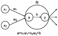
fig. 20 is a diagram illustrating a configuration example of a semiconductor device;
fig. 21 is a diagram illustrating a configuration example of a memory cell;
fig. 22 is a diagram illustrating a configuration example of a bias circuit;
fig. 23 is a timing chart illustrating the operation of the semiconductor device;
fig. 24A to 24F are diagrams illustrating an electronic apparatus.
Detailed Description
The embodiments will be described in detail with reference to the accompanying drawings. Note that the present invention is not limited to the following description, and those skilled in the art can easily understand that the form and details thereof can be changed into various forms without departing from the spirit and scope of the present invention. Therefore, the present invention should not be construed as being limited to the description of the embodiments shown below. Note that in the structure of the invention described below, the same reference numerals are used in common in different drawings to denote the same portions or portions having the same functions, and a repetitive description thereof will be omitted. Note that the hatching of the same constituent elements is sometimes omitted or changed as appropriate in different drawings.
(embodiment mode 1)
In this embodiment, a display device according to an embodiment of the present invention is described with reference to the drawings.
One embodiment of the present invention is a display device having a function of adding correction data to image data. Each pixel is provided with a storage node that holds desired correction data. The correction data is generated by an external device and written in each pixel.
The correction data is added to the image data by capacitive coupling, and the resulting data is supplied to the display element. Accordingly, the display element can display the corrected image. This correction allows up-conversion of an image or the like, or correction of image quality that is degraded by variations in characteristics of transistors included in pixels.
Fig. 1 is a diagram illustrating a pixel 11a which can be used in a display device according to an embodiment of the present invention. The pixel 11a includes a transistor 101, a transistor 102, a transistor 103, a capacitor 104, a capacitor 105, and a liquid crystal element 106.
One of a source and a drain of the transistor 101 is electrically connected to one electrode of the capacitor 104. The other electrode of the capacitor 104 is electrically connected to one of the source and the drain of the transistor 102. One of a source and a drain of the transistor 102 is electrically connected to one of a source and a drain of the transistor 103. The other of the source and the drain of the transistor 103 is electrically connected to one electrode of the capacitor 105. One electrode of the capacitor 105 is electrically connected to one electrode of the liquid crystal element 106.
Here, a wiring to which the other electrode of the capacitor 104, one of the source and the drain of the transistor 102, and one of the source and the drain of the transistor 103 are connected is referred to as a node NM. A wiring connecting the other of the source and the drain of the transistor 103, one electrode of the capacitor 105, and one electrode of the liquid crystal element 106 is referred to as a node NA.
A gate of the transistor 101 is electrically connected to a wiring 122. A gate of the transistor 102 is electrically connected to a wiring 121. A gate of the transistor 103 is electrically connected to the wiring 126. The other of the source and the gate of the transistor 101 is electrically connected to a wiring 125. The other of the source and the gate of the transistor 102 is electrically connected to a wiring 124.
The other electrode of the capacitor 105 is electrically connected to the common wiring 132. The other electrode of the liquid crystal element 106 is electrically connected to a common wiring 133. Note that an arbitrary potential may be supplied to the common wirings 132, 133 and electrically connected to each other.
The wirings 121, 122, and 126 can function as signal lines for controlling the operation of the transistors. The wiring 125 may have a function as a signal line for supplying image data. The wiring 124 may have a function as a signal line for the node NM to write data.
The node NM is a storage node, and a signal supplied to the wiring 124 can be written to the node NM by turning on the transistor 102 and turning off the transistor 103. By using a transistor with extremely low off-state current as the transistor 102 and the transistor 103, the potential of the node NM can be held for a long time. As the transistor, for example, a transistor using a metal oxide for a channel formation region (hereinafter referred to as an OS transistor) can be used.
The OS transistor can be used for other transistors included in the pixel. The transistor included in the pixel may be a transistor including Si in a channel formation region (hereinafter referred to as a Si transistor), or may be both an OS transistor and a Si transistor. Examples of the Si transistor include a transistor containing amorphous silicon, a transistor containing crystalline silicon (typically, low-temperature polysilicon or single crystal silicon), and the like.
When a reflective liquid crystal element is used as a display element, a silicon substrate can be used, and a region where a Si transistor and an OS transistor overlap each other can be formed. Thus, even if the number of transistors is large, high pixel density can be achieved.
As a semiconductor material used for the OS transistor, a metal oxide having an energy gap of 2eV or more, preferably 2.5eV or more, and more preferably 3eV or more can be used. An oxide semiconductor containing indium or the like is typical, and for example, CAAC-OS or CAC-OS or the like mentioned later can be used. CAAC-OS is suitable for transistors where the atoms constituting the crystal are stable and reliability is important. The CAC-OS exhibits high mobility characteristics and is suitable for a transistor or the like which performs high-speed driving.
The OS transistor has a large energy gap and exhibits an extremely low off-state current characteristic. Unlike the Si transistor, the OS transistor does not cause impact ionization, avalanche breakdown, short channel effect, or the like, and thus can form a highly reliable circuit. In addition, variations in electrical characteristics due to non-uniformity in crystallinity caused by Si transistors are not easily generated in OS transistors.
As the semiconductor layer In the OS transistor, for example, a film represented by "In-M-Zn based oxide" containing indium, zinc, and M (a metal such as aluminum, titanium, gallium, germanium, yttrium, zirconium, lanthanum, cerium, tin, neodymium, or hafnium) can be used.
When the oxide semiconductor constituting the semiconductor layer is an In-M-Zn based oxide, the atomic ratio of the metal elements of the sputtering target for forming the In-M-Zn oxide film preferably satisfies in.gtoreq.M and Zn.gtoreq.M. The atomic ratio of the metal elements In the sputtering target is preferably In: M: Zn 1:1:1, In: M: Zn 1:1.2, In: M: Zn 3:1:2, In: M: Zn 4:2:3, In: M: Zn 4:2:4.1, In: M: Zn 5:1:6, In: M: Zn 5:1:7, In: M: Zn 5:1:8, and the like. Note that the atomic ratio of the metal element included in the formed semiconductor layer may vary within a range of ± 40% of the atomic ratio of the metal element in the sputtering target.
As the semiconductor layer, an oxide semiconductor having a low carrier density can be used. For example, a semiconductor layer having a carrier density of 1 × 10 can be used17/cm3Hereinafter, it is preferably 1 × 10¹⁵/cm3Hereinafter, more preferably 1 × 10¹³/cm3Hereinafter, more preferably 1 × 10¹¹/cm3Hereinafter, more preferably less than 1 × 10¹⁰/cm3,1×10-9/cm3The oxide semiconductor described above. Such an oxide semiconductor is referred to as an oxide semiconductor which is intrinsic to high purity or substantially intrinsic to high purity. This oxide semiconductor has a low defect level density and thus can be said to be an oxide semiconductor having stable characteristics.
Note that the present invention is not limited to the above description, and a material having an appropriate composition may be used in accordance with the semiconductor characteristics and the electrical characteristics (field effect mobility, threshold voltage, and the like) of a transistor which are required. In addition, it is preferable to appropriately set the carrier density, the impurity concentration, the defect density, the atomic ratio of the metal element to oxygen, the interatomic distance, the density, and the like of the semiconductor layer so as to obtain desired semiconductor characteristics of the transistor.
When the oxide semiconductor constituting the semiconductor layer contains silicon or carbon which is one of group 14 elements, oxygen defects increase, and the semiconductor layer is changed to an n-type. Thus, it is possible to provideThe concentration of silicon or carbon in the semiconductor layer (concentration measured by secondary ion mass spectrometry) was set to 2X 10¹⁸atoms/cm3Hereinafter, 2 × 10 is preferable17atoms/cm3The following.
In addition, when an alkali metal or an alkaline earth metal is bonded to an oxide semiconductor, carriers are generated, and an off-state current of a transistor may increase. Therefore, the concentration of the alkali metal or alkaline earth metal (concentration measured by secondary ion mass spectrometry) of the semiconductor layer was set to 1 × 10¹⁸atoms/cm3Hereinafter, 2 × 10 is preferable16atoms/cm3The following.
When the oxide semiconductor constituting the semiconductor layer contains nitrogen, electrons as carriers are generated, and the carrier density increases, so that n-type conversion is facilitated. As a result, a transistor including an oxide semiconductor containing nitrogen is likely to have normally-on characteristics. Therefore, the nitrogen concentration (concentration measured by secondary ion mass spectrometry) of the semiconductor layer is preferably 5 × 10¹⁸atoms/cm3The following.
The semiconductor layer may have a non-single crystal structure. The non-single crystal structure includes, for example, a CAAC-OS (C-Axis Aligned Crystalline Oxide Semiconductor) having a crystal with a C-Axis orientation, a polycrystalline structure, a microcrystalline structure, or an amorphous structure. In the non-single crystalline structure, the defect state density is highest in the amorphous structure, and is lowest in the CAAC-OS.
The oxide semiconductor film having an amorphous structure has, for example, disordered atomic arrangement and has no crystalline component. Alternatively, the oxide film having an amorphous structure has, for example, a completely amorphous structure and does not have a crystal portion.
The semiconductor layer may be a mixed film of two or more kinds selected from a region having an amorphous structure, a region having a microcrystalline structure, a region having a polycrystalline structure, a region having CAAC-OS, and a region having a single crystal structure. The hybrid film sometimes has, for example, a single-layer structure or a laminated structure including two or more of the above-described regions.
The structure of CAC (Cloud-Aligned Composite) -OS, which is one embodiment of a non-single crystal semiconductor layer, will be described below.
The CAC-OS is, for example, a structure in which elements contained in an oxide semiconductor are unevenly distributed, and the size of a material containing the unevenly distributed elements is 0.5nm or more and 10nm or less, preferably 1nm or more and 2nm or less or an approximate size. Note that a state in which one or more metal elements are unevenly distributed in the oxide semiconductor and a region including the metal elements is mixed in a size of 0.5nm or more and 10nm or less, preferably 1nm or more and 2nm or less, or approximately, is also referred to as a mosaic (mosaic) shape or a patch (patch) shape in the following.
The oxide semiconductor preferably contains at least indium. In particular, indium and zinc are preferably contained. In addition, one or more selected from aluminum, gallium, yttrium, copper, vanadium, beryllium, boron, silicon, titanium, iron, nickel, germanium, zirconium, molybdenum, lanthanum, cerium, neodymium, hafnium, tantalum, tungsten, magnesium, and the like may be contained.
For example, CAC-OS among In-Ga-Zn oxides (In CAC-OS, In-Ga-Zn oxide may be particularly referred to as CAC-IGZO) means that the material is divided into indium oxide (hereinafter, referred to as InO)X1(X1 is a real number greater than 0)) or indium zinc oxide (hereinafter, referred to as In)X2ZnY2OZ2(X2, Y2, and Z2 are real numbers greater than 0)) and gallium oxide (hereinafter referred to as GaO)X3(X3 is a real number greater than 0)) or gallium zinc oxide (hereinafter referred to as GaX4ZnY4OZ4(X4, Y4, and Z4 are real numbers greater than 0)), and the like, and the mosaic-shaped InOX1Or InX2ZnY2OZ2A structure uniformly distributed in the film (hereinafter, also referred to as a cloud).
In other words, the CAC-OS is of GaOX3A region containing as a main component InX2ZnY2OZ2Or InOX1A composite oxide semiconductor having a structure in which regions that are main components are mixed together. In this specification, for example, when the atomic number ratio of In to the element M In the first region is larger than the atomic number ratio of In to the element M In the second region, the In concentration In the first region is higher than that In the second region.
Note that IGZO is a generic term, and may be a compound containing In, Ga, Zn, and O.A typical example is InGaO3(ZnO)m1(m1 is a natural number) or In(1+x0)Ga(1-x0)O3(ZnO)m0A crystalline compound represented by (-1. ltoreq. x 0. ltoreq.1, m0 is an arbitrary number).
The crystalline compound has a single crystal structure, a polycrystalline structure, or a CAAC structure. The CAAC structure is a crystal structure in which a plurality of IGZO nanocrystals have c-axis orientation and are connected in a non-oriented manner on the a-b plane.
On the other hand, CAC-OS is related to the material composition of an oxide semiconductor. CAC-OS refers to the following composition: in the material composition containing In, Ga, Zn, and O, some of the nanoparticle-like regions containing Ga as a main component and some of the nanoparticle-like regions containing In as a main component were observed to be irregularly dispersed In a mosaic shape. Therefore, in CAC-OS, the crystal structure is a secondary factor.
The CAC-OS does not contain a laminate structure of two or more films different in composition. For example, a structure composed of two layers of a film containing In as a main component and a film containing Ga as a main component is not included.
Note that GaO is sometimes not observedX3A region containing as a main component InX2ZnY2OZ2Or InOX1Is a well-defined boundary between regions of major composition.
In the case where the CAC-OS contains one or more selected from aluminum, yttrium, copper, vanadium, beryllium, boron, silicon, titanium, iron, nickel, germanium, zirconium, molybdenum, lanthanum, cerium, neodymium, hafnium, tantalum, tungsten, magnesium, and the like in place of gallium, the CAC-OS means a constitution as follows: some of the nano-particle-like regions containing the element as a main component were observed and some of the nano-particle-like regions containing In as a main component were observed to be irregularly dispersed In a mosaic shape.
The CAC-OS can be formed by, for example, sputtering without intentionally heating the substrate. In the case of forming the CAC-OS by the sputtering method, as the film forming gas, one or more selected from an inert gas (typically argon), an oxygen gas, and a nitrogen gas may be used. The lower the flow ratio of the oxygen gas in the total flow of the film forming gas at the time of film formation, the better, for example, the flow ratio of the oxygen gas is set to 0% or more and less than 30%, preferably 0% or more and 10% or less.
The CAC-OS has the following characteristics: no clear peak was observed when measured by theta/2 theta scanning according to the out-of-plane method, which is one of X-ray diffraction (XRD) measurements. That is, it was found from the X-ray diffraction that the orientation in the a-b plane direction and the c-axis direction was not present in the measurement region.
In addition, in the electron diffraction pattern of CAC-OS obtained by irradiating an electron beam (also referred to as a nanobeam) having a beam diameter of 1nm, an annular region having high brightness and a plurality of bright spots in the annular region were observed. From this, it is known that the crystal structure of the CAC-OS has an nc (nano-crystal) structure having no orientation in the plane direction and the cross-sectional direction, from the electron diffraction pattern.
In addition, for example, In the CAC-OS of In-Ga-Zn oxide, it was confirmed that, based on an EDX plane analysis image obtained by Energy Dispersive X-ray spectrometry (EDX: Energy Dispersive X-ray spectroscopy): with GaOX3A region containing as a main component and InX2ZnY2OZ2Or InOX1The main component region is unevenly distributed and mixed.
The CAC-OS has a structure different from that of an IGZO compound in which metal elements are uniformly distributed, and has properties different from those of the IGZO compound. In other words, CAC-OS has a GaOX3Etc. as main component and InX2ZnY2OZ2Or InOX1The regions having the main components are separated from each other, and the regions having the elements as the main components are formed in a mosaic shape.
In here, InX2ZnY2OZ2Or InOX1The conductivity of the region having the main component is higher than that of GaOX3Etc. as the main component. In other words, when carriers flow InX2ZnY2OZ2Or InOX1The region containing the main component exhibits conductivity of the oxide semiconductor. Therefore, when In is usedX2ZnY2OZ2Or InOX1When the region as a main component is distributed in a cloud shape in the oxide semiconductor, high field-effect mobility (μ) can be achieved.
On the other hand, with GaOX3The insulating property of the region containing the above-mentioned component is higher than that of InX2ZnY2OZ2Or InOX1Is the region of the main component. In other words, when GaO is usedX3When the region containing the main component is distributed in the oxide semiconductor, leakage current can be suppressed, and a good switching operation can be achieved.
Therefore, when CAC-OS is used for the semiconductor element, the heat radiation is caused by GaOX3Insulation property of the like and the cause of InX2ZnY2OZ2Or InOX1Can realize high-current (I)on) And high field effect mobility (μ).
In addition, the semiconductor element using the CAC-OS has high reliability. Therefore, CAC-OS is suitable for constituent materials of various semiconductor devices.
In the pixel 11a, the correction data written to the node NM may be capacitively coupled with the image data supplied from the wiring 125, and the resultant data may be output to the node NA. The transistor 101 may have a function of selecting a pixel to supply image data. The transistor 103 may have a function as a switch for controlling the operation of the liquid crystal element 106.
For example, when a signal written to the node NM from the wiring 124 is larger than the threshold voltage of the transistor 102, the transistor 102 is turned on before image data is written, and the liquid crystal element 106 operates. Therefore, it is preferable that the transistor 103 is provided, and after the potential of the node NM is fixed, the transistor 103 is turned on to operate the liquid crystal element 106.
That is, the correction data may be appended to the supplied image data as long as the desired correction data is stored to the node NM. Note that since factors on the transmission path sometimes correct data to be attenuated, it is preferable to generate correction data in consideration of the attenuation.
The operation of the pixel 11a will be described in detail with reference to timing charts shown in fig. 2A and 2B. As the correction data (Vp) supplied to the wiring 124, either a positive signal or a negative signal may be used, and here, a case where a positive signal is supplied will be described. In the following description, "H" represents a high potential, and "L" represents a low potential.
First, an operation of writing correction data (Vp) to the node NM is described with reference to fig. 2A. In the case where the above-described image data correction such as conversion is aimed, it is preferable to perform this operation for each frame.
Note that, here, detailed changes due to the structure, operation timing, and the like of the circuit are not considered in the distribution, coupling, or loss of the potential. The potential change due to the capacitive coupling depends on the capacity ratio between the supply side and the supplied side, but for the sake of convenience of explanation, it is assumed that the capacitance values of the node NM and the node NA are sufficiently small.
At time T1, when the potential of the wiring 121 is "H", the potential of the wiring 122 is "L", the potential of the wiring 125 is "L", and the potential of the wiring 126 is "H", the transistor 102 and the transistor 103 are turned on, and the potential of the node NA is set to the potential of the wiring 124. At this time, the operation of the liquid crystal element 106 can be reset by changing the potential of the wiring 124 to a reset potential (for example, a standard potential such as 0V).
Note that the display operation of the liquid crystal element 106 of the previous frame is performed before time T1.
At time T2, when the potential of the wiring 121, the potential of the wiring 122, the potential of the wiring 125, and the potential of the wiring 126 are set to "L", the transistor 101 is turned on, and the potential of the other electrode of the capacitor 104 is set to "L". This operation is a reset operation performed before capacitive coupling.
At time T3, when the potential of the wiring 121 is "H", the potential of the wiring 122 is "H", the potential of the wiring 125 is "L", and the potential of the wiring 126 is "L", the transistor 102 is turned on, and the potential of the wiring 124 (correction data (Vp)) is written to the node NM. Note that the potential of the wiring 124 is preferably fixed to a desired value (correction data (Vp)) after the time T2 and before the time T3.
At time T4, when the potential of the wiring 121 is "L", the potential of the wiring 122 is "H", the potential of the wiring 125 is "L", and the potential of the wiring 126 is "L", the transistor 102 is turned off, and the correction data (Vp) is held at the node NM.
At time T5, when the potential of the wiring 121, the potential of the wiring 122, the potential of the wiring 125, and the potential of the wiring 126 are set to "L", the transistor 101 is turned off, and the writing operation of the correction data (Vp) is completed.
Next, an operation of correcting the image data (Vs) and an operation of displaying the liquid crystal element 106 will be described with reference to fig. 2B.
At time T11, when the potential of the wiring 121, the potential of the wiring 122, the potential of the wiring 124, and the potential of the wiring 126 are set to "L", and "H", the transistor 103 is turned on, and the potential of the node NM is distributed to the node NA. Note that the correction data (Vp) held in the node NM is preferably set in consideration of the potential distributed to the node NA.
At time T12, when the potential of the wiring 121 is "L", the potential of the wiring 122 is "H", the potential of the wiring 124 is "L", and the potential of the wiring 126 is "H", the transistor 101 is turned on, and the potential of the wiring 125 is added to the potential of the node NA by capacitive coupling of the capacitor 104. That is, the potential of the node NA becomes the potential (Vs + Vp)' of the correction data (Vp) distributed to the image data (Vs). Note that the potential (Vs + Vp)' also includes potential variation due to capacitive coupling between wirings, and the like.
At time T13, when the potential of the wiring 121 is "L", the potential of the wiring 122 is "L", the potential of the wiring 124 is "L", and the potential of the wiring 126 is "H", the transistor 101 is turned off, and the potential (Vs + Vp)' is held at the node NA. Then, the liquid crystal element 106 performs a display operation based on the potential.
The above description is made of the correction operation of the image data (Vs) and the display operation of the liquid crystal element 106. Note that, although the previously described writing operation of the correction data (Vp) and the inputting operation of the image data (Vs) may be performed at the same time, it is preferable that the writing operation of the correction data (Vp) is performed on all the pixels before the inputting operation of the image data (Vs) is performed. In one embodiment of the present invention, since the same image data can be supplied to a plurality of pixels at the same time, the operation speed is increased by writing the correction data (Vp) to all the pixels first, and details will be described later.
Note that when an operation such as up-conversion is not performed, a display operation of the liquid crystal element 106 can be performed by supplying image data to the wiring 124 and controlling on/off of the transistors 102 and 103. At this time, the transistor 101 is often in a non-conductive state.
The structure and operation of the pixels 11a described above are advantageous for image up-conversion. Up-conversion using the pixel 11a is explained with reference to fig. 3A and 3B.
For example, the number of pixels of the 8K4K display device is 4 times the number of pixels (3840 × 2160) of the 4K2K display device. That is, when image data displayed by one pixel of the 4K2K display device is displayed with the 8K4K display device, four pixels in the lateral and longitudinal directions of the 8K4K display device will display the same image data.
Fig. 3A shows an image with or without upconversion. Fig. 3A shows a state in which an original image (image data S1) is displayed on one pixel of a 4K2K display device, a state in which image data S1 is displayed on four pixels of an 8K4K display device without up-conversion, and a state in which image data S0 to S2 are displayed on four pixels of an 8K4K display device with up-conversion, when viewed sequentially from the left side.
As shown in fig. 3A, the image data S1 is displayed for all the first four pixels after the up-conversion, and the image data S0 to S2 are displayed for each pixel after the up-conversion, which contributes to the improvement of the resolution.
Fig. 3B illustrates the up-conversion operation in the pixel 11 a. In the pixel 11a, arbitrary correction data can be added to the image data as described above. Thus, the original image data S1 is supplied to each pixel as it is.
Further, W1 to W3 are supplied to each pixel as correction data. Here, the method of producing W1 to W3 is not particularly limited. The correction data may be generated in real time by an external device, or may be generated by reading the correction data stored in the recording medium and synchronizing it with the image data S1.
By performing the operation of the pixel 11a described above, each correction data is added to each image data, thereby generating new image data S0 to S2. Thereby, an image in which the original image data is up-converted can be displayed.
The conventional up-conversion using external correction is performed by generating new image data, and therefore, a burden on an external device is large. However, in the above-described aspect of the present invention, new image data is generated in the pixels to which the correction data is supplied, instead of changing the supplied image data, so that the load on the external device can be reduced. Further, new image data can be generated in a small number of steps in a pixel, and this can be performed even in a display device having a large number of pixels and a short horizontal period.
In addition, the pixel according to one embodiment of the present invention may have the structure of the pixel 11b shown in fig. 4A. The pixel 11b has a structure of the pixel 11a in which the transistor 103 and the wiring 126 are omitted.
The transistor 103 in the pixel 11a is a switch for avoiding the liquid crystal element 106 from being operated accidentally due to the supply of the correction data (Vp), and the transistor 103 may be omitted if the liquid crystal element 106 is operated but the operation thereof is not seen. For example, the backlight may be turned off while supplying the correction data (Vp).
The capacitor 105 may be omitted as in the pixel 11B' shown in fig. 4B. As described above, an OS transistor may be used as the transistor connected to the node NM. Since the leakage current of the OS transistor is extremely small, image data can be held for a long time even if the capacitor 105 used as a holding capacitance is omitted.
This configuration is effective even when the frame frequency is high and the retention period of image data is short, such as in field sequential driving. By omitting the capacitor 105, the aperture ratio can be improved. Further, the transmittance of the image can be improved. Note that a structure in which the capacitor 105 is omitted may be used for the structures of other pixel circuits shown in this specification.
The correction operation of the image data (Vs) and the display operation of the liquid crystal element 106 are described with reference to fig. 4C and 4D.
At time T1, when the potential of the wiring 121 is "H", the potential of the wiring 122 is "L", the potential of the wiring 124 is "L", and the potential of the wiring 125 is "L", the transistor 102 is turned on, and the potential of the node NA is set to the potential of the wiring 124. At this time, by changing the potential of the wiring 124 to a reset potential (for example, "L"), the operation of the liquid crystal element 106 can be reset.
Note that the display operation of the liquid crystal element 106 of the previous frame is performed before time T1.
At time T2, when the potential of the wiring 121 is "L", the potential of the wiring 122 is "H", the potential of the wiring 124 is "Vp", and the potential of the wiring 125 is "L", the transistor 101 is turned on, and the potential of the other electrode of the capacitor 104 is "L". This operation is a reset operation performed before capacitive coupling.
At time T3, the potential of the wiring 124 (correction data (Vp)) is written into the node NA by setting the potential of the wiring 121 to "H", the potential of the wiring 122 to "H", the potential of the wiring 124 to "Vp", and the potential of the wiring 125 to "L".
At time T4, when the potential of the wiring 121 is "L", the potential of the wiring 122 is "H", the potential of the wiring 124 is "Vp", and the potential of the wiring 125 is "L", the transistor 102 is turned off, and the correction data (Vp) is held at the node NA.
At time T5, when the potential of the wiring 121, the potential of the wiring 122, and the potential of the wiring 125 are set to "L", the transistor 101 is turned off, and the writing operation of the correction data (Vp) is ended.
Next, the operation of correcting the image data (Vs) and the operation of displaying the liquid crystal element 106 will be described. Note that a desired potential is supplied to the wiring 125 at an appropriate timing.
At time T11, when the potential of the wiring 121 is "L", the potential of the wiring 122 is "H", and the potential of the wiring 124 is "L", the transistor 101 is turned on, and the potential of the wiring 125 is added to the potential of the node NA by capacitive coupling of the capacitor 104. That is, the node NA becomes the potential (Vs + Vp)' of the image data (Vs) plus the correction data (Vp). Note that the potential (Vs + Vp)' also includes potential variation due to capacitive coupling between wirings, and the like.
At time T12, when the potential of the wiring 121, the potential of the wiring 122, and the potential of the wiring 124 are set to "L", the transistor 101 is turned off, and the potential (Vs + Vp)' is held at the node NA. Then, the liquid crystal element 106 performs a display operation based on the potential.
In addition, the pixel 11c shown in fig. 5A may be used as a pixel according to an embodiment of the present invention. The pixel 11c has a structure of the pixel 11a to which the transistor 107 and the wiring 130 are added.
In the pixel 11c, by supplying a reset potential to the wiring 130, the transistor 107 is turned on, whereby a reset operation of the liquid crystal element 106 can be performed. With this configuration, the writing operation of the potentials at the node NM and the node NA can be controlled independently, and the display operation period of the liquid crystal element 106 can be extended.
When the image correction operation is not performed, the display operation of the liquid crystal element 106 can be performed by supplying image data from the wiring 130 and controlling on/off of the transistor 107. At this time, the transistor 103 is often in a non-conductive state.
In addition, a pixel according to an embodiment of the present invention may have the structure of the pixel 11d shown in fig. 5B. The pixel 11d has a structure in which a back gate is provided in each transistor. The back gate is electrically connected with the front gate to improve the on-state current. In addition, a constant potential different from that of the front gate may be provided to the back gate. By adopting this structure, the threshold voltage of the transistor can be controlled. Although a structure in which a back gate is provided in all the transistors is shown in fig. 5B, a transistor in which a back gate is not provided may be included. Note that a structure in which a transistor has a back gate may be used for another pixel circuit in this embodiment mode.
In order to prevent burn-in, it is preferable to perform ac driving in which the polarity of each frame is inverted on the liquid crystal element 106 used in the display device according to one embodiment of the present invention. For example, when the same image is displayed between successive frames, the operations shown in table 1 or table 2 are performed. Note that a and b in the table denote fixed potentials.
Table 1 shows an example of an operation using a signal having a positive polarity in the nth frame (N is an integer of 1 or more). In the N +1 th frame, an operation using a signal of negative polarity represented by the pattern A, B or C is performed, and the correction data (Vp) and/or the image data (Vs) are adjusted and supplied so that the absolute values of the potential at the N th frame and the node NA are equal to each other. Table 2 shows an example of an operation using a negative signal in the nth frame, and an operation is performed so that the absolute values of the potentials of the nth frame and the node NA are equal to each other in the N +1 th frame. Note that in this operation, the common potential is fixed.
Note that the image data (Vs) is adjusted when operating in mode B, and therefore a still image or the like can be displayed without rewriting the correction data (Vp) between frames.
[ Table 1]

[ Table 2]

Fig. 6A to 6C are block diagrams of a display device which can use the pixel 11a, the pixel 11b, or the pixel 11C. The following describes each display device. Note that description of the same constituent elements overlapping between the drawings is omitted.
Fig. 6A shows an example of a display device including a pixel array in which pixels 11 are arranged in a matrix, a row driver 12, a column driver 13, a circuit 14, and a circuit 15. The wirings 121, 122, and 126 and the like are electrically connected to the row driver 12. The wirings 124 and 125 and the like are electrically connected to the column driver 13. As the pixel 11, either the pixel 11a or the pixel 11b can be used.
For example, a shift register circuit can be used as the row driver 12 and the column driver 13. The circuit 14 has a function of generating correction data. The circuit 14 may also be referred to as an external device for generating correction data. Further, the circuit 15 can supply a reset potential Sr for resetting the operation of the liquid crystal element 106 to the column driver 13.
The image data S1 described with reference to fig. 3A and 3B is input to the circuit 14, and the image data S1 and the generated correction data W are output to the column driver 13. Note that the image data S1 may not be input to the column driver 13 through the circuit 14.
In addition, the circuit 14 may have a neural network. For example, the highly accurate correction data W can be generated using a deep neural network that has learned with a large number of images as the supervised data.
Fig. 6B shows an example of a display device including a pixel array in which pixels 11c are arranged in a matrix, a row driver 12, a column driver 13, a circuit 14, and a circuit 15. The circuit 15 can supply the reset potential Sr to the wiring 130.
Fig. 6C shows an example of a display device including a pixel array in which pixels 11C are arranged in a matrix, a row driver 12, a column driver 13, a column driver 17, a circuit 14, and a circuit 15. The wiring 130 is electrically connected to the column driver 17.
As the column driver 17, for example, a register circuit can be used. The circuit 15 is capable of supplying a reset potential Sr to the column driver 17. In addition, when the image correction operation is not performed, the image data Sx may be supplied to the column driver 17 to perform the display operation of the liquid crystal element 106.
Note that although fig. 6A to 6C illustrate a structure including the circuit 14 and the circuit 15, a structure in which one circuit has functions of both may be employed.
A display device according to one embodiment of the present invention can generate an up-converted image in a pixel as shown in fig. 3A and 3B. Thus, a plurality of pixels are supplied with the same image data of low resolution. In the example shown in fig. 3A and 3B, four pixels in the lateral and longitudinal directions are supplied with the same image data. In this case, the same image data can be supplied to the signal lines connected to the pixels, and the signal lines to which the same image data is supplied can be electrically connected to each other, whereby the image data can be written at high speed.
Fig. 7 shows a part of a pixel array of a display device capable of color display, in which signal lines supplying the same image data can be electrically connected to each other through a switch. In general, a pixel of a display device capable of color display includes a combination of sub-pixels that emit R (red) and G (green) and B (blue) colors, respectively. Fig. 7 shows four pixels in the lateral and longitudinal directions, each of which is composed of R, G, B three subpixels arranged in the lateral direction.
Here, as shown in fig. 3A and 3B, four pixels in the lateral and longitudinal directions are input with the same image data. In fig. 7, the same image data is input to the subpixels R1 to R4. For example, the same image data can be input to four subpixels by supplying the same image data to the wirings 125[1] and 125[4] serving as signal lines connected to the subpixels R1 to R4 and sequentially inputting signals to the wirings 122[1] and 122[2] serving as scanning lines. However, this method is not efficient.
In one embodiment of the present invention, two signal lines are turned on by a switch provided between the signal lines, and two scanning lines are turned on by a switch provided between the scanning lines, whereby writing can be performed simultaneously to four sub-pixels.
As shown in fig. 7, by turning on the switch 141 provided between the wirings 125[1] and 125[4], image data supplied to one of the wirings 125[1] or 125[4] can be written to the subpixel R1 and the subpixel R2 at the same time. In this case, writing to the subpixel R3 and the subpixel R4 can be performed simultaneously by turning on the switch 144 provided between the wiring 122[1] and the wiring 122[2 ]. That is, the writing of four sub-pixels can be performed simultaneously.
Similarly, by turning on the switch 142 provided between the wirings 125[2] and 125[5] and the switch 143 provided between the wirings 125[3] and 125[6] as necessary, writing to four sub-pixels can be performed simultaneously in the other four sub-pixels. The switches 141 to 144 may use transistors, for example.
Writing data of four sub-pixels simultaneously can shorten the writing time and increase the frame frequency.
Next, simulation results of the pixel 11a shown in fig. 1 and the pixel 11b shown in fig. 4A are described. Common parameters are as follows. The transistor sizes are all 4 μm/4 μm in L/W, the capacitance value of the capacitor 104 is 100fF, the capacitance value of the capacitor 105 is 50fF, the capacitance value of the liquid crystal element 106 is 20fF, and the potentials of the common wirings 132 and 133 are both 0V. Note that SPICE was used as the circuit simulation software.
Fig. 8A to 8C are diagrams illustrating simulated operating parameters of the pixel 11 a. The vertical axis represents the potential of each wiring, and the horizontal axis represents the timing corresponding to the timing charts of fig. 2A and 2B.
Fig. 8A shows the potential of the wiring connected to the gate of the transistor, and the operation from time T2 to time T5 corresponds to the writing operation of the correction data (Vp). The operation from time T11 to time T13 corresponds to the operation of adding the image data (Vs) to the correction data (Vp).
Fig. 8B shows the potential of the wiring 124 that supplies correction data (Vp), where Vp is 8V. Note that the correction data (Vp) may be supplied to the wiring 124 between times T2 and T5.
Fig. 8C shows the potential of the wiring 125 supplying the image data (Vs), where the condition that the voltage changes every 1V from 1V to 8V is used. Note that, at the time of writing the correction data (Vp), 1V is supplied to the wiring 125 as the potential "L".
Fig. 8D is a simulation result showing the potential change of the node NA when the above-described operating parameters are used. The potential shown after the time T13 is the potential supplied to the node NA, which indicates that the potential is higher than the potential of the image data (Vs). However, as described above, the potential of the node NA may not be a desired potential because of the influence of a potential drop when the correction data (Vp) of the node NM is distributed to the node NA, a capacitance ratio at the time of capacitive coupling, a capacitance between wirings, and the like.
Fig. 9A shows a relationship between the potential of the image data (Vs) and the potential of the node NA when the above-described parameters are used, a circle (○) shows a simulation result when 8V is input as the correction data (Vp), note that Vref (the potential of the wiring 125 at the time of writing) is 1V, and Vp-Vref ═ 7V is satisfied, a triangle (△) shows a simulation result when the correction data (Vp) is directly written to the node NA, as shown in fig. 9A, there is a large difference between these potentials, and in a case where there is a limitation on design or operating conditions, sufficient correction may not be able to be performed.
In view of the results of fig. 9A, fig. 9B shows simulation results when the following tests are performed: whether or not the difference can be reduced by adding a potential corresponding to the loss to the correction data (Vp) in advance. When the above parameters are used, the potential of the node NA can be set to a desired value by adding a potential of +5.6V to the correction data (Vp).
Fig. 9C shows the simulation result when the capacitance value of the capacitor 104 is changed from 100fF to 300fF for the same purpose. Although there is a large difference in the potential of the image data (Vs) when it is low, the potential of the node NA can be made to be substantially a desired value.
As can be seen from this, by setting the correction data (Vp) or the capacitance value of the capacitor 104 to an appropriate value, the potential of the node NA can be made to be a desired value.
Fig. 10A to 10C are diagrams illustrating simulated operating parameters of the pixel 11 b. The vertical axis represents the potential of each wiring, and the horizontal axis represents the timing corresponding to the timing charts of fig. 4C and 4D. Since the transistor 103 is omitted in the pixel 11b, a signal of the wiring 126 is not illustrated in fig. 10A. Fig. 10B and 10C are the same as fig. 8B and 8C.
Fig. 10D is a simulation result showing a potential change of the node NA when the above-described operating parameters are used. Fig. 11 shows the relationship between the image data (Vs) and the node NA when the above-described parameters are used. The pixel 11b is not affected by the potential drop due to the distribution of the correction data (Vp), and therefore, the addition of the correction data (Vp) is not required. In addition, since the capacitance value of the capacitor 104 can be reduced, the degree of freedom of design can be improved.
A display device according to one embodiment of the present invention may have a pixel 11e structure shown in fig. 12A. The pixel 11e has a structure in which a transistor 112 is added to the pixel 11c shown in fig. 5A. As the transistor 112, an OS transistor can be used, for example, as in the case of other transistors.
A gate of the transistor 112 is electrically connected to one of a source and a drain of the transistor 102 and the other electrode of the capacitor 104. One of a source and a drain of the transistor 112 is electrically connected to one of a source and a drain of the transistor 103. The other of the source and the gate of the transistor 112 is electrically connected to a power supply line 131 (high potential).
In the pixel 11e, a wiring to which the other electrode of the capacitor 104, one of the source and the drain of the transistor 102, and the gate of the transistor 112 are connected is referred to as a node NM.
The wiring 130 electrically connected to the pixel 11e may have a function of supplying a signal line at a constant potential (low potential) for resetting image data. The wiring 124 may have a function as a signal line for writing data to the node NM.
In the pixel 11e, data written to the node NM may be capacitively coupled with image data supplied from the wiring 125, and the resultant data may be output to the node NA.
That is, the correction data may be appended to the supplied image data as long as the desired correction data is stored to the node NM. Note that since factors on the transmission path sometimes correct data to be attenuated, it is preferable to generate correction data in consideration of the attenuation.
The operation of the pixel 11e will be described in detail with reference to timing charts shown in fig. 12B and 12C. As the correction data (Vp) supplied to the wiring 124, either a positive signal or a negative signal may be used, and here, a case where a positive signal is supplied will be described. The wiring 130 is supplied with a reset potential (low potential). In the following description, "H" represents a high potential, and "L" represents a low potential.
First, an operation of writing correction data (Vp) to the node NM is described with reference to fig. 12B. In the case of image correction, it is generally preferable to perform this operation for each frame.
At time T1, when the potential of the wiring 121, the potential of the wiring 122, the potential of the wiring 125, and the potential of the wiring 126 are set to "L", the transistor 101 is turned on, and the potential of one electrode of the capacitor 104 is set to "L". This operation is a reset operation performed before capacitive coupling.
At time T2, when the potential of the wiring 121 is "H", the potential of the wiring 122 is "H", the potential of the wiring 125 is "L", and the potential of the wiring 126 is "L", the transistor 102 is turned on, and the potential of the wiring 124 (correction data (Vp)) is written to the node NM.
Although the display operation of the liquid crystal element 106 in the previous frame is performed before the time T2, the potential of the node NA becomes the reset potential by turning on the transistor 107, and the display operation of the liquid crystal element 106 is reset.
At time T3, when the potential of the wiring 121 is "L", the potential of the wiring 122 is "H", the potential of the wiring 125 is "L", and the potential of the wiring 126 is "L", the transistor 102 is turned off, and the correction data (Vp) is held at the node NM.
At time T4, when the potential of the wiring 121, the potential of the wiring 122, the potential of the wiring 125, and the potential of the wiring 126 are set to "L", the transistor 101 is turned off, and the writing operation of the correction data (Vp) is completed.
Next, an operation of correcting the image data (Vs) and an operation of displaying the liquid crystal element 106 will be described with reference to fig. 12C.
At time T11, when the potential of the wiring 121 is "L", the potential of the wiring 122 is "H", the potential of the wiring 124 is "L", and the potential of the wiring 126 is "L", the transistor 101 is turned on, and the potential of the wiring 125 is added to the potential of the node NM by capacitive coupling of the capacitor 104. That is, the node NM becomes the potential (Vs + Vp) of the image data (Vs) plus the correction data (Vp).
At time T12, when the potential of the wiring 121, the potential of the wiring 122, the potential of the wiring 124, and the potential of the wiring 126 are set to "L", the transistor 101 is turned off, and the potential of the node NM is fixed to Vs + Vp.
At time T13, when the potential of the wiring 121 is "L", the potential of the wiring 122 is "L", the potential of the wiring 124 is "L", and the potential of the wiring 126 is "H", the transistor 103 is turned on, the potential of the node NA is Vs + Vp, and the liquid crystal element 106 performs a display operation. Strictly speaking, the potential of the node NA corresponds to Vs + Vp minus the threshold voltage (V) of the transistor 112th) Here, VthIs a negligible minimum.
The above description is made of the correction operation of the image data (Vs) and the display operation of the liquid crystal element 106. Note that, although the writing operation of the correction data (Vp) and the input operation of the image data (Vs) described above may be performed continuously, it is preferable that the writing operation of the correction data (Vp) is performed on all pixels before the input operation of the image data (Vs) is performed. As described above, in one embodiment of the present invention, since the same image data can be supplied to a plurality of pixels at the same time, the operation speed is increased by writing the correction data (Vp) to all the pixels first.
This embodiment can be implemented in combination with the structures described in other embodiments and the like as appropriate.
(embodiment mode 2)
In this embodiment, a configuration example of a display device using a liquid crystal element will be described. Note that in this embodiment, the operation and function related to the correction described in embodiment 1 are omitted.
Fig. 13A to 13C show a structure of a display device which can be used in one embodiment of the present invention.
In fig. 13A, a sealant 4005 is provided so as to surround a display portion 215 provided over a first substrate 4001, and the display portion 215 is sealed by the sealant 4005 and a second substrate 4006.
The display portion 215 is provided with a pixel array including the pixels described in embodiment 1.
In fig. 13A, the scanning line driver circuit 221a, the signal line driver circuit 231a, the signal line driver circuit 232a, and the common line driver circuit 241a each include a plurality of integrated circuits 4042 provided on a printed circuit board 4041. The integrated circuit 4042 is formed of a single crystal semiconductor or a polycrystalline semiconductor. The signal line driver circuit 231a and the signal line driver circuit 232a function as the column driver described in embodiment 1. The scanning line driver circuit 221a functions as the row driver described in embodiment 1. The common line driver circuit 241a has a function of supplying a predetermined potential to the common line shown in embodiment 1.
Various signals and potentials are supplied to the scanning line driver circuit 221a, the common line driver circuit 241a, the signal line driver circuit 231a, and the signal line driver circuit 232a through an FPC (flexible printed circuit) 4018.
The integrated circuit 4042 included in the scanning line driver circuit 221a and the common line driver circuit 241a has a function of supplying a selection signal to the display portion 215. The integrated circuit 4042 included in the signal line driver circuit 231a and the signal line driver circuit 232a has a function of supplying image data to the display portion 215. An integrated circuit 4042 is mounted in a region different from a region surrounded by the sealant 4005 over the first substrate 4001.
Note that a connection method of the integrated circuit 4042 is not particularly limited, and a wire bonding method, a cog (chip On glass) method, a tcp (tape Carrier package) method, a cof (chip On film) method, or the like can be used.
Fig. 13B shows an example in which an integrated circuit 4042 included in the signal line driver circuit 231a and the signal line driver circuit 232a is mounted by the COG method. In addition, a system-on-panel (system-on-panel) can be formed by forming a part or the whole of the driver circuit over a substrate over which the display portion 215 is formed.
Fig. 13B shows an example in which the scanning line driver circuit 221a and the common line driver circuit 241a are formed over a substrate over which the display portion 215 is formed. By forming the driver circuit and the pixel circuit in the display portion 215 at the same time, the number of components can be reduced. Thereby, productivity can be improved.
In fig. 13B, a sealant 4005 is provided so as to surround the display portion 215, the scan line driver circuit 221a, and the common line driver circuit 241a provided over the first substrate 4001. The second substrate 4006 is provided over the display portion 215, the scan line driver circuit 221a, and the common line driver circuit 241 a. Thus, the display portion 215, the scan line driver circuit 221a, and the common line driver circuit 241a are sealed together with the display element by the first substrate 4001, the sealant 4005, and the second substrate 4006.
Although fig. 13B illustrates an example in which the signal line driver circuit 231a and the signal line driver circuit 232a are separately formed and mounted on the first substrate 4001, one embodiment of the present invention is not limited to this configuration, and a scan line driver circuit may be separately formed and mounted, or a part of the signal line driver circuit or a part of the scan line driver circuit may be separately formed and mounted. As shown in fig. 13C, the signal line driver circuit 231a and the signal line driver circuit 232a may be formed over a substrate over which the display portion 215 is formed.
Further, the display device may include a panel in which a display element is sealed, and a module in which an IC or the like including a controller is mounted on the panel.
The display portion and the scan line driver circuit which are provided over the first substrate include a plurality of transistors.
The transistors included in the peripheral driver circuit and the transistors included in the pixel circuit of the display portion may have the same structure or different structures. The transistors included in the peripheral driver circuit may all have the same structure, or two or more structures may be combined. Similarly, the transistors included in the pixel circuit may have the same structure, or two or more structures may be combined.
In addition, an input device 4200 may be provided over the second substrate 4006. The structure of providing the input device 4200 to the display device shown in fig. 13A and 13B can be used as a touch panel.
The sensing element (also referred to as a "sensing element") included in the touch panel according to one embodiment of the present invention is not particularly limited. Various sensors capable of detecting the approach or contact of a detection object such as a finger or a stylus pen can also be used as the sensing element.
For example, various types of sensors such as a capacitance type, a resistance film type, a surface acoustic wave type, an infrared type, an optical type, and a pressure-sensitive type can be used.
In this embodiment, a touch panel including a capacitance-type sensor element will be described as an example.
The capacitance type includes a surface type capacitance type, a projection type capacitance type, and the like. The projection type capacitance includes a self capacitance and a mutual capacitance. The use of mutual capacitance is preferred because multipoint sensing can be done simultaneously.
A touch panel according to one embodiment of the present invention can have various structures such as a structure in which a display device and a sensor element which are manufactured separately are bonded to each other, and a structure in which an electrode or the like constituting a sensor element is provided over one or both of a substrate supporting a display element and a counter substrate.
Fig. 14A and 14B illustrate an example of a touch panel. Fig. 14A is a perspective view of the touch panel 4210. Fig. 14B is a perspective view of the input device 4200. Note that only typical constituent elements are shown for clarity.
The touch screen 4210 has a structure in which a display device and a sensing element which are separately manufactured are attached.
The touch screen 4210 includes an input device 4200 and a display device which are disposed to overlap.
The input device 4200 includes a substrate 4263, an electrode 4227, an electrode 4228, a plurality of wirings 4237, a plurality of wirings 4238, and a plurality of wirings 4239. For example, the electrode 4227 may be electrically connected to the wiring 4237 or the wiring 4239. In addition, the electrode 4228 may be electrically connected to a wiring 4239. The FPC4272b can be electrically connected to each of the plurality of wirings 4237 and 4238. FPC4272b may be provided with IC4273 b.
A touch sensor may be provided between the first substrate 4001 and the second substrate 4006 of the display device. When a touch sensor is provided between the first substrate 4001 and the second substrate 4006, an optical touch sensor using a photoelectric conversion element can be used in addition to an electrostatic capacitance type touch sensor.
Fig. 15 is a sectional view taken along the chain line N1-N2 in fig. 13B. The display device shown in fig. 15 includes an electrode 4015, and the electrode 4015 is electrically connected to a terminal of an FPC4018 through an anisotropic conductive layer 4019. In fig. 15, an electrode 4015 is electrically connected to a wiring 4014 in an opening formed in the insulating layer 4112, the insulating layer 4111, and the insulating layer 4110.
The electrode 4015 and the first electrode layer 4030 are formed using the same conductive layer, and the wiring 4014 and source and drain electrodes of the transistor 4010 and the transistor 4011 are formed using the same conductive layer.
In addition, the display portion 215 and the scan line driver circuit 221a provided over the first substrate 4001 include a plurality of transistors. Fig. 15 shows a transistor 4010 in the display portion 215 and a transistor 4011 in the scan line driver circuit 221 a. Although a bottom-gate transistor is illustrated as the transistor 4010 and the transistor 4011 in fig. 15, a top-gate transistor may be used.
In fig. 15, an insulating layer 4112 is provided over the transistor 4010 and the transistor 4011.
In addition, a transistor 4010 and a transistor 4011 are provided over the insulating layer 4102. In addition, the transistor 4010 and the transistor 4011 include an electrode 4017 formed over an insulating layer 4111. The electrode 4017 can be used as a back gate electrode.
In addition, the display device shown in fig. 15 includes a capacitor 4020. The capacitor 4020 includes an electrode 4021 formed in the same step as a gate electrode of the transistor 4010 and electrodes formed in the same step as a source electrode and a drain electrode. These electrodes overlap with each other with an insulating layer 4103 interposed therebetween.
In general, the capacitance of a capacitor provided in a pixel portion of a display device is set so as to be able to hold electric charge for a specified period in consideration of the leakage current of a transistor arranged in the pixel portion, and the like. The capacity of the capacitor may be set in consideration of the off-state current of the transistor.
The transistor 4010 provided in the display portion 215 is electrically connected to a display element. Fig. 15 shows an example of a liquid crystal display device in which a liquid crystal element is used as a display element. In fig. 15, a liquid crystal element 4013 which is a display element includes a first electrode layer 4030, a second electrode layer 4031, and a liquid crystal layer 4008. Note that the insulating layers 4032 and 4033 which function as alignment films are provided so as to sandwich the liquid crystal layer 4008. The second electrode layer 4031 is provided on the second substrate 4006 side, and the first electrode layer 4030 and the second electrode layer 4031 overlap with each other with the liquid crystal layer 4008 interposed therebetween.
As the liquid crystal element 4013, liquid crystal elements using various modes can be used. For example, a Liquid Crystal element using a VA (Vertical Alignment: Vertical Alignment) mode, a TN (Twisted Nematic) mode, an IPS (In-Plane-Switching: In-Plane-Switching) mode, an ASM (axial Symmetric Aligned Micro-cell: Axially Symmetric Micro-cell) mode, an OCB (Optically Compensated Bend) mode, an FLC (Ferroelectric Liquid Crystal) mode, an AFLC (AntiFerroelectric Liquid Crystal) mode, an ECB (Electrically Controlled Birefringence) mode, a VA-IPS (Vertical Alignment In-Plane-Switching: Vertical Alignment In-Plane-Switching) mode, a guest-host mode, or the like can be used.
A normally black liquid crystal display device, for example, a transmission liquid crystal display device of a Vertical Alignment (VA) mode may be used as the liquid crystal display device described in this embodiment. As the Vertical Alignment mode, an MVA (Multi-Domain Vertical Alignment: Multi-quadrant Vertical Alignment) mode, a PVA (Patterned Vertical Alignment: Vertical Alignment) mode, an ASV (Advanced Super View: Advanced Super vision) mode, or the like can be used.
The liquid crystal element controls the transmission or non-transmission of light by the optical modulation action of liquid crystal. The optical modulation action of the liquid crystal is controlled by an electric field (horizontal electric field, vertical electric field, or oblique-direction electric field) applied to the liquid crystal. As the Liquid Crystal used for the Liquid Crystal element, a thermotropic Liquid Crystal, a low molecular Liquid Crystal, a Polymer Dispersed Liquid Crystal (PDLC: Polymer Dispersed Liquid Crystal), a ferroelectric Liquid Crystal, an antiferroelectric Liquid Crystal, or the like can be used. These liquid crystal materials exhibit a cholesteric phase, a smectic phase, a cubic phase, a chiral nematic phase, and isotropy, depending on conditions.
Although fig. 15 shows an example of a liquid crystal display device having a liquid crystal element of a vertical electric field method, one embodiment of the present invention may be applied to a liquid crystal display device having a liquid crystal element of a horizontal electric field method. In the case of the horizontal electric field system, a liquid crystal exhibiting a blue phase without using an alignment film may be used. The blue phase is one of liquid crystal phases, and is a phase appearing immediately before a cholesteric phase changes to a homogeneous phase when the temperature of cholesteric liquid crystal is increased. Since the blue phase occurs only in a narrow temperature range, a liquid crystal composition in which 5 wt% or more of a chiral agent is mixed is used for the liquid crystal layer 4008 to expand the temperature range. The liquid crystal composition containing a liquid crystal exhibiting a blue phase and a chiral agent has a high response speed and is optically isotropic. Further, the liquid crystal composition containing a liquid crystal exhibiting a blue phase and a chiral agent does not require an alignment treatment, and viewing angle dependence is small. Further, since the alignment film does not need to be provided and the rubbing treatment is not needed, electrostatic breakdown due to the rubbing treatment can be prevented, and defects and breakage of the liquid crystal display device in the manufacturing process can be reduced.
The spacer 4035 is a columnar spacer obtained by selectively etching an insulating layer, and is provided for controlling a space (cell gap) between the first electrode layer 4030 and the second electrode layer 4031. Note that a spherical spacer may also be used.
Further, an optical member (optical substrate) such as a black matrix (light-shielding layer), a colored layer (color filter), a polarizing member, a phase difference member, and an antireflection member may be appropriately provided as necessary. For example, circular polarization using a polarizing substrate and a phase difference substrate may be used. Further, as the light source, a backlight, a side light, or the like may be used. As the backlight or side light, Micro-LEDs and the like may be used.
In the display device shown in fig. 15, a light-shielding layer 4132, a colored layer 4131, and an insulating layer 4133 are provided between the second substrate 4006 and the second electrode layer 4031.
Examples of materials that can be used for the light-shielding layer 4132 include carbon black, titanium black, a metal oxide, and a composite oxide containing a solid solution of a plurality of metal oxides. The light-shielding layer 4132 may be a film made of a resin material or a thin film made of an inorganic material such as a metal. Further, a stacked film of films including materials of the colored layers 4131 may be used for the light-shielding layer 4132. For example, a stacked structure of a film including a material of the colored layer 4131 for transmitting light of a certain color and a film including a material of the colored layer 4131 for transmitting light of another color can be employed. The coloring layer 4131 is preferably made of the same material as the light-shielding layer 4132, because the process can be simplified as well as the same equipment can be used.
Examples of materials that can be used for the colored layer 4131 include metal materials, resin materials, and resin materials containing pigments or dyes. The light-shielding layer 4132 and the colored layer 4131 may be formed by the same method as that for forming each layer. For example, an inkjet method or the like can be used.
In addition, the display device shown in fig. 15 includes an insulating layer 4111 and an insulating layer 4104. As the insulating layer 4111 and the insulating layer 4104, insulating layers which are less likely to transmit impurity elements are used. By sandwiching the semiconductor layer of the transistor between the insulating layer 4111 and the insulating layer 4104, impurities from the outside can be prevented from being mixed.
Further, since a transistor is easily broken by static electricity or the like, a protection circuit for protecting a driver circuit is preferably provided. The protection circuit is preferably formed using a nonlinear element.
This embodiment can be implemented in combination with the structures described in other embodiments and the like as appropriate.
(embodiment mode 3)
In this embodiment, an example of a transistor which can be used in place of each transistor described in the above embodiments will be described with reference to the drawings.
A display device according to one embodiment of the present invention can be manufactured using various types of transistors such as a bottom gate transistor and a top gate transistor. Therefore, the material of the semiconductor layer or the transistor structure to be used can be easily replaced by an existing manufacturing line.
[ bottom-gate transistor ]
Fig. 16a1 is a cross-sectional view of a channel protective transistor 810 which is one type of a bottom-gate transistor. In fig. 16a1, a transistor 810 is formed over a substrate 771. Further, the transistor 810 includes an electrode 746 over a substrate 771 with an insulating layer 772 interposed therebetween. Further, a semiconductor layer 742 is provided over the electrode 746 with an insulating layer 726 interposed therebetween. The electrode 746 may be used as a gate electrode. The insulating layer 726 can be used as a gate insulating layer.
In addition, an insulating layer 741 is included over a channel formation region of the semiconductor layer 742. Further, an electrode 744a and an electrode 744b are provided over the insulating layer 726 so as to be in contact with part of the semiconductor layer 742. The electrode 744a may function as one of a source electrode and a drain electrode. The electrode 744b functions as the other of the source electrode and the drain electrode. A part of the electrode 744a and a part of the electrode 744b are formed over the insulating layer 741.
The insulating layer 741 may be used as a channel protective layer. By providing the insulating layer 741 over the channel formation region, the semiconductor layer 742 can be prevented from being exposed when the electrodes 744a and 744b are formed. This can prevent the channel formation region of the semiconductor layer 742 from being etched when the electrodes 744a and 744b are formed. According to one embodiment of the present invention, a transistor with excellent electrical characteristics can be realized.
In addition, the transistor 810 includes an insulating layer 728 over the electrode 744a, the electrode 744b, and the insulating layer 741, and an insulating layer 729 over the insulating layer 728.
When an oxide semiconductor is used for the semiconductor layer 742, a material which can extract oxygen from part of the semiconductor layer 742 to generate oxygen defects is preferably used for at least a portion of the electrodes 744a and 744b which is in contact with the semiconductor layer 742. The region in the semiconductor layer 742 where oxygen defects occur has an increased carrier concentration, and this region becomes n-type (n-type) by being converted to an n-type region+Layers). Therefore, the region can be used as a source region or a drain region. When an oxide semiconductor is used for the semiconductor layer 742, examples of a material which can deprive oxygen from the semiconductor layer 742 and generate oxygen defects include tungsten and titanium.
By forming a source region and a drain region in the semiconductor layer 742, contact resistance between the electrodes 744a and 744b and the semiconductor layer 742 can be reduced. Therefore, the electric characteristics of the transistor, such as field-effect mobility and threshold voltage, can be improved.
When a semiconductor such as silicon is used for the semiconductor layer 742, a layer functioning as an n-type semiconductor or a p-type semiconductor is preferably provided between the semiconductor layer 742 and the electrode 744a and between the semiconductor layer 742 and the electrode 744 b. A layer functioning as an n-type semiconductor or a p-type semiconductor may be used as a source region or a drain region of a transistor.
The insulating layer 729 is preferably formed using a material having a function of preventing diffusion of impurities from the outside into the transistor or reducing diffusion of impurities. The insulating layer 729 may be omitted as needed.
The difference between the transistor 811 and the transistor 810 shown in fig. 16a2 is that: the transistor 811 includes an electrode 723 which can function as a back gate electrode on the insulating layer 729. The electrode 723 can be formed using the same material and method as the gate electrode 746.
In general, the back gate electrode is formed using a conductive layer, and is provided so that a channel formation region of the semiconductor layer is sandwiched between the gate electrode and the back gate electrode. Therefore, the back gate electrode can have the same function as the gate electrode. The back gate electrode may have the same potential as the gate electrode, and may have a ground potential (GND potential) or an arbitrary potential. Further, the threshold voltage of the transistor can be changed by changing the potential of the back gate electrode independently without being interlocked with the gate electrode.
Both the electrode 746 and the electrode 723 can be used as gate electrodes. Accordingly, the insulating layer 726, the insulating layer 728, and the insulating layer 729 can be used as a gate insulating layer. In addition, the electrode 723 may be provided between the insulating layer 728 and the insulating layer 729.
Note that when one of the electrode 746 and the electrode 723 is referred to as a "gate electrode", the other is referred to as a "back gate electrode". For example, in the transistor 811, when the electrode 723 is referred to as a "gate electrode", the electrode 746 is referred to as a "back gate electrode". In addition, when the electrode 723 is used as a "gate electrode", the transistor 811 is one of top gate type transistors. In addition, one of the electrode 746 and the electrode 723 is sometimes referred to as a "first gate electrode", and the other is sometimes referred to as a "second gate electrode".
By providing the electrode 746 and the electrode 723 through the semiconductor layer 742 and setting the potentials of the electrode 746 and the electrode 723 to be the same, the region in the semiconductor layer 742 where carriers flow is further enlarged in the thickness direction, so that the amount of movement of carriers increases. As a result, the on-state current of the transistor 811 increases, and the field-effect mobility also increases.
Therefore, the transistor 811 has a large on-state current with respect to an occupied area. That is, the area occupied by the transistor 811 can be reduced with respect to the required on-state current. According to one embodiment of the present invention, the occupied area of the transistor can be reduced. Therefore, according to one embodiment of the present invention, a semiconductor device with high integration can be realized.
Further, since the gate electrode and the back gate electrode are formed using a conductive layer, they have a function of preventing an electric field generated outside the transistor from affecting a semiconductor layer forming a channel (particularly, an electric field shielding function against static electricity or the like). In addition, when the back gate electrode is formed larger than the semiconductor layer so as to cover the semiconductor layer with the back gate electrode, the electric field shielding function can be improved.
Further, by forming the back gate electrode using a conductive film having a light-shielding property, light can be prevented from entering the semiconductor layer from the back gate electrode side. This prevents optical deterioration of the semiconductor layer and deterioration of electrical characteristics such as threshold voltage shift of the transistor.
According to one embodiment of the present invention, a transistor with high reliability can be realized. In addition, a semiconductor device with high reliability can be realized.
Fig. 16B1 shows a cross-sectional view of a channel protective transistor 820 which is one of bottom-gate transistors. The transistor 820 has substantially the same structure as the transistor 810, but differs therefrom in that: the insulating layer 741 covers an end portion of the semiconductor layer 742. In addition, in an opening portion formed by selectively removing a portion of the insulating layer 741 which overlaps with the semiconductor layer 742, the semiconductor layer 742 is electrically connected to the electrode 744 a. In addition, in another opening portion formed by selectively removing a portion of the insulating layer 741 which overlaps with the semiconductor layer 742, the semiconductor layer 742 is electrically connected to the electrode 744 b. A region of the insulating layer 741 overlapping with the channel formation region may be used as a channel protective layer.
The transistor 821 shown in fig. 16B2 differs from the transistor 820 in that: the transistor 821 includes an electrode 723 which can be used as a back gate electrode over the insulating layer 729.
By providing the insulating layer 741, the semiconductor layer 742 can be prevented from being exposed when the electrodes 744a and 744b are formed. Therefore, the semiconductor layer 742 can be prevented from being thinned when the electrodes 744a and 744b are formed.
In addition, the distance between the electrode 744a and the electrode 746 and the distance between the electrode 744b and the electrode 746 of the transistors 820 and 821 are longer than those of the transistors 810 and 811. Accordingly, parasitic capacitance generated between the electrode 744a and the electrode 746 can be reduced. In addition, parasitic capacitance generated between the electrode 744b and the electrode 746 can be reduced. According to one embodiment of the present invention, a transistor having excellent electrical characteristics can be provided.
The transistor 825 shown in fig. 16C1 is a channel-etched transistor which is one of bottom-gate transistors. In the transistor 825, the electrode 744a and the electrode 744b are formed without using the insulating layer 741. Therefore, a part of the semiconductor layer 742 exposed when the electrode 744a and the electrode 744b are formed may be etched. On the other hand, since the insulating layer 741 is not provided, the productivity of the transistor can be improved.
The transistor 826 shown in fig. 16C2 differs from the transistor 825 in that: the transistor 826 has an electrode 723 which can function as a back gate electrode over the insulating layer 729.
[ Top-Gate type transistor ]
The transistor 842 shown in fig. 17a1 is one of top-gate transistors. The electrodes 744a and 744b are electrically connected to the semiconductor layer 742 in openings formed in the insulating layer 728 and the insulating layer 729.
In addition, as shown in fig. 17a3, by removing a part of the insulating layer 726 that does not overlap with the electrode 746, and introducing an impurity 755 into the semiconductor layer 742 using the electrode 746 and the remaining insulating layer 726 as masks, an impurity region can be formed in the semiconductor layer 742 so as to be self-aligned (self-alignment). Transistor 842 includes a region where insulating layer 726 extends beyond the end of electrode 746. When the impurity 755 is introduced into the semiconductor layer 742, the region of the semiconductor layer 742 where the impurity 755 is introduced through the insulating layer 726 has a lower impurity concentration than the region where the impurity 755 is not introduced through the insulating layer 726. Accordingly, an LDD (Lightly Doped Drain) region is formed in a region of the semiconductor layer 742 that does not overlap with the electrode 746.
The transistor 843 shown in fig. 17a2 differs from the transistor 842 in that the transistor 843 includes an electrode 723. The transistor 843 includes an electrode 723 formed over a substrate 771. The electrode 723 has a region stacked over the semiconductor layer 742 with an insulating layer 772 interposed therebetween. The electrode 723 can be used as a back gate electrode.
As in the transistor 844 shown in fig. 17B1 and the transistor 845 shown in fig. 17B2, the insulating layer 726 in a region not overlapping with the electrode 746 may be completely removed. Note that the insulating layer 726 may not be removed as in the transistor 846 shown in fig. 17C1 and the transistor 847 shown in fig. 17C 2.
In the transistors 842 to 847, an impurity 755 may be introduced into the semiconductor layer 742 with the electrode 746 as a mask after the electrode 746 is formed, whereby an impurity region may be formed in the semiconductor layer 742 in a self-aligned manner. According to one embodiment of the present invention, a transistor with excellent electrical characteristics can be realized. In addition, according to one embodiment of the present invention, a semiconductor device with high integration can be realized.
This embodiment can be implemented in combination with the structures described in other embodiments and the like as appropriate.
(embodiment mode 4)
In this embodiment, a semiconductor device which can be used for the row driver 12, the column drivers 13 and 17, the circuits 14 and 15, and the like described in the above embodiments will be described. The semiconductor device shown below can be used as a memory device.
In this embodiment, a description will be given of a dorsram (registered trademark) as an example of a memory device using an oxide semiconductor. "DOSRAM" is derived from a Dynamic Oxide Semiconductor Random Access Memory. DOSRAM refers to the following memory devices: the memory cell is a 1T1C (one transistor and one capacitor) type cell; the writing transistor is a transistor using an oxide semiconductor.
An example of the stacked structure of the dorsm 1000 will be described with reference to fig. 18. In the dorsm 1000, a sense amplifier portion 1002 that reads data and a cell array portion 1003 that stores data are stacked.
As shown in fig. 18, the sense amplifier portion 1002 is provided with bit lines BL, Si transistors Ta10, Ta 11. The Si transistors Ta10, Ta11 include semiconductor layers in a single crystal silicon wafer. The Si transistors Ta10, Ta11 constitute a sense amplifier and are electrically connected to the bit line BL.
The cell array section 1003 includes a plurality of memory cells 1001. Memory cell 1001 includes transistor Tw1 and capacitor C1. In the cell array section 1003, the two transistors Tw1 share a semiconductor layer. The semiconductor layer and the bit line BL are electrically connected by a conductor not shown.
The stacked-layer structure shown in fig. 18 can be used for various semiconductor devices formed by stacking a plurality of circuits including a transistor group.
The metal oxide, insulator, conductor, etc. in fig. 18 may be a single layer or a laminate layer. In order to produce these layers, various film formation methods such as a sputtering method, a Molecular Beam Epitaxy (MBE) method, a Pulsed Laser Ablation (PLA) method, a Chemical Vapor Deposition (CVD) method, and an Atomic Layer Deposition (ALD) method can be used. The CVD method includes a plasma CVD method, a thermal CVD method, a metal organic CVD method, and the like.
Here, the semiconductor layer of the transistor Tw1 is made of a metal oxide (oxide semiconductor). Here, an example in which the semiconductor layer is composed of 3 metal oxide layers is shown. The semiconductor layer is preferably made of a metal oxide containing In, Ga, and Zn.
Here, by adding an element that forms an oxygen defect or an element that bonds to an oxygen defect to the metal oxide, the carrier density of the metal oxide may be increased and the resistance may be lowered. For example, by selectively lowering the resistance of a semiconductor layer using a metal oxide, a source region or a drain region can be provided in the semiconductor layer.
Further, as an element for lowering the resistance of the metal oxide, boron or phosphorus is typical. In addition, hydrogen, carbon, nitrogen, fluorine, sulfur, chlorine, titanium, a rare gas element, or the like can also be used. Typical examples of the rare gas element include helium, neon, argon, krypton, and xenon. The concentration of this element can be measured by Secondary Ion Mass Spectrometry (SIMS) or the like.
In particular, boron and phosphorus are preferable because they can be used in an apparatus in a production line of amorphous silicon or low-temperature polysilicon. The existing setup can be used, whereby the equipment investment can be reduced.
For example, a transistor including a semiconductor layer which is selectively lowered in resistance can be formed using a dummy gate. Specifically, a dummy gate is provided on a semiconductor layer, and an element for lowering the resistance of the semiconductor layer is added to the semiconductor layer using the dummy gate as a mask. That is, the element is added to a region of the semiconductor layer which does not overlap with the dummy gate, thereby forming a region in which resistance is reduced. As a method of adding this element, there can be used: an ion implantation method in which an ionized source gas is added by mass separation; an ion doping method in which an ionized source gas is added without mass separation; and plasma immersion ion implantation method and the like.
As the conductive material for the conductor, there are the following materials: a semiconductor typified by polycrystalline silicon doped with an impurity element such as phosphorus; silicides such as nickel silicide; metals such as molybdenum, titanium, tantalum, tungsten, aluminum, copper, chromium, neodymium, and scandium; or a metal nitride (tantalum nitride, titanium nitride, molybdenum nitride, tungsten nitride) containing the above metal as a component. In addition, a conductive material such as indium tin oxide, indium oxide containing tungsten oxide, indium zinc oxide containing tungsten oxide, indium oxide containing titanium oxide, indium tin oxide containing titanium oxide, indium zinc oxide, or indium tin oxide to which silicon oxide is added may be used.
As an insulating material which can be used for an insulator, there are aluminum nitride, aluminum oxide, aluminum nitride oxide, aluminum oxynitride, magnesium oxide, silicon nitride, silicon oxide, silicon nitride oxide, silicon oxynitride, gallium oxide, germanium oxide, yttrium oxide, zirconium oxide, lanthanum oxide, neodymium oxide, hafnium oxide, tantalum oxide, aluminum silicate, and the like. In this specification and the like, oxynitride refers to a compound having an oxygen content greater than a nitrogen content, and oxynitride refers to a compound having a nitrogen content greater than an oxygen content.
This embodiment can be implemented in combination with the structures described in other embodiments and the like as appropriate.
(embodiment 5)
In this embodiment, a configuration example of a semiconductor device used as a neural network, which can be used for the circuit 14 and the like described in embodiment 1, will be described.
As shown in fig. 19A, the neural network NN may be composed of an input layer IL, an output layer OL, and an intermediate layer (hidden layer) HL. The input layer IL, the output layer OL and the intermediate layer HL all comprise one or more neurons (cells). Note that the intermediate layer HL may be one layer or two or more layers. A neural network including two or more intermediate layers HL may be referred to as DNN (deep neural network), and learning using the deep neural network may be referred to as deep learning.
Input data is input to each neuron of the input layer IL, an output signal of a neuron in the previous layer or the next layer is input to each neuron of the intermediate layer HL, and an output signal of a neuron in the previous layer is input to each neuron of the output layer OL. Note that each neuron may be connected to all neurons in the previous layer and the next layer (full connection), or may be connected to part of neurons.
Fig. 19B shows an example of an operation using neurons. Here, the neuron N and two neurons of the previous layer that output signals to the neuron N are shown. Neuron N is inputted to output x of neuron in the previous layer1And the output x of the neuron of the previous layer2. In the neuron N, an output x is calculated1And a weight w1Multiplication result of (x)1w1) And output x2And a weight w2Multiplication result of (x)2w2) The sum x of1w1+x2w2Then biased b as necessary to obtain the value a ═ x1w1+x2w2+ b. The value a is transformed by an activation function h, and the output signal y ═ h (a) is output from the neuron N.
Thus, the operation using neurons includes an operation of adding the product of the output of the neuron element of the previous layer and the weight, that is, a product-sum operation (x described above)1w1+x2w2). The product-sum operation may be performed by a program in software or hardware. When the product-sum operation is performed by hardware, a product-sum operation circuit may be used. As the product-sum operation circuit, either a digital circuit or an analog circuit may be used.
When an analog circuit is used as a product-sum operation circuit, an increase in processing speed and a reduction in power consumption can be achieved due to a reduction in the circuit scale of the product-sum operation circuit or a reduction in the number of accesses to a memory.
The product-sum operation circuit may be formed of a Si transistor or an OS transistor. In particular, since the OS transistor has an extremely small off-state current, it is preferably used as a transistor of an analog memory constituting a product-sum operation circuit. Note that the product-sum operation circuit may be configured by both of the Si transistor and the OS transistor. Next, a configuration example of a semiconductor device having a function of a product-sum operation circuit is described.
Structure example of semiconductor device
Fig. 20 shows an example of the configuration of a semiconductor device MAC having a function of performing an operation of a neural network. The semiconductor device MAC has a function of performing product-sum computation of first data corresponding to the connection strength (weight) between neurons and second data corresponding to input data. Note that the first data and the second data may be analog data or multi-valued data (dispersed data), respectively. The semiconductor device MAC has a function of converting data obtained by product-sum operation using an activation function.
The semiconductor device MAC includes a cell array CA, a current source circuit CS, a current mirror circuit CM, a circuit WDD, a circuit WLD, a circuit CLD, a bias circuit OFST, and an activation function circuit ACTV.
The cell array CA includes a plurality of memory cells MC and a plurality of memory cells MCref. Fig. 20 shows a configuration example in which the cell array CA includes m rows and n columns (m and n are integers equal to or greater than 1) of memory cells MC (MC [1, 1] to [ m, n ]) and m memory cells MCref (MCref [1] to [ m ]). The memory cell MC has a function of storing first data. In addition, the memory unit MCref has a function of storing reference data for product-sum operation. Note that the reference data may be analog data or multivalued data.
Memory cell MC [ i, j ]](i is an integer of 1 to m inclusive, and j is an integer of 1 to n inclusive) is connected to a wiring WL [ i]And wiring RW [ i ]]And a wiring WD [ j ]]And a wiring BL [ j ]]. In addition, memory cell MCref [ i]Is connected to a wiring WL [ i ]]And wiring RW [ i ]]A wiring WDref, and a wiring BLref. Here, the flow is in memory cell MC [ i, j]And wiring BL [ j ]]The current between is described as IMC[i,j]The stream is stored in a memory cell MCref [ i ]]The current flowing between the wiring BLref is represented by IMCref[i]。
Fig. 21 shows a specific configuration example of the memory cell MC and the memory cell MCref. Although the memory cells MC [1, 1], [2, 1] and the memory cells MCref [1], [2] are shown as typical examples in fig. 21, the same configuration can be used for other memory cells MC and MCref. Each of the memory cells MC and MCref includes transistors Tr11 and Tr12 and a capacitor C11. Here, a case where the transistor Tr11 and the transistor Tr12 are n-channel transistors will be described.
In the memory cell MC, the gate of the transistor Tr11 is connected to the wiring WL, one of the source and the drain is connected to the gate of the transistor Tr12 and the first electrode of the capacitor C11, and the other of the source and the drain is connected to the wiring WD. One of a source and a drain of the transistor Tr12 is connected to the wiring BL, and the other of the source and the drain is connected to the wiring VR. The second electrode of the capacitor C11 is connected to the wiring RW. The wiring VR has a function of supplying a predetermined potential. Here, as an example, a case where a low power supply potential (ground potential or the like) is supplied from the wiring VR will be described.
A node connected to one of the source and the drain of the transistor Tr11, the gate of the transistor Tr12, and the first electrode of the capacitor C11 is referred to as a node NM. Note that the nodes NM of the memory cells MC [1, 1], [2, 1] are referred to as nodes NM [1, 1], [2, 1], respectively.
The memory cell MCref also has the same structure as the memory cell MC. However, the memory cell MCref is connected to the wiring WDref instead of the wiring WD and to the wiring BLref instead of the wiring BL. In the memory cells MCref [1] and MCref [2], nodes connected to one of the source and the drain of the transistor Tr11, the gate of the transistor Tr12, and the first electrode of the capacitor C11 are referred to as nodes NMref [1] and nodes NMref [2], respectively.
The node NM and the node NMref are used as holding nodes of the memory cell MC and the memory cell MCref, respectively. The node NM holds the first data and the node NMref holds the reference data. In addition, current IMC[1,1]、IMC[2,1]Are respectively connected with wiring BL [1]]Flows to memory cell MC [1, 1]、[2,1]The transistor Tr 12. In addition, current IMCref[1]、IMCref[2]Respectively flows from the wiring BLref to the memory cell MCref [1]]、[2]The transistor Tr 12.
Since the transistor Tr11 has a function of holding the potential of the node NM or the node NMref, the off-state current of the transistor Tr11 is preferably small. Therefore, as the transistor Tr11, an OS transistor with extremely small off-state current is preferably used. This can suppress the potential variation of the node NM or the node NMref, thereby improving the calculation accuracy. Further, the frequency of the operation of refreshing the potential of the node NM or the node NMref can be suppressed to be low, whereby power consumption can be reduced.
The transistor Tr12 is not particularly limited, and for example, a Si transistor, an OS transistor, or the like can be used. In the case of using an OS transistor as the transistor Tr12, the transistor Tr12 can be manufactured using the same manufacturing apparatus as the transistor Tr11, so that manufacturing cost can be suppressed. Note that the transistor Tr12 may be an n-channel type transistor or a p-channel type transistor.
The current source circuit CS is connected to the wiring BL [1]]To [ n ]]And a wiring BLref. The current source circuit CS has a directional wiring BL [1]]To [ n ]]And the function of the wiring BLref to supply current. Note that supply to the wiring BL [1]]To [ n ]]May be different from the current value supplied to the wiring BLref. Here, the current source circuit CS is supplied to the wiring BL [1]]To [ n ]]Is described as ICThe current supplied from the current source circuit CS to the wiring BLref is denoted as ICref。
The current mirror circuit CM includes wirings IL [1] to [ n ] and a wiring ILref. The wirings IL [1] to [ n ] are connected to the wirings BL [1] to [ n ], respectively, and the wiring ILref is connected to the wiring BLref. Here, the connection portions of the wirings IL [1] to [ n ] and the wirings BL [1] to [ n ] are described as nodes NP [1] to [ n ]. A connection portion between the line ILref and the line BLref is referred to as a node NPref.
The current mirror circuit CM has a current I corresponding to the potential of the node NPrefCMFunction of flowing to wiring ILref and also of flowing the current ICMFlows to the wiring IL [1]]To [ n ]]The function of (c). FIG. 20 shows the current ICMIs drained from the wiring BLref to the wiring ILref and has a current ICMSlave wiring BL [1]]To [ n ]]Is discharged to the wiring IL [1]]To [ n ]]Examples of (3). Will pass from the current mirror circuit CM through the wiringBL[1]To [ n ]]The current flowing to the cell array CA is denoted as IB[1]To [ n ]]. Further, a current flowing from the current mirror circuit CM to the cell array CA through the wiring BLref is denoted as IBref。
The circuit WDD is connected to the wirings WD [1] to [ n ] and the wiring WDref. The circuit WDD has a function of supplying a potential corresponding to the first data stored in the memory cell MC to the wirings WD [1] to [ n ]. In addition, the circuit WDD has a function of supplying a potential corresponding to the reference data stored in the memory cell MCref to the wiring WDref. The circuit WLD is connected to wirings WL [1] to [ m ]. The circuit WLD has a function of supplying a signal for selecting the memory cell MC or the memory cell MCref to which data is written to the wirings WL [1] to [ m ]. The circuit CLD is connected to wirings RW [1] to [ m ]. The circuit CLD has a function of supplying a potential corresponding to second data to the wirings RW [1] to [ m ].
The bias circuit OFST is connected to the wiring BL [1]]To [ n ]]And wiring OL [1]]To [ n ]]. The bias circuit OFST has a function of detecting the slave wiring BL [1]]To [ n ]]The amount of current flowing to the bias circuit OFST and/or from the wiring BL [1]]To [ n ]]The amount of change in the current flowing to the bias circuit OFST. Further, the bias circuit OFST has a function of outputting the detection result to the wiring OL [1]]To [ n ]]The function of (c). Note that the bias circuit OFST may output a current corresponding to the detection result to the wiring OL, or may convert the current corresponding to the detection result into a voltage and output it to the wiring OL. The current flowing between the cell array CA and the bias circuit OFST is denoted as Iα[1]To [ n ]]。
Fig. 22 shows a configuration example of the bias circuit OFST. The bias circuit OFST shown in fig. 22 includes circuits OC [1] to [ n ]. The circuits OC [1] to [ n ] each include a transistor Tr21, a transistor Tr22, a transistor Tr23, a capacitor C21, and a resistance element R1. The connection relationship of the elements is shown in fig. 22. Note that a node connected to the first electrode of the capacitor C21 and the first terminal of the resistance element R1 is referred to as a node Na. In addition, a node connected to the second electrode of the capacitor C21, one of the source and the drain of the transistor Tr21, and the gate of the transistor Tr22 is referred to as a node Nb.
The wiring VrefL has a function of supplying a potential Vref, the wiring VaL has a function of supplying a potential Va, and the wiring VbL has a function of supplying a potential Vb. The wiring VDDL has a function of supplying the potential VDD, and the wiring VSSL has a function of supplying the potential VSS. Here, a case where the potential VDD is a high power supply potential and the potential VSS is a low power supply potential will be described. The wiring RST has a function of supplying a potential for controlling the on state of the transistor Tr 21. The transistor Tr22, the transistor Tr23, the wiring VDDL, the wiring VSSL, and the wiring VbL constitute a source follower circuit.
Next, an operation example of the circuits OC [1] to [ n ] is described. Note that although an example of the operation of the circuit OC [1] is described here as a typical example, the circuits OC [2] to [ n ] can also operate similarly to this. First, when the first current flows to the wiring BL [1], the potential of the node Na becomes a potential corresponding to the first current and the resistance value of the resistance element R1. At this time, the transistor Tr21 is in an on state, and the potential Va is supplied to the node Nb. Then, the transistor Tr21 becomes an off state.
Then, when the second current flows to the wiring BL [1]]At this time, the transistor Tr21 is in an off state, and the node Nb is in a floating state, so that the potential of the node Nb changes due to capacitive coupling when the potential of the node Na changesNaAnd when the capacitive coupling coefficient is 1, the potential of the node Nb is Va + △ VNa. A threshold voltage V at the transistor Tr22thWhile, the slave wiring OL [1]]Output potential Va + △ VNa-Vth. Here, Va ═ V is satisfiedthCan be selected from wiring OL [1]]Output potential △ VNa。
Potential △ VNaThe voltage is determined based on the amount of change from the first current to the second current, the resistance value of the resistive element R1, and the potential Vref, and the voltage is determined based on the resistance value of the resistive element R1 and the potential Vref, and the potential △ V is determined based on the known resistance value and potential VrefNaThe amount of change in the current flowing to the wiring BL.
As described above, signals corresponding to the amount of current and/or the amount of change in current detected by the bias circuit OFST are input to the active function circuit ACTV through the wirings OL [1] to [ n ].
The ACTV is connected to wirings OL [1] to [ n ] and wirings NIL [1] to [ n ]. The activate function circuit ACTV has a function of performing an operation to convert a signal input from the bias circuit OFST according to a predetermined activate function. As the activation function, for example, a sigmoid function, tanh function, softmax function, ReLU function, threshold function, or the like can be used. The signal converted by the active function circuit ACTV is output as output data to the wirings NIL [1] to [ n ].
Working example of semiconductor device
The product-sum operation can be performed on the first data and the second data using the semiconductor device MAC. Next, an example of operation of the semiconductor device MAC when performing product-sum operation will be described.
Fig. 23 is a timing chart showing an operation example of the semiconductor device MAC. FIG. 23 shows a wiring WL [1] in FIG. 21]And a wiring WL [2]]And a wiring WD [1]]WDref, and NM [1, 1]]Node NM [2, 1]]Node NMref 1]Node NMref 2]Wiring RW [1]]And a wiring RW [2]Potential transition of (2) and current IB[1]-Iα[1]And current IBrefA shift of the value of (c). Current IB[1]-Iα[1]Equivalent to slave wiring BL [1]]Flows to memory cell MC [1, 1]、[2,1]The sum of the currents of (a).
Although the operations of the memory cells MC [1, 1], [2, 1] and the memory cells MCref [1], [2] shown as a typical example in fig. 21 are described here, the other memory cells MC and MCref may perform the same operations.
[ storage of first data ]
First, at time T01-T02, the wiring WL [1]]Is at a high level, and a wiring WD [1]]Becomes larger than the ground potential (GND) by VPR-VW[1,1]The potential of the wiring WDref becomes larger than the ground potential by VPRThe potential of (2). Wiring RW [1]And a wiring RW [2]Becomes the standard potential (REFP). Note that the potential VW[1,1]Corresponding to the memory cell MC [1, 1]]The first data in (1). Further, potential VPRCorresponding to the reference data. Thus, memory cell MC [1, 1]]And a memory cell MCref [1]]Has a transistor Tr11 turned onStart State, node NM [1, 1]]Becomes VPR-VW[1,1]Node NMref [1]]Becomes VPR。
At this time, the slave wiring BL [1]]Flows to memory cell MC [1, 1]Current I of transistor Tr12MC[1,1],0Can be expressed by the following equation. Here, k is a constant depending on the channel length, the channel width, the mobility, the capacitance of the gate insulating film, and the like of the transistor Tr 12. In addition, VthIs the threshold voltage of the transistor Tr 12.
IMC[1,1],0=k(VPR-VW[1,1]-Vth)2(E1)
In addition, the current flows from the wiring BLref to the memory cell MCref [1]]Current I of transistor Tr12MCref[1],0Can be expressed by the following equation.
IMCref[1],0=k(VPR-Vth)2(E2)
Then, at time T02-T03, the potential of the wiring WL [1] becomes low. Therefore, the transistors Tr11 included in the memory cells MC [1, 1] and MCref [1] are turned off, and the potentials of the nodes NM [1, 1] and NMref [1] are held.
As described above, as the transistor Tr11, an OS transistor is preferably used. Thus, the potentials of the node NM [1, 1] and the node NMref [1] can be accurately maintained while suppressing the leakage current of the transistor Tr 11.
Next, at time T03-T04, the wire WL [2]]Is at a high level, and a wiring WD [1]]Becomes larger than the ground potential by VPR-VW[2,1]The potential of the wiring WDref becomes larger than the ground potential by VPRThe potential of (2). Note that the potential VW[2,1]Corresponding to the memory cell MC [2, 1]The first data in (1). Thus, memory cell MC [2, 1]And a memory cell MCref [2]]Having a transistor Tr11 turned on and a node NM [2, 1]]Becomes VPR-VW[2,1]Node NMref [2]]Becomes VPR。
At this time, the slave wiring BL [1]]Flows to memory cell MC [2, 1]Current I of transistor Tr12MC[2,1],0Can be expressed by the following equation.
IMC[2,1],0=k(VPR-VW[2,1]-Vth)2(E3)
In addition, the current flows from the wiring BLref to the memory cell MCref [2]]Current I of transistor Tr12MCref[2],0Can be expressed by the following equation.
IMCref[2],0=k(VPR-Vth)2(E4)
Then, at time T04-T05, the potential of the wiring WL [2] becomes low. Therefore, the transistors Tr11 included in the memory cells MC [2, 1] and MCref [2] are turned off, and the potentials of the nodes NM [2, 1] and NMref [2] are held.
Through the above operation, the first data is stored in the memory cells MC [1, 1], [2, 1], and the reference data is stored in the memory cells MCref [1], [2 ].
Here, at time T04-T05, consider flowing to wiring BL [1]]And the current of the wiring BLref. The wiring BLref is supplied with current from the current source circuit CS. The current flowing through the wiring BLref is drained to the current mirror circuit CM and the memory cell MCref [1]]、[2]. The current supplied from the current source circuit CS to the wiring BLref is referred to as ICrefThe current drained from the wiring BLref to the current mirror circuit CM is referred to as ICM,0At this time, the following equation is satisfied.
ICref-ICM,0=IMCref[1],0+IMCref[2],0(E5)
To wiring BL [1]]The current is supplied from the current source circuit CS. Flow-through wiring BL [1]]Is drained to the current mirror circuit CM and the memory cell MC [1, 1]]、[2,1]. In addition, current flows from wiring BL [1]]Flows to the bias circuit OFST. To supply from the current source circuit CS to the wiring BL [1]]Is called IC,0A slave wiring BL [1]]The current flowing to the bias circuit OFST is called Iα,0At this time, the following equation is satisfied.
IC-ICM,0=IMC[1,1],0+IMC[2,1],0+Iα,0(E6)
[ product-sum operation of first data and second data ]
Next, at time T05-T06, the wiring RW [1]Is greater than the standard potential by VX[1]. At this time, the potential VX[1]Is supplied to memory cell MC [1, 1]And a memory cell MCref [1]]The gate potential of the transistor Tr12 of each capacitor C11 rises due to capacitive coupling. Note that the potential VX[1]Corresponding to the supply to memory cell MC [1, 1]And a memory cell MCref [1]]The second data of (1).
The amount of change in the potential of the gate of the transistor Tr12 corresponds to the change in the potential of the wiring RW multiplied by the value of the capacitive coupling coefficient determined according to the configuration of the memory cell. The capacitive coupling coefficient is calculated from the capacitance of the capacitor C11, the gate capacitance and the parasitic capacitance of the transistor Tr12, and the like. For convenience, a case where the amount of change in the potential of the wiring RW is equal to the amount of change in the potential of the gate of the transistor Tr12, that is, a case where the capacitive coupling coefficient is 1 will be described below. In practice, the potential V is determined in consideration of the capacitive coupling coefficientXAnd (4) finishing.
When the potential V isX[1]Is supplied to memory cell MC [1, 1]And a memory cell MCref [1]]Capacitor C11, node NM [1, 1]]And node NMref [1]]All rise in potential of VX[1]。
Here, at time T05-T06, slave wiring BL [1]]Flows to memory cell MC [1, 1]Current I of transistor Tr12MC[1,1],1Can be expressed by the following equation.
IMC[1,1],1=k(VPR-VW[1,1]+VX[1]-Vth)2(E7)
That is, by applying the wiring RW [ 1)]Supply potential VX[1]From wiring BL [1]]Flows to memory cell MC [1, 1]Current increase △ I of the transistor Tr12MC[1,1]=IMC[1,1],1-IMC[1,1],0。
Further, at times T05-T06, a current flows from the wiring BLref to the memory cell MCref [1]]Current I of transistor Tr12MCref[1],1Can be expressed by the following equation.
IMCref[1],1=k(VPR+VX[1]-Vth)2(E8)
That is, by applying the wiring RW [ 1)]Supply potential VX[1]Flows from the wiring BLref to the memory cell MCref [1]]Current increase △ I of the transistor Tr12MCref[1]=IMCref[1],1-IMCref[1],0。
In addition, consider a flow to the wiring BL [1]]And the current of the wiring BLref. Supplying a current I from a current source circuit CS to a wiring BLrefCref. The current flowing through the wiring BLref is drained to the current mirror circuit CM and the memory cell MCref [1]]、[2]. The current drained from the wiring BLref to the current mirror circuit CM is referred to as ICM,1At this time, the following equation is satisfied.
ICref-ICM,1=IMCref[1],1+IMCref[2],1(E9)
To wiring BL [1]]Supplying a current I from a current source circuit CSC. Flow-through wiring BL [1]]Is drained to the current mirror circuit CM and the memory cell MC [1, 1]]、[2,1]. Further, current flows from wiring BL [1]]Flows to the bias circuit OFST. To-be-slave wiring BL [1]]The current flowing to the bias circuit OFST is called Iα,1At this time, the following equation is satisfied.
IC-ICM,1=IMC[1,1],1+IMC[2,1],1+Iα,1(E10)
The current I can be expressed by the following equations (E1) to (E10)α,0And current Iα,1Difference (difference current △ I)α)。
△Iα=Iα,1-Iα,0=2kVW[1,1]VX[1](E11)
Thus, the differential current △ IαIndicates a voltage corresponding to potential VW[1,1]And VX[1]The product of the two.
Then, at the time T06-T07, the potential of the wiring RW [1] becomes the standard potential, and the potentials of the node NM [1, 1] and the node NMref [1] are the same as those at the time T04-T05.
Next, at time T07-T08, the wiring RW [1]Becomes larger than the standard potential by VX[1]Potential of (1), wiring RW [2]Becomes larger than the standard potential by VX[2]The potential of (2). Therefore, electric potentialVX[1]Is supplied to memory cell MC [1, 1]And a memory cell MCref [1]]Capacitor C11, node NM [1, 1] due to capacitive coupling]And node NMref [1]]All rise in potential of VX[1]. In addition, potential VX[2]Is supplied to memory cell MC [2, 1]And a memory cell MCref [2]]Capacitor C11, node NM [2, 1] due to capacitive coupling]And node NMref 2]All rise in potential of VX[2]。
Here, at time T07-T08, slave wiring BL [1]]Flows to memory cell MC [2, 1]Current I of transistor Tr12MC[2,1],1Can be expressed by the following equation.
IMC[2,1],1=k(VPR-VW[2,1]+VX[2]-Vth)2(E12)
That is, by applying the wiring RW [2]]Supply potential VX[2]From wiring BL [1]]Flows to memory cell MC [2, 1]Current increase △ I of the transistor Tr12MC[2,1]=IMC[2,1],1-IMC[2,1],0。
Further, at times T07-T08, a current flows from the wiring BLref to the memory cell MCref [2]]Current I of transistor Tr12MCref[2],1Can be expressed by the following equation.
IMCref[2],1=k(VPR+VX[2]-Vth)2(E13)
That is, by applying the wiring RW [2]]Supply potential VX[2]From the wiring BLref to the memory cell MCref [2]]Current increase △ I of the transistor Tr12MCref[2]=IMCref[2],1-IMCref[2],0。
In addition, consider a flow to the wiring BL [1]]And the current of the wiring BLref. Supplying a current I from a current source circuit CS to a wiring BLrefCref. The current flowing through the wiring BLref is drained to the current mirror circuit CM and the memory cell MCref [1]]、[2]. The current drained from the wiring BLref to the current mirror circuit CM is referred to as ICM,2At this time, the following equation is satisfied.
ICref-ICM,2=IMCref[1],1+IMCref[2],1(E14)
To wiring BL [1]]From electricityThe current source circuit CS supplies a current IC. Flow-through wiring BL [1]]Is drained to the current mirror circuit CM and the memory cell MC [1, 1]]、[2,1]. Further, current flows from wiring BL [1]]Flows to the bias circuit OFST. To-be-slave wiring BL [1]]The current flowing to the bias circuit OFST is called Iα,2At this time, the following equation is satisfied.
IC-ICM,2=IMC[1,1],1+IMC[2,1],1+Iα,2(E15)
The current I can be expressed by the following formulas from formulas (E1) to (E8) and from formulas (E12) to (E15)α,0And current Iα,2Difference (difference current △ I)α)。
△Iα=Iα,2-Iα,0=2k(VW[1,1]VX[1]+VW[2,1]VX[2]) (E16)
Thus, the differential current △ IαIndicating corresponding to a counter potential VW[1,1]And potential VX[1]Sum of sum potential VW[2,1]And potential VX[2]The product of which is the value of the result of the addition.
Then, at the time T08 to T09, the potentials of the wirings RW [1] and RW [2] become the standard potentials, and the potentials of the nodes NM [1, 1], [2, 1] and the nodes NMref [1], [2] are the same as those at the times T04 to T05.
The differential current △ I input to the bias circuit OFST is as shown in equations (E11) and (E16)αCan be selected from the group consisting of potential V corresponding to the first data (weight)WAnd a potential V corresponding to second data (input data)XI.e. by using the bias circuit OFST to the difference current △ IαThe measurement is performed, and a result of product-sum operation of the first data and the second data can be obtained.
Note that although the above description has focused on memory cell MC [1, 1]]、[2,1]And a memory cell MCref [1]]、[2]However, the number of memory cells MC and MCref can be arbitrarily set, and when the number of rows m of memory cells MC and MCref is set to an arbitrary number I, the differential current △ I can be expressed by the following equationα。
△Iα=2kΣiVW[i,1]VX[i](E17)
In addition, by increasing the number of columns n of the memory cells MC and MCref, the number of parallel product-sum operations can be increased.
As described above, by using the semiconductor device MAC, the product-sum operation can be performed on the first data and the second data. By using the structures of the memory cell MC and the memory cell MCref shown in fig. 21, a product-sum operation circuit can be configured to have a small number of transistors. This can reduce the circuit scale of the semiconductor device MAC.
When the semiconductor device MAC is used for an operation using a neural network, the number of rows m of the memory cells MC may be made to correspond to the number of input data supplied to one neuron and the number of columns n of the memory cells MC may be made to correspond to the number of neurons. For example, a case where product-sum operation using the semiconductor device MAC is performed in the intermediate layer HL shown in fig. 19A is considered. At this time, the number of rows m of the memory cells MC may be set to the number of input data supplied from the input layer IL (the number of neurons of the input layer IL) and the number of columns n of the memory cells MC may be set to the number of neurons of the intermediate layer HL.
Note that the structure of the neural network using the semiconductor device MAC is not particularly limited. For example, the semiconductor device MAC can be used for a Convolutional Neural Network (CNN), a Recurrent Neural Network (RNN), an automatic encoder, a boltzmann machine (including a restricted boltzmann machine), and the like.
As described above, the product-sum operation of the neural network can be performed by using the semiconductor device MAC. Further, by using the memory cell MC and the memory cell MCref shown in fig. 21 for the cell array CA, an integrated circuit with high operation accuracy, low power consumption, or a small circuit scale can be provided.
This embodiment can be implemented in combination with the structures described in other embodiments and the like as appropriate.
(embodiment mode 6)
Examples of electronic devices that can use a display device according to one embodiment of the present invention include a display device, a personal computer, an image storage device and an image reproduction device each having a recording medium, a mobile phone, a game machine including a portable game machine, a portable data terminal, an electronic book reader, an imaging device such as a video camera or a digital camera, a goggle type display (head mounted display), a navigation system, an audio reproduction device (a car audio system, a digital audio player, or the like), a copier, a facsimile machine, a printer, a multifunction printer, an Automated Teller Machine (ATM), an automatic vending machine, and the like. Fig. 24A to 24F show specific examples of these electronic devices.
Fig. 24A shows a mobile phone which includes a housing 951, a display 952, operation buttons 953, an external connection port 954, a speaker 955, a microphone 956, a camera 957, and the like. The mobile phone includes a touch sensor in the display portion 952. By touching the display portion 952 with a finger, a stylus, or the like, all operations such as making a call or inputting characters can be performed. The frame 951 and the display portion 952 have flexibility, and the frame 951 and the display portion 952 can be bent when used as shown in fig. 24A. By using the display device according to one embodiment of the present invention for the display portion 952, high-quality display can be performed.
Fig. 24B shows a portable data terminal including a housing 911, a display portion 912, a speaker 913, a camera 919, and the like. Data can be input or output by using the touch panel function of the display portion 912. By using the display device according to one embodiment of the present invention for the display portion 912, high-quality display can be performed.
Fig. 24C shows a television set including a housing 971, a display portion 973, operation keys 974, a speaker 975, a communication connection terminal 976, a photosensor 977, and the like. The display portion 973 is provided with a touch sensor and can perform input operations. By using the display device according to one embodiment of the present invention for the display portion 973, high-quality display can be performed.
Fig. 24D shows an information processing terminal including a housing 901, a display portion 902, a display portion 903, a sensor 904, and the like. The display portion 902 and the display portion 903 are formed of one display panel and have flexibility. Further, the housing 901 is also flexible, and thus the information processing terminal can be used by being folded as shown in the drawing, and can be used by being formed into a flat plate like a tablet terminal. The sensor 904 can detect the shape of the housing 901, and for example, when the housing is bent, the display of the display portion 902 and the display portion 903 can be switched. By using the display device according to one embodiment of the present invention for the display portion 902 and the display portion 903, high-quality display can be performed.
Fig. 24E shows a digital camera which includes a housing 961, a shutter button 962, a microphone 963, a display portion 965, operation keys 966, a speaker 967, a zoom button 968, a lens 969, and the like. By using the display device according to one embodiment of the present invention for the display portion 965, high-quality display can be performed.
Fig. 24F is a digital signage having a large display 922. The digital signage can be mounted, for example, on the sides of the column 921. By using the display device according to one embodiment of the present invention for the display portion 922, high-quality display can be performed.
This embodiment can be implemented in combination with the structures described in other embodiments and the like as appropriate.
Description of the symbols
11: pixel, 11 a: pixel, 11 b: pixel, 11 c: pixel, 11 d: pixel, 11 e: pixel, 12: row driver, 13: column driver, 14: circuit, 15: circuit, 17: column driver, 101: transistor, 102: transistor, 103: transistor, 104: capacitor, 105: capacitor, 106: liquid crystal element, 107: transistors, 112: transistor, 121: wiring, 122: wiring, 124: wiring, 125: wiring, 126: wiring, 130: wiring, 131: power supply line, 132: common wiring, 133: common wiring, 141: switch, 142: switch, 143: switch, 144: a switch, 215: display unit, 221 a: scanning line driving circuit, 231 a: signal line drive circuit, 232 a: signal line drive circuit, 241 a: common line drive circuit, 723: electrode, 726: insulating layer, 728: insulating layer, 729: insulating layer, 741: insulating layer, 742: semiconductor layer, 744 a: electrode, 744 b: electrode, 746: electrode, 755: impurities 771: substrate, 772: insulating layer, 810: transistor, 811: transistor, 820: transistor, 821: a transistor, 825: transistor, 830: transistor, 840: transistor, 842: transistor, 843: transistor, 844: transistor, 845: transistor, 846: transistor, 847: transistor, 901: frame, 902: display unit, 903: display unit, 904: sensor, 911: frame body, 912: display unit, 913: speaker, 919: camera, 921: column, 922: display unit, 951: frame body, 952: display portion, 953: operation buttons, 954: external connection port, 955: speaker, 956: microphone, 957: camera, 961: frame body, 962: shutter button, 963: microphone, 965: display unit, 966: operation keys, 967: speaker, 968: zoom button, 969: lens, 971: frame, 973: display unit, 974: operation keys, 975: speaker, 976: connection terminal for communication, 977: optical sensor, 1000: DOSRAM, 1001: memory cell, 1002: sense amplifier unit, 1003: cell array section, 4001: substrate, 4005: sealant, 4006: substrate, 4008: liquid crystal layer, 4010: transistor, 4011: transistor, 4013: liquid crystal element, 4014: wiring, 4015: electrode, 4017: electrode, 4018: FPC, 4019: anisotropic conductive layer, 4020: capacitor, 4021: electrode, 4030: electrode layer, 4031: electrode layer, 4032: insulating layer, 4033: insulating layer, 4035: spacer, 4041: printed circuit board, 4042: integrated circuit, 4102: insulating layer, 4103: insulating layer, 4104: insulating layer, 4110: insulating layer, 4111: insulating layer, 4112: insulating layer, 4131: coloring layer, 4132: light-shielding layer 4133: insulating layer, 4200: input device, 4210: touch screen, 4227: electrode, 4228: electrode, 4237: wiring, 4238: wiring, 4239: wiring, 4263: substrate, 4272 b: FPC, 4273 b: IC (integrated circuit)
The present application is based on japanese patent application No. 2017-.
Claims (9)
1. A display device comprising a pixel, the pixel comprising:
a first transistor, a second transistor, a third transistor, a first capacitor, a second capacitor, and a display element,
wherein one of a source and a drain of the first transistor is electrically connected to one electrode of the first capacitor,
wherein the other electrode of the first capacitor is electrically connected to one of a source and a drain of the second transistor and one of a source and a drain of the third transistor, and
wherein the other of the source and the drain of the third transistor is electrically connected to one electrode of the second capacitor and the display element.
2. A display device comprising a pixel, the pixel comprising:
a first transistor, a second transistor, a first capacitor, a second capacitor, and a display element,
wherein one of a source and a drain of the first transistor is electrically connected to one electrode of the first capacitor, and
wherein the other electrode of the first capacitor is electrically connected to one of a source and a drain of the second transistor, one electrode of the second capacitor, and the display element.
3. A display device comprising a pixel, the pixel comprising:
a first transistor, a second transistor, a first capacitor, and a display element,
wherein one of a source and a drain of the first transistor is electrically connected to one electrode of the first capacitor, and
wherein the other electrode of the first capacitor is electrically connected to one of a source and a drain of the second transistor and the display element.
4. The display device according to any one of claims 1 to 3,
wherein the pixel further comprises a fourth transistor,
wherein one of a source and a drain of the fourth transistor is electrically connected to the display element, and
wherein the other of the source and the drain of the fourth transistor is electrically connected to a wiring configured to supply a constant potential.
5. The display device according to claim 1, wherein a channel formation region of the third transistor comprises a metal oxide containing In and Zn.
6. The display device according to any one of claims 1 to 3, wherein a channel formation region of the second transistor comprises a metal oxide containing In and Zn.
7. The display device according to any one of claims 1 to 3, wherein the display element is a liquid crystal element.
8. The display device according to any one of claims 1 to 3,
wherein the other of the source and the drain of the second transistor is electrically connected to a wiring configured to supply correction data, and
wherein the other of the source and the drain of the first transistor is electrically connected to a wiring configured to supply image data.
9. An electronic device comprising the display device according to any one of claims 1 to 3.
Applications Claiming Priority (9)
| Application Number | Priority Date | Filing Date | Title |
|---|---|---|---|
| JP2017177462 | 2017-09-15 | ||
| JP2017-177462 | 2017-09-15 | ||
| JP2017199264 | 2017-10-13 | ||
| JP2017-199264 | 2017-10-13 | ||
| JP2018-029287 | 2018-02-22 | ||
| JP2018029287 | 2018-02-22 | ||
| JP2018-075819 | 2018-04-11 | ||
| JP2018075819 | 2018-04-11 | ||
| PCT/IB2018/056715 WO2019053549A1 (en) | 2017-09-15 | 2018-09-04 | Display device and electronic device |
Publications (1)
| Publication Number | Publication Date |
|---|---|
| CN111052213A true CN111052213A (en) | 2020-04-21 |
Family
ID=65722465
Family Applications (1)
| Application Number | Title | Priority Date | Filing Date |
|---|---|---|---|
| CN201880058514.9A Pending CN111052213A (en) | 2017-09-15 | 2018-09-04 | Display device and electronic apparatus |
Country Status (6)
| Country | Link |
|---|---|
| US (2) | US11302278B2 (en) |
| JP (1) | JP7430980B2 (en) |
| KR (2) | KR102614815B1 (en) |
| CN (1) | CN111052213A (en) |
| TW (1) | TWI810206B (en) |
| WO (1) | WO2019053549A1 (en) |
Cited By (1)
| Publication number | Priority date | Publication date | Assignee | Title |
|---|---|---|---|---|
| WO2021164092A1 (en) * | 2020-02-18 | 2021-08-26 | 深圳市华星光电半导体显示技术有限公司 | Pixel driving circuit and driving method therefor, and display panel |
Families Citing this family (24)
| Publication number | Priority date | Publication date | Assignee | Title |
|---|---|---|---|---|
| US11189643B2 (en) | 2017-11-02 | 2021-11-30 | Semiconductor Energy Laboratory Co., Ltd. | Display device and electronic device |
| WO2019092540A1 (en) | 2017-11-09 | 2019-05-16 | Semiconductor Energy Laboratory Co., Ltd. | Semiconductor device, display device, and electronic device |
| KR102633768B1 (en) | 2017-12-06 | 2024-02-06 | 가부시키가이샤 한도오따이 에네루기 켄큐쇼 | Semiconductor devices, display devices, electronic devices, and operating methods |
| KR20200098548A (en) | 2017-12-21 | 2020-08-20 | 가부시키가이샤 한도오따이 에네루기 켄큐쇼 | Display devices and electronic devices |
| US11615756B2 (en) | 2017-12-22 | 2023-03-28 | Semiconductor Energy Laboratory Co., Ltd. | Display device, semiconductor device, and electronic device |
| CN111448608A (en) | 2017-12-22 | 2020-07-24 | 株式会社半导体能源研究所 | Display device and electronic apparatus |
| JP7242558B2 (en) | 2018-01-05 | 2023-03-20 | 株式会社半導体エネルギー研究所 | display module |
| KR102606487B1 (en) * | 2018-02-01 | 2023-11-27 | 가부시키가이샤 한도오따이 에네루기 켄큐쇼 | Display devices and electronic devices |
| JPWO2019162801A1 (en) | 2018-02-23 | 2021-03-18 | 株式会社半導体エネルギー研究所 | How to operate the display device |
| JP7246365B2 (en) | 2018-03-06 | 2023-03-27 | 株式会社半導体エネルギー研究所 | Displays and electronics |
| US11513409B2 (en) | 2018-03-30 | 2022-11-29 | Semiconductor Energy Laboratory Co., Ltd. | Display device |
| KR20210013151A (en) | 2018-05-25 | 2021-02-03 | 가부시키가이샤 한도오따이 에네루기 켄큐쇼 | Display devices and electronic devices |
| CN208141792U (en) | 2018-05-28 | 2018-11-23 | 北京京东方技术开发有限公司 | Shift register cell, circuit structure, driving circuit and display device |
| CN112425153A (en) | 2018-07-20 | 2021-02-26 | 株式会社半导体能源研究所 | Image pickup panel and image pickup apparatus |
| CN112655040A (en) | 2018-09-12 | 2021-04-13 | 株式会社半导体能源研究所 | Working method of display device |
| KR20210102249A (en) | 2018-12-19 | 2021-08-19 | 가부시키가이샤 한도오따이 에네루기 켄큐쇼 | Display devices and electronic devices |
| CN113228327A (en) | 2018-12-26 | 2021-08-06 | 株式会社半导体能源研究所 | Display device and electronic apparatus |
| WO2020161552A1 (en) | 2019-02-05 | 2020-08-13 | 株式会社半導体エネルギー研究所 | Display apparatus and electronic equipment |
| TW202114264A (en) | 2019-08-29 | 2021-04-01 | 日商半導體能源研究所股份有限公司 | Display device |
| JPWO2021099880A1 (en) * | 2019-11-21 | 2021-05-27 | ||
| KR20210106053A (en) * | 2020-02-19 | 2021-08-30 | 삼성디스플레이 주식회사 | Display device |
| US11500614B2 (en) | 2020-05-11 | 2022-11-15 | International Business Machines Corporation | Stacked FET multiply and accumulate integrated circuit |
| KR20220027382A (en) * | 2020-08-26 | 2022-03-08 | 삼성디스플레이 주식회사 | Display device |
| US11800698B2 (en) | 2021-08-17 | 2023-10-24 | International Business Machines Corporation | Semiconductor structure with embedded capacitor |
Citations (11)
| Publication number | Priority date | Publication date | Assignee | Title |
|---|---|---|---|---|
| CN101377913A (en) * | 2007-08-30 | 2009-03-04 | 索尼株式会社 | Display apparatus, driving method thereof and electronic equipment |
| CN101446723A (en) * | 2007-11-26 | 2009-06-03 | 三星电子株式会社 | Liquid crystal display |
| JP2011150010A (en) * | 2010-01-19 | 2011-08-04 | Seiko Epson Corp | Electrooptical device, method of driving the same, and electronic apparatus |
| US20110279427A1 (en) * | 2010-05-14 | 2011-11-17 | Semiconductor Energy Laboratory Co., Ltd. | Liquid crystal display device and electronic appliance |
| JP2012058335A (en) * | 2010-09-06 | 2012-03-22 | Seiko Epson Corp | Electro-optical device and electronic apparatus |
| CN102737586A (en) * | 2011-03-29 | 2012-10-17 | 三星电子株式会社 | Pixel circuit and method of operating the same |
| CN102763153A (en) * | 2009-11-06 | 2012-10-31 | 夏普株式会社 | Display device |
| US20130057532A1 (en) * | 2011-09-05 | 2013-03-07 | Young-Hak Lee | Pixel circuit of organic light emitting diode display device |
| JP2013242575A (en) * | 2013-06-24 | 2013-12-05 | Semiconductor Energy Lab Co Ltd | Liquid crystal display device |
| US9182643B1 (en) * | 2014-05-27 | 2015-11-10 | Apple Inc. | Display having pixel circuits with adjustable storage capacitors |
| CN106462020A (en) * | 2014-04-25 | 2017-02-22 | 夏普株式会社 | Lcd device |
Family Cites Families (39)
| Publication number | Priority date | Publication date | Assignee | Title |
|---|---|---|---|---|
| JP3533074B2 (en) | 1997-10-20 | 2004-05-31 | 日本電気株式会社 | LED panel with built-in VRAM function |
| JP3475938B2 (en) | 2000-05-26 | 2003-12-10 | セイコーエプソン株式会社 | Electro-optical device driving method, electro-optical device driving circuit, electro-optical device, and electronic apparatus |
| TW518552B (en) | 2000-08-18 | 2003-01-21 | Semiconductor Energy Lab | Liquid crystal display device, method of driving the same, and method of driving a portable information device having the liquid crystal display device |
| TWI221268B (en) | 2001-09-07 | 2004-09-21 | Semiconductor Energy Lab | Light emitting device and method of driving the same |
| JP2003215536A (en) * | 2002-01-21 | 2003-07-30 | Sharp Corp | Liquid crystal display device and driving method therefor |
| US20060001614A1 (en) | 2004-07-02 | 2006-01-05 | Wei-Chieh Hsueh | Apparatus for refreshing voltage data in display pixel circuit and organic light emitting diode display using the same |
| TW200701167A (en) * | 2005-04-15 | 2007-01-01 | Seiko Epson Corp | Electronic circuit, and driving method, electrooptical device, and electronic apparatus thereof |
| TWI429327B (en) | 2005-06-30 | 2014-03-01 | Semiconductor Energy Lab | Semiconductor device, display device, and electronic appliance |
| JP5064747B2 (en) | 2005-09-29 | 2012-10-31 | 株式会社半導体エネルギー研究所 | Semiconductor device, electrophoretic display device, display module, electronic device, and method for manufacturing semiconductor device |
| JP5078246B2 (en) | 2005-09-29 | 2012-11-21 | 株式会社半導体エネルギー研究所 | Semiconductor device and manufacturing method of semiconductor device |
| EP1998375A3 (en) * | 2005-09-29 | 2012-01-18 | Semiconductor Energy Laboratory Co, Ltd. | Semiconductor device having oxide semiconductor layer and manufacturing method |
| CN101460989B (en) * | 2006-08-30 | 2011-04-27 | 夏普株式会社 | Display device |
| TW202404099A (en) * | 2008-11-07 | 2024-01-16 | 日商半導體能源研究所股份有限公司 | Semiconductor device and manufacturing method thereof |
| KR101291384B1 (en) | 2008-11-21 | 2013-07-30 | 가부시키가이샤 한도오따이 에네루기 켄큐쇼 | Semiconductor device |
| JP5310244B2 (en) | 2009-05-12 | 2013-10-09 | ソニー株式会社 | Display device and display method |
| WO2011052367A1 (en) | 2009-10-30 | 2011-05-05 | Semiconductor Energy Laboratory Co., Ltd. | Semiconductor device |
| SG10201408329SA (en) * | 2009-12-25 | 2015-02-27 | Semiconductor Energy Lab | Memory device, semiconductor device, and electronic device |
| KR101127582B1 (en) * | 2010-01-04 | 2012-03-27 | 삼성모바일디스플레이주식회사 | P pixel circuit, organic electro-luminescent display apparatus and controlling method for the same |
| JP2011145447A (en) | 2010-01-14 | 2011-07-28 | Seiko Epson Corp | Display element drive circuit, electro-optical device, and electronic apparatus |
| JP2012145655A (en) * | 2011-01-07 | 2012-08-02 | Canon Inc | Image display device and method of controlling the same |
| JP5804732B2 (en) | 2011-03-04 | 2015-11-04 | 株式会社Joled | Driving method, display device, and electronic apparatus |
| TWI451176B (en) * | 2011-05-23 | 2014-09-01 | Au Optronics Corp | Liquid crystal display and method of charging/discharging pixels of a liquid crystal display |
| JP2013076812A (en) | 2011-09-30 | 2013-04-25 | Sony Corp | Pixel circuit, pixel circuit driving method, display apparatus, and electronic device |
| TWI587261B (en) | 2012-06-01 | 2017-06-11 | 半導體能源研究所股份有限公司 | Semiconductor device and method for driving semiconductor device |
| KR102006702B1 (en) | 2013-05-06 | 2019-10-01 | 엘지디스플레이 주식회사 | Organic light emitting diode display device and method for driving the same |
| JP2014224904A (en) * | 2013-05-16 | 2014-12-04 | 三星ディスプレイ株式會社Samsung Display Co.,Ltd. | Electro-optic device and method of driving the same |
| KR102050268B1 (en) * | 2013-08-30 | 2019-12-02 | 엘지디스플레이 주식회사 | Organic light emitting display device |
| JP6406926B2 (en) | 2013-09-04 | 2018-10-17 | 株式会社半導体エネルギー研究所 | Semiconductor device |
| KR102140444B1 (en) * | 2013-11-06 | 2020-08-04 | 엘지디스플레이 주식회사 | Organic Light Emitting Display Device |
| JP6570825B2 (en) | 2013-12-12 | 2019-09-04 | 株式会社半導体エネルギー研究所 | Electronics |
| JP6521794B2 (en) | 2014-09-03 | 2019-05-29 | 株式会社半導体エネルギー研究所 | Semiconductor device and electronic device |
| US10140940B2 (en) * | 2015-07-24 | 2018-11-27 | Japan Display Inc. | Display device |
| JP2017027012A (en) | 2015-07-24 | 2017-02-02 | 株式会社ジャパンディスプレイ | Display device |
| JP6665051B2 (en) * | 2016-07-25 | 2020-03-13 | 株式会社ジャパンディスプレイ | Display device and driving method thereof |
| JP6945986B2 (en) | 2016-10-28 | 2021-10-06 | キヤノン株式会社 | Arithmetic circuit, its control method and program |
| WO2019030595A1 (en) | 2017-08-11 | 2019-02-14 | 株式会社半導体エネルギー研究所 | Display device and electronic device |
| KR20200041969A (en) | 2017-08-31 | 2020-04-22 | 가부시키가이샤 한도오따이 에네루기 켄큐쇼 | Display devices and electronic devices |
| JP2019045613A (en) | 2017-08-31 | 2019-03-22 | 株式会社半導体エネルギー研究所 | Display device and electronic apparatus |
| JP2019045614A (en) | 2017-08-31 | 2019-03-22 | 株式会社半導体エネルギー研究所 | Display device and electronic apparatus |
-
2018
- 2018-09-04 CN CN201880058514.9A patent/CN111052213A/en active Pending
- 2018-09-04 KR KR1020207009512A patent/KR102614815B1/en active IP Right Grant
- 2018-09-04 US US16/644,103 patent/US11302278B2/en active Active
- 2018-09-04 WO PCT/IB2018/056715 patent/WO2019053549A1/en active Application Filing
- 2018-09-04 KR KR1020237042712A patent/KR20230170155A/en active Application Filing
- 2018-09-11 TW TW107131928A patent/TWI810206B/en active
- 2018-09-14 JP JP2018172011A patent/JP7430980B2/en active Active
-
2022
- 2022-04-05 US US17/713,358 patent/US11694648B2/en active Active
Patent Citations (11)
| Publication number | Priority date | Publication date | Assignee | Title |
|---|---|---|---|---|
| CN101377913A (en) * | 2007-08-30 | 2009-03-04 | 索尼株式会社 | Display apparatus, driving method thereof and electronic equipment |
| CN101446723A (en) * | 2007-11-26 | 2009-06-03 | 三星电子株式会社 | Liquid crystal display |
| CN102763153A (en) * | 2009-11-06 | 2012-10-31 | 夏普株式会社 | Display device |
| JP2011150010A (en) * | 2010-01-19 | 2011-08-04 | Seiko Epson Corp | Electrooptical device, method of driving the same, and electronic apparatus |
| US20110279427A1 (en) * | 2010-05-14 | 2011-11-17 | Semiconductor Energy Laboratory Co., Ltd. | Liquid crystal display device and electronic appliance |
| JP2012058335A (en) * | 2010-09-06 | 2012-03-22 | Seiko Epson Corp | Electro-optical device and electronic apparatus |
| CN102737586A (en) * | 2011-03-29 | 2012-10-17 | 三星电子株式会社 | Pixel circuit and method of operating the same |
| US20130057532A1 (en) * | 2011-09-05 | 2013-03-07 | Young-Hak Lee | Pixel circuit of organic light emitting diode display device |
| JP2013242575A (en) * | 2013-06-24 | 2013-12-05 | Semiconductor Energy Lab Co Ltd | Liquid crystal display device |
| CN106462020A (en) * | 2014-04-25 | 2017-02-22 | 夏普株式会社 | Lcd device |
| US9182643B1 (en) * | 2014-05-27 | 2015-11-10 | Apple Inc. | Display having pixel circuits with adjustable storage capacitors |
Cited By (1)
| Publication number | Priority date | Publication date | Assignee | Title |
|---|---|---|---|---|
| WO2021164092A1 (en) * | 2020-02-18 | 2021-08-26 | 深圳市华星光电半导体显示技术有限公司 | Pixel driving circuit and driving method therefor, and display panel |
Also Published As
| Publication number | Publication date |
|---|---|
| JP7430980B2 (en) | 2024-02-14 |
| WO2019053549A1 (en) | 2019-03-21 |
| US11694648B2 (en) | 2023-07-04 |
| TW201921331A (en) | 2019-06-01 |
| TWI810206B (en) | 2023-08-01 |
| JP2019185000A (en) | 2019-10-24 |
| KR20200047657A (en) | 2020-05-07 |
| KR20230170155A (en) | 2023-12-18 |
| US20220230600A1 (en) | 2022-07-21 |
| KR102614815B1 (en) | 2023-12-20 |
| US20200193928A1 (en) | 2020-06-18 |
| US11302278B2 (en) | 2022-04-12 |
Similar Documents
| Publication | Publication Date | Title |
|---|---|---|
| JP7430980B2 (en) | Display devices and electronic equipment | |
| KR102252563B1 (en) | Semiconductor device | |
| CN111052215B (en) | Display device and electronic apparatus | |
| JP7232371B2 (en) | Display device | |
| CN111328414B (en) | Display device and electronic apparatus | |
| JP7431358B2 (en) | Liquid crystal display devices and electronic equipment | |
| US11392005B2 (en) | Display device and electronic device | |
| JP7477672B2 (en) | Display device | |
| TW202407678A (en) | Display device and electronic device | |
| JP7176864B2 (en) | Displays and electronics |
Legal Events
| Date | Code | Title | Description |
|---|---|---|---|
| PB01 | Publication | ||
| PB01 | Publication | ||
| SE01 | Entry into force of request for substantive examination | ||
| SE01 | Entry into force of request for substantive examination |