WO2020161552A1 - Display apparatus and electronic equipment - Google Patents
Display apparatus and electronic equipment Download PDFInfo
- Publication number
- WO2020161552A1 WO2020161552A1 PCT/IB2020/050458 IB2020050458W WO2020161552A1 WO 2020161552 A1 WO2020161552 A1 WO 2020161552A1 IB 2020050458 W IB2020050458 W IB 2020050458W WO 2020161552 A1 WO2020161552 A1 WO 2020161552A1
- Authority
- WO
- WIPO (PCT)
- Prior art keywords
- transistor
- potential
- wiring
- electrode
- circuit
- Prior art date
Links
- 239000003990 capacitor Substances 0.000 claims description 104
- 239000004973 liquid crystal related substance Substances 0.000 claims description 83
- 230000015572 biosynthetic process Effects 0.000 claims description 14
- 229910052738 indium Inorganic materials 0.000 claims description 10
- 229910044991 metal oxide Inorganic materials 0.000 claims description 10
- 150000004706 metal oxides Chemical class 0.000 claims description 10
- 229910052733 gallium Inorganic materials 0.000 claims description 9
- 229910052719 titanium Inorganic materials 0.000 claims description 8
- 229910052782 aluminium Inorganic materials 0.000 claims description 7
- 229910052735 hafnium Inorganic materials 0.000 claims description 6
- 229910052725 zinc Inorganic materials 0.000 claims description 6
- 229910052684 Cerium Inorganic materials 0.000 claims description 5
- 229910052779 Neodymium Inorganic materials 0.000 claims description 5
- 229910052732 germanium Inorganic materials 0.000 claims description 5
- 229910052746 lanthanum Inorganic materials 0.000 claims description 5
- 229910052727 yttrium Inorganic materials 0.000 claims description 5
- 229910052726 zirconium Inorganic materials 0.000 claims description 5
- 229910052718 tin Inorganic materials 0.000 claims description 3
- 239000010410 layer Substances 0.000 description 247
- 239000004065 semiconductor Substances 0.000 description 135
- 230000006870 function Effects 0.000 description 64
- 239000000758 substrate Substances 0.000 description 49
- 239000011701 zinc Substances 0.000 description 46
- 238000000034 method Methods 0.000 description 45
- 239000000463 material Substances 0.000 description 35
- 239000010408 film Substances 0.000 description 33
- 238000010586 diagram Methods 0.000 description 29
- 229920005989 resin Polymers 0.000 description 22
- 239000011347 resin Substances 0.000 description 22
- 230000001965 increasing effect Effects 0.000 description 18
- 229910052751 metal Inorganic materials 0.000 description 16
- 229910052760 oxygen Inorganic materials 0.000 description 16
- 238000000149 argon plasma sintering Methods 0.000 description 14
- QVGXLLKOCUKJST-UHFFFAOYSA-N atomic oxygen Chemical compound [O] QVGXLLKOCUKJST-UHFFFAOYSA-N 0.000 description 14
- 239000013078 crystal Substances 0.000 description 14
- 230000005684 electric field Effects 0.000 description 14
- 239000001301 oxygen Substances 0.000 description 14
- 239000002131 composite material Substances 0.000 description 13
- 125000004429 atom Chemical group 0.000 description 12
- 239000012535 impurity Substances 0.000 description 12
- 230000001976 improved effect Effects 0.000 description 11
- 239000002184 metal Substances 0.000 description 11
- 230000004048 modification Effects 0.000 description 11
- 238000012986 modification Methods 0.000 description 11
- 150000001875 compounds Chemical class 0.000 description 10
- 238000009792 diffusion process Methods 0.000 description 10
- IJGRMHOSHXDMSA-UHFFFAOYSA-N Atomic nitrogen Chemical compound N#N IJGRMHOSHXDMSA-UHFFFAOYSA-N 0.000 description 9
- 201000005569 Gout Diseases 0.000 description 9
- 239000001257 hydrogen Substances 0.000 description 9
- 229910052739 hydrogen Inorganic materials 0.000 description 9
- 239000000203 mixture Substances 0.000 description 9
- 230000003287 optical effect Effects 0.000 description 9
- 238000004088 simulation Methods 0.000 description 9
- UFHFLCQGNIYNRP-UHFFFAOYSA-N Hydrogen Chemical compound [H][H] UFHFLCQGNIYNRP-UHFFFAOYSA-N 0.000 description 8
- XLOMVQKBTHCTTD-UHFFFAOYSA-N Zinc monoxide Chemical compound [Zn]=O XLOMVQKBTHCTTD-UHFFFAOYSA-N 0.000 description 8
- 230000007547 defect Effects 0.000 description 8
- 238000001514 detection method Methods 0.000 description 8
- 238000004519 manufacturing process Methods 0.000 description 8
- 239000000565 sealant Substances 0.000 description 8
- 239000010936 titanium Substances 0.000 description 8
- PXHVJJICTQNCMI-UHFFFAOYSA-N Nickel Chemical compound [Ni] PXHVJJICTQNCMI-UHFFFAOYSA-N 0.000 description 7
- 230000008859 change Effects 0.000 description 7
- 239000000126 substance Substances 0.000 description 7
- RTAQQCXQSZGOHL-UHFFFAOYSA-N Titanium Chemical compound [Ti] RTAQQCXQSZGOHL-UHFFFAOYSA-N 0.000 description 6
- 230000002349 favourable effect Effects 0.000 description 6
- 230000005669 field effect Effects 0.000 description 6
- APFVFJFRJDLVQX-UHFFFAOYSA-N indium atom Chemical compound [In] APFVFJFRJDLVQX-UHFFFAOYSA-N 0.000 description 6
- GYHNNYVSQQEPJS-UHFFFAOYSA-N Gallium Chemical compound [Ga] GYHNNYVSQQEPJS-UHFFFAOYSA-N 0.000 description 5
- XUIMIQQOPSSXEZ-UHFFFAOYSA-N Silicon Chemical compound [Si] XUIMIQQOPSSXEZ-UHFFFAOYSA-N 0.000 description 5
- XAGFODPZIPBFFR-UHFFFAOYSA-N aluminium Chemical compound [Al] XAGFODPZIPBFFR-UHFFFAOYSA-N 0.000 description 5
- 238000004040 coloring Methods 0.000 description 5
- 230000000694 effects Effects 0.000 description 5
- 229910052710 silicon Inorganic materials 0.000 description 5
- 239000010703 silicon Substances 0.000 description 5
- 125000006850 spacer group Chemical group 0.000 description 5
- XKRFYHLGVUSROY-UHFFFAOYSA-N Argon Chemical compound [Ar] XKRFYHLGVUSROY-UHFFFAOYSA-N 0.000 description 4
- XEEYBQQBJWHFJM-UHFFFAOYSA-N Iron Chemical compound [Fe] XEEYBQQBJWHFJM-UHFFFAOYSA-N 0.000 description 4
- 239000004983 Polymer Dispersed Liquid Crystal Substances 0.000 description 4
- 239000000969 carrier Substances 0.000 description 4
- 239000010949 copper Substances 0.000 description 4
- 238000000295 emission spectrum Methods 0.000 description 4
- 238000002149 energy-dispersive X-ray emission spectroscopy Methods 0.000 description 4
- 239000000945 filler Substances 0.000 description 4
- 239000011521 glass Substances 0.000 description 4
- VBJZVLUMGGDVMO-UHFFFAOYSA-N hafnium atom Chemical compound [Hf] VBJZVLUMGGDVMO-UHFFFAOYSA-N 0.000 description 4
- 230000007246 mechanism Effects 0.000 description 4
- 239000002105 nanoparticle Substances 0.000 description 4
- 229910052757 nitrogen Inorganic materials 0.000 description 4
- 238000005192 partition Methods 0.000 description 4
- 239000011241 protective layer Substances 0.000 description 4
- 238000001004 secondary ion mass spectrometry Methods 0.000 description 4
- 238000004544 sputter deposition Methods 0.000 description 4
- 238000005477 sputtering target Methods 0.000 description 4
- 238000003860 storage Methods 0.000 description 4
- WFKWXMTUELFFGS-UHFFFAOYSA-N tungsten Chemical compound [W] WFKWXMTUELFFGS-UHFFFAOYSA-N 0.000 description 4
- 229910052721 tungsten Inorganic materials 0.000 description 4
- 239000010937 tungsten Substances 0.000 description 4
- 239000011787 zinc oxide Substances 0.000 description 4
- UWCWUCKPEYNDNV-LBPRGKRZSA-N 2,6-dimethyl-n-[[(2s)-pyrrolidin-2-yl]methyl]aniline Chemical compound CC1=CC=CC(C)=C1NC[C@H]1NCCC1 UWCWUCKPEYNDNV-LBPRGKRZSA-N 0.000 description 3
- OKTJSMMVPCPJKN-UHFFFAOYSA-N Carbon Chemical compound [C] OKTJSMMVPCPJKN-UHFFFAOYSA-N 0.000 description 3
- RYGMFSIKBFXOCR-UHFFFAOYSA-N Copper Chemical compound [Cu] RYGMFSIKBFXOCR-UHFFFAOYSA-N 0.000 description 3
- MYMOFIZGZYHOMD-UHFFFAOYSA-N Dioxygen Chemical compound O=O MYMOFIZGZYHOMD-UHFFFAOYSA-N 0.000 description 3
- ZOKXTWBITQBERF-UHFFFAOYSA-N Molybdenum Chemical compound [Mo] ZOKXTWBITQBERF-UHFFFAOYSA-N 0.000 description 3
- QCWXUUIWCKQGHC-UHFFFAOYSA-N Zirconium Chemical compound [Zr] QCWXUUIWCKQGHC-UHFFFAOYSA-N 0.000 description 3
- 230000009471 action Effects 0.000 description 3
- 229910052799 carbon Inorganic materials 0.000 description 3
- ZMIGMASIKSOYAM-UHFFFAOYSA-N cerium Chemical compound [Ce][Ce][Ce][Ce][Ce][Ce][Ce][Ce][Ce][Ce][Ce][Ce][Ce][Ce][Ce][Ce][Ce][Ce][Ce][Ce][Ce][Ce][Ce][Ce][Ce][Ce][Ce][Ce][Ce][Ce][Ce][Ce][Ce][Ce][Ce][Ce][Ce][Ce] ZMIGMASIKSOYAM-UHFFFAOYSA-N 0.000 description 3
- 239000003086 colorant Substances 0.000 description 3
- 239000004020 conductor Substances 0.000 description 3
- 229910052802 copper Inorganic materials 0.000 description 3
- 230000008878 coupling Effects 0.000 description 3
- 238000010168 coupling process Methods 0.000 description 3
- 238000005859 coupling reaction Methods 0.000 description 3
- 229910001882 dioxygen Inorganic materials 0.000 description 3
- 238000010894 electron beam technology Methods 0.000 description 3
- 230000001747 exhibiting effect Effects 0.000 description 3
- 238000007667 floating Methods 0.000 description 3
- GNPVGFCGXDBREM-UHFFFAOYSA-N germanium atom Chemical compound [Ge] GNPVGFCGXDBREM-UHFFFAOYSA-N 0.000 description 3
- 229910003437 indium oxide Inorganic materials 0.000 description 3
- PJXISJQVUVHSOJ-UHFFFAOYSA-N indium(iii) oxide Chemical compound [O-2].[O-2].[O-2].[In+3].[In+3] PJXISJQVUVHSOJ-UHFFFAOYSA-N 0.000 description 3
- FZLIPJUXYLNCLC-UHFFFAOYSA-N lanthanum atom Chemical compound [La] FZLIPJUXYLNCLC-UHFFFAOYSA-N 0.000 description 3
- 229910052750 molybdenum Inorganic materials 0.000 description 3
- 239000011733 molybdenum Substances 0.000 description 3
- 239000002159 nanocrystal Substances 0.000 description 3
- QEFYFXOXNSNQGX-UHFFFAOYSA-N neodymium atom Chemical compound [Nd] QEFYFXOXNSNQGX-UHFFFAOYSA-N 0.000 description 3
- 229910052759 nickel Inorganic materials 0.000 description 3
- 239000002245 particle Substances 0.000 description 3
- BASFCYQUMIYNBI-UHFFFAOYSA-N platinum Chemical compound [Pt] BASFCYQUMIYNBI-UHFFFAOYSA-N 0.000 description 3
- 229920000642 polymer Polymers 0.000 description 3
- 229910052715 tantalum Inorganic materials 0.000 description 3
- GUVRBAGPIYLISA-UHFFFAOYSA-N tantalum atom Chemical compound [Ta] GUVRBAGPIYLISA-UHFFFAOYSA-N 0.000 description 3
- 239000010409 thin film Substances 0.000 description 3
- 238000002834 transmittance Methods 0.000 description 3
- VWQVUPCCIRVNHF-UHFFFAOYSA-N yttrium atom Chemical compound [Y] VWQVUPCCIRVNHF-UHFFFAOYSA-N 0.000 description 3
- YVTHLONGBIQYBO-UHFFFAOYSA-N zinc indium(3+) oxygen(2-) Chemical compound [O--].[Zn++].[In+3] YVTHLONGBIQYBO-UHFFFAOYSA-N 0.000 description 3
- VUFNLQXQSDUXKB-DOFZRALJSA-N 2-[4-[4-[bis(2-chloroethyl)amino]phenyl]butanoyloxy]ethyl (5z,8z,11z,14z)-icosa-5,8,11,14-tetraenoate Chemical group CCCCC\C=C/C\C=C/C\C=C/C\C=C/CCCC(=O)OCCOC(=O)CCCC1=CC=C(N(CCCl)CCCl)C=C1 VUFNLQXQSDUXKB-DOFZRALJSA-N 0.000 description 2
- PAYRUJLWNCNPSJ-UHFFFAOYSA-N Aniline Chemical compound NC1=CC=CC=C1 PAYRUJLWNCNPSJ-UHFFFAOYSA-N 0.000 description 2
- ZOXJGFHDIHLPTG-UHFFFAOYSA-N Boron Chemical compound [B] ZOXJGFHDIHLPTG-UHFFFAOYSA-N 0.000 description 2
- CURLTUGMZLYLDI-UHFFFAOYSA-N Carbon dioxide Chemical compound O=C=O CURLTUGMZLYLDI-UHFFFAOYSA-N 0.000 description 2
- FYYHWMGAXLPEAU-UHFFFAOYSA-N Magnesium Chemical compound [Mg] FYYHWMGAXLPEAU-UHFFFAOYSA-N 0.000 description 2
- KAESVJOAVNADME-UHFFFAOYSA-N Pyrrole Chemical compound C=1C=CNC=1 KAESVJOAVNADME-UHFFFAOYSA-N 0.000 description 2
- 229910052581 Si3N4 Inorganic materials 0.000 description 2
- YTPLMLYBLZKORZ-UHFFFAOYSA-N Thiophene Chemical compound C=1C=CSC=1 YTPLMLYBLZKORZ-UHFFFAOYSA-N 0.000 description 2
- GWEVSGVZZGPLCZ-UHFFFAOYSA-N Titan oxide Chemical compound O=[Ti]=O GWEVSGVZZGPLCZ-UHFFFAOYSA-N 0.000 description 2
- 238000002441 X-ray diffraction Methods 0.000 description 2
- HCHKCACWOHOZIP-UHFFFAOYSA-N Zinc Chemical compound [Zn] HCHKCACWOHOZIP-UHFFFAOYSA-N 0.000 description 2
- 229910052783 alkali metal Inorganic materials 0.000 description 2
- 150000001340 alkali metals Chemical class 0.000 description 2
- 229910052784 alkaline earth metal Inorganic materials 0.000 description 2
- 150000001342 alkaline earth metals Chemical class 0.000 description 2
- 229910052786 argon Inorganic materials 0.000 description 2
- 238000000231 atomic layer deposition Methods 0.000 description 2
- 229910052790 beryllium Inorganic materials 0.000 description 2
- ATBAMAFKBVZNFJ-UHFFFAOYSA-N beryllium atom Chemical compound [Be] ATBAMAFKBVZNFJ-UHFFFAOYSA-N 0.000 description 2
- 230000005540 biological transmission Effects 0.000 description 2
- 229910052796 boron Inorganic materials 0.000 description 2
- DQXBYHZEEUGOBF-UHFFFAOYSA-N but-3-enoic acid;ethene Chemical compound C=C.OC(=O)CC=C DQXBYHZEEUGOBF-UHFFFAOYSA-N 0.000 description 2
- 230000015556 catabolic process Effects 0.000 description 2
- 230000003098 cholesteric effect Effects 0.000 description 2
- 239000011651 chromium Substances 0.000 description 2
- 238000000576 coating method Methods 0.000 description 2
- 238000004891 communication Methods 0.000 description 2
- PMHQVHHXPFUNSP-UHFFFAOYSA-M copper(1+);methylsulfanylmethane;bromide Chemical compound Br[Cu].CSC PMHQVHHXPFUNSP-UHFFFAOYSA-M 0.000 description 2
- 239000002274 desiccant Substances 0.000 description 2
- 230000006866 deterioration Effects 0.000 description 2
- 230000009977 dual effect Effects 0.000 description 2
- 230000005611 electricity Effects 0.000 description 2
- 238000005530 etching Methods 0.000 description 2
- 239000005038 ethylene vinyl acetate Substances 0.000 description 2
- 239000005262 ferroelectric liquid crystals (FLCs) Substances 0.000 description 2
- 239000007789 gas Substances 0.000 description 2
- 230000004313 glare Effects 0.000 description 2
- 238000003384 imaging method Methods 0.000 description 2
- AMGQUBHHOARCQH-UHFFFAOYSA-N indium;oxotin Chemical compound [In].[Sn]=O AMGQUBHHOARCQH-UHFFFAOYSA-N 0.000 description 2
- 239000011261 inert gas Substances 0.000 description 2
- 229910010272 inorganic material Inorganic materials 0.000 description 2
- 239000011810 insulating material Substances 0.000 description 2
- 229910052742 iron Inorganic materials 0.000 description 2
- 229910052749 magnesium Inorganic materials 0.000 description 2
- 239000011777 magnesium Substances 0.000 description 2
- 238000002156 mixing Methods 0.000 description 2
- -1 moisture Chemical compound 0.000 description 2
- 239000000178 monomer Substances 0.000 description 2
- 239000010955 niobium Substances 0.000 description 2
- QGLKJKCYBOYXKC-UHFFFAOYSA-N nonaoxidotritungsten Chemical compound O=[W]1(=O)O[W](=O)(=O)O[W](=O)(=O)O1 QGLKJKCYBOYXKC-UHFFFAOYSA-N 0.000 description 2
- 230000003071 parasitic effect Effects 0.000 description 2
- 230000002093 peripheral effect Effects 0.000 description 2
- 229920001200 poly(ethylene-vinyl acetate) Polymers 0.000 description 2
- 229920002037 poly(vinyl butyral) polymer Polymers 0.000 description 2
- 229920000915 polyvinyl chloride Polymers 0.000 description 2
- 239000004800 polyvinyl chloride Substances 0.000 description 2
- 230000008569 process Effects 0.000 description 2
- 239000002096 quantum dot Substances 0.000 description 2
- HQVNEWCFYHHQES-UHFFFAOYSA-N silicon nitride Chemical compound N12[Si]34N5[Si]62N3[Si]51N64 HQVNEWCFYHHQES-UHFFFAOYSA-N 0.000 description 2
- 239000002356 single layer Substances 0.000 description 2
- 230000003068 static effect Effects 0.000 description 2
- 229920001187 thermosetting polymer Polymers 0.000 description 2
- OGIDPMRJRNCKJF-UHFFFAOYSA-N titanium oxide Inorganic materials [Ti]=O OGIDPMRJRNCKJF-UHFFFAOYSA-N 0.000 description 2
- 230000007704 transition Effects 0.000 description 2
- 229910001930 tungsten oxide Inorganic materials 0.000 description 2
- 229910052720 vanadium Inorganic materials 0.000 description 2
- GPPXJZIENCGNKB-UHFFFAOYSA-N vanadium Chemical compound [V]#[V] GPPXJZIENCGNKB-UHFFFAOYSA-N 0.000 description 2
- NIXOWILDQLNWCW-UHFFFAOYSA-M Acrylate Chemical compound [O-]C(=O)C=C NIXOWILDQLNWCW-UHFFFAOYSA-M 0.000 description 1
- 239000004925 Acrylic resin Substances 0.000 description 1
- 229920000178 Acrylic resin Polymers 0.000 description 1
- 239000004986 Cholesteric liquid crystals (ChLC) Substances 0.000 description 1
- VYZAMTAEIAYCRO-UHFFFAOYSA-N Chromium Chemical compound [Cr] VYZAMTAEIAYCRO-UHFFFAOYSA-N 0.000 description 1
- 239000005264 High molar mass liquid crystal Substances 0.000 description 1
- 206010021143 Hypoxia Diseases 0.000 description 1
- CERQOIWHTDAKMF-UHFFFAOYSA-M Methacrylate Chemical compound CC(=C)C([O-])=O CERQOIWHTDAKMF-UHFFFAOYSA-M 0.000 description 1
- 239000004988 Nematic liquid crystal Substances 0.000 description 1
- 239000004642 Polyimide Substances 0.000 description 1
- VYPSYNLAJGMNEJ-UHFFFAOYSA-N Silicium dioxide Chemical compound O=[Si]=O VYPSYNLAJGMNEJ-UHFFFAOYSA-N 0.000 description 1
- BQCADISMDOOEFD-UHFFFAOYSA-N Silver Chemical compound [Ag] BQCADISMDOOEFD-UHFFFAOYSA-N 0.000 description 1
- 239000004990 Smectic liquid crystal Substances 0.000 description 1
- 239000004974 Thermotropic liquid crystal Substances 0.000 description 1
- ATJFFYVFTNAWJD-UHFFFAOYSA-N Tin Chemical compound [Sn] ATJFFYVFTNAWJD-UHFFFAOYSA-N 0.000 description 1
- 239000000654 additive Substances 0.000 description 1
- 230000000996 additive effect Effects 0.000 description 1
- 229910045601 alloy Inorganic materials 0.000 description 1
- 239000000956 alloy Substances 0.000 description 1
- 229910021417 amorphous silicon Inorganic materials 0.000 description 1
- 238000013459 approach Methods 0.000 description 1
- 230000008901 benefit Effects 0.000 description 1
- 239000011230 binding agent Substances 0.000 description 1
- 239000006229 carbon black Substances 0.000 description 1
- 229910002092 carbon dioxide Inorganic materials 0.000 description 1
- 239000001569 carbon dioxide Substances 0.000 description 1
- 229910052800 carbon group element Inorganic materials 0.000 description 1
- 238000006243 chemical reaction Methods 0.000 description 1
- 238000005229 chemical vapour deposition Methods 0.000 description 1
- 229910052804 chromium Inorganic materials 0.000 description 1
- 239000011248 coating agent Substances 0.000 description 1
- 229910017052 cobalt Inorganic materials 0.000 description 1
- 239000010941 cobalt Substances 0.000 description 1
- GUTLYIVDDKVIGB-UHFFFAOYSA-N cobalt atom Chemical compound [Co] GUTLYIVDDKVIGB-UHFFFAOYSA-N 0.000 description 1
- 230000000295 complement effect Effects 0.000 description 1
- 229920001940 conductive polymer Polymers 0.000 description 1
- 239000000470 constituent Substances 0.000 description 1
- 150000004696 coordination complex Chemical class 0.000 description 1
- 229920001577 copolymer Polymers 0.000 description 1
- 238000012937 correction Methods 0.000 description 1
- 229910021419 crystalline silicon Inorganic materials 0.000 description 1
- 230000006378 damage Effects 0.000 description 1
- 238000007872 degassing Methods 0.000 description 1
- 238000013461 design Methods 0.000 description 1
- 125000004386 diacrylate group Chemical group 0.000 description 1
- 229910003460 diamond Inorganic materials 0.000 description 1
- 239000010432 diamond Substances 0.000 description 1
- 229910001873 dinitrogen Inorganic materials 0.000 description 1
- 239000006185 dispersion Substances 0.000 description 1
- 238000009826 distribution Methods 0.000 description 1
- 238000005401 electroluminescence Methods 0.000 description 1
- 238000002524 electron diffraction data Methods 0.000 description 1
- 239000003822 epoxy resin Substances 0.000 description 1
- 238000001704 evaporation Methods 0.000 description 1
- 238000000605 extraction Methods 0.000 description 1
- 230000012447 hatching Effects 0.000 description 1
- 150000002431 hydrogen Chemical class 0.000 description 1
- 230000001771 impaired effect Effects 0.000 description 1
- 230000001939 inductive effect Effects 0.000 description 1
- 150000002484 inorganic compounds Chemical class 0.000 description 1
- 239000011147 inorganic material Substances 0.000 description 1
- 230000001678 irradiating effect Effects 0.000 description 1
- 239000007788 liquid Substances 0.000 description 1
- 230000007257 malfunction Effects 0.000 description 1
- 238000013507 mapping Methods 0.000 description 1
- 239000011159 matrix material Substances 0.000 description 1
- 238000005259 measurement Methods 0.000 description 1
- 238000000691 measurement method Methods 0.000 description 1
- 229910021645 metal ion Inorganic materials 0.000 description 1
- 239000007769 metal material Substances 0.000 description 1
- 150000002739 metals Chemical class 0.000 description 1
- 229910021424 microcrystalline silicon Inorganic materials 0.000 description 1
- 229910021421 monocrystalline silicon Inorganic materials 0.000 description 1
- 229910052758 niobium Inorganic materials 0.000 description 1
- GUCVJGMIXFAOAE-UHFFFAOYSA-N niobium atom Chemical compound [Nb] GUCVJGMIXFAOAE-UHFFFAOYSA-N 0.000 description 1
- 150000004767 nitrides Chemical class 0.000 description 1
- 239000012788 optical film Substances 0.000 description 1
- TWNQGVIAIRXVLR-UHFFFAOYSA-N oxo(oxoalumanyloxy)alumane Chemical compound O=[Al]O[Al]=O TWNQGVIAIRXVLR-UHFFFAOYSA-N 0.000 description 1
- 239000000049 pigment Substances 0.000 description 1
- 229910052697 platinum Inorganic materials 0.000 description 1
- 229920000767 polyaniline Polymers 0.000 description 1
- 229910021420 polycrystalline silicon Inorganic materials 0.000 description 1
- 229920000647 polyepoxide Polymers 0.000 description 1
- 229920001721 polyimide Polymers 0.000 description 1
- 229920000128 polypyrrole Polymers 0.000 description 1
- 229920005591 polysilicon Polymers 0.000 description 1
- 229920000123 polythiophene Polymers 0.000 description 1
- 238000007639 printing Methods 0.000 description 1
- 238000012545 processing Methods 0.000 description 1
- 230000001681 protective effect Effects 0.000 description 1
- 230000006798 recombination Effects 0.000 description 1
- 238000005215 recombination Methods 0.000 description 1
- 238000002310 reflectometry Methods 0.000 description 1
- 230000004044 response Effects 0.000 description 1
- 239000000523 sample Substances 0.000 description 1
- 239000003566 sealing material Substances 0.000 description 1
- VSZWPYCFIRKVQL-UHFFFAOYSA-N selanylidenegallium;selenium Chemical compound [Se].[Se]=[Ga].[Se]=[Ga] VSZWPYCFIRKVQL-UHFFFAOYSA-N 0.000 description 1
- 238000000926 separation method Methods 0.000 description 1
- 229910052814 silicon oxide Inorganic materials 0.000 description 1
- 229920002050 silicone resin Polymers 0.000 description 1
- 229910052709 silver Inorganic materials 0.000 description 1
- 239000004332 silver Substances 0.000 description 1
- 239000006104 solid solution Substances 0.000 description 1
- 235000013599 spices Nutrition 0.000 description 1
- 230000008093 supporting effect Effects 0.000 description 1
- 238000010897 surface acoustic wave method Methods 0.000 description 1
- 229930192474 thiophene Natural products 0.000 description 1
- XOLBLPGZBRYERU-UHFFFAOYSA-N tin dioxide Chemical compound O=[Sn]=O XOLBLPGZBRYERU-UHFFFAOYSA-N 0.000 description 1
- 229910001887 tin oxide Inorganic materials 0.000 description 1
- 238000012546 transfer Methods 0.000 description 1
- 238000001771 vacuum deposition Methods 0.000 description 1
- LEONUFNNVUYDNQ-UHFFFAOYSA-N vanadium atom Chemical compound [V] LEONUFNNVUYDNQ-UHFFFAOYSA-N 0.000 description 1
- 230000000007 visual effect Effects 0.000 description 1
- XLYOFNOQVPJJNP-UHFFFAOYSA-N water Substances O XLYOFNOQVPJJNP-UHFFFAOYSA-N 0.000 description 1
Images


Classifications
-
- G—PHYSICS
- G09—EDUCATION; CRYPTOGRAPHY; DISPLAY; ADVERTISING; SEALS
- G09G—ARRANGEMENTS OR CIRCUITS FOR CONTROL OF INDICATING DEVICES USING STATIC MEANS TO PRESENT VARIABLE INFORMATION
- G09G3/00—Control arrangements or circuits, of interest only in connection with visual indicators other than cathode-ray tubes
- G09G3/20—Control arrangements or circuits, of interest only in connection with visual indicators other than cathode-ray tubes for presentation of an assembly of a number of characters, e.g. a page, by composing the assembly by combination of individual elements arranged in a matrix no fixed position being assigned to or needed to be assigned to the individual characters or partial characters
- G09G3/34—Control arrangements or circuits, of interest only in connection with visual indicators other than cathode-ray tubes for presentation of an assembly of a number of characters, e.g. a page, by composing the assembly by combination of individual elements arranged in a matrix no fixed position being assigned to or needed to be assigned to the individual characters or partial characters by control of light from an independent source
- G09G3/36—Control arrangements or circuits, of interest only in connection with visual indicators other than cathode-ray tubes for presentation of an assembly of a number of characters, e.g. a page, by composing the assembly by combination of individual elements arranged in a matrix no fixed position being assigned to or needed to be assigned to the individual characters or partial characters by control of light from an independent source using liquid crystals
- G09G3/3611—Control of matrices with row and column drivers
- G09G3/3674—Details of drivers for scan electrodes
- G09G3/3677—Details of drivers for scan electrodes suitable for active matrices only
-
- G—PHYSICS
- G02—OPTICS
- G02F—OPTICAL DEVICES OR ARRANGEMENTS FOR THE CONTROL OF LIGHT BY MODIFICATION OF THE OPTICAL PROPERTIES OF THE MEDIA OF THE ELEMENTS INVOLVED THEREIN; NON-LINEAR OPTICS; FREQUENCY-CHANGING OF LIGHT; OPTICAL LOGIC ELEMENTS; OPTICAL ANALOGUE/DIGITAL CONVERTERS
- G02F1/00—Devices or arrangements for the control of the intensity, colour, phase, polarisation or direction of light arriving from an independent light source, e.g. switching, gating or modulating; Non-linear optics
- G02F1/01—Devices or arrangements for the control of the intensity, colour, phase, polarisation or direction of light arriving from an independent light source, e.g. switching, gating or modulating; Non-linear optics for the control of the intensity, phase, polarisation or colour
- G02F1/13—Devices or arrangements for the control of the intensity, colour, phase, polarisation or direction of light arriving from an independent light source, e.g. switching, gating or modulating; Non-linear optics for the control of the intensity, phase, polarisation or colour based on liquid crystals, e.g. single liquid crystal display cells
- G02F1/133—Constructional arrangements; Operation of liquid crystal cells; Circuit arrangements
- G02F1/1333—Constructional arrangements; Manufacturing methods
- G02F1/1345—Conductors connecting electrodes to cell terminals
-
- G—PHYSICS
- G02—OPTICS
- G02F—OPTICAL DEVICES OR ARRANGEMENTS FOR THE CONTROL OF LIGHT BY MODIFICATION OF THE OPTICAL PROPERTIES OF THE MEDIA OF THE ELEMENTS INVOLVED THEREIN; NON-LINEAR OPTICS; FREQUENCY-CHANGING OF LIGHT; OPTICAL LOGIC ELEMENTS; OPTICAL ANALOGUE/DIGITAL CONVERTERS
- G02F1/00—Devices or arrangements for the control of the intensity, colour, phase, polarisation or direction of light arriving from an independent light source, e.g. switching, gating or modulating; Non-linear optics
- G02F1/01—Devices or arrangements for the control of the intensity, colour, phase, polarisation or direction of light arriving from an independent light source, e.g. switching, gating or modulating; Non-linear optics for the control of the intensity, phase, polarisation or colour
- G02F1/13—Devices or arrangements for the control of the intensity, colour, phase, polarisation or direction of light arriving from an independent light source, e.g. switching, gating or modulating; Non-linear optics for the control of the intensity, phase, polarisation or colour based on liquid crystals, e.g. single liquid crystal display cells
- G02F1/133—Constructional arrangements; Operation of liquid crystal cells; Circuit arrangements
- G02F1/136—Liquid crystal cells structurally associated with a semi-conducting layer or substrate, e.g. cells forming part of an integrated circuit
- G02F1/1362—Active matrix addressed cells
- G02F1/136286—Wiring, e.g. gate line, drain line
-
- G—PHYSICS
- G02—OPTICS
- G02F—OPTICAL DEVICES OR ARRANGEMENTS FOR THE CONTROL OF LIGHT BY MODIFICATION OF THE OPTICAL PROPERTIES OF THE MEDIA OF THE ELEMENTS INVOLVED THEREIN; NON-LINEAR OPTICS; FREQUENCY-CHANGING OF LIGHT; OPTICAL LOGIC ELEMENTS; OPTICAL ANALOGUE/DIGITAL CONVERTERS
- G02F1/00—Devices or arrangements for the control of the intensity, colour, phase, polarisation or direction of light arriving from an independent light source, e.g. switching, gating or modulating; Non-linear optics
- G02F1/01—Devices or arrangements for the control of the intensity, colour, phase, polarisation or direction of light arriving from an independent light source, e.g. switching, gating or modulating; Non-linear optics for the control of the intensity, phase, polarisation or colour
- G02F1/13—Devices or arrangements for the control of the intensity, colour, phase, polarisation or direction of light arriving from an independent light source, e.g. switching, gating or modulating; Non-linear optics for the control of the intensity, phase, polarisation or colour based on liquid crystals, e.g. single liquid crystal display cells
- G02F1/133—Constructional arrangements; Operation of liquid crystal cells; Circuit arrangements
- G02F1/136—Liquid crystal cells structurally associated with a semi-conducting layer or substrate, e.g. cells forming part of an integrated circuit
- G02F1/1362—Active matrix addressed cells
- G02F1/1368—Active matrix addressed cells in which the switching element is a three-electrode device
-
- G—PHYSICS
- G09—EDUCATION; CRYPTOGRAPHY; DISPLAY; ADVERTISING; SEALS
- G09G—ARRANGEMENTS OR CIRCUITS FOR CONTROL OF INDICATING DEVICES USING STATIC MEANS TO PRESENT VARIABLE INFORMATION
- G09G3/00—Control arrangements or circuits, of interest only in connection with visual indicators other than cathode-ray tubes
- G09G3/20—Control arrangements or circuits, of interest only in connection with visual indicators other than cathode-ray tubes for presentation of an assembly of a number of characters, e.g. a page, by composing the assembly by combination of individual elements arranged in a matrix no fixed position being assigned to or needed to be assigned to the individual characters or partial characters
- G09G3/22—Control arrangements or circuits, of interest only in connection with visual indicators other than cathode-ray tubes for presentation of an assembly of a number of characters, e.g. a page, by composing the assembly by combination of individual elements arranged in a matrix no fixed position being assigned to or needed to be assigned to the individual characters or partial characters using controlled light sources
- G09G3/30—Control arrangements or circuits, of interest only in connection with visual indicators other than cathode-ray tubes for presentation of an assembly of a number of characters, e.g. a page, by composing the assembly by combination of individual elements arranged in a matrix no fixed position being assigned to or needed to be assigned to the individual characters or partial characters using controlled light sources using electroluminescent panels
- G09G3/32—Control arrangements or circuits, of interest only in connection with visual indicators other than cathode-ray tubes for presentation of an assembly of a number of characters, e.g. a page, by composing the assembly by combination of individual elements arranged in a matrix no fixed position being assigned to or needed to be assigned to the individual characters or partial characters using controlled light sources using electroluminescent panels semiconductive, e.g. using light-emitting diodes [LED]
- G09G3/3208—Control arrangements or circuits, of interest only in connection with visual indicators other than cathode-ray tubes for presentation of an assembly of a number of characters, e.g. a page, by composing the assembly by combination of individual elements arranged in a matrix no fixed position being assigned to or needed to be assigned to the individual characters or partial characters using controlled light sources using electroluminescent panels semiconductive, e.g. using light-emitting diodes [LED] organic, e.g. using organic light-emitting diodes [OLED]
- G09G3/3225—Control arrangements or circuits, of interest only in connection with visual indicators other than cathode-ray tubes for presentation of an assembly of a number of characters, e.g. a page, by composing the assembly by combination of individual elements arranged in a matrix no fixed position being assigned to or needed to be assigned to the individual characters or partial characters using controlled light sources using electroluminescent panels semiconductive, e.g. using light-emitting diodes [LED] organic, e.g. using organic light-emitting diodes [OLED] using an active matrix
-
- G—PHYSICS
- G09—EDUCATION; CRYPTOGRAPHY; DISPLAY; ADVERTISING; SEALS
- G09G—ARRANGEMENTS OR CIRCUITS FOR CONTROL OF INDICATING DEVICES USING STATIC MEANS TO PRESENT VARIABLE INFORMATION
- G09G3/00—Control arrangements or circuits, of interest only in connection with visual indicators other than cathode-ray tubes
- G09G3/20—Control arrangements or circuits, of interest only in connection with visual indicators other than cathode-ray tubes for presentation of an assembly of a number of characters, e.g. a page, by composing the assembly by combination of individual elements arranged in a matrix no fixed position being assigned to or needed to be assigned to the individual characters or partial characters
- G09G3/22—Control arrangements or circuits, of interest only in connection with visual indicators other than cathode-ray tubes for presentation of an assembly of a number of characters, e.g. a page, by composing the assembly by combination of individual elements arranged in a matrix no fixed position being assigned to or needed to be assigned to the individual characters or partial characters using controlled light sources
- G09G3/30—Control arrangements or circuits, of interest only in connection with visual indicators other than cathode-ray tubes for presentation of an assembly of a number of characters, e.g. a page, by composing the assembly by combination of individual elements arranged in a matrix no fixed position being assigned to or needed to be assigned to the individual characters or partial characters using controlled light sources using electroluminescent panels
- G09G3/32—Control arrangements or circuits, of interest only in connection with visual indicators other than cathode-ray tubes for presentation of an assembly of a number of characters, e.g. a page, by composing the assembly by combination of individual elements arranged in a matrix no fixed position being assigned to or needed to be assigned to the individual characters or partial characters using controlled light sources using electroluminescent panels semiconductive, e.g. using light-emitting diodes [LED]
- G09G3/3208—Control arrangements or circuits, of interest only in connection with visual indicators other than cathode-ray tubes for presentation of an assembly of a number of characters, e.g. a page, by composing the assembly by combination of individual elements arranged in a matrix no fixed position being assigned to or needed to be assigned to the individual characters or partial characters using controlled light sources using electroluminescent panels semiconductive, e.g. using light-emitting diodes [LED] organic, e.g. using organic light-emitting diodes [OLED]
- G09G3/3266—Details of drivers for scan electrodes
-
- G—PHYSICS
- G09—EDUCATION; CRYPTOGRAPHY; DISPLAY; ADVERTISING; SEALS
- G09G—ARRANGEMENTS OR CIRCUITS FOR CONTROL OF INDICATING DEVICES USING STATIC MEANS TO PRESENT VARIABLE INFORMATION
- G09G3/00—Control arrangements or circuits, of interest only in connection with visual indicators other than cathode-ray tubes
- G09G3/20—Control arrangements or circuits, of interest only in connection with visual indicators other than cathode-ray tubes for presentation of an assembly of a number of characters, e.g. a page, by composing the assembly by combination of individual elements arranged in a matrix no fixed position being assigned to or needed to be assigned to the individual characters or partial characters
- G09G3/34—Control arrangements or circuits, of interest only in connection with visual indicators other than cathode-ray tubes for presentation of an assembly of a number of characters, e.g. a page, by composing the assembly by combination of individual elements arranged in a matrix no fixed position being assigned to or needed to be assigned to the individual characters or partial characters by control of light from an independent source
- G09G3/36—Control arrangements or circuits, of interest only in connection with visual indicators other than cathode-ray tubes for presentation of an assembly of a number of characters, e.g. a page, by composing the assembly by combination of individual elements arranged in a matrix no fixed position being assigned to or needed to be assigned to the individual characters or partial characters by control of light from an independent source using liquid crystals
- G09G3/3611—Control of matrices with row and column drivers
-
- G—PHYSICS
- G11—INFORMATION STORAGE
- G11C—STATIC STORES
- G11C19/00—Digital stores in which the information is moved stepwise, e.g. shift registers
- G11C19/28—Digital stores in which the information is moved stepwise, e.g. shift registers using semiconductor elements
-
- H—ELECTRICITY
- H01—ELECTRIC ELEMENTS
- H01L—SEMICONDUCTOR DEVICES NOT COVERED BY CLASS H10
- H01L21/00—Processes or apparatus adapted for the manufacture or treatment of semiconductor or solid state devices or of parts thereof
- H01L21/70—Manufacture or treatment of devices consisting of a plurality of solid state components formed in or on a common substrate or of parts thereof; Manufacture of integrated circuit devices or of parts thereof
- H01L21/77—Manufacture or treatment of devices consisting of a plurality of solid state components or integrated circuits formed in, or on, a common substrate
- H01L21/78—Manufacture or treatment of devices consisting of a plurality of solid state components or integrated circuits formed in, or on, a common substrate with subsequent division of the substrate into plural individual devices
- H01L21/82—Manufacture or treatment of devices consisting of a plurality of solid state components or integrated circuits formed in, or on, a common substrate with subsequent division of the substrate into plural individual devices to produce devices, e.g. integrated circuits, each consisting of a plurality of components
- H01L21/822—Manufacture or treatment of devices consisting of a plurality of solid state components or integrated circuits formed in, or on, a common substrate with subsequent division of the substrate into plural individual devices to produce devices, e.g. integrated circuits, each consisting of a plurality of components the substrate being a semiconductor, using silicon technology
- H01L21/8232—Field-effect technology
- H01L21/8234—MIS technology, i.e. integration processes of field effect transistors of the conductor-insulator-semiconductor type
-
- H—ELECTRICITY
- H01—ELECTRIC ELEMENTS
- H01L—SEMICONDUCTOR DEVICES NOT COVERED BY CLASS H10
- H01L27/00—Devices consisting of a plurality of semiconductor or other solid-state components formed in or on a common substrate
- H01L27/02—Devices consisting of a plurality of semiconductor or other solid-state components formed in or on a common substrate including semiconductor components specially adapted for rectifying, oscillating, amplifying or switching and having at least one potential-jump barrier or surface barrier; including integrated passive circuit elements with at least one potential-jump barrier or surface barrier
- H01L27/04—Devices consisting of a plurality of semiconductor or other solid-state components formed in or on a common substrate including semiconductor components specially adapted for rectifying, oscillating, amplifying or switching and having at least one potential-jump barrier or surface barrier; including integrated passive circuit elements with at least one potential-jump barrier or surface barrier the substrate being a semiconductor body
- H01L27/06—Devices consisting of a plurality of semiconductor or other solid-state components formed in or on a common substrate including semiconductor components specially adapted for rectifying, oscillating, amplifying or switching and having at least one potential-jump barrier or surface barrier; including integrated passive circuit elements with at least one potential-jump barrier or surface barrier the substrate being a semiconductor body including a plurality of individual components in a non-repetitive configuration
-
- H—ELECTRICITY
- H01—ELECTRIC ELEMENTS
- H01L—SEMICONDUCTOR DEVICES NOT COVERED BY CLASS H10
- H01L27/00—Devices consisting of a plurality of semiconductor or other solid-state components formed in or on a common substrate
- H01L27/02—Devices consisting of a plurality of semiconductor or other solid-state components formed in or on a common substrate including semiconductor components specially adapted for rectifying, oscillating, amplifying or switching and having at least one potential-jump barrier or surface barrier; including integrated passive circuit elements with at least one potential-jump barrier or surface barrier
- H01L27/04—Devices consisting of a plurality of semiconductor or other solid-state components formed in or on a common substrate including semiconductor components specially adapted for rectifying, oscillating, amplifying or switching and having at least one potential-jump barrier or surface barrier; including integrated passive circuit elements with at least one potential-jump barrier or surface barrier the substrate being a semiconductor body
- H01L27/08—Devices consisting of a plurality of semiconductor or other solid-state components formed in or on a common substrate including semiconductor components specially adapted for rectifying, oscillating, amplifying or switching and having at least one potential-jump barrier or surface barrier; including integrated passive circuit elements with at least one potential-jump barrier or surface barrier the substrate being a semiconductor body including only semiconductor components of a single kind
- H01L27/085—Devices consisting of a plurality of semiconductor or other solid-state components formed in or on a common substrate including semiconductor components specially adapted for rectifying, oscillating, amplifying or switching and having at least one potential-jump barrier or surface barrier; including integrated passive circuit elements with at least one potential-jump barrier or surface barrier the substrate being a semiconductor body including only semiconductor components of a single kind including field-effect components only
- H01L27/088—Devices consisting of a plurality of semiconductor or other solid-state components formed in or on a common substrate including semiconductor components specially adapted for rectifying, oscillating, amplifying or switching and having at least one potential-jump barrier or surface barrier; including integrated passive circuit elements with at least one potential-jump barrier or surface barrier the substrate being a semiconductor body including only semiconductor components of a single kind including field-effect components only the components being field-effect transistors with insulated gate
-
- H—ELECTRICITY
- H01—ELECTRIC ELEMENTS
- H01L—SEMICONDUCTOR DEVICES NOT COVERED BY CLASS H10
- H01L29/00—Semiconductor devices adapted for rectifying, amplifying, oscillating or switching, or capacitors or resistors with at least one potential-jump barrier or surface barrier, e.g. PN junction depletion layer or carrier concentration layer; Details of semiconductor bodies or of electrodes thereof ; Multistep manufacturing processes therefor
- H01L29/66—Types of semiconductor device ; Multistep manufacturing processes therefor
- H01L29/68—Types of semiconductor device ; Multistep manufacturing processes therefor controllable by only the electric current supplied, or only the electric potential applied, to an electrode which does not carry the current to be rectified, amplified or switched
- H01L29/76—Unipolar devices, e.g. field effect transistors
- H01L29/772—Field effect transistors
- H01L29/78—Field effect transistors with field effect produced by an insulated gate
- H01L29/786—Thin film transistors, i.e. transistors with a channel being at least partly a thin film
-
- H—ELECTRICITY
- H05—ELECTRIC TECHNIQUES NOT OTHERWISE PROVIDED FOR
- H05B—ELECTRIC HEATING; ELECTRIC LIGHT SOURCES NOT OTHERWISE PROVIDED FOR; CIRCUIT ARRANGEMENTS FOR ELECTRIC LIGHT SOURCES, IN GENERAL
- H05B33/00—Electroluminescent light sources
- H05B33/02—Details
-
- H—ELECTRICITY
- H05—ELECTRIC TECHNIQUES NOT OTHERWISE PROVIDED FOR
- H05B—ELECTRIC HEATING; ELECTRIC LIGHT SOURCES NOT OTHERWISE PROVIDED FOR; CIRCUIT ARRANGEMENTS FOR ELECTRIC LIGHT SOURCES, IN GENERAL
- H05B33/00—Electroluminescent light sources
- H05B33/12—Light sources with substantially two-dimensional radiating surfaces
- H05B33/14—Light sources with substantially two-dimensional radiating surfaces characterised by the chemical or physical composition or the arrangement of the electroluminescent material, or by the simultaneous addition of the electroluminescent material in or onto the light source
-
- H—ELECTRICITY
- H10—SEMICONDUCTOR DEVICES; ELECTRIC SOLID-STATE DEVICES NOT OTHERWISE PROVIDED FOR
- H10K—ORGANIC ELECTRIC SOLID-STATE DEVICES
- H10K50/00—Organic light-emitting devices
-
- H—ELECTRICITY
- H10—SEMICONDUCTOR DEVICES; ELECTRIC SOLID-STATE DEVICES NOT OTHERWISE PROVIDED FOR
- H10K—ORGANIC ELECTRIC SOLID-STATE DEVICES
- H10K59/00—Integrated devices, or assemblies of multiple devices, comprising at least one organic light-emitting element covered by group H10K50/00
-
- G—PHYSICS
- G09—EDUCATION; CRYPTOGRAPHY; DISPLAY; ADVERTISING; SEALS
- G09G—ARRANGEMENTS OR CIRCUITS FOR CONTROL OF INDICATING DEVICES USING STATIC MEANS TO PRESENT VARIABLE INFORMATION
- G09G2310/00—Command of the display device
- G09G2310/02—Addressing, scanning or driving the display screen or processing steps related thereto
- G09G2310/0264—Details of driving circuits
- G09G2310/0267—Details of drivers for scan electrodes, other than drivers for liquid crystal, plasma or OLED displays
-
- G—PHYSICS
- G09—EDUCATION; CRYPTOGRAPHY; DISPLAY; ADVERTISING; SEALS
- G09G—ARRANGEMENTS OR CIRCUITS FOR CONTROL OF INDICATING DEVICES USING STATIC MEANS TO PRESENT VARIABLE INFORMATION
- G09G2310/00—Command of the display device
- G09G2310/02—Addressing, scanning or driving the display screen or processing steps related thereto
- G09G2310/0264—Details of driving circuits
- G09G2310/0286—Details of a shift registers arranged for use in a driving circuit
-
- G—PHYSICS
- G09—EDUCATION; CRYPTOGRAPHY; DISPLAY; ADVERTISING; SEALS
- G09G—ARRANGEMENTS OR CIRCUITS FOR CONTROL OF INDICATING DEVICES USING STATIC MEANS TO PRESENT VARIABLE INFORMATION
- G09G2330/00—Aspects of power supply; Aspects of display protection and defect management
- G09G2330/02—Details of power systems and of start or stop of display operation
- G09G2330/021—Power management, e.g. power saving
Definitions
- One embodiment of the present invention relates to a display device.
- one embodiment of the present invention is not limited to the above technical field.
- the technical field of one embodiment of the invention disclosed in this specification and the like relates to an object, a method, or a manufacturing method.
- one embodiment of the present invention relates to a process, a machine, a manufacture, or a composition (composition of matter). Therefore, more specifically, as technical fields of one embodiment of the present invention disclosed in this specification, a semiconductor device, a display device, a liquid crystal display device, a light-emitting device, a lighting device, a power storage device, a storage device, an imaging device, or the like.
- An operation method or a manufacturing method thereof can be given as an example.
- a semiconductor device generally means a device that can function by utilizing semiconductor characteristics.
- a transistor and a semiconductor circuit are one mode of a semiconductor device.
- the memory device, the display device, the imaging device, and the electronic device may include a semiconductor device.
- Patent Document 1 discloses a technique of boosting the output voltage of a gate driver.
- Patent Literature 2 and Patent Literature 3 disclose a technique in which a transistor including zinc oxide or an In—Ga—Zn-based oxide is used for a switching element of a pixel of a display device.
- Patent Document 4 discloses a memory device having a configuration in which a transistor having an extremely low off-state current is used for a memory cell.
- Display devices are used in various electronic devices. Low voltage operation of the display device is one means for reducing the power consumption of the electronic device.
- a high voltage may be required depending on the type of display device (also referred to as a display element) provided in the pixel and the driving method.
- the voltage of image data is high, it is necessary to supply a high signal voltage to the gate of the transistor that controls writing of the image data. Even in such a case, low power consumption is desired.
- Another object is to provide a highly reliable display device. Another object is to provide a new display device or the like. Another object is to provide a method for operating the above display device. Another object is to provide a novel semiconductor device or the like.
- One embodiment of the present invention relates to a low power consumption display device.
- a display device having a shift register, a booster circuit, and a pixel, wherein the shift register has a first output terminal, a second output terminal, and a third output terminal.
- the shift register has a first output terminal, a second output terminal, and a third output terminal.
- the pixel has a fifth transistor.
- One of a source and a drain of the transistor is electrically connected to one electrode of the first capacitor, and one electrode of the first capacitor is electrically connected to one of the source and the drain of the third transistor.
- One of the source and drain of the third transistor is electrically connected to the gate of the fifth transistor, and the other electrode of the first capacitor is one of the source and drain of the second transistor and the fourth transistor.
- the gate of the first transistor and the gate of the fourth transistor are electrically connected to the first output terminal, and the gate of the second transistor is ,
- a display device electrically connected to the second output terminal, and a gate of the third transistor electrically connected to the third output terminal.
- the shift register can output the signal voltage in order of the first output terminal, the second output terminal, and the third output terminal.
- the booster circuit further includes a sixth transistor and a second capacitor, and one of a source and a drain of the sixth transistor is electrically connected to the first output terminal and the sixth transistor has a second capacitor.
- the other of the source and the drain is electrically connected to one electrode of the second capacitor and the gate of the first transistor, and the other electrode of the second capacitor is connected to one of the source and the drain of the first transistor. It can be electrically connected.
- the booster circuit further includes a seventh transistor, an eighth transistor, and a third capacitor, the gate of the seventh transistor is electrically connected to the third output terminal, and the seventh transistor Is electrically connected to one electrode of the third capacitor and one of the source and drain of the eighth transistor, and the gate of the eighth transistor is electrically connected to the first output terminal. Can be connected to.
- the other of the source and the drain of the third transistor and the other of the source and the drain of the fourth transistor can be electrically connected to each other.
- the pixel has a display element and can have a function of generating third data based on the first data and the second data and a function of performing display by the display element in accordance with the third data.
- a liquid crystal device can be used for the display element.
- a transistor included in the booster circuit and the pixel includes a metal oxide in a channel formation region, and the metal oxide includes In, Zn, and M (M is Al, Ti, Ga, Ge, Sn, Y, Zr, La). , Ce, Nd or Hf).
- a display device with low power consumption can be provided.
- a display device which can supply a voltage higher than the output voltage of the gate driver to the pixel can be provided.
- a display device which operates with a low-cost driver can be provided.
- a highly reliable display device can be provided.
- a new display device or the like can be provided.
- a method for operating the above display device can be provided.
- a novel semiconductor device or the like can be provided.
- FIG. 1 is a diagram illustrating a display device.
- FIG. 2A is a diagram illustrating a booster circuit.
- FIG. 2B is a timing chart illustrating the operation of the booster circuit.
- 3A and 3B are diagrams illustrating a booster circuit.
- FIG. 4 is a diagram illustrating a booster circuit.
- FIG. 5 is a timing chart for explaining the operation of the booster circuit.
- FIG. 6A is a diagram illustrating a booster circuit.
- FIG. 6B is a timing chart explaining the operation of the booster circuit.
- FIG. 7 is a diagram for explaining the booster circuit.
- 8A to 8C are diagrams for explaining another mode of the booster circuit and another connection mode of the booster circuit.
- 9A and 9B are diagrams illustrating a pixel circuit.
- 10A to 10D are diagrams illustrating a circuit including a display device.
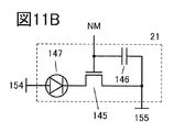
- 11A to 11D are diagrams illustrating a circuit including a display device.
- FIG. 12 is a diagram illustrating another mode of the transistor.
- FIG. 13 is a diagram illustrating a circuit used for the simulation.
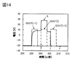
- FIG. 14 is a diagram illustrating a simulation result.
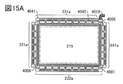
- 15A to 15C are diagrams illustrating a display device.
- 16A and 16B are diagrams illustrating a touch panel.
- 17A and 17B are diagrams illustrating a display device.
- FIG. 18 is a diagram illustrating a display device.
- 19A and 19B are diagrams illustrating a display device.
- 20A and 20B are diagrams illustrating a display device.
- 21A to 21E are diagrams illustrating a display device.
- 22A1 to 22C2 are diagrams illustrating transistors.
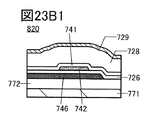
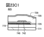
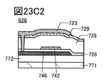
- 23A1 to 23C2 are diagrams illustrating a transistor.
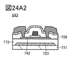
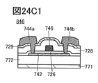
- 24A1 to 24C2 are diagrams illustrating transistors.
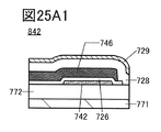
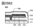
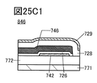
- 25A1 to 25C2 are diagrams illustrating transistors.
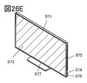
- 26A to 26F are diagrams illustrating electronic devices.
- the element may be composed of a plurality of elements.
- a plurality of transistors which operate as switches may be connected in series or in parallel.
- the capacitor may be divided and placed at a plurality of positions.
- one conductor may have a plurality of functions such as wiring, an electrode, and a terminal in some cases, and in this specification, a plurality of names may be used for the same element. Further, even when the elements are shown as directly connected on the circuit diagram, the elements may actually be connected through one or more conductors. In this specification, such a configuration is also included in the category of direct connection.
- One embodiment of the present invention is a display device including a circuit which boosts a signal voltage output from a gate driver. Since the signal voltage of the gate driver can be boosted and supplied to the pixel, it is suitable for driving a display device having a high threshold voltage. Further, by using the boosting function, it is possible to reduce the output of the gate driver and suppress the power consumption.
- a display device with low power consumption can be realized.
- a general-purpose driver can be used for both the source driver and the gate driver, so that a low-cost display device can be realized.
- FIG. 1 is a diagram illustrating a display device of one embodiment of the present invention.
- the display device includes a plurality of pixels 10, a circuit 13, a source driver 11, and a gate driver 12.
- the source driver 11 is electrically connected to the pixel 10.
- the gate driver 12 is electrically connected to the circuit 13.
- the circuit 13 is electrically connected to the pixel 10.
- the pixel 10 has a transistor 101 and a circuit 21.
- the circuit 21 has a display device.
- the circuit 21 can also include a transistor, a capacitor, and the like as appropriate.
- the gate of the transistor 101 is electrically connected to the wiring 125.
- a wiring connecting the transistor 101 and the circuit 21 is referred to as a node NM.
- the pixel 10 may have another configuration. Further, a plurality of pixels 10 are provided to form a pixel array 18.
- the circuits 13 can be provided for each row, for example, and can be electrically connected to the pixels 10 arranged in the same row.
- the pixel 10 pixel 10[n-1, m], pixel 10[n, m] pixel 10[n+1, m](m , N are natural numbers of 1 or more)
- circuits 13 circuit 13[n-1], circuit 13[n], circuit 13[n+1]
- the circuit 13 is a booster circuit, and has a function of boosting the signal voltage for pixel driving supplied from the gate driver 12.
- the circuit 13 is electrically connected to the pixel 10 through the wiring 125.
- a sequential circuit such as a shift register can be used for the source driver 11 and the gate driver 12.
- the pixel 10 may be driven by providing two or more of the source driver 11 and the gate driver 12 or both.
- the source driver 11 is electrically connected to the pixel 10 via the wiring 127.
- the output terminal 25a of the gate driver 12 is connected to the wiring 124[n-1], the output terminal 25b is connected to the wiring 124[n], and the output terminal 25c is connected to the wiring 124[n+1].
- the gate driver 12 has an output terminal 25a, an output terminal 25b, and an output terminal 25c, and can output a signal voltage in the order of the output terminal 25a, the output terminal 25b, and the output terminal 25c.
- the output terminal 25a, the output terminal 25b, and the output terminal 25c may be output terminals that do not overlap the timing of outputting the signal voltage.
- the output terminals may be the alternate output terminals, the alternate output terminals, or the like.
- the wiring 124[n-1] and the wiring 124[n+1] are electrically connected to the circuit 13[n].
- the circuit 13[n-1] and the circuit 13[n+1] are electrically connected to the three output terminals from which the gate driver 12 outputs the signal voltage. Note that the circuit 13 can be electrically connected to four or more output terminals included in the gate driver 12.
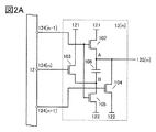
- FIG. 2A shows an example of the configuration of the circuit 13.
- the circuit 13 can have a structure including the transistor 102, the transistor 103, the transistor 104, the transistor 105, and the capacitor 106.
- FIG. 2 a circuit 13[n] electrically connected to the pixel 10 in the nth row is shown.
- One of a source and a drain of the transistor 102 is electrically connected to one electrode of the capacitor 106.
- One electrode of the capacitor 106 is electrically connected to one of a source and a drain of the transistor 104.
- the other electrode of the capacitor 106 is electrically connected to one of a source and a drain of the transistor 103 and one of a source and a drain of the transistor 105.
- the gate of the transistor 102 is electrically connected to the wiring 124[n-1].
- the gate of the transistor 103 is electrically connected to the wiring 124[n].
- the gate of the transistor 104 is electrically connected to the wiring 124[n+1].
- the gate of the transistor 105 is electrically connected to the wiring 124[n-1].
- the other of the source and the drain of the transistor 102 is electrically connected to the wiring 121.
- the other of the source and the drain of the transistor 103 is electrically connected to the wiring 121.
- the other of the source and the drain of the transistor 104 is electrically connected to the wiring 122.
- the other of the source and the drain of the transistor 105 is electrically connected to the wiring 122.
- the wirings 121 and 122 can have a function as power supply lines.
- the wiring 121 can be a high-potential power line and the wiring 122 can be a low-potential power line.
- a wiring connected to one of a source and a drain of the transistor 102, one electrode of the capacitor 106, and one of a source and a drain of the transistor 104 is referred to as a node A.
- a wiring connected to the other electrode of the capacitor 106, one of the source and the drain of the transistor 103 and one of the source and the drain of the transistor 105 is referred to as a node B.
- the node A functions as an output terminal and the wiring 125[n] is electrically connected.
- the gate of the transistor 102 and the gate of the transistor 105, which are connected to the wiring 124[n ⁇ 1], function as a first input terminal.
- the gate of the transistor 103 connected to the wiring 124[n] functions as a second input terminal.
- the gate of the transistor 104 connected to the wiring 124[n+1] functions as a third input terminal.
- V0 is input to the first input terminal
- V1 is input to the second input terminal (gate of the transistor 103)
- the node A is made floating
- V1 is input to the node B.
- C 106 the value of the capacitance of the capacitor 106 and the capacitance value of the node A and C A, the potential of the node A becomes "V1 + (C 106 / ( C 106 + C A)) ⁇ (V1-V0)" .
- C 106 /(C 106 +C A ) approaches 1, and the potential of the node A becomes “2V1-V0”.
- the circuit 13 can output a potential that is about twice the input potential.
- the circuit 13 can output the boosted potential and turn on the transistor of the pixel. Further, the circuit 13 outputs a potential for turning off the transistor of the pixel at the next timing.
- the potential can be supplied from the wiring 122 to the node A through the transistor 104 by inputting “V1” to the third input terminal (gate of the transistor 104).
- V1 is input to the node A or the node B through the transistor, the potential is actually lower than the potential input to the gate by the threshold voltage (V th ) of the transistor.
- V th threshold voltage
- the absolute value of V th is a sufficiently small value (generally 0 V), and a description thereof will be omitted.
- the node A and the node B act as holding nodes. Data can be written to each node by making a transistor connected to each node conductive. By turning off the transistor, the data can be held in each node. By using a transistor with extremely low off-state current as the transistor, leakage current can be suppressed and the potential of each node can be held for a long time.
- a transistor in which a metal oxide is used for a channel formation region hereinafter referred to as an OS transistor
- an OS transistor it is preferable to apply an OS transistor to any or all of the transistors included in the circuit 13. Further, an OS transistor may be applied to the element included in the circuit 21. Further, in the case where the operation is performed within the allowable leakage current amount, a transistor having Si in a channel formation region (hereinafter, Si transistor) may be applied. Alternatively, an OS transistor and a Si transistor may be used together. Note that examples of the Si transistor include a transistor having amorphous silicon, a transistor having crystalline silicon (microcrystalline silicon, low-temperature polysilicon, single crystal silicon), and the like. The above structure regarding the transistor can be applied to the other circuits described in this embodiment.
- a metal oxide having an energy gap of 2 eV or more, preferably 2.5 eV or more, more preferably 3 eV or more can be used.
- an oxide semiconductor containing indium or the like can be used, and for example, CAAC-OS or CAC-OS described later can be used.
- the CAAC-OS has stable atoms forming a crystal and is suitable for a transistor in which reliability is important. Further, since the CAC-OS exhibits high mobility characteristics, it is suitable for a transistor or the like which drives at high speed.
- the OS transistor Since the OS transistor has a large energy gap in the semiconductor layer, an extremely low off-current characteristic of several yA/ ⁇ m (a current value per 1 ⁇ m of channel width) can be exhibited. Further, the OS transistor has characteristics different from those of the Si transistor such that impact ionization, avalanche breakdown, short channel effect, and the like do not occur, and a highly reliable circuit can be formed. Further, variations in electrical characteristics due to non-uniformity of crystallinity, which is a problem in Si transistors, are less likely to occur in OS transistors.
- the semiconductor layer included in the OS transistor is an In-M-Zn-based oxide containing indium, zinc, and M (a metal such as aluminum, titanium, gallium, germanium, yttrium, zirconium, lanthanum, cerium, tin, neodymium, or hafnium).
- the film can be represented by.
- an In oxide, an In-Ga oxide, or an In-Zn oxide may be used for the semiconductor layer included in the OS transistor.
- the on-state current, the field-effect mobility, or the like of the OS transistor can be increased by using a semiconductor layer with a high proportion of indium.
- the In-M-Zn-based oxide can be formed by, for example, a sputtering method, an ALD (Atomic layer deposition) method, a MOCVD (Metal organic chemical vapor deposition) method, or the like.
- the atomic ratio of metal elements in the sputtering target preferably satisfies In?M and Zn?M.
- the oxide semiconductor included in the semiconductor layer is an In—Zn oxide
- the atomic ratio of metal elements in the sputtering target used for forming the In—Zn oxide preferably satisfies In ⁇ Zn. ..
- an oxide semiconductor having a low carrier concentration is used for the semiconductor layer.
- the semiconductor layer has a carrier concentration of 1 ⁇ 10 17 /cm 3 or less, preferably 1 ⁇ 10 15 /cm 3 or less, more preferably 1 ⁇ 10 13 /cm 3 or less, and more preferably 1 ⁇ 10 11 /cm 3. 3 or less, more preferably less than 1 ⁇ 10 10 /cm 3 , and 1 ⁇ 10 ⁇ 9 /cm 3 or more of an oxide semiconductor can be used.
- Such an oxide semiconductor is referred to as a highly purified intrinsic or substantially highly purified intrinsic oxide semiconductor. It can be said that the oxide semiconductor has low density of defect states and stable characteristics.
- the composition is not limited to these, and a material having an appropriate composition may be used depending on required semiconductor characteristics and electric characteristics of a transistor (field-effect mobility, threshold voltage, or the like). Further, in order to obtain the required semiconductor characteristics of the transistor, it is preferable that the carrier concentration and the impurity concentration of the semiconductor layer, the defect density, the atomic ratio of the metal element and oxygen, the interatomic distance, the density, and the like be appropriate. ..
- the concentration of silicon or carbon in the semiconductor layer (the concentration obtained by secondary ion mass spectrometry) is 2 ⁇ 10 18 atoms/cm 3 or less, preferably 2 ⁇ 10 17 atoms/cm 3 or less.
- the alkali metal and the alkaline earth metal might generate carriers when combined with the oxide semiconductor, which might increase the off-state current of the transistor. Therefore, the concentration of alkali metal or alkaline earth metal in the semiconductor layer (concentration obtained by secondary ion mass spectrometry) is 1 ⁇ 10 18 atoms/cm 3 or less, preferably 2 ⁇ 10 16 atoms/cm 3 or less.
- the nitrogen concentration in the semiconductor layer is preferably 5 ⁇ 10 18 atoms/cm 3 or less.
- oxygen when hydrogen is contained in the oxide semiconductor included in the semiconductor layer, oxygen reacts with oxygen which is bonded to a metal atom to be water, which might cause oxygen vacancies in the oxide semiconductor.
- the transistor When the channel formation region in the oxide semiconductor contains oxygen vacancies, the transistor might have normally-on characteristics.
- a defect in which hydrogen is contained in an oxygen vacancy may function as a donor and an electron which is a carrier may be generated.
- part of hydrogen may be bonded to oxygen which is bonded to a metal atom to generate an electron which is a carrier. Therefore, a transistor including an oxide semiconductor which contains a large amount of hydrogen is likely to have normally-on characteristics.
- a defect in which hydrogen is contained in an oxygen vacancy can function as a donor of an oxide semiconductor.
- the oxide semiconductor may be evaluated not by the donor concentration but by the carrier concentration. Therefore, in this specification and the like, a carrier concentration which is assumed to be a state where no electric field is applied may be used as a parameter of the oxide semiconductor, instead of the donor concentration. That is, the “carrier concentration” described in this specification and the like can be called the “donor concentration” in some cases.
- the hydrogen concentration obtained by secondary ion mass spectrometry is less than 1 ⁇ 10 20 atoms/cm 3 , preferably 1 ⁇ 10 19 atoms/cm 3. It is less than 3 , more preferably less than 5 ⁇ 10 18 atoms/cm 3 , and even more preferably less than 1 ⁇ 10 18 atoms/cm 3 .
- the oxide semiconductor is divided into a single crystal oxide semiconductor and a non-single crystal oxide semiconductor other than the single crystal oxide semiconductor.
- the non-single-crystal oxide semiconductor include a CAAC-OS (C-Axis Aligned Crystalline Oxide Semiconductor), a polycrystalline oxide semiconductor, an nc-OS (nanocrystal oxide semiconductor), and a pseudo-amorphous oxide semiconductor (a-like).
- OS amorphous-like oxide semiconductor
- the amorphous structure has the highest defect level density and the CAAC-OS has the lowest defect level density.
- the oxide semiconductor film having an amorphous structure has disordered atomic arrangement and no crystalline component, for example.
- the oxide film having an amorphous structure has, for example, a completely amorphous structure and has no crystal part.
- the semiconductor layer may be a mixed film including two or more kinds of an amorphous structure region, a microcrystalline structure region, a polycrystalline structure region, a CAAC-OS region, and a single crystal structure region.
- the mixed film may have, for example, a single-layer structure or a laminated structure including any two or more kinds of the above-mentioned regions.
- CAC Cloud-Aligned Composite
- the CAC-OS is a structure of a material in which an element included in an oxide semiconductor is unevenly distributed at a size of 0.5 nm to 10 nm inclusive, preferably 1 nm to 2 nm inclusive, or in the vicinity thereof.
- an oxide semiconductor one or more metal elements are unevenly distributed and a region including the metal element has a size of 0.5 nm to 10 nm, preferably 1 nm to 2 nm, or a size in the vicinity thereof.
- the state of being mixed with is also called a mosaic shape or a patch shape.
- the oxide semiconductor preferably contains at least indium. It is particularly preferable to contain indium and zinc. In addition to them, aluminum, gallium, yttrium, copper, vanadium, beryllium, boron, silicon, titanium, iron, nickel, germanium, zirconium, molybdenum, lanthanum, cerium, neodymium, hafnium, tantalum, tungsten, magnesium, etc. One kind or plural kinds selected from the above may be contained.
- CAC-OS in In-Ga-Zn oxide (In-Ga-Zn oxide among CAC-OS may be particularly referred to as CAC-IGZO) means indium oxide (hereinafter, InO).
- InO indium oxide
- X1 X1 is a real number larger than 0
- In X2 Zn Y2 O Z2 X2, Y2, and Z2 are real numbers larger than 0
- gallium indium oxide (hereinafter, InO).
- GaO X3 (X3 is a real number larger than 0)
- gallium zinc oxide hereinafter, Ga X4 Zn Y4 O Z4 (X4, Y4, and Z4 are real numbers larger than 0)
- InO X1 or In X2 Zn Y2 O Z2 having a mosaic shape is uniformly distributed in the film (hereinafter, also referred to as cloud shape). is there.
- the CAC-OS is a composite oxide semiconductor having a structure in which a region containing GaO X3 as a main component and a region containing In X2 Zn Y2 O Z2 or InO X1 are mixed.
- the atomic ratio of In to the element M in the first region is larger than the atomic ratio of In to the element M in the second region. It is assumed that the concentration of In is higher than that in the region of No. 2.
- IGZO is a common name and may refer to one compound of In, Ga, Zn, and O.
- InGaO 3 (ZnO) m1 (m1 is a natural number) or In (1+x0) Ga (1-x0) O 3 (ZnO) m0 (-1 ⁇ x0 ⁇ 1, m0 is an arbitrary number) is represented.
- Crystalline compounds may be mentioned.
- the crystalline compound has a single crystal structure, a polycrystalline structure, or a CAAC structure.
- the CAAC structure is a crystal structure in which a plurality of IGZO nanocrystals has c-axis orientation and is connected without being oriented in the ab plane.
- CAC-OS relates to a material structure of an oxide semiconductor.
- CAC-OS refers to a region that is observed in the form of nanoparticles mainly containing Ga as a part and nanoparticles mainly containing In as a part in a material structure containing In, Ga, Zn, and O.
- the regions that are observed in a pattern mean that the regions are randomly dispersed in a mosaic pattern. Therefore, in CAC-OS, the crystal structure is a secondary element.
- the CAC-OS does not include a stacked structure of two or more kinds of films having different compositions.
- a structure having two layers of a film containing In as a main component and a film containing Ga as a main component is not included.
- the CAC-OS has a region that is observed in the form of nanoparticles partially containing the metal element as a main component and a nanoparticle mainly containing In as a main component. The areas observed in the form of particles are randomly dispersed in a mosaic shape.
- the CAC-OS can be formed by a sputtering method under the condition that the substrate is not heated intentionally, for example.
- a sputtering method one or more selected from an inert gas (typically argon), an oxygen gas, and a nitrogen gas may be used as a film formation gas.
- an inert gas typically argon
- oxygen gas typically argon
- a nitrogen gas may be used as a film formation gas.
- the flow rate ratio of the oxygen gas is 0% or more and less than 30%, preferably 0% or more and 10% or less. ..
- the CAC-OS is characterized in that no clear peak is observed when it is measured using a ⁇ /2 ⁇ scan by an Out-of-plane method, which is one of the X-ray diffraction (XRD) measurement methods. Have. That is, it can be seen from the X-ray diffraction measurement that the orientations in the ab plane direction and the c-axis direction of the measurement region are not seen.
- XRD X-ray diffraction
- the electron beam diffraction pattern of the CAC-OS which is obtained by irradiating an electron beam with a probe diameter of 1 nm (also referred to as a nanobeam electron beam), a ring-shaped region having high brightness (ring region) and the ring are formed. Multiple bright spots are observed in the area. Therefore, it can be seen from the electron diffraction pattern that the crystal structure of CAC-OS has an nc (nano-crystal) structure having no orientation in the planar direction and the cross-sectional direction.
- nc nano-crystal
- GaO X3 is a main component by EDX mapping obtained using energy dispersive X-ray spectroscopy (EDX: Energy Dispersive X-ray spectroscopy). It can be confirmed that the region and the region containing In X2 Zn Y2 O Z2 or InO X1 as main components are unevenly distributed and mixed.
- the CAC-OS has a structure different from that of the IGZO compound in which the metal element is uniformly distributed, and has a property different from that of the IGZO compound. That is, in the CAC-OS, a region containing GaO X3 or the like as its main component and a region containing In X2 Zn Y2 O Z2 , or InO X1 as its main component are phase-separated from each other, and a region containing each element as its main component. Has a mosaic structure.
- the region containing In X2 Zn Y2 O Z2 or InO X1 as a main component is a region having higher conductivity than the region containing GaO X3 or the like as a main component. That, In X2 Zn Y2 O Z2 or InO X1, is an area which is the main component, by carriers flow, expressed the conductivity of the oxide semiconductor. Therefore, a region in which In X2 Zn Y2 O Z2 or InO X1 is a main component is distributed in the oxide semiconductor in a cloud shape, whereby high field-effect mobility ( ⁇ ) can be realized.
- the region containing GaO X3 or the like as the main component has a higher insulating property than the region containing In X2 Zn Y2 O Z2 or InO X1 as the main component. That is, since the region containing GaO X3 or the like as a main component is distributed in the oxide semiconductor, leakage current can be suppressed and favorable switching operation can be realized.
- the CAC-OS when used for a semiconductor element, the insulating property due to GaO X3 or the like and the conductive property due to In X2 Zn Y2 O Z2 or InO X1 are high due to complementary action.
- On-current (I on ) and high field-effect mobility ( ⁇ ) can be realized.
- the semiconductor element using the CAC-OS has high reliability. Therefore, the CAC-OS is suitable as a constituent material of various semiconductor devices.
- the transistor 102 When the potential of the wiring 124[n ⁇ 1] becomes “H” (the potential of the wiring 124[n] and the potential of the wiring 124[n+1] are “L”) at time T1, the transistor 102 is turned on and the potential of the node A is reached. Becomes "H”. In addition, the transistor 105 is turned on and the potential of the node B becomes “L”.
- the transistor 102 When the potential of the wiring 124[n ⁇ 1] becomes “L” (the potential of the wiring 124[n] and the potential of the wiring 124[n+1] are “L”) at the time T2, the transistor 102 is turned off and the node A of the node A is turned off. The potential is held at "H”. Further, the transistor 105 is turned off and the potential of the node B is held at “L”.
- the writing operation of the pixel 10 can be performed in a period in which the potential “2A” is supplied to the node A (wiring 125[n]) (after time T3 and before time T5). Further, after T5, the potential of the node A is held at “L”, so that the image signal written in the pixel 10 can be held until the next frame (next operation).
- FIG. 3A shows a modified example of the circuit 13.
- the circuit 13 illustrated in FIG. 3A differs from the circuit 13 illustrated in FIG. 2A in that the circuit 14 is provided and that the other of the source and the drain of the transistor 102 is electrically connected to the wiring 123.
- the circuit 14 is a circuit having a function of increasing the voltage output by the circuit 13.
- the circuit 14 can include a transistor 107 and a capacitor 108.
- One of a source and a drain of the transistor 107 is electrically connected to the wiring 124[n-1].
- the other of the source and the drain of the transistor 107 is electrically connected to one electrode of the capacitor 108 and the gate of the transistor 102.
- the other electrode of the capacitor 108 is electrically connected to the node A.
- one of the source and the drain of the transistor 107 serves as the first input terminal.
- the gate of the transistor 107 is electrically connected to the wiring 121.
- the other of the source and the drain of the transistor 102 is electrically connected to the wiring 123.
- the wiring 123 is a power supply line that supplies a potential higher than that of the wiring 121. Note that the other of the source and the drain of the transistor 102 may be electrically connected to the wiring 121.
- a bootstrap effect can be imparted. Due to the effect of bootstrap, a signal voltage higher than the input signal voltage can be output.
- the bootstrap operation is as follows. First, the potential “H” is input through the transistor 107 to the node C (the other of the source and the drain of the transistor 107, one electrode of the capacitor 108, a wiring to which the gate of the transistor 102 and the gate of the transistor 105 are connected). Then, a current flows through the transistor 102 until the potential of the node A rises from "L” to "H". At this time, the potential of the node C rises to “H” or higher due to capacitive coupling of the capacitor 108, so that the transistor 102 further flows current, so that the potential of the node A can be further raised.
- the potential “H” is supplied to one of the source and the drain and the gate of the transistor 107, and when the potential of the other of the source and the drain of the transistor 107 (node C) becomes higher than “H”, the transistor 107 is supplied to the transistor 107.
- the current stops flowing. That is, the transistor 107 serves as a diode.
- the structure including the circuit 14 can be applied to the other circuits described in this embodiment.
- the circuit 13 shown in FIG. 3A can be operated according to the timing chart shown in FIG. 2B. Note that at times T1 to T5, the potential of the node A can be higher than that of the circuit 13 in FIG. 2B as described above.
- FIG. 3B shows another modification of the circuit 13.
- the circuit 13 shown in FIG. 3B is different from the circuit 13 shown in FIG. 2A in that it has a circuit 15.
- the circuit 15 is a circuit which controls supply of a low potential to the wiring 125.
- the circuit 15 can have a structure including the transistor 109, the transistor 110, and the capacitor 111.
- One of a source and a drain of the transistor 109 is electrically connected to the wiring 121.
- the other of the source and the drain of the transistor 109 is electrically connected to one of the source and the drain of the transistor 110, one electrode of the capacitor 111, and the gate of the transistor 104.
- the other of the source and the drain of the transistor 110 is electrically connected to the wiring 122.
- the other electrode of the capacitor 111 is electrically connected to the wiring 122.
- the gate of the transistor 109 is electrically connected to the wiring 124[n+1].
- the gate of the transistor 110 is electrically connected to the wiring 124[n-1].
- the gates of the transistor 102, the transistor 105, and the transistor 110 serve as a first input terminal
- the gate of the transistor 109 serves as a third input terminal.
- the transistor 104 is turned off at time T6 in the timing chart illustrated in FIG. 2B, so that the wiring 125 is brought into a floating state. At this time, if the leakage current of the transistor 102 is relatively high, the potential of the wiring 125 is increased, which may cause the pixel 10 to malfunction.
- the circuit 15 is a circuit which holds the potential of the node D (a gate connecting the transistor 104, one electrode of the capacitor 111, the other of the source and the drain of the transistor 109 and one of the source and the drain of the transistor 110),
- the transistor 104 can be held in a conductive state or a non-conductive state.
- the operation of the circuit 15 is as follows. First, when the signal voltage “H” is input to the first input terminal, the transistor 110 is turned on and the potential “L” is supplied to the node D. At this time, the transistor 104 is non-conductive.
- the transistor 110 is turned off and the potential “L” is held at the node D. Subsequently, the potential “L” is held at the node D even while the boosting operation is performed with the signal voltage input to the second input terminal.
- the transistor 109 is turned on and the potential of the node D becomes “H”.
- the transistor 104 is turned on and the potential of the node A becomes “L”.
- the transistor 109 is turned off and the potential of the node D is held at “H”. This state is maintained until the next frame, during which the transistor 104 is on, and the potential “L” of the wiring 122 is continuously supplied to the node A. Therefore, the node A (wiring 125) can be kept at a constant potential “L”.
- the off-state current is extremely small, so that the potential of the wiring 125 is slightly increased.
- the structure including the circuit 15 can be applied to the other circuits described in this embodiment.
- the circuit 13 shown in FIG. 3B can be operated according to the timing chart shown in FIG. 2B. Note that even if the leakage current of the transistor 102 is relatively high, the potential of the node A can be kept constant after time T6.
- FIG. 4 shows another modification of the circuit 13.
- the circuit 13 described above is an example having three input terminals, but the circuit 13 shown in FIG. 4 is an example having four input terminals. With this configuration, the boosting function can be enhanced as compared with the circuit 13 described above.
- the circuit 13 illustrated in FIG. 4 has a structure in which a transistor 112, a transistor 113, and a capacitor 114 are added to the circuit 13 illustrated in FIG. 2A.
- One of a source and a drain of the transistor 102 is electrically connected to one electrode of the capacitor 106.
- One electrode of the capacitor 106 is electrically connected to one of a source and a drain of the transistor 104.
- the other electrode of the capacitor 106 is electrically connected to one of a source and a drain of the transistor 105, one of a source and a drain of the transistor 112, and one electrode of the capacitor 114.
- the other electrode of the capacitor 114 is electrically connected to one of a source and a drain of the transistor 103 and one of a source and a drain of the transistor 113.
- the gate of the transistor 102 is electrically connected to the wiring 124[n-2].
- the gate of the transistor 112 is electrically connected to the wiring 124[n-1].
- the gate of the transistor 113 is electrically connected to the wiring 124[n-1].
- the gate of the transistor 103 is electrically connected to the wiring 124[n].
- the gate of the transistor 104 is electrically connected to the wiring 124[n+1].
- the other of the source and the drain of the transistor 102 is electrically connected to the wiring 121.
- the other of the source and the drain of the transistor 103 is electrically connected to the wiring 121.
- the other of the source and the drain of the transistor 104 is electrically connected to the wiring 122.
- the other of the source and the drain of the transistor 105 is electrically connected to the wiring 122.
- the other of the source and the drain of the transistor 112 is electrically connected to the wiring 121.
- the other of the source and the drain of the transistor 113 is electrically connected to the wiring
- a wiring to which the other electrode of the capacitor 106, one of the source and the drain of the transistor 112, one electrode of the capacitor 114, and one of the source and the drain of the transistor 105 are connected is a node E.
- a wiring connected to the other electrode of the capacitor 114, one of the source and the drain of the transistor 103 and one of the source and the drain of the transistor 113 is referred to as a node F.
- the gate of the transistor 102 and the gate of the transistor 105 connected to the wiring 124[n ⁇ 2] function as the first input terminal.
- the gate of the transistor 112 and the gate of the transistor 113, which are connected to the wiring 124[n ⁇ 1], function as a second input terminal.
- the gate of the transistor 103 connected to the wiring 124[n] functions as a third input terminal.
- the gate of the transistor 104 connected to the wiring 124[n+1] functions as a fourth input terminal.
- the potential of the wiring 124[n ⁇ 2] becomes “H” (the potential of the wiring 124[n ⁇ 1], the potential of the wiring 124[n], and the potential of the wiring 124[n+1] are “L”).
- the transistor 102 is turned on, and the potential of the node A becomes “H”.
- the transistor 105 is turned on and the potential of the node E becomes “L”.
- the potential of the wiring 124[n ⁇ 2] becomes “L” (the potential of the wiring 124[n ⁇ 1], the potential of the wiring 124[n], and the potential of the wiring 124[n+1] are “L”).
- the transistor 102 is turned off and the potential of the node A is held at “H”. Further, the transistor 105 is turned off and the potential of the node E is held at “L”.
- the potential of the wiring 124[n ⁇ 1] becomes “H” (the potential of the wiring 124[n ⁇ 2], the potential of the wiring 124[n], and the potential of the wiring 124[n+1] are “L”).
- the transistor 112 becomes conductive, and the potential of the node E changes from “L” to "H”.
- the transistor 113 is turned on and the potential of the node F becomes “L”.
- the potential of the wiring 124[n ⁇ 1] becomes “L” (the potential of the wiring 124[n ⁇ 2], the potential of the wiring 124[n], and the potential of the wiring 124[n+1] are “L”).
- the transistor 112 is turned off, and the potential of the node E is held at “H”.
- the transistor 113 is turned off and the potential of the node F is held at “L”.
- the potential of the wiring 124[n] becomes “H” (the potential of the wiring 124[n ⁇ 2], the potential of the wiring 124[n ⁇ 1], and the potential of the wiring 124[n+1] are “L”).
- the transistor 103 is turned on, and the potential of the node F changes from “L” to "H”.
- the potential of the wiring 124[n] becomes “L” (the potential of the wiring 124[n ⁇ 2], the potential of the wiring 124[n ⁇ 1], and the potential of the wiring 124[n+1] are “L”).
- the transistor 103 is turned off and the potential of the node A is held at “3H”.
- the potential of the wiring 124[n+1] becomes “H” (the potential of the wiring 124[n ⁇ 2], the potential of the wiring 124[n ⁇ 1], and the potential of the wiring 124[n] are “L”).
- the transistor 104 is turned on, and the potential of the node A becomes “L”.
- the potential of the wiring 124[n+1] becomes “L” (the potential of the wiring 124[n ⁇ 2], the potential of the wiring 124[n ⁇ 1], and the potential of the wiring 124[n] are “L”).
- the transistor 104 is turned off, and the potential of the node A is held at “L”.
- the writing operation of the pixel 10 can be performed in a period in which the potential “3H” is supplied to the node A (the wiring 125[n]) (after time T5 and before time T7). Further, after T7, the potential of the node A is held at “L”, so that the image signal written in the pixel 10 can be held until the next frame (next operation).
- the boosting function can be enhanced by adding the configuration of two transistors and one capacitor to the circuit 13 of FIG. 2A. By further adding the configuration, the boosting function can be further enhanced.
- FIG. 6A shows another modification of the circuit 13.
- the circuit 13 illustrated in FIG. 6 has a simplified configuration, in which the transistor 103 and the transistor 105 are omitted from the circuit 13 illustrated in FIG. 2A.
- the wiring 124[n] is electrically connected to the other electrode of the capacitor 106. That is, the other electrode of the capacitor 106 functions as the second input terminal.
- the low potential is represented by “L” and the high potential is represented by “H”.
- the condition is that “H” is supplied to the wiring 121, “L” is supplied to the wiring 122, and “H” or “L” is supplied to the wiring 124.
- the transistor 102 When the potential of the wiring 124[n ⁇ 1] becomes “L” (the potential of the wiring 124[n] and the potential of the wiring 124[n+1] are “L”) at the time T2, the transistor 102 is turned off and the node A of the node A is turned off. The potential is held at "H”. At this time, the potential "L” is supplied to the other electrode of the capacitor 106.
- the potential of the node A becomes “2H” after the time T3, but returns to “H” at the time T4. That is, the period during which the high potential can be maintained becomes shorter than that of the circuit 13 described with reference to FIGS.
- the circuit 13 illustrated in FIG. 6A is preferably used for a display device in which a pixel writing time can be sufficiently taken even in such an operation.
- FIG. 7 shows a configuration in which one input terminal is added to the configuration of the circuit 13 shown in FIG. 4, and a maximum potential “4H” can be output.
- the difference from the circuit 13 shown in FIG. 4 is that the capacitor 115 is electrically connected to the node F.
- the capacitor 115 can be electrically connected to the final-stage input terminal that performs the boosting operation.
- the circuit 13 is connected to the output terminal of the gate driver 12 in FIGS. 1 to 7, the circuit 13 may be a component of the gate driver 12 as shown in FIG. 8A. With this configuration, boosting is performed inside the gate driver 12.
- the circuit such as a shift register included in the gate driver 12 and the circuit 13 may be stacked. By stacking these, the display device can have a narrower frame.
- the selection circuit 16 may be provided in the circuit 13.
- the selection circuit 16 can output the output potential boosted in the circuit 13 to the selected wiring 125.
- the number of circuits 13 provided in the display device can be reduced and the display device can have a narrower frame.
- the selection circuit 16 may be provided outside the circuit 13 and the selection circuit 16 may be electrically connected to the output terminal of the circuit 13.
- a selection circuit 17 may be provided between the gate driver 12 and the circuit 13.
- the selection circuit 17 can select a first path for outputting the signal voltage output by the gate driver 12 to the circuit 13 and a second path for bypassing the circuit 13 and outputting the signal voltage to the pixel 10.
- a signal voltage that is not boosted can be supplied to the pixel and power saving operation can be performed such as suppressing display brightness.
- the pixel 10 may have the configuration shown in FIG. 9A in addition to the configuration shown in FIG.
- the pixel 10 shown in FIG. 9A has a function of boosting the input data voltage.
- the pixel 10 illustrated in FIG. 9A includes a transistor 116, a transistor 117, a capacitor 118, and a circuit 21, and has two gate lines (wiring 125 and wiring 126) and two source lines (wiring 127 and wiring 128). It is electrically connected. Different circuits 13 are electrically connected to the wiring 125 and the wiring 126, respectively.
- a gate is electrically connected to the wiring 126, one of a source and a drain is electrically connected to the wiring 127, and the other of the source and the drain is electrically connected to one electrode of the capacitor 118 and the circuit 21.
- the gate is electrically connected to the wiring 125, one of the source and the drain is electrically connected to the wiring 128, and the other of the source and the drain is electrically connected to the other electrode of the capacitor 118.
- the transistor 116 is controlled by the signal supplied to the wiring 126, and the transistor 117 is controlled by the signal supplied to the wiring 125.
- the pixel 10 illustrated in FIG. 9A is effective when a high voltage is supplied to the display device included in the circuit 21.
- the boosting function of the pixel 10 will be described below. Note that in the pixel 10 illustrated in FIG. 9A, a wiring connecting the other of the source and the drain of the transistor 116, one electrode of the capacitor 118, and the circuit 21 is a node NM.
- the potential “D1” of the wiring 127 is supplied to the node NM through the transistor 116, and at a timing overlapping with this, the other potential of the capacitor 118 is supplied with the reference potential “V ref ” from the wiring 128 through the transistor 117. To do. At this time, the capacitor 118 holds “D1-V ref ”.
- the node NM is made floating, and the potential “D2” of the wiring 128 is supplied to the other electrode of the capacitor 118 through the transistor 117.
- the potential “D2” is a potential for addition.
- the potential of the node NM is D1+(C 118 /(C 118 +C NM )) ⁇ (D2-V ref )).
- a potential approximately twice as high as the potential that can be input from the wiring 125 or the wiring 126 can be supplied to the node NM.
- a high voltage can be supplied to the display device. Therefore, a display device having a high threshold voltage can be operated even if a general-purpose driver IC is used. Alternatively, the power consumption of the driver IC can be suppressed.
- the pixel 10 may have the configuration shown in FIG. 9B.
- the pixel 10 shown in FIG. 9B is different from the pixel 10 shown in FIG. 9A in that it has a transistor 119.
- the gate of the transistor 119 is electrically connected to the wiring 126
- one of the source and the drain is electrically connected to the other of the source and the drain of the transistor 117 and the other electrode of the capacitor 118
- the other of the source and the drain is the wiring 128. Electrically connected to.
- one of a source and a drain of the transistor 117 is connected to the wiring 127.
- the operation of supplying the reference potential and the addition potential to the other electrode of the capacitor 118 via the transistor 117 is performed as described above.
- two wirings 125 and 126 are required, and the wiring 128 needs to be rewritten alternately with the reference potential and the addition potential, which may cause a problem in high-speed operation and power consumption.
- the number of transistors 119 is increased, but the number of wirings is not increased because the gate of the transistor 119 can be connected to the wiring 126.
- the wiring 128 can be a dedicated wiring to which a reference potential is supplied, and the reference potential and the addition potential are not rewritten by one wiring alternately, which is suitable for high-speed operation and low power consumption. Can be said.
- a low potential line or the like connected to the circuit 21 can be used as the wiring 128, the number of wirings can be substantially reduced.
- the inversion potential “D1B” of “D1” may be used as “V ref ”.
- V ref a potential that is about three times the potential that can be input from the wiring 125 or the wiring 126 can be supplied to the node NM.
- the reversal potential means a potential having the same (or substantially the same) absolute value of the difference from a certain reference potential and different from the original potential.
- ⁇ Circuit 21> 10A to 10D are examples of configurations that can be applied to the circuit 21 and include a liquid crystal device as a display device.
- the configuration shown in FIG. 10A has a capacitor 141 and a liquid crystal device 142.
- One electrode of the liquid crystal device 142 is electrically connected to one electrode of the capacitor 141.
- One electrode of the capacitor 141 is electrically connected to the node NM.
- the other electrode of the capacitor 141 is electrically connected to the wiring 151.
- the other electrode of the liquid crystal device 142 is electrically connected to the wiring 152.
- the wirings 151 and 152 have a function of supplying power.
- the wirings 151 and 152 can supply a reference potential such as GND or 0 V or an arbitrary potential.
- the capacitor 141 may be omitted as shown in FIG. 10B.
- the OS transistor can be used as the transistor connected to the node NM. Since the leakage current of the OS transistor is extremely small, display can be maintained for a relatively long time even if the capacitor 141 functioning as a storage capacitor is omitted. Further, not limited to the configuration of the transistor, it is effective to omit the capacitor 141 when the display period can be shortened by a high speed operation such as field sequential driving. The aperture ratio can be improved by omitting the capacitor 141. Alternatively, the transmittance of the pixel can be improved.
- the operation of the liquid crystal device 142 is started when the potential of the node NM exceeds the operation threshold value of the liquid crystal device 142. Therefore, the display operation may start before the potential of the node NM is determined. However, in the case of a transmissive liquid crystal display device, the operation such as turning off the backlight is also used until the potential of the node NM is determined, so that the visual recognition can be suppressed even if an unnecessary display operation is performed. it can.
- FIG. 10C shows a structure in which a transistor 143 is added to the structure of FIG. 10A.
- One of a source and a drain of the transistor 143 is electrically connected to one electrode of the capacitor 141.
- the other of the source and the drain of the transistor 143 is electrically connected to the node NM.
- the potential of the node NM is applied to the liquid crystal device 142 with the conduction of the transistor 143. Therefore, the operation of the liquid crystal device 142 can be started at an arbitrary timing after the potential of the node NM is determined.
- FIG. 10D shows a structure in which a transistor 144 is added to the structure of FIG. 10C.
- One of a source and a drain of the transistor 144 is electrically connected to one electrode of the liquid crystal device 142.
- the other of the source and the drain of the transistor 144 is electrically connected to the wiring 153.
- the circuit 170 electrically connected to the wiring 153 can have a function of resetting the potentials supplied to the capacitor 141 and the liquid crystal device 142.
- 11A to 11D are examples of configurations that can be applied to the circuit 21 and include a light emitting device as a display device.
- the configuration shown in FIG. 11A includes a transistor 145, a capacitor 146, and a light emitting device 147.
- One of a source and a drain of the transistor 145 is electrically connected to one electrode of the light emitting device 147.
- One electrode of the light emitting device 147 is electrically connected to one electrode of the capacitor 146.
- the other electrode of the capacitor 146 is electrically connected to the gate of the transistor 145.
- the gate of the transistor 145 is electrically connected to the node NM.
- the other of the source and the drain of the transistor 145 is electrically connected to the wiring 154.
- the other electrode of the light emitting device 147 is electrically connected to the wiring 155.
- the wirings 154 and 155 have a function of supplying power.
- the wiring 154 can supply a high potential power source.
- the wiring 155 can supply low potential power.
- one electrode of the light emitting device 147 may be electrically connected to the wiring 154 and the other electrode of the light emitting device 147 may be electrically connected to the other of the source and the drain of the transistor 145. Good.
- the configuration can be applied to another circuit 21 including the light emitting device 147.
- FIG. 11C shows a configuration in which a transistor 148 is added to the configuration of FIG. 15A.
- One of a source and a drain of the transistor 148 is electrically connected to one of a source and a drain of the transistor 145.
- the other of the source and the drain of the transistor 148 is electrically connected to the light emitting device 147.
- the light emission of the light emitting device 147 can be started at any timing after the potential of the node NM is determined.
- FIG. 11D shows a configuration in which a transistor 149 is added to the configuration of FIG. 11A.
- One of a source and a drain of the transistor 149 is electrically connected to one of a source and a drain of the transistor 145.
- the other of the source and the drain of the transistor 149 is electrically connected to the wiring 156.
- the wiring 156 can be electrically connected to a supply source of a specific potential such as a reference potential. By supplying a specific potential from the wiring 156 to one of the source and the drain of the transistor 145, writing of image data can be stabilized. Further, the timing of light emission of the light emitting device 147 can be controlled.
- the wiring 156 can be connected to the circuit 171 and can also function as a monitor line.
- the circuit 171 can have one or more of a function as a supply source of the specific potential, a function of acquiring electric characteristics of the transistor 145, and a function of generating correction data.
- a transistor provided with a back gate may be used.
- the back gate is electrically connected to the front gate, which has the effect of increasing the on-current.
- the back gate may be electrically connected to a wiring which can supply a constant potential. With this structure, the threshold voltage of the transistor can be controlled.
- the transistor included in the circuit 21 may be provided with a back gate.
- FIG. 13 shows the configuration of the pixel 10 used in the simulation.
- the simulation uses the circuit configuration shown in FIG. 6A and targets the operation of the timing chart shown in FIG. 6B.
- the parameters used for the simulation are as follows.
- FIG. 14 shows simulation results, where the horizontal axis represents time ( ⁇ sec) and the vertical axis represents the voltage (V) of the node A of the pixel 10. Note that GOUT[i-1] is a signal voltage entering the gate of the transistor Tr1, GOUT[i] is a signal voltage entering the capacitor C1, and GOUT[i+1] is a signal voltage entering the gate of the transistor Tr2.
- the potential of the node A rises from -21 V in the initial state where GVSS is input to about 8.4 V at the input of GOUT[i-1] and about 27 at the input of GOUT[i]. It was confirmed that the voltage rose to 0.6 V and returned to 21 V at the input of GOUT[i+1]. Based on the initial state, it was confirmed that the output voltage when GOUT[i] was input could be boosted to about 1.65 times the output voltage when GOUT[i-1] was input. By performing a more appropriate design, the boosting characteristic can be further improved.
- This embodiment can be implemented in appropriate combination with any of the structures described in the other embodiments and the like.
- Embodiment 2 In this embodiment mode, a structural example of a display device using a liquid crystal device and a structural example of a display device using a light emitting device will be described. Note that, in the present embodiment, description of the elements, operations and functions of the display device described in Embodiment 1 will be omitted.
- the pixel described in Embodiment 1 can be used for the display device described in this embodiment.
- the scan line driver circuit described below corresponds to a gate driver
- the signal line driver circuit corresponds to a source driver.
- 15A to 15C are diagrams illustrating a structure of a display device in which one embodiment of the present invention can be used.
- a sealant 4005 is provided so as to surround the display portion 215 provided over the first substrate 4001, and the display portion 215 is sealed by the sealant 4005 and the second substrate 4006.
- the scan line driver circuit 221a, the signal line driver circuit 231a, the signal line driver circuit 232a, and the common line driver circuit 241a each include a plurality of integrated circuits 4042 which are provided over a printed circuit board 4041.
- the integrated circuit 4042 is formed using a single crystal semiconductor or a polycrystalline semiconductor.
- the common line driver circuit 241a has a function of supplying a prescribed potential to the wirings 151, 152, 154, 155, and the like described in Embodiment 1.
- the integrated circuit 4042 included in the scan line driver circuit 221a and the common line driver circuit 241a has a function of supplying a selection signal to the display portion 215.
- the integrated circuit 4042 included in the signal line driver circuit 231a and the signal line driver circuit 232a has a function of supplying image data to the display portion 215.
- the integrated circuit 4042 is mounted on a region of the first substrate 4001 which is different from the region surrounded by the sealant 4005.
- connection method of the integrated circuit 4042 is not particularly limited, and a wire bonding method, a COF (Chip On Film) method, a COG (Chip On Glass) method, a TCP (Tape Carrier Package) method, or the like can be used. it can.
- FIG. 15B illustrates an example in which the integrated circuit 4042 included in the signal line driver circuit 231a and the signal line driver circuit 232a is mounted by a COG method. Further, part or all of the driver circuit can be formed over the same substrate as the display portion 215, so that a system-on-panel can be formed.
- FIG. 15B illustrates an example in which the scan line driver circuit 221a and the common line driver circuit 241a are formed over the same substrate as the display portion 215.
- the sealant 4005 is provided so as to surround the display portion 215 provided over the first substrate 4001, the scan line driver circuit 221a, and the common line driver circuit 241a.
- a second substrate 4006 is provided over the display portion 215, the scan line driver circuit 221a, and the common line driver circuit 241a. Therefore, the display portion 215, the scan line driver circuit 221a, and the common line driver circuit 241a are sealed with the display device by the first substrate 4001, the sealant 4005, and the second substrate 4006.
- the signal line driver circuit 231a and the signal line driver circuit 232a are separately formed and mounted on the first substrate 4001; however, the invention is not limited to this structure.
- the scan line driver circuit may be separately formed and then mounted, or part of the signal line driver circuit or part of the scan line driver circuit may be separately formed and then mounted.
- the signal line driver circuit 231a and the signal line driver circuit 232a may be formed over the same substrate as the display portion 215.
- the display device may include a panel in which the display device is sealed and a module in which an IC or the like including a controller is mounted on the panel.
- the display portion and the scan line driver circuit which are provided over the first substrate include a plurality of transistors.
- the transistor the Si transistor or the OS transistor described in Embodiment 1 can be applied.
- the structure of the transistor included in the peripheral driver circuit and the structure of the transistor included in the pixel circuit of the display portion may be the same or different.
- the transistors included in the peripheral driver circuit may all have the same structure, or may have two or more types of structures.
- the transistors included in the pixel circuit may all have the same structure, or may have two or more types of structures.
- the input device 4200 can be provided over the second substrate 4006.
- the structure in which the display device illustrated in FIGS. 15A to 15C is provided with the input device 4200 can function as a touch panel.
- a detection device also referred to as a sensor element
- Various sensors that can detect the proximity or contact of a detection target such as a finger or a stylus can be applied as the detection device.
- various systems such as a capacitance system, a resistance film system, a surface acoustic wave system, an infrared system, an optical system, and a pressure-sensitive system can be used.
- a touch panel having a capacitance type detection device will be described as an example.
- the electrostatic capacity method there are a surface type electrostatic capacity method, a projection type electrostatic capacity method and the like. Further, as the projection type electrostatic capacity method, there are a self capacity method, a mutual capacity method and the like. It is preferable to use the mutual capacitance method because simultaneous multipoint detection is possible.
- the touch panel of one embodiment of the present invention has a structure in which a display device and a detection device which are separately manufactured are attached to each other, a structure in which an electrode or the like included in the detection device is provided on one or both of a substrate supporting the display device and a counter substrate, or the like. , Various configurations can be applied.
- FIG. 16A and 16B show an example of a touch panel.
- FIG. 16A is a perspective view of touch panel 4210.
- FIG. 16B is a schematic perspective view of the input device 4200. Note that, for clarity, only representative components are shown.
- the touch panel 4210 has a configuration in which a display device and a detection device that are separately manufactured are attached to each other.
- the touch panel 4210 includes an input device 4200 and a display device, which are provided in an overlapping manner.
- the input device 4200 includes a substrate 4263, an electrode 4227, an electrode 4228, a plurality of wirings 4237, a plurality of wirings 4238, and a plurality of wirings 4239.
- the electrode 4227 can be electrically connected to the wiring 4237 or the wiring 4239.
- the electrode 4228 can be electrically connected to the wiring 4239.
- the FPC 4272b is electrically connected to each of the plurality of wirings 4237 and the plurality of wirings 4238.
- An IC 4273b can be provided in the FPC 4272b.
- a touch sensor may be provided between the first substrate 4001 and the second substrate 4006 of the display device.
- a touch sensor is provided between the first substrate 4001 and the second substrate 4006, an optical touch sensor using a photoelectric conversion element may be used as well as a capacitance touch sensor.
- FIGS. 17A and 17B are cross-sectional views of a portion indicated by a chain line N1-N2 in FIG. 15B.
- the display device illustrated in FIGS. 17A and 17B includes an electrode 4015, and the electrode 4015 is electrically connected to a terminal included in the FPC 4018 through an anisotropic conductive layer 4019. 17A and 17B, the electrode 4015 is electrically connected to the wiring 4014 in the openings formed in the insulating layer 4112, the insulating layer 4111, and the insulating layer 4110.
- the electrode 4015 is formed using the same conductive layer as the first electrode layer 4030, and the wiring 4014 is formed using the same conductive layer as the source and drain electrodes of the transistor 4010 and the transistor 4011.
- the display portion 215 and the scan line driver circuit 221a provided over the first substrate 4001 each include a plurality of transistors.
- the transistor 4010 included in the display portion 215 and the scan line are included.
- the transistor 4011 included in the driver circuit 221a is illustrated. Note that although bottom gate transistors are illustrated as the transistors 4010 and 4011 in FIGS. 17A and 17B, top gate transistors may be used.
- the insulating layer 4112 is provided over the transistors 4010 and 4011.
- the partition 4510 is formed over the insulating layer 4112.
- the transistors 4010 and 4011 are provided over the insulating layer 4102.
- the transistor 4010 and the transistor 4011 each include an electrode 4017 formed over the insulating layer 4111.
- the electrode 4017 can function as a back gate electrode.
- the display device illustrated in FIGS. 17A and 17B includes a capacitor 4020.
- the capacitor 4020 shows an example in which the electrode 4021 formed in the same step as the gate electrode of the transistor 4010, the insulating layer 4103, and the electrode formed in the same step as the source electrode and the drain electrode are shown.
- the structure of the capacitor 4020 is not limited to this, and the capacitor 4020 may be formed using another conductive layer and an insulating layer.
- FIG. 17A is an example of a liquid crystal display device using a liquid crystal device as a display device.
- a liquid crystal device 4013 which is a display device includes a first electrode layer 4030, a second electrode layer 4031, and a liquid crystal layer 4008.
- an insulating layer 4032 and an insulating layer 4033 which function as alignment films are provided so as to sandwich the liquid crystal layer 4008.
- the second electrode layer 4031 is provided on the second substrate 4006 side, and the first electrode layer 4030 and the second electrode layer 4031 overlap with each other with the liquid crystal layer 4008 interposed therebetween.
- liquid crystal devices to which various modes are applied can be used.
- a VA Very Alignment
- a TN Transmission Nematic
- an IPS In-Plane-Switching
- ASM Analy Symmetrical Integrated Micro-cell
- OCB Optically Aligned Micro-cell
- AFLC Anti-ferroelectric Liquid Crystal
- ECB Electrode Controlled Birefringence
- VA-IPS mode guest-host mode, etc.
- a normally black liquid crystal display device for example, a transmissive liquid crystal display device adopting a vertical alignment (VA) mode may be applied to the liquid crystal display device shown in this embodiment.
- VA vertical alignment
- MVA Multi-Domain Vertical Alignment
- PVA Plasma Vertical Alignment
- ASV Advanced Super View
- the liquid crystal device is a device that controls transmission or non-transmission of light by an optical modulation action of liquid crystal.
- the optical modulation action of the liquid crystal is controlled by an electric field applied to the liquid crystal (including a horizontal electric field, a vertical electric field, and an oblique electric field).
- thermotropic liquid crystal low molecular liquid crystal
- polymer liquid crystal polymer dispersed liquid crystal
- PDLC Polymer Dispersed Liquid Crystal
- ferroelectric liquid crystal antiferroelectric liquid crystal, etc.
- These liquid crystal materials show a cholesteric phase, a smectic phase, a cubic phase, a chiral nematic phase, an isotropic phase, etc. depending on the conditions.
- FIG. 17A shows an example of a liquid crystal display device including a vertical electric field liquid crystal device
- a liquid crystal display device including a horizontal electric field liquid crystal device can be applied to one embodiment of the present invention.
- liquid crystal exhibiting a blue phase for which an alignment film is not used may be used.
- the blue phase is one of the liquid crystal phases, and is a phase that appears immediately before the transition from the cholesteric phase to the isotropic phase when the temperature of the cholesteric liquid crystal is raised. Since the blue phase appears only in a narrow temperature range, a liquid crystal composition in which 5 wt% or more of a chiral agent is mixed is used for the liquid crystal layer 4008 in order to improve the temperature range.
- a liquid crystal composition containing a liquid crystal exhibiting a blue phase and a chiral agent has a short response speed and shows optical isotropy.
- a liquid crystal composition containing a liquid crystal exhibiting a blue phase and a chiral agent does not require alignment treatment and has small viewing angle dependence. Further, since it is not necessary to provide an alignment film, rubbing treatment is not necessary, so that electrostatic breakdown caused by the rubbing treatment can be prevented and defects or damage of the liquid crystal display device during a manufacturing process can be reduced. ..
- the spacer 4035 is a columnar spacer obtained by selectively etching the insulating layer, and is provided to control the distance (cell gap) between the first electrode layer 4030 and the second electrode layer 4031. ing. A spherical spacer may be used.
- an optical member such as a black matrix (light-shielding layer), a coloring layer (color filter), a polarizing member, a retardation member, and an antireflection member may be appropriately provided.
- an optical member such as a black matrix (light-shielding layer), a coloring layer (color filter), a polarizing member, a retardation member, and an antireflection member
- circularly polarized light using a polarizing substrate and a retardation substrate may be used.
- a backlight, a sidelight, or the like may be used as the light source.
- a light-blocking layer 4132, a coloring layer 4131, and an insulating layer 4133 are provided between the second substrate 4006 and the second electrode layer 4031.
- the light shielding layer may be a film containing a resin material or a thin film of an inorganic material such as metal.
- a stacked film of films including a material for the coloring layer can be used for the light-blocking layer.
- a stacked structure of a film containing a material used for a colored layer which transmits light of a certain color and a film containing a material used for a colored layer which transmits light of another color can be used. It is preferable to use the same material for the colored layer and the light-shielding layer because the device can be used in common and the process can be simplified.
- Examples of the material that can be used for the colored layer include a metal material, a resin material, and a resin material containing a pigment or a dye.
- the light shielding layer and the colored layer can be formed by using, for example, an inkjet method.
- the display device illustrated in FIGS. 17A and 17B includes an insulating layer 4111 and an insulating layer 4104.
- an insulating layer 4111 and the insulating layer 4104 an insulating layer which hardly transmits an impurity element is used. By sandwiching the semiconductor layer of the transistor with the insulating layer 4111 and the insulating layer 4104, entry of impurities from the outside can be prevented.
- a light emitting device can be used as a display device included in the display device.
- an EL device utilizing electroluminescence can be applied.
- the EL device has a layer containing a light-emitting compound (also referred to as an “EL layer”) between a pair of electrodes.
- a potential difference larger than the threshold voltage of the EL device is generated between the pair of electrodes, holes are injected into the EL layer from the anode side and electrons are injected from the cathode side. The injected electrons and holes are recombined in the EL layer, and the light emitting compound contained in the EL layer emits light.
- an organic EL device for example, an organic EL device or an inorganic EL device can be used.
- an LED including a micro LED
- a compound semiconductor as a light emitting material
- the EL layer includes a substance having a high hole-injecting property, a substance having a high hole-transporting property, a hole-blocking material, a substance having a high electron-transporting property, a substance having a high electron-injecting property, or a bipolar substance in addition to the light-emitting compound.
- Organic substance a substance having a high electron-transporting property and a high hole-transporting property
- the EL layer can be formed by an evaporation method (including a vacuum evaporation method), a transfer method, a printing method, an inkjet method, a coating method, or the like.
- the inorganic EL device is classified into a dispersion type inorganic EL device and a thin film type inorganic EL device depending on the element configuration.
- the dispersion-type inorganic EL device has a light-emitting layer in which particles of a light-emitting material are dispersed in a binder, and the light emission mechanism is donor-acceptor recombination type light emission that utilizes a donor level and an acceptor level.
- the thin-film inorganic EL device has a structure in which a light emitting layer is sandwiched by dielectric layers and further sandwiched by electrodes, and the light emission mechanism is localized type light emission that utilizes inner-shell electron transition of metal ions.
- an organic EL device is used as a light emitting device for description.
- the light emitting device at least one of the pair of electrodes needs to be transparent in order to extract light emission. Then, a transistor and a light emitting device are formed on a substrate, and a top emission (top emission) structure in which light is emitted from a surface opposite to the substrate, or a bottom emission (bottom emission) structure in which light is emitted from a surface on the substrate side, There is a light emitting device with a dual emission (dual emission) structure that takes out light emission from both sides, and any light emitting device with an emission structure can be applied.
- FIG. 17B is an example of a light-emitting display device (also referred to as an “EL display device”) using a light-emitting device as a display device.
- the light emitting device 4513 which is a display device is electrically connected to the transistor 4010 provided in the display portion 215.
- the light-emitting device 4513 has a stacked-layer structure of the first electrode layer 4030, the light-emitting layer 4511, and the second electrode layer 4031, but is not limited to this structure.
- the structure of the light emitting device 4513 can be changed as appropriate depending on the direction of light extracted from the light emitting device 4513, or the like.
- the partition 4510 is formed using an organic insulating material or an inorganic insulating material. It is particularly preferable to use a photosensitive resin material and form an opening over the first electrode layer 4030 so that the side surface of the opening is an inclined surface with a continuous curvature.
- the light emitting layer 4511 may be formed of a single layer or a plurality of layers stacked.
- the emission color of the light emitting device 4513 can be white, red, green, blue, cyan, magenta, or yellow depending on the material forming the light emitting layer 4511.
- a method for realizing color display there are a method of combining a light emitting device 4513 having a white emission color and a coloring layer, and a method of providing a light emitting device 4513 having a different emission color for each pixel.
- the former method is more productive than the latter method.
- the latter method it is necessary to form the light emitting layer 4511 separately for each pixel, and thus the productivity is lower than that in the former method.
- the latter method it is possible to obtain a luminescent color having a higher color purity than in the former method.
- the color purity can be further increased by providing the light emitting device 4513 with a microcavity structure.
- the light emitting layer 4511 may include an inorganic compound such as a quantum dot.
- quantum dots in the light emitting layer, they can function as a light emitting material.
- a protective layer may be formed over the second electrode layer 4031 and the partition 4510 so that oxygen, hydrogen, moisture, carbon dioxide, and the like do not enter the light-emitting device 4513.
- the protective layer silicon nitride, silicon nitride oxide, aluminum oxide, aluminum nitride, aluminum oxynitride, aluminum nitride oxide, DLC (Diamond Like Carbon), or the like can be formed.
- a filler 4514 is provided and sealed in the space sealed by the first substrate 4001, the second substrate 4006, and the sealant 4005. In this way, it is preferable to package (enclose) a protective film (a laminated film, an ultraviolet curable resin film or the like) or a cover material that has high airtightness and little degassing so as not to be exposed to the outside air.
- an ultraviolet curable resin or a thermosetting resin in addition to an inert gas such as nitrogen or argon, an ultraviolet curable resin or a thermosetting resin can be used, and PVC (polyvinyl chloride), acrylic resin, polyimide, epoxy resin, silicone resin. , PVB (polyvinyl butyral), EVA (ethylene vinyl acetate), or the like can be used. Further, the filler 4514 may include a desiccant.
- a glass material such as a glass frit, a curable resin that cures at room temperature such as a two-liquid mixed resin, a photocurable resin, or a thermosetting resin can be used.
- the sealant 4005 may include a desiccant.
- a polarizing plate or an optical film such as a circular polarizing plate (including an elliptical polarizing plate), a retardation plate ( ⁇ /4 plate, ⁇ /2 plate), a color filter, etc. is provided on the emission surface of the light emitting device. You may provide suitably. Further, an antireflection film may be provided on the polarizing plate or the circularly polarizing plate. For example, it is possible to perform anti-glare processing that can reduce reflected glare by diffusing reflected light due to surface irregularities.
- the light emitting device into a microcavity structure
- light with high color purity can be extracted.
- the microcavity structure and the color filter glare can be reduced and the visibility of the displayed image can be improved.
- the first electrode layer and the second electrode layer (also referred to as a pixel electrode layer, a common electrode layer, a counter electrode layer, or the like) for applying a voltage to the display device, the direction of light to be extracted, the place where the electrode layer is provided, and Translucency and reflectivity may be selected depending on the pattern structure of the electrode layer.
- the first electrode layer 4030 and the second electrode layer 4031 are formed of indium oxide containing tungsten oxide, indium zinc oxide containing tungsten oxide, indium oxide containing titanium oxide, indium tin oxide, and indium containing titanium oxide.
- a light-transmitting conductive material such as tin oxide, indium zinc oxide, or indium tin oxide to which silicon oxide is added can be used.
- the first electrode layer 4030 and the second electrode layer 4031 are made of tungsten (W), molybdenum (Mo), zirconium (Zr), hafnium (Hf), vanadium (V), niobium (Nb), tantalum (Ta). , Chromium (Cr), cobalt (Co), nickel (Ni), titanium (Ti), platinum (Pt), aluminum (Al), copper (Cu), silver (Ag), and the like, or alloys thereof, or It can be formed using one or more kinds of metal nitrides.
- the first electrode layer 4030 and the second electrode layer 4031 can be formed using a conductive composition containing a conductive high molecule (also referred to as a conductive polymer).
- a conductive high molecule also referred to as a conductive polymer.
- a so-called ⁇ -electron conjugated conductive high molecule can be used. Examples thereof include polyaniline or a derivative thereof, polypyrrole or a derivative thereof, polythiophene or a derivative thereof, or a copolymer or a derivative thereof including two or more kinds of aniline, pyrrole and thiophene.
- the transistor is easily damaged by static electricity or the like, it is preferable to provide a protection circuit for protecting the driving circuit. It is preferable that the protection circuit includes a non-linear element.
- FIG. 18 shows an example in which the stack structure is applied to the liquid crystal display device shown in FIG. 17A, it may be applied to the EL display device shown in FIG. 17B.
- a light-transmitting conductive film having high light-transmitting property with respect to visible light is used for an electrode or a wiring, whereby the light transmittance in the pixel can be increased and the aperture ratio is substantially improved. Can be made.
- the semiconductor layer also has a light-transmitting property, so that the aperture ratio can be further increased.
- the display device may be configured by combining the liquid crystal display device and the light emitting device.
- the light emitting device is arranged on the opposite side of the display surface or on the edge of the display surface.
- the light emitting device has a function of supplying light to the display device.
- the light emitting device can also be called a backlight.
- the light emitting device can include a plate-shaped or sheet-shaped light guide unit (also referred to as a light guide plate) and a plurality of light emitting devices that emit light of different colors.
- a plate-shaped or sheet-shaped light guide unit also referred to as a light guide plate
- the light guide portion has a mechanism for changing the optical path (also referred to as a light extraction mechanism), which allows the light emitting device to uniformly illuminate the pixel portion of the display panel with light.
- the light guide portion may not be provided and the light emitting device may be arranged directly below the pixel.
- the light emitting device preferably has three color light emitting devices of red (R), green (G) and blue (B). Further, a white (W) light emitting device may be included. It is preferable to use a light emitting diode (LED: Light Emitting Diode) as the light emitting device.
- LED Light Emitting Diode
- the light emitting device has a full width at half maximum (FWHM: Full Width at Half Maximum) of 50 nm or less, preferably 40 nm or less, more preferably 30 nm or less, further preferably 20 nm or less, and extremely high color purity. It is preferably a light emitting device.
- the full width at half maximum of the emission spectrum is preferably as small as possible, but can be, for example, 1 nm or more. As a result, when performing color display, vivid display with high color reproducibility can be performed.
- the red light emitting device it is preferable to use an element having a peak wavelength of the emission spectrum in the range of 625 nm to 650 nm.
- the green light emitting device it is preferable to use an element having a peak wavelength of the emission spectrum in the range of 515 nm to 540 nm.
- the blue light emitting device it is preferable to use an element whose emission spectrum has a peak wavelength in the range of 445 nm or more and 470 nm or less.
- the display device can sequentially turn on and off the light emitting devices of three colors, drive the pixels in synchronization with the light emitting devices, and perform color display based on the successive additive color mixing method.
- the driving method can also be called field sequential driving.
- Field-sequential driving can display vivid color images. Moreover, a smooth moving image can be displayed.
- one pixel does not need to be formed with a plurality of subpixels of different colors, and an effective reflection area (also referred to as an effective display area or an aperture ratio) of one pixel can be increased, which is bright.
- the display can be done. Further, since it is not necessary to provide a color filter for the pixel, the transmittance of the pixel can be improved and a brighter display can be performed. In addition, the manufacturing process can be simplified and the manufacturing cost can be reduced.
- 19A and 19B are examples of schematic cross-sectional views of a display device capable of field sequential driving.
- a backlight unit capable of emitting light of each color of RGB is provided on the first substrate 4001 side of the display device.
- the color is not needed because the color is expressed by time-divisional light emission of each color of RGB.
- a backlight unit 4340a illustrated in FIG. 19A has a structure in which a plurality of light emitting devices 4342 are provided immediately below a pixel with a diffusion plate 4352 provided therebetween.
- the diffusion plate 4352 has a function of diffusing light emitted from the light emitting device 4342 to the first substrate 4001 side and uniformizing the luminance within the surface of the display portion.
- a polarizing plate may be provided between the light emitting device 4342 and the diffusion plate 4352, if necessary. Further, the diffusion plate 4352 may be omitted if it is unnecessary. Further, the light shielding layer 4132 may be omitted.
- the backlight unit 4340a can mount a large number of light-emitting devices 4342, which enables bright display. Further, there is an advantage that the light guide plate is unnecessary and the light efficiency of the light emitting device 4342 is not easily impaired. Note that the light-emitting device 4342 may be provided with a lens 4344 for light diffusion as needed.
- a backlight unit 4340b illustrated in FIG. 19B has a structure in which a light guide plate 4341 is provided immediately below a pixel with a diffusion plate 4352 provided therebetween.
- a plurality of light emitting devices 4342 are provided at the end of the light guide plate 4341.
- the light guide plate 4341 has a concavo-convex shape on the side opposite to the diffusion plate 4352, and the guided light can be scattered by the concavo-convex shape and emitted toward the diffusion plate 4352.
- the light emitting device 4342 can be fixed to the printed circuit board 4347. Note that, in FIG. 19B, the light emitting devices 4342 of each color of RGB are illustrated as overlapping, but the light emitting devices 4342 of each color of RGB can be arranged in the depth direction. Further, in the light guide plate 4341, a reflective layer 4348 that reflects visible light may be provided on the side surface on the opposite side of the light emitting device 4342.
- the backlight unit 4340b can reduce the number of the light emitting devices 4342, the backlight unit 4340b can be low cost and thin.
- a light scattering type liquid crystal device may be used as the liquid crystal device.
- the light scattering type liquid crystal device it is preferable to use an element having a composite material of liquid crystal and polymer.
- a polymer dispersed liquid crystal device can be used.
- a polymer network type liquid crystal (PNLC (Polymer Network Liquid Crystal)) element may be used.
- the light-scattering liquid crystal device has a structure in which a liquid crystal part is provided in a three-dimensional network structure of a resin part sandwiched by a pair of electrodes.
- a material used for the liquid crystal portion for example, nematic liquid crystal can be used.
- a photocurable resin can be used as the resin portion.
- a monofunctional monomer such as acrylate or methacrylate
- a polyfunctional monomer such as diacrylate, triacrylate, dimethacrylate, or trimethacrylate
- a polymerizable compound obtained by mixing these can be used.
- the light-scattering type liquid crystal device utilizes the anisotropy of the refractive index of the liquid crystal material and transmits or scatters light to perform display.
- the resin portion may also have anisotropy in refractive index.
- the light-scattering liquid crystal device is in an opaque state regardless of the viewing direction.
- the 20A shows a configuration in which the liquid crystal device 4013 of the display device of FIG. 19A is replaced with a light scattering type liquid crystal device 4016.
- the light-scattering liquid crystal device 4016 includes a composite layer 4009 including a liquid crystal portion and a resin portion, a first electrode layer 4030, and a second electrode layer 4031. Elements relating to field sequential driving are the same as those in FIG. 19A, but when the light scattering type liquid crystal device 4016 is used, the alignment film and the polarizing plate are unnecessary.
- the spacer 4035 is illustrated as having a spherical shape, it may have a columnar shape.
- FIG. 20B shows a configuration in which the liquid crystal device 4013 of the display device of FIG. 19B is replaced with a light scattering type liquid crystal device 4016.
- a transparent display device can be obtained in a normal state (a state where no display is performed). In this case, color display can be performed when the operation of scattering the light is performed.
- FIGS. 21A to 21E Modifications of the display device shown in FIG. 20B are shown in FIGS. 21A to 21E. 21A to 21E, for clarity, some elements of FIG. 20B are used and other elements are omitted.
- the first substrate 4001 has a function as a light guide plate.
- An uneven surface may be provided on the outer surface of the first substrate 4001.
- FIG. 21B shows a structure in which light is incident from the vicinity of the end of the composite layer 4009.
- Light can be emitted from the light-scattering liquid crystal device to the outside by utilizing total reflection at the interface between the composite layer 4009 and the second substrate 4006 and the interface between the composite layer 4009 and the first substrate 4001.
- a material whose refractive index is higher than that of the first substrate 4001 and the second substrate 4006 is used.
- the light emitting device 4342 may be provided not only on one side of the display device but also on two opposite sides as shown in FIG. 21C. Further, it may be provided on three sides or four sides. By providing the light-emitting device 4342 on a plurality of sides, light attenuation can be compensated and a large-area display device can be used.
- FIG. 21D shows a structure in which light emitted from the light emitting device 4342 is guided to the display device through the mirror 4345. With this structure, it is easy to guide light to the display device from a certain angle, and thus it is possible to efficiently obtain the total reflected light.
- FIG. 21E shows a structure in which a layer 4003 and a layer 4004 are stacked over the composite layer 4009.
- One of the layers 4003 and 4004 is a support such as a glass substrate, and the other can be formed with an inorganic film, an organic resin coating film, a film, or the like.
- a material having a higher refractive index than that of the layer 4004 is used for the resin portion of the composite layer 4009.
- a material having a higher refractive index than the layer 4003 is used for the layer 4004.
- a first interface is formed between the composite layer 4009 and the layer 4004, and a second interface is formed between the layer 4004 and the layer 4003.
- FIGS. 20B and 21A to 21E can be combined with each other.
- This embodiment can be implemented in appropriate combination with any of the structures described in the other embodiments and the like.
- the display device of one embodiment of the present invention can be manufactured using various types of transistors such as a bottom-gate transistor and a top-gate transistor. Therefore, the material of the semiconductor layer and the transistor structure used can be easily replaced according to the existing manufacturing line.
- FIG. 22A1 is a cross-sectional view in the channel length direction of a channel protection type transistor 810 which is a kind of bottom gate type transistor.
- the transistor 810 is formed over the substrate 771.
- the transistor 810 includes the electrode 746 over the substrate 771 with the insulating layer 772 provided therebetween.
- the semiconductor layer 742 is provided over the electrode 746 with the insulating layer 726 provided therebetween.
- the electrode 746 can function as a gate electrode.
- the insulating layer 726 can function as a gate insulating layer.
- the insulating layer 741 is provided over the channel formation region of the semiconductor layer 742. Further, the electrode 744a and the electrode 744b are provided over the insulating layer 726 in contact with part of the semiconductor layer 742.
- the electrode 744a can function as one of a source electrode and a drain electrode.
- the electrode 744b can function as the other of the source electrode and the drain electrode. Part of the electrode 744a and part of the electrode 744b are formed over the insulating layer 741.
- the insulating layer 741 can function as a channel protective layer. Providing the insulating layer 741 over the channel formation region can prevent the semiconductor layer 742 from being exposed when the electrodes 744a and 744b are formed. Therefore, the channel formation region of the semiconductor layer 742 can be prevented from being etched when the electrodes 744a and 744b are formed. According to one embodiment of the present invention, a transistor having favorable electric characteristics can be realized.
- the transistor 810 includes the insulating layer 728 over the electrode 744a, the electrode 744b, and the insulating layer 741 and the insulating layer 729 over the insulating layer 728.
- a material which can deprive oxygen from part of the semiconductor layer 742 to cause oxygen vacancies is used for at least portions of the electrodes 744a and 744b which are in contact with the semiconductor layer 742. It is preferable.
- the carrier concentration in the region where oxygen deficiency occurs in the semiconductor layer 742 is increased, and the region becomes n-type and becomes an n-type region (n + region). Therefore, the region can function as a source region or a drain region.
- tungsten, titanium, or the like can be given as an example of a material that can absorb oxygen from the semiconductor layer 742 and cause oxygen vacancies.
- a layer functioning as an n-type semiconductor or a p-type semiconductor is preferably provided between the semiconductor layer 742 and the electrode 744a and between the semiconductor layer 742 and the electrode 744b.
- the layer functioning as an n-type semiconductor or a p-type semiconductor can function as a source region or a drain region of a transistor.
- the insulating layer 729 is preferably formed using a material having a function of preventing or reducing diffusion of impurities from the outside into the transistor. Note that the insulating layer 729 can be omitted if necessary.
- the transistor 811 illustrated in FIG. 22A2 includes an electrode 723 which can function as a back gate electrode over the insulating layer 729.
- the electrode 723 can be formed using a material and a method similar to those of the electrode 746.
- the back gate electrode is formed of a conductive layer, and is arranged so that the channel formation region of the semiconductor layer is sandwiched between the gate electrode and the back gate electrode. Therefore, the back gate electrode can function similarly to the gate electrode.
- the potential of the back gate electrode may be the same as that of the gate electrode, ground potential (GND potential), or any potential. Further, the threshold voltage of the transistor can be changed by changing the potential of the back gate electrode independently without interlocking with the gate electrode.
- Both the electrode 746 and the electrode 723 can function as gate electrodes. Therefore, each of the insulating layer 726, the insulating layer 728, and the insulating layer 729 can function as a gate insulating layer. Note that the electrode 723 may be provided between the insulating layers 728 and 729.
- the other is referred to as a “back gate electrode”.
- the electrode 746 when the electrode 723 is referred to as a “gate electrode”, the electrode 746 is referred to as a “back gate electrode”.
- the transistor 811 can be considered as a kind of top-gate transistor.
- one of the electrode 746 and the electrode 723 may be referred to as a "first gate electrode”, and the other may be referred to as a "second gate electrode”.
- the electrode 746 and the electrode 723 With the electrode 746 and the electrode 723 with the semiconductor layer 742 provided therebetween, and further by making the electrode 746 and the electrode 723 have the same potential, a region where carriers flow in the semiconductor layer 742 becomes larger in the film thickness direction. The amount of carrier movement increases. As a result, the on-state current of the transistor 811 is increased and the field effect mobility is increased.
- the transistor 811 is a transistor having a large on-state current with respect to the occupied area. That is, the area occupied by the transistor 811 can be reduced with respect to the required on-state current. According to one embodiment of the present invention, the area occupied by the transistor can be reduced. Therefore, according to one embodiment of the present invention, a highly integrated semiconductor device can be realized.
- the gate electrode and the back gate electrode are formed of conductive layers, they have a function of preventing an electric field generated outside the transistor from acting on the semiconductor layer in which a channel is formed (especially an electric field shielding function against static electricity). .. Note that by forming the back gate electrode larger than the semiconductor layer and covering the semiconductor layer with the back gate electrode, the electric field shielding function can be improved.
- the back gate electrode by forming the back gate electrode with a conductive film having a light-blocking property, light can be prevented from entering the semiconductor layer from the back gate electrode side. Therefore, light deterioration of the semiconductor layer can be prevented, and deterioration of electric characteristics such as a shift of the threshold voltage of the transistor can be prevented.
- a highly reliable transistor can be realized.
- a semiconductor device with favorable reliability can be realized.
- FIG. 22B1 is a cross-sectional view in the channel length direction of a channel protection transistor 820 having a structure different from that of FIG. 22A1.
- the transistor 820 has substantially the same structure as the transistor 810, except that the insulating layer 741 covers an end portion of the semiconductor layer 742.
- the semiconductor layer 742 and the electrode 744a are electrically connected to each other in an opening formed by selectively removing part of the insulating layer 741 which overlaps with the semiconductor layer 742.
- the semiconductor layer 742 and the electrode 744b are electrically connected to each other in another opening formed by selectively removing part of the insulating layer 741 which overlaps with the semiconductor layer 742.
- a region of the insulating layer 741 which overlaps with the channel formation region can function as a channel protective layer.
- a transistor 821 illustrated in FIG. 22B2 is different from the transistor 820 in that an electrode 723 which can function as a back gate electrode is provided over an insulating layer 729.
- Providing the insulating layer 741 can prevent the semiconductor layer 742 from being exposed when the electrodes 744a and 744b are formed. Therefore, thinning of the semiconductor layer 742 can be prevented when the electrodes 744a and 744b are formed.
- the distance between the electrode 744a and the electrode 746 and the distance between the electrode 744b and the electrode 746 are longer than those of the transistor 810 and the transistor 811. Therefore, the parasitic capacitance generated between the electrode 744a and the electrode 746 can be reduced. Further, the parasitic capacitance generated between the electrode 744b and the electrode 746 can be reduced. According to one embodiment of the present invention, a transistor with favorable electric characteristics can be realized.
- 22C1 is a cross-sectional view in the channel length direction of a channel etching type transistor 825 which is one of bottom gate type transistors.
- the electrode 744a and the electrode 744b are formed without using the insulating layer 741. Therefore, part of the semiconductor layer 742 that is exposed when the electrodes 744a and 744b are formed may be etched. On the other hand, since the insulating layer 741 is not provided, the productivity of the transistor can be improved.
- a transistor 826 illustrated in FIG. 22C2 is different from the transistor 825 in that the electrode 823 which can function as a back gate electrode is provided over the insulating layer 729.
- 23A1 to 23C2 are cross-sectional views in the channel width direction of the transistors 810, 811, 820, 821, 825, and 826, respectively.
- the gate electrode and the back gate electrode are connected, and the potentials of the gate electrode and the back gate electrode are the same.
- the semiconductor layer 742 is sandwiched between the gate electrode and the back gate electrode.
- each of the gate electrode and the back gate electrode in the channel width direction is longer than the length of the semiconductor layer 742 in the channel width direction, and the entire semiconductor layer 742 in the channel width direction includes the insulating layers 726, 741, 728, and 729. It is a structure covered with a gate electrode and a back gate electrode with being sandwiched therebetween.
- the semiconductor layer 742 included in the transistor can be electrically surrounded by the electric fields of the gate electrode and the back gate electrode.
- a device structure of a transistor such as the transistor 821 or the transistor 826, which electrically surrounds the semiconductor layer 742 in which a channel formation region is formed by an electric field of a gate electrode and a back gate electrode is referred to as a Surrounded channel (S-channel) structure
- the S-channel structure With the S-channel structure, an electric field for inducing a channel by one or both of the gate electrode and the back gate electrode can be effectively applied to the semiconductor layer 742, so that the current drivability of the transistor is improved. It becomes possible to obtain high on-current characteristics. Further, since the on-state current can be increased, the transistor can be miniaturized. In addition, the S-channel structure can increase the mechanical strength of the transistor.
- the transistor 842 illustrated in FIG. 24A1 is one of top-gate transistors.
- the electrodes 744a and 744b are electrically connected to the semiconductor layer 742 in the openings formed in the insulating layers 728 and 729.
- the impurity region can be formed in alignment.
- the transistor 842 has a region in which the insulating layer 726 extends beyond the end portion of the electrode 746.
- the impurity concentration of a region of the semiconductor layer 742 in which impurities are introduced through the insulating layer 726 is lower than that of a region in which impurities are introduced without passing through the insulating layer 726. Therefore, in the semiconductor layer 742, an LDD (Lightly Doped Drain) region is formed in a region overlapping with the insulating layer 726 and not overlapping with the electrode 746.
- LDD Lightly Doped Drain
- the transistor 843 illustrated in FIG. 24A2 is different from the transistor 842 in including the electrode 723.
- the transistor 843 has an electrode 723 formed over the substrate 771.
- the electrode 723 has a region overlapping with the semiconductor layer 742 with the insulating layer 772 provided therebetween.
- the electrode 723 can function as a back gate electrode.
- the insulating layer 726 in a region which does not overlap with the electrode 746 may be entirely removed.
- the insulating layer 726 may be left as in the transistor 846 illustrated in FIG. 24C1 and the transistor 847 illustrated in FIG. 24C2.
- the impurity region can be formed in the semiconductor layer 742 in a self-aligning manner by forming the electrode 746 and then introducing impurities into the semiconductor layer 742 by using the electrode 746 as a mask.
- a transistor having favorable electric characteristics can be realized.
- a highly integrated semiconductor device can be realized.
- 25A1 to 25C2 are cross-sectional views of the transistors 842, 843, 844, 845, 846, and 847 in the channel width direction, respectively.
- the transistor 843, the transistor 845, and the transistor 847 have the S-channel structure described above. However, the invention is not limited to this, and the transistor 843, the transistor 845, and the transistor 847 do not have to have an S-channel structure.
- This embodiment can be implemented in appropriate combination with any of the structures described in the other embodiments and the like.
- a display device As an electronic device that can use the display device according to one embodiment of the present invention, a display device, a personal computer, an image storage device or an image reproducing device including a recording medium, a mobile phone, a game machine including a mobile phone, a mobile data terminal, or the like.
- E-book readers video cameras, cameras such as digital still cameras, goggle type displays (head mounted displays), navigation systems, sound reproduction devices (car audio, digital audio players, etc.), copiers, facsimiles, printers, printer multifunction machines , An automatic teller machine (ATM), a vending machine, and the like. Specific examples of these electronic devices are shown in FIGS.
- FIG. 26A illustrates a digital camera, which includes a housing 961, a shutter button 962, a microphone 963, a speaker 967, a display portion 965, operation keys 966, a zoom lever 968, a lens 969, and the like.
- a digital camera which includes a housing 961, a shutter button 962, a microphone 963, a speaker 967, a display portion 965, operation keys 966, a zoom lever 968, a lens 969, and the like.
- FIG. 26B shows a portable data terminal, which has a housing 911, a display portion 912, a speaker 913, operation buttons 914, a camera 919, and the like. Information can be input and output by the touch panel function of the display portion 912. By using the display device of one embodiment of the present invention for the display portion 912, various images can be displayed.
- FIG. 26C illustrates a mobile phone, which includes a housing 951, a display portion 952, operation buttons 953, an external connection port 954, a speaker 955, a microphone 956, a camera 957, and the like.
- the mobile phone includes a touch sensor in the display portion 952. All operations such as making a call or inputting a character can be performed by touching the display portion 952 with a finger, a stylus, or the like. Further, the housing 901 and the display portion 952 have flexibility and can be folded and used as illustrated. By using the display device of one embodiment of the present invention for the display portion 952, various images can be displayed.
- FIG. 26D shows a video camera, which includes a first housing 901, a second housing 902, a display portion 903, operation keys 904, a lens 905, a connecting portion 906, a speaker 907, and the like.
- the operation keys 904 and the lens 905 are provided in the first housing 901, and the display portion 903 is provided in the second housing 902.
- the display portion 903 is provided in the second housing 902.
- FIG. 26E illustrates a television, which includes a housing 971, a display portion 973, operation buttons 974, a speaker 975, a communication connection terminal 976, an optical sensor 977, and the like.
- the display portion 973 is provided with a touch sensor and can also perform input operation. By using the display device of one embodiment of the present invention for the display portion 973, various images can be displayed.
- FIG. 26F is a digital signage, which has a large display portion 922.
- a large display unit 922 is attached to the side surface of the pillar 921.
- This embodiment can be implemented in appropriate combination with any of the structures described in the other embodiments.
Abstract
Description
図2Aは、昇圧回路を説明する図である。図2Bは、昇圧回路の動作を説明するタイミングチャートである。
図3A、図3Bは、昇圧回路を説明する図である。
図4は、昇圧回路を説明する図である。
図5は、昇圧回路の動作を説明するタイミングチャートである。
図6Aは、昇圧回路を説明する図である。図6Bは、昇圧回路の動作を説明するタイミングチャートである。
図7は、昇圧回路を説明する図である。
図8A乃至図8Cは、昇圧回路の他の形態および昇圧回路の他の接続形態を説明する図である。
図9A、図9Bは、画素回路を説明する図である。
図10A乃至図10Dは、表示デバイスを有する回路を説明する図である。
図11A乃至図11Dは、表示デバイスを有する回路を説明する図である。
図12は、トランジスタの他の形態を説明する図である。
図13は、シミュレーションに用いた回路を説明する図である。
図14は、シミュレーション結果を説明する図である。
図15A乃至図15Cは、表示装置を説明する図である。
図16A、図16Bは、タッチパネルを説明する図である。
図17A、図17Bは、表示装置を説明する図である。
図18は、表示装置を説明する図である。
図19A、図19Bは、表示装置を説明する図である。
図20A、図20Bは、表示装置を説明する図である。
図21A乃至図21Eは、表示装置を説明する図である。
図22A1乃至図22C2は、トランジスタを説明する図である。
図23A1乃至図23C2は、トランジスタを説明する図である。
図24A1乃至図24C2は、トランジスタを説明する図である。
図25A1乃至図25C2は、トランジスタを説明する図である。
図26A乃至図26Fは、電子機器を説明する図である。 FIG. 1 is a diagram illustrating a display device.
FIG. 2A is a diagram illustrating a booster circuit. FIG. 2B is a timing chart illustrating the operation of the booster circuit.
3A and 3B are diagrams illustrating a booster circuit.
FIG. 4 is a diagram illustrating a booster circuit.
FIG. 5 is a timing chart for explaining the operation of the booster circuit.
FIG. 6A is a diagram illustrating a booster circuit. FIG. 6B is a timing chart explaining the operation of the booster circuit.
FIG. 7 is a diagram for explaining the booster circuit.
8A to 8C are diagrams for explaining another mode of the booster circuit and another connection mode of the booster circuit.
9A and 9B are diagrams illustrating a pixel circuit.
10A to 10D are diagrams illustrating a circuit including a display device.
11A to 11D are diagrams illustrating a circuit including a display device.
FIG. 12 is a diagram illustrating another mode of the transistor.
FIG. 13 is a diagram illustrating a circuit used for the simulation.
FIG. 14 is a diagram illustrating a simulation result.
15A to 15C are diagrams illustrating a display device.
16A and 16B are diagrams illustrating a touch panel.
17A and 17B are diagrams illustrating a display device.
FIG. 18 is a diagram illustrating a display device.
19A and 19B are diagrams illustrating a display device.
20A and 20B are diagrams illustrating a display device.
21A to 21E are diagrams illustrating a display device.
22A1 to 22C2 are diagrams illustrating transistors.
23A1 to 23C2 are diagrams illustrating a transistor.
24A1 to 24C2 are diagrams illustrating transistors.
25A1 to 25C2 are diagrams illustrating transistors.
26A to 26F are diagrams illustrating electronic devices.
本実施の形態では、本発明の一態様である表示装置について、図面を参照して説明する。 (Embodiment 1)
In this embodiment, a display device which is one embodiment of the present invention will be described with reference to the drawings.
図1は、本発明の一態様の表示装置を説明する図である。表示装置は、複数の画素10と、回路13と、ソースドライバ11と、ゲートドライバ12を有する。ソースドライバ11は、画素10と電気的に接続される。ゲートドライバ12は、回路13と電気的に接続される。回路13は、画素10と電気的に接続される。 <Display device>
FIG. 1 is a diagram illustrating a display device of one embodiment of the present invention. The display device includes a plurality of
図2Aに、回路13の構成の一例を示す。回路13は、トランジスタ102と、トランジスタ103と、トランジスタ104と、トランジスタ105と、キャパシタ106を有する構成とすることができる。図2では、第n行の画素10と電気的に接続する回路13[n]を示している。 <Booster circuit>
FIG. 2A shows an example of the configuration of the
回路13では、まず、第1の入力端子(トランジスタ102のゲートおよびトランジスタ105のゲート)に“V1”(高電位)を入力し、ノードAの電位を”V1”、ノードBの電位を”V0”(低電位)とする。このとき、キャパシタ106には“V1−V0”が保持される。 <Explanation of boosting operation>
In the
図2Bのタイミングチャートを用いて、図2Aに示す回路13の動作の一例を説明する。なお、以下の説明またはタイミングチャートにおいて、低電位を“L”、低電位の2倍値を“2L”、低電位の3倍値を“3L”、高電位を“H”、高電位の2倍値を“2H”、高電位の3倍値を“3H”で表す。また、配線121には“H”、配線122には“L”、配線124には“H”または“L”が供給される条件とする。 <Operation example of booster circuit>
An example of the operation of the
図3Aに、回路13の変形例を示す。図3Aに示す回路13は、回路14を有する点、およびトランジスタ102のソースまたはドレインの他方が配線123と電気的に接続する点が図2Aに示す回路13と異なる。回路14は、回路13が出力する電圧を高める機能を有する回路である。 <
FIG. 3A shows a modified example of the
図3Bに、回路13の別の変形例を示す。図3Bに示す回路13は、回路15を有する点が図2Aに示す回路13と異なる。回路15は、配線125への低電位の供給を制御する回路である。 <
FIG. 3B shows another modification of the
図3Bに示す回路13は、図2Bに示すタイミングチャートに従って動作させることができる。なお、トランジスタ102のリーク電流が比較的高かったとしても、時刻T6以降もノードAの電位は一定に保つことができる。 <Operation Example of
The
図4に、回路13の別の変形例を示す。なお、上述した回路13は、入力端子を3個有する例であるが、図4に示す回路13は、入力端子を4個有する例である。当該構成では、前述した回路13よりも昇圧機能を高めることができる。 <
FIG. 4 shows another modification of the
昇圧に関する基本的な動作は、図2Aに示す回路13と同じである。図5のタイミングチャートを用いて、図4に示す回路13の動作の一例を説明する。なお、配線121には“H”、配線122には“L”、配線124には“H”または“L”が供給される条件とする。 <Operation Example of
The basic operation regarding boosting is the same as that of the
図6Aに、回路13の別の変形例を示す。図6に示す回路13は、簡略化した構成であり、図2Aに示す回路13からトランジスタ103およびトランジスタ105を省いた構成である。当該構成では、キャパシタ106の他方の電極に配線124[n]が電気的に接続される。つまり、キャパシタ106の他方の電極が第2の入力端子として機能する。 <Variation 4 of booster circuit>
FIG. 6A shows another modification of the
昇圧に関する基本的な動作は、図2Aに示す回路13と同じである。トランジスタ103を省いているため、昇圧動作は、第2の入力端子に“H”の信号電圧が入力される期間に依存する。 <Operation Example of Modification 4>
The basic operation regarding boosting is the same as that of the
図1乃至図7では、ゲートドライバ12の出力端子に回路13が接続される構成として説明したが、図8Aに示すように、回路13は、ゲートドライバ12の構成要素であってもよい。当該構成では、ゲートドライバ12の内部で昇圧が行われるということになる。また、ゲートドライバ12が有するシフトレジスタなどの回路と、回路13は積層してもよい。これらを積層することで、表示装置を狭額縁化することができる。 <Other forms of booster circuit, other forms of connection of booster circuit>
Although the
画素10は、図2に示す構成のほか、図9Aに示す構成としてもよい。図9Aに示す画素10は、入力されたデータ電圧を昇圧する機能を有する。図9Aに示す画素10は、トランジスタ116、トランジスタ117、キャパシタ118および回路21を有し、2本のゲート線(配線125、配線126)、および2本のソース線(配線127、配線128)と電気的に接続される。配線125および配線126には、それぞれ異なる回路13が電気的に接続される。 <Pixel circuit>
The
図10A乃至図10Dは、回路21に適用でき、表示デバイスとして液晶デバイスを含む構成の例である。 <
10A to 10D are examples of configurations that can be applied to the
また、図12に例示するように、本発明の一態様の回路では、バックゲートを設けたトランジスタを用いてもよい。図12では、バックゲートがフロントゲートと電気的に接続された構成を示しており、オン電流を高める効果を有する。または、バックゲートが定電位を供給できる配線と電気的に接続された構成であってもよい。当該構成では、トランジスタのしきい値電圧を制御することができる。なお、回路21が有するトランジスタにもバックゲートを設けてもよい。 <Modification of transistor>
Further, as illustrated in FIG. 12, in the circuit of one embodiment of the present invention, a transistor provided with a back gate may be used. In FIG. 12, the back gate is electrically connected to the front gate, which has the effect of increasing the on-current. Alternatively, the back gate may be electrically connected to a wiring which can supply a constant potential. With this structure, the threshold voltage of the transistor can be controlled. Note that the transistor included in the
次に、画素の動作に関するシミュレーション結果を説明する。図13にシミュレーションに用いた画素10の構成を示す。シミュレーションは、図6Aに示した回路構成を用い、図6Bに示すタイミングチャートの動作を対象とした。 <Simulation result>
Next, the simulation result regarding the operation of the pixel will be described. FIG. 13 shows the configuration of the
本実施の形態では、液晶デバイスを用いた表示装置の構成例と、発光デバイスを用いた表示装置の構成例について説明する。なお、本実施の形態においては、実施の形態1で説明した表示装置の要素、動作および機能の説明は省略する。 (Embodiment 2)
In this embodiment mode, a structural example of a display device using a liquid crystal device and a structural example of a display device using a light emitting device will be described. Note that, in the present embodiment, description of the elements, operations and functions of the display device described in
本実施の形態では、上記実施の形態に示した各トランジスタに置き換えて用いることのできるトランジスタの一例について、図面を用いて説明する。 (Embodiment 3)
In this embodiment, an example of a transistor which can be used by replacing each of the transistors described in the above embodiments will be described with reference to drawings.
図22A1は、ボトムゲート型のトランジスタの一種であるチャネル保護型のトランジスタ810のチャネル長方向の断面図である。図22A1において、トランジスタ810は基板771上に形成されている。また、トランジスタ810は、基板771上に絶縁層772を介して電極746を有する。また、電極746上に絶縁層726を介して半導体層742を有する。電極746はゲート電極として機能できる。絶縁層726はゲート絶縁層として機能できる。 [Bottom gate type transistor]
FIG. 22A1 is a cross-sectional view in the channel length direction of a channel
図24A1に例示するトランジスタ842は、トップゲート型のトランジスタの1つである。電極744aおよび電極744bは、絶縁層728および絶縁層729に形成した開口部において半導体層742と電気的に接続する。 [Top gate type transistor]
The
本発明の一態様に係る表示装置を用いることができる電子機器として、表示機器、パーソナルコンピュータ、記録媒体を備えた画像記憶装置または画像再生装置、携帯電話、携帯型を含むゲーム機、携帯データ端末、電子書籍端末、ビデオカメラ、デジタルスチルカメラ等のカメラ、ゴーグル型ディスプレイ(ヘッドマウントディスプレイ)、ナビゲーションシステム、音響再生装置(カーオーディオ、デジタルオーディオプレイヤー等)、複写機、ファクシミリ、プリンタ、プリンタ複合機、現金自動預け入れ払い機(ATM)、自動販売機などが挙げられる。これら電子機器の具体例を図26に示す。 (Embodiment 4)
As an electronic device that can use the display device according to one embodiment of the present invention, a display device, a personal computer, an image storage device or an image reproducing device including a recording medium, a mobile phone, a game machine including a mobile phone, a mobile data terminal, or the like. , E-book readers, video cameras, cameras such as digital still cameras, goggle type displays (head mounted displays), navigation systems, sound reproduction devices (car audio, digital audio players, etc.), copiers, facsimiles, printers, printer multifunction machines , An automatic teller machine (ATM), a vending machine, and the like. Specific examples of these electronic devices are shown in FIGS.
Claims (9)
- シフトレジスタと、昇圧回路と、画素と、を有する表示装置であって、
前記シフトレジスタは、第1の出力端子と、第2の出力端子と、第3の出力端子と、を有し、
前記昇圧回路は、第1のトランジスタと、第2のトランジスタと、第3のトランジスタと、第4のトランジスタと、第1のキャパシタと、を有し、
前記画素は、第5のトランジスタを有し、
前記第1のトランジスタのソースまたはドレインの一方は、前記第1のキャパシタの一方の電極と電気的に接続され、
前記第1のキャパシタの一方の電極は、前記第3のトランジスタのソースまたはドレインの一方と電気的に接続され、
前記第3のトランジスタのソースまたはドレインの一方は、前記第5のトランジスタのゲートと電気的に接続され、
前記第1のキャパシタの他方の電極は、前記第2のトランジスタのソースまたはドレインの一方および前記第4のトランジスタのソースまたはドレインの一方と電気的に接続され、
前記第1のトランジスタのゲートおよび前記第4のトランジスタのゲートは、前記第1の出力端子と電気的に接続され、
前記第2のトランジスタのゲートは、前記第2の出力端子と電気的に接続され、
前記第3のトランジスタのゲートは、前記第3の出力端子と電気的に接続される表示装置。 A display device including a shift register, a booster circuit, and a pixel,
The shift register has a first output terminal, a second output terminal, and a third output terminal,
The booster circuit includes a first transistor, a second transistor, a third transistor, a fourth transistor, and a first capacitor,
The pixel has a fifth transistor,
One of a source and a drain of the first transistor is electrically connected to one electrode of the first capacitor,
One electrode of the first capacitor is electrically connected to one of a source and a drain of the third transistor,
One of a source and a drain of the third transistor is electrically connected to a gate of the fifth transistor,
The other electrode of the first capacitor is electrically connected to one of a source and a drain of the second transistor and one of a source and a drain of the fourth transistor,
A gate of the first transistor and a gate of the fourth transistor are electrically connected to the first output terminal,
A gate of the second transistor is electrically connected to the second output terminal,
A display device in which a gate of the third transistor is electrically connected to the third output terminal. - 請求項1において、
前記シフトレジスタは、前記第1の出力端子、前記第2の出力端子、前記第3の出力端子の順に信号電圧を出力する表示装置。 In claim 1,
The said shift register is a display device which outputs a signal voltage in order of the said 1st output terminal, the said 2nd output terminal, and the said 3rd output terminal. - 請求項1または2において、
前記昇圧回路は、さらに第6のトランジスタと、第2のキャパシタと、を有し、
前記第6のトランジスタのソースまたはドレインの一方は、前記第1の出力端子と電気的に接続され、
前記第6のトランジスタのソースまたはドレインの他方は、前記第2のキャパシタの一方の電極および前記第1のトランジスタのゲートと電気的に接続され、
前記第2のキャパシタの他方の電極は、前記第1のトランジスタのソースまたはドレインの一方と電気的に接続されている表示装置。 In claim 1 or 2,
The booster circuit further includes a sixth transistor and a second capacitor,
One of a source and a drain of the sixth transistor is electrically connected to the first output terminal,
The other of the source and the drain of the sixth transistor is electrically connected to one electrode of the second capacitor and the gate of the first transistor,
The display device in which the other electrode of the second capacitor is electrically connected to one of a source and a drain of the first transistor. - 請求項1または2において、
前記昇圧回路は、さらに第7のトランジスタと、第8のトランジスタと、第3のキャパシタと、を有し、
前記第7のトランジスタのゲートは、前記第3の出力端子と電気的に接続され、
前記第7のトランジスタのソースまたはドレインの一方は、前記第3のキャパシタの一方の電極、第3のトランジスタのゲートおよび前記第8のトランジスタのソースまたはドレインの一方と電気的に接続され、
前記第8のトランジスタのゲートは、前記第1の出力端子と電気的に接続される表示装置。 In claim 1 or 2,
The booster circuit further includes a seventh transistor, an eighth transistor, and a third capacitor,
A gate of the seventh transistor is electrically connected to the third output terminal,
One of a source and a drain of the seventh transistor is electrically connected to one electrode of the third capacitor, a gate of the third transistor, and one of a source and a drain of the eighth transistor,
A display device in which a gate of the eighth transistor is electrically connected to the first output terminal. - 請求項1乃至4のいずれか一項において、
前記第3のトランジスタのソースまたはドレインの他方と、前記第4のトランジスタのソースまたはドレインの他方とは電気的に接続されている表示装置。 In any one of Claim 1 thru|or 4,
A display device in which the other of the source and the drain of the third transistor and the other of the source and the drain of the fourth transistor are electrically connected. - 請求項1乃至5のいずれか一項において、
前記画素は、表示素子を有し、
前記画素は、第1のデータおよび第2のデータに基づいて第3のデータを生成する機能、および前記第3のデータに応じて前記表示素子で表示を行う機能を有する表示装置。 In any one of Claim 1 thru|or 5,
The pixel has a display element,
The pixel is a display device having a function of generating third data based on the first data and the second data, and a function of performing display on the display element according to the third data. - 請求項6において、
前記表示素子は、液晶デバイスである表示装置。 In claim 6,
The display device in which the display element is a liquid crystal device. - 請求項1乃至7のいずれか一項において、
前記昇圧回路および前記画素が有するトランジスタは、チャネル形成領域に金属酸化物を有し、前記金属酸化物は、Inと、Znと、M(MはAl、Ti、Ga、Ge、Sn、Y、Zr、La、Ce、NdまたはHf)と、を有する表示装置。 In any one of Claim 1 thru|or 7,
The transistor included in the booster circuit and the pixel includes a metal oxide in a channel formation region, and the metal oxide includes In, Zn, and M (M is Al, Ti, Ga, Ge, Sn, Y, Zr, La, Ce, Nd or Hf). - 請求項1乃至8のいずれか一項に記載の表示装置と、カメラと、を有する電子機器。 Electronic equipment comprising the display device according to any one of claims 1 to 8 and a camera.
Priority Applications (5)
| Application Number | Priority Date | Filing Date | Title |
|---|---|---|---|
| US17/425,766 US11735134B2 (en) | 2019-02-05 | 2020-01-22 | Display apparatus and electronic device |
| CN202080011189.8A CN113348501A (en) | 2019-02-05 | 2020-01-22 | Display device and electronic apparatus |
| KR1020217027643A KR20210116657A (en) | 2019-02-05 | 2020-01-22 | Display devices and electronic devices |
| JP2020570660A JP7412360B2 (en) | 2019-02-05 | 2020-01-22 | Display devices and electronic equipment |
| US18/235,498 US20230395036A1 (en) | 2019-02-05 | 2023-08-18 | Display apparatus and electronic device |
Applications Claiming Priority (2)
| Application Number | Priority Date | Filing Date | Title |
|---|---|---|---|
| JP2019018781 | 2019-02-05 | ||
| JP2019-018781 | 2019-02-05 |
Related Child Applications (2)
| Application Number | Title | Priority Date | Filing Date |
|---|---|---|---|
| US17/425,766 A-371-Of-International US11735134B2 (en) | 2019-02-05 | 2020-01-22 | Display apparatus and electronic device |
| US18/235,498 Continuation US20230395036A1 (en) | 2019-02-05 | 2023-08-18 | Display apparatus and electronic device |
Publications (1)
| Publication Number | Publication Date |
|---|---|
| WO2020161552A1 true WO2020161552A1 (en) | 2020-08-13 |
Family
ID=71947043
Family Applications (1)
| Application Number | Title | Priority Date | Filing Date |
|---|---|---|---|
| PCT/IB2020/050458 WO2020161552A1 (en) | 2019-02-05 | 2020-01-22 | Display apparatus and electronic equipment |
Country Status (5)
| Country | Link |
|---|---|
| US (2) | US11735134B2 (en) |
| JP (1) | JP7412360B2 (en) |
| KR (1) | KR20210116657A (en) |
| CN (1) | CN113348501A (en) |
| WO (1) | WO2020161552A1 (en) |
Citations (2)
| Publication number | Priority date | Publication date | Assignee | Title |
|---|---|---|---|---|
| JPH05281517A (en) * | 1992-01-31 | 1993-10-29 | Canon Inc | Active matrix liquid crystal light valve |
| JP2006113516A (en) * | 2004-10-18 | 2006-04-27 | Samsung Electronics Co Ltd | Voltage generator and method of generating voltage, display device having voltage generator, and apparatus for driving display device |
Family Cites Families (42)
| Publication number | Priority date | Publication date | Assignee | Title |
|---|---|---|---|---|
| DE69311930T2 (en) | 1992-01-31 | 1997-11-20 | Canon Kk | Liquid crystal light valve with active matrix and driver circuit |
| JP2003288062A (en) | 2002-01-22 | 2003-10-10 | Seiko Epson Corp | Method for generating control signal, control-signal generation circuit, data-line driving circuit, element substrate, optoelectronic device, and electronic apparatus |
| KR100574363B1 (en) * | 2002-12-04 | 2006-04-27 | 엘지.필립스 엘시디 주식회사 | Shift register with built-in level shifter |
| US7304502B2 (en) * | 2004-06-28 | 2007-12-04 | Samsung Sdi Co., Ltd | Level shifter and flat panel display comprising the same |
| EP1998375A3 (en) | 2005-09-29 | 2012-01-18 | Semiconductor Energy Laboratory Co, Ltd. | Semiconductor device having oxide semiconductor layer and manufacturing method |
| JP5078246B2 (en) | 2005-09-29 | 2012-11-21 | 株式会社半導体エネルギー研究所 | Semiconductor device and manufacturing method of semiconductor device |
| JP5064747B2 (en) | 2005-09-29 | 2012-10-31 | 株式会社半導体エネルギー研究所 | Semiconductor device, electrophoretic display device, display module, electronic device, and method for manufacturing semiconductor device |
| WO2007080813A1 (en) | 2006-01-07 | 2007-07-19 | Semiconductor Energy Laboratory Co., Ltd. | Semiconductor device, and display device and electronic device having the same |
| TWI427602B (en) | 2006-10-17 | 2014-02-21 | Semiconductor Energy Lab | Pulse output circuit, shift register, and display device |
| CN101241247B (en) * | 2007-02-09 | 2010-05-26 | 群康科技(深圳)有限公司 | Shift registers and LCD device |
| KR101618913B1 (en) | 2008-11-28 | 2016-05-09 | 가부시키가이샤 한도오따이 에네루기 켄큐쇼 | Display device and electronic device including the same |
| CN102804280B (en) | 2009-06-15 | 2015-04-15 | 夏普株式会社 | Shift register and display device |
| CN102598249B (en) | 2009-10-30 | 2014-11-05 | 株式会社半导体能源研究所 | Semiconductor device |
| KR102451852B1 (en) | 2009-11-20 | 2022-10-11 | 가부시키가이샤 한도오따이 에네루기 켄큐쇼 | Semiconductor device |
| KR101775180B1 (en) | 2010-02-12 | 2017-09-05 | 가부시키가이샤 한도오따이 에네루기 켄큐쇼 | Semiconductor device and method for driving the same |
| KR101772246B1 (en) | 2010-02-23 | 2017-08-28 | 가부시키가이샤 한도오따이 에네루기 켄큐쇼 | Display device, semiconductor device, and driving method thereof |
| KR101817926B1 (en) | 2010-03-02 | 2018-01-12 | 가부시키가이샤 한도오따이 에네루기 켄큐쇼 | Boosting circuit and rfid tag including boosting circuit |
| JP5702675B2 (en) | 2010-06-18 | 2015-04-15 | 株式会社半導体エネルギー研究所 | Method for manufacturing semiconductor device |
| WO2012053374A1 (en) | 2010-10-20 | 2012-04-26 | Semiconductor Energy Laboratory Co., Ltd. | Method for driving semiconductor device |
| DE112012004996T5 (en) | 2011-11-30 | 2014-09-11 | Semiconductor Energy Laboratory Co., Ltd. | display device |
| JP2013130802A (en) | 2011-12-22 | 2013-07-04 | Semiconductor Energy Lab Co Ltd | Semiconductor device, image display device, storage device, and electronic apparatus |
| US9058892B2 (en) | 2012-03-14 | 2015-06-16 | Semiconductor Energy Laboratory Co., Ltd. | Semiconductor device and shift register |
| US8937307B2 (en) | 2012-08-10 | 2015-01-20 | Semiconductor Energy Laboratory Co., Ltd. | Semiconductor device |
| US8952723B2 (en) | 2013-02-13 | 2015-02-10 | Semiconductor Energy Laboratory Co., Ltd. | Programmable logic device and semiconductor device |
| US9112460B2 (en) | 2013-04-05 | 2015-08-18 | Semiconductor Energy Laboratory Co., Ltd. | Signal processing device |
| US9246476B2 (en) | 2013-05-10 | 2016-01-26 | Semiconductor Energy Laboratory Co., Ltd. | Driver circuit |
| KR102397388B1 (en) | 2014-07-24 | 2022-05-13 | 가부시키가이샤 한도오따이 에네루기 켄큐쇼 | Semiconductor device, display module, and electronic appliance |
| US9766517B2 (en) | 2014-09-05 | 2017-09-19 | Semiconductor Energy Laboratory Co., Ltd. | Display device and display module |
| CN104332144B (en) | 2014-11-05 | 2017-04-12 | 深圳市华星光电技术有限公司 | Liquid crystal display panel and gate drive circuit thereof |
| US10418385B2 (en) * | 2016-11-18 | 2019-09-17 | Shanghai Tianma Micro-electronics Co., Ltd. | Array substrate and fabrication method thereof, display panel |
| US11145268B2 (en) * | 2017-04-10 | 2021-10-12 | Sharp Kabushiki Kaisha | Active matrix substrate including setting thin film transistor and resetting thin film transistor and display device including same |
| WO2019030595A1 (en) | 2017-08-11 | 2019-02-14 | 株式会社半導体エネルギー研究所 | Display device and electronic device |
| CN115578973A (en) | 2017-08-31 | 2023-01-06 | 株式会社半导体能源研究所 | Display device and electronic apparatus |
| US11302278B2 (en) | 2017-09-15 | 2022-04-12 | Semiconductor Energy Laboratory Co., Ltd. | Display device including pixel and electronic device |
| KR102579125B1 (en) | 2017-11-09 | 2023-09-14 | 가부시키가이샤 한도오따이 에네루기 켄큐쇼 | Display devices, methods of operation, and electronic devices |
| US10957720B2 (en) | 2017-11-09 | 2021-03-23 | Semiconductor Energy Laboratory Co., Ltd. | Semiconductor device, display device, and electronic device |
| KR102633768B1 (en) | 2017-12-06 | 2024-02-06 | 가부시키가이샤 한도오따이 에네루기 켄큐쇼 | Semiconductor devices, display devices, electronic devices, and operating methods |
| JP7291631B2 (en) | 2017-12-21 | 2023-06-15 | 株式会社半導体エネルギー研究所 | Display device |
| US11120764B2 (en) | 2017-12-21 | 2021-09-14 | Semiconductor Energy Laboratory Co., Ltd. | Display device and electronic device |
| CN111448608A (en) | 2017-12-22 | 2020-07-24 | 株式会社半导体能源研究所 | Display device and electronic apparatus |
| WO2020053701A1 (en) | 2018-09-12 | 2020-03-19 | 株式会社半導体エネルギー研究所 | Display device |
| US11562675B2 (en) | 2018-09-21 | 2023-01-24 | Semiconductor Energy Laboratory Co., Ltd. | Flip-flop circuit, driver circuit, display panel, display device, input/output device, and data processing device |
-
2020
- 2020-01-22 WO PCT/IB2020/050458 patent/WO2020161552A1/en active Application Filing
- 2020-01-22 KR KR1020217027643A patent/KR20210116657A/en unknown
- 2020-01-22 CN CN202080011189.8A patent/CN113348501A/en active Pending
- 2020-01-22 JP JP2020570660A patent/JP7412360B2/en active Active
- 2020-01-22 US US17/425,766 patent/US11735134B2/en active Active
-
2023
- 2023-08-18 US US18/235,498 patent/US20230395036A1/en active Pending
Patent Citations (2)
| Publication number | Priority date | Publication date | Assignee | Title |
|---|---|---|---|---|
| JPH05281517A (en) * | 1992-01-31 | 1993-10-29 | Canon Inc | Active matrix liquid crystal light valve |
| JP2006113516A (en) * | 2004-10-18 | 2006-04-27 | Samsung Electronics Co Ltd | Voltage generator and method of generating voltage, display device having voltage generator, and apparatus for driving display device |
Also Published As
| Publication number | Publication date |
|---|---|
| JPWO2020161552A1 (en) | 2020-08-13 |
| US11735134B2 (en) | 2023-08-22 |
| KR20210116657A (en) | 2021-09-27 |
| US20220108666A1 (en) | 2022-04-07 |
| JP7412360B2 (en) | 2024-01-12 |
| US20230395036A1 (en) | 2023-12-07 |
| CN113348501A (en) | 2021-09-03 |
Similar Documents
| Publication | Publication Date | Title |
|---|---|---|
| US11762250B2 (en) | Display device and electronic device | |
| US11798492B2 (en) | Display device and electronic device | |
| US11715435B2 (en) | Display apparatus and electronic device | |
| US20240105138A1 (en) | Display apparatus and electronic device | |
| JP2024050929A (en) | Display device | |
| US11436993B2 (en) | Display apparatus and electronic device | |
| US11435637B2 (en) | Display apparatus and electronic device | |
| WO2020161552A1 (en) | Display apparatus and electronic equipment | |
| CN113841253A (en) | Display device and electronic apparatus |
Legal Events
| Date | Code | Title | Description |
|---|---|---|---|
| 121 | Ep: the epo has been informed by wipo that ep was designated in this application |
Ref document number: 20752822 Country of ref document: EP Kind code of ref document: A1 |
|
| ENP | Entry into the national phase |
Ref document number: 2020570660 Country of ref document: JP Kind code of ref document: A |
|
| NENP | Non-entry into the national phase |
Ref country code: DE |
|
| ENP | Entry into the national phase |
Ref document number: 20217027643 Country of ref document: KR Kind code of ref document: A |
|
| 122 | Ep: pct application non-entry in european phase |
Ref document number: 20752822 Country of ref document: EP Kind code of ref document: A1 |