JP5064747B2 - Semiconductor device, electrophoretic display device, display module, electronic device, and method for manufacturing semiconductor device - Google Patents
Semiconductor device, electrophoretic display device, display module, electronic device, and method for manufacturing semiconductor device Download PDFInfo
- Publication number
- JP5064747B2 JP5064747B2 JP2006262991A JP2006262991A JP5064747B2 JP 5064747 B2 JP5064747 B2 JP 5064747B2 JP 2006262991 A JP2006262991 A JP 2006262991A JP 2006262991 A JP2006262991 A JP 2006262991A JP 5064747 B2 JP5064747 B2 JP 5064747B2
- Authority
- JP
- Japan
- Prior art keywords
- film
- gate electrode
- oxide semiconductor
- substrate
- semiconductor film
- Prior art date
- Legal status (The legal status is an assumption and is not a legal conclusion. Google has not performed a legal analysis and makes no representation as to the accuracy of the status listed.)
- Active
Links
Images


Description
本発明は、半導体装置及びその作製方法に関する。特に、酸化物半導体を用いた半導体装置に関する。また、その半導体装置を備えた電子機器に関する。 The present invention relates to a semiconductor device and a manufacturing method thereof. In particular, the present invention relates to a semiconductor device using an oxide semiconductor. The present invention also relates to an electronic device including the semiconductor device.
液晶ディスプレイ(LCD)やELディスプレイに代表されるフラットパネルディスプレイ(FPD)は、これまでのCRTに替わる表示装置として注目を集めている。特にアクティブマトリクス駆動の大型液晶パネルを搭載した大画面液晶テレビの開発は、液晶パネルメーカーにとって注力すべき重要な課題になっている。また、大画面のELテレビの開発も行われている。 A flat panel display (FPD) typified by a liquid crystal display (LCD) or an EL display has attracted attention as a display device that replaces a conventional CRT. In particular, the development of large-screen liquid crystal televisions equipped with large liquid crystal panels driven by an active matrix has become an important issue for LCD panel manufacturers to focus on. Large screen EL televisions are also being developed.
従来の液晶装置又はエレクトロルミネッセンス表示装置(以下、発光表示装置やEL表示装置と呼ぶ。)において、各画素を駆動する半導体素子としては結晶質珪素や非晶質珪素を用いた薄膜トランジスタ(以下、TFTと示す。)が用いられている。 In a conventional liquid crystal device or electroluminescence display device (hereinafter referred to as a light emitting display device or an EL display device), a thin film transistor (hereinafter referred to as a TFT) using crystalline silicon or amorphous silicon as a semiconductor element for driving each pixel. Is used).
結晶質珪素膜を用いたTFTは、非晶質珪素膜を用いたTFTと比べて移動度が2桁以上高く発光表示装置の画素を選択するための走査線駆動回路や、選択された画素にビデオ信号を供給するための信号線駆動回路などに用いた場合に高速動作が望める。しかしながら非晶質珪素を半導体膜に用いた場合と比べて半導体膜の結晶化のために工程が複雑化するため、その分歩留まりが低減し、コストが高くなるという難点がある。また、その結晶化のための加熱温度は550度以上であり、融点の低い樹脂やプラスチックなどの基板を用いることは困難である。 A TFT using a crystalline silicon film has a mobility two or more digits higher than that of a TFT using an amorphous silicon film, and a scanning line driving circuit for selecting a pixel of a light emitting display device or a selected pixel. High-speed operation can be expected when used in a signal line driving circuit for supplying a video signal. However, compared with the case where amorphous silicon is used for the semiconductor film, the process is complicated for crystallization of the semiconductor film, so that there is a problem that the yield is reduced and the cost is increased accordingly. Further, the heating temperature for the crystallization is 550 ° C. or more, and it is difficult to use a substrate such as a resin or plastic having a low melting point.
一方、非晶質珪素を半導体膜に用いたTFTは、高温加熱を行わないため樹脂やプラスチック基板を用いることができ、低コストで作製できる。しかしながら、非晶質珪素の半導体膜でチャネル形成領域を形成したTFTの移動度は大きくても0.2〜1.0cm2/V・s程度しか得ることができない上に、消費電力も高い。 On the other hand, a TFT using amorphous silicon as a semiconductor film can be manufactured at low cost because a high temperature heating is not performed and a resin or plastic substrate can be used. However, the mobility of a TFT in which a channel formation region is formed using an amorphous silicon semiconductor film can be only about 0.2 to 1.0 cm 2 / V · s, and power consumption is high.
また、非晶質珪素膜を基板上に成膜する場合、通常プラズマCVD法が用いられる。プラズマCVD法は成膜時に高真空下での加熱が必要であり、プラスチック基板や基板上の有機樹脂膜にダメージを与えるおそれがある。また、プラズマCVD法を用いて非晶質珪素膜を成膜する他に、スパッタリング法を用いて成膜を行った際にも、非晶質珪素膜が成膜後に大気に晒された場合、表面に薄い絶縁膜が形成されるおそれがある。 When an amorphous silicon film is formed on a substrate, a plasma CVD method is usually used. The plasma CVD method requires heating under high vacuum at the time of film formation, and may damage the plastic substrate and the organic resin film on the substrate. In addition to forming an amorphous silicon film using the plasma CVD method, when the amorphous silicon film is exposed to the atmosphere after the film formation, also when the film is formed using the sputtering method, A thin insulating film may be formed on the surface.
このような珪素からなる半導体に代わる材料として、近年、チャネル形成領域に酸化亜鉛などの酸化物半導体を用いてTFTを形成する報告がなされている(例えば、特許文献1、非特許文献1参照。)。酸化物半導体は、非晶質珪素からなる半導体により形成されたTFTと同等かそれ以上の移動度を有しているため、さらなる特性の向上が求められている。
本発明は、上記課題に鑑み、特性を向上させた半導体素子を有する半導体装置及びその作製方法を提供することを目的とする。 In view of the above problems, an object of the present invention is to provide a semiconductor device having a semiconductor element with improved characteristics and a manufacturing method thereof.
また、一方で、液晶テレビのように、より安価なプロセスで大面積デバイスを製造するために、基板の大型化が進んでいる。しかしながら、基板の大型化によって、撓みや歪みの影響を受けやすくなるといった問題がある。また、熱処理工程で基板が高温に加熱されると、歪みや収縮により基板の寸法が狂い、フォトリソグラフィー工程の精度が悪くなるといった問題がある。 On the other hand, in order to manufacture a large area device by a cheaper process like a liquid crystal television, the size of the substrate is increasing. However, there is a problem that an increase in the size of the substrate tends to be affected by bending and distortion. Further, when the substrate is heated to a high temperature in the heat treatment process, there is a problem that the dimensions of the substrate are out of order due to distortion or shrinkage, and the accuracy of the photolithography process is deteriorated.
そこで、本発明は、半導体装置に用いられる半導体素子の結晶化工程において、一辺が1メートルを超えるような大型基板にも、歩留まりよく半導体装置を作製可能な技術を提供することを目的とする。 In view of the above, an object of the present invention is to provide a technique capable of manufacturing a semiconductor device with a high yield even on a large substrate having a side exceeding 1 meter in a crystallization process of a semiconductor element used in the semiconductor device.
以上のように、本発明は、従来に比べ低コスト且つ生産性よく製造でき、さらに特性を向上させた半導体素子を有する半導体装置及びその作製方法を提供することを目的とする。 As described above, an object of the present invention is to provide a semiconductor device having a semiconductor element that can be manufactured with lower cost and higher productivity than the conventional one, and further improved in characteristics, and a method for manufacturing the semiconductor device.
本発明は、半導体として化合物半導体、より好ましくは酸化物半導体を用いる。酸化物半導体として、例えば、酸化亜鉛(ZnO)、InGaO3(ZnO)5、酸化マグネシウム亜鉛(MgxZn1−xO)、酸化カドミウム亜鉛(CdxZn1−xO)、酸化カドミウム(CdO)又はIn−Ga−Zn−O系のアモルファス酸化物半導体(a−IGZO)等を用いる。そして、化合物半導体に近接するゲート電極をランプ急速熱処理(LRTA:lamp rapid thermal annealing、又は単にランプ加熱ともいう)により加熱することで、化合物半導体の結晶化を選択的に促進させ、該結晶化を促進させた領域を少なくともチャネル形成領域に有する化合物半導体を用いたTFTを作製することを要旨とする。 In the present invention, a compound semiconductor, more preferably an oxide semiconductor is used as a semiconductor. As an oxide semiconductor, for example, zinc oxide (ZnO), InGaO 3 (ZnO) 5 , magnesium zinc oxide (Mg x Zn 1-x O), cadmium zinc oxide (Cd x Zn 1-x O), cadmium oxide (CdO) ) Or an In—Ga—Zn—O-based amorphous oxide semiconductor (a-IGZO) or the like is used. Then, the gate electrode adjacent to the compound semiconductor is heated by lamp rapid thermal annealing (also referred to as lamp rapid thermal annealing (LRTA)), thereby selectively promoting the crystallization of the compound semiconductor. The gist is to manufacture a TFT using a compound semiconductor having at least a promoted region in a channel formation region.
また、本発明の一は、基板上に形成されたゲート電極と、ゲート電極を覆って形成された絶縁膜と、絶縁膜上に形成された酸化物半導体膜とを有し、酸化物半導体膜は、第1の酸化物半導体領域及び第2の酸化物半導体領域を有し、ゲート電極と重なる位置に形成された第1の酸化物半導体領域は第2の酸化物半導体領域よりも結晶性が高いことを特徴とする。なお、結晶性とは、結晶中の原子配列の規則性の度合いを表現するもので、結晶性が良好である(結晶性が高い、結晶性が改善されているともいう。)酸化物半導体膜を用いてTFTを作製すると、その電気的特性は良好なものとなる。 Another embodiment of the present invention includes a gate electrode formed over a substrate, an insulating film formed so as to cover the gate electrode, and an oxide semiconductor film formed over the insulating film. Has a first oxide semiconductor region and a second oxide semiconductor region, and the first oxide semiconductor region formed in a position overlapping with the gate electrode has higher crystallinity than the second oxide semiconductor region. It is characterized by being expensive. Note that crystallinity represents the degree of regularity of atomic arrangement in a crystal, and the crystallinity is good (also referred to as high crystallinity or improved crystallinity). When a TFT is manufactured using, its electrical characteristics are good.
また、本発明の一は、基板上にゲート電極と酸化物半導体膜を有し、酸化物半導体膜は、絶縁膜を介してゲート電極と重なる領域において一部結晶化された領域を有することを特徴とする。 According to one embodiment of the present invention, a gate electrode and an oxide semiconductor film are provided over a substrate, and the oxide semiconductor film includes a partially crystallized region in a region overlapping with the gate electrode with an insulating film interposed therebetween. Features.
また、本発明の一は、基板上にゲート電極と、酸化物半導体膜と、導電膜を有し、導電膜は、酸化物半導体膜に接して設けられ、酸化物半導体膜は、絶縁膜を介してゲート電極と重なる領域において一部結晶化された領域を有することを特徴とする。 Another embodiment of the present invention includes a gate electrode, an oxide semiconductor film, and a conductive film over a substrate, the conductive film is provided in contact with the oxide semiconductor film, and the oxide semiconductor film includes an insulating film. And a region that is partially crystallized in a region overlapping with the gate electrode.
また、本発明の一は、基板上に形成されたゲート電極と、ゲート電極を覆って形成された絶縁膜と、絶縁膜上に形成された酸化物半導体膜とを有し、酸化物半導体膜は、少なくともゲート電極と重なる領域において結晶化していることを特徴とする。なお、結晶化するとは、非晶質の状態から結晶核が生成する又は結晶核が生成された状態から結晶粒が成長することをいう。 Another embodiment of the present invention includes a gate electrode formed over a substrate, an insulating film formed so as to cover the gate electrode, and an oxide semiconductor film formed over the insulating film. Is characterized in that it is crystallized at least in a region overlapping with the gate electrode. Crystallization means that crystal nuclei are generated from an amorphous state or crystal grains are grown from a state in which crystal nuclei are generated.
また、本発明の一は、基板上に形成されたゲート電極と、ゲート電極を覆って形成された絶縁膜と、絶縁膜上に形成された導電膜と、絶縁膜及び導電膜上に形成された酸化物半導体膜とを有し、酸化物半導体膜は、少なくとも前記ゲート電極と重なる領域において結晶化していることを特徴とする。 Another aspect of the present invention is a gate electrode formed over a substrate, an insulating film formed to cover the gate electrode, a conductive film formed over the insulating film, and an insulating film and the conductive film. The oxide semiconductor film is crystallized at least in a region overlapping with the gate electrode.
また、本発明の一は、基板上に形成されたゲート電極と、ゲート電極を覆って形成された絶縁膜と、絶縁膜上に形成された導電膜と、絶縁膜及び導電膜上に形成された酸化物半導体膜とを有し、ゲート電極は、導電膜よりも結晶化に用いる光源に対する反射率が低いことを特徴とする。なお、反射率の比較は導電膜が遮光性を有する金属膜等であるときに用いることとする。 Another aspect of the present invention is a gate electrode formed over a substrate, an insulating film formed to cover the gate electrode, a conductive film formed over the insulating film, and an insulating film and the conductive film. The gate electrode is characterized by having a lower reflectance with respect to the light source used for crystallization than the conductive film. Note that the comparison of reflectance is used when the conductive film is a metal film having a light shielding property or the like.
また、本発明の一は、基板上に形成されたゲート電極と、ゲート電極を覆って形成された絶縁膜と、絶縁膜上に形成された導電膜と、絶縁膜及び導電膜上に形成された酸化物半導体膜とを有し、ゲート電極は、導電膜よりも熱吸収率が高いことを特徴とする。 Another aspect of the present invention is a gate electrode formed over a substrate, an insulating film formed to cover the gate electrode, a conductive film formed over the insulating film, and an insulating film and the conductive film. The gate electrode has a higher heat absorption rate than the conductive film.
また、本発明の一は、基板上にゲート電極を形成し、ゲート電極上に絶縁膜を形成し、絶縁膜上に酸化物半導体膜を形成し、ゲート電極をLRTAすることにより、ゲート電極と重なる酸化物半導体膜の一部を結晶化させることを特徴とする。 Further, according to one embodiment of the present invention, a gate electrode is formed over a substrate, an insulating film is formed over the gate electrode, an oxide semiconductor film is formed over the insulating film, and the gate electrode is subjected to LRTA. Part of the overlapping oxide semiconductor film is crystallized.
また、本発明の一は、基板上にゲート電極を形成し、ゲート電極を覆って絶縁膜を形成し、絶縁膜上に酸化物半導体膜を形成し、ゲート電極をLRTAすることにより、酸化物半導体膜中に第1の酸化物半導体領域及び第2の酸化物半導体領域を形成し、ゲート電極と重なる位置に形成された第1の酸化物半導体領域は、前記第2の酸化物半導体領域よりも結晶性が高いことを特徴とする。 According to another embodiment of the present invention, a gate electrode is formed over a substrate, an insulating film is formed to cover the gate electrode, an oxide semiconductor film is formed over the insulating film, and the gate electrode is subjected to LRTA. A first oxide semiconductor region and a second oxide semiconductor region are formed in the semiconductor film, and the first oxide semiconductor region formed at a position overlapping with the gate electrode is formed from the second oxide semiconductor region. Is characterized by high crystallinity.
また、本発明の一は、基板上にゲート電極を形成し、ゲート電極上に絶縁膜を形成し、絶縁膜上に導電膜を形成し、絶縁膜及び導電膜上に酸化物半導体膜を形成し、ゲート電極にLRTAを行うことにより、酸化物半導体膜の一部を選択的に結晶化させることを特徴とする。 In one embodiment of the present invention, a gate electrode is formed over a substrate, an insulating film is formed over the gate electrode, a conductive film is formed over the insulating film, and an oxide semiconductor film is formed over the insulating film and the conductive film. Then, by performing LRTA on the gate electrode, part of the oxide semiconductor film is selectively crystallized.
また、本発明の一は、基板上にゲート電極を形成し、ゲート電極を覆って絶縁膜を形成し、絶縁膜上に酸化物半導体膜を形成し、酸化物半導体膜上に導電膜を形成し、ゲート電極をLRTAすることにより、酸化物半導体膜の一部を選択的に結晶化させることを特徴とする。 In one embodiment of the present invention, a gate electrode is formed over a substrate, an insulating film is formed to cover the gate electrode, an oxide semiconductor film is formed over the insulating film, and a conductive film is formed over the oxide semiconductor film In addition, a part of the oxide semiconductor film is selectively crystallized by LRTA of the gate electrode.
また、本発明の一において、基板上にゲート電極を形成し、ゲート電極を覆って絶縁膜を形成し、絶縁膜上に導電膜を形成し、絶縁膜及び導電膜上に酸化物半導体膜を形成し、ゲート電極をLRTAすることにより、酸化物半導体膜中に第1の酸化物半導体領域及び第2の酸化物半導体領域を形成する。このとき、ゲート電極と重なる位置に形成された第1の酸化物半導体領域は、第2の酸化物半導体領域よりも結晶性が高いことを特徴とする。 In one embodiment of the present invention, a gate electrode is formed over a substrate, an insulating film is formed to cover the gate electrode, a conductive film is formed over the insulating film, and an oxide semiconductor film is formed over the insulating film and the conductive film. The first oxide semiconductor region and the second oxide semiconductor region are formed in the oxide semiconductor film by forming and subjecting the gate electrode to LRTA. At this time, the first oxide semiconductor region formed in a position overlapping with the gate electrode has higher crystallinity than the second oxide semiconductor region.
また、本発明の一において、基板上にゲート電極を形成し、ゲート電極を覆って絶縁膜を形成し、絶縁膜上に酸化物半導体膜を形成し、酸化物半導体膜上に導電膜を形成し、ゲート電極をランプ加熱することにより、酸化物半導体膜中に第1の酸化物半導体領域及び第2の酸化物半導体領域を形成する。このとき、ゲート電極と重なる位置に形成された第1の酸化物半導体領域は、第2の酸化物半導体領域よりも結晶性が高いことを特徴とする。 In one embodiment of the present invention, a gate electrode is formed over a substrate, an insulating film is formed to cover the gate electrode, an oxide semiconductor film is formed over the insulating film, and a conductive film is formed over the oxide semiconductor film Then, the first oxide semiconductor region and the second oxide semiconductor region are formed in the oxide semiconductor film by lamp heating the gate electrode. At this time, the first oxide semiconductor region formed in a position overlapping with the gate electrode has higher crystallinity than the second oxide semiconductor region.
なお、上記導電膜は、Al、Ti、Cu、Au、Ag、Mo、Ni、Ta、Zr及びCoから選ばれる一つ又は複数の元素から形成されている。 Note that the conductive film is formed of one or more elements selected from Al, Ti, Cu, Au, Ag, Mo, Ni, Ta, Zr, and Co.
なお、上記酸化物半導体膜は、少なくとも酸化亜鉛(ZnO)を含むようにするとよい。例えば、InGaO3(ZnO)5、MgxZn1−xO又はCdxZn1−xOである。 Note that the oxide semiconductor film preferably contains at least zinc oxide (ZnO). For example, InGaO 3 (ZnO) 5 , Mg x Zn 1-x O, or Cd x Zn 1-x O.
なお、上記基板は、有機樹脂基板、無機樹脂基板、プラスチック基板又はガラス基板から選択されたいずれか一である。 Note that the substrate is any one selected from an organic resin substrate, an inorganic resin substrate, a plastic substrate, and a glass substrate.
なお、上記酸化物半導体膜は、スパッタリング法により形成される。 Note that the oxide semiconductor film is formed by a sputtering method.
なお、上記酸化物半導体膜には、窒素が添加されていても良い。窒素を添加することにより、酸化物半導体膜がn型の半導体の性質を示す場合、窒素がアクセプタ不純物として働く。このため、窒素が添加された酸化物半導体膜を用いて作製されたトランジスタのしきい値電圧を制御することができる。 Note that nitrogen may be added to the oxide semiconductor film. In the case where the oxide semiconductor film exhibits n-type semiconductor properties by adding nitrogen, nitrogen serves as an acceptor impurity. Therefore, the threshold voltage of a transistor manufactured using an oxide semiconductor film to which nitrogen is added can be controlled.
本発明の一は、ゲート電極として、タンタル(Ta)、タングステン(W)、チタン(Ti)、モリブデン(Mo)、クロム(Cr)、ニオブ(Nb)等から選択された元素またはこれらの元素を主成分とする合金材料若しくは化合物材料を用いることができる。 According to one aspect of the present invention, an element selected from tantalum (Ta), tungsten (W), titanium (Ti), molybdenum (Mo), chromium (Cr), niobium (Nb), or the like is used as a gate electrode. An alloy material or a compound material as a main component can be used.
本発明の一は、ハロゲンランプのランプ光を照射することにより酸化物半導体膜の結晶化を行うことを特徴とする。 One feature of the present invention is that the oxide semiconductor film is crystallized by irradiation with lamp light of a halogen lamp.
本発明の一は、ランプ光として、800nm〜2400nmの波長領域の光を用いる。また、可視光領域又は赤外光領域の波長を用いる。 In the present invention, light having a wavelength region of 800 nm to 2400 nm is used as lamp light. Further, the wavelength in the visible light region or the infrared light region is used.
なお、本発明の一は、上記半導体装置を有する液晶テレビジョン又はELテレビジョンである。 Note that one embodiment of the present invention is a liquid crystal television or an EL television including the semiconductor device.
また、本発明において、LRTAの代わりにレーザ光を照射して加熱処理を行ってもよく、例えば、レーザ光として赤外光レーザ、可視光レーザ、紫外光レーザなどを照射して選択的に酸化物半導体膜の結晶性を改善してもよい。あるいは、ランプ加熱を行いながらレーザ光を照射して選択的に酸化物半導体膜の結晶性を改善してもよい。レーザ照射を用いる場合、連続発振型のレーザビーム(CWレーザビーム)やパルス発振型のレーザビーム(パルスレーザビーム)を用いることができる。ここで用いることができるレーザビームは、Arレーザ、Krレーザ、エキシマレーザなどの気体レーザ、単結晶のYAG、YVO4、フォルステライト(Mg2SiO4)、YAlO3、GdVO4、若しくは多結晶(セラミック)のYAG、Y2O3、YVO4、YAlO3、GdVO4に、ドーパントとしてNd、Yb、Cr、Ti、Ho、Er、Tm、Taのうち1種または複数種添加されているものを媒質とするレーザ、ガラスレーザ、ルビーレーザ、アレキサンドライトレーザ、Ti:サファイアレーザ、銅蒸気レーザまたは金蒸気レーザのうち一種または複数種から発振されるものを用いることができる。このようなレーザビームの基本波、及びこれらの基本波の第2高調波から第4高調波のレーザビームを照射することで、結晶性を良好にすることができる。なお、レーザ光は酸化物半導体膜のバンドギャップよりもエネルギーの大きいものを用いる方が好ましい。例えば、KrF、ArF、XeCl、又はXeFのエキシマレーザ発振器から射出されるレーザ光を用いてもよい。 In the present invention, heat treatment may be performed by irradiating laser light instead of LRTA. For example, selective oxidation is performed by irradiating an infrared laser, a visible laser, an ultraviolet laser, or the like as a laser beam. The crystallinity of the physical semiconductor film may be improved. Alternatively, the crystallinity of the oxide semiconductor film may be selectively improved by irradiation with laser light while performing lamp heating. In the case of using laser irradiation, a continuous wave laser beam (CW laser beam) or a pulsed laser beam (pulse laser beam) can be used. The laser beam that can be used here is a gas laser such as an Ar laser, a Kr laser, or an excimer laser, single crystal YAG, YVO 4 , forsterite (Mg 2 SiO 4 ), YAlO 3 , GdVO 4 , or polycrystalline ( (Ceramics) YAG, Y 2 O 3 , YVO 4 , YAlO 3 , GdVO 4 with one or more of Nd, Yb, Cr, Ti, Ho, Er, Tm, Ta added as dopants A laser oscillated from one or more of laser, glass laser, ruby laser, alexandrite laser, Ti: sapphire laser, copper vapor laser, or gold vapor laser as a medium can be used. By irradiating the fundamental wave of such a laser beam and the second to fourth harmonics of these fundamental waves, the crystallinity can be improved. Note that it is preferable to use laser light having energy larger than the band gap of the oxide semiconductor film. For example, laser light emitted from an excimer laser oscillator of KrF, ArF, XeCl, or XeF may be used.
また、本発明において、半導体装置とは半導体素子(トランジスタやダイオードなど)を含む回路を有する装置をいい、半導体装置として、半導体素子で構成された集積回路、表示装置、無線タグ、ICタグ等が挙げられる。表示装置としては、代表的には液晶表示装置、発光装置、DMD(Digital Micromirror Device;デジタルマイクロミラーデバイス)、PDP(Plasma Display Panel;プラズマディスプレイパネル)、FED(Field Emission Display;フィールドエミッションディスプレイ)、電気泳動表示装置(電子ペーパー)等の表示装置があげられる。 In the present invention, a semiconductor device refers to a device having a circuit including a semiconductor element (such as a transistor or a diode). As the semiconductor device, an integrated circuit, a display device, a wireless tag, an IC tag, and the like each including a semiconductor element are used. Can be mentioned. Typical examples of the display device include a liquid crystal display device, a light emitting device, DMD (Digital Micromirror Device), PDP (Plasma Display Panel), FED (Field Emission Display), Examples thereof include display devices such as electrophoretic display devices (electronic paper).
また、本発明において、表示装置とは、表示素子を用いたデバイス、即ち画像表示デバイスを指す。また、表示パネルにコネクター、例えばフレキシブルプリント配線(FPC:Flexible Printed Circuit)もしくはTAB(Tape Automated Bonding)テープもしくはTCP(Tape Carrier Package)が取り付けられたモジュール、TABテープやTCPの先にプリント配線板が設けられたモジュール、または表示素子にCOG(Chip On Glass)方式によりIC(集積回路)やCPUが直接実装されたモジュールも全て表示装置に含むものとする。 In the present invention, the display device refers to a device using a display element, that is, an image display device. In addition, a connector, for example, a module in which a flexible printed wiring (FPC), TAB (Tape Automated Bonding) tape or TCP (Tape Carrier Package) is attached to the display panel, and a printed wiring board is attached to the end of the TAB tape or TCP. It is assumed that the display device includes all provided modules or modules in which an IC (Integrated Circuit) or a CPU is directly mounted on a display element by a COG (Chip On Glass) method.
なお本発明では、酸化物半導体膜は少なくともチャネル形成領域において結晶化していれば良い、若しくは結晶性が改善していればよい。またチャネル形成領域は、全て結晶化する必要はなく、少なくともゲート電極側の部分が結晶化されていればよい。 Note that in the present invention, the oxide semiconductor film only needs to be crystallized at least in the channel formation region, or crystallinity may be improved. Further, it is not necessary to crystallize the entire channel formation region, and it is sufficient that at least a portion on the gate electrode side is crystallized.
なお、化合物半導体として、酸化物半導体の他に窒化物半導体又は炭化物半導体を用いてもよい。さらに、可視光に対して透光性を有する半導体を用いることもできる。 Note that as the compound semiconductor, a nitride semiconductor or a carbide semiconductor may be used in addition to the oxide semiconductor. Further, a semiconductor having a light-transmitting property with respect to visible light can be used.
本発明では、ゲート電極をLRTAにより加熱することで酸化物半導体膜のチャネル形成領域における結晶性を良好にしている。その結果、酸化物半導体膜は局所的にしか加熱されないため、基板の大半は加熱されずに済み、基板のシュリンク(縮み)やたわみを抑制しつつ結晶化工程を行うことができる。したがって、工程を簡略化しつつ、移動度特性を向上させた半導体素子を有する半導体装置を作製することができる。 In the present invention, the crystallinity in the channel formation region of the oxide semiconductor film is improved by heating the gate electrode with LRTA. As a result, since the oxide semiconductor film is only heated locally, most of the substrate is not heated, and the crystallization process can be performed while suppressing shrinkage or deflection of the substrate. Therefore, a semiconductor device including a semiconductor element with improved mobility characteristics can be manufactured while simplifying the process.
また、基板上にゲート電極を形成し、ゲート電極上にゲート絶縁膜として機能する絶縁膜を形成し、絶縁膜上にゲート電極よりもLRTAの光源に対する反射率が高い配線を形成し、配線上に酸化物半導体膜を形成した後に基板表面又は裏面へLRTAを行う場合、配線は、ゲート電極よりもLRTAの光源に対する反射率が高いため、ゲート電極よりも加熱されずに済む。そのため、配線に低抵抗である銅やアルミニウム、銀などの比較的融点が低い導電膜を用いることができる。その結果、安価な半導体装置を提供することができる。 In addition, a gate electrode is formed on the substrate, an insulating film functioning as a gate insulating film is formed on the gate electrode, and a wiring having a higher reflectance with respect to the light source of the LRTA than the gate electrode is formed on the insulating film. In the case where LRTA is performed on the front surface or the back surface of the substrate after the oxide semiconductor film is formed, the wiring has a higher reflectivity with respect to the light source of the LRTA than the gate electrode, so that the wiring is not heated more than the gate electrode. Therefore, a conductive film having a relatively low melting point such as copper, aluminum, or silver having low resistance can be used for the wiring. As a result, an inexpensive semiconductor device can be provided.
また、酸化物半導体膜は、酸素を含む雰囲気に晒されても非晶質珪素膜のように酸化によって表面に絶縁膜が形成されない。したがって、成膜後に大気にさらされても膜の変化が少ない。 In addition, even when an oxide semiconductor film is exposed to an atmosphere containing oxygen, an insulating film is not formed on the surface by oxidation like an amorphous silicon film. Therefore, there is little change in the film even if it is exposed to the air after film formation.
また、酸化物半導体膜としてZnOを用いる場合、酸化物半導体膜の結晶化工程における熱処理温度を350℃程度又はそれ以下にできる。ZnOは、350度程度又はそれ以下の熱処理温度でも十分に結晶化が促進されるためである。その結果、樹脂基板を用いた場合にも基板のシュリンクを抑制することができる。
また、ゲート電極に、ソース配線及びドレイン配線よりランプから発する光に対する反射率が低い材料を用いてランプ加熱を行うため、ゲート電極から伝導する熱によりZnOの少なくともチャネル形成領域の結晶性が改善する一方で、ソース配線及びドレイン配線は加熱されにくいため、ソース配線及びドレイン配線に比較的融点の低い材料を用いることができる。例えば、ソース配線及びドレイン配線にAlを用いた場合、熱処理温度が350度以下で済むため、Alの半導体層への拡散を抑制できる。
In the case of using ZnO as the oxide semiconductor film, the heat treatment temperature in the crystallization process of the oxide semiconductor film can be set to about 350 ° C. or lower. This is because ZnO sufficiently promotes crystallization even at a heat treatment temperature of about 350 ° C. or lower. As a result, even when a resin substrate is used, shrinkage of the substrate can be suppressed.
Further, since lamp heating is performed on the gate electrode using a material having low reflectance with respect to light emitted from the lamp from the source wiring and the drain wiring, the crystallinity of at least the channel formation region of ZnO is improved by the heat conducted from the gate electrode. On the other hand, since the source wiring and the drain wiring are hardly heated, a material having a relatively low melting point can be used for the source wiring and the drain wiring. For example, when Al is used for the source wiring and the drain wiring, the heat treatment temperature may be 350 ° C. or less, so that diffusion of Al into the semiconductor layer can be suppressed.
以上のように、低温熱処理(350度程度又はそれ以下)で半導体装置を作製できるため、プロセスとして安価となる。 As described above, since a semiconductor device can be manufactured by low-temperature heat treatment (about 350 ° C. or less), the process is inexpensive.
さらに、酸化物半導体は透光性を有するため、透光性を有する導電膜でソース電極及びドレイン電極等を形成し、その上に画素電極を形成することにより、画素部の開口率を上げることができる。酸化物半導体として酸化亜鉛を用いる場合、酸化亜鉛はインジウム錫酸化物(ITO:Indium Tin Oxide)と比べて資源が豊富であり、より低抵抗であるため、画素電極としてITOの代わりに酸化亜鉛を用いることでより安価な半導体装置を得ることができる。
半導体膜にシリコンを用いる場合、チャネル形成領域に光が照射されるのを防止するため、チャネル形成領域に重なるように遮光膜を設けることを要する。その結果、画素部において、開口率の低下を余儀なくされる。一方、酸化物半導体膜に酸化亜鉛を用いた場合、亜鉛は比較的資源が豊富であり、また、酸化亜鉛は透光性を有するため、ソース電極、ドレイン電極及び画素電極を全て透光性を有するインジウム錫酸化物(ITO)、酸化珪素を含むインジウム錫酸化物(ITSO)、有機インジウム、有機スズ、酸化亜鉛、窒化チタンなどを含む透明導電性材料を用いて形成することで透過型の表示パネルにおいて、開口率の高い大型ディスプレイができる。また、バックライト光を有効に利用して省電力化することができる。例えば、建物の窓や自動車、電車、飛行機などのフロントガラス上に表示パネルを貼り付けることにより、画像や文字情報を直接表示するヘッドアップディスプレイを実現するといったこともできる。
Further, since an oxide semiconductor has a light-transmitting property, a source electrode, a drain electrode, and the like are formed using a light-transmitting conductive film, and a pixel electrode is formed thereover, whereby the aperture ratio of the pixel portion is increased. Can do. When zinc oxide is used as an oxide semiconductor, zinc oxide is richer in resources than indium tin oxide (ITO) and has a lower resistance, so that zinc oxide is used instead of ITO as a pixel electrode. By using it, a cheaper semiconductor device can be obtained.
In the case where silicon is used for the semiconductor film, it is necessary to provide a light-shielding film so as to overlap the channel formation region in order to prevent the channel formation region from being irradiated with light. As a result, the aperture ratio is inevitably lowered in the pixel portion. On the other hand, when zinc oxide is used for the oxide semiconductor film, zinc is relatively abundant and zinc oxide has a light-transmitting property. Therefore, the source electrode, the drain electrode, and the pixel electrode are all light-transmitting. Display using a transparent conductive material containing indium tin oxide (ITO), indium tin oxide containing silicon oxide (ITSO), organic indium, organic tin, zinc oxide, titanium nitride, or the like In the panel, a large display with a high aperture ratio can be made. In addition, power can be saved by effectively using the backlight. For example, a head-up display that directly displays images and text information can be realized by pasting a display panel on a windshield of a building window, a car, a train, an airplane, or the like.
以下、本発明の実施の形態について図面を参照しながら説明する。但し、本発明は多くの異なる態様で実施することが可能であり、本発明の趣旨及びその範囲から逸脱することなくその形態及び詳細を様々に変更し得ることは当業者であれば容易に理解される。例えば、本実施形態及び本実施例の各々を適宜組み合わせて本発明を実施することができる。従って、本実施の形態の記載内容に限定して解釈されるものではない。 Hereinafter, embodiments of the present invention will be described with reference to the drawings. However, the present invention can be implemented in many different modes, and those skilled in the art can easily understand that the modes and details can be variously changed without departing from the spirit and scope of the present invention. Is done. For example, the present invention can be implemented by appropriately combining each of the present embodiment and this example. Therefore, the present invention is not construed as being limited to the description of this embodiment mode.
(実施の形態1)
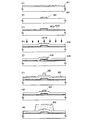
本実施形態では、LRTAを行い酸化物半導体膜の一部の結晶性を改善した領域をチャネル形成領域に用いるTFTの作製工程について図1(A)、(B)を用いて説明する。
(Embodiment 1)
In this embodiment, a manufacturing process of a TFT in which a region where the crystallinity of part of an oxide semiconductor film is improved by LRTA is used for a channel formation region will be described with reference to FIGS.
まず、基板101上に下地膜102を形成する。基板101には、ポリエチレンテレフタレート(PET)、ポリエチレンナフタレート(PEN)、ポリエーテルサルフォン(PES)、アクリル、ポリイミド等のプラスチック(合成樹脂)やガラスを用いることができる。
First, the
下地膜102としては、酸化珪素膜、窒化珪素膜または酸化窒化珪素膜(SiOxNy)(x>y)、窒化酸化珪素膜(SiNxOy)(x>y)等の絶縁膜の単層、或いは積層したものを用いる。なお、下地膜102は、スパッタリング法やCVD法などにより形成すればよい。なお、下地膜102は設けなくてもよいが、本発明においては形成した方が好ましい。下地膜102を形成することにより、下地膜102上に形成された電極や配線などから発生した熱が基板101に伝導するのを抑制することができる。下地膜102として、例えば、膜厚10〜400nmの窒化酸化珪素膜を用いることができる。次いで、下地膜102上にゲート電極103を形成する。
As the
ゲート電極103は、スパッタリング法により膜厚100〜200nmを形成すればよい。また、ゲート電極103は、タンタル(Ta)、タングステン(W)、チタン(Ti)、モリブデン(Mo)、クロム(Cr)、ニオブ(Nb)等から選択された元素またはこれらの元素を主成分とする合金材料若しくは化合物材料を用いて形成することができる。また、リン等の不純物元素をドーピングした多結晶珪素に代表される半導体材料により形成することもできる。
The
次いで、ゲート電極103を覆うゲート絶縁膜104を膜厚50〜500nm程度形成する。ゲート絶縁膜104は、スパッタリング法やプラズマCVD法等の各種CVD法により、珪素の酸化物または珪素の窒化物を含む膜を、単層または積層して形成する。具体的には、酸化珪素を含む膜(SiOx)、酸化窒化珪素を含む膜(SiOxNy)、窒化酸化珪素を含む膜(SiNxOy)を、単層構造として形成するか、当該これらの膜を適宜積層して形成する。また、ゲート電極103に酸素、窒素、または酸素及び窒素を含む雰囲気中で、高密度プラズマ処理を行うことにより、ゲート電極103の表面を酸化または窒化して、ゲート絶縁膜を形成してもよい。高密度プラズマ処理により形成されたゲート絶縁膜は、膜厚や膜質などの均一性に優れ、且つ緻密な膜を形成することができる。酸素を含む雰囲気としては、酸素(O2)、二酸化窒素(NO2)、もしくは一酸化二窒素(N2O)と、希ガスとの混合ガス、または、酸素(O2)、二酸化窒素(NO2)もしくは一酸化二窒素(N2O)と、希ガスと、水素(H2)との混合ガスを用いることができる。また、窒素を含む雰囲気としては、窒素(N2)もしくはアンモニア(NH3)と、希ガスとの混合ガス、または、窒素(N2)もしくはアンモニア(NH3)と、希ガスと、水素(H2)との混合ガスを用いることができる。高密度プラズマにより生成された酸素ラジカル(OHラジカルを含む場合もある)や窒素ラジカル(NHラジカルを含む場合もある)によって、ゲート電極103の表面を酸化又は窒化することができる。
Next, a
高密度プラズマ処理を行ってゲート絶縁膜104を形成する場合、1〜20nm、代表的には5〜10nmの絶縁膜がゲート電極103を覆うように形成される。この場合の反応は固相反応であるため、当該ゲート絶縁膜104とゲート電極103との界面準位密度をきわめて低くすることができる。また、ゲート電極103を直接酸化または窒化するため、形成されるゲート絶縁膜104の厚さを、均一にすることができる。すなわち、ここで示す高密度プラズマ処理で電極の表面を固相酸化することにより、均一性が良く、界面準位密度が低い絶縁膜を形成することができる。ここでは、タンタル(Ta)、タングステン(W)、チタン(Ti)、モリブデン(Mo)、クロム(Cr)、ニオブ(Nb)等から選択された元素またはこれらの元素を主成分とする合金材料若しくは化合物材料の酸化物がゲート絶縁膜104として機能する。
In the case where the
なお、ゲート絶縁膜104は、高密度プラズマ処理によって形成される絶縁膜のみを用いてもよいし、それに加えてプラズマや熱反応を利用したCVD法により酸化珪素、酸素を含む窒化珪素、窒素を含む酸化珪素などの絶縁膜を堆積し、少なくとも一つ積層させても良い。いずれにしても、高密度プラズマで形成した絶縁膜がゲート絶縁膜の一部又は全部であるトランジスタは、特性のばらつきを小さくすることができる。
Note that as the
また、ゲート絶縁膜104は、酸化物半導体膜との整合性の良好なアルミナ(Al2O3)、窒化アルミニウム(AlN)、酸化チタン(TiO2)、ジルコニア(ZrO2)、酸化リチウム(Li2O)、酸化カリウム(K2O)酸化ナトリウム(Na2O)、酸化インジウム(In2O3)、酸化イットリウム(Y2O3)、ジルコン酸カルシウム(CaZrO3)又はこれらのうち少なくとも2つを含む材料を用いてもよく、単層又は2層以上積層させて形成してもよい。
The
次いで、ゲート絶縁膜104上に配線105を膜厚50〜200nmとなるように形成する。配線材料としては、銀(Ag)、アルミニウム(Al)、金(Au)、銅(Cu)及びそれらの合金などを用いる。配線材料は、ゲート電極103に用いる材料よりも反射率の高いものであればよく、ゲート電極103との関係を考慮して適宜組み合わせて用いる。なお、配線は積層して形成してもよく、例えば、基板側からアルミニウム、チタンの積層配線としてもよい。チタンは、酸化物半導体膜とアルミニウムとの電気的な接触特性を良好にするのに有効である。また、アルミニウムが酸化物半導体膜中に拡散するのを抑制する役目も担っている。また、配線は透明導電膜、例えば、インジウム錫酸化物(ITO:Indium Tin Oxide)、酸化珪素を含むインジウム錫酸化物(ITSO)、インジウム亜鉛酸化物(IZO:Indium Zinc Oxide)、酸化インジウム(In2O3)、酸化錫(SnO2)、酸化亜鉛(ZnO)、アルミニウムを添加した酸化亜鉛(AlZnO)、ガリウムを添加した酸化亜鉛(GaZnO)酸化亜鉛(ZnO)、などで形成してもよい。なお、配線105は、ゲート電極103よりもランプ光に対して反射率の高い若しくは透過率の高い(又は熱吸収率の低い)ものを用いるとよい。
Next, the
次いで、ゲート絶縁膜104及び配線105上に酸化物半導体膜106を形成する。酸化物半導体膜106は、1族元素(例えば、リチウム(Li)、ナトリウム(Na)、カリウム(K)、ルビジウム(Rb)、セシウム(Cs))、13族元素(例えば、ボロン(B)、ガリウム(Ga)、インジウム(In)、タリウム(Tl))、14族元素(例えば、炭素(C)、シリコン(Si)、ゲルマニウム(Ge)、スズ(Sn)、鉛(Pb))、15族元素(例えば、窒素(N)、リン(P)、ヒ素(As)、アンチモン(Sb)、ビスマス(Bi))又は17族元素(例えば、フッ素(F)、塩素(Cl)、臭素(Br)、ヨウ素(I))等の不純物元素のうち一種、又は複数種が添加された酸化亜鉛(ZnO)の非晶質(アモルファス)状態、多結晶状態又は非晶質状態と多結晶状態が混在する微結晶(マイクロクリスタルとも呼ばれる。)状態のもの、又は何も不純物元素が添加されていないものを用いることができる。また、InGaO3(ZnO)5、酸化マグネシウム亜鉛(MgxZn1−xO)又は酸化カドミウム亜鉛(CdxZn1−xO)、酸化カドミウム(CdO)、In−Ga−Zn−O系のアモルファス酸化物半導体(a−IGZO)のうちいずれかを用いることができる。酸化物半導体膜106は25〜200nm(好ましくは30〜150nm)の厚さで0.4Paの圧力のもと、Ar:O2=50:5sccmの流量となる条件でスパッタリング法により成膜し、その後、0.05%に希釈したフッ酸を用いてエッチングにより所望の形状に形成する。酸化物半導体膜106は、非晶質珪素膜を用いた半導体膜と比べて、酸化のおそれがなく高真空にせずとも成膜できるため、プロセスとして安価である。なお、酸化亜鉛を有する酸化物半導体膜はプラズマに強いため、プラズマCVD(PCVD又はPECVDともいう)法を用いて成膜してもよい。プラズマCVD法はCVD法の中でも特に装置が簡単であり、生産性もよい。
Next, the
次いで、基板101の裏面へLRTAを行う(図1(A))。LRTAは、250〜570℃(好ましくは300℃〜400℃、より好ましくは300〜350℃)で1分〜1時間、好ましくは10分〜30分行うとよい。LRTAは、ハロゲンランプ、メタルハライドランプ、キセノンアークランプ、カーボンアークランプ、高圧ナトリウムランプ、高圧水銀ランプから選ばれた一種または複数種からの輻射により行う。LRTA法は、短時間での熱処理が可能であるため、ゲート電極103よりも配線105の反射率若しくは透過率が高ければ比較的融点の低い材料を用いることができる。LRTA法には、赤外光領域、可視光領域、紫外光領域等の波長の光を用いることができる。なお、LRTAの代わりにレーザ光を照射して加熱処理を行ってもよく、例えば、レーザ光として赤外光レーザ、可視光レーザ、紫外光レーザ等を用いることができる。また、LRTA及びレーザ光照射を組み合わせて選択的に酸化物半導体膜の結晶性を改善してもよい。レーザ照射を用いる場合、連続発振型のレーザビーム(CWレーザビーム)やパルス発振型のレーザビーム(パルスレーザビーム)を用いることができる。ここで用いることができるレーザビームは、Arレーザ、Krレーザ、エキシマレーザなどの気体レーザ、単結晶のYAG、YVO4、フォルステライト(Mg2SiO4)、YAlO3、GdVO4、若しくは多結晶(セラミック)のYAG、Y2O3、YVO4、YAlO3、GdVO4に、ドーパントとしてNd、Yb、Cr、Ti、Ho、Er、Tm、Taのうち1種または複数種添加されているものを媒質とするレーザ、ガラスレーザ、ルビーレーザ、アレキサンドライトレーザ、Ti:サファイアレーザ、銅蒸気レーザまたは金蒸気レーザのうち一種または複数種から発振されるものを用いることができる。このようなレーザビームの基本波、及びこれらの基本波の第2高調波から第4高調波のレーザビームを照射することで、結晶性を良好にすることができる。なお、レーザ光は酸化物半導体膜のバンドギャップよりもエネルギーの大きいものを用いる方が好ましい。例えば、KrF、ArF、XeCl、又はXeFのエキシマレーザ発振器から射出されるレーザ光を用いてもよい。
Next, LRTA is performed on the back surface of the substrate 101 (FIG. 1A). LRTA is performed at 250 to 570 ° C. (preferably 300 ° C. to 400 ° C., more preferably 300 to 350 ° C.) for 1 minute to 1 hour, preferably 10 minutes to 30 minutes. The LRTA is performed by radiation from one or more kinds selected from a halogen lamp, a metal halide lamp, a xenon arc lamp, a carbon arc lamp, a high pressure sodium lamp, and a high pressure mercury lamp. Since the LRTA method can perform heat treatment in a short time, a material having a relatively low melting point can be used as long as the reflectance or transmittance of the
このとき、ゲート電極103は配線105よりもランプ光に対する反射率が低く、より熱を吸収する材料を用いるため、配線105よりも高い温度まで加熱される。そのため、ゲート電極103周辺の酸化物半導体膜106が加熱され、第2の酸化物半導体領域108及び第2の酸化物半導体領域108よりも結晶性が良好な領域を有する第1の酸化物半導体領域107が形成される(図1(B)参照)。ここでは、ハロゲンランプを用いてゲート電極103にランプ光を照射しておよそ300℃に加熱し、その熱により酸化物半導体膜106を結晶化させ結晶性を改善させる。このとき、配線105は、ゲート電極103よりもランプ光に対する反射率若しくは透過率が高いものを用いるので、酸化物半導体膜106を結晶化させたとしても配線105の温度は300℃以下となる。
At this time, the
ここで、酸化物半導体膜として用いられるZnOの結晶性の熱処理温度依存性について図2に示す。図2は、流量Ar:O2=50:5(sccm)の割合とする成膜ガスを、吹き付けた状態(as−depo)、200℃、300℃、350℃の夫々の温度で1hr加熱したときの(002)面のX線強度を測定した結果を示す。熱処理温度が上昇するにつれ、(002)面の強度ピークは大きくなっている。したがって、少なくとも350℃までは、熱処理温度が高くなるほどZnOの結晶性は高くなる。一般的に結晶化が進むほど移動度は上がるため、熱処理は350℃前後で行った方が望ましい。なお、基板にシュリンク等の支障がなければZnOが400℃前後に加熱されるような熱処理を行ってもよい。 Here, FIG. 2 shows the heat treatment temperature dependence of the crystallinity of ZnO used as the oxide semiconductor film. FIG. 2 shows that a film-forming gas having a flow rate of Ar: O 2 = 50: 5 (sccm) was heated for 1 hour at a temperature of 200 ° C., 300 ° C., and 350 ° C. in a sprayed state (as-depo). The result of having measured the X-ray intensity of (002) plane at the time is shown. As the heat treatment temperature increases, the intensity peak on the (002) plane increases. Therefore, at least up to 350 ° C., the higher the heat treatment temperature, the higher the crystallinity of ZnO. In general, as the crystallization progresses, the mobility increases. Therefore, it is desirable to perform the heat treatment at around 350 ° C. Note that heat treatment may be performed so that ZnO is heated to around 400 ° C. if there is no problem such as shrinkage on the substrate.
一方、図1(A)においてゲート電極103及び配線105が形成されていない領域、つまり、基板101、下地膜102、ゲート絶縁膜104及び酸化物半導体膜106が積層されている領域では、配線105又はゲート電極103が形成されている領域と比べてランプ光は透過するため、熱を吸収しにくく加熱温度は配線105よりも低い温度となる。したがって、基板101は、大半の領域で350℃以下となるため、シュリンクが生じにくくなる。なお、ゲート電極103が形成されていない領域が大きければ大きいほど基板101のシュリンクは抑制される。
On the other hand, in the region where the
次いで、酸化物半導体膜106上に層間絶縁膜、ソース電極、ドレイン電極、画素電極、発光素子などの構造を形成することで半導体装置を作製する。
Next, a semiconductor device is manufactured by forming structures such as an interlayer insulating film, a source electrode, a drain electrode, a pixel electrode, and a light-emitting element over the
本発明では半導体としてZnOを用いる場合、300℃程度の熱処理温度でZnO層の結晶性が改善するため、結晶性珪素膜を半導体膜に用いる場合と比較して、熱処理温度を抑えることができる。また、透光性の高い酸化物半導体膜を用い、LRTAにより選択的にゲート電極を加熱するため、基板の大半は加熱されず基板のシュリンクを抑制することができる。また、ゲート電極よりもランプ光に対する反射率が高い材料を配線に用いるため、配線が加熱される温度を350℃程度と抑えても酸化物半導体膜の結晶性を改善することができる。そのため、融点が低いAl配線を用いることができる。また、酸化物半導体膜中の酸素がAlに拡散して絶縁膜を形成することを防止することができる。Al配線は、安価かつ低抵抗であるため、性能のよい半導体装置を低コストで生産性良く作製することができる。 In the present invention, when ZnO is used as a semiconductor, the crystallinity of the ZnO layer is improved at a heat treatment temperature of about 300 ° C. Therefore, the heat treatment temperature can be suppressed as compared with the case where a crystalline silicon film is used for a semiconductor film. In addition, since the gate electrode is selectively heated by LRTA using a highly light-transmitting oxide semiconductor film, most of the substrate is not heated and shrinkage of the substrate can be suppressed. In addition, since a material having higher reflectance with respect to lamp light than the gate electrode is used for the wiring, the crystallinity of the oxide semiconductor film can be improved even when the temperature at which the wiring is heated is suppressed to about 350 ° C. Therefore, an Al wiring having a low melting point can be used. In addition, oxygen in the oxide semiconductor film can be prevented from diffusing into Al to form an insulating film. Since the Al wiring is inexpensive and has low resistance, a semiconductor device with good performance can be manufactured at low cost with high productivity.
(実施の形態2)
本実施形態では、実施形態1とは異なる構造について図3(A)〜(C)を用いて説明する。なお、基板301上に下地膜302、ゲート電極303、ゲート絶縁膜304を形成するまでの工程は実施の形態1の基板101上に下地膜102、ゲート電極103、ゲート絶縁膜104を形成するまでの工程を参照されたい。
(Embodiment 2)
In this embodiment, a structure different from that in Embodiment 1 will be described with reference to FIGS. Note that the processes until the
ゲート絶縁膜304上に第1の酸化物半導体膜305を形成する。酸化物半導体膜305は、1族元素、13族元素、14族元素、15族元素又は17族元素の不純物元素のうち一種又は複数種が添加された酸化亜鉛(ZnO)の非晶質(アモルファス)状態、多結晶状態又は非晶質状態と多結晶状態が混在する微結晶(マイクロクリスタルとも呼ばれる。)状態のもの、又は何も不純物元素が添加されていないものを用いることができる。また、InGaO3(ZnO)5、酸化マグネシウム亜鉛(MgxZn1−xO)又は酸化カドミウム亜鉛(CdxZn1−xO)、酸化カドミウム(CdO)、In−Ga−Zn−O系のアモルファス酸化物半導体(a−IGZO)のうちいずれかを用いることができる。ここでは、第1の酸化物半導体膜305は酸化亜鉛を50〜200nm(好ましくは100〜150nm)の厚さでスパッタリング法により成膜する。
A first
次いで、結晶性を良好にするため基板表面からLRTAを行う(図3(A)。LRTAは、250〜570℃(好ましくは300℃〜400℃、より好ましくは300〜350℃)で1分〜1時間、好ましくは10分〜30分行えばよく、ハロゲンランプ、メタルハライドランプ、キセノンアークランプ、カーボンアークランプ、高圧ナトリウムランプ、高圧水銀ランプから選ばれた一種または複数種からの輻射により行う。本実施形態では、酸素雰囲気中においてゲート電極303がおよそ300℃となるように30分間のランプ加熱を行い、ゲート絶縁膜304を間に挟んでゲート電極303と重なる第1の酸化物半導体膜305の領域の結晶性を向上させる。第1の酸化物半導体膜305は透光性を有するため、ゲート電極303が優先して加熱されることでゲート電極303の周囲から外側に向けて第1の酸化物半導体膜305の結晶性が上がる。そして、図3(B)に示すように、第2の酸化物半導体領域309と、第2の酸化物半導体領域309よりも結晶性の良好な第1の酸化物半導体領域308を有する第2の酸化物半導体膜が形成される。なお、図3(A)では、基板301表面側へランプ加熱しているが基板裏面へLRTAしてもよい。酸化物半導体膜305は透光性を有するため、基板の大半の領域はLRTAを行っても加熱されにくい。そのため、基板に融点の低い樹脂などを用いても基板の縮み等による変形を抑制することができる。なお、LRTAの出力を上げて基板表面よりランプ加熱を行うことにより、直接酸化物半導体膜の表面近傍の結晶性を改善させてもよい。また、ランプ光の波長、ゲート電極の反射率及び酸化物半導体膜の膜厚を調節することにより、基板表面からランプ加熱を行う際、ゲート電極で反射したランプ光が酸化物半導体膜のゲート絶縁膜304側の表面付近で吸収され、ゲート電極と重なる酸化物半導体膜のゲート絶縁膜304側の表面付近が優先的に結晶化するようにしてもよい。また、基板にガラス基板を用いる場合、ランプ光は可視光から赤外光領域を利用する。この波長領域の光はガラス基板に吸収されにくいため、ガラス基板が加熱されるのを最小限に抑えることができる。なお、ランプ加熱は複数回行ってもよい。複数回行うことにより、基板温度の上昇を抑えつつゲート電極の加熱時間を稼ぐことができる。
Next, LRTA is performed from the substrate surface in order to improve the crystallinity (FIG. 3A). LRTA is 250 to 570 ° C. (preferably 300 to 400 ° C., more preferably 300 to 350 ° C.) for 1 minute to It may be performed for 1 hour, preferably 10 minutes to 30 minutes, and is performed by radiation from one or more kinds selected from a halogen lamp, a metal halide lamp, a xenon arc lamp, a carbon arc lamp, a high pressure sodium lamp, and a high pressure mercury lamp. In the embodiment, the region of the first
なお、LRTAの代わりにレーザ光や紫外光を照射、若しくはそれらを組み合わせて選択的に酸化物半導体膜の結晶性を改善してもよい。レーザ照射を用いる場合、連続発振型のレーザビーム(CWレーザビーム)やパルス発振型のレーザビーム(パルスレーザビーム)を用いることができる。ここで用いることができるレーザビームは、Arレーザ、Krレーザ、エキシマレーザなどの気体レーザ、単結晶のYAG、YVO4、フォルステライト(Mg2SiO4)、YAlO3、GdVO4、若しくは多結晶(セラミック)のYAG、Y2O3、YVO4、YAlO3、GdVO4に、ドーパントとしてNd、Yb、Cr、Ti、Ho、Er、Tm、Taのうち1種または複数種添加されているものを媒質とするレーザ、ガラスレーザ、ルビーレーザ、アレキサンドライトレーザ、Ti:サファイアレーザ、銅蒸気レーザまたは金蒸気レーザのうち一種または複数種から発振されるものを用いることができる。このようなレーザビームの基本波、及びこれらの基本波の第2高調波から第4高調波のレーザビームを照射することで、結晶性を良好にすることができる。なお、レーザ光は酸化物半導体膜のバンドギャップよりもエネルギーの大きいものを用いる方が好ましい。例えば、KrF、ArF、XeCl、又はXeFのエキシマレーザ発振器から射出されるレーザ光を用いてもよい。 Note that the crystallinity of the oxide semiconductor film may be selectively improved by irradiation with laser light or ultraviolet light instead of LRTA, or a combination thereof. In the case of using laser irradiation, a continuous wave laser beam (CW laser beam) or a pulsed laser beam (pulse laser beam) can be used. The laser beam that can be used here is a gas laser such as an Ar laser, a Kr laser, or an excimer laser, single crystal YAG, YVO 4 , forsterite (Mg 2 SiO 4 ), YAlO 3 , GdVO 4 , or polycrystalline ( (Ceramics) YAG, Y 2 O 3 , YVO 4 , YAlO 3 , GdVO 4 with one or more of Nd, Yb, Cr, Ti, Ho, Er, Tm, Ta added as dopants A laser oscillated from one or more of laser, glass laser, ruby laser, alexandrite laser, Ti: sapphire laser, copper vapor laser, or gold vapor laser as a medium can be used. By irradiating the fundamental wave of such a laser beam and the second to fourth harmonics of these fundamental waves, the crystallinity can be improved. Note that it is preferable to use laser light having energy larger than the band gap of the oxide semiconductor film. For example, laser light emitted from an excimer laser oscillator of KrF, ArF, XeCl, or XeF may be used.
次いで、第1の酸化物半導体領域308及び第2の酸化物半導体領域309上にスパッタリング法によりTiとAlを順に堆積し、Ti層とAl層を形成する。その後、Ti及びAl層をフォトリソグラフィー及びCl2ガスを用いてドライエッチングすることでソース配線及びドレイン配線となる配線306と配線307を形成する(図3(C))。配線306、307は、加速電圧1.5kw、圧力0.4Pa、Ar(流量30sccm)を用いて10〜200nmの膜厚で成膜する。なお、配線306、307は積層して形成しているが、酸化物半導体膜305との整合性がよい材料を用いるのであれば配線306、配線307は単層でもよい。なお、配線306、307として、アルミニウム(Al)、タングステン(W)、モリブデン(Mo)、ジルコニウム(Zr)、ハフニウム(Hf)、バナジウム(V)、ニオブ(Nb)、タンタル(Ta)、クロム(Cr)、コバルト(Co)、ニッケル(Ni)、白金(Pt)、チタン(Ti)、ネオジウム(Nd)等の金属又はその合金、若しくはその金属窒化物または、インジウム錫酸化物(ITO)、インジウム亜鉛酸化物(IZO)、酸化珪素を含むインジウム錫酸化物(ITSO)、酸化インジウム(In2O3)、酸化錫(SnO2)、酸化亜鉛(ZnO)、アルミニウムを添加した酸化亜鉛(AlZnO)、ガリウムを添加した酸化亜鉛(GaZnO)などの透光性を有する材料を適宜用いることができる。
Next, Ti and Al are sequentially deposited over the first
その後、酸化物半導体膜305、配線306、配線307上に層間絶縁膜、配線、画素電極、発光素子などの構造を形成することで半導体装置を作製する。
After that, a semiconductor device is manufactured by forming structures such as an interlayer insulating film, a wiring, a pixel electrode, and a light-emitting element over the
本実施形態では、酸化物半導体膜305にLRTAして結晶性を改善した後に配線を形成している。そのため、配線306は、ゲート電極303よりもランプ光に対する反射率が低い材料を用いても構わず、配線の材料は酸化物半導体膜305と整合性がよいものであれば実施形態1に挙げた材料に限られない。
In this embodiment, the wiring is formed after LRTA is performed on the
なお、LRTAによる加熱は、酸化物半導体膜305を成膜後、所望の形状に加工する前でも後に行ってもよい。
Note that heating by LRTA may be performed after the
本発明では半導体膜として酸化亜鉛を用いる場合、300℃程度の熱処理温度で半導体膜の結晶性が改善するため、結晶性珪素膜を半導体膜に用いる場合と比較して、熱処理温度を抑えることができ、低コストで結晶化工程を行うことができる。また、透光性の高い酸化物半導体膜を用い、LRTAにより選択的にゲート電極を加熱するため、基板の大半は加熱されず基板のシュリンクを抑制することができる。 In the present invention, when zinc oxide is used as the semiconductor film, the crystallinity of the semiconductor film is improved at a heat treatment temperature of about 300 ° C., so that the heat treatment temperature can be suppressed as compared with the case where a crystalline silicon film is used for the semiconductor film. The crystallization process can be performed at low cost. In addition, since the gate electrode is selectively heated by LRTA using a highly light-transmitting oxide semiconductor film, most of the substrate is not heated and shrinkage of the substrate can be suppressed.
(実施の形態3)
本発明の実施の形態について、図4、図5を用いて説明する。本実施の形態は、チャネル保護型の薄膜トランジスタを有する半導体装置の例である。
(Embodiment 3)
An embodiment of the present invention will be described with reference to FIGS. This embodiment is an example of a semiconductor device including a channel protective thin film transistor.
基板400は、バリウムホウケイ酸ガラス、アルミノホウケイ酸ガラス等からなるガラス基板、シリコン基板、耐熱性を有するプラスチック基板又は樹脂基板を用いる。プラスチック基板又は樹脂基板として、ポリエチレンテレフタレート(PET)、ポリエチレンナフタレート(PEN)、ポリエーテルサルフォン(PES)、アクリル、ポリイミド等を用いることができる。また、基板400の表面が平坦化されるようにCMP法などによって、研磨しても良い。なお、基板400上に、絶縁層を形成してもよい。絶縁層は、CVD法、プラズマCVD法、スパッタリング法、スピンコート法等の公知の方法により、珪素を含む酸化物材料、窒化物材料を少なくとも一つ用いて、単層又は積層して形成される。この絶縁層は、形成しなくても良いが、基板400からの汚染物質などを遮断する効果や基板に熱が伝わるのを抑制する効果がある。
As the
基板400上に導電膜401を形成する。導電膜401は、所望の形状に加工されゲート電極となる。導電膜401は、印刷法、電界メッキ法、蒸着法等の手法によりLRTA加熱に用いる光源の波長に対する反射率が低い(熱を吸収しやすい、つまり加熱されやすい)材料を用いて形成することが好ましい。反射率の低い材料を用いることにより、後の加熱工程が可能となる。導電膜401としては、タングステン(W)、モリブデン(Mo)、ジルコニウム(Zr)、ハフニウム(Hf)、バナジウム(V)、ニオブ(Nb)、タンタル(Ta)、クロム(Cr)、コバルト(Co)、ニッケル(Ni)、白金(Pt)、チタン(Ti)、ネオジウム(Nd)等の金属又はその合金、若しくはその金属窒化物を適宜用いることができる。また、これら複数の層を積層して形成しても良い。代表的には、基板表面に窒化タンタル膜、その上にタングステン膜を積層してもよい。また、珪素に一導電型を付与する不純物元素を添加した材料を用いても良い。例えば、非晶質珪素膜にリン(P)などのn型を付与する不純物元素が含まれたn型を有する珪素膜などを用いることができる。導電膜401は、10nm〜200nmの膜厚で成膜する。
A
本実施の形態では、タングステン(W)をスパッタリング法により膜厚150nmの導電膜401を形成する。
In this embodiment, the
導電膜401上にフォトリソグラフィ工程を用いてレジストからなるマスクを形成し、マスクを用いて導電膜401を所望の形状に加工してゲート電極402を形成する(図4(B)参照)。
A resist mask is formed over the
次いで、ゲート電極402上にゲート絶縁膜403a、ゲート絶縁膜403bを形成し2層の積層構造とする。積層される絶縁膜は、同チャンバー内で真空を破らずに同一温度下で、反応ガスを切り変えながら連続的に形成するとよい。真空を破らずに連続的に形成すると、積層する膜同士の界面が汚染されるのを防ぐことができる。
Next, a
ゲート絶縁膜403a、ゲート絶縁膜403bは、酸化珪素(SiOx)、窒化珪素(SiNx)、酸化窒化珪素(SiOxNy)(x>y)、窒化酸化珪素(SiNxOy)(x>y)などを適宜用いることができる。更には、ゲート電極402を酸化して、ゲート絶縁膜403aの代わりに、酸化膜を形成しても良い。なお、基板から不純物などの拡散を防止するため、ゲート絶縁膜403aとしては、窒化珪素(SiNx)、窒化酸化珪素(SiNxOy)(x>y)などを用いて形成することが好ましい。また、ゲート絶縁膜403bとしては、酸化珪素(SiOx)、酸化窒化珪素(SiOxNy)(x>y)などを用いて形成することが望ましい。なお、低い成膜温度でゲートリーク電流の少ない緻密な絶縁膜を形成するには、アルゴンなどの希ガス元素を反応ガスに含ませ、形成される絶縁膜中に混入させると良い。本実施の形態では、SiH4、NH3を反応ガスとして形成される膜厚50nm〜140nmの窒化珪素膜を用いてゲート絶縁膜403aを形成し、SiH4及びN2Oを反応ガスとして形成される膜厚100nmの酸化珪素膜を用いてゲート絶縁膜403bを積層して形成する。なお、ゲート絶縁膜403a及びゲート絶縁膜403bの膜厚をそれぞれ50nm〜100nmとすると好ましい。
The
また、ゲート絶縁膜403bは、後に形成する酸化物半導体膜との整合性が良好であるアルミナ(Al2O3)又は窒化アルミ(AlN)により形成してもよい。この場合、ゲート絶縁膜403aは絶縁性の高い酸化珪素、窒化珪素、酸化窒化珪素、窒化酸化珪素などを用い、ゲート絶縁膜403bに酸化物半導体膜との界面特性が良いアルミナ又は窒化アルミを用いることにより、信頼性の高いゲート絶縁膜を形成することができる。なお、ゲート絶縁膜を3層とし、3層目をアルミナ又は窒化アルミを用いたゲート絶縁膜としてもよい。
Alternatively, the
次にゲート絶縁膜403b上に酸化物半導体膜404を形成する。酸化物半導体膜404は流量Ar:O2=50:5sccm、圧力0.4Pa、100nmの厚さでスパッタリング法により成膜する。
Next, the
酸化物半導体膜404は、1族元素、13族元素、14族元素、15族元素又は17族元素等のうち一種、又は複数種の不純物元素が添加されたZnOの非晶質(アモルファス)状態、多結晶状態又は非晶質状態と多結晶状態が混在する微結晶(マイクロクリスタルとも呼ばれる。)状態のもの、又は何も不純物元素が添加されていないものを用いることができる。また、InGaO3(ZnO)5、酸化マグネシウム亜鉛(MgxZn1−xO)又は酸化カドミウム亜鉛(CdxZn1−xO)、酸化カドミウム(CdO)、In−Ga−Zn−O系のアモルファス酸化物半導体(a−IGZO)のうちいずれかを用いることができる。
The
なお、酸化物半導体膜404にZnOを用いる場合、窒素を添加(ドープ)しておくとよい。ZnOは本来n型の半導体の性質を示す。窒素を添加することで窒素がZnOに対してアクセプタ不純物として働くため、結果としてしきい値電圧を制御することができる。
Note that in the case where ZnO is used for the
次いで、基板400表面又は裏面よりLRTA法を用いて酸化物半導体膜404の加熱を行う(図4(D))。LRTAは、ハロゲンランプ、メタルハライドランプ、キセノンアークランプ、カーボンアークランプ、高圧ナトリウムランプ、高圧水銀ランプから選ばれた一種または複数種からの輻射により行う。LRTAは、250〜570℃(好ましくは300℃〜400℃、より好ましくは300〜350℃)で1分〜1時間、好ましくは10分〜30分行うとよい。本実施形態では、ハロゲンランプを光源として酸素雰囲気中で300℃、30分の条件でランプ加熱を行う。
Next, the
LRTAを行うことにより短時間で選択的にゲート電極402が加熱され、その加熱された熱によりゲート電極402の周辺に形成された点線で示す領域434において結晶性が向上した第1の酸化物半導体領域が形成される。一方、点線で示す領域434以外の領域424では、ランプ光の吸収が少ないため、ほとんど加熱されずに済み、第1の酸化物半導体領域と結晶性の異なる第2の酸化物半導体領域が形成される(図4(E))。したがって、ゲート電極402が形成されている領域のみ選択的に加熱され、その他の領域は加熱されないため基板400のシュリンクや撓みを抑制することができる。なお、LRTAの出力を上げて基板表面よりランプ加熱を行うことにより、直接酸化物半導体膜の表面近傍の結晶性を改善させてもよい。また、ランプ光の波長、ゲート電極の反射率及び酸化物半導体膜の膜厚を調節することにより、基板表面からランプ加熱を行う際、ゲート電極で反射したランプ光が酸化物半導体膜のゲート絶縁膜403b側の表面付近で吸収され、ゲート電極と重なる酸化物半導体膜のゲート絶縁膜403b側の表面付近が優先的に結晶化するようにしてもよい。また、基板にガラス基板を用いる場合、ランプ光は可視光から赤外光領域を利用する。この波長領域の光はガラス基板に吸収されにくいため、ガラス基板が加熱されるのを最小限に抑えることができる。なお、ランプ加熱は複数回行ってもよい。複数回行うことにより、基板温度の上昇を抑えつつゲート電極の加熱時間を稼ぐことができる。
By performing LRTA, the
なお、LRTAの代わりにレーザ光や紫外光を照射、若しくはそれらを組み合わせて選択的に酸化物半導体膜の結晶性を改善してもよい。レーザ照射を用いる場合、連続発振型のレーザビーム(CWレーザビーム)やパルス発振型のレーザビーム(パルスレーザビーム)を用いることができる。ここで用いることができるレーザビームは、Arレーザ、Krレーザ、エキシマレーザなどの気体レーザ、単結晶のYAG、YVO4、フォルステライト(Mg2SiO4)、YAlO3、GdVO4、若しくは多結晶(セラミック)のYAG、Y2O3、YVO4、YAlO3、GdVO4に、ドーパントとしてNd、Yb、Cr、Ti、Ho、Er、Tm、Taのうち1種または複数種添加されているものを媒質とするレーザ、ガラスレーザ、ルビーレーザ、アレキサンドライトレーザ、Ti:サファイアレーザ、銅蒸気レーザまたは金蒸気レーザのうち一種または複数種から発振されるものを用いることができる。このようなレーザビームの基本波、及びこれらの基本波の第2高調波から第4高調波のレーザビームを照射することで、結晶性を良好にすることができる。なお、レーザ光は酸化物半導体膜のバンドギャップよりもエネルギーの大きいものを用いる方が好ましい。例えば、KrF、ArF、XeCl、又はXeFのエキシマレーザ発振器から射出されるレーザ光を用いてもよい。 Note that the crystallinity of the oxide semiconductor film may be selectively improved by irradiation with laser light or ultraviolet light instead of LRTA, or a combination thereof. In the case of using laser irradiation, a continuous wave laser beam (CW laser beam) or a pulsed laser beam (pulse laser beam) can be used. The laser beam that can be used here is a gas laser such as an Ar laser, a Kr laser, or an excimer laser, single crystal YAG, YVO 4 , forsterite (Mg 2 SiO 4 ), YAlO 3 , GdVO 4 , or polycrystalline ( (Ceramics) YAG, Y 2 O 3 , YVO 4 , YAlO 3 , GdVO 4 with one or more of Nd, Yb, Cr, Ti, Ho, Er, Tm, Ta added as dopants A laser oscillated from one or more of laser, glass laser, ruby laser, alexandrite laser, Ti: sapphire laser, copper vapor laser, or gold vapor laser as a medium can be used. By irradiating the fundamental wave of such a laser beam and the second to fourth harmonics of these fundamental waves, the crystallinity can be improved. Note that it is preferable to use laser light having energy larger than the band gap of the oxide semiconductor film. For example, laser light emitted from an excimer laser oscillator of KrF, ArF, XeCl, or XeF may be used.
次いで、酸化物半導体膜404上に、保護膜405を形成し、保護膜405上にレジスト406を形成する(図4(F)参照)。レジスト406をマスクとしてフォトリソグラフィ工程により保護膜405を所望の形状に加工してチャネル保護膜407を形成する。チャネル保護膜には、酸化珪素(SiOx)、窒化珪素(SiNx)、酸化窒化珪素(SiOxNy)(x>y)、窒化酸化珪素(SiNxOy)(x>y)などを適宜用いることができる。チャネル保護膜407を形成することにより、ソース電極層、ドレイン電極層を形成する際にチャネル部の半導体層のエッチングを防ぐことが出来る。本実施形態では、保護膜405として窒化珪素を成膜して、チャネル保護膜407を形成する(図4(G)参照)。
Next, a
次に、酸化物半導体膜404をフォトリソグラフィ工程を用いてレジストによるマスク408を作製し(図4(H))、マスク408を用いてエッチングを行い、所望の形状に加工された酸化物半導体膜409(島状酸化物半導体膜ともいう)を形成する(図5(A))。なお、エッチングには、希釈したフッ酸を用いる。その後、酸化物半導体膜409上に第1の導電膜411、第2の導電膜412を形成し、フォトリソグラフィ工程を用いてレジストによるマスク413を形成する(図5(B))。マスク413を用いて第1の導電膜411、第2の導電膜412を所望の形状に加工し、ソース電極又はドレイン電極として機能する第1の導電膜414a、414b、第2の導電膜415a、415bを形成する(図5(C))。
Next, a
マスクは、感光剤を含む市販のレジスト材料を用いてもよく、例えば、代表的なポジ型レジストである、ノボラック樹脂と感光剤であるナフトキノンジアジド化合物、ネガ型レジストであるベース樹脂、ジフェニルシランジオール及び酸発生剤などを用いてもよい。いずれの材料を用いるとしても、その表面張力と粘度は、溶媒の濃度を調整したり、界面活性剤等を加えたりして適宜調整する。また導電膜に感光性を有する感光性物質を含む導電性材料を用いると、レジストからなるマスクを形成しなくても導電膜に直接レーザ光を照射し、露光、エッチャントによる除去を行うことで、所望の形状に加工することができる。この場合、マスクを形成せずともよいので工程が簡略化する利点がある。 For the mask, a commercially available resist material containing a photosensitizer may be used. For example, a novolak resin that is a typical positive resist and a naphthoquinonediazide compound that is a photosensitizer, a base resin that is a negative resist, diphenylsilanediol In addition, an acid generator or the like may be used. Whichever material is used, the surface tension and viscosity are appropriately adjusted by adjusting the concentration of the solvent or adding a surfactant or the like. Further, when a conductive material containing a photosensitive substance having photosensitivity is used for the conductive film, the conductive film is directly irradiated with laser light without forming a resist mask, and exposure and removal by an etchant are performed. It can be processed into a desired shape. In this case, there is an advantage that the process is simplified because it is not necessary to form a mask.
感光性物質を含む導電性材料としては、Ag、Au、Cu、Ni、Al、Ptなどの金属或いは合金と、有機高分子樹脂、光重合開始剤、光重合単量体、または溶剤などからなる感光性樹脂とを含んだものを用いればよい。有機高分子樹脂としては、ノボラック樹脂、アクリル系コポリマー、メタクリル系コポリマー、セルローズ誘導体、環化ゴム系樹脂などを用いる。 The conductive material containing a photosensitive substance is composed of a metal or alloy such as Ag, Au, Cu, Ni, Al, Pt, and an organic polymer resin, a photopolymerization initiator, a photopolymerization monomer, or a solvent. What contains the photosensitive resin may be used. As the organic polymer resin, a novolak resin, an acrylic copolymer, a methacrylic copolymer, a cellulose derivative, a cyclized rubber resin, or the like is used.
なお、第1の導電膜411を形成する前に、酸化物半導体膜404上に、n型の酸化物半導体として、例えば、アルミニウムを添加した酸化亜鉛(AlZnO)又はガリウムを添加した酸化亜鉛(GaZnO)からなる導電膜をもう一層設けてもよい。AlZnOまたはGaZnOからなる導電膜を形成することにより第1の導電膜411と酸化物半導体膜409との整合性が良くなりソース電極及びドレイン電極との接触抵抗を下げることができる。また、例えば、GaZnO上にTi或いはTi上にGaZnOを形成した積層構造としてもよい。
Note that before the first
また、第1の導電膜414a、414b及び第2の導電膜415a、415bとして、アルミニウム(Al)、タングステン(W)、モリブデン(Mo)、ジルコニウム(Zr)、ハフニウム(Hf)、バナジウム(V)、ニオブ(Nb)、タンタル(Ta)、銅(Cu)、クロム(Cr)、コバルト(Co)、ニッケル(Ni)、白金(Pt)、チタン(Ti)、ネオジウム(Nd)等の金属又はその合金、若しくはその金属窒化物を適宜用いることができる。例えば、第1の導電膜がTiで第2の導電膜がAl、第1の導電膜がTaで第2の導電膜がW、第1の導電膜がTaNで第2の導電膜がAl、第1の導電膜がTaNで第2の導電膜がCu、第1の導電膜がTiで第2の導電膜がAlでさらに第3の導電膜としてTiを用いるといった組み合わせも考えられる。また1層目と2層目のいずれか一方にAgPdCu合金を用いても良い。W、AlとSiの合金(Al−Si)、TiNを順次積層した3層構造としてもよい。Wの代わりに窒化タングステンを用いてもよいし、AlとSiの合金(Al−Si)に代えてAlとTiの合金膜(Al−Ti)を用いてもよいし、TiNに代えてTiを用いてもよい。アルミニウムには耐熱性を向上させるためにチタン、シリコン、スカンジウム、ネオジウム、銅などの元素を0.5〜5原子%添加させても良い。
As the first conductive films 414a and 414b and the second
また、第1の導電膜411及び第2の導電膜412を形成する導電性材料として、インジウム錫酸化物(ITO)、インジウム亜鉛酸化物(IZO)、酸化珪素を含むインジウム錫酸化物(ITSO)、酸化インジウム(In2O3)、酸化錫(SnO2)、酸化亜鉛(ZnO)、窒化チタンなどの透光性を有する材料及びそれらを適宜組み合わせて形成してもよい。
In addition, as a conductive material for forming the first
なお本実施形態では、酸化物半導体膜305にLRTAして結晶性を改善した後に第1の導電膜411及び第2の導電膜412を形成している。そのため、第1の導電膜411及び第2の導電膜412は、ゲート電極402よりもランプ光に対する反射率が低い材料を用いても構わず、配線又は電極として用いられる導電性材料は酸化物半導体膜305と整合性がよいものであれば実施形態1に挙げた材料に限らない。
Note that in this embodiment, the first
なお、本実施形態において、エッチング加工は、プラズマエッチング(ドライエッチング)又はウエットエッチングのどちらを採用しても良いが、大面積基板を処理するにはプラズマエッチングが適している。エッチングガスとしては、CF4、NF3、SF6、CHF3などのフッ素系又はCl2、BCl3、SiCl4もしくはCCl4などを代表とする塩素系ガス、あるいはO2のガスを用い、HeやArなどの不活性ガスを適宜加えても良い。また、大気圧放電のエッチング加工を適用すれば、局所的な放電加工も可能であり、基板の全面にマスク層を形成する必要はない。 In this embodiment, plasma etching (dry etching) or wet etching may be employed for the etching process, but plasma etching is suitable for processing a large area substrate. As an etching gas, a fluorine-based gas such as CF 4 , NF 3 , SF 6 , or CHF 3 , a chlorine-based gas typified by Cl 2 , BCl 3 , SiCl 4, CCl 4, or the like, or an O 2 gas is used. An inert gas such as Ar or Ar may be added as appropriate. Further, if an atmospheric pressure discharge etching process is applied, a local electric discharge process is also possible, and it is not necessary to form a mask layer on the entire surface of the substrate.
なお、本実施形態のフォトリソグラフィ工程において、レジストを塗布する前に、酸化物半導体膜表面に、膜厚が数nm程度の絶縁膜を形成してもよい。この工程により酸化物半導体膜とレジストとが直接接触することを回避することが可能であり、レジストに含まれている不純物が酸化物半導体膜中に侵入するのを防止できる。 Note that in the photolithography process of this embodiment, an insulating film with a thickness of about several nanometers may be formed on the surface of the oxide semiconductor film before applying the resist. Through this step, it is possible to avoid direct contact between the oxide semiconductor film and the resist, and impurities contained in the resist can be prevented from entering the oxide semiconductor film.
以上の工程で、チャネル部の半導体層がエッチングされないボトムゲート型(逆スタガ型ともいう。)の薄膜トランジスタを作製することが出来る。なお、本実施形態では、ボトムゲート型のTFTを作製したが、基板上に設けられた酸化物半導体膜上にゲート絶縁膜を介して形成したゲート電極をLRTAで加熱して、少なくとも酸化物半導体膜のチャネル形成領域の結晶性を改善できるのであればトップゲート型TFTであってもよい。 Through the above process, a bottom-gate (also referred to as an inverted staggered) thin film transistor in which the semiconductor layer in the channel portion is not etched can be manufactured. Note that, in this embodiment, a bottom-gate TFT is manufactured. However, at least an oxide semiconductor is formed by heating a gate electrode formed on a substrate provided on a substrate with a gate insulating film interposed therebetween by LRTA. A top gate TFT may be used as long as the crystallinity of the channel formation region of the film can be improved.
本実施形態は、実施形態1、2と適宜組み合わせることができる。
(実施の形態4)
本発明の実施の形態について、図6を用いて説明する。本実施の形態は、実施の形態3において、チャネルエッチ型の薄膜トランジスタを有する半導体装置の例である。よって、同一部分又は同様な機能を有する部分の繰り返しの説明は省略する。
This embodiment can be combined with Embodiments 1 and 2 as appropriate.
(Embodiment 4)
An embodiment of the present invention will be described with reference to FIG. This embodiment is an example of a semiconductor device having a channel-etched thin film transistor in Embodiment 3. Therefore, repetitive description of the same portion or a portion having a similar function is omitted.
基板600上にゲート電極層602を形成し、ゲート電極層602を覆うようにゲート絶縁膜603a及びゲート絶縁膜603bを形成する(図6(A)参照)。ゲート絶縁膜603b上に酸化物半導体膜を形成し、基板表面からLRTAを行い、点線で示す領域にて結晶性が向上した第1の酸化物半導体領域604と、第1の酸化物半導体領域604よりも結晶化が進行していない第2の酸化物半導体領域605を有する酸化物半導体膜を形成する(図6(B)参照)。酸化物半導体膜上にマスク608を設け(図6(C))、フォトリソグラフィ工程を用いて酸化物半導体膜を所望の形状に加工し、酸化物半導体膜609を形成する(図6(D))。
A
次に、第1の導電膜611及び第2の導電膜612を形成する。そして、レジストからなるマスク613を形成する。図6(E)参照)。本実施の形態では、第1の導電膜611及び第2の導電膜612として、それぞれチタンとアルミニウムを含む導電膜をスパッタリング法によって形成する。
Next, a first
その後、フォトリソグラフィ工程によりマスク613を用いて所望の形状に加工し、ソース電極又はドレイン電極として機能する第1の導電膜615a、615b、第2の導電膜616a、616bを形成する(図6(F))。
After that, the first
以上の工程で、半導体層におけるチャネル部の一部がエッチングされている薄膜トランジスタを作製することが出来る。 Through the above process, a thin film transistor in which part of a channel portion in a semiconductor layer is etched can be manufactured.
なお、本実施形態において、酸化物半導体膜と第1の導電膜611の間にn型の酸化物半導体として、例えば、アルミニウムを添加した酸化亜鉛(AlZnO)又はガリウムを添加した酸化亜鉛(GaZnO)からなる導電膜をもう一層設けてもよい。また、例えば、GaZnO上にTi或いはTi上にGaZnOを形成した積層構造としてもよい。n型の酸化物半導体膜を形成することにより、ソース電極及びドレイン電極となる第1の導電膜611と、酸化物半導体膜との接続を良好にし、接触抵抗を下げることができる。
Note that in this embodiment, as an n-type oxide semiconductor between the oxide semiconductor film and the first
本実施形態は、実施形態1、2と適宜組み合わせることができる。
(実施の形態5)
This embodiment can be combined with Embodiments 1 and 2 as appropriate.
(Embodiment 5)
本実施の形態では、実施形態3又は実施形態4で形成したボトムゲート型の薄膜トランジスタと画素電極が接続された発光装置について図7を用いて説明する。なお、本実施の形態の薄膜トランジスタはチャネルエッチ型である。 In this embodiment, a light-emitting device in which the bottom-gate thin film transistor formed in Embodiment 3 or Embodiment 4 and a pixel electrode are connected is described with reference to FIGS. Note that the thin film transistor of this embodiment is a channel etch type.
図7に、駆動回路に用いられるTFTの断面図と、画素部に用いられるTFTの断面図を示す。701は駆動回路に用いられるTFTの断面図に相当し、702は画素部に用いられるTFT断面図に相当し、703は該TFT702によって電流が供給される発光素子の断面図に相当する。TFT701、702はボトムゲート型である。
FIG. 7 shows a cross-sectional view of a TFT used in a driver circuit and a cross-sectional view of a TFT used in a pixel portion.
駆動回路のTFT701は、基板700上に形成されたゲート電極710と、ゲート電極710を覆っているゲート絶縁膜711と、ゲート絶縁膜711を間に挟んでゲート電極710と重なっている、酸化亜鉛を含む酸化物半導体膜712とを有している。さらにTFT701は、ソース電極またはドレイン電極として機能する第1の導電膜713と、第2の導電膜714とを有している。なお、第1の導電膜713及び第2の導電膜714は配線層としても機能する。
The
図7では、ゲート絶縁膜711が2層の絶縁膜で形成されているが、本発明はこの構成に限定されない。ゲート絶縁膜711が単層または3層以上の絶縁膜で形成されていても良い。
In FIG. 7, the
また第2の導電膜714は、アルミニウム又はアルミニウムを含む合金で形成されている。そして一対の第2の導電膜714は、酸化物半導体膜712のチャネル形成領域を間に挟んで、向かい合っている。
The second
また第1の導電膜713は、チタンで形成されている。第1の導電膜713は必ずしも設ける必要はないが、酸化物半導体膜712と第2の導電膜714との電気的接触特性は良好となる。また、酸化物半導体膜712中の酸素が第2の導電膜に拡散するのを防止するバリア層としての機能も有する。その結果、TFTの信頼性を向上させることができる。なお、酸化物半導体膜は特に何をせずともn型を示すことが知られている。よって、チャネルが形成される第1の酸化物半導体膜には、p型の導電性を付与する不純物を添加し、極力I型(真性半導体)に近づくようにその導電型を制御しておいてもよい。
The first
画素部のTFT702は、基板700上に形成されたゲート電極720と、ゲート電極720を覆っているゲート絶縁膜711と、ゲート絶縁膜711を間に挟んでゲート電極720と重なっている、酸化物半導体膜722とを有している。さらにTFT702は、ソース電極またはドレイン電極として機能する一対の第1の導電膜723と、第2の導電膜724とを有している。
The
また第2の導電膜724は、アルミニウム又はアルミニウムを含む合金で形成されている。そして一対の第2の導電膜724は、酸化物半導体膜722のチャネルが形成される領域を間に挟んで、向かい合っている。
The second
また第1の導電膜723は、チタンで形成されている。第1の導電膜723は必ずしも設ける必要はないが、酸化物半導体膜722との電気的接触特性は良好となる。また、酸化物半導体膜722中の酸素が第2の導電膜724に拡散するのを防止するバリア層としての機能も有する。その結果、TFTの信頼性を向上させることができる。なお、酸化物半導体膜722は特に何をせずともn型を示すことが知られている。よって、チャネルが形成される第1の酸化物半導体膜には、p型の導電性を付与する不純物を添加し、極力I型に近づくようにその導電型を制御しておいてもよい。
The first
また、TFT701、702を覆うように、絶縁膜からなる第1のパッシベーション膜740、第2のパッシベーション膜741が形成されている。第1のパッシベーション膜740及び第2のパッシベーション膜741は、プラズマCVD法又はスパッタリング法などの薄膜形成法を用い、窒化珪素、酸化珪素、窒化酸化珪素、酸化窒化珪素、酸化窒化アルミニウム、または酸化アルミニウム、ダイアモンドライクカーボン(DLC)、窒素含有炭素(CN)、その他の絶縁性材料を用いて形成することができる。TFT701、702を覆うパッシベーション膜は2層に限らず、単層であっても良いし、3層以上であっても良い。例えば第1のパッシベーション膜740を窒化珪素、第2のパッシベーション膜741を酸化珪素で形成することができる。窒化珪素または窒化酸化珪素でパッシベーション膜を形成することで、外部からの不純物が半導体素子内に侵入するのを防いだり、TFT701、702が水分などの影響により、劣化するのを防ぐことができる。本実施の形態では、第1のパッシベーション膜740及び第2のパッシベーション膜741は同チャンバー内でガス切り替えを行い連続的に形成した。
In addition, a
次いで、第2の導電膜724の一方を、発光素子703の画素電極730に接続している。
Next, one of the second
次いで、絶縁層729(隔壁、土手、バンク層とも呼ばれる)を選択的に形成する。絶縁層729は、画素電極730上に開口部を有するように形成し、第2パッシベーション膜741を覆って形成する。本実施の形態では、絶縁層729を全面を覆うように形成し、レジスト等のマスクによって、エッチングする。
Next, an insulating layer 729 (also referred to as a partition wall, a bank, or a bank layer) is selectively formed. The insulating
絶縁層729は、酸化珪素、窒化珪素、酸化窒化珪素、酸化アルミニウム、窒化アルミニウム、酸化窒化アルミニウムその他の無機絶縁性材料、又はシロキサン系材料を出発材料として形成された珪素、酸素、水素からなる化合物のうちSi−O−Si結合を含む無機シロキサン系の絶縁材料、珪素と結合している水素がメチルやフェニルのような有機基によって置換された有機シロキサン系の絶縁材料で形成することができる。アクリル樹脂、ポリイミド樹脂等の感光性、非感光性の材料を用いて形成してもよい。絶縁層729は曲率半径が連続的に変化する形状が好ましく、上に形成される電界発光層731、対向電極732の被覆性が向上する。
The insulating
次いで、画素電極730上に接するように、電界発光層731が形成される。電界発光層731として、赤色(R)、緑色(G)、青色(B)の発光を示す材料を、それぞれ蒸着マスクを用いた蒸着法等によって選択的に形成する。赤色(R)、緑色(G)、青色(B)の発光を示す材料はカラーフィルタ同様、液滴吐出法により形成することもでき(低分子または高分子材料など)、この場合マスクを用いずとも、RGBの塗り分けを行うことができるため好ましい。なお、RGBによる三色の組合せの他に、エメラルドグリーンを加えた四色としてもよい。また、朱色を加えてもよい。また、白色発光するEL素子を含む画素を組み合わせても良い。
Next, an
該電界発光層731に接するように対向電極732が形成されている。なお発光素子703は陽極と陰極とを有しているが、いずれか一方を画素電極、他方を対向電極として用いる。こうして、発光素子を用いた表示機能を有する発光装置が完成する。
A
本発明では、酸化物半導体膜のチャネル形成領域は少なくとも結晶化された領域を含むため、非晶質珪素膜を用いたTFTに比べて高い移動度のTFTを得ることができる。また、結晶性珪素膜を用いたTFTに比べて結晶化工程が低温で済むため、プロセスとして安価である。 In the present invention, since the channel formation region of the oxide semiconductor film includes at least a crystallized region, a TFT with higher mobility than a TFT using an amorphous silicon film can be obtained. In addition, since the crystallization process can be performed at a lower temperature than a TFT using a crystalline silicon film, the process is inexpensive.
本実施形態は、実施形態1〜4と適宜組み合わせることができる。
(実施の形態6)
This embodiment can be appropriately combined with the first to fourth embodiments.
(Embodiment 6)
本実施の形態では、本発明を適用したボトムゲート型の薄膜トランジスタからなる半導体素子と画素電極が接続された液晶表示装置について図13〜図18を用いて説明する。なお、第2のパッシベーション膜741までの形成については、実施の形態5を参照することができるため、図7と同一の符号を付し説明について省略する。
In this embodiment, a liquid crystal display device in which a semiconductor element formed using a bottom-gate thin film transistor to which the present invention is applied and a pixel electrode are connected will be described with reference to FIGS. Note that the fifth embodiment can be referred to for the formation up to the
図13(A)のように、第2のパッシベーション膜741を形成後、該第2のパッシベーション膜741を覆って、絶縁層1329を形成する。
As shown in FIG. 13A, after the
次いで、コンタクトホールを介して第2の導電膜714、724とそれぞれ接続する配線1371、1372、1373、1374を形成する。そして、第2の導電膜724は、配線1374を介して液晶素子1303の画素電極1330に電気的に接続している。画素電極1330は、透過型の液晶表示パネルを作製する場合には、酸化タングステンを含むインジウム酸化物、酸化タングステンを含むインジウム亜鉛酸化物、酸化チタンを含むインジウム酸化物、酸化チタンを含むインジウム錫酸化物などを用いることができる。勿論、インジウム錫酸化物(ITO)、インジウム亜鉛酸化物(IZO)、酸化珪素を添加したインジウム錫酸化物(ITSO)なども用いることができる。また、反射型の表示パネルを作製する場合には、反射性を有する金属薄膜として、チタン、タングステン、ニッケル、金、白金、銀、アルミニウム、マグネシウム、カルシウム、リチウム、およびそれらの合金からなる導電膜などを用いることができる。画素電極1330は、蒸着法、スパッタ法、CVD法、印刷法または液滴吐出法などを用いて形成することができる。
Next,
また画素電極1330上に接するように、配向膜1331が形成されている。一方、画素電極1330を間に挟んで第1の基板700と向かい合っている第2の基板1340の下には、対向電極1341と、配向膜1342が順に積層されている。そして、画素電極1330及び配向膜1331と、対向電極1341及び配向膜1342との間に液晶1343が設けられており、画素電極1330と液晶1343と対向電極1341とが重なり合っている部分が液晶素子1303に相当する。なお、画素電極1330は、図13(B)に示すように、TFT702上に延設して形成してもよい。酸化物半導体膜は可視光に対して透光性を有するため、第1の導電膜713、723及び第2の導電膜714、724に透光性を有するインジウム錫酸化物(ITO)、酸化珪素を含むインジウム錫酸化物(ITSO)、有機インジウム、有機スズ、酸化亜鉛、窒化チタンなどを含む透明導電膜を用いた場合、画素部の開口率を上げることができる。
An
なお、画素電極1330と対向電極1341との距離(セルギャップ)は、スペーサ1361によって制御されている。図13(A)では、第1の基板700側に設けられた絶縁膜を所望の形状に加工することでスペーサ1361を形成しているが、別途用意した球状のスペーサを、配向膜1331上に分散して、セルギャップの制御を行うようにしても良い。1362はシール材に相当し、シール材1362によって、液晶1343を第1の基板700と第2の基板1340の間に封止することができる。
Note that the distance (cell gap) between the
また第1の基板700の、TFT701及びTFT702が形成されていない面に、偏光板1350が設けられている。また、第2の基板1340の、対向電極1341が形成されている面とは逆の面に、偏光板1351が設けられている。なお本発明の液晶表示装置は、配向膜及び偏光板の数及び設ける位置については、図13(A)に示す構成に限定されない。
A
本発明では、少なくとも酸化物半導体膜のチャネル形成領域における結晶性が改善されているので、非晶質珪素膜を用いたTFTに比べて高い移動度のTFTを得ることができる。また、結晶性珪素膜を用いたTFTに比べて結晶化工程が低温で済むため、プロセスとして安価である。さらに、ランプ加熱により選択的に酸化物半導体膜の結晶性を高めているため、酸化物半導体膜全体を結晶化するのに比べて結晶化にかかる時間を短縮できる。そのため、歩留まりを高めることができる。また、結晶化を選択的に行う且つ短時間で行うため、基板のシュリンクが起きにくく、樹脂基板等の比較的融点の低い基板を用いることができる。そのため、低コストでTFTを作製することができる。 In the present invention, since the crystallinity at least in the channel formation region of the oxide semiconductor film is improved, a TFT having higher mobility than a TFT using an amorphous silicon film can be obtained. In addition, since the crystallization process can be performed at a lower temperature than a TFT using a crystalline silicon film, the process is inexpensive. Further, since the crystallinity of the oxide semiconductor film is selectively increased by lamp heating, the time required for crystallization can be shortened as compared to crystallization of the entire oxide semiconductor film. Therefore, the yield can be increased. In addition, since the crystallization is performed selectively and in a short time, the substrate is unlikely to shrink, and a substrate having a relatively low melting point such as a resin substrate can be used. Therefore, a TFT can be manufactured at low cost.
また、チャネル形成領域は可視光を吸収しないため、不要な光キャリアが発生しない。そのため、耐光性に優れたTFTを形成することができる。 In addition, since the channel formation region does not absorb visible light, unnecessary optical carriers are not generated. Therefore, a TFT with excellent light resistance can be formed.
次に、本発明の液晶表示装置が有する画素の別の構成について説明する。図14(A)に、画素の回路図の一形態を、図14(B)に図14(A)に対応する画素の断面構造の一形態を示す。 Next, another structure of the pixel included in the liquid crystal display device of the present invention will be described. FIG. 14A illustrates one mode of a pixel circuit diagram, and FIG. 14B illustrates one mode of a cross-sectional structure of a pixel corresponding to FIG.
図14(A)、図14(B)において、1501は画素へのビデオ信号の入力を制御するためのスイッチング用TFTに相当し、1502は液晶素子に相当する。具体的には、スイッチング用TFT1501を介して画素に入力されたビデオ信号の電位が、液晶素子1502の画素電極に供給される。なお1503は、スイッチング用TFT1501がオフのときに液晶素子1502の画素電極と対向電極の間の電圧を保持するための容量素子に相当する。
14A and 14B,
具体的には、スイッチング用TFT1501は、ゲート電極が走査線Gに接続されており、ソース領域とドレイン領域が、一方は信号線Sに、他方は液晶素子1502の画素電極1504に接続されている。容量素子1503が有する2つの電極は、一方が液晶素子1502の画素電極1504に接続され、他方に一定の電位、望ましくは対向電極と同じ高さの電位が供給されている。
Specifically, the switching
なお、図14(A)、図14(B)では、スイッチング用TFT1501が直列に接続され、なおかつゲート電極1510が接続された複数のTFTが酸化物半導体膜1512を共有しているような構成を有する、マルチゲート構造となっている。マルチゲート構造とすることで、スイッチング用TFT1501のオフ電流を低減させることができる。具体的に図14(A)、図14(B)ではスイッチング用TFT1501が2つのTFTが直列に接続されたような構成を有しているが、3つ以上のTFTが直列に接続され、なおかつゲート電極が接続されたようなマルチゲート構造であっても良い。また、スイッチング用TFTは必ずしもマルチゲート構造である必要はなく、ゲート電極とチャネル形成領域が一つずつ通常のシングルゲート構造のTFTであっても良い。
14A and 14B, a structure in which a
次に、本発明の液晶表示装置が有するTFTの、図13、図14とは異なる形態について説明する。図15に、駆動回路に用いられるTFTの断面図と、画素部に用いられるTFTの断面図を示す。2301は駆動回路に用いられるTFTの断面図に相当し、2302は画素部に用いられるスイッチング用TFTの断面図に相当し、2303は液晶素子の断面図に相当する。 Next, a mode different from those in FIGS. 13 and 14 of the TFT included in the liquid crystal display device of the present invention will be described. FIG. 15 shows a cross-sectional view of a TFT used in a driver circuit and a cross-sectional view of a TFT used in a pixel portion. 2301 corresponds to a cross-sectional view of a TFT used in a driver circuit, 2302 corresponds to a cross-sectional view of a switching TFT used in a pixel portion, and 2303 corresponds to a cross-sectional view of a liquid crystal element.
駆動回路のTFT2301と画素部のTFT2302は、基板2300上に形成されたゲート電極2310、2320と、ゲート電極2310、2320を覆っているゲート絶縁膜2311と、ゲート絶縁膜2311を間に挟んでゲート電極2310、2320と重なっている、チャネル形成領域に少なくとも結晶化した領域を有する酸化物半導体膜2312、2322とをそれぞれ有している。そして、酸化物半導体膜2312、2322のチャネル形成領域を覆うように、絶縁膜で形成されたチャネル保護膜2390、2391が形成されている。チャネル保護膜2390、2391は、TFT2301、2302の作製工程において、酸化物半導体膜2312、2322のチャネル形成領域がエッチングされてしまうのを防ぐために設ける。さらにTFT2301、2302は、ソース電極またはドレイン電極として機能する一対の第1の導電膜2313、2323と、第2の導電膜2314、2324とを有している。なお、第1の導電膜2313、2323及び第2の導電膜2314、2324は配線層としても機能する。
The
図15では、ゲート絶縁膜2311が2層の絶縁膜で形成されているが、本発明はこの構成に限定されない。ゲート絶縁膜2311が単層または3層以上の絶縁膜で形成されていても良い。
In FIG. 15, the
また第2の導電膜2314、2324は、アルミニウム又はアルミニウムを含む合金で形成されている。そして一対の第2の導電膜2314、2324は、酸化物半導体膜2322のチャネルが形成される領域を間に挟んでそれぞれ向かい合っている。
The second
また第1の導電膜2313、2323は、チタンで形成されている。第1の導電膜2313、2323は必ずしも設ける必要はないが、酸化物半導体膜2312、2322との電気的接触特性は良好となる。また、酸化物半導体膜2312、2322中の酸素が第2の導電膜2314、2324に拡散するのを防止するバリア層としての機能も有する。その結果、TFTの信頼性を向上させることができる。なお、酸化物半導体膜2312、2322は特に何をせずともn型を示すことが知られている。よって、チャネルが形成される酸化物半導体膜には、p型の導電性を付与する不純物を添加し、極力I型に近づくようにその導電型を制御しておいてもよい。
The first
また、TFT2301、2302を覆うように、絶縁膜からなる第1のパッシベーション膜2380、第2のパッシベーション膜2381が形成されている。第1のパッシベーション膜2380及び第2のパッシベーション膜2381は、プラズマCVD法又はスパッタリング法などの薄膜形成法を用い、窒化珪素、酸化珪素、窒化酸化珪素、酸化窒化珪素、酸化窒化アルミニウム、または酸化アルミニウム、ダイアモンドライクカーボン(DLC)、窒素含有炭素(CN)、その他の絶縁性材料を用いて形成することができる。TFT2301、2302を覆うパッシベーション膜は2層に限らず、単層であっても良いし、3層以上であっても良い。例えば第1のパッシベーション膜2380を窒化珪素、第2のパッシベーション膜2381を酸化珪素で形成することができる。窒化珪素または窒化酸化珪素でパッシベーション膜を形成することで、外部からの不純物が半導体素子内に侵入するのを防いだり、TFT2301、2302が水分などの影響により、劣化するのを防ぐことができる。本実施の形態では、第1のパッシベーション膜2380及び第2のパッシベーション膜2381は同チャンバー内でガス切り替えを行い連続的に形成した。
Further, a
次いで、第2のパッシベーション膜2381を覆って、絶縁層2329を形成する。そして、コンタクトホールを介して第2の導電膜2314、2324とそれぞれ接続する配線2371、2372、2373、2374を形成する。そして、第2の導電膜2324は、配線2374を介して液晶素子2303の画素電極2330に電気的に接続している。
Next, an insulating
また、画素電極2330上に接するように、配向膜2331が形成されている。一方、画素電極2330を間に挟んで第1の基板2300と向かい合っている第2の基板2340上には、対向電極2341と、配向膜2342が順に積層されている。そして、画素電極2330及び配向膜2331と、対向電極2341及び配向膜2342との間に液晶2343が設けられており、画素電極2330と液晶2343と対向電極2341とが重なり合っている部分が液晶素子2303に相当する。なお、画素電極は、TFT上に延設して形成してもよい。第1の導電膜及び第2の導電膜に透光性を有するインジウム錫酸化物(ITO)、酸化珪素を含むインジウム錫酸化物(ITSO)、有機インジウム、有機スズ、酸化亜鉛、窒化チタンなどを含む透明導電膜を用いた場合、画素部の開口率を上げることができる。
An
なお、画素電極2330と対向電極2341との距離(セルギャップ)は、スペーサ2361によって制御されている。図15では、絶縁膜を所望の形状に加工することでスペーサ2361を形成しているが、別途用意した球状のスペーサを、配向膜2331上に分散して、セルギャップの制御を行うようにしても良い。2362はシール材に相当し、シール材2362によって、液晶2343を第1の基板2300と第2の基板2340の間に封止することができる。
Note that a distance (cell gap) between the
また第1の基板2300の、TFT2301及びTFT2302が形成されている面とは逆の面に、偏光板2350が設けられている。また、第2の基板2340の、対向電極2341が形成されている面とは逆の面に、偏光板2351が設けられている。なお本発明の液晶表示装置は、配向膜及び偏光板の数及び設ける位置については、図15に示す構成に限定されない。
A polarizing plate 2350 is provided on the surface of the
次に、本発明の液晶表示装置に用いられる素子基板の構成を示す。 Next, the structure of the element substrate used for the liquid crystal display device of the present invention is shown.
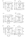
図16に、信号線駆動回路6013のみを別途形成し、第1の基板6011上に形成された画素部6012と接続している素子基板の形態を示す。画素部6012及び走査線駆動回路6014は、少なくともチャネル形成領域に結晶化された領域を含む酸化物半導体膜を有するTFTを用いて形成する。非晶質珪素膜を用いるTFTよりも高い移動度が得られるトランジスタで信号線駆動回路を形成することで、走査線駆動回路よりも高い駆動周波数が要求される信号線駆動回路の動作を安定させることができる。なお、信号線駆動回路6013は、単結晶シリコンの半導体を用いたトランジスタ、多結晶の半導体を用いたTFT、またはSOIを用いたトランジスタであっても良い。画素部6012と、信号線駆動回路6013と、走査線駆動回路6014とに、それぞれ電源の電位、各種信号等が、FPC6015を介して供給される。
FIG. 16 illustrates a mode of an element substrate in which only the signal
なお、信号線駆動回路及び走査線駆動回路を、共に画素部と同じ基板上に形成しても良い。 Note that both the signal line driver circuit and the scan line driver circuit may be formed over the same substrate as the pixel portion.
また、駆動回路を別途形成する場合、必ずしも駆動回路が形成された基板を、画素部が形成された基板上に張り合わせる必要はなく、例えばFPC上に張り合わせるようにしても良い。図17(A)に、信号線駆動回路6023のみを別途形成し、第1の基板6021上に形成された画素部6022及び走査線駆動回路6024と接続している素子基板の形態を示す。画素部6022及び走査線駆動回路6024は、少なくともチャネル形成領域に結晶化された領域を含む酸化物半導体膜を用いたTFTによって形成する。信号線駆動回路6023は、FPC6025を介して画素部6022と接続されている。画素部6022と、信号線駆動回路6023と、走査線駆動回路6024とに、それぞれ電源の電位、各種信号等が、FPC6025を介して供給される。
In the case where the driver circuit is separately formed, the substrate on which the driver circuit is formed is not necessarily attached to the substrate on which the pixel portion is formed, and may be attached to, for example, an FPC. FIG. 17A illustrates a mode of an element substrate in which only the signal
また、信号線駆動回路の一部のみまたは走査線駆動回路の一部のみを、少なくともチャネル形成領域に結晶化された領域を含む酸化物半導体膜を有するTFTを用いて画素部と同じ基板上に形成し、残りを別途形成して画素部と電気的に接続するようにしても良い。図17(B)に、信号線駆動回路が有するアナログスイッチ6033aを、画素部6032、走査線駆動回路6034と同じ第1の基板6031上に形成し、信号線駆動回路が有するシフトレジスタ6033bを別途異なる基板に形成して基板6031に貼り合わせる素子基板の形態を、図17(B)に示す。画素部6032及び走査線駆動回路6034は、少なくともチャネル形成領域に結晶化された領域を含む酸化物半導体膜を有するTFTを用いて形成する。信号線駆動回路が有するシフトレジスタ6033bは、FPC6035を介して画素部6032と接続されている。画素部6032と、信号線駆動回路に含まれるアナログスイッチ6033a、シフトレジスタ6033bと、走査線駆動回路6034とに、それぞれ電源の電位、各種信号等が、FPC6035を介して供給される。
In addition, only part of the signal line driver circuit or part of the scan line driver circuit is formed over the same substrate as the pixel portion by using a TFT having an oxide semiconductor film including a region crystallized at least in a channel formation region. It may be formed, and the rest may be separately formed and electrically connected to the pixel portion. In FIG. 17B, an
図16、図17に示すように、本発明の液晶表示装置は、駆動回路の一部または全部を、画素部と同じ基板上に、少なくともチャネル形成領域に結晶化された領域を含む酸化物半導体膜を有するTFTを用いて形成することができる。 As shown in FIGS. 16 and 17, the liquid crystal display device of the present invention includes an oxide semiconductor in which part or all of a driver circuit includes a region crystallized at least in a channel formation region over the same substrate as a pixel portion. It can be formed using a TFT having a film.
なお、別途形成した基板の接続方法は、特に限定されるものではなく、COG(Chip On Glass)方法やワイヤボンディング方法、或いはTAB(Tape Automated Bonding)方法などを用いることができる。また接続する位置は、電気的な接続が可能であるならば、図18に示した位置に限定されない。また、コントローラ、CPU、メモリ等を別途形成し、接続するようにしても良い。 Note that a method for connecting a separately formed substrate is not particularly limited, and a COG (Chip On Glass) method, a wire bonding method, a TAB (Tape Automated Bonding) method, or the like can be used. The connection position is not limited to the position illustrated in FIG. 18 as long as electrical connection is possible. In addition, a controller, a CPU, a memory, and the like may be separately formed and connected.
なお本発明で用いる信号線駆動回路は、シフトレジスタとアナログスイッチのみを有する形態に限定されない。シフトレジスタとアナログスイッチに加え、バッファ、レベルシフタ、ソースフォロワ等、他の回路を有していても良い。また、シフトレジスタとアナログスイッチは必ずしも設ける必要はなく、例えばシフトレジスタの代わりにデコーダ回路のような信号線の選択ができる別の回路を用いても良いし、アナログスイッチの代わりにラッチ等を用いても良い。 Note that the signal line driver circuit used in the present invention is not limited to a mode having only a shift register and an analog switch. In addition to the shift register and the analog switch, other circuits such as a buffer, a level shifter, and a source follower may be included. The shift register and the analog switch are not necessarily provided. For example, another circuit that can select a signal line such as a decoder circuit may be used instead of the shift register, or a latch or the like may be used instead of the analog switch. May be.
図18(A)に本発明を適用した液晶表示装置のブロック図を示す。図18(A)に示す液晶表示装置は、液晶素子を備えた画素を複数有する画素部801と、各画素を選択する走査線駆動回路802と、選択された画素へのビデオ信号の入力を制御する信号線駆動回路803とを有する。
FIG. 18A shows a block diagram of a liquid crystal display device to which the present invention is applied. A liquid crystal display device illustrated in FIG. 18A controls a pixel portion 801 including a plurality of pixels each including a liquid crystal element, a scan
図18(A)において信号線駆動回路803は、シフトレジスタ804、アナログスイッチ805を有している。シフトレジスタ804には、クロック信号(CLK)、スタートパルス信号(SP)が入力されている。クロック信号(CLK)とスタートパルス信号(SP)が入力されると、シフトレジスタ804においてタイミング信号が生成され、アナログスイッチ805に入力される。 In FIG. 18A, the signal line driver circuit 803 includes a shift register 804 and an analog switch 805. A clock signal (CLK) and a start pulse signal (SP) are input to the shift register 804. When the clock signal (CLK) and the start pulse signal (SP) are input, a timing signal is generated in the shift register 804 and input to the analog switch 805.
またアナログスイッチ805には、ビデオ信号(video signal)が与えられている。アナログスイッチ805は入力されるタイミング信号に従ってビデオ信号をサンプリングし、後段の信号線に供給する。 A video signal (video signal) is supplied to the analog switch 805. The analog switch 805 samples the video signal in accordance with the input timing signal and supplies it to the subsequent signal line.
次に、走査線駆動回路802の構成について説明する。走査線駆動回路802は、シフトレジスタ806、バッファ807を有している。また場合によってはレベルシフタを有していても良い。走査線駆動回路802において、シフトレジスタ806にクロック信号(CLK)及びスタートパルス信号(SP)が入力されることによって、選択信号が生成される。生成された選択信号はバッファ807において緩衝増幅され、対応する走査線に供給される。走査線には、1ライン分の画素のトランジスタのゲートが接続されている。そして、1ライン分の画素のトランジスタを一斉にONにしなくてはならないので、バッファ807は大きな電流を流すことが可能なものが用いられる。
Next, the configuration of the scan
フルカラーの液晶表示装置で、R(赤)、G(緑)、B(青)に対応するビデオ信号を、順にサンプリングして対応する信号線に供給している場合、シフトレジスタ804とアナログスイッチ805とを接続するための端子数が、アナログスイッチ805と画素部801の信号線を接続するための端子数の1/3程度に相当する。よって、アナログスイッチ805を画素部801と同じ基板上に形成することで、アナログスイッチ805を画素部801と異なる基板上に形成した場合に比べて、別途形成した基板の接続に用いる端子の数を抑えることができ、接続不良の発生確率を抑え、歩留まりを高めることができる。 In a full color liquid crystal display device, when video signals corresponding to R (red), G (green), and B (blue) are sequentially sampled and supplied to corresponding signal lines, a shift register 804 and an analog switch 805 are provided. And the number of terminals for connecting the analog switch 805 and the signal line of the pixel portion 801 corresponds to about 3. Therefore, by forming the analog switch 805 over the same substrate as the pixel portion 801, the number of terminals used for connecting a separately formed substrate can be reduced as compared with the case where the analog switch 805 is formed over a different substrate from the pixel portion 801. Thus, the probability of occurrence of connection failure can be suppressed, and the yield can be increased.
図18(B)に、図18(A)とは異なる、本発明に係る液晶表示装置のブロック図を示す。図18(B)において信号線駆動回路813は、シフトレジスタ814、ラッチA815、ラッチB816、D/A変換回路(以下、DAC817という)を有している。走査線駆動回路812は、図18(A)の場合と同じ構成を有しているものとする。
FIG. 18B is a block diagram of a liquid crystal display device according to the present invention, which is different from FIG. In FIG. 18B, the signal line driver circuit 813 includes a shift register 814, a latch A 815, a latch B 816, and a D / A conversion circuit (hereinafter referred to as a DAC 817). The scan
シフトレジスタ814には、クロック信号(CLK)、スタートパルス信号(SP)が入力されている。クロック信号(CLK)とスタートパルス信号(SP)が入力されると、シフトレジスタ814においてタイミング信号が生成され、一段目のラッチA815に順に入力される。ラッチA815にタイミング信号が入力されると、該タイミング信号に同期して、ビデオ信号が順にラッチA815に書き込まれ、保持される。なお、図18(B)ではラッチA815に順にビデオ信号を書き込んでいると仮定するが、本発明はこの構成に限定されない。複数のステージのラッチA815をいくつかのグループに分け、各グループごとに並行してビデオ信号を入力する、いわゆる分割駆動を行っても良い。なおこのときのグループの数を分割数と呼ぶ。例えば4つのステージごとにラッチをグループに分けた場合、4分割で分割駆動すると言う。 A clock signal (CLK) and a start pulse signal (SP) are input to the shift register 814. When the clock signal (CLK) and the start pulse signal (SP) are input, a timing signal is generated in the shift register 814 and sequentially input to the first-stage latch A815. When a timing signal is input to the latch A815, video signals are sequentially written and held in the latch A815 in synchronization with the timing signal. Note that in FIG. 18B, it is assumed that video signals are sequentially written in the latch A 815, but the present invention is not limited to this structure. A plurality of stages of latches A815 may be divided into several groups, and so-called divided driving may be performed in which video signals are input in parallel for each group. Note that the number of groups at this time is called the number of divisions. For example, when the latches are divided into groups for every four stages, it is said that the driving is divided into four.
ラッチA815の全てのステージのラッチへの、ビデオ信号の書き込みが一通り終了するまでの時間を、ライン期間と呼ぶ。実際には、上記ライン期間に水平帰線期間が加えられた期間をライン期間に含むことがある。 The time until video signal writing to all the latches of the latch A 815 is completed is called a line period. Actually, the line period may include a period in which a horizontal blanking period is added to the line period.
1ライン期間が終了すると、2段目のラッチB816にラッチ信号(Latch Signal)が供給され、該ラッチ信号に同期してラッチA815に保持されているビデオ信号が、ラッチB816に一斉に書き込まれ、保持される。ビデオ信号をラッチB816に送出し終えたラッチA815には、再びシフトレジスタ814からのタイミング信号に同期して、次のビデオ信号の書き込みが順次行われる。この2順目の1ライン期間中には、ラッチB816に書き込まれ、保持されているビデオ信号が、DAC817に入力される。
When one line period ends, a latch signal (Latch Signal) is supplied to the second-stage latch B816, and the video signal held in the latch A815 in synchronization with the latch signal is written to the latch B816 all at once, Retained. In the latch A 815 that has finished sending the video signal to the latch B 816, the next video signal is sequentially written in synchronization with the timing signal from the shift register 814 again. During the second line 1-line period, the video signal written and held in the latch B 816 is input to the
DAC817では、入力されたビデオ信号をデジタルからアナログに変換し、対応する信号線に供給する。
The
なお、図18(A)、図18(B)に示す構成は、本実施形態に係る液晶表示装置の一形態であり、信号線駆動回路と走査線駆動回路の構成はこれに限定されない。 Note that the structures illustrated in FIGS. 18A and 18B are one embodiment of the liquid crystal display device according to this embodiment, and the structures of the signal line driver circuit and the scan line driver circuit are not limited thereto.
なお、図16〜18は、本実施形態に係る液晶表示装置に限らず、発光装置やその他の表示装置に用いることができる。 16 to 18 are not limited to the liquid crystal display device according to the present embodiment, but can be used for a light emitting device and other display devices.
なお、本実施形態は、実施形態1〜4と適宜組み合わせることができる。 In addition, this embodiment can be combined with Embodiments 1-4 suitably.
本実施例では、実施形態5で説明した発光装置に用いる発光素子の形態を、図8を用いて説明する。
In this example, a mode of a light-emitting element used for the light-emitting device described in
図8(A)は、第1の画素電極11に、透光性を有し且つ仕事関数の大きい導電膜を用い、第2の画素電極17に、仕事関数の小さい導電膜を用いて形成した例である。第1の画素電極11を透光性の酸化物導電性材料で形成し、代表的には酸化珪素を1〜15原子%の濃度で含む酸化物導電性材料で形成している。その上に正孔注入層若しくは正孔輸送層41、発光層42、電子輸送層若しくは電子注入層43を積層した発光物質を含む層16を設けている。第2の画素電極17は、LiFやMgAgなどアルカリ金属又はアルカリ土類金属の単体、化合物又は合金を含む第1の電極層33とアルミニウムなどの金属材料で形成する第2の電極層34で形成している。この構造の画素は、図中の矢印で示したように第1の画素電極11側から光を放射することが可能となる。
In FIG. 8A, the
図8(B)は、第1の画素電極11に、仕事関数の大きい導電膜を用い、第2の画素電極17に、透光性を有し且つ仕事関数の小さい導電膜を用いて形成した例である。第1の画素電極11はアルミニウム、チタンなどの金属、又は該金属と化学量論的組成比以下の濃度で窒素を含む金属材料で形成する第1の電極層35と、酸化珪素を1〜15原子%の濃度で含む酸化物導電性材料で形成する第2の電極層32との積層構造で形成している。その上に正孔注入層若しくは正孔輸送層41、発光層42、電子輸送層若しくは電子注入層43を積層した発光物質を含む層16を設けている。第2の画素電極17は、LiFやCaFなどのアルカリ金属又はアルカリ土類金属の単体、化合物又は合金を含む第3の電極層33とアルミニウムなどの金属材料で形成する第4の電極層34で形成する。第2の電極のいずれの層をも100nm以下の厚さとして光を透過可能な状態としておくことで、図中の矢印で示したように第2の画素電極17から光を放射することが可能となる。
In FIG. 8B, the
図8(E)は、両方向、即ち第1の電極及び第2の電極から光を放射する例を示し、第1の画素電極11に、透光性を有し且つ仕事関数の大きい導電膜を用い、第2の画素電極17に、透光性を有し且つ仕事関数の小さい導電膜を用いる。代表的には、第1の画素電極11を、酸化珪素を1〜15原子%の濃度で含む酸化物導電性材料で形成し、第2の画素電極17を、それぞれ100nm以下の厚さのLiFやCaFなどのアルカリ金属又はアルカリ土類金属の単体、化合物又は合金を含む第3の電極層33とアルミニウムなどの金属材料で形成する第4の電極層34で形成することで、図中の矢印で示したように、第1の画素電極11及び第2の画素電極17の両側から光を放射することが可能となる。
FIG. 8E illustrates an example in which light is emitted from both directions, that is, from the first electrode and the second electrode. A conductive film having a light-transmitting property and a large work function is formed on the
図8(C)は、第1の画素電極11に、透光性を有し且つ仕事関数の小さい導電膜を用い、第2の画素電極17に、仕事関数の大きい導電膜を用いて形成した例である。発光物質を含む層を電子輸送層若しくは電子注入層43、発光層42、正孔注入層若しくは正孔輸送層41の順に積層した構成を示している。第2の画素電極17は、発光物質を含む層16側から酸化珪素を1〜15原子%の濃度で含む酸化物導電性材料で形成する第2の電極層32、アルミニウム、チタンなどの金属、又は該金属と化学量論的組成比以下の濃度で窒素を含む金属材料で形成する第1の電極層35の積層構造で形成している。第1の画素電極11は、LiFやCaFなどのアルカリ金属又はアルカリ土類金属の単体、化合物又は合金を含む第3の電極層33とアルミニウムなどの金属材料で形成する第4の電極層34で形成するが、いずれの層も100nm以下の厚さとして光を透過可能な状態としておくことで、図中の矢印で示したように第1の画素電極11から光を放射することが可能となる。
In FIG. 8C, the
図8(D)は、第1の画素電極11に、仕事関数の小さい導電膜を用い、第2の画素電極17に、透光性を有し且つ仕事関数の大きい導電膜を用いて形成した例である。発光物質を含む層を電子輸送層若しくは電子注入層43、発光層42、正孔注入層若しくは正孔輸送層41の順に積層した構成を示している。第1の画素電極11は図8(A)と同様な構成とし、膜厚は発光物質を含む層で発光した光を反射可能な程度に厚く形成している。第2の画素電極17は、酸化珪素を1〜15原子%の濃度で含む酸化物導電性材料で構成している。この構造において、正孔注入層を無機物である金属酸化物(代表的には酸化モリブデン若しくは酸化バナジウム)で形成することにより、第2の電極層32を形成する際に導入される酸素が供給されて正孔注入性が向上し、駆動電圧を低下させることができる。また、第2の画素電極17を、透光性を有する導電膜で形成することで、図中の矢印で示したように、第2の画素電極17の両側から光を放射することが可能となる。
8D, the
図8(F)は、両方向、即ち第1の画素電極及び第2の画素電極から光を放射する例を示し、第1の画素電極11に、透光性を有し且つ仕事関数の小さい導電膜を用い、第2の画素電極17に、透光性を有し且つ仕事関数の大きい導電膜を用いる。代表的には、第1の画素電極11を、それぞれ100nm以下の厚さのLiFやCaFなどのアルカリ金属又はアルカリ土類金属の単体、化合物又は合金を含む第3の電極層33とアルミニウムなどの金属材料で形成する第4の電極層34で形成し、第2の画素電極17を、酸化珪素を1〜15原子%の濃度で含む酸化物導電性材料で形成すればよい。
FIG. 8F illustrates an example in which light is emitted from both directions, that is, from the first pixel electrode and the second pixel electrode. The
なお、上記で述べたように発光物質を含む層16は、有機化合物又は無機化合物を含む電荷注入輸送物質及び発光材料で形成し、その分子数から低分子系有機化合物、中分子系有機化合物(昇華性を有さず、連鎖する分子の長さが10μm以下の有機化合物、代表的にはデンドリマー、オリゴマー等が挙げられる。)、高分子系有機化合物から選ばれた一種又は複数種の層を含み、電子注入輸送性又は正孔注入輸送性の無機化合物と組み合わせても良い。
Note that, as described above, the
電荷注入輸送物質のうち、特に電子輸送性の高い物質としては、例えばトリス(8−キノリノラト)アルミニウム(略称:Alq3)、トリス(4−メチル−8−キノリノラト)アルミニウム(略称:Almq3)、ビス(10−ヒドロキシベンゾ[h]−キノリナト)ベリリウム(略称:BeBq2)、ビス(2−メチル−8−キノリノラト)−4−フェニルフェノラト−アルミニウム(略称:BAlq)など、キノリン骨格またはベンゾキノリン骨格を有する金属錯体等が挙げられる。 Among the charge injecting and transporting substances, substances having a particularly high electron transporting property include, for example, tris (8-quinolinolato) aluminum (abbreviation: Alq 3 ), tris (4-methyl-8-quinolinolato) aluminum (abbreviation: Almq 3 ), Bis (10-hydroxybenzo [h] -quinolinato) beryllium (abbreviation: BeBq 2 ), bis (2-methyl-8-quinolinolato) -4-phenylphenolato-aluminum (abbreviation: BAlq), quinoline skeleton or benzoquinoline Examples thereof include metal complexes having a skeleton.
また、正孔輸送性の高い物質としては、例えば4,4’−ビス[N−(1−ナフチル)−N−フェニル−アミノ]−ビフェニル(略称:α−NPD)や4,4’−ビス[N−(3−メチルフェニル)−N−フェニル−アミノ]−ビフェニル(略称:TPD)や4,4’,4’’−トリス(N,N−ジフェニル−アミノ)−トリフェニルアミン(略称:TDATA)、4,4’,4’’−トリス[N−(3−メチルフェニル)−N−フェニル−アミノ]−トリフェニルアミン(略称:MTDATA)などの芳香族アミン系(即ち、ベンゼン環−窒素の結合を有する)の化合物が挙げられる。 As a substance having a high hole-transport property, for example, 4,4′-bis [N- (1-naphthyl) -N-phenyl-amino] -biphenyl (abbreviation: α-NPD) or 4,4′-bis [N- (3-methylphenyl) -N-phenyl-amino] -biphenyl (abbreviation: TPD) or 4,4 ′, 4 ″ -tris (N, N-diphenyl-amino) -triphenylamine (abbreviation: Aromatic amine systems such as TDATA), 4,4 ′, 4 ″ -tris [N- (3-methylphenyl) -N-phenyl-amino] -triphenylamine (abbreviation: MTDATA) (ie, benzene ring— Compound having a nitrogen bond).
また、電荷注入輸送物質のうち、特に電子注入性の高い物質としては、フッ化リチウム(LiF)、フッ化セシウム(CsF)、フッ化カルシウム(CaF2)等のようなアルカリ金属又はアルカリ土類金属の化合物が挙げられる。また、この他、Alq3のような電子輸送性の高い物質とマグネシウム(Mg)のようなアルカリ土類金属との混合物であってもよい。 Among the charge injecting and transporting materials, materials having particularly high electron injecting properties include alkali metals or alkaline earths such as lithium fluoride (LiF), cesium fluoride (CsF), calcium fluoride (CaF 2 ) and the like. Metal compounds can be mentioned. In addition, a mixture of a substance having a high electron transport property such as Alq3 and an alkaline earth metal such as magnesium (Mg) may be used.
電荷注入輸送物質のうち、正孔注入性の高い物質としては、例えば、モリブデン酸化物(MoOx)やバナジウム酸化物(VOx)、ルテニウム酸化物(RuOx)、タングステン酸化物(WOx)、マンガン酸化物(MnOx)等の金属酸化物が挙げられる。また、この他、フタロシアニン(略称:H2Pc)や銅フタロシアニン(CuPc)等のフタロシアニン系の化合物が挙げられる。 Among the charge injection / transport materials, examples of the material having a high hole injection property include molybdenum oxide (MoO x ), vanadium oxide (VO x ), ruthenium oxide (RuO x ), and tungsten oxide (WO x ). And metal oxides such as manganese oxide (MnO x ). In addition, phthalocyanine compounds such as phthalocyanine (abbreviation: H 2 Pc) and copper phthalocyanine (CuPc) can be given.
発光層42は、発光波長帯の異なる発光層を画素毎に形成して、カラー表示を行う構成としても良い。典型的には、R(赤)、G(緑)、B(青)の各色に対応した発光層を形成する。この場合にも、画素の光放射側にその発光波長帯の光を透過するフィルター(着色層)を設けた構成とすることで、色純度の向上や、画素部の鏡面化(映り込み)の防止を図ることができる。フィルター(着色層)を設けることで、従来必要であるとされていた円偏光版などを省略することが可能となり、発光層から放射される光の損失を無くすことができる。さらに、斜方から画素部(表示画面)を見た場合に起こる色調の変化を低減することができる。
The
発光層42を形成する発光材料には様々な材料がある。低分子系有機発光材料では、4−(ジシアノメチレン)−2−メチル−6−[2−(1,1,7,7−テトラメチルジュロリジン−9−イル)エテニル]−4H−ピラン(略称:DCJT)、4−ジシアノメチレン−2−t−ブチル−6−[2−(1,1,7,7−テトラメチルジュロリジル−9−イル)エテニル]−4H−ピラン(略称:DCJTB)、ペリフランテン、2,5−ジシアノ−1,4−ビス[2−(10−メトキシ−1,1,7,7−テトラメチルジュロリジン−9−イル)エテニル]ベンゼン、N,N’−ジメチルキナクリドン(略称:DMQd)、クマリン6、クマリン545T、トリス(8−キノリノラト)アルミニウム(略称:Alq3)、9,9’−ビアントリル、9,10−ジフェニルアントラセン(略称:DPA)や9,10−ビス(2−ナフチル)アントラセン(略称:DNA)等を用いることができる。また、この他の物質でもよい。
There are various light emitting materials for forming the
一方、高分子系有機発光材料は低分子系に比べて物理的強度が高く、素子の耐久性が高い。また塗布により成膜することが可能であるので、素子の作製が比較的容易である。高分子系有機発光材料を用いた発光素子の構造は、低分子系有機発光材料を用いたときと基本的には同じであり、陰極、発光物質を含む層、陽極の順に積層した構造となる。しかし、高分子系有機発光材料を用いた発光物質を含む層を形成する際には、低分子系有機発光材料を用いたときのような積層構造を形成させることは難しく、多くの場合2層構造となる。具体的には、陰極、発光層、正孔輸送層、陽極という順に積層した構造である。 On the other hand, the high molecular organic light emitting material has higher physical strength than the low molecular weight material, and the durability of the device is high. In addition, since the film can be formed by coating, the device can be manufactured relatively easily. The structure of a light emitting element using a polymer organic light emitting material is basically the same as that of using a low molecular weight organic light emitting material, and is a structure in which a cathode, a layer containing a light emitting substance, and an anode are laminated in this order. . However, when forming a layer containing a light emitting material using a high molecular weight organic light emitting material, it is difficult to form a layered structure as in the case of using a low molecular weight organic light emitting material, and in many cases two layers are formed. It becomes a structure. Specifically, it is a structure in which a cathode, a light emitting layer, a hole transport layer, and an anode are laminated in this order.
発光色は、発光層を形成する材料で決まるため、これらを選択することで所望の発光を示す発光素子を形成することができる。発光層の形成に用いることができる高分子系の発光材料は、ポリパラフェニレンビニレン系、ポリパラフェニレン系、ポリチオフェン系、ポリフルオレン系が挙げられる。 Since the light emission color is determined by the material for forming the light emitting layer, a light emitting element exhibiting desired light emission can be formed by selecting these materials. Examples of the polymer light emitting material that can be used for forming the light emitting layer include polyparaphenylene vinylene, polyparaphenylene, polythiophene, and polyfluorene.
ポリパラフェニレンビニレン系には、ポリ(パラフェニレンビニレン) [PPV] の誘導体、ポリ(2,5−ジアルコキシ−1,4−フェニレンビニレン) [RO−PPV]、ポリ(2−(2’−エチル−ヘキソキシ)−5−メトキシ−1,4−フェニレンビニレン)[MEH−PPV]、ポリ(2−(ジアルコキシフェニル)−1,4−フェニレンビニレン)[ROPh−PPV]等が挙げられる。ポリパラフェニレン系には、ポリパラフェニレン[PPP]の誘導体、ポリ(2,5−ジアルコキシ−1,4−フェニレン)[RO−PPP]、ポリ(2,5−ジヘキソキシ−1,4−フェニレン)等が挙げられる。ポリチオフェン系には、ポリチオフェン[PT]の誘導体、ポリ(3−アルキルチオフェン)[PAT]、ポリ(3−ヘキシルチオフェン)[PHT]、ポリ(3−シクロヘキシルチオフェン)[PCHT]、ポリ(3−シクロヘキシル−4−メチルチオフェン)[PCHMT]、ポリ(3,4−ジシクロヘキシルチオフェン)[PDCHT]、ポリ[3−(4−オクチルフェニル)−チオフェン][POPT]、ポリ[3−(4−オクチルフェニル)−2,2ビチオフェン][PTOPT]等が挙げられる。ポリフルオレン系には、ポリフルオレン[PF]の誘導体、ポリ(9,9−ジアルキルフルオレン)[PDAF]、ポリ(9,9−ジオクチルフルオレン)[PDOF]等が挙げられる。 Examples of the polyparaphenylene vinylene include poly (paraphenylene vinylene) [PPV] derivatives, poly (2,5-dialkoxy-1,4-phenylene vinylene) [RO-PPV], poly (2- (2′- Ethyl-hexoxy) -5-methoxy-1,4-phenylenevinylene) [MEH-PPV], poly (2- (dialkoxyphenyl) -1,4-phenylenevinylene) [ROPh-PPV] and the like. Examples of polyparaphenylene include derivatives of polyparaphenylene [PPP], poly (2,5-dialkoxy-1,4-phenylene) [RO-PPP], poly (2,5-dihexoxy-1,4-phenylene). ) And the like. The polythiophene series includes polythiophene [PT] derivatives, poly (3-alkylthiophene) [PAT], poly (3-hexylthiophene) [PHT], poly (3-cyclohexylthiophene) [PCHT], poly (3-cyclohexyl). -4-methylthiophene) [PCHMT], poly (3,4-dicyclohexylthiophene) [PDCHT], poly [3- (4-octylphenyl) -thiophene] [POPT], poly [3- (4-octylphenyl) -2,2 bithiophene] [PTOPT] and the like. Examples of the polyfluorene series include polyfluorene [PF] derivatives, poly (9,9-dialkylfluorene) [PDAF], poly (9,9-dioctylfluorene) [PDOF], and the like.
なお、正孔輸送性の高分子系有機発光材料を、陽極と発光性の高分子系有機発光材料の間に挟んで形成すると、陽極からの正孔注入性を向上させることができる。一般にアクセプター材料と共に水に溶解させたものをスピンコート法などで塗布する。また、有機溶媒には不溶であるため、上述した発光性の発光材料との積層が可能である。正孔輸送性の高分子系有機発光材料としては、PEDOTとアクセプター材料としてのショウノウスルホン酸(CSA)の混合物、ポリアニリン[PANI]とアクセプター材料としてのポリスチレンスルホン酸[PSS]の混合物等が挙げられる。 Note that when a hole-transporting polymer-based organic light-emitting material is sandwiched between an anode and a light-emitting polymer-based organic light-emitting material, hole injection properties from the anode can be improved. In general, an acceptor material dissolved in water is applied by spin coating or the like. In addition, since it is insoluble in an organic solvent, it can be stacked with the above-described light-emitting material. Examples of the hole-transporting polymer organic light emitting material include a mixture of PEDOT and camphor sulfonic acid (CSA) as an acceptor material, a mixture of polyaniline [PANI] and polystyrene sulfonic acid [PSS] as an acceptor material, and the like. .
また、発光層42は単色又は白色の発光を呈する構成とすることができる。白色発光材料を用いる場合には、画素の光放射側に特定の波長の光を透過するフィルター(着色層)を設けた構成としてカラー表示を可能にすることができる。
The
白色に発光する発光層を形成するには、例えば、Alq3、部分的に赤色発光色素であるナイルレッドを添加したAlq3、Alq3、p−EtTAZ、TPD(芳香族ジアミン)を蒸着法により順次積層することで白色を得ることができる。また、スピンコートを用いた塗布法により発光層を形成する場合には、塗布した後、真空加熱で焼成することが好ましい。例えば、正孔注入層として作用するポリ(エチレンジオキシチオフェン)/ポリ(スチレンスルホン酸)水溶液(PEDOT/PSS)を全面に塗布、焼成し、その後、発光層として作用する発光中心色素(1,1,4,4−テトラフェニル−1,3−ブタジエン(TPB)、4−ジシアノメチレン−2−メチル−6−(p−ジメチルアミノ−スチリル)−4H−ピラン(DCM1)、ナイルレッド、クマリン6など)を添加したポリビニルカルバゾール(PVK)溶液を全面に塗布、焼成すればよい。 To form a light emitting layer that emits white light, for example, Alq 3, Alq 3, Alq 3 added with Nile Red which is partly red light emitting pigment, p-EtTAZ, by TPD (aromatic diamine) evaporation A white color can be obtained by sequentially laminating. Moreover, when forming a light emitting layer by the apply | coating method using spin coating, after apply | coating, it is preferable to bake by vacuum heating. For example, a poly (ethylenedioxythiophene) / poly (styrenesulfonic acid) aqueous solution (PEDOT / PSS) that acts as a hole injection layer is applied and baked on the entire surface, and then a luminescent center dye (1, 1,4,4-tetraphenyl-1,3-butadiene (TPB), 4-dicyanomethylene-2-methyl-6- (p-dimethylamino-styryl) -4H-pyran (DCM1), Nile Red, Coumarin 6 Etc.) may be applied and fired over the entire surface.
発光層は単層で形成することもでき、ホール輸送性のポリビニルカルバゾール(PVK)に電子輸送性の1,3,4−オキサジアゾール誘導体(PBD)を分散させてもよい。また、30wt%のPBDを電子輸送剤として分散し、4種類の色素(TPB、クマリン6、DCM1、ナイルレッド)を適当量分散することで白色発光が得られる。ここで示した白色発光が得られる発光素子の他にも、発光層の材料を適宜選択することによって、赤色発光、緑色発光、または青色発光が得られる発光素子を作製することができる。 The light emitting layer can also be formed as a single layer, and an electron transporting 1,3,4-oxadiazole derivative (PBD) may be dispersed in hole transporting polyvinyl carbazole (PVK). Further, white light emission can be obtained by dispersing 30 wt% PBD as an electron transporting agent and dispersing an appropriate amount of four kinds of dyes (TPB, coumarin 6, DCM1, Nile red). In addition to the light-emitting element that can emit white light as shown here, a light-emitting element that can obtain red light emission, green light emission, or blue light emission can be manufactured by appropriately selecting the material of the light-emitting layer.
なお、正孔輸送性の高分子系有機発光材料を、陽極と発光性の高分子系有機発光材料の間に挟んで形成すると、陽極からの正孔注入性を向上させることができる。一般にアクセプター材料と共に水に溶解させたものをスピンコート法などで塗布する。また、有機溶媒には不溶であるため、上述した発光性の有機発光材料との積層が可能である。正孔輸送性の高分子系有機発光材料としては、PEDOTとアクセプター材料としてのショウノウスルホン酸(CSA)の混合物、ポリアニリン[PANI]とアクセプター材料としてのポリスチレンスルホン酸[PSS]の混合物等が挙げられる。 Note that when a hole-transporting polymer-based organic light-emitting material is sandwiched between an anode and a light-emitting polymer-based organic light-emitting material, hole injection properties from the anode can be improved. In general, an acceptor material dissolved in water is applied by spin coating or the like. In addition, since it is insoluble in an organic solvent, it can be stacked with the above-described light-emitting organic light-emitting material. Examples of the hole-transporting polymer organic light emitting material include a mixture of PEDOT and camphor sulfonic acid (CSA) as an acceptor material, a mixture of polyaniline [PANI] and polystyrene sulfonic acid [PSS] as an acceptor material, and the like. .
さらに、発光層42は、一重項励起発光材料の他、金属錯体などを含む三重項励起材料を用いても良い。例えば、赤色の発光性の画素、緑色の発光性の画素及び青色の発光性の画素のうち、輝度半減時間が比較的短い赤色の発光性の画素を三重項励起発光材料で形成し、他を一重項励起発光材料で形成する。三重項励起発光材料は発光効率が良いので、同じ輝度を得るのに消費電力が少なくて済むという特徴がある。すなわち、赤色画素に適用した場合、発光素子に流す電流量が少なくて済むので、信頼性を向上させることができる。低消費電力化として、赤色の発光性の画素と緑色の発光性の画素とを三重項励起発光材料で形成し、青色の発光性の画素を一重項励起発光材料で形成しても良い。人間の視感度が高い緑色の発光素子も三重項励起発光材料で形成することで、より低消費電力化を図ることができる。
Further, for the
三重項励起発光材料の一例としては、金属錯体をドーパントとして用いたものがあり、第3遷移系列元素である白金を中心金属とする金属錯体、イリジウムを中心金属とする金属錯体などが知られている。三重項励起発光材料としては、これらの化合物に限られることはなく、上記構造を有し、且つ中心金属に周期表の8〜10属に属する元素を有する化合物を用いることも可能である。 Examples of triplet excited luminescent materials include those using a metal complex as a dopant, and metal complexes having a third transition series element platinum as the central metal and metal complexes having iridium as the central metal are known. Yes. The triplet excited light-emitting material is not limited to these compounds, and a compound having the above structure and having an element belonging to group 8 to 10 in the periodic table as a central metal can also be used.
以上に掲げる発光物質を含む層を形成する物質は一例であり、正孔注入輸送層、正孔輸送層、電子注入輸送層、電子輸送層、発光層、電子ブロック層、正孔ブロック層などの機能性の各層を適宜積層することで発光素子を形成することができる。また、これらの各層を合わせた混合層又は混合接合を形成しても良い。発光層の層構造は変化しうるものであり、特定の電子注入領域や発光領域を備えていない代わりに、もっぱらこの目的用の電極を備えたり、発光性の材料を分散させて備えたりする変形は、本発明の趣旨を逸脱しない範囲において許容されうるものである。 The substances forming the layer containing the light-emitting substance listed above are examples, such as a hole injecting and transporting layer, a hole transporting layer, an electron injecting and transporting layer, an electron transporting layer, a light emitting layer, an electron blocking layer, and a hole blocking layer. A light-emitting element can be formed by appropriately stacking functional layers. Moreover, you may form the mixed layer or mixed junction which combined these each layer. The layer structure of the light-emitting layer can be changed, and instead of having a specific electron injection region or light-emitting region, it is possible to provide a modification with an electrode for this purpose or a dispersed light-emitting material. Can be permitted without departing from the spirit of the present invention.
本実施例では本発明に係る発光装置の表示パネルの画素回路、及びその動作構成について、図9を用いて説明する。表示パネルの動作構成は、ビデオ信号がデジタルの表示装置において、画素に入力されるビデオ信号が電圧で規定されるのものと、電流で規定されるのものとがある。ビデオ信号が電圧によって規定されるものには、発光素子に印加される電圧が一定のもの(CVCV)と、発光素子に印加される電流が一定のもの(CVCC)とがある。また、ビデオ信号が電流によって規定されるものには、発光素子に印加される電圧が一定のもの(CCCV)と、発光素子に印加される電流が一定のもの(CCCC)とがある。本実施例では、CVCV動作をする画素を図9(A)及び(B)用いて説明する。また、CVCC動作をする画素を図9(C)〜(F)を用いて説明する。 In this embodiment, a pixel circuit of a display panel of a light-emitting device according to the present invention and an operation configuration thereof will be described with reference to FIGS. There are two types of operation configurations of the display panel, in which a video signal input to a pixel is defined by voltage and a current is defined by current in a display device in which a video signal is digital. There are two types of video signals defined by voltage, one having a constant voltage applied to the light emitting element (CVCV) and one having a constant current applied to the light emitting element (CVCC). In addition, a video signal is defined by current, there are a constant voltage applied to the light emitting element (CCCV) and a constant current applied to the light emitting element (CCCC). In this embodiment, a pixel that performs a CVCV operation will be described with reference to FIGS. A pixel that performs the CVCC operation will be described with reference to FIGS.
図9(A)及び(B)に示す画素は、列方向に信号線3710及び電源線3711、行方向に走査線3714が配置される。また、スイッチング用TFT3701、駆動用TFT3703、容量素子3702及び発光素子3705を有する。
In the pixel shown in FIGS. 9A and 9B, a
なお、スイッチング用TFT3701及び駆動用TFT3703は、オンしているときは線形領域で動作する。また駆動用TFT3703は発光素子3705に電圧を印加するか否かを制御する役目を有する。両TFTは同じ導電型を有していると作製工程上好ましい。本実施例ではスイッチング用TFT3701をnチャネル型TFTとし、駆動用TFT3703をpチャネル型TFTとして形成する。また駆動用TFT3703には、エンハンスメント型だけでなく、ディプリーション型のTFTを用いてもよい。また、駆動用TFT3703のチャネル幅Wとチャネルと長Lの比(W/L)は、TFTの移動度にもよるが1〜1000であることが好ましい。W/Lが大きいほど、TFTの電気特性が向上する。
Note that the switching
図9(A)、(B)に示す画素において、スイッチング用TFT3701は、画素に対するビデオ信号の入力を制御するものであり、スイッチング用TFT3701がオンとなると、画素内にビデオ信号が入力される。すると、容量素子3702にそのビデオ信号の電圧が保持される。
In the pixel shown in FIGS. 9A and 9B, the switching
図9(A)において、電源線3711がVssで発光素子3705の対向電極がVddの場合、即ち図8(C)及び(D)の場合、発光素子の対向電極は陽極であり、駆動用TFT3703に接続される電極は陰極である。この場合、駆動用TFT3703の特性バラツキによる輝度ムラを抑制することが可能である。
9A, in the case where the
図9(A)において、電源線3711がVddで発光素子3705の対向電極がVssの場合、即ち図8(A)及び(B)の場合、発光素子の対向電極は陰極であり、駆動用TFT3703に接続される電極は陽極である。この場合、Vddより電圧の高いビデオ信号を信号線3710に入力することにより、容量素子3702にそのビデオ信号の電圧が保持され、駆動用TFT3703が線形領域で動作するので、TFTのバラツキによる輝度ムラを改善することが可能である。
9A, in the case where the
図9(B)に示す画素は、TFT3706と走査線3715を追加している以外は、図9(A)に示す画素構成と同じである。
The pixel shown in FIG. 9B has the same pixel structure as that shown in FIG. 9A except that a
TFT3706は、新たに配置された走査線3715によりオン又はオフが制御される。TFT3706がオンとなると、容量素子3702に保持された電荷は放電し、駆動用TFT3703がオフとなる。つまり、TFT3706の配置により、強制的に発光素子3705に電流が流れない状態を作ることができる。そのためTFT3706を消去用TFTと呼ぶことができる。従って、図9(B)の構成は、全ての画素に対する信号の書き込みを待つことなく、書き込み期間の開始と同時又は直後に点灯期間を開始することができるため、発光のデューティ比を向上することが可能となる。
The
上記動作構成を有する画素において、発光素子3705の電流値は、線形領域で動作する駆動用TFT3703により決定することができる。上記構成により、TFTの特性のバラツキを抑制することが可能であり、TFT特性のバラツキに起因した発光素子の輝度ムラを改善して、画質を向上させた表示装置を提供することができる。
In the pixel having the above operation configuration, the current value of the light-emitting
次に、CVCC動作をする画素を図9(C)〜(F)を用いて説明する。図9(C)に示す画素は、図9(A)に示す画素構成に、電源線3712、電流制御用TFT3704が設けられている。
Next, a pixel that performs the CVCC operation will be described with reference to FIGS. In the pixel illustrated in FIG. 9C, a
図9(E)に示す画素は、駆動用TFT3703のゲート電極が、行方向に配置された電源線3712に接続される点が異なっており、それ以外は図9(C)に示す画素と同じ構成である。つまり、図9(C)、(E)に示す両画素は、同じ等価回路図を示す。しかしながら、行方向に電源線3712が配置される場合(図9(C))と、列方向に電源線3712が配置される場合(図9(E))とでは、各電源線は異なる層に形成された導電膜で形成される。ここでは、駆動用TFT3703のゲート電極が接続される配線に注目し、これらを作製する層が異なることを表すために、図9(C)、(E)として分けて記載する。
The pixel shown in FIG. 9E is the same as the pixel shown in FIG. 9C except that the gate electrode of the driving
なお、スイッチング用TFT3701は線形領域で動作し、駆動用TFT3703は飽和領域で動作する。また駆動用TFT3703は発光素子3705に流れる電流値を制御する役目を有し、電流制御用TFT3704は飽和領域で動作し発光素子3705に対する電流の供給を制御する役目を有する。
Note that the switching
図9(D)及び(F)示す画素はそれぞれ、図9(C)及び(E)に示す画素に、消去用のTFT3706と走査線3715を追加している以外は、図9(C)及び(E)に示す画素構成と同じである。
9D and 9F are the same as those shown in FIGS. 9C and 9E, respectively, except that an erasing
なお、図9(A)及び(B)に示される画素でも、CVCC動作をすることは可能である。また、図9(C)〜(F)に示される動作構成を有する画素は、図9(A)及び(B)と同様に、発光素子の電流の流れる方向によって、Vdd及びVssを適宜変えることが可能である。 Note that the CVCC operation can also be performed in the pixels shown in FIGS. 9A and 9B. In addition, in the pixel having the operation configuration shown in FIGS. 9C to 9F, Vdd and Vss are appropriately changed depending on the direction of current flow of the light-emitting element, as in FIGS. 9A and 9B. Is possible.
上記構成を有する画素は、電流制御用TFT3704が線形領域で動作するために、電流制御用TFT3704のVgsの僅かな変動は、発光素子3705の電流値に影響を及ぼさない。つまり、発光素子3705の電流値は、飽和領域で動作する駆動用TFT3703により決定することができる。上記構成により、TFTの特性バラツキに起因した発光素子の輝度ムラを改善して、画質を向上させた表示装置を提供することができる。
In the pixel having the above structure, since the
なお、容量素子3702を設けた構成を示したが、本発明はこれに限定されず、ビデオ信号を保持する容量がゲート容量などで、まかなうことが可能な場合には、容量素子3702を設けなくてもよい。
Note that although a structure including the
このようなアクティブマトリクス型の表示装置は、画素密度が増えた場合、各画素にTFTが設けられているため低電圧駆動でき、有利であると考えられている。 Such an active matrix display device is considered to be advantageous when the pixel density increases, because each pixel is provided with a TFT and can be driven at a low voltage.
また、本発明に係る表示装置において、画面表示の駆動方法は特に限定されず、例えば、点順次駆動方法や線順次駆動方法や面順次駆動方法などを用いればよい。代表的には、線順次駆動方法とし、時分割階調駆動方法や面積階調駆動方法を適宜用いればよい。また、表示装置のソース線に入力する映像信号は、アナログ信号であってもよいし、デジタル信号であってもよく、適宜、映像信号に合わせて駆動回路などを設計すればよい。 In the display device according to the present invention, the screen display driving method is not particularly limited. For example, a dot sequential driving method, a line sequential driving method, a surface sequential driving method, or the like may be used. Typically, a line sequential driving method is used, and a time-division gray scale driving method or an area gray scale driving method may be used as appropriate. The video signal input to the source line of the display device may be an analog signal or a digital signal, and a drive circuit or the like may be designed in accordance with the video signal as appropriate.
本実施例では、本発明に係る駆動回路の実装について、図10を用いて説明する。 In this embodiment, mounting of a driving circuit according to the present invention will be described with reference to FIG.
図10(A)に示すように、画素部1401の周辺に信号線駆動回路1402、及び走査線駆動回路1403a、1403bを実装する。図10(A)では、信号線駆動回路1402、及び走査線駆動回路1403a、1403b等として、公知の異方性導電接着剤、及び異方性導電フィルムを用いた実装方法、COG方式、ワイヤボンディング方法、並びに半田バンプを用いたリフロー処理等により、基板1400上にICチップ1405を実装する。ここでは、COG方式を用いる。そして、FPC(フレキシブルプリントサーキット)1406を介して、ICチップと外部回路とを接続する。
As shown in FIG. 10A, a signal
また、図10(B)に示すように、酸化物半導体でTFTを代表とする半導体素子を形成する場合、画素部1401と走査線駆動回路1403a、1403b等を基板上に一体形成し、信号線駆動回路1402等を別途ICチップとして実装する場合がある。図10(B)において、信号線駆動回路1402として、COG方式により、基板1400上にICチップ1405を実装する。そして、FPC1406を介して、ICチップと外部回路とを接続する。
10B, in the case where a semiconductor element typified by a TFT is formed using an oxide semiconductor, the
さらに、図10(C)に示すように、COG方式に代えて、TAB方式により信号線駆動回路1402等を実装する場合がある。そして、FPC1406を介して、ICチップと外部回路とを接続する。図10(C)において、信号線駆動回路をTAB方式により実装しているが、走査線駆動回路をTAB方式により実装してもよい。
Further, as shown in FIG. 10C, the signal
ICチップをTAB方式により実装すると、基板に対して画素部を大きく設けることができ、狭額縁化を達成することができる。 When the IC chip is mounted by the TAB method, a pixel portion can be provided larger than the substrate, and a narrow frame can be achieved.
ICチップは、シリコンウェハを用いて形成するが、ICチップの代わりにガラス基板上にICを形成したIC(以下、ドライバICと表記する)を設けてもよい。ICチップは、円形のシリコンウェハからICチップを取り出すため、母体基板形状に制約がある。一方ドライバICは、母体基板がガラスであり、形状に制約がないため、生産性を高めることができる。そのため、ドライバICの形状寸法は自由に設定することができる。例えば、ドライバICの長辺の長さを15〜80mmとして形成すると、ICチップを実装する場合と比較し、必要な数を減らすことができる。その結果、接続端子数を低減することができ、製造上の歩留まりを向上させることができる。 The IC chip is formed using a silicon wafer, but an IC (hereinafter referred to as a driver IC) in which an IC is formed on a glass substrate may be provided instead of the IC chip. Since an IC chip is taken out from a circular silicon wafer, the shape of the base substrate is limited. On the other hand, the driver IC has a mother substrate made of glass and has no restriction in shape, so that productivity can be improved. Therefore, the shape of the driver IC can be set freely. For example, when the length of the long side of the driver IC is 15 to 80 mm, the required number can be reduced as compared with the case where the IC chip is mounted. As a result, the number of connection terminals can be reduced, and the manufacturing yield can be improved.
ドライバICは、基板上に形成された結晶性半導体を用いて形成することができ、結晶性半導体は連続発振型のレーザ光を照射することで形成するとよい。連続発振型のレーザ光を照射して得られる半導体膜は、結晶欠陥が少なく、大粒径の結晶粒を有する。その結果、このような半導体膜を有するトランジスタは、移動度や応答速度が良好となり、高速駆動が可能となり、ドライバICに好適である。本発明の少なくともチャネル形成領域の結晶性が改善された酸化物半導体膜を用いてドライバICを形成してもよい。 The driver IC can be formed using a crystalline semiconductor formed over a substrate, and the crystalline semiconductor is preferably formed by irradiation with continuous wave laser light. A semiconductor film obtained by irradiation with continuous wave laser light has few crystal defects and large crystal grains. As a result, a transistor having such a semiconductor film has favorable mobility and response speed, can be driven at high speed, and is suitable for a driver IC. The driver IC may be formed using an oxide semiconductor film in which the crystallinity of at least the channel formation region of the present invention is improved.
本実施例では、本発明に係る表示モジュールについて説明する。ここでは、表示モジュールの一例として、液晶モジュールを、図11を用いて示す。 In this embodiment, a display module according to the present invention will be described. Here, a liquid crystal module is shown as an example of a display module with reference to FIG.
基板1601と対向基板1602とが、シール材1600により固着され、それらの間には画素部1603と液晶層1604とが設けられ表示領域を形成している。
A
着色層1605は、カラー表示を行う場合に必要であり、RGB方式の場合は、赤、緑、青の各色に対応した着色層が各画素に対応して設けられている。基板1601と対向基板1602との外側には、偏光板1606、1607が配設されている。また、偏光板1606の表面には、保護膜1616が形成されており、外部からの衝撃を緩和している。
The
基板1601に設けられた接続端子1608には、FPC1609を介して配線基板1610が接続されている。配線基板1610には、画素駆動回路(ICチップ、ドライバIC等)、コントロール回路や電源回路などの外部回路1612が組み込まれている。
A
冷陰極管1613、反射板1614、及び光学フィルム1615はバックライトユニットであり、これらが光源となって液晶表示パネルへ光を投射する。液晶パネル、光源、配線基板、FPC等は、ベゼル1617で保持及び保護されている。
The
本実施例は、本発明に係る電子機器として、テレビジョン装置(単にテレビ、又はテレビジョン受信機ともよぶ)、デジタルカメラ、デジタルビデオカメラ、携帯電話装置(単に携帯電話機、携帯電話ともよぶ)、PDA等の携帯情報端末、携帯型ゲーム機、コンピュータ用のモニター、コンピュータ、カーオーディオ等の音響再生装置、家庭用ゲーム機等の記録媒体を備えた画像再生装置等について図面を参照して説明する。 In this embodiment, as an electronic apparatus according to the present invention, a television device (also simply referred to as a television or a television receiver), a digital camera, a digital video camera, a mobile phone device (also simply referred to as a mobile phone or a mobile phone), A portable information terminal such as a PDA, a portable game machine, a computer monitor, a computer, an audio reproduction device such as a car audio, and an image reproduction device including a recording medium such as a home game machine will be described with reference to the drawings. .
図12(A)に示す携帯情報端末は、本体9201、表示部9202等を含んでいる。本発明の一である表示装置を用いることにより、携帯情報端末を安価に提供することができる。
A portable information terminal illustrated in FIG. 12A includes a
図12(B)に示すデジタルビデオカメラは、表示部9701、表示部9702等を含んでいる。本発明の一である表示装置を用いることにより、デジタルビデオカメラを安価に提供することができる。
A digital video camera shown in FIG. 12B includes a
図12(C)に示す携帯端末は、本体9101、表示部9102等を含んでいる。表示部9102は、実施形態1〜5、及び実施例1〜4で示すものを適用することができる。本発明の一である表示装置を用いることにより、携帯端末を安価に提供することができる。
A portable terminal illustrated in FIG. 12C includes a
図12(D)に示す携帯型のテレビジョン装置は、本体9301、表示部9302等を含んでいる。本発明の一である表示装置を用いることにより、携帯型のテレビジョン装置を安価に提供することができる。このようなテレビジョン装置は携帯電話などの携帯端末に搭載する小型のものから、持ち運びをすることができる中型のもの、また、大型のもの(例えば40インチ以上)まで、幅広く適用することができる。
A portable television device shown in FIG. 12D includes a
図12(E)に示す携帯型のコンピュータは、本体9401、表示部9402等を含んでいる。本発明の一である表示装置を用いることにより、携帯型のコンピュータを安価に提供することができる。
A portable computer shown in FIG. 12E includes a
図12(F)に示すテレビジョン装置は、本体9501、表示部9502等を含んでいる。本発明の一である表示装置を用いることにより、テレビジョン装置を安価に提供することができる。
A television device illustrated in FIG. 12F includes a
上記に挙げた電子機器において、二次電池を用いているものは、消費電力を削減した分、電子機器の使用時間を長持ちさせることができ、二次電池を充電する手間を省くことができる。 Among the electronic devices listed above, those using a secondary battery can extend the usage time of the electronic device as much as power consumption is reduced, and can save the trouble of charging the secondary battery.
本実施例では、本発明に用いるLRTA装置の構成について図19を用いて説明する。 In this embodiment, the configuration of the LRTA apparatus used in the present invention will be described with reference to FIG.
図19(A)において、ガラス基板1901上に、ゲート電極1922、ゲート絶縁膜1923a、1923b、酸化物半導体膜1902が形成されている。また、基板下面側に赤外光ランプ1903、基板上面側に紫外光ランプ1904が設けられている。そして、紫外光ランプ1904に並列して第1の赤外光補助ランプ1905、第2の赤外光補助ランプ1906を配置する。なお、第1の赤外光補助ランプ1905、第2の赤外光補助ランプ1906は設けなくてもよい。
In FIG. 19A, a
また、本実施例では紫外光ランプ1904の(基板の移動方向に対して)前方および後方に第1の赤外光補助ランプ1905、第2の赤外光補助光ランプ1906を配置する構成としているが、片方のみに配置した構成とすることもできる。
In this embodiment, the first infrared light
以上の様な構成において、各ランプ(赤外光ランプ1903〜第2の赤外光補助ランプ1906)は図中の矢印の方向に向かって移動し、線状光を走査する。本実施例の構成では、まずゲート絶縁膜1923a、1923bを介してゲート電極1922と重なっている酸化物半導体膜1902の点線で示す領域1908に第1の赤外光補助ランプ1905により赤外光が照射されて加熱される。そして、基板の移動に伴い前方へと移動していく。なお、基板にランプ照射をする際に各ランプを移動させているが、ガラス基板1901を移動させても又はランプと基板の両方を移動させてもよい。
In the configuration as described above, each lamp (
第1の赤外光補助ランプ1905照射後、基板上面側から紫外光ランプ1904からの紫外光が照射され、かつ、基板下面側から赤外光ランプ1903からの赤外光が照射されてゲート電極1922と重なる酸化物半導体膜1902の領域1908が加熱される。本実施例の場合、酸化物半導体膜1902の結晶化はこの領域1908が優先して行われる。
After irradiation with the first auxiliary
紫外光ランプ1904及び赤外光ランプ1903からの照射により加熱された領域1908は、紫外光ランプ1904後方に配置された第2の赤外光補助ランプ1906からの赤外光により加熱される。第2の赤外光補助ランプ1906からの赤外光の照射は、結晶化が促進した領域1908をさらに加熱するために設けられている。
A
以上の様に、酸化物半導体膜1902中のゲート電極1922と重なる領域(途中から結晶性酸化物半導体膜となる領域)1908は、見かけ上基板の移動に伴って前方へ移動する。
As described above, the
ここで図19(B)に示すのは、酸化物半導体膜1902の領域1908について、時間(Time)と温度(Temp. )の関係を示した図である。図19(B)に示す様に、時間の経過に伴ってまず前加熱(プレヒート)状態となり、次いで主加熱(メインヒート)状態、後加熱(ポストヒート)状態と続く。
Here, FIG. 19B illustrates the relationship between time (Time) and temperature (Temp.) In the
図19(B)から明らかな様に、プレヒート状態ではある程度にまで温度が上げられ、次のメインヒート状態との温度勾配を緩和する役割を果たしている。これは、メインヒート状態で急激に熱せられて酸化物半導体膜に歪みエネルギー等が蓄積するのを防ぐための工夫である。 As is clear from FIG. 19B, the temperature is increased to some extent in the preheating state, and plays a role of relaxing the temperature gradient with the next main heating state. This is a contrivance for preventing accumulation of strain energy or the like in the oxide semiconductor film due to rapid heating in the main heat state.
そのため、第1の赤外光補助ランプ1905の出力エネルギーは赤外光ランプ1903の出力エネルギーよりも小さめに設定しておくことが望ましい。この時、どの様な温度勾配を形成する様に調節するかは実施者が適宜決定すれば良い。
Therefore, it is desirable to set the output energy of the first infrared light
次に、プレヒート状態を通過すると、基板下面側から赤外光を照射され、膜面温度が 250〜570℃でまで上昇したメインヒート状態となる。この状態で酸化物半導体膜1902中の領域1908は結晶性が良好となる。なお、同時に照射される紫外光は電子励起に寄与するので熱的な変化はもたらさない。
Next, when the preheat state is passed, infrared light is irradiated from the lower surface side of the substrate, and the film surface temperature is increased to 250 to 570 ° C. to become a main heat state. In this state, the
メインヒート状態で得られた結晶性が改善した領域1908は紫外光ランプ1904の後方に配置された第2の赤外光補助ランプ1906によって加熱される。このポストヒート状態は、メインヒート状態の急冷により熱的平衡の崩れた状態で結晶化が終了するのを防ぐ役割を果たす。これは結晶化に要する時間に余裕を持たせて最も安定な結合状態を得るための工夫である。
The
従って、第2の赤外光補助ランプ1906も基板下面に配置される赤外光ランプ1903よりも出力エネルギーを小さく設定し、徐々に温度が下がる様な温度勾配を形成する様に調節することが望ましい。
Accordingly, the second auxiliary
以上の様な構成とすることで、ゲート電極と重なる酸化物半導体膜の一部が加熱されるため、基板のシュリンクを抑制することができる。また、結晶化工程を各ランプ又は基板を移動させながら行うことによりスループットを上げることができる。また、酸化物半導体膜の急加熱および結晶性酸化物半導体膜の急冷により生じうる応力歪み、不対結合手等の結晶欠陥の発生を抑制し、結晶性に優れた領域1908を有する酸化物半導体膜を得ることができる。
With such a structure, a part of the oxide semiconductor film overlapping with the gate electrode is heated, so that shrinkage of the substrate can be suppressed. Further, throughput can be increased by performing the crystallization process while moving each lamp or substrate. In addition, an oxide semiconductor having a
また、第1の赤外光補助ランプ1905、第2の赤外光補助ランプ1906を設けずに照射加熱を行うことで、基板にかかる熱を抑制してもよい。
In addition, heat applied to the substrate may be suppressed by performing irradiation heating without providing the first infrared light
なお、本実施例では、線状ランプを用いたLRTA装置の構成について説明したが、面状ランプを用いて結晶化工程を行ってもよい。 In this embodiment, the configuration of the LRTA apparatus using a linear lamp has been described, but the crystallization process may be performed using a planar lamp.
本実施例では、本発明に係る半導体装置を電気泳動表示装置に適用した例について図20を参照しながら示す。 In this embodiment, an example in which a semiconductor device according to the present invention is applied to an electrophoretic display device will be described with reference to FIG.
図20に示す電気泳動表示装置は、本体2010、画像を表示する画素部2011、ドライバIC2012、受信装置2013、フィルムバッテリー2014などを含んでいる。ドライバIC2012や受信装置2013などは半導体部品を用い実装しても良い。本発明の半導体装置は画素部2011やドライバIC2012に用いることができる。なお、画素部2011は、マイクロカプセルやジリコンビーズなどが配列された表示層と、それを制御するドライバ層が積層した構造となっている。表示層とドライバ層は2枚のプラスチックフィルムで挟まれている。
The electrophoretic display device illustrated in FIG. 20 includes a
このような電気泳動表示装置は電子ペーパーとも呼ばれており、非常に軽く、可撓性を有していることから筒状に丸めることも可能であり、持ち運びに非常に有利である。したがって、大画面の表示媒体を自由に持ち運びすることができる。また、本発明の半導体装置を画素部2011等に用いるため、安価な表示装置を提供することができる。
Such an electrophoretic display device is also referred to as electronic paper, and is extremely light and flexible. Therefore, the electrophoretic display device can be rolled into a cylindrical shape, which is very advantageous for carrying. Accordingly, a large-screen display medium can be carried freely. In addition, since the semiconductor device of the present invention is used for the
本実施例の電気泳動表示装置として様々な形態が考えられ得るが、プラスの電荷を有する第1の粒子と、マイナスの電荷を有する第2の粒子とを含むマイクロカプセルが溶媒または溶質に複数分散されたものであり、マイクロカプセルに電界を印加することによって、マイクロカプセル中の粒子を互いに反対方向に移動させて一方側に集合した粒子の色のみを表示するものである。なお、第1の粒子または第2の粒子は染料を含み、電界がない場合において移動しないものである。また、第1の粒子の色と第2の粒子の色は異なるもの(無色を含む)とする。マイクロカプセルを溶媒中に分散させたものが電子インクと呼ばれるものであり、この電子インクはガラス、プラスチック、布、紙などの表面に印刷することができる。 Although various forms can be considered as the electrophoretic display device of this embodiment, a plurality of microcapsules including first particles having a positive charge and second particles having a negative charge are dispersed in a solvent or a solute. By applying an electric field to the microcapsule, the particles in the microcapsule are moved in opposite directions to display only the color of the particles assembled on one side. Note that the first particle or the second particle contains a dye and does not move in the absence of an electric field. In addition, the color of the first particles and the color of the second particles are different (including colorless). A solution in which microcapsules are dispersed in a solvent is referred to as electronic ink. This electronic ink can be printed on a surface of glass, plastic, cloth, paper, or the like.
また、本発明の半導体装置は、可視光に対して透光性を有する酸化物半導体膜に併せて、ソース電極及びドレイン電極などに可視光に対して透光性を有するインジウム錫酸化物(ITO)、酸化珪素を含むインジウム錫酸化物(ITSO)、有機インジウム、有機スズ、酸化亜鉛、窒化チタンなどを含む透明導電膜を用いることができる。ドライバ層に用いるTFTに従来のアモルファスシリコンやポリシリコンを用いたのであれば、チャネル形成領域に光が照射されないようにするために、チャネル形成領域に重ねて遮光膜を設けることを要する。しかしながら、本発明のように、可視光に対して透光性を有する酸化物半導体膜、ソース電極およびドレイン電極を用いてドライバ層を作製することにより、両面表示の電気泳動表示装置を得ることができる。 In addition, the semiconductor device of the present invention includes an indium tin oxide (ITO) that is transparent to visible light in a source electrode, a drain electrode, and the like in addition to an oxide semiconductor film that is transparent to visible light. ), A transparent conductive film containing indium tin oxide containing silicon oxide (ITSO), organic indium, organic tin, zinc oxide, titanium nitride, or the like can be used. If conventional amorphous silicon or polysilicon is used for the TFT used for the driver layer, it is necessary to provide a light-shielding film over the channel formation region so that the channel formation region is not irradiated with light. However, as in the present invention, a double-sided electrophoretic display device can be obtained by forming a driver layer using an oxide semiconductor film that is transparent to visible light, a source electrode, and a drain electrode. it can.
尚、本発明の半導体装置は、ナビゲーションシステム、音響再生装置(カーオーディオ、オーディオコンポ等)、パーソナルコンピュータ、ゲーム機器、携帯情報端末(モバイルコンピュータ、携帯電話、携帯型ゲーム機または電子書籍等)に加え、冷蔵庫装置、洗濯機、炊飯器、固定電話装置、真空掃除機、体温計など家庭電化製品から、電車内の吊し広告、鉄道駅や空港の発着案内版など大面積のインフォメーションディスプレイまで、主に静止画像を表示する手段として用いることができる。 Note that the semiconductor device of the present invention is used in navigation systems, sound reproduction devices (car audio, audio components, etc.), personal computers, game machines, and portable information terminals (mobile computers, mobile phones, portable game machines, electronic books, etc.). In addition, the main products range from home appliances such as refrigerators, washing machines, rice cookers, landline telephones, vacuum cleaners, thermometers, and large-area information displays such as hanging advertisements in trains and arrival / departure guides at railway stations and airports. It can be used as a means for displaying still images.
本実施例は、本発明に係るデジタルオーディオプレーヤーについて図21を参照して説明する。 In this embodiment, a digital audio player according to the present invention will be described with reference to FIG.
図21に示すデジタルオーディオプレーヤーは、本体2110、表示部2111、メモリ部2112、操作部2113、イヤホン2114等を含んでいる。なお、イヤホン2114の代わりにヘッドホンや無線式イヤホンを用いることができる。表示部2111として、液晶又は有機EL等を用いることができる。メモリ部2112として、記録容量が20メガバイト(MB)〜200ギガバイト(GB)のフラッシュメモリを用い、操作部2113を操作することにより、映像や音声(音楽)を記録、再生することができる。
A digital audio player shown in FIG. 21 includes a
本発明の半導体装置が有するTFTの酸化物半導体膜のチャネル形成領域は少なくとも結晶化した領域を有するため、本発明の半導体装置を表示部2111に設けることで、安価で性能のよいデジタルオーディオプレーヤーを提供することができる。さらに、酸化物半導体膜のチャネル形成領域は透明であり可視光を吸収しないため、不要な光キャリアが発生しない。そのため、チャネル形成領域において光照射による特性劣化が生じないため、信頼性の高いデジタルオーディオプレーヤーを提供することができる。
Since the channel formation region of the oxide semiconductor film of the TFT included in the semiconductor device of the present invention includes at least a crystallized region, a low-cost and high-performance digital audio player can be obtained by providing the semiconductor device of the present invention in the
本実施例は、実施形態1〜6、実施例1〜4と適宜組み合わせることができる。 This example can be appropriately combined with Embodiments 1 to 6 and Examples 1 to 4.
101 基板
102 下地膜
103 ゲート電極
104 ゲート絶縁膜
105 配線
106 酸化物半導体膜
107 第1の酸化物半導体領域
108 第2の酸化物半導体領域
301 基板
302 下地膜
303 ゲート電極
304 ゲート絶縁膜
305 酸化物半導体膜
306 配線
307 配線
308 第1の酸化物半導体領域
309 第2の酸化物半導体領域
400 基板
401 導電膜
402 ゲート電極
403a ゲート絶縁膜
403b ゲート絶縁膜
404 酸化物半導体膜
405 保護膜
406 レジスト
407 チャネル保護膜
408 マスク
409 酸化物半導体膜
411 第1の導電膜
412 第2の導電膜
413 マスク
414a 第1の導電膜
414b 第1の導電膜
415a 第2の導電膜
415b 第2の導電膜
424 領域
434 領域
101
Claims (24)
前記導電膜は、前記酸化物半導体膜に接して設けられ、
前記酸化物半導体膜は、前記ゲート絶縁膜を介して前記ゲート電極と重なる領域において前記結晶領域を有することを特徴とする半導体装置。 A gate electrode, a gate insulating film, an oxide semiconductor film containing In, Ga, and Zn having an amorphous region and a crystal region, and a conductive film over a substrate;
The conductive film is provided in contact with the oxide semiconductor film;
The semiconductor device, wherein the oxide semiconductor film includes the crystal region in a region overlapping with the gate electrode with the gate insulating film interposed therebetween.
前記導電膜は、前記酸化物半導体膜に接して設けられ、
前記酸化物半導体膜は、前記ゲート絶縁膜を介して前記ゲート電極と重なる領域において前記結晶領域を有し、
前記ゲート電極は、前記導電膜よりもハロゲンランプに対する反射率が低いことを特徴とする半導体装置。 A gate electrode, a gate insulating film, an oxide semiconductor film containing In, Ga, and Zn having an amorphous region and a crystal region, and a conductive film over a substrate;
The conductive film is provided in contact with the oxide semiconductor film;
The oxide semiconductor film has the crystal region in a region overlapping with the gate electrode through the gate insulating film,
The semiconductor device according to claim 1, wherein the gate electrode has a lower reflectance to the halogen lamp than the conductive film.
前記導電膜は、前記酸化物半導体膜に接して設けられ、
前記酸化物半導体膜は、前記ゲート絶縁膜を介して前記ゲート電極と重なる領域において前記結晶領域を有し、
前記ゲート電極は、前記導電膜よりもハロゲンランプに対する熱吸収率が高いことを特徴とする半導体装置。 A gate electrode, a gate insulating film, an oxide semiconductor film containing In, Ga, and Zn having an amorphous region and a crystal region, and a conductive film over a substrate;
The conductive film is provided in contact with the oxide semiconductor film;
The oxide semiconductor film has the crystal region in a region overlapping with the gate electrode through the gate insulating film,
The semiconductor device according to claim 1, wherein the gate electrode has a higher heat absorption rate with respect to the halogen lamp than the conductive film.
前記ゲート電極を覆ってゲート絶縁膜を形成し、
前記ゲート絶縁膜上にInとGaとZnとを含む酸化物半導体膜を形成し、
前記ゲート電極をランプ加熱することにより、前記酸化物半導体膜のうち、少なくとも前記ゲート電極と重なる領域の前記ゲート電極側から結晶化させることを特徴とする半導体装置の作製方法。 Forming a gate electrode on the substrate;
Forming a gate insulating film covering the gate electrode;
Forming an oxide semiconductor film containing In, Ga, and Zn on the gate insulating film;
A method for manufacturing a semiconductor device, wherein the gate electrode is crystallized from at least a region of the oxide semiconductor film overlapping with the gate electrode by lamp heating.
前記ゲート電極を覆ってゲート絶縁膜を形成し、
前記ゲート絶縁膜上にInとGaとZnとを含む酸化物半導体膜を形成し、
前記ゲート電極をランプ加熱することにより、前記酸化物半導体膜のうち、少なくとも前記ゲート電極と重なる領域の前記ゲート電極側から結晶化させ、前記ゲート電極側の前記結晶領域は結晶性が高いことを特徴とする半導体装置の作製方法。 Forming a gate electrode on the substrate;
Forming a gate insulating film covering the gate electrode;
Forming an oxide semiconductor film containing In, Ga, and Zn on the gate insulating film;
Lamp heating the gate electrode to crystallize at least the region overlapping with the gate electrode from the gate electrode side of the oxide semiconductor film, and the crystal region on the gate electrode side has high crystallinity. A method for manufacturing a semiconductor device.
前記ゲート電極を覆ってゲート絶縁膜を形成し、
前記ゲート絶縁膜上にInとGaとZnとを含む酸化物半導体膜を形成し、
前記基板上の前記酸化物半導体膜上から可視光領域の波長を有するランプ光を照射して、前記ゲート電極を加熱することにより、前記酸化物半導体膜のうち、少なくとも前記ゲート電極と重なる領域の前記ゲート電極側から結晶化させることを特徴とする半導体装置の作製方法。 Forming a gate electrode on the substrate;
Forming a gate insulating film covering the gate electrode;
Forming an oxide semiconductor film containing In, Ga, and Zn on the gate insulating film;
By irradiating lamp light having a wavelength in the visible light region from above the oxide semiconductor film on the substrate and heating the gate electrode, at least a region of the oxide semiconductor film overlapping with the gate electrode is heated. A method for manufacturing a semiconductor device, wherein crystallization is performed from the gate electrode side.
前記ゲート電極を覆ってゲート絶縁膜を形成し、
前記ゲート絶縁膜上にInとGaとZnとを含む酸化物半導体膜を形成し、
前記基板上の前記酸化物半導体膜上から可視光領域の波長を有するランプ光を照射して、前記ゲート電極を加熱することにより、前記酸化物半導体膜のうち、少なくとも前記ゲート電極と重なる領域の前記ゲート電極側から結晶化させ、前記ゲート電極側の前記結晶領域は結晶性が高いことを特徴とする半導体装置の作製方法。 Forming a gate electrode on the substrate;
Forming a gate insulating film covering the gate electrode;
Forming an oxide semiconductor film containing In, Ga, and Zn on the gate insulating film;
By irradiating lamp light having a wavelength in the visible light region from above the oxide semiconductor film on the substrate and heating the gate electrode, at least a region of the oxide semiconductor film overlapping with the gate electrode is heated. A method for manufacturing a semiconductor device, characterized in that crystallization is performed from the gate electrode side, and the crystal region on the gate electrode side has high crystallinity.
前記ゲート電極を覆ってゲート絶縁膜を形成し、
前記ゲート絶縁膜上にInとGaとZnとを含む酸化物半導体膜を形成し、
前記酸化物半導体膜上に導電膜を形成し、
前記ゲート電極をランプ加熱することにより、前記酸化物半導体膜の一部を選択的に結晶化させることを特徴とする半導体装置の作製方法。 Forming a gate electrode on the substrate;
Forming a gate insulating film covering the gate electrode;
Forming an oxide semiconductor film containing In, Ga, and Zn on the gate insulating film;
Forming a conductive film on the oxide semiconductor film;
A method for manufacturing a semiconductor device, wherein a portion of the oxide semiconductor film is selectively crystallized by lamp-heating the gate electrode.
前記ゲート電極を覆ってゲート絶縁膜を形成し、
前記ゲート絶縁膜上にInとGaとZnとを含む酸化物半導体膜を形成し、
前記酸化物半導体膜上に導電膜を形成し、
前記ゲート電極をランプ加熱することにより、前記酸化物半導体膜のうち、少なくとも前記ゲート電極と重なる領域の前記ゲート電極側から結晶化させることを特徴とする半導体装置の作製方法。 Forming a gate electrode on the substrate;
Forming a gate insulating film covering the gate electrode;
Forming an oxide semiconductor film containing In, Ga, and Zn on the gate insulating film;
Forming a conductive film on the oxide semiconductor film;
A method for manufacturing a semiconductor device, wherein the gate electrode is crystallized from at least a region of the oxide semiconductor film overlapping with the gate electrode by lamp heating.
前記ゲート電極を覆ってゲート絶縁膜を形成し、
前記ゲート絶縁膜上にInとGaとZnとを含む酸化物半導体膜を形成し、
前記酸化物半導体膜上に導電膜を形成し、
前記ゲート電極をランプ加熱することにより、前記酸化物半導体膜のうち、少なくとも前記ゲート電極と重なる領域の前記ゲート電極側から結晶化させ、前記ゲート電極側の結晶領域は結晶性が高いことを特徴とする半導体装置の作製方法。 Forming a gate electrode on the substrate;
Forming a gate insulating film covering the gate electrode;
Forming an oxide semiconductor film containing In, Ga, and Zn on the gate insulating film;
Forming a conductive film on the oxide semiconductor film;
Lamp heating of the gate electrode causes crystallization from the gate electrode side of at least a region overlapping with the gate electrode in the oxide semiconductor film, and the crystal region on the gate electrode side has high crystallinity. A method for manufacturing a semiconductor device.
Priority Applications (1)
| Application Number | Priority Date | Filing Date | Title |
|---|---|---|---|
| JP2006262991A JP5064747B2 (en) | 2005-09-29 | 2006-09-27 | Semiconductor device, electrophoretic display device, display module, electronic device, and method for manufacturing semiconductor device |
Applications Claiming Priority (3)
| Application Number | Priority Date | Filing Date | Title |
|---|---|---|---|
| JP2005283782 | 2005-09-29 | ||
| JP2005283782 | 2005-09-29 | ||
| JP2006262991A JP5064747B2 (en) | 2005-09-29 | 2006-09-27 | Semiconductor device, electrophoretic display device, display module, electronic device, and method for manufacturing semiconductor device |
Related Child Applications (8)
| Application Number | Title | Priority Date | Filing Date |
|---|---|---|---|
| JP2008200670A Division JP5020190B2 (en) | 2005-09-29 | 2008-08-04 | Semiconductor device and manufacturing method thereof |
| JP2009177524A Division JP5137912B2 (en) | 2005-09-29 | 2009-07-30 | Method for manufacturing semiconductor device |
| JP2010129921A Division JP5116804B2 (en) | 2005-09-29 | 2010-06-07 | Semiconductor device |
| JP2011008550A Division JP5031109B2 (en) | 2005-09-29 | 2011-01-19 | Semiconductor device and manufacturing method thereof |
| JP2012055690A Division JP5640032B2 (en) | 2005-09-29 | 2012-03-13 | Semiconductor device, module, and electronic device |
| JP2012160290A Division JP5478676B2 (en) | 2005-09-29 | 2012-07-19 | Method for manufacturing semiconductor device |
| JP2012160408A Division JP5640045B2 (en) | 2005-09-29 | 2012-07-19 | Semiconductor device, electrophoretic display device, display module, and electronic device |
| JP2012160330A Division JP5448280B2 (en) | 2005-09-29 | 2012-07-19 | Semiconductor device |
Publications (3)
| Publication Number | Publication Date |
|---|---|
| JP2007123861A JP2007123861A (en) | 2007-05-17 |
| JP2007123861A5 JP2007123861A5 (en) | 2008-09-18 |
| JP5064747B2 true JP5064747B2 (en) | 2012-10-31 |
Family
ID=38147305
Family Applications (1)
| Application Number | Title | Priority Date | Filing Date |
|---|---|---|---|
| JP2006262991A Active JP5064747B2 (en) | 2005-09-29 | 2006-09-27 | Semiconductor device, electrophoretic display device, display module, electronic device, and method for manufacturing semiconductor device |
Country Status (1)
| Country | Link |
|---|---|
| JP (1) | JP5064747B2 (en) |
Cited By (2)
| Publication number | Priority date | Publication date | Assignee | Title |
|---|---|---|---|---|
| KR101515543B1 (en) * | 2013-08-12 | 2015-05-11 | 동의대학교 산학협력단 | Thin film transistor and Method of manufacturing the same |
| KR101680047B1 (en) | 2009-10-14 | 2016-11-28 | 가부시키가이샤 한도오따이 에네루기 켄큐쇼 | Semiconductor device and manufacturing method thereof |
Families Citing this family (917)
| Publication number | Priority date | Publication date | Assignee | Title |
|---|---|---|---|---|
| EP3614442A3 (en) | 2005-09-29 | 2020-03-25 | Semiconductor Energy Laboratory Co., Ltd. | Semiconductor device having oxide semiconductor layer and manufactoring method thereof |
| JP4793679B2 (en) * | 2005-11-10 | 2011-10-12 | 富士電機株式会社 | Thin film transistor |
| US8008670B2 (en) | 2006-02-21 | 2011-08-30 | Semiconductor Energy Laboratory Co., Ltd. | Light emitting device |
| JP4999400B2 (en) * | 2006-08-09 | 2012-08-15 | キヤノン株式会社 | Oxide semiconductor film dry etching method |
| JP4989309B2 (en) | 2007-05-18 | 2012-08-01 | 株式会社半導体エネルギー研究所 | Liquid crystal display |
| US8803781B2 (en) * | 2007-05-18 | 2014-08-12 | Semiconductor Energy Laboratory Co., Ltd. | Semiconductor device and display device |
| JP2008300514A (en) * | 2007-05-30 | 2008-12-11 | Ihi Corp | Laser annealing method and laser annealing device |
| JP2008299269A (en) * | 2007-06-04 | 2008-12-11 | Bridgestone Corp | Book type information display device |
| US8354674B2 (en) * | 2007-06-29 | 2013-01-15 | Semiconductor Energy Laboratory Co., Ltd. | Semiconductor device wherein a property of a first semiconductor layer is different from a property of a second semiconductor layer |
| WO2009018509A1 (en) * | 2007-08-02 | 2009-02-05 | Applied Materials, Inc. | Thin film transistors using thin film semiconductor materials |
| US20100320457A1 (en) * | 2007-11-22 | 2010-12-23 | Masahito Matsubara | Etching solution composition |
| JP5213422B2 (en) | 2007-12-04 | 2013-06-19 | キヤノン株式会社 | Oxide semiconductor element having insulating layer and display device using the same |
| WO2009075281A1 (en) * | 2007-12-13 | 2009-06-18 | Idemitsu Kosan Co., Ltd. | Field effect transistor using oxide semiconductor and method for manufacturing the same |
| CN101960603A (en) * | 2008-01-08 | 2011-01-26 | 莫克斯特尼克公司 | High-performance heterostructure light emitting devices and methods |
| TWI467761B (en) * | 2008-01-17 | 2015-01-01 | Idemitsu Kosan Co | Field effect transistor, semiconductor device and manufacturing method thereof |
| WO2009093625A1 (en) * | 2008-01-23 | 2009-07-30 | Idemitsu Kosan Co., Ltd. | Field-effect transistor, method for manufacturing field-effect transistor, display device using field-effect transistor, and semiconductor device |
| US8247315B2 (en) | 2008-03-17 | 2012-08-21 | Semiconductor Energy Laboratory Co., Ltd. | Plasma processing apparatus and method for manufacturing semiconductor device |
| JP2009267399A (en) * | 2008-04-04 | 2009-11-12 | Fujifilm Corp | Semiconductor device, manufacturing method therefor, display device, and manufacturing method therefor |
| JP5704790B2 (en) * | 2008-05-07 | 2015-04-22 | キヤノン株式会社 | Thin film transistor and display device |
| KR101461127B1 (en) | 2008-05-13 | 2014-11-14 | 삼성디스플레이 주식회사 | Semiconductor device and method for manufacturing the same |
| KR101449460B1 (en) * | 2008-05-23 | 2014-10-13 | 주성엔지니어링(주) | Thin film transistor array substrate and method of manufacturing the same |
| KR20090126766A (en) | 2008-06-05 | 2009-12-09 | 삼성전자주식회사 | Thin film transistor panel |
| US8314765B2 (en) | 2008-06-17 | 2012-11-20 | Semiconductor Energy Laboratory Co., Ltd. | Driver circuit, display device, and electronic device |
| US8258511B2 (en) * | 2008-07-02 | 2012-09-04 | Applied Materials, Inc. | Thin film transistors using multiple active channel layers |
| KR100963104B1 (en) | 2008-07-08 | 2010-06-14 | 삼성모바일디스플레이주식회사 | Thin film transistor, method of manufacturing the thin film transistor and flat panel display device having the thin film transistor |
| TWI495108B (en) | 2008-07-31 | 2015-08-01 | Semiconductor Energy Lab | Method for manufacturing semiconductor devices |
| TWI500159B (en) | 2008-07-31 | 2015-09-11 | Semiconductor Energy Lab | Semiconductor device and method for manufacturing the same |
| JP5616038B2 (en) * | 2008-07-31 | 2014-10-29 | 株式会社半導体エネルギー研究所 | Method for manufacturing semiconductor device |
| TWI570937B (en) | 2008-07-31 | 2017-02-11 | 半導體能源研究所股份有限公司 | Semiconductor device and method for manufacturing the same |
| JP2010056541A (en) * | 2008-07-31 | 2010-03-11 | Semiconductor Energy Lab Co Ltd | Semiconductor device and manufacturing method thereof |
| TWI508282B (en) * | 2008-08-08 | 2015-11-11 | Semiconductor Energy Lab | Semiconductor device and method for manufacturing the same |
| JP5480554B2 (en) | 2008-08-08 | 2014-04-23 | 株式会社半導体エネルギー研究所 | Semiconductor device |
| TWI424506B (en) * | 2008-08-08 | 2014-01-21 | Semiconductor Energy Lab | Method for manufacturing semiconductor device |
| JP5608347B2 (en) | 2008-08-08 | 2014-10-15 | 株式会社半導体エネルギー研究所 | Semiconductor device and manufacturing method of semiconductor device |
| JP5525778B2 (en) | 2008-08-08 | 2014-06-18 | 株式会社半導体エネルギー研究所 | Semiconductor device |
| KR20100023151A (en) * | 2008-08-21 | 2010-03-04 | 삼성모바일디스플레이주식회사 | Thin film transistor and fabricating method thereof |
| JP5417332B2 (en) | 2008-08-29 | 2014-02-12 | 株式会社アルバック | Method for manufacturing field effect transistor |
| US8021916B2 (en) | 2008-09-01 | 2011-09-20 | Semiconductor Energy Laboratory Co., Ltd. | Method for manufacturing semiconductor device |
| US9082857B2 (en) * | 2008-09-01 | 2015-07-14 | Semiconductor Energy Laboratory Co., Ltd. | Semiconductor device comprising an oxide semiconductor layer |
| JP5627071B2 (en) | 2008-09-01 | 2014-11-19 | 株式会社半導体エネルギー研究所 | Method for manufacturing semiconductor device |
| JP5274165B2 (en) * | 2008-09-08 | 2013-08-28 | 富士フイルム株式会社 | Thin film field effect transistor and method of manufacturing the same |
| KR101812935B1 (en) | 2008-09-12 | 2018-01-30 | 가부시키가이샤 한도오따이 에네루기 켄큐쇼 | Display device |
| KR101783193B1 (en) | 2008-09-12 | 2017-09-29 | 가부시키가이샤 한도오따이 에네루기 켄큐쇼 | Display device |
| KR101644406B1 (en) | 2008-09-12 | 2016-08-01 | 가부시키가이샤 한도오따이 에네루기 켄큐쇼 | Display device |
| KR101767864B1 (en) * | 2008-09-12 | 2017-08-11 | 가부시키가이샤 한도오따이 에네루기 켄큐쇼 | Semiconductor device and manufacturing method thereof |
| KR101636755B1 (en) | 2008-09-19 | 2016-07-06 | 가부시키가이샤 한도오따이 에네루기 켄큐쇼 | Display device |
| KR102305881B1 (en) * | 2008-09-19 | 2021-09-28 | 가부시키가이샤 한도오따이 에네루기 켄큐쇼 | Semiconductor device |
| CN103985718B (en) | 2008-09-19 | 2019-03-22 | 株式会社半导体能源研究所 | Display device |
| CN102160103B (en) | 2008-09-19 | 2013-09-11 | 株式会社半导体能源研究所 | Display device |
| WO2010032639A1 (en) * | 2008-09-19 | 2010-03-25 | Semiconductor Energy Laboratory Co., Ltd. | Display device and manufacturing method of the same |
| WO2010038566A1 (en) * | 2008-09-30 | 2010-04-08 | コニカミノルタホールディングス株式会社 | Thin film transistor and method for manufacturing same |
| US8284142B2 (en) * | 2008-09-30 | 2012-10-09 | Semiconductor Energy Laboratory Co., Ltd. | Display device |
| WO2010038820A1 (en) | 2008-10-03 | 2010-04-08 | Semiconductor Energy Laboratory Co., Ltd. | Display device |
| EP2172804B1 (en) | 2008-10-03 | 2016-05-11 | Semiconductor Energy Laboratory Co, Ltd. | Display device |
| CN103928476A (en) | 2008-10-03 | 2014-07-16 | 株式会社半导体能源研究所 | Display Device And Method For Manufacturing The Same |
| WO2010038819A1 (en) | 2008-10-03 | 2010-04-08 | Semiconductor Energy Laboratory Co., Ltd. | Display device |
| EP2172977A1 (en) | 2008-10-03 | 2010-04-07 | Semiconductor Energy Laboratory Co., Ltd. | Display device |
| JP5552753B2 (en) | 2008-10-08 | 2014-07-16 | ソニー株式会社 | Thin film transistor and display device |
| CN101719493B (en) | 2008-10-08 | 2014-05-14 | 株式会社半导体能源研究所 | Display device |
| JP5484853B2 (en) * | 2008-10-10 | 2014-05-07 | 株式会社半導体エネルギー研究所 | Method for manufacturing semiconductor device |
| KR101799601B1 (en) | 2008-10-16 | 2017-11-20 | 가부시키가이샤 한도오따이 에네루기 켄큐쇼 | Light-emitting display device |
| JP5361651B2 (en) | 2008-10-22 | 2013-12-04 | 株式会社半導体エネルギー研究所 | Method for manufacturing semiconductor device |
| JP5442234B2 (en) | 2008-10-24 | 2014-03-12 | 株式会社半導体エネルギー研究所 | Semiconductor device and display device |
| JP5616012B2 (en) * | 2008-10-24 | 2014-10-29 | 株式会社半導体エネルギー研究所 | Method for manufacturing semiconductor device |
| WO2010047288A1 (en) * | 2008-10-24 | 2010-04-29 | Semiconductor Energy Laboratory Co., Ltd. | Method for manufacturing semiconductordevice |
| KR101667909B1 (en) | 2008-10-24 | 2016-10-28 | 가부시키가이샤 한도오따이 에네루기 켄큐쇼 | Method for manufacturing semiconductor device |
| US8106400B2 (en) | 2008-10-24 | 2012-01-31 | Semiconductor Energy Laboratory Co., Ltd. | Semiconductor device and method for manufacturing the same |
| EP2180518B1 (en) * | 2008-10-24 | 2018-04-25 | Semiconductor Energy Laboratory Co, Ltd. | Method for manufacturing semiconductor device |
| US8741702B2 (en) * | 2008-10-24 | 2014-06-03 | Semiconductor Energy Laboratory Co., Ltd. | Method for manufacturing semiconductor device |
| EP2351088B1 (en) | 2008-10-24 | 2016-09-14 | Semiconductor Energy Laboratory Co, Ltd. | Semiconductor device and method for manufacturing the same |
| KR101603303B1 (en) | 2008-10-31 | 2016-03-14 | 가부시키가이샤 한도오따이 에네루기 켄큐쇼 | Conductive oxynitride and method for manufacturing conductive oxynitride film |
| KR101631454B1 (en) | 2008-10-31 | 2016-06-17 | 가부시키가이샤 한도오따이 에네루기 켄큐쇼 | Logic circuit |
| TWI567829B (en) * | 2008-10-31 | 2017-01-21 | 半導體能源研究所股份有限公司 | Semiconductor device and method for manufacturing the same |
| WO2010050419A1 (en) * | 2008-10-31 | 2010-05-06 | Semiconductor Energy Laboratory Co., Ltd. | Driver circuit and display device |
| TW202115917A (en) | 2008-11-07 | 2021-04-16 | 日商半導體能源研究所股份有限公司 | Semiconductor device and manufacturing method thereof |
| TWI467663B (en) * | 2008-11-07 | 2015-01-01 | Semiconductor Energy Lab | Semiconductor device and method for manufacturing the semiconductor device |
| TWI487104B (en) | 2008-11-07 | 2015-06-01 | Semiconductor Energy Lab | Semiconductor device and method for manufacturing the same |
| EP2184783B1 (en) | 2008-11-07 | 2012-10-03 | Semiconductor Energy Laboratory Co, Ltd. | Semiconductor device and method for manufacturing the same |
| CN101740631B (en) * | 2008-11-07 | 2014-07-16 | 株式会社半导体能源研究所 | Semiconductor device and method for manufacturing the semiconductor device |
| KR20130138352A (en) * | 2008-11-07 | 2013-12-18 | 가부시키가이샤 한도오따이 에네루기 켄큐쇼 | Semiconductor device |
| KR101432764B1 (en) * | 2008-11-13 | 2014-08-21 | 가부시키가이샤 한도오따이 에네루기 켄큐쇼 | Method for manufacturing semiconductor device |
| TWI536577B (en) | 2008-11-13 | 2016-06-01 | 半導體能源研究所股份有限公司 | Semiconductor device and method for manufacturing the same |
| JP2010123595A (en) * | 2008-11-17 | 2010-06-03 | Sony Corp | Thin film transistor and display |
| JP2010123758A (en) * | 2008-11-19 | 2010-06-03 | Nec Corp | Thin film device and method of manufacturing the same |
| JP2010153802A (en) * | 2008-11-20 | 2010-07-08 | Semiconductor Energy Lab Co Ltd | Semiconductor device and method of manufacturing the same |
| KR101238823B1 (en) * | 2008-11-21 | 2013-03-04 | 한국전자통신연구원 | The thin film transistor and the manufacuring method thereof |
| KR101785887B1 (en) * | 2008-11-21 | 2017-10-16 | 가부시키가이샤 한도오따이 에네루기 켄큐쇼 | Semiconductor device, and display device |
| JP2012033516A (en) * | 2008-11-26 | 2012-02-16 | Ulvac Japan Ltd | Transistor and method of manufacturing the same |
| KR102400984B1 (en) * | 2008-11-28 | 2022-05-24 | 가부시키가이샤 한도오따이 에네루기 켄큐쇼 | Semiconductor device, display device and electronic device including the same |
| TWI506795B (en) | 2008-11-28 | 2015-11-01 | Semiconductor Energy Lab | Semiconductor device and method for manufacturing the same |
| TWI483038B (en) | 2008-11-28 | 2015-05-01 | Semiconductor Energy Lab | Liquid crystal display device |
| TWI585955B (en) | 2008-11-28 | 2017-06-01 | 半導體能源研究所股份有限公司 | Photosensor and display device |
| KR101643204B1 (en) | 2008-12-01 | 2016-07-27 | 가부시키가이샤 한도오따이 에네루기 켄큐쇼 | Semiconductor device and manufacturing method thereof |
| US9991311B2 (en) | 2008-12-02 | 2018-06-05 | Arizona Board Of Regents On Behalf Of Arizona State University | Dual active layer semiconductor device and method of manufacturing the same |
| US9721825B2 (en) | 2008-12-02 | 2017-08-01 | Arizona Board Of Regents, A Body Corporate Of The State Of Arizona, Acting For And On Behalf Of Arizona State University | Method of providing a flexible semiconductor device and flexible semiconductor device thereof |
| US9601530B2 (en) | 2008-12-02 | 2017-03-21 | Arizona Board Of Regents, A Body Corporated Of The State Of Arizona, Acting For And On Behalf Of Arizona State University | Dual active layer semiconductor device and method of manufacturing the same |
| TWI633371B (en) * | 2008-12-03 | 2018-08-21 | 半導體能源研究所股份有限公司 | Liquid crystal display device |
| JP5491833B2 (en) | 2008-12-05 | 2014-05-14 | 株式会社半導体エネルギー研究所 | Semiconductor device |
| WO2010071034A1 (en) | 2008-12-19 | 2010-06-24 | Semiconductor Energy Laboratory Co., Ltd. | Method for manufacturing transistor |
| JP5615540B2 (en) * | 2008-12-19 | 2014-10-29 | 株式会社半導体エネルギー研究所 | Method for manufacturing semiconductor device |
| EP2202802B1 (en) * | 2008-12-24 | 2012-09-26 | Semiconductor Energy Laboratory Co., Ltd. | Driver circuit and semiconductor device |
| US8441007B2 (en) * | 2008-12-25 | 2013-05-14 | Semiconductor Energy Laboratory Co., Ltd. | Display device and manufacturing method thereof |
| US8114720B2 (en) * | 2008-12-25 | 2012-02-14 | Semiconductor Energy Laboratory Co., Ltd. | Semiconductor device and manufacturing method thereof |
| KR101719350B1 (en) * | 2008-12-25 | 2017-03-23 | 가부시키가이샤 한도오따이 에네루기 켄큐쇼 | Semiconductor device and manufacturing method thereof |
| US8383470B2 (en) | 2008-12-25 | 2013-02-26 | Semiconductor Energy Laboratory Co., Ltd. | Thin film transistor (TFT) having a protective layer and manufacturing method thereof |
| US8330156B2 (en) | 2008-12-26 | 2012-12-11 | Semiconductor Energy Laboratory Co., Ltd. | Thin film transistor with a plurality of oxide clusters over the gate insulating layer |
| TWI501319B (en) | 2008-12-26 | 2015-09-21 | Semiconductor Energy Lab | Semiconductor device and manufacturing method thereof |
| KR101648927B1 (en) | 2009-01-16 | 2016-08-17 | 가부시키가이샤 한도오따이 에네루기 켄큐쇼 | Semiconductor device and manufacturing method thereof |
| KR100993416B1 (en) | 2009-01-20 | 2010-11-09 | 삼성모바일디스플레이주식회사 | Thin film transistor, method of manufacturing the thin film transistor and flat panel display device having the thin film transistor |
| US8492756B2 (en) | 2009-01-23 | 2013-07-23 | Semiconductor Energy Laboratory Co., Ltd. | Semiconductor device and method for manufacturing the same |
| US8395740B2 (en) * | 2009-01-30 | 2013-03-12 | Semiconductor Energy Laboratory Co., Ltd. | Liquid crystal display device having blue phase liquid crystal and particular electrode arrangement |
| US8436350B2 (en) | 2009-01-30 | 2013-05-07 | Semiconductor Energy Laboratory Co., Ltd. | Semiconductor device using an oxide semiconductor with a plurality of metal clusters |
| US8174021B2 (en) * | 2009-02-06 | 2012-05-08 | Semiconductor Energy Laboratory Co., Ltd. | Semiconductor device and method of manufacturing the semiconductor device |
| JP4752927B2 (en) * | 2009-02-09 | 2011-08-17 | ソニー株式会社 | Thin film transistor and display device |
| US8247812B2 (en) | 2009-02-13 | 2012-08-21 | Semiconductor Energy Laboratory Co., Ltd. | Transistor, semiconductor device including the transistor, and manufacturing method of the transistor and the semiconductor device |
| CN101840936B (en) | 2009-02-13 | 2014-10-08 | 株式会社半导体能源研究所 | Semiconductor device including a transistor, and manufacturing method of the semiconductor device |
| US8247276B2 (en) | 2009-02-20 | 2012-08-21 | Semiconductor Energy Laboratory Co., Ltd. | Thin film transistor, method for manufacturing the same, and semiconductor device |
| US8841661B2 (en) | 2009-02-25 | 2014-09-23 | Semiconductor Energy Laboratory Co., Ltd. | Staggered oxide semiconductor TFT semiconductor device and manufacturing method thereof |
| US8704216B2 (en) * | 2009-02-27 | 2014-04-22 | Semiconductor Energy Laboratory Co., Ltd. | Semiconductor device and manufacturing method thereof |
| US20100224878A1 (en) | 2009-03-05 | 2010-09-09 | Semiconductor Energy Laboratory Co., Ltd. | Semiconductor device |
| US8461582B2 (en) | 2009-03-05 | 2013-06-11 | Semiconductor Energy Laboratory Co., Ltd. | Semiconductor device and method for manufacturing the same |
| US20100224880A1 (en) * | 2009-03-05 | 2010-09-09 | Semiconductor Energy Laboratory Co., Ltd. | Semiconductor device |
| KR101671210B1 (en) | 2009-03-06 | 2016-11-01 | 가부시키가이샤 한도오따이 에네루기 켄큐쇼 | Semiconductor device and method for manufacturing the same |
| TW201106069A (en) * | 2009-03-11 | 2011-02-16 | Semiconductor Energy Lab | Liquid crystal display device |
| KR102391280B1 (en) | 2009-03-12 | 2022-04-28 | 가부시키가이샤 한도오따이 에네루기 켄큐쇼 | Semiconductor device |
| TWI556323B (en) | 2009-03-13 | 2016-11-01 | 半導體能源研究所股份有限公司 | Semiconductor device and method for manufacturing the semiconductor device |
| US8450144B2 (en) | 2009-03-26 | 2013-05-28 | Semiconductor Energy Laboratory Co., Ltd. | Semiconductor device and method for manufacturing the same |
| TWI529942B (en) | 2009-03-27 | 2016-04-11 | 半導體能源研究所股份有限公司 | Semiconductor device |
| KR101681884B1 (en) | 2009-03-27 | 2016-12-05 | 가부시키가이샤 한도오따이 에네루기 켄큐쇼 | Semiconductor device, display device, and electronic appliance |
| TWI485851B (en) | 2009-03-30 | 2015-05-21 | Semiconductor Energy Lab | Semiconductor device and method for manufacturing the same |
| US8338226B2 (en) | 2009-04-02 | 2012-12-25 | Semiconductor Energy Laboratory Co., Ltd. | Method for manufacturing semiconductor device |
| TWI489628B (en) | 2009-04-02 | 2015-06-21 | Semiconductor Energy Lab | Semiconductor device and method for manufacturing the same |
| TWI535023B (en) | 2009-04-16 | 2016-05-21 | 半導體能源研究所股份有限公司 | Semiconductor device and manufacturing method thereof |
| JP2010276829A (en) * | 2009-05-28 | 2010-12-09 | Sumitomo Chemical Co Ltd | Display device |
| EP2256814B1 (en) * | 2009-05-29 | 2019-01-16 | Semiconductor Energy Laboratory Co, Ltd. | Oxide semiconductor device and method for manufacturing the same |
| EP2256795B1 (en) * | 2009-05-29 | 2014-11-19 | Semiconductor Energy Laboratory Co., Ltd. | Manufacturing method for oxide semiconductor device |
| JP5521034B2 (en) | 2009-05-29 | 2014-06-11 | アリゾナ・ボード・オブ・リージェンツ,フォー・アンド・オン・ビハーフ・オブ・アリゾナ・ステート・ユニバーシティ | Method for providing flexible semiconductor device at high temperature and flexible semiconductor device |
| JP5564331B2 (en) | 2009-05-29 | 2014-07-30 | 株式会社半導体エネルギー研究所 | Method for manufacturing semiconductor device |
| WO2010150446A1 (en) * | 2009-06-24 | 2010-12-29 | シャープ株式会社 | Thin film transistor, method for manufacturing same, active matrix substrate, display panel and display device |
| JPWO2011001715A1 (en) | 2009-06-29 | 2012-12-13 | シャープ株式会社 | Oxide semiconductor, thin film transistor array substrate, manufacturing method thereof, and display device |
| KR101810699B1 (en) | 2009-06-30 | 2018-01-25 | 가부시키가이샤 한도오따이 에네루기 켄큐쇼 | Method for manufacturing semiconductor device |
| KR102011616B1 (en) | 2009-06-30 | 2019-08-16 | 가부시키가이샤 한도오따이 에네루기 켄큐쇼 | Method for manufacturing semiconductor device |
| KR101944656B1 (en) * | 2009-06-30 | 2019-04-17 | 가부시키가이샤 한도오따이 에네루기 켄큐쇼 | Method for manufacturing semiconductor device |
| KR20180120804A (en) * | 2009-06-30 | 2018-11-06 | 가부시키가이샤 한도오따이 에네루기 켄큐쇼 | Method for manufacturing semiconductor device |
| JP5663214B2 (en) * | 2009-07-03 | 2015-02-04 | 株式会社半導体エネルギー研究所 | Method for manufacturing semiconductor device |
| KR20170119742A (en) * | 2009-07-03 | 2017-10-27 | 가부시키가이샤 한도오따이 에네루기 켄큐쇼 | Method for manufacturing semiconductor device |
| KR101476817B1 (en) | 2009-07-03 | 2014-12-26 | 가부시키가이샤 한도오따이 에네루기 켄큐쇼 | Display device including transistor and manufacturing method thereof |
| KR101857405B1 (en) | 2009-07-10 | 2018-05-11 | 가부시키가이샤 한도오따이 에네루기 켄큐쇼 | Semiconductor device and method for manufacturing the same |
| KR102319490B1 (en) * | 2009-07-10 | 2021-11-01 | 가부시키가이샤 한도오따이 에네루기 켄큐쇼 | Method for manufacturing liquid crystal display device |
| KR101460868B1 (en) | 2009-07-10 | 2014-11-11 | 가부시키가이샤 한도오따이 에네루기 켄큐쇼 | Semiconductor device |
| WO2011007682A1 (en) | 2009-07-17 | 2011-01-20 | Semiconductor Energy Laboratory Co., Ltd. | Method of manufacturing semiconductor device |
| WO2011007675A1 (en) * | 2009-07-17 | 2011-01-20 | Semiconductor Energy Laboratory Co., Ltd. | Semiconductor device and manufacturing method thereof |
| WO2011007677A1 (en) | 2009-07-17 | 2011-01-20 | Semiconductor Energy Laboratory Co., Ltd. | Semiconductor device and method for manufacturing the same |
| KR101782176B1 (en) | 2009-07-18 | 2017-09-26 | 가부시키가이샤 한도오따이 에네루기 켄큐쇼 | Semiconductor device and method for manufacturing the same |
| CN102473733B (en) | 2009-07-18 | 2015-09-30 | 株式会社半导体能源研究所 | The method of semiconductor device and manufacture semiconductor device |
| WO2011010543A1 (en) * | 2009-07-18 | 2011-01-27 | Semiconductor Energy Laboratory Co., Ltd. | Semiconductor device and method for manufacturing semiconductor device |
| WO2011010545A1 (en) | 2009-07-18 | 2011-01-27 | Semiconductor Energy Laboratory Co., Ltd. | Semiconductor device and method for manufacturing the same |
| WO2011010542A1 (en) | 2009-07-23 | 2011-01-27 | Semiconductor Energy Laboratory Co., Ltd. | Semiconductor device and method for manufacturing the same |
| WO2011010546A1 (en) * | 2009-07-24 | 2011-01-27 | Semiconductor Energy Laboratory Co., Ltd. | Semiconductor device |
| WO2011013502A1 (en) * | 2009-07-31 | 2011-02-03 | Semiconductor Energy Laboratory Co., Ltd. | Semiconductor device and manufacturing method thereof |
| CN105070761B (en) | 2009-07-31 | 2019-08-20 | 株式会社半导体能源研究所 | Display device |
| WO2011013523A1 (en) | 2009-07-31 | 2011-02-03 | Semiconductor Energy Laboratory Co., Ltd. | Semiconductor device and method for manufacturing the same |
| KR20120051727A (en) | 2009-07-31 | 2012-05-22 | 가부시키가이샤 한도오따이 에네루기 켄큐쇼 | Semiconductor device and manufacturing method thereof |
| CN105097946B (en) | 2009-07-31 | 2018-05-08 | 株式会社半导体能源研究所 | Semiconductor device and its manufacture method |
| TWI596741B (en) * | 2009-08-07 | 2017-08-21 | 半導體能源研究所股份有限公司 | Semiconductor device and method for manufacturing the same |
| TWI528527B (en) * | 2009-08-07 | 2016-04-01 | 半導體能源研究所股份有限公司 | Semiconductor device and method for manufacturing semiconductor device |
| EP2284891B1 (en) | 2009-08-07 | 2019-07-24 | Semiconductor Energy Laboratory Co, Ltd. | Semiconductor device and manufacturing method thereof |
| JP5642447B2 (en) * | 2009-08-07 | 2014-12-17 | 株式会社半導体エネルギー研究所 | Semiconductor device |
| TWI700810B (en) | 2009-08-07 | 2020-08-01 | 日商半導體能源研究所股份有限公司 | Semiconductor device and method for manufacturing the same |
| TWI634642B (en) * | 2009-08-07 | 2018-09-01 | 半導體能源研究所股份有限公司 | Semiconductor device and manufacturing method thereof |
| JP5663231B2 (en) | 2009-08-07 | 2015-02-04 | 株式会社半導体エネルギー研究所 | Light emitting device |
| US8115883B2 (en) | 2009-08-27 | 2012-02-14 | Semiconductor Energy Laboratory Co., Ltd. | Display device and method for manufacturing the same |
| WO2011027649A1 (en) * | 2009-09-02 | 2011-03-10 | Semiconductor Energy Laboratory Co., Ltd. | Semiconductor device including a transistor, and manufacturing method of semiconductor device |
| WO2011027701A1 (en) | 2009-09-04 | 2011-03-10 | Semiconductor Energy Laboratory Co., Ltd. | Light-emitting device and method for manufacturing the same |
| WO2011027723A1 (en) | 2009-09-04 | 2011-03-10 | Semiconductor Energy Laboratory Co., Ltd. | Semiconductor device and method for manufacturing the same |
| KR101460869B1 (en) | 2009-09-04 | 2014-11-11 | 가부시끼가이샤 도시바 | Thin-film transistor and method for manufacturing the thin-film transistor |
| WO2011027676A1 (en) | 2009-09-04 | 2011-03-10 | Semiconductor Energy Laboratory Co., Ltd. | Semiconductor device and manufacturing method thereof |
| WO2011027702A1 (en) | 2009-09-04 | 2011-03-10 | Semiconductor Energy Laboratory Co., Ltd. | Light-emitting device and method for manufacturing the same |
| KR101988341B1 (en) | 2009-09-04 | 2019-06-12 | 가부시키가이샤 한도오따이 에네루기 켄큐쇼 | Light-emitting device and method for manufacturing the same |
| WO2011027715A1 (en) | 2009-09-04 | 2011-03-10 | Semiconductor Energy Laboratory Co., Ltd. | Manufacturing method of semiconductor device |
| WO2011027656A1 (en) | 2009-09-04 | 2011-03-10 | Semiconductor Energy Laboratory Co., Ltd. | Transistor and display device |
| KR101746198B1 (en) | 2009-09-04 | 2017-06-12 | 가부시키가이샤 한도오따이 에네루기 켄큐쇼 | Display device and electronic device |
| JP5700626B2 (en) * | 2009-09-04 | 2015-04-15 | 株式会社半導体エネルギー研究所 | EL display device |
| WO2011027664A1 (en) | 2009-09-04 | 2011-03-10 | Semiconductor Energy Laboratory Co., Ltd. | Liquid crystal display device and method for manufacturing the same |
| WO2011034012A1 (en) * | 2009-09-16 | 2011-03-24 | Semiconductor Energy Laboratory Co., Ltd. | Logic circuit, light emitting device, semiconductor device, and electronic device |
| WO2011033915A1 (en) | 2009-09-16 | 2011-03-24 | Semiconductor Energy Laboratory Co., Ltd. | Semiconductor device and manufacturing method thereof |
| CN105428424A (en) * | 2009-09-16 | 2016-03-23 | 株式会社半导体能源研究所 | Transistor and display device |
| US9715845B2 (en) * | 2009-09-16 | 2017-07-25 | Semiconductor Energy Laboratory Co., Ltd. | Semiconductor display device |
| CN102024410B (en) | 2009-09-16 | 2014-10-22 | 株式会社半导体能源研究所 | Semiconductor device and electronic appliance |
| CN105609565B (en) * | 2009-09-16 | 2019-02-22 | 株式会社半导体能源研究所 | Semiconductor devices and its manufacturing method |
| KR102480780B1 (en) | 2009-09-16 | 2022-12-22 | 가부시키가이샤 한도오따이 에네루기 켄큐쇼 | Light-emitting device and manufacturing method thereof |
| WO2011033911A1 (en) * | 2009-09-16 | 2011-03-24 | Semiconductor Energy Laboratory Co., Ltd. | Semiconductor device and manufacturing method thereof |
| KR101026213B1 (en) * | 2009-09-21 | 2011-03-31 | 경원대학교 산학협력단 | Fabrication of transparent thin film transistor by using laser patterning |
| KR20120071393A (en) | 2009-09-24 | 2012-07-02 | 가부시키가이샤 한도오따이 에네루기 켄큐쇼 | Semiconductor device and manufacturing method thereof |
| CN104934483B (en) * | 2009-09-24 | 2018-08-10 | 株式会社半导体能源研究所 | Semiconductor element and its manufacturing method |
| KR102054650B1 (en) * | 2009-09-24 | 2019-12-11 | 가부시키가이샤 한도오따이 에네루기 켄큐쇼 | Oxide semiconductor film and semiconductor device |
| KR101890096B1 (en) | 2009-09-24 | 2018-08-20 | 가부시키가이샤 한도오따이 에네루기 켄큐쇼 | Driver circuit, display device including the driver circuit, and electronic appliance including the display device |
| KR20220122778A (en) * | 2009-09-24 | 2022-09-02 | 가부시키가이샤 한도오따이 에네루기 켄큐쇼 | Light-emitting device |
| WO2011036981A1 (en) * | 2009-09-24 | 2011-03-31 | Semiconductor Energy Laboratory Co., Ltd. | Semiconductor device |
| KR101740943B1 (en) | 2009-09-24 | 2017-06-15 | 가부시키가이샤 한도오따이 에네루기 켄큐쇼 | Display device |
| WO2011037008A1 (en) | 2009-09-24 | 2011-03-31 | Semiconductor Energy Laboratory Co., Ltd. | Method for manufacturing oxide semiconductor film and method for manufacturing semiconductor device |
| WO2011043163A1 (en) | 2009-10-05 | 2011-04-14 | Semiconductor Energy Laboratory Co., Ltd. | Semiconductor device and manufacturing method thereof |
| WO2011043182A1 (en) | 2009-10-05 | 2011-04-14 | Semiconductor Energy Laboratory Co., Ltd. | Method for removing electricity and method for manufacturing semiconductor device |
| EP2486594B1 (en) * | 2009-10-08 | 2017-10-25 | Semiconductor Energy Laboratory Co., Ltd. | Oxide semiconductor device |
| KR102596694B1 (en) | 2009-10-08 | 2023-11-01 | 가부시키가이샤 한도오따이 에네루기 켄큐쇼 | Display device |
| EP2486596A4 (en) | 2009-10-09 | 2013-08-28 | Semiconductor Energy Lab | Semiconductor device and method for manufacturing the same |
| KR101820973B1 (en) | 2009-10-09 | 2018-01-22 | 가부시키가이샤 한도오따이 에네루기 켄큐쇼 | Semiconductor device and method for manufacturing the semiconductor device |
| WO2011043206A1 (en) | 2009-10-09 | 2011-04-14 | Semiconductor Energy Laboratory Co., Ltd. | Semiconductor device |
| WO2011043164A1 (en) | 2009-10-09 | 2011-04-14 | Semiconductor Energy Laboratory Co., Ltd. | Semiconductor device and method for manufacturing the semiconductor device |
| WO2011043194A1 (en) | 2009-10-09 | 2011-04-14 | Semiconductor Energy Laboratory Co., Ltd. | Semiconductor device and method for manufacturing the same |
| KR101711236B1 (en) | 2009-10-09 | 2017-02-28 | 가부시키가이샤 한도오따이 에네루기 켄큐쇼 | Semiconductor device |
| KR101721285B1 (en) | 2009-10-09 | 2017-03-29 | 가부시키가이샤 한도오따이 에네루기 켄큐쇼 | Shift register and display device |
| KR101959693B1 (en) | 2009-10-09 | 2019-03-18 | 가부시키가이샤 한도오따이 에네루기 켄큐쇼 | Semiconductor device and manufacturing method thereof |
| CN102687204A (en) | 2009-10-09 | 2012-09-19 | 株式会社半导体能源研究所 | Shift register and display device and driving method thereof |
| KR102142835B1 (en) | 2009-10-09 | 2020-08-10 | 가부시키가이샤 한도오따이 에네루기 켄큐쇼 | Semiconductor device |
| KR102070268B1 (en) * | 2009-10-09 | 2020-01-29 | 가부시키가이샤 한도오따이 에네루기 켄큐쇼 | Semiconductor device |
| KR101778513B1 (en) | 2009-10-09 | 2017-09-15 | 가부시키가이샤 한도오따이 에네루기 켄큐쇼 | Light-emitting display device and electronic device including the same |
| KR101962603B1 (en) * | 2009-10-16 | 2019-03-28 | 가부시키가이샤 한도오따이 에네루기 켄큐쇼 | Liquid crystal display device and electronic device including the liquid crystal display device |
| EP2489032B1 (en) | 2009-10-16 | 2017-05-31 | Semiconductor Energy Laboratory Co. Ltd. | Liquid crystal display device and electronic apparatus having the same |
| CN104992980B (en) | 2009-10-16 | 2018-11-20 | 株式会社半导体能源研究所 | Logic circuit and semiconductor devices |
| US8546797B2 (en) | 2009-10-20 | 2013-10-01 | Stanley Electric Co., Ltd. | Zinc oxide based compound semiconductor device |
| JP5426315B2 (en) * | 2009-10-20 | 2014-02-26 | スタンレー電気株式会社 | ZnO-based compound semiconductor device |
| EP2491586B1 (en) | 2009-10-21 | 2019-11-20 | Semiconductor Energy Laboratory Co. Ltd. | Semiconductor device |
| KR101875794B1 (en) * | 2009-10-21 | 2018-08-09 | 가부시키가이샤 한도오따이 에네루기 켄큐쇼 | Display device and electronic device including display device |
| KR101812683B1 (en) | 2009-10-21 | 2017-12-27 | 가부시키가이샤 한도오따이 에네루기 켄큐쇼 | Method for manufacturing semiconductor device |
| WO2011048923A1 (en) | 2009-10-21 | 2011-04-28 | Semiconductor Energy Laboratory Co., Ltd. | E-book reader |
| KR102377866B1 (en) | 2009-10-21 | 2022-03-22 | 가부시키가이샤 한도오따이 에네루기 켄큐쇼 | Analog circuit and semiconductor device |
| KR101847656B1 (en) * | 2009-10-21 | 2018-05-24 | 가부시키가이샤 한도오따이 에네루기 켄큐쇼 | Semiconductor device and method for manufacturing the same |
| WO2011052351A1 (en) * | 2009-10-29 | 2011-05-05 | Semiconductor Energy Laboratory Co., Ltd. | Semiconductor device |
| CN102668095B (en) * | 2009-10-30 | 2016-08-03 | 株式会社半导体能源研究所 | Transistor |
| KR101770981B1 (en) * | 2009-10-30 | 2017-08-24 | 가부시키가이샤 한도오따이 에네루기 켄큐쇼 | Logic circuit and semiconductor device |
| WO2011052382A1 (en) | 2009-10-30 | 2011-05-05 | Semiconductor Energy Laboratory Co., Ltd. | Semiconductor device and method for manufacturing the same |
| CN102668096B (en) * | 2009-10-30 | 2015-04-29 | 株式会社半导体能源研究所 | Semiconductor device and method for manufacturing the same |
| IN2012DN03080A (en) | 2009-10-30 | 2015-07-31 | Semiconductor Energy Lab | |
| KR102066532B1 (en) | 2009-11-06 | 2020-01-15 | 가부시키가이샤 한도오따이 에네루기 켄큐쇼 | Semiconductor device |
| CN102598279B (en) | 2009-11-06 | 2015-10-07 | 株式会社半导体能源研究所 | Semiconductor device |
| KR101747158B1 (en) | 2009-11-06 | 2017-06-14 | 가부시키가이샤 한도오따이 에네루기 켄큐쇼 | Method for manufacturing semiconductor device |
| WO2011055769A1 (en) | 2009-11-06 | 2011-05-12 | Semiconductor Energy Laboratory Co., Ltd. | Method for manufacturing semiconductor element and semiconductor device, and deposition apparatus |
| KR102148664B1 (en) | 2009-11-06 | 2020-08-28 | 가부시키가이샤 한도오따이 에네루기 켄큐쇼 | Semiconductor device and manufacturing method thereof |
| JP5539846B2 (en) | 2009-11-06 | 2014-07-02 | 株式会社半導体エネルギー研究所 | Evaluation method, manufacturing method of semiconductor device |
| KR101750982B1 (en) * | 2009-11-06 | 2017-06-26 | 가부시키가이샤 한도오따이 에네루기 켄큐쇼 | Semiconductor device and manufacturing method thereof |
| US9177974B2 (en) | 2009-11-09 | 2015-11-03 | Sharp Kabushiki Kaisha | Active matrix substrate and liquid crystal display panel including the same, and method for manufacturing active matrix substrate with gate insulating film not provided where auxiliary capacitor is provided |
| KR20120106950A (en) * | 2009-11-13 | 2012-09-27 | 가부시키가이샤 한도오따이 에네루기 켄큐쇼 | Sputtering target and method for manufacturing the same, and transistor |
| WO2011058865A1 (en) * | 2009-11-13 | 2011-05-19 | Semiconductor Energy Laboratory Co., Ltd. | Semiconductor devi ce |
| KR101799265B1 (en) | 2009-11-13 | 2017-11-20 | 가부시키가이샤 한도오따이 에네루기 켄큐쇼 | Semiconductor device and manufacturing method thereof |
| WO2011058882A1 (en) | 2009-11-13 | 2011-05-19 | Semiconductor Energy Laboratory Co., Ltd. | Sputtering target and manufacturing method thereof, and transistor |
| KR101893332B1 (en) * | 2009-11-13 | 2018-08-31 | 가부시키가이샤 한도오따이 에네루기 켄큐쇼 | Semiconductor device and driving method thereof |
| KR101975741B1 (en) | 2009-11-13 | 2019-05-09 | 가부시키가이샤 한도오따이 에네루기 켄큐쇼 | Method for packaging target material and method for mounting target |
| KR20230174763A (en) * | 2009-11-13 | 2023-12-28 | 가부시키가이샤 한도오따이 에네루기 켄큐쇼 | Display device and electronic device including the same |
| KR101922849B1 (en) * | 2009-11-20 | 2018-11-27 | 가부시키가이샤 한도오따이 에네루기 켄큐쇼 | Semiconductor device |
| WO2011062057A1 (en) * | 2009-11-20 | 2011-05-26 | Semiconductor Energy Laboratory Co., Ltd. | Semiconductor device |
| WO2011062048A1 (en) * | 2009-11-20 | 2011-05-26 | Semiconductor Energy Laboratory Co., Ltd. | Thin film transistor |
| KR101995704B1 (en) | 2009-11-20 | 2019-07-03 | 가부시키가이샤 한도오따이 에네루기 켄큐쇼 | Method for manufacturing semiconductor device |
| WO2011062041A1 (en) * | 2009-11-20 | 2011-05-26 | Semiconductor Energy Laboratory Co., Ltd. | Transistor |
| US8355109B2 (en) * | 2009-11-24 | 2013-01-15 | Semiconductor Energy Laboratory Co., Ltd. | Liquid crystal display device comprising a liquid crystal material exhibiting a blue phase and a structure body projecting into the liquid crystal layer |
| KR101658533B1 (en) * | 2009-11-25 | 2016-09-22 | 엘지디스플레이 주식회사 | Oxide thin film transistor and method of fabricating the same |
| CN102640293B (en) | 2009-11-27 | 2015-07-22 | 株式会社半导体能源研究所 | Semiconductor device |
| KR101506304B1 (en) | 2009-11-27 | 2015-03-26 | 가부시키가이샤 한도오따이 에네루기 켄큐쇼 | Semiconductor device and method for manufacturing the same |
| KR101825345B1 (en) | 2009-11-28 | 2018-02-05 | 가부시키가이샤 한도오따이 에네루기 켄큐쇼 | Stacked oxide material, semiconductor device, and method for manufacturing the semiconductor device |
| WO2011065210A1 (en) | 2009-11-28 | 2011-06-03 | Semiconductor Energy Laboratory Co., Ltd. | Stacked oxide material, semiconductor device, and method for manufacturing the semiconductor device |
| KR102426613B1 (en) | 2009-11-28 | 2022-07-29 | 가부시키가이샤 한도오따이 에네루기 켄큐쇼 | Semiconductor device and manufacturing method thereof |
| CN102648490B (en) | 2009-11-30 | 2016-08-17 | 株式会社半导体能源研究所 | Liquid crystal display, for driving the method for this liquid crystal display and include the electronic equipment of this liquid crystal display |
| KR101605723B1 (en) * | 2009-12-01 | 2016-03-24 | 엘지디스플레이 주식회사 | Method of fabricating oxide thin film transistor |
| KR101623961B1 (en) * | 2009-12-02 | 2016-05-26 | 삼성전자주식회사 | Transistor, method of manufacturing the same and electronic device comprising transistor |
| KR20220149630A (en) * | 2009-12-04 | 2022-11-08 | 가부시키가이샤 한도오따이 에네루기 켄큐쇼 | Semiconductor device |
| JP2011139052A (en) | 2009-12-04 | 2011-07-14 | Semiconductor Energy Lab Co Ltd | Semiconductor memory device |
| KR20220136513A (en) | 2009-12-04 | 2022-10-07 | 가부시키가이샤 한도오따이 에네루기 켄큐쇼 | Semiconductor device |
| KR101501420B1 (en) * | 2009-12-04 | 2015-03-10 | 가부시키가이샤 한도오따이 에네루기 켄큐쇼 | Display device |
| KR20120107107A (en) | 2009-12-04 | 2012-09-28 | 가부시키가이샤 한도오따이 에네루기 켄큐쇼 | Semiconductor device |
| KR101857693B1 (en) | 2009-12-04 | 2018-05-14 | 가부시키가이샤 한도오따이 에네루기 켄큐쇼 | Display device |
| KR102117506B1 (en) | 2009-12-04 | 2020-06-01 | 가부시키가이샤 한도오따이 에네루기 켄큐쇼 | Semiconductor device and manufacturing method thereof |
| CN104795323B (en) * | 2009-12-04 | 2017-12-29 | 株式会社半导体能源研究所 | Semiconductor device and its manufacture method |
| WO2011070900A1 (en) | 2009-12-08 | 2011-06-16 | Semiconductor Energy Laboratory Co., Ltd. | Semiconductor device and manufacturing method thereof |
| KR20120106786A (en) | 2009-12-08 | 2012-09-26 | 가부시키가이샤 한도오따이 에네루기 켄큐쇼 | Semiconductor device and manufacturing method thereof |
| EP2511896B1 (en) | 2009-12-09 | 2019-05-08 | Sharp Kabushiki Kaisha | Semiconductor device and method for producing same |
| WO2011070929A1 (en) | 2009-12-11 | 2011-06-16 | Semiconductor Energy Laboratory Co., Ltd. | Semiconductor device and electronic device |
| KR20120102748A (en) | 2009-12-11 | 2012-09-18 | 가부시키가이샤 한도오따이 에네루기 켄큐쇼 | Field effect transistor |
| KR101720072B1 (en) * | 2009-12-11 | 2017-03-27 | 가부시키가이샤 한도오따이 에네루기 켄큐쇼 | Nonvolatile latch circuit and logic circuit, and semiconductor device using the same |
| WO2011070901A1 (en) | 2009-12-11 | 2011-06-16 | Semiconductor Energy Laboratory Co., Ltd. | Semiconductor device and manufacturing method thereof |
| CN104600105B (en) | 2009-12-11 | 2018-05-08 | 株式会社半导体能源研究所 | Semiconductor device |
| JP5727204B2 (en) | 2009-12-11 | 2015-06-03 | 株式会社半導体エネルギー研究所 | Method for manufacturing semiconductor device |
| WO2011074590A1 (en) | 2009-12-17 | 2011-06-23 | Semiconductor Energy Laboratory Co., Ltd. | Semiconductor device, measurement apparatus, and measurement method of relative permittivity |
| CN104700890B (en) | 2009-12-18 | 2017-10-17 | 株式会社半导体能源研究所 | Non-volatile latch circuit and logic circuit and use their semiconductor devices |
| CN105140245B (en) | 2009-12-18 | 2018-07-17 | 株式会社半导体能源研究所 | Liquid crystal display and electronic equipment |
| KR101768433B1 (en) | 2009-12-18 | 2017-08-16 | 가부시키가이샤 한도오따이 에네루기 켄큐쇼 | Method for manufacturing semiconductor device |
| KR101900662B1 (en) * | 2009-12-18 | 2018-11-08 | 가부시키가이샤 한도오따이 에네루기 켄큐쇼 | Liquid crystal display device and driving method thereof |
| WO2011074407A1 (en) | 2009-12-18 | 2011-06-23 | Semiconductor Energy Laboratory Co., Ltd. | Semiconductor device and method for manufacturing the same |
| WO2011074506A1 (en) | 2009-12-18 | 2011-06-23 | Semiconductor Energy Laboratory Co., Ltd. | Semiconductor device and method for manufacturing the same |
| KR101622733B1 (en) * | 2009-12-21 | 2016-05-20 | 엘지디스플레이 주식회사 | Method of fabricating oxide thin film transistor |
| KR101994632B1 (en) * | 2009-12-25 | 2019-07-02 | 가부시키가이샤 한도오따이 에네루기 켄큐쇼 | Semiconductor device |
| WO2011077978A1 (en) | 2009-12-25 | 2011-06-30 | Semiconductor Energy Laboratory Co., Ltd. | Method for manufacturing display device |
| KR102459005B1 (en) | 2009-12-25 | 2022-10-27 | 가부시키가이샤 한도오따이 에네루기 켄큐쇼 | Memory device, semiconductor device, and electronic device |
| WO2011081041A1 (en) | 2009-12-28 | 2011-07-07 | Semiconductor Energy Laboratory Co., Ltd. | Semiconductor device and method for manufacturing the semiconductor device |
| CN102656691B (en) * | 2009-12-28 | 2015-07-29 | 株式会社半导体能源研究所 | Storage arrangement and semiconductor device |
| WO2011081008A1 (en) | 2009-12-28 | 2011-07-07 | Semiconductor Energy Laboratory Co., Ltd. | Liquid crystal display device and electronic device |
| CN105353551A (en) | 2009-12-28 | 2016-02-24 | 株式会社半导体能源研究所 | Liquid crystal display device and electronic device |
| KR101436120B1 (en) | 2009-12-28 | 2014-09-01 | 가부시키가이샤 한도오따이 에네루기 켄큐쇼 | Method for manufacturing semiconductor device |
| KR101842860B1 (en) | 2010-01-20 | 2018-03-28 | 가부시키가이샤 한도오따이 에네루기 켄큐쇼 | Method for driving display device |
| WO2011089832A1 (en) * | 2010-01-20 | 2011-07-28 | Semiconductor Energy Laboratory Co., Ltd. | Method for driving display device and liquid crystal display device |
| KR101787734B1 (en) | 2010-01-20 | 2017-10-18 | 가부시키가이샤 한도오따이 에네루기 켄큐쇼 | Semiconductor memory device |
| KR101747421B1 (en) | 2010-01-20 | 2017-06-14 | 가부시키가이샤 한도오따이 에네루기 켄큐쇼 | Driving method of liquid crystal display device |
| EP2526622B1 (en) | 2010-01-20 | 2015-09-23 | Semiconductor Energy Laboratory Co. Ltd. | Semiconductor device |
| KR101816505B1 (en) | 2010-01-20 | 2018-01-09 | 가부시키가이샤 한도오따이 에네루기 켄큐쇼 | Display method of display device |
| WO2011089834A1 (en) * | 2010-01-20 | 2011-07-28 | Semiconductor Energy Laboratory Co., Ltd. | Display device and method for driving the same |
| WO2011089847A1 (en) | 2010-01-20 | 2011-07-28 | Semiconductor Energy Laboratory Co., Ltd. | Signal processing circuit and method for driving the same |
| CN102714221A (en) | 2010-01-21 | 2012-10-03 | 夏普株式会社 | Circuit board, display device, and process for production of circuit board |
| CN102742014B (en) * | 2010-01-22 | 2015-06-24 | 株式会社半导体能源研究所 | Semiconductor device |
| CN102714026B (en) * | 2010-01-24 | 2016-09-14 | 株式会社半导体能源研究所 | Display device |
| WO2011089844A1 (en) * | 2010-01-24 | 2011-07-28 | Semiconductor Energy Laboratory Co., Ltd. | Display device and manufacturing method thereof |
| US9391209B2 (en) | 2010-02-05 | 2016-07-12 | Semiconductor Energy Laboratory Co., Ltd. | Semiconductor device |
| KR101791713B1 (en) | 2010-02-05 | 2017-10-30 | 가부시키가이샤 한도오따이 에네루기 켄큐쇼 | Field effect transistor and semiconductor device |
| WO2011096276A1 (en) | 2010-02-05 | 2011-08-11 | Semiconductor Energy Laboratory Co., Ltd. | Liquid crystal display device |
| WO2011096275A1 (en) * | 2010-02-05 | 2011-08-11 | Semiconductor Energy Laboratory Co., Ltd. | Semiconductor device |
| KR20120130763A (en) * | 2010-02-05 | 2012-12-03 | 가부시키가이샤 한도오따이 에네루기 켄큐쇼 | Semiconductor device and method for manufacturing semiconductor device |
| KR20150010776A (en) | 2010-02-05 | 2015-01-28 | 가부시키가이샤 한도오따이 에네루기 켄큐쇼 | Semiconductor device and method for manufacturing the same |
| US8947337B2 (en) * | 2010-02-11 | 2015-02-03 | Semiconductor Energy Laboratory Co., Ltd. | Display device |
| US8617920B2 (en) | 2010-02-12 | 2013-12-31 | Semiconductor Energy Laboratory Co., Ltd. | Semiconductor device and manufacturing method thereof |
| KR101636998B1 (en) * | 2010-02-12 | 2016-07-08 | 삼성디스플레이 주식회사 | Thin Film Transistor and Method to Fabricate the Same |
| KR101814222B1 (en) | 2010-02-12 | 2018-01-02 | 가부시키가이샤 한도오따이 에네루기 켄큐쇼 | Liquid crystal display device and electronic device |
| KR20230145240A (en) | 2010-02-18 | 2023-10-17 | 가부시키가이샤 한도오따이 에네루기 켄큐쇼 | Semiconductor device |
| CN105826363B (en) | 2010-02-19 | 2020-01-14 | 株式会社半导体能源研究所 | Semiconductor device and method for manufacturing the same |
| KR101820776B1 (en) | 2010-02-19 | 2018-01-22 | 가부시키가이샤 한도오따이 에네루기 켄큐쇼 | Semiconductor device |
| WO2011102248A1 (en) * | 2010-02-19 | 2011-08-25 | Semiconductor Energy Laboratory Co., Ltd. | Liquid crystal display device and electronic device |
| KR101906151B1 (en) * | 2010-02-19 | 2018-10-11 | 가부시키가이샤 한도오따이 에네루기 켄큐쇼 | Transistor and display device using the same |
| JP5740169B2 (en) | 2010-02-19 | 2015-06-24 | 株式会社半導体エネルギー研究所 | Method for manufacturing transistor |
| KR20240035927A (en) * | 2010-02-23 | 2024-03-18 | 가부시키가이샤 한도오따이 에네루기 켄큐쇼 | Semiconductor device and manufacturing method thereof |
| US9000438B2 (en) | 2010-02-26 | 2015-04-07 | Semiconductor Energy Laboratory Co., Ltd. | Semiconductor device and manufacturing method thereof |
| JP5413845B2 (en) * | 2010-02-26 | 2014-02-12 | 住友化学株式会社 | Liquid crystal display device, liquid crystal display device manufacturing method, and liquid crystal display device manufacturing apparatus |
| CN102770903B (en) * | 2010-02-26 | 2015-10-07 | 株式会社半导体能源研究所 | Display device and possess the E-book reader of this display device |
| KR101950364B1 (en) * | 2010-02-26 | 2019-02-20 | 가부시키가이샤 한도오따이 에네루기 켄큐쇼 | Liquid crystal display device |
| WO2011105198A1 (en) * | 2010-02-26 | 2011-09-01 | Semiconductor Energy Laboratory Co., Ltd. | Semiconductor device |
| CN113540253A (en) * | 2010-02-26 | 2021-10-22 | 株式会社半导体能源研究所 | Method for manufacturing semiconductor device |
| WO2011105268A1 (en) * | 2010-02-26 | 2011-09-01 | Semiconductor Energy Laboratory Co., Ltd. | Method for manufacturing semiconductor device |
| CN105245218B (en) | 2010-03-02 | 2019-01-22 | 株式会社半导体能源研究所 | Output of pulse signal circuit and shift register |
| KR101828960B1 (en) | 2010-03-02 | 2018-02-13 | 가부시키가이샤 한도오따이 에네루기 켄큐쇼 | Pulse signal output circuit and shift register |
| JP2011203726A (en) * | 2010-03-05 | 2011-10-13 | Semiconductor Energy Lab Co Ltd | Display device |
| WO2011108346A1 (en) | 2010-03-05 | 2011-09-09 | Semiconductor Energy Laboratory Co., Ltd. | Manufacturing method of oxide semiconductor film and manufacturing method of transistor |
| KR102268217B1 (en) * | 2010-03-05 | 2021-06-24 | 가부시키가이샤 한도오따이 에네루기 켄큐쇼 | Display device |
| KR20130062919A (en) * | 2010-03-26 | 2013-06-13 | 가부시키가이샤 한도오따이 에네루기 켄큐쇼 | Method for manufacturing semiconductor device |
| CN102822979B (en) | 2010-03-26 | 2015-08-26 | 株式会社半导体能源研究所 | Semiconductor device |
| WO2011122299A1 (en) * | 2010-03-31 | 2011-10-06 | Semiconductor Energy Laboratory Co., Ltd. | Driving method of liquid crystal display device |
| WO2011122280A1 (en) | 2010-03-31 | 2011-10-06 | Semiconductor Energy Laboratory Co., Ltd. | Semiconductor display device |
| DE112011101152T5 (en) * | 2010-03-31 | 2013-01-10 | Semiconductor Energy Laboratory Co.,Ltd. | Liquid crystal display device and method for its control |
| US8653514B2 (en) | 2010-04-09 | 2014-02-18 | Semiconductor Energy Laboratory Co., Ltd. | Semiconductor device and method for manufacturing the same |
| KR101803730B1 (en) | 2010-04-09 | 2017-12-01 | 가부시키가이샤 한도오따이 에네루기 켄큐쇼 | Semiconductor device |
| KR101881729B1 (en) | 2010-04-16 | 2018-07-27 | 가부시키가이샤 한도오따이 에네루기 켄큐쇼 | Deposition method and method for manufacturing semiconductor device |
| CN105321961B (en) | 2010-04-23 | 2018-10-02 | 株式会社半导体能源研究所 | The manufacturing method of semiconductor device |
| DE112011101396T5 (en) * | 2010-04-23 | 2013-03-21 | Semiconductor Energy Laboratory Co., Ltd. | Display device and driving method for the same |
| JP5581263B2 (en) * | 2010-05-13 | 2014-08-27 | 株式会社半導体エネルギー研究所 | Buffer circuit |
| US8664658B2 (en) | 2010-05-14 | 2014-03-04 | Semiconductor Energy Laboratory Co., Ltd. | Semiconductor device |
| WO2011145484A1 (en) | 2010-05-21 | 2011-11-24 | Semiconductor Energy Laboratory Co., Ltd. | Semiconductor device |
| WO2012021197A2 (en) | 2010-05-21 | 2012-02-16 | Arizona Board Of Regents, For And On Behalf Of Arizona State University | Method of manufacturing electronic devices on both sides of a carrier substrate and electronic devices thereof |
| WO2012021196A2 (en) | 2010-05-21 | 2012-02-16 | Arizona Board Of Regents, For And On Behalf Of Arizona State University | Method for manufacturing electronic devices and electronic devices thereof |
| US8629438B2 (en) | 2010-05-21 | 2014-01-14 | Semiconductor Energy Laboratory Co., Ltd. | Semiconductor device and manufacturing method thereof |
| WO2011151955A1 (en) | 2010-05-31 | 2011-12-08 | シャープ株式会社 | Semiconductor element, thin film transistor substrate, and display device |
| EP2579315B1 (en) | 2010-06-02 | 2018-08-15 | Sharp Kabushiki Kaisha | Method of manufacturing a thin film transistor |
| WO2011155295A1 (en) | 2010-06-10 | 2011-12-15 | Semiconductor Energy Laboratory Co., Ltd. | Dc/dc converter, power supply circuit, and semiconductor device |
| KR101862808B1 (en) | 2010-06-18 | 2018-05-30 | 가부시키가이샤 한도오따이 에네루기 켄큐쇼 | Semiconductor device |
| US8552425B2 (en) | 2010-06-18 | 2013-10-08 | Semiconductor Energy Laboratory Co., Ltd. | Semiconductor device |
| WO2012002104A1 (en) | 2010-06-30 | 2012-01-05 | Semiconductor Energy Laboratory Co., Ltd. | Semiconductor device and manufacturing method thereof |
| WO2012002040A1 (en) | 2010-07-01 | 2012-01-05 | Semiconductor Energy Laboratory Co., Ltd. | Driving method of liquid crystal display device |
| US8441010B2 (en) | 2010-07-01 | 2013-05-14 | Semiconductor Energy Laboratory Co., Ltd. | Semiconductor device |
| US9336739B2 (en) * | 2010-07-02 | 2016-05-10 | Semiconductor Energy Laboratory Co., Ltd. | Liquid crystal display device |
| US8642380B2 (en) | 2010-07-02 | 2014-02-04 | Semiconductor Energy Laboratory Co., Ltd. | Manufacturing method of semiconductor device |
| WO2012002186A1 (en) * | 2010-07-02 | 2012-01-05 | Semiconductor Energy Laboratory Co., Ltd. | Semiconductor device |
| US8785241B2 (en) | 2010-07-16 | 2014-07-22 | Semiconductor Energy Laboratory Co., Ltd. | Semiconductor device and manufacturing method thereof |
| KR101920709B1 (en) * | 2010-07-30 | 2018-11-22 | 삼성전자주식회사 | Transistor, method of manufacturing the same and electronic device comprising transistor |
| TWI605549B (en) * | 2010-08-06 | 2017-11-11 | 半導體能源研究所股份有限公司 | Semiconductor device |
| US8422272B2 (en) | 2010-08-06 | 2013-04-16 | Semiconductor Energy Laboratory Co., Ltd. | Semiconductor device and driving method thereof |
| WO2012017843A1 (en) | 2010-08-06 | 2012-02-09 | Semiconductor Energy Laboratory Co., Ltd. | Semiconductor integrated circuit |
| JP5671418B2 (en) * | 2010-08-06 | 2015-02-18 | 株式会社半導体エネルギー研究所 | Driving method of semiconductor device |
| TWI509707B (en) | 2010-08-16 | 2015-11-21 | Semiconductor Energy Lab | Manufacturing method of semiconductor device |
| TWI508294B (en) | 2010-08-19 | 2015-11-11 | Semiconductor Energy Lab | Semiconductor device |
| US8685787B2 (en) | 2010-08-25 | 2014-04-01 | Semiconductor Energy Laboratory Co., Ltd. | Manufacturing method of semiconductor device |
| US8883555B2 (en) | 2010-08-25 | 2014-11-11 | Semiconductor Energy Laboratory Co., Ltd. | Electronic device, manufacturing method of electronic device, and sputtering target |
| JP5727892B2 (en) * | 2010-08-26 | 2015-06-03 | 株式会社半導体エネルギー研究所 | Semiconductor device |
| JP2013009285A (en) | 2010-08-26 | 2013-01-10 | Semiconductor Energy Lab Co Ltd | Signal processing circuit and method of driving the same |
| JP5864163B2 (en) | 2010-08-27 | 2016-02-17 | 株式会社半導体エネルギー研究所 | Semiconductor device design method |
| US8575610B2 (en) | 2010-09-02 | 2013-11-05 | Semiconductor Energy Laboratory Co., Ltd. | Semiconductor device and method for driving the same |
| US8728860B2 (en) * | 2010-09-03 | 2014-05-20 | Semiconductor Energy Laboratory Co., Ltd. | Method for manufacturing semiconductor device |
| KR20130099074A (en) | 2010-09-03 | 2013-09-05 | 가부시키가이샤 한도오따이 에네루기 켄큐쇼 | Sputtering target and method for manufacturing semiconductor device |
| WO2012029595A1 (en) * | 2010-09-03 | 2012-03-08 | Semiconductor Energy Laboratory Co., Ltd. | Oscillator circuit and semiconductor device using the oscillator circuit |
| US8922236B2 (en) * | 2010-09-10 | 2014-12-30 | Semiconductor Energy Laboratory Co., Ltd. | Semiconductor memory device and method for inspecting the same |
| US8766253B2 (en) | 2010-09-10 | 2014-07-01 | Semiconductor Energy Laboratory Co., Ltd. | Semiconductor device |
| US8797487B2 (en) | 2010-09-10 | 2014-08-05 | Semiconductor Energy Laboratory Co., Ltd. | Transistor, liquid crystal display device, and manufacturing method thereof |
| KR20120026970A (en) | 2010-09-10 | 2012-03-20 | 가부시키가이샤 한도오따이 에네루기 켄큐쇼 | Semiconductor device and light-emitting device |
| KR101932576B1 (en) * | 2010-09-13 | 2018-12-26 | 가부시키가이샤 한도오따이 에네루기 켄큐쇼 | Semiconductor device and method for manufacturing the same |
| JP2012256821A (en) | 2010-09-13 | 2012-12-27 | Semiconductor Energy Lab Co Ltd | Memory device |
| US9546416B2 (en) | 2010-09-13 | 2017-01-17 | Semiconductor Energy Laboratory Co., Ltd. | Method of forming crystalline oxide semiconductor film |
| US8592879B2 (en) | 2010-09-13 | 2013-11-26 | Semiconductor Energy Laboratory Co., Ltd. | Method for manufacturing semiconductor device |
| US8871565B2 (en) | 2010-09-13 | 2014-10-28 | Semiconductor Energy Laboratory Co., Ltd. | Method for manufacturing semiconductor device |
| US8664097B2 (en) | 2010-09-13 | 2014-03-04 | Semiconductor Energy Laboratory Co., Ltd. | Manufacturing method of semiconductor device |
| US8835917B2 (en) | 2010-09-13 | 2014-09-16 | Semiconductor Energy Laboratory Co., Ltd. | Semiconductor device, power diode, and rectifier |
| TWI539453B (en) | 2010-09-14 | 2016-06-21 | 半導體能源研究所股份有限公司 | Memory device and semiconductor device |
| KR20140054465A (en) | 2010-09-15 | 2014-05-08 | 가부시키가이샤 한도오따이 에네루기 켄큐쇼 | Semiconductor device and display device |
| CN103119699B (en) * | 2010-09-22 | 2016-08-17 | 凸版印刷株式会社 | Thin film transistor (TFT) and manufacture method thereof and image display device |
| TWI574259B (en) | 2010-09-29 | 2017-03-11 | 半導體能源研究所股份有限公司 | Semiconductor memory device and method for driving the same |
| TWI539456B (en) | 2010-10-05 | 2016-06-21 | 半導體能源研究所股份有限公司 | Semiconductor memory device and driving method thereof |
| US8803143B2 (en) * | 2010-10-20 | 2014-08-12 | Semiconductor Energy Laboratory Co., Ltd. | Thin film transistor including buffer layers with high resistivity |
| JP5775712B2 (en) * | 2010-10-28 | 2015-09-09 | 株式会社ジャパンディスプレイ | Display device |
| US8916866B2 (en) | 2010-11-03 | 2014-12-23 | Semiconductor Energy Laboratory Co., Ltd. | Semiconductor device |
| US8569754B2 (en) | 2010-11-05 | 2013-10-29 | Semiconductor Energy Laboratory Co., Ltd. | Semiconductor device and manufacturing method thereof |
| TWI555205B (en) | 2010-11-05 | 2016-10-21 | 半導體能源研究所股份有限公司 | Semiconductor device and method for manufacturing the same |
| US8936965B2 (en) | 2010-11-26 | 2015-01-20 | Semiconductor Energy Laboratory Co., Ltd. | Semiconductor device and manufacturing method thereof |
| US8816425B2 (en) | 2010-11-30 | 2014-08-26 | Semiconductor Energy Laboratory Co., Ltd. | Semiconductor device and method for manufacturing the same |
| TWI562379B (en) | 2010-11-30 | 2016-12-11 | Semiconductor Energy Lab Co Ltd | Semiconductor device and method for manufacturing semiconductor device |
| US8809852B2 (en) | 2010-11-30 | 2014-08-19 | Semiconductor Energy Laboratory Co., Ltd. | Semiconductor film, semiconductor element, semiconductor device, and method for manufacturing the same |
| US8823092B2 (en) | 2010-11-30 | 2014-09-02 | Semiconductor Energy Laboratory Co., Ltd. | Semiconductor device and manufacturing method thereof |
| US8629496B2 (en) | 2010-11-30 | 2014-01-14 | Semiconductor Energy Laboratory Co., Ltd. | Semiconductor device and method for manufacturing the same |
| KR102110496B1 (en) | 2010-12-03 | 2020-05-13 | 가부시키가이샤 한도오따이 에네루기 켄큐쇼 | Oxide semiconductor film and semiconductor device |
| KR102424181B1 (en) | 2010-12-17 | 2022-07-21 | 가부시키가이샤 한도오따이 에네루기 켄큐쇼 | Oxide material and semiconductor device |
| US8894825B2 (en) | 2010-12-17 | 2014-11-25 | Semiconductor Energy Laboratory Co., Ltd. | Sputtering target, method for manufacturing the same, manufacturing semiconductor device |
| US9443984B2 (en) | 2010-12-28 | 2016-09-13 | Semiconductor Energy Laboratory Co., Ltd. | Semiconductor device and manufacturing method thereof |
| WO2012090799A1 (en) | 2010-12-28 | 2012-07-05 | Semiconductor Energy Laboratory Co., Ltd. | Semiconductor device and method for manufacturing the same |
| WO2012090974A1 (en) | 2010-12-28 | 2012-07-05 | Semiconductor Energy Laboratory Co., Ltd. | Semiconductor device and method for manufacturing the same |
| JP5784479B2 (en) | 2010-12-28 | 2015-09-24 | 株式会社半導体エネルギー研究所 | Semiconductor device |
| JP5975635B2 (en) * | 2010-12-28 | 2016-08-23 | 株式会社半導体エネルギー研究所 | Semiconductor device |
| WO2012090973A1 (en) | 2010-12-28 | 2012-07-05 | Semiconductor Energy Laboratory Co., Ltd. | Semiconductor device and manufacturing method thereof |
| KR101812702B1 (en) * | 2010-12-30 | 2018-01-30 | 주성엔지니어링(주) | Thin film transistor and Method of manufacturing the same |
| KR101761804B1 (en) * | 2011-11-22 | 2017-08-10 | 주성엔지니어링(주) | Thin film transistor and Method of manufacturing the same |
| TWI562142B (en) | 2011-01-05 | 2016-12-11 | Semiconductor Energy Lab Co Ltd | Storage element, storage device, and signal processing circuit |
| JP5977523B2 (en) | 2011-01-12 | 2016-08-24 | 株式会社半導体エネルギー研究所 | Method for manufacturing transistor |
| US8536571B2 (en) | 2011-01-12 | 2013-09-17 | Semiconductor Energy Laboratory Co., Ltd. | Manufacturing method of semiconductor device |
| US8912080B2 (en) | 2011-01-12 | 2014-12-16 | Semiconductor Energy Laboratory Co., Ltd. | Manufacturing method of the semiconductor device |
| TWI570809B (en) | 2011-01-12 | 2017-02-11 | 半導體能源研究所股份有限公司 | Semiconductor device and manufacturing method thereof |
| US20120178224A1 (en) | 2011-01-12 | 2012-07-12 | Semiconductor Energy Laboratory Co., Ltd. | Method for manufacturing semiconductor device |
| TWI535032B (en) | 2011-01-12 | 2016-05-21 | 半導體能源研究所股份有限公司 | Method for manufacturing semiconductor device |
| JP5859839B2 (en) | 2011-01-14 | 2016-02-16 | 株式会社半導体エネルギー研究所 | Storage element driving method and storage element |
| JP5527225B2 (en) * | 2011-01-14 | 2014-06-18 | ソニー株式会社 | Thin film transistor and display device |
| KR102026718B1 (en) | 2011-01-14 | 2019-09-30 | 가부시키가이샤 한도오따이 에네루기 켄큐쇼 | Memory device, semiconductor device, and detecting method |
| TWI619230B (en) | 2011-01-14 | 2018-03-21 | 半導體能源研究所股份有限公司 | Semiconductor memory device |
| JP5716407B2 (en) * | 2011-01-17 | 2015-05-13 | 株式会社リコー | Field effect transistor, display element, image display device, and system |
| JP5897910B2 (en) | 2011-01-20 | 2016-04-06 | 株式会社半導体エネルギー研究所 | Method for manufacturing semiconductor device |
| TWI570920B (en) | 2011-01-26 | 2017-02-11 | 半導體能源研究所股份有限公司 | Semiconductor device and manufacturing method thereof |
| TWI539597B (en) | 2011-01-26 | 2016-06-21 | 半導體能源研究所股份有限公司 | Semiconductor device and manufacturing method thereof |
| TWI525619B (en) | 2011-01-27 | 2016-03-11 | 半導體能源研究所股份有限公司 | Memory circuit |
| KR20130140824A (en) | 2011-01-27 | 2013-12-24 | 가부시키가이샤 한도오따이 에네루기 켄큐쇼 | Semiconductor device |
| TWI520273B (en) | 2011-02-02 | 2016-02-01 | 半導體能源研究所股份有限公司 | Semiconductor memory device |
| US9799773B2 (en) | 2011-02-02 | 2017-10-24 | Semiconductor Energy Laboratory Co., Ltd. | Transistor and semiconductor device |
| US8780614B2 (en) | 2011-02-02 | 2014-07-15 | Semiconductor Energy Laboratory Co., Ltd. | Semiconductor memory device |
| US8643007B2 (en) | 2011-02-23 | 2014-02-04 | Semiconductor Energy Laboratory Co., Ltd. | Semiconductor device |
| US8669552B2 (en) * | 2011-03-02 | 2014-03-11 | Applied Materials, Inc. | Offset electrode TFT structure |
| US9646829B2 (en) * | 2011-03-04 | 2017-05-09 | Semiconductor Energy Laboratory Co., Ltd. | Manufacturing method of semiconductor device |
| US9023684B2 (en) | 2011-03-04 | 2015-05-05 | Semiconductor Energy Laboratory Co., Ltd. | Semiconductor device and manufacturing method thereof |
| US8841664B2 (en) | 2011-03-04 | 2014-09-23 | Semiconductor Energy Laboratory Co., Ltd. | Semiconductor device |
| JP5827145B2 (en) | 2011-03-08 | 2015-12-02 | 株式会社半導体エネルギー研究所 | Signal processing circuit |
| US8541781B2 (en) | 2011-03-10 | 2013-09-24 | Semiconductor Energy Laboratory Co., Ltd. | Semiconductor device and method for manufacturing the same |
| TWI521612B (en) * | 2011-03-11 | 2016-02-11 | 半導體能源研究所股份有限公司 | Method of manufacturing semiconductor device |
| JP2012209543A (en) | 2011-03-11 | 2012-10-25 | Semiconductor Energy Lab Co Ltd | Semiconductor device |
| WO2012128030A1 (en) | 2011-03-18 | 2012-09-27 | Semiconductor Energy Laboratory Co., Ltd. | Oxide semiconductor film, semiconductor device, and manufacturing method of semiconductor device |
| US9219159B2 (en) | 2011-03-25 | 2015-12-22 | Semiconductor Energy Laboratory Co., Ltd. | Method for forming oxide semiconductor film and method for manufacturing semiconductor device |
| US8956944B2 (en) | 2011-03-25 | 2015-02-17 | Semiconductor Energy Laboratory Co., Ltd. | Semiconductor device and method for manufacturing the same |
| TWI545652B (en) | 2011-03-25 | 2016-08-11 | 半導體能源研究所股份有限公司 | Semiconductor device and manufacturing method thereof |
| US9012904B2 (en) | 2011-03-25 | 2015-04-21 | Semiconductor Energy Laboratory Co., Ltd. | Semiconductor device and method for manufacturing the same |
| JP6053098B2 (en) * | 2011-03-28 | 2016-12-27 | 株式会社半導体エネルギー研究所 | Semiconductor device |
| US8927329B2 (en) | 2011-03-30 | 2015-01-06 | Semiconductor Energy Laboratory Co., Ltd. | Method for manufacturing oxide semiconductor device with improved electronic properties |
| TWI567735B (en) | 2011-03-31 | 2017-01-21 | 半導體能源研究所股份有限公司 | Memory circuit, memory unit, and signal processing circuit |
| US9082860B2 (en) | 2011-03-31 | 2015-07-14 | Semiconductor Energy Laboratory Co., Ltd. | Semiconductor device |
| US9960278B2 (en) * | 2011-04-06 | 2018-05-01 | Yuhei Sato | Manufacturing method of semiconductor device |
| SG194073A1 (en) * | 2011-04-07 | 2013-11-29 | Univ Arizona | Dual active layers for semiconductor devices and methods of manufacturing the same |
| US9093538B2 (en) | 2011-04-08 | 2015-07-28 | Semiconductor Energy Laboratory Co., Ltd. | Semiconductor device and method for manufacturing the same |
| US9012905B2 (en) | 2011-04-08 | 2015-04-21 | Semiconductor Energy Laboratory Co., Ltd. | Semiconductor device including transistor comprising oxide semiconductor and method for manufacturing the same |
| US8779488B2 (en) * | 2011-04-15 | 2014-07-15 | Semiconductor Energy Laboratory Co., Ltd. | Semiconductor memory device |
| US8878174B2 (en) | 2011-04-15 | 2014-11-04 | Semiconductor Energy Laboratory Co., Ltd. | Semiconductor element, memory circuit, integrated circuit, and driving method of the integrated circuit |
| US9331206B2 (en) | 2011-04-22 | 2016-05-03 | Semiconductor Energy Laboratory Co., Ltd. | Oxide material and semiconductor device |
| JP5946683B2 (en) | 2011-04-22 | 2016-07-06 | 株式会社半導体エネルギー研究所 | Semiconductor device |
| CN105931967B (en) * | 2011-04-27 | 2019-05-03 | 株式会社半导体能源研究所 | The manufacturing method of semiconductor device |
| TWI743509B (en) | 2011-05-05 | 2021-10-21 | 日商半導體能源研究所股份有限公司 | Semiconductor device and method for manufacturing the same |
| US9117701B2 (en) | 2011-05-06 | 2015-08-25 | Semiconductor Energy Laboratory Co., Ltd. | Semiconductor device |
| US8709922B2 (en) * | 2011-05-06 | 2014-04-29 | Semiconductor Energy Laboratory Co., Ltd. | Semiconductor device |
| TWI541978B (en) * | 2011-05-11 | 2016-07-11 | 半導體能源研究所股份有限公司 | Semiconductor device and method for driving semiconductor device |
| US8946066B2 (en) | 2011-05-11 | 2015-02-03 | Semiconductor Energy Laboratory Co., Ltd. | Method of manufacturing semiconductor device |
| US9954110B2 (en) | 2011-05-13 | 2018-04-24 | Semiconductor Energy Laboratory Co., Ltd. | EL display device and electronic device |
| KR101957315B1 (en) | 2011-05-13 | 2019-03-12 | 가부시키가이샤 한도오따이 에네루기 켄큐쇼 | Semiconductor device |
| WO2012157463A1 (en) | 2011-05-13 | 2012-11-22 | Semiconductor Energy Laboratory Co., Ltd. | Semiconductor device |
| JP5886128B2 (en) | 2011-05-13 | 2016-03-16 | 株式会社半導体エネルギー研究所 | Semiconductor device |
| JP6076617B2 (en) * | 2011-05-13 | 2017-02-08 | 株式会社半導体エネルギー研究所 | Display device |
| WO2012157472A1 (en) | 2011-05-13 | 2012-11-22 | Semiconductor Energy Laboratory Co., Ltd. | Semiconductor device |
| TWI587306B (en) | 2011-05-13 | 2017-06-11 | 半導體能源研究所股份有限公司 | Semiconductor device |
| DE112012002113T5 (en) | 2011-05-16 | 2014-02-13 | Semiconductor Energy Laboratory Co., Ltd. | Programmable logic device |
| US9117920B2 (en) * | 2011-05-19 | 2015-08-25 | Semiconductor Energy Laboratory Co., Ltd. | Method for manufacturing semiconductor device using oxide semiconductor |
| KR102081792B1 (en) | 2011-05-19 | 2020-02-26 | 가부시키가이샤 한도오따이 에네루기 켄큐쇼 | Arithmetic circuit and method of driving the same |
| US8581625B2 (en) | 2011-05-19 | 2013-11-12 | Semiconductor Energy Laboratory Co., Ltd. | Programmable logic device |
| JP5886496B2 (en) | 2011-05-20 | 2016-03-16 | 株式会社半導体エネルギー研究所 | Semiconductor device |
| TWI616873B (en) * | 2011-05-20 | 2018-03-01 | 半導體能源研究所股份有限公司 | Memory device and signal processing circuit |
| JP5936908B2 (en) | 2011-05-20 | 2016-06-22 | 株式会社半導体エネルギー研究所 | Parity bit output circuit and parity check circuit |
| WO2012161059A1 (en) * | 2011-05-20 | 2012-11-29 | Semiconductor Energy Laboratory Co., Ltd. | Semiconductor device and method for driving the same |
| JP5892852B2 (en) | 2011-05-20 | 2016-03-23 | 株式会社半導体エネルギー研究所 | Programmable logic device |
| JP5731904B2 (en) | 2011-05-25 | 2015-06-10 | ルネサスエレクトロニクス株式会社 | Semiconductor device and manufacturing method of semiconductor device |
| US8610482B2 (en) | 2011-05-27 | 2013-12-17 | Semiconductor Energy Laboratory Co., Ltd. | Trimming circuit and method for driving trimming circuit |
| US8669781B2 (en) | 2011-05-31 | 2014-03-11 | Semiconductor Energy Laboratory Co., Ltd. | Semiconductor device |
| US8679905B2 (en) * | 2011-06-08 | 2014-03-25 | Cbrite Inc. | Metal oxide TFT with improved source/drain contacts |
| JP6012263B2 (en) | 2011-06-09 | 2016-10-25 | 株式会社半導体エネルギー研究所 | Semiconductor memory device |
| CN103597545B (en) | 2011-06-09 | 2016-10-19 | 株式会社半导体能源研究所 | Cache memory and driving method thereof |
| JP6104522B2 (en) | 2011-06-10 | 2017-03-29 | 株式会社半導体エネルギー研究所 | Semiconductor device |
| KR20120138074A (en) * | 2011-06-14 | 2012-12-24 | 삼성디스플레이 주식회사 | Thin film transistor, thin film transistor display panel and method of manufacturing the same |
| TWI557910B (en) | 2011-06-16 | 2016-11-11 | 半導體能源研究所股份有限公司 | Semiconductor device and a method for manufacturing the same |
| KR102377750B1 (en) | 2011-06-17 | 2022-03-23 | 가부시키가이샤 한도오따이 에네루기 켄큐쇼 | Liquid crystal display device |
| US8901554B2 (en) | 2011-06-17 | 2014-12-02 | Semiconductor Energy Laboratory Co., Ltd. | Semiconductor device including channel formation region including oxide semiconductor |
| US9166055B2 (en) | 2011-06-17 | 2015-10-20 | Semiconductor Energy Laboratory Co., Ltd. | Semiconductor device and method for manufacturing the same |
| KR20130007426A (en) | 2011-06-17 | 2013-01-18 | 가부시키가이샤 한도오따이 에네루기 켄큐쇼 | Semiconductor device and manufacturing method thereof |
| WO2013005380A1 (en) | 2011-07-01 | 2013-01-10 | Semiconductor Energy Laboratory Co., Ltd. | Semiconductor device and manufacturing method thereof |
| JP2013021034A (en) * | 2011-07-07 | 2013-01-31 | Ulvac Japan Ltd | Laser annealing method and semiconductor device manufacturing method |
| KR102014876B1 (en) * | 2011-07-08 | 2019-08-27 | 가부시키가이샤 한도오따이 에네루기 켄큐쇼 | Semiconductor device and method for manufacturing the same |
| US9496138B2 (en) | 2011-07-08 | 2016-11-15 | Semiconductor Energy Laboratory Co., Ltd. | Method for manufacturing oxide semiconductor film, method for manufacturing semiconductor device, and semiconductor device |
| US9385238B2 (en) * | 2011-07-08 | 2016-07-05 | Semiconductor Energy Laboratory Co., Ltd. | Transistor using oxide semiconductor |
| TWI565067B (en) | 2011-07-08 | 2017-01-01 | 半導體能源研究所股份有限公司 | Semiconductor device and manufacturing method thereof |
| JP2013042117A (en) | 2011-07-15 | 2013-02-28 | Semiconductor Energy Lab Co Ltd | Semiconductor device |
| US8847220B2 (en) | 2011-07-15 | 2014-09-30 | Semiconductor Energy Laboratory Co., Ltd. | Semiconductor device |
| US8643008B2 (en) | 2011-07-22 | 2014-02-04 | Semiconductor Energy Laboratory Co., Ltd. | Semiconductor device |
| US8718224B2 (en) | 2011-08-05 | 2014-05-06 | Semiconductor Energy Laboratory Co., Ltd. | Pulse signal output circuit and shift register |
| CN103765596B (en) * | 2011-08-11 | 2018-07-13 | 出光兴产株式会社 | Thin film transistor |
| JP6006572B2 (en) | 2011-08-18 | 2016-10-12 | 株式会社半導体エネルギー研究所 | Semiconductor device |
| JP6128775B2 (en) * | 2011-08-19 | 2017-05-17 | 株式会社半導体エネルギー研究所 | Semiconductor device |
| WO2013039126A1 (en) | 2011-09-16 | 2013-03-21 | Semiconductor Energy Laboratory Co., Ltd. | Semiconductor device |
| US9082663B2 (en) | 2011-09-16 | 2015-07-14 | Semiconductor Energy Laboratory Co., Ltd. | Semiconductor device and manufacturing method thereof |
| WO2013042562A1 (en) | 2011-09-22 | 2013-03-28 | Semiconductor Energy Laboratory Co., Ltd. | Semiconductor device |
| US8841675B2 (en) | 2011-09-23 | 2014-09-23 | Semiconductor Energy Laboratory Co., Ltd. | Minute transistor |
| JP2013084333A (en) | 2011-09-28 | 2013-05-09 | Semiconductor Energy Lab Co Ltd | Shift register circuit |
| KR102128369B1 (en) | 2011-09-29 | 2020-06-30 | 가부시키가이샤 한도오따이 에네루기 켄큐쇼 | Semiconductor device |
| TWI605590B (en) | 2011-09-29 | 2017-11-11 | 半導體能源研究所股份有限公司 | Semiconductor device and method for manufacturing the same |
| US8736315B2 (en) | 2011-09-30 | 2014-05-27 | Semiconductor Energy Laboratory Co., Ltd. | Semiconductor device |
| US20130087784A1 (en) | 2011-10-05 | 2013-04-11 | Semiconductor Energy Laboratory Co., Ltd. | Semiconductor device and manufacturing method thereof |
| JP6022880B2 (en) | 2011-10-07 | 2016-11-09 | 株式会社半導体エネルギー研究所 | Semiconductor device and manufacturing method of semiconductor device |
| US10014068B2 (en) | 2011-10-07 | 2018-07-03 | Semiconductor Energy Laboratory Co., Ltd. | Semiconductor device |
| JP2013093561A (en) * | 2011-10-07 | 2013-05-16 | Semiconductor Energy Lab Co Ltd | Oxide semiconductor film and semiconductor device |
| US9117916B2 (en) | 2011-10-13 | 2015-08-25 | Semiconductor Energy Laboratory Co., Ltd. | Semiconductor device comprising oxide semiconductor film |
| JP5912394B2 (en) | 2011-10-13 | 2016-04-27 | 株式会社半導体エネルギー研究所 | Semiconductor device |
| US9018629B2 (en) | 2011-10-13 | 2015-04-28 | Semiconductor Energy Laboratory Co., Ltd. | Semiconductor device and method for manufacturing semiconductor device |
| JP6026839B2 (en) | 2011-10-13 | 2016-11-16 | 株式会社半導体エネルギー研究所 | Semiconductor device |
| JP6226518B2 (en) | 2011-10-24 | 2017-11-08 | 株式会社半導体エネルギー研究所 | Semiconductor device |
| KR101976212B1 (en) * | 2011-10-24 | 2019-05-07 | 가부시키가이샤 한도오따이 에네루기 켄큐쇼 | Semiconductor device and method for manufacturing the same |
| WO2013061895A1 (en) | 2011-10-28 | 2013-05-02 | Semiconductor Energy Laboratory Co., Ltd. | Semiconductor device and manufacturing method thereof |
| KR102012981B1 (en) | 2011-11-09 | 2019-08-21 | 가부시키가이샤 한도오따이 에네루기 켄큐쇼 | Semiconductor device |
| US8796682B2 (en) | 2011-11-11 | 2014-08-05 | Semiconductor Energy Laboratory Co., Ltd. | Method for manufacturing a semiconductor device |
| JP6076038B2 (en) | 2011-11-11 | 2017-02-08 | 株式会社半導体エネルギー研究所 | Method for manufacturing display device |
| JP2013104079A (en) * | 2011-11-11 | 2013-05-30 | Solar Applied Materials Technology Corp | TARGET, UNDERLYING MATERIAL FOR Co-BASED OR Fe-BASED MAGNETIC RECORDING MEDIUM, AND MAGNETIC RECORDING MEDIUM |
| JP6122275B2 (en) | 2011-11-11 | 2017-04-26 | 株式会社半導体エネルギー研究所 | Display device |
| US8878177B2 (en) | 2011-11-11 | 2014-11-04 | Semiconductor Energy Laboratory Co., Ltd. | Semiconductor device and method for manufacturing semiconductor device |
| US8772094B2 (en) | 2011-11-25 | 2014-07-08 | Semiconductor Energy Laboratory Co., Ltd. | Method for manufacturing semiconductor device |
| US8951899B2 (en) | 2011-11-25 | 2015-02-10 | Semiconductor Energy Laboratory | Method for manufacturing semiconductor device |
| US9057126B2 (en) | 2011-11-29 | 2015-06-16 | Semiconductor Energy Laboratory Co., Ltd. | Method for manufacturing sputtering target and method for manufacturing semiconductor device |
| US9076871B2 (en) | 2011-11-30 | 2015-07-07 | Semiconductor Energy Laboratory Co., Ltd. | Semiconductor device and method for manufacturing the same |
| TWI591611B (en) | 2011-11-30 | 2017-07-11 | 半導體能源研究所股份有限公司 | Semiconductor display device |
| US20130137232A1 (en) | 2011-11-30 | 2013-05-30 | Semiconductor Energy Laboratory Co., Ltd. | Method for forming oxide semiconductor film and method for manufacturing semiconductor device |
| CN103137701B (en) | 2011-11-30 | 2018-01-19 | 株式会社半导体能源研究所 | Transistor and semiconductor device |
| JP2013137853A (en) | 2011-12-02 | 2013-07-11 | Semiconductor Energy Lab Co Ltd | Storage device and driving method thereof |
| WO2013089115A1 (en) | 2011-12-15 | 2013-06-20 | Semiconductor Energy Laboratory Co., Ltd. | Semiconductor device and method for manufacturing the same |
| JP2013149953A (en) * | 2011-12-20 | 2013-08-01 | Semiconductor Energy Lab Co Ltd | Semiconductor device and method for manufacturing semiconductor device |
| US8785258B2 (en) | 2011-12-20 | 2014-07-22 | Semiconductor Energy Laboratory Co., Ltd. | Method for manufacturing semiconductor device |
| KR102100425B1 (en) | 2011-12-27 | 2020-04-13 | 가부시키가이샤 한도오따이 에네루기 켄큐쇼 | Semiconductor device and method for manufacturing the same |
| TWI584383B (en) | 2011-12-27 | 2017-05-21 | 半導體能源研究所股份有限公司 | Semiconductor device and method for manufacturing the same |
| US9099560B2 (en) | 2012-01-20 | 2015-08-04 | Semiconductor Energy Laboratory Co., Ltd. | Semiconductor device and manufacturing method thereof |
| KR102412138B1 (en) | 2012-01-25 | 2022-06-22 | 가부시키가이샤 한도오따이 에네루기 켄큐쇼 | Semiconductor device and method for manufacturing semiconductor device |
| TWI581431B (en) | 2012-01-26 | 2017-05-01 | 半導體能源研究所股份有限公司 | Semiconductor device and method for manufacturing the same |
| US8956912B2 (en) | 2012-01-26 | 2015-02-17 | Semiconductor Energy Laboratory Co., Ltd. | Method for manufacturing semiconductor device |
| US9419146B2 (en) | 2012-01-26 | 2016-08-16 | Semiconductor Energy Laboratory Co., Ltd. | Semiconductor device and method for manufacturing the same |
| US9196741B2 (en) | 2012-02-03 | 2015-11-24 | Semiconductor Energy Laboratory Co., Ltd. | Semiconductor device |
| US8916424B2 (en) | 2012-02-07 | 2014-12-23 | Semiconductor Energy Laboratory Co., Ltd. | Method for manufacturing semiconductor device |
| US9859114B2 (en) | 2012-02-08 | 2018-01-02 | Semiconductor Energy Laboratory Co., Ltd. | Oxide semiconductor device with an oxygen-controlling insulating layer |
| US9112037B2 (en) | 2012-02-09 | 2015-08-18 | Semiconductor Energy Laboratory Co., Ltd. | Semiconductor device |
| US20130207111A1 (en) | 2012-02-09 | 2013-08-15 | Semiconductor Energy Laboratory Co., Ltd. | Semiconductor device, display device including semiconductor device, electronic device including semiconductor device, and method for manufacturing semiconductor device |
| JP6108858B2 (en) | 2012-02-17 | 2017-04-05 | 株式会社半導体エネルギー研究所 | P-type semiconductor material and semiconductor device |
| JP6220526B2 (en) | 2012-02-29 | 2017-10-25 | 株式会社半導体エネルギー研究所 | Method for manufacturing semiconductor device |
| US9036766B2 (en) | 2012-02-29 | 2015-05-19 | Semiconductor Energy Laboratory Co., Ltd. | Semiconductor device |
| KR101963226B1 (en) * | 2012-02-29 | 2019-04-01 | 삼성전자주식회사 | Transistor, method of manufacturing the same and electronic device including transistor |
| JP2013183001A (en) | 2012-03-01 | 2013-09-12 | Semiconductor Energy Lab Co Ltd | Semiconductor device |
| US9735280B2 (en) | 2012-03-02 | 2017-08-15 | Semiconductor Energy Laboratory Co., Ltd. | Semiconductor device, method for manufacturing semiconductor device, and method for forming oxide film |
| US8754693B2 (en) | 2012-03-05 | 2014-06-17 | Semiconductor Energy Laboratory Co., Ltd. | Latch circuit and semiconductor device |
| JP6168795B2 (en) | 2012-03-14 | 2017-07-26 | 株式会社半導体エネルギー研究所 | Method for manufacturing semiconductor device |
| US9058892B2 (en) | 2012-03-14 | 2015-06-16 | Semiconductor Energy Laboratory Co., Ltd. | Semiconductor device and shift register |
| US9349849B2 (en) | 2012-03-28 | 2016-05-24 | Semiconductor Energy Laboratory Co., Ltd. | Semiconductor device and electronic device including the semiconductor device |
| US8941113B2 (en) | 2012-03-30 | 2015-01-27 | Semiconductor Energy Laboratory Co., Ltd. | Semiconductor element, semiconductor device, and manufacturing method of semiconductor element |
| US8901556B2 (en) | 2012-04-06 | 2014-12-02 | Semiconductor Energy Laboratory Co., Ltd. | Insulating film, method for manufacturing semiconductor device, and semiconductor device |
| JP6128906B2 (en) | 2012-04-13 | 2017-05-17 | 株式会社半導体エネルギー研究所 | Semiconductor device |
| KR20230157542A (en) | 2012-04-13 | 2023-11-16 | 가부시키가이샤 한도오따이 에네루기 켄큐쇼 | Semiconductor device |
| JP6059566B2 (en) | 2012-04-13 | 2017-01-11 | 株式会社半導体エネルギー研究所 | Method for manufacturing semiconductor device |
| JP6143423B2 (en) | 2012-04-16 | 2017-06-07 | 株式会社半導体エネルギー研究所 | Manufacturing method of semiconductor device |
| US9219164B2 (en) | 2012-04-20 | 2015-12-22 | Semiconductor Energy Laboratory Co., Ltd. | Semiconductor device with oxide semiconductor channel |
| CN102683424B (en) * | 2012-04-28 | 2013-08-07 | 京东方科技集团股份有限公司 | Display device and array substrate as well as thin film transistor and manufacturing method thereof |
| US9048323B2 (en) | 2012-04-30 | 2015-06-02 | Semiconductor Energy Laboratory Co., Ltd. | Semiconductor device |
| KR102551443B1 (en) | 2012-05-10 | 2023-07-06 | 가부시키가이샤 한도오따이 에네루기 켄큐쇼 | Semiconductor device |
| KR102082793B1 (en) | 2012-05-10 | 2020-02-28 | 가부시키가이샤 한도오따이 에네루기 켄큐쇼 | Display device and method for manufacturing the same |
| KR20210109658A (en) * | 2012-05-10 | 2021-09-06 | 가부시키가이샤 한도오따이 에네루기 켄큐쇼 | Semiconductor device |
| US9001549B2 (en) | 2012-05-11 | 2015-04-07 | Semiconductor Energy Laboratory Co., Ltd. | Semiconductor device |
| KR102087443B1 (en) | 2012-05-11 | 2020-03-10 | 가부시키가이샤 한도오따이 에네루기 켄큐쇼 | Semiconductor device and driving method of semiconductor device |
| US8995607B2 (en) | 2012-05-31 | 2015-03-31 | Semiconductor Energy Laboratory Co., Ltd. | Pulse signal output circuit and shift register |
| CN107591316B (en) | 2012-05-31 | 2021-06-08 | 株式会社半导体能源研究所 | Semiconductor device with a plurality of semiconductor chips |
| US8901557B2 (en) | 2012-06-15 | 2014-12-02 | Semiconductor Energy Laboratory Co., Ltd. | Semiconductor device |
| US9059219B2 (en) | 2012-06-27 | 2015-06-16 | Semiconductor Energy Laboratory Co., Ltd. | Semiconductor device and method for manufacturing semiconductor device |
| KR102161077B1 (en) | 2012-06-29 | 2020-09-29 | 가부시키가이샤 한도오따이 에네루기 켄큐쇼 | Semiconductor device |
| KR102358093B1 (en) | 2012-06-29 | 2022-02-08 | 가부시키가이샤 한도오따이 에네루기 켄큐쇼 | A method for manufacturing semiconductor device |
| US8873308B2 (en) | 2012-06-29 | 2014-10-28 | Semiconductor Energy Laboratory Co., Ltd. | Signal processing circuit |
| US10134852B2 (en) | 2012-06-29 | 2018-11-20 | Semiconductor Energy Laboratory Co., Ltd. | Semiconductor device |
| CN104685633B (en) * | 2012-07-03 | 2018-08-03 | Imec 非营利协会 | The method for making thin film transistor (TFT) |
| KR102099262B1 (en) | 2012-07-11 | 2020-04-09 | 가부시키가이샤 한도오따이 에네루기 켄큐쇼 | Liquid crystal display device and method for driving the same |
| JP2014032399A (en) * | 2012-07-13 | 2014-02-20 | Semiconductor Energy Lab Co Ltd | Liquid crystal display device |
| JP6006558B2 (en) | 2012-07-17 | 2016-10-12 | 株式会社半導体エネルギー研究所 | Semiconductor device and manufacturing method thereof |
| KR102505680B1 (en) | 2012-07-20 | 2023-03-02 | 가부시키가이샤 한도오따이 에네루기 켄큐쇼 | Display device and electronic device including the display device |
| KR102101000B1 (en) | 2012-07-20 | 2020-04-14 | 가부시키가이샤 한도오따이 에네루기 켄큐쇼 | Display device |
| JP2014042004A (en) | 2012-07-26 | 2014-03-06 | Semiconductor Energy Lab Co Ltd | Semiconductor device and manufacturing method of the same |
| JP6224931B2 (en) | 2012-07-27 | 2017-11-01 | 株式会社半導体エネルギー研究所 | Semiconductor device |
| CN104508549B (en) | 2012-08-03 | 2018-02-06 | 株式会社半导体能源研究所 | Semiconductor device |
| EP2880690B1 (en) | 2012-08-03 | 2019-02-27 | Semiconductor Energy Laboratory Co. Ltd. | Semiconductor device with oxide semiconductor stacked film |
| JP2014199899A (en) | 2012-08-10 | 2014-10-23 | 株式会社半導体エネルギー研究所 | Semiconductor device |
| JP2014057298A (en) | 2012-08-10 | 2014-03-27 | Semiconductor Energy Lab Co Ltd | Semiconductor device driving method |
| US9245958B2 (en) | 2012-08-10 | 2016-01-26 | Semiconductor Energy Laboratory Co., Ltd. | Semiconductor device and method for manufacturing the same |
| US8937307B2 (en) | 2012-08-10 | 2015-01-20 | Semiconductor Energy Laboratory Co., Ltd. | Semiconductor device |
| KR102099261B1 (en) | 2012-08-10 | 2020-04-09 | 가부시키가이샤 한도오따이 에네루기 켄큐쇼 | Semiconductor device and manufacturing method thereof |
| US9929276B2 (en) | 2012-08-10 | 2018-03-27 | Semiconductor Energy Laboratory Co., Ltd. | Semiconductor device and method for manufacturing the same |
| JP2014057296A (en) | 2012-08-10 | 2014-03-27 | Semiconductor Energy Lab Co Ltd | Semiconductor device driving method |
| TWI581404B (en) | 2012-08-10 | 2017-05-01 | 半導體能源研究所股份有限公司 | Semiconductor device and method for driving semiconductor device |
| KR102100290B1 (en) * | 2012-08-14 | 2020-05-27 | 삼성디스플레이 주식회사 | Thin film transistor and method of manufacturing the same and display device including the same |
| KR20140026257A (en) | 2012-08-23 | 2014-03-05 | 가부시키가이샤 한도오따이 에네루기 켄큐쇼 | Display device |
| DE102013216824A1 (en) | 2012-08-28 | 2014-03-06 | Semiconductor Energy Laboratory Co., Ltd. | Semiconductor device |
| KR20140029202A (en) | 2012-08-28 | 2014-03-10 | 가부시키가이샤 한도오따이 에네루기 켄큐쇼 | Display device |
| US9625764B2 (en) | 2012-08-28 | 2017-04-18 | Semiconductor Energy Laboratory Co., Ltd. | Display device and electronic device |
| KR102161078B1 (en) | 2012-08-28 | 2020-09-29 | 가부시키가이샤 한도오따이 에네루기 켄큐쇼 | Display device and manufacturing method thereof |
| TWI611511B (en) | 2012-08-31 | 2018-01-11 | 半導體能源研究所股份有限公司 | Semiconductor device |
| US8981372B2 (en) | 2012-09-13 | 2015-03-17 | Semiconductor Energy Laboratory Co., Ltd. | Display device and electronic appliance |
| US9018624B2 (en) | 2012-09-13 | 2015-04-28 | Semiconductor Energy Laboratory Co., Ltd. | Display device and electronic appliance |
| KR102250010B1 (en) | 2012-09-13 | 2021-05-11 | 가부시키가이샤 한도오따이 에네루기 켄큐쇼 | Semiconductor device |
| KR102226090B1 (en) | 2012-10-12 | 2021-03-09 | 가부시키가이샤 한도오따이 에네루기 켄큐쇼 | Method for manufacturing semiconductor device and manufacturing apparatus of semiconductor device |
| JP5951442B2 (en) | 2012-10-17 | 2016-07-13 | 株式会社半導体エネルギー研究所 | Semiconductor device |
| KR102227591B1 (en) | 2012-10-17 | 2021-03-15 | 가부시키가이샤 한도오따이 에네루기 켄큐쇼 | Semiconductor device |
| JP6021586B2 (en) | 2012-10-17 | 2016-11-09 | 株式会社半導体エネルギー研究所 | Semiconductor device |
| KR102220279B1 (en) | 2012-10-19 | 2021-02-24 | 가부시키가이샤 한도오따이 에네루기 켄큐쇼 | Method for forming multilayer film including oxide semiconductor film and method for manufacturing semiconductor device |
| US9287411B2 (en) | 2012-10-24 | 2016-03-15 | Semiconductor Energy Laboratory Co., Ltd. | Semiconductor device and method for manufacturing the same |
| KR102279459B1 (en) | 2012-10-24 | 2021-07-19 | 가부시키가이샤 한도오따이 에네루기 켄큐쇼 | Semiconductor device and method for manufacturing the same |
| TWI691084B (en) | 2012-10-24 | 2020-04-11 | 日商半導體能源研究所股份有限公司 | Semiconductor device and method for manufacturing the same |
| JP6219562B2 (en) * | 2012-10-30 | 2017-10-25 | 株式会社半導体エネルギー研究所 | Display device and electronic device |
| JP6285150B2 (en) * | 2012-11-16 | 2018-02-28 | 株式会社半導体エネルギー研究所 | Semiconductor device |
| JP6317059B2 (en) | 2012-11-16 | 2018-04-25 | 株式会社半導体エネルギー研究所 | Semiconductor device and display device |
| TWI613813B (en) | 2012-11-16 | 2018-02-01 | 半導體能源研究所股份有限公司 | Semiconductor device |
| WO2014084153A1 (en) | 2012-11-28 | 2014-06-05 | Semiconductor Energy Laboratory Co., Ltd. | Display device |
| US9412764B2 (en) | 2012-11-28 | 2016-08-09 | Semiconductor Energy Laboratory Co., Ltd. | Semiconductor device, display device, and electronic device |
| US9153649B2 (en) | 2012-11-30 | 2015-10-06 | Semiconductor Energy Laboratory Co., Ltd. | Semiconductor device and method for evaluating semiconductor device |
| US9594281B2 (en) | 2012-11-30 | 2017-03-14 | Semiconductor Energy Laboratory Co., Ltd. | Liquid crystal display device |
| US9246011B2 (en) | 2012-11-30 | 2016-01-26 | Semiconductor Energy Laboratory Co., Ltd. | Semiconductor device |
| KR102207028B1 (en) | 2012-12-03 | 2021-01-22 | 가부시키가이샤 한도오따이 에네루기 켄큐쇼 | Semiconductor device |
| US9349593B2 (en) | 2012-12-03 | 2016-05-24 | Semiconductor Energy Laboratory Co., Ltd. | Method for manufacturing semiconductor device |
| JP5995698B2 (en) * | 2012-12-06 | 2016-09-21 | 富士フイルム株式会社 | Thin film transistor and manufacturing method thereof, crystalline oxide semiconductor thin film and manufacturing method thereof, display device, and X-ray sensor |
| KR102459007B1 (en) | 2012-12-25 | 2022-10-27 | 가부시키가이샤 한도오따이 에네루기 켄큐쇼 | Semiconductor device |
| KR102241249B1 (en) | 2012-12-25 | 2021-04-15 | 가부시키가이샤 한도오따이 에네루기 켄큐쇼 | Resistor, display device, and electronic device |
| US9905585B2 (en) | 2012-12-25 | 2018-02-27 | Semiconductor Energy Laboratory Co., Ltd. | Semiconductor device comprising capacitor |
| KR101395906B1 (en) * | 2012-12-26 | 2014-05-19 | 중앙대학교 산학협력단 | Thin film transistor and method for manufacturing thereof |
| TWI607510B (en) | 2012-12-28 | 2017-12-01 | 半導體能源研究所股份有限公司 | Semiconductor device and manufacturing method of the same |
| WO2014104265A1 (en) | 2012-12-28 | 2014-07-03 | Semiconductor Energy Laboratory Co., Ltd. | Semiconductor device and manufacturing method thereof |
| US9391096B2 (en) | 2013-01-18 | 2016-07-12 | Semiconductor Energy Laboratory Co., Ltd. | Semiconductor device and method for manufacturing the same |
| TWI614813B (en) | 2013-01-21 | 2018-02-11 | 半導體能源研究所股份有限公司 | Method for manufacturing semiconductor device |
| US8981374B2 (en) | 2013-01-30 | 2015-03-17 | Semiconductor Energy Laboratory Co., Ltd. | Semiconductor device |
| JP2014154714A (en) * | 2013-02-08 | 2014-08-25 | Nippon Hoso Kyokai <Nhk> | Organic electroluminescent element, display device and method of manufacturing organic electroluminescent element |
| TWI618252B (en) | 2013-02-12 | 2018-03-11 | 半導體能源研究所股份有限公司 | Semiconductor device |
| TWI651839B (en) | 2013-02-27 | 2019-02-21 | 半導體能源研究所股份有限公司 | Semiconductor device, drive circuit and display device |
| KR102153110B1 (en) | 2013-03-06 | 2020-09-07 | 가부시키가이샤 한도오따이 에네루기 켄큐쇼 | Semiconductor film and semiconductor device |
| US9269315B2 (en) | 2013-03-08 | 2016-02-23 | Semiconductor Energy Laboratory Co., Ltd. | Driving method of semiconductor device |
| JP6355374B2 (en) | 2013-03-22 | 2018-07-11 | 株式会社半導体エネルギー研究所 | Method for manufacturing semiconductor device |
| US10347769B2 (en) | 2013-03-25 | 2019-07-09 | Semiconductor Energy Laboratory Co., Ltd. | Thin film transistor with multi-layer source/drain electrodes |
| JP6376788B2 (en) | 2013-03-26 | 2018-08-22 | 株式会社半導体エネルギー研究所 | Semiconductor device and manufacturing method thereof |
| JP6395409B2 (en) | 2013-03-27 | 2018-09-26 | 株式会社半導体エネルギー研究所 | Semiconductor device and manufacturing method thereof |
| JP6211287B2 (en) * | 2013-04-04 | 2017-10-11 | 株式会社半導体エネルギー研究所 | Method for manufacturing semiconductor device |
| JP6198434B2 (en) | 2013-04-11 | 2017-09-20 | 株式会社半導体エネルギー研究所 | Display device and electronic device |
| JP6224338B2 (en) | 2013-04-11 | 2017-11-01 | 株式会社半導体エネルギー研究所 | Semiconductor device, display device, and method for manufacturing semiconductor device |
| US10304859B2 (en) | 2013-04-12 | 2019-05-28 | Semiconductor Energy Laboratory Co., Ltd. | Semiconductor device having an oxide film on an oxide semiconductor film |
| US9915848B2 (en) | 2013-04-19 | 2018-03-13 | Semiconductor Energy Laboratory Co., Ltd. | Display device and electronic device |
| US9893192B2 (en) | 2013-04-24 | 2018-02-13 | Semiconductor Energy Laboratory Co., Ltd. | Semiconductor device |
| JP6401483B2 (en) | 2013-04-26 | 2018-10-10 | 株式会社半導体エネルギー研究所 | Method for manufacturing semiconductor device |
| TWI631711B (en) | 2013-05-01 | 2018-08-01 | 半導體能源研究所股份有限公司 | Semiconductor device |
| US9231002B2 (en) | 2013-05-03 | 2016-01-05 | Semiconductor Energy Laboratory Co., Ltd. | Display device and electronic device |
| US9704894B2 (en) | 2013-05-10 | 2017-07-11 | Semiconductor Energy Laboratory Co., Ltd. | Display device including pixel electrode including oxide |
| US9647125B2 (en) | 2013-05-20 | 2017-05-09 | Semiconductor Energy Laboratory Co., Ltd. | Semiconductor device and method for manufacturing the same |
| DE112014002485T5 (en) | 2013-05-20 | 2016-03-03 | Semiconductor Energy Laboratory Co., Ltd. | Semiconductor device |
| US9343579B2 (en) | 2013-05-20 | 2016-05-17 | Semiconductor Energy Laboratory Co., Ltd. | Semiconductor device |
| TWI664731B (en) | 2013-05-20 | 2019-07-01 | 半導體能源研究所股份有限公司 | Semiconductor device |
| US9799772B2 (en) | 2013-05-29 | 2017-10-24 | Joled Inc. | Thin film transistor device, method for manufacturing same and display device |
| TWI649606B (en) | 2013-06-05 | 2019-02-01 | 日商半導體能源研究所股份有限公司 | Display device and electronic device |
| TWI624936B (en) | 2013-06-05 | 2018-05-21 | 半導體能源研究所股份有限公司 | Display device |
| US9806198B2 (en) | 2013-06-05 | 2017-10-31 | Semiconductor Energy Laboratory Co., Ltd. | Semiconductor device and method for manufacturing the same |
| US9773915B2 (en) | 2013-06-11 | 2017-09-26 | Semiconductor Energy Laboratory Co., Ltd. | Semiconductor device and manufacturing method thereof |
| JP6018607B2 (en) | 2013-07-12 | 2016-11-02 | 株式会社半導体エネルギー研究所 | Semiconductor device |
| JP2015036797A (en) | 2013-08-15 | 2015-02-23 | ソニー株式会社 | Display device and electronic apparatus |
| JP6329843B2 (en) | 2013-08-19 | 2018-05-23 | 株式会社半導体エネルギー研究所 | Semiconductor device |
| KR102232133B1 (en) | 2013-08-22 | 2021-03-24 | 가부시키가이샤 한도오따이 에네루기 켄큐쇼 | Semiconductor device |
| US9443987B2 (en) | 2013-08-23 | 2016-09-13 | Semiconductor Energy Laboratory Co., Ltd. | Semiconductor device |
| TW202339281A (en) | 2013-10-10 | 2023-10-01 | 日商半導體能源研究所股份有限公司 | Liquid crystal display device |
| JP2015179247A (en) * | 2013-10-22 | 2015-10-08 | 株式会社半導体エネルギー研究所 | display device |
| WO2015060133A1 (en) | 2013-10-22 | 2015-04-30 | Semiconductor Energy Laboratory Co., Ltd. | Semiconductor device |
| DE102014220672A1 (en) | 2013-10-22 | 2015-05-07 | Semiconductor Energy Laboratory Co., Ltd. | Semiconductor device |
| JP2015109424A (en) | 2013-10-22 | 2015-06-11 | 株式会社半導体エネルギー研究所 | Semiconductor device, method for manufacturing semiconductor device and etchant used for semiconductor device |
| JP6625796B2 (en) | 2013-10-25 | 2019-12-25 | 株式会社半導体エネルギー研究所 | Display device |
| JP6440457B2 (en) | 2013-11-07 | 2018-12-19 | 株式会社半導体エネルギー研究所 | Semiconductor device |
| US20150155313A1 (en) | 2013-11-29 | 2015-06-04 | Semiconductor Energy Laboratory Co., Ltd. | Semiconductor device |
| JP2016001712A (en) | 2013-11-29 | 2016-01-07 | 株式会社半導体エネルギー研究所 | Method of manufacturing semiconductor device |
| CN105793995A (en) | 2013-11-29 | 2016-07-20 | 株式会社半导体能源研究所 | Semiconductor device, method for manufacturing the same, and display device |
| US9882014B2 (en) | 2013-11-29 | 2018-01-30 | Semiconductor Energy Laboratory Co., Ltd. | Semiconductor device and method for manufacturing the same |
| KR20230010833A (en) | 2013-12-02 | 2023-01-19 | 가부시키가이샤 한도오따이 에네루기 켄큐쇼 | Display device |
| US9601634B2 (en) | 2013-12-02 | 2017-03-21 | Semiconductor Energy Laboratory Co., Ltd. | Semiconductor device |
| US9991392B2 (en) | 2013-12-03 | 2018-06-05 | Semiconductor Energy Laboratory Co., Ltd. | Semiconductor device and manufacturing method thereof |
| JP2016027597A (en) * | 2013-12-06 | 2016-02-18 | 株式会社半導体エネルギー研究所 | Semiconductor device |
| US9349751B2 (en) | 2013-12-12 | 2016-05-24 | Semiconductor Energy Laboratory Co., Ltd. | Semiconductor device |
| TWI642186B (en) | 2013-12-18 | 2018-11-21 | 日商半導體能源研究所股份有限公司 | Semiconductor device |
| US9379192B2 (en) | 2013-12-20 | 2016-06-28 | Semiconductor Energy Laboratory Co., Ltd. | Semiconductor device |
| JP6444714B2 (en) | 2013-12-20 | 2018-12-26 | 株式会社半導体エネルギー研究所 | Method for manufacturing semiconductor device |
| KR102283814B1 (en) | 2013-12-25 | 2021-07-29 | 가부시키가이샤 한도오따이 에네루기 켄큐쇼 | Semiconductor device |
| JP6402017B2 (en) | 2013-12-26 | 2018-10-10 | 株式会社半導体エネルギー研究所 | Semiconductor device |
| WO2015097589A1 (en) | 2013-12-26 | 2015-07-02 | Semiconductor Energy Laboratory Co., Ltd. | Semiconductor device |
| JPWO2015098225A1 (en) | 2013-12-26 | 2017-03-23 | 旭硝子株式会社 | Semiconductor device and manufacturing method of semiconductor device |
| KR102320576B1 (en) | 2013-12-27 | 2021-11-02 | 가부시키가이샤 한도오따이 에네루기 켄큐쇼 | Semiconductor device |
| US10381224B2 (en) | 2014-01-23 | 2019-08-13 | Arizona Board Of Regents On Behalf Of Arizona State University | Method of providing an electronic device and electronic device thereof |
| WO2015156891A2 (en) | 2014-01-23 | 2015-10-15 | Arizona Board Of Regents, Acting For And On Behalf Of Arizona State University | Method of providing a flexible semiconductor device and flexible semiconductor device thereof |
| WO2017034645A2 (en) | 2015-06-09 | 2017-03-02 | ARIZONA BOARD OF REGENTS, a body corporate for THE STATE OF ARIZONA for and on behalf of ARIZONA STATE UNIVERSITY | Method of providing an electronic device and electronic device thereof |
| KR102306200B1 (en) | 2014-01-24 | 2021-09-30 | 가부시키가이샤 한도오따이 에네루기 켄큐쇼 | Semiconductor device |
| WO2015114476A1 (en) | 2014-01-28 | 2015-08-06 | Semiconductor Energy Laboratory Co., Ltd. | Semiconductor device |
| KR102325158B1 (en) | 2014-01-30 | 2021-11-10 | 가부시키가이샤 한도오따이 에네루기 켄큐쇼 | Semiconductor device, electronic device, and manufacturing method of semiconductor device |
| US9929279B2 (en) | 2014-02-05 | 2018-03-27 | Semiconductor Energy Laboratory Co., Ltd. | Semiconductor device and manufacturing method thereof |
| CN111524967A (en) | 2014-02-21 | 2020-08-11 | 株式会社半导体能源研究所 | Semiconductor film, transistor, semiconductor device, display device, and electronic apparatus |
| US10985196B2 (en) | 2014-02-24 | 2021-04-20 | Lg Display Co., Ltd. | Thin film transistor substrate with intermediate insulating layer and display using the same |
| US10325937B2 (en) * | 2014-02-24 | 2019-06-18 | Lg Display Co., Ltd. | Thin film transistor substrate with intermediate insulating layer and display using the same |
| US10096489B2 (en) | 2014-03-06 | 2018-10-09 | Semiconductor Energy Laboratory Co., Ltd. | Method for manufacturing semiconductor device |
| US9443872B2 (en) | 2014-03-07 | 2016-09-13 | Semiconductor Energy Laboratory Co., Ltd. | Semiconductor device |
| US9653611B2 (en) | 2014-03-07 | 2017-05-16 | Semiconductor Energy Laboratory Co., Ltd. | Semiconductor device |
| KR102528615B1 (en) | 2014-03-13 | 2023-05-08 | 가부시키가이샤 한도오따이 에네루기 켄큐쇼 | Imaging device |
| US9917110B2 (en) | 2014-03-14 | 2018-03-13 | Semiconductor Energy Laboratory Co., Ltd. | Semiconductor device |
| KR102367921B1 (en) | 2014-03-14 | 2022-02-25 | 가부시키가이샤 한도오따이 에네루기 켄큐쇼 | Circuit system |
| JP2015176965A (en) * | 2014-03-14 | 2015-10-05 | 株式会社日本製鋼所 | Method for producing oxide-based material |
| KR20160132982A (en) | 2014-03-18 | 2016-11-21 | 가부시키가이샤 한도오따이 에네루기 켄큐쇼 | Semiconductor device and manufacturing method thereof |
| KR102332469B1 (en) | 2014-03-28 | 2021-11-30 | 가부시키가이샤 한도오따이 에네루기 켄큐쇼 | Transistor and semiconductor device |
| JP6541398B2 (en) | 2014-04-11 | 2019-07-10 | 株式会社半導体エネルギー研究所 | Semiconductor device |
| WO2015159179A1 (en) | 2014-04-18 | 2015-10-22 | Semiconductor Energy Laboratory Co., Ltd. | Semiconductor device and electronic device |
| KR102380829B1 (en) | 2014-04-23 | 2022-03-31 | 가부시키가이샤 한도오따이 에네루기 켄큐쇼 | Imaging device |
| US10043913B2 (en) | 2014-04-30 | 2018-08-07 | Semiconductor Energy Laboratory Co., Ltd. | Semiconductor film, semiconductor device, display device, module, and electronic device |
| JP6486712B2 (en) | 2014-04-30 | 2019-03-20 | 株式会社半導体エネルギー研究所 | Oxide semiconductor film |
| TWI686899B (en) | 2014-05-02 | 2020-03-01 | 日商半導體能源研究所股份有限公司 | Semiconductor device, touch sensor, and display device |
| JP6537341B2 (en) | 2014-05-07 | 2019-07-03 | 株式会社半導体エネルギー研究所 | Semiconductor device |
| TWI695502B (en) | 2014-05-09 | 2020-06-01 | 日商半導體能源研究所股份有限公司 | Semiconductor device |
| CN106663640B (en) | 2014-05-13 | 2020-01-07 | 代表亚利桑那大学的亚利桑那校董会 | Method of providing an electronic device and electronic device thereof |
| TWI672804B (en) | 2014-05-23 | 2019-09-21 | 日商半導體能源研究所股份有限公司 | Manufacturing method of semiconductor device |
| US9874775B2 (en) | 2014-05-28 | 2018-01-23 | Semiconductor Energy Laboratory Co., Ltd. | Liquid crystal display device and electronic device |
| KR102373263B1 (en) | 2014-05-30 | 2022-03-10 | 가부시키가이샤 한도오따이 에네루기 켄큐쇼 | Semiconductor device and method for manufacturing the same |
| TWI646658B (en) | 2014-05-30 | 2019-01-01 | 日商半導體能源研究所股份有限公司 | Semiconductor device |
| KR20230140605A (en) | 2014-05-30 | 2023-10-06 | 가부시키가이샤 한도오따이 에네루기 켄큐쇼 | Semiconductor device, manufacturing method thereof, and electronic device |
| US9881954B2 (en) | 2014-06-11 | 2018-01-30 | Semiconductor Energy Laboratory Co., Ltd. | Imaging device |
| KR102437450B1 (en) | 2014-06-13 | 2022-08-30 | 가부시키가이샤 한도오따이 에네루기 켄큐쇼 | Semiconductor device and electronic device including the semiconductor device |
| KR20150146409A (en) | 2014-06-20 | 2015-12-31 | 가부시키가이샤 한도오따이 에네루기 켄큐쇼 | Semiconductor device, display device, input/output device, and electronic device |
| US9722090B2 (en) | 2014-06-23 | 2017-08-01 | Semiconductor Energy Laboratory Co., Ltd. | Semiconductor device including first gate oxide semiconductor film, and second gate |
| US9461179B2 (en) | 2014-07-11 | 2016-10-04 | Semiconductor Energy Laboratory Co., Ltd. | Thin film transistor device (TFT) comprising stacked oxide semiconductor layers and having a surrounded channel structure |
| US10147747B2 (en) | 2014-08-21 | 2018-12-04 | Semiconductor Energy Laboratory Co., Ltd. | Semiconductor device, manufacturing method thereof, and electronic device |
| US10559667B2 (en) | 2014-08-25 | 2020-02-11 | Semiconductor Energy Laboratory Co., Ltd. | Semiconductor device and method for measuring current of semiconductor device |
| US9766517B2 (en) | 2014-09-05 | 2017-09-19 | Semiconductor Energy Laboratory Co., Ltd. | Display device and display module |
| WO2016046685A1 (en) | 2014-09-26 | 2016-03-31 | Semiconductor Energy Laboratory Co., Ltd. | Imaging device |
| US9450581B2 (en) | 2014-09-30 | 2016-09-20 | Semiconductor Energy Laboratory Co., Ltd. | Logic circuit, semiconductor device, electronic component, and electronic device |
| JP6392061B2 (en) * | 2014-10-01 | 2018-09-19 | 東京エレクトロン株式会社 | Electronic device, manufacturing method thereof, and manufacturing apparatus thereof |
| JP6570417B2 (en) | 2014-10-24 | 2019-09-04 | 株式会社半導体エネルギー研究所 | Imaging apparatus and electronic apparatus |
| CN107111970B (en) | 2014-10-28 | 2021-08-13 | 株式会社半导体能源研究所 | Display device, method for manufacturing display device, and electronic apparatus |
| WO2016067159A1 (en) | 2014-10-28 | 2016-05-06 | Semiconductor Energy Laboratory Co., Ltd. | Functional panel, method for manufacturing the same, module, data processing device |
| JP2016092413A (en) | 2014-10-29 | 2016-05-23 | 株式会社半導体エネルギー研究所 | Imaging apparatus and electronic apparatus |
| TWI711165B (en) | 2014-11-21 | 2020-11-21 | 日商半導體能源研究所股份有限公司 | Semiconductor device and electronic device |
| KR102456654B1 (en) | 2014-11-26 | 2022-10-18 | 가부시키가이샤 한도오따이 에네루기 켄큐쇼 | Display device and electronic device |
| JP6647841B2 (en) | 2014-12-01 | 2020-02-14 | 株式会社半導体エネルギー研究所 | Preparation method of oxide |
| US9773832B2 (en) | 2014-12-10 | 2017-09-26 | Semiconductor Energy Laboratory Co., Ltd. | Semiconductor device and electronic device |
| US10446582B2 (en) | 2014-12-22 | 2019-10-15 | Arizona Board Of Regents On Behalf Of Arizona State University | Method of providing an imaging system and imaging system thereof |
| JP5859632B2 (en) * | 2014-12-22 | 2016-02-10 | 株式会社半導体エネルギー研究所 | Display device |
| US9741742B2 (en) | 2014-12-22 | 2017-08-22 | Arizona Board Of Regents, A Body Corporate Of The State Of Arizona, Acting For And On Behalf Of Arizona State University | Deformable electronic device and methods of providing and using deformable electronic device |
| US10522693B2 (en) | 2015-01-16 | 2019-12-31 | Semiconductor Energy Laboratory Co., Ltd. | Memory device and electronic device |
| TWI710124B (en) | 2015-01-30 | 2020-11-11 | 日商半導體能源研究所股份有限公司 | Imaging device and electronic device |
| US9647132B2 (en) | 2015-01-30 | 2017-05-09 | Semiconductor Energy Laboratory Co., Ltd. | Semiconductor device and memory device |
| WO2016125044A1 (en) | 2015-02-06 | 2016-08-11 | Semiconductor Energy Laboratory Co., Ltd. | Device, manufacturing method thereof, and electronic device |
| WO2016125052A1 (en) | 2015-02-06 | 2016-08-11 | 株式会社半導体エネルギー研究所 | Semiconductor device and method for manufacturing same |
| US9685560B2 (en) | 2015-03-02 | 2017-06-20 | Semiconductor Energy Laboratory Co., Ltd. | Transistor, method for manufacturing transistor, semiconductor device, and electronic device |
| WO2016139828A1 (en) * | 2015-03-03 | 2016-09-09 | 株式会社 東芝 | Semiconductor device |
| JP6801969B2 (en) | 2015-03-03 | 2020-12-16 | 株式会社半導体エネルギー研究所 | Semiconductor devices, display devices, and electronic devices |
| CN114546158A (en) | 2015-03-17 | 2022-05-27 | 株式会社半导体能源研究所 | Touch screen |
| JP6765199B2 (en) | 2015-03-17 | 2020-10-07 | 株式会社半導体エネルギー研究所 | Touch panel |
| JP6662665B2 (en) | 2015-03-19 | 2020-03-11 | 株式会社半導体エネルギー研究所 | Liquid crystal display device and electronic equipment using the liquid crystal display device |
| JP6688116B2 (en) | 2015-03-24 | 2020-04-28 | 株式会社半導体エネルギー研究所 | Imaging device and electronic device |
| US10429704B2 (en) | 2015-03-26 | 2019-10-01 | Semiconductor Energy Laboratory Co., Ltd. | Display device, display module including the display device, and electronic device including the display device or the display module |
| TW202340820A (en) | 2015-03-27 | 2023-10-16 | 日商半導體能源研究所股份有限公司 | Touch panel |
| US9716852B2 (en) | 2015-04-03 | 2017-07-25 | Semiconductor Energy Laboratory Co., Ltd. | Broadcast system |
| US9685476B2 (en) | 2015-04-03 | 2017-06-20 | Semiconductor Energy Laboratory Co., Ltd. | Imaging device and electronic device |
| US10389961B2 (en) | 2015-04-09 | 2019-08-20 | Semiconductor Energy Laboratory Co., Ltd. | Imaging device and electronic device |
| US10372274B2 (en) | 2015-04-13 | 2019-08-06 | Semiconductor Energy Laboratory Co., Ltd. | Semiconductor device and touch panel |
| US9848146B2 (en) | 2015-04-23 | 2017-12-19 | Semiconductor Energy Laboratory Co., Ltd. | Imaging device and electronic device |
| DE102016206922A1 (en) | 2015-05-08 | 2016-11-10 | Semiconductor Energy Laboratory Co., Ltd. | touchscreen |
| US9912897B2 (en) | 2015-05-11 | 2018-03-06 | Semiconductor Energy Laboratory Co., Ltd. | Imaging device and electronic device |
| US10684500B2 (en) | 2015-05-27 | 2020-06-16 | Semiconductor Energy Laboratory Co., Ltd. | Touch panel |
| US10139663B2 (en) | 2015-05-29 | 2018-11-27 | Semiconductor Energy Laboratory Co., Ltd. | Input/output device and electronic device |
| KR102553553B1 (en) | 2015-06-12 | 2023-07-10 | 가부시키가이샤 한도오따이 에네루기 켄큐쇼 | Imaging device, method for operating the same, and electronic device |
| KR102619052B1 (en) | 2015-06-15 | 2023-12-29 | 가부시키가이샤 한도오따이 에네루기 켄큐쇼 | Display device |
| WO2017006419A1 (en) * | 2015-07-06 | 2017-01-12 | 堺ディスプレイプロダクト株式会社 | Display device |
| TWI738569B (en) | 2015-07-07 | 2021-09-01 | 日商半導體能源研究所股份有限公司 | Imaging device and operating method thereof |
| US9887218B2 (en) | 2015-07-16 | 2018-02-06 | Semiconductor Energy Laboratory Co., Ltd. | Imaging device, operating method thereof, and electronic device |
| US9876946B2 (en) | 2015-08-03 | 2018-01-23 | Semiconductor Energy Laboratory Co., Ltd. | Imaging device and electronic device |
| US10373991B2 (en) | 2015-08-19 | 2019-08-06 | Semiconductor Energy Laboratory Co., Ltd. | Imaging device, operating method thereof, and electronic device |
| US10090344B2 (en) | 2015-09-07 | 2018-10-02 | Semiconductor Energy Laboratory Co., Ltd. | Imaging device, method for operating the same, module, and electronic device |
| WO2017042658A1 (en) | 2015-09-10 | 2017-03-16 | Semiconductor Energy Laboratory Co., Ltd. | Imaging device, module, electronic device, and method of operating the imaging device |
| US10896923B2 (en) | 2015-09-18 | 2021-01-19 | Semiconductor Energy Laboratory Co., Ltd. | Method of operating an imaging device with global shutter system |
| JP2017063420A (en) | 2015-09-25 | 2017-03-30 | 株式会社半導体エネルギー研究所 | Semiconductor device |
| KR20180063084A (en) | 2015-09-30 | 2018-06-11 | 가부시키가이샤 한도오따이 에네루기 켄큐쇼 | Semiconductor devices and electronic devices |
| US10109667B2 (en) | 2015-10-09 | 2018-10-23 | Semiconductor Energy Laboratory Co., Ltd. | Imaging device, module, and electronic device |
| JP6864456B2 (en) | 2015-10-15 | 2021-04-28 | 株式会社半導体エネルギー研究所 | Semiconductor device |
| JP6917700B2 (en) | 2015-12-02 | 2021-08-11 | 株式会社半導体エネルギー研究所 | Semiconductor device |
| US20170168333A1 (en) | 2015-12-11 | 2017-06-15 | Semiconductor Energy Laboratory Co., Ltd. | Display device and separation method |
| JP6907512B2 (en) * | 2015-12-15 | 2021-07-21 | 株式会社リコー | Manufacturing method of field effect transistor |
| CN106887436B (en) * | 2015-12-16 | 2019-10-25 | 鸿富锦精密工业(深圳)有限公司 | Thin-film transistor array base-plate and preparation method thereof |
| JP6802701B2 (en) | 2015-12-18 | 2020-12-16 | 株式会社半導体エネルギー研究所 | Display devices, modules and electronic devices |
| US10020336B2 (en) | 2015-12-28 | 2018-07-10 | Semiconductor Energy Laboratory Co., Ltd. | Imaging device and electronic device using three dimentional (3D) integration |
| KR102617041B1 (en) | 2015-12-28 | 2023-12-26 | 가부시키가이샤 한도오따이 에네루기 켄큐쇼 | devices, television systems, and electronic devices |
| US9576984B1 (en) * | 2016-01-14 | 2017-02-21 | Hon Hai Precision Industry Co., Ltd. | Thin film transistor array panel and conducting structure |
| US10027896B2 (en) | 2016-01-15 | 2018-07-17 | Semiconductor Energy Laboratory Co., Ltd. | Image display system, operation method of the same, and electronic device |
| JP6676990B2 (en) * | 2016-02-01 | 2020-04-08 | 株式会社リコー | Method for manufacturing field effect transistor |
| US9947700B2 (en) | 2016-02-03 | 2018-04-17 | Semiconductor Energy Laboratory Co., Ltd. | Imaging device and electronic device |
| US10115741B2 (en) | 2016-02-05 | 2018-10-30 | Semiconductor Energy Laboratory Co., Ltd. | Semiconductor device and electronic device |
| KR20170096956A (en) | 2016-02-17 | 2017-08-25 | 가부시키가이샤 한도오따이 에네루기 켄큐쇼 | Semiconductor device and electronic device |
| US10347681B2 (en) | 2016-02-19 | 2019-07-09 | Semiconductor Energy Laboratory Co., Ltd. | Imaging device |
| US10573621B2 (en) | 2016-02-25 | 2020-02-25 | Semiconductor Energy Laboratory Co., Ltd. | Imaging system and manufacturing apparatus |
| US10263114B2 (en) | 2016-03-04 | 2019-04-16 | Semiconductor Energy Laboratory Co., Ltd. | Semiconductor device, method for manufacturing the same, or display device including the same |
| US10014325B2 (en) | 2016-03-10 | 2018-07-03 | Semiconductor Energy Laboratory Co., Ltd. | Semiconductor device and electronic device |
| US9882064B2 (en) | 2016-03-10 | 2018-01-30 | Semiconductor Energy Laboratory Co., Ltd. | Transistor and electronic device |
| CN108780256B (en) | 2016-03-15 | 2022-10-18 | 株式会社半导体能源研究所 | Display device, module, and electronic apparatus |
| US10333004B2 (en) | 2016-03-18 | 2019-06-25 | Semiconductor Energy Laboratory Co., Ltd. | Semiconductor device, semiconductor wafer, module and electronic device |
| US10096720B2 (en) | 2016-03-25 | 2018-10-09 | Semiconductor Energy Laboratory Co., Ltd. | Transistor, semiconductor device, and electronic device |
| JP6863803B2 (en) | 2016-04-07 | 2021-04-21 | 株式会社半導体エネルギー研究所 | Display device |
| WO2017175095A1 (en) | 2016-04-08 | 2017-10-12 | Semiconductor Energy Laboratory Co., Ltd. | Semiconductor device and manufacturing method thereof |
| JP6968567B2 (en) | 2016-04-22 | 2021-11-17 | 株式会社半導体エネルギー研究所 | Manufacturing method of semiconductor device |
| US10032918B2 (en) | 2016-04-22 | 2018-07-24 | Semiconductor Energy Laboratory Co., Ltd. | Semiconductor device and method for manufacturing the same |
| US10008502B2 (en) | 2016-05-04 | 2018-06-26 | Semiconductor Energy Laboratory Co., Ltd. | Memory device |
| JP2017203983A (en) * | 2016-05-06 | 2017-11-16 | 株式会社半導体エネルギー研究所 | Semiconductor device, system, and operation method |
| JP7109887B2 (en) | 2016-05-20 | 2022-08-01 | 株式会社半導体エネルギー研究所 | display system |
| US10078243B2 (en) | 2016-06-03 | 2018-09-18 | Semiconductor Energy Laboratory Co., Ltd. | Display device |
| TWI712029B (en) | 2016-06-17 | 2020-12-01 | 日商半導體能源研究所股份有限公司 | Display device, and driving method of display device |
| KR102330605B1 (en) | 2016-06-22 | 2021-11-24 | 가부시키가이샤 한도오따이 에네루기 켄큐쇼 | Semiconductor device |
| JP2016174186A (en) * | 2016-06-27 | 2016-09-29 | 株式会社半導体エネルギー研究所 | Manufacturing method of semiconductor device |
| TWI737665B (en) | 2016-07-01 | 2021-09-01 | 日商半導體能源硏究所股份有限公司 | Semiconductor device and method for manufacturing semiconductor device |
| TWI709952B (en) | 2016-07-01 | 2020-11-11 | 日商半導體能源研究所股份有限公司 | Electronic device and driving method of electronic device |
| TWI720097B (en) | 2016-07-11 | 2021-03-01 | 日商半導體能源硏究所股份有限公司 | Sputtering target and method for manufacturing the same |
| KR20190032414A (en) | 2016-07-26 | 2019-03-27 | 가부시키가이샤 한도오따이 에네루기 켄큐쇼 | Semiconductor device |
| KR102446134B1 (en) | 2016-07-29 | 2022-09-21 | 가부시키가이샤 한도오따이 에네루기 켄큐쇼 | Semiconductor device, display system, and electronic device |
| WO2018025116A1 (en) | 2016-08-03 | 2018-02-08 | Semiconductor Energy Laboratory Co., Ltd. | Imaging device, imaging module, electronic device, and imaging system |
| US10678078B2 (en) | 2016-08-05 | 2020-06-09 | Semiconductor Energy Laboratory Co., Ltd. | Display device and method for manufacturing the display device |
| KR20180016271A (en) | 2016-08-05 | 2018-02-14 | 가부시키가이샤 한도오따이 에네루기 켄큐쇼 | Display device |
| US10141544B2 (en) | 2016-08-10 | 2018-11-27 | Semiconductor Energy Laboratory Co., Ltd. | Electroluminescent display device and manufacturing method thereof |
| KR102465645B1 (en) | 2016-08-17 | 2022-11-11 | 가부시키가이샤 한도오따이 에네루기 켄큐쇼 | Display device |
| JP2018032018A (en) | 2016-08-17 | 2018-03-01 | 株式会社半導体エネルギー研究所 | Semiconductor device, display module, and electronic apparatus |
| TW202129783A (en) | 2016-08-24 | 2021-08-01 | 日商半導體能源研究所股份有限公司 | Semiconductor device and manufacturing method thereof |
| WO2018042285A1 (en) | 2016-08-30 | 2018-03-08 | Semiconductor Energy Laboratory Co., Ltd. | Semiconductor device, display device, and electronic device |
| US9978879B2 (en) | 2016-08-31 | 2018-05-22 | Semiconductor Energy Laboratory Co., Ltd. | Semiconductor device |
| WO2018051208A1 (en) | 2016-09-14 | 2018-03-22 | Semiconductor Energy Laboratory Co., Ltd. | Semiconductor device and manufacturing method of the same |
| CN109716426A (en) | 2016-09-30 | 2019-05-03 | 株式会社半导体能源研究所 | Display system and electronic equipment |
| KR20180037105A (en) | 2016-10-03 | 2018-04-11 | 가부시키가이샤 한도오따이 에네루기 켄큐쇼 | Display device, display module, and manufacturing method of display device |
| US10411003B2 (en) | 2016-10-14 | 2019-09-10 | Semiconductor Energy Laboratory Co., Ltd. | Semiconductor device and method for manufacturing the same |
| KR102384624B1 (en) | 2016-10-21 | 2022-04-11 | 가부시키가이샤 한도오따이 에네루기 켄큐쇼 | semiconductor device |
| KR20180048327A (en) | 2016-11-01 | 2018-05-10 | 가부시키가이샤 한도오따이 에네루기 켄큐쇼 | Semiconductor device and manufacturing method thereof |
| WO2018087631A1 (en) | 2016-11-09 | 2018-05-17 | Semiconductor Energy Laboratory Co., Ltd. | Display device, display module, electronic device, and method for manufacturing the display device |
| DE112017005659T5 (en) | 2016-11-10 | 2019-08-22 | Semiconductor Energy Laboratory Co., Ltd. | Display device and method of operation of the display device |
| US10790318B2 (en) | 2016-11-22 | 2020-09-29 | Semiconductor Energy Laboratory Co., Ltd. | Display device, method for manufacturing the same, and electronic device |
| JP7050460B2 (en) | 2016-11-22 | 2022-04-08 | 株式会社半導体エネルギー研究所 | Display device |
| KR20230043232A (en) | 2016-11-23 | 2023-03-30 | 가부시키가이샤 한도오따이 에네루기 켄큐쇼 | Display device, display module, and electronic device |
| US20180145096A1 (en) | 2016-11-23 | 2018-05-24 | Semiconductor Energy Laboratory Co., Ltd. | Display device and electronic device |
| US10756118B2 (en) | 2016-11-30 | 2020-08-25 | Semiconductor Energy Laboratory Co., Ltd. | Display device, display module, and electronic device |
| US10748479B2 (en) | 2016-12-07 | 2020-08-18 | Semiconductor Energy Laboratories Co., Ltd. | Semiconductor device, display system, and electronic device |
| US10147681B2 (en) | 2016-12-09 | 2018-12-04 | Semiconductor Energy Laboratory Co., Ltd. | Semiconductor device and manufacturing method thereof |
| JP2018098313A (en) * | 2016-12-12 | 2018-06-21 | 株式会社ブイ・テクノロジー | Oxide semiconductor device manufacturing method |
| US10319743B2 (en) | 2016-12-16 | 2019-06-11 | Semiconductor Energy Laboratory Co., Ltd. | Semiconductor device, display system, and electronic device |
| CN113660439A (en) | 2016-12-27 | 2021-11-16 | 株式会社半导体能源研究所 | Imaging device and electronic apparatus |
| WO2018130899A1 (en) | 2017-01-11 | 2018-07-19 | Semiconductor Energy Laboratory Co., Ltd. | Display device |
| WO2018130954A1 (en) | 2017-01-16 | 2018-07-19 | 株式会社半導体エネルギー研究所 | Semiconductor device |
| WO2018130930A1 (en) | 2017-01-16 | 2018-07-19 | Semiconductor Energy Laboratory Co., Ltd. | Display device |
| TWI748035B (en) | 2017-01-20 | 2021-12-01 | 日商半導體能源硏究所股份有限公司 | Display system and electronic device |
| KR20190104394A (en) | 2017-01-24 | 2019-09-09 | 가부시키가이샤 한도오따이 에네루기 켄큐쇼 | Display device and electronic device |
| US10910407B2 (en) | 2017-01-30 | 2021-02-02 | Semiconductor Energy Laboratory Co., Ltd. | Semiconductor device |
| US10608017B2 (en) | 2017-01-31 | 2020-03-31 | Semiconductor Energy Laboratory Co., Ltd. | Display device, display module, and electronic device |
| US10504470B2 (en) | 2017-02-07 | 2019-12-10 | Semiconductor Energy Laboratory Co., Ltd. | Driving method of display device |
| CN110402497A (en) | 2017-03-29 | 2019-11-01 | 株式会社半导体能源研究所 | The manufacturing method of semiconductor device, semiconductor device |
| JP6498715B2 (en) * | 2017-04-05 | 2019-04-10 | 三星ディスプレイ株式會社Samsung Display Co.,Ltd. | Display device |
| WO2018197994A1 (en) | 2017-04-28 | 2018-11-01 | Semiconductor Energy Laboratory Co., Ltd. | Semiconductor device and manufacturing method of semiconductor device |
| JP7080231B2 (en) | 2017-06-27 | 2022-06-03 | 株式会社半導体エネルギー研究所 | Semiconductor device |
| KR102578536B1 (en) | 2017-06-27 | 2023-09-13 | 가부시키가이샤 한도오따이 에네루기 켄큐쇼 | Display system and data processing methods |
| US11101300B2 (en) | 2017-07-26 | 2021-08-24 | Semiconductor Energy Laboratory Co., Ltd. | Semiconductor device and manufacturing method of semiconductor device |
| WO2019030595A1 (en) | 2017-08-11 | 2019-02-14 | 株式会社半導体エネルギー研究所 | Display device and electronic device |
| JP7265479B2 (en) | 2017-08-25 | 2023-04-26 | 株式会社半導体エネルギー研究所 | SEMICONDUCTOR DEVICE AND METHOD FOR MANUFACTURING SEMICONDUCTOR DEVICE |
| WO2019043483A1 (en) | 2017-08-31 | 2019-03-07 | Semiconductor Energy Laboratory Co., Ltd. | Display device and electronic device |
| US11574573B2 (en) | 2017-09-05 | 2023-02-07 | Semiconductor Energy Laboratory Co., Ltd. | Display system |
| US11296085B2 (en) | 2017-09-15 | 2022-04-05 | Semiconductor Energy Laboratory Co., Ltd. | Semiconductor device |
| WO2019053549A1 (en) | 2017-09-15 | 2019-03-21 | Semiconductor Energy Laboratory Co., Ltd. | Display device and electronic device |
| JP2019066517A (en) * | 2017-09-28 | 2019-04-25 | 株式会社ジャパンディスプレイ | Display device |
| DE112018005219T5 (en) | 2017-11-02 | 2020-06-18 | Semiconductor Energy Laboratory Co., Ltd. | Display device and electronic device |
| US11087675B2 (en) | 2017-11-09 | 2021-08-10 | Semiconductor Energy Laboratory Co., Ltd. | Display device, operation method thereof, and electronic device |
| KR102595701B1 (en) | 2017-12-22 | 2023-10-27 | 가부시키가이샤 한도오따이 에네루기 켄큐쇼 | Display devices and electronic devices |
| CN111542780B (en) | 2018-01-05 | 2023-11-21 | 株式会社半导体能源研究所 | Display device, display module and electronic equipment |
| JP7267212B2 (en) | 2018-02-09 | 2023-05-01 | 株式会社半導体エネルギー研究所 | liquid crystal display |
| CN112005289B (en) | 2018-04-26 | 2023-07-18 | 株式会社半导体能源研究所 | Display device and electronic apparatus |
| WO2019220267A1 (en) | 2018-05-17 | 2019-11-21 | 株式会社半導体エネルギー研究所 | Display device |
| JPWO2019224655A1 (en) | 2018-05-25 | 2021-07-26 | 株式会社半導体エネルギー研究所 | Display devices and electronic devices |
| WO2019234543A1 (en) | 2018-06-06 | 2019-12-12 | 株式会社半導体エネルギー研究所 | Display device, display module, and electronic device |
| KR20210027358A (en) | 2018-07-05 | 2021-03-10 | 가부시키가이샤 한도오따이 에네루기 켄큐쇼 | Display devices and electronic devices |
| JP7349996B2 (en) | 2018-08-21 | 2023-09-25 | 株式会社半導体エネルギー研究所 | Display devices and electronic equipment |
| WO2020058798A1 (en) | 2018-09-21 | 2020-03-26 | 株式会社半導体エネルギー研究所 | Display apparatus and electronic device |
| US20220045039A1 (en) | 2018-09-28 | 2022-02-10 | Semiconductor Energy Laboratory Co., Ltd. | Method for Manufacturing Display Device and Display Device Manufacturing Apparatus |
| WO2020089728A1 (en) | 2018-11-02 | 2020-05-07 | 株式会社半導体エネルギー研究所 | Display device, display module and electronic device |
| US11663990B2 (en) | 2018-11-09 | 2023-05-30 | Semiconductor Energy Laboratory Co., Ltd. | Display apparatus and electronic device |
| JP6715312B2 (en) * | 2018-12-04 | 2020-07-01 | 三星ディスプレイ株式會社Samsung Display Co.,Ltd. | Display device |
| US11436993B2 (en) | 2018-12-19 | 2022-09-06 | Semiconductor Energy Laboratory Co., Ltd. | Display apparatus and electronic device |
| KR102019935B1 (en) * | 2018-12-21 | 2019-11-04 | 엘지디스플레이 주식회사 | X-ray detecter having the thin film transistor |
| JPWO2020136494A1 (en) | 2018-12-26 | 2020-07-02 | ||
| KR20210116657A (en) | 2019-02-05 | 2021-09-27 | 가부시키가이샤 한도오따이 에네루기 켄큐쇼 | Display devices and electronic devices |
| KR101987800B1 (en) * | 2019-02-08 | 2019-10-01 | 삼성디스플레이 주식회사 | Thin film transistor array panel and manufacturing method for a thin film transistor array panel |
| CN113711295A (en) | 2019-05-10 | 2021-11-26 | 株式会社半导体能源研究所 | Display device and electronic apparatus |
| JP7356815B2 (en) | 2019-05-14 | 2023-10-05 | トライベイル テクノロジーズ, エルエルシー | Thin film transistor substrates and display devices |
| WO2020240329A1 (en) * | 2019-05-30 | 2020-12-03 | 株式会社半導体エネルギー研究所 | Display device and electronic apparatus |
| US11711922B2 (en) | 2019-07-12 | 2023-07-25 | Semiconductor Energy Laboratory Co., Ltd. | Memory device with memory cells comprising multiple transistors |
| CN114258586A (en) | 2019-08-22 | 2022-03-29 | 株式会社半导体能源研究所 | Memory cell and memory device |
| JPWO2021048672A1 (en) | 2019-09-09 | 2021-03-18 | ||
| US11210048B2 (en) | 2019-10-04 | 2021-12-28 | Semiconductor Energy Laboratory Co., Ltd. | Display device, display module, and electronic device |
| KR20220079567A (en) | 2019-10-11 | 2022-06-13 | 가부시키가이샤 한도오따이 에네루기 켄큐쇼 | store |
| WO2022009017A1 (en) | 2020-07-09 | 2022-01-13 | 株式会社半導体エネルギー研究所 | Display device and electronic instrument |
| TW202211195A (en) | 2020-08-12 | 2022-03-16 | 日商半導體能源研究所股份有限公司 | Display device, method for operating same, and electronic instrument |
| CN116324956A (en) | 2020-10-01 | 2023-06-23 | 株式会社半导体能源研究所 | Display device and electronic apparatus |
Family Cites Families (11)
| Publication number | Priority date | Publication date | Assignee | Title |
|---|---|---|---|---|
| JP3402030B2 (en) * | 1995-11-10 | 2003-04-28 | ソニー株式会社 | Thin-film semiconductor device manufacturing method |
| JP4326604B2 (en) * | 1997-09-29 | 2009-09-09 | 株式会社半導体エネルギー研究所 | Method for manufacturing semiconductor device |
| JP4164562B2 (en) * | 2002-09-11 | 2008-10-15 | 独立行政法人科学技術振興機構 | Transparent thin film field effect transistor using homologous thin film as active layer |
| TWI227529B (en) * | 2002-05-22 | 2005-02-01 | Kawasaki Masashi | Semiconductor device and display device using the same |
| JP2004235180A (en) * | 2003-01-28 | 2004-08-19 | Sanyo Electric Co Ltd | Semiconductor device and its manufacturing method |
| JP4118706B2 (en) * | 2003-02-25 | 2008-07-16 | 株式会社半導体エネルギー研究所 | Method for manufacturing liquid crystal display device |
| JP2004273732A (en) * | 2003-03-07 | 2004-09-30 | Sharp Corp | Active matrix substrate and its producing process |
| JP2004311702A (en) * | 2003-04-07 | 2004-11-04 | Sumitomo Heavy Ind Ltd | Thin film transistor and manufacturing method thereof |
| JP4108633B2 (en) * | 2003-06-20 | 2008-06-25 | シャープ株式会社 | THIN FILM TRANSISTOR, MANUFACTURING METHOD THEREOF, AND ELECTRONIC DEVICE |
| US7642573B2 (en) * | 2004-03-12 | 2010-01-05 | Hewlett-Packard Development Company, L.P. | Semiconductor device |
| EP1810335B1 (en) * | 2004-11-10 | 2020-05-27 | Canon Kabushiki Kaisha | Light-emitting device |
-
2006
- 2006-09-27 JP JP2006262991A patent/JP5064747B2/en active Active
Cited By (2)
| Publication number | Priority date | Publication date | Assignee | Title |
|---|---|---|---|---|
| KR101680047B1 (en) | 2009-10-14 | 2016-11-28 | 가부시키가이샤 한도오따이 에네루기 켄큐쇼 | Semiconductor device and manufacturing method thereof |
| KR101515543B1 (en) * | 2013-08-12 | 2015-05-11 | 동의대학교 산학협력단 | Thin film transistor and Method of manufacturing the same |
Also Published As
| Publication number | Publication date |
|---|---|
| JP2007123861A (en) | 2007-05-17 |
Similar Documents
| Publication | Publication Date | Title |
|---|---|---|
| JP6990263B2 (en) | Semiconductor device | |
| JP5064747B2 (en) | Semiconductor device, electrophoretic display device, display module, electronic device, and method for manufacturing semiconductor device |
Legal Events
| Date | Code | Title | Description |
|---|---|---|---|
| A521 | Request for written amendment filed |
Free format text: JAPANESE INTERMEDIATE CODE: A523 Effective date: 20080806 |
|
| A621 | Written request for application examination |
Free format text: JAPANESE INTERMEDIATE CODE: A621 Effective date: 20080806 |
|
| A871 | Explanation of circumstances concerning accelerated examination |
Free format text: JAPANESE INTERMEDIATE CODE: A871 Effective date: 20110817 |
|
| A977 | Report on retrieval |
Free format text: JAPANESE INTERMEDIATE CODE: A971007 Effective date: 20110929 |
|
| A131 | Notification of reasons for refusal |
Free format text: JAPANESE INTERMEDIATE CODE: A131 Effective date: 20111011 |
|
| A975 | Report on accelerated examination |
Free format text: JAPANESE INTERMEDIATE CODE: A971005 Effective date: 20110927 |
|
| A521 | Request for written amendment filed |
Free format text: JAPANESE INTERMEDIATE CODE: A523 Effective date: 20111207 |
|
| A131 | Notification of reasons for refusal |
Free format text: JAPANESE INTERMEDIATE CODE: A131 Effective date: 20120117 |
|
| A521 | Request for written amendment filed |
Free format text: JAPANESE INTERMEDIATE CODE: A523 Effective date: 20120313 |
|
| A131 | Notification of reasons for refusal |
Free format text: JAPANESE INTERMEDIATE CODE: A131 Effective date: 20120619 |
|
| A521 | Request for written amendment filed |
Free format text: JAPANESE INTERMEDIATE CODE: A523 Effective date: 20120719 |
|
| TRDD | Decision of grant or rejection written | ||
| A01 | Written decision to grant a patent or to grant a registration (utility model) |
Free format text: JAPANESE INTERMEDIATE CODE: A01 Effective date: 20120807 |
|
| A01 | Written decision to grant a patent or to grant a registration (utility model) |
Free format text: JAPANESE INTERMEDIATE CODE: A01 |
|
| A61 | First payment of annual fees (during grant procedure) |
Free format text: JAPANESE INTERMEDIATE CODE: A61 Effective date: 20120809 |
|
| R150 | Certificate of patent or registration of utility model |
Ref document number: 5064747 Country of ref document: JP Free format text: JAPANESE INTERMEDIATE CODE: R150 Free format text: JAPANESE INTERMEDIATE CODE: R150 |
|
| FPAY | Renewal fee payment (event date is renewal date of database) |
Free format text: PAYMENT UNTIL: 20150817 Year of fee payment: 3 |
|
| FPAY | Renewal fee payment (event date is renewal date of database) |
Free format text: PAYMENT UNTIL: 20150817 Year of fee payment: 3 |
|
| R250 | Receipt of annual fees |
Free format text: JAPANESE INTERMEDIATE CODE: R250 |
|
| R250 | Receipt of annual fees |
Free format text: JAPANESE INTERMEDIATE CODE: R250 |
|
| R250 | Receipt of annual fees |
Free format text: JAPANESE INTERMEDIATE CODE: R250 |
|
| R250 | Receipt of annual fees |
Free format text: JAPANESE INTERMEDIATE CODE: R250 |
|
| R250 | Receipt of annual fees |
Free format text: JAPANESE INTERMEDIATE CODE: R250 |
|
| R250 | Receipt of annual fees |
Free format text: JAPANESE INTERMEDIATE CODE: R250 |
|
| R250 | Receipt of annual fees |
Free format text: JAPANESE INTERMEDIATE CODE: R250 |
|
| R250 | Receipt of annual fees |
Free format text: JAPANESE INTERMEDIATE CODE: R250 |
|
| R250 | Receipt of annual fees |
Free format text: JAPANESE INTERMEDIATE CODE: R250 |