JP5784479B2 - Semiconductor device - Google Patents
Semiconductor device Download PDFInfo
- Publication number
- JP5784479B2 JP5784479B2 JP2011278165A JP2011278165A JP5784479B2 JP 5784479 B2 JP5784479 B2 JP 5784479B2 JP 2011278165 A JP2011278165 A JP 2011278165A JP 2011278165 A JP2011278165 A JP 2011278165A JP 5784479 B2 JP5784479 B2 JP 5784479B2
- Authority
- JP
- Japan
- Prior art keywords
- region
- transistor
- oxide semiconductor
- insulating film
- electrode
- Prior art date
- Legal status (The legal status is an assumption and is not a legal conclusion. Google has not performed a legal analysis and makes no representation as to the accuracy of the status listed.)
- Active
Links
- 239000004065 semiconductor Substances 0.000 title claims description 325
- IJGRMHOSHXDMSA-UHFFFAOYSA-N Atomic nitrogen Chemical compound N#N IJGRMHOSHXDMSA-UHFFFAOYSA-N 0.000 claims description 60
- 239000007789 gas Substances 0.000 claims description 55
- 239000001301 oxygen Substances 0.000 claims description 52
- 229910052760 oxygen Inorganic materials 0.000 claims description 52
- QVGXLLKOCUKJST-UHFFFAOYSA-N atomic oxygen Chemical compound [O] QVGXLLKOCUKJST-UHFFFAOYSA-N 0.000 claims description 51
- 238000010438 heat treatment Methods 0.000 claims description 41
- 239000001257 hydrogen Substances 0.000 claims description 32
- 229910052739 hydrogen Inorganic materials 0.000 claims description 32
- 229910052757 nitrogen Inorganic materials 0.000 claims description 30
- 125000004429 atom Chemical group 0.000 claims description 26
- 239000011701 zinc Substances 0.000 claims description 26
- 239000013078 crystal Substances 0.000 claims description 19
- 229910052751 metal Inorganic materials 0.000 claims description 19
- 239000002184 metal Substances 0.000 claims description 19
- 229910007541 Zn O Inorganic materials 0.000 claims description 9
- 150000004767 nitrides Chemical class 0.000 claims description 9
- 229910052725 zinc Inorganic materials 0.000 claims description 7
- 229910020923 Sn-O Inorganic materials 0.000 claims description 6
- 229910052738 indium Inorganic materials 0.000 claims description 6
- HCHKCACWOHOZIP-UHFFFAOYSA-N Zinc Chemical compound [Zn] HCHKCACWOHOZIP-UHFFFAOYSA-N 0.000 claims description 5
- 229910052733 gallium Inorganic materials 0.000 claims description 5
- 125000004435 hydrogen atom Chemical class [H]* 0.000 claims description 4
- APFVFJFRJDLVQX-UHFFFAOYSA-N indium atom Chemical compound [In] APFVFJFRJDLVQX-UHFFFAOYSA-N 0.000 claims description 3
- GYHNNYVSQQEPJS-UHFFFAOYSA-N Gallium Chemical compound [Ga] GYHNNYVSQQEPJS-UHFFFAOYSA-N 0.000 claims description 2
- 239000010408 film Substances 0.000 description 629
- 239000002019 doping agent Substances 0.000 description 111
- 238000000034 method Methods 0.000 description 84
- 239000000758 substrate Substances 0.000 description 68
- 239000002585 base Substances 0.000 description 66
- 230000015572 biosynthetic process Effects 0.000 description 44
- 238000005530 etching Methods 0.000 description 41
- 229910044991 metal oxide Inorganic materials 0.000 description 38
- 150000004706 metal oxides Chemical class 0.000 description 38
- 239000003990 capacitor Substances 0.000 description 34
- UFHFLCQGNIYNRP-UHFFFAOYSA-N Hydrogen Chemical compound [H][H] UFHFLCQGNIYNRP-UHFFFAOYSA-N 0.000 description 27
- VUFNLQXQSDUXKB-DOFZRALJSA-N 2-[4-[4-[bis(2-chloroethyl)amino]phenyl]butanoyloxy]ethyl (5z,8z,11z,14z)-icosa-5,8,11,14-tetraenoate Chemical compound CCCCC\C=C/C\C=C/C\C=C/C\C=C/CCCC(=O)OCCOC(=O)CCCC1=CC=C(N(CCCl)CCCl)C=C1 VUFNLQXQSDUXKB-DOFZRALJSA-N 0.000 description 24
- 238000011282 treatment Methods 0.000 description 21
- 230000006870 function Effects 0.000 description 20
- 239000011229 interlayer Substances 0.000 description 20
- 238000004519 manufacturing process Methods 0.000 description 20
- 238000009832 plasma treatment Methods 0.000 description 18
- XUIMIQQOPSSXEZ-UHFFFAOYSA-N Silicon Chemical compound [Si] XUIMIQQOPSSXEZ-UHFFFAOYSA-N 0.000 description 17
- 230000000694 effects Effects 0.000 description 15
- 229910052710 silicon Inorganic materials 0.000 description 15
- 239000010703 silicon Substances 0.000 description 15
- 238000010586 diagram Methods 0.000 description 14
- 239000000463 material Substances 0.000 description 13
- 125000004430 oxygen atom Chemical group O* 0.000 description 13
- 238000000206 photolithography Methods 0.000 description 13
- XLOMVQKBTHCTTD-UHFFFAOYSA-N Zinc monoxide Chemical compound [Zn]=O XLOMVQKBTHCTTD-UHFFFAOYSA-N 0.000 description 12
- 239000010410 layer Substances 0.000 description 12
- 238000004544 sputter deposition Methods 0.000 description 12
- XKRFYHLGVUSROY-UHFFFAOYSA-N Argon Chemical compound [Ar] XKRFYHLGVUSROY-UHFFFAOYSA-N 0.000 description 10
- 238000004458 analytical method Methods 0.000 description 10
- 239000012535 impurity Substances 0.000 description 10
- VYPSYNLAJGMNEJ-UHFFFAOYSA-N silicon dioxide Inorganic materials O=[Si]=O VYPSYNLAJGMNEJ-UHFFFAOYSA-N 0.000 description 10
- 239000004020 conductor Substances 0.000 description 9
- PXHVJJICTQNCMI-UHFFFAOYSA-N Nickel Chemical compound [Ni] PXHVJJICTQNCMI-UHFFFAOYSA-N 0.000 description 8
- RTAQQCXQSZGOHL-UHFFFAOYSA-N Titanium Chemical compound [Ti] RTAQQCXQSZGOHL-UHFFFAOYSA-N 0.000 description 8
- 229910052782 aluminium Inorganic materials 0.000 description 8
- XAGFODPZIPBFFR-UHFFFAOYSA-N aluminium Chemical compound [Al] XAGFODPZIPBFFR-UHFFFAOYSA-N 0.000 description 8
- 150000002500 ions Chemical class 0.000 description 8
- 229910052719 titanium Inorganic materials 0.000 description 8
- 239000010936 titanium Substances 0.000 description 8
- 229910052581 Si3N4 Inorganic materials 0.000 description 7
- 230000005684 electric field Effects 0.000 description 7
- 239000012212 insulator Substances 0.000 description 7
- 238000005468 ion implantation Methods 0.000 description 7
- 239000000203 mixture Substances 0.000 description 7
- HQVNEWCFYHHQES-UHFFFAOYSA-N silicon nitride Chemical compound N12[Si]34N5[Si]62N3[Si]51N64 HQVNEWCFYHHQES-UHFFFAOYSA-N 0.000 description 7
- 239000000969 carrier Substances 0.000 description 6
- 238000001312 dry etching Methods 0.000 description 6
- 229910021421 monocrystalline silicon Inorganic materials 0.000 description 6
- TWNQGVIAIRXVLR-UHFFFAOYSA-N oxo(oxoalumanyloxy)alumane Chemical compound O=[Al]O[Al]=O TWNQGVIAIRXVLR-UHFFFAOYSA-N 0.000 description 6
- 229910052814 silicon oxide Inorganic materials 0.000 description 6
- 239000002356 single layer Substances 0.000 description 6
- 238000001228 spectrum Methods 0.000 description 6
- XLYOFNOQVPJJNP-UHFFFAOYSA-N water Substances O XLYOFNOQVPJJNP-UHFFFAOYSA-N 0.000 description 6
- 239000011787 zinc oxide Substances 0.000 description 6
- 239000002156 adsorbate Substances 0.000 description 5
- 229910052786 argon Inorganic materials 0.000 description 5
- 238000003795 desorption Methods 0.000 description 5
- 239000011159 matrix material Substances 0.000 description 5
- 230000002093 peripheral effect Effects 0.000 description 5
- VYZAMTAEIAYCRO-UHFFFAOYSA-N Chromium Chemical compound [Cr] VYZAMTAEIAYCRO-UHFFFAOYSA-N 0.000 description 4
- XPDWGBQVDMORPB-UHFFFAOYSA-N Fluoroform Chemical compound FC(F)F XPDWGBQVDMORPB-UHFFFAOYSA-N 0.000 description 4
- 229910005191 Ga 2 O 3 Inorganic materials 0.000 description 4
- XEEYBQQBJWHFJM-UHFFFAOYSA-N Iron Chemical compound [Fe] XEEYBQQBJWHFJM-UHFFFAOYSA-N 0.000 description 4
- 229910052783 alkali metal Inorganic materials 0.000 description 4
- 150000001340 alkali metals Chemical class 0.000 description 4
- 239000000460 chlorine Substances 0.000 description 4
- 229910052804 chromium Inorganic materials 0.000 description 4
- 239000011651 chromium Substances 0.000 description 4
- 239000011521 glass Substances 0.000 description 4
- 150000002431 hydrogen Chemical class 0.000 description 4
- 125000002887 hydroxy group Chemical group [H]O* 0.000 description 4
- 229910052759 nickel Inorganic materials 0.000 description 4
- 230000001590 oxidative effect Effects 0.000 description 4
- 238000001020 plasma etching Methods 0.000 description 4
- 229910052718 tin Inorganic materials 0.000 description 4
- QTBSBXVTEAMEQO-UHFFFAOYSA-N Acetic acid Chemical compound CC(O)=O QTBSBXVTEAMEQO-UHFFFAOYSA-N 0.000 description 3
- ZAMOUSCENKQFHK-UHFFFAOYSA-N Chlorine atom Chemical compound [Cl] ZAMOUSCENKQFHK-UHFFFAOYSA-N 0.000 description 3
- YCKRFDGAMUMZLT-UHFFFAOYSA-N Fluorine atom Chemical compound [F] YCKRFDGAMUMZLT-UHFFFAOYSA-N 0.000 description 3
- MWUXSHHQAYIFBG-UHFFFAOYSA-N Nitric oxide Chemical compound O=[N] MWUXSHHQAYIFBG-UHFFFAOYSA-N 0.000 description 3
- WGLPBDUCMAPZCE-UHFFFAOYSA-N Trioxochromium Chemical compound O=[Cr](=O)=O WGLPBDUCMAPZCE-UHFFFAOYSA-N 0.000 description 3
- 239000000956 alloy Substances 0.000 description 3
- 238000005229 chemical vapour deposition Methods 0.000 description 3
- 229910052801 chlorine Inorganic materials 0.000 description 3
- 229910000423 chromium oxide Inorganic materials 0.000 description 3
- 229910052731 fluorine Inorganic materials 0.000 description 3
- 239000011737 fluorine Substances 0.000 description 3
- 229910052735 hafnium Inorganic materials 0.000 description 3
- SHXXPRJOPFJRHA-UHFFFAOYSA-K iron(iii) fluoride Chemical compound F[Fe](F)F SHXXPRJOPFJRHA-UHFFFAOYSA-K 0.000 description 3
- 239000007769 metal material Substances 0.000 description 3
- -1 oxygen nitride Chemical class 0.000 description 3
- 239000010453 quartz Substances 0.000 description 3
- 238000005001 rutherford backscattering spectroscopy Methods 0.000 description 3
- 229910052708 sodium Inorganic materials 0.000 description 3
- 239000011734 sodium Substances 0.000 description 3
- QGZKDVFQNNGYKY-UHFFFAOYSA-N Ammonia Chemical compound N QGZKDVFQNNGYKY-UHFFFAOYSA-N 0.000 description 2
- 101001047514 Bos taurus Lethal(2) giant larvae protein homolog 1 Proteins 0.000 description 2
- RYGMFSIKBFXOCR-UHFFFAOYSA-N Copper Chemical compound [Cu] RYGMFSIKBFXOCR-UHFFFAOYSA-N 0.000 description 2
- 102100040844 Dual specificity protein kinase CLK2 Human genes 0.000 description 2
- 101000749291 Homo sapiens Dual specificity protein kinase CLK2 Proteins 0.000 description 2
- 108010083687 Ion Pumps Proteins 0.000 description 2
- BPQQTUXANYXVAA-UHFFFAOYSA-N Orthosilicate Chemical compound [O-][Si]([O-])([O-])[O-] BPQQTUXANYXVAA-UHFFFAOYSA-N 0.000 description 2
- NBIIXXVUZAFLBC-UHFFFAOYSA-N Phosphoric acid Chemical compound OP(O)(O)=O NBIIXXVUZAFLBC-UHFFFAOYSA-N 0.000 description 2
- 229910020868 Sn-Ga-Zn Inorganic materials 0.000 description 2
- ATJFFYVFTNAWJD-UHFFFAOYSA-N Tin Chemical compound [Sn] ATJFFYVFTNAWJD-UHFFFAOYSA-N 0.000 description 2
- QCWXUUIWCKQGHC-UHFFFAOYSA-N Zirconium Chemical compound [Zr] QCWXUUIWCKQGHC-UHFFFAOYSA-N 0.000 description 2
- 238000011276 addition treatment Methods 0.000 description 2
- 238000005452 bending Methods 0.000 description 2
- 230000015556 catabolic process Effects 0.000 description 2
- 229910052802 copper Inorganic materials 0.000 description 2
- 239000010949 copper Substances 0.000 description 2
- 230000007547 defect Effects 0.000 description 2
- 230000002950 deficient Effects 0.000 description 2
- 230000006866 deterioration Effects 0.000 description 2
- AJNVQOSZGJRYEI-UHFFFAOYSA-N digallium;oxygen(2-) Chemical compound [O-2].[O-2].[O-2].[Ga+3].[Ga+3] AJNVQOSZGJRYEI-UHFFFAOYSA-N 0.000 description 2
- 238000001678 elastic recoil detection analysis Methods 0.000 description 2
- 230000001747 exhibiting effect Effects 0.000 description 2
- 230000002349 favourable effect Effects 0.000 description 2
- 229910001195 gallium oxide Inorganic materials 0.000 description 2
- VBJZVLUMGGDVMO-UHFFFAOYSA-N hafnium atom Chemical compound [Hf] VBJZVLUMGGDVMO-UHFFFAOYSA-N 0.000 description 2
- 239000001307 helium Substances 0.000 description 2
- 229910052734 helium Inorganic materials 0.000 description 2
- SWQJXJOGLNCZEY-UHFFFAOYSA-N helium atom Chemical compound [He] SWQJXJOGLNCZEY-UHFFFAOYSA-N 0.000 description 2
- 238000009616 inductively coupled plasma Methods 0.000 description 2
- 229910052742 iron Inorganic materials 0.000 description 2
- 229910052744 lithium Inorganic materials 0.000 description 2
- 230000014759 maintenance of location Effects 0.000 description 2
- 230000003071 parasitic effect Effects 0.000 description 2
- 238000005268 plasma chemical vapour deposition Methods 0.000 description 2
- 230000005855 radiation Effects 0.000 description 2
- 238000004151 rapid thermal annealing Methods 0.000 description 2
- LIVNPJMFVYWSIS-UHFFFAOYSA-N silicon monoxide Chemical compound [Si-]#[O+] LIVNPJMFVYWSIS-UHFFFAOYSA-N 0.000 description 2
- 238000003860 storage Methods 0.000 description 2
- VZGDMQKNWNREIO-UHFFFAOYSA-N tetrachloromethane Chemical compound ClC(Cl)(Cl)Cl VZGDMQKNWNREIO-UHFFFAOYSA-N 0.000 description 2
- TXEYQDLBPFQVAA-UHFFFAOYSA-N tetrafluoromethane Chemical compound FC(F)(F)F TXEYQDLBPFQVAA-UHFFFAOYSA-N 0.000 description 2
- 239000010409 thin film Substances 0.000 description 2
- WFKWXMTUELFFGS-UHFFFAOYSA-N tungsten Chemical compound [W] WFKWXMTUELFFGS-UHFFFAOYSA-N 0.000 description 2
- 229910052721 tungsten Inorganic materials 0.000 description 2
- 239000010937 tungsten Substances 0.000 description 2
- 238000001039 wet etching Methods 0.000 description 2
- 229910052726 zirconium Inorganic materials 0.000 description 2
- VXEGSRKPIUDPQT-UHFFFAOYSA-N 4-[4-(4-methoxyphenyl)piperazin-1-yl]aniline Chemical compound C1=CC(OC)=CC=C1N1CCN(C=2C=CC(N)=CC=2)CC1 VXEGSRKPIUDPQT-UHFFFAOYSA-N 0.000 description 1
- 229910000838 Al alloy Inorganic materials 0.000 description 1
- 229910018120 Al-Ga-Zn Inorganic materials 0.000 description 1
- 229910018137 Al-Zn Inorganic materials 0.000 description 1
- 229910018573 Al—Zn Inorganic materials 0.000 description 1
- VHUUQVKOLVNVRT-UHFFFAOYSA-N Ammonium hydroxide Chemical compound [NH4+].[OH-] VHUUQVKOLVNVRT-UHFFFAOYSA-N 0.000 description 1
- CPELXLSAUQHCOX-UHFFFAOYSA-M Bromide Chemical compound [Br-] CPELXLSAUQHCOX-UHFFFAOYSA-M 0.000 description 1
- OKTJSMMVPCPJKN-UHFFFAOYSA-N Carbon Chemical compound [C] OKTJSMMVPCPJKN-UHFFFAOYSA-N 0.000 description 1
- MYMOFIZGZYHOMD-UHFFFAOYSA-N Dioxygen Chemical compound O=O MYMOFIZGZYHOMD-UHFFFAOYSA-N 0.000 description 1
- 102100040862 Dual specificity protein kinase CLK1 Human genes 0.000 description 1
- 101000749294 Homo sapiens Dual specificity protein kinase CLK1 Proteins 0.000 description 1
- CPELXLSAUQHCOX-UHFFFAOYSA-N Hydrogen bromide Chemical compound Br CPELXLSAUQHCOX-UHFFFAOYSA-N 0.000 description 1
- 206010021143 Hypoxia Diseases 0.000 description 1
- DGAQECJNVWCQMB-PUAWFVPOSA-M Ilexoside XXIX Chemical compound C[C@@H]1CC[C@@]2(CC[C@@]3(C(=CC[C@H]4[C@]3(CC[C@@H]5[C@@]4(CC[C@@H](C5(C)C)OS(=O)(=O)[O-])C)C)[C@@H]2[C@]1(C)O)C)C(=O)O[C@H]6[C@@H]([C@H]([C@@H]([C@H](O6)CO)O)O)O.[Na+] DGAQECJNVWCQMB-PUAWFVPOSA-M 0.000 description 1
- ZOKXTWBITQBERF-UHFFFAOYSA-N Molybdenum Chemical compound [Mo] ZOKXTWBITQBERF-UHFFFAOYSA-N 0.000 description 1
- GRYLNZFGIOXLOG-UHFFFAOYSA-N Nitric acid Chemical compound O[N+]([O-])=O GRYLNZFGIOXLOG-UHFFFAOYSA-N 0.000 description 1
- 239000004341 Octafluorocyclobutane Substances 0.000 description 1
- CBENFWSGALASAD-UHFFFAOYSA-N Ozone Chemical compound [O-][O+]=O CBENFWSGALASAD-UHFFFAOYSA-N 0.000 description 1
- 229910018503 SF6 Inorganic materials 0.000 description 1
- 229910003902 SiCl 4 Inorganic materials 0.000 description 1
- 241001591005 Siga Species 0.000 description 1
- BLRPTPMANUNPDV-UHFFFAOYSA-N Silane Chemical compound [SiH4] BLRPTPMANUNPDV-UHFFFAOYSA-N 0.000 description 1
- 229910000577 Silicon-germanium Inorganic materials 0.000 description 1
- BQCADISMDOOEFD-UHFFFAOYSA-N Silver Chemical compound [Ag] BQCADISMDOOEFD-UHFFFAOYSA-N 0.000 description 1
- 229910020833 Sn-Al-Zn Inorganic materials 0.000 description 1
- 229910020994 Sn-Zn Inorganic materials 0.000 description 1
- 229910009069 Sn—Zn Inorganic materials 0.000 description 1
- LEVVHYCKPQWKOP-UHFFFAOYSA-N [Si].[Ge] Chemical compound [Si].[Ge] LEVVHYCKPQWKOP-UHFFFAOYSA-N 0.000 description 1
- 229910045601 alloy Inorganic materials 0.000 description 1
- 229910000147 aluminium phosphate Inorganic materials 0.000 description 1
- 229910021529 ammonia Inorganic materials 0.000 description 1
- 235000011114 ammonium hydroxide Nutrition 0.000 description 1
- 229910021417 amorphous silicon Inorganic materials 0.000 description 1
- 229910052799 carbon Inorganic materials 0.000 description 1
- 239000000919 ceramic Substances 0.000 description 1
- 238000000576 coating method Methods 0.000 description 1
- 150000001875 compounds Chemical class 0.000 description 1
- 239000000470 constituent Substances 0.000 description 1
- PMHQVHHXPFUNSP-UHFFFAOYSA-M copper(1+);methylsulfanylmethane;bromide Chemical compound Br[Cu].CSC PMHQVHHXPFUNSP-UHFFFAOYSA-M 0.000 description 1
- 238000009792 diffusion process Methods 0.000 description 1
- 229910001873 dinitrogen Inorganic materials 0.000 description 1
- 229910001882 dioxygen Inorganic materials 0.000 description 1
- 230000005284 excitation Effects 0.000 description 1
- 239000005350 fused silica glass Substances 0.000 description 1
- 229910000449 hafnium oxide Inorganic materials 0.000 description 1
- WIHZLLGSGQNAGK-UHFFFAOYSA-N hafnium(4+);oxygen(2-) Chemical compound [O-2].[O-2].[Hf+4] WIHZLLGSGQNAGK-UHFFFAOYSA-N 0.000 description 1
- 229910052736 halogen Inorganic materials 0.000 description 1
- 150000002367 halogens Chemical class 0.000 description 1
- 150000004678 hydrides Chemical class 0.000 description 1
- QOSATHPSBFQAML-UHFFFAOYSA-N hydrogen peroxide;hydrate Chemical compound O.OO QOSATHPSBFQAML-UHFFFAOYSA-N 0.000 description 1
- 238000002513 implantation Methods 0.000 description 1
- 229910003437 indium oxide Inorganic materials 0.000 description 1
- PJXISJQVUVHSOJ-UHFFFAOYSA-N indium(iii) oxide Chemical compound [O-2].[O-2].[O-2].[In+3].[In+3] PJXISJQVUVHSOJ-UHFFFAOYSA-N 0.000 description 1
- 239000011261 inert gas Substances 0.000 description 1
- 230000010354 integration Effects 0.000 description 1
- 150000002605 large molecules Chemical class 0.000 description 1
- 239000004973 liquid crystal related substance Substances 0.000 description 1
- 229920002521 macromolecule Polymers 0.000 description 1
- QSHDDOUJBYECFT-UHFFFAOYSA-N mercury Chemical compound [Hg] QSHDDOUJBYECFT-UHFFFAOYSA-N 0.000 description 1
- 229910052753 mercury Inorganic materials 0.000 description 1
- 229910001507 metal halide Inorganic materials 0.000 description 1
- 150000005309 metal halides Chemical class 0.000 description 1
- 239000011259 mixed solution Substances 0.000 description 1
- 238000002156 mixing Methods 0.000 description 1
- 229910052750 molybdenum Inorganic materials 0.000 description 1
- 239000011733 molybdenum Substances 0.000 description 1
- QKCGXXHCELUCKW-UHFFFAOYSA-N n-[4-[4-(dinaphthalen-2-ylamino)phenyl]phenyl]-n-naphthalen-2-ylnaphthalen-2-amine Chemical compound C1=CC=CC2=CC(N(C=3C=CC(=CC=3)C=3C=CC(=CC=3)N(C=3C=C4C=CC=CC4=CC=3)C=3C=C4C=CC=CC4=CC=3)C3=CC4=CC=CC=C4C=C3)=CC=C21 QKCGXXHCELUCKW-UHFFFAOYSA-N 0.000 description 1
- 229910017604 nitric acid Inorganic materials 0.000 description 1
- 125000004433 nitrogen atom Chemical group N* 0.000 description 1
- QJGQUHMNIGDVPM-UHFFFAOYSA-N nitrogen group Chemical group [N] QJGQUHMNIGDVPM-UHFFFAOYSA-N 0.000 description 1
- BCCOBQSFUDVTJQ-UHFFFAOYSA-N octafluorocyclobutane Chemical compound FC1(F)C(F)(F)C(F)(F)C1(F)F BCCOBQSFUDVTJQ-UHFFFAOYSA-N 0.000 description 1
- 235000019407 octafluorocyclobutane Nutrition 0.000 description 1
- SIWVEOZUMHYXCS-UHFFFAOYSA-N oxo(oxoyttriooxy)yttrium Chemical compound O=[Y]O[Y]=O SIWVEOZUMHYXCS-UHFFFAOYSA-N 0.000 description 1
- 238000005192 partition Methods 0.000 description 1
- 238000005498 polishing Methods 0.000 description 1
- 229910021420 polycrystalline silicon Inorganic materials 0.000 description 1
- 229910052594 sapphire Inorganic materials 0.000 description 1
- 239000010980 sapphire Substances 0.000 description 1
- 238000000926 separation method Methods 0.000 description 1
- 229910000077 silane Inorganic materials 0.000 description 1
- HBMJWWWQQXIZIP-UHFFFAOYSA-N silicon carbide Chemical compound [Si+]#[C-] HBMJWWWQQXIZIP-UHFFFAOYSA-N 0.000 description 1
- 229910010271 silicon carbide Inorganic materials 0.000 description 1
- 239000005049 silicon tetrachloride Substances 0.000 description 1
- 229910052709 silver Inorganic materials 0.000 description 1
- 239000004332 silver Substances 0.000 description 1
- 241000894007 species Species 0.000 description 1
- 230000003595 spectral effect Effects 0.000 description 1
- 238000004611 spectroscopical analysis Methods 0.000 description 1
- 230000003068 static effect Effects 0.000 description 1
- 239000000126 substance Substances 0.000 description 1
- SFZCNBIFKDRMGX-UHFFFAOYSA-N sulfur hexafluoride Chemical compound FS(F)(F)(F)(F)F SFZCNBIFKDRMGX-UHFFFAOYSA-N 0.000 description 1
- 229960000909 sulfur hexafluoride Drugs 0.000 description 1
- 229910052715 tantalum Inorganic materials 0.000 description 1
- GUVRBAGPIYLISA-UHFFFAOYSA-N tantalum atom Chemical compound [Ta] GUVRBAGPIYLISA-UHFFFAOYSA-N 0.000 description 1
- XOLBLPGZBRYERU-UHFFFAOYSA-N tin dioxide Chemical compound O=[Sn]=O XOLBLPGZBRYERU-UHFFFAOYSA-N 0.000 description 1
- 229910001887 tin oxide Inorganic materials 0.000 description 1
- FAQYAMRNWDIXMY-UHFFFAOYSA-N trichloroborane Chemical compound ClB(Cl)Cl FAQYAMRNWDIXMY-UHFFFAOYSA-N 0.000 description 1
- 229910052720 vanadium Inorganic materials 0.000 description 1
- GPPXJZIENCGNKB-UHFFFAOYSA-N vanadium Chemical compound [V]#[V] GPPXJZIENCGNKB-UHFFFAOYSA-N 0.000 description 1
- 229910052724 xenon Inorganic materials 0.000 description 1
- FHNFHKCVQCLJFQ-UHFFFAOYSA-N xenon atom Chemical compound [Xe] FHNFHKCVQCLJFQ-UHFFFAOYSA-N 0.000 description 1
- 229910052727 yttrium Inorganic materials 0.000 description 1
- VWQVUPCCIRVNHF-UHFFFAOYSA-N yttrium atom Chemical compound [Y] VWQVUPCCIRVNHF-UHFFFAOYSA-N 0.000 description 1
Images


Classifications
-
- H—ELECTRICITY
- H01—ELECTRIC ELEMENTS
- H01L—SEMICONDUCTOR DEVICES NOT COVERED BY CLASS H10
- H01L29/00—Semiconductor devices specially adapted for rectifying, amplifying, oscillating or switching and having potential barriers; Capacitors or resistors having potential barriers, e.g. a PN-junction depletion layer or carrier concentration layer; Details of semiconductor bodies or of electrodes thereof ; Multistep manufacturing processes therefor
- H01L29/66—Types of semiconductor device ; Multistep manufacturing processes therefor
- H01L29/68—Types of semiconductor device ; Multistep manufacturing processes therefor controllable by only the electric current supplied, or only the electric potential applied, to an electrode which does not carry the current to be rectified, amplified or switched
- H01L29/76—Unipolar devices, e.g. field effect transistors
- H01L29/772—Field effect transistors
- H01L29/78—Field effect transistors with field effect produced by an insulated gate
- H01L29/786—Thin film transistors, i.e. transistors with a channel being at least partly a thin film
- H01L29/7869—Thin film transistors, i.e. transistors with a channel being at least partly a thin film having a semiconductor body comprising an oxide semiconductor material, e.g. zinc oxide, copper aluminium oxide, cadmium stannate
- H01L29/78693—Thin film transistors, i.e. transistors with a channel being at least partly a thin film having a semiconductor body comprising an oxide semiconductor material, e.g. zinc oxide, copper aluminium oxide, cadmium stannate the semiconducting oxide being amorphous
-
- H—ELECTRICITY
- H01—ELECTRIC ELEMENTS
- H01L—SEMICONDUCTOR DEVICES NOT COVERED BY CLASS H10
- H01L29/00—Semiconductor devices specially adapted for rectifying, amplifying, oscillating or switching and having potential barriers; Capacitors or resistors having potential barriers, e.g. a PN-junction depletion layer or carrier concentration layer; Details of semiconductor bodies or of electrodes thereof ; Multistep manufacturing processes therefor
- H01L29/66—Types of semiconductor device ; Multistep manufacturing processes therefor
- H01L29/68—Types of semiconductor device ; Multistep manufacturing processes therefor controllable by only the electric current supplied, or only the electric potential applied, to an electrode which does not carry the current to be rectified, amplified or switched
- H01L29/76—Unipolar devices, e.g. field effect transistors
- H01L29/772—Field effect transistors
- H01L29/78—Field effect transistors with field effect produced by an insulated gate
- H01L29/786—Thin film transistors, i.e. transistors with a channel being at least partly a thin film
- H01L29/78696—Thin film transistors, i.e. transistors with a channel being at least partly a thin film characterised by the structure of the channel, e.g. multichannel, transverse or longitudinal shape, length or width, doping structure, or the overlap or alignment between the channel and the gate, the source or the drain, or the contacting structure of the channel
-
- H—ELECTRICITY
- H01—ELECTRIC ELEMENTS
- H01L—SEMICONDUCTOR DEVICES NOT COVERED BY CLASS H10
- H01L21/00—Processes or apparatus adapted for the manufacture or treatment of semiconductor or solid state devices or of parts thereof
- H01L21/02—Manufacture or treatment of semiconductor devices or of parts thereof
- H01L21/02104—Forming layers
- H01L21/02365—Forming inorganic semiconducting materials on a substrate
- H01L21/02518—Deposited layers
- H01L21/02521—Materials
- H01L21/02565—Oxide semiconducting materials not being Group 12/16 materials, e.g. ternary compounds
-
- H—ELECTRICITY
- H01—ELECTRIC ELEMENTS
- H01L—SEMICONDUCTOR DEVICES NOT COVERED BY CLASS H10
- H01L21/00—Processes or apparatus adapted for the manufacture or treatment of semiconductor or solid state devices or of parts thereof
- H01L21/02—Manufacture or treatment of semiconductor devices or of parts thereof
- H01L21/04—Manufacture or treatment of semiconductor devices or of parts thereof the devices having potential barriers, e.g. a PN junction, depletion layer or carrier concentration layer
- H01L21/34—Manufacture or treatment of semiconductor devices or of parts thereof the devices having potential barriers, e.g. a PN junction, depletion layer or carrier concentration layer the devices having semiconductor bodies not provided for in groups H01L21/0405, H01L21/0445, H01L21/06, H01L21/16 and H01L21/18 with or without impurities, e.g. doping materials
- H01L21/46—Treatment of semiconductor bodies using processes or apparatus not provided for in groups H01L21/428
- H01L21/477—Thermal treatment for modifying the properties of semiconductor bodies, e.g. annealing, sintering
-
- H—ELECTRICITY
- H01—ELECTRIC ELEMENTS
- H01L—SEMICONDUCTOR DEVICES NOT COVERED BY CLASS H10
- H01L21/00—Processes or apparatus adapted for the manufacture or treatment of semiconductor or solid state devices or of parts thereof
- H01L21/70—Manufacture or treatment of devices consisting of a plurality of solid state components formed in or on a common substrate or of parts thereof; Manufacture of integrated circuit devices or of parts thereof
- H01L21/77—Manufacture or treatment of devices consisting of a plurality of solid state components or integrated circuits formed in, or on, a common substrate
- H01L21/78—Manufacture or treatment of devices consisting of a plurality of solid state components or integrated circuits formed in, or on, a common substrate with subsequent division of the substrate into plural individual devices
- H01L21/82—Manufacture or treatment of devices consisting of a plurality of solid state components or integrated circuits formed in, or on, a common substrate with subsequent division of the substrate into plural individual devices to produce devices, e.g. integrated circuits, each consisting of a plurality of components
- H01L21/822—Manufacture or treatment of devices consisting of a plurality of solid state components or integrated circuits formed in, or on, a common substrate with subsequent division of the substrate into plural individual devices to produce devices, e.g. integrated circuits, each consisting of a plurality of components the substrate being a semiconductor, using silicon technology
- H01L21/8232—Field-effect technology
- H01L21/8234—MIS technology, i.e. integration processes of field effect transistors of the conductor-insulator-semiconductor type
- H01L21/823412—MIS technology, i.e. integration processes of field effect transistors of the conductor-insulator-semiconductor type with a particular manufacturing method of the channel structures, e.g. channel implants, halo or pocket implants, or channel materials
-
- H—ELECTRICITY
- H01—ELECTRIC ELEMENTS
- H01L—SEMICONDUCTOR DEVICES NOT COVERED BY CLASS H10
- H01L21/00—Processes or apparatus adapted for the manufacture or treatment of semiconductor or solid state devices or of parts thereof
- H01L21/70—Manufacture or treatment of devices consisting of a plurality of solid state components formed in or on a common substrate or of parts thereof; Manufacture of integrated circuit devices or of parts thereof
- H01L21/77—Manufacture or treatment of devices consisting of a plurality of solid state components or integrated circuits formed in, or on, a common substrate
- H01L21/78—Manufacture or treatment of devices consisting of a plurality of solid state components or integrated circuits formed in, or on, a common substrate with subsequent division of the substrate into plural individual devices
- H01L21/82—Manufacture or treatment of devices consisting of a plurality of solid state components or integrated circuits formed in, or on, a common substrate with subsequent division of the substrate into plural individual devices to produce devices, e.g. integrated circuits, each consisting of a plurality of components
- H01L21/822—Manufacture or treatment of devices consisting of a plurality of solid state components or integrated circuits formed in, or on, a common substrate with subsequent division of the substrate into plural individual devices to produce devices, e.g. integrated circuits, each consisting of a plurality of components the substrate being a semiconductor, using silicon technology
- H01L21/8232—Field-effect technology
- H01L21/8234—MIS technology, i.e. integration processes of field effect transistors of the conductor-insulator-semiconductor type
- H01L21/823418—MIS technology, i.e. integration processes of field effect transistors of the conductor-insulator-semiconductor type with a particular manufacturing method of the source or drain structures, e.g. specific source or drain implants or silicided source or drain structures or raised source or drain structures
-
- H—ELECTRICITY
- H01—ELECTRIC ELEMENTS
- H01L—SEMICONDUCTOR DEVICES NOT COVERED BY CLASS H10
- H01L21/00—Processes or apparatus adapted for the manufacture or treatment of semiconductor or solid state devices or of parts thereof
- H01L21/70—Manufacture or treatment of devices consisting of a plurality of solid state components formed in or on a common substrate or of parts thereof; Manufacture of integrated circuit devices or of parts thereof
- H01L21/77—Manufacture or treatment of devices consisting of a plurality of solid state components or integrated circuits formed in, or on, a common substrate
- H01L21/78—Manufacture or treatment of devices consisting of a plurality of solid state components or integrated circuits formed in, or on, a common substrate with subsequent division of the substrate into plural individual devices
- H01L21/82—Manufacture or treatment of devices consisting of a plurality of solid state components or integrated circuits formed in, or on, a common substrate with subsequent division of the substrate into plural individual devices to produce devices, e.g. integrated circuits, each consisting of a plurality of components
- H01L21/822—Manufacture or treatment of devices consisting of a plurality of solid state components or integrated circuits formed in, or on, a common substrate with subsequent division of the substrate into plural individual devices to produce devices, e.g. integrated circuits, each consisting of a plurality of components the substrate being a semiconductor, using silicon technology
- H01L21/8232—Field-effect technology
- H01L21/8234—MIS technology, i.e. integration processes of field effect transistors of the conductor-insulator-semiconductor type
- H01L21/823462—MIS technology, i.e. integration processes of field effect transistors of the conductor-insulator-semiconductor type with a particular manufacturing method of the gate insulating layers, e.g. different gate insulating layer thicknesses, particular gate insulator materials or particular gate insulator implants
-
- H—ELECTRICITY
- H01—ELECTRIC ELEMENTS
- H01L—SEMICONDUCTOR DEVICES NOT COVERED BY CLASS H10
- H01L21/00—Processes or apparatus adapted for the manufacture or treatment of semiconductor or solid state devices or of parts thereof
- H01L21/70—Manufacture or treatment of devices consisting of a plurality of solid state components formed in or on a common substrate or of parts thereof; Manufacture of integrated circuit devices or of parts thereof
- H01L21/77—Manufacture or treatment of devices consisting of a plurality of solid state components or integrated circuits formed in, or on, a common substrate
- H01L21/78—Manufacture or treatment of devices consisting of a plurality of solid state components or integrated circuits formed in, or on, a common substrate with subsequent division of the substrate into plural individual devices
- H01L21/82—Manufacture or treatment of devices consisting of a plurality of solid state components or integrated circuits formed in, or on, a common substrate with subsequent division of the substrate into plural individual devices to produce devices, e.g. integrated circuits, each consisting of a plurality of components
- H01L21/822—Manufacture or treatment of devices consisting of a plurality of solid state components or integrated circuits formed in, or on, a common substrate with subsequent division of the substrate into plural individual devices to produce devices, e.g. integrated circuits, each consisting of a plurality of components the substrate being a semiconductor, using silicon technology
- H01L21/8232—Field-effect technology
- H01L21/8234—MIS technology, i.e. integration processes of field effect transistors of the conductor-insulator-semiconductor type
- H01L21/823475—MIS technology, i.e. integration processes of field effect transistors of the conductor-insulator-semiconductor type interconnection or wiring or contact manufacturing related aspects
-
- H—ELECTRICITY
- H01—ELECTRIC ELEMENTS
- H01L—SEMICONDUCTOR DEVICES NOT COVERED BY CLASS H10
- H01L27/00—Devices consisting of a plurality of semiconductor or other solid-state components formed in or on a common substrate
- H01L27/02—Devices consisting of a plurality of semiconductor or other solid-state components formed in or on a common substrate including semiconductor components specially adapted for rectifying, oscillating, amplifying or switching and having potential barriers; including integrated passive circuit elements having potential barriers
- H01L27/12—Devices consisting of a plurality of semiconductor or other solid-state components formed in or on a common substrate including semiconductor components specially adapted for rectifying, oscillating, amplifying or switching and having potential barriers; including integrated passive circuit elements having potential barriers the substrate being other than a semiconductor body, e.g. an insulating body
- H01L27/1214—Devices consisting of a plurality of semiconductor or other solid-state components formed in or on a common substrate including semiconductor components specially adapted for rectifying, oscillating, amplifying or switching and having potential barriers; including integrated passive circuit elements having potential barriers the substrate being other than a semiconductor body, e.g. an insulating body comprising a plurality of TFTs formed on a non-semiconducting substrate, e.g. driving circuits for AMLCDs
- H01L27/1222—Devices consisting of a plurality of semiconductor or other solid-state components formed in or on a common substrate including semiconductor components specially adapted for rectifying, oscillating, amplifying or switching and having potential barriers; including integrated passive circuit elements having potential barriers the substrate being other than a semiconductor body, e.g. an insulating body comprising a plurality of TFTs formed on a non-semiconducting substrate, e.g. driving circuits for AMLCDs with a particular composition, shape or crystalline structure of the active layer
- H01L27/1225—Devices consisting of a plurality of semiconductor or other solid-state components formed in or on a common substrate including semiconductor components specially adapted for rectifying, oscillating, amplifying or switching and having potential barriers; including integrated passive circuit elements having potential barriers the substrate being other than a semiconductor body, e.g. an insulating body comprising a plurality of TFTs formed on a non-semiconducting substrate, e.g. driving circuits for AMLCDs with a particular composition, shape or crystalline structure of the active layer with semiconductor materials not belonging to the group IV of the periodic table, e.g. InGaZnO
-
- H—ELECTRICITY
- H01—ELECTRIC ELEMENTS
- H01L—SEMICONDUCTOR DEVICES NOT COVERED BY CLASS H10
- H01L29/00—Semiconductor devices specially adapted for rectifying, amplifying, oscillating or switching and having potential barriers; Capacitors or resistors having potential barriers, e.g. a PN-junction depletion layer or carrier concentration layer; Details of semiconductor bodies or of electrodes thereof ; Multistep manufacturing processes therefor
- H01L29/02—Semiconductor bodies ; Multistep manufacturing processes therefor
- H01L29/04—Semiconductor bodies ; Multistep manufacturing processes therefor characterised by their crystalline structure, e.g. polycrystalline, cubic or particular orientation of crystalline planes
- H01L29/045—Semiconductor bodies ; Multistep manufacturing processes therefor characterised by their crystalline structure, e.g. polycrystalline, cubic or particular orientation of crystalline planes by their particular orientation of crystalline planes
-
- H—ELECTRICITY
- H01—ELECTRIC ELEMENTS
- H01L—SEMICONDUCTOR DEVICES NOT COVERED BY CLASS H10
- H01L29/00—Semiconductor devices specially adapted for rectifying, amplifying, oscillating or switching and having potential barriers; Capacitors or resistors having potential barriers, e.g. a PN-junction depletion layer or carrier concentration layer; Details of semiconductor bodies or of electrodes thereof ; Multistep manufacturing processes therefor
- H01L29/02—Semiconductor bodies ; Multistep manufacturing processes therefor
- H01L29/06—Semiconductor bodies ; Multistep manufacturing processes therefor characterised by their shape; characterised by the shapes, relative sizes, or dispositions of the semiconductor regions ; characterised by the concentration or distribution of impurities within semiconductor regions
- H01L29/08—Semiconductor bodies ; Multistep manufacturing processes therefor characterised by their shape; characterised by the shapes, relative sizes, or dispositions of the semiconductor regions ; characterised by the concentration or distribution of impurities within semiconductor regions with semiconductor regions connected to an electrode carrying current to be rectified, amplified or switched and such electrode being part of a semiconductor device which comprises three or more electrodes
- H01L29/0843—Source or drain regions of field-effect devices
- H01L29/0847—Source or drain regions of field-effect devices of field-effect transistors with insulated gate
-
- H—ELECTRICITY
- H01—ELECTRIC ELEMENTS
- H01L—SEMICONDUCTOR DEVICES NOT COVERED BY CLASS H10
- H01L29/00—Semiconductor devices specially adapted for rectifying, amplifying, oscillating or switching and having potential barriers; Capacitors or resistors having potential barriers, e.g. a PN-junction depletion layer or carrier concentration layer; Details of semiconductor bodies or of electrodes thereof ; Multistep manufacturing processes therefor
- H01L29/02—Semiconductor bodies ; Multistep manufacturing processes therefor
- H01L29/12—Semiconductor bodies ; Multistep manufacturing processes therefor characterised by the materials of which they are formed
- H01L29/24—Semiconductor bodies ; Multistep manufacturing processes therefor characterised by the materials of which they are formed including, apart from doping materials or other impurities, only semiconductor materials not provided for in groups H01L29/16, H01L29/18, H01L29/20, H01L29/22
-
- H—ELECTRICITY
- H01—ELECTRIC ELEMENTS
- H01L—SEMICONDUCTOR DEVICES NOT COVERED BY CLASS H10
- H01L29/00—Semiconductor devices specially adapted for rectifying, amplifying, oscillating or switching and having potential barriers; Capacitors or resistors having potential barriers, e.g. a PN-junction depletion layer or carrier concentration layer; Details of semiconductor bodies or of electrodes thereof ; Multistep manufacturing processes therefor
- H01L29/40—Electrodes ; Multistep manufacturing processes therefor
- H01L29/43—Electrodes ; Multistep manufacturing processes therefor characterised by the materials of which they are formed
- H01L29/49—Metal-insulator-semiconductor electrodes, e.g. gates of MOSFET
- H01L29/4908—Metal-insulator-semiconductor electrodes, e.g. gates of MOSFET for thin film semiconductor, e.g. gate of TFT
-
- H—ELECTRICITY
- H01—ELECTRIC ELEMENTS
- H01L—SEMICONDUCTOR DEVICES NOT COVERED BY CLASS H10
- H01L29/00—Semiconductor devices specially adapted for rectifying, amplifying, oscillating or switching and having potential barriers; Capacitors or resistors having potential barriers, e.g. a PN-junction depletion layer or carrier concentration layer; Details of semiconductor bodies or of electrodes thereof ; Multistep manufacturing processes therefor
- H01L29/40—Electrodes ; Multistep manufacturing processes therefor
- H01L29/43—Electrodes ; Multistep manufacturing processes therefor characterised by the materials of which they are formed
- H01L29/49—Metal-insulator-semiconductor electrodes, e.g. gates of MOSFET
- H01L29/51—Insulating materials associated therewith
- H01L29/517—Insulating materials associated therewith the insulating material comprising a metallic compound, e.g. metal oxide, metal silicate
-
- H—ELECTRICITY
- H01—ELECTRIC ELEMENTS
- H01L—SEMICONDUCTOR DEVICES NOT COVERED BY CLASS H10
- H01L29/00—Semiconductor devices specially adapted for rectifying, amplifying, oscillating or switching and having potential barriers; Capacitors or resistors having potential barriers, e.g. a PN-junction depletion layer or carrier concentration layer; Details of semiconductor bodies or of electrodes thereof ; Multistep manufacturing processes therefor
- H01L29/66—Types of semiconductor device ; Multistep manufacturing processes therefor
- H01L29/66007—Multistep manufacturing processes
- H01L29/66075—Multistep manufacturing processes of devices having semiconductor bodies comprising group 14 or group 13/15 materials
- H01L29/66227—Multistep manufacturing processes of devices having semiconductor bodies comprising group 14 or group 13/15 materials the devices being controllable only by the electric current supplied or the electric potential applied, to an electrode which does not carry the current to be rectified, amplified or switched, e.g. three-terminal devices
- H01L29/66409—Unipolar field-effect transistors
- H01L29/66477—Unipolar field-effect transistors with an insulated gate, i.e. MISFET
- H01L29/66742—Thin film unipolar transistors
-
- H—ELECTRICITY
- H01—ELECTRIC ELEMENTS
- H01L—SEMICONDUCTOR DEVICES NOT COVERED BY CLASS H10
- H01L29/00—Semiconductor devices specially adapted for rectifying, amplifying, oscillating or switching and having potential barriers; Capacitors or resistors having potential barriers, e.g. a PN-junction depletion layer or carrier concentration layer; Details of semiconductor bodies or of electrodes thereof ; Multistep manufacturing processes therefor
- H01L29/66—Types of semiconductor device ; Multistep manufacturing processes therefor
- H01L29/66007—Multistep manufacturing processes
- H01L29/66969—Multistep manufacturing processes of devices having semiconductor bodies not comprising group 14 or group 13/15 materials
-
- H—ELECTRICITY
- H01—ELECTRIC ELEMENTS
- H01L—SEMICONDUCTOR DEVICES NOT COVERED BY CLASS H10
- H01L29/00—Semiconductor devices specially adapted for rectifying, amplifying, oscillating or switching and having potential barriers; Capacitors or resistors having potential barriers, e.g. a PN-junction depletion layer or carrier concentration layer; Details of semiconductor bodies or of electrodes thereof ; Multistep manufacturing processes therefor
- H01L29/66—Types of semiconductor device ; Multistep manufacturing processes therefor
- H01L29/68—Types of semiconductor device ; Multistep manufacturing processes therefor controllable by only the electric current supplied, or only the electric potential applied, to an electrode which does not carry the current to be rectified, amplified or switched
- H01L29/76—Unipolar devices, e.g. field effect transistors
- H01L29/772—Field effect transistors
- H01L29/78—Field effect transistors with field effect produced by an insulated gate
- H01L29/786—Thin film transistors, i.e. transistors with a channel being at least partly a thin film
- H01L29/78606—Thin film transistors, i.e. transistors with a channel being at least partly a thin film with supplementary region or layer in the thin film or in the insulated bulk substrate supporting it for controlling or increasing the safety of the device
- H01L29/78618—Thin film transistors, i.e. transistors with a channel being at least partly a thin film with supplementary region or layer in the thin film or in the insulated bulk substrate supporting it for controlling or increasing the safety of the device characterised by the drain or the source properties, e.g. the doping structure, the composition, the sectional shape or the contact structure
- H01L29/78621—Thin film transistors, i.e. transistors with a channel being at least partly a thin film with supplementary region or layer in the thin film or in the insulated bulk substrate supporting it for controlling or increasing the safety of the device characterised by the drain or the source properties, e.g. the doping structure, the composition, the sectional shape or the contact structure with LDD structure or an extension or an offset region or characterised by the doping profile
-
- H—ELECTRICITY
- H01—ELECTRIC ELEMENTS
- H01L—SEMICONDUCTOR DEVICES NOT COVERED BY CLASS H10
- H01L29/00—Semiconductor devices specially adapted for rectifying, amplifying, oscillating or switching and having potential barriers; Capacitors or resistors having potential barriers, e.g. a PN-junction depletion layer or carrier concentration layer; Details of semiconductor bodies or of electrodes thereof ; Multistep manufacturing processes therefor
- H01L29/66—Types of semiconductor device ; Multistep manufacturing processes therefor
- H01L29/68—Types of semiconductor device ; Multistep manufacturing processes therefor controllable by only the electric current supplied, or only the electric potential applied, to an electrode which does not carry the current to be rectified, amplified or switched
- H01L29/76—Unipolar devices, e.g. field effect transistors
- H01L29/772—Field effect transistors
- H01L29/78—Field effect transistors with field effect produced by an insulated gate
- H01L29/786—Thin film transistors, i.e. transistors with a channel being at least partly a thin film
- H01L29/7869—Thin film transistors, i.e. transistors with a channel being at least partly a thin film having a semiconductor body comprising an oxide semiconductor material, e.g. zinc oxide, copper aluminium oxide, cadmium stannate
Landscapes
- Engineering & Computer Science (AREA)
- Power Engineering (AREA)
- Microelectronics & Electronic Packaging (AREA)
- Condensed Matter Physics & Semiconductors (AREA)
- General Physics & Mathematics (AREA)
- Physics & Mathematics (AREA)
- Computer Hardware Design (AREA)
- Ceramic Engineering (AREA)
- Manufacturing & Machinery (AREA)
- Chemical & Material Sciences (AREA)
- Crystallography & Structural Chemistry (AREA)
- Thin Film Transistor (AREA)
- Semiconductor Memories (AREA)
- Electrodes Of Semiconductors (AREA)
- Recrystallisation Techniques (AREA)
- Non-Volatile Memory (AREA)
- Dram (AREA)
- Metal-Oxide And Bipolar Metal-Oxide Semiconductor Integrated Circuits (AREA)
Description
開示する本発明は、酸化物半導体を用いた半導体装置及びその作製方法に関する。 The disclosed invention relates to a semiconductor device using an oxide semiconductor and a manufacturing method thereof.
なお、本明細書中において半導体装置とは、半導体特性を利用することで機能しうる装置全般を指す。本明細書中のトランジスタは半導体装置であり、該トランジスタを含む電気光学装置、半導体回路及び電子機器は全て半導体装置に含まれる。 Note that in this specification, a semiconductor device refers to all devices that can function by utilizing semiconductor characteristics. A transistor in this specification is a semiconductor device, and an electro-optical device, a semiconductor circuit, and an electronic device including the transistor are all included in the semiconductor device.
液晶表示装置や発光表示装置に代表されるフラットパネルディスプレイの多くに用いられているトランジスタは、ガラス基板上に形成されたアモルファスシリコン、単結晶シリコン又は多結晶シリコンなどのシリコン半導体によって構成されている。また、該シリコン半導体を用いたトランジスタは、集積回路(IC)などにも利用されている。 Transistors used in many flat panel displays typified by liquid crystal display devices and light-emitting display devices are composed of silicon semiconductors such as amorphous silicon, single crystal silicon, or polycrystalline silicon formed on a glass substrate. . In addition, a transistor including the silicon semiconductor is used for an integrated circuit (IC) or the like.
上記シリコン半導体に代わって、半導体特性を示す金属酸化物をトランジスタに用いる技術が注目されている。なお、本明細書中では、半導体特性を示す金属酸化物を酸化物半導体とよぶことにする。 In place of the silicon semiconductor, a technique using a metal oxide exhibiting semiconductor characteristics for a transistor has attracted attention. Note that in this specification, a metal oxide exhibiting semiconductor characteristics is referred to as an oxide semiconductor.
例えば、酸化物半導体として、酸化亜鉛、In−Ga−Zn−O系酸化物を用いてトランジスタを作製し、該トランジスタを表示装置の画素のスイッチング素子などに用いる技術が開示されている(特許文献1及び特許文献2参照)。 For example, a technique is disclosed in which a transistor is formed using zinc oxide or an In—Ga—Zn—O-based oxide as an oxide semiconductor, and the transistor is used for a switching element of a pixel of a display device or the like (Patent Document). 1 and Patent Document 2).
また、酸化物半導体を用いたトランジスタにおいて、ソース領域及びドレイン領域と、ソース電極及びドレイン電極との間に、緩衝層として窒素を含む導電性の高い酸化物半導体を設けることで、酸化物半導体と、ソース電極及びドレイン電極とのコンタクト抵抗を低減する技術が開示されている(特許文献3参照)。 In addition, in a transistor including an oxide semiconductor, a highly conductive oxide semiconductor containing nitrogen is provided as a buffer layer between the source and drain regions and the source and drain electrodes. A technique for reducing contact resistance with a source electrode and a drain electrode has been disclosed (see Patent Document 3).
また、酸化物半導体を用いたトランジスタのソース領域及びドレイン領域をセルフアラインに形成する方法として、酸化物半導体表面を露出させて、アルゴンプラズマ処理を行い、その露出した部分の酸化物半導体の抵抗率を低下させる方法が開示されている(非特許文献1参照)。 In addition, as a method for forming a source region and a drain region of a transistor using an oxide semiconductor in a self-aligned manner, the surface of the oxide semiconductor is exposed, and argon plasma treatment is performed, and the resistivity of the exposed oxide semiconductor is measured. Has been disclosed (see Non-Patent Document 1).
しかしながら、この方法では、酸化物半導体表面を露出させて、アルゴンプラズマ処理を行うことにより、ソース領域及びドレイン領域となるべき部分の酸化物半導体も同時にエッチングされ、ソース領域及びドレイン領域が薄層化する(非特許文献1の図8参照)。その結果、ソース領域及びドレイン領域の抵抗が増加し、また、薄層化に伴うオーバーエッチングによる不良品発生の確率も増加する。 However, in this method, the oxide semiconductor surface is exposed and the argon plasma treatment is performed, so that the oxide semiconductor in the portion to be the source region and the drain region is also etched, and the source region and the drain region are thinned. (Refer to FIG. 8 of Non-Patent Document 1). As a result, the resistance of the source region and the drain region increases, and the probability of occurrence of defective products due to over-etching associated with the thinning increases.
この現象は、酸化物半導体へのプラズマ処理に用いるイオン種の、原子半径が大きい場合に顕著になる。 This phenomenon becomes remarkable when the atomic radius of the ion species used for the plasma treatment of the oxide semiconductor is large.
酸化物半導体層が十分な厚さであれば問題とはならないのであるが、チャネル長を200nm以下とする場合には、短チャネル効果を防止する上で、チャネルとなる部分の酸化物半導体層の厚さは20nm以下、好ましくは10nm以下であることが求められる。そのような薄い酸化物半導体層を扱う場合には、上記のようなプラズマ処理は好ましくない。 If the oxide semiconductor layer has a sufficient thickness, there is no problem. However, in the case where the channel length is set to 200 nm or less, in order to prevent the short channel effect, the oxide semiconductor layer in the portion serving as the channel The thickness is required to be 20 nm or less, preferably 10 nm or less. In the case of handling such a thin oxide semiconductor layer, the above plasma treatment is not preferable.
トランジスタを用いた集積回路において、集積化にはトランジスタの微細化が必要である。 In an integrated circuit using transistors, miniaturization of transistors is necessary for integration.
トランジスタの微細化において、極端にチャネル長が短縮されたトランジスタは、しきい値電圧の低下など電気特性に変動が生じる。この現象は短チャネル効果と呼ばれ、この短チャネル効果を抑制することは、トランジスタの微細化における課題の1つである。 In miniaturization of a transistor, a transistor whose channel length is extremely shortened changes in electrical characteristics such as a decrease in threshold voltage. This phenomenon is called a short channel effect, and suppressing this short channel effect is one of the problems in miniaturization of transistors.
酸化物半導体を用いたトランジスタは、シリコンを用いたトランジスタと比較して、室温においてオフ電流が小さいことが知られており、これは熱励起により生じるキャリアが少ない、つまりキャリア密度が小さいためであると考えられている。 Transistors using an oxide semiconductor are known to have lower off-state current at room temperature than transistors using silicon, because there are fewer carriers generated by thermal excitation, that is, the carrier density is low. It is believed that.
本発明の一態様は、微細化による電気特性の変動が生じにくい半導体装置を提供することを課題とする。 An object of one embodiment of the present invention is to provide a semiconductor device in which variation in electric characteristics due to miniaturization hardly occurs.
上記課題を解決する手段は、酸化物半導体を用いたトランジスタにおいて、チャネル形成領域を含む酸化物半導体膜にドーパントを含む領域を設けることである。詳細には、チャネル形成領域を含む酸化物半導体膜にドーパントを含む一対の非晶質領域を2箇所設けて、それぞれの領域のドーパント濃度に差を設けることである。このようにすることで、該酸化物半導体膜のドレイン領域で生じる電界が該チャネル形成領域に加わる電界を緩和することができるため短チャネル効果を抑制できる。なお、本明細書において、ドーパントとは、チャネル形成領域を含む酸化物半導体膜に添加される元素の総称である。 A means for solving the above problem is to provide a region including a dopant in an oxide semiconductor film including a channel formation region in a transistor including an oxide semiconductor. Specifically, two pairs of amorphous regions including a dopant are provided in an oxide semiconductor film including a channel formation region, and a difference in dopant concentration between the regions is provided. In this manner, the electric field generated in the drain region of the oxide semiconductor film can be reduced, so that the short channel effect can be suppressed. Note that in this specification, a dopant is a general term for elements added to an oxide semiconductor film including a channel formation region.
また、チャネル形成領域の酸化物半導体は非単結晶であり、詳細には、該非単結晶のab面に垂直な方向から見て、三角形、又は、六角形、又は正三角形、正六角形の原子配列を有し、且つ、c軸に垂直な方向から見て、金属原子が層状、又は、金属原子と酸素原子が層状に配列した結晶部分を含む。なお、本明細書では、該結晶部分をc軸配向結晶とよぶことにし、該c軸配向結晶を有する酸化物半導体をCAAC酸化物半導体(CAAC−OS:c−axis aligned crystaline oxide semiconductor)とよぶことにする。また、該チャネル形成領域をCAAC酸化物半導体領域とすることで、可視光や紫外光の照射よるトランジスタの電気特性の変動を抑制し、半導体装置の信頼性を向上させることができる。 In addition, the oxide semiconductor in the channel formation region is non-single crystal. Specifically, when viewed from a direction perpendicular to the ab plane of the non-single crystal, an atomic arrangement of a triangle, a hexagon, a regular triangle, or a regular hexagon And a crystal portion in which metal atoms are arranged in layers or metal atoms and oxygen atoms are arranged in layers when viewed from a direction perpendicular to the c-axis. Note that in this specification, the crystal portion is referred to as a c-axis aligned crystal, and an oxide semiconductor including the c-axis aligned crystal is referred to as a CAAC oxide semiconductor (CAAC-OS) (CAAC-OS: c-axis aligned crystal oxide semiconductor). I will decide. In addition, when the channel formation region is a CAAC oxide semiconductor region, variation in electrical characteristics of the transistor due to irradiation with visible light or ultraviolet light can be suppressed, and the reliability of the semiconductor device can be improved.
そこで、本発明の一態様は、第1の領域と、第1の領域の側面に接した一対の第2の領域と、一対の第2の領域の側面に接した一対の第3の領域と、を含む酸化物半導体膜と、酸化物半導体膜上に設けられたゲート絶縁膜と、ゲート絶縁膜上に第1の領域と重畳した第1の電極と、を有し、第1の領域は、CAAC酸化物半導体領域であり、一対の第2の領域及び一対の第3の領域は、ドーパントを含む非晶質な酸化物半導体領域であり、一対の第3の領域のドーパント濃度は、一対の第2の領域のドーパント濃度より高い半導体装置である。 Thus, according to one embodiment of the present invention, a first region, a pair of second regions in contact with side surfaces of the first region, and a pair of third regions in contact with side surfaces of the pair of second regions are provided. , A gate insulating film provided over the oxide semiconductor film, and a first electrode overlapping with the first region over the gate insulating film, wherein the first region is , The CAAC oxide semiconductor region, the pair of second regions and the pair of third regions are amorphous oxide semiconductor regions containing a dopant, and the dopant concentration of the pair of third regions is a pair. The semiconductor device has a higher dopant concentration than the second region.
上記酸化物半導体膜は、In、Ga、Sn及びZnから選ばれた二以上の元素を含む酸化物半導体膜とすることが好ましい。 The oxide semiconductor film is preferably an oxide semiconductor film containing two or more elements selected from In, Ga, Sn, and Zn.
上記半導体装置において、一対の第3の領域には電気的に接続された第2の電極及び第3の電極を有する。 In the above semiconductor device, the pair of third regions includes a second electrode and a third electrode which are electrically connected.
一対の第2の領域及び一対の第3の領域は、ゲート絶縁膜及び第1の電極の側面に設けられたサイドウォール絶縁膜を通過させてドーパントを添加することによりセルフアラインに形成することができる。つまり、サイドウォール絶縁膜を設けることによって、一対の第2の領域を、ドーパントの添加される量が少ない領域(本明細書では低濃度領域とよぶことにする。)とすることができる。そして、一対の第3の領域を、ドーパントの添加される量が多い領域(本明細書では高濃度領域とよぶことにする。)とすることができる。また、サイドウォール絶縁膜を設けることによって、一対の第2の領域を、チャネル形成領域として機能する第1の領域と、ソース領域及びドレイン領域として機能する一対の第3の領域との間に形成することができる。 The pair of second regions and the pair of third regions may be formed in a self-aligned manner by adding a dopant through a sidewall insulating film provided on a side surface of the gate insulating film and the first electrode. it can. In other words, by providing the sidewall insulating film, the pair of second regions can be a region where a small amount of dopant is added (referred to as a low concentration region in this specification). The pair of third regions can be a region where a large amount of dopant is added (referred to as a high concentration region in this specification). Further, by providing the sidewall insulating film, the pair of second regions is formed between the first region functioning as a channel formation region and the pair of third regions functioning as a source region and a drain region. can do.
一対の第2の領域及び一対の第3の領域に添加されるドーパントは、水素又は希ガス元素から選ばれた一以上の元素とし、一対の第2の領域及び一対の第3の領域に含まれるドーパント濃度は、1×10¹⁹atoms/cm3以上1×1022atoms/cm3以下が好ましい。さらに、一対の第2の領域のドーパント濃度は、5×1018atoms/cm3以上5×1019atoms/cm3未満とし、一対の第3の領域のドーパント濃度は、5×1019atoms/cm3以上1×1022atoms/cm3以下とすることがさらに好ましい。 The dopant added to the pair of second regions and the pair of third regions is one or more elements selected from hydrogen or a rare gas element, and is included in the pair of second regions and the pair of third regions. The dopant concentration is preferably 1 × 10 19 atoms / cm 3 or more and 1 × 10 22 atoms / cm 3 or less. Furthermore, the dopant concentration of the pair of second regions, 5 × and 10 18 atoms / cm 3 or more 5 × 10 19 atoms / cm of less than 3, the pair dopant concentration in the third region, 5 × 10 19 atoms / More preferably, it is not less than cm 3 and not more than 1 × 10 22 atoms / cm 3 .
また、本発明の一態様の半導体装置において、第2の電極及び第3の電極は、一対の第3の領域の上面に接する形態であってもよく、一対の第3の領域の下面に接する形態であってもよい。 In the semiconductor device of one embodiment of the present invention, the second electrode and the third electrode may be in contact with the upper surfaces of the pair of third regions, and are in contact with the lower surfaces of the pair of third regions. Form may be sufficient.
ゲート絶縁膜の形成される範囲は、サイドウォール絶縁膜の形成の仕方によって変わる。具体的には、ゲート絶縁膜の形成される範囲を、第1の領域、第2の領域及び第3の領域上とする形態と、第1の領域上のみとする形態とがある。 The range in which the gate insulating film is formed varies depending on how the sidewall insulating film is formed. Specifically, there are a mode in which the gate insulating film is formed over the first region, the second region, and the third region, and a mode in which only the first region is formed.
サイドウォール絶縁膜を窒化物絶縁体膜とし、ゲート絶縁膜を酸化物絶縁体膜とする場合、該窒化物絶縁体及び該酸化物絶縁体のエッチング選択比により、該ゲート絶縁膜はサイドウォール絶縁膜を形成する際のエッチングストッパーとして機能し、該ゲート絶縁膜の下面と接する酸化物半導体膜への過剰なエッチングを抑制することができる。結果として、本構成の半導体装置は、該ゲート絶縁膜が第1の領域、一対の第2の領域及び一対の第3の領域上に残存した構造となる。 When the sidewall insulating film is a nitride insulator film and the gate insulating film is an oxide insulator film, the gate insulating film is sidewall-insulated depending on the etching selectivity of the nitride insulator and the oxide insulator. It functions as an etching stopper when forming the film and can suppress excessive etching of the oxide semiconductor film in contact with the lower surface of the gate insulating film. As a result, the semiconductor device having this structure has a structure in which the gate insulating film remains on the first region, the pair of second regions, and the pair of third regions.
また、サイドウォール絶縁膜及びゲート絶縁膜を共に酸化物絶縁体膜とする際は、該酸化物絶縁体膜及び第1の電極のエッチング選択比を利用して、一対の第2の領域及び一対の第3の領域上に設けられている該ゲート絶縁膜をエッチングすることができる。結果として、本構成の半導体装置は、第1の領域上に該ゲート絶縁膜が残存した構造となる。 In addition, when both the sidewall insulating film and the gate insulating film are formed as an oxide insulator film, the etching selectivity of the oxide insulator film and the first electrode is used to make a pair of second regions and a pair of regions. The gate insulating film provided on the third region can be etched. As a result, the semiconductor device having this structure has a structure in which the gate insulating film remains on the first region.
本発明に一態様であるトランジスタの低濃度領域及び高濃度領域を形成するためのドーパントの添加は、イオンドーピング法又はイオンインプランテーション法などを用いることができる。さらに、イオンドーピング法又はイオンインプランテーション法の代わりに、添加するドーパントを含むガス雰囲気にてプラズマを発生させて、被添加物に対してプラズマ処理を行うことでドーパントを添加することもできる。 For the addition of the dopant for forming the low concentration region and the high concentration region of the transistor which is one embodiment of the present invention, an ion doping method, an ion implantation method, or the like can be used. Further, instead of the ion doping method or the ion implantation method, the dopant may be added by generating plasma in a gas atmosphere containing the dopant to be added and performing plasma treatment on the object to be added.
また、ドーパントとして希ガスなどの原子半径の大きい元素用いて、上記プラズマ処理で添加する場合、ゲート絶縁膜が酸化物半導体膜を覆った状態(ゲート絶縁膜が第1の領域、一対の第2の領域及び一対の第3の領域上に設けられた状態)で行うとよい。なぜなら、トランジスタの作製工程において、酸化物半導体膜が露出した状態で上記プラズマ処理を行うと、酸化物半導体膜の一対の第3の領域となる部分がエッチングされて、薄膜化する可能性があるからである。 In addition, when an element having a large atomic radius such as a rare gas is used as a dopant and is added by the above plasma treatment, the gate insulating film covers the oxide semiconductor film (the gate insulating film is a first region, a pair of second layers And a state provided on the third region and the pair of third regions). This is because if the plasma treatment is performed with the oxide semiconductor film exposed in the manufacturing process of the transistor, the pair of third regions of the oxide semiconductor film may be etched and thinned. Because.
このようにすることで、酸化物半導体膜の高濃度領域となる部分のエッチングを防ぎ、高濃度領域の薄膜化を抑制できる。加えて、酸化物半導体膜とゲート絶縁膜の界面も清浄に保つことができるので、トランジスタの電気特性及び信頼性を向上させることができる。 Thus, etching of a portion that becomes a high concentration region of the oxide semiconductor film can be prevented, and thinning of the high concentration region can be suppressed. In addition, the interface between the oxide semiconductor film and the gate insulating film can be kept clean, so that the electrical characteristics and reliability of the transistor can be improved.
本発明の一態様によって、電気特性及び信頼性が良好で、かつ微細化を行いやすい、酸化物半導体を用いた半導体装置を提供することができる。 According to one embodiment of the present invention, a semiconductor device including an oxide semiconductor that has favorable electrical characteristics and reliability and can be easily miniaturized can be provided.
本発明の実施の形態について、図面を用いて詳細に説明する。ただし、本発明は以下の説明に限定されず、本発明の趣旨及びその範囲から逸脱することなくその形態及び詳細を様々に変更し得ることは当業者であれば容易に理解される。従って、本発明は以下に示す実施の形態の記載内容に限定して解釈されるものではない。なお、以下に説明する本発明の構成において、同一部分又は同様な機能を有する部分には、同一の符号を異なる図面間で共通して用い、その繰り返しの説明は省略する。 Embodiments of the present invention will be described in detail with reference to the drawings. However, the present invention is not limited to the following description, and it is easily understood by those skilled in the art that modes and details can be variously changed without departing from the spirit and scope of the present invention. Therefore, the present invention should not be construed as being limited to the description of the embodiments below. Note that in the structures of the present invention described below, the same portions or portions having similar functions are denoted by the same reference numerals in different drawings, and description thereof is not repeated.
なお、本明細書で説明する各図において、各構成の大きさ、膜の厚さ、又は領域は、明瞭化のために誇張されている場合がある。よって、必ずしもそのスケールに限定されない。 Note that in each drawing described in this specification, the size, the film thickness, or the region of each component is exaggerated for clarity in some cases. Therefore, it is not necessarily limited to the scale.
また、本明細書にて用いる第1、第2、第3などの用語は、構成要素の混同を避けるために付したものであり、数的に限定するものではない。そのため、例えば、「第1の」を「第2の」又は「第3の」などと適宜置き換えて説明することができる。 Further, the terms such as first, second, and third used in this specification are given for avoiding confusion between components, and are not limited numerically. Therefore, for example, the description can be made by appropriately replacing “first” with “second” or “third”.
「ソース」や「ドレイン」の機能は、回路動作において電流の方向が変化する場合などには入れ替わることがある。このため、本明細書においては、「ソース」や「ドレイン」の用語は、入れ替えて用いることができるものとする。
(実施の形態1)
The functions of “source” and “drain” may be interchanged when the direction of current changes during circuit operation. Therefore, in this specification, the terms “source” and “drain” can be used interchangeably.
(Embodiment 1)
本実施の形態では、本発明の一態様であるトランジスタの構造及び作製方法について、図1乃至図3を用いて説明する。 In this embodiment, a structure and a manufacturing method of a transistor which is one embodiment of the present invention will be described with reference to FIGS.
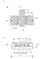
〈トランジスタ100の構造及び特徴〉
図1(A)は、トランジスタ100の平面図である。なお、図1(A)において、下地絶縁膜102、ゲート絶縁膜111及び層間絶縁膜117は、便宜上、図示していない。
<Structure and Features of
FIG. 1A is a plan view of the
図1(A)より、酸化物半導体膜103上には、第1の電極113及び第1の電極113の側面に設けられたサイドウォール絶縁膜115が設けられている。そして、第2の電極119a及び第3の電極119bは、開口部116a、116bを介して酸化物半導体膜103の一対の第3の領域109a、109b上に設けられている。また、第2の電極119a及び第3の電極119bは、一対の第3の領域109a、109bの上面と接している。トランジスタ100はトップゲート構造でトップコンタクト型のトランジスタである。
As shown in FIG. 1A, a
図1(B)は、トランジスタ100におけるA−B間の断面図である。図1(B)より、基板101上に下地絶縁膜102が設けられており、下地絶縁膜102上には、第1の領域105、一対の第2の領域107a、107b及び一対の第3の領域109a、109bを含む酸化物半導体膜103が設けられている。一対の第2の領域107a、107bは第1の領域105の側面に接して設けられている。一対の第3の領域109a、109bは、一対の第2の領域107a、107bの側面に接して設けられている。
FIG. 1B is a cross-sectional view taken along a line AB in the
酸化物半導体膜103上にゲート絶縁膜111が設けられている。ゲート絶縁膜111上には、第1の領域105と重畳した第1の電極113が設けられている。第1の電極113の側面には、サイドウォール絶縁膜115a、115b(サイドウォール絶縁膜115)が接して設けられている。
A
ゲート絶縁膜111、第1の電極113及びサイドウォール絶縁膜115a、115b上には、層間絶縁膜117が設けられている。
An interlayer insulating
第2の電極119a及び第3の電極119bは、ゲート絶縁膜111及び層間絶縁膜117に設けられた開口部116a、116bを介して一対の第3の領域109a、109bと接して設けられている。なお、ゲート絶縁膜111は、第1の領域105、一対の第2の領域107a、107b及び一対の第3の領域109a、109bに接している。
The
第2の電極119a及び第3の電極119bの端部は、テーパ形状であってもよいが、第1の電極113の端部は垂直な形状であることが好ましい。第1の電極113の端部を垂直な形状とし、該第1の電極113上にサイドウォール絶縁膜115(サイドウォール絶縁膜115a、115b)となる絶縁膜を形成し、異方性の高いエッチングを行うことで、サイドウォール絶縁膜115(サイドウォール絶縁膜115a、115b)を形成することができるようになる。
The ends of the
また、詳細は後述するが、図1(A)及び図1(B)より、一対の第2の領域107a、107bは酸化物半導体膜103がサイドウォール絶縁膜115と重畳する領域に相当する。そして、サイドウォール絶縁膜115(サイドウォール絶縁膜115a、115b)は、第1の電極113の側面及びゲート絶縁膜111と接する領域以外の少なくとも一部は湾曲形状を有してもよい。
Although details will be described later, the pair of
第1の領域105、一対の第2の領域107a、107b及び一対の第3の領域109a、109bを含む酸化物半導体膜103は、In、Ga、Sn及びZnから選ばれた二以上の元素を含む金属酸化物である。なお、該金属酸化物は、バンドギャップが2eV以上、好ましくは2.5eV以上、より好ましくは3eV以上のものである。このように、バンドギャップの広い金属酸化物を用いることで、トランジスタ100のオフ電流を低減することができる。
The
トランジスタ100において、第1の領域105はチャネル形成領域として機能する。
In the
第1の領域105は、先に記述したCAAC酸化物半導体領域である。CAAC酸化物半導体は単結晶ではないが、また、非晶質のみから形成されているものでもない。また、CAAC酸化物半導体は結晶化した部分(結晶部分)を含むが、1つの結晶部分と他の結晶部分の境界を明確に判別できないこともある。CAAC酸化物半導体に含まれる酸素の一部は窒素で置換されてもよい。また、CAAC酸化物半導体を構成する個々の結晶部分のc軸は一定の方向(例えば、CAAC酸化物半導体を支持する基板面やCAAC酸化物半導体膜の表面や膜面、界面等に垂直な方向)に揃っていてもよい。あるいは、CAAC酸化物半導体を構成する個々の結晶部分のab面の法線は一定の方向(例えば、CAAC酸化物半導体を支持する基板面やCAAC酸化物半導体膜の表面や膜面、界面等に垂直な方向)を向いていてもよい。なお、CAAC酸化物半導体はその組成等に応じて、導体、半導体、又は絶縁体となる。そして、CAAC酸化物半導体は、その組成等に応じて、可視光に対して透明又は不透明となる。CAAC酸化物半導体の例として、形成した表面、形成されている基板面、又は、界面に垂直な方向から観察すると、三角形、又は六角形の原子配列が認められ、且つその形成断面を観察すると金属原子、又は、金属原子と酸素原子(あるいは窒素原子)の層状配列が認められる材料が挙げられる。
The
また、第1の領域105の水素濃度は、1×10²⁰atoms/cm3以下、好ましくは1×1019atoms/cm3以下、より好ましくは1×1018atoms/cm3以下である。チャネル形成領域である第1の領域105がCAAC酸化物半導体領域であり、且つ水素濃度が低減されているトランジスタ100は、光照射前後及びBT(ゲート・熱バイアス)ストレス試験前後において、しきい値電圧の変動が小さいことから安定した電気特性を有し、信頼性の高いトランジスタといえる。
The hydrogen concentration in the
一対の第2の領域107a、107b及び一対の第3の領域109a、109bは、導電率が10S/cm以上1000S/cm以下、好ましくは100S/cm以上1000S/cm以下とする。また、一対の第3の領域109a、109bの導電率のほうが、一対の第2の領域107a、107bの導電率より高い。なお、導電率が低すぎると、トランジスタ100のオン電流が低下してしまう。
The conductivity of the pair of
また、一対の第2の領域107a、107b及び一対の第3の領域109a、109bは、ドーパントを含む非晶質領域である。一対の第2の領域107a、107b及び一対の第3の領域109a、109bはドーパントとして、水素又は希ガス元素から選ばれた一以上の元素が添加されている。
The pair of
一対の第2の領域107a、107b及び一対の第3の領域109a、109bのドーパント濃度を増加させると、キャリア密度を増加させることができるが、ドーパント濃度を増加させすぎると、ドーパントがキャリアの移動を阻害することになり、一対の第2の領域107a、107b及び一対の第3の領域109a、109bの導電性を低下させることになる。
Increasing the dopant concentration in the pair of
従って、一対の第2の領域107a、107b及び一対の第3の領域109a、109bのドーパント濃度は、5×10¹⁸atoms/cm3以上1×1022atoms/cm3以下であることが好ましい。さらに、一対の第3の領域109a、109bのドーパント濃度は、一対の第2の領域107a、107bのドーパント濃度より高い。具体的には、一対の第2の領域107a、107bのドーパント濃度は、5×1018atoms/cm3以上5×1019atoms/cm3未満とし、一対の第3の領域109a、109bのドーパント濃度は、5×1019atoms/cm3以上1×1022atoms/cm3以下とするのが好ましい。また、これらドーパント濃度の差は、トランジスタ100にサイドウォール絶縁膜115(サイドウォール絶縁膜115a、115b)が設けられているため、ドーパントを添加する工程においてセルフアラインに形成される。
Accordingly, the dopant concentration of the pair of
一対の第3の領域109a、109bはトランジスタ100のソース領域及びドレイン領域として機能する。トランジスタ100は、ドーパント濃度に差を有する非晶質領域(低濃度領域及び高濃度領域)をチャネル形成領域の第1の領域105の両端に設けることで、チャネル形成領域である第1の領域105に加わる電界を緩和させることができる。詳細には、低濃度領域である一対の第2の領域107a、107b、及び高濃度領域である一対の第3の領域109a、109bをチャネル形成領域の第1の領域105の両端に設けることで、トランジスタ100は、第1の領域105に形成されるチャネルにおけるバンド端の曲がりがほとんど生じない効果を示す。よって、一対の第2の領域107a、107b及び一対の第3の領域109a、109bを設けることで短チャネル効果を抑制することができる。
The pair of
〈トランジスタ100の作製方法〉
次に、トランジスタ100の作製方法について、図2及び図3を用いて説明する。
<Method for
Next, a method for manufacturing the
基板101に下地絶縁膜102を形成する。下地絶縁膜102は、スパッタリング法、CVD法、塗布法などで形成することができる。なお、下地絶縁膜102の厚さに限定はないが、下地絶縁膜102の厚さは50nm以上とすることが好ましい。
A
基板101は、材質などに大きな制限はないが、少なくとも、後の熱処理に耐えうる程度の耐熱性を有している必要がある。例えば、ガラス基板、セラミック基板、石英基板、サファイア基板などを、基板101として用いてもよい。また、シリコンや炭化シリコンなどの単結晶半導体基板、多結晶半導体基板、シリコンゲルマニウムなどの化合物半導体基板、SOI基板などを適用することも可能であり、これらの基板上に半導体素子が設けられたものを、基板101として用いてもよい。
There is no particular limitation on the material of the
また、基板101として、可撓性基板を用いてもよい。可撓性基板上にトランジスタを設ける場合、可撓性基板上に直接的にトランジスタを作製してもよいし、他の基板にトランジスタを作製した後、これを剥離し、可撓性基板に転置してもよい。なお、トランジスタを剥離し、可撓性基板に転置するためには、上記他の基板とトランジスタとの間に、剥離が容易な領域を設けるとよい。
Further, a flexible substrate may be used as the
下地絶縁膜102は、基板101からの不純物(例えば、LiやNaなどのアルカリ金属など)の拡散を防止する他に、トランジスタ100の作製工程におけるエッチング工程によって、基板101がエッチングされることを防ぐ。
The base
また、下地絶縁膜102としては、酸化シリコン膜、酸化ガリウム膜、酸化アルミニウム膜などの酸化物絶縁膜、もしくは窒化シリコン膜、窒化アルミニウム膜などの窒化物絶縁膜、又は酸化窒化シリコン膜、酸化窒化アルミニウム膜、窒化酸化シリコン膜から選ばれる絶縁膜の単層構造又はこれらの積層構造を用いる。なお、下地絶縁膜102は、酸化物半導体膜103と接する部分において酸素を含むことが好ましい。
As the
下地絶縁膜102をスパッタリング法で形成する場合、シリコンターゲット、石英ターゲット、アルミニウムターゲット又は酸化アルミニウムターゲットなどを用いて、酸素を含む雰囲気ガス中で形成すればよい。雰囲気ガス中の酸素の割合は、雰囲気ガス全体に対して6体積%以上とする。好ましくは、50体積%以上とする。雰囲気ガス中の酸素ガスの割合を高めることで、加熱により酸素放出される絶縁膜を形成することができる。
In the case where the
ターゲット中の水素も極力取り除かれていると好ましい。具体的には、OH基が100ppm以下、好ましくは10ppm以下、より好ましくは1ppm以下の酸化物ターゲットを用いることで、下地絶縁膜102中の水素濃度を低減し、トランジスタ100の電気特性及び信頼性を高めることができる。例えば、溶融石英は、OH基が10ppm以下としやすく、またコストが低いため好ましい。もちろんOH基濃度の低い合成石英のターゲットを用いてもよい。
It is preferable that hydrogen in the target is removed as much as possible. Specifically, by using an oxide target with an OH group of 100 ppm or less, preferably 10 ppm or less, more preferably 1 ppm or less, the hydrogen concentration in the
さらに、トランジスタ100の作製にあたり、LiやNaなどのアルカリ金属は、不純物であるため含有量を少なくすることが好ましい。基板101にアルカリ金属などの不純物を含むガラス基板を用いる場合、アルカリ金属の侵入防止のため、下地絶縁膜102として、上記窒化物絶縁膜を形成することが好ましく、さらに、上記窒化物絶縁膜上に上記酸化物絶縁膜を積層することが好ましい。
Further, in manufacturing the
ここで、酸化窒化シリコンとは、その組成において、窒素よりも酸素の含有量が多いものを示し、例えば、酸素が50原子%以上70原子%以下、窒素が0.5原子%以上15原子%以下、珪素が25原子%以上35原子%以下、水素が0原子%以上10原子%以下の範囲で含まれるものをいう。また、窒化酸化シリコンとは、その組成において、酸素よりも窒素の含有量が多いものを示し、例えば、酸素が5原子%以上30原子%以下、窒素が20原子%以上55原子%以下、珪素が25原子%以上35原子%以下、水素が10原子%以上25原子%以下の範囲で含まれるものをいう。但し、上記範囲は、ラザフォード後方散乱法(RBS:Rutherford Backscattering Spectrometry)や、水素前方散乱法(HFS:Hydrogen Forward Scattering)を用いて測定した場合のものである。また、構成元素の含有比率は、その合計が100原子%を超えない値をとる。 Here, silicon oxynitride indicates a composition having a higher oxygen content than nitrogen. For example, oxygen is 50 atomic% to 70 atomic%, and nitrogen is 0.5 atomic% to 15 atomic%. Hereinafter, silicon is contained in the range of 25 atomic% to 35 atomic% and hydrogen in the range of 0 atomic% to 10 atomic%. Silicon nitride oxide refers to a composition having a nitrogen content higher than that of oxygen. For example, oxygen is 5 atomic% to 30 atomic%, nitrogen is 20 atomic% to 55 atomic%, silicon In the range of 25 atomic% to 35 atomic% and hydrogen in the range of 10 atomic% to 25 atomic%. However, the above ranges are those measured using Rutherford Backscattering Spectrometry (RBS) or Hydrogen Forward Scattering (HFS). Further, the content ratio of the constituent elements takes a value that the total does not exceed 100 atomic%.
また、下地絶縁膜102は、酸化物半導体膜103と接する部分において酸素を含むことが好ましいことから、下地絶縁膜102として、加熱により酸素放出される絶縁膜を用いてもよい。なお、「加熱により酸素放出される」とは、TDS(Thermal Desorption Spectroscopy:昇温脱離ガス分光法)分析にて、酸素原子に換算した酸素の放出量が1.0×10¹⁸atoms/cm3以上、好ましくは3.0×1020atoms/cm3以上であることをいう。
Further, since the
以下、酸素の放出量をTDS分析で酸素原子に換算して定量する方法について説明する。 Hereinafter, a method for quantifying the amount of released oxygen by converting it into oxygen atoms by TDS analysis will be described.
TDS分析したときの気体の放出量は、スペクトルの積分値に比例する。このため、絶縁膜のスペクトルの積分値と、標準試料の基準値に対する比とにより、気体の放出量を計算することができる。標準試料の基準値とは、所定の原子を含む試料の、スペクトルの積分値に対する原子の密度の割合である。 The amount of gas released when TDS analysis is performed is proportional to the integral value of the spectrum. For this reason, the amount of gas emission can be calculated from the integral value of the spectrum of the insulating film and the ratio of the standard sample to the reference value. The reference value of the standard sample is the ratio of the density of atoms to the integral value of the spectrum of a sample containing a predetermined atom.
例えば、標準試料である所定の密度の水素を含むシリコンウェハのTDS分析結果、及び絶縁膜のTDS分析結果から、絶縁膜の酸素分子の放出量(NO2)は、数式1で求めることができる。ここで、TDS分析で得られる質量数32で検出されるスペクトルの全てが酸素分子由来と仮定する。質量数32のものとしてCH3OHがあるが、存在する可能性が低いものとしてここでは考慮しない。また、酸素原子の同位体である質量数17の酸素原子及び質量数18の酸素原子を含む酸素分子についても、自然界における存在比率が極微量であるため考慮しない。
For example, the amount of released oxygen molecules (N O2 ) in the insulating film can be obtained from
![]()
![]()
NH2は、標準試料から脱離した水素分子を密度で換算した値である。SH2は、標準試料をTDS分析したときのスペクトルの積分値である。ここで、標準試料の基準値を、NH2/SH2とする。SO2は、絶縁膜をTDS分析したときのスペクトルの積分値である。αは、TDS分析におけるスペクトル強度に影響する係数である。数式1の詳細に関しては、特開平6−275697公報を参照できる。なお、上記した酸素の放出量の数値は、電子科学株式会社製の昇温脱離分析装置EMD−WA1000S/Wを用い、標準試料として1×1016atoms/cm3の水素原子を含むシリコンウェハを用いて測定した数値である。
N H2 is a value obtained by converting hydrogen molecules desorbed from the standard sample by density. SH2 is an integral value of a spectrum when a standard sample is subjected to TDS analysis. Here, the reference value of the standard sample is N H2 / SH 2 . S O2 is an integral value of a spectrum when the insulating film is subjected to TDS analysis. α is a coefficient that affects the spectral intensity in the TDS analysis. For details of
また、TDS分析において、酸素の一部は酸素原子として検出される。酸素分子と酸素原子の比率は、酸素分子のイオン化率から算出することができる。なお、上述のαは酸素分子のイオン化率を含むため、酸素分子の放出量を評価することで、酸素原子の放出量についても見積もることができる。 In TDS analysis, part of oxygen is detected as oxygen atoms. The ratio of oxygen molecules to oxygen atoms can be calculated from the ionization rate of oxygen molecules. Note that since the above α includes the ionization rate of oxygen molecules, the amount of released oxygen atoms can be estimated by evaluating the amount of released oxygen molecules.
なお、NO2は酸素分子の放出量である。絶縁膜においては、酸素原子に換算したときの酸素の放出量は、酸素分子の放出量の2倍となる。 Note that N 2 O 2 is the amount of released oxygen molecules. In the insulating film, the amount of released oxygen when converted to oxygen atoms is twice the amount of released oxygen molecules.
加熱により酸素放出される絶縁膜の一例として、酸素が過剰な酸化シリコン(SiOX(X>2))がある。酸素が過剰な酸化シリコン(SiOX(X>2))とは、シリコン原子数の2倍より多い酸素原子を単位体積当たりに含むものである。単位体積当たりのシリコン原子数及び酸素原子数は、ラザフォード後方散乱法により測定した値である。 As an example of an insulating film from which oxygen is released by heating, there is silicon oxide (SiO X (X> 2)) in which oxygen is excessive. Oxygen-excess silicon oxide (SiO X (X> 2)) contains oxygen atoms more than twice the number of silicon atoms per unit volume. The number of silicon atoms and the number of oxygen atoms per unit volume are values measured by Rutherford backscattering method.
下地絶縁膜102として、加熱により酸素放出される絶縁膜を用いることで、酸化物半導体膜103に酸素を供給され、下地絶縁膜102及び酸化物半導体膜103の界面準位を低減できる。従って、トランジスタ100の動作に起因して生じうる電荷などが、下地絶縁膜102及び酸化物半導体膜103の界面に捕獲されることを抑制でき、トランジスタ100を電気特性の劣化の少ないトランジスタとすることができる。
By using an insulating film from which oxygen is released by heating as the
さらに、酸化物半導体膜103の酸素欠損に起因して電荷が生じる場合がある。一般に酸化物半導体における酸素欠損は、その酸素欠損の一部がドナーとなりキャリアである電子を生じる。つまりトランジスタ100においても、酸化物半導体膜103の酸素欠損の一部はドナーとなりキャリアである電子が生じることで、トランジスタ100のしきい値電圧がマイナス方向に変動してしまう。そして、酸化物半導体膜103において、該電子の生成は、酸化物半導体膜103と下地絶縁膜102との界面近傍で生じる酸素欠損おいて顕著である。下地絶縁膜102から酸化物半導体膜103に酸素が十分に放出されることにより、しきい値電圧がマイナス方向へ変動させる酸化物半導体膜103の酸素欠損を補うことができる。
Further, charge may be generated due to oxygen vacancies in the
即ち、下地絶縁膜102に、加熱により酸素放出される絶縁膜を用いることで、酸化物半導体膜103及び下地絶縁膜102の界面準位、ならびに酸化物半導体膜103の酸素欠損を低減し、酸化物半導体膜103及び下地絶縁膜102の界面における電荷の捕獲の影響を小さくすることができる。
In other words, by using an insulating film from which oxygen is released by heating as the
次に、下地絶縁膜102上に酸化物半導体膜103を形成する。
Next, the
具体的には、膜全体がCAAC酸化物半導体膜である酸化物半導体膜140を形成し、その後、酸化物半導体膜140にドーパントを添加することで一対の第2の領域107a、107b及び一対の第3の領域109a、109bを形成して、酸化物半導体膜103を形成する。そこで、ドーパントを添加して一対の第2の領域107a、107b及び一対の第3の領域109a、109bを形成する前のCAAC酸化物半導体膜である酸化物半導体膜140の作製方法を説明する。
Specifically, the
CAAC酸化物半導体膜である酸化物半導体膜140の作製方法として2種類の方法がある。
There are two methods for manufacturing the
1つの方法は、酸化物半導体を形成する際に、基板を加熱しながら行う方法(便宜上、1step法と言う。)であり、もう1つの方法は、酸化物半導体を2回に分けて形成し、2回の加熱処理を行い作製する方法(便宜上、2step法と言う。)である。 One method is a method in which an oxide semiconductor is formed while heating the substrate (referred to as a one-step method for convenience), and the other method is to form the oxide semiconductor in two steps. This is a method of performing heat treatment twice (referred to as a two-step method for convenience).
はじめに、1step法にて酸化物半導体膜140を形成する方法について説明する。
First, a method for forming the
まず、酸化物半導体膜103で説明した酸化物半導体材料を用いてスパッタリング法により、下地絶縁膜102が形成された基板101を加熱しながら形成する。なお、本工程で形成された酸化物半導体膜を、便宜上、酸化物半導体膜130とする。基板101を加熱する温度は、200℃以上400℃以下、好ましくは250℃以上350℃以下とすればよく、酸化物半導体膜130は厚さ1nm以上50nm以下で形成すればよい。
First, the
ここで、酸化物半導体膜130を形成するスパッタリング装置について、以下に詳細を説明する。
Here, a sputtering device for forming the
酸化物半導体膜130を形成する処理室は、リークレートを1×10⁻¹⁰Pa・m3/秒以下とすることが好ましく、それによりスパッタリング法により形成する際、膜中への不純物の混入を低減することができる。
The treatment chamber in which the
リークレートを低くするには、外部リークのみならず内部リークを低減する必要がある。外部リークとは、微小な穴やシール不良などによって真空系の外から気体が流入することである。内部リークとは、真空系内のバルブなどの仕切りからの漏れや内部の部材からの放出ガスに起因する。リークレートを1×10⁻¹⁰Pa・m3/秒以下とするためには、外部リーク及び内部リークの両面から対策をとる必要がある。 In order to reduce the leak rate, it is necessary to reduce not only external leakage but also internal leakage. The external leak is a gas flowing from outside the vacuum system due to a minute hole or a defective seal. The internal leak is caused by leakage from a partition such as a valve in the vacuum system or gas released from an internal member. In order to set the leak rate to 1 × 10 −10 Pa · m 3 / sec or less, it is necessary to take measures from both the external leak and the internal leak.
外部リークを減らすには、処理室の開閉部分はメタルガスケットでシールするとよい。メタルガスケットは、フッ化鉄、酸化アルミニウム、又は酸化クロムによって被覆された金属材料を用いると好ましい。メタルガスケットはOリングと比べ密着性が高く、外部リークを低減できる。また、フッ化鉄、酸化アルミニウム、酸化クロムなどの不動態によって被覆された金属材料を用いることで、メタルガスケットから生じる水素を含む放出ガスが抑制され、内部リークも低減することができる。 In order to reduce external leakage, the open / close portion of the processing chamber may be sealed with a metal gasket. The metal gasket is preferably a metal material coated with iron fluoride, aluminum oxide, or chromium oxide. Metal gaskets have higher adhesion than O-rings and can reduce external leakage. In addition, by using a metal material coated with a passive material such as iron fluoride, aluminum oxide, or chromium oxide, an outgas including hydrogen generated from the metal gasket can be suppressed, and an internal leak can be reduced.
処理室の内壁として用いる部材は、水素を含む放出ガスの少ないアルミニウム、クロム、チタン、ジルコニウム、ニッケルもしくはバナジウム、又は、これらを鉄、クロム及びニッケルなどの少なくとも一を含む合金材料に被覆したものを用いてもよい。鉄、クロム及びニッケルなどの少なくとも一を含む合金材料は、剛性があり、熱に強く、また加工に適している。ここで、処理室の内壁の表面積を小さくするために、該部材の表面凹凸を研磨などによって低減しておくと、放出ガスを低減できる。又は、該部材をフッ化鉄、酸化アルミニウム、酸化クロムなどの不動態で被覆してもよい。 The member used as the inner wall of the processing chamber is made of aluminum, chromium, titanium, zirconium, nickel, or vanadium that emits less hydrogen containing hydrogen, or an alloy material containing at least one of iron, chromium, nickel, and the like. It may be used. An alloy material containing at least one of iron, chromium, nickel and the like is rigid, heat resistant, and suitable for processing. Here, in order to reduce the surface area of the inner wall of the processing chamber, if the surface irregularities of the member are reduced by polishing or the like, the emitted gas can be reduced. Alternatively, the member may be coated with a passive material such as iron fluoride, aluminum oxide, or chromium oxide.
さらに、雰囲気ガスを処理室に導入する直前に、雰囲気ガスの精製機を設けることが好ましい。このとき、精製機から処理室までの配管の長さを5m以下、好ましくは1m以下とする。配管の長さを5m以下又は1m以下とすることで、配管からの放出ガスの影響を長さに応じて低減できる。 Furthermore, it is preferable to provide a purifier for the atmospheric gas immediately before introducing the atmospheric gas into the processing chamber. At this time, the length of the pipe from the refiner to the processing chamber is 5 m or less, preferably 1 m or less. By setting the length of the pipe to 5 m or less or 1 m or less, the influence of the gas released from the pipe can be reduced according to the length.
処理室の排気は、ドライポンプなどの粗引きポンプと、スパッタイオンポンプ、ターボ分子ポンプ及びクライオポンプなどの高真空ポンプとを適宜組み合わせて行うとよい。ターボ分子ポンプは大きいサイズの分子の排気が優れる一方、水素や水の排気能力が低い。そこで、水の排気能力の高いクライオポンプ及び水素の排気能力の高いスパッタイオンポンプを組み合わせて使用することが有効となる。 The processing chamber may be evacuated by appropriately combining a roughing pump such as a dry pump and a high vacuum pump such as a sputter ion pump, a turbo molecular pump, or a cryopump. Turbomolecular pumps excel large molecules, but have low hydrogen and water exhaust capabilities. Therefore, it is effective to use a cryopump having a high water exhaust capability and a sputter ion pump having a high hydrogen exhaust capability in combination.
処理室内に存在する吸着物は、内壁に吸着しているために処理室の圧力に影響しないが、処理室を排気した際のガス放出の原因となる。そのため、リークレートと排気速度に相関はないが、排気能力の高いポンプを用いて、処理室に存在する吸着物をできる限り脱離し、予め排気しておくことが重要である。なお、吸着物の脱離を促すために、処理室をベーキングしてもよい。ベーキングすることで吸着物の脱離速度を10倍程度大きくすることができる。ベーキングは100℃以上450℃以下で行えばよい。このとき、不活性ガスを導入しながら吸着物の除去を行うと、排気するだけでは脱離しにくい水などの脱離速度をさらに大きくすることができる。 The adsorbate present in the processing chamber does not affect the pressure in the processing chamber because it is adsorbed on the inner wall, but causes gas emission when the processing chamber is exhausted. For this reason, there is no correlation between the leak rate and the exhaust speed, but it is important to desorb the adsorbate present in the processing chamber as much as possible and exhaust it in advance using a pump having a high exhaust capability. Note that the treatment chamber may be baked to promote desorption of the adsorbate. Baking can increase the desorption rate of the adsorbate by about 10 times. Baking may be performed at 100 ° C to 450 ° C. At this time, if the adsorbate is removed while introducing the inert gas, it is possible to further increase the desorption rate of water or the like that is difficult to desorb only by exhausting.
スパッタリング法において、プラズマを発生させるための電源装置は、RF電源装置、AC電源装置、DC電源装置等を適宜用いることができる。 In the sputtering method, an RF power supply device, an AC power supply device, a DC power supply device, or the like can be used as appropriate as a power supply device for generating plasma.
酸化物半導体膜130をスパッタリング法で形成する際、ターゲットとしては、亜鉛を含む金属酸化物ターゲットを用いることができる。また、インジウム、ガリウム、スズ及び亜鉛から選ばれた二以上の元素を含む金属酸化物ターゲットを用いることができる。当該ターゲットとしては、例えば、四元系金属酸化物であるIn−Sn−Ga−Zn系金属酸化物や、三元系金属酸化物であるIn−Ga−Zn系金属酸化物、In−Sn−Zn系金属酸化物、In−Al−Zn系金属酸化物、Sn−Ga−Zn系金属酸化物、Al−Ga−Zn系金属酸化物、Sn−Al−Zn系金属酸化物や、In−Hf−Zn系金属酸化物、In−La−Zn系金属酸化物、In−Ce−Zn系金属酸化物、In−Pr−Zn系金属酸化物、In−Nd−Zn系金属酸化物、In−Sm−Zn系金属酸化物、In−Eu−Zn系金属酸化物、In−Gd−Zn系金属酸化物、In−Tb−Zn系金属酸化物、In−Dy−Zn系金属酸化物、In−Ho−Zn系金属酸化物、In−Er−Zn系金属酸化物、In−Tm−Zn系金属酸化物、In−Yb−Zn系金属酸化物、In−Lu−Zn系金属酸化物や、二元系金属酸化物であるIn−Zn系金属酸化物、Sn−Zn系金属酸化物、In−Ga系金属酸化物や、インジウム、スズ又は亜鉛などを含む一元系金属酸化物などのターゲットを用いることができる。
When the
ターゲットの一例として、In、Ga、及びZnを含む金属酸化物ターゲット(In−Ga−Zn系金属酸化物)を、In2O3:Ga2O3:ZnO=1:1:1[mol数比]の組成比とする。また、In2O3:Ga2O3:ZnO=1:1:2[mol数比]の組成比を有するターゲット、又はIn2O3:Ga2O3:ZnO=1:1:4[mol数比]の組成比を有するターゲット、In2O3:Ga2O3:ZnO=2:1:8[mol数比]の組成比を有するターゲットを用いることもできる。 As an example of the target, a metal oxide target (In—Ga—Zn-based metal oxide) containing In, Ga, and Zn is used as In 2 O 3 : Ga 2 O 3 : ZnO = 1: 1: 1 [number of moles. Ratio]. In addition, a target having a composition ratio of In 2 O 3 : Ga 2 O 3 : ZnO = 1: 1: 2 [molar ratio], or In 2 O 3 : Ga 2 O 3 : ZnO = 1: 1: 4 [ A target having a composition ratio of mol number ratio] and a target having a composition ratio of In 2 O 3 : Ga 2 O 3 : ZnO = 2: 1: 8 [mol number ratio] can also be used.
なお、雰囲気ガスは、希ガス(代表的にはアルゴン)雰囲気、酸素雰囲気、希ガス及び酸素の混合ガスを適宜用いる。また、雰囲気ガスには、水素、水、水酸基又は水素化物などの不純物が除去された高純度ガスを用いることが好ましい。 Note that as the atmosphere gas, a rare gas (typically argon) atmosphere, an oxygen atmosphere, or a mixed gas of a rare gas and oxygen is used as appropriate. Moreover, it is preferable to use high purity gas from which impurities, such as hydrogen, water, a hydroxyl group, or hydride, were removed as atmospheric gas.
上記スパッタリング装置を用いることで、水素の混入が低減された酸化物半導体膜130を形成することができる。
With the use of the above sputtering apparatus, the
また、下地絶縁膜102及び酸化物半導体膜130は、真空下で連続して形成してもよい。例えば、基板101表面の水素を含む不純物を、熱処理又はプラズマ処理で除去した後、大気に暴露することなく下地絶縁膜102を形成し、続けて大気に暴露することなく酸化物半導体膜130を形成してもよい。このようにすることで、基板101表面の水素を含む不純物を低減し、また、基板101と下地絶縁膜102の界面、下地絶縁膜102と酸化物半導体膜130との界面に、大気成分が付着することを抑制できる。その結果、電気特性が良好で、信頼性の高いトランジスタ100を作製することができる。
Alternatively, the
ついで、第1のフォトリソグラフィ工程を行い、酸化物半導体膜130上にレジストマスクを形成する。該レジストマスクを用いて、第1のエッチング工程で加工し、島状の酸化物半導体膜132を形成する。なお、該レジストマスクは、フォトリソグラフィ工程の他にインクジェット法、印刷法等を適宜用いることができる。
Next, a first photolithography step is performed to form a resist mask over the
第1のエッチング工程において、島状の酸化物半導体膜132の端部がテーパ形状となるようにエッチングすることが好ましい。島状の酸化物半導体膜132の端部をテーパ形状とすることで、後に形成されるゲート絶縁膜111の被覆性を向上させることができる。フォトリソグラフィ工程を用いる場合は、レジストマスクを後退させつつエッチングすることでテーパ形状とすることができる。
In the first etching step, etching is preferably performed so that an end portion of the island-shaped
第1のエッチング工程は、ドライエッチング又はウェットエッチングでよく、これらを組み合わせて行ってもよい。ウェットエッチングするエッチング液としては、燐酸と酢酸と硝酸を混ぜた溶液、アンモニア過水(31重量%過酸化水素水:28重量%アンモニア水:水=5:2:2(体積比))などを用いることができる。また、ITO07N(関東化学社製)を用いてもよい。 The first etching step may be dry etching or wet etching, or may be performed in combination. As an etchant for wet etching, a mixed solution of phosphoric acid, acetic acid and nitric acid, ammonia perwater (31 wt% hydrogen peroxide water: 28 wt% ammonia water: water = 5: 2: 2 (volume ratio)), etc. Can be used. In addition, ITO07N (manufactured by Kanto Chemical Co., Inc.) may be used.
ドライエッチングに用いるエッチングガスとしては、塩素を含むガス(塩素系ガス、例えば塩素(Cl2)、三塩化硼素(BCl3)、四塩化珪素(SiCl4)、四塩化炭素(CCl4)など)が好ましい。 As an etching gas used for dry etching, a gas containing chlorine (chlorine-based gas such as chlorine (Cl 2 ), boron trichloride (BCl 3 ), silicon tetrachloride (SiCl 4 ), carbon tetrachloride (CCl 4 ), or the like) Is preferred.
また、フッ素を含むガス(フッ素系ガス、例えば四弗化炭素(CF4)、六弗化硫黄(SF6)、三弗化窒素(NF3)、トリフルオロメタン(CHF3)など)、臭化水素(HBr)、酸素(O2)、これらのガスにヘリウム(He)やアルゴン(Ar)などの希ガスを添加したガス、などを用いることができる。 Gas containing fluorine (fluorine-based gas such as carbon tetrafluoride (CF 4 ), sulfur hexafluoride (SF 6 ), nitrogen trifluoride (NF 3 ), trifluoromethane (CHF 3 ), etc.), bromide Hydrogen (HBr), oxygen (O 2 ), a gas obtained by adding a rare gas such as helium (He) or argon (Ar) to these gases, or the like can be used.
ドライエッチングとしては、平行平板型RIE(Reactive Ion Etching)法や、ICP(Inductively Coupled Plasma:誘導結合型プラズマ)エッチング法を用いることができる。所望の形状に加工できるように、エッチング条件(コイル型の電極に印加される電力量、基板側の電極に印加される電力量、基板側の電極温度など)を適宜調節する。 As the dry etching, a parallel plate RIE (Reactive Ion Etching) method or an ICP (Inductively Coupled Plasma) etching method can be used. Etching conditions (such as the amount of power applied to the coil-type electrode, the amount of power applied to the substrate-side electrode, and the electrode temperature on the substrate side) are adjusted as appropriate so that the substrate can be processed into a desired shape.
酸化物半導体膜132を形成後に、加熱処理を行い、酸化物半導体膜140を形成する。加熱処理の温度を150℃以上650℃以下、好ましくは250℃以上450℃以下とし、酸化性雰囲気又は不活性雰囲気で行う。ここで、酸化性雰囲気は、酸素、オゾン又は窒化酸素などの酸化性ガスを10ppm以上含有する雰囲気をいう。また、不活性雰囲気は、前述の酸化性ガスが10ppm未満であり、その他、窒素又は希ガスで充填された雰囲気をいう。処理時間は3分〜24時間とする。処理時間を長くするほど非晶質領域に対して結晶領域の割合の多い酸化物半導体膜を形成することができるが、24時間を超える熱処理は生産性の低下を招くため好ましくない。なお、該加熱処理は、酸化物半導体膜132を形成した後にゲート絶縁膜111を形成してから行ってもよい。
After the
上記加熱処理は、酸化物半導体膜132から水素を放出させると共に、下地絶縁膜102に含まれる酸素の一部を、酸化物半導体膜132と、下地絶縁膜102における酸化物半導体膜132の界面近傍に拡散させる。
The above heat treatment releases hydrogen from the
加熱処理に用いる加熱処理装置に特別な限定はなく、抵抗発熱体などの発熱体からの熱伝導又は熱輻射によって、被処理物を加熱する装置を備えていてもよい。例えば、電気炉や、GRTA(Gas Rapid Thermal Anneal)装置、LRTA(Lamp Rapid Thermal Anneal)装置等のRTA(Rapid Thermal Anneal)装置を用いることができる。LRTA装置は、ハロゲンランプ、メタルハライドランプ、キセノンアークランプ、カーボンアークランプ、高圧ナトリウムランプ、高圧水銀ランプなどのランプから発する光(電磁波)の輻射により、被処理物を加熱する装置である。GRTA装置は、高温のガスを用いて加熱処理を行う装置である。 There is no particular limitation on a heat treatment apparatus used for the heat treatment, and the apparatus may include a device that heats an object to be processed by heat conduction or heat radiation from a heating element such as a resistance heating element. For example, an electric furnace, a rapid thermal annealing (RTA) apparatus such as a GRTA (Gas Rapid Thermal Anneal) apparatus, or an LRTA (Lamp Rapid Thermal Anneal) apparatus can be used. The LRTA apparatus is an apparatus that heats an object to be processed by radiation of light (electromagnetic waves) emitted from a lamp such as a halogen lamp, a metal halide lamp, a xenon arc lamp, a carbon arc lamp, a high pressure sodium lamp, or a high pressure mercury lamp. The GRTA apparatus is an apparatus that performs heat treatment using a high-temperature gas.
ここで、2step法で酸化物半導体膜140を形成する方法について説明する。
Here, a method for forming the
第1の酸化物半導体膜を形成し、窒素、酸素、希ガス、又は乾燥空気の雰囲気下で、400℃以上750℃以下の第1の加熱処理を行う。該第1の加熱処理によって、第1の酸化物半導体膜の表面を含む領域に、結晶領域を有する第1の結晶性酸化物半導体膜が形成される。そして、該第1の酸化物半導体膜よりも厚い第2の酸化物半導体膜を形成し、400℃以上750℃以下の第2の加熱処理を行い、該第1の結晶性酸化物半導体膜を結晶成長の種として、上方に結晶成長させ、第2の酸化物半導体膜の全体を結晶化させる(第2の結晶性酸化物半導体膜を形成する)。以上より形成された第1の結晶性酸化物半導体膜及び第2の結晶性酸化物半導体膜を、酸化物半導体膜130とし、上記第1のフォトリソグラフィ工程及び上記第1のエッチング工程を行い、酸化物半導体膜132を形成し、1step法で説明した酸化物半導体膜132形成後に行う加熱処理を行うことで、酸化物半導体膜140を形成できる。なお、第1の加熱処理及び第2の加熱処理に用いる加熱処理装置は、1step法で説明した酸化物半導体膜132形成後に行う加熱処理に用いる加熱処理装置のいずれかとすればよい。
A first oxide semiconductor film is formed, and first heat treatment is performed at 400 ° C to 750 ° C in an atmosphere of nitrogen, oxygen, a rare gas, or dry air. By the first heat treatment, a first crystalline oxide semiconductor film having a crystalline region is formed in a region including the surface of the first oxide semiconductor film. Then, a second oxide semiconductor film thicker than the first oxide semiconductor film is formed, a second heat treatment is performed at 400 ° C. to 750 ° C., and the first crystalline oxide semiconductor film is formed As seeds for crystal growth, crystal growth is performed upward, and the entire second oxide semiconductor film is crystallized (a second crystalline oxide semiconductor film is formed). The first crystalline oxide semiconductor film and the second crystalline oxide semiconductor film formed as described above are used as the
次に、酸化物半導体膜140上に、ゲート絶縁膜111、第1の電極113を形成する(図3(A)参照)。ゲート絶縁膜111は、下地絶縁膜102と同様にして形成することができる。ゲート絶縁膜111の厚さは、1nm以上300nm以下、より好ましくは5nm以上50nm以下とするとよい。
Next, the
ゲート絶縁膜111は、酸化シリコン膜、酸化ガリウム膜、酸化アルミニウム膜、窒化シリコン膜、酸化窒化シリコン膜、酸化窒化アルミニウム膜、又は窒化酸化シリコン膜から選ばれる絶縁膜の単層構造、又はこれらの積層構造を用いる。ゲート絶縁膜111においても、酸化物半導体膜103と接する部分において酸素を含むことが好ましい。また、加熱により酸素放出される絶縁膜を用いてもよい。ゲート絶縁膜111として、加熱により酸素放出される絶縁膜を用いることで、酸化物半導体膜103に生じる欠陥を修復することができ、トランジスタ100の電気特性の劣化を抑制できる。
The
また、酸化ハフニウム、酸化イットリウム、ハフニウムシリケート(HfSixOy(x>0、y>0))、窒素が添加されたハフニウムシリケート(HfSixOyNz(x>0、y>0、z>0))、ハフニウムアルミネート(HfAlxOy(x>0、y>0))、などのhigh−k材料を用いることができる。high−k材料は、誘電率が高いため、例えば、酸化シリコン膜をゲート絶縁膜に用いた場合と同じゲート絶縁膜容量を有したまま、物理的なゲート絶縁膜の厚さを厚くすることができる。それゆえ、ゲートリーク電流を低減できる。なお、ゲート絶縁膜111として、該high−k材料を単層構造として用いてもよいし、上記絶縁膜との積層構造としてもよい。
Further, hafnium oxide, yttrium oxide, hafnium silicate (HfSi x O y (x> 0, y> 0)), hafnium silicate added with nitrogen (HfSi x O y N z (x> 0, y> 0, z) > 0)), hafnium aluminate (HfAl x O y (x> 0, y> 0)), and the like can be used. Since the high-k material has a high dielectric constant, for example, the thickness of the physical gate insulating film may be increased while having the same gate insulating film capacitance as that when a silicon oxide film is used as the gate insulating film. it can. Therefore, the gate leakage current can be reduced. Note that the high-k material may be used as a single-layer structure or a stacked structure with the insulating film as the
第1の電極113は、上記した導電材料を用いてスパッタリング法により導電膜を形成する。第2のフォトリソグラフィ工程を行い、該導電膜上にレジストマスクを形成した後、該レジストマスクを用いて第2のエッチング工程で加工し、第1の電極113を形成する。第1の電極113の厚さは、特に限定はなく、用いる導電材料の電気抵抗や、作製工程にかかる時間を考慮し、適宜決めることができる。
As the
また、ゲート絶縁膜111及び第1の電極113となる導電膜は、大気に暴露することなく、連続で形成することが好ましい。
The conductive film to be the
第1の電極113は導電材料として、アルミニウム、チタン、クロム、ニッケル、銅、イットリウム、ジルコニウム、モリブデン、銀、タンタル、又はタングステンからなる単体金属、又はこれを主成分とする合金を単層構造又は積層構造として用いる。例えば、シリコンを含むアルミニウム膜の単層構造、アルミニウム膜上にチタン膜を積層する二層構造、タングステン膜上にチタン膜を積層する二層構造、銅−マグネシウム−アルミニウム合金膜上に銅膜を積層する二層構造、チタン膜と、そのチタン膜上に重ねてアルミニウム膜を積層し、さらにその上にチタン膜を形成する三層構造などがある。なお、酸化インジウム、酸化錫又は酸化亜鉛を含む透明導電材料を用いてもよい。なお、第1の電極113は配線としても機能する。
The
また、第1の電極113とゲート絶縁膜111との間に、窒素を含むIn−Ga−Zn−O膜や、窒素を含むIn−Sn−O膜や、窒素を含むIn−Ga−O膜や、窒素を含むIn−Zn−O膜や、窒素を含むSn−O膜や、窒素を含むIn−O膜や、金属窒化膜(InN、ZnNなど)を設けることが好ましい。これらの膜は5eV、好ましくは5.5eV以上の仕事関数を有し、トランジスタ100の電気特性において、しきい値電圧をプラスにすることができ、トランジスタ100を所謂ノーマリーオフのトランジスタとすることができる。例えば、窒素を含むIn−Ga−Zn−O膜を用いる場合、少なくとも酸化物半導体膜140より高い窒素濃度、具体的には7原子%以上のIn−Ga−Zn−O膜を用いる。
Further, an In—Ga—Zn—O film containing nitrogen, an In—Sn—O film containing nitrogen, or an In—Ga—O film containing nitrogen is provided between the
次に、サイドウォール絶縁膜115a、115bを形成する。サイドウォール絶縁膜115(サイドウォール絶縁膜115a、115bを含む)は、下地絶縁膜102及びゲート絶縁膜111で説明した絶縁膜のいずれかで形成されている。
Next, sidewall insulating
トランジスタ100は、第1の領域105、一対の第2の領域107a、107b及び一対の第3の領域109a、109bのいずれの領域においても、ゲート絶縁膜111が設けられている。このような構造とするには、ゲート絶縁膜111とサイドウォール絶縁膜115(サイドウォール絶縁膜115a、115bを含む)をエッチングレートの異なる絶縁膜とすればよい。このような構造とすることで、サイドウォール絶縁膜115を形成する際に、ゲート絶縁膜111をエッチングストッパーとして機能させることができる。ゲート絶縁膜111をエッチングストッパーとして用いることにより、酸化物半導体膜140への過剰なエッチングを抑制することができる。さらに、サイドウォール絶縁膜115を形成する際のエッチングの終点(エンドポイント)も容易に検出できる。また、ゲート絶縁膜111をエッチングストッパーとして機能させることで、サイドウォール絶縁膜115の幅(図1(B)のサイドウォール絶縁膜115a、115bがゲート絶縁膜111と接している幅)の制御が容易になる。低濃度領域である一対の第2の領域107a、107bの範囲は、サイドウォール絶縁膜115の幅(図1(B)のサイドウォール絶縁膜115a、115bがゲート絶縁膜111と接している幅)に対応して決まる。該低濃度領域の範囲を大きくすると、それだけチャネル形成領域として機能する第1の領域105に加わる電界を緩和することができる。
In the
まず、ゲート絶縁膜111及び第1の電極113上に、サイドウォール絶縁膜115a、115bとなる絶縁膜114を形成する(図3(B)参照)。絶縁膜114は、下地絶縁膜102と同様にして形成することができ、上記列挙した絶縁膜のいずれかとする。絶縁膜114の厚さは特に限定はないが、絶縁膜114に第3のエッチング工程を行うことでサイドウォール絶縁膜115a、115bを形成する(図3(C)参照)。第3のエッチング工程とは、異方性の高いエッチングであり、サイドウォール絶縁膜115a、115bは、絶縁膜114に異方性の高いエッチング工程を行うことでセルフアラインに形成することができる。ここで、異方性の高いエッチングとしては、ドライエッチングが好ましく、例えば、エッチングガスとして、トリフルオロメタン(CHF3)、オクタフルオロシクロブタン(C4F8)、テトラフルオロメタン(CF4)などのフッ素を含むガスを用いることができ、ヘリウム(He)やアルゴン(Ar)などの希ガス又は水素(H2)を添加してもよい。さらに、ドライエッチングとして、基板に高周波電圧を印加する、反応性イオンエッチング法(RIE法)を用いるのが好ましい。
First, the insulating
また、一対の第2の領域107a、107bのドーパント濃度は、サイドウォール絶縁膜115a、115bの厚さに対応することから、一対の第2の領域107a、107bのドーパント濃度が上記した値となるように、サイドウォール絶縁膜115a、115bの厚さ、さらには第1の電極113の厚さを決めればよい。なお、ここでのサイドウォール絶縁膜115a、115bの厚さとは、ゲート絶縁膜111と接している面から、第1の電極113と接している面の最頂部までをいう。
Further, since the dopant concentration of the pair of
また、低濃度領域である一対の第2の領域107a、107bの範囲は、サイドウォール絶縁膜115の幅(ここでは、図1(B)のサイドウォール絶縁膜115a、115bがゲート絶縁膜111と接している幅)に対応して決まる。さらには、サイドウォール絶縁膜115の幅は、第1の電極113の厚さに対応することから、一対の第2の領域107a、107bの範囲が、所望の範囲となるように、第1の電極113の厚さを決めればよい。
The range of the pair of
次に、酸化物半導体膜140にドーパント150を添加する処理を行い、酸化物半導体膜103を形成する(図3(D)参照)。
Next, treatment for adding the
添加するドーパント150は、水素又は希ガス元素のいずれかから選択される一以上の元素とする。また、酸化物半導体膜140にドーパント150を添加する方法として、イオンドーピング法又はイオンインプランテーション法を用いることができる。イオンドーピング法又はイオンインプランテーション法を用いることで、ドーパント150の添加深さ(添加領域)が制御し易くなり、ドーパント150を精度良く酸化物半導体膜140に添加することができる。また、イオンドーピング法又はイオンインプランテーション法によりドーパント150を添加する際に、基板101を加熱しながら行ってもよい。さらに、イオンドーピング法又はイオンインプランテーション法の代わりに、添加するドーパントを含むガス雰囲気にてプラズマを発生させて、被添加物に対してプラズマ処理を行うことでドーパントを添加することもできる。
The
水素は、酸化物半導体膜140中で電子供与体(ドナー)として機能し、酸化物半導体膜140をN型化させる。また、希ガス元素は酸化物半導体膜140中に欠陥を作り、酸化物半導体膜140をN型化させる。なお、水素は拡散しやすく、チャネル形成領域である第1の領域105に水素が拡散すると、トランジスタ特性が劣化する可能性がある。このため、ドーパント150としては希ガス元素を用いる方が好ましい。
Hydrogen functions as an electron donor (donor) in the
また、希ガスなどの原子半径の大きい元素をドーパント150として、上記プラズマ処理で添加する場合は、ゲート絶縁膜が第1の領域、一対の第2の領域及び一対の第3の領域上に設けられる形態とすることが好ましい。例えば、トランジスタ100が、ソース領域及びドレイン領域となる一対の第3の領域109a、109bが露出する形態であるとし、上記プラズマ処理を行うと、酸化物半導体膜140の一対の第3の領域109a、109bとなる部分がエッチングされて、薄膜化する可能性がある。ゲート絶縁膜111が第1の領域105、一対の第2の領域107a、107b及び一対の第3の領域109a、109b上に設けられた状態で行うことで、ゲート絶縁膜111が、酸化物半導体膜140の一対の第3の領域109a、109bとなる部分のエッチングを防ぎ、薄膜化を抑制できる。加えて、酸化物半導体膜103とゲート絶縁膜111の界面も清浄に保つことができるので、トランジスタ100の電気特性及び信頼性を向上させることができる。
In addition, when an element having a large atomic radius such as a rare gas is added as the
酸化物半導体膜140にドーパント150を添加する際、ドーパント150はゲート絶縁膜111及びサイドウォール絶縁膜115a、115bを通過して酸化物半導体膜140に添加される。そして、酸化物半導体膜140に添加されるドーパント150の量は、ゲート絶縁膜111だけを通過して添加される領域より、ゲート絶縁膜111及びサイドウォール絶縁膜115a、115bを通過して添加される領域のほうが少ない。従って、一対の第2の領域107a、107b及び一対に第3の領域109a、109bは、セルフアラインに形成される(図3(E)参照)。また、ドーパント150は、第1の電極113と重なる領域の酸化物半導体膜140には添加されない。
When the
さらに、一対の第2の領域107a、107b及び一対の第3の領域109a、109bは、ドーパント150の添加のダメージにより結晶性が低減し、非晶質領域となる。また、ドーパント150を添加する量などを調節することによって、ダメージ量を低減させ、一対の第2の領域107a、107b及び一対の第3の領域109a、109bを完全な非晶質領域とならないように形成することもできる。その場合、一対の第2の領域107a、107b及び一対の第3の領域109a、109bは、少なくとも第1の領域105よりも非晶質領域の割合が大きい領域となる。
Further, the pair of
また、ドーパント150を添加した後に、加熱処理を行ってもよい。該加熱処理は、酸化物半導体膜140を形成する際に行う加熱処理と同様にして行えばよいが、一対の第2の領域107a、107b及び一対の第3の領域109a、109bが結晶化しない温度が好ましい。
Further, heat treatment may be performed after the
なお、酸化物半導体膜140にドーパント150を添加する処理は、複数回行ってもよい。酸化物半導体膜140にドーパント150を添加する処理を複数回行う場合、ドーパント150は複数回すべてにおいて同じであってもよいし、1回の処理毎に変えてもよい。例えば、図3(A)のように第1の電極113を形成後に、一度、ドーパント150を添加する処理(第1の添加処理)を行い、サイドウォール絶縁膜115a、115bを形成後に、再度、ドーパント150を添加する処理(第2の添加処理)を行ってもよい。第1の添加処理と第2の添加処理におけるドーパント150は同じ元素でもよいし、異なる元素でもよい。
Note that the treatment for adding the
次に、ゲート絶縁膜111、サイドウォール絶縁膜115a、115b及び第1の電極113上に層間絶縁膜117となる絶縁膜を形成し、該絶縁膜及びゲート絶縁膜111に第3のフォトリソグラフィ工程及び第4のエッチング工程を行い、開口部116a、116bを形成する。第3のフォトリソグラフィ工程及び第4のエッチング工程は、第1のフォトリソグラフィ工程及び第1のエッチング工程と同様とすればよい。
Next, an insulating film to be an interlayer insulating
層間絶縁膜117には、酸化シリコン膜、酸化窒化シリコン膜、窒化酸化シリコン膜又は窒化シリコン膜を用い、スパッタリング法、CVD法などで形成すればよい。このとき、層間絶縁膜117には、加熱により酸素を放出しにくい膜を用いることが好ましい。これは、一対の第2の領域107a、107b及び一対の第3の領域109a、109bの導電率を低下させないためである。具体的には、CVD法により、シランガスを主材料とし、酸化窒素ガス、窒素ガス、水素ガス及び希ガスから適切な原料ガスを選択し、それらを混合して形成すればよい。また、基板温度を300℃以上550℃以下とすればよい。CVD法を用いることで、加熱により酸素を放出しにくい膜とすることができる。
The
次に、開口部116a、116bを介して、一対の第3の領域109a、109bと接続する第2の電極119a及び第3の電極119bを形成する(図1(B)参照)。
Next, the
第2の電極119a及び第3の電極119bはそれぞれ配線としても機能し、第1の電極113とで説明したものを用いて形成されている。
Each of the
また、トランジスタ100において、第2の電極119a及び第3の電極119bと接する一対の第3の領域109a、109bは、ドーパントを添加された導電率の高い領域であることから、第2の電極119a及び第3の電極119bと一対の第3の領域109a、109bの接触抵抗を低減できるため、トランジスタ100のオン電流を増大させることができる。
In the
第2の電極119a及び第3の電極119bは、第1の電極113と同様に上記した導電材料を用いて導電膜を形成し、該導電膜に第4のフォトリソグラフィ工程及び第5のエッチング工程を行うことで形成する。なお、第4のフォトリソグラフィ工程及び第5のエッチング工程は、第1のフォトリソグラフィ工程及び第1のエッチング工程と同様とすればよい。
As in the
以上より、トランジスタ100を作製することができる。
Through the above steps, the
このように、開示する発明の一態様では、微細化に伴う問題点を解消することができるため、結果として、トランジスタサイズを十分に小さくすることが可能になる。トランジスタサイズを十分に小さくすることで、半導体装置の占める面積が小さくなるため、半導体装置の取り数が増大する。これにより、半導体装置あたりの製造コストは抑制される。また、同等の機能を保ったまま半導体装置が小型化されるため、大きさを同程度とする場合には、さらに機能が高められた半導体装置を実現することができる。また、チャネル長の縮小による、動作の高速化、低消費電力化などの効果を得ることもできる。つまり、開示する発明の一態様により酸化物半導体を用いたトランジスタの微細化が達成されることで、これに付随する様々な効果を得ることが可能である。なお、本実施の形態は、他の実施の形態と適宜組み合わせることができる。 As described above, according to one embodiment of the disclosed invention, problems associated with miniaturization can be solved; as a result, the transistor size can be sufficiently reduced. By making the transistor size sufficiently small, the area occupied by the semiconductor device is reduced, so that the number of semiconductor devices is increased. Thereby, the manufacturing cost per semiconductor device is suppressed. In addition, since the semiconductor device is miniaturized while maintaining the same function, a semiconductor device with further enhanced functions can be realized when the sizes are approximately the same. In addition, it is possible to obtain effects such as high-speed operation and low power consumption by reducing the channel length. That is, according to one embodiment of the disclosed invention, miniaturization of a transistor including an oxide semiconductor is achieved, so that various effects associated therewith can be obtained. Note that this embodiment can be combined with any of the other embodiments as appropriate.
(実施の形態2)
本実施の形態では、実施の形態1で示したトランジスタ100と構成が一部異なるトランジスタ200について説明する。
(Embodiment 2)
In this embodiment, a
〈トランジスタ200の構造及び特徴〉
トランジスタ200は、トランジスタ100のゲート絶縁膜111の形状が異なったトランジスタである。
<Structure and Features of
The
図4(A)は、トランジスタ200の平面図である。なお、図4(A)において、下地絶縁膜202、ゲート絶縁膜211及び層間絶縁膜217は、便宜上、図示していない。
FIG. 4A is a plan view of the
図4(A)より、酸化物半導体膜203上には、第1の電極213及び第1の電極213の側面に設けられたサイドウォール絶縁膜215が設けられている。そして、第2の電極219a及び第3の電極219bは、開口部216a、216bを介して酸化物半導体膜203の第3の領域209a、209b上に設けられている。また、第2の電極219a及び第3の電極219bは、第3の領域209a、209bの上面と接している。トランジスタ200はトップゲート構造でトップコンタクト型のトランジスタである。
4A, the
図4(B)は、トランジスタ200におけるC−D間の断面図である。図4(B)より、基板201上に下地絶縁膜202が設けられており、下地絶縁膜202上には、第1の領域205、一対の第2の領域207a、207b及び一対の第3の領域209a、209bを含む酸化物半導体膜203が設けられている。一対の第2の領域207a、207bは第1の領域205の側面に接して設けられている。一対の第3の領域209a、209bは、一対の第2の領域207a、207bの側面に接して設けられている。
FIG. 4B is a cross-sectional view taken along the line C-D in the
酸化物半導体膜203上にゲート絶縁膜211が設けられている。ゲート絶縁膜211は、第1の領域205に接している。ゲート絶縁膜211上には、第1の領域205と重畳した第1の電極213が設けられている。第1の電極213の側面には、サイドウォール絶縁膜215a、215bが接して設けられている。
A
第2の電極219a及び第3の電極219bは、第1の電極213及びサイドウォール絶縁膜215a、215b上に設けられた層間絶縁膜217の開口部216a、216bを介して一対の第3の領域209a、209bの上面に接している。
The
第2の電極219a及び第3の電極219bの端部は、テーパ形状であってもよいが、第1の電極213の端部は垂直な形状であることが好ましい。第1の電極213の端部を垂直な形状とし、第1の電極213上にサイドウォール絶縁膜215(サイドウォール絶縁膜215a、215b)となる絶縁膜を形成し、異方性の高いエッチングを行うことで、サイドウォール絶縁膜215(サイドウォール絶縁膜215a、215b)を形成することができる。
The ends of the
また、図4(A)より、第2の領域207a、207bは酸化物半導体膜203がサイドウォール絶縁膜215と重畳する領域に相当する。そして、サイドウォール絶縁膜215は、第1の電極213の側面及びゲート絶縁膜211と接する領域以外の少なくとも一部は湾曲形状を有している。
4A, the
トランジスタ100は、ゲート絶縁膜111が第1の領域105、一対の第2の領域107a、107b及び一対の第3の領域109a、109bに接しているため、開口部116a、116bはゲート絶縁膜111及び層間絶縁膜117に設けられる。しかし、トランジスタ200は、ゲート絶縁膜211が第1の領域205のみに接しているため、開口部216a、216bは層間絶縁膜217のみに設けられる。
In the
また、トランジスタ200において、ゲート絶縁膜211は第1の領域205に接しているため、ゲート絶縁膜211は酸化物半導体膜203の形状(段差)に沿って覆っていない。言い換えると、ゲート絶縁膜211には酸化物半導体膜203の段差を乗り越えている部分がない。ゲート絶縁膜211に酸化物半導体膜203の段差を乗り越えている部分がないことによって、トランジスタ200はゲート絶縁膜211を起因とするリーク電流を低減し、かつゲート絶縁膜211の耐圧を高めることができる。そのため、ゲート絶縁膜211を5nm近くまで薄膜化して用いてもトランジスタを動作させることができる。なお、ゲート絶縁膜211を薄膜化することで、短チャネル効果を抑制し、かつトランジスタの動作速度を高めることができる。
In the
さらに、トランジスタ200はゲート絶縁膜211の段差乗り越え部がないため、第1の電極213と一対の第2の領域207a、207b及び一対の第3の領域209a、209bとの間に生じる寄生容量がほとんどない。それゆえ、トランジスタ200はチャネル長を縮小した場合においても、しきい値電圧の変動を低減することができる。
Further, since the
〈トランジスタ200の作製方法〉
次に、トランジスタ200の作製方法について、図2及び図5を用いて説明する。
<Method for
Next, a method for manufacturing the
トランジスタ200の作製方法のゲート絶縁膜211となる絶縁膜210を形成する前までの工程(図2の酸化物半導体膜140を形成する工程)は、トランジスタ100と同じであるため、実施の形態1を参照できる(図2参照)。なお、基板201及び下地絶縁膜202は、実施の形態1で説明した基板101及び下地絶縁膜102と同じ構成とすればよい。
The steps before the formation of the insulating
次に、酸化物半導体膜140上に絶縁膜210を形成する。絶縁膜210は実施の形態1のゲート絶縁膜111として用いることができるもので形成する。そして、絶縁膜210上に第1の電極213となる導電膜212を形成する(図5(A)参照)。導電膜212は、実施の形態1で説明した第1の電極113に用いることができる導電材料で形成する。なお、導電膜212の形成方法は、実施の形態1と同様にスパッタリング法を用いればよい。
Next, the insulating
また、絶縁膜210及び導電膜212は、大気に暴露することなく、連続で形成することが好ましい。
The insulating
絶縁膜210及び導電膜212を加工して、ゲート絶縁膜211及び第1の電極213を形成する。この加工により、トランジスタ100のゲート絶縁膜111の形状と異なったゲート絶縁膜211を形成することができる。なお、絶縁膜210及び導電膜212の加工は、実施の形態1で説明したフォトリソグラフィ工程及びエッチング工程を適宜用いて行えばよい。ゲート絶縁膜211の厚さは、実施の形態1で説明した内容をもとに適宜決めればよい。
The insulating
次に、酸化物半導体膜140、ゲート絶縁膜211及び第1の電極213上にサイドウォール絶縁膜215a、215bとなる絶縁膜214を形成する(図5(B)参照)。絶縁膜214は、実施の形態1の下地絶縁膜102として用いることができるもので形成する。その後、絶縁膜214を加工して、サイドウォール絶縁膜215a、215bを形成する(図5(C)参照)。絶縁膜214をサイドウォール絶縁膜215a、215bに加工する方法は、実施の形態1で説明した絶縁膜114をサイドウォール絶縁膜115a、115bに加工する方法と同じとすればよい。
Next, an insulating
また、サイドウォール絶縁膜215a、215bの厚さは、後に酸化物半導体膜203となる酸化物半導体膜140と接している面から、第1の電極213と接している面の最頂部までをいう。そして、後に形成される一対の第2の領域207a、207bのドーパント濃度は、サイドウォール絶縁膜215a、215bの厚さに対応することから、一対の第2の領域207a、207bのドーパント濃度が、実施の形態1で説明した値となるように、サイドウォール絶縁膜215a、215bの厚さ、さらには第1の電極213の厚さを決めればよい。
The thicknesses of the
また、低濃度領域である一対の第2の領域207a、207bの範囲は、サイドウォール絶縁膜215の幅(ここでは、図4(B)のサイドウォール絶縁膜215a、215bが酸化物半導体膜203と接している幅)に対応して決まる。低濃度領域の範囲を大きくすると、それだけチャネル形成領域として機能する第1の領域205に加わる電界を緩和することができる。サイドウォール絶縁膜215の幅は、第1の電極213の厚さに対応することから、一対の第2の領域207a、207bの範囲が、所望の範囲となるように、第1の電極213の厚さを決めればよい。
In addition, the range of the pair of
次に、酸化物半導体膜140にドーパント150を添加する処理を行う(図5(D)参照)。酸化物半導体膜140にドーパント150を添加する処理は、実施の形態1と同様にして行えばよく、ここでの処理によって、第1の領域205、一対の第2の領域207a、207b及び一対の第3の領域209a、209bが形成される(図5(E)参照)。なお、ここでの処理により形成される第1の領域205、一対の第2の領域207a、207b及び一対の第3の領域209a、209bは、実施の形態1で説明した第1の領域105、一対の第2の領域107a、107b及び一対の第3の領域109a、109bと同様の構成となる。
Next, treatment for adding the
さらに、ドーパント150の添加はイオンドーピング法又はイオンインプランテーション法などによる注入する以外の方法でも行うことができる。例えば、ドーパントを含むガス雰囲気にてプラズマを発生させて、被添加物(ここでは、酸化物半導体膜140)に対して該プラズマを照射させるプラズマ処理である。該プラズマを発生させる装置としては、ドライエッチング装置やプラズマCVD装置、高密度プラズマCVD装置などを用いることができる。また、該プラズマ処理は基板201を加熱しながら行ってもよい。
Further, the addition of the
トランジスタ200のように、酸化物半導体膜140の一対の第3の領域209a、209bとなる部分が露出している場合、ドーパントとして希ガス元素を用いて、プラズマ処理で添加すると実施の形態1で説明したように一対の第3の領域209a、209bとなる部分がエッチングされ、薄膜化する可能性がある。そのため、一対の第3の領域209a、209bとなる酸化物半導体膜140の部分が露出している場合は、ドーパントとして水素を用いることが好ましい。
In a case where the pair of
なお、酸化物半導体膜140にドーパント150を添加する処理は、実施の形態1と同様に複数回行うことができる。
Note that the treatment for adding the
また、ドーパント150を添加した後に、加熱処理を行ってもよい。該加熱処理は、酸化物半導体膜140を形成する際に行う加熱処理と同様にして行えばよいが、一対の第2の領域207a、207b及び一対の第3の領域209a、209bが結晶化しない温度が好ましい。
Further, heat treatment may be performed after the
次に、層間絶縁膜217、開口部216a、216b、第2の電極219a及び第3の電極219bは、実施の形態1で説明した層間絶縁膜117、開口部116a、116b、第2の電極119a及び第3の電極119bと同様にして形成すればよい。以上により、トランジスタ200を作製することができる(図4(B)参照)。
Next, the
本実施の形態で説明したトランジスタ200は、実施の形態1と同様の効果を得ることができる。なお、本実施の形態は、他の実施の形態と適宜組み合わせることができる。
The
(実施の形態3)
本実施の形態では、先の実施の形態で示したトランジスタと構成が一部異なるトランジスタ300について説明する。
(Embodiment 3)
In this embodiment, a
〈トランジスタ300の構造及び特徴〉
トランジスタ300は、第2の電極219a及び第3の電極219bの一対の第3の領域209a、209bと接する面において、トランジスタ200と異なっている。
<Structure and Features of
The
図6(A)は、トランジスタ300の平面図である。なお、図6(A)において、下地絶縁膜302、ゲート絶縁膜311及び層間絶縁膜317は、便宜上、図示していない。
FIG. 6A is a plan view of the
図6(A)より、酸化物半導体膜303上には、第1の電極313及び第1の電極313の側面に設けられたサイドウォール絶縁膜315が設けられている。そして、第2の電極319a及び第3の電極319bは、酸化物半導体膜303の第3の領域309a、309bの下面と接している。トランジスタ300はトップゲート構造でボトムコンタクト型のトランジスタである。
6A, the
図6(B)は、トランジスタ300におけるE−F間の断面図である。図6(B)より、基板301上に下地絶縁膜302が設けられており、下地絶縁膜302上には、第1の領域305、一対の第2の領域307a、307b及び一対の第3の領域309a、309bを含む酸化物半導体膜303、並びに第2の電極319a及び第3の電極319bが設けられている。一対の第2の領域307a、307bは第1の領域305の側面に接して設けられている。一対の第3の領域309a、309bは、一対の第2の領域307a、307bの側面に接して設けられている。
FIG. 6B is a cross-sectional view taken along the line EF in the
酸化物半導体膜303上にゲート絶縁膜311が設けられている。ゲート絶縁膜311は、第1の領域305に接している。ゲート絶縁膜311上には、第1の領域305と重畳した第1の電極313が設けられている。第1の電極313の側面には、サイドウォール絶縁膜315a、315bが接して設けられている。
A
ゲート絶縁膜311、第1の電極313及びサイドウォール絶縁膜315a、315b上には層間絶縁膜317が設けられている。
An interlayer insulating
第2の電極319a及び第3の電極319bの端部は、テーパ形状であってもよいが、第1の電極313の端部は垂直な形状であることが好ましい。第1の電極313の端部を垂直な形状とし、第1の電極313上にサイドウォール絶縁膜315(サイドウォール絶縁膜315a、315b)となる絶縁膜を形成し、異方性の高いエッチングを行うことで、サイドウォール絶縁膜315(サイドウォール絶縁膜315a、315b)を形成することができる。
The ends of the
また、図6(A)より、第2の領域307a、307bは酸化物半導体膜303がサイドウォール絶縁膜315と重畳する領域に相当する。そして、サイドウォール絶縁膜315は、第1の電極313の側面及びゲート絶縁膜311と接する領域以外の少なくとも一部は湾曲形状を有している。
6A, the
また、トランジスタ300において、ゲート絶縁膜311が第1の領域305に接しているため、ゲート絶縁膜311は酸化物半導体膜303の形状(段差)に沿って覆っていない。言い換えると、ゲート絶縁膜311には酸化物半導体膜303の段差を乗り越えている部分がない。ゲート絶縁膜311に酸化物半導体膜303の段差を乗り越えている部分がないことによって、トランジスタ300はゲート絶縁膜311を起因とするリーク電流を低減し、かつゲート絶縁膜311の耐圧を高めることができる。そのため、ゲート絶縁膜311を5nm近くまで薄膜化して用いてもトランジスタを動作させることができる。なお、ゲート絶縁膜311を薄膜化することで、短チャネル効果を抑制し、かつトランジスタの動作速度を高めることができる。
In the
さらに、トランジスタ300はゲート絶縁膜311の段差乗り越え部がないため、第1の電極313と一対の第2の領域307a、307b及び一対の第3の領域309a、309bとの間に生じる寄生容量がほとんどない。それゆえ、トランジスタ300はチャネル長を縮小した場合においても、しきい値電圧の変動を低減することができる。
Further, since the
また、図6に示したトランジスタ300は、ゲート絶縁膜311が第1の電極313と接する領域のみに設けられている形態であるが、ゲート絶縁膜311は、実施の形態1と同様に第3の領域309a、309b(さらには、第2の電極319a及び第3の電極319b)上にも設けられる形態であってもよい。
In the
〈トランジスタ300の作製方法〉
次に、トランジスタ300の作製方法について、図7を用いて説明する。
<Method for
Next, a method for manufacturing the
基板301上に下地絶縁膜302を形成し、下地絶縁膜302上に第2の電極319a及び第3の電極319bとなる導電膜を形成し、該導電膜を加工し、第2の電極319a及び第3の電極319bを形成する。基板301、下地絶縁膜302は実施の形態1で説明した基板101及び下地絶縁膜102と同じ構成とすればよい。該導電膜は、実施の形態1で説明した第2の電極119a及び第3の電極119bに用いることができる導電材料で形成する。なお、該導電膜の形成方法は、実施の形態1と同様にスパッタリング法を用いればよい。また、該導電膜の加工は、実施の形態1で説明したフォトリソグラフィ工程及びエッチング工程を適宜用いて行えばよい。
A
下地絶縁膜302、第2の電極319a及び第3の電極319b上に酸化物半導体膜340を形成する(図7(A)参照)。酸化物半導体膜340は、実施の形態1で説明した酸化物半導体膜140と同様にして形成することができる(図2参照)。
An
次に、第2の電極319a、第3の電極319b及び酸化物半導体膜340上に、ゲート絶縁膜311及び第1の電極313を形成する。まず、酸化物半導体膜340上に、ゲート絶縁膜311となる絶縁膜を形成する。ゲート絶縁膜311及び第1の電極313は、実施の形態2のゲート絶縁膜211及び第1の電極213と同様に形成すればよい。
Next, the
次に、酸化物半導体膜340、ゲート絶縁膜311及び第1の電極313上にサイドウォール絶縁膜315a、315bとなる絶縁膜314を形成する(図7(B)参照)。絶縁膜314は、実施の形態1の下地絶縁膜102として用いることができるもので形成する。その後、絶縁膜314を加工して、サイドウォール絶縁膜315a、315bを形成する(図7(C)参照)。絶縁膜314をサイドウォール絶縁膜315a、315bに加工する方法は、実施の形態1で説明した絶縁膜114をサイドウォール絶縁膜115a、115bに加工する方法と同じとすればよい。
Next, an insulating
また、サイドウォール絶縁膜315a、315bの厚さは、後に酸化物半導体膜303となる酸化物半導体膜340と接している面から、第1の電極313と接している面の最頂部までをいう。そして、後に形成される一対の第2の領域307a、307bのドーパント濃度は、サイドウォール絶縁膜315a、315bの厚さに対応することから、一対の第2の領域307a、307bのドーパント濃度が、実施の形態1で説明した値となるように、サイドウォール絶縁膜315a、315bの厚さ、さらには第1の電極313の厚さを決めればよい。
The thickness of the
また、低濃度領域である一対の第2の領域307a、307bの範囲は、サイドウォール絶縁膜315の幅(ここでは、図6(B)のサイドウォール絶縁膜315a、315bが酸化物半導体膜340と接している幅)に対応して決まる。低濃度領域の範囲を大きくすると、それだけチャネル形成領域として機能する第1の領域305に加わる電界を緩和することができる。サイドウォール絶縁膜315の幅は、第1の電極313の厚さに対応することから、一対の第2の領域307a、307bの範囲が、所望の範囲となるように、第1の電極313の厚さを決めればよい。
In addition, the range of the pair of
次に、酸化物半導体膜340にドーパント150を添加する処理を行う(図7(D)参照)。酸化物半導体膜340にドーパント150を添加する処理は、実施の形態1と同様にして行えばよく、ここでの処理によって、第1の領域305、一対の第2の領域307a、307b及び一対の第3の領域309a、309bが形成される(図7(E)参照)。なお、ここでの処理により形成される第1の領域305、一対の第2の領域307a、307b及び一対の第3の領域309a、309bは、実施の形態1で説明した第1の領域105、一対の第2の領域107a、107b及び一対の第3の領域109a、109bと同様の構成である。
Next, treatment for adding the
さらに、トランジスタ300は、トランジスタ200と同様に、酸化物半導体膜340の一部が露出した状態でドーパント150が添加される形態である。よって、ドーパント150の添加方法として、実施の形態2と同様にプラズマ処理を用いることができる。なお、該プラズマ処理は実施の形態2で説明したプラズマ処理と同様である。
Further, as in the
トランジスタ300のように、酸化物半導体膜340の一対の第3の領域309a、309bとなる部分が露出している場合、ドーパントとして希ガス元素を用いて、プラズマ処理で添加すると実施の形態1で説明したように一対の第3の領域309a、309bとなる部分がエッチングされ、薄膜化する可能性がある。そのため、一対の第3の領域309a、309bとなる酸化物半導体膜340の部分が露出している場合は、ドーパントとして水素を用いることが好ましい。
In the case where the pair of
また、ゲート絶縁膜311が、実施の形態1と同様に第3の領域309a、309b(さらには、第2の電極319a及び第3の電極319b)上にも設けられる形態の場合であっても、酸化物半導体膜340にドーパント150を添加する処理を行うことができる。その際、ドーパント150はゲート絶縁膜311及びサイドウォール絶縁膜315a、315bを通過して、酸化物半導体膜340に添加される。このような形態の場合は、ドーパント150として、問題なく希ガス元素を用いることができる。
Even in the case where the
なお、酸化物半導体膜340にドーパント150を添加する処理は、実施の形態1と同様に複数回行うことができる。
Note that the treatment for adding the
また、ドーパント150を添加した後に、加熱処理を行ってもよい。該加熱処理は、酸化物半導体膜340を形成する際に行う加熱処理と同様にして行えばよいが、一対の第2の領域307a、307b及び一対の第3の領域309a、309bが結晶化しない温度が好ましい。
Further, heat treatment may be performed after the
次に、第1の電極313、第2の電極319a、第3の電極319b、及びサイドウォール絶縁膜315a、315b上に、層間絶縁膜317として、実施の形態1で説明した層間絶縁膜117と同様にして形成する。以上により、トランジスタ300を作製することができる(図6(B)参照)。
Next, the
本実施の形態で説明したトランジスタ300は、実施の形態1と同様の効果を得ることができる。なお、本実施の形態は、他の実施の形態と適宜組み合わせることができる。
The
(実施の形態4)
本実施の形態では、実施の形態1乃至実施の形態3に示したトランジスタにおいて、酸化物半導体膜に含まれる第1の領域、一対の第2の領域及び一対の第3の領域がトランジスタに与える電気特性の影響を、バンド図を用いて説明する。なお、図6に示すトランジスタ300を例にして説明する。
(Embodiment 4)
In this embodiment, in the transistor described in any of
図8(A)及び図8(B)は、トランジスタ300(図6(B)参照)のG−H間の断面におけるエネルギーバンド図(模式図)を示す。なお、図8(B)はソース領域とドレイン領域の間の電圧を等電位(VD=0V)とした場合を示している。トランジスタ300は、第1の領域305(OS1とする)、一対の第2の領域307a、307b(OS2とする)及び一対の第3の領域309a、309b(OS3とする)を含む酸化物半導体膜303、並びに、第2の電極319a及び第3の電極319b(metalとする)を有するトランジスタである。
FIGS. 8A and 8B are energy band diagrams (schematic diagrams) of the transistor 300 (see FIG. 6B) taken along the line GH. Note that FIG. 8B illustrates the case where the voltage between the source region and the drain region is equipotential (VD = 0 V). The
トランジスタ300のチャネル形成領域は、OS1により形成されており、OS1は、膜中から水分(水素を含む)などの不純物をできるだけ除去、脱離させて高純度化することにより真性(I型)とした酸化物半導体、又は限りなく真性に近づけた酸化物半導体により形成されている。そうすることにより、フェルミ準位(Ef)は真性フェルミ準位(Ei)と同じレベルにすることができる。
The channel formation region of the
また、トランジスタ300の低濃度領域は、OS2により形成されており、ソース領域及びドレイン領域は、OS3により形成されている。OS2及びOS3は、OS1と同様に、膜中から水分(水素を含む)などの不純物をできるだけ除去、脱離させて高純度化することにより真性(I型)としたもの、又は限りなく真性に近づけた酸化物半導体とし、その後、水素又は希ガス元素のいずれかから選択された一以上のドーパントを添加することによってドナーとして機能するか、又は酸素欠損が生じる。それにより、OS2及びOS3は、OS1と比べてキャリア密度が高くなり、フェルミ準位の位置が伝導帯の近くになる。
In addition, the low concentration region of the
図8(A)は、真空準位(Evacとする)、第1の領域305(OS1とする)、一対の第2の領域307a、307b(OS2とする)、一対の第3の領域309a、309b(OS3とする)、第2の電極319a及び第3の電極319b(metalとする)のバンド構造の関係である。ここで、IPはイオン化ポテンシャル、Eaは電子親和力、Egはバンドギャップ、Wfは仕事関数を示す。また、Ecは伝導帯の下端、Evは価電子帯の上端、Efはフェルミ準位を示す。なお、各符号の末尾に示す記号は、1がOS1を、2がOS2を、3がOS3を、mがmetalであることをそれぞれ示す。ここではmetalとしてWf_mが4.1eV(チタンなど)を想定している。
FIG. 8A illustrates a vacuum level (referred to as Evac), a first region 305 (referred to as OS1), a pair of
OS1は高純度化された酸化物半導体であり、極めてキャリア密度が低いためEf_1はEc及びEvの概ね中央にあるとする。また、OS2及びOS3はドーパントが添加されたキャリア密度の高い酸化物半導体であり、Ec_2とEf_2が、Ec_3とEf_3が概ね一致する。OS1、OS2及びOS3に示す酸化物半導体は、バンドギャップ(Eg)が3.15eV、電子親和力(Ea)は4.3eVと言われている。 Since OS1 is a highly purified oxide semiconductor and has a very low carrier density, it is assumed that Ef_1 is approximately at the center of Ec and Ev. OS2 and OS3 are oxide semiconductors with a high carrier density to which a dopant is added, and Ec_2 and Ef_2 are approximately equal to Ec_3 and Ef_3. The oxide semiconductors represented by OS1, OS2, and OS3 are said to have a band gap (Eg) of 3.15 eV and an electron affinity (Ea) of 4.3 eV.
図8(B)に示すように、チャネル形成領域であるOS1と低濃度領域であるOS2が接触すると、OS1及びOS2のフェルミ準位が一致するようにキャリアの移動が起こり、OS1及びOS2のバンド端が曲がる。さらに、低濃度領域であるOS2とソース領域及びドレイン領域であるOS3が接触する場合も、OS2及びOS3のフェルミ準位が一致するようにキャリアの移動が起こり、OS2及びOS3のバンド端が曲がる。さらに、ソース領域及びドレイン領域であるOS3とmetalが接触した場合も、OS3及びmetalのフェルミ準位が一致するようにキャリアの移動が起こり、OS3のバンド端が曲がる。 As shown in FIG. 8B, when OS1 which is a channel formation region and OS2 which is a low concentration region are in contact with each other, carriers move so that the Fermi levels of OS1 and OS2 coincide with each other, and the bands of OS1 and OS2 The edge is bent. Further, even when OS2 which is a low concentration region and OS3 which is a source region and a drain region are in contact with each other, carriers move so that the Fermi levels of OS2 and OS3 coincide with each other, and the band edges of OS2 and OS3 are bent. Further, even when OS3 which is a source region and a drain region is in contact with metal, carriers move so that the Fermi levels of OS3 and metal coincide with each other, and the band edge of OS3 is bent.
このように、チャネルとなるOS1と第2の電極319a及び第3の電極319bとなるmetalとの間に、キャリア密度が高く、且つ該キャリア密度に差を有する酸化物半導体であるOS2及びOS3が形成されることにより、酸化物半導体膜303と金属とのコンタクトをオーミックにすることができ、またコンタクト抵抗を低減させることができる。その結果として、トランジスタ300のオン電流を増加させることができる。また、OS1のバンド端の曲がりを小さくすることができるため、トランジスタ300の短チャネル効果を低減できる。
As described above, OS2 and OS3 which are oxide semiconductors having a high carrier density and a difference in carrier density between OS1 serving as a channel and metal serving as the
(実施の形態5)
本実施の形態では、先の実施の形態で示したトランジスタと異なるトランジスタの例について図9を用いて説明する。
(Embodiment 5)
In this embodiment, an example of a transistor different from the transistor described in the above embodiment will be described with reference to FIGS.
図9(A)はトランジスタ400の断面図であり、図9(B)は図9(A)の点線部を拡大した図である。
9A is a cross-sectional view of the
トランジスタ400の構造は以下の通りである。基板401上に下地絶縁膜402が設けられている。下地絶縁膜402上には第1の領域405、一対の第2の領域407a、407b、一対の第3の領域409a、409b及び一対の第4の領域410a、410bを含む酸化物半導体膜403が設けられている。一対の第4の領域410a、410b上に第2の電極419a及び第3の電極419bが設けられている。第1の領域405、一対の第2の領域407a、407b、一対の第3の領域409a、409b、及び一対の第4の領域410a、410b、第2の電極419a及び第3の電極419b上にゲート絶縁膜411が設けられている。第1の電極413が第1の領域405と重畳してゲート絶縁膜411上に設けられている。
The structure of the
トランジスタ400はトップゲート構造でトップコンタクト型のトランジスタであり、トランジスタ100、トランジスタ200及びトランジスタ300とは異なり、一対の第4の領域410a、410bが設けられている。
The
基板401、下地絶縁膜402、第1の領域405、ゲート絶縁膜411、第1の電極413、第2の電極419a及び第3の電極419bは、実施の形態1で説明した基板101、下地絶縁膜102、第1の領域105、ゲート絶縁膜111、第1の電極113、第2の電極119a及び第3の電極119bと同様にして形成することができる。
The
チャネル形成領域である第1の領域405は実施の形態1で説明したCAAC酸化物半導体領域であり、一対の第4の領域410a、410bも実施の形態1で説明したCAAC酸化物半導体領域である。一対の第2の領域407a、407b及び一対の第3の領域409a、409bは、ドーパントが含まれた非晶質領域であり、該ドーパントは実施の形態1で説明したものと同様である。また、一対の第2の領域407a、407bのドーパント濃度と、一対の第3の領域409a、409bのドーパント濃度は異なっている。一対の第2の領域407a、407b及び一対の第3の領域409a、409bのドーパント濃度の範囲は、実施の形態1で説明したドーパント濃度の範囲である。
The
トランジスタ400は、実施の形態1で説明した酸化物半導体膜140を形成後に、第1の電極413、第2の電極419a及び第3の電極419bを利用して、ドーパント濃度の異なる領域(第1の領域405、一対の第2の領域407a、407b及び一対の第3の領域409a、409b、一対の第4の領域410a、410b)を形成することができる。
In the
一対の第3の領域409a、409bは、第2の電極419a及び第3の電極419bがテーパ形状としているために形成される。また、第2の電極419a及び第3の電極419bの厚さを薄くすることで、一対の第3の領域409a、409bの範囲を拡大することができる。
The pair of
なお、トランジスタ100、トランジスタ200及びトランジスタ300は、それぞれのトランジスタに設けられた第1の電極及びサイドウォール絶縁膜を利用して、ドーパント濃度の異なる領域(それぞれのトランジスタにおける第1の領域、一対の第2の領域及び一対の第3の領域)を形成したトランジスタである。
Note that the
以上より、トランジスタ400は、チャネル形成領域である第1の領域405を介して、ドーパント濃度が異なる一対の第2の領域407a、407b及び一対の第3の領域409a、409bが設けられており、チャネル形成領域である第1の領域405に加わる電界を緩和することができるため、短チャネル効果を抑制できる。
As described above, the
また、トランジスタ400の他に、上記実施の形態で示したトランジスタと異なるトランジスタの例としてトランジスタ500を説明する。
In addition to the
図9(C)はトランジスタ500の断面図であり、図9(D)は図9(C)の点線部を拡大した図である。
FIG. 9C is a cross-sectional view of the
トランジスタ500の構造は以下の通りである。基板401上に下地絶縁膜402が設けられている。下地絶縁膜402上には、第1の電極413及び第1の電極413を覆っているゲート絶縁膜411が設けられている。ゲート絶縁膜411上には、第1の領域405、一対の第2の領域407a、407b、一対の第3の領域409a、409b及び一対の第4の領域410a、410bを含む酸化物半導体膜403が設けられている。一対の第4の領域410a、410b上に第2の電極419a及び第3の電極419bが設けられている。第1の領域405上には絶縁膜420が設けられている。
The structure of the
トランジスタ500はボトムゲート構造でトップコンタクト型のトランジスタであり、トランジスタ100、トランジスタ200及びトランジスタ300とは異なり、一対の第4の領域410a、410bが設けられている。
The
基板401、下地絶縁膜402、第1の領域405、ゲート絶縁膜411、第1の電極413、第2の電極419a及び第3の電極419bは、実施の形態1で説明した基板101、下地絶縁膜102、第1の領域105、ゲート絶縁膜111、第1の電極113、第2の電極119a及び第3の電極119bと同様にして形成することができる。なお、トランジスタ500はボトムゲート構造であることから、第1の電極413は、第2の電極419a及び第3の電極419b同様にテーパ形状であることが好ましい。第1の電極413をテーパ形状とすることで、ゲート絶縁膜411の被覆性を向上させることができる。
The
チャネル形成領域である第1の領域405は実施の形態1で説明したCAAC酸化物半導体領域であり、一対の第4の領域410a、410bも実施の形態1で説明したCAAC酸化物半導体領域である。一対の第2の領域407a、407b及び一対の第3の領域409a、409bは、ドーパントが含まれた非晶質領域であり、該ドーパントは実施の形態1で説明したものと同様である。また、一対の第2の領域407a、407bのドーパント濃度と、一対の第3の領域409a、409bのドーパント濃度は異なっている。一対の第2の領域407a、407b及び一対の第3の領域409a、409bのドーパント濃度の範囲は、実施の形態1で説明したドーパント濃度の範囲である。
The
トランジスタ500は、ゲート絶縁膜411上に実施の形態1で説明した酸化物半導体膜140を形成した後に、第2の電極419a、第3の電極419b及び絶縁膜420を利用して、ドーパント濃度の異なる領域(第1の領域405、一対の第2の領域407a、407b及び一対の第3の領域409a、409b、一対の第4の領域410a、410b)を形成することができる。絶縁膜420は、第1の領域405にドーパントが添加されないように厚く形成することが必要である。
In the
また、一対の第3の領域409a、409bは、第2の電極419a及び第3の電極419bがテーパ形状としているために形成される。また、第2の電極419a及び第3の電極419bの厚さを薄くすることで、一対の第3の領域409a、409bの範囲を拡大することができる。
The pair of
なお、トランジスタ100、トランジスタ200及びトランジスタ300は、それぞれのトランジスタに設けられた第1の電極及びサイドウォール絶縁膜を利用して、ドーパント濃度の異なる領域(それぞれのトランジスタにおける第1の領域、一対の第2の領域及び一対の第3の領域)を形成したトランジスタである。
Note that the
以上より、トランジスタ500は、チャネル形成領域である第1の領域405を介して、ドーパント濃度が異なる一対の第2の領域407a、407b及び一対の第3の領域409a、409bが設けられており、チャネル形成領域である第1の領域405に加わる電界を緩和することができるため、短チャネル効果を抑制できる。
As described above, the
(実施の形態6)
本実施の形態では、図10を用いて、ドーパントを添加した酸化物半導体を用いた抵抗素子について説明する。
(Embodiment 6)
In this embodiment, a resistance element using an oxide semiconductor to which a dopant is added will be described with reference to FIGS.
図10(A)は、抵抗素子600を示している。以下に、抵抗素子600の構成を記載する。基板601上に下地絶縁膜602が設けられている。下地絶縁膜602上にドーパントを添加された酸化物半導体膜603が設けられている。酸化物半導体膜603上に導電膜604a、604bが設けられている。つまり、抵抗素子600は酸化物半導体膜603を抵抗とする。ドーパントが添加された酸化物半導体膜603は、例えば、実施の形態2で示した酸化物半導体膜140(図5(A)及び(B)参照)上にゲート絶縁膜211及び第1の電極213が形成されないようにした後にドーパントを添加することで形成することができる。また、導電膜604a、604bは、先の実施の形態で説明した第1の電極に用いることができる導電材料により形成することができる。
FIG. 10A shows a
図10(B)は、抵抗素子610を示している。以下に、抵抗素子610の構成を記載する。基板601上に下地絶縁膜602が設けられている。下地絶縁膜602上にドーパントを添加された酸化物半導体膜603が設けられている。酸化物半導体膜603上に絶縁膜606が設けられている。絶縁膜606及び酸化物半導体膜603の一部に接して導電膜604a、604bが設けられている。抵抗素子610においても酸化物半導体膜603を抵抗とする。ドーパントが添加された酸化物半導体膜603は、例えば、実施の形態2で示した酸化物半導体膜140(図5(A)及び(B)参照)上にゲート絶縁膜211及び第1の電極213が形成されないようにした後にドーパントを添加することで形成することができる。絶縁膜606は、先の実施の形態で説明した下地絶縁膜、ゲート絶縁膜、層間絶縁膜を適宜用いればよい。また、導電膜604a、604bは、先の実施の形態で説明した第1の電極に用いることができる導電材料により形成することができる。以上より、抵抗素子610は、抵抗として機能する導電膜604a、604bと接する酸化物半導体膜603の電流経路を一定にすることができ、より精度の高い抵抗値を有する抵抗素子である。
FIG. 10B shows the
(実施の形態7)
図11(A)に半導体装置を構成する記憶素子(以下、メモリセルとも記す)の回路図の一例を示す。メモリセルは、酸化物半導体以外の材料をチャネル形成領域に用いたトランジスタ1160と酸化物半導体をチャネル形成領域に用いたトランジスタ1162によって構成される。
(Embodiment 7)
FIG. 11A illustrates an example of a circuit diagram of a memory element (hereinafter also referred to as a memory cell) included in the semiconductor device. The memory cell includes a
酸化物半導体をチャネル形成領域に用いたトランジスタ1162は、先の実施の形態に従って作製することができる。
The
図11(A)に示すように、トランジスタ1160のゲート電極と、トランジスタ1162のソース電極又はドレイン電極の一方とは、電気的に接続されている。また、第1の配線(1st Line:ソース線ともよぶ)とトランジスタ1160のソース電極とは、電気的に接続され、第2の配線(2nd Line:ビット線ともよぶ)とトランジスタ1160のドレイン電極とは、電気的に接続されている。そして、第3の配線(3rd Line:第1信号線ともよぶ)とトランジスタ1162のソース電極又はドレイン電極の他方とは、電気的に接続され、第4の配線(4th Line:第2信号線ともよぶ)と、トランジスタ1162のゲート電極とは、電気的に接続されている。
As shown in FIG. 11A, the gate electrode of the
酸化物半導体以外の材料、例えば単結晶シリコンをチャネル形成領域に用いたトランジスタ1160は十分な高速動作が可能なため、トランジスタ1160を用いることにより、記憶内容の読み出しなどを高速に行うことが可能である。また、酸化物半導体をチャネル形成領域に用いたトランジスタ1162は、トランジスタ1160に比べてオフ電流が小さいという特徴を有している。このため、トランジスタ1162をオフ状態とすることで、トランジスタ1160のゲート電極の電位を極めて長時間にわたって保持することが可能である。
Since the
ゲート電極の電位が保持可能という特徴を生かすことで、次のように、情報の書き込み、保持、読み出しが可能である。 By utilizing the feature that the potential of the gate electrode can be held, information can be written, held, and read as follows.
はじめに、情報の書き込み及び保持について説明する。まず、第4の配線の電位を、トランジスタ1162がオン状態となる電位として、トランジスタ1162をオン状態とする。これにより、第3の配線の電位が、トランジスタ1160のゲート電極に与えられる(書き込み)。その後、第4の配線の電位を、トランジスタ1162がオフ状態となる電位として、トランジスタ1162をオフ状態とすることにより、トランジスタ1160のゲート電極の電位が保持される(保持)。
First, information writing and holding will be described. First, the potential of the fourth wiring is set to a potential at which the
トランジスタ1162のオフ電流はトランジスタ1160に比べて小さいから、トランジスタ1160のゲート電極の電位は長時間にわたって保持される。例えば、トランジスタ1160のゲート電極の電位がトランジスタ1160をオン状態とする電位であれば、トランジスタ1160のオン状態が長時間にわたって保持されることになる。また、トランジスタ1160のゲート電極の電位がトランジスタ1160をオフ状態とする電位であれば、トランジスタ1160のオフ状態が長時間にわたって保持される。
Since the off-state current of the
次に、情報の読み出しについて説明する。上述のように、トランジスタ1160のオン状態又はオフ状態が保持された状態において、第1の配線に所定の電位(低電位)が与えられると、トランジスタ1160のオン状態又はオフ状態に応じて、第2の配線の電位は異なる値をとる。例えば、トランジスタ1160がオン状態の場合には、第1の配線の電位に対して、第2の配線の電位が低下することになる。また、トランジスタ1160がオフ状態の場合には、第2の配線の電位は変化しない。
Next, reading of information will be described. As described above, when a predetermined potential (low potential) is applied to the first wiring in a state in which the
このように、情報が保持された状態において、第2の配線の電位と、所定の電位とを比較することで、情報を読み出すことができる。 In this manner, in a state where information is held, information can be read by comparing the potential of the second wiring with a predetermined potential.
次に、情報の書き換えについて説明する。情報の書き換えは、上記情報の書き込み及び保持と同様に行われる。つまり、第4の配線の電位を、トランジスタ1162がオン状態となる電位として、トランジスタ1162をオン状態とする。これにより、第3の配線の電位(新たな情報に係る電位)が、トランジスタ1160のゲート電極に与えられる。その後、第4の配線の電位を、トランジスタ1162がオフ状態となる電位として、トランジスタ1162をオフ状態とすることにより、新たな情報が保持された状態となる。
Next, information rewriting will be described. Information rewriting is performed in the same manner as the writing and holding of the information. That is, the potential of the fourth wiring is set to a potential at which the
このように、開示する発明に係るメモリセルは、再度の情報の書き込みによって直接的に情報を書き換えることが可能である。このためフラッシュメモリなどにおいて必要とされる消去動作が不要であり、消去動作に起因する動作速度の低下を抑制することができる。つまり、メモリセルを有する半導体装置の高速動作が実現される。 In this manner, the memory cell according to the disclosed invention can directly rewrite information by writing information again. For this reason, an erasing operation required in a flash memory or the like is unnecessary, and a reduction in operating speed due to the erasing operation can be suppressed. That is, high-speed operation of a semiconductor device having memory cells is realized.
また、図11(A)のメモリセルを発展させたメモリセルの回路図の一例を図11(B)に示す。 FIG. 11B illustrates an example of a circuit diagram of a memory cell obtained by developing the memory cell in FIG.
図11(B)に示すメモリセル1100は、第1の配線SL(ソース線)と、第2の配線BL(ビット線)と、第3の配線S1(第1信号線)と、第4の配線S2(第2信号線)と、第5の配線WL(ワード線)と、トランジスタ1164(第1のトランジスタ)と、トランジスタ1161(第2のトランジスタ)と、トランジスタ1163(第3のトランジスタ)と、から構成されている。トランジスタ1164及びトランジスタ1163は、酸化物半導体以外の材料をチャネル形成領域に用いており、トランジスタ1161は酸化物半導体をチャネル形成領域に用いている。
A
ここで、トランジスタ1164のゲート電極と、トランジスタ1161のソース電極又はドレイン電極の一方とは、電気的に接続されている。また、第1の配線SLと、トランジスタ1164のソース電極とは、電気的に接続され、トランジスタ1164のドレイン電極と、トランジスタ1163のソース電極とは、電気的に接続されている。そして、第2の配線BLと、トランジスタ1163のドレイン電極とは、電気的に接続され、第3の配線S1と、トランジスタ1161のソース電極又はドレイン電極の他方とは、電気的に接続され、第4の配線S2と、トランジスタ1161のゲート電極とは、電気的に接続され、第5の配線WLと、トランジスタ1163のゲート電極とは電気的に接続されている。
Here, the gate electrode of the
次に、回路の動作について具体的に説明する。 Next, the operation of the circuit will be specifically described.
メモリセル1100への書込みを行う場合は、第1の配線SLを0V、第5の配線WLを0V、第2の配線BLを0V、第4の配線S2を2Vとする。データ”1”を書き込む場合には第3の配線S1を2V、データ”0”を書き込む場合には第3の配線S1を0Vとする。このとき、トランジスタ1163はオフ状態、トランジスタ1161はオン状態となる。なお、書き込み終了にあたっては、第3の配線S1の電位が変化する前に、第4の配線S2を0Vとして、トランジスタ1161をオフ状態にする。
When writing to the
その結果、データ”1”書込み後にはトランジスタ1164のゲート電極に接続されるノード(以下、ノードA)の電位が約2V、データ”0”書込み後にはノードAの電位が約0Vとなる。ノードAには、第3の配線S1の電位に応じた電荷が蓄積されるが、トランジスタ1161のオフ電流は、単結晶シリコンをチャネル形成領域に用いたトランジスタと比べて小さく、トランジスタ1164のゲート電極の電位は長時間にわたって保持される。
As a result, the potential of a node (hereinafter referred to as node A) connected to the gate electrode of the
次に、メモリセルの読み出しを行う場合は、第1の配線SLを0V、第5の配線WLを2V、第4の配線S2を0V、第3の配線S1を0Vとし、第2の配線BLに接続されている読み出し回路を動作状態とする。このとき、トランジスタ1163はオン状態、トランジスタ1161はオフ状態となる。
Next, when reading data from a memory cell, the first wiring SL is set to 0V, the fifth wiring WL is set to 2V, the fourth wiring S2 is set to 0V, the third wiring S1 is set to 0V, and the second wiring BL is set. The readout circuit connected to is set in an operating state. At this time, the
データ”0”、つまりノードAが約0Vの状態であればトランジスタ1164はオフ状態であるから、第2の配線BLと第1の配線SL間の抵抗は高い状態となる。一方、データ”1”、つまりノードAが約2Vの状態であればトランジスタ1164がオン状態であるから、第2の配線BLと第1の配線SL間の抵抗は低い状態となる。読み出し回路は、メモリセルの抵抗状態の違いから、データ”0”,”1”を読み出すことができる。なお、書込み時の第2の配線BLは0Vとしたが、フローティング状態や0V以上の電位に充電されていても構わない。読み出し時の第3の配線S1は0Vとしたが、フローティング状態や0V以上の電位に充電されていても構わない。
Since the
なお、データ”1”とデータ”0”は便宜上の定義であって、逆であっても構わない。また、上述した動作電圧は一例である。動作電圧は、データ”0”の場合にトランジスタ1164がオフ状態となり、データ”1”の場合にトランジスタ1164がオン状態となるように、また、書込み時にトランジスタ1161がオン状態、書込み時以外ではオフ状態となるように、また、読み出し時にトランジスタ1163がオン状態となるように選べばよい。特に2Vの代わりに、周辺の論理回路の電源電位VDDを用いてもよい。
Note that data “1” and data “0” are definitions for convenience, and may be reversed. The operating voltage described above is an example. The operating voltage is such that the
本実施の形態では理解の簡単のため、最小記憶単位(1ビット)のメモリセルについて説明したが、メモリセルの構成はこれに限られるものではない。複数のメモリセルを適当に接続して、より高度な半導体装置を構成することもできる。例えば、上記メモリセルを複数用いて、NAND型やNOR型の半導体装置を構成することが可能である。配線の構成も図11(A)や図11(B)に限定されず、適宜変更することができる。 In this embodiment, the memory cell of the minimum storage unit (1 bit) has been described for easy understanding, but the configuration of the memory cell is not limited to this. A more advanced semiconductor device can be configured by appropriately connecting a plurality of memory cells. For example, a NAND-type or NOR-type semiconductor device can be formed using a plurality of the memory cells. The wiring configuration is not limited to that shown in FIGS. 11A and 11B, and can be changed as appropriate.
図12に、m×nビットの記憶容量を有する本発明の一態様に係る半導体装置のブロック回路図を示す。 FIG. 12 is a block circuit diagram of a semiconductor device according to one embodiment of the present invention having a memory capacity of m × n bits.
図12に示す半導体装置は、m本の第5の配線WL(1)〜WL(m)及び第4の配線S2(1)〜S2(m)と、n本の第2の配線BL(1)〜BL(n)及び第3の配線S1(1)〜S1(n)と、複数のメモリセル1100(1、1)〜1100(m、n)が縦m個(行)×横n個(列)(m、nは自然数)のマトリクス状に配置されたメモリセルアレイ1110と、第2の配線及び第3の配線駆動回路1111や、第4の配線及び第5の配線駆動回路1113や、読み出し回路1112といった周辺回路によって構成されている。他の周辺回路として、リフレッシュ回路等が設けられてもよい。
The semiconductor device illustrated in FIG. 12 includes m fifth wirings WL (1) to WL (m), fourth wirings S2 (1) to S2 (m), and n second wirings BL (1 ) To BL (n) and the third wirings S1 (1) to S1 (n) and a plurality of memory cells 1100 (1,1) to 1100 (m, n) m vertically (rows) × n horizontally. (Column) (m and n are natural numbers) arranged in a matrix of
各メモリセルの代表として、メモリセル1100(i、j)を考える。ここで、メモリセル1100(i、j)(iは1以上m以下の整数、jは1以上n以下の整数)は、第2の配線BL(j)、第3の配線S1(j)、第5の配線WL(i)及び第4の配線S2(i)、及び第1の配線にそれぞれ接続されている。第1の配線には第1の配線電位Vsが与えられている。また、第2の配線BL(1)〜BL(n)及び第3の配線S1(1)〜S1(n)は第2の配線及び第3の配線駆動回路1111、並びに読み出し回路1112に接続されている。また、第5の配線WL(1)〜WL(m)及び第4の配線S2(1)〜S2(m)は第4の配線及び第5の配線駆動回路1113に接続されている。
As a representative of each memory cell, a memory cell 1100 (i, j) is considered. Here, the memory cell 1100 (i, j) (i is an integer of 1 to m, j is an integer of 1 to n) includes the second wiring BL (j), the third wiring S1 (j), The fifth wiring WL (i), the fourth wiring S2 (i), and the first wiring are connected to each other. The first wiring potential Vs is applied to the first wiring. The second wirings BL (1) to BL (n) and the third wirings S1 (1) to S1 (n) are connected to the second wiring and the third
図12に示した半導体装置の動作について説明する。本構成では、行ごとの書込み及び読み出しを行う。 An operation of the semiconductor device illustrated in FIG. 12 will be described. In this configuration, writing and reading are performed for each row.
第i行のメモリセル1100(i、1)〜1100(i、n)に書込みを行う場合は、第1の配線電位Vsを0V、第5の配線WL(i)を0V、第2の配線BL(1)〜BL(n)を0V、第4の配線S2(i)を2Vとする。このときトランジスタ1161は、オン状態となる。第3の配線S1(1)〜S1(n)は、データ”1”を書き込む列は2V、データ”0”を書き込む列は0Vとする。なお、書き込み終了にあたっては、第3の配線S1(1)〜S1(n)の電位が変化する前に、第4の配線S2(i)を0Vとして、トランジスタ1161をオフ状態にする。また、非選択の第5の配線WLは0V、非選択の第4の配線S2は0Vとする。
When data is written in the memory cells 1100 (i, 1) to 1100 (i, n) in the i-th row, the first wiring potential Vs is 0 V, the fifth wiring WL (i) is 0 V, and the second wiring BL (1) to BL (n) are set to 0V, and the fourth wiring S2 (i) is set to 2V. At this time, the
その結果、データ”1”の書込みを行ったメモリセルのトランジスタ1164のゲート電極に接続されるノード(以下、ノードA)の電位は約2V、データ”0”の書込みを行ったメモリセルのノードAの電位は約0Vとなる(図11(B)及び図12参照)。また、非選択メモリセルのノードAの電位は変わらない。
As a result, the potential of a node (hereinafter referred to as node A) connected to the gate electrode of the
第i行のメモリセル1100(i、1)〜1100(i、n)の読み出しを行う場合は、第1の配線電位Vsを0V、第5の配線WL(i)を2V、第4の配線S2(i)を0V、第3の配線S1(1)〜S1(n)を0Vとし、第2の配線BL(1)〜BL(n)に接続されている読み出し回路を動作状態とする。読み出し回路では、例えば、メモリセルの抵抗状態の違いから、データ”0”,”1”を読み出すことができる。なお、非選択の第5の配線WLは0V、非選択の第4の配線S2は0Vとする。なお、書込み時の第2の配線BLは0Vとしたが、フローティング状態や0V以上の電位に充電されていても構わない。読み出し時の第3の配線S1は0Vとしたが、フローティング状態や0V以上の電位に充電されていても構わない。 When reading data from the memory cells 1100 (i, 1) to 1100 (i, n) in the i-th row, the first wiring potential Vs is 0 V, the fifth wiring WL (i) is 2 V, and the fourth wiring S2 (i) is set to 0V, the third wirings S1 (1) to S1 (n) are set to 0V, and the reading circuit connected to the second wirings BL (1) to BL (n) is set in an operating state. In the read circuit, for example, data “0” and “1” can be read from the difference in resistance state of the memory cell. Note that the non-selected fifth wiring WL is set to 0V, and the non-selected fourth wiring S2 is set to 0V. Note that the second wiring BL at the time of writing is set to 0 V, but may be charged in a floating state or a potential of 0 V or more. Although the third wiring S1 at the time of reading is set to 0V, it may be charged in a floating state or a potential of 0V or higher.
なお、データ”1”とデータ”0”は便宜上の定義であって、逆であっても構わない。また、上述した動作電圧は一例である。動作電圧は、データ”0”の場合にトランジスタ1164がオフ状態となり、データ”1”の場合にトランジスタ1164がオン状態となるように、また、書込み時にトランジスタ1161がオン状態、書込み時以外ではオフ状態となるように、また、読み出し時にトランジスタ1163がオン状態となるように選べばよい。特に2Vの代わりに、周辺の論理回路の電源電位VDDを用いてもよい。
Note that data “1” and data “0” are definitions for convenience, and may be reversed. The operating voltage described above is an example. The operating voltage is such that the
(実施の形態8)
本実施の形態では、容量素子を有するメモリセルの回路図の一例を示す。図13(A)に示すメモリセル1170は、第1の配線SL、第2の配線BL、第3の配線S1、第4の配線S2と、第5の配線WLと、トランジスタ1171(第1のトランジスタ)と、トランジスタ1172(第2のトランジスタ)と、容量素子1173とから構成されている。トランジスタ1171は、酸化物半導体以外の材料をチャネル形成領域に用いており、トランジスタ1172はチャネル形成領域に酸化物半導体を用いている。
(Embodiment 8)
In this embodiment, an example of a circuit diagram of a memory cell including a capacitor is shown. A
ここで、トランジスタ1171のゲート電極と、トランジスタ1172のソース電極又はドレイン電極の一方と、容量素子1173の一方の電極とは、電気的に接続されている。また、第1の配線SLと、トランジスタ1171のソース電極とは、電気的に接続され、第2の配線BLと、トランジスタ1171のドレイン電極とは、電気的に接続され、第3の配線S1と、トランジスタ1172のソース電極又はドレイン電極の他方とは、電気的に接続され、第4の配線S2と、トランジスタ1172のゲート電極とは、電気的に接続され、第5の配線WLと、容量素子1173の他方の電極とは、電気的に接続されている。
Here, the gate electrode of the
次に、回路の動作について具体的に説明する。 Next, the operation of the circuit will be specifically described.
メモリセル1170への書込みを行う場合は、第1の配線SLを0V、第5の配線WLを0V、第2の配線BLを0V、第4の配線S2を2Vとする。データ”1”を書き込む場合には第3の配線S1を2V、データ”0”を書き込む場合には第3の配線S1を0Vとする。このとき、トランジスタ1172はオン状態となる。なお、書き込み終了にあたっては、第3の配線S1の電位が変化する前に、第4の配線S2を0Vとして、トランジスタ1172をオフ状態にする。
In writing to the
その結果、データ”1”の書込み後にはトランジスタ1171のゲート電極に接続されるノード(以下、ノードA)の電位が約2V、データ”0”の書込み後にはノードAの電位が約0Vとなる。 As a result, after data “1” is written, the potential of a node connected to the gate electrode of the transistor 1171 (hereinafter, node A) is about 2 V, and after data “0” is written, the potential of node A is about 0 V. .
メモリセル1170の読み出しを行う場合は、第1の配線SLを0V、第5の配線WLを2V、第4の配線S2を0V、第3の配線S1を0Vとし、第2の配線BLに接続されている読み出し回路を動作状態とする。このとき、トランジスタ1172は、オフ状態となる。
In the case of reading data from the
第5の配線WLを2Vとした場合のトランジスタ1171の状態について説明する。トランジスタ1171の状態を決めるノードAの電位は、第5の配線WL−ノードA間の容量C1と、トランジスタ1171のゲート電極−ソース電極及びドレイン電極間の容量C2に依存する。
A state of the
なお、読み出し時の第3の配線S1は0Vとしたが、フローティング状態や0V以上の電位に充電されていても構わない。データ”1”とデータ”0”は便宜上の定義であって、逆であっても構わない。 Note that the third wiring S1 at the time of reading is set to 0 V, but may be charged in a floating state or a potential of 0 V or higher. Data “1” and data “0” are definitions for convenience and may be reversed.
書き込み時の第3の配線S1の電位は、書込み後にトランジスタ1172がオフ状態となり、また、第5の配線WL電位が0Vの場合にトランジスタ1171がオフ状態である範囲で、データ”0”、”1”の電位をそれぞれ選べばよい。読み出し時の第5の配線WL電位は、データ”0”の場合にトランジスタ1171がオフ状態となり、データ”1”の場合にトランジスタ1171がオン状態となるように選べばよい。また、トランジスタ1171のしきい値電圧も、一例である。上述したトランジスタ1171の状態を変えない範囲であれば、どのようなしきい値でも構わない。
The potential of the third wiring S1 at the time of writing is data “0” and “0” within a range in which the
また、第1のゲート電極、及び第2のゲート電極を有する選択トランジスタと、容量素子を有するメモリセルを用いるNOR型の半導体記憶装置の例について図13(B)を用いて説明する。 An example of a NOR-type semiconductor memory device using a selection transistor having a first gate electrode and a second gate electrode and a memory cell having a capacitor will be described with reference to FIG.
図13(B)に示す本発明の一態様に係る半導体装置は、I行(Iは2以上の自然数)J列(Jは自然数)にマトリクス状に配列された複数のメモリセルを備えたメモリセルアレイを具備する。 A semiconductor device according to one embodiment of the present invention illustrated in FIG. 13B includes a memory including a plurality of memory cells arranged in matrix in I rows (I is a natural number of 2 or more) and J columns (J is a natural number). A cell array is provided.
図13(B)に示すメモリセルアレイは、i行(iは3以上の自然数)j列(jは3以上の自然数)にマトリクス状に配列された複数のメモリセル1180と、i本のワード線WL(ワード線WL_1乃至ワード線WL_i)と、i本の容量線CL(容量線CL_1乃至容量線CL_i)と、i本のゲート線BGL(ゲート線BGL_1乃至ゲート線BGL_i)と、j本のビット線BL(ビット線BL_1乃至ビット線BL_j)と、ソース線SLと、を具備する。
A memory cell array illustrated in FIG. 13B includes a plurality of
さらに、複数のメモリセル1180のそれぞれ(メモリセル1180(M,N)(ただし、Nは1以上j以下の自然数、Mは1以上i以下の自然数)ともいう)は、トランジスタ1181(M,N)と、容量素子1183(M,N)と、トランジスタ1182(M,N)と、を備える。 Further, each of the plurality of memory cells 1180 (memory cell 1180 (M, N) (where N is also a natural number of 1 to j and M is a natural number of 1 to i)) includes a transistor 1181 (M, N ), A capacitor 1183 (M, N), and a transistor 1182 (M, N).
なお、半導体記憶装置において、容量素子は、第1の容量電極、第2の容量電極、並びに第1の容量電極及び第2の容量電極に重畳する誘電体層により構成される。容量素子は、第1の容量電極及び第2の容量電極の間に印加される電圧に応じて電荷が蓄積される。 Note that in the semiconductor memory device, the capacitor element includes a first capacitor electrode, a second capacitor electrode, and a dielectric layer overlapping with the first capacitor electrode and the second capacitor electrode. The capacitor accumulates electric charge according to a voltage applied between the first capacitor electrode and the second capacitor electrode.
トランジスタ1181(M,N)は、Nチャネル型トランジスタであり、ソース電極、ドレイン電極、第1のゲート電極、及び第2のゲート電極を有する。なお、本実施の形態の半導体記憶装置において、必ずしもトランジスタ1181をNチャネル型トランジスタにしなくてもよい。
The transistor 1181 (M, N) is an N-channel transistor and includes a source electrode, a drain electrode, a first gate electrode, and a second gate electrode. Note that in the semiconductor memory device in this embodiment, the
トランジスタ1181(M,N)のソース電極及びドレイン電極の一方は、ビット線BL_Nに接続され、トランジスタ1181(M,N)の第1のゲート電極は、ワード線WL_Mに接続され、トランジスタ1181(M,N)の第2のゲート電極は、ゲート線BGL_Mに接続される。トランジスタ1181(M,N)のソース電極及びドレイン電極の一方がビット線BL_Nに接続される構成にすることにより、メモリセル毎に選択的にデータを読み出すことができる。 One of a source electrode and a drain electrode of the transistor 1181 (M, N) is connected to the bit line BL_N, a first gate electrode of the transistor 1181 (M, N) is connected to the word line WL_M, and the transistor 1181 (M , N) is connected to the gate line BGL_M. With the structure in which one of the source electrode and the drain electrode of the transistor 1181 (M, N) is connected to the bit line BL_N, data can be selectively read for each memory cell.
トランジスタ1181(M,N)は、メモリセル1180(M,N)において選択トランジスタとしての機能を有する。 The transistor 1181 (M, N) functions as a selection transistor in the memory cell 1180 (M, N).
トランジスタ1181(M,N)としては、酸化物半導体をチャネル形成領域に用いたトランジスタを用いることができる。 As the transistor 1181 (M, N), a transistor in which an oxide semiconductor is used for a channel formation region can be used.
トランジスタ1182(M,N)は、Pチャネル型トランジスタである。なお、本実施の形態の半導体記憶装置において、必ずしもトランジスタ1182をPチャネル型トランジスタにしなくてもよい。
The transistor 1182 (M, N) is a P-channel transistor. Note that in the semiconductor memory device in this embodiment, the
トランジスタ1182(M,N)のソース電極及びドレイン電極の一方は、ソース線SLに接続され、トランジスタ1182(M,N)のソース電極及びドレイン電極の他方は、ビット線BL_Nに接続され、トランジスタ1182(M,N)のゲート電極は、トランジスタ1181(M,N)のソース電極及びドレイン電極の他方に接続される。 One of a source electrode and a drain electrode of the transistor 1182 (M, N) is connected to the source line SL, and the other of the source electrode and the drain electrode of the transistor 1182 (M, N) is connected to the bit line BL_N. The gate electrode of (M, N) is connected to the other of the source electrode and the drain electrode of the transistor 1181 (M, N).
トランジスタ1182(M,N)は、メモリセル1180(M,N)において、出力トランジスタとしての機能を有する。トランジスタ1182(M,N)としては、例えば単結晶シリコンをチャネル形成領域に用いるトランジスタを用いることができる。 The transistor 1182 (M, N) functions as an output transistor in the memory cell 1180 (M, N). As the transistor 1182 (M, N), for example, a transistor using single crystal silicon for a channel formation region can be used.
容量素子1183(M,N)の第1の容量電極は、容量線CL_Mに接続され、容量素子1183(M,N)の第2の容量電極は、トランジスタ1181(M,N)のソース電極及びドレイン電極の他方に接続される。なお、容量素子1183(M,N)は、保持容量としての機能を有する。 A first capacitor electrode of the capacitor 1183 (M, N) is connected to the capacitor line CL_M, and a second capacitor electrode of the capacitor 1183 (M, N) is a source electrode of the transistor 1181 (M, N) and Connected to the other drain electrode. Note that the capacitor 1183 (M, N) functions as a storage capacitor.
ワード線WL_1乃至ワード線WL_iのそれぞれの電圧は、例えばデコーダを用いた駆動回路により制御される。 Each voltage of the word lines WL_1 to WL_i is controlled by, for example, a driving circuit using a decoder.
ビット線BL_1乃至ビット線BL_jのそれぞれの電圧は、例えばデコーダを用いた駆動回路により制御される。 Each voltage of the bit lines BL_1 to BL_j is controlled by, for example, a driver circuit using a decoder.
容量線CL_1乃至容量線CL_iのそれぞれの電圧は、例えばデコーダを用いた駆動回路により制御される。 The voltages of the capacitor lines CL_1 to CL_i are controlled by a driving circuit using a decoder, for example.
ゲート線BGL_1乃至ゲート線BGL_iのそれぞれの電圧は、例えばゲート線駆動回路を用いて制御される。 Each voltage of the gate lines BGL_1 to BGL_i is controlled using, for example, a gate line driver circuit.
ゲート線駆動回路は、例えばダイオード及び第1の容量電極がダイオードのアノード及びゲート線BGLに電気的に接続される容量素子を備える回路により構成される。 The gate line driving circuit is configured by a circuit including a capacitor in which a diode and a first capacitor electrode are electrically connected to an anode of the diode and a gate line BGL, for example.
トランジスタ1181の第2のゲート電極の電圧を調整することにより、トランジスタ1181の閾値電圧を調整することができる。従って、選択トランジスタとして機能するトランジスタ1181の閾値電圧を調整し、オフ状態におけるトランジスタ1181のソース電極及びドレイン電極の間に流れる電流を極力小さくすることができる。よって、記憶回路におけるデータの保持期間を長くすることができる。また、データの書き込み及び読み出しに必要な電圧を従来の半導体装置より低くすることができるため、消費電力を低減することができる。
By adjusting the voltage of the second gate electrode of the
(実施の形態9)
本実施の形態では、先の実施の形態に示すトランジスタを用いた半導体装置の例について、図14を参照して説明する。
(Embodiment 9)
In this embodiment, an example of a semiconductor device using the transistor described in the above embodiment will be described with reference to FIGS.
図14(A)には、いわゆるDRAM(Dynamic Random Access Memory)に相当する構成の半導体装置の一例を示す。図14(A)に示すメモリセルアレイ1120は、複数のメモリセル1130がマトリクス状に配列された構成を有している。また、メモリセルアレイ1120は、m本の第1の配線、及びn本の第2の配線を有する。なお、本実施の形態においては、第1の配線をビット線BLとよび、第2の配線をワード線WLとよぶ。
FIG. 14A illustrates an example of a semiconductor device having a structure corresponding to a so-called DRAM (Dynamic Random Access Memory). A
メモリセル1130は、トランジスタ1131と、容量素子1132と、から構成されている。トランジスタ1131のゲート電極は、第1の配線(ワード線WL)と接続されている。また、トランジスタ1131のソース電極又はドレイン電極の一方は、第2の配線(ビット線BL)と接続されており、トランジスタ1131のソース電極又はドレイン電極の他方は、容量素子の電極の一方と接続されている。また、容量素子の電極の他方は容量線CLと接続され、一定の電位が与えられている。トランジスタ1131には、先の実施の形態に示すトランジスタが適用される。
The
先の実施の形態において示した酸化物半導体をチャネル形成領域に用いるトランジスタは、単結晶シリコンをチャネル形成領域に用いたトランジスタに比べてオフ電流が小さいという特徴を有する。このため、いわゆるDRAMとして認識されている図14(A)に示す半導体装置に当該トランジスタを適用する場合、実質的な不揮発性メモリを得ることが可能である。 The transistor using the oxide semiconductor in the channel formation region described in the above embodiment has a feature of lower off-state current than a transistor using single crystal silicon for the channel formation region. Therefore, when the transistor is applied to the semiconductor device illustrated in FIG. 14A recognized as a so-called DRAM, a substantial nonvolatile memory can be obtained.
図14(B)には、いわゆるSRAM(Static Random Access Memory)に相当する構成の半導体装置の一例を示す。図14(B)に示すメモリセルアレイ1140は、複数のメモリセル1150がマトリクス状に配列された構成とすることができる。また、メモリセルアレイ1140は、第1の配線(ワード線WL)、第2の配線(ビット線BL)及び第3の配線(反転ビット線/BL)をそれぞれ複数本有する。
FIG. 14B illustrates an example of a semiconductor device having a structure corresponding to a so-called SRAM (Static Random Access Memory). A
メモリセル1150は、第1のトランジスタ1151、第2のトランジスタ1152、第3のトランジスタ1153、第4のトランジスタ1154、第5のトランジスタ1155、及び第6のトランジスタ1156を有している。第1のトランジスタ1151と第2のトランジスタ1152は、選択トランジスタとして機能する。また、第3のトランジスタ1153と第4のトランジスタ1154のうち、一方はnチャネル型トランジスタ(ここでは、第4のトランジスタ1154)であり、他方はpチャネル型トランジスタ(ここでは、第3のトランジスタ1153)である。つまり、第3のトランジスタ1153と第4のトランジスタ1154によってCMOS回路が構成されている。同様に、第5のトランジスタ1155と第6のトランジスタ1156によってCMOS回路が構成されている。
The
第1のトランジスタ1151、第2のトランジスタ1152、第4のトランジスタ1154、第6のトランジスタ1156は、nチャネル型のトランジスタであり、先の実施の形態において示したトランジスタを適用することができる。第3のトランジスタ1153と第5のトランジスタ1155は、pチャネル型のトランジスタであり、酸化物半導体以外の材料(例えば、単結晶シリコンなど)をチャネル形成領域に用いる。
The
本実施の形態に示す構成、方法などは、他の実施の形態に示す構成、方法などと適宜組み合わせて用いることができる。 The structures, methods, and the like described in this embodiment can be combined as appropriate with any of the structures, methods, and the like described in the other embodiments.
(実施の形態10)
酸化物半導体をチャネル形成領域に用いたトランジスタを少なくとも一部に用いてCPU(Central Processing Unit)を構成することができる。
(Embodiment 10)
A CPU (Central Processing Unit) can be formed using at least part of a transistor in which an oxide semiconductor is used for a channel formation region.
図15(A)は、CPUの具体的な構成を示すブロック図である。図15(A)に示すCPUは、基板1190上に、演算回路(ALU:Arithmetic logic unit)1191、ALUコントローラ1192、インストラクションデコーダ1193、インタラプトコントローラ1194、タイミングコントローラ1195、レジスタ1196、レジスタコントローラ1197、バスインターフェース(Bus I/F)1198、書き換え可能なROM1199、及びROMインターフェース(ROM I/F)1189を有している。基板1190は、半導体基板、SOI基板、ガラス基板などを用いる。ROM1199及びROM I/F1189は、別チップに設けてもよい。勿論、図15(A)に示すCPUは、その構成を簡略化して示した一例にすぎず、実際のCPUはその用途によって多種多様な構成を有している。
FIG. 15A is a block diagram illustrating a specific configuration of a CPU. The CPU illustrated in FIG. 15A includes an arithmetic circuit (ALU) 1191, an
Bus I/F1198を介してCPUに入力された命令は、インストラクションデコーダ1193に入力され、デコードされた後、ALUコントローラ1192、インタラプトコントローラ1194、レジスタコントローラ1197、タイミングコントローラ1195に入力される。
Instructions input to the CPU via the Bus I /
ALUコントローラ1192、インタラプトコントローラ1194、レジスタコントローラ1197、タイミングコントローラ1195は、デコードされた命令に基づき、各種制御を行なう。具体的にALUコントローラ1192は、ALU1191の動作を制御するための信号を生成する。また、インタラプトコントローラ1194は、CPUのプログラム実行中に、外部の入出力装置や、周辺回路からの割り込み要求を、その優先度やマスク状態から判断し、処理する。レジスタコントローラ1197は、レジスタ1196のアドレスを生成し、CPUの状態に応じてレジスタ1196の読み出しや書き込みを行なう。
The
また、タイミングコントローラ1195は、ALU1191、ALUコントローラ1192、インストラクションデコーダ1193、インタラプトコントローラ1194、及びレジスタコントローラ1197の動作のタイミングを制御する信号を生成する。例えばタイミングコントローラ1195は、基準クロック信号CLK1を元に、内部クロック信号CLK2を生成する内部クロック生成部を備えており、クロック信号CLK2を上記各種回路に供給する。
In addition, the
図15(A)に示すCPUでは、レジスタ1196に、記憶素子が設けられている。レジスタ1196の記憶素子には、実施の形態8に記載されている記憶素子を用いることができる。
In the CPU illustrated in FIG. 15A, a memory element is provided in the
図15(A)に示すCPUにおいて、レジスタコントローラ1197は、ALU1191からの指示に従い、レジスタ1196における保持動作の選択を行う。すなわち、レジスタ1196が有する記憶素子において、位相反転素子によるデータの保持を行うか、容量素子によるデータの保持を行うかを、選択する。位相反転素子によるデータの保持が選択されている場合、レジスタ1196内の記憶素子への、電源電圧の供給が行われる。容量素子におけるデータの保持が選択されている場合、容量素子へのデータの書き換えが行われ、レジスタ1196内の記憶素子への電源電圧の供給を停止することができる。
In the CPU illustrated in FIG. 15A, the
電源停止に関しては、図15(B)又は図15(C)に示すように、記憶素子群と、電源電位VDD又は電源電位VSSの与えられているノード間に、スイッチング素子を設けることにより行うことができる。以下に図15(B)及び図15(C)の回路の説明を行う。 The power supply is stopped by providing a switching element between the memory element group and the node to which the power supply potential VDD or the power supply potential VSS is applied, as shown in FIG. 15B or 15C. Can do. The circuits in FIGS. 15B and 15C will be described below.
図15(B)及び図15(C)では、記憶素子への電源電位の供給を制御するスイッチング素子に、酸化物半導体をチャネル形成領域に用いたトランジスタを含む記憶回路の構成の一例を示す。 15B and 15C illustrate an example of a structure of a memory circuit including a transistor in which an oxide semiconductor is used for a channel formation region as a switching element that controls supply of a power supply potential to the memory element.
図15(B)に示す記憶装置は、スイッチング素子1141と、記憶素子1142を複数有する記憶素子群1143とを有している。具体的に、各記憶素子1142には、実施の形態8に記載されている記憶素子を用いることができる。記憶素子群1143が有する各記憶素子1142には、スイッチング素子1141を介して、ハイレベルの電源電位VDDが供給されている。さらに、記憶素子群1143が有する各記憶素子1142には、信号INの電位と、ローレベルの電源電位VSSの電位が与えられている。
A memory device illustrated in FIG. 15B includes a
図15(B)では、スイッチング素子1141として、酸化物半導体をチャネル形成領域に有するトランジスタを用いており、該トランジスタは、そのゲート電極に与えられる信号SigAによりスイッチングが制御される。
In FIG. 15B, a transistor including an oxide semiconductor in a channel formation region is used as the
なお、図15(B)では、スイッチング素子1141がトランジスタを一つだけ有する構成を示しているが、特に限定されず、トランジスタを複数有していてもよい。スイッチング素子1141が、スイッチング素子として機能するトランジスタを複数有している場合、上記複数のトランジスタは並列に接続されていてもよいし、直列に接続されていてもよいし、直列と並列が組み合わされて接続されていてもよい。
Note that FIG. 15B illustrates a structure in which the
また、図15(B)では、スイッチング素子1141により、記憶素子群1143が有する各記憶素子1142への、ハイレベルの電源電位VDDの供給が制御されているが、スイッチング素子1141により、ローレベルの電源電位VSSの供給が制御されていてもよい。
In FIG. 15B, the
また、図15(C)には、記憶素子群1143が有する各記憶素子1142に、スイッチング素子1141を介して、ローレベルの電源電位VSSが供給されている、記憶装置の一例を示す。スイッチング素子1141により、記憶素子群1143が有する各記憶素子1142への、ローレベルの電源電位VSSの供給を制御することができる。
FIG. 15C illustrates an example of a memory device in which a low-level power supply potential VSS is supplied to each
記憶素子群と、電源電位VDD又は電源電位VSSの与えられているノード間に、スイッチング素子を設け、一時的にCPUの動作を停止し、電源電圧の供給を停止した場合においてもデータを保持することが可能であり、消費電力の低減を行うことができる。具体的には、例えば、パーソナルコンピュータのユーザーが、キーボードなどの入力装置への情報の入力を停止している間でも、CPUの動作を停止することができ、それにより消費電力を低減することができる。 A switching element is provided between the memory element group and a node to which the power supply potential VDD or the power supply potential VSS is applied, temporarily stopping the operation of the CPU and retaining data even when the supply of the power supply voltage is stopped. It is possible to reduce power consumption. Specifically, for example, the operation of the CPU can be stopped while the user of the personal computer stops inputting information to an input device such as a keyboard, thereby reducing power consumption. it can.
ここでは、CPUを例に挙げて説明したが、DSP(Digital Signal Processor)、カスタムLSI、FPGA(Field Programmable Gate Array)等のLSIにも応用可能である。 Here, the CPU has been described as an example, but the present invention can also be applied to LSIs such as a DSP (Digital Signal Processor), a custom LSI, and an FPGA (Field Programmable Gate Array).
本実施の形態は、上記実施の形態と適宜組み合わせて実施することが可能である。 This embodiment can be implemented in combination with any of the above embodiments as appropriate.
100 トランジスタ
101 基板
102 下地絶縁膜
103 酸化物半導体膜
105 第1の領域
107a 第2の領域
107b 第2の領域
109a 第3の領域
109b 第3の領域
111 ゲート絶縁膜
113 第1の電極
114 絶縁膜
115 サイドウォール絶縁膜
115a サイドウォール絶縁膜
115b サイドウォール絶縁膜
117 層間絶縁膜
119a 第2の電極
119b 第3の電極
116a 開口部
116b 開口部
130 酸化物半導体膜
132 酸化物半導体膜
140 酸化物半導体膜
150 ドーパント
200 トランジスタ
201 基板
202 下地絶縁膜
203 酸化物半導体膜
205 第1の領域
207a 第2の領域
207b 第2の領域
209a 第3の領域
209b 第3の領域
210 絶縁膜
211 ゲート絶縁膜
212 導電膜
213 第1の電極
215 サイドウォール絶縁膜
215a サイドウォール絶縁膜
215b サイドウォール絶縁膜
216a 開口部
216b 開口部
214 絶縁膜
217 層間絶縁膜
219a 第2の電極
219b 第3の電極
300 トランジスタ
301 基板
302 下地絶縁膜
303 酸化物半導体膜
305 第1の領域
307a 第2の領域
307b 第2の領域
309a 第3の領域
309b 第3の領域
311 ゲート絶縁膜
313 第1の電極
314 絶縁膜
315 サイドウォール絶縁膜
315a サイドウォール絶縁膜
315b サイドウォール絶縁膜
317 層間絶縁膜
319a 第2の電極
319b 第3の電極
340 酸化物半導体膜
400 トランジスタ
401 基板
402 下地絶縁膜
403 酸化物半導体膜
405 第1の領域
407a 第2の領域
407b 第2の領域
409a 第3の領域
409b 第3の領域
410a 第4の領域
410b 第4の領域
411 ゲート絶縁膜
413 第1の電極
419a 第2の電極
419b 第3の電極
420 絶縁膜
500 トランジスタ
600 抵抗素子
601 基板
602 下地絶縁膜
603 酸化物半導体膜
604a 導電膜
604b 導電膜
606 絶縁膜
610 抵抗素子
1100 メモリセル
1110 メモリセルアレイ
1111 配線駆動回路
1112 読み出し回路
1113 配線駆動回路
1120 メモリセルアレイ
1130 メモリセル
1131 トランジスタ
1132 容量素子
1140 メモリセルアレイ
1141 スイッチング素子
1142 記憶素子
1143 記憶素子群
1150 メモリセル
1151 トランジスタ
1152 トランジスタ
1153 トランジスタ
1154 トランジスタ
1155 トランジスタ
1156 トランジスタ
1160 トランジスタ
1161 トランジスタ
1162 トランジスタ
1163 トランジスタ
1164 トランジスタ
1170 メモリセル
1171 トランジスタ
1172 トランジスタ
1173 容量素子
1180 メモリセル
1181 トランジスタ
1182 トランジスタ
1183 容量素子
1189 ROMインターフェース
1190 基板
1191 ALU
1192 ALUコントローラ
1193 インストラクションデコーダ
1194 インタラプトコントローラ
1195 タイミングコントローラ
1196 レジスタ
1197 レジスタコントローラ
1198 バスインターフェース
1199 ROM
100 transistor 101 substrate 102 base insulating film 103 oxide semiconductor film 105 first region 107a second region 107b second region 109a third region 109b third region 111 gate insulating film 113 first electrode 114 insulating film 115 sidewall insulating film 115a sidewall insulating film 115b sidewall insulating film 117 interlayer insulating film 119a second electrode 119b third electrode 116a opening 116b opening 130 oxide semiconductor film 132 oxide semiconductor film 140 oxide semiconductor film 150 dopant 200 transistor 201 substrate 202 base insulating film 203 oxide semiconductor film 205 first region 207a second region 207b second region 209a third region 209b third region 210 insulating film 211 gate insulating film 212 conductive film 213 first Electrode 215 Side wall insulating film 215a Side wall insulating film 215b Side wall insulating film 216a Opening 216b Opening 214 Insulating film 217 Interlayer insulating film 219a Second electrode 219b Third electrode 300 Transistor 301 Substrate 302 Base insulating film 303 Oxide Semiconductor film 305 First region 307a Second region 307b Second region 309a Third region 309b Third region 311 Gate insulating film 313 First electrode 314 Insulating film 315 Side wall insulating film 315a Side wall insulating film 315b Sidewall insulating film 317 Interlayer insulating film 319a Second electrode 319b Third electrode 340 Oxide semiconductor film 400 Transistor 401 Substrate 402 Base insulating film 403 Oxide semiconductor film 405 First region 407a Second region 407b Second Region 409a Third region 409b Third region 410a Fourth region 410b Fourth region 411 Gate insulating film 413 First electrode 419a Second electrode 419b Third electrode 420 Insulating film 500 Transistor 600 Resistive element 601 Substrate 602 Base insulating film 603 Oxide semiconductor film 604a Conductive film 604b Conductive film 606 Insulating film 610 Resistance element 1100 Memory cell 1110 Memory cell array 1111 Wiring driver circuit 1112 Read circuit 1113 Wiring driver circuit 1120 Memory cell array 1130 Memory cell 1131 Transistor 1132 Capacitor element 1140 Memory cell array 1141 Switching element 1142 Memory element 1143 Memory element group 1150 Memory cell 1151 Transistor 1152 Transistor 1153 Transistor 1154 Transistor Transistor 1155 Transistor 1156 Transistor 1160 Transistor 1161 Transistor 1162 Transistor 1163 Transistor 1164 Transistor 1170 Memory cell 1171 Transistor 1172 Transistor 1173 Capacitor 1180 Memory cell 1181 Transistor 1182 Transistor 1183 Capacitor 1189 ROM interface 1190 Substrate 1191 ALU
1192
Claims (6)
前記第1の絶縁層は、前記酸化物半導体層の第1の領域上に設けられ、
前記第1の導電層は、前記第1の絶縁層を介して前記第1の領域と重なる領域を有し、
前記第2の絶縁層は、前記第1の導電層の側面に接する領域を有し、
前記第3の絶縁層は、前記第1の導電層上、前記酸化物半導体層上、及び前記第2の絶縁層上に設けられ、
前記第2の導電層は、前記第3の絶縁層に設けられた第1の開口部を介して前記酸化物半導体層の第2の領域と電気的に接続され、
前記第3の導電層は、前記第3の絶縁層に設けられた第2の開口部を介して前記酸化物半導体層の第3の領域と電気的に接続され、
前記第1の導電層と前記第1の絶縁層との間に、窒素を含むIn−Ga−Zn−O膜、窒素を含むIn−Sn−O膜、窒素を含むIn−Ga−O膜、窒素を含むIn−Zn−O膜、窒素を含むSn−O膜、窒素を含むIn−O膜または金属窒化膜を有し、
前記第2の領域及び前記第3の領域は、元素を有し、
前記第1の領域と前記第2の領域との間の領域の元素の濃度は、前記第2の領域の元素の濃度よりも低く、
前記第1の領域と前記第3の領域との間の領域の元素の濃度は、前記第3の領域の元素の濃度よりも低く、
前記元素は、希ガス元素又は水素のうち一以上の元素であり、
前記第1の領域は、前記酸化物半導体層の表面に対して垂直方向に沿うようにc軸配向した結晶を有し、
前記第2の領域及び前記第3の領域は、前記第1の領域よりも結晶性が低いことを特徴とする半導体装置。 An oxide semiconductor layer, first to third insulating layers, and first to third conductive layers;
The first insulating layer is provided on a first region of the oxide semiconductor layer;
The first conductive layer has a region overlapping the first region via the first insulating layer,
The second insulating layer has a region in contact with a side surface of the first conductive layer,
The third insulating layer is provided on the first conductive layer, the oxide semiconductor layer, and the second insulating layer,
The second conductive layer is electrically connected to a second region of the oxide semiconductor layer through a first opening provided in the third insulating layer,
The third conductive layer is electrically connected to a third region of the oxide semiconductor layer through a second opening provided in the third insulating layer;
Between the first conductive layer and the first insulating layer, an In—Ga—Zn—O film containing nitrogen, an In—Sn—O film containing nitrogen, an In—Ga—O film containing nitrogen, In-Zn-O film containing nitrogen, Sn-O film containing nitrogen, In-O film containing nitrogen or metal nitride film,
The second region and the third region have elements,
The concentration of the element in the region between the first region and the second region is lower than the concentration of the element in the second region,
The concentration of the element in the region between the first region and the third region is lower than the concentration of the element in the third region,
The element is one or more elements of a rare gas element or hydrogen,
The first region has a c-axis oriented crystal along a direction perpendicular to the surface of the oxide semiconductor layer,
The semiconductor device, wherein the second region and the third region are lower in crystallinity than the first region.
前記第1の絶縁層は、前記酸化物半導体層の第1の領域上に設けられ、
前記第1の導電層は、前記第1の絶縁層を介して前記第1の領域と重なる領域を有し、
前記第1の導電層の端部と、前記第1の絶縁層の端部は一致し、
前記第2の絶縁層は、前記第1の導電層の側面に接する領域を有し、
前記第3の絶縁層は、前記第1の導電層上、前記酸化物半導体層上、及び前記第2の絶縁層上に設けられ、
前記第2の導電層は、前記第3の絶縁層に設けられた第1の開口部を介して前記酸化物半導体層の第2の領域と電気的に接続され、
前記第3の導電層は、前記第3の絶縁層に設けられた第2の開口部を介して前記酸化物半導体層の第3の領域と電気的に接続され、
前記第1の導電層と前記第1の絶縁層との間に、窒素を含むIn−Ga−Zn−O膜、窒素を含むIn−Sn−O膜、窒素を含むIn−Ga−O膜、窒素を含むIn−Zn−O膜、窒素を含むSn−O膜、窒素を含むIn−O膜または金属窒化膜を有し、
前記第2の領域及び前記第3の領域は、元素を有し、
前記第1の領域と前記第2の領域との間の領域の元素の濃度は、前記第2の領域の元素の濃度よりも低く、
前記第1の領域と前記第3の領域との間の領域の元素の濃度は、前記第3の領域の元素の濃度よりも低く、
前記元素は、希ガス元素又は水素のうち一以上の元素であり、
前記第1の領域は、前記酸化物半導体層の表面に対して垂直方向に沿うようにc軸配向した結晶を有し、
前記第2の領域及び前記第3の領域は、前記第1の領域よりも結晶性が低いことを特徴とする半導体装置。 An oxide semiconductor layer, first to third insulating layers, and first to third conductive layers;
The first insulating layer is provided on a first region of the oxide semiconductor layer;
The first conductive layer has a region overlapping the first region via the first insulating layer,
The end portion of the first conductive layer and the end portion of the first insulating layer coincide with each other,
The second insulating layer has a region in contact with a side surface of the first conductive layer,
The third insulating layer is provided on the first conductive layer, the oxide semiconductor layer, and the second insulating layer,
The second conductive layer is electrically connected to a second region of the oxide semiconductor layer through a first opening provided in the third insulating layer,
The third conductive layer is electrically connected to a third region of the oxide semiconductor layer through a second opening provided in the third insulating layer;
Between the first conductive layer and the first insulating layer, an In—Ga—Zn—O film containing nitrogen, an In—Sn—O film containing nitrogen, an In—Ga—O film containing nitrogen, In-Zn-O film containing nitrogen, Sn-O film containing nitrogen, In-O film containing nitrogen or metal nitride film,
The second region and the third region have elements,
The concentration of the element in the region between the first region and the second region is lower than the concentration of the element in the second region,
The concentration of the element in the region between the first region and the third region is lower than the concentration of the element in the third region,
The element is one or more elements of a rare gas element or hydrogen,
The first region has a c-axis oriented crystal along a direction perpendicular to the surface of the oxide semiconductor layer,
The semiconductor device, wherein the second region and the third region are lower in crystallinity than the first region.
前記第2の領域及び前記第3の領域の元素の濃度は、5×10¹⁸atoms/cm3以上1×1022atoms/cm3以下であることを特徴とする半導体装置。 In claim 1 or 2,
The element concentration of the second region and the third region is 5 × 10 18 atoms / cm 3 or more and 1 × 10 22 atoms / cm 3 or less.
前記酸化物半導体層は、第4の絶縁層上に設けられ、
前記第4の絶縁層は、加熱により前記酸化物半導体層へ酸素を供給することができる機能を有することを特徴とする半導体装置。 In any one of Claims 1 thru | or 3,
The oxide semiconductor layer is provided on a fourth insulating layer;
The fourth insulating layer has a function of supplying oxygen to the oxide semiconductor layer by heating.
前記第2の絶縁層は、窒素を有することを特徴とする半導体装置。 In any one of Claims 1 thru | or 4,
The semiconductor device, wherein the second insulating layer contains nitrogen.
前記酸化物半導体層は、インジウム、ガリウム、及び亜鉛を有することを特徴とする半導体装置。 In any one of Claims 1 thru | or 5,
The semiconductor device, wherein the oxide semiconductor layer contains indium, gallium, and zinc.
Priority Applications (1)
| Application Number | Priority Date | Filing Date | Title |
|---|---|---|---|
| JP2011278165A JP5784479B2 (en) | 2010-12-28 | 2011-12-20 | Semiconductor device |
Applications Claiming Priority (3)
| Application Number | Priority Date | Filing Date | Title |
|---|---|---|---|
| JP2010292895 | 2010-12-28 | ||
| JP2010292895 | 2010-12-28 | ||
| JP2011278165A JP5784479B2 (en) | 2010-12-28 | 2011-12-20 | Semiconductor device |
Related Child Applications (1)
| Application Number | Title | Priority Date | Filing Date |
|---|---|---|---|
| JP2015144517A Division JP6118849B2 (en) | 2010-12-28 | 2015-07-22 | Method for manufacturing semiconductor device |
Publications (3)
| Publication Number | Publication Date |
|---|---|
| JP2012151455A JP2012151455A (en) | 2012-08-09 |
| JP2012151455A5 JP2012151455A5 (en) | 2014-03-27 |
| JP5784479B2 true JP5784479B2 (en) | 2015-09-24 |
Family
ID=46315539
Family Applications (9)
| Application Number | Title | Priority Date | Filing Date |
|---|---|---|---|
| JP2011278165A Active JP5784479B2 (en) | 2010-12-28 | 2011-12-20 | Semiconductor device |
| JP2015144517A Active JP6118849B2 (en) | 2010-12-28 | 2015-07-22 | Method for manufacturing semiconductor device |
| JP2017059684A Active JP6320593B2 (en) | 2010-12-28 | 2017-03-24 | Transistor, memory element |
| JP2018071434A Active JP6479236B2 (en) | 2010-12-28 | 2018-04-03 | Transistor |
| JP2019018632A Active JP6683854B2 (en) | 2010-12-28 | 2019-02-05 | Transistor |
| JP2020055272A Withdrawn JP2020127013A (en) | 2010-12-28 | 2020-03-26 | Semiconductor device |
| JP2022000482A Active JP7331159B2 (en) | 2010-12-28 | 2022-01-05 | transistor |
| JP2023130051A Active JP7508666B2 (en) | 2010-12-28 | 2023-08-09 | Semiconductor Device |
| JP2024098677A Pending JP2024111154A (en) | 2010-12-28 | 2024-06-19 | Semiconductor Device |
Family Applications After (8)
| Application Number | Title | Priority Date | Filing Date |
|---|---|---|---|
| JP2015144517A Active JP6118849B2 (en) | 2010-12-28 | 2015-07-22 | Method for manufacturing semiconductor device |
| JP2017059684A Active JP6320593B2 (en) | 2010-12-28 | 2017-03-24 | Transistor, memory element |
| JP2018071434A Active JP6479236B2 (en) | 2010-12-28 | 2018-04-03 | Transistor |
| JP2019018632A Active JP6683854B2 (en) | 2010-12-28 | 2019-02-05 | Transistor |
| JP2020055272A Withdrawn JP2020127013A (en) | 2010-12-28 | 2020-03-26 | Semiconductor device |
| JP2022000482A Active JP7331159B2 (en) | 2010-12-28 | 2022-01-05 | transistor |
| JP2023130051A Active JP7508666B2 (en) | 2010-12-28 | 2023-08-09 | Semiconductor Device |
| JP2024098677A Pending JP2024111154A (en) | 2010-12-28 | 2024-06-19 | Semiconductor Device |
Country Status (4)
| Country | Link |
|---|---|
| US (7) | US8941112B2 (en) |
| JP (9) | JP5784479B2 (en) |
| CN (2) | CN108321091A (en) |
| TW (1) | TWI588995B (en) |
Families Citing this family (57)
| Publication number | Priority date | Publication date | Assignee | Title |
|---|---|---|---|---|
| WO2011074407A1 (en) | 2009-12-18 | 2011-06-23 | Semiconductor Energy Laboratory Co., Ltd. | Semiconductor device and method for manufacturing the same |
| US8829512B2 (en) | 2010-12-28 | 2014-09-09 | Semiconductor Energy Laboratory Co., Ltd. | Semiconductor device and method for manufacturing the same |
| US8941112B2 (en) | 2010-12-28 | 2015-01-27 | Semiconductor Energy Laboratory Co., Ltd. | Semiconductor device and method for manufacturing the same |
| WO2012090973A1 (en) | 2010-12-28 | 2012-07-05 | Semiconductor Energy Laboratory Co., Ltd. | Semiconductor device and manufacturing method thereof |
| WO2012090799A1 (en) | 2010-12-28 | 2012-07-05 | Semiconductor Energy Laboratory Co., Ltd. | Semiconductor device and method for manufacturing the same |
| JP6030298B2 (en) * | 2010-12-28 | 2016-11-24 | 株式会社半導体エネルギー研究所 | Buffer storage device and signal processing circuit |
| US9443984B2 (en) | 2010-12-28 | 2016-09-13 | Semiconductor Energy Laboratory Co., Ltd. | Semiconductor device and manufacturing method thereof |
| JP5731369B2 (en) | 2010-12-28 | 2015-06-10 | 株式会社半導体エネルギー研究所 | Method for manufacturing semiconductor device |
| TWI620328B (en) | 2011-01-26 | 2018-04-01 | 半導體能源研究所股份有限公司 | Semiconductor device and manufacturing method thereof |
| US8541781B2 (en) * | 2011-03-10 | 2013-09-24 | Semiconductor Energy Laboratory Co., Ltd. | Semiconductor device and method for manufacturing the same |
| US9331206B2 (en) | 2011-04-22 | 2016-05-03 | Semiconductor Energy Laboratory Co., Ltd. | Oxide material and semiconductor device |
| US9111795B2 (en) | 2011-04-29 | 2015-08-18 | Semiconductor Energy Laboratory Co., Ltd. | Semiconductor device with capacitor connected to memory element through oxide semiconductor film |
| KR102081792B1 (en) | 2011-05-19 | 2020-02-26 | 가부시키가이샤 한도오따이 에네루기 켄큐쇼 | Arithmetic circuit and method of driving the same |
| KR102093909B1 (en) | 2011-05-19 | 2020-03-26 | 가부시키가이샤 한도오따이 에네루기 켄큐쇼 | Circuit and method of driving the same |
| US20120298998A1 (en) | 2011-05-25 | 2012-11-29 | Semiconductor Energy Laboratory Co., Ltd. | Method for forming oxide semiconductor film, semiconductor device, and method for manufacturing semiconductor device |
| US8716073B2 (en) | 2011-07-22 | 2014-05-06 | Semiconductor Energy Laboratory Co., Ltd. | Method for processing oxide semiconductor film and method for manufacturing semiconductor device |
| US9082663B2 (en) | 2011-09-16 | 2015-07-14 | Semiconductor Energy Laboratory Co., Ltd. | Semiconductor device and manufacturing method thereof |
| WO2013039126A1 (en) | 2011-09-16 | 2013-03-21 | Semiconductor Energy Laboratory Co., Ltd. | Semiconductor device |
| US8952379B2 (en) | 2011-09-16 | 2015-02-10 | Semiconductor Energy Laboratory Co., Ltd. | Semiconductor device |
| US9431545B2 (en) | 2011-09-23 | 2016-08-30 | Semiconductor Energy Laboratory Co., Ltd. | Semiconductor device and method for manufacturing the same |
| JP6022880B2 (en) | 2011-10-07 | 2016-11-09 | 株式会社半導体エネルギー研究所 | Semiconductor device and manufacturing method of semiconductor device |
| US8637864B2 (en) | 2011-10-13 | 2014-01-28 | Semiconductor Energy Laboratory Co., Ltd. | Semiconductor device and method of manufacturing the same |
| JP5912394B2 (en) | 2011-10-13 | 2016-04-27 | 株式会社半導体エネルギー研究所 | Semiconductor device |
| JP6026839B2 (en) | 2011-10-13 | 2016-11-16 | 株式会社半導体エネルギー研究所 | Semiconductor device |
| US9018629B2 (en) | 2011-10-13 | 2015-04-28 | Semiconductor Energy Laboratory Co., Ltd. | Semiconductor device and method for manufacturing semiconductor device |
| JP6053490B2 (en) | 2011-12-23 | 2016-12-27 | 株式会社半導体エネルギー研究所 | Method for manufacturing semiconductor device |
| KR101308809B1 (en) * | 2012-01-20 | 2013-09-13 | 경희대학교 산학협력단 | Fabrication method of oxide semiconductor thin film transistor and display devices and sensor device applying it |
| US9653614B2 (en) | 2012-01-23 | 2017-05-16 | Semiconductor Energy Laboratory Co., Ltd. | Semiconductor device and method for manufacturing the same |
| US9419146B2 (en) | 2012-01-26 | 2016-08-16 | Semiconductor Energy Laboratory Co., Ltd. | Semiconductor device and method for manufacturing the same |
| US20130221345A1 (en) * | 2012-02-28 | 2013-08-29 | Semiconductor Energy Laboratory Co., Ltd. | Semiconductor device and method for manufacturing the same |
| US9553200B2 (en) | 2012-02-29 | 2017-01-24 | Semiconductor Energy Laboratory Co., Ltd. | Semiconductor device and method for manufacturing the same |
| JP6168795B2 (en) | 2012-03-14 | 2017-07-26 | 株式会社半導体エネルギー研究所 | Method for manufacturing semiconductor device |
| US8941113B2 (en) | 2012-03-30 | 2015-01-27 | Semiconductor Energy Laboratory Co., Ltd. | Semiconductor element, semiconductor device, and manufacturing method of semiconductor element |
| KR20130111872A (en) | 2012-04-02 | 2013-10-11 | 삼성디스플레이 주식회사 | Thin film transistor, thin film transistor array panel including the same and manufacturing method thereof |
| US8987047B2 (en) | 2012-04-02 | 2015-03-24 | Samsung Display Co., Ltd. | Thin film transistor, thin film transistor array panel including the same, and method of manufacturing the same |
| US10861978B2 (en) | 2012-04-02 | 2020-12-08 | Samsung Display Co., Ltd. | Display device |
| US8860023B2 (en) | 2012-05-01 | 2014-10-14 | Semiconductor Energy Laboratory Co., Ltd. | Semiconductor device |
| KR20130136063A (en) | 2012-06-04 | 2013-12-12 | 삼성디스플레이 주식회사 | Thin film transistor, thin film transistor array panel including the same and manufacturing method thereof |
| TWI596778B (en) | 2012-06-29 | 2017-08-21 | 半導體能源研究所股份有限公司 | Semiconductor device and method for manufacturing semiconductor device |
| US9231111B2 (en) * | 2013-02-13 | 2016-01-05 | Semiconductor Energy Laboratory Co., Ltd. | Semiconductor device |
| JP2014187181A (en) * | 2013-03-22 | 2014-10-02 | Toshiba Corp | Semiconductor device and manufacturing method of the same |
| US20150155313A1 (en) * | 2013-11-29 | 2015-06-04 | Semiconductor Energy Laboratory Co., Ltd. | Semiconductor device |
| US9991392B2 (en) | 2013-12-03 | 2018-06-05 | Semiconductor Energy Laboratory Co., Ltd. | Semiconductor device and manufacturing method thereof |
| US9443876B2 (en) * | 2014-02-05 | 2016-09-13 | Semiconductor Energy Laboratory Co., Ltd. | Semiconductor device, display device including the semiconductor device, display module including the display device, and electronic device including the semiconductor device, the display device, and the display module |
| JP2015188062A (en) * | 2014-02-07 | 2015-10-29 | 株式会社半導体エネルギー研究所 | semiconductor device |
| US9640669B2 (en) * | 2014-03-13 | 2017-05-02 | Semiconductor Energy Laboratory Co., Ltd. | Semiconductor device, display device including the semiconductor device, display module including the display device, and electronic appliance including the semiconductor device, the display device, and the display module |
| US10002971B2 (en) | 2014-07-03 | 2018-06-19 | Semiconductor Energy Laboratory Co., Ltd. | Semiconductor device and display device including the semiconductor device |
| KR20160114511A (en) | 2015-03-24 | 2016-10-05 | 가부시키가이샤 한도오따이 에네루기 켄큐쇼 | Method for manufacturing semiconductor device |
| CN114695562A (en) * | 2015-05-22 | 2022-07-01 | 株式会社半导体能源研究所 | Semiconductor device and display device including the same |
| US9768254B2 (en) * | 2015-07-30 | 2017-09-19 | International Business Machines Corporation | Leakage-free implantation-free ETSOI transistors |
| CN106409919A (en) * | 2015-07-30 | 2017-02-15 | 株式会社半导体能源研究所 | Semiconductor device and display device including the semiconductor device |
| JP6968567B2 (en) * | 2016-04-22 | 2021-11-17 | 株式会社半導体エネルギー研究所 | Manufacturing method of semiconductor device |
| CN107123687B (en) * | 2017-05-11 | 2020-03-13 | 京东方科技集团股份有限公司 | Thin film transistor, manufacturing method thereof, array substrate and display device |
| KR20230164225A (en) * | 2018-02-01 | 2023-12-01 | 가부시키가이샤 한도오따이 에네루기 켄큐쇼 | Display device and electronic apparatus |
| US11309427B2 (en) * | 2019-03-04 | 2022-04-19 | Boe Technology Group Co., Ltd. | Thin film transistor and method for manufacturing a thin film transistor |
| JP7284986B2 (en) * | 2019-04-08 | 2023-06-01 | 株式会社Joled | Semiconductor device and display device |
| KR102697041B1 (en) | 2019-06-10 | 2024-08-20 | 삼성전자주식회사 | Semiconductor device |
Family Cites Families (165)
| Publication number | Priority date | Publication date | Assignee | Title |
|---|---|---|---|---|
| JPS60198861A (en) | 1984-03-23 | 1985-10-08 | Fujitsu Ltd | Thin film transistor |
| JPH0244256B2 (en) | 1987-01-28 | 1990-10-03 | Kagaku Gijutsucho Mukizaishitsu Kenkyushocho | INGAZN2O5DESHIMESARERUROTSUHOSHOKEINOSOJOKOZOOJUSURUKAGOBUTSUOYOBISONOSEIZOHO |
| JPS63210023A (en) | 1987-02-24 | 1988-08-31 | Natl Inst For Res In Inorg Mater | Compound having laminar structure of hexagonal crystal system expressed by ingazn4o7 and its production |
| JPH0244258B2 (en) | 1987-02-24 | 1990-10-03 | Kagaku Gijutsucho Mukizaishitsu Kenkyushocho | INGAZN3O6DESHIMESARERUROTSUHOSHOKEINOSOJOKOZOOJUSURUKAGOBUTSUOYOBISONOSEIZOHO |
| JPH0244260B2 (en) | 1987-02-24 | 1990-10-03 | Kagaku Gijutsucho Mukizaishitsu Kenkyushocho | INGAZN5O8DESHIMESARERUROTSUHOSHOKEINOSOJOKOZOOJUSURUKAGOBUTSUOYOBISONOSEIZOHO |
| JPH0244262B2 (en) | 1987-02-27 | 1990-10-03 | Kagaku Gijutsucho Mukizaishitsu Kenkyushocho | INGAZN6O9DESHIMESARERUROTSUHOSHOKEINOSOJOKOZOOJUSURUKAGOBUTSUOYOBISONOSEIZOHO |
| JPH0244263B2 (en) | 1987-04-22 | 1990-10-03 | Kagaku Gijutsucho Mukizaishitsu Kenkyushocho | INGAZN7O10DESHIMESARERUROTSUHOSHOKEINOSOJOKOZOOJUSURUKAGOBUTSUOYOBISONOSEIZOHO |
| JPS63268184A (en) | 1987-04-24 | 1988-11-04 | Sony Corp | Semiconductor memory device |
| JPH05251705A (en) | 1992-03-04 | 1993-09-28 | Fuji Xerox Co Ltd | Thin-film transistor |
| JP3298974B2 (en) | 1993-03-23 | 2002-07-08 | 電子科学株式会社 | Thermal desorption gas analyzer |
| JP3479375B2 (en) | 1995-03-27 | 2003-12-15 | 科学技術振興事業団 | Metal oxide semiconductor device in which a pn junction is formed with a thin film transistor made of a metal oxide semiconductor such as cuprous oxide, and methods for manufacturing the same |
| JP3450095B2 (en) * | 1995-07-25 | 2003-09-22 | 富士通株式会社 | Semiconductor device and manufacturing method thereof |
| JPH11505377A (en) | 1995-08-03 | 1999-05-18 | フィリップス エレクトロニクス ネムローゼ フェンノートシャップ | Semiconductor device |
| US5817548A (en) | 1995-11-10 | 1998-10-06 | Sony Corporation | Method for fabricating thin film transistor device |
| JP3625598B2 (en) | 1995-12-30 | 2005-03-02 | 三星電子株式会社 | Manufacturing method of liquid crystal display device |
| US6310363B1 (en) * | 1998-05-15 | 2001-10-30 | Semiconductor Energy Laboratory Co., Ltd. | Thin-film transistor and semiconductor device using thin-film transistors with N and P impurities in the source and drain regions |
| US6541793B2 (en) * | 1997-05-30 | 2003-04-01 | Semiconductor Energy Laboratory Co., Ltd. | Thin-film transistor and semiconductor device using thin-film transistors |
| JP4318768B2 (en) | 1997-07-23 | 2009-08-26 | 株式会社半導体エネルギー研究所 | Method for manufacturing semiconductor device |
| JP2000026119A (en) | 1998-07-09 | 2000-01-25 | Hoya Corp | Article having transparent electrically conductive oxide thin film and its manufacture |
| JP4170454B2 (en) | 1998-07-24 | 2008-10-22 | Hoya株式会社 | Article having transparent conductive oxide thin film and method for producing the same |
| JP2000150861A (en) | 1998-11-16 | 2000-05-30 | Tdk Corp | Oxide thin film |
| JP3276930B2 (en) | 1998-11-17 | 2002-04-22 | 科学技術振興事業団 | Transistor and semiconductor device |
| TW460731B (en) | 1999-09-03 | 2001-10-21 | Ind Tech Res Inst | Electrode structure and production method of wide viewing angle LCD |
| JP4089858B2 (en) | 2000-09-01 | 2008-05-28 | 国立大学法人東北大学 | Semiconductor device |
| KR20020038482A (en) | 2000-11-15 | 2002-05-23 | 모리시타 요이찌 | Thin film transistor array, method for producing the same, and display panel using the same |
| JP2003050405A (en) * | 2000-11-15 | 2003-02-21 | Matsushita Electric Ind Co Ltd | Thin film transistor array, its manufacturing method and display panel using the same array |
| JP3997731B2 (en) | 2001-03-19 | 2007-10-24 | 富士ゼロックス株式会社 | Method for forming a crystalline semiconductor thin film on a substrate |
| JP2002289859A (en) | 2001-03-23 | 2002-10-04 | Minolta Co Ltd | Thin-film transistor |
| TW502452B (en) | 2001-07-13 | 2002-09-11 | Macronix Int Co Ltd | Manufacturing method of MOS transistor |
| US6788108B2 (en) * | 2001-07-30 | 2004-09-07 | Semiconductor Energy Laboratory Co., Ltd. | Semiconductor device |
| JP4090716B2 (en) | 2001-09-10 | 2008-05-28 | 雅司 川崎 | Thin film transistor and matrix display device |
| JP3925839B2 (en) | 2001-09-10 | 2007-06-06 | シャープ株式会社 | Semiconductor memory device and test method thereof |
| JP4164562B2 (en) | 2002-09-11 | 2008-10-15 | 独立行政法人科学技術振興機構 | Transparent thin film field effect transistor using homologous thin film as active layer |
| EP1443130B1 (en) | 2001-11-05 | 2011-09-28 | Japan Science and Technology Agency | Natural superlattice homologous single crystal thin film, method for preparation thereof, and device using said single crystal thin film |
| JP4083486B2 (en) | 2002-02-21 | 2008-04-30 | 独立行政法人科学技術振興機構 | Method for producing LnCuO (S, Se, Te) single crystal thin film |
| US7049190B2 (en) | 2002-03-15 | 2006-05-23 | Sanyo Electric Co., Ltd. | Method for forming ZnO film, method for forming ZnO semiconductor layer, method for fabricating semiconductor device, and semiconductor device |
| JP3933591B2 (en) | 2002-03-26 | 2007-06-20 | 淳二 城戸 | Organic electroluminescent device |
| JP2003332578A (en) * | 2002-05-09 | 2003-11-21 | Sharp Corp | Thin film transistor, its manufacturing method, and liquid crystal display device using it |
| US7339187B2 (en) | 2002-05-21 | 2008-03-04 | State Of Oregon Acting By And Through The Oregon State Board Of Higher Education On Behalf Of Oregon State University | Transistor structures |
| AU2003236143A1 (en) | 2002-05-22 | 2003-12-02 | Masashi Kawasaki | Semiconductor device and display comprising same |
| JP2004022625A (en) | 2002-06-13 | 2004-01-22 | Murata Mfg Co Ltd | Manufacturing method of semiconductor device and its manufacturing method |
| US7105868B2 (en) | 2002-06-24 | 2006-09-12 | Cermet, Inc. | High-electron mobility transistor with zinc oxide |
| US20040031983A1 (en) * | 2002-08-19 | 2004-02-19 | Weng-Hsing Huang | Structure of a memory device and fabrication method thereof |
| US7067843B2 (en) | 2002-10-11 | 2006-06-27 | E. I. Du Pont De Nemours And Company | Transparent oxide semiconductor thin film transistors |
| JP4166105B2 (en) | 2003-03-06 | 2008-10-15 | シャープ株式会社 | Semiconductor device and manufacturing method thereof |
| JP2004273732A (en) | 2003-03-07 | 2004-09-30 | Sharp Corp | Active matrix substrate and its producing process |
| TW591741B (en) | 2003-06-09 | 2004-06-11 | Taiwan Semiconductor Mfg | Fabrication method for multiple spacer widths |
| JP4108633B2 (en) | 2003-06-20 | 2008-06-25 | シャープ株式会社 | THIN FILM TRANSISTOR, MANUFACTURING METHOD THEREOF, AND ELECTRONIC DEVICE |
| US6963083B2 (en) * | 2003-06-30 | 2005-11-08 | Lg.Philips Lcd Co., Ltd. | Liquid crystal display device having polycrystalline TFT and fabricating method thereof |
| US7262463B2 (en) | 2003-07-25 | 2007-08-28 | Hewlett-Packard Development Company, L.P. | Transistor including a deposited channel region having a doped portion |
| KR100585410B1 (en) | 2003-11-11 | 2006-06-07 | 엘지.필립스 엘시디 주식회사 | Method for switching and driving device for liquid crystal display device with driving circuit |
| JP4561960B2 (en) * | 2004-01-23 | 2010-10-13 | フォスター電機株式会社 | Speaker diaphragm |
| SG115733A1 (en) * | 2004-03-12 | 2005-10-28 | Semiconductor Energy Lab | Thin film transistor, semiconductor device, and method for manufacturing the same |
| US7282782B2 (en) | 2004-03-12 | 2007-10-16 | Hewlett-Packard Development Company, L.P. | Combined binary oxide semiconductor device |
| KR101019337B1 (en) | 2004-03-12 | 2011-03-07 | 도꾸리쯔교세이호징 가가꾸 기쥬쯔 신꼬 기꼬 | Amorphous oxide and thin film transistor |
| US7145174B2 (en) | 2004-03-12 | 2006-12-05 | Hewlett-Packard Development Company, Lp. | Semiconductor device |
| US7297977B2 (en) | 2004-03-12 | 2007-11-20 | Hewlett-Packard Development Company, L.P. | Semiconductor device |
| US20050258491A1 (en) * | 2004-05-14 | 2005-11-24 | International Business Machines Corporation | Threshold and flatband voltage stabilization layer for field effect transistors with high permittivity gate oxides |
| US7211825B2 (en) | 2004-06-14 | 2007-05-01 | Yi-Chi Shih | Indium oxide-based thin film transistors and circuits |
| JP2006100760A (en) | 2004-09-02 | 2006-04-13 | Casio Comput Co Ltd | Thin-film transistor and its manufacturing method |
| US7285501B2 (en) | 2004-09-17 | 2007-10-23 | Hewlett-Packard Development Company, L.P. | Method of forming a solution processed device |
| US7298084B2 (en) | 2004-11-02 | 2007-11-20 | 3M Innovative Properties Company | Methods and displays utilizing integrated zinc oxide row and column drivers in conjunction with organic light emitting diodes |
| EP2455975B1 (en) | 2004-11-10 | 2015-10-28 | Canon Kabushiki Kaisha | Field effect transistor with amorphous oxide |
| US7868326B2 (en) | 2004-11-10 | 2011-01-11 | Canon Kabushiki Kaisha | Field effect transistor |
| US7453065B2 (en) | 2004-11-10 | 2008-11-18 | Canon Kabushiki Kaisha | Sensor and image pickup device |
| AU2005302963B2 (en) | 2004-11-10 | 2009-07-02 | Cannon Kabushiki Kaisha | Light-emitting device |
| US7829444B2 (en) | 2004-11-10 | 2010-11-09 | Canon Kabushiki Kaisha | Field effect transistor manufacturing method |
| US7791072B2 (en) | 2004-11-10 | 2010-09-07 | Canon Kabushiki Kaisha | Display |
| US7863611B2 (en) | 2004-11-10 | 2011-01-04 | Canon Kabushiki Kaisha | Integrated circuits utilizing amorphous oxides |
| US7579224B2 (en) | 2005-01-21 | 2009-08-25 | Semiconductor Energy Laboratory Co., Ltd. | Method for manufacturing a thin film semiconductor device |
| TWI505473B (en) | 2005-01-28 | 2015-10-21 | Semiconductor Energy Lab | Semiconductor device, electronic device, and method of manufacturing semiconductor device |
| TWI390735B (en) | 2005-01-28 | 2013-03-21 | Semiconductor Energy Lab | Semiconductor device, electronic device, and method of manufacturing semiconductor device |
| US7858451B2 (en) | 2005-02-03 | 2010-12-28 | Semiconductor Energy Laboratory Co., Ltd. | Electronic device, semiconductor device and manufacturing method thereof |
| US7948171B2 (en) | 2005-02-18 | 2011-05-24 | Semiconductor Energy Laboratory Co., Ltd. | Light emitting device |
| US20060197092A1 (en) | 2005-03-03 | 2006-09-07 | Randy Hoffman | System and method for forming conductive material on a substrate |
| US8681077B2 (en) | 2005-03-18 | 2014-03-25 | Semiconductor Energy Laboratory Co., Ltd. | Semiconductor device, and display device, driving method and electronic apparatus thereof |
| JP5008323B2 (en) | 2005-03-28 | 2012-08-22 | 株式会社半導体エネルギー研究所 | Memory device |
| TWI475667B (en) | 2005-03-28 | 2015-03-01 | Semiconductor Energy Lab | Memory device and manufacturing method the same |
| US7544967B2 (en) | 2005-03-28 | 2009-06-09 | Massachusetts Institute Of Technology | Low voltage flexible organic/transparent transistor for selective gas sensing, photodetecting and CMOS device applications |
| US7645478B2 (en) | 2005-03-31 | 2010-01-12 | 3M Innovative Properties Company | Methods of making displays |
| US8300031B2 (en) | 2005-04-20 | 2012-10-30 | Semiconductor Energy Laboratory Co., Ltd. | Semiconductor device comprising transistor having gate and drain connected through a current-voltage conversion element |
| JP2006344849A (en) | 2005-06-10 | 2006-12-21 | Casio Comput Co Ltd | Thin film transistor |
| US7691666B2 (en) | 2005-06-16 | 2010-04-06 | Eastman Kodak Company | Methods of making thin film transistors comprising zinc-oxide-based semiconductor materials and transistors made thereby |
| US7402506B2 (en) | 2005-06-16 | 2008-07-22 | Eastman Kodak Company | Methods of making thin film transistors comprising zinc-oxide-based semiconductor materials and transistors made thereby |
| US7507618B2 (en) | 2005-06-27 | 2009-03-24 | 3M Innovative Properties Company | Method for making electronic devices using metal oxide nanoparticles |
| KR100711890B1 (en) | 2005-07-28 | 2007-04-25 | 삼성에스디아이 주식회사 | Organic Light Emitting Display and Fabrication Method for the same |
| JP2007059128A (en) | 2005-08-23 | 2007-03-08 | Canon Inc | Organic electroluminescent display device and manufacturing method thereof |
| JP4850457B2 (en) | 2005-09-06 | 2012-01-11 | キヤノン株式会社 | Thin film transistor and thin film diode |
| JP5116225B2 (en) | 2005-09-06 | 2013-01-09 | キヤノン株式会社 | Manufacturing method of oxide semiconductor device |
| JP2007073705A (en) | 2005-09-06 | 2007-03-22 | Canon Inc | Oxide-semiconductor channel film transistor and its method of manufacturing same |
| JP4280736B2 (en) | 2005-09-06 | 2009-06-17 | キヤノン株式会社 | Semiconductor element |
| JP5064747B2 (en) * | 2005-09-29 | 2012-10-31 | 株式会社半導体エネルギー研究所 | Semiconductor device, electrophoretic display device, display module, electronic device, and method for manufacturing semiconductor device |
| EP1995787A3 (en) | 2005-09-29 | 2012-01-18 | Semiconductor Energy Laboratory Co, Ltd. | Semiconductor device having oxide semiconductor layer and manufacturing method therof |
| JP5078246B2 (en) | 2005-09-29 | 2012-11-21 | 株式会社半導体エネルギー研究所 | Semiconductor device and manufacturing method of semiconductor device |
| JP5037808B2 (en) | 2005-10-20 | 2012-10-03 | キヤノン株式会社 | Field effect transistor using amorphous oxide, and display device using the transistor |
| US7655994B2 (en) | 2005-10-26 | 2010-02-02 | International Business Machines Corporation | Low threshold voltage semiconductor device with dual threshold voltage control means |
| CN101667544B (en) | 2005-11-15 | 2012-09-05 | 株式会社半导体能源研究所 | Semiconductor device and method of manufacturing a semiconductor device |
| KR101229280B1 (en) * | 2005-12-28 | 2013-02-04 | 삼성디스플레이 주식회사 | Display substrate, method of manufacturing the same and display panel having the same |
| TWI292281B (en) | 2005-12-29 | 2008-01-01 | Ind Tech Res Inst | Pixel structure of active organic light emitting diode and method of fabricating the same |
| US7867636B2 (en) | 2006-01-11 | 2011-01-11 | Murata Manufacturing Co., Ltd. | Transparent conductive film and method for manufacturing the same |
| JP4977478B2 (en) | 2006-01-21 | 2012-07-18 | 三星電子株式会社 | ZnO film and method of manufacturing TFT using the same |
| US7576394B2 (en) | 2006-02-02 | 2009-08-18 | Kochi Industrial Promotion Center | Thin film transistor including low resistance conductive thin films and manufacturing method thereof |
| US7977169B2 (en) | 2006-02-15 | 2011-07-12 | Kochi Industrial Promotion Center | Semiconductor device including active layer made of zinc oxide with controlled orientations and manufacturing method thereof |
| JP5015470B2 (en) | 2006-02-15 | 2012-08-29 | 財団法人高知県産業振興センター | Thin film transistor and manufacturing method thereof |
| JP4421564B2 (en) * | 2006-02-16 | 2010-02-24 | 株式会社半導体エネルギー研究所 | Method for manufacturing semiconductor device |
| JP5110803B2 (en) | 2006-03-17 | 2012-12-26 | キヤノン株式会社 | FIELD EFFECT TRANSISTOR USING OXIDE FILM FOR CHANNEL AND METHOD FOR MANUFACTURING THE SAME |
| KR20070101595A (en) * | 2006-04-11 | 2007-10-17 | 삼성전자주식회사 | Zno thin film transistor |
| US20070252928A1 (en) | 2006-04-28 | 2007-11-01 | Toppan Printing Co., Ltd. | Structure, transmission type liquid crystal display, reflection type display and manufacturing method thereof |
| JP2009528670A (en) | 2006-06-02 | 2009-08-06 | 財団法人高知県産業振興センター | Semiconductor equipment and manufacturing method thereof |
| KR100796654B1 (en) * | 2006-06-02 | 2008-01-22 | 삼성에스디아이 주식회사 | Organic light emitting display and method of manufacturing the same |
| US20070287221A1 (en) * | 2006-06-12 | 2007-12-13 | Xerox Corporation | Fabrication process for crystalline zinc oxide semiconductor layer |
| JP5028033B2 (en) | 2006-06-13 | 2012-09-19 | キヤノン株式会社 | Oxide semiconductor film dry etching method |
| KR100746622B1 (en) | 2006-06-29 | 2007-08-08 | 주식회사 하이닉스반도체 | Method of fabricating the mos transistor |
| US8095104B2 (en) | 2006-06-30 | 2012-01-10 | Semiconductor Energy Laboratory Co., Ltd. | Semiconductor device and electronic device having the same |
| JP5204998B2 (en) * | 2006-06-30 | 2013-06-05 | 株式会社半導体エネルギー研究所 | Semiconductor device |
| JP4609797B2 (en) | 2006-08-09 | 2011-01-12 | Nec液晶テクノロジー株式会社 | Thin film device and manufacturing method thereof |
| JP4999400B2 (en) | 2006-08-09 | 2012-08-15 | キヤノン株式会社 | Oxide semiconductor film dry etching method |
| JP4404881B2 (en) | 2006-08-09 | 2010-01-27 | 日本電気株式会社 | Thin film transistor array, manufacturing method thereof, and liquid crystal display device |
| US7663165B2 (en) | 2006-08-31 | 2010-02-16 | Aptina Imaging Corporation | Transparent-channel thin-film transistor-based pixels for high-performance image sensors |
| JP4332545B2 (en) | 2006-09-15 | 2009-09-16 | キヤノン株式会社 | Field effect transistor and manufacturing method thereof |
| JP5164357B2 (en) | 2006-09-27 | 2013-03-21 | キヤノン株式会社 | Semiconductor device and manufacturing method of semiconductor device |
| JP4274219B2 (en) | 2006-09-27 | 2009-06-03 | セイコーエプソン株式会社 | Electronic devices, organic electroluminescence devices, organic thin film semiconductor devices |
| US7622371B2 (en) | 2006-10-10 | 2009-11-24 | Hewlett-Packard Development Company, L.P. | Fused nanocrystal thin film semiconductor and method |
| JP2008112909A (en) * | 2006-10-31 | 2008-05-15 | Kochi Prefecture Sangyo Shinko Center | Thin film semiconductor device, and manufacturing method therefor |
| KR101416876B1 (en) | 2006-11-17 | 2014-07-08 | 가부시키가이샤 한도오따이 에네루기 켄큐쇼 | Semiconductor device and method for manufacturing the same |
| US7772021B2 (en) | 2006-11-29 | 2010-08-10 | Samsung Electronics Co., Ltd. | Flat panel displays comprising a thin-film transistor having a semiconductive oxide in its channel and methods of fabricating the same for use in flat panel displays |
| JP2008140684A (en) | 2006-12-04 | 2008-06-19 | Toppan Printing Co Ltd | Color el display, and its manufacturing method |
| KR101303578B1 (en) | 2007-01-05 | 2013-09-09 | 삼성전자주식회사 | Etching method of thin film |
| KR100877153B1 (en) | 2007-01-09 | 2009-01-09 | 한국전자통신연구원 | ZnO Semiconductor Film The Manufacturing Method for Electronic Device and The Thin Film Transistor Including The ZnO Semiconductor Film |
| US8207063B2 (en) | 2007-01-26 | 2012-06-26 | Eastman Kodak Company | Process for atomic layer deposition |
| KR100851215B1 (en) | 2007-03-14 | 2008-08-07 | 삼성에스디아이 주식회사 | Thin film transistor and organic light-emitting dislplay device having the thin film transistor |
| US7795613B2 (en) | 2007-04-17 | 2010-09-14 | Toppan Printing Co., Ltd. | Structure with transistor |
| KR101325053B1 (en) | 2007-04-18 | 2013-11-05 | 삼성디스플레이 주식회사 | Thin film transistor substrate and manufacturing method thereof |
| KR20080094300A (en) | 2007-04-19 | 2008-10-23 | 삼성전자주식회사 | Thin film transistor and method of manufacturing the same and flat panel display comprising the same |
| KR101334181B1 (en) | 2007-04-20 | 2013-11-28 | 삼성전자주식회사 | Thin Film Transistor having selectively crystallized channel layer and method of manufacturing the same |
| WO2008133345A1 (en) | 2007-04-25 | 2008-11-06 | Canon Kabushiki Kaisha | Oxynitride semiconductor |
| JP5043499B2 (en) | 2007-05-02 | 2012-10-10 | 財団法人高知県産業振興センター | Electronic device and method for manufacturing electronic device |
| JPWO2008139860A1 (en) * | 2007-05-07 | 2010-07-29 | 出光興産株式会社 | Semiconductor thin film, semiconductor thin film manufacturing method, and semiconductor element |
| KR101345376B1 (en) | 2007-05-29 | 2013-12-24 | 삼성전자주식회사 | Fabrication method of ZnO family Thin film transistor |
| US8334537B2 (en) | 2007-07-06 | 2012-12-18 | Semiconductor Energy Laboratory Co., Ltd. | Light-emitting device |
| JP5354999B2 (en) | 2007-09-26 | 2013-11-27 | キヤノン株式会社 | Method for manufacturing field effect transistor |
| JP5215158B2 (en) * | 2007-12-17 | 2013-06-19 | 富士フイルム株式会社 | Inorganic crystalline alignment film, method for manufacturing the same, and semiconductor device |
| KR101412761B1 (en) * | 2008-01-18 | 2014-07-02 | 삼성디스플레이 주식회사 | Thin film transistor array substrate and method of fabricating the same |
| WO2009093625A1 (en) * | 2008-01-23 | 2009-07-30 | Idemitsu Kosan Co., Ltd. | Field-effect transistor, method for manufacturing field-effect transistor, display device using field-effect transistor, and semiconductor device |
| JP5704790B2 (en) * | 2008-05-07 | 2015-04-22 | キヤノン株式会社 | Thin film transistor and display device |
| KR101496148B1 (en) | 2008-05-15 | 2015-02-27 | 삼성전자주식회사 | Semiconductor device and method of manufacturing the same |
| EP2297778A1 (en) * | 2008-05-23 | 2011-03-23 | Semiconductor Energy Laboratory Co, Ltd. | Semiconductor device |
| TWI475282B (en) * | 2008-07-10 | 2015-03-01 | Semiconductor Energy Lab | Liquid crystal display device and method for manufacturing the same |
| JP5358324B2 (en) * | 2008-07-10 | 2013-12-04 | 株式会社半導体エネルギー研究所 | Electronic paper |
| JP4623179B2 (en) | 2008-09-18 | 2011-02-02 | ソニー株式会社 | Thin film transistor and manufacturing method thereof |
| JP5430113B2 (en) | 2008-10-08 | 2014-02-26 | キヤノン株式会社 | Field effect transistor and manufacturing method thereof |
| JP5451280B2 (en) | 2008-10-09 | 2014-03-26 | キヤノン株式会社 | Wurtzite crystal growth substrate, manufacturing method thereof, and semiconductor device |
| EP2184783B1 (en) | 2008-11-07 | 2012-10-03 | Semiconductor Energy Laboratory Co, Ltd. | Semiconductor device and method for manufacturing the same |
| KR20100055324A (en) * | 2008-11-17 | 2010-05-26 | 가부시키가이샤 한도오따이 에네루기 켄큐쇼 | Light-emitting element and light-emitting device |
| JP2010140919A (en) | 2008-12-09 | 2010-06-24 | Hitachi Ltd | Oxide semiconductor device, manufacturing method thereof, and active matrix substrate |
| JP5781720B2 (en) | 2008-12-15 | 2015-09-24 | ルネサスエレクトロニクス株式会社 | Semiconductor device and manufacturing method of semiconductor device |
| KR20100075026A (en) * | 2008-12-24 | 2010-07-02 | 삼성전자주식회사 | Thin film transistor array substrate and method of fabricating the same |
| JP2010205987A (en) | 2009-03-04 | 2010-09-16 | Sony Corp | Thin film transistor, method for manufacturing the same, and display |
| WO2011074407A1 (en) | 2009-12-18 | 2011-06-23 | Semiconductor Energy Laboratory Co., Ltd. | Semiconductor device and method for manufacturing the same |
| KR101706081B1 (en) * | 2010-04-06 | 2017-02-15 | 삼성디스플레이 주식회사 | Thin film transistor, method for manufacturing the same, and liquid crystal display including this |
| WO2012090799A1 (en) | 2010-12-28 | 2012-07-05 | Semiconductor Energy Laboratory Co., Ltd. | Semiconductor device and method for manufacturing the same |
| WO2012090973A1 (en) | 2010-12-28 | 2012-07-05 | Semiconductor Energy Laboratory Co., Ltd. | Semiconductor device and manufacturing method thereof |
| JP5731369B2 (en) | 2010-12-28 | 2015-06-10 | 株式会社半導体エネルギー研究所 | Method for manufacturing semiconductor device |
| US8941112B2 (en) | 2010-12-28 | 2015-01-27 | Semiconductor Energy Laboratory Co., Ltd. | Semiconductor device and method for manufacturing the same |
| US9443984B2 (en) | 2010-12-28 | 2016-09-13 | Semiconductor Energy Laboratory Co., Ltd. | Semiconductor device and manufacturing method thereof |
-
2011
- 2011-12-20 US US13/330,749 patent/US8941112B2/en not_active Expired - Fee Related
- 2011-12-20 JP JP2011278165A patent/JP5784479B2/en active Active
- 2011-12-26 TW TW100148627A patent/TWI588995B/en not_active IP Right Cessation
- 2011-12-28 CN CN201810449776.XA patent/CN108321091A/en active Pending
- 2011-12-28 CN CN2011104620457A patent/CN102569351A/en active Pending
-
2015
- 2015-01-15 US US14/597,546 patent/US9337321B2/en active Active
- 2015-07-22 JP JP2015144517A patent/JP6118849B2/en active Active
-
2016
- 2016-05-05 US US15/147,069 patent/US10522692B2/en active Active
-
2017
- 2017-03-24 JP JP2017059684A patent/JP6320593B2/en active Active
-
2018
- 2018-04-03 JP JP2018071434A patent/JP6479236B2/en active Active
-
2019
- 2019-02-05 JP JP2019018632A patent/JP6683854B2/en active Active
- 2019-09-19 US US16/575,869 patent/US10886414B2/en active Active
-
2020
- 2020-03-26 JP JP2020055272A patent/JP2020127013A/en not_active Withdrawn
- 2020-10-30 US US17/084,745 patent/US11670721B2/en active Active
-
2022
- 2022-01-05 JP JP2022000482A patent/JP7331159B2/en active Active
-
2023
- 2023-04-13 US US18/134,115 patent/US11923249B2/en active Active
- 2023-08-09 JP JP2023130051A patent/JP7508666B2/en active Active
-
2024
- 2024-02-28 US US18/589,607 patent/US20240203794A1/en active Pending
- 2024-06-19 JP JP2024098677A patent/JP2024111154A/en active Pending
Also Published As
| Publication number | Publication date |
|---|---|
| CN108321091A (en) | 2018-07-24 |
| JP2022033289A (en) | 2022-02-28 |
| TWI588995B (en) | 2017-06-21 |
| JP2020127013A (en) | 2020-08-20 |
| TW201244094A (en) | 2012-11-01 |
| US20200013903A1 (en) | 2020-01-09 |
| US11923249B2 (en) | 2024-03-05 |
| JP2019087758A (en) | 2019-06-06 |
| JP2024111154A (en) | 2024-08-16 |
| JP6118849B2 (en) | 2017-04-19 |
| JP2012151455A (en) | 2012-08-09 |
| JP7331159B2 (en) | 2023-08-22 |
| US20120161121A1 (en) | 2012-06-28 |
| US10522692B2 (en) | 2019-12-31 |
| US10886414B2 (en) | 2021-01-05 |
| JP6683854B2 (en) | 2020-04-22 |
| US20150125992A1 (en) | 2015-05-07 |
| US20160247939A1 (en) | 2016-08-25 |
| JP6320593B2 (en) | 2018-05-09 |
| CN102569351A (en) | 2012-07-11 |
| JP7508666B2 (en) | 2024-07-01 |
| JP2015188116A (en) | 2015-10-29 |
| JP2017130684A (en) | 2017-07-27 |
| US20230275158A1 (en) | 2023-08-31 |
| US20240203794A1 (en) | 2024-06-20 |
| US20210074861A1 (en) | 2021-03-11 |
| US8941112B2 (en) | 2015-01-27 |
| JP6479236B2 (en) | 2019-03-06 |
| JP2023153225A (en) | 2023-10-17 |
| US9337321B2 (en) | 2016-05-10 |
| US11670721B2 (en) | 2023-06-06 |
| JP2018139294A (en) | 2018-09-06 |
Similar Documents
| Publication | Publication Date | Title |
|---|---|---|
| JP6479236B2 (en) | Transistor | |
| JP6518358B2 (en) | Method for manufacturing semiconductor device | |
| JP5975635B2 (en) | Semiconductor device |
Legal Events
| Date | Code | Title | Description |
|---|---|---|---|
| A521 | Request for written amendment filed |
Free format text: JAPANESE INTERMEDIATE CODE: A523 Effective date: 20140212 |
|
| A621 | Written request for application examination |
Free format text: JAPANESE INTERMEDIATE CODE: A621 Effective date: 20140212 |
|
| A977 | Report on retrieval |
Free format text: JAPANESE INTERMEDIATE CODE: A971007 Effective date: 20150126 |
|
| A131 | Notification of reasons for refusal |
Free format text: JAPANESE INTERMEDIATE CODE: A131 Effective date: 20150210 |
|
| A521 | Request for written amendment filed |
Free format text: JAPANESE INTERMEDIATE CODE: A523 Effective date: 20150319 |
|
| TRDD | Decision of grant or rejection written | ||
| A01 | Written decision to grant a patent or to grant a registration (utility model) |
Free format text: JAPANESE INTERMEDIATE CODE: A01 Effective date: 20150714 |
|
| A61 | First payment of annual fees (during grant procedure) |
Free format text: JAPANESE INTERMEDIATE CODE: A61 Effective date: 20150722 |
|
| R150 | Certificate of patent or registration of utility model |
Ref document number: 5784479 Country of ref document: JP Free format text: JAPANESE INTERMEDIATE CODE: R150 |
|
| R250 | Receipt of annual fees |
Free format text: JAPANESE INTERMEDIATE CODE: R250 |
|
| R250 | Receipt of annual fees |
Free format text: JAPANESE INTERMEDIATE CODE: R250 |
|
| R250 | Receipt of annual fees |
Free format text: JAPANESE INTERMEDIATE CODE: R250 |
|
| R250 | Receipt of annual fees |
Free format text: JAPANESE INTERMEDIATE CODE: R250 |
|
| R250 | Receipt of annual fees |
Free format text: JAPANESE INTERMEDIATE CODE: R250 |
|
| R250 | Receipt of annual fees |
Free format text: JAPANESE INTERMEDIATE CODE: R250 |
|
| R250 | Receipt of annual fees |
Free format text: JAPANESE INTERMEDIATE CODE: R250 |