WO2009093625A1 - Field-effect transistor, method for manufacturing field-effect transistor, display device using field-effect transistor, and semiconductor device - Google Patents
Field-effect transistor, method for manufacturing field-effect transistor, display device using field-effect transistor, and semiconductor device Download PDFInfo
- Publication number
- WO2009093625A1 WO2009093625A1 PCT/JP2009/050916 JP2009050916W WO2009093625A1 WO 2009093625 A1 WO2009093625 A1 WO 2009093625A1 JP 2009050916 W JP2009050916 W JP 2009050916W WO 2009093625 A1 WO2009093625 A1 WO 2009093625A1
- Authority
- WO
- WIPO (PCT)
- Prior art keywords
- effect transistor
- drain
- field effect
- source
- film
- Prior art date
Links
- 239000004065 semiconductor Substances 0.000 title claims abstract description 323
- 230000005669 field effect Effects 0.000 title claims abstract description 209
- 238000000034 method Methods 0.000 title claims description 119
- 238000004519 manufacturing process Methods 0.000 title claims description 66
- 229910052760 oxygen Inorganic materials 0.000 claims abstract description 118
- 239000001301 oxygen Substances 0.000 claims abstract description 106
- QVGXLLKOCUKJST-UHFFFAOYSA-N atomic oxygen Chemical compound [O] QVGXLLKOCUKJST-UHFFFAOYSA-N 0.000 claims abstract description 104
- 239000000203 mixture Substances 0.000 claims abstract description 83
- 239000011261 inert gas Substances 0.000 claims abstract description 29
- 238000010438 heat treatment Methods 0.000 claims description 52
- 230000008569 process Effects 0.000 claims description 37
- 229910052725 zinc Inorganic materials 0.000 claims description 32
- 238000005530 etching Methods 0.000 claims description 29
- 229910052738 indium Inorganic materials 0.000 claims description 28
- 238000009832 plasma treatment Methods 0.000 claims description 24
- 229910052710 silicon Inorganic materials 0.000 claims description 24
- 229910052782 aluminium Inorganic materials 0.000 claims description 21
- 229910052733 gallium Inorganic materials 0.000 claims description 18
- 229910052750 molybdenum Inorganic materials 0.000 claims description 17
- 230000000694 effects Effects 0.000 claims description 16
- 229910052719 titanium Inorganic materials 0.000 claims description 16
- 239000012298 atmosphere Substances 0.000 claims description 15
- 229910052802 copper Inorganic materials 0.000 claims description 15
- 229910052759 nickel Inorganic materials 0.000 claims description 15
- 229910052751 metal Inorganic materials 0.000 claims description 14
- 239000002184 metal Substances 0.000 claims description 14
- 229910052758 niobium Inorganic materials 0.000 claims description 14
- 229910052726 zirconium Inorganic materials 0.000 claims description 14
- CBENFWSGALASAD-UHFFFAOYSA-N Ozone Chemical compound [O-][O+]=O CBENFWSGALASAD-UHFFFAOYSA-N 0.000 claims description 13
- 229910052735 hafnium Inorganic materials 0.000 claims description 13
- 229910052706 scandium Inorganic materials 0.000 claims description 13
- 229910052721 tungsten Inorganic materials 0.000 claims description 13
- 229910052804 chromium Inorganic materials 0.000 claims description 12
- 229910052748 manganese Inorganic materials 0.000 claims description 12
- 239000002131 composite material Substances 0.000 claims description 11
- 238000005477 sputtering target Methods 0.000 claims description 11
- 229910052796 boron Inorganic materials 0.000 claims description 10
- 229910052732 germanium Inorganic materials 0.000 claims description 10
- 229910052720 vanadium Inorganic materials 0.000 claims description 10
- 229910052747 lanthanoid Inorganic materials 0.000 claims description 9
- 150000002602 lanthanoids Chemical class 0.000 claims description 9
- 229910052718 tin Inorganic materials 0.000 claims description 9
- 229910052727 yttrium Inorganic materials 0.000 claims description 9
- 229910045601 alloy Inorganic materials 0.000 claims description 8
- 239000000956 alloy Substances 0.000 claims description 8
- 229910052684 Cerium Inorganic materials 0.000 claims description 7
- 229910052692 Dysprosium Inorganic materials 0.000 claims description 7
- 229910052691 Erbium Inorganic materials 0.000 claims description 7
- 229910052693 Europium Inorganic materials 0.000 claims description 7
- 229910052688 Gadolinium Inorganic materials 0.000 claims description 7
- 229910052689 Holmium Inorganic materials 0.000 claims description 7
- 229910052765 Lutetium Inorganic materials 0.000 claims description 7
- 229910052779 Neodymium Inorganic materials 0.000 claims description 7
- 229910052777 Praseodymium Inorganic materials 0.000 claims description 7
- 229910052772 Samarium Inorganic materials 0.000 claims description 7
- 229910052771 Terbium Inorganic materials 0.000 claims description 7
- 229910052775 Thulium Inorganic materials 0.000 claims description 7
- 229910052769 Ytterbium Inorganic materials 0.000 claims description 7
- 239000004020 conductor Substances 0.000 claims description 7
- 229910052746 lanthanum Inorganic materials 0.000 claims description 7
- 229910052742 iron Inorganic materials 0.000 claims description 6
- 230000005684 electric field Effects 0.000 claims description 5
- 150000002739 metals Chemical class 0.000 claims description 4
- 229910052697 platinum Inorganic materials 0.000 claims description 4
- 230000001678 irradiating effect Effects 0.000 claims description 3
- 239000010408 film Substances 0.000 description 357
- 239000010410 layer Substances 0.000 description 197
- 239000011701 zinc Substances 0.000 description 114
- 239000000758 substrate Substances 0.000 description 95
- 239000010409 thin film Substances 0.000 description 54
- 229910052739 hydrogen Inorganic materials 0.000 description 47
- 239000001257 hydrogen Substances 0.000 description 47
- 230000001681 protective effect Effects 0.000 description 46
- UFHFLCQGNIYNRP-UHFFFAOYSA-N Hydrogen Chemical compound [H][H] UFHFLCQGNIYNRP-UHFFFAOYSA-N 0.000 description 40
- 239000011241 protective layer Substances 0.000 description 36
- XLOMVQKBTHCTTD-UHFFFAOYSA-N Zinc monoxide Chemical compound [Zn]=O XLOMVQKBTHCTTD-UHFFFAOYSA-N 0.000 description 35
- 238000004544 sputter deposition Methods 0.000 description 30
- 229910004298 SiO 2 Inorganic materials 0.000 description 28
- 238000005401 electroluminescence Methods 0.000 description 26
- 239000000843 powder Substances 0.000 description 26
- 239000000463 material Substances 0.000 description 25
- 238000005259 measurement Methods 0.000 description 25
- 239000002994 raw material Substances 0.000 description 24
- 229910004205 SiNX Inorganic materials 0.000 description 23
- 230000015572 biosynthetic process Effects 0.000 description 23
- 229910003437 indium oxide Inorganic materials 0.000 description 20
- PJXISJQVUVHSOJ-UHFFFAOYSA-N indium(iii) oxide Chemical compound [O-2].[O-2].[O-2].[In+3].[In+3] PJXISJQVUVHSOJ-UHFFFAOYSA-N 0.000 description 20
- 239000011787 zinc oxide Substances 0.000 description 20
- 239000007789 gas Substances 0.000 description 19
- 239000011521 glass Substances 0.000 description 19
- IJGRMHOSHXDMSA-UHFFFAOYSA-N Atomic nitrogen Chemical compound N#N IJGRMHOSHXDMSA-UHFFFAOYSA-N 0.000 description 17
- 230000007423 decrease Effects 0.000 description 16
- 239000004973 liquid crystal related substance Substances 0.000 description 16
- VYPSYNLAJGMNEJ-UHFFFAOYSA-N silicon dioxide Inorganic materials O=[Si]=O VYPSYNLAJGMNEJ-UHFFFAOYSA-N 0.000 description 16
- 230000008859 change Effects 0.000 description 15
- 239000002245 particle Substances 0.000 description 15
- XUIMIQQOPSSXEZ-UHFFFAOYSA-N Silicon Chemical compound [Si] XUIMIQQOPSSXEZ-UHFFFAOYSA-N 0.000 description 14
- 238000001994 activation Methods 0.000 description 14
- 230000004913 activation Effects 0.000 description 14
- 230000009467 reduction Effects 0.000 description 14
- 239000010703 silicon Substances 0.000 description 14
- 229910052814 silicon oxide Inorganic materials 0.000 description 13
- XKRFYHLGVUSROY-UHFFFAOYSA-N Argon Chemical compound [Ar] XKRFYHLGVUSROY-UHFFFAOYSA-N 0.000 description 12
- YZCKVEUIGOORGS-OUBTZVSYSA-N Deuterium Chemical compound [2H] YZCKVEUIGOORGS-OUBTZVSYSA-N 0.000 description 12
- 230000000052 comparative effect Effects 0.000 description 12
- 229910052805 deuterium Inorganic materials 0.000 description 12
- 238000000682 scanning probe acoustic microscopy Methods 0.000 description 12
- 238000009616 inductively coupled plasma Methods 0.000 description 11
- 238000005498 polishing Methods 0.000 description 11
- 238000010298 pulverizing process Methods 0.000 description 11
- 238000012546 transfer Methods 0.000 description 11
- 229910021417 amorphous silicon Inorganic materials 0.000 description 9
- 239000013078 crystal Substances 0.000 description 9
- 238000010586 diagram Methods 0.000 description 9
- -1 hydrogen ions Chemical class 0.000 description 9
- 238000000623 plasma-assisted chemical vapour deposition Methods 0.000 description 9
- 229910018072 Al 2 O 3 Inorganic materials 0.000 description 8
- 229910044991 metal oxide Inorganic materials 0.000 description 8
- 150000004706 metal oxides Chemical class 0.000 description 8
- 229910052757 nitrogen Inorganic materials 0.000 description 8
- 238000005001 rutherford backscattering spectroscopy Methods 0.000 description 8
- 238000001678 elastic recoil detection analysis Methods 0.000 description 7
- 239000013081 microcrystal Substances 0.000 description 7
- 239000011812 mixed powder Substances 0.000 description 7
- 230000003647 oxidation Effects 0.000 description 7
- 238000007254 oxidation reaction Methods 0.000 description 7
- 239000000523 sample Substances 0.000 description 7
- 239000011734 sodium Substances 0.000 description 7
- 239000000126 substance Substances 0.000 description 7
- 238000009281 ultraviolet germicidal irradiation Methods 0.000 description 7
- 238000004458 analytical method Methods 0.000 description 6
- 229910052786 argon Inorganic materials 0.000 description 6
- 238000005229 chemical vapour deposition Methods 0.000 description 6
- 238000000151 deposition Methods 0.000 description 6
- 238000011156 evaluation Methods 0.000 description 6
- 238000010304 firing Methods 0.000 description 6
- 150000002431 hydrogen Chemical class 0.000 description 6
- 239000012535 impurity Substances 0.000 description 6
- 238000005468 ion implantation Methods 0.000 description 6
- 238000012545 processing Methods 0.000 description 6
- 238000001004 secondary ion mass spectrometry Methods 0.000 description 6
- 230000003746 surface roughness Effects 0.000 description 6
- 210000002858 crystal cell Anatomy 0.000 description 5
- 229910021419 crystalline silicon Inorganic materials 0.000 description 5
- 230000003247 decreasing effect Effects 0.000 description 5
- 230000006870 function Effects 0.000 description 5
- 238000001755 magnetron sputter deposition Methods 0.000 description 5
- 239000011159 matrix material Substances 0.000 description 5
- QSHDDOUJBYECFT-UHFFFAOYSA-N mercury Chemical compound [Hg] QSHDDOUJBYECFT-UHFFFAOYSA-N 0.000 description 5
- 229910052753 mercury Inorganic materials 0.000 description 5
- 239000011347 resin Substances 0.000 description 5
- 229920005989 resin Polymers 0.000 description 5
- 238000005245 sintering Methods 0.000 description 5
- 229910052708 sodium Inorganic materials 0.000 description 5
- 238000001228 spectrum Methods 0.000 description 5
- 238000012360 testing method Methods 0.000 description 5
- 238000001039 wet etching Methods 0.000 description 5
- 241001175904 Labeo bata Species 0.000 description 4
- 229910018068 Li 2 O Inorganic materials 0.000 description 4
- ZOKXTWBITQBERF-UHFFFAOYSA-N Molybdenum Chemical compound [Mo] ZOKXTWBITQBERF-UHFFFAOYSA-N 0.000 description 4
- 229910002367 SrTiO Inorganic materials 0.000 description 4
- 229910010413 TiO 2 Inorganic materials 0.000 description 4
- 238000010521 absorption reaction Methods 0.000 description 4
- 238000005452 bending Methods 0.000 description 4
- 239000003990 capacitor Substances 0.000 description 4
- 239000000969 carrier Substances 0.000 description 4
- 230000008021 deposition Effects 0.000 description 4
- 230000006866 deterioration Effects 0.000 description 4
- 239000001307 helium Substances 0.000 description 4
- 229910052734 helium Inorganic materials 0.000 description 4
- SWQJXJOGLNCZEY-UHFFFAOYSA-N helium atom Chemical compound [He] SWQJXJOGLNCZEY-UHFFFAOYSA-N 0.000 description 4
- 230000001771 impaired effect Effects 0.000 description 4
- 150000004767 nitrides Chemical class 0.000 description 4
- 238000000059 patterning Methods 0.000 description 4
- 239000011112 polyethylene naphthalate Substances 0.000 description 4
- 229920000139 polyethylene terephthalate Polymers 0.000 description 4
- 239000005020 polyethylene terephthalate Substances 0.000 description 4
- 238000007088 Archimedes method Methods 0.000 description 3
- 108091006149 Electron carriers Proteins 0.000 description 3
- 230000005355 Hall effect Effects 0.000 description 3
- MUBZPKHOEPUJKR-UHFFFAOYSA-N Oxalic acid Chemical compound OC(=O)C(O)=O MUBZPKHOEPUJKR-UHFFFAOYSA-N 0.000 description 3
- 229920001665 Poly-4-vinylphenol Polymers 0.000 description 3
- 238000002056 X-ray absorption spectroscopy Methods 0.000 description 3
- 125000004429 atom Chemical group 0.000 description 3
- 239000002585 base Substances 0.000 description 3
- 239000002775 capsule Substances 0.000 description 3
- 238000004140 cleaning Methods 0.000 description 3
- 150000001875 compounds Chemical class 0.000 description 3
- 238000011109 contamination Methods 0.000 description 3
- 230000006378 damage Effects 0.000 description 3
- AJNVQOSZGJRYEI-UHFFFAOYSA-N digallium;oxygen(2-) Chemical compound [O-2].[O-2].[O-2].[Ga+3].[Ga+3] AJNVQOSZGJRYEI-UHFFFAOYSA-N 0.000 description 3
- 238000005315 distribution function Methods 0.000 description 3
- 238000001312 dry etching Methods 0.000 description 3
- 238000002149 energy-dispersive X-ray emission spectroscopy Methods 0.000 description 3
- 238000000192 extended X-ray absorption fine structure spectroscopy Methods 0.000 description 3
- 229910001195 gallium oxide Inorganic materials 0.000 description 3
- 230000005484 gravity Effects 0.000 description 3
- 230000006872 improvement Effects 0.000 description 3
- 238000002347 injection Methods 0.000 description 3
- 239000007924 injection Substances 0.000 description 3
- 150000002500 ions Chemical class 0.000 description 3
- 238000004093 laser heating Methods 0.000 description 3
- 230000007257 malfunction Effects 0.000 description 3
- 229910021645 metal ion Inorganic materials 0.000 description 3
- 125000004430 oxygen atom Chemical group O* 0.000 description 3
- 229920003023 plastic Polymers 0.000 description 3
- 229920003207 poly(ethylene-2,6-naphthalate) Polymers 0.000 description 3
- 229920000052 poly(p-xylylene) Polymers 0.000 description 3
- 229920001721 polyimide Polymers 0.000 description 3
- 238000001552 radio frequency sputter deposition Methods 0.000 description 3
- 238000004151 rapid thermal annealing Methods 0.000 description 3
- 238000005546 reactive sputtering Methods 0.000 description 3
- 238000004506 ultrasonic cleaning Methods 0.000 description 3
- XLYOFNOQVPJJNP-UHFFFAOYSA-N water Substances O XLYOFNOQVPJJNP-UHFFFAOYSA-N 0.000 description 3
- 239000004215 Carbon black (E152) Substances 0.000 description 2
- DGAQECJNVWCQMB-PUAWFVPOSA-M Ilexoside XXIX Chemical compound C[C@@H]1CC[C@@]2(CC[C@@]3(C(=CC[C@H]4[C@]3(CC[C@@H]5[C@@]4(CC[C@@H](C5(C)C)OS(=O)(=O)[O-])C)C)[C@@H]2[C@]1(C)O)C)C(=O)O[C@H]6[C@@H]([C@H]([C@@H]([C@H](O6)CO)O)O)O.[Na+] DGAQECJNVWCQMB-PUAWFVPOSA-M 0.000 description 2
- WHXSMMKQMYFTQS-UHFFFAOYSA-N Lithium Chemical compound [Li] WHXSMMKQMYFTQS-UHFFFAOYSA-N 0.000 description 2
- 239000004952 Polyamide Substances 0.000 description 2
- 229910006404 SnO 2 Inorganic materials 0.000 description 2
- 238000002441 X-ray diffraction Methods 0.000 description 2
- 238000000333 X-ray scattering Methods 0.000 description 2
- HCHKCACWOHOZIP-UHFFFAOYSA-N Zinc Chemical compound [Zn] HCHKCACWOHOZIP-UHFFFAOYSA-N 0.000 description 2
- OGIIWTRTOXDWEH-UHFFFAOYSA-N [O].[O-][O+]=O Chemical compound [O].[O-][O+]=O OGIIWTRTOXDWEH-UHFFFAOYSA-N 0.000 description 2
- 229910002065 alloy metal Inorganic materials 0.000 description 2
- 210000004027 cell Anatomy 0.000 description 2
- 239000000470 constituent Substances 0.000 description 2
- 230000007547 defect Effects 0.000 description 2
- 238000011161 development Methods 0.000 description 2
- 238000009792 diffusion process Methods 0.000 description 2
- 238000009826 distribution Methods 0.000 description 2
- 230000002349 favourable effect Effects 0.000 description 2
- 239000012530 fluid Substances 0.000 description 2
- 229910052737 gold Inorganic materials 0.000 description 2
- 239000010931 gold Substances 0.000 description 2
- 229930195733 hydrocarbon Natural products 0.000 description 2
- 150000002430 hydrocarbons Chemical class 0.000 description 2
- GPRLSGONYQIRFK-UHFFFAOYSA-N hydron Chemical compound [H+] GPRLSGONYQIRFK-UHFFFAOYSA-N 0.000 description 2
- AMGQUBHHOARCQH-UHFFFAOYSA-N indium;oxotin Chemical compound [In].[Sn]=O AMGQUBHHOARCQH-UHFFFAOYSA-N 0.000 description 2
- 238000009776 industrial production Methods 0.000 description 2
- 238000007733 ion plating Methods 0.000 description 2
- 229910052743 krypton Inorganic materials 0.000 description 2
- DNNSSWSSYDEUBZ-UHFFFAOYSA-N krypton atom Chemical compound [Kr] DNNSSWSSYDEUBZ-UHFFFAOYSA-N 0.000 description 2
- 229910052744 lithium Inorganic materials 0.000 description 2
- 229910052749 magnesium Inorganic materials 0.000 description 2
- 239000011733 molybdenum Substances 0.000 description 2
- 229910052754 neon Inorganic materials 0.000 description 2
- GKAOGPIIYCISHV-UHFFFAOYSA-N neon atom Chemical compound [Ne] GKAOGPIIYCISHV-UHFFFAOYSA-N 0.000 description 2
- 239000010955 niobium Substances 0.000 description 2
- 230000003071 parasitic effect Effects 0.000 description 2
- 230000000149 penetrating effect Effects 0.000 description 2
- 229910052698 phosphorus Inorganic materials 0.000 description 2
- 238000007539 photo-oxidation reaction Methods 0.000 description 2
- 238000000206 photolithography Methods 0.000 description 2
- 239000004033 plastic Substances 0.000 description 2
- 229920002647 polyamide Polymers 0.000 description 2
- 239000004417 polycarbonate Substances 0.000 description 2
- 229920000515 polycarbonate Polymers 0.000 description 2
- 229910021420 polycrystalline silicon Inorganic materials 0.000 description 2
- 238000011946 reduction process Methods 0.000 description 2
- 230000000630 rising effect Effects 0.000 description 2
- 238000007789 sealing Methods 0.000 description 2
- 229910052709 silver Inorganic materials 0.000 description 2
- 238000004611 spectroscopical analysis Methods 0.000 description 2
- 239000007921 spray Substances 0.000 description 2
- 229910052715 tantalum Inorganic materials 0.000 description 2
- 238000007725 thermal activation Methods 0.000 description 2
- 238000002834 transmittance Methods 0.000 description 2
- 238000001771 vacuum deposition Methods 0.000 description 2
- 229910052724 xenon Inorganic materials 0.000 description 2
- FHNFHKCVQCLJFQ-UHFFFAOYSA-N xenon atom Chemical compound [Xe] FHNFHKCVQCLJFQ-UHFFFAOYSA-N 0.000 description 2
- YVTHLONGBIQYBO-UHFFFAOYSA-N zinc indium(3+) oxygen(2-) Chemical compound [O--].[Zn++].[In+3] YVTHLONGBIQYBO-UHFFFAOYSA-N 0.000 description 2
- 238000004438 BET method Methods 0.000 description 1
- ZOXJGFHDIHLPTG-UHFFFAOYSA-N Boron Chemical compound [B] ZOXJGFHDIHLPTG-UHFFFAOYSA-N 0.000 description 1
- 241000194370 Cyclocephala pan Species 0.000 description 1
- MYMOFIZGZYHOMD-UHFFFAOYSA-N Dioxygen Chemical compound O=O MYMOFIZGZYHOMD-UHFFFAOYSA-N 0.000 description 1
- YCKRFDGAMUMZLT-UHFFFAOYSA-N Fluorine atom Chemical compound [F] YCKRFDGAMUMZLT-UHFFFAOYSA-N 0.000 description 1
- 206010021143 Hypoxia Diseases 0.000 description 1
- 239000004988 Nematic liquid crystal Substances 0.000 description 1
- OAICVXFJPJFONN-UHFFFAOYSA-N Phosphorus Chemical compound [P] OAICVXFJPJFONN-UHFFFAOYSA-N 0.000 description 1
- BLRPTPMANUNPDV-UHFFFAOYSA-N Silane Chemical compound [SiH4] BLRPTPMANUNPDV-UHFFFAOYSA-N 0.000 description 1
- CDBYLPFSWZWCQE-UHFFFAOYSA-L Sodium Carbonate Chemical compound [Na+].[Na+].[O-]C([O-])=O CDBYLPFSWZWCQE-UHFFFAOYSA-L 0.000 description 1
- ATJFFYVFTNAWJD-UHFFFAOYSA-N Tin Chemical compound [Sn] ATJFFYVFTNAWJD-UHFFFAOYSA-N 0.000 description 1
- 230000002159 abnormal effect Effects 0.000 description 1
- NIXOWILDQLNWCW-UHFFFAOYSA-N acrylic acid group Chemical group C(C=C)(=O)O NIXOWILDQLNWCW-UHFFFAOYSA-N 0.000 description 1
- 239000003513 alkali Substances 0.000 description 1
- 229910052910 alkali metal silicate Inorganic materials 0.000 description 1
- 230000005540 biological transmission Effects 0.000 description 1
- 238000001354 calcination Methods 0.000 description 1
- 229910052791 calcium Inorganic materials 0.000 description 1
- 230000015556 catabolic process Effects 0.000 description 1
- 238000006243 chemical reaction Methods 0.000 description 1
- 238000009694 cold isostatic pressing Methods 0.000 description 1
- 238000006731 degradation reaction Methods 0.000 description 1
- 230000003111 delayed effect Effects 0.000 description 1
- 239000010432 diamond Substances 0.000 description 1
- 229910003460 diamond Inorganic materials 0.000 description 1
- 229910001882 dioxygen Inorganic materials 0.000 description 1
- 238000010494 dissociation reaction Methods 0.000 description 1
- 230000005593 dissociations Effects 0.000 description 1
- 239000000428 dust Substances 0.000 description 1
- 230000005674 electromagnetic induction Effects 0.000 description 1
- 238000004993 emission spectroscopy Methods 0.000 description 1
- 238000005516 engineering process Methods 0.000 description 1
- 238000001704 evaporation Methods 0.000 description 1
- 230000008020 evaporation Effects 0.000 description 1
- 230000001747 exhibiting effect Effects 0.000 description 1
- 229920002457 flexible plastic Polymers 0.000 description 1
- 238000007667 floating Methods 0.000 description 1
- 239000011737 fluorine Substances 0.000 description 1
- 229910052731 fluorine Inorganic materials 0.000 description 1
- 239000011888 foil Substances 0.000 description 1
- PCHJSUWPFVWCPO-UHFFFAOYSA-N gold Chemical group [Au] PCHJSUWPFVWCPO-UHFFFAOYSA-N 0.000 description 1
- 238000001654 grazing-incidence X-ray scattering Methods 0.000 description 1
- 125000005843 halogen group Chemical group 0.000 description 1
- 238000002513 implantation Methods 0.000 description 1
- APFVFJFRJDLVQX-UHFFFAOYSA-N indium atom Chemical compound [In] APFVFJFRJDLVQX-UHFFFAOYSA-N 0.000 description 1
- 239000011229 interlayer Substances 0.000 description 1
- 238000010884 ion-beam technique Methods 0.000 description 1
- 238000003475 lamination Methods 0.000 description 1
- 239000007788 liquid Substances 0.000 description 1
- 239000012528 membrane Substances 0.000 description 1
- 239000005300 metallic glass Substances 0.000 description 1
- 238000002156 mixing Methods 0.000 description 1
- 239000012299 nitrogen atmosphere Substances 0.000 description 1
- 230000003287 optical effect Effects 0.000 description 1
- 239000005416 organic matter Substances 0.000 description 1
- 230000010355 oscillation Effects 0.000 description 1
- 235000006408 oxalic acid Nutrition 0.000 description 1
- TWNQGVIAIRXVLR-UHFFFAOYSA-N oxo(oxoalumanyloxy)alumane Chemical compound O=[Al]O[Al]=O TWNQGVIAIRXVLR-UHFFFAOYSA-N 0.000 description 1
- RVTZCBVAJQQJTK-UHFFFAOYSA-N oxygen(2-);zirconium(4+) Chemical compound [O-2].[O-2].[Zr+4] RVTZCBVAJQQJTK-UHFFFAOYSA-N 0.000 description 1
- 239000011574 phosphorus Substances 0.000 description 1
- 229920006254 polymer film Polymers 0.000 description 1
- 239000002861 polymer material Substances 0.000 description 1
- 229920005591 polysilicon Polymers 0.000 description 1
- 238000012805 post-processing Methods 0.000 description 1
- 238000007639 printing Methods 0.000 description 1
- 239000010453 quartz Substances 0.000 description 1
- 238000011160 research Methods 0.000 description 1
- 230000027756 respiratory electron transport chain Effects 0.000 description 1
- 229910000077 silane Inorganic materials 0.000 description 1
- 239000005368 silicate glass Substances 0.000 description 1
- LIVNPJMFVYWSIS-UHFFFAOYSA-N silicon monoxide Chemical compound [Si-]#[O+] LIVNPJMFVYWSIS-UHFFFAOYSA-N 0.000 description 1
- 239000007787 solid Substances 0.000 description 1
- 238000001179 sorption measurement Methods 0.000 description 1
- 238000003756 stirring Methods 0.000 description 1
- 229910052712 strontium Inorganic materials 0.000 description 1
- 239000002344 surface layer Substances 0.000 description 1
- 238000004381 surface treatment Methods 0.000 description 1
- 230000005469 synchrotron radiation Effects 0.000 description 1
- 230000001131 transforming effect Effects 0.000 description 1
- 230000005068 transpiration Effects 0.000 description 1
- 238000005406 washing Methods 0.000 description 1
- 239000013585 weight reducing agent Substances 0.000 description 1
- 238000009279 wet oxidation reaction Methods 0.000 description 1
- 229910001928 zirconium oxide Inorganic materials 0.000 description 1
Images


Classifications
-
- H—ELECTRICITY
- H01—ELECTRIC ELEMENTS
- H01L—SEMICONDUCTOR DEVICES NOT COVERED BY CLASS H10
- H01L29/00—Semiconductor devices adapted for rectifying, amplifying, oscillating or switching, or capacitors or resistors with at least one potential-jump barrier or surface barrier, e.g. PN junction depletion layer or carrier concentration layer; Details of semiconductor bodies or of electrodes thereof ; Multistep manufacturing processes therefor
- H01L29/66—Types of semiconductor device ; Multistep manufacturing processes therefor
- H01L29/68—Types of semiconductor device ; Multistep manufacturing processes therefor controllable by only the electric current supplied, or only the electric potential applied, to an electrode which does not carry the current to be rectified, amplified or switched
- H01L29/76—Unipolar devices, e.g. field effect transistors
- H01L29/772—Field effect transistors
- H01L29/78—Field effect transistors with field effect produced by an insulated gate
- H01L29/786—Thin film transistors, i.e. transistors with a channel being at least partly a thin film
- H01L29/7869—Thin film transistors, i.e. transistors with a channel being at least partly a thin film having a semiconductor body comprising an oxide semiconductor material, e.g. zinc oxide, copper aluminium oxide, cadmium stannate
Definitions
- the present invention relates to a field effect transistor, a method for manufacturing the same, and a display device using the same.
- the present invention also relates to a semiconductor device using an oxide semiconductor, in particular, a field effect transistor.
- TFTs thin film transistors
- LCD liquid crystal display devices
- EL electroluminescence display devices
- FED field emission displays
- a silicon semiconductor As a material for the thin film transistor, a silicon semiconductor is most widely used. In general, a silicon single crystal is used for a high-frequency amplifier element, an integrated circuit element, and the like that require high-speed operation, and amorphous silicon is used for a liquid crystal driving element and the like because of a demand for a large area.
- the crystalline silicon-based thin film can be formed only on an expensive substrate having high heat resistance such as a silicon wafer or quartz, and there is a problem that a large amount of energy and the number of steps are required for production.
- the element configuration of a TFT using a crystalline silicon-based thin film is limited to a top gate type, it is difficult to reduce costs such as a reduction in the number of masks.
- amorphous silicon semiconductor (amorphous silicon) that can be formed at a relatively low temperature has a lower switching speed than a crystalline silicon-based thin film. Therefore, when used as a switching element for driving a display device, a high-speed moving image is obtained. May not be able to follow the display.
- Such silicon-based thin films are generally manufactured by a chemical vapor deposition (CVD) method.
- a gate electrode, a gate insulating layer, a semiconductor layer such as hydrogenated amorphous silicon (a-Si: H), a source and a drain electrode are provided on a substrate such as glass. It has an inverted staggered structure stacked in order.
- a TFT having this structure is used as a drive element for a flat panel display represented by an active matrix liquid crystal display in the field of large area devices including image sensors.
- Patent Document 1 discloses an oxide semiconductor thin film using metal oxide, which is more stable than a silicon-based semiconductor thin film.
- the transparent semiconductor thin film made of the above metal oxide particularly the transparent semiconductor thin film formed by crystallizing zinc oxide at a high temperature, has a low field-effect mobility (about 1 cm 2 / V ⁇ sec), a low on-off ratio, and leakage. It has drawbacks such as a large current, unclear pinch-off, and a tendency to be normally on, making industrial practical application difficult.
- transparent semiconductor thin films made of metal oxides are inferior in chemical resistance, difficult to wet etching, require high pressure during film formation, require high temperature treatment at 700 ° C or higher, etc. There were also restrictions.
- the transparent semiconductor film made of a metal oxide has low TFT performance such as electrolytic mobility in the bottom gate configuration, and the film thickness has to be 50 nm or more in the top gate configuration in order to improve the performance.
- Patent Document 2 discloses a method for manufacturing an amorphous oxide semiconductor film made of indium oxide, gallium oxide, and zinc oxide, and an amorphous oxide semiconductor film made of indium oxide and zinc oxide, and driving a thin film transistor. ing.
- the transistor characteristics (Id-Vg characteristics) of the TFT using the amorphous oxide semiconductor film sometimes vary. For example, when the characteristic variation is used in a pixel circuit of a display, the operation of a display such as an organic EL or a liquid crystal to be driven is varied, and the image quality is deteriorated.
- Patent Document 3 discloses a transistor in which the concentration of hydrogen or deuterium in the source region and the drain region is larger than the concentration of hydrogen or deuterium in the channel region.
- hydrogen ions are scattered and mobility decreases, defects occur in the gate insulating film and leakage current increases, traps are generated at the interface, threshold voltage increases, and implanted hydrogen is driven.
- the transistor performance is greatly deteriorated due to a change in characteristics due to movement due to stress.
- the hydrogen concentration at a specific part is high, there is a risk that the variation of the current value is increased, the off-current is increased, and the threshold voltage shift amount is increased.
- Patent Document 4 discloses an electrode obtained by modifying a semiconductor layer made of zinc oxide to which impurities other than hydrogen are added to be conductive. However, it has been difficult to put it to practical use due to performance degradation due to diffusion of impurities.
- Patent Document 5 discloses a transistor using an indium-gallium-zinc oxide film.
- a transistor in which the electrical resistivity of the oxide film is adjusted only by the oxygen partial pressure at the time of film formation such as an increase in energy width (E 0 ) of a non-localized level of a semiconductor layer, a decrease in mobility, etc.
- E 0 energy width
- Patent Document 6 and Patent Document 7 disclose a method for manufacturing a semiconductor device including a step of changing conductivity by modulating an oxygen composition ratio of a partial region of a metal oxide film included in an insulating film. .
- Patent Documents 6 and 7 do not examine the semiconductor layer and the electrode at all.
- the compositions of the semiconductor layer and the electrode are greatly different, there are problems such as contact resistance being generated and the manufacturing process being complicated.
- the structure of a thin film transistor is a staggered (top gate) structure in which a gate insulating film and a gate terminal (gate electrode) are formed in order on a semiconductor film (channel layer), or a gate terminal (gate electrode).
- a staggered (top gate) structure in which a gate insulating film and a gate terminal (gate electrode) are formed in order on a semiconductor film (channel layer), or a gate terminal (gate electrode).
- an inverted staggered (bottom gate) structure in which a gate insulating film and a semiconductor film (channel layer) are sequentially formed is known.
- a method of providing a light shielding layer that blocks visible light is known.
- a metal thin film is used as the light shielding layer.
- Providing a light-shielding layer made of a metal thin film not only increases the number of manufacturing steps, but also has a floating potential, so the light-shielding layer needs to be at the ground level. There is a problem that parasitic capacitance occurs even when the ground level is set.
- the manufacture of a transistor using a silicon thin film has a problem in terms of safety and equipment cost because it is manufactured using a silane-based gas.
- the amorphous silicon thin film has a mobility as low as about 0.5 cm 2 / Vs when used as a TFT and has a small band gap, it has a risk of absorbing visible light and malfunctioning.
- a polycrystalline silicon thin film requires a relatively high-temperature heat process, which has high energy costs and is difficult to form directly on a large glass substrate.
- a transparent semiconductor thin film made of a metal oxide has been attracting attention as being more stable than a silicon-based semiconductor thin film.
- the electron mobility of an oxide crystal increases as the s orbital overlap of metal ions increases, and a Zn, In, Sn oxide crystal having a large atomic number has a large electron transfer of 0.1 to 200 cm 2 / Vs.
- a degree Furthermore, in an oxide, oxygen and metal ions are ionically bonded, so there is no direction of chemical bonding, and even in an amorphous state where the bonding direction is not uniform, electron mobility close to the mobility of the crystalline state It is possible to have a degree.
- a transistor with high field-effect mobility can be formed even if the metal oxide is amorphous.
- various semiconductor devices using crystalline / amorphous metal oxides containing Zn, In, and Sn, circuits using the same, and the like have been studied.
- organic semiconductor material can be produced by, for example, a printing process without using a vacuum process, so that the transistor can be manufactured at a low temperature, and can be provided on a flexible plastic substrate.
- organic semiconductor materials have the disadvantage that their mobility is extremely low and they are vulnerable to deterioration over time, and they have not yet been widely used and put into practical use.
- the above-described oxide semiconductor can be formed at low temperature, a transistor using various substrates is highly likely to be obtained.
- an oxide semiconductor is used for the channel layer, there is a problem that a contact resistance between the channel layer and the source electrode or the drain electrode is increased, and it is difficult to obtain a good transistor.
- the thermal history is received, there is a problem that the contact resistance changes and the transistor characteristics deteriorate. The influence of the contact resistance becomes remarkable especially when the channel length is shortened, and the characteristics of the transistor are deteriorated. For this reason, there has been a problem in miniaturization of transistors.
- drain concentration tends to occur in the channel layer, and there is a possibility that a good transistor cannot be obtained.
- Patent Document 8 a method has been proposed in which a source / drain region having a lower resistance than that of an oxide semiconductor thin film layer is formed to improve contactability.
- Patent Document 9 a method of providing an intervening layer having higher conductivity than the channel layer by changing the amount of oxygen depending on the film formation conditions (Patent Document 9), a method of reducing the surface of the oxide semiconductor thin film layer by plasma or the like ( Patent Document 10, Non-Patent Document 1), a method using ion implantation (Patent Documents 3 and 11), and the like have been proposed.
- An object of the present invention is to provide a highly reliable field effect transistor with little variation in transistor characteristics and little change over time.
- An object of the present invention is to provide a semiconductor device such as a field effect transistor.
- an object of the present invention is to solve the above problems and provide a favorable transistor using an oxide semiconductor as a channel layer and a manufacturing method thereof.
- the inventors of the present invention have made the composition of the source region, the drain region and the channel region excluding the oxygen element and the inert gas substantially the same so that the transistor characteristics are less varied and the change with time is less reliable. It has been found that a high field effect transistor can be obtained. In addition, by adjusting the oxygen concentration in the source or drain region to be lower than the oxygen concentration in the channel region without adding a special element to the source and drain regions, variations in transistor characteristics and changes over time are reduced. It was found that a highly reliable field effect transistor can be obtained.
- an oxide semiconductor that is a non-degenerate semiconductor can be connected to a conductor through an oxide semiconductor that is a degenerate semiconductor, whereby resistance and carrier injection properties can be controlled. Further, the inventors have found that the production of non-degenerate semiconductors and degenerate semiconductors can be controlled by changing the composition or composition ratio, and the present invention has been completed.
- the following field effect transistors and the like are provided. 1. Having an oxide film as a semiconductor layer, The oxide film has a channel part, a source part and a drain part; A field-effect transistor having substantially the same composition excluding oxygen element and inert gas at the channel part, the source part and the drain part. 2. 2. The field effect transistor according to 1, wherein the oxygen concentration in each of the source part and the drain part is lower than the oxygen concentration in the channel part. 3. 3. The field effect transistor according to 1 or 2, wherein the source part and the drain part are self-aligned with a gate electrode. 4). 4.
- the oxide film includes one or more elements selected from the group consisting of Zr, Hf, Ge, Si, Ti, Mn, W, Mo, V, Nb, B, Sc, Y and lanthanoid elements, In and Zn 6.
- 8. A display device using the field effect transistor according to any one of 1 to 7.
- 9. Forming an oxide film; and reducing the resistance of part of the oxide film to form a source part and a drain part, A method of manufacturing a field effect transistor in which the oxide film has a channel part, a source part, and a drain part. 10. 10.
- 11. 10 The method for producing a field effect transistor according to 9, wherein the resistance of a part of the oxide film is reduced by an inert gas plasma treatment.
- 12 Forming an oxide film; and increasing the resistance of part of the oxide film to form a channel portion; A method of manufacturing a field effect transistor in which the oxide film has a channel part, a source part, and a drain part.
- 13. 13 The method for producing a field effect transistor according to 12, wherein the resistance of a part of the oxide film is increased by oxygen plasma treatment or ozone treatment.
- a semiconductor device having a structure in which an oxide semiconductor which is a non-degenerate semiconductor is connected to a conductor through an oxide semiconductor which is a degenerate semiconductor. 16.
- the channel part is a non-degenerate semiconductor, and at least one of the source part and the drain part is a degenerate semiconductor;
- a field effect transistor wherein a channel portion is connected to a source electrode and a drain electrode through a source portion and a drain portion. 17.
- the composition of at least one of the source part and the drain part is different from that of the channel part.
- 18. The field effect transistor according to 16 or 17, wherein the channel portion, the source portion, and the drain portion are oxides containing In element. 19.
- the channel part, the source part and the drain part are oxides containing In element, Zn element and other element X, 19.
- the channel part, the source part and the drain part are oxides containing In, Zn and an element X;
- the composition of the channel portion satisfies the following atomic ratio of region 1, region 2 or region 3,
- the field effect transistor according to any one of 16 to 18, wherein the composition of the source part and the drain part satisfies an atomic ratio of the following region 4.
- the element X is Ga, Al, B, Sc, Y, lanthanoids (La, Ce, Pr, Nd, Sm, Eu, Gd, Tb, Dy, Ho, Er, Tm, Yb, Lu), Zr, Hf
- the channel portion is an oxide containing In element, Zn element and element X;
- the source part and the drain part are oxides containing In element, Zn element and element Y;
- the element X and the element Y are Ga, Al, B, Sc, Y, lanthanoids (La, Ce, Pr, Nd, Sm, Eu, Gd, Tb, Dy, Ho, Er, Tm, Yb, Lu), respectively.
- the field effect transistor according to any one of 16 to 18, wherein the element X and the element Y are different. 23. 18.
- 28. 28. The method of manufacturing a field effect transistor according to 26 or 27, wherein the channel part and the source part and the drain part are formed using sputtering targets having different compositions or composition ratios.
- the present invention it is possible to provide a semiconductor device such as a field effect transistor or a resistance change type memory having good characteristics.
- a semiconductor device such as a field effect transistor or a resistance change type memory having good characteristics.
- the effective S / D series resistance of the field effect transistor is reduced, and a good transistor can be obtained.
- the effective S / D series resistance can be stabilized, and in particular, the reliability of transistor characteristics can be improved even if the channel length is short.
- FIG. 6 is a diagram illustrating hysteresis of a transfer curve of a transistor manufactured in Example 1.
- FIG. 6 is a diagram illustrating hysteresis of a transfer curve of a transistor manufactured in Comparative Example 1.
- FIG. It is a figure which shows the relationship between temperature and mobility of an oxide semiconductor.
- FIG. 1 is a schematic cross-sectional view of a field effect transistor (hereinafter sometimes simply referred to as a transistor) according to a first embodiment of the present invention.
- a gate insulating film 30 is laminated on a supporting substrate 10 including a gate electrode 20 so as to cover the supporting substrate 10 and the gate electrode 20, and a semiconductor layer is further formed on the gate insulating film 30.
- 40 are stacked.
- the semiconductor layer 40 has a channel part 42 and a source part / drain part 44 due to the difference in resistance.
- a protective layer 50 is laminated on the semiconductor layer 40 so as to cover the semiconductor layer 40, and a wedge-shaped source / drain electrode 60 in contact with the source / drain region 44 is formed through the protective layer 50. is doing.
- the field effect transistor 1 is a bottom gate type
- the field effect transistor according to the first aspect of the present invention is not limited to this.
- the field effect transistor according to the first aspect of the present invention may be, for example, a bottom gate type or a top gate type, and is preferably a bottom gate type transistor in which a semiconductor layer includes a protective film described later.
- the field effect transistor according to the first aspect of the present invention has an oxide film as a semiconductor layer, the oxide film has a channel part, a source part, and a drain part, and oxygen in the channel part, the source part, and the drain part.
- the composition excluding elements and inert gas is almost the same. If each part of the oxide film contains different elements and the composition other than the oxygen element and the inert gas is not the same, the contained element becomes a source of scattering and the mobility is lowered. Problems such as increased leakage current, increased threshold voltage due to traps at the interface, and different elements becoming mobile ions that move due to stress during driving and change their characteristics. was there. Examples of different elements that cause such problems include hydrogen, sodium, and lithium.
- the composition excluding the oxygen element and the inert gas in the channel part, the source part and the drain part is substantially the same” is specified for each part of the channel part, the source part and the drain part.
- the doping of the element and the adjustment of the doping concentration are not performed.
- normally doped elements are hydrogen (H), sodium (Na), lithium (Li), phosphorus (P), boron ( B).
- H (hydrogen) concentration is uniform (substantially the same). In order to make them substantially the same, not only the doping of a specific element and the adjustment of the doping concentration but also the removal of the elements mixed in the process etc. by the heat treatment etc. and the homogeneity of the elements may be performed. .
- the oxide film as the semiconductor layer is preferably made of an oxide containing one or more elements selected from the group consisting of In, Zn, Ga, and Sn, and more preferably an amorphous oxide of a composite oxide containing In and Zn. More preferably, it is an amorphous film of a composite oxide containing In, Zn and Ga, an amorphous film of a composite oxide containing In, Zn and Al, or Zr, Hf, Ge, Si, Ti.
- the oxide film is amorphous because a specific peak cannot be found by X-ray diffraction.
- a clear peak is not found by X-ray diffraction of the amorphous oxide film, and it contains microcrystals that can be observed with a transmission electron microscope (TEM).
- the average particle size of the microcrystals is preferably 10 nm or less, more preferably 5 nm or less, and particularly preferably 1 nm or less.
- the amorphous oxide film contains microcrystals, mobility can be improved.
- the amorphous oxide film includes microcrystals having an average particle size exceeding 10 nm, when this amorphous oxide film is used for a transistor, variation between elements may be increased.
- Oxide element which is a semiconductor layer, has almost the same composition except for oxygen elements and inert gas in the source, drain, and channel regions, thereby suppressing element movement between the source, drain, and channel regions. It is possible to suppress the generation of contact resistance and the deterioration of transistor characteristics due to the change in semiconductor characteristics of the semiconductor layer.
- the inert gas means nitrogen (N), helium (He), neon (Ne), argon (Ar), krypton (Kr), and xenon (Xe).
- the inert gas may be mixed as an impurity in the oxide film during sputtering, plasma treatment, etc., but if the inert gas content in the oxide film is about 100 ppm or less, the semiconductor characteristics Has little effect on
- the content of the inert gas in the oxide film is preferably 100 ppm or less.
- the content of the inert gas exceeds 100 ppm, the transistor characteristics may be deteriorated, for example, the mobility of the TFT is lowered. It is preferable that the contents of the inert gas in the channel portion, the source portion, and the drain portion of the oxide film are almost the same because the uniformity of the oxide film is increased.
- composition ratio of the oxide film excluding the oxygen element and the inert gas in the channel part, the source part and the drain part is almost the same is that XRF (fluorescent X-ray) analysis, ICP (inductively coupled plasma) analysis, RBS ( It can be confirmed by using Rutherford backscattering spectrum (AES) analysis, AES (Auger electron spectroscopy), EDX (energy dispersive X-ray fluorescence), SIMS (secondary ion mass spectrometry), HFS (hydrogen forward scattering spectrum), etc. .
- AES Rutherford backscattering spectrum
- AES Alger electron spectroscopy
- EDX energy dispersive X-ray fluorescence
- SIMS secondary ion mass spectrometry
- HFS hydrogen forward scattering spectrum
- the oxygen concentration of each of the source part and the drain part is preferably set lower than the oxygen concentration of the channel part.
- the oxygen concentration in the source part, drain part and channel part can be confirmed by measuring AES (Auger electron spectroscopy) or EDX (energy dispersive fluorescent X-ray).
- AES Alger electron spectroscopy
- EDX energy dispersive fluorescent X-ray
- the hydrogen concentration in the channel portion, the source portion, and the drain portion of the oxide film is substantially the same.
- the hydrogen concentration at the high hydrogen concentration site is preferably less than 100 times the hydrogen concentration at the low hydrogen concentration site, and particularly preferably less than 10 times.
- the measurement of the hydrogen concentration in the source part, the drain part and the channel part can be evaluated by SIMS (secondary ion mass spectrometry) or HFS (hydrogen forward scattering spectrometry).
- the source and drain sites are preferably self-aligned with the gate electrode.
- the overlap between the gate electrode and the source part / drain part may be fluctuated due to a mask alignment error.
- the capacitance changes as the overlap between the gate electrode and the source part / drain part changes. There is a risk of uneven display inside.
- the overlap between the source or drain region and the gate electrode is usually 3.0 ⁇ m or less, preferably 2.0 ⁇ m or less, more preferably 1.0 ⁇ m or less, further preferably 0.5 ⁇ m or less, and particularly preferably 0.2 ⁇ m or less.
- the overlap between the source or drain region and the gate electrode exceeds 3.0 ⁇ m, the parasitic capacitance of the transistor may increase and the circuit operation may be delayed.
- the field effect transistor according to the first aspect of the present invention has a source region and a drain region that are self-aligned with the gate electrode, and preferably has a coplanar structure.
- a coplanar transistor has a gate electrode and a source / drain region on the same side of the semiconductor layer; the semiconductor layer and the source / drain electrode are in the same plane; or the semiconductor layer and the source / drain electrode are parallel to the substrate A transistor having a structure which is not in contact with a surface.
- staggered structure The structure opposite to the above coplanar structure is called staggered structure.
- a staggered transistor since the electric field is curved, a trap is generated at the semiconductor interface or the gate insulating film, and there is a possibility that transistor characteristics such as mobility, threshold voltage, and S value are deteriorated.
- the staggered transistor generates contact resistance at the interface between the semiconductor layer and the source / drain electrodes, and there is a risk that transistor characteristics such as mobility, threshold voltage, S value, and hysteresis will deteriorate.
- the supporting substrate to be used is not particularly limited, and a known substrate can be used as long as the effects of the present invention are not impaired.
- glass substrates such as alkali-free glass, soda glass, and quartz glass; resinous substrates such as polyethylene terephthalate (PET), polyamide, and polycarbonate (PC); and metal thin film (foil) substrates can be used.
- PET polyethylene terephthalate
- PC polycarbonate
- metal thin film (foil) substrates can be used.
- the thickness of the support substrate is usually 0.01 to 10 mm.
- the material of the gate electrode is not particularly limited, and a known material can be used as long as the effects of the present invention are not lost.
- transparent electrodes such as indium tin oxide (ITO), indium zinc oxide, ZnO, and SnO 2 , metal electrodes such as Al, Ag, Cr, Ni, Mo, Au, Ti, and Ta, or metals containing these Alloy metal electrodes can be used.
- ITO indium tin oxide
- ZnO zinc oxide
- SnO 2 metal electrodes
- metal electrodes such as Al, Ag, Cr, Ni, Mo, Au, Ti, and Ta
- metals containing these Alloy metal electrodes can be used.
- the material having such characteristics include a metal electrode or an alloy metal electrode. These materials are more preferably used after surface treatment to reduce the reflectance.
- the gate electrode preferably has a stacked structure of two or more layers.
- the contact resistance can be reduced and the interface strength can be improved.
- the thickness of the gate electrode is usually 50 to 300 nm.
- the gate insulating film to be used is not particularly limited, and a known insulating film can be used as long as the effects of the present invention are not impaired.
- Examples of the material of the gate insulating film include SiO 2 , SiN x (which may include hydrogen), Al 2 O 3 , Ta 2 O 5 , TiO 2 , MgO, ZrO 2 , CeO 2 , K 2 O, and Li 2 O.
- SiO 2 , SiN x , Al 2 O 3 , Y 2 O 3 , Hf 2 O 3 , and CaHfO 3 are used, and more preferably, SiO 2 , SiN x , Y 2 O 3 , Hf 2 O 3 , and CaHfO 3 are used. Note that the number of oxygen in these compounds does not necessarily match the stoichiometric ratio (for example, it may be SiO 2 or SiO x ).
- the gate insulating film may have a structure in which two or more insulating films of different materials are stacked.
- the gate insulating film may be crystalline, polycrystalline, or amorphous, and is preferably polycrystalline or amorphous from the viewpoint of productivity.
- the gate insulating film may have a stacked structure of two or more layers.
- the gate insulating film is a laminate of an insulating film made of SiO 2 and an insulating film made of a material having a higher dielectric constant than SiO 2 (for example, SiNx), and the semiconductor layer side is an insulating film made of SiO 2. It is possible to achieve both an interface and a high dielectric constant.
- the thickness of the gate insulating film is usually 5 to 500 nm.
- the semiconductor layer having a channel part, a source part, and a drain part is preferably sealed with a protective film.
- a protective film By sealing the semiconductor layer with a protective film, it is possible to prevent deterioration of characteristics due to the influence of the process environment and the environment during use.
- the protective film a material similar to that of the gate insulating film can be used.
- the semiconductor layer preferably has a light shielding structure.
- a light-blocking structure for example, a light-blocking layer
- the light shielding layer for example, a thin film having a large absorption at a wavelength of 500 nm or less can be used.
- the light shielding layer may be laminated on either the upper part or the lower part of the semiconductor layer, but is preferably laminated on both the upper part and the lower part. In the case where the light shielding layer is stacked only on one of the upper and lower portions of the semiconductor layer, the structure may be devised so that the semiconductor layer does not hit light.
- the light shielding layer may also be used as a gate insulating film, a black matrix, or the like.
- the electron carrier concentration of the semiconductor layer is preferably 10 13 to 10 18 / cm 3 .
- the electron carrier concentration of the semiconductor layer exceeds 10 18 / cm 3 , the off-state current of the transistor may be increased.
- the electron carrier concentration of the semiconductor layer is less than 10 13 / cm 3 , the mobility of the transistor may be reduced.
- the specific resistance of the semiconductor layer is preferably 10 ⁇ 1 to 10 10 ⁇ cm, more preferably 10 1 to 10 9 ⁇ cm, and still more preferably 10 3 to 10 8 ⁇ cm.
- the specific resistance of the semiconductor layer is less than 10 ⁇ 1 ⁇ cm, the off-state current of the transistor may be increased.
- the specific resistance of the semiconductor layer exceeds 10 10 ⁇ cm, the mobility of the transistor may be reduced.
- the resistivity of the source part and the drain part of the semiconductor layer is preferably 10 ⁇ 2 to 10 ⁇ 10 times, more preferably 10 ⁇ 4 to 10 ⁇ 9 times the resistivity of the channel part.
- the specific resistance of the source part and the drain part of the semiconductor layer is preferably 10 ⁇ 5 to 10 ⁇ 1 ⁇ cm, more preferably 10 ⁇ 4 to 10 ⁇ 2 ⁇ cm, and further preferably 10 ⁇ 4 to 10 ⁇ 10. -3 ⁇ cm.
- the specific resistance of the source region and the drain region is more than 10 ⁇ 1 ⁇ cm, the contact resistance with the source / drain electrodes is increased, and when the TFT is used, the transistor characteristics may be deteriorated, for example, the S value is increased.
- the specific resistance of the source part and the drain part is less than 10 ⁇ 5 ⁇ cm, there is a possibility that the material and the manufacturing method are limited and industrialization becomes difficult.
- the band gap of the semiconductor layer is preferably 2.0 to 6.0 eV, more preferably 2.8 to 4.8 eV.
- the band gap of the semiconductor layer is less than 2.0 eV, visible light is absorbed and the field effect transistor may malfunction.
- the band gap of the semiconductor layer exceeds 6.0 eV, the field effect transistor may not function.
- the semiconductor layer is preferably a non-degenerate semiconductor exhibiting a thermal activation type. If the semiconductor layer is a degenerate semiconductor, there are too many carriers, which may increase the off-current / gate leakage current, or the threshold may be negative and normally on.
- the surface roughness (RMS) of the semiconductor layer is preferably 1 nm or less, more preferably 0.6 nm or less, and particularly preferably 0.3 nm or less. When the surface roughness of the semiconductor layer exceeds 1 nm, the mobility of the transistor may be reduced.
- the energy width (E 0 ) of the delocalized level of the semiconductor layer is preferably 14 meV or less, more preferably 10 meV or less, further preferably 8 meV or less, and particularly preferably 6 meV or less.
- the energy width (E 0 ) of the delocalized level of the semiconductor layer exceeds 14 meV, the mobility of the transistor may be reduced, and the threshold value and the S value may be too large. This is probably because the large energy width (E 0 ) of the delocalized level of the semiconductor layer reflects the poor short-range order of the semiconductor layer.
- the energy width (E 0 ) of the delocalized level of the semiconductor layer can be obtained from the relationship between the carrier concentration and the activation energy measured using the Hall effect while changing the temperature from 4 to 300K.
- the thickness of the semiconductor layer is usually 0.5 to 500 nm, preferably 1 to 150 nm, more preferably 3 to 80 nm, and particularly preferably 10 to 60 nm.
- the thickness of the semiconductor layer is less than 0.5 nm, it may be difficult to industrially uniformly stack the semiconductor layers.
- the thickness of the semiconductor layer exceeds 500 nm, the lamination time of the semiconductor layer becomes long and industrial production may be difficult.
- the thickness of the semiconductor layer is 3 to 80 nm, transistor characteristics such as mobility and on / off ratio are particularly good.
- the material for the protective layer is not particularly limited, but is preferably an amorphous oxide or an amorphous nitride.
- SiO 2, SiNx, Al 2 O 3, Ta 2 O 5, TiO 2, MgO, ZrO 2, CeO 2, K 2 O, Li 2 O, Na 2 O, Rb 2 O, Sc 2 O 3, Y 2 O 3 , Hf 2 O 3 , CaHfO 3 , PbTi 3 , BaTa 2 O 6 , SrTiO 3 , AlN, or the like can be used.
- the number of oxygen in these oxides does not necessarily match the stoichiometric ratio (for example, it may be SiO 2 or SiOx).
- SiNx may contain a hydrogen element.
- the protective layer may have a structure in which two or more different insulating films are stacked.
- the protective layer may be crystalline, polycrystalline, or amorphous, but is preferably polycrystalline or amorphous, particularly preferably non-crystalline from the viewpoint of easy industrial production. It is crystalline. If the protective layer is an amorphous film, the smoothness of the interface is poor and the mobility can be prevented from being lowered, and the threshold voltage and S value can be prevented from becoming too large.
- the material of the protective layer is not an oxide, oxygen in the semiconductor moves to the protective layer side, and there is a possibility that the off-state current becomes high or the threshold voltage becomes negative, indicating normally-off.
- an organic insulating film such as poly (4-vinylphenol) (PVP) or parylene may be used for the protective layer of the semiconductor layer.
- the protective layer of the semiconductor layer may have a laminated structure of two or more layers of an inorganic insulating film and an organic insulating film. The thickness of the protective layer is usually 5 to 500 nm.
- the material of the source electrode and the drain electrode is not particularly limited.
- a transparent electrode such as indium tin oxide (ITO), indium zinc oxide, ZnO, SnO 2 , Al, Ag, Cr, Ni, Mo, Au
- a metal electrode such as Ti or Ta, or a metal electrode made of an alloy of these metals can be used.
- the source electrode and the drain electrode are preferably a laminate of two or more layers. By forming the source electrode and the drain electrode as a stacked body, the contact resistance can be reduced and the interface strength can be improved. In order to reduce the contact resistance of the source electrode and the drain electrode, it is preferable to adjust the resistance in advance by plasma treatment, ozone treatment or the like at the interface with the electrode of the semiconductor layer.
- the mobility of the field effect transistor is preferably 1 cm 2 / Vs or more, more preferably 3 cm 2 / Vs or more, and particularly preferably 8 cm 2 / Vs or more.
- the mobility of the transistor is less than 1 cm 2 / Vs, there is a possibility that the switching speed of the transistor becomes slow and cannot be used for a large-screen high-definition display.
- the off-state current of the field effect transistor is preferably 2 pA or less, more preferably 1 pA or less.
- the off-state current of the transistor exceeds 2 pA, the contrast may be deteriorated and the uniformity of the screen may be deteriorated when the transistor is used as a display TFT.
- the threshold voltage of the field effect transistor is preferably 0 to 4V, more preferably 0 to 3V, and particularly preferably 0 to 2V.
- the threshold voltage of the transistor is less than 0, the transistor is normally on, and it is necessary to apply a voltage when the transistor is off, which may increase power consumption.
- the threshold voltage of the transistor is more than 5V, the driving voltage of the transistor becomes large and the power consumption may increase.
- the S value of the field effect transistor is preferably 0.8 V / dec or less, more preferably 0.3 V / dec or less, still more preferably 0.25 V / dec or less, and particularly preferably 0.2 V. / Dec or less.
- the driving voltage of the transistor increases and power consumption may increase.
- the organic EL display is DC-driven, so that the power consumption can be greatly reduced by setting the S value of the transistor to 0.3 V / dec or less.
- the shift amount of the threshold voltage of the field effect transistor before and after applying a 3 ⁇ A DC voltage at 60 ° C. for 100 hours is preferably 1.0 V or less, more preferably 0.5 V or less.
- the shift amount is more than 1V, if a transistor having such a shift amount is used for an organic EL display, the image quality may change.
- the field-effect transistor preferably has a small hysteresis when the gate voltage is raised and lowered with a transfer curve and a small variation in threshold voltage when measured in the atmosphere (a change in the surrounding atmosphere).
- the ratio W / L of the channel width W to the channel length L of the thin film transistor is usually 0.1 to 100, preferably 1 to 20, and particularly preferably 2 to 8.
- W / L is less than 0.1, the field effect mobility of the thin film transistor may be lowered, and pinch-off may be unclear.
- W / L exceeds 100, the leakage current of the thin film transistor may increase and the on-off ratio may decrease.
- the channel length L of the thin film transistor is usually 0.1 to 1000 ⁇ m, preferably 1 to 100 ⁇ m, more preferably 2 to 10 ⁇ m.
- the channel length L of the thin film transistor is less than 0.1 ⁇ m, industrial manufacture of the thin film transistor may be difficult and leakage current may be increased.
- the channel length L exceeds 1000 ⁇ m, the element may be too large.
- the on / off ratio of the field effect transistor is preferably 10 6 or more, more preferably 10 7 or more, and particularly preferably 10 8 or more.
- the gate leakage current of the field effect transistor is preferably 1 pA or less. When the gate leakage current exceeds 1 pA, the contrast may deteriorate when used as a TFT of a display.
- the field effect transistor according to the first aspect of the present invention can be manufactured by using a manufacturing method including any one of the following steps (1) to (3).
- An oxide film is formed, and a source part and a drain part are formed by reducing the resistance of part of the oxide film.
- An oxide film is formed, and a channel portion is formed by increasing the resistance of part of the oxide film.
- An oxide film is formed, the oxide film is covered with an insulating film, a gate electrode is formed on the insulating film, the gate electrode is heated, and a partial resistance of the oxide film is increased to form a channel. Forming part.
- the manufacturing method of the field effect transistor according to the first aspect of the present invention will be specifically described with reference to the drawings.
- FIG. 2 is a process diagram showing one embodiment of a method for producing a field effect transistor (bottom gate type) according to the first aspect of the present invention.
- the gate electrode 20 is formed on the support substrate 10 (FIG. 2A)
- the gate insulating film 30 is formed so as to cover the gate electrode 20, and the gate insulating film 30 is formed.
- a semiconductor layer 40 and a resist 50 are stacked on each other (FIG. 2B).
- exposure from the support substrate 10 side and resist removal are performed, and the resist 70 is patterned into a desired shape (FIGS. 2C, 2D, and 2E).
- the exposed resist 72 is removed, and UV irradiation is performed from the semiconductor layer side of the laminate on which the resist 70 is patterned to reduce the resistance of a part of the semiconductor layer, so that the channel region 42 and the source / drain regions are formed in the semiconductor layer 40. 44 is formed (FIG. 2F).
- the patterned resist 70 is removed (FIG. 2G), and the protective layer 50 and the source / drain electrode 60 are formed on the semiconductor layer 40, thereby forming a field effect type.
- the transistor 2 is assumed (FIG. 2H).
- the semiconductor layer is preferably laminated using DC sputtering or AC sputtering.
- DC sputtering and AC sputtering can reduce damage to a semiconductor layer during stacking.
- Field effect transistors in which semiconductor layers are stacked by DC sputtering or AC sputtering can be expected to have effects such as a reduction in threshold voltage shift, an improvement in mobility, a reduction in threshold voltage, and a reduction in S value.
- a thermal history of 70 to 350 ° C. is preferably given to the stacked semiconductor layers.
- the heat history is more preferably 80 to 260 ° C., further preferably 90 to 180 ° C., and particularly preferably 100 to 150 ° C.
- the thermal history applied to the semiconductor layer is lower than 70 ° C., the thermal stability and heat resistance of the obtained transistor may be decreased, the mobility may be decreased, the S value may be increased, and the threshold voltage may be increased.
- the heat history applied to the semiconductor layer exceeds 350 ° C., a support substrate having low heat resistance cannot be used, and expensive heat treatment equipment is required, which may increase manufacturing costs.
- resin-made support substrates such as PEN (polyethylene naphthalate)
- the thermal history is preferably performed in an inert gas atmosphere with an oxygen partial pressure of 10 ⁇ 3 Pa or less, or after a protective film is formed on the semiconductor layer.
- the method for forming a gate insulating film other than the semiconductor layer is not particularly limited, and a known film forming method such as CVD or sputtering can be used.
- the portion of the semiconductor layer (oxide film) whose resistance is reduced by reducing the resistance is defined as a source region / drain region, and the portion where the resistance of the semiconductor layer is not decreased is defined as a channel region.
- a method for reducing the resistance of a part of the semiconductor layer irradiation with short wavelength light under a low oxygen partial pressure, irradiation with short wavelength light, inert gas plasma treatment, Heat treatment in forming gas and hydrogen plasma treatment can be used, preferably irradiation with short wavelength light under low oxygen partial pressure or inert plasma treatment or heat treatment in forming gas, more preferably inert gas plasma treatment or forming. Heat treatment in gas.
- the resistance reduction process can be performed using the hydrogen plasma process.
- hydrogen may be mixed into the source part and the drain part, which may cause the transistor to change with time, and may reduce the reliability of the transistor. is there.
- the oxygen partial pressure is usually 10 3 Pa or less, preferably 10 Pa or less, more preferably 10 ⁇ 1 Pa or less, and even more preferably 10 ⁇ . 2 Pa or less, particularly preferably 10 ⁇ 3 Pa or less.
- the oxygen partial pressure exceeds 10 3 Pa, it may take too much time for the resistance reduction treatment, and the resistance reduction treatment may not be sufficiently performed.
- Irradiation with short wavelength light can be performed by using, for example, an ultrahigh pressure mercury lamp, a low pressure mercury lamp, or an X-ray.
- the wavelength of the short wavelength light to be irradiated is usually 100 to 400 nm, preferably 150 to 350 nm, more preferably 200 to 320 nm.
- the wavelength of irradiation light is less than 100 nm, there is a possibility that each member of the transistor is deteriorated.
- the wavelength of the irradiation light is more than 400 nm, there is a possibility that the effect of the resistance reduction treatment is small.
- Examples of the short wavelength light having the above-described wavelength include the ultraviolet rays shown in the first embodiment.
- the inert gas used is nitrogen (N), helium (He), neon (Ne), argon (Ar), krypton (Kr), and xenon (Xe).
- Argon is preferable from the viewpoint of industrial ease of use.
- the heat treatment method is not limited, but it is preferable to heat by RTA (rapid thermal annealing) for 0.1 to 5 minutes. When the heating time is within the above range, the resistance can be reduced uniformly and reproducibly.
- FIG. 3 is a process diagram showing another embodiment of a method for manufacturing a field effect transistor (bottom gate type) according to the first aspect of the present invention.
- the gate electrode 20 is formed on the support substrate 10 (FIG. 3A)
- the gate insulating film 30 is formed so as to cover the gate electrode 20, and the gate insulating film 30 is formed.
- a semiconductor layer 40, a protective film 80, and a resist 70 are stacked on the substrate (FIG. 3B). About this laminated body, the exposure from the support substrate 10 side and resist removal are performed, and the resist 70 is patterned into a desired shape (FIGS. 3C, 3D, and 3E).
- the patterned resist 70 is removed (FIG. 3F).
- UV irradiation is performed from the semiconductor layer side to reduce the resistance of a part of the semiconductor layer, so that the channel part 42 and the source part / drain part are formed in the semiconductor layer 40. 44 (FIG. 3G), and the protective layer 50 and the source / drain electrodes 60 are formed over the semiconductor layer 40 to form the field effect transistor 3 (FIG. 3H).
- other than UV irradiation such as inert gas plasma treatment, heat treatment in forming gas, hydrogen plasma treatment, etc. Low resistance treatment may be used.
- This embodiment is the same as Embodiment 1 except that a protective film is provided on the semiconductor layer. As described above, by sealing the semiconductor layer with the protective film, it is possible to prevent the characteristics from being deteriorated due to the influence of the process environment and the environment during use.
- FIG. 4 is a process diagram showing another embodiment of a method for manufacturing a field effect transistor (bottom gate type) according to the first aspect of the present invention.
- the gate electrode 20 is formed on the support substrate 10 (FIG. 4A)
- the gate insulating film 30 is formed so as to cover the gate electrode 20, and the gate insulating film 30 is formed.
- the semiconductor layer 40 and the resist 70 are stacked (FIG. 4B).
- exposure from the support substrate 10 side and resist removal are performed, and the resist 70 is patterned into a desired shape (FIGS. 4C, 4D, and 4E).
- Oxygen plasma treatment is performed from the semiconductor layer side of the laminate on which the resist 70 is patterned to increase the resistance of a part of the semiconductor layer, thereby forming a channel part 42 and source / drain parts 44 in the semiconductor layer 40 (FIG. F)).
- the patterned resist 70 is removed (FIG. 4G), and the protective layer 50 and the source / drain electrodes 60 are formed on the semiconductor layer 40 to form the field effect transistor 4 (FIG. 4H).
- the portion of the semiconductor layer (oxide film) whose resistance is increased by increasing the resistance is used as the channel portion, and the portion of the semiconductor layer where the resistance is not increased is the source. Site / drain site.
- high resistance treatment oxygen plasma treatment (plasma oxidation), ozone treatment (ozone oxidation), high pressure treatment (high pressure oxidation), and light treatment
- examples thereof include a low-temperature oxidation method such as (photo-oxidation), a method of covering with a protective film made of an oxide, and oxygen plasma treatment or ozone treatment is preferably used.
- high resistance treatment may be performed by applying the method.
- an oxide film is exposed to oxygen plasma generated by exciting a gas containing oxygen at an arbitrary applied frequency (frequency of applied voltage, power supply frequency), or surface wave plasma is applied. This can be done by generating.
- an applied frequency of the oxygen plasma treatment plasma oxidation
- any frequency such as a radio frequency (RF), a very high frequency (VHF), a microwave ( ⁇ wave), or the like can be used.
- the applied frequency is preferably 1 kHz or more and 300 MHz or less, more preferably 1 MHz or more and 30 MHz or less, and particularly preferably 13.56 MHz. If the applied frequency is outside the range of 1 kHz to 300 MHz, the oxygen plasma may not be stable.
- the input voltage is preferably 100 W or more, more preferably 300 W or more.
- the pressure is preferably 5 Pa or more and 0.1 MPa or less. When the pressure is less than 5 Pa, the resistance increasing treatment may be insufficient or it may take too much time. On the other hand, when the pressure exceeds 0.1 MPa, the substrate may be heated.
- surface wave plasma When microwaves ( ⁇ waves) are used for oxygen plasma treatment, surface wave plasma can be generated.
- the surface wave plasma generates a high density plasma in the vicinity of the ⁇ wave introduction portion, and the ⁇ wave does not reach the substrate at a distance from the plasma surface, and the resistance of the oxide film can be increased with low damage.
- Ozone treatment (ozone oxidation) and light treatment (photooxidation) excite oxygen gas by UV light, dissociate into ozone, and increase the resistance of the oxide film by oxygen atoms, oxygen ozone, and oxygen radicals generated by the dissociation
- oxygen atoms are more active and effective than oxygen ozone and oxygen radicals.
- an excimer lamp Xe excimer lamp or the like
- a high-pressure mercury lamp a low-pressure mercury lamp, an excimer laser, or the like
- an excimer laser or the like
- a part of the semiconductor layer is often a protective film made of an oxide, and energy can be applied to the protective film by heating or the like to increase the resistance of the portion covered with the protective film. It is estimated that the high resistance treatment can increase the resistance by oxygen moving from the protective film side to the semiconductor layer side.
- the substrate temperature when heating is preferably 200 to 550 ° C.
- the resistance increase may be insufficient or it may take too much time.
- the substrate temperature exceeds 550 ° C. the substrate may be warped, deformed, or contracted.
- the heating time is preferably 1 to 240 minutes, more preferably 10 to 120 minutes. When the heating time is less than 1 minute, there is a possibility that the increase in resistance is insufficient or takes too much time. On the other hand, if the heating time exceeds 240 minutes, the substrate may be warped, deformed, or contracted.
- FIG. 5 is a process diagram showing another embodiment of the method for producing the field effect transistor (bottom gate type) according to the first aspect of the present invention.
- the gate electrode 20 is formed on the support substrate 10 (FIG. 5A)
- the gate insulating film 30 is formed so as to cover the gate electrode 20, and the gate insulating film 30 is formed.
- the semiconductor layer 40, the protective film 80, and the resist 70 are stacked (FIG. 5B).
- exposure from the support substrate 10 side and resist removal are performed, and the resist 70 is patterned into a desired shape (FIGS. 5C, 5D, and 5E).
- the protective film of the stacked body is etched to pattern the protective film into a desired shape, and the patterned resist 70 is removed (FIG. 5F).
- the stacked body having the patterned protective film 80 on the semiconductor layer 40 is irradiated with UV from the semiconductor layer side to increase the resistance of a part of the semiconductor layer. (FIG. 5G), and a protective layer 50 and source / drain electrodes 60 are formed on the semiconductor layer 40 to form a field effect transistor 5 (FIG. 5H).
- This embodiment is the same as Embodiment 2 except that a part of the semiconductor layer is increased by using a high resistance treatment, and a channel part and a source part / drain part are formed in the semiconductor layer.
- FIG. 6 is a process diagram showing another embodiment of the method for manufacturing the field effect transistor (bottom gate type) according to the first aspect of the present invention.
- the gate electrode 20 is formed on the support substrate 10 (FIG. 6A)
- the gate insulating film 30 is formed so as to cover the gate electrode 20, and the formed gate insulating film 30 is formed.
- the semiconductor layer 40, the protective film 80, and the resist 70 are stacked (FIG. 6B).
- exposure from the support substrate 10 side and resist removal are performed, and the resist 70 is patterned into a desired shape ((C), (D) in FIG. 6, and (E) in FIG. 6).
- the protective film of the stacked body is etched to pattern the protective film into a desired shape, and the patterned resist 70 is removed (FIG. 6F)
- a stacked layer having the patterned protective film 80 on the semiconductor layer 40 is subjected to heat treatment to increase the resistance of a part of the semiconductor layer, thereby forming the channel part 42 and the source part / drain part 44 in the semiconductor layer 40 (FIG. 6G).
- the layer 50 and the source / drain electrodes 60 are formed to form the field effect transistor 6 (FIG. 6H).
- the heating temperature of the above heat treatment is preferably 200 to 550 ° C., more preferably 250 to 400 ° C.
- the heating temperature is less than 200 ° C., there is a possibility that the resistance cannot be sufficiently increased.
- the heating temperature is higher than 550 ° C.
- the heat treatment time is preferably 1 to 240 minutes, more preferably 10 to 120 minutes. If the heating time is less than 1 minute, the resistance may not be sufficiently increased. On the other hand, if the heating time exceeds 240 minutes, the substrate may warp, and deformation, shrinkage, etc. may occur.
- the heat treatment is performed in a low oxygen concentration atmosphere, an inert gas atmosphere, a low pressure atmosphere, or a forming gas, the resistance of the semiconductor portion not covered with the protective film is preferably reduced.
- the heating may be performed using RTA.
- FIG. 7 is a process diagram showing another embodiment of the method for manufacturing the field effect transistor (top gate type) according to the first aspect of the present invention.
- the semiconductor layer 40, the gate insulating film 30, and the gate electrode 20 are stacked in this order on the support substrate 10 (FIG. 7A).
- the stacked gate electrode 20 is heated (FIG. 7B) to form a channel portion 42 and a source / drain portion 44 in the semiconductor layer 40 (FIG. 7C).
- the gate insulating film 30 is etched to form a contact hole 90, and a source / drain electrode 60 is formed so as to fill the contact hole 90, thereby forming the field effect transistor 7 (FIG. 7E). ).
- the surface of the support substrate 10 is preferably protected with a SiO 2 film or a SiNx film formed by CVD, sputtering, or the like.
- Protecting the support substrate 10 is preferable because it prevents diffusion of metal ions and the like from the support substrate.
- the gate electrode by heating the gate electrode, the resistance of the semiconductor layer covered with the protective film or the insulating film is increased, the portion with the increased resistance is used as the channel portion, and the portion of the semiconductor layer where the resistance is not increased is the source. Site / drain site.
- the oxide film formed on the supporting substrate is preferably a conductive film.
- the oxide film is a conductive film
- the gate electrode when the gate electrode is heated to convert a part of the oxide film into a semiconductor to form a channel region, the remaining part of the oxide film is likely to be a source region and a drain region.
- a conductive film having a specific resistance of 10 ⁇ 5 to 10 0 ⁇ cm is preferable, and a conductive film having a specific resistance of 10 ⁇ 4 to 10 ⁇ 2 ⁇ cm is more preferable. If the specific resistance of the conductive film is 10 0 [Omega] cm, greater than the conductive film to the source part, upon the drain part, there is a possibility that the ohmic contact between the wiring connection is not established.
- the gate insulating film is preferably made of an oxide.
- the gate insulating film is made of an oxide and the gate insulating film is in an excessive oxygen state, when the gate electrode is heated, excessive oxygen is supplied to the oxide film, and the oxide film becomes a semiconductor and becomes a channel region. Can be made easier.
- the heating method of the gate electrode is not particularly limited, and for example, a known heating method such as lamp heating, semiconductor laser heating, excimer laser heating, electromagnetic induction heating, plasma jet heating or the like can be used. Among these heating methods, lamp heating and semiconductor laser heating are preferable from the viewpoint of uniform heating, and lamp heating is more preferable from the viewpoint of heating a large area.
- FIG. 8 is a process diagram showing another embodiment of the method for manufacturing the field effect transistor (bottom gate type) according to the first aspect of the present invention.
- the gate electrode 20 is formed on the support substrate 10 (FIG. 8A)
- the gate insulating film 30 is formed so as to cover the gate electrode 20, and the gate insulating film 30 is formed.
- the semiconductor layer 40, the protective film 80, and the resist 70 are stacked (FIG. 8B).
- exposure from the support substrate 10 side and resist removal are performed, and the resist 70 is patterned into a desired shape (FIGS. 8C, 8D, and 8E).
- the patterned resist 70 is removed (FIG. 8F).
- the protective layer 50 is formed on the stacked body having the patterned protective film 80 on the semiconductor layer 40, and at the same time, the resistance of a part of the semiconductor layer is reduced, so that the channel part 42 and the source part / drain part 44 are formed in the semiconductor layer 40. (FIG. 8G), and source / drain electrodes 60 are formed on the semiconductor layer 40 to form a field effect transistor 8 (FIG. 8H).
- the protective layer 50 is laminated by, for example, plasma enhanced chemical vapor deposition (PECVD) or the like, and at the same time, the resistance of a part of the semiconductor layer is reduced, and the channel region 42 is formed in the semiconductor layer 40. Other than that, the source / drain region 44 is formed (FIG. 8G).
- PECVD plasma enhanced chemical vapor deposition
- an oxide film such as SiOx is formed as the protective layer 80 by PECVD, and a SiNx: H layer is formed as the protective layer 50 by PECVD.
- SiNx: H layer is formed as the protective layer 50, improvement in moisture resistance can be expected.
- the field effect transistor manufacturing method according to the first aspect of the present invention has been described above. By combining the manufacturing methods of Embodiments 1 to 7, the resistance of the channel region of the semiconductor layer is increased, and the source region / drain region is increased. A field effect transistor may be manufactured by reducing the resistance of the part.
- the field effect transistor according to the first aspect of the present invention can be suitably used for a display device.
- the source part or the drain part of the semiconductor layer of the field effect transistor according to the first aspect of the present invention is electrically connected to the electrode of the display element of the display device.
- the display element is preferably a display element that is an electroluminescence element or a liquid crystal cell.
- a plurality of these display elements and the field effect transistor of the first aspect of the present invention are preferably arranged two-dimensionally on a substrate.
- FIG. 9 is a schematic sectional view showing an example of use of the field effect transistor according to the first aspect of the present invention.
- an electrode of a display element such as an organic or inorganic electroluminescence (EL) element or a liquid crystal element is connected to a drain which is an output terminal of the field effect transistor.
- EL organic or inorganic electroluminescence
- a field effect transistor including an oxide film (channel layer) 112, a source electrode 113, a drain electrode 114, a gate insulating film 115, and a gate electrode 116 is formed on the substrate 111.
- An electrode 118 is connected to the drain electrode 114 through an interlayer insulating film 117, the electrode 118 is in contact with the light emitting layer 119, and the light emitting layer 119 is in contact with the electrode 120.
- the current injected into the light-emitting layer 119 can be controlled by the value of the current flowing from the source electrode 113 to the drain electrode 114 through the channel formed in the oxide film 112. Therefore, this can be controlled by the voltage of the gate electrode 116 of the field effect transistor.
- the electrode 118, the light emitting layer 119, and the electrode 120 constitute an inorganic or organic electroluminescence element.
- FIG. 10 is a schematic cross-sectional view showing another example of use of the field effect transistor according to the first aspect of the present invention.
- the drain electrode 114 is extended to serve as the electrode 118, and this can be configured as an electrode 118 for applying a voltage to the liquid crystal cell or the electrophoretic particle cell 123 sandwiched between the high resistance films 121 and 122. .
- the liquid crystal cell, the electrophoretic particle cell 123, the high resistance layers 121 and 122, the electrode 118, and the electrode 20 constitute a display element.
- the voltage applied to these display elements can be controlled by the value of current flowing from the source electrode 113 to the drain electrode 114 through the channel formed in the amorphous oxide semiconductor film 112. Therefore, this can be controlled by the voltage of the gate electrode 116 of the TFT.
- the display medium of the display element is a capsule in which fluid and particles are sealed in an insulating film, the high resistance films 121 and 122 are unnecessary.
- the field effect transistor is represented by a top gate coplanar configuration, but the present embodiment is not necessarily limited to this configuration.
- the connection between the drain electrode, which is the output terminal of the field effect transistor, and the display element are topologically identical, other configurations such as a staggered type are possible.
- the present embodiment is not necessarily limited to this configuration.
- either electrode or both electrodes may be provided perpendicular to the substrate.
- the display device according to the first aspect of the present invention is not necessarily limited to this configuration.
- the field-effect transistor shown in the figure may be connected to another field-effect transistor, and the field-effect transistor in the figure only needs to be the final stage of the circuit using these field-effect transistors.
- any one of the electrodes has an emission wavelength or a reflection wavelength. It must be transparent to the wavelength of light.
- a transmissive display element such as a transmissive liquid crystal element, both electrodes need to be transparent to transmitted light.
- a transparent display element can be formed.
- a display element can be provided on a low heat-resistant substrate such as a lightweight, flexible and transparent resin plastic substrate.
- FIG. 11 is a schematic cross-sectional view of another embodiment of the field effect transistor according to the first aspect of the present invention. Specifically, FIG. 11 is a schematic cross-sectional view of a display device in which pixels including an EL element (here, an organic EL element) and a field effect transistor are two-dimensionally arranged.
- an EL element here, an organic EL element
- a field effect transistor are two-dimensionally arranged.
- reference numeral 181 denotes a transistor for driving the organic EL layer 184
- reference numeral 182 denotes a transistor for selecting a pixel.
- the capacitor 183 is for holding a selected state, stores electric charge between the common electrode line 187 and the source portion of the transistor 182, and holds a signal of the gate of the transistor 181. Pixel selection is determined by the scanning electrode line 185 and the signal electrode line 186.
- An image signal is applied as a pulse signal from a driver circuit (not shown) through the scanning electrode 185 to the gate electrode.
- a pixel is selected by applying another pulse signal from another driver circuit (not shown) to the transistor 182 through the signal electrode 186.
- the transistor 182 is turned on, and electric charge is accumulated in the capacitor 183 between the signal electrode line 186 and the source of the transistor 182.
- the gate voltage of the transistor 181 is maintained at a desired voltage, and the transistor 181 is turned on. This state is maintained until the next signal is received. While the transistor 181 is ON, voltage and current are continuously supplied to the organic EL layer 184 and light emission is maintained.
- one transistor has two transistors and one capacitor, one or more transistors may be incorporated in order to improve performance.
- an effective EL element can be obtained by using the field effect transistor according to the first aspect of the present invention in the transistor portion.
- the short side of the island of the In 2 O 3 —ZnO film that forms the drain electrode is extended to 100 ⁇ m, leaving the extended 90 ⁇ m portion, and wiring to the source electrode and the gate electrode is secured. Then, the TFT is covered with an insulating layer. A polyimide film is applied thereon and a rubbing process is performed. On the other hand, an In 2 O 3 —ZnO film, which is a transparent conductive film, and a polyimide film are formed on a glass substrate, and a rubbing process is prepared.
- a voltage is applied to the source electrode of the field effect transistor and the applied voltage of the gate electrode is changed, a part of the island of In 2 O 3 —ZnO film extended from the drain electrode is 30 ⁇ m ⁇ 90 ⁇ m. Only in the region, the light transmittance changes. Further, the transmittance can be continuously changed by the source-drain voltage under the gate voltage at which the field effect transistor is turned on. In this manner, a display element having a liquid crystal cell as a display element corresponding to FIG. 10 is produced.
- a white plastic substrate is used as a substrate on which the TFT is formed, each electrode of the TFT is replaced with gold, and the polyimide film and the polarizing plate are discarded. And it is set as the structure filled with the capsule which coat
- the display element having this configuration the voltage between the drain electrode extended by the field effect transistor and the upper In 2 O 3 —ZnO film is controlled, and thus the particles in the capsule move up and down. Accordingly, display can be performed by controlling the reflectance of the extended drain electrode region viewed from the transparent substrate side.
- a plurality of field effect transistors are formed adjacent to each other to form, for example, a current control circuit having a normal 4-transistor 1-capacitor configuration, and one of the final stage transistors is used as a TFT in FIG. 9 to drive an EL element.
- a field effect transistor using the above In 2 O 3 —ZnO film as a drain electrode is used.
- an organic electroluminescence element including a charge injection layer and a light emitting layer is formed in a 30 ⁇ m ⁇ 90 ⁇ m region which is a part of an island of the In 2 O 3 —ZnO film extended from the drain electrode.
- a display element using an EL element can be formed.
- the display element and the field effect transistor are arranged two-dimensionally.
- a pixel occupying an area of about 30 ⁇ m ⁇ 115 ⁇ m including a display element such as the liquid crystal cell or EL element and a field effect transistor is 7425 ⁇ each with a pitch of 40 ⁇ m in the short side direction and a pitch of 120 ⁇ m in the long side direction.
- 1790 square array is 7425 gate wirings penetrating the gate electrodes of 7425 field-effect transistors in the long side direction, and the portion where the source electrode of 1790 TFT protrudes 5 ⁇ m from the island of the amorphous oxide semiconductor film is in the short side direction.
- 7425 signal wirings are provided to penetrate through.
- an A4 size active matrix type color image display apparatus of about 211 ppi can be configured by providing a color filter on the surface with the same size as that of the liquid crystal display element and with RGB repeating in the long side direction. be able to.
- the gate electrode of the first field effect transistor of the two field effect transistors included in one EL element is wired to the gate line, and the source electrode of the second field effect transistor is the signal line. Further, the emission wavelength of the EL element is repeated in RGB in the long side direction. In this way, a light emitting color image display device having the same resolution can be configured.
- the driver circuit for driving the active matrix may be configured using the TFT of the present embodiment, which is the same as the field effect transistor of the pixel, or an existing IC chip may be used.
- a semiconductor device has a structure in which an oxide semiconductor that is a non-degenerate semiconductor is connected to a conductor through an oxide semiconductor that is a degenerate semiconductor.
- Examples of the structure include connection of a channel layer (oxide semiconductor) and source / drain electrodes (conductor) in a field effect transistor, and a high resistance layer and a low resistance layer of a resistance change memory.
- an oxide semiconductor which is a non-degenerate semiconductor refers to a semiconductor whose temperature characteristics of conductivity are thermally activated and have large temperature dependence.
- an oxide semiconductor which is a degenerate semiconductor means a temperature characteristic of mobility or conductivity which does not show a heat activation type and has a small temperature dependency. Whether an oxide semiconductor is a non-degenerate semiconductor or a degenerate semiconductor can be determined by measuring the temperature dependency of mobility or electrical conductivity.
- a semiconductor whose activation energy obtained from the temperature dependence of mobility or conductivity is 25 meV or more is a non-degenerate semiconductor, and a semiconductor whose energy is less than 25 meV is a degenerate semiconductor.
- the activation energy is the activation energy of the oxide semiconductor film obtained from the Arrhenius plot of electrical conductivity.
- the oxide semiconductor is made of a complex oxide that satisfies a predetermined composition ratio.
- An oxide semiconductor can be produced, for example, by forming a thin film by sputtering using a complex oxide target.
- the composite oxide target is made of, for example, a mixed powder containing an oxide such as indium oxide at a predetermined element ratio.
- the raw material powder can be produced by finely pulverizing with a ball mill or the like, then forming into a target and firing. Details will be described in an example of a field effect transistor described later.
- the following method can be used to make a non-degenerate semiconductor and a degenerate semiconductor separately.
- (1) Method of changing composition or composition ratio between non-degenerate semiconductor and degenerate semiconductor (2) Method of adjusting oxygen partial pressure during film formation (3) Method of ion implantation
- the method of (1) above When the composition of the channel portion is the composition of the region 1, 2 or 3 described later, it can be easily made a non-degenerate semiconductor.
- the method (2) it is possible to easily form a non-degenerate semiconductor when the oxygen partial pressure during film formation is 10 ⁇ 2 Pa or less.
- the method (3) it is possible to easily form a non-degenerate semiconductor when hydrogen ion irradiation of 1 ⁇ 10 15 (1 / cm 2 ) or more is performed. Further, the high resistance method of the first aspect of the present invention may be used to make a non-degenerate semiconductor, or a low resistance method may be used to make a degenerate semiconductor.
- the method (1) or (2) is preferable, and the method (1) is particularly preferable.
- This method makes it easy to produce a highly stable semiconductor. If it is produced by a method such as oxygen partial pressure or ion implantation at the time of production, there is a possibility that stability is impaired because it is greatly deviated from the stoichiometric ratio.
- the conductor is not particularly limited, and is a metal or alloy used for an electrode or wiring of a semiconductor device, specifically, Ti, Pt, Cr, W, Al, Ni, Cu, Mo, Ta, Au, Nb and alloys or laminates containing them can be used.
- a field effect transistor will be described below as a specific example of the semiconductor device according to the second aspect of the present invention.
- the field effect transistor according to the second aspect of the present invention includes a channel portion made of an oxide semiconductor, and a source portion and a drain portion made of an oxide semiconductor having a composition different from that of the channel portion.
- the channel portion is connected to the source electrode and the drain electrode through the source portion and the drain portion.
- FIG. 12 is a schematic cross-sectional view of a field effect transistor according to one embodiment of the second aspect of the present invention.
- gate electrodes 011 are formed in a stripe pattern on a substrate 010.
- a gate insulating film 012 is provided so as to cover the gate electrode 011, and a channel portion 021 is formed on the gate insulating film 012 and on the gate electrode 012.
- a source / drain part 022 is formed at both ends of the channel part 021 in a direction orthogonal to the gate electrode 012.
- a source electrode / drain electrode 013 is formed on the source / drain portion 022.
- the channel part 021 and the source / drain part 022 are the oxide semiconductor 020.
- the channel portion 021 is made of a non-degenerate semiconductor, and the source / drain portion 022 is made of a degenerate semiconductor.
- the channel part 021 is connected to a source electrode / drain electrode 013 which is a conductor via a source part / drain part 022.
- the channel portion is a non-degenerate semiconductor, and at least one of the source portion and the drain portion is a degenerate semiconductor. If the channel portion is not a non-degenerate semiconductor, off-state current may increase when the transistor is used, or the transistor may be normally on. If the source and drain portions are not degenerate semiconductors, when a transistor is formed, the contact resistance with the electrode increases, the mobility and on / off ratio decrease, the threshold voltage increases, and the transistor characteristics may deteriorate. There is. In the second aspect of the present invention, it is preferable that the composition of the oxide semiconductor constituting the channel portion is different from the composition of the oxide semiconductor constituting the source portion and the drain portion.
- the activation energy of the oxide semiconductor constituting the channel portion is preferably 30 meV or more, more preferably 40 meV or more, further preferably 50 meV or more, and particularly preferably 100 meV or more. If it is less than 30 meV, the off-current may be high or normally on.
- the activation energy of the oxide semiconductor constituting the source part and / or the drain part is preferably less than 20 meV, more preferably less than 10 meV, and particularly preferably less than 5 meV. If it is 20 meV or more, the effective S / D series resistance increases, and the transistor characteristics may be deteriorated, for example, the mobility and the on / off ratio decrease, and the threshold voltage increases.
- the configuration of the field effect transistor according to the second aspect of the present invention is not limited to the field effect transistor 001 shown in FIG.
- FIG. 13 is a schematic cross-sectional view of a field effect transistor according to another embodiment of the second aspect of the present invention.
- the field effect transistor 002 has a configuration in which an etching stopper (protective film) 014 is stacked in the gap between the source part and the drain part above the channel part 021. Others are the same as those of the field-effect transistor 001.
- the etching stopper 014 By forming the etching stopper 014, a change in characteristics due to an external atmosphere can be suppressed.
- FIG. 14 is a schematic cross-sectional view illustrating an example of a top gate type field effect transistor.
- a protective film 015 is provided on a substrate 010, and a source / drain electrode 013 is formed thereon.
- the source / drain electrode 013 is laminated.
- a channel part 021 is formed on the source / drain part 022 and in a gap between them, and a gate insulating film 012 is formed on the channel part 021.
- FIG. 15 is a schematic cross-sectional view showing an example of a top gate type field effect transistor.
- the field effect transistor 004 is a coplanar transistor, and the channel portion and the source / drain portions are on the same plane.
- a source / drain part 022 is formed on the protective film 015 of the substrate 010 with a gap, and a channel part 021 is formed in the gap.
- a gate insulating film 012 and a protective film 014 are laminated in this order, and the source / drain part 022 and the source / drain electrode 013 are connected via a contact hole penetrating them. Is connected.
- the transistor of each said embodiment has both a source part and a drain part, in this invention, it should just be at least 1 of a source part and a drain part. However, it is preferable that both the source part and the drain part are present.
- the composition of the oxide semiconductor forming the source portion and the drain portion may be the same or different.
- the source and drain portions may be juxtaposed with the channel portion, or may be stacked as shown in FIGS. It is preferable that the source part and the drain part are stacked above or below the channel part. If it is not a laminated structure, it may be difficult to connect the channel part to the source part and the drain part with high accuracy.
- Substrate there is no particular limitation, and those known in this technical field can be used.
- glass substrates such as alkali silicate glass, non-alkali glass and quartz glass, silicon substrates, resin substrates such as acrylic, polycarbonate and polyethylene naphthalate (PEN), polymer film bases such as polyethylene terephthalate (PET) and polyamide Materials can be used.
- the thickness of the substrate or base material is generally 0.1 to 10 mm, preferably 0.3 to 5 mm.
- a glass substrate those chemically or thermally reinforced are preferred.
- a glass substrate and a resin substrate are preferable, and a glass substrate is particularly preferable.
- weight reduction is required, a resin substrate or a polymer material is preferable.
- An oxide semiconductor is composed of a complex oxide that satisfies a predetermined composition ratio.
- the oxide semiconductor (channel portion, source portion, and drain portion) can be manufactured using, for example, a complex oxide target.
- the composite oxide target is made of, for example, a mixed powder containing indium oxide, zinc oxide, and an oxide of element X so as to satisfy an element ratio described later.
- the raw material powder can be produced by finely pulverizing with a ball mill or the like, then forming into a target and firing.
- a part of raw material powder to be used may be one obtained by collecting from high-purity indium oxide-containing scrap such as target scraps and used targets.
- indium oxide recovered from the ITO target preferably contains Sn (tin) as an impurity.
- Indium oxide can be recovered by a known method such as the method described in JP-A No. 2002-069544.
- the element X Ga, Al, B, Sc, Y, lanthanoids (La, Ce, Pr, Nd, Sm, Eu, Gd, Tb, Dy, Ho, Er, Tm, Yb, Lu), Zr, Hf , Ge, Si, Ti, Mn, W, Mo, V, Cu, Ni, Co, Fe, Cr, and Nb are preferable, and Ga, Al, Zr, Hf, and Cu are particularly preferable. Furthermore, Ga, Al, and Zr are particularly preferable. When the element X is Zr, Hf, Ge, Si, Ti, V, and Nb, it is easy to manufacture a target having a particularly good appearance and a high bending strength.
- the purity of each raw material powder is usually 99.9% (3N) or higher, preferably 99.99% (4N) or higher, more preferably 99.995% or higher, particularly preferably 99.999% (5N) or higher. . If the purity of each raw material powder is less than 99.9% (3N), the semiconductor characteristics may be deteriorated due to impurities, appearance defects such as color unevenness and spots may occur, and reliability may be reduced. is there.
- the specific surface area of the indium oxide powder is 8 to 10 m 2 / g
- the specific surface area of the zinc oxide powder is 2 to 4 m 2 / g
- the specific surface area of the oxide of the element X is 8 to 10 m 2 / g. Is preferred.
- the median diameter of the indium oxide powder is preferably 0.2 to 2 ⁇ m
- the median diameter of the zinc oxide powder is preferably 0.8 to 1.6 ⁇ m.
- the mixed powder is mixed and ground using, for example, a wet medium stirring mill.
- the specific surface area after pulverization is increased by 1.5 to 2.5 m 2 / g from the specific surface area of the raw material mixed powder, or is pulverized so that the average median diameter after pulverization is 0.6 to 1 ⁇ m. It is preferable to do.
- a high-density oxide sintered body can be obtained without requiring a calcination step at all. Moreover, a reduction process is also unnecessary.
- the increase in the specific surface area of the raw material mixed powder is less than 1.0 m 2 / g or the average median diameter of the raw material mixed powder after pulverization exceeds 1 ⁇ m, the sintered density may not be sufficiently increased.
- the increase in the specific surface area of the raw material mixed powder exceeds 3.0 m 2 / g, or if the average median diameter after pulverization is less than 0.6 ⁇ m, contamination from the pulverizer during pulverization (impurity contamination amount) ) May increase.
- the specific surface area of each powder is a value measured by the BET method.
- the median diameter of the particle size distribution of each powder is a value measured with a particle size distribution meter.
- the obtained molded product is sintered to obtain a sintered body.
- Sintering is preferably performed at 1350 to 1600 ° C. for 2 to 20 hours. When the temperature is lower than 1350 ° C., the density is not improved. When the temperature exceeds 1600 ° C., zinc is evaporated, the composition of the sintered body is changed, or voids (voids) are generated in the sintered body due to the evaporation. There is. Sintering is preferably performed in an oxygen atmosphere by circulating oxygen or under pressure. Thereby, transpiration of zinc can be suppressed, and a sintered body free from voids (voids) can be obtained.
- the oxide sintered body manufactured in this manner has a high density and generates less nodules and particles during use, an oxide semiconductor film having excellent film characteristics can be manufactured.
- the oxide sintered body becomes a target by performing processing such as polishing. Specifically, the sintered body is ground by, for example, a surface grinder so that the surface roughness Ra is 5 ⁇ m or less. Further, the sputter surface of the target may be mirror-finished so that the average surface roughness Ra is 1000 angstroms or less. For this mirror finishing (polishing), a known polishing technique such as mechanical polishing, chemical polishing, mechanochemical polishing (a combination of mechanical polishing and chemical polishing) can be used.
- polishing to # 2000 or more with a fixed abrasive polisher polishing liquid: water
- lapping with loose abrasive lapping abrasive: SiC paste, etc.
- lapping by changing the abrasive to diamond paste can be obtained by:
- Such a polishing method is not particularly limited.
- the obtained target By bonding the obtained target to a backing plate, it can be used by being mounted on various film forming apparatuses.
- the film forming method include a sputtering method, a PLD (pulse laser deposition) method, a vacuum deposition method, and an ion plating method.
- cleaning, etc. can be used for the cleaning process of a target. When removing foreign matter by air blow, it is possible to remove the foreign matter more effectively by suctioning with a dust collector from the opposite side of the nozzle.
- ultrasonic cleaning can also be performed.
- a method of performing multiple oscillation at a frequency of 25 to 300 KHz is effective.
- the particle size of each compound in the oxide sintered body is preferably 20 ⁇ m or less, more preferably 10 ⁇ m or less, and particularly preferably 5 ⁇ m or less.
- the particle size is an average particle size measured with an electron probe microanalyzer (EPMA).
- the crystal grain size is, for example, the raw material indium oxide, the oxide of X element, the blending ratio of each powder of zinc oxide, the grain size of the raw material powder, the purity, the temperature rise time, the sintering temperature, the sintering time, It is obtained by adjusting the sintering atmosphere and the temperature lowering time. If the particle size of the compound is larger than 20 ⁇ m, nodules may be generated during sputtering.
- the density of the target is preferably 95% or more of the theoretical density, more preferably 98% or more, and particularly preferably 99% or more. If the density of the target is less than 95%, the strength is insufficient and the target may be damaged during film formation. In addition, performance may be uneven when a transistor is manufactured.
- the theoretical relative density of the target is the specific gravity of each oxide (for example, ZnO is 5.66 g / cm 3 , In 2 O 3 is 7.12 g / cm 3 , and ZrO 2 is 5.98 g / cm 3 ). The density is calculated from the quantitative ratio, and the ratio with the density measured by the Archimedes method is calculated to obtain the theoretical relative density.
- the target bulk resistance is preferably 20 m ⁇ or less, more preferably 10 m ⁇ or less, and particularly preferably 5 m ⁇ or less. If it is greater than 20 m ⁇ , the target may be damaged during film formation by DC sputtering. In addition, a spark may be generated due to abnormal discharge, and the target may be cracked, or particles ejected by the spark may adhere to the deposition substrate and deteriorate the performance as an oxide semiconductor film. In addition, the target may break during discharge.
- the bulk resistance is a value measured by a four-probe method using a resistivity meter.
- the bending strength of the target according to the second aspect of the present invention is preferably 8 kg / mm 2 or more, more preferably 10 kg / mm 2 or more, and particularly preferably 12 kg / mm 2 or more.
- the target is required to have a certain level of bending force because a load is applied during transportation and mounting of the target, and the target may be damaged. If the target is less than 8 kg / mm 2 , it cannot be used as a target. There is a fear.
- the bending strength of the target can be measured according to JIS R 1601.
- the second aspect of the present invention it is necessary to make an oxide semiconductor into a non-degenerate semiconductor and a degenerate semiconductor.
- a method of changing the composition or the composition ratio between the non-degenerate semiconductor and the degenerate semiconductor is preferable for the production.
- the channel part, the source part, and the drain part are preferably oxides containing In, and the ratio of In in all elements except oxygen in the channel part is the same as that of the source part and the drain part. It is preferable to make it smaller than the ratio of In in all elements except oxygen.
- the channel portion, the source portion, and the drain portion are oxides containing In, the channel portion, the source portion, and the drain portion have a similar electronic structure, and it is easy to prevent resistance from being generated on the contact surface.
- the channel part, the source part, and the drain part preferably contain 20 atomic% or more of In, and more preferably contain 30 atomic% or more of all elements except oxygen. If it is less than 20 atomic%, the mobility of the transistor may be lowered.
- the channel portion also becomes a degenerate semiconductor, and the off-current of the transistor is high. There is a risk of becoming normally on.
- compositions or composition ratios excluding oxygen, hydrogen and deuterium are different. It is preferable that the contents of oxygen, hydrogen and deuterium are substantially the same. When the contents of oxygen, hydrogen, and deuterium are different, there is a possibility that the characteristics change due to movement of oxygen, hydrogen, and deuterium between the two layers when receiving a thermal history.
- the composition of the source part and the drain part may be the same or different.
- the channel portion, the source portion, and the drain portion are oxides containing In, Zn, and the element X, and the ratio of X in all elements except oxygen in the channel portion is X in the total elements in the source portion and the drain portion. It is preferable that the ratio is larger.
- the ratio of X is small, carriers due to oxygen vacancies are likely to be generated, and a degenerate semiconductor is likely to be formed. If the ratio of X in all elements excluding oxygen in the channel portion is smaller than the ratio of X in all elements in the source and drain portions, the channel portion also becomes a degenerate semiconductor, and the off-state current of the transistor becomes high. There is a risk of becoming a Marion.
- the channel portion, the source portion, and the drain portion are oxides containing In, Zn, and the element X, and the composition of the channel portion satisfies the atomic ratio of any of the following regions 1, 2, and 3, and the source portion And the drain portion preferably satisfies the following atomic ratio of the region 4.
- a preferred composition region of the oxide semiconductor according to the second embodiment of the present invention is shown in FIG. In addition, the point in FIG. 16 has shown the composition of the oxide semiconductor in the Example mentioned later.
- the region 1 or the region 3 is preferable, and the region 1 is particularly preferable.
- the off current is low and the on / off ratio is high, which is favorable.
- In region 1, In / (In + Zn + X) is more preferably 0.25 to 0.45. If In / (In + Zn + X) is less than 0.20, the mobility may decrease. If it is larger than 0.55, the off-current may become large or normally-on. If Zn / (In + Zn + X) is greater than 0.80, the mobility may decrease or the chemical resistance may decrease. If X / (In + Zn + X) is greater than 0.80, the mobility may decrease, the S value may increase, or the etching rate may decrease.
- Zn / (In + Zn + X) is more preferably 0.15 to 0.43, and further preferably 0.20 to 0.40.
- X / (In + Zn + X) is more preferably 0.01 to 0.09, and further preferably 0.02 to 0.08.
- the channel portion is an oxide containing In, Zn, and an element X
- the source portion and the drain portion are oxides containing In, Zn, and an element Y
- the element X and the element Y are , Ga, Al, B, Sc, Y, lanthanoids (La, Ce, Pr, Nd, Sm, Eu, Gd, Tb, Dy, Ho, Er, Tm, Yb, Lu), Zr, Hf, Ge, Si , Ti, Mn, W, Mo, V, Cu, Ni, Co, Fe, Cr, Nb, and Sn.
- the element X and the element Y may be different.
- the element X is more preferably Ga, Al, Zr, Hf, or Cu, and particularly preferably Ga, Al, or Zr.
- the element Y is more preferably Ga, Al, Zr, Hf, Cu, or Sn, and particularly preferably Ga, Al, or Zr.
- the etching selectivity between the source and drain portions and the channel portion is preferably 5 or more, and more preferably 10 or more. If it is less than 5, the channel portion is etched when the source / drain portions are etched, so that the channel portion may need to be thickened.
- the etching selection ratio is a value calculated from the etching rate when etching is performed with a PAN etchant at 30 ° C. In the conventional a-Si channel etching type manufacturing process, the etching selectivity between the channel portion (a-Si) and the source and drain portions (a + Si doped with n + a-Si and P) is only about 3. The thickness of the channel portion needs to be about 300 nm.
- the etching selectivity of the channel part, the source part and the drain part can be increased by changing the composition or composition ratio, and the thickness of the channel part can be reduced even in the channel etching type manufacturing process. It is possible to achieve both high productivity and good transistor characteristics.
- the channel portion may be a crystalline oxide containing indium and one or more positive divalent elements.
- the positive divalent element Zn, Cu, Co, Ni, Mn, Mg, Ca or Sr is preferable, and Zn, Cu, Co, Ni, Mn and Mg are particularly preferable.
- the crystalline oxide may be single crystal, polycrystal, or microcrystal, but polycrystal is preferable.
- the crystalline oxide preferably has an In 2 O 3 bixbite structure.
- the positive trivalent element and the positive tetravalent element may be included.
- the channel portion may be amorphous or crystalline. Further, the amorphous may contain microcrystals.
- the source part and the drain part may be amorphous or crystalline, but preferably contain amorphous. If the material does not contain amorphous material, the work function may be reduced and the contact resistance with the electrode may be increased. It is preferable that the channel portion and one of the source portion and the drain portion are amorphous and one is crystalline because the etching selectivity is increased. It is particularly preferable that the channel part is crystalline and the source part and the drain part are amorphous because the etching selection ratio is large and the contact resistance does not increase. Crystalline and amorphous can be confirmed by XRD. The presence of microcrystals can be confirmed by cross-sectional TEM.
- the specific resistance of the channel portion is preferably 10 ⁇ 1 to 10 9 ⁇ cm, and the specific resistance of the source portion and the drain portion is preferably 10 ⁇ 5 to 10 ⁇ 1 ⁇ cm. More preferably, the channel section has a specific resistance of 10 1 to 10 8 ⁇ cm, and the source section and the drain section have a specific resistance of 5 ⁇ 10 ⁇ 5 to 5 ⁇ 10 ⁇ 1 ⁇ cm. Particularly preferably, the channel section has a specific resistance of 10 2 to 10 7 ⁇ cm and the source section and the drain section have a specific resistance of 10 ⁇ 4 to 10 ⁇ 2 ⁇ cm. If the specific resistance of the channel portion is smaller than 10 ⁇ 1 ⁇ cm, the off current may be increased.
- the mobility may decrease or the threshold voltage may increase. If the specific resistance of the source part and the drain part is smaller than 10 ⁇ 5 ⁇ cm, contact resistance may be generated between the channel part and the source part and drain part. If it exceeds 10 ⁇ 1 ⁇ cm, the contact resistance may increase.
- the carrier density in the channel portion is preferably 10 12 to 10 18 cm ⁇ 3
- the carrier density in the source portion and the drain portion is preferably 10 18 cm ⁇ 3 to 10 21 cm ⁇ 3 .
- the carrier density in the channel part is more preferably less than 2 ⁇ 10 17 cm ⁇ 3 .
- the carrier density of the source part and the drain part more preferably 2 ⁇ 10 18 cm -3 ⁇ 10 21 cm -3, particularly preferably 4 ⁇ 10 18 cm -3 ⁇ 10 21 cm -3. If the carrier density in the channel portion is larger than 10 18 cm ⁇ 3 , off current may be increased or normally on may occur. If it is less than 10 12 cm ⁇ 3 , the mobility may decrease.
- the contact resistance increases and the transistor characteristics may be deteriorated. If it is greater than 10 21 cm ⁇ 3 , contact resistance may occur at the joint surface between the channel portion, the source portion, and the drain portion.
- the work function or electron affinity of the source part and drain part is preferably 3.0 to 6.0 V.
- the work function can be measured by a photoelectric effect or the like. If it is out of the above range, the contact resistance with the electrode may increase.
- the effective S / D series resistance is the sum of the source or drain contact resistance and the bulk resistance associated with the access region between the contact and the conduction channel, and has a great influence on the characteristics of the transistor. In particular, when the thickness of the semiconductor layer increases, the influence of the effective S / D series resistance is large. The reason why the effective S / D series resistance is reduced in the second aspect of the present invention is considered to be that the contact with the electrode is improved, the contact resistance is reduced, and the bulk resistance is reduced.
- the band gap of the channel part is preferably 2.0 to 6.0 eV, and more preferably 2.8 to 5.0 eV. If the band gap is smaller than 2.0 eV, visible light is absorbed and the field effect transistor may malfunction. On the other hand, if it is larger than 6.0 eV, it is difficult to supply carriers and the field effect transistor may not function.
- the surface roughness (RMS) of the channel part is preferably 1 nm or less, more preferably 0.6 nm or less, and particularly preferably 0.3 nm or less. If it is larger than 1 nm, the mobility may decrease.
- the channel portion is preferably an amorphous film that maintains at least part of the edge sharing structure of the bixbite structure of indium oxide. Whether or not the amorphous film containing indium oxide maintains at least a part of the edge sharing structure of the bixbite structure of indium oxide is determined by small angle incident X-ray scattering (GIXS) using high-intensity synchrotron radiation or the like.
- GGIXS small angle incident X-ray scattering
- a / B is 0.70 or less, when an oxide semiconductor is used as a channel portion of a transistor, mobility may be decreased, or a threshold value or an S value may be excessively increased. It is considered that the small A / B reflects the poor short-range order of the amorphous film.
- the average In—In bond distance is preferably 0.300 to 0.322 nm, and particularly preferably 0.310 to 0.320 nm.
- the average bond distance of In—In can be determined by X-ray absorption spectroscopy.
- the measurement by X-ray absorption spectroscopy shows an X-ray absorption wide-area microstructure (EXAFS) that has spread to a high energy as high as several hundred eV from the rise.
- EXAFS is caused by backscattering of electrons by atoms around the excited atom. Interference effect between the flying electron wave and the back-scattered wave occurs. Interference depends on the wavelength of the electronic state and the optical path length to and from surrounding atoms.
- a radial distribution function (RDF) is obtained by Fourier transforming EXAFS.
- the average bond distance can be estimated from the RDF peak.
- the channel portion is preferably an amorphous film
- the energy width (E 0 ) of the delocalized level is preferably 14 meV or less.
- the energy width (E 0 ) of the delocalized level in the channel part is more preferably 10 meV or less, further preferably 8 meV or less, and particularly preferably 6 meV or less.
- the energy width (E 0 ) of the delocalized level is larger than 14 meV, when an oxide semiconductor is used as a channel portion of a transistor, mobility may be lowered or a threshold value or an S value may be too large. It is considered that the large energy width (E 0 ) of the delocalized level in the channel part reflects the poor short-range order of the amorphous film.
- the film thickness of the channel part is usually 1 to 500 nm, preferably 5 to 200 nm, more preferably 10 to 150 nm, and particularly preferably 20 to 120 nm. If it is thinner than 1 nm, it is difficult to form a uniform film industrially. On the other hand, if it is thicker than 500 nm, the mobility may be lowered, and the film formation time becomes long and cannot be employed industrially. Further, when it is within the range of 20 to 120 nm, TFT characteristics such as mobility and on / off ratio are particularly good.
- the film thickness of the source part or the drain part is usually 1 to 300 nm, preferably 3 to 150 nm, more preferably 5 to 100 nm, and particularly preferably 10 to 80 nm. If it is thinner than 1 nm, the effective S / D series resistance may be increased. On the other hand, if it is thicker than 300 nm, the mobility may decrease.
- the field effect transistor preferably has a channel part protective layer. Without the protective layer in the channel portion, oxygen in the semiconductor surface layer is desorbed in a vacuum or under a low pressure, which may increase the off-current or make the threshold voltage negative. Further, even in the atmosphere, there is a risk that variations in transistor characteristics such as threshold voltage may increase due to the influence of surroundings such as humidity.
- the protective film may also serve as an etching stopper.
- the material for forming the protective layer is not particularly limited. What is generally used can be arbitrarily selected as long as the effects of the present invention are not lost.
- SiO 2, SiNx, Al 2 O 3, Ta 2 O 5, TiO 2, MgO, ZrO 2, CeO 2, K 2 O, Li 2 O, Na 2 O, Rb 2 O, Sc 2 O 3, Y 2 O 3 , Hf 2 O 3 , CaHfO 3 , PbTi 3 , BaTa 2 O 6 , SrTiO 3 , AlN, or the like can be used.
- the number of oxygen in these oxides and the number of nitrogen in nitrides do not necessarily coincide with the stoichiometric ratio (for example, it may be SiO 2 or SiOx, and may be SiN or SiNx.
- X is larger than 0.1) Less than 10.)
- SiNx may contain a hydrogen element.
- Such a protective film may have a structure in which two or more different insulating films are stacked.
- the protective layer may be crystalline, polycrystalline, or amorphous, but is preferably polycrystalline or amorphous that is easy to produce industrially. However, it is particularly preferred that the protective layer is amorphous. If it is not an amorphous film, the smoothness of the interface is poor, and the mobility may be lowered, or the threshold voltage and S value may be too large.
- the protective layer of the channel part is preferably an amorphous oxide or an amorphous nitride, and particularly preferably an amorphous oxide.
- the protective layer is not an oxide, oxygen in the channel portion may move to the protective layer side, resulting in an increase in off-current or a negative threshold voltage, which may indicate normally-off.
- an organic insulating film such as poly (4-vinylphenol) (PVP) or parylene may be used for the protective layer of the channel portion.
- the protective layer may have a laminated structure of two or more layers of an inorganic insulating film and an organic insulating film.
- Gate insulating film The material for forming the gate insulating film is not particularly limited. What is generally used can be arbitrarily selected as long as the effects of the present invention are not lost. For example, SiO 2, SiNx, Al 2 O 3, Ta 2 O 5, TiO 2, MgO, ZrO 2, CeO 2, K 2 O, Li 2 O, Na 2 O, Rb 2 O, Sc 2 O 3, Y 2 O 3 , Hf 2 O 3 , CaHfO 3 , PbTi 3 , BaTa 2 O 6 , SrTiO 3 , AlN, or the like can be used.
- the number of oxygen in these oxides and the number of nitrogen in nitrides do not necessarily coincide with the stoichiometric ratio (for example, it may be SiO 2 or SiOx, and may be SiN or SiNx.
- X is larger than 0.1) Less than 10.)
- SiNx may contain a hydrogen element.
- Such a gate insulating film may have a structure in which two or more different insulating films are stacked.
- the gate insulating film may be crystalline, polycrystalline, or amorphous, but is preferably polycrystalline or amorphous that is easy to manufacture industrially.
- the gate insulating film may be an organic insulating film such as poly (4-vinylphenol) (PVP) or parylene. Further, the gate insulating film may have a stacked structure of two or more layers of an inorganic insulating film and an organic insulating film.
- Electrode There are no particular restrictions on the material for forming each of the gate electrode, the source electrode, and the drain electrode. Ti, Pt, Cr, W, Al, Ni, Cu, Mo, Ta, Au, Nb and alloys containing them Those generally used within a range not losing the effects of the present invention, such as those selected from the above, can be arbitrarily selected. Two or more of these may be laminated. Thereby, it is preferable to reduce the contact resistance or improve the interface strength.
- the contact resistance (R SD W) between the source part and the source electrode and / or the drain part and the drain electrode is preferably 180 ⁇ cm or less, more preferably 100 ⁇ cm or less, further preferably 50 ⁇ cm or less, and particularly preferably 20 ⁇ cm or less. If it is larger than 200 ⁇ cm, the mobility and on / off ratio may decrease, and the S value and threshold voltage may increase.
- the contact resistance (R SD W) can be measured by the method described in Non-Patent Document 2.
- mobility is preferably at least 1 cm 2 / Vs, more preferably at least 3 cm 2 / Vs, particularly preferably at least 8 cm 2 / Vs. If it is smaller than 1 cm 2 / Vs, the switching speed becomes slow, and there is a possibility that it cannot be used for a large-screen high-definition display.
- the on / off ratio is preferably 10 6 or more, more preferably 10 7 or more, and particularly preferably 10 8 or more.
- the off current is preferably 2 pA or less, and more preferably 1 pA or less.
- the contrast When the off-current is larger than 2 pA, the contrast may be deteriorated or the uniformity of the screen may be deteriorated when the TFT is used as a display TFT.
- the gate leakage current is preferably 1 pA or less. If it is larger than 1 pA, the contrast may deteriorate when used as a TFT of a display.
- the threshold voltage is usually ⁇ 2 to 10V, preferably ⁇ 1 to 4V, more preferably ⁇ 0.5 to 3V, and particularly preferably 0 to 2V. If it is smaller than ⁇ 2 V, normally on is required, and it is necessary to apply a voltage when the power is off, which may increase power consumption. If it is greater than 10 V, the driving voltage may increase and the power consumption may increase, or high mobility may be required.
- the S value is preferably 0.8 V / dec or less, more preferably 0.3 V / dec or less, further preferably 0.25 V / dec or less, and particularly preferably 0.2 V / dec or less. If it is greater than 0.8 V / dec, the drive voltage may increase and power consumption may increase.
- the S value is a value indicating the steepness of the drain current that rises sharply from the off state to the on state when the gate voltage is increased from the off state.
- S value dVg / dlog (Ids) The smaller the S value, the sharper the rise ("All about Thin Film Transistor Technology", Ikuhiro Ukai, 2007, Industrial Research Committee).
- the S value is large, it is necessary to apply a high gate voltage when switching from on to off, and power consumption may increase.
- the shift amount of the threshold voltage before and after being applied for 100 hours at a DC voltage of 10 ⁇ A at 50 ° C. is preferably 1.0 V or less, and more preferably 0.5 V or less. If it is greater than 1V, the image quality may change when used as a transistor in an organic EL display. Further, it is preferable that the hysteresis is small when the gate voltage is raised or lowered on the transfer curve.
- the ratio W / L of the channel width W to the channel length L is usually 0.1 to 100, preferably 0.5 to 20, and particularly preferably 1 to 8. If W / L exceeds 100, the leakage current may increase or the on-off ratio may decrease. If it is less than 0.1, the field effect mobility may be lowered, or pinch-off may be unclear.
- the channel length L is usually 0.1 to 1000 ⁇ m, preferably 0.2 to 100 ⁇ m, more preferably 0.5 to 10 ⁇ m, and particularly preferably 1 to 5 ⁇ m. If the thickness is less than 0.1 ⁇ m, it is difficult to produce industrially and the leakage current may increase. If the thickness exceeds 1000 ⁇ m, the device becomes too large, which is not preferable.
- the field effect transistor according to the second aspect of the present invention preferably has a structure that shields the channel portion. If the channel portion is not shielded (for example, a light shielding layer), when light enters the channel portion, carrier electrons may be excited and off current may be increased.
- the light shielding layer is preferably a thin film having absorption at 300 to 800 nm.
- the light shielding layer may be on the upper part or the lower part of the channel part, but is preferably on both the upper part and the lower part. Further, the light shielding layer may also be used as a gate insulating film, a black matrix, or the like. When the light shielding layer is on only one side, it is necessary to devise a structure so that light is not irradiated to the channel portion from the side without the light shielding layer.
- the oxide resistance layer having a higher resistance than the channel portion is provided between the channel portion and the gate insulating film and / or between the channel portion and the protective layer. It is preferable to have. Without the oxide resistance layer, off current is generated, the threshold voltage becomes negative and normally on, and there is a possibility that the channel part may be altered during the post-treatment process such as protective film formation or etching, resulting in deterioration of characteristics.
- the following can be illustrated as an oxide resistance layer.
- ⁇ Amorphous oxide film with the same composition as the channel part formed at a higher oxygen partial pressure than when the channel part was formed ⁇ Amorphous oxide film with the same composition as the channel part but with a different composition ratio
- the In composition ratio is preferably smaller than that of the channel portion.
- the composition ratio of the element X is larger than that of the channel portion.
- the oxide resistance layer is preferably an oxide containing In and Zn. If these are not included, element movement occurs between the oxide resistance layer and the channel portion, and the threshold voltage may shift significantly when a stress test or the like is performed.
- the field effect transistor manufacturing method according to the second aspect of the present invention includes a step of forming a channel portion and a step of forming a source portion and a drain portion. It has the process of heat-processing at temperature higher than film
- the processing target it is preferable not to expose the processing target to the atmosphere between the step of forming the channel portion and the step of forming the source portion and the drain portion.
- moisture, oxygen, organic matter, etc. are adsorbed on the surface of the channel portion or the source and drain portions.
- a high resistance layer is formed, which may deteriorate the characteristics of the transistor.
- the channel portion, the source portion, and the drain portion using sputtering targets having different compositions or composition ratios.
- the composition or composition ratio is different. It is also possible to form each film using However, in order to uniformly form a large area, it is preferable to form each of the channel portion, the source portion, and the drain portion using sputtering targets having different compositions or composition ratios.
- Each component (layer) of the field effect transistor described above can be formed by a technique known in the art.
- a chemical film formation method such as a spray method, a dip method, or a CVD method
- a physical film formation method such as a sputtering method, a vacuum evaporation method, an ion plating method, or a pulse laser deposition method.
- the method can be used. Since the carrier density is easily controlled and the film quality can be easily improved, a physical film formation method is preferably used, and a sputtering method is more preferably used because of high productivity.
- a method using a sintered complex oxide target In sputtering, a method using a sintered complex oxide target, a method using co-sputtering using a plurality of sintered targets, a method using reactive sputtering using an alloy target, and the like can be used.
- the uniformity and reproducibility are deteriorated, or the energy width of delocalized levels (E 0 ) May increase, and the transistor characteristics may be deteriorated, for example, the mobility may be decreased or the threshold voltage may be increased.
- a composite oxide sintered target is used.
- the source part and the drain part may be formed separately from the channel part, or the composition may be changed by adding an element to the composition of the channel part.
- the channel part may be formed separately from the source part and the drain part, or the composition may be changed by adding an element to the composition of the source part and the drain part.
- the formed film can be patterned by various etching methods. Etching can be freely used by either dry etching or wet etching. From the viewpoint of productivity, wet etching is preferable. For wet etching, it is preferable to use an etchant such as oxalic acid, PAN, or CAN. Dry etching can be performed in an atmosphere of a fluorine-containing gas or a gas containing hydrocarbon. It is preferable to perform in a gas atmosphere containing hydrocarbon because the etching rate can be increased.
- the oxide semiconductor is preferably formed by RF, DC, or AC sputtering.
- RF reactive metal vapor deposition
- DC or AC sputtering damage during film formation can be reduced as compared with RF sputtering. For this reason, in the field effect transistor, effects such as a reduction in threshold voltage shift, an improvement in mobility, a reduction in threshold voltage, and a reduction in S value can be expected.
- the heat treatment is performed at a temperature higher than the film formation temperature after the film formation of the source part, the drain part, and the channel part.
- the film forming temperature is usually 150 ° C. or lower, and in the present invention, heat treatment is performed at 70 to 350 ° C. If it is lower than 70 ° C., the thermal stability and heat resistance of the obtained transistor may be lowered, the mobility may be lowered, the S value may be increased, or the threshold voltage may be increased. On the other hand, when the temperature is higher than 350 ° C., there is a possibility that a substrate having no heat resistance cannot be used or the cost for heat treatment is increased.
- the heat treatment temperature is preferably 80 to 260 ° C, more preferably 90 to 180 ° C, and further preferably 100 to 150 ° C.
- a heat treatment temperature of 180 ° C. or lower is preferable because a resin substrate having low heat resistance such as PEN can be used as the substrate.
- the heat treatment time is usually preferably 1 second to 24 hours, but is preferably adjusted by the treatment temperature. For example, at 70 to 180 ° C., 10 minutes to 24 hours are more preferable, 20 minutes to 6 hours are more preferable, and 30 minutes to 3 hours are particularly preferable. At 180 to 260 ° C., 6 minutes to 4 hours is more preferable, and 15 minutes to 2 hours is more preferable. At 260 to 300 ° C., 30 seconds to 4 hours is more preferable, and 1 minute to 2 hours is particularly preferable. At 300 to 350 ° C., 1 second to 1 hour is more preferable, and 2 seconds to 30 minutes is particularly preferable.
- the heat treatment is preferably performed in an inert gas in an environment where the oxygen partial pressure is 10 ⁇ 3 Pa or less, or after the channel portion is covered with a protective layer. This improves the reproducibility of manufacturing.
- Experimental example 1 The oxide film having a specific resistance of 10 4 ⁇ cm is irradiated with ultraviolet rays in a low oxygen partial pressure environment (total pressure: 10 ⁇ 5 Pa, oxygen partial pressure ⁇ 10 ⁇ 6 Pa) to reduce the resistance, and the irradiation time The relationship between (treatment time) and resistance was evaluated. The results are shown in FIG. In addition, it was confirmed that the oxygen concentration in the film was lowered by the ultraviolet irradiation by AES.
- Experimental example 2 An oxide film having a specific resistance of 10 4 ⁇ cm was subjected to an argon plasma treatment to reduce the resistance, and the relationship between the treatment time and the resistance was evaluated. The results are shown in FIG. In addition, it was confirmed that the oxygen concentration in the film was lowered by argon plasma treatment with AES.
- Experimental example 3 An oxide film having a specific resistance of 10 ⁇ 3 ⁇ cm was subjected to oxygen plasma treatment to increase the resistance, and the relationship between irradiation time (treatment time) and resistance was evaluated. The results are shown in FIG. It was also confirmed that the oxygen concentration in the film was increased by oxygen plasma treatment by AES.
- Example 1 The powder of indium oxide, zinc oxide and zirconium oxide has an atomic ratio [In / (In + Zn + Zr)] of 0.48, an atomic ratio [Zn / (In + Zn + Zr)] of 0.50, and an atomic ratio [Zr / (In + Zn + Zr)]. It mixed so that it might become 0.02. This mixture was supplied to a wet ball mill and mixed and ground for 72 hours to obtain a raw material fine powder. After granulating the obtained raw material fine powder, it is press-molded to a size of 10 cm in diameter and 5 mm in thickness to form a molded body, and this molded body is placed in a firing furnace and fired at 1500 ° C. for 12 hours, A sintered body (target) was obtained. The obtained target had a bulk resistance of 3 m ⁇ and a density of 0.99. The obtained target had no color unevenness and high uniformity in appearance.
- the obtained sputtering target was attached to a DC magnetron sputtering film forming apparatus, and a transparent conductive film (oxide film) having a film thickness of 70 nm was formed on a glass substrate (Corning 1737).
- a transparent conductive film oxide film having a film thickness of 70 nm was formed on a glass substrate (Corning 1737).
- the composition of the obtained oxide film was analyzed by an ICP method, the atomic ratio [In / (In + Zn + Zr)] was 0.49, the atomic ratio [Zn / (In + Zn + Zr)] was 0.49, and the atomic ratio [Zr / ( In + Zn + Zr)] was 0.02.
- the sputtering conditions for the oxide film are as follows. Substrate temperature: 25 ° C Ultimate pressure: 1 ⁇ 10 ⁇ 6 Pa Atmospheric gas: Ar 99.5% and oxygen 0.5% Sputtering pressure (total pressure): 2 ⁇ 10 ⁇ 1 Pa Input power: 100W Deposition time: 7 minutes ST distance 1: 90 mm
- the oxide film was heat-treated at 270 ° C. for 2 hours in a nitrogen environment to obtain a transparent semiconductor thin film.
- the carrier concentration and hole mobility of the obtained transparent semiconductor thin film were measured with a hole measuring device.
- the transparent semiconductor thin film was n-type
- the carrier concentration was 4 ⁇ 10 17 cm ⁇ 3
- the hole mobility was 2 cm 2 / Vs
- the energy band gap was sufficiently large as 3.7 eV.
- hole measuring apparatus and its measurement conditions are as follows. [Hall measuring device] Made by Toyo Technica: Resi Test 8310 [Measurement condition] Room temperature (25 ° C) 0.5 [T] 10 -4 to 10 -12 A AC magnetic field hall measurement
- the X-ray crystal structure analysis of the obtained transparent semiconductor thin film confirmed that the transparent semiconductor thin film was amorphous.
- the surface roughness of the transparent semiconductor thin film was RMS 0.2 nm.
- the optically determined band gap of the obtained transparent semiconductor thin film was 3.8 eV.
- the measurement temperature was changed in the range of 77 to 300K, and the Hall effect was measured.
- the transparent semiconductor thin film was a thermally active type and was a non-degenerate semiconductor.
- the energy width (E 0 ) of the delocalized level of the transparent semiconductor thin film was 6 meV or less.
- the obtained transparent semiconductor thin film was subjected to X-ray scattering measurement to obtain a radial distribution function (RDF).
- RDF radial distribution function
- a / B is 1 when the maximum value of RDF between the interatomic distances of 0.30 and 0.36 nm is A, and the maximum value of RDF between the interatomic distances of 0.36 and 0.42 is B. .3.
- the average In—In bond distance determined by X-ray absorption spectroscopy was 0.318 nm.
- a gate electrode 20 made of Mo is formed to 100 nm on the support substrate 10 (FIG. 2A), and a gate insulating film 30 made of SiNx: H is formed to a thickness of 200 nm so as to cover the gate electrode 20.
- a 70 nm-thick semiconductor layer 40 and a resist 70 were stacked over the gate insulating film 30 by the above-described method (FIG. 2B). About this laminated body, exposure from the support substrate 10 side and resist removal were performed, and the resist 70 was patterned into a desired shape (FIGS. 2C, 2D, and 2E).
- UV irradiation with an ultrahigh pressure mercury lamp is performed for 60 minutes in a nitrogen atmosphere with an oxygen partial pressure of 10 ⁇ 3 Pa or less to reduce the resistance of a part of the semiconductor layer, A channel region 42 and source / drain regions 44 were formed in the semiconductor layer 40 (FIG. 2F).
- the patterned resist 70 is removed (FIG. 2G), and the protective layer 50 and the source / drain electrodes 60 are formed on the semiconductor layer 40, thereby forming a field effect type.
- Transistor 2 was obtained (FIG. 2H).
- the obtained transistor was analyzed by XRF (fluorescent X-ray) and ICP (inductively coupled plasma), and it was confirmed that the composition ratio of the channel part, the source part and the drain part excluding oxygen element and inert gas was the same. did. Further, it was confirmed by RBS (Rutherford backscattering spectrum) and Auger spectroscopy that the oxygen content in the channel part was higher than that in the source part and the drain part.
- XRF fluorescent X-ray
- ICP inductively coupled plasma
- Example 2 The powder of indium oxide, zinc oxide and aluminum oxide has an atomic ratio [In / (In + Zn + Al)] of 0.58, an atomic ratio [Zn / (In + Zn + Al)] of 0.40, and an atomic ratio [Al / (In + Zn + Al)]. It mixed so that it might become 0.02. This mixture was supplied to a wet ball mill and mixed and ground for 72 hours to obtain a raw material fine powder. After granulating the obtained raw material fine powder, it is press-molded to a size of 10 cm in diameter and 5 mm in thickness to form a molded body, and this molded body is placed in a firing furnace and fired at 1500 ° C. for 12 hours, A sintered body (target) was obtained. The obtained target had a bulk resistance of 2 m ⁇ and a density of 0.99. The obtained target had no color unevenness and high uniformity in appearance.
- the obtained sputtering target was attached to a DC magnetron sputtering film forming apparatus, and a transparent conductive film (oxide film) having a film thickness of 70 nm was formed on a glass substrate (Corning 1737).
- a transparent conductive film oxide film having a film thickness of 70 nm was formed on a glass substrate (Corning 1737).
- the composition of the obtained oxide film was analyzed by an ICP method, the atomic ratio [In / (In + Zn + Al)] was 0.59, the atomic ratio [Zn / (In + Zn + Al)] was 0.39, and the atomic ratio [Zr / ( In + Zn + Al)] was 0.02.
- the sputtering conditions for the oxide film are as follows. Substrate temperature: 25 ° C Ultimate pressure: 1 ⁇ 10 ⁇ 6 Pa Atmospheric gas: Ar100% Sputtering pressure (total pressure): 1 ⁇ 10 ⁇ 1 Pa Input power: 100W Deposition time: 7 minutes ST distance 1: 90 mm
- the obtained conductive film (oxide film) was confirmed by XRD, it was amorphous.
- the carrier concentration and hole mobility of this conductive film were measured with a hole measuring device.
- the conductive film was n-type, the carrier concentration was 2 ⁇ 10 20 cm ⁇ 3 , the hole mobility was 40 cm 2 / Vs, and the energy band gap was sufficiently large as 3.6 eV.
- a gate electrode 20 made of Mo is formed to 100 nm on the support substrate 10 (FIG. 4A), and a gate insulating film 30 made of SiNx: H is formed to a thickness of 200 nm so as to cover the gate electrode 20.
- the above-described conductive film (oxide film) layer 40 having a thickness of 70 nm and the resist 70 were stacked (FIG. 4B).
- FIG.4 (C), FIG.4 (D), and FIG.4 (E) Oxygen plasma treatment was performed by exposing the laminated body patterned with the resist 70 to oxygen plasma generated under conditions of a wave number of 13.56 MHz, an amplifier power of 500 W, and an oxygen pressure of 330 Pa from the conductive film (oxide film) side.
- the resistance of a part of the transparent conductive film (oxide film) was increased, and a channel part 42 and a source part / drain part 44 were formed in the conductive film (oxide film) 40 (FIG. 4F).
- the patterned resist 70 was removed (FIG. 4G), and the protective layer 50 and the source / drain electrodes 60 were formed on the semiconductor layer 40 to form the field effect transistor 4 (FIG. 4H).
- the obtained transistor was analyzed by XRF (fluorescent X-ray) and ICP (inductively coupled plasma), and it was confirmed that the composition ratio of the channel part, the source part and the drain part excluding oxygen element and inert gas was the same. did. Further, it was confirmed by RBS (Rutherford backscattering spectrum) and Auger spectroscopy that the oxygen content in the channel part was higher than that in the source part and the drain part.
- XRF fluorescent X-ray
- ICP inductively coupled plasma
- Example 3 A transistor was manufactured in the same manner as in Example 1 except that a protective film (film thickness: 50 nm) made of SiO 2 was formed on the semiconductor layer.
- the obtained transistor was analyzed by XRF (fluorescent X-ray) and ICP (inductively coupled plasma), and it was confirmed that the composition ratio of the channel part, the source part and the drain part excluding oxygen element and inert gas was the same. did. Further, it was confirmed by RBS (Rutherford backscattering spectrum) and Auger spectroscopy that the oxygen content in the channel part was higher than that in the source part and the drain part.
- XRF fluorescent X-ray
- ICP inductively coupled plasma
- a conductive film (oxide film) 40 similar to that of the second embodiment, a gate insulating film 30 made of SiO 2 and a gate made of Mo on a support substrate 10 made of a glass substrate whose surface is protected by a SiO 2 film formed by CVD.
- the electrodes 20 were stacked in this order (FIG. 7A).
- the gate electrode 20 of this laminate was heated with an infrared lamp (FIG. 7B), and a channel portion 42 and source / drain portions 44 were formed in the semiconductor layer 40 (FIG. 7C).
- the gate insulating film 30 is etched to form a contact hole 90, and a source / drain electrode 60 is formed so as to fill the contact hole 90, thereby forming the field effect transistor 7 (FIG. 7E). ).
- Example 5 A field effect transistor was fabricated in the same manner as in Example 4 except that a Xe lamp was used instead of the infrared lamp as a heating method for the gate electrode.
- Example 6 A field effect transistor was fabricated in the same manner as in Example 4 except that a semiconductor laser was used in place of the infrared lamp as a heating method for the gate electrode.
- Example 7 A sputtering target in which the atomic ratio [In / (In + Zn + Ga)] is 0.46, the atomic ratio [Zn / (In + Zn + Ga)] is 0.48, and the atomic ratio [Ga / (In + Zn + Ga)] is 0.06 is as in Example 1.
- a conductive film (oxide film) was formed in the same manner as in Example 1. Using this conductive film (oxide film), a field effect transistor was produced in the same manner as in Example 1.
- Example 8 A sputtering target having an atomic ratio [In / (In + Zn + Ga)] of 0.50, an atomic ratio [Zn / (In + Zn + Ga)] of 0.25, and an atomic ratio [Ga / (In + Zn + Ga)] of 0.25
- a conductive film (oxide film) was formed in the same manner as in Example 1. Using this conductive film (oxide film), a field effect transistor was produced in the same manner as in Example 1.
- Example 9 A sputtering target having an atomic ratio [In / (In + Zn + Ga)] of 0.50, an atomic ratio [Zn / (In + Zn + Ga)] of 0.25, and an atomic ratio [Ga / (In + Zn + Ga)] of 0.25 A conductive film (oxide film) was formed in the same manner as in Example 1.
- a gate electrode 20 made of Mo is formed to 100 nm on the support substrate 10 (FIG. 8A), and a gate insulating film 30 made of SiO 2 is formed to cover the gate electrode 20 to a thickness of 200 nm. on the insulating film 30 was laminated a protective film 80 and the resist 70 composed of the semiconductor layer 40, SiO 2 of the above-described film thickness 70 nm (FIG. 8 (B)).
- FIG. 8F A protective layer 50 made of SiNx: H is laminated on the etched protective film 80 by PECVD, and at the same time, the resistance of a part of the semiconductor layer is reduced to form a channel part 42 and a source part / drain part 44 in the semiconductor layer 40. (FIG. 8G).
- a source / drain electrode 60 was further formed on the source / drain region 44 through a contact hole to obtain a field effect transistor 8 (FIG. 8H).
- Comparative Example 1 A transistor was fabricated in the same manner as in Example 1 except that hydrogen ion implantation was performed instead of UV irradiation.
- Comparative Example 2 A transistor was produced in the same manner as in Example 1 except that UV irradiation was not performed.
- the transistors evaluated in Examples 1 to 9 and Comparative Examples 1 and 2 were evaluated as follows. The results are shown in Tables 1 and 2.
- Mobility and off-current Using a semiconductor parameter analyzer (Keutley 4200), mobility under room temperature / light-shielding environment, hysteresis of the transfer curve, and off-current were measured.
- (2) Variation in Current Value The on-current Ion variation ( ⁇ of Ion / average value) of 16 adjacent transistors was measured at a plurality of locations in the substrate with a semiconductor parameter analyzer, and the average was taken as the variation in current value.
- Threshold voltage shift amount When a voltage of 15 V is applied to the gate electrode and driven for 24 hours in an environment of 50 ° C., the amount of change in threshold voltage is measured with a semiconductor parameter analyzer, and is defined as the threshold voltage shift amount. .
- Hydrogen concentration The hydrogen concentration of the channel region and the source / drain region of the semiconductor layer was measured by SIMS. As a result of the measurement, a semiconductor layer in which the hydrogen concentration in the part where the hydrogen concentration is high is less than 10 times the hydrogen concentration in the part where the hydrogen concentration is low is evaluated as “uniform” (substantially the same). Uniform ”(not nearly identical). In the measurement of the hydrogen concentration by SIMS, the measurement accuracy was improved by preparing and measuring a hydrogen standard sample.
- This hydrogen standard sample is a hydrogen standard sample in an ultrathin silicon insulating film, and was prepared as an ultrathin silicon oxide film containing deuterium having a known concentration.
- This method can mix deuterium at a constant concentration into an ultrathin silicon oxide film by performing wet oxidation of silicon crystals using a source gas containing hydrogen isotopes (deuterium) having the same chemical properties as hydrogen.
- the deuterium concentration in the ultrathin silicon oxide film is quantified by using a helium (He) fast ion beam recoil analysis (ERDA) or a mass reaction of a helium isotope ( 3 He) with a mass number of 3
- He helium
- ERDA helium fast ion beam recoil analysis
- 3 He helium isotope
- HFS hydrogen forward scattering spectrometry
- An oxide semiconductor that is a non-degenerate semiconductor means an oxide semiconductor having a temperature characteristic of conductivity that is thermally activated and having a large temperature dependency.
- an oxide semiconductor which is a degenerate semiconductor refers to an oxide semiconductor whose mobility or conductivity temperature characteristics do not exhibit a thermal activation type and whose temperature dependency is small. Whether an oxide semiconductor is a non-degenerate semiconductor or a degenerate semiconductor can be determined by measuring the temperature dependency of mobility or electrical conductivity.
- a semiconductor whose activation energy obtained from the temperature dependency of mobility or conductivity was 25 meV or more was defined as a non-degenerate semiconductor, and a semiconductor whose energy was less than 25 meV was defined as a degenerate semiconductor.
- the activation energy is the activation energy of the oxide semiconductor film obtained from the slope of the straight line of the Arrhenius plot of electrical conductivity.
- the temperature dependence of mobility was measured with a Hall measuring device.
- hole measuring apparatus and its measurement conditions were as follows.
- Table 1 shows that the transfer curves of the transistors of Examples 1 to 9 have little hysteresis, and the transistors of Comparative Examples 1 and 2 have large transfer curves.
- the hysteresis of the transfer curve of the transistor of Example 1 is shown in FIG. 21, and the hysteresis of the transfer curve of the transistor of Comparative Example 1 is shown in FIG.
- Comparative Example 1 since the hydrogen concentration is not uniform due to the ion implantation, it is estimated that the mobility is low, the variation of the current value is large, and the off-current is high. In Comparative Example 2, since the resistance reduction treatment is not performed, it is estimated that the source / drain portion is a non-degenerate semiconductor, the mobility is low, the current value varies greatly, and the off-current is high.
- Example 10 (1) Production of Sputtering Target A for Channel Part As raw materials, indium oxide, zinc oxide and gallium oxide powders have an atomic ratio [In / (In + Zn + Ga)] of 0.32 and an atomic ratio [Zn / (In + Zn + Ga)]. The mixture was mixed so that the atomic ratio [Ga / (In + Zn + Ga)] was 0.36. This was supplied to a wet ball mill and mixed and ground for 72 hours to obtain a raw material fine powder. After granulating the obtained raw material fine powder, it was press-molded to a size of 10 cm in diameter and 5 mm in thickness, put in a firing furnace and fired at 1500 ° C. for 12 hours to obtain a sintered body (target). . The target had a bulk resistance of 3 m ⁇ and a theoretical relative density of 0.99. The theoretical relative density was obtained by calculating the ratio of the density calculated from the specific gravity of each oxide and the amount ratio thereof to the density measured by the Archimedes method.
- a field effect transistor having the structure shown in FIG. 13 was produced. After depositing 200 nm of molybdenum metal on a glass substrate by RF sputtering at room temperature, patterning was performed by wet etching to produce a gate electrode. Next, SiNx was formed at a temperature of 300 ° C. (thickness: 200 nm) using a plasma enhanced chemical vapor deposition apparatus (PECVD) on the substrate on which the gate electrode was formed, thereby forming a gate insulating film.
- PECVD plasma enhanced chemical vapor deposition apparatus
- the channel portion target A manufactured in (1) is mounted on a DC magnetron sputtering film forming apparatus, which is one of the DC sputtering methods, formed on the gate insulating film, and then patterned to channel. Part (film thickness 100 nm) was formed.
- Sputtering conditions were: substrate temperature (film formation temperature); 25 ° C., ultimate pressure; 1 ⁇ 10 ⁇ 6 Pa, atmospheric gas; Ar 99.5% and oxygen 0.5%, sputtering pressure (total pressure); 2 ⁇ 10 ⁇ 1 Pa, input power 100 W, film formation time 6 minutes, ST distance 110 mm.
- the channel portion was patterned by a photolithography process.
- etching stopper protecting film
- the source / drain part thinness 30 nm
- a source electrode and a drain electrode made of molybdenum metal were formed.
- patterning was performed by a photolithography process.
- the obtained film corresponding to the channel portion and the source and drain portions were analyzed by emission spectroscopy (ICP).
- the film corresponding to the channel portion has an atomic ratio [In / (In + Zn + Ga)] of 0.34, an atomic ratio [Zn / (In + Zn + Ga)] of 0.33, and an atomic ratio [Ga / (In + Zn + Ga)] of 0. .33.
- the film corresponding to the source and drain portions has an atomic ratio [In / (In + Zn + Ga)] of 0.78, an atomic ratio [Zn / (In + Zn + Ga)] of 0.2, and an atomic ratio [Ga / (In + Zn + Ga)].
- the composition of the target and the composition of the film coincided.
- the oxide semiconductor film was heat-treated at 300 ° C. for 1 hour in a nitrogen environment. Both halo patterns were observed by X-ray crystal structure analysis and confirmed to be amorphous.
- the carrier concentration and hole mobility of the semiconductor film after the heat treatment were measured with a hole measuring device. As a result, the carrier concentration of the film corresponding to the channel portion is 5 ⁇ 10 15 cm ⁇ 3 , the specific resistance is 5 ⁇ 10 3 ⁇ cm, and the carrier concentration of the film corresponding to the source portion and the drain portion is 9 ⁇ 10 19 cm ⁇ 3.
- the specific resistance was 1.5 ⁇ 10 ⁇ 3 ⁇ cm.
- the Hall measuring device and the measurement conditions were as follows: ⁇ Hall measuring device manufactured by Toyo Technica: Resi Test 8310 ⁇ Measurement conditions Measurement temperature: Room temperature (25 °C) Measurement magnetic field: 0.5T Measurement current: 10 ⁇ 12 to 10 ⁇ 4 A Measurement mode: AC magnetic field hall measurement
- FIG. 23 shows the relationship between the temperature and mobility of an oxide semiconductor.
- the activation energy can be calculated from the slope of the straight line.
- (1) corresponds to a source part and a drain part
- (2) corresponds to a channel part.
- the film corresponding to the channel part is a non-degenerate semiconductor with an activation energy of about 35 meV and is a non-degenerate semiconductor
- the film corresponding to the source part and the drain part is a degenerate semiconductor with an activation energy of less than 3 meV. .
- Example 11 A field effect transistor having the structure shown in FIG. 12 was fabricated.
- a field effect transistor was fabricated in the same manner as in Example 10 except that the etching stopper (protective film) was not provided and the source / drain electrodes and the source / drain portions were etched together. Note that the etching selectivity of the source and drain portions and the channel portion was 5 or more. The etching selectivity was determined from the ratio of etching rates measured using a 30 ° C. PAN etchant.
- Example 12 A field effect transistor having the structure shown in FIG. 14 was produced. On the glass substrate with the SiOx protective film, the source / drain electrodes (200 nm) made of molybdenum and the source / drain portions were formed and patterned. After forming and patterning a channel part (30 nm) and a gate insulating film (200 nm) made of SiOx, a gate electrode (300 nm) made of molybdenum was formed.
- Example 13 A field effect transistor having the structure shown in FIG. 15 was fabricated.
- An oxide semiconductor film was formed (30 nm) on a glass substrate with a SiOx protective film, and a part was made into a channel part and a part and a source part / drain part by post-processing.
- a gate insulating film 200 nm
- a gate electrode 100 nm
- a protective film 300 nm
- source / drain electrodes were formed.
- Examples 14 to 20 Comparative Examples 3 to 7 A field effect transistor was fabricated in the same manner as in Example 10 except that the composition of the channel portion target, the source portion, and the drain portion target was changed.
- Example 21 A field effect transistor was fabricated in the same manner as in Example 10 except that the composition of the channel portion target, the source portion and the drain portion target, and the atmospheric gas were changed and the sputtering method was changed to RF magnetron sputtering.
- Examples 22 to 28 The electric field is the same as in Example 10 except that SiOx (thickness: 200 nm) by a plasma enhanced chemical vapor deposition apparatus (PECVD) is used as the gate insulating film and the composition of the channel portion target, the source portion and the drain portion target is changed. An effect transistor was fabricated. Tables 3 to 5 show the evaluation results of the transistors manufactured in Examples and Comparative Examples, and the compositions and properties of the channel part, the source part, and the drain part.
- PECVD plasma enhanced chemical vapor deposition apparatus
- Example 10 [Evaluation of channel length dependency (Evaluation of effective S / D series resistance)]
- field effect transistors were manufactured in which the channel length (L) was changed to 10, 20, 30, 40, and 50 ⁇ m, and the mobility was measured.
- the channel length dependence of mobility was hardly confirmed, and it was found that the effective S / D series resistance (R SD ) was small.
- R SD was 35 ⁇ cm.
- the effective S / D series resistance (R SD ) of Examples 11 to 28 and Examples 1 to 9 measured in the same manner was 100 ⁇ cm or less.
- Comparative Example 3 a field effect transistor with the channel length (L) changed in the same manner as described above was manufactured, and the mobility was measured.
- the field effect transistor of the present invention has transistor characteristics suitable for a display device such as a flat display.
- the semiconductor device of the present invention can be applied to integrated circuits such as logic circuits, memory circuits, and differential amplifier circuits. In particular, it can be suitably used as a switching element for driving a liquid crystal display or an organic EL display.
- integrated circuits such as logic circuits, memory circuits, and differential amplifier circuits.
- it can be suitably used as a switching element for driving a liquid crystal display or an organic EL display.
Abstract
Provided is a field-effect transistor wherein an oxide film is arranged as a semiconductor layer, the oxide film has a channel portion, a source portion and a drain portion, and compositions of the channel portion, the source portion and the drain portion, excluding oxygen element and an inert gas, are substantially the same.
Description
本発明は、電界効果型トランジスタ及びその製造方法、並びにそれを用いた表示装置に関する。また、本発明は、酸化物半導体を用いた半導体装置、特に電界効果型トランジスタに関する。
The present invention relates to a field effect transistor, a method for manufacturing the same, and a display device using the same. The present invention also relates to a semiconductor device using an oxide semiconductor, in particular, a field effect transistor.
電界効果型トランジスタは、半導体メモリ集積回路の単位電子素子、高周波信号増幅素子、液晶駆動用素子等として広く用いられており、現在、最も多く実用化されている電子デバイスである。
特に近年は表示装置のめざましい発展に伴って、液晶表示装置(LCD)、エレクトロルミネッセンス表示装置(EL)、フィールドエミッションディスプレイ(FED)等の表示装置のスイッチング素子として、薄膜トランジスタ(TFT)が多用されている。 Field effect transistors are widely used as unit electronic elements, high frequency signal amplifying elements, liquid crystal driving elements and the like of semiconductor memory integrated circuits, and are the most widely used electronic devices at present.
In particular, with the remarkable development of display devices in recent years, thin film transistors (TFTs) are frequently used as switching elements for display devices such as liquid crystal display devices (LCD), electroluminescence display devices (EL), and field emission displays (FED). Yes.
上記薄膜トランジスタの材料としては、シリコン半導体が最も広く用いられている。一般に、高速動作が必要な高周波増幅素子、集積回路用素子等には、シリコン単結晶が用いられ、液晶駆動用素子等には、大面積化の要求からアモルファスシリコンが用いられている。
As a material for the thin film transistor, a silicon semiconductor is most widely used. In general, a silicon single crystal is used for a high-frequency amplifier element, an integrated circuit element, and the like that require high-speed operation, and amorphous silicon is used for a liquid crystal driving element and the like because of a demand for a large area.
しかしながら、結晶性シリコン系薄膜は、結晶化を図る際に、例えば800℃以上の高温が必要であり、ガラス基板上や有機物基板上への構成が困難であった。このため、結晶性シリコン系薄膜は、シリコンウェハーや石英等の耐熱性の高い高価な基板上にしか成膜できないばかりか、製造に際して多大なエネルギーと工程数を要する等の問題があった。
また、結晶性シリコン系薄膜を用いたTFTの素子構成はトップゲート型に限定されるため、マスク枚数の削減等のコストダウンが困難であった。 However, when crystallizing a crystalline silicon-based thin film, a high temperature of, for example, 800 ° C. or higher is necessary, and it is difficult to construct the crystalline silicon-based thin film on a glass substrate or an organic substrate. For this reason, the crystalline silicon-based thin film can be formed only on an expensive substrate having high heat resistance such as a silicon wafer or quartz, and there is a problem that a large amount of energy and the number of steps are required for production.
In addition, since the element configuration of a TFT using a crystalline silicon-based thin film is limited to a top gate type, it is difficult to reduce costs such as a reduction in the number of masks.
一方、比較的低温で形成可能な非晶性シリコン半導体(アモルファスシリコン)は、結晶性シリコン系薄膜に比べてスイッチング速度が遅いため、表示装置を駆動するスイッチング素子として使用したときに、高速な動画の表示に追従できないおそれがある。
On the other hand, amorphous silicon semiconductor (amorphous silicon) that can be formed at a relatively low temperature has a lower switching speed than a crystalline silicon-based thin film. Therefore, when used as a switching element for driving a display device, a high-speed moving image is obtained. May not be able to follow the display.
現在、表示装置を駆動させるスイッチング素子としては、シリコン系半導体膜を用いた素子が主流を占めている。これは、シリコン薄膜の安定性、加工性の良さに加え、スイッチング速度が速い等、種々の性能が良好なためである。そして、このようなシリコン系薄膜は、一般に化学蒸気析出法(CVD)法により製造されている。
Currently, as a switching element for driving a display device, an element using a silicon-based semiconductor film dominates. This is because various performances such as high switching speed in addition to the stability and workability of the silicon thin film are good. Such silicon-based thin films are generally manufactured by a chemical vapor deposition (CVD) method.
従来の薄膜トランジスタ(TFT)は、例えばガラス等の基板上にゲ-ト電極、ゲ-ト絶縁層、水素化アモルファスシリコン(a-Si:H)等の半導体層、ソ-ス及びドレイン電極をこの順に積層した逆スタガ構造を有する。この構造を有するTFTは、イメージセンサーを始め、大面積デバイスの分野において、アクティブマトリスク型の液晶ディスプレイに代表されるフラットパネルディスプレイ等の駆動素子として用いられている。しかし、フラットパネルディスプレイの高機能化に伴い、薄膜トランジスタのさらなる高速化が求められている。
このような状況下、特許文献1ではシリコン系半導体薄膜よりも安定性が優れる、金属酸化物を用いた酸化物半導体薄膜を開示している。 In a conventional thin film transistor (TFT), a gate electrode, a gate insulating layer, a semiconductor layer such as hydrogenated amorphous silicon (a-Si: H), a source and a drain electrode are provided on a substrate such as glass. It has an inverted staggered structure stacked in order. A TFT having this structure is used as a drive element for a flat panel display represented by an active matrix liquid crystal display in the field of large area devices including image sensors. However, with higher functionality of flat panel displays, there is a demand for further speeding up of thin film transistors.
Under such circumstances,Patent Document 1 discloses an oxide semiconductor thin film using metal oxide, which is more stable than a silicon-based semiconductor thin film.
このような状況下、特許文献1ではシリコン系半導体薄膜よりも安定性が優れる、金属酸化物を用いた酸化物半導体薄膜を開示している。 In a conventional thin film transistor (TFT), a gate electrode, a gate insulating layer, a semiconductor layer such as hydrogenated amorphous silicon (a-Si: H), a source and a drain electrode are provided on a substrate such as glass. It has an inverted staggered structure stacked in order. A TFT having this structure is used as a drive element for a flat panel display represented by an active matrix liquid crystal display in the field of large area devices including image sensors. However, with higher functionality of flat panel displays, there is a demand for further speeding up of thin film transistors.
Under such circumstances,
しかしながら、上記金属酸化物からなる透明半導体薄膜は、特に酸化亜鉛を高温で結晶化してなる透明半導体薄膜は、低い電界効果移動度(1cm2/V・sec程度)、低いon-off比、漏れ電流が大きい、ピンチオフが不明瞭、ノーマリーオンになりやすい等の欠点を有し、工業的な実用化が困難であった。これら欠点に加えて、金属酸化物からなる透明半導体薄膜は、耐薬品性が劣る、ウェットエッチングが困難、成膜時に高い圧力が必要、700℃以上の高温処理が必要等の製造プロセスや使用環境にも制限があった。
また、金属酸化物からなる透明半導体膜は、ボトムゲート構成での電解移動度等のTFT性能が低く、性能を上げるためにトップゲート構成で膜厚を50nm以上にする必要があった。 However, the transparent semiconductor thin film made of the above metal oxide, particularly the transparent semiconductor thin film formed by crystallizing zinc oxide at a high temperature, has a low field-effect mobility (about 1 cm 2 / V · sec), a low on-off ratio, and leakage. It has drawbacks such as a large current, unclear pinch-off, and a tendency to be normally on, making industrial practical application difficult. In addition to these disadvantages, transparent semiconductor thin films made of metal oxides are inferior in chemical resistance, difficult to wet etching, require high pressure during film formation, require high temperature treatment at 700 ° C or higher, etc. There were also restrictions.
Further, the transparent semiconductor film made of a metal oxide has low TFT performance such as electrolytic mobility in the bottom gate configuration, and the film thickness has to be 50 nm or more in the top gate configuration in order to improve the performance.
特許文献2では、酸化インジウム、酸化ガリウム及び酸化亜鉛からなる非晶質酸化物半導体膜、及び酸化インイジウム及び酸化亜鉛からなる非晶質酸化物半導体膜を作製し、薄膜トランジスタを駆動させる方法を開示している。
しかし、組成及び製造条件にもよるが、非晶質酸化物半導体膜を用いたTFTのトランジスタ特性(Id-Vg特性)は、ばらつきが生じる場合があった。特性のばらつきは、例えばディスプレイの画素回路等に用いる場合に、駆動対象である有機EL、液晶等のディスプレイの動作にばらつきを生み、画像品位を落とすことになる。Patent Document 2 discloses a method for manufacturing an amorphous oxide semiconductor film made of indium oxide, gallium oxide, and zinc oxide, and an amorphous oxide semiconductor film made of indium oxide and zinc oxide, and driving a thin film transistor. ing.
However, depending on the composition and manufacturing conditions, the transistor characteristics (Id-Vg characteristics) of the TFT using the amorphous oxide semiconductor film sometimes vary. For example, when the characteristic variation is used in a pixel circuit of a display, the operation of a display such as an organic EL or a liquid crystal to be driven is varied, and the image quality is deteriorated.
しかし、組成及び製造条件にもよるが、非晶質酸化物半導体膜を用いたTFTのトランジスタ特性(Id-Vg特性)は、ばらつきが生じる場合があった。特性のばらつきは、例えばディスプレイの画素回路等に用いる場合に、駆動対象である有機EL、液晶等のディスプレイの動作にばらつきを生み、画像品位を落とすことになる。
However, depending on the composition and manufacturing conditions, the transistor characteristics (Id-Vg characteristics) of the TFT using the amorphous oxide semiconductor film sometimes vary. For example, when the characteristic variation is used in a pixel circuit of a display, the operation of a display such as an organic EL or a liquid crystal to be driven is varied, and the image quality is deteriorated.
特許文献3は、ソース部位及びドレイン部位の水素又は重水素の濃度が、チャンネル部位の水素又は重水素の濃度よりも大きいトランジスタを開示している。しかし、上記トランジスタは、水素イオンは散乱元となり移動度が低下する、ゲート絶縁膜に欠陥が発生しリーク電流が増加する、界面にトラップが発生し閾値電圧が上昇する、注入された水素が駆動時のストレスで移動して特性が変化する等によりトランジスタ性能が大きく低下する問題点があった。また、特定部位の水素濃度が高いことによって、電流値のばらつきを大きくする、オフ電流を高くする、閾値電圧のシフト量を大きくする等のおそれがあった。また、ソース部位及びドレイン部位に水素を注入する設備は大型化が難しく、且つ製造コストが高くなるため実用化は困難であった。
Patent Document 3 discloses a transistor in which the concentration of hydrogen or deuterium in the source region and the drain region is larger than the concentration of hydrogen or deuterium in the channel region. However, in the above transistor, hydrogen ions are scattered and mobility decreases, defects occur in the gate insulating film and leakage current increases, traps are generated at the interface, threshold voltage increases, and implanted hydrogen is driven. There is a problem that the transistor performance is greatly deteriorated due to a change in characteristics due to movement due to stress. In addition, since the hydrogen concentration at a specific part is high, there is a risk that the variation of the current value is increased, the off-current is increased, and the threshold voltage shift amount is increased. In addition, it is difficult to increase the size of equipment for injecting hydrogen into the source and drain sites, and the production cost is high, making it difficult to put it into practical use.
特許文献4は、水素以外の不純物を添加した酸化亜鉛からなる半導体層を導電性に改質した電極を開示している。しかし、不純物の拡散による性能低下等により実用化は困難であった。
Patent Document 4 discloses an electrode obtained by modifying a semiconductor layer made of zinc oxide to which impurities other than hydrogen are added to be conductive. However, it has been difficult to put it to practical use due to performance degradation due to diffusion of impurities.
特許文献5は、インジウム-ガリウム-亜鉛酸化物膜を用いたトランジスタを開示している。しかし、上記酸化物膜の電気抵抗率を成膜時の酸素分圧のみで調整している、半導体層の非局在準位のエネルギー幅(E0)の増加、移動度の低下等のトランジスタ特性が低いという問題があった。
Patent Document 5 discloses a transistor using an indium-gallium-zinc oxide film. However, a transistor in which the electrical resistivity of the oxide film is adjusted only by the oxygen partial pressure at the time of film formation, such as an increase in energy width (E 0 ) of a non-localized level of a semiconductor layer, a decrease in mobility, etc. There was a problem that the characteristics were low.
特許文献6及び特許文献7は、絶縁膜に含まれる金属酸化物膜の一部の領域の酸素組成比を変調させることにより導電性を変化させる工程を含む半導体装置の製造方法を開示している。しかし、特許文献6及び7は、半導体層及び電極についてはなんら検討していない。また、半導体層と電極の組成が大きく異なっているため接触抵抗が発生したり、製造工程が複雑になる等の問題があった。
Patent Document 6 and Patent Document 7 disclose a method for manufacturing a semiconductor device including a step of changing conductivity by modulating an oxygen composition ratio of a partial region of a metal oxide film included in an insulating film. . However, Patent Documents 6 and 7 do not examine the semiconductor layer and the electrode at all. In addition, since the compositions of the semiconductor layer and the electrode are greatly different, there are problems such as contact resistance being generated and the manufacturing process being complicated.
薄膜トランジスタ(TFT)の構造として、半導体膜(チャンネル層)の上にゲート絶縁膜とゲート端子(ゲート電極)とを順に形成するスタガ(トップゲート)構造のものや、ゲート端子(ゲート電極)の上にゲート絶縁膜と半導体膜(チャンネル層)とを順に形成する逆スタガ(ボトムゲート)構造のもの等が知られている。
The structure of a thin film transistor (TFT) is a staggered (top gate) structure in which a gate insulating film and a gate terminal (gate electrode) are formed in order on a semiconductor film (channel layer), or a gate terminal (gate electrode). In addition, an inverted staggered (bottom gate) structure in which a gate insulating film and a semiconductor film (channel layer) are sequentially formed is known.
半導体活性層に可視光が照射されると導電性を示し、漏れ電流が発生して誤動作のおそれがある等、スイッチング素子としての特性が劣化するという問題があった。そのため、可視光を遮断する遮光層を設ける方法が知られており、例えば、遮光層としては金属薄膜が用いられている。
金属薄膜からなる遮光層を設けると、製造工程が増えるだけでなく、浮遊電位を持つこととなるので、遮光層をグランドレベルにする必要がある。グランドレベルにした場合にも寄生容量が発生するという問題がある。 When the semiconductor active layer is irradiated with visible light, there is a problem that the characteristics as a switching element are deteriorated, such as conductivity being exhibited and a leakage current being generated, which may cause malfunction. Therefore, a method of providing a light shielding layer that blocks visible light is known. For example, a metal thin film is used as the light shielding layer.
Providing a light-shielding layer made of a metal thin film not only increases the number of manufacturing steps, but also has a floating potential, so the light-shielding layer needs to be at the ground level. There is a problem that parasitic capacitance occurs even when the ground level is set.
シリコン薄膜を用いるトランジスタの製造は、シラン系のガスを用いて製造するため安全性や設備費用の点で問題があった。また、非晶質シリコン薄膜はTFTとした場合の移動度が0.5cm2/Vs程度と低くまたバンドギャップが小さいため可視光を吸収し誤動作するおそれがあった。また、多結晶シリコン薄膜は比較的高温の熱工程を要し、エネルギー費用が高いうえ大型のガラス基板上に直接形成することは困難である。
The manufacture of a transistor using a silicon thin film has a problem in terms of safety and equipment cost because it is manufactured using a silane-based gas. In addition, since the amorphous silicon thin film has a mobility as low as about 0.5 cm 2 / Vs when used as a TFT and has a small band gap, it has a risk of absorbing visible light and malfunctioning. In addition, a polycrystalline silicon thin film requires a relatively high-temperature heat process, which has high energy costs and is difficult to form directly on a large glass substrate.
このような状況下、近年にあっては、シリコン系半導体薄膜よりも安定性が優れるものとして、金属酸化物からなる透明半導体薄膜が注目されている。一般に酸化物結晶の電子移動度は、金属イオンのs軌道の重なりが大きくなるほど大きくなり、原子番号の大きなZn,In,Snの酸化物結晶は、0.1から200cm2/Vsの大きな電子移動度を持つ。さらに、酸化物では、酸素と金属イオンとがイオン結合しているために、化学結合の方向性がなく、結合の方向が不均一な非晶質状態でも、結晶状態の移動度に近い電子移動度を有することが可能となる。このことから、シリコン系半導体と異なり金属酸化物は非晶質でも電界効果移動度の高いトランジスタを作ることが可能である。これらの点を利用しZn、In、Snを含む結晶質・非晶質の金属酸化物を用いた様々な半導体デバイスや、それを用いた回路等が検討されている。
Under such circumstances, in recent years, a transparent semiconductor thin film made of a metal oxide has been attracting attention as being more stable than a silicon-based semiconductor thin film. In general, the electron mobility of an oxide crystal increases as the s orbital overlap of metal ions increases, and a Zn, In, Sn oxide crystal having a large atomic number has a large electron transfer of 0.1 to 200 cm 2 / Vs. Have a degree. Furthermore, in an oxide, oxygen and metal ions are ionically bonded, so there is no direction of chemical bonding, and even in an amorphous state where the bonding direction is not uniform, electron mobility close to the mobility of the crystalline state It is possible to have a degree. Thus, unlike a silicon-based semiconductor, a transistor with high field-effect mobility can be formed even if the metal oxide is amorphous. Utilizing these points, various semiconductor devices using crystalline / amorphous metal oxides containing Zn, In, and Sn, circuits using the same, and the like have been studied.
また、近年、有機半導体材料を用いた薄膜トランジスタが盛んに研究されている。有機半導体材料は、真空プロセスを用いず、例えば、印刷プロセスで作成できるため、低温でトランジスタの製造ができる可能性があり、また、可撓性のプラスチック基材上に設けることができる等の利点を有する。
しかしながら、有機半導体材料は移動度が極めて低く、また、経時劣化にも弱いという難点があり、未だ広範な使用、実用に至っていない。 In recent years, thin film transistors using organic semiconductor materials have been actively studied. The organic semiconductor material can be produced by, for example, a printing process without using a vacuum process, so that the transistor can be manufactured at a low temperature, and can be provided on a flexible plastic substrate. Have
However, organic semiconductor materials have the disadvantage that their mobility is extremely low and they are vulnerable to deterioration over time, and they have not yet been widely used and put into practical use.
一方、上述した酸化物半導体は、低温で形成することができるので、各種基板を用いたトランジスタが得られる可能性が高い。しかしながら、酸化物半導体をチャンネル層に用いると、チャンネル層とソース電極又はドレイン電極間の接触抵抗が大きくなり、良好なトランジスタが得られにくいという問題があった。
また、熱履歴を受けると接触抵抗が変化しトランジスタ特性が低下するという問題があった。接触抵抗の影響は、特にチャンネル長が短くなると顕著になりトランジスタの特性を低下させる。このため、トランジスタの微細化に問題があった。また、前記チャンネル層にドレイン集中が生じやすく同様に良好なトランジスタが得られないおそれがあった。 On the other hand, since the above-described oxide semiconductor can be formed at low temperature, a transistor using various substrates is highly likely to be obtained. However, when an oxide semiconductor is used for the channel layer, there is a problem that a contact resistance between the channel layer and the source electrode or the drain electrode is increased, and it is difficult to obtain a good transistor.
In addition, when the thermal history is received, there is a problem that the contact resistance changes and the transistor characteristics deteriorate. The influence of the contact resistance becomes remarkable especially when the channel length is shortened, and the characteristics of the transistor are deteriorated. For this reason, there has been a problem in miniaturization of transistors. In addition, drain concentration tends to occur in the channel layer, and there is a possibility that a good transistor cannot be obtained.
そこで、酸化物半導体薄膜層よりも抵抗の低いソース・ドレイン領域を形成し、コンタクト性を向上させる方法が提案されている(特許文献8)。具体的な方法として、成膜条件により酸素量を変えることで、チャンネル層より導電率が高い介在層を設ける方法(特許文献9)、プラズマ等により酸化物半導体薄膜層の表面を還元する方法(特許文献10、非特許文献1)、イオン注入を用いる方法(特許文献3,11)等が提案されている。
Therefore, a method has been proposed in which a source / drain region having a lower resistance than that of an oxide semiconductor thin film layer is formed to improve contactability (Patent Document 8). As a specific method, a method of providing an intervening layer having higher conductivity than the channel layer by changing the amount of oxygen depending on the film formation conditions (Patent Document 9), a method of reducing the surface of the oxide semiconductor thin film layer by plasma or the like ( Patent Document 10, Non-Patent Document 1), a method using ion implantation (Patent Documents 3 and 11), and the like have been proposed.
しかし、成膜時の酸素量を変え導電率の高い介在層を設けたり、プラズマ処理により表面を還元する方法では、酸素含有量が化学両論比から大きく外れ、プロセスや使用時の熱履歴により効果が失われるおそれや処理層の厚みを制御できないという問題があった。
また、イオン注入する方法では製造方法や材料の選定が制限されるおそれや、水素等の軽い注入元素が使用時に移動して安定性が損なわれるおそれがあった。
特開2003-86808号公報
米国特許出願公開2005/0199959号明細書
特開2007-250983号公報
特開2003-050405号公報
特開2007-305658号公報
特開2007-311817号公報
特開2007-073701号公報
特開2003-298062号公報
特開2007-150158号公報
特開2007-220819号公報
特開2007-220818号公報
Appl.Phys.Lett.90,22104(2007)
Hyun-Joong Chung et al., ELETROCHEMICAL AND SOLID-STATE LETTERS,11(3),H51(2008)
However, in the method of changing the amount of oxygen during film formation and providing an intervening layer with high conductivity or reducing the surface by plasma treatment, the oxygen content deviates greatly from the stoichiometric ratio, and it is more effective due to the thermal history during the process and use. There is a problem that the thickness of the treatment layer cannot be controlled.
In addition, in the ion implantation method, the selection of the manufacturing method and the material may be restricted, or the light implantation element such as hydrogen may move during use and the stability may be impaired.
JP 2003-86808 A US Patent Application Publication No. 2005/0199959 JP 2007-250983 A JP 2003-050405 A JP 2007-305658 A JP 2007-31817 A Japanese Patent Laid-Open No. 2007-077301 JP 2003-298062 A JP 2007-150158 A JP 2007-220819 A JP 2007-220818 A Appl. Phys. Lett. 90, 22104 (2007) Hyun-Joong Chung et al. , ELETROCHEMICAL AND SOLID-STATE LETTERS, 11 (3), H51 (2008)
また、イオン注入する方法では製造方法や材料の選定が制限されるおそれや、水素等の軽い注入元素が使用時に移動して安定性が損なわれるおそれがあった。
In addition, in the ion implantation method, the selection of the manufacturing method and the material may be restricted, or the light implantation element such as hydrogen may move during use and the stability may be impaired.
本発明の目的は、トランジスタ特性のばらつき及びその経時変化が少ない信頼性の高い電界効果型トランジスタを提供することである。
An object of the present invention is to provide a highly reliable field effect transistor with little variation in transistor characteristics and little change over time.
酸化物半導体を電界効果型トランジスタに用いると、酸化物半導体と、ソース電極又はドレイン電極間の有効S/D直列抵抗が大きくなる課題や、酸化物半導体にドレイン集中が生じやすくなる課題があった。
本発明の目的は、電界効果型トランジスタ等の半導体装置を提供することである。例えば、上記の課題を解決し、酸化物半導体をチャンネル層とした良好なトランジスタ及びその製造方法を提供することを目的とする。 When an oxide semiconductor is used for a field effect transistor, there is a problem that an effective S / D series resistance between the oxide semiconductor and the source electrode or the drain electrode is increased, and a problem that drain concentration is likely to occur in the oxide semiconductor. .
An object of the present invention is to provide a semiconductor device such as a field effect transistor. For example, an object of the present invention is to solve the above problems and provide a favorable transistor using an oxide semiconductor as a channel layer and a manufacturing method thereof.
本発明者らは鋭意検討した結果、ソース部位、又はドレイン部位及びチャンネル部位の酸素元素及び不活性ガスを除く組成をほぼ同一とすることにより、トランジスタ特性のばらつき及びその経時変化が少ない信頼性の高い電界効果型トランジスタが得られることを見出した。加えて、ソース部位及びドレイン部位に特別な元素を添加せず、ソース部位又はドレイン部位の酸素の濃度をチャンネル部位の酸素の濃度より低く調整することにより、トランジスタ特性のばらつき及びその経時変化が少ない信頼性の高い電界効果型トランジスタが得られることを見出した。
As a result of intensive studies, the inventors of the present invention have made the composition of the source region, the drain region and the channel region excluding the oxygen element and the inert gas substantially the same so that the transistor characteristics are less varied and the change with time is less reliable. It has been found that a high field effect transistor can be obtained. In addition, by adjusting the oxygen concentration in the source or drain region to be lower than the oxygen concentration in the channel region without adding a special element to the source and drain regions, variations in transistor characteristics and changes over time are reduced. It was found that a highly reliable field effect transistor can be obtained.
また、本発明者らは、非縮退半導体である酸化物半導体が、縮退半導体である酸化物半導体を介して導電体と接続することで、抵抗やキャリア注入性を制御できることを見出した。また、非縮退半導体と縮退半導体の作り分けは、組成又は組成比を変えることで制御できることを見出し、本発明を完成させた。
In addition, the present inventors have found that an oxide semiconductor that is a non-degenerate semiconductor can be connected to a conductor through an oxide semiconductor that is a degenerate semiconductor, whereby resistance and carrier injection properties can be controlled. Further, the inventors have found that the production of non-degenerate semiconductors and degenerate semiconductors can be controlled by changing the composition or composition ratio, and the present invention has been completed.
本発明によれば、以下の電界効果型トランジスタ等が提供される。
1. 酸化物膜を半導体層として有し、
前記酸化物膜がチャンネル部位、ソース部位及びドレイン部位を有し、
前記チャンネル部位、ソース部位及びドレイン部位の酸素元素及び不活性ガスを除く組成が実質同一である電界効果型トランジスタ。
2. 前記ソース部位及びドレイン部位のそれぞれの酸素濃度が、前記チャンネル部位の酸素濃度よりも低い1に記載の電界効果型トランジスタ。
3. 前記ソース部位及びドレイン部位が、ゲート電極と自己整合している1又は2に記載の電界効果型トランジスタ。
4. 前記酸化物膜が、In、Zn、Ga及びSnからなる群から選択される1以上の元素を含む酸化物からなる1~3のいずれかに記載の電界効果型トランジスタ。
5. 前記酸化物膜が、In及びZnを含む複合酸化物の非晶質膜である1~4のいずれかに記載の電界効果型トランジスタ。
6. 前記酸化物膜が、In、Zn及びGaを含む複合酸化物の非晶質膜、又はIn、Zn及びAlを含む複合酸化物の非晶質膜である1~5のいずれかに記載の電界効果型トランジスタ。
7. 前記酸化物膜が、Zr、Hf、Ge、Si、Ti、Mn、W、Mo、V、Nb、B、Sc、Y及びランタノイド類元素からなる群から選択される1以上の元素、In及びZnを含む複合酸化物の非晶質膜である1~5のいずれかに記載の電界効果型トランジスタ。
8. 1~7のいずれかに記載の電界効果型トランジスタを用いた表示装置。
9. 酸化物膜を形成する工程、及び
前記酸化物膜の一部の抵抗を減少させてソース部位及びドレイン部位を形成する工程を含み、
前記酸化物膜がチャンネル部位、ソース部位及びドレイン部位を有する電界効果型トランジスタの製造方法。
10. 低酸素分圧環境下で短波長の光を照射することにより前記酸化物膜の一部の抵抗を減少させる9に記載の電界効果型トランジスタの製造方法。
11. 不活性ガスプラズマ処理により前記酸化物膜の一部の抵抗を減少させる9に記載の電界効果型トランジスタの製造方法。
12. 酸化物膜を形成する工程、及び
前記酸化物膜の一部の抵抗を増加させてチャンネル部を形成する工程を含み、
前記酸化物膜がチャンネル部位、ソース部位及びドレイン部位を有する電界効果型トランジスタの製造方法。
13. 酸素プラズマ処理又はオゾン処理により前記酸化物膜の一部の抵抗を増加させる12に記載の電界効果型トランジスタの製造方法。
14. 酸化物膜を形成する工程、
前記酸化物膜を絶縁膜で被覆する工程、及び
前記絶縁膜上にゲート電極を形成し、前記ゲート電極を加熱して前記酸化物膜の一部の抵抗を増加させてチャンネル部を形成する工程を含み、
前記酸化物膜がチャンネル部位、ソース部位及びドレイン部位を有する電界効果型トランジスタの製造方法。
15. 非縮退半導体である酸化物半導体が、縮退半導体である酸化物半導体を介して導電体と接続している構造を有することを特徴とする半導体装置。
16. 酸化物半導体からなるチャンネル部と、酸化物半導体からなるソース部及びドレイン部を含み、
前記チャンネル部が非縮退半導体であり、前記ソース部及びドレイン部の少なくとも一方が縮退半導体であり、
チャンネル部がソース部及びドレイン部を介して、ソース電極及びドレイン電極と接続していることを特徴とする電界効果型トランジスタ。
17. 前記ソース部及びドレイン部の少なくとも一方の組成が、チャンネル部と異なっていることを特徴とする16の電界効果型トランジスタ。
18. 前記チャンネル部、ソース部及びドレイン部が、In元素を含む酸化物であることを特徴とする16又は17に記載の電界効果型トランジスタ。
19. 前記チャンネル部、ソース部及びドレイン部が、In元素、Zn元素及びその他の元素Xを含む酸化物であり、
酸素元素を除く全元素中の元素Xの割合が、ソース部及びドレイン部よりもチャンネル部において高いことを特徴とする16~18のいずれかに記載の電界効果型トランジスタ。
20. 前記チャンネル部、ソース部及びドレイン部がIn、Zn及び元素Xを含む酸化物であり、
前記チャンネル部の組成が、下記の領域1、領域2又は領域3の原子比を満たし、
前記ソース部及びドレイン部の組成が、下記の領域4の原子比を満たすことを特徴とする16~18のいずれかに記載の電界効果型トランジスタ。
領域1
In/(In+Zn+X)=0.20~0.55
Zn/(In+Zn+X)=0.00~0.80
X/(In+Zn+X)=0.00~0.80
領域2
In/(In+Zn+X)=0.55~0.90
Zn/(In+Zn+X)=0.00~0.35
X/(In+Zn+X)=0.10~0.45
領域3
In/(In+Zn+X)=0.90~1.00
Zn/(In+Zn+X)=0.00~0.10
X/(In+Zn+X)=0.00~0.10
領域4
In/(In+Zn+X)=0.55~0.90
Zn/(In+Zn+X)=0.00~0.45
X/(In+Zn+X)=0.00~0.10
21. 前記元素Xが、Ga、Al、B、Sc、Y、ランタノイド類(La、Ce、Pr、Nd、Sm、Eu、Gd、Tb、Dy、Ho、Er、Tm、Yb、Lu)、Zr、Hf、Ge、Si、Ti、Mn、W、Mo、V、Cu、Ni、Co、Fe、Cr及びNbからなる群から選択される元素であることを特徴とする19又は20に記載の電界効果型トランジスタ。
22. 前記チャンネル部がIn元素、Zn元素及び元素Xを含む酸化物であり、
前記ソース部及びドレイン部がIn元素、Zn元素及び元素Yを含む酸化物であり、
前記元素X及び元素Yが、それぞれGa、Al、B、Sc、Y、ランタノイド類(La、Ce、Pr、Nd、Sm、Eu、Gd、Tb、Dy、Ho、Er、Tm、Yb、Lu)、Zr、Hf、Ge、Si、Ti、Mn、W、Mo、V、Cu、Ni、Co、Fe、Cr、Nb及びSnからなる群から選択される元素であり、
前記元素Xと元素Yが異なることを特徴とする16~18のいずれかに記載の電界効果型トランジスタ。
23. 前記チャンネル部が、In元素と1種以上の正二価元素を含む結晶質酸化物からなることを特徴とする16又は17に記載の電界効果型トランジスタ。
24. 前記ソース部及びドレイン部と、チャンネル部のエッチング選択比が5以上であることを特徴とする16~23のいずれかに記載の電界効果型トランジスタ。
25. ソース電極、ドレイン電極及びゲート電極の少なくとも1つが、Ti、Pt、Cr、W、Al、Ni、Cu、Mo、Ta、Au及びNbからなる群から選択される金属、又は前記金属を1つ以上含む合金からなることを特徴とする16~24のいずれかに記載の電界効果型トランジスタ。
26. チャンネル部を成膜する工程と、
ソース部及びドレイン部を成膜する工程と、
上記2つの成膜工程の後に、成膜温度より高い温度で熱処理する工程と、
を含むことを特徴とする16~25のいずれかに記載の電界効果型トランジスタの製造方法。
27. 前記チャンネル部を成膜する工程と、ソース部及びドレイン部を成膜する工程との間において、処理対象を大気に暴露させないことを特徴とする26に記載の電界効果型トランジスタの製造方法。
28. 前記チャンネル部と、前記ソース部及びドレイン部を、組成又は組成比が異なるスパッタリングターゲットを用いて成膜することを特徴とする26又は27に記載の電界効果型トランジスタの製造方法。 According to the present invention, the following field effect transistors and the like are provided.
1. Having an oxide film as a semiconductor layer,
The oxide film has a channel part, a source part and a drain part;
A field-effect transistor having substantially the same composition excluding oxygen element and inert gas at the channel part, the source part and the drain part.
2. 2. The field effect transistor according to 1, wherein the oxygen concentration in each of the source part and the drain part is lower than the oxygen concentration in the channel part.
3. 3. The field effect transistor according to 1 or 2, wherein the source part and the drain part are self-aligned with a gate electrode.
4). 4. The field effect transistor according to any one of 1 to 3, wherein the oxide film is made of an oxide containing one or more elements selected from the group consisting of In, Zn, Ga, and Sn.
5). 5. The field effect transistor according to any one of 1 to 4, wherein the oxide film is a composite oxide amorphous film containing In and Zn.
6). 6. The electric field according to any one of 1 to 5, wherein the oxide film is a composite oxide amorphous film containing In, Zn, and Ga, or a composite oxide amorphous film containing In, Zn, and Al. Effect transistor.
7). The oxide film includes one or more elements selected from the group consisting of Zr, Hf, Ge, Si, Ti, Mn, W, Mo, V, Nb, B, Sc, Y and lanthanoid elements, In and Zn 6. The field effect transistor according to any one of 1 to 5, which is an amorphous film of a complex oxide containing
8). 8. A display device using the field effect transistor according to any one of 1 to 7.
9. Forming an oxide film; and reducing the resistance of part of the oxide film to form a source part and a drain part,
A method of manufacturing a field effect transistor in which the oxide film has a channel part, a source part, and a drain part.
10. 10. The method for producing a field effect transistor according to 9, wherein the resistance of a part of the oxide film is reduced by irradiating light having a short wavelength in a low oxygen partial pressure environment.
11. 10. The method for producing a field effect transistor according to 9, wherein the resistance of a part of the oxide film is reduced by an inert gas plasma treatment.
12 Forming an oxide film; and increasing the resistance of part of the oxide film to form a channel portion;
A method of manufacturing a field effect transistor in which the oxide film has a channel part, a source part, and a drain part.
13. 13. The method for producing a field effect transistor according to 12, wherein the resistance of a part of the oxide film is increased by oxygen plasma treatment or ozone treatment.
14 Forming an oxide film;
Covering the oxide film with an insulating film; forming a gate electrode on the insulating film; and heating the gate electrode to increase a partial resistance of the oxide film to form a channel portion Including
A method of manufacturing a field effect transistor in which the oxide film has a channel part, a source part, and a drain part.
15. A semiconductor device having a structure in which an oxide semiconductor which is a non-degenerate semiconductor is connected to a conductor through an oxide semiconductor which is a degenerate semiconductor.
16. Including a channel portion made of an oxide semiconductor, and a source portion and a drain portion made of an oxide semiconductor,
The channel part is a non-degenerate semiconductor, and at least one of the source part and the drain part is a degenerate semiconductor;
A field effect transistor, wherein a channel portion is connected to a source electrode and a drain electrode through a source portion and a drain portion.
17. 16. The field effect transistor according to claim 16, wherein the composition of at least one of the source part and the drain part is different from that of the channel part.
18. The field effect transistor according to 16 or 17, wherein the channel portion, the source portion, and the drain portion are oxides containing In element.
19. The channel part, the source part and the drain part are oxides containing In element, Zn element and other element X,
19. The field effect transistor according to any one of 16 to 18, wherein the ratio of the element X in all elements excluding the oxygen element is higher in the channel portion than in the source portion and the drain portion.
20. The channel part, the source part and the drain part are oxides containing In, Zn and an element X;
The composition of the channel portion satisfies the following atomic ratio ofregion 1, region 2 or region 3,
The field effect transistor according to any one of 16 to 18, wherein the composition of the source part and the drain part satisfies an atomic ratio of thefollowing region 4.
Region 1
In / (In + Zn + X) = 0.20 to 0.55
Zn / (In + Zn + X) = 0.00 to 0.80
X / (In + Zn + X) = 0.00 to 0.80
Region 2
In / (In + Zn + X) = 0.55-0.90
Zn / (In + Zn + X) = 0.00 to 0.35
X / (In + Zn + X) = 0.10 to 0.45
Region 3
In / (In + Zn + X) = 0.90 to 1.00
Zn / (In + Zn + X) = 0.00 to 0.10
X / (In + Zn + X) = 0.00 to 0.10
Region 4
In / (In + Zn + X) = 0.55-0.90
Zn / (In + Zn + X) = 0.00 to 0.45
X / (In + Zn + X) = 0.00 to 0.10
21. The element X is Ga, Al, B, Sc, Y, lanthanoids (La, Ce, Pr, Nd, Sm, Eu, Gd, Tb, Dy, Ho, Er, Tm, Yb, Lu), Zr, Hf A field effect type according to 19 or 20, which is an element selected from the group consisting of Ge, Si, Ti, Mn, W, Mo, V, Cu, Ni, Co, Fe, Cr and Nb Transistor.
22. The channel portion is an oxide containing In element, Zn element and element X;
The source part and the drain part are oxides containing In element, Zn element and element Y;
The element X and the element Y are Ga, Al, B, Sc, Y, lanthanoids (La, Ce, Pr, Nd, Sm, Eu, Gd, Tb, Dy, Ho, Er, Tm, Yb, Lu), respectively. , Zr, Hf, Ge, Si, Ti, Mn, W, Mo, V, Cu, Ni, Co, Fe, Cr, Nb and Sn,
19. The field effect transistor according to any one of 16 to 18, wherein the element X and the element Y are different.
23. 18. The field effect transistor according to 16 or 17, wherein the channel portion is made of a crystalline oxide containing In element and one or more positive divalent elements.
24. 24. The field effect transistor according to any one of 16 to 23, wherein an etching selectivity between the source and drain portions and the channel portion is 5 or more.
25. At least one of the source electrode, the drain electrode, and the gate electrode is a metal selected from the group consisting of Ti, Pt, Cr, W, Al, Ni, Cu, Mo, Ta, Au, and Nb, or one or more of the metals 25. The field effect transistor according to any one of 16 to 24, comprising an alloy containing the same.
26. Forming a channel part; and
Forming a source portion and a drain portion;
A step of performing a heat treatment at a temperature higher than the film forming temperature after the two film forming steps;
The method for producing a field effect transistor according to any one of 16 to 25, which comprises:
27. 27. The method of manufacturing a field effect transistor according to 26, wherein the process target is not exposed to the atmosphere between the step of forming the channel portion and the step of forming the source portion and the drain portion.
28. 28. The method of manufacturing a field effect transistor according to 26 or 27, wherein the channel part and the source part and the drain part are formed using sputtering targets having different compositions or composition ratios.
1. 酸化物膜を半導体層として有し、
前記酸化物膜がチャンネル部位、ソース部位及びドレイン部位を有し、
前記チャンネル部位、ソース部位及びドレイン部位の酸素元素及び不活性ガスを除く組成が実質同一である電界効果型トランジスタ。
2. 前記ソース部位及びドレイン部位のそれぞれの酸素濃度が、前記チャンネル部位の酸素濃度よりも低い1に記載の電界効果型トランジスタ。
3. 前記ソース部位及びドレイン部位が、ゲート電極と自己整合している1又は2に記載の電界効果型トランジスタ。
4. 前記酸化物膜が、In、Zn、Ga及びSnからなる群から選択される1以上の元素を含む酸化物からなる1~3のいずれかに記載の電界効果型トランジスタ。
5. 前記酸化物膜が、In及びZnを含む複合酸化物の非晶質膜である1~4のいずれかに記載の電界効果型トランジスタ。
6. 前記酸化物膜が、In、Zn及びGaを含む複合酸化物の非晶質膜、又はIn、Zn及びAlを含む複合酸化物の非晶質膜である1~5のいずれかに記載の電界効果型トランジスタ。
7. 前記酸化物膜が、Zr、Hf、Ge、Si、Ti、Mn、W、Mo、V、Nb、B、Sc、Y及びランタノイド類元素からなる群から選択される1以上の元素、In及びZnを含む複合酸化物の非晶質膜である1~5のいずれかに記載の電界効果型トランジスタ。
8. 1~7のいずれかに記載の電界効果型トランジスタを用いた表示装置。
9. 酸化物膜を形成する工程、及び
前記酸化物膜の一部の抵抗を減少させてソース部位及びドレイン部位を形成する工程を含み、
前記酸化物膜がチャンネル部位、ソース部位及びドレイン部位を有する電界効果型トランジスタの製造方法。
10. 低酸素分圧環境下で短波長の光を照射することにより前記酸化物膜の一部の抵抗を減少させる9に記載の電界効果型トランジスタの製造方法。
11. 不活性ガスプラズマ処理により前記酸化物膜の一部の抵抗を減少させる9に記載の電界効果型トランジスタの製造方法。
12. 酸化物膜を形成する工程、及び
前記酸化物膜の一部の抵抗を増加させてチャンネル部を形成する工程を含み、
前記酸化物膜がチャンネル部位、ソース部位及びドレイン部位を有する電界効果型トランジスタの製造方法。
13. 酸素プラズマ処理又はオゾン処理により前記酸化物膜の一部の抵抗を増加させる12に記載の電界効果型トランジスタの製造方法。
14. 酸化物膜を形成する工程、
前記酸化物膜を絶縁膜で被覆する工程、及び
前記絶縁膜上にゲート電極を形成し、前記ゲート電極を加熱して前記酸化物膜の一部の抵抗を増加させてチャンネル部を形成する工程を含み、
前記酸化物膜がチャンネル部位、ソース部位及びドレイン部位を有する電界効果型トランジスタの製造方法。
15. 非縮退半導体である酸化物半導体が、縮退半導体である酸化物半導体を介して導電体と接続している構造を有することを特徴とする半導体装置。
16. 酸化物半導体からなるチャンネル部と、酸化物半導体からなるソース部及びドレイン部を含み、
前記チャンネル部が非縮退半導体であり、前記ソース部及びドレイン部の少なくとも一方が縮退半導体であり、
チャンネル部がソース部及びドレイン部を介して、ソース電極及びドレイン電極と接続していることを特徴とする電界効果型トランジスタ。
17. 前記ソース部及びドレイン部の少なくとも一方の組成が、チャンネル部と異なっていることを特徴とする16の電界効果型トランジスタ。
18. 前記チャンネル部、ソース部及びドレイン部が、In元素を含む酸化物であることを特徴とする16又は17に記載の電界効果型トランジスタ。
19. 前記チャンネル部、ソース部及びドレイン部が、In元素、Zn元素及びその他の元素Xを含む酸化物であり、
酸素元素を除く全元素中の元素Xの割合が、ソース部及びドレイン部よりもチャンネル部において高いことを特徴とする16~18のいずれかに記載の電界効果型トランジスタ。
20. 前記チャンネル部、ソース部及びドレイン部がIn、Zn及び元素Xを含む酸化物であり、
前記チャンネル部の組成が、下記の領域1、領域2又は領域3の原子比を満たし、
前記ソース部及びドレイン部の組成が、下記の領域4の原子比を満たすことを特徴とする16~18のいずれかに記載の電界効果型トランジスタ。
領域1
In/(In+Zn+X)=0.20~0.55
Zn/(In+Zn+X)=0.00~0.80
X/(In+Zn+X)=0.00~0.80
領域2
In/(In+Zn+X)=0.55~0.90
Zn/(In+Zn+X)=0.00~0.35
X/(In+Zn+X)=0.10~0.45
領域3
In/(In+Zn+X)=0.90~1.00
Zn/(In+Zn+X)=0.00~0.10
X/(In+Zn+X)=0.00~0.10
領域4
In/(In+Zn+X)=0.55~0.90
Zn/(In+Zn+X)=0.00~0.45
X/(In+Zn+X)=0.00~0.10
21. 前記元素Xが、Ga、Al、B、Sc、Y、ランタノイド類(La、Ce、Pr、Nd、Sm、Eu、Gd、Tb、Dy、Ho、Er、Tm、Yb、Lu)、Zr、Hf、Ge、Si、Ti、Mn、W、Mo、V、Cu、Ni、Co、Fe、Cr及びNbからなる群から選択される元素であることを特徴とする19又は20に記載の電界効果型トランジスタ。
22. 前記チャンネル部がIn元素、Zn元素及び元素Xを含む酸化物であり、
前記ソース部及びドレイン部がIn元素、Zn元素及び元素Yを含む酸化物であり、
前記元素X及び元素Yが、それぞれGa、Al、B、Sc、Y、ランタノイド類(La、Ce、Pr、Nd、Sm、Eu、Gd、Tb、Dy、Ho、Er、Tm、Yb、Lu)、Zr、Hf、Ge、Si、Ti、Mn、W、Mo、V、Cu、Ni、Co、Fe、Cr、Nb及びSnからなる群から選択される元素であり、
前記元素Xと元素Yが異なることを特徴とする16~18のいずれかに記載の電界効果型トランジスタ。
23. 前記チャンネル部が、In元素と1種以上の正二価元素を含む結晶質酸化物からなることを特徴とする16又は17に記載の電界効果型トランジスタ。
24. 前記ソース部及びドレイン部と、チャンネル部のエッチング選択比が5以上であることを特徴とする16~23のいずれかに記載の電界効果型トランジスタ。
25. ソース電極、ドレイン電極及びゲート電極の少なくとも1つが、Ti、Pt、Cr、W、Al、Ni、Cu、Mo、Ta、Au及びNbからなる群から選択される金属、又は前記金属を1つ以上含む合金からなることを特徴とする16~24のいずれかに記載の電界効果型トランジスタ。
26. チャンネル部を成膜する工程と、
ソース部及びドレイン部を成膜する工程と、
上記2つの成膜工程の後に、成膜温度より高い温度で熱処理する工程と、
を含むことを特徴とする16~25のいずれかに記載の電界効果型トランジスタの製造方法。
27. 前記チャンネル部を成膜する工程と、ソース部及びドレイン部を成膜する工程との間において、処理対象を大気に暴露させないことを特徴とする26に記載の電界効果型トランジスタの製造方法。
28. 前記チャンネル部と、前記ソース部及びドレイン部を、組成又は組成比が異なるスパッタリングターゲットを用いて成膜することを特徴とする26又は27に記載の電界効果型トランジスタの製造方法。 According to the present invention, the following field effect transistors and the like are provided.
1. Having an oxide film as a semiconductor layer,
The oxide film has a channel part, a source part and a drain part;
A field-effect transistor having substantially the same composition excluding oxygen element and inert gas at the channel part, the source part and the drain part.
2. 2. The field effect transistor according to 1, wherein the oxygen concentration in each of the source part and the drain part is lower than the oxygen concentration in the channel part.
3. 3. The field effect transistor according to 1 or 2, wherein the source part and the drain part are self-aligned with a gate electrode.
4). 4. The field effect transistor according to any one of 1 to 3, wherein the oxide film is made of an oxide containing one or more elements selected from the group consisting of In, Zn, Ga, and Sn.
5). 5. The field effect transistor according to any one of 1 to 4, wherein the oxide film is a composite oxide amorphous film containing In and Zn.
6). 6. The electric field according to any one of 1 to 5, wherein the oxide film is a composite oxide amorphous film containing In, Zn, and Ga, or a composite oxide amorphous film containing In, Zn, and Al. Effect transistor.
7). The oxide film includes one or more elements selected from the group consisting of Zr, Hf, Ge, Si, Ti, Mn, W, Mo, V, Nb, B, Sc, Y and lanthanoid elements, In and Zn 6. The field effect transistor according to any one of 1 to 5, which is an amorphous film of a complex oxide containing
8). 8. A display device using the field effect transistor according to any one of 1 to 7.
9. Forming an oxide film; and reducing the resistance of part of the oxide film to form a source part and a drain part,
A method of manufacturing a field effect transistor in which the oxide film has a channel part, a source part, and a drain part.
10. 10. The method for producing a field effect transistor according to 9, wherein the resistance of a part of the oxide film is reduced by irradiating light having a short wavelength in a low oxygen partial pressure environment.
11. 10. The method for producing a field effect transistor according to 9, wherein the resistance of a part of the oxide film is reduced by an inert gas plasma treatment.
12 Forming an oxide film; and increasing the resistance of part of the oxide film to form a channel portion;
A method of manufacturing a field effect transistor in which the oxide film has a channel part, a source part, and a drain part.
13. 13. The method for producing a field effect transistor according to 12, wherein the resistance of a part of the oxide film is increased by oxygen plasma treatment or ozone treatment.
14 Forming an oxide film;
Covering the oxide film with an insulating film; forming a gate electrode on the insulating film; and heating the gate electrode to increase a partial resistance of the oxide film to form a channel portion Including
A method of manufacturing a field effect transistor in which the oxide film has a channel part, a source part, and a drain part.
15. A semiconductor device having a structure in which an oxide semiconductor which is a non-degenerate semiconductor is connected to a conductor through an oxide semiconductor which is a degenerate semiconductor.
16. Including a channel portion made of an oxide semiconductor, and a source portion and a drain portion made of an oxide semiconductor,
The channel part is a non-degenerate semiconductor, and at least one of the source part and the drain part is a degenerate semiconductor;
A field effect transistor, wherein a channel portion is connected to a source electrode and a drain electrode through a source portion and a drain portion.
17. 16. The field effect transistor according to claim 16, wherein the composition of at least one of the source part and the drain part is different from that of the channel part.
18. The field effect transistor according to 16 or 17, wherein the channel portion, the source portion, and the drain portion are oxides containing In element.
19. The channel part, the source part and the drain part are oxides containing In element, Zn element and other element X,
19. The field effect transistor according to any one of 16 to 18, wherein the ratio of the element X in all elements excluding the oxygen element is higher in the channel portion than in the source portion and the drain portion.
20. The channel part, the source part and the drain part are oxides containing In, Zn and an element X;
The composition of the channel portion satisfies the following atomic ratio of
The field effect transistor according to any one of 16 to 18, wherein the composition of the source part and the drain part satisfies an atomic ratio of the
In / (In + Zn + X) = 0.20 to 0.55
Zn / (In + Zn + X) = 0.00 to 0.80
X / (In + Zn + X) = 0.00 to 0.80
In / (In + Zn + X) = 0.55-0.90
Zn / (In + Zn + X) = 0.00 to 0.35
X / (In + Zn + X) = 0.10 to 0.45
In / (In + Zn + X) = 0.90 to 1.00
Zn / (In + Zn + X) = 0.00 to 0.10
X / (In + Zn + X) = 0.00 to 0.10
In / (In + Zn + X) = 0.55-0.90
Zn / (In + Zn + X) = 0.00 to 0.45
X / (In + Zn + X) = 0.00 to 0.10
21. The element X is Ga, Al, B, Sc, Y, lanthanoids (La, Ce, Pr, Nd, Sm, Eu, Gd, Tb, Dy, Ho, Er, Tm, Yb, Lu), Zr, Hf A field effect type according to 19 or 20, which is an element selected from the group consisting of Ge, Si, Ti, Mn, W, Mo, V, Cu, Ni, Co, Fe, Cr and Nb Transistor.
22. The channel portion is an oxide containing In element, Zn element and element X;
The source part and the drain part are oxides containing In element, Zn element and element Y;
The element X and the element Y are Ga, Al, B, Sc, Y, lanthanoids (La, Ce, Pr, Nd, Sm, Eu, Gd, Tb, Dy, Ho, Er, Tm, Yb, Lu), respectively. , Zr, Hf, Ge, Si, Ti, Mn, W, Mo, V, Cu, Ni, Co, Fe, Cr, Nb and Sn,
19. The field effect transistor according to any one of 16 to 18, wherein the element X and the element Y are different.
23. 18. The field effect transistor according to 16 or 17, wherein the channel portion is made of a crystalline oxide containing In element and one or more positive divalent elements.
24. 24. The field effect transistor according to any one of 16 to 23, wherein an etching selectivity between the source and drain portions and the channel portion is 5 or more.
25. At least one of the source electrode, the drain electrode, and the gate electrode is a metal selected from the group consisting of Ti, Pt, Cr, W, Al, Ni, Cu, Mo, Ta, Au, and Nb, or one or more of the metals 25. The field effect transistor according to any one of 16 to 24, comprising an alloy containing the same.
26. Forming a channel part; and
Forming a source portion and a drain portion;
A step of performing a heat treatment at a temperature higher than the film forming temperature after the two film forming steps;
The method for producing a field effect transistor according to any one of 16 to 25, which comprises:
27. 27. The method of manufacturing a field effect transistor according to 26, wherein the process target is not exposed to the atmosphere between the step of forming the channel portion and the step of forming the source portion and the drain portion.
28. 28. The method of manufacturing a field effect transistor according to 26 or 27, wherein the channel part and the source part and the drain part are formed using sputtering targets having different compositions or composition ratios.
本発明によれば、トランジスタ特性のばらつき及びその経時変化が少ない信頼性の高い電界効果型トランジスタを提供することができる。
According to the present invention, it is possible to provide a highly reliable field effect transistor with little variation in transistor characteristics and little change over time.
本発明によれば、特性のよい電界効果型トランジスタや抵抗変化型メモリ等の半導体装置を提供することが可能となる。特に、チャンネル部と異なる組成あるいは組成比のソース部及びドレイン部を設けることで、電界効果型トランジスタの有効S/D直列抵抗を低減し、良好なトランジスタが得られる。また、有効S/D直列抵抗を安定させ、特に、チャンネル長が短くともトランジスタ特性の信頼性を向上させることが可能となる。
According to the present invention, it is possible to provide a semiconductor device such as a field effect transistor or a resistance change type memory having good characteristics. In particular, by providing a source part and a drain part having a composition or composition ratio different from that of the channel part, the effective S / D series resistance of the field effect transistor is reduced, and a good transistor can be obtained. In addition, the effective S / D series resistance can be stabilized, and in particular, the reliability of transistor characteristics can be improved even if the channel length is short.
以下、本発明の第1の態様について詳細に説明する。
図1は本発明の第1の態様の電界効果型トランジスタ(以下、単にトランジスタという場合がある)の概略断面図である。
電界効果型トランジスタ1は、ゲート電極20を具備する支持基板10上に、支持基板10及びゲート電極20を覆うようにしてゲート絶縁膜30が積層しており、ゲート絶縁膜30上にさらに半導体層40が積層している。半導体層40は、その抵抗の違いにより、チャンネル部位42及びソース部位・ドレイン部位44を有する。半導体層40上には、半導体層40を覆うようにして保護層50が積層しており、ソース部位・ドレイン部位44に接した楔形状のソース・ドレイン電極60が保護層50を貫通して形成している。 Hereinafter, the first aspect of the present invention will be described in detail.
FIG. 1 is a schematic cross-sectional view of a field effect transistor (hereinafter sometimes simply referred to as a transistor) according to a first embodiment of the present invention.
In thefield effect transistor 1, a gate insulating film 30 is laminated on a supporting substrate 10 including a gate electrode 20 so as to cover the supporting substrate 10 and the gate electrode 20, and a semiconductor layer is further formed on the gate insulating film 30. 40 are stacked. The semiconductor layer 40 has a channel part 42 and a source part / drain part 44 due to the difference in resistance. A protective layer 50 is laminated on the semiconductor layer 40 so as to cover the semiconductor layer 40, and a wedge-shaped source / drain electrode 60 in contact with the source / drain region 44 is formed through the protective layer 50. is doing.
図1は本発明の第1の態様の電界効果型トランジスタ(以下、単にトランジスタという場合がある)の概略断面図である。
電界効果型トランジスタ1は、ゲート電極20を具備する支持基板10上に、支持基板10及びゲート電極20を覆うようにしてゲート絶縁膜30が積層しており、ゲート絶縁膜30上にさらに半導体層40が積層している。半導体層40は、その抵抗の違いにより、チャンネル部位42及びソース部位・ドレイン部位44を有する。半導体層40上には、半導体層40を覆うようにして保護層50が積層しており、ソース部位・ドレイン部位44に接した楔形状のソース・ドレイン電極60が保護層50を貫通して形成している。 Hereinafter, the first aspect of the present invention will be described in detail.
FIG. 1 is a schematic cross-sectional view of a field effect transistor (hereinafter sometimes simply referred to as a transistor) according to a first embodiment of the present invention.
In the
上記電界効果型トランジスタ1はボトムゲート型であるが、本発明の第1の態様の電界効果型トランジスタはこれに限定されない。本発明の第1の態様の電界効果型トランジスタは、例えばボトムゲート型でもトップゲート型でもよく、好ましくは半導体層が後述の保護膜を備えたボトムゲート型トランジスタである。
Although the field effect transistor 1 is a bottom gate type, the field effect transistor according to the first aspect of the present invention is not limited to this. The field effect transistor according to the first aspect of the present invention may be, for example, a bottom gate type or a top gate type, and is preferably a bottom gate type transistor in which a semiconductor layer includes a protective film described later.
本発明の第1の態様の電界効果型トランジスタは、酸化物膜を半導体層として有し、酸化物膜がチャンネル部位、ソース部位及びドレイン部位を有し、チャンネル部位、ソース部位及びドレイン部位の酸素元素及び不活性ガスを除く組成がほぼ同一である。
酸化物膜の各部位が互いに異なる元素を含み、酸素元素及び不活性ガスを除く組成が同一でない場合、含有元素が散乱元となって移動度が低下する、ゲート絶縁膜に欠陥が発生してリーク電流が増加する、界面にトラップが発生して閾値電圧が上昇する、及び異なる元素が可動イオンとなって駆動時のストレスで移動して特性が変化する等によりトランジスタ性能が大きく低下する問題点があった。このような問題を発生させる異なる元素としては、例えば水素、ナトリウム、リチウム等があげられる。 The field effect transistor according to the first aspect of the present invention has an oxide film as a semiconductor layer, the oxide film has a channel part, a source part, and a drain part, and oxygen in the channel part, the source part, and the drain part. The composition excluding elements and inert gas is almost the same.
If each part of the oxide film contains different elements and the composition other than the oxygen element and the inert gas is not the same, the contained element becomes a source of scattering and the mobility is lowered. Problems such as increased leakage current, increased threshold voltage due to traps at the interface, and different elements becoming mobile ions that move due to stress during driving and change their characteristics. was there. Examples of different elements that cause such problems include hydrogen, sodium, and lithium.
本発明の第1の態様において、「チャンネル部位、ソース部位及びドレイン部位の酸素元素及び不活性ガスを除く組成が実質同一である」とは、チャンネル部位、ソース部位及びドレイン部位の各部位に特定の元素のドーピングやドーピング濃度の調整が行われていないことを意味する。
ここで、通常ドーピングされる元素(酸素元素及び不活性ガスを除く組成として実質同一であるべき元素)は、水素(H)、ナトリウム(Na)、リチウム(Li)、リン(P)、ホウ素(B)である。この中で特にH(水素)濃度が均一(ほぼ同一)であることが好ましい。
実質同一とするために、特定の元素のドーピングやドーピング濃度の調整を行わないばかりではなく、熱処理等により工程上等で混入した元素の除去や元素の不均一性の均一化を行ってもよい。 In the first aspect of the present invention, “the composition excluding the oxygen element and the inert gas in the channel part, the source part and the drain part is substantially the same” is specified for each part of the channel part, the source part and the drain part. This means that the doping of the element and the adjustment of the doping concentration are not performed.
Here, normally doped elements (elements that should be substantially the same as the composition excluding oxygen element and inert gas) are hydrogen (H), sodium (Na), lithium (Li), phosphorus (P), boron ( B). Among these, it is particularly preferable that the H (hydrogen) concentration is uniform (substantially the same).
In order to make them substantially the same, not only the doping of a specific element and the adjustment of the doping concentration but also the removal of the elements mixed in the process etc. by the heat treatment etc. and the homogeneity of the elements may be performed. .
半導体層である酸化物膜は、好ましくはIn、Zn、Ga及びSnからなる群から選択される1以上の元素を含む酸化物からなり、より好ましくはIn及びZnを含む複合酸化物の非晶質膜であり、さらに好ましくはIn、Zn及びGaを含む複合酸化物の非晶質膜、In、Zn及びAlを含む複合酸化物の非晶質膜、又はZr、Hf、Ge、Si、Ti、Mn、W、Mo、V、Nb、B、Sc、Y及びランタノイド類元素(例えばLa、Ce、Pr、Nd、Sm、Eu、Gd、Tb、Dy、Ho、Er、Tm、Yb及びLu)からなる群から選択される1以上の元素、In及びZnを含む複合酸化物の非晶質膜である。
The oxide film as the semiconductor layer is preferably made of an oxide containing one or more elements selected from the group consisting of In, Zn, Ga, and Sn, and more preferably an amorphous oxide of a composite oxide containing In and Zn. More preferably, it is an amorphous film of a composite oxide containing In, Zn and Ga, an amorphous film of a composite oxide containing In, Zn and Al, or Zr, Hf, Ge, Si, Ti. , Mn, W, Mo, V, Nb, B, Sc, Y and lanthanoid elements (eg, La, Ce, Pr, Nd, Sm, Eu, Gd, Tb, Dy, Ho, Er, Tm, Yb and Lu) An amorphous film of a complex oxide containing one or more elements selected from the group consisting of In and Zn.
酸化物膜が非晶質であることは、X線回折で特定のピークが見出せないことから判断できる。本発明の第1の態様では、非晶質酸化物膜のX線回折で明確なピークが見出せず、透過型電子顕微鏡(TEM)で観察できる程度の微結晶を含んでいると好ましい。この微結晶の平均粒径は、好ましくは10nm以下であり、より好ましくは5nm以下であり、特に好ましくは1nm以下である。非晶質酸化物膜が微結晶を含むことにより、移動度を向上させることができる。但し、非晶質酸化物膜が平均粒径10nm超の微結晶を含む場合、この非晶質酸化物膜をトランジスタに用いると、素子間のばらつきが大きくなるおそれがある。
It can be judged that the oxide film is amorphous because a specific peak cannot be found by X-ray diffraction. In the first aspect of the present invention, it is preferable that a clear peak is not found by X-ray diffraction of the amorphous oxide film, and it contains microcrystals that can be observed with a transmission electron microscope (TEM). The average particle size of the microcrystals is preferably 10 nm or less, more preferably 5 nm or less, and particularly preferably 1 nm or less. When the amorphous oxide film contains microcrystals, mobility can be improved. However, in the case where the amorphous oxide film includes microcrystals having an average particle size exceeding 10 nm, when this amorphous oxide film is used for a transistor, variation between elements may be increased.
半導体層である酸化物膜のチャンネル部位、ソース部位及びドレイン部位の酸素元素及び不活性ガスを除く組成がほぼ同一であることにより、ソース部位・ドレイン部位とチャンネル部位の間で元素の移動を抑制でき、半導体層の半導体特性の変化に伴う接触抵抗の発生及びトランジスタ特性の低下を抑制することができる。
Oxide element, which is a semiconductor layer, has almost the same composition except for oxygen elements and inert gas in the source, drain, and channel regions, thereby suppressing element movement between the source, drain, and channel regions. It is possible to suppress the generation of contact resistance and the deterioration of transistor characteristics due to the change in semiconductor characteristics of the semiconductor layer.
本発明の第1の態様において不活性ガスとは、窒素(N)、ヘリウム(He)、ネオン(Ne)、アルゴン(Ar)、クリプトン(Kr)、及びキセノン(Xe)を意味する。不活性ガスは、スパッタリング、プラズマ処理等の酸化物膜成膜時に、膜中に不純物として混入する場合があるが、酸化物膜中の不活性ガスの含有量が100ppm以下程度であれば半導体特性にほとんど影響を与えない。
In the first embodiment of the present invention, the inert gas means nitrogen (N), helium (He), neon (Ne), argon (Ar), krypton (Kr), and xenon (Xe). The inert gas may be mixed as an impurity in the oxide film during sputtering, plasma treatment, etc., but if the inert gas content in the oxide film is about 100 ppm or less, the semiconductor characteristics Has little effect on
酸化物膜中の不活性ガスの含有量は、好ましくは100ppm以下である。不活性ガスの含有量が100ppm超の場合、TFTの移動度が低下する等トランジスタ特性が低下するおそれがある。酸化物膜のチャンネル部位、ソース部位及びドレイン部位の不活性ガスの含有量がほぼ同一であると、酸化物膜の均一性が増すので好ましい。
The content of the inert gas in the oxide film is preferably 100 ppm or less. When the content of the inert gas exceeds 100 ppm, the transistor characteristics may be deteriorated, for example, the mobility of the TFT is lowered. It is preferable that the contents of the inert gas in the channel portion, the source portion, and the drain portion of the oxide film are almost the same because the uniformity of the oxide film is increased.
酸化物膜が有するチャンネル部位、ソース部位及びドレイン部位の酸素元素及び不活性ガスを除く組成比がほぼ同一であることは、XRF(蛍光X線)分析、ICP(誘導結合プラズマ)分析、RBS(ラザフォード後方散乱スペクトル)分析、AES(オージェ電子分光)、EDX(エネルギー分散型蛍光X線)、SIMS(2次イオン質量分析)、HFS(hydrogen forward scattering spectrometry)等を用いることにより確認することができる。
The fact that the composition ratio of the oxide film excluding the oxygen element and the inert gas in the channel part, the source part and the drain part is almost the same is that XRF (fluorescent X-ray) analysis, ICP (inductively coupled plasma) analysis, RBS ( It can be confirmed by using Rutherford backscattering spectrum (AES) analysis, AES (Auger electron spectroscopy), EDX (energy dispersive X-ray fluorescence), SIMS (secondary ion mass spectrometry), HFS (hydrogen forward scattering spectrum), etc. .
ソース部位及びドレイン部位のそれぞれの酸素濃度は、好ましくはチャンネル部位の酸素濃度よりも低く設定する。ソース部位及びドレイン部位のそれぞれの酸素濃度を、チャンネル部位の酸素濃度よりも低く設定することにより、酸素欠損によるキャリアが増加して比抵抗が十分に小さくなることが期待できる。
ソース部位、ドレイン部位及びチャンネル部位の酸素濃度は、AES(オージェ電子分光)やEDX(エネルギー分散型蛍光X線)を測定することにより確認することができる。
酸化物膜が有するチャンネル部位、ソース部位及びドレイン部位の水素濃度がほぼ同一であることが特に好ましい。水素濃度が高い部位の水素濃度が、水素濃度の低い部位の水素濃度の100倍未満であることが好ましく、10倍未満であることが特に好ましい。
また、ソース部位、ドレイン部位及びチャンネル部位の水素濃度の測定は、SIMS(2次イオン質量分析)やHFS(hydrogen forward scattering spectrometry)により評価することができる。 The oxygen concentration of each of the source part and the drain part is preferably set lower than the oxygen concentration of the channel part. By setting the oxygen concentration of each of the source part and the drain part to be lower than the oxygen concentration of the channel part, it can be expected that the carrier due to oxygen deficiency increases and the specific resistance becomes sufficiently small.
The oxygen concentration in the source part, drain part and channel part can be confirmed by measuring AES (Auger electron spectroscopy) or EDX (energy dispersive fluorescent X-ray).
It is particularly preferable that the hydrogen concentration in the channel portion, the source portion, and the drain portion of the oxide film is substantially the same. The hydrogen concentration at the high hydrogen concentration site is preferably less than 100 times the hydrogen concentration at the low hydrogen concentration site, and particularly preferably less than 10 times.
Further, the measurement of the hydrogen concentration in the source part, the drain part and the channel part can be evaluated by SIMS (secondary ion mass spectrometry) or HFS (hydrogen forward scattering spectrometry).
ソース部位及びドレイン部位は、好ましくはゲート電極と自己整合している。
ソース部位及びドレイン部位がゲート電極と自己整合していない場合、マスク合わせエラーによりゲート電極とソース部位・ドレイン部位の重なりが変動するおそれがある。ソース部位及びドレイン部位がゲート電極と自己整合していない電界効果型トランジスタを表示装置に用いた場合、ゲート電極とソース部位・ドレイン部位の重なりが変動するに伴って電気容量が変動し、表示装置内部で表示ムラを発生させるおそれがある。 The source and drain sites are preferably self-aligned with the gate electrode.
When the source part and the drain part are not self-aligned with the gate electrode, the overlap between the gate electrode and the source part / drain part may be fluctuated due to a mask alignment error. When a field effect transistor in which a source part and a drain part are not self-aligned with a gate electrode is used for a display device, the capacitance changes as the overlap between the gate electrode and the source part / drain part changes. There is a risk of uneven display inside.
ソース部位又はドレイン部位とゲート電極の重なりは、通常3.0μm以下、好ましくは2.0μm以下、より好ましくは1.0μm以下、さらに好ましくは0.5μm以下、特に好ましくは0.2μm以下である。ソース部位又はドレイン部位とゲート電極の重なりが3.0μm超の場合、トランジスタの寄生容量が大きくなり回路動作が遅くなるおそれがある。
The overlap between the source or drain region and the gate electrode is usually 3.0 μm or less, preferably 2.0 μm or less, more preferably 1.0 μm or less, further preferably 0.5 μm or less, and particularly preferably 0.2 μm or less. . When the overlap between the source or drain region and the gate electrode exceeds 3.0 μm, the parasitic capacitance of the transistor may increase and the circuit operation may be delayed.
本発明の第1の態様の電界効果型トランジスタは、ソース部位及びドレイン部位がゲート電極と自己整合しているとともに、好ましくはさらにコプレーナ構造をとる。
コプレーナ型トランジスタとは、ゲート電極及びソース部位・ドレイン部位が半導体層に対して同一側;半導体層とソース・ドレイン電極が同一面内にある;又は半導体層とソース・ドレイン電極が基板と平行な面で接していない構造を有するトランジスタを言う。 The field effect transistor according to the first aspect of the present invention has a source region and a drain region that are self-aligned with the gate electrode, and preferably has a coplanar structure.
A coplanar transistor has a gate electrode and a source / drain region on the same side of the semiconductor layer; the semiconductor layer and the source / drain electrode are in the same plane; or the semiconductor layer and the source / drain electrode are parallel to the substrate A transistor having a structure which is not in contact with a surface.
上記コプレーナ構造と逆の構造をスタガ構造という。スタガ型トランジスタは、電界が湾曲してかかるため、半導体界面やゲート絶縁膜でトラップが発生し、移動度、閾値電圧、S値等のトランジスタ特性が低下するおそれがある。加えて、スタガ型トランジスタは、半導体層とソース・ドレイン電極の界面で接触抵抗が発生し、移動度、閾値電圧、S値、ヒステリシス等のトランジスタ特性が低下するおそれがある。
The structure opposite to the above coplanar structure is called staggered structure. In a staggered transistor, since the electric field is curved, a trap is generated at the semiconductor interface or the gate insulating film, and there is a possibility that transistor characteristics such as mobility, threshold voltage, and S value are deteriorated. In addition, the staggered transistor generates contact resistance at the interface between the semiconductor layer and the source / drain electrodes, and there is a risk that transistor characteristics such as mobility, threshold voltage, S value, and hysteresis will deteriorate.
以下、本発明の第1の態様の電界効果型トランジスタの各部材等について説明する。
用いる支持基板は特に限定されず、本発明の効果を損ねない範囲で公知の基板を用いることができる。具体的には、無アルカリガラス、ソーダガラス、石英ガラス等のガラス基板;ポリエチレンテレフタレート(PET)、ポリアミド、ポリカーボネート(PC)等の樹脂性基板、金属薄膜(ホイル)基板を用いることができる。但し、Si基板等の単結晶基板は、大型化が難しいため、製造コストが増大するおそれがある。
支持基板の厚みは、通常、0.01~10mmである。 Hereinafter, each member of the field effect transistor according to the first aspect of the present invention will be described.
The supporting substrate to be used is not particularly limited, and a known substrate can be used as long as the effects of the present invention are not impaired. Specifically, glass substrates such as alkali-free glass, soda glass, and quartz glass; resinous substrates such as polyethylene terephthalate (PET), polyamide, and polycarbonate (PC); and metal thin film (foil) substrates can be used. However, since it is difficult to increase the size of a single crystal substrate such as a Si substrate, the manufacturing cost may increase.
The thickness of the support substrate is usually 0.01 to 10 mm.
ゲート電極の材料は特に限定されず、本発明の効果を失わない範囲で公知の材料を用いることができる。例えば、インジウム錫酸化物(ITO)、インジウム亜鉛酸化物、ZnO、SnO2等の透明電極、Al,Ag,Cr,Ni,Mo,Au,Ti,Ta等の金属電極、又はこれらを金属を含む合金の金属電極を用いることができる。
トランジスタの製造過程でゲート電極を加熱する必要がある場合は、反射率が低く、熱吸収率が高い材料を選ぶと加熱が容易となり好ましい。このような特性を有する上記材料としては、金属電極又は合金の金属電極が挙げられる。これら材料は、より好ましくは表面処理して反射率を下げて用いる。 The material of the gate electrode is not particularly limited, and a known material can be used as long as the effects of the present invention are not lost. For example, transparent electrodes such as indium tin oxide (ITO), indium zinc oxide, ZnO, and SnO 2 , metal electrodes such as Al, Ag, Cr, Ni, Mo, Au, Ti, and Ta, or metals containing these Alloy metal electrodes can be used.
When it is necessary to heat the gate electrode in the process of manufacturing a transistor, it is preferable to select a material having a low reflectance and a high heat absorption rate because heating is easy. Examples of the material having such characteristics include a metal electrode or an alloy metal electrode. These materials are more preferably used after surface treatment to reduce the reflectance.
ゲート電極は、好ましくは2層以上の積層構造を有する。ゲート電極が2層以上の積層構造を有することにより、接触抵抗の低減及び界面強度の向上が可能となる。
ゲート電極の厚みは、通常、50~300nmである。 The gate electrode preferably has a stacked structure of two or more layers. When the gate electrode has a stacked structure of two or more layers, the contact resistance can be reduced and the interface strength can be improved.
The thickness of the gate electrode is usually 50 to 300 nm.
用いるゲート絶縁膜は特に限定されず、本発明の効果を損ねない範囲で公知の絶縁膜を用いることができる。ゲート絶縁膜の材料としては、例えばSiO2,SiNx(水素を含んでもよい),Al2O3,Ta2O5,TiO2,MgO,ZrO2,CeO2,K2O,Li2O,Na2O,Rb2O,Sc2O3,Y2O3,Hf2O3,CaHfO3,PbTi3,BaTa2O6,SrTiO3,AlN等の化合物を用いることができ、好ましくはSiO2,SiNx,Al2O3,Y2O3,Hf2O3,CaHfO3を用い、より好ましくはSiO2,SiNx,Y2O3,Hf2O3,CaHfO3を用いる。
尚、これらの化合物の酸素数は、必ずしも化学量論比と一致していなくともよい(例えば、SiO2でもSiOxでもよい)。 The gate insulating film to be used is not particularly limited, and a known insulating film can be used as long as the effects of the present invention are not impaired. Examples of the material of the gate insulating film include SiO 2 , SiN x (which may include hydrogen), Al 2 O 3 , Ta 2 O 5 , TiO 2 , MgO, ZrO 2 , CeO 2 , K 2 O, and Li 2 O. , Na 2 O, Rb 2 O, Sc 2 O 3 , Y 2 O 3 , Hf 2 O 3 , CaHfO 3 , PbTi 3 , BaTa 2 O 6 , SrTiO 3 , AlN, and the like, preferably SiO 2 , SiN x , Al 2 O 3 , Y 2 O 3 , Hf 2 O 3 , and CaHfO 3 are used, and more preferably, SiO 2 , SiN x , Y 2 O 3 , Hf 2 O 3 , and CaHfO 3 are used.
Note that the number of oxygen in these compounds does not necessarily match the stoichiometric ratio (for example, it may be SiO 2 or SiO x ).
上記ゲート絶縁膜は、材料の異なる2層以上の絶縁膜を積層した構造でもよい。また、ゲート絶縁膜は、結晶質、多結晶質及び非晶質のいずれでもよく、生産性の観点から好ましくは多結晶質又は非晶質である。
The gate insulating film may have a structure in which two or more insulating films of different materials are stacked. The gate insulating film may be crystalline, polycrystalline, or amorphous, and is preferably polycrystalline or amorphous from the viewpoint of productivity.
ゲート絶縁膜は2層以上の積層構造を有してもよい。特にゲート絶縁膜がSiO2からなる絶縁膜及びSiO2より誘電率の高い材料(例えばSiNx)からなる絶縁膜の積層体であって、半導体層側をSiO2からなる絶縁膜とすると、良好な界面と高い誘電率の両立することができる。
ゲート絶縁膜の厚みは、通常、5~500nmである。 The gate insulating film may have a stacked structure of two or more layers. In particular, the gate insulating film is a laminate of an insulating film made of SiO 2 and an insulating film made of a material having a higher dielectric constant than SiO 2 (for example, SiNx), and the semiconductor layer side is an insulating film made of SiO 2. It is possible to achieve both an interface and a high dielectric constant.
The thickness of the gate insulating film is usually 5 to 500 nm.
チャンネル部位、ソース部位及びドレイン部位を有する半導体層は、保護膜で封止されていると好ましい。半導体層を保護膜で封止することにより、プロセス環境及び使用時の環境の影響を受けて特性が劣化するのを防ぐことができる。
上記保護膜としては、ゲート絶縁膜と同様の材料を用いることができる。 The semiconductor layer having a channel part, a source part, and a drain part is preferably sealed with a protective film. By sealing the semiconductor layer with a protective film, it is possible to prevent deterioration of characteristics due to the influence of the process environment and the environment during use.
As the protective film, a material similar to that of the gate insulating film can be used.
半導体層は、好ましくは遮光構造を有する。半導体層が遮光構造(例えば遮光層)を有することにより、半導体層に光があたることによりキャリア電子が励起され、オフ電流が高くなるのを防ぐことができる。
The semiconductor layer preferably has a light shielding structure. When the semiconductor layer has a light-blocking structure (for example, a light-blocking layer), it is possible to prevent carrier electrons from being excited by light being applied to the semiconductor layer and an increase in off-state current.
遮光層としては、例えば波長500nm以下に大きな吸収を持つ薄膜を用いることができる。遮光層は半導体層の上部、下部どちらに積層してもよいが、好ましくは上部下部ともに積層する。遮光層が半導体層の上部下部のどちらか一方のみに積層してる場合、半導体層が光にあたらないよう構造を工夫するとよい。
尚、遮光層はゲート絶縁膜、ブラックマトリックス等として兼用してもよい。 As the light shielding layer, for example, a thin film having a large absorption at a wavelength of 500 nm or less can be used. The light shielding layer may be laminated on either the upper part or the lower part of the semiconductor layer, but is preferably laminated on both the upper part and the lower part. In the case where the light shielding layer is stacked only on one of the upper and lower portions of the semiconductor layer, the structure may be devised so that the semiconductor layer does not hit light.
The light shielding layer may also be used as a gate insulating film, a black matrix, or the like.
半導体層の電子キャリア濃度は、好ましくは1013~1018/cm3である。半導体層の電子キャリア濃度が1018/cm3超の場合、トランジスタのオフ電流が高くなるおそれがある。一方、半導体層の電子キャリア濃度が1013/cm3未満の場合、トランジスタの移動度が小さくなるおそれがある。
The electron carrier concentration of the semiconductor layer is preferably 10 13 to 10 18 / cm 3 . When the electron carrier concentration of the semiconductor layer exceeds 10 18 / cm 3 , the off-state current of the transistor may be increased. On the other hand, when the electron carrier concentration of the semiconductor layer is less than 10 13 / cm 3 , the mobility of the transistor may be reduced.
半導体層の比抵抗は、好ましくは10-1~1010Ωcmであり、より好ましくは101~109Ωcmであり、さらに好ましくは103~108Ωcmである。半導体層の比抵抗が10-1Ωcmより未満の場合、トランジスタのオフ電流が高くなるおそれがある。一方、半導体層の比抵抗が1010Ωcm超の場合、トランジスタの移動度が小さくなるおそれがある。
The specific resistance of the semiconductor layer is preferably 10 −1 to 10 10 Ωcm, more preferably 10 1 to 10 9 Ωcm, and still more preferably 10 3 to 10 8 Ωcm. When the specific resistance of the semiconductor layer is less than 10 −1 Ωcm, the off-state current of the transistor may be increased. On the other hand, when the specific resistance of the semiconductor layer exceeds 10 10 Ωcm, the mobility of the transistor may be reduced.
半導体層のソース部位及びドレイン部位の抵抗率は、好ましくはチャンネル部位の抵抗率の10-2~10-10倍であり、より好ましくは10-4~10-9倍である。
また、半導体層のソース部位及びドレイン部位の比抵抗は、好ましくは10-5~10-1Ωcmであり、より好ましくは10-4~10-2Ωcmであり、さらに好ましくは10-4~10-3Ωcmである。ソース部位及びドレイン部位の比抵抗が10-1Ωcm超の場合、ソース・ドレイン電極との接触抵抗が大きくなりTFTとした際に、S値が大きくなる等トランジスタ特性が低下するおそれがある。ソース部位及びドレイン部位の比抵抗を10-5Ωcm未満の場合、材料・製造方法が制限され工業化が困難となるおそれがある。 The resistivity of the source part and the drain part of the semiconductor layer is preferably 10 −2 to 10 −10 times, more preferably 10 −4 to 10 −9 times the resistivity of the channel part.
The specific resistance of the source part and the drain part of the semiconductor layer is preferably 10 −5 to 10 −1 Ωcm, more preferably 10 −4 to 10 −2 Ωcm, and further preferably 10 −4 to 10 −10. -3 Ωcm. When the specific resistance of the source region and the drain region is more than 10 −1 Ωcm, the contact resistance with the source / drain electrodes is increased, and when the TFT is used, the transistor characteristics may be deteriorated, for example, the S value is increased. When the specific resistance of the source part and the drain part is less than 10 −5 Ωcm, there is a possibility that the material and the manufacturing method are limited and industrialization becomes difficult.
半導体層のバンドギャップは、好ましくは2.0~6.0eVであり、より好ましくは2.8~4.8eVである。半導体層のバンドギャップが2.0eV未満の場合、可視光を吸収し電界効果型トランジスタが誤動作するおそれがある。一方、半導体層のバンドギャップが6.0eV超の場合、電界効果型トランジスタが機能しなくなるおそれがある。
The band gap of the semiconductor layer is preferably 2.0 to 6.0 eV, more preferably 2.8 to 4.8 eV. When the band gap of the semiconductor layer is less than 2.0 eV, visible light is absorbed and the field effect transistor may malfunction. On the other hand, when the band gap of the semiconductor layer exceeds 6.0 eV, the field effect transistor may not function.
半導体層は、熱活性型を示す非縮退半導体であると好ましい。半導体層が縮退半導体であると、キャリアが多すぎてオフ電流・ゲートリーク電流が増加したり、閾値が負になりノーマリーオンとなるおそれがある。
The semiconductor layer is preferably a non-degenerate semiconductor exhibiting a thermal activation type. If the semiconductor layer is a degenerate semiconductor, there are too many carriers, which may increase the off-current / gate leakage current, or the threshold may be negative and normally on.
半導体層の表面粗さ(RMS)は、好ましくは1nm以下であり、より好ましくは0.6nm以下であり、特に好ましくは0.3nm以下である。半導体層の表面粗さが1nm超の場合、トランジスタの移動度が低下するおそれがある。
The surface roughness (RMS) of the semiconductor layer is preferably 1 nm or less, more preferably 0.6 nm or less, and particularly preferably 0.3 nm or less. When the surface roughness of the semiconductor layer exceeds 1 nm, the mobility of the transistor may be reduced.
半導体層の非局在準位のエネルギー幅(E0)は好ましくは14meV以下であり、より好ましくは10meV以下であり、さらに好ましくは8meV以下であり、特に好ましくは6meV以下である。半導体層の非局在準位のエネルギー幅(E0)が14meV超の場合、トランジスタの移動度が低下したり、閾値及びS値が大きくなりすぎるおそれがある。これは半導体層の非局在準位のエネルギー幅(E0)が大きいことは、半導体層の近距離秩序性が悪いことを反映しているものと考えられる。
The energy width (E 0 ) of the delocalized level of the semiconductor layer is preferably 14 meV or less, more preferably 10 meV or less, further preferably 8 meV or less, and particularly preferably 6 meV or less. When the energy width (E 0 ) of the delocalized level of the semiconductor layer exceeds 14 meV, the mobility of the transistor may be reduced, and the threshold value and the S value may be too large. This is probably because the large energy width (E 0 ) of the delocalized level of the semiconductor layer reflects the poor short-range order of the semiconductor layer.
半導体層の非局在準位のエネルギー幅(E0)は、温度を4~300Kまで変化させ、ホール効果を用いて測定したキャリア濃度及び活性化エネルギーの関係から求めることができる。
The energy width (E 0 ) of the delocalized level of the semiconductor layer can be obtained from the relationship between the carrier concentration and the activation energy measured using the Hall effect while changing the temperature from 4 to 300K.
半導体層の厚みは、通常0.5~500nmであり、好ましくは1~150nm、より好ましくは3~80nm、特に好ましくは10~60nmである。半導体層の厚みが0.5nm未満の場合、半導体層を工業的に均一に積層することが難しくなるおそれがある。一方、半導体層の厚みが500nm超の場合、半導体層の積層時間が長くなり工業生産が困難となるおそれがある。半導体層の厚みが3~80nmであると、移動度、オンオフ比等のトランジスタ特性が特に良好である。
The thickness of the semiconductor layer is usually 0.5 to 500 nm, preferably 1 to 150 nm, more preferably 3 to 80 nm, and particularly preferably 10 to 60 nm. When the thickness of the semiconductor layer is less than 0.5 nm, it may be difficult to industrially uniformly stack the semiconductor layers. On the other hand, when the thickness of the semiconductor layer exceeds 500 nm, the lamination time of the semiconductor layer becomes long and industrial production may be difficult. When the thickness of the semiconductor layer is 3 to 80 nm, transistor characteristics such as mobility and on / off ratio are particularly good.
保護層の材料としては、特に制限はないが、好ましくは非晶質酸化物又は非晶質窒化物である。
例えば、SiO2,SiNx,Al2O3,Ta2O5,TiO2,MgO,ZrO2,CeO2,K2O,Li2O,Na2O,Rb2O,Sc2O3,Y2O3,Hf2O3,CaHfO3,PbTi3,BaTa2O6,SrTiO3,AlN等を用いることができる。これらのなかでも、好ましくはSiO2,SiNx,Al2O3,Y2O3,Hf2O3,CaHfO3であり、より好ましくはSiO2,SiNx,Y2O3,Hf2O3,CaHfO3であり、特に好ましくはSiO2,Y2O3,Hf2O3,CaHfO3等の酸化物である。尚、これらの酸化物の酸素数は、必ずしも化学量論比と一致していなくともよい(例えば、SiO2でもSiOxでもよい)。また、SiNxは水素元素を含んでも良い。 The material for the protective layer is not particularly limited, but is preferably an amorphous oxide or an amorphous nitride.
For example, SiO 2, SiNx, Al 2O 3, Ta 2 O 5, TiO 2, MgO, ZrO 2, CeO 2, K 2 O, Li 2 O, Na 2 O, Rb 2 O, Sc 2 O 3, Y 2 O 3 , Hf 2 O 3 , CaHfO 3 , PbTi 3 , BaTa 2 O 6 , SrTiO 3 , AlN, or the like can be used. Among them, preferred are SiO 2, SiNx, Al 2 O 3, Y 2 O 3, Hf 2 O 3, CaHfO 3, more preferably SiO 2, SiNx, Y 2 O 3, Hf 2 O 3, CaHfO 3 is particularly preferable, and oxides such as SiO 2 , Y 2 O 3 , Hf 2 O 3 , and CaHfO 3 are particularly preferable. Note that the number of oxygen in these oxides does not necessarily match the stoichiometric ratio (for example, it may be SiO 2 or SiOx). SiNx may contain a hydrogen element.
例えば、SiO2,SiNx,Al2O3,Ta2O5,TiO2,MgO,ZrO2,CeO2,K2O,Li2O,Na2O,Rb2O,Sc2O3,Y2O3,Hf2O3,CaHfO3,PbTi3,BaTa2O6,SrTiO3,AlN等を用いることができる。これらのなかでも、好ましくはSiO2,SiNx,Al2O3,Y2O3,Hf2O3,CaHfO3であり、より好ましくはSiO2,SiNx,Y2O3,Hf2O3,CaHfO3であり、特に好ましくはSiO2,Y2O3,Hf2O3,CaHfO3等の酸化物である。尚、これらの酸化物の酸素数は、必ずしも化学量論比と一致していなくともよい(例えば、SiO2でもSiOxでもよい)。また、SiNxは水素元素を含んでも良い。 The material for the protective layer is not particularly limited, but is preferably an amorphous oxide or an amorphous nitride.
For example, SiO 2, SiNx, Al 2
保護層は、異なる2層以上の絶縁膜を積層した構造でもよい。
また、保護層は、結晶質、多結晶質、非晶質のいずれであってもよいが、工業的に製造しやすい観点から、好ましくは多結晶質又は非晶質であり、特に好ましくは非晶質である。保護層が非晶質膜であれば、界面の平滑性が悪く移動度が低下したり、閾値電圧やS値が大きくなりすぎるのを防ぐことができる。 The protective layer may have a structure in which two or more different insulating films are stacked.
The protective layer may be crystalline, polycrystalline, or amorphous, but is preferably polycrystalline or amorphous, particularly preferably non-crystalline from the viewpoint of easy industrial production. It is crystalline. If the protective layer is an amorphous film, the smoothness of the interface is poor and the mobility can be prevented from being lowered, and the threshold voltage and S value can be prevented from becoming too large.
保護層の材料が酸化物でない場合、半導体中の酸素が保護層側に移動し、オフ電流が高くなったり、閾値電圧が負になりノーマリーオフを示すおそれがある。
また、半導体層の保護層は、poly(4-vinylphenol)(PVP)、パリレン等の有機絶縁膜を用いてもよい。さらに、半導体層の保護層は、無機絶縁膜及び有機絶縁膜の2層以上積層構造を有してもよい。
保護層の厚みは、通常5~500nmである。 When the material of the protective layer is not an oxide, oxygen in the semiconductor moves to the protective layer side, and there is a possibility that the off-state current becomes high or the threshold voltage becomes negative, indicating normally-off.
Further, an organic insulating film such as poly (4-vinylphenol) (PVP) or parylene may be used for the protective layer of the semiconductor layer. Furthermore, the protective layer of the semiconductor layer may have a laminated structure of two or more layers of an inorganic insulating film and an organic insulating film.
The thickness of the protective layer is usually 5 to 500 nm.
ソ-ス電極及びドレイン電極の材料は特に限定されず、例えばインジウム錫酸化物(ITO),インジウム亜鉛酸化物,ZnO,SnO2等の透明電極、Al,Ag,Cr,Ni,Mo,Au,Ti,Ta等の金属電極、又はこれら金属の合金からなる金属電極を用いることができる。
ソ-ス電極及びドレイン電極は、好ましくは2層以上の積層体とする。ソース電極及びドレイン電極を積層体とすることにより、接触抵抗を低減したり、界面強度を向上させることができる。また、ソ-ス電極、ドレイン電極の接触抵抗を低減させるため、半導体層の電極との界面をプラズマ処理、オゾン処理等で予め抵抗を調整すると好ましい。 The material of the source electrode and the drain electrode is not particularly limited. For example, a transparent electrode such as indium tin oxide (ITO), indium zinc oxide, ZnO, SnO 2 , Al, Ag, Cr, Ni, Mo, Au, A metal electrode such as Ti or Ta, or a metal electrode made of an alloy of these metals can be used.
The source electrode and the drain electrode are preferably a laminate of two or more layers. By forming the source electrode and the drain electrode as a stacked body, the contact resistance can be reduced and the interface strength can be improved. In order to reduce the contact resistance of the source electrode and the drain electrode, it is preferable to adjust the resistance in advance by plasma treatment, ozone treatment or the like at the interface with the electrode of the semiconductor layer.
電界効果型トランジスタの移動度は、好ましくは1cm2/Vs以上であり、より好ましくは3cm2/Vs以上であり、特に好ましくは8cm2/Vs以上である。トランジスタの移動度が1cm2/Vs未満の場合、トランジスタのスイッチング速度が遅くなり大画面高精細のディスプレイに用いることができないおそれがある。
The mobility of the field effect transistor is preferably 1 cm 2 / Vs or more, more preferably 3 cm 2 / Vs or more, and particularly preferably 8 cm 2 / Vs or more. When the mobility of the transistor is less than 1 cm 2 / Vs, there is a possibility that the switching speed of the transistor becomes slow and cannot be used for a large-screen high-definition display.
電界効果型トランジスタのオフ電流は、好ましくは2pA以下であり、より好ましくは1pA以下である。トランジスタのオフ電流が2pA超の場合、ディスプレイのTFTとして用いた場合にコントラストが悪くなる、及び画面の均一性が悪くなるおそれがある。
The off-state current of the field effect transistor is preferably 2 pA or less, more preferably 1 pA or less. When the off-state current of the transistor exceeds 2 pA, the contrast may be deteriorated and the uniformity of the screen may be deteriorated when the transistor is used as a display TFT.
電界効果型トランジスタの閾値電圧は、好ましくは0~4Vであり、より好ましくは0~3Vであり、特に好ましくは0~2Vである。トランジスタの閾値電圧が0未満の場合、トランジスタがノーマリーオンとなり、オフ時に電圧をかける必要があることから消費電力が大きくなるおそれがある。一方、トランジスタの閾値電圧が5V超の場合、トランジスタの駆動電圧が大きくなり消費電力が大きくなるおそれがある。
The threshold voltage of the field effect transistor is preferably 0 to 4V, more preferably 0 to 3V, and particularly preferably 0 to 2V. When the threshold voltage of the transistor is less than 0, the transistor is normally on, and it is necessary to apply a voltage when the transistor is off, which may increase power consumption. On the other hand, when the threshold voltage of the transistor is more than 5V, the driving voltage of the transistor becomes large and the power consumption may increase.
電界効果型トランジスタのS値は、好ましくは0.8V/dec以下であり、より好ましくは0.3V/dec以下であり、さらに好ましくは0.25V/dec以下であり、特に好ましくは0.2V/dec以下である。トランジスタのS値が0.8V/dec超の場合、トランジスタの駆動電圧が大きくなり消費電力が大きくなるおそれがある。特に、本発明の電界効果型トランジスタを有機ELディスプレイに用いる場合は、有機ELディスプレイは直流駆動であるため、トランジスタのS値を0.3V/dec以下にすると消費電力を大幅に低減できる。
The S value of the field effect transistor is preferably 0.8 V / dec or less, more preferably 0.3 V / dec or less, still more preferably 0.25 V / dec or less, and particularly preferably 0.2 V. / Dec or less. When the S value of the transistor is more than 0.8 V / dec, the driving voltage of the transistor increases and power consumption may increase. In particular, when the field effect transistor of the present invention is used for an organic EL display, the organic EL display is DC-driven, so that the power consumption can be greatly reduced by setting the S value of the transistor to 0.3 V / dec or less.
3μAの直流電圧を60℃100時間加えた前後の電界効果型トランジスタの閾値電圧のシフト量は、好ましくは1.0V以下であり、より好ましくは0.5V以下である。シフト量が1V超の場合、このようなシフト量であるトランジスタを有機ELディスプレイに用いると、画質が変化するおそれがある。
加えて、電界効果型トランジスタは、好ましくは伝達曲線でゲート電圧を昇降させた場合のヒステリシス及び大気下で測定した時(周囲の雰囲気の変動)の閾値電圧のばらつきが小さい。 The shift amount of the threshold voltage of the field effect transistor before and after applying a 3 μA DC voltage at 60 ° C. for 100 hours is preferably 1.0 V or less, more preferably 0.5 V or less. When the shift amount is more than 1V, if a transistor having such a shift amount is used for an organic EL display, the image quality may change.
In addition, the field-effect transistor preferably has a small hysteresis when the gate voltage is raised and lowered with a transfer curve and a small variation in threshold voltage when measured in the atmosphere (a change in the surrounding atmosphere).
薄膜トランジスタのチャンネル幅Wとチャンネル長Lの比W/Lは、通常0.1~100であり、好ましくは1~20、特に好ましくは2~8である。W/Lが0.1未満の場合、薄膜トランジスタの電界効果移動度が低下する、及びピンチオフが不明瞭になるおそれがある。一方、W/Lが100超の場合、薄膜トランジスタの漏れ電流が増加する、及びon-off比が低下するおそれがある。
The ratio W / L of the channel width W to the channel length L of the thin film transistor is usually 0.1 to 100, preferably 1 to 20, and particularly preferably 2 to 8. When W / L is less than 0.1, the field effect mobility of the thin film transistor may be lowered, and pinch-off may be unclear. On the other hand, if W / L exceeds 100, the leakage current of the thin film transistor may increase and the on-off ratio may decrease.
薄膜トランジスタのチャンネル長Lは通常、0.1~1000μmであり、好ましくは1~100μm、さらに好ましくは2~10μmである。薄膜トランジスタのチャンネル長Lが0.1μm未満の場合、薄膜トランジスタの工業的製造が難しくなる、及び漏れ電流が大きくなるおそれがある。一方、チャンネル長Lが1000μm超の場合、素子が大きくなりすぎるおそれがある。
The channel length L of the thin film transistor is usually 0.1 to 1000 μm, preferably 1 to 100 μm, more preferably 2 to 10 μm. When the channel length L of the thin film transistor is less than 0.1 μm, industrial manufacture of the thin film transistor may be difficult and leakage current may be increased. On the other hand, when the channel length L exceeds 1000 μm, the element may be too large.
電界効果型トランジスタのオンオフ比は、好ましくは106以上であり、より好ましくは107以上であり、特に好ましくは108以上である。
電界効果型トランジスタのゲートリーク電流は、好ましくは1pA以下である。ゲートリーク電流が1pA超の場合、ディスプレイのTFTとして用いた場合にコントラストが悪くなるおそれがある。 The on / off ratio of the field effect transistor is preferably 10 6 or more, more preferably 10 7 or more, and particularly preferably 10 8 or more.
The gate leakage current of the field effect transistor is preferably 1 pA or less. When the gate leakage current exceeds 1 pA, the contrast may deteriorate when used as a TFT of a display.
本発明の第1の態様の電界効果型トランジスタは、下記(1)~(3)のいずれかの工程を含む製造方法を用いることにより製造することができる。
(1)酸化物膜を形成し、酸化物膜の一部の抵抗を減少させてソース部位及びドレイン部位を形成する。
(2)酸化物膜を形成し、酸化物膜の一部の抵抗を増加させてチャンネル部を形成する。
(3)酸化物膜を形成し、酸化物膜を絶縁膜で被覆し、絶縁膜上にゲート電極を形成して、ゲート電極を加熱し、酸化物膜の一部の抵抗を増加させてチャンネル部を形成する。
以下、本発明の第1の態様の電界効果型トランジスタの製造方法を図面を用いて具体的に説明する。 The field effect transistor according to the first aspect of the present invention can be manufactured by using a manufacturing method including any one of the following steps (1) to (3).
(1) An oxide film is formed, and a source part and a drain part are formed by reducing the resistance of part of the oxide film.
(2) An oxide film is formed, and a channel portion is formed by increasing the resistance of part of the oxide film.
(3) An oxide film is formed, the oxide film is covered with an insulating film, a gate electrode is formed on the insulating film, the gate electrode is heated, and a partial resistance of the oxide film is increased to form a channel. Forming part.
Hereinafter, the manufacturing method of the field effect transistor according to the first aspect of the present invention will be specifically described with reference to the drawings.
[実施形態1]
図2は、本発明の第1の態様の電界効果型トランジスタ(ボトムゲート型)の製造方法の一実施形態を示す工程図である。
本実施形態では、まず支持基板10上にゲート電極20を形成し(図2(A))、ゲート電極20を覆うようにしてゲート絶縁膜30を成膜し、成膜したゲート絶縁膜30上に半導体層40及びレジスト50を積層する(図2(B))。この積層体について、支持基板10側からの露光及びレジスト除去を行い、レジスト70を所望の形状にパターニングする(図2(C)、図2(D)及び図2(E))。露光したレジスト72を除去して、レジスト70をパターニングした積層体の半導体層側からUV照射を行って半導体層の一部の抵抗を減少させ、半導体層40にチャンネル部位42及びソース部位・ドレイン部位44を形成する(図2(F))。チャンネル部位42及びソース部位・ドレイン部位44形成後、パターニングしたレジスト70を除去し(図2(G))、半導体層40上に保護層50とソース・ドレイン電極60を形成して、電界効果型トランジスタ2とする(図2(H))。 [Embodiment 1]
FIG. 2 is a process diagram showing one embodiment of a method for producing a field effect transistor (bottom gate type) according to the first aspect of the present invention.
In the present embodiment, first, thegate electrode 20 is formed on the support substrate 10 (FIG. 2A), the gate insulating film 30 is formed so as to cover the gate electrode 20, and the gate insulating film 30 is formed. A semiconductor layer 40 and a resist 50 are stacked on each other (FIG. 2B). About this laminated body, exposure from the support substrate 10 side and resist removal are performed, and the resist 70 is patterned into a desired shape (FIGS. 2C, 2D, and 2E). The exposed resist 72 is removed, and UV irradiation is performed from the semiconductor layer side of the laminate on which the resist 70 is patterned to reduce the resistance of a part of the semiconductor layer, so that the channel region 42 and the source / drain regions are formed in the semiconductor layer 40. 44 is formed (FIG. 2F). After forming the channel part 42 and the source part / drain part 44, the patterned resist 70 is removed (FIG. 2G), and the protective layer 50 and the source / drain electrode 60 are formed on the semiconductor layer 40, thereby forming a field effect type. The transistor 2 is assumed (FIG. 2H).
図2は、本発明の第1の態様の電界効果型トランジスタ(ボトムゲート型)の製造方法の一実施形態を示す工程図である。
本実施形態では、まず支持基板10上にゲート電極20を形成し(図2(A))、ゲート電極20を覆うようにしてゲート絶縁膜30を成膜し、成膜したゲート絶縁膜30上に半導体層40及びレジスト50を積層する(図2(B))。この積層体について、支持基板10側からの露光及びレジスト除去を行い、レジスト70を所望の形状にパターニングする(図2(C)、図2(D)及び図2(E))。露光したレジスト72を除去して、レジスト70をパターニングした積層体の半導体層側からUV照射を行って半導体層の一部の抵抗を減少させ、半導体層40にチャンネル部位42及びソース部位・ドレイン部位44を形成する(図2(F))。チャンネル部位42及びソース部位・ドレイン部位44形成後、パターニングしたレジスト70を除去し(図2(G))、半導体層40上に保護層50とソース・ドレイン電極60を形成して、電界効果型トランジスタ2とする(図2(H))。 [Embodiment 1]
FIG. 2 is a process diagram showing one embodiment of a method for producing a field effect transistor (bottom gate type) according to the first aspect of the present invention.
In the present embodiment, first, the
半導体層は好ましくはDCスパッタリング又はACスパッタリングを用いて積層する。DCスパッタリング及びACスパッタリングはRFスパッタリングに比べて、積層時に半導体層が受けるダメージを減少させることが可能となる。DCスパッタリング又はACスパッタリングで半導体層を積層した電界効果型トランジスタには、閾値電圧シフトの低減、移動度の向上、閾値電圧の減少、S値の減少等の効果が期待できる。
The semiconductor layer is preferably laminated using DC sputtering or AC sputtering. Compared with RF sputtering, DC sputtering and AC sputtering can reduce damage to a semiconductor layer during stacking. Field effect transistors in which semiconductor layers are stacked by DC sputtering or AC sputtering can be expected to have effects such as a reduction in threshold voltage shift, an improvement in mobility, a reduction in threshold voltage, and a reduction in S value.
積層した半導体層に、好ましくは70~350℃の熱履歴を与える。当該熱履歴は、より好ましくは80~260℃であり、さらに好ましくは90~180℃であり、特に好ましくは100~150℃である。半導体層に与える熱履歴が70℃未満の場合、得られるトランジスタの熱安定性及び耐熱性が低下する、移動度が低下する、S値が増加する、並びに閾値電圧が高くなるおそれがある。一方、半導体層に与える熱履歴が350℃超の場合、耐熱性の低い支持基板を使用できないうえ、高額な熱処理用設備が必要となり製造コストが増大するおそれがある。
尚、上記の温度範囲のうち、与える熱履歴が180℃以下であれば、PEN(ポリエチレンナフタレート)等の樹脂製支持基板を用いることができる。 A thermal history of 70 to 350 ° C. is preferably given to the stacked semiconductor layers. The heat history is more preferably 80 to 260 ° C., further preferably 90 to 180 ° C., and particularly preferably 100 to 150 ° C. When the thermal history applied to the semiconductor layer is lower than 70 ° C., the thermal stability and heat resistance of the obtained transistor may be decreased, the mobility may be decreased, the S value may be increased, and the threshold voltage may be increased. On the other hand, when the heat history applied to the semiconductor layer exceeds 350 ° C., a support substrate having low heat resistance cannot be used, and expensive heat treatment equipment is required, which may increase manufacturing costs.
In addition, if the thermal history to give is 180 degrees C or less among said temperature range, resin-made support substrates, such as PEN (polyethylene naphthalate), can be used.
熱履歴は、好ましくは不活性ガス雰囲気下で酸素分圧が10-3Pa以下として行う、又は半導体層上に保護膜を成膜した後に行う。これら条件下で半導体層に熱履歴を与えることにより、効果の再現性を高めることができる。
The thermal history is preferably performed in an inert gas atmosphere with an oxygen partial pressure of 10 −3 Pa or less, or after a protective film is formed on the semiconductor layer. By giving a thermal history to the semiconductor layer under these conditions, the reproducibility of the effect can be enhanced.
半導体層以外のゲート絶縁膜等の成膜方法は、特に限定されず、CVDやスパッタ等の公知の成膜方法を利用することができる。
The method for forming a gate insulating film other than the semiconductor layer is not particularly limited, and a known film forming method such as CVD or sputtering can be used.
本実施形態では半導体層(酸化物膜)の一部の抵抗を減少させることにより低抵抗化した部分をソース部位・ドレイン部位とし、半導体層の抵抗を減少させていない部分をチャンネル部位とする。
In the present embodiment, the portion of the semiconductor layer (oxide film) whose resistance is reduced by reducing the resistance is defined as a source region / drain region, and the portion where the resistance of the semiconductor layer is not decreased is defined as a channel region.
半導体層の一部の抵抗を減少させる方法(以下、低抵抗化処理という場合がある)としては、低酸素分圧下での短波長光の照射、短波長光の照射、不活性ガスプラズマ処理、フォーミングガス中の熱処理、水素プラズマ処理が利用でき、好ましくは低酸素分圧下での短波長光の照射又は不活性プラズマ処理又はフォーミングガス中の熱処理であり、より好ましくは不活性ガスプラズマ処理又はフォーミングガス中の熱処理である。上述のように水素プラズマ処理を用いて低抵抗化処理を行うことができるが、水素がソース部位やドレイン部位に混入し、トランジスタの経時変化が発生する、及びトランジスタの信頼性が低下するおそれがある。
As a method for reducing the resistance of a part of the semiconductor layer (hereinafter sometimes referred to as a low resistance treatment), irradiation with short wavelength light under a low oxygen partial pressure, irradiation with short wavelength light, inert gas plasma treatment, Heat treatment in forming gas and hydrogen plasma treatment can be used, preferably irradiation with short wavelength light under low oxygen partial pressure or inert plasma treatment or heat treatment in forming gas, more preferably inert gas plasma treatment or forming. Heat treatment in gas. As described above, the resistance reduction process can be performed using the hydrogen plasma process. However, hydrogen may be mixed into the source part and the drain part, which may cause the transistor to change with time, and may reduce the reliability of the transistor. is there.
低抵抗化処理に低酸素分圧下での短波長光の照射を用いる場合、酸素分圧は通常、103Pa以下、好ましくは10Pa以下、より好ましくは10-1Pa以下、さらに好ましくは10-2Pa以下、特に好ましくは10-3Pa以下である。酸素分圧が103Pa超の場合、低抵抗化処理に時間がかかるすぎる、及び十分に低抵抗化処理できないおそれがある。
When short-wavelength light irradiation under a low oxygen partial pressure is used for the resistance reduction treatment, the oxygen partial pressure is usually 10 3 Pa or less, preferably 10 Pa or less, more preferably 10 −1 Pa or less, and even more preferably 10 −. 2 Pa or less, particularly preferably 10 −3 Pa or less. When the oxygen partial pressure exceeds 10 3 Pa, it may take too much time for the resistance reduction treatment, and the resistance reduction treatment may not be sufficiently performed.
短波長光の照射は、例えば超高圧水銀ランプ、低圧水銀ランプ、X線を用いることに行うことができる。
照射する短波長光の波長は、通常100~400nm、好ましくは150~350nm、より好ましくは200~320nmである。照射光の波長が100nm未満の場合、トランジスタの各部材を劣化させるおそれがある。一方、照射光の波長が400nm超の場合、低抵抗化処理の効果が少ないおそれがある。上記の波長をを有する短波長光としては、実施形態1に示す紫外線が挙げられる。 Irradiation with short wavelength light can be performed by using, for example, an ultrahigh pressure mercury lamp, a low pressure mercury lamp, or an X-ray.
The wavelength of the short wavelength light to be irradiated is usually 100 to 400 nm, preferably 150 to 350 nm, more preferably 200 to 320 nm. When the wavelength of irradiation light is less than 100 nm, there is a possibility that each member of the transistor is deteriorated. On the other hand, when the wavelength of the irradiation light is more than 400 nm, there is a possibility that the effect of the resistance reduction treatment is small. Examples of the short wavelength light having the above-described wavelength include the ultraviolet rays shown in the first embodiment.
低抵抗化処理に不活性ガスプラズマを用いる場合、用いる不活性ガスとしては窒素(N)、ヘリウム(He)、ネオン(Ne)、アルゴン(Ar)、クリプトン(Kr)、及びキセノン(Xe)を使用でき、工業的な使用しやすさの観点から好ましくはアルゴンである。
低抵抗化処理にフォーミングガス中の熱処理を用いる場合、フォーミングガスとしては水素・窒素混合ガスが好ましく、フォーミングガス組成としては水素(H2):窒素(N2)=1:100~1:1が好ましく、1:20~1:5が特に好ましい。また、熱処理方法に制限はないが、RTA(ラピッドサーマルアニーリング)により0.1~5分加熱することが好ましい。加熱時間が上記範囲内の場合、均一に再現よく低抵抗化できる。 When an inert gas plasma is used for the resistance reduction treatment, the inert gas used is nitrogen (N), helium (He), neon (Ne), argon (Ar), krypton (Kr), and xenon (Xe). Argon is preferable from the viewpoint of industrial ease of use.
When heat treatment in a forming gas is used for the resistance reduction treatment, the forming gas is preferably a hydrogen / nitrogen mixed gas, and the forming gas composition is hydrogen (H 2 ): nitrogen (N 2 ) = 1: 100 to 1: 1. Is preferred, and 1:20 to 1: 5 is particularly preferred. The heat treatment method is not limited, but it is preferable to heat by RTA (rapid thermal annealing) for 0.1 to 5 minutes. When the heating time is within the above range, the resistance can be reduced uniformly and reproducibly.
[実施形態2]
図3は、本発明の第1の態様の電界効果型トランジスタ(ボトムゲート型)の製造方法の他の実施形態を示す工程図である。
本実施形態では、まず支持基板10上にゲート電極20を形成し(図3(A))、ゲート電極20を覆うようにしてゲート絶縁膜30を成膜し、成膜したゲート絶縁膜30上に半導体層40、保護膜80及びレジスト70を積層する(図3(B))。この積層体について、支持基板10側からの露光及びレジスト除去を行い、レジスト70を所望の形状にパターニングする(図3(C)、図3(D)及び図3(E))。レジスト70をパターニングした積層体の保護膜をエッチングし保護膜を所望形状にパターニングした後、パターニングしたレジスト70を除去する(図3(F))。パターン化した保護膜80を半導体層40上に有する積層体について、半導体層側からUV照射を行って半導体層の一部の抵抗を減少させ、半導体層40にチャンネル部位42及びソース部位・ドレイン部位44を形成し(図3(G))、半導体層40上に保護層50とソース・ドレイン電極60を形成して、電界効果型トランジスタ3とする(図3(H))。
尚、半導体層40にチャンネル部位42及びソース部位・ドレイン部位44を形成する(図3(G))際は、不活性ガスプラズマ処理、フォーミングガス中の熱処理、水素プラズマ処理等のUV照射以外の低抵抗化処理を用いてもよい。 [Embodiment 2]
FIG. 3 is a process diagram showing another embodiment of a method for manufacturing a field effect transistor (bottom gate type) according to the first aspect of the present invention.
In the present embodiment, first, thegate electrode 20 is formed on the support substrate 10 (FIG. 3A), the gate insulating film 30 is formed so as to cover the gate electrode 20, and the gate insulating film 30 is formed. A semiconductor layer 40, a protective film 80, and a resist 70 are stacked on the substrate (FIG. 3B). About this laminated body, the exposure from the support substrate 10 side and resist removal are performed, and the resist 70 is patterned into a desired shape (FIGS. 3C, 3D, and 3E). After etching the protective film of the laminate in which the resist 70 is patterned to pattern the protective film into a desired shape, the patterned resist 70 is removed (FIG. 3F). With respect to the stacked body having the patterned protective film 80 on the semiconductor layer 40, UV irradiation is performed from the semiconductor layer side to reduce the resistance of a part of the semiconductor layer, so that the channel part 42 and the source part / drain part are formed in the semiconductor layer 40. 44 (FIG. 3G), and the protective layer 50 and the source / drain electrodes 60 are formed over the semiconductor layer 40 to form the field effect transistor 3 (FIG. 3H).
Incidentally, when forming thechannel part 42 and the source part / drain part 44 in the semiconductor layer 40 (FIG. 3G), other than UV irradiation such as inert gas plasma treatment, heat treatment in forming gas, hydrogen plasma treatment, etc. Low resistance treatment may be used.
図3は、本発明の第1の態様の電界効果型トランジスタ(ボトムゲート型)の製造方法の他の実施形態を示す工程図である。
本実施形態では、まず支持基板10上にゲート電極20を形成し(図3(A))、ゲート電極20を覆うようにしてゲート絶縁膜30を成膜し、成膜したゲート絶縁膜30上に半導体層40、保護膜80及びレジスト70を積層する(図3(B))。この積層体について、支持基板10側からの露光及びレジスト除去を行い、レジスト70を所望の形状にパターニングする(図3(C)、図3(D)及び図3(E))。レジスト70をパターニングした積層体の保護膜をエッチングし保護膜を所望形状にパターニングした後、パターニングしたレジスト70を除去する(図3(F))。パターン化した保護膜80を半導体層40上に有する積層体について、半導体層側からUV照射を行って半導体層の一部の抵抗を減少させ、半導体層40にチャンネル部位42及びソース部位・ドレイン部位44を形成し(図3(G))、半導体層40上に保護層50とソース・ドレイン電極60を形成して、電界効果型トランジスタ3とする(図3(H))。
尚、半導体層40にチャンネル部位42及びソース部位・ドレイン部位44を形成する(図3(G))際は、不活性ガスプラズマ処理、フォーミングガス中の熱処理、水素プラズマ処理等のUV照射以外の低抵抗化処理を用いてもよい。 [Embodiment 2]
FIG. 3 is a process diagram showing another embodiment of a method for manufacturing a field effect transistor (bottom gate type) according to the first aspect of the present invention.
In the present embodiment, first, the
Incidentally, when forming the
本実施形態は、半導体層上に保護膜を設けたほかは実施形態1と同様である。上述したように、半導体層を保護膜で封止することにより、プロセス環境及び使用時の環境の影響を受けて特性が劣化するのを防ぐことができる。
This embodiment is the same as Embodiment 1 except that a protective film is provided on the semiconductor layer. As described above, by sealing the semiconductor layer with the protective film, it is possible to prevent the characteristics from being deteriorated due to the influence of the process environment and the environment during use.
[実施形態3]
図4は、本発明の第1の態様の電界効果型トランジスタ(ボトムゲート型)の製造方法の他の実施形態を示す工程図である。
本実施形態では、まず支持基板10上にゲート電極20を形成し(図4(A))、ゲート電極20を覆うようにしてゲート絶縁膜30を成膜し、成膜したゲート絶縁膜30上に半導体層40及びレジスト70を積層する(図4(B))。この積層体について、支持基板10側からの露光及びレジスト除去を行い、レジスト70を所望の形状にパターニングする(図4(C)、図4(D)及び図4(E))。レジスト70をパターニングした積層体の半導体層側から酸素プラズマ処理を行って半導体層の一部の抵抗を増加させ、半導体層40にチャンネル部位42及びソース部位・ドレイン部位44を形成する(図4(F))。パターニングしたレジスト70を除去し(図4(G))、半導体層40上に保護層50とソース・ドレイン電極60を形成して、電界効果型トランジスタ4とする(図4(H))。 [Embodiment 3]
FIG. 4 is a process diagram showing another embodiment of a method for manufacturing a field effect transistor (bottom gate type) according to the first aspect of the present invention.
In the present embodiment, first, thegate electrode 20 is formed on the support substrate 10 (FIG. 4A), the gate insulating film 30 is formed so as to cover the gate electrode 20, and the gate insulating film 30 is formed. Then, the semiconductor layer 40 and the resist 70 are stacked (FIG. 4B). About this laminated body, exposure from the support substrate 10 side and resist removal are performed, and the resist 70 is patterned into a desired shape (FIGS. 4C, 4D, and 4E). Oxygen plasma treatment is performed from the semiconductor layer side of the laminate on which the resist 70 is patterned to increase the resistance of a part of the semiconductor layer, thereby forming a channel part 42 and source / drain parts 44 in the semiconductor layer 40 (FIG. F)). The patterned resist 70 is removed (FIG. 4G), and the protective layer 50 and the source / drain electrodes 60 are formed on the semiconductor layer 40 to form the field effect transistor 4 (FIG. 4H).
図4は、本発明の第1の態様の電界効果型トランジスタ(ボトムゲート型)の製造方法の他の実施形態を示す工程図である。
本実施形態では、まず支持基板10上にゲート電極20を形成し(図4(A))、ゲート電極20を覆うようにしてゲート絶縁膜30を成膜し、成膜したゲート絶縁膜30上に半導体層40及びレジスト70を積層する(図4(B))。この積層体について、支持基板10側からの露光及びレジスト除去を行い、レジスト70を所望の形状にパターニングする(図4(C)、図4(D)及び図4(E))。レジスト70をパターニングした積層体の半導体層側から酸素プラズマ処理を行って半導体層の一部の抵抗を増加させ、半導体層40にチャンネル部位42及びソース部位・ドレイン部位44を形成する(図4(F))。パターニングしたレジスト70を除去し(図4(G))、半導体層40上に保護層50とソース・ドレイン電極60を形成して、電界効果型トランジスタ4とする(図4(H))。 [Embodiment 3]
FIG. 4 is a process diagram showing another embodiment of a method for manufacturing a field effect transistor (bottom gate type) according to the first aspect of the present invention.
In the present embodiment, first, the
本実施形態では、実施形態1と異なり、半導体層(酸化物膜)の一部の抵抗を増加させることにより高抵抗化した部分をチャンネル部位とし、半導体層の抵抗を増加させていない部分をソース部位・ドレイン部位とする。
In the present embodiment, unlike the first embodiment, the portion of the semiconductor layer (oxide film) whose resistance is increased by increasing the resistance is used as the channel portion, and the portion of the semiconductor layer where the resistance is not increased is the source. Site / drain site.
半導体層の一部の抵抗を増加させる方法(以下、高抵抗化処理という場合がある)としては、酸素プラズマ処理(プラズマ酸化)、オゾン処理(オゾン酸化)、高圧処理(高圧酸化)、光処理(光酸化)等の低温酸化法、酸化物による保護膜で覆う方法等が挙げられ、好ましくは酸素プラズマ処理又はオゾン処理を用いる。
上記方法に加え、「低温ポリシリコン薄膜トランジスタの開発-システムオンパネルをめざして-(監修:浦岡行治、シーエムシー出版)」第5章等に記載のシリコンを酸化させ絶縁膜を作製する際の方法を応用して高抵抗化処理を行なってもよい。 As a method for increasing the resistance of a part of the semiconductor layer (hereinafter sometimes referred to as high resistance treatment), oxygen plasma treatment (plasma oxidation), ozone treatment (ozone oxidation), high pressure treatment (high pressure oxidation), and light treatment Examples thereof include a low-temperature oxidation method such as (photo-oxidation), a method of covering with a protective film made of an oxide, and oxygen plasma treatment or ozone treatment is preferably used.
In addition to the above-mentioned method, “Development of low-temperature polysilicon thin film transistor-Aiming at system on panel (Supervision: Yukiharu Uraoka, CMC Publishing)”Chapter 5 etc. High resistance treatment may be performed by applying the method.
上記方法に加え、「低温ポリシリコン薄膜トランジスタの開発-システムオンパネルをめざして-(監修:浦岡行治、シーエムシー出版)」第5章等に記載のシリコンを酸化させ絶縁膜を作製する際の方法を応用して高抵抗化処理を行なってもよい。 As a method for increasing the resistance of a part of the semiconductor layer (hereinafter sometimes referred to as high resistance treatment), oxygen plasma treatment (plasma oxidation), ozone treatment (ozone oxidation), high pressure treatment (high pressure oxidation), and light treatment Examples thereof include a low-temperature oxidation method such as (photo-oxidation), a method of covering with a protective film made of an oxide, and oxygen plasma treatment or ozone treatment is preferably used.
In addition to the above-mentioned method, “Development of low-temperature polysilicon thin film transistor-Aiming at system on panel (Supervision: Yukiharu Uraoka, CMC Publishing)”
酸素プラズマ処理(プラズマ酸化)は、任意の印加周波数(印加する電圧の周波数、電源周波数)により酸素を含むガスを励起して発生した酸素プラズマに、酸化物膜を暴露する、又は表面波プラズマを発生させることにより行うことができる。
酸素プラズマ処理(プラズマ酸化)の印加周波数は、無線周波数(RF)、超短波(VHF)、マイクロ波(μ波)等任意のものを利用できる。 In the oxygen plasma treatment (plasma oxidation), an oxide film is exposed to oxygen plasma generated by exciting a gas containing oxygen at an arbitrary applied frequency (frequency of applied voltage, power supply frequency), or surface wave plasma is applied. This can be done by generating.
As an applied frequency of the oxygen plasma treatment (plasma oxidation), any frequency such as a radio frequency (RF), a very high frequency (VHF), a microwave (μ wave), or the like can be used.
印加周波数は、好ましくは1kHz以上300MHz以下であり、より好ましくは1MHz以上30MHz以下であり、特に好ましくは13.56MHzである。印加周波数が1kHz以上300MHz以下の範囲外である場合、酸素プラズマが安定しないおそれがある。
The applied frequency is preferably 1 kHz or more and 300 MHz or less, more preferably 1 MHz or more and 30 MHz or less, and particularly preferably 13.56 MHz. If the applied frequency is outside the range of 1 kHz to 300 MHz, the oxygen plasma may not be stable.
投入電圧は、好ましくは100W以上であり、より好ましくは300W以上である。また、圧力は好ましくは5Pa以上0.1MPa以下である。圧力が5Pa未満の場合、高抵抗化処理が不十分となる、又は時間がかかりすぎるおそれがある。一方、圧力が0.1MPa超の場合、基板を加熱してしまうおそれがある。
The input voltage is preferably 100 W or more, more preferably 300 W or more. The pressure is preferably 5 Pa or more and 0.1 MPa or less. When the pressure is less than 5 Pa, the resistance increasing treatment may be insufficient or it may take too much time. On the other hand, when the pressure exceeds 0.1 MPa, the substrate may be heated.
酸素プラズマ処理にマイクロ波(μ波)を用いる場合、表面波プラズマを発生させることができる。表面波プラズマは、μ波導入部近傍で高密度プラズマを発生させ、プラズマ表面から距離がある基板には直接μ波が届かず、低損傷で酸化物膜の抵抗を増加させることができる。
When microwaves (μ waves) are used for oxygen plasma treatment, surface wave plasma can be generated. The surface wave plasma generates a high density plasma in the vicinity of the μ wave introduction portion, and the μ wave does not reach the substrate at a distance from the plasma surface, and the resistance of the oxide film can be increased with low damage.
オゾン処理(オゾン酸化)及び光処理(光酸化)は、UV光等により酸素ガスを励起し、オゾンに解離させ、解離により発生する酸素原子、酸素オゾン及び酸素ラジカルによって酸化物膜の抵抗を増加させる。特に上記オゾン処理及び光処理の際に酸素原子が発生していると、酸素原子は酸素オゾン、酸素ラジカルよりも活性が高く効果的である。
UV光源としては、エキシマランプ(Xeエキシマランプ等)、高圧水銀灯、低圧水銀灯、エキシマレーザー等を用いることができる。 Ozone treatment (ozone oxidation) and light treatment (photooxidation) excite oxygen gas by UV light, dissociate into ozone, and increase the resistance of the oxide film by oxygen atoms, oxygen ozone, and oxygen radicals generated by the dissociation Let In particular, when oxygen atoms are generated during the ozone treatment and the light treatment, the oxygen atoms are more active and effective than oxygen ozone and oxygen radicals.
As the UV light source, an excimer lamp (Xe excimer lamp or the like), a high-pressure mercury lamp, a low-pressure mercury lamp, an excimer laser, or the like can be used.
また、半導体層の一部を酸化物からなる保護膜で多い、保護膜に加熱等によりエネルギーを与え、保護膜で覆った部分の高抵抗化処理することができる。当該高抵抗化処理は、保護膜側から半導体層側に酸素が移動して、高抵抗化できると推定される。
Also, a part of the semiconductor layer is often a protective film made of an oxide, and energy can be applied to the protective film by heating or the like to increase the resistance of the portion covered with the protective film. It is estimated that the high resistance treatment can increase the resistance by oxygen moving from the protective film side to the semiconductor layer side.
上記高抵抗化処理において、加熱する場合の基板温度は好ましくは200~550℃である。基板温度が200℃未満の場合、高抵抗化が不十分、又は時間がかかる過ぎるおそれがある。一方、基板温度が550℃超の場合、基板が反り・変形・収縮等してしまうおそれがある。
加熱時間は、好ましくは1~240分であり、より好ましくは10~120分である。加熱時間が1分未満の場合、高抵抗化が不十分又は時間がかかりすぎるおそれがある。一方、加熱時間が240分超の場合、基板が反り・変形・収縮等をしてしまうおそれがある。 In the high resistance treatment, the substrate temperature when heating is preferably 200 to 550 ° C. When the substrate temperature is less than 200 ° C., the resistance increase may be insufficient or it may take too much time. On the other hand, when the substrate temperature exceeds 550 ° C., the substrate may be warped, deformed, or contracted.
The heating time is preferably 1 to 240 minutes, more preferably 10 to 120 minutes. When the heating time is less than 1 minute, there is a possibility that the increase in resistance is insufficient or takes too much time. On the other hand, if the heating time exceeds 240 minutes, the substrate may be warped, deformed, or contracted.
[実施形態4]
図5は、本発明の第1の態様の電界効果型トランジスタ(ボトムゲート型)の製造方法の他の実施形態を示す工程図である。
本実施形態では、まず支持基板10上にゲート電極20を形成し(図5(A))、ゲート電極20を覆うようにしてゲート絶縁膜30を成膜し、成膜したゲート絶縁膜30上に半導体層40、保護膜80及びレジスト70を積層する(図5(B))。この積層体について、支持基板10側からの露光及びレジスト除去を行い、レジスト70を所望の形状にパターニングする(図5(C)、図5(D)及び図5(E))。レジスト70をパターニングした後、積層体の保護膜をエッチングし保護膜を所望形状にパターニングし、パターン化レジスト70を除去する(図5(F))。パターン化保護膜80を半導体層40上に有する積層体について、半導体層側からUV照射を行って半導体層の一部の抵抗を増加させ、半導体層40にチャンネル部位42及びソース部位・ドレイン部位44を形成し(図5(G))、半導体層40上に保護層50とソース・ドレイン電極60を形成して、電界効果型トランジスタ5とする(図5(H))。 [Embodiment 4]
FIG. 5 is a process diagram showing another embodiment of the method for producing the field effect transistor (bottom gate type) according to the first aspect of the present invention.
In the present embodiment, first, thegate electrode 20 is formed on the support substrate 10 (FIG. 5A), the gate insulating film 30 is formed so as to cover the gate electrode 20, and the gate insulating film 30 is formed. Then, the semiconductor layer 40, the protective film 80, and the resist 70 are stacked (FIG. 5B). About this laminated body, exposure from the support substrate 10 side and resist removal are performed, and the resist 70 is patterned into a desired shape (FIGS. 5C, 5D, and 5E). After the resist 70 is patterned, the protective film of the stacked body is etched to pattern the protective film into a desired shape, and the patterned resist 70 is removed (FIG. 5F). The stacked body having the patterned protective film 80 on the semiconductor layer 40 is irradiated with UV from the semiconductor layer side to increase the resistance of a part of the semiconductor layer. (FIG. 5G), and a protective layer 50 and source / drain electrodes 60 are formed on the semiconductor layer 40 to form a field effect transistor 5 (FIG. 5H).
図5は、本発明の第1の態様の電界効果型トランジスタ(ボトムゲート型)の製造方法の他の実施形態を示す工程図である。
本実施形態では、まず支持基板10上にゲート電極20を形成し(図5(A))、ゲート電極20を覆うようにしてゲート絶縁膜30を成膜し、成膜したゲート絶縁膜30上に半導体層40、保護膜80及びレジスト70を積層する(図5(B))。この積層体について、支持基板10側からの露光及びレジスト除去を行い、レジスト70を所望の形状にパターニングする(図5(C)、図5(D)及び図5(E))。レジスト70をパターニングした後、積層体の保護膜をエッチングし保護膜を所望形状にパターニングし、パターン化レジスト70を除去する(図5(F))。パターン化保護膜80を半導体層40上に有する積層体について、半導体層側からUV照射を行って半導体層の一部の抵抗を増加させ、半導体層40にチャンネル部位42及びソース部位・ドレイン部位44を形成し(図5(G))、半導体層40上に保護層50とソース・ドレイン電極60を形成して、電界効果型トランジスタ5とする(図5(H))。 [Embodiment 4]
FIG. 5 is a process diagram showing another embodiment of the method for producing the field effect transistor (bottom gate type) according to the first aspect of the present invention.
In the present embodiment, first, the
本実施形態は、高抵抗化処理を用いて半導体層の一部を増加させ、半導体層にチャンネル部位及びソース部位・ドレイン部位を形成するほかは実施形態2と同様である。
This embodiment is the same as Embodiment 2 except that a part of the semiconductor layer is increased by using a high resistance treatment, and a channel part and a source part / drain part are formed in the semiconductor layer.
[実施形態5]
図6は、本発明の第1の態様の電界効果型トランジスタ(ボトムゲート型)の製造方法の他の実施形態を示す工程図である。
本実施形態では、まず支持基板10上にゲート電極20を形成し(図6(A))、ゲート電極20を覆うようにしてゲート絶縁膜30を成膜し、成膜したゲート絶縁膜30上に半導体層40、保護膜80及びレジスト70を積層する(図6(B))。この積層体について、支持基板10側からの露光及びレジスト除去を行い、レジスト70を所望の形状にパターニングする((図6(C)、図6(D)及び図6(E))。レジスト70をパターニングした後、積層体の保護膜をエッチングし保護膜を所望形状にパターニングし、パターン化レジスト70を除去する(図6(F))。パターン化保護膜80を半導体層40上に有する積層体について、加熱処理を行って半導体層の一部の抵抗を増加させ、半導体層40にチャンネル部位42及びソース部位・ドレイン部位44を形成し(図6(G))、半導体層40上に保護層50とソース・ドレイン電極60を形成して、電界効果型トランジスタ6とする(図6(H))。 [Embodiment 5]
FIG. 6 is a process diagram showing another embodiment of the method for manufacturing the field effect transistor (bottom gate type) according to the first aspect of the present invention.
In this embodiment, first, thegate electrode 20 is formed on the support substrate 10 (FIG. 6A), the gate insulating film 30 is formed so as to cover the gate electrode 20, and the formed gate insulating film 30 is formed. Then, the semiconductor layer 40, the protective film 80, and the resist 70 are stacked (FIG. 6B). About this laminated body, exposure from the support substrate 10 side and resist removal are performed, and the resist 70 is patterned into a desired shape ((C), (D) in FIG. 6, and (E) in FIG. 6). After patterning, the protective film of the stacked body is etched to pattern the protective film into a desired shape, and the patterned resist 70 is removed (FIG. 6F) A stacked layer having the patterned protective film 80 on the semiconductor layer 40. The body is subjected to heat treatment to increase the resistance of a part of the semiconductor layer, thereby forming the channel part 42 and the source part / drain part 44 in the semiconductor layer 40 (FIG. 6G). The layer 50 and the source / drain electrodes 60 are formed to form the field effect transistor 6 (FIG. 6H).
図6は、本発明の第1の態様の電界効果型トランジスタ(ボトムゲート型)の製造方法の他の実施形態を示す工程図である。
本実施形態では、まず支持基板10上にゲート電極20を形成し(図6(A))、ゲート電極20を覆うようにしてゲート絶縁膜30を成膜し、成膜したゲート絶縁膜30上に半導体層40、保護膜80及びレジスト70を積層する(図6(B))。この積層体について、支持基板10側からの露光及びレジスト除去を行い、レジスト70を所望の形状にパターニングする((図6(C)、図6(D)及び図6(E))。レジスト70をパターニングした後、積層体の保護膜をエッチングし保護膜を所望形状にパターニングし、パターン化レジスト70を除去する(図6(F))。パターン化保護膜80を半導体層40上に有する積層体について、加熱処理を行って半導体層の一部の抵抗を増加させ、半導体層40にチャンネル部位42及びソース部位・ドレイン部位44を形成し(図6(G))、半導体層40上に保護層50とソース・ドレイン電極60を形成して、電界効果型トランジスタ6とする(図6(H))。 [Embodiment 5]
FIG. 6 is a process diagram showing another embodiment of the method for manufacturing the field effect transistor (bottom gate type) according to the first aspect of the present invention.
In this embodiment, first, the
上記加熱処理の加熱温度は、好ましくは200~550℃であり、より好ましくは250~400℃である。加熱温度が200℃未満の場合、十分高抵抗化できないおそれがある。一方、加熱温度が550℃超の場合、基板に反り、変形、収縮等が起こるおそれがる。
加熱処理時間は、好ましくは1~240分であり、より好ましくは10~120分である。加熱時間が1分未満の場合、十分高抵抗化できないおそれがある。一方、加熱時間が240分超の場合、基板に反り、変形、収縮等が起こるおそれがる。上記加熱処理は低酸素濃度雰囲気、不活性ガス雰囲気又は低圧雰囲気下、フォーミングガス下で行なうと保護膜で覆われていない半導体部が低抵抗化されて好ましい。また、上記加熱はRTAを用いてもよい。 The heating temperature of the above heat treatment is preferably 200 to 550 ° C., more preferably 250 to 400 ° C. When the heating temperature is less than 200 ° C., there is a possibility that the resistance cannot be sufficiently increased. On the other hand, when the heating temperature is higher than 550 ° C., the substrate may be warped, deformed, or contracted.
The heat treatment time is preferably 1 to 240 minutes, more preferably 10 to 120 minutes. If the heating time is less than 1 minute, the resistance may not be sufficiently increased. On the other hand, if the heating time exceeds 240 minutes, the substrate may warp, and deformation, shrinkage, etc. may occur. When the heat treatment is performed in a low oxygen concentration atmosphere, an inert gas atmosphere, a low pressure atmosphere, or a forming gas, the resistance of the semiconductor portion not covered with the protective film is preferably reduced. The heating may be performed using RTA.
[実施形態6]
図7は、本発明の第1の態様の電界効果型トランジスタ(トップゲート型)の製造方法の他の実施形態を示す工程図である。
本実施形態では、まず支持基板10上に半導体層40、ゲート絶縁膜30及びゲート電極20をこの順に積層する(図7(A))。この積層体のゲート電極20を加熱し(図7(B))、半導体層40にチャンネル部位42及びソース部位・ドレイン部位44を形成する(図7(C))。続いて、ゲート絶縁膜30をエッチングしてコンタクトホール90を形成し、このコンタクトホール90を埋めるように、ソース・ドレイン電極60を形成して、電界効果型トランジスタ7とする(図7(E))。 [Embodiment 6]
FIG. 7 is a process diagram showing another embodiment of the method for manufacturing the field effect transistor (top gate type) according to the first aspect of the present invention.
In this embodiment, first, thesemiconductor layer 40, the gate insulating film 30, and the gate electrode 20 are stacked in this order on the support substrate 10 (FIG. 7A). The stacked gate electrode 20 is heated (FIG. 7B) to form a channel portion 42 and a source / drain portion 44 in the semiconductor layer 40 (FIG. 7C). Subsequently, the gate insulating film 30 is etched to form a contact hole 90, and a source / drain electrode 60 is formed so as to fill the contact hole 90, thereby forming the field effect transistor 7 (FIG. 7E). ).
図7は、本発明の第1の態様の電界効果型トランジスタ(トップゲート型)の製造方法の他の実施形態を示す工程図である。
本実施形態では、まず支持基板10上に半導体層40、ゲート絶縁膜30及びゲート電極20をこの順に積層する(図7(A))。この積層体のゲート電極20を加熱し(図7(B))、半導体層40にチャンネル部位42及びソース部位・ドレイン部位44を形成する(図7(C))。続いて、ゲート絶縁膜30をエッチングしてコンタクトホール90を形成し、このコンタクトホール90を埋めるように、ソース・ドレイン電極60を形成して、電界効果型トランジスタ7とする(図7(E))。 [Embodiment 6]
FIG. 7 is a process diagram showing another embodiment of the method for manufacturing the field effect transistor (top gate type) according to the first aspect of the present invention.
In this embodiment, first, the
支持基板10の表面は、好ましくはCVD、スパッタ等で成膜したSiO2膜又はSiNx膜で保護する。支持基板10を保護することにより、支持基板からの金属イオン等の拡散が防止でき好ましい。
The surface of the support substrate 10 is preferably protected with a SiO 2 film or a SiNx film formed by CVD, sputtering, or the like. Protecting the support substrate 10 is preferable because it prevents diffusion of metal ions and the like from the support substrate.
本実施形態ではゲート電極を加熱することにより、保護膜又は絶縁膜で覆われた半導体層を高抵抗化し、高抵抗化した部分をチャンネル部位とし、半導体層の抵抗を増加させていない部分をソース部位・ドレイン部位とする。
In this embodiment, by heating the gate electrode, the resistance of the semiconductor layer covered with the protective film or the insulating film is increased, the portion with the increased resistance is used as the channel portion, and the portion of the semiconductor layer where the resistance is not increased is the source. Site / drain site.
支持基板上に成膜する酸化物膜は、好ましくは導電膜である。酸化物膜が導電膜であると、ゲート電極を加熱して酸化物膜の一部を半導体化させてチャンネル部位とする際に、酸化物膜の残りの部分がソース部位、ドレイン部位としやすい。
このような導電膜としては、好ましくは比抵抗が10-5~100Ωcmである導電膜であり、より好ましくは10-4~10-2Ωcmである導電膜である。導電膜の比抵抗が100Ωcm超の場合、当該導電膜をソース部位、ドレイン部位とした際に、配線接続とのオーミックコンタクトが取れないおそれがある。 The oxide film formed on the supporting substrate is preferably a conductive film. When the oxide film is a conductive film, when the gate electrode is heated to convert a part of the oxide film into a semiconductor to form a channel region, the remaining part of the oxide film is likely to be a source region and a drain region.
As such a conductive film, a conductive film having a specific resistance of 10 −5 to 10 0 Ωcm is preferable, and a conductive film having a specific resistance of 10 −4 to 10 −2 Ωcm is more preferable. If the specific resistance of the conductive film is 10 0 [Omega] cm, greater than the conductive film to the source part, upon the drain part, there is a possibility that the ohmic contact between the wiring connection is not established.
ゲート絶縁膜は好ましくは酸化物からなる。ゲート絶縁膜が酸化物からなり、ゲート絶縁膜が酸素過多の状態にあることにより、ゲート電極を加熱した際に、過多である酸素が酸化物膜に供給され、酸化物膜が半導体化しチャンネル部位となることを容易にすることができる。
The gate insulating film is preferably made of an oxide. When the gate insulating film is made of an oxide and the gate insulating film is in an excessive oxygen state, when the gate electrode is heated, excessive oxygen is supplied to the oxide film, and the oxide film becomes a semiconductor and becomes a channel region. Can be made easier.
ゲート電極の加熱方法は特に限定されず、例えばランプ加熱、半導体レーザー加熱、エキシマーレーザー加熱、電磁誘導加熱、プラズマジェット加熱等の公知の加熱方法を用いることができる。これら加熱方法の中でも、均一に加熱できる観点から好ましくはランプ加熱、及び半導体レーザー加熱が好ましく、大面積を加熱できる観点からさらに好ましくはランプ加熱である。
The heating method of the gate electrode is not particularly limited, and for example, a known heating method such as lamp heating, semiconductor laser heating, excimer laser heating, electromagnetic induction heating, plasma jet heating or the like can be used. Among these heating methods, lamp heating and semiconductor laser heating are preferable from the viewpoint of uniform heating, and lamp heating is more preferable from the viewpoint of heating a large area.
[実施形態7]
図8は、本発明の第1の態様の電界効果型トランジスタ(ボトムゲート型)の製造方法の他の実施形態を示す工程図である。
本実施形態では、まず支持基板10上にゲート電極20を形成し(図8(A))、ゲート電極20を覆うようにしてゲート絶縁膜30を成膜し、成膜したゲート絶縁膜30上に半導体層40、保護膜80及びレジスト70を積層する(図8(B))。この積層体について、支持基板10側からの露光及びレジスト除去を行い、レジスト70を所望の形状にパターニングする(図8(C)、図8(D)及び図8(E))。レジスト70をパターニングした積層体の保護膜をエッチングし保護膜を所望形状にパターニングした後、パターニングしたレジスト70を除去する(図8(F))。パターン化した保護膜80を半導体層40上に有する積層体上に、保護層50を形成すると同時に半導体層の一部の抵抗を減少させ、半導体層40にチャンネル部位42及びソース部位・ドレイン部位44を形成し(図8(G))、半導体層40上にソース・ドレイン電極60を形成して、電界効果型トランジスタ8とする(図8(H))。 [Embodiment 7]
FIG. 8 is a process diagram showing another embodiment of the method for manufacturing the field effect transistor (bottom gate type) according to the first aspect of the present invention.
In the present embodiment, first, thegate electrode 20 is formed on the support substrate 10 (FIG. 8A), the gate insulating film 30 is formed so as to cover the gate electrode 20, and the gate insulating film 30 is formed. Then, the semiconductor layer 40, the protective film 80, and the resist 70 are stacked (FIG. 8B). About this laminated body, exposure from the support substrate 10 side and resist removal are performed, and the resist 70 is patterned into a desired shape (FIGS. 8C, 8D, and 8E). After etching the protective film of the laminate in which the resist 70 is patterned to pattern the protective film into a desired shape, the patterned resist 70 is removed (FIG. 8F). The protective layer 50 is formed on the stacked body having the patterned protective film 80 on the semiconductor layer 40, and at the same time, the resistance of a part of the semiconductor layer is reduced, so that the channel part 42 and the source part / drain part 44 are formed in the semiconductor layer 40. (FIG. 8G), and source / drain electrodes 60 are formed on the semiconductor layer 40 to form a field effect transistor 8 (FIG. 8H).
図8は、本発明の第1の態様の電界効果型トランジスタ(ボトムゲート型)の製造方法の他の実施形態を示す工程図である。
本実施形態では、まず支持基板10上にゲート電極20を形成し(図8(A))、ゲート電極20を覆うようにしてゲート絶縁膜30を成膜し、成膜したゲート絶縁膜30上に半導体層40、保護膜80及びレジスト70を積層する(図8(B))。この積層体について、支持基板10側からの露光及びレジスト除去を行い、レジスト70を所望の形状にパターニングする(図8(C)、図8(D)及び図8(E))。レジスト70をパターニングした積層体の保護膜をエッチングし保護膜を所望形状にパターニングした後、パターニングしたレジスト70を除去する(図8(F))。パターン化した保護膜80を半導体層40上に有する積層体上に、保護層50を形成すると同時に半導体層の一部の抵抗を減少させ、半導体層40にチャンネル部位42及びソース部位・ドレイン部位44を形成し(図8(G))、半導体層40上にソース・ドレイン電極60を形成して、電界効果型トランジスタ8とする(図8(H))。 [Embodiment 7]
FIG. 8 is a process diagram showing another embodiment of the method for manufacturing the field effect transistor (bottom gate type) according to the first aspect of the present invention.
In the present embodiment, first, the
尚、本実施形態は、UV照射を行う代わりに保護層50を例えばプラズマ化学気相成長法(PECVD)等で積層すると同時に半導体層の一部の抵抗を減少させ、半導体層40にチャンネル部位42及びソース部位・ドレイン部位44を形成する(図8(G))他は実施形態2と同様である。
In this embodiment, instead of performing UV irradiation, the protective layer 50 is laminated by, for example, plasma enhanced chemical vapor deposition (PECVD) or the like, and at the same time, the resistance of a part of the semiconductor layer is reduced, and the channel region 42 is formed in the semiconductor layer 40. Other than that, the source / drain region 44 is formed (FIG. 8G).
保護層80としてPECVDによりSiOx等の酸化膜を形成し、保護層50としてPECVDによりSiNx:H層を形成すると好ましい。保護層50としてSiNx:H層を形成すると特に耐湿性の向上が期待できる。
It is preferable that an oxide film such as SiOx is formed as the protective layer 80 by PECVD, and a SiNx: H layer is formed as the protective layer 50 by PECVD. When a SiNx: H layer is formed as the protective layer 50, improvement in moisture resistance can be expected.
以上、本発明の第1の態様の電界効果型トランジスタの製造方法を説明したが、実施形態1~7の製造方法を組み合わせて、半導体層のチャンネル部位の抵抗を増加させ、且つソース部位・ドレイン部位の抵抗を低減させることにより電界効果型トランジスタを製造してもよい。
The field effect transistor manufacturing method according to the first aspect of the present invention has been described above. By combining the manufacturing methods of Embodiments 1 to 7, the resistance of the channel region of the semiconductor layer is increased, and the source region / drain region is increased. A field effect transistor may be manufactured by reducing the resistance of the part.
本発明の第1の態様の電界効果型トランジスタは、表示装置に好適に用いることができる。具体的には表示装置の表示素子の電極に、本発明の第1の態様の電界効果型トランジスタの半導体層のソース部位又はドレイン部位を電気的に接続させる。上記表示素子は、好ましくはエレクトロルミネッセンス素子、又は液晶セルである表示素子である。
本発明の第1の態様の表示装置は、好ましくは基板上にこれら表示素子及び本発明の第1の態様の電界効果型トランジスタが二次元的に複数配されている。 The field effect transistor according to the first aspect of the present invention can be suitably used for a display device. Specifically, the source part or the drain part of the semiconductor layer of the field effect transistor according to the first aspect of the present invention is electrically connected to the electrode of the display element of the display device. The display element is preferably a display element that is an electroluminescence element or a liquid crystal cell.
In the display device of the first aspect of the present invention, a plurality of these display elements and the field effect transistor of the first aspect of the present invention are preferably arranged two-dimensionally on a substrate.
図9は本発明の第1の態様の電界効果型トランジスタの利用例を示す概略断面図である。図9において、電界効果型トランジスタの出力端子であるドレインに、有機又は無機のエレクトロルミネッセンス(EL)素子、液晶素子等の表示素子の電極が接続している。
FIG. 9 is a schematic sectional view showing an example of use of the field effect transistor according to the first aspect of the present invention. In FIG. 9, an electrode of a display element such as an organic or inorganic electroluminescence (EL) element or a liquid crystal element is connected to a drain which is an output terminal of the field effect transistor.
基体111上に、酸化物膜(チャンネル層)112と、ソース電極113と、ドレイン電極114とゲート絶縁膜115と、ゲート電極116から構成される電界効果トランジスタを形成する。そして、ドレイン電極114に、層間絶縁膜117を介して電極118が接続されており、電極118は発光層119と接し、さらに発光層119が電極120と接している。かかる構成により、発光層119に注入する電流を、ソース電極113からドレイン電極114に酸化物膜112に形成されるチャネルを介して流れる電流値によって制御することが可能となる。従って、これを電界効果トランジスタのゲート電極116の電圧によって制御することができる。ここで、電極118、発光層119、電極120は無機もしくは有機のエレクトロルミネッセンス素子を構成する。
A field effect transistor including an oxide film (channel layer) 112, a source electrode 113, a drain electrode 114, a gate insulating film 115, and a gate electrode 116 is formed on the substrate 111. An electrode 118 is connected to the drain electrode 114 through an interlayer insulating film 117, the electrode 118 is in contact with the light emitting layer 119, and the light emitting layer 119 is in contact with the electrode 120. With this configuration, the current injected into the light-emitting layer 119 can be controlled by the value of the current flowing from the source electrode 113 to the drain electrode 114 through the channel formed in the oxide film 112. Therefore, this can be controlled by the voltage of the gate electrode 116 of the field effect transistor. Here, the electrode 118, the light emitting layer 119, and the electrode 120 constitute an inorganic or organic electroluminescence element.
図10は本発明の第1の態様の電界効果型トランジスタの他の利用例を示す概略断面図である。
ドレイン電極114が延長されて電極118を兼ねており、これを高抵抗膜121、122に挟まれた液晶セルや電気泳動型粒子セル123へ電圧を印加する電極118とする構成を取ることができる。液晶セルや電気泳動型粒子セル123、高抵抗層121及び122、電極118、電極20は表示素子を構成する。これら表示素子に印加する電圧を、ソース電極113からドレイン電極114に非晶質酸化物半導体膜112に形成されるチャネルを介して流れる電流値によって制御することが可能となる。従ってこれをTFTのゲート電極116の電圧によって制御することができる。ここで表示素子の表示媒体が流体と粒子を絶縁性被膜中に封止したカプセルであるなら、高抵抗膜121、122は不要である。 FIG. 10 is a schematic cross-sectional view showing another example of use of the field effect transistor according to the first aspect of the present invention.
Thedrain electrode 114 is extended to serve as the electrode 118, and this can be configured as an electrode 118 for applying a voltage to the liquid crystal cell or the electrophoretic particle cell 123 sandwiched between the high resistance films 121 and 122. . The liquid crystal cell, the electrophoretic particle cell 123, the high resistance layers 121 and 122, the electrode 118, and the electrode 20 constitute a display element. The voltage applied to these display elements can be controlled by the value of current flowing from the source electrode 113 to the drain electrode 114 through the channel formed in the amorphous oxide semiconductor film 112. Therefore, this can be controlled by the voltage of the gate electrode 116 of the TFT. Here, if the display medium of the display element is a capsule in which fluid and particles are sealed in an insulating film, the high resistance films 121 and 122 are unnecessary.
ドレイン電極114が延長されて電極118を兼ねており、これを高抵抗膜121、122に挟まれた液晶セルや電気泳動型粒子セル123へ電圧を印加する電極118とする構成を取ることができる。液晶セルや電気泳動型粒子セル123、高抵抗層121及び122、電極118、電極20は表示素子を構成する。これら表示素子に印加する電圧を、ソース電極113からドレイン電極114に非晶質酸化物半導体膜112に形成されるチャネルを介して流れる電流値によって制御することが可能となる。従ってこれをTFTのゲート電極116の電圧によって制御することができる。ここで表示素子の表示媒体が流体と粒子を絶縁性被膜中に封止したカプセルであるなら、高抵抗膜121、122は不要である。 FIG. 10 is a schematic cross-sectional view showing another example of use of the field effect transistor according to the first aspect of the present invention.
The
上述の2つの実施形態において、電界効果型トランジスタとしては、トップゲートのコプレナー型の構成で代表させたが、本実施形態は必ずしも本構成に限定されるものではない。例えば、電界効果型トランジスタの出力端子であるドレイン電極と表示素子の接続が位相幾何的に同一であれば、スタガ型等他の構成も可能である。
In the above-described two embodiments, the field effect transistor is represented by a top gate coplanar configuration, but the present embodiment is not necessarily limited to this configuration. For example, if the connection between the drain electrode, which is the output terminal of the field effect transistor, and the display element are topologically identical, other configurations such as a staggered type are possible.
また、上述の2つの実施形態においては、表示素子を駆動する一対の電極が、基体と平行に設けられた例を図示したが、本実施形態は必ずしも本構成に限定されるものではない。例えば、電界効果型トランジスタの出力端子であるドレイン電極と表示素子の接続が位相幾何的に同一であれば、いずれかの電極もしくは両電極が基体と垂直に設けられていてもよい。
In the above-described two embodiments, an example in which the pair of electrodes for driving the display element is provided in parallel with the base body is illustrated, but the present embodiment is not necessarily limited to this configuration. For example, as long as the connection between the drain electrode, which is the output terminal of the field effect transistor, and the display element are topologically the same, either electrode or both electrodes may be provided perpendicular to the substrate.
さらに、上述の2実施形態においては、表示素子に接続される電界効果型トランジスタをひとつだけ図示したが、本発明の第1の態様の表示装置は必ずしも本構成に限定されるものではない。例えば、図中に示した電界効果型トランジスタがさらに別の電界効果型トランジスタに接続されていてもよく、図中の電界効果型トランジスタはそれら電界効果型トランジスタによる回路の最終段であればよい。
Furthermore, in the above-described two embodiments, only one field effect transistor connected to the display element is illustrated, but the display device according to the first aspect of the present invention is not necessarily limited to this configuration. For example, the field-effect transistor shown in the figure may be connected to another field-effect transistor, and the field-effect transistor in the figure only needs to be the final stage of the circuit using these field-effect transistors.
ここで、表示素子を駆動する一対の電極が、基体と平行に設けられた場合、表示素子がEL素子もしくは反射型液晶素子等の反射型表示素子ならば、いずれかの電極が発光波長もしくは反射光の波長に対して透明である必要がある。あるいは透過型液晶素子等の透過型表示素子ならば、両電極とも透過光に対して透明である必要がある。
Here, when a pair of electrodes for driving the display element is provided in parallel with the substrate, if the display element is a reflective display element such as an EL element or a reflective liquid crystal element, any one of the electrodes has an emission wavelength or a reflection wavelength. It must be transparent to the wavelength of light. Alternatively, in the case of a transmissive display element such as a transmissive liquid crystal element, both electrodes need to be transparent to transmitted light.
さらに本発明の第1の態様の電界効果型トランジスタでは、全ての構成体を透明にすることも可能であり、これにより、透明な表示素子を形成することもできる。また、軽量可撓で透明な樹脂製プラスチック基板等低耐熱性基体の上にも、かかる表示素子を設けることができる。
Furthermore, in the field effect transistor according to the first aspect of the present invention, it is possible to make all the constituents transparent, whereby a transparent display element can be formed. Further, such a display element can be provided on a low heat-resistant substrate such as a lightweight, flexible and transparent resin plastic substrate.
図11は本発明の第1の態様の電界効果型トランジスタの他の実施形態の概略断面図である。具体的には、図11はEL素子(ここでは有機EL素子)と電界効果型トランジスタを含む画素を二次元状に配置した表示装置の概略断面図である。
FIG. 11 is a schematic cross-sectional view of another embodiment of the field effect transistor according to the first aspect of the present invention. Specifically, FIG. 11 is a schematic cross-sectional view of a display device in which pixels including an EL element (here, an organic EL element) and a field effect transistor are two-dimensionally arranged.
図11において、181は有機EL層184を駆動するトランジスタであり、182は画素を選択するトランジスタである。また、コンデンサ183は選択された状態を保持するためのものであり、共通電極線187とトランジスタ182のソース部分との間に電荷を蓄え、トランジスタ181のゲートの信号を保持している。画素選択は走査電極線185と信号電極線186により決定される。
In FIG. 11, reference numeral 181 denotes a transistor for driving the organic EL layer 184, and reference numeral 182 denotes a transistor for selecting a pixel. The capacitor 183 is for holding a selected state, stores electric charge between the common electrode line 187 and the source portion of the transistor 182, and holds a signal of the gate of the transistor 181. Pixel selection is determined by the scanning electrode line 185 and the signal electrode line 186.
画像信号がドライバ回路(図示せず)から走査電極185を通してゲート電極へパルス信号で印加される。それと同時に、別のドライバ回路(図示せず)から信号電極186を通してやはりパスル信号でトランジスタ182へと印加されて画素が選択される。そのときトランジスタ182がONとなり信号電極線186とトランジスタ182のソースの間にあるコンデンサ183に電荷が蓄積される。これによりトランジスタ181のゲート電圧が所望の電圧に保持されトランジスタ181はONになる。この状態は次の信号を受け取るまで保持される。トランジスタ181がONである状態の間、有機EL層184には電圧、電流が供給され続け発光が維持されることになる。
An image signal is applied as a pulse signal from a driver circuit (not shown) through the scanning electrode 185 to the gate electrode. At the same time, a pixel is selected by applying another pulse signal from another driver circuit (not shown) to the transistor 182 through the signal electrode 186. At that time, the transistor 182 is turned on, and electric charge is accumulated in the capacitor 183 between the signal electrode line 186 and the source of the transistor 182. As a result, the gate voltage of the transistor 181 is maintained at a desired voltage, and the transistor 181 is turned on. This state is maintained until the next signal is received. While the transistor 181 is ON, voltage and current are continuously supplied to the organic EL layer 184 and light emission is maintained.
図11では、1画素にトランジスタ2ヶコンデンサー1ヶの構成であるが、性能を向上させるためにさらに多くのトランジスタ等を組み込んでも構わない。本質的なのはトランジスタ部分に本発明の第1の態様の電界効果トランジスタを用いることにより、有効なEL素子が得られる。
In FIG. 11, although one transistor has two transistors and one capacitor, one or more transistors may be incorporated in order to improve performance. Essentially, an effective EL element can be obtained by using the field effect transistor according to the first aspect of the present invention in the transistor portion.
以下、図10の電界効果型トランジスタを用いた表示素子について説明する。この電界効果型トランジスタにおいて、ドレイン電極をなすIn2O3-ZnO膜の島の短辺を100μmまで延長し、延長された90μmの部分を残し、ソース電極及びゲート電極への配線を確保した上で、TFTを絶縁層で被覆する。この上にポリイミド膜を塗布し、ラビング工程を施す。一方で、同じくガラス基板上に透明導電膜であるIn2O3-ZnO膜とポリイミド膜を形成し、ラビング工程を施したものを用意し、上記電界効果型トランジスタを形成した基板と5μmの空隙を空けて対向させ、ここにネマチック液晶を注入する。さらにこの構造体の両側に一対の偏光板を設ける。ここで、電界効果型トランジスタのソース電極に電圧を印加し、ゲート電極の印加電圧を変化させると、ドレイン電極から延長されたIn2O3-ZnO膜の島の一部である30μm×90μmの領域のみ、光透過率が変化する。またその透過率は、電界効果型トランジスタがオン状態となるゲート電圧の下ではソース-ドレイン間電圧によっても連続的に変化させることができる。かようにして、図10に対応した、液晶セルを表示素子とする表示素子を作成する。
Hereinafter, a display element using the field effect transistor of FIG. 10 will be described. In this field effect transistor, the short side of the island of the In 2 O 3 —ZnO film that forms the drain electrode is extended to 100 μm, leaving the extended 90 μm portion, and wiring to the source electrode and the gate electrode is secured. Then, the TFT is covered with an insulating layer. A polyimide film is applied thereon and a rubbing process is performed. On the other hand, an In 2 O 3 —ZnO film, which is a transparent conductive film, and a polyimide film are formed on a glass substrate, and a rubbing process is prepared. The substrate on which the field effect transistor is formed and a 5 μm gap A nematic liquid crystal is injected into this with a gap between them. Further, a pair of polarizing plates is provided on both sides of the structure. Here, when a voltage is applied to the source electrode of the field effect transistor and the applied voltage of the gate electrode is changed, a part of the island of In 2 O 3 —ZnO film extended from the drain electrode is 30 μm × 90 μm. Only in the region, the light transmittance changes. Further, the transmittance can be continuously changed by the source-drain voltage under the gate voltage at which the field effect transistor is turned on. In this manner, a display element having a liquid crystal cell as a display element corresponding to FIG. 10 is produced.
TFTを形成する基板として白色のプラスチック基板を用い、TFTの各電極を金に置き換え、ポリイミド膜と偏光板を廃する構成とする。そして、白色と透明のプラスチック基板の空隙に粒子と流体を絶縁性皮膜にて被覆したカプセルを充填させる構成とする。この構成の表示素子の場合、本電界効果型トランジスタによって延長されたドレイン電極と上部のIn2O3-ZnO膜間の電圧が制御され、よってカプセル内の粒子が上下に移動する。それによって、透明基板側から見た延長されたドレイン電極領域の反射率を制御することで表示を行うことができる。
A white plastic substrate is used as a substrate on which the TFT is formed, each electrode of the TFT is replaced with gold, and the polyimide film and the polarizing plate are discarded. And it is set as the structure filled with the capsule which coat | covered the particle | grains and the fluid with the insulating film in the space | gap of a white and transparent plastic substrate. In the case of the display element having this configuration, the voltage between the drain electrode extended by the field effect transistor and the upper In 2 O 3 —ZnO film is controlled, and thus the particles in the capsule move up and down. Accordingly, display can be performed by controlling the reflectance of the extended drain electrode region viewed from the transparent substrate side.
また、電界効果型トランジスタを複数隣接して形成して、たとえば、通常の4トランジスタ1キャパシタ構成の電流制御回路を構成し、その最終段トランジスタのひとつを図9のTFTとして、EL素子を駆動することもできる。たとえば、上述のIn2O3-ZnO膜をドレイン電極とする電界効果型トランジスタを用いる。そして、ドレイン電極から延長されたIn2O3-ZnO膜の島の一部である30μm×90μmの領域に電荷注入層と発光層からなる有機エレクトロルミネッセンス素子を形成する。こうして、EL素子を用いる表示素子を形成することができる。
Further, a plurality of field effect transistors are formed adjacent to each other to form, for example, a current control circuit having a normal 4-transistor 1-capacitor configuration, and one of the final stage transistors is used as a TFT in FIG. 9 to drive an EL element. You can also. For example, a field effect transistor using the above In 2 O 3 —ZnO film as a drain electrode is used. Then, an organic electroluminescence element including a charge injection layer and a light emitting layer is formed in a 30 μm × 90 μm region which is a part of an island of the In 2 O 3 —ZnO film extended from the drain electrode. Thus, a display element using an EL element can be formed.
上記表示素子と電界効果型トランジスタを二次元に配列させる。たとえば、上記液晶セル、EL素子等の表示素子と、電界効果型トランジスタとを含めて約30μm×115μmの面積を占める画素を、短辺方向に40μmピッチ、長辺方向に120μmピッチでそれぞれ7425×1790個方形配列する。そして、長辺方向に7425個の電界効果型トランジスタのゲート電極を貫くゲート配線を1790本、1790個のTFTのソース電極が非晶質酸化物半導体膜の島から5μmはみ出した部分を短辺方向に貫く信号配線を7425本設ける。そして、それぞれをゲートドライバ回路、ソースドライバ回路に接続する。さらに液晶表示素子の場合、液晶表示素子と同サイズで位置を合わせRGBが長辺方向に反復するカラーフィルタを表面に設ければ、約211ppiでA4サイズのアクティブマトリクス型カラー画像表示装置を構成することができる。
¡The display element and the field effect transistor are arranged two-dimensionally. For example, a pixel occupying an area of about 30 μm × 115 μm including a display element such as the liquid crystal cell or EL element and a field effect transistor is 7425 × each with a pitch of 40 μm in the short side direction and a pitch of 120 μm in the long side direction. 1790 square array. Then, 1790 gate wirings penetrating the gate electrodes of 7425 field-effect transistors in the long side direction, and the portion where the source electrode of 1790 TFT protrudes 5 μm from the island of the amorphous oxide semiconductor film is in the short side direction. 7425 signal wirings are provided to penetrate through. Then, each is connected to a gate driver circuit and a source driver circuit. Further, in the case of a liquid crystal display element, an A4 size active matrix type color image display apparatus of about 211 ppi can be configured by providing a color filter on the surface with the same size as that of the liquid crystal display element and with RGB repeating in the long side direction. be able to.
また、EL素子においても、ひとつのEL素子に含まれる2つの電界効果型トランジスタのうち第一電界効果型トランジスタのゲート電極をゲート線に配線し、第二電界効果型トランジスタのソース電極を信号線に配線し、さらに、EL素子の発光波長を長辺方向にRGBで反復させる。こうすることで、同じ解像度の発光型カラー画像表示装置を構成することができる。
ここで、アクティブマトリクスを駆動するドライバ回路は、画素の電界効果型トランジスタと同じ本実施形態のTFTを用いて構成しても良いし、既存のICチップを用いても良い。 Also in the EL element, the gate electrode of the first field effect transistor of the two field effect transistors included in one EL element is wired to the gate line, and the source electrode of the second field effect transistor is the signal line. Further, the emission wavelength of the EL element is repeated in RGB in the long side direction. In this way, a light emitting color image display device having the same resolution can be configured.
Here, the driver circuit for driving the active matrix may be configured using the TFT of the present embodiment, which is the same as the field effect transistor of the pixel, or an existing IC chip may be used.
以下、本発明の第2の態様について詳細に説明する。
本発明の第2の態様の半導体装置は、非縮退半導体である酸化物半導体が、縮退半導体である酸化物半導体を介して導電体と接続している構造を有することを特徴とする。
上記構造の例としては、電界効果型トランジスタにおけるチャンネル層(酸化物半導体)とソース・ドレイン電極(導電体)の接続や、抵抗変化型メモリの高抵抗層と低抵抗層が挙げられる。
接続部に本発明の第2の態様の構造を採用することにより、接続部の抵抗やキャリア注入性を制御でき、特性のよい半導体装置を作製することが可能となる。 Hereinafter, the second aspect of the present invention will be described in detail.
A semiconductor device according to a second aspect of the present invention has a structure in which an oxide semiconductor that is a non-degenerate semiconductor is connected to a conductor through an oxide semiconductor that is a degenerate semiconductor.
Examples of the structure include connection of a channel layer (oxide semiconductor) and source / drain electrodes (conductor) in a field effect transistor, and a high resistance layer and a low resistance layer of a resistance change memory.
By adopting the structure of the second aspect of the present invention for the connection portion, the resistance and carrier injection property of the connection portion can be controlled, and a semiconductor device with good characteristics can be manufactured.
本発明の第2の態様において、非縮退半導体である酸化物半導体とは、伝導率の温度特性が熱活性型を示し、温度依存性が大きなものをいう。
一方、縮退半導体である酸化物半導体とは、移動度あるいは伝導率の温度特性が熱活性型を示さず、温度依存性が小さいものをいう。
酸化物半導体が、非縮退半導体であるか縮退半導体であるかは、移動度又は電気伝導率の温度依存性を測定することで判断できる。本発明の第2の態様では、移動度又は伝導率の温度依存性から求めた活性化エネルギーが25meV以上のものを非縮退半導体とし、25meV未満のものを縮退半導体とする。
ここで、活性化エネルギーとは、電気伝導率のアレニウスプロットから求めた酸化物半導体膜の活性化エネルギーのことである。 In the second embodiment of the present invention, an oxide semiconductor which is a non-degenerate semiconductor refers to a semiconductor whose temperature characteristics of conductivity are thermally activated and have large temperature dependence.
On the other hand, an oxide semiconductor which is a degenerate semiconductor means a temperature characteristic of mobility or conductivity which does not show a heat activation type and has a small temperature dependency.
Whether an oxide semiconductor is a non-degenerate semiconductor or a degenerate semiconductor can be determined by measuring the temperature dependency of mobility or electrical conductivity. In the second aspect of the present invention, a semiconductor whose activation energy obtained from the temperature dependence of mobility or conductivity is 25 meV or more is a non-degenerate semiconductor, and a semiconductor whose energy is less than 25 meV is a degenerate semiconductor.
Here, the activation energy is the activation energy of the oxide semiconductor film obtained from the Arrhenius plot of electrical conductivity.
酸化物半導体は、所定の組成比を満たす複合酸化物からなる。酸化物半導体は、例えば、複合酸化物ターゲットを使用してスパッタリングにより薄膜とすることで作製できる。
複合酸化物ターゲットは、例えば、酸化インジウム等の酸化物を、所定の元素比率で含む混合粉体を原料とする。原料粉体をボールミル等で微粉体化した後、ターゲット状に成形し焼成することによって作製できる。詳細については後述する電界効果型トランジスタの例で説明する。 The oxide semiconductor is made of a complex oxide that satisfies a predetermined composition ratio. An oxide semiconductor can be produced, for example, by forming a thin film by sputtering using a complex oxide target.
The composite oxide target is made of, for example, a mixed powder containing an oxide such as indium oxide at a predetermined element ratio. The raw material powder can be produced by finely pulverizing with a ball mill or the like, then forming into a target and firing. Details will be described in an example of a field effect transistor described later.
非縮退半導体と縮退半導体の作り分けは、例えば、下記の方法が挙げられる。
(1)非縮退半導体と縮退半導体とで、組成又は組成比を変える方法
(2)成膜時に酸素分圧を調整する方法
(3)イオン注入する方法
上記(1)の方法を用いることにより、チャンネル部の組成が後述する領域1,2又は3の組成である場合に非縮退半導体とさせやすくできる。上記(2)の方法を用いることにより、成膜時の酸素分圧を10-2Pa以下とした場合に非縮退半導体とさせやすくできる。上記(3)の方法を用いることにより、1×10¹⁵(1/cm2)以上の水素イオン照射を行うと非縮退半導体とさせやすくできる。
また、本発明の第1の態様の高抵抗化の方法を用い、非縮退半導体としたり、あるいは低抵抗化の方法を用い縮退半導体としてもよい。 For example, the following method can be used to make a non-degenerate semiconductor and a degenerate semiconductor separately.
(1) Method of changing composition or composition ratio between non-degenerate semiconductor and degenerate semiconductor (2) Method of adjusting oxygen partial pressure during film formation (3) Method of ion implantation By using the method of (1) above, When the composition of the channel portion is the composition of the region 1, 2 or 3 described later, it can be easily made a non-degenerate semiconductor. By using the method (2), it is possible to easily form a non-degenerate semiconductor when the oxygen partial pressure during film formation is 10 −2 Pa or less. By using the method (3), it is possible to easily form a non-degenerate semiconductor when hydrogen ion irradiation of 1 × 10 15 (1 / cm 2 ) or more is performed.
Further, the high resistance method of the first aspect of the present invention may be used to make a non-degenerate semiconductor, or a low resistance method may be used to make a degenerate semiconductor.
(1)非縮退半導体と縮退半導体とで、組成又は組成比を変える方法
(2)成膜時に酸素分圧を調整する方法
(3)イオン注入する方法
上記(1)の方法を用いることにより、チャンネル部の組成が後述する領域1,2又は3の組成である場合に非縮退半導体とさせやすくできる。上記(2)の方法を用いることにより、成膜時の酸素分圧を10-2Pa以下とした場合に非縮退半導体とさせやすくできる。上記(3)の方法を用いることにより、1×10¹⁵(1/cm2)以上の水素イオン照射を行うと非縮退半導体とさせやすくできる。
また、本発明の第1の態様の高抵抗化の方法を用い、非縮退半導体としたり、あるいは低抵抗化の方法を用い縮退半導体としてもよい。 For example, the following method can be used to make a non-degenerate semiconductor and a degenerate semiconductor separately.
(1) Method of changing composition or composition ratio between non-degenerate semiconductor and degenerate semiconductor (2) Method of adjusting oxygen partial pressure during film formation (3) Method of ion implantation By using the method of (1) above, When the composition of the channel portion is the composition of the
Further, the high resistance method of the first aspect of the present invention may be used to make a non-degenerate semiconductor, or a low resistance method may be used to make a degenerate semiconductor.
これらのうち、(1)あるいは(2)の方法が好ましく、(1)の方法が特に好ましい。この方法では安定性の高い半導体を作製しやすい。作製時の酸素分圧やイオン注入等の方法で作製すると、化学量論比から大きくずれているため安定性が損なわれるおそれがある。
Of these, the method (1) or (2) is preferable, and the method (1) is particularly preferable. This method makes it easy to produce a highly stable semiconductor. If it is produced by a method such as oxygen partial pressure or ion implantation at the time of production, there is a possibility that stability is impaired because it is greatly deviated from the stoichiometric ratio.
本発明の第2の態様において、導電体は特に制限なく、半導体装置の電極や配線等に使用される金属、合金、具体的には、Ti,Pt,Cr,W,Al,Ni,Cu,Mo,Ta,Au,Nb及びそれらを含む合金や積層体等を使用することができる。
以下、本発明の第2の態様の半導体装置の具体例として、電界効果型トランジスタの例について説明する。 In the second aspect of the present invention, the conductor is not particularly limited, and is a metal or alloy used for an electrode or wiring of a semiconductor device, specifically, Ti, Pt, Cr, W, Al, Ni, Cu, Mo, Ta, Au, Nb and alloys or laminates containing them can be used.
An example of a field effect transistor will be described below as a specific example of the semiconductor device according to the second aspect of the present invention.
本発明の第2の態様の電界効果型トランジスタは、酸化物半導体からなるチャンネル部と、チャンネル部と組成の異なる酸化物半導体からなるソース部及びドレイン部を含む。そして、チャンネル部がソース部及びドレイン部を介して、ソース電極及びドレイン電極と接続していることを特徴とする。
図12は、本発明の第2の態様の一実施形態の電界効果型トランジスタの概略断面図である。
電界効果型トランジスタ001では、基板010上に、ゲート電極011がストライプ状に形成されている。このゲート電極011を覆うようにゲート絶縁膜012を有し、このゲート絶縁膜012上であって、かつ、ゲート電極012上にチャンネル部021が形成されている。
チャンネル部021の両端に、ゲート電極012と直交する方向にソース部・ドレイン部022が形成されている。ソース部・ドレイン部022上にソース電極・ドレイン電極013が形成されている。 The field effect transistor according to the second aspect of the present invention includes a channel portion made of an oxide semiconductor, and a source portion and a drain portion made of an oxide semiconductor having a composition different from that of the channel portion. The channel portion is connected to the source electrode and the drain electrode through the source portion and the drain portion.
FIG. 12 is a schematic cross-sectional view of a field effect transistor according to one embodiment of the second aspect of the present invention.
In thefield effect transistor 001, gate electrodes 011 are formed in a stripe pattern on a substrate 010. A gate insulating film 012 is provided so as to cover the gate electrode 011, and a channel portion 021 is formed on the gate insulating film 012 and on the gate electrode 012.
A source /drain part 022 is formed at both ends of the channel part 021 in a direction orthogonal to the gate electrode 012. A source electrode / drain electrode 013 is formed on the source / drain portion 022.
図12は、本発明の第2の態様の一実施形態の電界効果型トランジスタの概略断面図である。
電界効果型トランジスタ001では、基板010上に、ゲート電極011がストライプ状に形成されている。このゲート電極011を覆うようにゲート絶縁膜012を有し、このゲート絶縁膜012上であって、かつ、ゲート電極012上にチャンネル部021が形成されている。
チャンネル部021の両端に、ゲート電極012と直交する方向にソース部・ドレイン部022が形成されている。ソース部・ドレイン部022上にソース電極・ドレイン電極013が形成されている。 The field effect transistor according to the second aspect of the present invention includes a channel portion made of an oxide semiconductor, and a source portion and a drain portion made of an oxide semiconductor having a composition different from that of the channel portion. The channel portion is connected to the source electrode and the drain electrode through the source portion and the drain portion.
FIG. 12 is a schematic cross-sectional view of a field effect transistor according to one embodiment of the second aspect of the present invention.
In the
A source /
本実施形態では、チャンネル部021、ソース部・ドレイン部022が酸化物半導体020である。そして、チャンネル部021が非縮退半導体からなり、ソース部・ドレイン部022が縮退半導体からなる。チャンネル部021は、導電体であるソース電極・ドレイン電極013に、ソース部・ドレイン部022を介して接続している。
このような構造とすることにより、酸化物半導体と、ソース電極又はドレイン電極間の有効S/D直列抵抗を低くでき、また、酸化物半導体へのドレイン集中を抑制できる。 In this embodiment, thechannel part 021 and the source / drain part 022 are the oxide semiconductor 020. The channel portion 021 is made of a non-degenerate semiconductor, and the source / drain portion 022 is made of a degenerate semiconductor. The channel part 021 is connected to a source electrode / drain electrode 013 which is a conductor via a source part / drain part 022.
With such a structure, the effective S / D series resistance between the oxide semiconductor and the source or drain electrode can be reduced, and drain concentration on the oxide semiconductor can be suppressed.
このような構造とすることにより、酸化物半導体と、ソース電極又はドレイン電極間の有効S/D直列抵抗を低くでき、また、酸化物半導体へのドレイン集中を抑制できる。 In this embodiment, the
With such a structure, the effective S / D series resistance between the oxide semiconductor and the source or drain electrode can be reduced, and drain concentration on the oxide semiconductor can be suppressed.
本発明の第2の態様のトランジスタでは、チャンネル部が非縮退半導体であり、前記ソース部及びドレイン部の少なくとも一方が縮退半導体である。チャンネル部が非縮退半導体でないと、トランジスタとした際オフ電流が高くなったり、ノーマリーオンとなるおそれがある。また、ソース部及びドレイン部が縮退半導体でないと、トランジスタとした際、電極との接触抵抗が大きくなり、移動度やオンオフ比が低下したり、閾値電圧が大きくなる等、トランジスタ特性が劣化するおそれがある。
本発明の第2の態様では、チャンネル部を構成する酸化物半導体の組成と、ソース部及びドレイン部を構成する酸化物半導体の組成が異なることが好ましい。 In the transistor of the second aspect of the present invention, the channel portion is a non-degenerate semiconductor, and at least one of the source portion and the drain portion is a degenerate semiconductor. If the channel portion is not a non-degenerate semiconductor, off-state current may increase when the transistor is used, or the transistor may be normally on. If the source and drain portions are not degenerate semiconductors, when a transistor is formed, the contact resistance with the electrode increases, the mobility and on / off ratio decrease, the threshold voltage increases, and the transistor characteristics may deteriorate. There is.
In the second aspect of the present invention, it is preferable that the composition of the oxide semiconductor constituting the channel portion is different from the composition of the oxide semiconductor constituting the source portion and the drain portion.
チャンネル部を構成する酸化物半導体の活性化エネルギーは30meV以上が好ましく、40meV以上がより好ましく、50meV以上がさらに好ましく、100meV以上が特に好ましい。30meVより小さいと、オフ電流が高くなったり、ノーマリーオンとなるおそれがある。
ソース部あるいは/及びドレイン部を構成する酸化物半導体の活性化エネルギーは20meV未満が好ましく、10meV未満がより好ましく、5meV未満が特に好ましい。20meV以上だと、有効S/D直列抵抗が大きくなり、移動度やオンオフ比が低下したり、閾値電圧が大きくなる等、トランジスタ特性が劣化するおそれがある。 The activation energy of the oxide semiconductor constituting the channel portion is preferably 30 meV or more, more preferably 40 meV or more, further preferably 50 meV or more, and particularly preferably 100 meV or more. If it is less than 30 meV, the off-current may be high or normally on.
The activation energy of the oxide semiconductor constituting the source part and / or the drain part is preferably less than 20 meV, more preferably less than 10 meV, and particularly preferably less than 5 meV. If it is 20 meV or more, the effective S / D series resistance increases, and the transistor characteristics may be deteriorated, for example, the mobility and the on / off ratio decrease, and the threshold voltage increases.
尚、本発明の第2の態様の電界効果型トランジスタの構成は、図12に示した電界効果型トランジスタ001に限られない。例えば、以下の図13~図15に示す構成が挙げられる。
図13は、本発明の第2の態様の他の実施形態の電界効果型トランジスタの概略断面図である。電界効果型トランジスタ002は、チャンネル部021の上部であって、ソース部とドレイン部の間の間隙部に、エッチングストッパー(保護膜)014を積層した構成をしている。その他は上記電界効果型トランジスタ001と同様である。
エッチングストッパー014を形成することにより、外部の雰囲気による特性の変化が抑制できる。 The configuration of the field effect transistor according to the second aspect of the present invention is not limited to thefield effect transistor 001 shown in FIG. For example, the following configurations shown in FIGS.
FIG. 13 is a schematic cross-sectional view of a field effect transistor according to another embodiment of the second aspect of the present invention. Thefield effect transistor 002 has a configuration in which an etching stopper (protective film) 014 is stacked in the gap between the source part and the drain part above the channel part 021. Others are the same as those of the field-effect transistor 001.
By forming theetching stopper 014, a change in characteristics due to an external atmosphere can be suppressed.
図13は、本発明の第2の態様の他の実施形態の電界効果型トランジスタの概略断面図である。電界効果型トランジスタ002は、チャンネル部021の上部であって、ソース部とドレイン部の間の間隙部に、エッチングストッパー(保護膜)014を積層した構成をしている。その他は上記電界効果型トランジスタ001と同様である。
エッチングストッパー014を形成することにより、外部の雰囲気による特性の変化が抑制できる。 The configuration of the field effect transistor according to the second aspect of the present invention is not limited to the
FIG. 13 is a schematic cross-sectional view of a field effect transistor according to another embodiment of the second aspect of the present invention. The
By forming the
図14は、トップゲート型の電界効果型トランジスタの例を示す概略断面図である。
電界効果型トランジスタ003では、基板010上に保護膜015を有し、その上にソース電極・ドレイン電極013が形成されている。ソース電極・ドレイン電極013上に、ソース部・ドレイン部022が積層されている。さらに、ソース部・ドレイン部022上、及びこれらの間隙部にチャンネル部021が形成され、チャンネル部021にゲート絶縁膜012が形成されている。ゲート絶縁膜012上であって、ソース電極・ドレイン電極013の間隙部に相当する箇所にゲート電極011がある。 FIG. 14 is a schematic cross-sectional view illustrating an example of a top gate type field effect transistor.
In thefield effect transistor 003, a protective film 015 is provided on a substrate 010, and a source / drain electrode 013 is formed thereon. On the source / drain electrode 013, the source / drain part 022 is laminated. Further, a channel part 021 is formed on the source / drain part 022 and in a gap between them, and a gate insulating film 012 is formed on the channel part 021. On the gate insulating film 012, there is a gate electrode 011 at a location corresponding to the gap between the source electrode / drain electrode 013.
電界効果型トランジスタ003では、基板010上に保護膜015を有し、その上にソース電極・ドレイン電極013が形成されている。ソース電極・ドレイン電極013上に、ソース部・ドレイン部022が積層されている。さらに、ソース部・ドレイン部022上、及びこれらの間隙部にチャンネル部021が形成され、チャンネル部021にゲート絶縁膜012が形成されている。ゲート絶縁膜012上であって、ソース電極・ドレイン電極013の間隙部に相当する箇所にゲート電極011がある。 FIG. 14 is a schematic cross-sectional view illustrating an example of a top gate type field effect transistor.
In the
図15は、トップゲート型の電界効果型トランジスタの例を示す概略断面図である。電界効果型トランジスタ004は、コプラナー構造のトランジスタであって、チャンネル部とソース部・ドレイン部が同一平面上にある。具体的に、基板010の保護膜015上に、ソース部・ドレイン部022を、間隙を設けて形成し、その間隙にチャンネル部021を形成している。チャンネル部021及びソース部・ドレイン部022上に、ゲート絶縁膜012及び保護膜014をこの順に積層し、これらを貫通するコンタクトホールを介して、ソース部・ドレイン部022とソース電極・ドレイン電極013を接続している。
FIG. 15 is a schematic cross-sectional view showing an example of a top gate type field effect transistor. The field effect transistor 004 is a coplanar transistor, and the channel portion and the source / drain portions are on the same plane. Specifically, a source / drain part 022 is formed on the protective film 015 of the substrate 010 with a gap, and a channel part 021 is formed in the gap. On the channel part 021 and the source / drain part 022, a gate insulating film 012 and a protective film 014 are laminated in this order, and the source / drain part 022 and the source / drain electrode 013 are connected via a contact hole penetrating them. Is connected.
尚、上記の各実施形態のトランジスタは、ソース部及びドレイン部をともに有するが、本発明では、ソース部及びドレイン部の少なくとも1つあればよい。
但し、ソース部及びドレイン部がともにある方が好ましい。
また、ソース部とドレイン部を形成する酸化物半導体の組成は同一でも異なっていてもよい。
図15に示したトランジスタ004のように、ソース部及びドレイン部がチャンネル部と並立していてもよく、図12~14のように積層していてもよい。ソース部及びドレイン部がチャンネル部の上又は下に積層されていることが好ましい。積層構造でない場合、チャンネル部をソース部及びドレイン部に精度よく接続することが難しいおそれがある。 In addition, although the transistor of each said embodiment has both a source part and a drain part, in this invention, it should just be at least 1 of a source part and a drain part.
However, it is preferable that both the source part and the drain part are present.
In addition, the composition of the oxide semiconductor forming the source portion and the drain portion may be the same or different.
Like thetransistor 004 shown in FIG. 15, the source and drain portions may be juxtaposed with the channel portion, or may be stacked as shown in FIGS. It is preferable that the source part and the drain part are stacked above or below the channel part. If it is not a laminated structure, it may be difficult to connect the channel part to the source part and the drain part with high accuracy.
但し、ソース部及びドレイン部がともにある方が好ましい。
また、ソース部とドレイン部を形成する酸化物半導体の組成は同一でも異なっていてもよい。
図15に示したトランジスタ004のように、ソース部及びドレイン部がチャンネル部と並立していてもよく、図12~14のように積層していてもよい。ソース部及びドレイン部がチャンネル部の上又は下に積層されていることが好ましい。積層構造でない場合、チャンネル部をソース部及びドレイン部に精度よく接続することが難しいおそれがある。 In addition, although the transistor of each said embodiment has both a source part and a drain part, in this invention, it should just be at least 1 of a source part and a drain part.
However, it is preferable that both the source part and the drain part are present.
In addition, the composition of the oxide semiconductor forming the source portion and the drain portion may be the same or different.
Like the
以下、本発明の第2の態様の電界効果型トランジスタを構成部材について説明する。
1.基板
特に制限はなく、本技術分野で公知のものを使用できる。例えば、ケイ酸アルカリ系ガラス、無アルカリガラス、石英ガラス等のガラス基板、シリコン基板、アクリル、ポリカーボネート、ポリエチレンナフタレート(PEN)等の樹脂基板、ポリエチレンテレフタレート(PET)、ポリアミド等の高分子フィルム基材等が使用できる。
基板や基材の厚さは0.1~10mmが一般的であり、0.3~5mmが好ましい。ガラス基板の場合は、化学的に、或いは熱的に強化させたものが好ましい。
透明性や平滑性が求められる場合は、ガラス基板、樹脂基板が好ましく、ガラス基板が特に好ましい。軽量化が求められる場合は樹脂基板や高分子機材が好ましい。 Hereinafter, the field effect transistor according to the second aspect of the present invention will be described with respect to the constituent members.
1. Substrate There is no particular limitation, and those known in this technical field can be used. For example, glass substrates such as alkali silicate glass, non-alkali glass and quartz glass, silicon substrates, resin substrates such as acrylic, polycarbonate and polyethylene naphthalate (PEN), polymer film bases such as polyethylene terephthalate (PET) and polyamide Materials can be used.
The thickness of the substrate or base material is generally 0.1 to 10 mm, preferably 0.3 to 5 mm. In the case of a glass substrate, those chemically or thermally reinforced are preferred.
When transparency and smoothness are required, a glass substrate and a resin substrate are preferable, and a glass substrate is particularly preferable. When weight reduction is required, a resin substrate or a polymer material is preferable.
2.酸化物半導体
酸化物半導体は、所定の組成比を満たす複合酸化物からなる。酸化物半導体(チャンネル部、ソース部及びドレイン部)は、例えば、複合酸化物ターゲットを使用して作製できる。
複合酸化物ターゲットは、例えば、酸化インジウム、酸化亜鉛及び元素Xの酸化物を、後述する元素比率を満たすように含む混合粉体を原料とする。原料粉体をボールミル等で微粉体化した後、ターゲット状に成形し焼成することによって作製できる。
尚、使用する原料粉体の一部は、ターゲットの端材や使用済みターゲット等の高純度酸化インジウム含有スクラップから回収して作製したものであってもよい。特に、ITOターゲットから回収した酸化インジウムは不純物としてSn(錫)を適度に含んでおり好ましい。酸化インジウムの回収は特開2002-069544号に記載の方法等、公知の方法を用いることができる。 2. Oxide Semiconductor An oxide semiconductor is composed of a complex oxide that satisfies a predetermined composition ratio. The oxide semiconductor (channel portion, source portion, and drain portion) can be manufactured using, for example, a complex oxide target.
The composite oxide target is made of, for example, a mixed powder containing indium oxide, zinc oxide, and an oxide of element X so as to satisfy an element ratio described later. The raw material powder can be produced by finely pulverizing with a ball mill or the like, then forming into a target and firing.
In addition, a part of raw material powder to be used may be one obtained by collecting from high-purity indium oxide-containing scrap such as target scraps and used targets. In particular, indium oxide recovered from the ITO target preferably contains Sn (tin) as an impurity. Indium oxide can be recovered by a known method such as the method described in JP-A No. 2002-069544.
元素Xとしては、Ga、Al、B、Sc、Y、ランタノイド類(La、Ce、Pr、Nd、Sm、Eu、Gd、Tb、Dy、Ho、Er、Tm、Yb、Lu)、Zr、Hf、Ge、Si、Ti、Mn、W、Mo、V、Cu、Ni、Co、Fe、Cr、Nbから選ばれた元素であることが好ましく、特に、Ga、Al、Zr、Hf、Cuが好ましく、さらに、Ga、Al、Zrが特に好ましい。
尚、元素XがZr、Hf、Ge、Si、Ti、V及びNbであると、特に外観のよく抗折力の高いターゲットを製造しやすい。 As the element X, Ga, Al, B, Sc, Y, lanthanoids (La, Ce, Pr, Nd, Sm, Eu, Gd, Tb, Dy, Ho, Er, Tm, Yb, Lu), Zr, Hf , Ge, Si, Ti, Mn, W, Mo, V, Cu, Ni, Co, Fe, Cr, and Nb are preferable, and Ga, Al, Zr, Hf, and Cu are particularly preferable. Furthermore, Ga, Al, and Zr are particularly preferable.
When the element X is Zr, Hf, Ge, Si, Ti, V, and Nb, it is easy to manufacture a target having a particularly good appearance and a high bending strength.
各原料粉の純度は、通常99.9%(3N)以上、好ましくは99.99%(4N)以上、さらに好ましくは99.995%以上、特に好ましくは99.999%(5N)以上である。各原料粉の純度が99.9%(3N)未満だと、不純物により半導体特性が低下したり、色むらや斑点等の外観上の不良が発生したり、信頼性が低下する等のおそれがある。
原料粉について、酸化インジウム粉の比表面積を8~10m2/g、酸化亜鉛粉の比表面積を2~4m2/g、元素Xの酸化物の比表面積を8~10m2/gとすることが好ましい。又は、酸化インジウム粉のメジアン径を0.2~2μm、酸化亜鉛粉のメジアン径を0.8~1.6μmとすることが好ましい。 The purity of each raw material powder is usually 99.9% (3N) or higher, preferably 99.99% (4N) or higher, more preferably 99.995% or higher, particularly preferably 99.999% (5N) or higher. . If the purity of each raw material powder is less than 99.9% (3N), the semiconductor characteristics may be deteriorated due to impurities, appearance defects such as color unevenness and spots may occur, and reliability may be reduced. is there.
Regarding the raw material powder, the specific surface area of the indium oxide powder is 8 to 10 m 2 / g, the specific surface area of the zinc oxide powder is 2 to 4 m 2 / g, and the specific surface area of the oxide of the element X is 8 to 10 m 2 / g. Is preferred. Alternatively, the median diameter of the indium oxide powder is preferably 0.2 to 2 μm, and the median diameter of the zinc oxide powder is preferably 0.8 to 1.6 μm.
混合粉体を、例えば、湿式媒体撹拌ミルを使用して混合粉砕する。このとき、粉砕後の比表面積が原料混合粉体の比表面積より1.5~2.5m2/g増加する程度か、又は粉砕後の平均メジアン径が0.6~1μmとなる程度に粉砕することが好ましい。このように調整した原料粉を使用することにより、仮焼工程を全く必要とせずに、高密度の酸化物焼結体を得ることができる。また、還元工程も不要となる。
尚、原料混合粉体の比表面積の増加分が1.0m2/g未満又は粉砕後の原料混合粉の平均メジアン径が1μmを超えると、焼結密度が十分に大きくならない場合がある。一方、原料混合粉体の比表面積の増加分が3.0m2/gを超える場合又は粉砕後の平均メジアン径が0.6μm未満にすると、粉砕時の粉砕器機等からのコンタミ(不純物混入量)が増加する場合がある。 The mixed powder is mixed and ground using, for example, a wet medium stirring mill. At this time, the specific surface area after pulverization is increased by 1.5 to 2.5 m 2 / g from the specific surface area of the raw material mixed powder, or is pulverized so that the average median diameter after pulverization is 0.6 to 1 μm. It is preferable to do. By using the raw material powder thus adjusted, a high-density oxide sintered body can be obtained without requiring a calcination step at all. Moreover, a reduction process is also unnecessary.
In addition, if the increase in the specific surface area of the raw material mixed powder is less than 1.0 m 2 / g or the average median diameter of the raw material mixed powder after pulverization exceeds 1 μm, the sintered density may not be sufficiently increased. On the other hand, if the increase in the specific surface area of the raw material mixed powder exceeds 3.0 m 2 / g, or if the average median diameter after pulverization is less than 0.6 μm, contamination from the pulverizer during pulverization (impurity contamination amount) ) May increase.
ここで、各粉体の比表面積はBET法で測定した値である。各粉体の粒度分布のメジアン径は、粒度分布計で測定した値である。これらの値は、粉体を乾式粉砕法、湿式粉砕法等により粉砕することにより調整できる。
粉砕工程後の原料をスプレードライヤー等で乾燥した後、成形する。成形は公知の方法、例えば、加圧成形、冷間静水圧加圧が採用できる。 Here, the specific surface area of each powder is a value measured by the BET method. The median diameter of the particle size distribution of each powder is a value measured with a particle size distribution meter. These values can be adjusted by pulverizing the powder by a dry pulverization method, a wet pulverization method or the like.
The raw material after the pulverization step is dried with a spray dryer or the like and then molded. For forming, a known method such as pressure forming or cold isostatic pressing can be employed.
次いで、得られた成形物を焼結して焼結体を得る。焼結は、1350~1600℃で2~20時間焼結することが好ましい。1350℃未満では、密度が向上せず、また、1600℃を超えると亜鉛が蒸散し、焼結体の組成が変化したり、蒸散により焼結体中にボイド(空隙)が発生したりする場合がある。
また、焼結は酸素を流通することにより酸素雰囲気中で焼結するか、加圧下にて焼結するのがよい。これにより亜鉛の蒸散を抑えることができ、ボイド(空隙)のない焼結体が得られる。 Next, the obtained molded product is sintered to obtain a sintered body. Sintering is preferably performed at 1350 to 1600 ° C. for 2 to 20 hours. When the temperature is lower than 1350 ° C., the density is not improved. When the temperature exceeds 1600 ° C., zinc is evaporated, the composition of the sintered body is changed, or voids (voids) are generated in the sintered body due to the evaporation. There is.
Sintering is preferably performed in an oxygen atmosphere by circulating oxygen or under pressure. Thereby, transpiration of zinc can be suppressed, and a sintered body free from voids (voids) can be obtained.
このようにして製造した焼結体は、密度が高いため、使用時におけるノジュールやパーティクルの発生が少ないことから、膜特性に優れた酸化物半導体膜を作製することができる。
酸化物焼結体は、研磨等の加工を施すことによりターゲットとなる。具体的には、焼結体を、例えば、平面研削盤で研削して表面粗さRaを5μm以下とする。さらに、ターゲットのスパッタ面に鏡面加工を施して、平均表面粗さRaが1000オングストローム以下としてもよい。この鏡面加工(研磨)は機械的な研磨、化学研磨、メカノケミカル研磨(機械的な研磨と化学研磨の併用)等の、すでに知られている研磨技術を用いることができる。例えば、固定砥粒ポリッシャー(ポリッシュ液:水)で#2000以上にポリッシングしたり、又は遊離砥粒ラップ(研磨材:SiCペースト等)にてラッピング後、研磨材をダイヤモンドペーストに換えてラッピングすることによって得ることができる。このような研磨方法には特に制限はない。 Since the sintered body manufactured in this manner has a high density and generates less nodules and particles during use, an oxide semiconductor film having excellent film characteristics can be manufactured.
The oxide sintered body becomes a target by performing processing such as polishing. Specifically, the sintered body is ground by, for example, a surface grinder so that the surface roughness Ra is 5 μm or less. Further, the sputter surface of the target may be mirror-finished so that the average surface roughness Ra is 1000 angstroms or less. For this mirror finishing (polishing), a known polishing technique such as mechanical polishing, chemical polishing, mechanochemical polishing (a combination of mechanical polishing and chemical polishing) can be used. For example, polishing to # 2000 or more with a fixed abrasive polisher (polishing liquid: water) or lapping with loose abrasive lapping (abrasive: SiC paste, etc.), and then lapping by changing the abrasive to diamond paste Can be obtained by: Such a polishing method is not particularly limited.
得られたターゲットをバッキングプレートへボンディングすることにより、各種成膜装置に装着して使用できる。成膜法としては、例えば、スパッタリング法、PLD(パルスレーザーディポジション)法、真空蒸着法、イオンプレーティング法等が挙げられる。
尚、ターゲットの清浄処理には、エアーブローや流水洗浄等を使用できる。エアーブローで異物を除去する際には、ノズルの向い側から集塵機で吸気を行なうとより有効に除去できる。 By bonding the obtained target to a backing plate, it can be used by being mounted on various film forming apparatuses. Examples of the film forming method include a sputtering method, a PLD (pulse laser deposition) method, a vacuum deposition method, and an ion plating method.
In addition, air blow, running water washing | cleaning, etc. can be used for the cleaning process of a target. When removing foreign matter by air blow, it is possible to remove the foreign matter more effectively by suctioning with a dust collector from the opposite side of the nozzle.
エアーブローや流水洗浄の他に、超音波洗浄等を行なうこともできる。超音波洗浄では、周波数25~300KHzの間で多重発振させて行なう方法が有効である。例えば周波数25~300KHzの間で、25KHz刻みに12種類の周波数を多重発振させて超音波洗浄を行なうのがよい。
¡In addition to air blow and running water cleaning, ultrasonic cleaning can also be performed. For ultrasonic cleaning, a method of performing multiple oscillation at a frequency of 25 to 300 KHz is effective. For example, it is preferable to perform ultrasonic cleaning by multiplying twelve types of frequencies in 25 KHz increments between frequencies of 25 to 300 KHz.
酸化物焼結体中における各化合物の粒径は、それぞれ20μm以下が好ましく、10μm以下がさらに好ましく、5μm以下が特に好ましい。尚、粒径は電子プローブマイクロアナライザ(EPMA)で測定した平均粒径である。結晶粒径は、例えば、原料である酸化インジウム、X元素の酸化物、酸化亜鉛の各粉体の配合比や原料粉体の粒径、純度、昇温時間、焼結温度、焼結時間、焼結雰囲気、降温時間を調製することにより得られる。化合物の粒径が20μmより大きいとスパッタ時にノジュールが発生するおそれがある。
The particle size of each compound in the oxide sintered body is preferably 20 μm or less, more preferably 10 μm or less, and particularly preferably 5 μm or less. The particle size is an average particle size measured with an electron probe microanalyzer (EPMA). The crystal grain size is, for example, the raw material indium oxide, the oxide of X element, the blending ratio of each powder of zinc oxide, the grain size of the raw material powder, the purity, the temperature rise time, the sintering temperature, the sintering time, It is obtained by adjusting the sintering atmosphere and the temperature lowering time. If the particle size of the compound is larger than 20 μm, nodules may be generated during sputtering.
ターゲットの密度は、理論密度の95%以上が好ましく、98%以上がより好ましく、99%以上が特に好ましい。ターゲットの密度が95%より小さいと強度が不十分となり成膜時にターゲットが破損するおそれがある。また、トランジスタを作製した際に性能が不均一になるおそれがある。
ここで、ターゲットの理論相対密度は、各酸化物の比重(例えば、ZnOは5.66g/cm3、In2O3は7.12g/cm3、ZrO2は5.98g/cm3)とその量比から密度を計算し、アルキメデス法で測定した密度との比率を計算して理論相対密度とする。 The density of the target is preferably 95% or more of the theoretical density, more preferably 98% or more, and particularly preferably 99% or more. If the density of the target is less than 95%, the strength is insufficient and the target may be damaged during film formation. In addition, performance may be uneven when a transistor is manufactured.
Here, the theoretical relative density of the target is the specific gravity of each oxide (for example, ZnO is 5.66 g / cm 3 , In 2 O 3 is 7.12 g / cm 3 , and ZrO 2 is 5.98 g / cm 3 ). The density is calculated from the quantitative ratio, and the ratio with the density measured by the Archimedes method is calculated to obtain the theoretical relative density.
ターゲットのバルク抵抗は、20mΩ以下が好ましく、10mΩ以下がより好ましく、5mΩ以下が特に好ましい。20mΩより大きいとDCスパッタでの成膜時にターゲットが破損するおそれがある。また、異常放電によりスパークが発生し、ターゲットが割れたり、スパークにより飛び出した粒子が成膜基板に付着し、酸化物半導体膜としての性能を低下させたりする場合がある。また、放電時にターゲットが割れるおそれもある。
尚、バルク抵抗は抵抗率計を使用し、四探針法により測定した値である。 The target bulk resistance is preferably 20 mΩ or less, more preferably 10 mΩ or less, and particularly preferably 5 mΩ or less. If it is greater than 20 mΩ, the target may be damaged during film formation by DC sputtering. In addition, a spark may be generated due to abnormal discharge, and the target may be cracked, or particles ejected by the spark may adhere to the deposition substrate and deteriorate the performance as an oxide semiconductor film. In addition, the target may break during discharge.
The bulk resistance is a value measured by a four-probe method using a resistivity meter.
本発明の第2の態様のターゲットの抗折力は、8kg/mm2以上であることが好ましく、10kg/mm2以上であることがより好ましく、12kg/mm2以上であることが特に好ましい。ターゲットの運搬、取り付け時に荷重がかかり、ターゲットが破損するおそれがあるという理由で、ターゲットには、一定以上の抗折力が要求され、8kg/mm2未満では、ターゲットとしての使用に耐えられないおそれがある。ターゲットの抗折力は、JIS R 1601に準じて測定することができる。
The bending strength of the target according to the second aspect of the present invention is preferably 8 kg / mm 2 or more, more preferably 10 kg / mm 2 or more, and particularly preferably 12 kg / mm 2 or more. The target is required to have a certain level of bending force because a load is applied during transportation and mounting of the target, and the target may be damaged. If the target is less than 8 kg / mm 2 , it cannot be used as a target. There is a fear. The bending strength of the target can be measured according to JIS R 1601.
本発明の第2の態様においては、酸化物半導体を非縮退半導体と縮退半導体に作り分ける必要がある。上述したとおり、作り分けには、非縮退半導体と縮退半導体とで、組成又は組成比を変える方法が好ましい。
In the second aspect of the present invention, it is necessary to make an oxide semiconductor into a non-degenerate semiconductor and a degenerate semiconductor. As described above, a method of changing the composition or the composition ratio between the non-degenerate semiconductor and the degenerate semiconductor is preferable for the production.
上記の方法では、例えば、チャンネル部、ソース部及びドレイン部がInを含む酸化物であることが好ましく、また、チャンネル部の酸素を除く全元素中のInの割合が、ソース部及びドレイン部の酸素を除く全元素中のInの割合より小さくすることが好ましい。
チャンネル部、ソース部及びドレイン部がInを含む酸化物であると、チャンネル部とソース部及びドレイン部が類似の電子構造を持ち接触面で抵抗が発生することを防ぎやすい。チャンネル部、ソース部及びドレイン部は、酸素を除く全元素中のうち、Inを20原子%以上含んでいることが好ましく、30原子%以上含んでいることがより好ましい。20原子%未満だとトランジスタの移動度が低下するおそれがある。 In the above method, for example, the channel part, the source part, and the drain part are preferably oxides containing In, and the ratio of In in all elements except oxygen in the channel part is the same as that of the source part and the drain part. It is preferable to make it smaller than the ratio of In in all elements except oxygen.
When the channel portion, the source portion, and the drain portion are oxides containing In, the channel portion, the source portion, and the drain portion have a similar electronic structure, and it is easy to prevent resistance from being generated on the contact surface. The channel part, the source part, and the drain part preferably contain 20 atomic% or more of In, and more preferably contain 30 atomic% or more of all elements except oxygen. If it is less than 20 atomic%, the mobility of the transistor may be lowered.
また、Inの含有量が多いと酸素欠損によるキャリアが生成しやすく、縮退半導体となりやすい。チャンネル部の酸素を除く全元素中のInの割合が、ソース部及びドレイン部の酸素を除く全元素中のInの割合以上であると、チャンネル部も縮退半導体になり、トランジスタのオフ電流が高くなったり、ノーマリーオンとなるおそれがある。
Also, if the In content is large, carriers due to oxygen vacancies are easily generated, and a degenerate semiconductor is likely to be formed. When the proportion of In in all elements except oxygen in the channel portion is equal to or higher than the proportion of In in all elements except oxygen in the source and drain portions, the channel portion also becomes a degenerate semiconductor, and the off-current of the transistor is high. There is a risk of becoming normally on.
酸素、水素及び重水素を除いた組成あるいは組成比が異なることが好ましい。酸素、水素及び重水素は含有量がほぼ同一であることが好ましい。酸素、水素及び重水素の含有量が異なると熱履歴を受けた際に、二層間で酸素、水素及び重水素が移動して特性が変化するおそれがある。
尚、ソース部とドレイン部の組成は同一でも異なっていてもよい。 It is preferable that the compositions or composition ratios excluding oxygen, hydrogen and deuterium are different. It is preferable that the contents of oxygen, hydrogen and deuterium are substantially the same. When the contents of oxygen, hydrogen, and deuterium are different, there is a possibility that the characteristics change due to movement of oxygen, hydrogen, and deuterium between the two layers when receiving a thermal history.
The composition of the source part and the drain part may be the same or different.
また、チャンネル部、ソース部及びドレイン部がIn、Zn、元素Xを含む酸化物であり、チャンネル部の酸素を除く全元素中のXの割合が、ソース部及びドレイン部の全元素中のXの割合より大きいことが好ましい。
Xの割合が少ないと酸素欠損によるキャリアが生成しやすく、縮退半導体となりやすい。チャンネル部の酸素を除く全元素中のXの割合が、ソース部及びドレイン部の全元素中のXの割合より少ないと、チャンネル部も縮退半導体になり、トランジスタのオフ電流が高くなったり、ノーマリーオンとなるおそれがある。 Further, the channel portion, the source portion, and the drain portion are oxides containing In, Zn, and the element X, and the ratio of X in all elements except oxygen in the channel portion is X in the total elements in the source portion and the drain portion. It is preferable that the ratio is larger.
When the ratio of X is small, carriers due to oxygen vacancies are likely to be generated, and a degenerate semiconductor is likely to be formed. If the ratio of X in all elements excluding oxygen in the channel portion is smaller than the ratio of X in all elements in the source and drain portions, the channel portion also becomes a degenerate semiconductor, and the off-state current of the transistor becomes high. There is a risk of becoming a Marion.
チャンネル部、ソース部及びドレイン部が、In、Zn、元素Xを含む酸化物であり、チャンネル部の組成が、下記の領域1、領域2及び領域3のいずれかの原子比を満たし、ソース部及びドレイン部が、下記の領域4の原子比を満たすことが好ましい。
本発明の第2の態様における酸化物半導体の好ましい組成領域を図16に示す。尚、図16中の点は後述する実施例における酸化物半導体の組成を示している。 The channel portion, the source portion, and the drain portion are oxides containing In, Zn, and the element X, and the composition of the channel portion satisfies the atomic ratio of any of the following regions 1, 2, and 3, and the source portion And the drain portion preferably satisfies the following atomic ratio of the region 4.
A preferred composition region of the oxide semiconductor according to the second embodiment of the present invention is shown in FIG. In addition, the point in FIG. 16 has shown the composition of the oxide semiconductor in the Example mentioned later.
本発明の第2の態様における酸化物半導体の好ましい組成領域を図16に示す。尚、図16中の点は後述する実施例における酸化物半導体の組成を示している。 The channel portion, the source portion, and the drain portion are oxides containing In, Zn, and the element X, and the composition of the channel portion satisfies the atomic ratio of any of the following
A preferred composition region of the oxide semiconductor according to the second embodiment of the present invention is shown in FIG. In addition, the point in FIG. 16 has shown the composition of the oxide semiconductor in the Example mentioned later.
領域1
In/(In+Zn+X)=0.20~0.55
Zn/(In+Zn+X)=0.00~0.80
X/(In+Zn+X)=0.00~0.80
領域2
In/(In+Zn+X)=0.55~0.90
Zn/(In+Zn+X)=0.00~0.35
X/(In+Zn+X)=0.10~0.45
領域3
In/(In+Zn+X)=0.90~1.00
Zn/(In+Zn+X)=0.00~0.10
X/(In+Zn+X)=0.00~0.10
領域4
In/(In+Zn+X)=0.55~0.90
Zn/(In+Zn+X)=0.00~0.45
X/(In+Zn+X)=0~0.10Region 1
In / (In + Zn + X) = 0.20 to 0.55
Zn / (In + Zn + X) = 0.00 to 0.80
X / (In + Zn + X) = 0.00 to 0.80
Region 2
In / (In + Zn + X) = 0.55-0.90
Zn / (In + Zn + X) = 0.00 to 0.35
X / (In + Zn + X) = 0.10 to 0.45
Region 3
In / (In + Zn + X) = 0.90 to 1.00
Zn / (In + Zn + X) = 0.00 to 0.10
X / (In + Zn + X) = 0.00 to 0.10
Region 4
In / (In + Zn + X) = 0.55-0.90
Zn / (In + Zn + X) = 0.00 to 0.45
X / (In + Zn + X) = 0 to 0.10
In/(In+Zn+X)=0.20~0.55
Zn/(In+Zn+X)=0.00~0.80
X/(In+Zn+X)=0.00~0.80
領域2
In/(In+Zn+X)=0.55~0.90
Zn/(In+Zn+X)=0.00~0.35
X/(In+Zn+X)=0.10~0.45
領域3
In/(In+Zn+X)=0.90~1.00
Zn/(In+Zn+X)=0.00~0.10
X/(In+Zn+X)=0.00~0.10
領域4
In/(In+Zn+X)=0.55~0.90
Zn/(In+Zn+X)=0.00~0.45
X/(In+Zn+X)=0~0.10
In / (In + Zn + X) = 0.20 to 0.55
Zn / (In + Zn + X) = 0.00 to 0.80
X / (In + Zn + X) = 0.00 to 0.80
In / (In + Zn + X) = 0.55-0.90
Zn / (In + Zn + X) = 0.00 to 0.35
X / (In + Zn + X) = 0.10 to 0.45
In / (In + Zn + X) = 0.90 to 1.00
Zn / (In + Zn + X) = 0.00 to 0.10
X / (In + Zn + X) = 0.00 to 0.10
In / (In + Zn + X) = 0.55-0.90
Zn / (In + Zn + X) = 0.00 to 0.45
X / (In + Zn + X) = 0 to 0.10
領域1~3のうちでは、領域1あるいは領域3が好ましく、領域1が特に好が好ましい。領域1、3では、オフ電流が低くオンオフ比が高くなり良好である。
領域1において、In/(In+Zn+X)は、0.25~0.45であることがより好ましい。In/(In+Zn+X)が0.20より小さいと移動度が低下するおそれがある。0.55より大きいとオフ電流が大きくなったり、ノーマリーオンとなるおそれがある。
Zn/(In+Zn+X)が0.80より大きいと、移動度が低下したり、耐薬品性が低下するおそれがある。
X/(In+Zn+X)が0.80より大きいと、移動度が低下したり、S値が大きくなったり、エッチングレートが低下するおそれがある。 Of theregions 1 to 3, the region 1 or the region 3 is preferable, and the region 1 is particularly preferable. In regions 1 and 3, the off current is low and the on / off ratio is high, which is favorable.
Inregion 1, In / (In + Zn + X) is more preferably 0.25 to 0.45. If In / (In + Zn + X) is less than 0.20, the mobility may decrease. If it is larger than 0.55, the off-current may become large or normally-on.
If Zn / (In + Zn + X) is greater than 0.80, the mobility may decrease or the chemical resistance may decrease.
If X / (In + Zn + X) is greater than 0.80, the mobility may decrease, the S value may increase, or the etching rate may decrease.
領域1において、In/(In+Zn+X)は、0.25~0.45であることがより好ましい。In/(In+Zn+X)が0.20より小さいと移動度が低下するおそれがある。0.55より大きいとオフ電流が大きくなったり、ノーマリーオンとなるおそれがある。
Zn/(In+Zn+X)が0.80より大きいと、移動度が低下したり、耐薬品性が低下するおそれがある。
X/(In+Zn+X)が0.80より大きいと、移動度が低下したり、S値が大きくなったり、エッチングレートが低下するおそれがある。 Of the
In
If Zn / (In + Zn + X) is greater than 0.80, the mobility may decrease or the chemical resistance may decrease.
If X / (In + Zn + X) is greater than 0.80, the mobility may decrease, the S value may increase, or the etching rate may decrease.
領域4において、In/(In+Zn+X)は、0.57~0.85がより好ましく、0.6~0.8がさらに好ましい。
Zn/(In+Zn+X)は、0.15~0.43がより好ましく、0.20~0.40がさらに好ましい。
X/(In+Zn+X)は、0.01~0.09がより好ましく、0.02~0.08がさらに好ましい。 In theregion 4, In / (In + Zn + X) is more preferably 0.57 to 0.85, and further preferably 0.6 to 0.8.
Zn / (In + Zn + X) is more preferably 0.15 to 0.43, and further preferably 0.20 to 0.40.
X / (In + Zn + X) is more preferably 0.01 to 0.09, and further preferably 0.02 to 0.08.
Zn/(In+Zn+X)は、0.15~0.43がより好ましく、0.20~0.40がさらに好ましい。
X/(In+Zn+X)は、0.01~0.09がより好ましく、0.02~0.08がさらに好ましい。 In the
Zn / (In + Zn + X) is more preferably 0.15 to 0.43, and further preferably 0.20 to 0.40.
X / (In + Zn + X) is more preferably 0.01 to 0.09, and further preferably 0.02 to 0.08.
本発明の第2の態様において、チャンネル部がIn、Zn及び元素Xを含む酸化物であり、ソース部及びドレイン部がIn、Zn及び元素Yを含む酸化物であり、元素X、元素Yが、Ga、Al、B、Sc、Y、ランタノイド類(La、Ce、Pr、Nd、Sm、Eu、Gd、Tb、Dy、Ho、Er、Tm、Yb、Lu)、Zr、Hf、Ge、Si、Ti、Mn、W、Mo、V、Cu、Ni、Co、Fe、Cr、Nb、Snから選ばれた元素であり、元素Xと元素Yが異なっていてもよい。
尚、元素Xは、それぞれGa、Al、Zr、Hf、Cuがより好ましく、Ga、Al、Zrが特に好ましい。
元素Yは、Ga、Al、Zr、Hf、Cu、Snがより好ましく、Ga、Al、Zrが特に好ましい。
このように、元素Xと元素Yが異なることで、エッチング選択比等特性を調整することができる。 In the second aspect of the present invention, the channel portion is an oxide containing In, Zn, and an element X, the source portion and the drain portion are oxides containing In, Zn, and an element Y, and the element X and the element Y are , Ga, Al, B, Sc, Y, lanthanoids (La, Ce, Pr, Nd, Sm, Eu, Gd, Tb, Dy, Ho, Er, Tm, Yb, Lu), Zr, Hf, Ge, Si , Ti, Mn, W, Mo, V, Cu, Ni, Co, Fe, Cr, Nb, and Sn. The element X and the element Y may be different.
The element X is more preferably Ga, Al, Zr, Hf, or Cu, and particularly preferably Ga, Al, or Zr.
The element Y is more preferably Ga, Al, Zr, Hf, Cu, or Sn, and particularly preferably Ga, Al, or Zr.
Thus, the characteristics such as the etching selectivity can be adjusted by the difference between the element X and the element Y.
ソース部及びドレイン部と、チャンネル部のエッチング選択比は5以上であることが好ましく、10以上がより好ましい。5より小さいと、ソース部・ドレイン部をエッチングした際にチャンネル部までエッチングされるためチャンネル部の膜厚を厚くする必要がでるおそれがある。
尚、エッチング選択比は、30℃のPANエッチング液でエッチィングした際のエッチング速度から計算した値である。
従来のa-Siのチャンネルエッチング型の製造プロセスでは、チャンネル部(a-Si)とソース部及びドレイン部(n+a-Si、Pをドープしたa-Si)のエッチング選択比が3程度でしかなく、チャンネル部の厚みを300nm程度にする必要があった。しかし、本発明の第2の態様では組成あるいは組成比を変えることでチャンネル部とソース部及びドレイン部のエッチング選択比を大きくすることができ、チャンネルエッチング型の製造プロセスでもチャンネル部の厚みを薄くすることが可能となり、高い生産性と良好なトランジスタの特性の両立させることも可能となる。 The etching selectivity between the source and drain portions and the channel portion is preferably 5 or more, and more preferably 10 or more. If it is less than 5, the channel portion is etched when the source / drain portions are etched, so that the channel portion may need to be thickened.
The etching selection ratio is a value calculated from the etching rate when etching is performed with a PAN etchant at 30 ° C.
In the conventional a-Si channel etching type manufacturing process, the etching selectivity between the channel portion (a-Si) and the source and drain portions (a + Si doped with n + a-Si and P) is only about 3. The thickness of the channel portion needs to be about 300 nm. However, in the second aspect of the present invention, the etching selectivity of the channel part, the source part and the drain part can be increased by changing the composition or composition ratio, and the thickness of the channel part can be reduced even in the channel etching type manufacturing process. It is possible to achieve both high productivity and good transistor characteristics.
チャンネル部は、インジウムと1種以上の正二価元素を含む結晶質酸化物であってもよい。正二価元素としては、Zn、Cu、Co、Ni、Mn、Mg、Ca又はSrが好ましく、Zn、Cu、Co、Ni、Mn、Mgが特に好ましい。
結晶質酸化物は、単結晶でも多結晶でも微結晶でも構わないが、多結晶が好ましい。
結晶質酸化物はIn2O3のビックスバイト構造をとることが好ましい。また、正三価元素、正四価元素を含んでいてもよい。 The channel portion may be a crystalline oxide containing indium and one or more positive divalent elements. As the positive divalent element, Zn, Cu, Co, Ni, Mn, Mg, Ca or Sr is preferable, and Zn, Cu, Co, Ni, Mn and Mg are particularly preferable.
The crystalline oxide may be single crystal, polycrystal, or microcrystal, but polycrystal is preferable.
The crystalline oxide preferably has an In 2 O 3 bixbite structure. Moreover, the positive trivalent element and the positive tetravalent element may be included.
本発明の第2の態様において、チャンネル部は非晶質であっても、結晶質でもよい。また、非晶質は微結晶を含んでいてもよい。
ソース部及びドレイン部は、非晶質でも、結晶質でも構わないが、非晶質を含むことが好ましい。非晶質を含まないと仕事関数が小さくなり電極との接触抵抗が大きくなるおそれがある。
チャンネル部と、ソース部及びドレイン部の一方が非晶質で、一方が結晶質であるとエッチング選択比が大きくなり好ましい。チャンネル部が結晶質、ソース部及びドレイン部が非晶質であるとエッチング選択比が大きく、接触抵抗が大きくなるおそれがなく特に好ましい。結晶質、非晶質はXRDで確認できる。微結晶を含んでいることは断面TEMで確認できる。 In the second aspect of the present invention, the channel portion may be amorphous or crystalline. Further, the amorphous may contain microcrystals.
The source part and the drain part may be amorphous or crystalline, but preferably contain amorphous. If the material does not contain amorphous material, the work function may be reduced and the contact resistance with the electrode may be increased.
It is preferable that the channel portion and one of the source portion and the drain portion are amorphous and one is crystalline because the etching selectivity is increased. It is particularly preferable that the channel part is crystalline and the source part and the drain part are amorphous because the etching selection ratio is large and the contact resistance does not increase. Crystalline and amorphous can be confirmed by XRD. The presence of microcrystals can be confirmed by cross-sectional TEM.
チャンネル部の比抵抗は、10-1~109Ωcm、ソース部及びドレイン部の比抵抗が10-5~10-1Ωcmであることが好ましい。より好ましくは、チャンネル部の比抵抗が101~108Ωcm、ソース部及びドレイン部の比抵抗が5×10⁻⁵~5×10⁻¹Ωcmである。特に好ましくは、チャンネル部の比抵抗が102~107Ωcm、ソース部及びドレイン部の比抵抗が10-4~10-2Ωcmである。チャンネル部の比抵抗が10-1Ωcmより小さいとオフ電流が大きくなるおそれがある。109Ωcmより大きいと移動度が小さくなったり閾値電圧が高くなるおそれがある。ソース部及びドレイン部の比抵抗が、10-5Ωcmより小さいとチャンネル部とソース部及びドレイン部の間に接触抵抗が生じるおそれがある。10-1Ωcmより大きいと接触抵抗が大きくなるおそれがある。
The specific resistance of the channel portion is preferably 10 −1 to 10 9 Ωcm, and the specific resistance of the source portion and the drain portion is preferably 10 −5 to 10 −1 Ωcm. More preferably, the channel section has a specific resistance of 10 1 to 10 8 Ωcm, and the source section and the drain section have a specific resistance of 5 × 10 −5 to 5 × 10 −1 Ωcm. Particularly preferably, the channel section has a specific resistance of 10 2 to 10 7 Ωcm and the source section and the drain section have a specific resistance of 10 −4 to 10 −2 Ωcm. If the specific resistance of the channel portion is smaller than 10 −1 Ωcm, the off current may be increased. If it is larger than 10 9 Ωcm, the mobility may decrease or the threshold voltage may increase. If the specific resistance of the source part and the drain part is smaller than 10 −5 Ωcm, contact resistance may be generated between the channel part and the source part and drain part. If it exceeds 10 −1 Ωcm, the contact resistance may increase.
チャンネル部のキャリア密度は1012~1018cm-3、ソース部及びドレイン部のキャリア密度が1018cm-3~1021cm-3であることが好ましい。チャンネル部のキャリア密度は2×1017cm-3未満がより好ましい。ソース部及びドレイン部のキャリア密度は、2×1018cm-3~1021cm-3であることがより好ましく、4×1018cm-3~1021cm-3であることが特に好ましい。チャンネル部のキャリア密度が1018cm-3より大きいとオフ電流が高くなったり、ノーマリーオンとなるおそれがある。1012cm-3より小さいと移動度が低下するおそれがある。ソース部及びドレイン部のキャリア密度が1018cm-3より小さいと接触抵抗が大きくなりトランジスタ特性が低下するおそれがある。1021cm-3より大きいとチャンネル部とソース部及びドレイン部との接合面に接触抵抗が生じるおそれがある。
The carrier density in the channel portion is preferably 10 12 to 10 18 cm −3 , and the carrier density in the source portion and the drain portion is preferably 10 18 cm −3 to 10 21 cm −3 . The carrier density in the channel part is more preferably less than 2 × 10 17 cm −3 . The carrier density of the source part and the drain part, more preferably 2 × 10 18 cm -3 ~ 10 21 cm -3, particularly preferably 4 × 10 18 cm -3 ~ 10 21 cm -3. If the carrier density in the channel portion is larger than 10 18 cm −3 , off current may be increased or normally on may occur. If it is less than 10 12 cm −3 , the mobility may decrease. If the carrier density of the source part and the drain part is smaller than 10 18 cm −3 , the contact resistance increases and the transistor characteristics may be deteriorated. If it is greater than 10 21 cm −3 , contact resistance may occur at the joint surface between the channel portion, the source portion, and the drain portion.
ソース部及びドレイン部の仕事関数あるいは電子親和力が3.0~6.0Vであることが好ましい。仕事関数は、光電効果等により測定できる。上記範囲外だと電極との接触抵抗が大きくなるおそれがある。
通常、有効S/D直列抵抗は、ソースあるいはドレインコンタクト抵抗とコンタクトとコンダクション・チャンネル間のアクセス領域に関連するバルク抵抗の合計をいい、トランジスタの特性に大きな影響を与える。特に半導体層の厚みが増大すると有効S/D直列抵抗の影響が大きい。尚、本発明の第2の態様で、有効S/D直列抵抗が低減される理由は、電極とのコンタクトが改善されコンタクト抵抗が低減されたり、バルク抵抗が低減するためと思われる。 The work function or electron affinity of the source part and drain part is preferably 3.0 to 6.0 V. The work function can be measured by a photoelectric effect or the like. If it is out of the above range, the contact resistance with the electrode may increase.
Normally, the effective S / D series resistance is the sum of the source or drain contact resistance and the bulk resistance associated with the access region between the contact and the conduction channel, and has a great influence on the characteristics of the transistor. In particular, when the thickness of the semiconductor layer increases, the influence of the effective S / D series resistance is large. The reason why the effective S / D series resistance is reduced in the second aspect of the present invention is considered to be that the contact with the electrode is improved, the contact resistance is reduced, and the bulk resistance is reduced.
チャンネル部のバンドギャップは2.0~6.0eVであることが好ましく、特に、2.8~5.0eVがより好ましい。バンドギャップは、2.0eVより小さいと可視光を吸収し電界効果型トランジスタが誤動作するおそれがある。一方、6.0eVより大きいとキャリアが供給されにくくなり電界効果型トランジスタが機能しなくなるおそれがある。
The band gap of the channel part is preferably 2.0 to 6.0 eV, and more preferably 2.8 to 5.0 eV. If the band gap is smaller than 2.0 eV, visible light is absorbed and the field effect transistor may malfunction. On the other hand, if it is larger than 6.0 eV, it is difficult to supply carriers and the field effect transistor may not function.
チャンネル部の表面粗さ(RMS)は、1nm以下が好ましく、0.6nm以下がさらに好ましく、0.3nm以下が特に好ましい。1nmより大きいと、移動度が低下するおそれがある。
チャンネル部は、酸化インジウムのビックスバイト構造の稜共有構造の少なくとも一部を維持している非晶質膜であることが好ましい。酸化インジウムを含む非晶質膜が酸化インジウムのビックスバイト構造の稜共有構造の少なくとも一部を維持しているかどうかは、高輝度のシンクロトロン放射等を用いた微小角入射X線散乱(GIXS)によって求めた動径分布関数(RDF)により、In-X(Xは,In,Zn)を表すピークが0.30から0.36nmの間にあることで確認できる。詳細については、下記の文献を参照すればよい。
F.Utsuno, et al.,Thin Solid Films,Volume 496, 2006, Pages 95-98 The surface roughness (RMS) of the channel part is preferably 1 nm or less, more preferably 0.6 nm or less, and particularly preferably 0.3 nm or less. If it is larger than 1 nm, the mobility may decrease.
The channel portion is preferably an amorphous film that maintains at least part of the edge sharing structure of the bixbite structure of indium oxide. Whether or not the amorphous film containing indium oxide maintains at least a part of the edge sharing structure of the bixbite structure of indium oxide is determined by small angle incident X-ray scattering (GIXS) using high-intensity synchrotron radiation or the like. From the radial distribution function (RDF) obtained by the above, it can be confirmed that the peak representing In—X (X is In, Zn) is between 0.30 and 0.36 nm. For details, the following documents may be referred to.
F. Utsuno, et al. , Thin Solid Films, Volume 496, 2006, Pages 95-98
さらに、原子間距離が0.30から0.36nmの間のRDFの最大値をA、原子間距離が0.36から0.42の間のRDFの最大値をBとした場合に、A/B>0.70の関係を満たすことが好ましく、A/B>0.85がより好ましく、A/B>1がさらに好ましく、A/B>1.2が特に好ましい。A/Bが0.70以下だと、酸化物半導体をトランジスタのチャンネル部として用いた場合、移動度が低下したり、閾値やS値が大きくなりすぎるおそれがある。A/Bが小さいことは、非晶質膜の近距離秩序性が悪いことを反映しているものと考えられる。
また、In-Inの平均結合距離が0.300~0.322nmであることが好ましく、0.310~0.320nmであることが特に好ましい。In-Inの平均結合距離はX線吸収分光法により求めることができる。X線吸収分光法による測定では、立ち上がりから数百eVも高いエネルギーのところまで広がったX線吸収広域微細構造(EXAFS)を示す。EXAFSは励起された原子の周囲の原子による電子の後方散乱によって引き起こされる。飛び出していく電子波と後方散乱された波との干渉効果が起こる。干渉は電子状態の波長と周囲の原子へ行き来する光路長に依存する。EXAFSをフーリエ変換することで動径分布関数(RDF)が得られる。RDFのピークから平均結合距離を見積もることができる。 Further, when the maximum value of RDF between the interatomic distances of 0.30 and 0.36 nm is A, and the maximum value of RDF between the interatomic distances of 0.36 and 0.42 is B, A / It is preferable to satisfy the relationship of B> 0.70, more preferably A / B> 0.85, still more preferably A / B> 1, and particularly preferably A / B> 1.2. When A / B is 0.70 or less, when an oxide semiconductor is used as a channel portion of a transistor, mobility may be decreased, or a threshold value or an S value may be excessively increased. It is considered that the small A / B reflects the poor short-range order of the amorphous film.
The average In—In bond distance is preferably 0.300 to 0.322 nm, and particularly preferably 0.310 to 0.320 nm. The average bond distance of In—In can be determined by X-ray absorption spectroscopy. The measurement by X-ray absorption spectroscopy shows an X-ray absorption wide-area microstructure (EXAFS) that has spread to a high energy as high as several hundred eV from the rise. EXAFS is caused by backscattering of electrons by atoms around the excited atom. Interference effect between the flying electron wave and the back-scattered wave occurs. Interference depends on the wavelength of the electronic state and the optical path length to and from surrounding atoms. A radial distribution function (RDF) is obtained by Fourier transforming EXAFS. The average bond distance can be estimated from the RDF peak.
本発明の第2の態様では、チャンネル部が非晶質膜であり、非局在準位のエネルギー幅(E0)が14meV以下であることが好ましい。チャンネル部の非局在準位のエネルギー幅(E0)は10meV以下がより好ましく、8meV以下がさらに好ましく6meV以下が特に好ましい。
非局在準位のエネルギー幅(E0)が14meVより大きいと、酸化物半導体をトランジスタのチャンネル部として用いた場合、移動度が低下したり、閾値やS値が大きくなりすぎるおそれがある。チャンネル部の非局在準位のエネルギー幅(E0)が大きいことは、非晶質膜の近距離秩序性が悪いことを反映しているものと考えられる。 In the second aspect of the present invention, the channel portion is preferably an amorphous film, and the energy width (E 0 ) of the delocalized level is preferably 14 meV or less. The energy width (E 0 ) of the delocalized level in the channel part is more preferably 10 meV or less, further preferably 8 meV or less, and particularly preferably 6 meV or less.
When the energy width (E 0 ) of the delocalized level is larger than 14 meV, when an oxide semiconductor is used as a channel portion of a transistor, mobility may be lowered or a threshold value or an S value may be too large. It is considered that the large energy width (E 0 ) of the delocalized level in the channel part reflects the poor short-range order of the amorphous film.
チャンネル部の膜厚は、通常1~500nm、好ましくは5~200nm、より好ましくは10~150nm、特に好ましくは20~120nmである。1nmより薄いと工業的に均一に成膜することが難しい。一方、500nmより厚いと移動度が低下するおそれがあり、また成膜時間が長くなり工業的に採用できない。また、20~120nmの範囲内にあると、移動度やオンオフ比等TFT特性が特に良好である。
The film thickness of the channel part is usually 1 to 500 nm, preferably 5 to 200 nm, more preferably 10 to 150 nm, and particularly preferably 20 to 120 nm. If it is thinner than 1 nm, it is difficult to form a uniform film industrially. On the other hand, if it is thicker than 500 nm, the mobility may be lowered, and the film formation time becomes long and cannot be employed industrially. Further, when it is within the range of 20 to 120 nm, TFT characteristics such as mobility and on / off ratio are particularly good.
ソース部又はドレイン部の膜厚は、通常1~300nm、好ましくは3~150nm、より好ましくは5~100nm、特に好ましくは10~80nmである。1nmより薄いと有効S/D直列抵抗が高くなるおそれがある。一方、300nmより厚いと移動度が低下するおそれがある。
The film thickness of the source part or the drain part is usually 1 to 300 nm, preferably 3 to 150 nm, more preferably 5 to 100 nm, and particularly preferably 10 to 80 nm. If it is thinner than 1 nm, the effective S / D series resistance may be increased. On the other hand, if it is thicker than 300 nm, the mobility may decrease.
3.チャンネル部の保護層
電界効果型トランジスタは、チャンネル部の保護層があることが好ましい。チャンネル部の保護層が無いと、真空中や低圧下で半導体の表面層の酸素が脱離し、オフ電流が高くなったり、閾値電圧が負になるおそれがある。また、大気下でも湿度等周囲の影響を受け、閾値電圧等のトランジスタ特性のばらつきが大きくなるおそれがある。保護膜はエッチングストッパーを兼ねていてもよい。
保護層を形成する材料は特に制限はない。本発明の効果を失わない範囲で一般に用いられているものを任意に選択できる。例えば、SiO2,SiNx,Al2O3,Ta2O5,TiO2,MgO,ZrO2,CeO2,K2O,Li2O,Na2O,Rb2O,Sc2O3,Y2O3,Hf2O3,CaHfO3,PbTi3,BaTa2O6,SrTiO3,AlN等を用いることができる。これらのなかでも、SiO2,SiNx,Al2O3,Y2O3,Hf2O3,CaHfO3を用いるのが好ましく、より好ましくはSiO2,SiNx,Y2O3,Hf2O3,CaHfO3であり、特に好ましくはSiO2,Y2O3,Hf2O3,CaHfO3等の酸化物である。これらの酸化物の酸素数や窒化物の窒素数は、必ずしも化学量論比と一致していなくともよい(例えば、SiO2でもSiOxでもよく、SiNでもSiNxでもよい。xは0.1より大きく10より小さい。)。また、SiNxは水素元素を含んでいても良い。 3. Channel part protective layer The field effect transistor preferably has a channel part protective layer. Without the protective layer in the channel portion, oxygen in the semiconductor surface layer is desorbed in a vacuum or under a low pressure, which may increase the off-current or make the threshold voltage negative. Further, even in the atmosphere, there is a risk that variations in transistor characteristics such as threshold voltage may increase due to the influence of surroundings such as humidity. The protective film may also serve as an etching stopper.
The material for forming the protective layer is not particularly limited. What is generally used can be arbitrarily selected as long as the effects of the present invention are not lost. For example, SiO 2, SiNx, Al 2O 3, Ta 2 O 5, TiO 2, MgO, ZrO 2, CeO 2, K 2 O, Li 2 O, Na 2 O, Rb 2 O, Sc 2 O 3, Y 2 O 3 , Hf 2 O 3 , CaHfO 3 , PbTi 3 , BaTa 2 O 6 , SrTiO 3 , AlN, or the like can be used. Among these, SiO 2, SiNx, Al 2 O 3, Y 2 O 3, Hf 2 O 3, it is preferable to use CaHfO 3, more preferably SiO 2, SiNx, Y 2 O 3, Hf 2 O 3 , CaHfO 3 , and oxides such as SiO 2 , Y 2 O 3 , Hf 2 O 3 , and CaHfO 3 are particularly preferable. The number of oxygen in these oxides and the number of nitrogen in nitrides do not necessarily coincide with the stoichiometric ratio (for example, it may be SiO 2 or SiOx, and may be SiN or SiNx. X is larger than 0.1) Less than 10.) SiNx may contain a hydrogen element.
電界効果型トランジスタは、チャンネル部の保護層があることが好ましい。チャンネル部の保護層が無いと、真空中や低圧下で半導体の表面層の酸素が脱離し、オフ電流が高くなったり、閾値電圧が負になるおそれがある。また、大気下でも湿度等周囲の影響を受け、閾値電圧等のトランジスタ特性のばらつきが大きくなるおそれがある。保護膜はエッチングストッパーを兼ねていてもよい。
保護層を形成する材料は特に制限はない。本発明の効果を失わない範囲で一般に用いられているものを任意に選択できる。例えば、SiO2,SiNx,Al2O3,Ta2O5,TiO2,MgO,ZrO2,CeO2,K2O,Li2O,Na2O,Rb2O,Sc2O3,Y2O3,Hf2O3,CaHfO3,PbTi3,BaTa2O6,SrTiO3,AlN等を用いることができる。これらのなかでも、SiO2,SiNx,Al2O3,Y2O3,Hf2O3,CaHfO3を用いるのが好ましく、より好ましくはSiO2,SiNx,Y2O3,Hf2O3,CaHfO3であり、特に好ましくはSiO2,Y2O3,Hf2O3,CaHfO3等の酸化物である。これらの酸化物の酸素数や窒化物の窒素数は、必ずしも化学量論比と一致していなくともよい(例えば、SiO2でもSiOxでもよく、SiNでもSiNxでもよい。xは0.1より大きく10より小さい。)。また、SiNxは水素元素を含んでいても良い。 3. Channel part protective layer The field effect transistor preferably has a channel part protective layer. Without the protective layer in the channel portion, oxygen in the semiconductor surface layer is desorbed in a vacuum or under a low pressure, which may increase the off-current or make the threshold voltage negative. Further, even in the atmosphere, there is a risk that variations in transistor characteristics such as threshold voltage may increase due to the influence of surroundings such as humidity. The protective film may also serve as an etching stopper.
The material for forming the protective layer is not particularly limited. What is generally used can be arbitrarily selected as long as the effects of the present invention are not lost. For example, SiO 2, SiNx, Al 2
このような保護膜は、異なる2層以上の絶縁膜を積層した構造でもよい。
また、保護層は、結晶質、多結晶質、非晶質のいずれであってもよいが、工業的に製造しやすい多結晶質か、非晶質であるのが好ましい。しかし、保護層が非晶質であることが特に好ましい。非晶質膜でないと界面の平滑性が悪く移動度が低下したり、閾値電圧やS値が大きくなりすぎるおそれがある。
チャンネル部の保護層は、非晶質酸化物あるいは非晶質窒化物であることが好ましく、非晶質酸化物であることが特に好ましい。また、保護層が酸化物でないとチャンネル部中の酸素が保護層側に移動し、オフ電流が高くなったり、閾値電圧が負になりノーマリーオフを示すおそれがある。
また、チャンネル部の保護層は、ポリ(4-ビニルフェノール)(PVP)、パリレン等の有機絶縁膜を用いてもよい。さらに、保護層は無機絶縁膜及び有機絶縁膜の2層以上積層構造を有してもよい。 Such a protective film may have a structure in which two or more different insulating films are stacked.
The protective layer may be crystalline, polycrystalline, or amorphous, but is preferably polycrystalline or amorphous that is easy to produce industrially. However, it is particularly preferred that the protective layer is amorphous. If it is not an amorphous film, the smoothness of the interface is poor, and the mobility may be lowered, or the threshold voltage and S value may be too large.
The protective layer of the channel part is preferably an amorphous oxide or an amorphous nitride, and particularly preferably an amorphous oxide. Further, if the protective layer is not an oxide, oxygen in the channel portion may move to the protective layer side, resulting in an increase in off-current or a negative threshold voltage, which may indicate normally-off.
In addition, an organic insulating film such as poly (4-vinylphenol) (PVP) or parylene may be used for the protective layer of the channel portion. Furthermore, the protective layer may have a laminated structure of two or more layers of an inorganic insulating film and an organic insulating film.
4.ゲート絶縁膜
ゲート絶縁膜を形成する材料は特に制限はない。本発明の効果を失わない範囲で一般に用いられているものを任意に選択できる。例えば、SiO2,SiNx,Al2O3,Ta2O5,TiO2,MgO,ZrO2,CeO2,K2O,Li2O,Na2O,Rb2O,Sc2O3,Y2O3,Hf2O3,CaHfO3,PbTi3,BaTa2O6,SrTiO3,AlN等を用いることができる。これらのなかでも、SiO2,SiNx,Al2O3,Y2O3,Hf2O3,CaHfO3を用いるのが好ましく、より好ましくはSiO2,SiNx,Y2O3,Hf2O3,CaHfO3である。これらの酸化物の酸素数や窒化物の窒素数は、必ずしも化学量論比と一致していなくともよい(例えば、SiO2でもSiOxでもよく、SiNでもSiNxでもよい。xは0.1より大きく10より小さい。)。また、SiNxは水素元素を含んでいても良い。
このようなゲート絶縁膜は、異なる2層以上の絶縁膜を積層した構造でもよい。また、ゲート絶縁膜は、結晶質、多結晶質、非晶質のいずれであってもよいが、工業的に製造しやすい多結晶質か、非晶質であるのが好ましい。
また、ゲート絶縁膜は、ポリ(4-ビニルフェノール)(PVP)、パリレン等の有機絶縁膜を用いてもよい。さらに、ゲート絶縁膜は無機絶縁膜及び有機絶縁膜の2層以上積層構造を有してもよい。 4). Gate insulating film The material for forming the gate insulating film is not particularly limited. What is generally used can be arbitrarily selected as long as the effects of the present invention are not lost. For example, SiO 2, SiNx, Al 2O 3, Ta 2 O 5, TiO 2, MgO, ZrO 2, CeO 2, K 2 O, Li 2 O, Na 2 O, Rb 2 O, Sc 2 O 3, Y 2 O 3 , Hf 2 O 3 , CaHfO 3 , PbTi 3 , BaTa 2 O 6 , SrTiO 3 , AlN, or the like can be used. Among these, SiO 2, SiNx, Al 2 O 3, Y 2 O 3, Hf 2 O 3, it is preferable to use CaHfO 3, more preferably SiO 2, SiNx, Y 2 O 3, Hf 2 O 3 , CaHfO 3 . The number of oxygen in these oxides and the number of nitrogen in nitrides do not necessarily coincide with the stoichiometric ratio (for example, it may be SiO 2 or SiOx, and may be SiN or SiNx. X is larger than 0.1) Less than 10.) SiNx may contain a hydrogen element.
Such a gate insulating film may have a structure in which two or more different insulating films are stacked. The gate insulating film may be crystalline, polycrystalline, or amorphous, but is preferably polycrystalline or amorphous that is easy to manufacture industrially.
The gate insulating film may be an organic insulating film such as poly (4-vinylphenol) (PVP) or parylene. Further, the gate insulating film may have a stacked structure of two or more layers of an inorganic insulating film and an organic insulating film.
ゲート絶縁膜を形成する材料は特に制限はない。本発明の効果を失わない範囲で一般に用いられているものを任意に選択できる。例えば、SiO2,SiNx,Al2O3,Ta2O5,TiO2,MgO,ZrO2,CeO2,K2O,Li2O,Na2O,Rb2O,Sc2O3,Y2O3,Hf2O3,CaHfO3,PbTi3,BaTa2O6,SrTiO3,AlN等を用いることができる。これらのなかでも、SiO2,SiNx,Al2O3,Y2O3,Hf2O3,CaHfO3を用いるのが好ましく、より好ましくはSiO2,SiNx,Y2O3,Hf2O3,CaHfO3である。これらの酸化物の酸素数や窒化物の窒素数は、必ずしも化学量論比と一致していなくともよい(例えば、SiO2でもSiOxでもよく、SiNでもSiNxでもよい。xは0.1より大きく10より小さい。)。また、SiNxは水素元素を含んでいても良い。
このようなゲート絶縁膜は、異なる2層以上の絶縁膜を積層した構造でもよい。また、ゲート絶縁膜は、結晶質、多結晶質、非晶質のいずれであってもよいが、工業的に製造しやすい多結晶質か、非晶質であるのが好ましい。
また、ゲート絶縁膜は、ポリ(4-ビニルフェノール)(PVP)、パリレン等の有機絶縁膜を用いてもよい。さらに、ゲート絶縁膜は無機絶縁膜及び有機絶縁膜の2層以上積層構造を有してもよい。 4). Gate insulating film The material for forming the gate insulating film is not particularly limited. What is generally used can be arbitrarily selected as long as the effects of the present invention are not lost. For example, SiO 2, SiNx, Al 2
Such a gate insulating film may have a structure in which two or more different insulating films are stacked. The gate insulating film may be crystalline, polycrystalline, or amorphous, but is preferably polycrystalline or amorphous that is easy to manufacture industrially.
The gate insulating film may be an organic insulating film such as poly (4-vinylphenol) (PVP) or parylene. Further, the gate insulating film may have a stacked structure of two or more layers of an inorganic insulating film and an organic insulating film.
5.電極
ゲート電極、ソ-ス電極及びドレイン電極の各電極を形成する材料に特に制限はなく、Ti,Pt,Cr,W,Al,Ni,Cu,Mo,Ta,Au,Nb及びそれらを含む合金から選ばれるもの等、本発明の効果を失わない範囲で一般に用いられているものを任意に選択することができる。
また、これらを2層以上積層してもよい。これにより接触抵抗を低減したり、界面強度を向上させることが好ましい。 5). Electrode There are no particular restrictions on the material for forming each of the gate electrode, the source electrode, and the drain electrode. Ti, Pt, Cr, W, Al, Ni, Cu, Mo, Ta, Au, Nb and alloys containing them Those generally used within a range not losing the effects of the present invention, such as those selected from the above, can be arbitrarily selected.
Two or more of these may be laminated. Thereby, it is preferable to reduce the contact resistance or improve the interface strength.
ソース部とソース電極、及び/又はドレイン部とドレイン電極のコンタクト抵抗(RSDW)は、180Ωcm以下が好ましく、100Ωcm以下がより好ましく、50Ωcm以下がさらに好ましく、20Ωcm以下が特に好ましい。200Ωcmより大きいと移動度やオンオフ比が低下し、S値や閾値電圧が高くなるおそれがある。コンタクト抵抗(RSDW)は非特許文献2等に記載の方法で測定できる。
The contact resistance (R SD W) between the source part and the source electrode and / or the drain part and the drain electrode is preferably 180 Ωcm or less, more preferably 100 Ωcm or less, further preferably 50 Ωcm or less, and particularly preferably 20 Ωcm or less. If it is larger than 200 Ωcm, the mobility and on / off ratio may decrease, and the S value and threshold voltage may increase. The contact resistance (R SD W) can be measured by the method described in Non-Patent Document 2.
本発明の第2の態様の電界効果トランジスタでは、移動度は1cm2/Vs以上が好ましく、3cm2/Vs以上がより好ましく、8cm2/Vs以上が特に好ましい。1cm2/Vsより小さいとスイッチング速度が遅くなり大画面高精細のディスプレイに用いることができないおそれがある。
オンオフ比は、106以上が好ましく、107以上がより好ましく、108以上が特に好ましい。
オフ電流は、2pA以下が好ましく、1pA以下がより好ましい。オフ電流が2pAより大きいとディスプレイのTFTとして用いた場合にコントラストが悪くなったり、画面の均一性が悪くなるおそれがある。
ゲートリーク電流は1pA以下が好ましい。1pAより大きいとディスプレイのTFTとして用いた場合にコントラストが悪くなるおそれがある。 In the field-effect transistor of the second aspect of the present invention, mobility is preferably at least 1 cm 2 / Vs, more preferably at least 3 cm 2 / Vs, particularly preferably at least 8 cm 2 / Vs. If it is smaller than 1 cm 2 / Vs, the switching speed becomes slow, and there is a possibility that it cannot be used for a large-screen high-definition display.
The on / off ratio is preferably 10 6 or more, more preferably 10 7 or more, and particularly preferably 10 8 or more.
The off current is preferably 2 pA or less, and more preferably 1 pA or less. When the off-current is larger than 2 pA, the contrast may be deteriorated or the uniformity of the screen may be deteriorated when the TFT is used as a display TFT.
The gate leakage current is preferably 1 pA or less. If it is larger than 1 pA, the contrast may deteriorate when used as a TFT of a display.
閾値電圧は、通常-2~10Vであるが、-1~4Vが好ましく、-0.5~3Vがより好ましく、0~2Vが特に好ましい。-2Vより小さいとノーマリーオンとなり、オフ時に電圧をかける必要になり消費電力が大きくなるおそれがある。10Vより大きいと駆動電圧が大きくなり消費電力が大きくなったり、高い移動度が必要となるおそれがある。
また、S値は0.8V/dec以下が好ましく、0.3V/dec以下がより好ましく、0.25V/dec以下がさらに好ましく、0.2V/dec以下が特に好ましい。0.8V/decより大きいと駆動電圧が大きくなり消費電力が大きくなるおそれがある。特に、有機ELディスプレイで用いる場合は、直流駆動のためS値を0.3V/dec以下にすると消費電力を大幅に低減できるため好ましい。
尚、S値(Swing Factor)とは、オフ状態からゲート電圧を増加させた際に、オフ状態からオン状態にかけてドレイン電流が急峻に立ち上がるが、この急峻さを示す値である。下記式で定義されるように、ドレイン電流が1桁(10倍)上昇するときのゲート電圧の増分をS値とする。
S値=dVg/dlog(Ids)
S値が小さいほど急峻な立ち上がりとなる(「薄膜トランジスタ技術のすべて」、鵜飼育弘著、2007年刊、工業調査会)。
S値が大きいと、オンからオフに切り替える際に高いゲート電圧をかける必要があり、消費電力が大きくなるおそれがある。 The threshold voltage is usually −2 to 10V, preferably −1 to 4V, more preferably −0.5 to 3V, and particularly preferably 0 to 2V. If it is smaller than −2 V, normally on is required, and it is necessary to apply a voltage when the power is off, which may increase power consumption. If it is greater than 10 V, the driving voltage may increase and the power consumption may increase, or high mobility may be required.
The S value is preferably 0.8 V / dec or less, more preferably 0.3 V / dec or less, further preferably 0.25 V / dec or less, and particularly preferably 0.2 V / dec or less. If it is greater than 0.8 V / dec, the drive voltage may increase and power consumption may increase. In particular, when used in an organic EL display, it is preferable to reduce the S value to 0.3 V / dec or less because of direct current drive because power consumption can be greatly reduced.
The S value (Swing Factor) is a value indicating the steepness of the drain current that rises sharply from the off state to the on state when the gate voltage is increased from the off state. As defined by the following equation, an increment of the gate voltage when the drain current increases by one digit (10 times) is defined as an S value.
S value = dVg / dlog (Ids)
The smaller the S value, the sharper the rise ("All about Thin Film Transistor Technology", Ikuhiro Ukai, 2007, Industrial Research Committee).
When the S value is large, it is necessary to apply a high gate voltage when switching from on to off, and power consumption may increase.
また、10μAの直流電圧50℃で100時間加えた前後の閾値電圧のシフト量は、1.0V以下が好ましく、0.5V以下がより好ましい。1Vより大きいと有機ELディスプレイのトランジスタとして利用した場合、画質が変化してしまうおそれがある。
また、伝達曲線でゲート電圧を昇降させた場合のヒステリシスが小さい方が好ましい。
また、チャンネル幅Wとチャンネル長Lの比W/Lは、通常0.1~100、好ましくは0.5~20、特に好ましくは1~8である。W/Lが100を越えると漏れ電流が増えたり、on-off比が低下したりするおそれがある。0.1より小さいと電界効果移動度が低下したり、ピンチオフが不明瞭になったりするおそれがある。 Further, the shift amount of the threshold voltage before and after being applied for 100 hours at a DC voltage of 10 μA at 50 ° C. is preferably 1.0 V or less, and more preferably 0.5 V or less. If it is greater than 1V, the image quality may change when used as a transistor in an organic EL display.
Further, it is preferable that the hysteresis is small when the gate voltage is raised or lowered on the transfer curve.
The ratio W / L of the channel width W to the channel length L is usually 0.1 to 100, preferably 0.5 to 20, and particularly preferably 1 to 8. If W / L exceeds 100, the leakage current may increase or the on-off ratio may decrease. If it is less than 0.1, the field effect mobility may be lowered, or pinch-off may be unclear.
また、チャンネル長Lは通常0.1~1000μm、好ましくは0.2~100μm、さらに好ましくは0.5~10μm、特に好ましくは1~5μmである。0.1μm未満は工業的に製造が難しくまた漏れ電流が大きくなるおそれがある、1000μm超では素子が大きくなりすぎて好ましくない。
The channel length L is usually 0.1 to 1000 μm, preferably 0.2 to 100 μm, more preferably 0.5 to 10 μm, and particularly preferably 1 to 5 μm. If the thickness is less than 0.1 μm, it is difficult to produce industrially and the leakage current may increase. If the thickness exceeds 1000 μm, the device becomes too large, which is not preferable.
本発明の第2の態様の電界効果型トランジスタは、チャンネル部を遮光する構造を持つことが好ましい。チャンネル部を遮光する構造(例えば、遮光層)を持っていないと、光がチャンネル部に入射した場合にキャリア電子が励起されオフ電流が高くなるおそれがある。遮光層は、300~800nmに吸収を持つ薄膜が好ましい。遮光層はチャンネル部の上部、下部どちらかでも構わないが、上部及び下部の両方にあることが好ましい。また、遮光層はゲート絶縁膜やブラックマトリックス等と兼用されていても構わない。遮光層が片側だけにある場合、遮光層が無い側から光がチャンネル部に照射しないよう構造上工夫する必要がある。
The field effect transistor according to the second aspect of the present invention preferably has a structure that shields the channel portion. If the channel portion is not shielded (for example, a light shielding layer), when light enters the channel portion, carrier electrons may be excited and off current may be increased. The light shielding layer is preferably a thin film having absorption at 300 to 800 nm. The light shielding layer may be on the upper part or the lower part of the channel part, but is preferably on both the upper part and the lower part. Further, the light shielding layer may also be used as a gate insulating film, a black matrix, or the like. When the light shielding layer is on only one side, it is necessary to devise a structure so that light is not irradiated to the channel portion from the side without the light shielding layer.
また、本発明の第2の態様の電界効果型トランジスタでは、チャンネル部とゲート絶縁膜との間、及び/又はチャンネル部と保護層との間に、チャンネル部よりも抵抗の高い酸化物抵抗層を有することが好ましい。酸化物抵抗層が無いとオフ電流が発生する、閾値電圧が負となりノーマリーオンとなる、保護膜成膜やエッチング等の後処理工程時にチャンネル部が変質し特性が劣化するおそれがある。
In the field effect transistor according to the second aspect of the present invention, the oxide resistance layer having a higher resistance than the channel portion is provided between the channel portion and the gate insulating film and / or between the channel portion and the protective layer. It is preferable to have. Without the oxide resistance layer, off current is generated, the threshold voltage becomes negative and normally on, and there is a possibility that the channel part may be altered during the post-treatment process such as protective film formation or etching, resulting in deterioration of characteristics.
酸化物抵抗層としては、以下のものが例示できる。
・チャンネル部の成膜時よりも高い酸素分圧で成膜したチャンネル部と同一組成の非晶質酸化物膜
・チャンネル部と同一組成であるが組成比を変えた非晶質酸化物膜
・In及びZnを含みチャンネル部と異なる元素Xを含む非晶質酸化物膜
・酸化インジウムを主成分とする多結晶酸化物膜
・酸化インジウムを主成分とし、Zn、Cu、Co、Ni、Mn、Mg等の正二価元素を1種以上ドープした多結晶酸化物膜
チャンネル部と同一組成であるが組成比を変えた非晶質酸化物膜や、In及びZnを含みチャンネル部と異なる元素Xを含む非晶質酸化物膜の場合は、In組成比がチャンネル部よりも少ないことが好ましい。また、元素Xの組成比がチャンネル部よりも多いことが好ましい。
酸化物抵抗層は、In及びZnを含む酸化物であることが好ましい。これらを含まないと、酸化物抵抗層とチャンネル部の間で元素の移動が発生し、ストレス試験等を行った際に閾値電圧のシフトが大きくなるおそれがある。 The following can be illustrated as an oxide resistance layer.
・ Amorphous oxide film with the same composition as the channel part formed at a higher oxygen partial pressure than when the channel part was formed ・ Amorphous oxide film with the same composition as the channel part but with a different composition ratio An amorphous oxide film containing In and Zn and containing an element X different from the channel part. A polycrystalline oxide film containing indium oxide as a main component. Indium oxide as a main component. Zn, Cu, Co, Ni, Mn, Polycrystalline oxide film doped with one or more positive divalent elements such as Mg An amorphous oxide film having the same composition as the channel part but with a different composition ratio, or an element X containing In and Zn and different from the channel part In the case of the included amorphous oxide film, the In composition ratio is preferably smaller than that of the channel portion. Moreover, it is preferable that the composition ratio of the element X is larger than that of the channel portion.
The oxide resistance layer is preferably an oxide containing In and Zn. If these are not included, element movement occurs between the oxide resistance layer and the channel portion, and the threshold voltage may shift significantly when a stress test or the like is performed.
続いて、本発明の第2の態様の電界効果型トランジスタの製造方法について説明する。
本発明の第2の態様の電界効果型トランジスタの製造方法では、チャンネル部を成膜する工程と、ソース部及びドレイン部を成膜する工程を有し、これら2つの成膜工程の後に、成膜温度より高い温度で熱処理する工程を有することを特徴とする。
成膜工程の後に成膜温度より高い温度で熱処理することにより、チャンネル部とソース部及びドレイン部の間に発生する、水分、酸素等の吸着等で形成された高抵抗層が消失し、トランジスタ特性が向上する。 Then, the manufacturing method of the field effect transistor of the 2nd aspect of this invention is demonstrated.
The field effect transistor manufacturing method according to the second aspect of the present invention includes a step of forming a channel portion and a step of forming a source portion and a drain portion. It has the process of heat-processing at temperature higher than film | membrane temperature, It is characterized by the above-mentioned.
By performing heat treatment at a temperature higher than the film formation temperature after the film formation process, the high resistance layer formed by adsorption of moisture, oxygen, or the like generated between the channel portion, the source portion, and the drain portion disappears, and the transistor Improved characteristics.
本発明の第2の態様では、チャンネル部を成膜する工程と、ソース部及びドレイン部を成膜する工程との間において、処理対象を大気に暴露させないことが好ましい。
チャンネル部を成膜する工程と、ソース部及びドレイン部を成膜する工程との間で大気に暴露されると、チャンネル部又は、ソース部及びドレイン部の表面に水分、酸素、有機物等が吸着し高抵抗層が形成され、トランジスタの特性を低下させるおそれがある。 In the second aspect of the present invention, it is preferable not to expose the processing target to the atmosphere between the step of forming the channel portion and the step of forming the source portion and the drain portion.
When exposed to the air between the step of forming the channel portion and the step of forming the source and drain portions, moisture, oxygen, organic matter, etc. are adsorbed on the surface of the channel portion or the source and drain portions. However, a high resistance layer is formed, which may deteriorate the characteristics of the transistor.
また、チャンネル部と、ソース部及びドレイン部を、組成又は組成比が異なるスパッタリングターゲットを用いて成膜することが好ましい。
チャンネル部と、ソース部及びドレイン部の組成を異ならせるには、同じターゲットを用いコスパッタや反応性スパッタで、チャンネル部とソース部及びドレイン部を成膜しても、組成あるいは組成比の異なるターゲットを用い各々成膜することもできる。しかし、大面積を均一に成膜するには、組成あるいは組成比が異なるスパッタリングターゲットを用いて、チャンネル部とソース部及びドレイン部を各々成膜することが好ましい。 In addition, it is preferable to form the channel portion, the source portion, and the drain portion using sputtering targets having different compositions or composition ratios.
To make the composition of the channel part, the source part and the drain part different from each other, even if the channel part, the source part and the drain part are formed by co-sputtering or reactive sputtering using the same target, the composition or composition ratio is different. It is also possible to form each film using However, in order to uniformly form a large area, it is preferable to form each of the channel portion, the source portion, and the drain portion using sputtering targets having different compositions or composition ratios.
上述した電界効果型トランジスタの各構成部材(層)は、本技術分野で公知の手法で形成できる。
具体的に、成膜方法としては、スプレー法、ディップ法、CVD法等の化学的成膜方法、又はスパッタ法、真空蒸着法、イオンプレーティング法、パルスレーザーディポジション法等の物理的成膜方法を用いることができる。キャリア密度が制御し易い、及び膜質向上が容易であることから、好ましくは物理的成膜方法を用い、より好ましくは生産性が高いことからスパッタ法を用いる。 Each component (layer) of the field effect transistor described above can be formed by a technique known in the art.
Specifically, as a film formation method, a chemical film formation method such as a spray method, a dip method, or a CVD method, or a physical film formation method such as a sputtering method, a vacuum evaporation method, an ion plating method, or a pulse laser deposition method. The method can be used. Since the carrier density is easily controlled and the film quality can be easily improved, a physical film formation method is preferably used, and a sputtering method is more preferably used because of high productivity.
スパッタリングでは、複合酸化物の焼結ターゲットを用いる方法、複数の焼結ターゲットを用いコスパッタを用いる方法、合金ターゲットを用い反応性スパッタを用いる方法等が利用できる。但し、複数の焼結ターゲットを用いコスパッタを用いる方法や、合金ターゲットを用い反応性スパッタを用いる方法では、均一性や再現性が悪くなる場合や、非局在準位のエネルギー幅(E0)が大きくなる場合があり、移動度が低下したり、閾値電圧が大きくなる等、トランジスタ特性が低下するおそれがある。好ましくは、複合酸化物の焼結ターゲットを用いる。
In sputtering, a method using a sintered complex oxide target, a method using co-sputtering using a plurality of sintered targets, a method using reactive sputtering using an alloy target, and the like can be used. However, in the method using co-sputtering using a plurality of sintered targets or the method using reactive sputtering using an alloy target, the uniformity and reproducibility are deteriorated, or the energy width of delocalized levels (E 0 ) May increase, and the transistor characteristics may be deteriorated, for example, the mobility may be decreased or the threshold voltage may be increased. Preferably, a composite oxide sintered target is used.
尚、ソース部及びドレイン部は、チャンネル部と別個に成膜しても、チャンネル部の組成に元素を添加する等して組成を変化させてもよい。チャンネル部は、ソース部及びドレイン部と別個に成膜しても、ソース部及びドレイン部の組成に元素を添加する等して組成を変化させてもよい。
The source part and the drain part may be formed separately from the channel part, or the composition may be changed by adding an element to the composition of the channel part. The channel part may be formed separately from the source part and the drain part, or the composition may be changed by adding an element to the composition of the source part and the drain part.
形成した膜を各種エッチング法によりパターニングできる。
エッチングは、ドライエッチングでもウェットエッチングでも自由に利用できる。生産性からは、ウェットエッチングが好ましい。
ウェットエッチングは、修酸系・PAN系・CAN系等のエッチャント液を用いることが好ましい。
ドライエッチングはフッ素系ガスや炭化水素を含むガス等の雰囲気中でおこなうことができる。炭化水素を含むガス雰囲気中で行うとエッチング速度が速くでき好ましい。 The formed film can be patterned by various etching methods.
Etching can be freely used by either dry etching or wet etching. From the viewpoint of productivity, wet etching is preferable.
For wet etching, it is preferable to use an etchant such as oxalic acid, PAN, or CAN.
Dry etching can be performed in an atmosphere of a fluorine-containing gas or a gas containing hydrocarbon. It is preferable to perform in a gas atmosphere containing hydrocarbon because the etching rate can be increased.
本発明の第2の態様では酸化物半導体を、RF、DC又はACスパッタリングにより成膜することが好ましい。DC又はACスパッタリングを用いることにより、RFスパッタリングの場合と比べて、成膜時のダメージを低減できる。このため、電界効果型トランジスタにおいて、閾値電圧シフトの低減、移動度の向上、閾値電圧の減少、S値の減少等の効果が期待できる。
In the second aspect of the present invention, the oxide semiconductor is preferably formed by RF, DC, or AC sputtering. By using DC or AC sputtering, damage during film formation can be reduced as compared with RF sputtering. For this reason, in the field effect transistor, effects such as a reduction in threshold voltage shift, an improvement in mobility, a reduction in threshold voltage, and a reduction in S value can be expected.
本発明の第2の態様では、ソース部及びドレイン部、チャンネル部の成膜後に、成膜温度より高い温度で熱処理する。成膜温度は、通常150℃以下であり、本発明では、70~350℃で熱処理する。70℃より低いと得られるトランジスタの熱安定性や耐熱性が低下したり、移動度が低くなったり、S値が大きくなったり、閾値電圧が高くなるおそれがある。一方、350℃より高いと耐熱性のない基板が使用できなかったり、熱処理用の設備費用がかかるおそれがある。
熱処理温度は80~260℃が好ましく、90~180℃がより好ましく、100~150℃がさらに好ましい。特に、熱処理温度が180℃以下であれば、基板としてPEN等の耐熱性の低い樹脂基板を利用できるため好ましい。
熱処理時間は、通常1秒~24時間が好ましいが、処理温度により調整することが好ましい。例えば、70~180℃では、10分から24時間がより好ましく、20分から6時間がさらに好ましく、30分~3時間が特に好ましい。180~260℃では、6分から4時間がより好ましく、15分から2時間がさらに好ましい。260~300℃では、30秒から4時間がより好ましく、1分から2時間が特に好ましい。300~350℃では、1秒から1時間がより好ましく、2秒から30分が特に好ましい。 In the second aspect of the present invention, the heat treatment is performed at a temperature higher than the film formation temperature after the film formation of the source part, the drain part, and the channel part. The film forming temperature is usually 150 ° C. or lower, and in the present invention, heat treatment is performed at 70 to 350 ° C. If it is lower than 70 ° C., the thermal stability and heat resistance of the obtained transistor may be lowered, the mobility may be lowered, the S value may be increased, or the threshold voltage may be increased. On the other hand, when the temperature is higher than 350 ° C., there is a possibility that a substrate having no heat resistance cannot be used or the cost for heat treatment is increased.
The heat treatment temperature is preferably 80 to 260 ° C, more preferably 90 to 180 ° C, and further preferably 100 to 150 ° C. In particular, a heat treatment temperature of 180 ° C. or lower is preferable because a resin substrate having low heat resistance such as PEN can be used as the substrate.
The heat treatment time is usually preferably 1 second to 24 hours, but is preferably adjusted by the treatment temperature. For example, at 70 to 180 ° C., 10 minutes to 24 hours are more preferable, 20 minutes to 6 hours are more preferable, and 30 minutes to 3 hours are particularly preferable. At 180 to 260 ° C., 6 minutes to 4 hours is more preferable, and 15 minutes to 2 hours is more preferable. At 260 to 300 ° C., 30 seconds to 4 hours is more preferable, and 1 minute to 2 hours is particularly preferable. At 300 to 350 ° C., 1 second to 1 hour is more preferable, and 2 seconds to 30 minutes is particularly preferable.
熱処理は、不活性ガス中で酸素分圧が10-3Pa以下の環境下で行うか、あるいはチャンネル部を保護層で覆った後に行うことが好ましい。これにより製造の再現性が向上する。
[実施例] The heat treatment is preferably performed in an inert gas in an environment where the oxygen partial pressure is 10 −3 Pa or less, or after the channel portion is covered with a protective layer. This improves the reproducibility of manufacturing.
[Example]
[実施例] The heat treatment is preferably performed in an inert gas in an environment where the oxygen partial pressure is 10 −3 Pa or less, or after the channel portion is covered with a protective layer. This improves the reproducibility of manufacturing.
[Example]
実験例1
比抵抗が104Ωcmの酸化物膜に、低酸素分圧環境下(全圧:10-5Pa、酸素分圧<10-6Pa)で紫外線を照射して低抵抗化処理し、照射時間(処理時間)と抵抗の関係を評価した。結果を図17に示す。また、AESにより紫外線照射によって膜中の酸素濃度が低下していることを確認した。 Experimental example 1
The oxide film having a specific resistance of 10 4 Ωcm is irradiated with ultraviolet rays in a low oxygen partial pressure environment (total pressure: 10 −5 Pa, oxygen partial pressure <10 −6 Pa) to reduce the resistance, and the irradiation time The relationship between (treatment time) and resistance was evaluated. The results are shown in FIG. In addition, it was confirmed that the oxygen concentration in the film was lowered by the ultraviolet irradiation by AES.
実験例2
比抵抗が104Ωcmの酸化物膜に、アルゴンプラズマ処理を施して低抵抗化処理し、処理時間と抵抗の関係を評価した。結果を図18に示す。また、AESによりアルゴンプラズマ処理によって膜中の酸素濃度が低下していることを確認した。 Experimental example 2
An oxide film having a specific resistance of 10 4 Ωcm was subjected to an argon plasma treatment to reduce the resistance, and the relationship between the treatment time and the resistance was evaluated. The results are shown in FIG. In addition, it was confirmed that the oxygen concentration in the film was lowered by argon plasma treatment with AES.
実験例3
比抵抗が10-3Ωcmの酸化物膜に、酸素プラズマ処理を施して高抵抗化処理し、照射時間(処理時間)と抵抗の関係を評価した。結果を図19に示す。また、AESにより酸素プラズマ処理によって膜中の酸素濃度が上昇していることを確認した。 Experimental example 3
An oxide film having a specific resistance of 10 −3 Ωcm was subjected to oxygen plasma treatment to increase the resistance, and the relationship between irradiation time (treatment time) and resistance was evaluated. The results are shown in FIG. It was also confirmed that the oxygen concentration in the film was increased by oxygen plasma treatment by AES.
実験例4
比抵抗が10-3Ωcmの酸化物膜に、オゾン処理(酸素分圧7.5×10⁴Pa)を施して高抵抗化処理し、処理時間と抵抗の関係を評価した。結果を図20に示す。また、AESによりオゾン処理によって膜中の酸素濃度が上昇していることを確認した。 Experimental Example 4
An oxide film having a specific resistance of 10 −3 Ωcm was subjected to ozone treatment (oxygen partial pressure 7.5 × 10 4 Pa) to increase the resistance, and the relationship between the treatment time and resistance was evaluated. The results are shown in FIG. It was also confirmed that the oxygen concentration in the film was increased by ozone treatment by AES.
実施例1
酸化インジウム、酸化亜鉛及び酸化ジルコニウムの粉末を、原子比〔In/(In+Zn+Zr)〕が0.48、原子比〔Zn/(In+Zn+Zr)〕が0.50、原子比〔Zr/(In+Zn+Zr)〕が0.02となるように混合した。この混合物を湿式ボールミルに供給し、72時間混合粉砕して原料微粉末を得た。
得られた原料微粉末を造粒した後、直径10cm、厚さ5mmの寸法にプレス成形して成形体とし、この成形体を焼成炉に入れ、1500℃,12時間の条件で焼成して、焼結体(ターゲット)を得た。
得られたターゲットのバルク抵抗は3mΩであり、密度は0.99であった。得られたターゲットは色むらが無く、外観の均一性が高かった。 Example 1
The powder of indium oxide, zinc oxide and zirconium oxide has an atomic ratio [In / (In + Zn + Zr)] of 0.48, an atomic ratio [Zn / (In + Zn + Zr)] of 0.50, and an atomic ratio [Zr / (In + Zn + Zr)]. It mixed so that it might become 0.02. This mixture was supplied to a wet ball mill and mixed and ground for 72 hours to obtain a raw material fine powder.
After granulating the obtained raw material fine powder, it is press-molded to a size of 10 cm in diameter and 5 mm in thickness to form a molded body, and this molded body is placed in a firing furnace and fired at 1500 ° C. for 12 hours, A sintered body (target) was obtained.
The obtained target had a bulk resistance of 3 mΩ and a density of 0.99. The obtained target had no color unevenness and high uniformity in appearance.
得られたスパッタリングターゲットを、DCマグネトロンスパッタリング成膜装置に装着し、ガラス基板(コーニング1737)上に膜厚70nmの透明導電膜(酸化物膜)を成膜した。
得られた酸化物膜の組成をICP法で分析したところ、原子比〔In/(In+Zn+Zr)〕が0.49、原子比〔Zn/(In+Zn+Zr)〕が0.49、原子比〔Zr/(In+Zn+Zr)〕が0.02であった。 The obtained sputtering target was attached to a DC magnetron sputtering film forming apparatus, and a transparent conductive film (oxide film) having a film thickness of 70 nm was formed on a glass substrate (Corning 1737).
When the composition of the obtained oxide film was analyzed by an ICP method, the atomic ratio [In / (In + Zn + Zr)] was 0.49, the atomic ratio [Zn / (In + Zn + Zr)] was 0.49, and the atomic ratio [Zr / ( In + Zn + Zr)] was 0.02.
尚、酸化物膜のスパッタ条件は以下の通りである。
基板温度:25℃
到達圧力:1×10⁻⁶Pa
雰囲気ガス:Ar99.5%及び酸素0.5%
スパッタ圧力(全圧):2×10⁻¹Pa
投入電力:100W
成膜時間:7分間
S-T距離1:90mm The sputtering conditions for the oxide film are as follows.
Substrate temperature: 25 ° C
Ultimate pressure: 1 × 10 −6 Pa
Atmospheric gas: Ar 99.5% and oxygen 0.5%
Sputtering pressure (total pressure): 2 × 10 −1 Pa
Input power: 100W
Deposition time: 7 minutes ST distance 1: 90 mm
上記酸化物膜を窒素環境下で、270℃、2時間の加熱処理を行い、透明半導体薄膜とした。
The oxide film was heat-treated at 270 ° C. for 2 hours in a nitrogen environment to obtain a transparent semiconductor thin film.
得られた透明半導体薄膜のキャリア濃度及びホール移動度をホール測定装置により測定した。その結果、透明半導体薄膜はn型を示し、キャリア濃度は4×1017cm-3、ホール移動度は2cm2/Vsであり、エネルギーバンドギャップは3.7eVと十分に大きかった。
尚、ホール測定装置及びその測定条件は下記のとおりである。
[ホール測定装置]
東陽テクニカ製:Resi Test8310
[測定条件]
室温(25℃)
0.5[T]
10-4~10-12A
AC磁場ホール測定 The carrier concentration and hole mobility of the obtained transparent semiconductor thin film were measured with a hole measuring device. As a result, the transparent semiconductor thin film was n-type, the carrier concentration was 4 × 10 17 cm −3 , the hole mobility was 2 cm 2 / Vs, and the energy band gap was sufficiently large as 3.7 eV.
In addition, the hall | hole measuring apparatus and its measurement conditions are as follows.
[Hall measuring device]
Made by Toyo Technica: Resi Test 8310
[Measurement condition]
Room temperature (25 ° C)
0.5 [T]
10 -4 to 10 -12 A
AC magnetic field hall measurement
得られた透明半導体薄膜をX線結晶構造解析したところ、透明半導体薄膜が非晶質であることが確認された。得られた透明半導体薄膜をAMF(原子間力顕微鏡)により測定したところ、透明半導体薄膜の表面粗さはRMS0.2nmであった。また、得られた透明半導体薄膜の光学的に求めたバンドギャップは3.8eVであった。
The X-ray crystal structure analysis of the obtained transparent semiconductor thin film confirmed that the transparent semiconductor thin film was amorphous. When the obtained transparent semiconductor thin film was measured by AMF (atomic force microscope), the surface roughness of the transparent semiconductor thin film was RMS 0.2 nm. Further, the optically determined band gap of the obtained transparent semiconductor thin film was 3.8 eV.
得られた透明半導体薄膜について、77~300Kの範囲で測定温度を変化させホール効果を測定した結果、透明半導体薄膜は熱活性型を示し、非縮退半導体であることが確認できた。また、温度を変化させホール効果を用いて測定したキャリア濃度と活性化エネルギーの関係から、透明半導体薄膜の非局在準位のエネルギー幅(E0)は6meV以下であった。
With respect to the obtained transparent semiconductor thin film, the measurement temperature was changed in the range of 77 to 300K, and the Hall effect was measured. As a result, it was confirmed that the transparent semiconductor thin film was a thermally active type and was a non-degenerate semiconductor. Further, from the relationship between the carrier concentration and the activation energy measured using the Hall effect by changing the temperature, the energy width (E 0 ) of the delocalized level of the transparent semiconductor thin film was 6 meV or less.
得られた透明半導体薄膜についてX線散乱測定し、動径分布関数(RDF)を求めた。その結果、In-Inを表すピークが0.35nm付近に観測され、酸化インジウムのビックスバイト構造の稜共有構造が残っていることが確認できた。原子間距離が0.30から0.36nmの間のRDFの最大値をA、原子間距離が0.36から0.42の間のRDFの最大値をBとした場合のA/Bは1.3であった。X線吸収分光法によって求めたIn-Inの平均結合距離が0.318nmであった。
The obtained transparent semiconductor thin film was subjected to X-ray scattering measurement to obtain a radial distribution function (RDF). As a result, a peak representing In—In was observed in the vicinity of 0.35 nm, and it was confirmed that the edge sharing structure of the bixbite structure of indium oxide remained. A / B is 1 when the maximum value of RDF between the interatomic distances of 0.30 and 0.36 nm is A, and the maximum value of RDF between the interatomic distances of 0.36 and 0.42 is B. .3. The average In—In bond distance determined by X-ray absorption spectroscopy was 0.318 nm.
この透明半導体薄膜を用いて、以下の実施形態1に準じた方法でトランジスタ(チャンネル幅W=20μm、チャンネル長L=10μm)を製造した。
支持基板10上に、Moからなるゲート電極20を100nm形成し(図2(A))、ゲート電極20を覆うようにしてSiNx:Hからなるゲート絶縁膜30を200nm成膜し、成膜したゲート絶縁膜30上に、上述の方法で膜厚70nmの半導体層40及びレジスト70を積層した(図2(B))。この積層体について、支持基板10側からの露光及びレジスト除去を行い、レジスト70を所望の形状にパターニングした(図2(C)、図2(D)及び図2(E))。レジスト70をパターニングした積層体の半導体層側から、酸素分圧が10-3Pa以下の窒素雰囲気下で超高圧水銀ランプによるUV照射を60分行って半導体層の一部の抵抗を減少させ、半導体層40にチャンネル部位42及びソース部位・ドレイン部位44を形成した(図2(F))。チャンネル部位42及びソース部位・ドレイン部位44形成後、パターニングしたレジスト70を除去し(図2(G))、半導体層40上に保護層50とソース・ドレイン電極60を形成して、電界効果型トランジスタ2とした(図2(H))。 Using this transparent semiconductor thin film, a transistor (channel width W = 20 μm, channel length L = 10 μm) was manufactured by the method according to the followingEmbodiment 1.
Agate electrode 20 made of Mo is formed to 100 nm on the support substrate 10 (FIG. 2A), and a gate insulating film 30 made of SiNx: H is formed to a thickness of 200 nm so as to cover the gate electrode 20. A 70 nm-thick semiconductor layer 40 and a resist 70 were stacked over the gate insulating film 30 by the above-described method (FIG. 2B). About this laminated body, exposure from the support substrate 10 side and resist removal were performed, and the resist 70 was patterned into a desired shape (FIGS. 2C, 2D, and 2E). From the semiconductor layer side of the laminate on which the resist 70 is patterned, UV irradiation with an ultrahigh pressure mercury lamp is performed for 60 minutes in a nitrogen atmosphere with an oxygen partial pressure of 10 −3 Pa or less to reduce the resistance of a part of the semiconductor layer, A channel region 42 and source / drain regions 44 were formed in the semiconductor layer 40 (FIG. 2F). After forming the channel part 42 and the source part / drain part 44, the patterned resist 70 is removed (FIG. 2G), and the protective layer 50 and the source / drain electrodes 60 are formed on the semiconductor layer 40, thereby forming a field effect type. Transistor 2 was obtained (FIG. 2H).
支持基板10上に、Moからなるゲート電極20を100nm形成し(図2(A))、ゲート電極20を覆うようにしてSiNx:Hからなるゲート絶縁膜30を200nm成膜し、成膜したゲート絶縁膜30上に、上述の方法で膜厚70nmの半導体層40及びレジスト70を積層した(図2(B))。この積層体について、支持基板10側からの露光及びレジスト除去を行い、レジスト70を所望の形状にパターニングした(図2(C)、図2(D)及び図2(E))。レジスト70をパターニングした積層体の半導体層側から、酸素分圧が10-3Pa以下の窒素雰囲気下で超高圧水銀ランプによるUV照射を60分行って半導体層の一部の抵抗を減少させ、半導体層40にチャンネル部位42及びソース部位・ドレイン部位44を形成した(図2(F))。チャンネル部位42及びソース部位・ドレイン部位44形成後、パターニングしたレジスト70を除去し(図2(G))、半導体層40上に保護層50とソース・ドレイン電極60を形成して、電界効果型トランジスタ2とした(図2(H))。 Using this transparent semiconductor thin film, a transistor (channel width W = 20 μm, channel length L = 10 μm) was manufactured by the method according to the following
A
得られたトランジスタについて、XRF(蛍光X線)分析及びICP(誘導結合プラズマ)分析したところ、チャンネル部位、ソース部位及びドレイン部位の酸素元素及び不活性ガスを除く組成比が同一であることを確認した。また、RBS(ラザフォード後方散乱スペクトル)及びオージェ分光により、チャンネル部位の酸素含有量がソース部位及びドレイン部位より多いことを確認した。
The obtained transistor was analyzed by XRF (fluorescent X-ray) and ICP (inductively coupled plasma), and it was confirmed that the composition ratio of the channel part, the source part and the drain part excluding oxygen element and inert gas was the same. did. Further, it was confirmed by RBS (Rutherford backscattering spectrum) and Auger spectroscopy that the oxygen content in the channel part was higher than that in the source part and the drain part.
実施例2
酸化インジウム、酸化亜鉛及び酸化アルミニウムの粉末を、原子比〔In/(In+Zn+Al)〕が0.58、原子比〔Zn/(In+Zn+Al)〕が0.40、原子比〔Al/(In+Zn+Al)〕が0.02となるように混合した。この混合物を湿式ボールミルに供給し、72時間混合粉砕して原料微粉末を得た。
得られた原料微粉末を造粒した後、直径10cm、厚さ5mmの寸法にプレス成形して成形体とし、この成形体を焼成炉に入れ、1500℃,12時間の条件で焼成して、焼結体(ターゲット)を得た。
得られたターゲットのバルク抵抗は2mΩであり、密度は0.99であった。得られたターゲットは色むらが無く、外観の均一性が高かった。 Example 2
The powder of indium oxide, zinc oxide and aluminum oxide has an atomic ratio [In / (In + Zn + Al)] of 0.58, an atomic ratio [Zn / (In + Zn + Al)] of 0.40, and an atomic ratio [Al / (In + Zn + Al)]. It mixed so that it might become 0.02. This mixture was supplied to a wet ball mill and mixed and ground for 72 hours to obtain a raw material fine powder.
After granulating the obtained raw material fine powder, it is press-molded to a size of 10 cm in diameter and 5 mm in thickness to form a molded body, and this molded body is placed in a firing furnace and fired at 1500 ° C. for 12 hours, A sintered body (target) was obtained.
The obtained target had a bulk resistance of 2 mΩ and a density of 0.99. The obtained target had no color unevenness and high uniformity in appearance.
得られたスパッタリングターゲットを、DCマグネトロンスパッタリング成膜装置に装着し、ガラス基板(コーニング1737)上に膜厚70nmの透明導電膜(酸化物膜)を成膜した。
得られた酸化物膜の組成をICP法で分析したところ、原子比〔In/(In+Zn+Al)〕が0.59、原子比〔Zn/(In+Zn+Al)〕が0.39、原子比〔Zr/(In+Zn+Al)〕が0.02であった。 The obtained sputtering target was attached to a DC magnetron sputtering film forming apparatus, and a transparent conductive film (oxide film) having a film thickness of 70 nm was formed on a glass substrate (Corning 1737).
When the composition of the obtained oxide film was analyzed by an ICP method, the atomic ratio [In / (In + Zn + Al)] was 0.59, the atomic ratio [Zn / (In + Zn + Al)] was 0.39, and the atomic ratio [Zr / ( In + Zn + Al)] was 0.02.
尚、酸化物膜のスパッタ条件は以下の通りである。
基板温度:25℃
到達圧力:1×10⁻⁶Pa
雰囲気ガス:Ar100%
スパッタ圧力(全圧):1×10⁻¹Pa
投入電力:100W
成膜時間:7分間
S-T距離1:90mm The sputtering conditions for the oxide film are as follows.
Substrate temperature: 25 ° C
Ultimate pressure: 1 × 10 −6 Pa
Atmospheric gas: Ar100%
Sputtering pressure (total pressure): 1 × 10 −1 Pa
Input power: 100W
Deposition time: 7 minutes ST distance 1: 90 mm
得られた導電膜(酸化物膜)をXRDで確認したところ非晶質であった。この導電膜のキャリア濃度及びホール移動度をホール測定装置により測定した。その結果、導電膜はn型を示し、キャリア濃度は2×1020cm-3、ホール移動度は40cm2/Vsであり、エネルギーバンドギャップは3.6eVと十分に大きかった。
When the obtained conductive film (oxide film) was confirmed by XRD, it was amorphous. The carrier concentration and hole mobility of this conductive film were measured with a hole measuring device. As a result, the conductive film was n-type, the carrier concentration was 2 × 10 20 cm −3 , the hole mobility was 40 cm 2 / Vs, and the energy band gap was sufficiently large as 3.6 eV.
この導電膜を用いて、以下の実施形態3に準じた方法でトランジスタ(チャンネル幅W=20μm、チャンネル長L=10μm)を製造した。
支持基板10上に、Moからなるゲート電極20を100nm形成し(図4(A))、ゲート電極20を覆うようにしてSiNx:Hからなるゲート絶縁膜30を200nm成膜し、成膜したゲート絶縁膜30上に、70nmの上述の導電膜(酸化物膜)層40及びレジスト70を積層した(図4(B))。この積層体について、支持基板10側からの露光及びレジスト除去を行い、レジスト70を所望の形状にパターニングした(図4(C)、図4(D)及び図4(E))。レジスト70をパターニングした積層体の導電膜(酸化物膜)側から波数13.56MHz、アンプパワー500W、酸素圧力330Paの条件で発生させた酸素プラズマに10分間暴露することで酸素プラズマ処理を行って透明導電膜(酸化物膜)の一部の抵抗を増加させ、導電膜(酸化物膜)40にチャンネル部位42及びソース部位・ドレイン部位44を形成した(図4(F))。パターニングしたレジスト70を除去し(図4(G))、半導体層40上に保護層50とソース・ドレイン電極60を形成して、電界効果型トランジスタ4とした(図4(H))。 Using this conductive film, a transistor (channel width W = 20 μm, channel length L = 10 μm) was manufactured by a method according to the followingEmbodiment 3.
Agate electrode 20 made of Mo is formed to 100 nm on the support substrate 10 (FIG. 4A), and a gate insulating film 30 made of SiNx: H is formed to a thickness of 200 nm so as to cover the gate electrode 20. On the gate insulating film 30, the above-described conductive film (oxide film) layer 40 having a thickness of 70 nm and the resist 70 were stacked (FIG. 4B). About this laminated body, the exposure from the support substrate 10 side and resist removal were performed, and the resist 70 was patterned into the desired shape (FIG.4 (C), FIG.4 (D), and FIG.4 (E)). Oxygen plasma treatment was performed by exposing the laminated body patterned with the resist 70 to oxygen plasma generated under conditions of a wave number of 13.56 MHz, an amplifier power of 500 W, and an oxygen pressure of 330 Pa from the conductive film (oxide film) side. The resistance of a part of the transparent conductive film (oxide film) was increased, and a channel part 42 and a source part / drain part 44 were formed in the conductive film (oxide film) 40 (FIG. 4F). The patterned resist 70 was removed (FIG. 4G), and the protective layer 50 and the source / drain electrodes 60 were formed on the semiconductor layer 40 to form the field effect transistor 4 (FIG. 4H).
支持基板10上に、Moからなるゲート電極20を100nm形成し(図4(A))、ゲート電極20を覆うようにしてSiNx:Hからなるゲート絶縁膜30を200nm成膜し、成膜したゲート絶縁膜30上に、70nmの上述の導電膜(酸化物膜)層40及びレジスト70を積層した(図4(B))。この積層体について、支持基板10側からの露光及びレジスト除去を行い、レジスト70を所望の形状にパターニングした(図4(C)、図4(D)及び図4(E))。レジスト70をパターニングした積層体の導電膜(酸化物膜)側から波数13.56MHz、アンプパワー500W、酸素圧力330Paの条件で発生させた酸素プラズマに10分間暴露することで酸素プラズマ処理を行って透明導電膜(酸化物膜)の一部の抵抗を増加させ、導電膜(酸化物膜)40にチャンネル部位42及びソース部位・ドレイン部位44を形成した(図4(F))。パターニングしたレジスト70を除去し(図4(G))、半導体層40上に保護層50とソース・ドレイン電極60を形成して、電界効果型トランジスタ4とした(図4(H))。 Using this conductive film, a transistor (channel width W = 20 μm, channel length L = 10 μm) was manufactured by a method according to the following
A
得られたトランジスタについて、XRF(蛍光X線)分析及びICP(誘導結合プラズマ)分析したところ、チャンネル部位、ソース部位及びドレイン部位の酸素元素及び不活性ガスを除く組成比が同一であることを確認した。
また、RBS(ラザフォード後方散乱スペクトル)及びオージェ分光により、チャンネル部位の酸素含有量がソース部位及びドレイン部位より多いことを確認した。 The obtained transistor was analyzed by XRF (fluorescent X-ray) and ICP (inductively coupled plasma), and it was confirmed that the composition ratio of the channel part, the source part and the drain part excluding oxygen element and inert gas was the same. did.
Further, it was confirmed by RBS (Rutherford backscattering spectrum) and Auger spectroscopy that the oxygen content in the channel part was higher than that in the source part and the drain part.
実施例3
半導体層上にSiO2からなる保護膜(膜厚:50nm)を形成した他は実施例1と同様にしてトランジスタを製造した。
得られたトランジスタについて、XRF(蛍光X線)分析及びICP(誘導結合プラズマ)分析したところ、チャンネル部位、ソース部位及びドレイン部位の酸素元素及び不活性ガスを除く組成比が同一であることを確認した。
また、RBS(ラザフォード後方散乱スペクトル)及びオージェ分光により、チャンネル部位の酸素含有量がソース部位及びドレイン部位より多いことを確認した。 Example 3
A transistor was manufactured in the same manner as in Example 1 except that a protective film (film thickness: 50 nm) made of SiO 2 was formed on the semiconductor layer.
The obtained transistor was analyzed by XRF (fluorescent X-ray) and ICP (inductively coupled plasma), and it was confirmed that the composition ratio of the channel part, the source part and the drain part excluding oxygen element and inert gas was the same. did.
Further, it was confirmed by RBS (Rutherford backscattering spectrum) and Auger spectroscopy that the oxygen content in the channel part was higher than that in the source part and the drain part.
実施例4
実施例2と同様に作製した導電膜(酸化物膜)を用い、実施形態6に準じた方法でトランジスタ(チャンネル幅W=20μm、チャンネル長L=10μm)を製造した。
CVDにより成膜したSiO2膜で表面が保護されたガラス基板からなる支持基板10上に実施例2と同様の導電膜(酸化膜)40、SiO2からなるゲート絶縁膜30及びMoからなるゲート電極20をこの順に積層した(図7(A))。この積層体のゲート電極20を赤外線ランプで加熱し(図7(B))、半導体層40にチャンネル部位42及びソース部位・ドレイン部位44を形成した(図7(C))。続いて、ゲート絶縁膜30をエッチングしてコンタクトホール90を形成し、このコンタクトホール90を埋めるように、ソース・ドレイン電極60を形成して、電界効果型トランジスタ7とした(図7(E))。 Example 4
A transistor (channel width W = 20 μm, channel length L = 10 μm) was manufactured by the method according to Embodiment 6 using the conductive film (oxide film) manufactured in the same manner as in Example 2.
A conductive film (oxide film) 40 similar to that of the second embodiment, agate insulating film 30 made of SiO 2 and a gate made of Mo on a support substrate 10 made of a glass substrate whose surface is protected by a SiO 2 film formed by CVD. The electrodes 20 were stacked in this order (FIG. 7A). The gate electrode 20 of this laminate was heated with an infrared lamp (FIG. 7B), and a channel portion 42 and source / drain portions 44 were formed in the semiconductor layer 40 (FIG. 7C). Subsequently, the gate insulating film 30 is etched to form a contact hole 90, and a source / drain electrode 60 is formed so as to fill the contact hole 90, thereby forming the field effect transistor 7 (FIG. 7E). ).
実施例2と同様に作製した導電膜(酸化物膜)を用い、実施形態6に準じた方法でトランジスタ(チャンネル幅W=20μm、チャンネル長L=10μm)を製造した。
CVDにより成膜したSiO2膜で表面が保護されたガラス基板からなる支持基板10上に実施例2と同様の導電膜(酸化膜)40、SiO2からなるゲート絶縁膜30及びMoからなるゲート電極20をこの順に積層した(図7(A))。この積層体のゲート電極20を赤外線ランプで加熱し(図7(B))、半導体層40にチャンネル部位42及びソース部位・ドレイン部位44を形成した(図7(C))。続いて、ゲート絶縁膜30をエッチングしてコンタクトホール90を形成し、このコンタクトホール90を埋めるように、ソース・ドレイン電極60を形成して、電界効果型トランジスタ7とした(図7(E))。 Example 4
A transistor (channel width W = 20 μm, channel length L = 10 μm) was manufactured by the method according to Embodiment 6 using the conductive film (oxide film) manufactured in the same manner as in Example 2.
A conductive film (oxide film) 40 similar to that of the second embodiment, a
実施例5
ゲート電極の加熱方法として、赤外線ランプの代わりにXeランプを用いた他は実施例4と同様にして電界効果型トランジスタを作製した。 Example 5
A field effect transistor was fabricated in the same manner as in Example 4 except that a Xe lamp was used instead of the infrared lamp as a heating method for the gate electrode.
ゲート電極の加熱方法として、赤外線ランプの代わりにXeランプを用いた他は実施例4と同様にして電界効果型トランジスタを作製した。 Example 5
A field effect transistor was fabricated in the same manner as in Example 4 except that a Xe lamp was used instead of the infrared lamp as a heating method for the gate electrode.
実施例6
ゲート電極の加熱方法として、赤外線ランプの代わりに半導体レーザーを用いた他は実施例4と同様にして電界効果型トランジスタを作製した。 Example 6
A field effect transistor was fabricated in the same manner as in Example 4 except that a semiconductor laser was used in place of the infrared lamp as a heating method for the gate electrode.
ゲート電極の加熱方法として、赤外線ランプの代わりに半導体レーザーを用いた他は実施例4と同様にして電界効果型トランジスタを作製した。 Example 6
A field effect transistor was fabricated in the same manner as in Example 4 except that a semiconductor laser was used in place of the infrared lamp as a heating method for the gate electrode.
実施例7
原子比〔In/(In+Zn+Ga)〕が0.46、原子比〔Zn/(In+Zn+Ga)〕が0.48、原子比〔Ga/(In+Zn+Ga)〕が0.06であるスパッタリングターゲットを実施例1と同様にして作製し、実施例1と同様にして導電膜(酸化物膜)を成膜した。この導電膜(酸化物膜)を用いて、実施例1と同様にして電界効果型トランジスタを作製した。 Example 7
A sputtering target in which the atomic ratio [In / (In + Zn + Ga)] is 0.46, the atomic ratio [Zn / (In + Zn + Ga)] is 0.48, and the atomic ratio [Ga / (In + Zn + Ga)] is 0.06 is as in Example 1. A conductive film (oxide film) was formed in the same manner as in Example 1. Using this conductive film (oxide film), a field effect transistor was produced in the same manner as in Example 1.
実施例8
原子比〔In/(In+Zn+Ga)〕が0.50、原子比〔Zn/(In+Zn+Ga)〕が0.25、原子比〔Ga/(In+Zn+Ga)〕が0.25であるスパッタリングターゲットを実施例1と同様にして作製し、実施例1と同様にして導電膜(酸化物膜)を成膜した。この導電膜(酸化物膜)を用いて、実施例1と同様にして電界効果型トランジスタを作製した。 Example 8
A sputtering target having an atomic ratio [In / (In + Zn + Ga)] of 0.50, an atomic ratio [Zn / (In + Zn + Ga)] of 0.25, and an atomic ratio [Ga / (In + Zn + Ga)] of 0.25 A conductive film (oxide film) was formed in the same manner as in Example 1. Using this conductive film (oxide film), a field effect transistor was produced in the same manner as in Example 1.
実施例9
原子比〔In/(In+Zn+Ga)〕が0.50、原子比〔Zn/(In+Zn+Ga)〕が0.25、原子比〔Ga/(In+Zn+Ga)〕が0.25であるスパッタリングターゲットを実施例1と同様にして作製し、実施例1と同様にして導電膜(酸化物膜)を成膜した。 Example 9
A sputtering target having an atomic ratio [In / (In + Zn + Ga)] of 0.50, an atomic ratio [Zn / (In + Zn + Ga)] of 0.25, and an atomic ratio [Ga / (In + Zn + Ga)] of 0.25 A conductive film (oxide film) was formed in the same manner as in Example 1.
この導電膜を用いて、以下の実施形態7に準じた方法でトランジスタ(チャンネル幅W=20μm、チャンネル長L=10μm)を製造した。
支持基板10上に、Moからなるゲート電極20を100nm形成し(図8(A))、ゲート電極20を覆うようにしてSiO2からなるゲート絶縁膜30を200nm成膜し、成膜したゲート絶縁膜30上に、膜厚70nmの上述の半導体層40、SiO2からなる保護膜80及びレジスト70を積層した(図8(B))。この積層体について、支持基板10側からの露光及びレジスト除去を行い、レジスト70を所望の形状にパターニングした(図8(C)、図8(D)及び図2(E))。保護膜80を所望の形状にエッチングし、レジスト70を除去した(図8(F))。エッチングした保護膜80上に、SiNx:Hからなる保護層50をPECVDにより積層すると同時に半導体層の一部の抵抗を減少させ、半導体層40にチャンネル部位42及びソース部位・ドレイン部位44を形成した(図8(G))。ソース部位・ドレイン部位44上にさらにコンタクトホールを介してソース・ドレイン電極60を形成して、電界効果型トランジスタ8とした(図8(H))。 Using this conductive film, a transistor (channel width W = 20 μm, channel length L = 10 μm) was manufactured by a method according to the followingEmbodiment 7.
Agate electrode 20 made of Mo is formed to 100 nm on the support substrate 10 (FIG. 8A), and a gate insulating film 30 made of SiO 2 is formed to cover the gate electrode 20 to a thickness of 200 nm. on the insulating film 30 was laminated a protective film 80 and the resist 70 composed of the semiconductor layer 40, SiO 2 of the above-described film thickness 70 nm (FIG. 8 (B)). About this laminated body, the exposure from the support substrate 10 side and resist removal were performed, and the resist 70 was patterned into the desired shape (FIG.8 (C), FIG.8 (D), and FIG.2 (E)). The protective film 80 was etched into a desired shape, and the resist 70 was removed (FIG. 8F). A protective layer 50 made of SiNx: H is laminated on the etched protective film 80 by PECVD, and at the same time, the resistance of a part of the semiconductor layer is reduced to form a channel part 42 and a source part / drain part 44 in the semiconductor layer 40. (FIG. 8G). A source / drain electrode 60 was further formed on the source / drain region 44 through a contact hole to obtain a field effect transistor 8 (FIG. 8H).
支持基板10上に、Moからなるゲート電極20を100nm形成し(図8(A))、ゲート電極20を覆うようにしてSiO2からなるゲート絶縁膜30を200nm成膜し、成膜したゲート絶縁膜30上に、膜厚70nmの上述の半導体層40、SiO2からなる保護膜80及びレジスト70を積層した(図8(B))。この積層体について、支持基板10側からの露光及びレジスト除去を行い、レジスト70を所望の形状にパターニングした(図8(C)、図8(D)及び図2(E))。保護膜80を所望の形状にエッチングし、レジスト70を除去した(図8(F))。エッチングした保護膜80上に、SiNx:Hからなる保護層50をPECVDにより積層すると同時に半導体層の一部の抵抗を減少させ、半導体層40にチャンネル部位42及びソース部位・ドレイン部位44を形成した(図8(G))。ソース部位・ドレイン部位44上にさらにコンタクトホールを介してソース・ドレイン電極60を形成して、電界効果型トランジスタ8とした(図8(H))。 Using this conductive film, a transistor (channel width W = 20 μm, channel length L = 10 μm) was manufactured by a method according to the following
A
比較例1
UV照射の代わりに、水素イオン注入を行った他は実施例1の同様にしてトランジスタを作製した。 Comparative Example 1
A transistor was fabricated in the same manner as in Example 1 except that hydrogen ion implantation was performed instead of UV irradiation.
UV照射の代わりに、水素イオン注入を行った他は実施例1の同様にしてトランジスタを作製した。 Comparative Example 1
A transistor was fabricated in the same manner as in Example 1 except that hydrogen ion implantation was performed instead of UV irradiation.
比較例2
UV照射を行わなかった他は実施例1と同様にしてトランジスタを作成した。 Comparative Example 2
A transistor was produced in the same manner as in Example 1 except that UV irradiation was not performed.
UV照射を行わなかった他は実施例1と同様にしてトランジスタを作成した。 Comparative Example 2
A transistor was produced in the same manner as in Example 1 except that UV irradiation was not performed.
実施例1~9並びに比較例1及び2で製造したトランジスタについて以下の評価を行った。結果を表1及び表2に示す。
(1)移動度及びオフ電流
半導体パラメーターアナライザー(ケースレー4200)を用いて、室温・遮光環境下での移動度、伝達曲線のヒステリシス及びオフ電流を測定した。
(2)電流値のバラツキ
隣接する16個のトランジスタのオン電流Ionバラツキ(Ionのσ/平均値)を半導体パラメーターアナライザーを基板内の複数箇所で測定し、その平均を電流値のバラツキとした。
(3)閾値電圧のシフト量
ゲート電極に15Vの電圧を印加し、50℃の環境下で24時間駆動したときの閾値電圧の変化量を半導体パラメーターアナライザーで測定し、閾値電圧のシフト量とした。
(4)水素濃度
SIMSにより半導体層のチャンネル部位及びソース部位・ドレイン部位の水素濃度を測定した。測定の結果、水素濃度が高い部位の水素濃度が、水素濃度の低い部位の水素濃度の10倍未満の半導体層を「均一」(ほぼ同一)と評価し、10倍以上の半導体層を「不均一」(ほぼ同一ではない)と評価した。
尚、SIMSによる水素濃度の測定に当たっては、水素標準試料を作製して測定することにより測定精度を高めた。この水素標準試料は、極薄シリコン絶縁膜中の水素標準試料であり、濃度既知の重水素を含む極薄シリコン酸化膜として作製した。この方法は、水素と化学的性質の等しい水素の同位体(重水素)を含む原料ガスを利用してシリコン結晶の湿式酸化を行うことで極薄シリコン酸化膜に一定濃度の重水素を混入できること、さらに、極薄シリコン酸化膜中の重水素濃度の定量を、ヘリウム(He)高速イオンビームの反跳分析(ERDA)又は質量数3のヘリウム同位体(3He)の核反応技術を利用することで、水素(重水素)成分を含む試料の表面汚染の影響なく行えること等により極薄シリコン絶縁膜中の水素標準試料として、濃度既知の重水素を含む極薄シリコン酸化膜を作製できた。
水素濃度の測定は、HFS(hydrogen forward scattering spectrometry)でも行ったが、均一・不均一の判断は同様の結果が得られた。
(5)チャンネル部位及びソース部位・ドレイン部位の状態
非縮退半導体である酸化物半導体とは、伝導率の温度特性が熱活性型を示し、温度依存性が大きな酸化物半導体をいう。一方、縮退半導体である酸化物半導体とは、移動度あるいは伝導率の温度特性が熱活性型を示さず、温度依存性が小さい酸化物半導体をいう。
酸化物半導体が、非縮退半導体であるか縮退半導体であるかは、移動度又は電気伝導率の温度依存性を測定することで判断できる。移動度又は伝導率の温度依存性から求めた活性化エネルギーが25meV以上のものを非縮退半導体とし、25meV未満のものを縮退半導体とした。
ここで、活性化エネルギーとは、電気伝導率のアレニウスプロットの直線の傾きから求めた酸化物半導体膜の活性化エネルギーのことである。
移動度の温度依存性を、ホール測定装置により測定した。尚、ホール測定装置、及びその測定条件は下記のとおりであった。
・ホール測定装置
東陽テクニカ製:Resi Test8310
・測定条件
測定温度:室温(77~300K)
測定磁場:0.5T
測定電流:10-12~10-4A
測定モード:AC磁場ホール測定 The transistors evaluated in Examples 1 to 9 and Comparative Examples 1 and 2 were evaluated as follows. The results are shown in Tables 1 and 2.
(1) Mobility and off-current Using a semiconductor parameter analyzer (Keutley 4200), mobility under room temperature / light-shielding environment, hysteresis of the transfer curve, and off-current were measured.
(2) Variation in Current Value The on-current Ion variation (σ of Ion / average value) of 16 adjacent transistors was measured at a plurality of locations in the substrate with a semiconductor parameter analyzer, and the average was taken as the variation in current value.
(3) Threshold voltage shift amount When a voltage of 15 V is applied to the gate electrode and driven for 24 hours in an environment of 50 ° C., the amount of change in threshold voltage is measured with a semiconductor parameter analyzer, and is defined as the threshold voltage shift amount. .
(4) Hydrogen concentration The hydrogen concentration of the channel region and the source / drain region of the semiconductor layer was measured by SIMS. As a result of the measurement, a semiconductor layer in which the hydrogen concentration in the part where the hydrogen concentration is high is less than 10 times the hydrogen concentration in the part where the hydrogen concentration is low is evaluated as “uniform” (substantially the same). Uniform ”(not nearly identical).
In the measurement of the hydrogen concentration by SIMS, the measurement accuracy was improved by preparing and measuring a hydrogen standard sample. This hydrogen standard sample is a hydrogen standard sample in an ultrathin silicon insulating film, and was prepared as an ultrathin silicon oxide film containing deuterium having a known concentration. This method can mix deuterium at a constant concentration into an ultrathin silicon oxide film by performing wet oxidation of silicon crystals using a source gas containing hydrogen isotopes (deuterium) having the same chemical properties as hydrogen. In addition, the deuterium concentration in the ultrathin silicon oxide film is quantified by using a helium (He) fast ion beam recoil analysis (ERDA) or a mass reaction of a helium isotope ( 3 He) with a mass number of 3 As a result, it was possible to produce an ultrathin silicon oxide film containing deuterium with a known concentration as a hydrogen standard sample in an ultrathin silicon insulating film, because it could be performed without the influence of surface contamination of the sample containing hydrogen (deuterium) components. .
The hydrogen concentration was measured by HFS (hydrogen forward scattering spectrometry), but the same result was obtained for the determination of uniformity or non-uniformity.
(5) State of Channel Site and Source / Drain Site An oxide semiconductor that is a non-degenerate semiconductor means an oxide semiconductor having a temperature characteristic of conductivity that is thermally activated and having a large temperature dependency. On the other hand, an oxide semiconductor which is a degenerate semiconductor refers to an oxide semiconductor whose mobility or conductivity temperature characteristics do not exhibit a thermal activation type and whose temperature dependency is small.
Whether an oxide semiconductor is a non-degenerate semiconductor or a degenerate semiconductor can be determined by measuring the temperature dependency of mobility or electrical conductivity. A semiconductor whose activation energy obtained from the temperature dependency of mobility or conductivity was 25 meV or more was defined as a non-degenerate semiconductor, and a semiconductor whose energy was less than 25 meV was defined as a degenerate semiconductor.
Here, the activation energy is the activation energy of the oxide semiconductor film obtained from the slope of the straight line of the Arrhenius plot of electrical conductivity.
The temperature dependence of mobility was measured with a Hall measuring device. In addition, the hall | hole measuring apparatus and its measurement conditions were as follows.
・ Hall measuring device manufactured by Toyo Technica: Resi Test 8310
・ Measurement conditions Measurement temperature: Room temperature (77-300K)
Measurement magnetic field: 0.5T
Measurement current: 10 −12 to 10 −4 A
Measurement mode: AC magnetic field hall measurement

表1から、実施例1~9のトランジスタの伝達曲線のヒステリシスは少なく、比較例1及び比較例2のトランジスタは伝達曲線のヒステリシスが大きいことがわかる。実施例1のトランジスタの伝達曲線のヒステリシスを図21に、及び比較例1のトランジスタの伝達曲線のヒステリシスを図22に示す。
Table 1 shows that the transfer curves of the transistors of Examples 1 to 9 have little hysteresis, and the transistors of Comparative Examples 1 and 2 have large transfer curves. The hysteresis of the transfer curve of the transistor of Example 1 is shown in FIG. 21, and the hysteresis of the transfer curve of the transistor of Comparative Example 1 is shown in FIG.

比較例1はイオン注入により水素濃度が不均一となっているため、移動度が低く、電流値のばらつきが大きく、オフ電流が高くなっていると推定される。比較例2は、低抵抗化処理を行っていないため、ソース・ドレイン部が非縮退半導体となり、移動度が低く、電流値のばらつきが大きく、オフ電流が高くなっていると推定される。
In Comparative Example 1, since the hydrogen concentration is not uniform due to the ion implantation, it is estimated that the mobility is low, the variation of the current value is large, and the off-current is high. In Comparative Example 2, since the resistance reduction treatment is not performed, it is estimated that the source / drain portion is a non-degenerate semiconductor, the mobility is low, the current value varies greatly, and the off-current is high.
実施例10
(1)チャンネル部用スパッタリングターゲットAの製造
原料として、酸化インジウム、酸化亜鉛及び酸化ガリウムの粉末を、原子比〔In/(In+Zn+Ga)〕が0.32、原子比〔Zn/(In+Zn+Ga)〕が0.36、原子比〔Ga/(In+Zn+Ga)〕が0.32となるように混合した。これを湿式ボールミルに供給し、72時間混合粉砕して原料微粉末を得た。
得られた原料微粉末を造粒した後、直径10cm、厚さ5mmの寸法にプレス成形し、これを焼成炉に入れ、1500℃で12時間焼成して、焼結体(ターゲット)を得た。
ターゲットのバルク抵抗は3mΩ、理論相対密度は0.99であった。尚、理論相対密度は各酸化物の比重とその量比から計算した密度を、アルキメデス法で測定した密度との比率を計算して求めた。 Example 10
(1) Production of Sputtering Target A for Channel Part As raw materials, indium oxide, zinc oxide and gallium oxide powders have an atomic ratio [In / (In + Zn + Ga)] of 0.32 and an atomic ratio [Zn / (In + Zn + Ga)]. The mixture was mixed so that the atomic ratio [Ga / (In + Zn + Ga)] was 0.36. This was supplied to a wet ball mill and mixed and ground for 72 hours to obtain a raw material fine powder.
After granulating the obtained raw material fine powder, it was press-molded to a size of 10 cm in diameter and 5 mm in thickness, put in a firing furnace and fired at 1500 ° C. for 12 hours to obtain a sintered body (target). .
The target had a bulk resistance of 3 mΩ and a theoretical relative density of 0.99. The theoretical relative density was obtained by calculating the ratio of the density calculated from the specific gravity of each oxide and the amount ratio thereof to the density measured by the Archimedes method.
(2)ソース部・ドレイン部用スパッタリングターゲットBの製造
原料として、酸化インジウム、酸化亜鉛及び酸化ガリウムの粉末を、原子比〔In/(In+Zn+Ga)〕が0.75、原子比〔Zn/(In+Zn+Ga)〕が0.23、原子比〔Ga/(In+Zn+Ga)〕が0.02となるように混合した。これを湿式ボールミルに供給し、72時間混合粉砕して原料微粉末を得た。
得られた原料微粉末を造粒した後、直径10cm、厚さ5mmの寸法にプレス成形し、これを焼成炉に入れ、1500℃で12時間焼成して、焼結体(ターゲット)を得た。
ターゲットのバルク抵抗は4mΩ、理論相対密度は0.99であった。
尚、理論相対密度は各酸化物の比重とその量比から計算した密度を、アルキメデス法で測定した密度との比率を計算して求めた。 (2) Production of Sputtering Target B for Source / Drain Part As raw materials, powder of indium oxide, zinc oxide and gallium oxide has an atomic ratio [In / (In + Zn + Ga)] of 0.75 and an atomic ratio [Zn / (In + Zn + Ga). )] Is 0.23 and the atomic ratio [Ga / (In + Zn + Ga)] is 0.02. This was supplied to a wet ball mill and mixed and ground for 72 hours to obtain a raw material fine powder.
After granulating the obtained raw material fine powder, it was press-molded to a size of 10 cm in diameter and 5 mm in thickness, put in a firing furnace and fired at 1500 ° C. for 12 hours to obtain a sintered body (target). .
The target had a bulk resistance of 4 mΩ and a theoretical relative density of 0.99.
The theoretical relative density was obtained by calculating the ratio of the density calculated from the specific gravity of each oxide and the amount ratio thereof to the density measured by the Archimedes method.
(3)電界効果型トランジスタの作製
図13に示す構造の電界効果型トランジスタを作製した。
ガラス基板上に、室温のRFスパッタリングでモリブデン金属を200nm積層した後、ウェットエッチングでパターニングし、ゲート電極を作製した。
次に、ゲート電極を作製した基板にプラズマ化学気相成長装置(PECVD)にて、SiNxを300℃で成膜(厚さ200nm)し、ゲート絶縁膜とした。
次に、(1)で製造したチャンネル部用ターゲットAを、DCスパッタ法の一つであるDCマグネトロンスパッタリング法の成膜装置に装着し、ゲート絶縁膜上に成膜し、その後パターニングしてチェンネル部(膜厚100nm)を形成した。
スパッタ条件は、基板温度(成膜温度);25℃、到達圧力;1×10⁻⁶Pa、雰囲気ガス;Ar99.5%及び酸素0.5%、スパッタ圧力(全圧);2×10⁻¹Pa、投入電力100W、成膜時間6分間、S-T距離110mmとした。
成膜後、フォトリソ工程によりチャンネル部をパターニングした。
次に、エッチングストッパー(保護膜)層としてSiO2層を成膜、パターニングした。
続いて、(2)で製造したソース部・ドレイン部用ターゲットBを用い、DCマグネトロンスパッタリング法により、チャンネル部と同じスパッタリング条件でソース部・ドレイン部(膜厚30nm)を成膜した。さらに、モリブデン金属からなるソース電極・ドレイン電極を成膜した。成膜後、フォトリソ工程によりパターニングした。
その後、窒素環境下、300℃で1時間熱処理してW=20μm、L=4μmのボトムゲート構造のエッチングストッパー型電界効果型トランジスタを製造した。 (3) Production of Field Effect Transistor A field effect transistor having the structure shown in FIG. 13 was produced.
After depositing 200 nm of molybdenum metal on a glass substrate by RF sputtering at room temperature, patterning was performed by wet etching to produce a gate electrode.
Next, SiNx was formed at a temperature of 300 ° C. (thickness: 200 nm) using a plasma enhanced chemical vapor deposition apparatus (PECVD) on the substrate on which the gate electrode was formed, thereby forming a gate insulating film.
Next, the channel portion target A manufactured in (1) is mounted on a DC magnetron sputtering film forming apparatus, which is one of the DC sputtering methods, formed on the gate insulating film, and then patterned to channel. Part (film thickness 100 nm) was formed.
Sputtering conditions were: substrate temperature (film formation temperature); 25 ° C., ultimate pressure; 1 × 10 −6 Pa, atmospheric gas; Ar 99.5% and oxygen 0.5%, sputtering pressure (total pressure); 2 × 10 − 1 Pa, input power 100 W, film formation time 6 minutes, ST distance 110 mm.
After film formation, the channel portion was patterned by a photolithography process.
Next, a SiO 2 layer was formed and patterned as an etching stopper (protective film) layer.
Subsequently, the source / drain part (thickness 30 nm) was formed under the same sputtering conditions as the channel part by DC magnetron sputtering using the source / drain part target B manufactured in (2). Further, a source electrode and a drain electrode made of molybdenum metal were formed. After film formation, patterning was performed by a photolithography process.
Thereafter, an etching stopper field effect transistor having a bottom gate structure of W = 20 μm and L = 4 μm was manufactured by heat treatment at 300 ° C. for 1 hour in a nitrogen environment.
図13に示す構造の電界効果型トランジスタを作製した。
ガラス基板上に、室温のRFスパッタリングでモリブデン金属を200nm積層した後、ウェットエッチングでパターニングし、ゲート電極を作製した。
次に、ゲート電極を作製した基板にプラズマ化学気相成長装置(PECVD)にて、SiNxを300℃で成膜(厚さ200nm)し、ゲート絶縁膜とした。
次に、(1)で製造したチャンネル部用ターゲットAを、DCスパッタ法の一つであるDCマグネトロンスパッタリング法の成膜装置に装着し、ゲート絶縁膜上に成膜し、その後パターニングしてチェンネル部(膜厚100nm)を形成した。
スパッタ条件は、基板温度(成膜温度);25℃、到達圧力;1×10⁻⁶Pa、雰囲気ガス;Ar99.5%及び酸素0.5%、スパッタ圧力(全圧);2×10⁻¹Pa、投入電力100W、成膜時間6分間、S-T距離110mmとした。
成膜後、フォトリソ工程によりチャンネル部をパターニングした。
次に、エッチングストッパー(保護膜)層としてSiO2層を成膜、パターニングした。
続いて、(2)で製造したソース部・ドレイン部用ターゲットBを用い、DCマグネトロンスパッタリング法により、チャンネル部と同じスパッタリング条件でソース部・ドレイン部(膜厚30nm)を成膜した。さらに、モリブデン金属からなるソース電極・ドレイン電極を成膜した。成膜後、フォトリソ工程によりパターニングした。
その後、窒素環境下、300℃で1時間熱処理してW=20μm、L=4μmのボトムゲート構造のエッチングストッパー型電界効果型トランジスタを製造した。 (3) Production of Field Effect Transistor A field effect transistor having the structure shown in FIG. 13 was produced.
After depositing 200 nm of molybdenum metal on a glass substrate by RF sputtering at room temperature, patterning was performed by wet etching to produce a gate electrode.
Next, SiNx was formed at a temperature of 300 ° C. (thickness: 200 nm) using a plasma enhanced chemical vapor deposition apparatus (PECVD) on the substrate on which the gate electrode was formed, thereby forming a gate insulating film.
Next, the channel portion target A manufactured in (1) is mounted on a DC magnetron sputtering film forming apparatus, which is one of the DC sputtering methods, formed on the gate insulating film, and then patterned to channel. Part (
Sputtering conditions were: substrate temperature (film formation temperature); 25 ° C., ultimate pressure; 1 × 10 −6 Pa, atmospheric gas; Ar 99.5% and oxygen 0.5%, sputtering pressure (total pressure); 2 × 10 − 1 Pa, input power 100 W, film formation time 6 minutes, ST distance 110 mm.
After film formation, the channel portion was patterned by a photolithography process.
Next, a SiO 2 layer was formed and patterned as an etching stopper (protective film) layer.
Subsequently, the source / drain part (
Thereafter, an etching stopper field effect transistor having a bottom gate structure of W = 20 μm and L = 4 μm was manufactured by heat treatment at 300 ° C. for 1 hour in a nitrogen environment.
(4)薄膜評価
ガラス基板(コーニング1737)上に、上記(1)(2)で製造したターゲットA及びBを使用して、チャンネル部とソース部及びドレイン部に相当する膜を形成し評価した。 (4) Thin film evaluation On the glass substrate (Corning 1737), using the targets A and B manufactured in the above (1) and (2), films corresponding to the channel part, the source part and the drain part were formed and evaluated. .
ガラス基板(コーニング1737)上に、上記(1)(2)で製造したターゲットA及びBを使用して、チャンネル部とソース部及びドレイン部に相当する膜を形成し評価した。 (4) Thin film evaluation On the glass substrate (Corning 1737), using the targets A and B manufactured in the above (1) and (2), films corresponding to the channel part, the source part and the drain part were formed and evaluated. .
得られたチャンネル部とソース部及びドレイン部に相当する膜を発光分光分析法(ICP)で分析した。
その結果、チャンネル部に相当する膜は、原子比〔In/(In+Zn+Ga)〕が0.34、原子比〔Zn/(In+Zn+Ga)〕が0.33、原子比〔Ga/(In+Zn+Ga)〕が0.33であった。
また、ソース部及びドレイン部に相当する膜は、原子比〔In/(In+Zn+Ga)〕が0.78、原子比〔Zn/(In+Zn+Ga)〕が0.2、原子比〔Ga/(In+Zn+Ga)〕が0.02であった。
このように、ターゲットの組成と膜の組成は一致することが確認できた。 The obtained film corresponding to the channel portion and the source and drain portions were analyzed by emission spectroscopy (ICP).
As a result, the film corresponding to the channel portion has an atomic ratio [In / (In + Zn + Ga)] of 0.34, an atomic ratio [Zn / (In + Zn + Ga)] of 0.33, and an atomic ratio [Ga / (In + Zn + Ga)] of 0. .33.
The film corresponding to the source and drain portions has an atomic ratio [In / (In + Zn + Ga)] of 0.78, an atomic ratio [Zn / (In + Zn + Ga)] of 0.2, and an atomic ratio [Ga / (In + Zn + Ga)]. Was 0.02.
Thus, it was confirmed that the composition of the target and the composition of the film coincided.
上記酸化物半導体膜を窒素環境下で、300℃で1時間の熱処理を行った。X線結晶構造解析により、ともにハローパターンが観測され、非晶質であることが確認された。
熱処理後の半導体膜のキャリア濃度及びホール移動度を、ホール測定装置により測定した。その結果、チャンネル部に相当する膜のキャリア濃度は5×1015cm-3、比抵抗は5×10³Ωcm、ソース部及びドレイン部に相当する膜のキャリア濃度は9×1019cm-3、比抵抗は1.5×10⁻³Ωcmであった。
尚、ホール測定装置、及びその測定条件は下記のとおりであった、
・ホール測定装置
東陽テクニカ製:Resi Test8310
・測定条件
測定温度:室温(25℃)
測定磁場:0.5T
測定電流:10-12~10-4A
測定モード:AC磁場ホール測定 The oxide semiconductor film was heat-treated at 300 ° C. for 1 hour in a nitrogen environment. Both halo patterns were observed by X-ray crystal structure analysis and confirmed to be amorphous.
The carrier concentration and hole mobility of the semiconductor film after the heat treatment were measured with a hole measuring device. As a result, the carrier concentration of the film corresponding to the channel portion is 5 × 10 15 cm −3 , the specific resistance is 5 × 10 3 Ωcm, and the carrier concentration of the film corresponding to the source portion and the drain portion is 9 × 10 19 cm −3. The specific resistance was 1.5 × 10 −3 Ωcm.
The Hall measuring device and the measurement conditions were as follows:
・ Hall measuring device manufactured by Toyo Technica: Resi Test 8310
・ Measurement conditions Measurement temperature: Room temperature (25 ℃)
Measurement magnetic field: 0.5T
Measurement current: 10 −12 to 10 −4 A
Measurement mode: AC magnetic field hall measurement
さらに、同様に移動度の温度依存性を評価した。図23に酸化物半導体の温度と移動度の関係を示す。直線の傾きから活性化エネルギーを計算できる。図中(1)がソース部及びドレイン部に相当し、(2)がチャンネル部に相当する。チャンネル部に相当する膜は活性化エネルギー約35meVで熱活性型を示し非縮退半導体であること、ソース部及びドレイン部に相当する膜は活性化エネルギー3meV未満で縮退半導体であることが確認できた。
Furthermore, the temperature dependence of mobility was similarly evaluated. FIG. 23 shows the relationship between the temperature and mobility of an oxide semiconductor. The activation energy can be calculated from the slope of the straight line. In the figure, (1) corresponds to a source part and a drain part, and (2) corresponds to a channel part. It was confirmed that the film corresponding to the channel part is a non-degenerate semiconductor with an activation energy of about 35 meV and is a non-degenerate semiconductor, and the film corresponding to the source part and the drain part is a degenerate semiconductor with an activation energy of less than 3 meV. .
(5)トランジスタの評価
電界効果型トランジスタについて、下記の評価を行った。
(a)電界効果移動度(μ)、オンオフ比、オフ電流、ゲートリーク電流、S値、閾値電圧(Vth)
半導体パラメーターアナライザー(ケースレー4200)を用い、室温、大気中、かつ遮光環境下で測定した。
(b)ヒステリシス
半導体パラメーターアナライザーを用い、昇電圧時の伝達曲線(I-V特性)と降電圧時の伝達曲線(I-V特性)を測定し、昇降時の電圧の差をΔVgとする。ΔVgの最大値が0.5V以下であるものを「少ない」、0.5~3Vであるものを「ある」、3V以上であるものを「大きい」とした。
(c)ストレス試験
ストレス条件は、ゲート電圧15Vで10μAの直流電圧を50℃で100時間加えることとした。ストレスをかける前後のVthを比較し、閾値電圧のシフト量(ΔVth)を測定した。 (5) Evaluation of transistor The following evaluation was performed about the field effect transistor.
(A) Field effect mobility (μ), on / off ratio, off current, gate leakage current, S value, threshold voltage (Vth)
Measurement was performed using a semiconductor parameter analyzer (Keutley 4200) at room temperature, in the air, and in a light-shielding environment.
(B) Hysteresis Using a semiconductor parameter analyzer, the transfer curve at the time of rising voltage (IV characteristic) and the transfer curve at the time of falling voltage (IV characteristic) are measured, and the difference in voltage at the time of rising and falling is taken as ΔVg. When the maximum value of ΔVg was 0.5 V or less, it was “less”, when it was 0.5-3 V, “some”, and when it was 3 V or more, “large”.
(C) Stress test The stress condition was that a DC voltage of 10 μA was applied at 50 ° C. for 100 hours at a gate voltage of 15V. The threshold voltage shift amount (ΔVth) was measured by comparing Vth before and after applying stress.
実施例11
図12に示す構造の電界効果型トランジスタを作製した。
エッチングストッパー(保護膜)を設けず、ソース電極・ドレイン電極とソース部・ドレイン部を合わせてエッチングした他は実施例10と同様に電界効果トランジスタを作製した。
尚、ソース部及びドレイン部と、チャンネル部のエッチング選択比が5以上であった。
エッチング選択比は、30℃PANエッチング液を用いて測定したエッチング速度の比から求めた。 Example 11
A field effect transistor having the structure shown in FIG. 12 was fabricated.
A field effect transistor was fabricated in the same manner as in Example 10 except that the etching stopper (protective film) was not provided and the source / drain electrodes and the source / drain portions were etched together.
Note that the etching selectivity of the source and drain portions and the channel portion was 5 or more.
The etching selectivity was determined from the ratio of etching rates measured using a 30 ° C. PAN etchant.
実施例12
図14に示す構造の電界効果型トランジスタを作製した。
SiOx保護膜の付いたガラス基板上で、モリブデンからなるソース・ドレイン電極(200nm)及びソース部・ドレイン部を成膜・パターニングした。チャンネル部(30nm)・SiOxからなるゲート絶縁膜(200nm)を成膜・パターニングした後、モリブデンからなるゲート電極(300nm)を形成した。 Example 12
A field effect transistor having the structure shown in FIG. 14 was produced.
On the glass substrate with the SiOx protective film, the source / drain electrodes (200 nm) made of molybdenum and the source / drain portions were formed and patterned. After forming and patterning a channel part (30 nm) and a gate insulating film (200 nm) made of SiOx, a gate electrode (300 nm) made of molybdenum was formed.
実施例13
図15に示す構造の電界効果型トランジスタを作製した。
SiOx保護膜の付いたガラス基板上に酸化物半導体を成膜(30nm)し、後処理により一部をチャンネル部、一部とソース部・ドレイン部とした。SiOxからなるゲート絶縁膜(200nm)及びゲート電極(100nm)を形成した後、SiNxからなる保護膜(300nm)を形成した。ドライエッチングでコンタクトホールを作製した後、ソース・ドレイン電極を形成した。 Example 13
A field effect transistor having the structure shown in FIG. 15 was fabricated.
An oxide semiconductor film was formed (30 nm) on a glass substrate with a SiOx protective film, and a part was made into a channel part and a part and a source part / drain part by post-processing. After forming a gate insulating film (200 nm) and a gate electrode (100 nm) made of SiOx, a protective film (300 nm) made of SiNx was formed. After forming contact holes by dry etching, source / drain electrodes were formed.
実施例14~20、比較例3~7
チャンネル部用ターゲット、ソース部及びドレイン部用ターゲットの組成を変えた他は実施例10と同様に電界効果型トランジスタを作製した。 Examples 14 to 20, Comparative Examples 3 to 7
A field effect transistor was fabricated in the same manner as in Example 10 except that the composition of the channel portion target, the source portion, and the drain portion target was changed.
実施例21
チャンネル部用ターゲット、ソース部及びドレイン部用ターゲットの組成、雰囲気ガスを変え、スパッタ方式をRFマグネトロンスパッタとした他は実施例10と同様に電界効果型トランジスタを作製した。 Example 21
A field effect transistor was fabricated in the same manner as in Example 10 except that the composition of the channel portion target, the source portion and the drain portion target, and the atmospheric gas were changed and the sputtering method was changed to RF magnetron sputtering.
実施例22~28
ゲート絶縁膜として、プラズマ化学気相成長装置(PECVD)によるSiOx(厚さ200nm)を用い、チャンネル部用ターゲット、ソース部及びドレイン部用ターゲットの組成を変えた他は実施例10と同様に電界効果型トランジスタを作製した。
表3~5に、実施例及び比較例で作製したトランジスタの評価結果、チャンネル部、ソース部・ドレイン部の組成及び性質を示す。 Examples 22 to 28
The electric field is the same as in Example 10 except that SiOx (thickness: 200 nm) by a plasma enhanced chemical vapor deposition apparatus (PECVD) is used as the gate insulating film and the composition of the channel portion target, the source portion and the drain portion target is changed. An effect transistor was fabricated.
Tables 3 to 5 show the evaluation results of the transistors manufactured in Examples and Comparative Examples, and the compositions and properties of the channel part, the source part, and the drain part.

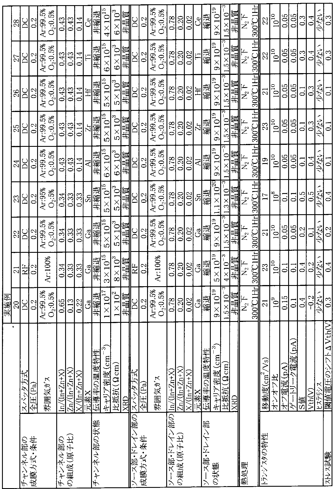

[チャンネル長依存性の評価(有効S/D直列抵抗の評価)]
実施例10において、チャンネル長(L)を10、20、30、40、50μmと変えた電界効果トランジスタを作製し、その移動度を測定した。その結果、移動度のチャンネル長依存性はほとんど確認できず有効S/D直列抵抗(RSD)が小さいことが分かった。RSDは35Ωcmであった。また同様に測定した実施例11~28、及び実施例1~9の有効S/D直列抵抗(RSD)も100Ωcm以下であった。
一方、比較例3において、チャンネル長(L)を上記と同様に変えた電界効果トランジスタを作製し、その移動度を測定した結果、実施例10と比較して大きなチャンネル長依存性(チャンネル長が短いほど移動度が低下)が確認され、有効S/D直列抵抗が大きいことが分かった。RSDは230Ωcmであった。また同様に測定した比較例2、5、6及び7の有効S/D直列抵抗(RSD)も100Ωcm超であった。 [Evaluation of channel length dependency (Evaluation of effective S / D series resistance)]
In Example 10, field effect transistors were manufactured in which the channel length (L) was changed to 10, 20, 30, 40, and 50 μm, and the mobility was measured. As a result, the channel length dependence of mobility was hardly confirmed, and it was found that the effective S / D series resistance (R SD ) was small. R SD was 35Ωcm. In addition, the effective S / D series resistance (R SD ) of Examples 11 to 28 and Examples 1 to 9 measured in the same manner was 100 Ωcm or less.
On the other hand, in Comparative Example 3, a field effect transistor with the channel length (L) changed in the same manner as described above was manufactured, and the mobility was measured. As a result, the channel length dependency (channel length was larger than that in Example 10). The shorter the shorter, the lower the mobility) was confirmed, and it was found that the effective S / D series resistance was large. The RSD was 230 Ωcm. Moreover, the effective S / D series resistance (R SD ) of Comparative Examples 2, 5, 6 and 7 measured in the same manner was more than 100 Ωcm.
本発明の電界効果型トランジスタはフラットディスプレイ等の表示装置に好適なトランジスタ特性を有する。
本発明の半導体装置は、論理回路、メモリ回路、差動増幅回路等の集積回路に適用できる。特に、液晶ディスプレイ又は有機ELディスプレイを駆動させるスイッチング素子として好適に使用できる。
この明細書に記載の文献内容をここに援用する。 The field effect transistor of the present invention has transistor characteristics suitable for a display device such as a flat display.
The semiconductor device of the present invention can be applied to integrated circuits such as logic circuits, memory circuits, and differential amplifier circuits. In particular, it can be suitably used as a switching element for driving a liquid crystal display or an organic EL display.
The literature content described in this specification is incorporated herein by reference.
Claims (28)
- 酸化物膜を半導体層として有し、
前記酸化物膜がチャンネル部位、ソース部位及びドレイン部位を有し、
前記チャンネル部位、ソース部位及びドレイン部位の酸素元素及び不活性ガスを除く組成が実質同一である電界効果型トランジスタ。 Having an oxide film as a semiconductor layer,
The oxide film has a channel part, a source part and a drain part;
A field-effect transistor having substantially the same composition excluding oxygen element and inert gas at the channel part, the source part and the drain part. - 前記ソース部位及びドレイン部位のそれぞれの酸素濃度が、前記チャンネル部位の酸素濃度よりも低い請求項1に記載の電界効果型トランジスタ。 The field effect transistor according to claim 1, wherein the oxygen concentration of each of the source region and the drain region is lower than the oxygen concentration of the channel region.
- 前記ソース部位及びドレイン部位が、ゲート電極と自己整合している請求項1又は2に記載の電界効果型トランジスタ。 3. The field effect transistor according to claim 1, wherein the source part and the drain part are self-aligned with the gate electrode.
- 前記酸化物膜が、In、Zn、Ga及びSnからなる群から選択される1以上の元素を含む酸化物からなる請求項1~3のいずれかに記載の電界効果型トランジスタ。 4. The field effect transistor according to claim 1, wherein the oxide film is made of an oxide containing one or more elements selected from the group consisting of In, Zn, Ga, and Sn.
- 前記酸化物膜が、In及びZnを含む複合酸化物の非晶質膜である請求項1~4のいずれかに記載の電界効果型トランジスタ。 5. The field effect transistor according to claim 1, wherein the oxide film is an amorphous film of a complex oxide containing In and Zn.
- 前記酸化物膜が、In、Zn及びGaを含む複合酸化物の非晶質膜、又はIn、Zn及びAlを含む複合酸化物の非晶質膜である請求項1~5のいずれかに記載の電界効果型トランジスタ。 6. The oxide film according to claim 1, wherein the oxide film is a composite oxide amorphous film containing In, Zn, and Ga, or a composite oxide amorphous film containing In, Zn, and Al. Field effect transistor.
- 前記酸化物膜が、Zr、Hf、Ge、Si、Ti、Mn、W、Mo、V、Nb、B、Sc、Y及びランタノイド類元素からなる群から選択される1以上の元素、In及びZnを含む複合酸化物の非晶質膜である請求項1~5のいずれかに記載の電界効果型トランジスタ。 The oxide film is one or more elements selected from the group consisting of Zr, Hf, Ge, Si, Ti, Mn, W, Mo, V, Nb, B, Sc, Y and lanthanoid elements, In and Zn 6. The field effect transistor according to claim 1, which is a complex oxide amorphous film containing
- 請求項1~7のいずれかに記載の電界効果型トランジスタを用いた表示装置。 A display device using the field effect transistor according to any one of claims 1 to 7.
- 酸化物膜を形成する工程、及び
前記酸化物膜の一部の抵抗を減少させてソース部位及びドレイン部位を形成する工程を含み、
前記酸化物膜がチャンネル部位、ソース部位及びドレイン部位を有する電界効果型トランジスタの製造方法。 Forming an oxide film; and reducing the resistance of part of the oxide film to form a source part and a drain part,
A method of manufacturing a field effect transistor in which the oxide film has a channel part, a source part, and a drain part. - 低酸素分圧環境下で短波長の光を照射することにより前記酸化物膜の一部の抵抗を減少させる請求項9に記載の電界効果型トランジスタの製造方法。 10. The method of manufacturing a field effect transistor according to claim 9, wherein the resistance of a part of the oxide film is reduced by irradiating light having a short wavelength in a low oxygen partial pressure environment.
- 不活性ガスプラズマ処理により前記酸化物膜の一部の抵抗を減少させる請求項9に記載の電界効果型トランジスタの製造方法。 10. The method of manufacturing a field effect transistor according to claim 9, wherein the resistance of a part of the oxide film is reduced by an inert gas plasma treatment.
- 酸化物膜を形成する工程、及び
前記酸化物膜の一部の抵抗を増加させてチャンネル部を形成する工程を含み、
前記酸化物膜がチャンネル部位、ソース部位及びドレイン部位を有する電界効果型トランジスタの製造方法。 Forming an oxide film; and increasing the resistance of part of the oxide film to form a channel portion;
A method of manufacturing a field effect transistor in which the oxide film has a channel part, a source part, and a drain part. - 酸素プラズマ処理又はオゾン処理により前記酸化物膜の一部の抵抗を増加させる請求項12に記載の電界効果型トランジスタの製造方法。 The method of manufacturing a field effect transistor according to claim 12, wherein the resistance of a part of the oxide film is increased by oxygen plasma treatment or ozone treatment.
- 酸化物膜を形成する工程、
前記酸化物膜を絶縁膜で被覆する工程、及び
前記絶縁膜上にゲート電極を形成し、前記ゲート電極を加熱して前記酸化物膜の一部の抵抗を増加させてチャンネル部を形成する工程を含み、
前記酸化物膜がチャンネル部位、ソース部位及びドレイン部位を有する電界効果型トランジスタの製造方法。 Forming an oxide film;
Covering the oxide film with an insulating film; forming a gate electrode on the insulating film; and heating the gate electrode to increase a partial resistance of the oxide film to form a channel portion Including
A method of manufacturing a field effect transistor in which the oxide film has a channel part, a source part, and a drain part. - 非縮退半導体である酸化物半導体が、縮退半導体である酸化物半導体を介して導電体と接続している構造を有することを特徴とする半導体装置。 A semiconductor device having a structure in which an oxide semiconductor that is a non-degenerate semiconductor is connected to a conductor through an oxide semiconductor that is a degenerate semiconductor.
- 酸化物半導体からなるチャンネル部と、酸化物半導体からなるソース部及びドレイン部を含み、
前記チャンネル部が非縮退半導体であり、前記ソース部及びドレイン部の少なくとも一方が縮退半導体であり、
チャンネル部がソース部及びドレイン部を介して、ソース電極及びドレイン電極と接続していることを特徴とする電界効果型トランジスタ。 Including a channel portion made of an oxide semiconductor, and a source portion and a drain portion made of an oxide semiconductor,
The channel part is a non-degenerate semiconductor, and at least one of the source part and the drain part is a degenerate semiconductor;
A field effect transistor, wherein a channel portion is connected to a source electrode and a drain electrode through a source portion and a drain portion. - 前記ソース部及びドレイン部の少なくとも一方の組成が、チャンネル部と異なっていることを特徴とする請求項16の電界効果型トランジスタ。 The field effect transistor according to claim 16, wherein the composition of at least one of the source part and the drain part is different from that of the channel part.
- 前記チャンネル部、ソース部及びドレイン部が、In元素を含む酸化物であることを特徴とする請求項16又は17に記載の電界効果型トランジスタ。 18. The field effect transistor according to claim 16, wherein the channel portion, the source portion, and the drain portion are oxides containing In element.
- 前記チャンネル部、ソース部及びドレイン部が、In元素、Zn元素及びその他の元素Xを含む酸化物であり、
酸素元素を除く全元素中の元素Xの割合が、ソース部及びドレイン部よりもチャンネル部において高いことを特徴とする請求項16~18のいずれかに記載の電界効果型トランジスタ。 The channel part, the source part and the drain part are oxides containing In element, Zn element and other element X,
19. The field effect transistor according to claim 16, wherein the ratio of the element X in all elements excluding the oxygen element is higher in the channel portion than in the source portion and the drain portion. - 前記チャンネル部、ソース部及びドレイン部がIn、Zn及び元素Xを含む酸化物であり、
前記チャンネル部の組成が、下記の領域1、領域2又は領域3の原子比を満たし、
前記ソース部及びドレイン部の組成が、下記の領域4の原子比を満たすことを特徴とする請求項16~18のいずれかに記載の電界効果型トランジスタ。
領域1
In/(In+Zn+X)=0.20~0.55
Zn/(In+Zn+X)=0.00~0.80
X/(In+Zn+X)=0.00~0.80
領域2
In/(In+Zn+X)=0.55~0.90
Zn/(In+Zn+X)=0.00~0.35
X/(In+Zn+X)=0.10~0.45
領域3
In/(In+Zn+X)=0.90~1.00
Zn/(In+Zn+X)=0.00~0.10
X/(In+Zn+X)=0.00~0.10
領域4
In/(In+Zn+X)=0.55~0.90
Zn/(In+Zn+X)=0.00~0.45
X/(In+Zn+X)=0.00~0.10 The channel part, the source part and the drain part are oxides containing In, Zn and an element X;
The composition of the channel portion satisfies the following atomic ratio of region 1, region 2 or region 3,
The field effect transistor according to any one of claims 16 to 18, wherein the composition of the source part and the drain part satisfies an atomic ratio of the following region 4.
Region 1
In / (In + Zn + X) = 0.20 to 0.55
Zn / (In + Zn + X) = 0.00 to 0.80
X / (In + Zn + X) = 0.00 to 0.80
Region 2
In / (In + Zn + X) = 0.55-0.90
Zn / (In + Zn + X) = 0.00 to 0.35
X / (In + Zn + X) = 0.10 to 0.45
Region 3
In / (In + Zn + X) = 0.90 to 1.00
Zn / (In + Zn + X) = 0.00 to 0.10
X / (In + Zn + X) = 0.00 to 0.10
Region 4
In / (In + Zn + X) = 0.55-0.90
Zn / (In + Zn + X) = 0.00 to 0.45
X / (In + Zn + X) = 0.00 to 0.10 - 前記元素Xが、Ga、Al、B、Sc、Y、ランタノイド類(La、Ce、Pr、Nd、Sm、Eu、Gd、Tb、Dy、Ho、Er、Tm、Yb、Lu)、Zr、Hf、Ge、Si、Ti、Mn、W、Mo、V、Cu、Ni、Co、Fe、Cr及びNbからなる群から選択される元素であることを特徴とする請求項19又は20に記載の電界効果型トランジスタ。 The element X is Ga, Al, B, Sc, Y, lanthanoids (La, Ce, Pr, Nd, Sm, Eu, Gd, Tb, Dy, Ho, Er, Tm, Yb, Lu), Zr, Hf The electric field according to claim 19 or 20, wherein the electric field is an element selected from the group consisting of: Ge, Si, Ti, Mn, W, Mo, V, Cu, Ni, Co, Fe, Cr, and Nb. Effect transistor.
- 前記チャンネル部がIn元素、Zn元素及び元素Xを含む酸化物であり、
前記ソース部及びドレイン部がIn元素、Zn元素及び元素Yを含む酸化物であり、
前記元素X及び元素Yが、それぞれGa、Al、B、Sc、Y、ランタノイド類(La、Ce、Pr、Nd、Sm、Eu、Gd、Tb、Dy、Ho、Er、Tm、Yb、Lu)、Zr、Hf、Ge、Si、Ti、Mn、W、Mo、V、Cu、Ni、Co、Fe、Cr、Nb及びSnからなる群から選択される元素であり、
前記元素Xと元素Yが異なることを特徴とする請求項16~18のいずれかに記載の電界効果型トランジスタ。 The channel portion is an oxide containing In element, Zn element and element X;
The source part and the drain part are oxides containing In element, Zn element and element Y;
The element X and the element Y are Ga, Al, B, Sc, Y, lanthanoids (La, Ce, Pr, Nd, Sm, Eu, Gd, Tb, Dy, Ho, Er, Tm, Yb, Lu), respectively. , Zr, Hf, Ge, Si, Ti, Mn, W, Mo, V, Cu, Ni, Co, Fe, Cr, Nb and Sn,
19. The field effect transistor according to claim 16, wherein the element X and the element Y are different. - 前記チャンネル部が、In元素と1種以上の正二価元素を含む結晶質酸化物からなることを特徴とする請求項16又は17に記載の電界効果型トランジスタ。 The field effect transistor according to claim 16 or 17, wherein the channel portion is made of a crystalline oxide containing In element and one or more positive divalent elements.
- 前記ソース部及びドレイン部と、チャンネル部のエッチング選択比が5以上であることを特徴とする請求項16~23のいずれかに記載の電界効果型トランジスタ。 The field effect transistor according to any one of claims 16 to 23, wherein an etching selectivity between the source and drain portions and the channel portion is 5 or more.
- ソース電極、ドレイン電極及びゲート電極の少なくとも1つが、Ti、Pt、Cr、W、Al、Ni、Cu、Mo、Ta、Au及びNbからなる群から選択される金属、又は前記金属を1つ以上含む合金からなることを特徴とする請求項16~24のいずれかに記載の電界効果型トランジスタ。 At least one of the source electrode, the drain electrode, and the gate electrode is a metal selected from the group consisting of Ti, Pt, Cr, W, Al, Ni, Cu, Mo, Ta, Au, and Nb, or one or more of the metals The field effect transistor according to any one of claims 16 to 24, comprising an alloy containing the same.
- チャンネル部を成膜する工程と、
ソース部及びドレイン部を成膜する工程と、
上記2つの成膜工程の後に、成膜温度より高い温度で熱処理する工程と、
を含むことを特徴とする請求項16~25のいずれかに記載の電界効果型トランジスタの製造方法。 Forming a channel part; and
Forming a source portion and a drain portion;
A step of performing a heat treatment at a temperature higher than the film forming temperature after the two film forming steps;
The method for producing a field effect transistor according to any one of claims 16 to 25, comprising: - 前記チャンネル部を成膜する工程と、ソース部及びドレイン部を成膜する工程との間において、処理対象を大気に暴露させないことを特徴とする請求項26に記載の電界効果型トランジスタの製造方法。 27. The method of manufacturing a field effect transistor according to claim 26, wherein the process target is not exposed to the atmosphere between the step of forming the channel portion and the step of forming the source portion and the drain portion. .
- 前記チャンネル部と、前記ソース部及びドレイン部を、組成又は組成比が異なるスパッタリングターゲットを用いて成膜することを特徴とする請求項26又は27に記載の電界効果型トランジスタの製造方法。 28. The method of manufacturing a field effect transistor according to claim 26, wherein the channel part and the source part and the drain part are formed using sputtering targets having different compositions or composition ratios.
Priority Applications (1)
| Application Number | Priority Date | Filing Date | Title |
|---|---|---|---|
| US12/864,078 US20100295042A1 (en) | 2008-01-23 | 2009-01-22 | Field-effect transistor, method for manufacturing field-effect transistor, display device using field-effect transistor, and semiconductor device |
Applications Claiming Priority (4)
| Application Number | Priority Date | Filing Date | Title |
|---|---|---|---|
| JP2008013085 | 2008-01-23 | ||
| JP2008-013085 | 2008-01-23 | ||
| JP2008-100088 | 2008-04-08 | ||
| JP2008100088 | 2008-04-08 |
Publications (1)
| Publication Number | Publication Date |
|---|---|
| WO2009093625A1 true WO2009093625A1 (en) | 2009-07-30 |
Family
ID=40901131
Family Applications (1)
| Application Number | Title | Priority Date | Filing Date |
|---|---|---|---|
| PCT/JP2009/050916 WO2009093625A1 (en) | 2008-01-23 | 2009-01-22 | Field-effect transistor, method for manufacturing field-effect transistor, display device using field-effect transistor, and semiconductor device |
Country Status (3)
| Country | Link |
|---|---|
| US (1) | US20100295042A1 (en) |
| TW (1) | TW200941729A (en) |
| WO (1) | WO2009093625A1 (en) |
Cited By (84)
| Publication number | Priority date | Publication date | Assignee | Title |
|---|---|---|---|---|
| JP2010040645A (en) * | 2008-08-01 | 2010-02-18 | Fujifilm Corp | Thin film field effect transistor manufacturing method and thin film field effect transistor manufactured by manufacturing method |
| CN101877311A (en) * | 2010-06-30 | 2010-11-03 | 复旦大学 | Method for effectively adjusting work function of TiN metal gate |
| WO2011024501A1 (en) * | 2009-08-31 | 2011-03-03 | シャープ株式会社 | Oxide semiconductor, thin film transistor, and display device |
| WO2011030582A1 (en) * | 2009-09-11 | 2011-03-17 | シャープ株式会社 | Oxide semiconductor, thin film transistor, and display device |
| CN101997003A (en) * | 2009-08-07 | 2011-03-30 | 株式会社半导体能源研究所 | Semiconductor device and manufacturing method thereof |
| JP2011077106A (en) * | 2009-09-29 | 2011-04-14 | Dainippon Printing Co Ltd | Thin-film integrated circuit device and manufacturing method therefor |
| WO2011045960A1 (en) * | 2009-10-16 | 2011-04-21 | シャープ株式会社 | Thin-film transistor, process for production of same, and display device equipped with same |
| WO2011048924A1 (en) * | 2009-10-21 | 2011-04-28 | Semiconductor Energy Laboratory Co., Ltd. | Display device and electronic device including display device |
| US20110101351A1 (en) * | 2009-10-29 | 2011-05-05 | Semiconductor Energy Laboratory Co., Ltd. | Semiconductor device |
| JP2011103433A (en) * | 2009-11-11 | 2011-05-26 | Samsung Mobile Display Co Ltd | Thin film transistor and organic electroluminescent display device including the same |
| JP2011103454A (en) * | 2009-10-16 | 2011-05-26 | Semiconductor Energy Lab Co Ltd | Logic circuit and semiconductor device |
| JP2011107697A (en) * | 2009-10-21 | 2011-06-02 | Semiconductor Energy Lab Co Ltd | Electronic book reader |
| JP2011187952A (en) * | 2010-02-12 | 2011-09-22 | Semiconductor Energy Lab Co Ltd | Semiconductor device and method of manufacturing the same |
| WO2011126093A1 (en) * | 2010-04-07 | 2011-10-13 | 株式会社神戸製鋼所 | Oxide for semiconductor layer of thin film transistor, sputtering target, and thin film transistor |
| JP2011228622A (en) * | 2010-03-30 | 2011-11-10 | Sony Corp | Thin film transistor, manufacturing method thereof, and display device |
| WO2011158703A1 (en) * | 2010-06-18 | 2011-12-22 | Semiconductor Energy Laboratory Co., Ltd. | Semiconductor device |
| JP2012182165A (en) * | 2011-02-28 | 2012-09-20 | Sony Corp | Display device and electronic apparatus |
| JP2013012610A (en) * | 2011-06-29 | 2013-01-17 | Dainippon Printing Co Ltd | Thin film transistor and manufacturing method of the same |
| JP2013055080A (en) * | 2011-08-31 | 2013-03-21 | Japan Display East Co Ltd | Display device and manufacturing method thereof |
| JP2013065840A (en) * | 2011-08-31 | 2013-04-11 | Semiconductor Energy Lab Co Ltd | Semiconductor device and method for manufacturing semiconductor device |
| JP2013077858A (en) * | 2009-11-13 | 2013-04-25 | Semiconductor Energy Lab Co Ltd | Semiconductor device |
| JP2013077836A (en) * | 2009-09-16 | 2013-04-25 | Semiconductor Energy Lab Co Ltd | Semiconductor device |
| JP2013084735A (en) * | 2011-10-07 | 2013-05-09 | Semiconductor Energy Lab Co Ltd | Oxide semiconductor film and semiconductor device |
| JP2013084752A (en) * | 2011-10-07 | 2013-05-09 | Semiconductor Energy Lab Co Ltd | Semiconductor device and method of fabricating the same |
| JP2013093621A (en) * | 2009-11-27 | 2013-05-16 | Semiconductor Energy Lab Co Ltd | Semiconductor device |
| JP2013131765A (en) * | 2009-10-08 | 2013-07-04 | Semiconductor Energy Lab Co Ltd | Semiconductor device manufacturing method |
| JPWO2011125940A1 (en) * | 2010-04-06 | 2013-07-11 | 株式会社日立製作所 | Thin film transistor and manufacturing method thereof |
| JP2013201211A (en) * | 2012-03-23 | 2013-10-03 | Sony Corp | Thin film transistor, manufacturing method of thin film transistor, and electronic equipment |
| US8552425B2 (en) | 2010-06-18 | 2013-10-08 | Semiconductor Energy Laboratory Co., Ltd. | Semiconductor device |
| JP2014007393A (en) * | 2012-05-31 | 2014-01-16 | Semiconductor Energy Lab Co Ltd | Semiconductor device and manufacturing method of the same |
| JP2014015673A (en) * | 2012-06-13 | 2014-01-30 | Idemitsu Kosan Co Ltd | Sputtering target, semiconductor thin film and thin film transistor using the same |
| JP2014017500A (en) * | 2009-10-30 | 2014-01-30 | Semiconductor Energy Lab Co Ltd | Semiconductor device |
| JP2014022549A (en) * | 2012-07-18 | 2014-02-03 | Japan Advanced Institute Of Science & Technology Hokuriku | Thin film transistor and manufacturing method of thin film transistor |
| JP2014099653A (en) * | 2008-08-08 | 2014-05-29 | Semiconductor Energy Lab Co Ltd | Semiconductor device |
| JP2014103415A (en) * | 2009-11-06 | 2014-06-05 | Semiconductor Energy Lab Co Ltd | Oxide semiconductor film and semiconductor device |
| JP2014143404A (en) * | 2012-12-25 | 2014-08-07 | Semiconductor Energy Lab Co Ltd | Resistance element, display device, and electronic apparatus |
| JP2014157893A (en) * | 2013-02-15 | 2014-08-28 | Mitsubishi Electric Corp | Thin-film transistor and method of manufacturing the same |
| JP2014207472A (en) * | 2010-05-21 | 2014-10-30 | 株式会社半導体エネルギー研究所 | Semiconductor device |
| WO2014181777A1 (en) * | 2013-05-09 | 2014-11-13 | 独立行政法人物質・材料研究機構 | Thin-film transistor and method for manufacturing same |
| JP2015052803A (en) * | 2009-08-27 | 2015-03-19 | 株式会社半導体エネルギー研究所 | Display device manufacture method and display device |
| JP2015092603A (en) * | 2009-11-20 | 2015-05-14 | 株式会社半導体エネルギー研究所 | Semiconductor device |
| JP2015097275A (en) * | 2009-11-20 | 2015-05-21 | 株式会社半導体エネルギー研究所 | Semiconductor device |
| JP2015135989A (en) * | 2010-03-08 | 2015-07-27 | 株式会社半導体エネルギー研究所 | semiconductor device |
| JP2015156021A (en) * | 2009-10-09 | 2015-08-27 | 株式会社半導体エネルギー研究所 | Method of manufacturing display device |
| JP2015164196A (en) * | 2009-12-11 | 2015-09-10 | 株式会社半導体エネルギー研究所 | Method for producing semiconductor device |
| US9136389B2 (en) | 2008-10-24 | 2015-09-15 | Semiconductor Energy Laboratory Co., Ltd. | Oxide semiconductor, thin film transistor, and display device |
| JP2015195400A (en) * | 2009-12-18 | 2015-11-05 | 株式会社半導体エネルギー研究所 | semiconductor device |
| JP2015213178A (en) * | 2009-12-04 | 2015-11-26 | 株式会社半導体エネルギー研究所 | Semiconductor device |
| US9214563B2 (en) | 2009-09-24 | 2015-12-15 | Semiconductor Energy Laboratory Co., Ltd. | Oxide semiconductor film and semiconductor device |
| JP2015233147A (en) * | 2010-05-21 | 2015-12-24 | 株式会社半導体エネルギー研究所 | Method of manufacturing semiconductor device |
| JP2016001747A (en) * | 2010-04-23 | 2016-01-07 | 株式会社半導体エネルギー研究所 | Method of manufacturing semiconductor device |
| JP2016026389A (en) * | 2010-04-07 | 2016-02-12 | 株式会社神戸製鋼所 | Oxide for semiconductor layer of thin film transistor, sputtering target, and thin film transistor |
| US9306072B2 (en) | 2009-10-08 | 2016-04-05 | Semiconductor Energy Laboratory Co., Ltd. | Oxide semiconductor layer and semiconductor device |
| US9366896B2 (en) | 2012-10-12 | 2016-06-14 | Semiconductor Energy Laboratory Co., Ltd. | Liquid crystal display device and touch panel |
| JP2016136647A (en) * | 2010-11-11 | 2016-07-28 | 株式会社半導体エネルギー研究所 | Semiconductor device |
| JP2016157954A (en) * | 2010-07-26 | 2016-09-01 | 株式会社半導体エネルギー研究所 | Semiconductor device |
| JP2016213483A (en) * | 2010-09-10 | 2016-12-15 | 株式会社半導体エネルギー研究所 | Semiconductor device |
| JP2017017367A (en) * | 2009-10-14 | 2017-01-19 | 株式会社半導体エネルギー研究所 | Semiconductor device |
| US9553200B2 (en) | 2012-02-29 | 2017-01-24 | Semiconductor Energy Laboratory Co., Ltd. | Semiconductor device and method for manufacturing the same |
| JP2017028302A (en) * | 2009-11-20 | 2017-02-02 | 株式会社半導体エネルギー研究所 | Method of manufacturing semiconductor device |
| JP2017028315A (en) * | 2010-03-26 | 2017-02-02 | 株式会社半導体エネルギー研究所 | Semiconductor device manufacturing method |
| US20170046002A1 (en) * | 2010-06-16 | 2017-02-16 | Semiconductor Energy Laboratory Co., Ltd. | Input-Output Device and Method for Driving Input-Output Device |
| US20170059909A1 (en) * | 2009-10-30 | 2017-03-02 | Semiconductor Energy Laboratory Co., Ltd. | Semiconductor device and method for manufacturing the same |
| JP2017069576A (en) * | 2011-07-22 | 2017-04-06 | 株式会社半導体エネルギー研究所 | Semiconductor device and semiconductor device manufacturing method |
| JP2017073558A (en) * | 2010-03-26 | 2017-04-13 | 株式会社半導体エネルギー研究所 | Method of manufacturing semiconductor device |
| JP2017123487A (en) * | 2009-08-07 | 2017-07-13 | 株式会社半導体エネルギー研究所 | Semiconductor device |
| JP2017142521A (en) * | 2009-11-30 | 2017-08-17 | 株式会社半導体エネルギー研究所 | Liquid crystal display device manufacture method |
| JP2017157844A (en) * | 2010-08-16 | 2017-09-07 | 株式会社半導体エネルギー研究所 | Manufacturing method for semiconductor device |
| WO2017159413A1 (en) * | 2016-03-14 | 2017-09-21 | シャープ株式会社 | Semiconductor apparatus and method for manufacturing semiconductor apparatus |
| JP2017182077A (en) * | 2010-03-05 | 2017-10-05 | 株式会社半導体エネルギー研究所 | Display device manufacture method |
| US10217736B2 (en) | 2013-09-23 | 2019-02-26 | Semiconductor Energy Laboratory Co., Ltd. | Semiconductor device including transistor and capacitor |
| US10236287B2 (en) | 2013-09-23 | 2019-03-19 | Semiconductor Energy Laboratory Co., Ltd. | Semiconductor device including semiconductor electrically surrounded by electric field of conductive film |
| JP2019087758A (en) * | 2010-12-28 | 2019-06-06 | 株式会社半導体エネルギー研究所 | Transistor |
| JP2019149553A (en) * | 2013-06-05 | 2019-09-05 | 株式会社半導体エネルギー研究所 | Display device |
| JP2019216281A (en) * | 2015-11-25 | 2019-12-19 | 株式会社アルバック | Thin film transistor, oxide semiconductor film, and sputtering target |
| JP2020010061A (en) * | 2009-12-18 | 2020-01-16 | 株式会社半導体エネルギー研究所 | Transistor |
| JP2020053700A (en) * | 2009-11-06 | 2020-04-02 | 株式会社半導体エネルギー研究所 | Display unit |
| JP2020194983A (en) * | 2009-09-16 | 2020-12-03 | 株式会社半導体エネルギー研究所 | Semiconductor device |
| JP2021013029A (en) * | 2009-10-16 | 2021-02-04 | 株式会社半導体エネルギー研究所 | Manufacture method for semiconductor device |
| JP2021057601A (en) * | 2009-09-16 | 2021-04-08 | 株式会社半導体エネルギー研究所 | Manufacturing method for display device |
| JP2021100122A (en) * | 2009-06-30 | 2021-07-01 | 株式会社半導体エネルギー研究所 | Display device |
| US11081502B2 (en) | 2012-01-26 | 2021-08-03 | Semiconductor Energy Laboratory Co., Ltd. | Semiconductor device and method for manufacturing the same |
| JP2022518522A (en) * | 2019-09-18 | 2022-03-15 | 華南理工大学 | Composite metal oxide semiconductors and thin film transistors and their applications |
| US11374130B2 (en) | 2020-02-07 | 2022-06-28 | Kioxia Corporation | Semiconductor device and semiconductor memory device |
Families Citing this family (63)
| Publication number | Priority date | Publication date | Assignee | Title |
|---|---|---|---|---|
| US8247276B2 (en) * | 2009-02-20 | 2012-08-21 | Semiconductor Energy Laboratory Co., Ltd. | Thin film transistor, method for manufacturing the same, and semiconductor device |
| US8704216B2 (en) | 2009-02-27 | 2014-04-22 | Semiconductor Energy Laboratory Co., Ltd. | Semiconductor device and manufacturing method thereof |
| US8450144B2 (en) * | 2009-03-26 | 2013-05-28 | Semiconductor Energy Laboratory Co., Ltd. | Semiconductor device and method for manufacturing the same |
| JP5663231B2 (en) | 2009-08-07 | 2015-02-04 | 株式会社半導体エネルギー研究所 | Light emitting device |
| WO2011027702A1 (en) | 2009-09-04 | 2011-03-10 | Semiconductor Energy Laboratory Co., Ltd. | Light-emitting device and method for manufacturing the same |
| KR102375647B1 (en) | 2009-10-16 | 2022-03-17 | 가부시키가이샤 한도오따이 에네루기 켄큐쇼 | Liquid crystal display device and electronic apparatus having the same |
| KR101847656B1 (en) | 2009-10-21 | 2018-05-24 | 가부시키가이샤 한도오따이 에네루기 켄큐쇼 | Semiconductor device and method for manufacturing the same |
| KR101952065B1 (en) * | 2009-11-06 | 2019-02-25 | 가부시키가이샤 한도오따이 에네루기 켄큐쇼 | Semiconductor device and operating method thereof |
| KR20220116369A (en) * | 2009-11-13 | 2022-08-22 | 가부시키가이샤 한도오따이 에네루기 켄큐쇼 | Display device and electronic device including the same |
| KR102451852B1 (en) * | 2009-11-20 | 2022-10-11 | 가부시키가이샤 한도오따이 에네루기 켄큐쇼 | Semiconductor device |
| KR101824124B1 (en) | 2009-11-28 | 2018-02-01 | 가부시키가이샤 한도오따이 에네루기 켄큐쇼 | Semiconductor device and method for manufacturing the same |
| KR101800038B1 (en) * | 2009-12-04 | 2017-11-21 | 가부시키가이샤 한도오따이 에네루기 켄큐쇼 | Display device |
| WO2011077966A1 (en) * | 2009-12-25 | 2011-06-30 | Semiconductor Energy Laboratory Co., Ltd. | Semiconductor device and method for manufacturing the same |
| KR101748763B1 (en) * | 2010-01-15 | 2017-06-20 | 가부시키가이샤 한도오따이 에네루기 켄큐쇼 | Semiconductor device and electronic device |
| JP5776192B2 (en) * | 2010-02-16 | 2015-09-09 | 株式会社リコー | Field effect transistor, display element, image display apparatus and system |
| WO2011105184A1 (en) | 2010-02-26 | 2011-09-01 | Semiconductor Energy Laboratory Co., Ltd. | Method for manufacturing semiconductor device |
| KR101921047B1 (en) * | 2010-03-26 | 2018-11-23 | 가부시키가이샤 한도오따이 에네루기 켄큐쇼 | Method for manufacturing semiconductor device |
| KR101877377B1 (en) | 2010-04-23 | 2018-07-11 | 가부시키가이샤 한도오따이 에네루기 켄큐쇼 | Manufacturing method of semiconductor device |
| US20120001179A1 (en) * | 2010-07-02 | 2012-01-05 | Semiconductor Energy Laboratory Co., Ltd. | Semiconductor device |
| WO2012002186A1 (en) | 2010-07-02 | 2012-01-05 | Semiconductor Energy Laboratory Co., Ltd. | Semiconductor device |
| JP2012015436A (en) * | 2010-07-05 | 2012-01-19 | Sony Corp | Thin film transistor and display device |
| JP5081959B2 (en) * | 2010-08-31 | 2012-11-28 | Jx日鉱日石金属株式会社 | Oxide sintered body and oxide semiconductor thin film |
| US8558960B2 (en) | 2010-09-13 | 2013-10-15 | Semiconductor Energy Laboratory Co., Ltd. | Liquid crystal display device and method for manufacturing the same |
| JP2012256012A (en) * | 2010-09-15 | 2012-12-27 | Semiconductor Energy Lab Co Ltd | Display device |
| US8854865B2 (en) * | 2010-11-24 | 2014-10-07 | Semiconductor Energy Laboratory Co., Ltd. | Semiconductor memory device |
| TW202320146A (en) | 2011-01-26 | 2023-05-16 | 日商半導體能源研究所股份有限公司 | Semiconductor device and manufacturing method thereof |
| JP2012169344A (en) * | 2011-02-10 | 2012-09-06 | Sony Corp | Thin film transistor, display device and electronic equipment |
| US8581625B2 (en) * | 2011-05-19 | 2013-11-12 | Semiconductor Energy Laboratory Co., Ltd. | Programmable logic device |
| JP6091083B2 (en) * | 2011-05-20 | 2017-03-08 | 株式会社半導体エネルギー研究所 | Storage device |
| TWI447983B (en) | 2011-05-24 | 2014-08-01 | Au Optronics Corp | Semiconductor structure and organic electroluminescence device |
| US8673426B2 (en) | 2011-06-29 | 2014-03-18 | Semiconductor Energy Laboratory Co., Ltd. | Driver circuit, method of manufacturing the driver circuit, and display device including the driver circuit |
| US9252279B2 (en) * | 2011-08-31 | 2016-02-02 | Semiconductor Energy Laboratory Co., Ltd. | Semiconductor device and manufacturing method thereof |
| FR2980040B1 (en) * | 2011-09-14 | 2016-02-05 | Commissariat Energie Atomique | ORGANIC FIELD EFFECT TRANSISTOR |
| US8969867B2 (en) * | 2012-01-18 | 2015-03-03 | Semiconductor Energy Laboratory Co., Ltd. | Semiconductor device |
| KR102179912B1 (en) | 2012-03-23 | 2020-11-17 | 고쿠리츠켄큐카이하츠호진 카가쿠기쥬츠신코키코 | Thin film transistor and method for manufacturing thin film transistor |
| CN103579355B (en) * | 2012-07-25 | 2016-12-07 | 群康科技(深圳)有限公司 | Thin film transistor base plate and manufacture method thereof and include the display of this substrate |
| TWI476934B (en) * | 2012-07-25 | 2015-03-11 | Innocom Tech Shenzhen Co Ltd | Thin film transistor substrate, display thereof and manufacturing method thereof |
| TWI469359B (en) * | 2012-08-31 | 2015-01-11 | Innocom Tech Shenzhen Co Ltd | Tft substrate and fabrication method thereof, display |
| TWI681233B (en) | 2012-10-12 | 2020-01-01 | 日商半導體能源研究所股份有限公司 | Liquid crystal display device, touch panel and method for manufacturing liquid crystal display device |
| KR102046996B1 (en) | 2012-10-16 | 2019-11-21 | 삼성디스플레이 주식회사 | Thin film transistor array |
| JP6283191B2 (en) * | 2012-10-17 | 2018-02-21 | 株式会社半導体エネルギー研究所 | Semiconductor device |
| TWI500179B (en) * | 2013-06-05 | 2015-09-11 | Univ Nat Chiao Tung | Thin film transistor with uv light absorber layer |
| TWI506797B (en) * | 2013-06-21 | 2015-11-01 | Ye Xin Technology Consulting Co Ltd | Thin film transistor and fabricating method thereof |
| CN104253158B (en) * | 2013-06-27 | 2017-10-27 | 鸿富锦精密工业(深圳)有限公司 | Thin film transistor (TFT) and its manufacture method |
| US9529239B2 (en) * | 2013-12-31 | 2016-12-27 | Shenzhen China Star Optoelectronics Technologies Co., Ltd. | Manufacturing method and repairing method for display device as well as liquid crystal display panel |
| US9299848B2 (en) | 2014-03-14 | 2016-03-29 | Semiconductor Energy Laboratory Co., Ltd. | Semiconductor device, RF tag, and electronic device |
| US20150329371A1 (en) * | 2014-05-13 | 2015-11-19 | Semiconductor Energy Laboratory Co., Ltd. | Oxide, semiconductor device, module, and electronic device |
| DE102014111140B4 (en) * | 2014-08-05 | 2019-08-14 | Infineon Technologies Austria Ag | Semiconductor device with field effect structures with different gate materials and method for the production thereof |
| KR101636146B1 (en) * | 2014-09-16 | 2016-07-07 | 한양대학교 산학협력단 | Thin film transistor, and method of fabricating the same |
| CN106601681A (en) * | 2015-10-20 | 2017-04-26 | 上海新昇半导体科技有限公司 | Cmos structure and preparation method thereof |
| US9773787B2 (en) | 2015-11-03 | 2017-09-26 | Semiconductor Energy Laboratory Co., Ltd. | Semiconductor device, memory device, electronic device, or method for driving the semiconductor device |
| TWI579974B (en) * | 2015-12-25 | 2017-04-21 | 國立交通大學 | A resistive memory, resistive memory unit and thin-film transistor having composition of amorphous metal oxide |
| KR102617041B1 (en) | 2015-12-28 | 2023-12-26 | 가부시키가이샤 한도오따이 에네루기 켄큐쇼 | devices, television systems, and electronic devices |
| CN108780621B (en) * | 2016-03-31 | 2020-07-31 | 夏普株式会社 | Method for manufacturing active matrix substrate |
| CN114115609A (en) | 2016-11-25 | 2022-03-01 | 株式会社半导体能源研究所 | Display device and working method thereof |
| JP6782211B2 (en) * | 2017-09-08 | 2020-11-11 | 株式会社東芝 | Transparent electrodes, devices using them, and methods for manufacturing devices |
| CN109190563B (en) * | 2018-09-05 | 2022-02-25 | 京东方科技集团股份有限公司 | Display panel, preparation method thereof and display device |
| KR20210129114A (en) * | 2019-03-01 | 2021-10-27 | 가부시키가이샤 한도오따이 에네루기 켄큐쇼 | semiconductor device |
| JP7326795B2 (en) * | 2019-03-20 | 2023-08-16 | 株式会社リコー | FIELD EFFECT TRANSISTOR, DISPLAY DEVICE, IMAGE DISPLAY DEVICE, AND SYSTEM |
| JP7284986B2 (en) * | 2019-04-08 | 2023-06-01 | 株式会社Joled | Semiconductor device and display device |
| CN110797395A (en) * | 2019-09-18 | 2020-02-14 | 华南理工大学 | Doped metal oxide semiconductor, thin film transistor and application |
| WO2023108608A1 (en) * | 2021-12-17 | 2023-06-22 | 昆山龙腾光电股份有限公司 | Array substrate and manufacturing method therefor, and display panel |
| EP4286339A1 (en) * | 2022-05-31 | 2023-12-06 | Imec VZW | Mixed metal oxides |
Citations (8)
| Publication number | Priority date | Publication date | Assignee | Title |
|---|---|---|---|---|
| JP2002289859A (en) * | 2001-03-23 | 2002-10-04 | Minolta Co Ltd | Thin-film transistor |
| JP2004235180A (en) * | 2003-01-28 | 2004-08-19 | Sanyo Electric Co Ltd | Semiconductor device and its manufacturing method |
| JP2005268724A (en) * | 2004-03-22 | 2005-09-29 | Sony Corp | Electronic element and method for manufacturing same |
| JP2006165531A (en) * | 2004-11-10 | 2006-06-22 | Canon Inc | Method of manufacturing field effect transistor |
| JP2007123861A (en) * | 2005-09-29 | 2007-05-17 | Semiconductor Energy Lab Co Ltd | Semiconductor device and its manufacturing method |
| WO2007063966A1 (en) * | 2005-12-02 | 2007-06-07 | Idemitsu Kosan Co., Ltd. | Tft substrate and tft substrate manufacturing method |
| JP2007220816A (en) * | 2006-02-15 | 2007-08-30 | Kochi Prefecture Sangyo Shinko Center | Thin-film transistor and manufacturing method thereof |
| JP2007250983A (en) * | 2006-03-17 | 2007-09-27 | Canon Inc | Field effect transistor using oxide film for channel, and manufacturing method thereof |
Family Cites Families (6)
| Publication number | Priority date | Publication date | Assignee | Title |
|---|---|---|---|---|
| KR20020038482A (en) * | 2000-11-15 | 2002-05-23 | 모리시타 요이찌 | Thin film transistor array, method for producing the same, and display panel using the same |
| US6536174B2 (en) * | 2001-05-07 | 2003-03-25 | Michael T Foster | Reinforced storm shutter |
| JP4090716B2 (en) * | 2001-09-10 | 2008-05-28 | 雅司 川崎 | Thin film transistor and matrix display device |
| US7145174B2 (en) * | 2004-03-12 | 2006-12-05 | Hewlett-Packard Development Company, Lp. | Semiconductor device |
| US7829444B2 (en) * | 2004-11-10 | 2010-11-09 | Canon Kabushiki Kaisha | Field effect transistor manufacturing method |
| EP1995787A3 (en) * | 2005-09-29 | 2012-01-18 | Semiconductor Energy Laboratory Co, Ltd. | Semiconductor device having oxide semiconductor layer and manufacturing method therof |
-
2009
- 2009-01-22 WO PCT/JP2009/050916 patent/WO2009093625A1/en active Application Filing
- 2009-01-22 US US12/864,078 patent/US20100295042A1/en not_active Abandoned
- 2009-01-23 TW TW098102842A patent/TW200941729A/en unknown
Patent Citations (8)
| Publication number | Priority date | Publication date | Assignee | Title |
|---|---|---|---|---|
| JP2002289859A (en) * | 2001-03-23 | 2002-10-04 | Minolta Co Ltd | Thin-film transistor |
| JP2004235180A (en) * | 2003-01-28 | 2004-08-19 | Sanyo Electric Co Ltd | Semiconductor device and its manufacturing method |
| JP2005268724A (en) * | 2004-03-22 | 2005-09-29 | Sony Corp | Electronic element and method for manufacturing same |
| JP2006165531A (en) * | 2004-11-10 | 2006-06-22 | Canon Inc | Method of manufacturing field effect transistor |
| JP2007123861A (en) * | 2005-09-29 | 2007-05-17 | Semiconductor Energy Lab Co Ltd | Semiconductor device and its manufacturing method |
| WO2007063966A1 (en) * | 2005-12-02 | 2007-06-07 | Idemitsu Kosan Co., Ltd. | Tft substrate and tft substrate manufacturing method |
| JP2007220816A (en) * | 2006-02-15 | 2007-08-30 | Kochi Prefecture Sangyo Shinko Center | Thin-film transistor and manufacturing method thereof |
| JP2007250983A (en) * | 2006-03-17 | 2007-09-27 | Canon Inc | Field effect transistor using oxide film for channel, and manufacturing method thereof |
Cited By (226)
| Publication number | Priority date | Publication date | Assignee | Title |
|---|---|---|---|---|
| JP2010040645A (en) * | 2008-08-01 | 2010-02-18 | Fujifilm Corp | Thin film field effect transistor manufacturing method and thin film field effect transistor manufactured by manufacturing method |
| JP2014099653A (en) * | 2008-08-08 | 2014-05-29 | Semiconductor Energy Lab Co Ltd | Semiconductor device |
| US9136389B2 (en) | 2008-10-24 | 2015-09-15 | Semiconductor Energy Laboratory Co., Ltd. | Oxide semiconductor, thin film transistor, and display device |
| US11417754B2 (en) | 2009-06-30 | 2022-08-16 | Semiconductor Energy Laboratory Co., Ltd. | Method for manufacturing semiconductor device |
| JP7030223B2 (en) | 2009-06-30 | 2022-03-04 | 株式会社半導体エネルギー研究所 | Display device |
| JP2021100122A (en) * | 2009-06-30 | 2021-07-01 | 株式会社半導体エネルギー研究所 | Display device |
| US10243005B2 (en) | 2009-08-07 | 2019-03-26 | Semiconductor Energy Laboratory Co., Ltd. | Semiconductor device and manufacturing method thereof |
| JP2017123487A (en) * | 2009-08-07 | 2017-07-13 | 株式会社半導体エネルギー研究所 | Semiconductor device |
| US9466756B2 (en) | 2009-08-07 | 2016-10-11 | Semiconductor Energy Laboratory Co., Ltd. | Semiconductor device and manufacturing method thereof |
| CN101997003A (en) * | 2009-08-07 | 2011-03-30 | 株式会社半导体能源研究所 | Semiconductor device and manufacturing method thereof |
| JP2015052803A (en) * | 2009-08-27 | 2015-03-19 | 株式会社半導体エネルギー研究所 | Display device manufacture method and display device |
| KR101969290B1 (en) * | 2009-08-27 | 2019-04-17 | 가부시키가이샤 한도오따이 에네루기 켄큐쇼 | Method for manufacturing a semiconductor device |
| US11923206B2 (en) | 2009-08-27 | 2024-03-05 | Semiconductor Energy Laboratory Co., Ltd. | Display device and method for manufacturing the same |
| KR101754102B1 (en) * | 2009-08-27 | 2017-07-05 | 가부시키가이샤 한도오따이 에네루기 켄큐쇼 | Method for manufacturing a semiconductor device |
| KR101849069B1 (en) * | 2009-08-27 | 2018-04-17 | 가부시키가이샤 한도오따이 에네루기 켄큐쇼 | Method for manufacturing a semiconductor device |
| US11024516B2 (en) | 2009-08-27 | 2021-06-01 | Semiconductor Energy Laboratory Co., Ltd. | Display device and method for manufacturing the same |
| US10373843B2 (en) | 2009-08-27 | 2019-08-06 | Semiconductor Energy Laboratory Co., Ltd. | Display device and method for manufacturing the same |
| KR20180039034A (en) * | 2009-08-27 | 2018-04-17 | 가부시키가이샤 한도오따이 에네루기 켄큐쇼 | Method for manufacturing a semiconductor device |
| US11532488B2 (en) | 2009-08-27 | 2022-12-20 | Semiconductor Energy Laboratory Co., Ltd. | Display device and method for manufacturing the same |
| US8829513B2 (en) | 2009-08-31 | 2014-09-09 | Sharp Kabushiki Kaisha | Oxide semiconductor including Ga, In, Zn, and O and A thin film transistor and a display with the oxide semiconductor including Ga, In, Zn, and O |
| WO2011024501A1 (en) * | 2009-08-31 | 2011-03-03 | シャープ株式会社 | Oxide semiconductor, thin film transistor, and display device |
| WO2011030582A1 (en) * | 2009-09-11 | 2011-03-17 | シャープ株式会社 | Oxide semiconductor, thin film transistor, and display device |
| JP2020194983A (en) * | 2009-09-16 | 2020-12-03 | 株式会社半導体エネルギー研究所 | Semiconductor device |
| JP2022000899A (en) * | 2009-09-16 | 2022-01-04 | 株式会社半導体エネルギー研究所 | Display device |
| JP2013077836A (en) * | 2009-09-16 | 2013-04-25 | Semiconductor Energy Lab Co Ltd | Semiconductor device |
| JP2016006912A (en) * | 2009-09-16 | 2016-01-14 | 株式会社半導体エネルギー研究所 | Oxide semiconductor layer and semiconductor device |
| US11183597B2 (en) | 2009-09-16 | 2021-11-23 | Semiconductor Energy Laboratory Co., Ltd. | Semiconductor device and manufacturing method thereof |
| US11211499B2 (en) | 2009-09-16 | 2021-12-28 | Semiconductor Energy Laboratory Co., Ltd. | Semiconductor device and manufacturing method thereof |
| JP2013110425A (en) * | 2009-09-16 | 2013-06-06 | Semiconductor Energy Lab Co Ltd | Semiconductor device manufacturing method |
| JP2021057601A (en) * | 2009-09-16 | 2021-04-08 | 株式会社半導体エネルギー研究所 | Manufacturing method for display device |
| JP2014239242A (en) * | 2009-09-16 | 2014-12-18 | 株式会社半導体エネルギー研究所 | Semiconductor device |
| JP7401492B2 (en) | 2009-09-16 | 2023-12-19 | 株式会社半導体エネルギー研究所 | display device |
| JP2019186568A (en) * | 2009-09-16 | 2019-10-24 | 株式会社半導体エネルギー研究所 | Transistor |
| US11791417B2 (en) | 2009-09-16 | 2023-10-17 | Semiconductor Energy Laboratory Co., Ltd. | Semiconductor device and manufacturing method thereof |
| US9935202B2 (en) | 2009-09-16 | 2018-04-03 | Semiconductor Energy Laboratory Co., Ltd. | Transistor and display device comprising oxide semiconductor layer |
| US9214563B2 (en) | 2009-09-24 | 2015-12-15 | Semiconductor Energy Laboratory Co., Ltd. | Oxide semiconductor film and semiconductor device |
| JP2017022400A (en) * | 2009-09-24 | 2017-01-26 | 株式会社半導体エネルギー研究所 | Oxide semiconductor film and semiconductor device |
| JP2018139297A (en) * | 2009-09-24 | 2018-09-06 | 株式会社半導体エネルギー研究所 | Display |
| US10418491B2 (en) | 2009-09-24 | 2019-09-17 | Semiconductor Energy Laboratory Co., Ltd. | Oxide semiconductor film and semiconductor device |
| US9318617B2 (en) | 2009-09-24 | 2016-04-19 | Semiconductor Energy Laboratory Co., Ltd. | Method for manufacturing a semiconductor device |
| US9853167B2 (en) | 2009-09-24 | 2017-12-26 | Semiconductor Energy Laboratory Co., Ltd. | Oxide semiconductor film and semiconductor device |
| JP2011077106A (en) * | 2009-09-29 | 2011-04-14 | Dainippon Printing Co Ltd | Thin-film integrated circuit device and manufacturing method therefor |
| US9406808B2 (en) | 2009-10-08 | 2016-08-02 | Semiconductor Energy Laboratory Co., Ltd. | Semiconductor device, display device, and electronic appliance |
| JP2013131765A (en) * | 2009-10-08 | 2013-07-04 | Semiconductor Energy Lab Co Ltd | Semiconductor device manufacturing method |
| JP2020145447A (en) * | 2009-10-08 | 2020-09-10 | 株式会社半導体エネルギー研究所 | Display device |
| JP2019096916A (en) * | 2009-10-08 | 2019-06-20 | 株式会社半導体エネルギー研究所 | Semiconductor device |
| JP2019169723A (en) * | 2009-10-08 | 2019-10-03 | 株式会社半導体エネルギー研究所 | Semiconductor device |
| US9306072B2 (en) | 2009-10-08 | 2016-04-05 | Semiconductor Energy Laboratory Co., Ltd. | Oxide semiconductor layer and semiconductor device |
| JP2015222821A (en) * | 2009-10-08 | 2015-12-10 | 株式会社半導体エネルギー研究所 | Semiconductor device manufacturing method |
| JP2017017328A (en) * | 2009-10-08 | 2017-01-19 | 株式会社半導体エネルギー研究所 | Semiconductor device manufacturing method |
| US10115831B2 (en) | 2009-10-08 | 2018-10-30 | Semiconductor Energy Laboratory Co., Ltd. | Semiconductor device having an oxide semiconductor layer comprising a nanocrystal |
| JP6994537B2 (en) | 2009-10-08 | 2022-01-14 | 株式会社半導体エネルギー研究所 | Display device and television device |
| KR20190071837A (en) * | 2009-10-08 | 2019-06-24 | 가부시키가이샤 한도오따이 에네루기 켄큐쇼 | Semiconductor device |
| KR102108943B1 (en) * | 2009-10-08 | 2020-05-12 | 가부시키가이샤 한도오따이 에네루기 켄큐쇼 | Semiconductor device |
| JP2014053621A (en) * | 2009-10-08 | 2014-03-20 | Semiconductor Energy Lab Co Ltd | Semiconductor device manufacturing method |
| US10411158B2 (en) | 2009-10-09 | 2019-09-10 | Semiconductor Energy Laboratory Co., Ltd. | Light-emitting display device having oxide semiconductor layer overlapping with adjacent pixel electrode |
| JP2019056908A (en) * | 2009-10-09 | 2019-04-11 | 株式会社半導体エネルギー研究所 | Manufacturing method of display device |
| JP2016170423A (en) * | 2009-10-09 | 2016-09-23 | 株式会社半導体エネルギー研究所 | Method of manufacturing display device |
| US11901485B2 (en) | 2009-10-09 | 2024-02-13 | Semiconductor Energy Laboratory Co., Ltd. | Light-emitting display device having a first pixel and a second pixel and an oxide semiconductor layer having a region overlapping a light-emitting region of the second pixel |
| JP2015156021A (en) * | 2009-10-09 | 2015-08-27 | 株式会社半導体エネルギー研究所 | Method of manufacturing display device |
| US9318654B2 (en) | 2009-10-09 | 2016-04-19 | Semiconductor Energy Laboratory Co., Ltd. | Light-emitting display device and electronic device including the same |
| US11355669B2 (en) | 2009-10-09 | 2022-06-07 | Semiconductor Energy Laboratory Co., Ltd. | Light-emitting display device and electronic device including an oxide semiconductor layer |
| US10566497B2 (en) | 2009-10-09 | 2020-02-18 | Semiconductor Energy Laboratory Co., Ltd. | Light-emitting display device including a first pixel and a second pixel |
| JP2018041087A (en) * | 2009-10-09 | 2018-03-15 | 株式会社半導体エネルギー研究所 | Method of manufacturing display device |
| JP2017017367A (en) * | 2009-10-14 | 2017-01-19 | 株式会社半導体エネルギー研究所 | Semiconductor device |
| US10593810B2 (en) | 2009-10-16 | 2020-03-17 | Semiconductor Energy Laboratory Co., Ltd. | Logic circuit and semiconductor device |
| JP2021013029A (en) * | 2009-10-16 | 2021-02-04 | 株式会社半導体エネルギー研究所 | Manufacture method for semiconductor device |
| JP2017028304A (en) * | 2009-10-16 | 2017-02-02 | 株式会社半導体エネルギー研究所 | Display device |
| US8400187B2 (en) | 2009-10-16 | 2013-03-19 | Semiconductor Energy Laboratory Co., Ltd. | Logic circuit and semiconductor device |
| WO2011045960A1 (en) * | 2009-10-16 | 2011-04-21 | シャープ株式会社 | Thin-film transistor, process for production of same, and display device equipped with same |
| US10770597B2 (en) | 2009-10-16 | 2020-09-08 | Semiconductor Energy Laboratory Co., Ltd. | Logic circuit and semiconductor device |
| US11742432B2 (en) | 2009-10-16 | 2023-08-29 | Semiconductor Energy Laboratory Co., Ltd. | Logic circuit and semiconductor device |
| US11756966B2 (en) | 2009-10-16 | 2023-09-12 | Semiconductor Energy Laboratory Co., Ltd. | Logic circuit and semiconductor device |
| JP2011103454A (en) * | 2009-10-16 | 2011-05-26 | Semiconductor Energy Lab Co Ltd | Logic circuit and semiconductor device |
| US10490671B2 (en) | 2009-10-16 | 2019-11-26 | Semiconductor Energy Laboratory Co., Ltd. | Logic circuit and semiconductor device |
| KR20210128503A (en) * | 2009-10-16 | 2021-10-26 | 가부시키가이샤 한도오따이 에네루기 켄큐쇼 | Semiconductor device |
| KR102577885B1 (en) | 2009-10-16 | 2023-09-14 | 가부시키가이샤 한도오따이 에네루기 켄큐쇼 | Semiconductor device |
| KR102462043B1 (en) * | 2009-10-16 | 2022-11-03 | 가부시키가이샤 한도오따이 에네루기 켄큐쇼 | Semiconductor device |
| US11302824B2 (en) | 2009-10-16 | 2022-04-12 | Semiconductor Energy Laboratory Co., Ltd. | Logic circuit and semiconductor device |
| JP2022118230A (en) * | 2009-10-16 | 2022-08-12 | 株式会社半導体エネルギー研究所 | Semiconductor device manufacturing method |
| US10211344B2 (en) | 2009-10-16 | 2019-02-19 | Semiconductor Energy Laboratory Co., Ltd. | Logic circuit and semiconductor device |
| KR20220150429A (en) * | 2009-10-16 | 2022-11-10 | 가부시키가이샤 한도오따이 에네루기 켄큐쇼 | Semiconductor device |
| US9245484B2 (en) | 2009-10-21 | 2016-01-26 | Semiconductor Energy Laboratory Co., Ltd. | E-book reader |
| TWI505006B (en) * | 2009-10-21 | 2015-10-21 | Semiconductor Energy Lab | E-book reader |
| WO2011048924A1 (en) * | 2009-10-21 | 2011-04-28 | Semiconductor Energy Laboratory Co., Ltd. | Display device and electronic device including display device |
| US10657882B2 (en) | 2009-10-21 | 2020-05-19 | Semiconductor Energy Laboratory Co., Ltd. | Display device and electronic device including display device |
| US11107396B2 (en) | 2009-10-21 | 2021-08-31 | Semiconductor Energy Laboratory Co., Ltd. | Display device and electronic device including thin film transistor including top-gate |
| JP2011107697A (en) * | 2009-10-21 | 2011-06-02 | Semiconductor Energy Lab Co Ltd | Electronic book reader |
| US20190012960A1 (en) | 2009-10-21 | 2019-01-10 | Semiconductor Energy Laboratory Co., Ltd. | Display device and electronic device including display device |
| TWI561907B (en) * | 2009-10-21 | 2016-12-11 | Semiconductor Energy Lab Co Ltd | Display device |
| US10083651B2 (en) | 2009-10-21 | 2018-09-25 | Semiconductor Energy Laboratory Co., Ltd. | Display device and electronic device including display device |
| US8890781B2 (en) | 2009-10-21 | 2014-11-18 | Semiconductor Energy Laboratory Co., Ltd. | Display device and electronic device including display device |
| KR101293261B1 (en) * | 2009-10-21 | 2013-08-09 | 가부시키가이샤 한도오따이 에네루기 켄큐쇼 | Display device and electronic device including display device |
| US9165502B2 (en) | 2009-10-21 | 2015-10-20 | Semiconductor Energy Laboratory Co., Ltd. | Display device and electronic device including display device |
| US10490553B2 (en) * | 2009-10-29 | 2019-11-26 | Semiconductor Energy Laboratory Co., Ltd. | Semiconductor device |
| US20110101351A1 (en) * | 2009-10-29 | 2011-05-05 | Semiconductor Energy Laboratory Co., Ltd. | Semiconductor device |
| US9722086B2 (en) | 2009-10-30 | 2017-08-01 | Semiconductor Energy Laboratory Co., Ltd. | Logic circuit and semiconductor device |
| JP2014017500A (en) * | 2009-10-30 | 2014-01-30 | Semiconductor Energy Lab Co Ltd | Semiconductor device |
| US20170059909A1 (en) * | 2009-10-30 | 2017-03-02 | Semiconductor Energy Laboratory Co., Ltd. | Semiconductor device and method for manufacturing the same |
| US11776968B2 (en) | 2009-11-06 | 2023-10-03 | Semiconductor Energy Laboratory Co., Ltd. | Semiconductor device comprising oxide semiconductor layer |
| JP2014103415A (en) * | 2009-11-06 | 2014-06-05 | Semiconductor Energy Lab Co Ltd | Oxide semiconductor film and semiconductor device |
| JP2017034268A (en) * | 2009-11-06 | 2017-02-09 | 株式会社半導体エネルギー研究所 | Method for manufacturing semiconductor device |
| US11107840B2 (en) | 2009-11-06 | 2021-08-31 | Semiconductor Energy Laboratory Co., Ltd. | Method for fabricating a semiconductor device comprising an oxide semiconductor |
| US11107838B2 (en) | 2009-11-06 | 2021-08-31 | Semiconductor Energy Laboratory Co., Ltd. | Transistor comprising an oxide semiconductor |
| JP7389171B2 (en) | 2009-11-06 | 2023-11-29 | 株式会社半導体エネルギー研究所 | Transistor and transistor manufacturing method |
| US20210288079A1 (en) | 2009-11-06 | 2021-09-16 | Semiconductor Energy Laboratory Co., Ltd. | Semiconductor device and manufacturing method thereof |
| US9384976B2 (en) | 2009-11-06 | 2016-07-05 | Semiconductor Energy Laboratory Co., Ltd. | Method for manufacturing semiconductor device |
| JP2020053700A (en) * | 2009-11-06 | 2020-04-02 | 株式会社半導体エネルギー研究所 | Display unit |
| US10868046B2 (en) | 2009-11-06 | 2020-12-15 | Semiconductor Energy Laboratory Co., Ltd. | Semiconductor device applying an oxide semiconductor |
| JP2011103433A (en) * | 2009-11-11 | 2011-05-26 | Samsung Mobile Display Co Ltd | Thin film transistor and organic electroluminescent display device including the same |
| US11456385B2 (en) | 2009-11-13 | 2022-09-27 | Semiconductor Energy Laboratory Co., Ltd. | Semiconductor device and manufacturing method thereof |
| US10056494B2 (en) | 2009-11-13 | 2018-08-21 | Semiconductor Energy Laboratory Co., Ltd. | Semiconductor device and manufacturing method thereof |
| JP2017135415A (en) * | 2009-11-13 | 2017-08-03 | 株式会社半導体エネルギー研究所 | Semiconductor device manufacturing method |
| US10516055B2 (en) | 2009-11-13 | 2019-12-24 | Semiconductor Energy Laboratory Co., Ltd. | Semiconductor device and manufacturing method thereof |
| US10944010B2 (en) | 2009-11-13 | 2021-03-09 | Semiconductor Energy Laboratory Co., Ltd. | Semiconductor device |
| KR101931206B1 (en) | 2009-11-13 | 2018-12-21 | 가부시키가이샤 한도오따이 에네루기 켄큐쇼 | Semiconductor device and manufacturing method thereof |
| US11955557B2 (en) | 2009-11-13 | 2024-04-09 | Semiconductor Energy Laboratory Co., Ltd. | Semiconductor device and manufacturing method thereof |
| TWI508290B (en) * | 2009-11-13 | 2015-11-11 | 半導體能源研究所股份有限公司 | Semiconductor device and manufacturing method thereof |
| US8742544B2 (en) | 2009-11-13 | 2014-06-03 | Semiconductor Energy Laboratory Co., Ltd. | Semiconductor device and manufacturing method thereof |
| JP2013077858A (en) * | 2009-11-13 | 2013-04-25 | Semiconductor Energy Lab Co Ltd | Semiconductor device |
| US9219162B2 (en) | 2009-11-13 | 2015-12-22 | Semiconductor Energy Laboratory Co., Ltd. | Semiconductor device and manufacturing method thereof |
| JP2015092603A (en) * | 2009-11-20 | 2015-05-14 | 株式会社半導体エネルギー研究所 | Semiconductor device |
| JP2015097275A (en) * | 2009-11-20 | 2015-05-21 | 株式会社半導体エネルギー研究所 | Semiconductor device |
| US10186619B2 (en) | 2009-11-20 | 2019-01-22 | Semiconductor Energy Laboratory Co., Ltd. | Method for manufacturing semiconductor device |
| JP2017028302A (en) * | 2009-11-20 | 2017-02-02 | 株式会社半導体エネルギー研究所 | Method of manufacturing semiconductor device |
| JP2014132668A (en) * | 2009-11-27 | 2014-07-17 | Semiconductor Energy Lab Co Ltd | Semiconductor device |
| JP2013093621A (en) * | 2009-11-27 | 2013-05-16 | Semiconductor Energy Lab Co Ltd | Semiconductor device |
| US20190109259A1 (en) | 2009-11-27 | 2019-04-11 | Semiconductor Energy Laboratory Co., Ltd. | Semiconductor device and method for manufacturing the same |
| US9748436B2 (en) | 2009-11-27 | 2017-08-29 | Semiconductor Energy Laboratory Co., Ltd. | Semiconductor device and method for manufacturing the same |
| US10396236B2 (en) | 2009-11-27 | 2019-08-27 | Semiconductor Energy Laboratory Co., Ltd. | Semiconductor device and display device |
| US11894486B2 (en) | 2009-11-27 | 2024-02-06 | Semiconductor Energy Laboratory Co., Ltd. | Method for manufacturing semiconductor device |
| US11636825B2 (en) | 2009-11-30 | 2023-04-25 | Semiconductor Energy Laboratory Co., Ltd. | Liquid crystal display device, method for driving the same, and electronic device including the same |
| US10847116B2 (en) | 2009-11-30 | 2020-11-24 | Semiconductor Energy Laboratory Co., Ltd. | Reducing pixel refresh rate for still images using oxide transistors |
| US11282477B2 (en) | 2009-11-30 | 2022-03-22 | Semiconductor Energy Laboratory Co., Ltd. | Liquid crystal display device, method for driving the same, and electronic device including the same |
| JP2017142521A (en) * | 2009-11-30 | 2017-08-17 | 株式会社半導体エネルギー研究所 | Liquid crystal display device manufacture method |
| JP2015213178A (en) * | 2009-12-04 | 2015-11-26 | 株式会社半導体エネルギー研究所 | Semiconductor device |
| JP2015164196A (en) * | 2009-12-11 | 2015-09-10 | 株式会社半導体エネルギー研究所 | Method for producing semiconductor device |
| JP2020010061A (en) * | 2009-12-18 | 2020-01-16 | 株式会社半導体エネルギー研究所 | Transistor |
| US10453964B2 (en) | 2009-12-18 | 2019-10-22 | Semiconductor Energy Laboratory Co., Ltd. | Semiconductor device and method for manufacturing the same |
| US11798952B2 (en) | 2009-12-18 | 2023-10-24 | Semiconductor Energy Laboratory Co., Ltd. | Liquid crystal display device and electronic device |
| US9240488B2 (en) | 2009-12-18 | 2016-01-19 | Semiconductor Energy Laboratory Co., Ltd. | Semiconductor device and method for manufacturing the same |
| JP2015195400A (en) * | 2009-12-18 | 2015-11-05 | 株式会社半導体エネルギー研究所 | semiconductor device |
| US9378980B2 (en) | 2009-12-18 | 2016-06-28 | Semiconductor Energy Laboratory Co., Ltd. | Semiconductor device and method for manufacturing the same |
| US11282864B2 (en) | 2009-12-18 | 2022-03-22 | Semiconductor Energy Laboratory Co., Ltd. | Liquid crystal display device and electronic device |
| US9728651B2 (en) | 2009-12-18 | 2017-08-08 | Semiconductor Energy Laboratory Co., Ltd. | Semiconductor device and method for manufacturing the same |
| JP2011187952A (en) * | 2010-02-12 | 2011-09-22 | Semiconductor Energy Lab Co Ltd | Semiconductor device and method of manufacturing the same |
| JP2015111705A (en) * | 2010-02-12 | 2015-06-18 | 株式会社半導体エネルギー研究所 | Method of manufacturing transistor |
| JP2019174840A (en) * | 2010-03-05 | 2019-10-10 | 株式会社半導体エネルギー研究所 | Display |
| JP2017182077A (en) * | 2010-03-05 | 2017-10-05 | 株式会社半導体エネルギー研究所 | Display device manufacture method |
| JP2015135989A (en) * | 2010-03-08 | 2015-07-27 | 株式会社半導体エネルギー研究所 | semiconductor device |
| JP2017028315A (en) * | 2010-03-26 | 2017-02-02 | 株式会社半導体エネルギー研究所 | Semiconductor device manufacturing method |
| JP2017073558A (en) * | 2010-03-26 | 2017-04-13 | 株式会社半導体エネルギー研究所 | Method of manufacturing semiconductor device |
| US9941414B2 (en) | 2010-03-26 | 2018-04-10 | Semiconductor Energy Laboratory Co., Ltd. | Metal oxide semiconductor device |
| JP2011228622A (en) * | 2010-03-30 | 2011-11-10 | Sony Corp | Thin film transistor, manufacturing method thereof, and display device |
| US10763371B2 (en) | 2010-03-30 | 2020-09-01 | Joled Inc. | Thin-film transistor, method of manufacturing the same, and display device |
| US9859437B2 (en) | 2010-03-30 | 2018-01-02 | Joled Inc. | Thin-film transistor, method of manufacturing the same, and display device |
| JPWO2011125940A1 (en) * | 2010-04-06 | 2013-07-11 | 株式会社日立製作所 | Thin film transistor and manufacturing method thereof |
| JP5554832B2 (en) * | 2010-04-06 | 2014-07-23 | 株式会社日立製作所 | Thin film transistor and manufacturing method thereof |
| JP2012124446A (en) * | 2010-04-07 | 2012-06-28 | Kobe Steel Ltd | Oxide for semiconductor layer of thin film transistor and sputtering target, and thin film transistor |
| JP2016026389A (en) * | 2010-04-07 | 2016-02-12 | 株式会社神戸製鋼所 | Oxide for semiconductor layer of thin film transistor, sputtering target, and thin film transistor |
| US10468535B2 (en) | 2010-04-07 | 2019-11-05 | Kobe Steel, Ltd. | Oxide for semiconductor layer of thin film transistor, sputtering target, and thin film transistor |
| WO2011126093A1 (en) * | 2010-04-07 | 2011-10-13 | 株式会社神戸製鋼所 | Oxide for semiconductor layer of thin film transistor, sputtering target, and thin film transistor |
| JP2016001747A (en) * | 2010-04-23 | 2016-01-07 | 株式会社半導体エネルギー研究所 | Method of manufacturing semiconductor device |
| US9299723B2 (en) | 2010-05-21 | 2016-03-29 | Semiconductor Energy Laboratory Co., Ltd. | Semiconductor device with light-blocking layers |
| JP2017085155A (en) * | 2010-05-21 | 2017-05-18 | 株式会社半導体エネルギー研究所 | Method of manufacturing semiconductor device |
| JP2018082209A (en) * | 2010-05-21 | 2018-05-24 | 株式会社半導体エネルギー研究所 | Method of manufacturing semiconductor device |
| JP2015233147A (en) * | 2010-05-21 | 2015-12-24 | 株式会社半導体エネルギー研究所 | Method of manufacturing semiconductor device |
| JP2014207472A (en) * | 2010-05-21 | 2014-10-30 | 株式会社半導体エネルギー研究所 | Semiconductor device |
| US20170046002A1 (en) * | 2010-06-16 | 2017-02-16 | Semiconductor Energy Laboratory Co., Ltd. | Input-Output Device and Method for Driving Input-Output Device |
| JP2015213184A (en) * | 2010-06-18 | 2015-11-26 | 株式会社半導体エネルギー研究所 | Semiconductor device |
| WO2011158703A1 (en) * | 2010-06-18 | 2011-12-22 | Semiconductor Energy Laboratory Co., Ltd. | Semiconductor device |
| US9685561B2 (en) | 2010-06-18 | 2017-06-20 | Semiconductor Energy Laboratories Co., Ltd. | Method for manufacturing a semiconductor device |
| US9349820B2 (en) | 2010-06-18 | 2016-05-24 | Semiconductor Energy Laboratory Co., Ltd. | Method for manufacturing semiconductor device |
| US9947799B2 (en) | 2010-06-18 | 2018-04-17 | Semiconductor Energy Laboratory Co., Ltd. | Semiconductor device |
| US9590112B2 (en) | 2010-06-18 | 2017-03-07 | Semiconductor Energy Laboratory Co., Ltd. | Semiconductor device |
| US8552425B2 (en) | 2010-06-18 | 2013-10-08 | Semiconductor Energy Laboratory Co., Ltd. | Semiconductor device |
| US9076876B2 (en) | 2010-06-18 | 2015-07-07 | Semiconductor Energy Laboratory Co., Ltd. | Semiconductor device |
| US8916865B2 (en) | 2010-06-18 | 2014-12-23 | Semiconductor Energy Laboratory Co., Ltd. | Semiconductor device |
| CN101877311B (en) * | 2010-06-30 | 2012-03-21 | 复旦大学 | Method for effectively adjusting work function of TiN metal gate |
| CN101877311A (en) * | 2010-06-30 | 2010-11-03 | 复旦大学 | Method for effectively adjusting work function of TiN metal gate |
| JP2016157954A (en) * | 2010-07-26 | 2016-09-01 | 株式会社半導体エネルギー研究所 | Semiconductor device |
| JP2017157844A (en) * | 2010-08-16 | 2017-09-07 | 株式会社半導体エネルギー研究所 | Manufacturing method for semiconductor device |
| JP2016213483A (en) * | 2010-09-10 | 2016-12-15 | 株式会社半導体エネルギー研究所 | Semiconductor device |
| US10153360B2 (en) | 2010-11-11 | 2018-12-11 | Semiconductor Energy Laboratory Co., Ltd. | Semiconductor device and method for manufacturing the same |
| US11631756B2 (en) | 2010-11-11 | 2023-04-18 | Semiconductor Energy Laboratory Co., Ltd. | Semiconductor device and method for manufacturing the same |
| US9673305B2 (en) | 2010-11-11 | 2017-06-06 | Semiconductor Energy Laboratory Co., Ltd. | Semiconductor device and method for manufacturing the same |
| JP2016136647A (en) * | 2010-11-11 | 2016-07-28 | 株式会社半導体エネルギー研究所 | Semiconductor device |
| US10811522B2 (en) | 2010-11-11 | 2020-10-20 | Semiconductor Energy Laboratory Co., Ltd. | Semiconductor device and method for manufacturing the same |
| US11670721B2 (en) | 2010-12-28 | 2023-06-06 | Semiconductor Energy Laboratory Co., Ltd. | Semiconductor device and method for manufacturing the same |
| US11923249B2 (en) | 2010-12-28 | 2024-03-05 | Semiconductor Energy Laboratory Co., Ltd. | Semiconductor device and method for manufacturing the same |
| JP2019087758A (en) * | 2010-12-28 | 2019-06-06 | 株式会社半導体エネルギー研究所 | Transistor |
| US10886414B2 (en) | 2010-12-28 | 2021-01-05 | Semiconductor Energy Laboratory Co., Ltd. | Semiconductor device and method for manufacturing the same |
| JP2012182165A (en) * | 2011-02-28 | 2012-09-20 | Sony Corp | Display device and electronic apparatus |
| JP2013012610A (en) * | 2011-06-29 | 2013-01-17 | Dainippon Printing Co Ltd | Thin film transistor and manufacturing method of the same |
| JP2017069576A (en) * | 2011-07-22 | 2017-04-06 | 株式会社半導体エネルギー研究所 | Semiconductor device and semiconductor device manufacturing method |
| US9660092B2 (en) | 2011-08-31 | 2017-05-23 | Semiconductor Energy Laboratory Co., Ltd. | Oxide semiconductor thin film transistor including oxygen release layer |
| JP2013055080A (en) * | 2011-08-31 | 2013-03-21 | Japan Display East Co Ltd | Display device and manufacturing method thereof |
| JP2013065840A (en) * | 2011-08-31 | 2013-04-11 | Semiconductor Energy Lab Co Ltd | Semiconductor device and method for manufacturing semiconductor device |
| JP2013084735A (en) * | 2011-10-07 | 2013-05-09 | Semiconductor Energy Lab Co Ltd | Oxide semiconductor film and semiconductor device |
| JP2013084752A (en) * | 2011-10-07 | 2013-05-09 | Semiconductor Energy Lab Co Ltd | Semiconductor device and method of fabricating the same |
| US11682677B2 (en) | 2012-01-26 | 2023-06-20 | Semiconductor Energy Laboratory Co., Ltd. | Semiconductor device and method for manufacturing the same |
| US11081502B2 (en) | 2012-01-26 | 2021-08-03 | Semiconductor Energy Laboratory Co., Ltd. | Semiconductor device and method for manufacturing the same |
| US9553200B2 (en) | 2012-02-29 | 2017-01-24 | Semiconductor Energy Laboratory Co., Ltd. | Semiconductor device and method for manufacturing the same |
| JP2013201211A (en) * | 2012-03-23 | 2013-10-03 | Sony Corp | Thin film transistor, manufacturing method of thin film transistor, and electronic equipment |
| JP2014007393A (en) * | 2012-05-31 | 2014-01-16 | Semiconductor Energy Lab Co Ltd | Semiconductor device and manufacturing method of the same |
| JP2014015673A (en) * | 2012-06-13 | 2014-01-30 | Idemitsu Kosan Co Ltd | Sputtering target, semiconductor thin film and thin film transistor using the same |
| JP2014022549A (en) * | 2012-07-18 | 2014-02-03 | Japan Advanced Institute Of Science & Technology Hokuriku | Thin film transistor and manufacturing method of thin film transistor |
| US9366896B2 (en) | 2012-10-12 | 2016-06-14 | Semiconductor Energy Laboratory Co., Ltd. | Liquid crystal display device and touch panel |
| JP2014143404A (en) * | 2012-12-25 | 2014-08-07 | Semiconductor Energy Lab Co Ltd | Resistance element, display device, and electronic apparatus |
| US10629625B2 (en) | 2012-12-25 | 2020-04-21 | Semiconductor Energy Laboratory Co., Ltd. | Resistor, display device, and electronic device |
| US10978492B2 (en) | 2012-12-25 | 2021-04-13 | Semiconductor Energy Laboratory Co., Ltd. | Resistor, display device, and electronic device |
| US10229934B2 (en) | 2012-12-25 | 2019-03-12 | Semiconductor Energy Laboratory Co., Ltd. | Resistor, display device, and electronic device |
| JP2014157893A (en) * | 2013-02-15 | 2014-08-28 | Mitsubishi Electric Corp | Thin-film transistor and method of manufacturing the same |
| JPWO2014181777A1 (en) * | 2013-05-09 | 2017-02-23 | 国立研究開発法人物質・材料研究機構 | Thin film transistor and manufacturing method thereof |
| WO2014181777A1 (en) * | 2013-05-09 | 2014-11-13 | 独立行政法人物質・材料研究機構 | Thin-film transistor and method for manufacturing same |
| JP7076601B2 (en) | 2013-06-05 | 2022-05-27 | 株式会社半導体エネルギー研究所 | Display device |
| JP2019149553A (en) * | 2013-06-05 | 2019-09-05 | 株式会社半導体エネルギー研究所 | Display device |
| JP2021100123A (en) * | 2013-06-05 | 2021-07-01 | 株式会社半導体エネルギー研究所 | Display device |
| US10217736B2 (en) | 2013-09-23 | 2019-02-26 | Semiconductor Energy Laboratory Co., Ltd. | Semiconductor device including transistor and capacitor |
| US10236287B2 (en) | 2013-09-23 | 2019-03-19 | Semiconductor Energy Laboratory Co., Ltd. | Semiconductor device including semiconductor electrically surrounded by electric field of conductive film |
| JP2019216281A (en) * | 2015-11-25 | 2019-12-19 | 株式会社アルバック | Thin film transistor, oxide semiconductor film, and sputtering target |
| WO2017159413A1 (en) * | 2016-03-14 | 2017-09-21 | シャープ株式会社 | Semiconductor apparatus and method for manufacturing semiconductor apparatus |
| US10656483B2 (en) | 2016-03-14 | 2020-05-19 | Sharp Kabushiki Kaisha | Semiconductor apparatus and method for manufacturing semiconductor apparatus |
| JP7424659B2 (en) | 2019-09-18 | 2024-01-30 | 華南理工大学 | Composite metal oxide semiconductors and thin film transistors and their applications |
| JP2022518522A (en) * | 2019-09-18 | 2022-03-15 | 華南理工大学 | Composite metal oxide semiconductors and thin film transistors and their applications |
| US11374130B2 (en) | 2020-02-07 | 2022-06-28 | Kioxia Corporation | Semiconductor device and semiconductor memory device |
Also Published As
| Publication number | Publication date |
|---|---|
| TW200941729A (en) | 2009-10-01 |
| US20100295042A1 (en) | 2010-11-25 |
Similar Documents
| Publication | Publication Date | Title |
|---|---|---|
| WO2009093625A1 (en) | Field-effect transistor, method for manufacturing field-effect transistor, display device using field-effect transistor, and semiconductor device | |
| KR102319775B1 (en) | Semiconductor device | |
| KR102465272B1 (en) | Semiconductor device | |
| JP7340645B2 (en) | display device | |
| US20210020784A1 (en) | SEMICONDUCTOR FILM COMPRISING AN OXIDE CONTAINING IN ATOMS, Sn ATOMS AND Zn ATOMS | |
| US11735403B2 (en) | Sputtering target and method for manufacturing the same | |
| US8779419B2 (en) | Semiconductor device, polycrystalline semiconductor thin film, process for producing polycrystalline semiconductor thin film, field effect transistor, and process for producing field effect transistor | |
| US9252287B2 (en) | Display device and electronic appliance | |
| JP2024016072A (en) | display device | |
| KR101291977B1 (en) | Semiconductor thin film, method for producing same, thin film transistor and active-matrix-driven display panel | |
| JP6301600B2 (en) | Semiconductor device | |
| JP2018190989A (en) | Semiconductor device | |
| EP1950177A1 (en) | Semiconductor thin film, method for producing same, and thin film transistor | |
| JP2021044567A (en) | Transistor | |
| TWI811761B (en) | Metal oxide and semiconductor device | |
| WO2015115330A1 (en) | Thin-film transistor, oxide semiconductor, and method for producing same |
Legal Events
| Date | Code | Title | Description |
|---|---|---|---|
| 121 | Ep: the epo has been informed by wipo that ep was designated in this application |
Ref document number: 09703775 Country of ref document: EP Kind code of ref document: A1 |
|
| WWE | Wipo information: entry into national phase |
Ref document number: 12864078 Country of ref document: US |
|
| NENP | Non-entry into the national phase |
Ref country code: DE |
|
| 122 | Ep: pct application non-entry in european phase |
Ref document number: 09703775 Country of ref document: EP Kind code of ref document: A1 |
|
| NENP | Non-entry into the national phase |
Ref country code: JP |