US9859437B2 - Thin-film transistor, method of manufacturing the same, and display device - Google Patents
Thin-film transistor, method of manufacturing the same, and display device Download PDFInfo
- Publication number
- US9859437B2 US9859437B2 US13/053,997 US201113053997A US9859437B2 US 9859437 B2 US9859437 B2 US 9859437B2 US 201113053997 A US201113053997 A US 201113053997A US 9859437 B2 US9859437 B2 US 9859437B2
- Authority
- US
- United States
- Prior art keywords
- film
- resistance
- region
- film transistor
- thin
- Prior art date
- Legal status (The legal status is an assumption and is not a legal conclusion. Google has not performed a legal analysis and makes no representation as to the accuracy of the status listed.)
- Active, expires
Links
- 239000010409 thin film Substances 0.000 title claims abstract description 148
- 238000004519 manufacturing process Methods 0.000 title description 38
- 239000004065 semiconductor Substances 0.000 claims abstract description 99
- 239000010408 film Substances 0.000 claims description 497
- 229910052751 metal Inorganic materials 0.000 claims description 134
- 239000002184 metal Substances 0.000 claims description 134
- 239000000463 material Substances 0.000 claims description 25
- TWNQGVIAIRXVLR-UHFFFAOYSA-N oxo(oxoalumanyloxy)alumane Chemical compound O=[Al]O[Al]=O TWNQGVIAIRXVLR-UHFFFAOYSA-N 0.000 claims description 24
- GWEVSGVZZGPLCZ-UHFFFAOYSA-N Titan oxide Chemical group O=[Ti]=O GWEVSGVZZGPLCZ-UHFFFAOYSA-N 0.000 claims description 5
- 229910003437 indium oxide Inorganic materials 0.000 claims description 5
- PJXISJQVUVHSOJ-UHFFFAOYSA-N indium(iii) oxide Chemical compound [O-2].[O-2].[O-2].[In+3].[In+3] PJXISJQVUVHSOJ-UHFFFAOYSA-N 0.000 claims description 5
- OGIDPMRJRNCKJF-UHFFFAOYSA-N titanium oxide Inorganic materials [Ti]=O OGIDPMRJRNCKJF-UHFFFAOYSA-N 0.000 claims description 5
- QVGXLLKOCUKJST-UHFFFAOYSA-N atomic oxygen Chemical compound [O] QVGXLLKOCUKJST-UHFFFAOYSA-N 0.000 abstract description 47
- 239000001301 oxygen Substances 0.000 abstract description 47
- 229910052760 oxygen Inorganic materials 0.000 abstract description 47
- XAGFODPZIPBFFR-UHFFFAOYSA-N aluminium Chemical compound [Al] XAGFODPZIPBFFR-UHFFFAOYSA-N 0.000 abstract description 42
- 229910052782 aluminium Inorganic materials 0.000 abstract description 40
- 239000010936 titanium Substances 0.000 abstract description 35
- 239000002019 doping agent Substances 0.000 abstract description 25
- 229910052738 indium Inorganic materials 0.000 abstract description 22
- APFVFJFRJDLVQX-UHFFFAOYSA-N indium atom Chemical compound [In] APFVFJFRJDLVQX-UHFFFAOYSA-N 0.000 abstract description 22
- RTAQQCXQSZGOHL-UHFFFAOYSA-N Titanium Chemical compound [Ti] RTAQQCXQSZGOHL-UHFFFAOYSA-N 0.000 abstract description 21
- 229910052719 titanium Inorganic materials 0.000 abstract description 21
- GYHNNYVSQQEPJS-UHFFFAOYSA-N Gallium Chemical compound [Ga] GYHNNYVSQQEPJS-UHFFFAOYSA-N 0.000 abstract description 20
- 229910052733 gallium Inorganic materials 0.000 abstract description 20
- ATJFFYVFTNAWJD-UHFFFAOYSA-N Tin Chemical compound [Sn] ATJFFYVFTNAWJD-UHFFFAOYSA-N 0.000 abstract description 17
- 229910052718 tin Inorganic materials 0.000 abstract description 17
- ZOXJGFHDIHLPTG-UHFFFAOYSA-N Boron Chemical compound [B] ZOXJGFHDIHLPTG-UHFFFAOYSA-N 0.000 abstract description 16
- XUIMIQQOPSSXEZ-UHFFFAOYSA-N Silicon Chemical compound [Si] XUIMIQQOPSSXEZ-UHFFFAOYSA-N 0.000 abstract description 16
- 229910052796 boron Inorganic materials 0.000 abstract description 16
- 229910052732 germanium Inorganic materials 0.000 abstract description 16
- GNPVGFCGXDBREM-UHFFFAOYSA-N germanium atom Chemical compound [Ge] GNPVGFCGXDBREM-UHFFFAOYSA-N 0.000 abstract description 16
- 229910052710 silicon Inorganic materials 0.000 abstract description 16
- 239000010703 silicon Substances 0.000 abstract description 16
- 238000000034 method Methods 0.000 description 120
- 239000010410 layer Substances 0.000 description 46
- 239000011229 interlayer Substances 0.000 description 38
- VYPSYNLAJGMNEJ-UHFFFAOYSA-N Silicium dioxide Chemical compound O=[Si]=O VYPSYNLAJGMNEJ-UHFFFAOYSA-N 0.000 description 32
- 238000010438 heat treatment Methods 0.000 description 30
- 239000000758 substrate Substances 0.000 description 30
- 230000004048 modification Effects 0.000 description 25
- 238000012986 modification Methods 0.000 description 25
- 238000005530 etching Methods 0.000 description 21
- 230000008569 process Effects 0.000 description 20
- 229910052755 nonmetal Inorganic materials 0.000 description 18
- XKRFYHLGVUSROY-UHFFFAOYSA-N Argon Chemical compound [Ar] XKRFYHLGVUSROY-UHFFFAOYSA-N 0.000 description 16
- 235000012239 silicon dioxide Nutrition 0.000 description 16
- 239000000377 silicon dioxide Substances 0.000 description 16
- 238000004544 sputter deposition Methods 0.000 description 16
- 230000015572 biosynthetic process Effects 0.000 description 15
- 238000000206 photolithography Methods 0.000 description 15
- ZOKXTWBITQBERF-UHFFFAOYSA-N Molybdenum Chemical compound [Mo] ZOKXTWBITQBERF-UHFFFAOYSA-N 0.000 description 12
- 229910052750 molybdenum Inorganic materials 0.000 description 12
- 239000011733 molybdenum Substances 0.000 description 12
- 238000007254 oxidation reaction Methods 0.000 description 12
- 230000003647 oxidation Effects 0.000 description 11
- 230000003071 parasitic effect Effects 0.000 description 10
- 238000000151 deposition Methods 0.000 description 9
- 229910052581 Si3N4 Inorganic materials 0.000 description 8
- XLOMVQKBTHCTTD-UHFFFAOYSA-N Zinc monoxide Chemical compound [Zn]=O XLOMVQKBTHCTTD-UHFFFAOYSA-N 0.000 description 8
- 229910052786 argon Inorganic materials 0.000 description 8
- 239000010949 copper Substances 0.000 description 8
- HQVNEWCFYHHQES-UHFFFAOYSA-N silicon nitride Chemical compound N12[Si]34N5[Si]62N3[Si]51N64 HQVNEWCFYHHQES-UHFFFAOYSA-N 0.000 description 8
- 238000010586 diagram Methods 0.000 description 7
- QTBSBXVTEAMEQO-UHFFFAOYSA-N Acetic acid Chemical compound CC(O)=O QTBSBXVTEAMEQO-UHFFFAOYSA-N 0.000 description 6
- 238000000137 annealing Methods 0.000 description 6
- 230000004888 barrier function Effects 0.000 description 6
- 230000008021 deposition Effects 0.000 description 6
- 230000000694 effects Effects 0.000 description 6
- 239000003990 capacitor Substances 0.000 description 5
- 238000005229 chemical vapour deposition Methods 0.000 description 5
- 230000003247 decreasing effect Effects 0.000 description 5
- 239000007789 gas Substances 0.000 description 5
- 239000004973 liquid crystal related substance Substances 0.000 description 5
- 239000002356 single layer Substances 0.000 description 5
- RYGMFSIKBFXOCR-UHFFFAOYSA-N Copper Chemical compound [Cu] RYGMFSIKBFXOCR-UHFFFAOYSA-N 0.000 description 4
- NBIIXXVUZAFLBC-UHFFFAOYSA-N Phosphoric acid Chemical compound OP(O)(O)=O NBIIXXVUZAFLBC-UHFFFAOYSA-N 0.000 description 4
- 229910052802 copper Inorganic materials 0.000 description 4
- 239000011810 insulating material Substances 0.000 description 4
- 238000005268 plasma chemical vapour deposition Methods 0.000 description 4
- UFHFLCQGNIYNRP-UHFFFAOYSA-N Hydrogen Chemical compound [H][H] UFHFLCQGNIYNRP-UHFFFAOYSA-N 0.000 description 3
- 239000007772 electrode material Substances 0.000 description 3
- 238000002149 energy-dispersive X-ray emission spectroscopy Methods 0.000 description 3
- 239000011521 glass Substances 0.000 description 3
- 239000000203 mixture Substances 0.000 description 3
- 238000005546 reactive sputtering Methods 0.000 description 3
- 239000011787 zinc oxide Substances 0.000 description 3
- KRHYYFGTRYWZRS-UHFFFAOYSA-N Fluorane Chemical compound F KRHYYFGTRYWZRS-UHFFFAOYSA-N 0.000 description 2
- GRYLNZFGIOXLOG-UHFFFAOYSA-N Nitric acid Chemical compound O[N+]([O-])=O GRYLNZFGIOXLOG-UHFFFAOYSA-N 0.000 description 2
- 229910000147 aluminium phosphate Inorganic materials 0.000 description 2
- 230000001413 cellular effect Effects 0.000 description 2
- 239000003086 colorant Substances 0.000 description 2
- 230000007547 defect Effects 0.000 description 2
- 238000009792 diffusion process Methods 0.000 description 2
- AJNVQOSZGJRYEI-UHFFFAOYSA-N digallium;oxygen(2-) Chemical compound [O-2].[O-2].[O-2].[Ga+3].[Ga+3] AJNVQOSZGJRYEI-UHFFFAOYSA-N 0.000 description 2
- 230000005611 electricity Effects 0.000 description 2
- 229910001195 gallium oxide Inorganic materials 0.000 description 2
- 239000001257 hydrogen Substances 0.000 description 2
- 229910052739 hydrogen Inorganic materials 0.000 description 2
- 238000005259 measurement Methods 0.000 description 2
- 230000008018 melting Effects 0.000 description 2
- 238000002844 melting Methods 0.000 description 2
- 229910017604 nitric acid Inorganic materials 0.000 description 2
- 230000001590 oxidative effect Effects 0.000 description 2
- 238000000623 plasma-assisted chemical vapour deposition Methods 0.000 description 2
- 239000002985 plastic film Substances 0.000 description 2
- 229920006255 plastic film Polymers 0.000 description 2
- 229920000139 polyethylene terephthalate Polymers 0.000 description 2
- 239000005020 polyethylene terephthalate Substances 0.000 description 2
- 238000007789 sealing Methods 0.000 description 2
- YVTHLONGBIQYBO-UHFFFAOYSA-N zinc indium(3+) oxygen(2-) Chemical compound [O--].[Zn++].[In+3] YVTHLONGBIQYBO-UHFFFAOYSA-N 0.000 description 2
- ZAMOUSCENKQFHK-UHFFFAOYSA-N Chlorine atom Chemical compound [Cl] ZAMOUSCENKQFHK-UHFFFAOYSA-N 0.000 description 1
- HCHKCACWOHOZIP-UHFFFAOYSA-N Zinc Chemical compound [Zn] HCHKCACWOHOZIP-UHFFFAOYSA-N 0.000 description 1
- 229910007541 Zn O Inorganic materials 0.000 description 1
- 238000004458 analytical method Methods 0.000 description 1
- 238000000231 atomic layer deposition Methods 0.000 description 1
- 229910052810 boron oxide Inorganic materials 0.000 description 1
- 230000015556 catabolic process Effects 0.000 description 1
- 239000000919 ceramic Substances 0.000 description 1
- 239000000460 chlorine Substances 0.000 description 1
- 229910052801 chlorine Inorganic materials 0.000 description 1
- 150000001875 compounds Chemical class 0.000 description 1
- 239000000470 constituent Substances 0.000 description 1
- 230000008878 coupling Effects 0.000 description 1
- 238000010168 coupling process Methods 0.000 description 1
- 238000005859 coupling reaction Methods 0.000 description 1
- 239000002178 crystalline material Substances 0.000 description 1
- 238000006731 degradation reaction Methods 0.000 description 1
- 230000001419 dependent effect Effects 0.000 description 1
- JKWMSGQKBLHBQQ-UHFFFAOYSA-N diboron trioxide Chemical compound O=BOB=O JKWMSGQKBLHBQQ-UHFFFAOYSA-N 0.000 description 1
- 230000008034 disappearance Effects 0.000 description 1
- 238000009826 distribution Methods 0.000 description 1
- 238000001312 dry etching Methods 0.000 description 1
- 238000005401 electroluminescence Methods 0.000 description 1
- 238000001704 evaporation Methods 0.000 description 1
- 230000006870 function Effects 0.000 description 1
- YBMRDBCBODYGJE-UHFFFAOYSA-N germanium oxide Inorganic materials O=[Ge]=O YBMRDBCBODYGJE-UHFFFAOYSA-N 0.000 description 1
- 239000012535 impurity Substances 0.000 description 1
- 238000010348 incorporation Methods 0.000 description 1
- AMGQUBHHOARCQH-UHFFFAOYSA-N indium;oxotin Chemical compound [In].[Sn]=O AMGQUBHHOARCQH-UHFFFAOYSA-N 0.000 description 1
- 230000001788 irregular Effects 0.000 description 1
- 229910000464 lead oxide Inorganic materials 0.000 description 1
- 239000011159 matrix material Substances 0.000 description 1
- PVADDRMAFCOOPC-UHFFFAOYSA-N oxogermanium Chemical compound [Ge]=O PVADDRMAFCOOPC-UHFFFAOYSA-N 0.000 description 1
- NQBRDZOHGALQCB-UHFFFAOYSA-N oxoindium Chemical compound [O].[In] NQBRDZOHGALQCB-UHFFFAOYSA-N 0.000 description 1
- YEXPOXQUZXUXJW-UHFFFAOYSA-N oxolead Chemical compound [Pb]=O YEXPOXQUZXUXJW-UHFFFAOYSA-N 0.000 description 1
- 239000002245 particle Substances 0.000 description 1
- 230000002093 peripheral effect Effects 0.000 description 1
- 238000009832 plasma treatment Methods 0.000 description 1
- 239000004033 plastic Substances 0.000 description 1
- 229920003023 plastic Polymers 0.000 description 1
- 239000011112 polyethylene naphthalate Substances 0.000 description 1
- -1 polyethylene terephthalate Polymers 0.000 description 1
- 238000001004 secondary ion mass spectrometry Methods 0.000 description 1
- 230000000087 stabilizing effect Effects 0.000 description 1
- 229910001220 stainless steel Inorganic materials 0.000 description 1
- 239000010935 stainless steel Substances 0.000 description 1
- 239000000126 substance Substances 0.000 description 1
- XOLBLPGZBRYERU-UHFFFAOYSA-N tin dioxide Chemical compound O=[Sn]=O XOLBLPGZBRYERU-UHFFFAOYSA-N 0.000 description 1
- 229910001887 tin oxide Inorganic materials 0.000 description 1
- 230000007704 transition Effects 0.000 description 1
- 238000001771 vacuum deposition Methods 0.000 description 1
- 238000001039 wet etching Methods 0.000 description 1
- 229910052725 zinc Inorganic materials 0.000 description 1
- 239000011701 zinc Substances 0.000 description 1
Images


Classifications
-
- H—ELECTRICITY
- H01—ELECTRIC ELEMENTS
- H01L—SEMICONDUCTOR DEVICES NOT COVERED BY CLASS H10
- H01L29/00—Semiconductor devices adapted for rectifying, amplifying, oscillating or switching, or capacitors or resistors with at least one potential-jump barrier or surface barrier, e.g. PN junction depletion layer or carrier concentration layer; Details of semiconductor bodies or of electrodes thereof ; Multistep manufacturing processes therefor
- H01L29/66—Types of semiconductor device ; Multistep manufacturing processes therefor
- H01L29/68—Types of semiconductor device ; Multistep manufacturing processes therefor controllable by only the electric current supplied, or only the electric potential applied, to an electrode which does not carry the current to be rectified, amplified or switched
- H01L29/76—Unipolar devices, e.g. field effect transistors
- H01L29/772—Field effect transistors
- H01L29/78—Field effect transistors with field effect produced by an insulated gate
- H01L29/786—Thin film transistors, i.e. transistors with a channel being at least partly a thin film
- H01L29/7869—Thin film transistors, i.e. transistors with a channel being at least partly a thin film having a semiconductor body comprising an oxide semiconductor material, e.g. zinc oxide, copper aluminium oxide, cadmium stannate
-
- H—ELECTRICITY
- H01—ELECTRIC ELEMENTS
- H01L—SEMICONDUCTOR DEVICES NOT COVERED BY CLASS H10
- H01L29/00—Semiconductor devices adapted for rectifying, amplifying, oscillating or switching, or capacitors or resistors with at least one potential-jump barrier or surface barrier, e.g. PN junction depletion layer or carrier concentration layer; Details of semiconductor bodies or of electrodes thereof ; Multistep manufacturing processes therefor
- H01L29/40—Electrodes ; Multistep manufacturing processes therefor
- H01L29/41—Electrodes ; Multistep manufacturing processes therefor characterised by their shape, relative sizes or dispositions
- H01L29/417—Electrodes ; Multistep manufacturing processes therefor characterised by their shape, relative sizes or dispositions carrying the current to be rectified, amplified or switched
- H01L29/41725—Source or drain electrodes for field effect devices
- H01L29/41733—Source or drain electrodes for field effect devices for thin film transistors with insulated gate
-
- H—ELECTRICITY
- H01—ELECTRIC ELEMENTS
- H01L—SEMICONDUCTOR DEVICES NOT COVERED BY CLASS H10
- H01L29/00—Semiconductor devices adapted for rectifying, amplifying, oscillating or switching, or capacitors or resistors with at least one potential-jump barrier or surface barrier, e.g. PN junction depletion layer or carrier concentration layer; Details of semiconductor bodies or of electrodes thereof ; Multistep manufacturing processes therefor
- H01L29/40—Electrodes ; Multistep manufacturing processes therefor
- H01L29/43—Electrodes ; Multistep manufacturing processes therefor characterised by the materials of which they are formed
- H01L29/45—Ohmic electrodes
-
- H—ELECTRICITY
- H01—ELECTRIC ELEMENTS
- H01L—SEMICONDUCTOR DEVICES NOT COVERED BY CLASS H10
- H01L29/00—Semiconductor devices adapted for rectifying, amplifying, oscillating or switching, or capacitors or resistors with at least one potential-jump barrier or surface barrier, e.g. PN junction depletion layer or carrier concentration layer; Details of semiconductor bodies or of electrodes thereof ; Multistep manufacturing processes therefor
- H01L29/66—Types of semiconductor device ; Multistep manufacturing processes therefor
- H01L29/66007—Multistep manufacturing processes
- H01L29/66075—Multistep manufacturing processes of devices having semiconductor bodies comprising group 14 or group 13/15 materials
- H01L29/66227—Multistep manufacturing processes of devices having semiconductor bodies comprising group 14 or group 13/15 materials the devices being controllable only by the electric current supplied or the electric potential applied, to an electrode which does not carry the current to be rectified, amplified or switched, e.g. three-terminal devices
- H01L29/66409—Unipolar field-effect transistors
- H01L29/66477—Unipolar field-effect transistors with an insulated gate, i.e. MISFET
- H01L29/66742—Thin film unipolar transistors
-
- H—ELECTRICITY
- H01—ELECTRIC ELEMENTS
- H01L—SEMICONDUCTOR DEVICES NOT COVERED BY CLASS H10
- H01L29/00—Semiconductor devices adapted for rectifying, amplifying, oscillating or switching, or capacitors or resistors with at least one potential-jump barrier or surface barrier, e.g. PN junction depletion layer or carrier concentration layer; Details of semiconductor bodies or of electrodes thereof ; Multistep manufacturing processes therefor
- H01L29/66—Types of semiconductor device ; Multistep manufacturing processes therefor
- H01L29/66007—Multistep manufacturing processes
- H01L29/66969—Multistep manufacturing processes of devices having semiconductor bodies not comprising group 14 or group 13/15 materials
-
- H—ELECTRICITY
- H01—ELECTRIC ELEMENTS
- H01L—SEMICONDUCTOR DEVICES NOT COVERED BY CLASS H10
- H01L29/00—Semiconductor devices adapted for rectifying, amplifying, oscillating or switching, or capacitors or resistors with at least one potential-jump barrier or surface barrier, e.g. PN junction depletion layer or carrier concentration layer; Details of semiconductor bodies or of electrodes thereof ; Multistep manufacturing processes therefor
- H01L29/66—Types of semiconductor device ; Multistep manufacturing processes therefor
- H01L29/68—Types of semiconductor device ; Multistep manufacturing processes therefor controllable by only the electric current supplied, or only the electric potential applied, to an electrode which does not carry the current to be rectified, amplified or switched
- H01L29/76—Unipolar devices, e.g. field effect transistors
- H01L29/772—Field effect transistors
- H01L29/78—Field effect transistors with field effect produced by an insulated gate
- H01L29/786—Thin film transistors, i.e. transistors with a channel being at least partly a thin film
- H01L29/78606—Thin film transistors, i.e. transistors with a channel being at least partly a thin film with supplementary region or layer in the thin film or in the insulated bulk substrate supporting it for controlling or increasing the safety of the device
- H01L29/78618—Thin film transistors, i.e. transistors with a channel being at least partly a thin film with supplementary region or layer in the thin film or in the insulated bulk substrate supporting it for controlling or increasing the safety of the device characterised by the drain or the source properties, e.g. the doping structure, the composition, the sectional shape or the contact structure
-
- H—ELECTRICITY
- H01—ELECTRIC ELEMENTS
- H01L—SEMICONDUCTOR DEVICES NOT COVERED BY CLASS H10
- H01L29/00—Semiconductor devices adapted for rectifying, amplifying, oscillating or switching, or capacitors or resistors with at least one potential-jump barrier or surface barrier, e.g. PN junction depletion layer or carrier concentration layer; Details of semiconductor bodies or of electrodes thereof ; Multistep manufacturing processes therefor
- H01L29/66—Types of semiconductor device ; Multistep manufacturing processes therefor
- H01L29/68—Types of semiconductor device ; Multistep manufacturing processes therefor controllable by only the electric current supplied, or only the electric potential applied, to an electrode which does not carry the current to be rectified, amplified or switched
- H01L29/76—Unipolar devices, e.g. field effect transistors
- H01L29/772—Field effect transistors
- H01L29/78—Field effect transistors with field effect produced by an insulated gate
- H01L29/786—Thin film transistors, i.e. transistors with a channel being at least partly a thin film
- H01L29/78696—Thin film transistors, i.e. transistors with a channel being at least partly a thin film characterised by the structure of the channel, e.g. multichannel, transverse or longitudinal shape, length or width, doping structure, or the overlap or alignment between the channel and the gate, the source or the drain, or the contacting structure of the channel
Definitions
- the present application relates to a thin-film transistor using an oxide semiconductor, to a method of manufacturing the same, and to a display device provided with the thin-film transistor.
- An active-driving-type liquid crystal display device and an active-driving-type organic electroluminescence (hereinafter simply referred to as “EL”) display device each use a thin-film transistor (TFT) as a drive element, and each cause an electric charge, which corresponds to a signal voltage for writing an image, to be held in a hold capacitor.
- TFT thin-film transistor
- the signal voltage may fluctuate, leading to an occurrence of image degradation.
- an attempt has been made to reduce the parasitic capacitance formed in the cross region of the gate electrode and the source electrode or the drain electrode, in the thin-film transistor in which an oxide semiconductor such as zinc oxide (ZnO) and indium gallium zinc oxide (IGZO) is used for a channel.
- an oxide semiconductor such as zinc oxide (ZnO) and indium gallium zinc oxide (IGZO) is used for a channel.
- Non-Patent Document 1 Japanese Unexamined Patent Application Publication No. 2007-220817 (JP2007-220817A) and J. Park et al. “Self-aligned top-gate amorphous gallium indium zinc oxide thin film transistors”, Applied Physics Letters, American Institute of Physics, 93, 053501 (2008) (Non-Patent Document 1) each disclose a self-aligned top-gate thin-film transistor.
- a gate electrode and a gate insulating film are formed to have the same shape on a channel region of an oxide semiconductor thin-film layer, and a region of the oxide semiconductor thin-film layer uncovered by the gate electrode and the gate insulating film is then made low in resistance to form a source-drain region.
- Non-Patent Document 2 discloses a bottom-gate thin-film transistor having a self-aligned structure, which forms a source region and a drain region in an oxide semiconductor film with a back-side exposure in which a gate electrode is utilized as a mask.
- JP2007-220817A and the Non-Patent Document 2 each form a silicon nitride film serving as an interlayer insulating film with a plasma chemical vapor deposition (CVD) method, and each introduce hydrogen included in the silicon nitride film into an oxide semiconductor thin-film layer, to form a low-resistance source-drain region in a self-aligned fashion.
- the technique disclosed in JP2007-220817A further uses a plasma process utilizing hydrogen gas in combination with the introduction of hydrogen from the silicon nitride film.
- a technique disclosed in the Non-Patent Document 1 exposes an oxide semiconductor film under a plasma atmosphere utilizing argon gas to form a low-resistance source-drain region.
- each of the source region and the drain region extending in the depth direction from the upper face of each of the source region and the drain region is provided with the low-resistance region, which includes, as a dopant, one or more elements selected from the group consisting of aluminum, boron, gallium, indium, titanium, silicon, germanium, tin, and lead. Hence, an element characteristic is stabilized.
- each of the source region and the drain region extending in the depth direction from the upper face of each of the source region and the drain region is provided with the low-resistance region, which includes the oxygen concentration which is lower than the oxygen concentration of the channel region. Hence, an element characteristic is stabilized.
- a thin film transistor in an embodiment, includes an oxide semiconductor layer including a source region, a drain region, and a channel region wherein a portion of the source and drain regions has an oxygen concentration less than the channel region.
- the portion of the source and drain regions is a low-resistance region extending in a depth direction from an upper face thereof.
- the low-resistance region extends within 10 nm in the depth direction from the upper face thereof.
- a high-resistance material layer is provided that is formed on at least the portion of the source and drain regions.
- the high-resistance material layer is selected from the group consisting of titanium oxide, aluminum oxide, and indium oxide.
- the high-resistance material layer includes a plurality of island-shaped metal films.
- the island-shaped metal films are spaced apart so as to provide a clearance gap.
- the portion of the source and drain regions is a low-resistance region extending in a depth direction from an upper face thereof, and wherein a first portion of the island-shaped metal films is in contact with the low resistance region and a second portion of the island-shaped metal films is in contact with a gate electrode.
- the thin film transistor further includes an insulating layer.
- the thin film transistor further includes a source electrode and a drain electrode.
- the thin film transistor is configured as any one of a top gate structure and a bottom gate structure.
- a thin film transistor in an embodiment, includes an oxide semiconductor layer including a source region, a drain region, and a channel region, wherein a portion of the source and drain regions includes a dopant selected from the group consisting of aluminum, boron, gallium, indium, titanium, silicon, germanium, tin, lead, and combinations thereof.
- the portion of the source and drain regions is a low-resistance region extending in a depth direction from an upper face thereof.
- the low-resistance region extends at least within 30 nm in the depth direction from the upper face thereof.
- the thin film transistor further includes a high-resistance material layer that is formed on at least the portion of the source and drain regions.
- the high-resistance material layer includes a constituent selected from the group consisting of titanium, aluminum, and indium, boron, gallium, silicon, germanium, tin, and lead.
- the high-resistance material layer includes any one of a plurality of island-shaped metal films and a plurality of island-shaped nonmetal films.
- any one of the island-shaped metal films and the island-shaped nonmetal films are spaced apart so as to provide a clearance gap.
- the portion of the source and drain regions is a low-resistance region extending in a depth direction from an upper face thereof, and wherein a first portion of any one of the island-shaped metal films and the island-shaped nonmetal films is in contact with the low resistance region and a second portion of any one of the island-shaped metal films and the island-shaped nonmetal films is in contact with a gate electrode.
- the thin film transistor further includes an insulating layer.
- the thin film transistor further includes a source electrode and a drain electrode.
- the thin film transistor is configured as any one of a top gate structure and a bottom gate structure.
- a method of manufacturing a thin film transistor includes forming an oxide semiconductor layer including a source region, a drain region, and a channel region, wherein a portion of the source and drain regions includes an oxygen concentration less than the channel region.
- the portion of the source and drain regions is a low-resistance region.
- the method further includes forming a metal layer; and heat treating the metal layer thereby forming the low-resistance region.
- the metal layer is heat treated at an annealing temperature.
- the method further includes removing the metal layer subsequent to heat treatment.
- the metal layer includes a plurality of island-shaped metal films.
- the metal layer is formed on the source and drain regions.
- the method further includes forming an insulating layer.
- the method further includes a source electrode and a drain electrode.
- the thin film transistor is configured as any one of a bottom gate structure and a top gate structure.
- a method of manufacturing a thin film transistor including forming an oxide semiconductor layer including a source region, a drain region, and a channel region, wherein a portion of the source and drain regions includes a dopant selected from the group consisting of aluminum, boron, gallium, indium, titanium, silicon, germanium, tin, lead, and combinations thereof.
- the portion of the source and drain regions is a low-resistance region.
- the method further includes forming any one of a metal layer and a nonmetal layer; and heat treating any one of the metal layer and the nonmetal layer thereby forming the low-resistance region.
- the method further includes removing any one of the metal layer and the nonmetal layer subsequent to heat treatment.
- the metal layer includes a plurality of island-shaped metal films and the nonmetal layer includes a plurality of island-shaped nonmetal films.
- any one of the metal layer and the nonmetal layer is formed on the source and drain regions.
- the method further includes forming an insulating layer.
- the method further includes forming a source electrode and a drain electrode.
- the thin film transistor is configured as any one of a bottom gate structure and a top gate structure.
- the low-resistance region which includes one or more elements selected from the group consisting of aluminum, boron, gallium, indium, titanium, silicon, germanium, tin, and lead as a dopant, or includes the oxygen concentration which is lower than the oxygen concentration of the channel region, is provided in at least a part of each of the source region and the drain region extending in the depth direction from the upper face of each of the source region and the drain region. Therefore, it is possible to stabilize a characteristic of the thin-film transistor having the self-aligned structure. Therefore, when the thin-film transistor is used to configure the display device, it is possible to achieve high-quality displaying by the thin-film transistor, having the self-aligned structure in which the parasitic capacitance is reduced and having the stabilized characteristic.
- the gate insulating film and the gate electrode are formed in this order and in the same shape on the channel region of the oxide semiconductor film. Then, the metal film or the nonmetal film serving as the dopant material film is formed on the oxide semiconductor film, the gate insulating film, and the gate electrode.
- the heat treatment is performed to oxidize the metal film or the nonmetal film serving as the dopant material film into the high-resistance film, and to form the low-resistance region including, as a dopant, one or more elements selected from the group consisting of aluminum, boron, gallium, indium, titanium, silicon, germanium, tin, and lead, or including the oxygen concentration which is lower than the oxygen concentration of the channel region, in at least a part of each of the source region and the drain region extending in the depth direction from the upper face of each of the source region and the drain region.
- the low-resistance region without using a process step having a large number of varying factors such a plasma process step. Therefore, unlike existing techniques, it is possible to solve dependence of an element characteristic on the plasma process step, and to achieve a stable element characteristic.
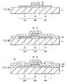
- FIG. 1 is a cross-sectional view illustrating a configuration of a thin-film transistor according to a first embodiment.
- FIGS. 2A to 2C are cross-sectional views illustrating a manufacturing method of the thin-film transistor illustrated in FIG. 1 in order of process steps.
- FIGS. 3A to 3C are cross-sectional views illustrating process steps subsequent to those of FIGS. 2A to 2C .
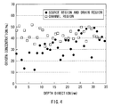
- FIG. 4 is a diagram representing a result of energy-dispersive X-ray spectroscopy analysis of a channel region and a low-resistance region.
- FIGS. 5A and 5B are diagrams comparing characteristics of the thin-film transistor illustrated in FIG. 1 with those of an existing thin-film transistor.
- FIG. 6 is a diagram representing a result of measurement of an aluminum concentration of a low-resistance region of a thin-film transistor according to a second embodiment.
- FIG. 7 is a cross-sectional view illustrating a configuration of a thin-film transistor according to a first modification.
- FIGS. 8A to 8C are cross-sectional views illustrating a manufacturing method of the thin-film transistor illustrated in FIG. 7 in order of process steps.
- FIG. 9 is a cross-sectional view illustrating a configuration of the thin-film transistor according to the second embodiment.
- FIGS. 10A to 10D are cross-sectional views illustrating a manufacturing method of the thin-film transistor illustrated in FIG. 9 in order of process steps.
- FIGS. 11A to 11C are cross-sectional views illustrating process steps subsequent to those of FIGS. 10A to 10D .
- FIG. 12 is a cross-sectional view illustrating a configuration of a thin-film transistor according to a second modification.
- FIGS. 13A to 13C are cross-sectional views illustrating a manufacturing method of the thin-film transistor illustrated in FIG. 12 in order of process steps.
- FIG. 14 is a cross-sectional view illustrating a configuration of a thin-film transistor according to a third embodiment.
- FIG. 15 is a cross-sectional view illustrating an example of island-shaped high-resistance films.
- FIG. 16 is a cross-sectional view illustrating another example of the island-shaped high-resistance films.
- FIG. 17 is an explanatory view for describing sizes of the island-shaped high-resistance films.
- FIGS. 18A to 18C are cross-sectional views illustrating a manufacturing method of the thin-film transistor illustrated in FIG. 14 in order of process steps.
- FIGS. 19A to 19D are cross-sectional views for describing the process steps illustrated in FIGS. 18A to 18C in detail.
- FIG. 20 illustrates the Thornton's model.
- FIGS. 21A and 21B are diagrams comparing characteristics of the thin-film transistor illustrated in FIG. 14 with those of an existing thin-film transistor.
- FIGS. 22A and 22B are diagrams each representing characteristics of a thin-film transistor when a thickness of a high-resistance film is varied.
- FIGS. 23A and 23B are cross-sectional views illustrating a manufacturing method of a thin-film transistor according to a third modification in order of process steps.
- FIGS. 24A and 24B are cross-sectional views illustrating process steps subsequent to those of FIGS. 23A and 23B .
- FIGS. 25A and 25B are cross-sectional views illustrating a manufacturing method of a thin-film transistor according to a fourth modification in order of process steps.
- FIGS. 26A and 26B are cross-sectional views illustrating process steps subsequent to those of FIGS. 25A and 25B .
- FIG. 27 is a cross-sectional view illustrating a configuration of a thin-film transistor according to a fourth embodiment.
- FIGS. 28A to 28D are cross-sectional views illustrating a manufacturing method of the thin-film transistor illustrated in FIG. 27 in order of process steps.
- FIGS. 29A to 29C are cross-sectional views illustrating process steps subsequent to those of FIGS. 28A to 28D .
- FIG. 30 illustrates a configuration of a circuit of a display device according to a first application example.
- FIG. 31 is an equivalent circuit diagram illustrating an example of a pixel driving circuit illustrated in FIG. 30 .
- FIG. 32 is a perspective view illustrating an external appearance of a second application example.
- FIG. 33A is a perspective view illustrating an external appearance of a third application example as viewed from a front side thereof
- FIG. 33B is a perspective view illustrating the external appearance of the third application example as viewed from a back side thereof.
- FIG. 34 is a perspective view illustrating an external appearance of a fourth application example.
- FIG. 35 is a perspective view illustrating an external appearance of a fifth application example.
- FIG. 36A is a front view in an open state of a sixth application example
- FIG. 36B is a side view in the open state
- FIG. 36C is a front view in a closed state
- FIG. 36D is a left side view
- FIG. 36E is a right side view
- FIG. 36F is a top view
- FIG. 36G is a bottom view.
- FIG. 37 is a cross-sectional view illustrating a modification of the thin-film transistor illustrated in FIG. 1 .
- First Embodiment an embodiment of a top-gate thin-film transistor in which a low-resistance region is formed by utilizing oxidation of metal.
- Second Embodiment an embodiment of the top-gate thin-film transistor in which the low-resistance region is formed by utilizing dopant.
- First Modification a modification of the top-gate thin-film transistor in which a high-resistance film is removed.
- Third Embodiment an embodiment of a bottom-gate thin-film transistor in which the high-resistance film is remained.
- Second Modification a modification of the bottom-gate thin-film transistor in which the high-resistance film is removed.
- Fourth Embodiment an embodiment of the top-gate thin-film transistor in which the high-resistance film is formed in an island-like shape.
- Third Modification a modification of a manufacturing method in which a metal film is patterned in an island-like shape and is then oxide to form the high-resistance film.
- Fourth Modification a modification of the manufacturing method in which the metal film is oxide to form the high-resistance film and is then patterned in the island-like shape.
- FIG. 1 illustrates a cross-sectional configuration of a thin-film transistor 1 according to a first embodiment.
- the thin-film transistor 1 may be used as a drive element in a device such as a liquid crystal display and an organic EL display.
- the thin-film transistor 1 may have a top-gate structure (or a staggered structure), in which an oxide semiconductor film 20 , a gate insulating film 30 , a gate electrode 40 , a high-resistance film 50 , an interlayer insulating film 60 , a source electrode 70 S, and a drain electrode 70 D are stacked in this order on a substrate 11 , for example.
- the substrate 11 may be configured by a glass substrate, a plastic film, or other suitable member, for example.
- a material of a plastic can be polyethylene terephthalate (PET), polyethylene naphthalate (PEN), or other suitable material.
- PET polyethylene terephthalate
- PEN polyethylene naphthalate
- the plastic film which is inexpensive, may be used in order to deposit the oxide semiconductor film 20 without heating the substrate 11 in a later-described sputtering process.
- the substrate 11 may be a metal substrate depending on an application, such as a stainless steel (SUS).
- the oxide semiconductor film 20 is provided on the substrate 11 in an island-like shape including the gate electrode 40 and peripheral sections of the gate electrode 40 , and functions as an active layer of the thin-film transistor 1 .
- the oxide semiconductor film 20 may have a thickness of about 50 nm, for example, and has a channel region 20 A opposed to the gate electrode 40 .
- the gate insulating film 30 and the gate electrode 40 are provided in this order and in the same shape on the channel region 20 A.
- a source region 20 S is provided on one side of the channel region 20 A, and a drain region 20 D is provided on the other side of the channel region 20 A.
- the channel region 20 A is configured by an oxide semiconductor.
- oxide semiconductor refers to a compound including oxygen and one or more elements such as indium, gallium, zinc, and tin.
- the oxide semiconductor can be an amorphous oxide semiconductor and a crystalline oxide semiconductor.
- the amorphous oxide semiconductor can be indium gallium zinc oxide (IGZO).
- the crystalline oxide semiconductor can be zinc oxide (ZnO), indium zinc oxide (IZO; Registered Trademark), indium gallium oxide (IGO), indium tin oxide (ITO), and indium oxide (InO).
- Each of the source region 20 S and the drain region 20 D includes a low-resistance region 21 in a partial region extending in a depth direction from an upper face thereof.
- the low-resistance region 21 may have an oxygen concentration which is lower than that of the channel region 20 A, for example, and is thereby made low in resistance. This makes it possible for the thin-film transistor 1 to have a self-aligned structure, and to be able to stabilize its characteristics.
- the oxygen concentration of the low-resistance region 21 be equal to or less than 30%, since a resistance increases when the oxygen concentration in the low-resistance region 21 exceeds 30%.
- a region other than the low-resistance region 21 of each of the source region 20 S and the drain region 20 D is configured by an oxide semiconductor as with the channel region 20 A.
- a depth of the low-resistance region 21 will be described later in detail.
- the gate insulating film 30 may have a thickness of about 300 nm, for example.
- the gate insulating film 30 may be a monolayer film, which can be a silicon dioxide film, a silicon nitride film, a silicon nitride oxide film, an aluminum oxide film, or other suitable film, or a multilayer film thereof.
- the silicon dioxide film or the aluminum oxide film is preferable, in that the silicon dioxide film and the aluminum oxide film are difficult to reduce the oxide semiconductor film 20 .
- the gate electrode 40 serves to apply a gate voltage to the thin-film transistor 1 , and to control an electron density in the oxide semiconductor film 20 with the gate voltage.
- the gate electrode 40 is provided in a selective region on the substrate 11 .
- the gate electrode 40 has a thickness of between 10 nm and 500 nm both inclusive, and preferably has a thickness of about 200 nm, and may be configured of molybdenum (Mo).
- Mo molybdenum
- a material structuring the gate electrode 40 be a metal having a low resistance, which can be aluminum (Al), copper (Cu), or other suitable metal, since the gate electrode 40 is desirably low in resistance.
- a multilayer film having a combination of a low-resistance layer and a barrier layer is also preferable, since this makes it possible to make the gate electrode 40 low in resistance.
- the low-resistance layer can be aluminum (Al), copper (Cu), or other suitable element
- the barrier layer can be titanium (Ti), molybdenum (Mo), or other suitable element.
- the high-resistance film 50 is provided between the interlayer insulating film 60 and the oxide semiconductor film 20 , between the interlayer insulating film 60 and the gate insulating film 30 , and between the interlayer insulating film 60 and the gate electrode 40 .
- the high-resistance film 50 is a metal film which serves as a source of supply of metal which is diffused into the low-resistance region 21 , and which is oxidized, in a later-described manufacturing process.
- the high-resistance film 50 may be configured by titanium oxide, aluminum oxide, indium oxide, or other suitable oxide.
- the high-resistance film 50 made of titanium oxide, aluminum oxide, or indium oxide has an excellent barrier property against outside air, and is thus able to reduce an influence of oxygen or moisture that changes electrical characteristics of the oxide semiconductor film 20 .
- providing of the high-resistance film 50 makes it possible to stabilize electrical characteristics of the thin-film transistor 1 , and to further increase an effect achieved by the interlayer insulating film 60 .
- a thickness of the high-resistance film 50 may be equal to or less than 20 nm, for example.
- the interlayer insulating film 60 is provided on surfaces of the oxide semiconductor film 20 , the gate insulating film 30 , and the gate electrode 40 with the high-resistance film 50 in between.
- the interlayer insulating film 60 may have a thickness of about 300 nm, for example.
- the interlayer insulating film 60 may be configured of a monolayer film, which can be a silicon dioxide film, an aluminum oxide film, or other suitable film, or a multilayer film thereof.
- the multilayer film of the silicon dioxide film and the aluminum oxide film makes it possible to suppress incorporation or diffusion of moisture into the oxide semiconductor film 20 , and to further increase electrical stability and reliability of the thin-film transistor 1 .
- the source electrode 70 S and the drain electrode 70 D are connected to the low-resistance region 21 through connection holes provided in the interlayer insulating film 60 and the high-resistance film 50 .
- the source electrode 70 S and the drain electrode 70 D each may have a thickness of about 200 nm, and may be configured of molybdenum (Mo).
- Mo molybdenum
- the source electrode 70 S and the drain electrode 70 D each be configured by a metal (or a metal wiring) having a low resistance, which can be aluminum (Al), copper (Cu), or other suitable metal.
- a multilayer film having a combination of a low-resistance layer and a barrier layer is also preferable.
- the low-resistance layer can be aluminum (Al), copper (Cu), or other suitable element
- the barrier layer can be titanium (Ti), molybdenum (Mo), or other suitable element.
- each of the source electrode 70 S and the drain electrode 70 D be provided to evade or bypass a region immediately above the gate electrode 40 , since this enables to reduce parasitic capacitances formed in a cross region of the gate electrode 40 and the source electrode 70 S and in a cross region of the gate electrode 40 and the drain electrode 70 D.
- the thin-film transistor 1 may be manufactured, for example, as follows.
- FIGS. 2A to 3C illustrate a manufacturing method of the thin-film transistor 1 in order of process steps.
- the oxide semiconductor film 20 made of the material described above, is formed at a thickness of about 50 nm on the entire surface of the substrate 11 with a sputtering method, for example.
- a ceramic target having the same composition as that of the oxide semiconductor film 20 to be formed is used.
- an oxygen partial pressure is so controlled that desired transistor characteristics are obtained, since a carrier concentration in the oxide semiconductor film 20 is largely dependent on the oxygen partial pressure in sputtering.
- the oxide semiconductor film 20 is shaped in the island-like shape, which includes the channel region 20 A, the source region 20 S on one side thereof, and the drain region 20 D on the other side thereof, with photolithography and etching processes, for example.
- the oxide semiconductor film 20 be processed with a wet-etching utilizing a mixture of phosphoric acid, nitric acid, and acetic acid.
- the use of the mixture of phosphoric acid, nitric acid, and acetic acid makes it possible to sufficiently increase a selectivity ratio relative to an underlying substrate, and to process relatively easily.
- a gate insulating material film 30 A which can be the silicon dioxide film, the aluminum oxide film, or other suitable oxide film, is formed at a thickness of about 300 nm on the entire surfaces of the substrate 11 and the oxide semiconductor film 20 with a plasma chemical vapor deposition (CVD) method etc., for example.
- the silicon dioxide film here may be formed with a reactive-sputtering method, other than the plasma CVD method mentioned before.
- the aluminum oxide film may be formed with a reactive-sputtering method, a CVD method, or an atomic layer deposition method.
- a gate electrode material film 40 A which can be the monolayer film including molybdenum (Mo), titanium (Ti), aluminum (Al), or other suitable element, or the multilayer film thereof, is formed at a thickness of about 200 nm on the entire surface of the gate insulating material film 30 A with a sputtering method, for example.
- the gate electrode material film 40 A is shaped into a desired shape with photolithography and etching processes, for example, to form the gate electrode 40 on the channel region 20 A of the oxide semiconductor film 20 .
- the gate electrode 40 is utilized as a mask to etch the gate insulating material film 30 A so as to form the gate insulating film 30 .
- the oxide semiconductor film 20 is configured by a crystalline material such as ZnO, IZO, and IGO, it is possible to use a chemical solution such as hydrofluoric acid to maintain a significantly large etching selectivity ratio and process easily, in etching the gate insulating material film 30 A.
- the gate insulating film 30 and the gate electrode 40 are formed in this order and in the same shape on the channel region 20 A of the oxide semiconductor film 20 .
- a metal film 50 A configured of a metal which reacts at a relatively low temperature with oxygen, such as titanium (Ti), aluminum (Al), and indium (In), is formed at a thickness of between 5 nm and 10 nm both inclusive on surfaces of the oxide semiconductor film 20 , the gate insulating film 30 , and the gate electrode 40 with a sputtering method, for example.
- a heat treatment is performed to oxidize the metal film 50 A so as to form the high-resistance film 50 .
- This oxidation reaction of the metal film 50 A utilizes a part of oxygen included in the source region 20 S and the drain region 20 D.
- oxygen concentrations in the source region 20 S and the drain region 20 D start to decrease from the upper faces of the source region 20 S and the drain region 20 D that contact with the metal film 50 A as the oxidation of the metal film 50 A progresses.
- each of the source region 20 S and the drain region 20 D extending in the depth direction from the upper face of each of the source region 20 S and the drain region 20 D, is formed with the low-resistance region 21 , which has the lower oxygen concentration than that of the channel region 20 A.
- FIG. 4 represents a result of examination on dependence in the depth direction of the oxygen concentration in the channel region 20 A as well as the oxygen concentrations in the source region 20 S and the drain region 20 D using an energy-dispersive X-ray spectroscopy (EDX) method, after performing the heat treatment of the metal film 50 A as in the manufacturing method described above.
- a material of the oxide semiconductor film 20 was IGZO, and the metal film 50 A was an aluminum film which had a thickness of 5 nm.
- the heat treatment was conducted with annealing at a temperature of 300 degrees centigrade.
- the oxygen concentrations in the source region 20 S and the drain region 20 D are lower than the oxygen concentration in the channel region 20 A throughout in the depth direction.
- a difference between the oxygen concentration in the channel region 20 A and the oxygen concentrations in the source region 20 S and the drain region 20 D is highly distinct in a region within the depth of 10 nm, in particular.
- the low-resistance region 21 is a part of each of the source region 20 S and the drain region 20 D extending in the depth direction from the upper face thereof, which part, to be more specific, is the region within 10 nm in the depth direction from the upper face thereof.
- the heat treatment of the metal film 50 A be performed with the annealing at a temperature of about 300 degrees centigrade as described above, for example.
- the annealing may be performed under a gas atmosphere having an oxidizing property that includes oxygen etc. This makes it possible to prevent the oxygen concentration of the low-resistance region 21 from being too low and to supply enough oxygen to the oxide semiconductor film 20 . This in turn makes it possible to curtail an annealing process performed in a later process step, thereby allowing a simplified manufacturing process.
- a temperature of the substrate 11 may be set at a relatively high temperature of about 200 degrees centigrade in the process step of forming the metal film 50 A illustrated in FIG. 3A , for example. This enables to form the low-resistance region 21 without performing the heat treatment illustrated in FIG. 3B . In this case, it is possible to reduce the carrier concentration in the oxide semiconductor film 20 to a level desirable for a transistor.
- the metal film 50 A be formed at the thickness of 10 nm or less as described above. Allowing the thickness of the metal film 50 A to be equal to or less than 10 nm makes it possible to completely oxidize the metal film 50 A with the heat treatment. When the metal film 50 A is not completely oxidized, a process step of removing the metal film 50 A with etching may become desirable. The process step of removing with etching is unnecessary when the metal film 50 A is completely oxidized and thereby the high-resistance film 50 is obtained, making it possible to simplify the manufacturing process. The thickness of the high-resistance film 50 consequently becomes 20 nm or less when the metal film 50 A is formed at the thickness of 10 nm or less.
- the oxidation with a method such as an oxidation under a vapor atmosphere and a plasma oxidation, as a method of oxidizing the metal film 50 A.
- the plasma oxidation can be performed immediately before the formation of the interlayer insulating film 60 with the plasma CVD method in a later process step, and is thus advantageous in that the number of process steps does not have to be increased in particular.
- the plasma oxidation be performed at conditions where the temperature of the substrate 11 is set at about 200 to 400 degrees centigrade, and where plasma is generated under a gas atmosphere containing oxygen such as oxygen and oxygen dinitride, for example, since this makes it possible to form the high-resistance film 50 having the excellent barrier property against outside air as described above.
- the high-resistance film 50 is also formed on sections such as the gate insulating film 30 and the gate electrode 40 , other than on the source region 20 S and the drain region 20 D of the oxide semiconductor film 20 . However, remaining the high-resistance film 50 without removing the same with etching will not be a cause of a leakage current.
- the interlayer insulating film 60 which can be the silicon dioxide film, the aluminum oxide film, or other suitable film, or the multilayer film thereof, is formed at the thickness described above on the high-resistance film 50 , for example.
- the silicon dioxide film may be formed with a plasma CVD method.
- the aluminum oxide film be formed with a reactive-sputtering method utilizing an aluminum target and a direct-current (DC) power or an alternating-current (AC) power, since this makes it possible to perform the deposition quickly.
- the connection hole is formed in each of the interlayer insulating film 60 and the high-resistance film 50 with photolithography and etching processes, for example.
- a film which can be a molybdenum (Mo) film or other suitable film, is formed at a thickness of about 200 nm on the interlayer insulating film 60 with a sputtering method, for example, and photolithography and etching processes are performed to shape the same into a predetermined shape.
- the source electrode 70 S and the drain electrode 70 D are connected to the low-resistance regions 21 as illustrated in FIG. 1 .
- the thin-film transistor 1 illustrated in FIG. 1 is completed.
- a current (a drain current) is generated in the channel region 20 A of the oxide semiconductor film 20 when a voltage (a gate voltage), which is equal to or higher than a predetermined threshold voltage, is applied to the gate electrode 40 through an unillustrated wiring layer.
- a voltage a gate voltage
- at least a part of each of the source region 20 S and the drain region 20 D extending in the depth direction from the upper face of each of the source region 20 S and the drain region 20 D is provided with the low-resistance region 21 , which is lower in oxygen concentration than that of the channel region 20 A.
- FIG. 5B represents a result of examination on transistor characteristics of the actually-fabricated thin-film transistor 1 having the low-resistance region 21 with the manufacturing method described in the foregoing.
- the metal film 50 A was an aluminum film which had a thickness of 5 nm.
- the heat treatment was conducted with annealing at a temperature of 300 degrees centigrade under an oxygen atmosphere for one hour to form the low-resistance region 21 .
- an ON-current of a transistor was increased by two digits or more in the thin-film transistor 1 in which the low-resistance region 21 was formed by the heat treatment of the metal film 50 A, as compared with the thin-film transistor in which the formation and the heat treatment of the metal film were not conducted.
- each of the source region 20 S and the drain region 20 D of the oxide semiconductor film 20 extending in the depth direction from the upper face of each of the source region 20 S and the drain region 20 D is provided with the low-resistance region 21 having the lower oxygen concentration than that of the channel region 20 A.
- the thin-film transistor 1 having the self-aligned structure in which the parasitic capacitance is reduced and having the stabilized characteristics, and to address attaining of larger screen, higher definition, and higher frame rate, when the thin-film transistor 1 described in the foregoing is used to configure an active-driving-type display.
- the gate insulating film 30 and the gate electrode 40 are formed in this order and in the same shape on the channel region 20 A of the oxide semiconductor film 20 .
- the metal film 50 A is formed on the oxide semiconductor film 20 , the gate insulating film 30 , and the gate electrode 40 .
- the heat treatment is performed on the metal film 50 A to oxidize the metal film 50 A into the high-resistance film 50 , and to form the low-resistance region 21 having the lower oxygen concentration than that of the channel region 20 A in a part of each of the source region 20 S and the drain region 20 D extending in the depth direction from the upper face of each of the source region 20 S and the drain region 20 D.
- the low-resistance region 21 is formed without using a process step having a large number of varying factors such a plasma process step. Hence, unlike existing techniques, it is possible to solve dependence of an element characteristic on the plasma process step, and to achieve a stable element characteristic.
- a thin-film transistor according to a second embodiment has a similar configuration as that of the thin-film transistor 1 according to the first embodiment illustrated in FIG. 1 , except that a configuration and a manufacturing method of the low-resistance region 21 are different from those in the first embodiment described above. Note that the same or equivalent elements as those according to the first embodiment are denoted with the same reference numerals, and will not be described in detail. Also, process steps corresponding to those in the first embodiment will be described with reference to FIGS. 1 to 3C .
- the low-resistance region 21 is made low in resistance by containing one or more elements selected from a group including aluminum (Al), boron (B), gallium (Ga), indium (In), titanium (Ti), silicon (Si), germanium (Ge), tin (Sn), and lead (Pb) as a dopant.
- Thin-film transistor 1 is thereby able to have the self-aligned structure and to stabilize a characteristic.
- a dopant concentration, desirable for making the oxide semiconductor low in resistance in this case be equal to or more than 1 ⁇ 1019 cm-3.
- the low-resistance region 21 may contain only one of the elements in the group described above, or may contain two or more elements. Also, it is preferable that the dopant concentration of the one or more elements included in the low-resistance region 21 be higher than that of the channel region 20 A.
- the thin-film transistor 1 according to the second embodiment may be manufactured, for example, as follows.
- the oxide semiconductor film 20 is formed with the process step illustrated in FIG. 2A .
- the gate insulating film 30 and the gate electrode 40 are formed in this order and in the same shape on the channel region 20 A of the oxide semiconductor film 20 with the process steps illustrated in FIGS. 2B and 2C in a similar manner as in the first embodiment.
- the low-resistance region 21 which contains, as a dopant, one or more elements selected from a group including aluminum (Al), boron (B), gallium (Ga), indium (In), titanium (Ti), silicon (Si), germanium (Ge), tin (Sn), and lead (Pb) in a part of each of the source region 20 S and the drain region 20 D extending in the depth direction from the upper face of each of the source region 20 S and the drain region 20 D.
- a group including aluminum (Al), boron (B), gallium (Ga), indium (In), titanium (Ti), silicon (Si), germanium (Ge), tin (Sn), and lead (Pb) in a part of each of the source region 20 S and the drain region 20 D extending in the depth direction from the upper face of each of the source region 20 S and the drain region 20 D.
- the low-resistance region 21 may be formed with the process steps illustrated in FIGS. 3A and 3B in a similar manner as in the first embodiment when the low-resistance region 21 contains aluminum (Al), indium (In), or titanium (Ti). More specifically, the metal film 50 A configured of aluminum (Al), indium (In), or titanium (Ti) as a dopant material film is formed on the surfaces of the oxide semiconductor film 20 , the gate insulating film 30 , and the gate electrode 40 . Then, the metal film 50 A is subjected to the heat treatment, by which the metal film 50 A is oxidized, and thus the high-resistance film 50 configured of aluminum oxide, indium oxide, or titanium oxide is formed.
- the low-resistance region 21 which includes aluminum (Al), indium (In), or titanium (Ti), in a part of each of the source region 20 S and the drain region 20 D extending in the depth direction from the upper face thereof.
- the low-resistance region 21 contains boron (B), gallium (Ga), silicon (Si), germanium (Ge), tin (Sn), or lead (Pb), the low-resistance region 21 may also be formed with the same process steps as those in the case of aluminum (Al), indium (In), or titanium (Ti). More specifically, the metal film or the nonmetal film 50 A configured of boron (B), gallium (Ga), silicon (Si), germanium (Ge), tin (Sn), or lead (Pb) as the dopant material film is formed on the surfaces of the oxide semiconductor film 20 , the gate insulating film 30 , and the gate electrode 40 .
- the metal film or the nonmetal film 50 A is subjected to the heat treatment, by which the metal film or the nonmetal film 50 A is oxidized, and thus the high-resistance film 50 configured of boron oxide, gallium oxide, silicon dioxide, germanium oxide, tin oxide, or lead oxide is formed.
- the low-resistance region 21 which includes boron (B), gallium (Ga), silicon (Si), germanium (Ge), tin (Sn), or lead (Pb), in a part of each of the source region 20 S and the drain region 20 D extending in the depth direction from the upper face thereof.
- FIG. 6 represents a result of measurement of an aluminum concentration in the low-resistance region 21 with a secondary ion mass spectrometry (SIMS) method, by actually fabricating the low-resistance region 21 which includes aluminum (Al) as the dopant with the manufacturing method described in the foregoing. It can be seen from FIG. 6 that the highest concentration of aluminum is included in the vicinity of a surface of the oxide semiconductor, and that aluminum which is 1 ⁇ 1019 cm-3 or more is included in the oxide semiconductor even in a region 40 nm deep from the surface.
- SIMS secondary ion mass spectrometry
- the interlayer insulating film 60 is formed on the high-resistance film 50 with the process step illustrated in FIG. 3C , in a similar manner as in the first embodiment. Then, as illustrated in FIG. 1 , the connection hole is formed in each of the interlayer insulating film 60 and the high-resistance film 50 with photolithography and etching processes, for example.
- a film which can be a molybdenum (Mo) film or other suitable film, is formed at a thickness of about 200 nm on the interlayer insulating film 60 with a sputtering method, for example, and photolithography and etching processes are performed to shape the same into a predetermined shape.
- the source electrode 70 S and the drain electrode 70 D are connected to the low-resistance regions 21 as again illustrated in FIG. 1 .
- the thin-film transistor 1 illustrated in FIG. 1 is completed.
- the current (the drain current) is generated in the channel region 20 A of the oxide semiconductor film 20 when the voltage (the gate voltage), which is equal to or higher than a predetermined threshold voltage, is applied to the gate electrode 40 , as in the first embodiment.
- each of the source region 20 S and the drain region 20 D extending in the depth direction from the upper face of each of the source region 20 S and the drain region 20 D is provided with the low-resistance region 21 , which contains one or more elements selected from a group including aluminum (Al), boron (B), gallium (Ga), indium (In), titanium (Ti), silicon (Si), germanium (Ge), tin (Sn), and lead (Pb) as a dopant.
- Al aluminum
- B boron
- Ga gallium
- In indium
- Ti titanium
- Si silicon
- germanium germanium
- Sn germanium
- Pb lead
- each of the source region 20 S and the drain region 20 D of the oxide semiconductor film 20 extending in the depth direction from the upper face of each of the source region 20 S and the drain region 20 D is provided with the low-resistance region 21 , which contains one or more elements selected from a group including aluminum (Al), boron (B), gallium (Ga), indium (In), titanium (Ti), silicon (Si), germanium (Ge), tin (Sn), and lead (Pb) as a dopant.
- the thin-film transistor 1 having the self-aligned structure in which the parasitic capacitance is reduced and having the stabilized characteristics, and to address the attaining of larger screen, higher definition, and higher frame rate, when the thin-film transistor 1 described in the foregoing is used to configure an active-driving-type display.
- the gate insulating film 30 and the gate electrode 40 are provided in this order and in the same shape on the channel region 20 A of the oxide semiconductor film 20 . Then, the metal film or the nonmetal film 50 A is formed as the dopant material film on the oxide semiconductor film 20 , the gate insulating film 30 , and the gate electrode 40 .
- the heat treatment is performed on the metal film or the nonmetal film 50 A to oxidize the metal film or the nonmetal 50 A into the high-resistance film 50 , and to form the low-resistance region 21 , which contains one or more elements selected from a group including aluminum (Al), boron (B), gallium (Ga), indium (In), titanium (Ti), silicon (Si), germanium (Ge), tin (Sn), and lead (Pb) as a dopant, in a part of each of the source region 20 S and the drain region 20 D extending in the depth direction from the upper face of each of the source region 20 S and the drain region 20 D.
- the low-resistance region 21 is formed without using a process step having a large number of varying factors such a plasma process step. Hence, unlike existing techniques, it is possible to solve dependence of an element characteristic on the plasma process step, and to achieve a stable element characteristic.
- FIG. 7 illustrates a cross-sectional configuration of a thin-film transistor 1 A according to a first modification.
- the thin-film transistor 1 A has a configuration, an operation, and an effect, which are similar to those of the thin-film transistor 1 according to the first embodiment described above, except that the high-resistance film 50 is not provided so as to reduce a leakage current.
- the thin-film transistor 1 A may be manufactured, for example, as follows. First, in a similar manner as in the first embodiment, the oxide semiconductor film 20 , the gate insulating film 30 , the gate electrode 40 , and the metal film 50 A are formed on the substrate 11 , and the metal film 50 A is subjected to the heat treatment to form the low-resistance region 21 and the high-resistance film 50 , with the process steps illustrated in FIGS. 2A to 3B . Then, as illustrated in FIG. 8A , the high-resistance film 50 is removed with etching.
- the use of a dry-etching method utilizing gas, which contains chlorine etc. makes it possible to easily remove the high-resistance film 50 as well as the metal film 50 A that has not been completely oxidized.
- the interlayer insulating film 60 is formed in a similar manner as in the first embodiment.
- the connection holes are provided in the interlayer insulating film 60 , and the source electrode 70 S and the drain electrode 70 D are connected to the low-resistance regions 21 , in a similar manner as in the first embodiment.
- FIG. 9 illustrates a cross-sectional configuration of a thin-film transistor 1 B according to a third embodiment.
- the thin-film transistor 1 B has a similar configuration as that of the thin-film transistor 1 according to the first embodiment described above, except that the thin-film transistor 1 B is a bottom-gate thin-film transistor in which the gate electrode 40 , the gate insulating film 30 , the oxide semiconductor film 20 , a channel protecting film 80 , the interlayer insulating film 60 , the source electrode 70 S, and the drain electrode 70 D are stacked in this order on the substrate 11 .
- the same or equivalent elements as those according to the first embodiment are denoted with the same reference numerals, and will not be described in detail.
- the channel protecting film 80 is provided on the channel region 20 A of the oxide semiconductor film 20 .
- the channel protecting film 80 may have a thickness of about 200 nm, and may be configured of a monolayer film, which can be a silicon dioxide film, a silicon nitride film, an aluminum oxide film, or other suitable film, or a multilayer film thereof, for example.
- the thin-film transistor 1 B may be manufactured, for example, as follows. Note that reference is made to the first embodiment to describe process steps that are same as those in the first embodiment.
- a film which can be a molybdenum (Mo) film or other suitable film, is formed at a thickness of about 200 nm on the entire surface of the substrate 11 with a method such as a sputtering method and an evaporation method, for example.
- the molybdenum film is patterned with a photolithography method, for example, to form the gate electrode 40 as illustrated in FIG. 10A .
- the gate insulating film 30 which can be a silicon dioxide film, an aluminum oxide film, or other suitable film, is formed at a thickness of about 300 nm on the entire surface of the substrate 11 on which the gate electrode 40 is formed, with a plasma CVD method, for example.
- the oxide semiconductor film 20 is formed on the gate insulating film 30 in a similar manner as in the first embodiment.
- a channel protecting material film which can be a monolayer film of a silicon dioxide film, a silicon nitride film, an aluminum oxide film, or other suitable film, or a multilayer film thereof, is formed at a thickness of about 200 nm on the entire surfaces of the oxide semiconductor film 20 and the gate insulating film 30 .
- a back-side exposure in which the gate electrode 40 is utilized as a mask, is used to form the channel protecting film 80 at a position close to the gate electrode 40 in a self-aligned fashion.
- the metal film 50 A is formed on the oxide semiconductor film 20 and the channel protecting film 80 in a similar manner as in the first embodiment.
- the heat treatment is performed to oxidize the metal film 50 A so as to form the high-resistance film 50 , and to form the low-resistance region 21 having the lower oxygen concentration than that of the channel region 20 A in a part of each of the source region 20 S and the drain region 20 D extending in the depth direction from the upper face of each of the source region 20 S and the drain region 20 D.
- the interlayer insulating film 60 is formed on the high-resistance film 50 in a similar manner as in the first embodiment.
- the connection holes are provided in each of the interlayer insulating film 60 and the high-resistance film 50 , and the source electrode 70 S and the drain electrode 70 D are connected to the low-resistance regions 21 , in a similar manner as in the first embodiment.
- the thin-film transistor 1 B illustrated in FIG. 9 is completed.
- FIG. 12 illustrates a cross-sectional configuration of a thin-film transistor 1 C according to a second modification.
- the thin-film transistor 1 C has a configuration, an operation, and an effect, which are similar to those of the thin-film transistor 1 B according to the third embodiment described above, except that the high-resistance film 50 is not provided so as to reduce a leakage current.
- the thin-film transistor 1 C may be manufactured, for example, as follows. First, in a similar manner as in the third embodiment, the gate electrode 40 , the gate insulating film 30 , the oxide semiconductor film 20 , the channel protecting film 80 , and the metal film 50 A are formed on the substrate 11 , and the metal film 50 A is subjected to the heat treatment to form the low-resistance region 21 and the high-resistance film 50 , with the process steps illustrated in FIGS. 10A to 10D . Then, as illustrated in FIG. 13A , the high-resistance film 50 is removed with etching. Then, as illustrated in FIG. 13B , the interlayer insulating film 60 is formed in a similar manner as in the third embodiment.
- connection holes are provided in the interlayer insulating film 60 , and the source electrode 70 S and the drain electrode 70 D are connected to the low-resistance regions 21 , in a similar manner as in the third embodiment.
- FIG. 14 illustrates a configuration of a thin-film transistor 1 D according to a fourth embodiment.
- the thin-film transistor 1 D has a similar configuration as that of the thin-film transistor 1 according to the first embodiment described above, except that the high-resistance film 50 is configured by a plurality of discontinuous island-shaped high-resistance films 51 .
- the same or equivalent elements as those according to the first embodiment are denoted with the same reference numerals, and will not be described in detail.
- Each of the island-shaped high-resistance films 51 may be configured of aluminum oxide, for example.
- the island-shaped high resistance film 51 does not necessarily have to be configured by aluminum oxide in its entirety in a thickness direction thereof.
- the island-shaped high resistance film 51 may have a configuration in which only an upper surface thereof is configured of aluminum oxide as an oxidized section 53 A, and in which a section (or a lower part) other than the upper surface is configured of metallic aluminum as an unoxidized section 53 B.
- FIG. 15 the island-shaped high resistance film 51 may have a configuration in which only an upper surface thereof is configured of aluminum oxide as an oxidized section 53 A, and in which a section (or a lower part) other than the upper surface is configured of metallic aluminum as an unoxidized section 53 B.
- the island-shaped high resistance film 51 may have a configuration in which the upper surface and side faces thereof are each configured of aluminum oxide as the oxidized section 53 A, and in which a section (or a central part) other than the upper surface and the side faces is configured of metallic aluminum as the unoxidized section 53 B, for example.
- the clearance gap 52 allows the adjacent island-shaped high-resistance films 51 to be physically separated from each other, and thereby each of the island-shaped high-resistance films 51 has an island-shaped configuration where the adjacent island-shaped high-resistance films 51 are not two-dimensionally connected to each other.
- the island-shaped high-resistance films 51 hardly flow electricity in an in-plane direction mutually, making it possible to block the leakage current from the gate electrode 40 to the source electrode 70 S or from the gate electrode 40 to the drain electrode 70 D.
- Planar shapes of the island-shaped high-resistance films 51 and the clearance gap 52 are not particularly limited.
- the island-shaped high-resistance film 51 and the clearance gap 52 each may have an irregular planar shape.
- the plurality of island-shaped high-resistance films 51 are separated from one another by the clearance gap 52 , at least at one position between the gate electrode 40 and the oxide semiconductor film 20 (side faces of the gate insulating film 30 ). In other words, it is preferable that side which is the longest among the island-shaped high-resistance films 51 be shorter in length than a thickness of the gate insulating film 30 .
- the thin-film transistor 1 D may be manufactured, for example, as follows.
- FIGS. 18A to 18C illustrate a manufacturing method of the thin-film transistor 1 D illustrated in FIG. 14 in order of process steps. Note that reference is made to FIGS. 2A to 2C to describe process steps that are same as those in the first embodiment.
- the oxide semiconductor film 20 is formed with the process step illustrated in FIG. 2A in a similar manner as in the first embodiment. Then, the gate insulating film 30 and the gate electrode 40 are formed in this order and in the same shape on the channel region 20 A of the oxide semiconductor film 20 with the process steps illustrated in FIGS. 2B and 2C in a similar manner as in the first embodiment.
- FIG. 18A the metal film 50 A configured of the plurality of island-shaped metal films 51 A, which are made of aluminum (Al), is formed on the surfaces of the oxide semiconductor film 20 , the gate insulating film 30 , and the gate electrode 40 .
- FIG. 19A schematically illustrates the metal film 50 A configured of the plurality of island-shaped metal films 51 A in an enlarged fashion. The clearance gaps 52 are generated among the plurality of island-shaped metal films 51 A.
- a method such as a vacuum evaporation method and a sputtering method is suitable as a technique of forming the metal film 50 A.
- the most suitable technique for forming the metal film 50 A configured of the plurality of island-shaped metal films 51 A is the sputtering method.
- FIG. 20 represents the Thornton's model in a sputtering method, where T is a substrate temperature, and Tm is a melting point of a material.
- differences in crystallinity and grain size distribution of a to-be-formed film occur by varying a temperature of a substrate and a pressure of argon (Ar) serving as sputtering gas.
- a state referred to as “ZONE 3” is obtained when T/Tm is large and the pressure of argon is low, i.e., the energy of particles to be sputtered is extremely large and a metal film is easy to move on a substrate, by which an extremely dense film is formed.
- a state referred to as “ZONE 1” is obtained when T/Tm is small and the pressure of argon is high.
- the film is rough even when the film is made very thick. That is, formation of the island-shaped films is possible in an early process of formation.
- the heat treatment is performed in a similar manner as in the first embodiment to oxidize the plurality of island-shaped metal films 51 A of the metal film 50 A, by which the high-resistance film 50 having the plurality of island-shaped high-resistance film 51 configured of aluminum oxide is formed.
- This results in the formation of the low-resistance region 21 , which includes aluminum as a dopant, or which has the lower oxygen concentration than that of the channel region 20 A, in a part of each of the source region 20 S and the drain region 20 D extending in the depth direction from the upper face thereof.
- FIG. 19B schematically illustrates oxidation of the metal film 50 A in an enlarged fashion.
- the plurality of island-shaped metal films 51 A of the metal film 50 A absorb oxygen O2 in an atmosphere and oxygen O within the oxide semiconductor film 20 serving as an underlying layer, and are thereby oxidized.
- each of the island-shaped metal films 51 A increases in volume in accordance with an amount of oxygen absorbed.
- a surface area, which contacts with oxygen, of the metal film 50 A configured of the plurality of island-shaped metal films 51 A increases. Hence, the oxidation is further promoted, making it possible to suppress the leakage current also from this respect.
- the oxide semiconductor film 20 the low-resistance region 21 is formed immediately below each of the island-like metal films 51 A.
- FIG. 19C schematically illustrates, in an enlarged fashion, that the high-resistance film 50 configured of the plurality of island-shaped high-resistance films 51 is formed, and that the low-resistance region 21 is formed in the oxide semiconductor film 20 , by the oxidation of the metal film 50 A.
- the island-shaped high-resistance film 51 expands by the oxidation, whereas the clearance gap 52 shrinks.
- the island-shaped high-resistance films 51 there may be the island-shaped high-resistance film 51 which is separated from the adjacent island-shaped high-resistance film 51 by the clearance gap 52 , and there may also be the island-shaped high-resistance film 51 which is joined to the adjacent island-shaped high-resistance film 51 by disappearance of the clearance gap 52 .
- the interlayer insulating film 60 is formed on the high-resistance film 50 in a similar manner as in the first embodiment. Then, as illustrated in FIG. 14 , the connection holes are formed in the interlayer insulating film 60 with photolithography and etching processes, for example.
- a film which can be a molybdenum (Mo) film or other suitable film, is formed at a thickness of about 200 nm on the interlayer insulating film 60 with a sputtering method, for example, and photolithography and etching processes are performed to shape the same into a predetermined shape.
- the source electrode 70 S and the drain electrode 70 D are connected to the low-resistance regions 21 as again illustrated in FIG. 14 .
- FIG. 19D illustrates a state where the source electrode 70 S and the drain electrode 70 D are formed on the plurality of island-shaped high-resistance films 51 .
- the plurality of island-shaped high-resistance films 51 are separated from one another by the clearance gaps 52 , so that the source electrode 70 S and the drain electrode 70 D are connected to the low-resistance regions 21 through the clearance gaps 52 .
- a contact resistance between the source electrode 70 S and the low-resistance region 21 , and that between the drain electrode 70 D and the low-resistance region 21 are decreased, thereby making it possible to eliminate a process step of removing the island-shaped high-resistance films 51 on the low-resistance region 21 .
- the thin-film transistor 1 D illustrated in FIG. 14 is completed.
- the current (the drain current) is generated in the channel region 20 A of the oxide semiconductor film 20 when the voltage (the gate voltage), which is equal to or higher than a predetermined threshold voltage, is applied to the gate electrode 40 , as in the first embodiment.
- the high-resistance film 50 is configured by the plurality of discontinuous island-shaped high-resistance films 51 , and the adjacent island-shaped high-resistance films 51 are physically separated from each other by the clearance gap 52 . Hence, electricity hardly flows among the island-shaped high-resistance films 51 . Thus, the leakage current from the gate electrode 40 to the source electrode 70 S or from the gate electrode 40 to the drain electrode 70 D is blocked, making it possible to improve transistor characteristics.
- FIG. 21A represents a result of examination on transistor characteristics of the actually-fabricated thin-film transistor 1 D having the high-resistance film 50 configured of the plurality of island-shaped high-resistance films 51 with the manufacturing method described in the foregoing.
- a silicon dioxide (SiO2) film was first formed at a thickness of 200 nm as a buffer layer on the substrate 11 , made of a glass substrate, with a plasma-enhanced chemical vapor deposition (PECVD) method.
- PECVD plasma-enhanced chemical vapor deposition
- the oxide semiconductor film 20 made of an InGaZnO film was formed at a thickness of 40 nm.
- the metal film 50 A made of an aluminum film was formed at a thickness of 5 nm.
- the metal film 50 A was deposited under deposition conditions where the substrate temperature was about 100 degrees centigrade and the argon pressure was about 0.5 PA. T/Tm in this case equals to 0.15 since the melting point of aluminum is about 660 degrees centigrade. Because the argon pressure was low, it was likely that the deposition was achieved under a state of “ZONE T (transition)” in the Thornton's model represented in FIG. 20 . However, examination on a cross-section of the deposited metal film 50 A confirmed that the plurality of discontinuous island-shaped metal films 51 A were formed.
- the deposition may be achieved under the state of “ZONE 1”, and that the thickness of the metal film 50 A can be made thick. Then, the heat treatment was performed on the metal film 50 A at 300 degrees centigrade under an atmosphere containing about 30% of oxygen for one hour, to form the low-resistance region 21 .
- an ON-current of a transistor was increased by two digits or more in the thin-film transistor 1 D, in which the low-resistance region 21 was formed and in which the high-resistance film 50 configured of the plurality of island-shaped high-resistance films 51 was formed by the heat treatment of the metal film 50 A configured of the plurality of island-shaped metal films 51 A, as compared with the thin-film transistor in which the formation and the heat treatment of the metal film were not conducted.
- FIGS. 22A and 22B each represent a result of examination on a source-drain current Id and a gate-drain current Ig of the thin-film transistor 1 D, in which examinations the thin-film transistors 1 D, each having the high-resistance film 50 of different thickness by varying the thickness of the metal film 50 A at 5 nm or 10 nm, were fabricated.
- an OFF-state current of a transistor is large in the thin-film transistor 1 D having the 10 nm thick metal film 50 A as compared with the thin-film transistor 1 D having the 5 nm thick metal film 50 A, suggesting that there was a connection between the source electrode 70 S and the drain electrode 70 D.
- leakage currents denoted by Ig are significantly large, meaning that the high-resistance film 50 obviously served as a leakage path.
- Ig leakage currents denoted by forming the metal film 50 A at the thickness of 5 nm or less reduces the leakage and allows the transistor characteristics to be improved.
- the high-resistance film 50 is configured by the plurality of island-shaped high-resistance films 51 .
- the contact resistance between the source electrode 70 S and the low-resistance region 21 , and that between the drain electrode 70 D and the low-resistance region 21 are decreased, thereby eliminating the process step of removing the island-shaped high-resistance films 51 on the low-resistance region 21 .
- FIGS. 23A to 24B illustrate a manufacturing method of the thin-film transistor 1 D according to a third modification in order of process steps.
- the manufacturing method according to this modification differs from that according to the fourth embodiment described above in a formation method of the high-resistance film 50 .
- FIGS. 2A to 2C describe process steps that correspond to those in the first embodiment.
- the oxide semiconductor film 20 is formed with the process step illustrated in FIG. 2A in a similar manner as in the first embodiment. Then, the gate insulating film 30 and the gate electrode 40 are formed in this order and in the same shape on the channel region 20 A of the oxide semiconductor film 20 with the process steps illustrated in FIGS. 2B and 2C in a similar manner as in the first embodiment.
- the metal film 50 A configured of aluminum (Al) is formed as an uniform continuous film on the surfaces of the oxide semiconductor film 20 , the gate insulating film 30 , and the gate electrode 40 .
- the metal film 50 A is patterned with photolithography and etching processes, for example, to divide the metal film 50 A into the plurality of island-shaped metal films 51 A.
- the clearance gaps 52 are provided among the plurality of island-shaped metal films 51 A, and these clearance gaps 52 are utilized to physically separate the plurality of island-shaped metal films 51 A from one another.
- the heat treatment is performed in a similar manner as in the first embodiment to oxidize the plurality of island-shaped metal films 51 A of the metal film 50 A, by which the high-resistance film 50 having the plurality of island-shaped high-resistance film 51 configured of aluminum oxide is formed.
- This results in the formation of the low-resistance region 21 , which includes aluminum as a dopant, or which has the lower oxygen concentration than that of the channel region 20 A, in a part of each of the source region 20 S and the drain region 20 D extending in the depth direction from the upper face thereof.
- the interlayer insulating film 60 is formed on the high-resistance film 50 in a similar manner as in the first embodiment. Then, as illustrated in FIG. 14 , the connection holes are formed in the interlayer insulating film 60 with photolithography and etching processes, for example.
- a film which can be a molybdenum (Mo) film or other suitable film, is formed at a thickness of about 200 nm on the interlayer insulating film 60 with a sputtering method, for example, and photolithography and etching processes are performed to shape the same into a predetermined shape.
- the source electrode 70 S and the drain electrode 70 D are connected to the low-resistance regions 21 as again illustrated in FIG. 14 .
- the plurality of island-shaped high-resistance films 51 are separated from one another by the clearance gaps 52 , so that the source electrode 70 S and the drain electrode 70 D are connected to the low-resistance regions 21 through the clearance gaps 52 .
- the contact resistance between the source electrode 70 S and the low-resistance region 21 , and that between the drain electrode 70 D and the low-resistance region 21 , are decreased, thereby making it possible to eliminate the process step of removing the island-shaped high-resistance films 51 on the low-resistance region 21 .
- the thin-film transistor 1 D illustrated in FIG. 14 is completed.
- FIGS. 25A to 26B illustrate a manufacturing method of the thin-film transistor 1 D according to a fourth modification in order of process steps.
- the manufacturing method according to this modification differs from that according to the fourth embodiment described above in a formation method of the high-resistance film 50 .
- FIGS. 2A to 2C describe process steps that correspond to those in the first embodiment.
- the oxide semiconductor film 20 is formed with the process step illustrated in FIG. 2A in a similar manner as in the first embodiment. Then, the gate insulating film 30 and the gate electrode 40 are formed in this order and in the same shape on the channel region 20 A of the oxide semiconductor film 20 with the process steps illustrated in FIGS. 2B and 2C in a similar manner as in the first embodiment.
- the metal film 50 A configured of aluminum (Al) is formed as the uniform continuous film on the surfaces of the oxide semiconductor film 20 , the gate insulating film 30 , and the gate electrode 40 .
- the heat treatment is performed in a similar manner as in the first embodiment to oxidize the metal film 50 A so as to form the high-resistance film 50 .
- This results in the formation of the low-resistance region 21 , which includes aluminum as a dopant, or which has the lower oxygen concentration than that of the channel region 20 A, in a part of each of the source region 20 S and the drain region 20 D extending in the depth direction from the upper face thereof.
- the high-resistance film 50 is patterned with photolithography and etching processes, for example, to divide the high-resistance film 50 into the plurality of island-shaped high-resistance films 51 .
- the clearance gaps 52 are provided among the plurality of island-shaped high-resistance films 51 , and these clearance gaps 52 are utilized to physically separate the plurality of island-shaped high-resistance films 51 from one another.
- the interlayer insulating film 60 is formed on the high-resistance film 50 in a similar manner as in the first embodiment. Then, as illustrated in FIG. 14 , the connection holes are formed in the interlayer insulating film 60 with photolithography and etching processes, for example.
- a film which can be a molybdenum (Mo) film or other suitable film, is formed at a thickness of about 200 nm on the interlayer insulating film 60 with a sputtering method, for example, and photolithography and etching processes are performed to shape the same into a predetermined shape.
- the source electrode 70 S and the drain electrode 70 D are connected to the low-resistance regions 21 as again illustrated in FIG. 14 .
- the plurality of island-shaped high-resistance films 51 are separated from one another by the clearance gaps 52 , so that the source electrode 70 S and the drain electrode 70 D are connected to the low-resistance regions 21 through the clearance gaps 52 .
- the contact resistance between the source electrode 70 S and the low-resistance region 21 , and that between the drain electrode 70 D and the low-resistance region 21 , are decreased, thereby making it possible to eliminate the process step of removing the island-shaped high-resistance films 51 on the low-resistance region 21 .
- the thin-film transistor 1 D illustrated in FIG. 14 is completed.
- FIG. 27 illustrates a cross-sectional configuration of a thin-film transistor 1 E according to a fifth embodiment.
- the thin-film transistor 1 E has a similar configuration as that of each of the thin-film transistors 1 B and 1 D according to the third and the fourth embodiments described above, except that the thin-film transistor 1 E is a bottom-gate thin-film transistor in which the gate electrode 40 , the gate insulating film 30 , the oxide semiconductor film 20 , the channel protecting film 80 , the interlayer insulating film 60 , the source electrode 70 S, and the drain electrode 70 D are stacked in this order on the substrate 11 .
- the same or equivalent elements as those according to the third and the fourth embodiments are denoted with the same reference numerals, and will not be described in detail.
- the thin-film transistor 1 E may be manufactured, for example, as follows. Note that reference is made to the first embodiment or the third embodiment to describe process steps that are same as those in the first embodiment or the third embodiment.
- the gate electrode 40 and the gate insulating film 30 are formed in order on the substrate 11 with the process step illustrated in FIG. 10A in a similar manner as in the third embodiment.
- the oxide semiconductor film 20 is formed on the gate insulating film 30 with the process step illustrated in FIG. 10B in a similar manner as in the third embodiment.
- the channel protecting film 80 is formed on the oxide semiconductor film 20 with the process step illustrated in FIG. 10C in a similar manner as in the third embodiment.
- the metal film 50 A configured of the plurality of island-shaped metal films 51 A is formed on the oxide semiconductor film 20 , the channel protecting film 80 , and the gate insulating film 30 with the process step illustrated in FIG. 18A in a similar manner as in the fourth embodiment.
- the heat treatment is performed in a similar manner as in the fourth embodiment to oxidize the plurality of island-shaped metal films 51 A of the metal film 50 A with the process step illustrated in FIG. 18B so as to form the high-resistance film 50 configured of the plurality of island-shaped high-resistance films 51 .
- This results in the formation of the low-resistance region 21 , having the lower oxygen concentration than that of the channel region 20 A, in a part or in the entire part of each of the source region 20 S and the drain region 20 D extending in the depth direction from the upper face thereof.
- the interlayer insulating film 60 is formed on the high-resistance film 50 in a similar manner as in the first embodiment.
- connection holes are provided in the interlayer insulating film 60 , and the source electrode 70 S and the drain electrode 70 D are connected to the low-resistance regions 21 , in a similar manner as in the first embodiment.
- the thin-film transistor 1 E illustrated in FIG. 27 is completed.
- FIG. 30 illustrates a configuration of a circuit of a display device 90 provided with any one of the thin-film transistors 1 to 1 E as a drive element.
- the display device 90 may be a display such as a liquid crystal display and an organic EL display, for example.
- the display device 90 is provided, on a drive panel 91 , with a plurality of pixels 10 R, 10 G, and 10 B which are arranged in matrix, and various driving circuits for driving those pixels 10 R, 10 G, and 10 B.
- the pixels 10 R, 10 G, and 10 B may be elements, such as liquid crystal display elements and organic EL elements, which emit lights for red, green, and blue, respectively, although the number of colors and the types of colors are not limited thereto.
- These three pixels 10 R, 10 G, and 10 B are grouped as a single pixel to configure a displaying region 110 having a plurality of such pixels.
- a signal line driving circuit 120 and a scanning line driving circuit 130 each serving as a driver for image displaying
- a pixel driving circuit 150 which are provided as the driving circuits, for example.
- An unillustrated sealing panel is attached to the drive panel 91 , by which sealing panel the pixels 10 R, 10 G, and 10 B, and the driving circuits are sealed.
- FIG. 31 is an equivalent circuit diagram of the pixel driving circuit 150 .
- the pixel driving circuit 150 is an active-type driving circuit in which transistors Tr 1 and Tr 2 are arranged. Each of the transistors Tr 1 and Tr 2 is any one of the thin-film transistors 1 to 1 E described above. A capacitor Cs is provided between the transistors Tr 1 and Tr 2 .
- the pixel 10 R (or the pixel 10 G or 10 B) is connected in series to the transistor Tr 1 between a first power source line (Vcc) and a second power source line (GND).
- the pixel driving circuit 150 is further provided with a plurality of signal lines 120 A arranged in columns, and a plurality of scanning lines 130 A arranged in rows.
- Each of the signal lines 120 A is connected to the signal line driving circuit 120 , from which circuit image signals are supplied to source electrodes of the transistors Tr 2 through the signal lines 120 A.
- Each of the scanning lines 130 A is connected to the scanning line driving circuit 130 , from which circuit scanning signals are sequentially supplied to gate electrodes of the transistors Tr 2 through the scanning lines 130 A.
- each of the transistors Tr 1 and Tr 2 is configured by any one of the thin-film transistors 1 to 1 E according to the embodiments and the modifications. Hence, it is possible to perform high-quality displaying by any one of the thin-film transistors 1 to 1 E having a reduced parasitic capacitance by a self-aligned structure and having stabilized characteristics.
- Such a display device 90 may be employed in any electronic devices, such as those according to second to sixth application examples as follows, for example.
- FIG. 32 illustrates an external appearance of a television device.
- the television device is provided with an image display screen unit 300 including a front panel 310 and a filter glass 320 , for example.
- FIGS. 33A and 33B each illustrate an external appearance of a digital camera.
- the digital camera is provided with a light emitting unit 410 for flash, a display unit 420 , a menu switch section 430 , and a shutter-release button 440 , for example.
- FIG. 34 illustrates an external appearance of laptop personal computer.
- the laptop personal computer is provided with a body 510 , a keyboard 520 for input-manipulation of characters and the like, and a display unit 530 for displaying an image, for example.
- FIG. 35 illustrates an external appearance of a video camera.
- the video camera is provided with a body 610 , a lens 620 provided in a front face of the body 610 for picking-up an image of an object, a shooting start/stop switch 630 , and a display unit 640 , for example.
- FIGS. 36A to 36G each illustrate an external appearance of a cellular phone.
- the cellular phone couples an upper casing 710 and a lower casing 720 through a coupling part (or a hinge) 730 , and is provided with a display 740 , a sub-display 750 , a picture light 760 , and a camera 770 , for example.
- the present application has been described in the foregoing by way of example with reference to the embodiments, the modifications, and the application examples, the present application is not limited thereto but may be modified in a wide variety of ways.
- a part of each of the source region 20 S and the drain region 20 D extending in the depth direction from the upper face of each of the source region 20 S and the drain region 20 D is provided with the low-resistance region 21 .
- the low-resistance region 21 may be provided in at least a part of each of the source region 20 S and the drain region 20 D extending in the depth direction from the upper face of each of the source region 20 S and the drain region 20 D.
- the low-resistance region 21 may be provided in the entire part of each of the source region 20 S and the drain region 20 D extending in the depth direction from the upper face of each of the source region 20 S and the drain region 20 D.
- the oxide semiconductor film 20 is provided directly on the substrate 11 .
- the oxide semiconductor film 20 may be provided on the substrate 11 with an insulating film such as a silicon dioxide film, a silicon nitride film, and an aluminum oxide film in between. This makes it possible to suppress diffusion of an influential factor, such as impurity and moisture, from the substrate 11 into the oxide semiconductor film 20 .
- materials and thicknesses of various layers, deposition methods, and deposition conditions are illustrative, and not limitative. Other materials, thicknesses, deposition methods, and deposition conditions may be employed.
- the present application is applicable to display devices utilizing other display elements, such as inorganic EL elements, electrodeposition-type display elements, and electrochromic-type display elements.
Abstract
Description
Claims (9)
Priority Applications (1)
| Application Number | Priority Date | Filing Date | Title |
|---|---|---|---|
| US15/813,735 US10763371B2 (en) | 2010-03-30 | 2017-11-15 | Thin-film transistor, method of manufacturing the same, and display device |
Applications Claiming Priority (4)
| Application Number | Priority Date | Filing Date | Title |
|---|---|---|---|
| JP2010079293 | 2010-03-30 | ||
| JP2010-079293 | 2010-03-30 | ||
| JP2010-245035 | 2010-11-01 | ||
| JP2010245035A JP5708910B2 (en) | 2010-03-30 | 2010-11-01 | THIN FILM TRANSISTOR, MANUFACTURING METHOD THEREOF, AND DISPLAY DEVICE |
Related Child Applications (1)
| Application Number | Title | Priority Date | Filing Date |
|---|---|---|---|
| US15/813,735 Division US10763371B2 (en) | 2010-03-30 | 2017-11-15 | Thin-film transistor, method of manufacturing the same, and display device |
Publications (2)
| Publication Number | Publication Date |
|---|---|
| US20110240998A1 US20110240998A1 (en) | 2011-10-06 |
| US9859437B2 true US9859437B2 (en) | 2018-01-02 |
Family
ID=44697196
Family Applications (2)
| Application Number | Title | Priority Date | Filing Date |
|---|---|---|---|
| US13/053,997 Active 2034-06-11 US9859437B2 (en) | 2010-03-30 | 2011-03-22 | Thin-film transistor, method of manufacturing the same, and display device |
| US15/813,735 Active US10763371B2 (en) | 2010-03-30 | 2017-11-15 | Thin-film transistor, method of manufacturing the same, and display device |
Family Applications After (1)
| Application Number | Title | Priority Date | Filing Date |
|---|---|---|---|
| US15/813,735 Active US10763371B2 (en) | 2010-03-30 | 2017-11-15 | Thin-film transistor, method of manufacturing the same, and display device |
Country Status (4)
| Country | Link |
|---|---|
| US (2) | US9859437B2 (en) |
| JP (1) | JP5708910B2 (en) |
| KR (2) | KR20110109885A (en) |
| CN (1) | CN102208452B (en) |
Cited By (18)
| Publication number | Priority date | Publication date | Assignee | Title |
|---|---|---|---|---|
| US10026847B2 (en) | 2011-11-18 | 2018-07-17 | Semiconductor Energy Laboratory Co., Ltd. | Semiconductor element, method for manufacturing semiconductor element, and semiconductor device including semiconductor element |
| US10032926B2 (en) | 2012-06-15 | 2018-07-24 | Semiconductor Energy Laboratory Co., Ltd. | Semiconductor device including an oxide semiconductor |
| US10741693B2 (en) | 2015-12-31 | 2020-08-11 | Lg Display Co., Ltd. | Thin film transistor, display including the same, and method of fabricating the same |
| USRE48290E1 (en) * | 2012-06-04 | 2020-10-27 | Samsung Display Co., Ltd. | Thin film transistor array panel |
| US11069796B2 (en) | 2018-08-09 | 2021-07-20 | Semiconductor Energy Laboratory Co., Ltd. | Manufacturing method of semiconductor device |
| US11177176B2 (en) | 2017-10-20 | 2021-11-16 | Semiconductor Energy Laboratory Co., Ltd. | Semiconductor device and method for manufacturing semiconductor device |
| US11189735B2 (en) * | 2019-04-08 | 2021-11-30 | Joled Inc. | Semiconductor device and display apparatus |
| US11315961B2 (en) | 2017-03-17 | 2022-04-26 | Ricoh Company, Ltd. | Field-effect transistor, method for producing same, display element, display device, and system |
| US11322442B2 (en) | 2018-01-05 | 2022-05-03 | Semiconductor Energy Laboratory Co., Ltd. | Semiconductor device including transistor with oxide semiconductor and method for manufacturing the semiconductor device |
| US11349006B2 (en) | 2018-03-02 | 2022-05-31 | Semiconductor Energy Laboratory Co., Ltd. | Semiconductor device and fabrication method thereof |
| US11349032B2 (en) | 2017-12-22 | 2022-05-31 | Semiconductor Energy Laboratory Co., Ltd. | Semiconductor device |
| US20220173130A1 (en) | 2018-11-01 | 2022-06-02 | Lg Display Co., Ltd. | Panel, electronic device and transistor |
| US11424334B2 (en) | 2017-11-02 | 2022-08-23 | Semiconductor Energy Laboratory Co., Ltd. | Semiconductor device |
| US11430897B2 (en) | 2018-03-23 | 2022-08-30 | Semiconductor Energy Laboratory Co., Ltd. | Semiconductor device |
| US11437523B2 (en) | 2012-04-06 | 2022-09-06 | Semiconductor Energy Laboratory Co., Ltd. | Insulating film, method for manufacturing semiconductor device, and semiconductor device |
| US11581427B2 (en) | 2018-06-29 | 2023-02-14 | Semiconductor Energy Laboratory Co., Ltd. | Manufacturing method of semiconductor device |
| US11799032B2 (en) | 2018-03-16 | 2023-10-24 | Semiconductor Energy Laboratory Co., Ltd. | Semiconductor device and method for manufacturing semiconductor device |
| US11887993B2 (en) | 2019-05-13 | 2024-01-30 | Hewlett-Packard Development Company, L.P. | Thin-film transistors |
Families Citing this family (128)
| Publication number | Priority date | Publication date | Assignee | Title |
|---|---|---|---|---|
| JP5213421B2 (en) * | 2007-12-04 | 2013-06-19 | キヤノン株式会社 | Oxide semiconductor thin film transistor |
| WO2011145633A1 (en) * | 2010-05-21 | 2011-11-24 | Semiconductor Energy Laboratory Co., Ltd. | Semiconductor device |
| JP5917035B2 (en) * | 2010-07-26 | 2016-05-11 | 株式会社半導体エネルギー研究所 | Semiconductor device |
| US9069219B2 (en) * | 2010-08-07 | 2015-06-30 | Sharp Kabushiki Kaisha | Thin film transistor substrate and liquid crystal display device provided with same |
| US8797303B2 (en) * | 2011-03-21 | 2014-08-05 | Qualcomm Mems Technologies, Inc. | Amorphous oxide semiconductor thin film transistor fabrication method |
| KR101597886B1 (en) * | 2011-04-18 | 2016-02-26 | 샤프 가부시키가이샤 | Thin-film transistor, display panel, and method for producing thin-film transistor |
| JP6005401B2 (en) * | 2011-06-10 | 2016-10-12 | 株式会社半導体エネルギー研究所 | Method for manufacturing semiconductor device |
| US8901554B2 (en) | 2011-06-17 | 2014-12-02 | Semiconductor Energy Laboratory Co., Ltd. | Semiconductor device including channel formation region including oxide semiconductor |
| US8716073B2 (en) * | 2011-07-22 | 2014-05-06 | Semiconductor Energy Laboratory Co., Ltd. | Method for processing oxide semiconductor film and method for manufacturing semiconductor device |
| US9287405B2 (en) * | 2011-10-13 | 2016-03-15 | Semiconductor Energy Laboratory Co., Ltd. | Semiconductor device comprising oxide semiconductor |
| US9379254B2 (en) * | 2011-11-18 | 2016-06-28 | Qualcomm Mems Technologies, Inc. | Amorphous oxide semiconductor thin film transistor fabrication method |
| US8962386B2 (en) * | 2011-11-25 | 2015-02-24 | Semiconductor Energy Laboratory Co., Ltd. | Semiconductor device and method for manufacturing the same |
| KR102084274B1 (en) * | 2011-12-15 | 2020-03-03 | 가부시키가이샤 한도오따이 에네루기 켄큐쇼 | Semiconductor device and method for manufacturing the same |
| JP6111398B2 (en) * | 2011-12-20 | 2017-04-12 | 株式会社Joled | Display device and electronic device |
| US8969867B2 (en) * | 2012-01-18 | 2015-03-03 | Semiconductor Energy Laboratory Co., Ltd. | Semiconductor device |
| US20130187150A1 (en) * | 2012-01-20 | 2013-07-25 | Semiconductor Energy Laboratory Co., Ltd. | Semiconductor device |
| US9653614B2 (en) | 2012-01-23 | 2017-05-16 | Semiconductor Energy Laboratory Co., Ltd. | Semiconductor device and method for manufacturing the same |
| JP6080563B2 (en) * | 2012-01-23 | 2017-02-15 | 株式会社半導体エネルギー研究所 | Method for manufacturing semiconductor device |
| US8916424B2 (en) * | 2012-02-07 | 2014-12-23 | Semiconductor Energy Laboratory Co., Ltd. | Method for manufacturing semiconductor device |
| US9859114B2 (en) * | 2012-02-08 | 2018-01-02 | Semiconductor Energy Laboratory Co., Ltd. | Oxide semiconductor device with an oxygen-controlling insulating layer |
| JP6019331B2 (en) * | 2012-03-05 | 2016-11-02 | 株式会社Joled | Transistor, semiconductor device, display device, electronic device, and method for manufacturing semiconductor device |
| TW201338173A (en) | 2012-02-28 | 2013-09-16 | Sony Corp | Transistor, method of manufacturing the transistor, display, and electronic apparatus |
| JP6142136B2 (en) * | 2012-02-28 | 2017-06-07 | 株式会社Joled | Transistor manufacturing method, display device manufacturing method, and electronic device manufacturing method |
| CN102646632B (en) | 2012-03-08 | 2014-04-02 | 京东方科技集团股份有限公司 | Array substrate, manufacturing method thereof and display device |
| JP6168795B2 (en) * | 2012-03-14 | 2017-07-26 | 株式会社半導体エネルギー研究所 | Method for manufacturing semiconductor device |
| JP6087672B2 (en) * | 2012-03-16 | 2017-03-01 | 株式会社半導体エネルギー研究所 | Semiconductor device |
| JP5995309B2 (en) * | 2012-03-28 | 2016-09-21 | 住友電工デバイス・イノベーション株式会社 | Semiconductor device and manufacturing method thereof |
| US9337213B2 (en) * | 2012-04-04 | 2016-05-10 | Sharp Kabushiki Kaisha | Semiconductor device and method for manufacturing same |
| KR101912406B1 (en) * | 2012-04-12 | 2019-01-07 | 삼성디스플레이 주식회사 | Backplane for flat panel display apparatus, the method of manufacturing for the backplane, and organic light emitting display apparatus comprising the backplane |
| US9166054B2 (en) * | 2012-04-13 | 2015-10-20 | Semiconductor Energy Laboratory Co., Ltd. | Semiconductor device and manufacturing method thereof |
| KR20130117558A (en) | 2012-04-18 | 2013-10-28 | 삼성디스플레이 주식회사 | Thin film transistor, thin film transistor array panel and manufacturing method for a thin film transistor array panel |
| JP5838119B2 (en) * | 2012-04-24 | 2015-12-24 | 株式会社ジャパンディスプレイ | THIN FILM TRANSISTOR AND DISPLAY DEVICE USING THE SAME |
| KR102056407B1 (en) * | 2012-05-09 | 2019-12-16 | 아이엠이씨 브이제트더블유 | Method for increasing the electrical conductivity of metal oxide semiconductor layers |
| KR101957972B1 (en) * | 2012-06-05 | 2019-07-04 | 엘지디스플레이 주식회사 | Thin Film Transistor Substrate And Method For Manufacturing The Same |
| US9508758B2 (en) * | 2012-06-15 | 2016-11-29 | Sony Corporation | Display device, semiconductor device, and method of manufacturing display device |
| JP6080141B2 (en) * | 2012-09-18 | 2017-02-15 | エルジー・ケム・リミテッド | Transparent conductive film, method for manufacturing transparent conductive film, electronic device, and thin film transistor |
| KR102009017B1 (en) * | 2012-09-28 | 2019-10-23 | 엘지디스플레이 주식회사 | Oxide thin film transistor for display device and method for fabricating the same |
| CN102916051B (en) * | 2012-10-11 | 2015-09-02 | 京东方科技集团股份有限公司 | A kind of thin-film transistor and preparation method thereof, array base palte and display unit |
| KR102001057B1 (en) | 2012-10-31 | 2019-07-18 | 엘지디스플레이 주식회사 | Method of fabricating array substrate |
| JP2014093433A (en) * | 2012-11-05 | 2014-05-19 | Sony Corp | Semiconductor device, display device and electronic apparatus |
| KR102072800B1 (en) | 2012-11-29 | 2020-02-04 | 삼성디스플레이 주식회사 | Method of manufacturing for thin film transistor and thin film transistor thereof, and method of manufacturing for organic luminescence display |
| US9246011B2 (en) * | 2012-11-30 | 2016-01-26 | Semiconductor Energy Laboratory Co., Ltd. | Semiconductor device |
| CN103022149B (en) | 2012-12-14 | 2015-06-10 | 京东方科技集团股份有限公司 | Thin film transistor, array base plate, manufacturing method and display device |
| DE112013006219T5 (en) | 2012-12-25 | 2015-09-24 | Semiconductor Energy Laboratory Co., Ltd. | Semiconductor device and its manufacturing method |
| TWI607510B (en) | 2012-12-28 | 2017-12-01 | 半導體能源研究所股份有限公司 | Semiconductor device and manufacturing method of the same |
| US9466725B2 (en) * | 2013-01-24 | 2016-10-11 | Semiconductor Energy Laboratory Co., Ltd. | Semiconductor device and method for manufacturing the same |
| JP5948427B2 (en) | 2013-03-18 | 2016-07-06 | パナソニック株式会社 | Thin film semiconductor substrate, light emitting panel, and method of manufacturing thin film semiconductor substrate |
| KR102123529B1 (en) | 2013-03-28 | 2020-06-17 | 삼성디스플레이 주식회사 | Thin film transistor array panel and manufacturing method thereof |
| CN103219391B (en) | 2013-04-07 | 2016-03-02 | 京东方科技集团股份有限公司 | A kind of thin-film transistor and preparation method thereof, array base palte and display unit |
| JP6151070B2 (en) * | 2013-04-11 | 2017-06-21 | 株式会社ジャパンディスプレイ | THIN FILM TRANSISTOR AND DISPLAY DEVICE USING THE SAME |
| KR102107535B1 (en) | 2013-04-18 | 2020-05-29 | 삼성디스플레이 주식회사 | Method of manufacturing for TFT and TFT thereof, and method of manufacturing for organic luminescence display and organic luminescence display thereof |
| US9806198B2 (en) * | 2013-06-05 | 2017-10-31 | Semiconductor Energy Laboratory Co., Ltd. | Semiconductor device and method for manufacturing the same |
| US9773915B2 (en) * | 2013-06-11 | 2017-09-26 | Semiconductor Energy Laboratory Co., Ltd. | Semiconductor device and manufacturing method thereof |
| TWI506797B (en) * | 2013-06-21 | 2015-11-01 | Ye Xin Technology Consulting Co Ltd | Thin film transistor and fabricating method thereof |
| KR102080482B1 (en) * | 2013-07-23 | 2020-02-24 | 엘지디스플레이 주식회사 | Oxide Thin Film Transistor Array Board And Method Manufacturing Of The Same |
| JP6426177B2 (en) * | 2013-07-24 | 2018-11-21 | アイメック・ヴェーゼットウェーImec Vzw | Method of manufacturing metal oxide semiconductor thin film transistor |
| KR20150028449A (en) * | 2013-09-06 | 2015-03-16 | 삼성디스플레이 주식회사 | Thin-film transistor substrate and method of manufacturing thin-film transistor substrate |
| KR102225594B1 (en) | 2013-09-12 | 2021-03-09 | 삼성디스플레이 주식회사 | Thin film transistor and manufacturing method thereof |
| KR102168473B1 (en) * | 2013-09-26 | 2020-10-21 | 인텔 코포레이션 | Methods of forming low band gap source and drain structures in microelectronic devices |
| CN103500710B (en) * | 2013-10-11 | 2015-11-25 | 京东方科技集团股份有限公司 | A kind of thin-film transistor manufacture method, thin-film transistor and display device |
| KR102207916B1 (en) * | 2013-10-17 | 2021-01-27 | 삼성디스플레이 주식회사 | Thin film transistor array substrate, organic light-emitting display apparatus and manufacturing of the thin film transistor array substrate |
| KR102080484B1 (en) * | 2013-10-31 | 2020-02-24 | 엘지디스플레이 주식회사 | Array substrate for Liquid crystal display device and Method for manufacturing the same |
| KR102162885B1 (en) * | 2013-11-25 | 2020-10-08 | 엘지디스플레이 주식회사 | A array substrate and method of fabricating the same |
| JP2016027597A (en) | 2013-12-06 | 2016-02-18 | 株式会社半導体エネルギー研究所 | Semiconductor device |
| KR102513764B1 (en) | 2013-12-27 | 2023-03-24 | 가부시키가이샤 한도오따이 에네루기 켄큐쇼 | Light-emitting device |
| US9397149B2 (en) | 2013-12-27 | 2016-07-19 | Semiconductor Energy Laboratory Co., Ltd. | Semiconductor device |
| KR102345617B1 (en) | 2014-01-13 | 2022-01-03 | 삼성디스플레이 주식회사 | Display panel |
| TWI535034B (en) * | 2014-01-29 | 2016-05-21 | 友達光電股份有限公司 | Pixel structure and method of fabricating the same |
| US9443876B2 (en) | 2014-02-05 | 2016-09-13 | Semiconductor Energy Laboratory Co., Ltd. | Semiconductor device, display device including the semiconductor device, display module including the display device, and electronic device including the semiconductor device, the display device, and the display module |
| JP6585354B2 (en) | 2014-03-07 | 2019-10-02 | 株式会社半導体エネルギー研究所 | Semiconductor device |
| US9640669B2 (en) | 2014-03-13 | 2017-05-02 | Semiconductor Energy Laboratory Co., Ltd. | Semiconductor device, display device including the semiconductor device, display module including the display device, and electronic appliance including the semiconductor device, the display device, and the display module |
| CN110867469B (en) | 2014-03-17 | 2023-12-29 | 三星显示有限公司 | Organic EL display device |
| JP2016025100A (en) * | 2014-07-16 | 2016-02-08 | 株式会社Joled | Semiconductor device, display device, and electronic apparatus |
| CN106537567B (en) * | 2014-07-16 | 2019-08-27 | 株式会社日本有机雷特显示器 | Transistor, display device and electronic equipment |
| US10115830B2 (en) | 2014-07-29 | 2018-10-30 | Semiconductor Energy Laboratory Co., Ltd. | Semiconductor device, manufacturing method thereof, and electronic device |
| CN104143533B (en) * | 2014-08-07 | 2017-06-27 | 深圳市华星光电技术有限公司 | High-res AMOLED backboard manufacture methods |
| JP2016111105A (en) | 2014-12-03 | 2016-06-20 | 株式会社Joled | Thin film transistor, manufacturing method thereof, and display device |
| JP6519073B2 (en) | 2014-12-03 | 2019-05-29 | 株式会社Joled | THIN FILM TRANSISTOR, METHOD FOR MANUFACTURING THE SAME, AND DISPLAY DEVICE |
| JP6444745B2 (en) * | 2015-01-22 | 2018-12-26 | 東芝メモリ株式会社 | Semiconductor device and manufacturing method thereof |
| JP6430302B2 (en) * | 2015-03-13 | 2018-11-28 | 東芝メモリ株式会社 | Nonvolatile semiconductor memory device |
| US10147823B2 (en) * | 2015-03-19 | 2018-12-04 | Semiconductor Energy Laboratory Co., Ltd. | Semiconductor device |
| JP2017017208A (en) * | 2015-07-02 | 2017-01-19 | 株式会社ジャパンディスプレイ | Semiconductor device |
| WO2017013691A1 (en) | 2015-07-17 | 2017-01-26 | 株式会社Joled | Thin film transistor and method for manufacturing thin film transistor |
| JP6851166B2 (en) | 2015-10-12 | 2021-03-31 | 株式会社半導体エネルギー研究所 | Manufacturing method of semiconductor device |
| KR102477631B1 (en) | 2015-12-09 | 2022-12-14 | 삼성디스플레이 주식회사 | Organic light emitting display and method for manufacturing the same |
| JP6539873B2 (en) | 2016-03-16 | 2019-07-10 | 株式会社Joled | Thin film transistor, and display device provided with thin film transistor |
| JP2017175022A (en) * | 2016-03-24 | 2017-09-28 | 株式会社Joled | Thin film transistor |
| US10109650B2 (en) | 2016-04-01 | 2018-10-23 | Joled Inc. | Semiconductor device and active matrix substrate using semiconductor device |
| CN105742240B (en) * | 2016-04-05 | 2019-09-13 | 武汉华星光电技术有限公司 | A kind of manufacturing method of LTPS array substrate |
| KR20170119801A (en) * | 2016-04-19 | 2017-10-30 | 삼성디스플레이 주식회사 | Organic light emitting display device and method of manufacturing organic light emitting display device |
| JP6563367B2 (en) | 2016-06-15 | 2019-08-21 | 株式会社Joled | Active matrix substrate, active matrix substrate manufacturing method, and display device |
| JP7007080B2 (en) * | 2016-07-19 | 2022-02-10 | 株式会社ジャパンディスプレイ | TFT circuit board |
| CN106129086B (en) * | 2016-07-21 | 2019-04-30 | 深圳市华星光电技术有限公司 | TFT substrate and preparation method thereof |
| KR102471021B1 (en) * | 2016-09-29 | 2022-11-25 | 삼성디스플레이 주식회사 | Thin film transistor array panel and manufacturing method thereof |
| KR102618961B1 (en) | 2016-09-30 | 2024-01-02 | 삼성디스플레이 주식회사 | Trasistor substrate, display device, and manufacturing method of trasistor substrate |
| CN108305874B (en) | 2017-01-12 | 2022-03-08 | 株式会社日本有机雷特显示器 | Semiconductor device with a plurality of semiconductor chips |
| CN106952827A (en) * | 2017-03-16 | 2017-07-14 | 深圳市华星光电技术有限公司 | Thin film transistor (TFT) and its manufacture method, display panel |
| TW201901971A (en) * | 2017-05-12 | 2019-01-01 | 日商半導體能源研究所股份有限公司 | Semiconductor device and method of manufacturing semiconductor device |
| KR20200004344A (en) | 2017-05-19 | 2020-01-13 | 가부시키가이샤 한도오따이 에네루기 켄큐쇼 | Semiconductor Device, Display Device, and Manufacturing Method of Semiconductor Device |
| US20200119199A1 (en) * | 2017-05-26 | 2020-04-16 | Semiconductor Energy Laboratory Co., Ltd. | Semiconductor device and method for manufacturing semiconductor device |
| JP2018206828A (en) * | 2017-05-31 | 2018-12-27 | 株式会社半導体エネルギー研究所 | Semiconductor device, and method of manufacturing the same |
| CN107293493A (en) | 2017-06-06 | 2017-10-24 | 武汉华星光电技术有限公司 | The preparation method of indium gallium zinc oxide thin film transistor (TFT) |
| US11056491B2 (en) | 2017-06-27 | 2021-07-06 | Semiconductor Energy Laboratory Co., Ltd. | Semiconductor device and method for manufacturing semiconductor device |
| KR101979308B1 (en) * | 2017-08-03 | 2019-08-28 | 고려대학교 산학협력단 | Oxide thin film transistor and method for manufacturing the same |
| US11626037B2 (en) | 2017-08-04 | 2023-04-11 | Semiconductor Energy Laboratory Co., Ltd. | Semiconductor device and display device |
| KR102512106B1 (en) | 2017-09-01 | 2023-03-21 | 가부시키가이샤 한도오따이 에네루기 켄큐쇼 | Semiconductor device and display device |
| JP7175900B2 (en) | 2017-09-01 | 2022-11-21 | 株式会社半導体エネルギー研究所 | Semiconductor device and display device |
| KR20200044851A (en) | 2017-09-05 | 2020-04-29 | 가부시키가이샤 한도오따이 에네루기 켄큐쇼 | Semiconductor device and manufacturing method of semiconductor device |
| JPWO2019048983A1 (en) | 2017-09-05 | 2020-10-15 | 株式会社半導体エネルギー研究所 | Semiconductor devices and methods for manufacturing semiconductor devices |
| CN107664889B (en) * | 2017-09-14 | 2020-05-22 | 深圳市华星光电半导体显示技术有限公司 | Electrostatic protection circuit of TFT device and liquid crystal display panel |
| JP7109902B2 (en) * | 2017-10-26 | 2022-08-01 | 株式会社ジャパンディスプレイ | Display device and manufacturing method thereof |
| JP6896020B2 (en) * | 2017-11-14 | 2021-06-30 | 株式会社半導体エネルギー研究所 | Semiconductor device |
| JP6542329B2 (en) * | 2017-11-14 | 2019-07-10 | 株式会社半導体エネルギー研究所 | Semiconductor device |
| JP7237859B2 (en) | 2018-01-19 | 2023-03-13 | 株式会社半導体エネルギー研究所 | Manufacturing method of semiconductor device |
| US10854612B2 (en) | 2018-03-21 | 2020-12-01 | Samsung Electronics Co., Ltd. | Semiconductor device including active region with variable atomic concentration of oxide semiconductor material and method of forming the same |
| JP2019169606A (en) * | 2018-03-23 | 2019-10-03 | シャープ株式会社 | Active matrix substrate and method of manufacturing the same |
| WO2019186315A1 (en) | 2018-03-29 | 2019-10-03 | 株式会社半導体エネルギー研究所 | Semiconductor device and production method for semiconductor device |
| JP7212673B2 (en) * | 2018-03-30 | 2023-01-25 | 株式会社半導体エネルギー研究所 | Display device |
| JP7275112B2 (en) | 2018-04-20 | 2023-05-17 | 株式会社半導体エネルギー研究所 | semiconductor equipment |
| JP6795543B2 (en) * | 2018-04-27 | 2020-12-02 | 株式会社Joled | Manufacturing method of semiconductor devices |
| JP2020027862A (en) * | 2018-08-10 | 2020-02-20 | 株式会社ジャパンディスプレイ | Display and method for manufacturing the same |
| CN109860118B (en) * | 2018-12-18 | 2021-01-15 | 深圳市华星光电技术有限公司 | Array substrate and preparation method thereof |
| JPWO2020165698A1 (en) | 2019-02-15 | 2020-08-20 | ||
| WO2020202286A1 (en) * | 2019-03-29 | 2020-10-08 | シャープ株式会社 | Display device and method for manufacturing display device |
| US20220238724A1 (en) * | 2019-06-04 | 2022-07-28 | Sakai Display Products Corporation | Thin film transistor and manufacturing method of same, and display device |
| US11251268B2 (en) * | 2020-01-28 | 2022-02-15 | Taiwan Semiconductor Manufacturing Co., Ltd. | Semiconductor device with doped structure |
| CN114388625A (en) * | 2020-10-19 | 2022-04-22 | 华为技术有限公司 | Thin film transistor, manufacturing method thereof, driving substrate and electronic equipment |
| WO2022106953A1 (en) | 2020-11-17 | 2022-05-27 | 株式会社半導体エネルギー研究所 | Semiconductor device and method of manufacturing semiconductor device |
Citations (25)
| Publication number | Priority date | Publication date | Assignee | Title |
|---|---|---|---|---|
| US3084300A (en) * | 1961-02-17 | 1963-04-02 | Micro Systems Inc | Semiconductor strain gauge |
| JPH02256248A (en) | 1989-03-29 | 1990-10-17 | Canon Inc | Manufacture of thin film semiconductor element |
| US5079476A (en) * | 1990-02-09 | 1992-01-07 | Motorola, Inc. | Encapsulated field emission device |
| JPH0945925A (en) | 1995-07-31 | 1997-02-14 | Sanyo Electric Co Ltd | Method for manufacturing transistor, method for manufacturing thin-film transistor, and display |
| US20030218221A1 (en) | 2002-05-21 | 2003-11-27 | the State of Oregon acting by and through the behalf of Oregon State University | Transistor structures and methods for making the same |
| JP2006502597A (en) | 2002-05-21 | 2006-01-19 | ザ・ステート・オブ・オレゴン・アクティング・バイ・アンド・スルー・ザ・ステート・ボード・オブ・ハイヤー・エデュケーション・オン・ビハーフ・オブ・オレゴン・ステート・ユニバーシティ | Transistor structure and manufacturing method thereof |
| US20060079057A1 (en) * | 2004-09-24 | 2006-04-13 | Electronics And Telecommunications Research Institute | Field effect transistor and method of fabricating the same |
| US20060094168A1 (en) * | 2004-10-29 | 2006-05-04 | Randy Hoffman | Method of forming a thin film component |
| JP2007220817A (en) | 2006-02-15 | 2007-08-30 | Kochi Prefecture Sangyo Shinko Center | Thin-film transistor and manufacturing method thereof |
| JP2007220818A (en) | 2006-02-15 | 2007-08-30 | Kochi Prefecture Sangyo Shinko Center | Thin-film transistor and manufacturing method thereof |
| US20070241327A1 (en) | 2006-04-18 | 2007-10-18 | Samsung Electronics Co. Ltd. | Fabrication methods of a ZnO thin film structure and a ZnO thin film transistor, and a ZnO thin film structure and a ZnO thin film transistor |
| US20080197350A1 (en) | 2007-02-16 | 2008-08-21 | Samsung Electronics Co., Ltd. | Thin film transistor and method of forming the same |
| WO2008114588A1 (en) * | 2007-03-20 | 2008-09-25 | Idemitsu Kosan Co., Ltd. | Sputtering target, oxide semiconductor film and semiconductor device |
| WO2008149873A1 (en) | 2007-05-31 | 2008-12-11 | Canon Kabushiki Kaisha | Manufacturing method of thin film transistor using oxide semiconductor |
| JP2009147192A (en) | 2007-12-17 | 2009-07-02 | Fujifilm Corp | Crystalline inorganic film and method of manufacturing the same, and semiconductor device |
| WO2009093625A1 (en) | 2008-01-23 | 2009-07-30 | Idemitsu Kosan Co., Ltd. | Field-effect transistor, method for manufacturing field-effect transistor, display device using field-effect transistor, and semiconductor device |
| JP2009206437A (en) | 2008-02-29 | 2009-09-10 | Hitachi Displays Ltd | Display device and method of manufacturing the same |
| JP2009278115A (en) | 2008-05-15 | 2009-11-26 | Samsung Electronics Co Ltd | Transistor, semiconductor element including the same, and method of manufacturing them |
| US20100025678A1 (en) * | 2008-07-31 | 2010-02-04 | Shunpei Yamazaki | Semiconductor device and method for manufacturing the same |
| US20100038641A1 (en) * | 2008-08-14 | 2010-02-18 | Fujifilm Corporation | Thin film field effect transistor |
| JP2010056437A (en) | 2008-08-29 | 2010-03-11 | Toshiba Corp | Method of manufacturing semiconductor device, and semiconductor device |
| US20100224873A1 (en) * | 2009-03-06 | 2010-09-09 | Semiconductor Energy Laboratory Co., Ltd. | Semiconductor device and method for manufacturing the same |
| JP2010277272A (en) | 2009-05-27 | 2010-12-09 | Oki Electric Ind Co Ltd | Load distribution control device, program and method, and load distribution device and information processor |
| JP2011119718A (en) | 2009-11-06 | 2011-06-16 | Semiconductor Energy Lab Co Ltd | Semiconductor device and method of manufacturing the same |
| US20110147738A1 (en) | 2009-12-18 | 2011-06-23 | Semiconductor Energy Laboratory Co., Ltd. | Semiconductor device and method for manufacturing the same |
Family Cites Families (4)
| Publication number | Priority date | Publication date | Assignee | Title |
|---|---|---|---|---|
| JP2006100760A (en) | 2004-09-02 | 2006-04-13 | Casio Comput Co Ltd | Thin-film transistor and its manufacturing method |
| JP2007250982A (en) * | 2006-03-17 | 2007-09-27 | Canon Inc | Thin-film transistor employing nitride semiconductor, and display |
| KR101441542B1 (en) * | 2008-03-26 | 2014-09-18 | 삼성디스플레이 주식회사 | Thin film transistor substrate, display device including the same, and method of manufacturing the thin film transistor substrate |
| US9082857B2 (en) * | 2008-09-01 | 2015-07-14 | Semiconductor Energy Laboratory Co., Ltd. | Semiconductor device comprising an oxide semiconductor layer |
-
2010
- 2010-11-01 JP JP2010245035A patent/JP5708910B2/en active Active
-
2011
- 2011-03-21 CN CN201110067996.4A patent/CN102208452B/en active Active
- 2011-03-22 KR KR1020110025260A patent/KR20110109885A/en active Search and Examination
- 2011-03-22 US US13/053,997 patent/US9859437B2/en active Active
-
2017
- 2017-09-28 KR KR1020170126056A patent/KR101847355B1/en active IP Right Grant
- 2017-11-15 US US15/813,735 patent/US10763371B2/en active Active
Patent Citations (30)
| Publication number | Priority date | Publication date | Assignee | Title |
|---|---|---|---|---|
| US3084300A (en) * | 1961-02-17 | 1963-04-02 | Micro Systems Inc | Semiconductor strain gauge |
| JPH02256248A (en) | 1989-03-29 | 1990-10-17 | Canon Inc | Manufacture of thin film semiconductor element |
| US5079476A (en) * | 1990-02-09 | 1992-01-07 | Motorola, Inc. | Encapsulated field emission device |
| JPH0945925A (en) | 1995-07-31 | 1997-02-14 | Sanyo Electric Co Ltd | Method for manufacturing transistor, method for manufacturing thin-film transistor, and display |
| US20030218221A1 (en) | 2002-05-21 | 2003-11-27 | the State of Oregon acting by and through the behalf of Oregon State University | Transistor structures and methods for making the same |
| JP2006502597A (en) | 2002-05-21 | 2006-01-19 | ザ・ステート・オブ・オレゴン・アクティング・バイ・アンド・スルー・ザ・ステート・ボード・オブ・ハイヤー・エデュケーション・オン・ビハーフ・オブ・オレゴン・ステート・ユニバーシティ | Transistor structure and manufacturing method thereof |
| US20060079057A1 (en) * | 2004-09-24 | 2006-04-13 | Electronics And Telecommunications Research Institute | Field effect transistor and method of fabricating the same |
| US20060094168A1 (en) * | 2004-10-29 | 2006-05-04 | Randy Hoffman | Method of forming a thin film component |
| JP2007220817A (en) | 2006-02-15 | 2007-08-30 | Kochi Prefecture Sangyo Shinko Center | Thin-film transistor and manufacturing method thereof |
| JP2007220818A (en) | 2006-02-15 | 2007-08-30 | Kochi Prefecture Sangyo Shinko Center | Thin-film transistor and manufacturing method thereof |
| US20070241327A1 (en) | 2006-04-18 | 2007-10-18 | Samsung Electronics Co. Ltd. | Fabrication methods of a ZnO thin film structure and a ZnO thin film transistor, and a ZnO thin film structure and a ZnO thin film transistor |
| JP2007284342A (en) | 2006-04-18 | 2007-11-01 | Samsung Electronics Co Ltd | ZnO SEMICONDUCTOR THIN FILM, METHOD OF FABRICATING ZnO THIN FILM TRANSISTOR AND ZnO THIN FILM TRANSISTOR FABRICATED WITH APPLICATION OF THE METHOD |
| US20080197350A1 (en) | 2007-02-16 | 2008-08-21 | Samsung Electronics Co., Ltd. | Thin film transistor and method of forming the same |
| JP2008205469A (en) | 2007-02-16 | 2008-09-04 | Samsung Electronics Co Ltd | Thin film transistor and method of forming the same |
| WO2008114588A1 (en) * | 2007-03-20 | 2008-09-25 | Idemitsu Kosan Co., Ltd. | Sputtering target, oxide semiconductor film and semiconductor device |
| US20110315936A1 (en) * | 2007-03-20 | 2011-12-29 | Idemitsu Kosan Co., Ltd. | Sputtering target, oxide semiconductor film and semiconductor device |
| JP2009010362A (en) | 2007-05-31 | 2009-01-15 | Canon Inc | Manufacturing method of thin film transistor using oxide semiconductor |
| WO2008149873A1 (en) | 2007-05-31 | 2008-12-11 | Canon Kabushiki Kaisha | Manufacturing method of thin film transistor using oxide semiconductor |
| JP2009147192A (en) | 2007-12-17 | 2009-07-02 | Fujifilm Corp | Crystalline inorganic film and method of manufacturing the same, and semiconductor device |
| US20100295042A1 (en) | 2008-01-23 | 2010-11-25 | Idemitsu Kosan Co., Ltd. | Field-effect transistor, method for manufacturing field-effect transistor, display device using field-effect transistor, and semiconductor device |
| WO2009093625A1 (en) | 2008-01-23 | 2009-07-30 | Idemitsu Kosan Co., Ltd. | Field-effect transistor, method for manufacturing field-effect transistor, display device using field-effect transistor, and semiconductor device |
| JP2009206437A (en) | 2008-02-29 | 2009-09-10 | Hitachi Displays Ltd | Display device and method of manufacturing the same |
| JP2009278115A (en) | 2008-05-15 | 2009-11-26 | Samsung Electronics Co Ltd | Transistor, semiconductor element including the same, and method of manufacturing them |
| US20100025678A1 (en) * | 2008-07-31 | 2010-02-04 | Shunpei Yamazaki | Semiconductor device and method for manufacturing the same |
| US20100038641A1 (en) * | 2008-08-14 | 2010-02-18 | Fujifilm Corporation | Thin film field effect transistor |
| JP2010056437A (en) | 2008-08-29 | 2010-03-11 | Toshiba Corp | Method of manufacturing semiconductor device, and semiconductor device |
| US20100224873A1 (en) * | 2009-03-06 | 2010-09-09 | Semiconductor Energy Laboratory Co., Ltd. | Semiconductor device and method for manufacturing the same |
| JP2010277272A (en) | 2009-05-27 | 2010-12-09 | Oki Electric Ind Co Ltd | Load distribution control device, program and method, and load distribution device and information processor |
| JP2011119718A (en) | 2009-11-06 | 2011-06-16 | Semiconductor Energy Lab Co Ltd | Semiconductor device and method of manufacturing the same |
| US20110147738A1 (en) | 2009-12-18 | 2011-06-23 | Semiconductor Energy Laboratory Co., Ltd. | Semiconductor device and method for manufacturing the same |
Non-Patent Citations (4)
| Title |
|---|
| J. Park, et al., "Self-Aligned Top-Gate Amorphous Gallium Indium Zinc Oxide Think Film Transistors", Applied Physics Letters, American Institute of Physics, 2008, vol. 93, 053501. |
| Japanese Office Action dated Sep. 25, 2014 in corresponding Japanese Application No. 2010245035. |
| R. Hayashi, et al., "Improved Amorphous In-Ga-Zn-O TFTs", SID 08 Digest, 2008, 42.1, pp. 621-624. |
| R. Hayashi, et al., "Improved Amorphous In—Ga—Zn—O TFTs", SID 08 Digest, 2008, 42.1, pp. 621-624. |
Cited By (28)
| Publication number | Priority date | Publication date | Assignee | Title |
|---|---|---|---|---|
| US10026847B2 (en) | 2011-11-18 | 2018-07-17 | Semiconductor Energy Laboratory Co., Ltd. | Semiconductor element, method for manufacturing semiconductor element, and semiconductor device including semiconductor element |
| US11437523B2 (en) | 2012-04-06 | 2022-09-06 | Semiconductor Energy Laboratory Co., Ltd. | Insulating film, method for manufacturing semiconductor device, and semiconductor device |
| USRE48290E1 (en) * | 2012-06-04 | 2020-10-27 | Samsung Display Co., Ltd. | Thin film transistor array panel |
| US11424368B2 (en) * | 2012-06-15 | 2022-08-23 | Semiconductor Energy Laboratory Co., Ltd. | Semiconductor device including an oxide semiconductor |
| US10032926B2 (en) | 2012-06-15 | 2018-07-24 | Semiconductor Energy Laboratory Co., Ltd. | Semiconductor device including an oxide semiconductor |
| US10483404B2 (en) | 2012-06-15 | 2019-11-19 | Semiconductor Energy Laboratory Co., Ltd. | Thin film transistor with multiple oxide semiconductor layers |
| US10741695B2 (en) * | 2012-06-15 | 2020-08-11 | Semiconductor Energy Laboratory Co., Ltd. | Semiconductor device including an oxide semiconductor |
| US10741693B2 (en) | 2015-12-31 | 2020-08-11 | Lg Display Co., Ltd. | Thin film transistor, display including the same, and method of fabricating the same |
| US11777039B2 (en) | 2015-12-31 | 2023-10-03 | Lg Display Co., Ltd. | Method of fabricating thin film transistor and display including the same |
| US11322621B2 (en) | 2015-12-31 | 2022-05-03 | Lg Display Co., Ltd. | Thin film transistor, display including the same, and method of fabricating the same |
| US11315961B2 (en) | 2017-03-17 | 2022-04-26 | Ricoh Company, Ltd. | Field-effect transistor, method for producing same, display element, display device, and system |
| US11177176B2 (en) | 2017-10-20 | 2021-11-16 | Semiconductor Energy Laboratory Co., Ltd. | Semiconductor device and method for manufacturing semiconductor device |
| US11929412B2 (en) | 2017-11-02 | 2024-03-12 | Semiconductor Energy Laboratory Co., Ltd. | Semiconductor device |
| US11424334B2 (en) | 2017-11-02 | 2022-08-23 | Semiconductor Energy Laboratory Co., Ltd. | Semiconductor device |
| US11349032B2 (en) | 2017-12-22 | 2022-05-31 | Semiconductor Energy Laboratory Co., Ltd. | Semiconductor device |
| US11935962B2 (en) | 2017-12-22 | 2024-03-19 | Semiconductor Energy Laboratory Co., Ltd. | Semiconductor device |
| US11322442B2 (en) | 2018-01-05 | 2022-05-03 | Semiconductor Energy Laboratory Co., Ltd. | Semiconductor device including transistor with oxide semiconductor and method for manufacturing the semiconductor device |
| US11810858B2 (en) | 2018-01-05 | 2023-11-07 | Semiconductor Energy Laboratory Co., Ltd. | Semiconductor device including transistor with doped oxide semiconductor and method for manufacturing the semiconductor device |
| US11349006B2 (en) | 2018-03-02 | 2022-05-31 | Semiconductor Energy Laboratory Co., Ltd. | Semiconductor device and fabrication method thereof |
| US11799032B2 (en) | 2018-03-16 | 2023-10-24 | Semiconductor Energy Laboratory Co., Ltd. | Semiconductor device and method for manufacturing semiconductor device |
| US11935963B2 (en) | 2018-03-23 | 2024-03-19 | Semiconductor Energy Laboratory Co., Ltd. | Semiconductor device |
| US11430897B2 (en) | 2018-03-23 | 2022-08-30 | Semiconductor Energy Laboratory Co., Ltd. | Semiconductor device |
| US11581427B2 (en) | 2018-06-29 | 2023-02-14 | Semiconductor Energy Laboratory Co., Ltd. | Manufacturing method of semiconductor device |
| US11069796B2 (en) | 2018-08-09 | 2021-07-20 | Semiconductor Energy Laboratory Co., Ltd. | Manufacturing method of semiconductor device |
| US11705460B2 (en) | 2018-11-01 | 2023-07-18 | Lg Display Co., Ltd. | Panel, electronic device and transistor |
| US20220173130A1 (en) | 2018-11-01 | 2022-06-02 | Lg Display Co., Ltd. | Panel, electronic device and transistor |
| US11189735B2 (en) * | 2019-04-08 | 2021-11-30 | Joled Inc. | Semiconductor device and display apparatus |
| US11887993B2 (en) | 2019-05-13 | 2024-01-30 | Hewlett-Packard Development Company, L.P. | Thin-film transistors |
Also Published As
| Publication number | Publication date |
|---|---|
| CN102208452B (en) | 2015-07-08 |
| KR101847355B1 (en) | 2018-04-09 |
| CN102208452A (en) | 2011-10-05 |
| US20110240998A1 (en) | 2011-10-06 |
| JP2011228622A (en) | 2011-11-10 |
| KR20170117928A (en) | 2017-10-24 |
| KR20110109885A (en) | 2011-10-06 |
| US10763371B2 (en) | 2020-09-01 |
| US20180076330A1 (en) | 2018-03-15 |
| JP5708910B2 (en) | 2015-04-30 |
Similar Documents
| Publication | Publication Date | Title |
|---|---|---|
| US10763371B2 (en) | Thin-film transistor, method of manufacturing the same, and display device | |
| US10615266B2 (en) | Thin-film transistor, manufacturing method thereof, and array substrate | |
| US8624240B2 (en) | Top gate thin film transistor and display apparatus including the same | |
| TWI479662B (en) | Thin film transistor and display device | |
| US20110215328A1 (en) | Thin film transistor, method of manufacturing the thin film transistor, and display device | |
| US20110186853A1 (en) | Thin film transistor, method of manufacturing the same, and display unit | |
| US20110140116A1 (en) | Thin film transistor, display device, and electronic device | |
| KR20230048490A (en) | Array Substrate For Thin Film Transistor | |
| CN102097487A (en) | Oxide semiconductor thin film transistor and method of manufacturing the same | |
| TW201145520A (en) | Thin film transistor, display device, and electronic unit | |
| US20150187948A1 (en) | Semiconductor device and method for producing same | |
| KR20110010323A (en) | Thin film transistor and manufacturing method of the same | |
| TW201041144A (en) | Thin film transistor, method of manufacturing the same, and display device | |
| EP2579316A1 (en) | Thin film transistor and manufacturing method thereof | |
| US9508544B2 (en) | Semiconductor device and method for manufacturing same | |
| US8816352B2 (en) | Display device and electronic device | |
| JP2012104566A (en) | Thin-film transistor circuit board and method of manufacturing the same | |
| US10121883B2 (en) | Manufacturing method of top gate thin-film transistor | |
| KR20140144388A (en) | Thin film transistor array panel | |
| US20180315860A1 (en) | Vertical thin-film transistor with multiple-junction channel | |
| KR20110080118A (en) | Thin film transistor having etch stop multi-layers and method of manufacturing the same | |
| US10551704B2 (en) | Active matrix substrate method of manufacturing active matrix substrate, and display device | |
| US10510898B2 (en) | Thin film transistor and manufacturing method therefor | |
| US10340390B2 (en) | Semiconductor device and method for producing the same | |
| JP6327548B2 (en) | Thin film transistor and manufacturing method thereof |
Legal Events
| Date | Code | Title | Description |
|---|---|---|---|
| AS | Assignment |
Owner name: SONY CORPORATION, JAPAN Free format text: ASSIGNMENT OF ASSIGNORS INTEREST;ASSIGNORS:MOROSAWA, NARIHIRO;OSHIMA, YOSHIHIRO;REEL/FRAME:026133/0515 Effective date: 20110127 |
|
| AS | Assignment |
Owner name: JOLED INC, JAPAN Free format text: ASSIGNMENT OF ASSIGNORS INTEREST;ASSIGNOR:SONY CORPORATION;REEL/FRAME:035616/0124 Effective date: 20150508 |
|
| AS | Assignment |
Owner name: JOLED INC., JAPAN Free format text: CORRECTIVE ASSIGNMENT TO CORRECT THE RECEIVING PARTY DATA PREVIOUSLY RECORDED AT REEL: 035616 FRAME: 0124. ASSIGNOR(S) HEREBY CONFIRMS THE ASSIGNMENT;ASSIGNOR:SONY CORPORATION;REEL/FRAME:035771/0551 Effective date: 20150508 |
|
| STCF | Information on status: patent grant |
Free format text: PATENTED CASE |
|
| MAFP | Maintenance fee payment |
Free format text: PAYMENT OF MAINTENANCE FEE, 4TH YEAR, LARGE ENTITY (ORIGINAL EVENT CODE: M1551); ENTITY STATUS OF PATENT OWNER: LARGE ENTITY Year of fee payment: 4 |
|
| AS | Assignment |
Owner name: INCJ, LTD., JAPAN Free format text: SECURITY INTEREST;ASSIGNOR:JOLED, INC.;REEL/FRAME:063396/0671 Effective date: 20230112 |
|
| AS | Assignment |
Owner name: JOLED, INC., JAPAN Free format text: CORRECTION BY AFFIDAVIT FILED AGAINST REEL/FRAME 063396/0671;ASSIGNOR:JOLED, INC.;REEL/FRAME:064067/0723 Effective date: 20230425 |
|
| AS | Assignment |
Owner name: JDI DESIGN AND DEVELOPMENT G.K., JAPAN Free format text: ASSIGNMENT OF ASSIGNORS INTEREST;ASSIGNOR:JOLED, INC.;REEL/FRAME:066382/0619 Effective date: 20230714 |