JP6019331B2 - Transistor, semiconductor device, display device, electronic device, and method for manufacturing semiconductor device - Google Patents
Transistor, semiconductor device, display device, electronic device, and method for manufacturing semiconductor device Download PDFInfo
- Publication number
- JP6019331B2 JP6019331B2 JP2012047586A JP2012047586A JP6019331B2 JP 6019331 B2 JP6019331 B2 JP 6019331B2 JP 2012047586 A JP2012047586 A JP 2012047586A JP 2012047586 A JP2012047586 A JP 2012047586A JP 6019331 B2 JP6019331 B2 JP 6019331B2
- Authority
- JP
- Japan
- Prior art keywords
- film
- oxide semiconductor
- oxide
- gate electrode
- etching protective
- Prior art date
- Legal status (The legal status is an assumption and is not a legal conclusion. Google has not performed a legal analysis and makes no representation as to the accuracy of the status listed.)
- Active
Links
- 239000004065 semiconductor Substances 0.000 title claims description 204
- 238000004519 manufacturing process Methods 0.000 title claims description 22
- 238000000034 method Methods 0.000 title description 52
- 238000005530 etching Methods 0.000 claims description 166
- 230000001681 protective effect Effects 0.000 claims description 132
- 239000003990 capacitor Substances 0.000 claims description 85
- 238000003860 storage Methods 0.000 claims description 73
- 239000000463 material Substances 0.000 claims description 45
- 229910052782 aluminium Inorganic materials 0.000 claims description 18
- XAGFODPZIPBFFR-UHFFFAOYSA-N aluminium Chemical compound [Al] XAGFODPZIPBFFR-UHFFFAOYSA-N 0.000 claims description 18
- TWNQGVIAIRXVLR-UHFFFAOYSA-N oxo(oxoalumanyloxy)alumane Chemical compound O=[Al]O[Al]=O TWNQGVIAIRXVLR-UHFFFAOYSA-N 0.000 claims description 11
- 238000000206 photolithography Methods 0.000 claims description 11
- ZOKXTWBITQBERF-UHFFFAOYSA-N Molybdenum Chemical compound [Mo] ZOKXTWBITQBERF-UHFFFAOYSA-N 0.000 claims description 10
- 229910052750 molybdenum Inorganic materials 0.000 claims description 10
- 239000011733 molybdenum Substances 0.000 claims description 10
- 239000011241 protective layer Substances 0.000 claims description 7
- 229910052779 Neodymium Inorganic materials 0.000 claims description 6
- 239000002019 doping agent Substances 0.000 claims description 6
- QEFYFXOXNSNQGX-UHFFFAOYSA-N neodymium atom Chemical compound [Nd] QEFYFXOXNSNQGX-UHFFFAOYSA-N 0.000 claims description 6
- 229910052710 silicon Inorganic materials 0.000 claims description 6
- 239000010703 silicon Substances 0.000 claims description 6
- 238000005401 electroluminescence Methods 0.000 claims description 5
- AMGQUBHHOARCQH-UHFFFAOYSA-N indium;oxotin Chemical compound [In].[Sn]=O AMGQUBHHOARCQH-UHFFFAOYSA-N 0.000 claims description 5
- ZOXJGFHDIHLPTG-UHFFFAOYSA-N Boron Chemical compound [B] ZOXJGFHDIHLPTG-UHFFFAOYSA-N 0.000 claims description 4
- OAICVXFJPJFONN-UHFFFAOYSA-N Phosphorus Chemical compound [P] OAICVXFJPJFONN-UHFFFAOYSA-N 0.000 claims description 4
- 229910052785 arsenic Inorganic materials 0.000 claims description 4
- RQNWIZPPADIBDY-UHFFFAOYSA-N arsenic atom Chemical compound [As] RQNWIZPPADIBDY-UHFFFAOYSA-N 0.000 claims description 4
- 229910052796 boron Inorganic materials 0.000 claims description 4
- 239000002178 crystalline material Substances 0.000 claims description 4
- 229910052732 germanium Inorganic materials 0.000 claims description 4
- GNPVGFCGXDBREM-UHFFFAOYSA-N germanium atom Chemical compound [Ge] GNPVGFCGXDBREM-UHFFFAOYSA-N 0.000 claims description 4
- 239000011574 phosphorus Substances 0.000 claims description 4
- 229910052698 phosphorus Inorganic materials 0.000 claims description 4
- HCHKCACWOHOZIP-UHFFFAOYSA-N Zinc Chemical compound [Zn] HCHKCACWOHOZIP-UHFFFAOYSA-N 0.000 claims 1
- 239000011701 zinc Substances 0.000 claims 1
- 229910052725 zinc Inorganic materials 0.000 claims 1
- 239000010408 film Substances 0.000 description 528
- 239000010410 layer Substances 0.000 description 56
- 239000000758 substrate Substances 0.000 description 49
- 229910052751 metal Inorganic materials 0.000 description 39
- 239000002184 metal Substances 0.000 description 39
- 239000011229 interlayer Substances 0.000 description 25
- 230000008569 process Effects 0.000 description 25
- QTBSBXVTEAMEQO-UHFFFAOYSA-N Acetic acid Chemical compound CC(O)=O QTBSBXVTEAMEQO-UHFFFAOYSA-N 0.000 description 18
- 238000005516 engineering process Methods 0.000 description 17
- 230000004888 barrier function Effects 0.000 description 16
- 239000004973 liquid crystal related substance Substances 0.000 description 15
- QVGXLLKOCUKJST-UHFFFAOYSA-N atomic oxygen Chemical compound [O] QVGXLLKOCUKJST-UHFFFAOYSA-N 0.000 description 13
- 229910052760 oxygen Inorganic materials 0.000 description 13
- 239000001301 oxygen Substances 0.000 description 13
- NBIIXXVUZAFLBC-UHFFFAOYSA-N Phosphoric acid Chemical compound OP(O)(O)=O NBIIXXVUZAFLBC-UHFFFAOYSA-N 0.000 description 12
- 230000004048 modification Effects 0.000 description 12
- 238000012986 modification Methods 0.000 description 12
- 238000004544 sputter deposition Methods 0.000 description 12
- 239000012044 organic layer Substances 0.000 description 9
- 238000007789 sealing Methods 0.000 description 9
- 238000001312 dry etching Methods 0.000 description 8
- 238000007254 oxidation reaction Methods 0.000 description 8
- 239000011347 resin Substances 0.000 description 8
- 229920005989 resin Polymers 0.000 description 8
- 238000010438 heat treatment Methods 0.000 description 7
- 230000003647 oxidation Effects 0.000 description 7
- 239000010936 titanium Substances 0.000 description 7
- 238000001039 wet etching Methods 0.000 description 7
- KRHYYFGTRYWZRS-UHFFFAOYSA-N Fluorane Chemical compound F KRHYYFGTRYWZRS-UHFFFAOYSA-N 0.000 description 6
- 101100153525 Homo sapiens TNFRSF25 gene Proteins 0.000 description 6
- GRYLNZFGIOXLOG-UHFFFAOYSA-N Nitric acid Chemical compound O[N+]([O-])=O GRYLNZFGIOXLOG-UHFFFAOYSA-N 0.000 description 6
- RTAQQCXQSZGOHL-UHFFFAOYSA-N Titanium Chemical compound [Ti] RTAQQCXQSZGOHL-UHFFFAOYSA-N 0.000 description 6
- 102100022203 Tumor necrosis factor receptor superfamily member 25 Human genes 0.000 description 6
- XLOMVQKBTHCTTD-UHFFFAOYSA-N Zinc monoxide Chemical compound [Zn]=O XLOMVQKBTHCTTD-UHFFFAOYSA-N 0.000 description 6
- 239000000956 alloy Substances 0.000 description 6
- 229910045601 alloy Inorganic materials 0.000 description 6
- 229910000147 aluminium phosphate Inorganic materials 0.000 description 6
- 230000015572 biosynthetic process Effects 0.000 description 6
- 239000007769 metal material Substances 0.000 description 6
- 239000011259 mixed solution Substances 0.000 description 6
- 229910017604 nitric acid Inorganic materials 0.000 description 6
- 238000005070 sampling Methods 0.000 description 6
- VYPSYNLAJGMNEJ-UHFFFAOYSA-N silicon dioxide Inorganic materials O=[Si]=O VYPSYNLAJGMNEJ-UHFFFAOYSA-N 0.000 description 6
- 229910052719 titanium Inorganic materials 0.000 description 6
- XUIMIQQOPSSXEZ-UHFFFAOYSA-N Silicon Chemical compound [Si] XUIMIQQOPSSXEZ-UHFFFAOYSA-N 0.000 description 5
- 229910021417 amorphous silicon Inorganic materials 0.000 description 5
- 230000000694 effects Effects 0.000 description 5
- 239000007789 gas Substances 0.000 description 5
- 229910052738 indium Inorganic materials 0.000 description 5
- APFVFJFRJDLVQX-UHFFFAOYSA-N indium atom Chemical compound [In] APFVFJFRJDLVQX-UHFFFAOYSA-N 0.000 description 5
- 239000011810 insulating material Substances 0.000 description 5
- 239000011368 organic material Substances 0.000 description 5
- -1 polyethylene terephthalate Polymers 0.000 description 5
- 238000000926 separation method Methods 0.000 description 5
- HQVNEWCFYHHQES-UHFFFAOYSA-N silicon nitride Chemical compound N12[Si]34N5[Si]62N3[Si]51N64 HQVNEWCFYHHQES-UHFFFAOYSA-N 0.000 description 5
- 229910052814 silicon oxide Inorganic materials 0.000 description 5
- TYHJXGDMRRJCRY-UHFFFAOYSA-N zinc indium(3+) oxygen(2-) tin(4+) Chemical compound [O-2].[Zn+2].[Sn+4].[In+3] TYHJXGDMRRJCRY-UHFFFAOYSA-N 0.000 description 5
- 229910052581 Si3N4 Inorganic materials 0.000 description 4
- NRTOMJZYCJJWKI-UHFFFAOYSA-N Titanium nitride Chemical compound [Ti]#N NRTOMJZYCJJWKI-UHFFFAOYSA-N 0.000 description 4
- 239000011575 calcium Substances 0.000 description 4
- 238000000576 coating method Methods 0.000 description 4
- 239000000470 constituent Substances 0.000 description 4
- 239000010949 copper Substances 0.000 description 4
- 230000005525 hole transport Effects 0.000 description 4
- 238000002347 injection Methods 0.000 description 4
- 239000007924 injection Substances 0.000 description 4
- 239000011777 magnesium Substances 0.000 description 4
- 230000001590 oxidative effect Effects 0.000 description 4
- 230000003071 parasitic effect Effects 0.000 description 4
- 230000000149 penetrating effect Effects 0.000 description 4
- 238000005268 plasma chemical vapour deposition Methods 0.000 description 4
- 239000011734 sodium Substances 0.000 description 4
- 229920000178 Acrylic resin Polymers 0.000 description 3
- 239000004925 Acrylic resin Substances 0.000 description 3
- RYGMFSIKBFXOCR-UHFFFAOYSA-N Copper Chemical compound [Cu] RYGMFSIKBFXOCR-UHFFFAOYSA-N 0.000 description 3
- GYHNNYVSQQEPJS-UHFFFAOYSA-N Gallium Chemical compound [Ga] GYHNNYVSQQEPJS-UHFFFAOYSA-N 0.000 description 3
- 239000012790 adhesive layer Substances 0.000 description 3
- 238000000137 annealing Methods 0.000 description 3
- 238000000231 atomic layer deposition Methods 0.000 description 3
- 238000005229 chemical vapour deposition Methods 0.000 description 3
- 230000000052 comparative effect Effects 0.000 description 3
- 229910052802 copper Inorganic materials 0.000 description 3
- 230000007547 defect Effects 0.000 description 3
- 238000010586 diagram Methods 0.000 description 3
- 229910052733 gallium Inorganic materials 0.000 description 3
- 150000002739 metals Chemical class 0.000 description 3
- 229920001721 polyimide Polymers 0.000 description 3
- 239000002356 single layer Substances 0.000 description 3
- 239000000126 substance Substances 0.000 description 3
- YVTHLONGBIQYBO-UHFFFAOYSA-N zinc indium(3+) oxygen(2-) Chemical compound [O--].[Zn++].[In+3] YVTHLONGBIQYBO-UHFFFAOYSA-N 0.000 description 3
- OYPRJOBELJOOCE-UHFFFAOYSA-N Calcium Chemical compound [Ca] OYPRJOBELJOOCE-UHFFFAOYSA-N 0.000 description 2
- PXGOKWXKJXAPGV-UHFFFAOYSA-N Fluorine Chemical compound FF PXGOKWXKJXAPGV-UHFFFAOYSA-N 0.000 description 2
- DGAQECJNVWCQMB-PUAWFVPOSA-M Ilexoside XXIX Chemical compound C[C@@H]1CC[C@@]2(CC[C@@]3(C(=CC[C@H]4[C@]3(CC[C@@H]5[C@@]4(CC[C@@H](C5(C)C)OS(=O)(=O)[O-])C)C)[C@@H]2[C@]1(C)O)C)C(=O)O[C@H]6[C@@H]([C@H]([C@@H]([C@H](O6)CO)O)O)O.[Na+] DGAQECJNVWCQMB-PUAWFVPOSA-M 0.000 description 2
- FYYHWMGAXLPEAU-UHFFFAOYSA-N Magnesium Chemical compound [Mg] FYYHWMGAXLPEAU-UHFFFAOYSA-N 0.000 description 2
- 239000004642 Polyimide Substances 0.000 description 2
- ATJFFYVFTNAWJD-UHFFFAOYSA-N Tin Chemical compound [Sn] ATJFFYVFTNAWJD-UHFFFAOYSA-N 0.000 description 2
- 230000008901 benefit Effects 0.000 description 2
- 229910052791 calcium Inorganic materials 0.000 description 2
- 239000004020 conductor Substances 0.000 description 2
- 230000007423 decrease Effects 0.000 description 2
- 229910052731 fluorine Inorganic materials 0.000 description 2
- 239000011737 fluorine Substances 0.000 description 2
- 239000011521 glass Substances 0.000 description 2
- 229910010272 inorganic material Inorganic materials 0.000 description 2
- 239000011147 inorganic material Substances 0.000 description 2
- 238000009413 insulation Methods 0.000 description 2
- 229910052749 magnesium Inorganic materials 0.000 description 2
- 230000014759 maintenance of location Effects 0.000 description 2
- 239000011159 matrix material Substances 0.000 description 2
- 239000000203 mixture Substances 0.000 description 2
- 230000002093 peripheral effect Effects 0.000 description 2
- 229920003207 poly(ethylene-2,6-naphthalate) Polymers 0.000 description 2
- 239000011112 polyethylene naphthalate Substances 0.000 description 2
- 229920000139 polyethylene terephthalate Polymers 0.000 description 2
- 239000005020 polyethylene terephthalate Substances 0.000 description 2
- 238000005546 reactive sputtering Methods 0.000 description 2
- 229910052708 sodium Inorganic materials 0.000 description 2
- 238000004528 spin coating Methods 0.000 description 2
- 229910052718 tin Inorganic materials 0.000 description 2
- 239000012780 transparent material Substances 0.000 description 2
- 239000011787 zinc oxide Substances 0.000 description 2
- 229910000838 Al alloy Inorganic materials 0.000 description 1
- KZBUYRJDOAKODT-UHFFFAOYSA-N Chlorine Chemical compound ClCl KZBUYRJDOAKODT-UHFFFAOYSA-N 0.000 description 1
- BQCADISMDOOEFD-UHFFFAOYSA-N Silver Chemical compound [Ag] BQCADISMDOOEFD-UHFFFAOYSA-N 0.000 description 1
- GWEVSGVZZGPLCZ-UHFFFAOYSA-N Titan oxide Chemical compound O=[Ti]=O GWEVSGVZZGPLCZ-UHFFFAOYSA-N 0.000 description 1
- 229910003481 amorphous carbon Inorganic materials 0.000 description 1
- 238000004380 ashing Methods 0.000 description 1
- GPBUGPUPKAGMDK-UHFFFAOYSA-N azanylidynemolybdenum Chemical compound [Mo]#N GPBUGPUPKAGMDK-UHFFFAOYSA-N 0.000 description 1
- 239000000919 ceramic Substances 0.000 description 1
- 230000008859 change Effects 0.000 description 1
- 230000006866 deterioration Effects 0.000 description 1
- AJNVQOSZGJRYEI-UHFFFAOYSA-N digallium;oxygen(2-) Chemical compound [O-2].[O-2].[O-2].[Ga+3].[Ga+3] AJNVQOSZGJRYEI-UHFFFAOYSA-N 0.000 description 1
- KPUWHANPEXNPJT-UHFFFAOYSA-N disiloxane Chemical class [SiH3]O[SiH3] KPUWHANPEXNPJT-UHFFFAOYSA-N 0.000 description 1
- 229910001195 gallium oxide Inorganic materials 0.000 description 1
- 238000005286 illumination Methods 0.000 description 1
- 229910003437 indium oxide Inorganic materials 0.000 description 1
- PJXISJQVUVHSOJ-UHFFFAOYSA-N indium(iii) oxide Chemical compound [O-2].[O-2].[O-2].[In+3].[In+3] PJXISJQVUVHSOJ-UHFFFAOYSA-N 0.000 description 1
- 238000002955 isolation Methods 0.000 description 1
- 239000012528 membrane Substances 0.000 description 1
- 150000004767 nitrides Chemical class 0.000 description 1
- 229920003986 novolac Polymers 0.000 description 1
- NQBRDZOHGALQCB-UHFFFAOYSA-N oxoindium Chemical compound [O].[In] NQBRDZOHGALQCB-UHFFFAOYSA-N 0.000 description 1
- 239000002245 particle Substances 0.000 description 1
- 238000000059 patterning Methods 0.000 description 1
- 230000035515 penetration Effects 0.000 description 1
- 238000002294 plasma sputter deposition Methods 0.000 description 1
- 229920006255 plastic film Polymers 0.000 description 1
- 239000009719 polyimide resin Substances 0.000 description 1
- 239000010453 quartz Substances 0.000 description 1
- 238000005215 recombination Methods 0.000 description 1
- 230000006798 recombination Effects 0.000 description 1
- HBMJWWWQQXIZIP-UHFFFAOYSA-N silicon carbide Chemical compound [Si+]#[C-] HBMJWWWQQXIZIP-UHFFFAOYSA-N 0.000 description 1
- 229910052709 silver Inorganic materials 0.000 description 1
- 239000004332 silver Substances 0.000 description 1
- 239000000243 solution Substances 0.000 description 1
- 238000000638 solvent extraction Methods 0.000 description 1
- 230000000087 stabilizing effect Effects 0.000 description 1
- 239000010935 stainless steel Substances 0.000 description 1
- 229910001220 stainless steel Inorganic materials 0.000 description 1
- JBQYATWDVHIOAR-UHFFFAOYSA-N tellanylidenegermanium Chemical compound [Te]=[Ge] JBQYATWDVHIOAR-UHFFFAOYSA-N 0.000 description 1
- 229920001187 thermosetting polymer Polymers 0.000 description 1
- 239000010409 thin film Substances 0.000 description 1
- XOLBLPGZBRYERU-UHFFFAOYSA-N tin dioxide Chemical compound O=[Sn]=O XOLBLPGZBRYERU-UHFFFAOYSA-N 0.000 description 1
- 229910001887 tin oxide Inorganic materials 0.000 description 1
- OGIDPMRJRNCKJF-UHFFFAOYSA-N titanium oxide Inorganic materials [Ti]=O OGIDPMRJRNCKJF-UHFFFAOYSA-N 0.000 description 1
- 238000001771 vacuum deposition Methods 0.000 description 1
- XLYOFNOQVPJJNP-UHFFFAOYSA-N water Chemical compound O XLYOFNOQVPJJNP-UHFFFAOYSA-N 0.000 description 1
Images


Description
本技術は、酸化物半導体を用いたトランジスタ、このトランジスタを備えた半導体装置およびその製造方法、並びに表示装置および電子機器に関する。 The present technology relates to a transistor including an oxide semiconductor, a semiconductor device including the transistor, a manufacturing method thereof, a display device, and an electronic device.
アクティブ駆動方式の液晶表示装置や有機EL(Electroluminescence)表示装置は、薄膜トランジスタ(TFT:Thin Film Transistor)を駆動素子として用いると共に、映像を書き込むための信号電圧に対応する電荷を保持容量に保持させている。しかし、TFTのゲート電極とソース・ドレイン電極との交差領域に生じる寄生容量が大きくなると、信号電圧が変動してしまい、画質の劣化を引き起こす場合がある。 Active drive type liquid crystal display devices and organic EL (Electroluminescence) display devices use thin film transistors (TFTs) as drive elements and hold charges corresponding to signal voltages for writing images in a holding capacitor. Yes. However, when the parasitic capacitance generated in the intersection region between the gate electrode and the source / drain electrode of the TFT is increased, the signal voltage may fluctuate, which may cause deterioration in image quality.
特に、有機EL表示装置では、寄生容量が大きい場合には保持容量も大きくする必要があり、画素のレイアウトに応じて配線等の占める割合が大きくなる。その結果、配線間のショート等の確率が増加し、製造歩留まりが低下してしまう。 In particular, in the organic EL display device, when the parasitic capacitance is large, it is necessary to increase the storage capacitance, and the ratio of the wiring and the like increases depending on the pixel layout. As a result, the probability of a short circuit between wirings increases and the manufacturing yield decreases.
そこで、酸化亜鉛(ZnO)または酸化インジウムガリウム亜鉛(IGZO)等の酸化物半導体をチャネルに用いたTFTでは、ゲート電極とソース・ドレイン電極との交差領域に形成される寄生容量を低減する方法が提案されている(例えば、特許文献1〜3、非特許文献1,2)。
Therefore, in a TFT using an oxide semiconductor such as zinc oxide (ZnO) or indium gallium zinc oxide (IGZO) as a channel, there is a method for reducing the parasitic capacitance formed in the intersection region between the gate electrode and the source / drain electrode. It has been proposed (for example,
特許文献1〜3および非特許文献1には、酸化物半導体膜のチャネル領域上に、ゲート電極およびゲート絶縁膜を平面視で同位置に設けた後、酸化物半導体膜のゲート電極およびゲート絶縁膜から露出された領域を低抵抗化してソース・ドレイン領域を形成する方法、所謂セルフアライン(自己整合)で形成されたトップゲート型TFTが記載されている。一方、非特許文献2はセルフアライン構造のボトムゲート型TFTを開示したものであり、このTFTはゲート電極をマスクとした裏面露光により酸化物半導体膜にソース・ドレイン領域が形成されている。
In
上記のような酸化物半導体を用いたトランジスタでは、製造工程での酸化物半導体膜の損傷を防いで電気特性を向上させることが望まれている。 In a transistor using an oxide semiconductor as described above, it is desired to improve electrical characteristics by preventing damage to the oxide semiconductor film in the manufacturing process.
本技術はかかる問題点に鑑みてなされたもので、その第1の目的は、酸化物半導体膜を保護して電気特性を向上させたトランジスタ、半導体装置、表示装置および電子機器を提供することにある。第2の目的は、酸化物半導体膜を保護することにより電気特性を向上させることが可能な半導体装置の製造方法を提供することにある。 The present technology has been made in view of such a problem, and a first object of the present technology is to provide a transistor, a semiconductor device, a display device, and an electronic device in which an electrical property is improved by protecting an oxide semiconductor film. is there. A second object is to provide a method for manufacturing a semiconductor device capable of improving electrical characteristics by protecting an oxide semiconductor film.
本技術によるトランジスタは、ゲート電極と、ゲート電極に対向してチャネル領域を有する酸化物半導体膜と、少なくとも一部が酸化物半導体膜に接するエッチング保護膜と、ゲート電極およびエッチング保護膜を覆うと共にゲート電極とエッチング保護膜との間で酸化物半導体膜に接する酸化膜と、酸化膜の貫通孔を介してエッチング保護膜に電気的に接続されたソース・ドレイン電極とを備えたものである。 The transistor according to the present technology covers a gate electrode, an oxide semiconductor film having a channel region facing the gate electrode, an etching protective film at least partially in contact with the oxide semiconductor film, and the gate electrode and the etching protective film. An oxide film in contact with the oxide semiconductor film between the gate electrode and the etching protective film, and a source / drain electrode electrically connected to the etching protective film through a through hole of the oxide film are provided.
本技術による半導体装置は、トランジスタおよび保持容量素子を備え、トランジスタは、ゲート電極と、ゲート電極に対向してチャネル領域を有する酸化物半導体膜と、少なくとも一部が酸化物半導体膜に接するエッチング保護膜と、ゲート電極およびエッチング保護膜を覆うと共にゲート電極とエッチング保護膜との間で酸化物半導体膜に接する酸化膜と、酸化膜の貫通孔を介してエッチング保護膜に電気的に接続されたソース・ドレイン電極とを有し、保持容量素子の一方の電極は、エッチング保護膜の一部により構成され、保持容量素子の他方の電極は、ゲート電極と同一材料により構成されているものである。 A semiconductor device according to the present technology includes a transistor and a storage capacitor, and the transistor includes a gate electrode, an oxide semiconductor film having a channel region facing the gate electrode, and etching protection at least partially in contact with the oxide semiconductor film. An oxide film covering the gate electrode and the etching protective film and contacting the oxide semiconductor film between the gate electrode and the etching protective film, and electrically connected to the etching protective film through a through hole of the oxide film And one electrode of the storage capacitor element is formed of a part of the etching protective film, and the other electrode of the storage capacitor element is formed of the same material as the gate electrode. .
本技術による表示装置は、表示素子、表示素子を駆動するトランジスタおよび保持容量素子を備え、トランジスタは、ゲート電極と、ゲート電極に対向してチャネル領域を有する酸化物半導体膜と、少なくとも一部が酸化物半導体膜に接するエッチング保護膜と、ゲート電極およびエッチング保護膜を覆うと共にゲート電極とエッチング保護膜との間で酸化物半導体膜に接する酸化膜と、酸化膜の貫通孔を介してエッチング保護膜に電気的に接続されたソース・ドレイン電極とを有し、保持容量素子の一方の電極は、エッチング保護膜の一部により構成され、保持容量素子の他方の電極は、ゲート電極と同一材料により構成されているものである。 A display device according to the present technology includes a display element, a transistor for driving the display element, and a storage capacitor element. The transistor includes a gate electrode, an oxide semiconductor film having a channel region facing the gate electrode, and at least a part thereof. Etch protection film in contact with the oxide semiconductor film, an oxide film that covers the gate electrode and the etching protection film and is in contact with the oxide semiconductor film between the gate electrode and the etching protection film, and etching protection through the through hole of the oxide film Source / drain electrodes electrically connected to the film, one electrode of the storage capacitor element is constituted by a part of the etching protection film, and the other electrode of the storage capacitor element is made of the same material as the gate electrode It is comprised by .
本技術による電子機器は、上記表示装置を備えたものである。 An electronic apparatus according to the present technology includes the display device.
本技術のトランジスタ、半導体装置、表示装置または電子機器では、ソース・ドレイン電極と酸化物半導体膜とは、エッチング保護膜を介して電気的に接続されている。酸化膜に貫通孔を設ける際には、このエッチング保護膜により酸化物半導体膜が保護される。 In the transistor, the semiconductor device, the display device, or the electronic device of the present technology, the source / drain electrodes and the oxide semiconductor film are electrically connected via an etching protective film. When the through hole is provided in the oxide film, the oxide semiconductor film is protected by the etching protection film.
本技術による半導体装置の製造方法は、トランジスタを形成する工程を含み、トランジスタを形成する工程は、チャネル領域を有する酸化物半導体膜を形成する工程と、酸化物半導体膜に接するエッチング保護膜を形成する工程と、酸化物半導体膜のチャネル領域に対向してゲート電極を形成する工程と、ゲート電極およびエッチング保護膜を覆うと共にゲート電極とエッチング保護膜との間で酸化物半導体膜に接する酸化膜を形成する工程と、酸化膜に貫通孔を設け、貫通孔を介してソース・ドレイン電極をエッチング保護膜に電気的に接続する工程とを含むものである。 A method for manufacturing a semiconductor device according to the present technology includes a step of forming a transistor, and the step of forming a transistor includes a step of forming an oxide semiconductor film having a channel region and an etching protective film in contact with the oxide semiconductor film. A step of forming a gate electrode so as to face the channel region of the oxide semiconductor film, and an oxide film that covers the gate electrode and the etching protective film and is in contact with the oxide semiconductor film between the gate electrode and the etching protective film And a step of providing a through hole in the oxide film and electrically connecting the source / drain electrode to the etching protective film through the through hole.
本技術の半導体装置の製造方法では、エッチング保護膜により、製造工程、特に酸化膜に貫通孔を設ける際に酸化物半導体膜が保護される。 In the method for manufacturing a semiconductor device according to the present technology, the oxide semiconductor film is protected by the etching protective film when the through hole is provided in the manufacturing process, particularly in the oxide film.
本技術のトランジスタ、半導体装置およびその製造方法、並びに表示装置および電子機器によれば、酸化物半導体膜と酸化膜との間にエッチング保護膜を設けるようにしたので、製造工程での酸化物半導体膜の損傷を防ぐことができる。よって、電気特性を向上させることが可能となる。 According to the transistor, the semiconductor device, the manufacturing method thereof, the display device, and the electronic device of the present technology, the etching protective film is provided between the oxide semiconductor film and the oxide film. Film damage can be prevented. Therefore, it is possible to improve electrical characteristics.
以下、本技術の実施の形態について、図面を参照して詳細に説明する。なお、説明は以下の順序で行う。
1.第1の実施の形態(酸化物半導体膜と酸化膜との間にチャネル保護膜を有する例:有機EL表示装置)
2.変形例1(酸化物半導体膜の側面とチャネル保護膜の側面とが揃っている例)
3.変形例2(酸化物半導体膜と保持容量素子の一方の電極とを接続する配線を有する例)
4.第2の実施の形態(液晶表示装置)
5.第3の実施の形態(電子ペーパー)
6.適用例
Hereinafter, embodiments of the present technology will be described in detail with reference to the drawings. The description will be given in the following order.
1. First embodiment (an example in which a channel protective film is provided between an oxide semiconductor film and an oxide film: an organic EL display device)
2. Modification 1 (example in which the side surface of the oxide semiconductor film and the side surface of the channel protective film are aligned)
3. Modification 2 (an example having a wiring connecting the oxide semiconductor film and one electrode of the storage capacitor element)
4). Second Embodiment (Liquid Crystal Display Device)
5. Third embodiment (electronic paper)
6). Application examples
<第1の実施の形態>
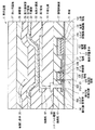
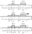
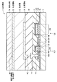
図1は本技術の第1の実施の形態に係る表示装置(表示装置1)の断面構成を表したも
のである。この表示装置1はアクティブマトリクス型の有機EL(Electroluminescence)表示装置であり、基板11上にトランジスタ10Tおよびトランジスタ10Tにより駆動される有機EL素子20をそれぞれ複数有している。図1には、一のトランジスタ10Tおよび有機EL素子20に対応する領域(サブピクセル)を示す。
<First Embodiment>
FIG. 1 illustrates a cross-sectional configuration of a display device (display device 1) according to a first embodiment of the present technology. This
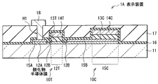
トランジスタ10Tは、基板11上に酸化物半導体膜12,ゲート絶縁膜13Tおよびゲート電極14Tをこの順に有するスタガ構造(トップゲート型)のTFTである。酸化物半導体膜12上にはゲート絶縁膜13Tと共にエッチング保護膜15A,15Bが設けられている。このエッチング保護膜15A,15Bおよびゲート電極14Tは酸化膜16に覆われ、酸化膜16上には層間絶縁膜17が設けられている。一対のソース・ドレイン電極18(一方は図示せず)は、層間絶縁膜17および酸化膜16の接続孔H1(一方は図示せず)を介して酸化物半導体膜12に電気的に接続されている。
The
表示装置1(半導体装置)は、一対のエッチング保護膜15A,15Bのうち一方のエッチング保護膜(エッチング保護膜15B)をトランジスタ10Tと共有する保持容量素子10Cを有している。これらトランジスタ10Tおよび保持容量素子10C上に平坦化膜19を間にして有機EL素子20が設けられている。
The display device 1 (semiconductor device) includes a storage capacitor element 10C that shares one etching protection film (
(トランジスタ10T)
基板11は、例えば、石英,ガラス,シリコンまたは樹脂(プラスチック)フィルムなどの板材により構成されている。後述のスパッタ法において、基板11を加熱することなく酸化物半導体膜12を成膜するため、安価な樹脂フィルムを用いることができる。樹脂材料としては、例えば、PET(ポリエチレンテレフタレート)またはPEN(ポリエチレンナフタレート)などが挙げられる。この他にも、目的に応じて、ステンレス鋼(SUS)などの金属基板を用いるようにしてもよい。
(
The
酸化物半導体膜12は、基板11上の選択的な領域に設けられ、トランジスタ10Tの活性層としての機能を有するものである。酸化物半導体膜12は、例えば、インジウム(In),ガリウム(Ga),亜鉛(Zn)およびスズ(Sn)のうちの少なくとも1種の元素の酸化物を主成分として含むものである。具体的には、非晶質のものとして、酸化インジウムスズ亜鉛(ITZO)または酸化インジウムガリウム亜鉛(IGZO: InGaZnO)等、結晶性のものとして酸化亜鉛(ZnO),酸化インジウム亜鉛(IZO(登録商標)),酸化インジウムガリウム(IGO),酸化インジウムスズ(ITO)または酸化インジウム(InO)等がそれぞれ挙げられる。非晶質あるいは結晶性の酸化物半導体材料のどちらを用いてもよいが、容易にエッチング保護膜15A,15Bとのエッチング選択性を確保することができるため、酸化インジウムスズ亜鉛または結晶性の酸化物半導体材料を用いることが好ましい。酸化物半導体膜12の厚み(積層方向の厚み、以下単に厚みという。)は、例えば50nm程度である。
The
この酸化物半導体膜12は上層のゲート電極14Tに対向してチャネル領域12Tを有すると共に、チャネル領域12Tの両側に隣接して、チャネル領域12Tよりも電気抵抗率の低い低抵抗領域12B(ソース・ドレイン領域)を一対有している。低抵抗領域12Bは酸化物半導体膜12の表面(上面)から厚み方向の一部に設けられたものであり、例えば、酸化物半導体材料にアルミニウム(Al)等の金属を反応させて金属(ドーパント)を拡散させることにより形成されている。トランジスタ10Tでは、この低抵抗領域12Bによりセルフアライン(自己整合)構造が実現される。また、低抵抗領域12Bはトランジスタ10Tの特性を安定化させる役割をも有するものである。低抵抗領域12Bよりも外側の酸化物半導体膜12に接してエッチング保護膜15A,15Bが設けられている。
The
ゲート電極14Tはゲート絶縁膜13Tを間にしてチャネル領域12T上に設けられて
いる。ゲート電極14Tおよびゲート絶縁膜13Tは平面視で互いに同一形状を有してい
る。ゲート絶縁膜13Tは例えば厚みが300nm程度であり、シリコン酸化膜(SiO),シリコン窒化膜(SiN),シリコン窒化酸化膜(SiON)または酸化アルミニウム膜(AlO)などのうちの1種よりなる単層膜あるいはそれらのうちの2種以上よりなる積層膜により構成されている。ゲート絶縁膜13Tには酸化物半導体膜12を還元させにくい材料、例えば、シリコン酸化膜あるいは酸化アルミニウム膜を用いることが好ましい。
The
ゲート電極14Tは、トランジスタ10Tに印加されるゲート電圧(Vg)によって酸
化物半導膜12(チャネル領域12T)中のキャリア密度を制御すると共に、電位を供給
す配線としての機能を有するものである。このゲート電極14Tは、例えばモリブデン(Mo),窒化モリブデニウム(MoN),チタン(Ti),窒化チタン(TiN),アルミニウム,銀(Ag),ネオジウム(Nd)および銅(Cu)のうちの1種からなる単体もしくはこれらの合金により構成されている。複数の単体または合金を用いた積層構造であってもよい。ゲート電極14Tは低抵抗な金属、例えば、アルミニウム,ネオジウムを含有するアルミニウム合金(Al−Nd)または銅等により構成することが好ましい。このような低抵抗な金属からなる層(低抵抗層14TA)に、例えばチタン,窒化チタン,モリブデンまたは窒化モリブデニウムからなる層(バリア層14TB)を積層させるようにしてもよい(図2(A))。2つのバリア層(バリア層14TB,14TC)の間に低抵抗層14TAを挟むようにしてもよい(図2(B))。バリア層14TB,14TCは、エッチングで使用される希フッ酸等の薬液に対する耐性が高いため、例えば、接続孔H1の形成時にこれを用いたウェッエッチングを行うことが可能となる。また、ゲート電極14TはITO等の透明導電膜により構成することも可能である。ゲート電極14Tの厚みは、例えば10nm〜500nmである。
The
エッチング保護膜15Aは、層間絶縁膜17および酸化膜16に接続孔H1を形成する際のエッチングから酸化物半導体膜12を保護するためのものである。エッチング保護膜15Bは、ゲート絶縁膜13Tを間にしてエッチング保護膜15Aに対向すると共に、酸化物半導体膜12の外側に拡幅して保持容量素子10Cの一方の電極(下部電極)を構成している。このエッチング保護膜15Bもエッチング保護膜15Aと同様に、ソース・ドレイン電極18と対をなすソース・ドレイン電極(図示せず)を酸化物半導体膜12に接続するための貫通孔(図示せず)を形成する際のエッチングから酸化物半導体膜12を保護するためのものである。即ち、この一対のエッチング保護膜15A,15Bにより製造工程での酸化物半導体膜12の損傷を防いで、トランジスタ10Tの電気特性を向上させることが可能となる。なお、エッチング保護膜15A,15Bは少なくとも一部が酸化物半導体膜12に接していればよい。
The etching protective film 15 </ b> A is for protecting the
エッチング保護膜15A,15Bは、酸化物半導体膜12の低抵抗領域12Bとソース・ドレイン電極18(一方は図示せず)とを電気的に接続するものでもあり、これらの互いの対向面の位置は、低抵抗領域12Bの端部(エッチング保護膜15A,15B側の端部)の位置と平面視で一致している。このようなエッチング保護膜15A,15Bは例えば酸化物半導体膜12と異なるエッチング選択性を有する金属材料、具体的にはITO,モリブデン膜またはネオジウムを含むアルミニウム膜等により構成されている。エッチング保護膜15A,15Bには低抵抗化した半導体材料、例えばドーパントとしてリン,ボロンまたはヒ素を含むシリコンまたはゲルマニウム等も用いることができる。エッチング保護膜15A,15Bの厚みは、例えば100nm程度である。
The
図3に示したように、エッチング保護膜15Aも酸化物半導体膜12の外側に拡幅させ、この酸化物半導体膜12の外側に対向する位置に接続孔(接続孔H3)を設けるようにしてもよい。接続孔H1,H3のどちらを設けるようにしてもよいが、エッチング保護膜15Aの形成面積を小さくし、酸化物半導体膜12に対向する位置の接続孔H1を設けることが好ましい。これによりトランジスタ10Tを縮小化することができる。
As shown in FIG. 3, the etching
エッチング保護膜15A,15B上の酸化膜16は、ゲート電極14Tとエッチング保護膜15A,15Bそれぞれとの間で酸化物半導体膜12に接している。この酸化膜16は保持容量素子10Cも覆っている。酸化膜16は後述する製造工程において、酸化物半導膜12の低抵抗領域12Bに拡散される金属の供給源となる金属膜が酸化されて残存したものである。酸化膜16は、例えば、厚みが20nm以下程度であり、酸化チタン,酸化アルミニウム,酸化インジウムまたは酸化スズ等により構成されている。これらを複数積層させるようにしてもよい。このような酸化膜16は上記のようなプロセス上の役割の他、トランジスタ10Tにおける酸化物半導体膜12の電気特性を変化させる酸素や水分の影響を低減する機能、即ちバリア機能をも有している。従って、酸化膜16を設けることにより、トランジスタ10Tおよび保持容量素子10Cの電気的特性を安定化させ、層間絶縁膜17の効果をより高めることが可能となる。
The
バリア機能を高めるため、図4に示したように、酸化膜16に例えば、厚み30nm〜50nm程度の酸化アルミニウムまたは窒化シリコンからなる保護膜16Pを積層させるようにしてもよい。これにより、トランジスタ10Tにおける酸化物半導体膜12の電気特性がより安定する。保護膜16Pを設けた場合、接続孔H1は保護膜16Pを貫通する。
In order to enhance the barrier function, a
層間絶縁膜17は酸化膜16上に設けられ、酸化膜16と同様にトランジスタ10Tの外側に延在して保持容量素子10Cを覆っている。この層間絶縁膜17は例えば、アクリル樹脂,ポリイミドまたはシロキサン等の有機材料あるいはシリコン酸化膜,シリコン窒化膜,シリコン酸窒化膜または酸化アルミニウム等の無機材料により構成されている。このような有機材料と無機材料とを積層させるようにしてもよい。有機材料を含有する層間絶縁膜17は、容易にその厚みを例えば2μm程度に厚膜化することが可能となる。このように厚膜化された層間絶縁膜17は、ゲート電極14Tの加工後に形成される段差を十分に被覆して絶縁性を確保することができる。
The
ソース・ドレイン電極18は、層間絶縁膜17上にパターン化して設けられ、層間絶縁膜17および酸化膜16を貫通する接続孔H1(貫通孔)を介してエッチング保護膜15A,15Bに接続されている。ソース・ドレイン電極18は、ゲート電極14Tの直上を回避して設けられていること望ましい。ゲート電極14Tとソース・ドレイン電極18との交差領域に寄生容量が形成されることを防ぐためである。このソース・ドレイン電極18は、例えば厚みが500nm程度であり、上記ゲート電極14Tで挙げた金属または透明導電膜と同様の材料により構成されている。ソース・ドレイン電極18も、アルミニウムまたは銅等の低抵抗金属材料により構成されていることが好ましく、また、低抵抗層とバリア層との積層膜であることがより好ましい。ソース・ドレイン電極18をこのような積層膜により構成することで、配線遅延の少ない駆動が可能になるためである。
The source /
(保持容量素子10C)
保持容量素子10Cはトランジスタ10Tと共に基板11上に設けられ、例えば、後述の画素回路50Aにおいて電荷を保持する容量素子である。この保持容量素子10Cは、基板11側からトランジスタ10Tと共有のエッチング保護膜15B,容量絶縁膜13Cおよび上部電極14Cをこの順に有している。即ち、保持容量素子10Cの下部電極(一方の電極)はエッチング保護膜15Bの一部(電極領域15C)により構成されている。詳細は後述するが、これにより、容量値の印加電圧依存性をなくし、ゲート電圧の大きさに関わらず十分な容量を確保して表示特性を維持することができる。
(Retention capacitance element 10C)
The storage capacitor element 10C is provided on the
容量絶縁膜13Cは、例えばゲート絶縁膜13Tと同一工程により形成されたものであり、ゲート絶縁膜13Tと同一材料により構成され、同一膜厚を有している。容量絶縁膜13Cを無機絶縁材料により構成することにより大きな容量の保持容量素子10Cを得ることができる。また、上部電極14Cも、例えば、ゲート電極14Tと同一工程により構成されたものであり、ゲート電極14Tと同一材料により構成され、同一膜厚を有している。積層構造を有するようにしてもよい(図2)。容量絶縁膜13Cとゲート絶縁膜13T、上部電極14Cとゲート電極14Tをそれぞれ互いに別工程で形成するようにしてもよく、これらを互いに異なる材料、異なる膜厚で形成するようにしてもよい。
The capacitive
(有機EL素子20)
有機EL素子20は、平坦化膜19上に設けられている。この有機EL素子20は平坦化膜19側から第1電極21、画素分離膜22、有機層23および第2電極24をこの順に有しており、素子保護層25により封止されている。素子保護層25上には熱硬化樹脂または紫外線硬化樹脂からなる接着層26を間にして封止用基板27が貼り合わされている。表示装置1は、有機層23で発生した光を基板11側から取り出すボトムエミッション方式(下面発光方式)であってもよく、封止用基板27側から取り出すトップエミッション方式(上面発光方式)であってもよい。
(Organic EL element 20)
The
平坦化膜19は、ソース・ドレイン電極18上および層間絶縁膜17上に、基板11の表示領域(後述の図4 表示領域50)全体に渡り設けられ、接続孔H2を有している。この接続孔H2は、トランジスタ10Tのソース・ドレイン電極18と有機EL素子20の第1電極21とを接続するためのものである。平坦化膜19は、例えばポリイミドまたはアクリル系樹脂により構成されている。
The
第1電極21は、接続孔H2を埋め込むように平坦化膜19上に設けられている。この第1電極21は、例えばアノードとして機能するものであり、素子毎に設けられている。表示装置1がボトムエミッション方式である場合には、第1電極21を透明導電膜、例えば、酸化インジウムスズ(ITO),酸化インジウム亜鉛(IZO)またはインジウム亜鉛オキシド(InZnO)等のいずれかよりなる単層膜またはこれらのうちの2種以上からなる積層膜により構成する。一方、表示装置1がトップエミッション方式である場合には、第1電極21を、反射性の金属、例えば、アルミニウム,マグネシウム(Mg),カルシウム(Ca)およびナトリウム(Na)のうちの少なくとも1種からなる単体金属、またはこれらのうちの少なくとも1種を含む合金よりなる単層膜、あるいは単体金属または合金を積層した多層膜により構成する。
The first electrode 21 is provided on the
第1電極21をソース・ドレイン電極18の表面(有機EL素子20側の面)に接して設けるようにしてもよい。これにより、平坦化膜19を省略し、工程数を減らして表示装置1を製造することが可能となる。
The first electrode 21 may be provided in contact with the surface of the source / drain electrode 18 (the surface on the
画素分離膜22は第1電極21と第2電極24との間の絶縁性を確保すると共に各素子の発光領域を区画分離するためのものであり、各素子の発光領域に対向して開口を有している。この画素分離膜22は例えば、ポリイミド,アクリル樹脂またはノボラック系樹脂などの感光性樹脂により構成されている。 The pixel separation film 22 is for ensuring insulation between the first electrode 21 and the second electrode 24 and for partitioning and separating the light emitting regions of each element. Have. The pixel separation film 22 is made of, for example, a photosensitive resin such as polyimide, acrylic resin, or novolac resin.
有機層23は、画素分離膜22の開口を覆うように設けられている。この有機層23は有機電界発光層(有機EL層)を含み、駆動電流の印加によって発光を生じるものである。有機層23は、例えば基板11(第1電極21)側から、正孔注入層、正孔輸送層、有機EL層および電子輸送層をこの順に有しており、電子と正孔との再結合が有機EL層で生じて光が発生する。有機EL層の構成材料は、一般的な低分子または高分子の有機材料であればよく、特に限定されない。例えば赤、緑および青色を発光する有機EL層が素子毎に塗り分けられていてもよく、あるいは、白色を発光する有機EL層(例えば、赤、緑および青色の有機EL層を積層したもの)が基板11の全面に渡り設けられていてもよい。正孔注入層は、正孔注入効率を高めると共にリークを防止するためのものであり、正孔輸送層は、有機EL層への正孔輸送効率を高めるためのものである。正孔注入層、正孔輸送層あるいは電子輸送層等の有機EL層以外の層は、必要に応じて設けるようにすればよい。
The organic layer 23 is provided so as to cover the opening of the pixel isolation film 22. The organic layer 23 includes an organic electroluminescent layer (organic EL layer), and emits light when a driving current is applied. The organic layer 23 has, for example, a hole injection layer, a hole transport layer, an organic EL layer, and an electron transport layer in this order from the substrate 11 (first electrode 21) side, and recombination of electrons and holes. Is generated in the organic EL layer to generate light. The constituent material of the organic EL layer may be a general low molecular or high molecular organic material, and is not particularly limited. For example, an organic EL layer that emits red, green, and blue may be applied separately for each element, or an organic EL layer that emits white (for example, a stack of red, green, and blue organic EL layers). May be provided over the entire surface of the
第2電極24は、例えば、カソードとして機能するものであり、金属導電膜により構成されている。表示装置1がボトムエミッション方式である場合には、この第2電極24を反射性の金属、例えば、アルミニウム,マグネシウム(Mg),カルシウム(Ca)およびナトリウム(Na)のうちの少なくとも1種からなる単体金属、またはこれらのうちの少なくとも1種を含む合金よりなる単層膜、あるいは単体金属または合金を積層した多層膜により構成する。一方、表示装置1がトップエミッション方式である場合には、第2電極24にITOやIZOなどの透明導電膜を用いる。この第2電極24は、第1電極21と絶縁された状態で例えば各素子に共通して設けられている。
The second electrode 24 functions as, for example, a cathode and is made of a metal conductive film. When the
素子保護層25は、絶縁性材料または導電性材料のいずれにより構成されていてもよい。絶縁性材料としては、例えば、アモルファスシリコン(a−Si),アモルファス炭化シリコン(a−SiC),アモルファス窒化シリコン(a−Si(1-X)NX)またはアモルファスカーボン(a−C)等が挙げられる。 The element protective layer 25 may be made of either an insulating material or a conductive material. Examples of the insulating material include amorphous silicon (a-Si), amorphous silicon carbide (a-SiC), amorphous silicon nitride (a-Si (1-X) N x ), and amorphous carbon (a-C). Can be mentioned.
封止用基板27は、トランジスタ10T,保持容量素子10Cおよび有機EL素子20を間にして基板11と対向するよう、配置されている。封止用基板27には、上記基板11と同様の材料を用いることができる。表示装置1がトップエミッション方式である場合には、封止用基板27に透明材料を用い、封止用基板27側にカラーフィルタや遮光膜を設けるようにしてもよい。表示装置1がボトムエミッション方式である場合には、基板11を透明材料により構成し、例えばカラーフィルタや遮光膜を基板11側に設けておく。
The sealing substrate 27 is disposed so as to face the
(周辺回路および画素回路の構成)
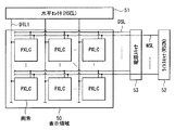
図5に示したように、表示装置1はこのような有機EL素子20を含む画素PXLCを複数有しており、画素PXLCは基板11上の表示領域50に例えばマトリクス状に配置されている。表示領域50の周辺には信号線駆動回路としての水平セレクタ(HSEL)51、走査線駆動回路としてのライトスキャナ(WSCN)52および電源線駆動回路としての電源スキャナ53が設けられている。
(Configuration of peripheral circuit and pixel circuit)
As shown in FIG. 5, the
表示領域50では、列方向に複数(整数n個)の信号線DTL1〜DTLnが、行方向に複数(整数m個)の走査線WSL1〜WSLmがそれぞれ配置されている。これら信号線DTLと走査線DSLとの各交差点に、画素PXLC(R,G,Bに対応する画素のいずれか1つ)が設けられている。各信号線DTLは、水平セレクタ51に電気的に接続され、水平セレクタ51から信号線DTLを介して各画素PXLCに映像信号が供給される。一方、各走査線WSLは、ライトスキャナ52に電気的に接続され、ライトスキャナ52から走査線WSLを介して各画素PXLCに走査信号(選択パルス)が供給される。各電源線DSLは電源スキャナ53に接続され、電源スキャナ53から電源線DSLを介して各画素PXLCに電源信号(制御パルス)が供給される。
In the
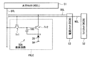
図6は、画素PXLCにおける具体的な回路構成例を表したものである。各画素PXLCは、有機EL素子20を含む画素回路50Aを有している。この画素回路50Aは、サンプリング用トランジスタTr1および駆動用トランジスタTr2と、保持容量素子10Cと、有機EL素子20とを有するアクティブ型の駆動回路である。なお、サンプリング用トランジスタTr1および駆動用トランジスタTr2のうち少なくともいずれか1つが、上記トランジスタ10Tに相当する。
FIG. 6 illustrates a specific circuit configuration example in the pixel PXLC. Each pixel PXLC has a
サンプリング用トランジスタTr1は、そのゲートが対応する走査線WSLに接続され、そのソースおよびドレインのうちの一方が対応する信号線DTLに接続され、他方が駆動用トランジスタTr2のゲートに接続されている。駆動用トランジスタTr2は、そのドレインが対応する電源線DSLに接続され、ソースが有機EL素子20のアノードに接続されている。また、この有機EL素子20のカソードは、接地配線5Hに接続されている。なお、この接地配線5Hは、全ての画素PXLCに対して共通に配線されている。保持容量素子10Cは、駆動用トランジスタTr2のソースとゲートとの間に配置されている。
The sampling transistor Tr1 has its gate connected to the corresponding scanning line WSL, one of its source and drain connected to the corresponding signal line DTL, and the other connected to the gate of the driving transistor Tr2. The drain of the driving transistor Tr2 is connected to the corresponding power supply line DSL, and the source is connected to the anode of the
サンプリング用トランジスタTr1は、走査線WSLから供給される走査信号(選択パルス)に応じて導通することにより、信号線DTLから供給される映像信号の信号電位をサンプリングし、保持容量素子10Cに保持するものである。駆動用トランジスタTr2は、所定の第1電位(図示せず)に設定された電源線DSLから電流の供給を受け、保持容量素子10Cに保持された信号電位に応じて、駆動電流を有機EL素子20へ供給するものである。有機EL素子20は、この駆動用トランジスタTr2から供給された駆動電流により、映像信号の信号電位に応じた輝度で発光するようになっている。
The sampling transistor Tr1 conducts according to the scanning signal (selection pulse) supplied from the scanning line WSL, thereby sampling the signal potential of the video signal supplied from the signal line DTL and holding it in the holding capacitor element 10C. Is. The driving transistor Tr2 is supplied with a current from a power supply line DSL set to a predetermined first potential (not shown), and drives the driving current according to the signal potential held in the holding capacitor element 10C as an organic EL element. 20 is supplied. The
このような回路構成では、走査線WSLから供給される走査信号(選択パルス)に応じてサンプリング用トランジスタTr1が導通することにより、信号線DTLから供給された映像信号の信号電位がサンプリングされ、保持容量素子10Cに保持される。また、上記第1電位に設定された電源線DSLから駆動用トランジスタTr2へ電流が供給され、保持容量素子10Cに保持された信号電位に応じて、駆動電流が有機EL素子20(赤色、緑色および青色の各有機EL素子)へ供給される。そして、各有機EL素子20は、供給された駆動電流により、映像信号の信号電位に応じた輝度で発光する。これにより、表示装置1において、映像信号に基づく映像表示がなされる。
In such a circuit configuration, the sampling transistor Tr1 is turned on according to the scanning signal (selection pulse) supplied from the scanning line WSL, whereby the signal potential of the video signal supplied from the signal line DTL is sampled and held. It is held by the capacitive element 10C. In addition, a current is supplied from the power supply line DSL set to the first potential to the driving transistor Tr2, and the driving current is changed to the organic EL element 20 (red, green and red) according to the signal potential held in the holding capacitor element 10C. To each blue organic EL element). Each
この表示装置1は、例えば次のようにして製造することができる。
The
(トランジスタ10Tおよび保持容量素子10Cを形成する工程)
まず、図7(A)に示したように、基板11上に上述した材料よりなる酸化物半導体膜12を形成する。具体的には、まず基板11の全面にわたって、例えばスパッタリング法により、酸化物半導体材料膜(図示せず)を例えば50nm程度の厚みで成膜する。この際、ターゲットとしては、成膜対象の酸化物半導体と同一組成のセラミックを用いる。また、酸化物半導体中のキャリア濃度は、スパッタリングの際の酸素分圧に大きく依存するので、所望のトランジスタ特性が得られるように酸素分圧を制御する。酸化物半導体膜12を上述の酸化インジウムスズ亜鉛または結晶性材料により構成しておくと、後述のエッチング保護膜15A,15B、ゲート絶縁膜13Tそれぞれのエッチング工程において、容易にエッチング選択性を向上させることができる。次いで、例えばフォトリソグラフィおよびエッチングにより、成膜した酸化物半導体材料膜を所定の形状にパターニングする。その際、リン酸、硝酸および酢酸の混合液を用いたウェットエッチングにより加工することが好ましい。リン酸、硝酸および酢酸の混合液は、下地との選択比を十分に大きくすることが可能であり、比較的容易に加工が可能となる。
(Process of forming
First, as illustrated in FIG. 7A, the
続いて、図7(B)に示したように、酸化物半導体膜12上にエッチング保護膜15A,15Bを形成する。具体的には、酸化物半導体膜12上および基板11上に上述の金属材料または低抵抗化した半導体材料等を成膜したのち、これをエッチングして形成する。エッチング保護膜15Bは、酸化物半導体膜12上から酸化物半導体膜12の外側に延在させる。エッチング保護膜15A,15Bを例えば、ITO,モリブデン膜またはネオジウムを含むアルミニウム膜等の金属材料、酸化物半導体膜12を酸化インジウムスズ亜鉛または結晶性酸化物半導体材料によりそれぞれ構成する場合、例えばリン酸、硝酸および酢酸の混合液を用いたウェットエッチングを行うことができる。一方、エッチング保護膜15A,15Bを例えば、リン,ボロンまたはヒ素等のドーパントを含有するシリコン膜またはゲルマニウム膜により構成する場合、フッ素等を含むガス雰囲気中でのドライエッチングを行うことができる。このドライエッチングでは、非晶質の酸化物半導体膜12であっても、これを残した状態でエッチング保護膜15A,15Bが形成される。リン酸、硝酸および酢酸の混合液でエッチングされにくい金属材料によりエッチング保護膜15A,15Bを構成する場合にもこのドライエッチングを用いることが可能である。
Subsequently, as illustrated in FIG. 7B, etching protective films 15 </ b> A and 15 </ b> B are formed over the
エッチング保護膜15A,15Bを形成した後、図7(C)に示したように、基板11の全面に渡って例えば厚み200nmのシリコン酸化膜または酸化アルミニウム膜よりなる絶縁膜13および厚み500nmモリブデン,チタンまたはアルミニウム等の金属材料からなる導電膜14をこの順に成膜する。絶縁膜13は、例えばプラズマCVD(Chemical Vapor Deposition ;化学気相成長)法により成膜することができる。シリコン酸化膜からなる絶縁膜13はプラズマCVD法のほか、反応性スパッタリング法により形成することも可能である。また、絶縁膜13に酸化アルミニウム膜を用いる場合には、上記反応性スパッタリング法,CVD法に加え、原子層成膜法を用いることも可能である。導電膜14は、例えばスパッタリング法により形成することができる。
After forming the
導電膜14を成膜した後、この導電膜14を、例えばフォトリソグラフィおよびエッチングによりパターニングし、酸化物半導体膜12上の選択的な領域にゲート電極14Tおよび上部電極14Cを形成する。次いで、このゲート電極14T、上部電極14Cをマスクとして絶縁膜13をエッチングする。これにより、ゲート絶縁膜13Tがゲート電極14Tと、容量絶縁膜13Cが上部電極14Cとそれぞれ平面視で略同一形状にパターニングされる(図8(A))。酸化物半導体膜12が上記結晶性材料により構成されている場合には、このエッチング工程でフッ酸等の薬液を用いることにより、非常に大きなエッチング選択比を維持して容易に加工することができる。保持容量素子10Cの容量絶縁膜13Cおよび上部電極14Cは、ゲート電極14Tおよびゲート絶縁膜13Tを形成した後、絶縁膜13、導電膜14とは別の材料を用いて形成するようにしてもよい。
After the
ゲート電極14Tが例えばアルミニウムからなる低抵抗層14TAと窒化チタンからなるバリア層14TBとの積層構造を有する場合(図2(A))には、以下のようにしてゲート電極14Tを形成することも可能である。まず、図9(A)に示したように、絶縁膜13上に例えばアルミニウムからなる導電膜14MA、窒化チタンからなる導電膜14MBをスパッタリング法により成膜した後、フォトリソグラフィ工程を経て導電膜14MB上にレジスト30のパターンを形成する。次いで、導電膜14MBおよび導電膜14MAに例えばドライエッチングを行った後、続けて絶縁膜13もドライエッチングし(図9(B))、レジスト30を除去する(図9(C))。これにより、低抵抗層14TAおよびバリア層14TBからなるゲート電極14Tを形成することができる。
When the
また、ゲート電極14Tが例えばゲート絶縁膜13T側から、チタンからなるバリア層14TC、アルミニウムからなる低抵抗層14TAおよびモリブデンからなるバリア層14TBにより構成されている場合(図2(B))には、以下のようにしてゲート電極14Tを形成することも可能である。まず、図10(A)に示したように、絶縁膜13上に例えばチタンからなる導電膜14MC、アルミニウムからなる導電膜14MAおよびモリブデンからなる導電膜14MBをスパッタリング法により成膜した後、フォトリソグラフィ工程を経て導電膜14MB上にレジスト30のパターンを形成する。次いで、導電膜14MBおよび導電膜14MAに例えばリン酸、硝酸および酢酸の混合液を用いたウェットエッチングを行った後(図10(B))、例えば塩素ガスにより導電膜14MCのドライエッチングを行う。このようにウェットエッチングおよびドライエッチングを用いてゲート電極14Tを形成することにより欠陥が少なく、かつ電気特性の高いトランジスタ10Tを形成することが可能となる。これは以下のような理由による。導電膜14MAを構成するアルミニウムはドライエッチングの際にパーティクルが発生して欠陥を生じ易い。ここでは、ウェットエッチングを用いて導電膜14MAをパターニングすることにより、この欠陥の発生を防ぐことができる。また、トランジスタのチャネルの線幅は電気特性に大きく影響するが、これを導電膜14MCのドライエッチングにより精密に制御することが可能となる。
In the case where the
導電膜14MCをエッチングした後、絶縁膜13のエッチング(図10(C))およびレジスト30の除去(図10(D))を行って、低抵抗層14TAおよびバリア層14TB,14TCからなるゲート電極14Tを完成させる。
After etching the conductive film 14MC, the insulating
ゲート電極14T,上部電極14C,ゲート絶縁膜13Tおよび容量絶縁膜13を形成した後、図8(B)に示したように、基板11上の全面に渡って、例えばスパッタリング法または原子層成膜法により、例えばチタン,アルミニウム,スズまたはインジウム等からなる金属膜16Aを例えば5nm以上10nm以下の厚みで成膜する。金属膜16Aは酸素と比較的低温で反応する金属により構成し、ゲート電極14T(ゲート絶縁膜13T)とエッチング保護膜15A,15Bそれぞれとの間で酸化物半導体膜12に接触させて形成する。金属膜16Aを形成した後、例えば、スパッタリング法または原子層成膜法により厚み50nm程度の酸化アルミニウム膜からなる保護膜16P(図4)を形成するようにしてもよい。
After forming the
次いで、図8(C)に示したように、例えば200℃程度の温度で熱処理を行うことにより金属膜16Aが酸化され、これによって酸化膜16が形成される。この際、酸化物半導体膜12の酸化膜16が接する部分、即ちチャネル領域12Tに隣接する位置には、その厚み方向の酸化膜16側の一部に低抵抗領域12Bが形成される。この金属膜16Aの酸化反応には、酸化物半導体膜12に含まれる酸素の一部が利用されるため、金属膜16Aの酸化の進行に伴って、酸化物半導体膜12では、その金属膜16Aと接する表面(上面)側から酸素濃度が低下していく。一方、金属膜16Aからアルミニウム等の金属が酸化物半導体膜12中に拡散する。この金属元素がドーパントとして機能し、金属膜16Aと接する酸化物半導体膜12の上面側の領域が低抵抗化される。これにより、チャネル領域12Tよりも電気抵抗の低い低抵抗領域12Bが形成される。
Next, as shown in FIG. 8C, the heat treatment is performed at a temperature of about 200 ° C., for example, to oxidize the
金属膜16Aの熱処理としては、上述のように200℃程度の温度でアニールすることが好ましい。その際、酸素等を含む酸化性のガス雰囲気でアニールを行うことで、低抵抗領域12Bの酸素濃度が低くなりすぎるのを抑え、酸化物半導体膜12に十分な酸素を供給することが可能となる。これにより、後工程で行うアニール工程を削減して工程の簡略化を行うことが可能となる。
As the heat treatment of the
酸化膜16は、上記アニール工程に代えて、例えば、基板11上に金属膜16Aを形成する際の基板11の温度を比較的高めに設定することにより形成するようにしてもよい。例えば、図8(B)の工程で、基板11の温度を200℃程度に保ちつつ金属膜16Aを成膜すると、熱処理を行わずに酸化物半導体膜12の所定の領域を低抵抗化することができる。この場合には、酸化物半導体膜12のキャリア濃度をトランジスタとして必要なレベルに低減することが可能である。
The
金属膜16Aは、上述のように10nm以下の厚みで成膜することが好ましい。金属膜16Aの厚みを10nm以下とすれば、熱処理によって金属膜16Aを完全に酸化させる(酸化膜16を形成する)ことができるからである。金属膜16Aが完全に酸化されていない場合には、この未酸化の金属膜16Aをエッチングにより除去する工程が必要となる。十分に酸化されていない金属膜16Aがゲート電極14T上および上部電極14C上などに残存しているとリーク電流が発生する虞があるためである。金属膜16Aが完全に酸化され、酸化膜16が形成された場合には、そのような除去工程が不要となり、製造工程の簡略化が可能となる。つまり、エッチングによる除去工程を行わなくとも、リーク電流の発生を防止できる。なお、金属膜16Aを10nm以下の厚みで成膜した場合、熱処理後の酸化膜16の厚みは、20nm以下程度となる。
The
金属膜16Aを酸化させる方法としては、上記のような熱処理のほか、水蒸気雰囲気での酸化またはプラズマ酸化などの方法を用いることも可能である。特にプラズマ酸化の場合、次のような利点がある。酸化膜16の形成後、層間絶縁膜17をプラズマCVD法により形成するが(後述の図11(A))、金属膜16Aに対してプラズマ酸化処理を施した後、続けて(連続的に)、層間絶縁膜17を成膜可能である。従って、工程を増やす必要がないという利点がある。プラズマ酸化は例えば、基板11の温度を200℃〜400℃程度にし、酸素および二窒化酸素の混合ガス等の酸素を含むガス雰囲気中でプラズマを発生させて処理することが望ましい。これにより、上述したような外気に対して良好なバリア性を有する酸化膜16を形成することができるからである。
As a method for oxidizing the
酸化膜16を形成した後、図11(A)に示したように、酸化膜16上の全面にわたって、層間絶縁膜17を形成する。層間絶縁膜17が無機絶縁材料を含む場合には、例えばプラズマCVD法,スパッタリング法あるいは原子層成膜法を用い、層間絶縁膜17が有機絶縁材料を含む場合には、例えばスピンコート法やスリットコート法などの塗布法を用いることができる。塗布法により、厚膜化された層間絶縁膜17を容易に形成することができる。続いて、露光、現像工程を行い、層間絶縁膜17の所定の箇所に接続孔H1を形成する。層間絶縁膜17に感光性樹脂を用いた場合には、この感光性樹脂により露光、現像を行うことが可能である。
After the
本実施の形態では、エッチング保護膜15A,15Bが設けられているので、酸化物半導体膜12を傷つけずに酸化膜16を貫通する接続孔H1を形成することができる(図11(B))。以下、これについて説明する。
In this embodiment, since the etching
図12は、比較例に係る表示装置(表示装置100)のトランジスタ(トランジスタ100T)および保持容量素子(保持容量素子100C)の断面構成を表したものである。このトランジスタ100Tはエッチング保護膜を有しておらず、一対のソース・ドレイン電極18(一方は図示せず)が直接、酸化物半導体膜12の低抵抗領域12Bに接続されている。
FIG. 12 illustrates a cross-sectional configuration of a transistor (
このようなトランジスタ100Tでは、酸化物半導体膜12および酸化膜16のうち、酸化膜16のみを選択的にエッチングして接続孔H1を形成することが困難である(図13(A),図13(B))。これは、酸化膜16のエッチングレートが、酸化物半導体膜12のエッチングレートと比較して低いことに起因している。
In such a
これに対し、トランジスタ10Tでは、酸化物半導体膜12上にエッチング保護膜15A,15Bが設けられているので、エッチング保護膜15A,15Bのエッチングレートを調整して酸化膜16との間のエッチング選択性を高めることが可能となる。即ち、エッチング保護膜15A,15Bの上部に酸化膜16を貫通する接続孔H1を容易に形成することができる。例えば、エッチング保護膜15A,15Bがモリブデン膜、酸化膜16が酸化アルミニウム膜である場合には、希フッ酸を用いることにより、酸化膜16のみを容易に除去することが可能である。従って、酸化物半導体膜12をエッチングすることなく、ソース・ドレイン電極18と酸化物半導体膜12の低抵抗領域12B(エッチング保護膜15A)との間の電気的な接続を確保することができる。
On the other hand, in the
また、上述のように酸化膜16上に保護膜16Pを設けることが好ましいが、このバリア機能の高い保護膜16Pに用いる材料は、非常にエッチングされにくいものが多い。トランジスタ10Tでは、厚く、かつ、高いバリア機能を有する保護膜16Pが設けられている場合にも、エッチング保護膜15A,15Bにより、酸化物半導体膜12を保護することができる。
In addition, it is preferable to provide the
接続孔H1を形成した後、層間絶縁膜17上に、例えばスパッタリング法により、上述のソース・ドレイン電極18の構成材料からなる導電膜(図示せず)を形成し、この導電膜によりコンタクトホールH1を埋め込む。そののち、この導電膜を例えばフォトリソグラフィおよびエッチングにより所定の形状にパターニングする。これにより、層間絶縁膜17上に一対のソース・ドレイン電極18が形成されると共に、ソース・ドレイン電極18が接続孔H1を介してエッチング保護膜15A,15Bに電気的に接続される(図11(C))。以上により、基板11上に、トランジスタ10Tおよび保持容量素子10Cを形成する。
After the connection hole H1 is formed, a conductive film (not shown) made of the constituent material of the source /
(平坦化膜19を形成する工程)
続いて、層間絶縁膜17およびソース・ドレイン電極18を覆うように、上述した材料よりなる平坦化膜19を、例えばスピンコート法やスリットコート法により成膜し、ソース・ドレイン電極18に対向する領域の一部に接続孔H2を形成する。
(Step of forming the planarizing film 19)
Subsequently, a
(有機EL素子20を形成する工程)
次いで、この平坦化膜19上に、有機EL素子20を形成する。具体的には、平坦化膜19上に、接続孔H2を埋め込むように、上述した材料よりなる第1電極21を例えばスパッタリング法により成膜した後、フォトリソグラフィおよびエッチングによりパターニングする。この後、第1電極21上に開口を有する画素分離膜22を形成した後、有機層23を例えば真空蒸着法により成膜する。続いて、有機層23上に、上述した材料よりなる第2電極24を例えばスパッタリング法により形成する。次いで、この第2電極24上に保護層25を例えばCVD法により成膜した後、この保護層25上に、接着層26を用いて封止用基板27を貼り合わせる。以上により、図1に示した表示装置1を完成する。
(Step of forming organic EL element 20)
Next, an
この表示装置1では、例えばR,G,Bのいずれかに対応する各画素PXLCに、各色の映像信号に応じた駆動電流が印加されると、第1電極21および第2電極24を通じて、有機層23に電子および正孔が注入される。これらの電子および正孔は、有機層23に含まれる有機EL層においてそれぞれ再結合され、発光を生じる。このようにして、表示装置1では、例えばR,G,Bのフルカラーの映像表示がなされる。また、この映像表示動作の際に保持容量素子10Cの一端に、映像信号に対応する電位が印加されることにより、保持容量素子10Cには、映像信号に対応する電荷が蓄積される。
In the
ここでは、酸化物半導体膜12上にエッチング保護膜15A,15Bが設けられているので、容易に酸化膜16を貫通する接続孔H1を形成し、ソース・ドレイン電極18とエッチング保護膜15A,15Bとを接続することができる。即ち、酸化物半導体膜12はエッチングされることなく、エッチング保護膜15A,15Bを介してソース・ドレイン電極18に電気的に接続される。
Here, since the etching
また、表示装置1では、保持容量素子10Cの電圧依存性をなくし、表示品位を高めることができる。
In the
比較例の保持容量素子100C(図12)は、酸化物半導体膜12、容量絶縁膜13Cおよび上部電極14Cにより構成されている。酸化物半導体膜12のうち、保持容量素子100Cを構成する部分は、チャネル領域12Tと同じ抵抗率の容量領域12Cである。このような保持容量素子100Cでは、下部電極が酸化物半導体膜12により構成されているので、容量に電圧依存性が生じ、表示品位が低下する虞がある。
The storage capacitor element 100C (FIG. 12) of the comparative example includes the
これに対し、表示装置1では、保持容量素子10Cの下部電極がエッチング保護膜15Bの電極領域15Cにより構成されているので、保持容量素子10Cの容量を印加電圧の大きさに左右されることなく、常に十分に確保することが可能となる。従って、表示装置1では高い表示品位を実現することができる。
On the other hand, in the
このように本実施の形態では、エッチング保護膜15A,15Bを設けるようにしたので、製造工程での酸化物半導体膜12の損傷を防ぎ、トランジスタ10Tの電気特性を向上させることができる。また、保持容量素子10Cの電圧依存性をなくし、高い表示品位を実現することも可能である。即ち、少ない工程数でトランジスタ10Tの電気特性の向上および保持容量素子10Cの容量の安定化を実現できる。
As described above, in this embodiment, since the etching
更に、酸化膜16上に高いバリア機能を有する保護膜16Pを厚く設けることが可能となり、トランジスタ10Tの電気特性を安定化することができる。
Further, it is possible to provide a thick
以下、本実施の形態の変形例および他の実施の形態について説明するが、以降の説明において上記実施の形態と同一構成部分については同一符号を付してその説明は適宜省略する。 Hereinafter, modifications of the present embodiment and other embodiments will be described. In the following description, the same components as those of the above-described embodiment will be denoted by the same reference numerals, and description thereof will be omitted as appropriate.
<変形例1>
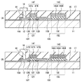
図14は、上記第1の実施の形態の変形例1に係る表示装置(表示装置1A)のトランジスタ10Tおよび保持容量素子10Cの断面構成を表したものである。この表示装置1Aでは、トランジスタ10Tの酸化物半導体膜(酸化物半導体膜12A)が保持容量素子10Cと基板11との間に延在している。この点を除き、表示装置1Aは上記実施の形態の表示装置1と同様の構成を有し、その作用および効果も同様である。
<
FIG. 14 illustrates a cross-sectional configuration of the
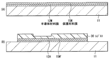
酸化物半導体膜12Aは、チャネル保護膜15Bの下面(基板11との対向面)全面に接して設けられ、その側面の位置はチャネル保護膜15A,15Bの側面(互いの対向面と反対側の面)の位置と平面視で一致している。このような酸化物半導体膜12およびエッチング保護膜15A,15Bは、共に一のフォトリソグラフィ工程で形成することができる。
The
まず、図15(A)に示したように、基板11の全面に酸化物半導体膜12の構成材料からなる半導体材料膜12Mおよびエッチング保護膜15A,15Bの構成材料からなる保護材料膜15Mを例えば、スパッタリング法によりこの順に成膜する。次いで、ハーフトーンマスクを用いたフォトリソグラフィにより、保護材料膜15上に面内の位置により膜厚が異なるレジスト(レジスト30)を形成した後、半導体材料膜12Mをエッチングして、酸化物半導体膜12Aを形成する(図15(B))。このとき、半導体材料膜12Mと共に保護材料膜15Mがエッチングされて平面視で酸化物半導体膜12Aと同一形状の保護材料膜15M’が形成される。即ち、酸化物半導体膜12Aの側面の位置と保護材料膜15M’(エッチング保護膜15A,15B)の側面の位置とが一致する。ハーフトーンマスクにより、酸化物半導体膜12Aのチャネル領域12および低抵抗領域12Bの形成予定領域に対向する位置のレジスト30の膜厚を、これ以外の部分の膜厚よりも薄く形成しておく。
First, as shown in FIG. 15A, a
続いて、このレジスト30の全面を酸素プラズマ等により、アッシングして膜厚の薄い部分のレジスト30を除去した後、露出された保護材料膜15M’をエッチングする。これにより、エッチング保護膜15A,15Bが形成される。保護材料膜15M’のエッチングには、上記第1の実施の形態で説明したように、例えばリン酸、硝酸および酢酸の混合液を用いたウェットエッチングまたはフッ素等含むガス雰囲気中でのドライエッチングなどを用いることができる。
Subsequently, ashing is performed on the entire surface of the resist 30 with oxygen plasma or the like to remove the thin portion of the resist 30, and then the exposed
エッチング保護膜15A,15Bを形成した後、残存したレジスト30を除去し(図16(A))、基板11上にゲート絶縁膜13T,容量絶縁膜13C、ゲート電極14T,上部電極14C、酸化膜16を設けると共に、酸化物半導体膜12Aに低抵抗領域12Bを形成する(図16(B))。続いて、上記第1の実施の形態と同様にして層間絶縁膜17およびソース・ドレイン電極18を形成することにより、トランジスタ10Tおよび保持容量素子10Cを完成させる。このような表示装置1Aでは、フォトリソグラフィの工程を増やすことなく高い電気特性を有するトランジスタ10Tおよび安定した容量の保持容量素子10Cを得ることができる。
After the
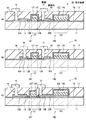
<変形例2>
図17は、上記第1の実施の形態の変形例2に係る表示装置(表示装置1B)のトランジスタ10Tおよび保持容量素子10Cの断面構成を表したものである。この表示装置1Bは、酸化物半導体膜12の低抵抗領域12Bと電極領域15Cを有するエッチング保護膜15Bとを電気的に接続するための配線31を有するものである。この点を除き、表示装置1Bは上記実施の形態の表示装置1と同様の構成を有し、その作用および効果も同様である。
<Modification 2>
FIG. 17 illustrates a cross-sectional configuration of the
配線31は、トランジスタ10Tと保持容量素子10Cとをより電気的に安定な状態で接続するためのものであり、例えば、ソース・ドレイン電極18と同様の導電材料により構成されている。この配線31は、層間絶縁膜17および酸化膜16を貫通する接続孔(接続孔H4)を埋めると共に酸化物半導体膜12の低抵抗領域12Bとエッチング保護膜15Bとに接している。配線31をソース・ドレイン電極18と同層に、同一工程で形成することが可能であるが、ソース・ドレイン電極18と異なる層に別の工程で設けるようにしてもよい。ソース・ドレイン電極18とエッチング保護膜15Aとは、図17(A)に示したように、酸化物半導体膜12の外側に対向する位置に設けられた接続孔H3を介して接続されていてもよく、図17(B)に示したように、酸化物半導体膜12に対向する位置に設けられた接続孔H1を介して接続されていてもよい。また、図17(C)に示したように、酸化物半導体膜12の側面の位置とエッチング保護膜15A,15Bの側面の位置とが揃っていてもよい。配線31が、ソース・ドレイン電極の一方を構成するようにしてもよい。
The
<第2の実施の形態>
図18は、本技術の第2の実施の形態に係る表示装置(表示装置2)の断面構成を表したものである。この表示装置2は、上記第1の実施の形態(表示装置1)の有機EL素子20に代えて液晶表示素子40を有するものである。この点を除き、表示装置2は上記実施の形態の表示装置1と同様の構成を有し、その作用および効果も同様である。
<Second Embodiment>
FIG. 18 illustrates a cross-sectional configuration of a display device (display device 2) according to the second embodiment of the present technology. This display device 2 has a liquid crystal display element 40 instead of the
表示装置2は、表示装置1と同様のトランジスタ10Tおよび保持容量素子10Cを有するものであり、このトランジスタ10Tおよび保持容量素子10Cの上層に平坦化膜19を間にして液晶表示素子40が設けられている。
The display device 2 includes a
液晶表示素子40は、例えば、画素電極41と対向電極42との間に液晶層43を封止したものであり、画素電極41および対向電極42の液晶層43側の各面には、配向膜44A,44Bが設けられている。画素電極41は、画素毎に配設されており、例えばトランジスタ10Tのソース・ドレイン電極18に電気的に接続されている。対向電極42は、対向基板45上に複数の画素に共通の電極として設けられ、例えばコモン電位に保持されている。液晶層43は、例えばVA(Vertical Alignment:垂直配向)モード,TN(Twisted Nematic)モードあるいはIPS(In Plane Switching)モード等により駆動される液晶により構成されている。
In the liquid crystal display element 40, for example, a liquid crystal layer 43 is sealed between a pixel electrode 41 and a counter electrode 42. An alignment film is formed on each surface of the pixel electrode 41 and the counter electrode 42 on the liquid crystal layer 43 side. 44A and 44B are provided. The pixel electrode 41 is provided for each pixel and is electrically connected to, for example, the source /
また、基板11の下方には、バックライト46が備えられており、基板11のバックライト46側および対向基板45上には、偏光板47A,47Bが貼り合わせられている。
Further, a backlight 46 is provided below the
バックライト46は、液晶層43へ向けて光を照射する光源であり、例えばLED(Light Emitting Diode)やCCFL(Cold Cathode Fluorescent Lamp )等を複数含むものである。このバックライト46は、図示しないバックライト駆動部によって、点灯状態および消灯状態が制御されるようになっている。 The backlight 46 is a light source that irradiates light toward the liquid crystal layer 43 and includes, for example, a plurality of LEDs (Light Emitting Diodes), CCFLs (Cold Cathode Fluorescent Lamps), and the like. The backlight 46 is controlled to be turned on and off by a backlight driving unit (not shown).
偏光板47A,47B(偏光子,検光子)は、例えば互いにクロスニコルの状態で配置されており、これにより、例えばバックライト46からの照明光を電圧無印加状態(オフ状態)では遮断、電圧印加状態(オン状態)では透過させるようになっている。 The polarizing plates 47A and 47B (polarizers and analyzers) are arranged, for example, in a crossed Nicols state, so that, for example, the illumination light from the backlight 46 is cut off when no voltage is applied (off state). In the applied state (on state), the light is transmitted.
この表示装置2では、上記実施の形態の表示装置1と同様に、エッチング保護膜15A,15Bにより酸化物半導体膜12が保護される。これにより、本実施の形態においても、トランジスタ10Tの電気特性を向上させることができる。
In the display device 2, the
<第3の実施の形態>
図19は、本技術の第3の実施の形態に係る表示装置(表示装置3)の断面構成を表したものである。この表示装置3は所謂電子ペーパーであり、表示装置1の有機EL素子20に代えて電気泳動型表示素子50を有している。この点を除き、表示装置3は上記実施の形態の表示装置1と同様の構成を有し、その作用および効果も同様である。
<Third Embodiment>
FIG. 19 illustrates a cross-sectional configuration of a display device (display device 3) according to the third embodiment of the present technology. The display device 3 is so-called electronic paper, and includes an
表示装置3は、表示装置1と同様のトランジスタ10Tおよび保持容量素子10Cを有するものであり、このトランジスタ10Tおよび保持容量素子10Cの上層に平坦化膜19を間にして電気泳動型表示素子50が設けられている。
The display device 3 includes a
電気泳動型表示素子50は、例えば、画素電極51と共通電極52との間に電気泳動型表示体よりなる表示層53を封止したものである。画素電極51は、画素毎に配設されており、例えばトランジスタ10Tのソース・ドレイン電極17に電気的に接続されている。共通電極52は、対向基板54上に複数の画素に共通の電極として設けられている。
In the
この表示装置3では、上記実施の形態の表示装置1と同様に、エッチング保護膜15A,15Bにより酸化物半導体膜12が保護される。これにより、本実施の形態においても、トランジスタ10Tの電気特性を向上させることができる。
In the display device 3, the
(適用例)
以下、上記のような表示装置(表示装置1,1A,1B,2,3)の電子機器への適用例について説明する。電子機器としては、例えばテレビジョン装置,デジタルカメラ,ノート型パーソナルコンピュータ、携帯電話等の携帯端末装置あるいはビデオカメラ等が挙げられる。言い換えると、上記表示装置は、外部から入力された映像信号あるいは内部で生成した映像信号を、画像あるいは映像として表示するあらゆる分野の電子機器に適用することが可能である。
(Application example)
Hereinafter, application examples of the display devices (
(モジュール)
上記表示装置は、例えば図20に示したようなモジュールとして、後述の適用例1〜7
などの種々の電子機器に組み込まれる。このモジュールは、例えば、基板11の一辺に、封止用基板27または対向基板45,54から露出した領域61を設け、この露出した領域61に、水平セレクタ51、ライトスキャナ52および電源スキャナ53の配線を延長して外部接続端子(図示せず)を形成したものである。この外部接続端子には、信号の入出力のためのフレキシブルプリント配線基板(FPC;Flexible Printed Circuit)62が設けられていてもよい。
(module)
The display device is, for example, a module as shown in FIG.
Embedded in various electronic devices. In this module, for example, a
(適用例1)
図21(A)および図21(B)はそれぞれ、上記実施の形態の表示装置が適用される電子ブックの外観を表したものである。この電子ブックは、例えば、表示部210および非表示部220を有しており、この表示部210が上記実施の形態の表示装置により構成されている。
(Application example 1)
FIG. 21A and FIG. 21B each illustrate the appearance of an electronic book to which the display device of the above embodiment is applied. The electronic book has, for example, a
(適用例2)
図22は、上記実施の形態の表示装置が適用されるスマートフォンの外観を表したものである。このスマートフォンは、例えば、表示部230および非表示部240を有しており、この表示部230が上記実施の形態の表示装置により構成されている。
(Application example 2)
FIG. 22 illustrates the appearance of a smartphone to which the display device of the above embodiment is applied. This smartphone has, for example, a display unit 230 and a non-display unit 240, and the display unit 230 is configured by the display device of the above embodiment.
(適用例3)
図23は、上記実施の形態の表示装置が適用されるテレビジョン装置の外観を表したものである。このテレビジョン装置は、例えば、フロントパネル310およびフィルターガラス320を含む映像表示画面部300を有しており、この映像表示画面部300は、上記実施の形態の表示装置により構成されている。
(Application example 3)
FIG. 23 illustrates an appearance of a television device to which the display device of the above embodiment is applied. This television apparatus has, for example, a video display screen unit 300 including a front panel 310 and a filter glass 320, and the video display screen unit 300 is configured by the display device of the above embodiment.
(適用例4)
図24は、上記実施の形態の表示装置が適用されるデジタルカメラの外観を表したものである。このデジタルカメラは、例えば、フラッシュ用の発光部410、表示部420、メニュースイッチ430およびシャッターボタン440を有しており、この表示部420が上記実施の形態の表示装置により構成されている。
(Application example 4)
FIG. 24 shows the appearance of a digital camera to which the display device of the above embodiment is applied. The digital camera includes, for example, a flash light emitting unit 410, a display unit 420, a menu switch 430, and a
(適用例5)
図25は、上記実施の形態の表示装置が適用されるノート型パーソナルコンピュータの外観を表したものである。このノート型パーソナルコンピュータは、例えば、本体510,文字等の入力操作のためのキーボード520および画像を表示する表示部530を有しており、この表示部530が上記実施の形態の表示装置により構成されている。
(Application example 5)
FIG. 25 illustrates the appearance of a notebook personal computer to which the display device of the above embodiment is applied. The notebook personal computer has, for example, a main body 510, a keyboard 520 for inputting characters and the like, and a display unit 530 for displaying an image. The display unit 530 is constituted by the display device of the above embodiment. Has been.
(適用例6)
図26は、上記実施の形態の表示装置が適用されるビデオカメラの外観を表したものである。このビデオカメラは、例えば、本体部610,この本体部610の前方側面に設けられた被写体撮影用のレンズ620,撮影時のスタート/ストップスイッチ630および表示部640を有している。そして、この表示部640が上記実施の形態の表示装置により構成されている。
(Application example 6)
FIG. 26 shows the appearance of a video camera to which the display device of the above embodiment is applied. This video camera includes, for example, a main body 610, a subject photographing lens 620 provided on the front side surface of the main body 610, a start /
(適用例7)
図27は、上記実施の形態の表示装置が適用される携帯電話機の外観を表したものである。この携帯電話機は、例えば、上側筐体710と下側筐体720とを連結部(ヒンジ部)730で連結したものであり、ディスプレイ740,サブディスプレイ750,ピクチャーライト760およびカメラ770を有している。そして、これらのうちのディスプレイ740またはサブディスプレイ750が、上記実施の形態の表示装置により構成されている。
(Application example 7)
FIG. 27 illustrates an appearance of a mobile phone to which the display device of the above embodiment is applied. For example, the mobile phone is obtained by connecting an
以上、実施の形態および変形例を挙げて本技術を説明したが、本技術はこれら実施の形態等に限定されず、種々の変形が可能である。例えば、上記実施の形態等では、電極領域15Cを有するエッチング保護膜15Bについて説明したが、図28に示したように、保持容量素子10Cの下部電極を酸化物半導体膜12の一部により構成するようにしてもよい。
As described above, the present technology has been described with the embodiment and the modified examples, but the present technology is not limited to the embodiment and the like, and various modifications are possible. For example, in the above-described embodiment and the like, the etching
また、上記実施の形態等では、低抵抗領域12Bが、チャネル領域12Cに隣接した部分の表面(上面)から厚み方向の一部に設けられている場合について説明したが、低抵抗領域12Bは、酸化物半導体膜12の表面(上面)から厚み方向の全部に設けることも可能である。
In the above-described embodiment and the like, the case where the
更に、上記実施の形態等において説明した各層の材料および厚み、または成膜方法および成膜条件などは限定されるものではなく、他の材料および厚みとしてもよく、または他の成膜方法および成膜条件としてもよい。 Further, the material and thickness of each layer described in the above embodiments and the like, or the film formation method and film formation conditions are not limited, and other materials and thicknesses may be used, or other film formation methods and film formation may be used. It is good also as film | membrane conditions.
加えて、上記実施の形態等では、有機EL素子20,液晶表示素子30,電気泳動型表示素子40,トランジスタ10Tおよび保持容量素子10Cの構成を具体的に挙げて説明したが、全ての層を備える必要はなく、また、他の層を更に備えていてもよい。例えば、図15,図16では図1に示したトランジスタ10Tおよび保持容量素子10Cを図示したが、図14(変形例1)または図17(変形例2)に示したトランジスタ10Tおよび保持容量素子10Cの上に液晶表示素子30または電気泳動型表示素子40を設けるようにしてもよい。
In addition, in the above-described embodiment and the like, the configuration of the
更にまた、本技術は、有機EL素子20,液晶表示素子30,電気泳動型表示素子40のほか、無機エレクトロルミネッセンス素子などの他の表示素子を用いた表示装置にも適用可能である。また、上記実施の形態等では、機能素子として表示素子を有する半導体装置、即ち、表示装置について説明したが、本技術は、他の機能素子を有する半導体装置、例えば受光素子を有するセンサー等にも適用可能である。
Furthermore, the present technology can be applied to a display device using other display elements such as an inorganic electroluminescence element in addition to the
加えてまた、例えば、上記実施の形態において表示装置の構成を具体的に挙げて説明したが、全ての構成要素を備える必要はなく、また、他の構成要素を更に備えていてもよい。 In addition, for example, the configuration of the display device has been specifically described in the above-described embodiment, but it is not necessary to include all the components, and other components may be further included.
なお、本技術は以下のような構成を取ることも可能である。
(1)ゲート電極と、前記ゲート電極に対向してチャネル領域を有する酸化物半導体膜と 、少なくとも一部が前記酸化物半導体膜に接するエッチング保護膜と、前記ゲート電極および前記エッチング保護膜を覆うと共に前記ゲート電極と前記エッチング保護膜との間で前記酸化物半導体膜に接する酸化膜と、前記酸化膜の貫通孔を介して前記エッチング保護膜に電気的に接続されたソース・ドレイン電極とを備えたトランジスタ。
(2)前記酸化物半導体膜の前記酸化膜と接する部分に低抵抗領域を有する前記(1)記載のトランジスタ。
(3)前記ゲート電極を間にして一対の前記エッチング保護膜を有し、前記一対のエッチング保護膜の対向面の位置と前記低抵抗領域の端部の位置とが一致している前記(2)記載のトランジスタ。
(4)前記酸化物半導体膜に対向する位置に前記貫通孔を有する前記(1)乃至(3)のうちいずれか1つに記載のトランジスタ。
(5)前記酸化膜と前記ソース・ドレイン電極との間に保護膜を有し、前記貫通孔は、前記酸化膜と共に前記保護膜を貫通する前記(1)乃至(4)のうちいずれか1つに記載のトランジスタ。
(6)前記エッチング保護膜は、ドーパントとしてリン,ボロンまたはヒ素を含有するシリコンまたはゲルマニウムにより構成されている前記(1)乃至(5)のうちいずれか1つに記載のトランジスタ。
(7)前記エッチング保護膜は、モリブデン膜,ネオジウムを含むアルミニウム膜およびITO(酸化インジウムスズ)のうちのいずれか1つを含む前記(1)乃至(5)のうちいずれか1つに記載のトランジスタ。
(8)前記酸化物半導体膜は酸化インジウムスズ亜鉛または結晶性材料により構成されている前記(1)乃至(7)のうちいずれか1つに記載のトランジスタ。
(9)前記エッチング保護膜は前記酸化物半導体膜の外側に拡幅し、前記酸化物半導体膜の外側に対向する位置に前記貫通孔を有する前記(1)または(2)記載のトランジスタ。
(10)前記酸化膜は、酸化アルミニウムを含む前記(1)乃至(9)のうちいずれか1つに記載のトランジスタ。
(11)トランジスタを備え、前記トランジスタは、ゲート電極と、前記ゲート電極に対向してチャネル領域を有する酸化物半導体膜と、少なくとも一部が前記酸化物半導体膜に接するエッチング保護膜と、前記ゲート電極および前記エッチング保護膜を覆うと共に前記ゲート電極と前記エッチング保護膜との間で前記酸化物半導体膜に接する酸化膜と、前記酸化膜の貫通孔を介して前記エッチング保護膜に電気的に接続されたソース・ドレイン電極とを有する半導体装置。
(12)保持容量素子を有し、前記エッチング保護膜の一部が前記保持容量素子の一方の電極を構成する前記(11)記載の半導体装置。
(13)前記酸化物半導体膜の前記酸化膜と接する部分に設けられた低抵抗領域と、前記酸化物半導体膜の低抵抗領域と前記保持容量素子の一方の電極とを電気的に接続する配線とを有する前記(12)記載の半導体装置。
(14)前記酸化物半導体膜は前記保持容量素子の一方の電極と接し、前記酸化物半導体膜の側面の位置と前記エッチング保護膜の側面の位置とが一致している前記(12)または(13)記載の半導体装置。
(15)表示素子および前記表示素子を駆動するトランジスタを備え、前記トランジスタは、ゲート電極と、前記ゲート電極に対向してチャネル領域を有する酸化物半導体膜と、少なくとも一部が前記酸化物半導体膜に接するエッチング保護膜と、前記ゲート電極および前記エッチング保護膜を覆うと共に前記ゲート電極と前記エッチング保護膜との間で前記酸化物半導体膜に接する酸化膜と、前記酸化膜の貫通孔を介して前記エッチング保護膜に電気的に接続されたソース・ドレイン電極とを有する表示装置。
(16)前記表示素子として有機EL(Electroluminescence)素子を有する前記(15)記載の表示装置。
(17)表示素子および前記表示素子を駆動するトランジスタを有する表示装置を備え、前記トランジスタは、ゲート電極と、前記ゲート電極に対向してチャネル領域を有する酸化物半導体膜と、少なくとも一部が前記酸化物半導体膜に接するエッチング保護膜と、前記ゲート電極および前記エッチング保護膜を覆うと共に前記ゲート電極と前記エッチング保護膜との間で前記酸化物半導体膜に接する酸化膜と、前記酸化膜の貫通孔を介して前記エッチング保護膜に電気的に接続されたソース・ドレイン電極とを有する電子機器。
(18)トランジスタを形成する工程を含み、前記トランジスタを形成する工程は、チャネル領域を有する酸化物半導体膜を形成する工程と、前記酸化物半導体膜に接するエッチング保護膜を形成する工程と、前記酸化物半導体膜のチャネル領域に対向してゲート電極を形成する工程と、前記ゲート電極および前記エッチング保護膜を覆うと共に前記ゲート電極と前記エッチング保護膜との間で前記酸化物半導体膜に接する酸化膜を形成する工程と、前記酸化膜に貫通孔を設け、前記貫通孔を介してソース・ドレイン電極を前記エッチング保護膜に電気的に接続する工程とを含む半導体装置の製造方法。
(19)保持容量素子を形成する工程を有し、前記エッチング保護膜を形成する工程で、前記保持容量素子の一方の電極を前記エッチング保護膜の一部により形成する前記(1
8)記載の半導体装置の製造方法。
(20)ハーフトーンマスクを用いることにより、一のフォトリソグラフィ工程で前記酸化物半導体膜および前記エッチング保護膜を形成する前記(19)記載の半導体装置の製造方法。
In addition, this technique can also take the following structures.
(1) A gate electrode, an oxide semiconductor film having a channel region facing the gate electrode, an etching protective film at least partially in contact with the oxide semiconductor film, and covering the gate electrode and the etching protective film And an oxide film in contact with the oxide semiconductor film between the gate electrode and the etching protective film, and a source / drain electrode electrically connected to the etching protective film through a through hole of the oxide film. Transistor provided.
(2) The transistor according to (1), wherein the oxide semiconductor film has a low resistance region in a portion in contact with the oxide film.
(3) A pair of the etching protective films is provided with the gate electrode interposed therebetween, and the positions of the opposing surfaces of the pair of etching protective films coincide with the positions of the end portions of the low resistance region. ) The transistor described.
(4) The transistor according to any one of (1) to (3), wherein the through hole is provided at a position facing the oxide semiconductor film.
(5) A protective film is provided between the oxide film and the source / drain electrodes, and the through-hole is any one of (1) to (4) that penetrates the protective film together with the oxide film. Transistor according to one.
(6) The transistor according to any one of (1) to (5), wherein the etching protective film is made of silicon or germanium containing phosphorus, boron, or arsenic as a dopant.
(7) The etching protective film according to any one of (1) to (5), including any one of a molybdenum film, an aluminum film containing neodymium, and ITO (indium tin oxide). Transistor.
(8) The transistor according to any one of (1) to (7), wherein the oxide semiconductor film is made of indium tin zinc oxide or a crystalline material.
(9) The transistor according to (1) or (2), wherein the etching protection film is widened outside the oxide semiconductor film and has the through hole at a position facing the outside of the oxide semiconductor film.
(10) The transistor according to any one of (1) to (9), wherein the oxide film includes aluminum oxide.
(11) A transistor is provided, the transistor including a gate electrode, an oxide semiconductor film having a channel region facing the gate electrode, an etching protective film at least partially in contact with the oxide semiconductor film, and the gate An oxide film that covers the electrode and the etching protective film and is in contact with the oxide semiconductor film between the gate electrode and the etching protective film, and is electrically connected to the etching protective film through a through hole of the oxide film Device having a source / drain electrode formed.
(12) The semiconductor device according to (11), further including a storage capacitor element, wherein a part of the etching protective film constitutes one electrode of the storage capacitor element.
(13) A wiring for electrically connecting a low resistance region provided in a portion of the oxide semiconductor film in contact with the oxide film, and the low resistance region of the oxide semiconductor film and one electrode of the storage capacitor element The semiconductor device as described in (12) above.
(14) The oxide semiconductor film is in contact with one electrode of the storage capacitor element, and the position of the side surface of the oxide semiconductor film coincides with the position of the side surface of the etching protective film. 13) The semiconductor device described in.
(15) A display element and a transistor for driving the display element are provided, the transistor including a gate electrode, an oxide semiconductor film having a channel region facing the gate electrode, and at least a part of the oxide semiconductor film An etching protective film in contact with the oxide film, an oxide film covering the gate electrode and the etching protective film and in contact with the oxide semiconductor film between the gate electrode and the etching protective film, and a through hole of the oxide film A display device having source / drain electrodes electrically connected to the etching protection film.
(16) The display device according to (15), wherein the display element includes an organic EL (Electroluminescence) element.
(17) A display device including a display element and a transistor that drives the display element, the transistor including a gate electrode, an oxide semiconductor film having a channel region facing the gate electrode, and at least a part of the oxide semiconductor film An etching protective film in contact with the oxide semiconductor film; an oxide film that covers the gate electrode and the etching protective film and is in contact with the oxide semiconductor film between the gate electrode and the etching protective film; and a penetration of the oxide film An electronic apparatus having a source / drain electrode electrically connected to the etching protective film through a hole.
(18) including a step of forming a transistor, the step of forming the transistor including a step of forming an oxide semiconductor film having a channel region, a step of forming an etching protective film in contact with the oxide semiconductor film, Forming a gate electrode facing the channel region of the oxide semiconductor film; and oxidizing contacting the oxide semiconductor film between the gate electrode and the etching protective film while covering the gate electrode and the etching protective film A method of manufacturing a semiconductor device, comprising: forming a film; and providing a through hole in the oxide film and electrically connecting a source / drain electrode to the etching protective film through the through hole.
(19) The method includes forming a storage capacitor element, and forming the etching protective film, wherein one electrode of the storage capacitor element is formed by a part of the etching protective film.
8) A method for producing a semiconductor device as described above.
(20) The method for manufacturing a semiconductor device according to (19), wherein the oxide semiconductor film and the etching protective film are formed in one photolithography process by using a halftone mask.
1,1A,1B,2,3・・・表示装置、10T・・・トランジスタ、10C・・・保持容量素子、11・・・基板、12・・・酸化物半導体膜、12T・・・チャネル領域、12B・・・低抵抗領域、13T・・・ゲート絶縁膜、14T・・・ゲート電極、15A,15B・・・チャネル保護膜、16・・・酸化膜、17・・・層間絶縁膜、18・・・ソース・ドレイン電極、19・・・平坦化膜、20・・・有機EL素子、21・・・第1電極、22・・・画素分離膜、23・・・有機層、24・・・第2電極、25・・・保護層、26・・・接着層、27・・・封止用基板、H1,H2,H3,H4・・・接続孔、50・・・表示領域、51・・・水平セレクタ、52・・・ライトスキャナ、53・・・電源スキャナ、DSL・・・走査線、DTL・・・信号線、50A・・・画素回路、40・・・液晶表示素子、41,51・・・画素電極、42・・・対向電極、43・・・液晶層、44A,44B・・・配向膜、45,54・・・対向基板、46・・・バックライト、47A,47B・・・偏光板、50・・・電気泳動型表示素子、52・・・共通電極、53・・・表示層。
DESCRIPTION OF
Claims (17)
前記トランジスタは、
ゲート電極と、
前記ゲート電極に対向してチャネル領域を有する酸化物半導体膜と、
少なくとも一部が前記酸化物半導体膜に接するエッチング保護膜と、
前記ゲート電極および前記エッチング保護膜を覆うと共に前記ゲート電極と前記エッチング保護膜との間で前記酸化物半導体膜に接する酸化膜と、
前記酸化膜の貫通孔を介して前記エッチング保護膜に電気的に接続されたソース・ドレイン電極とを有し、
前記保持容量素子の一方の電極は、前記エッチング保護膜の一部により構成され、前記保持容量素子の他方の電極は、前記ゲート電極と同一材料により構成されている
半導体装置。 A transistor and a storage capacitor ;
The transistor is
A gate electrode;
An oxide semiconductor film having a channel region facing the gate electrode;
An etching protective film at least partially in contact with the oxide semiconductor film;
An oxide film that covers the gate electrode and the etching protective film and is in contact with the oxide semiconductor film between the gate electrode and the etching protective film;
Through said through-hole of the oxide film have a source-drain electrode electrically connected to the etching protective film,
One electrode of the storage capacitor element is configured by a part of the etching protective film, and the other electrode of the storage capacitor element is configured by the same material as the gate electrode .
請求項1記載の半導体装置。 The semiconductor device according to claim 1, wherein the oxide semiconductor film has a low resistance region in a portion in contact with the oxide film.
前記一対のエッチング保護膜の対向面の位置と前記低抵抗領域の端部の位置とが一致している
請求項2記載の半導体装置。 A pair of the etching protective films with the gate electrode in between;
The semiconductor device according to claim 2, wherein a position of an opposing surface of the pair of etching protective films is coincident with a position of an end portion of the low resistance region.
請求項1乃至3のうちいずれか1つ記載の半導体装置。 The semiconductor device according any one of claims 1 to 3 having the through hole at a position opposed to the oxide semiconductor film.
前記貫通孔は、前記酸化膜と共に前記保護膜を貫通する
請求項1乃至4のうちいずれか1つ記載の半導体装置。 A protective film between the oxide film and the source / drain electrodes;
The through holes, the semiconductor device according any one of claims 1 to 4 through the protective layer together with the oxide film.
請求項1乃至5のうちいずれか1つ記載の半導体装置。 The etching protective film, a semiconductor device of phosphorus, wherein any one of claims 1 to 5 is formed of a silicon or germanium containing boron or arsenic as a dopant.
請求項1乃至5のうちいずれか1つ記載の半導体装置。 The etching protective film, a molybdenum film, an aluminum film and ITO semiconductor device according any one of claims 1 to 5 comprising any one of (indium tin oxide) containing neodymium.
請求項1乃至7のうちいずれか1つ記載の半導体装置。 The oxide semiconductor film is a semiconductor device according any one of claims 1 to 7 is constituted by indium tin oxide, zinc or crystalline materials.
前記酸化物半導体膜の外側に対向する位置に前記貫通孔を有する
請求項1乃至3のうちいずれか1つ記載の半導体装置。 The etching protective film is widened outside the oxide semiconductor film,
The semiconductor device according any one of claims 1 to 3 having the through hole at a position facing the outside of the oxide semiconductor film.
請求項1乃至9のうちいずれか1つ記載の半導体装置。 The oxide film, a semiconductor device according any one of claims 1 to 9 comprising the aluminum oxide.
前記酸化物半導体膜の低抵抗領域と前記保持容量素子の一方の電極とを電気的に接続する配線とを有する
請求項1乃至10のうちいずれか1つ記載の半導体装置。 A low resistance region provided in a portion of the oxide semiconductor film in contact with the oxide film;
The semiconductor device according any one of claims 1 to 10 and a wiring for electrically connecting the one electrode of the storage capacitor element and the low-resistance region of the oxide semiconductor film.
前記酸化物半導体膜の側面の位置と前記エッチング保護膜の側面の位置とが一致している
請求項1乃至8のうちいずれか1つ記載の半導体装置。 The oxide semiconductor film is in contact with one electrode of the storage capacitor element,
9. The semiconductor device according to claim 1, wherein a position of a side surface of the oxide semiconductor film coincides with a position of a side surface of the etching protection film .
前記トランジスタは、
ゲート電極と、
前記ゲート電極に対向してチャネル領域を有する酸化物半導体膜と、
少なくとも一部が前記酸化物半導体膜に接するエッチング保護膜と、
前記ゲート電極および前記エッチング保護膜を覆うと共に前記ゲート電極と前記エッチング保護膜との間で前記酸化物半導体膜に接する酸化膜と、
前記酸化膜の貫通孔を介して前記エッチング保護膜に電気的に接続されたソース・ドレイン電極とを有し、
前記保持容量素子の一方の電極は、前記エッチング保護膜の一部により構成され、前記保持容量素子の他方の電極は、前記ゲート電極と同一材料により構成されている
表示装置。 Comprising a transistor and a storage capacitor element for driving a display element, a pre-Symbol display element,
The transistor is
A gate electrode;
An oxide semiconductor film having a channel region facing the gate electrode;
An etching protective film at least partially in contact with the oxide semiconductor film;
An oxide film that covers the gate electrode and the etching protective film and is in contact with the oxide semiconductor film between the gate electrode and the etching protective film;
Through said through-hole of the oxide film have a source-drain electrode electrically connected to the etching protective film,
One electrode of the storage capacitor element is configured by a part of the etching protective film, and the other electrode of the storage capacitor element is configured by the same material as the gate electrode .
請求項13記載の表示装置。 The display device according to claim 13, comprising an organic EL (Electroluminescence) element as the display element.
前記トランジスタは、
ゲート電極と、
前記ゲート電極に対向してチャネル領域を有する酸化物半導体膜と、
少なくとも一部が前記酸化物半導体膜に接するエッチング保護膜と、
前記ゲート電極および前記エッチング保護膜を覆うと共に前記ゲート電極と前記エッチング保護膜との間で前記酸化物半導体膜に接する酸化膜と、
前記酸化膜の貫通孔を介して前記エッチング保護膜に電気的に接続されたソース・ドレイン電極とを有し、
前記保持容量素子の一方の電極は、前記エッチング保護膜の一部により構成され、前記保持容量素子の他方の電極は、前記ゲート電極と同一材料により構成されている
電子機器。 Comprising a display device including a transistor and the storage capacitor element for driving a display element, a pre-Symbol display element,
The transistor is
A gate electrode;
An oxide semiconductor film having a channel region facing the gate electrode;
An etching protective film at least partially in contact with the oxide semiconductor film;
An oxide film that covers the gate electrode and the etching protective film and is in contact with the oxide semiconductor film between the gate electrode and the etching protective film;
Through said through-hole of the oxide film have a source-drain electrode electrically connected to the etching protective film,
One electrode of the storage capacitor element is configured by a part of the etching protective film, and the other electrode of the storage capacitor element is configured by the same material as the gate electrode .
前記トランジスタを形成する工程は、
チャネル領域を有する酸化物半導体膜を形成する工程と、
前記酸化物半導体膜に接するエッチング保護膜を形成する工程と、
前記酸化物半導体膜のチャネル領域に対向してゲート電極を形成する工程と、
前記ゲート電極および前記エッチング保護膜を覆うと共に前記ゲート電極と前記エッチング保護膜との間で前記酸化物半導体膜に接する酸化膜を形成する工程と、
前記酸化膜に貫通孔を設け、前記貫通孔を介してソース・ドレイン電極を前記エッチング保護膜に電気的に接続する工程とを含み、
前記保持容量素子の一方の電極を、前記エッチング保護膜の一部により形成し、前記保持容量素子の他方の電極を、前記ゲート電極と同一材料により形成する
半導体装置の製造方法。 Forming a transistor and a storage capacitor ,
The step of forming the transistor comprises:
Forming an oxide semiconductor film having a channel region;
Forming an etching protective film in contact with the oxide semiconductor film;
Forming a gate electrode facing the channel region of the oxide semiconductor film;
Forming an oxide film that covers the gate electrode and the etching protective film and is in contact with the oxide semiconductor film between the gate electrode and the etching protective film;
Wherein the oxide film is formed a through hole, it viewed including the step of electrically connecting the source and drain electrode on the etching protective film through the through-hole,
A method of manufacturing a semiconductor device , wherein one electrode of the storage capacitor element is formed by a part of the etching protective film, and the other electrode of the storage capacitor element is formed of the same material as the gate electrode .
前記トランジスタを形成する工程は、
チャネル領域を有する酸化物半導体膜を形成する工程と、
前記酸化物半導体膜に接するエッチング保護膜を形成する工程と、
前記酸化物半導体膜のチャネル領域に対向してゲート電極を形成する工程と、
前記ゲート電極および前記エッチング保護膜を覆うと共に前記ゲート電極と前記エッチング保護膜との間で前記酸化物半導体膜に接する酸化膜を形成する工程と、
前記酸化膜に貫通孔を設け、前記貫通孔を介してソース・ドレイン電極を前記エッチング保護膜に電気的に接続する工程とを含み、
前記保持容量素子の一方の電極を前記エッチング保護膜の一部により形成し、
ハーフトーンマスクを用いることにより、一のフォトリソグラフィ工程で前記酸化物半導体膜および前記エッチング保護膜を形成する
半導体装置の製造方法。 Forming a transistor and a storage capacitor,
The step of forming the transistor comprises:
Forming an oxide semiconductor film having a channel region;
Forming an etching protective film in contact with the oxide semiconductor film;
Forming a gate electrode facing the channel region of the oxide semiconductor film;
Forming an oxide film that covers the gate electrode and the etching protective film and is in contact with the oxide semiconductor film between the gate electrode and the etching protective film;
Providing a through hole in the oxide film, and electrically connecting a source / drain electrode to the etching protective film through the through hole,
One electrode of the storage capacitor element is formed by a part of the etching protective film,
By using the halftone mask, forming the oxide semiconductor film and the etching protective film in one photolithography step
Method of manufacturing a semi-conductor device.
Priority Applications (6)
| Application Number | Priority Date | Filing Date | Title |
|---|---|---|---|
| JP2012047586A JP6019331B2 (en) | 2012-03-05 | 2012-03-05 | Transistor, semiconductor device, display device, electronic device, and method for manufacturing semiconductor device |
| TW102103204A TW201338173A (en) | 2012-02-28 | 2013-01-28 | Transistor, method of manufacturing the transistor, display, and electronic apparatus |
| KR1020130016903A KR20130098906A (en) | 2012-02-28 | 2013-02-18 | Transistor, method of manufacturing the transistor, semiconductor unit, method of manufacturing the semiconductor unit, display, and electronic apparatus |
| US13/770,201 US8883571B2 (en) | 2012-02-28 | 2013-02-19 | Transistor, method of manufacturing the transistor, semiconductor unit, method of manufacturing the semiconductor unit, display, and electronic apparatus |
| CN2013100558210A CN103295909A (en) | 2012-02-28 | 2013-02-21 | Transistor, method of manufacturing the transistor, semiconductor unit, method of manufacturing the semiconductor unit, and display |
| US14/530,943 US9276120B2 (en) | 2012-02-28 | 2014-11-03 | Transistor, method of manufacturing the transistor, semiconductor unit, method of manufacturing the semiconductor unit, display, and electronic apparatus |
Applications Claiming Priority (1)
| Application Number | Priority Date | Filing Date | Title |
|---|---|---|---|
| JP2012047586A JP6019331B2 (en) | 2012-03-05 | 2012-03-05 | Transistor, semiconductor device, display device, electronic device, and method for manufacturing semiconductor device |
Publications (2)
| Publication Number | Publication Date |
|---|---|
| JP2013183111A JP2013183111A (en) | 2013-09-12 |
| JP6019331B2 true JP6019331B2 (en) | 2016-11-02 |
Family
ID=49273538
Family Applications (1)
| Application Number | Title | Priority Date | Filing Date |
|---|---|---|---|
| JP2012047586A Active JP6019331B2 (en) | 2012-02-28 | 2012-03-05 | Transistor, semiconductor device, display device, electronic device, and method for manufacturing semiconductor device |
Country Status (1)
| Country | Link |
|---|---|
| JP (1) | JP6019331B2 (en) |
Families Citing this family (4)
| Publication number | Priority date | Publication date | Assignee | Title |
|---|---|---|---|---|
| JP2015056566A (en) * | 2013-09-13 | 2015-03-23 | エルジー ディスプレイ カンパニー リミテッド | Thin film transistor, electrode substrate for display device and manufacturing methods of those |
| TWI663726B (en) * | 2014-05-30 | 2019-06-21 | Semiconductor Energy Laboratory Co., Ltd. | Semiconductor device, module, and electronic device |
| JP6539873B2 (en) * | 2016-03-16 | 2019-07-10 | 株式会社Joled | Thin film transistor, and display device provided with thin film transistor |
| WO2018056117A1 (en) * | 2016-09-20 | 2018-03-29 | シャープ株式会社 | Semiconductor device and display device |
Family Cites Families (4)
| Publication number | Priority date | Publication date | Assignee | Title |
|---|---|---|---|---|
| JP2008218960A (en) * | 2007-02-08 | 2008-09-18 | Mitsubishi Electric Corp | Thin film transistor device, method of manufacturing the same, and display apparatus |
| KR101065407B1 (en) * | 2009-08-25 | 2011-09-16 | 삼성모바일디스플레이주식회사 | Organic light emitting diode display and method for manufacturing the same |
| JP5708910B2 (en) * | 2010-03-30 | 2015-04-30 | ソニー株式会社 | THIN FILM TRANSISTOR, MANUFACTURING METHOD THEREOF, AND DISPLAY DEVICE |
| JP6005401B2 (en) * | 2011-06-10 | 2016-10-12 | 株式会社半導体エネルギー研究所 | Method for manufacturing semiconductor device |
-
2012
- 2012-03-05 JP JP2012047586A patent/JP6019331B2/en active Active
Also Published As
| Publication number | Publication date |
|---|---|
| JP2013183111A (en) | 2013-09-12 |
Similar Documents
| Publication | Publication Date | Title |
|---|---|---|
| JP6111398B2 (en) | Display device and electronic device | |
| JP6019329B2 (en) | Display device and electronic device | |
| JP6561386B2 (en) | Transistor, display device and electronic device | |
| US9276120B2 (en) | Transistor, method of manufacturing the transistor, semiconductor unit, method of manufacturing the semiconductor unit, display, and electronic apparatus | |
| JP5766481B2 (en) | Display device and electronic device | |
| JP6111458B2 (en) | Semiconductor device, display device and electronic apparatus | |
| JP2015108731A (en) | Semiconductor device and manufacturing method thereof, and display device and electronic apparatus | |
| JP2014093433A (en) | Semiconductor device, display device and electronic apparatus | |
| JP6142136B2 (en) | Transistor manufacturing method, display device manufacturing method, and electronic device manufacturing method | |
| US20150179681A1 (en) | Semiconductor device, method of manufacturing the same, display unit, and electronic apparatus | |
| JP6019331B2 (en) | Transistor, semiconductor device, display device, electronic device, and method for manufacturing semiconductor device | |
| JP2016100585A (en) | Semiconductor device, manufacturing method of the same, display device and electronic apparatus | |
| JP2013207015A (en) | Semiconductor device, display device and electronic apparatus | |
| JP2013207193A (en) | Semiconductor device, manufacturing method of the same, display device and electronic apparatus |
Legal Events
| Date | Code | Title | Description |
|---|---|---|---|
| A621 | Written request for application examination |
Free format text: JAPANESE INTERMEDIATE CODE: A621 Effective date: 20150128 |
|
| A711 | Notification of change in applicant |
Free format text: JAPANESE INTERMEDIATE CODE: A712 Effective date: 20150327 |
|
| A977 | Report on retrieval |
Free format text: JAPANESE INTERMEDIATE CODE: A971007 Effective date: 20160217 |
|
| A131 | Notification of reasons for refusal |
Free format text: JAPANESE INTERMEDIATE CODE: A131 Effective date: 20160223 |
|
| A521 | Request for written amendment filed |
Free format text: JAPANESE INTERMEDIATE CODE: A523 Effective date: 20160414 |
|
| TRDD | Decision of grant or rejection written | ||
| A01 | Written decision to grant a patent or to grant a registration (utility model) |
Free format text: JAPANESE INTERMEDIATE CODE: A01 Effective date: 20160823 |
|
| A61 | First payment of annual fees (during grant procedure) |
Free format text: JAPANESE INTERMEDIATE CODE: A61 Effective date: 20160826 |
|
| R150 | Certificate of patent or registration of utility model |
Ref document number: 6019331 Country of ref document: JP Free format text: JAPANESE INTERMEDIATE CODE: R150 |
|
| R250 | Receipt of annual fees |
Free format text: JAPANESE INTERMEDIATE CODE: R250 |
|
| R250 | Receipt of annual fees |
Free format text: JAPANESE INTERMEDIATE CODE: R250 |
|
| R250 | Receipt of annual fees |
Free format text: JAPANESE INTERMEDIATE CODE: R250 |
|
| R250 | Receipt of annual fees |
Free format text: JAPANESE INTERMEDIATE CODE: R250 |
|
| S303 | Written request for registration of pledge or change of pledge |
Free format text: JAPANESE INTERMEDIATE CODE: R316303 |
|
| R350 | Written notification of registration of transfer |
Free format text: JAPANESE INTERMEDIATE CODE: R350 |
|
| S803 | Written request for registration of cancellation of provisional registration |
Free format text: JAPANESE INTERMEDIATE CODE: R316803 |
|
| R350 | Written notification of registration of transfer |
Free format text: JAPANESE INTERMEDIATE CODE: R350 |
|
| R250 | Receipt of annual fees |
Free format text: JAPANESE INTERMEDIATE CODE: R250 |