JP6851166B2 - Manufacturing method of semiconductor device - Google Patents
Manufacturing method of semiconductor device Download PDFInfo
- Publication number
- JP6851166B2 JP6851166B2 JP2016197784A JP2016197784A JP6851166B2 JP 6851166 B2 JP6851166 B2 JP 6851166B2 JP 2016197784 A JP2016197784 A JP 2016197784A JP 2016197784 A JP2016197784 A JP 2016197784A JP 6851166 B2 JP6851166 B2 JP 6851166B2
- Authority
- JP
- Japan
- Prior art keywords
- film
- insulating film
- transistor
- oxide semiconductor
- oxide
- Prior art date
- Legal status (The legal status is an assumption and is not a legal conclusion. Google has not performed a legal analysis and makes no representation as to the accuracy of the status listed.)
- Active
Links
- 239000004065 semiconductor Substances 0.000 title claims description 668
- 238000004519 manufacturing process Methods 0.000 title claims description 54
- 238000000034 method Methods 0.000 claims description 228
- 230000001681 protective effect Effects 0.000 claims description 208
- 230000008569 process Effects 0.000 claims description 25
- 238000009832 plasma treatment Methods 0.000 claims description 17
- 150000004767 nitrides Chemical class 0.000 claims description 16
- 229910010272 inorganic material Inorganic materials 0.000 claims description 11
- 239000011147 inorganic material Substances 0.000 claims description 10
- 239000011368 organic material Substances 0.000 claims description 9
- 239000010408 film Substances 0.000 description 1782
- 239000000758 substrate Substances 0.000 description 204
- 239000010410 layer Substances 0.000 description 193
- 230000006870 function Effects 0.000 description 158
- 239000004973 liquid crystal related substance Substances 0.000 description 128
- 239000011701 zinc Substances 0.000 description 89
- 239000007789 gas Substances 0.000 description 80
- 239000013078 crystal Substances 0.000 description 79
- 239000012535 impurity Substances 0.000 description 79
- 229910052751 metal Inorganic materials 0.000 description 68
- 239000002184 metal Substances 0.000 description 65
- 229910052760 oxygen Inorganic materials 0.000 description 59
- 239000001301 oxygen Substances 0.000 description 59
- QVGXLLKOCUKJST-UHFFFAOYSA-N atomic oxygen Chemical compound [O] QVGXLLKOCUKJST-UHFFFAOYSA-N 0.000 description 58
- 239000000463 material Substances 0.000 description 58
- IJGRMHOSHXDMSA-UHFFFAOYSA-N Atomic nitrogen Chemical compound N#N IJGRMHOSHXDMSA-UHFFFAOYSA-N 0.000 description 49
- 229910044991 metal oxide Inorganic materials 0.000 description 46
- 150000004706 metal oxides Chemical class 0.000 description 46
- 238000012545 processing Methods 0.000 description 45
- -1 oxygen radicals Chemical class 0.000 description 44
- 229910052814 silicon oxide Inorganic materials 0.000 description 44
- 229910052721 tungsten Inorganic materials 0.000 description 42
- 239000010937 tungsten Substances 0.000 description 41
- 238000004544 sputter deposition Methods 0.000 description 39
- 229910052581 Si3N4 Inorganic materials 0.000 description 38
- 239000010949 copper Substances 0.000 description 38
- 229910052802 copper Inorganic materials 0.000 description 37
- WFKWXMTUELFFGS-UHFFFAOYSA-N tungsten Chemical compound [W] WFKWXMTUELFFGS-UHFFFAOYSA-N 0.000 description 37
- HQVNEWCFYHHQES-UHFFFAOYSA-N silicon nitride Chemical compound N12[Si]34N5[Si]62N3[Si]51N64 HQVNEWCFYHHQES-UHFFFAOYSA-N 0.000 description 36
- RYGMFSIKBFXOCR-UHFFFAOYSA-N Copper Chemical compound [Cu] RYGMFSIKBFXOCR-UHFFFAOYSA-N 0.000 description 35
- VYPSYNLAJGMNEJ-UHFFFAOYSA-N Silicium dioxide Chemical compound O=[Si]=O VYPSYNLAJGMNEJ-UHFFFAOYSA-N 0.000 description 35
- XUIMIQQOPSSXEZ-UHFFFAOYSA-N Silicon Chemical compound [Si] XUIMIQQOPSSXEZ-UHFFFAOYSA-N 0.000 description 35
- 229910052739 hydrogen Inorganic materials 0.000 description 35
- 229910052710 silicon Inorganic materials 0.000 description 35
- 239000010703 silicon Substances 0.000 description 35
- RTAQQCXQSZGOHL-UHFFFAOYSA-N Titanium Chemical compound [Ti] RTAQQCXQSZGOHL-UHFFFAOYSA-N 0.000 description 32
- 125000004429 atom Chemical group 0.000 description 32
- 229910052719 titanium Inorganic materials 0.000 description 32
- 239000010936 titanium Substances 0.000 description 32
- 239000001257 hydrogen Substances 0.000 description 31
- 230000001965 increasing effect Effects 0.000 description 29
- 238000009413 insulation Methods 0.000 description 26
- UFHFLCQGNIYNRP-UHFFFAOYSA-N Hydrogen Chemical compound [H][H] UFHFLCQGNIYNRP-UHFFFAOYSA-N 0.000 description 25
- 238000010586 diagram Methods 0.000 description 25
- 238000005401 electroluminescence Methods 0.000 description 25
- 238000001312 dry etching Methods 0.000 description 23
- 229910052757 nitrogen Inorganic materials 0.000 description 23
- 229910052782 aluminium Inorganic materials 0.000 description 22
- XAGFODPZIPBFFR-UHFFFAOYSA-N aluminium Chemical compound [Al] XAGFODPZIPBFFR-UHFFFAOYSA-N 0.000 description 22
- 238000005229 chemical vapour deposition Methods 0.000 description 22
- 238000005268 plasma chemical vapour deposition Methods 0.000 description 22
- 230000007547 defect Effects 0.000 description 21
- 238000001039 wet etching Methods 0.000 description 21
- XKRFYHLGVUSROY-UHFFFAOYSA-N Argon Chemical compound [Ar] XKRFYHLGVUSROY-UHFFFAOYSA-N 0.000 description 20
- 230000005684 electric field Effects 0.000 description 20
- 229910052738 indium Inorganic materials 0.000 description 20
- 206010021143 Hypoxia Diseases 0.000 description 19
- 230000015572 biosynthetic process Effects 0.000 description 19
- 238000010438 heat treatment Methods 0.000 description 19
- APFVFJFRJDLVQX-UHFFFAOYSA-N indium atom Chemical compound [In] APFVFJFRJDLVQX-UHFFFAOYSA-N 0.000 description 19
- 239000008188 pellet Substances 0.000 description 19
- 239000000523 sample Substances 0.000 description 19
- PXHVJJICTQNCMI-UHFFFAOYSA-N Nickel Chemical compound [Ni] PXHVJJICTQNCMI-UHFFFAOYSA-N 0.000 description 18
- 239000004020 conductor Substances 0.000 description 18
- 229910052735 hafnium Inorganic materials 0.000 description 18
- 239000000203 mixture Substances 0.000 description 18
- 239000002356 single layer Substances 0.000 description 18
- MWUXSHHQAYIFBG-UHFFFAOYSA-N nitrogen oxide Inorganic materials O=[N] MWUXSHHQAYIFBG-UHFFFAOYSA-N 0.000 description 17
- XEEYBQQBJWHFJM-UHFFFAOYSA-N Iron Chemical compound [Fe] XEEYBQQBJWHFJM-UHFFFAOYSA-N 0.000 description 14
- 230000008859 change Effects 0.000 description 14
- 238000000576 coating method Methods 0.000 description 14
- 239000012212 insulator Substances 0.000 description 14
- 238000002230 thermal chemical vapour deposition Methods 0.000 description 14
- 229910052725 zinc Inorganic materials 0.000 description 14
- HCHKCACWOHOZIP-UHFFFAOYSA-N Zinc Chemical compound [Zn] HCHKCACWOHOZIP-UHFFFAOYSA-N 0.000 description 13
- 238000011276 addition treatment Methods 0.000 description 13
- 239000012298 atmosphere Substances 0.000 description 13
- GQPLMRYTRLFLPF-UHFFFAOYSA-N Nitrous Oxide Chemical compound [O-][N+]#N GQPLMRYTRLFLPF-UHFFFAOYSA-N 0.000 description 12
- VBJZVLUMGGDVMO-UHFFFAOYSA-N hafnium atom Chemical compound [Hf] VBJZVLUMGGDVMO-UHFFFAOYSA-N 0.000 description 12
- 238000002173 high-resolution transmission electron microscopy Methods 0.000 description 12
- 238000001459 lithography Methods 0.000 description 12
- QGZKDVFQNNGYKY-UHFFFAOYSA-N Ammonia Chemical compound N QGZKDVFQNNGYKY-UHFFFAOYSA-N 0.000 description 11
- 238000000151 deposition Methods 0.000 description 11
- 238000005530 etching Methods 0.000 description 11
- 239000011521 glass Substances 0.000 description 11
- 239000011347 resin Substances 0.000 description 11
- 229920005989 resin Polymers 0.000 description 11
- 238000003917 TEM image Methods 0.000 description 10
- NRTOMJZYCJJWKI-UHFFFAOYSA-N Titanium nitride Chemical compound [Ti]#N NRTOMJZYCJJWKI-UHFFFAOYSA-N 0.000 description 10
- 229910052786 argon Inorganic materials 0.000 description 10
- 239000003990 capacitor Substances 0.000 description 10
- 230000008021 deposition Effects 0.000 description 10
- 238000010894 electron beam technology Methods 0.000 description 10
- ZOKXTWBITQBERF-UHFFFAOYSA-N Molybdenum Chemical compound [Mo] ZOKXTWBITQBERF-UHFFFAOYSA-N 0.000 description 9
- BLRPTPMANUNPDV-UHFFFAOYSA-N Silane Chemical compound [SiH4] BLRPTPMANUNPDV-UHFFFAOYSA-N 0.000 description 9
- 230000000694 effects Effects 0.000 description 9
- 238000005468 ion implantation Methods 0.000 description 9
- 229910052750 molybdenum Inorganic materials 0.000 description 9
- 239000011733 molybdenum Substances 0.000 description 9
- 229910052759 nickel Inorganic materials 0.000 description 9
- 230000003287 optical effect Effects 0.000 description 9
- 229910021420 polycrystalline silicon Inorganic materials 0.000 description 9
- 239000002994 raw material Substances 0.000 description 9
- 229910000077 silane Inorganic materials 0.000 description 9
- 229910000449 hafnium oxide Inorganic materials 0.000 description 8
- WIHZLLGSGQNAGK-UHFFFAOYSA-N hafnium(4+);oxygen(2-) Chemical compound [O-2].[O-2].[Hf+4] WIHZLLGSGQNAGK-UHFFFAOYSA-N 0.000 description 8
- 239000002159 nanocrystal Substances 0.000 description 8
- 230000001590 oxidative effect Effects 0.000 description 8
- 229920001721 polyimide Polymers 0.000 description 8
- 239000002096 quantum dot Substances 0.000 description 8
- XLYOFNOQVPJJNP-UHFFFAOYSA-N water Substances O XLYOFNOQVPJJNP-UHFFFAOYSA-N 0.000 description 8
- OKTJSMMVPCPJKN-UHFFFAOYSA-N Carbon Chemical compound [C] OKTJSMMVPCPJKN-UHFFFAOYSA-N 0.000 description 7
- 230000001133 acceleration Effects 0.000 description 7
- 239000012790 adhesive layer Substances 0.000 description 7
- 230000005540 biological transmission Effects 0.000 description 7
- 239000011248 coating agent Substances 0.000 description 7
- 238000004891 communication Methods 0.000 description 7
- 230000006378 damage Effects 0.000 description 7
- 229910052742 iron Inorganic materials 0.000 description 7
- 239000002070 nanowire Substances 0.000 description 7
- TWNQGVIAIRXVLR-UHFFFAOYSA-N oxo(oxoalumanyloxy)alumane Chemical compound O=[Al]O[Al]=O TWNQGVIAIRXVLR-UHFFFAOYSA-N 0.000 description 7
- 230000003071 parasitic effect Effects 0.000 description 7
- 238000007639 printing Methods 0.000 description 7
- 229910052715 tantalum Inorganic materials 0.000 description 7
- GUVRBAGPIYLISA-UHFFFAOYSA-N tantalum atom Chemical compound [Ta] GUVRBAGPIYLISA-UHFFFAOYSA-N 0.000 description 7
- MZLGASXMSKOWSE-UHFFFAOYSA-N tantalum nitride Chemical compound [Ta]#N MZLGASXMSKOWSE-UHFFFAOYSA-N 0.000 description 7
- PWHULOQIROXLJO-UHFFFAOYSA-N Manganese Chemical compound [Mn] PWHULOQIROXLJO-UHFFFAOYSA-N 0.000 description 6
- 229910052784 alkaline earth metal Inorganic materials 0.000 description 6
- 229910045601 alloy Inorganic materials 0.000 description 6
- 239000000956 alloy Substances 0.000 description 6
- 229910021417 amorphous silicon Inorganic materials 0.000 description 6
- 229910052796 boron Inorganic materials 0.000 description 6
- 229910052799 carbon Inorganic materials 0.000 description 6
- 210000004027 cell Anatomy 0.000 description 6
- 238000002425 crystallisation Methods 0.000 description 6
- 238000002524 electron diffraction data Methods 0.000 description 6
- 210000001508 eye Anatomy 0.000 description 6
- 229910052733 gallium Inorganic materials 0.000 description 6
- 150000002431 hydrogen Chemical class 0.000 description 6
- AMGQUBHHOARCQH-UHFFFAOYSA-N indium;oxotin Chemical compound [In].[Sn]=O AMGQUBHHOARCQH-UHFFFAOYSA-N 0.000 description 6
- 229910052748 manganese Inorganic materials 0.000 description 6
- 239000011572 manganese Substances 0.000 description 6
- 239000007800 oxidant agent Substances 0.000 description 6
- 229920000728 polyester Polymers 0.000 description 6
- 238000003672 processing method Methods 0.000 description 6
- 238000005477 sputtering target Methods 0.000 description 6
- 239000000126 substance Substances 0.000 description 6
- 239000010409 thin film Substances 0.000 description 6
- 229910052718 tin Inorganic materials 0.000 description 6
- 238000007740 vapor deposition Methods 0.000 description 6
- UWCWUCKPEYNDNV-LBPRGKRZSA-N 2,6-dimethyl-n-[[(2s)-pyrrolidin-2-yl]methyl]aniline Chemical compound CC1=CC=CC(C)=C1NC[C@H]1NCCC1 UWCWUCKPEYNDNV-LBPRGKRZSA-N 0.000 description 5
- MGWGWNFMUOTEHG-UHFFFAOYSA-N 4-(3,5-dimethylphenyl)-1,3-thiazol-2-amine Chemical compound CC1=CC(C)=CC(C=2N=C(N)SC=2)=C1 MGWGWNFMUOTEHG-UHFFFAOYSA-N 0.000 description 5
- ZOXJGFHDIHLPTG-UHFFFAOYSA-N Boron Chemical compound [B] ZOXJGFHDIHLPTG-UHFFFAOYSA-N 0.000 description 5
- VYZAMTAEIAYCRO-UHFFFAOYSA-N Chromium Chemical compound [Cr] VYZAMTAEIAYCRO-UHFFFAOYSA-N 0.000 description 5
- GYHNNYVSQQEPJS-UHFFFAOYSA-N Gallium Chemical compound [Ga] GYHNNYVSQQEPJS-UHFFFAOYSA-N 0.000 description 5
- OAICVXFJPJFONN-UHFFFAOYSA-N Phosphorus Chemical compound [P] OAICVXFJPJFONN-UHFFFAOYSA-N 0.000 description 5
- 239000004983 Polymer Dispersed Liquid Crystal Substances 0.000 description 5
- ATJFFYVFTNAWJD-UHFFFAOYSA-N Tin Chemical compound [Sn] ATJFFYVFTNAWJD-UHFFFAOYSA-N 0.000 description 5
- 229910007541 Zn O Inorganic materials 0.000 description 5
- 230000009471 action Effects 0.000 description 5
- 229910052783 alkali metal Inorganic materials 0.000 description 5
- 150000001340 alkali metals Chemical class 0.000 description 5
- 150000001342 alkaline earth metals Chemical class 0.000 description 5
- 229910021529 ammonia Inorganic materials 0.000 description 5
- 238000004458 analytical method Methods 0.000 description 5
- 239000000969 carrier Substances 0.000 description 5
- 229910052804 chromium Inorganic materials 0.000 description 5
- 239000011651 chromium Substances 0.000 description 5
- 239000003086 colorant Substances 0.000 description 5
- 239000005262 ferroelectric liquid crystals (FLCs) Substances 0.000 description 5
- 230000005669 field effect Effects 0.000 description 5
- 239000007788 liquid Substances 0.000 description 5
- 239000007769 metal material Substances 0.000 description 5
- JCXJVPUVTGWSNB-UHFFFAOYSA-N nitrogen dioxide Inorganic materials O=[N]=O JCXJVPUVTGWSNB-UHFFFAOYSA-N 0.000 description 5
- 229910052698 phosphorus Inorganic materials 0.000 description 5
- 239000011574 phosphorus Substances 0.000 description 5
- 229920003023 plastic Polymers 0.000 description 5
- 239000004033 plastic Substances 0.000 description 5
- 239000003566 sealing material Substances 0.000 description 5
- 238000001004 secondary ion mass spectrometry Methods 0.000 description 5
- 238000012916 structural analysis Methods 0.000 description 5
- 238000011282 treatment Methods 0.000 description 5
- WZJUBBHODHNQPW-UHFFFAOYSA-N 2,4,6,8-tetramethyl-1,3,5,7,2$l^{3},4$l^{3},6$l^{3},8$l^{3}-tetraoxatetrasilocane Chemical compound C[Si]1O[Si](C)O[Si](C)O[Si](C)O1 WZJUBBHODHNQPW-UHFFFAOYSA-N 0.000 description 4
- 229910052779 Neodymium Inorganic materials 0.000 description 4
- BPQQTUXANYXVAA-UHFFFAOYSA-N Orthosilicate Chemical compound [O-][Si]([O-])([O-])[O-] BPQQTUXANYXVAA-UHFFFAOYSA-N 0.000 description 4
- CBENFWSGALASAD-UHFFFAOYSA-N Ozone Chemical compound [O-][O+]=O CBENFWSGALASAD-UHFFFAOYSA-N 0.000 description 4
- 239000004642 Polyimide Substances 0.000 description 4
- BQCADISMDOOEFD-UHFFFAOYSA-N Silver Chemical compound [Ag] BQCADISMDOOEFD-UHFFFAOYSA-N 0.000 description 4
- BOTDANWDWHJENH-UHFFFAOYSA-N Tetraethyl orthosilicate Chemical compound CCO[Si](OCC)(OCC)OCC BOTDANWDWHJENH-UHFFFAOYSA-N 0.000 description 4
- GWEVSGVZZGPLCZ-UHFFFAOYSA-N Titan oxide Chemical compound O=[Ti]=O GWEVSGVZZGPLCZ-UHFFFAOYSA-N 0.000 description 4
- QCWXUUIWCKQGHC-UHFFFAOYSA-N Zirconium Chemical compound [Zr] QCWXUUIWCKQGHC-UHFFFAOYSA-N 0.000 description 4
- 229920003235 aromatic polyamide Polymers 0.000 description 4
- 229910052785 arsenic Inorganic materials 0.000 description 4
- 230000003098 cholesteric effect Effects 0.000 description 4
- 239000000470 constituent Substances 0.000 description 4
- 230000001186 cumulative effect Effects 0.000 description 4
- 238000003795 desorption Methods 0.000 description 4
- 230000006866 deterioration Effects 0.000 description 4
- 239000000835 fiber Substances 0.000 description 4
- 239000011888 foil Substances 0.000 description 4
- 210000003128 head Anatomy 0.000 description 4
- 229910003437 indium oxide Inorganic materials 0.000 description 4
- PJXISJQVUVHSOJ-UHFFFAOYSA-N indium(iii) oxide Chemical compound [O-2].[O-2].[O-2].[In+3].[In+3] PJXISJQVUVHSOJ-UHFFFAOYSA-N 0.000 description 4
- 150000002500 ions Chemical class 0.000 description 4
- WPBNNNQJVZRUHP-UHFFFAOYSA-L manganese(2+);methyl n-[[2-(methoxycarbonylcarbamothioylamino)phenyl]carbamothioyl]carbamate;n-[2-(sulfidocarbothioylamino)ethyl]carbamodithioate Chemical compound [Mn+2].[S-]C(=S)NCCNC([S-])=S.COC(=O)NC(=S)NC1=CC=CC=C1NC(=S)NC(=O)OC WPBNNNQJVZRUHP-UHFFFAOYSA-L 0.000 description 4
- 239000011159 matrix material Substances 0.000 description 4
- QEFYFXOXNSNQGX-UHFFFAOYSA-N neodymium atom Chemical compound [Nd] QEFYFXOXNSNQGX-UHFFFAOYSA-N 0.000 description 4
- 229960001730 nitrous oxide Drugs 0.000 description 4
- QGLKJKCYBOYXKC-UHFFFAOYSA-N nonaoxidotritungsten Chemical compound O=[W]1(=O)O[W](=O)(=O)O[W](=O)(=O)O1 QGLKJKCYBOYXKC-UHFFFAOYSA-N 0.000 description 4
- HMMGMWAXVFQUOA-UHFFFAOYSA-N octamethylcyclotetrasiloxane Chemical compound C[Si]1(C)O[Si](C)(C)O[Si](C)(C)O[Si](C)(C)O1 HMMGMWAXVFQUOA-UHFFFAOYSA-N 0.000 description 4
- 239000002245 particle Substances 0.000 description 4
- 229920000139 polyethylene terephthalate Polymers 0.000 description 4
- 239000005020 polyethylene terephthalate Substances 0.000 description 4
- 239000002243 precursor Substances 0.000 description 4
- 239000002904 solvent Substances 0.000 description 4
- 238000003860 storage Methods 0.000 description 4
- CZDYPVPMEAXLPK-UHFFFAOYSA-N tetramethylsilane Chemical compound C[Si](C)(C)C CZDYPVPMEAXLPK-UHFFFAOYSA-N 0.000 description 4
- 238000007736 thin film deposition technique Methods 0.000 description 4
- OGIDPMRJRNCKJF-UHFFFAOYSA-N titanium oxide Inorganic materials [Ti]=O OGIDPMRJRNCKJF-UHFFFAOYSA-N 0.000 description 4
- 238000002834 transmittance Methods 0.000 description 4
- 229910001930 tungsten oxide Inorganic materials 0.000 description 4
- YVTHLONGBIQYBO-UHFFFAOYSA-N zinc indium(3+) oxygen(2-) Chemical compound [O--].[Zn++].[In+3] YVTHLONGBIQYBO-UHFFFAOYSA-N 0.000 description 4
- 229910052726 zirconium Inorganic materials 0.000 description 4
- ZAMOUSCENKQFHK-UHFFFAOYSA-N Chlorine atom Chemical compound [Cl] ZAMOUSCENKQFHK-UHFFFAOYSA-N 0.000 description 3
- 230000004075 alteration Effects 0.000 description 3
- RQNWIZPPADIBDY-UHFFFAOYSA-N arsenic atom Chemical compound [As] RQNWIZPPADIBDY-UHFFFAOYSA-N 0.000 description 3
- 230000004888 barrier function Effects 0.000 description 3
- 239000002585 base Substances 0.000 description 3
- 239000000460 chlorine Substances 0.000 description 3
- 229910052801 chlorine Inorganic materials 0.000 description 3
- 229910017052 cobalt Inorganic materials 0.000 description 3
- 239000010941 cobalt Substances 0.000 description 3
- GUTLYIVDDKVIGB-UHFFFAOYSA-N cobalt atom Chemical compound [Co] GUTLYIVDDKVIGB-UHFFFAOYSA-N 0.000 description 3
- 230000008025 crystallization Effects 0.000 description 3
- 238000011161 development Methods 0.000 description 3
- 230000018109 developmental process Effects 0.000 description 3
- AJNVQOSZGJRYEI-UHFFFAOYSA-N digallium;oxygen(2-) Chemical compound [O-2].[O-2].[O-2].[Ga+3].[Ga+3] AJNVQOSZGJRYEI-UHFFFAOYSA-N 0.000 description 3
- 229910001873 dinitrogen Inorganic materials 0.000 description 3
- 238000002003 electron diffraction Methods 0.000 description 3
- 230000001747 exhibiting effect Effects 0.000 description 3
- 201000003373 familial cold autoinflammatory syndrome 3 Diseases 0.000 description 3
- 238000007667 floating Methods 0.000 description 3
- 229910001195 gallium oxide Inorganic materials 0.000 description 3
- 239000001307 helium Substances 0.000 description 3
- 229910052734 helium Inorganic materials 0.000 description 3
- SWQJXJOGLNCZEY-UHFFFAOYSA-N helium atom Chemical compound [He] SWQJXJOGLNCZEY-UHFFFAOYSA-N 0.000 description 3
- 238000005984 hydrogenation reaction Methods 0.000 description 3
- 239000011261 inert gas Substances 0.000 description 3
- 229910052743 krypton Inorganic materials 0.000 description 3
- DNNSSWSSYDEUBZ-UHFFFAOYSA-N krypton atom Chemical compound [Kr] DNNSSWSSYDEUBZ-UHFFFAOYSA-N 0.000 description 3
- 238000010030 laminating Methods 0.000 description 3
- 239000012528 membrane Substances 0.000 description 3
- 230000004048 modification Effects 0.000 description 3
- 238000012986 modification Methods 0.000 description 3
- 229910052754 neon Inorganic materials 0.000 description 3
- GKAOGPIIYCISHV-UHFFFAOYSA-N neon atom Chemical compound [Ne] GKAOGPIIYCISHV-UHFFFAOYSA-N 0.000 description 3
- 229920000647 polyepoxide Polymers 0.000 description 3
- 229920000642 polymer Polymers 0.000 description 3
- 239000010453 quartz Substances 0.000 description 3
- 239000011669 selenium Substances 0.000 description 3
- 229910052709 silver Inorganic materials 0.000 description 3
- 239000004332 silver Substances 0.000 description 3
- 125000006850 spacer group Chemical group 0.000 description 3
- 229910052717 sulfur Inorganic materials 0.000 description 3
- JBQYATWDVHIOAR-UHFFFAOYSA-N tellanylidenegermanium Chemical compound [Te]=[Ge] JBQYATWDVHIOAR-UHFFFAOYSA-N 0.000 description 3
- 229910052724 xenon Inorganic materials 0.000 description 3
- FHNFHKCVQCLJFQ-UHFFFAOYSA-N xenon atom Chemical compound [Xe] FHNFHKCVQCLJFQ-UHFFFAOYSA-N 0.000 description 3
- 229910052727 yttrium Inorganic materials 0.000 description 3
- QTBSBXVTEAMEQO-UHFFFAOYSA-M Acetate Chemical compound CC([O-])=O QTBSBXVTEAMEQO-UHFFFAOYSA-M 0.000 description 2
- 239000004925 Acrylic resin Substances 0.000 description 2
- 229920000178 Acrylic resin Polymers 0.000 description 2
- 101150110971 CIN7 gene Proteins 0.000 description 2
- CURLTUGMZLYLDI-UHFFFAOYSA-N Carbon dioxide Chemical compound O=C=O CURLTUGMZLYLDI-UHFFFAOYSA-N 0.000 description 2
- 229920000298 Cellophane Polymers 0.000 description 2
- 229910052684 Cerium Inorganic materials 0.000 description 2
- 239000004986 Cholesteric liquid crystals (ChLC) Substances 0.000 description 2
- 229920000742 Cotton Polymers 0.000 description 2
- 101100286980 Daucus carota INV2 gene Proteins 0.000 description 2
- MYMOFIZGZYHOMD-UHFFFAOYSA-N Dioxygen Chemical compound O=O MYMOFIZGZYHOMD-UHFFFAOYSA-N 0.000 description 2
- 239000004593 Epoxy Substances 0.000 description 2
- KRHYYFGTRYWZRS-UHFFFAOYSA-M Fluoride anion Chemical compound [F-] KRHYYFGTRYWZRS-UHFFFAOYSA-M 0.000 description 2
- PXGOKWXKJXAPGV-UHFFFAOYSA-N Fluorine Chemical compound FF PXGOKWXKJXAPGV-UHFFFAOYSA-N 0.000 description 2
- 229910004129 HfSiO Inorganic materials 0.000 description 2
- 101150110298 INV1 gene Proteins 0.000 description 2
- FYYHWMGAXLPEAU-UHFFFAOYSA-N Magnesium Chemical compound [Mg] FYYHWMGAXLPEAU-UHFFFAOYSA-N 0.000 description 2
- 239000004677 Nylon Substances 0.000 description 2
- 229920012266 Poly(ether sulfone) PES Polymers 0.000 description 2
- 239000004952 Polyamide Substances 0.000 description 2
- 239000004743 Polypropylene Substances 0.000 description 2
- 229920000297 Rayon Polymers 0.000 description 2
- 239000004990 Smectic liquid crystal Substances 0.000 description 2
- 229910008813 Sn—Si Inorganic materials 0.000 description 2
- NINIDFKCEFEMDL-UHFFFAOYSA-N Sulfur Chemical compound [S] NINIDFKCEFEMDL-UHFFFAOYSA-N 0.000 description 2
- 239000004974 Thermotropic liquid crystal Substances 0.000 description 2
- 239000007983 Tris buffer Substances 0.000 description 2
- 238000002441 X-ray diffraction Methods 0.000 description 2
- 101100397044 Xenopus laevis invs-a gene Proteins 0.000 description 2
- 101100397045 Xenopus laevis invs-b gene Proteins 0.000 description 2
- XLOMVQKBTHCTTD-UHFFFAOYSA-N Zinc monoxide Chemical compound [Zn]=O XLOMVQKBTHCTTD-UHFFFAOYSA-N 0.000 description 2
- NIXOWILDQLNWCW-UHFFFAOYSA-N acrylic acid group Chemical group C(C=C)(=O)O NIXOWILDQLNWCW-UHFFFAOYSA-N 0.000 description 2
- 239000005407 aluminoborosilicate glass Substances 0.000 description 2
- 239000004760 aramid Substances 0.000 description 2
- GPBUGPUPKAGMDK-UHFFFAOYSA-N azanylidynemolybdenum Chemical compound [Mo]#N GPBUGPUPKAGMDK-UHFFFAOYSA-N 0.000 description 2
- 229910052788 barium Inorganic materials 0.000 description 2
- DSAJWYNOEDNPEQ-UHFFFAOYSA-N barium atom Chemical compound [Ba] DSAJWYNOEDNPEQ-UHFFFAOYSA-N 0.000 description 2
- 230000008901 benefit Effects 0.000 description 2
- 229910052795 boron group element Inorganic materials 0.000 description 2
- 239000005388 borosilicate glass Substances 0.000 description 2
- 239000000872 buffer Substances 0.000 description 2
- 210000005252 bulbus oculi Anatomy 0.000 description 2
- 229910052800 carbon group element Inorganic materials 0.000 description 2
- 230000015556 catabolic process Effects 0.000 description 2
- 239000003054 catalyst Substances 0.000 description 2
- 239000000919 ceramic Substances 0.000 description 2
- ZMIGMASIKSOYAM-UHFFFAOYSA-N cerium Chemical compound [Ce][Ce][Ce][Ce][Ce][Ce][Ce][Ce][Ce][Ce][Ce][Ce][Ce][Ce][Ce][Ce][Ce][Ce][Ce][Ce][Ce][Ce][Ce][Ce][Ce][Ce][Ce][Ce][Ce][Ce][Ce][Ce][Ce][Ce][Ce][Ce][Ce][Ce] ZMIGMASIKSOYAM-UHFFFAOYSA-N 0.000 description 2
- 238000006243 chemical reaction Methods 0.000 description 2
- 230000000295 complement effect Effects 0.000 description 2
- 150000001879 copper Chemical class 0.000 description 2
- 238000012937 correction Methods 0.000 description 2
- AXAZMDOAUQTMOW-UHFFFAOYSA-N dimethylzinc Chemical compound C[Zn]C AXAZMDOAUQTMOW-UHFFFAOYSA-N 0.000 description 2
- 229910001882 dioxygen Inorganic materials 0.000 description 2
- PZPGRFITIJYNEJ-UHFFFAOYSA-N disilane Chemical compound [SiH3][SiH3] PZPGRFITIJYNEJ-UHFFFAOYSA-N 0.000 description 2
- 238000010494 dissociation reaction Methods 0.000 description 2
- 230000005593 dissociations Effects 0.000 description 2
- 229920001971 elastomer Polymers 0.000 description 2
- 238000001962 electrophoresis Methods 0.000 description 2
- 125000003700 epoxy group Chemical group 0.000 description 2
- 239000004744 fabric Substances 0.000 description 2
- 239000002657 fibrous material Substances 0.000 description 2
- 238000001914 filtration Methods 0.000 description 2
- 229910052731 fluorine Inorganic materials 0.000 description 2
- 239000011737 fluorine Substances 0.000 description 2
- 238000004868 gas analysis Methods 0.000 description 2
- 229910052732 germanium Inorganic materials 0.000 description 2
- GNPVGFCGXDBREM-UHFFFAOYSA-N germanium atom Chemical compound [Ge] GNPVGFCGXDBREM-UHFFFAOYSA-N 0.000 description 2
- PCHJSUWPFVWCPO-UHFFFAOYSA-N gold Chemical compound [Au] PCHJSUWPFVWCPO-UHFFFAOYSA-N 0.000 description 2
- 229910052737 gold Inorganic materials 0.000 description 2
- 239000010931 gold Substances 0.000 description 2
- 229910001385 heavy metal Inorganic materials 0.000 description 2
- FFUAGWLWBBFQJT-UHFFFAOYSA-N hexamethyldisilazane Chemical compound C[Si](C)(C)N[Si](C)(C)C FFUAGWLWBBFQJT-UHFFFAOYSA-N 0.000 description 2
- 230000001939 inductive effect Effects 0.000 description 2
- 230000001788 irregular Effects 0.000 description 2
- 229910052746 lanthanum Inorganic materials 0.000 description 2
- FZLIPJUXYLNCLC-UHFFFAOYSA-N lanthanum atom Chemical compound [La] FZLIPJUXYLNCLC-UHFFFAOYSA-N 0.000 description 2
- 239000010985 leather Substances 0.000 description 2
- 229910052749 magnesium Inorganic materials 0.000 description 2
- 239000011777 magnesium Substances 0.000 description 2
- 230000007257 malfunction Effects 0.000 description 2
- 238000002156 mixing Methods 0.000 description 2
- CUZHTAHNDRTVEF-UHFFFAOYSA-N n-[bis(dimethylamino)alumanyl]-n-methylmethanamine Chemical compound [Al+3].C[N-]C.C[N-]C.C[N-]C CUZHTAHNDRTVEF-UHFFFAOYSA-N 0.000 description 2
- 239000001272 nitrous oxide Substances 0.000 description 2
- 235000013842 nitrous oxide Nutrition 0.000 description 2
- 229920001778 nylon Polymers 0.000 description 2
- 150000002894 organic compounds Chemical class 0.000 description 2
- 125000002524 organometallic group Chemical group 0.000 description 2
- NFHFRUOZVGFOOS-UHFFFAOYSA-N palladium;triphenylphosphane Chemical compound [Pd].C1=CC=CC=C1P(C=1C=CC=CC=1)C1=CC=CC=C1.C1=CC=CC=C1P(C=1C=CC=CC=1)C1=CC=CC=C1.C1=CC=CC=C1P(C=1C=CC=CC=1)C1=CC=CC=C1.C1=CC=CC=C1P(C=1C=CC=CC=1)C1=CC=CC=C1 NFHFRUOZVGFOOS-UHFFFAOYSA-N 0.000 description 2
- 230000000737 periodic effect Effects 0.000 description 2
- 229910052696 pnictogen Inorganic materials 0.000 description 2
- 229920002647 polyamide Polymers 0.000 description 2
- 239000011112 polyethylene naphthalate Substances 0.000 description 2
- 239000009719 polyimide resin Substances 0.000 description 2
- 229920001155 polypropylene Polymers 0.000 description 2
- 229920005591 polysilicon Polymers 0.000 description 2
- 229920002635 polyurethane Polymers 0.000 description 2
- 239000004814 polyurethane Substances 0.000 description 2
- 239000004800 polyvinyl chloride Substances 0.000 description 2
- 229920000915 polyvinyl chloride Polymers 0.000 description 2
- 229920002620 polyvinyl fluoride Polymers 0.000 description 2
- 150000003254 radicals Chemical class 0.000 description 2
- 239000002964 rayon Substances 0.000 description 2
- 230000004044 response Effects 0.000 description 2
- 230000002441 reversible effect Effects 0.000 description 2
- 239000005060 rubber Substances 0.000 description 2
- 229910052706 scandium Inorganic materials 0.000 description 2
- SIXSYDAISGFNSX-UHFFFAOYSA-N scandium atom Chemical compound [Sc] SIXSYDAISGFNSX-UHFFFAOYSA-N 0.000 description 2
- 238000007789 sealing Methods 0.000 description 2
- 229910052711 selenium Inorganic materials 0.000 description 2
- 230000035945 sensitivity Effects 0.000 description 2
- 150000004756 silanes Chemical class 0.000 description 2
- 239000002210 silicon-based material Substances 0.000 description 2
- 239000005361 soda-lime glass Substances 0.000 description 2
- 238000001179 sorption measurement Methods 0.000 description 2
- 239000010935 stainless steel Substances 0.000 description 2
- 229910001220 stainless steel Inorganic materials 0.000 description 2
- 239000004575 stone Substances 0.000 description 2
- 239000011593 sulfur Substances 0.000 description 2
- 229920002994 synthetic fiber Polymers 0.000 description 2
- 239000012209 synthetic fiber Substances 0.000 description 2
- 229920003002 synthetic resin Polymers 0.000 description 2
- 239000000057 synthetic resin Substances 0.000 description 2
- 229910052714 tellurium Inorganic materials 0.000 description 2
- 230000007704 transition Effects 0.000 description 2
- 229910052723 transition metal Inorganic materials 0.000 description 2
- LXEXBJXDGVGRAR-UHFFFAOYSA-N trichloro(trichlorosilyl)silane Chemical compound Cl[Si](Cl)(Cl)[Si](Cl)(Cl)Cl LXEXBJXDGVGRAR-UHFFFAOYSA-N 0.000 description 2
- QQQSFSZALRVCSZ-UHFFFAOYSA-N triethoxysilane Chemical compound CCO[SiH](OCC)OCC QQQSFSZALRVCSZ-UHFFFAOYSA-N 0.000 description 2
- MCULRUJILOGHCJ-UHFFFAOYSA-N triisobutylaluminium Chemical compound CC(C)C[Al](CC(C)C)CC(C)C MCULRUJILOGHCJ-UHFFFAOYSA-N 0.000 description 2
- JLTRXTDYQLMHGR-UHFFFAOYSA-N trimethylaluminium Chemical compound C[Al](C)C JLTRXTDYQLMHGR-UHFFFAOYSA-N 0.000 description 2
- XCZXGTMEAKBVPV-UHFFFAOYSA-N trimethylgallium Chemical compound C[Ga](C)C XCZXGTMEAKBVPV-UHFFFAOYSA-N 0.000 description 2
- VEDJZFSRVVQBIL-UHFFFAOYSA-N trisilane Chemical compound [SiH3][SiH2][SiH3] VEDJZFSRVVQBIL-UHFFFAOYSA-N 0.000 description 2
- 239000011800 void material Substances 0.000 description 2
- 239000002023 wood Substances 0.000 description 2
- VWQVUPCCIRVNHF-UHFFFAOYSA-N yttrium atom Chemical compound [Y] VWQVUPCCIRVNHF-UHFFFAOYSA-N 0.000 description 2
- 210000002925 A-like Anatomy 0.000 description 1
- FIPWRIJSWJWJAI-UHFFFAOYSA-N Butyl carbitol 6-propylpiperonyl ether Chemical compound C1=C(CCC)C(COCCOCCOCCCC)=CC2=C1OCO2 FIPWRIJSWJWJAI-UHFFFAOYSA-N 0.000 description 1
- 238000004435 EPR spectroscopy Methods 0.000 description 1
- 244000228957 Ferula foetida Species 0.000 description 1
- 239000005264 High molar mass liquid crystal Substances 0.000 description 1
- DGAQECJNVWCQMB-PUAWFVPOSA-M Ilexoside XXIX Chemical compound C[C@@H]1CC[C@@]2(CC[C@@]3(C(=CC[C@H]4[C@]3(CC[C@@H]5[C@@]4(CC[C@@H](C5(C)C)OS(=O)(=O)[O-])C)C)[C@@H]2[C@]1(C)O)C)C(=O)O[C@H]6[C@@H]([C@H]([C@@H]([C@H](O6)CO)O)O)O.[Na+] DGAQECJNVWCQMB-PUAWFVPOSA-M 0.000 description 1
- WHXSMMKQMYFTQS-UHFFFAOYSA-N Lithium Chemical compound [Li] WHXSMMKQMYFTQS-UHFFFAOYSA-N 0.000 description 1
- BUGBHKTXTAQXES-UHFFFAOYSA-N Selenium Chemical compound [Se] BUGBHKTXTAQXES-UHFFFAOYSA-N 0.000 description 1
- 230000004913 activation Effects 0.000 description 1
- 238000000137 annealing Methods 0.000 description 1
- 229910052787 antimony Inorganic materials 0.000 description 1
- 238000004380 ashing Methods 0.000 description 1
- 238000005452 bending Methods 0.000 description 1
- UMIVXZPTRXBADB-UHFFFAOYSA-N benzocyclobutene Chemical compound C1=CC=C2CCC2=C1 UMIVXZPTRXBADB-UHFFFAOYSA-N 0.000 description 1
- 230000000903 blocking effect Effects 0.000 description 1
- 230000005587 bubbling Effects 0.000 description 1
- 229910052793 cadmium Inorganic materials 0.000 description 1
- BDOSMKKIYDKNTQ-UHFFFAOYSA-N cadmium atom Chemical compound [Cd] BDOSMKKIYDKNTQ-UHFFFAOYSA-N 0.000 description 1
- 229910002092 carbon dioxide Inorganic materials 0.000 description 1
- 239000001569 carbon dioxide Substances 0.000 description 1
- 239000002041 carbon nanotube Substances 0.000 description 1
- 229910021393 carbon nanotube Inorganic materials 0.000 description 1
- 239000002131 composite material Substances 0.000 description 1
- 150000001875 compounds Chemical class 0.000 description 1
- 238000011109 contamination Methods 0.000 description 1
- PMHQVHHXPFUNSP-UHFFFAOYSA-M copper(1+);methylsulfanylmethane;bromide Chemical compound Br[Cu].CSC PMHQVHHXPFUNSP-UHFFFAOYSA-M 0.000 description 1
- 239000011258 core-shell material Substances 0.000 description 1
- 238000006356 dehydrogenation reaction Methods 0.000 description 1
- 238000013461 design Methods 0.000 description 1
- ZOCHARZZJNPSEU-UHFFFAOYSA-N diboron Chemical compound B#B ZOCHARZZJNPSEU-UHFFFAOYSA-N 0.000 description 1
- HQWPLXHWEZZGKY-UHFFFAOYSA-N diethylzinc Chemical compound CC[Zn]CC HQWPLXHWEZZGKY-UHFFFAOYSA-N 0.000 description 1
- 238000009792 diffusion process Methods 0.000 description 1
- 239000004815 dispersion polymer Substances 0.000 description 1
- 238000006073 displacement reaction Methods 0.000 description 1
- 230000009977 dual effect Effects 0.000 description 1
- 239000000428 dust Substances 0.000 description 1
- 238000005538 encapsulation Methods 0.000 description 1
- 239000003822 epoxy resin Substances 0.000 description 1
- 210000000744 eyelid Anatomy 0.000 description 1
- 210000000887 face Anatomy 0.000 description 1
- 230000012447 hatching Effects 0.000 description 1
- 238000010191 image analysis Methods 0.000 description 1
- 150000002484 inorganic compounds Chemical class 0.000 description 1
- 230000001678 irradiating effect Effects 0.000 description 1
- 238000005304 joining Methods 0.000 description 1
- 238000000608 laser ablation Methods 0.000 description 1
- 238000005499 laser crystallization Methods 0.000 description 1
- 229910052744 lithium Inorganic materials 0.000 description 1
- 230000005389 magnetism Effects 0.000 description 1
- 230000000873 masking effect Effects 0.000 description 1
- 239000013081 microcrystal Substances 0.000 description 1
- 229910021424 microcrystalline silicon Inorganic materials 0.000 description 1
- 238000012544 monitoring process Methods 0.000 description 1
- 230000006855 networking Effects 0.000 description 1
- 239000012299 nitrogen atmosphere Substances 0.000 description 1
- 230000001151 other effect Effects 0.000 description 1
- 230000003647 oxidation Effects 0.000 description 1
- 238000007254 oxidation reaction Methods 0.000 description 1
- 125000004430 oxygen atom Chemical group O* 0.000 description 1
- 238000000059 patterning Methods 0.000 description 1
- 230000035515 penetration Effects 0.000 description 1
- 230000010287 polarization Effects 0.000 description 1
- 229920006122 polyamide resin Polymers 0.000 description 1
- 238000010248 power generation Methods 0.000 description 1
- 238000003825 pressing Methods 0.000 description 1
- 230000002250 progressing effect Effects 0.000 description 1
- 230000000750 progressive effect Effects 0.000 description 1
- 230000009993 protective function Effects 0.000 description 1
- 238000004549 pulsed laser deposition Methods 0.000 description 1
- 230000005855 radiation Effects 0.000 description 1
- 239000005871 repellent Substances 0.000 description 1
- 238000005070 sampling Methods 0.000 description 1
- 239000010980 sapphire Substances 0.000 description 1
- 229910052594 sapphire Inorganic materials 0.000 description 1
- 238000004098 selected area electron diffraction Methods 0.000 description 1
- 238000004904 shortening Methods 0.000 description 1
- 239000000377 silicon dioxide Substances 0.000 description 1
- 238000009751 slip forming Methods 0.000 description 1
- 229910052708 sodium Inorganic materials 0.000 description 1
- 239000011734 sodium Substances 0.000 description 1
- 238000006467 substitution reaction Methods 0.000 description 1
- PORWMNRCUJJQNO-UHFFFAOYSA-N tellurium atom Chemical compound [Te] PORWMNRCUJJQNO-UHFFFAOYSA-N 0.000 description 1
- 230000008719 thickening Effects 0.000 description 1
- 150000003624 transition metals Chemical class 0.000 description 1
- RGGPNXQUMRMPRA-UHFFFAOYSA-N triethylgallium Chemical compound CC[Ga](CC)CC RGGPNXQUMRMPRA-UHFFFAOYSA-N 0.000 description 1
- IBEFSUTVZWZJEL-UHFFFAOYSA-N trimethylindium Chemical compound C[In](C)C IBEFSUTVZWZJEL-UHFFFAOYSA-N 0.000 description 1
- 238000001771 vacuum deposition Methods 0.000 description 1
- 239000011787 zinc oxide Substances 0.000 description 1
Images


Classifications
-
- H—ELECTRICITY
- H01—ELECTRIC ELEMENTS
- H01L—SEMICONDUCTOR DEVICES NOT COVERED BY CLASS H10
- H01L27/00—Devices consisting of a plurality of semiconductor or other solid-state components formed in or on a common substrate
- H01L27/02—Devices consisting of a plurality of semiconductor or other solid-state components formed in or on a common substrate including semiconductor components specially adapted for rectifying, oscillating, amplifying or switching and having potential barriers; including integrated passive circuit elements having potential barriers
- H01L27/12—Devices consisting of a plurality of semiconductor or other solid-state components formed in or on a common substrate including semiconductor components specially adapted for rectifying, oscillating, amplifying or switching and having potential barriers; including integrated passive circuit elements having potential barriers the substrate being other than a semiconductor body, e.g. an insulating body
- H01L27/1214—Devices consisting of a plurality of semiconductor or other solid-state components formed in or on a common substrate including semiconductor components specially adapted for rectifying, oscillating, amplifying or switching and having potential barriers; including integrated passive circuit elements having potential barriers the substrate being other than a semiconductor body, e.g. an insulating body comprising a plurality of TFTs formed on a non-semiconducting substrate, e.g. driving circuits for AMLCDs
- H01L27/1259—Multistep manufacturing methods
- H01L27/1288—Multistep manufacturing methods employing particular masking sequences or specially adapted masks, e.g. half-tone mask
-
- H—ELECTRICITY
- H01—ELECTRIC ELEMENTS
- H01L—SEMICONDUCTOR DEVICES NOT COVERED BY CLASS H10
- H01L27/00—Devices consisting of a plurality of semiconductor or other solid-state components formed in or on a common substrate
- H01L27/02—Devices consisting of a plurality of semiconductor or other solid-state components formed in or on a common substrate including semiconductor components specially adapted for rectifying, oscillating, amplifying or switching and having potential barriers; including integrated passive circuit elements having potential barriers
- H01L27/12—Devices consisting of a plurality of semiconductor or other solid-state components formed in or on a common substrate including semiconductor components specially adapted for rectifying, oscillating, amplifying or switching and having potential barriers; including integrated passive circuit elements having potential barriers the substrate being other than a semiconductor body, e.g. an insulating body
- H01L27/1214—Devices consisting of a plurality of semiconductor or other solid-state components formed in or on a common substrate including semiconductor components specially adapted for rectifying, oscillating, amplifying or switching and having potential barriers; including integrated passive circuit elements having potential barriers the substrate being other than a semiconductor body, e.g. an insulating body comprising a plurality of TFTs formed on a non-semiconducting substrate, e.g. driving circuits for AMLCDs
- H01L27/1222—Devices consisting of a plurality of semiconductor or other solid-state components formed in or on a common substrate including semiconductor components specially adapted for rectifying, oscillating, amplifying or switching and having potential barriers; including integrated passive circuit elements having potential barriers the substrate being other than a semiconductor body, e.g. an insulating body comprising a plurality of TFTs formed on a non-semiconducting substrate, e.g. driving circuits for AMLCDs with a particular composition, shape or crystalline structure of the active layer
- H01L27/1225—Devices consisting of a plurality of semiconductor or other solid-state components formed in or on a common substrate including semiconductor components specially adapted for rectifying, oscillating, amplifying or switching and having potential barriers; including integrated passive circuit elements having potential barriers the substrate being other than a semiconductor body, e.g. an insulating body comprising a plurality of TFTs formed on a non-semiconducting substrate, e.g. driving circuits for AMLCDs with a particular composition, shape or crystalline structure of the active layer with semiconductor materials not belonging to the group IV of the periodic table, e.g. InGaZnO
-
- H—ELECTRICITY
- H01—ELECTRIC ELEMENTS
- H01L—SEMICONDUCTOR DEVICES NOT COVERED BY CLASS H10
- H01L27/00—Devices consisting of a plurality of semiconductor or other solid-state components formed in or on a common substrate
- H01L27/02—Devices consisting of a plurality of semiconductor or other solid-state components formed in or on a common substrate including semiconductor components specially adapted for rectifying, oscillating, amplifying or switching and having potential barriers; including integrated passive circuit elements having potential barriers
- H01L27/12—Devices consisting of a plurality of semiconductor or other solid-state components formed in or on a common substrate including semiconductor components specially adapted for rectifying, oscillating, amplifying or switching and having potential barriers; including integrated passive circuit elements having potential barriers the substrate being other than a semiconductor body, e.g. an insulating body
- H01L27/1214—Devices consisting of a plurality of semiconductor or other solid-state components formed in or on a common substrate including semiconductor components specially adapted for rectifying, oscillating, amplifying or switching and having potential barriers; including integrated passive circuit elements having potential barriers the substrate being other than a semiconductor body, e.g. an insulating body comprising a plurality of TFTs formed on a non-semiconducting substrate, e.g. driving circuits for AMLCDs
- H01L27/1218—Devices consisting of a plurality of semiconductor or other solid-state components formed in or on a common substrate including semiconductor components specially adapted for rectifying, oscillating, amplifying or switching and having potential barriers; including integrated passive circuit elements having potential barriers the substrate being other than a semiconductor body, e.g. an insulating body comprising a plurality of TFTs formed on a non-semiconducting substrate, e.g. driving circuits for AMLCDs with a particular composition or structure of the substrate
-
- H—ELECTRICITY
- H01—ELECTRIC ELEMENTS
- H01L—SEMICONDUCTOR DEVICES NOT COVERED BY CLASS H10
- H01L27/00—Devices consisting of a plurality of semiconductor or other solid-state components formed in or on a common substrate
- H01L27/02—Devices consisting of a plurality of semiconductor or other solid-state components formed in or on a common substrate including semiconductor components specially adapted for rectifying, oscillating, amplifying or switching and having potential barriers; including integrated passive circuit elements having potential barriers
- H01L27/12—Devices consisting of a plurality of semiconductor or other solid-state components formed in or on a common substrate including semiconductor components specially adapted for rectifying, oscillating, amplifying or switching and having potential barriers; including integrated passive circuit elements having potential barriers the substrate being other than a semiconductor body, e.g. an insulating body
- H01L27/1214—Devices consisting of a plurality of semiconductor or other solid-state components formed in or on a common substrate including semiconductor components specially adapted for rectifying, oscillating, amplifying or switching and having potential barriers; including integrated passive circuit elements having potential barriers the substrate being other than a semiconductor body, e.g. an insulating body comprising a plurality of TFTs formed on a non-semiconducting substrate, e.g. driving circuits for AMLCDs
- H01L27/1222—Devices consisting of a plurality of semiconductor or other solid-state components formed in or on a common substrate including semiconductor components specially adapted for rectifying, oscillating, amplifying or switching and having potential barriers; including integrated passive circuit elements having potential barriers the substrate being other than a semiconductor body, e.g. an insulating body comprising a plurality of TFTs formed on a non-semiconducting substrate, e.g. driving circuits for AMLCDs with a particular composition, shape or crystalline structure of the active layer
-
- H—ELECTRICITY
- H01—ELECTRIC ELEMENTS
- H01L—SEMICONDUCTOR DEVICES NOT COVERED BY CLASS H10
- H01L27/00—Devices consisting of a plurality of semiconductor or other solid-state components formed in or on a common substrate
- H01L27/02—Devices consisting of a plurality of semiconductor or other solid-state components formed in or on a common substrate including semiconductor components specially adapted for rectifying, oscillating, amplifying or switching and having potential barriers; including integrated passive circuit elements having potential barriers
- H01L27/12—Devices consisting of a plurality of semiconductor or other solid-state components formed in or on a common substrate including semiconductor components specially adapted for rectifying, oscillating, amplifying or switching and having potential barriers; including integrated passive circuit elements having potential barriers the substrate being other than a semiconductor body, e.g. an insulating body
- H01L27/1214—Devices consisting of a plurality of semiconductor or other solid-state components formed in or on a common substrate including semiconductor components specially adapted for rectifying, oscillating, amplifying or switching and having potential barriers; including integrated passive circuit elements having potential barriers the substrate being other than a semiconductor body, e.g. an insulating body comprising a plurality of TFTs formed on a non-semiconducting substrate, e.g. driving circuits for AMLCDs
- H01L27/1259—Multistep manufacturing methods
- H01L27/127—Multistep manufacturing methods with a particular formation, treatment or patterning of the active layer specially adapted to the circuit arrangement
-
- H—ELECTRICITY
- H01—ELECTRIC ELEMENTS
- H01L—SEMICONDUCTOR DEVICES NOT COVERED BY CLASS H10
- H01L29/00—Semiconductor devices specially adapted for rectifying, amplifying, oscillating or switching and having potential barriers; Capacitors or resistors having potential barriers, e.g. a PN-junction depletion layer or carrier concentration layer; Details of semiconductor bodies or of electrodes thereof ; Multistep manufacturing processes therefor
- H01L29/66—Types of semiconductor device ; Multistep manufacturing processes therefor
- H01L29/66007—Multistep manufacturing processes
- H01L29/66969—Multistep manufacturing processes of devices having semiconductor bodies not comprising group 14 or group 13/15 materials
-
- H—ELECTRICITY
- H01—ELECTRIC ELEMENTS
- H01L—SEMICONDUCTOR DEVICES NOT COVERED BY CLASS H10
- H01L29/00—Semiconductor devices specially adapted for rectifying, amplifying, oscillating or switching and having potential barriers; Capacitors or resistors having potential barriers, e.g. a PN-junction depletion layer or carrier concentration layer; Details of semiconductor bodies or of electrodes thereof ; Multistep manufacturing processes therefor
- H01L29/66—Types of semiconductor device ; Multistep manufacturing processes therefor
- H01L29/68—Types of semiconductor device ; Multistep manufacturing processes therefor controllable by only the electric current supplied, or only the electric potential applied, to an electrode which does not carry the current to be rectified, amplified or switched
- H01L29/76—Unipolar devices, e.g. field effect transistors
- H01L29/772—Field effect transistors
- H01L29/78—Field effect transistors with field effect produced by an insulated gate
- H01L29/786—Thin film transistors, i.e. transistors with a channel being at least partly a thin film
- H01L29/78606—Thin film transistors, i.e. transistors with a channel being at least partly a thin film with supplementary region or layer in the thin film or in the insulated bulk substrate supporting it for controlling or increasing the safety of the device
- H01L29/78618—Thin film transistors, i.e. transistors with a channel being at least partly a thin film with supplementary region or layer in the thin film or in the insulated bulk substrate supporting it for controlling or increasing the safety of the device characterised by the drain or the source properties, e.g. the doping structure, the composition, the sectional shape or the contact structure
- H01L29/78621—Thin film transistors, i.e. transistors with a channel being at least partly a thin film with supplementary region or layer in the thin film or in the insulated bulk substrate supporting it for controlling or increasing the safety of the device characterised by the drain or the source properties, e.g. the doping structure, the composition, the sectional shape or the contact structure with LDD structure or an extension or an offset region or characterised by the doping profile
-
- H—ELECTRICITY
- H01—ELECTRIC ELEMENTS
- H01L—SEMICONDUCTOR DEVICES NOT COVERED BY CLASS H10
- H01L29/00—Semiconductor devices specially adapted for rectifying, amplifying, oscillating or switching and having potential barriers; Capacitors or resistors having potential barriers, e.g. a PN-junction depletion layer or carrier concentration layer; Details of semiconductor bodies or of electrodes thereof ; Multistep manufacturing processes therefor
- H01L29/66—Types of semiconductor device ; Multistep manufacturing processes therefor
- H01L29/68—Types of semiconductor device ; Multistep manufacturing processes therefor controllable by only the electric current supplied, or only the electric potential applied, to an electrode which does not carry the current to be rectified, amplified or switched
- H01L29/76—Unipolar devices, e.g. field effect transistors
- H01L29/772—Field effect transistors
- H01L29/78—Field effect transistors with field effect produced by an insulated gate
- H01L29/786—Thin film transistors, i.e. transistors with a channel being at least partly a thin film
- H01L29/78645—Thin film transistors, i.e. transistors with a channel being at least partly a thin film with multiple gate
- H01L29/78648—Thin film transistors, i.e. transistors with a channel being at least partly a thin film with multiple gate arranged on opposing sides of the channel
-
- H—ELECTRICITY
- H01—ELECTRIC ELEMENTS
- H01L—SEMICONDUCTOR DEVICES NOT COVERED BY CLASS H10
- H01L29/00—Semiconductor devices specially adapted for rectifying, amplifying, oscillating or switching and having potential barriers; Capacitors or resistors having potential barriers, e.g. a PN-junction depletion layer or carrier concentration layer; Details of semiconductor bodies or of electrodes thereof ; Multistep manufacturing processes therefor
- H01L29/66—Types of semiconductor device ; Multistep manufacturing processes therefor
- H01L29/68—Types of semiconductor device ; Multistep manufacturing processes therefor controllable by only the electric current supplied, or only the electric potential applied, to an electrode which does not carry the current to be rectified, amplified or switched
- H01L29/76—Unipolar devices, e.g. field effect transistors
- H01L29/772—Field effect transistors
- H01L29/78—Field effect transistors with field effect produced by an insulated gate
- H01L29/786—Thin film transistors, i.e. transistors with a channel being at least partly a thin film
- H01L29/7869—Thin film transistors, i.e. transistors with a channel being at least partly a thin film having a semiconductor body comprising an oxide semiconductor material, e.g. zinc oxide, copper aluminium oxide, cadmium stannate
-
- H—ELECTRICITY
- H01—ELECTRIC ELEMENTS
- H01L—SEMICONDUCTOR DEVICES NOT COVERED BY CLASS H10
- H01L29/00—Semiconductor devices specially adapted for rectifying, amplifying, oscillating or switching and having potential barriers; Capacitors or resistors having potential barriers, e.g. a PN-junction depletion layer or carrier concentration layer; Details of semiconductor bodies or of electrodes thereof ; Multistep manufacturing processes therefor
- H01L29/66—Types of semiconductor device ; Multistep manufacturing processes therefor
- H01L29/68—Types of semiconductor device ; Multistep manufacturing processes therefor controllable by only the electric current supplied, or only the electric potential applied, to an electrode which does not carry the current to be rectified, amplified or switched
- H01L29/76—Unipolar devices, e.g. field effect transistors
- H01L29/772—Field effect transistors
- H01L29/78—Field effect transistors with field effect produced by an insulated gate
- H01L29/786—Thin film transistors, i.e. transistors with a channel being at least partly a thin film
- H01L29/78696—Thin film transistors, i.e. transistors with a channel being at least partly a thin film characterised by the structure of the channel, e.g. multichannel, transverse or longitudinal shape, length or width, doping structure, or the overlap or alignment between the channel and the gate, the source or the drain, or the contacting structure of the channel
Landscapes
- Engineering & Computer Science (AREA)
- Power Engineering (AREA)
- Microelectronics & Electronic Packaging (AREA)
- Condensed Matter Physics & Semiconductors (AREA)
- General Physics & Mathematics (AREA)
- Physics & Mathematics (AREA)
- Computer Hardware Design (AREA)
- Ceramic Engineering (AREA)
- Manufacturing & Machinery (AREA)
- Crystallography & Structural Chemistry (AREA)
- Chemical & Material Sciences (AREA)
- Liquid Crystal (AREA)
- Devices For Indicating Variable Information By Combining Individual Elements (AREA)
- Thin Film Transistor (AREA)
- Electroluminescent Light Sources (AREA)
- Electrodes Of Semiconductors (AREA)
- Metal-Oxide And Bipolar Metal-Oxide Semiconductor Integrated Circuits (AREA)
Description
本発明の一態様は、半導体装置及びその作製方法に関する。 One aspect of the present invention relates to a semiconductor device and a method for manufacturing the same.
なお、本発明の一態様は、上記の技術分野に限定されない。本明細書等で開示する発明の一態様の技術分野は、物、方法、または、製造方法に関する。または、本発明は、プロセス、マシン、マニュファクチャ、または、組成物(コンポジション・オブ・マター)に関する。特に、本発明の一態様は、半導体装置、表示装置、発光装置、蓄電装置、記憶装置、それらの駆動方法、またはそれらの製造方法に関する。 One aspect of the present invention is not limited to the above technical fields. The technical field of one aspect of the invention disclosed in the present specification and the like relates to a product, a method, or a manufacturing method. Alternatively, the present invention relates to a process, machine, manufacture, or composition (composition of matter). In particular, one aspect of the present invention relates to a semiconductor device, a display device, a light emitting device, a power storage device, a storage device, a method for driving the same, or a method for manufacturing the same.
なお、本明細書等において、半導体装置とは、半導体特性を利用することで機能しうる装置全般を指す。トランジスタなどの半導体素子をはじめ、半導体回路、演算装置、記憶装置は、半導体装置の一態様である。撮像装置、表示装置、液晶表示装置、発光装置、電気光学装置、発電装置(薄膜太陽電池、有機薄膜太陽電池等を含む)、及び電子機器は、半導体装置を有している場合がある。 In the present specification and the like, the semiconductor device refers to all devices that can function by utilizing the semiconductor characteristics. A semiconductor device such as a transistor, a semiconductor circuit, an arithmetic unit, and a storage device are one aspect of the semiconductor device. An image pickup device, a display device, a liquid crystal display device, a light emitting device, an electro-optical device, a power generation device (including a thin-film solar cell, an organic thin-film solar cell, etc.), and an electronic device may have a semiconductor device.
絶縁表面を有する基板上に形成された半導体薄膜を用いてトランジスタ(電界効果トランジスタ(FET)、または薄膜トランジスタ(TFT)ともいう)を構成する技術が注目されている。該トランジスタは集積回路(IC)や画像表示装置(表示装置)のような電子デバイスに広く応用されている。トランジスタに適用可能な半導体薄膜としてシリコンを代表とする半導体材料が広く知られているが、その他の材料として酸化物半導体が注目されている。 Attention is being paid to a technique for constructing a transistor (also referred to as a field effect transistor (FET) or a thin film transistor (TFT)) using a semiconductor thin film formed on a substrate having an insulating surface. The transistor is widely applied to electronic devices such as integrated circuits (ICs) and image display devices (display devices). Semiconductor materials typified by silicon are widely known as semiconductor thin films applicable to transistors, but oxide semiconductors are attracting attention as other materials.
例えば、酸化物半導体として、In、Zn、Ga、Snなどを含む非晶質酸化物を用いてトランジスタを作製する技術が開示されている(特許文献1参照)。 For example, a technique for manufacturing a transistor using an amorphous oxide containing In, Zn, Ga, Sn, etc. as an oxide semiconductor is disclosed (see Patent Document 1).
また、自己整列トップゲート構造を有する酸化物薄膜のトランジスタを作製する技術が開示されている(特許文献2参照)。また、チャネル長Lが短く微細化が可能な酸化物半導体を用いたトップゲート型の半導体素子を作製する技術が開示されている(特許文献3参照)。 Further, a technique for producing an oxide thin film transistor having a self-aligned top gate structure is disclosed (see Patent Document 2). Further, a technique for manufacturing a top-gate type semiconductor device using an oxide semiconductor having a short channel length L and capable of miniaturization is disclosed (see Patent Document 3).
また、絶縁表面上に設けられた結晶構造を有する半導体膜(代表的には、ポリシリコン膜、微結晶シリコン膜など)を、トランジスタの活性層に用いる開発が進んでいる。ポリシリコン膜を用いたトランジスタは、電界効果移動度が高いことから、いろいろな機能回路を形成することが可能である。 Further, development is progressing in which a semiconductor film having a crystal structure provided on an insulating surface (typically, a polysilicon film, a microcrystalline silicon film, etc.) is used as an active layer of a transistor. Transistors using a polysilicon film have high field-effect mobility, so that various functional circuits can be formed.
例えば、アクティブマトリクス型液晶表示装置には、機能ブロック毎に画像表示を行う画素回路や、CMOS回路を基本としたシフトレジスタ回路、レベルシフタ回路、バッファ回路、サンプリング回路などの集積回路が同一基板上に形成される。それらの回路のうち、スイッチ素子として機能する画素トランジスタと保持容量を有する画素部は、液晶に電圧を印加して駆動させている。 For example, in an active matrix type liquid crystal display device, a pixel circuit that displays an image for each functional block, a shift register circuit based on a CMOS circuit, a level shifter circuit, a buffer circuit, a sampling circuit, and other integrated circuits are mounted on the same substrate. It is formed. Among these circuits, a pixel transistor that functions as a switch element and a pixel portion having a holding capacity are driven by applying a voltage to the liquid crystal.
また、頭部に装着する表示装置(ヘッドマウントディスプレイや、眼鏡型)や、腕部に装着する表示装置(時計型や、リストバンド型)など人体に装着して使用される表示装置が提案されている。このように、様々な形態の表示装置が提案されているため、使用者は、表示装置を使用する上で表示品位が高い、即ち高精細な表示装置を望んでいる。 In addition, display devices that are worn on the human body, such as display devices that are worn on the head (head-mounted display and glasses type) and display devices that are worn on the arms (clock type and wristband type), have been proposed. ing. As described above, since various forms of display devices have been proposed, the user desires a display device having high display quality, that is, a high-definition display device in using the display device.
例えば、アクティブマトリクス型の液晶表示装置においては、画素部において有効画面領域(開口率とも呼ばれる)を広げる開発が進められている。有効画面領域の面積を大きくするには画素部に配置される画素トランジスタの占める面積をできるだけ小さくする必要に迫られている。また、製造コストの低減を図るために駆動回路を画素部と同一基板上に作り込む開発も進められている。 For example, in an active matrix type liquid crystal display device, development is underway to widen the effective screen area (also called aperture ratio) in the pixel portion. In order to increase the area of the effective screen area, it is necessary to reduce the area occupied by the pixel transistors arranged in the pixel portion as much as possible. Further, in order to reduce the manufacturing cost, development is underway to build the drive circuit on the same substrate as the pixel portion.
トランジスタの占める面積をできるだけ小さくするために、トランジスタのゲート電極の線幅を微細化する技術がいくつか提案されている。例えば、トランジスタのゲート絶縁膜の段部にサイドウォール状のゲート電極を形成する方法が提案されている(特許文献4参照)。 In order to reduce the area occupied by the transistor as much as possible, some techniques for reducing the line width of the gate electrode of the transistor have been proposed. For example, a method of forming a sidewall-shaped gate electrode on a step portion of a gate insulating film of a transistor has been proposed (see Patent Document 4).
酸化物半導体膜を有するトランジスタとしては、例えば、逆スタガ型(ボトムゲート構造ともいう)またはスタガ型(トップゲート構造ともいう)等が挙げられる。酸化物半導体膜を有するトランジスタを表示装置に適用する場合、スタガ型のトランジスタよりも逆スタガ型のトランジスタの方が、作製工程が比較的簡単であり製造コストを抑えられるため、利用される場合が多い。しかしながら、表示装置の画面の大型化、または表示装置の画質の高精細化(例えば、4k×2k(水平方向画素数=3840画素、垂直方向画素数=2160画素)または8k×4k(水平方向画素数=7680画素、垂直方向画素数=4320画素)に代表される高精細な表示装置)が進むと、逆スタガ型のトランジスタでは、ゲート電極とソース電極及びドレイン電極との間の寄生容量が生じる場合がある。該寄生容量の大きさによっては、信号遅延等が大きくなり、表示装置の画質が劣化するという問題があった。そこで、酸化物半導体膜を有するスタガ型のトランジスタについて、安定した半導体特性及び高い信頼性を有する構造の開発が望まれている。 Examples of the transistor having an oxide semiconductor film include an inverted stagger type (also referred to as a bottom gate structure) and a stagger type (also referred to as a top gate structure). When a transistor having an oxide semiconductor film is applied to a display device, an inverted staggered transistor may be used rather than a staggered transistor because the manufacturing process is relatively simple and the manufacturing cost can be suppressed. There are many. However, the screen of the display device is enlarged, or the image quality of the display device is improved (for example, 4k × 2k (horizontal pixel number = 3840 pixels, vertical pixel number = 2160 pixels) or 8k × 4k (horizontal pixel). As the number of high-definition display devices (number = 7680 pixels, number of vertical pixels = 4320 pixels) advances, a parasitic capacitance between the gate electrode, the source electrode, and the drain electrode is generated in the inverted stagger type transistor. In some cases. Depending on the size of the parasitic capacitance, there is a problem that the signal delay or the like becomes large and the image quality of the display device deteriorates. Therefore, it is desired to develop a structure having stable semiconductor characteristics and high reliability for a staggered transistor having an oxide semiconductor film.
また、表示装置の画質の高精細化が進むと、酸化物半導体膜を有するトランジスタとしては、微細化された構造が望まれる。トランジスタの微細化としては、特にチャネル長Lの長さが重要となる。例えば、酸化物半導体膜を有するトランジスタの形成時において、リソグラフィプロセスを用いてパターニングする場合、リソグラフィプロセスでは、装置の解像度、または使用するレジスト材料の感度等によって、チャネル長Lを短くするには限界がある。 Further, as the image quality of display devices becomes higher in definition, a miniaturized structure is desired as a transistor having an oxide semiconductor film. The length of the channel length L is particularly important for miniaturization of the transistor. For example, when patterning using a lithography process at the time of forming a transistor having an oxide semiconductor film, there is a limit in shortening the channel length L in the lithography process depending on the resolution of the apparatus, the sensitivity of the resist material used, and the like. There is.
上記問題に鑑み、本発明の一態様は、酸化物半導体を有するトランジスタにおいて、電気特性の変動を抑制すると共に、信頼性を向上させることを課題の1つとする。または、本発明の一態様は、酸化物半導体を有するスタガ型のトランジスタを提供することを課題の1つとする。または、本発明の一態様は、酸化物半導体を有するオン電流が大きいトランジスタを提供することを課題の1つとする。または、本発明の一態様は、酸化物半導体を有するオフ電流が小さいトランジスタを提供することを課題の1つとする。または、本発明の一態様は、消費電力が低減された半導体装置を提供することを課題の1つとする。または、本発明の一態様は、酸化物半導体を有し、微細化されたトランジスタを提供することを課題の1つとする。または、本発明の一態様は、新規な半導体装置を提供することを課題の1つとする。 In view of the above problems, one aspect of the present invention is to suppress fluctuations in electrical characteristics and improve reliability in a transistor having an oxide semiconductor. Alternatively, one aspect of the present invention is to provide a staggered transistor having an oxide semiconductor. Alternatively, one aspect of the present invention is to provide a transistor having an oxide semiconductor and having a large on-current. Alternatively, one aspect of the present invention is to provide a transistor having an oxide semiconductor and having a small off-current. Alternatively, one aspect of the present invention is to provide a semiconductor device with reduced power consumption. Alternatively, one aspect of the present invention is to provide a miniaturized transistor having an oxide semiconductor. Alternatively, one aspect of the present invention is to provide a novel semiconductor device.
または、表示装置において、高精細化を達成させるため、画素ピッチを小さくすることが挙げられる。具体的には、画素密度が1000ppi(pixel per inch)を超える表示装置を実現することを課題の一とする。また、高品位の画質を達成させるため、開口率を高くすることも目標の一つと言える。高い開口率を実現するためには、配線幅が小さい配線パターン、具体的には線幅1.5μm未満の微細な配線を形成し、配線間隔が小さい配線パターンを形成することを課題の一とする。 Alternatively, in the display device, the pixel pitch may be reduced in order to achieve high definition. Specifically, one of the problems is to realize a display device having a pixel density of more than 1000 ppi (pixel per inch). In addition, it can be said that one of the goals is to increase the aperture ratio in order to achieve high-quality image quality. In order to realize a high aperture ratio, one of the problems is to form a wiring pattern with a small wiring width, specifically, a fine wiring with a line width of less than 1.5 μm, and a wiring pattern with a small wiring interval. To do.
または、安定した電気特性を有するトランジスタを提供することを課題の一とする。または、該トランジスタを有する半導体装置を提供することを課題の一とする。または、該半導体装置を有するモジュールを提供することを課題の一とする。または、該半導体装置、または該モジュールを有する電子機器を提供することを課題の一とする。または、新規な半導体装置を提供することを課題の一とする。 Alternatively, it is an object of the present invention to provide a transistor having stable electrical characteristics. Alternatively, one of the tasks is to provide a semiconductor device having the transistor. Alternatively, one of the tasks is to provide a module having the semiconductor device. Alternatively, one of the tasks is to provide the semiconductor device or the electronic device having the module. Alternatively, one of the issues is to provide a new semiconductor device.
なお、上記の課題の記載は、他の課題の存在を妨げるものではない。なお、本発明の一態様は、必ずしも、これらの課題の全てを解決する必要はない。上記以外の課題は、明細書等の記載から自ずと明らかになるものであり、明細書等の記載から上記以外の課題を抽出することが可能である。 The description of the above-mentioned problem does not prevent the existence of other problems. It should be noted that one aspect of the present invention does not necessarily have to solve all of these problems. Issues other than the above are self-evident from the description of the specification and the like, and it is possible to extract problems other than the above from the description of the specification and the like.
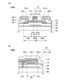
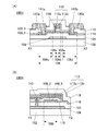
本発明の一態様は、酸化物半導体膜を有する半導体装置の作製方法であって、酸化物半導体膜を形成する工程と、酸化物半導体膜上に絶縁膜を成膜する工程と、絶縁膜上に導電膜を成膜する工程と、導電膜上に第1の保護膜を成膜する工程と、第1の保護膜上に第2の保護膜を形成する工程と、を有し、第1の保護膜、導電膜、及び絶縁膜は、第2の保護膜をマスクに加工され、第2の保護膜を除去した後に、導電膜及び絶縁膜は、第1の保護膜をマスクに、第2の保護膜よりも小さい面積で加工される、半導体装置の作製方法である。 One aspect of the present invention is a method for manufacturing a semiconductor device having an oxide semiconductor film, which comprises a step of forming an oxide semiconductor film, a step of forming an insulating film on the oxide semiconductor film, and a step of forming an insulating film on the insulating film. It has a step of forming a conductive film on the conductive film, a step of forming a first protective film on the conductive film, and a step of forming a second protective film on the first protective film. The protective film, the conductive film, and the insulating film are processed by using the second protective film as a mask, and after the second protective film is removed, the conductive film and the insulating film are formed by using the first protective film as a mask. This is a method for manufacturing a semiconductor device, which is processed in an area smaller than that of the protective film (2).
また、本発明の他の一態様は、酸化物半導体膜を有する半導体装置の作製方法であって、酸化物半導体膜を形成する工程と、酸化物半導体膜上に絶縁膜を成膜する工程と、絶縁膜上に導電膜を成膜する工程と、導電膜上に第1の保護膜を成膜する工程と、第1の保護膜上に第2の保護膜を形成する工程と、を有し、第1の保護膜、導電膜、及び絶縁膜は、第2の保護膜をマスクに加工され、第2の保護膜を除去した後に、導電膜及び絶縁膜は、第1の保護膜をマスクに、第2の保護膜よりも小さい面積で加工され、第1の保護膜上から酸化物半導体膜に対してプラズマ処理を行い、第1の保護膜を除去した後に、導電膜及び酸化物半導体膜上に窒化物絶縁膜が成膜される、半導体装置の作製方法である。 Another aspect of the present invention is a method for manufacturing a semiconductor device having an oxide semiconductor film, which comprises a step of forming an oxide semiconductor film and a step of forming an insulating film on the oxide semiconductor film. There are a step of forming a conductive film on the insulating film, a step of forming a first protective film on the conductive film, and a step of forming a second protective film on the first protective film. Then, the first protective film, the conductive film, and the insulating film are processed with the second protective film as a mask, and after the second protective film is removed, the conductive film and the insulating film are formed with the first protective film. The mask is processed in an area smaller than that of the second protective film, the oxide semiconductor film is subjected to plasma treatment from above the first protective film, and after the first protective film is removed, the conductive film and the oxide are formed. This is a method for manufacturing a semiconductor device in which a nitride insulating film is formed on a semiconductor film.
上記態様において、プラズマ処理は、アルゴン及び窒素のいずれか一方または双方の雰囲気下で行われると好ましい。 In the above aspect, it is preferable that the plasma treatment is performed in the atmosphere of either one or both of argon and nitrogen.
また、上記態様において、導電膜は、第2の保護膜の面積の15%以上50%以下で形成されると好ましい。 Further, in the above aspect, the conductive film is preferably formed in an area of 15% or more and 50% or less of the area of the second protective film.
また、上記態様において、第1の保護膜は、無機材料により形成され、第2の保護膜は、有機材料により形成されると好ましい。 Further, in the above aspect, it is preferable that the first protective film is formed of an inorganic material and the second protective film is formed of an organic material.
また、上記態様において、導電膜は、金属酸化膜と、金属酸化膜上の金属膜とにより形成されると好ましい。 Further, in the above aspect, the conductive film is preferably formed by a metal oxide film and a metal film on the metal oxide film.
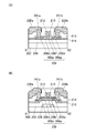
また、本発明の他の一態様は、ガラス基板上の半導体膜と、半導体膜上の絶縁膜と、半導体膜と一部重なり、且つ絶縁膜上のゲート電極と、を有し、半導体膜は、一対の低抵抗領域と、一対の低抵抗領域の間のチャネル領域と、を有し、チャネル長方向において、低抵抗領域の幅は、チャネル領域のチャネル長と同じ、またはチャネル領域のチャネル長よりも広い半導体装置である。 Further, another aspect of the present invention includes a semiconductor film on a glass substrate, an insulating film on the semiconductor film, a gate electrode partially overlapping the semiconductor film, and a gate electrode on the insulating film. , A pair of low resistance regions and a channel region between a pair of low resistance regions, and in the channel length direction, the width of the low resistance region is the same as the channel length of the channel region, or the channel length of the channel region. It is a wider semiconductor device.
また、上記態様において、低抵抗領域の一部は、ゲート電極と重なると好ましい。 Further, in the above aspect, it is preferable that a part of the low resistance region overlaps with the gate electrode.
また、上記態様において、チャネル長は、1.5μm未満であると好ましい。 Further, in the above aspect, the channel length is preferably less than 1.5 μm.
また、上記態様において、半導体膜は、結晶構造を有すると好ましい。また、上記態様において、半導体膜は、多結晶シリコン膜であると好ましい。 Further, in the above aspect, it is preferable that the semiconductor film has a crystal structure. Further, in the above aspect, the semiconductor film is preferably a polycrystalline silicon film.
また、本発明の他の一態様は、上記記載の半導体装置と、表示素子とを有する表示装置である。また、本発明の他の一態様は、上記記載の表示装置と、タッチセンサとを有する表示モジュールである。また、本発明の他の一態様は、上記記載の半導体装置、表示装置、または表示モジュールと、操作キーまたはバッテリと、を有する電子機器である。 Further, another aspect of the present invention is a display device having the above-mentioned semiconductor device and a display element. Another aspect of the present invention is a display module having the above-mentioned display device and a touch sensor. Further, another aspect of the present invention is an electronic device having the above-mentioned semiconductor device, display device, or display module, and an operation key or a battery.
本発明の一態様により、酸化物半導体を有するトランジスタにおいて、電気特性の変動を抑制すると共に、信頼性を向上させることができる。または、本発明の一態様により、酸化物半導体を有するスタガ型のトランジスタを提供することができる。または、本発明の一態様により、酸化物半導体を有するオン電流が大きいトランジスタを提供することができる。または、本発明の一態様により、酸化物半導体を有するオフ電流が小さいトランジスタを提供することができる。または、本発明の一態様により、消費電力が低減された半導体装置を提供することができる。または、本発明の一態様により、酸化物半導体を有し、微細化されたトランジスタを提供することができる。または、本発明の一態様により、新規な半導体装置を提供することができる。 According to one aspect of the present invention, in a transistor having an oxide semiconductor, fluctuations in electrical characteristics can be suppressed and reliability can be improved. Alternatively, according to one aspect of the present invention, a staggered transistor having an oxide semiconductor can be provided. Alternatively, according to one aspect of the present invention, it is possible to provide a transistor having an oxide semiconductor and having a large on-current. Alternatively, according to one aspect of the present invention, it is possible to provide a transistor having an oxide semiconductor and having a small off-current. Alternatively, one aspect of the present invention can provide a semiconductor device with reduced power consumption. Alternatively, according to one aspect of the present invention, it is possible to provide a transistor having an oxide semiconductor and miniaturized. Alternatively, one aspect of the present invention can provide a novel semiconductor device.
また、本発明の一態様により、画素密度が1000ppiを超える表示装置を実現することができる。または、本発明の一態様により、安定した電気特性を有するトランジスタを提供することができる。または、本発明の一態様により、上記トランジスタを有する半導体装置を提供することができる。または、本発明の一態様により、上記半導体装置を有するモジュールを提供することができる。または、本発明の一態様により、上記半導体装置または上記モジュールを有する電子機器を提供することができる。または、本発明の一態様により、新規な半導体装置を提供することができる。 Further, according to one aspect of the present invention, it is possible to realize a display device having a pixel density of more than 1000 ppi. Alternatively, one aspect of the present invention can provide a transistor having stable electrical characteristics. Alternatively, according to one aspect of the present invention, a semiconductor device having the above-mentioned transistor can be provided. Alternatively, according to one aspect of the present invention, a module having the above semiconductor device can be provided. Alternatively, according to one aspect of the present invention, it is possible to provide the semiconductor device or an electronic device having the module. Alternatively, one aspect of the present invention can provide a novel semiconductor device.
なお、これらの効果の記載は、他の効果の存在を妨げるものではない。なお、本発明の一態様は、必ずしも、これらの効果の全てを有する必要はない。なお、これら以外の効果は、明細書、図面、請求項などの記載から、自ずと明らかとなるものであり、明細書、図面、請求項などの記載から、これら以外の効果を抽出することが可能である。 The description of these effects does not preclude the existence of other effects. It should be noted that one aspect of the present invention does not necessarily have to have all of these effects. It should be noted that the effects other than these are naturally clarified from the description of the description, drawings, claims, etc., and it is possible to extract the effects other than these from the description of the description, drawings, claims, etc. Is.
以下、実施の形態について図面を参照しながら説明する。ただし、実施の形態は多くの異なる態様で実施することが可能であり、趣旨及びその範囲から逸脱することなくその形態及び詳細を様々に変更し得ることは当業者であれば容易に理解される。従って、本発明は、以下の実施の形態の記載内容に限定して解釈されるものではない。 Hereinafter, embodiments will be described with reference to the drawings. However, it is easily understood by those skilled in the art that the embodiments can be implemented in many different embodiments, and that the embodiments and details can be variously changed without departing from the spirit and scope thereof. .. Therefore, the present invention is not construed as being limited to the description of the following embodiments.
また、図面において、大きさ、層の厚さ、又は領域は、明瞭化のために誇張されている場合がある。よって、必ずしもそのスケールに限定されない。なお図面は、理想的な例を模式的に示したものであり、図面に示す形状又は値などに限定されない。 Also, in the drawings, the size, layer thickness, or area may be exaggerated for clarity. Therefore, it is not necessarily limited to that scale. The drawings schematically show ideal examples, and are not limited to the shapes or values shown in the drawings.
また、本明細書にて用いる「第1」、「第2」、「第3」という序数詞は、構成要素の混同を避けるために付したものであり、数的に限定するものではないことを付記する。 In addition, the ordinal numbers "first", "second", and "third" used in the present specification are added to avoid confusion of the components, and are not limited numerically. Addition.
また、本明細書において、「上に」、「下に」などの配置を示す語句は、構成同士の位置関係を、図面を参照して説明するために、便宜上用いている。また、構成同士の位置関係は、各構成を描写する方向に応じて適宜変化するものである。従って、明細書で説明した語句に限定されず、状況に応じて適切に言い換えることができる。 Further, in the present specification, terms indicating the arrangement such as "above" and "below" are used for convenience in order to explain the positional relationship between the configurations with reference to the drawings. Further, the positional relationship between the configurations changes as appropriate according to the direction in which each configuration is depicted. Therefore, it is not limited to the words and phrases explained in the specification, and can be appropriately paraphrased according to the situation.
また、本明細書等において、トランジスタとは、ゲートと、ドレインと、ソースとを含む少なくとも三つの端子を有する素子である。そして、ドレイン(ドレイン端子、ドレイン領域またはドレイン電極)とソース(ソース端子、ソース領域またはソース電極)の間にチャネル領域を有しており、ドレインとチャネル領域とソースとを介して電流を流すことができるものである。なお、本明細書等において、チャネル領域とは、電流が主として流れる領域をいう。 Further, in the present specification and the like, a transistor is an element having at least three terminals including a gate, a drain, and a source. Then, a channel region is provided between the drain (drain terminal, drain region or drain electrode) and the source (source terminal, source region or source electrode), and a current flows through the drain, the channel region and the source. Can be done. In the present specification and the like, the channel region refers to a region in which a current mainly flows.
また、ソースやドレインの機能は、異なる極性のトランジスタを採用する場合や、回路動作において電流の方向が変化する場合などには入れ替わることがある。このため、本明細書等においては、ソースやドレインの用語は、入れ替えて用いることができるものとする。 Further, the functions of the source and the drain may be interchanged when transistors having different polarities are adopted or when the direction of the current changes in the circuit operation. Therefore, in the present specification and the like, the terms source and drain can be used interchangeably.
また、本明細書等において、「電気的に接続」には、「何らかの電気的作用を有するもの」を介して接続されている場合が含まれる。ここで、「何らかの電気的作用を有するもの」は、接続対象間での電気信号の授受を可能とするものであれば、特に制限を受けない。例えば、「何らかの電気的作用を有するもの」には、電極や配線をはじめ、トランジスタなどのスイッチング素子、抵抗素子、インダクタ、キャパシタ、その他の各種機能を有する素子などが含まれる。 Further, in the present specification and the like, "electrically connected" includes a case where they are connected via "something having some kind of electrical action". Here, the "thing having some kind of electrical action" is not particularly limited as long as it enables the exchange of electric signals between the connection targets. For example, "things having some kind of electrical action" include electrodes, wirings, switching elements such as transistors, resistance elements, inductors, capacitors, and other elements having various functions.
また、本明細書等において、「平行」とは、二つの直線が−10°以上10°以下の角度で配置されている状態をいう。したがって、−5°以上5°以下の場合も含まれる。また、「垂直」とは、二つの直線が80°以上100°以下の角度で配置されている状態をいう。したがって、85°以上95°以下の場合も含まれる。 Further, in the present specification and the like, "parallel" means a state in which two straight lines are arranged at an angle of −10 ° or more and 10 ° or less. Therefore, the case of −5 ° or more and 5 ° or less is also included. Further, "vertical" means a state in which two straight lines are arranged at an angle of 80 ° or more and 100 ° or less. Therefore, the case of 85 ° or more and 95 ° or less is also included.
また、本明細書等において、「膜」という用語と、「層」という用語とは、互いに入れ替えることが可能である。例えば、「導電層」という用語を、「導電膜」という用語に変更することが可能な場合がある。または、例えば、「絶縁膜」という用語を、「絶縁層」という用語に変更することが可能な場合がある。 Further, in the present specification and the like, the term "membrane" and the term "layer" can be interchanged with each other. For example, it may be possible to change the term "conductive layer" to the term "conductive layer". Alternatively, for example, it may be possible to change the term "insulating film" to the term "insulating layer".
また、本明細書等において、特に断りがない場合、オフ電流とは、トランジスタがオフ状態(非導通状態、遮断状態、ともいう)にあるときのドレイン電流をいう。オフ状態とは、特に断りがない場合、nチャネル型トランジスタでは、ゲートとソースの間の電圧Vgsがしきい値電圧Vthよりも低い状態、pチャネル型トランジスタでは、ゲートとソースの間の電圧Vgsがしきい値電圧Vthよりも高い状態をいう。例えば、nチャネル型のトランジスタのオフ電流とは、ゲートとソースの間の電圧Vgsがしきい値電圧Vthよりも低いときのドレイン電流を言う場合がある。 Further, in the present specification and the like, unless otherwise specified, the off current means a drain current when the transistor is in an off state (also referred to as a non-conducting state or a cutoff state). Unless otherwise specified, the off state is a state in which the voltage Vgs between the gate and the source is lower than the threshold voltage Vth in the n-channel transistor, and the voltage Vgs between the gate and the source in the p-channel transistor. Is higher than the threshold voltage Vth. For example, the off-current of an n-channel transistor may refer to the drain current when the voltage Vgs between the gate and the source is lower than the threshold voltage Vth.
トランジスタのオフ電流は、Vgsに依存する場合がある。従って、トランジスタのオフ電流がI以下である、とは、トランジスタのオフ電流がI以下となるVgsの値が存在することを言う場合がある。トランジスタのオフ電流は、所定のVgsにおけるオフ状態、所定の範囲内のVgsにおけるオフ状態、または、十分に低減されたオフ電流が得られるVgsにおけるオフ状態、等におけるオフ電流を指す場合がある。 The off current of the transistor may depend on Vgs. Therefore, the fact that the off-current of the transistor is I or less may mean that there is a value of Vgs in which the off-current of the transistor is I or less. The off-current of a transistor may refer to an off-current in a predetermined Vgs, an off-state in Vgs within a predetermined range, an off-state in Vgs in which a sufficiently reduced off-current can be obtained, and the like.
一例として、しきい値電圧Vthが0.5Vであり、Vgsが0.5Vにおけるドレイン電流が1×10⁻⁹Aであり、Vgsが0.1Vにおけるドレイン電流が1×10⁻¹³Aであり、Vgsが−0.5Vにおけるドレイン電流が1×10⁻¹⁹Aであり、Vgsが−0.8Vにおけるドレイン電流が1×10⁻²²Aであるようなnチャネル型トランジスタを想定する。当該トランジスタのドレイン電流は、Vgsが−0.5Vにおいて、または、Vgsが−0.5V乃至−0.8Vの範囲において、1×10⁻¹⁹A以下であるから、当該トランジスタのオフ電流は1×10⁻¹⁹A以下である、と言う場合がある。当該トランジスタのドレイン電流が1×10⁻²²A以下となるVgsが存在するため、当該トランジスタのオフ電流は1×10⁻²²A以下である、と言う場合がある。 As an example, the threshold voltage Vth is 0.5 V, the drain current at Vgs is 0.5 V is 1 × 10 -9 A, and the drain current at Vgs is 0.1 V is 1 × 10 -13 A. Assume an n-channel transistor having a drain current of 1 × 10 -19 A at Vgs of −0.5 V and a drain current of 1 × 10 -22 A at Vgs of −0.8 V. Since the drain current of the transistor is 1 × 10 -19 A or less when Vgs is −0.5 V or Vgs is in the range of −0.5 V to −0.8 V, the off current of the transistor is 1. It may be said that it is × 10-19 A or less. Since there are Vgs in which the drain current of the transistor is 1 × 10-22 A or less, it may be said that the off current of the transistor is 1 × 10-22 A or less.
また、本明細書等では、チャネル幅Wを有するトランジスタのオフ電流を、チャネル幅Wあたりを流れる電流値で表す場合がある。また、所定のチャネル幅(例えば1μm)あたりを流れる電流値で表す場合がある。後者の場合、オフ電流の単位は、電流/長さの次元を持つ単位(例えば、A/μm)で表される場合がある。 Further, in the present specification and the like, the off-current of a transistor having a channel width W may be represented by a current value flowing per channel width W. Further, it may be represented by a current value flowing around a predetermined channel width (for example, 1 μm). In the latter case, the unit of off-current may be represented by a unit having a current / length dimension (eg, A / μm).
トランジスタのオフ電流は、温度に依存する場合がある。本明細書において、オフ電流は、特に記載がない場合、室温、60℃、85℃、95℃、または125℃におけるオフ電流を表す場合がある。または、当該トランジスタが含まれる半導体装置等の信頼性が保証される温度、または、当該トランジスタが含まれる半導体装置等が使用される温度(例えば、5℃乃至35℃のいずれか一の温度)におけるオフ電流、を表す場合がある。トランジスタのオフ電流がI以下である、とは、室温、60℃、85℃、95℃、125℃、当該トランジスタが含まれる半導体装置等の信頼性が保証される温度、または、当該トランジスタが含まれる半導体装置等が使用される温度(例えば、5℃乃至35℃のいずれか一の温度)、におけるトランジスタのオフ電流がI以下となるVgsの値が存在することを指す場合がある。 The off current of the transistor may depend on the temperature. In the present specification, the off-current may represent an off-current at room temperature, 60 ° C., 85 ° C., 95 ° C., or 125 ° C., unless otherwise specified. Alternatively, at a temperature at which the reliability of the semiconductor device or the like containing the transistor is guaranteed, or at a temperature at which the semiconductor device or the like containing the transistor is used (for example, any one temperature of 5 ° C to 35 ° C). May represent off-current. The off-current of a transistor is I or less, which means room temperature, 60 ° C., 85 ° C., 95 ° C., 125 ° C., a temperature at which reliability of a semiconductor device or the like including the transistor is guaranteed, or the transistor is included. It may indicate that there is a value of Vgs in which the off-current of the transistor is I or less at the temperature at which the semiconductor device or the like is used (for example, any one temperature of 5 ° C. to 35 ° C.).
トランジスタのオフ電流は、ドレインとソースの間の電圧Vdsに依存する場合がある。本明細書において、オフ電流は、特に記載がない場合、Vdsが0.1V、0.8V、1V、1.2V、1.8V、2.5V,3V、3.3V、10V、12V、16V、または20Vにおけるオフ電流を表す場合がある。または、当該トランジスタが含まれる半導体装置等の信頼性が保証されるVds、または、当該トランジスタが含まれる半導体装置等において使用されるVdsにおけるオフ電流、を表す場合がある。トランジスタのオフ電流がI以下である、とは、Vdsが0.1V、0.8V、1V、1.2V、1.8V、2.5V,3V、3.3V、10V、12V、16V、20V、当該トランジスタが含まれる半導体装置等の信頼性が保証されるVds、または、当該トランジスタが含まれる半導体装置等において使用されるVds、におけるトランジスタのオフ電流がI以下となるVgsの値が存在することを指す場合がある。 The off-current of the transistor may depend on the voltage Vds between the drain and the source. In the present specification, the off-current has Vds of 0.1V, 0.8V, 1V, 1.2V, 1.8V, 2.5V, 3V, 3.3V, 10V, 12V, 16V unless otherwise specified. , Or may represent off-current at 20V. Alternatively, it may represent Vds in which the reliability of the semiconductor device or the like including the transistor is guaranteed, or the off-current in Vds used in the semiconductor device or the like including the transistor. When the off current of the transistor is I or less, Vds is 0.1V, 0.8V, 1V, 1.2V, 1.8V, 2.5V, 3V, 3.3V, 10V, 12V, 16V, 20V. , There is a value of Vgs in which the off current of the transistor is I or less in Vds in which the reliability of the semiconductor device or the like including the transistor is guaranteed, or Vds in which the reliability of the semiconductor device or the like including the transistor is guaranteed. It may refer to that.
上記オフ電流の説明において、ドレインをソースと読み替えてもよい。つまり、オフ電流は、トランジスタがオフ状態にあるときのソースを流れる電流を言う場合もある。 In the above description of the off-current, the drain may be read as the source. That is, the off-current may refer to the current flowing through the source when the transistor is in the off state.
また、本明細書等では、オフ電流と同じ意味で、リーク電流と記載する場合がある。また、本明細書等において、オフ電流とは、例えば、トランジスタがオフ状態にあるときに、ソースとドレインとの間に流れる電流を指す場合がある。 Further, in the present specification and the like, it may be described as a leak current in the same meaning as an off current. Further, in the present specification and the like, the off current may refer to, for example, the current flowing between the source and the drain when the transistor is in the off state.
また、本明細書等において、「半導体」と表記した場合であっても、例えば、導電性が十分に低い場合は、「絶縁体」としての特性を有する場合がある。また、「半導体」と「絶縁体」とは境界が曖昧であり、厳密に区別できない場合がある。したがって、本明細書等に記載の「半導体」は、「絶縁体」に言い換えることが可能な場合がある。同様に、本明細書等に記載の「絶縁体」は、「半導体」に言い換えることが可能な場合がある。または、本明細書等に記載の「絶縁体」を「半絶縁体」に言い換えることが可能な場合がある。 Further, even when the term "semiconductor" is used in the present specification or the like, for example, when the conductivity is sufficiently low, it may have characteristics as an "insulator". In addition, the boundary between "semiconductor" and "insulator" is ambiguous, and it may not be possible to strictly distinguish between them. Therefore, the "semiconductor" described in the present specification and the like may be paraphrased as an "insulator". Similarly, the “insulator” described in the present specification and the like may be paraphrased as “semiconductor”. Alternatively, it may be possible to paraphrase the "insulator" described in the present specification and the like into a "semi-insulator".
また、本明細書等において、「半導体」と表記した場合であっても、例えば、導電性が十分に高い場合は、「導電体」としての特性を有する場合がある。また、「半導体」と「導電体」とは境界が曖昧であり、厳密に区別できない場合がある。したがって、本明細書等に記載の「半導体」は、「導電体」に言い換えることが可能な場合がある。同様に、本明細書等に記載の「導電体」は、「半導体」に言い換えることが可能な場合がある。 Further, even when the term "semiconductor" is used in the present specification or the like, for example, when the conductivity is sufficiently high, it may have characteristics as a "conductor". In addition, the boundary between "semiconductor" and "conductor" is ambiguous, and it may not be possible to strictly distinguish between them. Therefore, the "semiconductor" described in the present specification and the like may be paraphrased as a "conductor". Similarly, the "conductor" described in the present specification and the like may be paraphrased as a "semiconductor".
また、本明細書等において、半導体の不純物とは、半導体を構成する主成分以外をいう。例えば、濃度が0.1原子%未満の元素は不純物である。不純物が含まれることにより、半導体にDOS(Density of States)が形成されることや、キャリア移動度が低下することや、結晶性が低下することなどが起こる場合がある。半導体が酸化物半導体を有する場合、半導体の特性を変化させる不純物としては、例えば、第1族元素、第2族元素、第13族元素、第14族元素、第15族元素、主成分以外の遷移金属などがあり、特に、水素(水にも含まれる)、リチウム、ナトリウム、シリコン、ホウ素、リン、炭素、窒素などがある。酸化物半導体の場合、例えば水素などの不純物の混入によって酸素欠損を形成する場合がある。また、半導体がシリコンを有する場合、半導体の特性を変化させる不純物としては、例えば、酸素、水素を除く第1族元素、第2族元素、第13族元素、第15族元素などがある。
Further, in the present specification and the like, the impurities of the semiconductor refer to other than the main components constituting the semiconductor. For example, an element having a concentration of less than 0.1 atomic% is an impurity. Due to the inclusion of impurities, DOS (Density of States) may be formed in the semiconductor, carrier mobility may be lowered, crystallinity may be lowered, and the like. When the semiconductor has an oxide semiconductor, the impurities that change the characteristics of the semiconductor include, for example,
(実施の形態1)
本実施の形態では、酸化物半導体膜を有する半導体装置、及び当該半導体装置の作製方法の一例について、図1乃至図15を用いて説明する。
(Embodiment 1)
In the present embodiment, an example of a semiconductor device having an oxide semiconductor film and a method for manufacturing the semiconductor device will be described with reference to FIGS. 1 to 15.
<1−1.半導体装置の構成例1>
図1(A)(B)(C)に、酸化物半導体膜を有する半導体装置の一例を示す。ここでは半導体装置として、トランジスタを示す。なお、図1(A)(B)(C)に示すトランジスタは、スタガ型(トップゲート構造)である。
<1-1. Semiconductor device configuration example 1>
1 (A), (B), and (C) show an example of a semiconductor device having an oxide semiconductor film. Here, a transistor is shown as a semiconductor device. The transistors shown in FIGS. 1A, 1B, and 1C are staggered type (top gate structure).
図1(A)は、トランジスタ100の上面図であり、図1(B)は図1(A)の一点鎖線X1−X2間の断面図であり、図1(C)は図1(A)の一点鎖線Y1−Y2間の断面図である。なお、図1(A)では、明瞭化のため、絶縁膜などの構成要素を省略して図示している。なお、トランジスタの上面図においては、以降の図面においても図1(A)と同様に、構成要素の一部を省略して図示する場合がある。また、一点鎖線X1−X2方向をチャネル長(L)方向、一点鎖線Y1−Y2方向をチャネル幅(W)方向と呼称する場合がある。
1 (A) is a top view of the
なお、本発明の一態様の半導体装置においては、トランジスタのチャネル長(L)は、好ましくは0.2μm以上1.5μm未満、より好ましくは、0.5μm以上1.0μm以下である。上述のチャネル長(L)としたトランジスタを表示装置に用いることで、表示装置の画素密度を高めることができる。 In the semiconductor device of one aspect of the present invention, the channel length (L) of the transistor is preferably 0.2 μm or more and less than 1.5 μm, and more preferably 0.5 μm or more and 1.0 μm or less. By using the transistor having the channel length (L) described above in the display device, the pixel density of the display device can be increased.
図1(A)(B)(C)に示すトランジスタ100は、基板102上の絶縁膜104と、絶縁膜104上の酸化物半導体膜108と、酸化物半導体膜108上の絶縁膜110と、絶縁膜110上の導電膜112と、絶縁膜104、酸化物半導体膜108、及び導電膜112上の絶縁膜116と、を有する。
The
酸化物半導体膜108は、導電膜112と重なるチャネル領域108iと、絶縁膜116と接するソース領域108sと、絶縁膜116と接するドレイン領域108dと、を有する。さらに、酸化物半導体膜108は、チャネル領域108iとソース領域108sとの間、及びチャネル領域108iとドレイン領域108dとの間に低抵抗領域108aを有する。なお、チャネル領域108iは、導電膜112の内側に形成される場合がある。この場合、低抵抗領域108aと、導電膜112とが重なる領域が形成される。例えば、低抵抗領域108a中の不純物(例えば水など)が、チャネル領域108i側に横方向に拡散することで、チャネル領域108iが、導電膜112の内側に形成される場合がある。この場合、導電膜112の長さよりも、チャネル領域108iの長さが短くなる。すなわちトランジスタ100の実効L長が短くなる場合がある。また、低抵抗領域108aと、導電膜112とが、重なることで、所謂LDD領域(Lightly Doped Drain領域)が形成されうる。LDD領域を設けることによって、ドレイン領域の電界緩和が可能となる。したがって、ドレイン領域の電界に起因したトランジスタのしきい値電圧の変動を低減することができる。
The
また、導電膜112は、絶縁膜110上の金属酸化膜112aと、金属酸化膜112a上の金属膜112bと、を有する。例えば、金属酸化膜112aを酸素雰囲気中で形成することで、絶縁膜110中に酸素を添加することができる。また、金属膜112bを低抵抗の金属膜により形成することで、導電膜112の抵抗を低くすることができる。または、金属膜112bを遮光性の金属膜により形成することで、上方からチャネル領域108iに入射する光を遮光することができる。
Further, the
また、絶縁膜116は、窒素または水素を有する。絶縁膜116と、低抵抗領域108a、ソース領域108s、及びドレイン領域108dと、が接することで、絶縁膜116中の窒素または水素が低抵抗領域108a、ソース領域108s、及びドレイン領域108d中に添加される。低抵抗領域108a、ソース領域108s、及びドレイン領域108dは、窒素または水素が添加されることで、キャリア密度が高くなる。なお、低抵抗領域108aは、チャネル領域108iよりも抵抗が低く、且つソース領域108s及びドレイン領域108dよりも抵抗が高い。低抵抗領域108aの詳細については、後述する。
Further, the insulating
また、トランジスタ100は、絶縁膜116上の絶縁膜118と、絶縁膜116、118に設けられた開口部141aを介して、ソース領域108sに電気的に接続される導電膜120aと、絶縁膜116、118に設けられた開口部141bを介して、ドレイン領域108dに電気的に接続される導電膜120bと、を有していてもよい。
Further, the
なお、本明細書等において、絶縁膜104を第1の絶縁膜と、絶縁膜110を第2の絶縁膜と、絶縁膜116を第3の絶縁膜と、絶縁膜118を第4の絶縁膜と、それぞれ呼称する場合がある。また、導電膜112は、ゲート電極としての機能を有し、導電膜120aは、ソース電極としての機能を有し、導電膜120bは、ドレイン電極としての機能を有する。
In the present specification and the like, the insulating
また、絶縁膜110は、ゲート絶縁膜としての機能を有する。また、絶縁膜110は、過剰酸素領域を有する。絶縁膜110が過剰酸素領域を有することで、酸化物半導体膜108が有するチャネル領域108i中に過剰酸素を供給することができる。よって、チャネル領域108iに形成されうる酸素欠損を過剰酸素により補填することができるため、信頼性の高い半導体装置を提供することができる。
Further, the insulating
なお、酸化物半導体膜108中に過剰酸素を供給させるためには、酸化物半導体膜108の下方に形成される絶縁膜104に過剰酸素を供給してもよい。ただし、この場合、絶縁膜104中に含まれる過剰酸素は、酸化物半導体膜108が有する低抵抗領域108a、ソース領域108s、及びドレイン領域108dにも供給されうる。低抵抗領域108a、ソース領域108s、及びドレイン領域108d中に過剰酸素が供給されると、低抵抗領域108a、ソース領域108s、及びドレイン領域108dの抵抗が高くなる場合がある。
In order to supply excess oxygen to the
一方で、酸化物半導体膜108の上方に形成される絶縁膜110に過剰酸素を有する構成とすることで、チャネル領域108iにのみ選択的に過剰酸素を供給させることが可能となる。
On the other hand, by configuring the insulating
また、酸化物半導体膜108が有する、低抵抗領域108a、ソース領域108s及びドレイン領域108dは、それぞれ、酸素欠損を形成する元素、または酸素欠損と結合する元素を有すると好ましい。当該酸素欠損を形成する元素、または酸素欠損と結合する元素としては、絶縁膜116が有する窒素または水素が挙げられる。また、これらの他にも、酸素欠損を形成する元素、または酸素欠損と結合する元素としては、代表的にはホウ素、炭素、フッ素、リン、硫黄、塩素、チタン、希ガス等が挙げられる。また、希ガス元素の代表例としては、ヘリウム、ネオン、アルゴン、クリプトン、及びキセノン等がある。
Further, it is preferable that the
上記酸素欠損を形成する元素、または酸素欠損と結合する元素は、絶縁膜116の構成元素が低抵抗領域108a、ソース領域108s、及びドレイン領域108dに拡散することにより、または不純物元素添加処理により低抵抗領域108a、ソース領域108s、及びドレイン領域108d中に添加される。
The elements forming the oxygen deficiency or the elements binding to the oxygen deficiency are low due to the constituent elements of the insulating
不純物元素が酸化物半導体膜に添加されると、酸化物半導体膜中の金属元素と酸素の結合が切断され、酸素欠損が形成される。または、不純物元素が酸化物半導体膜に添加されると、酸化物半導体膜中の金属元素と結合していた酸素が不純物元素と結合し、金属元素から酸素が脱離され、酸素欠損が形成される。これらの結果、酸化物半導体膜においてキャリア密度が増加し、導電性が高くなる。 When an impurity element is added to the oxide semiconductor film, the bond between the metal element and oxygen in the oxide semiconductor film is broken, and an oxygen deficiency is formed. Alternatively, when an impurity element is added to the oxide semiconductor film, oxygen bonded to the metal element in the oxide semiconductor film is combined with the impurity element, oxygen is desorbed from the metal element, and oxygen deficiency is formed. To. As a result, the carrier density of the oxide semiconductor film is increased and the conductivity is increased.
なお、図1に示すトランジスタ100を表示装置の画素トランジスタ及び駆動トランジスタのいずれか一方または双方に用いることで、表示装置の解像度を1000ppi(pixel per inch)以上、好ましくは2000ppi以上、さらに好ましくは3000ppi以上とすることができる。
By using the
<1−2.半導体装置の作製方法1>
ここで、図1に示すトランジスタ100の作製方法の一例について、図2乃至図4を用いて説明する。なお、図2乃至図4は、トランジスタ100の作製方法を説明するチャネル長(L)方向及びチャネル幅(W)方向の断面図である。
<1-2. Manufacturing method of
Here, an example of a method for manufacturing the
なお、以下に示す作製方法とすることで、トランジスタ100のチャネル長(L)を、0.2μm以上1.5μm未満、より好ましくは、0.5μm以上1.0μm以下とすることができる。例えば、リソグラフィ法に用いる露光装置が可能な最小の加工寸法が1.5μmである場合、本実施の形態では、露光装置が可能な最小の加工寸法以下のチャネル長(L)とすることができる。
By using the manufacturing method shown below, the channel length (L) of the
[酸化物半導体膜を形成する工程]
まず、基板102上に絶縁膜104を成膜する。続いて、絶縁膜104上に酸化物半導体膜を成膜する。その後、当該酸化物半導体膜を島状に加工することで、酸化物半導体膜107を形成する(図2(A)参照)。
[Step of forming an oxide semiconductor film]
First, the insulating
絶縁膜104としては、スパッタリング法、CVD法、蒸着法、パルスレーザー堆積(PLD)法、印刷法、塗布法等を適宜用いて成膜することができる。本実施の形態においては、絶縁膜104として、プラズマCVD装置を用い、厚さ400nmの窒化シリコン膜と、厚さ50nmの酸化窒化シリコン膜とを成膜する。なお、絶縁膜104を成膜せずに、基板102上に酸化物半導体膜107を形成してもよい。
The insulating
また、絶縁膜104を成膜した後、絶縁膜104に酸素を添加してもよい。絶縁膜104に添加する酸素としては、酸素ラジカル、酸素原子、酸素原子イオン、酸素分子イオン等がある。また、添加方法としては、イオンドーピング法、イオン注入法、プラズマ処理法等がある。また、絶縁膜104上に酸素の脱離を抑制する膜を成膜した後、該膜を介して絶縁膜104に酸素を添加してもよい。
Further, oxygen may be added to the insulating
上述の酸素の脱離を抑制する膜として、インジウム、亜鉛、ガリウム、錫、アルミニウム、クロム、タンタル、チタン、モリブデン、ニッケル、鉄、コバルト、またはタングステンの1以上を有する導電膜あるいは半導体膜を用いて成膜することができる。 As the above-mentioned film that suppresses the desorption of oxygen, a conductive film or a semiconductor film having one or more of indium, zinc, gallium, tin, aluminum, chromium, tantalum, titanium, molybdenum, nickel, iron, cobalt, or tungsten is used. Can be formed into a film.
また、プラズマ処理で酸素の添加を行う場合、マイクロ波で酸素を励起し、高密度な酸素プラズマを発生させることで、絶縁膜104への酸素添加量を増加させることができる。
Further, when oxygen is added by plasma treatment, the amount of oxygen added to the insulating
酸化物半導体膜107としては、スパッタリング法、塗布法、パルスレーザー蒸着法、レーザーアブレーション法、熱CVD法等により形成することができる。なお、酸化物半導体膜107への加工には、酸化物半導体膜上にリソグラフィ工程によりマスクを形成した後、該マスクを用いて酸化物半導体膜の一部をエッチングすること形成することができる。また、印刷法を用いて、素子分離された酸化物半導体膜107を直接形成してもよい。
The
スパッタリング法で酸化物半導体膜を形成する場合、プラズマを発生させるための電源装置は、RF電源装置、AC電源装置、DC電源装置等を適宜用いることができる。また、酸化物半導体膜を形成する場合のスパッタリングガスは、希ガス(代表的にはアルゴン)、酸素、希ガス及び酸素の混合ガスを適宜用いる。なお、希ガス及び酸素の混合ガスの場合、希ガスに対して酸素のガス比を高めることが好ましい。 When the oxide semiconductor film is formed by the sputtering method, an RF power supply device, an AC power supply device, a DC power supply device, or the like can be appropriately used as the power supply device for generating plasma. Further, as the sputtering gas for forming the oxide semiconductor film, a rare gas (typically argon), oxygen, a mixed gas of rare gas and oxygen is appropriately used. In the case of a mixed gas of rare gas and oxygen, it is preferable to increase the gas ratio of oxygen to the rare gas.
なお、酸化物半導体膜を形成する際に、例えば、スパッタリング法を用いる場合、基板温度を150℃以上750℃以下、または150℃以上450℃以下、または200℃以上350℃以下として、酸化物半導体膜を成膜することで、結晶性を高めることができるため好ましい。 When forming an oxide semiconductor film, for example, when a sputtering method is used, the substrate temperature is set to 150 ° C. or higher and 750 ° C. or lower, or 150 ° C. or higher and 450 ° C. or lower, or 200 ° C. or higher and 350 ° C. or lower. It is preferable to form a film because the crystallinity can be enhanced.
なお、本実施の形態においては、酸化物半導体膜107として、スパッタリング装置を用い、スパッタリングターゲットとしてIn−Ga−Zn金属酸化物(In:Ga:Zn=4:2:4.1[原子数比])を用いて、膜厚35nmの酸化物半導体膜を成膜する。
In this embodiment, a sputtering device is used as the
また、酸化物半導体膜107を形成した後、加熱処理を行い、酸化物半導体膜107の脱水素化または脱水化をしてもよい。加熱処理の温度は、代表的には、150℃以上基板歪み点未満、または250℃以上450℃以下、または300℃以上450℃以下である。
Further, after forming the
加熱処理は、ヘリウム、ネオン、アルゴン、キセノン、クリプトン等の希ガス、または窒素を含む不活性ガス雰囲気で行うことができる。または、不活性ガス雰囲気で加熱した後、酸素雰囲気で加熱してもよい。なお、上記不活性雰囲気及び酸素雰囲気に水素、水などが含まれないことが好ましい。処理時間は3分以上24時間以下とすればよい。 The heat treatment can be carried out in a rare gas such as helium, neon, argon, xenon or krypton, or in an atmosphere of an inert gas containing nitrogen. Alternatively, after heating in an inert gas atmosphere, heating may be performed in an oxygen atmosphere. It is preferable that the inert atmosphere and the oxygen atmosphere do not contain hydrogen, water or the like. The processing time may be 3 minutes or more and 24 hours or less.
該加熱処理は、電気炉、RTA装置等を用いることができる。RTA装置を用いることで、短時間に限り、基板の歪み点以上の温度で熱処理を行うことができる。そのため加熱処理時間を短縮することができる。 An electric furnace, an RTA device, or the like can be used for the heat treatment. By using the RTA device, the heat treatment can be performed at a temperature equal to or higher than the strain point of the substrate for a short time. Therefore, the heat treatment time can be shortened.
酸化物半導体膜を加熱しながら成膜する、または酸化物半導体膜を形成した後、加熱処理を行うことで、酸化物半導体膜中の水素濃度を低減させることができる。 The hydrogen concentration in the oxide semiconductor film can be reduced by forming a film while heating the oxide semiconductor film or by performing heat treatment after forming the oxide semiconductor film.
[酸化物半導体膜上に絶縁膜を成膜する工程]
次に、絶縁膜104及び酸化物半導体膜107上に絶縁膜110_0を成膜する(図2(B)参照)。
[Step of forming an insulating film on an oxide semiconductor film]
Next, the insulating film 110_0 is formed on the insulating
絶縁膜110_0としては、酸化シリコン膜または酸化窒化シリコン膜を、プラズマ化学気相堆積装置(PECVD装置、または単にプラズマCVD装置という)を用いて成膜することができる。この場合、原料ガスとしては、シリコンを含む堆積性気体及び酸化性気体を用いることが好ましい。シリコンを含む堆積性気体の代表例としては、シラン、ジシラン、トリシラン、フッ化シラン等がある。酸化性気体としては、酸素、オゾン、一酸化二窒素、二酸化窒素等がある。 As the insulating film 110_0, a silicon oxide film or a silicon oxide nitride film can be formed by using a plasma chemical vapor deposition apparatus (PECVD apparatus, or simply referred to as a plasma CVD apparatus). In this case, it is preferable to use a sedimentary gas containing silicon and an oxidizing gas as the raw material gas. Typical examples of the sedimentary gas containing silicon include silane, disilane, trisilane, fluorinated silane and the like. Examples of the oxidizing gas include oxygen, ozone, nitrous oxide, nitrogen dioxide and the like.
また、絶縁膜110_0として、堆積性気体の流量に対する酸化性気体の流量を20倍より大きく100倍未満、または40倍以上80倍以下とし、処理室内の圧力を100Pa未満、または50Pa以下とするプラズマCVD装置を用いることで、欠陥量の少ない酸化窒化シリコン膜を成膜することができる。 Further, as the insulating film 110_0, the flow rate of the oxidizing gas is greater than 20 times and less than 100 times, or 40 times or more and 80 times or less with respect to the flow rate of the sedimentary gas, and the pressure in the treatment chamber is less than 100 Pa or 50 Pa or less. By using the CVD apparatus, it is possible to form a silicon oxide film with a small amount of defects.
また、絶縁膜110_0として、プラズマCVD装置の真空排気された処理室内に載置された基板を280℃以上400℃以下に保持し、処理室に原料ガスを導入して処理室内における圧力を20Pa以上250Pa以下、さらに好ましくは100Pa以上250Pa以下とし、処理室内に設けられる電極に高周波電力を供給する条件により、絶縁膜110_0として、緻密である酸化シリコン膜または酸化窒化シリコン膜を成膜することができる。 Further, as the insulating film 110_0, the substrate placed in the vacuum-exhausted processing chamber of the plasma CVD apparatus is held at 280 ° C. or higher and 400 ° C. or lower, and the raw material gas is introduced into the processing chamber to increase the pressure in the processing chamber to 20 Pa or higher. A dense silicon oxide film or silicon oxide nitride film can be formed as the insulating film 110_0 under the condition that the insulating film is 250 Pa or less, more preferably 100 Pa or more and 250 Pa or less, and high-frequency power is supplied to the electrodes provided in the processing chamber. ..
また、絶縁膜110_0を、マイクロ波を用いたプラズマCVD装置を用いて成膜してもよい。マイクロ波とは300MHzから300GHzの周波数域を指す。マイクロ波は、電子温度が低く、電子エネルギーが小さい。また、供給された電力において、電子の加速に用いられる割合が少なく、より多くの分子の解離及び電離に用いられることが可能であり、密度の高いプラズマ(高密度プラズマ)を励起することができる。このため、被成膜面及び堆積物へのプラズマダメージが少なく、欠陥の少ない絶縁膜110_0を成膜することができる。 Further, the insulating film 110_0 may be formed by using a plasma CVD apparatus using microwaves. Microwave refers to the frequency range of 300 MHz to 300 GHz. Microwaves have low electron temperature and low electron energy. Further, in the supplied electric power, the ratio used for accelerating electrons is small, it can be used for dissociation and ionization of more molecules, and it is possible to excite a high-density plasma (high-density plasma). .. Therefore, the insulating film 110_0 with less plasma damage to the surface to be filmed and deposits and few defects can be formed.
本実施の形態では絶縁膜110_0として、プラズマCVD装置を用い、厚さ20nmの酸化窒化シリコン膜を成膜する。 In the present embodiment, a plasma CVD apparatus is used as the insulating film 110_0 to form a silicon oxide film having a thickness of 20 nm.
[絶縁膜上に導電膜を成膜する工程]
次に、絶縁膜110_0上に導電膜112_0を成膜する。なお、本実施の形態においては、導電膜112_0として、金属酸化膜112a_0と、金属膜112b_0と、を成膜する(図2(C)参照)。
[Step of forming a conductive film on an insulating film]
Next, the conductive film 112_0 is formed on the insulating film 110_0. In the present embodiment, a metal oxide film 112a_0 and a metal film 112b_0 are formed as the conductive film 112_0 (see FIG. 2C).
なお、金属酸化膜112a_0の形成時に金属酸化膜112a_0から絶縁膜110_0中に酸素が添加される場合がある。図2(C)において、金属酸化膜112a_0から絶縁膜110_0中に添加される酸素を矢印で模式的に表している。 When the metal oxide film 112a_0 is formed, oxygen may be added from the metal oxide film 112a_0 into the insulating film 110_0. In FIG. 2C, the oxygen added from the metal oxide film 112a_0 to the insulating film 110_0 is schematically represented by an arrow.
金属酸化膜112a_0の形成方法としては、スパッタリング法を用い、形成時に酸素ガスを含む雰囲気で形成することが好ましい。形成時に酸素ガスを含む雰囲気で金属酸化膜112a_0を形成することで、絶縁膜110_0中に酸素を好適に添加することができる。なお、金属酸化膜112a_0の形成方法としては、スパッタリング法に限定されず、その他の方法、例えばALD法を用いてもよい。 As a method for forming the metal oxide film 112a_0, it is preferable to use a sputtering method and to form the metal oxide film 112a_0 in an atmosphere containing oxygen gas at the time of formation. By forming the metal oxide film 112a_0 in an atmosphere containing oxygen gas at the time of formation, oxygen can be suitably added to the insulating film 110_0. The method for forming the metal oxide film 112a_0 is not limited to the sputtering method, and other methods, for example, the ALD method may be used.
本実施の形態においては、金属酸化膜112a_0として、スパッタリング法を用いて、膜厚が10nmのIn−Ga−Zn酸化物であるIGZO膜(In:Ga:Zn=4:2:4.1(原子数比)を成膜する。また、金属酸化膜112a_0の形成前、または金属酸化膜112a_0の形成後に、絶縁膜110_0中に酸素添加処理を行ってもよい。当該酸素添加処理の方法としては、絶縁膜104の形成後に行うことのできる酸素の添加と同様とすればよい。
In the present embodiment, the metal oxide film 112a_0 is an IGZO film (In: Ga: Zn = 4: 2: 4.1) which is an In-Ga-Zn oxide having a film thickness of 10 nm by using a sputtering method. Atomic number ratio) is formed. Further, oxygen addition treatment may be performed in the insulating film 110_0 before the formation of the metal oxide film 112a_0 or after the formation of the metal oxide film 112a_0. , The same as the addition of oxygen that can be performed after the formation of the insulating
また、金属膜112b_0の成膜方法としては、スパッタリング法、またはALD法を用いて形成すればよい。本実施の形態においては、金属膜112b_0として、スパッタリング法を用いて、膜厚が50nmの窒化チタン膜と、膜厚が100nmのチタン膜との積層膜を成膜する。 Further, as a method for forming the metal film 112b_0, a sputtering method or an ALD method may be used to form the metal film 112b_0. In the present embodiment, as the metal film 112b_0, a laminated film of a titanium nitride film having a film thickness of 50 nm and a titanium film having a film thickness of 100 nm is formed by using a sputtering method.
[導電膜上に第1の保護膜を成膜する工程]
次に、導電膜112_0上に第1の保護膜113_0を成膜する(図2(D)参照)。
[Step of forming a first protective film on the conductive film]
Next, the first protective film 113_0 is formed on the conductive film 112_0 (see FIG. 2D).
第1の保護膜113_0の成膜方法としては、スパッタリング法、またはALD法を用いて形成すればよい。本実施の形態においては、第1の保護膜113_0として、スパッタリング法を用いて膜厚が100nmのタングステン膜を成膜する。 As a method for forming the first protective film 113_0, it may be formed by using a sputtering method or an ALD method. In the present embodiment, as the first protective film 113_0, a tungsten film having a film thickness of 100 nm is formed by using a sputtering method.
[第1の保護膜上に第2の保護膜を形成する工程]
次に、第1の保護膜113_0上に第2の保護膜140を形成する(図3(A)参照)。
[Step of forming a second protective film on the first protective film]
Next, a second
第2の保護膜140の形成方法としては、レジスト塗布工程と、リソグラフィ工程と、を用いて形成すればよい。なお、本実施の形態においては、第2の保護膜140のチャネル長(L)方向の長さを1.5μmとして形成する。
As a method for forming the second
[第2の保護膜を用いての加工]
次に、第1の保護膜113_0、導電膜112_0、及び絶縁膜110_0を、第2の保護膜140を用いて加工する(図3(B)参照)。
[Processing using a second protective film]
Next, the first protective film 113_0, the conductive film 112_0, and the insulating film 110_0 are processed using the second protective film 140 (see FIG. 3B).
第1の保護膜113_0、導電膜112_0、及び絶縁膜110_0の加工方法としては、ウエットエッチング法及びドライエッチング法のいずれか一方または双方を用いることができる。本実施の形態においては、ドライエッチング法を用いて第1の保護膜113_0、導電膜112_0、及び絶縁膜110_0の加工を行う。 As a processing method for the first protective film 113_0, the conductive film 112_0, and the insulating film 110_0, either one or both of the wet etching method and the dry etching method can be used. In the present embodiment, the first protective film 113_0, the conductive film 112_0, and the insulating film 110_0 are processed by using a dry etching method.
図3(B)において、第2の保護膜140を用いて加工することで、第1の保護膜113_0は島状の第1の保護膜113に、導電膜112_0は島状の導電膜112_1に、絶縁膜110_0は島状の絶縁膜110_1に、それぞれ加工される。なお、導電膜112_1は、金属酸化膜112a_1と、金属膜112b_1とを有する。
In FIG. 3B, by processing with the second
また、第1の保護膜113、導電膜112_1、絶縁膜110_1の側端部は、第2の保護膜140の側端部と概略同じ位置に形成される。すなわち、第1の保護膜113、導電膜112_1、絶縁膜110_1のチャネル長(L)方向の長さが、概略1.5μmで形成される。
Further, the side end portions of the first
また、第2の保護膜140を用いて加工する際に、第2の保護膜140が重ならない領域の酸化物半導体膜107の膜厚が薄くなる場合がある。また、第2の保護膜140を用いて加工する際に、エッチャントまたはエッチングガス(例えば、塩素など)が酸化物半導体膜107中に添加される、あるいは導電膜112_1または絶縁膜110_1の構成元素が酸化物半導体膜107中に添加される場合がある。
Further, when processing with the second
[第1の保護膜を用いての加工]
次に、第2の保護膜140を除去し、導電膜112_1及び絶縁膜110_1を、第1の保護膜113を用いて加工する(図3(C)参照)。
[Processing using the first protective film]
Next, the second
第2の保護膜140の除去方法としては、ウエットエッチング法及びドライエッチング法のいずれか一方または双方を用いることができる。本実施の形態においては、ウエットエッチング法を用い第2の保護膜140を除去する。
As a method for removing the second
導電膜112_1及び絶縁膜110_1の加工方法としては、ウエットエッチング法及びドライエッチング法のいずれか一方または双方を用いることができる。 As a processing method for the conductive film 112_1 and the insulating film 110_1, either one or both of the wet etching method and the dry etching method can be used.
図3(C)において、第1の保護膜113を用いて加工することで、導電膜112_1は導電膜112に、絶縁膜110_1は絶縁膜110に、それぞれ加工される。なお、導電膜112は、金属酸化膜112aと、金属膜112bとを有する。また、金属酸化膜112a、金属膜112b、及び絶縁膜110は、第1の保護膜113よりも小さい面積で加工される。特に、金属酸化膜112a及び金属膜112bは、第1の保護膜113の面積の15%以上50%以下で形成されると好ましい。
In FIG. 3C, the conductive film 112_1 is processed into the
例えば、第2の保護膜140のチャネル長(L)方向の長さが、1.5μmである場合、金属酸化膜112a、及び金属膜112bのチャネル長(L)方向の長さを、0.225μmから0.75μmの範囲とすることができる。なお、金属酸化膜112a、及び金属膜112bのチャネル長(L)方向の長さを第2の保護膜140のチャネル長(L)方向の長さの15%未満として加工した場合、基板面内での寸法ばらつきが大きくなるため、上述の範囲とするのが好適である。
For example, when the length of the second
本実施の形態においては、金属酸化膜112a、金属膜112b、及び絶縁膜110の形成方法としては、ウエットエッチング法を用い、第1の保護膜113をマスクにサイドエッチングを行うことで、第1の保護膜113の側端部よりも、金属酸化膜112a、金属膜112b、及び絶縁膜110の側端部を内側に形成することができる。
In the present embodiment, as a method for forming the
また、上記ウエットエッチング法を用いたエッチングを、異なるエッチャントを用い、複数回行ってもよい。 Further, the etching using the wet etching method may be performed a plurality of times using different etchants.
なお、本実施の形態においては、第2の保護膜140を除去した後、第1の保護膜113を用いて、導電膜112及び絶縁膜110を形成する方法について例示したが、これに限定されない。例えば、第2の保護膜140を除去せずに残した状態で、第2の保護膜140及び第1の保護膜113を用いて、導電膜112及び絶縁膜110を形成してもよい。この場合、導電膜112及び絶縁膜110を形成した後に、第2の保護膜140を除去すればよい。
In the present embodiment, a method of forming the
[プラズマ処理を行う工程]
次に、第1の保護膜113上から酸化物半導体膜107に対してプラズマ処理を行う(図3(D)参照)。
[Plasma processing process]
Next, plasma treatment is performed on the
図3(D)において、プラズマ147を用いたプラズマ処理の様子を模式的に表している。なお、プラズマ処理を行うことで、酸化物半導体膜107中には、ソース領域108s_0、及びドレイン領域108d_0が形成される。ソース領域108s_0、及びドレイン領域108d_0は、酸化物半導体膜107の第1の保護膜113と重ならない領域に形成される。
FIG. 3D schematically shows the state of plasma
また、プラズマ147を用いたプラズマ処理は、アルゴンまたは窒素のいずれか一方または双方の雰囲気下で行われると好適である。特にアルゴンと窒素とを含む混合ガス雰囲気下で行われると、さらに好適である。例えば、アルゴンのガス流量に対して、窒素のガス流量を5倍以上20倍以下、好ましくは、8倍以上10倍以下の比率とすることで、ソース領域108s_0及びドレイン領域108d_0の表面の平坦性を向上させることができる。
Further, it is preferable that the plasma treatment using the
例えば、上記プラズマ処理としては、エッチング装置を用いて、流量100sccmのアルゴンガスと、流量1000sccmの窒素ガスとを、エッチング装置のチャンバー内に導入し、チャンバー内の圧力を40Paとし、RF電源(27.12MHz)に1000Wの電力を供給して行えばよい。 For example, in the plasma treatment, an etching apparatus is used to introduce an argon gas having a flow rate of 100 sccm and a nitrogen gas having a flow rate of 1000 sccm into the chamber of the etching apparatus, set the pressure in the chamber to 40 Pa, and use an RF power supply (27). It is sufficient to supply 1000 W of power to .12 MHz).
上記プラズマ処理では、添加する不純物元素を含むガス雰囲気にてプラズマを発生させて、プラズマ処理を行うことによって、不純物元素を酸化物半導体膜中に添加することができる。プラズマを発生させる装置としては、上述のエッチング装置の他に、アッシング装置、プラズマCVD装置、高密度プラズマCVD装置等を用いてもよい。 In the above plasma treatment, the impurity element can be added to the oxide semiconductor film by generating plasma in a gas atmosphere containing the impurity element to be added and performing the plasma treatment. As an apparatus for generating plasma, in addition to the above-mentioned etching apparatus, an ashing apparatus, a plasma CVD apparatus, a high-density plasma CVD apparatus, or the like may be used.
なお、本実施の形態では、第1の保護膜113上から酸化物半導体膜107に対してプラズマ処理を行う方法について例示したが、これに限定されない。例えば、プラズマ処理の代わりに、イオンドーピング法、イオン注入法などの不純物元素の添加処理を行ってもよい。
In the present embodiment, a method of performing plasma treatment on the
なお、不純物元素の原料ガスとして、B2H6、PH3、CH4、N2、NH3、AlH3、AlCl3、SiH4、Si2H6、F2、HF、H2及び希ガスの一以上を用いることができる。または、希ガスで希釈されたB2H6、PH3、N2、NH3、AlH3、AlCl3、F2、HF、及びH2の一以上を用いることができる。なお、希ガス元素の代表例としては、ヘリウム、ネオン、アルゴン、クリプトン、及びキセノン等がある。 As raw material gases for impurity elements, B 2 H 6 , PH 3 , CH 4 , N 2 , NH 3 , AlH 3 , AlCl 3 , SiH 4 , Si 2 H 6 , F 2 , HF, H 2 and rare gas. One or more can be used. Alternatively, one or more of B 2 H 6 , PH 3 , N 2 , NH 3 , Al H 3 , AlCl 3 , F 2 , HF, and H 2 diluted with a rare gas can be used. Typical examples of rare gas elements include helium, neon, argon, krypton, xenon and the like.
または、希ガスを添加した後、B2H6、PH3、CH4、N2、NH3、AlH3、AlCl3、SiH4、Si2H6、F2、HF、及びH2の一以上を酸化物半導体膜107に添加してもよい。または、B2H6、PH3、CH4、N2、NH3、AlH3、AlCl3、SiH4、Si2H6、F2、HF、及びH2の一以上を添加した後、希ガスを酸化物半導体膜107に添加してもよい。
Alternatively, after adding the rare gas, one of B 2 H 6 , PH 3 , CH 4 , N 2 , NH 3 , Al H 3 , AlCl 3 , SiH 4 , Si 2 H 6 , F 2 , HF, and H 2 . The above may be added to the
[窒化物絶縁膜を成膜する工程]
次に、第1の保護膜113を除去し、絶縁膜104、酸化物半導体膜107、及び導電膜112上に、絶縁膜116を形成する(図4(A)参照)。
[Step of forming a nitride insulating film]
Next, the first
図4(A)において、絶縁膜116を形成することで、酸化物半導体膜107は、チャネル領域108i、低抵抗領域108a、ソース領域108s、及びドレイン領域108dを有する酸化物半導体膜108へと加工される。
In FIG. 4A, by forming the insulating
なお、チャネル領域108iは、絶縁膜110と接する領域に形成され、ソース領域108s、及びドレイン領域108dは、絶縁膜116と接する領域に形成される。また、低抵抗領域108aは、第1の保護膜113が重なり、且つ絶縁膜110が重ならない領域に形成される。
The
チャネル領域108iは、プラズマ処理時には、第1の保護膜113等に覆われているため、プラズマ147に曝されることはない。また、チャネル領域108iは、絶縁膜110と接することで、絶縁膜116と接しないため、実質的にi型となる。一方で、ソース領域108s、及びドレイン領域108dは、プラズマ147に曝され、且つ絶縁膜116と接するため、実質的にn型となる。また、低抵抗領域108aは、プラズマ147には曝されないが、絶縁膜116と接するため、実質的にn型となる。ただし、低抵抗領域108aは、プラズマ147に曝されない分、ソース領域108s、及びドレイン領域108dよりも、抵抗が高い領域となる。
Since the
なお、低抵抗領域108aは、所謂、LDD(Lightly Doped Drain)領域として機能する。酸化物半導体膜108中にLDD領域を設けることによって、ドレイン領域の電界緩和が可能となる。したがって、ドレイン領域の電界に起因したトランジスタのしきい値電圧の変動を低減することができる。
The
また、第1の保護膜113の除去方法としては、ウエットエッチング法及びドライエッチング法のいずれか一方または双方を用いて行うことができる。本実施の形態においては、ドライエッチング法を用いて第1の保護膜113を除去する。
Further, as a method for removing the first
また、本実施の形態においては、絶縁膜116として、プラズマCVD装置を用い、厚さ100nmの窒化酸化シリコン膜を成膜する。当該窒化酸化シリコン膜の成膜条件としては、例えば、プラズマCVD装置を用いて、基板温度を220℃とし、流量50sccmのシランガスと、流量5000sccmの窒素ガスと、流量100sccmのアンモニアガスとを、プラズマCVD装置のチャンバー内に導入し、チャンバー内の圧力を100Paとし、RF電源(27.12MHz)に1000Wの電力を供給して行えばよい。
Further, in the present embodiment, a plasma CVD apparatus is used as the insulating
絶縁膜116として、窒化酸化シリコン膜を用いることで、絶縁膜116に接する低抵抗領域108a、ソース領域108s、及びドレイン領域108dに窒化酸化シリコン膜中の窒素または水素を供給することができる。また、絶縁膜116の形成時の温度を上述の温度とすることで、絶縁膜110に含まれる過剰酸素が外部に放出されるのを抑制することができる。
By using the silicon nitride film as the insulating
[酸化物絶縁膜を成膜する工程]
次に、絶縁膜116上に絶縁膜118を形成する(図4(B)参照)。
[Step of forming an oxide insulating film]
Next, the insulating
本実施の形態においては、絶縁膜118として、プラズマCVD装置を用い、厚さ300nmの酸化窒化シリコン膜を形成する。
In the present embodiment, a plasma CVD apparatus is used as the insulating
[開口部の形成]
次に、絶縁膜118上の所望の位置に、リソグラフィによりマスクを形成した後、絶縁膜118及び絶縁膜116の一部をエッチングすることで、ソース領域108sに達する開口部141aと、ドレイン領域108dに達する開口部141bと、を形成する(図4(C)参照)。
[Formation of opening]
Next, a mask is formed at a desired position on the insulating
絶縁膜118及び絶縁膜116をエッチングする方法としては、ウエットエッチング法及びドライエッチング法のいずれか一方または双方を用いればよい。本実施の形態においては、ドライエッチング法を用い、絶縁膜118、及び絶縁膜116を加工する。
As a method for etching the insulating
次に、開口部141a、141bを覆うように、ソース領域108s、ドレイン領域108d、及び絶縁膜118上に導電膜を形成し、当該導電膜を所望の形状に加工することで、導電膜120a、120bを形成する(図4(D)参照)。
Next, a conductive film is formed on the
本実施の形態においては、導電膜120a、120bとして、スパッタリング装置を用い、厚さ50nmのタングステン膜と、厚さ400nmの銅膜との積層膜を形成する。
In the present embodiment, as the
なお、導電膜120a、120bとなる導電膜の加工方法としては、ウエットエッチング法及びドライエッチング法のいずれか一方または双方を用いればよい。本実施の形態では、ウエットエッチング法にて銅膜をエッチングしたのち、ドライエッチング法にてタングステン膜をエッチングすることで導電膜を加工し、導電膜120a、120bを形成する。
As a method for processing the conductive film to be the
以上の工程により、図1に示すトランジスタ100を作製することができる。
By the above steps, the
なお、トランジスタ100を構成する膜(絶縁膜、金属酸化膜、金属膜、酸化物半導体膜、導電膜等)としては、上述の形成方法の他、スパッタリング法、化学気相堆積(CVD)法、真空蒸着法、パルスレーザー堆積(PLD)法、ALD法を用いて形成することができる。あるいは、塗布法や印刷法で形成することができる。成膜方法としては、スパッタリング法、プラズマ化学気相堆積(PECVD)法が代表的であるが、熱CVD法でもよい。熱CVD法の例として、有機金属化学気相堆積(MOCVD)法が挙げられる。
As the film (insulating film, metal oxide film, metal film, oxide semiconductor film, conductive film, etc.) constituting the
熱CVD法は、チャンバー内を大気圧または減圧下とし、原料ガスと酸化剤を同時にチャンバー内に送り、基板近傍または基板上で反応させて基板上に堆積させることで成膜を行う。このように、熱CVD法は、プラズマを発生させない成膜方法であるため、プラズマダメージにより欠陥が生成されることが無いという利点を有する。 In the thermal CVD method, the inside of the chamber is set to atmospheric pressure or reduced pressure, and the raw material gas and the oxidizing agent are simultaneously sent into the chamber, reacted in the vicinity of the substrate or on the substrate, and deposited on the substrate to form a film. As described above, since the thermal CVD method is a film forming method that does not generate plasma, it has an advantage that defects are not generated due to plasma damage.
MOCVD法などの熱CVD法は、上記記載の導電膜、絶縁膜、酸化物半導体膜、金属酸化膜などの膜を形成することができ、例えば、In−Ga−Zn−O膜を成膜する場合には、トリメチルインジウム(In(CH3)3)、トリメチルガリウム(Ga(CH3)3)、及びジメチル亜鉛を用いる(Zn(CH3)2)。これらの組み合わせに限定されず、トリメチルガリウムに代えてトリエチルガリウム(Ga(C2H5)3)を用いることもでき、ジメチル亜鉛に代えてジエチル亜鉛(Zn(C2H5)2)を用いることもできる。 A thermal CVD method such as the MOCVD method can form a film such as the conductive film, an insulating film, an oxide semiconductor film, or a metal oxide film described above, and for example, an In-Ga-Zn-O film is formed. In some cases, trimethylindium (In (CH 3 ) 3 ), trimethylgallium (Ga (CH 3 ) 3 ), and dimethylzinc are used (Zn (CH 3 ) 2 ). The combination is not limited to these, and triethylgallium (Ga (C 2 H 5 ) 3 ) can be used instead of trimethylgallium, and diethylzinc (Zn (C 2 H 5 ) 2 ) can be used instead of dimethylzinc. You can also do it.
また、ALDを利用する成膜装置により酸化ハフニウム膜を形成する場合には、溶媒とハフニウム前駆体を含む液体(ハフニウムアルコキシドや、テトラキスジメチルアミドハフニウム(TDMAH、Hf[N(CH3)2]4)やテトラキス(エチルメチルアミド)ハフニウムなどのハフニウムアミド)を気化させた原料ガスと、酸化剤としてオゾン(O3)の2種類のガスを用いる。 When a hafnium oxide film is formed by a film forming apparatus using ALD, a liquid containing a solvent and a hafnium precursor (hafnium alkoxide or tetrakisdimethylamide hafnium (TDHA, Hf [N (CH 3 ) 2 ] 2] 4 ) and and tetrakis (ethylmethylamido) material gases hafnium amide) is vaporized, such as hafnium, using two types of gas ozone (O 3) as an oxidizing agent.
また、ALDを利用する成膜装置により酸化アルミニウム膜を形成する場合には、溶媒とアルミニウム前駆体を含む液体(トリメチルアルミニウム(TMA、Al(CH3)3)など)を気化させた原料ガスと、酸化剤としてH2Oの2種類のガスを用いる。他の材料としては、トリス(ジメチルアミド)アルミニウム、トリイソブチルアルミニウム、アルミニウムトリス(2,2,6,6−テトラメチル−3,5−ヘプタンジオナート)などがある。 When an aluminum oxide film is formed by a film forming apparatus using ALD, a liquid containing a solvent and an aluminum precursor (trimethylaluminum (TMA, Al (CH 3 ) 3 ), etc.) is vaporized with a raw material gas. , using two types of gases H 2 O as the oxidizing agent. Other materials include tris (dimethylamide) aluminum, triisobutylaluminum, aluminum tris (2,2,6,6-tetramethyl-3,5-heptaneto) and the like.
また、ALDを利用する成膜装置により酸化シリコン膜を形成する場合には、ヘキサクロロジシランを被成膜面に吸着させ、酸化性ガス(O2、一酸化二窒素)のラジカルを供給して吸着物と反応させる。 In the case of forming the silicon oxide film using a deposition apparatus employing ALD is hexachlorodisilane adsorbed on the film-forming surface, and supplying radicals for oxidizing gas (O 2, dinitrogen monoxide) adsorption React with things.
また、ALDを利用する成膜装置によりタングステン膜を成膜する場合には、WF6ガスとB2H6ガスを順次導入して初期タングステン膜を形成し、その後、WF6ガスとH2ガスとを用いてタングステン膜を形成する。なお、B2H6ガスに代えてSiH4ガスを用いてもよい。 When a tungsten film is formed by a film forming apparatus using ALD, WF 6 gas and B 2 H 6 gas are sequentially introduced to form an initial tungsten film, and then WF 6 gas and H 2 gas are formed. To form a tungsten film using. In addition, SiH 4 gas may be used instead of B 2 H 6 gas.
また、ALDを利用する成膜装置により酸化物半導体膜、例えばIn−Ga−Zn−O膜を成膜する場合には、In(CH3)3ガスとO3ガスを用いてIn−O層を形成し、その後、Ga(CH3)3ガスとO3ガスとを用いてGaO層を形成し、更にその後Zn(CH3)2ガスとO3ガスとを用いてZnO層を形成する。なお、これらの層の順番はこの例に限らない。また、これらのガスを用いてIn−Ga−O層やIn−Zn−O層、Ga−Zn−O層などの混合化合物層を形成しても良い。なお、O3ガスに変えてAr等の不活性ガスで水をバブリングして得られたH2Oガスを用いても良いが、Hを含まないO3ガスを用いる方が好ましい。 Further, when an oxide semiconductor film, for example, an In-Ga-Zn-O film is formed by a film forming apparatus using ALD, the In-O layer is formed by using In (CH 3 ) 3 gas and O 3 gas. After that, a GaO layer is formed using Ga (CH 3 ) 3 gas and O 3 gas, and then a ZnO layer is formed using Zn (CH 3 ) 2 gas and O 3 gas. The order of these layers is not limited to this example. Further, these gases may be used to form a mixed compound layer such as an In—Ga—O layer, an In—Zn—O layer, and a Ga—Zn—O layer. Incidentally, O 3 may be used of H 2 O gas obtained by bubbling water with an inert gas such as Ar in place of the gas, but better to use an O 3 gas containing no H are preferred.
<1−3.半導体装置の構成要素>
次に、図1(A)(B)(C)に示す半導体装置の構成要素の詳細について説明する。
<1-3. Components of semiconductor devices>
Next, the details of the components of the semiconductor device shown in FIGS. 1A, 1B, and 1C will be described.
[基板]
基板102としては、様々な基板を用いることができ、特定のものに限定されることはない。基板の一例としては、半導体基板(例えば単結晶基板またはシリコン基板)、SOI基板、ガラス基板、石英基板、プラスチック基板、金属基板、ステンレス・スチル基板、ステンレス・スチル・ホイルを有する基板、タングステン基板、タングステン・ホイルを有する基板、可撓性基板、貼り合わせフィルム、繊維状の材料を含む紙、または基材フィルムなどがある。ガラス基板の一例としては、バリウムホウケイ酸ガラス、アルミノホウケイ酸ガラス、またはソーダライムガラスなどがある。可撓性基板、貼り合わせフィルム、基材フィルムなどの一例としては、以下のものがあげられる。例えば、ポリエチレンテレフタレート(PET)、ポリエチレンナフタレート(PEN)、ポリエーテルサルフォン(PES)に代表されるプラスチックがある。または、一例としては、アクリル等の合成樹脂などがある。または、一例としては、ポリプロピレン、ポリエステル、ポリフッ化ビニル、ポリ塩化ビニルなどがある。または、一例としては、ポリアミド、ポリイミド、アラミド、エポキシ、無機蒸着フィルム、または紙類などがある。特に、半導体基板、単結晶基板、またはSOI基板などを用いてトランジスタを製造することによって、特性、サイズ、または形状などのばらつきが少なく、電流能力が高く、サイズの小さいトランジスタを製造することができる。このようなトランジスタによって回路を構成すると、回路の低消費電力化、または回路の高集積化を図ることができる。
[substrate]
Various substrates can be used as the
また、基板102として、可撓性基板を用い、可撓性基板上に直接、トランジスタを形成してもよい。または、基板102とトランジスタの間に剥離層を設けてもよい。剥離層は、その上に半導体装置を一部あるいは全部完成させた後、基板102より分離し、他の基板に転載するのに用いることができる。その際、トランジスタを耐熱性の劣る基板や可撓性の基板にも転載できる。なお、上述の剥離層には、例えば、タングステン膜と酸化シリコン膜との無機膜の積層構造の構成、または基板上にポリイミド等の有機樹脂膜が形成された構成等を用いることができる。
Further, a flexible substrate may be used as the
トランジスタが転載される基板の一例としては、上述したトランジスタを形成することが可能な基板に加え、紙基板、セロファン基板、アラミドフィルム基板、ポリイミドフィルム基板、石材基板、木材基板、布基板(天然繊維(絹、綿、麻)、合成繊維(ナイロン、ポリウレタン、ポリエステル)若しくは再生繊維(アセテート、キュプラ、レーヨン、再生ポリエステル)などを含む)、皮革基板、またはゴム基板などがある。これらの基板を用いることにより、特性のよいトランジスタの形成、消費電力の小さいトランジスタの形成、壊れにくい装置の製造、耐熱性の付与、軽量化、または薄型化を図ることができる。 As an example of a substrate on which a transistor is transferred, in addition to the substrate capable of forming the above-mentioned transistor, a paper substrate, a cellophane substrate, an aramid film substrate, a polyimide film substrate, a stone substrate, a wood substrate, and a cloth substrate (natural fiber). (Including silk, cotton, linen), synthetic fibers (nylon, polyurethane, polyester) or recycled fibers (including acetate, cupra, rayon, recycled polyester), leather substrates, or rubber substrates. By using these substrates, it is possible to form a transistor having good characteristics, to form a transistor having low power consumption, to manufacture a device that is hard to break, to impart heat resistance, to reduce the weight, or to reduce the thickness.
[第1の絶縁膜]
絶縁膜104としては、スパッタリング法、CVD法、蒸着法、パルスレーザー堆積(PLD)法、印刷法、塗布法等を適宜用いて形成することができる。また、絶縁膜104としては、例えば、酸化物絶縁膜または窒化物絶縁膜を単層または積層して形成することができる。なお、酸化物半導体膜108との界面特性を向上させるため、絶縁膜104において少なくとも酸化物半導体膜108と接する領域は酸化物絶縁膜で形成することが好ましい。また、絶縁膜104として加熱により酸素を放出する酸化物絶縁膜を用いることで、加熱処理により絶縁膜104に含まれる酸素を、酸化物半導体膜108に移動させることが可能である。
[First insulating film]
The insulating
絶縁膜104の厚さは、50nm以上、または100nm以上3000nm以下、または200nm以上1000nm以下とすることができる。絶縁膜104を厚くすることで、絶縁膜104の酸素放出量を増加させることができると共に、絶縁膜104と酸化物半導体膜108との界面における界面準位、並びに酸化物半導体膜108のチャネル領域108iに含まれる酸素欠損を低減することが可能である。
The thickness of the insulating
絶縁膜104として、例えば酸化シリコン、酸化窒化シリコン、窒化酸化シリコン、窒化シリコン、酸化アルミニウム、酸化ハフニウム、酸化ガリウムまたはGa−Zn酸化物などを用いればよく、単層または積層で設けることができる。本実施の形態では、絶縁膜104として、窒化シリコン膜と、酸化窒化シリコン膜との積層構造を用いる。このように、絶縁膜104を積層構造として、下層側に窒化シリコン膜を用い、上層側に酸化窒化シリコン膜を用いることで、酸化物半導体膜108中に効率よく酸素を導入することができる。
As the insulating
[酸化物半導体膜]
酸化物半導体膜108については、実施の形態2で詳細に説明する。
[Oxide semiconductor film]
The
[第2の絶縁膜]
絶縁膜110は、トランジスタ100のゲート絶縁膜として機能する。また、絶縁膜110は、酸化物半導体膜108、特にチャネル領域108iに酸素を供給する機能を有する。例えば、絶縁膜110としては、酸化物絶縁膜または窒化物絶縁膜を単層または積層して形成することができる。なお、酸化物半導体膜108との界面特性を向上させるため、絶縁膜110において、酸化物半導体膜108と接する領域は、少なくとも酸化物絶縁膜を用いて形成することが好ましい。絶縁膜110として、例えば酸化シリコン、酸化窒化シリコン、窒化酸化シリコン、窒化シリコンなどを用いればよい。
[Second insulating film]
The insulating
また、絶縁膜110の厚さは、5nm以上400nm以下、または5nm以上300nm以下、または10nm以上250nm以下とすることができる。
The thickness of the insulating
また、絶縁膜110は、欠陥が少ないことが好ましく、代表的には、電子スピン共鳴法(ESR:Electron Spin Resonance)で観察されるシグナルが少ない方が好ましい。例えば、上述のシグナルとしては、g値が2.001に観察されるE’センターが挙げられる。なお、E’センターは、シリコンのダングリングボンドに起因する。絶縁膜110としては、E’センター起因のスピン密度が、3×10¹⁷spins/cm3以下、好ましくは5×1016spins/cm3以下である酸化シリコン膜、または酸化窒化シリコン膜を用いればよい。
Further, the insulating
また、絶縁膜110には、上述のシグナル以外に二酸化窒素(NO2)に起因するシグナルが観察される場合がある。当該シグナルは、Nの核スピンにより3つのシグナルに分裂しており、それぞれのg値が2.037以上2.039以下(第1のシグナルとする)、g値が2.001以上2.003以下(第2のシグナルとする)、及びg値が1.964以上1.966以下(第3のシグナルとする)に観察される。
Further, in the insulating
例えば、絶縁膜110として、二酸化窒素(NO2)起因のスピン密度が、1×10¹⁷spins/cm3以上1×1018spins/cm3未満である絶縁膜を用いると好適である。
For example, as the insulating
なお、二酸化窒素(NO2)を含む窒素酸化物(NOx)は、絶縁膜110中に準位を形成する。当該準位は、酸化物半導体膜108のエネルギーギャップ内に位置する。そのため、窒素酸化物(NOx)が、絶縁膜110及び酸化物半導体膜108の界面に拡散すると、当該準位が絶縁膜110側において電子をトラップする場合がある。この結果、トラップされた電子が、絶縁膜110及び酸化物半導体膜108界面近傍に留まるため、トランジスタのしきい値電圧をプラス方向にシフトさせてしまう。したがって、絶縁膜110としては、窒素酸化物の含有量が少ない膜を用いると、トランジスタのしきい値電圧のシフトを低減することができる。
The nitrogen oxide (NO x ) containing nitrogen dioxide (NO 2 ) forms a level in the insulating
窒素酸化物(NOx)の放出量が少ない絶縁膜としては、例えば、酸化窒化シリコン膜を用いることができる。当該酸化窒化シリコン膜は、昇温脱離ガス分析法(TDS:Thermal Desorption Spectroscopy)において、窒素酸化物(NOx)の放出量よりアンモニアの放出量が多い膜であり、代表的にはアンモニアの放出量が1×10¹⁸分子cm−3以上5×10¹⁹分子cm−3以下である。なお、上記のアンモニアの放出量は、TDSにおける加熱処理の温度が50℃以上650℃以下、または50℃以上550℃以下の範囲での総量である。 As the insulating film in which the amount of nitrogen oxide (NO x ) released is small, for example, a silicon oxide nitride film can be used. The silicon oxide nitride film is a film in which the amount of ammonia released is larger than the amount of nitrogen oxide (NO x ) released in the thermal desorption gas analysis method (TDS: Thermal Desorption Gas Analysis), and is typically of ammonia. The amount released is 1 × 10 18 molecules cm -3 or more and 5 × 10 19 molecules cm -3 or less. The amount of ammonia released is the total amount in the range where the temperature of the heat treatment in TDS is 50 ° C. or higher and 650 ° C. or lower, or 50 ° C. or higher and 550 ° C. or lower.
窒素酸化物(NOx)は、加熱処理においてアンモニア及び酸素と反応するため、アンモニアの放出量が多い絶縁膜を用いることで窒素酸化物(NOx)が低減される。 Since nitrogen oxides (NO x ) react with ammonia and oxygen in the heat treatment, nitrogen oxides (NO x ) can be reduced by using an insulating film that releases a large amount of ammonia.
なお、絶縁膜110をSIMSで分析した場合、膜中の窒素濃度が6×10²⁰atoms/cm3以下であると好ましい。
When the insulating
また、絶縁膜110として、ハフニウムシリケート(HfSiOx)、窒素が添加されたハフニウムシリケート(HfSixOyNz)、窒素が添加されたハフニウムアルミネート(HfAlxOyNz)、酸化ハフニウムなどのhigh−k材料を用いてもよい。当該high−k材料を用いることでトランジスタのゲートリークを低減できる。
Further, as the insulating
また、絶縁膜110を、有機シランガスを用いたCVD法を用いて成膜してもよい。有機シランガスとしては、珪酸エチル(TEOS:化学式Si(OC2H5)4)、テトラメチルシラン(TMS:化学式Si(CH3)4)、テトラメチルシクロテトラシロキサン(TMCTS)、オクタメチルシクロテトラシロキサン(OMCTS)、ヘキサメチルジシラザン(HMDS)、トリエトキシシラン(SiH(OC2H5)3)、トリスジメチルアミノシラン(SiH(N(CH3)2)3)などのシリコン含有化合物を用いることができる。有機シランガスを用いたCVD法を用いることで、被覆性の高い絶縁膜110を形成することができる。
Further, the insulating
[第3の絶縁膜]
絶縁膜116は、窒素または水素を有する。また、絶縁膜116は、フッ素を有していてもよい。絶縁膜116としては、例えば、窒化物絶縁膜が挙げられる。該窒化物絶縁膜としては、窒化シリコン、窒化酸化シリコン、酸化窒化シリコン、窒化フッ化シリコン、フッ化窒化シリコン等を用いて形成することができる。絶縁膜116に含まれる水素濃度は、1×10²²atoms/cm3以上であると好ましい。また、絶縁膜116は、酸化物半導体膜108の低抵抗領域108a、ソース領域108s、及びドレイン領域108dと接する。したがって、絶縁膜116と接する低抵抗領域108a、ソース領域108s、及びドレイン領域108d中の不純物(窒素または水素)濃度が高くなり、ソース領域108s、及びドレイン領域108dのキャリア密度を高めることができる。
[Third insulating film]
The insulating
[第4の絶縁膜]
絶縁膜118としては、酸化物絶縁膜を用いることができる。また、絶縁膜118としては、酸化物絶縁膜と、窒化物絶縁膜との積層膜を用いることができる。絶縁膜118として、例えば酸化シリコン、酸化窒化シリコン、窒化酸化シリコン、酸化アルミニウム、酸化ハフニウム、酸化ガリウムまたはGa−Zn酸化物などを用いればよい。
[Fourth insulating film]
An oxide insulating film can be used as the insulating
また、絶縁膜118としては、外部からの水素、水等のバリア膜として機能する膜であることが好ましい。
Further, the insulating
絶縁膜118の厚さは、30nm以上500nm以下、または100nm以上400nm以下とすることができる。
The thickness of the insulating
[導電膜]
導電膜112、120a、120bとしては、スパッタリング法、真空蒸着法、パルスレーザー堆積(PLD)法、熱CVD法等を用いて形成することができる。また、導電膜112、120a、120bとしては、例えば、アルミニウム、クロム、銅、タンタル、チタン、モリブデン、ニッケル、鉄、コバルト、タングステンから選ばれた金属元素、または上述した金属元素を成分とする合金か、上述した金属元素を組み合わせた合金等を用いて形成することができる。また、マンガン、ジルコニウムのいずれか一または複数から選択された金属元素を用いてもよい。また、導電膜112、120a、120bは、単層構造でも、二層以上の積層構造としてもよい。例えば、シリコンを含むアルミニウム膜の単層構造、マンガンを含む銅膜の単層構造、アルミニウム膜上にチタン膜を積層する二層構造、窒化チタン膜上にチタン膜を積層する二層構造、窒化チタン膜上にタングステン膜を積層する二層構造、窒化タンタル膜または窒化タングステン膜上にタングステン膜を積層する二層構造、マンガンを含む銅膜上に銅膜を積層する二層構造、チタン膜上に銅膜を積層する二層構造、チタン膜と、そのチタン膜上にアルミニウム膜を積層し、さらにその上にチタン膜を形成する三層構造、マンガンを含む銅膜上に銅膜を積層し、さらにその上にマンガンを含む銅膜を形成する三層構造等がある。また、アルミニウムに、チタン、タンタル、タングステン、モリブデン、クロム、ネオジム、スカンジウムから選ばれた一または複数を組み合わせた合金膜、もしくは窒化膜を用いてもよい。
[Conducting film]
The
特に、導電膜112、120a、120bとしては、銅を含む材料を用いると好適である。導電膜112、120a、120bに銅を含む材料を用いると、抵抗を低くすることができる。例えば、基板102として大面積の基板を用いた場合においても信号の遅延等を抑制することができる。
In particular, as the
また、導電膜112、120a、120bは、インジウム錫酸化物(Indium Tin Oxide:ITO)、酸化タングステンを含むインジウム酸化物、酸化タングステンを含むインジウム亜鉛酸化物、酸化チタンを含むインジウム酸化物、酸化チタンを含むインジウム錫酸化物、インジウム亜鉛酸化物、シリコンを含むインジウム錫酸化物(In−Sn−Si酸化物:ITSOともいう)等の透光性を有する導電性材料を適用することもできる。また、上記透光性を有する導電性材料と、上記金属元素の積層構造とすることもできる。
The
なお、導電膜112として、In−Ga−Zn酸化物に代表される酸化物半導体を用いてよい。当該酸化物半導体は、絶縁膜116から窒素または水素が供給されることで、キャリア密度が高くなる。別言すると、酸化物半導体は、酸化物導電体(OC:Oxide Conductor)として機能する。したがって、酸化物半導体は、ゲート電極として用いることができる。
As the
例えば、導電膜112としては、酸化物導電体(OC)の単層構造、金属膜の単層構造、または酸化物導電体(OC)と、金属膜との積層構造等が挙げられる。
For example, examples of the
なお、導電膜112として、遮光性を有する金属膜の単層構造、または酸化物導電体(OC)と遮光性を有する金属膜との積層構造を用いる場合、導電膜112の下方に形成されるチャネル領域108iを遮光することができるため、好適である。また、導電膜112として、酸化物半導体または酸化物導電体(OC)と、遮光性を有する金属膜との積層構造を用いる場合、酸化物半導体または酸化物導電体(OC)上に、金属膜(例えば、チタン膜、タングステン膜など)を形成することで、金属膜中の構成元素が酸化物半導体または酸化物導電体(OC)側に拡散し低抵抗化する、金属膜の成膜時のダメージ(例えば、スパッタリングダメージなど)により低抵抗化する、あるいは金属膜中に酸化物半導体または酸化物導電体(OC)中の酸素が拡散することで、酸素欠損が形成され低抵抗化する。
When a single-layer structure of a metal film having a light-shielding property or a laminated structure of an oxide conductor (OC) and a metal film having a light-shielding property is used as the
また、本実施の形態に示すように、導電膜112が、金属酸化膜112aと、金属膜112bとを有する構造の場合、金属酸化膜112aに上述の酸化物導電体(OC)を用い、金属膜112bに上述の金属膜を用いればよい。
Further, as shown in the present embodiment, when the
また、導電膜112、120a、120bの厚さとしては、30nm以上500nm以下、または100nm以上400nm以下とすることができる。
The thickness of the
[第1の保護膜]
第1の保護膜113は、所謂ハードマスクとしての機能を有する。第1の保護膜113としては、スパッタリング法、真空蒸着法、パルスレーザー堆積(PLD)法、熱CVD法等を用いて形成することができる。また、第1の保護膜113としては、無機材料により形成されると好ましい。第1の保護膜113を無機材料により形成することで、絶縁膜110、及び導電膜112を好適に加工することができる。第1の保護膜113としては、例えば、上述した導電膜、及び第1の絶縁膜乃至第4の絶縁膜に記載の材料を用いればよい。好ましくは、第1の保護膜113としては、チタン膜、窒化チタン膜、タングステン膜、窒化タングステン膜、モリブデン膜、窒化モリブデン膜、銅膜、酸化シリコン膜、酸化窒化シリコン膜、窒化酸化シリコン膜、または窒化シリコン膜の中から選ばれるいずれか一つまたは複数を用いればよい。また、第1の保護膜113を上述した導電膜、及び第1の絶縁膜乃至第4の絶縁膜に記載の材料を積層して用いてもよい。
[First protective film]
The first
また、導電膜112、120a、120bを、成膜装置及び露光装置を用いずに、ナノインプリント装置を用いて形成してもよい。
Further, the
[第2の保護膜]
第2保護膜140としては、有機材料により形成されると好ましい。第2の保護膜140を有機材料により形成することで、所望の形状に加工しやすいため好適である。第2の保護膜140としては、例えば、感光性の有機樹脂等を用いればよい。代表的には、レジスト等が挙げられる。なお、当該レジストとしては、ポジ型及びネガ型の双方を用いることができる。
[Second protective film]
The second
<1−4.半導体装置の構成例2>
次に、図1(A)(B)(C)に示す半導体装置と異なる構成について、図5(A)(B)(C)を用いて説明する。
<1-4. Semiconductor device configuration example 2>
Next, a configuration different from the semiconductor device shown in FIGS. 1 (A), (B), and (C) will be described with reference to FIGS. 5 (A), (B), and (C).
図5(A)は、トランジスタ100Aの上面図であり、図5(B)は図5(A)の一点鎖線X1−X2間の断面図であり、図5(C)は図5(A)の一点鎖線Y1−Y2間の断面図である。
5 (A) is a top view of the
図5(A)(B)(C)に示すトランジスタ100Aは、基板102上の導電膜106と、導電膜106上の絶縁膜104と、絶縁膜104上の酸化物半導体膜108と、酸化物半導体膜108上の絶縁膜110と、絶縁膜110上の導電膜112と、絶縁膜104、酸化物半導体膜108、及び導電膜112上の絶縁膜116と、を有する。
The
酸化物半導体膜108は、導電膜112と重なるチャネル領域108iと、絶縁膜116と接するソース領域108sと、絶縁膜116と接するドレイン領域108dと、を有する。さらに、酸化物半導体膜108は、チャネル領域108iとソース領域108sとの間、及びチャネル領域108iとドレイン領域108dとの間に低抵抗領域108aを有する。
The
また、導電膜112は、絶縁膜110上の金属酸化膜112aと、金属酸化膜112a上の金属膜112bと、を有する。
Further, the
トランジスタ100Aは、先に示すトランジスタ100の構成に加え、導電膜106と、開口部143と、を有する。
The
なお、開口部143は、絶縁膜104、110に設けられる。また、導電膜106は、開口部143を介して、導電膜112と、電気的に接続される。よって、導電膜106と導電膜112には、同じ電位が与えられる。なお、開口部143を設けずに、導電膜106と、導電膜112と、に異なる電位を与えてもよい。または、開口部143を設けずに、導電膜106を遮光膜として用いてもよい。例えば、導電膜106を遮光性の材料により形成することで、チャネル領域108iに照射される下方からの光を抑制することができる。
The
また、トランジスタ100Aの構成とする場合、導電膜106は、第1のゲート電極(ボトムゲート電極ともいう)としての機能を有し、導電膜112は、第2のゲート電極(トップゲート電極ともいう)としての機能を有する。また、絶縁膜104は、第1のゲート絶縁膜としての機能を有し、絶縁膜110は、第2のゲート絶縁膜としての機能を有する。
Further, in the case of the configuration of the
導電膜106としては、先に記載の導電膜112、120a、120bと同様の材料を用いることができる。特に導電膜106として、銅を含む材料により形成することで抵抗を低くすることができるため好適である。例えば、導電膜106を窒化チタン膜、窒化タンタル膜、またはタングステン膜上に銅膜を設ける積層構造とし、導電膜120a、120bを窒化チタン膜、窒化タンタル膜、またはタングステン膜上に銅膜を設ける積層構造とすると好適である。この場合、トランジスタ100Aを表示装置の画素トランジスタ及び駆動トランジスタのいずれか一方または双方に用いることで、導電膜106と導電膜120aとの間に生じる寄生容量、及び導電膜106と導電膜120bとの間に生じる寄生容量を低くすることができる。したがって、導電膜106、導電膜120a、及び導電膜120bを、トランジスタ100Aの第1のゲート電極、ソース電極、及びドレイン電極として用いるのみならず、表示装置の電源供給用の配線、信号供給用の配線、または接続用の配線等に用いる事も可能となる。
As the
このように、図5(A)(B)(C)に示すトランジスタ100Aは、先に説明したトランジスタ100と異なり、酸化物半導体膜108の上下にゲート電極として機能する導電膜を有する構造である。トランジスタ100Aに示すように、本発明の一態様の半導体装置には、複数のゲート電極を設けてもよい。
As described above, the
また、図5(C)に示すように、酸化物半導体膜108は、第1のゲート電極として機能する導電膜106と、第2のゲート電極として機能する導電膜112のそれぞれと対向するように位置し、2つのゲート電極として機能する導電膜に挟まれている。
Further, as shown in FIG. 5C, the
また、導電膜112のチャネル幅方向の長さは、酸化物半導体膜108のチャネル幅方向の長さよりも長く、酸化物半導体膜108のチャネル幅方向全体は、絶縁膜110を介して導電膜112に覆われている。また、導電膜112と導電膜106とは、絶縁膜104、及び絶縁膜110に設けられる開口部143において接続されるため、酸化物半導体膜108のチャネル幅方向の側面の一方は、絶縁膜110を介して導電膜112と対向している。
Further, the length of the
別言すると、トランジスタ100Aのチャネル幅方向において、導電膜106及び導電膜112は、絶縁膜104、及び絶縁膜110に設けられる開口部143において接続すると共に、絶縁膜104、及び絶縁膜110を介して酸化物半導体膜108を取り囲む構成である。
In other words, in the channel width direction of the
このような構成を有することで、トランジスタ100Aに含まれる酸化物半導体膜108を、第1のゲート電極として機能する導電膜106及び第2のゲート電極として機能する導電膜112の電界によって電気的に取り囲むことができる。トランジスタ100Aのように、第1のゲート電極及び第2のゲート電極の電界によって、チャネル領域が形成される酸化物半導体膜を電気的に取り囲むトランジスタのデバイス構造をSurrounded channel(S−channel)構造と呼ぶことができる。
With such a configuration, the
トランジスタ100Aは、S−channel構造を有するため、導電膜106または導電膜112によってチャネルを誘起させるための電界を効果的に酸化物半導体膜108に印加することができるため、トランジスタ100Aの電流駆動能力が向上し、高いオン電流特性を得ることが可能となる。また、オン電流を高くすることが可能であるため、トランジスタ100Aを微細化することが可能となる。また、トランジスタ100Aは、酸化物半導体膜108が導電膜106、及び導電膜112によって取り囲まれた構造を有するため、トランジスタ100Aの機械的強度を高めることができる。
Since the
なお、トランジスタ100Aのチャネル幅方向において、酸化物半導体膜108の開口部143が形成されていない側に、開口部143と異なる開口部を形成してもよい。
In the channel width direction of the
また、トランジスタ100Aに示すように、トランジスタが、半導体膜を間に挟んで存在する一対のゲート電極を有している場合、一方のゲート電極には信号Aが、他方のゲート電極には固定電位Vbが与えられてもよい。また、一方のゲート電極には信号Aが、他方のゲート電極には信号Bが与えられてもよい。また、一方のゲート電極には固定電位Vaが、他方のゲート電極には固定電位Vbが与えられてもよい。
Further, as shown in the
信号Aは、例えば、導通状態または非導通状態を制御するための信号である。信号Aは、電位V1、または電位V2(V1>V2とする)の2種類の電位をとるデジタル信号であってもよい。例えば、電位V1を高電源電位とし、電位V2を低電源電位とすることができる。信号Aは、アナログ信号であってもよい。 The signal A is, for example, a signal for controlling a conductive state or a non-conducting state. The signal A may be a digital signal having two types of potentials, the potential V1 and the potential V2 (V1> V2). For example, the potential V1 can be set to a high power supply potential, and the potential V2 can be set to a low power supply potential. The signal A may be an analog signal.
固定電位Vbは、例えば、トランジスタのしきい値電圧VthAを制御するための電位である。固定電位Vbは、電位V1、または電位V2であってもよい。この場合、固定電位Vbを生成するための電位発生回路を、別途設ける必要がなく好ましい。固定電位Vbは、電位V1、または電位V2と異なる電位であってもよい。固定電位Vbを低くすることで、しきい値電圧VthAを高くできる場合がある。その結果、ゲートーソース間電圧Vgsが0Vのときのドレイン電流を低減し、トランジスタを有する回路のリーク電流を低減できる場合がある。例えば、固定電位Vbを低電源電位よりも低くしてもよい。一方で、固定電位Vbを高くすることで、しきい値電圧VthAを低くできる場合がある。その結果、ゲート−ソース間電圧Vgsが高電源電位のときのドレイン電流を向上させ、トランジスタを有する回路の動作速度を向上できる場合がある。例えば、固定電位Vbを低電源電位よりも高くしてもよい。 The fixed potential Vb is, for example, a potential for controlling the threshold voltage VthA of the transistor. The fixed potential Vb may be the potential V1 or the potential V2. In this case, it is not necessary to separately provide a potential generation circuit for generating a fixed potential Vb, which is preferable. The fixed potential Vb may be a potential different from the potential V1 or the potential V2. By lowering the fixed potential Vb, the threshold voltage VthA may be increased. As a result, the drain current when the gate-source voltage Vgs is 0V may be reduced, and the leakage current of the circuit having the transistor may be reduced. For example, the fixed potential Vb may be lower than the low power supply potential. On the other hand, the threshold voltage VthA may be lowered by increasing the fixed potential Vb. As a result, the drain current when the gate-source voltage Vgs is a high power supply potential can be improved, and the operating speed of the circuit having a transistor may be improved. For example, the fixed potential Vb may be higher than the low power supply potential.
信号Bは、例えば、導通状態または非導通状態を制御するための信号である。信号Bは、電位V3、または電位V4(V3>V4とする)の2種類の電位をとるデジタル信号であってもよい。例えば、電位V3を高電源電位とし、電位V4を低電源電位とすることができる。信号Bは、アナログ信号であってもよい。 The signal B is, for example, a signal for controlling a conductive state or a non-conducting state. The signal B may be a digital signal having two types of potentials, the potential V3 or the potential V4 (V3> V4). For example, the potential V3 can be set to a high power supply potential, and the potential V4 can be set to a low power supply potential. The signal B may be an analog signal.
信号Aと信号Bが共にデジタル信号である場合、信号Bは、信号Aと同じデジタル値を持つ信号であってもよい。この場合、トランジスタのオン電流を向上し、トランジスタを有する回路の動作速度を向上できる場合がある。このとき、信号Aにおける電位V1及び電位V2は、信号Bにおける電位V3及び電位V4と、異なっていても良い。例えば、信号Bが入力されるゲートに対応するゲート絶縁膜が、信号Aが入力されるゲートに対応するゲート絶縁膜よりも厚い場合、信号Bの電位振幅(V3−V4)を、信号Aの電位振幅(V1−V2)より大きくしても良い。そうすることで、トランジスタの導通状態または非導通状態に対して、信号Aが与える影響と、信号Bが与える影響と、を同程度とすることができる場合がある。 When both the signal A and the signal B are digital signals, the signal B may be a signal having the same digital value as the signal A. In this case, the on-current of the transistor may be improved, and the operating speed of the circuit having the transistor may be improved. At this time, the potentials V1 and V2 in the signal A may be different from the potentials V3 and V4 in the signal B. For example, when the gate insulating film corresponding to the gate to which the signal B is input is thicker than the gate insulating film corresponding to the gate to which the signal A is input, the potential amplitude (V3-V4) of the signal B is set to the signal A. It may be larger than the potential amplitude (V1-V2). By doing so, the influence of the signal A and the influence of the signal B on the conducting state or the non-conducting state of the transistor may be made comparable.
信号Aと信号Bが共にデジタル信号である場合、信号Bは、信号Aと異なるデジタル値を持つ信号であってもよい。この場合、トランジスタの制御を信号Aと信号Bによって別々に行うことができ、より高い機能を実現できる場合がある。例えば、トランジスタがnチャネル型である場合、信号Aが電位V1であり、かつ、信号Bが電位V3である場合のみ導通状態となる場合や、信号Aが電位V2であり、かつ、信号Bが電位V4である場合のみ非導通状態となる場合には、一つのトランジスタでNAND回路やNOR回路等の機能を実現できる場合がある。また、信号Bは、しきい値電圧VthAを制御するための信号であってもよい。例えば、信号Bは、トランジスタを有する回路が動作している期間と、当該回路が動作していない期間と、で電位が異なる信号であっても良い。信号Bは、回路の動作モードに合わせて電位が異なる信号であってもよい。この場合、信号Bは信号Aほど頻繁には電位が切り替わらない場合がある。 When both the signal A and the signal B are digital signals, the signal B may be a signal having a digital value different from that of the signal A. In this case, the transistor can be controlled separately by the signal A and the signal B, and a higher function may be realized. For example, when the transistor is an n-channel type, the conduction state is obtained only when the signal A has the potential V1 and the signal B has the potential V3, or the signal A has the potential V2 and the signal B has the potential V2. When the non-conducting state occurs only when the potential is V4, it may be possible to realize functions such as a NAND circuit and a NOR circuit with one transistor. Further, the signal B may be a signal for controlling the threshold voltage VthA. For example, the signal B may be a signal having different potentials depending on the period during which the circuit having the transistor is operating and the period during which the circuit is not operating. The signal B may be a signal having a different potential according to the operation mode of the circuit. In this case, the potential of the signal B may not switch as frequently as the signal A.
信号Aと信号Bが共にアナログ信号である場合、信号Bは、信号Aと同じ電位のアナログ信号、信号Aの電位を定数倍したアナログ信号、または、信号Aの電位を定数だけ加算もしくは減算したアナログ信号等であってもよい。この場合、トランジスタのオン電流が向上し、トランジスタを有する回路の動作速度を向上できる場合がある。信号Bは、信号Aと異なるアナログ信号であってもよい。この場合、トランジスタの制御を信号Aと信号Bによって別々に行うことができ、より高い機能を実現できる場合がある。 When both signal A and signal B are analog signals, signal B is an analog signal having the same potential as signal A, an analog signal obtained by multiplying the potential of signal A by a constant, or the potential of signal A added or subtracted by a constant. It may be an analog signal or the like. In this case, the on-current of the transistor may be improved, and the operating speed of the circuit having the transistor may be improved. The signal B may be an analog signal different from the signal A. In this case, the transistor can be controlled separately by the signal A and the signal B, and a higher function may be realized.
信号Aがデジタル信号であり、信号Bがアナログ信号であってもよい。または信号Aがアナログ信号であり、信号Bがデジタル信号であってもよい。 The signal A may be a digital signal and the signal B may be an analog signal. Alternatively, the signal A may be an analog signal and the signal B may be a digital signal.
トランジスタの両方のゲート電極に固定電位を与える場合、トランジスタを、抵抗素子と同等の素子として機能させることができる場合がある。例えば、トランジスタがnチャネル型である場合、固定電位Vaまたは固定電位Vbを高く(低く)することで、トランジスタの実効抵抗を低く(高く)することができる場合がある。固定電位Va及び固定電位Vbを共に高く(低く)することで、一つのゲートしか有さないトランジスタによって得られる実効抵抗よりも低い(高い)実効抵抗が得られる場合がある。 When a fixed potential is applied to both gate electrodes of a transistor, the transistor may be able to function as an element equivalent to a resistance element. For example, when the transistor is an n-channel type, the effective resistance of the transistor may be lowered (high) by raising (lowering) the fixed potential Va or the fixed potential Vb. By increasing (lowering) both the fixed potential Va and the fixed potential Vb, an effective resistance lower (higher) than the effective resistance obtained by a transistor having only one gate may be obtained.
なお、トランジスタ100Aのその他の構成は、先に示すトランジスタ100と同様であり、同様の効果を奏する。
The other configurations of the
<1−5.半導体装置の作製方法2>
ここで、図5に示すトランジスタ100Aの作製方法の一例について、図6乃至図8を用いて説明する。なお、図6乃至図8は、トランジスタ100Aの作製方法を説明するチャネル長(L)方向及びチャネル幅(W)方向の断面図である。以下に示す作製方法とすることで、トランジスタ100Aのチャネル長(L)を、0.2μm以上1.5μm未満、より好ましくは、0.5μm以上1.0μm以下とすることができる。
<1-5. Manufacturing method of
Here, an example of the method for manufacturing the
[酸化物半導体膜を形成する工程]
まず、基板102上に導電膜106を形成する。その後、基板102及び導電膜106上に絶縁膜104を成膜する。続いて、絶縁膜104上に酸化物半導体膜を成膜する。その後、当該酸化物半導体膜を島状に加工することで、酸化物半導体膜107を形成する(図6(A)参照)。
[Step of forming an oxide semiconductor film]
First, the
本実施の形態では、導電膜106として、スパッタリング装置を用い、厚さ10nmのチタン膜と、厚さ100nmの銅膜との積層膜を形成する。また、絶縁膜104として、プラズマCVD装置を用い、厚さ400nmの窒化シリコン膜と、厚さ50nmの酸化窒化シリコン膜とを成膜する。また、酸化物半導体膜107として、スパッタリング装置を用い、スパッタリングターゲットとしてIn−Ga−Zn金属酸化物(In:Ga:Zn=4:2:4.1[原子数比])を用いて、膜厚35nmの酸化物半導体膜を成膜する。
In the present embodiment, a sputtering device is used as the
[酸化物半導体膜上に絶縁膜を成膜する工程]
次に、絶縁膜104及び酸化物半導体膜107上に絶縁膜110_0を成膜する(図6(B)参照)。
[Step of forming an insulating film on an oxide semiconductor film]
Next, the insulating film 110_0 is formed on the insulating
本実施の形態では絶縁膜110_0として、プラズマCVD装置を用い、厚さ20nmの酸化窒化シリコン膜を成膜する。 In the present embodiment, a plasma CVD apparatus is used as the insulating film 110_0 to form a silicon oxide film having a thickness of 20 nm.
[開口部の形成]
次に、絶縁膜110_0上の所望の位置に、リソグラフィによりマスクを形成した後、絶縁膜110_0及び絶縁膜104の一部をエッチングすることで、導電膜106に達する開口部143を形成する(図6(C)参照)。
[Formation of opening]
Next, a mask is formed at a desired position on the insulating film 110_0 by lithography, and then a part of the insulating film 110_0 and the insulating
開口部143としては、ドライエッチング装置及びウエットエッチング装置のいずれか一方または双方を用いることで形成できる。
The
[絶縁膜上に導電膜を成膜する工程]
次に、絶縁膜110_0上に導電膜112_0を成膜する。なお、本実施の形態においては、導電膜112_0として、金属酸化膜112a_0と、金属膜112b_0と、を成膜する(図6(D)参照)。
[Step of forming a conductive film on an insulating film]
Next, the conductive film 112_0 is formed on the insulating film 110_0. In the present embodiment, a metal oxide film 112a_0 and a metal film 112b_0 are formed as the conductive film 112_0 (see FIG. 6D).
なお、金属酸化膜112a_0の形成時に金属酸化膜112a_0から絶縁膜110_0中に酸素が添加される場合がある。図6(D)において、金属酸化膜112a_0から絶縁膜110_0中に添加される酸素を矢印で模式的に表している。 When the metal oxide film 112a_0 is formed, oxygen may be added from the metal oxide film 112a_0 into the insulating film 110_0. In FIG. 6D, the oxygen added from the metal oxide film 112a_0 to the insulating film 110_0 is schematically represented by an arrow.
本実施の形態においては、金属酸化膜112a_0として、スパッタリング法を用いて、膜厚が10nmのIn−Ga−Zn酸化物であるIGZO膜(In:Ga:Zn=4:2:4.1(原子数比)を成膜する。また、金属膜112b_0として、スパッタリング法を用いて、膜厚が50nmの窒化チタン膜と、膜厚が100nmのチタン膜との積層膜を成膜する。 In the present embodiment, the metal oxide film 112a_0 is an IGZO film (In: Ga: Zn = 4: 2: 4.1) which is an In-Ga-Zn oxide having a film thickness of 10 nm by using a sputtering method. Atomic number ratio) is formed. Further, as the metal film 112b_0, a laminated film of a titanium nitride film having a film thickness of 50 nm and a titanium film having a film thickness of 100 nm is formed by using a sputtering method.
なお、導電膜112_0と導電膜106とが、開口部143を介して電気的に接続される。
The conductive film 112_0 and the
[導電膜上に第1の保護膜を成膜する工程]
次に、導電膜112_0上に第1の保護膜113_0を成膜する(図7(A)参照)。
[Step of forming a first protective film on the conductive film]
Next, a first protective film 113_0 is formed on the conductive film 112_0 (see FIG. 7A).
本実施の形態においては、第1の保護膜113_0として、スパッタリング法を用いて膜厚が100nmのチタン膜を成膜する。 In the present embodiment, as the first protective film 113_0, a titanium film having a film thickness of 100 nm is formed by using a sputtering method.
[第1の保護膜上に第2の保護膜を形成する工程]
次に、第1の保護膜113_0上に第2の保護膜140を形成する(図7(B)参照)。
[Step of forming a second protective film on the first protective film]
Next, a second
第2の保護膜140の形成方法としては、レジスト塗布工程と、リソグラフィ工程と、を用いて形成すればよい。なお、本実施の形態においては、第2の保護膜140のチャネル長(L)方向の長さを1.5μmとして形成する。
As a method for forming the second
[第2の保護膜を用いての加工]
次に、第1の保護膜113_0、導電膜112_0、及び絶縁膜110_0を、第2の保護膜140を用いて加工する(図7(C)参照)。
[Processing using a second protective film]
Next, the first protective film 113_0, the conductive film 112_0, and the insulating film 110_0 are processed using the second protective film 140 (see FIG. 7C).
図7(C)において、第2の保護膜140を用いて加工することで、第1の保護膜113_0は島状の第1の保護膜113に、導電膜112_0は島状の導電膜112_1に、絶縁膜110_0は島状の絶縁膜110_1に、それぞれ加工される。なお、導電膜112_1は、金属酸化膜112a_1と、金属膜112b_1とを有する。
In FIG. 7C, by processing with the second
また、第1の保護膜113、導電膜112_1、絶縁膜110_1の側端部は、第2の保護膜140の側端部と概略同じ位置に形成される。すなわち、第1の保護膜113、導電膜112_1、絶縁膜110_1のチャネル長(L)方向の長さが、概略1.5μmで形成される。
Further, the side end portions of the first
[第1の保護膜を用いての加工]
次に、第2の保護膜140を除去し、導電膜112_1、及び絶縁膜110_1を、第1の保護膜113を用いて加工する(図7(D)参照)。
[Processing using the first protective film]
Next, the second
図7(D)において、第1の保護膜113を用いて加工することで、導電膜112_1は導電膜112に、絶縁膜110_1は絶縁膜110に、それぞれ加工される。なお、導電膜112は、金属酸化膜112aと、金属膜112bとを有する。また、金属酸化膜112a、金属膜112b、及び絶縁膜110は、第1の保護膜113よりも小さい面積で加工される。特に、金属酸化膜112a、及び金属膜112bは、第1の保護膜113の面積の15%以上50%以下で形成されると好ましい。
In FIG. 7D, the conductive film 112_1 is processed into the
[プラズマ処理を行う工程]
次に、第1の保護膜113上から酸化物半導体膜107に対してプラズマ処理を行う(図8(A)参照)。
[Plasma processing process]
Next, plasma treatment is performed on the
図8(A)において、プラズマ処理の様子をプラズマ147として模式的に表している。なお、プラズマ処理を行うことで、酸化物半導体膜107中には、ソース領域108s_0、及びドレイン領域108d_0が形成される。ソース領域108s_0、及びドレイン領域108d_0は、酸化物半導体膜107の第1の保護膜113と重ならない領域に形成される。
In FIG. 8A, the state of plasma processing is schematically represented as
[窒化物絶縁膜を成膜する工程]
次に、第1の保護膜113を除去し、絶縁膜104、酸化物半導体膜107、及び導電膜112上に、絶縁膜116を形成する(図8(B)参照)。
[Step of forming a nitride insulating film]
Next, the first
図8(B)において、絶縁膜116を形成することで、酸化物半導体膜107は、チャネル領域108i、低抵抗領域108a、ソース領域108s、及びドレイン領域108dを有する酸化物半導体膜108へと加工される。
In FIG. 8B, by forming the insulating
なお、チャネル領域108iは、絶縁膜110と接する領域に形成され、ソース領域108s、及びドレイン領域108dは、絶縁膜116と接する領域に形成される。また、低抵抗領域108aは、第1の保護膜113が重なり、且つ絶縁膜110が重ならない領域に形成される。
The
本実施の形態においては、絶縁膜116として、プラズマCVD装置を用い、厚さ100nmの窒化酸化シリコン膜を成膜する。
In the present embodiment, a plasma CVD apparatus is used as the insulating
[酸化物絶縁膜を成膜する工程]
次に、絶縁膜116上に絶縁膜118を形成する(図8(C)参照)。
[Step of forming an oxide insulating film]
Next, the insulating
本実施の形態においては、絶縁膜118として、プラズマCVD装置を用い、厚さ300nmの酸化窒化シリコン膜を形成する。
In the present embodiment, a plasma CVD apparatus is used as the insulating
[開口部の形成]
次に、絶縁膜118上の所望の位置に、リソグラフィによりマスクを形成した後、絶縁膜118及び絶縁膜116の一部をエッチングすることで、ソース領域108sに達する開口部141aと、ドレイン領域108dに達する開口部141bと、を形成する。その後、開口部141a、141bを覆うように、ソース領域108s、ドレイン領域108d、及び絶縁膜118上に導電膜を形成し、当該導電膜を所望の形状に加工することで、導電膜120a、120bを形成する(図8(D)参照)。
[Formation of opening]
Next, a mask is formed at a desired position on the insulating
本実施の形態においては、導電膜120a、120bとして、スパッタリング装置を用い、厚さ50nmのタングステン膜と、厚さ400nmの銅膜との積層膜を形成する。
In the present embodiment, as the
以上の工程により、図5に示すトランジスタ100Aを作製することができる。
By the above steps, the
<1−6.半導体装置の構成例3>
次に、図5(A)(B)(C)に示す半導体装置と異なる構成について、図9乃至図15を用いて説明する。
<1-6. Semiconductor device configuration example 3>
Next, a configuration different from the semiconductor device shown in FIGS. 5 (A), (B), and (C) will be described with reference to FIGS. 9 to 15.
図9(A)(B)に示すトランジスタ100Bは、先に示すトランジスタ100Aと比較し、導電膜112、及び絶縁膜110の形状が異なる。具体的には、トランジスタ100Bは、トランジスタのチャネル長(L)方向の断面において、導電膜112の下端部と、絶縁膜110の上端部との位置が異なる。導電膜112の下端部は、絶縁膜110の上端部よりも内側に形成される。
The
例えば、導電膜112と、絶縁膜110と、を異なるエッチャントで、それぞれ加工することで、トランジスタ100Bの構造とすることができる。
For example, the
図10(A)(B)に示すトランジスタ100Cは、先に示すトランジスタ100Aと比較し、絶縁膜118上に平坦化膜として機能する絶縁膜122が設けられている点が異なる。それ以外の構成については、先に示すトランジスタ100Aと同様の構成であり、同様の効果を奏する。
The
絶縁膜122は、トランジスタ等に起因する凹凸等を平坦化させる機能を有する。絶縁膜122としては、絶縁性であればよく、無機材料または有機材料を用いて形成される。該無機材料としては、酸化シリコン膜、酸化窒化シリコン膜、窒化酸化シリコン膜、窒化シリコン膜、酸化アルミニウム膜、窒化アルミニウム膜等が挙げられる。該有機材料としては、例えば、アクリル樹脂、またはポリイミド樹脂等の感光性の樹脂材料が挙げられる。
The insulating
なお、図10(A)(B)においては、絶縁膜122が有する開口部の形状は、開口部141a、141bよりも大きい形状としたが、これに限定されず、例えば、開口部141a、141bと同じ形状、または開口部141a、141bよりも小さい形状としてもよい。
In FIGS. 10A and 10B, the shape of the opening of the insulating
また、図10(A)(B)においては、絶縁膜122上に導電膜120a、120bを設ける構成について例示したがこれに限定されず、例えば、絶縁膜118上に導電膜120a、120bを設け、導電膜120a、120b上に絶縁膜122を設ける構成としてもよい。
Further, in FIGS. 10A and 10B, the configuration in which the
図11(A)(B)は、トランジスタ100Dの断面図であり、図12(A)(B)は、トランジスタ100Eの断面図であり、図13(A)(B)は、トランジスタ100Fの断面図であり、図14(A)(B)は、トランジスタ100Gの断面図であり、図15(A)(B)は、トランジスタ100Hの断面図である。なお、トランジスタ100D、トランジスタ100E、トランジスタ100F、トランジスタ100G、及びトランジスタ100Hの上面図としては、図5(A)に示すトランジスタ100Aと同様であるため、ここでの説明は省略する。
11 (A) and 11 (B) are cross-sectional views of the
トランジスタ100D、トランジスタ100E、トランジスタ100F、トランジスタ100G、及びトランジスタ100Hは、先に示すトランジスタ100Aと酸化物半導体膜108の構造が異なる。それ以外の構成については、先に示すトランジスタ100Aと同様の構成であり、同様の効果を奏する。
The
図11(A)(B)に示すトランジスタ100Dが有する酸化物半導体膜108は、絶縁膜104上の酸化物半導体膜108_1と、酸化物半導体膜108_1上の酸化物半導体膜108_2と、酸化物半導体膜108_2上の酸化物半導体膜108_3と、を有する。また、チャネル領域108i、低抵抗領域108a、ソース領域108s、及びドレイン領域108dは、それぞれ、酸化物半導体膜108_1、酸化物半導体膜108_2、及び酸化物半導体膜108_3の3層の積層構造である。
The
図12(A)(B)に示すトランジスタ100Eが有する酸化物半導体膜108は、絶縁膜104上の酸化物半導体膜108_2と、酸化物半導体膜108_2上の酸化物半導体膜108_3と、を有する。また、チャネル領域108i、低抵抗領域108a、ソース領域108s、及びドレイン領域108dは、それぞれ、酸化物半導体膜108_2、及び酸化物半導体膜108_3の2層の積層構造である。
The
図13(A)(B)に示すトランジスタ100Fが有する酸化物半導体膜108は、絶縁膜104上の酸化物半導体膜108_1と、酸化物半導体膜108_1上の酸化物半導体膜108_2と、を有する。また、チャネル領域108i、低抵抗領域108a、ソース領域108s、及びドレイン領域108dは、それぞれ、酸化物半導体膜108_1、及び酸化物半導体膜108_2の2層の積層構造である。
The
図14(A)(B)に示すトランジスタ100Gが有する酸化物半導体膜108は、絶縁膜104上の酸化物半導体膜108_1と、酸化物半導体膜108_1上の酸化物半導体膜108_2と、酸化物半導体膜108_2上の酸化物半導体膜108_3と、を有する。また、チャネル領域108iは、酸化物半導体膜108_1、酸化物半導体膜108_2、及び酸化物半導体膜108_3の3層の積層構造であり、低抵抗領域108a、ソース領域108s、及びドレイン領域108dは、それぞれ、酸化物半導体膜108_1、及び酸化物半導体膜108_2の2層の積層構造である。なお、トランジスタ100Gのチャネル幅(W)方向の断面において、酸化物半導体膜108_3が、酸化物半導体膜108_1及び酸化物半導体膜108_2の側面を覆う。
The
図15(A)(B)に示すトランジスタ100Hが有する酸化物半導体膜108は、絶縁膜104上の酸化物半導体膜108_2と、酸化物半導体膜108_2上の酸化物半導体膜108_3と、を有する。また、チャネル領域108iは、酸化物半導体膜108_2、及び酸化物半導体膜108_3の2層の積層構造であり、低抵抗領域108a、ソース領域108s、及びドレイン領域108dは、それぞれ、酸化物半導体膜108_2の単層構造である。なお、トランジスタ100Hのチャネル幅(W)方向の断面において、酸化物半導体膜108_3が、酸化物半導体膜108_2の側面を覆う。
The
チャネル領域108iのチャネル幅(W)方向の側面またはその近傍においては、加工におけるダメージにより欠陥(例えば、酸素欠損)が形成されやすい、あるいは不純物の付着により汚染されやすい。そのため、チャネル領域108iが実質的に真性であっても、電界などのストレスが印加されることによって、チャネル領域108iのチャネル幅(W)方向の側面またはその近傍が活性化され、低抵抗(n型)領域となりやすい。また、チャネル領域108iのチャネル幅(W)方向の側面またはその近傍がn型領域の場合、当該n型領域がキャリアのパスとなるため、寄生チャネルが形成される場合がある。
On the side surface of the
そこで、トランジスタ100G、及びトランジスタ100Hにおいては、チャネル領域108iを積層構造とし、チャネル領域108iのチャネル幅(W)方向の側面を、積層構造の一方の層で覆う構成とする。当該構成とすることで、チャネル領域108iの側面またはその近傍の欠陥を抑制する、あるいはチャネル領域108iの側面またはその近傍への不純物の付着を低減することが可能となる。
Therefore, in the
なお、トランジスタ100D、トランジスタ100E、トランジスタ100F、トランジスタ100G、及びトランジスタ100Hに示す積層構造の酸化物半導体膜のバンド構造については、実施の形態2にて詳細を説明する。
The band structure of the oxide semiconductor film having the laminated structure shown in the
なお、本実施の形態で示す構成は、他の実施の形態で示す構成と適宜組み合わせて用いることができる。 The configuration shown in this embodiment can be used in combination with the configurations shown in other embodiments as appropriate.
(実施の形態2)
本実施の形態では、シリコン膜を有する半導体装置、及び当該半導体装置の作製方法の一例について、図16乃至図22を用いて説明する。なお、本実施の形態においては、シリコン膜として、nチャネル型の低温多結晶シリコン(Low Temperature Poly Silicon)膜を用いる構成について例示する。
(Embodiment 2)
In the present embodiment, an example of a semiconductor device having a silicon film and a method for manufacturing the semiconductor device will be described with reference to FIGS. 16 to 22. In the present embodiment, a configuration in which an n-channel type low temperature polycrystalline silicon film is used as the silicon film will be exemplified.
<2−1.半導体装置の構成例1>
図16(A)(B)(C)に、シリコン膜を有する半導体装置の一例を示す。ここでは半導体装置として、トランジスタを示す。なお、図16(A)(B)(C)に示すトランジスタは、スタガ型(トップゲート構造)である。
<2-1. Semiconductor device configuration example 1>
16 (A), (B), and (C) show an example of a semiconductor device having a silicon film. Here, a transistor is shown as a semiconductor device. The transistors shown in FIGS. 16A, 16B, and 16C have a staggered type (top gate structure).
図16(A)は、トランジスタ200の上面図であり、図16(B)は図16(A)の一点鎖線X1−X2間の断面図であり、図16(C)は図16(A)の一点鎖線Y1−Y2間の断面図である。なお、図16(A)では、明瞭化のため、絶縁膜などの構成要素を省略して図示している。なお、トランジスタの上面図においては、以降の図面においても図16(A)と同様に、構成要素の一部を省略して図示する場合がある。また、一点鎖線X1−X2方向をチャネル長(L)方向、一点鎖線Y1−Y2方向をチャネル幅(W)方向と呼称する場合がある。
16 (A) is a top view of the
なお、本発明の一態様の半導体装置においては、トランジスタのチャネル長(L)は、好ましくは0.2μm以上1.5μm未満、より好ましくは、0.5μm以上1.0μm以下である。上述のチャネル長(L)としたトランジスタを表示装置に用いることで、表示装置の画素密度を高めることができる。 In the semiconductor device of one aspect of the present invention, the channel length (L) of the transistor is preferably 0.2 μm or more and less than 1.5 μm, and more preferably 0.5 μm or more and 1.0 μm or less. By using the transistor having the channel length (L) described above in the display device, the pixel density of the display device can be increased.
図16(A)(B)(C)に示すトランジスタ200は、基板202上の絶縁膜204と、絶縁膜204上の半導体膜208と、半導体膜208上の絶縁膜210と、半導体膜208と一部重なり、且つ絶縁膜210上の導電膜212と、を有する。また、絶縁膜204、半導体膜208、及び導電膜212上に絶縁膜216と、絶縁膜218とが、設けられる。
The
半導体膜208は、シリコン膜を有する。また、当該シリコン膜は、結晶構造を有する。例えば、シリコン膜を、様々な方法により結晶化させることができる。シリコン膜を結晶化させる方法としては、レーザー光を用いたレーザー結晶化法、金属の触媒元素を用いる結晶化法、熱処理による熱結晶化法が挙げられる。または、これらの結晶化法を組み合わせて結晶化させてもよい。
The
本実施の形態では、非晶質シリコン膜にレーザー光を照射して多結晶シリコン膜とし、当該多結晶シリコン膜を半導体膜208として用いる。
In the present embodiment, the amorphous silicon film is irradiated with laser light to form a polycrystalline silicon film, and the polycrystalline silicon film is used as the
また、半導体膜208は、導電膜212と重なるチャネル領域208iと、絶縁膜216と接するソース領域208sと、絶縁膜216と接するドレイン領域208dと、を有する。さらに、半導体膜208は、チャネル領域208iとソース領域208sとの間、及びチャネル領域208iとドレイン領域208dとの間に低抵抗領域208aを有する。
Further, the
低抵抗領域208aは、所謂LDD(Lightly Doped Drain)領域として機能する。また、低抵抗領域208a、ソース領域208s、及びドレイン領域208dには、半導体膜208にn型の導電型の導電性を付与する不純物元素、例えば、リン(P)、ヒ素(As)等が添加されている。
The
また、図16(B)に示すように、チャネル長(L)方向において、低抵抗領域208aの幅は、チャネル領域208iのチャネル長よりも広い。または、低抵抗領域208aの幅は、チャネル領域208iのチャネル長と同じでも良い。
Further, as shown in FIG. 16B, the width of the
上記構成とすることで、トランジスタのチャネル長(L)が短い場合、例えば、トランジスタのチャネル長(L)が1.5μm未満の場合、低抵抗領域208aの幅がチャネル長と同じ、またはチャネル長よりも広いため、ドレイン領域208dに印加された電圧によって加速されるキャリアに起因する劣化(ホットキャリア劣化ともいう)を好適に抑制することができる。よって、信頼性の高い半導体装置を提供することができる。
With the above configuration, when the channel length (L) of the transistor is short, for example, when the channel length (L) of the transistor is less than 1.5 μm, the width of the
また、本発明の一態様においては、低抵抗領域208a、ソース領域208s、及びドレイン領域208dを、それぞれ自己整合的に形成することができる。低抵抗領域208a、ソース領域208s、及びドレイン領域208dの形成方法については、後述する。
Further, in one aspect of the present invention, the
また、トランジスタ200は、絶縁膜216、218に設けられた開口部241aを介して、ソース領域208sに電気的に接続される導電膜220aと、絶縁膜216、218に設けられた開口部241bを介して、ドレイン領域208dに電気的に接続される導電膜220bと、を有していてもよい。
Further, the
なお、本明細書等において、絶縁膜204を第1の絶縁膜と、絶縁膜210を第2の絶縁膜と、絶縁膜216を第3の絶縁膜と、絶縁膜218を第4の絶縁膜と、それぞれ呼称する場合がある。また、絶縁膜210は、ゲート絶縁膜としての機能を有し、導電膜212は、ゲート電極としての機能を有し、導電膜220aは、ソース電極としての機能を有し、導電膜220bは、ドレイン電極としての機能を有する。
In the present specification and the like, the insulating
また、本実施の形態においては、nチャネル型のトランジスタを例示しているが、これに限定されない。例えば、半導体膜208に添加するn型の導電型の導電性を付与する不純物元素を、p型の導電型の導電性を付与する不純物元素とすることで、pチャネル型のトランジスタとしてもよい。なお、上記p型の導電型の導電性を付与する不純物元素としては、例えば、ボロン(B)、アルミニウム(Al)、ガリウム(Ga)等が挙げられる。また、図16に示すトランジスタ200のチャネル領域208iに、上記p型の導電型の導電性を付与する不純物元素を微量に添加してもよい。
Further, in the present embodiment, an n-channel type transistor is illustrated, but the present invention is not limited to this. For example, a p-channel transistor may be obtained by using an impurity element that imparts n-type conductivity-type conductivity added to the
また、図16に示すトランジスタ200を表示装置の画素トランジスタ及び駆動トランジスタのいずれか一方または双方に用いることで、表示装置の解像度を1000ppi以上、好ましくは2000ppi以上、さらに好ましくは3000ppi以上とすることができる。
Further, by using the
<2−2.半導体装置の作製方法1>
ここで、図16に示すトランジスタ200の作製方法の一例について、図17乃至図20を用いて説明する。なお、図17乃至図20は、図16に示すnチャネル型のトランジスタ200と、nチャネル型のトランジスタ200と同一基板上に設けられるpチャネル型のトランジスタ250との作製方法を説明するチャネル長(L)方向の断面図である。
<2-2. Manufacturing method of
Here, an example of the method for manufacturing the
また、以下の説明において、トランジスタ200と、トランジスタ250との構成要素を明確に区別しない場合においては、同一の符号を用いて説明する場合がある。
Further, in the following description, when the components of the
なお、以下に示す作製方法とすることで、トランジスタ200及びトランジスタ250のチャネル長(L)を、0.2μm以上1.5μm未満、より好ましくは、0.5μm以上1.0μm以下とすることができる。例えば、リソグラフィ法に用いる露光装置が可能な最小の加工寸法が1.5μmである場合、本実施の形態では、露光装置が可能な最小の加工寸法以下のチャネル長(L)とすることができる。
By using the manufacturing method shown below, the channel length (L) of the
[絶縁膜及び半導体膜を形成する工程]
まず、基板202上に絶縁膜204を成膜する。続いて、絶縁膜204上に半導体膜208_0を成膜する(図17(A)参照)。
[Step of forming insulating film and semiconductor film]
First, the insulating
基板202としては、ガラス基板を用いる。また、絶縁膜204としては、スパッタリング法、CVD法、蒸着法、パルスレーザー堆積(PLD)法、印刷法、塗布法等を適宜用いて成膜することができる。本実施の形態においては、絶縁膜204として、プラズマCVD装置を用い、厚さ300nmの窒化シリコン膜と、厚さ50nmの酸化窒化シリコン膜とを成膜する。
A glass substrate is used as the
半導体膜208_0としては、スパッタリング法、CVD法を用いて形成することができる。本実施の形態においては、半導体膜208_0として、プラズマCVD装置を用い、厚さ50nmの非晶質シリコン膜を成膜する。 The semiconductor film 208_0 can be formed by using a sputtering method or a CVD method. In the present embodiment, an amorphous silicon film having a thickness of 50 nm is formed as the semiconductor film 208_0 by using a plasma CVD apparatus.
なお、上記非晶質シリコン膜の含有水素量が多い場合には、熱処理、代表的には400℃以上550℃以下の温度で加熱して非晶質シリコン膜中から、水素を脱離させる処理(脱水素処理ともいう)を行ってもよい。例えば、非晶質シリコン膜の含有水素量が5原子%以下とすることで、結晶化工程での製造歩留まりを高めることができる。 When the amount of hydrogen contained in the amorphous silicon film is large, it is heat-treated, typically heated at a temperature of 400 ° C. or higher and 550 ° C. or lower to dehydrogenate hydrogen from the amorphous silicon film. (Also referred to as dehydrogenation treatment) may be performed. For example, by setting the hydrogen content of the amorphous silicon film to 5 atomic% or less, the production yield in the crystallization step can be increased.
また、絶縁膜204と、半導体膜208_0とを、真空中で連続して成膜すると好ましい。このような成膜方法とすることで、絶縁膜204と、半導体膜208_0との界面の汚染を抑制することができる。
Further, it is preferable that the insulating
[半導体膜を結晶化させる工程]
次に、半導体膜208_0を結晶化させることで、結晶構造を有する半導体膜208_1を形成する(図17(B)参照)。
[Step of crystallizing semiconductor film]
Next, the semiconductor film 208_1 is crystallized to form a semiconductor film 208_1 having a crystal structure (see FIG. 17B).
半導体膜208_0の結晶化方法としては、図17(B)に示すように、半導体膜208_1の上方よりレーザー光246を照射することで半導体膜208_0を結晶化させることができる。レーザー光246としては、例えば、193nm、248nm、308nm、または351nmの波長を用いればよい。本実施の形態では、エキシマレーザー装置を用いて、半導体膜208_0の結晶化を行う。
As a method for crystallizing the semiconductor film 208_0, as shown in FIG. 17B, the semiconductor film 208_0 can be crystallized by irradiating a
なお、図17(B)においては、図示しないが、金属の触媒元素を用いる結晶化工程を行ってもよい。 Although not shown in FIG. 17B, a crystallization step using a metal catalyst element may be performed.
[半導体膜を島状に加工する工程]
次に、半導体膜208_1を加工し、島状の半導体膜208_2を形成する(図17(C)参照)。
[Process of processing semiconductor film into islands]
Next, the semiconductor film 208_1 is processed to form an island-shaped semiconductor film 208_2 (see FIG. 17C).
半導体膜208_1の加工方法としては、ウエットエッチング法及びドライエッチング法のいずれか一方または双方を用いることができる。本実施の形態においては、ドライエッチング法を用いて、半導体膜208_1を加工する。 As the processing method of the semiconductor film 208_1, either one or both of the wet etching method and the dry etching method can be used. In the present embodiment, the semiconductor film 208_1 is processed by using a dry etching method.
[半導体膜上に絶縁膜及び導電膜を成膜する工程]
次に、絶縁膜204及び半導体膜208_2上に絶縁膜210_0、及び導電膜212_0を成膜する(図17(D)参照)。
[Step of forming an insulating film and a conductive film on a semiconductor film]
Next, the insulating film 210_0 and the conductive film 212_0 are formed on the insulating
絶縁膜210_0としては、酸化シリコン膜または酸化窒化シリコン膜を、プラズマ化学気相堆積装置(PECVD装置、または単にプラズマCVD装置という)を用いて成膜することができる。この場合、原料ガスとしては、シリコンを含む堆積性気体及び酸化性気体を用いることが好ましい。シリコンを含む堆積性気体の代表例としては、シラン、ジシラン、トリシラン、フッ化シラン等がある。酸化性気体としては、酸素、オゾン、一酸化二窒素、二酸化窒素等がある。 As the insulating film 210_0, a silicon oxide film or a silicon oxide nitride film can be formed by using a plasma chemical vapor deposition apparatus (PECVD apparatus, or simply referred to as a plasma CVD apparatus). In this case, it is preferable to use a sedimentary gas containing silicon and an oxidizing gas as the raw material gas. Typical examples of the sedimentary gas containing silicon include silane, disilane, trisilane, fluorinated silane and the like. Examples of the oxidizing gas include oxygen, ozone, nitrous oxide, nitrogen dioxide and the like.
また、絶縁膜210_0として、堆積性気体の流量に対する酸化性気体の流量を20倍より大きく100倍未満、または40倍以上80倍以下とし、処理室内の圧力を100Pa未満、または50Pa以下とするプラズマCVD装置を用いることで、欠陥量の少ない酸化窒化シリコン膜を成膜することができる。 Further, as the insulating film 210_0, the flow rate of the oxidizing gas is greater than 20 times and less than 100 times, or 40 times or more and 80 times or less with respect to the flow rate of the sedimentary gas, and the pressure in the treatment chamber is less than 100 Pa or 50 Pa or less. By using the CVD apparatus, it is possible to form a silicon oxide film with a small amount of defects.
また、絶縁膜210_0として、プラズマCVD装置の真空排気された処理室内に載置された基板を280℃以上400℃以下に保持し、処理室に原料ガスを導入して処理室内における圧力を20Pa以上250Pa以下、さらに好ましくは100Pa以上250Pa以下とし、処理室内に設けられる電極に高周波電力を供給する条件により、絶縁膜210_0として、緻密である酸化シリコン膜または酸化窒化シリコン膜を成膜することができる。 Further, as the insulating film 210_0, the substrate placed in the vacuum-exhausted processing chamber of the plasma CVD apparatus is held at 280 ° C. or higher and 400 ° C. or lower, and the raw material gas is introduced into the processing chamber to increase the pressure in the processing chamber to 20 Pa or higher. A dense silicon oxide film or silicon oxide nitride film can be formed as the insulating film 210_0 under the condition that the insulating film is 250 Pa or less, more preferably 100 Pa or more and 250 Pa or less, and high-frequency power is supplied to the electrodes provided in the processing chamber. ..
また、絶縁膜210_0を、マイクロ波を用いたプラズマCVD装置を用いて成膜してもよい。マイクロ波とは300MHzから300GHzの周波数域を指す。マイクロ波は、電子温度が低く、電子エネルギーが小さい。また、供給された電力において、電子の加速に用いられる割合が少なく、より多くの分子の解離及び電離に用いられることが可能であり、密度の高いプラズマ(高密度プラズマ)を励起することができる。このため、被成膜面及び堆積物へのプラズマダメージが少なく、欠陥の少ない絶縁膜210_0を成膜することができる。 Further, the insulating film 210_0 may be formed by using a plasma CVD apparatus using microwaves. Microwave refers to the frequency range of 300 MHz to 300 GHz. Microwaves have low electron temperature and low electron energy. Further, in the supplied electric power, the ratio used for accelerating electrons is small, it can be used for dissociation and ionization of more molecules, and it is possible to excite a high-density plasma (high-density plasma). .. Therefore, the insulating film 210_0 with less plasma damage to the surface to be filmed and deposits and few defects can be formed.
本実施の形態では絶縁膜210_0として、プラズマCVD装置を用い、厚さ20nmの酸化窒化シリコン膜を成膜する。 In the present embodiment, a plasma CVD apparatus is used as the insulating film 210_0 to form a silicon oxide film having a thickness of 20 nm.
導電膜212_0としては、スパッタリング装置またはALD装置を用いて形成すればよい。本実施の形態では、導電膜212_0として、スパッタリング装置を用いて、窒化タンタル膜と、タングステン膜との2層の積層膜を成膜する。なお、本実施の形態においては、導電膜212_0を2層の積層膜を成膜する構成について例示したが、これに限定されない。例えば、導電膜212_0を、単層膜、または3層以上の積層膜としてもよい。 The conductive film 212_0 may be formed by using a sputtering device or an ALD device. In the present embodiment, as the conductive film 212_0, a two-layer laminated film of a tantalum nitride film and a tungsten film is formed by using a sputtering device. In the present embodiment, the configuration in which the conductive film 212_0 is formed into a two-layer laminated film has been illustrated, but the present invention is not limited to this. For example, the conductive film 212_0 may be a single-layer film or a laminated film having three or more layers.
[導電膜上に第1の保護膜を成膜する工程]
次に、導電膜212_0上に第1の保護膜213_0を成膜する(図18(A)参照)。
[Step of forming a first protective film on the conductive film]
Next, a first protective film 213_0 is formed on the conductive film 212_0 (see FIG. 18A).
第1の保護膜213_0の成膜方法としては、スパッタリング法、またはALD法を用いて形成すればよい。本実施の形態においては、第1の保護膜213_0として、スパッタリング法を用いて膜厚が100nmのチタン膜を成膜する。 As a method for forming the first protective film 213_0, it may be formed by using a sputtering method or an ALD method. In the present embodiment, as the first protective film 213_0, a titanium film having a film thickness of 100 nm is formed by using a sputtering method.
[第1の保護膜上に第2の保護膜を形成する工程]
次に、第1の保護膜213_0上に第2の保護膜240を形成する(図18(B)参照)。
[Step of forming a second protective film on the first protective film]
Next, a second
第2の保護膜240の形成方法としては、レジスト塗布工程と、リソグラフィ工程と、を用いて形成すればよい。なお、本実施の形態においては、第2の保護膜240のチャネル長(L)方向の長さを1.5μmとして形成する。
As a method for forming the second
[第2の保護膜を用いての加工]
次に、第1の保護膜213_0、導電膜212_0、及び絶縁膜210_0を、第2の保護膜240を用いて加工する(図18(C)参照)。
[Processing using a second protective film]
Next, the first protective film 213_0, the conductive film 212_0, and the insulating film 210_0 are processed using the second protective film 240 (see FIG. 18C).
第1の保護膜213_0、導電膜212_0、及び絶縁膜210_0の加工方法としては、ウエットエッチング法及びドライエッチング法のいずれか一方または双方を用いることができる。本実施の形態においては、ドライエッチング法を用いて第1の保護膜213_0、導電膜212_0、及び絶縁膜210_0の加工を行う。 As a processing method for the first protective film 213_0, the conductive film 212_0, and the insulating film 210_0, either one or both of the wet etching method and the dry etching method can be used. In the present embodiment, the first protective film 213_0, the conductive film 212_0, and the insulating film 210_0 are processed by using a dry etching method.
図18(C)において、第2の保護膜240を用いて加工することで、第1の保護膜213_0は島状の第1の保護膜213に、導電膜212_0は島状の導電膜212_1に、絶縁膜210_0は島状の絶縁膜210_1に、それぞれ加工される。
In FIG. 18C, by processing with the second
また、第1の保護膜213、導電膜212_1、及び絶縁膜210_1の側端部は、第2の保護膜240の側端部と概略同じ位置に形成される。すなわち、第1の保護膜213、導電膜212_1、及び絶縁膜210_1のチャネル長(L)方向の長さが、概略1.5μmで形成される。
Further, the side end portions of the first
また、第2の保護膜240を用いて加工する際に、第2の保護膜240が重ならない領域の半導体膜208の膜厚が薄くなる場合がある。また、第2の保護膜240を用いて加工する際に、エッチャントまたはエッチングガス(例えば、塩素など)が半導体膜208中に添加される、あるいは導電膜212_1または絶縁膜210_1の構成元素が半導体膜208中に添加される場合がある。
Further, when processing with the second
[第1の不純物元素添加処理]
次に、第2の保護膜240をマスクに、不純物元素247を半導体膜208に添加する(図18(D)参照)。
[First impurity element addition treatment]
Next, the
不純物元素247としては、半導体膜208にn型の導電性を付与する不純物元素を用いる。
As the
本実施の形態では、イオン注入法を用いて、半導体膜208に不純物元素247の注入を行う。当該イオン注入法において、P元素を用い、ドーズ量を1×10¹³atoms/cm2以上5×1014atoms/cm2以下、加速電圧を40kV以上80kV以下として行なう。なお、ここでは、不純物元素247としてP元素を用いるがこれに限定されず、例えば、As、Sb、S、Te、Se等の元素を用いてもよい。
In the present embodiment, the
第1の不純物元素添加処理により、半導体膜208中には、自己整合的に不純物領域208s_0及び不純物領域208d_0が形成される。不純物領域208s_0及び不純物領域208d_0には1×10¹⁸atoms/cm3以上1×1020atoms/cm3以下の濃度でn型の導電性を付与する不純物元素が添加される。
By the first impurity element addition treatment, the impurity region 208s_0 and the impurity region 208d_0 are self-alignedly formed in the
[第1の保護膜を用いての加工]
次に、第2の保護膜240を除去し、導電膜212_1及び絶縁膜210_1を、第1の保護膜213を用いて加工する(図19(A)参照)。
[Processing using the first protective film]
Next, the second
第2の保護膜240の除去方法としては、ウエットエッチング法及びドライエッチング法のいずれか一方または双方を用いることができる。本実施の形態においては、ウエットエッチング法を用い第2の保護膜240を除去する。
As a method for removing the second
導電膜212_1及び絶縁膜210_1の加工方法としては、ウエットエッチング法及びドライエッチング法のいずれか一方または双方を用いることができる。 As a processing method for the conductive film 212_1 and the insulating film 210_1, either one or both of the wet etching method and the dry etching method can be used.
図19(A)において、第1の保護膜213を用いて加工することで、導電膜212_1は導電膜212に、絶縁膜210_1は絶縁膜210に、それぞれ加工される。なお、導電膜212及び絶縁膜210は、第1の保護膜213よりも小さい面積で、それぞれ加工される。特に、導電膜212は、第1の保護膜213の面積の15%以上50%以下で形成されると好ましい。
In FIG. 19A, the conductive film 212_1 is processed into the
例えば、第2の保護膜240のチャネル長(L)方向の長さが、1.5μmである場合、導電膜212のチャネル長(L)方向の長さを、0.225μmから0.75μmの範囲とすることができる。なお、導電膜212のチャネル長(L)方向の長さを第2の保護膜240のチャネル長(L)方向の長さの15%未満として加工した場合、基板面内での寸法ばらつきが大きくなるため、上述の範囲とするのが好適である。
For example, when the length of the second
[第2の不純物元素添加処理]
次に、第1の保護膜213をマスクに、不純物元素248を半導体膜208に添加する(図19(B)参照)。
[Second impurity element addition treatment]
Next, the
不純物元素248としては、半導体膜208にn型の導電性を付与する不純物元素を用いる。
As the
本実施の形態では、イオン注入法を用いて2回に分けて不純物元素248の注入を行う。1回目のイオン注入法において、P元素を用いて、ドーズ量を1×10¹³atoms/cm2以上1×1015atoms/cm2以下、加速電圧を60kV以上120kV以下として行なう。なお、1回目のイオン注入法では、第1の保護膜213を不純物元素が通過するように、第1の不純物元素添加処理よりも加速電圧を高くすると好適である。また、1回目のイオン注入法の際に、LDD領域として機能する低抵抗領域208aを形成するため、第1の不純物元素添加処理よりもP元素のドーズ量を下げると好適である。
In the present embodiment, the
また、2回目のイオン注入法において、P元素を用い、ドーズ量を1×10¹⁵atoms/cm2以上1×1017atoms/cm2以下、加速電圧を50kV以上100kV以下として行なえばよい。なお、本実施の形態においては、第2の不純物元素添加処理を2回に分けて行うが、これに限定されない。例えば、第2の不純物元素添加処理を1回で行う、または3回以上に分けて行ってもよい。 Further, in the second ion implantation method, the dose amount may be 1 × 10 15 atoms / cm 2 or more and 1 × 10 17 atoms / cm 2 or less, and the acceleration voltage may be 50 kV or more and 100 kV or less by using the P element. In the present embodiment, the second impurity element addition treatment is performed in two steps, but the present invention is not limited to this. For example, the second impurity element addition treatment may be performed once, or may be divided into three or more times.
第2の不純物元素添加処理を行うことで、低抵抗領域208aには、1×10¹⁸atoms/cm3以上5×1019atoms/cm3以下の濃度でn型の導電性を付与する不純物元素が添加され、ソース領域208s及びドレイン領域208dには、1×1019atoms/cm3以上5×1021atoms/cm3以下の濃度でn型の導電性を付与する不純物元素が添加される。
By performing the second impurity element addition treatment, an impurity element that imparts n-type conductivity to the low resistance region 208a at a concentration of 1 × 10 18 atoms / cm 3 or more and 5 × 10 19 atoms / cm 3 or less. Is added, and an impurity element that imparts n-type conductivity at a concentration of 1 × 10 19 atoms / cm 3 or more and 5 × 10 21 atoms / cm 3 or less is added to the
[第3の不純物元素添加処理]
次に、トランジスタ200が形成される領域に保護膜252を形成し、続けて保護膜252をマスクに、不純物元素249を半導体膜208に添加する(図19(C)参照)。
[Third impurity element addition treatment]
Next, the
保護膜252としては、レジスト等を用いればよい。
As the
不純物元素249としては、半導体膜208にp型の導電性を付与する不純物元素を用いる。
As the
本実施の形態では、イオンドープ法を用いて、半導体膜208に不純物元素249の注入を行う。当該イオンドープ法では、ジボラン(B2H6)を用いて行なう。
In the present embodiment, the
第3の不純物元素添加処理を行うことで、第1の保護膜213がマスクとして機能し、トランジスタ250の半導体膜208中には、低抵抗領域208ap、ソース領域208sp、及びドレイン領域208dpが形成される。なお、低抵抗領域208apと、ソース領域208sp及びドレイン領域208dpとは、p型の導電性を付与する不純物元素の濃度が異なる。低抵抗領域208apは、第1の保護膜213があるため、ソース領域208sp及びドレイン領域208dpよりも、不純物元素の濃度が低くなる。
By performing the third impurity element addition treatment, the first
なお、低抵抗領域208ap、ソース領域208sp、及びドレイン領域208dpとしては、それぞれ2×10²⁰atoms/cm3以上2×1021atoms/cm3以下の濃度でp型の導電性を付与する不純物元素が添加される。上記濃度とすることで、半導体膜208中の不純物元素としては、n型よりもp型の導電性を付与する不純物元素の方が優勢となる。すなわち、トランジスタ250においては、半導体膜208中にn型の導電性を付与する不純物元素が添加された後、p型の導電性を付与する不純物元素が添加され、極性がn型からp型に反転する。
The low resistance region 208ap, the source region 208sp, and the drain region 208dp are impurity elements that impart p-type conductivity at concentrations of 2 × 10 20 atoms / cm 3 or more and 2 × 10 21 atoms / cm 3 or less, respectively. Is added. With the above concentration, as the impurity element in the
[保護膜を除去する工程]
次に、保護膜252及び第1の保護膜213を除去する(図19(D)参照)。
[Step of removing the protective film]
Next, the
保護膜252及び第1の保護膜213の除去方法としては、ウエットエッチング法及びドライエッチング法のいずれか一方または双方を用いることができる。本実施の形態においては、ウエットエッチング法を用い保護膜252を除去し、その後、ドライエッチング法を用い第1の保護膜213を除去する。
As a method for removing the
なお、図19(D)において、保護膜252及び第1の保護膜213を除去することで、トランジスタ200には、低抵抗領域208a、ソース領域208s、ドレイン領域208d、及びチャネル領域208iを有する半導体膜208が形成される。また、トランジスタ250には、低抵抗領域208ap、ソース領域208sp、ドレイン領域208dp、及びチャネル領域208iを有する半導体膜208pが形成される。
In FIG. 19D, by removing the
[絶縁膜を成膜する工程]
次に、絶縁膜204、半導体膜208、及び半導体膜208p上に、絶縁膜216及び絶縁膜218を成膜する(図20(A)参照)。
[Step of forming an insulating film]
Next, the insulating
絶縁膜216及び絶縁膜218は、保護膜としての機能を有する。
The insulating
本実施の形態においては、絶縁膜216としては、プラズマCVD装置を用い、厚さ100nmの窒化シリコン膜を成膜する。また、絶縁膜218としては、プラズマCVD装置を用い、厚さ300nmの酸化窒化シリコン膜を成膜する。
In the present embodiment, a plasma CVD apparatus is used as the insulating
なお、絶縁膜216の成膜後、または絶縁膜218の成膜後に熱処理を行うと好適である。当該熱処理によって、半導体膜208に添加された不純物元素を活性化させることができる。例えば、熱アニール法で活性化を行なう場合、酸素濃度が1ppm以下、好ましくは0.1ppm以下の窒素雰囲気中で、400℃以上700℃未満(好ましくは500℃以上600℃以下)で行なう。さらに、3%以上100%以下の水素を含む雰囲気中で、300℃以上450℃以下で1時間以上12時間以下の熱処理を行い、半導体膜208を水素化する工程を行ってもよい。この水素化する工程は、熱的に励起された水素によりシリコン膜のダングリングボンドを終端する目的で行なわれる。水素化の他の手段として、プラズマ水素化(プラズマにより励起された水素を用いる)を行っても良い。
It is preferable to perform the heat treatment after the film formation of the insulating
[開口部の形成]
次に、絶縁膜218上の所望の位置に、リソグラフィによりマスクを形成した後、絶縁膜218及び絶縁膜216の一部をエッチングすることで、ソース領域208sに達する開口部241aと、ドレイン領域208dに達する開口部241bと、ソース領域208spに達する開口部241cと、ドレイン領域208dpに達する開口部241dと、を形成する(図20(B)参照)。
[Formation of opening]
Next, a mask is formed at a desired position on the insulating
絶縁膜218及び絶縁膜216をエッチングする方法としては、ウエットエッチング法及びドライエッチング法のいずれか一方または双方を用いればよい。本実施の形態においては、ドライエッチング法を用い、絶縁膜218、及び絶縁膜216を加工する。
As a method for etching the insulating
次に、開口部241a、241b、241c、241dを覆うように、絶縁膜218上に導電膜を形成し、当該導電膜を所望の形状に加工することで、導電膜220a、220bを形成する(図20(C)参照)。
Next, a conductive film is formed on the insulating
本実施の形態においては、導電膜220a、220bとして、スパッタリング装置を用い、厚さ50nmのタングステン膜と、厚さ400nmの銅膜との積層膜を形成する。
In the present embodiment, as the
なお、導電膜220a、220bとなる導電膜の加工方法としては、ウエットエッチング法及びドライエッチング法のいずれか一方または双方を用いればよい。本実施の形態では、ウエットエッチング法にて銅膜をエッチングしたのち、ドライエッチング法にてタングステン膜をエッチングすることで導電膜を加工し、導電膜220a、220bを形成する。
As a method for processing the conductive film to be the
以上の工程により、図16に示すnチャネル型のトランジスタ200と、nチャネル型のトランジスタ200と同一基板上に形成される、pチャネル型のトランジスタ250とを作製することができる。
Through the above steps, the n-
なお、トランジスタ200、250を構成する膜(絶縁膜、導電膜、半導体膜等)としては、上述の形成方法の他、スパッタリング法、化学気相堆積(CVD)法、真空蒸着法、パルスレーザー堆積(PLD)法、ALD法を用いて形成することができる。あるいは、塗布法や印刷法で形成することができる。成膜方法としては、スパッタリング法、プラズマ化学気相堆積(PECVD)法が代表的であるが、熱CVD法でもよい。熱CVD法の例として、有機金属化学気相堆積(MOCVD)法が挙げられる。
As the films (insulating film, conductive film, semiconductor film, etc.) constituting the
熱CVD法は、チャンバー内を大気圧または減圧下とし、原料ガスと酸化剤を同時にチャンバー内に送り、基板近傍または基板上で反応させて基板上に堆積させることで成膜を行う。このように、熱CVD法は、プラズマを発生させない成膜方法であるため、プラズマダメージにより欠陥が生成されることが無いという利点を有する。 In the thermal CVD method, the inside of the chamber is set to atmospheric pressure or reduced pressure, and the raw material gas and the oxidizing agent are simultaneously sent into the chamber, reacted in the vicinity of the substrate or on the substrate, and deposited on the substrate to form a film. As described above, since the thermal CVD method is a film forming method that does not generate plasma, it has an advantage that defects are not generated due to plasma damage.
また、ALDを利用する成膜装置により酸化ハフニウム膜を形成する場合には、溶媒とハフニウム前駆体を含む液体(ハフニウムアルコキシドや、テトラキスジメチルアミドハフニウム(TDMAH、Hf[N(CH3)2]4)やテトラキス(エチルメチルアミド)ハフニウムなどのハフニウムアミド)を気化させた原料ガスと、酸化剤としてオゾン(O3)の2種類のガスを用いる。 When a hafnium oxide film is formed by a film forming apparatus using ALD, a liquid containing a solvent and a hafnium precursor (hafnium alkoxide or tetrakisdimethylamide hafnium (TDHA, Hf [N (CH 3 ) 2 ] 2] 4 ) and and tetrakis (ethylmethylamido) material gases hafnium amide) is vaporized, such as hafnium, using two types of gas ozone (O 3) as an oxidizing agent.
また、ALDを利用する成膜装置により酸化アルミニウム膜を形成する場合には、溶媒とアルミニウム前駆体を含む液体(トリメチルアルミニウム(TMA、Al(CH3)3)など)を気化させた原料ガスと、酸化剤としてH2Oの2種類のガスを用いる。他の材料としては、トリス(ジメチルアミド)アルミニウム、トリイソブチルアルミニウム、アルミニウムトリス(2,2,6,6−テトラメチル−3,5−ヘプタンジオナート)などがある。 When an aluminum oxide film is formed by a film forming apparatus using ALD, a liquid containing a solvent and an aluminum precursor (trimethylaluminum (TMA, Al (CH 3 ) 3 ), etc.) is vaporized with a raw material gas. , using two types of gases H 2 O as the oxidizing agent. Other materials include tris (dimethylamide) aluminum, triisobutylaluminum, aluminum tris (2,2,6,6-tetramethyl-3,5-heptaneto) and the like.
また、ALDを利用する成膜装置により酸化シリコン膜を形成する場合には、ヘキサクロロジシランを被成膜面に吸着させ、酸化性ガス(O2、一酸化二窒素)のラジカルを供給して吸着物と反応させる。 In the case of forming the silicon oxide film using a deposition apparatus employing ALD is hexachlorodisilane adsorbed on the film-forming surface, and supplying radicals for oxidizing gas (O 2, dinitrogen monoxide) adsorption React with things.
また、ALDを利用する成膜装置によりタングステン膜を成膜する場合には、WF6ガスとB2H6ガスを順次導入して初期タングステン膜を形成し、その後、WF6ガスとH2ガスとを用いてタングステン膜を形成する。なお、B2H6ガスに代えてSiH4ガスを用いてもよい。 When a tungsten film is formed by a film forming apparatus using ALD, WF 6 gas and B 2 H 6 gas are sequentially introduced to form an initial tungsten film, and then WF 6 gas and H 2 gas are formed. To form a tungsten film using. In addition, SiH 4 gas may be used instead of B 2 H 6 gas.
<2−3.半導体装置の構成要素>
次に、図16(A)(B)(C)に示す半導体装置の構成要素の詳細について説明する。
<2-3. Components of semiconductor devices>
Next, the details of the components of the semiconductor device shown in FIGS. 16A, 16B, and 16C will be described.
[基板]
基板202としては、様々な基板を用いることができ、特定のものに限定されることはない。基板の一例としては、半導体基板(例えば単結晶基板またはシリコン基板)、SOI基板、ガラス基板、石英基板、プラスチック基板、金属基板、ステンレス・スチル基板、ステンレス・スチル・ホイルを有する基板、タングステン基板、タングステン・ホイルを有する基板、可撓性基板、貼り合わせフィルム、繊維状の材料を含む紙、または基材フィルムなどがある。ガラス基板の一例としては、バリウムホウケイ酸ガラス、アルミノホウケイ酸ガラス、またはソーダライムガラスなどがある。可撓性基板、貼り合わせフィルム、基材フィルムなどの一例としては、以下のものがあげられる。例えば、ポリエチレンテレフタレート(PET)、ポリエチレンナフタレート(PEN)、ポリエーテルサルフォン(PES)に代表されるプラスチックがある。または、一例としては、アクリル等の合成樹脂などがある。または、一例としては、ポリプロピレン、ポリエステル、ポリフッ化ビニル、ポリ塩化ビニルなどがある。または、一例としては、ポリアミド、ポリイミド、アラミド、エポキシ、無機蒸着フィルム、または紙類などがある。特に、半導体基板、単結晶基板、またはSOI基板などを用いてトランジスタを製造することによって、特性、サイズ、または形状などのばらつきが少なく、電流能力が高く、サイズの小さいトランジスタを製造することができる。このようなトランジスタによって回路を構成すると、回路の低消費電力化、または回路の高集積化を図ることができる。
[substrate]
Various substrates can be used as the
また、基板202として、可撓性基板を用い、可撓性基板上に直接、トランジスタを形成してもよい。または、基板202とトランジスタの間に剥離層を設けてもよい。剥離層は、その上に半導体装置を一部あるいは全部完成させた後、基板202より分離し、他の基板に転載するのに用いることができる。その際、トランジスタを耐熱性の劣る基板や可撓性の基板にも転載できる。なお、上述の剥離層には、例えば、タングステン膜と酸化シリコン膜との無機膜の積層構造の構成、または基板上にポリイミド等の有機樹脂膜が形成された構成等を用いることができる。
Further, a flexible substrate may be used as the
トランジスタが転載される基板の一例としては、上述したトランジスタを形成することが可能な基板に加え、紙基板、セロファン基板、アラミドフィルム基板、ポリイミドフィルム基板、石材基板、木材基板、布基板(天然繊維(絹、綿、麻)、合成繊維(ナイロン、ポリウレタン、ポリエステル)若しくは再生繊維(アセテート、キュプラ、レーヨン、再生ポリエステル)などを含む)、皮革基板、またはゴム基板などがある。これらの基板を用いることにより、特性のよいトランジスタの形成、消費電力の小さいトランジスタの形成、壊れにくい装置の製造、耐熱性の付与、軽量化、または薄型化を図ることができる。 As an example of a substrate on which a transistor is transferred, in addition to the substrate capable of forming the above-mentioned transistor, a paper substrate, a cellophane substrate, an aramid film substrate, a polyimide film substrate, a stone substrate, a wood substrate, and a cloth substrate (natural fiber). (Including silk, cotton, linen), synthetic fibers (nylon, polyurethane, polyester) or recycled fibers (including acetate, cupra, rayon, recycled polyester), leather substrates, or rubber substrates. By using these substrates, it is possible to form a transistor having good characteristics, to form a transistor having low power consumption, to manufacture a device that is hard to break, to impart heat resistance, to reduce the weight, or to reduce the thickness.
[第1の絶縁膜]
絶縁膜204としては、スパッタリング法、CVD法、蒸着法、パルスレーザー堆積(PLD)法、印刷法、塗布法等を適宜用いて形成することができる。また、絶縁膜204としては、例えば、酸化物絶縁膜または窒化物絶縁膜を単層または積層して形成することができる。絶縁膜204の厚さは、50nm以上、または100nm以上3000nm以下、または200nm以上1000nm以下とすることができる。
[First insulating film]
The insulating
絶縁膜204として、例えば酸化シリコン、酸化窒化シリコン、窒化酸化シリコン、窒化シリコン、酸化アルミニウム、または酸化ハフニウムなどを用いればよく、単層または積層で設けることができる。本実施の形態では、絶縁膜204として、窒化シリコン膜と、酸化窒化シリコン膜との積層構造を用いる。このように、絶縁膜204を積層構造としてもよい。
As the insulating
[半導体膜]
半導体膜208は、シリコン膜を有する。また、当該シリコン膜は、結晶構造を有する。半導体膜208としては、特に低温多結晶シリコン膜を用いると好適である。
[Semiconductor film]
The
[第2の絶縁膜]
絶縁膜210は、トランジスタ200のゲート絶縁膜として機能する。絶縁膜210としては、酸化物絶縁膜または窒化物絶縁膜を単層または積層して形成することができる。絶縁膜210として、例えば酸化シリコン、酸化窒化シリコン、窒化酸化シリコン、窒化シリコンなどを用いればよい。
[Second insulating film]
The insulating
また、絶縁膜210の厚さは、5nm以上400nm以下、または5nm以上300nm以下、または10nm以上250nm以下とすることができる。
The thickness of the insulating
また、絶縁膜210として、ハフニウムシリケート(HfSiOx)、窒素が添加されたハフニウムシリケート(HfSixOyNz)、窒素が添加されたハフニウムアルミネート(HfAlxOyNz)、酸化ハフニウムなどのhigh−k材料を用いてもよい。当該high−k材料を用いることでトランジスタのゲートリークを低減できる。
Further, as the insulating
また、絶縁膜210を、有機シランガスを用いたCVD法を用いて成膜してもよい。有機シランガスとしては、珪酸エチル(TEOS:化学式Si(OC2H5)4)、テトラメチルシラン(TMS:化学式Si(CH3)4)、テトラメチルシクロテトラシロキサン(TMCTS)、オクタメチルシクロテトラシロキサン(OMCTS)、ヘキサメチルジシラザン(HMDS)、トリエトキシシラン(SiH(OC2H5)3)、トリスジメチルアミノシラン(SiH(N(CH3)2)3)などのシリコン含有化合物を用いることができる。有機シランガスを用いたCVD法を用いることで、被覆性の高い絶縁膜210を形成することができる。
Further, the insulating
[第3の絶縁膜]
絶縁膜216は、保護膜としての機能を有する。絶縁膜216としては、例えば、窒化物絶縁膜または酸化物絶縁膜が挙げられる。窒化物絶縁膜としては、窒化シリコン、窒化酸化シリコン、窒化フッ化シリコン、フッ化窒化シリコン等を用いればよい。また、酸化物絶縁膜としては、酸化シリコン、酸化窒化シリコン、酸化アルミニウム、酸化ハフニウム等を用いればよい。
[Third insulating film]
The insulating
[第4の絶縁膜]
絶縁膜218としては、窒化物絶縁膜または酸化物絶縁膜を用いることができる。また、絶縁膜218としては、絶縁膜216に列挙した材料を用いることができる。
[Fourth insulating film]
As the insulating
また、絶縁膜218としては、外部からの水素、水等のバリア膜として機能する膜であることが好ましい。
Further, the insulating
絶縁膜218の厚さは、30nm以上500nm以下、または100nm以上400nm以下とすることができる。
The thickness of the insulating
[導電膜]
導電膜212、220a、220bとしては、スパッタリング法、真空蒸着法、パルスレーザー堆積(PLD)法、熱CVD法等を用いて形成することができる。また、導電膜212、220a、220bとしては、例えば、アルミニウム、クロム、銅、タンタル、チタン、モリブデン、ニッケル、鉄、コバルト、タングステンから選ばれた金属元素、または上述した金属元素を成分とする合金か、上述した金属元素を組み合わせた合金等を用いて形成することができる。また、マンガン、ジルコニウムのいずれか一または複数から選択された金属元素を用いてもよい。また、導電膜212、220a、220bは、単層構造でも、二層以上の積層構造としてもよい。例えば、シリコンを含むアルミニウム膜の単層構造、マンガンを含む銅膜の単層構造、アルミニウム膜上にチタン膜を積層する二層構造、窒化チタン膜上にチタン膜を積層する二層構造、窒化チタン膜上にタングステン膜を積層する二層構造、窒化タンタル膜または窒化タングステン膜上にタングステン膜を積層する二層構造、マンガンを含む銅膜上に銅膜を積層する二層構造、チタン膜上に銅膜を積層する二層構造、チタン膜と、そのチタン膜上にアルミニウム膜を積層し、さらにその上にチタン膜を形成する三層構造、マンガンを含む銅膜上に銅膜を積層し、さらにその上にマンガンを含む銅膜を形成する三層構造等がある。また、アルミニウムに、チタン、タンタル、タングステン、モリブデン、クロム、ネオジム、スカンジウムから選ばれた一または複数を組み合わせた合金膜、もしくは窒化膜を用いてもよい。
[Conducting film]
The
特に、導電膜212、220a、220bとしては、銅を含む材料を用いると好適である。導電膜212、220a、220bに銅を含む材料を用いると、抵抗を低くすることができる。例えば、基板202として大面積の基板を用いた場合においても信号の遅延等を抑制することができる。
In particular, as the
また、導電膜212、220a、220bは、インジウム錫酸化物(Indium Tin Oxide:ITO)、酸化タングステンを含むインジウム酸化物、酸化タングステンを含むインジウム亜鉛酸化物、酸化チタンを含むインジウム酸化物、酸化チタンを含むインジウム錫酸化物、インジウム亜鉛酸化物、シリコンを含むインジウム錫酸化物(In−Sn−Si酸化物:ITSOともいう)等の透光性を有する導電性材料を適用することもできる。また、上記透光性を有する導電性材料と、上記金属元素の積層構造とすることもできる。
The
また、導電膜212、220a、220bの厚さとしては、30nm以上500nm以下、または100nm以上400nm以下とすることができる。
The thickness of the
また、導電膜212、220a、220bを、成膜装置及び露光装置を用いずに、ナノインプリント装置を用いて形成してもよい。
Further, the
[第1の保護膜]
第1の保護膜213は、所謂ハードマスクとしての機能を有する。第1の保護膜213としては、スパッタリング法、真空蒸着法、パルスレーザー堆積(PLD)法、熱CVD法等を用いて形成することができる。また、第1の保護膜213としては、無機材料により形成されると好ましい。第1の保護膜213を無機材料により形成することで、絶縁膜210、及び導電膜212を好適に加工することができる。第1の保護膜213としては、例えば、上述した導電膜、及び第1の絶縁膜乃至第4の絶縁膜に記載の材料を用いればよい。好ましくは、第1の保護膜213としては、チタン膜、窒化チタン膜、タングステン膜、窒化タングステン膜、モリブデン膜、窒化モリブデン膜、銅膜、酸化シリコン膜、酸化窒化シリコン膜、窒化酸化シリコン膜、または窒化シリコン膜の中から選ばれるいずれか一つまたは複数を用いればよい。また、第1の保護膜213を上述した導電膜、及び第1の絶縁膜乃至第4の絶縁膜に記載の材料を積層して用いてもよい。
[First protective film]
The first
[第2の保護膜]
第2保護膜240としては、有機材料により形成されると好ましい。第2の保護膜240を有機材料により形成することで、所望の形状に加工しやすいため好適である。第2の保護膜240としては、例えば、感光性の有機樹脂等を用いればよい。代表的には、レジスト等が挙げられる。なお、当該レジストとしては、ポジ型及びネガ型の双方を用いることができる。
[Second protective film]
The second
<2−4.半導体装置の構成例2>
次に、図16(A)(B)(C)に示す半導体装置と異なる構成について、図21(A)(B)(C)を用いて説明する。
<2-4. Semiconductor device configuration example 2>
Next, a configuration different from the semiconductor device shown in FIGS. 16 (A), (B), and (C) will be described with reference to FIGS. 21 (A), (B), and (C).
図21(A)は、トランジスタ200Aの上面図であり、図21(B)は図21(A)の一点鎖線X1−X2間の断面図であり、図21(C)は図21(A)の一点鎖線Y1−Y2間の断面図である。
21 (A) is a top view of the
図21(A)(B)(C)に示すトランジスタ200Aは、基板202上の導電膜206と、導電膜206上の絶縁膜204と、絶縁膜204上の半導体膜208と、半導体膜208上の絶縁膜210と、半導体膜208と一部重なり、且つ絶縁膜210上の導電膜212と、を有する。また、絶縁膜204、半導体膜208、及び導電膜212上に絶縁膜216と、絶縁膜218とが、設けられる。
The
半導体膜208は、シリコン膜を有する。また、当該シリコン膜は、結晶構造を有する。例えば、非晶質シリコン膜にレーザー光を照射して多結晶シリコン膜とし、当該多結晶シリコン膜を半導体膜208として用いることができる。
The
また、半導体膜208は、導電膜212と重なるチャネル領域208iと、絶縁膜216と接するソース領域208sと、絶縁膜216と接するドレイン領域208dと、を有する。さらに、半導体膜208は、チャネル領域208iとソース領域208sとの間、及びチャネル領域208iとドレイン領域208dとの間に低抵抗領域208aを有する。
Further, the
低抵抗領域208aは、LDD領域として機能する。また、低抵抗領域208a、ソース領域208s、及びドレイン領域208dには、半導体膜208にn型の導電型の導電性を付与する不純物元素、例えば、リン(P)、ヒ素(As)等が添加されている。
The
また、図21(B)に示すように、チャネル長(L)方向において、低抵抗領域208aの幅は、チャネル領域208iのチャネル長よりも広い。または、低抵抗領域208aの幅は、チャネル領域208iのチャネル長と同じでも良い。
Further, as shown in FIG. 21 (B), the width of the
上記構成とすることで、トランジスタのチャネル長(L)が短い場合、例えば、トランジスタのチャネル長(L)が1.5μm未満の場合、低抵抗領域208aの幅がチャネル長と同じ、またはチャネル長よりも広いため、ドレイン領域208dに印加された電圧によって加速されるキャリアに起因する劣化(ホットキャリア劣化ともいう)を好適に抑制することができる。よって、信頼性の高い半導体装置を提供することができる。
With the above configuration, when the channel length (L) of the transistor is short, for example, when the channel length (L) of the transistor is less than 1.5 μm, the width of the
また、本発明の一態様においては、低抵抗領域208a、ソース領域208s、及びドレイン領域208dを、それぞれ自己整合的に形成することができる。
Further, in one aspect of the present invention, the
トランジスタ200Aは、先に示すトランジスタ200の構成に加え、導電膜206と、開口部243と、を有する。
The
なお、開口部243は、絶縁膜204、210に設けられる。また、導電膜206は、開口部243を介して、導電膜212と、電気的に接続される。よって、導電膜206と導電膜212には、同じ電位が与えられる。なお、開口部243を設けずに、導電膜206と、導電膜212と、に異なる電位を与えてもよい。または、開口部243を設けずに、導電膜206を遮光膜として用いてもよい。例えば、導電膜206を遮光性の材料により形成することで、チャネル領域208iに照射される下方からの光を抑制することができる。
The
また、トランジスタ200Aの構成とする場合、導電膜206は、第1のゲート電極(ボトムゲート電極ともいう)としての機能を有し、導電膜212は、第2のゲート電極(トップゲート電極ともいう)としての機能を有する。また、絶縁膜204は、第1のゲート絶縁膜としての機能を有し、絶縁膜210は、第2のゲート絶縁膜としての機能を有する。
Further, in the case of the configuration of the
導電膜206としては、先に記載の導電膜212、220a、220bと同様の材料を用いることができる。特に導電膜206として、銅を含む材料により形成することで抵抗を低くすることができるため好適である。例えば、導電膜206を窒化チタン膜、窒化タンタル膜、またはタングステン膜上に銅膜を設ける積層構造とし、導電膜220a、220bを窒化チタン膜、窒化タンタル膜、またはタングステン膜上に銅膜を設ける積層構造とすると好適である。この場合、トランジスタ200Aを表示装置の画素トランジスタ及び駆動トランジスタのいずれか一方または双方に用いることで、導電膜206と導電膜220aとの間に生じる寄生容量、及び導電膜206と導電膜220bとの間に生じる寄生容量を低くすることができる。したがって、導電膜206、導電膜220a、及び導電膜220bを、トランジスタ200Aの第1のゲート電極、ソース電極、及びドレイン電極として用いるのみならず、表示装置の電源供給用の配線、信号供給用の配線、または接続用の配線等に用いる事も可能となる。
As the
このように、図21(A)(B)(C)に示すトランジスタ200Aは、先に説明したトランジスタ200と異なり、半導体膜208の上下にゲート電極として機能する導電膜を有する構造である。トランジスタ200Aに示すように、本発明の一態様の半導体装置には、複数のゲート電極を設けてもよい。
As described above, the
また、図21(C)に示すように、半導体膜208は、第1のゲート電極として機能する導電膜206と、第2のゲート電極として機能する導電膜212のそれぞれと対向するように位置し、2つのゲート電極として機能する導電膜に挟まれている。
Further, as shown in FIG. 21C, the
また、導電膜212のチャネル幅方向の長さは、半導体膜208のチャネル幅方向の長さよりも長く、半導体膜208のチャネル幅方向全体は、絶縁膜210を介して導電膜212に覆われている。また、導電膜212と導電膜206とは、絶縁膜204、及び絶縁膜210に設けられる開口部243において接続されるため、半導体膜208のチャネル幅方向の側面の一方は、絶縁膜210を介して導電膜212と対向している。
Further, the length of the
別言すると、トランジスタ200Aのチャネル幅方向において、導電膜206及び導電膜212は、絶縁膜204、及び絶縁膜210に設けられる開口部243において接続すると共に、絶縁膜204、及び絶縁膜210を介して半導体膜208を取り囲む構成である。
In other words, in the channel width direction of the
このような構成を有することで、トランジスタ200Aに含まれる半導体膜208を、第1のゲート電極として機能する導電膜206及び第2のゲート電極として機能する導電膜212の電界によって電気的に取り囲むことができる。トランジスタ200Aのように、第1のゲート電極及び第2のゲート電極の電界によって、チャネル領域が形成される半導体膜を電気的に取り囲むトランジスタのデバイス構造をSurrounded channel(S−channel)構造と呼ぶことができる。
By having such a configuration, the
トランジスタ200Aは、S−channel構造を有するため、導電膜206または導電膜212によってチャネルを誘起させるための電界を効果的に半導体膜208に印加することができるため、トランジスタ200Aの電流駆動能力が向上し、高いオン電流特性を得ることが可能となる。また、オン電流を高くすることが可能であるため、トランジスタ200Aを微細化することが可能となる。また、トランジスタ200Aは、半導体膜208が導電膜206、及び導電膜212によって取り囲まれた構造を有するため、トランジスタ200Aの機械的強度を高めることができる。
Since the
なお、トランジスタ200Aのチャネル幅方向において、半導体膜208の開口部243が形成されていない側に、開口部243と異なる開口部を形成してもよい。
In the channel width direction of the
また、トランジスタ200Aに示すように、トランジスタが、半導体膜を間に挟んで存在する一対のゲート電極を有している場合、一方のゲート電極には信号Aが、他方のゲート電極には固定電位Vbが与えられてもよい。また、一方のゲート電極には信号Aが、他方のゲート電極には信号Bが与えられてもよい。また、一方のゲート電極には固定電位Vaが、他方のゲート電極には固定電位Vbが与えられてもよい。
Further, as shown in the
信号Aは、例えば、導通状態または非導通状態を制御するための信号である。信号Aは、電位V1、または電位V2(V1>V2とする)の2種類の電位をとるデジタル信号であってもよい。例えば、電位V1を高電源電位とし、電位V2を低電源電位とすることができる。信号Aは、アナログ信号であってもよい。 The signal A is, for example, a signal for controlling a conductive state or a non-conducting state. The signal A may be a digital signal having two types of potentials, the potential V1 and the potential V2 (V1> V2). For example, the potential V1 can be set to a high power supply potential, and the potential V2 can be set to a low power supply potential. The signal A may be an analog signal.
固定電位Vbは、例えば、トランジスタのしきい値電圧VthAを制御するための電位である。固定電位Vbは、電位V1、または電位V2であってもよい。この場合、固定電位Vbを生成するための電位発生回路を、別途設ける必要がなく好ましい。固定電位Vbは、電位V1、または電位V2と異なる電位であってもよい。固定電位Vbを低くすることで、しきい値電圧VthAを高くできる場合がある。その結果、ゲートーソース間電圧Vgsが0Vのときのドレイン電流を低減し、トランジスタを有する回路のリーク電流を低減できる場合がある。例えば、固定電位Vbを低電源電位よりも低くしてもよい。一方で、固定電位Vbを高くすることで、しきい値電圧VthAを低くできる場合がある。その結果、ゲート−ソース間電圧Vgsが高電源電位のときのドレイン電流を向上させ、トランジスタを有する回路の動作速度を向上できる場合がある。例えば、固定電位Vbを低電源電位よりも高くしてもよい。 The fixed potential Vb is, for example, a potential for controlling the threshold voltage VthA of the transistor. The fixed potential Vb may be the potential V1 or the potential V2. In this case, it is not necessary to separately provide a potential generation circuit for generating a fixed potential Vb, which is preferable. The fixed potential Vb may be a potential different from the potential V1 or the potential V2. By lowering the fixed potential Vb, the threshold voltage VthA may be increased. As a result, the drain current when the gate-source voltage Vgs is 0V may be reduced, and the leakage current of the circuit having the transistor may be reduced. For example, the fixed potential Vb may be lower than the low power supply potential. On the other hand, the threshold voltage VthA may be lowered by increasing the fixed potential Vb. As a result, the drain current when the gate-source voltage Vgs is a high power supply potential can be improved, and the operating speed of the circuit having a transistor may be improved. For example, the fixed potential Vb may be higher than the low power supply potential.
信号Bは、例えば、導通状態または非導通状態を制御するための信号である。信号Bは、電位V3、または電位V4(V3>V4とする)の2種類の電位をとるデジタル信号であってもよい。例えば、電位V3を高電源電位とし、電位V4を低電源電位とすることができる。信号Bは、アナログ信号であってもよい。 The signal B is, for example, a signal for controlling a conductive state or a non-conducting state. The signal B may be a digital signal having two types of potentials, the potential V3 or the potential V4 (V3> V4). For example, the potential V3 can be set to a high power supply potential, and the potential V4 can be set to a low power supply potential. The signal B may be an analog signal.
信号Aと信号Bが共にデジタル信号である場合、信号Bは、信号Aと同じデジタル値を持つ信号であってもよい。この場合、トランジスタのオン電流を向上し、トランジスタを有する回路の動作速度を向上できる場合がある。このとき、信号Aにおける電位V1及び電位V2は、信号Bにおける電位V3及び電位V4と、異なっていても良い。例えば、信号Bが入力されるゲートに対応するゲート絶縁膜が、信号Aが入力されるゲートに対応するゲート絶縁膜よりも厚い場合、信号Bの電位振幅(V3−V4)を、信号Aの電位振幅(V1−V2)より大きくしても良い。そうすることで、トランジスタの導通状態または非導通状態に対して、信号Aが与える影響と、信号Bが与える影響と、を同程度とすることができる場合がある。 When both the signal A and the signal B are digital signals, the signal B may be a signal having the same digital value as the signal A. In this case, the on-current of the transistor may be improved, and the operating speed of the circuit having the transistor may be improved. At this time, the potentials V1 and V2 in the signal A may be different from the potentials V3 and V4 in the signal B. For example, when the gate insulating film corresponding to the gate to which the signal B is input is thicker than the gate insulating film corresponding to the gate to which the signal A is input, the potential amplitude (V3-V4) of the signal B is set to the signal A. It may be larger than the potential amplitude (V1-V2). By doing so, the influence of the signal A and the influence of the signal B on the conducting state or the non-conducting state of the transistor may be made comparable.
信号Aと信号Bが共にデジタル信号である場合、信号Bは、信号Aと異なるデジタル値を持つ信号であってもよい。この場合、トランジスタの制御を信号Aと信号Bによって別々に行うことができ、より高い機能を実現できる場合がある。例えば、トランジスタがnチャネル型である場合、信号Aが電位V1であり、かつ、信号Bが電位V3である場合のみ導通状態となる場合や、信号Aが電位V2であり、かつ、信号Bが電位V4である場合のみ非導通状態となる場合には、一つのトランジスタでNAND回路やNOR回路等の機能を実現できる場合がある。また、信号Bは、しきい値電圧VthAを制御するための信号であってもよい。例えば、信号Bは、トランジスタを有する回路が動作している期間と、当該回路が動作していない期間と、で電位が異なる信号であっても良い。信号Bは、回路の動作モードに合わせて電位が異なる信号であってもよい。この場合、信号Bは信号Aほど頻繁には電位が切り替わらない場合がある。 When both the signal A and the signal B are digital signals, the signal B may be a signal having a digital value different from that of the signal A. In this case, the transistor can be controlled separately by the signal A and the signal B, and a higher function may be realized. For example, when the transistor is an n-channel type, the conduction state is obtained only when the signal A has the potential V1 and the signal B has the potential V3, or the signal A has the potential V2 and the signal B has the potential V2. When the non-conducting state occurs only when the potential is V4, it may be possible to realize functions such as a NAND circuit and a NOR circuit with one transistor. Further, the signal B may be a signal for controlling the threshold voltage VthA. For example, the signal B may be a signal having different potentials depending on the period during which the circuit having the transistor is operating and the period during which the circuit is not operating. The signal B may be a signal having a different potential according to the operation mode of the circuit. In this case, the potential of the signal B may not switch as frequently as the signal A.
信号Aと信号Bが共にアナログ信号である場合、信号Bは、信号Aと同じ電位のアナログ信号、信号Aの電位を定数倍したアナログ信号、または、信号Aの電位を定数だけ加算もしくは減算したアナログ信号等であってもよい。この場合、トランジスタのオン電流が向上し、トランジスタを有する回路の動作速度を向上できる場合がある。信号Bは、信号Aと異なるアナログ信号であってもよい。この場合、トランジスタの制御を信号Aと信号Bによって別々に行うことができ、より高い機能を実現できる場合がある。 When both signal A and signal B are analog signals, signal B is an analog signal having the same potential as signal A, an analog signal obtained by multiplying the potential of signal A by a constant, or the potential of signal A added or subtracted by a constant. It may be an analog signal or the like. In this case, the on-current of the transistor may be improved, and the operating speed of the circuit having the transistor may be improved. The signal B may be an analog signal different from the signal A. In this case, the transistor can be controlled separately by the signal A and the signal B, and a higher function may be realized.
信号Aがデジタル信号であり、信号Bがアナログ信号であってもよい。または信号Aがアナログ信号であり、信号Bがデジタル信号であってもよい。 The signal A may be a digital signal and the signal B may be an analog signal. Alternatively, the signal A may be an analog signal and the signal B may be a digital signal.
トランジスタの両方のゲート電極に固定電位を与える場合、トランジスタを、抵抗素子と同等の素子として機能させることができる場合がある。例えば、トランジスタがnチャネル型である場合、固定電位Vaまたは固定電位Vbを高く(低く)することで、トランジスタの実効抵抗を低く(高く)することができる場合がある。固定電位Va及び固定電位Vbを共に高く(低く)することで、一つのゲートしか有さないトランジスタによって得られる実効抵抗よりも低い(高い)実効抵抗が得られる場合がある。 When a fixed potential is applied to both gate electrodes of a transistor, the transistor may be able to function as an element equivalent to a resistance element. For example, when the transistor is an n-channel type, the effective resistance of the transistor may be lowered (high) by raising (lowering) the fixed potential Va or the fixed potential Vb. By increasing (lowering) both the fixed potential Va and the fixed potential Vb, an effective resistance lower (higher) than the effective resistance obtained by a transistor having only one gate may be obtained.
なお、トランジスタ200Aのその他の構成は、先に示すトランジスタ200と同様であり、同様の効果を奏する。
The other configurations of the
<2−5.半導体装置の構成例3>
次に、図16(A)(B)(C)に示すトランジスタ200、及び図21(A)(B)(C)に示すトランジスタ200Aの変形例について、図22(A)(B)を用いて説明する。
<2-5. Semiconductor device configuration example 3>
Next, with respect to the modification of the
図22(A)はトランジスタ200のチャネル長(L)方向の変形例の断面図であり、図22(B)はトランジスタ200Aのチャネル長(L)方向の変形例の断面図である。なお、図22(A)に示すトランジスタの上面図、及びチャネル幅(W)方向の断面図としては、それぞれ図16(A)に示す上面図、及び図16(C)に示す断面図と同様であるため、ここでの説明は省略する。また、図22(B)に示すトランジスタの上面図、及びチャネル幅(W)方向の断面図としては、それぞれ図21(A)に示す上面図、及び図21(C)に示す断面図と同様であるため、ここでの説明は省略する。
FIG. 22 (A) is a cross-sectional view of a modified example of the
図22(A)(B)に示すトランジスタは、先に説明したトランジスタ200、及びトランジスタ200Aと比較し、半導体膜208が有する低抵抗領域208aのチャネル長(L)方向の長さが異なる。具体的には、図22(A)(B)に示すトランジスタにおいては、低抵抗領域208aは、導電膜212の下方にも形成される。別言すると、低抵抗領域208aの一部は、ゲート電極として機能する導電膜212と重なる。
The transistors shown in FIGS. 22A and 22A have different lengths in the channel length (L) direction of the
上記構成とすることで、導電膜212と重なる低抵抗領域208aは、所謂オーバーラップ領域(Lov領域ともいう)として機能する。なお、Lov領域とは、ゲート電極として機能する導電膜212と重なり、且つチャネル領域208iよりも抵抗が低い領域である。Lov領域を有する構造とすることで、チャネル領域208iと、ソース領域208s及びドレイン領域208dとの間に高抵抗領域が形成されないため、トランジスタのオン電流を高めることができる。
With the above configuration, the
図22(A)(B)に示す、低抵抗領域208aの形成方法としては、例えば、不純物元素を添加したのちに、熱処理を行うことで、チャネル領域208iに横方向に上記不純物元素を拡散させることで形成することができる。
As a method of forming the
なお、本実施の形態で示す構成は、他の実施の形態で示す構成と適宜組み合わせて用いることができる。 The configuration shown in this embodiment can be used in combination with the configurations shown in other embodiments as appropriate.
(実施の形態3)
本実施の形態においては、本発明の一態様に用いることのできる、酸化物半導体の組成、及び酸化物半導体の構造等について、図23乃至図30を参照して説明する。
(Embodiment 3)
In the present embodiment, the composition of the oxide semiconductor, the structure of the oxide semiconductor, and the like that can be used in one aspect of the present invention will be described with reference to FIGS. 23 to 30.
<3−1.酸化物半導体の組成>
まず、酸化物半導体の組成について説明する。
<3-1. Composition of oxide semiconductor>
First, the composition of the oxide semiconductor will be described.
酸化物半導体は、少なくともインジウムまたは亜鉛を含むことが好ましい。特にインジウム及び亜鉛を含むことが好ましい。また、それらに加えて、アルミニウム、ガリウム、イットリウムまたはスズなどが含まれていることが好ましい。また、ホウ素、シリコン、チタン、鉄、ニッケル、ゲルマニウム、ジルコニウム、モリブデン、ランタン、セリウム、ネオジム、ハフニウム、タンタル、タングステン、またはマグネシウムなどから選ばれた一種、または複数種が含まれていてもよい。 The oxide semiconductor preferably contains at least indium or zinc. In particular, it preferably contains indium and zinc. In addition to them, aluminum, gallium, yttrium, tin and the like are preferably contained. It may also contain one or more selected from boron, silicon, titanium, iron, nickel, germanium, zirconium, molybdenum, lanthanum, cerium, neodymium, hafnium, tantalum, tungsten, magnesium and the like.
ここで、酸化物半導体が、インジウム、元素M及び亜鉛を有する場合を考える。なお、元素Mは、アルミニウム、ガリウム、イットリウムまたはスズなどとする。そのほかの元素Mに適用可能な元素としては、ホウ素、シリコン、チタン、鉄、ニッケル、ゲルマニウム、ジルコニウム、モリブデン、ランタン、セリウム、ネオジム、ハフニウム、タンタル、タングステン、マグネシウムなどがある。ただし、元素Mとして、前述の元素を複数組み合わせても構わない。 Here, consider the case where the oxide semiconductor has indium, the element M, and zinc. The element M is aluminum, gallium, yttrium, tin, or the like. Examples of elements applicable to the other element M include boron, silicon, titanium, iron, nickel, germanium, zirconium, molybdenum, lanthanum, cerium, neodymium, hafnium, tantalum, tungsten, and magnesium. However, a plurality of the above-mentioned elements may be combined as the element M.
まず、図23(A)、図23(B)、および図23(C)を用いて、本発明に係る酸化物半導体が有するインジウム、元素M及び亜鉛の原子数比の好ましい範囲について説明する。なお、図23には、酸素の原子数比については記載しない。また、酸化物半導体が有するインジウム、元素M、及び亜鉛の原子数比のそれぞれの項を[In]、[M]、および[Zn]とする。 First, a preferable range of atomic number ratios of indium, element M, and zinc contained in the oxide semiconductor according to the present invention will be described with reference to FIGS. 23 (A), 23 (B), and 23 (C). Note that FIG. 23 does not show the atomic number ratio of oxygen. Further, the terms of the atomic number ratios of indium, element M, and zinc contained in the oxide semiconductor are [In], [M], and [Zn].
図23(A)、図23(B)、および図23(C)において、破線は、[In]:[M]:[Zn]=(1+α):(1−α):1の原子数比(−1≦α≦1)となるライン、[In]:[M]:[Zn]=(1+α):(1−α):2の原子数比となるライン、[In]:[M]:[Zn]=(1+α):(1−α):3の原子数比となるライン、[In]:[M]:[Zn]=(1+α):(1−α):4の原子数比となるライン、および[In]:[M]:[Zn]=(1+α):(1−α):5の原子数比となるラインを表す。 In FIGS. 23 (A), 23 (B), and 23 (C), the broken line indicates the atomic number ratio of [In]: [M]: [Zn] = (1 + α) :( 1-α): 1. Line where (-1 ≤ α ≤ 1), [In]: [M]: [Zn] = (1 + α): (1-α): Line where the atomic number ratio is 2, [In]: [M] : [Zn] = (1 + α): (1-α): A line having an atomic number ratio of 3, [In]: [M]: [Zn] = (1 + α): (1-α): 4 atomic numbers It represents a line having a ratio and a line having an atomic number ratio of [In]: [M]: [Zn] = (1 + α) :( 1-α): 5.
また、一点鎖線は、[In]:[M]:[Zn]=1:1:βの原子数比(β≧0)となるライン、[In]:[M]:[Zn]=1:2:βの原子数比となるライン、[In]:[M]:[Zn]=1:3:βの原子数比となるライン、[In]:[M]:[Zn]=1:4:βの原子数比となるライン、[In]:[M]:[Zn]=2:1:βの原子数比となるライン、及び[In]:[M]:[Zn]=5:1:βの原子数比となるラインを表す。 The one-point chain line is a line having an atomic number ratio of [In]: [M]: [Zn] = 1: 1: β (β ≧ 0), [In]: [M]: [Zn] = 1: 2: Atomic number ratio of β, [In]: [M]: [Zn] = 1: 3: Atomic number ratio of β, [In]: [M]: [Zn] = 1: 4: Atomic number ratio of β, [In]: [M]: [Zn] = 2: 1: β atomic number ratio, and [In]: [M]: [Zn] = 5 Represents a line with an atomic number ratio of 1: β.
また、図23に示す、[In]:[M]:[Zn]=0:2:1の原子数比またはその近傍値の酸化物半導体は、スピネル型の結晶構造をとりやすい。 Further, the oxide semiconductor having an atomic number ratio of [In]: [M]: [Zn] = 0: 2: 1 or a value close thereto shown in FIG. 23 tends to have a spinel-type crystal structure.
図23(A)および図23(B)では、本発明の一態様の酸化物半導体が有する、インジウム、元素M、及び亜鉛の原子数比の好ましい範囲の一例について示している。 23 (A) and 23 (B) show an example of a preferable range of atomic number ratios of indium, element M, and zinc contained in the oxide semiconductor of one aspect of the present invention.
一例として、図24に、[In]:[M]:[Zn]=1:1:1である、InMZnO4の結晶構造を示す。また、図24は、b軸に平行な方向から観察した場合のInMZnO4の結晶構造である。なお、図24に示すM、Zn、酸素を有する層(以下、(M,Zn)層)における金属元素は、元素Mまたは亜鉛を表している。この場合、元素Mと亜鉛の割合が等しいものとする。元素Mと亜鉛とは、置換が可能であり、配列は不規則である。 As an example, FIG. 24 shows the crystal structure of InMZnO 4 in which [In]: [M]: [Zn] = 1: 1: 1. Further, FIG. 24 is a crystal structure of InMZnO 4 when observed from a direction parallel to the b-axis. The metal element in the layer having M, Zn, and oxygen (hereinafter, (M, Zn) layer) shown in FIG. 24 represents the element M or zinc. In this case, it is assumed that the ratios of the element M and zinc are equal. The elements M and zinc can be substituted and the arrangement is irregular.
InMZnO4は、層状の結晶構造(層状構造ともいう)をとり、図24に示すように、インジウム、および酸素を有する層(以下、In層)が1に対し、元素M、亜鉛、および酸素を有する(M,Zn)層が2となる。 InMZnO 4 has a layered crystal structure (also referred to as a layered structure), and as shown in FIG. 24, indium and a layer having oxygen (hereinafter referred to as In layer) are 1 with respect to elements M, zinc, and oxygen. The number of (M, Zn) layers is 2.
また、インジウムと元素Mは、互いに置換可能である。そのため、(M,Zn)層の元素Mがインジウムと置換し、(In,M,Zn)層と表すこともできる。その場合、In層が1に対し、(In,M,Zn)層が2である層状構造をとる。 Further, indium and element M can be replaced with each other. Therefore, the element M of the (M, Zn) layer can be replaced with indium and expressed as the (In, M, Zn) layer. In that case, it has a layered structure in which the In layer is 1 and the (In, M, Zn) layer is 2.
[In]:[M]:[Zn]=1:1:2となる原子数比の酸化物半導体は、In層が1に対し、(M,Zn)層が3である層状構造をとる。つまり、[In]および[M]に対し[Zn]が大きくなると、酸化物半導体が結晶化した場合、In層に対する(M,Zn)層の割合が増加する。 An oxide semiconductor having an atomic number ratio of [In]: [M]: [Zn] = 1: 1: 2 has a layered structure in which the In layer is 1 and the (M, Zn) layer is 3. That is, when [Zn] is larger than [In] and [M], the ratio of the (M, Zn) layer to the In layer increases when the oxide semiconductor is crystallized.
ただし、酸化物半導体中において、In層が1層に対し、(M,Zn)層の層数が非整数である場合、In層が1層に対し、(M,Zn)層の層数が整数である層状構造を複数種有する場合がある。例えば、[In]:[M]:[Zn]=1:1:1.5である場合、In層が1に対し、(M,Zn)層が2である層状構造と、(M,Zn)層が3である層状構造とが混在する層状構造となる場合がある。 However, in the oxide semiconductor, when the number of layers of the (M, Zn) layer is non-integer with respect to one layer of the In layer, the number of layers of the (M, Zn) layer is larger than that of one layer of the In layer. It may have multiple types of layered structures that are integers. For example, when [In]: [M]: [Zn] = 1: 1: 1.5, a layered structure in which the In layer is 1 and the (M, Zn) layer is 2, and (M, Zn) ) The layered structure may be a mixture of the layered structure having 3 layers.
例えば、酸化物半導体をスパッタリング装置にて成膜する場合、ターゲットの原子数比からずれた原子数比の膜が形成される。特に、成膜時の基板温度によっては、ターゲットの[Zn]よりも、膜の[Zn]が小さくなる場合がある。 For example, when an oxide semiconductor is formed by a sputtering apparatus, a film having an atomic number ratio deviating from the target atomic number ratio is formed. In particular, depending on the substrate temperature at the time of film formation, the film [Zn] may be smaller than the target [Zn].
また、酸化物半導体中に複数の相が共存する場合がある(二相共存、三相共存など)。例えば、原子数比が[In]:[M]:[Zn]=0:2:1の近傍値である場合、スピネル型の結晶構造と層状の結晶構造との二相が共存しやすい。また、原子数比が[In]:[M]:[Zn]=1:0:0の近傍値である場合、ビックスバイト型の結晶構造と層状の結晶構造との二相が共存しやすい。酸化物半導体中に複数の相が共存する場合、異なる結晶構造の間において、結晶粒界(グレインバウンダリーともいう)が形成される場合がある。 In addition, a plurality of phases may coexist in the oxide semiconductor (two-phase coexistence, three-phase coexistence, etc.). For example, when the atomic number ratio is in the vicinity of [In]: [M]: [Zn] = 0: 2: 1, two phases of a spinel-type crystal structure and a layered crystal structure tend to coexist. Further, when the atomic number ratio is in the vicinity of [In]: [M]: [Zn] = 1: 0: 0, two phases of a big bite-type crystal structure and a layered crystal structure tend to coexist. When a plurality of phases coexist in an oxide semiconductor, grain boundaries (also referred to as grain boundaries) may be formed between different crystal structures.
また、インジウムの含有率を高くすることで、酸化物半導体のキャリア移動度(電子移動度)を高くすることができる。これは、インジウム、元素M及び亜鉛を有する酸化物半導体では、主として重金属のs軌道がキャリア伝導に寄与しており、インジウムの含有率を高くすることにより、s軌道が重なる領域がより大きくなるため、インジウムの含有率が高い酸化物半導体はインジウムの含有率が低い酸化物半導体と比較してキャリア移動度が高くなるためである。 Further, by increasing the indium content, the carrier mobility (electron mobility) of the oxide semiconductor can be increased. This is because in oxide semiconductors containing indium, element M, and zinc, the s orbitals of heavy metals mainly contribute to carrier conduction, and by increasing the content of indium, the region where the s orbitals overlap becomes larger. This is because an oxide semiconductor having a high indium content has a higher carrier mobility than an oxide semiconductor having a low indium content.
一方、酸化物半導体中のインジウムおよび亜鉛の含有率が低くなると、キャリア移動度が低くなる。従って、原子数比が[In]:[M]:[Zn]=0:1:0、およびその近傍値である場合(例えば図23(C)に示す領域C)は、絶縁性が高くなる。 On the other hand, when the content of indium and zinc in the oxide semiconductor is low, the carrier mobility is low. Therefore, when the atomic number ratio is [In]: [M]: [Zn] = 0: 1: 0 and its neighboring values (for example, region C shown in FIG. 23C), the insulating property is high. ..
従って、本発明の一態様の酸化物半導体は、キャリア移動度が高く、かつ、結晶粒界が少ない層状構造となりやすい、図23(A)の領域Aで示される原子数比を有することが好ましい。 Therefore, it is preferable that the oxide semiconductor of one aspect of the present invention has the atomic number ratio shown in the region A of FIG. 23 (A), which tends to have a layered structure having high carrier mobility and few grain boundaries. ..
また、図23(B)に示す領域Bは、[In]:[M]:[Zn]=4:2:3から4.1、およびその近傍値を示している。近傍値には、例えば、[In]:[M]:[Zn]=5:3:4が含まれる。領域Bで示される原子数比を有する酸化物半導体は、特に、結晶性が高く、キャリア移動度も高い優れた酸化物半導体である。 Further, the region B shown in FIG. 23 (B) shows [In]: [M]: [Zn] = 4: 2: 3 to 4.1, and values in the vicinity thereof. The neighborhood value includes, for example, [In]: [M]: [Zn] = 5: 3: 4. The oxide semiconductor having the atomic number ratio shown in the region B is an excellent oxide semiconductor having high crystallinity and high carrier mobility.
なお、酸化物半導体が、層状構造を形成する条件は、原子数比によって一義的に定まらない。原子数比により、層状構造を形成するための難易の差はある。一方、同じ原子数比であっても、形成条件により、層状構造になる場合も層状構造にならない場合もある。従って、図示する領域は、酸化物半導体が層状構造を有する原子数比を示す領域であり、領域A乃至領域Cの境界は厳密ではない。 The conditions under which the oxide semiconductor forms a layered structure are not uniquely determined by the atomic number ratio. Depending on the atomic number ratio, there is a difference in the difficulty of forming a layered structure. On the other hand, even if the atomic number ratio is the same, the layered structure may or may not be formed depending on the formation conditions. Therefore, the region shown is a region showing the atomic number ratio of the oxide semiconductor having a layered structure, and the boundary between the regions A and C is not strict.
<3−2.酸化物半導体をトランジスタに用いる構成>
続いて、酸化物半導体をトランジスタに用いる構成について説明する。
<3-2. Configuration using oxide semiconductors for transistors>
Subsequently, a configuration using an oxide semiconductor for the transistor will be described.
なお、酸化物半導体をトランジスタに用いることで、結晶粒界におけるキャリア散乱等を減少させることができるため、高い電界効果移動度のトランジスタを実現することができる。また、信頼性の高いトランジスタを実現することができる。 By using an oxide semiconductor for the transistor, carrier scattering and the like at the grain boundaries can be reduced, so that a transistor with high field effect mobility can be realized. Moreover, a highly reliable transistor can be realized.
また、トランジスタのチャネル領域には、キャリア密度の低い酸化物半導体を用いることが好ましい。例えば、酸化物半導体は、キャリア密度が8×1011cm−3未満、好ましくは1×1011cm−3未満、さらに好ましくは1×1010cm−3未満であり、1×10⁻⁹cm−3以上とすればよい。 Further, it is preferable to use an oxide semiconductor having a low carrier density in the channel region of the transistor. For example, oxide semiconductors have a carrier density of less than 8 × 10 11 cm -3 , preferably less than 1 × 10 11 cm -3 , more preferably less than 1 × 10 10 cm -3 , and 1 × 10 -9 cm. It may be -3 or more.
なお、高純度真性または実質的に高純度真性である酸化物半導体は、キャリア発生源が少ないため、キャリア密度を低くすることができる。また、高純度真性または実質的に高純度真性である酸化物半導体は、欠陥準位密度が低いため、トラップ準位密度も低くなる場合がある。 Since the oxide semiconductor having high purity intrinsicity or substantially high purity intrinsicity has few carrier sources, the carrier density can be lowered. Further, since the oxide semiconductor having high purity intrinsicity or substantially high purity intrinsicity has a low defect level density, the trap level density may also be low.
また、酸化物半導体のトラップ準位に捕獲された電荷は、消失するまでに要する時間が長く、あたかも固定電荷のように振る舞うことがある。そのため、トラップ準位密度の高い酸化物半導体にチャネル領域が形成されるトランジスタは、電気特性が不安定となる場合がある。 In addition, the charge captured at the trap level of the oxide semiconductor takes a long time to disappear, and may behave as if it were a fixed charge. Therefore, a transistor in which a channel region is formed in an oxide semiconductor having a high trap level density may have unstable electrical characteristics.
従って、トランジスタの電気特性を安定にするためには、酸化物半導体中の不純物濃度を低減することが有効である。また、酸化物半導体中の不純物濃度を低減するためには、近接する膜中の不純物濃度も低減することが好ましい。不純物としては、水素、窒素、アルカリ金属、アルカリ土類金属、鉄、ニッケル、シリコン等がある。 Therefore, in order to stabilize the electrical characteristics of the transistor, it is effective to reduce the impurity concentration in the oxide semiconductor. Further, in order to reduce the impurity concentration in the oxide semiconductor, it is preferable to reduce the impurity concentration in the adjacent film. Impurities include hydrogen, nitrogen, alkali metals, alkaline earth metals, iron, nickel, silicon and the like.
ここで、酸化物半導体中における各不純物の影響について説明する。 Here, the influence of each impurity in the oxide semiconductor will be described.
酸化物半導体において、第14族元素の一つであるシリコンや炭素が含まれると、酸化物半導体において欠陥準位が形成される。このため、酸化物半導体におけるシリコンや炭素の濃度と、酸化物半導体との界面近傍のシリコンや炭素の濃度(二次イオン質量分析法(SIMS:Secondary Ion Mass Spectrometry)により得られる濃度)を、2×10¹⁸atoms/cm3以下、好ましくは2×1017atoms/cm3以下とする。 When silicon or carbon, which is one of the Group 14 elements, is contained in the oxide semiconductor, a defect level is formed in the oxide semiconductor. Therefore, the concentration of silicon and carbon in the oxide semiconductor and the concentration of silicon and carbon near the interface with the oxide semiconductor (concentration obtained by secondary ion mass spectrometry (SIMS)) are 2 × 10 18 atoms / cm 3 or less, preferably 2 × 10 17 atoms / cm 3 or less.
また、酸化物半導体にアルカリ金属またはアルカリ土類金属が含まれると、欠陥準位を形成し、キャリアを生成する場合がある。従って、アルカリ金属またはアルカリ土類金属が含まれている酸化物半導体を用いたトランジスタはノーマリーオン特性となりやすい。このため、酸化物半導体中のアルカリ金属またはアルカリ土類金属の濃度を低減することが好ましい。具体的には、SIMSにより得られる酸化物半導体中のアルカリ金属またはアルカリ土類金属の濃度を、1×10¹⁸atoms/cm3以下、好ましくは2×1016atoms/cm3以下にする。 Further, when the oxide semiconductor contains an alkali metal or an alkaline earth metal, a defect level may be formed and carriers may be generated. Therefore, a transistor using an oxide semiconductor containing an alkali metal or an alkaline earth metal tends to have a normally-on characteristic. Therefore, it is preferable to reduce the concentration of alkali metal or alkaline earth metal in the oxide semiconductor. Specifically, the concentration of the alkali metal or alkaline earth metal in the oxide semiconductor obtained by SIMS is set to 1 × 10 18 atoms / cm 3 or less, preferably 2 × 10 16 atoms / cm 3 or less.
また、酸化物半導体において、窒素が含まれると、キャリアである電子が生じ、キャリア密度が増加し、n型化しやすい。この結果、窒素が含まれている酸化物半導体を半導体に用いたトランジスタはノーマリーオン特性となりやすい。従って、該酸化物半導体において、窒素はできる限り低減されていることが好ましい、例えば、酸化物半導体中の窒素濃度は、SIMSにおいて、5×10¹⁹atoms/cm3未満、好ましくは5×1018atoms/cm3以下、より好ましくは1×1018atoms/cm3以下、さらに好ましくは5×1017atoms/cm3以下とする。 Further, in an oxide semiconductor, when nitrogen is contained, electrons as carriers are generated, the carrier density is increased, and the n-type is easily formed. As a result, a transistor using an oxide semiconductor containing nitrogen as a semiconductor tends to have a normally-on characteristic. Therefore, it is preferable that nitrogen is reduced as much as possible in the oxide semiconductor, for example, the nitrogen concentration in the oxide semiconductor is less than 5 × 10 19 atoms / cm 3 in SIMS, preferably 5 × 10 18 Atoms / cm 3 or less, more preferably 1 × 10 18 atoms / cm 3 or less, still more preferably 5 × 10 17 atoms / cm 3 or less.
また、酸化物半導体に含まれる水素は、金属原子と結合する酸素と反応して水になるため、酸素欠損を形成する場合がある。該酸素欠損に水素が入ることで、キャリアである電子が生成される場合がある。また、水素の一部が金属原子と結合する酸素と結合して、キャリアである電子を生成することがある。従って、水素が含まれている酸化物半導体を用いたトランジスタはノーマリーオン特性となりやすい。このため、酸化物半導体中の水素はできる限り低減されていることが好ましい。具体的には、酸化物半導体において、SIMSにより得られる水素濃度を、1×10²⁰atoms/cm3未満、好ましくは1×1019atoms/cm3未満、より好ましくは5×1018atoms/cm3未満、さらに好ましくは1×1018atoms/cm3未満とする。 Further, hydrogen contained in an oxide semiconductor reacts with oxygen bonded to a metal atom to become water, which may form an oxygen deficiency. When hydrogen enters the oxygen deficiency, electrons that are carriers may be generated. In addition, a part of hydrogen may be combined with oxygen that is bonded to a metal atom to generate an electron as a carrier. Therefore, a transistor using an oxide semiconductor containing hydrogen tends to have a normally-on characteristic. Therefore, it is preferable that hydrogen in the oxide semiconductor is reduced as much as possible. Specifically, in an oxide semiconductor, the hydrogen concentration obtained by SIMS is less than 1 × 10 20 atoms / cm 3 , preferably less than 1 × 10 19 atoms / cm 3 , and more preferably 5 × 10 18 atoms / cm. Less than 3 , more preferably less than 1 × 10 18 atoms / cm 3 .
不純物が十分に低減された酸化物半導体をトランジスタのチャネル形成領域に用いることで、安定した電気特性を付与することができる。 By using an oxide semiconductor in which impurities are sufficiently reduced in the channel formation region of the transistor, stable electrical characteristics can be imparted.
また、酸化物半導体膜は、エネルギーギャップが2eV以上、または2.5eV以上、または3eV以上であると好ましい。 Further, the oxide semiconductor film preferably has an energy gap of 2 eV or more, 2.5 eV or more, or 3 eV or more.
また、酸化物半導体膜の厚さは、3nm以上200nm以下、好ましくは3nm以上100nm以下、さらに好ましくは3nm以上60nm以下である。 The thickness of the oxide semiconductor film is 3 nm or more and 200 nm or less, preferably 3 nm or more and 100 nm or less, and more preferably 3 nm or more and 60 nm or less.
また、酸化物半導体膜がIn−M−Zn酸化物の場合、In−M−Zn酸化物を成膜するために用いるスパッタリングターゲットの金属元素の原子数比として、In:M:Zn=1:1:0.5、In:M:Zn=1:1:1、In:M:Zn=1:1:1.2、In:M:Zn=2:1:1.5、In:M:Zn=2:1:2.3、In:M:Zn=2:1:3、In:M:Zn=3:1:2、In:M:Zn=4:2:4.1、In:M:Zn=5:1:7等が好ましい。 When the oxide semiconductor film is In-M-Zn oxide, the atomic number ratio of the metal element of the sputtering target used for forming the In-M-Zn oxide is In: M: Zn = 1: 1: 0.5, In: M: Zn = 1: 1: 1, In: M: Zn = 1: 1: 1.2, In: M: Zn = 2: 1: 1.5, In: M: Zn = 2: 1: 2.3, In: M: Zn = 2: 1: 3, In: M: Zn = 3: 1: 2, In: M: Zn = 4: 2: 4.1, In: M: Zn = 5: 1: 7 and the like are preferable.
なお、成膜される酸化物半導体膜の金属元素の原子数比はそれぞれ、上記のスパッタリングターゲットに含まれる金属元素の原子数比のプラスマイナス40%程度変動することがある。例えば、スパッタリングターゲットとして、原子数比がIn:Ga:Zn=4:2:4.1を用いる場合、成膜される酸化物半導体膜の原子数比は、In:Ga:Zn=4:2:3近傍となる場合がある。また、スパッタリングターゲットとして、原子数比がIn:Ga:Zn=5:1:7を用いる場合、成膜される酸化物半導体膜の原子数比は、In:Ga:Zn=5:1:6近傍となる場合がある。 The atomic number ratio of the metal element of the oxide semiconductor film to be formed may fluctuate by about plus or minus 40% of the atomic number ratio of the metal element contained in the sputtering target. For example, when the atomic number ratio of In: Ga: Zn = 4: 2: 4.1 is used as the sputtering target, the atomic number ratio of the oxide semiconductor film to be formed is In: Ga: Zn = 4: 2. : May be near 3. When the atomic number ratio of In: Ga: Zn = 5: 1: 7 is used as the sputtering target, the atomic number ratio of the oxide semiconductor film to be formed is In: Ga: Zn = 5: 1: 6. It may be in the vicinity.
<3−3.酸化物半導体の積層構造>
次に、酸化物半導体の積層構造について説明する。
<3-3. Laminated structure of oxide semiconductor>
Next, the laminated structure of the oxide semiconductor will be described.
ここでは、酸化物半導体の積層構造として、酸化物半導体を2層構造または3層構造とした場合について説明する。酸化物半導体S1、酸化物半導体S2、及び酸化物半導体S3の積層構造に接する絶縁体のバンド図と、酸化物半導体S2及び酸化物半導体S3の積層構造に接する絶縁体のバンド図と、について、図25を用いて説明する。 Here, a case where the oxide semiconductor has a two-layer structure or a three-layer structure as the laminated structure of the oxide semiconductor will be described. Regarding the band diagram of the insulator in contact with the laminated structure of the oxide semiconductor S1, the oxide semiconductor S2, and the oxide semiconductor S3, and the band diagram of the insulator in contact with the laminated structure of the oxide semiconductor S2 and the oxide semiconductor S3. This will be described with reference to FIG. 25.
図25(A)は、絶縁体I1、酸化物半導体S1、酸化物半導体S2、酸化物半導体S3、及び絶縁体I2を有する積層構造の膜厚方向のバンド図の一例である。また、図25(B)は、絶縁体I1、酸化物半導体S2、酸化物半導体S3、及び絶縁体I2を有する積層構造の膜厚方向のバンド図の一例である。なお、バンド図は、理解を容易にするため絶縁体I1、酸化物半導体S1、酸化物半導体S2、酸化物半導体S3、及び絶縁体I2の伝導帯下端のエネルギー準位(Ec)を示す。 FIG. 25A is an example of a band diagram in the film thickness direction of a laminated structure having an insulator I1, an oxide semiconductor S1, an oxide semiconductor S2, an oxide semiconductor S3, and an insulator I2. Further, FIG. 25B is an example of a band diagram in the film thickness direction of the laminated structure having the insulator I1, the oxide semiconductor S2, the oxide semiconductor S3, and the insulator I2. The band diagram shows the energy levels (Ec) of the lower end of the conduction band of the insulator I1, the oxide semiconductor S1, the oxide semiconductor S2, the oxide semiconductor S3, and the insulator I2 for easy understanding.
酸化物半導体S1、酸化物半導体S3は、酸化物半導体S2よりも伝導帯下端のエネルギー準位が真空準位に近く、代表的には、酸化物半導体S2の伝導帯下端のエネルギー準位と、酸化物半導体S1、酸化物半導体S3の伝導帯下端のエネルギー準位との差が、0.15eV以上、または0.5eV以上、かつ2eV以下、または1eV以下であることが好ましい。すなわち、酸化物半導体S1、酸化物半導体S3の電子親和力よりも、酸化物半導体S2の電子親和力が大きく、酸化物半導体S1、酸化物半導体S3の電子親和力と、酸化物半導体S2の電子親和力との差は、0.15eV以上、または0.5eV以上、かつ2eV以下、または1eV以下であることが好ましい。 The oxide semiconductor S1 and the oxide semiconductor S3 have an energy level at the lower end of the conduction band closer to the vacuum level than the oxide semiconductor S2, and typically, the energy level at the lower end of the conduction band of the oxide semiconductor S2 and the energy level. The difference between the energy level at the lower end of the conduction band of the oxide semiconductor S1 and the oxide semiconductor S3 is preferably 0.15 eV or more, 0.5 eV or more, and 2 eV or less, or 1 eV or less. That is, the electron affinity of the oxide semiconductor S2 is larger than the electron affinity of the oxide semiconductor S1 and the oxide semiconductor S3, and the electron affinity of the oxide semiconductor S1 and the oxide semiconductor S3 and the electron affinity of the oxide semiconductor S2 The difference is preferably 0.15 eV or more, 0.5 eV or more, and 2 eV or less, or 1 eV or less.
図25(A)、及び図25(B)に示すように、酸化物半導体S1、酸化物半導体S2、酸化物半導体S3において、伝導帯下端のエネルギー準位はなだらかに変化する。換言すると、連続的に変化または連続接合するともいうことができる。このようなバンド図を有するためには、酸化物半導体S1と酸化物半導体S2との界面、または酸化物半導体S2と酸化物半導体S3との界面において形成される混合層の欠陥準位密度を低くするとよい。 As shown in FIGS. 25 (A) and 25 (B), in the oxide semiconductor S1, the oxide semiconductor S2, and the oxide semiconductor S3, the energy level at the lower end of the conduction band changes gently. In other words, it can also be said to be continuously changing or continuously joining. In order to have such a band diagram, the defect level density of the mixed layer formed at the interface between the oxide semiconductor S1 and the oxide semiconductor S2 or the interface between the oxide semiconductor S2 and the oxide semiconductor S3 is lowered. It is good to do.
具体的には、酸化物半導体S1と酸化物半導体S2、酸化物半導体S2と酸化物半導体S3が、酸素以外に共通の元素を有する(主成分とする)ことで、欠陥準位密度が低い混合層を形成することができる。例えば、酸化物半導体S2がIn−Ga−Zn酸化物半導体の場合、酸化物半導体S1、酸化物半導体S3として、In−Ga−Zn酸化物半導体、Ga−Zn酸化物半導体、酸化ガリウムなどを用いるとよい。 Specifically, the oxide semiconductor S1 and the oxide semiconductor S2, and the oxide semiconductor S2 and the oxide semiconductor S3 have a common element (main component) other than oxygen, so that the defect level density is low. Layers can be formed. For example, when the oxide semiconductor S2 is an In-Ga-Zn oxide semiconductor, In-Ga-Zn oxide semiconductor, Ga-Zn oxide semiconductor, gallium oxide or the like is used as the oxide semiconductor S1 and the oxide semiconductor S3. It is good.
このとき、キャリアの主たる経路は酸化物半導体S2となる。酸化物半導体S1と酸化物半導体S2との界面、及び酸化物半導体S2と酸化物半導体S3との界面における欠陥準位密度を低くすることができるため、界面散乱によるキャリア伝導への影響が小さく、高いオン電流が得られる。 At this time, the main path of the carrier is the oxide semiconductor S2. Since the defect level density at the interface between the oxide semiconductor S1 and the oxide semiconductor S2 and the interface between the oxide semiconductor S2 and the oxide semiconductor S3 can be lowered, the influence of interfacial scattering on carrier conduction is small. High on-current can be obtained.
トラップ準位に電子が捕獲されることで、捕獲された電子は固定電荷のように振る舞うため、トランジスタのしきい値電圧はプラス方向にシフトしてしまう。酸化物半導体S1、酸化物半導体S3を設けることにより、トラップ準位を酸化物半導体S2より遠ざけることができる。当該構成とすることで、トランジスタのしきい値電圧がプラス方向にシフトすることを防止することができる。 When electrons are trapped at the trap level, the trapped electrons behave like a fixed charge, and the threshold voltage of the transistor shifts in the positive direction. By providing the oxide semiconductor S1 and the oxide semiconductor S3, the trap level can be kept away from the oxide semiconductor S2. With this configuration, it is possible to prevent the threshold voltage of the transistor from shifting in the positive direction.
酸化物半導体S1、酸化物半導体S3は、酸化物半導体S2と比較して、導電率が十分に低い材料を用いる。このとき、酸化物半導体S2、酸化物半導体S2と酸化物半導体S1との界面、及び酸化物半導体S2と酸化物半導体S3との界面が、主にチャネル領域として機能する。例えば、酸化物半導体S1、酸化物半導体S3には、図23(C)において、絶縁性が高くなる領域Cで示す原子数比の酸化物半導体を用いればよい。なお、図23(C)に示す領域Cは、[In]:[M]:[Zn]=0:1:0、およびその近傍値である原子数比を示している。 As the oxide semiconductor S1 and the oxide semiconductor S3, a material having a sufficiently low conductivity as compared with the oxide semiconductor S2 is used. At this time, the oxide semiconductor S2, the interface between the oxide semiconductor S2 and the oxide semiconductor S1, and the interface between the oxide semiconductor S2 and the oxide semiconductor S3 mainly function as a channel region. For example, for the oxide semiconductor S1 and the oxide semiconductor S3, the oxide semiconductor having the atomic number ratio shown in the region C where the insulating property is high may be used in FIG. 23 (C). The region C shown in FIG. 23 (C) shows [In]: [M]: [Zn] = 0: 1: 0, and the atomic number ratio which is a value in the vicinity thereof.
特に、酸化物半導体S2に領域Aで示される原子数比の酸化物半導体を用いる場合、酸化物半導体S1及び酸化物半導体S3には、[M]/[In]が1以上、好ましくは2以上である酸化物半導体を用いることが好ましい。また、酸化物半導体S3として、十分に高い絶縁性を得ることができる[M]/([Zn]+[In])が1以上である酸化物半導体を用いることが好適である。 In particular, when an oxide semiconductor having an atomic number ratio shown in region A is used for the oxide semiconductor S2, the oxide semiconductor S1 and the oxide semiconductor S3 have [M] / [In] of 1 or more, preferably 2 or more. It is preferable to use an oxide semiconductor which is. Further, as the oxide semiconductor S3, it is preferable to use an oxide semiconductor having [M] / ([Zn] + [In]) of 1 or more, which can obtain sufficiently high insulating properties.
<3−4.酸化物半導体の構造>
次に、酸化物半導体の構造について説明する。
<3-4. Structure of oxide semiconductor>
Next, the structure of the oxide semiconductor will be described.
酸化物半導体は、単結晶酸化物半導体と、それ以外の非単結晶酸化物半導体と、に分けられる。非単結晶酸化物半導体としては、CAAC−OS(c−axis−aligned crystalline oxide semiconductor)、多結晶酸化物半導体、nc−OS(nanocrystalline oxide semiconductor)、擬似非晶質酸化物半導体(a−like OS:amorphous−like oxide semiconductor)及び非晶質酸化物半導体などがある。 Oxide semiconductors are divided into single crystal oxide semiconductors and other non-single crystal oxide semiconductors. Examples of the non-single crystal oxide semiconductor include CAAC-OS (c-axis-aligned crystal linear semiconductor), polycrystalline oxide semiconductor, nc-OS (nanocrystalline oxide semiconductor), and pseudoamorphic oxide semiconductor (a-like). : Amorphous-like oxide semiconductor) and amorphous oxide semiconductors.
また別の観点では、酸化物半導体は、非晶質酸化物半導体と、それ以外の結晶性酸化物半導体と、に分けられる。結晶性酸化物半導体としては、単結晶酸化物半導体、CAAC−OS、多結晶酸化物半導体及びnc−OSなどがある。 From another viewpoint, the oxide semiconductor is divided into an amorphous oxide semiconductor and other crystalline oxide semiconductors. Examples of the crystalline oxide semiconductor include a single crystal oxide semiconductor, CAAC-OS, a polycrystalline oxide semiconductor, and nc-OS.
非晶質構造は、一般に、等方的であって不均質構造を持たない、準安定状態で原子の配置が固定化していない、結合角度が柔軟である、短距離秩序は有するが長距離秩序を有さない、などといわれている。 Amorphous structures are generally isotropic and have no heterogeneous structure, are in a metastable state with unfixed atomic arrangements, have flexible bond angles, have short-range order but long-range order. It is said that it does not have.
すなわち、安定な酸化物半導体を完全な非晶質(completely amorphous)酸化物半導体とは呼べない。また、等方的でない(例えば、微小な領域において周期構造を有する)酸化物半導体を、完全な非晶質酸化物半導体とは呼べない。一方、a−like OSは、等方的でないが、鬆(ボイドともいう。)を有する不安定な構造である。不安定であるという点では、a−like OSは、物性的に非晶質酸化物半導体に近い。 That is, a stable oxide semiconductor cannot be called a complete amorphous oxide semiconductor. Further, an oxide semiconductor that is not isotropic (for example, has a periodic structure in a minute region) cannot be called a completely amorphous oxide semiconductor. On the other hand, a-like OS is not isotropic, but has an unstable structure having voids (also referred to as voids). In terms of instability, the a-like OS is physically close to an amorphous oxide semiconductor.
[CAAC−OS]
まずは、CAAC−OSについて説明する。
[CAAC-OS]
First, CAAC-OS will be described.
CAAC−OSは、c軸配向した複数の結晶部(ペレットともいう。)を有する酸化物半導体の一種である。 CAAC-OS is a kind of oxide semiconductor having a plurality of c-axis oriented crystal portions (also referred to as pellets).
CAAC−OSをX線回折(XRD:X−Ray Diffraction)によって解析した場合について説明する。例えば、空間群R−3mに分類されるInGaZnO4の結晶を有するCAAC−OSに対し、out−of−plane法による構造解析を行うと、図26(A)に示すように回折角(2θ)が31°近傍にピークが現れる。このピークは、InGaZnO4の結晶の(009)面に帰属されることから、CAAC−OSでは、結晶がc軸配向性を有し、c軸がCAAC−OSの膜を形成する面(被形成面ともいう。)、または上面に略垂直な方向を向いていることが確認できる。なお、2θが31°近傍のピークの他に、2θが36°近傍にもピークが現れる場合がある。2θが36°近傍のピークは、空間群Fd−3mに分類される結晶構造に起因する。そのため、CAAC−OSは、該ピークを示さないことが好ましい。 A case where CAAC-OS is analyzed by X-ray diffraction (XRD: X-Ray Diffraction) will be described. For example, when a structural analysis by the out-of-plane method is performed on a CAAC-OS having crystals of InGaZnO 4 classified in the space group R-3m, the diffraction angle (2θ) is as shown in FIG. 26 (A). A peak appears near 31 °. Since this peak is attributed to the (009) plane of the InGaZnO 4 crystal, in CAAC-OS, the crystal has c-axis orientation and the c-axis forms the CAAC-OS film (formed). It can be confirmed that the surface is oriented substantially perpendicular to the surface) or the upper surface. In addition to the peak where 2θ is in the vicinity of 31 °, a peak may appear in the vicinity where 2θ is in the vicinity of 36 °. The peak in which 2θ is in the vicinity of 36 ° is due to the crystal structure classified in the space group Fd-3m. Therefore, it is preferable that CAAC-OS does not show the peak.
一方、CAAC−OSに対し、被形成面に平行な方向からX線を入射させるin−plane法による構造解析を行うと、2θが56°近傍にピークが現れる。このピークは、InGaZnO4の結晶の(110)面に帰属される。そして、2θを56°近傍に固定し、試料面の法線ベクトルを軸(φ軸)として試料を回転させながら分析(φスキャン)を行っても、図26(B)に示すように明瞭なピークは現れない。一方、単結晶InGaZnO4に対し、2θを56°近傍に固定してφスキャンした場合、図26(C)に示すように(110)面と等価な結晶面に帰属されるピークが6本観察される。したがって、XRDを用いた構造解析から、CAAC−OSは、a軸及びb軸の配向が不規則であることが確認できる。 On the other hand, when structural analysis is performed by the in-plane method in which X-rays are incident on CAAC-OS from a direction parallel to the surface to be formed, a peak appears in the vicinity of 2θ at 56 °. This peak is attributed to the (110) plane of the InGaZnO 4 crystal. Then, even if 2θ is fixed in the vicinity of 56 ° and analysis (φ scan) is performed while rotating the sample with the normal vector of the sample surface as the axis (φ axis), it is clear as shown in FIG. 26 (B). No peak appears. On the other hand, when 2θ is fixed in the vicinity of 56 ° and φ-scanned with respect to the single crystal InGaZnO 4 , six peaks assigned to the crystal plane equivalent to the (110) plane are observed as shown in FIG. 26 (C). Will be done. Therefore, from the structural analysis using XRD, it can be confirmed that the orientation of the a-axis and the b-axis of CAAC-OS is irregular.
次に、電子回折によって解析したCAAC−OSについて説明する。例えば、InGaZnO4の結晶を有するCAAC−OSに対し、CAAC−OSの被形成面に平行にプローブ径が300nmの電子線を入射させると、図26(D)に示すような回折パターン(制限視野電子回折パターンともいう。)が現れる場合がある。この回折パターンには、InGaZnO4の結晶の(009)面に起因するスポットが含まれる。したがって、電子回折によっても、CAAC−OSに含まれるペレットがc軸配向性を有し、c軸が被形成面または上面に略垂直な方向を向いていることがわかる。一方、同じ試料に対し、試料面に垂直にプローブ径が300nmの電子線を入射させたときの回折パターンを図26(E)に示す。図26(E)より、リング状の回折パターンが確認される。したがって、プローブ径が300nmの電子線を用いた電子回折によっても、CAAC−OSに含まれるペレットのa軸及びb軸は配向性を有さないことがわかる。なお、図26(E)における第1リングは、InGaZnO4の結晶の(010)面及び(100)面などに起因すると考えられる。また、図26(E)における第2リングは(110)面などに起因すると考えられる。 Next, the CAAC-OS analyzed by electron diffraction will be described. For example, when an electron beam having a probe diameter of 300 nm is incident on a CAAC-OS having a crystal of InGaZnO 4 in parallel with the surface to be formed of the CAAC-OS, a diffraction pattern (selected area) as shown in FIG. An electron diffraction pattern) may appear. This diffraction pattern includes spots due to the (009) plane of the InGaZnO 4 crystal. Therefore, even by electron diffraction, it can be seen that the pellets contained in CAAC-OS have c-axis orientation, and the c-axis is oriented in a direction substantially perpendicular to the surface to be formed or the upper surface. On the other hand, FIG. 26 (E) shows a diffraction pattern when an electron beam having a probe diameter of 300 nm is incident on the same sample perpendicularly to the sample surface. From FIG. 26 (E), a ring-shaped diffraction pattern is confirmed. Therefore, it can be seen that the a-axis and b-axis of the pellets contained in CAAC-OS do not have orientation even by electron diffraction using an electron beam having a probe diameter of 300 nm. It is considered that the first ring in FIG. 26 (E) is caused by the (010) plane and the (100) plane of the crystal of InGaZnO 4. Further, it is considered that the second ring in FIG. 26 (E) is caused by the surface (110) and the like.
また、透過型電子顕微鏡(TEM:Transmission Electron Microscope)によって、CAAC−OSの明視野像と回折パターンとの複合解析像(高分解能TEM像ともいう。)を観察すると、複数のペレットを確認することができる。一方、高分解能TEM像であってもペレット同士の境界、即ち結晶粒界(グレインバウンダリーともいう。)を明確に確認することができない場合がある。そのため、CAAC−OSは、結晶粒界に起因する電子移動度の低下が起こりにくいといえる。 In addition, when observing a composite analysis image (also referred to as a high-resolution TEM image) of a bright-field image of CAAC-OS and a diffraction pattern with a transmission electron microscope (TEM: Transmission Electron Microscope), a plurality of pellets can be confirmed. Can be done. On the other hand, even in a high-resolution TEM image, the boundary between pellets, that is, the grain boundary (also referred to as grain boundary) may not be clearly confirmed. Therefore, it can be said that CAAC-OS is unlikely to cause a decrease in electron mobility due to grain boundaries.
図27(A)に、試料面と略平行な方向から観察したCAAC−OSの断面の高分解能TEM像を示す。高分解能TEM像の観察には、球面収差補正(Spherical Aberration Corrector)機能を用いた。球面収差補正機能を用いた高分解能TEM像を、特にCs補正高分解能TEM像と呼ぶ。Cs補正高分解能TEM像は、例えば、日本電子株式会社製原子分解能分析電子顕微鏡JEM−ARM200Fなどによって観察することができる。 FIG. 27 (A) shows a high-resolution TEM image of a cross section of CAAC-OS observed from a direction substantially parallel to the sample surface. The spherical aberration correction (Spherical Aberration Director) function was used for observing the high-resolution TEM image. A high-resolution TEM image using the spherical aberration correction function is particularly called a Cs-corrected high-resolution TEM image. The Cs-corrected high-resolution TEM image can be observed, for example, with an atomic resolution analysis electron microscope JEM-ARM200F manufactured by JEOL Ltd.
図27(A)より、金属原子が層状に配列している領域であるペレットを確認することができる。ペレット一つの大きさは1nm以上のものや、3nm以上のものがあることがわかる。したがって、ペレットを、ナノ結晶(nc:nanocrystal)と呼ぶこともできる。また、CAAC−OSを、CANC(C−Axis Aligned nanocrystals)を有する酸化物半導体と呼ぶこともできる。ペレットは、CAAC−OSの被形成面または上面の凹凸を反映しており、CAAC−OSの被形成面または上面と平行となる。 From FIG. 27 (A), pellets, which are regions in which metal atoms are arranged in layers, can be confirmed. It can be seen that the size of one pellet is 1 nm or more and 3 nm or more. Therefore, pellets can also be referred to as nanocrystals (nc: nanocrystals). Further, CAAC-OS can also be referred to as an oxide semiconductor having CANC (C-Axis Aligned nanocrystals). The pellets reflect the irregularities on the surface or top surface of the CAAC-OS to be formed and are parallel to the surface or top surface of the CAAC-OS to be formed.
また、図27(B)及び図27(C)に、試料面と略垂直な方向から観察したCAAC−OSの平面のCs補正高分解能TEM像を示す。図27(D)及び図27(E)は、それぞれ図27(B)及び図27(C)を画像処理した像である。以下では、画像処理の方法について説明する。まず、図27(B)を高速フーリエ変換(FFT:Fast Fourier Transform)処理することでFFT像を取得する。次に、取得したFFT像において原点を基準に、2.8nm−1から5.0nm−1の間の範囲を残すマスク処理する。次に、マスク処理したFFT像を、逆高速フーリエ変換(IFFT:Inverse Fast Fourier Transform)処理することで画像処理した像を取得する。こうして取得した像をFFTフィルタリング像と呼ぶ。FFTフィルタリング像は、Cs補正高分解能TEM像から周期成分を抜き出した像であり、格子配列を示している。 Further, FIGS. 27 (B) and 27 (C) show Cs-corrected high-resolution TEM images of the plane of CAAC-OS observed from a direction substantially perpendicular to the sample surface. 27 (D) and 27 (E) are images obtained by image-processing FIGS. 27 (B) and 27 (C), respectively. The image processing method will be described below. First, an FFT image is acquired by performing a fast Fourier transform (FFT) process on FIG. 27 (B). Then, relative to the origin in the FFT image acquired, for masking leaves a range between 5.0 nm -1 from 2.8 nm -1. Next, the masked FFT image is subjected to an inverse fast Fourier transform (IFFT) process to obtain an image-processed image. The image obtained in this way is called an FFT filtering image. The FFT filtering image is an image obtained by extracting periodic components from a Cs-corrected high-resolution TEM image, and shows a grid array.
図27(D)では、格子配列の乱れた箇所を破線で示している。破線で囲まれた領域が、一つのペレットである。そして、破線で示した箇所がペレットとペレットとの連結部である。破線は、六角形状であるため、ペレットが六角形状であることがわかる。なお、ペレットの形状は、正六角形状とは限らず、非正六角形状である場合が多い。 In FIG. 27 (D), the disordered portion of the lattice arrangement is shown by a broken line. The area surrounded by the broken line is one pellet. The part indicated by the broken line is the connecting portion between the pellets. Since the broken line has a hexagonal shape, it can be seen that the pellet has a hexagonal shape. The shape of the pellet is not limited to a regular hexagonal shape, and is often a non-regular hexagonal shape.
図27(E)では、格子配列の揃った領域と、別の格子配列の揃った領域と、の間を点線で示している。点線近傍においても、明確な結晶粒界を確認することはできない。点線近傍の格子点を中心に周囲の格子点を繋ぐと、歪んだ六角形や、五角形及び/または七角形などが形成できる。即ち、格子配列を歪ませることによって結晶粒界の形成を抑制していることがわかる。これは、CAAC−OSが、a−b面方向において原子配列が稠密でないことや、金属元素が置換することで原子間の結合距離が変化することなどによって、歪みを許容することができるためと考えられる。 In FIG. 27 (E), a dotted line is shown between the region where the grid arrangement is aligned and the region where another grid arrangement is aligned. A clear grain boundary cannot be confirmed even in the vicinity of the dotted line. By connecting the surrounding grid points around the grid points near the dotted line, a distorted hexagon, pentagon and / or heptagon can be formed. That is, it can be seen that the formation of grain boundaries is suppressed by distorting the lattice arrangement. This is because CAAC-OS can tolerate distortion due to the fact that the atomic arrangement is not dense in the ab plane direction and that the bond distance between atoms changes due to the substitution of metal elements. Conceivable.
以上に示すように、CAAC−OSは、c軸配向性を有し、かつa−b面方向において複数のペレット(ナノ結晶)が連結し、歪みを有した結晶構造となっている。よって、CAAC−OSを、CAA crystal(c−axis−aligned a−b−plane−anchored crystal)を有する酸化物半導体と称することもできる。 As shown above, CAAC-OS has a c-axis orientation and has a distorted crystal structure in which a plurality of pellets (nanocrystals) are connected in the ab plane direction. Therefore, CAAC-OS can also be referred to as an oxide semiconductor having a CAA crystal (c-axis-aligned a-b-plane-anchored crystal).
CAAC−OSは結晶性の高い酸化物半導体である。酸化物半導体の結晶性は不純物の混入や欠陥の生成などによって低下する場合があるため、CAAC−OSは不純物や欠陥(酸素欠損など)の少ない酸化物半導体ともいえる。 CAAC-OS is a highly crystalline oxide semiconductor. Since the crystallinity of an oxide semiconductor may decrease due to the mixing of impurities or the formation of defects, CAAC-OS can be said to be an oxide semiconductor having few impurities and defects (oxygen deficiency, etc.).
なお、不純物は、酸化物半導体の主成分以外の元素で、水素、炭素、シリコン、遷移金属元素などがある。例えば、シリコンなどの、酸化物半導体を構成する金属元素よりも酸素との結合力の強い元素は、酸化物半導体から酸素を奪うことで酸化物半導体の原子配列を乱し、結晶性を低下させる要因となる。また、鉄やニッケルなどの重金属、アルゴン、二酸化炭素などは、原子半径(または分子半径)が大きいため、酸化物半導体の原子配列を乱し、結晶性を低下させる要因となる。 Impurities are elements other than the main components of oxide semiconductors, such as hydrogen, carbon, silicon, and transition metal elements. For example, an element such as silicon, which has a stronger bond with oxygen than the metal element constituting the oxide semiconductor, disturbs the atomic arrangement of the oxide semiconductor by depriving the oxide semiconductor of oxygen and lowers the crystallinity. It becomes a factor. Further, heavy metals such as iron and nickel, argon, carbon dioxide, and the like have a large atomic radius (or molecular radius), which disturbs the atomic arrangement of the oxide semiconductor and causes a decrease in crystallinity.
[nc−OS]
次に、nc−OSについて説明する。
[Nc-OS]
Next, the nc-OS will be described.
nc−OSをXRDによって解析した場合について説明する。例えば、nc−OSに対し、out−of−plane法による構造解析を行うと、配向性を示すピークが現れない。即ち、nc−OSの結晶は配向性を有さない。 The case where the nc-OS is analyzed by XRD will be described. For example, when structural analysis is performed on nc-OS by the out-of-plane method, a peak indicating orientation does not appear. That is, the crystals of nc-OS have no orientation.
また、例えば、InGaZnO4の結晶を有するnc−OSを薄片化し、厚さが34nmの領域に対し、被形成面に平行にプローブ径が50nmの電子線を入射させると、図28(A)に示すようなリング状の回折パターン(ナノビーム電子回折パターン)が観測される。また、同じ試料にプローブ径が1nmの電子線を入射させたときの回折パターン(ナノビーム電子回折パターン)を図28(B)に示す。図28(B)より、リング状の領域内に複数のスポットが観測される。したがって、nc−OSは、プローブ径が50nmの電子線を入射させることでは秩序性が確認されないが、プローブ径が1nmの電子線を入射させることでは秩序性が確認される。 Further, for example, when nc-OS having a crystal of InGaZnO 4 is sliced and an electron beam having a probe diameter of 50 nm is incident on a region having a thickness of 34 nm in parallel with the surface to be formed, FIG. 28 (A) shows. A ring-shaped diffraction pattern (nanobeam electron diffraction pattern) as shown is observed. Further, FIG. 28 (B) shows a diffraction pattern (nanobeam electron diffraction pattern) when an electron beam having a probe diameter of 1 nm is incident on the same sample. From FIG. 28B, a plurality of spots are observed in the ring-shaped region. Therefore, the order of the nc-OS is not confirmed by injecting an electron beam having a probe diameter of 50 nm, but the order is confirmed by injecting an electron beam having a probe diameter of 1 nm.
また、厚さが10nm未満の領域に対し、プローブ径が1nmの電子線を入射させると、図28(C)に示すように、スポットが略正六角状に配置された電子回折パターンを観測される場合がある。したがって、厚さが10nm未満の範囲において、nc−OSが秩序性の高い領域、即ち結晶を有することがわかる。なお、結晶が様々な方向を向いているため、規則的な電子回折パターンが観測されない領域もある。 Further, when an electron beam having a probe diameter of 1 nm is incident on a region having a thickness of less than 10 nm, an electron diffraction pattern in which spots are arranged in a substantially regular hexagonal shape is observed as shown in FIG. 28 (C). May occur. Therefore, it can be seen that the nc-OS has a highly ordered region, that is, a crystal in the range of the thickness of less than 10 nm. Since the crystals are oriented in various directions, there are some regions where the regular electron diffraction pattern is not observed.
図28(D)に、被形成面と略平行な方向から観察したnc−OSの断面のCs補正高分解能TEM像を示す。nc−OSは、高分解能TEM像において、補助線で示す箇所などのように結晶部を確認することのできる領域と、明確な結晶部を確認することのできない領域と、を有する。nc−OSに含まれる結晶部は、1nm以上10nm以下の大きさであり、特に1nm以上3nm以下の大きさであることが多い。なお、結晶部の大きさが10nmより大きく100nm以下である酸化物半導体を微結晶酸化物半導体(micro crystalline oxide semiconductor)と呼ぶことがある。nc−OSは、例えば、高分解能TEM像では、結晶粒界を明確に確認できない場合がある。なお、ナノ結晶は、CAAC−OSにおけるペレットと起源を同じくする可能性がある。そのため、以下ではnc−OSの結晶部をペレットと呼ぶ場合がある。 FIG. 28 (D) shows a Cs-corrected high-resolution TEM image of the cross section of the nc-OS observed from a direction substantially parallel to the surface to be formed. The nc-OS has a region in which a crystal portion can be confirmed, such as a portion indicated by an auxiliary line, and a region in which a clear crystal portion cannot be confirmed in a high-resolution TEM image. The crystal portion contained in nc-OS has a size of 1 nm or more and 10 nm or less, and in particular, it often has a size of 1 nm or more and 3 nm or less. An oxide semiconductor having a crystal portion larger than 10 nm and 100 nm or less may be referred to as a microcrystal oxide semiconductor. In the nc-OS, for example, the crystal grain boundary may not be clearly confirmed in a high-resolution TEM image. It should be noted that nanocrystals may have the same origin as pellets in CAAC-OS. Therefore, in the following, the crystal part of nc-OS may be referred to as a pellet.
このように、nc−OSは、微小な領域(例えば、1nm以上10nm以下の領域、特に1nm以上3nm以下の領域)において原子配列に周期性を有する。また、nc−OSは、異なるペレット間で結晶方位に規則性が見られない。そのため、膜全体で配向性が見られない。したがって、nc−OSは、分析方法によっては、a−like OSや非晶質酸化物半導体と区別が付かない場合がある。 As described above, the nc-OS has periodicity in the atomic arrangement in a minute region (for example, a region of 1 nm or more and 10 nm or less, particularly a region of 1 nm or more and 3 nm or less). In addition, nc-OS does not show regularity in crystal orientation between different pellets. Therefore, no orientation is observed in the entire film. Therefore, the nc-OS may be indistinguishable from the a-like OS and the amorphous oxide semiconductor depending on the analysis method.
なお、ペレット(ナノ結晶)間で結晶方位が規則性を有さないことから、nc−OSを、RANC(Random Aligned nanocrystals)を有する酸化物半導体、またはNANC(Non−Aligned nanocrystals)を有する酸化物半導体と呼ぶこともできる。 Since the crystal orientation does not have regularity between pellets (nanocrystals), nc-OS is an oxide semiconductor having RANC (Random Aligned nanocrystals) or an oxide having NANC (Non-Aligned nanocrystals). It can also be called a semiconductor.
nc−OSは、非晶質酸化物半導体よりも規則性の高い酸化物半導体である。そのため、nc−OSは、a−like OSや非晶質酸化物半導体よりも欠陥準位密度が低くなる。ただし、nc−OSは、異なるペレット間で結晶方位に規則性が見られない。そのため、nc−OSは、CAAC−OSと比べて欠陥準位密度が高くなる。 nc-OS is an oxide semiconductor having higher regularity than an amorphous oxide semiconductor. Therefore, the defect level density of nc-OS is lower than that of a-like OS and amorphous oxide semiconductors. However, nc-OS does not show regularity in crystal orientation between different pellets. Therefore, nc-OS has a higher defect level density than CAAC-OS.
[a−like OS]
a−like OSは、nc−OSと非晶質酸化物半導体との間の構造を有する酸化物半導体である。
[A-like OS]
The a-like OS is an oxide semiconductor having a structure between nc-OS and an amorphous oxide semiconductor.
図29に、a−like OSの高分解能断面TEM像を示す。ここで、図29(A)は電子照射開始時におけるa−like OSの高分解能断面TEM像である。図29(B)は4.3×10⁸e−/nm2の電子(e−)照射後におけるa−like OSの高分解能断面TEM像である。図29(A)及び図29(B)より、a−like OSは電子照射開始時から、縦方向に延伸する縞状の明領域が観察されることがわかる。また、明領域は、電子照射後に形状が変化することがわかる。なお、明領域は、鬆または低密度領域と推測される。 FIG. 29 shows a high-resolution cross-sectional TEM image of the a-like OS. Here, FIG. 29 (A) is a high-resolution cross-sectional TEM image of the a-like OS at the start of electron irradiation. FIG. 29 (B) is a high-resolution cross-sectional TEM image of the a-like OS after irradiation with electrons (e − ) of 4.3 × 10 8 e − / nm 2. From FIGS. 29 (A) and 29 (B), it can be seen that in the a-like OS, a striped bright region extending in the vertical direction is observed from the start of electron irradiation. It can also be seen that the shape of the bright region changes after electron irradiation. The bright region is presumed to be a void or a low density region.
鬆を有するため、a−like OSは、不安定な構造である。以下では、a−like OSが、CAAC−OS及びnc−OSと比べて不安定な構造であることを示すため、電子照射による構造の変化を示す。 Due to its porosity, the a-like OS has an unstable structure. In the following, in order to show that the a-like OS has an unstable structure as compared with CAAC-OS and nc-OS, the structural change due to electron irradiation is shown.
試料として、a−like OS、nc−OS及びCAAC−OSを準備する。いずれの試料もIn−Ga−Zn酸化物である。 As a sample, a-like OS, nc-OS and CAAC-OS are prepared. Both samples are In-Ga-Zn oxides.
まず、各試料の高分解能断面TEM像を取得する。高分解能断面TEM像により、各試料は、いずれも結晶部を有する。 First, a high-resolution cross-sectional TEM image of each sample is acquired. According to the high-resolution cross-sectional TEM image, each sample has a crystal part.
なお、InGaZnO4の結晶の単位格子は、In−O層を3層有し、またGa−Zn−O層を6層有する、計9層がc軸方向に層状に重なった構造を有することが知られている。これらの近接する層同士の間隔は、(009)面の格子面間隔(d値ともいう。)と同程度であり、結晶構造解析からその値は0.29nmと求められている。したがって、以下では、格子縞の間隔が0.28nm以上0.30nm以下である箇所を、InGaZnO4の結晶部と見なした。なお、格子縞は、InGaZnO4の結晶のa−b面に対応する。 The unit cell of the crystal of InGaZnO 4 has a structure in which a total of 9 layers are stacked in a layered manner in the c-axis direction, which has 3 In-O layers and 6 Ga-Zn-O layers. Are known. The distance between these adjacent layers is about the same as the grid plane distance (also referred to as d value) of the (009) plane, and the value is determined to be 0.29 nm from the crystal structure analysis. Therefore, in the following, the portion where the interval between the plaids is 0.28 nm or more and 0.30 nm or less is regarded as the crystal portion of InGaZnO 4. The plaids correspond to the ab planes of the InGaZnO 4 crystal.
図30は、各試料の結晶部(22箇所から30箇所)の平均の大きさを調査した例である。なお、上述した格子縞の長さを結晶部の大きさとしている。図30より、a−like OSは、TEM像の取得などに係る電子の累積照射量に応じて結晶部が大きくなっていくことがわかる。図30より、TEMによる観察初期においては1.2nm程度の大きさだった結晶部(初期核ともいう。)が、電子(e−)の累積照射量が4.2×10⁸e−/nm2においては1.9nm程度の大きさまで成長していることがわかる。一方、nc−OS及びCAAC−OSは、電子照射開始時から電子の累積照射量が4.2×108e−/nm2までの範囲で、結晶部の大きさに変化が見られないことがわかる。図30より、電子の累積照射量によらず、nc−OS及びCAAC−OSの結晶部の大きさは、それぞれ1.3nm程度及び1.8nm程度であることがわかる。なお、電子線照射及びTEMの観察は、日立透過電子顕微鏡H−9000NARを用いた。電子線照射条件は、加速電圧を300kV、電流密度を6.7×105e−/(nm2・s)、照射領域の直径を230nmとした。 FIG. 30 is an example of investigating the average size of the crystal portions (22 to 30 locations) of each sample. The length of the above-mentioned plaid is defined as the size of the crystal portion. From FIG. 30, it can be seen that in the a-like OS, the crystal portion becomes larger according to the cumulative irradiation amount of electrons related to the acquisition of the TEM image and the like. From FIG. 30, in the initially observed by TEM (also referred to as initial nuclei.) Crystal portion was a size of about 1.2nm and electrons (e -) cumulative dose is 4.2 × 10 8 e of the - / nm It can be seen that in No. 2, it has grown to a size of about 1.9 nm. On the other hand, in nc-OS and CAAC-OS, there is no change in the size of the crystal part in the range where the cumulative electron irradiation amount is 4.2 × 10 8 e − / nm 2 from the start of electron irradiation. I understand. From FIG. 30, it can be seen that the sizes of the crystal portions of nc-OS and CAAC-OS are about 1.3 nm and about 1.8 nm, respectively, regardless of the cumulative irradiation amount of electrons. A Hitachi transmission electron microscope H-9000 NAR was used for electron beam irradiation and TEM observation. Electron beam irradiation conditions, the acceleration voltage 300 kV, current density 6.7 × 10 5 e - / ( nm 2 · s), the diameter of the irradiated area was 230 nm.
このように、a−like OSは、電子照射によって結晶部の成長が見られる場合がある。一方、nc−OS及びCAAC−OSは、電子照射による結晶部の成長がほとんど見られない。即ち、a−like OSは、nc−OS及びCAAC−OSと比べて、不安定な構造であることがわかる。 As described above, in the a-like OS, growth of the crystal portion may be observed by electron irradiation. On the other hand, in nc-OS and CAAC-OS, almost no growth of the crystal portion due to electron irradiation is observed. That is, it can be seen that the a-like OS has an unstable structure as compared with the nc-OS and the CAAC-OS.
また、鬆を有するため、a−like OSは、nc−OS及びCAAC−OSと比べて密度の低い構造である。具体的には、a−like OSの密度は、同じ組成の単結晶の密度の78.6%以上92.3%未満である。また、nc−OSの密度及びCAAC−OSの密度は、同じ組成の単結晶の密度の92.3%以上100%未満である。単結晶の密度の78%未満である酸化物半導体は、成膜すること自体が困難である。 Further, since it has a void, the a-like OS has a structure having a lower density than that of the nc-OS and the CAAC-OS. Specifically, the density of a-like OS is 78.6% or more and less than 92.3% of the density of a single crystal having the same composition. The density of nc-OS and the density of CAAC-OS are 92.3% or more and less than 100% of the density of single crystals having the same composition. It is difficult to form an oxide semiconductor having a density of less than 78% of a single crystal.
例えば、In:Ga:Zn=1:1:1[原子数比]を満たす酸化物半導体において、菱面体晶構造を有する単結晶InGaZnO4の密度は6.357g/cm3である。よって、例えば、In:Ga:Zn=1:1:1[原子数比]を満たす酸化物半導体において、a−like OSの密度は5.0g/cm3以上5.9g/cm3未満である。また、例えば、In:Ga:Zn=1:1:1[原子数比]を満たす酸化物半導体において、nc−OSの密度及びCAAC−OSの密度は5.9g/cm3以上6.3g/cm3未満である。 For example, in an oxide semiconductor satisfying In: Ga: Zn = 1: 1: 1 [atomic number ratio], the density of the single crystal InGaZnO 4 having a rhombohedral structure is 6.357 g / cm 3 . Therefore, for example, in an oxide semiconductor satisfying In: Ga: Zn = 1: 1: 1 [atomic number ratio], the density of a-like OS is 5.0 g / cm 3 or more and less than 5.9 g / cm 3. .. Further, for example, in an oxide semiconductor satisfying In: Ga: Zn = 1: 1: 1 [atomic number ratio], the density of nc-OS and the density of CAAC-OS are 5.9 g / cm 3 or more and 6.3 g /. It is less than cm 3.
なお、同じ組成の単結晶が存在しない場合、任意の割合で組成の異なる単結晶を組み合わせることにより、所望の組成における単結晶に相当する密度を見積もることができる。所望の組成の単結晶に相当する密度は、組成の異なる単結晶を組み合わせる割合に対して、加重平均を用いて見積もればよい。ただし、密度は、可能な限り少ない種類の単結晶を組み合わせて見積もることが好ましい。 When single crystals having the same composition do not exist, the density corresponding to the single crystal in the desired composition can be estimated by combining single crystals having different compositions at an arbitrary ratio. The density corresponding to a single crystal having a desired composition may be estimated by using a weighted average with respect to the ratio of combining single crystals having different compositions. However, it is preferable to estimate the density by combining as few types of single crystals as possible.
以上のように、酸化物半導体は、様々な構造をとり、それぞれが様々な特性を有する。なお、酸化物半導体は、例えば、非晶質酸化物半導体、a−like OS、nc−OS、CAAC−OSのうち、二種以上を有する積層膜であってもよい。 As described above, oxide semiconductors have various structures, and each has various characteristics. The oxide semiconductor may be, for example, a laminated film having two or more of amorphous oxide semiconductor, a-like OS, nc-OS, and CAAC-OS.
以上、本実施の形態に示す構成は、他の実施の形態に示す構成と適宜、組み合わせて用いることができる。 As described above, the configuration shown in this embodiment can be used in combination with the configuration shown in other embodiments as appropriate.
(実施の形態4)
本実施の形態においては、先の実施の形態で例示したトランジスタを有する表示装置の一例について、図31乃至図41を用いて以下説明を行う。
(Embodiment 4)
In the present embodiment, an example of the display device having the transistor illustrated in the previous embodiment will be described below with reference to FIGS. 31 to 41.
図31は、表示装置の一例を示す上面図である。図31に示す表示装置700は、第1の基板701上に設けられた画素部702と、第1の基板701に設けられたソースドライバ回路部704及びゲートドライバ回路部706と、画素部702、ソースドライバ回路部704、及びゲートドライバ回路部706を囲むように配置されるシール材712と、第1の基板701に対向するように設けられる第2の基板705と、を有する。なお、第1の基板701と第2の基板705は、シール材712によって封止されている。すなわち、画素部702、ソースドライバ回路部704、及びゲートドライバ回路部706は、第1の基板701とシール材712と第2の基板705によって封止されている。なお、図31には図示しないが、第1の基板701と第2の基板705の間には表示素子が設けられる。
FIG. 31 is a top view showing an example of the display device. The
また、表示装置700は、第1の基板701上のシール材712によって囲まれている領域とは異なる領域に、画素部702、ソースドライバ回路部704、及びゲートドライバ回路部706と、それぞれ電気的に接続されるFPC端子部708(FPC:Flexible printed circuit)が設けられる。また、FPC端子部708には、FPC716が接続され、FPC716によって画素部702、ソースドライバ回路部704、及びゲートドライバ回路部706に各種信号等が供給される。また、画素部702、ソースドライバ回路部704、ゲートドライバ回路部706、及びFPC端子部708には、信号線710が各々接続されている。FPC716により供給される各種信号等は、信号線710を介して、画素部702、ソースドライバ回路部704、ゲートドライバ回路部706、及びFPC端子部708に与えられる。
Further, the
また、表示装置700にゲートドライバ回路部706を複数設けてもよい。また、表示装置700としては、ソースドライバ回路部704、及びゲートドライバ回路部706を画素部702と同じ第1の基板701に形成している例を示しているが、この構成に限定されない。例えば、ゲートドライバ回路部706のみを第1の基板701に形成しても良い、またはソースドライバ回路部704のみを第1の基板701に形成しても良い。この場合、ソースドライバ回路またはゲートドライバ回路等が形成された基板(例えば、単結晶半導体膜、多結晶半導体膜で形成された駆動回路基板)を、第1の基板701に形成する構成としても良い。なお、別途形成した駆動回路基板の接続方法は、特に限定されるものではなく、COG(Chip On Glass)方法、ワイヤボンディング方法などを用いることができる。
Further, the
また、表示装置700が有する画素部702、ソースドライバ回路部704及びゲートドライバ回路部706は、複数のトランジスタを有しており、本発明の一態様の半導体装置であるトランジスタを適用することができる。
Further, the
また、表示装置700は、様々な素子を有することが出来る。該素子の一例としては、例えば、エレクトロルミネッセンス(EL)素子(有機物及び無機物を含むEL素子、有機EL素子、無機EL素子、LEDなど)、発光トランジスタ素子(電流に応じて発光するトランジスタ)、電子放出素子、液晶素子、電子インク素子、電気泳動素子、エレクトロウェッティング素子、プラズマディスプレイパネル(PDP)、MEMS(マイクロ・エレクトロ・メカニカル・システム)ディスプレイ(例えば、グレーティングライトバルブ(GLV)、デジタルマイクロミラーデバイス(DMD)、デジタル・マイクロ・シャッター(DMS)素子、インターフェロメトリック・モジュレーション(IMOD)素子など)、圧電セラミックディスプレイなどが挙げられる。
Further, the
また、EL素子を用いた表示装置の一例としては、ELディスプレイなどがある。電子放出素子を用いた表示装置の一例としては、フィールドエミッションディスプレイ(FED)又はSED方式平面型ディスプレイ(SED:Surface−conduction Electron−emitter Display)などがある。液晶素子を用いた表示装置の一例としては、液晶ディスプレイ(透過型液晶ディスプレイ、半透過型液晶ディスプレイ、反射型液晶ディスプレイ、直視型液晶ディスプレイ、投射型液晶ディスプレイ)などがある。電子インク素子又は電気泳動素子を用いた表示装置の一例としては、電子ペーパーなどがある。なお、半透過型液晶ディスプレイや反射型液晶ディスプレイを実現する場合には、画素電極の一部、または、全部が、反射電極としての機能を有するようにすればよい。例えば、画素電極の一部、または、全部が、アルミニウム、銀、などを有するようにすればよい。さらに、その場合、反射電極の下に、SRAMなどの記憶回路を設けることも可能である。これにより、さらに、消費電力を低減することができる。 Further, as an example of a display device using an EL element, there is an EL display or the like. An example of a display device using an electron emitting element is a field emission display (FED) or a SED type flat display (SED: Surface-conduction Electron-emitter Display). An example of a display device using a liquid crystal element is a liquid crystal display (transmissive liquid crystal display, semi-transmissive liquid crystal display, reflective liquid crystal display, direct-view liquid crystal display, projection liquid crystal display). An example of a display device using an electronic ink element or an electrophoresis element is electronic paper. In the case of realizing a semi-transmissive liquid crystal display or a reflective liquid crystal display, a part or all of the pixel electrodes may have a function as a reflective electrode. For example, a part or all of the pixel electrodes may have aluminum, silver, or the like. Further, in that case, it is also possible to provide a storage circuit such as SRAM under the reflective electrode. Thereby, the power consumption can be further reduced.
なお、表示装置700における表示方式は、プログレッシブ方式やインターレース方式等を用いることができる。また、カラー表示する際に画素で制御する色要素としては、RGB(Rは赤、Gは緑、Bは青を表す)の三色に限定されない。例えば、Rの画素とGの画素とBの画素とW(白)の画素の四画素から構成されてもよい。または、ペンタイル配列のように、RGBのうちの2色分で一つの色要素を構成し、色要素よって、異なる2色を選択して構成してもよい。またはRGBに、イエロー、シアン、マゼンタ等を一色以上追加してもよい。なお、色要素のドット毎にその表示領域の大きさが異なっていてもよい。ただし、開示する発明はカラー表示の表示装置に限定されるものではなく、モノクロ表示の表示装置に適用することもできる。
As the display method in the
また、バックライト(有機EL素子、無機EL素子、LED、蛍光灯など)に白色発光(W)を用いて表示装置をフルカラー表示させるために、着色層(カラーフィルタともいう。)を用いてもよい。着色層は、例えば、レッド(R)、グリーン(G)、ブルー(B)、イエロー(Y)などを適宜組み合わせて用いることができる。着色層を用いることで、着色層を用いない場合と比べて色の再現性を高くすることができる。このとき、着色層を有する領域と、着色層を有さない領域と、を配置することによって、着色層を有さない領域における白色光を直接表示に利用しても構わない。一部に着色層を有さない領域を配置することで、明るい表示の際に、着色層による輝度の低下を少なくでき、消費電力を2割から3割程度低減できる場合がある。ただし、有機EL素子や無機EL素子などの自発光素子を用いてフルカラー表示する場合、R、G、B、Y、Wを、それぞれの発光色を有する素子から発光させても構わない。自発光素子を用いることで、着色層を用いた場合よりも、さらに消費電力を低減できる場合がある。 Further, in order to display the display device in full color by using white light emission (W) for the backlight (organic EL element, inorganic EL element, LED, fluorescent lamp, etc.), a colored layer (also referred to as a color filter) may be used. Good. As the colored layer, for example, red (R), green (G), blue (B), yellow (Y) and the like can be appropriately combined and used. By using the colored layer, the color reproducibility can be improved as compared with the case where the colored layer is not used. At this time, the white light in the region without the colored layer may be directly used for display by arranging the region having the colored layer and the region without the colored layer. By arranging a region having no colored layer in a part, it is possible to reduce the decrease in brightness due to the colored layer and reduce the power consumption by about 20% to 30% at the time of bright display. However, when full-color display is performed using a self-luminous element such as an organic EL element or an inorganic EL element, R, G, B, Y, and W may be emitted from an element having each emission color. By using the self-luminous element, the power consumption may be further reduced as compared with the case where the colored layer is used.
また、カラー化方式としては、上述の白色発光からの発光の一部をカラーフィルタを通すことで赤色、緑色、青色に変換する方式(カラーフィルタ方式)の他、赤色、緑色、青色の発光をそれぞれ用いる方式(3色方式)、または青色発光からの発光の一部を赤色や緑色に変換する方式(色変換方式、量子ドット方式)を適用してもよい。 In addition to the above-mentioned method of converting a part of the light emitted from the white light emission into red, green, and blue by passing it through a color filter (color filter method), the colorization method also emits red, green, and blue light. The method used for each (three-color method) or the method of converting a part of the light emitted from the blue light emission to red or green (color conversion method, quantum dot method) may be applied.
本実施の形態においては、表示素子として液晶素子及びEL素子を用いる構成について、図32及び図33を用いて説明する。なお、図32は、図31に示す一点鎖線Q−Rにおける断面図であり、表示素子として液晶素子を用いた構成である。また、図33は、図31に示す一点鎖線Q−Rにおける断面図であり、表示素子としてEL素子を用いた構成である。 In the present embodiment, a configuration in which a liquid crystal element and an EL element are used as display elements will be described with reference to FIGS. 32 and 33. Note that FIG. 32 is a cross-sectional view of the alternate long and short dash line QR shown in FIG. 31, and has a configuration in which a liquid crystal element is used as the display element. Further, FIG. 33 is a cross-sectional view of the alternate long and short dash line QR shown in FIG. 31, and has a configuration in which an EL element is used as a display element.
まず、図32及び図33に示す共通部分について最初に説明し、次に異なる部分について以下説明する。 First, the common parts shown in FIGS. 32 and 33 will be described first, and then the different parts will be described below.
<4−1.表示装置の共通部分に関する説明>
図32及び図33に示す表示装置700は、引き回し配線部711と、画素部702と、ソースドライバ回路部704と、FPC端子部708と、を有する。また、引き回し配線部711は、信号線710を有する。また、画素部702は、トランジスタ750及び容量素子790を有する。また、ソースドライバ回路部704は、トランジスタ752を有する。
<4-1. Explanation of common parts of display devices>
The
トランジスタ750及びトランジスタ752は、先に示すトランジスタ100と同様の構成である。なお、トランジスタ750及びトランジスタ752の構成については、先の実施の形態に示す、その他のトランジスタを用いてもよい。
The
本実施の形態で用いるトランジスタは、高純度化し、酸素欠損の形成を抑制した酸化物半導体膜を有する。該トランジスタは、オフ電流を低くすることができる。よって、画像信号等の電気信号の保持時間を長くすることができ、電源オン状態では書き込み間隔も長く設定できる。よって、リフレッシュ動作の頻度を少なくすることができるため、消費電力を抑制する効果を奏する。 The transistor used in this embodiment has an oxide semiconductor film that is highly purified and suppresses the formation of oxygen deficiency. The transistor can reduce the off-current. Therefore, the holding time of an electric signal such as an image signal can be lengthened, and the writing interval can be set long when the power is on. Therefore, the frequency of the refresh operation can be reduced, which has the effect of suppressing power consumption.
また、本実施の形態で用いるトランジスタは、比較的高い電界効果移動度が得られるため、高速駆動が可能である。例えば、このような高速駆動が可能なトランジスタを液晶表示装置に用いることで、画素部のスイッチングトランジスタと、駆動回路部に使用するドライバトランジスタを同一基板上に形成することができる。すなわち、別途駆動回路として、シリコンウェハ等により形成された半導体装置を用いる必要がないため、半導体装置の部品点数を削減することができる。また、画素部においても、高速駆動が可能なトランジスタを用いることで、高画質な画像を提供することができる。 Further, the transistor used in the present embodiment can be driven at high speed because a relatively high field effect mobility can be obtained. For example, by using such a transistor capable of high-speed driving in a liquid crystal display device, a switching transistor in a pixel portion and a driver transistor used in a driving circuit portion can be formed on the same substrate. That is, since it is not necessary to separately use a semiconductor device formed of a silicon wafer or the like as a drive circuit, the number of parts of the semiconductor device can be reduced. Further, also in the pixel portion, by using a transistor capable of high-speed driving, it is possible to provide a high-quality image.
容量素子790は、トランジスタ750が有する酸化物半導体膜と、同一の酸化物半導体膜を加工する工程を経て形成される下部電極と、トランジスタ750が有するソース電極及びドレイン電極として機能する導電膜と、同一の導電膜を加工する工程を経て形成される上部電極と、を有する。また、下部電極と上部電極との間には、トランジスタ750が有する第3の絶縁膜及び第4の絶縁膜と、同一の絶縁膜を形成する工程を経て形成される絶縁膜が設けられる。すなわち、容量素子790は、一対の電極間に誘電体として機能する絶縁膜が挟持された積層型の構造である。
The
また、図32及び図33において、トランジスタ750、トランジスタ752、及び容量素子790上に平坦化絶縁膜770が設けられている。
Further, in FIGS. 32 and 33, a flattening insulating
平坦化絶縁膜770としては、ポリイミド樹脂、アクリル樹脂、ポリイミドアミド樹脂、ベンゾシクロブテン樹脂、ポリアミド樹脂、エポキシ樹脂等の耐熱性を有する有機材料を用いることができる。なお、これらの材料で形成される絶縁膜を複数積層させることで、平坦化絶縁膜770を形成してもよい。また、平坦化絶縁膜770を設けない構成としてもよい。
As the flattening insulating
また、図32及び図33においては、画素部702が有するトランジスタ750と、ソースドライバ回路部704が有するトランジスタ752と、を同じ構造のトランジスタを用いる構成について例示したが、これに限定されない。例えば、画素部702と、ソースドライバ回路部704とは、異なるトランジスタを用いてもよい。
Further, in FIGS. 32 and 33, the configuration in which the
なお、画素部702と、ソースドライバ回路部704とに、異なるトランジスタを用いる場合においては、実施の形態1に示すスタガ型のトランジスタと、逆スタガ型のトランジスタとを組み合わせて用いてもよい。具体的には、画素部702にスタガ型のトランジスタを用い、ソースドライバ回路部704に逆スタガ型のトランジスタを用いる構成、あるいは画素部702に逆スタガ型のトランジスタを用い、ソースドライバ回路部704にスタガ型のトランジスタを用いる構成などが挙げられる。なお、上記のソースドライバ回路部704を、ゲートドライバ回路部と読み替えてもよい。
When different transistors are used for the
ここで、画素部702またはソースドライバ回路部704に用いることのできる、逆スタガ型のトランジスタを、図37乃至図41に示す。
Here, reverse stagger type transistors that can be used for the
図37(A)は、トランジスタ300Aの上面図であり、図37(B)は、図37(A)に示す一点鎖線X1−X2間における切断面の断面図に相当し、図37(C)は、図37(A)に示す一点鎖線Y1−Y2間における切断面の断面図に相当する。なお、図37(A)において、煩雑になることを避けるため、トランジスタ300Aの構成要素の一部(ゲート絶縁膜として機能する絶縁膜等)を省略して図示している。また、一点鎖線X1−X2方向をチャネル長方向、一点鎖線Y1−Y2方向をチャネル幅方向と呼称する場合がある。なお、トランジスタの上面図においては、以降の図面においても図37(A)と同様に、構成要素の一部を省略して図示する場合がある。
37 (A) is a top view of the
トランジスタ300Aは、基板302上のゲート電極として機能する導電膜304と、基板302及び導電膜304上の絶縁膜306と、絶縁膜306上の絶縁膜307と、絶縁膜307上の酸化物半導体膜308と、酸化物半導体膜308に電気的に接続されるソース電極として機能する導電膜312aと、酸化物半導体膜308に電気的に接続されるドレイン電極として機能する導電膜312bと、を有する。また、トランジスタ300A上、より詳しくは、導電膜312a、312b及び酸化物半導体膜308上には絶縁膜314、316、及び絶縁膜318が設けられる。絶縁膜314、316、318は、トランジスタ300Aの保護絶縁膜としての機能を有する。
The
図38(A)は、トランジスタ300Bの上面図であり、図38(B)は、図38(A)に示す一点鎖線X1−X2間における切断面の断面図に相当し、図38(C)は、図38(A)に示す一点鎖線Y1−Y2間における切断面の断面図に相当する。
FIG. 38 (A) is a top view of the
トランジスタ300Bは、基板302上のゲート電極として機能する導電膜304と、基板302及び導電膜304上の絶縁膜306と、絶縁膜306上の絶縁膜307と、絶縁膜307上の酸化物半導体膜308と、酸化物半導体膜308上の絶縁膜314と、絶縁膜314上の絶縁膜316と、絶縁膜314及び絶縁膜316に設けられる開口部341aを介して酸化物半導体膜308に電気的に接続されるソース電極として機能する導電膜312aと、絶縁膜314及び絶縁膜316に設けられる開口部341bを介して酸化物半導体膜308に電気的に接続されるドレイン電極として機能する導電膜312bと、を有する。また、トランジスタ300B上、より詳しくは、導電膜312a、312b、及び絶縁膜316上には絶縁膜318が設けられる。絶縁膜314及び絶縁膜316は、酸化物半導体膜308の保護絶縁膜としての機能を有する。絶縁膜318は、トランジスタ300Bの保護絶縁膜としての機能を有する。
The
トランジスタ300Aにおいては、チャネルエッチ型の構造であったのに対し、図38(A)(B)(C)に示すトランジスタ300Bは、チャネル保護型の構造である。
The
図39(A)は、トランジスタ300Cの上面図であり、図39(B)は、図39(A)に示す一点鎖線X1−X2間における切断面の断面図に相当し、図39(C)は、図39(A)に示す一点鎖線Y1−Y2間における切断面の断面図に相当する。
39 (A) is a top view of the
トランジスタ300Cは、図38(A)(B)(C)に示すトランジスタ300Bと絶縁膜314、316の形状が相違する。具体的には、トランジスタ300Cの絶縁膜314、316は、酸化物半導体膜308のチャネル領域上に島状に設けられる。その他の構成は、トランジスタ300Bと同様である。
The
図40(A)は、トランジスタ300Dの上面図であり、図40(B)は、図40(A)に示す一点鎖線X1−X2間における切断面の断面図に相当し、図40(C)は、図40(A)に示す一点鎖線Y1−Y2間における切断面の断面図に相当する。
40 (A) is a top view of the
トランジスタ300Dは、基板302上の第1のゲート電極として機能する導電膜304と、基板302及び導電膜304上の絶縁膜306と、絶縁膜306上の絶縁膜307と、絶縁膜307上の酸化物半導体膜308と、酸化物半導体膜308上の絶縁膜314と、絶縁膜314上の絶縁膜316と、酸化物半導体膜308に電気的に接続されるソース電極として機能する導電膜312aと、酸化物半導体膜308に電気的に接続されるドレイン電極として機能する導電膜312bと、導電膜312a、312b及び絶縁膜316上の絶縁膜318と、絶縁膜318上の導電膜320a、320bと、を有する。
The
また、トランジスタ300Dにおいて、絶縁膜314、316、318は、トランジスタ300Dの第2のゲート絶縁膜としての機能を有する。また、トランジスタ300Dにおいて、導電膜320aは、表示装置に用いる画素電極としての機能を有する。また、導電膜320aは、絶縁膜314、316、318に設けられる開口部342cを介して、導電膜312bと接続される。また、トランジスタ300Dにおいて、導電膜320bは、第2のゲート電極(バックゲート電極ともいう)として機能する。
Further, in the
また、図40(C)に示すように導電膜320bは、絶縁膜306、307、314、316、318に設けられる開口部342a、342bにおいて、第1のゲート電極として機能する導電膜304に接続される。よって、導電膜320bと導電膜304とは、同じ電位が与えられる。
Further, as shown in FIG. 40C, the
なお、トランジスタ300Dにおいては、開口部342a、342bを設け、導電膜320bと導電膜304を接続する構成について例示したが、これに限定されない。例えば、開口部342aまたは開口部342bのいずれか一方の開口部のみを形成し、導電膜320bと導電膜304を接続する構成、または開口部342a及び開口部342bを設けずに、導電膜320bと導電膜304を接続しない構成としてもよい。なお、導電膜320bと導電膜304とを接続しない構成の場合、導電膜320bと導電膜304には、それぞれ異なる電位を与えることができる。
Although the
なお、トランジスタ300Dは、先に説明のS−channel構造を有する。
The
また、図37(A)(B)(C)に示すトランジスタ300Aが有する酸化物半導体膜308を複数の積層構造としてもよい。その場合の一例を図41(A)(B)(C)(D)に示す。
Further, the
図41(A)(B)は、トランジスタ300Eの断面図であり、図41(C)(D)は、トランジスタ300Fの断面図である。なお、トランジスタ300E、300Fの上面図としては、図37(A)に示すトランジスタ300Aと同様である。
41 (A) and 41 (B) are cross-sectional views of the
図41(A)(B)に示すトランジスタ300Eが有する酸化物半導体膜308は、酸化物半導体膜308_1と、酸化物半導体膜308_2と、酸化物半導体膜308_3と、を有する。また、図41(C)(D)に示すトランジスタ300Fが有する酸化物半導体膜308は、酸化物半導体膜308_2と、酸化物半導体膜308_3と、を有する。
The
なお、導電膜304、絶縁膜306、絶縁膜307、酸化物半導体膜308、導電膜312a、導電膜312b、絶縁膜314、絶縁膜316、絶縁膜318、及び導電膜320a、320bとしては、それぞれ先の実施の形態1に記載の導電膜112、絶縁膜116、絶縁膜110、酸化物半導体膜108、導電膜120a、導電膜120b、絶縁膜104、絶縁膜118、絶縁膜116、導電膜112の材料及び形成方法を用いることで、形成することができる。
The
また、トランジスタ300A乃至トランジスタ300Fの構造を、それぞれ自由に組み合わせて用いてもよい。
Further, the structures of the
再び、図31乃至図33戻り、表示装置について説明を行う。信号線710は、トランジスタ750、752のソース電極及びドレイン電極として機能する導電膜と同じ工程を経て形成される。なお、信号線710は、トランジスタ750、752のソース電極及びドレイン電極と異なる工程を経て形成された導電膜、例えば、ゲート電極として機能する酸化物半導体膜と同じ工程を経て形成される酸化物半導体膜を用いてもよい。信号線710として、例えば、銅元素を含む材料を用いた場合、配線抵抗に起因する信号遅延等が少なく、大画面での表示が可能となる。
The display device will be described again by returning to FIGS. 31 to 33. The
また、FPC端子部708は、接続電極760、異方性導電膜780、及びFPC716を有する。なお、接続電極760は、トランジスタ750、752のソース電極及びドレイン電極として機能する導電膜と同じ工程を経て形成される。また、接続電極760は、FPC716が有する端子と異方性導電膜780を介して、電気的に接続される。
Further, the FPC
また、第1の基板701及び第2の基板705としては、例えばガラス基板を用いることができる。また、第1の基板701及び第2の基板705として、可撓性を有する基板を用いてもよい。該可撓性を有する基板としては、例えばプラスチック基板等が挙げられる。
Further, as the
また、第1の基板701と第2の基板705の間には、構造体778が設けられる。構造体778は、絶縁膜を選択的にエッチングすることで得られる柱状のスペーサであり、第1の基板701と第2の基板705の間の距離(セルギャップ)を制御するために設けられる。なお、構造体778として、球状のスペーサを用いていても良い。
Further, a
また、第2の基板705側には、ブラックマトリクスとして機能する遮光膜738と、カラーフィルタとして機能する着色膜736と、遮光膜738及び着色膜736に接する絶縁膜734が設けられる。
Further, on the
<4−2.液晶素子を用いる表示装置の構成例>
図32に示す表示装置700は、液晶素子775を有する。液晶素子775は、導電膜772、導電膜774、及び液晶層776を有する。導電膜774は、第2の基板705側に設けられ、対向電極としての機能を有する。図32に示す表示装置700は、導電膜772と導電膜774に印加される電圧によって、液晶層776の配向状態が変わることによって光の透過、非透過が制御され画像を表示することができる。
<4-2. Configuration example of a display device using a liquid crystal element>
The
また、導電膜772は、トランジスタ750が有するソース電極及びドレイン電極として機能する導電膜に接続される。導電膜772は、平坦化絶縁膜770上に形成され画素電極、すなわち表示素子の一方の電極として機能する。また、導電膜772は、反射電極としての機能を有する。図32に示す表示装置700は、外光を利用し導電膜772で光を反射して着色膜736を介して表示する、所謂反射型のカラー液晶表示装置である。
Further, the
導電膜772としては、可視光において透光性のある導電膜、または可視光において反射性のある導電膜を用いることができる。可視光において透光性のある導電膜としては、例えば、インジウム(In)、亜鉛(Zn)、錫(Sn)の中から選ばれた一種を含む材料を用いるとよい。可視光において反射性のある導電膜としては、例えば、アルミニウム、または銀を含む材料を用いるとよい。本実施の形態においては、導電膜772として、可視光において、反射性のある導電膜を用いる。
As the
また、図32に示す表示装置700においては、画素部702の平坦化絶縁膜770の一部に凹凸が設けられている。該凹凸は、例えば、平坦化絶縁膜770を樹脂膜で形成し、該樹脂膜の表面に凹凸を設けることで形成することができる。また、反射電極として機能する導電膜772は、上記凹凸に沿って形成される。したがって、外光が導電膜772に入射した場合において、導電膜772の表面で光を乱反射することが可能となり、視認性を向上させることができる。
Further, in the
なお、図32に示す表示装置700は、反射型のカラー液晶表示装置について例示したが、これに限定されない、例えば、導電膜772を可視光において、透光性のある導電膜を用いることで透過型のカラー液晶表示装置としてもよい。透過型のカラー液晶表示装置の場合、平坦化絶縁膜770に設けられる凹凸については、設けない構成としてもよい。
The
ここで、透過型のカラー液晶表示装置の一例を図34に示す。図34は、図31に示す一点鎖線Q−Rにおける断面図であり、表示素子として液晶素子を用いた構成である。また、図34に示す表示装置700は、液晶素子の駆動方式として横電界方式(例えば、FFSモード)を用いる構成の一例である。図34に示す構成の場合、画素電極として機能する導電膜772上に絶縁膜773が設けられ、絶縁膜773上に導電膜774が設けられる。この場合、導電膜774は、共通電極(コモン電極ともいう)としての機能を有し、絶縁膜773を介して、導電膜772と導電膜774との間に生じる電界によって、液晶層776の配向状態を制御することができる。
Here, an example of a transmissive color liquid crystal display device is shown in FIG. 34. FIG. 34 is a cross-sectional view of the alternate long and short dash line QR shown in FIG. 31, and has a configuration in which a liquid crystal element is used as the display element. Further, the
また、図32及び図34において図示しないが、導電膜772または導電膜774のいずれか一方または双方に、液晶層776と接する側に、それぞれ配向膜を設ける構成としてもよい。また、図32及び図34において図示しないが、偏光部材、位相差部材、反射防止部材などの光学部材(光学基板)などは適宜設けてもよい。例えば、偏光基板及び位相差基板による円偏光を用いてもよい。また、光源としてバックライト、サイドライトなどを用いてもよい。
Further, although not shown in FIGS. 32 and 34, an alignment film may be provided on either one or both of the
表示素子として液晶素子を用いる場合、サーモトロピック液晶、低分子液晶、高分子液晶、高分子分散型液晶、強誘電性液晶、反強誘電性液晶等を用いることができる。これらの液晶材料は、条件により、コレステリック相、スメクチック相、キュービック相、カイラルネマチック相、等方相等を示す。 When a liquid crystal element is used as the display element, a thermotropic liquid crystal, a low molecular weight liquid crystal, a polymer liquid crystal, a polymer dispersion type liquid crystal, a strong dielectric liquid crystal, an anti-strong dielectric liquid crystal, or the like can be used. Depending on the conditions, these liquid crystal materials exhibit a cholesteric phase, a smectic phase, a cubic phase, a chiral nematic phase, an isotropic phase and the like.
また、横電界方式を採用する場合、配向膜を用いないブルー相を示す液晶を用いてもよい。ブルー相は液晶相の一つであり、コレステリック液晶を昇温していくと、コレステリック相から等方相へ転移する直前に発現する相である。ブルー相は狭い温度範囲でしか発現しないため、温度範囲を改善するために数重量%以上のカイラル剤を混合させた液晶組成物を液晶層に用いる。ブルー相を示す液晶とカイラル剤とを含む液晶組成物は、応答速度が短く、光学的等方性であるため配向処理が不要である。また配向膜を設けなくてもよいのでラビング処理も不要となるため、ラビング処理によって引き起こされる静電破壊を防止することができ、作製工程中の液晶表示装置の不良や破損を軽減することができる。また、ブルー相を示す液晶材料は、視野角依存性が小さい。 Further, when the transverse electric field method is adopted, a liquid crystal showing a blue phase without using an alignment film may be used. The blue phase is one of the liquid crystal phases, and is a phase that appears immediately before the transition from the cholesteric phase to the isotropic phase when the temperature of the cholesteric liquid crystal is raised. Since the blue phase is expressed only in a narrow temperature range, a liquid crystal composition mixed with a chiral agent of several weight% or more is used for the liquid crystal layer in order to improve the temperature range. A liquid crystal composition containing a liquid crystal exhibiting a blue phase and a chiral agent does not require an orientation treatment because it has a short response rate and is optically isotropic. Further, since it is not necessary to provide an alignment film, the rubbing process is not required, so that electrostatic breakdown caused by the rubbing process can be prevented, and defects and breakage of the liquid crystal display device during the manufacturing process can be reduced. .. Further, the liquid crystal material showing the blue phase has a small viewing angle dependence.
また、表示素子として液晶素子を用いる場合、TN(Twisted Nematic)モード、IPS(In−Plane−Switching)モード、FFS(Fringe Field Switching)モード、ASM(Axially Symmetric aligned Micro−cell)モード、OCB(Optical Compensated Birefringence)モード、FLC(Ferroelectric Liquid Crystal)モード、AFLC(AntiFerroelectric Liquid Crystal)モードなどを用いることができる。 When a liquid crystal element is used as the display element, TN (Twisted Nematic) mode, IPS (In-Plane-Switching) mode, FFS (Fringe Field Switching) mode, ASM (Axially Symmetrically named Micro-cell) mode, A Compensated Birefringence mode, a FLC (Ferroelectric Liquid Crystal) mode, an AFLC (Antiferroelectric Liquid Crystal) mode, and the like can be used.
また、ノーマリーブラック型の液晶表示装置、例えば垂直配向(VA)モードを採用した透過型の液晶表示装置としてもよい。垂直配向モードとしては、いくつか挙げられるが、例えば、MVA(Multi−Domain Vertical Alignment)モード、PVA(Patterned Vertical Alignment)モード、ASVモードなどを用いることができる。 Further, a normally black type liquid crystal display device, for example, a transmissive type liquid crystal display device adopting a vertical orientation (VA) mode may be used. As the vertical orientation mode, for example, MVA (Multi-Domain Vertical Alignment) mode, PVA (Patterned Vertical Alignment) mode, ASV mode and the like can be used.
<4−3.発光素子を用いる表示装置>
図33に示す表示装置700は、発光素子782を有する。発光素子782は、導電膜784、EL層786、及び導電膜788を有する。図33に示す表示装置700は、発光素子782が有するEL層786が発光することによって、画像を表示することができる。なお、EL層786は、有機化合物、または量子ドットなどの無機化合物を有する。
<4-3. Display device using light emitting element>
The
有機化合物に用いることのできる材料としては、蛍光性材料または燐光性材料などが挙げられる。また、量子ドットに用いることのできる材料としては、コロイド状量子ドット材料、合金型量子ドット材料、コア・シェル型量子ドット材料、コア型量子ドット材料、などが挙げられる。また、12族と16族、13族と15族、または14族と16族の元素グループを含む材料を用いてもよい。または、カドミウム(Cd)、セレン(Se)、亜鉛(Zn)、硫黄(S)、リン(P)、インジウム(In)、テルル(Te)、鉛(Pb)、ガリウム(Ga)、ヒ素(As)、アルミニウム(Al)、等の元素を有する量子ドット材料を用いてもよい。
Examples of the material that can be used for the organic compound include a fluorescent material and a phosphorescent material. Examples of materials that can be used for quantum dots include colloidal quantum dot materials, alloy-type quantum dot materials, core-shell type quantum dot materials, and core-type quantum dot materials. Further, a material containing an element group of
また、導電膜784は、トランジスタ750が有するソース電極及びドレイン電極として機能する導電膜に接続される。導電膜784は、平坦化絶縁膜770上に形成され画素電極、すなわち表示素子の一方の電極として機能する。導電膜784としては、可視光において透光性のある導電膜、または可視光において反射性のある導電膜を用いることができる。可視光において透光性のある導電膜としては、例えば、インジウム(In)、亜鉛(Zn)、錫(Sn)の中から選ばれた一種を含む材料を用いるとよい。可視光において反射性のある導電膜としては、例えば、アルミニウム、または銀を含む材料を用いるとよい。
Further, the
また、図33に示す表示装置700には、平坦化絶縁膜770及び導電膜784上に絶縁膜730が設けられる。絶縁膜730は、導電膜784の一部を覆う。なお、発光素子782はトップエミッション構造である。したがって、導電膜788は透光性を有し、EL層786が発する光を透過する。なお、本実施の形態においては、トップエミッション構造について、例示するが、これに限定されない。例えば、導電膜784側に光を射出するボトムエミッション構造や、導電膜784及び導電膜788の双方に光を射出するデュアルエミッション構造にも適用することができる。
Further, in the
また、発光素子782と重なる位置に、着色膜736が設けられ、絶縁膜730と重なる位置、引き回し配線部711、及びソースドライバ回路部704に遮光膜738が設けられている。また、着色膜736及び遮光膜738は、絶縁膜734で覆われている。また、発光素子782と絶縁膜734の間は封止膜732で充填されている。なお、図33に示す表示装置700においては、着色膜736を設ける構成について例示したが、これに限定されない。例えば、EL層786を塗り分けにより形成する場合においては、着色膜736を設けない構成としてもよい。
Further, a
<4−4.表示装置に入出力装置を設ける構成例>
また、図33及び図34に示す表示装置700に入出力装置を設けてもよい。当該入出力装置としては、例えば、タッチパネル等が挙げられる。
<4-4. Configuration example in which an input / output device is provided in the display device>
Further, the
図33及び図34に示す表示装置700にタッチパネル791を設ける構成を図35及び図36に示す。
35 and 36 show a configuration in which the
図35は図33に示す表示装置700にタッチパネル791を設ける構成の断面図であり、図36は図34に示す表示装置700にタッチパネル791を設ける構成の断面図である。
35 is a cross-sectional view of a configuration in which the
まず、図35及び図36に示すタッチパネル791について、以下説明を行う。
First, the
図35及び図36に示すタッチパネル791は、第2の基板705と着色膜736との間に設けられる、所謂インセル型のタッチパネルである。タッチパネル791は、着色膜736を形成する前に、第2の基板705側に形成すればよい。
The
なお、タッチパネル791は、遮光膜738と、絶縁膜792と、電極793と、電極794と、絶縁膜795と、電極796と、絶縁膜797と、を有する。例えば、指やスタイラスなどの被検知体が近接することで、電極793と、電極794との相互容量の変化を検知することができる。
The
また、図35及び図36に示すトランジスタ750の上方においては、電極793と、電極794との交差部を明示している。電極796は、絶縁膜795に設けられた開口部を介して、電極794を挟む2つの電極793と電気的に接続されている。なお、図35及び図36においては、電極796が設けられる領域を画素部702に設ける構成を例示したが、これに限定されず、例えば、ソースドライバ回路部704に形成してもよい。
Further, above the
電極793及び電極794は、遮光膜738と重なる領域に設けられる。また、図35に示すように、電極793は、発光素子782と重ならないように設けられると好ましい。また、図36に示すように、電極793は、液晶素子775と重ならないように設けられると好ましい。別言すると、電極793は、発光素子782及び液晶素子775と重なる領域に開口部を有する。すなわち、電極793はメッシュ形状を有する。このような構成とすることで、電極793は、発光素子782が射出する光を遮らない構成とすることができる。または、電極793は、液晶素子775を透過する光を遮らない構成とすることができる。したがって、タッチパネル791を配置することによる輝度の低下が極めて少ないため、視認性が高く、且つ消費電力が低減された表示装置を実現できる。なお、電極794も同様の構成とすればよい。
The
また、電極793及び電極794が発光素子782と重ならない場合は、電極793及び電極794には、可視光の透過率が低い金属材料を用いることができる。または、電極793及び電極794が液晶素子775と重ならない場合は、電極793及び電極794には、可視光の透過率が低い金属材料を用いることができる。
When the
そのため、可視光の透過率が高い酸化物材料を用いた電極と比較して、電極793及び電極794の抵抗を低くすることが可能となり、タッチパネルのセンサ感度を向上させることができる。
Therefore, the resistance of the
例えば、電極793、794、796には、導電性のナノワイヤを用いてもよい。当該ナノワイヤは、直径の平均値が1nm以上100nm以下、好ましくは5nm以上50nm以下、より好ましくは5nm以上25nm以下の大きさとすればよい。また、上記ナノワイヤとしては、Agナノワイヤ、Cuナノワイヤ、またはAlナノワイヤ等の金属ナノワイヤ、あるいは、カーボンナノチューブなどを用いればよい。例えば、電極664、665、667のいずれか一つあるいは全部にAgナノワイヤを用いる場合、可視光における光透過率を89%以上、シート抵抗値を40Ω/□以上100Ω/□以下とすることができる。
For example, conductive nanowires may be used for the
また、図35及び図36においては、インセル型のタッチパネルの構成について例示したが、これに限定されない。例えば、表示装置700上に形成する、所謂オンセル型のタッチパネルや、表示装置700に貼り合わせて用いる、所謂アウトセル型のタッチパネルとしてもよい。
Further, in FIGS. 35 and 36, the configuration of the in-cell type touch panel has been illustrated, but the present invention is not limited to this. For example, a so-called on-cell type touch panel formed on the
このように、本発明の一態様の表示装置は、様々な形態のタッチパネルと組み合わせて用いることができる。 As described above, the display device of one aspect of the present invention can be used in combination with various types of touch panels.
本実施の形態に示す構成は、他の実施の形態に示す構成と適宜組み合わせて用いることができる。 The configuration shown in this embodiment can be used in combination with the configuration shown in other embodiments as appropriate.
(実施の形態5)
本実施の形態では、本発明の一態様の半導体装置を有する表示装置について、図42を用いて説明を行う。
(Embodiment 5)
In the present embodiment, a display device having the semiconductor device of one aspect of the present invention will be described with reference to FIG. 42.
<5.表示装置の回路構成>
図42(A)に示す表示装置は、表示素子の画素を有する領域(以下、画素部502という)と、画素部502の外側に配置され、画素を駆動するための回路を有する回路部(以下、駆動回路部504という)と、素子の保護機能を有する回路(以下、保護回路506という)と、端子部507と、を有する。なお、保護回路506は、設けない構成としてもよい。
<5. Display device circuit configuration>
The display device shown in FIG. 42 (A) has a region having pixels of the display element (hereinafter referred to as a pixel unit 502) and a circuit unit (hereinafter referred to as a circuit unit) arranged outside the
駆動回路部504の一部、または全部は、画素部502と同一基板上に形成されていることが望ましい。これにより、部品数や端子数を減らすことが出来る。駆動回路部504の一部、または全部が、画素部502と同一基板上に形成されていない場合には、駆動回路部504の一部、または全部は、COGやTAB(Tape Automated Bonding)によって、実装することができる。
It is desirable that a part or all of the
画素部502は、X行(Xは2以上の自然数)Y列(Yは2以上の自然数)に配置された複数の表示素子を駆動するための回路(以下、画素回路501という)を有し、駆動回路部504は、画素を選択する信号(走査信号)を出力する回路(以下、ゲートドライバ504aという)、画素の表示素子を駆動するための信号(データ信号)を供給するための回路(以下、ソースドライバ504b)などの駆動回路を有する。
The
ゲートドライバ504aは、シフトレジスタ等を有する。ゲートドライバ504aは、端子部507を介して、シフトレジスタを駆動するための信号が入力され、信号を出力する。例えば、ゲートドライバ504aは、スタートパルス信号、クロック信号等が入力され、パルス信号を出力する。ゲートドライバ504aは、走査信号が与えられる配線(以下、走査線GL_1乃至GL_Xという)の電位を制御する機能を有する。なお、ゲートドライバ504aを複数設け、複数のゲートドライバ504aにより、走査線GL_1乃至GL_Xを分割して制御してもよい。または、ゲートドライバ504aは、初期化信号を供給することができる機能を有する。ただし、これに限定されず、ゲートドライバ504aは、別の信号を供給することも可能である。
The
ソースドライバ504bは、シフトレジスタ等を有する。ソースドライバ504bは、端子部507を介して、シフトレジスタを駆動するための信号の他、データ信号の元となる信号(画像信号)が入力される。ソースドライバ504bは、画像信号を元に画素回路501に書き込むデータ信号を生成する機能を有する。また、ソースドライバ504bは、スタートパルス、クロック信号等が入力されて得られるパルス信号に従って、データ信号の出力を制御する機能を有する。また、ソースドライバ504bは、データ信号が与えられる配線(以下、データ線DL_1乃至DL_Yという)の電位を制御する機能を有する。または、ソースドライバ504bは、初期化信号を供給することができる機能を有する。ただし、これに限定されず、ソースドライバ504bは、別の信号を供給することも可能である。
The
ソースドライバ504bは、例えば複数のアナログスイッチなどを用いて構成される。ソースドライバ504bは、複数のアナログスイッチを順次オン状態にすることにより、画像信号を時分割した信号をデータ信号として出力できる。また、シフトレジスタなどを用いてソースドライバ504bを構成してもよい。
The
複数の画素回路501のそれぞれは、走査信号が与えられる複数の走査線GLの一つを介してパルス信号が入力され、データ信号が与えられる複数のデータ線DLの一つを介してデータ信号が入力される。また、複数の画素回路501のそれぞれは、ゲートドライバ504aによりデータ信号のデータの書き込み及び保持が制御される。例えば、m行n列目の画素回路501は、走査線GL_m(mはX以下の自然数)を介してゲートドライバ504aからパルス信号が入力され、走査線GL_mの電位に応じてデータ線DL_n(nはY以下の自然数)を介してソースドライバ504bからデータ信号が入力される。
In each of the plurality of
図42(A)に示す保護回路506は、例えば、ゲートドライバ504aと画素回路501の間の配線である走査線GLに接続される。または、保護回路506は、ソースドライバ504bと画素回路501の間の配線であるデータ線DLに接続される。または、保護回路506は、ゲートドライバ504aと端子部507との間の配線に接続することができる。または、保護回路506は、ソースドライバ504bと端子部507との間の配線に接続することができる。なお、端子部507は、外部の回路から表示装置に電源及び制御信号、及び画像信号を入力するための端子が設けられた部分をいう。
The
保護回路506は、自身が接続する配線に一定の範囲外の電位が与えられたときに、該配線と別の配線とを導通状態にする回路である。
The
図42(A)に示すように、画素部502と駆動回路部504にそれぞれ保護回路506を設けることにより、ESD(Electro Static Discharge:静電気放電)などにより発生する過電流に対する表示装置の耐性を高めることができる。ただし、保護回路506の構成はこれに限定されず、例えば、ゲートドライバ504aに保護回路506を接続した構成、またはソースドライバ504bに保護回路506を接続した構成とすることもできる。あるいは、端子部507に保護回路506を接続した構成とすることもできる。
As shown in FIG. 42 (A), by providing
また、図42(A)においては、ゲートドライバ504aとソースドライバ504bによって駆動回路部504を形成している例を示しているが、この構成に限定されない。例えば、ゲートドライバ504aのみを形成し、別途用意されたソースドライバ回路が形成された基板(例えば、単結晶半導体膜、多結晶半導体膜で形成された駆動回路基板)を実装する構成としても良い。
Further, FIG. 42A shows an example in which the
また、図42(A)に示す複数の画素回路501は、例えば、図42(B)に示す構成とすることができる。
Further, the plurality of
図42(B)に示す画素回路501は、液晶素子570と、トランジスタ550と、容量素子560と、を有する。トランジスタ550に先の実施の形態に示すトランジスタを適用することができる。
The
液晶素子570の一対の電極の一方の電位は、画素回路501の仕様に応じて適宜設定される。液晶素子570は、書き込まれるデータにより配向状態が設定される。なお、複数の画素回路501のそれぞれが有する液晶素子570の一対の電極の一方に共通の電位(コモン電位)を与えてもよい。また、各行の画素回路501の液晶素子570の一対の電極の一方に異なる電位を与えてもよい。
The potential of one of the pair of electrodes of the
例えば、液晶素子570を備える表示装置の駆動方法としては、TNモード、STNモード、VAモード、ASM(Axially Symmetric Aligned Micro−cell)モード、OCB(Optically Compensated Birefringence)モード、FLC(Ferroelectric Liquid Crystal)モード、AFLC(AntiFerroelectric Liquid Crystal)モード、MVAモード、PVA(Patterned Vertical Alignment)モード、IPSモード、FFSモード、又はTBA(Transverse Bend Alignment)モードなどを用いてもよい。また、表示装置の駆動方法としては、上述した駆動方法の他、ECB(Electrically Controlled Birefringence)モード、PDLC(Polymer Dispersed Liquid Crystal)モード、PNLC(Polymer Network Liquid Crystal)モード、ゲストホストモードなどがある。ただし、これに限定されず、液晶素子及びその駆動方式として様々なものを用いることができる。
For example, as a method of driving a display device including a
m行n列目の画素回路501において、トランジスタ550のソース電極またはドレイン電極の一方は、データ線DL_nに電気的に接続され、他方は液晶素子570の一対の電極の他方に電気的に接続される。また、トランジスタ550のゲート電極は、走査線GL_mに電気的に接続される。トランジスタ550は、オン状態またはオフ状態になることにより、データ信号のデータの書き込みを制御する機能を有する。
In the
容量素子560の一対の電極の一方は、電位が供給される配線(以下、電位供給線VL)に電気的に接続され、他方は、液晶素子570の一対の電極の他方に電気的に接続される。なお、電位供給線VLの電位の値は、画素回路501の仕様に応じて適宜設定される。容量素子560は、書き込まれたデータを保持する保持容量としての機能を有する。
One of the pair of electrodes of the
例えば、図42(B)の画素回路501を有する表示装置では、例えば、図42(A)に示すゲートドライバ504aにより各行の画素回路501を順次選択し、トランジスタ550をオン状態にしてデータ信号のデータを書き込む。
For example, in the display device having the
データが書き込まれた画素回路501は、トランジスタ550がオフ状態になることで保持状態になる。これを行毎に順次行うことにより、画像を表示できる。
The
また、図42(A)に示す複数の画素回路501は、例えば、図42(C)に示す構成とすることができる。
Further, the plurality of
また、図42(C)に示す画素回路501は、トランジスタ552、554と、容量素子562と、発光素子572と、を有する。トランジスタ552及びトランジスタ554のいずれか一方または双方に先の実施の形態に示すトランジスタを適用することができる。
Further, the
トランジスタ552のソース電極及びドレイン電極の一方は、データ信号が与えられる配線(以下、データ線DL_nという)に電気的に接続される。さらに、トランジスタ552のゲート電極は、ゲート信号が与えられる配線(以下、走査線GL_mという)に電気的に接続される。
One of the source electrode and the drain electrode of the
トランジスタ552は、オン状態またはオフ状態になることにより、データ信号のデータの書き込みを制御する機能を有する。
The
容量素子562の一対の電極の一方は、電位が与えられる配線(以下、電位供給線VL_aという)に電気的に接続され、他方は、トランジスタ552のソース電極及びドレイン電極の他方に電気的に接続される。
One of the pair of electrodes of the
容量素子562は、書き込まれたデータを保持する保持容量としての機能を有する。
The
トランジスタ554のソース電極及びドレイン電極の一方は、電位供給線VL_aに電気的に接続される。さらに、トランジスタ554のゲート電極は、トランジスタ552のソース電極及びドレイン電極の他方に電気的に接続される。
One of the source electrode and the drain electrode of the
発光素子572のアノード及びカソードの一方は、電位供給線VL_bに電気的に接続され、他方は、トランジスタ554のソース電極及びドレイン電極の他方に電気的に接続される。
One of the anode and cathode of the
発光素子572としては、例えば有機エレクトロルミネセンス素子(有機EL素子ともいう)などを用いることができる。ただし、発光素子572としては、これに限定されず、無機材料からなる無機EL素子を用いても良い。
As the
なお、電位供給線VL_a及び電位供給線VL_bの一方には、高電源電位VDDが与えられ、他方には、低電源電位VSSが与えられる。 One of the potential supply line VL_a and the potential supply line VL_b is given a high power supply potential VDD, and the other is given a low power supply potential VSS.
図42(C)の画素回路501を有する表示装置では、例えば、図42(A)に示すゲートドライバ504aにより各行の画素回路501を順次選択し、トランジスタ552をオン状態にしてデータ信号のデータを書き込む。
In the display device having the
データが書き込まれた画素回路501は、トランジスタ552がオフ状態になることで保持状態になる。さらに、書き込まれたデータ信号の電位に応じてトランジスタ554のソース電極とドレイン電極の間に流れる電流量が制御され、発光素子572は、流れる電流量に応じた輝度で発光する。これを行毎に順次行うことにより、画像を表示できる。
The
本実施の形態に示す構成は、他の実施の形態に示す構成と適宜組み合わせて用いることができる。 The configuration shown in this embodiment can be used in combination with the configuration shown in other embodiments as appropriate.
(実施の形態6)
本実施の形態では、上述の実施の形態で説明したトランジスタの適用可能な回路構成の一例について、図43乃至図46を用いて説明する。
(Embodiment 6)
In the present embodiment, an example of the applicable circuit configuration of the transistor described in the above-described embodiment will be described with reference to FIGS. 43 to 46.
なお、本実施の形態においては、先の実施の形態で説明した酸化物半導体を有するトランジスタを、OSトランジスタと呼称して以下説明を行う。 In this embodiment, the transistor having the oxide semiconductor described in the previous embodiment is referred to as an OS transistor and will be described below.
<6.インバータ回路の構成例>
図43(A)には、駆動回路が有するシフトレジスタやバッファ等に適用することができるインバータの回路図を示す。インバータ800は、入力端子INに与える信号の論理を反転した信号を出力端子OUTに出力する。インバータ800は、複数のOSトランジスタを有する。信号SBGは、OSトランジスタの電気特性を切り替えることができる信号である。
<6. Inverter circuit configuration example>
FIG. 43A shows a circuit diagram of an inverter that can be applied to a shift register, a buffer, or the like included in the drive circuit. The
図43(B)は、インバータ800の一例である。インバータ800は、OSトランジスタ810、およびOSトランジスタ820を有する。インバータ800は、nチャネル型トランジスタのみで作製することができるため、CMOS(Complementary Metal Oxide Semiconductor)でインバータ(CMOSインバータ)を作製する場合と比較して、低コストで作製することが可能である。
FIG. 43B is an example of the
なお、OSトランジスタを有するインバータ800は、Siトランジスタで構成されるCMOS上に配置することもできる。インバータ800は、CMOSの回路に重ねて配置できるため、インバータ800を追加する分の回路面積の増加を抑えることができる。
The
OSトランジスタ810、820は、フロントゲートとして機能する第1ゲートと、バックゲートとして機能する第2ゲートと、ソースまたはドレインの一方として機能する第1端子と、ソースまたはドレインの他方として機能する第2端子とを有する。
The
OSトランジスタ810の第1ゲートは、第2端子に接続される。OSトランジスタ810の第2ゲートは、信号SBGを供給する配線に接続される。OSトランジスタ810の第1端子は、電圧VDDを与える配線に接続される。OSトランジスタ810の第2端子は、出力端子OUTに接続される。
The first gate of the
OSトランジスタ820の第1ゲートは、入力端子INに接続される。OSトランジスタ820の第2ゲートは、入力端子INに接続される。OSトランジスタ820の第1端子は、出力端子OUTに接続される。OSトランジスタ820の第2端子は、電圧VSSを与える配線に接続される。
The first gate of the
図43(C)は、インバータ800の動作を説明するためのタイミングチャートである。図43(C)のタイミングチャートでは、入力端子INの信号波形、出力端子OUTの信号波形、信号SBGの信号波形、およびOSトランジスタ810のしきい値電圧の変化について示している。
FIG. 43C is a timing chart for explaining the operation of the
信号SBGをOSトランジスタ810の第2ゲートに与えることで、OSトランジスタ810のしきい値電圧を制御することができる。
By giving the signal SBG to the second gate of the
信号SBGは、しきい値電圧をマイナスシフトさせるための電圧VBG_A、しきい値電圧をプラスシフトさせるための電圧VBG_Bを有する。第2ゲートに電圧VBG_Aを与えることで、OSトランジスタ810はしきい値電圧VTH_Aにマイナスシフトさせることができる。また、第2ゲートに電圧VBG_Bを与えることで、OSトランジスタ810は、しきい値電圧VTH_Bにプラスシフトさせることができる。
Signal S BG has a voltage V BG_B for shifted in the positive voltage V BG_A, the threshold voltage for negative shift the threshold voltage. By applying the voltage V BG_A to the second gate, the
前述の説明を可視化するために、図44(A)には、トランジスタの電気特性の一つである、Id−Vgカーブを示す。 In order to visualize the above description, FIG. 44A shows an Id-Vg curve, which is one of the electrical characteristics of the transistor.
上述したOSトランジスタ810の電気特性は、第2ゲートの電圧を電圧VBG_Aのように大きくすることで、図44(A)中の破線840で表される曲線にシフトさせることができる。また、上述したOSトランジスタ810の電気特性は、第2ゲートの電圧を電圧VBG_Bのように小さくすることで、図44(A)中の実線841で表される曲線にシフトさせることができる。図44(A)に示すように、OSトランジスタ810は、信号SBGを電圧VBG_Aあるいは電圧VBG_Bというように切り替えることで、しきい値電圧をプラスシフトあるいはマイナスシフトさせることができる。
The electrical characteristics of the
しきい値電圧をしきい値電圧VTH_Bにプラスシフトさせることで、OSトランジスタ810は電流が流れにくい状態とすることができる。図44(B)には、この状態を可視化して示す。
By positively shifting the threshold voltage to the threshold voltage VTH_B , the
図44(B)に図示するように、OSトランジスタ810に流れる電流IBを極めて小さくすることができる。そのため、入力端子INに与える信号がハイレベルでOSトランジスタ820はオン状態(ON)のとき、出力端子OUTの電圧を急峻に下降させることができる。
As shown in FIG. 44 (B), it can be extremely small current I B flowing through the
図44(B)に図示したように、OSトランジスタ810に流れる電流が流れにくい状態とすることができるため、図43(C)に示すタイミングチャートにおける出力端子の信号波形831を急峻に変化させることができる。電圧VDDを与える配線と、電圧VSSを与える配線との間に流れる貫通電流を少なくすることができるため、低消費電力での動作を行うことができる。
As shown in FIG. 44 (B), since the current flowing through the
また、しきい値電圧をしきい値電圧VTH_Aにマイナスシフトさせることで、OSトランジスタ810は電流が流れやすい状態とすることができる。図44(C)には、この状態を可視化して示す。図44(C)に図示するように、このとき流れる電流IAを少なくとも電流IBよりも大きくすることができる。そのため、入力端子INに与える信号がローレベルでOSトランジスタ820はオフ状態(OFF)のとき、出力端子OUTの電圧を急峻に上昇させることができる。図44(C)に図示したように、OSトランジスタ810に流れる電流が流れやすい状態とすることができるため、図43(C)に示すタイミングチャートにおける出力端子の信号波形832を急峻に変化させることができる。
Further , by negatively shifting the threshold voltage to the threshold voltage VTH_A, the
なお、信号SBGによるOSトランジスタ810のしきい値電圧の制御は、OSトランジスタ820の状態が切り替わる以前、すなわち時刻T1やT2よりも前に行うことが好ましい。例えば、図43(C)に図示するように、入力端子INに与える信号がハイレベルに切り替わる時刻T1よりも前に、しきい値電圧VTH_Aから、しきい値電圧VTH_BにOSトランジスタ810のしきい値電圧を切り替えることが好ましい。また、図43(C)に図示するように、入力端子INに与える信号がローレベルに切り替わる時刻T2よりも前に、しきい値電圧VTH_Bからしきい値電圧VTH_AにOSトランジスタ810のしきい値電圧を切り替えることが好ましい。
It is preferable that the control of the threshold voltage of the
なお、図43(C)のタイミングチャートでは、入力端子INに与える信号に応じて信号SBGを切り替える構成を示したが、別の構成としてもよい。例えば、しきい値電圧を制御するための電圧は、フローティング状態としたOSトランジスタ810の第2ゲートに保持させる構成としてもよい。当該構成を実現可能な回路構成の一例について、図45(A)に示す。
Although the timing chart of FIG. 43C shows a configuration in which the signal SBG is switched according to the signal given to the input terminal IN, another configuration may be used. For example, the voltage for controlling the threshold voltage may be held in the second gate of the
図45(A)では、図43(B)で示した回路構成に加えて、OSトランジスタ850を有する。OSトランジスタ850の第1端子は、OSトランジスタ810の第2ゲートに接続される。またOSトランジスタ850の第2端子は、電圧VBG_B(あるいは電圧VBG_A)を与える配線に接続される。OSトランジスタ850の第1ゲートは、信号SFを与える配線に接続される。OSトランジスタ850の第2ゲートは、電圧VBG_B(あるいは電圧VBG_A)を与える配線に接続される。
FIG. 45 (A) has an OS transistor 850 in addition to the circuit configuration shown in FIG. 43 (B). The first terminal of the OS transistor 850 is connected to the second gate of the
図45(A)の動作について、図45(B)のタイミングチャートを用いて説明する。 The operation of FIG. 45 (A) will be described with reference to the timing chart of FIG. 45 (B).
OSトランジスタ810のしきい値電圧を制御するための電圧は、入力端子INに与える信号がハイレベルに切り替わる時刻T3よりも前に、OSトランジスタ810の第2ゲートに与える構成とする。信号SFをハイレベルとしてOSトランジスタ850をオン状態とし、ノードNBGにしきい値電圧を制御するための電圧VBG_Bを与える。
The voltage for controlling the threshold voltage of the
ノードNBGが電圧VBG_Bとなった後は、OSトランジスタ850をオフ状態とする。OSトランジスタ850は、オフ電流が極めて小さいため、オフ状態にし続けることで、一旦ノードNBGに保持させた電圧VBG_Bを保持することができる。そのため、OSトランジスタ850の第2ゲートに電圧VBG_Bを与える動作の回数が減るため、電圧VBG_Bの書き換えに要する分の消費電力を小さくすることができる。 After the node N BG becomes the voltage V BG_B , the OS transistor 850 is turned off. OS transistor 850, an off-state current is extremely small, by continuing to the OFF state, it is possible to hold the voltage V BG_B obtained by temporarily held in the node N BG. Therefore, since the number of operations of applying the voltage V BG_B to the second gate of the OS transistor 850 is reduced, the power consumption required for rewriting the voltage V BG_B can be reduced.
なお、図43(B)及び図45(A)の回路構成では、OSトランジスタ810の第2ゲートに与える電圧を外部からの制御によって与える構成について示したが、別の構成としてもよい。例えば、しきい値電圧を制御するための電圧を、入力端子INに与える信号を基に生成し、OSトランジスタ810の第2ゲートに与える構成としてもよい。当該構成を実現可能な回路構成の一例について、図46(A)に示す。
Although the circuit configurations of FIGS. 43 (B) and 45 (A) show the configuration in which the voltage applied to the second gate of the
図46(A)では、図43(B)で示した回路構成において、入力端子INとOSトランジスタ810の第2ゲートとの間にCMOSインバータ860を有する。CMOSインバータ860の入力端子は、入力端子INに接続される。CMOSインバータ860の出力端子は、OSトランジスタ810の第2ゲートに接続される。
In FIG. 46 (A), in the circuit configuration shown in FIG. 43 (B), a
図46(A)の動作について、図46(B)のタイミングチャートを用いて説明する。図46(B)のタイミングチャートでは、入力端子INの信号波形、出力端子OUTの信号波形、CMOSインバータ860の出力波形IN_B、及びOSトランジスタ810のしきい値電圧の変化について示している。
The operation of FIG. 46 (A) will be described with reference to the timing chart of FIG. 46 (B). The timing chart of FIG. 46B shows changes in the signal waveform of the input terminal IN, the signal waveform of the output terminal OUT, the output waveform IN_B of the
入力端子INに与える信号の論理を反転した信号である出力波形IN_Bは、OSトランジスタ810のしきい値電圧を制御する信号とすることができる。したがって、図44(A)乃至図44(C)で説明したように、OSトランジスタ810のしきい値電圧を制御できる。例えば、図46(B)における時刻T4となるとき、入力端子INに与える信号がハイレベルでOSトランジスタ820はオン状態となる。このとき、出力波形IN_Bはローレベルとなる。そのため、OSトランジスタ810は電流が流れにくい状態とすることができ、出力端子OUTの電圧の上昇を急峻に下降させることができる。
The output waveform IN_B, which is a signal obtained by inverting the logic of the signal given to the input terminal IN, can be a signal for controlling the threshold voltage of the
また、図46(B)における時刻T5となるとき、入力端子INに与える信号がローレベルでOSトランジスタ820はオフ状態となる。このとき、出力波形IN_Bはハイレベルとなる。そのため、OSトランジスタ810は電流が流れやすい状態とすることができ、出力端子OUTの電圧を急峻に上昇させることができる。
Further, when the time T5 in FIG. 46B is reached, the signal given to the input terminal IN is at a low level and the
以上説明したように本実施の形態の構成では、OSトランジスタを有するインバータにおける、バックゲートの電圧を入力端子INの信号の論理にしたがって切り替える。当該構成とすることで、OSトランジスタのしきい値電圧を制御することができる。入力端子INに与える信号によってOSトランジスタのしきい値電圧を制御することで、出力端子OUTの電圧を急峻に変化させることができる。また、電源電圧を与える配線間の貫通電流を小さくすることができる。そのため、低消費電力化を図ることができる。 As described above, in the configuration of the present embodiment, the voltage of the back gate in the inverter having the OS transistor is switched according to the logic of the signal of the input terminal IN. With this configuration, the threshold voltage of the OS transistor can be controlled. By controlling the threshold voltage of the OS transistor by the signal given to the input terminal IN, the voltage of the output terminal OUT can be changed sharply. In addition, the penetration current between the wirings that give the power supply voltage can be reduced. Therefore, it is possible to reduce the power consumption.
本実施の形態に示す構成は、他の実施の形態に示す構成と適宜組み合わせて用いることができる。 The configuration shown in this embodiment can be used in combination with the configuration shown in other embodiments as appropriate.
(実施の形態7)
本実施の形態では、上述の実施の形態で説明した酸化物半導体を有するトランジスタ(OSトランジスタ)を、複数の回路に用いる半導体装置の一例について、図47乃至図50を用いて説明する。
(Embodiment 7)
In the present embodiment, an example of a semiconductor device in which the transistor (OS transistor) having an oxide semiconductor described in the above-described embodiment is used in a plurality of circuits will be described with reference to FIGS. 47 to 50.
<7.半導体装置の回路構成例>
図47(A)は、半導体装置900のブロック図である。半導体装置900は、電源回路901、回路902、電圧生成回路903、回路904、電圧生成回路905および回路906を有する。
<7. Circuit configuration example of semiconductor device>
FIG. 47 (A) is a block diagram of the
電源回路901は、基準となる電圧VORGを生成する回路である。電圧VORGは、単一の電圧ではなく、複数の電圧でもよい。電圧VORGは、半導体装置900の外部から与えられる電圧V0を基に生成することができる。半導体装置900は、外部から与えられる単一の電源電圧を基に電圧VORGを生成できる。そのため半導体装置900は、外部から電源電圧を複数与えることなく動作することができる。
The
回路902、904および906は、異なる電源電圧で動作する回路である。例えば回路902の電源電圧は、電圧VORGと電圧VSS(VORG>VSS)とを基に印加される電圧である。また、例えば回路904の電源電圧は、電圧VPOGと電圧VSS(VPOG>VORG)とによって印加される電圧である。また、例えば回路906の電源電圧は、電圧VORGと電圧VSSと電圧VNEG(VORG>VSS>VNEG)とを基に印加される電圧である。なお電圧VSSは、グラウンド電位(GND)と等電位とすれば、電源回路901で生成する電圧の種類を削減できる。
電圧生成回路903は、電圧VPOGを生成する回路である。電圧生成回路903は、電源回路901から与えられる電圧VORGを基に電圧VPOGを生成できる。そのため、回路904を有する半導体装置900は、外部から与えられる単一の電源電圧を基に動作することができる。
The
電圧生成回路905は、電圧VNEGを生成する回路である。電圧生成回路905は、電源回路901から与えられる電圧VORGを基に電圧VNEGを生成できる。そのため、回路906を有する半導体装置900は、外部から与えられる単一の電源電圧を基に動作することができる。
The
図47(B)は電圧VPOGで動作する回路904の一例、図47(C)は回路904を動作させるための信号の波形の一例である。
FIG. 47 (B) is an example of a circuit 904 that operates at a voltage V POG , and FIG. 47 (C) is an example of a signal waveform for operating the
図47(B)では、トランジスタ911を示している。トランジスタ911のゲートに与える信号は、例えば、電圧VPOGと電圧VSSを基に生成される。当該信号は、トランジスタ911を導通状態とする動作時に電圧VPOG、非導通状態とする動作時に電圧VSSとする。電圧VPOGは、図47(C)に図示するように、電圧VORGより大きい。そのため、トランジスタ911は、ソース(S)とドレイン(D)との間をより確実に導通状態にできる。その結果、回路904は、誤動作が低減された回路とすることができる。
FIG. 47 (B) shows the
図47(D)は電圧VNEGで動作する回路906の一例、図47(E)は回路906を動作させるための信号の波形の一例である。
FIG. 47 (D) is an example of the circuit 906 operating at the voltage VNEG , and FIG. 47 (E) is an example of the waveform of the signal for operating the
図47(D)では、バックゲートを有するトランジスタ912を示している。トランジスタ912のゲートに与える信号は、例えば、電圧VORGと電圧VSSを基にして生成される。当該信号は、トランジスタ912を導通状態とする動作時に電圧VORG、非導通状態とする動作時に電圧VSSを基に生成される。また、トランジスタ912のバックゲートに与える信号は、電圧VNEGを基に生成される。電圧VNEGは、図47(E)に図示するように、電圧VSS(GND)より小さい。そのため、トランジスタ912の閾値電圧は、プラスシフトするように制御することができる。そのため、トランジスタ912をより確実に非導通状態とすることができ、ソース(S)とドレイン(D)との間を流れる電流を小さくできる。その結果、回路906は、誤動作が低減され、且つ低消費電力化が図られた回路とすることができる。
FIG. 47 (D) shows a
なお、電圧VNEGは、トランジスタ912のバックゲートに直接与える構成としてもよい。あるいは、電圧VORGと電圧VNEGを基に、トランジスタ912のゲートに与える信号を生成し、当該信号をトランジスタ912のバックゲートに与える構成としてもよい。
The voltage V NEG may be directly applied to the back gate of the
また図48(A)(B)には、図47(D)(E)の変形例を示す。 Further, FIGS. 48 (A) and 48 (B) show modified examples of FIGS. 47 (D) and 47 (E).
図48(A)に示す回路図では、電圧生成回路905と、回路906と、の間に制御回路921によって導通状態が制御できるトランジスタ922を示す。トランジスタ922は、nチャネル型のOSトランジスタとする。制御回路921が出力する制御信号SBGは、トランジスタ922の導通状態を制御する信号である。また回路906が有するトランジスタ912A、912Bは、トランジスタ922と同じOSトランジスタである。
The circuit diagram shown in FIG. 48A shows a
図48(B)のタイミングチャートには、制御信号SBGの電位の変化を示し、トランジスタ912A、912Bのバックゲートの電位の状態をノードNBGの電位の変化で示す。制御信号SBGがハイレベルのときにトランジスタ922が導通状態となり、ノードNBGが電圧VNEGとなる。その後、制御信号SBGがローレベルのときにノードNBGが電気的にフローティングとなる。トランジスタ922は、OSトランジスタであるため、オフ電流が小さい。そのため、ノードNBGが電気的にフローティングであっても、一旦与えた電圧VNEGを保持することができる。
The timing chart of FIG. 48 (B), the control signal indicates a change in the potential of the S BG,
また、図49(A)には、上述した電圧生成回路903に適用可能な回路構成の一例を示す。図49(A)に示す電圧生成回路903は、ダイオードD1乃至D5、キャパシタC1乃至C5、およびインバータINVを有する5段のチャージポンプである。クロック信号CLKは、キャパシタC1乃至C5に直接、あるいはインバータINVを介して与えられる。インバータINVの電源電圧を、電圧VORGと電圧VSSとを基に印加される電圧とすると、クロック信号CLKを与えることによって、電圧VORGの5倍の正電圧に昇圧された電圧VPOGを得ることができる。なお、ダイオードD1乃至D5の順方向電圧は0Vとしている。また、チャージポンプの段数を変更することで、所望の電圧VPOGを得ることができる。
Further, FIG. 49A shows an example of a circuit configuration applicable to the
また、図49(B)には、上述した電圧生成回路905に適用可能な回路構成の一例を示す。図49(B)に示す電圧生成回路905は、ダイオードD1乃至D5、キャパシタC1乃至C5、およびインバータINVを有する4段のチャージポンプである。クロック信号CLKは、キャパシタC1乃至C5に直接、あるいはインバータINVを介して与えられる。インバータINVの電源電圧を、電圧VORGと電圧VSSとを基に印加される電圧とすると、クロック信号CLKを与えることによって、グラウンド、すなわち電圧VSSから電圧VORGの4倍の負電圧に降圧された電圧VNEGを得ることができる。なお、ダイオードD1乃至D5の順方向電圧は0Vとしている。また、チャージポンプの段数を変更することで、所望の電圧VNEGを得ることができる。
Further, FIG. 49B shows an example of a circuit configuration applicable to the
なお、上述した電圧生成回路903の回路構成は、図49(A)で示す回路図の構成に限らない。例えば、電圧生成回路903の変形例を図50(A)乃至図50(C)に示す。なお、電圧生成回路903の変形例は、図50(A)乃至図50(C)に示す電圧生成回路903A乃至903Cにおいて、各配線に与える電圧を変更すること、あるいは素子の配置を変更することで実現可能である。
The circuit configuration of the
図50(A)に示す電圧生成回路903Aは、トランジスタM1乃至M10、キャパシタC11乃至C14、およびインバータINV1を有する。クロック信号CLKは、トランジスタM1乃至M10のゲートに直接、あるいはインバータINV1を介して与えられる。クロック信号CLKを与えることによって、電圧VORGの4倍の正電圧に昇圧された電圧VPOGを得ることができる。なお、段数を変更することで、所望の電圧VPOGを得ることができる。図50(A)に示す電圧生成回路903Aは、トランジスタM1乃至M10をOSトランジスタとすることでオフ電流を小さくでき、キャパシタC11乃至C14に保持した電荷の漏れを抑制できる。そのため、効率的に電圧VORGから電圧VPOGへの昇圧を図ることができる。
The
また、図50(B)に示す電圧生成回路903Bは、トランジスタM11乃至M14、キャパシタC15、C16、およびインバータINV2を有する。クロック信号CLKは、トランジスタM11乃至M14のゲートに直接、あるいはインバータINV2を介して与えられる。クロック信号CLKを与えることによって、電圧VORGの2倍の正電圧に昇圧された電圧VPOGを得ることができる。図50(B)に示す電圧生成回路903Bは、トランジスタM11乃至M14をOSトランジスタとすることでオフ電流を小さくでき、キャパシタC15、C16に保持した電荷の漏れを抑制できる。そのため、効率的に電圧VORGから電圧VPOGへの昇圧を図ることができる。
Further, the
また、図50(C)に示す電圧生成回路903Cは、インダクタInd1、トランジスタM15、ダイオードD6、およびキャパシタC17を有する。トランジスタM15は、制御信号ENによって、導通状態が制御される。制御信号ENによって、電圧VORGが昇圧された電圧VPOGを得ることができる。図50(C)に示す電圧生成回路903Cは、インダクタInd1を用いて電圧の昇圧を行うため、変換効率の高い電圧の昇圧を行うことができる。
Further, the
以上説明したように本実施の形態の構成では、半導体装置が有する回路に必要な電圧を内部で生成することができる。そのため半導体装置は、外部から与える電源電圧の数を削減できる。 As described above, in the configuration of the present embodiment, the voltage required for the circuit of the semiconductor device can be internally generated. Therefore, the semiconductor device can reduce the number of power supply voltages given from the outside.
以上、本実施の形態で示す構成等は、他の実施の形態で示す構成と適宜組み合わせて用いることができる。 As described above, the configuration and the like shown in this embodiment can be used in appropriate combination with the configurations shown in other embodiments.
(実施の形態8)
本実施の形態では、本発明の一態様の半導体装置を有する表示モジュール及び電子機器について、図51乃至図54を用いて説明を行う。
(Embodiment 8)
In the present embodiment, the display module and the electronic device having the semiconductor device of one aspect of the present invention will be described with reference to FIGS. 51 to 54.
<8−1.表示モジュール>
図51に示す表示モジュール7000は、上部カバー7001と下部カバー7002との間に、FPC7003に接続されたタッチパネル7004、FPC7005に接続された表示パネル7006、バックライト7007、フレーム7009、プリント基板7010、バッテリ7011を有する。
<8-1. Display module>
The
本発明の一態様の半導体装置は、例えば、表示パネル7006に用いることができる。
The semiconductor device of one aspect of the present invention can be used, for example, for the
上部カバー7001及び下部カバー7002は、タッチパネル7004及び表示パネル7006のサイズに合わせて、形状や寸法を適宜変更することができる。
The shape and dimensions of the
タッチパネル7004は、抵抗膜方式または静電容量方式のタッチパネルを表示パネル7006に重畳して用いることができる。また、表示パネル7006の対向基板(封止基板)に、タッチパネル機能を持たせるようにすることも可能である。また、表示パネル7006の各画素内に光センサを設け、光学式のタッチパネルとすることも可能である。
The
バックライト7007は、光源7008を有する。なお、図51において、バックライト7007上に光源7008を配置する構成について例示したが、これに限定さない。例えば、バックライト7007の端部に光源7008を配置し、さらに光拡散板を用いる構成としてもよい。なお、有機EL素子等の自発光型の発光素子を用いる場合、または反射型パネル等の場合においては、バックライト7007を設けない構成としてもよい。
The
フレーム7009は、表示パネル7006の保護機能の他、プリント基板7010の動作により発生する電磁波を遮断するための電磁シールドとしての機能を有する。またフレーム7009は、放熱板としての機能を有していてもよい。
In addition to the protective function of the
プリント基板7010は、電源回路、ビデオ信号及びクロック信号を出力するための信号処理回路を有する。電源回路に電力を供給する電源としては、外部の商用電源であっても良いし、別途設けたバッテリ7011による電源であってもよい。バッテリ7011は、商用電源を用いる場合には、省略可能である。
The printed
また、表示モジュール7000は、偏光板、位相差板、プリズムシートなどの部材を追加して設けてもよい。
Further, the
<8−2.電子機器1>
次に、図52(A)乃至図52(E)に電子機器の一例を示す。
<8-2.
Next, FIGS. 52 (A) to 52 (E) show an example of an electronic device.
図52(A)は、ファインダー8100を取り付けた状態のカメラ8000の外観を示す図である。
FIG. 52 (A) is a diagram showing the appearance of the
カメラ8000は、筐体8001、表示部8002、操作ボタン8003、シャッターボタン8004等を有する。またカメラ8000には、着脱可能なレンズ8006が取り付けられている。
The
ここではカメラ8000として、レンズ8006を筐体8001から取り外して交換することが可能な構成としたが、レンズ8006と筐体が一体となっていてもよい。
Here, the
カメラ8000は、シャッターボタン8004を押すことにより、撮像することができる。また、表示部8002はタッチパネルとしての機能を有し、表示部8002をタッチすることにより撮像することも可能である。
The
カメラ8000の筐体8001は、電極を有するマウントを有し、ファインダー8100のほか、ストロボ装置等を接続することができる。
The
ファインダー8100は、筐体8101、表示部8102、ボタン8103等を有する。
The
筐体8101は、カメラ8000のマウントと係合するマウントを有しており、ファインダー8100をカメラ8000に取り付けることができる。また当該マウントには電極を有し、当該電極を介してカメラ8000から受信した映像等を表示部8102に表示させることができる。
The
ボタン8103は、電源ボタンとしての機能を有する。ボタン8103により、表示部8102の表示のオン・オフを切り替えることができる。
カメラ8000の表示部8002、及びファインダー8100の表示部8102に、本発明の一態様の表示装置を適用することができる。
The display device of one aspect of the present invention can be applied to the
なお、図52(A)では、カメラ8000とファインダー8100とを別の電子機器とし、これらを脱着可能な構成としたが、カメラ8000の筐体8001に、表示装置を備えるファインダーが内蔵されていてもよい。
In FIG. 52A, the
図52(B)は、ヘッドマウントディスプレイ8200の外観を示す図である。
FIG. 52B is a diagram showing the appearance of the head-mounted
ヘッドマウントディスプレイ8200は、装着部8201、レンズ8202、本体8203、表示部8204、ケーブル8205等を有している。また装着部8201には、バッテリ8206が内蔵されている。
The head-mounted
ケーブル8205は、バッテリ8206から本体8203に電力を供給する。本体8203は無線受信機等を備え、受信した画像データ等の映像情報を表示部8204に表示させることができる。また、本体8203に設けられたカメラで使用者の眼球やまぶたの動きを捉え、その情報をもとに使用者の視点の座標を算出することにより、使用者の視点を入力手段として用いることができる。
The
また、装着部8201には、使用者に触れる位置に複数の電極が設けられていてもよい。本体8203は使用者の眼球の動きに伴って電極に流れる電流を検知することにより、使用者の視点を認識する機能を有していてもよい。また、当該電極に流れる電流を検知することにより、使用者の脈拍をモニタする機能を有していてもよい。また、装着部8201には、温度センサ、圧力センサ、加速度センサ等の各種センサを有していてもよく、使用者の生体情報を表示部8204に表示する機能を有していてもよい。また、使用者の頭部の動きなどを検出し、表示部8204に表示する映像をその動きに合わせて変化させてもよい。
Further, the mounting
表示部8204に、本発明の一態様の表示装置を適用することができる。
A display device according to one aspect of the present invention can be applied to the
図52(C)(D)(E)は、ヘッドマウントディスプレイ8300の外観を示す図である。
52 (C), (D), and (E) are views showing the appearance of the head-mounted
ヘッドマウントディスプレイ8300は、筐体8301、2つの表示部8302、操作ボタン8303、及びバンド状の固定具8304を有する。
The head-mounted
ヘッドマウントディスプレイ8300は、上記ヘッドマウントディスプレイ8200が有する機能に加え、2つの表示部を備える。
The head-mounted
2つの表示部8302を有することで、使用者は片方の目につき1つの表示部を見ることができる。これにより、視差を用いた3次元表示等を行う際であっても、高い解像度の映像を表示することができる。また、表示部8302は使用者の目を概略中心とした円弧状に湾曲している。これにより、使用者の目から表示部の表示面までの距離が一定となるため、使用者はより自然な映像を見ることができる。また、表示部からの光の輝度や色度が見る角度によって変化してしまうような場合であっても、表示部の表示面の法線方向に使用者の目が位置するため、実質的にその影響を無視することができるため、より現実感のある映像を表示することができる。
By having two
操作ボタン8303は、電源ボタンなどの機能を有する。また操作ボタン8303の他にボタンを有していてもよい。
The
また、図52(E)に示すように、表示部8302と使用者の目の位置との間に、レンズ8305を有していてもよい。レンズ8305により、使用者は表示部8302を拡大してみることができるため、より臨場感が高まる。このとき、図52(E)に示すように、視度調節のためにレンズの位置を変化させるダイヤル8306を有していてもよい。
Further, as shown in FIG. 52 (E), the
表示部8302に、本発明の一態様の表示装置を適用することができる。本発明の一態様の半導体装置を有する表示装置は、極めて精細度が高いため、図52(E)のようにレンズ8305を用いて拡大したとしても、使用者に画素が視認されることなく、より現実感の高い映像を表示することができる。
A display device according to one aspect of the present invention can be applied to the
<8−3.電子機器2>
次に、図52(A)乃至図52(E)に示す電子機器と、異なる電子機器の一例を図53(A)乃至図53(G)に示す。
<8-3.
Next, an example of an electronic device different from the electronic device shown in FIGS. 52 (A) to 52 (E) is shown in FIGS. 53 (A) to 53 (G).
図53(A)乃至図53(G)に示す電子機器は、筐体9000、表示部9001、スピーカ9003、操作キー9005(電源スイッチ、又は操作スイッチを含む)、接続端子9006、センサ9007(力、変位、位置、速度、加速度、角速度、回転数、距離、光、液、磁気、温度、化学物質、音声、時間、硬度、電場、電流、電圧、電力、放射線、流量、湿度、傾度、振動、におい又は赤外線を測定する機能を含むもの)、マイクロフォン9008、等を有する。
The electronic devices shown in FIGS. 53 (A) to 53 (G) include a
図53(A)乃至図53(G)に示す電子機器は、様々な機能を有する。例えば、様々な情報(静止画、動画、テキスト画像など)を表示部に表示する機能、タッチパネル機能、カレンダー、日付または時刻などを表示する機能、様々なソフトウェア(プログラム)によって処理を制御する機能、無線通信機能、無線通信機能を用いて様々なコンピュータネットワークに接続する機能、無線通信機能を用いて様々なデータの送信または受信を行う機能、記録媒体に記録されているプログラムまたはデータを読み出して表示部に表示する機能、等を有することができる。なお、図53(A)乃至図53(G)に示す電子機器が有することのできる機能はこれらに限定されず、様々な機能を有することができる。また、図53(A)乃至図53(G)には図示していないが、電子機器には、複数の表示部を有する構成としてもよい。また、該電子機器にカメラ等を設け、静止画を撮影する機能、動画を撮影する機能、撮影した画像を記録媒体(外部またはカメラに内蔵)に保存する機能、撮影した画像を表示部に表示する機能、等を有していてもよい。 The electronic devices shown in FIGS. 53 (A) to 53 (G) have various functions. For example, a function to display various information (still images, moving images, text images, etc.) on the display unit, a touch panel function, a function to display a calendar, date or time, etc., a function to control processing by various software (programs), Wireless communication function, function to connect to various computer networks using wireless communication function, function to transmit or receive various data using wireless communication function, read and display programs or data recorded on recording media It can have a function of displaying on a unit, and the like. The functions that the electronic devices shown in FIGS. 53 (A) to 53 (G) can have are not limited to these, and can have various functions. Further, although not shown in FIGS. 53 (A) to 53 (G), the electronic device may have a configuration having a plurality of display units. In addition, the electronic device is provided with a camera or the like, and has a function of shooting a still image, a function of shooting a moving image, a function of saving the shot image in a recording medium (external or built in the camera), and displaying the shot image on a display unit. It may have a function to perform.
図53(A)乃至図53(G)に示す電子機器の詳細について、以下説明を行う。 Details of the electronic devices shown in FIGS. 53 (A) to 53 (G) will be described below.
図53(A)は、テレビジョン装置9100を示す斜視図である。テレビジョン装置9100は、表示部9001を大画面、例えば、50インチ以上、または100インチ以上の表示部9001を組み込むことが可能である。
FIG. 53 (A) is a perspective view showing the
図53(B)は、携帯情報端末9101を示す斜視図である。携帯情報端末9101は、例えば電話機、手帳又は情報閲覧装置等から選ばれた一つ又は複数の機能を有する。具体的には、スマートフォンとして用いることができる。なお、携帯情報端末9101は、スピーカ、接続端子、センサ等を設けてもよい。また、携帯情報端末9101は、文字や画像情報をその複数の面に表示することができる。例えば、3つの操作ボタン9050(操作アイコンまたは単にアイコンともいう)を表示部9001の一の面に表示することができる。また、破線の矩形で示す情報9051を表示部9001の他の面に表示することができる。なお、情報9051の一例としては、電子メールやSNS(ソーシャル・ネットワーキング・サービス)や電話などの着信を知らせる表示、電子メールやSNSなどの題名、電子メールやSNSなどの送信者名、日時、時刻、バッテリの残量、アンテナ受信の強度などがある。または、情報9051が表示されている位置に、情報9051の代わりに、操作ボタン9050などを表示してもよい。
FIG. 53 (B) is a perspective view showing a
図53(C)は、携帯情報端末9102を示す斜視図である。携帯情報端末9102は、表示部9001の3面以上に情報を表示する機能を有する。ここでは、情報9052、情報9053、情報9054がそれぞれ異なる面に表示されている例を示す。例えば、携帯情報端末9102の使用者は、洋服の胸ポケットに携帯情報端末9102を収納した状態で、その表示(ここでは情報9053)を確認することができる。具体的には、着信した電話の発信者の電話番号又は氏名等を、携帯情報端末9102の上方から観察できる位置に表示する。使用者は、携帯情報端末9102をポケットから取り出すことなく、表示を確認し、電話を受けるか否かを判断できる。
FIG. 53 (C) is a perspective view showing a
図53(D)は、腕時計型の携帯情報端末9200を示す斜視図である。携帯情報端末9200は、移動電話、電子メール、文章閲覧及び作成、音楽再生、インターネット通信、コンピュータゲームなどの種々のアプリケーションを実行することができる。また、表示部9001はその表示面が湾曲して設けられ、湾曲した表示面に沿って表示を行うことができる。また、携帯情報端末9200は、通信規格された近距離無線通信を実行することが可能である。例えば無線通信可能なヘッドセットと相互通信することによって、ハンズフリーで通話することもできる。また、携帯情報端末9200は、接続端子9006を有し、他の情報端末とコネクターを介して直接データのやりとりを行うことができる。また接続端子9006を介して充電を行うこともできる。なお、充電動作は接続端子9006を介さずに無線給電により行ってもよい。
FIG. 53 (D) is a perspective view showing a wristwatch-type
図53(E)(F)(G)は、折り畳み可能な携帯情報端末9201を示す斜視図である。また、図53(E)が携帯情報端末9201を展開した状態の斜視図であり、図53(F)が携帯情報端末9201を展開した状態または折り畳んだ状態の一方から他方に変化する途中の状態の斜視図であり、図53(G)が携帯情報端末9201を折り畳んだ状態の斜視図である。携帯情報端末9201は、折り畳んだ状態では可搬性に優れ、展開した状態では、継ぎ目のない広い表示領域により表示の一覧性に優れる。携帯情報端末9201が有する表示部9001は、ヒンジ9055によって連結された3つの筐体9000に支持されている。ヒンジ9055を介して2つの筐体9000間を屈曲させることにより、携帯情報端末9201を展開した状態から折りたたんだ状態に可逆的に変形させることができる。例えば、携帯情報端末9201は、曲率半径1mm以上150mm以下で曲げることができる。
53 (E), (F), and (G) are perspective views showing a foldable
また、図54(A)(B)は、複数の表示パネルを有する表示装置の斜視図である。なお、図54(A)は、複数の表示パネルが巻き取られた形態の斜視図であり、図54(B)は、複数の表示パネルが展開された状態の斜視図である。 Further, FIGS. 54 (A) and 54 (B) are perspective views of a display device having a plurality of display panels. Note that FIG. 54 (A) is a perspective view in which a plurality of display panels are wound up, and FIG. 54 (B) is a perspective view in a state in which the plurality of display panels are unfolded.
図54(A)(B)に示す表示装置9500は、複数の表示パネル9501と、軸部9511と、軸受部9512と、を有する。また、複数の表示パネル9501は、表示領域9502と、透光性を有する領域9503と、を有する。
The
また、複数の表示パネル9501は、可撓性を有する。また、隣接する2つの表示パネル9501は、それらの一部が互いに重なるように設けられる。例えば、隣接する2つの表示パネル9501の透光性を有する領域9503を重ね合わせることができる。複数の表示パネル9501を用いることで、大画面の表示装置とすることができる。また、使用状況に応じて、表示パネル9501を巻き取ることが可能であるため、汎用性に優れた表示装置とすることができる。
Further, the plurality of
また、図54(A)(B)においては、表示領域9502が隣接する表示パネル9501で離間する状態を図示しているが、これに限定されず、例えば、隣接する表示パネル9501の表示領域9502を隙間なく重ねあわせることで、連続した表示領域9502としてもよい。
Further, in FIGS. 54A and 54B, a state in which the
本実施の形態において述べた電子機器は、何らかの情報を表示するための表示部を有することを特徴とする。ただし、本発明の一態様の半導体装置は、表示部を有さない電子機器にも適用することができる。 The electronic device described in the present embodiment is characterized by having a display unit for displaying some information. However, the semiconductor device of one aspect of the present invention can also be applied to an electronic device having no display unit.
本実施の形態に示す構成は、他の実施の形態に示す構成と適宜組み合わせて用いることができる。 The configuration shown in this embodiment can be used in combination with the configuration shown in other embodiments as appropriate.
(実施の形態9)
本実施の形態では、本発明の一態様の半導体装置を有する表示装置について、図55及び図56を用いて説明を行う。
(Embodiment 9)
In the present embodiment, a display device having the semiconductor device of one aspect of the present invention will be described with reference to FIGS. 55 and 56.
<9−1.表示装置の斜視概略図>
本実施の形態の表示装置について、図55を用いて説明を行う。図55は、表示装置510の斜視概略図である。
<9-1. Schematic perspective of the display device>
The display device of this embodiment will be described with reference to FIG. 55. FIG. 55 is a schematic perspective view of the
表示装置510は、基板511と基板512とが貼り合わされた構成を有する。図55では、基板512を破線で明示している。
The
表示装置510は、表示部514、回路516、配線518等を有する。図55では表示装置510にIC520及びFPC522が実装されている例を示している。そのため、図55に示す構成は、表示装置510、IC520、及びFPC522を有する表示モジュールということもできる。
The
回路516としては、例えば走査線駆動回路を用いることができる。
As the
配線518は、表示部514及び回路516に信号及び電力を供給する機能を有する。当該信号及び電力は、FPC522を介して外部から、またはIC520から配線518に入力される。
The
図55では、COG(Chip On Glass)方式またはCOF(Chip on Film)方式等により、基板511にIC520が設けられている例を示す。IC520は、例えば走査線駆動回路または信号線駆動回路などを有するICを適用できる。なお、表示装置510には、IC520を設けない構成としてもよい。また、IC520を、COF方式等により、FPCに実装してもよい。
FIG. 55 shows an example in which the
図55には、表示部514の一部の拡大図を示している。表示部514には、複数の表示素子が有する電極524がマトリクス状に配置されている。電極524は、可視光を反射する機能を有し、液晶素子574(後述する)の反射電極として機能する。
FIG. 55 shows an enlarged view of a part of the
また、図55に示すように、電極524は開口部526を有する。さらに表示部514は、電極524よりも基板511側に、発光素子588を有する。発光素子588からの光は、電極524の開口部526を介して基板512側に射出される。発光素子588の発光領域の面積と開口部526の面積とは等しくてもよい。発光素子588の発光領域の面積と開口部526の面積のうち一方が他方よりも大きいと、位置ずれに対するマージンが大きくなるため好ましい。
Further, as shown in FIG. 55, the
<9−2.表示装置の断面図>
図56に、図55で示した表示装置510の、FPC522を含む領域の一部、回路516を含む領域の一部、及び表示部514を含む領域の一部をそれぞれ切断したときの断面図の一例を示す。
<9-2. Sectional view of display device>
FIG. 56 is a cross-sectional view of the
図56に示す表示装置510は、基板511と基板512の間に、トランジスタ501t、トランジスタ505t、トランジスタ506t、液晶素子574、発光素子588、絶縁層530、絶縁層531、着色層532等を有する。基板512と絶縁層530は接着層534を介して接着される。基板511と絶縁層531は接着層535を介して接着されている。
The
なお、図56に示す表示装置510は、ハイブリッドディスプレイの一例である。また、表示装置510は、ハイブリッド表示を行うことができる。
The
ハイブリッド表示とは、1つのパネルにおいて、反射光と、自発光とを併用して、色調または光強度を互いに補完して、文字及び/または画像を表示する方法である。または、ハイブリッド表示とは、同一画素または同一副画素において複数の表示素子から、それぞれの光を用いて、文字及び/または画像を表示する方法である。ただし、ハイブリッド表示を行っているハイブリッドディスプレイを局所的にみると、複数の表示素子のいずれか一を用いて表示される画素または副画素と、複数の表示素子の二以上を用いて表示される画素または副画素と、を有する場合がある。 The hybrid display is a method of displaying characters and / or images on one panel by using reflected light and self-luminous light in combination to complement each other in color tone or light intensity. Alternatively, the hybrid display is a method of displaying characters and / or images from a plurality of display elements in the same pixel or the same sub-pixel using their respective lights. However, when a hybrid display performing a hybrid display is locally viewed, it is displayed using a pixel or a sub-pixel displayed using any one of a plurality of display elements and two or more of the plurality of display elements. It may have a pixel or a sub-pixel.
なお、本明細書等において、上記構成のいずれか1つまたは複数の表現を満たすものを、ハイブリッド表示という。 In the present specification and the like, a display that satisfies any one or more of the above configurations is referred to as a hybrid display.
また、ハイブリッドディスプレイは、同一画素または同一副画素に複数の表示素子を有する。なお、複数の表示素子としては、例えば、光を反射する反射型素子と、光を射出する自発光素子とが挙げられる。なお、反射型素子と、自発光素子とは、それぞれ独立に制御することができる。ハイブリッドディスプレイは、表示部において、反射光、及び自発光のいずれか一方または双方を用いて、文字及び/または画像を表示する機能を有する。 Further, the hybrid display has a plurality of display elements in the same pixel or the same sub-pixel. Examples of the plurality of display elements include a reflective element that reflects light and a self-luminous element that emits light. The reflective element and the self-luminous element can be controlled independently. The hybrid display has a function of displaying characters and / or images in the display unit by using either one or both of reflected light and self-luminous light.
基板512には、着色層532、遮光層536、絶縁層530、液晶素子574の共通電極として機能する電極537、配向膜538b、絶縁層539等が設けられている。基板512の外側の面には、偏光板540を有する。絶縁層530は、平坦化層としての機能を有していてもよい。絶縁層530により、電極537の表面を概略平坦にできるため、液晶層541の配向状態を均一にできる。絶縁層539は、液晶素子574のセルギャップを保持するためのスペーサとして機能する。絶縁層539が可視光を透過する場合は、絶縁層539を液晶素子574の表示領域と重ねて配置してもよい。
The
液晶素子574は反射型の液晶素子である。液晶素子574は、画素電極として機能する電極542、液晶層541、電極537が積層された積層構造を有する。電極542の基板511側に接して、可視光を反射する電極524が設けられている。電極524は開口部526を有する。電極542及び電極537は可視光を透過する。液晶層541と電極542の間に配向膜538aが設けられている。液晶層541と電極537との間に配向膜538bが設けられている。
The
液晶素子574において、電極524は可視光を反射する機能を有し、電極537は可視光を透過する機能を有する。基板512側から入射した光は、偏光板540により偏光され、電極537、液晶層541を透過し、電極524で反射する。そして液晶層541及び電極537を再度透過して、偏光板540に達する。このとき、電極524と電極537の間に与える電圧によって液晶の配向を制御し、光の光学変調を制御することができる。すなわち、偏光板540を介して射出される光の強度を制御することができる。また光は着色層532によって特定の波長領域以外の光が吸収されることにより、取り出される光は、例えば赤色を呈する光となる。
In the
図56に示すように、開口部526には可視光を透過する電極542が設けられていることが好ましい。これにより、開口部526と重なる領域においてもそれ以外の領域と同様に液晶層541が配向するため、これらの領域の境界部で液晶の配向不良が生じ、光が漏れてしまうことを抑制できる。
As shown in FIG. 56, it is preferable that the
接続部543において、電極524は、導電層544を介して、トランジスタ506tが有する導電層545と電気的に接続されている。トランジスタ506tは、液晶素子574の駆動を制御する機能を有する。
In the
接着層534が設けられる一部の領域には、接続部546が設けられている。接続部546において、電極542と同一の導電膜を加工して得られた導電層と、電極537の一部が、接続体547により電気的に接続されている。したがって、基板512側に形成された電極537に、基板511側に接続されたFPC522から入力される信号または電位を、接続部546を介して供給することができる。
A connecting
接続体547としては、例えば導電性の粒子を用いることができる。導電性の粒子としては、有機樹脂またはシリカなどの粒子の表面を金属材料で被覆したものを用いることができる。金属材料としてニッケルや金を用いると接触抵抗を低減できるため好ましい。またニッケルをさらに金で被覆するなど、2種類以上の金属材料を層状に被覆させた粒子を用いることが好ましい。また接続体547として、弾性変形、または塑性変形する材料を用いることが好ましい。
As the connecting
接続体547は、接着層534に覆われるように配置することが好ましい。例えば接着層534となるペースト等を塗布した後に、接続体547を配置すればよい。
The connecting
発光素子588は、ボトムエミッション型の発光素子である。発光素子588は、絶縁層530側から画素電極として機能する電極548、EL層576、及び共通電極として機能する電極577の順に積層された積層構造を有する。電極548は、絶縁層578に設けられた開口を介して、トランジスタ505tが有する導電層579と接続されている。トランジスタ505tは、発光素子588の駆動を制御する機能を有する。絶縁層531が電極548の端部を覆っている。電極577は可視光を反射する材料を含み、電極548は可視光を透過する材料を含む。発光素子588が発する光は、絶縁層530、開口部526等を介して、基板512側に射出される。
The
液晶素子574及び発光素子588は、画素によって着色層の色を変えることで、様々な色を呈することができる。表示装置510は、液晶素子574を用いて、カラー表示を行うことができる。表示装置510は、発光素子588を用いて、カラー表示を行うことができる。
The
トランジスタ501t、トランジスタ505t、及びトランジスタ506tは、いずれも絶縁層580の基板511側の面上に形成されている。これらのトランジスタは、同一の工程を用いて作製することができる。
The
また、トランジスタ501t、トランジスタ505t、及びトランジスタ506tは、いずれも先の実施の形態1及び実施の形態2に示す、本発明の一態様の半導体装置を用いることができる。したがって、微細化されたトランジスタと、複数の表示素子とを組み合わせることで、表示品位の高い表示装置を提供できる。
Further, as the
液晶素子574と電気的に接続される回路は、発光素子588と電気的に接続される回路と同一面上に形成されることが好ましい。これにより、2つの回路を別々の面上に形成する場合に比べて、表示装置の厚さを薄くすることができる。また、2つのトランジスタを同一の工程で作製できるため、2つのトランジスタを別々の面上に形成する場合に比べて、作製工程を簡略化することができる。
The circuit electrically connected to the
液晶素子574の画素電極は、トランジスタが有するゲート絶縁層を挟んで、発光素子588の画素電極とは反対に位置する。
The pixel electrode of the
トランジスタ505tは、発光素子588に流れる電流を制御するトランジスタ(駆動トランジスタともいう)である。なお、トランジスタのチャネル形成領域に用いる材料には、金属酸化物を用いると好ましい。また、トランジスタ505tとは別に、画素の選択、非選択状態を制御するトランジスタ(スイッチングトランジスタ、または選択トランジスタともいう)を設けてもよい。
The
絶縁層580の基板511側には、絶縁層581、絶縁層582、絶縁層583等の絶縁層が設けられている。絶縁層581は、その一部が各トランジスタの下地絶縁層として機能する。絶縁層582は、トランジスタのゲート絶縁層として機能する。絶縁層583は、トランジスタの保護絶縁膜として機能する。絶縁層578は、平坦化層としての機能を有する。なお、トランジスタを覆う絶縁層の数は限定されず、単層であっても2層以上であってもよい。
Insulating layers such as an insulating
各トランジスタを覆う絶縁層の少なくとも一層に、水や水素などの不純物が拡散しにくい材料を用いることが好ましい。これにより、絶縁層をバリア膜として機能させることができる。このような構成とすることで、トランジスタに対して外部から不純物が拡散することを効果的に抑制することが可能となり、信頼性の高い表示装置を実現できる。 It is preferable to use a material in which impurities such as water and hydrogen do not easily diffuse into at least one layer of the insulating layer covering each transistor. Thereby, the insulating layer can function as a barrier film. With such a configuration, it is possible to effectively suppress the diffusion of impurities from the outside to the transistor, and a highly reliable display device can be realized.
トランジスタ501t、トランジスタ505t、及びトランジスタ506tは、ゲートとして機能する導電層584、ゲート絶縁層として機能する絶縁層558、ソース及びドレインとして機能する導電層545及び導電層585、並びに、半導体層586を有する。ここでは、同一の導電膜を加工して得られる複数の層に、同じハッチングパターンを付している。
The
トランジスタ501t及びトランジスタ505tは、トランジスタ506tの構成に加えて、ゲートとして機能する導電層587を有する。
The
トランジスタ501t及びトランジスタ505tには、チャネルが形成される半導体層を2つのゲートで挟持する構成が適用されている。2つのゲートを接続し、これらに同一の信号を供給することによりトランジスタを駆動してもよい。このようなトランジスタは他のトランジスタと比較して電界効果移動度を高めることが可能であり、オン電流を増大させることができる。その結果、高速駆動が可能な回路を作製することができる。さらには、回路部の占有面積を縮小することが可能となる。オン電流の大きなトランジスタを適用することで、表示装置を大型化、または高精細化したときに配線数が増大したとしても、各配線における信号遅延を低減することが可能であり、表示ムラを抑制することができる。
A configuration in which a semiconductor layer on which a channel is formed is sandwiched between two gates is applied to the
または、2つのゲートのうち、一方にしきい値電圧を制御するための電位を与え、他方に駆動のための電位を与えることで、トランジスタのしきい値電圧を制御することができる。 Alternatively, the threshold voltage of the transistor can be controlled by giving a potential for controlling the threshold voltage to one of the two gates and giving a potential for driving to the other.
なお、表示装置が有するトランジスタの構造に限定はない。回路516が有するトランジスタと、表示部514が有するトランジスタは、同じ構造であってもよく、異なる構造であってもよい。回路516が有する複数のトランジスタは、全て同じ構造であってもよく、2種類以上の構造が組み合わせて用いられていてもよい。同様に、表示部514が有する複数のトランジスタは、全て同じ構造であってもよく、2種類以上の構造が組み合わせて用いられていてもよい。
The structure of the transistor of the display device is not limited. The transistor included in the
基板511の基板512と重ならない領域には、接続部589が設けられている。接続部589では、配線518が接続層590を介してFPC522と電気的に接続されている。接続部589は、接続部543と同様の構成を有している。接続部589の上面は、電極542と同一の導電膜を加工して得られた導電層が露出している。これにより、接続部589とFPC522とを接続層590を介して電気的に接続することができる。
A connecting
基板512の外側の面に配置する偏光板540として直線偏光板を用いてもよいが、円偏光板を用いることもできる。円偏光板としては、例えば直線偏光板と1/4波長位相差板を積層したものを用いることができる。これにより、外光反射を抑制することができる。また、偏光板の種類に応じて、液晶素子574に用いる液晶素子のセルギャップ、配向、駆動電圧等を調整することで、所望のコントラストが実現されるようにすればよい。
A linear polarizing plate may be used as the
なお、基板512の外側には各種光学部材を配置することができる。光学部材としては、偏光板、位相差板、光拡散層(拡散フィルムなど)、反射防止層、及び集光フィルム等が挙げられる。また、基板512の外側には、ゴミの付着を抑制する帯電防止膜、汚れを付着しにくくする撥水性の膜、使用に伴う傷の発生を抑制するハードコート膜等を配置してもよい。
Various optical members can be arranged on the outside of the
基板511及び基板512には、それぞれ、ガラス、石英、セラミック、サファイヤ、有機樹脂などを用いることができる。基板511及び基板512に可撓性を有する材料を用いると、表示装置の可撓性を高めることができる。
Glass, quartz, ceramic, sapphire, organic resin and the like can be used for the
液晶素子574としては、例えば垂直配向(VA:Vertical Alignment)モードが適用された液晶素子を用いることができる。垂直配向モードとしては、MVA(Multi−Domain Vertical Alignment)モード、PVA(Patterned Vertical Alignment)モード、ASV(Advanced Super View)モードなどを用いることができる。
As the
液晶素子574には、様々なモードが適用された液晶素子を用いることができる。例えばVAモードのほかに、TN(Twisted Nematic)モード、IPS(In−Plane−Switching)モード、FFS(Fringe Field Switching)モード、ASM(Axially Symmetric aligned Micro−cell)モード、OCB(Optically Compensated Birefringence)モード、FLC(Ferroelectric Liquid Crystal)モード、AFLC(AntiFerroelectric Liquid Crystal)モード等が適用された液晶素子を用いることができる。
As the
液晶素子は、液晶の光学的変調作用によって光の透過または非透過を制御する素子である。液晶の光学的変調作用は、液晶にかかる電界(横方向の電界、縦方向の電界または斜め方向の電界を含む)によって制御される。液晶素子に用いる液晶としては、サーモトロピック液晶、低分子液晶、高分子液晶、高分子分散型液晶(PDLC:Polymer Dispersed Liquid Crystal)、強誘電性液晶、反強誘電性液晶等を用いることができる。これらの液晶材料は、条件により、コレステリック相、スメクチック相、キュービック相、カイラルネマチック相、等方相等を示す。 The liquid crystal element is an element that controls the transmission or non-transmission of light by the optical modulation action of the liquid crystal. The optical modulation action of a liquid crystal is controlled by an electric field applied to the liquid crystal (including a horizontal electric field, a vertical electric field, or an oblique electric field). As the liquid crystal used for the liquid crystal element, a thermotropic liquid crystal, a low molecular weight liquid crystal, a high molecular weight liquid crystal, a polymer dispersed liquid crystal (PDLC: Polymer Dispersed Liquid Crystal), a strong dielectric liquid crystal, an anti-strong dielectric liquid crystal, or the like can be used. .. Depending on the conditions, these liquid crystal materials exhibit a cholesteric phase, a smectic phase, a cubic phase, a chiral nematic phase, an isotropic phase and the like.
液晶材料としては、ポジ型の液晶、またはネガ型の液晶のいずれを用いてもよく、適用するモードや設計に応じて最適な液晶材料を用いればよい。 As the liquid crystal material, either a positive type liquid crystal or a negative type liquid crystal may be used, and the optimum liquid crystal material may be used according to the mode and design to which the liquid crystal is applied.
液晶の配向を制御するため、配向膜を設けることができる。なお、横電界方式を採用する場合、配向膜を用いないブルー相を示す液晶を用いてもよい。ブルー相は液晶相の一つであり、コレステリック液晶を昇温していくと、コレステリック相から等方相へ転移する直前に発現する相である。ブルー相は狭い温度範囲でしか発現しないため、温度範囲を改善するために数重量%以上のカイラル剤を混合させた液晶組成物を液晶に用いる。ブルー相を示す液晶とカイラル剤とを含む液晶組成物は、応答速度が短く、光学的等方性である。また、ブルー相を示す液晶とカイラル剤とを含む液晶組成物は、配向処理が不要であり、視野角依存性が小さい。また配向膜を設けなくてもよいのでラビング処理も不要となるため、ラビング処理によって引き起こされる静電破壊を防止することができ、作製工程中の液晶表示装置の不良や破損を軽減することができる。 An alignment film can be provided to control the orientation of the liquid crystal. When the transverse electric field method is adopted, a liquid crystal showing a blue phase without using an alignment film may be used. The blue phase is one of the liquid crystal phases, and is a phase that appears immediately before the transition from the cholesteric phase to the isotropic phase when the temperature of the cholesteric liquid crystal is raised. Since the blue phase is expressed only in a narrow temperature range, a liquid crystal composition mixed with a chiral agent of several weight% or more is used for the liquid crystal in order to improve the temperature range. A liquid crystal composition containing a liquid crystal exhibiting a blue phase and a chiral agent has a short response speed and is optically isotropic. Further, the liquid crystal composition containing the liquid crystal exhibiting the blue phase and the chiral agent does not require an orientation treatment and has a small viewing angle dependence. Further, since it is not necessary to provide an alignment film, the rubbing process is not required, so that electrostatic breakdown caused by the rubbing process can be prevented, and defects and breakage of the liquid crystal display device during the manufacturing process can be reduced. ..
反射型の液晶素子を用いる場合には、表示面側に偏光板540を設ける。またこれとは別に、表示面側に光拡散板を配置すると、視認性を向上させられるため好ましい。
When a reflective liquid crystal element is used, a
偏光板540よりも外側に、フロントライトを設けてもよい。フロントライトとしては、エッジライト型のフロントライトを用いることが好ましい。LED(Light Emitting Diode)を備えるフロントライトを用いると、消費電力を低減できるため好ましい。
A front light may be provided outside the
本実施の形態に示す構成は、他の実施の形態に示す構成と適宜組み合わせて用いることができる。 The configuration shown in this embodiment can be used in combination with the configuration shown in other embodiments as appropriate.
100 トランジスタ
100A トランジスタ
100B トランジスタ
100C トランジスタ
100D トランジスタ
100E トランジスタ
100F トランジスタ
100G トランジスタ
100H トランジスタ
102 基板
104 絶縁膜
106 導電膜
107 酸化物半導体膜
108 酸化物半導体膜
108_1 酸化物半導体膜
108_2 酸化物半導体膜
108_3 酸化物半導体膜
108a 低抵抗領域
108d ドレイン領域
108d_0 ドレイン領域
108i チャネル領域
108s ソース領域
108s_0 ソース領域
110 絶縁膜
110_0 絶縁膜
110_1 絶縁膜
112 導電膜
112_0 導電膜
112_1 導電膜
112a 金属酸化膜
112a_0 金属酸化膜
112a_1 金属酸化膜
112b 金属膜
112b_0 金属膜
112b_1 金属膜
113 保護膜
113_0 保護膜
116 絶縁膜
118 絶縁膜
120a 導電膜
120b 導電膜
122 絶縁膜
140 保護膜
141a 開口部
141b 開口部
143 開口部
147 プラズマ
200 トランジスタ
200A トランジスタ
202 基板
204 絶縁膜
206 導電膜
208 半導体膜
208_0 半導体膜
208_1 半導体膜
208_2 半導体膜
208a 低抵抗領域
208ap 低抵抗領域
208d ドレイン領域
208d_0 不純物領域
208dp ドレイン領域
208i チャネル領域
208p 半導体膜
208s ソース領域
208s_0 不純物領域
208sp ソース領域
210 絶縁膜
210_0 絶縁膜
210_1 絶縁膜
212 導電膜
212_0 導電膜
212_1 導電膜
213 保護膜
213_0 保護膜
216 絶縁膜
218 絶縁膜
220a 導電膜
220b 導電膜
240 保護膜
241a 開口部
241b 開口部
241c 開口部
241d 開口部
243 開口部
246 レーザー光
247 不純物元素
248 不純物元素
249 不純物元素
250 トランジスタ
252 保護膜
300A トランジスタ
300B トランジスタ
300C トランジスタ
300D トランジスタ
300E トランジスタ
300F トランジスタ
302 基板
304 導電膜
306 絶縁膜
307 絶縁膜
308 酸化物半導体膜
308_1 酸化物半導体膜
308_2 酸化物半導体膜
308_3 酸化物半導体膜
312a 導電膜
312b 導電膜
314 絶縁膜
316 絶縁膜
318 絶縁膜
320a 導電膜
320b 導電膜
341a 開口部
341b 開口部
342a 開口部
342b 開口部
342c 開口部
501 画素回路
501t トランジスタ
505t トランジスタ
506t トランジスタ
502 画素部
504 駆動回路部
504a ゲートドライバ
504b ソースドライバ
506 保護回路
507 端子部
510 表示装置
511 基板
512 基板
514 表示部
516 回路
518 配線
520 IC
522 FPC
524 電極
526 開口部
530 絶縁層
531 絶縁層
532 着色層
534 接着層
535 接着層
536 遮光層
537 電極
538a 配向膜
538b 配向膜
539 絶縁層
540 偏光板
541 液晶層
542 電極
543 接続部
544 導電層
545 導電層
546 接続部
547 接続体
548 電極
550 トランジスタ
552 トランジスタ
554 トランジスタ
560 容量素子
562 容量素子
570 液晶素子
572 発光素子
574 液晶素子
576 EL層
577 電極
578 絶縁層
579 導電層
580 絶縁層
581 絶縁層
582 絶縁層
583 絶縁層
584 導電層
585 導電層
586 半導体層
587 導電層
588 発光素子
589 接続部
590 接続層
664 電極
665 電極
667 電極
700 表示装置
701 基板
702 画素部
704 ソースドライバ回路部
705 基板
706 ゲートドライバ回路部
708 FPC端子部
710 信号線
711 配線部
712 シール材
716 FPC
730 絶縁膜
732 封止膜
734 絶縁膜
736 着色膜
738 遮光膜
750 トランジスタ
752 トランジスタ
760 接続電極
770 平坦化絶縁膜
772 導電膜
773 絶縁膜
774 導電膜
775 液晶素子
776 液晶層
778 構造体
780 異方性導電膜
782 発光素子
784 導電膜
786 EL層
788 導電膜
790 容量素子
791 タッチパネル
792 絶縁膜
793 電極
794 電極
795 絶縁膜
796 電極
797 絶縁膜
800 インバータ
810 OSトランジスタ
820 OSトランジスタ
831 信号波形
832 信号波形
840 破線
841 実線
850 OSトランジスタ
860 CMOSインバータ
900 半導体装置
901 電源回路
902 回路
903 電圧生成回路
903A 電圧生成回路
903B 電圧生成回路
903C 電圧生成回路
904 回路
905 電圧生成回路
906 回路
911 トランジスタ
912 トランジスタ
912A トランジスタ
912B トランジスタ
921 制御回路
922 トランジスタ
7000 表示モジュール
7001 上部カバー
7002 下部カバー
7003 FPC
7004 タッチパネル
7005 FPC
7006 表示パネル
7007 バックライト
7008 光源
7009 フレーム
7010 プリント基板
7011 バッテリ
8000 カメラ
8001 筐体
8002 表示部
8003 操作ボタン
8004 シャッターボタン
8006 レンズ
8100 ファインダー
8101 筐体
8102 表示部
8103 ボタン
8200 ヘッドマウントディスプレイ
8201 装着部
8202 レンズ
8203 本体
8204 表示部
8205 ケーブル
8206 バッテリ
8300 ヘッドマウントディスプレイ
8301 筐体
8302 表示部
8303 操作ボタン
8304 固定具
8305 レンズ
8306 ダイヤル
9000 筐体
9001 表示部
9003 スピーカ
9005 操作キー
9006 接続端子
9007 センサ
9008 マイクロフォン
9050 操作ボタン
9051 情報
9052 情報
9053 情報
9054 情報
9055 ヒンジ
9100 テレビジョン装置
9101 携帯情報端末
9102 携帯情報端末
9200 携帯情報端末
9201 携帯情報端末
9500 表示装置
9501 表示パネル
9502 表示領域
9503 領域
9511 軸部
9512 軸受部
100 Transistor 100A Transistor 100B Transistor 100C Transistor 100D Transistor 100E Transistor 100F Transistor 100G Transistor 100H Transistor 102 Substrate 104 Insulation film 106 Conductive 107 Oxide semiconductor film 108 Oxide semiconductor film 108_1 Oxide semiconductor film 108_2 Oxide semiconductor film 108_2 Oxide semiconductor Film 108a Low resistance region 108d Drain region 108d_0 Drain region 108i Channel region 108s Source region 108s_0 Source region 110 Insulating film 110_0 Insulating film 110_1 Insulating film 112 Conductive 112_ Conductive 112_1 Conductive 112a Metal oxide film 112a_0 Metal oxide film 112a_1 Metal oxide film 112b Metal film 112b_0 Metal film 112b_1 Metal film 113 Protective film 113_ Protective film 116 Insulating film 118 Insulating film 120a Conductive 120b Conductive 122 Insulating film 140 Protective film 141a Opening 141b Opening 143 Opening 147 Plasma 200 Transistor 200A Transistor 202 Substrate 204 Insulation film 206 Conductive 208 Semiconductor film 208_1 Semiconductor film 208_1 Semiconductor film 208_2 Semiconductor film 208a Low resistance area 208ap Low resistance area 208d Drain area 208d_0 Impurity area 208dp Drain area 208i Channel area 208p Semiconductor film 208s Source area 208s_0 Impurity area 208sp Source area 210 Insulation film 210_1 Insulation film 210_1 Insulation film 212 Conduction film 212_1 Conduction film 212_1 Conduction film 213 Protective film 213_1 Protective film 216 Insulation film 218 Insulation film 220a Conduction 220b Conduction 240 Protective film 241a Opening 241b Opening 241c Opening 241d Opening Part 243 Opening 246 Laser light 247 Impurity element 248 Impure element 249 Impure element 250 Transparency 252 Protective film 300A Transistor 300B Transistor 300C Transistor 300D Transistor 300E Transistor 300F Transistor 302 Substrate 304 Conductive 306 Insulation film 307 Insulation film 308 Oxide semiconductor film 308_1 Oxide semiconductor film 308_2 Oxide semiconductor film 308_3 Oxide semiconductor film 312a Conductive 312b Conductive 314 Insulation film 31 6 Insulation film 318 Insulation film 320a Conductive film 320b Conductive film 341a Opening 341b Opening 342a Opening 342b Opening 342c Opening 501 Pixel circuit 501t Transistor 505t Transistor 506t Transistor 502 Pixel 504 Drive circuit 504a Gate driver 504b Source driver 506 Protection circuit 507 Terminal 510 Display device 511 Board 512 Board 514 Display 516 Circuit 518 Wiring 520 IC
522 FPC
730
7004
7006
Claims (4)
酸化物半導体膜を形成する工程と、
前記酸化物半導体膜上に絶縁膜を成膜する工程と、
前記絶縁膜上に導電膜を成膜する工程と、
前記導電膜上に第1の保護膜を成膜する工程と、
前記第1の保護膜上に第2の保護膜を形成する工程と、を有し、
前記第1の保護膜、前記導電膜、及び前記絶縁膜は、前記第2の保護膜をマスクに加工され、
前記第2の保護膜を除去した後に、前記導電膜及び前記絶縁膜は、前記第1の保護膜をマスクに、前記第2の保護膜よりも小さい面積で加工される、半導体装置の作製方法。 A method for manufacturing a semiconductor device having an oxide semiconductor film.
The process of forming an oxide semiconductor film and
The step of forming an insulating film on the oxide semiconductor film and
The step of forming a conductive film on the insulating film and
A step of forming a first protective film on the conductive film and
It has a step of forming a second protective film on the first protective film.
The first protective film, the conductive film, and the insulating film are processed by using the second protective film as a mask.
A method for manufacturing a semiconductor device, in which after removing the second protective film, the conductive film and the insulating film are processed in an area smaller than that of the second protective film by using the first protective film as a mask. ..
酸化物半導体膜を形成する工程と、
前記酸化物半導体膜上に絶縁膜を成膜する工程と、
前記絶縁膜上に導電膜を成膜する工程と、
前記導電膜上に第1の保護膜を成膜する工程と、
前記第1の保護膜上に第2の保護膜を形成する工程と、を有し、
前記第1の保護膜、前記導電膜、及び前記絶縁膜は、前記第2の保護膜をマスクに加工され、
前記第2の保護膜を除去した後に、前記導電膜及び前記絶縁膜は、前記第1の保護膜をマスクに、前記第2の保護膜よりも小さい面積で加工され、
前記第1の保護膜上から前記酸化物半導体膜に対してプラズマ処理を行い、
前記第1の保護膜を除去した後に、前記導電膜及び前記酸化物半導体膜上に窒化物絶縁膜が成膜される、半導体装置の作製方法。 A method for manufacturing a semiconductor device having an oxide semiconductor film.
The process of forming an oxide semiconductor film and
The step of forming an insulating film on the oxide semiconductor film and
The step of forming a conductive film on the insulating film and
A step of forming a first protective film on the conductive film and
It has a step of forming a second protective film on the first protective film.
The first protective film, the conductive film, and the insulating film are processed by using the second protective film as a mask.
After removing the second protective film, the conductive film and the insulating film are processed with the first protective film as a mask in an area smaller than that of the second protective film.
Plasma treatment is performed on the oxide semiconductor film from above the first protective film, and the oxide semiconductor film is subjected to plasma treatment.
A method for manufacturing a semiconductor device, in which a nitride insulating film is formed on the conductive film and the oxide semiconductor film after the first protective film is removed.
前記導電膜は、前記第2の保護膜の面積の15%以上50%以下で形成される、半導体装置の作製方法。 In claim 1 or 2,
A method for manufacturing a semiconductor device, wherein the conductive film is formed in an area of 15% or more and 50% or less of the area of the second protective film.
前記第1の保護膜は、無機材料により形成され、
前記第2の保護膜は、有機材料により形成される、半導体装置の作製方法。 In any one of claims 1 to 3,
The first protective film is formed of an inorganic material and is made of an inorganic material.
The second protective film is a method for manufacturing a semiconductor device, which is formed of an organic material.
Applications Claiming Priority (4)
| Application Number | Priority Date | Filing Date | Title |
|---|---|---|---|
| JP2015201654 | 2015-10-12 | ||
| JP2015201656 | 2015-10-12 | ||
| JP2015201654 | 2015-10-12 | ||
| JP2015201656 | 2015-10-12 |
Publications (3)
| Publication Number | Publication Date |
|---|---|
| JP2017076785A JP2017076785A (en) | 2017-04-20 |
| JP2017076785A5 JP2017076785A5 (en) | 2019-11-14 |
| JP6851166B2 true JP6851166B2 (en) | 2021-03-31 |
Family
ID=58499920
Family Applications (1)
| Application Number | Title | Priority Date | Filing Date |
|---|---|---|---|
| JP2016197784A Active JP6851166B2 (en) | 2015-10-12 | 2016-10-06 | Manufacturing method of semiconductor device |
Country Status (2)
| Country | Link |
|---|---|
| US (1) | US9985056B2 (en) |
| JP (1) | JP6851166B2 (en) |
Families Citing this family (15)
| Publication number | Priority date | Publication date | Assignee | Title |
|---|---|---|---|---|
| WO2017064590A1 (en) * | 2015-10-12 | 2017-04-20 | Semiconductor Energy Laboratory Co., Ltd. | Method for manufacturing semiconductor device |
| SG10201608737QA (en) | 2015-10-29 | 2017-05-30 | Semiconductor Energy Lab Co Ltd | Method for manufacturing semiconductor device |
| US10741587B2 (en) | 2016-03-11 | 2020-08-11 | Semiconductor Energy Laboratory Co., Ltd. | Semiconductor device, semiconductor wafer, module, electronic device, and manufacturing method the same |
| JP2018206828A (en) * | 2017-05-31 | 2018-12-27 | 株式会社半導体エネルギー研究所 | Semiconductor device, and method of manufacturing the same |
| CN108333844A (en) * | 2018-02-06 | 2018-07-27 | 京东方科技集团股份有限公司 | Array substrate and its manufacturing method, display panel and its manufacturing method |
| JP7071841B2 (en) * | 2018-02-28 | 2022-05-19 | 株式会社半導体エネルギー研究所 | Semiconductor devices and methods for manufacturing semiconductor devices |
| WO2019171505A1 (en) * | 2018-03-07 | 2019-09-12 | シャープ株式会社 | Thin film transistor, method for producing same and display device |
| WO2019176040A1 (en) * | 2018-03-15 | 2019-09-19 | シャープ株式会社 | Active-matrix substrate and display device |
| CN108538789A (en) * | 2018-03-30 | 2018-09-14 | 武汉华星光电技术有限公司 | The preparation method of CMOS transistor, the preparation method of array substrate |
| WO2019200463A1 (en) * | 2018-04-16 | 2019-10-24 | Orpyx Medical Technologies Inc. | High-resistance sensor and method for using same |
| CN110190132A (en) * | 2019-05-17 | 2019-08-30 | 深圳市华星光电半导体显示技术有限公司 | Film transistor device and preparation method thereof |
| KR20210005454A (en) * | 2019-07-05 | 2021-01-14 | 삼성전자주식회사 | Method of manufacturing light emitting device package and method of manufacturing display panel using the same |
| JP7201556B2 (en) * | 2019-08-30 | 2023-01-10 | 株式会社ジャパンディスプレイ | semiconductor equipment |
| EP3799133A1 (en) * | 2019-09-24 | 2021-03-31 | LG Display Co., Ltd. | Thin film transistor, method of manufacturing the thin film transistor, and display apparatus including the thin film transistor |
| CN111584426B (en) * | 2020-05-14 | 2023-03-28 | 深圳市华星光电半导体显示技术有限公司 | Preparation method of display panel, display panel and display device |
Family Cites Families (60)
| Publication number | Priority date | Publication date | Assignee | Title |
|---|---|---|---|---|
| JPH05182983A (en) * | 1991-12-27 | 1993-07-23 | Seiko Epson Corp | Manufacture of thin-film transistor |
| JPH06188263A (en) * | 1992-12-16 | 1994-07-08 | Fujitsu Ltd | Manufacture of self-alignment type thin film transistor |
| JP3325996B2 (en) * | 1994-02-10 | 2002-09-17 | 株式会社半導体エネルギー研究所 | Semiconductor device manufacturing method |
| GB9406900D0 (en) * | 1994-04-07 | 1994-06-01 | Philips Electronics Uk Ltd | Manufacture of electronic devices comprising thin -film transistors |
| JPH07321329A (en) * | 1994-05-27 | 1995-12-08 | Matsushita Electric Ind Co Ltd | Method for manufacturing thin film transistor and liquid display unit |
| TW418539B (en) * | 1998-05-29 | 2001-01-11 | Samsung Electronics Co Ltd | A method for forming TFT in liquid crystal display |
| JP4531175B2 (en) * | 1998-12-03 | 2010-08-25 | 株式会社半導体エネルギー研究所 | Method for manufacturing semiconductor device |
| US7235810B1 (en) * | 1998-12-03 | 2007-06-26 | Semiconductor Energy Laboratory Co., Ltd. | Semiconductor device and method of fabricating the same |
| JP5408829B2 (en) | 1999-12-28 | 2014-02-05 | ゲットナー・ファンデーション・エルエルシー | Method for manufacturing active matrix substrate |
| KR100390522B1 (en) * | 2000-12-01 | 2003-07-07 | 피티플러스(주) | Method for fabricating thin film transistor including a crystalline silicone active layer |
| US7238557B2 (en) | 2001-11-14 | 2007-07-03 | Semiconductor Energy Laboratory Co., Ltd. | Semiconductor device and method of fabricating the same |
| US6891227B2 (en) | 2002-03-20 | 2005-05-10 | International Business Machines Corporation | Self-aligned nanotube field effect transistor and method of fabricating same |
| JP2003282881A (en) | 2002-03-22 | 2003-10-03 | Sharp Corp | Thin film transistor, its fabricating method and liquid crystal display |
| JP3764401B2 (en) | 2002-04-18 | 2006-04-05 | 株式会社東芝 | Manufacturing method of semiconductor device |
| US7297977B2 (en) | 2004-03-12 | 2007-11-20 | Hewlett-Packard Development Company, L.P. | Semiconductor device |
| JP5109223B2 (en) | 2004-08-04 | 2012-12-26 | ソニー株式会社 | Field effect transistor |
| JP5118810B2 (en) | 2004-11-10 | 2013-01-16 | キヤノン株式会社 | Field effect transistor |
| JP5138163B2 (en) | 2004-11-10 | 2013-02-06 | キヤノン株式会社 | Field effect transistor |
| US7791072B2 (en) | 2004-11-10 | 2010-09-07 | Canon Kabushiki Kaisha | Display |
| KR100998527B1 (en) | 2004-11-10 | 2010-12-07 | 고쿠리츠다이가쿠호진 토쿄고교 다이가꾸 | Amorphous oxide and field effect transistor |
| TWI242290B (en) | 2004-11-22 | 2005-10-21 | Au Optronics Corp | Fabrication method of thin film transistor |
| JP4560502B2 (en) | 2005-09-06 | 2010-10-13 | キヤノン株式会社 | Field effect transistor |
| JP5078246B2 (en) | 2005-09-29 | 2012-11-21 | 株式会社半導体エネルギー研究所 | Semiconductor device and manufacturing method of semiconductor device |
| US7576394B2 (en) | 2006-02-02 | 2009-08-18 | Kochi Industrial Promotion Center | Thin film transistor including low resistance conductive thin films and manufacturing method thereof |
| JP2007220818A (en) | 2006-02-15 | 2007-08-30 | Kochi Prefecture Sangyo Shinko Center | Thin-film transistor and manufacturing method thereof |
| JP5015471B2 (en) | 2006-02-15 | 2012-08-29 | 財団法人高知県産業振興センター | Thin film transistor and manufacturing method thereof |
| JP5110803B2 (en) | 2006-03-17 | 2012-12-26 | キヤノン株式会社 | FIELD EFFECT TRANSISTOR USING OXIDE FILM FOR CHANNEL AND METHOD FOR MANUFACTURING THE SAME |
| KR101206033B1 (en) | 2006-04-18 | 2012-11-28 | 삼성전자주식회사 | Fabrication method of ZnO Thin Film and ZnO Transistor, and Thin Film Transistor adopting the same |
| WO2008126492A1 (en) | 2007-04-05 | 2008-10-23 | Idemitsu Kosan Co., Ltd. | Field-effect transistor, and process for producing field-effect transistor |
| WO2008136505A1 (en) | 2007-05-08 | 2008-11-13 | Idemitsu Kosan Co., Ltd. | Semiconductor device, thin film transistor and methods for manufacturing the semiconductor device and the thin film transistor |
| TWI343654B (en) * | 2007-07-25 | 2011-06-11 | Au Optronics Corp | Method for fabricating pixel structures |
| KR101496148B1 (en) | 2008-05-15 | 2015-02-27 | 삼성전자주식회사 | Semiconductor device and method of manufacturing the same |
| JP5608347B2 (en) | 2008-08-08 | 2014-10-15 | 株式会社半導体エネルギー研究所 | Semiconductor device and manufacturing method of semiconductor device |
| JP5480554B2 (en) | 2008-08-08 | 2014-04-23 | 株式会社半導体エネルギー研究所 | Semiconductor device |
| US9082857B2 (en) | 2008-09-01 | 2015-07-14 | Semiconductor Energy Laboratory Co., Ltd. | Semiconductor device comprising an oxide semiconductor layer |
| JP5430113B2 (en) | 2008-10-08 | 2014-02-26 | キヤノン株式会社 | Field effect transistor and manufacturing method thereof |
| EP2202802B1 (en) | 2008-12-24 | 2012-09-26 | Semiconductor Energy Laboratory Co., Ltd. | Driver circuit and semiconductor device |
| US8179490B2 (en) | 2009-06-12 | 2012-05-15 | Au Optronics Corporation | Pixel designs of improving the aperture ratio in an LCD |
| WO2011043163A1 (en) | 2009-10-05 | 2011-04-14 | Semiconductor Energy Laboratory Co., Ltd. | Semiconductor device and manufacturing method thereof |
| KR102295450B1 (en) | 2009-10-09 | 2021-08-27 | 가부시키가이샤 한도오따이 에네루기 켄큐쇼 | Display device |
| WO2011043194A1 (en) | 2009-10-09 | 2011-04-14 | Semiconductor Energy Laboratory Co., Ltd. | Semiconductor device and method for manufacturing the same |
| KR101895561B1 (en) | 2009-11-13 | 2018-09-07 | 가부시키가이샤 한도오따이 에네루기 켄큐쇼 | Semiconductor device and manufacturing method thereof |
| WO2011068028A1 (en) | 2009-12-04 | 2011-06-09 | Semiconductor Energy Laboratory Co., Ltd. | Semiconductor element, semiconductor device, and method for manufacturing the same |
| JP5708910B2 (en) | 2010-03-30 | 2015-04-30 | ソニー株式会社 | THIN FILM TRANSISTOR, MANUFACTURING METHOD THEREOF, AND DISPLAY DEVICE |
| JP2012033836A (en) | 2010-08-03 | 2012-02-16 | Canon Inc | Top gate type thin film transistor and display device including the same |
| US8704230B2 (en) | 2010-08-26 | 2014-04-22 | Semiconductor Energy Laboratory Co., Ltd. | Semiconductor device and manufacturing method thereof |
| WO2012090973A1 (en) | 2010-12-28 | 2012-07-05 | Semiconductor Energy Laboratory Co., Ltd. | Semiconductor device and manufacturing method thereof |
| US9112036B2 (en) | 2011-06-10 | 2015-08-18 | Semiconductor Energy Laboratory Co., Ltd. | Manufacturing method of semiconductor device |
| JP6005401B2 (en) | 2011-06-10 | 2016-10-12 | 株式会社半導体エネルギー研究所 | Method for manufacturing semiconductor device |
| JP6016532B2 (en) | 2011-09-07 | 2016-10-26 | 株式会社半導体エネルギー研究所 | Semiconductor device |
| US8952379B2 (en) | 2011-09-16 | 2015-02-10 | Semiconductor Energy Laboratory Co., Ltd. | Semiconductor device |
| US9082663B2 (en) | 2011-09-16 | 2015-07-14 | Semiconductor Energy Laboratory Co., Ltd. | Semiconductor device and manufacturing method thereof |
| WO2013039126A1 (en) | 2011-09-16 | 2013-03-21 | Semiconductor Energy Laboratory Co., Ltd. | Semiconductor device |
| US8941113B2 (en) | 2012-03-30 | 2015-01-27 | Semiconductor Energy Laboratory Co., Ltd. | Semiconductor element, semiconductor device, and manufacturing method of semiconductor element |
| TWI596778B (en) | 2012-06-29 | 2017-08-21 | 半導體能源研究所股份有限公司 | Semiconductor device and method for manufacturing semiconductor device |
| JP2016027597A (en) | 2013-12-06 | 2016-02-18 | 株式会社半導体エネルギー研究所 | Semiconductor device |
| US9929279B2 (en) | 2014-02-05 | 2018-03-27 | Semiconductor Energy Laboratory Co., Ltd. | Semiconductor device and manufacturing method thereof |
| US9443876B2 (en) * | 2014-02-05 | 2016-09-13 | Semiconductor Energy Laboratory Co., Ltd. | Semiconductor device, display device including the semiconductor device, display module including the display device, and electronic device including the semiconductor device, the display device, and the display module |
| JP6585354B2 (en) | 2014-03-07 | 2019-10-02 | 株式会社半導体エネルギー研究所 | Semiconductor device |
| US10002971B2 (en) | 2014-07-03 | 2018-06-19 | Semiconductor Energy Laboratory Co., Ltd. | Semiconductor device and display device including the semiconductor device |
-
2016
- 2016-10-06 JP JP2016197784A patent/JP6851166B2/en active Active
- 2016-10-10 US US15/289,621 patent/US9985056B2/en not_active Expired - Fee Related
Also Published As
| Publication number | Publication date |
|---|---|
| JP2017076785A (en) | 2017-04-20 |
| US9985056B2 (en) | 2018-05-29 |
| US20170104018A1 (en) | 2017-04-13 |
Similar Documents
| Publication | Publication Date | Title |
|---|---|---|
| JP6851166B2 (en) | Manufacturing method of semiconductor device | |
| JP7352607B2 (en) | semiconductor equipment | |
| JP6803682B2 (en) | Manufacturing method of semiconductor device | |
| US11942554B2 (en) | Semiconductor device, display device including the semiconductor device, and an electronic device including the semiconductor device | |
| JP7254867B2 (en) | Manufacturing method of semiconductor device | |
| JP6867134B2 (en) | Manufacturing method of semiconductor devices and transistors | |
| JP7293282B2 (en) | semiconductor equipment | |
| JP6867792B2 (en) | Semiconductor devices, display devices, display modules, and electronic devices | |
| JP2017034251A (en) | Semiconductor device and display device having the same | |
| JP6942486B2 (en) | Semiconductor devices and display devices | |
| JP6942845B2 (en) | Semiconductor device | |
| JP2017005064A (en) | Semiconductor device, and display device having the same | |
| JP7026717B2 (en) | Semiconductor device |
Legal Events
| Date | Code | Title | Description |
|---|---|---|---|
| A80 | Written request to apply exceptions to lack of novelty of invention |
Free format text: JAPANESE INTERMEDIATE CODE: A80 Effective date: 20161013 |
|
| A521 | Request for written amendment filed |
Free format text: JAPANESE INTERMEDIATE CODE: A523 Effective date: 20191002 |
|
| A621 | Written request for application examination |
Free format text: JAPANESE INTERMEDIATE CODE: A621 Effective date: 20191002 |
|
| A977 | Report on retrieval |
Free format text: JAPANESE INTERMEDIATE CODE: A971007 Effective date: 20200924 |
|
| A131 | Notification of reasons for refusal |
Free format text: JAPANESE INTERMEDIATE CODE: A131 Effective date: 20200929 |
|
| A521 | Request for written amendment filed |
Free format text: JAPANESE INTERMEDIATE CODE: A523 Effective date: 20201127 |
|
| TRDD | Decision of grant or rejection written | ||
| A01 | Written decision to grant a patent or to grant a registration (utility model) |
Free format text: JAPANESE INTERMEDIATE CODE: A01 Effective date: 20210216 |
|
| A61 | First payment of annual fees (during grant procedure) |
Free format text: JAPANESE INTERMEDIATE CODE: A61 Effective date: 20210309 |
|
| R150 | Certificate of patent or registration of utility model |
Ref document number: 6851166 Country of ref document: JP Free format text: JAPANESE INTERMEDIATE CODE: R150 |