JP2012033836A - Top gate type thin film transistor and display device including the same - Google Patents
Top gate type thin film transistor and display device including the same Download PDFInfo
- Publication number
- JP2012033836A JP2012033836A JP2010174234A JP2010174234A JP2012033836A JP 2012033836 A JP2012033836 A JP 2012033836A JP 2010174234 A JP2010174234 A JP 2010174234A JP 2010174234 A JP2010174234 A JP 2010174234A JP 2012033836 A JP2012033836 A JP 2012033836A
- Authority
- JP
- Japan
- Prior art keywords
- layer
- oxide semiconductor
- electrode layer
- gate
- gate electrode
- Prior art date
- Legal status (The legal status is an assumption and is not a legal conclusion. Google has not performed a legal analysis and makes no representation as to the accuracy of the status listed.)
- Pending
Links
- 239000010409 thin film Substances 0.000 title claims abstract description 7
- 239000010410 layer Substances 0.000 claims abstract description 263
- 239000004065 semiconductor Substances 0.000 claims abstract description 123
- 239000001257 hydrogen Substances 0.000 claims abstract description 38
- 229910052739 hydrogen Inorganic materials 0.000 claims abstract description 38
- 239000011241 protective layer Substances 0.000 claims abstract description 31
- 239000000758 substrate Substances 0.000 claims abstract description 24
- 229910052733 gallium Inorganic materials 0.000 claims abstract description 5
- 229910052738 indium Inorganic materials 0.000 claims abstract description 5
- 229910052718 tin Inorganic materials 0.000 claims abstract description 5
- 229910052725 zinc Inorganic materials 0.000 claims abstract description 5
- 125000004435 hydrogen atom Chemical class [H]* 0.000 claims 1
- 150000002431 hydrogen Chemical class 0.000 abstract description 21
- 238000009792 diffusion process Methods 0.000 abstract description 17
- UFHFLCQGNIYNRP-UHFFFAOYSA-N Hydrogen Chemical compound [H][H] UFHFLCQGNIYNRP-UHFFFAOYSA-N 0.000 abstract description 16
- 239000010408 film Substances 0.000 description 42
- 238000000034 method Methods 0.000 description 28
- 238000000206 photolithography Methods 0.000 description 17
- 238000005530 etching Methods 0.000 description 16
- 238000004544 sputter deposition Methods 0.000 description 16
- 229910052581 Si3N4 Inorganic materials 0.000 description 15
- HQVNEWCFYHHQES-UHFFFAOYSA-N silicon nitride Chemical compound N12[Si]34N5[Si]62N3[Si]51N64 HQVNEWCFYHHQES-UHFFFAOYSA-N 0.000 description 15
- VYPSYNLAJGMNEJ-UHFFFAOYSA-N Silicium dioxide Chemical compound O=[Si]=O VYPSYNLAJGMNEJ-UHFFFAOYSA-N 0.000 description 13
- 230000015572 biosynthetic process Effects 0.000 description 13
- 229910052814 silicon oxide Inorganic materials 0.000 description 13
- 239000007789 gas Substances 0.000 description 11
- 229910052751 metal Inorganic materials 0.000 description 7
- 239000002184 metal Substances 0.000 description 7
- 238000010586 diagram Methods 0.000 description 6
- 239000000203 mixture Substances 0.000 description 6
- 238000005268 plasma chemical vapour deposition Methods 0.000 description 6
- 239000011521 glass Substances 0.000 description 5
- 238000000623 plasma-assisted chemical vapour deposition Methods 0.000 description 5
- 239000007772 electrode material Substances 0.000 description 4
- 238000007740 vapor deposition Methods 0.000 description 4
- 229910045601 alloy Inorganic materials 0.000 description 3
- 239000000956 alloy Substances 0.000 description 3
- 229910052782 aluminium Inorganic materials 0.000 description 3
- 239000003990 capacitor Substances 0.000 description 3
- 239000004020 conductor Substances 0.000 description 3
- 238000005401 electroluminescence Methods 0.000 description 3
- 229910052737 gold Inorganic materials 0.000 description 3
- 229910052759 nickel Inorganic materials 0.000 description 3
- 229910052697 platinum Inorganic materials 0.000 description 3
- 238000003860 storage Methods 0.000 description 3
- 229910052719 titanium Inorganic materials 0.000 description 3
- 229910004298 SiO 2 Inorganic materials 0.000 description 2
- XUIMIQQOPSSXEZ-UHFFFAOYSA-N Silicon Chemical compound [Si] XUIMIQQOPSSXEZ-UHFFFAOYSA-N 0.000 description 2
- 238000000151 deposition Methods 0.000 description 2
- 230000000694 effects Effects 0.000 description 2
- 238000000313 electron-beam-induced deposition Methods 0.000 description 2
- 229910052750 molybdenum Inorganic materials 0.000 description 2
- 229920000139 polyethylene terephthalate Polymers 0.000 description 2
- 239000005020 polyethylene terephthalate Substances 0.000 description 2
- 238000001552 radio frequency sputter deposition Methods 0.000 description 2
- 229910052710 silicon Inorganic materials 0.000 description 2
- 239000010703 silicon Substances 0.000 description 2
- 239000004642 Polyimide Substances 0.000 description 1
- 229910007541 Zn O Inorganic materials 0.000 description 1
- 229910021417 amorphous silicon Inorganic materials 0.000 description 1
- QVGXLLKOCUKJST-UHFFFAOYSA-N atomic oxygen Chemical compound [O] QVGXLLKOCUKJST-UHFFFAOYSA-N 0.000 description 1
- 238000005229 chemical vapour deposition Methods 0.000 description 1
- 230000008021 deposition Effects 0.000 description 1
- 230000006866 deterioration Effects 0.000 description 1
- 238000009826 distribution Methods 0.000 description 1
- 238000005566 electron beam evaporation Methods 0.000 description 1
- 238000010894 electron beam technology Methods 0.000 description 1
- 238000001704 evaporation Methods 0.000 description 1
- 230000005525 hole transport Effects 0.000 description 1
- AMGQUBHHOARCQH-UHFFFAOYSA-N indium;oxotin Chemical compound [In].[Sn]=O AMGQUBHHOARCQH-UHFFFAOYSA-N 0.000 description 1
- 238000009413 insulation Methods 0.000 description 1
- 239000004973 liquid crystal related substance Substances 0.000 description 1
- 238000004519 manufacturing process Methods 0.000 description 1
- 239000000463 material Substances 0.000 description 1
- 239000011159 matrix material Substances 0.000 description 1
- 238000005259 measurement Methods 0.000 description 1
- 150000002739 metals Chemical class 0.000 description 1
- IBHBKWKFFTZAHE-UHFFFAOYSA-N n-[4-[4-(n-naphthalen-1-ylanilino)phenyl]phenyl]-n-phenylnaphthalen-1-amine Chemical compound C1=CC=CC=C1N(C=1C2=CC=CC=C2C=CC=1)C1=CC=C(C=2C=CC(=CC=2)N(C=2C=CC=CC=2)C=2C3=CC=CC=C3C=CC=2)C=C1 IBHBKWKFFTZAHE-UHFFFAOYSA-N 0.000 description 1
- 239000001301 oxygen Substances 0.000 description 1
- 229910052760 oxygen Inorganic materials 0.000 description 1
- 230000003071 parasitic effect Effects 0.000 description 1
- 238000009832 plasma treatment Methods 0.000 description 1
- 239000004033 plastic Substances 0.000 description 1
- 229920003023 plastic Polymers 0.000 description 1
- 239000002985 plastic film Substances 0.000 description 1
- 229920006255 plastic film Polymers 0.000 description 1
- 239000004417 polycarbonate Substances 0.000 description 1
- 229920000515 polycarbonate Polymers 0.000 description 1
- 229910021420 polycrystalline silicon Inorganic materials 0.000 description 1
- 239000011112 polyethylene naphthalate Substances 0.000 description 1
- -1 polyethylene terephthalate Polymers 0.000 description 1
- 229920001721 polyimide Polymers 0.000 description 1
- 229920005591 polysilicon Polymers 0.000 description 1
- 230000001737 promoting effect Effects 0.000 description 1
- 239000002994 raw material Substances 0.000 description 1
- HBMJWWWQQXIZIP-UHFFFAOYSA-N silicon carbide Chemical compound [Si+]#[C-] HBMJWWWQQXIZIP-UHFFFAOYSA-N 0.000 description 1
- 229910010271 silicon carbide Inorganic materials 0.000 description 1
- 239000010935 stainless steel Substances 0.000 description 1
- 229910001220 stainless steel Inorganic materials 0.000 description 1
Images


Classifications
-
- H—ELECTRICITY
- H01—ELECTRIC ELEMENTS
- H01L—SEMICONDUCTOR DEVICES NOT COVERED BY CLASS H10
- H01L29/00—Semiconductor devices adapted for rectifying, amplifying, oscillating or switching, or capacitors or resistors with at least one potential-jump barrier or surface barrier, e.g. PN junction depletion layer or carrier concentration layer; Details of semiconductor bodies or of electrodes thereof ; Multistep manufacturing processes therefor
- H01L29/66—Types of semiconductor device ; Multistep manufacturing processes therefor
- H01L29/68—Types of semiconductor device ; Multistep manufacturing processes therefor controllable by only the electric current supplied, or only the electric potential applied, to an electrode which does not carry the current to be rectified, amplified or switched
- H01L29/76—Unipolar devices, e.g. field effect transistors
- H01L29/772—Field effect transistors
- H01L29/78—Field effect transistors with field effect produced by an insulated gate
- H01L29/786—Thin film transistors, i.e. transistors with a channel being at least partly a thin film
- H01L29/7869—Thin film transistors, i.e. transistors with a channel being at least partly a thin film having a semiconductor body comprising an oxide semiconductor material, e.g. zinc oxide, copper aluminium oxide, cadmium stannate
-
- H—ELECTRICITY
- H01—ELECTRIC ELEMENTS
- H01L—SEMICONDUCTOR DEVICES NOT COVERED BY CLASS H10
- H01L29/00—Semiconductor devices adapted for rectifying, amplifying, oscillating or switching, or capacitors or resistors with at least one potential-jump barrier or surface barrier, e.g. PN junction depletion layer or carrier concentration layer; Details of semiconductor bodies or of electrodes thereof ; Multistep manufacturing processes therefor
- H01L29/66—Types of semiconductor device ; Multistep manufacturing processes therefor
- H01L29/66007—Multistep manufacturing processes
- H01L29/66969—Multistep manufacturing processes of devices having semiconductor bodies not comprising group 14 or group 13/15 materials
-
- H—ELECTRICITY
- H01—ELECTRIC ELEMENTS
- H01L—SEMICONDUCTOR DEVICES NOT COVERED BY CLASS H10
- H01L29/00—Semiconductor devices adapted for rectifying, amplifying, oscillating or switching, or capacitors or resistors with at least one potential-jump barrier or surface barrier, e.g. PN junction depletion layer or carrier concentration layer; Details of semiconductor bodies or of electrodes thereof ; Multistep manufacturing processes therefor
- H01L29/66—Types of semiconductor device ; Multistep manufacturing processes therefor
- H01L29/68—Types of semiconductor device ; Multistep manufacturing processes therefor controllable by only the electric current supplied, or only the electric potential applied, to an electrode which does not carry the current to be rectified, amplified or switched
- H01L29/76—Unipolar devices, e.g. field effect transistors
- H01L29/772—Field effect transistors
- H01L29/78—Field effect transistors with field effect produced by an insulated gate
- H01L29/786—Thin film transistors, i.e. transistors with a channel being at least partly a thin film
- H01L29/78606—Thin film transistors, i.e. transistors with a channel being at least partly a thin film with supplementary region or layer in the thin film or in the insulated bulk substrate supporting it for controlling or increasing the safety of the device
- H01L29/78618—Thin film transistors, i.e. transistors with a channel being at least partly a thin film with supplementary region or layer in the thin film or in the insulated bulk substrate supporting it for controlling or increasing the safety of the device characterised by the drain or the source properties, e.g. the doping structure, the composition, the sectional shape or the contact structure
-
- H—ELECTRICITY
- H01—ELECTRIC ELEMENTS
- H01L—SEMICONDUCTOR DEVICES NOT COVERED BY CLASS H10
- H01L29/00—Semiconductor devices adapted for rectifying, amplifying, oscillating or switching, or capacitors or resistors with at least one potential-jump barrier or surface barrier, e.g. PN junction depletion layer or carrier concentration layer; Details of semiconductor bodies or of electrodes thereof ; Multistep manufacturing processes therefor
- H01L29/66—Types of semiconductor device ; Multistep manufacturing processes therefor
- H01L29/68—Types of semiconductor device ; Multistep manufacturing processes therefor controllable by only the electric current supplied, or only the electric potential applied, to an electrode which does not carry the current to be rectified, amplified or switched
- H01L29/76—Unipolar devices, e.g. field effect transistors
- H01L29/772—Field effect transistors
- H01L29/78—Field effect transistors with field effect produced by an insulated gate
- H01L29/786—Thin film transistors, i.e. transistors with a channel being at least partly a thin film
- H01L29/78645—Thin film transistors, i.e. transistors with a channel being at least partly a thin film with multiple gate
- H01L29/78648—Thin film transistors, i.e. transistors with a channel being at least partly a thin film with multiple gate arranged on opposing sides of the channel
Abstract
Description
本発明は、酸化物半導体を半導体層として用いたトップゲート型薄膜トランジスタ及びこれを備えた表示装置に関する。 The present invention relates to a top-gate thin film transistor using an oxide semiconductor as a semiconductor layer and a display device including the same.
アクティブマトリクス型液晶表示素子や有機エレクトロルミネッセンス(EL)素子等の表示装置における駆動回路には、アモルファスシリコンや低温ポリシリコンを半導体層として用いた薄膜トランジスタ(TFT)が広く使用されている。しかし、これらのTFTの作製には高温プロセスが不可欠であり、プラスチック基板やフィルム基板等の耐熱性が低いとされるフレキシブルな基板の使用は困難である。 Thin film transistors (TFTs) using amorphous silicon or low-temperature polysilicon as a semiconductor layer are widely used in drive circuits in display devices such as active matrix liquid crystal display elements and organic electroluminescence (EL) elements. However, a high-temperature process is indispensable for manufacturing these TFTs, and it is difficult to use a flexible substrate having low heat resistance such as a plastic substrate or a film substrate.
一方、近年、ZnOを主成分とする酸化物半導体を半導体層に用いたTFTの開発が活発に行われており、この酸化物半導体は低温での成膜が可能であり、プラスチック基板やフィルム基板等の上にTFTを形成することが可能である。しかし、ZnOを主成分とする酸化物半導体は雰囲気に対して感受性が高く、TFTとして実際に使用するためには保護層により酸化物半導体層を雰囲気から隔絶する必要がある。 On the other hand, in recent years, TFTs using an oxide semiconductor mainly composed of ZnO as a semiconductor layer have been actively developed, and the oxide semiconductor can be formed at a low temperature. It is possible to form a TFT on the substrate. However, an oxide semiconductor containing ZnO as a main component is highly sensitive to the atmosphere, and the oxide semiconductor layer needs to be isolated from the atmosphere by a protective layer in order to be actually used as a TFT.
この保護層の形成方法としては、一般的には成膜速度が早く、生産性に優れたプラズマ化学気相成長(PECVD)法が用いられている。しかし、PECVD法により形成された保護層として機能する窒化シリコン等の絶縁層は層中の水素量が大きいため、この保護層から酸化物半導体で形成されたチャネル領域に水素が拡散すると、酸化物半導体が低抵抗化することが知られている(非特許文献1参照)。 As a method for forming this protective layer, a plasma enhanced chemical vapor deposition (PECVD) method is generally used, which has a high film formation rate and excellent productivity. However, since an insulating layer such as silicon nitride that functions as a protective layer formed by PECVD has a large amount of hydrogen in the layer, if hydrogen diffuses from the protective layer to a channel region formed of an oxide semiconductor, an oxide layer is formed. It is known that a semiconductor has a low resistance (see Non-Patent Document 1).
このチャネル領域への水素拡散を防ぐ方法としては、ZnOを主成分とするトップゲート型多結晶酸化物TFTにおいて、ゲート絶縁層及びゲート電極層をマスクにして水素を含む保護層を形成する方法が開示されている(特許文献1参照)。このとき、半導体層の、マスクされなかった領域の水素濃度が増大することにより、半導体層の前記領域が低抵抗化し、自己整合的にソース・ドレイン電極層が形成され、コプラナー構造のTFTが得られる。 As a method of preventing hydrogen diffusion into the channel region, a method of forming a protective layer containing hydrogen using a gate insulating layer and a gate electrode layer as a mask in a top gate type polycrystalline oxide TFT mainly composed of ZnO. It is disclosed (see Patent Document 1). At this time, by increasing the hydrogen concentration in the unmasked region of the semiconductor layer, the resistance of the region of the semiconductor layer is reduced, and source / drain electrode layers are formed in a self-aligned manner, thereby obtaining a coplanar TFT. It is done.
特許文献1の構成において、水素を含む保護層を形成する際に半導体層のチャネル領域への水素拡散を防ぐためには、マスクとなるゲート絶縁層又はゲート電極層に十分に水素拡散を抑制する機能が必要となる。
In the configuration of
ゲート絶縁層として酸化シリコン等を用いた場合、半導体層の低抵抗化を防ぐためにはより厚いゲート絶縁層が好ましいが、ゲート絶縁層が厚くなるとTFTの駆動電圧が増大するか、或いはオン電流の低下やS値の劣化を招く。 When silicon oxide or the like is used as the gate insulating layer, a thicker gate insulating layer is preferable to prevent the resistance of the semiconductor layer from being lowered. However, as the gate insulating layer becomes thicker, the driving voltage of the TFT increases, This leads to a decrease and deterioration of the S value.
従って、ゲート電極層に水素の拡散を抑制する機能を与えることがより望ましい。しかし、ゲート電極層としてMoを用いた場合、200nmの膜厚でも水素拡散を抑制することができないことが本発明者らによって明らかにされている。また、ゲート電極層に多結晶酸化物半導体であるITO(Indium Tin Oxide)やZnO等を用いた場合でも、多結晶酸化物半導体中の粒界を伝わって水素が拡散してしまうため、半導体層のチャネル領域の低抵抗化を抑制することができない。以上のことから、水素拡散を抑制することが可能なゲート電極層が望まれていた。 Therefore, it is more desirable to give the gate electrode layer a function of suppressing hydrogen diffusion. However, it has been clarified by the present inventors that when Mo is used as the gate electrode layer, hydrogen diffusion cannot be suppressed even with a film thickness of 200 nm. In addition, even when ITO (Indium Tin Oxide), ZnO, or the like, which is a polycrystalline oxide semiconductor, is used for the gate electrode layer, the hydrogen diffuses through the grain boundary in the polycrystalline oxide semiconductor. It is not possible to suppress a reduction in resistance of the channel region. From the above, a gate electrode layer capable of suppressing hydrogen diffusion has been desired.
そこで、本発明は、酸化物半導体層のチャネル領域の、水素拡散による低抵抗化を抑制するトップゲート型酸化物半導体TFT及びこれを備えた表示装置を提供することを目的とする。 In view of the above, an object of the present invention is to provide a top gate type oxide semiconductor TFT which suppresses a reduction in resistance due to hydrogen diffusion in a channel region of an oxide semiconductor layer, and a display device including the top gate type oxide semiconductor TFT.
上記課題を解決するために、本発明は、基板の上に、ソース電極層と、ドレイン電極層と、酸化物半導体層と、ゲート絶縁層と、In、Ga、Zn、Snの少なくとも1種類の元素を含むアモルファス酸化物半導体からなるゲート電極層と、水素を含む保護層と、を有し、前記ゲート絶縁層は前記酸化物半導体層のチャネル領域の上に形成され、前記ゲート電極層は前記ゲート絶縁層の上に形成され、前記保護層は前記ゲート電極層の上に形成されていることを特徴とするトップゲート型薄膜トランジスタを提供するものである。 In order to solve the above problems, the present invention provides a source electrode layer, a drain electrode layer, an oxide semiconductor layer, a gate insulating layer, and at least one of In, Ga, Zn, and Sn on a substrate. A gate electrode layer made of an amorphous oxide semiconductor containing an element; and a protective layer containing hydrogen, wherein the gate insulating layer is formed on a channel region of the oxide semiconductor layer, and the gate electrode layer is A top gate type thin film transistor is provided, wherein the top gate type thin film transistor is formed on a gate insulating layer, and the protective layer is formed on the gate electrode layer.
本発明によれば、水素を含む保護層の堆積や水素プラズマ処理を行った場合でも、酸化物半導体によって形成されたチャネル領域の低抵抗化を抑制できる。また、本発明のゲート電極層を用いることによりゲート絶縁層のリーク電流密度が低減できる。 According to the present invention, reduction in resistance of a channel region formed of an oxide semiconductor can be suppressed even when a protective layer containing hydrogen is deposited or hydrogen plasma treatment is performed. In addition, the leakage current density of the gate insulating layer can be reduced by using the gate electrode layer of the present invention.
以下に、添付図面を参照して本発明のトップゲート型薄膜トランジスタ(TFT)の好適な実施形態について説明する。 Hereinafter, preferred embodiments of a top-gate thin film transistor (TFT) according to the present invention will be described with reference to the accompanying drawings.
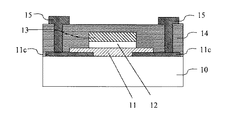
図1は、本発明の好適な実施形態の一例である、トップゲート型コプラナー構造の酸化物半導体TFTの構成を示す断面図である。10は基板、11は酸化物半導体層、11aは酸化物半導体層のチャネル領域、11bは酸化物半導体層のソース・ドレイン領域、12はゲート絶縁層、13はゲート電極層、14は保護層、15はソース・ドレイン配線層である。
FIG. 1 is a cross-sectional view showing a configuration of an oxide semiconductor TFT having a top gate type coplanar structure, which is an example of a preferred embodiment of the present invention. 10 is a substrate, 11 is an oxide semiconductor layer, 11a is a channel region of the oxide semiconductor layer, 11b is a source / drain region of the oxide semiconductor layer, 12 is a gate insulating layer, 13 is a gate electrode layer, 14 is a protective layer,
基板10としてはガラス基板を用いるのが好ましい。ポリエチレン・テレフタレート(PET)、ポリエチレン・ナフタレート(PEN)、ポリイミド、ポリカーボネート等のプラスチックのフィルム、並びに薄板、絶縁層をコーティングしたステンレス基板等を用いても良い。
A glass substrate is preferably used as the
まず、基板10上にスパッタ法、パルスレーザー蒸着法(PLD法)、電子ビーム蒸着法等により酸化物半導体層11を形成する。その後、フォトリソグラフィー法とエッチング法等により酸化物半導体層11をパターニングする。酸化物半導体層11としてはIn、Ga、Zn、Snの少なくとも1種類の元素を含むアモルファス酸化物半導体を用いるのが好ましい。
First, the
次に、酸化物半導体層11上(酸化物半導体層のチャネル領域11a上)にスパッタ法、パルスレーザー蒸着法(PLD法)、電子ビーム蒸着法、プラズマCVD法等によりゲート絶縁層12を形成する。ゲート絶縁層12は酸化物半導体層11と直接接するため、ゲート絶縁層12形成の際に酸化物半導体層のチャネル領域11aの低抵抗化を抑制する機能が要求される。具体的には、ゲート絶縁層12としては酸化シリコンや酸窒化シリコン等の酸素を含む絶縁層を用いるのが好ましい。これらの絶縁層の組成がストイキオメトリーから外れていても何ら問題はない。
Next, the
続いて、ゲート絶縁層12上にスパッタ法、PLD法、電子ビーム蒸着法等よりゲート電極層13を形成する。その後、フォトリソグラフィー法とエッチング法等によりゲート絶縁層12及びゲート電極層13をパターニングする。ゲート電極層13としてはIn、Ga、Zn、Snの少なくとも1種類の元素を含むアモルファス酸化物半導体を用いるのが好ましい。ゲート電極層13はTi、Pt、Au、Ni、Al、Mo等の金属やそれらの合金等の金属電極材料及びそれらの積層膜と、ITO等の酸化物導電体等の電極材料と、の積層にしても良く、この場合はどちらが上層でも良い。
Subsequently, the
次に、酸化物半導体層11上(酸化物半導体層のソース・ドレイン領域11bとなる領域上)及びゲート電極層13上に保護層14を形成する。保護層14には、酸化物半導体層11の、上部にゲート電極層13が形成されていない領域(酸化物半導体層のソース・ドレイン領域11bとなる領域)、及び酸化物半導体から成るゲート電極層13を低抵抗化させる機能が要求される。酸化物半導体は水素を添加することにより低抵抗化させることが可能であるため、保護層14としては水素を含む絶縁層を用いるのが好ましい。具体的には水素を含む窒化シリコン膜、酸化シリコン膜、酸窒化シリコン膜、炭化シリコン膜及びこれらの積層膜等を用いるのが好ましい。これらの絶縁層の組成がストイキオメトリーから外れていても何ら問題はない。形成方法としては水素を含む原料ガスを用いるプラズマCVD法が、プラズマによる酸化物半導体への水素拡散の促進効果もあるため望ましい。このとき、原料中の水素が、酸化物半導体層11の、上部にゲート電極層13が形成されていない領域(酸化物半導体層のソース・ドレイン領域11bとなる領域)及びゲート電極層13に拡散する。この拡散により、酸化物半導体層11の、上部にゲート電極層13が形成されていない領域が低抵抗化すると同時にゲート電極層13も低抵抗化する。また、このとき、酸化物半導体層11の、上部にゲート電極層13が形成されていない領域には、ゲート絶縁層12及びゲート電極層13をマスクとして自己整合的に酸化物半導体層のソース・ドレイン領域11bが形成される。即ち、ソース電極層及びドレイン電極層が形成される。そして、酸化物半導体層のチャネル領域11a及び酸化物半導体層のソース・ドレイン領域11bが同一の酸化物半導体層11で形成されている状態になる。これにより、寄生容量の小さいTFTの作製が可能である。なお、酸化物半導体層のソース・ドレイン領域11bを別の層で別途形成し、ソース・ドレイン電極層としても良い。その際のTFTの構造は、図2に示すボトムコンタクト構造や図3に示すトップコンタクト構造等とするのが好ましい。この際のソース・ドレイン電極層としてはTi、Pt、Au、Ni、Al、Mo等の金属やそれらの合金等の金属電極材料及びそれらの積層膜、ITO等の酸化物導電体等を用いるのが好ましい。
Next, the
続いて、フォトリソグラフィー法とエッチング法等により保護層14にコンタクトホールを形成する。その後、スパッタ法、パルスレーザー蒸着法(PLD法)、電子ビーム蒸着法、CVD法等により外部との電気的接続を行うためにソース・ドレイン配線層15を形成する。ソース・ドレイン配線層15としては良好な電気伝導性を有するものであれば良く、例えばTi、Pt、Au、Ni、Al、Mo等の金属やそれらの合金等の金属電極材料及びそれらの積層膜、ITO等の酸化物導電体等を用いるのが好ましい。なお、酸化物半導体層のソース・ドレイン領域11bをそのままソース・ドレイン配線層15として用いても良い。
Subsequently, a contact hole is formed in the
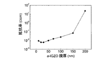
ここで、図4にIn−Ga−Zn−O系アモルファス酸化物半導体(アモルファスIGZO)からなるゲート電極層上に、水素を含む絶縁層である窒化シリコン層を形成した時の抵抗率の膜厚依存性を示す。窒化シリコン層はPECVD法により形成した。アモルファス酸化物半導体の抵抗率は窒化シリコン層を形成する前は測定限界である105Ωcmよりも大きい値としたが、窒化シリコン層の形成により、図4に示すように十分に低抵抗化した。図4より、アモルファス酸化物半導体からなるゲート電極層の膜厚が30nmを超えると抵抗率が増加することが分かる。このことは膜厚方向に抵抗率の分布があることを示しており、水素を含む絶縁層の界面から離れるにつれて、アモルファス酸化物半導体膜の抵抗率が増加しているといえる。つまり、アモルファス酸化物半導体には水素拡散による低抵抗化を抑制する機能がある。 Here, the film thickness of resistivity when a silicon nitride layer which is an insulating layer containing hydrogen is formed over the gate electrode layer made of an In—Ga—Zn—O-based amorphous oxide semiconductor (amorphous IGZO) in FIG. Indicates dependency. The silicon nitride layer was formed by PECVD. The resistivity of the amorphous oxide semiconductor was set to a value larger than the measurement limit of 10 5 Ωcm before the silicon nitride layer was formed, but the resistance was sufficiently lowered as shown in FIG. 4 by the formation of the silicon nitride layer. . FIG. 4 shows that the resistivity increases when the thickness of the gate electrode layer made of an amorphous oxide semiconductor exceeds 30 nm. This indicates that there is a resistivity distribution in the film thickness direction, and it can be said that the resistivity of the amorphous oxide semiconductor film increases as the distance from the interface of the insulating layer containing hydrogen increases. That is, the amorphous oxide semiconductor has a function of suppressing a reduction in resistance due to hydrogen diffusion.
一方、アモルファス酸化物半導体上に酸化シリコン層とMo層を順次形成した積層膜があるボトムゲート型酸化物半導体TFTを作製した。このときの酸化シリコン、Moの膜厚はそれぞれ300nm、200nmとした。酸化シリコン層はPECVD法、Mo層はスパッタ法でそれぞれ形成した。このTFT上に、水素を含む絶縁層である窒化シリコン層を形成する前と形成した後のId−Vg特性を図5に示す。図5より、膜厚300nmの酸化シリコン層及び膜厚200nmのMo層があっても、窒化シリコン層を形成後、TFTはオフできなくなってしまっていることが分かる。つまり、これらの膜は、窒化シリコン層からの水素拡散による酸化物半導体層のチャネル領域の低抵抗化を抑制できていないことが分かる。その理由は明らかでないが、Mo層が多結晶膜であることから、粒界における増速拡散がこの結果を招いている可能性がある。これに対して、アモルファス酸化物半導体に粒界は存在しない。これらの結果とゲート絶縁層は薄い方がTFTの特性上の望ましいことから、ゲート電極層13に水素拡散を抑制する機能がある方が望ましいと言える。
On the other hand, a bottom-gate oxide semiconductor TFT having a laminated film in which a silicon oxide layer and a Mo layer are sequentially formed on an amorphous oxide semiconductor was manufactured. The film thicknesses of silicon oxide and Mo at this time were 300 nm and 200 nm, respectively. The silicon oxide layer was formed by PECVD, and the Mo layer was formed by sputtering. FIG. 5 shows the Id-Vg characteristics before and after the silicon nitride layer, which is an insulating layer containing hydrogen, is formed on the TFT. From FIG. 5, it can be seen that even if there is a silicon oxide layer having a thickness of 300 nm and a Mo layer having a thickness of 200 nm, the TFT cannot be turned off after the silicon nitride layer is formed. That is, it can be seen that these films cannot suppress the resistance reduction of the channel region of the oxide semiconductor layer due to hydrogen diffusion from the silicon nitride layer. The reason is not clear, but since the Mo layer is a polycrystalline film, accelerated diffusion at the grain boundary may cause this result. On the other hand, there is no grain boundary in the amorphous oxide semiconductor. Since these results and the thinner gate insulating layer are desirable in terms of TFT characteristics, it can be said that the
さらに、図6に示す構造で基板10上に下部電極層24、絶縁層25、上部電極層26からなる蓄積容量を形成した。この上部電極層26に低抵抗化したアモルファス酸化物半導体を用いた場合と金属を用いた場合の下部電極層24と上部電極層26間におけるリーク電流密度の比較を図7に示す。このとき、下部電極層24にはTi/Au/Ti層、絶縁層25には酸化シリコン層をそれぞれ用いた。図6に示すように、蓄積容量の上部電極層26の絶縁層と接する側にアモルファス酸化物半導体層を用いた場合の方が、下部電極層24と上部電極層26間のリーク電流密度が小さいことが分かる。以上のことから、このように低抵抗化したアモルファス酸化物半導体層をトップゲート型TFTにおけるゲート電極層に用いる場合も、ゲート絶縁層のリーク電流密度低減の効果が期待できる。
Further, a storage capacitor composed of the
こうして、トップゲート型コプラナー構造酸化物半導体TFTが完成する。本発明においては、このように上記トランジスタを基板上に二次元状に複数配(平面状に縦横に配置)することができる。 Thus, a top-gate coplanar structure oxide semiconductor TFT is completed. In the present invention, a plurality of the above transistors can be arranged two-dimensionally (arranged vertically and horizontally in a plane) on the substrate in this way.
以下、本発明の実施例について詳細に説明するが、本発明はこれらによって何ら限定されるものではない。 Examples of the present invention will be described in detail below, but the present invention is not limited to these examples.
(実施例1)
図1は本実施例のトップゲート型コプラナー構造の酸化物半導体TFTである。
Example 1
FIG. 1 shows an oxide semiconductor TFT having a top gate type coplanar structure according to this embodiment.
まず、ガラス基板10上に、酸化物半導体層11として、膜厚30nmのアモルファスIGZOをスパッタ法により形成した。酸化物半導体層11はDCスパッタ装置を用いて基板温度は室温(25℃)で形成した。ターゲットとしてはInGaZnO4組成を有する多結晶焼結体を用い、投入DCパワーは300Wとした。成膜時の雰囲気は全圧0.5Paとし、その際のガス流量比はAr:O2=98:2とした。その後、フォトリソグラフィー法とエッチング法により酸化物半導体層11をパターニングした。
First, an amorphous IGZO film having a thickness of 30 nm was formed as the
次に、酸化物半導体層11上(酸化物半導体層のチャネル領域11a上)に、ゲート絶縁層12として、膜厚100nmの酸化シリコン膜をスパッタ法により形成した。酸化シリコン膜はRFスパッタ装置を用いて室温で形成した。ターゲットとしては4インチSiO2を用い、投入RFパワーは500Wとした。成膜時の雰囲気は全圧0.5Paとし、その際のガス流量比はAr:O2=90:10とした。
Next, a 100-nm-thick silicon oxide film was formed as the
続いて、ゲート絶縁層12上に、ゲート電極層13として、膜厚200nmのアモルファスIGZOをスパッタ法により形成した。ゲート電極層13はDCスパッタ装置を用いて基板温度は室温(25℃)で形成した。ターゲットとしてはInGaZnO4組成を有する多結晶焼結体を用い、投入DCパワーは150Wとした。成膜時の雰囲気は全圧0.5Paとし、その際のガス流量比はAr:O2=80:20とした。その後、フォトリソグラフィー法とエッチング法によりゲート絶縁層12及びゲート電極層13をパターニングした。
Subsequently, an amorphous IGZO film having a thickness of 200 nm was formed as a
次に、酸化物半導体層11上(酸化物半導体層のソース・ドレイン領域11bとなる領域上)及びゲート電極層13上に、保護層14として、膜厚300nmの水素を含む窒化シリコン膜をプラズマCVD法により形成した。プラズマCVD法による窒化シリコン膜の形成時の基板温度は150℃とした。プロセスガスとしてはSiH4、NH3、N2を用い、ガス流量比はSiH4:NH3:N2=1:2.5:25とした。投入RFパワー密度と圧力はそれぞれ0.9W/cm2、150Paとした。また、保護層14の形成と同時に、酸化物半導体層11の、上部にゲート電極層13が形成されていない領域が低抵抗化し、酸化物半導体層のソース・ドレイン領域11bとなり、更にゲート電極層13が低抵抗化した。
Next, a 300-nm-thick silicon nitride film containing hydrogen is formed as a
最後に、フォトリソグラフィー法とエッチング法により保護層14にコンタクトホールを形成した後、ソース・ドレイン配線層15として膜厚100nmのMoを形成した。その後、フォトリソグラフィー法とエッチング法によりソース・ドレイン配線層15をパターニングした。
Finally, contact holes were formed in the
上記工程により、本実施例の酸化物半導体TFTを完成させた。 Through the above process, the oxide semiconductor TFT of this example was completed.
本実施例では、膜厚200nmのアモルファス酸化物半導体をトップゲート型TFTにおけるゲート電極層13とし、ゲート電極層13上に、保護層14として膜厚300nmの水素を含む窒化シリコン膜を形成した。よって、前述の図4及び図7の説明にて述べたように、酸化物半導体層のチャネル領域11aの、水素拡散による低抵抗化を抑制でき、更にゲート絶縁層12のリーク電流密度を低減できた。
In this embodiment, an amorphous oxide semiconductor with a thickness of 200 nm is used as the
(実施例2)
図2は本実施例のトップゲート型ボトムコンタクト構造の酸化物半導体TFTである。
(Example 2)
FIG. 2 shows an oxide semiconductor TFT having a top gate type bottom contact structure according to this embodiment.
まず、ガラス基板10上に、ソース・ドレイン電極層11cとして、膜厚200nmのMoを形成した後、フォトリソグラフィー法とエッチング法によりソース・ドレイン電極層11cをパターニングした。
First, Mo having a film thickness of 200 nm was formed on the
次に、実施例1と同様にして酸化物半導体層11(酸化物半導体層のチャネル領域)、ゲート絶縁層12を順次形成した。
Next, in the same manner as in Example 1, the oxide semiconductor layer 11 (the channel region of the oxide semiconductor layer) and the
続いて、ゲート絶縁層12上に、ゲート電極層13として、膜厚200nmのアモルファスIGZOをスパッタ法により形成した。ゲート電極層13はDCスパッタ装置を用いて室温(25℃)で形成した。ターゲットとしてはInGaZnO4組成を有する多結晶焼結体を用い、投入DCパワーは150Wとした。成膜時の雰囲気は全圧0.5Paとし、その際のガス流量比はAr:O2=80:20とした。その後、フォトリソグラフィー法とエッチング法によりゲート電極層13をパターニングした。
Subsequently, an amorphous IGZO film having a thickness of 200 nm was formed as a
次に、実施例1と同様にして保護層14を形成した。保護層14の形成により、ゲート電極層13が低抵抗化した。
Next, the
最後に、フォトリソグラフィー法とエッチング法により保護層14にコンタクトホールを形成した後、ソース・ドレイン配線層15として、膜厚100nmのMoを形成した。その後、フォトリソグラフィー法とエッチング法によりソース・ドレイン配線層15をパターニングした。
Finally, contact holes were formed in the
上記工程により、本実施例の酸化物半導体TFTを完成させた。 Through the above process, the oxide semiconductor TFT of this example was completed.
本実施例では、膜厚200nmのアモルファス酸化物半導体をトップゲート型TFTにおけるゲート電極層13とし、ゲート電極層13上に、保護層14として膜厚300nmの水素を含む窒化シリコン膜を形成した。よって、前述の図4及び図7の説明にて述べたように、実施例1と同様に、酸化物半導体層11(酸化物半導体層のチャネル領域)の、水素拡散による低抵抗化を抑制でき、更にゲート絶縁層12のリーク電流密度を低減できた。
In this embodiment, an amorphous oxide semiconductor with a thickness of 200 nm is used as the
(実施例3)
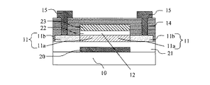
図8は本実施例のダブルゲート型コプラナー構造の酸化物半導体TFTである。
(Example 3)
FIG. 8 shows an oxide semiconductor TFT having a double gate type coplanar structure according to this embodiment.
まず、ガラス基板10上に、ボトムゲート電極層20として、膜厚200nmのMoを形成した後、フォトリソグラフィー法とエッチング法によりボトムゲート電極層20をパターニングした。
First, Mo having a thickness of 200 nm was formed on the
次に、ガラス基板10上及びボトムゲート電極層20上に、下側ゲート絶縁層21として、膜厚200nmの酸化シリコン膜をプラズマCVD法により形成した。プラズマCVD法による酸化シリコン膜の形成時の基板温度は340℃とした。プロセスガスとしてはSiH4、N2Oを用い、ガス流量比はSiH4:N2O=1:25とした。投入RFパワー密度と圧力はそれぞれ0.9W/cm2、173Paとした。
Next, a 200 nm-thickness silicon oxide film was formed as a lower
次に、実施例1と同様にして酸化物半導体層11を形成した。
Next, the
続いて、酸化物半導体層11上(酸化物半導体層のチャネル領域11a上)に、上側ゲート絶縁層22として、膜厚100nmの酸化シリコン膜をスパッタ法により形成した。上側ゲート絶縁層22はRFスパッタ装置を用いて室温(25℃)で形成した。ターゲットとしてはSiO2を用い、投入RFパワーは500Wとした。成膜時の雰囲気は全圧0.5Paとし、その際のガス流量比はAr:O2=90:10とした。
Subsequently, a silicon oxide film having a thickness of 100 nm was formed as the upper
次に、フォトリソグラフィー法とエッチング法により、下側ゲート絶縁層21及び上側ゲート絶縁層22にコンタクトホール(図8に不図示)を形成した。
Next, contact holes (not shown in FIG. 8) were formed in the lower
続いて、上側ゲート絶縁層22上に、トップゲート電極層23として、膜厚200nmのアモルファスIGZOをスパッタ法により形成した。トップゲート電極層23はDCスパッタ装置を用いて基板温度は室温(25℃)で形成した。ターゲットとしてはInGaZnO4組成を有する多結晶焼結体を用い、投入DCパワーは150Wとした。成膜時の雰囲気は全圧0.5Paとし、その際のガス流量比はAr:O2=80:20とした。ボトムゲート電極層20とトップゲート電極層23は、前述のコンタクトホールを介して電気的に接続した。その後、ボトムゲート電極層20をマスクとする裏面露光を用いたフォトリソグラフィー法とエッチング法により上側ゲート絶縁層22及びトップゲート電極層23をパターニングした。ボトムゲート電極層20をマスクとした裏面露光を用いることにより、トップゲート電極層23がボトムゲート電極層20に対して準自己整合的にパターニングされた。
Subsequently, an amorphous IGZO film having a thickness of 200 nm was formed as a top
次に、実施例1と同様にして保護層14を形成した。保護層14の形成と同時に、酸化物半導体層11の、上部にトップゲート電極層23が形成されていない領域の酸化物半導体層11が低抵抗化し、酸化物半導体層のソース・ドレイン領域11bとなり、更にトップゲート電極層23が低抵抗化した。酸化物半導体層のソース・ドレイン領域11bはボトムゲート電極層20に対して準自己整合的、かつトップゲート電極層23に対して自己整合的に形成された。
Next, the
最後に、フォトリソグラフィー法とエッチング法により保護層14にコンタクトホールを形成した後、ソース・ドレイン配線層15として、膜厚100nmのMoを形成した。その後、フォトリソグラフィー法によりソース・ドレイン配線層15をパターニングした。
Finally, contact holes were formed in the
上記工程により、本実施例の酸化物半導体TFTを完成させた。 Through the above process, the oxide semiconductor TFT of this example was completed.
本実施例では、膜厚200nmのアモルファス酸化物半導体をダブルゲート型TFTにおける上側ゲート電極層23とし、上側ゲート電極層23上に、保護層14として膜厚300nmの水素を含む窒化シリコン膜を形成した。よって、前述の図4及び図7の説明にて述べたように、実施例1及び2と同様に、酸化物半導体層のチャネル領域11aの、水素拡散による低抵抗化を抑制でき、更にゲート絶縁層12のリーク電流密度を低減できた。
In this embodiment, an amorphous oxide semiconductor with a thickness of 200 nm is used as the upper
(実施例4)
図9は本実施例の表示装置であり、トップゲート型コプラナー構造の酸化物半導体TFTと、表示素子を備えた表示装置である。酸化物半導体TFTは実施例1と同様にして作製した。なお、図1〜図3及び図8のうちのいずれの酸化物半導体TFTを用いても良い。
Example 4
FIG. 9 shows a display device of this embodiment, which is a display device including an oxide semiconductor TFT having a top gate type coplanar structure and a display element. The oxide semiconductor TFT was manufactured in the same manner as in Example 1. Note that any of the oxide semiconductor TFTs in FIGS. 1 to 3 and FIG. 8 may be used.
まず、本発明の酸化物半導体TFT120上に、絶縁層121として、シリコン窒化膜をプラズマCVD法により形成した後、フォトリソグラフィー法とエッチング法により絶縁層121にコンタクトホールを形成した。次に、絶縁層121上に、電極層123として、ソース配線層122に絶縁層121を介してITOをスパッタ法により形成した。その後、電極層123上に、正孔輸送層124として、α‐NPDを蒸着法により形成した後、発光層125として、Alq3を蒸着法により形成した。最後に、発光層125上に、電極層126として、MgAgを蒸着法により形成した。
First, a silicon nitride film was formed as an insulating
上記工程により、本発明の酸化物半導体TFTと、有機エレクトロルミネッセンス素子を表示素子として備え、TFTのソース電極層又はドレイン電極層と前記表示素子が電気的に接続された、本実施例の表示装置を完成させた。 According to the above process, the display device of this embodiment is provided with the oxide semiconductor TFT of the present invention and an organic electroluminescence element as a display element, and the display electrode is electrically connected to the source or drain electrode layer of the TFT. Was completed.
10:基板、11:酸化物半導体層、11a:酸化物半導体層のチャネル領域、11b:酸化物半導体層のソース・ドレイン領域、11c:ソース・ドレイン電極層、12:ゲート絶縁層、13:ゲート電極層、14:保護層、15:ソース・ドレイン配線層 10: substrate, 11: oxide semiconductor layer, 11a: channel region of oxide semiconductor layer, 11b: source / drain region of oxide semiconductor layer, 11c: source / drain electrode layer, 12: gate insulating layer, 13: gate Electrode layer, 14: protective layer, 15: source / drain wiring layer
Claims (4)
前記ゲート絶縁層は前記酸化物半導体層のチャネル領域の上に形成され、
前記ゲート電極層は前記ゲート絶縁層の上に形成され、
前記保護層は前記ゲート電極層の上に形成されていることを特徴とするトップゲート型薄膜トランジスタ。 On the substrate, a source electrode layer, a drain electrode layer, an oxide semiconductor layer, a gate insulating layer, and a gate electrode layer made of an amorphous oxide semiconductor containing at least one element of In, Ga, Zn, and Sn And a protective layer containing hydrogen,
The gate insulating layer is formed on a channel region of the oxide semiconductor layer;
The gate electrode layer is formed on the gate insulating layer;
The top gate type thin film transistor, wherein the protective layer is formed on the gate electrode layer.
前記トップゲート型薄膜トランジスタのソース電極層又はドレイン電極層と前記表示素子が電気的に接続されていることを特徴とする表示装置。 A top-gate thin film transistor according to any one of claims 1 to 3 and a display element,
A display device, wherein a source electrode layer or a drain electrode layer of the top-gate thin film transistor and the display element are electrically connected.
Priority Applications (2)
| Application Number | Priority Date | Filing Date | Title |
|---|---|---|---|
| JP2010174234A JP2012033836A (en) | 2010-08-03 | 2010-08-03 | Top gate type thin film transistor and display device including the same |
| US13/188,215 US8624240B2 (en) | 2010-08-03 | 2011-07-21 | Top gate thin film transistor and display apparatus including the same |
Applications Claiming Priority (1)
| Application Number | Priority Date | Filing Date | Title |
|---|---|---|---|
| JP2010174234A JP2012033836A (en) | 2010-08-03 | 2010-08-03 | Top gate type thin film transistor and display device including the same |
Publications (2)
| Publication Number | Publication Date |
|---|---|
| JP2012033836A true JP2012033836A (en) | 2012-02-16 |
| JP2012033836A5 JP2012033836A5 (en) | 2013-09-12 |
Family
ID=45555465
Family Applications (1)
| Application Number | Title | Priority Date | Filing Date |
|---|---|---|---|
| JP2010174234A Pending JP2012033836A (en) | 2010-08-03 | 2010-08-03 | Top gate type thin film transistor and display device including the same |
Country Status (2)
| Country | Link |
|---|---|
| US (1) | US8624240B2 (en) |
| JP (1) | JP2012033836A (en) |
Cited By (34)
| Publication number | Priority date | Publication date | Assignee | Title |
|---|---|---|---|---|
| US20120032173A1 (en) * | 2010-08-03 | 2012-02-09 | Canon Kabushiki Kaisha | Top gate thin film transistor and display apparatus including the same |
| KR20140002500A (en) * | 2012-06-29 | 2014-01-08 | 가부시키가이샤 한도오따이 에네루기 켄큐쇼 | Semiconductor device and method for manufacturing semiconductor device |
| KR20140102146A (en) * | 2013-02-13 | 2014-08-21 | 가부시키가이샤 한도오따이 에네루기 켄큐쇼 | Semiconductor device and manufacturing method of semiconductor device |
| KR20150092722A (en) * | 2014-02-05 | 2015-08-13 | 가부시키가이샤 한도오따이 에네루기 켄큐쇼 | Semiconductor device, display device including the semiconductor device, display module including the display device, and electronic device including the semiconductor device, the display device, and the display module |
| JP2015233135A (en) * | 2014-05-15 | 2015-12-24 | 株式会社半導体エネルギー研究所 | Semiconductor device, and display device having the same |
| US9412876B2 (en) | 2014-02-07 | 2016-08-09 | Semiconductor Energy Laboratory Co., Ltd. | Semiconductor device |
| WO2016189414A1 (en) * | 2015-05-22 | 2016-12-01 | Semiconductor Energy Laboratory Co., Ltd. | Semiconductor device and display device including the semiconductor device |
| US9530894B2 (en) | 2014-02-07 | 2016-12-27 | Semiconductor Energy Laboratory Co., Ltd. | Semiconductor device |
| JP2017005064A (en) * | 2015-06-08 | 2017-01-05 | 株式会社半導体エネルギー研究所 | Semiconductor device, and display device having the same |
| WO2017009738A1 (en) * | 2015-07-14 | 2017-01-19 | 株式会社半導体エネルギー研究所 | Semiconductor device and method for manufacturing same |
| JP2017028252A (en) * | 2015-05-22 | 2017-02-02 | 株式会社半導体エネルギー研究所 | Semiconductor device and display device having semiconductor device |
| JP2017054899A (en) * | 2015-09-09 | 2017-03-16 | 株式会社半導体エネルギー研究所 | Semiconductor device, display device, electronic apparatus using the display device |
| US9634150B2 (en) | 2014-03-07 | 2017-04-25 | Semiconductor Energy Laboratory Co., Ltd. | Semiconductor device, display device, input/output device, and electronic device |
| WO2017122110A1 (en) * | 2016-01-15 | 2017-07-20 | 株式会社半導体エネルギー研究所 | Display device, display module, and electronic instrument |
| JP2017228752A (en) * | 2015-08-19 | 2017-12-28 | 株式会社半導体エネルギー研究所 | Semiconductor device manufacturing method |
| US9859391B2 (en) | 2015-10-27 | 2018-01-02 | Nlt Technologies, Ltd. | Thin film transistor, display device, and method for manufacturing thin film transistor |
| CN107579111A (en) * | 2016-07-05 | 2018-01-12 | 三星显示有限公司 | Thin film transistor (TFT) and the thin-film transistor display panel including the thin film transistor (TFT) |
| US9923097B2 (en) | 2013-12-06 | 2018-03-20 | Semiconductor Energy Laboratory Co., Ltd. | Semiconductor device |
| JP2018121049A (en) * | 2016-12-23 | 2018-08-02 | 株式会社半導体エネルギー研究所 | Semiconductor device and semiconductor device manufacturing method |
| JPWO2017085595A1 (en) * | 2015-11-20 | 2018-09-20 | 株式会社半導体エネルギー研究所 | Semiconductor device, method for manufacturing the semiconductor device, or display device having the semiconductor device |
| KR20180124040A (en) * | 2016-02-12 | 2018-11-20 | 가부시키가이샤 한도오따이 에네루기 켄큐쇼 | Semiconductor device and display device including the semiconductor device |
| JP2018195837A (en) * | 2013-10-22 | 2018-12-06 | 株式会社半導体エネルギー研究所 | Semiconductor device |
| JP2019041122A (en) * | 2014-02-05 | 2019-03-14 | 株式会社半導体エネルギー研究所 | Semiconductor device |
| US10276644B2 (en) | 2015-08-13 | 2019-04-30 | Samsung Display Co., Ltd | Organic light emitting diode display and manufacturing method thereof |
| JP2019134182A (en) * | 2014-01-24 | 2019-08-08 | 株式会社半導体エネルギー研究所 | Semiconductor device |
| JP2019186573A (en) * | 2014-03-14 | 2019-10-24 | 株式会社半導体エネルギー研究所 | Method of manufacturing semiconductor device |
| US10566437B2 (en) | 2015-08-25 | 2020-02-18 | Mitsubishi Electric Corporation | Thin film transistor and array substrate |
| KR20200053640A (en) * | 2017-10-12 | 2020-05-18 | 어플라이드 머티어리얼스, 인코포레이티드 | Process to reduce plasma-induced damage |
| JP2020127016A (en) * | 2020-04-01 | 2020-08-20 | 株式会社半導体エネルギー研究所 | Semiconductor device |
| JP2020145451A (en) * | 2015-03-03 | 2020-09-10 | 株式会社半導体エネルギー研究所 | Production method of semiconductor device |
| JP2021028984A (en) * | 2013-05-20 | 2021-02-25 | 株式会社半導体エネルギー研究所 | Transistor |
| JP2021048403A (en) * | 2015-03-03 | 2021-03-25 | 株式会社半導体エネルギー研究所 | Liquid crystal display device |
| KR20220137143A (en) * | 2016-03-22 | 2022-10-11 | 가부시키가이샤 한도오따이 에네루기 켄큐쇼 | Semiconductor device and display device including the same |
| KR102655935B1 (en) | 2016-02-12 | 2024-04-11 | 가부시키가이샤 한도오따이 에네루기 켄큐쇼 | Semiconductor device and display device including the semiconductor device |
Families Citing this family (28)
| Publication number | Priority date | Publication date | Assignee | Title |
|---|---|---|---|---|
| WO2011074407A1 (en) | 2009-12-18 | 2011-06-23 | Semiconductor Energy Laboratory Co., Ltd. | Semiconductor device and method for manufacturing the same |
| US9209314B2 (en) | 2010-06-16 | 2015-12-08 | Semiconductor Energy Laboratory Co., Ltd. | Field effect transistor |
| JP5975635B2 (en) | 2010-12-28 | 2016-08-23 | 株式会社半導体エネルギー研究所 | Semiconductor device |
| US9443984B2 (en) | 2010-12-28 | 2016-09-13 | Semiconductor Energy Laboratory Co., Ltd. | Semiconductor device and manufacturing method thereof |
| US9082663B2 (en) | 2011-09-16 | 2015-07-14 | Semiconductor Energy Laboratory Co., Ltd. | Semiconductor device and manufacturing method thereof |
| CN103843145B (en) | 2011-09-29 | 2017-03-29 | 株式会社半导体能源研究所 | Semiconductor device |
| KR20140074384A (en) | 2011-10-14 | 2014-06-17 | 가부시키가이샤 한도오따이 에네루기 켄큐쇼 | Semiconductor device |
| US8796683B2 (en) | 2011-12-23 | 2014-08-05 | Semiconductor Energy Laboratory Co., Ltd. | Semiconductor device |
| JP2014093433A (en) * | 2012-11-05 | 2014-05-19 | Sony Corp | Semiconductor device, display device and electronic apparatus |
| KR102222344B1 (en) * | 2013-05-02 | 2021-03-02 | 가부시키가이샤 한도오따이 에네루기 켄큐쇼 | Semiconductor device |
| TWI742574B (en) | 2013-05-16 | 2021-10-11 | 日商半導體能源研究所股份有限公司 | Semiconductor device |
| TWI624936B (en) | 2013-06-05 | 2018-05-21 | 半導體能源研究所股份有限公司 | Display device |
| CN103346089B (en) * | 2013-06-13 | 2016-10-26 | 北京大学深圳研究生院 | A kind of autoregistration bilayer channel metal-oxide thin film transistor (TFT) and preparation method thereof |
| TWI527201B (en) | 2013-11-06 | 2016-03-21 | 友達光電股份有限公司 | Pixel structure and fabricating method thereof |
| US9397149B2 (en) | 2013-12-27 | 2016-07-19 | Semiconductor Energy Laboratory Co., Ltd. | Semiconductor device |
| KR102513764B1 (en) | 2013-12-27 | 2023-03-24 | 가부시키가이샤 한도오따이 에네루기 켄큐쇼 | Light-emitting device |
| US9929279B2 (en) | 2014-02-05 | 2018-03-27 | Semiconductor Energy Laboratory Co., Ltd. | Semiconductor device and manufacturing method thereof |
| US9640669B2 (en) | 2014-03-13 | 2017-05-02 | Semiconductor Energy Laboratory Co., Ltd. | Semiconductor device, display device including the semiconductor device, display module including the display device, and electronic appliance including the semiconductor device, the display device, and the display module |
| US20170317217A1 (en) * | 2014-11-11 | 2017-11-02 | Sharp Kabushiki Kaisha | Semiconductor device and method for manufacturing same |
| KR102281848B1 (en) | 2015-01-26 | 2021-07-26 | 삼성디스플레이 주식회사 | Thin film transistor and method of manufacturing the same |
| US11024725B2 (en) | 2015-07-24 | 2021-06-01 | Semiconductor Energy Laboratory Co., Ltd. | Semiconductor device including metal oxide film |
| JP6851166B2 (en) | 2015-10-12 | 2021-03-31 | 株式会社半導体エネルギー研究所 | Manufacturing method of semiconductor device |
| JP6821982B2 (en) * | 2015-10-27 | 2021-01-27 | 天馬微電子有限公司 | Manufacturing method of thin film transistor, display device and thin film transistor |
| TW201804613A (en) * | 2016-07-26 | 2018-02-01 | 聯華電子股份有限公司 | Oxide semiconductor device |
| KR102510397B1 (en) | 2017-09-01 | 2023-03-16 | 삼성디스플레이 주식회사 | Thin film transistor and display device comprising the same |
| CN110349974A (en) * | 2019-06-25 | 2019-10-18 | 武汉华星光电半导体显示技术有限公司 | A kind of array substrate and preparation method thereof, display device |
| CN111403425B (en) * | 2020-03-31 | 2023-04-14 | 成都京东方显示科技有限公司 | Array substrate, manufacturing method thereof and display panel |
| CN113823676B (en) * | 2020-06-18 | 2023-07-04 | 联华电子股份有限公司 | Semiconductor device and method for manufacturing the same |
Citations (2)
| Publication number | Priority date | Publication date | Assignee | Title |
|---|---|---|---|---|
| JP2007073699A (en) * | 2005-09-06 | 2007-03-22 | Canon Inc | Manufacturing method of oxide semiconductor device |
| JP2009272427A (en) * | 2008-05-07 | 2009-11-19 | Canon Inc | Thin-film transistor and method of manufacturing the same |
Family Cites Families (27)
| Publication number | Priority date | Publication date | Assignee | Title |
|---|---|---|---|---|
| US6452091B1 (en) | 1999-07-14 | 2002-09-17 | Canon Kabushiki Kaisha | Method of producing thin-film single-crystal device, solar cell module and method of producing the same |
| JP3445187B2 (en) | 1999-08-03 | 2003-09-08 | キヤノン株式会社 | Semiconductor device defect compensation method |
| JP2002206168A (en) | 2000-10-24 | 2002-07-26 | Canon Inc | Method for depositing silicon-based thin film, method for depositing silicon-based semiconductor layer and photovoltaic element |
| US6930025B2 (en) | 2001-02-01 | 2005-08-16 | Canon Kabushiki Kaisha | Transparent conductive film formation process, photovoltaic device production process, transparent conductive film, and photovoltaic device |
| JP2002231984A (en) | 2001-02-01 | 2002-08-16 | Canon Inc | Method for forming transparent conductive film, method for compensating defective area of semiconductor layer, photovoltaic element and manufacturing method therefor |
| US6858308B2 (en) | 2001-03-12 | 2005-02-22 | Canon Kabushiki Kaisha | Semiconductor element, and method of forming silicon-based film |
| JP2003007629A (en) | 2001-04-03 | 2003-01-10 | Canon Inc | Method of forming silicon film, the silicon film, and semiconductor device |
| JP2004289034A (en) | 2003-03-25 | 2004-10-14 | Canon Inc | Treatment method for zinc oxide film and method for manufacturing photovoltaic element using same |
| KR100675285B1 (en) | 2005-10-10 | 2007-01-29 | 삼성전자주식회사 | Semiconductor device having vertical transistor and method of fabricating the same |
| JP5037808B2 (en) | 2005-10-20 | 2012-10-03 | キヤノン株式会社 | Field effect transistor using amorphous oxide, and display device using the transistor |
| JP5015471B2 (en) | 2006-02-15 | 2012-08-29 | 財団法人高知県産業振興センター | Thin film transistor and manufacturing method thereof |
| JP5127183B2 (en) | 2006-08-23 | 2013-01-23 | キヤノン株式会社 | Thin film transistor manufacturing method using amorphous oxide semiconductor film |
| US8143115B2 (en) | 2006-12-05 | 2012-03-27 | Canon Kabushiki Kaisha | Method for manufacturing thin film transistor using oxide semiconductor and display apparatus |
| JP5305630B2 (en) | 2006-12-05 | 2013-10-02 | キヤノン株式会社 | Manufacturing method of bottom gate type thin film transistor and manufacturing method of display device |
| JP5354862B2 (en) | 2007-02-19 | 2013-11-27 | キヤノン株式会社 | Amorphous insulator film and thin film transistor |
| US20090001881A1 (en) | 2007-06-28 | 2009-01-01 | Masaya Nakayama | Organic el display and manufacturing method thereof |
| JP5213422B2 (en) * | 2007-12-04 | 2013-06-19 | キヤノン株式会社 | Oxide semiconductor element having insulating layer and display device using the same |
| US8049292B2 (en) | 2008-03-27 | 2011-11-01 | Semiconductor Energy Laboratory Co., Ltd. | Semiconductor device and method for manufacturing semiconductor device |
| JP2010045263A (en) | 2008-08-15 | 2010-02-25 | Idemitsu Kosan Co Ltd | Oxide semiconductor, sputtering target, and thin-film transistor |
| US8129718B2 (en) | 2008-08-28 | 2012-03-06 | Canon Kabushiki Kaisha | Amorphous oxide semiconductor and thin film transistor using the same |
| CN102257621B (en) * | 2008-12-19 | 2013-08-21 | 株式会社半导体能源研究所 | Method for manufacturing transistor |
| TWI556323B (en) * | 2009-03-13 | 2016-11-01 | 半導體能源研究所股份有限公司 | Semiconductor device and method for manufacturing the semiconductor device |
| KR101791812B1 (en) * | 2009-09-04 | 2017-10-30 | 가부시키가이샤 한도오따이 에네루기 켄큐쇼 | Manufacturing method of semiconductor device |
| CN102549757A (en) * | 2009-09-30 | 2012-07-04 | 佳能株式会社 | Thin-film transistor |
| WO2011045960A1 (en) * | 2009-10-16 | 2011-04-21 | シャープ株式会社 | Thin-film transistor, process for production of same, and display device equipped with same |
| KR20120106786A (en) * | 2009-12-08 | 2012-09-26 | 가부시키가이샤 한도오따이 에네루기 켄큐쇼 | Semiconductor device and manufacturing method thereof |
| JP2012033836A (en) * | 2010-08-03 | 2012-02-16 | Canon Inc | Top gate type thin film transistor and display device including the same |
-
2010
- 2010-08-03 JP JP2010174234A patent/JP2012033836A/en active Pending
-
2011
- 2011-07-21 US US13/188,215 patent/US8624240B2/en active Active
Patent Citations (2)
| Publication number | Priority date | Publication date | Assignee | Title |
|---|---|---|---|---|
| JP2007073699A (en) * | 2005-09-06 | 2007-03-22 | Canon Inc | Manufacturing method of oxide semiconductor device |
| JP2009272427A (en) * | 2008-05-07 | 2009-11-19 | Canon Inc | Thin-film transistor and method of manufacturing the same |
Cited By (96)
| Publication number | Priority date | Publication date | Assignee | Title |
|---|---|---|---|---|
| US8624240B2 (en) * | 2010-08-03 | 2014-01-07 | Canon Kabushiki Kaisha | Top gate thin film transistor and display apparatus including the same |
| US20120032173A1 (en) * | 2010-08-03 | 2012-02-09 | Canon Kabushiki Kaisha | Top gate thin film transistor and display apparatus including the same |
| KR102240219B1 (en) * | 2012-06-29 | 2021-04-13 | 가부시키가이샤 한도오따이 에네루기 켄큐쇼 | Semiconductor device and method for manufacturing semiconductor device |
| KR20140002500A (en) * | 2012-06-29 | 2014-01-08 | 가부시키가이샤 한도오따이 에네루기 켄큐쇼 | Semiconductor device and method for manufacturing semiconductor device |
| JP2014030000A (en) * | 2012-06-29 | 2014-02-13 | Semiconductor Energy Lab Co Ltd | Semiconductor device and semiconductor device manufacturing method |
| KR102099445B1 (en) | 2012-06-29 | 2020-04-09 | 가부시키가이샤 한도오따이 에네루기 켄큐쇼 | Semiconductor device and method for manufacturing semiconductor device |
| KR20200038448A (en) * | 2012-06-29 | 2020-04-13 | 가부시키가이샤 한도오따이 에네루기 켄큐쇼 | Semiconductor device and method for manufacturing semiconductor device |
| JP2017168854A (en) * | 2012-06-29 | 2017-09-21 | 株式会社半導体エネルギー研究所 | Manufacturing method for semiconductor device |
| US10811521B2 (en) | 2012-06-29 | 2020-10-20 | Semiconductor Energy Laboratory Co., Ltd. | Semiconductor device and method for manufacturing semiconductor device |
| US11393918B2 (en) | 2012-06-29 | 2022-07-19 | Semiconductor Energy Laboratory Co., Ltd. | Semiconductor device and method for manufacturing semiconductor device |
| KR102185167B1 (en) * | 2013-02-13 | 2020-12-01 | 가부시키가이샤 한도오따이 에네루기 켄큐쇼 | Semiconductor device and manufacturing method of semiconductor device |
| US10217870B2 (en) | 2013-02-13 | 2019-02-26 | Semiconductor Energy Laboratory Co., Ltd. | Semiconductor device and manufacturing method of semiconductor device |
| KR20140102146A (en) * | 2013-02-13 | 2014-08-21 | 가부시키가이샤 한도오따이 에네루기 켄큐쇼 | Semiconductor device and manufacturing method of semiconductor device |
| JP2014195049A (en) * | 2013-02-13 | 2014-10-09 | Semiconductor Energy Lab Co Ltd | Semiconductor device and semiconductor device manufacturing method |
| JP7185677B2 (en) | 2013-05-20 | 2022-12-07 | 株式会社半導体エネルギー研究所 | transistor |
| US11646380B2 (en) | 2013-05-20 | 2023-05-09 | Semiconductor Energy Laboratory Co., Ltd. | Semiconductor device |
| US11217704B2 (en) | 2013-05-20 | 2022-01-04 | Semiconductor Energy Laboratory Co., Ltd. | Semiconductor device |
| JP2021028984A (en) * | 2013-05-20 | 2021-02-25 | 株式会社半導体エネルギー研究所 | Transistor |
| US11949021B2 (en) | 2013-05-20 | 2024-04-02 | Semiconductor Energy Laboratory Co., Ltd. | Semiconductor device |
| JP2018195837A (en) * | 2013-10-22 | 2018-12-06 | 株式会社半導体エネルギー研究所 | Semiconductor device |
| US9923097B2 (en) | 2013-12-06 | 2018-03-20 | Semiconductor Energy Laboratory Co., Ltd. | Semiconductor device |
| JP2019134182A (en) * | 2014-01-24 | 2019-08-08 | 株式会社半導体エネルギー研究所 | Semiconductor device |
| KR20150092722A (en) * | 2014-02-05 | 2015-08-13 | 가부시키가이샤 한도오따이 에네루기 켄큐쇼 | Semiconductor device, display device including the semiconductor device, display module including the display device, and electronic device including the semiconductor device, the display device, and the display module |
| US11699762B2 (en) | 2014-02-05 | 2023-07-11 | Semiconductor Energy Laboratory Co., Ltd. | Semiconductor device, display device including the semiconductor device, display module including the display device, and electronic device including the semiconductor device, the display device, and the display module |
| JP2019041122A (en) * | 2014-02-05 | 2019-03-14 | 株式会社半導体エネルギー研究所 | Semiconductor device |
| US11107837B2 (en) | 2014-02-05 | 2021-08-31 | Semiconductor Energy Laboratory Co., Ltd. | Semiconductor device, display device including the semiconductor device, display module including the display device, and electronic device including the semicondutor device, the display device, and the display module |
| KR102306498B1 (en) * | 2014-02-05 | 2021-09-28 | 가부시키가이샤 한도오따이 에네루기 켄큐쇼 | Semiconductor device, display device including the semiconductor device, display module including the display device, and electronic device including the semiconductor device, the display device, and the display module |
| US9530894B2 (en) | 2014-02-07 | 2016-12-27 | Semiconductor Energy Laboratory Co., Ltd. | Semiconductor device |
| US9847358B2 (en) | 2014-02-07 | 2017-12-19 | Semiconductor Energy Laboratory Co., Ltd. | Semiconductor device |
| US10763282B2 (en) | 2014-02-07 | 2020-09-01 | Semiconductor Energy Laboratory Co., Ltd. | Semiconductor device |
| US11355529B2 (en) | 2014-02-07 | 2022-06-07 | Semiconductor Energy Laboratory Co., Ltd. | Semiconductor device |
| US10367013B2 (en) | 2014-02-07 | 2019-07-30 | Semiconductor Energy Laboratory Co., Ltd. | Semiconductor device |
| US9412876B2 (en) | 2014-02-07 | 2016-08-09 | Semiconductor Energy Laboratory Co., Ltd. | Semiconductor device |
| US9997637B2 (en) | 2014-02-07 | 2018-06-12 | Semiconductor Energy Laboratory Co., Ltd. | Semiconductor device |
| US10249768B2 (en) | 2014-02-07 | 2019-04-02 | Semiconductor Energy Laboratory Co., Ltd. | Semiconductor device |
| US9634150B2 (en) | 2014-03-07 | 2017-04-25 | Semiconductor Energy Laboratory Co., Ltd. | Semiconductor device, display device, input/output device, and electronic device |
| US9859444B2 (en) | 2014-03-07 | 2018-01-02 | Semiconductor Energy Laboratory Co., Ltd. | Semiconductor device, display device, input/output device, and electronic device |
| US11876126B2 (en) | 2014-03-14 | 2024-01-16 | Semiconductor Energy Laboratory Co., Ltd. | Method for manufacturing semiconductor device |
| JP2019186573A (en) * | 2014-03-14 | 2019-10-24 | 株式会社半導体エネルギー研究所 | Method of manufacturing semiconductor device |
| JP2015233135A (en) * | 2014-05-15 | 2015-12-24 | 株式会社半導体エネルギー研究所 | Semiconductor device, and display device having the same |
| US10998448B2 (en) | 2014-05-15 | 2021-05-04 | Semiconductor Energy Laboratory Co., Ltd. | Thin film semiconductor device including back gate comprising oxide semiconductor material |
| US11594642B2 (en) | 2014-05-15 | 2023-02-28 | Semiconductor Energy Laboratory Co., Ltd. | Thin film semiconductor device including back gate comprising oxide semiconductor material |
| JP2020021957A (en) * | 2014-05-15 | 2020-02-06 | 株式会社半導体エネルギー研究所 | Semiconductor device |
| JP2021048403A (en) * | 2015-03-03 | 2021-03-25 | 株式会社半導体エネルギー研究所 | Liquid crystal display device |
| JP2020145451A (en) * | 2015-03-03 | 2020-09-10 | 株式会社半導体エネルギー研究所 | Production method of semiconductor device |
| JP2021057600A (en) * | 2015-05-22 | 2021-04-08 | 株式会社半導体エネルギー研究所 | Manufacturing method for semiconductor device |
| TWI758755B (en) * | 2015-05-22 | 2022-03-21 | 日商半導體能源研究所股份有限公司 | Semiconductor device and display device including the semiconductor device |
| CN107683531A (en) * | 2015-05-22 | 2018-02-09 | 株式会社半导体能源研究所 | Semiconductor device and the display device including the semiconductor device |
| CN107683531B (en) * | 2015-05-22 | 2022-04-29 | 株式会社半导体能源研究所 | Semiconductor device and display device including the same |
| JP2022164695A (en) * | 2015-05-22 | 2022-10-27 | 株式会社半導体エネルギー研究所 | Semiconductor device |
| US9837547B2 (en) | 2015-05-22 | 2017-12-05 | Semiconductor Energy Laboratory Co., Ltd. | Semiconductor device comprising oxide conductor and display device including the semiconductor device |
| US11695078B2 (en) | 2015-05-22 | 2023-07-04 | Semiconductor Energy Laboratory Co., Ltd. | Semiconductor device and display device including semiconductor device |
| WO2016189414A1 (en) * | 2015-05-22 | 2016-12-01 | Semiconductor Energy Laboratory Co., Ltd. | Semiconductor device and display device including the semiconductor device |
| US9748403B2 (en) | 2015-05-22 | 2017-08-29 | Semiconductor Energy Laboratory Co., Ltd. | Semiconductor device and display device including the semiconductor device |
| US10032929B2 (en) | 2015-05-22 | 2018-07-24 | Semiconductor Energy Laboratory Co., Ltd. | Semiconductor device and display device including the semiconductor device |
| US10861981B2 (en) | 2015-05-22 | 2020-12-08 | Semiconductor Energy Laboratory Co., Ltd. | Semiconductor device comprising an oxide semiconductor |
| JP2020205423A (en) * | 2015-05-22 | 2020-12-24 | 株式会社半導体エネルギー研究所 | Semiconductor device |
| US10903368B2 (en) | 2015-05-22 | 2021-01-26 | Semiconductor Energy Laboratory Co., Ltd. | Semiconductor device and display device including semiconductor device |
| JP6999758B2 (en) | 2015-05-22 | 2022-01-19 | 株式会社半導体エネルギー研究所 | Semiconductor device |
| US10319861B2 (en) | 2015-05-22 | 2019-06-11 | Semiconductor Energy Laboratory Co., Ltd. | Semiconductor device comprising oxide conductor |
| JP2016219801A (en) * | 2015-05-22 | 2016-12-22 | 株式会社半導体エネルギー研究所 | Semiconductor device and display device including the semiconductor device |
| JP2017028252A (en) * | 2015-05-22 | 2017-02-02 | 株式会社半導体エネルギー研究所 | Semiconductor device and display device having semiconductor device |
| JP2017005064A (en) * | 2015-06-08 | 2017-01-05 | 株式会社半導体エネルギー研究所 | Semiconductor device, and display device having the same |
| WO2017009738A1 (en) * | 2015-07-14 | 2017-01-19 | 株式会社半導体エネルギー研究所 | Semiconductor device and method for manufacturing same |
| US10811487B2 (en) | 2015-08-13 | 2020-10-20 | Samsung Display Co., Ltd. | Organic light emitting diode display and manufacturing method thereof |
| US11450728B2 (en) | 2015-08-13 | 2022-09-20 | Samsung Display Co., Ltd. | Organic light emitting diode display and manufacturing method thereof |
| US10276644B2 (en) | 2015-08-13 | 2019-04-30 | Samsung Display Co., Ltd | Organic light emitting diode display and manufacturing method thereof |
| US9893202B2 (en) | 2015-08-19 | 2018-02-13 | Semiconductor Energy Laboratory Co., Ltd. | Manufacturing method of semiconductor device |
| JP2017228752A (en) * | 2015-08-19 | 2017-12-28 | 株式会社半導体エネルギー研究所 | Semiconductor device manufacturing method |
| US10566437B2 (en) | 2015-08-25 | 2020-02-18 | Mitsubishi Electric Corporation | Thin film transistor and array substrate |
| JP2017054899A (en) * | 2015-09-09 | 2017-03-16 | 株式会社半導体エネルギー研究所 | Semiconductor device, display device, electronic apparatus using the display device |
| US9859391B2 (en) | 2015-10-27 | 2018-01-02 | Nlt Technologies, Ltd. | Thin film transistor, display device, and method for manufacturing thin film transistor |
| US11682733B2 (en) | 2015-11-20 | 2023-06-20 | Semiconductor Energy Laboratory Co., Ltd. | Semiconductor device, manufacturing method of the semiconductor device, or display device including the semiconductor device |
| US11038065B2 (en) | 2015-11-20 | 2021-06-15 | Semiconductor Energy Laboratory Co., Ltd. | Semiconductor device, manufacturing method of the semiconductor device, or display device including the semiconductor device |
| JPWO2017085595A1 (en) * | 2015-11-20 | 2018-09-20 | 株式会社半導体エネルギー研究所 | Semiconductor device, method for manufacturing the semiconductor device, or display device having the semiconductor device |
| WO2017122110A1 (en) * | 2016-01-15 | 2017-07-20 | 株式会社半導体エネルギー研究所 | Display device, display module, and electronic instrument |
| KR20180124040A (en) * | 2016-02-12 | 2018-11-20 | 가부시키가이샤 한도오따이 에네루기 켄큐쇼 | Semiconductor device and display device including the semiconductor device |
| KR102655935B1 (en) | 2016-02-12 | 2024-04-11 | 가부시키가이샤 한도오따이 에네루기 켄큐쇼 | Semiconductor device and display device including the semiconductor device |
| JP2022020682A (en) * | 2016-02-12 | 2022-02-01 | 株式会社半導体エネルギー研究所 | Semiconductor device |
| JP7341204B2 (en) | 2016-02-12 | 2023-09-08 | 株式会社半導体エネルギー研究所 | semiconductor equipment |
| KR20220137143A (en) * | 2016-03-22 | 2022-10-11 | 가부시키가이샤 한도오따이 에네루기 켄큐쇼 | Semiconductor device and display device including the same |
| KR102640383B1 (en) * | 2016-03-22 | 2024-02-27 | 가부시키가이샤 한도오따이 에네루기 켄큐쇼 | Semiconductor device and display device including the same |
| US11721769B2 (en) | 2016-03-22 | 2023-08-08 | Semiconductor Energy Laboratory Co., Ltd. | Semiconductor device and display device including the same |
| CN107579111A (en) * | 2016-07-05 | 2018-01-12 | 三星显示有限公司 | Thin film transistor (TFT) and the thin-film transistor display panel including the thin film transistor (TFT) |
| CN107579111B (en) * | 2016-07-05 | 2022-06-03 | 三星显示有限公司 | Thin film transistor and thin film transistor array panel including the same |
| US9991389B2 (en) | 2016-07-05 | 2018-06-05 | Samsung Display Co., Ltd. | Thin film transistor, a thin film transistor array panel including the same, and a method of manufacturing the same |
| US11271098B2 (en) | 2016-12-23 | 2022-03-08 | Semiconductor Energy Laboratory Co., Ltd. | Semiconductor device and method for manufacturing the same |
| JP7126823B2 (en) | 2016-12-23 | 2022-08-29 | 株式会社半導体エネルギー研究所 | Manufacturing method of semiconductor device |
| JP2018121049A (en) * | 2016-12-23 | 2018-08-02 | 株式会社半導体エネルギー研究所 | Semiconductor device and semiconductor device manufacturing method |
| KR102446402B1 (en) | 2017-10-12 | 2022-09-21 | 어플라이드 머티어리얼스, 인코포레이티드 | Processes to reduce plasma-induced damage |
| KR102573763B1 (en) | 2017-10-12 | 2023-08-31 | 어플라이드 머티어리얼스, 인코포레이티드 | Process to reduce plasma induced damage |
| US11670722B2 (en) | 2017-10-12 | 2023-06-06 | Applied Materials, Inc. | Process to reduce plasma induced damage |
| KR20200053640A (en) * | 2017-10-12 | 2020-05-18 | 어플라이드 머티어리얼스, 인코포레이티드 | Process to reduce plasma-induced damage |
| KR20220132056A (en) * | 2017-10-12 | 2022-09-29 | 어플라이드 머티어리얼스, 인코포레이티드 | Process to reduce plasma induced damage |
| JP2020127016A (en) * | 2020-04-01 | 2020-08-20 | 株式会社半導体エネルギー研究所 | Semiconductor device |
| JP7026717B2 (en) | 2020-04-01 | 2022-02-28 | 株式会社半導体エネルギー研究所 | Semiconductor device |
Also Published As
| Publication number | Publication date |
|---|---|
| US8624240B2 (en) | 2014-01-07 |
| US20120032173A1 (en) | 2012-02-09 |
Similar Documents
| Publication | Publication Date | Title |
|---|---|---|
| JP2012033836A (en) | Top gate type thin film transistor and display device including the same | |
| JP5704790B2 (en) | Thin film transistor and display device | |
| US11824062B2 (en) | Thin film transistor, method for manufacturing the same, and semiconductor device | |
| US10763371B2 (en) | Thin-film transistor, method of manufacturing the same, and display device | |
| US10665614B2 (en) | Display panel and method for manufacturing thin film transistor substrate | |
| US20110095288A1 (en) | Thin film transistor and display device | |
| KR102518392B1 (en) | Array Substrate For Thin Film Transistor | |
| JP2011091110A (en) | Circuit using oxide semiconductor element and method of manufacturing the same, and display device | |
| JPWO2011039853A1 (en) | Thin film transistor | |
| KR20110010323A (en) | Thin film transistor and manufacturing method of the same | |
| JP2012038891A (en) | Bottom-gate type thin film transistor | |
| WO2013179837A1 (en) | Semiconductor device and method for manufacturing same | |
| JP6331052B2 (en) | THIN FILM TRANSISTOR, METHOD FOR PRODUCING THIN FILM TRANSISTOR AND ORGANIC EL DISPLAY DEVICE | |
| US20190131322A1 (en) | Method for manufacturing thin-film transistor and thin-film transistor | |
| US8994020B2 (en) | Thin film transistor with channel protection film of specific resistivity | |
| US20180190823A1 (en) | Semiconductor device and manufacturing method of semiconductor device | |
| US10340390B2 (en) | Semiconductor device and method for producing the same | |
| JP2018137424A (en) | Thin-film transistor, thin-film device, and method for manufacturing thin-film transistor | |
| JP6277356B2 (en) | Thin film transistor and manufacturing method thereof | |
| JP6209918B2 (en) | THIN FILM TRANSISTOR AND METHOD FOR MANUFACTURING THIN FILM TRANSISTOR | |
| JP2016111233A (en) | Thin film transistor and manufacturing method of thin film transistor | |
| JP6358595B2 (en) | Thin film transistor manufacturing method | |
| JP2016111238A (en) | Thin film transistor and manufacturing method of thin film transistor | |
| JP2016111092A (en) | Thin film transistor | |
| JP2014157907A (en) | Thin film transistor and manufacturing method of the same |
Legal Events
| Date | Code | Title | Description |
|---|---|---|---|
| A521 | Request for written amendment filed |
Free format text: JAPANESE INTERMEDIATE CODE: A523 Effective date: 20130730 |
|
| A621 | Written request for application examination |
Free format text: JAPANESE INTERMEDIATE CODE: A621 Effective date: 20130730 |
|
| A977 | Report on retrieval |
Free format text: JAPANESE INTERMEDIATE CODE: A971007 Effective date: 20140430 |
|
| A131 | Notification of reasons for refusal |
Free format text: JAPANESE INTERMEDIATE CODE: A131 Effective date: 20140513 |
|
| A02 | Decision of refusal |
Free format text: JAPANESE INTERMEDIATE CODE: A02 Effective date: 20141021 |