JP2011091110A - Circuit using oxide semiconductor element and method of manufacturing the same, and display device - Google Patents
Circuit using oxide semiconductor element and method of manufacturing the same, and display device Download PDFInfo
- Publication number
- JP2011091110A JP2011091110A JP2009241818A JP2009241818A JP2011091110A JP 2011091110 A JP2011091110 A JP 2011091110A JP 2009241818 A JP2009241818 A JP 2009241818A JP 2009241818 A JP2009241818 A JP 2009241818A JP 2011091110 A JP2011091110 A JP 2011091110A
- Authority
- JP
- Japan
- Prior art keywords
- layer
- oxide semiconductor
- electrode layer
- circuit
- gate
- Prior art date
- Legal status (The legal status is an assumption and is not a legal conclusion. Google has not performed a legal analysis and makes no representation as to the accuracy of the status listed.)
- Pending
Links
- 239000004065 semiconductor Substances 0.000 title claims abstract description 102
- 238000004519 manufacturing process Methods 0.000 title claims description 13
- 239000010410 layer Substances 0.000 claims abstract description 185
- 239000011241 protective layer Substances 0.000 claims abstract description 51
- 239000000758 substrate Substances 0.000 claims abstract description 45
- 238000003860 storage Methods 0.000 claims abstract description 39
- 239000003990 capacitor Substances 0.000 claims description 40
- 238000002834 transmittance Methods 0.000 claims description 12
- 229910052733 gallium Inorganic materials 0.000 claims description 3
- 229910052738 indium Inorganic materials 0.000 claims description 3
- 229910052725 zinc Inorganic materials 0.000 claims description 3
- 238000005984 hydrogenation reaction Methods 0.000 claims description 2
- 229910052718 tin Inorganic materials 0.000 claims description 2
- 230000015572 biosynthetic process Effects 0.000 abstract description 10
- 230000035699 permeability Effects 0.000 abstract 2
- 239000010408 film Substances 0.000 description 42
- 238000000034 method Methods 0.000 description 40
- 238000004544 sputter deposition Methods 0.000 description 18
- 238000000206 photolithography Methods 0.000 description 15
- 238000005530 etching Methods 0.000 description 13
- 229910052739 hydrogen Inorganic materials 0.000 description 13
- 239000001257 hydrogen Substances 0.000 description 13
- UFHFLCQGNIYNRP-UHFFFAOYSA-N Hydrogen Chemical compound [H][H] UFHFLCQGNIYNRP-UHFFFAOYSA-N 0.000 description 10
- VYPSYNLAJGMNEJ-UHFFFAOYSA-N Silicium dioxide Chemical compound O=[Si]=O VYPSYNLAJGMNEJ-UHFFFAOYSA-N 0.000 description 10
- 229910052814 silicon oxide Inorganic materials 0.000 description 10
- 239000000463 material Substances 0.000 description 9
- 239000007772 electrode material Substances 0.000 description 8
- 239000007789 gas Substances 0.000 description 7
- 238000005229 chemical vapour deposition Methods 0.000 description 6
- 230000003071 parasitic effect Effects 0.000 description 6
- 239000004033 plastic Substances 0.000 description 6
- 229920003023 plastic Polymers 0.000 description 6
- 229920000139 polyethylene terephthalate Polymers 0.000 description 6
- 239000005020 polyethylene terephthalate Substances 0.000 description 6
- 238000004549 pulsed laser deposition Methods 0.000 description 6
- 238000005401 electroluminescence Methods 0.000 description 5
- 229910052581 Si3N4 Inorganic materials 0.000 description 4
- 239000004973 liquid crystal related substance Substances 0.000 description 4
- 238000005268 plasma chemical vapour deposition Methods 0.000 description 4
- 229920001721 polyimide Polymers 0.000 description 4
- HQVNEWCFYHHQES-UHFFFAOYSA-N silicon nitride Chemical compound N12[Si]34N5[Si]62N3[Si]51N64 HQVNEWCFYHHQES-UHFFFAOYSA-N 0.000 description 4
- 239000010409 thin film Substances 0.000 description 4
- 229910004298 SiO 2 Inorganic materials 0.000 description 3
- 238000009792 diffusion process Methods 0.000 description 3
- 230000000694 effects Effects 0.000 description 3
- 238000000313 electron-beam-induced deposition Methods 0.000 description 3
- 150000002431 hydrogen Chemical class 0.000 description 3
- 239000011229 interlayer Substances 0.000 description 3
- 229910052751 metal Inorganic materials 0.000 description 3
- 239000002184 metal Substances 0.000 description 3
- 239000000203 mixture Substances 0.000 description 3
- 238000001552 radio frequency sputter deposition Methods 0.000 description 3
- XUIMIQQOPSSXEZ-UHFFFAOYSA-N Silicon Chemical compound [Si] XUIMIQQOPSSXEZ-UHFFFAOYSA-N 0.000 description 2
- 239000011521 glass Substances 0.000 description 2
- 230000005525 hole transport Effects 0.000 description 2
- IBHBKWKFFTZAHE-UHFFFAOYSA-N n-[4-[4-(n-naphthalen-1-ylanilino)phenyl]phenyl]-n-phenylnaphthalen-1-amine Chemical compound C1=CC=CC=C1N(C=1C2=CC=CC=C2C=CC=1)C1=CC=C(C=2C=CC(=CC=2)N(C=2C=CC=CC=2)C=2C3=CC=CC=C3C=CC=2)C=C1 IBHBKWKFFTZAHE-UHFFFAOYSA-N 0.000 description 2
- 238000000623 plasma-assisted chemical vapour deposition Methods 0.000 description 2
- -1 polyethylene terephthalate Polymers 0.000 description 2
- 229910052710 silicon Inorganic materials 0.000 description 2
- 239000010703 silicon Substances 0.000 description 2
- 239000011701 zinc Substances 0.000 description 2
- XLOMVQKBTHCTTD-UHFFFAOYSA-N zinc oxide Inorganic materials [Zn]=O XLOMVQKBTHCTTD-UHFFFAOYSA-N 0.000 description 2
- 239000011787 zinc oxide Substances 0.000 description 2
- 239000005725 8-Hydroxyquinoline Substances 0.000 description 1
- 239000004988 Nematic liquid crystal Substances 0.000 description 1
- 239000004642 Polyimide Substances 0.000 description 1
- 239000007983 Tris buffer Substances 0.000 description 1
- 229910007541 Zn O Inorganic materials 0.000 description 1
- 230000002411 adverse Effects 0.000 description 1
- 229910045601 alloy Inorganic materials 0.000 description 1
- 239000000956 alloy Substances 0.000 description 1
- 229910052782 aluminium Inorganic materials 0.000 description 1
- 229910021417 amorphous silicon Inorganic materials 0.000 description 1
- 230000004888 barrier function Effects 0.000 description 1
- 239000004020 conductor Substances 0.000 description 1
- 210000002858 crystal cell Anatomy 0.000 description 1
- 238000000151 deposition Methods 0.000 description 1
- 238000010586 diagram Methods 0.000 description 1
- 238000005566 electron beam evaporation Methods 0.000 description 1
- 238000001704 evaporation Methods 0.000 description 1
- 230000001747 exhibiting effect Effects 0.000 description 1
- 230000005669 field effect Effects 0.000 description 1
- 229920002457 flexible plastic Polymers 0.000 description 1
- 229910052737 gold Inorganic materials 0.000 description 1
- AMGQUBHHOARCQH-UHFFFAOYSA-N indium;oxotin Chemical compound [In].[Sn]=O AMGQUBHHOARCQH-UHFFFAOYSA-N 0.000 description 1
- 239000011810 insulating material Substances 0.000 description 1
- 239000011159 matrix material Substances 0.000 description 1
- 150000002739 metals Chemical class 0.000 description 1
- 229910052750 molybdenum Inorganic materials 0.000 description 1
- 229910052759 nickel Inorganic materials 0.000 description 1
- 229910052760 oxygen Inorganic materials 0.000 description 1
- 229960003540 oxyquinoline Drugs 0.000 description 1
- 238000009832 plasma treatment Methods 0.000 description 1
- 239000002985 plastic film Substances 0.000 description 1
- 229920006255 plastic film Polymers 0.000 description 1
- 229910052697 platinum Inorganic materials 0.000 description 1
- 239000004417 polycarbonate Substances 0.000 description 1
- 229920000515 polycarbonate Polymers 0.000 description 1
- 229910021420 polycrystalline silicon Inorganic materials 0.000 description 1
- 239000011112 polyethylene naphthalate Substances 0.000 description 1
- 229920005591 polysilicon Polymers 0.000 description 1
- 230000001737 promoting effect Effects 0.000 description 1
- MCJGNVYPOGVAJF-UHFFFAOYSA-N quinolin-8-ol Chemical compound C1=CN=C2C(O)=CC=CC2=C1 MCJGNVYPOGVAJF-UHFFFAOYSA-N 0.000 description 1
- 239000002994 raw material Substances 0.000 description 1
- HBMJWWWQQXIZIP-UHFFFAOYSA-N silicon carbide Chemical compound [Si+]#[C-] HBMJWWWQQXIZIP-UHFFFAOYSA-N 0.000 description 1
- 229910010271 silicon carbide Inorganic materials 0.000 description 1
- 239000010935 stainless steel Substances 0.000 description 1
- 229910001220 stainless steel Inorganic materials 0.000 description 1
- 229910052719 titanium Inorganic materials 0.000 description 1
- 238000007740 vapor deposition Methods 0.000 description 1
- YVTHLONGBIQYBO-UHFFFAOYSA-N zinc indium(3+) oxygen(2-) Chemical compound [O--].[Zn++].[In+3] YVTHLONGBIQYBO-UHFFFAOYSA-N 0.000 description 1
Images


Abstract
Description
本発明は酸化物半導体素子と複数の配線より成る回路及びその製造方法、並びにそのような回路を有する表示装置に関するものである。 The present invention relates to a circuit comprising an oxide semiconductor element and a plurality of wirings, a method for manufacturing the circuit, and a display device having such a circuit.
現在、アクティブマトリクス型液晶表示素子や有機エレクトロルミネッセンス(EL)素子等の表示装置における駆動回路として、アモルファスシリコンや低温ポリシリコンを半導体層として用いた薄膜トランジスタ(Thin Film Transistor,TFT)を用いた回路が広く使用されている。
しかし、これらのTFTの作製には高温プロセスが不可欠であり、プラスチック基板やフィルム基板など耐熱性が低いとされるフレキシブルな基板の使用は困難である。
一方、近年、ZnOを主成分として用いた酸化物半導体をチャネル層に用いたTFTの開発が活発に行われている。
前記酸化物半導体は、低温での成膜が可能であり、プラスチック基板やフィルム基板上にフレキシブルなTFTを形成することが可能である。
また、最近ではIn、Ga、Zn、Oからなるアモルファス酸化物半導体をTFTのチャネル層に用いる技術が研究されている。
Currently, as a drive circuit in a display device such as an active matrix liquid crystal display element or an organic electroluminescence (EL) element, a circuit using a thin film transistor (Thin Film Transistor, TFT) using amorphous silicon or low-temperature polysilicon as a semiconductor layer is available. Widely used.
However, a high-temperature process is indispensable for manufacturing these TFTs, and it is difficult to use a flexible substrate having low heat resistance such as a plastic substrate or a film substrate.
On the other hand, in recent years, TFTs using an oxide semiconductor using ZnO as a main component for a channel layer have been actively developed.
The oxide semiconductor can be formed at a low temperature, and a flexible TFT can be formed over a plastic substrate or a film substrate.
Recently, a technique for using an amorphous oxide semiconductor made of In, Ga, Zn, and O for a channel layer of a TFT has been studied.
近年、室温でポリエチレン・テレフタレート(PET)フィルムなどの基板上に高い電界効果移動度(6−9cm2V−1s−1)を示すアモルファス酸化物半導体TFTを形成することが可能であることが知られている。
このように酸化物半導体TFTを用いた回路は、フレキシブル基板を使用した表示装置の駆動回路として非常に有望であると言える。
しかし、プラスチックやフィルムなどのフレキシブル基板は、ガラス基板などと比べて熱などによる基板の収縮や反りなどが大きい。そのため、駆動回路形成過程における基板の変形やそれに伴うアライメントずれにより、基板面内でのTFTの電気特性や寄生容量のバラツキを生じやすい。そのため、TFTの特性を決定付けるチャネル領域およびソース・ドレイン領域を自己整合的に形成するのが望ましい。
In recent years, it has been possible to form amorphous oxide semiconductor TFTs exhibiting high field effect mobility (6-9 cm 2 V −1 s −1 ) on a substrate such as a polyethylene terephthalate (PET) film at room temperature. Are known.
Thus, it can be said that a circuit using an oxide semiconductor TFT is very promising as a driver circuit for a display device using a flexible substrate.
However, a flexible substrate such as a plastic or a film has a larger shrinkage or warpage of the substrate due to heat or the like than a glass substrate or the like. Therefore, variations in the electrical characteristics and parasitic capacitance of the TFT within the substrate surface are likely to occur due to the deformation of the substrate in the process of forming the drive circuit and the accompanying misalignment. For this reason, it is desirable to form the channel region and the source / drain regions that determine the characteristics of the TFT in a self-aligning manner.
ZnOを主成分とするトップゲート型多結晶酸化物TFTにおいて、ゲート絶縁層およびゲート電極をマスクとして利用して、半導体層に水素を含有する層間絶縁層を形成する方法が知られている。半導体層中の水素濃度が増大することにより、半導体層が低抵抗化し、自己整合的にソース・ドレイン電極が形成され、コプラナー構造のTFTが得られる。この構造では、ソース・ドレイン領域からチャネル領域までの寄生抵抗を小さくすることが可能であり、電流制限の発生を抑制できる。また、ソース・ドレイン領域とゲート電極の寄生容量減少によるTFT動作速度の向上などの効果が得られる。
また、特許文献1にはトップゲート型アモルファス酸化物半導体TFTにおいてゲート絶縁層およびゲート電極をマスクとして利用して酸化物半導体層に水素プラズマ処理を行う方法が開示されている。これにより半導体層が低抵抗化し、自己整合的にソース・ドレイン電極が形成され、コプラナー構造のTFTが得られる。
In a top gate type polycrystalline oxide TFT mainly composed of ZnO, a method of forming an interlayer insulating layer containing hydrogen in a semiconductor layer using a gate insulating layer and a gate electrode as a mask is known. By increasing the hydrogen concentration in the semiconductor layer, the resistance of the semiconductor layer is reduced, and source / drain electrodes are formed in a self-aligned manner, whereby a coplanar structure TFT is obtained. With this structure, it is possible to reduce the parasitic resistance from the source / drain region to the channel region, and to suppress the occurrence of current limitation. Further, an effect such as an improvement in TFT operation speed due to a reduction in parasitic capacitance between the source / drain regions and the gate electrode can be obtained.
Patent Document 1 discloses a method of performing hydrogen plasma treatment on an oxide semiconductor layer using a gate insulating layer and a gate electrode as a mask in a top-gate amorphous oxide semiconductor TFT. As a result, the resistance of the semiconductor layer is reduced, source / drain electrodes are formed in a self-aligned manner, and a coplanar TFT is obtained.
しかしながら、特許文献1で示されるような自己整合的にソース・ドレイン電極が形成されるトップゲート型コプラナー構造のTFTの場合、酸化物半導体チャネル層上にゲート絶縁層を形成する必要がある。ゲート絶縁層をプラズマ化学気相蒸着法(CVD法)やスパッタ法などを用いて形成する場合、ゲート絶縁層と酸化物半導体チャネル層との界面へのプラズマによるダメージが問題となる。また、このダメージが移動度、S値、電気的ストレスに対する安定性の低下などTFTの特性に悪影響を及ぼす場合がある。
このことから、ゲート絶縁膜と酸化物半導体チャネル層との界面にダメージが入りにくい、ボトムゲート型TFTを自己整合的に形成するのが望ましい。
However, in the case of a TFT having a top gate type coplanar structure in which source / drain electrodes are formed in a self-aligned manner as shown in Patent Document 1, it is necessary to form a gate insulating layer on the oxide semiconductor channel layer. When the gate insulating layer is formed using a plasma chemical vapor deposition method (CVD method) or a sputtering method, damage to the interface between the gate insulating layer and the oxide semiconductor channel layer becomes a problem. In addition, this damage may adversely affect TFT characteristics such as mobility, S value, and reduced stability against electrical stress.
For this reason, it is desirable to form a bottom-gate TFT in a self-aligned manner that hardly damages the interface between the gate insulating film and the oxide semiconductor channel layer.
また、発明者らは、チャネル保護層をマスクに、層間絶縁層形成時の水素拡散により酸化物半導体層を低抵抗化させ、ソース・ドレイン領域を形成することにより、コプラナー構造のボトムゲート型アモルファス酸化物半導体TFTを作製する方法を実施している。この方法においても、紫外光を透過しないゲート電極をマスクにして、裏面露光を行うことによって、チャネル保護層のパターンを形成することで自己整合的にチャネル領域およびソース・ドレイン領域を形成することが可能である。また、低抵抗化したアモルファス酸化物半導体層を駆動回路の配線や蓄積容量などの電極に用いることも可能である。また、酸化物半導体層が可視光に対して透明であることを利用して、液晶表示素子やボトムエミッション型の有機EL素子を用いた表示装置の画素内配線や蓄積容量などの電極に用いることで、開口率を向上させることが可能となる。 Further, the inventors reduced the resistance of the oxide semiconductor layer by hydrogen diffusion at the time of forming the interlayer insulating layer using the channel protective layer as a mask, and formed source / drain regions, thereby forming a bottom gate type amorphous structure having a coplanar structure. A method for manufacturing an oxide semiconductor TFT is implemented. Also in this method, the channel region and the source / drain regions can be formed in a self-aligned manner by forming the pattern of the channel protective layer by performing backside exposure using the gate electrode that does not transmit ultraviolet light as a mask. Is possible. In addition, an amorphous oxide semiconductor layer with reduced resistance can be used for electrodes of a driver circuit wiring or a storage capacitor. In addition, by using the fact that the oxide semiconductor layer is transparent to visible light, the oxide semiconductor layer is used for an electrode such as a wiring in a pixel or a storage capacitor of a display device using a liquid crystal display element or a bottom emission type organic EL element. Thus, the aperture ratio can be improved.
しかし、酸化物半導体層を回路の配線に用いる場合、裏面露光のみによりチャネル保護層のパターンを形成すると、酸化物半導体層より下層に形成される紫外光を透過しないゲート配線の上や蓄積容量などの下部電極の上に形成された酸化物半導体層の配線および電極上にチャネル保護層が残る。その残ったチャネル保護層がマスクとなり、層間絶縁膜形成による水素拡散を行っても、チャネル保護層下の酸化物半導体層配線および電極は低抵抗化しない。よって、その領域の配線は抵抗成分となり、配線や電極はその機能を持たなくなる。そこで本発明が解決しようとする課題は、酸化物半導体層配線および電極上における不要なチャネル保護層形成を抑制することである。 However, when an oxide semiconductor layer is used for circuit wiring, if the pattern of the channel protective layer is formed only by backside exposure, it is formed on the gate wiring that does not transmit ultraviolet light formed below the oxide semiconductor layer, storage capacitance, etc. The channel protective layer remains on the wiring of the oxide semiconductor layer formed on the lower electrode and the electrode. Even if the remaining channel protective layer serves as a mask and hydrogen diffusion is performed by forming an interlayer insulating film, the resistance of the oxide semiconductor layer wiring and the electrode under the channel protective layer is not lowered. Therefore, the wiring in that region becomes a resistance component, and the wiring and the electrode do not have the function. Therefore, the problem to be solved by the present invention is to suppress formation of an unnecessary channel protective layer on the oxide semiconductor layer wiring and the electrode.
本発明の回路は、基板の上に、ゲート電極層と蓄積容量下部電極層とが形成され、前記基板と前記ゲート電極層と前記蓄積容量下部電極層の上に、ゲート絶縁層が形成され、前記ゲート絶縁層の上に、酸化物半導体層が形成され、前記酸化物半導体層の上に、チャネル保護層が前記ゲート電極層に対して自己整合的に形成され、前記酸化物半導体層と前記チャネル保護層の上に、保護層が形成され、前記ゲート電極層は所定波長の光の透過率が30%以下であり、前記蓄積容量下部電極層は前記所定波長の光の透過率が70%以上であり、前記酸化物半導体層がソース領域、ドレイン領域、チャネル領域及び蓄積容量上部電極層を有することを特徴とする。 In the circuit of the present invention, a gate electrode layer and a storage capacitor lower electrode layer are formed on a substrate, and a gate insulating layer is formed on the substrate, the gate electrode layer, and the storage capacitor lower electrode layer, An oxide semiconductor layer is formed on the gate insulating layer, and a channel protective layer is formed on the oxide semiconductor layer in a self-aligned manner with respect to the gate electrode layer. A protective layer is formed on the channel protective layer, the gate electrode layer has a light transmittance of a predetermined wavelength of 30% or less, and the storage capacitor lower electrode layer has a light transmittance of the predetermined wavelength of 70%. The oxide semiconductor layer has a source region, a drain region, a channel region, and a storage capacitor upper electrode layer.
本発明の回路によれば、裏面露光のみによるチャネル保護層パターンの形成を行っても、酸化物半導体層配線および電極として形成したい領域上に不要なチャネル保護層が残らないようにすることが可能である。 According to the circuit of the present invention, it is possible to prevent an unnecessary channel protective layer from remaining on an oxide semiconductor layer wiring and a region to be formed as an electrode even when a channel protective layer pattern is formed only by back exposure. It is.
以下に、添付図面を参照して本発明を実施するための最良の形態を説明する。
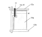
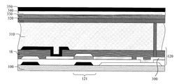
図1は、本発明の回路における代表例の一部を抽出したものである。本発明においては、図1の回路を二次元状に複数配する(同一平面上に縦横に複数配置する)ことで形成される。図8は、図1の回路におけるA−A’断面図であり、配線交差部、薄膜トランジスタ部、蓄積容量部を示している。
図1及び図8において、10は基板、11はゲート電極層、12aはゲート配線層、12bは蓄積容量下部電極層、13はゲート絶縁層、14は酸化物半導体層(チャネル領域)、14aはソース領域・ドレイン領域、酸化物半導体配線層および蓄積容量上部電極層である。そして、15はチャネル保護層、16は保護層である。
製造方法は六つの工程から構成され、その流れは図6のフローチャートに示すとおりである。図7は本発明の一実施形態としての回路の製造工程を示す断面図である。
The best mode for carrying out the present invention will be described below with reference to the accompanying drawings.
FIG. 1 shows a part of representative examples in the circuit of the present invention. In the present invention, it is formed by arranging a plurality of the circuits in FIG. 1 two-dimensionally (arranging a plurality of circuits vertically and horizontally on the same plane). FIG. 8 is a cross-sectional view taken along the line AA ′ in the circuit of FIG. 1, and shows a wiring crossing portion, a thin film transistor portion, and a storage capacitor portion.
1 and 8, 10 is a substrate, 11 is a gate electrode layer, 12a is a gate wiring layer, 12b is a storage capacitor lower electrode layer, 13 is a gate insulating layer, 14 is an oxide semiconductor layer (channel region), and 14a is They are a source region / drain region, an oxide semiconductor wiring layer, and a storage capacitor upper electrode layer.
The manufacturing method is composed of six steps, the flow of which is as shown in the flowchart of FIG. FIG. 7 is a cross-sectional view showing a circuit manufacturing process as one embodiment of the present invention.
基板10には、フレキシブルなプラスチック基板を用いる。プラスチック基板としては、ポリエチレン・テレフタレート(PET)、ポリエチレン・ナフタレート(PEN)、ポリイミド、ポリカーボネートなどのフィルム、並びに薄板が挙げられる。また、基板の表面が絶縁膜により構成されたバリアコート層でコーティングされていても構わない。また、ガラス基板や絶縁層をコーティングしたステンレス基板などを用いても良い。
As the
(第1工程)
まず、基板10の上にゲート電極層11を形成する。ゲート電極層11の形成には、スパッタ法、パルスレーザー蒸着法(PLD法)、電子ビーム蒸着法、化学気相蒸着法(CVD法)等を用いることができる。電極材料は、所定波長の光(例えば、400nm未満の少なくとも一部の領域の紫外光)に対して遮光性を有する材料であり、かつ、良好な電気伝導性を有するものであればよい。遮光性を有するとは、透過率0%である必要はない。透過率が30%以下であれば良く、好ましくは10%以下、より好ましくは5%以下、更に好ましくは、0.01%以下である。例えば、Ti、Pt、Au、Ni、Al、Moなどの金属やそれらの合金などの金属電極材料およびそれらの積層膜を用いることができる。もちろん、材料自体の遮光性は低くても、膜厚を厚くすることで、上記透過率に相当する遮光性が確保できれるのであれば、本発明のゲート電極層の材料は特に限定されるものではない。
(First step)
First, the
次にフォトリソグラフィー法等を用いてゲート電極層11のパターンを形成する。また、ゲート電極層11を、酸化物半導体配線14aとの交差部の下部に形成される領域および酸化物半導体配線14aを蓄積容量の上部電極に用いる場合の下部電極以外の領域における配線や電極に用いても構わない。
Next, a pattern of the
(第2工程)
そして、パターニングされたゲート電極層11を有する基板10の上にゲート配線層12aおよび蓄積容量下部電極層(以下、「容量下部電極層」とも記す)12bを形成する。ゲート配線12aおよび容量下部電極12bの形成には、スパッタ法、パルスレーザー蒸着法(PLD法)、電子ビーム蒸着法、化学気相蒸着法(CVD法)等を用いることができる。電極材料は、所定波長の光(例えば、400nm未満の少なくとも一部の領域の紫外光)に対して透明性を有する材料であり、かつ、良好な電気伝導性を有するものであればよい。透明性を有するとは、透過率が70%以上であれば良く、好ましくは80%以上、より好ましくは90%以上である。例えば、ITO(Indium Tin Oxide)やIZO(Indium Zinc Oxide)などの酸化物導電体を用いることができる。次にフォトリソグラフィー法等を用いて、ゲート配線12aおよび容量下部電極12bのパターンを形成する。
前述の例では、ゲート電極層11の形成後にゲート配線層12aおよび蓄積容量下部電極層12bを形成しているが、逆の順番で形成しても構わない。
(Second step)
Then, a
In the above example, the
(第3工程)
そして、パターニングされたゲート配線層12aおよび蓄積容量下部電極層12bを有する基板10の上にゲート絶縁層13を形成する。ゲート絶縁層の形成には、スパッタ法、パルスレーザー蒸着法(PLD法)、電子ビーム蒸着法、プラズマCVD法(PECVD法)等を用いることができる。ゲート絶縁材料は、400nm未満の少なくとも一部の領域の紫外光に対して透明性を有する材料であり、かつ、良好な絶縁特性を有するものであればよい。例えば、PECVD法やスパッタ法などによるシリコン酸化膜やシリコン窒化膜を用いることができる。
(Third step)
Then, the
(第4工程)
さらにゲート絶縁層13の上に酸化物膜からなる酸化物半導体層14を形成する。作製には、スパッタ法、PLD法、電子ビーム蒸着法等を用いることができる。酸化物半導体層14は、In、Ga、Zn、Snから選択される少なくとも1種類の元素を含むアモルファス酸化物半導体を用いることが可能である。酸化物半導体層14はフォトリソグラフィー法とエッチング法を用いてパターニングされる。
(4th process)
Further, an
(第5工程)
次に酸化物半導体層14の上にスパッタ法によりチャネル保護層15を形成する。酸化物半導体層14と直接接するチャネル保護層15にはチャネル保護層形成の際に酸化物半導体を低抵抗化させない機能が要求される。さらにチャネル保護層15の上に水素を含有する絶縁層(保護層16)を形成した際にチャネル保護層の膜厚で水素の透過量を制御し、酸化物半導体の抵抗率を制御できる機能も必要である。具体的にはシリコン酸化膜やシリコン酸窒化膜などのOを含有する絶縁層が望ましい。また、これらの絶縁層の組成がストイキオメトリーから外れていても何ら問題はない。チャネル保護層15は、裏面露光を用いたフォトリソグラフィー法とエッチング法を用いてパターニングされる。このとき、ゲート電極層11をマスクとして裏面露光が行われるので、チャネル保護層15はゲート電極層11が存在する領域上のみに自己整合的に形成される。
(5th process)
Next, the channel
(第6工程)
次に保護層16を成膜し、酸化物半導体層の所定領域を低抵抗化する。保護層16には、酸化物半導体層上に直接形成した際に酸化物半導体層を低抵抗化させる機能が要求される。酸化物半導体は水素を添加することにより低抵抗化させることが可能である。よって、酸化物半導体層の上に水素を含む絶縁層を形成する。具体的には、水素を含むシリコン窒化膜、シリコン酸化膜、シリコン酸窒化膜、シリコン炭化膜およびこれらの積層膜などが望ましい。また、これらの絶縁層の組成がストイキオメトリーから外れていても何ら問題はない。
(6th process)
Next, the
形成方法としては水素を含む原料ガスを用いるプラズマCVD法が、プラズマによる酸化物半導体への水素拡散の促進効果もあるため望ましい。この際、原料中の水素が酸化物半導体層に拡散し、チャネル保護層がない領域の酸化物半導体層が低抵抗化する。これにより、ソース領域・ドレイン領域、酸化物半導体配線層および蓄積容量上部電極14aが形成される。また、自己整合的に形成されたチャネル保護層15をマスクとしてドレイン領域・ソース領域14aが形成されるので、ゲート電極に対するドレイン領域・ソース領域の重なりを小さくすることができる。これにより、寄生容量の小さいTFTの作製が可能である。また、ゲート電極層11が存在しない領域上の酸化物半導体層の上にはチャネル保護層15は形成されていないため、その領域上の酸化物半導体層はすべて低抵抗化する。
最後に外部と電気的な接続を行うために、フォトリソグラフィー法とエッチング法により、保護層16にコンタクトホールを形成する。
As a formation method, a plasma CVD method using a source gas containing hydrogen is preferable because it has an effect of promoting diffusion of hydrogen into an oxide semiconductor by plasma. At this time, hydrogen in the raw material diffuses into the oxide semiconductor layer, and the resistance of the oxide semiconductor layer in the region where there is no channel protective layer is reduced. Thereby, the source region / drain region, the oxide semiconductor wiring layer, and the storage capacitor
Finally, in order to make electrical connection with the outside, a contact hole is formed in the
図2に、蓄積容量の上部電極の絶縁層と接する側に低抵抗化した酸化物半導体層を用いた場合(○)と金属のみを電極に用いた場合(◆)の電極間におけるリーク電流密度の比較を示す。図2に示すように、蓄積容量の上部電極の絶縁層と接する側に酸化物半導体層を用いた場合の方が、リーク電流密度が小さいことが分かる。このように低抵抗化した酸化物半導体層を蓄積容量の上部電極に用いる場合、リーク電流密度低減の効果も期待できる。
こうして、ボトムゲート型コプラナー構造酸化物半導体TFTを有する本発明の回路が完成する。
Fig. 2 shows the leakage current density between the electrodes when the oxide semiconductor layer with reduced resistance is used on the side of the storage electrode in contact with the insulating layer (◯) and when only the metal is used as the electrode (♦). A comparison of is shown. As shown in FIG. 2, it can be seen that the leakage current density is smaller when the oxide semiconductor layer is used on the side of the storage capacitor in contact with the insulating layer of the upper electrode. When the oxide semiconductor layer having such a low resistance is used for the upper electrode of the storage capacitor, an effect of reducing the leakage current density can be expected.
Thus, the circuit of the present invention having the bottom gate type coplanar structure oxide semiconductor TFT is completed.
これより、本発明の実施例についてさらに詳細に説明するが、本発明はこれらによって何ら限定されるものではない。
(実施例1)
図1及び図8に示す1つの蓄積容量に対して1つのボトムゲート型コプラナー構造の酸化物半導体TFTを有する回路を作成する。ただし、図1は作成する回路の一部分を示すものであり、作成する回路は図1に示す蓄積容量とTFTを二次元状に複数配する(同一平面上に縦横に複数配置する)ことで形成される。
Examples of the present invention will now be described in more detail, but the present invention is not limited by these.
Example 1
A circuit having one bottom gate type coplanar structure oxide semiconductor TFT with respect to one storage capacitor shown in FIGS. However, FIG. 1 shows a part of a circuit to be created, and the circuit to be created is formed by arranging a plurality of storage capacitors and TFTs shown in FIG. 1 in a two-dimensional manner (a plurality of them are arranged vertically and horizontally on the same plane). Is done.
まず、PET基板10の上に、ゲート電極層11を形成するための電極層をスパッタ法により成膜する。(図7(a))
電極材料にはMoを用い、膜厚は100nmである。その後、フォトリソグラフィー法とエッチング法とを用いて電極をパターニングし、ゲート電極層11とする。
First, an electrode layer for forming the
Mo is used for the electrode material, and the film thickness is 100 nm. Thereafter, the electrode is patterned using a photolithography method and an etching method to form the
次に、ゲート配線層12aおよび容量下部電極層12bをスパッタ法により形成する。(図7(b))
ゲート配線12aおよび容量下部電極12bの材料には、ITOを用い、膜厚は100nmである。
Next, the
ITO is used as the material of the
次に、ゲート絶縁層13として200nmのシリコン酸化膜を、スパッタ法を用いて成膜。(図7(c))
該シリコン酸化膜はRFスパッタ装置を用いて基板温度は室温(25℃)で形成する。ターゲットは4インチ径のSiO2を用い、投入RFパワーは500Wである。成膜時の雰囲気は、全圧0.5Paであり、その際のガス流量はAr=100%である。
Next, a 200 nm silicon oxide film is formed as the
The silicon oxide film is formed using an RF sputtering apparatus at a substrate temperature of room temperature (25 ° C.). The target uses 4 inch diameter SiO 2 and the input RF power is 500 W. The atmosphere during film formation is a total pressure of 0.5 Pa, and the gas flow rate at that time is Ar = 100%.
次に、ゲート絶縁層13の上に形成される酸化物半導体層14として、膜厚30nmのアモルファスIGZO(In−Ga−Zn−O)を成膜する。(図7(d))
該酸化物半導体層は、DCスパッタ装置を用いて基板温度は室温(25℃)で形成する。ターゲットは4インチ径のInGaZnO4組成を有する多結晶焼結体を用い、投入RFパワーは150Wとする。成膜時の雰囲気は、全圧0.5Paとし、その際のガス流量はAr:O2=98:2とする。その後、フォトリソグラフィー法とエッチング法を用いて酸化物半導体層14をパターニングする。
Next, as the
The oxide semiconductor layer is formed using a DC sputtering apparatus at a substrate temperature of room temperature (25 ° C.). The target is a polycrystalline sintered body having a 4 inch diameter InGaZnO 4 composition, and the input RF power is 150 W. The atmosphere during film formation is a total pressure of 0.5 Pa, and the gas flow rate at that time is Ar: O 2 = 98: 2. After that, the
次に、酸化物半導体層14の上にチャネル保護層15として、スパッタ法により、膜厚100nmのシリコン酸化膜を成膜する。
該シリコン酸化膜はRFスパッタ装置を用いて基板温度は室温で形成する。ターゲットは4インチ径のSiO2を用い、投入RFパワーは500Wとする。シリコン酸化膜成膜時の雰囲気は、全圧0.5Paであり、その際のガス流量はAr:O2=90:10である。そして、ゲート電極層11をマスクとして裏面露光を用いたフォトリソグラフィー法とエッチング法により、チャネル保護層15をパターニングする。(図7(e))
Next, a 100-nm-thick silicon oxide film is formed as the channel
The silicon oxide film is formed using an RF sputtering apparatus at a substrate temperature of room temperature. The target is 4 inch diameter SiO 2 and the input RF power is 500 W. The atmosphere during the formation of the silicon oxide film is a total pressure of 0.5 Pa, and the gas flow rate at that time is Ar: O 2 = 90: 10. Then, the channel
さらに保護層16として、プラズマCVD法により、膜厚300nmのシリコン窒化膜を成膜する。このプラズマCVD法によるシリコン窒化膜の形成時の基板温度は150℃とする。また、プロセスガスには、SiH4、NH3、N2を用い、ガス流量比はSiH4:NH3:N2=1:2.5:25とする。また、投入RFパワー密度と圧力はそれぞれ0.9W/cm2、150Paとする。
保護層16の形成と同時にチャネル保護層15の無い領域の酸化物半導体層が、水素添加処理によって低抵抗化し、ソース領域・ドレイン領域、酸化物半導体配線層および蓄積容量上部電極14aとなる。
Further, a silicon nitride film having a thickness of 300 nm is formed as the
Simultaneously with the formation of the
最後に外部と電気的な接続を行うために、フォトリソグラフィー法とエッチング法により、保護層16にコンタクトホール(図示せず)を形成する。
以上の工程により、本発明の酸化物半導体TFTを有する回路が完成する。
本発明の回路の構成により、電気特性や寄生容量の基板内でのバラツキが小さい酸化物半導体TFTを有する回路を作製することが可能である。
Finally, in order to make electrical connection with the outside, a contact hole (not shown) is formed in the
Through the above steps, a circuit having the oxide semiconductor TFT of the present invention is completed.
With the circuit configuration of the present invention, a circuit including an oxide semiconductor TFT in which variation in electric characteristics and parasitic capacitance in a substrate is small can be manufactured.
(実施例2)
図3に示す1つの蓄積容量に対して2つのボトムゲート型コプラナー構造の酸化物半導体TFTを有する回路を作成する。ただし、図3は作成する回路の一部分を示すものであり、作成した回路は図3に示す蓄積容量とTFTを二次元状に複数配する(同一平面上に縦横に複数配置する)ことで形成される。図10は、図3の回路におけるB−B’断面図であり、配線交差部、薄膜トランジスタ部、蓄積容量部を示す。
(Example 2)
A circuit having two bottom-gate coplanar structure oxide semiconductor TFTs for one storage capacitor shown in FIG. 3 is formed. However, FIG. 3 shows a part of the circuit to be created, and the created circuit is formed by arranging a plurality of storage capacitors and TFTs shown in FIG. 3 in a two-dimensional manner (a plurality of them are arranged vertically and horizontally on the same plane). Is done. FIG. 10 is a cross-sectional view taken along the line BB ′ in the circuit of FIG. 3 and shows a wiring intersection portion, a thin film transistor portion, and a storage capacitor portion.
まず、PET基板10の上に、ゲート電極層11を形成するための電極層をスパッタ法により形成する。電極材料にはMoを用い、膜厚は100nmである。その後、フォトリソグラフィー法とエッチング法とを用いて電極をパターニングし、ゲート電極層11およびゲート配線層11aとする。(図9(a))
First, an electrode layer for forming the
次に、画素内配線層12aおよび蓄積容量下部電極層12bをスパッタ法により形成する。(図9(b))
ゲート配線12aおよび容量下部電極12bの材料には、ITOを用い、膜厚は100nmである。
実施例1と異なり、酸化物半導体配線層および蓄積容量上部電極層14aが上部に形成される領域周辺以外のゲート配線層のほとんどは第1のゲート配線層11aで形成される。
Next, the in-
ITO is used as the material of the
Unlike the first embodiment, most of the gate wiring layers other than the periphery of the region where the oxide semiconductor wiring layer and the storage capacitor
次に、ゲート絶縁層13として200nmのシリコン酸化膜を、スパッタ法を用いて成膜する。(図9(c))
該シリコン酸化膜はRFスパッタ装置を用いて基板温度は室温で成膜する。ターゲットにはSiO2を用い、投入RFパワーは500Wである。成膜時の雰囲気は、全圧0.5Paであり、その際のガス流量はAr=100%である。
Next, a 200 nm silicon oxide film is formed as the
The silicon oxide film is formed using an RF sputtering apparatus at a substrate temperature of room temperature. SiO 2 is used as a target, and the input RF power is 500 W. The atmosphere during film formation is a total pressure of 0.5 Pa, and the gas flow rate at that time is Ar = 100%.
次にフォトリソグラフィー法とエッチング法により、ゲート絶縁層13に第1のコンタクトホール18を形成する。(図9(d))
その後、酸化物半導体層14、チャネル保護層15及び保護層16を実施例1と同様に形成する。(図9(e))
次にフォトリソグラフィー法とエッチング法により、保護層16に第2のコンタクトホール19を形成する。
Next, a
After that, the
Next, a
さらにソース・ドレイン配線層17を形成するための電極層をスパッタ法により成膜する。電極材料にはMoを用い、膜厚は200nmとする。その後、フォトリソグラフィー法とエッチング法により、ソース・ドレイン配線層17をパターニングする。
以上の工程により、本発明の酸化物半導体TFTを有する回路が完成となる。
本発明の回路の構成により、電気特性や寄生容量の基板内でのバラツキが小さい酸化物半導体TFTを有する回路を作製することが可能である。
Further, an electrode layer for forming the source /
Through the above steps, a circuit having the oxide semiconductor TFT of the present invention is completed.
With the circuit configuration of the present invention, a circuit including an oxide semiconductor TFT in which variation in electric characteristics and parasitic capacitance in a substrate is small can be manufactured.
(実施例3)
本実施例ではボトムゲート型コプラナー構造の酸化物半導体TFTを用いた図4の表示装置について説明する。酸化物半導体TFTを有する回路(駆動回路)の製造工程は、前記実施例1と同様である。実施例1と同様の方法で、プラスチック基板110の上に酸化物半導体TFT121を有する回路120を形成後、フォトリソグラフィー法とエッチング法により、保護層16にコンタクトホールを形成する。
さらに、画素電極140をスパッタ法により成膜する。電極材料には、ITOを用い、膜厚は100nmである。この上にポリイミド膜150を塗布し、ラビング工程を施す。
(Example 3)
In this embodiment, the display device in FIG. 4 using an oxide semiconductor TFT having a bottom gate type coplanar structure will be described. The manufacturing process of the circuit having the oxide semiconductor TFT (driving circuit) is the same as that of the first embodiment. After forming the
Further, the
一方で、同じくプラスチック基板190の上にITO膜180とポリイミド膜170を形成し、ラビング工程を施したものを用意する。さらに前記酸化物半導体TFTを有する回路120を形成した基板110と5μmの空隙を空けて対向させ、間にネマチック液晶160を注入する。さらにこの構造体の両側に一対の偏光板100、200を設ける。ここで、信号線130に電圧を印加し、酸化物半導体TFT121のゲート電極131の電圧を変化させると、画素電極ITO140の領域のみ、光透過率が変化する。またその透過率は、酸化物半導体TFT121がオン状態となるゲート電圧の下ではソース−ドレイン間電圧によっても連続的に変化させることができる。このようにして、図4に示す液晶セルを表示素子(発光素子)とする表示装置を作成する。
本発明の回路の構成では、ゲート電極層以外、可視光に対して透明な材料で形成されているため、非常に開口率の高い回路を実現することが可能である。
On the other hand, an
In the circuit configuration of the present invention, a circuit having a very high aperture ratio can be realized because it is made of a material transparent to visible light except for the gate electrode layer.
(実施例4)
本実施例ではボトムゲート型コプラナー構造の酸化物半導体TFTを有する回路を用いた図5の表示装置について説明する。酸化物半導体TFTを有する回路の製造工程は、前記実施例2と同様である。まず本発明の酸化物半導体TFTを有する回路120の上に平坦化層310を形成する。平坦化層310にはポリイミド膜を用いる。そして、保護層16および平坦化層310にフォトリソグラフィー法とエッチング法を用いてコンタクトホールを形成する。そして、酸化物半導体配線層300上に保護層16および絶縁層310に形成されたコンタクトホールを介して電極320を形成する。電極320にはスパッタ法により形成したITOを用いる。次に電極320の上に正孔輸送層330、発光層340を蒸着法により形成する。正孔輸送層330、発光層340にはそれぞれα‐NPD(4,4’-bis[N-(1-naphthyl)-N-phenyl-amino]biphenyl)、Alq3(tris(8-hydroxyquinoline))を用いる。さらに発光層340の上に電極350を蒸着法により形成する。電極材料にはAlを用いる。このようにして、図5に示す、ボトムエミッション型の有機EL素子を表示素子とする表示装置を作製する。
本発明の回路の構成では、画素回路内はゲート電極層以外、可視光に対して透明な材料で形成されているため、非常に開口率の高い画素回路を実現することが可能である。
Example 4
In this embodiment, the display device in FIG. 5 using a circuit having an oxide semiconductor TFT having a bottom-gate coplanar structure will be described. The manufacturing process of the circuit having the oxide semiconductor TFT is the same as that of the second embodiment. First, the
In the circuit configuration of the present invention, the pixel circuit is formed of a material transparent to visible light other than the gate electrode layer, so that a pixel circuit with a very high aperture ratio can be realized.
本発明の酸化物半導体TFTを有する回路は、液晶ディスプレイや有機ELディスプレイの駆動回路として応用することができる。また、プラスチックフィルムをはじめとするフレキシブル基板への適用に対して有利であり、フレキシブル・ディスプレイへの応用が可能である。 The circuit having the oxide semiconductor TFT of the present invention can be applied as a driving circuit for a liquid crystal display or an organic EL display. Further, it is advantageous for application to a flexible substrate such as a plastic film, and can be applied to a flexible display.
10 基板
11 ゲート電極層
11a ゲート配線層
12a ゲート配線層および画素内配線層
12b 蓄積容量下部電極
13 ゲート絶縁層
14 酸化物半導体層
14a ソース・ドレイン領域、酸化物半導体配線層および蓄積容量上部電極
15 チャネル保護層
16 保護層
DESCRIPTION OF
Claims (5)
前記基板と前記ゲート電極層と前記蓄積容量下部電極層の上に、ゲート絶縁層が形成され、
前記ゲート絶縁層の上に、酸化物半導体層が形成され、
前記酸化物半導体層の上に、チャネル保護層が前記ゲート電極層に対して自己整合的に形成され、
前記酸化物半導体層と前記チャネル保護層の上に、保護層が形成され、
前記ゲート電極層は所定波長の光の透過率が30%以下であり、前記蓄積容量下部電極層は前記所定波長の光の透過率が70%以上であり、前記酸化物半導体層がソース領域、ドレイン領域、チャネル領域及び蓄積容量上部電極層を有することを特徴とする回路。 On the substrate, a gate electrode layer and a storage capacitor lower electrode layer are formed,
A gate insulating layer is formed on the substrate, the gate electrode layer, and the storage capacitor lower electrode layer,
An oxide semiconductor layer is formed on the gate insulating layer,
A channel protective layer is formed on the oxide semiconductor layer in a self-aligned manner with respect to the gate electrode layer,
A protective layer is formed on the oxide semiconductor layer and the channel protective layer,
The gate electrode layer has a light transmittance of a predetermined wavelength of 30% or less, the storage capacitor lower electrode layer has a light transmittance of the predetermined wavelength of 70% or more, the oxide semiconductor layer is a source region, A circuit comprising a drain region, a channel region, and a storage capacitor upper electrode layer.
前記基板の上に、前記所定波長の光の透過率が70%以上である蓄積容量下部電極層を形成する工程と、
前記基板と前記ゲート電極層と前記蓄積容量下部電極層の上に、ゲート絶縁層を形成する工程と、
前記ゲート絶縁層の上に、酸化物半導体層を形成する工程と、
前記酸化物半導体層の上に、第1の保護層を形成し、前記所定波長の光を裏面露光し、前記第1の保護層をエッチングして、前記ゲート電極層に対して自己整合的なチャネル保護層を形成する工程と、
前記チャネル保護層によって保護されていない領域に水素添加処理を施して、前記酸化物半導体層の前記チャネル保護層によって保護されていない領域を低抵抗化する工程と、を含むことを特徴とする回路の製造方法。 Forming a gate electrode layer having a light transmittance of a predetermined wavelength of 30% or less on a substrate;
Forming a storage capacitor lower electrode layer having a light transmittance of 70% or more on the substrate;
Forming a gate insulating layer on the substrate, the gate electrode layer, and the storage capacitor lower electrode layer;
Forming an oxide semiconductor layer on the gate insulating layer;
A first protective layer is formed on the oxide semiconductor layer, the light having the predetermined wavelength is back-exposed, the first protective layer is etched, and is self-aligned with the gate electrode layer. Forming a channel protective layer;
Applying a hydrogenation process to a region not protected by the channel protective layer to reduce the resistance of the region of the oxide semiconductor layer that is not protected by the channel protective layer. Manufacturing method.
Priority Applications (1)
| Application Number | Priority Date | Filing Date | Title |
|---|---|---|---|
| JP2009241818A JP2011091110A (en) | 2009-10-20 | 2009-10-20 | Circuit using oxide semiconductor element and method of manufacturing the same, and display device |
Applications Claiming Priority (1)
| Application Number | Priority Date | Filing Date | Title |
|---|---|---|---|
| JP2009241818A JP2011091110A (en) | 2009-10-20 | 2009-10-20 | Circuit using oxide semiconductor element and method of manufacturing the same, and display device |
Publications (2)
| Publication Number | Publication Date |
|---|---|
| JP2011091110A true JP2011091110A (en) | 2011-05-06 |
| JP2011091110A5 JP2011091110A5 (en) | 2012-11-29 |
Family
ID=44109122
Family Applications (1)
| Application Number | Title | Priority Date | Filing Date |
|---|---|---|---|
| JP2009241818A Pending JP2011091110A (en) | 2009-10-20 | 2009-10-20 | Circuit using oxide semiconductor element and method of manufacturing the same, and display device |
Country Status (1)
| Country | Link |
|---|---|
| JP (1) | JP2011091110A (en) |
Cited By (18)
| Publication number | Priority date | Publication date | Assignee | Title |
|---|---|---|---|---|
| CN103189970A (en) * | 2011-10-28 | 2013-07-03 | 松下电器产业株式会社 | Thin film semiconductor device, and method for producing thin film semiconductor device |
| JP2013165108A (en) * | 2012-02-09 | 2013-08-22 | Sony Corp | Thin-film transistor, method for manufacturing thin-film transistor, display device, and electronic equipment |
| JP2014063141A (en) * | 2012-08-03 | 2014-04-10 | Semiconductor Energy Lab Co Ltd | Semiconductor device |
| KR20150028721A (en) * | 2013-09-06 | 2015-03-16 | 가부시키가이샤 한도오따이 에네루기 켄큐쇼 | Semiconductor device |
| US9048322B2 (en) | 2012-11-19 | 2015-06-02 | Samsung Display Co., Ltd. | Display substrate and method of manufacturing the same |
| WO2015087586A1 (en) * | 2013-12-10 | 2015-06-18 | シャープ株式会社 | Semiconductor device and method for manufacturing same |
| US9252284B2 (en) | 2013-09-02 | 2016-02-02 | Samsung Display Co., Ltd. | Display substrate and method of manufacturing a display substrate |
| JP2016100521A (en) * | 2014-11-25 | 2016-05-30 | 株式会社ジャパンディスプレイ | Thin film transistor and manufacturing method of the same |
| US9419021B2 (en) | 2013-08-05 | 2016-08-16 | Japan Display Inc. | Thin film transistor circuit and display device using it |
| JP2017055138A (en) * | 2012-06-29 | 2017-03-16 | 株式会社半導体エネルギー研究所 | Semiconductor device manufacturing method |
| JP2018152581A (en) * | 2013-06-28 | 2018-09-27 | 株式会社半導体エネルギー研究所 | Semiconductor device |
| JP2018163376A (en) * | 2011-11-11 | 2018-10-18 | 株式会社半導体エネルギー研究所 | Electronic apparatus |
| JP2019114815A (en) * | 2013-12-27 | 2019-07-11 | 株式会社半導体エネルギー研究所 | Semiconductor device |
| JP2020027862A (en) * | 2018-08-10 | 2020-02-20 | 株式会社ジャパンディスプレイ | Display and method for manufacturing the same |
| JP2020115580A (en) * | 2012-08-10 | 2020-07-30 | 株式会社半導体エネルギー研究所 | Semiconductor device |
| JP2022008528A (en) * | 2014-09-05 | 2022-01-13 | 株式会社半導体エネルギー研究所 | Display device |
| JP2022088391A (en) * | 2011-12-22 | 2022-06-14 | 株式会社半導体エネルギー研究所 | Semiconductor device |
| JP7430763B2 (en) | 2017-05-19 | 2024-02-13 | 株式会社半導体エネルギー研究所 | semiconductor equipment |
Citations (5)
| Publication number | Priority date | Publication date | Assignee | Title |
|---|---|---|---|---|
| JPH06317809A (en) * | 1993-05-07 | 1994-11-15 | Fujitsu Ltd | Production of thin-film transistor matrix |
| JP2007299833A (en) * | 2006-04-28 | 2007-11-15 | Toppan Printing Co Ltd | Structure body, transmissive liquid crystal display, method for manufacturing the same and method for manufacturing semiconductor circuit |
| JP2009099887A (en) * | 2007-10-19 | 2009-05-07 | Hitachi Displays Ltd | Display device |
| WO2009075281A1 (en) * | 2007-12-13 | 2009-06-18 | Idemitsu Kosan Co., Ltd. | Field effect transistor using oxide semiconductor and method for manufacturing the same |
| JP2009141002A (en) * | 2007-12-04 | 2009-06-25 | Canon Inc | Oxide semiconductor element having insulating layer, and display device using the same |
-
2009
- 2009-10-20 JP JP2009241818A patent/JP2011091110A/en active Pending
Patent Citations (5)
| Publication number | Priority date | Publication date | Assignee | Title |
|---|---|---|---|---|
| JPH06317809A (en) * | 1993-05-07 | 1994-11-15 | Fujitsu Ltd | Production of thin-film transistor matrix |
| JP2007299833A (en) * | 2006-04-28 | 2007-11-15 | Toppan Printing Co Ltd | Structure body, transmissive liquid crystal display, method for manufacturing the same and method for manufacturing semiconductor circuit |
| JP2009099887A (en) * | 2007-10-19 | 2009-05-07 | Hitachi Displays Ltd | Display device |
| JP2009141002A (en) * | 2007-12-04 | 2009-06-25 | Canon Inc | Oxide semiconductor element having insulating layer, and display device using the same |
| WO2009075281A1 (en) * | 2007-12-13 | 2009-06-18 | Idemitsu Kosan Co., Ltd. | Field effect transistor using oxide semiconductor and method for manufacturing the same |
Cited By (41)
| Publication number | Priority date | Publication date | Assignee | Title |
|---|---|---|---|---|
| CN103189970A (en) * | 2011-10-28 | 2013-07-03 | 松下电器产业株式会社 | Thin film semiconductor device, and method for producing thin film semiconductor device |
| US8907341B2 (en) | 2011-10-28 | 2014-12-09 | Panasonic Corporation | Thin-film semiconductor device and method for fabricating thin-film semiconductor device |
| CN103189970B (en) * | 2011-10-28 | 2016-09-28 | 株式会社日本有机雷特显示器 | Thin film semiconductor device and the manufacture method of thin film semiconductor device |
| JP2018163376A (en) * | 2011-11-11 | 2018-10-18 | 株式会社半導体エネルギー研究所 | Electronic apparatus |
| JP2022088391A (en) * | 2011-12-22 | 2022-06-14 | 株式会社半導体エネルギー研究所 | Semiconductor device |
| JP7291821B2 (en) | 2011-12-22 | 2023-06-15 | 株式会社半導体エネルギー研究所 | semiconductor equipment |
| JP2013165108A (en) * | 2012-02-09 | 2013-08-22 | Sony Corp | Thin-film transistor, method for manufacturing thin-film transistor, display device, and electronic equipment |
| JP2017055138A (en) * | 2012-06-29 | 2017-03-16 | 株式会社半導体エネルギー研究所 | Semiconductor device manufacturing method |
| KR20210014760A (en) * | 2012-06-29 | 2021-02-09 | 가부시키가이샤 한도오따이 에네루기 켄큐쇼 | A method for manufacturing semiconductor device |
| KR102358093B1 (en) * | 2012-06-29 | 2022-02-08 | 가부시키가이샤 한도오따이 에네루기 켄큐쇼 | A method for manufacturing semiconductor device |
| JP2014063141A (en) * | 2012-08-03 | 2014-04-10 | Semiconductor Energy Lab Co Ltd | Semiconductor device |
| US9941309B2 (en) | 2012-08-03 | 2018-04-10 | Semiconductor Energy Laboratory Co., Ltd. | Semiconductor device |
| JP2022050449A (en) * | 2012-08-10 | 2022-03-30 | 株式会社半導体エネルギー研究所 | Semiconductor device |
| JP2020115580A (en) * | 2012-08-10 | 2020-07-30 | 株式会社半導体エネルギー研究所 | Semiconductor device |
| JP7460309B2 (en) | 2012-08-10 | 2024-04-02 | 株式会社半導体エネルギー研究所 | semiconductor equipment |
| JP6999733B2 (en) | 2012-08-10 | 2022-01-19 | 株式会社半導体エネルギー研究所 | Semiconductor device |
| US9048322B2 (en) | 2012-11-19 | 2015-06-02 | Samsung Display Co., Ltd. | Display substrate and method of manufacturing the same |
| JP2018152581A (en) * | 2013-06-28 | 2018-09-27 | 株式会社半導体エネルギー研究所 | Semiconductor device |
| JP2019220707A (en) * | 2013-06-28 | 2019-12-26 | 株式会社半導体エネルギー研究所 | Liquid crystal display unit |
| US9419021B2 (en) | 2013-08-05 | 2016-08-16 | Japan Display Inc. | Thin film transistor circuit and display device using it |
| US9252284B2 (en) | 2013-09-02 | 2016-02-02 | Samsung Display Co., Ltd. | Display substrate and method of manufacturing a display substrate |
| JP2022017385A (en) * | 2013-09-06 | 2022-01-25 | 株式会社半導体エネルギー研究所 | Semiconductor device |
| KR20150028721A (en) * | 2013-09-06 | 2015-03-16 | 가부시키가이샤 한도오따이 에네루기 켄큐쇼 | Semiconductor device |
| JP2018174339A (en) * | 2013-09-06 | 2018-11-08 | 株式会社半導体エネルギー研究所 | Semiconductor device |
| JP7247303B2 (en) | 2013-09-06 | 2023-03-28 | 株式会社半導体エネルギー研究所 | semiconductor equipment |
| KR102294507B1 (en) * | 2013-09-06 | 2021-08-30 | 가부시키가이샤 한도오따이 에네루기 켄큐쇼 | Semiconductor device |
| JPWO2015087586A1 (en) * | 2013-12-10 | 2017-03-16 | シャープ株式会社 | Semiconductor device and manufacturing method thereof |
| WO2015087586A1 (en) * | 2013-12-10 | 2015-06-18 | シャープ株式会社 | Semiconductor device and method for manufacturing same |
| CN105814481A (en) * | 2013-12-10 | 2016-07-27 | 夏普株式会社 | Semiconductor device and method for manufacturing same |
| CN105814481B (en) * | 2013-12-10 | 2018-09-18 | 夏普株式会社 | Semiconductor device and its manufacturing method |
| US9613990B2 (en) | 2013-12-10 | 2017-04-04 | Sharp Kabushiki Kaisha | Semiconductor device and method for manufacturing same |
| US11380795B2 (en) | 2013-12-27 | 2022-07-05 | Semiconductor Energy Laboratory Co., Ltd. | Semiconductor device comprising an oxide semiconductor film |
| US10818795B2 (en) | 2013-12-27 | 2020-10-27 | Semiconductor Energy Laboratory Co., Ltd. | Semiconductor device |
| US11757041B2 (en) | 2013-12-27 | 2023-09-12 | Semiconductor Energy Laboratory Co., Ltd. | Semiconductor device |
| JP2019114815A (en) * | 2013-12-27 | 2019-07-11 | 株式会社半導体エネルギー研究所 | Semiconductor device |
| JP2022008528A (en) * | 2014-09-05 | 2022-01-13 | 株式会社半導体エネルギー研究所 | Display device |
| JP7117433B2 (en) | 2014-09-05 | 2022-08-12 | 株式会社半導体エネルギー研究所 | Display device |
| JP2016100521A (en) * | 2014-11-25 | 2016-05-30 | 株式会社ジャパンディスプレイ | Thin film transistor and manufacturing method of the same |
| JP7430763B2 (en) | 2017-05-19 | 2024-02-13 | 株式会社半導体エネルギー研究所 | semiconductor equipment |
| JP2020027862A (en) * | 2018-08-10 | 2020-02-20 | 株式会社ジャパンディスプレイ | Display and method for manufacturing the same |
| CN112424918A (en) * | 2018-08-10 | 2021-02-26 | 株式会社日本显示器 | Display device and method for manufacturing the same |
Similar Documents
| Publication | Publication Date | Title |
|---|---|---|
| JP2011091110A (en) | Circuit using oxide semiconductor element and method of manufacturing the same, and display device | |
| JP5704790B2 (en) | Thin film transistor and display device | |
| KR102180037B1 (en) | Flexible display and manufacturing method thereof | |
| US9748280B2 (en) | Thin film transistor and method of fabricating the same, array substrate and method of fabricating the same, and display device | |
| WO2016056204A1 (en) | Thin film transistor substrate, method for manufacturing thin film transistor substrate, and display panel | |
| US10644165B2 (en) | Thin-film transistor, method of fabricating thin-film transistor, and display device | |
| US9263539B2 (en) | Thin-film transistor and fabrication method thereof, array substrate and display device | |
| EP2657973A1 (en) | Display device, array substrate, thin film transistor and method for manufacturing the same | |
| JP2012033836A (en) | Top gate type thin film transistor and display device including the same | |
| JP6330207B2 (en) | Display device and thin film transistor substrate | |
| JP2011091110A5 (en) | ||
| TW201535750A (en) | Thin film transistor and manufacturing method for the same | |
| WO2015043220A1 (en) | Thin film transistor, preparation method therefor, array substrate, and display apparatus | |
| JP2013051328A (en) | Active-matrix display device and method of manufacturing the same | |
| US9508544B2 (en) | Semiconductor device and method for manufacturing same | |
| US9812541B2 (en) | Array substrate, method for fabricating the same and display device | |
| WO2017219412A1 (en) | Method for manufacturing top gate thin-film transistor | |
| KR102392007B1 (en) | Thin film transistor and display device comprising the same | |
| JP6142300B2 (en) | Thin film transistor manufacturing method | |
| JP6500202B2 (en) | Thin film transistor and method of manufacturing thin film transistor | |
| JP6209918B2 (en) | THIN FILM TRANSISTOR AND METHOD FOR MANUFACTURING THIN FILM TRANSISTOR | |
| KR20160049172A (en) | Thin film transistor array substrate and display device comprising the same | |
| JP6500203B2 (en) | Thin film transistor and method of manufacturing thin film transistor | |
| JP6264015B2 (en) | THIN FILM TRANSISTOR AND METHOD FOR PRODUCING THIN FILM TRANSISTOR | |
| JPWO2015045213A1 (en) | Thin film transistor substrate and manufacturing method thereof |
Legal Events
| Date | Code | Title | Description |
|---|---|---|---|
| A521 | Request for written amendment filed |
Free format text: JAPANESE INTERMEDIATE CODE: A523 Effective date: 20121016 |
|
| A621 | Written request for application examination |
Free format text: JAPANESE INTERMEDIATE CODE: A621 Effective date: 20121016 |
|
| A977 | Report on retrieval |
Free format text: JAPANESE INTERMEDIATE CODE: A971007 Effective date: 20140114 |
|
| A131 | Notification of reasons for refusal |
Free format text: JAPANESE INTERMEDIATE CODE: A131 Effective date: 20140210 |
|
| A131 | Notification of reasons for refusal |
Free format text: JAPANESE INTERMEDIATE CODE: A131 Effective date: 20140919 |
|
| A02 | Decision of refusal |
Free format text: JAPANESE INTERMEDIATE CODE: A02 Effective date: 20150202 |