JP2009099887A - Display device - Google Patents
Display device Download PDFInfo
- Publication number
- JP2009099887A JP2009099887A JP2007272084A JP2007272084A JP2009099887A JP 2009099887 A JP2009099887 A JP 2009099887A JP 2007272084 A JP2007272084 A JP 2007272084A JP 2007272084 A JP2007272084 A JP 2007272084A JP 2009099887 A JP2009099887 A JP 2009099887A
- Authority
- JP
- Japan
- Prior art keywords
- semiconductor layer
- electrode
- display device
- oxide semiconductor
- data line
- Prior art date
- Legal status (The legal status is an assumption and is not a legal conclusion. Google has not performed a legal analysis and makes no representation as to the accuracy of the status listed.)
- Pending
Links
- 239000010408 film Substances 0.000 claims abstract description 297
- 239000004065 semiconductor Substances 0.000 claims abstract description 188
- 239000010409 thin film Substances 0.000 claims abstract description 93
- 239000000758 substrate Substances 0.000 claims abstract description 77
- 230000001681 protective effect Effects 0.000 claims description 72
- 229910052751 metal Inorganic materials 0.000 claims description 69
- 239000002184 metal Substances 0.000 claims description 69
- 230000004048 modification Effects 0.000 claims description 5
- 238000012986 modification Methods 0.000 claims description 5
- 239000010410 layer Substances 0.000 abstract description 186
- 102100036464 Activated RNA polymerase II transcriptional coactivator p15 Human genes 0.000 abstract description 60
- 101000713904 Homo sapiens Activated RNA polymerase II transcriptional coactivator p15 Proteins 0.000 abstract description 60
- 229910004444 SUB1 Inorganic materials 0.000 abstract description 60
- 238000004519 manufacturing process Methods 0.000 abstract description 37
- 239000011241 protective layer Substances 0.000 abstract 1
- 238000000034 method Methods 0.000 description 142
- 239000004973 liquid crystal related substance Substances 0.000 description 74
- 230000008569 process Effects 0.000 description 44
- 238000000206 photolithography Methods 0.000 description 42
- 238000005530 etching Methods 0.000 description 39
- PXHVJJICTQNCMI-UHFFFAOYSA-N Nickel Chemical compound [Ni] PXHVJJICTQNCMI-UHFFFAOYSA-N 0.000 description 32
- 238000010586 diagram Methods 0.000 description 28
- 239000003990 capacitor Substances 0.000 description 24
- 238000003860 storage Methods 0.000 description 22
- VYZAMTAEIAYCRO-UHFFFAOYSA-N Chromium Chemical compound [Cr] VYZAMTAEIAYCRO-UHFFFAOYSA-N 0.000 description 16
- RYGMFSIKBFXOCR-UHFFFAOYSA-N Copper Chemical compound [Cu] RYGMFSIKBFXOCR-UHFFFAOYSA-N 0.000 description 16
- ZOKXTWBITQBERF-UHFFFAOYSA-N Molybdenum Chemical compound [Mo] ZOKXTWBITQBERF-UHFFFAOYSA-N 0.000 description 16
- BQCADISMDOOEFD-UHFFFAOYSA-N Silver Chemical compound [Ag] BQCADISMDOOEFD-UHFFFAOYSA-N 0.000 description 16
- RTAQQCXQSZGOHL-UHFFFAOYSA-N Titanium Chemical compound [Ti] RTAQQCXQSZGOHL-UHFFFAOYSA-N 0.000 description 16
- HCHKCACWOHOZIP-UHFFFAOYSA-N Zinc Chemical compound [Zn] HCHKCACWOHOZIP-UHFFFAOYSA-N 0.000 description 16
- 229910045601 alloy Inorganic materials 0.000 description 16
- 239000000956 alloy Substances 0.000 description 16
- 229910052782 aluminium Inorganic materials 0.000 description 16
- XAGFODPZIPBFFR-UHFFFAOYSA-N aluminium Chemical compound [Al] XAGFODPZIPBFFR-UHFFFAOYSA-N 0.000 description 16
- 239000011651 chromium Substances 0.000 description 16
- 229910052804 chromium Inorganic materials 0.000 description 16
- 229910052802 copper Inorganic materials 0.000 description 16
- 239000010949 copper Substances 0.000 description 16
- 229910052750 molybdenum Inorganic materials 0.000 description 16
- 239000011733 molybdenum Substances 0.000 description 16
- 229910052759 nickel Inorganic materials 0.000 description 16
- 229910052709 silver Inorganic materials 0.000 description 16
- 239000004332 silver Substances 0.000 description 16
- 229910052715 tantalum Inorganic materials 0.000 description 16
- GUVRBAGPIYLISA-UHFFFAOYSA-N tantalum atom Chemical compound [Ta] GUVRBAGPIYLISA-UHFFFAOYSA-N 0.000 description 16
- 239000010936 titanium Substances 0.000 description 16
- 229910052719 titanium Inorganic materials 0.000 description 16
- WFKWXMTUELFFGS-UHFFFAOYSA-N tungsten Chemical compound [W] WFKWXMTUELFFGS-UHFFFAOYSA-N 0.000 description 16
- 239000010937 tungsten Substances 0.000 description 16
- 229910052721 tungsten Inorganic materials 0.000 description 16
- 229910052725 zinc Inorganic materials 0.000 description 16
- 239000011701 zinc Substances 0.000 description 16
- VYPSYNLAJGMNEJ-UHFFFAOYSA-N Silicium dioxide Chemical compound O=[Si]=O VYPSYNLAJGMNEJ-UHFFFAOYSA-N 0.000 description 14
- 230000015572 biosynthetic process Effects 0.000 description 13
- 230000009467 reduction Effects 0.000 description 11
- PCTMTFRHKVHKIS-BMFZQQSSSA-N (1s,3r,4e,6e,8e,10e,12e,14e,16e,18s,19r,20r,21s,25r,27r,30r,31r,33s,35r,37s,38r)-3-[(2r,3s,4s,5s,6r)-4-amino-3,5-dihydroxy-6-methyloxan-2-yl]oxy-19,25,27,30,31,33,35,37-octahydroxy-18,20,21-trimethyl-23-oxo-22,39-dioxabicyclo[33.3.1]nonatriaconta-4,6,8,10 Chemical compound C1C=C2C[C@@H](OS(O)(=O)=O)CC[C@]2(C)[C@@H]2[C@@H]1[C@@H]1CC[C@H]([C@H](C)CCCC(C)C)[C@@]1(C)CC2.O[C@H]1[C@@H](N)[C@H](O)[C@@H](C)O[C@H]1O[C@H]1/C=C/C=C/C=C/C=C/C=C/C=C/C=C/[C@H](C)[C@@H](O)[C@@H](C)[C@H](C)OC(=O)C[C@H](O)C[C@H](O)CC[C@@H](O)[C@H](O)C[C@H](O)C[C@](O)(C[C@H](O)[C@H]2C(O)=O)O[C@H]2C1 PCTMTFRHKVHKIS-BMFZQQSSSA-N 0.000 description 9
- 239000011521 glass Substances 0.000 description 9
- 229910004541 SiN Inorganic materials 0.000 description 8
- 229910007717 ZnSnO Inorganic materials 0.000 description 8
- 238000009792 diffusion process Methods 0.000 description 8
- 229920005989 resin Polymers 0.000 description 8
- 239000011347 resin Substances 0.000 description 8
- PNEYBMLMFCGWSK-UHFFFAOYSA-N aluminium oxide Inorganic materials [O-2].[O-2].[O-2].[Al+3].[Al+3] PNEYBMLMFCGWSK-UHFFFAOYSA-N 0.000 description 7
- 229910052681 coesite Inorganic materials 0.000 description 7
- 229910052593 corundum Inorganic materials 0.000 description 7
- 229910052906 cristobalite Inorganic materials 0.000 description 7
- 238000000059 patterning Methods 0.000 description 7
- 239000000377 silicon dioxide Substances 0.000 description 7
- 235000012239 silicon dioxide Nutrition 0.000 description 7
- 229910052682 stishovite Inorganic materials 0.000 description 7
- 229910052905 tridymite Inorganic materials 0.000 description 7
- 229910001845 yogo sapphire Inorganic materials 0.000 description 7
- 238000000137 annealing Methods 0.000 description 4
- 230000000694 effects Effects 0.000 description 4
- 230000005684 electric field Effects 0.000 description 4
- 238000005468 ion implantation Methods 0.000 description 4
- 239000000463 material Substances 0.000 description 4
- 239000011159 matrix material Substances 0.000 description 4
- AMGQUBHHOARCQH-UHFFFAOYSA-N indium;oxotin Chemical compound [In].[Sn]=O AMGQUBHHOARCQH-UHFFFAOYSA-N 0.000 description 2
- 239000012528 membrane Substances 0.000 description 2
- 229920003002 synthetic resin Polymers 0.000 description 2
- 239000000057 synthetic resin Substances 0.000 description 2
- 229910018072 Al 2 O 3 Inorganic materials 0.000 description 1
- 229910004298 SiO 2 Inorganic materials 0.000 description 1
- 230000008859 change Effects 0.000 description 1
- 238000005516 engineering process Methods 0.000 description 1
- 239000012212 insulator Substances 0.000 description 1
- 230000014759 maintenance of location Effects 0.000 description 1
- 150000002739 metals Chemical class 0.000 description 1
- 230000003647 oxidation Effects 0.000 description 1
- 238000007254 oxidation reaction Methods 0.000 description 1
- 230000007261 regionalization Effects 0.000 description 1
- 239000010935 stainless steel Substances 0.000 description 1
- 229910001220 stainless steel Inorganic materials 0.000 description 1
Images


Classifications
-
- H—ELECTRICITY
- H01—ELECTRIC ELEMENTS
- H01L—SEMICONDUCTOR DEVICES NOT COVERED BY CLASS H10
- H01L29/00—Semiconductor devices adapted for rectifying, amplifying, oscillating or switching, or capacitors or resistors with at least one potential-jump barrier or surface barrier, e.g. PN junction depletion layer or carrier concentration layer; Details of semiconductor bodies or of electrodes thereof ; Multistep manufacturing processes therefor
- H01L29/66—Types of semiconductor device ; Multistep manufacturing processes therefor
- H01L29/68—Types of semiconductor device ; Multistep manufacturing processes therefor controllable by only the electric current supplied, or only the electric potential applied, to an electrode which does not carry the current to be rectified, amplified or switched
- H01L29/76—Unipolar devices, e.g. field effect transistors
- H01L29/772—Field effect transistors
- H01L29/78—Field effect transistors with field effect produced by an insulated gate
- H01L29/786—Thin film transistors, i.e. transistors with a channel being at least partly a thin film
- H01L29/7869—Thin film transistors, i.e. transistors with a channel being at least partly a thin film having a semiconductor body comprising an oxide semiconductor material, e.g. zinc oxide, copper aluminium oxide, cadmium stannate
-
- H—ELECTRICITY
- H01—ELECTRIC ELEMENTS
- H01L—SEMICONDUCTOR DEVICES NOT COVERED BY CLASS H10
- H01L27/00—Devices consisting of a plurality of semiconductor or other solid-state components formed in or on a common substrate
- H01L27/02—Devices consisting of a plurality of semiconductor or other solid-state components formed in or on a common substrate including semiconductor components specially adapted for rectifying, oscillating, amplifying or switching and having at least one potential-jump barrier or surface barrier; including integrated passive circuit elements with at least one potential-jump barrier or surface barrier
- H01L27/12—Devices consisting of a plurality of semiconductor or other solid-state components formed in or on a common substrate including semiconductor components specially adapted for rectifying, oscillating, amplifying or switching and having at least one potential-jump barrier or surface barrier; including integrated passive circuit elements with at least one potential-jump barrier or surface barrier the substrate being other than a semiconductor body, e.g. an insulating body
- H01L27/1214—Devices consisting of a plurality of semiconductor or other solid-state components formed in or on a common substrate including semiconductor components specially adapted for rectifying, oscillating, amplifying or switching and having at least one potential-jump barrier or surface barrier; including integrated passive circuit elements with at least one potential-jump barrier or surface barrier the substrate being other than a semiconductor body, e.g. an insulating body comprising a plurality of TFTs formed on a non-semiconducting substrate, e.g. driving circuits for AMLCDs
- H01L27/1222—Devices consisting of a plurality of semiconductor or other solid-state components formed in or on a common substrate including semiconductor components specially adapted for rectifying, oscillating, amplifying or switching and having at least one potential-jump barrier or surface barrier; including integrated passive circuit elements with at least one potential-jump barrier or surface barrier the substrate being other than a semiconductor body, e.g. an insulating body comprising a plurality of TFTs formed on a non-semiconducting substrate, e.g. driving circuits for AMLCDs with a particular composition, shape or crystalline structure of the active layer
- H01L27/1225—Devices consisting of a plurality of semiconductor or other solid-state components formed in or on a common substrate including semiconductor components specially adapted for rectifying, oscillating, amplifying or switching and having at least one potential-jump barrier or surface barrier; including integrated passive circuit elements with at least one potential-jump barrier or surface barrier the substrate being other than a semiconductor body, e.g. an insulating body comprising a plurality of TFTs formed on a non-semiconducting substrate, e.g. driving circuits for AMLCDs with a particular composition, shape or crystalline structure of the active layer with semiconductor materials not belonging to the group IV of the periodic table, e.g. InGaZnO
-
- H—ELECTRICITY
- H01—ELECTRIC ELEMENTS
- H01L—SEMICONDUCTOR DEVICES NOT COVERED BY CLASS H10
- H01L29/00—Semiconductor devices adapted for rectifying, amplifying, oscillating or switching, or capacitors or resistors with at least one potential-jump barrier or surface barrier, e.g. PN junction depletion layer or carrier concentration layer; Details of semiconductor bodies or of electrodes thereof ; Multistep manufacturing processes therefor
- H01L29/40—Electrodes ; Multistep manufacturing processes therefor
- H01L29/41—Electrodes ; Multistep manufacturing processes therefor characterised by their shape, relative sizes or dispositions
- H01L29/417—Electrodes ; Multistep manufacturing processes therefor characterised by their shape, relative sizes or dispositions carrying the current to be rectified, amplified or switched
- H01L29/41725—Source or drain electrodes for field effect devices
- H01L29/41733—Source or drain electrodes for field effect devices for thin film transistors with insulated gate
Abstract
Description
本発明は表示装置に係り、各画素に薄膜トランジスタを備える表示装置に関する。 The present invention relates to a display device, and more particularly to a display device including a thin film transistor in each pixel.
たとえばアクティブ・マトリックス型の液晶表示装置は、液晶を介して対向配置される各基板のうち一方の基板の液晶側の面に、x方向に延在されy方向に並設されるゲート線とy方向に延在されx方向に並設されるデータ線とで囲まれた領域を画素領域とし、この画素領域には、少なくとも、該ゲート線からの信号(走査信号)によってオンされる前記薄膜トランジスタと、このオンされた該薄膜トランジスタを介して前記データ線からの映像信号が供給される画素電極とを備えて構成されている。 For example, an active matrix type liquid crystal display device includes a gate line and a y line extending in the x direction and arranged in parallel in the y direction on the liquid crystal side surface of one of the substrates that are opposed to each other through the liquid crystal A region surrounded by data lines extending in the direction and arranged in parallel in the x direction is a pixel region, and the pixel region includes at least the thin film transistor turned on by a signal (scanning signal) from the gate line And a pixel electrode to which a video signal from the data line is supplied through the turned-on thin film transistor.
ここで、前記薄膜トランジスタ、ゲート線、データ線、および画素電極等は、フォトリソグラフィ技術による選択エッチングよって所望のパターンに形成された導電層、半導体層、絶縁膜等を所望の順序で基板上に積層させることによって形成されている。 Here, the thin film transistor, the gate line, the data line, the pixel electrode, and the like are laminated on the substrate in a desired order by a conductive layer, a semiconductor layer, an insulating film, and the like formed in a desired pattern by selective etching using a photolithography technique. It is formed by letting.
このような構成からなる表示装置は、フレキシブル化および低コスト化のため、積層膜数の低減、フォトリソグラフィ技術による選択エッチングの工程数を低減させることが要望されている。 A display device having such a configuration is required to reduce the number of laminated films and the number of selective etching steps by photolithography technology for flexibility and cost reduction.
そして、このような要望に対処するため、たとえば、薄膜トランジスタのチャネルを形成する半導体層として酸化物半導体層を用い、導電膜からなるデータ線および画素電極を前記酸化物半導体層に直接接続する技術が知られている。 In order to cope with such a demand, for example, there is a technique in which an oxide semiconductor layer is used as a semiconductor layer for forming a channel of a thin film transistor, and a data line and a pixel electrode made of a conductive film are directly connected to the oxide semiconductor layer. Are known.
このような表示装置はたとえば下記特許文献1に開示がなされている。
しかし、上記特許文献1に記載された表示装置は、データ線と画素電極が同一導電膜によって形成されており、たとえば、データ線および画素電極をたとえばITO(Indium Tin Oxide)などの透明導電膜によって構成した場合、データ線における電気抵抗が高くなってしまうことを免れないものとなる。 However, in the display device described in Patent Document 1, the data lines and the pixel electrodes are formed of the same conductive film. For example, the data lines and the pixel electrodes are formed of a transparent conductive film such as ITO (Indium Tin Oxide). When configured, it is inevitable that the electrical resistance in the data line becomes high.
また、該導電膜にたとえば金属などの不透明導電膜を用いた場合、バックライトを利用した透過型液晶表示装置に適用することができないという不都合を有する。 Further, when an opaque conductive film such as a metal is used for the conductive film, there is a disadvantage that it cannot be applied to a transmissive liquid crystal display device using a backlight.
本発明の目的は、積層膜数、製造工数を低減し得る構成の表示装置を提供することにある。 An object of the present invention is to provide a display device having a configuration capable of reducing the number of laminated films and the number of manufacturing steps.
また、本発明の他の目的は、画素の開口率の向上を図った表示装置を提供することにある。 Another object of the present invention is to provide a display device in which the aperture ratio of a pixel is improved.
本願において開示される発明のうち、代表的なものの概要を簡単に説明すれば、以下のとおりである。 Of the inventions disclosed in this application, the outline of typical ones will be briefly described as follows.
(1)本発明による表示装置は、たとえば、基板上に、ゲート線、ゲート絶縁膜が順次形成され、その上にデータ線、画素電極、半導体層が形成され、さらにその上に保護膜が形成された画素を有し、
前記ゲート線の一部が薄膜トランジスタのゲート電極を兼ね、
前記データ線の一部が薄膜トランジスタのドレイン電極を兼ね、
前記画素電極の一部が薄膜トランジスタのソース電極を兼ね、
前記半導体層が酸化物半導体層から成る表示装置であって、
前記酸化物半導体層と前記ドレイン電極および前記ソース電極が直接に接続され、かつ前記データ線と前記画素電極が別の導電膜から構成されていることを特徴とする。
(1) In the display device according to the present invention, for example, a gate line and a gate insulating film are sequentially formed on a substrate, a data line, a pixel electrode, and a semiconductor layer are formed thereon, and a protective film is further formed thereon. Pixels
A part of the gate line also serves as a gate electrode of the thin film transistor,
A part of the data line also serves as a drain electrode of the thin film transistor,
A part of the pixel electrode also serves as a source electrode of the thin film transistor,
The semiconductor device is a display device comprising an oxide semiconductor layer,
The oxide semiconductor layer, the drain electrode, and the source electrode are directly connected, and the data line and the pixel electrode are formed of different conductive films.
(2)本発明による表示装置は、たとえば、(1)の構成を前提とし、前記ドレイン電極および前記ソース電極の上層に前記酸化物半導体層が形成されていることを特徴とする。 (2) The display device according to the present invention is characterized in that, for example, on the premise of the configuration of (1), the oxide semiconductor layer is formed on the drain electrode and the source electrode.
(3)本発明による表示装置は、たとえば、(1)の構成を前提とし、前記ドレイン電極および前記ソース電極のうちの一方の上層に前記酸化物半導体層が形成され、該酸化物半導体層の上層に前記ドレイン電極および前記ソース電極のうちの他方が形成されていることを特徴とする。 (3) In the display device according to the present invention, for example, based on the configuration of (1), the oxide semiconductor layer is formed on one of the drain electrode and the source electrode. The other of the drain electrode and the source electrode is formed in an upper layer.
(4)本発明による表示装置は、たとえば、(1)の構成を前提とし、前記酸化物半導体層の上層に前記ドレイン電極および前記ソース電極が形成されていることを特徴とする。 (4) The display device according to the present invention is characterized in that, for example, on the premise of the configuration of (1), the drain electrode and the source electrode are formed in an upper layer of the oxide semiconductor layer.
(5)本発明による表示装置は、たとえば、(1)の構成を前提とし、前記データ線が金属、あるいは金属とその他の導電膜の積層膜、あるいは金属と半導体膜の積層膜から構成され、前記画素電極が透明導電膜から構成されていることを特徴とする。 (5) In the display device according to the present invention, for example, on the premise of the configuration of (1), the data line is composed of a metal, a laminated film of a metal and another conductive film, or a laminated film of a metal and a semiconductor film, The pixel electrode is made of a transparent conductive film.
(6)本発明による表示装置は、たとえば、(1)の構成を前提とし、平面的に観た場合、前記ドレイン電極および前記ソース電極のうちの一方あるいは両方が前記ゲート電極と重なりを持つことを特徴とする。 (6) The display device according to the present invention is premised on the configuration of (1), for example, and when viewed in plan, one or both of the drain electrode and the source electrode overlap with the gate electrode. It is characterized by.
(7)本発明による表示装置は、たとえば、基板上に、ゲート線、ゲート絶縁膜が順次形成され、その上にデータ線、半導体層、保護膜が形成され、さらに保護膜上に該保護膜に形成されたスルーホールを通して前記薄膜トランジスタのソースと接続する画素電極が形成された画素を有し、
前記ゲート線の一部が薄膜トランジスタのゲート電極を兼ね、
前記データ線の一部が薄膜トランジスタのドレイン電極を兼ね、
前記画素電極の一部が薄膜トランジスタのソース電極を兼ね、
前記半導体層が酸化物半導体層から成る表示装置であって、
前記半導体層と前記ドレイン電極および前記ソース電極が直接に接続されていることを特徴とする。
(7) In the display device according to the present invention, for example, a gate line and a gate insulating film are sequentially formed on a substrate, a data line, a semiconductor layer, and a protective film are formed thereon, and the protective film is further formed on the protective film. A pixel electrode formed to connect to the source of the thin film transistor through the through-hole formed in
A part of the gate line also serves as a gate electrode of the thin film transistor,
A part of the data line also serves as a drain electrode of the thin film transistor,
A part of the pixel electrode also serves as a source electrode of the thin film transistor,
The semiconductor device is a display device comprising an oxide semiconductor layer,
The semiconductor layer, the drain electrode, and the source electrode are directly connected.
(8)本発明による表示装置は、たとえば、(7)の構成を前提とし、前記ドレイン電極の上層に前記酸化物半導体層が形成され、該酸化膜半導体層の上層に前記保護膜が形成されていることを特徴とする。 (8) In the display device according to the present invention, for example, based on the configuration of (7), the oxide semiconductor layer is formed on the drain electrode, and the protective film is formed on the oxide semiconductor layer. It is characterized by.
(9)本発明による表示装置は、たとえば、(7)の構成を前提とし、前記酸化物半導体層の上層に前記ドレイン電極が形成され、該ドレイン電極の上層に前記保護膜が形成されていることを特徴とする。 (9) In the display device according to the present invention, for example, based on the configuration of (7), the drain electrode is formed on the oxide semiconductor layer, and the protective film is formed on the drain electrode. It is characterized by that.
(10)本発明による表示装置は、たとえば、(7)の構成を前提とし、前記酸化物半導体層の上層に前記保護膜が形成され、該保護膜の上層に該保護膜に形成されたスルーホールを通して薄膜トランジスタのドレインと接続されたデータ線、該保護膜の上層に該保護膜に形成されたスルーホールを通して薄膜トランジスタのソースと接続された画素電極が形成されていることを特徴とする。 (10) In the display device according to the present invention, for example, on the premise of the configuration of (7), the protective film is formed on the oxide semiconductor layer, and the through film formed on the protective film on the protective film. A data line connected to the drain of the thin film transistor through the hole, and a pixel electrode connected to the source of the thin film transistor through the through hole formed in the protective film are formed above the protective film.
(11)本発明による表示装置は、たとえば、(10)の構成を前提とし、前記データ線と前記画素電極が同一の導電膜から成ることを特徴とする。 (11) The display device according to the present invention is, for example, on the premise of the configuration of (10), wherein the data line and the pixel electrode are made of the same conductive film.
(12)本発明による表示装置は、たとえば、(7)の構成を前提とし、前記データ線が金属、あるいは金属とその他の導電膜の積層膜、あるいは金属と半導体膜の積層膜から構成され、前記画素電極が透明導電膜から構成されていることを特徴とする。 (12) In the display device according to the present invention, for example, on the premise of the configuration of (7), the data line is composed of a metal, a laminated film of a metal and another conductive film, or a laminated film of a metal and a semiconductor film, The pixel electrode is made of a transparent conductive film.
(13)本発明による表示装置は、たとえば、(7)の構成を前提とし、前記ゲート電極と、前記ドレイン電極および前記ソース電極のうち一方あるいは両方が重なりを持つことを特徴とする。 (13) The display device according to the present invention is, for example, on the premise of the configuration of (7), wherein one or both of the gate electrode and the drain electrode and the source electrode are overlapped.
(14)本発明による表示装置は、たとえば、(1)あるいは(7)の構成を前提とし、前記酸化物半導体層の一部の領域を改質により低抵抗化し、低抵抗化した領域に前記データ線および前記画素電極のうちの一方あるいは両方を接続することを特徴とする。 (14) The display device according to the present invention is based on, for example, the configuration of (1) or (7), and a part of the oxide semiconductor layer is reduced in resistance by modification, and the resistance is reduced in the region with reduced resistance. One or both of the data line and the pixel electrode are connected.
(15)本発明による表示装置は、たとえば、基板上に、ゲート線、ゲート絶縁膜が順次形成され、その上にデータ線、画素電極、半導体層が形成され、その上に保護膜が形成された画素を有し、
前記ゲート線の一部が薄膜トランジスタのゲート電極を兼ね、
前記データ線の一部が薄膜トランジスタのドレイン電極を兼ね、
前記画素電極の一部が薄膜トランジスタのソース電極を兼ね、
前記半導体層が酸化物半導体層から成る表示装置であって、
前記酸化物半導体層の一部を改質により低抵抗化することで、前記データ線、あるいは前記画素電極、あるいは前記データ線と前記画素電極の両方を前記低抵抗化された部分で一体に形成することを特徴とする。
(15) In the display device according to the present invention, for example, a gate line and a gate insulating film are sequentially formed on a substrate, a data line, a pixel electrode, and a semiconductor layer are formed thereon, and a protective film is formed thereon. And have pixels
A part of the gate line also serves as a gate electrode of the thin film transistor,
A part of the data line also serves as a drain electrode of the thin film transistor,
A part of the pixel electrode also serves as a source electrode of the thin film transistor,
The semiconductor device is a display device comprising an oxide semiconductor layer,
By reducing the resistance of a part of the oxide semiconductor layer by modification, the data line, the pixel electrode, or both the data line and the pixel electrode are integrally formed at the reduced resistance part. It is characterized by doing.
(16)本発明による表示装置は、たとえば、(15)の構成を前提とし、前記データ線が酸化物半導体層の低抵抗化された領域で形成され、該酸化物半導体層の上層に前記保護膜が形成され、
前記保護膜の上層に該保護膜に形成されたスルーホールを通して薄膜トランジスタのソースに接続された画素電極が形成されていることを特徴とする。
(16) In the display device according to the present invention, for example, on the premise of the configuration of (15), the data line is formed in a region where the resistance of the oxide semiconductor layer is reduced, and the protection is formed on the oxide semiconductor layer. A film is formed,
A pixel electrode connected to a source of the thin film transistor through a through hole formed in the protective film is formed on the protective film.
(17)本発明による表示装置は、たとえば、(15)の構成を前提とし、前記ドレイン電極が前記ゲート電極と重なりをもって形成され、該ドレイン電極の上層に酸化物半導体層が形成され、該酸化物半導体層はその一部が低抵抗化されて画素電極が形成されていることを特徴とする。 (17) In the display device according to the present invention, for example, based on the configuration of (15), the drain electrode is formed so as to overlap the gate electrode, an oxide semiconductor layer is formed on the drain electrode, and the oxidation A part of the physical semiconductor layer is reduced in resistance to form a pixel electrode.
(18)本発明による表示装置は、たとえば、(1)、(7)あるいは(15)の構成を前提とし、櫛歯形状の画素電極を有し、該画素電極は平板状の対向電極に絶縁膜を介して重ねて配置され、
前記対向電極はコモン線を介して前記画素電極に供給さる映像信号に対して基準となる電圧信号が供給されることを特徴とする。
(18) A display device according to the present invention has, for example, the configuration of (1), (7), or (15), and has a comb-like pixel electrode, and the pixel electrode is insulated from a flat counter electrode. Placed over the membrane,
The counter electrode is supplied with a voltage signal serving as a reference for a video signal supplied to the pixel electrode through a common line.
なお、本発明は以上の構成に限定されず、本発明の技術思想を逸脱しない範囲で種々の変更が可能である。 In addition, this invention is not limited to the above structure, A various change is possible in the range which does not deviate from the technical idea of this invention.
このように構成した表示装置は積層膜数と製造工数を低減し得る構成とすることができる。 The display device thus configured can be configured to reduce the number of laminated films and the number of manufacturing steps.
また、このように構成した表示装置は、画素の開口率の向上を図ることができる。 Further, the display device thus configured can improve the aperture ratio of the pixel.
以下、本発明による表示装置およびその製造方法の実施例について図面を用いて説明をする。 Embodiments of a display device and a manufacturing method thereof according to the present invention will be described below with reference to the drawings.
〈実施例1〉
(全体の構成)
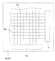
図2は、液晶表示装置の液晶を介して対向配置される各基板のうち一方の基板SUB1の液晶側の面の液晶表示領域に形成される回路の一実施例を示す構成図である。
<Example 1>
(Overall configuration)
FIG. 2 is a block diagram showing an embodiment of a circuit formed in the liquid crystal display region on the liquid crystal side surface of one of the substrates SUB1 among the substrates opposed to each other through the liquid crystal of the liquid crystal display device.
図2において、y方向に延在されx方向に並設されるデータ線DLと、このデータ線DLと絶縁されてx方向に延在されy方向に並設されるゲート線GLを有し、これら各信号線によって囲まれる矩形状の領域が画素の領域(図中点線枠で示す)に相当するようになっている。これにより、各画素はマトリックス状に配置され、この画素群によって前記液晶表示領域を構成するようになっている。 In FIG. 2, a data line DL extending in the y direction and arranged in parallel in the x direction, and a gate line GL insulated from the data line DL and extending in the x direction and arranged in parallel in the y direction, A rectangular area surrounded by these signal lines corresponds to a pixel area (indicated by a dotted frame in the figure). Thus, the pixels are arranged in a matrix, and the liquid crystal display area is configured by the pixel group.
各画素の領域にはその大部分にわたってたとえば透明電極からなる画素電極PXが形成され、この画素電極PXは薄膜トランジスタTFTを介してたとえば図中左側に隣接するデータ線DLと接続されるようになっている。該薄膜トランジスタTFTは、そのオン、オフの駆動によって、データ線DLからの信号を画素電極PXへの供給、非供給を制御するようになっている。 A pixel electrode PX made of, for example, a transparent electrode is formed over most of each pixel region, and the pixel electrode PX is connected to a data line DL adjacent to the left side in the drawing through the thin film transistor TFT, for example. Yes. The thin film transistor TFT controls the supply and non-supply of the signal from the data line DL to the pixel electrode PX by driving on and off.
前記薄膜トランジスタTFTは、たとえば、その半導体層(この実施例では酸化物半導体層OSCが使用されている)の下方に前記ゲート線GLの延在部で形成されるゲート電極GTを配置させた構造、いわゆるボトムゲート型と称されるMIS(Metal Insulator Semiconductor)構造として形成されている。 The thin film transistor TFT has, for example, a structure in which a gate electrode GT formed by an extension portion of the gate line GL is disposed below the semiconductor layer (the oxide semiconductor layer OSC is used in this embodiment). It is formed as a MIS (Metal Insulator Semiconductor) structure called a so-called bottom gate type.
これにより、各ゲート線GLのそれぞれに信号(走査信号)が順次供給されることにより、画素列の各画素の薄膜トランジスタTFTがオンされ、そのオンのタイミングに応じて各データ線DLにそれぞれ映像信号を供給することにより、この映像信号の電圧は前記画素列の各画素における画素電極PXに印加されるようになる。 Thereby, by sequentially supplying a signal (scanning signal) to each of the gate lines GL, the thin film transistor TFT of each pixel of the pixel column is turned on, and a video signal is applied to each data line DL according to the ON timing. The voltage of this video signal is applied to the pixel electrode PX in each pixel of the pixel column.
なお、この実施例に示す液晶表示装置は、前記基板SUB1と液晶を介して配置される図示しない他の基板を有し、この基板の液晶側の面には各画素に共通な対向電極が形成され、この対向電極はたとえば透明電極から構成され、前記データ線DLに供給される信号(映像信号)に対して基準となる電圧からなる信号が供給されるようになっている。 The liquid crystal display device shown in this embodiment has the substrate SUB1 and another substrate (not shown) disposed through the liquid crystal, and a common electrode common to each pixel is formed on the liquid crystal side surface of the substrate. The counter electrode is formed of a transparent electrode, for example, and is supplied with a signal having a reference voltage with respect to a signal (video signal) supplied to the data line DL.
前記液晶には前記画素電極PXと前記対向電極の電位差によって発生する電界が印加され、それに応じて該液晶の分子が挙動するようになっている。 An electric field generated by a potential difference between the pixel electrode PX and the counter electrode is applied to the liquid crystal, and the molecules of the liquid crystal behave accordingly.
また、図2には図示されていないが、画素の詳細な説明あるいは他の実施例の説明に応じ、データ線DLと絶縁され画素列ごとにゲート線GLと平行して延在される保持容量線(後に符号RCで示す)が備えられる場合がある。該保持容量RCは、たとえばゲート線GL(ゲート電極GT)と同層に形成される。 Although not shown in FIG. 2, a storage capacitor that is insulated from the data line DL and extends in parallel with the gate line GL for each pixel column according to the detailed description of the pixel or the description of another embodiment. A line (denoted later by the symbol RC) may be provided. For example, the storage capacitor RC is formed in the same layer as the gate line GL (gate electrode GT).
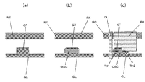
(画素の構成)
図1(a)は、図2に示した各画素のうち一の画素を抜き出して描いた図である。また、図1(b)は図2(a)のA−B−C−D線における断面図である。
(Pixel structure)
FIG. 1A is a diagram illustrating one pixel extracted from each pixel illustrated in FIG. FIG. 1B is a cross-sectional view taken along the line ABCD in FIG.
図1において、基板SUB1の液晶側の面に、まず、ゲート線GLおよびゲート電極GTが形成されている。 In FIG. 1, a gate line GL and a gate electrode GT are first formed on the surface of the substrate SUB1 on the liquid crystal side.
そして、基板SUB1の表面には、前記ゲート線GLおよびゲート電極GTをも被って絶縁膜GIが形成されている。この絶縁膜GIは薄膜トランジスタTFTの形成領域においてゲート絶縁膜として機能するようになる。 An insulating film GI is formed on the surface of the substrate SUB1 so as to cover the gate line GL and the gate electrode GT. This insulating film GI functions as a gate insulating film in the region where the thin film transistor TFT is formed.
前記絶縁膜GIの上面にはデータ線DLが形成され、その薄膜トランジスタTFTの近傍部が該薄膜トランジスタTFTの形成領域にまで延在されて該薄膜トランジスタTFTのドレイン電極DTが形成されている。 A data line DL is formed on the upper surface of the insulating film GI, and the vicinity of the thin film transistor TFT is extended to the formation region of the thin film transistor TFT to form the drain electrode DT of the thin film transistor TFT.
一方、前記絶縁膜GIの上面には、画素領域の周辺を除く中央部の大部分に画素電極PXが形成され、この画素電極PXの前記薄膜トランジスタTFTの近傍部が該薄膜トランジスタTFTの形成領域にまで延在されて該薄膜トランジスタTFTのソース電極STが形成されている。 On the other hand, on the upper surface of the insulating film GI, a pixel electrode PX is formed in most of the central portion excluding the periphery of the pixel region, and the vicinity of the thin film transistor TFT of the pixel electrode PX extends to the formation region of the thin film transistor TFT. A source electrode ST of the thin film transistor TFT is formed extending.
薄膜トランジスタTFTはドレイン電極とソース電極を有し、それらはバイアスの印加状態によって入れ替わるものであるが、この明細書においては、便宜上、データ線と接続される電極をドレイン電極DTと称し、画素電極PXと接続される電極をソース電極STと称する。 The thin film transistor TFT has a drain electrode and a source electrode, which are switched depending on a bias application state. In this specification, for convenience, an electrode connected to a data line is referred to as a drain electrode DT, and a pixel electrode PX The electrode connected to is referred to as source electrode ST.
ここで、前記データ線DLと画素電極PXは、それぞれの材料が異なっており、前記データ線DLは、たとえば、モリブデン、クロム、タングステン、アルミ、銅、チタン、ニッケル、タンタル、銀、亜鉛、あるいはその他の金属の単膜、それらの合金膜、それらの積層膜、それらとITO(Indium Tin Oxide)やZnO系等の透明酸化物層の積層膜によって形成されているのに対し、前記画素電極PXは、たとえば、ITOやZnO系等の透明酸化物層等からなる透明導電膜によって形成されている。 Here, the data line DL and the pixel electrode PX are made of different materials, and the data line DL is made of, for example, molybdenum, chromium, tungsten, aluminum, copper, titanium, nickel, tantalum, silver, zinc, or The pixel electrode PX is formed of other metal single films, alloy films thereof, laminated films thereof, and laminated films of transparent oxide layers such as ITO (Indium Tin Oxide) and ZnO. Is formed by a transparent conductive film made of, for example, a transparent oxide layer such as ITO or ZnO.
そして、該薄膜トランジスタTFTの形成領域には酸化物半導体層OSCが形成され、該酸化物半導体層OSCの下方には前記ドレイン電極DTおよびソース電極STが配置されるようになっている。前記酸化物半導体層OSCは、たとえば、ZnO、InGaZnO、ZnInO、ZnSnOなどから構成され、前記薄膜トランジスタTFTのチャネルが形成される半導体層となっている。 An oxide semiconductor layer OSC is formed in the formation region of the thin film transistor TFT, and the drain electrode DT and the source electrode ST are disposed below the oxide semiconductor layer OSC. The oxide semiconductor layer OSC is made of, for example, ZnO, InGaZnO, ZnInO, ZnSnO, or the like, and is a semiconductor layer in which the channel of the thin film transistor TFT is formed.
ここで、図2において、データ線DLから延在されるドレイン電極DT、画素電極PXから延在されるソース電極STは、それぞれ、薄膜トランジスタTFTのゲート電極GTと重なりを持つように形成され、その上を覆うように酸化膜半導体層OSCが形成された積層構造となっている。 Here, in FIG. 2, the drain electrode DT extending from the data line DL and the source electrode ST extending from the pixel electrode PX are formed so as to overlap with the gate electrode GT of the thin film transistor TFT, respectively. It has a stacked structure in which an oxide film semiconductor layer OSC is formed so as to cover the top.
そして、前記ドレイン電極DTおよびソース電極STは、いずれも酸化物半導体層OSCと直接に接続された構成となっており、たとえばコンタクト層等が介在されていない構成となっている。酸化物半導体の性質からコンタクト層を介在させなくてもドレイン電極DTおよびソース電極STとオーミック接続を達成できるからである。 The drain electrode DT and the source electrode ST are both directly connected to the oxide semiconductor layer OSC, for example, without a contact layer. This is because an ohmic connection with the drain electrode DT and the source electrode ST can be achieved without interposing a contact layer due to the nature of the oxide semiconductor.
なお、図1に示した構成において、ゲート線GLおよびゲート電極GTは、たとえば、モリブデン、クロム、タングステン、アルミ、銅、チタン、ニッケル、タンタル、銀、亜鉛、あるいはその他の金属の単膜、それらの合金膜、それらの積層膜、それらとITOやZnO系等の透明酸化物層の積層膜によって形成されている。また、絶縁膜GIは、たとえば、SiO2、SiN、Al2O3などの絶縁膜によって形成されている。 In the configuration shown in FIG. 1, the gate line GL and the gate electrode GT are, for example, a single film of molybdenum, chromium, tungsten, aluminum, copper, titanium, nickel, tantalum, silver, zinc, or other metal, or Alloy films thereof, laminated films thereof, and laminated films of those and transparent oxide layers such as ITO and ZnO. The insulating film GI is formed of an insulating film such as SiO 2 , SiN, Al 2 O 3 , for example.
また、このようにデータ線DL、画素電極PX、および薄膜トランジスタTFTが形成された基板SUB1の表面には保護膜PASが形成され、この保護膜PASは前記画素電極PXの周辺を除く中央の大部分の領域に開口OPが形成されている。 In addition, a protective film PAS is formed on the surface of the substrate SUB1 on which the data lines DL, the pixel electrodes PX, and the thin film transistors TFT are formed, and the protective film PAS is mostly in the center except the periphery of the pixel electrodes PX. An opening OP is formed in this area.
該保護膜PASは前記薄膜トランジスタTFTの液晶との直接の接触を回避するために設けられ、前記開口OPは画素電極PXを液晶に近接させて位置づけ該液晶の分子を制御し易くするために形成されている。 The protective film PAS is provided to avoid direct contact with the liquid crystal of the thin film transistor TFT, and the opening OP is formed to position the pixel electrode PX close to the liquid crystal and to easily control the molecules of the liquid crystal. ing.
なお、図1(a)には、たとえば、保持容量線RCがゲート線GL(ゲート電極GT)と同層で形成され、絶縁膜GIを介して画素電極PXと重ねられて形成されている。保持容量線RCと画素電極PXとの間に前記絶縁膜GIを誘電体膜とする容量を構成し、この容量によって、画素電極PXに供給される映像信号を蓄積するようになっている。 In FIG. 1A, for example, the storage capacitor line RC is formed in the same layer as the gate line GL (gate electrode GT), and is formed so as to overlap the pixel electrode PX via the insulating film GI. A capacitor using the insulating film GI as a dielectric film is formed between the storage capacitor line RC and the pixel electrode PX, and a video signal supplied to the pixel electrode PX is stored by this capacitor.
(製造方法)
図3は、上述した液晶表示装置の製造方法の一実施例を示す工程図で、図2に示した画素における工程を示している。
(Production method)
FIG. 3 is a process diagram showing an embodiment of the method for manufacturing the liquid crystal display device described above, and shows the process in the pixel shown in FIG.
以下、工程順に説明する。 Hereinafter, it demonstrates in order of a process.
工程1.(図3(a))
たとえばガラスからなる基板SUB1を用意し、この基板SUB1の表面(液晶側の面)の全域にたとえば金属膜を形成する。
Step 1. (Fig. 3 (a))
For example, a substrate SUB1 made of glass is prepared, and a metal film, for example, is formed over the entire surface (surface on the liquid crystal side) of the substrate SUB1.
そして、周知のフォトリソグラフィ技術による選択エッチング法を用いて前記金属膜をパターン化し、ゲート線GL、ゲート電極GTおよび保持容量線RCを形成する。 Then, the metal film is patterned using a selective etching method by a well-known photolithography technique, and the gate line GL, the gate electrode GT, and the storage capacitor line RC are formed.
その後、基板SUB1の表面に、前記ゲート線GL、ゲート電極GTおよび保持容量線RCをも被って絶縁膜GI(図示せず)を形成する。 Thereafter, an insulating film GI (not shown) is formed on the surface of the substrate SUB1 so as to cover the gate line GL, the gate electrode GT, and the storage capacitor line RC.
工程2.(図3(b))
前記絶縁膜GIの表面の全域に金属膜を形成し、フォトリソグラフィ技術による選択エッチング法を用いて前記金属膜をパターン化し、データ線DLおよびドレイン電極DTを形成する。
A metal film is formed over the entire surface of the insulating film GI, and the metal film is patterned using a selective etching method using a photolithography technique to form the data line DL and the drain electrode DT.
さらに、前記絶縁膜GIの表面に前記データ線DLおよびドレイン電極DTをも被って透明導電膜を形成し、フォトリソグラフィ技術による選択エッチング法を用いて前記透明導電膜をパターン化し、画素電極PXおよびソース電極を形成する。 Further, a transparent conductive film is formed on the surface of the insulating film GI so as to cover the data line DL and the drain electrode DT, and the transparent conductive film is patterned using a selective etching method using a photolithography technique, and the pixel electrodes PX and A source electrode is formed.
工程3.(図3(c))
基板SUB1の表面の全域に、前記データ線DLおよび画素電極PX等をも被って酸化物半導体層を形成し、フォトリソグラフィ技術による選択エッチング法を用いて前記酸化物半導体層をパターン化し、薄膜トランジスタTFTの酸化物半導体層OSCを形成する。
Step 3. (Fig. 3 (c))
A thin film transistor TFT is formed by forming an oxide semiconductor layer covering the data line DL, the pixel electrode PX and the like over the entire surface of the substrate SUB1, and patterning the oxide semiconductor layer using a selective etching method using a photolithography technique. The oxide semiconductor layer OSC is formed.
その後は、基板SUB1の表面の全域に、たとえば樹脂等の絶縁膜を形成し、フォトリソグラフィ技術による選択エッチング法を用いて前記絶縁膜をパターン化して保護膜PAS(図示せず)を形成する。 Thereafter, an insulating film such as a resin is formed over the entire surface of the substrate SUB1, and the insulating film is patterned using a selective etching method using a photolithography technique to form a protective film PAS (not shown).
この保護膜PASは、画素電極PXの僅かな周辺を除く中央部のほとんどを露出させる開口OPとともに、図示されていないが、データ線DLおよびゲート線GLの端部を露出させるコンタクト孔が形成されるようになる。 The protective film PAS has an opening OP that exposes most of the central portion except for the slight periphery of the pixel electrode PX, and a contact hole that exposes the end portions of the data line DL and the gate line GL, although not shown. Become so.
以上の工程において、金属層等の所定のパターンの加工はフォトリソグラフィ技術による選択エッチング法を用いたものであるが、これに限定されることはなく、たとえば印刷技術などを用いてもよい。 In the above steps, the processing of a predetermined pattern such as a metal layer is performed by a selective etching method using a photolithography technique, but is not limited to this, and for example, a printing technique may be used.
上述のように、本実施例の液晶表示装置の製造方法では、基板SUB1の液晶側の面の液晶表示領域において、積層膜数が6層で、5回のパターン形成工程で製造することができることが判る。 As described above, in the method of manufacturing the liquid crystal display device according to the present embodiment, the number of stacked films is six in the liquid crystal display region on the liquid crystal side surface of the substrate SUB1, and can be manufactured in five pattern forming steps. I understand.
本実施例の構成では、データ線DLに金属膜を用い、画素電極PXに透明導電膜を用いるので、上記特許文献1に記載された表示装置でデータ線DLと画素電極PXの両方に透明導電膜などを用いた場合にデータ線DLの電気抵抗が高くなってしまうという不都合を回避できる。 In the configuration of this embodiment, a metal film is used for the data line DL and a transparent conductive film is used for the pixel electrode PX. Therefore, in the display device described in Patent Document 1, both the data line DL and the pixel electrode PX are transparent. When a film or the like is used, the disadvantage that the electric resistance of the data line DL becomes high can be avoided.
また、特許文献1に記載された表示装置でデータ線DLと画素電極PXの両方に金属を用いた場合に透過型液晶表示装置に適用することができないという不都合を回避できる。 Further, it is possible to avoid the disadvantage that the display device described in Patent Document 1 cannot be applied to the transmissive liquid crystal display device when metal is used for both the data line DL and the pixel electrode PX.
さらに、データ線DLに金属を用いて応力を低減することで、データ線DLに硬いITOなどを用いた場合に表示装置をフレキシブル化することが困難という不都合を回避できる。 Further, by reducing the stress by using a metal for the data line DL, it is possible to avoid the inconvenience that it is difficult to make the display device flexible when a hard ITO or the like is used for the data line DL.
〈実施例2〉
(画素の構成)
図4(a)は、本発明による表示装置の画素の構成の他の実施例を示す平面図で、図1(a)に対応した図となっている。また、図4(b)は、図4(a)のA−B−C−D線における断面図である。図1と同符号の部材は図1に示す部材と同機能を有するようになっている。
<Example 2>
(Pixel configuration)
FIG. 4A is a plan view showing another embodiment of the pixel configuration of the display device according to the present invention and corresponds to FIG. FIG. 4B is a cross-sectional view taken along the line ABCD in FIG. 1 have the same function as the member shown in FIG.
図4において、図1と比較して異なる構成は、画素電極PXが薄膜トランジスタTFTの酸化物半導体層OSCより上層に形成され、該画素電極PXと一体に形成される薄膜トランジスタTFTのソース電極STが、ゲート電極GTと重なりをもつとともに、前記酸化物半導体層OSCの上面に直接に当接されて形成されていることにある。 4, the configuration different from that in FIG. 1 is that the pixel electrode PX is formed above the oxide semiconductor layer OSC of the thin film transistor TFT, and the source electrode ST of the thin film transistor TFT formed integrally with the pixel electrode PX is It is formed so as to overlap with the gate electrode GT and to be in direct contact with the upper surface of the oxide semiconductor layer OSC.
なお、データ線DLは薄膜トランジスタTFTの酸化物半導体層OSCより下層に形成され、該データ線DLと一体に形成されたドレイン電極DTは、ゲート電極GTと重なりをもつとともに、前記酸化物半導体層OSCの下面に直接に当接されて形成されていることは、図1の場合と同様である。 Note that the data line DL is formed below the oxide semiconductor layer OSC of the thin film transistor TFT, and the drain electrode DT formed integrally with the data line DL has an overlap with the gate electrode GT and the oxide semiconductor layer OSC. It is the same as in the case of FIG.
ここで、ゲート線GLおよびゲート電極GTは、たとえば、モリブデン、クロム、タングステン、アルミ、銅、チタン、ニッケル、タンタル、銀、亜鉛、あるいはその他の金属の単膜、それらの合金膜、それらの積層膜、それらとITOやZnO系等の透明酸化物層の積層膜によって形成されている。ゲート絶縁膜GIは、たとえば、SiO2、SiN、Al2O3などの絶縁膜によって形成されている。データ線DLは、たとえば、モリブデン、クロム、タングステン、アルミ、銅、チタン、ニッケル、タンタル、銀、亜鉛、あるいはその他の金属の単膜、それらの合金膜、それらの積層膜、それらとITOやZnO系等の透明酸化物層の積層膜によって形成されている。画素電極PXは、たとえば、ITOやZnO系等の透明導電膜によって形成され、酸化物半導体層OSCは、たとえば、ZnO、InGaZnO、ZnInO、ZnSnOなどで形成されている。 Here, the gate line GL and the gate electrode GT are, for example, a single film of molybdenum, chromium, tungsten, aluminum, copper, titanium, nickel, tantalum, silver, zinc, or other metal, an alloy film thereof, or a laminate thereof. It is formed of a film and a laminated film of these and a transparent oxide layer such as ITO or ZnO. The gate insulating film GI is formed of an insulating film such as SiO2, SiN, Al2O3, for example. The data line DL is, for example, a single film of molybdenum, chromium, tungsten, aluminum, copper, titanium, nickel, tantalum, silver, zinc, or other metal, an alloy film thereof, a laminated film thereof, ITO and ZnO It is formed by a laminated film of a transparent oxide layer such as a system. The pixel electrode PX is formed of, for example, a transparent conductive film such as ITO or ZnO, and the oxide semiconductor layer OSC is formed of, for example, ZnO, InGaZnO, ZnInO, ZnSnO, or the like.
(製造方法)
図5は、液晶表示装置の製造方法の他の実施例を示す工程図で、図4に示した画素における工程を示す。
(Production method)
FIG. 5 is a process diagram showing another embodiment of the method of manufacturing the liquid crystal display device, and shows the process in the pixel shown in FIG.
以下、工程順に説明する。 Hereinafter, it demonstrates in order of a process.
工程1.(図5(a))
たとえばガラスからなる基板SUB1を用意し、この基板SUB1の表面(液晶側の面)の全域にたとえば金属膜を形成する。
Step 1. (Fig. 5 (a))
For example, a substrate SUB1 made of glass is prepared, and a metal film, for example, is formed over the entire surface (surface on the liquid crystal side) of the substrate SUB1.
そして、周知のフォトリソグラフィ技術による選択エッチング法を用いて前記金属膜をパターン化し、ゲート線GL、ゲート電極GTおよび保持容量線RCを形成する。 Then, the metal film is patterned using a selective etching method by a well-known photolithography technique, and the gate line GL, the gate electrode GT, and the storage capacitor line RC are formed.
その後、基板SUB1の表面に、前記ゲート線GL、ゲート電極GTおよび保持容量線RCをも被って絶縁膜GI(図示せず)を形成する。 Thereafter, an insulating film GI (not shown) is formed on the surface of the substrate SUB1 so as to cover the gate line GL, the gate electrode GT, and the storage capacitor line RC.
工程2.(図5(b))
前記絶縁膜GIの表面の全域に金属膜を形成し、フォトリソグラフィ技術による選択エッチング法を用いて前記金属膜をパターン化し、データ線DLおよびドレイン電極DTを形成する。
A metal film is formed over the entire surface of the insulating film GI, and the metal film is patterned using a selective etching method using a photolithography technique to form the data line DL and the drain electrode DT.
さらに、基板SUB1の表面の全域に、前記データ線DLおよびドレイン電極DTをも被って酸化物半導体層を形成し、フォトリソグラフィ技術による選択エッチング法を用いて前記酸化物半導体層をパターン化し、薄膜トランジスタTFTの酸化物半導体層OSCを形成する。 Further, an oxide semiconductor layer is formed over the entire surface of the substrate SUB1 so as to cover the data line DL and the drain electrode DT, and the oxide semiconductor layer is patterned using a selective etching method using a photolithography technique. An oxide semiconductor layer OSC of the TFT is formed.
工程3.(図5(c))
前記絶縁膜GIの表面に酸化物半導体層OSC等をも被って透明導電膜を形成し、フォトリソグラフィ技術による選択エッチング法を用いて前記透明導電膜をパターン化し、画素電極PXおよびソース電極を形成する。
Step 3. (Fig. 5 (c))
A transparent conductive film is formed on the surface of the insulating film GI so as to cover the oxide semiconductor layer OSC and the like, and the transparent conductive film is patterned using a selective etching method using a photolithography technique to form a pixel electrode PX and a source electrode To do.
その後は、基板SUB1の表面の全域に、たとえば樹脂等の絶縁膜を形成し、フォトリソグラフィ技術による選択エッチング法を用いて前記絶縁膜をパターン化して保護膜PAS(図示せず)を形成する。 Thereafter, an insulating film such as a resin is formed over the entire surface of the substrate SUB1, and the insulating film is patterned using a selective etching method using a photolithography technique to form a protective film PAS (not shown).
この保護膜PASは、画素電極PXの僅かな周辺を除く中央部のほとんどを露出させる開口OPとともに、図示されていないが、データ線DLおよびゲート線GLの端部を露出させるコンタクト孔が形成されるようになる。 The protective film PAS has an opening OP that exposes most of the central portion except for the slight periphery of the pixel electrode PX, and a contact hole that exposes the end portions of the data line DL and the gate line GL, although not shown. Become so.
以上の工程において、金属層等の所定のパターンの加工はフォトリソグラフィ技術による選択エッチング法を用いたものであるが、これに限定されることはなく、たとえば印刷技術などを用いてもよい。 In the above steps, the processing of a predetermined pattern such as a metal layer is performed by a selective etching method using a photolithography technique, but is not limited to this, and for example, a printing technique may be used.
上述のように、本実施例の液晶表示装置の製造方法では、基板SUB1の液晶側の面の液晶表示領域において、積層膜数が6層で、5回のパターン形成工程で製造することができることが判る。 As described above, in the method of manufacturing the liquid crystal display device according to the present embodiment, the number of stacked films is six in the liquid crystal display region on the liquid crystal side surface of the substrate SUB1, and can be manufactured in five pattern forming steps. I understand.
本実施例の構成では、データ線DLに金属膜を用い、画素電極PXに透明導電膜を用いるので、上記特許文献1に記載された表示装置でデータ線DLと画素電極PXの両方にITOなどを用いた場合にデータ線DLの電気抵抗が高くなってしまうという不都合を回避できる。 In the configuration of this embodiment, a metal film is used for the data line DL and a transparent conductive film is used for the pixel electrode PX. Therefore, in the display device described in Patent Document 1, ITO is used for both the data line DL and the pixel electrode PX. This can avoid the disadvantage that the electrical resistance of the data line DL becomes high.
また、特許文献1に記載された表示装置でデータ線DLと画素電極PXの両方に金属を用いた場合に透過型液晶表示装置に適用することができないという不都合を回避できる。 Further, it is possible to avoid the disadvantage that the display device described in Patent Document 1 cannot be applied to the transmissive liquid crystal display device when metal is used for both the data line DL and the pixel electrode PX.
さらに、データ線DLに金属を用いて応力を低減することで、データ線DLに硬いITOなどを用いた場合に表示装置をフレキシブル化することが困難という不都合を回避できる。 Further, by reducing the stress by using a metal for the data line DL, it is possible to avoid the inconvenience that it is difficult to make the display device flexible when a hard ITO or the like is used for the data line DL.
〈実施例3〉
(画素の構成)
図6(a)は、本発明による表示装置の画素の構成の他の実施例を示す平面図で、図1(a)に対応した図となっている。図6(b)は、図6(a)のA−B−C−D線における断面図である。図1と同符号の部材は図1に示す部材と同機能を有するようになっている。
<Example 3>
(Pixel configuration)
FIG. 6A is a plan view showing another embodiment of the configuration of the pixel of the display device according to the present invention, and corresponds to FIG. FIG. 6B is a cross-sectional view taken along the line ABCD in FIG. 1 have the same function as the member shown in FIG.
図6において、図1の場合と比較して異なる構成は、まず、保護膜PASは基板SUB1の表面の全域に形成され、前記保護膜PASの上面に画素電極PXが形成されているところにある。 In FIG. 6, the configuration different from the case of FIG. 1 is that the protective film PAS is formed on the entire surface of the substrate SUB1, and the pixel electrode PX is formed on the upper surface of the protective film PAS. .
そして、前記画素電極PXのうち薄膜トランジスタTFTに近接する部分において、前記保護膜PASに形成されたスルーホールTHを通して、該薄膜トランジスタTFTの酸化物半導体層OSCの一部(ソース領域)に接続されている。 In the portion of the pixel electrode PX close to the thin film transistor TFT, the pixel electrode PX is connected to a part (source region) of the oxide semiconductor layer OSC of the thin film transistor TFT through the through hole TH formed in the protective film PAS. .
ここで、酸化物半導体層OSCと画素電極PXの接続部はゲート電極GTと重なりをもつようになっている。 Here, a connection portion between the oxide semiconductor layer OSC and the pixel electrode PX overlaps with the gate electrode GT.
なお、データ線DLは薄膜トランジスタTFTの酸化物半導体層OSCより下層に形成され、該データ線DLと一体に形成されたドレイン電極DTは、ゲート電極GTと重なりをもつとともに、前記酸化物半導体層OSCの下面に直接に当接されて形成されていることは、図1の場合と同様である。 Note that the data line DL is formed below the oxide semiconductor layer OSC of the thin film transistor TFT, and the drain electrode DT formed integrally with the data line DL has an overlap with the gate electrode GT and the oxide semiconductor layer OSC. It is the same as in the case of FIG.
ゲート線GLおよびゲート電極GTは、たとえば、モリブデン、クロム、タングステン、アルミ、銅、チタン、ニッケル、タンタル、銀、亜鉛、あるいはその他の金属の単膜、それらの合金膜、それらの積層膜、それらとITOやZnO系等の透明酸化物層の積層膜によって形成されている。 The gate line GL and the gate electrode GT are, for example, molybdenum, chromium, tungsten, aluminum, copper, titanium, nickel, tantalum, silver, zinc, or other metal single films, alloy films thereof, laminated films thereof, and the like. And a laminated film of transparent oxide layers such as ITO and ZnO.
ゲート絶縁膜GIは、たとえば、SiO2、SiN、Al2O3などの絶縁膜によって形成されている。 The gate insulating film GI is formed of an insulating film such as SiO2, SiN, Al2O3, for example.
データ線DLは、たとえば、モリブデン、クロム、タングステン、アルミ、銅、チタン、ニッケル、タンタル、銀、亜鉛、あるいはその他の金属の単膜、それらの合金膜、それらの積層膜、それらとITOやZnO系等の透明酸化物層の積層膜によって形成れている。 The data line DL is, for example, a single film of molybdenum, chromium, tungsten, aluminum, copper, titanium, nickel, tantalum, silver, zinc, or other metal, an alloy film thereof, a laminated film thereof, ITO and ZnO It is formed of a laminated film of a transparent oxide layer such as a system.
画素電極PXは、たとえば、ITOやZnO系等の透明導電膜によって形成され、酸化物半導体層OSCは、たとえば、ZnO、InGaZnO、ZnInO、ZnSnOなどによって形成されている。 The pixel electrode PX is formed of, for example, a transparent conductive film such as ITO or ZnO, and the oxide semiconductor layer OSC is formed of, for example, ZnO, InGaZnO, ZnInO, ZnSnO, or the like.
(製造方法)
図7は、液晶表示装置の製造方法の他の実施例を示す工程図で、図6に示した画素における工程を示している。
(Production method)
FIG. 7 is a process chart showing another embodiment of the method for manufacturing the liquid crystal display device, and shows the process in the pixel shown in FIG.
以下、工程順に説明する。 Hereinafter, it demonstrates in order of a process.
工程1.(図7(a))
たとえばガラスからなる基板SUB1を用意し、この基板SUB1の表面(液晶側の面)の全域にたとえば金属膜を形成する。
Step 1. (Fig. 7 (a))
For example, a substrate SUB1 made of glass is prepared, and a metal film, for example, is formed over the entire surface (surface on the liquid crystal side) of the substrate SUB1.
そして、周知のフォトリソグラフィ技術による選択エッチング法を用いて前記金属膜をパターン化し、ゲート線GL、ゲート電極GTおよび保持容量線RCを形成する。 Then, the metal film is patterned using a selective etching method by a well-known photolithography technique, and the gate line GL, the gate electrode GT, and the storage capacitor line RC are formed.
その後、基板SUB1の表面に、前記ゲート線GL、ゲート電極GTおよび保持容量線RCをも被って絶縁膜GI(図示せず)を形成する。 Thereafter, an insulating film GI (not shown) is formed on the surface of the substrate SUB1 so as to cover the gate line GL, the gate electrode GT, and the storage capacitor line RC.
工程2.(図7(b))
前記絶縁膜GIの表面の全域に金属膜を形成し、フォトリソグラフィ技術による選択エッチング法を用いて前記金属膜をパターン化し、データ線DLおよびドレイン電極DTを形成する。
A metal film is formed over the entire surface of the insulating film GI, and the metal film is patterned using a selective etching method using a photolithography technique to form the data line DL and the drain electrode DT.
さらに、基板SUB1の表面の全域に、前記データ線DLおよびドレイン電極DTをも被って酸化物半導体層を形成し、フォトリソグラフィ技術による選択エッチング法を用いて前記酸化物半導体層をパターン化し、薄膜トランジスタTFTの酸化物半導体層OSCを形成する。 Further, an oxide semiconductor layer is formed over the entire surface of the substrate SUB1 so as to cover the data line DL and the drain electrode DT, and the oxide semiconductor layer is patterned using a selective etching method using a photolithography technique. An oxide semiconductor layer OSC of the TFT is formed.
工程3.(図7(c))
基板SUB1の表面の全域に、たとえば樹脂等の絶縁膜を形成し、フォトリソグラフィ技術による選択エッチング法を用いて前記絶縁膜をパターン化して保護膜PAS(図示せず)を形成する。
Step 3. (Fig. 7 (c))
An insulating film such as a resin is formed over the entire surface of the substrate SUB1, and the protective film PAS (not shown) is formed by patterning the insulating film using a selective etching method using a photolithography technique.
この保護膜PASは、前記パターン化によって、薄膜トランジスタTFTの前記酸化物半導体層OSCのうちソース領域の部分を露出させるスルーホールTHが形成され、また、図示されていないがデータ線DLおよびゲート線GLの端部を露出させるコンタクト孔が形成される。 Through the patterning, the protective film PAS is formed with a through hole TH that exposes a portion of the source region of the oxide semiconductor layer OSC of the thin film transistor TFT. Although not shown, the data line DL and the gate line GL are not shown. A contact hole is formed to expose the end of the contact.
その後、前記保護膜PASの表面に、前記スルーホールTHおよびコンタクト孔をも被って透明導電膜を形成し、フォトリソグラフィ技術による選択エッチング法を用いて前記透明導電膜をパターン化し、画素電極PXおよびソース電極を形成する。 Thereafter, a transparent conductive film is formed on the surface of the protective film PAS so as to cover the through hole TH and the contact hole, and the transparent conductive film is patterned using a selective etching method using a photolithography technique, and the pixel electrodes PX and A source electrode is formed.
この場合、前記ソース電極STの部分は前記スルーホールTHを通して前記酸化物半導体層OSCのうちソース領域の部分に直接接続されるようになる。 In this case, the source electrode ST portion is directly connected to the source region portion of the oxide semiconductor layer OSC through the through hole TH.
以上の工程において、金属層等の所定のパターンの加工はフォトリソグラフィ技術による選択エッチング法を用いたものであるが、これに限定されることはなく、たとえば印刷技術などを用いてもよい。 In the above steps, the processing of a predetermined pattern such as a metal layer is performed by a selective etching method using a photolithography technique, but is not limited to this, and for example, a printing technique may be used.
上述のように、本実施例の液晶表示装置の製造方法では、基板SUB1の液晶側の面の液晶表示領域において、積層膜数が6層で、5回のパターン形成工程で製造することができることが判る。 As described above, in the method of manufacturing the liquid crystal display device according to the present embodiment, the number of stacked films is six in the liquid crystal display region on the liquid crystal side of the substrate SUB1 and can be manufactured in five pattern forming steps. I understand.
本実施例の構成では、データ線DLに金属膜を用い、画素電極PXに透明導電膜を用いるので、上記特許文献1に記載された表示装置でデータ線DLと画素電極PXの両方にITOなどを用いた場合にデータ線DLの電気抵抗が高くなってしまうという不都合を回避できる。 In the configuration of this embodiment, a metal film is used for the data line DL and a transparent conductive film is used for the pixel electrode PX. Therefore, in the display device described in Patent Document 1, ITO is used for both the data line DL and the pixel electrode PX. This can avoid the disadvantage that the electrical resistance of the data line DL becomes high.
また、特許文献1に記載された表示装置でデータ線DLと画素電極PXの両方に金属を用いた場合に透過型液晶表示装置に適用することができないという不都合を回避できる。 Further, it is possible to avoid the disadvantage that the display device described in Patent Document 1 cannot be applied to the transmissive liquid crystal display device when metal is used for both the data line DL and the pixel electrode PX.
さらに、データ線DLに金属を用いて応力を低減することで、データ線DLに硬いITOなどを用いた場合に表示装置をフレキシブル化することが困難という不都合を回避できる。 Further, by reducing the stress by using metal for the data lines DL, it is possible to avoid the disadvantage that it is difficult to make the display device flexible when using hard ITO or the like for the data lines DL.
さらに、保護膜上の画素電極PXは、液晶と近い距離に位置づけられ、該液晶の分子を制御し易くできる効果を奏する。 Further, the pixel electrode PX on the protective film is positioned at a distance close to the liquid crystal, and has an effect that the liquid crystal molecules can be easily controlled.
〈実施例4〉
(画素の構成)
図8(a)は、本発明による表示装置の画素の構成の他の実施例を示す平面図で、図1(a)に対応した図となっている。図8(b)は、図8(a)のA−B−C−D線における断面図である。図1と同符号の部材は図1に示す部材と同機能を有するようになっている。
<Example 4>
(Pixel configuration)
FIG. 8A is a plan view showing another embodiment of the configuration of the pixel of the display device according to the present invention, and corresponds to FIG. FIG.8 (b) is sectional drawing in the ABCD line | wire of Fig.8 (a). 1 have the same function as the member shown in FIG.
図8において、図1と比較して異なる構成は、まず、保護膜PASは基板SUB1の表面の全域に形成され、前記保護膜PASの上面にデータ線DLおよび画素電極PXが形成されているところにある。 In FIG. 8, the configuration different from that in FIG. 1 is that the protective film PAS is formed on the entire surface of the substrate SUB1, and the data lines DL and the pixel electrodes PX are formed on the upper surface of the protective film PAS. It is in.
そして、前記データ線DLのうち薄膜トランジスタTFTに近接する部分において、前記保護膜PASに形成されたスルーホールTH1を通して、該薄膜トランジスタTFTの酸化物半導体層OSCの一部(ドレイン領域)に接続されている。 A portion of the data line DL adjacent to the thin film transistor TFT is connected to a part (drain region) of the oxide semiconductor layer OSC of the thin film transistor TFT through a through hole TH1 formed in the protective film PAS. .
また、前記画素電極PXのうち薄膜トランジスタTFTに近接する部分において、前記保護膜PASに形成されたスルーホールTH2を通して、該薄膜トランジスタTFTの酸化物半導体層OSCの一部(ソース領域)に接続されている。 Further, in a portion of the pixel electrode PX that is close to the thin film transistor TFT, the pixel electrode PX is connected to a part (source region) of the oxide semiconductor layer OSC of the thin film transistor TFT through a through hole TH2 formed in the protective film PAS. .
ここで、データ線DLの前記酸化物半導体層OSCとの接続部は薄膜トランジスタTFTのドレイン電極として機能し、ゲート電極GTと重なりをもつようになっている。また、画素電極PXの前記酸化物半導体層OSCとの接続部はソース電極として機能し、ゲート電極GTと重なりをもつようになっている。 Here, the connection portion of the data line DL with the oxide semiconductor layer OSC functions as a drain electrode of the thin film transistor TFT and overlaps with the gate electrode GT. In addition, the connection portion of the pixel electrode PX with the oxide semiconductor layer OSC functions as a source electrode and overlaps with the gate electrode GT.
ゲート線GLおよびゲート電極GTは、たとえば、モリブデン、クロム、タングステン、アルミ、銅、チタン、ニッケル、タンタル、銀、亜鉛、あるいはその他の金属の単膜、それらの合金膜、それらの積層膜、それらとITOやZnO系等の透明酸化物層の積層膜によって形成されている。 The gate line GL and the gate electrode GT are, for example, molybdenum, chromium, tungsten, aluminum, copper, titanium, nickel, tantalum, silver, zinc, or other metal single films, alloy films thereof, laminated films thereof, and the like. And a laminated film of transparent oxide layers such as ITO and ZnO.
ゲート絶縁膜GIは、たとえば、SiO2、SiN、Al2O3などの絶縁膜によって形成されている。 The gate insulating film GI is formed of an insulating film such as SiO2, SiN, Al2O3, for example.
データ線DLと画素電極PXは、たとえば、モリブデン、クロム、タングステン、アルミ、銅、チタン、ニッケル、タンタル、銀、亜鉛、あるいはその他の金属の単膜、それらの合金膜、それらの積層膜、それらとITOやZnO系等の透明酸化物層の積層膜、あるいはITOやZnO系等の透明導電膜などの同一の膜から形成されている。 The data lines DL and the pixel electrodes PX are, for example, molybdenum, chromium, tungsten, aluminum, copper, titanium, nickel, tantalum, silver, zinc, or other metal single films, alloy films thereof, laminated films thereof, and the like. And a transparent oxide layer such as ITO or ZnO, or a transparent conductive film such as ITO or ZnO.
酸化物半導体層OSCは、たとえば、ZnO、InGaZnO、ZnInO、ZnSnOなどによって形成されている。 The oxide semiconductor layer OSC is made of, for example, ZnO, InGaZnO, ZnInO, ZnSnO, or the like.
(製造方法)
図9は、液晶表示装置の製造方法の他の実施例を示す工程図で、図8に示した画素における工程を示している。
(Production method)
FIG. 9 is a process diagram showing another embodiment of the method of manufacturing the liquid crystal display device, and shows the process in the pixel shown in FIG.
以下、工程順に説明する。 Hereinafter, it demonstrates in order of a process.
工程1.(図9(a))
たとえばガラスからなる基板SUB1を用意し、この基板SUB1の表面(液晶側の面)の全域にたとえば金属膜を形成する。
Step 1. (Fig. 9 (a))
For example, a substrate SUB1 made of glass is prepared, and a metal film, for example, is formed over the entire surface (surface on the liquid crystal side) of the substrate SUB1.
そして、周知のフォトリソグラフィ技術による選択エッチング法を用いて前記金属膜をパターン化し、ゲート線GL、ゲート電極GTおよび保持容量線RCを形成する。 Then, the metal film is patterned using a selective etching method by a well-known photolithography technique, and the gate line GL, the gate electrode GT, and the storage capacitor line RC are formed.
その後、基板SUB1の表面に、前記ゲート線GL、ゲート電極GTおよび保持容量線RCをも被って絶縁膜GI(図示せず)を形成する。 Thereafter, an insulating film GI (not shown) is formed on the surface of the substrate SUB1 so as to cover the gate line GL, the gate electrode GT, and the storage capacitor line RC.
工程2.(図9(b))
前記絶縁膜GIの表面の全域に酸化物半導体層を形成し、フォトリソグラフィ技術による選択エッチング法を用いて前記酸化物半導体層をパターン化し、薄膜トランジスタTFTの形成領域において酸化物半導体層OSCを残存させる。
An oxide semiconductor layer is formed over the entire surface of the insulating film GI, and the oxide semiconductor layer is patterned using a selective etching method using a photolithography technique, so that the oxide semiconductor layer OSC remains in a formation region of the thin film transistor TFT. .
工程3.(図9(c))
基板SUB1の表面の全域に、たとえば樹脂等の絶縁膜を形成し、フォトリソグラフィ技術による選択エッチング法を用いて前記絶縁膜をパターン化して保護膜PAS(図示せず)を形成する。
Step 3. (Fig. 9 (c))
An insulating film such as a resin is formed over the entire surface of the substrate SUB1, and the protective film PAS (not shown) is formed by patterning the insulating film using a selective etching method using a photolithography technique.
この保護膜PASは、前記パターン化によって、薄膜トランジスタTFTの前記酸化物半導体層OSCのうちドレイン領域およびソース領域の各部分を露出させるスルーホールTH1、TH2が形成され、また、図示されていないがデータ線DLおよびゲート線GLの端部を露出させるコンタクト孔が形成される。 Through the patterning, the protective film PAS is formed with through holes TH1 and TH2 that expose portions of the drain region and the source region of the oxide semiconductor layer OSC of the thin film transistor TFT. Contact holes that expose the ends of the line DL and the gate line GL are formed.
その後、前記保護膜PASの表面に、前記スルーホールTHおよびコンタクト孔をも被って金属膜を形成し、フォトリソグラフィ技術による選択エッチング法を用いて前記透明導電膜をパターン化し、データ線DLおよび画素電極PXを形成する。 Thereafter, a metal film is formed on the surface of the protective film PAS so as to cover the through hole TH and the contact hole, and the transparent conductive film is patterned using a selective etching method using a photolithography technique, and the data lines DL and pixels An electrode PX is formed.
データ線DLの一部は、保護膜PASのスルーホールTH1を通して前記酸化物半導体層OSCのドレイン領域に接続され、薄膜トランジスタTFTのドレイン電極DTとして機能するようになっている。また、画素電極PXの一部は、保護膜PASのスルーホールTH2を通して前記酸化物半導体層OSCのソース領域に接続され、薄膜トランジスタTFTのソース電極STとして機能するようになっている。 A part of the data line DL is connected to the drain region of the oxide semiconductor layer OSC through the through hole TH1 of the protective film PAS, and functions as the drain electrode DT of the thin film transistor TFT. A part of the pixel electrode PX is connected to the source region of the oxide semiconductor layer OSC through the through hole TH2 of the protective film PAS, and functions as the source electrode ST of the thin film transistor TFT.
以上の工程でパターンの形成には、たとえばフォトリソグラフィ技術を用いているが、これに限定されず、たとえば印刷技術などを用いてもよい。 For example, a photolithography technique is used to form a pattern in the above steps, but the present invention is not limited to this. For example, a printing technique or the like may be used.
上述のように、本実施例の構成では、基板SUB1の液晶側の面の液晶表示領域は、積層膜数が5層で、4回のパターン形成工程で製造することができる。 As described above, in the configuration of this embodiment, the liquid crystal display region on the liquid crystal side surface of the substrate SUB1 has five laminated films and can be manufactured by four pattern formation steps.
また、本実施例の構成では、画素電極PXと液晶の距離が近接し、かつ基板SUB1の液晶との界面となる表面の凹凸を小さくできるため、液晶を効率良く制御できる効果を奏する。 Further, in the configuration of the present embodiment, the distance between the pixel electrode PX and the liquid crystal is close, and the unevenness of the surface serving as the interface with the liquid crystal of the substrate SUB1 can be reduced, so that the liquid crystal can be controlled efficiently.
〈実施例5〉
(画素の構成)
図10(a)は、本発明による表示装置の画素の構成の他の実施例を示す平面図で、図1(a)に対応した図となっている。図10(b)は、図10(a)のA−B−C−D線における断面図である。図1と同符号の部材は図1に示す部材と同機能を有するようになっている。
<Example 5>
(Pixel configuration)
FIG. 10A is a plan view showing another embodiment of the structure of the pixel of the display device according to the present invention, and corresponds to FIG. FIG.10 (b) is sectional drawing in the ABCD line | wire of Fig.10 (a). 1 have the same function as the member shown in FIG.
図10(a)において、薄膜トランジスタTFTの酸化物半導体層OSCは、ゲート電極GTと重なりを持つように形成され、該ゲート電極GTの両脇にそれぞれ延在されて形成されている。 In FIG. 10A, the oxide semiconductor layer OSC of the thin film transistor TFT is formed so as to overlap the gate electrode GT, and is formed to extend on both sides of the gate electrode GT.
該酸化物半導体層OSCは、前記ゲート電極GTの直上のいわゆるチャネルとして機能する領域は高抵抗の半導体層として形成され、それ以外の領域は低抵抗の半導体層として形成されている。 In the oxide semiconductor layer OSC, a region functioning as a so-called channel immediately above the gate electrode GT is formed as a high-resistance semiconductor layer, and other regions are formed as low-resistance semiconductor layers.
このような酸化物半導体層OSCが形成された基板SUB1の表面は、該酸化物半導体層OSCをも被って保護膜PASが形成されている。 A protective film PAS is formed on the surface of the substrate SUB1 on which the oxide semiconductor layer OSC is formed so as to cover the oxide semiconductor layer OSC.
そして、保護膜PASの表面にはデータ線DLが形成され、その一部は該保護膜PASに形成されたスルーホールTH1を通して前記酸化物半導体層OSCの一端側の低抵抗の半導体層に直接接続されている。また、保護膜PASの表面には画素電極PXが形成され、その一部は該保護膜PASに形成されたスルーホールTH2を通して前記酸化物半導体層OSCの他端側の低抵抗の半導体層に直接接続されている。 A data line DL is formed on the surface of the protective film PAS, and a part of the data line DL is directly connected to a low-resistance semiconductor layer on one end side of the oxide semiconductor layer OSC through a through hole TH1 formed in the protective film PAS. Has been. Further, the pixel electrode PX is formed on the surface of the protective film PAS, and a part of the pixel electrode PX is directly applied to the low resistance semiconductor layer on the other end side of the oxide semiconductor layer OSC through the through hole TH2 formed in the protective film PAS. It is connected.
ゲート線GLおよびゲート電極GTは、たとえば、モリブデン、クロム、タングステン、アルミ、銅、チタン、ニッケル、タンタル、銀、亜鉛、あるいはその他の金属の単膜、それらの合金膜、それらの積層膜、それらとITOやZnO系等の透明酸化物層の積層膜によって形成されている。 The gate line GL and the gate electrode GT are, for example, molybdenum, chromium, tungsten, aluminum, copper, titanium, nickel, tantalum, silver, zinc, or other metal single films, alloy films thereof, laminated films thereof, and the like. And a laminated film of transparent oxide layers such as ITO and ZnO.
絶縁膜GIは、たとえば、SiO2、SiN、Al2O3などの絶縁膜によって形成されている。 The insulating film GI is formed of an insulating film such as SiO2, SiN, Al2O3, for example.
データ線DLと画素電極PXは、たとえば、モリブデン、クロム、タングステン、アルミ、銅、チタン、ニッケル、タンタル、銀、亜鉛、あるいはその他の金属の単膜、それらの合金膜、それらの積層膜、それらとITOやZnO系等の透明酸化物層の積層膜,あるいはITOやZnO系等の透明導電膜などの同一の膜から形成されている。 The data line DL and the pixel electrode PX are, for example, a single film of molybdenum, chromium, tungsten, aluminum, copper, titanium, nickel, tantalum, silver, zinc, or other metal, an alloy film thereof, a laminated film thereof, or the like. And a transparent oxide layer such as ITO or ZnO or a transparent conductive film such as ITO or ZnO.
酸化物半導体層OSCは、たとえば、ZnO、InGaZnO、ZnInO、ZnSnOなどによって形成される。 The oxide semiconductor layer OSC is formed of, for example, ZnO, InGaZnO, ZnInO, ZnSnO, or the like.
(製造方法)
図11は、液晶表示装置の製造方法の他の実施例を示す工程図で、図10に示した画素における工程を示している。
(Production method)
FIG. 11 is a process diagram showing another embodiment of the method of manufacturing the liquid crystal display device, and shows the process in the pixel shown in FIG.
以下、工程順に説明する。 Hereinafter, it demonstrates in order of a process.
工程1.(図11(a))
たとえばガラスからなる基板SUB1を用意し、この基板SUB1の表面(液晶側の面)の全域にたとえば金属膜を形成する。
Step 1. (Fig. 11 (a))
For example, a substrate SUB1 made of glass is prepared, and a metal film, for example, is formed over the entire surface (surface on the liquid crystal side) of the substrate SUB1.
そして、周知のフォトリソグラフィ技術による選択エッチング法を用いて前記金属膜をパターン化し、ゲート線GL、ゲート電極GTおよび保持容量線RCを形成する。 Then, the metal film is patterned using a selective etching method by a well-known photolithography technique, and the gate line GL, the gate electrode GT, and the storage capacitor line RC are formed.
その後、基板SUB1の表面に、前記ゲート線GL、ゲート電極GTおよび保持容量線RCをも被って絶縁膜GI(図示せず)を形成する。 Thereafter, an insulating film GI (not shown) is formed on the surface of the substrate SUB1 so as to cover the gate line GL, the gate electrode GT, and the storage capacitor line RC.
工程2.(図11(b))
前記絶縁膜GIの表面の全域に酸化物半導体層を形成し、フォトリソグラフィ技術による選択エッチング法を用いて前記酸化物半導体層をパターン化し、薄膜トランジスタTFTの形成領域において酸化物半導体層OSCを残存させる。
An oxide semiconductor layer is formed over the entire surface of the insulating film GI, and the oxide semiconductor layer is patterned using a selective etching method using a photolithography technique, so that the oxide semiconductor layer OSC remains in a formation region of the thin film transistor TFT. .
この酸化物半導体層OSCは、前記ゲート電極GTの直上のいわゆるチャネルとして機能する領域は高抵抗の半導体層(図中符号HRで示す)として形成され、それ以外の領域は低抵抗の半導体層(図中符号LRで示す)として形成されている。 In the oxide semiconductor layer OSC, a region functioning as a so-called channel immediately above the gate electrode GT is formed as a high-resistance semiconductor layer (indicated by reference numeral HR in the figure), and other regions are formed as low-resistance semiconductor layers ( It is formed as LR in the figure.
このような酸化物半導体層OSCは、図12に示すように、高抵抗の酸化物半導体層OSCを形成した後に、そのチャネルとして機能させる領域上にたとえばレジストあるいはハードマスク等で覆い、これらレジストあるいはハードマスク等から露出された部分をイオン注入や熱拡散、レーザ拡散などによるドーピング、あるいはレーザ照射、還元アニールなどによる膜の改質を行なって低抵抗化することによって得られる。 As shown in FIG. 12, such an oxide semiconductor layer OSC is formed by forming a high-resistance oxide semiconductor layer OSC and then covering the region functioning as a channel with, for example, a resist or a hard mask. The portion exposed from the hard mask or the like is obtained by reducing the resistance by doping by ion implantation, thermal diffusion, laser diffusion, or the like, or by modifying the film by laser irradiation, reduction annealing, or the like.
この場合、酸化物半導体層OSCのパターン化と、パターン化された酸化物半導体層OSCの選択領域の低抵抗化を、ハーフトーンマスクを用いることによって同一のマスク工程で行うことができる。 In this case, the patterning of the oxide semiconductor layer OSC and the resistance reduction of the selected region of the patterned oxide semiconductor layer OSC can be performed in the same mask process by using a halftone mask.
工程3.(図11(c))
基板SUB1の表面にたとえば樹脂からなる保護膜PASを形成し、前記酸化物半導体層OSCの一端側の低抵抗の半導体層の一部を露出させるスルーホールTH1、前記酸化物半導体層OSCの他端側の低抵抗の半導体層の一部を露出させるスルーホールTH2を形成する。
Step 3. (Fig. 11 (c))
A protective film PAS made of, for example, a resin is formed on the surface of the substrate SUB1, and a through hole TH1 exposing a part of the low-resistance semiconductor layer on one end side of the oxide semiconductor layer OSC and the other end of the oxide semiconductor layer OSC A through hole TH2 exposing a part of the low-resistance semiconductor layer on the side is formed.
なお、この際、図示していないが、データ線DLおよびゲート線GLの端部を露出させるコンタクト孔も形成する。 At this time, although not shown, contact holes for exposing the ends of the data lines DL and the gate lines GL are also formed.
その後、前記保護膜PASの表面に、前記スルーホールTH1、TH2およびコンタクト孔をも被って透明導電膜を形成し、フォトリソグラフィ技術による選択エッチング法を用いて前記透明導電膜をパターン化し、データ線DLおよび画素電極PXを形成する。 Thereafter, a transparent conductive film is formed on the surface of the protective film PAS so as to cover the through holes TH1 and TH2 and the contact hole, and the transparent conductive film is patterned using a selective etching method using a photolithography technique, and a data line is formed. DL and pixel electrode PX are formed.
データ線DLの一部は、保護膜PASのスルーホールTH1を通して前記酸化物半導体層OSCの一端側の低抵抗の半導体層(ドレイン領域)に接続され、薄膜トランジスタTFTのドレイン電極DTとして機能するようになっている。また、画素電極PXの一部は、保護膜PASのスルーホールTH2を通して前記酸化物半導体層OSCの他端側の低抵抗の半導体層(ソース領域)に接続され、薄膜トランジスタTFTのソース電極STとして機能するようになっている。 A part of the data line DL is connected to the low resistance semiconductor layer (drain region) on one end side of the oxide semiconductor layer OSC through the through hole TH1 of the protective film PAS so as to function as the drain electrode DT of the thin film transistor TFT. It has become. Further, a part of the pixel electrode PX is connected to the low resistance semiconductor layer (source region) on the other end side of the oxide semiconductor layer OSC through the through hole TH2 of the protective film PAS, and functions as the source electrode ST of the thin film transistor TFT. It is supposed to be.
以上の工程でパターンの形成には、たとえばフォトリソグラフィ技術を用いているが、これに限定されず、たとえば印刷技術などを用いてもよい。 For example, a photolithography technique is used to form a pattern in the above steps, but the present invention is not limited to this. For example, a printing technique or the like may be used.
上述のように、本実施例の製造方法は、基板SUB1の液晶側の面の液晶表示領域は、積層膜数が5層で、5回のパターン形成工程で製造することができる。 As described above, according to the manufacturing method of the present embodiment, the liquid crystal display region on the liquid crystal side surface of the substrate SUB1 has five stacked films and can be manufactured in five pattern forming steps.
また、本実施例の構成では、画素電極PXと液晶の距離が近接し、かつ基板SUB1の表面の凹凸が小さいため、液晶を効率良く制御できる効果を奏する。 Further, in the configuration of this embodiment, since the distance between the pixel electrode PX and the liquid crystal is close and the unevenness of the surface of the substrate SUB1 is small, there is an effect that the liquid crystal can be controlled efficiently.
〈実施例6〉
(画素の構成)
図13(a)は、本発明による表示装置の画素の構成の他の実施例を示す平面図で、図10(a)に対応した図となっている。図13(b)は、図13(a)のA−B−C−D線における断面図である。図10と同符号の部材は図1に示す部材と同機能を有するようになっている。
<Example 6>
(Pixel configuration)
FIG. 13A is a plan view showing another embodiment of the configuration of the pixel of the display device according to the present invention, and corresponds to FIG. FIG.13 (b) is sectional drawing in the ABCD line | wire of Fig.13 (a). The members having the same reference numerals as those in FIG. 10 have the same functions as the members shown in FIG.
図13において、図10と比較して異なる構成は、まず、データ線DLは酸化物半導体層OSCと同層に形成されている。そして、前記酸化物半導体層OSCは、薄膜トランジスタTFTのチャネルとして機能させる領域を高抵抗に、それ以外の領域を低抵抗に形成しており、前記データ線DLは前記酸化物半導体層OSCの一端側の低抵抗の半導体層と一体になって形成されていることにある。 In FIG. 13, the configuration different from that in FIG. 10 is that the data line DL is first formed in the same layer as the oxide semiconductor layer OSC. In addition, the oxide semiconductor layer OSC has a region that functions as a channel of the thin film transistor TFT formed with high resistance and the other region formed with low resistance, and the data line DL is on one end side of the oxide semiconductor layer OSC. It is formed integrally with the low-resistance semiconductor layer.
すなわち、前記データ線DLは酸化物半導体層のOSCの低抵抗化された部分として構成されている。 That is, the data line DL is configured as a portion of the oxide semiconductor layer where the resistance of the OSC is reduced.
なお、画素電極PXは、保護膜PASの上面に形成され、該保護膜PASに形成したスルーホールTHを通して前記酸化物半導体層OSCの他端側の半導体層と直接接続されて図10の場合と同様になっている。 Note that the pixel electrode PX is formed on the upper surface of the protective film PAS, and is directly connected to the semiconductor layer on the other end side of the oxide semiconductor layer OSC through the through hole TH formed in the protective film PAS. It is the same.
ゲート線GLおよびゲート電極GTは、モリブデン、クロム、タングステン、アルミ、銅、チタン、ニッケル、タンタル、銀、亜鉛、あるいはその他の金属の単膜、それらの合金膜、それらの積層膜、それらとITOやZnO系等の透明酸化物層の積層膜によって形成されている。 The gate line GL and the gate electrode GT are composed of molybdenum, chromium, tungsten, aluminum, copper, titanium, nickel, tantalum, silver, zinc, or other metal single films, their alloy films, their laminated films, and those with ITO. Or a ZnO-based transparent oxide layer.
ゲート絶縁膜GIは、たとえば、SiO2、SiN、Al2O3などの絶縁膜によって形成されている。 The gate insulating film GI is formed of an insulating film such as SiO2, SiN, Al2O3, for example.
画素電極PXは、ITOやZnO系の透明導電膜、モリブデン、クロム、タングステン、アルミ、銅、チタン、ニッケル、タンタル、銀、亜鉛、あるいはその他の金属の単膜、それらの合金膜、それらの積層膜、それらとITOやZnO系等の透明酸化物層の積層膜によって形成されている。 The pixel electrode PX is an ITO or ZnO-based transparent conductive film, molybdenum, chromium, tungsten, aluminum, copper, titanium, nickel, tantalum, silver, zinc, or other metal single film, an alloy film thereof, or a laminate thereof. It is formed of a film and a laminated film of these and a transparent oxide layer such as ITO or ZnO.
データ線DLの材料ともなる酸化物半導体層OSCは、たとえば、ZnO、InGaZnO、ZnInO、ZnSnOなどの酸化物によって形成されている。 The oxide semiconductor layer OSC that also serves as the material of the data line DL is formed of an oxide such as ZnO, InGaZnO, ZnInO, or ZnSnO.
(製造方法)
図14は、液晶表示装置の製造方法の他の実施例を示す工程図で、図13に示した画素における工程を示している。
(Production method)
FIG. 14 is a process chart showing another embodiment of the method for manufacturing the liquid crystal display device, and shows the process in the pixel shown in FIG.
以下、工程順に説明する。 Hereinafter, it demonstrates in order of a process.
工程1.(図14(a))
たとえばガラスからなる基板SUB1を用意し、この基板SUB1の表面(液晶側の面)の全域にたとえば金属膜を形成する。
Step 1. (Fig. 14 (a))
For example, a substrate SUB1 made of glass is prepared, and a metal film, for example, is formed over the entire surface (surface on the liquid crystal side) of the substrate SUB1.
そして、周知のフォトリソグラフィ技術による選択エッチング法を用いて前記金属膜をパターン化し、ゲート線GL、ゲート電極GTおよび保持容量線RCを形成する。 Then, the metal film is patterned using a selective etching method by a well-known photolithography technique, and the gate line GL, the gate electrode GT, and the storage capacitor line RC are formed.
その後、基板SUB1の表面に、前記ゲート線GL、ゲート電極GTおよび保持容量線RCをも被って絶縁膜GI(図示せず)を形成する。 Thereafter, an insulating film GI (not shown) is formed on the surface of the substrate SUB1 so as to cover the gate line GL, the gate electrode GT, and the storage capacitor line RC.
工程2.(図14(b))
前記絶縁膜GIの表面の全域に酸化物半導体層を形成し、フォトリソグラフィ技術による選択エッチング法を用いて前記酸化物半導体層をパターン化し、データ線DLおよび薄膜トランジスタTFTの形成領域において酸化物半導体層OSCを残存させる。
An oxide semiconductor layer is formed over the entire surface of the insulating film GI, the oxide semiconductor layer is patterned using a selective etching method using a photolithography technique, and the oxide semiconductor layer is formed in the formation region of the data line DL and the thin film transistor TFT. Leave OSC.
データ線DLの形成領域における酸化物半導体層OSCと薄膜トランジスタTFTの形成領域における酸化物半導体層OSCは互いに連続したパターンで形成される。 The oxide semiconductor layer OSC in the formation region of the data line DL and the oxide semiconductor layer OSC in the formation region of the thin film transistor TFT are formed in a continuous pattern.
この酸化物半導体層OSCは、前記ゲート電極GTの直上のいわゆるチャネルとして機能する領域は高抵抗の半導体層(図中符号HRで示す)として形成され、それ以外の領域は低抵抗の半導体層(図中符号LRで示す)として形成されている。 In the oxide semiconductor layer OSC, a region functioning as a so-called channel immediately above the gate electrode GT is formed as a high-resistance semiconductor layer (indicated by reference numeral HR in the figure), and other regions are formed as low-resistance semiconductor layers ( It is formed as LR in the figure.
このことから、データ線DLおよびこれに接続される薄膜トランジスタTFTのドレイン電極DTは、前記酸化物半導体層OSCの低抵抗の半導体層で構成されることになる。 Therefore, the data line DL and the drain electrode DT of the thin film transistor TFT connected to the data line DL are configured by a low-resistance semiconductor layer of the oxide semiconductor layer OSC.
このような酸化物半導体層OSCは、図12に示したように、高抵抗の酸化物半導体層OSCを形成した後に、そのチャネルとして機能させる領域上をたとえばレジストあるいはハードマスク等で覆い、これらレジストあるいはハードマスク等から露出された部分にイオン注入や熱拡散、レーザ拡散などによるドーピング、あるいはレーザ照射、還元アニールなどによる膜の改質を行なって低抵抗化することによって得られる。 As shown in FIG. 12, such an oxide semiconductor layer OSC is formed by forming a high-resistance oxide semiconductor layer OSC and then covering a region functioning as a channel with, for example, a resist or a hard mask. Alternatively, it can be obtained by reducing the resistance by performing doping by ion implantation, thermal diffusion, laser diffusion, or the like, or modification of the film by laser irradiation, reduction annealing, or the like on the exposed portion from the hard mask or the like.
この場合、酸化物半導体層OSCのパターン化と、パターン化された酸化物半導体層OSCの選択領域の低抵抗化を、ハーフトーンマスクを用いることによって同一のマスク工程で行うことができる。 In this case, the patterning of the oxide semiconductor layer OSC and the resistance reduction of the selected region of the patterned oxide semiconductor layer OSC can be performed in the same mask process by using a halftone mask.
工程3.(図14(c))
基板SUB1の表面にたとえば樹脂からなる保護膜PASを形成し、前記酸化物半導体層OSCのソース領域となる低抵抗の半導体層の一部を露出させるスルーホールTHを形成する。
Step 3. (Fig. 14 (c))
A protective film PAS made of, for example, a resin is formed on the surface of the substrate SUB1, and a through hole TH that exposes a part of the low resistance semiconductor layer that becomes the source region of the oxide semiconductor layer OSC is formed.
なお、この際、図示していないが、前記保護膜PASにデータ線DLおよびゲート線GLの端部を露出させるコンタクト孔も形成する。 At this time, although not shown, contact holes for exposing the ends of the data lines DL and the gate lines GL are also formed in the protective film PAS.
その後、前記保護膜PASの表面に、前記スルーホールTHおよびコンタクト孔をも被って透明導電膜を形成し、フォトリソグラフィ技術による選択エッチング法を用いて前記透明導電膜をパターン化し、画素電極PXを形成する。 Thereafter, a transparent conductive film is formed on the surface of the protective film PAS so as to cover the through hole TH and the contact hole, and the transparent conductive film is patterned using a selective etching method using a photolithography technique, so that the pixel electrode PX is formed. Form.
画素電極PXの一部は、保護膜PASのスルーホールTHを通して前記酸化物半導体層OSCのソース領域となる低抵抗の半導体層に接続され、薄膜トランジスタTFTのソース電極STとして機能するようになっている。 A part of the pixel electrode PX is connected to a low-resistance semiconductor layer serving as a source region of the oxide semiconductor layer OSC through the through hole TH of the protective film PAS, and functions as a source electrode ST of the thin film transistor TFT. .
以上の工程でパターンの形成には、たとえばフォトリソグラフィ技術を用いているが、これに限定されず、たとえば印刷技術などを用いてもよい。 For example, a photolithography technique is used to form a pattern in the above steps, but the present invention is not limited to this. For example, a printing technique or the like may be used.
上述のように、本実施例の製造方法は、基板SUB1の液晶側の面の液晶表示領域は、積層膜数が5層で、5回のパターン形成工程で製造することができる。 As described above, according to the manufacturing method of the present embodiment, the liquid crystal display region on the liquid crystal side surface of the substrate SUB1 has five stacked films and can be manufactured in five pattern forming steps.
また、本実施例の構成では、画素電極PXと液晶の距離が近接し、かつ基板SUB1の表面の凹凸が小さいため、液晶を効率良く制御できる効果を奏する。 Further, in the configuration of this embodiment, since the distance between the pixel electrode PX and the liquid crystal is close and the unevenness of the surface of the substrate SUB1 is small, there is an effect that the liquid crystal can be controlled efficiently.
〈実施例7〉
(画素の構成)
図15(a)は、本発明による表示装置の画素の構成の他の実施例を示す平面図で、図1(a)に対応した図となっている。また、図15(b)は、図15(a)のA−B−C−D線における断面図である。図1と同符号の部材は図1に示す部材と同機能を有するようになっている。
<Example 7>
(Pixel configuration)
FIG. 15A is a plan view showing another embodiment of the pixel configuration of the display device according to the present invention and corresponds to FIG. FIG. 15B is a cross-sectional view taken along the line ABCD in FIG. 1 have the same function as the member shown in FIG.
図15において、図1の場合と比較して異なる構成は、画素電極PXにあり、この画素電極PXは、薄膜トランジスタTFTの半導体層である酸化物半導体層OSCから延在して一体に形成され、該酸化物半導体層OSCを低抵抗化した領域(符号LRで示す)で構成している。 In FIG. 15, the pixel electrode PX has a different configuration compared to the case of FIG. 1. The pixel electrode PX extends from the oxide semiconductor layer OSC, which is a semiconductor layer of the thin film transistor TFT, and is integrally formed. The oxide semiconductor layer OSC is formed of a low resistance region (indicated by reference sign LR).
したがって、ゲート電極GTの上方に形成される薄膜トランジスタTFTの酸化物半導体層OSCは該薄膜トランジスタTFTのチャネル領域となる高抵抗の領域(符号HRで示す)を有し、前記画素電極PXとの境界は前記ゲート電極GTの上方に位置づけられている。 Therefore, the oxide semiconductor layer OSC of the thin film transistor TFT formed above the gate electrode GT has a high resistance region (indicated by reference numeral HR) which becomes a channel region of the thin film transistor TFT, and the boundary with the pixel electrode PX is It is positioned above the gate electrode GT.
なお、前記画素電極PXの前記チャネル領域との境界に近接する部分は薄膜トランジスタTFTのソース電極STとして機能している。 Note that a portion of the pixel electrode PX adjacent to the boundary with the channel region functions as the source electrode ST of the thin film transistor TFT.
データ線DLと一体に形成される薄膜トランジスタTFTのドレイン電極DTは、高抵抗の酸化物半導体層OSCの下層に位置づけられ該酸化物半導体層OSCと直接に接続され、図1に示す構成と同様となっている。 The drain electrode DT of the thin film transistor TFT formed integrally with the data line DL is positioned below the high-resistance oxide semiconductor layer OSC and directly connected to the oxide semiconductor layer OSC, and has the same configuration as that shown in FIG. It has become.
また、薄膜トランジスタTFT等を被って形成される保護膜PASは、
前記画素電極PXの僅かな周辺を除いた中央の大部分を露呈させる開口OPが形成されているのも、図1に示す構成と同様となっている。
Further, the protective film PAS formed by covering the thin film transistor TFT, etc.
The opening OP that exposes most of the center excluding the slight periphery of the pixel electrode PX is also formed in the same manner as the configuration shown in FIG.
ゲート線GLおよびゲート電極GTは、たとえば、モリブデン、クロム、タングステン、アルミ、銅、チタン、ニッケル、タンタル、銀、亜鉛、あるいはその他の金属の単膜、それらの合金膜、それらの積層膜、それらとITOやZnO系等の透明酸化物層の積層膜によって形成されている。 The gate line GL and the gate electrode GT are, for example, molybdenum, chromium, tungsten, aluminum, copper, titanium, nickel, tantalum, silver, zinc, or other metal single films, alloy films thereof, laminated films thereof, and the like. And a laminated film of transparent oxide layers such as ITO and ZnO.
ゲート絶縁膜GIは、たとえば、SiO2、SiN、Al2O3などの絶縁膜によって形成されている。 The gate insulating film GI is formed of an insulating film such as SiO2, SiN, Al2O3, for example.
データ線DLは、たとえば、モリブデン、クロム、タングステン、アルミ、銅、チタン、ニッケル、タンタル、銀、亜鉛、あるいはその他の金属の単膜、それらの合金膜、それらの積層膜、それらとITOやZnO系等の透明酸化物層の積層膜によって形成されている。 The data line DL is, for example, a single film of molybdenum, chromium, tungsten, aluminum, copper, titanium, nickel, tantalum, silver, zinc, or other metal, an alloy film thereof, a laminated film thereof, ITO and ZnO It is formed by a laminated film of a transparent oxide layer such as a system.
酸化物半導体層OSCは、たとえば、ZnO、InGaZnO、ZnInO、ZnSnOなどによって形成されている。 The oxide semiconductor layer OSC is made of, for example, ZnO, InGaZnO, ZnInO, ZnSnO, or the like.
(製造方法)
図16は、液晶表示装置の製造方法の他の実施例を示す工程図で、液晶表示領域の一画素における工程を示す。
(Production method)
FIG. 16 is a process diagram showing another embodiment of the method of manufacturing the liquid crystal display device, and shows the process in one pixel of the liquid crystal display region.
以下、工程順に説明する。 Hereinafter, it demonstrates in order of a process.
工程1.(図16(a))
たとえばガラスからなる基板SUB1を用意し、この基板SUB1の表面(液晶側の面)の全域にたとえば金属膜を形成する。
Step 1. (Fig. 16 (a))
For example, a substrate SUB1 made of glass is prepared, and a metal film, for example, is formed over the entire surface (surface on the liquid crystal side) of the substrate SUB1.
そして、周知のフォトリソグラフィ技術による選択エッチング法を用いて前記金属膜をパターン化し、ゲート線GL、ゲート電極GTおよび保持容量線RCを形成する。 Then, the metal film is patterned using a selective etching method by a well-known photolithography technique, and the gate line GL, the gate electrode GT, and the storage capacitor line RC are formed.
その後、基板SUB1の表面に、前記ゲート線GL、ゲート電極GTおよび保持容量線RCをも被って絶縁膜GI(図示せず)を形成する。 Thereafter, an insulating film GI (not shown) is formed on the surface of the substrate SUB1 so as to cover the gate line GL, the gate electrode GT, and the storage capacitor line RC.
工程2.(図16(b))
前記絶縁膜GIの表面の全域に金属膜を形成し、フォトリソグラフィ技術による選択エッチング法を用いて前記金属膜をパターン化し、データ線DLおよびドレイン電極DTを形成する。
A metal film is formed over the entire surface of the insulating film GI, and the metal film is patterned using a selective etching method using a photolithography technique to form the data line DL and the drain electrode DT.
さらに、前記絶縁膜GIの表面に前記データ線DLおよびドレイン電極DTをも被って酸化物半導体層OSCを形成し、フォトリソグラフィ技術による選択エッチング法を用いて前記酸化物半導体層OSCをパターン化し、薄膜トランジスタTFTの半導体層の形成領域の他に、画素電極PXおよびソース電極STの形成領域にも残存させる。 Further, an oxide semiconductor layer OSC is formed on the surface of the insulating film GI so as to cover the data line DL and the drain electrode DT, and the oxide semiconductor layer OSC is patterned using a selective etching method using a photolithography technique, In addition to the formation region of the semiconductor layer of the thin film transistor TFT, it is left also in the formation region of the pixel electrode PX and the source electrode ST.
工程3.(図16(c))
前記酸化物半導体層OSCの全域のうち画素電極PXおよびソース電極STの形成領域を低抵抗化する。
Step 3. (Fig. 16 (c))
The region where the pixel electrode PX and the source electrode ST are formed in the entire oxide semiconductor layer OSC is reduced in resistance.
酸化物半導体層OSCの選択的な低抵抗化は、上述したように、低抵抗化を回避する領域(ここでは、チャネルおよびドレインとして機能する領域)を、たとえばレジストやハードマスク等で覆い、その後イオン注入や熱拡散、レーザ拡散などによるドーピング、あるいはレーザ照射、還元アニールなどによって膜の改質を行なうことでなされる。 As described above, the selective reduction of the resistance of the oxide semiconductor layer OSC is performed by covering a region where resistance reduction is avoided (here, a region functioning as a channel and a drain) with, for example, a resist or a hard mask. The film is modified by doping by ion implantation, thermal diffusion, laser diffusion, or the like, or laser irradiation, reduction annealing, or the like.
この場合、マスクとしてハーフトーンマスクを用いることにより、1回のマスク工程で、前記酸化物半導体層OSCの選択除去と選択的な低抵抗化を行うことができる。 In this case, by using a halftone mask as a mask, the oxide semiconductor layer OSC can be selectively removed and the resistance can be selectively reduced in one mask process.
その後は、基板SUB1の表面の全域に、たとえば樹脂等の絶縁膜を形成し、フォトリソグラフィ技術による選択エッチング法を用いて前記絶縁膜をパターン化して保護膜PAS(図示せず)を形成する。 Thereafter, an insulating film such as a resin is formed over the entire surface of the substrate SUB1, and the insulating film is patterned using a selective etching method using a photolithography technique to form a protective film PAS (not shown).
この保護膜PASは、画素電極PXの僅かな周辺を除く中央部のほとんどを露出させる開口OPとともに、図示されていないが、データ線DLおよびゲート線GLの端部を露出させるコンタクト孔が形成されるようになる。 The protective film PAS has an opening OP that exposes most of the central portion except for the slight periphery of the pixel electrode PX, and a contact hole that exposes the end portions of the data line DL and the gate line GL, although not shown. Become so.
以上の工程において、金属層等の所定のパターンの加工はフォトリソグラフィ技術による選択エッチング法を用いたものであるが、これに限定されることはなく、たとえば印刷技術などを用いてもよい。 In the above steps, the processing of a predetermined pattern such as a metal layer is performed by a selective etching method using a photolithography technique, but is not limited to this, and for example, a printing technique may be used.
上述のように、本実施例の液晶表示装置の製造方法では、基板SUB1の液晶側の面の液晶表示領域において、積層膜数が5層で、4回のパターン形成工程で製造することができることが判る。 As described above, in the method of manufacturing the liquid crystal display device according to the present embodiment, the number of stacked films is five in the liquid crystal display region on the liquid crystal side surface of the substrate SUB1, and can be manufactured by four pattern forming steps. I understand.
〈実施例8〉
(画素の構成)
図17(a)は、本発明による表示装置の画素の構成の他の実施例を示す平面図で、図15(a)に対応した図となっている。また、図17(b)は、図17(a)のA−B−C−D線における断面図である。図15と同符号の部材は図15に示す部材と同機能を有するようになっている。
<Example 8>
(Pixel configuration)
FIG. 17A is a plan view showing another embodiment of the pixel configuration of the display device according to the present invention and corresponds to FIG. 15A. Moreover, FIG.17 (b) is sectional drawing in the ABCD line | wire of Fig.17 (a). The members having the same reference numerals as those in FIG. 15 have the same functions as the members shown in FIG.
図17において、図15の場合と比較して異なる構成は、データ線DLにおいてもそれと一体に形成される薄膜トランジスタTFTのドレイン電極とともに、前記薄膜トランジスタTFTの半導体層である酸化物半導体層OSCから延在して一体に形成され、該酸化物半導体層OSCを低抵抗化した領域(符号LRで示す)で構成していることにある。 In FIG. 17, the configuration different from the case of FIG. 15 extends from the oxide semiconductor layer OSC, which is the semiconductor layer of the thin film transistor TFT, together with the drain electrode of the thin film transistor TFT formed integrally with the data line DL. In other words, the oxide semiconductor layer OSC is formed of a region having a low resistance (indicated by reference numeral LR).
ゲート電極GTの上方に形成される薄膜トランジスタTFTの酸化物半導体層OSCは該薄膜トランジスタTFTのチャネル領域となる高抵抗の領域(符号HRで示す)を有し、前記データ線DLとの境界は前記ゲート電極GTの上方に位置づけられている。 The oxide semiconductor layer OSC of the thin film transistor TFT formed above the gate electrode GT has a high resistance region (indicated by reference numeral HR) that becomes a channel region of the thin film transistor TFT, and the boundary with the data line DL is the gate. It is positioned above the electrode GT.
なお、前記データ線DLの前記チャネル領域との境界に近接する部分は薄膜トランジスタTFTのドレイン電極DTとして機能している。 Note that the portion of the data line DL adjacent to the boundary with the channel region functions as the drain electrode DT of the thin film transistor TFT.
ゲート線GLおよびゲート電極GTは、たとえば、モリブデン、クロム、タングステン、アルミ、銅、チタン、ニッケル、タンタル、銀、亜鉛、あるいはその他の金属の単膜、それらの合金膜、それらの積層膜、それらとITOやZnO系等の透明酸化物層の積層膜によって形成されている。 The gate line GL and the gate electrode GT are, for example, molybdenum, chromium, tungsten, aluminum, copper, titanium, nickel, tantalum, silver, zinc, or other metal single films, alloy films thereof, laminated films thereof, and the like. And a laminated film of transparent oxide layers such as ITO and ZnO.
ゲート絶縁膜GIは、たとえば、SiO2、SiN、Al2O3などの絶縁膜によって形成されている。 The gate insulating film GI is formed of an insulating film such as SiO2, SiN, Al2O3, for example.
酸化物半導体層は、たとえば、ZnO、InGaZnO、ZnInO、ZnSnOなどによって形成されている。 The oxide semiconductor layer is made of, for example, ZnO, InGaZnO, ZnInO, ZnSnO, or the like.
(製造方法)
図18は、液晶表示装置の製造方法の他の実施例を示す工程図で、液晶表示領域の一画素における工程を示す。
(Production method)
FIG. 18 is a process diagram showing another embodiment of the method for manufacturing the liquid crystal display device, and shows the process in one pixel of the liquid crystal display region.
以下、工程順に説明する。 Hereinafter, it demonstrates in order of a process.
工程1.(図18(a))
たとえばガラスからなる基板SUB1を用意し、この基板SUB1の表面(液晶側の面)の全域にたとえば金属膜を形成する。
Step 1. (FIG. 18 (a))
For example, a substrate SUB1 made of glass is prepared, and a metal film, for example, is formed over the entire surface (surface on the liquid crystal side) of the substrate SUB1.
そして、周知のフォトリソグラフィ技術による選択エッチング法を用いて前記金属膜をパターン化し、ゲート線GL、ゲート電極GTおよび保持容量線RCを形成する。 Then, the metal film is patterned using a selective etching method by a well-known photolithography technique, and the gate line GL, the gate electrode GT, and the storage capacitor line RC are formed.
その後、基板SUB1の表面に、前記ゲート線GL、ゲート電極GTおよび保持容量線RCをも被って絶縁膜GI(図示せず)を形成する。 Thereafter, an insulating film GI (not shown) is formed on the surface of the substrate SUB1 so as to cover the gate line GL, the gate electrode GT, and the storage capacitor line RC.
工程2.(図18(b))
前記絶縁膜GIの表面に酸化物半導体層OSCを形成する。この場合、この実施例では該酸化物半導体層OSCとしてたとえば低抵抗化されたものを形成している。
An oxide semiconductor layer OSC is formed on the surface of the insulating film GI. In this case, in this embodiment, for example, the oxide semiconductor layer OSC having a reduced resistance is formed.
そして、フォトリソグラフィ技術による選択エッチング法を用いて前記酸化物半導体層OSCをパターン化し、薄膜トランジスタTFTの半導体層の形成領域の他に、画素電極PXおよびソース電極STの形成領域、およびデータ線DLおよびドレイン電極DTの形成領域に残存させる。 Then, the oxide semiconductor layer OSC is patterned using a selective etching method using a photolithography technique, in addition to the formation region of the semiconductor layer of the thin film transistor TFT, the formation region of the pixel electrode PX and the source electrode ST, and the data lines DL and It remains in the formation region of the drain electrode DT.
工程3.(図18(c))
前記酸化物半導体層OSCの全域のうち薄膜トランジスタTFTのチャネル領域に相当する部分以外を高抵抗化する。
Step 3. (FIG. 18 (c))
The resistance of the entire oxide semiconductor layer OSC other than the portion corresponding to the channel region of the thin film transistor TFT is increased.
酸化物半導体層OSCの選択的な低抵抗化は、低抵抗化を回避する領域(ここでは、チャネル領域)を、たとえばレジストやハードマスク等で覆い、その後それ以外の部分にイオン注入や熱拡散、レーザ拡散などによるドーピング、あるいはレーザ照射、還元アニールなどによって膜の改質を行なうことでなされる。 The selective reduction of the resistance of the oxide semiconductor layer OSC is achieved by covering a region (here, a channel region) where resistance reduction is avoided with, for example, a resist or a hard mask, and then ion implantation or thermal diffusion in other portions. The film is modified by doping by laser diffusion, laser irradiation, reduction annealing, or the like.
この場合、マスクとしてハーフトーンマスクを用いることにより、1回のマスク工程で、前記酸化物半導体層OSCの選択的除去と選択的な領域の低抵抗化を行うことができる。 In this case, by using a halftone mask as a mask, the oxide semiconductor layer OSC can be selectively removed and the resistance of the selective region can be reduced in one mask process.
その後は、基板SUB1の表面の全域に、たとえば樹脂等の絶縁膜を形成し、フォトリソグラフィ技術による選択エッチング法を用いて前記絶縁膜をパターン化して保護膜PAS(図示せず)を形成する。 Thereafter, an insulating film such as a resin is formed over the entire surface of the substrate SUB1, and the insulating film is patterned using a selective etching method using a photolithography technique to form a protective film PAS (not shown).
この保護膜PASは、画素電極PXの僅かな周辺を除く中央部のほとんどを露出させる開口OPとともに、図示されていないが、データ線DLおよびゲート線GLの端部を露出させるコンタクト孔が形成されるようになる。 The protective film PAS has an opening OP that exposes most of the central portion except for the slight periphery of the pixel electrode PX, and a contact hole that exposes the end portions of the data line DL and the gate line GL, although not shown. Become so.
以上の工程において、金属層等の所定のパターンの加工はフォトリソグラフィ技術による選択エッチング法を用いたものであるが、これに限定されることはなく、たとえば印刷技術などを用いてもよい。 In the above steps, the processing of a predetermined pattern such as a metal layer is performed by a selective etching method using a photolithography technique, but is not limited to this, and for example, a printing technique may be used.
上述のように、本実施例の液晶表示装置の製造方法では、基板SUB1の液晶側の面の液晶表示領域において、積層膜数が4層で、3回のパターン形成工程で製造することができることが判る。 As described above, in the method of manufacturing the liquid crystal display device according to the present embodiment, the number of stacked films is four in the liquid crystal display region on the liquid crystal side of the substrate SUB1, and can be manufactured in three pattern forming steps. I understand.
〈実施例9〉
(画素の構成)
図19(a)は、本発明による表示装置の画素の構成の他の実施例を示す平面図であり、図1(a)と対応した図となっている。また、図19(b)は、図19(a)のA−B−C−D線における断面図である。図1と同符号の部材は図1に示す部材と同機能を有するようになっている。
<Example 9>
(Pixel configuration)
FIG. 19A is a plan view showing another embodiment of the pixel configuration of the display device according to the present invention, and corresponds to FIG. Moreover, FIG.19 (b) is sectional drawing in the ABCD line | wire of Fig.19 (a). 1 have the same function as the member shown in FIG.
図19において、図1と比較して異なる構成は、まず、ゲート信号線GLと同層に画素領域の大部分に及んで平板状の対向電極CTが形成されており、この対向電極CTの上方には絶縁膜GIを介して画素電極PXが前記対向電極CTと重畳して形成されていることにある。 In FIG. 19, a configuration different from that in FIG. 1 is that a flat counter electrode CT is formed in the same layer as the gate signal line GL over the most part of the pixel region, and above the counter electrode CT. The pixel electrode PX is formed so as to overlap the counter electrode CT via the insulating film GI.
そして、前記対向電極CTには該対向電極CTと一体に前記ゲート信号線GLと平行して形成されているコモン線CLを通して基準信号が供給されるようになっていることにある。 The counter electrode CT is supplied with a reference signal through a common line CL formed in parallel with the gate signal line GL integrally with the counter electrode CT.
さらに、映像信号が供給される前記画素電極PXはたとえば櫛歯状のパターンからなり複数の線状電極が並設された電極群で構成されていることにある。 Further, the pixel electrode PX to which the video signal is supplied is constituted by an electrode group having, for example, a comb-like pattern and a plurality of linear electrodes arranged in parallel.
このような液晶表示装置は、画素電極PXと対向電極CTの間に、基板SUB1の面と平行な電界成分を一部に含む電界(いわゆる横電界)を発生させて液晶の分子を駆動させる構成(IPS:In-Plane-Switching)となっている。 Such a liquid crystal display device is configured to drive liquid crystal molecules by generating an electric field (so-called lateral electric field) partially including an electric field component parallel to the surface of the substrate SUB1 between the pixel electrode PX and the counter electrode CT. (IPS: In-Plane-Switching).
図19に示す構成は、図1に示す構成において、上記IPS構造を適用させたものであるが、上述した各実施例においても上記IPS構造を適用させることができる。 The configuration shown in FIG. 19 is obtained by applying the IPS structure to the configuration shown in FIG. 1, but the IPS structure can also be applied to each of the embodiments described above.
〈実施例10〉
図20は、マトリックス状に画素が形成された基板SUB1上に、ゲート信号駆動回路Vおよびデータ信号駆動回路Heが形成されていることを示した平面図である。
<Example 10>
FIG. 20 is a plan view showing that the gate signal drive circuit V and the data signal drive circuit He are formed on the substrate SUB1 on which pixels are formed in a matrix.
各ゲート線GLへの走査信号の供給はゲート信号駆動回路Vによってなされ、各データ線DLへの映像信号の供給はデータ信号駆動回路Heによってなされるようになっている。 The scanning signal is supplied to each gate line GL by the gate signal driving circuit V, and the video signal is supplied to each data line DL by the data signal driving circuit He.
なお、図20には図示されていないが、基板SUB1に保持容量RC、あるいはコモン線CLおよび対向電極CTを形成する場合において、保持容量RC、あるいはコモン線CLは、モリブデン、クロム、タングステン、アルミ、銅、チタン、ニッケル、タンタル、銀、亜鉛、あるいはその他の金属の単膜、それらの積層膜、それらの合金膜、それらとITOやZnO系等の透明酸化物層の積層膜によって構成してもよい。 Although not shown in FIG. 20, when the storage capacitor RC or the common line CL and the counter electrode CT are formed on the substrate SUB1, the storage capacitor RC or the common line CL is made of molybdenum, chromium, tungsten, aluminum, or the like. Consists of single films of copper, titanium, nickel, tantalum, silver, zinc, or other metals, their laminated films, their alloy films, and laminated films of transparent oxide layers such as ITO and ZnO Also good.
前記基板SUBは、通常のガラス基板以外に、たとえば合成樹脂あるいはステンレス等からなるフレキシブル基板として構成してもよい。低温で成膜可能な材料を用いているため基板SUB1の材料に合成樹脂を用いることができるからである。 The substrate SUB may be configured as a flexible substrate made of, for example, synthetic resin or stainless steel in addition to a normal glass substrate. This is because a synthetic resin can be used as the material of the substrate SUB1 because a material that can be formed at a low temperature is used.
上述した各実施例の表示装置およびその製造方法は、透過型、反射型、半透過型、IPS型、あるいはIPS−Pro型の各液晶表示装置はもちろんのこと、有機EL表示装置等の他の表示装置にも適用できる。画素毎に薄膜トランジスタを備えアクティブマトリクス駆動がなされる表示装置において同様の課題を有するからである。 The display devices and manufacturing methods thereof according to the above-described embodiments are not limited to transmissive, reflective, transflective, IPS, or IPS-Pro liquid crystal display devices, and other organic EL display devices. It can also be applied to a display device. This is because a display device that includes a thin film transistor for each pixel and performs active matrix driving has the same problem.
上述した各実施例はそれぞれ単独に、あるいは組み合わせて用いても良い。それぞれの実施例での効果を単独であるいは相乗して奏することができるからである。 Each of the embodiments described above may be used alone or in combination. This is because the effects of the respective embodiments can be achieved independently or synergistically.
SUB1……基板、TFT……薄膜トランジスタ、GI……絶縁膜、GL……ゲート線、GT……ゲート電極、DL……データ線、DT……ドレイン電極、PX……画素電極、ST……ソース電極、OSC……酸化物半導体層、HR……高抵抗の半導体層、LR……低抵抗の半導体層、RC……保持容量、CL……コモン線、CT……対向電極、PAS……保護膜、OP……開口、TH……スルーホール、V……ゲート信号駆動回路、He……ソース信号駆動回路。 SUB1 ... Substrate, TFT ... Thin film transistor, GI ... Insulating film, GL ... Gate line, GT ... Gate electrode, DL ... Data line, DT ... Drain electrode, PX ... Pixel electrode, ST ... Source Electrode, OSC ... Oxide semiconductor layer, HR ... High resistance semiconductor layer, LR ... Low resistance semiconductor layer, RC ... Retention capacitance, CL ... Common line, CT ... Counter electrode, PAS ... Protection Membrane, OP ... opening, TH ... through hole, V ... gate signal driving circuit, He ... source signal driving circuit.
Claims (18)
前記ゲート線の一部が薄膜トランジスタのゲート電極を兼ね、
前記データ線の一部が薄膜トランジスタのドレイン電極を兼ね、
前記画素電極の一部が薄膜トランジスタのソース電極を兼ね、
前記半導体層が酸化物半導体層から成る表示装置であって、
前記酸化物半導体層と前記ドレイン電極および前記ソース電極が直接に接続され、かつ前記データ線と前記画素電極が別の導電膜から構成されていることを特徴とする表示装置。 A gate line and a gate insulating film are sequentially formed on a substrate, a data line, a pixel electrode, and a semiconductor layer are formed thereon, and a pixel on which a protective film is further formed.
A part of the gate line also serves as a gate electrode of the thin film transistor,
A part of the data line also serves as a drain electrode of the thin film transistor,
A part of the pixel electrode also serves as a source electrode of the thin film transistor,
The semiconductor device is a display device comprising an oxide semiconductor layer,
The display device, wherein the oxide semiconductor layer, the drain electrode, and the source electrode are directly connected, and the data line and the pixel electrode are formed of different conductive films.
前記ゲート線の一部が薄膜トランジスタのゲート電極を兼ね、
前記データ線の一部が薄膜トランジスタのドレイン電極を兼ね、
前記画素電極の一部が薄膜トランジスタのソース電極を兼ね、
前記半導体層が酸化物半導体層から成る表示装置であって、
前記半導体層と前記ドレイン電極および前記ソース電極が直接に接続されていることを特徴とする表示装置。 A gate line and a gate insulating film are sequentially formed on the substrate, and a data line, a semiconductor layer, and a protective film are formed on the gate line, and a source of the thin film transistor through a through hole formed in the protective film on the protective film. A pixel having a pixel electrode to be connected;
A part of the gate line also serves as a gate electrode of the thin film transistor,
A part of the data line also serves as a drain electrode of the thin film transistor,
A part of the pixel electrode also serves as a source electrode of the thin film transistor,
The semiconductor device is a display device comprising an oxide semiconductor layer,
The display device, wherein the semiconductor layer, the drain electrode, and the source electrode are directly connected.
前記ゲート線の一部が薄膜トランジスタのゲート電極を兼ね、
前記データ線の一部が薄膜トランジスタのドレイン電極を兼ね、
前記画素電極の一部が薄膜トランジスタのソース電極を兼ね、
前記半導体層が酸化物半導体層から成る表示装置であって、
前記酸化物半導体層の一部を改質により低抵抗化することで、前記データ線、あるいは前記画素電極、あるいは前記データ線と前記画素電極の両方を前記低抵抗化された部分で一体に形成することを特徴とする表示装置。 A gate line and a gate insulating film are sequentially formed on a substrate, a data line, a pixel electrode, and a semiconductor layer are formed thereon, and a pixel having a protective film formed thereon is provided.
A part of the gate line also serves as a gate electrode of the thin film transistor,
A part of the data line also serves as a drain electrode of the thin film transistor,
A part of the pixel electrode also serves as a source electrode of the thin film transistor,
The semiconductor device is a display device comprising an oxide semiconductor layer,
By reducing the resistance of a part of the oxide semiconductor layer by modification, the data line, the pixel electrode, or both the data line and the pixel electrode are integrally formed at the reduced resistance part. A display device characterized by:
前記保護膜の上層に該保護膜に形成されたスルーホールを通して薄膜トランジスタのソースに接続された画素電極が形成されていることを特徴とする請求項15に記載の表示装置。 The data line is formed in a low resistance region of the oxide semiconductor layer, and the protective film is formed on the oxide semiconductor layer.
16. The display device according to claim 15, wherein a pixel electrode connected to a source of the thin film transistor through a through hole formed in the protective film is formed on the protective film.
前記対向電極はコモン線を介して前記画素電極に供給さる映像信号に対して基準となる電圧信号が供給されることを特徴とする請求項1、7あるいは15に記載の表示装置。 The pixel electrode has a comb-like shape, and the pixel electrode is arranged so as to overlap the flat counter electrode via an insulating film,
16. The display device according to claim 1, wherein the counter electrode is supplied with a voltage signal serving as a reference for a video signal supplied to the pixel electrode through a common line.
Priority Applications (2)
| Application Number | Priority Date | Filing Date | Title |
|---|---|---|---|
| JP2007272084A JP2009099887A (en) | 2007-10-19 | 2007-10-19 | Display device |
| US12/253,257 US7737517B2 (en) | 2007-10-19 | 2008-10-17 | Display device |
Applications Claiming Priority (1)
| Application Number | Priority Date | Filing Date | Title |
|---|---|---|---|
| JP2007272084A JP2009099887A (en) | 2007-10-19 | 2007-10-19 | Display device |
Publications (2)
| Publication Number | Publication Date |
|---|---|
| JP2009099887A true JP2009099887A (en) | 2009-05-07 |
| JP2009099887A5 JP2009099887A5 (en) | 2010-11-18 |
Family
ID=40562552
Family Applications (1)
| Application Number | Title | Priority Date | Filing Date |
|---|---|---|---|
| JP2007272084A Pending JP2009099887A (en) | 2007-10-19 | 2007-10-19 | Display device |
Country Status (2)
| Country | Link |
|---|---|
| US (1) | US7737517B2 (en) |
| JP (1) | JP2009099887A (en) |
Cited By (37)
| Publication number | Priority date | Publication date | Assignee | Title |
|---|---|---|---|---|
| WO2011010415A1 (en) * | 2009-07-24 | 2011-01-27 | シャープ株式会社 | Method for manufacturing thin film transistor substrate |
| JP2011029304A (en) * | 2009-07-23 | 2011-02-10 | Seiko Epson Corp | Semiconductor device, method of manufacturing semiconductor device, and electronic apparatus |
| JP2011091110A (en) * | 2009-10-20 | 2011-05-06 | Canon Inc | Circuit using oxide semiconductor element and method of manufacturing the same, and display device |
| JP2011100117A (en) * | 2009-10-09 | 2011-05-19 | Semiconductor Energy Lab Co Ltd | Liquid crystal display device and electronic device including the same |
| JP2011170327A (en) * | 2010-01-20 | 2011-09-01 | Semiconductor Energy Lab Co Ltd | Method of driving liquid crystal display device |
| JP2011187506A (en) * | 2010-03-04 | 2011-09-22 | Sony Corp | Thin-film transistor, method of manufacturing the thin-film transistor, and display device |
| WO2011142061A1 (en) * | 2010-05-14 | 2011-11-17 | シャープ株式会社 | Thin-film transistor substrate and liquid-crystal display device provided with the same |
| JP2011254037A (en) * | 2010-06-04 | 2011-12-15 | Optrex Corp | Liquid crystal display device and method for manufacturing liquid crystal display device |
| JP2012084865A (en) * | 2010-09-13 | 2012-04-26 | Semiconductor Energy Lab Co Ltd | Liquid crystal display device and liquid crystal display device manufacturing method |
| JP2012203121A (en) * | 2011-03-24 | 2012-10-22 | Sony Corp | Display device, method of manufacturing display device, and electronic device |
| JP2012222180A (en) * | 2011-04-11 | 2012-11-12 | Kanto Chem Co Inc | Etchant composition for transparent conductive film |
| JP2013507771A (en) * | 2009-11-04 | 2013-03-04 | シーブライト・インコーポレイテッド | Manufacturing method of metal oxide FET with reduced mask level |
| US8482004B2 (en) | 2009-10-09 | 2013-07-09 | Semiconductor Energy Laboratory Co., Ltd. | Light-emitting display device and electronic device including the same |
| WO2013161738A1 (en) * | 2012-04-23 | 2013-10-31 | シャープ株式会社 | Semiconductor device and method of manufacture thereof |
| WO2013191044A1 (en) * | 2012-06-22 | 2013-12-27 | シャープ株式会社 | Semiconductor device and method for producing same |
| WO2014042125A1 (en) * | 2012-09-12 | 2014-03-20 | シャープ株式会社 | Semiconductor device and method for manufacturing same |
| JP2014170942A (en) * | 2008-05-16 | 2014-09-18 | Semiconductor Energy Lab Co Ltd | Method for manufacturing semiconductor device |
| TWI455313B (en) * | 2009-11-27 | 2014-10-01 | Semiconductor Energy Lab | Semiconductor device |
| JP2014232824A (en) * | 2013-05-30 | 2014-12-11 | 三菱電機株式会社 | Thin-film transistor, substrate for display panel, display panel, display device, and method for manufacturing thin-film transistor |
| US9035299B2 (en) | 2010-12-01 | 2015-05-19 | Sharp Kabushiki Kaisha | Semiconductor device and method for producing same |
| KR20160036749A (en) * | 2014-09-25 | 2016-04-05 | 엘지디스플레이 주식회사 | Thin film transistor array substrate and method for fabricating the same |
| JP2016106400A (en) * | 2009-02-06 | 2016-06-16 | 株式会社半導体エネルギー研究所 | Semiconductor device |
| US9496292B2 (en) | 2012-06-14 | 2016-11-15 | Japan Display Inc. | Display device and manufacturing method for same |
| JP2017085158A (en) * | 2009-07-03 | 2017-05-18 | 株式会社半導体エネルギー研究所 | Method for manufacturing semiconductor device |
| JP2017103463A (en) * | 2009-08-07 | 2017-06-08 | 株式会社半導体エネルギー研究所 | Semiconductor device |
| KR20170071481A (en) * | 2014-08-24 | 2017-06-23 | 선전 로욜 테크놀로지스 컴퍼니 리미티드 | Thin film transistor device, display and method for fabricating same |
| JP2017116957A (en) * | 2009-12-04 | 2017-06-29 | 株式会社半導体エネルギー研究所 | Liquid crystal display device |
| KR101768478B1 (en) * | 2010-12-17 | 2017-08-17 | 엘지디스플레이 주식회사 | Thin film transistor substrate and method of fabricating the same |
| WO2017195699A1 (en) * | 2016-05-10 | 2017-11-16 | シャープ株式会社 | Active matrix substrate, method for producing same, and display device |
| WO2019077901A1 (en) * | 2017-10-20 | 2019-04-25 | 株式会社ジャパンディスプレイ | Diode, transistor, and display device having diode and transistor |
| JP2019186566A (en) * | 2009-10-14 | 2019-10-24 | 株式会社半導体エネルギー研究所 | Semiconductor device |
| KR20190140106A (en) * | 2009-09-04 | 2019-12-18 | 가부시키가이샤 한도오따이 에네루기 켄큐쇼 | Light-emitting device and method for manufacturing the same |
| JP2020127012A (en) * | 2009-07-10 | 2020-08-20 | 株式会社半導体エネルギー研究所 | Semiconductor device |
| US10955950B2 (en) | 2016-11-09 | 2021-03-23 | Semiconductor Energy Laboratory Co., Ltd. | Display device, display module, electronic device, and method for manufacturing the display device |
| JP2021106291A (en) * | 2009-07-31 | 2021-07-26 | 株式会社半導体エネルギー研究所 | Semiconductor device |
| JP7308336B2 (en) | 2009-10-16 | 2023-07-13 | 株式会社半導体エネルギー研究所 | Display device |
| US11923206B2 (en) | 2009-08-27 | 2024-03-05 | Semiconductor Energy Laboratory Co., Ltd. | Display device and method for manufacturing the same |
Families Citing this family (42)
| Publication number | Priority date | Publication date | Assignee | Title |
|---|---|---|---|---|
| WO2009091013A1 (en) * | 2008-01-17 | 2009-07-23 | Idemitsu Kosan Co., Ltd. | Field effect transistor, semiconductor device and semiconductor device manufacturing method |
| EP2202802B1 (en) | 2008-12-24 | 2012-09-26 | Semiconductor Energy Laboratory Co., Ltd. | Driver circuit and semiconductor device |
| JP4844627B2 (en) * | 2008-12-24 | 2011-12-28 | ソニー株式会社 | Thin film transistor manufacturing method and display device manufacturing method |
| TWI540647B (en) | 2008-12-26 | 2016-07-01 | 半導體能源研究所股份有限公司 | Semiconductor device and manufacturing method thereof |
| KR101048996B1 (en) * | 2009-01-12 | 2011-07-12 | 삼성모바일디스플레이주식회사 | Thin film transistor and flat panel display having same |
| KR101681884B1 (en) | 2009-03-27 | 2016-12-05 | 가부시키가이샤 한도오따이 에네루기 켄큐쇼 | Semiconductor device, display device, and electronic appliance |
| EP2513893A4 (en) * | 2009-12-18 | 2016-09-07 | Semiconductor Energy Lab | Liquid crystal display device and electronic device |
| WO2011089843A1 (en) | 2010-01-20 | 2011-07-28 | Semiconductor Energy Laboratory Co., Ltd. | Method for driving display device |
| WO2011132351A1 (en) * | 2010-04-21 | 2011-10-27 | シャープ株式会社 | Semiconductor element, method for producing semiconductor element, active matrix substrate, and display device |
| KR101229712B1 (en) * | 2010-05-24 | 2013-02-04 | 샤프 가부시키가이샤 | Thin film transistor substrate and method for producing same |
| US20130215370A1 (en) * | 2010-08-18 | 2013-08-22 | Sharp Kabushiki Kaisha | Display device substrate, method for producing the same, and display device |
| US8229943B2 (en) * | 2010-08-26 | 2012-07-24 | Hewlett-Packard Development Company, L.P. | System and method for modifying an executing query |
| TW201237967A (en) * | 2011-03-10 | 2012-09-16 | Chunghwa Picture Tubes Ltd | Manufacturing method of thin film transistor |
| US9379143B2 (en) * | 2011-03-30 | 2016-06-28 | Sharp Kabushiki Kaisha | Active matrix substrate, display device, and active matrix substrate manufacturing method |
| JP2013055080A (en) * | 2011-08-31 | 2013-03-21 | Japan Display East Co Ltd | Display device and manufacturing method thereof |
| TWI497689B (en) * | 2011-12-02 | 2015-08-21 | Ind Tech Res Inst | Semiconductor device and manufacturing method thereof |
| KR20210078571A (en) | 2012-03-13 | 2021-06-28 | 가부시키가이샤 한도오따이 에네루기 켄큐쇼 | Light-emitting device and method for driving the same |
| KR101486363B1 (en) * | 2012-08-22 | 2015-01-26 | 엘지디스플레이 주식회사 | Organic Light Emitting Diode Display Device |
| KR101454190B1 (en) * | 2012-12-07 | 2014-11-03 | 엘지디스플레이 주식회사 | Array substrate and method of fabricating the same |
| US8981374B2 (en) | 2013-01-30 | 2015-03-17 | Semiconductor Energy Laboratory Co., Ltd. | Semiconductor device |
| US9915848B2 (en) | 2013-04-19 | 2018-03-13 | Semiconductor Energy Laboratory Co., Ltd. | Display device and electronic device |
| CN103236442B (en) * | 2013-04-23 | 2016-12-28 | 京东方科技集团股份有限公司 | Thin film transistor (TFT) and manufacture method, array base palte, electronic installation |
| CN103928530B (en) * | 2013-05-09 | 2018-09-21 | 上海天马微电子有限公司 | Oxide film transistor array substrate and its manufacturing method |
| TWI618058B (en) | 2013-05-16 | 2018-03-11 | 半導體能源研究所股份有限公司 | Semiconductor device |
| JP6475424B2 (en) | 2013-06-05 | 2019-02-27 | 株式会社半導体エネルギー研究所 | Semiconductor device |
| TWI687748B (en) | 2013-06-05 | 2020-03-11 | 日商半導體能源研究所股份有限公司 | Display device and electronic device |
| JP2014239173A (en) * | 2013-06-10 | 2014-12-18 | 株式会社ジャパンディスプレイ | Thin film transistor and display device using the same |
| KR102244553B1 (en) | 2013-08-23 | 2021-04-23 | 가부시키가이샤 한도오따이 에네루기 켄큐쇼 | Capacitor and semiconductor device |
| JP6607681B2 (en) | 2014-03-07 | 2019-11-20 | 株式会社半導体エネルギー研究所 | Semiconductor device |
| TWI695375B (en) | 2014-04-10 | 2020-06-01 | 日商半導體能源研究所股份有限公司 | Memory device and semiconductor device |
| WO2015170220A1 (en) | 2014-05-09 | 2015-11-12 | Semiconductor Energy Laboratory Co., Ltd. | Memory device and electronic device |
| CN104091831A (en) * | 2014-06-27 | 2014-10-08 | 京东方科技集团股份有限公司 | Thin film transistor, array substrate and display device |
| US9905700B2 (en) | 2015-03-13 | 2018-02-27 | Semiconductor Energy Laboratory Co., Ltd. | Semiconductor device or memory device and driving method thereof |
| WO2016166628A1 (en) | 2015-04-13 | 2016-10-20 | Semiconductor Energy Laboratory Co., Ltd. | Semiconductor device and manufacturing method of the same |
| US9841833B2 (en) * | 2015-06-30 | 2017-12-12 | Lg Display Co., Ltd. | Touch sensor integrated display device |
| US9741400B2 (en) | 2015-11-05 | 2017-08-22 | Semiconductor Energy Laboratory Co., Ltd. | Semiconductor device, memory device, electronic device, and method for operating the semiconductor device |
| KR20180093000A (en) * | 2015-12-11 | 2018-08-20 | 가부시키가이샤 한도오따이 에네루기 켄큐쇼 | Display device and separation method |
| JP6802701B2 (en) * | 2015-12-18 | 2020-12-16 | 株式会社半導体エネルギー研究所 | Display devices, modules and electronic devices |
| US9887010B2 (en) | 2016-01-21 | 2018-02-06 | Semiconductor Energy Laboratory Co., Ltd. | Semiconductor device, memory device, and driving method thereof |
| TWI683427B (en) * | 2018-08-15 | 2020-01-21 | 友達光電股份有限公司 | Pixel structure |
| CN109659238B (en) * | 2019-03-12 | 2019-05-31 | 南京中电熊猫平板显示科技有限公司 | A kind of thin film transistor (TFT) and its manufacturing method |
| CN111081783A (en) * | 2019-12-05 | 2020-04-28 | 深圳市华星光电半导体显示技术有限公司 | Thin film transistor, preparation method thereof and display device |
Citations (13)
| Publication number | Priority date | Publication date | Assignee | Title |
|---|---|---|---|---|
| JP2001068431A (en) | 1999-08-27 | 2001-03-16 | Inst Of Physical & Chemical Res | Formation method for ohmic electrode of n-type compound semiconductor |
| JP2002040484A (en) * | 2000-07-26 | 2002-02-06 | Hitachi Ltd | Active matrix type liquid crystal display device |
| JP2003050405A (en) * | 2000-11-15 | 2003-02-21 | Matsushita Electric Ind Co Ltd | Thin film transistor array, its manufacturing method and display panel using the same array |
| JP2004055654A (en) * | 2002-07-17 | 2004-02-19 | Pioneer Electronic Corp | Organic semiconductor element |
| JP2004318165A (en) * | 1996-05-15 | 2004-11-11 | Seiko Epson Corp | Method for manufacturing thin film device, method for forming thin film transistor, and method for manufacturing electronic equipment |
| WO2005088726A1 (en) * | 2004-03-12 | 2005-09-22 | Japan Science And Technology Agency | Amorphous oxide and thin film transistor |
| JP2005268724A (en) * | 2004-03-22 | 2005-09-29 | Sony Corp | Electronic element and method for manufacturing same |
| JP2007073699A (en) | 2005-09-06 | 2007-03-22 | Canon Inc | Manufacturing method of oxide semiconductor device |
| JP2007220817A (en) * | 2006-02-15 | 2007-08-30 | Kochi Prefecture Sangyo Shinko Center | Thin-film transistor and manufacturing method thereof |
| JP2007220816A (en) * | 2006-02-15 | 2007-08-30 | Kochi Prefecture Sangyo Shinko Center | Thin-film transistor and manufacturing method thereof |
| JP2007220818A (en) * | 2006-02-15 | 2007-08-30 | Kochi Prefecture Sangyo Shinko Center | Thin-film transistor and manufacturing method thereof |
| JP2007250983A (en) * | 2006-03-17 | 2007-09-27 | Canon Inc | Field effect transistor using oxide film for channel, and manufacturing method thereof |
| JP2007250982A (en) * | 2006-03-17 | 2007-09-27 | Canon Inc | Thin-film transistor employing nitride semiconductor, and display |
Family Cites Families (3)
| Publication number | Priority date | Publication date | Assignee | Title |
|---|---|---|---|---|
| JP3567142B2 (en) * | 2000-05-25 | 2004-09-22 | シャープ株式会社 | Metal wiring and active matrix substrate using the same |
| JP2004349583A (en) | 2003-05-23 | 2004-12-09 | Sharp Corp | Manufacturing method of transistor |
| US7211825B2 (en) * | 2004-06-14 | 2007-05-01 | Yi-Chi Shih | Indium oxide-based thin film transistors and circuits |
-
2007
- 2007-10-19 JP JP2007272084A patent/JP2009099887A/en active Pending
-
2008
- 2008-10-17 US US12/253,257 patent/US7737517B2/en active Active
Patent Citations (13)
| Publication number | Priority date | Publication date | Assignee | Title |
|---|---|---|---|---|
| JP2004318165A (en) * | 1996-05-15 | 2004-11-11 | Seiko Epson Corp | Method for manufacturing thin film device, method for forming thin film transistor, and method for manufacturing electronic equipment |
| JP2001068431A (en) | 1999-08-27 | 2001-03-16 | Inst Of Physical & Chemical Res | Formation method for ohmic electrode of n-type compound semiconductor |
| JP2002040484A (en) * | 2000-07-26 | 2002-02-06 | Hitachi Ltd | Active matrix type liquid crystal display device |
| JP2003050405A (en) * | 2000-11-15 | 2003-02-21 | Matsushita Electric Ind Co Ltd | Thin film transistor array, its manufacturing method and display panel using the same array |
| JP2004055654A (en) * | 2002-07-17 | 2004-02-19 | Pioneer Electronic Corp | Organic semiconductor element |
| WO2005088726A1 (en) * | 2004-03-12 | 2005-09-22 | Japan Science And Technology Agency | Amorphous oxide and thin film transistor |
| JP2005268724A (en) * | 2004-03-22 | 2005-09-29 | Sony Corp | Electronic element and method for manufacturing same |
| JP2007073699A (en) | 2005-09-06 | 2007-03-22 | Canon Inc | Manufacturing method of oxide semiconductor device |
| JP2007220817A (en) * | 2006-02-15 | 2007-08-30 | Kochi Prefecture Sangyo Shinko Center | Thin-film transistor and manufacturing method thereof |
| JP2007220816A (en) * | 2006-02-15 | 2007-08-30 | Kochi Prefecture Sangyo Shinko Center | Thin-film transistor and manufacturing method thereof |
| JP2007220818A (en) * | 2006-02-15 | 2007-08-30 | Kochi Prefecture Sangyo Shinko Center | Thin-film transistor and manufacturing method thereof |
| JP2007250983A (en) * | 2006-03-17 | 2007-09-27 | Canon Inc | Field effect transistor using oxide film for channel, and manufacturing method thereof |
| JP2007250982A (en) * | 2006-03-17 | 2007-09-27 | Canon Inc | Thin-film transistor employing nitride semiconductor, and display |
Non-Patent Citations (2)
| Title |
|---|
| CSNC200758940207; 野村研二(他5名): '「アモルファス酸化物半導体を用いた透明フレキシブルTFTの室温作製」' 第52回応用物理学関係連合講演会講演予稿集 第2分冊, 20050329, 第709頁, (社)応用物理学会 * |
| JPN6013014419; 野村研二(他5名): '「アモルファス酸化物半導体を用いた透明フレキシブルTFTの室温作製」' 第52回応用物理学関係連合講演会講演予稿集 第2分冊, 20050329, 第709頁, (社)応用物理学会 * |
Cited By (93)
| Publication number | Priority date | Publication date | Assignee | Title |
|---|---|---|---|---|
| US11133332B2 (en) | 2008-05-16 | 2021-09-28 | Semiconductor Energy Laboratory Co., Ltd. | Semiconductor device and manufacturing method of the same |
| US9397255B2 (en) | 2008-05-16 | 2016-07-19 | Semiconductor Energy Laboratory Co., Ltd. | Semiconductor device and manufacturing method of the same |
| US10580797B2 (en) | 2008-05-16 | 2020-03-03 | Semiconductor Energy Laboratory Co., Ltd. | Semiconductor device and manufacturing method of the same |
| US9041202B2 (en) | 2008-05-16 | 2015-05-26 | Semiconductor Energy Laboratory Co., Ltd. | Semiconductor device and manufacturing method of the same |
| JP2014170942A (en) * | 2008-05-16 | 2014-09-18 | Semiconductor Energy Lab Co Ltd | Method for manufacturing semiconductor device |
| US11646322B2 (en) | 2008-05-16 | 2023-05-09 | Semiconductor Energy Laboratory Co., Ltd. | Semiconductor device having conductive oxide electrode layers in direct contact with oxide semiconductor layer |
| JP2016106400A (en) * | 2009-02-06 | 2016-06-16 | 株式会社半導体エネルギー研究所 | Semiconductor device |
| JP2018067725A (en) * | 2009-02-06 | 2018-04-26 | 株式会社半導体エネルギー研究所 | Semiconductor device |
| JP2017085158A (en) * | 2009-07-03 | 2017-05-18 | 株式会社半導体エネルギー研究所 | Method for manufacturing semiconductor device |
| JP2020127012A (en) * | 2009-07-10 | 2020-08-20 | 株式会社半導体エネルギー研究所 | Semiconductor device |
| US11855194B2 (en) | 2009-07-10 | 2023-12-26 | Semiconductor Energy Laboratory Co., Ltd. | Method for manufacturing semiconductor device |
| US11152493B2 (en) | 2009-07-10 | 2021-10-19 | Semiconductor Energy Laboratory Co., Ltd. | Method for manufacturing semiconductor device |
| JP2011029304A (en) * | 2009-07-23 | 2011-02-10 | Seiko Epson Corp | Semiconductor device, method of manufacturing semiconductor device, and electronic apparatus |
| JP5074625B2 (en) * | 2009-07-24 | 2012-11-14 | シャープ株式会社 | Method for manufacturing thin film transistor substrate |
| JPWO2011010415A1 (en) * | 2009-07-24 | 2012-12-27 | シャープ株式会社 | Method for manufacturing thin film transistor substrate |
| WO2011010415A1 (en) * | 2009-07-24 | 2011-01-27 | シャープ株式会社 | Method for manufacturing thin film transistor substrate |
| CN102473362A (en) * | 2009-07-24 | 2012-05-23 | 夏普株式会社 | Method for manufacturing thin film transistor substrate |
| US8481373B2 (en) | 2009-07-24 | 2013-07-09 | Sharp Kabushiki Kaisha | Method for manufacturing thin film transistor substrate |
| US11348949B2 (en) | 2009-07-31 | 2022-05-31 | Semiconductor Energy Laboratory Co., Ltd. | Semiconductor device |
| JP2021106291A (en) * | 2009-07-31 | 2021-07-26 | 株式会社半導体エネルギー研究所 | Semiconductor device |
| US11728350B2 (en) | 2009-07-31 | 2023-08-15 | Semiconductor Energy Laboratory Co., Ltd. | Semiconductor device including transistor |
| JP7116214B2 (en) | 2009-07-31 | 2022-08-09 | 株式会社半導体エネルギー研究所 | semiconductor equipment |
| US9954005B2 (en) | 2009-08-07 | 2018-04-24 | Semiconductor Energy Laboratory Co., Ltd. | Semiconductor device comprising oxide semiconductor layer |
| JP2017103463A (en) * | 2009-08-07 | 2017-06-08 | 株式会社半導体エネルギー研究所 | Semiconductor device |
| JP2018120231A (en) * | 2009-08-07 | 2018-08-02 | 株式会社半導体エネルギー研究所 | Display device |
| US11923206B2 (en) | 2009-08-27 | 2024-03-05 | Semiconductor Energy Laboratory Co., Ltd. | Display device and method for manufacturing the same |
| JP7456039B2 (en) | 2009-08-27 | 2024-03-26 | 株式会社半導体エネルギー研究所 | semiconductor equipment |
| US11024747B2 (en) | 2009-09-04 | 2021-06-01 | Semiconductor Energy Laboratory Co., Ltd. | Light-emitting device and method for manufacturing the same |
| KR102221207B1 (en) * | 2009-09-04 | 2021-03-03 | 가부시키가이샤 한도오따이 에네루기 켄큐쇼 | Light-emitting device and method for manufacturing the same |
| KR20210022775A (en) * | 2009-09-04 | 2021-03-03 | 가부시키가이샤 한도오따이 에네루기 켄큐쇼 | Light-emitting device and method for manufacturing the same |
| US10672915B2 (en) | 2009-09-04 | 2020-06-02 | Semiconductor Energy Laboratory Co., Ltd. | Light-emitting device and method for manufacturing the same |
| KR102389975B1 (en) * | 2009-09-04 | 2022-04-25 | 가부시키가이샤 한도오따이 에네루기 켄큐쇼 | Light-emitting device and method for manufacturing the same |
| KR20190140106A (en) * | 2009-09-04 | 2019-12-18 | 가부시키가이샤 한도오따이 에네루기 켄큐쇼 | Light-emitting device and method for manufacturing the same |
| US11626521B2 (en) | 2009-09-04 | 2023-04-11 | Semiconductor Energy Laboratory Co., Ltd. | Light-emitting device and method for manufacturing the same |
| US8482004B2 (en) | 2009-10-09 | 2013-07-09 | Semiconductor Energy Laboratory Co., Ltd. | Light-emitting display device and electronic device including the same |
| US9318654B2 (en) | 2009-10-09 | 2016-04-19 | Semiconductor Energy Laboratory Co., Ltd. | Light-emitting display device and electronic device including the same |
| US11355669B2 (en) | 2009-10-09 | 2022-06-07 | Semiconductor Energy Laboratory Co., Ltd. | Light-emitting display device and electronic device including an oxide semiconductor layer |
| JP2020074012A (en) * | 2009-10-09 | 2020-05-14 | 株式会社半導体エネルギー研究所 | Display device |
| JP2014170239A (en) * | 2009-10-09 | 2014-09-18 | Semiconductor Energy Lab Co Ltd | Display device |
| US10566497B2 (en) | 2009-10-09 | 2020-02-18 | Semiconductor Energy Laboratory Co., Ltd. | Light-emitting display device including a first pixel and a second pixel |
| KR101424950B1 (en) | 2009-10-09 | 2014-08-01 | 가부시키가이샤 한도오따이 에네루기 켄큐쇼 | Liquid crystal display device |
| US10411158B2 (en) | 2009-10-09 | 2019-09-10 | Semiconductor Energy Laboratory Co., Ltd. | Light-emitting display device having oxide semiconductor layer overlapping with adjacent pixel electrode |
| JP2017194691A (en) * | 2009-10-09 | 2017-10-26 | 株式会社半導体エネルギー研究所 | Liquid crystal display device |
| JP2011100117A (en) * | 2009-10-09 | 2011-05-19 | Semiconductor Energy Lab Co Ltd | Liquid crystal display device and electronic device including the same |
| US8482690B2 (en) | 2009-10-09 | 2013-07-09 | Semiconductor Energy Laboratory Co., Ltd. | Liquid crystal display device and electronic device including the same |
| US11901485B2 (en) | 2009-10-09 | 2024-02-13 | Semiconductor Energy Laboratory Co., Ltd. | Light-emitting display device having a first pixel and a second pixel and an oxide semiconductor layer having a region overlapping a light-emitting region of the second pixel |
| JP2019186566A (en) * | 2009-10-14 | 2019-10-24 | 株式会社半導体エネルギー研究所 | Semiconductor device |
| US11742432B2 (en) | 2009-10-16 | 2023-08-29 | Semiconductor Energy Laboratory Co., Ltd. | Logic circuit and semiconductor device |
| JP7308336B2 (en) | 2009-10-16 | 2023-07-13 | 株式会社半導体エネルギー研究所 | Display device |
| JP2011091110A (en) * | 2009-10-20 | 2011-05-06 | Canon Inc | Circuit using oxide semiconductor element and method of manufacturing the same, and display device |
| JP2013507771A (en) * | 2009-11-04 | 2013-03-04 | シーブライト・インコーポレイテッド | Manufacturing method of metal oxide FET with reduced mask level |
| US11894486B2 (en) | 2009-11-27 | 2024-02-06 | Semiconductor Energy Laboratory Co., Ltd. | Method for manufacturing semiconductor device |
| TWI691099B (en) * | 2009-11-27 | 2020-04-11 | 日商半導體能源研究所股份有限公司 | Semiconductor device and method for manufacturing the same |
| TWI664749B (en) * | 2009-11-27 | 2019-07-01 | 日商半導體能源研究所股份有限公司 | Semiconductor device |
| US20190109259A1 (en) | 2009-11-27 | 2019-04-11 | Semiconductor Energy Laboratory Co., Ltd. | Semiconductor device and method for manufacturing the same |
| US10396236B2 (en) | 2009-11-27 | 2019-08-27 | Semiconductor Energy Laboratory Co., Ltd. | Semiconductor device and display device |
| US9748436B2 (en) | 2009-11-27 | 2017-08-29 | Semiconductor Energy Laboratory Co., Ltd. | Semiconductor device and method for manufacturing the same |
| TWI455313B (en) * | 2009-11-27 | 2014-10-01 | Semiconductor Energy Lab | Semiconductor device |
| JP2017116957A (en) * | 2009-12-04 | 2017-06-29 | 株式会社半導体エネルギー研究所 | Liquid crystal display device |
| KR20170135996A (en) * | 2010-01-20 | 2017-12-08 | 가부시키가이샤 한도오따이 에네루기 켄큐쇼 | Driving method of liquid crystal display device |
| KR101747421B1 (en) | 2010-01-20 | 2017-06-14 | 가부시키가이샤 한도오따이 에네루기 켄큐쇼 | Driving method of liquid crystal display device |
| JP2011170327A (en) * | 2010-01-20 | 2011-09-01 | Semiconductor Energy Lab Co Ltd | Method of driving liquid crystal display device |
| KR102011801B1 (en) | 2010-01-20 | 2019-08-19 | 가부시키가이샤 한도오따이 에네루기 켄큐쇼 | Driving method of liquid crystal display device |
| US9448451B2 (en) | 2010-01-20 | 2016-09-20 | Semiconductor Energy Laboratory Co., Ltd. | Driving method of liquid crystal display device |
| KR101805102B1 (en) | 2010-01-20 | 2017-12-05 | 가부시키가이샤 한도오따이 에네루기 켄큐쇼 | Driving method of liquid crystal display device |
| US9214121B2 (en) | 2010-01-20 | 2015-12-15 | Semiconductor Energy Laboratory Co., Ltd. | Driving method of liquid crystal display device |
| JP2011187506A (en) * | 2010-03-04 | 2011-09-22 | Sony Corp | Thin-film transistor, method of manufacturing the thin-film transistor, and display device |
| WO2011142061A1 (en) * | 2010-05-14 | 2011-11-17 | シャープ株式会社 | Thin-film transistor substrate and liquid-crystal display device provided with the same |
| JP2011254037A (en) * | 2010-06-04 | 2011-12-15 | Optrex Corp | Liquid crystal display device and method for manufacturing liquid crystal display device |
| US10522572B2 (en) | 2010-09-13 | 2019-12-31 | Semiconductor Energy Laboratory Co., Ltd. | Liquid crystal display device and method for manufacturing the same |
| US11682678B2 (en) | 2010-09-13 | 2023-06-20 | Semiconductor Energy Laboratory Co., Ltd. | Liquid crystal display device and method for manufacturing the same |
| US11417688B2 (en) | 2010-09-13 | 2022-08-16 | Semiconductor Energy Laboratory Co., Ltd. | Liquid crystal display device and method for manufacturing the same |
| US11024655B2 (en) | 2010-09-13 | 2021-06-01 | Semiconductor Energy Laboratory Co., Ltd. | Liquid crystal display device and method for manufacturing the same |
| JP2012084865A (en) * | 2010-09-13 | 2012-04-26 | Semiconductor Energy Lab Co Ltd | Liquid crystal display device and liquid crystal display device manufacturing method |
| US9917112B2 (en) | 2010-09-13 | 2018-03-13 | Semiconductor Energy Laboratory Co., Ltd. | Liquid crystal display device and method for manufacturing the same |
| US9035299B2 (en) | 2010-12-01 | 2015-05-19 | Sharp Kabushiki Kaisha | Semiconductor device and method for producing same |
| KR101768478B1 (en) * | 2010-12-17 | 2017-08-17 | 엘지디스플레이 주식회사 | Thin film transistor substrate and method of fabricating the same |
| JP2012203121A (en) * | 2011-03-24 | 2012-10-22 | Sony Corp | Display device, method of manufacturing display device, and electronic device |
| JP2012222180A (en) * | 2011-04-11 | 2012-11-12 | Kanto Chem Co Inc | Etchant composition for transparent conductive film |
| WO2013161738A1 (en) * | 2012-04-23 | 2013-10-31 | シャープ株式会社 | Semiconductor device and method of manufacture thereof |
| US9496292B2 (en) | 2012-06-14 | 2016-11-15 | Japan Display Inc. | Display device and manufacturing method for same |
| WO2013191044A1 (en) * | 2012-06-22 | 2013-12-27 | シャープ株式会社 | Semiconductor device and method for producing same |
| WO2014042125A1 (en) * | 2012-09-12 | 2014-03-20 | シャープ株式会社 | Semiconductor device and method for manufacturing same |
| JP2014232824A (en) * | 2013-05-30 | 2014-12-11 | 三菱電機株式会社 | Thin-film transistor, substrate for display panel, display panel, display device, and method for manufacturing thin-film transistor |
| KR20170071481A (en) * | 2014-08-24 | 2017-06-23 | 선전 로욜 테크놀로지스 컴퍼니 리미티드 | Thin film transistor device, display and method for fabricating same |
| KR101990712B1 (en) * | 2014-08-24 | 2019-09-30 | 선전 로욜 테크놀로지스 컴퍼니 리미티드 | Thin film transistor device, display and method for fabricating same |
| KR102247659B1 (en) | 2014-09-25 | 2021-05-03 | 엘지디스플레이 주식회사 | Thin film transistor array substrate and method for fabricating the same |
| KR20160036749A (en) * | 2014-09-25 | 2016-04-05 | 엘지디스플레이 주식회사 | Thin film transistor array substrate and method for fabricating the same |
| WO2017195699A1 (en) * | 2016-05-10 | 2017-11-16 | シャープ株式会社 | Active matrix substrate, method for producing same, and display device |
| JPWO2017195699A1 (en) * | 2016-05-10 | 2019-02-14 | シャープ株式会社 | Active matrix substrate, method for manufacturing the same, and display device |
| US10955950B2 (en) | 2016-11-09 | 2021-03-23 | Semiconductor Energy Laboratory Co., Ltd. | Display device, display module, electronic device, and method for manufacturing the display device |
| JP7064309B2 (en) | 2017-10-20 | 2022-05-10 | 株式会社ジャパンディスプレイ | Diodes, transistors, and display devices with these |
| WO2019077901A1 (en) * | 2017-10-20 | 2019-04-25 | 株式会社ジャパンディスプレイ | Diode, transistor, and display device having diode and transistor |
Also Published As
| Publication number | Publication date |
|---|---|
| US20090101895A1 (en) | 2009-04-23 |
| US7737517B2 (en) | 2010-06-15 |
Similar Documents
| Publication | Publication Date | Title |
|---|---|---|
| JP2009099887A (en) | Display device | |
| JP5111867B2 (en) | Display device | |
| JP4833799B2 (en) | Method for manufacturing pixel array substrate | |
| US8431452B2 (en) | TFT-LCD array substrate and manufacturing method thereof | |
| JP5226259B2 (en) | Liquid crystal display | |
| JP5384088B2 (en) | Display device | |
| KR102182428B1 (en) | Display device and manufacturing method thereof | |
| US8187929B2 (en) | Mask level reduction for MOSFET | |
| JP2009211009A (en) | Liquid crystal display device | |
| JP2006338008A (en) | Array substrate having enhanced numerical aperture, method of manufacturing the same, and display apparatus having the same | |
| JP2010061095A (en) | Thin film transistor display plate and method for manufacturing the same | |
| JP2005079283A (en) | Thin film semiconductor device and its manufacturing method, electro-optical device, and electronic apparatus | |
| US20120126233A1 (en) | Thin film transistor array panel and method for manufacturing the same | |
| KR20110058076A (en) | Oxide thin film transistor and method of fabricating the same | |
| US20200185425A1 (en) | Active matrix substrate and production method therefor | |
| JP5111167B2 (en) | Liquid crystal display | |
| JP2007013083A (en) | Thin film transistor and its manufacturing method | |
| US20160181278A1 (en) | Array substrate, method for manufacturing the same, and display device | |
| JP2010039229A (en) | Display device | |
| KR102261760B1 (en) | Thin film transistor array panel and manufacturing method thereof | |
| JP2005049877A (en) | Thin film transistor display plate and its manufacturing method | |
| KR20120043404A (en) | Display apparatus and method of manufacturing the same | |
| JP2005026690A (en) | Tft display panel and manufacturing method | |
| JP2010039228A (en) | Display | |
| JP2004333673A (en) | Display device |
Legal Events
| Date | Code | Title | Description |
|---|---|---|---|
| A521 | Request for written amendment filed |
Free format text: JAPANESE INTERMEDIATE CODE: A523 Effective date: 20101004 |
|
| A621 | Written request for application examination |
Free format text: JAPANESE INTERMEDIATE CODE: A621 Effective date: 20101004 |
|
| A711 | Notification of change in applicant |
Free format text: JAPANESE INTERMEDIATE CODE: A712 Effective date: 20110218 |
|
| RD03 | Notification of appointment of power of attorney |
Free format text: JAPANESE INTERMEDIATE CODE: A7423 Effective date: 20110218 |
|
| A131 | Notification of reasons for refusal |
Free format text: JAPANESE INTERMEDIATE CODE: A131 Effective date: 20121204 |
|
| A521 | Request for written amendment filed |
Free format text: JAPANESE INTERMEDIATE CODE: A523 Effective date: 20121225 |
|
| A02 | Decision of refusal |
Free format text: JAPANESE INTERMEDIATE CODE: A02 Effective date: 20130402 |
|
| A521 | Request for written amendment filed |
Free format text: JAPANESE INTERMEDIATE CODE: A523 Effective date: 20130701 |
|
| A911 | Transfer to examiner for re-examination before appeal (zenchi) |
Free format text: JAPANESE INTERMEDIATE CODE: A911 Effective date: 20130708 |
|
| A912 | Re-examination (zenchi) completed and case transferred to appeal board |
Free format text: JAPANESE INTERMEDIATE CODE: A912 Effective date: 20130830 |