JP2012015436A - Thin film transistor and display device - Google Patents
Thin film transistor and display device Download PDFInfo
- Publication number
- JP2012015436A JP2012015436A JP2010152754A JP2010152754A JP2012015436A JP 2012015436 A JP2012015436 A JP 2012015436A JP 2010152754 A JP2010152754 A JP 2010152754A JP 2010152754 A JP2010152754 A JP 2010152754A JP 2012015436 A JP2012015436 A JP 2012015436A
- Authority
- JP
- Japan
- Prior art keywords
- film
- insulating film
- oxide semiconductor
- region
- thin film
- Prior art date
- Legal status (The legal status is an assumption and is not a legal conclusion. Google has not performed a legal analysis and makes no representation as to the accuracy of the status listed.)
- Pending
Links
- 239000010409 thin film Substances 0.000 title claims abstract description 129
- 239000010408 film Substances 0.000 claims abstract description 664
- 239000004065 semiconductor Substances 0.000 claims abstract description 125
- 239000011229 interlayer Substances 0.000 claims abstract description 89
- QVGXLLKOCUKJST-UHFFFAOYSA-N atomic oxygen Chemical compound [O] QVGXLLKOCUKJST-UHFFFAOYSA-N 0.000 claims abstract description 56
- 229910052760 oxygen Inorganic materials 0.000 claims abstract description 56
- 239000001301 oxygen Substances 0.000 claims abstract description 56
- 229920005989 resin Polymers 0.000 claims abstract description 56
- 239000011347 resin Substances 0.000 claims abstract description 56
- 239000000758 substrate Substances 0.000 claims description 38
- TWNQGVIAIRXVLR-UHFFFAOYSA-N oxo(oxoalumanyloxy)alumane Chemical compound O=[Al]O[Al]=O TWNQGVIAIRXVLR-UHFFFAOYSA-N 0.000 claims description 21
- 229910052782 aluminium Inorganic materials 0.000 claims description 20
- XAGFODPZIPBFFR-UHFFFAOYSA-N aluminium Chemical compound [Al] XAGFODPZIPBFFR-UHFFFAOYSA-N 0.000 claims description 20
- XLOMVQKBTHCTTD-UHFFFAOYSA-N Zinc monoxide Chemical compound [Zn]=O XLOMVQKBTHCTTD-UHFFFAOYSA-N 0.000 claims description 12
- 229910052738 indium Inorganic materials 0.000 claims description 9
- APFVFJFRJDLVQX-UHFFFAOYSA-N indium atom Chemical compound [In] APFVFJFRJDLVQX-UHFFFAOYSA-N 0.000 claims description 9
- 239000011787 zinc oxide Substances 0.000 claims description 5
- GWEVSGVZZGPLCZ-UHFFFAOYSA-N Titan oxide Chemical compound O=[Ti]=O GWEVSGVZZGPLCZ-UHFFFAOYSA-N 0.000 claims description 4
- 239000002019 doping agent Substances 0.000 claims description 4
- 229910003437 indium oxide Inorganic materials 0.000 claims description 4
- PJXISJQVUVHSOJ-UHFFFAOYSA-N indium(iii) oxide Chemical compound [O-2].[O-2].[O-2].[In+3].[In+3] PJXISJQVUVHSOJ-UHFFFAOYSA-N 0.000 claims description 4
- OGIDPMRJRNCKJF-UHFFFAOYSA-N titanium oxide Inorganic materials [Ti]=O OGIDPMRJRNCKJF-UHFFFAOYSA-N 0.000 claims description 4
- YVTHLONGBIQYBO-UHFFFAOYSA-N zinc indium(3+) oxygen(2-) Chemical compound [O--].[Zn++].[In+3] YVTHLONGBIQYBO-UHFFFAOYSA-N 0.000 claims description 3
- AJNVQOSZGJRYEI-UHFFFAOYSA-N digallium;oxygen(2-) Chemical compound [O-2].[O-2].[O-2].[Ga+3].[Ga+3] AJNVQOSZGJRYEI-UHFFFAOYSA-N 0.000 claims description 2
- 229910001195 gallium oxide Inorganic materials 0.000 claims description 2
- 230000007547 defect Effects 0.000 abstract description 14
- 230000004888 barrier function Effects 0.000 abstract description 8
- 238000009792 diffusion process Methods 0.000 abstract description 7
- 238000002156 mixing Methods 0.000 abstract description 2
- 229910052751 metal Inorganic materials 0.000 description 68
- 239000002184 metal Substances 0.000 description 68
- 238000000034 method Methods 0.000 description 51
- 230000004048 modification Effects 0.000 description 41
- 238000012986 modification Methods 0.000 description 41
- 238000004519 manufacturing process Methods 0.000 description 40
- 238000005530 etching Methods 0.000 description 36
- 230000008569 process Effects 0.000 description 36
- 238000004544 sputter deposition Methods 0.000 description 21
- 239000010410 layer Substances 0.000 description 19
- 238000000137 annealing Methods 0.000 description 16
- 238000010438 heat treatment Methods 0.000 description 16
- 239000000463 material Substances 0.000 description 15
- 238000007254 oxidation reaction Methods 0.000 description 15
- VYPSYNLAJGMNEJ-UHFFFAOYSA-N Silicium dioxide Chemical compound O=[Si]=O VYPSYNLAJGMNEJ-UHFFFAOYSA-N 0.000 description 14
- 230000003647 oxidation Effects 0.000 description 14
- 229910052814 silicon oxide Inorganic materials 0.000 description 14
- 239000010936 titanium Substances 0.000 description 14
- 239000007789 gas Substances 0.000 description 12
- 230000001590 oxidative effect Effects 0.000 description 12
- 238000005268 plasma chemical vapour deposition Methods 0.000 description 12
- XKRFYHLGVUSROY-UHFFFAOYSA-N Argon Chemical compound [Ar] XKRFYHLGVUSROY-UHFFFAOYSA-N 0.000 description 10
- 239000001257 hydrogen Substances 0.000 description 10
- 229910052739 hydrogen Inorganic materials 0.000 description 10
- 239000011810 insulating material Substances 0.000 description 10
- 238000000206 photolithography Methods 0.000 description 10
- 230000001681 protective effect Effects 0.000 description 10
- QTBSBXVTEAMEQO-UHFFFAOYSA-N Acetic acid Chemical compound CC(O)=O QTBSBXVTEAMEQO-UHFFFAOYSA-N 0.000 description 9
- 229910052581 Si3N4 Inorganic materials 0.000 description 9
- 239000007772 electrode material Substances 0.000 description 9
- HQVNEWCFYHHQES-UHFFFAOYSA-N silicon nitride Chemical compound N12[Si]34N5[Si]62N3[Si]51N64 HQVNEWCFYHHQES-UHFFFAOYSA-N 0.000 description 9
- 230000015572 biosynthetic process Effects 0.000 description 8
- 239000010949 copper Substances 0.000 description 8
- 230000000694 effects Effects 0.000 description 8
- 239000004973 liquid crystal related substance Substances 0.000 description 8
- 229910052750 molybdenum Inorganic materials 0.000 description 8
- 239000011733 molybdenum Substances 0.000 description 8
- 230000003071 parasitic effect Effects 0.000 description 8
- 238000001039 wet etching Methods 0.000 description 8
- UFHFLCQGNIYNRP-UHFFFAOYSA-N Hydrogen Chemical compound [H][H] UFHFLCQGNIYNRP-UHFFFAOYSA-N 0.000 description 7
- ZOKXTWBITQBERF-UHFFFAOYSA-N Molybdenum Chemical compound [Mo] ZOKXTWBITQBERF-UHFFFAOYSA-N 0.000 description 7
- RTAQQCXQSZGOHL-UHFFFAOYSA-N Titanium Chemical compound [Ti] RTAQQCXQSZGOHL-UHFFFAOYSA-N 0.000 description 7
- 229910044991 metal oxide Inorganic materials 0.000 description 7
- 150000004706 metal oxides Chemical class 0.000 description 7
- 229910052719 titanium Inorganic materials 0.000 description 7
- KRHYYFGTRYWZRS-UHFFFAOYSA-N Fluorane Chemical compound F KRHYYFGTRYWZRS-UHFFFAOYSA-N 0.000 description 6
- NBIIXXVUZAFLBC-UHFFFAOYSA-N Phosphoric acid Chemical compound OP(O)(O)=O NBIIXXVUZAFLBC-UHFFFAOYSA-N 0.000 description 6
- 238000010586 diagram Methods 0.000 description 6
- 238000010030 laminating Methods 0.000 description 6
- OFIYHXOOOISSDN-UHFFFAOYSA-N tellanylidenegallium Chemical compound [Te]=[Ga] OFIYHXOOOISSDN-UHFFFAOYSA-N 0.000 description 6
- 229910052786 argon Inorganic materials 0.000 description 5
- IJGRMHOSHXDMSA-UHFFFAOYSA-N Atomic nitrogen Chemical compound N#N IJGRMHOSHXDMSA-UHFFFAOYSA-N 0.000 description 4
- RYGMFSIKBFXOCR-UHFFFAOYSA-N Copper Chemical compound [Cu] RYGMFSIKBFXOCR-UHFFFAOYSA-N 0.000 description 4
- GYHNNYVSQQEPJS-UHFFFAOYSA-N Gallium Chemical compound [Ga] GYHNNYVSQQEPJS-UHFFFAOYSA-N 0.000 description 4
- 239000000919 ceramic Substances 0.000 description 4
- 238000005229 chemical vapour deposition Methods 0.000 description 4
- 229910052802 copper Inorganic materials 0.000 description 4
- 239000013078 crystal Substances 0.000 description 4
- 229910052733 gallium Inorganic materials 0.000 description 4
- 150000002431 hydrogen Chemical class 0.000 description 4
- 229920001721 polyimide Polymers 0.000 description 4
- 239000002356 single layer Substances 0.000 description 4
- GRYLNZFGIOXLOG-UHFFFAOYSA-N Nitric acid Chemical compound O[N+]([O-])=O GRYLNZFGIOXLOG-UHFFFAOYSA-N 0.000 description 3
- 229910000147 aluminium phosphate Inorganic materials 0.000 description 3
- 239000003990 capacitor Substances 0.000 description 3
- 238000001312 dry etching Methods 0.000 description 3
- 229910017604 nitric acid Inorganic materials 0.000 description 3
- -1 polyethylene terephthalate Polymers 0.000 description 3
- 238000005546 reactive sputtering Methods 0.000 description 3
- QGZKDVFQNNGYKY-UHFFFAOYSA-N Ammonia Chemical compound N QGZKDVFQNNGYKY-UHFFFAOYSA-N 0.000 description 2
- 239000004642 Polyimide Substances 0.000 description 2
- 230000008901 benefit Effects 0.000 description 2
- 230000008859 change Effects 0.000 description 2
- 230000007423 decrease Effects 0.000 description 2
- 238000005401 electroluminescence Methods 0.000 description 2
- 238000002149 energy-dispersive X-ray emission spectroscopy Methods 0.000 description 2
- 239000011521 glass Substances 0.000 description 2
- 238000002844 melting Methods 0.000 description 2
- 230000008018 melting Effects 0.000 description 2
- 239000011259 mixed solution Substances 0.000 description 2
- 239000000203 mixture Substances 0.000 description 2
- 229910052757 nitrogen Inorganic materials 0.000 description 2
- 239000011368 organic material Substances 0.000 description 2
- 239000002985 plastic film Substances 0.000 description 2
- 229920006255 plastic film Polymers 0.000 description 2
- 229920003207 poly(ethylene-2,6-naphthalate) Polymers 0.000 description 2
- 239000011112 polyethylene naphthalate Substances 0.000 description 2
- 229920000139 polyethylene terephthalate Polymers 0.000 description 2
- 239000005020 polyethylene terephthalate Substances 0.000 description 2
- 238000007789 sealing Methods 0.000 description 2
- 238000003860 storage Methods 0.000 description 2
- 239000000126 substance Substances 0.000 description 2
- 230000008685 targeting Effects 0.000 description 2
- 238000002834 transmittance Methods 0.000 description 2
- XLYOFNOQVPJJNP-UHFFFAOYSA-N water Chemical compound O XLYOFNOQVPJJNP-UHFFFAOYSA-N 0.000 description 2
- 239000004925 Acrylic resin Substances 0.000 description 1
- 229920000178 Acrylic resin Polymers 0.000 description 1
- ZAMOUSCENKQFHK-UHFFFAOYSA-N Chlorine atom Chemical compound [Cl] ZAMOUSCENKQFHK-UHFFFAOYSA-N 0.000 description 1
- ATJFFYVFTNAWJD-UHFFFAOYSA-N Tin Chemical compound [Sn] ATJFFYVFTNAWJD-UHFFFAOYSA-N 0.000 description 1
- HCHKCACWOHOZIP-UHFFFAOYSA-N Zinc Chemical compound [Zn] HCHKCACWOHOZIP-UHFFFAOYSA-N 0.000 description 1
- 229910007541 Zn O Inorganic materials 0.000 description 1
- 238000000231 atomic layer deposition Methods 0.000 description 1
- 239000000460 chlorine Substances 0.000 description 1
- 229910052801 chlorine Inorganic materials 0.000 description 1
- 150000001875 compounds Chemical class 0.000 description 1
- 239000000470 constituent Substances 0.000 description 1
- 238000003795 desorption Methods 0.000 description 1
- 238000004070 electrodeposition Methods 0.000 description 1
- 238000005516 engineering process Methods 0.000 description 1
- 150000003949 imides Chemical class 0.000 description 1
- 239000012535 impurity Substances 0.000 description 1
- AMGQUBHHOARCQH-UHFFFAOYSA-N indium;oxotin Chemical compound [In].[Sn]=O AMGQUBHHOARCQH-UHFFFAOYSA-N 0.000 description 1
- 238000009413 insulation Methods 0.000 description 1
- 238000011835 investigation Methods 0.000 description 1
- 238000005468 ion implantation Methods 0.000 description 1
- 150000002500 ions Chemical class 0.000 description 1
- 239000007788 liquid Substances 0.000 description 1
- 239000011159 matrix material Substances 0.000 description 1
- 150000002751 molybdenum Chemical class 0.000 description 1
- 229920003986 novolac Polymers 0.000 description 1
- NQBRDZOHGALQCB-UHFFFAOYSA-N oxoindium Chemical compound [O].[In] NQBRDZOHGALQCB-UHFFFAOYSA-N 0.000 description 1
- 238000000059 patterning Methods 0.000 description 1
- 238000009832 plasma treatment Methods 0.000 description 1
- 239000004033 plastic Substances 0.000 description 1
- 229920003023 plastic Polymers 0.000 description 1
- 238000006722 reduction reaction Methods 0.000 description 1
- 238000009751 slip forming Methods 0.000 description 1
- 229910001220 stainless steel Inorganic materials 0.000 description 1
- 239000010935 stainless steel Substances 0.000 description 1
- 229910052718 tin Inorganic materials 0.000 description 1
- 239000011135 tin Substances 0.000 description 1
- 238000007740 vapor deposition Methods 0.000 description 1
- 229910052725 zinc Inorganic materials 0.000 description 1
- 239000011701 zinc Substances 0.000 description 1
Images


Classifications
-
- H—ELECTRICITY
- H01—ELECTRIC ELEMENTS
- H01L—SEMICONDUCTOR DEVICES NOT COVERED BY CLASS H10
- H01L29/00—Semiconductor devices adapted for rectifying, amplifying, oscillating or switching, or capacitors or resistors with at least one potential-jump barrier or surface barrier, e.g. PN junction depletion layer or carrier concentration layer; Details of semiconductor bodies or of electrodes thereof ; Multistep manufacturing processes therefor
- H01L29/66—Types of semiconductor device ; Multistep manufacturing processes therefor
- H01L29/68—Types of semiconductor device ; Multistep manufacturing processes therefor controllable by only the electric current supplied, or only the electric potential applied, to an electrode which does not carry the current to be rectified, amplified or switched
- H01L29/76—Unipolar devices, e.g. field effect transistors
- H01L29/772—Field effect transistors
- H01L29/78—Field effect transistors with field effect produced by an insulated gate
- H01L29/786—Thin film transistors, i.e. transistors with a channel being at least partly a thin film
- H01L29/7869—Thin film transistors, i.e. transistors with a channel being at least partly a thin film having a semiconductor body comprising an oxide semiconductor material, e.g. zinc oxide, copper aluminium oxide, cadmium stannate
-
- H—ELECTRICITY
- H01—ELECTRIC ELEMENTS
- H01L—SEMICONDUCTOR DEVICES NOT COVERED BY CLASS H10
- H01L29/00—Semiconductor devices adapted for rectifying, amplifying, oscillating or switching, or capacitors or resistors with at least one potential-jump barrier or surface barrier, e.g. PN junction depletion layer or carrier concentration layer; Details of semiconductor bodies or of electrodes thereof ; Multistep manufacturing processes therefor
- H01L29/66—Types of semiconductor device ; Multistep manufacturing processes therefor
- H01L29/68—Types of semiconductor device ; Multistep manufacturing processes therefor controllable by only the electric current supplied, or only the electric potential applied, to an electrode which does not carry the current to be rectified, amplified or switched
- H01L29/76—Unipolar devices, e.g. field effect transistors
- H01L29/772—Field effect transistors
- H01L29/78—Field effect transistors with field effect produced by an insulated gate
- H01L29/786—Thin film transistors, i.e. transistors with a channel being at least partly a thin film
- H01L29/78606—Thin film transistors, i.e. transistors with a channel being at least partly a thin film with supplementary region or layer in the thin film or in the insulated bulk substrate supporting it for controlling or increasing the safety of the device
- H01L29/78618—Thin film transistors, i.e. transistors with a channel being at least partly a thin film with supplementary region or layer in the thin film or in the insulated bulk substrate supporting it for controlling or increasing the safety of the device characterised by the drain or the source properties, e.g. the doping structure, the composition, the sectional shape or the contact structure
-
- H—ELECTRICITY
- H01—ELECTRIC ELEMENTS
- H01L—SEMICONDUCTOR DEVICES NOT COVERED BY CLASS H10
- H01L29/00—Semiconductor devices adapted for rectifying, amplifying, oscillating or switching, or capacitors or resistors with at least one potential-jump barrier or surface barrier, e.g. PN junction depletion layer or carrier concentration layer; Details of semiconductor bodies or of electrodes thereof ; Multistep manufacturing processes therefor
- H01L29/66—Types of semiconductor device ; Multistep manufacturing processes therefor
- H01L29/68—Types of semiconductor device ; Multistep manufacturing processes therefor controllable by only the electric current supplied, or only the electric potential applied, to an electrode which does not carry the current to be rectified, amplified or switched
- H01L29/76—Unipolar devices, e.g. field effect transistors
- H01L29/772—Field effect transistors
- H01L29/78—Field effect transistors with field effect produced by an insulated gate
- H01L29/786—Thin film transistors, i.e. transistors with a channel being at least partly a thin film
- H01L29/78606—Thin film transistors, i.e. transistors with a channel being at least partly a thin film with supplementary region or layer in the thin film or in the insulated bulk substrate supporting it for controlling or increasing the safety of the device
- H01L29/78636—Thin film transistors, i.e. transistors with a channel being at least partly a thin film with supplementary region or layer in the thin film or in the insulated bulk substrate supporting it for controlling or increasing the safety of the device with supplementary region or layer for improving the flatness of the device
Abstract
Description
本発明は、酸化物半導体を用いた薄膜トランジスタ(TFT;Thin Film Transistor)およびこれを備えた表示装置に関する。 The present invention relates to a thin film transistor (TFT) using an oxide semiconductor and a display device including the same.
アクティブ駆動方式の液晶表示装置または有機EL(Electroluminescence )表示装置では、薄膜トランジスタを駆動素子として用いると共に、映像を書き込むための信号電圧に対応する電荷を保持容量に保持させている。しかし、薄膜トランジスタのゲート電極とソース電極またはドレイン電極との交差領域に生じる寄生容量が大きくなると、信号電圧が変動してしまい、画質の悪化を引き起こすおそれがある。 In an active drive type liquid crystal display device or an organic EL (Electroluminescence) display device, a thin film transistor is used as a drive element, and a charge corresponding to a signal voltage for writing an image is held in a holding capacitor. However, when the parasitic capacitance generated in the intersection region between the gate electrode and the source electrode or the drain electrode of the thin film transistor is increased, the signal voltage may fluctuate and the image quality may be deteriorated.
特に有機EL表示装置では、寄生容量が大きい場合には保持容量も大きくする必要があり、画素のレイアウトにおいて配線等の占める割合が大きくなる。その結果、配線間のショート等の確率が増加し、製造歩留まりが低下してしまうという問題が生じる。 In particular, in an organic EL display device, when the parasitic capacitance is large, it is necessary to increase the storage capacitance, and the proportion of wiring and the like in the pixel layout increases. As a result, there is a problem that the probability of a short circuit between wirings increases and the manufacturing yield decreases.
そこで、従来では、例えば酸化亜鉛(ZnO)または酸化インジウムガリウム亜鉛(IGZO)等の酸化物半導体をチャネルに用いた薄膜トランジスタについて、ゲート電極とソース電極またはドレイン電極との交差領域に形成される寄生容量を低減する試みがなされている。 Therefore, conventionally, for a thin film transistor using, for example, an oxide semiconductor such as zinc oxide (ZnO) or indium gallium zinc oxide (IGZO) as a channel, parasitic capacitance formed in an intersection region between the gate electrode and the source electrode or drain electrode Attempts have been made to reduce this.
例えば特許文献1および非特許文献1では、酸化物半導体薄膜層のチャネル領域上に、ゲート電極およびゲート絶縁膜を同一形状に形成したのち、酸化物半導体薄膜層のゲート電極およびゲート絶縁膜に覆われていない領域を低抵抗化してソース・ドレイン領域を形成するセルフアライン(自己整合)トップゲート薄膜トランジスタが記載されている。また、非特許文献2には、ゲート電極をマスクとした裏面露光により酸化物半導体膜にソース領域およびドレイン領域を形成するセルフアライン構造のボトムゲート薄膜トランジスタが記載されている。
For example, in
しかしながら、特許文献1および非特許文献1では、ゲート電極およびゲート絶縁膜をエッチングした後に層間絶縁膜を形成するようにしていたので、エッチング後にゲート電極およびゲート絶縁膜の合計厚みに相当する大きな段差が発生し、通常のプラズマCVD法により形成した絶縁膜のみからなる層間絶縁膜によっては段差を被覆しきれない場合があった。そのため、引き続き形成されるソース電極およびドレイン電極の断線あるいは短絡などの不良を引き起こしやすいという問題があった。また、非特許文献2では、チャネル保護膜をエッチングした後に層間絶縁膜を形成していたので、エッチング後にチャネル保護膜の厚みに相当する段差が発生し、特許文献1および非特許文献1と同様の問題が生じていた。
However, in
本発明はかかる問題点に鑑みてなされたもので、その目的は、層間絶縁膜に起因する不良を抑え、セルフアライン構造の信頼性を向上させることが可能な薄膜トランジスタおよびこれを備えた表示装置を提供することにある。 The present invention has been made in view of such problems, and an object thereof is to provide a thin film transistor capable of suppressing defects caused by an interlayer insulating film and improving the reliability of a self-aligned structure and a display device including the same. It is to provide.
本発明による薄膜トランジスタは、以下の(A)〜(D)の構成要素を備えたものである。
(A)ゲート電極
(B)ゲート電極に対向してチャネル領域を有すると共にチャネル領域の一方の側にソース領域、他方の側にドレイン領域を有する酸化物半導体膜
(C)酸化物半導体膜に接して設けられると共に接続孔を有し、有機樹脂膜を含む層間絶縁膜
(D)接続孔を介してソース領域およびドレイン領域にそれぞれ接続されたソース電極およびドレイン電極
The thin film transistor according to the present invention includes the following components (A) to (D).
(A) Gate electrode (B) An oxide semiconductor film having a channel region opposite to the gate electrode and having a source region on one side of the channel region and a drain region on the other side (C) in contact with the oxide semiconductor film A source electrode and a drain electrode, each having a connection hole and connected to a source region and a drain region via an interlayer insulating film (D) connection hole including an organic resin film
本発明の薄膜トランジスタでは、層間絶縁膜が有機樹脂膜を含んでいるので、層間絶縁膜の厚みを大きくすることが可能となり、ソース電極およびドレイン電極の断線あるいは短絡など、層間絶縁膜に起因する不良が抑えられる。 In the thin film transistor of the present invention, since the interlayer insulating film includes an organic resin film, it is possible to increase the thickness of the interlayer insulating film, and defects caused by the interlayer insulating film such as disconnection or short circuit of the source electrode and the drain electrode. Is suppressed.
本発明による表示装置は、薄膜トランジスタおよび画素を備え、薄膜トランジスタは、上記本発明の薄膜トランジスタにより構成されたものである。 A display device according to the present invention includes a thin film transistor and a pixel, and the thin film transistor is constituted by the thin film transistor of the present invention.
本発明の表示装置では、上記本発明の薄膜トランジスタによって画素が駆動され、画像表示がなされる。 In the display device of the present invention, pixels are driven by the thin film transistor of the present invention to display an image.
本発明の薄膜トランジスタによれば、層間絶縁膜が有機樹脂膜を含むようにしたので、ソース電極およびドレイン電極の断線あるいは短絡など、層間絶縁膜に起因する不良を抑え、セルフアライン構造の信頼性を向上させることが可能となる。よって、この薄膜トランジスタを用いて表示装置を構成すれば、寄生容量の小さいセルフアライン構造と共に高い信頼性を有する本発明の薄膜トランジスタにより、高品質な表示が可能となる。 According to the thin film transistor of the present invention, since the interlayer insulating film includes the organic resin film, defects due to the interlayer insulating film such as disconnection or short circuit of the source electrode and the drain electrode are suppressed, and the reliability of the self-aligned structure is improved. It becomes possible to improve. Therefore, when a display device is formed using this thin film transistor, high-quality display can be achieved by the thin film transistor of the present invention having high reliability with a self-aligned structure with small parasitic capacitance.
以下、本発明の実施の形態について図面を参照して詳細に説明する。なお、説明は以下の順序で行う。
1.第1の実施の形態(トップゲート薄膜トランジスタ;層間絶縁膜を第1無機絶縁膜および有機樹脂膜の2層構造とし、第1無機絶縁膜を金属膜の酸化により形成した例)
2.変形例1(第1無機絶縁膜を、金属膜および金属酸化膜を積層し、金属膜を酸化させることにより形成した例)
3.変形例2(低抵抗領域を、プラズマを用いて形成した例)
4.変形例3(低抵抗領域を、シリコン窒化膜からの水素の拡散により形成した例)
5.変形例4(酸化物半導体膜を、非晶質膜および結晶化膜の積層膜を形成し、この積層膜をエッチングにより加工する例)
6.変形例5(酸化物半導体膜を、非晶質膜および未結晶化膜の積層膜を形成し、この積層膜をエッチングにより加工したのちに、非晶質膜をアニールして結晶化膜を形成する例)
7.第2の実施の形態(トップゲート薄膜トランジスタ;層間絶縁膜を有機樹脂膜のみにより構成する例)
8.第3の実施の形態(トップゲート薄膜トランジスタ;層間絶縁膜を第1無機絶縁膜,有機樹脂膜および第2無機絶縁膜の3層構造とし、第1の無機絶縁膜を金属膜の酸化により形成した例)
9.第4の実施の形態(金属膜を酸化させたのち除去し、層間絶縁膜を有機樹脂膜および第2無機絶縁膜の2層構造とする例)
9.第5の実施の形態(ボトムゲート薄膜トランジスタ;層間絶縁膜を第1無機絶縁膜および有機樹脂膜の2層構造とし、第1無機絶縁膜を金属膜の酸化により形成した例)
10.第6の実施の形態(ボトムゲート薄膜トランジスタ;層間絶縁膜を有機樹脂膜のみにより構成する例)
11.第7の実施の形態(ボトムゲート薄膜トランジスタ;層間絶縁膜を第1無機絶縁膜,有機樹脂膜および第2無機絶縁膜の3層構造とし、第1無機絶縁膜を金属膜の酸化により形成した例)
12.第8の実施の形態(金属膜を酸化させたのち除去し、層間絶縁膜を有機樹脂膜および第2無機絶縁膜の2層構造とする例)
13.適用例
Hereinafter, embodiments of the present invention will be described in detail with reference to the drawings. The description will be given in the following order.
1. First embodiment (top gate thin film transistor; an example in which an interlayer insulating film has a two-layer structure of a first inorganic insulating film and an organic resin film, and the first inorganic insulating film is formed by oxidation of a metal film)
2. Modification 1 (Example in which the first inorganic insulating film is formed by laminating a metal film and a metal oxide film and oxidizing the metal film)
3. Modification 2 (example in which the low resistance region is formed using plasma)
4). Modification 3 (example in which the low resistance region is formed by hydrogen diffusion from the silicon nitride film)
5. Modification 4 (Example in which an oxide semiconductor film is formed as a laminated film of an amorphous film and a crystallized film, and this laminated film is processed by etching)
6). Modification 5 (Forming an oxide semiconductor film into a laminated film of an amorphous film and an uncrystallized film, and processing the laminated film by etching, and then annealing the amorphous film to form a crystallized film Example)
7). Second embodiment (top gate thin film transistor; an example in which an interlayer insulating film is composed only of an organic resin film)
8). Third Embodiment (Top-Gate Thin Film Transistor; Interlayer Insulating Film has a Three-layer Structure of First Insulating Insulating Film, Organic Resin Film, and Second Insulating Insulating Film, and First Insulating Insulating Film Formed by Oxidizing Metal Film Example)
9. Fourth Embodiment (Example in which a metal film is oxidized and then removed, and the interlayer insulating film has a two-layer structure of an organic resin film and a second inorganic insulating film)
9. Fifth embodiment (bottom gate thin film transistor; an example in which an interlayer insulating film has a two-layer structure of a first inorganic insulating film and an organic resin film, and the first inorganic insulating film is formed by oxidation of a metal film)
10. Sixth embodiment (bottom gate thin film transistor; an example in which an interlayer insulating film is composed only of an organic resin film)
11. Seventh embodiment (bottom gate thin film transistor; an example in which an interlayer insulating film has a three-layer structure of a first inorganic insulating film, an organic resin film, and a second inorganic insulating film, and the first inorganic insulating film is formed by oxidation of a metal film) )
12 Eighth Embodiment (Example in which a metal film is oxidized and removed, and the interlayer insulating film has a two-layer structure of an organic resin film and a second inorganic insulating film)
13. Application examples
(第1の実施の形態)
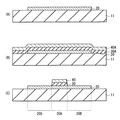
図1は、本発明の第1の実施の形態に係る薄膜トランジスタ1の断面構造を表すものである。薄膜トランジスタ1は、液晶ディスプレイや有機ELディスプレイなどの駆動素子として用いられるものであり、例えば、基板11に酸化物半導体膜20,ゲート絶縁膜30,ゲート電極40,層間絶縁膜50,ソース電極60Sおよびドレイン電極60Dがこの順に積層されたトップゲート型(スタガ型)の構成を有している。
(First embodiment)
FIG. 1 shows a cross-sectional structure of a
基板11は、例えば、ガラス基板やプラスチックフィルムなどにより構成されている。プラスチック材料としては、例えばPET(ポリエチレンテレフタレート)、PEN(ポリエチレンナフタレート)などが挙げられる。後述のスパッタ法において、基板11を加熱することなく酸化物半導体膜20を成膜するため、安価なプラスチックフィルムを用いることができる。また、基板11は、目的に応じて、ステンレス鋼(SUS)などの金属基板であってもよい。
The
酸化物半導体膜20は、基板11上に、ゲート電極40およびその近傍を含む島状に設けられ、薄膜トランジスタ1の活性層としての機能を有するものである。酸化物半導体膜20は、例えば厚みが50nm程度であり、ゲート電極40に対向してチャネル領域20Aを有している。チャネル領域20A上には、ゲート絶縁膜30およびゲート電極40がこの順に同一形状で設けられており、チャネル領域20Aの一方の側にはソース領域20S、他方の側にはドレイン領域20Dがそれぞれ設けられている。すなわち、この薄膜トランジスタ1は、セルフアライン(自己整合)構造を有するものである。
The
チャネル領域20Aは、酸化物半導体により構成されている。ここで酸化物半導体とは、インジウム,ガリウム,亜鉛,スズ等の元素と、酸素とを含む化合物である。具体的には、非晶質の酸化物半導体としては、酸化インジウムガリウム亜鉛(IGZO)が挙げられ、結晶性の酸化物半導体としては、酸化亜鉛(ZnO),酸化インジウム亜鉛(IZO(登録商標)),酸化インジウムガリウム(IGO)、酸化インジウムスズ(ITO)、酸化インジウム(InO)等が挙げられる。
The
ソース領域20Sおよびドレイン領域20Dは、それぞれ、上面から深さ方向における一部に低抵抗領域21を有している。
Each of the
低抵抗領域21は、例えば、チャネル領域20Aよりも酸素濃度が低いことにより低抵抗化されている。低抵抗領域21に含まれる酸素濃度は、30%以下であることが望ましい。低抵抗領域21中の酸素濃度が30%を超えると、抵抗が高くなってしまうからである。
The
あるいは、低抵抗領域21は、アルミニウムをドーパントとして含んでいることにより低抵抗化されている。低抵抗領域21に含まれるアルミニウム濃度は、チャネル領域20Aよりも高いことが好ましい。
Alternatively, the
なお、ソース領域20Sおよびドレイン領域20Dの低抵抗領域21以外の領域は、チャネル領域20Aと同様に酸化物半導体により構成されている。低抵抗領域21の深さについては後述する。
Note that the regions other than the low-
ゲート絶縁膜30は、例えば、厚みが300nm程度であり、シリコン酸化膜,シリコン窒化膜,シリコン窒化酸化膜または酸化アルミニウム膜などの単層膜または積層膜により構成されている。特に、シリコン酸化膜または酸化アルミニウム膜は、酸化物半導体膜20を還元させにくいので好ましい。
The
ゲート電極40は、薄膜トランジスタ1にゲート電圧を印加し、このゲート電圧により酸化物半導体膜20中の電子密度を制御する役割を有するものである。ゲート電極40は、基板11上の選択的な領域に設けられ、例えば、厚みが10nm〜500nm、具体的には200nm程度であり、モリブデン(Mo)により構成されている。ゲート電極40は低抵抗であることが望ましいので、その構成材料としては、例えば、アルミニウム(Al)または銅(Cu)などの低抵抗金属が好ましい。また、アルミニウム(Al)または銅(Cu)よりなる低抵抗層と、チタン(Ti)またはモリブデン(Mo)よりなるバリア層とを組み合わせた積層膜も好ましい。ゲート電極40の低抵抗化が可能となるからである。
The
層間絶縁膜50は、酸化物半導体膜40に接して設けられ、有機樹脂膜51を含んでいる。これにより、この薄膜トランジスタ1は、層間絶縁膜50に起因する不良を抑え、セルフアライン構造を有する薄膜トランジスタ1の信頼性を向上させることが可能となっている。
The
有機樹脂膜51は、例えば、厚みが2μm〜3μm程度であり、ポリイミド等のイミド系樹脂,アクリル系樹脂またはノボラック系樹脂等の有機樹脂膜により構成されている。層間絶縁膜50が有機樹脂膜51を含むことにより、層間絶縁膜50を2μm程度の厚膜とすることが可能となる。よって、ゲート絶縁膜30およびゲート電極40の段差を、十分に厚い層間絶縁膜50により確実に被覆し、ソース電極60Sおよびドレイン電極60Dの断線あるいは短絡など、層間絶縁膜50に起因する不良を低減することが可能となる。また、金属配線により形成される配線容量を低減することが可能となり、液晶または有機ELディスプレイの大型化およびハイフレームレート化に十分に対応することが可能となる。
The
また、層間絶縁膜50は、有機樹脂膜51および第1無機絶縁膜52の積層構造を有していることが好ましい。酸化物半導体膜20は酸素や水分により電気特性が変化しやすいものであるが、酸素や水分などに対するバリア性の高い第1無機絶縁膜51により、酸化物半導体膜20への水分の混入や拡散を抑え、薄膜トランジスタ1の信頼性を向上させることが可能となる。
The
層間絶縁膜50は、第1無機絶縁膜52および有機樹脂膜51を酸化物半導体膜40の側からこの順に積層したものであることが好ましい。バリア性の高い第1無機絶縁膜52により、酸化物半導体膜40の近くで保護することが可能となるので、より高い効果が得られるからである。
The
第1無機絶縁膜52は、例えば、酸化アルミニウム膜,酸化チタン膜または酸化インジウム膜により構成されていることが好ましい。酸化チタン,酸化アルミニウムまたは酸化インジウムよりなる第1無機絶縁膜52は、外気に対して良好なバリア性を有するので、酸化物半導体膜20の電気的特性を変化させる酸素や水分の影響を低減し、薄膜トランジスタ1の電気特性を安定化させることが可能となる。第1無機絶縁膜52の厚みは、例えば20nm以下である。
The first inorganic insulating
ソース電極60Sおよびドレイン電極60Dは、層間絶縁膜50に設けられた接続孔50Aを介してソース領域20Sおよびドレイン領域20Dの低抵抗領域21に接続されている。ソース電極60Sおよびドレイン電極60Dは、例えば、厚みが200nm程度であり、モリブデン(Mo)により構成されている。また、ソース電極60Sおよびドレイン電極60Dは、ゲート電極40と同様に、アルミニウム(Al)または銅(Cu)などの低抵抗金属配線により構成されていることが好ましい。更に、アルミニウム(Al)または銅(Cu)よりなる低抵抗層と、チタン(Ti)またはモリブデン(Mo)よりなるバリア層とを組み合わせた積層膜も好ましい。このような積層膜を用いることにより、配線遅延の少ない駆動が可能となる。
The
また、ソース電極60Sおよびドレイン電極60Dは、ゲート電極40直上の領域を回避して設けられていることが望ましい。ゲート電極40とソース電極60Sおよびドレイン電極60Dとの交差領域に形成される寄生容量を低減することが可能となるからである。
Further, it is desirable that the
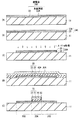
この薄膜トランジスタ1は、例えば次のようにして製造することができる。
The
図2および図3は、薄膜トランジスタ1の製造方法を工程順に表したものである。まず、基板11の全面に、例えばスパッタリング法により、上述した材料よりなる酸化物半導体膜20を、50nm程度の厚みで形成する。その際、ターゲットとしては、形成しようとする酸化物半導体膜20と同一組成のセラミックターゲットを用いる。また、酸化物半導体膜20中のキャリア濃度はスパッタリングの際の酸素分圧に大きく依存するので、所望のトランジスタ特性が得られるように酸素分圧を制御する。
2 and 3 show the method of manufacturing the
次いで、図2(A)に示したように、例えばフォトリソグラフィおよびエッチングにより酸化物半導体膜20を、チャネル領域20Aおよびその一方の側にソース領域20S、他方の側にドレイン領域20Dを含む島状に成形する。その際、リン酸と硝酸と酢酸との混合液を用いたウェットエッチングにより加工することが好ましい。リン酸と硝酸と酢酸との混合液は、下地との選択比を十分に大きくすることが可能であり、比較的容易に加工が可能となる。
Next, as shown in FIG. 2A, an
続いて、図2(B)に示したように、基板11および酸化物半導体膜20の全面に、例えばプラズマCVD(Chemical Vapor Deposition ;化学気相成長)法等により、シリコン酸化膜または酸化アルミニウム膜などのゲート絶縁材料膜30Aを、300nm程度の厚みで形成する。シリコン酸化膜はプラズマCVD法のほか、反応性スパッタリング法により形成することが可能である。また、酸化アルミニウム膜は、反応性スパッタリング法,CVD法または原子層成膜法により形成することが可能である。
Subsequently, as shown in FIG. 2B, a silicon oxide film or an aluminum oxide film is formed on the entire surface of the
そののち、同じく図2(B)に示したように、ゲート絶縁材料膜30Aの全面に、例えばスパッタリング法により、モリブデン(Mo)、チタン(Ti)、アルミニウム(Al)等の単層膜あるいは積層膜よりなるゲート電極材料膜40Aを、200nm程度の厚みで形成する。
Thereafter, as shown in FIG. 2B, a single-layer film or a laminated film of molybdenum (Mo), titanium (Ti), aluminum (Al), or the like is formed on the entire surface of the gate insulating
ゲート電極材料膜40Aを形成したのち、図2(C)に示したように、例えばフォトリソグラフィおよびエッチングにより、ゲート電極材料膜40Aを所望の形状に成形して、酸化物半導体膜20のチャネル領域20A上にゲート電極40を形成する。
After forming the gate
引き続き、同じく図2(C)に示したように、ゲート電極40をマスクとしてゲート絶縁材料膜30をエッチングすることによりゲート絶縁膜30を形成する。このとき、酸化物半導体膜20をZnO,IZO,IGO等の結晶化材料により構成した場合には、ゲート絶縁材料膜30Aをエッチングする際に、フッ酸等の薬液を用いて非常に大きなエッチング選択比を維持して容易に加工することが可能となる。これにより、酸化物半導体膜20のチャネル領域20A上に、ゲート絶縁膜30およびゲート電極40がこの順に同一形状で形成される。
Subsequently, as shown in FIG. 2C, the
ゲート絶縁膜30およびゲート電極40を形成したのち、図3(A)に示したように、酸化物半導体膜20,ゲート絶縁膜30およびゲート電極40の表面に、例えばスパッタリング法により、チタン(Ti),アルミニウム(Al)またはインジウム(In)等の酸素と比較的低温で反応する金属よりなる金属膜52Aを、例えば10nm以下、具体的には5nm以上10nm以下の厚みで形成する。
After forming the
金属膜52Aを形成したのち、熱処理を行うことにより、図3(B)に示したように、金属膜50Aが酸化されて第1無機絶縁膜52が形成される。この金属膜52Aの酸化反応には、ソース領域20Sおよびドレイン領域20Dに含まれる酸素の一部が利用される。そのため、金属膜52Aの酸化の進行に伴って、ソース領域20Sおよびドレイン領域20Dの金属膜52Aと接する上面側から、ソース領域20Sおよびドレイン領域20中の酸素濃度が低下していく。これにより、ソース領域20Sおよびドレイン領域20Dの上面から深さ方向における一部に、チャネル領域20Aよりも酸素濃度が低い低抵抗領域21が形成される。
After the
図4は、上述した製造方法と同様にして、金属膜52Aの熱処理を行ったのち、チャネル領域20A、並びにソース領域20Sおよびドレイン領域20D中の酸素濃度の深さ方向の依存性をEDX法(エネルギー分散形X線分光法)を用いて調べた結果を表したものである。その際、酸化物半導体薄膜20の材料はIGZOとし、金属膜52Aは厚み5nmのアルミニウム膜とし、熱処理は300℃のアニールにより行った。
FIG. 4 shows the depth dependence of the oxygen concentration in the
図4に示したように、ソース領域20Sおよびドレイン領域20D中の酸素濃度は、深さ方向の全体にわたって、チャネル領域20A中の酸素濃度よりも低くなっていることが分かる。中でも特に深さ10nm以内の領域では、チャネル領域20A中の酸素濃度と、ソース領域20Sおよびドレイン領域20D中の酸素濃度との差がきわめて明瞭になっている。すなわち、低抵抗領域21は、ソース領域20Sおよびドレイン領域20Dの上面から深さ方向の一部、具体的には10nm以内の領域であることが分かる。
As shown in FIG. 4, it can be seen that the oxygen concentration in the
また、低抵抗領域21を形成するために金属膜52Aの材料としてアルミニウムを用いた場合には、金属膜52Aの熱処理に伴い、ソース領域20Sおよびドレイン領域20Dの金属膜52Aと接する上面側から、ソース領域20Sおよびドレイン領域20中にアルミニウムが拡散する。これにより、ソース領域20Sおよびドレイン領域20Dの上面から深さ方向における一部に、アルミニウムをドーパントとして含む低抵抗領域21が形成される。この低抵抗領域21に含まれるアルミニウム濃度は、チャネル領域20Aよりも高くなる。すなわち、低抵抗領域21に含まれるアルミニウムは、ドーパントとしてソース領域20Sおよびドレイン領域20Dを低抵抗化させる機能も有している。
In addition, when aluminum is used as the material of the
金属膜52Aの熱処理としては、例えば、上述したように、300℃程度の温度でアニールすることが好ましい。その際、酸素等を含む酸化性のガス雰囲気でアニールを行うことで、低抵抗領域21の酸素濃度が低くなりすぎるのを抑え、チャネルとなる酸化物半導体膜20に十分な酸素を供給することが可能となる。よって、後工程で行うアニール工程を削減することが可能となり、工程の簡略化が可能となる。
As the heat treatment of the
また、例えば、図3(A)に示した金属膜52Aを形成する工程で基板11の温度を200℃程度に比較的高い温度とすることにより、図3(B)に示した熱処理を行わずに低抵抗領域21を形成することも可能である。この場合には、チャネルとなる酸化物半導体膜20のキャリア濃度をトランジスタとして必要なレベルに低減することが可能である。
Further, for example, in the step of forming the
金属膜52Aは、上述したように10nm以下の厚みで形成することが好ましい。金属膜52Aの厚みを10nm以下とすれば、酸化性のガス雰囲気中でのアニールを行うことにより、酸素プラズマ中において金属膜52Aを完全に酸化することが可能となるからである。よって、完全に酸化されなかった金属膜52Aをエッチングにより除去する工程が不要となり、製造工程の簡略化が可能となる。金属膜52Aを10nm以下の厚みで形成した場合、第1無機絶縁膜52の厚みは結果として20nm以下となる。
The
その際、金属膜52Aを酸化させる方法としては、熱処理のほか、水蒸気雰囲気での酸化、またはプラズマ酸化などの方法により酸化を促進させることも可能である。プラズマ酸化では、例えば、基板11の温度を200℃〜400℃程度にして、酸素や二窒化酸素等の酸素を含むガス雰囲気中でプラズマを発生させて処理することが望ましい。これにより、上述したような外気に対して良好なバリア性を有する第1無機絶縁膜52を形成することが可能となるからである。
At this time, as a method of oxidizing the
なお、第1無機絶縁膜52は、酸化物半導体膜20のソース領域20Sおよびドレイン領域20D以外に、ゲート絶縁膜30またはゲート電極40上などにも形成される。しかし、第1無機絶縁膜52をエッチングにより除去せずに残しておいてもリーク電流の原因になることはない。
Note that the first inorganic insulating
ここで、液晶ディスプレイや有機ELディスプレイ等の応用において、光を薄膜トランジスタ1の基板11方向に透過する必要がある場合においては、第1無機絶縁膜52を残した場合においては、第1無機絶縁膜52の透過率が低く、輝度が低下してしまいディスプレイとしての表示品位が低下する場合がある。この様な場合においては、酸化物半導体膜20と接している第1無機絶縁膜52以外の領域をフォトリソグラフィーとエッチングプロセスを行うことにより除去することも可能である。この様なプロセス工程を経ることで、ディスプレイの透過率を向上させることが可能になるので、液晶ディスプレイや有機ELの応用において、光を薄膜トランジスタ1の基板11を通して透過する応用に本実施の形態の技術を用いることも可能となる。
Here, in applications such as liquid crystal displays and organic EL displays, when it is necessary to transmit light toward the
低抵抗領域21を形成したのち、図3(C)に示したように、第1無機絶縁膜52上に、例えばスピンコーターまたはスリットコーターを用いて上述した材料よりなる有機樹脂を上述した厚みで塗布し、露光および現像を行うことにより所望のパターンを形成する。続いて例えば200℃〜300℃程度の温度でアニールすることにより、図3(C)に示したように、接続孔50Aを有する有機樹脂膜51を形成する。
After forming the
このように層間絶縁膜50が有機樹脂膜51を含むようにすることにより、CVD工程のような真空工程を用いることなく層間絶縁膜50を形成することが可能となる。よって、酸化物半導体膜20中の酸素の脱離やCVD工程で生じる水素等による還元反応の影響を抑制した状態で薄膜トランジスタ1を形成することが可能となる。その結果、電気的安定性や信頼性に優れた薄膜トランジスタ1を形成することが可能となる。
By making the
続いて、図1に示したように、例えばフォトリソグラフィおよびエッチングにより、層間絶縁膜50の第1無機絶縁膜52に接続孔50Aを形成する。そののち、層間絶縁膜50の上に、例えばスパッタリング法により、例えばモリブデン(Mo)膜を200nmの厚みで形成し、フォトリソグラフィおよびエッチングにより所定の形状に成形する。これにより、図1に示したように、接続孔50Aを介してソース電極60Sおよびドレイン電極60Dをソース領域20Sおよびドレイン領域20Dの低抵抗領域21に接続する。以上により、図1に示した薄膜トランジスタ1が完成する。
Subsequently, as illustrated in FIG. 1, a
この薄膜トランジスタ1では、図示しない配線層を通じてゲート電極40に所定のしきい値電圧以上の電圧(ゲート電圧)が印加されると、酸化物半導体膜20のチャネル領域20A中に電流(ドレイン電流)が生じる。ここでは、層間絶縁膜50が有機樹脂膜51を含んでいるので、層間絶縁膜50の厚みを大きくすることが可能となっており、ゲート絶縁膜30およびゲート電極40の段差が、十分に厚い層間絶縁膜50により確実に被覆されている。よって、ソース電極60Sおよびドレイン電極60Dの断線あるいは短絡など、層間絶縁膜50に起因する不良が抑えられる。
In this
また、酸化物半導体膜20のソース領域20Sおよびドレイン領域20Dの上面から深さ方向における少なくとも一部に、チャネル領域20Aよりも酸素濃度が低く、および/またはアルミニウムをドナーとして多く含む低抵抗領域21が設けられているので、素子特性が安定したものとなる。
Further, at least part of the
図5(A)は、実際に上述した製造方法により層間絶縁膜50に有機樹脂膜51を含む薄膜トランジスタ1を作製し、トランジスタ特性を調べた結果を表したものである。その際、第1無機絶縁膜52としては厚み10nmの酸化アルミニウム膜、有機樹脂膜51としては厚み3μmのポリイミド膜を形成した。また、薄膜トランジスタ作製の最終工程には、酸素濃度40%の窒素と酸素とのガス雰囲気中において300℃、1時間のアニールを行った。
FIG. 5A shows a result of actually manufacturing the
一方、層間絶縁膜としてプラズマCVD法によりシリコン酸化膜を200nmの厚みで形成したことを除いては、図5(A)の場合と同様にして薄膜トランジスタを作製し、トランジスタ特性を調べた。薄膜トランジスタ作製の最終工程には、図5(A)の場合と同様に、酸素濃度40%の窒素と酸素とのガス雰囲気中において300℃、1時間のアニールを行った。得られた結果を図5(B)に示す。 On the other hand, a thin film transistor was manufactured in the same manner as in FIG. 5A except that a silicon oxide film having a thickness of 200 nm was formed as an interlayer insulating film by plasma CVD, and the transistor characteristics were examined. In the final step of manufacturing the thin film transistor, similarly to the case of FIG. 5A, annealing was performed at 300 ° C. for one hour in a gas atmosphere of nitrogen and oxygen having an oxygen concentration of 40%. The obtained result is shown in FIG.
図5(A)から分かるように、層間絶縁膜50として酸化アルミニウムよりなる第1無機絶縁膜52およびポリイミド膜よりなる有機樹脂膜51を形成した薄膜トランジスタ1では、オフ電流が十分に低く抑えられた良好な特性が得られた。これに対して、層間絶縁膜にシリコン酸化膜を用いた場合には、図5(B)から分かるように、ゲート電極にマイナス電圧を印加してもオフ状態にならなかった。
As can be seen from FIG. 5A, in the
この理由としては、層間絶縁膜50として第1無機絶縁膜52および有機樹脂膜51の積層構造を有する薄膜トランジスタ1では、ゲート電極40およびゲート絶縁膜30の加工後に形成された段差が、十分に厚い層間絶縁膜50で被覆され、ソース電極60Sおよびドレイン電極60Dの断線あるいは短絡など、層間絶縁膜50に起因する不良が低減されたからであると考えられる。また、薄膜トランジスタ作製の最終工程において酸化性ガス雰囲気中でのアニール工程により酸素の拡散が促進され、酸化物半導体膜20中に十分な量の酸素を供給することが可能になったということも考えられる。
This is because, in the
一方、層間絶縁膜としてシリコン酸化膜を用いた場合には、層間絶縁膜の厚みが薄く、不良の発生が十分に抑えられなかったことに加えて、アニール工程で十分な酸素を供給することが困難であったので、オフ状態にならないTFT特性になったものと考えられる。この場合にも、酸化性ガス雰囲気でのアニール時間を10時間程度にすれば、オフ状態になるTFT特性が得られるが、製造時間が非常に長くなってしまうという問題が生じる。 On the other hand, when a silicon oxide film is used as the interlayer insulating film, the thickness of the interlayer insulating film is thin and the occurrence of defects cannot be sufficiently suppressed, and sufficient oxygen can be supplied in the annealing process. Since it was difficult, it is considered that the TFT characteristics did not become an off state. Also in this case, if the annealing time in the oxidizing gas atmosphere is set to about 10 hours, TFT characteristics that are turned off can be obtained, but there is a problem that the manufacturing time becomes very long.
すなわち、層間絶縁膜50として酸化アルミニウムよりなる第1無機絶縁膜52およびポリイミドよりなる有機樹脂膜51を形成することにより、セルフアライン構造により寄生容量を低減すると共に素子特性および信頼性に優れた薄膜トランジスタ1を実現できることが分かった。
That is, by forming the first inorganic insulating
このように本実施の形態の薄膜トランジスタ1では、層間絶縁膜50が有機樹脂膜51を含むようにしたので、ソース電極60Sおよびドレイン電極60Dの断線あるいは短絡など、層間絶縁膜50に起因する不良を抑え、セルフアライン構造のトップゲート薄膜トランジスタ1の素子特性および信頼性を向上させることが可能となる。よって、この薄膜トランジスタ1を用いてアクティブ駆動方式のディスプレイを構成すれば、寄生容量の小さいセルフアライン構造と共に良好な素子特性および高い信頼性を有する薄膜トランジスタ1により、高品質な表示が可能となり、大画面化、高精細化、ハイフレームレート化に対応可能となる。また、保持容量の小さいレイアウトを適用することが可能となり、画素レイアウトにおける配線の占める割合を小さくすることが可能となる。よって、配線間ショートによる欠陥の発生確率を小さくし、製造歩留まりを高めることが可能となる。
As described above, in the
(変形例1)
図6および図7は、本発明の変形例1に係る薄膜トランジスタ1の製造方法を工程順に表したものである。この製造方法は、第1無機絶縁膜52を、金属膜52Aおよび金属酸化膜52Bを積層し、金属膜52Aを酸化させることにより形成したことにおいて、上記第1の実施の形態の製造方法とは異なるものである。なお、第1の実施の形態と製造工程が重複する部分については、図2を参照して説明する。
(Modification 1)
6 and 7 show a method of manufacturing the
まず、第1の実施の形態と同様にして、図2(A)ないし図2(C)に示した工程により、基板11に、酸化物半導体膜20,ゲート絶縁膜30およびゲート電極40を形成する。
First, in the same manner as in the first embodiment, the
次いで、図6(A)に示したように、酸化物半導体膜20,ゲート絶縁膜30およびゲート電極40の表面に、例えばスパッタリング法により、チタン(Ti),アルミニウム(Al)またはインジウム(In)等の酸素と比較的低温で反応する金属よりなる金属膜52Aを、例えば10nm以下、具体的には5nm以上10nm以下の厚みで形成する。
Next, as shown in FIG. 6A, titanium (Ti), aluminum (Al), or indium (In) is formed on the surfaces of the
続いて、同じく図6(A)に示したように、スパッタ装置のチャンバ(図示せず)内で、金属膜52Aに連続して、金属膜52Aの上に、酸化アルミニウム膜,酸化チタン膜または酸化インジウム膜よりなる金属酸化膜52Bを、例えば10nmないし50nmの厚みで形成する。
Subsequently, as shown in FIG. 6A, an aluminum oxide film, a titanium oxide film, or a
金属膜52Aおよび金属酸化膜52Bを形成したのち、第1の実施の形態と同様の熱処理を行うことにより、図6(B)に示したように、金属膜52Aが酸化されて第1無機絶縁膜52が形成される。第1無機絶縁膜52の厚みは、金属膜52Aの酸化後の厚み(金属膜52Aを10nm以下の厚みで形成した場合、20nm以下)と、金属酸化膜52Bの厚みとの合計厚みとなる。よって、第1無機絶縁膜52の厚みを厚くすることが可能となり、薄膜トランジスタ1の信頼性を更に向上させることが可能となる。
After forming the
また、第1無機絶縁膜52が形成されるのと同時に、第1の実施の形態と同様にして、ソース領域20Sおよびドレイン領域20Dの上面から深さ方向における一部に、チャネル領域20Aよりも酸素濃度が低い低抵抗領域21が形成される。
In addition, at the same time as the first inorganic insulating
金属膜52Aの熱処理としては、例えば、第1の実施の形態と同様に、300℃程度の温度でアニールすることが好ましい。その際、酸素等を含む酸化性のガス雰囲気でアニールを行うことで、低抵抗領域21の酸素濃度が低くなりすぎるのを抑え、チャネルとなる酸化物半導体膜20に十分な酸素を供給することが可能となる。よって、後工程で行うアニール工程を削減することが可能となり、工程の簡略化が可能となる。
As the heat treatment of the
また、例えば、図6(A)に示した金属膜52Aを形成する工程で基板11の温度を200℃程度に比較的高い温度とすることにより、図6(B)に示した熱処理を行わずに低抵抗領域21を形成することも可能である。この場合には、チャネルとなる酸化物半導体膜20のキャリア濃度をトランジスタとして必要なレベルに低減することが可能である。
Further, for example, in the step of forming the
金属膜52Aは、上述したように10nm以下の厚みで形成することが好ましい。金属膜52Aの厚みを10nm以下とすれば、金属膜52Aと金属酸化膜52Bとを連続的に形成することにより、酸素プラズマ中において金属膜52Aを完全に酸化することが可能となるからである。よって、完全に酸化されなかった金属膜52Aをエッチングにより除去する工程が不要となり、製造工程の簡略化が可能となる。
The
その際、金属膜52Aを酸化させる方法としては、第1の実施の形態と同様に、熱処理のほか、水蒸気雰囲気での酸化、またはプラズマ酸化などの方法により酸化を促進させることも可能である。特にプラズマ酸化は、変形例2で後述するように、後工程でシリコン酸化膜等よりなる第1層間絶縁膜52をプラズマCVD法により形成する直前に実施することが可能であり、特に工程を増やす必要がないという利点がある。プラズマ酸化では、例えば、基板11の温度を200℃〜400℃程度にして、酸素や二窒化酸素等の酸素を含むガス雰囲気中でプラズマを発生させて処理することが望ましい。これにより、上述したような外気に対して良好なバリア性を有する第1無機絶縁膜52を形成することが可能となるからである。
At this time, as a method of oxidizing the
なお、第1無機絶縁膜52は、第1の実施の形態と同様に、酸化物半導体膜20のソース領域20Sおよびドレイン領域20D以外に、ゲート絶縁膜30またはゲート電極40上などにも形成される。しかし、第1無機絶縁膜52をエッチングにより除去せずに残しておいてもリーク電流の原因になることはない。
The first inorganic insulating
低抵抗領域21を形成したのち、図6(C)に示したように、第1の実施の形態と同様にして、第1無機絶縁膜52上に、接続孔50Aを有する有機樹脂膜51を形成する。
After forming the
続いて、図7に示したように、第1の実施の形態と同様にして、層間絶縁膜50の第1無機絶縁膜52に接続孔50Aを形成し、この接続孔50Aを介してソース電極60Sおよびドレイン電極60Dをソース領域20Sおよびドレイン領域20Dの低抵抗領域21に接続する。以上により、薄膜トランジスタ1が完成する。
Subsequently, as shown in FIG. 7, in the same manner as in the first embodiment, a
本変形例1では、第1の実施の形態の効果に加えて、第1無機絶縁膜52を、金属膜52Aおよび金属酸化膜52Bを積層し、金属膜52Aを酸化させることにより形成するようにしたので、第1無機絶縁膜52の厚みを厚くすることが可能となる。よって、薄膜トランジスタ1の信頼性を更に向上させることが可能となる。
In the first modification, in addition to the effects of the first embodiment, the first inorganic insulating
(変形例2)
図8は、本発明の変形例2に係る薄膜トランジスタ1の製造方法を工程順に表したものである。この製造方法は、低抵抗領域21を、プラズマを用いて形成したことにおいて、上記第1の実施の形態の製造方法とは異なるものである。なお、第1の実施の形態と製造工程が重複する部分については、図1および図2を参照して説明する。
(Modification 2)
FIG. 8 shows a method of manufacturing the
まず、第1の実施の形態と同様にして、図2(A)ないし図2(C)に示した工程により、基板11に、酸化物半導体膜20,ゲート絶縁膜30およびゲート電極40を形成する。
First, in the same manner as in the first embodiment, the
次いで、図8(A)に示したように、プラズマCVD装置(図示せず)内で、水素,アルゴン,アンモニアガス等のプラズマPを発生させ、酸化物半導体膜20のソース領域20Sおよびドレイン領域20DをプラズマPに曝す。これにより、図8(B)に示したように、ソース領域20Sおよびドレイン領域20Dの上面から深さ方向における一部に、例えば1%程度の原子濃度の水素が導入され、低抵抗領域21が形成される。なお、低抵抗領域21は、プラズマCVD法などによる水素ガスを含むプラズマ処理のほか、イオンドーピングまたはイオン注入により形成することも可能である。
Next, as shown in FIG. 8A, a plasma P such as hydrogen, argon, ammonia gas or the like is generated in a plasma CVD apparatus (not shown), and the
続いて、図8(C)に示したように、酸化物半導体膜20,ゲート絶縁膜30およびゲート電極40の上に第1無機絶縁膜52を形成する。第1無機絶縁膜52としては、例えばプラズマCVD法により、例えばシリコン酸化膜あるいは酸化アルミニウム膜、またはそれらの積層膜を形成することが好ましい。このようにすれば、第1無機絶縁膜52をプラズマCVD法により形成する直前に、プラズマPを用いて低抵抗領域21を形成することが可能であり、特に工程を増やす必要がないという利点がある。
Subsequently, as illustrated in FIG. 8C, a first inorganic insulating
シリコン酸化膜はプラズマCVD法により形成することが可能である。酸化アルミニウム膜は、アルミニウムをターゲットとしたDCまたはAC電源による反応性スパッタリング法により形成することが望ましい。高速に成膜することが可能となるからである。第1無機絶縁膜52の厚みは、例えばスパッタリング法で酸化アルミニウム膜を成膜する場合、例えば50nm以下と厚く形成することが可能である。
The silicon oxide film can be formed by a plasma CVD method. The aluminum oxide film is desirably formed by a reactive sputtering method using a DC or AC power source targeting aluminum. This is because the film can be formed at high speed. For example, when the aluminum oxide film is formed by sputtering, the first inorganic insulating
そののち、同じく図8(C)に示したように、第1無機絶縁膜52上に、第1の実施の形態と同様にして、接続孔50Aを有する有機樹脂膜51を形成する。
After that, as shown in FIG. 8C, the
続いて、図1に示したように、第1の実施の形態と同様にして、層間絶縁膜50の第1無機絶縁膜52に接続孔50Aを形成し、この接続孔50Aを介してソース電極60Sおよびドレイン電極60Dをソース領域20Sおよびドレイン領域20Dの低抵抗領域21に接続する。以上により、薄膜トランジスタ1が完成する。
Subsequently, as shown in FIG. 1, similarly to the first embodiment, a
本変形例2では、層間絶縁膜50が有機樹脂膜51を含むようにしたので、第1の実施の形態と同様の効果が得られる。
In the second modification, since the
(変形例3)
図9は、本発明の変形例3に係る薄膜トランジスタ1の製造方法を工程順に表したものである。この製造方法は、低抵抗領域21を、シリコン窒化膜からの水素の拡散により形成したことにおいて、上記第1の実施の形態の製造方法とは異なるものである。なお、第1の実施の形態と製造工程が重複する部分については、図1および図2を参照して説明する。
(Modification 3)
FIG. 9 shows a method of manufacturing the
まず、第1の実施の形態と同様にして、図2(A)ないし図2(C)に示した工程により、基板11に、酸化物半導体膜20,ゲート絶縁膜30およびゲート電極40を形成する。
First, in the same manner as in the first embodiment, the
次いで、図9(A)に示したように、酸化物半導体膜20,ゲート絶縁膜30およびゲート電極40の表面に、例えばプラズマCVD法により、シリコン窒化膜などの膜中に水素を多く含有する絶縁膜よりなる第1無機絶縁膜52を形成する。このとき、第1無機絶縁膜52からソース領域20Sおよびドレイン領域20Dに水素が拡散することにより、ソース領域20Sおよびドレイン領域20Dの上面から深さ方向における一部に、例えば1%程度の原子濃度の水素が導入され、低抵抗領域21が形成される。
Next, as shown in FIG. 9A, the surface of the
続いて、図9(B)に示したように、第1無機絶縁膜52上に、第1の実施の形態と同様にして、接続孔50Aを有する有機樹脂膜51を形成する。
Subsequently, as shown in FIG. 9B, an
続いて、図1に示したように、第1の実施の形態と同様にして、層間絶縁膜50の第1無機絶縁膜52に接続孔50Aを形成し、この接続孔50Aを介してソース電極60Sおよびドレイン電極60Dをソース領域20Sおよびドレイン領域20Dの低抵抗領域21に接続する。以上により、薄膜トランジスタ1が完成する。
Subsequently, as shown in FIG. 1, similarly to the first embodiment, a
本変形例3では、層間絶縁膜50が有機樹脂膜51を含むようにしたので、第1の実施の形態と同様の効果が得られる。
In the third modification, since the
なお、本変形例3においては、第1無機絶縁膜52を形成する前に、変形例2と同様にして、図8(A)に示した工程により、酸化物半導体膜20のソース領域20Sおよびドレイン領域20Dを水素,アルゴン,アンモニアガス等のプラズマPに曝すことにより、ソース領域20Sおよびドレイン領域20Dの上面から深さ方向における一部に低抵抗領域21を形成するようにしてもよい。
In the third modification, before forming the first inorganic insulating
(変形例4)
図10は、本発明の変形例4に係る薄膜トランジスタ1Aの断面構成を表したものである。この薄膜トランジスタ1Aは、酸化物半導体膜20を非晶質膜22および結晶化膜23の積層構造としたことを除いては、上記第1の実施の形態の薄膜トランジスタ1と同様の構成を有し、その作用および効果も同様である。よって、対応する構成要素には同一の符号を付して説明する。
(Modification 4)
FIG. 10 illustrates a cross-sectional configuration of a thin film transistor 1A according to Modification 4 of the present invention. The thin film transistor 1A has the same configuration as the
基板11,ゲート絶縁膜30,ゲート電極40,層間絶縁膜50,ソース電極60Sおよびドレイン電極60Dについては、第1の実施の形態と同様である。
The
酸化物半導体膜20は、非晶質膜22および結晶化膜23の積層構造を有している。ソース電極60Sおよびドレイン電極60Dは、結晶化膜23に接して設けられている。具体的には、酸化物半導体膜20は、基板11側から非晶質膜22および結晶化膜23をこの順に積層した構造を有している。
The
非晶質膜22は、薄膜トランジスタ1のチャネルとしての機能を有するものであり、酸化物半導体膜20の基板11側に設けられている。非晶質膜22は、例えば、厚みが10nm〜50nm程度であり、IGZOなどのアモルファス状態の酸化物半導体により構成されている。アモルファス状態の酸化物半導体膜をチャネルに用いたTFTでは、均一性に優れた電気特性が得られる。
The
結晶化膜23は、製造工程において上層とのエッチング選択比を確保するためのものであり、酸化物半導体膜20のソース電極60Sおよびドレイン電極60D側に設けられている。結晶化膜23は、例えば、厚みが10nm〜50nm程度であり、酸化亜鉛,IZO,IGOなどの結晶化状態の酸化物半導体により構成されている。結晶化状態の酸化物半導体は、薬液に対する耐性が高く、製造工程において上層をエッチングする際に酸化物半導体膜20の意図しないエッチングを抑えることが可能となる。よって、酸化物半導体膜20の厚みを厚くする必要がなくなり、良好な電気特性が得られる。
The crystallized
なお、酸化物半導体膜20の厚み(非晶質膜22および結晶化膜23の合計厚み)は、製造工程でのアニールによる酸素供給効率を考慮すると、例えば20nm〜100nm程度であることが望ましい。
Note that the thickness of the oxide semiconductor film 20 (the total thickness of the
酸化物半導体膜20のソース領域20Sおよびドレイン領域20Dは、第1の実施の形態と同様に、それぞれ、上面から深さ方向における一部に、チャネル領域20Aよりも酸素濃度が低い低抵抗領域21を有している。なお、図10では、低抵抗領域21の深さと結晶膜23の厚みとが等しくなっている場合を表しているが、低抵抗領域21は、結晶膜23の上面から深さ方向における一部に設けられていてもよい。また、低抵抗領域21は、結晶膜23の上面から深さ方向における全部と、非結晶膜22の結晶膜23との界面から深さ方向における一部に設けられていてもよい。
As in the first embodiment, the
この薄膜トランジスタ1Aは、例えば次のようにして製造することができる。 The thin film transistor 1A can be manufactured, for example, as follows.
図11ないし図13は、この薄膜トランジスタ1Aの製造方法を工程順に表したものである。まず、図11(A)に示したように、基板11に、例えばスパッタリング法により、上述した厚みおよび材料よりなる非晶質膜22を形成する。具体的には、例えばIGZOよりなる非晶質膜22を形成する場合には、IGZO膜のセラミックをターゲットとしたDCスパッタ法を用い、アルゴンと酸素との混合ガスによるプラズマ放電にてゲート絶縁膜30上に非晶質膜41を形成する。なお、プラズマ放電の前に真空容器(図示せず)内の真空度が1×10⁻⁴Pa以下になるまで排気したのち、アルゴンと酸素との混合ガスを導入する。
11 to 13 show the manufacturing method of the thin film transistor 1A in the order of steps. First, as shown in FIG. 11A, the
このとき、チャネルとなる非晶質膜22中のキャリア濃度は、酸化物形成の際のアルゴンと酸素との流量比を変化させることで制御することが可能である。
At this time, the carrier concentration in the
次いで、同じく図11(A)に示したように、例えばスパッタリング法により、上述した厚みおよび材料よりなる結晶化膜23を形成する。具体的には、例えばIZOよりなる結晶化膜23を形成する場合には、IZO膜のセラミックをターゲットとしたDCスパッタ法を用いる。このようにして、非晶質膜22および結晶化膜23の積層膜24が形成される。
Next, as shown in FIG. 11A, the crystallized
続いて、図11(B)に示したように、例えばフォトリソグラフィおよびエッチングにより積層膜24を所定の形状、例えばゲート電極40およびその近傍を含むことが可能な島状に成形する。これにより、非晶質膜22および結晶化膜23の積層構造を有する酸化物半導体膜20が形成される。
Subsequently, as shown in FIG. 11B, the
そののち、図11(C)に示したように、基板11および酸化物半導体膜20の全面に、第1の実施の形態と同様にして、ゲート絶縁材料膜30Aおよびゲート電極材料膜40Aをこの順に形成する。
After that, as shown in FIG. 11C, the gate insulating
ゲート電極材料膜40Aを形成したのち、図11(D)に示したように、第1の実施の形態と同様にして、例えばフォトリソグラフィおよびエッチングにより、ゲート電極材料膜40Aを所望の形状に成形して、酸化物半導体膜20のチャネル領域20A上にゲート電極40を形成する。
After forming the gate
引き続き、同じく図11(D)に示したように、第1の実施の形態と同様にして、ゲート電極40をマスクとしてゲート絶縁材料膜30をエッチングすることによりゲート絶縁膜30を形成する。このとき、酸化物半導体膜20が基板11側から非晶質膜22および結晶化膜23をこの順に積層した構造を有しているので、ゲート絶縁材料膜30Aをエッチングする際に、フッ酸等の薬液を用いて非常に大きなエッチング選択比を維持して容易に加工することが可能となる。これにより、酸化物半導体膜20のチャネル領域20A上に、ゲート絶縁膜30およびゲート電極40がこの順に同一形状で形成される。
Subsequently, as shown in FIG. 11D, the
ゲート絶縁膜30およびゲート電極40を形成したのち、図12(A)に示したように、第1の実施の形態と同様にして、酸化物半導体膜20,ゲート絶縁膜30およびゲート電極40の表面に、例えばスパッタリング法により、チタン(Ti),アルミニウム(Al)またはインジウム(In)等の酸素と比較的低温で反応する金属よりなる金属膜52Aを、例えば10nm以下、具体的には5nm以上10nm以下の厚みで形成する。
After forming the
金属膜52Aを形成したのち、第1の実施の形態と同様にして、熱処理を行うことにより、図12(B)に示したように、金属膜50Aが酸化されて第1無機絶縁膜52が形成されると同時に、ソース領域20Sおよびドレイン領域20Dの上面から深さ方向における一部に、チャネル領域20Aよりも酸素濃度が低い低抵抗領域21が形成される。
After the
低抵抗領域21を形成したのち、図12(C)に示したように、第1の実施の形態と同様にして、第1無機絶縁膜52上に、接続孔50Aを有する有機樹脂膜51を形成する。
After forming the
有機樹脂膜51を形成したのち、図13に示したように、この層間絶縁膜50の第1無機絶縁膜52に例えばエッチングにより接続孔50Aを設け、この接続孔50A内に酸化物半導体膜20の結晶化層23を露出させる。このとき、層間絶縁膜50の第1無機絶縁膜52が結晶化膜23の上に設けられているので、結晶化膜23のエッチングレートが層間絶縁膜80およびゲート絶縁膜30に比べて十分に低くなり、層間絶縁膜50の第1無機絶縁膜52と酸化物半導体膜20とのウェットエッチング選択比が高くなる。よって、酸化物半導体膜20のエッチングを抑制したままで層間絶縁膜50の第1無機絶縁膜52を選択的にエッチングし、接続孔50Aを容易に形成することが可能となる。また、ドライエッチングにより加工しにくい酸化アルミニウム膜よりなる第1無機絶縁膜52もウェットエッチングにより容易に加工することが可能となる。
After forming the
続いて、図10に示したように、第1の実施の形態と同様にして、ソース電極60Sおよびドレイン電極60Dを形成し、接続孔50Aを介してソース電極60Sおよびドレイン電極60Dをソース領域20Sおよびドレイン領域20Dの低抵抗領域21に接続する。以上により、図10に示した薄膜トランジスタ1Bが完成する。
Subsequently, as shown in FIG. 10, similarly to the first embodiment, the
このように本変形例4では、酸化物半導体膜20を、非晶質膜22および結晶化膜23の積層構造としたので、非晶質膜22により、均一性の高い電気特性を得ることが可能となる。また、ソース電極60Sおよびドレイン電極60Dを結晶化膜23に接して設けるようにしたので、製造工程においてゲート絶縁膜30または第1無機絶縁膜52をエッチングする際に酸化物半導体膜20がエッチングされてしまうことを抑えることが可能となる。よって、酸化物半導体膜20の厚みを厚くする必要がなくなり、良好な電気特性を得ると共に、成膜時間の短縮および低コスト化が可能となる。
As described above, in the fourth modification, since the
(変形例5)
図14は、本発明の変形例5に係る薄膜トランジスタ1Aの製造方法を工程順に表したものである。この製造方法は、非晶質膜22および非晶質膜23Aの積層膜を形成し、この積層膜をエッチングにより加工したのちに、非晶質膜23Aをアニールして結晶化膜を形成するようにしたことにおいて、上記変形例4の製造方法とは異なるものである。なお、変形例4と製造工程が重複する部分については、図11ないし図13を参照して説明する。
(Modification 5)
FIG. 14 shows a method of manufacturing the thin film transistor 1A according to the fifth modification of the present invention in the order of steps. In this manufacturing method, a laminated film of an
まず、図14(A)に示したように、変形例4と同様にして、基板11に、例えばスパッタリング法により、上述した厚みおよび材料よりなる非晶質膜22を形成する。
First, as shown in FIG. 14A, the
次いで、同じく図4(A)に示したように、例えばスパッタリング法により、非晶質膜41よりも低融点の酸化物半導体よりなる非晶質膜23Aを形成する。具体的には、例えばIZOよりなる非晶質膜23Aを形成する場合には、IZO膜のセラミックをターゲットとしたDCスパッタ法を用い、スパッタリング条件を制御することにより非晶質状態のIZOよりなる非晶質膜23Aを形成する。このようにして、非晶質膜22および非晶質膜23Aの積層膜24Aが形成される。
Next, as shown in FIG. 4A, an amorphous film 23A made of an oxide semiconductor having a melting point lower than that of the amorphous film 41 is formed by, eg, sputtering. Specifically, for example, when the amorphous film 23A made of IZO is formed, a DC sputtering method using a ceramic of the IZO film as a target is used, and the sputtering condition is controlled to make the amorphous film IZO. An amorphous film 23A is formed. In this way, a
積層膜24Aを形成したのち、図14(B)に示したように、例えばフォトリソグラフィおよびエッチングにより積層膜24Aを所定の形状、例えばゲート電極20およびその近傍を含むことが可能な島状に成形する。このとき、非晶質膜22および非晶質膜23Aはいずれも非晶質状態なので、リン酸,硝酸および酢酸を含む混合液等によりウェットエッチングすることで低コスト化が可能である。
After forming the
積層膜43Aを成形したのち、図14(C)に示したように、非晶質膜23Aに対して例えば200℃〜400℃程度のアニール処理Aを行うことにより結晶化膜23を形成する。これにより、非晶質膜22および結晶化膜23の積層構造を有する酸化物半導体膜20が形成される。
After forming the laminated film 43A, as shown in FIG. 14C, the crystallized
酸化物半導体膜20を形成したのち、図14(D)に示したように、変形例4と同様にして、基板11および酸化物半導体膜20の全面に、ゲート絶縁材料膜30Aおよびゲート電極材料膜40Aをこの順に形成する。
After the
ゲート電極材料膜40Aを形成したのち、図14(E)に示したように、変形例4と同様にして、例えばフォトリソグラフィおよびエッチングにより、ゲート電極材料膜40Aを所望の形状に成形して、酸化物半導体膜20のチャネル領域20A上にゲート電極40を形成する。
After forming the gate
引き続き、同じく図14(E)に示したように、変形例4と同様にして、ゲート電極40をマスクとしてゲート絶縁材料膜30をエッチングすることによりゲート絶縁膜30を形成する。このとき、酸化物半導体膜20が基板11側から非晶質膜22および結晶化膜23をこの順に積層した構造を有しているので、ゲート絶縁材料膜30Aをエッチングする際に、フッ酸等の薬液を用いて非常に大きなエッチング選択比を維持して容易に加工することが可能となる。これにより、酸化物半導体膜20のチャネル領域20A上に、ゲート絶縁膜30およびゲート電極40がこの順に同一形状で形成される。
Subsequently, as shown in FIG. 14E, the
ゲート絶縁膜30およびゲート電極40を形成したのち、変形例4と同様にして、図12(A)に示した工程により、酸化物半導体膜20,ゲート絶縁膜30およびゲート電極40の表面に、例えばスパッタリング法により、チタン(Ti),アルミニウム(Al)またはインジウム(In)等の酸素と比較的低温で反応する金属よりなる金属膜52Aを、例えば10nm以下、具体的には5nm以上10nm以下の厚みで形成する。
After forming the
金属膜52Aを形成したのち、変形例4と同様にして、図12(B)に示した工程により、熱処理を行う。これにより、金属膜50Aが酸化されて第1無機絶縁膜52が形成されると同時に、ソース領域20Sおよびドレイン領域20Dの上面から深さ方向における一部に、チャネル領域20Aよりも酸素濃度が低い低抵抗領域21が形成される。
After forming the
低抵抗領域21を形成したのち、変形例4と同様にして、図12(C)に示した工程により、第1無機絶縁膜52上に、接続孔50Aを有する有機樹脂膜51を形成する。
After the formation of the
有機樹脂膜51を形成したのち、変形例4と同様にして、図13に示した工程により、この層間絶縁膜50の第1無機絶縁膜52に例えばエッチングにより接続孔50Aを設け、この接続孔50A内に酸化物半導体膜20の結晶化層23を露出させる。このとき、層間絶縁膜50の第1無機絶縁膜52が結晶化膜23の上に設けられているので、結晶化膜23のエッチングレートが層間絶縁膜80およびゲート絶縁膜30に比べて十分に低くなり、層間絶縁膜50の第1無機絶縁膜52と酸化物半導体膜20とのウェットエッチング選択比が高くなる。よって、酸化物半導体膜20のエッチングを抑制したままで層間絶縁膜50の第1無機絶縁膜52を選択的にエッチングし、接続孔50Aを容易に形成することが可能となる。また、ドライエッチングにより加工しにくい酸化アルミニウム膜よりなる第1無機絶縁膜52もウェットエッチングにより容易に加工することが可能となる。
After forming the
続いて、図10に示したように、変形例4と同様にして、ソース電極60Sおよびドレイン電極60Dを形成し、接続孔50Aを介してソース電極60Sおよびドレイン電極60Dをソース領域20Sおよびドレイン領域20Dの低抵抗領域21に接続する。以上により、図10に示した薄膜トランジスタ1Bが完成する。
Subsequently, as shown in FIG. 10, the
このように本変形例5では、酸化物半導体よりなる非晶質膜22および非晶質膜22よりも低融点の酸化物半導体よりなる非晶質膜23Aの積層膜24Aを形成したのち、この積層膜24Aをエッチングにより成形するようにしたので、低コストなウェットエッチングにより積層膜24Aを容易に所定の形状に加工することが可能となる。また、非晶質膜23Aをアニール処理することにより結晶化膜23を形成し、非晶質膜22および結晶化膜23の積層構造を有する酸化物半導体膜20を形成するようにしたので、製造工程においてゲート絶縁膜30または第1無機絶縁膜52と酸化物半導体膜20とのウェットエッチング選択比を高めることが可能となる。よって、変形例4と同様に、酸化物半導体膜20の厚みを厚くする必要がなくなり、良好な電気特性を得ると共に、成膜時間の短縮および低コスト化が可能となる。
As described above, in the fifth modification, after forming the
(第2の実施の形態)
図15は、本発明の第2の実施の形態に係る薄膜トランジスタ2の断面構成を表したものである。この薄膜トランジスタ2は、層間絶縁膜50を有機樹脂膜51のみにより構成したことを除いては、上記第1の実施の形態の薄膜トランジスタ1と同様の構成を有し、その作用および効果も同様である。
(Second Embodiment)
FIG. 15 illustrates a cross-sectional configuration of the
この薄膜トランジスタ2は、例えば、次のようにして製造することができる。まず、上記第1の実施の形態と同様にして、図2(A)ないし図3(B)に示した工程により、基板11に、酸化物半導体膜20,ゲート絶縁膜30,ゲート電極40および金属膜52Aを形成し、金属膜52Aの熱処理により低抵抗領域21および第1無機絶縁膜52を形成する。
The
次いで、図16(A)に示したように、エッチングにより第1無機絶縁膜52を除去する。その際、塩素等を含むガスを用いたドライエッチング法により、第1無機絶縁膜52および完全に酸化されなかった金属膜52Aを容易に除去することが可能である。
Next, as shown in FIG. 16A, the first inorganic insulating
続いて、図16(B)に示したように、第1無機絶縁膜52上に、第1の実施の形態と同様にして、接続孔50Aを有する有機樹脂膜51を形成する。
Subsequently, as shown in FIG. 16B, an
続いて、図15に示したように、第1の実施の形態と同様にして、接続孔50Aを介してソース電極60Sおよびドレイン電極60Dをソース領域20Sおよびドレイン領域20Dの低抵抗領域21に接続する。以上により、薄膜トランジスタ2が完成する。
Subsequently, as shown in FIG. 15, as in the first embodiment, the
本実施の形態では、エッチングにより第1無機絶縁膜52および完全に酸化されなかった金属膜52Aを除去し、層間絶縁膜50を有機樹脂膜51のみにより構成するようにしたので、第1の実施の形態に比べて更にリーク電流を低減することが可能となる。
In the present embodiment, the first inorganic insulating
なお、本実施の形態では低抵抗領域21を金属膜52Aの酸化により形成する場合について説明したが、低抵抗領域21は、変形例2と同様にプラズマを用いて形成してもよい。また、低抵抗領域21は、変形例3と同様に、窒化シリコン膜からの水素の拡散を用いて形成してもよい。
Although the case where the
(第3の実施の形態)
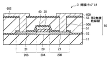
図17は、本発明の第3の実施の形態に係る薄膜トランジスタ3の断面構成を表したものである。この薄膜トランジスタ3は、層間絶縁膜50を第1無機絶縁膜52,有機樹脂膜51および第2無機絶縁膜53を酸化物半導体膜20の側からこの順に積層したものとしたことを除いては、上記第1の実施の形態の薄膜トランジスタ1と同様の構成を有している。
(Third embodiment)
FIG. 17 illustrates a cross-sectional configuration of the
第2無機絶縁膜53は、第1無機絶縁膜52と同様に酸化物半導体膜20への水分の混入や拡散を抑え、薄膜トランジスタ3の信頼性を更に向上させるためのものである。第2無機絶縁膜53は、例えば、厚みが10nm〜100nm程度であり、酸化アルミニウムにより構成されていることが望ましい。
Similar to the first inorganic insulating
この薄膜トランジスタ3は、有機樹脂膜51を形成したのち、有機樹脂膜51の上に、例えばスパッタリング法により、上述した厚みおよび材料よりなる第2無機絶縁膜52を形成し、第1無機絶縁膜52および第2無機絶縁膜53に接続孔50Aを設け、この接続孔50Aを介してソース電極60Sおよびドレイン電極60Dをソース領域20Sおよびドレイン領域20Dの低抵抗領域21に接続することを除いては、第1の実施の形態と同様にして製造することができる。
In the
このように本実施の形態では、層間絶縁膜50を第1無機絶縁膜52,有機樹脂膜51および第2無機絶縁膜53を酸化物半導体膜20の側からこの順に積層したものとしたので、薄膜トランジスタ3の信頼性を更に向上させることが可能となる。
Thus, in the present embodiment, the
(第4の実施の形態)
図18は、本発明の第4の実施の形態に係る薄膜トランジスタ4の断面構成を表したものである。この薄膜トランジスタ4は、基板11上にゲート電極40,ゲート絶縁膜30および酸化物半導体膜20,チャネル保護膜70,層間絶縁膜50(第1無機絶縁膜52および有機樹脂膜51),ソース電極60Sおよびドレイン電極60Dをこの順に積層したボトムゲート薄膜トランジスタである。このことを除いては、この薄膜トランジスタ4は、上記第1の実施の形態の薄膜トランジスタ1と同様の構成を有している。よって、対応する構成要素には同一の符号を付して説明する。
(Fourth embodiment)
FIG. 18 illustrates a cross-sectional configuration of the thin film transistor 4 according to the fourth embodiment of the present invention. The thin film transistor 4 includes a
チャネル保護膜70は、酸化物半導体膜20のチャネル領域20A上に設けられ、例えば、厚みが200nm程度であり、シリコン酸化膜,シリコン窒化膜または酸化アルミニウム膜の単層膜または積層膜により構成されている。
The channel
この薄膜トランジスタ4は、例えば次のようにして製造することができる。なお、第1の実施の形態と同一の工程については第1の実施の形態を参照して説明する。 The thin film transistor 4 can be manufactured, for example, as follows. Note that the same steps as those in the first embodiment will be described with reference to the first embodiment.
まず、基板11上の全面に例えばスパッタリング法や蒸着法を用いて、ゲート電極40の材料となるモリブデン(Mo)膜を、例えば200nm程度の厚みで形成する。このモリブデン膜を、例えばフォトリソグラフィ法を用いてパターニングすることにより、図19(A)に示したように、ゲート電極40を形成する。
First, a molybdenum (Mo) film as a material of the
次いで、同じく図19(A)に示したように、ゲート電極40を形成した基板11の全面に、例えばプラズマCVD法により、シリコン酸化膜または酸化アルミニウム膜などのゲート絶縁膜30を、300nm程度の厚みで形成する。
Next, as shown in FIG. 19A, a
次いで、図19(B)に示したように、ゲート絶縁膜30の上に、第1の実施の形態と同様にして、酸化物半導体膜20を形成する。
Next, as illustrated in FIG. 19B, the
続いて、酸化物半導体膜20およびゲート絶縁膜30上の全面に、シリコン酸化膜,シリコン窒化膜または酸化アルミニウム膜の単層膜または積層膜よりなるチャネル保護材料膜を、200nm程度の厚みで形成する。そののち、ゲート電極40をマスクとした裏面露光により、図19(C)に示したように、自己整合的にゲート電極40と近い位置にチャネル保護膜70を形成する。
Subsequently, a channel protective material film made of a single layer film or a laminated film of a silicon oxide film, a silicon nitride film, or an aluminum oxide film is formed on the entire surface of the
チャネル保護膜70を形成したのち、図19(D)に示したように、酸化物半導体膜20およびチャネル保護膜70の上に、第1の実施の形態と同様にして、金属膜52Aを形成する。
After forming the channel
引き続き、図20(A)に示したように、第1の実施の形態と同様にして、熱処理により、金属膜52Aを酸化させて第1無機絶縁膜52を形成すると共に、ソース領域20Aおよびドレイン領域20Dの上面から深さ方向の一部に、チャネル領域20Aよりも酸素濃度の低い低抵抗領域21を形成する。
Subsequently, as shown in FIG. 20A, as in the first embodiment, the
低抵抗領域21および第1無機絶縁膜52を形成したのち、図20(B)に示したように、第1の実施の形態と同様にして、第1無機絶縁膜52の上に、接続孔50Aを有する有機材料膜51を形成する。
After forming the low-
有機材料膜51を形成したのち、図18に示したように、第1の実施の形態と同様にして、層間絶縁膜50の第1無機絶縁膜52に接続孔50Aを設け、この接続孔50Aを介してソース電極60Sおよびドレイン電極60Dをソース領域20Sおよびドレイン領域20Dの低抵抗領域21に接続する。以上により、図18に示した薄膜トランジスタ4が完成する。
After forming the
この薄膜トランジスタ4では、層間絶縁膜50が有機樹脂膜51を含んでいるので、層間絶縁膜50の厚みを大きくすることが可能となっており、チャネル保護膜70の段差が、十分に厚い層間絶縁膜50により確実に被覆されている。よって、ソース電極60Sおよびドレイン電極60Dの断線あるいは短絡など、層間絶縁膜50に起因する不良が抑えられる。よって、セルフアライン構造のボトムゲート薄膜トランジスタ4の素子特性および信頼性を向上させることが可能となる。
In this thin film transistor 4, since the
(第5の実施の形態)
図21は、本発明の第5の実施の形態に係る薄膜トランジスタ5の断面構成を表したものである。この薄膜トランジスタ5は、層間絶縁膜50を有機樹脂膜51のみにより構成したことを除いては、第4の実施の形態の薄膜トランジスタ4と同様の構成を有し、同様にして製造することができる。この薄膜トランジスタ5の作用および効果は、第1,第2および第4の実施の形態と同様である。
(Fifth embodiment)
FIG. 21 illustrates a cross-sectional configuration of the
(第6の実施の形態)
図22は、本発明の第6の実施の形態に係る薄膜トランジスタ6の断面構成を表したものである。この薄膜トランジスタ6は、層間絶縁膜50を第1無機絶縁膜52,有機樹脂膜51および第2無機絶縁膜53を酸化物半導体膜20の側からこの順に積層したものとしたことを除いては、第4の実施の形態の薄膜トランジスタ4と同様の構成を有し、同様にして製造することができる。この薄膜トランジスタ6の作用および効果は、第1,第3および第4の実施の形態と同様である。
(Sixth embodiment)
FIG. 22 shows a cross-sectional configuration of a thin film transistor 6 according to the sixth embodiment of the present invention. The thin film transistor 6 has the same structure as that of the
<適用例1>
図23は、この薄膜トランジスタ1〜6,1A,1Bを駆動素子として備えた表示装置の回路構成を表すものである。表示装置80は、例えば液晶ディスプレイや有機ELディスプレイなどであり、駆動パネル81上に、マトリクス状に配設された複数の画素10R,10G,10Bと、これらの画素10R,10G,10Bを駆動するための各種駆動回路とが形成されたものである。画素10R,10G,10Bはそれぞれ、赤色(R:Red ),緑色(G:Green )および青色(B:Blue)の色光を発する液晶表示素子や有機EL素子などである。これら3つの画素10R,10G,10Bを一つのピクセルとして、複数のピクセルにより表示領域110が構成されている。駆動パネル91上には、駆動回路として、例えば映像表示用のドライバである信号線駆動回路120および走査線駆動回路130と、画素駆動回路150とが配設されている。この駆動パネル81には、図示しない封止パネルが貼り合わせられ、この封止パネルにより画素10R,10G,10Bおよび上記駆動回路が封止されている。
<Application example 1>
FIG. 23 shows a circuit configuration of a display device including the
図24は、画素駆動回路150の等価回路図である。画素駆動回路150は、上記薄膜トランジスタ1〜6,1A,1Bとして、トランジスタTr1,Tr2が配設されたアクティブ型の駆動回路である。トランジスタTr1,Tr2の間にはキャパシタCsが設けられ、第1の電源ライン(Vcc)および第2の電源ライン(GND)の間において、画素10R(または画素10G,10B)がトランジスタTr1に直列に接続されている。このような画素駆動回路150では、列方向に信号線120Aが複数配置され、行方向に走査線130Aが複数配置されている。各信号線120Aは、信号線駆動回路120に接続され、この信号線駆動回路120から信号線120Aを介してトランジスタTr2のソース電極に画像信号が供給されるようになっている。各走査線130Aは走査線駆動回路130に接続され、この走査線駆動回路130から走査線130Aを介してトランジスタTr2のゲート電極に走査信号が順次供給されるようになっている。この表示装置では、トランジスタTr1,Tr2が、上記実施の形態の薄膜トランジスタ1,1A〜1Cにより構成されているので、セルフアライン構造により寄生容量が小さくなっていると共に素子特性および信頼性の向上した薄膜トランジスタ1〜6,1A,1Bにより、高品質な表示が可能となる。このような表示装置80は、例えば次の適用例2〜6に示した電子機器に搭載することができる。
FIG. 24 is an equivalent circuit diagram of the
<適用例2>
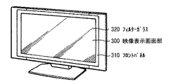
図25は、テレビジョン装置の外観を表したものである。このテレビジョン装置は、例えば、フロントパネル310およびフィルターガラス320を含む映像表示画面部300を有している。
<Application example 2>
FIG. 25 illustrates the appearance of a television device. The television apparatus includes a video display screen unit 300 including a front panel 310 and a filter glass 320, for example.
<適用例3>
図26は、デジタルスチルカメラの外観を表したものである。このデジタルスチルカメラは、例えば、フラッシュ用の発光部410、表示部420、メニュースイッチ430およびシャッターボタン440を有している。
<Application example 3>
FIG. 26 shows the appearance of a digital still camera. The digital still camera has, for example, a flash light emitting unit 410, a display unit 420, a menu switch 430, and a
<適用例4>
図27は、ノート型パーソナルコンピュータの外観を表したものである。このノート型パーソナルコンピュータは、例えば、本体510,文字等の入力操作のためのキーボード520および画像を表示する表示部530を有している。
<Application example 4>
FIG. 27 shows the appearance of a notebook personal computer. This notebook personal computer has, for example, a main body 510, a keyboard 520 for inputting characters and the like, and a display unit 530 for displaying an image.
<適用例5>
図28は、ビデオカメラの外観を表したものである。このビデオカメラは、例えば、本体部610,この本体部610の前方側面に設けられた被写体撮影用のレンズ620,撮影時のスタート/ストップスイッチ630および表示部640を有している。
<Application example 5>
FIG. 28 shows the appearance of the video camera. This video camera includes, for example, a main body 610, a subject photographing lens 620 provided on the front side surface of the main body 610, a start /
<適用例6>
図29は、携帯電話機の外観を表したものである。この携帯電話機は、例えば、上側筐体710と下側筐体720とを連結部(ヒンジ部)730で連結したものであり、ディスプレイ740,サブディスプレイ750,ピクチャーライト760およびカメラ770を有している。
<Application example 6>
FIG. 29 shows the appearance of a mobile phone. For example, the mobile phone is obtained by connecting an
以上、実施の形態を挙げて本発明を説明したが、本発明は上記実施の形態に限定されるものではなく、種々の変形が可能である。例えば、上記実施の形態では、低抵抗領域21がソース領域20Sおよびドレイン領域20Dの上面から深さ方向における一部に設けられている場合について説明したが、低抵抗領域21は、ソース領域20Sおよびドレイン領域20Dの上面から深さ方向における少なくとも一部に設けられていればよい。例えば、低抵抗領域21は、図30に示したように、ソース領域20Sおよびドレイン領域20Dの上面から深さ方向における全部に設けられていてもよい。
While the present invention has been described with reference to the embodiment, the present invention is not limited to the above embodiment, and various modifications can be made. For example, in the above embodiment, the case where the
また、例えば、上記実施の形態では、酸化物半導体膜20が基板11上に直接設けられている場合について説明したが、酸化物半導体20は、基板11上に、シリコン酸化膜,シリコン窒化膜または酸化アルミニウム膜などの絶縁膜を間にして設けられていてもよい。これにより、基板11から酸化物半導体膜20に不純物や水分などが拡散することを抑えることが可能となる。
For example, in the above embodiment, the case where the
更に、例えば、上記実施の形態において説明した各層の材料および厚み、または成膜方法および成膜条件などは限定されるものではなく、他の材料および厚みとしてもよく、または他の成膜方法および成膜条件としてもよい。 Furthermore, for example, the material and thickness of each layer described in the above embodiment, the film formation method and the film formation conditions are not limited, and other materials and thicknesses may be used, or other film formation methods and Film forming conditions may be used.
加えて、本発明は、液晶ディスプレイおよび有機ELディスプレイのほか、無機エレクトロルミネッセンス素子、またはエレクトロデポジション型もしくエレクトロクロミック型の表示素子などの他の表示素子を用いた表示装置にも適用可能である。 In addition to the liquid crystal display and the organic EL display, the present invention can be applied to a display device using other display elements such as an inorganic electroluminescence element or an electrodeposition type or electrochromic type display element. is there.
1…薄膜トランジスタ、11…基板、20…酸化物半導体薄膜、20A…チャネル領域、20S…ソース領域、20D…ドレイン領域、21…低抵抗領域、30…ゲート絶縁膜、40…ゲート電極、50…層間絶縁膜、51…有機樹脂膜、52…第1無機絶縁膜、52A…金属膜、53…第2無機絶縁膜、60S…ソース電極、60D…ドレイン電極、70…チャネル保護膜、80…表示装置、81…駆動パネル、10R,10G,10B…画素、110…表示領域、120…信号線駆動回路、130…走査線駆動回路、150…画素駆動回路、Tr1,Tr2…トランジスタ。
DESCRIPTION OF
Claims (12)
前記ゲート電極に対向してチャネル領域を有すると共に前記チャネル領域の一方の側にソース領域、他方の側にドレイン領域を有する酸化物半導体膜と、
前記酸化物半導体膜に接して設けられると共に接続孔を有し、有機樹脂膜を含む層間絶縁膜と、
前記接続孔を介して前記ソース領域および前記ドレイン領域にそれぞれ接続されたソース電極およびドレイン電極と
を備えた薄膜トランジスタ。 A gate electrode;
An oxide semiconductor film having a channel region facing the gate electrode and having a source region on one side of the channel region and a drain region on the other side;
An interlayer insulating film provided in contact with the oxide semiconductor film and having a connection hole, including an organic resin film;
A thin film transistor comprising a source electrode and a drain electrode respectively connected to the source region and the drain region through the connection hole.
請求項1記載の薄膜トランジスタ。 The thin film transistor according to claim 1, wherein the interlayer insulating film has a laminated structure of a first inorganic insulating film and the organic resin film.
請求項2記載の薄膜トランジスタ。 The thin film transistor according to claim 2, wherein the interlayer insulating film is formed by stacking the first inorganic insulating film and the organic resin film in this order from the oxide semiconductor film side.
請求項3記載の薄膜トランジスタ。 The thin film transistor according to claim 3, wherein the first inorganic insulating film is made of an aluminum oxide film, a titanium oxide film, or an indium oxide film.
請求項4記載の薄膜トランジスタ。 5. The thin film transistor according to claim 4, wherein the interlayer insulating film is formed by stacking the first inorganic insulating film, the organic resin film, and the second inorganic insulating film in this order from the oxide semiconductor film side.
前記酸化物半導体膜の前記チャネル領域上にゲート絶縁膜および前記ゲート電極がこの順に同一形状で設けられ、
前記酸化物半導体膜,前記ゲート絶縁膜および前記ゲート電極の表面に前記層間絶縁膜が設けられ、
前記層間絶縁膜に設けられた接続孔を介して前記ソース電極および前記ドレイン電極が前記ソース領域および前記ドレイン領域に接続されている
請求項5記載の薄膜トランジスタ。 The oxide semiconductor film is provided on a substrate;
A gate insulating film and the gate electrode are provided in the same shape in this order on the channel region of the oxide semiconductor film,
The interlayer insulating film is provided on the surfaces of the oxide semiconductor film, the gate insulating film, and the gate electrode,
The thin film transistor according to claim 5, wherein the source electrode and the drain electrode are connected to the source region and the drain region through a connection hole provided in the interlayer insulating film.
請求項1ないし6のいずれか1項に記載の薄膜トランジスタ。 7. The oxide semiconductor film includes a low resistance region having an oxygen concentration lower than that of the channel region at least in a depth direction from the upper surface of the source region and the drain region. A thin film transistor according to 1.
請求項7記載の薄膜トランジスタ。 The thin film transistor according to claim 7, wherein the low resistance region is a region within 10 nm in a depth direction from an upper surface of the source region and the drain region.
請求項1ないし6のいずれか1項に記載の薄膜トランジスタ。 7. The thin film transistor according to claim 1, wherein the oxide semiconductor film has a low-resistance region containing aluminum as a dopant in at least a part in a depth direction from the upper surface of the source region and the drain region. .
請求項1ないし9のいずれか1項に記載の薄膜トランジスタ。 The thin film transistor according to any one of claims 1 to 9, wherein the oxide semiconductor film has a configuration in which an amorphous film and a crystallized film are stacked in this order from the substrate side.
請求項10記載の薄膜トランジスタ。 The thin film transistor according to claim 10, wherein the crystallized film is formed of at least one selected from the group consisting of zinc oxide, indium zinc oxide, and indium gallium oxide.
前記薄膜トランジスタは、
ゲート電極と、
前記ゲート電極に対向してチャネル領域を有すると共に前記チャネル領域の一方の側にソース領域、他方の側にドレイン領域を有する酸化物半導体膜と、
前記酸化物半導体膜に接して設けられると共に接続孔を有し、有機樹脂膜を含む層間絶縁膜と、
前記接続孔を介して前記ソース領域および前記ドレイン領域にそれぞれ接続されたソース電極およびドレイン電極と
を備えた表示装置。 A thin film transistor and a pixel;
The thin film transistor
A gate electrode;
An oxide semiconductor film having a channel region facing the gate electrode and having a source region on one side of the channel region and a drain region on the other side;
An interlayer insulating film provided in contact with the oxide semiconductor film and having a connection hole, including an organic resin film;
A display device comprising: a source electrode and a drain electrode respectively connected to the source region and the drain region through the connection hole.
Priority Applications (5)
| Application Number | Priority Date | Filing Date | Title |
|---|---|---|---|
| JP2010152754A JP2012015436A (en) | 2010-07-05 | 2010-07-05 | Thin film transistor and display device |
| TW100118895A TWI479662B (en) | 2010-07-05 | 2011-05-30 | Thin film transistor and display device |
| US13/151,315 US20120001167A1 (en) | 2010-07-05 | 2011-06-02 | Thin film transistor and display device |
| KR1020110059968A KR20120003803A (en) | 2010-07-05 | 2011-06-21 | Thin film transistor and display device |
| CN2011101796221A CN102315277A (en) | 2010-07-05 | 2011-06-28 | Thin-film transistor and display unit |
Applications Claiming Priority (1)
| Application Number | Priority Date | Filing Date | Title |
|---|---|---|---|
| JP2010152754A JP2012015436A (en) | 2010-07-05 | 2010-07-05 | Thin film transistor and display device |
Publications (2)
| Publication Number | Publication Date |
|---|---|
| JP2012015436A true JP2012015436A (en) | 2012-01-19 |
| JP2012015436A5 JP2012015436A5 (en) | 2013-08-01 |
Family
ID=45399018
Family Applications (1)
| Application Number | Title | Priority Date | Filing Date |
|---|---|---|---|
| JP2010152754A Pending JP2012015436A (en) | 2010-07-05 | 2010-07-05 | Thin film transistor and display device |
Country Status (5)
| Country | Link |
|---|---|
| US (1) | US20120001167A1 (en) |
| JP (1) | JP2012015436A (en) |
| KR (1) | KR20120003803A (en) |
| CN (1) | CN102315277A (en) |
| TW (1) | TWI479662B (en) |
Cited By (45)
| Publication number | Priority date | Publication date | Assignee | Title |
|---|---|---|---|---|
| JP2012104639A (en) * | 2010-11-10 | 2012-05-31 | Toshiba Mobile Display Co Ltd | Thin-film transistor circuit board and method of manufacturing the same |
| JP2013048220A (en) * | 2011-07-22 | 2013-03-07 | Semiconductor Energy Lab Co Ltd | Semiconductor device |
| JP2013175718A (en) * | 2012-01-26 | 2013-09-05 | Semiconductor Energy Lab Co Ltd | Method for manufacturing semiconductor device |
| JP2013175717A (en) * | 2012-01-23 | 2013-09-05 | Semiconductor Energy Lab Co Ltd | Semiconductor device manufacturing method |
| JP2013175710A (en) * | 2012-01-23 | 2013-09-05 | Semiconductor Energy Lab Co Ltd | Semiconductor device and semiconductor device manufacturing method |
| JP2013179294A (en) * | 2012-02-08 | 2013-09-09 | Semiconductor Energy Lab Co Ltd | Semiconductor device and semiconductor device manufacturing method |
| JP2013179141A (en) * | 2012-02-28 | 2013-09-09 | Sony Corp | Transistor, manufacturing method of the same, display device and electronic apparatus |
| JP2013219345A (en) * | 2012-03-16 | 2013-10-24 | Semiconductor Energy Lab Co Ltd | Semiconductor device |
| JP2013236070A (en) * | 2012-04-13 | 2013-11-21 | Semiconductor Energy Lab Co Ltd | Semiconductor device |
| WO2014068859A1 (en) | 2012-11-05 | 2014-05-08 | Sony Corporation | Semiconductor device, display unit, and electronic apparatus |
| JP2014514747A (en) * | 2011-03-21 | 2014-06-19 | クゥアルコム・メムス・テクノロジーズ・インコーポレイテッド | Method for fabricating amorphous oxide semiconductor thin film transistor |
| US8883571B2 (en) | 2012-02-28 | 2014-11-11 | Sony Corporation | Transistor, method of manufacturing the transistor, semiconductor unit, method of manufacturing the semiconductor unit, display, and electronic apparatus |
| JP2015015458A (en) * | 2013-06-05 | 2015-01-22 | 株式会社半導体エネルギー研究所 | Semiconductor device and manufacturing method of the same |
| JP2015018929A (en) * | 2013-07-11 | 2015-01-29 | 三菱電機株式会社 | Semiconductor material, thin film transistor and thin film transistor manufacturing method |
| JP2015056566A (en) * | 2013-09-13 | 2015-03-23 | エルジー ディスプレイ カンパニー リミテッド | Thin film transistor, electrode substrate for display device and manufacturing methods of those |
| JP2015056565A (en) * | 2013-09-13 | 2015-03-23 | エルジー ディスプレイ カンパニー リミテッド | Thin film transistor, display device electrode substrate and manufacturing methods of those |
| JP2015065212A (en) * | 2013-09-24 | 2015-04-09 | 株式会社東芝 | Thin-film transistor, and method of manufacturing the same |
| JP2015519745A (en) * | 2012-05-09 | 2015-07-09 | アイメック・ヴェーゼットウェーImec Vzw | Method for increasing the electrical conductivity of a metal oxide semiconductor layer |
| JP2015144273A (en) * | 2013-12-27 | 2015-08-06 | 株式会社半導体エネルギー研究所 | semiconductor device |
| JP2015146444A (en) * | 2012-01-26 | 2015-08-13 | 株式会社半導体エネルギー研究所 | Method for manufacturing semiconductor device |
| JP2015164150A (en) * | 2014-02-28 | 2015-09-10 | 株式会社Joled | Transistor manufacturing method and display device manufacturing method |
| JP2015181158A (en) * | 2014-03-07 | 2015-10-15 | 株式会社半導体エネルギー研究所 | Semiconductor device, display device, input/output device, and electronic apparatus |
| JP2015185610A (en) * | 2014-03-20 | 2015-10-22 | 株式会社Joled | Thin film transistor and thin film transistor manufacturing method |
| WO2015186354A1 (en) * | 2014-06-03 | 2015-12-10 | 株式会社Joled | Thin film transistor and method for manufacturing same |
| JP2016027597A (en) * | 2013-12-06 | 2016-02-18 | 株式会社半導体エネルギー研究所 | Semiconductor device |
| JP2016111107A (en) * | 2014-12-03 | 2016-06-20 | 株式会社Joled | Thin film transistor, manufacturing method of the same and display device |
| US9379254B2 (en) | 2011-11-18 | 2016-06-28 | Qualcomm Mems Technologies, Inc. | Amorphous oxide semiconductor thin film transistor fabrication method |
| JP2016189482A (en) * | 2011-07-22 | 2016-11-04 | 株式会社半導体エネルギー研究所 | Semiconductor device |
| JP2017017352A (en) * | 2011-06-10 | 2017-01-19 | 株式会社半導体エネルギー研究所 | Method of manufacturing semiconductor device |
| JP2017017225A (en) * | 2015-07-02 | 2017-01-19 | 住友電気工業株式会社 | Semiconductor device and manufacturing method of the same |
| JP2017054899A (en) * | 2015-09-09 | 2017-03-16 | 株式会社半導体エネルギー研究所 | Semiconductor device, display device, electronic apparatus using the display device |
| JP2017168854A (en) * | 2012-06-29 | 2017-09-21 | 株式会社半導体エネルギー研究所 | Manufacturing method for semiconductor device |
| JP2017168642A (en) * | 2016-03-16 | 2017-09-21 | 株式会社Joled | Thin film transistor, and display device including the thin film transistor |
| JP2018164087A (en) * | 2014-07-16 | 2018-10-18 | 株式会社Joled | Transistor, display device and electronic equipment |
| JP2018174352A (en) * | 2011-06-29 | 2018-11-08 | 株式会社半導体エネルギー研究所 | Manufacturing method for semiconductor device |
| US10147823B2 (en) | 2015-03-19 | 2018-12-04 | Semiconductor Energy Laboratory Co., Ltd. | Semiconductor device |
| US10319883B2 (en) | 2016-12-20 | 2019-06-11 | Joled Inc. | Semiconductor device and display unit |
| US10373984B2 (en) | 2017-03-29 | 2019-08-06 | Japan Display Inc. | Display device |
| JP2019165230A (en) * | 2014-02-05 | 2019-09-26 | 株式会社半導体エネルギー研究所 | Method for manufacturing semiconductor device |
| US10453965B2 (en) | 2017-03-29 | 2019-10-22 | Japan Display Inc. | Display device |
| WO2020059026A1 (en) * | 2018-09-18 | 2020-03-26 | シャープ株式会社 | Display device and manufacturing method of display device |
| JP2020512689A (en) * | 2017-03-16 | 2020-04-23 | 深▲セン▼市▲華▼星光▲電▼半▲導▼体▲顕▼示技▲術▼有限公司 | Thin film transistor, manufacturing method thereof, and display panel |
| JP2020520557A (en) * | 2017-05-02 | 2020-07-09 | 深▲セン▼市華星光電技術有限公司 | OLED display panel and manufacturing method thereof |
| JP2022058505A (en) * | 2016-07-19 | 2022-04-12 | 株式会社ジャパンディスプレイ | TFT circuit board |
| US11348948B2 (en) | 2018-01-26 | 2022-05-31 | Japan Display Inc. | Manufacturing method of a display device |
Families Citing this family (66)
| Publication number | Priority date | Publication date | Assignee | Title |
|---|---|---|---|---|
| WO2011074407A1 (en) | 2009-12-18 | 2011-06-23 | Semiconductor Energy Laboratory Co., Ltd. | Semiconductor device and method for manufacturing the same |
| US9209314B2 (en) | 2010-06-16 | 2015-12-08 | Semiconductor Energy Laboratory Co., Ltd. | Field effect transistor |
| US8552425B2 (en) | 2010-06-18 | 2013-10-08 | Semiconductor Energy Laboratory Co., Ltd. | Semiconductor device |
| US9443984B2 (en) | 2010-12-28 | 2016-09-13 | Semiconductor Energy Laboratory Co., Ltd. | Semiconductor device and manufacturing method thereof |
| US8829512B2 (en) | 2010-12-28 | 2014-09-09 | Semiconductor Energy Laboratory Co., Ltd. | Semiconductor device and method for manufacturing the same |
| JP5685989B2 (en) * | 2011-02-28 | 2015-03-18 | ソニー株式会社 | Display device and electronic device |
| KR101597886B1 (en) * | 2011-04-18 | 2016-02-26 | 샤프 가부시키가이샤 | Thin-film transistor, display panel, and method for producing thin-film transistor |
| US9112036B2 (en) * | 2011-06-10 | 2015-08-18 | Semiconductor Energy Laboratory Co., Ltd. | Manufacturing method of semiconductor device |
| US8969154B2 (en) * | 2011-08-23 | 2015-03-03 | Micron Technology, Inc. | Methods for fabricating semiconductor device structures and arrays of vertical transistor devices |
| US9082663B2 (en) | 2011-09-16 | 2015-07-14 | Semiconductor Energy Laboratory Co., Ltd. | Semiconductor device and manufacturing method thereof |
| KR102108572B1 (en) * | 2011-09-26 | 2020-05-07 | 가부시키가이샤 한도오따이 에네루기 켄큐쇼 | Semiconductor device and method for manufacturing the same |
| WO2013047629A1 (en) | 2011-09-29 | 2013-04-04 | Semiconductor Energy Laboratory Co., Ltd. | Semiconductor device |
| US9287405B2 (en) * | 2011-10-13 | 2016-03-15 | Semiconductor Energy Laboratory Co., Ltd. | Semiconductor device comprising oxide semiconductor |
| CN104025301B (en) | 2011-10-14 | 2017-01-18 | 株式会社半导体能源研究所 | Semiconductor device |
| WO2013054823A1 (en) * | 2011-10-14 | 2013-04-18 | Semiconductor Energy Laboratory Co., Ltd. | Semiconductor device and manufacturing method thereof |
| CN103137701B (en) | 2011-11-30 | 2018-01-19 | 株式会社半导体能源研究所 | Transistor and semiconductor device |
| KR102084274B1 (en) * | 2011-12-15 | 2020-03-03 | 가부시키가이샤 한도오따이 에네루기 켄큐쇼 | Semiconductor device and method for manufacturing the same |
| US8796683B2 (en) | 2011-12-23 | 2014-08-05 | Semiconductor Energy Laboratory Co., Ltd. | Semiconductor device |
| US9419146B2 (en) * | 2012-01-26 | 2016-08-16 | Semiconductor Energy Laboratory Co., Ltd. | Semiconductor device and method for manufacturing the same |
| US8946714B2 (en) * | 2012-03-28 | 2015-02-03 | Sony Corporation | Semiconductor device and electronic apparatus including multilayer insulation film |
| CN102723309B (en) * | 2012-06-13 | 2014-07-02 | 京东方科技集团股份有限公司 | Array substrate and manufacturing method thereof as well as display device |
| JP6111458B2 (en) * | 2013-03-28 | 2017-04-12 | 株式会社Joled | Semiconductor device, display device and electronic apparatus |
| JP2014229814A (en) * | 2013-05-24 | 2014-12-08 | ソニー株式会社 | Thin-film transistor, display device, and electronic apparatus |
| CN103346093B (en) * | 2013-06-13 | 2015-12-23 | 北京大学深圳研究生院 | Top grid self-aligned thin film transistor that source/drain region is raised and preparation method thereof |
| WO2015010825A1 (en) | 2013-07-24 | 2015-01-29 | Imec Vzw | Method for improving the electrical conductivity of metal oxide semiconductor layers |
| KR102110226B1 (en) * | 2013-09-11 | 2020-05-14 | 삼성디스플레이 주식회사 | Display panel and method for fabricating the same |
| TWI528564B (en) * | 2013-09-23 | 2016-04-01 | 友達光電股份有限公司 | Thin film transistor and fabricating method thereof |
| CN103500710B (en) * | 2013-10-11 | 2015-11-25 | 京东方科技集团股份有限公司 | A kind of thin-film transistor manufacture method, thin-film transistor and display device |
| TWI527201B (en) * | 2013-11-06 | 2016-03-21 | 友達光電股份有限公司 | Pixel structure and fabricating method thereof |
| JP2016001712A (en) | 2013-11-29 | 2016-01-07 | 株式会社半導体エネルギー研究所 | Method of manufacturing semiconductor device |
| KR102254311B1 (en) * | 2013-12-05 | 2021-05-24 | 삼성디스플레이 주식회사 | Display substrates, methods of manufacturing the same and display devices including the same |
| US9640669B2 (en) * | 2014-03-13 | 2017-05-02 | Semiconductor Energy Laboratory Co., Ltd. | Semiconductor device, display device including the semiconductor device, display module including the display device, and electronic appliance including the semiconductor device, the display device, and the display module |
| JP6559444B2 (en) | 2014-03-14 | 2019-08-14 | 株式会社半導体エネルギー研究所 | Method for manufacturing semiconductor device |
| TWI548067B (en) | 2014-05-22 | 2016-09-01 | 友達光電股份有限公司 | Pixel structure |
| TWI539592B (en) | 2014-05-22 | 2016-06-21 | 友達光電股份有限公司 | Pixel structure |
| TW201611261A (en) * | 2014-06-06 | 2016-03-16 | 波利亞有限公司 | Self-aligned metal oxide transistors and methods of fabricating the same |
| JP2016111105A (en) * | 2014-12-03 | 2016-06-20 | 株式会社Joled | Thin film transistor, manufacturing method thereof, and display device |
| KR102386839B1 (en) * | 2014-12-22 | 2022-04-15 | 삼성전자주식회사 | Organic light-emitting device |
| TWI548100B (en) * | 2015-01-08 | 2016-09-01 | 友達光電股份有限公司 | Thin film transistor, display panel and manufacturing methods thereof |
| JP6736321B2 (en) | 2015-03-27 | 2020-08-05 | 株式会社半導体エネルギー研究所 | Method of manufacturing semiconductor device |
| TWI613706B (en) * | 2015-07-03 | 2018-02-01 | 友達光電股份有限公司 | Oxide semiconductor thin film transistor and manufacturing method thereof |
| CN106409919A (en) | 2015-07-30 | 2017-02-15 | 株式会社半导体能源研究所 | Semiconductor device and display device including the semiconductor device |
| KR20170119801A (en) * | 2016-04-19 | 2017-10-30 | 삼성디스플레이 주식회사 | Organic light emitting display device and method of manufacturing organic light emitting display device |
| KR102522595B1 (en) * | 2016-04-29 | 2023-04-17 | 삼성디스플레이 주식회사 | Transistor panel and manufacturing method thereof |
| US10096718B2 (en) * | 2016-06-17 | 2018-10-09 | Semiconductor Energy Laboratory Co., Ltd. | Transistor, electronic device, manufacturing method of transistor |
| CN106098560B (en) * | 2016-06-22 | 2019-03-12 | 深圳市华星光电技术有限公司 | The production method of top gate type thin film transistor |
| CN106024706B (en) * | 2016-06-22 | 2019-02-19 | 深圳市华星光电技术有限公司 | Array substrate and preparation method thereof |
| US10205008B2 (en) * | 2016-08-03 | 2019-02-12 | Semiconductor Energy Laboratory Co., Ltd. | Manufacturing method of semiconductor device |
| CN106252362B (en) * | 2016-08-31 | 2019-07-12 | 深圳市华星光电技术有限公司 | A kind of array substrate and preparation method thereof |
| KR102471021B1 (en) * | 2016-09-29 | 2022-11-25 | 삼성디스플레이 주식회사 | Thin film transistor array panel and manufacturing method thereof |
| JP6965894B2 (en) * | 2016-12-12 | 2021-11-10 | 住友電気工業株式会社 | Semiconductor device manufacturing method |
| JP2018133404A (en) * | 2017-02-14 | 2018-08-23 | 株式会社ジャパンディスプレイ | Semiconductor device |
| KR20180099974A (en) | 2017-02-27 | 2018-09-06 | 삼성디스플레이 주식회사 | Semiconductor device and method for fabricating the same |
| US20180323246A1 (en) * | 2017-05-02 | 2018-11-08 | Shenzhen China Star Optoelectronics Technology Co., Ltd. | Organic light-emitting diode display panel and manufacturing method thereof |
| CN107706199B (en) * | 2017-09-30 | 2020-05-05 | 深圳市华星光电半导体显示技术有限公司 | Manufacturing method of thin film transistor array substrate |
| CN107808826A (en) * | 2017-10-26 | 2018-03-16 | 京东方科技集团股份有限公司 | A kind of preparation method of bottom emitting top-gated self-aligned thin film transistor |
| JP2019091794A (en) * | 2017-11-14 | 2019-06-13 | シャープ株式会社 | Semiconductor device |
| CN107742647A (en) * | 2017-11-21 | 2018-02-27 | 中国电子科技集团公司第十三研究所 | Gallium oxide field-effect transistor |
| US10818801B2 (en) * | 2017-12-29 | 2020-10-27 | Shenzhen China Star Optoelectronics Technology Co., Ltd. | Thin-film transistor and manufacturing method thereof |
| CN108598145B (en) * | 2018-06-29 | 2021-08-31 | 上海天马微电子有限公司 | Organic light-emitting display panel and organic light-emitting display device |
| US20210343876A1 (en) * | 2018-08-01 | 2021-11-04 | Idemitsu Kosan Co.,Ltd. | Crystal structure compound, oxide sintered body, sputtering target, crystalline oxide thin film, amorphous oxide thin film, thin film transistor and electronic equipment |
| CN109037075B (en) * | 2018-08-09 | 2023-01-13 | 京东方科技集团股份有限公司 | Manufacturing method of thin film transistor, transistor and display substrate |
| CN111785736A (en) * | 2020-07-08 | 2020-10-16 | Tcl华星光电技术有限公司 | Array substrate and manufacturing method thereof |
| CN112002763A (en) * | 2020-08-10 | 2020-11-27 | 深圳市华星光电半导体显示技术有限公司 | TFT substrate, manufacturing method thereof and display panel |
| US11929436B2 (en) * | 2021-02-02 | 2024-03-12 | Taiwan Semiconductor Manufacturing Company Limited | Thin transistor including a hydrogen-blocking dielectric barrier and methods for forming the same |
| CN113437018B (en) * | 2021-06-02 | 2023-02-24 | 深圳市华星光电半导体显示技术有限公司 | Manufacturing method of array substrate, array substrate and display panel |
Citations (6)
| Publication number | Priority date | Publication date | Assignee | Title |
|---|---|---|---|---|
| JP2007220818A (en) * | 2006-02-15 | 2007-08-30 | Kochi Prefecture Sangyo Shinko Center | Thin-film transistor and manufacturing method thereof |
| JP2008004929A (en) * | 2006-05-26 | 2008-01-10 | Semiconductor Energy Lab Co Ltd | Non-volatile semiconductor storage device and manufacturing method thereof, semiconductor device and manufacturing method thereof, and method for manufacturing insulating film |
| JP2008040343A (en) * | 2006-08-09 | 2008-02-21 | Nec Corp | Thin film transistor array, method for manufacturing the same, and liquid crystal display device |
| WO2009034953A1 (en) * | 2007-09-10 | 2009-03-19 | Idemitsu Kosan Co., Ltd. | Thin film transistor |
| JP2010097601A (en) * | 2008-09-18 | 2010-04-30 | Semiconductor Energy Lab Co Ltd | Semiconductor device |
| JP2010135770A (en) * | 2008-11-07 | 2010-06-17 | Semiconductor Energy Lab Co Ltd | Semiconductor device |
Family Cites Families (10)
| Publication number | Priority date | Publication date | Assignee | Title |
|---|---|---|---|---|
| KR100412744B1 (en) * | 1999-03-30 | 2003-12-31 | 세이코 엡슨 가부시키가이샤 | Method of manufacturing thin-film transistor |
| KR100503129B1 (en) * | 2002-12-28 | 2005-07-22 | 엘지.필립스 엘시디 주식회사 | Dual Panel Type Electroluminescent Device and Method for Fabricating the same |
| US7576394B2 (en) * | 2006-02-02 | 2009-08-18 | Kochi Industrial Promotion Center | Thin film transistor including low resistance conductive thin films and manufacturing method thereof |
| KR101484297B1 (en) * | 2007-08-31 | 2015-01-19 | 가부시키가이샤 한도오따이 에네루기 켄큐쇼 | Display device and manufacturing method of the same |
| US20100295042A1 (en) * | 2008-01-23 | 2010-11-25 | Idemitsu Kosan Co., Ltd. | Field-effect transistor, method for manufacturing field-effect transistor, display device using field-effect transistor, and semiconductor device |
| KR100926030B1 (en) * | 2008-02-25 | 2009-11-11 | 한국과학기술연구원 | Organic/inorganic hybrid passivation layer for blocking moisture/oxygen transmission and improving gas barrier property |
| KR100964227B1 (en) * | 2008-05-06 | 2010-06-17 | 삼성모바일디스플레이주식회사 | Thin film transistor array substrate for flat panel display device, organic light emitting display device comprising the same, and manufacturing thereof |
| KR100941836B1 (en) * | 2008-05-19 | 2010-02-11 | 삼성모바일디스플레이주식회사 | Organic light emitting display device |
| KR101021479B1 (en) * | 2008-12-16 | 2011-03-16 | 성균관대학교산학협력단 | Thin film transistors, methods thereof and flat pannel display devices having the same |
| US8367486B2 (en) * | 2009-02-05 | 2013-02-05 | Semiconductor Energy Laboratory Co., Ltd. | Transistor and method for manufacturing the transistor |
-
2010
- 2010-07-05 JP JP2010152754A patent/JP2012015436A/en active Pending
-
2011
- 2011-05-30 TW TW100118895A patent/TWI479662B/en active
- 2011-06-02 US US13/151,315 patent/US20120001167A1/en not_active Abandoned
- 2011-06-21 KR KR1020110059968A patent/KR20120003803A/en not_active Application Discontinuation
- 2011-06-28 CN CN2011101796221A patent/CN102315277A/en active Pending
Patent Citations (6)
| Publication number | Priority date | Publication date | Assignee | Title |
|---|---|---|---|---|
| JP2007220818A (en) * | 2006-02-15 | 2007-08-30 | Kochi Prefecture Sangyo Shinko Center | Thin-film transistor and manufacturing method thereof |
| JP2008004929A (en) * | 2006-05-26 | 2008-01-10 | Semiconductor Energy Lab Co Ltd | Non-volatile semiconductor storage device and manufacturing method thereof, semiconductor device and manufacturing method thereof, and method for manufacturing insulating film |
| JP2008040343A (en) * | 2006-08-09 | 2008-02-21 | Nec Corp | Thin film transistor array, method for manufacturing the same, and liquid crystal display device |
| WO2009034953A1 (en) * | 2007-09-10 | 2009-03-19 | Idemitsu Kosan Co., Ltd. | Thin film transistor |
| JP2010097601A (en) * | 2008-09-18 | 2010-04-30 | Semiconductor Energy Lab Co Ltd | Semiconductor device |
| JP2010135770A (en) * | 2008-11-07 | 2010-06-17 | Semiconductor Energy Lab Co Ltd | Semiconductor device |
Cited By (79)
| Publication number | Priority date | Publication date | Assignee | Title |
|---|---|---|---|---|
| JP2012104639A (en) * | 2010-11-10 | 2012-05-31 | Toshiba Mobile Display Co Ltd | Thin-film transistor circuit board and method of manufacturing the same |
| JP2014514747A (en) * | 2011-03-21 | 2014-06-19 | クゥアルコム・メムス・テクノロジーズ・インコーポレイテッド | Method for fabricating amorphous oxide semiconductor thin film transistor |
| JP2017017352A (en) * | 2011-06-10 | 2017-01-19 | 株式会社半導体エネルギー研究所 | Method of manufacturing semiconductor device |
| US10833202B2 (en) | 2011-06-10 | 2020-11-10 | Semiconductor Energy Laboratory Co., Ltd. | Manufacturing method of semiconductor device |
| JP2019071451A (en) * | 2011-06-10 | 2019-05-09 | 株式会社半導体エネルギー研究所 | Semiconductor device |
| US9837545B2 (en) | 2011-06-10 | 2017-12-05 | Semiconductor Energy Laboratory Co., Ltd. | Manufacturing method of semiconductor device |
| JP2018098519A (en) * | 2011-06-10 | 2018-06-21 | 株式会社半導体エネルギー研究所 | Semiconductor device |
| JP2018174352A (en) * | 2011-06-29 | 2018-11-08 | 株式会社半導体エネルギー研究所 | Manufacturing method for semiconductor device |
| US10157939B2 (en) | 2011-07-22 | 2018-12-18 | Semiconductor Energy Laboratory Co., Ltd. | Semiconductor device including memory cell which includes transistor and capacitor |
| JP2013048220A (en) * | 2011-07-22 | 2013-03-07 | Semiconductor Energy Lab Co Ltd | Semiconductor device |
| JP2016189482A (en) * | 2011-07-22 | 2016-11-04 | 株式会社半導体エネルギー研究所 | Semiconductor device |
| US9666723B2 (en) | 2011-07-22 | 2017-05-30 | Semiconductor Energy Laboratory Co., Ltd. | Semiconductor device |
| US9379254B2 (en) | 2011-11-18 | 2016-06-28 | Qualcomm Mems Technologies, Inc. | Amorphous oxide semiconductor thin film transistor fabrication method |
| JP2022017390A (en) * | 2012-01-23 | 2022-01-25 | 株式会社半導体エネルギー研究所 | Semiconductor device |
| US10079312B2 (en) | 2012-01-23 | 2018-09-18 | Semiconductor Energy Laboratory Co., Ltd. | Semiconductor device and method for manufacturing the same |
| JP2017005273A (en) * | 2012-01-23 | 2017-01-05 | 株式会社半導体エネルギー研究所 | Manufacturing method of semiconductor device |
| US9653614B2 (en) | 2012-01-23 | 2017-05-16 | Semiconductor Energy Laboratory Co., Ltd. | Semiconductor device and method for manufacturing the same |
| JP2018041981A (en) * | 2012-01-23 | 2018-03-15 | 株式会社半導体エネルギー研究所 | Manufacturing method of semiconductor device |
| JP2013175710A (en) * | 2012-01-23 | 2013-09-05 | Semiconductor Energy Lab Co Ltd | Semiconductor device and semiconductor device manufacturing method |
| JP2020031219A (en) * | 2012-01-23 | 2020-02-27 | 株式会社半導体エネルギー研究所 | Semiconductor device |
| JP2013175717A (en) * | 2012-01-23 | 2013-09-05 | Semiconductor Energy Lab Co Ltd | Semiconductor device manufacturing method |
| US9614062B2 (en) | 2012-01-26 | 2017-04-04 | Semiconductor Energy Laboratory Co., Ltd. | Semiconductor device and method for manufacturing thereof |
| US9564457B2 (en) | 2012-01-26 | 2017-02-07 | Semiconductor Energy Laboratory Co., Ltd. | Method for manufacturing semiconductor device |
| JP2013175718A (en) * | 2012-01-26 | 2013-09-05 | Semiconductor Energy Lab Co Ltd | Method for manufacturing semiconductor device |
| JP2015146444A (en) * | 2012-01-26 | 2015-08-13 | 株式会社半導体エネルギー研究所 | Method for manufacturing semiconductor device |
| US9997545B2 (en) | 2012-01-26 | 2018-06-12 | Semiconductor Energy Laboratory Co., Ltd. | Semiconductor device and method for manufacturing thereof |
| JP2013179294A (en) * | 2012-02-08 | 2013-09-09 | Semiconductor Energy Lab Co Ltd | Semiconductor device and semiconductor device manufacturing method |
| US9859114B2 (en) | 2012-02-08 | 2018-01-02 | Semiconductor Energy Laboratory Co., Ltd. | Oxide semiconductor device with an oxygen-controlling insulating layer |
| US8883571B2 (en) | 2012-02-28 | 2014-11-11 | Sony Corporation | Transistor, method of manufacturing the transistor, semiconductor unit, method of manufacturing the semiconductor unit, display, and electronic apparatus |
| US9276120B2 (en) | 2012-02-28 | 2016-03-01 | Joled Inc. | Transistor, method of manufacturing the transistor, semiconductor unit, method of manufacturing the semiconductor unit, display, and electronic apparatus |
| JP2013179141A (en) * | 2012-02-28 | 2013-09-09 | Sony Corp | Transistor, manufacturing method of the same, display device and electronic apparatus |
| JP2017112390A (en) * | 2012-03-16 | 2017-06-22 | 株式会社半導体エネルギー研究所 | Semiconductor device |
| JP2013219345A (en) * | 2012-03-16 | 2013-10-24 | Semiconductor Energy Lab Co Ltd | Semiconductor device |
| JP2013236070A (en) * | 2012-04-13 | 2013-11-21 | Semiconductor Energy Lab Co Ltd | Semiconductor device |
| JP2015519745A (en) * | 2012-05-09 | 2015-07-09 | アイメック・ヴェーゼットウェーImec Vzw | Method for increasing the electrical conductivity of a metal oxide semiconductor layer |
| US11393918B2 (en) | 2012-06-29 | 2022-07-19 | Semiconductor Energy Laboratory Co., Ltd. | Semiconductor device and method for manufacturing semiconductor device |
| JP2017168854A (en) * | 2012-06-29 | 2017-09-21 | 株式会社半導体エネルギー研究所 | Manufacturing method for semiconductor device |
| US10811521B2 (en) | 2012-06-29 | 2020-10-20 | Semiconductor Energy Laboratory Co., Ltd. | Semiconductor device and method for manufacturing semiconductor device |
| WO2014068859A1 (en) | 2012-11-05 | 2014-05-08 | Sony Corporation | Semiconductor device, display unit, and electronic apparatus |
| JP2015015458A (en) * | 2013-06-05 | 2015-01-22 | 株式会社半導体エネルギー研究所 | Semiconductor device and manufacturing method of the same |
| JP2015018929A (en) * | 2013-07-11 | 2015-01-29 | 三菱電機株式会社 | Semiconductor material, thin film transistor and thin film transistor manufacturing method |
| JP2015056565A (en) * | 2013-09-13 | 2015-03-23 | エルジー ディスプレイ カンパニー リミテッド | Thin film transistor, display device electrode substrate and manufacturing methods of those |
| JP2015056566A (en) * | 2013-09-13 | 2015-03-23 | エルジー ディスプレイ カンパニー リミテッド | Thin film transistor, electrode substrate for display device and manufacturing methods of those |
| JP2015065212A (en) * | 2013-09-24 | 2015-04-09 | 株式会社東芝 | Thin-film transistor, and method of manufacturing the same |
| JP2021103797A (en) * | 2013-12-06 | 2021-07-15 | 株式会社半導体エネルギー研究所 | Semiconductor device |
| JP2016027597A (en) * | 2013-12-06 | 2016-02-18 | 株式会社半導体エネルギー研究所 | Semiconductor device |
| JP2015144273A (en) * | 2013-12-27 | 2015-08-06 | 株式会社半導体エネルギー研究所 | semiconductor device |
| US11011648B2 (en) | 2014-02-05 | 2021-05-18 | Semiconductor Energy Laboratory Co., Ltd. | Semiconductor device and manufacturing method thereof |
| US10680116B2 (en) | 2014-02-05 | 2020-06-09 | Semiconductor Energy Laboratory Co., Ltd. | Manufacturing method of semiconductor device including oxide semiconductor |
| US11942555B2 (en) | 2014-02-05 | 2024-03-26 | Semiconductor Energy Laboratory Co., Ltd. | Semiconductor device and manufacturing method thereof |
| US11640996B2 (en) | 2014-02-05 | 2023-05-02 | Semiconductor Energy Laboratory Co., Ltd. | Semiconductor device and manufacturing method thereof |
| JP2019165230A (en) * | 2014-02-05 | 2019-09-26 | 株式会社半導体エネルギー研究所 | Method for manufacturing semiconductor device |
| JP2015164150A (en) * | 2014-02-28 | 2015-09-10 | 株式会社Joled | Transistor manufacturing method and display device manufacturing method |
| JP2015181158A (en) * | 2014-03-07 | 2015-10-15 | 株式会社半導体エネルギー研究所 | Semiconductor device, display device, input/output device, and electronic apparatus |
| JP2015185610A (en) * | 2014-03-20 | 2015-10-22 | 株式会社Joled | Thin film transistor and thin film transistor manufacturing method |
| WO2015186354A1 (en) * | 2014-06-03 | 2015-12-10 | 株式会社Joled | Thin film transistor and method for manufacturing same |
| JP2018164087A (en) * | 2014-07-16 | 2018-10-18 | 株式会社Joled | Transistor, display device and electronic equipment |
| US10644165B2 (en) | 2014-12-03 | 2020-05-05 | Joled Inc. | Thin-film transistor, method of fabricating thin-film transistor, and display device |
| US10050150B2 (en) | 2014-12-03 | 2018-08-14 | Joled Inc. | Thin-film transistor, method of fabricating thin-film transistor, and display device |
| JP2016111107A (en) * | 2014-12-03 | 2016-06-20 | 株式会社Joled | Thin film transistor, manufacturing method of the same and display device |
| US10147823B2 (en) | 2015-03-19 | 2018-12-04 | Semiconductor Energy Laboratory Co., Ltd. | Semiconductor device |
| JP2017017225A (en) * | 2015-07-02 | 2017-01-19 | 住友電気工業株式会社 | Semiconductor device and manufacturing method of the same |
| JP2017054899A (en) * | 2015-09-09 | 2017-03-16 | 株式会社半導体エネルギー研究所 | Semiconductor device, display device, electronic apparatus using the display device |
| US10580799B2 (en) | 2016-03-16 | 2020-03-03 | Joled Inc. | Thin film transistor and display device comprising the same |
| US10192891B2 (en) | 2016-03-16 | 2019-01-29 | Joled Inc. | Thin film transistor and display device comprising the same |
| JP2017168642A (en) * | 2016-03-16 | 2017-09-21 | 株式会社Joled | Thin film transistor, and display device including the thin film transistor |
| JP2022058505A (en) * | 2016-07-19 | 2022-04-12 | 株式会社ジャパンディスプレイ | TFT circuit board |
| JP7350903B2 (en) | 2016-07-19 | 2023-09-26 | 株式会社ジャパンディスプレイ | TFT circuit board |
| US10319883B2 (en) | 2016-12-20 | 2019-06-11 | Joled Inc. | Semiconductor device and display unit |
| JP2020512689A (en) * | 2017-03-16 | 2020-04-23 | 深▲セン▼市▲華▼星光▲電▼半▲導▼体▲顕▼示技▲術▼有限公司 | Thin film transistor, manufacturing method thereof, and display panel |
| US10804297B2 (en) | 2017-03-29 | 2020-10-13 | Japan Display Inc. | Display device |
| US11177363B2 (en) | 2017-03-29 | 2021-11-16 | Japan Display Inc. | Display device |
| US11355520B2 (en) | 2017-03-29 | 2022-06-07 | Japan Display Inc. | Display device |
| US10453965B2 (en) | 2017-03-29 | 2019-10-22 | Japan Display Inc. | Display device |
| US10373984B2 (en) | 2017-03-29 | 2019-08-06 | Japan Display Inc. | Display device |
| US11855102B2 (en) | 2017-03-29 | 2023-12-26 | Japan Display Inc. | Display device |
| JP2020520557A (en) * | 2017-05-02 | 2020-07-09 | 深▲セン▼市華星光電技術有限公司 | OLED display panel and manufacturing method thereof |
| US11348948B2 (en) | 2018-01-26 | 2022-05-31 | Japan Display Inc. | Manufacturing method of a display device |
| WO2020059026A1 (en) * | 2018-09-18 | 2020-03-26 | シャープ株式会社 | Display device and manufacturing method of display device |
Also Published As
| Publication number | Publication date |
|---|---|
| TWI479662B (en) | 2015-04-01 |
| TW201214714A (en) | 2012-04-01 |
| US20120001167A1 (en) | 2012-01-05 |
| CN102315277A (en) | 2012-01-11 |
| KR20120003803A (en) | 2012-01-11 |
Similar Documents
| Publication | Publication Date | Title |
|---|---|---|
| JP2012015436A (en) | Thin film transistor and display device | |
| JP5708910B2 (en) | THIN FILM TRANSISTOR, MANUFACTURING METHOD THEREOF, AND DISPLAY DEVICE | |
| US9006734B2 (en) | Thin film transistor, method of manufacturing the same, and display unit | |
| JP2011187506A (en) | Thin-film transistor, method of manufacturing the thin-film transistor, and display device | |
| US9721977B2 (en) | Display device and electronic unit | |
| JP6111398B2 (en) | Display device and electronic device | |
| US8748878B2 (en) | Thin film transistor, method of manufacturing the same, and display device | |
| JP5743064B2 (en) | THIN FILM TRANSISTOR, MANUFACTURING METHOD THEREOF, AND DISPLAY DEVICE | |
| JP5766481B2 (en) | Display device and electronic device | |
| US9362312B2 (en) | Semiconductor device, display unit, and electronic apparatus | |
| JP2012015436A5 (en) | ||
| JP2012182165A (en) | Display device and electronic apparatus | |
| US9053984B2 (en) | Thin-film transistor, display unit, and electronic apparatus | |
| JP6142136B2 (en) | Transistor manufacturing method, display device manufacturing method, and electronic device manufacturing method | |
| JP2013211410A (en) | Thin film transistor, manufacturing method of the same, display device and electronic apparatus | |
| JP6019331B2 (en) | Transistor, semiconductor device, display device, electronic device, and method for manufacturing semiconductor device | |
| JP2012204548A (en) | Display device and manufacturing method therefor | |
| JP6019330B2 (en) | THIN FILM TRANSISTOR, METHOD FOR PRODUCING THIN FILM TRANSISTOR, DISPLAY DEVICE, AND ELECTRONIC DEVICE | |
| JP2013207193A (en) | Semiconductor device, manufacturing method of the same, display device and electronic apparatus |
Legal Events
| Date | Code | Title | Description |
|---|---|---|---|
| A521 | Request for written amendment filed |
Free format text: JAPANESE INTERMEDIATE CODE: A523 Effective date: 20130613 |
|
| A621 | Written request for application examination |
Free format text: JAPANESE INTERMEDIATE CODE: A621 Effective date: 20130613 |
|
| A977 | Report on retrieval |
Free format text: JAPANESE INTERMEDIATE CODE: A971007 Effective date: 20140430 |
|
| A131 | Notification of reasons for refusal |
Free format text: JAPANESE INTERMEDIATE CODE: A131 Effective date: 20140507 |
|
| A521 | Request for written amendment filed |
Free format text: JAPANESE INTERMEDIATE CODE: A523 Effective date: 20140620 |
|
| A02 | Decision of refusal |
Free format text: JAPANESE INTERMEDIATE CODE: A02 Effective date: 20141209 |