JP2014229814A - Thin-film transistor, display device, and electronic apparatus - Google Patents
Thin-film transistor, display device, and electronic apparatus Download PDFInfo
- Publication number
- JP2014229814A JP2014229814A JP2013109773A JP2013109773A JP2014229814A JP 2014229814 A JP2014229814 A JP 2014229814A JP 2013109773 A JP2013109773 A JP 2013109773A JP 2013109773 A JP2013109773 A JP 2013109773A JP 2014229814 A JP2014229814 A JP 2014229814A
- Authority
- JP
- Japan
- Prior art keywords
- oxide semiconductor
- semiconductor layer
- barrier film
- barrier
- film
- Prior art date
- Legal status (The legal status is an assumption and is not a legal conclusion. Google has not performed a legal analysis and makes no representation as to the accuracy of the status listed.)
- Pending
Links
- 239000010409 thin film Substances 0.000 title claims abstract description 36
- 239000010408 film Substances 0.000 claims abstract description 222
- 230000004888 barrier function Effects 0.000 claims abstract description 178
- 239000004065 semiconductor Substances 0.000 claims abstract description 115
- 239000000758 substrate Substances 0.000 claims abstract description 52
- 239000001257 hydrogen Substances 0.000 claims abstract description 32
- 229910052739 hydrogen Inorganic materials 0.000 claims abstract description 32
- UFHFLCQGNIYNRP-UHFFFAOYSA-N Hydrogen Chemical compound [H][H] UFHFLCQGNIYNRP-UHFFFAOYSA-N 0.000 claims abstract description 29
- 239000012535 impurity Substances 0.000 claims abstract description 16
- 239000010410 layer Substances 0.000 claims description 132
- 239000003990 capacitor Substances 0.000 claims description 22
- 229910052581 Si3N4 Inorganic materials 0.000 claims description 20
- HQVNEWCFYHHQES-UHFFFAOYSA-N silicon nitride Chemical compound N12[Si]34N5[Si]62N3[Si]51N64 HQVNEWCFYHHQES-UHFFFAOYSA-N 0.000 claims description 20
- 238000003860 storage Methods 0.000 claims description 19
- 239000000463 material Substances 0.000 claims description 18
- 230000001603 reducing effect Effects 0.000 claims description 16
- VYPSYNLAJGMNEJ-UHFFFAOYSA-N Silicium dioxide Chemical compound O=[Si]=O VYPSYNLAJGMNEJ-UHFFFAOYSA-N 0.000 claims description 13
- 229910052814 silicon oxide Inorganic materials 0.000 claims description 13
- XUIMIQQOPSSXEZ-UHFFFAOYSA-N Silicon Chemical compound [Si] XUIMIQQOPSSXEZ-UHFFFAOYSA-N 0.000 claims description 11
- 229910052710 silicon Inorganic materials 0.000 claims description 11
- 239000010703 silicon Substances 0.000 claims description 11
- TWNQGVIAIRXVLR-UHFFFAOYSA-N oxo(oxoalumanyloxy)alumane Chemical compound O=[Al]O[Al]=O TWNQGVIAIRXVLR-UHFFFAOYSA-N 0.000 claims description 9
- 239000011347 resin Substances 0.000 claims description 6
- 229920005989 resin Polymers 0.000 claims description 6
- 239000002356 single layer Substances 0.000 claims description 5
- GWEVSGVZZGPLCZ-UHFFFAOYSA-N Titan oxide Chemical compound O=[Ti]=O GWEVSGVZZGPLCZ-UHFFFAOYSA-N 0.000 claims description 4
- 238000005401 electroluminescence Methods 0.000 claims description 2
- OGIDPMRJRNCKJF-UHFFFAOYSA-N titanium oxide Inorganic materials [Ti]=O OGIDPMRJRNCKJF-UHFFFAOYSA-N 0.000 claims description 2
- 238000000034 method Methods 0.000 description 22
- XLOMVQKBTHCTTD-UHFFFAOYSA-N Zinc monoxide Chemical compound [Zn]=O XLOMVQKBTHCTTD-UHFFFAOYSA-N 0.000 description 15
- 230000008569 process Effects 0.000 description 12
- 238000004544 sputter deposition Methods 0.000 description 11
- 238000005530 etching Methods 0.000 description 10
- 229910052751 metal Inorganic materials 0.000 description 10
- 239000002184 metal Substances 0.000 description 10
- 239000007789 gas Substances 0.000 description 9
- 238000004519 manufacturing process Methods 0.000 description 9
- 229910052760 oxygen Inorganic materials 0.000 description 9
- 239000001301 oxygen Substances 0.000 description 9
- XKRFYHLGVUSROY-UHFFFAOYSA-N Argon Chemical compound [Ar] XKRFYHLGVUSROY-UHFFFAOYSA-N 0.000 description 8
- QVGXLLKOCUKJST-UHFFFAOYSA-N atomic oxygen Chemical compound [O] QVGXLLKOCUKJST-UHFFFAOYSA-N 0.000 description 8
- 239000011229 interlayer Substances 0.000 description 8
- 101100153525 Homo sapiens TNFRSF25 gene Proteins 0.000 description 7
- 102100022203 Tumor necrosis factor receptor superfamily member 25 Human genes 0.000 description 7
- 239000010949 copper Substances 0.000 description 7
- 229910052738 indium Inorganic materials 0.000 description 7
- APFVFJFRJDLVQX-UHFFFAOYSA-N indium atom Chemical compound [In] APFVFJFRJDLVQX-UHFFFAOYSA-N 0.000 description 7
- 235000014692 zinc oxide Nutrition 0.000 description 7
- 239000011787 zinc oxide Substances 0.000 description 7
- 229910052782 aluminium Inorganic materials 0.000 description 6
- XAGFODPZIPBFFR-UHFFFAOYSA-N aluminium Chemical compound [Al] XAGFODPZIPBFFR-UHFFFAOYSA-N 0.000 description 6
- 238000005268 plasma chemical vapour deposition Methods 0.000 description 6
- RYGMFSIKBFXOCR-UHFFFAOYSA-N Copper Chemical compound [Cu] RYGMFSIKBFXOCR-UHFFFAOYSA-N 0.000 description 5
- 238000005229 chemical vapour deposition Methods 0.000 description 5
- 229910052802 copper Inorganic materials 0.000 description 5
- 230000006866 deterioration Effects 0.000 description 5
- 238000000206 photolithography Methods 0.000 description 5
- 238000005070 sampling Methods 0.000 description 5
- 239000010936 titanium Substances 0.000 description 5
- IJGRMHOSHXDMSA-UHFFFAOYSA-N Atomic nitrogen Chemical compound N#N IJGRMHOSHXDMSA-UHFFFAOYSA-N 0.000 description 4
- GYHNNYVSQQEPJS-UHFFFAOYSA-N Gallium Chemical compound [Ga] GYHNNYVSQQEPJS-UHFFFAOYSA-N 0.000 description 4
- RTAQQCXQSZGOHL-UHFFFAOYSA-N Titanium Chemical compound [Ti] RTAQQCXQSZGOHL-UHFFFAOYSA-N 0.000 description 4
- 229910052786 argon Inorganic materials 0.000 description 4
- 238000009792 diffusion process Methods 0.000 description 4
- 229910052733 gallium Inorganic materials 0.000 description 4
- 238000006722 reduction reaction Methods 0.000 description 4
- 229910052719 titanium Inorganic materials 0.000 description 4
- ZOKXTWBITQBERF-UHFFFAOYSA-N Molybdenum Chemical compound [Mo] ZOKXTWBITQBERF-UHFFFAOYSA-N 0.000 description 3
- 239000004642 Polyimide Substances 0.000 description 3
- ATJFFYVFTNAWJD-UHFFFAOYSA-N Tin Chemical compound [Sn] ATJFFYVFTNAWJD-UHFFFAOYSA-N 0.000 description 3
- 230000009471 action Effects 0.000 description 3
- 230000000052 comparative effect Effects 0.000 description 3
- 239000011521 glass Substances 0.000 description 3
- 150000002431 hydrogen Chemical class 0.000 description 3
- 229910052750 molybdenum Inorganic materials 0.000 description 3
- 239000011733 molybdenum Substances 0.000 description 3
- 230000003071 parasitic effect Effects 0.000 description 3
- -1 polyethylene terephthalate Polymers 0.000 description 3
- 229920001721 polyimide Polymers 0.000 description 3
- 238000012545 processing Methods 0.000 description 3
- 229910052718 tin Inorganic materials 0.000 description 3
- QGZKDVFQNNGYKY-UHFFFAOYSA-N Ammonia Chemical compound N QGZKDVFQNNGYKY-UHFFFAOYSA-N 0.000 description 2
- KRHYYFGTRYWZRS-UHFFFAOYSA-N Fluorane Chemical compound F KRHYYFGTRYWZRS-UHFFFAOYSA-N 0.000 description 2
- 238000005033 Fourier transform infrared spectroscopy Methods 0.000 description 2
- GQPLMRYTRLFLPF-UHFFFAOYSA-N Nitrous Oxide Chemical compound [O-][N+]#N GQPLMRYTRLFLPF-UHFFFAOYSA-N 0.000 description 2
- 229910004298 SiO 2 Inorganic materials 0.000 description 2
- BLRPTPMANUNPDV-UHFFFAOYSA-N Silane Chemical compound [SiH4] BLRPTPMANUNPDV-UHFFFAOYSA-N 0.000 description 2
- 238000000137 annealing Methods 0.000 description 2
- 239000000919 ceramic Substances 0.000 description 2
- 239000000470 constituent Substances 0.000 description 2
- PMHQVHHXPFUNSP-UHFFFAOYSA-M copper(1+);methylsulfanylmethane;bromide Chemical compound Br[Cu].CSC PMHQVHHXPFUNSP-UHFFFAOYSA-M 0.000 description 2
- 238000010586 diagram Methods 0.000 description 2
- 238000001312 dry etching Methods 0.000 description 2
- 150000002500 ions Chemical class 0.000 description 2
- 239000004973 liquid crystal related substance Substances 0.000 description 2
- 239000011159 matrix material Substances 0.000 description 2
- 229910052757 nitrogen Inorganic materials 0.000 description 2
- 238000000059 patterning Methods 0.000 description 2
- 230000002093 peripheral effect Effects 0.000 description 2
- 229920000139 polyethylene terephthalate Polymers 0.000 description 2
- 239000005020 polyethylene terephthalate Substances 0.000 description 2
- 230000009467 reduction Effects 0.000 description 2
- 229910000077 silane Inorganic materials 0.000 description 2
- 238000001039 wet etching Methods 0.000 description 2
- 229910018072 Al 2 O 3 Inorganic materials 0.000 description 1
- 229910000838 Al alloy Inorganic materials 0.000 description 1
- 229920000106 Liquid crystal polymer Polymers 0.000 description 1
- 239000004977 Liquid-crystal polymers (LCPs) Substances 0.000 description 1
- 229920012266 Poly(ether sulfone) PES Polymers 0.000 description 1
- HCHKCACWOHOZIP-UHFFFAOYSA-N Zinc Chemical compound [Zn] HCHKCACWOHOZIP-UHFFFAOYSA-N 0.000 description 1
- QCWXUUIWCKQGHC-UHFFFAOYSA-N Zirconium Chemical compound [Zr] QCWXUUIWCKQGHC-UHFFFAOYSA-N 0.000 description 1
- 239000002253 acid Substances 0.000 description 1
- 150000007513 acids Chemical class 0.000 description 1
- NIXOWILDQLNWCW-UHFFFAOYSA-N acrylic acid group Chemical group C(C=C)(=O)O NIXOWILDQLNWCW-UHFFFAOYSA-N 0.000 description 1
- 229910021529 ammonia Inorganic materials 0.000 description 1
- 229910021417 amorphous silicon Inorganic materials 0.000 description 1
- 125000004429 atom Chemical group 0.000 description 1
- 238000000231 atomic layer deposition Methods 0.000 description 1
- 230000008901 benefit Effects 0.000 description 1
- 230000015572 biosynthetic process Effects 0.000 description 1
- 230000008859 change Effects 0.000 description 1
- 150000001875 compounds Chemical class 0.000 description 1
- 239000002178 crystalline material Substances 0.000 description 1
- 238000002425 crystallisation Methods 0.000 description 1
- 230000008025 crystallization Effects 0.000 description 1
- 230000007423 decrease Effects 0.000 description 1
- 230000003247 decreasing effect Effects 0.000 description 1
- AJNVQOSZGJRYEI-UHFFFAOYSA-N digallium;oxygen(2-) Chemical compound [O-2].[O-2].[O-2].[Ga+3].[Ga+3] AJNVQOSZGJRYEI-UHFFFAOYSA-N 0.000 description 1
- KPUWHANPEXNPJT-UHFFFAOYSA-N disiloxane Chemical class [SiH3]O[SiH3] KPUWHANPEXNPJT-UHFFFAOYSA-N 0.000 description 1
- 101150013423 dsl-1 gene Proteins 0.000 description 1
- 230000000694 effects Effects 0.000 description 1
- 230000002349 favourable effect Effects 0.000 description 1
- 229910001195 gallium oxide Inorganic materials 0.000 description 1
- AMGQUBHHOARCQH-UHFFFAOYSA-N indium;oxotin Chemical compound [In].[Sn]=O AMGQUBHHOARCQH-UHFFFAOYSA-N 0.000 description 1
- 238000009413 insulation Methods 0.000 description 1
- 238000005259 measurement Methods 0.000 description 1
- 239000012528 membrane Substances 0.000 description 1
- 238000012986 modification Methods 0.000 description 1
- 230000004048 modification Effects 0.000 description 1
- 238000005121 nitriding Methods 0.000 description 1
- 229960001730 nitrous oxide Drugs 0.000 description 1
- 235000013842 nitrous oxide Nutrition 0.000 description 1
- NQBRDZOHGALQCB-UHFFFAOYSA-N oxoindium Chemical compound [O].[In] NQBRDZOHGALQCB-UHFFFAOYSA-N 0.000 description 1
- 239000004417 polycarbonate Substances 0.000 description 1
- 229920000515 polycarbonate Polymers 0.000 description 1
- 239000011112 polyethylene naphthalate Substances 0.000 description 1
- 229920001296 polysiloxane Polymers 0.000 description 1
- 238000001552 radio frequency sputter deposition Methods 0.000 description 1
- 238000012827 research and development Methods 0.000 description 1
- 238000007789 sealing Methods 0.000 description 1
- 239000002904 solvent Substances 0.000 description 1
- 238000004611 spectroscopical analysis Methods 0.000 description 1
- 239000010935 stainless steel Substances 0.000 description 1
- 229910001220 stainless steel Inorganic materials 0.000 description 1
- 239000000126 substance Substances 0.000 description 1
- JBQYATWDVHIOAR-UHFFFAOYSA-N tellanylidenegermanium Chemical compound [Te]=[Ge] JBQYATWDVHIOAR-UHFFFAOYSA-N 0.000 description 1
- XLYOFNOQVPJJNP-UHFFFAOYSA-N water Chemical compound O XLYOFNOQVPJJNP-UHFFFAOYSA-N 0.000 description 1
- 239000011701 zinc Substances 0.000 description 1
- 229910052725 zinc Inorganic materials 0.000 description 1
- YVTHLONGBIQYBO-UHFFFAOYSA-N zinc indium(3+) oxygen(2-) Chemical compound [O--].[Zn++].[In+3] YVTHLONGBIQYBO-UHFFFAOYSA-N 0.000 description 1
- TYHJXGDMRRJCRY-UHFFFAOYSA-N zinc indium(3+) oxygen(2-) tin(4+) Chemical compound [O-2].[Zn+2].[Sn+4].[In+3] TYHJXGDMRRJCRY-UHFFFAOYSA-N 0.000 description 1
- 229910052726 zirconium Inorganic materials 0.000 description 1
Images


Classifications
-
- H—ELECTRICITY
- H01—ELECTRIC ELEMENTS
- H01L—SEMICONDUCTOR DEVICES NOT COVERED BY CLASS H10
- H01L27/00—Devices consisting of a plurality of semiconductor or other solid-state components formed in or on a common substrate
- H01L27/02—Devices consisting of a plurality of semiconductor or other solid-state components formed in or on a common substrate including semiconductor components specially adapted for rectifying, oscillating, amplifying or switching and having at least one potential-jump barrier or surface barrier; including integrated passive circuit elements with at least one potential-jump barrier or surface barrier
- H01L27/12—Devices consisting of a plurality of semiconductor or other solid-state components formed in or on a common substrate including semiconductor components specially adapted for rectifying, oscillating, amplifying or switching and having at least one potential-jump barrier or surface barrier; including integrated passive circuit elements with at least one potential-jump barrier or surface barrier the substrate being other than a semiconductor body, e.g. an insulating body
- H01L27/1214—Devices consisting of a plurality of semiconductor or other solid-state components formed in or on a common substrate including semiconductor components specially adapted for rectifying, oscillating, amplifying or switching and having at least one potential-jump barrier or surface barrier; including integrated passive circuit elements with at least one potential-jump barrier or surface barrier the substrate being other than a semiconductor body, e.g. an insulating body comprising a plurality of TFTs formed on a non-semiconducting substrate, e.g. driving circuits for AMLCDs
- H01L27/1222—Devices consisting of a plurality of semiconductor or other solid-state components formed in or on a common substrate including semiconductor components specially adapted for rectifying, oscillating, amplifying or switching and having at least one potential-jump barrier or surface barrier; including integrated passive circuit elements with at least one potential-jump barrier or surface barrier the substrate being other than a semiconductor body, e.g. an insulating body comprising a plurality of TFTs formed on a non-semiconducting substrate, e.g. driving circuits for AMLCDs with a particular composition, shape or crystalline structure of the active layer
- H01L27/1225—Devices consisting of a plurality of semiconductor or other solid-state components formed in or on a common substrate including semiconductor components specially adapted for rectifying, oscillating, amplifying or switching and having at least one potential-jump barrier or surface barrier; including integrated passive circuit elements with at least one potential-jump barrier or surface barrier the substrate being other than a semiconductor body, e.g. an insulating body comprising a plurality of TFTs formed on a non-semiconducting substrate, e.g. driving circuits for AMLCDs with a particular composition, shape or crystalline structure of the active layer with semiconductor materials not belonging to the group IV of the periodic table, e.g. InGaZnO
-
- H—ELECTRICITY
- H01—ELECTRIC ELEMENTS
- H01L—SEMICONDUCTOR DEVICES NOT COVERED BY CLASS H10
- H01L29/00—Semiconductor devices adapted for rectifying, amplifying, oscillating or switching, or capacitors or resistors with at least one potential-jump barrier or surface barrier, e.g. PN junction depletion layer or carrier concentration layer; Details of semiconductor bodies or of electrodes thereof ; Multistep manufacturing processes therefor
- H01L29/66—Types of semiconductor device ; Multistep manufacturing processes therefor
- H01L29/66007—Multistep manufacturing processes
- H01L29/66969—Multistep manufacturing processes of devices having semiconductor bodies not comprising group 14 or group 13/15 materials
-
- H—ELECTRICITY
- H01—ELECTRIC ELEMENTS
- H01L—SEMICONDUCTOR DEVICES NOT COVERED BY CLASS H10
- H01L29/00—Semiconductor devices adapted for rectifying, amplifying, oscillating or switching, or capacitors or resistors with at least one potential-jump barrier or surface barrier, e.g. PN junction depletion layer or carrier concentration layer; Details of semiconductor bodies or of electrodes thereof ; Multistep manufacturing processes therefor
- H01L29/66—Types of semiconductor device ; Multistep manufacturing processes therefor
- H01L29/68—Types of semiconductor device ; Multistep manufacturing processes therefor controllable by only the electric current supplied, or only the electric potential applied, to an electrode which does not carry the current to be rectified, amplified or switched
- H01L29/76—Unipolar devices, e.g. field effect transistors
- H01L29/772—Field effect transistors
- H01L29/78—Field effect transistors with field effect produced by an insulated gate
- H01L29/786—Thin film transistors, i.e. transistors with a channel being at least partly a thin film
- H01L29/78603—Thin film transistors, i.e. transistors with a channel being at least partly a thin film characterised by the insulating substrate or support
-
- H—ELECTRICITY
- H01—ELECTRIC ELEMENTS
- H01L—SEMICONDUCTOR DEVICES NOT COVERED BY CLASS H10
- H01L29/00—Semiconductor devices adapted for rectifying, amplifying, oscillating or switching, or capacitors or resistors with at least one potential-jump barrier or surface barrier, e.g. PN junction depletion layer or carrier concentration layer; Details of semiconductor bodies or of electrodes thereof ; Multistep manufacturing processes therefor
- H01L29/66—Types of semiconductor device ; Multistep manufacturing processes therefor
- H01L29/68—Types of semiconductor device ; Multistep manufacturing processes therefor controllable by only the electric current supplied, or only the electric potential applied, to an electrode which does not carry the current to be rectified, amplified or switched
- H01L29/76—Unipolar devices, e.g. field effect transistors
- H01L29/772—Field effect transistors
- H01L29/78—Field effect transistors with field effect produced by an insulated gate
- H01L29/786—Thin film transistors, i.e. transistors with a channel being at least partly a thin film
- H01L29/78606—Thin film transistors, i.e. transistors with a channel being at least partly a thin film with supplementary region or layer in the thin film or in the insulated bulk substrate supporting it for controlling or increasing the safety of the device
- H01L29/78618—Thin film transistors, i.e. transistors with a channel being at least partly a thin film with supplementary region or layer in the thin film or in the insulated bulk substrate supporting it for controlling or increasing the safety of the device characterised by the drain or the source properties, e.g. the doping structure, the composition, the sectional shape or the contact structure
-
- H—ELECTRICITY
- H01—ELECTRIC ELEMENTS
- H01L—SEMICONDUCTOR DEVICES NOT COVERED BY CLASS H10
- H01L29/00—Semiconductor devices adapted for rectifying, amplifying, oscillating or switching, or capacitors or resistors with at least one potential-jump barrier or surface barrier, e.g. PN junction depletion layer or carrier concentration layer; Details of semiconductor bodies or of electrodes thereof ; Multistep manufacturing processes therefor
- H01L29/66—Types of semiconductor device ; Multistep manufacturing processes therefor
- H01L29/68—Types of semiconductor device ; Multistep manufacturing processes therefor controllable by only the electric current supplied, or only the electric potential applied, to an electrode which does not carry the current to be rectified, amplified or switched
- H01L29/76—Unipolar devices, e.g. field effect transistors
- H01L29/772—Field effect transistors
- H01L29/78—Field effect transistors with field effect produced by an insulated gate
- H01L29/786—Thin film transistors, i.e. transistors with a channel being at least partly a thin film
- H01L29/7869—Thin film transistors, i.e. transistors with a channel being at least partly a thin film having a semiconductor body comprising an oxide semiconductor material, e.g. zinc oxide, copper aluminium oxide, cadmium stannate
Abstract
Description
本開示は、例えば酸化物半導体を用いた薄膜トランジスタ(TFT:Thin Film Transistor)およびそれを用いた表示装置ならびに電子機器に関する。 The present disclosure relates to a thin film transistor (TFT) using an oxide semiconductor, a display device using the same, and an electronic apparatus, for example.
酸化亜鉛あるいは酸素とインジウムを含む酸化物等は、優れた半導体(活性層)の性質を示すことから、薄膜トランジスタ(TFT:Thin Film Transistor)、発光デバイス、透明導電膜等の電子デバイスへの応用を目指し、研究開発が活発化している。このような酸化物を、TFTの活性層(チャネル)に用いた場合、非晶質(アモルファス)シリコンを用いたTFTと比較して、電子移動度が大きく、優れた電気特性を示すことがわかっている。また、室温付近の低温条件で形成した場合にも、高い移動度が期待できるという利点がある。 Zinc oxide or oxides containing oxygen and indium exhibit excellent semiconductor (active layer) properties, so they can be applied to electronic devices such as thin film transistors (TFTs), light-emitting devices, and transparent conductive films. Aiming at research and development. When such an oxide is used for the active layer (channel) of a TFT, it is found that it has a higher electron mobility and excellent electrical characteristics than a TFT using amorphous silicon. ing. In addition, there is an advantage that high mobility can be expected even when formed under a low temperature condition around room temperature.
ここで、シリコン(Si)やガラスなどよりなる基板上に半導体デバイスを形成する場合、基板側からの不純物(アルカリ性イオンなど)の浸入を防ぐために、シリコン窒化膜やシリコン酸化膜がバリア膜として利用されている。例えば、特許文献1では、基板表面に、バリア膜を介して、酸化物半導体を用いたTFTが形成されている。
Here, when a semiconductor device is formed on a substrate made of silicon (Si), glass, or the like, a silicon nitride film or a silicon oxide film is used as a barrier film in order to prevent intrusion of impurities (such as alkaline ions) from the substrate side. Has been. For example, in
上記のような酸化物半導体を用いたTFTにおいて、バリア性能を確保しつつ良好なトランジスタ特性を実現することが望まれている。 In a TFT using an oxide semiconductor as described above, it is desired to realize good transistor characteristics while ensuring barrier performance.
本開示はかかる問題点に鑑みてなされたもので、その目的は、良好なトランジスタ特性を得ることが可能な薄膜トランジスタおよび表示装置ならびに電子機器を提供することにある。 The present disclosure has been made in view of such problems, and an object of the present disclosure is to provide a thin film transistor, a display device, and an electronic apparatus that can obtain favorable transistor characteristics.
本開示の薄膜トランジスタは、基板と、基板上に形成されると共に、基板側からの不純物に対するバリア性と酸化物半導体層に対する還元性とを有する第1のバリア膜と、第1のバリア膜上の選択的な領域に形成されると共に、水素に対してバリア性を有する第2のバリア膜と、第2のバリア膜上に形成されると共に活性層として機能する第1部分と、第1のバリア膜上に形成されると共に第1部分よりも電気抵抗値の低い第2部分とを含む酸化物半導体層と、酸化物半導体層の第1部分の上に、ゲート絶縁膜を介して形成されたゲート電極と、酸化物半導体層の第2部分に電気的に接続されたソース電極またはドレイン電極とを備えたものである。 A thin film transistor of the present disclosure is formed on a substrate, a first barrier film having a barrier property against impurities from the substrate side and a reducing property to an oxide semiconductor layer, and the first barrier film A second barrier film formed in a selective region and having a barrier property against hydrogen; a first portion formed on the second barrier film and functioning as an active layer; and a first barrier An oxide semiconductor layer formed on the film and including a second portion having a lower electrical resistance than the first portion, and formed on the first portion of the oxide semiconductor layer via a gate insulating film A gate electrode and a source electrode or a drain electrode electrically connected to the second portion of the oxide semiconductor layer are provided.
本開示の表示装置は、それぞれが上記本開示の薄膜トランジスタを含む複数の画素を有するものである。 The display device according to the present disclosure includes a plurality of pixels each including the thin film transistor according to the present disclosure.
本開示の電子機器は、それぞれが上記本開示の薄膜トランジスタを含む複数の画素を有する表示装置を備えたものである。 An electronic apparatus according to the present disclosure includes a display device having a plurality of pixels each including the thin film transistor according to the present disclosure.
本開示の薄膜トランジスタ、表示装置および電子機器では、基板上に第1のバリア膜が形成されると共に、この第1のバリア膜と酸化物半導体層の第1部分との間に、水素に対してバリア性を有する第2のバリア膜が形成されている。第1のバリア膜により、不純物による酸化物半導体層全体の膜質劣化が抑制されると共に、酸化物半導体層の第2部分が選択的に低抵抗化される。一方、酸化物半導体層の第1部分では、第2のバリア膜の介在により、第1のバリア膜からの水素拡散が抑制され、還元作用による特性変動が抑制される。 In the thin film transistor, the display device, and the electronic device of the present disclosure, a first barrier film is formed over the substrate, and hydrogen is interposed between the first barrier film and the first portion of the oxide semiconductor layer. A second barrier film having a barrier property is formed. The first barrier film suppresses deterioration of the film quality of the entire oxide semiconductor layer due to impurities, and selectively reduces the resistance of the second portion of the oxide semiconductor layer. On the other hand, in the first portion of the oxide semiconductor layer, the diffusion of hydrogen from the first barrier film is suppressed by the intervention of the second barrier film, and the characteristic variation due to the reducing action is suppressed.
本開示の薄膜トランジスタ、表示装置および電子機器では、基板上に第1のバリア膜を有し、この第1のバリア膜と酸化物半導体層の第1部分との間には、水素に対してバリア性を有する第2のバリア膜を有する。第1のバリア膜により、不純物による酸化物半導体層全体の膜質劣化を抑制できると共に、酸化物半導体層の第2部分を選択的に低抵抗化することができる。一方、酸化物半導体層の第1部分では、第2のバリア膜の介在により、第1のバリア膜からの水素拡散による特性変動を抑制できる。即ち、バリア性能を確保しつつ、酸化物半導体層の所望の領域を低抵抗化すると共に、活性層の特性変動を抑制することができる。よって、良好なトランジスタ特性を実現することができる。 In the thin film transistor, the display device, and the electronic device of the present disclosure, a first barrier film is provided on the substrate, and a barrier against hydrogen is provided between the first barrier film and the first portion of the oxide semiconductor layer. A second barrier film having properties. The first barrier film can suppress deterioration in film quality of the entire oxide semiconductor layer due to impurities, and can selectively reduce the resistance of the second portion of the oxide semiconductor layer. On the other hand, in the first portion of the oxide semiconductor layer, the characteristic fluctuation due to hydrogen diffusion from the first barrier film can be suppressed by the intervention of the second barrier film. That is, while ensuring barrier performance, the resistance of the desired region of the oxide semiconductor layer can be reduced, and the characteristic variation of the active layer can be suppressed. Therefore, good transistor characteristics can be realized.
以下、本開示の実施の形態について図面を参照して詳細に説明する。尚、説明は以下の順序で行う。
1.実施の形態(第1バリア膜(SiN)と酸化物半導体層の活性層との間に第2バリア膜(SiO2)を有するトップゲート型薄膜トランジスタの例)
2.適用例(表示装置,電子機器の例)
Hereinafter, embodiments of the present disclosure will be described in detail with reference to the drawings. The description will be given in the following order.
1. Embodiment (example of top gate type thin film transistor having a second barrier film (SiO 2 ) between a first barrier film (SiN) and an active layer of an oxide semiconductor layer)
2. Application examples (examples of display devices and electronic devices)
<実施の形態>
[構成]
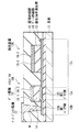
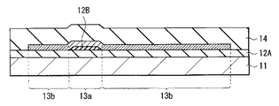
図1は、本開示の一の実施の形態に係る薄膜トランジスタ(トランジスタ10A)および保持容量(保持容量10B)の断面構成を表したものである。トランジスタ10Aは、例えばアクティブマトリクス型の有機ELディスプレイあるいは液晶ディスプレイなどの駆動素子として用いられ、いわゆるトップゲート構造を有する薄膜トランジスタである。
<Embodiment>
[Constitution]
FIG. 1 illustrates a cross-sectional configuration of a thin film transistor (
トランジスタ10Aでは、例えば、基板11上に、第1バリア膜12A、第2バリア膜12B、酸化物半導体層13、ゲート絶縁膜14およびゲート電極15がこの順に積層されている。酸化物半導体層13の一部(後述の第2部分13b)には、ソース・ドレイン電極17が電気的に接続されている。
In the
具体的には、第1バリア膜12Aは、例えば基板10の表面を覆って形成されており、この第1バリア膜12A上の選択的な領域に、第2バリア膜12Bが形成されている。酸化物半導体層13は、これらの第1バリア膜12Aおよび第2バリア膜12Bのうち、第2バリア膜12B上に活性層(チャネル)として機能する第1部分13aを有し、第1バリア膜12A上に、第1部分13aよりも電気抵抗の低い第2部分13bを有している。換言すると、酸化物半導体層13の第1部分13a直下の領域では、基板11上に第1バリア膜12Aおよび第2バリア膜12Bがこの順に積層され、第2部分13b直下の領域では、基板11上に第1バリア膜12Aのみが形成されている。このように、酸化物半導体層13の第2部分13bは、第1バリア膜12Aに接して形成される一方、第1部分13aは、第1バリア膜12A上に第2バリア膜12Bを介して形成されている。
Specifically, the
保持容量10Bは、例えば後述の保持容量素子(保持容量素子5C)に相当するものである。この保持容量10Bは、基板11上において、酸化物半導体層13の第2部分13bの一部を利用して形成されている。具体的には、保持容量10Bは、第2部分13b上に、ゲート絶縁膜14を介して、電極層15−1,15−2が積層されたものである。これらのゲート絶縁膜14および電極層15−1,15−2は、トランジスタ10Aのゲート絶縁膜14および電極層15−1,15−2(ゲート電極15)と、同一工程においてパターニング形成することができる。
The
基板11は、例えば、シリコンまたはガラスより構成されていてもよいし、可撓性(フレキシブル性)を有する材料から構成されていてもよい。可撓性を有する材料としては、例えば、ポリイミド(PI),ポリエチレンテレフタレート(PET),ポリエーテルサルフォン(PES),ポリエチレンナフタレート(PEN),ポリカーボネート(PC),液晶ポリマーなどの樹脂材料が挙げられる。あるいは、可撓性材料としては、上記樹脂材料の他にも、ステンレス(SUS),アルミニウム(Al)または銅(Cu)等のフレキシブル性を有する金属シートの表面に絶縁処理が施されたものであってもよい。この場合、厚みは例えば0.015mm〜1mmである。
The board |
第1バリア膜12Aは、基板11側から侵入する不純物(アルカリ性イオン,水分等)に対してバリア性を有すると共に、酸化物半導体層13に対して還元性を有している。このような機能を有する材料としては、例えば窒化シリコン(SiN)または酸窒化シリコン(SiON)が挙げられる。また、第1バリア膜12Aが有する還元性は、特に限定されるものではないが、例えば膜中の水素(H)の含有量が、3×10²¹個/cm3以上であることが望ましい。また、この水素量は、例えばFT−IR(フーリエ変換型の赤外分光分析)により解析することができる。第1バリア膜12Aの厚みは、例えば50nm〜1000nmであり、具体的には200nm程度である。
The
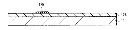
第2バリア膜12Bは、第1バリア膜12A上において、酸化物半導体層13の第1部分13aおよびゲート電極15に対向して、島状に形成されている。この第2バリア膜12Bは、水素に対するバリア性を有しており、即ち第1バリア膜12Aに含まれる水素の酸化物半導体層13への侵入を抑制して、酸化物半導体層13の還元反応を抑制する機能を有している。このような第2バリア膜12Bは、例えば、酸化シリコン(SiO2)、酸窒化シリコン、酸化アルミニウム(Al2O3)および酸化チタン(TiO2)のうちの少なくとも1種からなる単層膜、またはそれらのうちの2種以上からなる積層膜である。
The
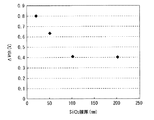
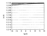
この第2バリア膜12Bの厚みは、特に限定されるものではないが、例えば20nm程度以上である。また、酸化物半導体層13のカバレッジ性の観点では、段切れ等が生じることを防ぐために、酸化物半導体層13と同等かそれ以下であることが望ましい。あるいは、以下の実験結果に基づき、トランジスタ10Aの閾値電圧の観点から膜厚を設定してもよい。図2に、第2バリア膜12Bの厚みと、閾値電圧のシフト量(ΔVth)との関係について示す。第2バリア膜12Bの厚みを20nm〜200nmの範囲で変化させて各閾値電圧のシフト量について測定したところ、厚みが100nmよりも小さい場合には、厚みが小さくなるに従って閾値電圧のシフト量が増した(デプレシフトした)。一方、厚みが100nm以上の場合には、シフト量に大きな変化がみられなかった。このように、トランジスタ10Aの閾値電圧シフトの観点では、第2バリア膜12Bの厚みにおいて飽和点が存在することが実験によってわかった。
The thickness of the
酸化物半導体層13は、例えばインジウム(In),ガリウム(Ga),亜鉛(Zn),スズ(Sn)等のうちの少なくとも1種の元素と、酸素とを含む化合物からなる。具体的には、非晶質の酸化物半導体としては、例えば酸化インジウムガリウム亜鉛(IGZO)および酸化インジウムスズ亜鉛(ITZO)等が挙げられ、結晶性の酸化物半導体としては、例えば酸化亜鉛(ZnO),酸化インジウム亜鉛(IZO),酸化インジウムガリウム(IGO),酸化インジウムスズ(ITO),酸化インジウム(InO)等が挙げられる。この酸化物半導体層13の厚みは、製造プロセスにおけるアニール時の酸素供給効率を考慮すると、例えば5〜100nmであることが望ましく、具体的には50nm程度である。
The
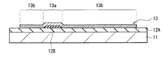
この酸化物半導体層13は、ゲート電極15とその近傍の領域を含む島状に形成され、上述のように、トランジスタ10Aの活性層としての第1部分13aと、低抵抗化領域としての第2部分13bとを含んでいる。第1部分13aは、所定のゲート電圧が印加されることによってチャネルを形成するものであり、第2バリア膜12Bと略同一形状を有している。この第1部分13aと略同一形状で、かつ第1部分13aと対向してゲート絶縁膜14およびゲート電極15が設けられている。
The
第2部分13bは、第1部分13aに隣接して(第1部分13aを囲むように)、かつ第1バリア膜12Aに接して、形成されている。この第2部分13bは、ソース領域およびドレイン領域として機能し、それらのうちの一方が例えばソース・ドレイン電極17に電気的に接続されると共に、他方が保持容量10Bに電気的に接続されている(ここでは、保持容量10Bの一部を構成している)。この第2部分13bは、第1バリア膜12Aと接することで、第1バリア膜12Aの還元性により(第1バリア膜12Aに含まれる水素による還元反応により)、低抵抗化されている。詳細には、例えば、第1バリア膜12Aの膜中に含まれる水素によって、酸化物半導体層13(第2部分13b)の膜中の酸素の結合手が奪われ、電子密度が増加することにより電気抵抗が低下する。第2部分13bの電気抵抗値は、酸化物半導体層13の構成材料および膜厚、第1バリア膜12Aの還元性(水素量)、プロセス条件等により適切な値に設定される。第1部分13aは、第1バリア膜12Aに直に接触しないように(第2バリア膜12Bを介して)形成されているので、第1バリア膜12Aの還元性の影響を受けず(または受けにくく)、低抵抗化されない(または低抵抗化されにくい)。
The
尚、酸化物半導体層13において、第1部分13aに隣接して第2部分13bが形成されているので、この第2部分13bにソース・ドレイン電極17を対向配置させて接続することができる。このため、ゲート電極15と、ソース・ドレイン電極17とを、互いに重ならないように(オーバーラップしないように)形成することができる。これにより、トランジスタ10Aにおける寄生容量を低減することができる。
In the
ゲート絶縁膜14は、例えば、厚みが300nm程度であり、例えば酸化シリコン,窒化シリコン,酸窒化シリコン、酸化アルミニウムおよび窒化アルミニウム等のうちの1種よりなる単層膜、またはそれらのうちの2種以上よりなる積層膜である。特に、酸化シリコンまたは酸化アルミニウムは、酸化物半導体層13を還元させにくいので好ましい。
The
ゲート電極15は、トランジスタ10Aにゲート電圧を印加し、このゲート電圧により酸化物半導体層13(第1部分13a)中の電子密度を制御する役割を有するものである。ゲート電極15は、例えば、厚みが10nm〜500nm、具体的には500nm程度である。このゲート電極15は、例えば電極層15−1,15−2の積層膜となっている。電極層15−1は、例えばアルミニウム(Al)または銅(Cu)等の金属層の表面に、チタン(Ti)またはモリブデン(Mo)等のバリアメタルが形成されたものである。電極層15−2は、例えばITO、IZOまたはIGZO等の酸化物半導体により構成されている。このゲート電極15は、低抵抗であることが望ましいので、電極層15−1には、上述のように、アルミニウムや銅等の低抵抗金属を用いることが好ましい。また、電極層15−1のアルミニウムまたは銅等と、電極層15−2(ITO,IZOまたはIGZO等)との間に、チタンまたはモリブデン等のバリアメタルが介在することにより、電極層15−1,15−2間において良好なコンタクトを得ることができる。
The
層間絶縁膜16は、酸化物半導体層13、ゲート絶縁膜14およびゲート電極15を覆って、基板11の表面(詳細には第1バリア膜12aの表面)に設けられている。層間絶縁膜16は、例えば、厚みが2um程度であり、アクリル、ポリイミドおよびシロキサン等の有機絶縁膜、あるいは、酸化シリコン、窒化シリコンおよび酸化アルミニウム等の無機絶縁膜から構成されている。あるいは、それらの有機絶縁膜と無機絶縁膜との積層膜であってもよい。例えば、酸化シリコンと酸化アルミニウムとの積層膜を用いることにより、酸化物半導体層13への水分の侵入や拡散を抑えることができ、トランジスタ10Aの電気的安定性および信頼性を高めることができる。この層間絶縁膜16には、ソース・ドレイン電極17と、酸化物半導体層13の第2部分13bとを電気的に接続するためのコンタクトホールHが設けられている。
The
ソース・ドレイン電極17は、上述のように、酸化物半導体層13の第2部分13bに電気的に接続されている。具体的には、ソース・ドレイン電極17は、酸化物半導体層13の第2部分13bに対向して配置されており、層間絶縁膜16のコンタクトホールHを介して第2部分13bに接続されている。このソース・ドレイン電極17は、トランジスタ10Aのソースまたはドレインとして機能するものであり、例えばアルミニウムまたは銅等の金属層の表面にモリブデンまたはチタン等のバリアメタルが形成されてなる積層膜である。ソース・ドレイン電極17には、ゲート電極15と同様、低抵抗金属としてアルミニウム等が用いられることが好ましく、バリアメタルとして、チタン等が用いられることがより好ましい。このような積層膜を用いることにより、配線遅延を軽減することが可能となる。また、ソース・ドレイン電極17の表面に、ネオジウム(Nd)を含有するアルミニウム合金またはITO等が形成されるようにしてもよい。これにより、例えばソース・ドレイン電極17を有機ELディスプレイのアノード電極(画素電極)として用いることも可能となる。このソース・ドレイン電極17は、ゲート電極15の直上の領域を回避して設けられていることが望ましい。ゲート電極15とソース・ドレイン電極15との交差領域に形成される寄生容量を低減することが可能となるからである。寄生容量が低減されることで保持容量10Bをより小さなレイアウトで形成可能となり、歩留まりを向上させることができる。
The source /
[製造方法]
図3A〜図6は、トランジスタ10Aの製造方法を説明するための断面図である。トランジスタ10Aは、例えば次のようにして製造することができる。
[Production method]
3A to 6 are cross-sectional views for explaining a manufacturing method of the
まず、図3Aに示したように、基板11上の全面に、上述した材料等よりなる第1バリア膜12Aおよび第2バリア膜12Bを、この順に、例えばプラズマCVD(Chemical Vapor Deposition)法またはスパッタ法等により成膜する。このとき、第2バリア膜12Bの厚みとしては、酸化物半導体層13のカバレッジあるいは閾値電圧シフト等を考慮して、適当な値を選択すればよい。また、プラズマCVD法を用いる場合、第1バリア膜12A(例えば窒化シリコン)の成膜時には、原料ガスとして、例えばシラン(SiH4)、アンモニア(NH3)、窒素等を含む混合ガスを用いる。第2バリア膜12B(例えば酸化シリコン)の成膜時には、原料ガスとして、シラン、一酸化二窒素(N2O)を含む混合ガスを用いる。あるいは、スパッタ法を用いる場合には、ターゲットとして、例えばシリコンを用い、チャンバー内に酸素や水蒸気、窒素等のガスを導入してプラズマ放電させる。
First, as shown in FIG. 3A, the
この後、図3Bに示したように、成膜した第1バリア膜12Aおよび第2バリア膜12Bのうちの第2バリア膜12Bのみを、例えばフォトリソグラフィ法を用いたドライエッチングまたはウェットエッチングにより所望の形状にパターニングする。エッチングの際には、第1バリア膜12A(例えば窒化シリコン)と、第2バリア膜(例えば酸化シリコン)との間でエッチング選択比が得られるようなエッチング条件を用い、第2バリア膜12Bのみを選択的にパターニングする。
Thereafter, as shown in FIG. 3B, only the
続いて、酸化物半導体層13を形成する。具体的には、まず図4Aに示したように、第1バリア膜12Aおよび第2バリア膜12Bを覆って、基板11の全面に、例えばスパッタ法により、上述した材料等よりなる酸化物半導体層13を成膜する。この際、酸化物半導体としてIGZOを用いる場合には、例えば酸化インジウムガリウム亜鉛のセラミックをターゲットとしたDCスパッタを行い、アルゴンと酸素を含む混合ガスを用いてプラズマ放電させる。この際、チャンバー内を、真空度が1×10⁻⁴Pa以下となるまで排気した後、アルゴンと酸素の混合ガスを導入することによりプラズマ放電を行う。あるいは、酸化物半導体として酸化亜鉛を用いる場合には、酸化亜鉛のセラミックをターゲットとしたRFスパッタあるいは亜鉛をターゲットとしたDCスパッタを行い、アルゴンと酸素を含む混合ガスを用いてプラズマ放電させる。尚、上記混合ガスにおけるアルゴンと酸素の流量比を変化させることで、チャネルとなる酸化物半導体層13(第1部分13a)中のキャリア濃度を制御することが出来る。
Subsequently, the
その後、図4Bに示したように、酸化物半導体層13を例えばフォトリソグラフィ法を用いたエッチングにより、所望の形状となるようにパターニングする。酸化物半導体は酸・アルカリのいずれにも容易に溶けるためにウェットエッチングによる加工が一般的であるが、ドライエッチングでの加工も可能である。尚、酸化物半導体として、酸化亜鉛やインジウム、ガリウム、ジリコニウム、錫などから成り、インジウムや錫の比率が他の構成元素よりも高い結晶性の材料を用いる場合は、結晶化アニールを施すことでエッチング溶媒に対する耐性を付与してもよい。
Thereafter, as illustrated in FIG. 4B, the
このとき、酸化物半導体層13のうち、例えば窒化シリコンからなる第1バリア膜12Aと接する部分が、水素の還元作用によって低抵抗化される(第2部分13bが形成される)。一方、酸化物半導体層13のうち、第2バリア膜12B上に形成された部分(第1部分13a)では、第2バリア膜12Bの水素バリア性により、第1バリア膜12Aに含まれる水素の影響による特性変動が抑制される。
At this time, a portion of the
次に、図5Aに示したように、基板11の全面に、ゲート絶縁膜14を成膜する。成膜方法としては、例えば窒化シリコンや酸化シリコンなどの積層膜をプラズマCVD法で形成する手法、あるいは、窒化シリコン、酸化シリコン、酸化アルミニウムあるいは窒化アルミニウムをスパッタ法等により形成する手法が挙げられる。
Next, as shown in FIG. 5A, a
続いて、図5Bに示したように、ゲート絶縁膜14の全面に、例えばスパッタ法により、上述した材料等よりなる金属層15−1,15−2を順に成膜する。
Subsequently, as shown in FIG. 5B, metal layers 15-1 and 15-2 made of the above-described materials or the like are sequentially formed on the entire surface of the
この後、図5Cに示したように、例えばフォトリソグラフィ法を用いたエッチングにより、電極層15−1,15−2をパターニングして、第1部分13aに対向する領域にゲート電極15を形成する。また、このパターニングの際に、酸化物半導体層13の第2部分13bの一部に対向する領域にも、電極層15−1,15−2の積層膜を残し、保持容量10Bを形成する。
Thereafter, as shown in FIG. 5C, the electrode layers 15-1 and 15-2 are patterned by, for example, etching using a photolithography method, and the
続いて、図5Dに示したように、例えば電極層15−1,15−2をマスクとして、ゲート絶縁膜14をエッチングすることによりゲート絶縁膜14をパターニングする。この際、酸化物半導体層13をZnO,IZO,IGO等の結晶化材料により構成した場合には、フッ酸等の薬液を用いてゲート絶縁膜14をエッチングするとよい。エッチング選択比が大きくなり容易に加工できるからである。これにより、酸化物半導体層13の第1部分13a上に、ゲート絶縁膜14およびゲート電極15がこの順に略同一形状で形成される。
Subsequently, as shown in FIG. 5D, the
次に、図6に示したように、上述した材料等よりなる層間絶縁膜16を、例えばプラズマCVD法、スパッタ法あるいは原子層成膜法等により成膜する。具体的には、窒化しシリコンおよび酸化シリコンを成膜する場合には、プラズマCVD法を用い、酸化アルミニウム等を成膜する場合には、DCスパッタやACスパッタあるいは、原子層成膜法を用いることができる。続いて、フォトリソグラフィ法を用いたエッチングにより、層間絶縁膜16にコンタクトホールHを形成する。このとき、コンタクトホールHを酸化物半導体層13の第2部分13bに対向する領域に形成する。その後、層間絶縁膜16の上に、例えばスパッタ法により、上述した材料等よりなるソース・ドレイン電極17を形成し、例えばフォトリソグラフィ法を用いたエッチングによりパターニングする。これにより、ソース・ドレイン電極17を酸化物半導体層13の第2部分13bに電気的に接続して形成することができる。以上により、図1に示したトランジスタ10Aおよび保持容量10Bが完成する。
Next, as shown in FIG. 6, the
[作用および効果]
本実施の形態のトランジスタ10Aでは、基板11上に、第1バリア膜12Aが形成されると共に、この第1バリア膜12Aと酸化物半導体層13の第1部分13aとの間に、水素バリア性を有する第2バリア膜12Aが形成されている。第1バリア膜12Aにより、不純物による酸化物半導体層13全体の膜質劣化が抑制されると共に、酸化物半導体層の第2部分13bが選択的に低抵抗化されて形成される。つまり、本実施の形態では、第1バリア膜12Aが、基板11側からの不純物の浸入を防ぐバリアとして機能すると共に、酸化物半導体層13の所定の領域(第2部分13b)への水素供給源として機能する。
[Action and effect]
In the
ここで、図7に、本実施の形態の比較例として、窒化シリコン膜上に酸化物半導体層を積層した場合(第2バリア膜12Bを形成しない場合)のトップゲート型トランジスタにおける電流電圧特性について示す。比較例のように、窒化シリコン膜が酸化物半導体層のチャネルと接すると、電流電圧特性が悪化する(オンオフ特性が得られない)。このように、例えばCVD法により形成される窒化シリコン膜では、水素の未結合手が多く含まれることから、その還元作用により特性が変動し易い。
Here, as a comparative example of this embodiment, FIG. 7 shows current-voltage characteristics in a top-gate transistor when an oxide semiconductor layer is stacked over a silicon nitride film (when the
これに対し、本実施の形態では、酸化物半導体層13の第1部分13aと第1バリア膜12Aとの間に、水素バリア性を有する第2バリア膜12Bが形成されている。この第2バリア膜12Bの介在により、上記のような第1バリア膜12Aからの水素拡散が抑制され、還元作用による第1部分13aの特性変動が抑制される。これにより、例えば図8に示したように、良好なオンオフ特性を有する電流電圧特性が得られる。尚、図8は、基板11の面内16箇所において、上述したような積層構造を有するトランジスタ10Aの各特性について測定したものである。また、第2バリア膜12Bの厚みは20nmとした。このように、第2バリア膜12Bの厚みが20nm以上であれば十分な特性が得られ、また、素子毎のばらつきも少ないことがわかる。
In contrast, in the present embodiment, a
また、例えば、特許文献1に記載されたトランジスタでは、トップゲート型の積層構造において、不純物バリアとしての窒化シリコン膜とは別に、低抵抗化のための(水素供給源としての)窒化シリコン膜が、酸化物半導体層上に別途形成される。このような構造では、窒化シリコン膜を2度の工程にわたって成膜するため、製造工程および製造コストが増加してしまう。また、この場合、酸化物半導体層の形成後にシリコン窒化膜をCVD法によって成膜することとなるため、プラズマ及びプラズマによって活性化された水素によって酸化物半導体が劣化するという懸念もある。本実施の形態では、上記のような第1バリア膜12Aおよび第2バリア膜12Bの積層構造により、第1バリア膜12Aにバリアおよび水素供給源としての2つの機能を持たせることができる。よって、例えば製造工程の簡易化および製造コストの削減を図ることもでき、またプラズマCVD成膜時の酸化物半導体の劣化を抑制することができる。特に、基板11に樹脂材料を用いた場合には、低温(例えば350℃程度)下でのCVDプロセスにより成膜することが望ましいが、このようなCVDプロセスでは、膜中に水素の未結合手を多く含むこととなる。従って、本実施の形態は、基板11として樹脂材料を用いた場合に特に有用である。
Further, for example, in the transistor described in
以上説明したように、本実施の形態では、基板11上に第1バリア膜12Aを有し、この第1バリア膜12Aと酸化物半導体層13の第1部分13aとの間には、水素に対してバリア性を有する第2バリア膜12Bを有する。第1バリア膜12Aにより、基板11側からの不純物による酸化物半導体層13全体の膜質劣化を抑制できると共に、酸化物半導体層13の第2部分13bを選択的に低抵抗化することができる。一方、酸化物半導体層13の第1部分13aでは、第2バリア膜12Bの介在により、第1バリア膜12Aの還元作用による特性変動を抑制できる。即ち、バリア性能を確保しつつ、酸化物半導体層13の所望の領域(第2部分13b)を低抵抗化すると共に、活性層(第1部分13a)の特性変動を抑制することができる。よって、良好なトランジスタ特性を実現することができる。
As described above, in this embodiment, the
このようなトランジスタ10Aを用いることにより、以下に説明するようなアクティブ駆動方式の表示装置および電子機器では、高品質な画像を表示可能となり、また、大画面化、高精細化およびハイフレームレート化等に対応可能になる。
By using such a
<適用例>
[表示装置]
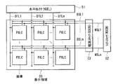
次に、上記実施の形態に係るトランジスタ10Aを適用した表示装置の全体構成および画素回路構成について説明する。図9は、有機ELディスプレイとして用いられる表示装置の周辺回路を含む全体構成を表すものである。このように、例えば基板11上には、有機EL素子を含む複数の画素PXLCがマトリクス状に配置されてなる表示領域50が形成され、この表示領域50の周辺に、信号線駆動回路としての水平セレクタ(HSEL)51と、走査線駆動回路としてのライトスキャナ(WSCN)52と、電源線駆動回路としての電源スキャナ(DSCN)53とが設けられている。但し、トランジスタ10Aは、ここで説明する有機ELディスプレイに限らず、他の表示装置、例えば液晶ディスプレイあるいは電子ペーパー等の様々なデバイスへ適用可能である。
<Application example>
[Display device]
Next, an overall configuration and a pixel circuit configuration of a display device to which the
表示領域50において、列方向には複数(整数n個)の信号線DTL1〜DTLnが配置され、行方向には、複数(整数m個)の走査線WSL1〜WSLmおよび電源線DSL1〜DSLmがそれぞれ配置されている。また、各信号線DTLと各走査線WSLとの交差点に、各画素PXLC(R、G、Bに対応する画素のいずれか1つ)が設けられている。各信号線DTLは水平セレクタ51に接続され、この水平セレクタ51から各信号線DTLへ映像信号が供給されるようになっている。各走査線WSLはライトスキャナ52に接続され、このライトスキャナ52から各走査線WSLへ走査信号(選択パルス)が供給されるようになっている。各電源線DSLは電源スキャナ53に接続され、この電源スキャナ53から各電源線DSLへ電源信号(制御パルス)が供給されるようになっている。
In the
図10は、画素PXLCにおける具体的な回路構成例を表したものである。各画素PXLCは、有機EL素子5Dを含む画素回路60を有している。この画素回路60は、サンプリング用トランジスタ5Aおよび駆動用トランジスタ5Bと、保持容量素子5Cと、有機EL素子5Dとを有するアクティブ型の駆動回路である。これらのうち、トランジスタ5A(またはトランジスタ5B)が、上記実施の形態のトランジスタ10Aに相当し、保持容量素子5Cが、上記実施の形態の保持容量10Bに相当する。
FIG. 10 illustrates a specific circuit configuration example in the pixel PXLC. Each pixel PXLC has a
サンプリング用トランジスタ5Aは、そのゲートが対応する走査線WSLに接続され、そのソースおよびドレインのうちの一方が対応する信号線DTLに接続され、他方が駆動用トランジスタ5Bのゲートに接続されている。駆動用トランジスタ5Bは、そのドレインが対応する電源線DSLに接続され、ソースが有機EL素子5Dのアノードに接続されている。また、この有機EL素子5Dのカソードは、接地配線5Hに接続されている。なお、この接地配線5Hは、全ての画素PXLCに対して共通に配線されている。保持容量素子5Cは、駆動用トランジスタ5Bのソースとゲートとの間に配置されている。 Sampling transistor 5A has its gate connected to corresponding scanning line WSL, one of its source and drain connected to corresponding signal line DTL, and the other connected to the gate of driving transistor 5B. The driving transistor 5B has its drain connected to the corresponding power supply line DSL and its source connected to the anode of the organic EL element 5D. The cathode of the organic EL element 5D is connected to the ground wiring 5H. The ground wiring 5H is wired in common to all the pixels PXLC. The storage capacitor element 5C is disposed between the source and gate of the driving transistor 5B.
サンプリング用トランジスタ5Aは、走査線WSLから供給される走査信号(選択パルス)に応じて導通することにより、信号線DTLから供給される映像信号の信号電位をサンプリングし、保持容量素子5Cに保持するものである。駆動用トランジスタ5Bは、所定の第1電位(図示せず)に設定された電源線DSLから電流の供給を受け、保持容量素子5Cに保持された信号電位に応じて、駆動電流を有機EL素子5Dへ供給するものである。有機EL素子5Dは、この駆動用トランジスタ5Bから供給された駆動電流により、映像信号の信号電位に応じた輝度で発光するようになっている。 The sampling transistor 5A conducts in accordance with the scanning signal (selection pulse) supplied from the scanning line WSL, thereby sampling the signal potential of the video signal supplied from the signal line DTL and holding it in the holding capacitor element 5C. Is. The driving transistor 5B receives a current supplied from a power supply line DSL set to a predetermined first potential (not shown), and changes the driving current to the organic EL element according to the signal potential held in the holding capacitor element 5C. Supply to 5D. The organic EL element 5D emits light with a luminance corresponding to the signal potential of the video signal by the driving current supplied from the driving transistor 5B.
このような回路構成では、走査線WSLから供給される走査信号(選択パルス)に応じてサンプリング用トランジスタ5Aが導通することにより、信号線DTLから供給された映像信号の信号電位がサンプリングされ、保持容量素子5Cに保持される。また、上記第1電位に設定された電源線DSLから駆動用トランジスタ5Bへ電流が供給され、保持容量素子5Cに保持された信号電位に応じて、駆動電流が有機EL素子5D(赤色、緑色および青色の各有機EL素子)へ供給される。そして、各有機EL素子5Dは、供給された駆動電流により、映像信号の信号電位に応じた輝度で発光する。これにより、表示装置において、映像信号に基づく映像表示がなされる。 In such a circuit configuration, the sampling transistor 5A is turned on according to the scanning signal (selection pulse) supplied from the scanning line WSL, whereby the signal potential of the video signal supplied from the signal line DTL is sampled and held. It is held in the capacitive element 5C. Further, a current is supplied from the power supply line DSL set to the first potential to the driving transistor 5B, and the driving current is changed to the organic EL element 5D (red, green and red) according to the signal potential held in the holding capacitor element 5C. To each blue organic EL element). Each organic EL element 5D emits light with luminance according to the signal potential of the video signal by the supplied drive current. Thereby, video display based on the video signal is performed on the display device.
[電子機器]
以下、上記のようなトランジスタ10Aを用いた表示装置を搭載した電子機器の一例について説明する。電子機器としては、例えばテレビジョン装置,デジタルカメラ,ノート型パーソナルコンピュータ、携帯電話等の携帯端末装置あるいはビデオカメラ等が挙げられる。言い換えると、上記表示装置は、外部から入力された映像信号あるいは内部で生成した映像信号を、画像あるいは映像として表示するあらゆる分野の電子機器に適用することが可能である。
[Electronics]
Hereinafter, an example of an electronic device in which the display device using the
上記表示装置は、例えば図11に示したようなモジュールとして、後述の適用例1〜6の電子機器に組み込まれる。このモジュールは、例えば、基板11の一辺に、封止用基板21から露出した領域210を設け、この領域210に、水平セレクタ51、ライトスキャナ52および電源スキャナ53の配線を延長して外部接続端子(図示せず)を形成したものである。この外部接続端子には、信号の入出力のためのフレキシブルプリント配線基板(FPC;Flexible Printed Circuit)220が設けられていてもよい。
The display device is incorporated in an electronic device of application examples 1 to 6 described later, for example, as a module as illustrated in FIG. In this module, for example, a
(適用例1)
図12は、テレビジョン装置の外観を表したものである。このテレビジョン装置は、例えば、フロントパネル310およびフィルターガラス320を含む映像表示画面部300を有しており、この映像表示画面部300が上記表示装置に相当する。
(Application example 1)
FIG. 12 illustrates the appearance of a television device. This television apparatus has, for example, a video display screen unit 300 including a front panel 310 and a filter glass 320, and the video display screen unit 300 corresponds to the display device.
(適用例2)
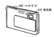
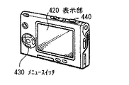
図13Aおよび図13Bは、デジタルカメラの外観を表したものである。このデジタルカメラは、例えば、フラッシュ用の発光部410、表示部420、メニュースイッチ430およびシャッターボタン440を有しており、この表示部420が上記表示装置に相当する。
(Application example 2)
13A and 13B show the appearance of a digital camera. The digital camera includes, for example, a flash light emitting unit 410, a display unit 420, a menu switch 430, and a
(適用例3)
図14は、ノート型パーソナルコンピュータの外観を表したものである。このノート型パーソナルコンピュータは、例えば、本体510,文字等の入力操作のためのキーボード520および画像を表示する表示部530を有しており、この表示部530が上記表示装置に相当する。
(Application example 3)
FIG. 14 shows the appearance of a notebook personal computer. The notebook personal computer has, for example, a
(適用例4)
図15は、ビデオカメラの外観を表したものである。このビデオカメラは、例えば、本体部610,この本体部610の前方側面に設けられた被写体撮影用のレンズ620,撮影時のスタート/ストップスイッチ630および表示部640を有している。この表示部640が上記表示装置に相当する。
(Application example 4)
FIG. 15 shows the appearance of a video camera. This video camera includes, for example, a main body 610, a
(適用例5)
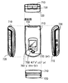
図16Aおよび図16Bは、携帯電話機の外観を表したものである。この携帯電話機は、例えば上側筐体710と下側筐体720とを連結部(ヒンジ部)730で連結したものであり、ディスプレイ740,サブディスプレイ750,ピクチャーライト760およびカメラ770を有している。そして、これらのうちのディスプレイ740またはサブディスプレイ750が、上記表示装置に相当する。
(Application example 5)
16A and 16B show the appearance of a mobile phone. This mobile phone is obtained by connecting, for example, an
(適用例6)
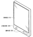
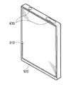
図17Aおよび図17Bは、スマートフォンの外観を表している。このスマートフォンは、例えば、表示部810および非表示部(筐体)820と、操作部830とを備えている。操作部830は、図17Aに示したように非表示部820の前面に設けられていてもよいし、図17Bに示したように上面に設けられていてもよい。
(Application example 6)
17A and 17B show the appearance of the smartphone. The smartphone includes a
以上、実施の形態を挙げて本開示を説明したが、本開示はこれらの実施の形態に限定されず、種々の変形が可能である。例えば、上記実施の形態では、第1バリア膜12Aおよび第2バリア膜12Bが、それぞれ単層膜である場合を例示したが、積層膜であってもよい。
Although the present disclosure has been described with reference to the embodiments, the present disclosure is not limited to these embodiments, and various modifications can be made. For example, in the above-described embodiment, the case where the
また、本開示のトランジスタの構成は、上記実施の形態において説明した積層構造に限定されるものではなく、更に他の層が形成されていてもよい。また、各層の材料や厚み、製造プロセス等も、上述したものに限定されない。 Further, the structure of the transistor of the present disclosure is not limited to the stacked structure described in the above embodiment, and other layers may be formed. Further, the material, thickness, manufacturing process, and the like of each layer are not limited to those described above.
尚、本開示は以下のような構成であってもよい。
(1)
基板と、
前記基板上に形成されると共に、前記基板側からの不純物に対するバリア性と前記酸化物半導体層に対する還元性とを有する第1のバリア膜と、
前記第1のバリア膜上の選択的な領域に形成されると共に、水素に対してバリア性を有する第2のバリア膜と、
前記第2のバリア膜上に形成されると共に活性層として機能する第1部分と、前記第1のバリア膜上に形成されると共に前記第1部分よりも電気抵抗値の低い第2部分とを含む酸化物半導体層と、
前記酸化物半導体層の前記第1部分の上に、ゲート絶縁膜を介して形成されたゲート電極と、
前記酸化物半導体層の前記第2部分に電気的に接続されたソース電極またはドレイン電極と
を備えた薄膜トランジスタ。
(2)
前記第1のバリア膜は、窒化シリコンおよび酸窒化シリコンのうちの少なくとも1種を含み、
前記第2のバリア膜は、酸化シリコン、酸窒化シリコン、酸化アルミニウムおよび酸化チタンのうちの少なくとも1種を含む単層膜または積層膜である
上記(1)に記載の薄膜トランジスタ。
(3)
前記基板は、可撓性を有する樹脂材料から構成されている
上記(1)または(2)に記載の薄膜トランジスタ。
(4)
前記酸化物半導体層の前記第2部分は、前記第1のバリア膜に接して形成されている
上記(1)〜(3)のいずれかに記載の薄膜トランジスタ。
(5)
前記ゲート電極および前記ゲート絶縁膜は、互いに同一形状にパターニングされている
上記(1)〜(4)のいずれかに記載の薄膜トランジスタ。
(6)
前記酸化物半導体層の前記第2部分を利用して保持容量が形成されている
上記(1)〜(5)のいずれかに記載の薄膜トランジスタ。
(7)
前記ソース電極または前記ドレイン電極は、前記酸化物半導体層の前記第2部分の一部に対向して設けられている
上記(1)〜(6)のいずれかに記載の薄膜トランジスタ。
(8)
それぞれが薄膜トランジスタを含む複数の画素を有し、
前記薄膜トランジスタは、
基板と、
前記基板上に形成されると共に、前記基板側からの不純物に対するバリア性と前記酸化物半導体層に対する還元性とを有する第1のバリア膜と、
前記第1のバリア膜上の選択的な領域に形成されると共に、水素に対してバリア性を有する第2のバリア膜と、
前記第2のバリア膜上に形成されると共に活性層として機能する第1部分と、前記第1のバリア膜上に形成されると共に前記第1部分よりも電気抵抗値の低い第2部分とを含む酸化物半導体層と、
前記酸化物半導体層の前記第1部分の上に、ゲート絶縁膜を介して形成されたゲート電極と、
前記酸化物半導体層の前記第2部分に電気的に接続されたソース電極またはドレイン電極と
を備えた表示装置。
(9)
有機電界発光表示装置である
上記(8)に記載の表示装置。
(10)
それぞれが薄膜トランジスタを含む複数の画素を有する表示装置を備え、
前記薄膜トランジスタは、
基板と、
前記基板上に形成されると共に、前記基板側からの不純物に対するバリア性と前記酸化物半導体層に対する還元性とを有する第1のバリア膜と、
前記第1のバリア膜上の選択的な領域に形成されると共に、水素に対してバリア性を有する第2のバリア膜と、
前記第2のバリア膜上に形成されると共に活性層として機能する第1部分と、前記第1のバリア膜上に形成されると共に前記第1部分よりも電気抵抗値の低い第2部分とを含む酸化物半導体層と、
前記酸化物半導体層の前記第1部分の上に、ゲート絶縁膜を介して形成されたゲート電極と、
前記酸化物半導体層の前記第2部分に電気的に接続されたソース電極またはドレイン電極と
を備えた電子機器。
The present disclosure may be configured as follows.
(1)
A substrate,
A first barrier film formed on the substrate and having a barrier property against impurities from the substrate side and a reducing property to the oxide semiconductor layer;
A second barrier film formed in a selective region on the first barrier film and having a barrier property against hydrogen;
A first portion formed on the second barrier film and functioning as an active layer; and a second portion formed on the first barrier film and having an electric resistance lower than that of the first portion. An oxide semiconductor layer containing,
A gate electrode formed on the first portion of the oxide semiconductor layer via a gate insulating film;
A thin film transistor comprising: a source electrode or a drain electrode electrically connected to the second portion of the oxide semiconductor layer.
(2)
The first barrier film includes at least one of silicon nitride and silicon oxynitride,
The thin film transistor according to (1), wherein the second barrier film is a single layer film or a laminated film including at least one of silicon oxide, silicon oxynitride, aluminum oxide, and titanium oxide.
(3)
The thin film transistor according to (1) or (2), wherein the substrate is made of a flexible resin material.
(4)
The thin film transistor according to any one of (1) to (3), wherein the second portion of the oxide semiconductor layer is formed in contact with the first barrier film.
(5)
The thin film transistor according to any one of (1) to (4), wherein the gate electrode and the gate insulating film are patterned in the same shape.
(6)
The thin film transistor according to any one of (1) to (5), wherein a storage capacitor is formed using the second portion of the oxide semiconductor layer.
(7)
The thin film transistor according to any one of (1) to (6), wherein the source electrode or the drain electrode is provided to face a part of the second portion of the oxide semiconductor layer.
(8)
Each having a plurality of pixels including thin film transistors;
The thin film transistor
A substrate,
A first barrier film formed on the substrate and having a barrier property against impurities from the substrate side and a reducing property to the oxide semiconductor layer;
A second barrier film formed in a selective region on the first barrier film and having a barrier property against hydrogen;
A first portion formed on the second barrier film and functioning as an active layer; and a second portion formed on the first barrier film and having an electric resistance lower than that of the first portion. An oxide semiconductor layer containing,
A gate electrode formed on the first portion of the oxide semiconductor layer via a gate insulating film;
A display device comprising: a source electrode or a drain electrode electrically connected to the second portion of the oxide semiconductor layer.
(9)
The display device according to (8), wherein the display device is an organic electroluminescence display device.
(10)
A display device having a plurality of pixels each including a thin film transistor;
The thin film transistor
A substrate,
A first barrier film formed on the substrate and having a barrier property against impurities from the substrate side and a reducing property to the oxide semiconductor layer;
A second barrier film formed in a selective region on the first barrier film and having a barrier property against hydrogen;
A first portion formed on the second barrier film and functioning as an active layer; and a second portion formed on the first barrier film and having an electric resistance lower than that of the first portion. An oxide semiconductor layer containing,
A gate electrode formed on the first portion of the oxide semiconductor layer via a gate insulating film;
An electronic device comprising: a source electrode or a drain electrode electrically connected to the second portion of the oxide semiconductor layer.
10A…トランジスタ、10B…保持容量、11…基板、12A…第1バリア膜、12B…第2バリア膜、13…酸化物半導体層、13a…第1部分(活性層)、13b…第2部分(低抵抗化領域)、14…ゲート絶縁膜、15…ゲート電極、15−1,15−2…電極層、16…層間絶縁膜、17…ソース・ドレイン電極。
DESCRIPTION OF
Claims (10)
前記基板上に形成されると共に、前記基板側からの不純物に対するバリア性と前記酸化物半導体層に対する還元性とを有する第1のバリア膜と、
前記第1のバリア膜上の選択的な領域に形成されると共に、水素に対してバリア性を有する第2のバリア膜と、
前記第2のバリア膜上に形成されると共に活性層として機能する第1部分と、前記第1のバリア膜上に形成されると共に前記第1部分よりも電気抵抗値の低い第2部分とを含む酸化物半導体層と、
前記酸化物半導体層の前記第1部分の上に、ゲート絶縁膜を介して形成されたゲート電極と、
前記酸化物半導体層の前記第2部分に電気的に接続されたソース電極またはドレイン電極と
を備えた薄膜トランジスタ。 A substrate,
A first barrier film formed on the substrate and having a barrier property against impurities from the substrate side and a reducing property to the oxide semiconductor layer;
A second barrier film formed in a selective region on the first barrier film and having a barrier property against hydrogen;
A first portion formed on the second barrier film and functioning as an active layer; and a second portion formed on the first barrier film and having an electric resistance lower than that of the first portion. An oxide semiconductor layer containing,
A gate electrode formed on the first portion of the oxide semiconductor layer via a gate insulating film;
A thin film transistor comprising: a source electrode or a drain electrode electrically connected to the second portion of the oxide semiconductor layer.
前記第2のバリア膜は、酸化シリコン、酸窒化シリコン、酸化アルミニウムおよび酸化チタンのうちの少なくとも1種を含む単層膜または積層膜である
請求項1に記載の薄膜トランジスタ。 The first barrier film includes at least one of silicon nitride and silicon oxynitride,
2. The thin film transistor according to claim 1, wherein the second barrier film is a single layer film or a laminated film including at least one of silicon oxide, silicon oxynitride, aluminum oxide, and titanium oxide.
請求項1に記載の薄膜トランジスタ。 The thin film transistor according to claim 1, wherein the substrate is made of a resin material having flexibility.
請求項1に記載の薄膜トランジスタ。 The thin film transistor according to claim 1, wherein the second portion of the oxide semiconductor layer is formed in contact with the first barrier film.
請求項1に記載の薄膜トランジスタ。 The thin film transistor according to claim 1, wherein the gate electrode and the gate insulating film are patterned in the same shape.
請求項1に記載の薄膜トランジスタ。 The thin film transistor according to claim 1, wherein a storage capacitor is formed using the second portion of the oxide semiconductor layer.
請求項1に記載の薄膜トランジスタ。 The thin film transistor according to claim 1, wherein the source electrode or the drain electrode is provided to face a part of the second portion of the oxide semiconductor layer.
前記薄膜トランジスタは、
基板と、
前記基板上に形成されると共に、前記基板側からの不純物に対するバリア性と前記酸化物半導体層に対する還元性とを有する第1のバリア膜と、
前記第1のバリア膜上の選択的な領域に形成されると共に、水素に対してバリア性を有する第2のバリア膜と、
前記第2のバリア膜上に形成されると共に活性層として機能する第1部分と、前記第1のバリア膜上に形成されると共に前記第1部分よりも電気抵抗値の低い第2部分とを含む酸化物半導体層と、
前記酸化物半導体層の前記第1部分の上に、ゲート絶縁膜を介して形成されたゲート電極と、
前記酸化物半導体層の前記第2部分に電気的に接続されたソース電極またはドレイン電極と
を備えた表示装置。 Each having a plurality of pixels including thin film transistors;
The thin film transistor
A substrate,
A first barrier film formed on the substrate and having a barrier property against impurities from the substrate side and a reducing property to the oxide semiconductor layer;
A second barrier film formed in a selective region on the first barrier film and having a barrier property against hydrogen;
A first portion formed on the second barrier film and functioning as an active layer; and a second portion formed on the first barrier film and having an electric resistance lower than that of the first portion. An oxide semiconductor layer containing,
A gate electrode formed on the first portion of the oxide semiconductor layer via a gate insulating film;
A display device comprising: a source electrode or a drain electrode electrically connected to the second portion of the oxide semiconductor layer.
請求項8に記載の表示装置。 The display device according to claim 8, which is an organic electroluminescence display device.
前記薄膜トランジスタは、
基板と、
前記基板上に形成されると共に、前記基板側からの不純物に対するバリア性と前記酸化物半導体層に対する還元性とを有する第1のバリア膜と、
前記第1のバリア膜上の選択的な領域に形成されると共に、水素に対してバリア性を有する第2のバリア膜と、
前記第2のバリア膜上に形成されると共に活性層として機能する第1部分と、前記第1のバリア膜上に形成されると共に前記第1部分よりも電気抵抗値の低い第2部分とを含む酸化物半導体層と、
前記酸化物半導体層の前記第1部分の上に、ゲート絶縁膜を介して形成されたゲート電極と、
前記酸化物半導体層の前記第2部分に電気的に接続されたソース電極またはドレイン電極と
を備えた電子機器。 A display device having a plurality of pixels each including a thin film transistor;
The thin film transistor
A substrate,
A first barrier film formed on the substrate and having a barrier property against impurities from the substrate side and a reducing property to the oxide semiconductor layer;
A second barrier film formed in a selective region on the first barrier film and having a barrier property against hydrogen;
A first portion formed on the second barrier film and functioning as an active layer; and a second portion formed on the first barrier film and having an electric resistance lower than that of the first portion. An oxide semiconductor layer containing,
A gate electrode formed on the first portion of the oxide semiconductor layer via a gate insulating film;
An electronic device comprising: a source electrode or a drain electrode electrically connected to the second portion of the oxide semiconductor layer.
Priority Applications (3)
| Application Number | Priority Date | Filing Date | Title |
|---|---|---|---|
| JP2013109773A JP2014229814A (en) | 2013-05-24 | 2013-05-24 | Thin-film transistor, display device, and electronic apparatus |
| US14/273,847 US9053984B2 (en) | 2013-05-24 | 2014-05-09 | Thin-film transistor, display unit, and electronic apparatus |
| CN201410209127.4A CN104183647B (en) | 2013-05-24 | 2014-05-16 | Thin film transistor (TFT), display unit and electronic equipment |
Applications Claiming Priority (1)
| Application Number | Priority Date | Filing Date | Title |
|---|---|---|---|
| JP2013109773A JP2014229814A (en) | 2013-05-24 | 2013-05-24 | Thin-film transistor, display device, and electronic apparatus |
Publications (2)
| Publication Number | Publication Date |
|---|---|
| JP2014229814A true JP2014229814A (en) | 2014-12-08 |
| JP2014229814A5 JP2014229814A5 (en) | 2015-08-06 |
Family
ID=51934793
Family Applications (1)
| Application Number | Title | Priority Date | Filing Date |
|---|---|---|---|
| JP2013109773A Pending JP2014229814A (en) | 2013-05-24 | 2013-05-24 | Thin-film transistor, display device, and electronic apparatus |
Country Status (3)
| Country | Link |
|---|---|
| US (1) | US9053984B2 (en) |
| JP (1) | JP2014229814A (en) |
| CN (1) | CN104183647B (en) |
Cited By (2)
| Publication number | Priority date | Publication date | Assignee | Title |
|---|---|---|---|---|
| JP2019012822A (en) * | 2017-06-16 | 2019-01-24 | 株式会社半導体エネルギー研究所 | Semiconductor device and manufacture method thereof |
| JP2021073716A (en) * | 2015-01-26 | 2021-05-13 | 株式会社半導体エネルギー研究所 | Semiconductor device |
Families Citing this family (6)
| Publication number | Priority date | Publication date | Assignee | Title |
|---|---|---|---|---|
| CN110867469B (en) * | 2014-03-17 | 2023-12-29 | 三星显示有限公司 | Organic EL display device |
| US9745645B2 (en) * | 2015-02-26 | 2017-08-29 | King Fahd University Of Petroleum And Minerals | Method of preparing silver nanoparticles and silver nanorings |
| CN106920754A (en) * | 2017-02-17 | 2017-07-04 | 深圳市华星光电技术有限公司 | A kind of thin film transistor (TFT) and preparation method thereof |
| CN106935659B (en) * | 2017-05-11 | 2021-01-22 | 京东方科技集团股份有限公司 | Thin film transistor, manufacturing method thereof, array substrate and display device |
| CN112289813B (en) * | 2020-10-29 | 2022-10-14 | 湖北长江新型显示产业创新中心有限公司 | Array substrate, display panel and display device |
| CN113097289A (en) * | 2021-03-30 | 2021-07-09 | 合肥维信诺科技有限公司 | Thin film transistor, preparation method thereof and array substrate |
Citations (4)
| Publication number | Priority date | Publication date | Assignee | Title |
|---|---|---|---|---|
| WO2009075281A1 (en) * | 2007-12-13 | 2009-06-18 | Idemitsu Kosan Co., Ltd. | Field effect transistor using oxide semiconductor and method for manufacturing the same |
| JP2009272427A (en) * | 2008-05-07 | 2009-11-19 | Canon Inc | Thin-film transistor and method of manufacturing the same |
| JP2012049513A (en) * | 2010-07-26 | 2012-03-08 | Semiconductor Energy Lab Co Ltd | Semiconductor device and method of manufacturing the same |
| JP2012160679A (en) * | 2011-02-03 | 2012-08-23 | Sony Corp | Thin-film transistor, display device, and electronic apparatus |
Family Cites Families (5)
| Publication number | Priority date | Publication date | Assignee | Title |
|---|---|---|---|---|
| US8059109B2 (en) * | 2005-05-20 | 2011-11-15 | Semiconductor Energy Laboratory Co., Ltd. | Display device and electronic apparatus |
| KR101056250B1 (en) * | 2009-10-21 | 2011-08-11 | 삼성모바일디스플레이주식회사 | Flat panel display and manufacturing method thereof |
| JP2012015436A (en) * | 2010-07-05 | 2012-01-19 | Sony Corp | Thin film transistor and display device |
| JP5636304B2 (en) | 2011-02-08 | 2014-12-03 | 株式会社ジャパンディスプレイ | Thin film transistor circuit board and manufacturing method thereof |
| KR20140012693A (en) * | 2011-03-01 | 2014-02-03 | 샤프 가부시키가이샤 | Thin-film transistor and method for manufacturing same, and display device |
-
2013
- 2013-05-24 JP JP2013109773A patent/JP2014229814A/en active Pending
-
2014
- 2014-05-09 US US14/273,847 patent/US9053984B2/en active Active
- 2014-05-16 CN CN201410209127.4A patent/CN104183647B/en active Active
Patent Citations (4)
| Publication number | Priority date | Publication date | Assignee | Title |
|---|---|---|---|---|
| WO2009075281A1 (en) * | 2007-12-13 | 2009-06-18 | Idemitsu Kosan Co., Ltd. | Field effect transistor using oxide semiconductor and method for manufacturing the same |
| JP2009272427A (en) * | 2008-05-07 | 2009-11-19 | Canon Inc | Thin-film transistor and method of manufacturing the same |
| JP2012049513A (en) * | 2010-07-26 | 2012-03-08 | Semiconductor Energy Lab Co Ltd | Semiconductor device and method of manufacturing the same |
| JP2012160679A (en) * | 2011-02-03 | 2012-08-23 | Sony Corp | Thin-film transistor, display device, and electronic apparatus |
Cited By (6)
| Publication number | Priority date | Publication date | Assignee | Title |
|---|---|---|---|---|
| JP2021073716A (en) * | 2015-01-26 | 2021-05-13 | 株式会社半導体エネルギー研究所 | Semiconductor device |
| JP7112539B2 (en) | 2015-01-26 | 2022-08-03 | 株式会社半導体エネルギー研究所 | semiconductor equipment |
| JP2019012822A (en) * | 2017-06-16 | 2019-01-24 | 株式会社半導体エネルギー研究所 | Semiconductor device and manufacture method thereof |
| JP7094786B2 (en) | 2017-06-16 | 2022-07-04 | 株式会社半導体エネルギー研究所 | Semiconductor equipment |
| US11626422B2 (en) | 2017-06-16 | 2023-04-11 | Semiconductor Energy Laboratory Co., Ltd. | Semiconductor device and method for manufacturing semiconductor device |
| US11943929B2 (en) | 2017-06-16 | 2024-03-26 | Semiconductor Energy Laboratory Co., Ltd. | Semiconductor device and method for manufacturing semiconductor device |
Also Published As
| Publication number | Publication date |
|---|---|
| CN104183647B (en) | 2018-06-08 |
| US9053984B2 (en) | 2015-06-09 |
| US20140346499A1 (en) | 2014-11-27 |
| CN104183647A (en) | 2014-12-03 |
Similar Documents
| Publication | Publication Date | Title |
|---|---|---|
| US9721977B2 (en) | Display device and electronic unit | |
| JP5679143B2 (en) | Thin film transistor, display device and electronic device | |
| US8748878B2 (en) | Thin film transistor, method of manufacturing the same, and display device | |
| JP6111398B2 (en) | Display device and electronic device | |
| JP5668917B2 (en) | Thin film transistor and manufacturing method thereof | |
| US20110215328A1 (en) | Thin film transistor, method of manufacturing the thin film transistor, and display device | |
| JP5766481B2 (en) | Display device and electronic device | |
| US20120001167A1 (en) | Thin film transistor and display device | |
| JP6111458B2 (en) | Semiconductor device, display device and electronic apparatus | |
| US9053984B2 (en) | Thin-film transistor, display unit, and electronic apparatus | |
| JP2011222767A (en) | Thin film transistor, display device, and electronic device | |
| JP2012174723A (en) | Thin film transistor, manufacturing method thereof, and display device | |
| US20150279871A1 (en) | Semiconductor device, display unit, and electronic apparatus | |
| JP6142136B2 (en) | Transistor manufacturing method, display device manufacturing method, and electronic device manufacturing method | |
| JP2013211410A (en) | Thin film transistor, manufacturing method of the same, display device and electronic apparatus | |
| US8981368B2 (en) | Thin film transistor, method of manufacturing thin film transistor, display, and electronic apparatus | |
| JP2012204548A (en) | Display device and manufacturing method therefor | |
| JP6019331B2 (en) | Transistor, semiconductor device, display device, electronic device, and method for manufacturing semiconductor device | |
| JP6019330B2 (en) | THIN FILM TRANSISTOR, METHOD FOR PRODUCING THIN FILM TRANSISTOR, DISPLAY DEVICE, AND ELECTRONIC DEVICE | |
| JP2013080769A (en) | Thin film transistor, display device and electronic equipment | |
| JP2013207015A (en) | Semiconductor device, display device and electronic apparatus |
Legal Events
| Date | Code | Title | Description |
|---|---|---|---|
| A711 | Notification of change in applicant |
Free format text: JAPANESE INTERMEDIATE CODE: A712 Effective date: 20150327 |
|
| A521 | Request for written amendment filed |
Free format text: JAPANESE INTERMEDIATE CODE: A523 Effective date: 20150617 |
|
| A621 | Written request for application examination |
Free format text: JAPANESE INTERMEDIATE CODE: A621 Effective date: 20150617 |
|
| A521 | Request for written amendment filed |
Free format text: JAPANESE INTERMEDIATE CODE: A523 Effective date: 20151001 |
|
| A977 | Report on retrieval |
Free format text: JAPANESE INTERMEDIATE CODE: A971007 Effective date: 20160630 |
|
| A131 | Notification of reasons for refusal |
Free format text: JAPANESE INTERMEDIATE CODE: A131 Effective date: 20160712 |
|
| A521 | Request for written amendment filed |
Free format text: JAPANESE INTERMEDIATE CODE: A523 Effective date: 20160810 |
|
| A02 | Decision of refusal |
Free format text: JAPANESE INTERMEDIATE CODE: A02 Effective date: 20161213 |