KR20140054465A - Semiconductor device and display device - Google Patents
Semiconductor device and display device Download PDFInfo
- Publication number
- KR20140054465A KR20140054465A KR1020147010616A KR20147010616A KR20140054465A KR 20140054465 A KR20140054465 A KR 20140054465A KR 1020147010616 A KR1020147010616 A KR 1020147010616A KR 20147010616 A KR20147010616 A KR 20147010616A KR 20140054465 A KR20140054465 A KR 20140054465A
- Authority
- KR
- South Korea
- Prior art keywords
- oxide semiconductor
- electrode
- gate electrode
- semiconductor film
- gate
- Prior art date
Links
- 239000004065 semiconductor Substances 0.000 title claims abstract description 356
- 239000011701 zinc Substances 0.000 claims description 65
- 229910052751 metal Inorganic materials 0.000 claims description 31
- 239000002184 metal Substances 0.000 claims description 29
- 238000000034 method Methods 0.000 claims description 21
- 229910052782 aluminium Inorganic materials 0.000 claims description 19
- XAGFODPZIPBFFR-UHFFFAOYSA-N aluminium Chemical compound [Al] XAGFODPZIPBFFR-UHFFFAOYSA-N 0.000 claims description 18
- 229910052733 gallium Inorganic materials 0.000 claims description 13
- 229910052738 indium Inorganic materials 0.000 claims description 12
- 229910052725 zinc Inorganic materials 0.000 claims description 11
- 239000011651 chromium Substances 0.000 claims description 10
- 239000010936 titanium Substances 0.000 claims description 10
- VYZAMTAEIAYCRO-UHFFFAOYSA-N Chromium Chemical compound [Cr] VYZAMTAEIAYCRO-UHFFFAOYSA-N 0.000 claims description 7
- ZOKXTWBITQBERF-UHFFFAOYSA-N Molybdenum Chemical compound [Mo] ZOKXTWBITQBERF-UHFFFAOYSA-N 0.000 claims description 7
- RTAQQCXQSZGOHL-UHFFFAOYSA-N Titanium Chemical compound [Ti] RTAQQCXQSZGOHL-UHFFFAOYSA-N 0.000 claims description 7
- 229910052804 chromium Inorganic materials 0.000 claims description 7
- 229910052750 molybdenum Inorganic materials 0.000 claims description 7
- 239000011733 molybdenum Substances 0.000 claims description 7
- 229910052715 tantalum Inorganic materials 0.000 claims description 7
- GUVRBAGPIYLISA-UHFFFAOYSA-N tantalum atom Chemical compound [Ta] GUVRBAGPIYLISA-UHFFFAOYSA-N 0.000 claims description 7
- 229910052719 titanium Inorganic materials 0.000 claims description 7
- WFKWXMTUELFFGS-UHFFFAOYSA-N tungsten Chemical compound [W] WFKWXMTUELFFGS-UHFFFAOYSA-N 0.000 claims description 7
- 229910052721 tungsten Inorganic materials 0.000 claims description 7
- 239000010937 tungsten Substances 0.000 claims description 7
- GYHNNYVSQQEPJS-UHFFFAOYSA-N Gallium Chemical compound [Ga] GYHNNYVSQQEPJS-UHFFFAOYSA-N 0.000 claims description 6
- APFVFJFRJDLVQX-UHFFFAOYSA-N indium atom Chemical compound [In] APFVFJFRJDLVQX-UHFFFAOYSA-N 0.000 claims description 6
- HCHKCACWOHOZIP-UHFFFAOYSA-N Zinc Chemical compound [Zn] HCHKCACWOHOZIP-UHFFFAOYSA-N 0.000 claims 4
- 239000010408 film Substances 0.000 description 254
- 239000000758 substrate Substances 0.000 description 60
- 238000004519 manufacturing process Methods 0.000 description 35
- 239000010410 layer Substances 0.000 description 28
- 125000004429 atom Chemical group 0.000 description 21
- 239000000463 material Substances 0.000 description 19
- 239000011734 sodium Substances 0.000 description 18
- IJGRMHOSHXDMSA-UHFFFAOYSA-N Atomic nitrogen Chemical compound N#N IJGRMHOSHXDMSA-UHFFFAOYSA-N 0.000 description 16
- 238000005401 electroluminescence Methods 0.000 description 16
- VUFNLQXQSDUXKB-DOFZRALJSA-N 2-[4-[4-[bis(2-chloroethyl)amino]phenyl]butanoyloxy]ethyl (5z,8z,11z,14z)-icosa-5,8,11,14-tetraenoate Chemical compound CCCCC\C=C/C\C=C/C\C=C/C\C=C/CCCC(=O)OCCOC(=O)CCCC1=CC=C(N(CCCl)CCCl)C=C1 VUFNLQXQSDUXKB-DOFZRALJSA-N 0.000 description 14
- 229910052581 Si3N4 Inorganic materials 0.000 description 12
- XLOMVQKBTHCTTD-UHFFFAOYSA-N Zinc monoxide Chemical compound [Zn]=O XLOMVQKBTHCTTD-UHFFFAOYSA-N 0.000 description 12
- QVGXLLKOCUKJST-UHFFFAOYSA-N atomic oxygen Chemical compound [O] QVGXLLKOCUKJST-UHFFFAOYSA-N 0.000 description 12
- 239000013078 crystal Substances 0.000 description 12
- 229910052760 oxygen Inorganic materials 0.000 description 12
- 239000001301 oxygen Substances 0.000 description 12
- HQVNEWCFYHHQES-UHFFFAOYSA-N silicon nitride Chemical compound N12[Si]34N5[Si]62N3[Si]51N64 HQVNEWCFYHHQES-UHFFFAOYSA-N 0.000 description 12
- 239000004020 conductor Substances 0.000 description 11
- 230000001681 protective effect Effects 0.000 description 11
- 239000000203 mixture Substances 0.000 description 10
- 125000004430 oxygen atom Chemical group O* 0.000 description 10
- 239000011777 magnesium Substances 0.000 description 9
- DGAQECJNVWCQMB-PUAWFVPOSA-M Ilexoside XXIX Chemical compound C[C@@H]1CC[C@@]2(CC[C@@]3(C(=CC[C@H]4[C@]3(CC[C@@H]5[C@@]4(CC[C@@H](C5(C)C)OS(=O)(=O)[O-])C)C)[C@@H]2[C@]1(C)O)C)C(=O)O[C@H]6[C@@H]([C@H]([C@@H]([C@H](O6)CO)O)O)O.[Na+] DGAQECJNVWCQMB-PUAWFVPOSA-M 0.000 description 8
- 238000010586 diagram Methods 0.000 description 8
- 239000001257 hydrogen Substances 0.000 description 8
- 229910052739 hydrogen Inorganic materials 0.000 description 8
- 229910052757 nitrogen Inorganic materials 0.000 description 8
- 230000008569 process Effects 0.000 description 8
- 229910052708 sodium Inorganic materials 0.000 description 8
- 229910007541 Zn O Inorganic materials 0.000 description 7
- 239000003381 stabilizer Substances 0.000 description 7
- CURLTUGMZLYLDI-UHFFFAOYSA-N Carbon dioxide Chemical compound O=C=O CURLTUGMZLYLDI-UHFFFAOYSA-N 0.000 description 6
- XUIMIQQOPSSXEZ-UHFFFAOYSA-N Silicon Chemical compound [Si] XUIMIQQOPSSXEZ-UHFFFAOYSA-N 0.000 description 6
- 239000003990 capacitor Substances 0.000 description 6
- 230000008859 change Effects 0.000 description 6
- 230000006866 deterioration Effects 0.000 description 6
- 150000002431 hydrogen Chemical class 0.000 description 6
- 229920005989 resin Polymers 0.000 description 6
- 239000011347 resin Substances 0.000 description 6
- 229910052710 silicon Inorganic materials 0.000 description 6
- 239000010703 silicon Substances 0.000 description 6
- 239000011787 zinc oxide Substances 0.000 description 6
- 229910020994 Sn-Zn Inorganic materials 0.000 description 5
- 229910009069 Sn—Zn Inorganic materials 0.000 description 5
- 230000004888 barrier function Effects 0.000 description 5
- 229910052735 hafnium Inorganic materials 0.000 description 5
- VBJZVLUMGGDVMO-UHFFFAOYSA-N hafnium atom Chemical compound [Hf] VBJZVLUMGGDVMO-UHFFFAOYSA-N 0.000 description 5
- -1 oxynitrides Chemical class 0.000 description 5
- 229910018137 Al-Zn Inorganic materials 0.000 description 4
- 229910018573 Al—Zn Inorganic materials 0.000 description 4
- FYYHWMGAXLPEAU-UHFFFAOYSA-N Magnesium Chemical compound [Mg] FYYHWMGAXLPEAU-UHFFFAOYSA-N 0.000 description 4
- 229910052783 alkali metal Inorganic materials 0.000 description 4
- 150000001340 alkali metals Chemical class 0.000 description 4
- 239000000956 alloy Substances 0.000 description 4
- 230000000694 effects Effects 0.000 description 4
- 229910003437 indium oxide Inorganic materials 0.000 description 4
- PJXISJQVUVHSOJ-UHFFFAOYSA-N indium(iii) oxide Chemical compound [O-2].[O-2].[O-2].[In+3].[In+3] PJXISJQVUVHSOJ-UHFFFAOYSA-N 0.000 description 4
- 238000002347 injection Methods 0.000 description 4
- 239000007924 injection Substances 0.000 description 4
- 229910052749 magnesium Inorganic materials 0.000 description 4
- 150000004767 nitrides Chemical class 0.000 description 4
- 239000002356 single layer Substances 0.000 description 4
- 239000010409 thin film Substances 0.000 description 4
- 229910052727 yttrium Inorganic materials 0.000 description 4
- VWQVUPCCIRVNHF-UHFFFAOYSA-N yttrium atom Chemical compound [Y] VWQVUPCCIRVNHF-UHFFFAOYSA-N 0.000 description 4
- VYPSYNLAJGMNEJ-UHFFFAOYSA-N Silicium dioxide Chemical compound O=[Si]=O VYPSYNLAJGMNEJ-UHFFFAOYSA-N 0.000 description 3
- NIXOWILDQLNWCW-UHFFFAOYSA-N acrylic acid group Chemical group C(C=C)(=O)O NIXOWILDQLNWCW-UHFFFAOYSA-N 0.000 description 3
- 229910052784 alkaline earth metal Inorganic materials 0.000 description 3
- 150000001342 alkaline earth metals Chemical class 0.000 description 3
- 230000015572 biosynthetic process Effects 0.000 description 3
- 229910002092 carbon dioxide Inorganic materials 0.000 description 3
- 239000001569 carbon dioxide Substances 0.000 description 3
- 230000007547 defect Effects 0.000 description 3
- 239000000945 filler Substances 0.000 description 3
- AMGQUBHHOARCQH-UHFFFAOYSA-N indium;oxotin Chemical compound [In].[Sn]=O AMGQUBHHOARCQH-UHFFFAOYSA-N 0.000 description 3
- 239000011159 matrix material Substances 0.000 description 3
- 238000005259 measurement Methods 0.000 description 3
- 230000007246 mechanism Effects 0.000 description 3
- 239000007769 metal material Substances 0.000 description 3
- 150000002894 organic compounds Chemical class 0.000 description 3
- 230000009467 reduction Effects 0.000 description 3
- 229910052814 silicon oxide Inorganic materials 0.000 description 3
- 238000004544 sputter deposition Methods 0.000 description 3
- XKRFYHLGVUSROY-UHFFFAOYSA-N Argon Chemical compound [Ar] XKRFYHLGVUSROY-UHFFFAOYSA-N 0.000 description 2
- 206010052128 Glare Diseases 0.000 description 2
- UFHFLCQGNIYNRP-UHFFFAOYSA-N Hydrogen Chemical compound [H][H] UFHFLCQGNIYNRP-UHFFFAOYSA-N 0.000 description 2
- WHXSMMKQMYFTQS-UHFFFAOYSA-N Lithium Chemical compound [Li] WHXSMMKQMYFTQS-UHFFFAOYSA-N 0.000 description 2
- 229910052779 Neodymium Inorganic materials 0.000 description 2
- 239000004642 Polyimide Substances 0.000 description 2
- ZLMJMSJWJFRBEC-UHFFFAOYSA-N Potassium Chemical compound [K] ZLMJMSJWJFRBEC-UHFFFAOYSA-N 0.000 description 2
- 229910020944 Sn-Mg Inorganic materials 0.000 description 2
- 229910005728 SnZn Inorganic materials 0.000 description 2
- GWEVSGVZZGPLCZ-UHFFFAOYSA-N Titan oxide Chemical compound O=[Ti]=O GWEVSGVZZGPLCZ-UHFFFAOYSA-N 0.000 description 2
- 229910009369 Zn Mg Inorganic materials 0.000 description 2
- 229910007573 Zn-Mg Inorganic materials 0.000 description 2
- 229910045601 alloy Inorganic materials 0.000 description 2
- 229910021417 amorphous silicon Inorganic materials 0.000 description 2
- 230000008901 benefit Effects 0.000 description 2
- DQXBYHZEEUGOBF-UHFFFAOYSA-N but-3-enoic acid;ethene Chemical compound C=C.OC(=O)CC=C DQXBYHZEEUGOBF-UHFFFAOYSA-N 0.000 description 2
- 239000010949 copper Substances 0.000 description 2
- 238000001678 elastic recoil detection analysis Methods 0.000 description 2
- 239000005038 ethylene vinyl acetate Substances 0.000 description 2
- 230000005281 excited state Effects 0.000 description 2
- 238000007667 floating Methods 0.000 description 2
- 239000011521 glass Substances 0.000 description 2
- 239000010931 gold Substances 0.000 description 2
- 239000012535 impurity Substances 0.000 description 2
- 229910052744 lithium Inorganic materials 0.000 description 2
- QEFYFXOXNSNQGX-UHFFFAOYSA-N neodymium atom Chemical compound [Nd] QEFYFXOXNSNQGX-UHFFFAOYSA-N 0.000 description 2
- QGLKJKCYBOYXKC-UHFFFAOYSA-N nonaoxidotritungsten Chemical compound O=[W]1(=O)O[W](=O)(=O)O[W](=O)(=O)O1 QGLKJKCYBOYXKC-UHFFFAOYSA-N 0.000 description 2
- 238000010606 normalization Methods 0.000 description 2
- 239000004033 plastic Substances 0.000 description 2
- 229920003023 plastic Polymers 0.000 description 2
- 229920001200 poly(ethylene-vinyl acetate) Polymers 0.000 description 2
- 229920002037 poly(vinyl butyral) polymer Polymers 0.000 description 2
- 229920001721 polyimide Polymers 0.000 description 2
- 239000004800 polyvinyl chloride Substances 0.000 description 2
- 229920000915 polyvinyl chloride Polymers 0.000 description 2
- 229910052700 potassium Inorganic materials 0.000 description 2
- 239000011591 potassium Substances 0.000 description 2
- 238000005001 rutherford backscattering spectroscopy Methods 0.000 description 2
- 238000007789 sealing Methods 0.000 description 2
- 238000001004 secondary ion mass spectrometry Methods 0.000 description 2
- 229910001415 sodium ion Inorganic materials 0.000 description 2
- 229910052718 tin Inorganic materials 0.000 description 2
- OGIDPMRJRNCKJF-UHFFFAOYSA-N titanium oxide Inorganic materials [Ti]=O OGIDPMRJRNCKJF-UHFFFAOYSA-N 0.000 description 2
- 238000002834 transmittance Methods 0.000 description 2
- 229910001930 tungsten oxide Inorganic materials 0.000 description 2
- YVTHLONGBIQYBO-UHFFFAOYSA-N zinc indium(3+) oxygen(2-) Chemical compound [O--].[Zn++].[In+3] YVTHLONGBIQYBO-UHFFFAOYSA-N 0.000 description 2
- 229910018120 Al-Ga-Zn Inorganic materials 0.000 description 1
- 229910017073 AlLi Inorganic materials 0.000 description 1
- 238000012935 Averaging Methods 0.000 description 1
- 229910052684 Cerium Inorganic materials 0.000 description 1
- RYGMFSIKBFXOCR-UHFFFAOYSA-N Copper Chemical compound [Cu] RYGMFSIKBFXOCR-UHFFFAOYSA-N 0.000 description 1
- 229910052691 Erbium Inorganic materials 0.000 description 1
- 229910052693 Europium Inorganic materials 0.000 description 1
- 229910052688 Gadolinium Inorganic materials 0.000 description 1
- 229910052689 Holmium Inorganic materials 0.000 description 1
- 229910052765 Lutetium Inorganic materials 0.000 description 1
- 239000004952 Polyamide Substances 0.000 description 1
- 229910052777 Praseodymium Inorganic materials 0.000 description 1
- 229910052772 Samarium Inorganic materials 0.000 description 1
- BQCADISMDOOEFD-UHFFFAOYSA-N Silver Chemical compound [Ag] BQCADISMDOOEFD-UHFFFAOYSA-N 0.000 description 1
- 229910020833 Sn-Al-Zn Inorganic materials 0.000 description 1
- 229910020868 Sn-Ga-Zn Inorganic materials 0.000 description 1
- FKNQFGJONOIPTF-UHFFFAOYSA-N Sodium cation Chemical compound [Na+] FKNQFGJONOIPTF-UHFFFAOYSA-N 0.000 description 1
- 229910052771 Terbium Inorganic materials 0.000 description 1
- 229910052775 Thulium Inorganic materials 0.000 description 1
- ATJFFYVFTNAWJD-UHFFFAOYSA-N Tin Chemical compound [Sn] ATJFFYVFTNAWJD-UHFFFAOYSA-N 0.000 description 1
- 229910052769 Ytterbium Inorganic materials 0.000 description 1
- 239000002313 adhesive film Substances 0.000 description 1
- 239000003513 alkali Substances 0.000 description 1
- 239000005407 aluminoborosilicate glass Substances 0.000 description 1
- 239000005354 aluminosilicate glass Substances 0.000 description 1
- 229910052786 argon Inorganic materials 0.000 description 1
- 229910052788 barium Inorganic materials 0.000 description 1
- DSAJWYNOEDNPEQ-UHFFFAOYSA-N barium atom Chemical compound [Ba] DSAJWYNOEDNPEQ-UHFFFAOYSA-N 0.000 description 1
- 239000011230 binding agent Substances 0.000 description 1
- 230000005540 biological transmission Effects 0.000 description 1
- 239000005388 borosilicate glass Substances 0.000 description 1
- 229910052791 calcium Inorganic materials 0.000 description 1
- 239000000969 carrier Substances 0.000 description 1
- 239000000919 ceramic Substances 0.000 description 1
- GWXLDORMOJMVQZ-UHFFFAOYSA-N cerium Chemical compound [Ce] GWXLDORMOJMVQZ-UHFFFAOYSA-N 0.000 description 1
- 150000001875 compounds Chemical class 0.000 description 1
- 229910052802 copper Inorganic materials 0.000 description 1
- 230000007797 corrosion Effects 0.000 description 1
- 238000005260 corrosion Methods 0.000 description 1
- 230000003247 decreasing effect Effects 0.000 description 1
- 238000007872 degassing Methods 0.000 description 1
- AJNVQOSZGJRYEI-UHFFFAOYSA-N digallium;oxygen(2-) Chemical compound [O-2].[O-2].[O-2].[Ga+3].[Ga+3] AJNVQOSZGJRYEI-UHFFFAOYSA-N 0.000 description 1
- 238000007599 discharging Methods 0.000 description 1
- KPUWHANPEXNPJT-UHFFFAOYSA-N disiloxane Chemical class [SiH3]O[SiH3] KPUWHANPEXNPJT-UHFFFAOYSA-N 0.000 description 1
- 239000006185 dispersion Substances 0.000 description 1
- 239000003822 epoxy resin Substances 0.000 description 1
- UYAHIZSMUZPPFV-UHFFFAOYSA-N erbium Chemical compound [Er] UYAHIZSMUZPPFV-UHFFFAOYSA-N 0.000 description 1
- 238000005530 etching Methods 0.000 description 1
- OGPBJKLSAFTDLK-UHFFFAOYSA-N europium atom Chemical compound [Eu] OGPBJKLSAFTDLK-UHFFFAOYSA-N 0.000 description 1
- 238000000605 extraction Methods 0.000 description 1
- 238000010304 firing Methods 0.000 description 1
- UIWYJDYFSGRHKR-UHFFFAOYSA-N gadolinium atom Chemical compound [Gd] UIWYJDYFSGRHKR-UHFFFAOYSA-N 0.000 description 1
- 229910001195 gallium oxide Inorganic materials 0.000 description 1
- 230000004313 glare Effects 0.000 description 1
- PCHJSUWPFVWCPO-UHFFFAOYSA-N gold Chemical compound [Au] PCHJSUWPFVWCPO-UHFFFAOYSA-N 0.000 description 1
- 229910052737 gold Inorganic materials 0.000 description 1
- 230000005283 ground state Effects 0.000 description 1
- KJZYNXUDTRRSPN-UHFFFAOYSA-N holmium atom Chemical compound [Ho] KJZYNXUDTRRSPN-UHFFFAOYSA-N 0.000 description 1
- 239000011261 inert gas Substances 0.000 description 1
- 150000002484 inorganic compounds Chemical class 0.000 description 1
- 229910010272 inorganic material Inorganic materials 0.000 description 1
- 239000012212 insulator Substances 0.000 description 1
- 229910052742 iron Inorganic materials 0.000 description 1
- 229910052746 lanthanum Inorganic materials 0.000 description 1
- FZLIPJUXYLNCLC-UHFFFAOYSA-N lanthanum atom Chemical compound [La] FZLIPJUXYLNCLC-UHFFFAOYSA-N 0.000 description 1
- OHSVLFRHMCKCQY-UHFFFAOYSA-N lutetium atom Chemical compound [Lu] OHSVLFRHMCKCQY-UHFFFAOYSA-N 0.000 description 1
- 229910052748 manganese Inorganic materials 0.000 description 1
- 229910021645 metal ion Inorganic materials 0.000 description 1
- 125000004433 nitrogen atom Chemical group N* 0.000 description 1
- 239000012788 optical film Substances 0.000 description 1
- AHLBNYSZXLDEJQ-FWEHEUNISA-N orlistat Chemical compound CCCCCCCCCCC[C@H](OC(=O)[C@H](CC(C)C)NC=O)C[C@@H]1OC(=O)[C@H]1CCCCCC AHLBNYSZXLDEJQ-FWEHEUNISA-N 0.000 description 1
- 238000007500 overflow downdraw method Methods 0.000 description 1
- 239000002245 particle Substances 0.000 description 1
- 238000005192 partition Methods 0.000 description 1
- 239000000049 pigment Substances 0.000 description 1
- 229920002647 polyamide Polymers 0.000 description 1
- 229920000647 polyepoxide Polymers 0.000 description 1
- 229920006267 polyester film Polymers 0.000 description 1
- 229920001296 polysiloxane Polymers 0.000 description 1
- PUDIUYLPXJFUGB-UHFFFAOYSA-N praseodymium atom Chemical compound [Pr] PUDIUYLPXJFUGB-UHFFFAOYSA-N 0.000 description 1
- 230000003252 repetitive effect Effects 0.000 description 1
- KZUNJOHGWZRPMI-UHFFFAOYSA-N samarium atom Chemical compound [Sm] KZUNJOHGWZRPMI-UHFFFAOYSA-N 0.000 description 1
- 229920006395 saturated elastomer Polymers 0.000 description 1
- 229910052706 scandium Inorganic materials 0.000 description 1
- SIXSYDAISGFNSX-UHFFFAOYSA-N scandium atom Chemical compound [Sc] SIXSYDAISGFNSX-UHFFFAOYSA-N 0.000 description 1
- 229920002050 silicone resin Polymers 0.000 description 1
- 229910052709 silver Inorganic materials 0.000 description 1
- 239000004332 silver Substances 0.000 description 1
- 229910001256 stainless steel alloy Inorganic materials 0.000 description 1
- 239000000126 substance Substances 0.000 description 1
- 230000003746 surface roughness Effects 0.000 description 1
- JBQYATWDVHIOAR-UHFFFAOYSA-N tellanylidenegermanium Chemical compound [Te]=[Ge] JBQYATWDVHIOAR-UHFFFAOYSA-N 0.000 description 1
- GZCRRIHWUXGPOV-UHFFFAOYSA-N terbium atom Chemical compound [Tb] GZCRRIHWUXGPOV-UHFFFAOYSA-N 0.000 description 1
- 229920001187 thermosetting polymer Polymers 0.000 description 1
- FRNOGLGSGLTDKL-UHFFFAOYSA-N thulium atom Chemical compound [Tm] FRNOGLGSGLTDKL-UHFFFAOYSA-N 0.000 description 1
- XOLBLPGZBRYERU-UHFFFAOYSA-N tin dioxide Chemical compound O=[Sn]=O XOLBLPGZBRYERU-UHFFFAOYSA-N 0.000 description 1
- 229910001887 tin oxide Inorganic materials 0.000 description 1
- 230000007704 transition Effects 0.000 description 1
- 238000001771 vacuum deposition Methods 0.000 description 1
- XLYOFNOQVPJJNP-UHFFFAOYSA-N water Chemical compound O XLYOFNOQVPJJNP-UHFFFAOYSA-N 0.000 description 1
- NAWDYIZEMPQZHO-UHFFFAOYSA-N ytterbium Chemical compound [Yb] NAWDYIZEMPQZHO-UHFFFAOYSA-N 0.000 description 1
Images


Classifications
-
- H—ELECTRICITY
- H01—ELECTRIC ELEMENTS
- H01L—SEMICONDUCTOR DEVICES NOT COVERED BY CLASS H10
- H01L29/00—Semiconductor devices adapted for rectifying, amplifying, oscillating or switching, or capacitors or resistors with at least one potential-jump barrier or surface barrier, e.g. PN junction depletion layer or carrier concentration layer; Details of semiconductor bodies or of electrodes thereof ; Multistep manufacturing processes therefor
- H01L29/66—Types of semiconductor device ; Multistep manufacturing processes therefor
- H01L29/68—Types of semiconductor device ; Multistep manufacturing processes therefor controllable by only the electric current supplied, or only the electric potential applied, to an electrode which does not carry the current to be rectified, amplified or switched
- H01L29/76—Unipolar devices, e.g. field effect transistors
- H01L29/772—Field effect transistors
- H01L29/78—Field effect transistors with field effect produced by an insulated gate
- H01L29/786—Thin film transistors, i.e. transistors with a channel being at least partly a thin film
- H01L29/7869—Thin film transistors, i.e. transistors with a channel being at least partly a thin film having a semiconductor body comprising an oxide semiconductor material, e.g. zinc oxide, copper aluminium oxide, cadmium stannate
-
- H—ELECTRICITY
- H01—ELECTRIC ELEMENTS
- H01L—SEMICONDUCTOR DEVICES NOT COVERED BY CLASS H10
- H01L27/00—Devices consisting of a plurality of semiconductor or other solid-state components formed in or on a common substrate
- H01L27/02—Devices consisting of a plurality of semiconductor or other solid-state components formed in or on a common substrate including semiconductor components specially adapted for rectifying, oscillating, amplifying or switching and having at least one potential-jump barrier or surface barrier; including integrated passive circuit elements with at least one potential-jump barrier or surface barrier
- H01L27/12—Devices consisting of a plurality of semiconductor or other solid-state components formed in or on a common substrate including semiconductor components specially adapted for rectifying, oscillating, amplifying or switching and having at least one potential-jump barrier or surface barrier; including integrated passive circuit elements with at least one potential-jump barrier or surface barrier the substrate being other than a semiconductor body, e.g. an insulating body
- H01L27/1214—Devices consisting of a plurality of semiconductor or other solid-state components formed in or on a common substrate including semiconductor components specially adapted for rectifying, oscillating, amplifying or switching and having at least one potential-jump barrier or surface barrier; including integrated passive circuit elements with at least one potential-jump barrier or surface barrier the substrate being other than a semiconductor body, e.g. an insulating body comprising a plurality of TFTs formed on a non-semiconducting substrate, e.g. driving circuits for AMLCDs
- H01L27/1222—Devices consisting of a plurality of semiconductor or other solid-state components formed in or on a common substrate including semiconductor components specially adapted for rectifying, oscillating, amplifying or switching and having at least one potential-jump barrier or surface barrier; including integrated passive circuit elements with at least one potential-jump barrier or surface barrier the substrate being other than a semiconductor body, e.g. an insulating body comprising a plurality of TFTs formed on a non-semiconducting substrate, e.g. driving circuits for AMLCDs with a particular composition, shape or crystalline structure of the active layer
- H01L27/1225—Devices consisting of a plurality of semiconductor or other solid-state components formed in or on a common substrate including semiconductor components specially adapted for rectifying, oscillating, amplifying or switching and having at least one potential-jump barrier or surface barrier; including integrated passive circuit elements with at least one potential-jump barrier or surface barrier the substrate being other than a semiconductor body, e.g. an insulating body comprising a plurality of TFTs formed on a non-semiconducting substrate, e.g. driving circuits for AMLCDs with a particular composition, shape or crystalline structure of the active layer with semiconductor materials not belonging to the group IV of the periodic table, e.g. InGaZnO
-
- H—ELECTRICITY
- H01—ELECTRIC ELEMENTS
- H01L—SEMICONDUCTOR DEVICES NOT COVERED BY CLASS H10
- H01L27/00—Devices consisting of a plurality of semiconductor or other solid-state components formed in or on a common substrate
- H01L27/02—Devices consisting of a plurality of semiconductor or other solid-state components formed in or on a common substrate including semiconductor components specially adapted for rectifying, oscillating, amplifying or switching and having at least one potential-jump barrier or surface barrier; including integrated passive circuit elements with at least one potential-jump barrier or surface barrier
- H01L27/12—Devices consisting of a plurality of semiconductor or other solid-state components formed in or on a common substrate including semiconductor components specially adapted for rectifying, oscillating, amplifying or switching and having at least one potential-jump barrier or surface barrier; including integrated passive circuit elements with at least one potential-jump barrier or surface barrier the substrate being other than a semiconductor body, e.g. an insulating body
- H01L27/1214—Devices consisting of a plurality of semiconductor or other solid-state components formed in or on a common substrate including semiconductor components specially adapted for rectifying, oscillating, amplifying or switching and having at least one potential-jump barrier or surface barrier; including integrated passive circuit elements with at least one potential-jump barrier or surface barrier the substrate being other than a semiconductor body, e.g. an insulating body comprising a plurality of TFTs formed on a non-semiconducting substrate, e.g. driving circuits for AMLCDs
- H01L27/1251—Devices consisting of a plurality of semiconductor or other solid-state components formed in or on a common substrate including semiconductor components specially adapted for rectifying, oscillating, amplifying or switching and having at least one potential-jump barrier or surface barrier; including integrated passive circuit elements with at least one potential-jump barrier or surface barrier the substrate being other than a semiconductor body, e.g. an insulating body comprising a plurality of TFTs formed on a non-semiconducting substrate, e.g. driving circuits for AMLCDs comprising TFTs having a different architecture, e.g. top- and bottom gate TFTs
-
- H—ELECTRICITY
- H01—ELECTRIC ELEMENTS
- H01L—SEMICONDUCTOR DEVICES NOT COVERED BY CLASS H10
- H01L29/00—Semiconductor devices adapted for rectifying, amplifying, oscillating or switching, or capacitors or resistors with at least one potential-jump barrier or surface barrier, e.g. PN junction depletion layer or carrier concentration layer; Details of semiconductor bodies or of electrodes thereof ; Multistep manufacturing processes therefor
- H01L29/66—Types of semiconductor device ; Multistep manufacturing processes therefor
- H01L29/68—Types of semiconductor device ; Multistep manufacturing processes therefor controllable by only the electric current supplied, or only the electric potential applied, to an electrode which does not carry the current to be rectified, amplified or switched
- H01L29/76—Unipolar devices, e.g. field effect transistors
- H01L29/772—Field effect transistors
- H01L29/78—Field effect transistors with field effect produced by an insulated gate
- H01L29/786—Thin film transistors, i.e. transistors with a channel being at least partly a thin film
- H01L29/78603—Thin film transistors, i.e. transistors with a channel being at least partly a thin film characterised by the insulating substrate or support
-
- H—ELECTRICITY
- H01—ELECTRIC ELEMENTS
- H01L—SEMICONDUCTOR DEVICES NOT COVERED BY CLASS H10
- H01L29/00—Semiconductor devices adapted for rectifying, amplifying, oscillating or switching, or capacitors or resistors with at least one potential-jump barrier or surface barrier, e.g. PN junction depletion layer or carrier concentration layer; Details of semiconductor bodies or of electrodes thereof ; Multistep manufacturing processes therefor
- H01L29/66—Types of semiconductor device ; Multistep manufacturing processes therefor
- H01L29/68—Types of semiconductor device ; Multistep manufacturing processes therefor controllable by only the electric current supplied, or only the electric potential applied, to an electrode which does not carry the current to be rectified, amplified or switched
- H01L29/76—Unipolar devices, e.g. field effect transistors
- H01L29/772—Field effect transistors
- H01L29/78—Field effect transistors with field effect produced by an insulated gate
- H01L29/786—Thin film transistors, i.e. transistors with a channel being at least partly a thin film
- H01L29/78606—Thin film transistors, i.e. transistors with a channel being at least partly a thin film with supplementary region or layer in the thin film or in the insulated bulk substrate supporting it for controlling or increasing the safety of the device
- H01L29/78618—Thin film transistors, i.e. transistors with a channel being at least partly a thin film with supplementary region or layer in the thin film or in the insulated bulk substrate supporting it for controlling or increasing the safety of the device characterised by the drain or the source properties, e.g. the doping structure, the composition, the sectional shape or the contact structure
- H01L29/78621—Thin film transistors, i.e. transistors with a channel being at least partly a thin film with supplementary region or layer in the thin film or in the insulated bulk substrate supporting it for controlling or increasing the safety of the device characterised by the drain or the source properties, e.g. the doping structure, the composition, the sectional shape or the contact structure with LDD structure or an extension or an offset region or characterised by the doping profile
- H01L29/78624—Thin film transistors, i.e. transistors with a channel being at least partly a thin film with supplementary region or layer in the thin film or in the insulated bulk substrate supporting it for controlling or increasing the safety of the device characterised by the drain or the source properties, e.g. the doping structure, the composition, the sectional shape or the contact structure with LDD structure or an extension or an offset region or characterised by the doping profile the source and the drain regions being asymmetrical
-
- H—ELECTRICITY
- H01—ELECTRIC ELEMENTS
- H01L—SEMICONDUCTOR DEVICES NOT COVERED BY CLASS H10
- H01L29/00—Semiconductor devices adapted for rectifying, amplifying, oscillating or switching, or capacitors or resistors with at least one potential-jump barrier or surface barrier, e.g. PN junction depletion layer or carrier concentration layer; Details of semiconductor bodies or of electrodes thereof ; Multistep manufacturing processes therefor
- H01L29/66—Types of semiconductor device ; Multistep manufacturing processes therefor
- H01L29/68—Types of semiconductor device ; Multistep manufacturing processes therefor controllable by only the electric current supplied, or only the electric potential applied, to an electrode which does not carry the current to be rectified, amplified or switched
- H01L29/76—Unipolar devices, e.g. field effect transistors
- H01L29/772—Field effect transistors
- H01L29/78—Field effect transistors with field effect produced by an insulated gate
- H01L29/786—Thin film transistors, i.e. transistors with a channel being at least partly a thin film
- H01L29/78645—Thin film transistors, i.e. transistors with a channel being at least partly a thin film with multiple gate
Abstract
절연 표면 위에 형성되고, 서로 떨어져 설치된 제 1 게이트 전극 및 제 2 게이트 전극과, 게이트 절연막을 사이에 끼우고, 제 1 게이트 전극 및 제 2 게이트 전극과 중첩되는 영역, 및 제 1 게이트 전극 및 제 2 게이트 전극과 중첩되지 않는 영역을 갖는 산화물 반도체막과, 게이트 절연막, 제 1 게이트 전극, 제 2 게이트 전극, 및, 산화물 반도체막을 덮고, 산화물 반도체막과 직접 접촉하고 있는 절연막을 갖는 반도체 장치가 제공된다.A first gate electrode and a second gate electrode which are formed on the insulating surface and are provided apart from each other and a region overlapping the first gate electrode and the second gate electrode and sandwiching the gate insulating film therebetween, There is provided a semiconductor device having an oxide semiconductor film having a region not overlapped with a gate electrode, and a gate insulating film, a first gate electrode, a second gate electrode, and an insulating film covering the oxide semiconductor film and in direct contact with the oxide semiconductor film .
Description
개시된 발명의 일 형태는, 반도체 장치, 표시 장치, 및 그것의 제작 방법에 관한 것이다.One aspect of the disclosed invention relates to a semiconductor device, a display device, and a method of manufacturing the same.
최근, 매트릭스 형상으로 배치된 표시 화소마다 박막 트랜지스터(Thin Film Transistor : TFT)로 이루어진 스위칭 소자나 전류 제어 소자를 형성한 액티브(active) 매트릭스형의 표시 장치(발광 표시 장치나 전기 이동식 표시 장치 등)가 활발하게 개발되고 있다. 이와 같은 발광 표시 장치의 하나로서, 예를 들어, 전계 발광(Electro Luminescence : EL) 표시 장치를 들 수 있다. 2. Description of the Related Art Recently, an active matrix type display device (a light emitting display device, an electro-mobile display device, or the like) having a switching element or a current control element formed of a thin film transistor (TFT) Is being actively developed. An example of such a light emitting display device is an electroluminescence (EL) display device.
또한, 채널 형성 영역에, 산화물 반도체막을 이용한 트랜지스터(이하「산화물 반도체 트랜지스터」라고 부름)를, 투광성을 갖는 기판 위에 형성하고, 표시 장치의 스위칭 소자 등에 이용하는 기술이 연구되고 있다(특허문헌 1 참조).Further, a technique of forming a transistor (hereinafter referred to as an " oxide semiconductor transistor ") using an oxide semiconductor film on a channel formation region on a substrate having light transmittance and using the same in a switching device of a display device has been studied (see Patent Document 1) .
산화물 반도체 트랜지스터는, 채널 형성 영역에 아모퍼스(amorphous) 실리콘막을 이용한 트랜지스터에 비해, 이동도가 높기 때문에, 온(on) 전류가 높다는 이점이 있다. 또한 산화물 반도체 트랜지스터의 오프(off) 전류는, 채널 형성 영역에 아모퍼스 실리콘막을 이용한 트랜지스터에 비해 낮다는 이점이 있다.The oxide semiconductor transistor has an advantage of high on current because it has a higher mobility than a transistor using an amorphous silicon film in a channel forming region. Also, the off-state current of the oxide semiconductor transistor has an advantage that it is lower than that of the transistor using the amorphous silicon film in the channel forming region.
그러나, 발광 표시 장치의 화소에 설치된 트랜지스터로서, 산화물 반도체 트랜지스터를 이용하는 경우, 산화물 반도체 트랜지스터의 온 전류가 지나치게 높을 우려가 있다. 온 전류가 지나치게 높은 트랜지스터는, 트랜지스터의 구동 전압의 작은 변동으로 드레인 전류가 크게 변동하게 된다. 트랜지스터의 드레인 전류가 크게 변동하면, 발광 표시 장치의 휘도가 크게 변동하는 문제가 발생한다.However, when an oxide semiconductor transistor is used as the transistor provided in the pixel of the light emitting display device, the ON current of the oxide semiconductor transistor may be excessively high. In a transistor having an excessively high on-current, the drain current largely fluctuates due to a small fluctuation in the drive voltage of the transistor. When the drain current of the transistor largely fluctuates, there arises a problem that the luminance of the light emitting display device fluctuates greatly.
따라서 화소에 형성된 산화물 반도체 트랜지스터는, 온 전류를 조절할 필요가 있다. 산화물 반도체 트랜지스터의 온 전류를 낮추기 위해서는, 산화물 반도체 트랜지스터의 채널 길이를 길게 형성하면 좋다.Therefore, the oxide semiconductor transistor formed in the pixel needs to adjust the ON current. In order to lower the ON current of the oxide semiconductor transistor, the channel length of the oxide semiconductor transistor may be long.
그러나, 산화물 반도체 트랜지스터의 채널 길이가 길어지면, 산화물 반도체 트랜지스터의 점유 면적이 증대하게 될 우려가 있다.However, if the channel length of the oxide semiconductor transistor is increased, the area occupied by the oxide semiconductor transistor may increase.
한편, 고정밀의 표시 장치는, 하나의 화소의 점유 면적이 작다.On the other hand, in a high-definition display device, an occupied area of one pixel is small.
그 때문에, 이 점유 면적이 작은 화소에, 이 점유 면적이 큰 트랜지스터를 이용하면, 표시 장치의 개구율이 낮아질 우려가 있다.Therefore, when a transistor having a large occupied area is used for a pixel having a small occupied area, the aperture ratio of the display device may be lowered.
이상을 감안하여, 표시된 발명의 일 형태에서는, 점유 면적을 증대시키지 않고 온 전류를 저감할 수 있는 산화물 반도체 트랜지스터를 얻는 것을 과제의 하나로 한다.In view of the above, an object of the present invention is to obtain an oxide semiconductor transistor capable of reducing the on-current without increasing the occupied area.
또한 표시된 발명의 일 형태에서는, 개구율을 감소시키지 않고, 온 전류가 저감된 산화물 반도체 트랜지스터를 화소에 이용한 표시 장치를 얻는 것을 과제의 하나로 한다.Another object of the present invention is to provide a display device using an oxide semiconductor transistor in which ON current is reduced without reducing the aperture ratio.
또한 산화물 반도체 트랜지스터는, 위에서 설명한 것처럼 온 전류가 높기 때문에, 게이트 드라이버나 소스 드라이버와 같은 구동 회로에 이용할 수 있다.Further, since the on-state current is high as described above, the oxide semiconductor transistor can be used for a drive circuit such as a gate driver or a source driver.
온 전류가 낮은 산화물 반도체 트랜지스터와 온 전류가 높은 산화물 반도체 트랜지스터를 같은 기판 위에 제작함으로써, 산화물 반도체 트랜지스터의 제작 공정을 삭감할 수 있고, 제작 비용을 억제할 수 있다.By fabricating an oxide semiconductor transistor having a low ON current and an oxide semiconductor transistor having a high ON current on the same substrate, the fabrication process of the oxide semiconductor transistor can be reduced, and production cost can be suppressed.
이상을 감안하여, 개시된 발명의 일 형태에서는, 같은 기판 위에, 온 전류가 낮은 산화물 반도체 트랜지스터 및 온 전류가 높은 산화물 반도체 트랜지스터를 제작하는 것을 과제의 하나로 한다.In view of the above, one of the tasks of the disclosed invention is to fabricate an oxide semiconductor transistor having a low ON current and an oxide semiconductor transistor having a high ON current on the same substrate.
또한 표시 장치의 제작에서, 같은 기판 위에, 화소에 온 전류가 낮은 산화물 반도체 트랜지스터를 제작하고, 또한 구동 회로에 온 전류가 높은 산화물 반도체 트랜지스터를 제작하면, 표시 장치의 제작 공정을 삭감할 수 있고, 제작 비용을 더 낮출 수 있다.Further, in manufacturing a display device, when an oxide semiconductor transistor having a low ON current is formed on the same substrate and an oxide semiconductor transistor having a high ON current is formed in the driver circuit, the manufacturing process of the display device can be reduced, The manufacturing cost can be further reduced.
따라서, 개시된 발명의 일 형태에서는, 같은 기판 위에, 화소에 온 전류가 낮은 산화물 반도체 트랜지스터를 이용하고, 또한 구동 회로에 온 전류가 높은 산화물 반도체 트랜지스터를 이용한 표시 장치를 얻는 것을 과제의 하나로 한다.Therefore, in one aspect of the disclosed invention, one of the problems is to obtain a display device using an oxide semiconductor transistor having a low on-current on a pixel, and using an oxide semiconductor transistor having a high on-current in the driver circuit, over the same substrate.
산화물 반도체 트랜지스터에서, 제 1 게이트 전극 및 제 2 게이트 전극이 소스 전극 측 및 드레인 전극 측 각각에 형성된다.In the oxide semiconductor transistor, the first gate electrode and the second gate electrode are formed on the source electrode side and the drain electrode side, respectively.
이것에 의해, 산화물 반도체막과 제 1 게이트 전극이 중첩하고 있는 영역과, 산화물 반도체막과 제 2 게이트 전극이 중첩하고 있는 영역과의 사이에, 산화물 반도체막과 게이트 전극이 중첩하지 않는 영역이 발생한다. 본 명세서에서는, 이 게이트 전극이 중첩하지 않는 산화물 반도체막의 영역을 Loff 영역이라고 부른다. 이 Loff 영역을 형성함으로써, 산화물 반도체 트랜지스터의 온 전류를 저감시킬 수 있다.As a result, a region where the oxide semiconductor film and the gate electrode do not overlap occurs between the region where the oxide semiconductor film and the first gate electrode overlap and the region where the oxide semiconductor film and the second gate electrode overlap each other do. In this specification, a region of the oxide semiconductor film in which the gate electrodes do not overlap is referred to as an off region. By forming the L off region, the ON current of the oxide semiconductor transistor can be reduced.
이상의 형태로 해서 제작된 산화물 반도체 트랜지스터를 화소에 이용함으로써, 산화물 반도체 트랜지스터의 점유 면적을 증대시키지 않고, 온 전류를 저감시킬 수 있다.By using the oxide semiconductor transistor fabricated in the above-described manner for a pixel, it is possible to reduce the ON current without increasing the area occupied by the oxide semiconductor transistor.
또한, 상기의 온 전류를 저감시킨 산화물 반도체 트랜지스터를 이용한 화소를 갖는 표시 장치에서는, 개구율이 감소하는 것을 억제할 수 있다.Further, in the display device having a pixel using the oxide semiconductor transistor in which the ON current is reduced, the decrease in the aperture ratio can be suppressed.
또한, Loff 영역을 형성하지 않는 산화물 반도체 트랜지스터는, 위에서 설명한 것과 같이 온 전류가 높다. 따라서 온 전류가 낮은 산화물 반도체 트랜지스터와, 온 전류가 높은 산화물 반도체 트랜지스터를 같은 기판 위에 제작할 수 있다.In addition, the oxide semiconductor transistor not forming the L off region has a high on-current as described above. Therefore, an oxide semiconductor transistor having a low ON current and an oxide semiconductor transistor having a high ON current can be fabricated on the same substrate.
이와 같이, 온 전류가 낮은 산화물 반도체 트랜지스터 및 온 전류가 높은 산화물 반도체 트랜지스터를 같은 기판 위에 제작함으로써, 제작 공정을 삭감할 수 있고, 제작 비용을 억제할 수 있다.Thus, by manufacturing the oxide semiconductor transistor having a low on-current and the oxide semiconductor transistor having a high on-current on the same substrate, the manufacturing process can be reduced and the manufacturing cost can be suppressed.
또한, Loff 영역을 형성하지 않는 산화물 반도체 트랜지스터(온 전류가 높은 산화물 반도체 트랜지스터)를 구동 회로를 구성하는 트랜지스터, Loff 영역을 형성한 산화물 반도체 트랜지스터(온 전류가 낮은 산화물 반도체 트랜지스터)를, 화소를 구성하는 트랜지스터로서 이용하면, 화소와 구동 회로의 산화물 반도체 트랜지스터를 같은 기판 위에 제작할 수 있다.Further, the oxide semiconductor transistor does not form an L off region (on the high current-oxide semiconductor transistor), a drive circuit for a transistor (an oxide semiconductor transistor with low on-state current), the oxide semiconductor transistor forming the L off regions configured for the pixel The oxide semiconductor transistor of the pixel and the driver circuit can be fabricated on the same substrate.
이와 같이, 같은 기판 위에, 화소에 온 전류가 낮은 산화물 반도체 트랜지스터를 제작하고, 또한 구동 회로에 온 전류가 높은 산화물 반도체 트랜지스터를 제작하면, 표시 장치의 제작 공정을 삭감할 수 있고, 제작 비용을 더 낮출 수 있다.As described above, when an oxide semiconductor transistor having a low ON current is formed on the same substrate and an oxide semiconductor transistor having a high ON current is formed in the driver circuit, the manufacturing process of the display device can be reduced, Can be lowered.
개시된 발명의 일 형태는, 반도체 장치에 관한 것으로, 이 반도체 장치는 절연 표면 위에 형성되고, 서로 떨어져 배치된 제 1 게이트 전극 및 제 2 게이트 전극과, 게이트 절연막을 사이에 끼우고, 이 제 1 게이트 전극 및 제 2 게이트 전극과 중첩하는 영역, 및 이 제 1 게이트 전극 및 제 2 게이트 전극과 중첩하지 않는 영역을 갖는 산화물 반도체막과, 이 제 1 게이트 전극의 일부 및 이 산화물 반도체막의 일부와 중첩하는 소스 전극 또는 드레인 전극의 한쪽과, 이 제 2 게이트 전극의 일부 및 이 산화물 반도체막의 일부와 중첩하는 소스 전극 또는 드레인 전극의 다른 한쪽과, 이 게이트 절연막, 이 제 1 게이트 전극, 이 제 2 게이트 전극, 이 산화물 반도체막, 및, 이 소스 전극 및 드레인 전극을 덮는 절연막을 가진다. 이 절연막은 이 산화물 반도체막과 직접 접촉하고 있다.According to one aspect of the disclosed invention, there is provided a semiconductor device comprising a first gate electrode and a second gate electrode formed on an insulating surface and disposed apart from each other, and a gate insulating film interposed between the first gate electrode and the second gate electrode, An oxide semiconductor film having a region overlapping the electrode and the second gate electrode, and an area not overlapping the first gate electrode and the second gate electrode, and a part of the first gate electrode and a part of the oxide semiconductor film One of the source electrode and the drain electrode, a part of the second gate electrode, and the other of the source electrode or the drain electrode overlapping a part of the oxide semiconductor film, and the gate insulating film, the first gate electrode, , The oxide semiconductor film, and an insulating film covering the source electrode and the drain electrode. This insulating film is in direct contact with the oxide semiconductor film.
개시된 발명의 일 형태는, 절연 표면 위에 형성된 제 1 트랜지스터 및 제 2 트랜지스터를 갖는 반도체 장치이다. 이 중 제 1 트랜지스터는 이 절연 표면 위에 형성되고, 서로 떨어져 배치된 제 1 게이트 전극 및 제 2 게이트 전극과, 게이트 절연막을 사이에 끼우고, 이 제 1 게이트 전극 및 제 2 게이트 전극과 중첩하는 영역, 및 이 제 1 게이트 전극 및 제 2 게이트 전극과 중첩하지 않는 영역을 갖는 제 1 산화물 반도체막과, 이 제 1 게이트 전극의 일부 및 이 제 1 산화물 반도체막의 일부와 중첩하는 제 1 소스 전극 또는 드레인 전극의 한쪽과, 이 제 2 게이트 전극의 일부 및 이 제 1 산화물 반도체막의 일부와 중첩하는 제 1 소스 전극 또는 드레인 전극의 다른 한쪽과, 이 게이트 절연막, 이 제 1 게이트 전극, 이 제 2 게이트 전극, 이 제 1 산화물 반도체막, 및, 이 제 1 소스 전극 및 드레인 전극을 덮는 절연막을 가진다. 이 절연막은 제 1 산화물 반도체막과 직접 접촉하고 있다. 절연 표면 위의 제 2 트랜지스터는 이 절연 표면 위에 형성된 제 3 게이트 전극과, 이 게이트 절연막을 사이에 끼우고, 이 제 3 게이트 전극과 중첩하는 제 2 산화물 반도체막과, 이 제 3 게이트 전극의 일부 및 이 제 2 산화물 반도체막의 일부와 중첩하는 제 2 소스 전극 및 드레인 전극과, 이 게이트 절연막, 이 제 3 게이트 전극, 이 제 2 산화물 반도체막, 및, 이 제 2 소스 전극 및 드레인 전극을 덮는 절연막을 갖는다. 이 절연막은 제 2 산화물 반도체막과 직접 접촉하고 있다.One aspect of the disclosed invention is a semiconductor device having a first transistor and a second transistor formed on an insulating surface. The first transistor includes a first gate electrode and a second gate electrode which are formed on the insulating surface and are spaced apart from each other, and a region overlapping the first gate electrode and the second gate electrode, And a first oxide semiconductor film having a region not overlapping with the first gate electrode and the second gate electrode, a first source electrode or drain region overlapping a part of the first gate electrode and a part of the first oxide semiconductor film, And the other of the first source electrode or the drain electrode overlapping a part of the second gate electrode and a part of the first oxide semiconductor film, and the other of the gate insulating film, the first gate electrode, , The first oxide semiconductor film, and an insulating film covering the first source electrode and the drain electrode. This insulating film is in direct contact with the first oxide semiconductor film. A second transistor on the insulating surface has a third gate electrode formed on the insulating surface, a second oxide semiconductor film sandwiching the gate insulating film therebetween and overlapping the third gate electrode, and a part of the third gate electrode And a second source electrode and a drain electrode overlapping with a part of the second oxide semiconductor film; and an insulating film covering the gate insulating film, the third gate electrode, the second oxide semiconductor film, and the second source electrode and the drain electrode Respectively. This insulating film is in direct contact with the second oxide semiconductor film.
개시된 발명의 일 형태는, 절연 표면 위에, 복수의 화소를 갖는 화소부, 및 이 화소부를 구동하는 구동 회로를 갖는 표시 장치이다. 이 복수의 화소는 각각, 발광 소자와, 이 발광 소자의 전류를 제어하는 전류 제어 소자와, 이 전류 제어 소자의 온 및 오프를 제어하는 스위칭 소자를 갖는다. 이 전류 제어 소자는, 이 절연 표면 위에 형성되고, 서로 떨어져 배치된 제 1 게이트 전극 및 제 2 게이트 전극과, 게이트 절연막을 사이에 끼우고, 이 제 1 게이트 전극 및 제 2 게이트 전극과 중첩하는 영역, 및 이 제 1 게이트 전극 및 제 2 게이트 전극과 중첩하지 않는 영역을 갖는 산화물 반도체막과, 이 제 1 게이트 전극의 일부 및 이 산화물 반도체막의 일부와 중첩하는 소스 전극 또는 드레인 전극의 한쪽과, 이 제 2 게이트 전극의 일부 및 이 산화물 반도체막의 일부와 중첩하는 소스 전극 또는 드레인 전극의 다른 한쪽과, 이 게이트 절연막, 이 제 1 게이트 전극, 이 제 2 게이트 전극, 이 산화물 반도체막, 및, 이 소스 전극 및 드레인 전극을 덮는 절연막을 갖는다. 이 절연막은 산화물 반도체막과 직접 접촉하고 있다.One aspect of the disclosed invention is a display device having a pixel portion having a plurality of pixels and a driving circuit for driving the pixel portion on an insulating surface. Each of the plurality of pixels has a light emitting element, a current control element for controlling the current of the light emitting element, and a switching element for controlling on and off of the current control element. The current control element includes a first gate electrode and a second gate electrode formed on the insulating surface and spaced apart from each other and a region overlapping the first gate electrode and the second gate electrode, And an oxide semiconductor film having a region not overlapped with the first gate electrode and the second gate electrode, and a source electrode or a drain electrode overlapping a part of the first gate electrode and a part of the oxide semiconductor film, The other of the source electrode or the drain electrode overlapped with a part of the second gate electrode and a part of the oxide semiconductor film and the other of the gate insulating film, the first gate electrode, the second gate electrode, the oxide semiconductor film, And an insulating film covering the electrode and the drain electrode. This insulating film is in direct contact with the oxide semiconductor film.
개시된 발명의 일 형태는, 절연 표면 위에, 복수의 화소를 갖는 화소부, 및, 이 화소부를 구동하는 구동 회로를 갖는 표시 장치이다. 이 복수의 화소는 각각, 제 1 트랜지스터를 포함한다. 이 제 1 트랜지스터는 이 절연 표면 위에 형성되고, 서로 떨어져 배치된 제 1 게이트 전극 및 제 2 게이트 전극과, 게이트 절연막을 사이에 끼우고, 이 제 1 게이트 전극 및 제 2 게이트 전극과 중첩하는 영역, 및 이 제 1 게이트 전극 및 제 2 게이트 전극과 중첩하지 않는 영역을 갖는 제 1 산화물 반도체막과, 이 제 1 게이트 전극의 일부 및 이 제 1 산화물 반도체막의 일부와 중첩하는 제 1 소스 전극 또는 드레인 전극의 한쪽과, 이 제 2 게이트 전극의 일부 및 이 제 1 산화물 반도체막의 일부와 중첩하는 제 1 소스 전극 또는 드레인 전극의 다른 한쪽과, 이 게이트 절연막, 이 제 1 게이트 전극, 이 제 2 게이트 전극, 이 제 1 산화물 반도체막, 및, 이 제 1 소스 전극 및 드레인 전극을 덮는 절연막을 갖는다. 이 절연막은 제 1 산화물 반도체막과 직접 접촉하고 있다. 이 구동 회로는 제 2 트랜지스터를 포함한다. 이 제 2 트랜지스터는 이 절연 표면 위에 형성된 제 3 게이트 전극과, 이 게이트 절연막을 사이에 끼우고, 이 제 3 게이트 전극과 중첩하는 제 2 산화물 반도체막과, 이 제 3 게이트 전극의 일부 및 이 제 2 산화물 반도체막의 일부와 중첩하는 제 2 소스 전극 및 드레인 전극과, 이 게이트 절연막, 이 제 3 게이트 전극, 이 제 2 산화물 반도체막, 및, 이 제 2 소스 전극 및 드레인 전극을 덮는 절연막을 갖는다. 이 절연막은 제 2 산화물 반도체막과 직접 접촉하고 있다.One aspect of the disclosed invention is a display device having a pixel portion having a plurality of pixels on an insulating surface, and a driver circuit for driving the pixel portion. Each of the plurality of pixels includes a first transistor. The first transistor includes a first gate electrode and a second gate electrode which are formed on the insulating surface and are spaced apart from each other and a region overlapping the first gate electrode and the second gate electrode, And a first oxide semiconductor film having a region not overlapped with the first gate electrode and the second gate electrode, a first source electrode or a drain electrode overlapping a part of the first gate electrode and a part of the first oxide semiconductor film, The other of the first source electrode or the drain electrode overlapping a part of the second gate electrode and a part of the first oxide semiconductor film, and the other of the gate insulating film, the first gate electrode, the second gate electrode, The first oxide semiconductor film, and an insulating film covering the first source electrode and the drain electrode. This insulating film is in direct contact with the first oxide semiconductor film. The driving circuit includes a second transistor. The second transistor includes a third gate electrode formed on the insulating surface, a second oxide semiconductor film sandwiching the gate insulating film therebetween and overlapping the third gate electrode, a part of the third gate electrode, A second source electrode and a drain electrode overlapping with a part of the oxide semiconductor film, and an insulating film covering the gate insulating film, the third gate electrode, the second oxide semiconductor film, and the second source electrode and the drain electrode. This insulating film is in direct contact with the second oxide semiconductor film.
개시된 발명의 일 형태에서, 이 복수의 화소는 각각 발광 소자를 갖는다.In an aspect of the disclosed invention, each of the plurality of pixels has a light emitting element.
개시된 발명의 일 형태는, 절연 표면 위에, 복수의 화소를 갖는 화소부, 및, 이 화소부를 구동하는 구동 회로를 갖는 표시 장치이다. 이 복수의 화소는 각각, 발광 소자와, 이 발광 소자의 전류를 제어하는 전류 제어 소자와, 이 전류 제어 소자의 온 및 오프를 제어하는 스위칭 소자를 갖는다. 이 전류 제어 소자는 제 1 트랜지스터를 포함한다. 이 제 1 트랜지스터는 이 절연 표면 위에 형성되고, 서로 떨어져 배치된 제 1 게이트 전극 및 제 2 게이트 전극과, 게이트 절연막을 사이에 끼우고, 이 제 1 게이트 전극 및 제 2 게이트 전극과 중첩하는 영역, 및 이 제 1 게이트 전극 및 제 2 게이트 전극과 중첩하지 않는 영역을 갖는 제 1 산화물 반도체막과, 이 제 1 게이트 전극의 일부 및 이 제 1 산화물 반도체막의 일부와 중첩하는 제 1 소스 전극 또는 드레인 전극의 한쪽과, 이 제 2 게이트 전극의 일부 및 이 제 1 산화물 반도체막의 일부와 중첩하는 제 1 소스 전극 또는 드레인 전극의 다른 한쪽과, 이 게이트 절연막, 이 제 1 게이트 전극, 이 제 2 게이트 전극, 이 제 1 산화물 반도체막, 및, 이 제 1 소스 전극 및 드레인 전극을 덮는 절연막을 갖는다. 이 절연막은 제 1 산화물 반도체막과 직접 접촉하고 있다. 이 구동 회로는 제 2 트랜지스터를 포함한다. 이 제 2 트랜지스터는 이 절연 표면 위에 형성된 제 3 게이트 전극과, 이 게이트 절연막을 사이에 끼우고, 이 제 3 게이트 전극과 중첩하는 제 2 산화물 반도체막과, 이 제 3 게이트 전극의 일부 및 이 제 2 산화물 반도체막의 일부와 중첩하는 제 2 소스 전극 또는 드레인 전극과, 이 게이트 절연막, 이 제 3 게이트 전극, 이 제 2 산화물 반도체막, 및, 이 제 2 소스 전극 및 드레인 전극을 덮는 절연막을 갖는다. 이 절연막은 제 2 산화물 반도체막과 직접 접촉하고 있다.One aspect of the disclosed invention is a display device having a pixel portion having a plurality of pixels on an insulating surface, and a driver circuit for driving the pixel portion. Each of the plurality of pixels has a light emitting element, a current control element for controlling the current of the light emitting element, and a switching element for controlling on and off of the current control element. The current control element includes a first transistor. The first transistor includes a first gate electrode and a second gate electrode which are formed on the insulating surface and are spaced apart from each other and a region overlapping the first gate electrode and the second gate electrode, And a first oxide semiconductor film having a region not overlapped with the first gate electrode and the second gate electrode, a first source electrode or a drain electrode overlapping a part of the first gate electrode and a part of the first oxide semiconductor film, The other of the first source electrode or the drain electrode overlapping a part of the second gate electrode and a part of the first oxide semiconductor film, and the other of the gate insulating film, the first gate electrode, the second gate electrode, The first oxide semiconductor film, and an insulating film covering the first source electrode and the drain electrode. This insulating film is in direct contact with the first oxide semiconductor film. The driving circuit includes a second transistor. The second transistor includes a third gate electrode formed on the insulating surface, a second oxide semiconductor film sandwiching the gate insulating film therebetween and overlapping the third gate electrode, a part of the third gate electrode, A second source electrode or a drain electrode overlapped with a part of the oxide semiconductor film, and an insulating film covering the gate insulating film, the third gate electrode, the second oxide semiconductor film, and the second source electrode and the drain electrode. This insulating film is in direct contact with the second oxide semiconductor film.
개시된 발명의 일 형태에서, 이 구동 회로는, 소스 드라이버 및 게이트 드라이버이다.In one aspect of the disclosed invention, the driving circuit is a source driver and a gate driver.
개시된 발명의 일 형태에 따라, 점유 면적을 증대하지 않고 온 전류를 저감할 수 있는 산화물 반도체 트랜지스터를 얻을 수 있다.According to one aspect of the disclosed invention, an oxide semiconductor transistor capable of reducing the on-current without increasing the occupied area can be obtained.
또한 개시된 발명의 일 형태에 따라, 개구율을 저감시키지 않고, 온 전류가 저감된 산화물 반도체 트랜지스터가 화소에 이용되는 표시 장치를 얻을 수 있다.According to still another aspect of the disclosed invention, there is provided a display device in which an oxide semiconductor transistor having a reduced on-current is used for a pixel without reducing the aperture ratio.
또한, 개시된 발명의 일 형태에 따라, 같은 기판 위에, 온 전류가 낮은 산화물 반도체 트랜지스터 및 온 전류가 높은 산화물 반도체 트랜지스터를 제작할 수 있다.According to an aspect of the disclosed invention, an oxide semiconductor transistor having a low on-current and an oxide semiconductor transistor having a high on-current can be fabricated on the same substrate.
온 전류가 낮은 산화물 반도체 트랜지스터와 온 전류가 높은 산화물 반도체 트랜지스터를 같은 기판 위에 제작함으로써, 산화물 반도체 트랜지스터의 제작 공정 수를 삭감할 수 있고, 제작 비용을 억제할 수 있다.By fabricating an oxide semiconductor transistor having a low ON current and an oxide semiconductor transistor having a high ON current on the same substrate, the number of manufacturing steps of the oxide semiconductor transistor can be reduced, and production cost can be suppressed.
또한, 개시된 발명의 일 형태에 따라, 같은 기판 위에, 화소에 온 전류가 낮은 산화물 반도체 트랜지스터를 이용하고, 또한 구동 회로에 온 전류가 높은 산화물 반도체 트랜지스터를 이용한 표시 장치를 얻을 수 있다.According to an aspect of the disclosed invention, a display device using an oxide semiconductor transistor having a low ON current in a pixel and an oxide semiconductor transistor having a high ON current in a driving circuit can be obtained on the same substrate.
같은 기판 위에, 화소에 온 전류가 낮은 산화물 반도체 트랜지스터를 제작하고, 또한 구동 회로에 온 전류가 높은 산화물 반도체 트랜지스터를 제작하면, 표시 장치의 제작 공정 수를 삭감할 수 있고, 제작 비용을 더 낮출 수 있다.When an oxide semiconductor transistor having a low ON current is formed on the same substrate and an oxide semiconductor transistor having a high ON current is formed in the driving circuit, the number of manufacturing steps of the display device can be reduced, have.
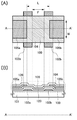
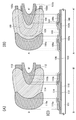
도 1(A)는 반도체 장치의 상면도이고 도 1(B)는 반도체 장치의 단면도.
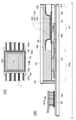
도 2(A) 및 도 2(B)는 반도체 장치의 상면도이고, 도 2(C)는 반도체 장치의 단면도.
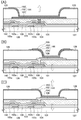
도 3의 (A) 내지 (C)는 반도체 장치의 제작 공정을 도시한 단면도.
도 4의 (A) 내지 (C)는 반도체 장치의 제작 공정을 도시한 단면도.
도 5(A)는 표시 장치의 블록도이고, 도 2(B)는 화소의 회로도.
도 6의 (A) 내지 (C)는 표시 장치의 단면도.
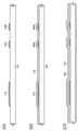
도 7(A)는 표시 패널의 상면도이고, 도 7(B)는 표시 패널의 단면도.
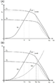
도 8은 산화물 반도체 트랜지스터의 Vgs-Id 특성을 도시한 도면.
도 9(A) 및 도 9(B)는 채널 길이가 서로 다른 트랜지스터의 특성을 도시한 도면.
도 10(A) 및 도 10(B)는 반도체 장치의 상면도이고, 도 10(C)는 반도체 장치의 단면도.
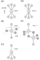
도 11의 (A) 내지 (C)는 산화물 재료의 구조를 설명한 도면.
도 12의 (A) 내지 (C)는 산화물 재료의 구조를 설명한 도면.
도 13의 (A) 내지 (C)는 산화물 재료의 구조를 설명한 도면.1 (A) is a top view of a semiconductor device, and Fig. 1 (B) is a cross-sectional view of a semiconductor device.
2 (A) and 2 (B) are top views of the semiconductor device, and FIG. 2 (C) is a cross-sectional view of the semiconductor device.
3 (A) to 3 (C) are cross-sectional views showing steps of manufacturing a semiconductor device.
4 (A) to 4 (C) are cross-sectional views showing a manufacturing process of a semiconductor device.
FIG. 5A is a block diagram of a display device, and FIG. 2B is a circuit diagram of a pixel.
6 (A) to 6 (C) are cross-sectional views of a display device.
7A is a top view of the display panel, and FIG. 7B is a sectional view of the display panel.
8 shows V gs -I d characteristics of an oxide semiconductor transistor;
Figs. 9A and 9B are diagrams showing the characteristics of transistors having different channel lengths. Fig.
10 (A) and 10 (B) are top views of a semiconductor device, and FIG. 10 (C) is a cross-sectional view of a semiconductor device.
11 (A) to 11 (C) are diagrams for explaining the structure of an oxide material.
12 (A) to 12 (C) are diagrams for explaining the structure of an oxide material.
13 (A) to 13 (C) are diagrams for explaining the structure of an oxide material.
이하, 본 명세서에 개시된 발명의 실시형태에 대해, 도면을 참고하여 설명한다. 다만, 본 명세서에 개시된 발명은 많은 다른 형태로 실시할 수 있고, 본 명세서에 개시된 발명의 취지 및 그 범위에서 벗어나지 않고 그 형태 및 상세한 사항을 다양하게 변경할 수 있는 것은 당업자이면 용이하게 이해된다는 점을 주목하라. 따라서, 본 실시형태의 기재 내용에 한정되어 해석되는 것은 아니다. 또한, 이하에 도시한 도면에서, 같은 부분 또는 마찬가지의 기능을 갖는 부분에는 같은 부호를 붙이고, 그 반복 설명은 생략한다는 점을 주목하라.Hereinafter, embodiments of the invention disclosed in this specification will be described with reference to the drawings. It will be apparent to those skilled in the art, however, that the invention herein disclosed may be embodied in many different forms and that various changes in form and details may be made therein without departing from the spirit and scope of the invention as disclosed herein Notice. Therefore, the present invention is not limited to the content of the present embodiment. Note that, in the drawings shown below, the same reference numerals are given to the same or similar functional portions, and the repetitive description thereof is omitted.
또한 본 명세서에 개시된 발명에서, 반도체 장치는, 반도체를 이용함으로써 기능하는 소자 및 장치 전반을 가리키고, 전자 회로, 표시 장치, 발광 장치 등을 포함하는 전기 장치 및 그 전기 장치를 탑재한 전자 기기를 그 범위로 함을 주목하라.Further, in the invention disclosed in this specification, a semiconductor device refers to an overall device and an apparatus functioning by using a semiconductor, and includes an electronic device including an electronic circuit, a display device, and a light emitting device, and an electronic device equipped with the electronic device. Note the range.
<Loff 영역을 갖는 산화물 반도체 트랜지스터><L off Oxide semiconductor transistor having a region &
도 1(B)에 도시한 산화물 반도체 트랜지스터(100)는, 절연 표면을 갖는 기판(101) 위에 형성되어 있다. 산화물 반도체 트랜지스터(100)는, 제 1 게이트 전극인 게이트 전극(102a), 제 2 게이트 전극인 게이트 전극(102b), 게이트 절연막(123), 제 1 산화물 반도체막인 산화물 반도체막(104), 소스 전극 또는 드레인 전극의 한쪽인 전극(105a), 소스 전극 또는 드레인 전극의 다른 한쪽인 전극(105b)을 가지고 있다.The
기판(101)은, 바륨 붕규산 유리 기판, 알루미노 붕규산 유리 기판, 또는 알루미노 규산염 유리 기판 등, 퓨전(fusion)법이나 플로팅(floating)법으로 제작된 무 알칼리 유리 기판, 세라믹 기판 외, 본 제작 공정의 처리 온도를 견딜 수 있는 내열성을 갖는 플라스틱 기판 등을 이용할 수 있다. 또한, 스테인리스 스틸 합금 등의 금속 기판의 표면에 절연막을 형성한 기판을 적용해도 좋다.The
기판(101) 위에 형성된 게이트 전극(102a) 및 게이트 전극(102b)은, 서로 떨어져 배치되어 있다. 또한, 게이트 전극(102a) 및 게이트 전극(102b)의 사이에는, 게이트 절연막(123)이 배치되어 있다.The
제 1 게이트 전극인 게이트 전극(102a), 및 제 2 게이트 전극인 게이트 전극(102b)은, 각각 티탄(Ti), 몰리브덴(Mo), 크롬(Cr), 탄탈(Ta), 텅스텐(W), 알루미늄(Al), 은(Ag), 금(Au), 구리(Cu) 중 어느 하나를 포함하는 도전막이다.The
또한, 게이트 전극(102a) 및 게이트 전극(102b)은 각각, 상기의 원소 중 어느 하나를 포함하는 도전막을 이용한 단층 구조여도 좋고, 또한 상기 원소 중 어느 하나를 포함하는 도전막의 적층 구조여도 좋다.The
또한, 게이트 전극(102a) 및 게이트 전극(102b) 각각의 위에는, 반도체막이나 도전막이 형성된다는 점을 주목하라. 반도체막이나 도전막의 단절 방지를 위해, 게이트 전극(102a) 및 게이트 전극(102b) 각각의 단부는, 테이퍼(taper) 형상이 되도록 가공하는 것이 바람직하다.Note that a semiconductor film or a conductive film is formed on each of the
게이트 절연막(123)은, 게이트 전극(102a) 및 게이트 전극(102b)을 덮도록 형성되어 있다.The
게이트 절연막(123)은, 산화규소막, 산화질화규소막, 질화산화규소, 질화규소막을 이용한 단층 구조, 또는 이들 막을 적층한 적층 구조를 이용해도 좋다.The
본 실시형태에서, 산화질화규소막은, 그 조성에서, 질소(N)보다 산소(O)의 함유량이 많고, 러더퍼드 후방 산란법(RBS : Rutherford Backscattering Spectrometry) 및 수소 전방 산란법(HFS : Hydrogen Forward Scattering)을 이용해서 측정한 경우에, 농도 범위로서 산소(O)가 55∼70 원자%, 질소(N)가 0.5∼15 원자%, 규소(Si)가 25∼35 원자%, 수소(H)가 0.1∼10 원자%의 범위로 포함되는 것을 말한다.In the present embodiment, the silicon oxynitride film has a larger content of oxygen (O) than nitrogen (N) in the composition, and is characterized by Rutherford backscattering spectrometry (RBS) and Hydrogen Forward Scattering (HFS) (O) in a concentration range of 0.5 to 15 atomic%, nitrogen (N) in a range of 25 to 35 atomic%, hydrogen (H) in a range of 0.1 to 0.1 atomic% To 10 atomic%.
또한, 질화산화규소막은, 그 조성에서, 산소(O)보다 질소(N)의 함유량이 많고, 농도 범위로서 산소(O)가 5∼30 원자%, 질소(N)가 20∼55 원자%, 규소(Si)가 25∼35 원자%, 수소(H)가 10∼30 원자%의 범위로 포함되는 것을 말한다.The silicon nitride oxide film has a larger content of nitrogen (N) than oxygen (O) in its composition and a concentration range of 5 to 30 atomic% of oxygen (O) and 20 to 55 atomic% of nitrogen (N) Means that silicon (Si) is contained in an amount of 25 to 35 atomic% and hydrogen (H) is contained in an amount of 10 to 30 atomic%.
다만, 산화질화규소 또는 질화산화규소를 구성하는 원자의 합계를 100 원자%로 했을 때, 질소(N), 산소(O), 규소(Si), 및 수소(H)의 함유 비율이 상기의 범위 내에 포함되는 것으로 함을 주목하라.However, when the content ratio of nitrogen (N), oxygen (O), silicon (Si) and hydrogen (H) is within the above range when the total amount of atoms constituting silicon oxynitride or silicon nitride oxide is 100 atomic% . ≪ / RTI >
또한, 게이트 절연막(123)으로서, 알루미늄(Al), 이트륨(Y), 마그네슘(Mg), 또는 하프늄(Hf)의 산화물, 알루미늄(Al), 이트륨(Y), 마그네슘(Mg), 또는 하프늄(Hf) 질화물, 알루미늄(Al), 이트륨(Y), 마그네슘(Mg), 또는 하프늄(Hf) 산화질화물, 또는 알루미늄(Al), 이트륨(Y), 마그네슘(Mg), 또는 하프늄(Hf) 질화산화물 중 어느 하나를 이용할 수 있다. 또한 이 산화물, 질화물, 산화질화물, 질화산화물의 적어도 2종 이상을 포함하는 화합물을 이용할 수도 있다.As the
또한 산화물 반도체 트랜지스터(100)는, 게이트 절연막(123) 위에 형성되고, 채널 형성 영역이 형성된 산화물 반도체막(104)을 가지고 있다. 산화물 반도체 트랜지스터(100)는, 연속된 면을 갖는 산화물 반도체막(104)을 가지고 있기 때문에, 캐리어의 이동에 장벽이 없고 적합하다.The
산화물 반도체막(104)과 제 1 게이트 전극(102a)이 중첩하고 있는 영역과, 산화물 반도체막(104)과 제 2 게이트 전극(102b)이 중첩하고 있는 영역과의 사이에, 산화물 반도체막(104)과 게이트 전극이 중첩하지 않는 영역이 발생한다. 본 명세서에서는, 제 1 게이트 전극(102a) 및 제 2 게이트 전극(102b) 어느 것과도 중첩하지 않는 산화물 반도체막(104)의 영역을 LOff 영역(109)이라고 부른다. 산화물 반도체 트랜지스터의 온 전류는 LOff 영역을 형성함으로써 감소될 수 있다.The
산화물 반도체막(104)으로서, 이하의 산화물 반도체의 박막을 이용한다.As the
본 실시형태에서 이용하는 산화물 반도체로서는, 적어도 인듐(In) 또는 아연(Zn)을 포함하는 것이 바람직하다. 특히 In과 Zn을 포함하는 것이 바람직하다. 또한, 이 산화물 반도체를 이용한 트랜지스터의 전기 특성의 편차를 줄이기 위한 스태빌라이저(stabilizer)로서, 그것들에 더하여 갈륨(Ga)을 갖는 것이 바람직하다. 또한, 스태빌라이저로서 주석(Sn)을 갖는 것이 바람직하다. 또한, 스태빌라이저로서 하프늄(Hf)을 갖는 것이 바람직하다. 또한, 스태빌라이저로서 알루미늄(Al)을 갖는 것이 바람직하다.The oxide semiconductor used in the present embodiment preferably contains at least indium (In) or zinc (Zn). In particular, it is preferable to include In and Zn. In addition, it is preferable to use a stabilizer as a stabilizer for reducing the variation of electric characteristics of the transistor using the oxide semiconductor, in addition to the stabilizer, gallium (Ga). Further, it is preferable to have tin (Sn) as the stabilizer. Further, it is preferable to have hafnium (Hf) as the stabilizer. Further, it is preferable to have aluminum (Al) as the stabilizer.
또한, 다른 스태빌라이저로서, 란탄족인, 란탄(La), 세륨(Ce), 프라세오디뮴(Pr), 네오디뮴(Nd), 사마륨(Sm), 유로퓸(Eu), 가돌리늄(Gd), 테르븀(Tb), 디스프로슘(Dy), 홀뮴(Ho), 에르븀(Er), 툴륨(Tm), 이테르븀(Yb), 루테튬(Lu) 중 어느 하나 1종 또는 복수종을 가져도 좋다.As other stabilizers, lanthanum (La), cerium (Ce), praseodymium (Pr), neodymium (Nd), samarium (Sm), europium (Eu), gadolinium (Gd), terbium (Dy), holmium (Ho), erbium (Er), thulium (Tm), ytterbium (Yb), and lutetium (Lu).
예를 들어, 산화물 반도체로서, 산화인듐, 산화주석, 산화아연, 이원계 금속의 산화물인 In-Zn계 산화물, Sn-Zn계 산화물, Al-Zn계 산화물, Zn-Mg계 산화물, Sn-Mg계 산화물, In-Mg계 산화물, In-Ga계 산화물, 삼원계 금속의 산화물인 In-Ga-Zn계 산화물(IGZO라고도 표기함), In-Al-Zn계 산화물, In-Sn-Zn계 산화물, Sn-Ga-Zn계 산화물, Al-Ga-Zn계 산화물, Sn-Al-Zn계 산화물, In-Hf-Zn계 산화물, In-La-Zn계 산화물, In-Ce-Zn계 산화물, In-Pr-Zn계 산화물, In-Nd-Zn계 산화물, In-Sm-Zn계 산화물, In-Eu-Zn계 산화물, In-Gd-Zn계 산화물, In-Tb-Zn계 산화물, In-Dy-Zn계 산화물, In-Ho-Zn계 산화물, In-Er-Zn계 산화물, In-Tm-Zn계 산화물, In-Yb-Zn계 산화물, In-Lu-Zn계 산화물, 사원계 금속의 산화물인 In-Sn-Ga-Zn계 산화물, In-Hf-Ga-Zn계 산화물, In-Al-Ga-Zn계 산화물, In-Sn-Al-Zn계 산화물, In-Sn-Hf-Zn계 산화물, In-Hf-Al-Zn계 산화물을 이용할 수 있다.Examples of the oxide semiconductor include indium oxide, tin oxide, zinc oxide, In-Zn oxide, Sn-Zn oxide, Al-Zn oxide, Zn-Mg oxide, Sn-Mg oxide Zn-based oxide, In-Zn-based oxide, In-Zn-based oxide, In-Ga-Zn-based oxide (also referred to as IGZO) Zn-based oxide, In-Ce-Zn-based oxide, In-Hf-Zn-based oxide, In-La-Zn-based oxide, In- In-Zn-based oxide, In-Tb-Zn-based oxide, In-Sm-Zn-based oxide, In- Zn-based oxide, In-Ho-Zn-based oxide, In-Er-Zn-based oxide, In-Tm-Zn-based oxide, In-Yb-Zn-based oxide, In- Zn-based oxide, In-Sn-Ga-Zn-based oxide, In-Hf-Ga-Zn-based oxide, In-Al- In-Hf-Al-Zn-based oxide is used There.
또한, 여기에서, 예를 들면, "In-Ga-Zn계 산화물"은, In과 Ga와 Zn을 주성분으로서 갖는 산화물이라는 의미이고, In과 Ga와 Zn의 비율은 불문함을 주목하라. 또한, In과 Ga와 Zn 이외의 금속 원소가 들어있어도 좋다.Note here that, for example, "In-Ga-Zn-based oxide" means an oxide having In, Ga and Zn as main components, and the ratio of In to Ga and Zn. In addition, metal elements other than Ga and Zn may be contained.
또한, 산화물 반도체로서, InMO3(ZnO)m (m>0, 또한, m은 정수가 아님)으로 표기되는 재료를 이용해도 좋다. 또한, M은, Ga, Fe, Mn 및 Co로부터 선택된 하나의 금속 원소 또는 복수의 금속 원소를 나타낸다. 또한, 산화물 반도체로서, In2SnO5(ZnO)n (n>0, 또한, n은 정수)으로 표기되는 재료를 이용해도 좋다.As the oxide semiconductor, a material represented by InMO 3 (ZnO) m (m> 0, and m is not an integer) may be used. Further, M represents one metal element or a plurality of metal elements selected from Ga, Fe, Mn and Co. As the oxide semiconductor, a material expressed by In 2 SnO 5 (ZnO) n (n> 0, and n is an integer) may be used.
예를 들어, In:Ga:Zn=1:1:1(=1/3:1/3:1/3) 또는 In:Ga:Zn=2:2:1(=2/5:2/5:1/5)의 원자비의 In-Ga-Zn계 산화물이나 그 조성의 근방의 산화물을 이용할 수 있다. 또는, In:Sn:Zn=1:1:1(=1/3:1/3:1/3), In:Sn:Zn=2:1:3(=1/3:1/6:1/2) 또는 In:Sn:Zn=2:1:5(=1/4:1/8:5/8)의 원자비의 In-Sn-Zn계 산화물이나 그 조성의 근방의 산화물을 이용하면 좋다.For example, the ratio of In: Ga: Zn = 1: 1: 1 (= 1/3: 1/3: 1/3) or In: Ga: Zn = 2: : 1/5) of In-Ga-Zn-based oxide or an oxide in the vicinity of the composition can be used. 1: 3: 1/3: 1/3: 1/3), In: Sn: Zn = 2: Sn-Zn based oxide having an atomic ratio of In: Sn: Zn = 2: 1: 5 (= 1/4: 1/8: 5/8) or an oxide in the vicinity of the composition good.
그러나, 이것들에 한정되지 않고, 필요로 하는 반도체 특성(이동도, 문턱값, 편차 등)에 따라 적절한 조성의 것을 이용하면 좋다. 또한, 필요로 하는 반도체 특성을 얻기 위해, 캐리어 밀도나 불순물 농도, 결함 밀도, 금속 원소와 산소의 원자수비, 원자간 결합 거리, 밀도 등을 적절한 것으로 하는 것이 바람직하다.However, the present invention is not limited to these examples, and it may be suitably used in accordance with the required semiconductor characteristics (mobility, threshold value, deviation, etc.). In order to obtain the required semiconductor characteristics, it is preferable that the carrier density, the impurity concentration, the defect density, the atomic ratio of the metal element and the oxygen, the distance between the atoms and the bonding distance, and the density are appropriately set.
예를 들어, In-Sn-Zn계 산화물에서는 비교적 용이하게 높은 이동도를 얻을 수 있다. 그러나, In-Ga-Zn계 산화물에서도, 벌크(bulk) 내 결함 밀도를 낮춤으로써 이동도를 높일 수 있다. For example, in the case of the In-Sn-Zn based oxide, relatively high mobility can be obtained. However, even in the case of the In-Ga-Zn-based oxide, the mobility can be increased by lowering the defect density in the bulk.
또한, 예를 들어, In, Ga, Zn의 원자수비가 In:Ga:Zn=a:b:c(a+b+c=1)인 산화물의 조성이, 원자수비가 In:Ga:Zn=A:B:C(A+B+C=1)의 산화물의 조성의 근방인 것은, a,b,c가, (a-A)2+(b-B)2+(c-C)2≤r2을 만족시키는 것을 말하고, r은, 예를 들면, 0.05로 하면 좋다. 다른 산화물이어도 마찬가지이다.For example, when the composition of the oxide in which the atomic ratio of In, Ga, Zn is In: Ga: Zn = a: b: c (a + b + c = 1) a: b: C is an (a + b + C = 1 ) near the composition of the oxides, a, b, c are, (aA) 2 + (bB ) that satisfies 2 + (cC) 2 ≤r 2 , And r may be 0.05, for example. The same applies to other oxides.
산화물 반도체는 단결정이어도, 비단결정이어도 좋다. 후자의 경우, 산화물 반도체가 아모퍼스여도, 다결정이어도 좋다. 또한, 아모퍼스 안에 결정성을 갖는 부분을 포함한 구조여도, 비아모퍼스여도 좋다.The oxide semiconductor may be single crystal or non-crystal. In the latter case, the oxide semiconductor may be amorphous or polycrystalline. In addition, a structure including a portion having crystallinity in the amorphous structure or a via-shaped structure may be used.
아모퍼스 상태의 산화물 반도체는, 비교적 용이하게 평탄한 표면을 얻을 수 있기 때문에, 이것을 이용하여 트랜지스터를 제작할 때의 계면 산란을 저감할 수 있고, 비교적 용이하게, 비교적 높은 이동도를 얻을 수 있다.Since the amorphous oxide semiconductor can obtain a relatively easily flat surface, it is possible to reduce the interfacial scattering when the transistor is fabricated using the oxide semiconductor, and comparatively high mobility can be relatively easily obtained.
또한, 결정성을 갖는 산화물 반도체에서는, 보다 벌크 내 결함을 저감할 수 있고, 표면의 평탄성을 높이면 아모퍼스 상태의 산화물 반도체 이상의 이동도를 얻을 수 있다. 표면의 평탄성을 높이기 위해서는, 평탄한 표면 위에 산화물 반도체를 형성하는 것이 바람직하다. 구체적으로는, 평균면 거칠기(Ra)가 1㎚ 이하, 바람직하게는 0.3㎚ 이하, 보다 바람직하게는 0.1㎚ 이하의 표면 위에 형성하면 좋다.In oxide semiconductors having crystallinity, defects in bulk can be reduced, and mobility higher than that of an amorphous oxide semiconductor can be obtained by increasing the flatness of the surface. In order to increase the flatness of the surface, it is preferable to form an oxide semiconductor on a flat surface. Specifically, it may be formed on the surface having an average surface roughness (Ra) of 1 nm or less, preferably 0.3 nm or less, more preferably 0.1 nm or less.
또한, Ra는, JIS B0601로 정의되는 중심선 평균 거칠기를 측정 면에 대해 적용할 수 있도록 삼차원으로 확장하여 얻어진 것이라는 점을 주목하라. Ra는 "기준면에서 지정면까지의 편차의 절대값을 평균한 값"으로 표현할 수 있고, 이하의 식으로 정의된다.Note also that Ra is obtained by extending the center line average roughness defined by JIS B0601 in three dimensions so that it can be applied to the measurement surface. Ra can be expressed as "a value obtained by averaging absolute values of deviations from a reference plane to a designated plane ", and is defined by the following equation.
[수학식 1][Equation 1]

또한, 상기에서, S0는, 측정면(좌표 (x1,y1)(x1,y2)(x2,y1)(x2,y2)로 나타내어지는 4점에 의해 둘러싸인 장방형의 영역)의 면적을 가리키고, Z0는 측정면의 평균 높이를 가리킨다. Ra는 원자간력 현미경(AFM : Atomic Force Microscope)으로 측정될 수 있다.Further, in the above, S 0, the measurement surface (coordinate (x 1, y 1) (x 1, y 2) (x 2, y 1) (x 2, y rectangular shape surrounded by the four points indicated by 2) , And Z 0 indicates the average height of the measurement surface. Ra can be measured with an atomic force microscope (AFM).
여기서 산화물 반도체가 결정성을 갖는 경우로서, c축 배향하고, 또한 ab면, 표면 또는 계면의 방향으로부터 봤을 때 삼각 형상 또는 육각 형상의 원자 배열을 갖고, c축에서는 금속 원자가 층상 또는 금속 원자와 산소 원자가 층상으로 배열되어 있고, ab면에서는 a축 또는 b축의 방향이 다른(c축을 중심으로 회전하는) 결정(CAAC : C Axis Aligned Crystal이라고도 함)을 포함하는 산화물에 대해 설명한다.In the case where the oxide semiconductor has crystallinity, it has a c-axis orientation, and has an atomic arrangement of a triangular or hexagonal shape when viewed from the direction of the ab plane, surface or interface. In the c axis, metal atoms are layer- (CAAC: C Axis Aligned Crystal) in which the atoms are arranged in layers and the direction of the a axis or the b axis in the ab plane is different (rotating around the c axis).
CAAC를 포함하는 산화물은, 넓은 의미로, 비단결정이고, 그 ab면에 수직인 방향에서 봤을 때, 삼각형, 육각형, 정삼각형 또는 정육각형의 원자 배열을 갖고, 또한 c축 방향으로 수직인 방향에서 봤을 때, 금속 원자가 층상, 또는 금속 원자와 산소 원자가 층상으로 배열된 상을 포함하는 산화물을 말한다.The oxide containing CAAC is broadly non-crystalline and has an atomic arrangement of triangular, hexagonal, equilateral, or regular hexagonal when viewed in a direction perpendicular to the ab plane, and when viewed in a direction perpendicular to the c axis direction , A metal atom, a layer, or an oxide comprising a metal atom and an oxygen atom arranged in layers.
CAAC는 단결정은 아니지만, 비정질만으로 형성된 것은 아니다. 또한, CAAC는 결정화된 부분(결정 부분)을 포함하지만, 하나의 결정 부분과 다른 결정 부분의 경계를 명확하게 판별할 수 없는 경우도 있다.CAAC is not a single crystal, but it is not formed by amorphous. In addition, although the CAAC includes a crystallized part (crystal part), there are cases where the boundary between one crystal part and another crystal part can not be clearly discriminated.
CAAC에 산소가 포함된 경우, 산소의 일부는 질소로 치환되어도 좋다. 또한, CAAC를 구성하는 개개의 결정 부분의 c축은 일정의 방향(예를 들어, CAAC를 지지하는 기판면, CAAC의 표면 등에 수직인 방향)으로 정렬되어 있어도 좋다. 또는, CAAC를 구성하는 개개의 결정 부분의 ab면의 법선은 일정 방향(예를 들어, CAAC를 지지하는 기판면, CAAC의 표면 등에 수직인 방향)을 향하고 있어도 좋다.If CAAC contains oxygen, some of the oxygen may be replaced by nitrogen. In addition, the c-axis of each crystal part constituting the CAAC may be aligned in a certain direction (for example, the direction perpendicular to the surface of the CAAC, the surface of the substrate supporting the CAAC, etc.). Or, the normal line of the ab plane of each crystal part constituting the CAAC may be directed to a certain direction (for example, the direction perpendicular to the surface of the CAAC, the surface of the CAAC, etc.).
CAAC는, 그 조성에 따라, 도체이거나, 반도체이거나, 절연체가 된다. 또한, 그 조성 등에 따라, 가시광에 대해 투명하거나 불투명하다.The CAAC may be a conductor, a semiconductor, or an insulator depending on its composition. Further, it is transparent or opaque to visible light depending on its composition and the like.
이와 같은 CAAC의 예로서, 막 형상으로 형성되고, 막 표면 또는 지지하는 기판면에 수직인 방향에서 관찰했을 때 삼각형 또는 육각형의 원자 배열이 인정되고, 또한 그 막 단면을 관찰했을 때 금속 원자 또는 금속 원자 및 산소 원자(또는 질소 원자)의 층상 배열이 인정되는 결정을 들 수도 있다.As an example of such a CAAC, a triangular or hexagonal atomic arrangement is observed when observed in the film surface or a direction perpendicular to the surface of the supporting substrate, and when observing the film surface, And a crystal in which a layered arrangement of atoms and oxygen atoms (or nitrogen atoms) is recognized.
CAAC에 포함되는 결정 구조의 일례에 대해 도 11 내지 도 13을 이용하여 상세하게 설명한다. 또한, 특별히 언급하지 않는 한, 도 11 내지 도 13은 윗방향을 c축 방향으로 하고, c축 방향과 직교하는 면을 ab면으로 한다. 또한, 단순히 상반부, 하반부라고 하는 경우, ab면을 경계로 한 경우의 상반부, 하반부를 말한다. 또한, 도 11에서, 동그라미로 둘러싸인 O는 4배위의 O를 나타내고, 이중 동그라미로 둘러싸인 O는 3배위의 O를 나타낸다.An example of the crystal structure included in the CAAC will be described in detail with reference to Figs. 11 to 13. Fig. Unless otherwise noted, Figs. 11 to 13 show the c-axis direction in the upper direction and the ab-plane in the plane orthogonal to the c-axis direction. In the case of simply upper half and lower half, it refers to the upper half and lower half of the case where the ab plane is the boundary. In Fig. 11, O surrounded by a circle represents O of four coordinates, and O surrounded by double circles represents O of three coordinates.
도 11(A)에, 1개의 6배위의 In과, In에 근방의 6개의 4배위의 산소 원자(이하 4배위의 O)를 갖는 구조를 도시한다. 여기에서는, 금속 원자가 1개에 대해, 근접의 산소 원자만 나타낸 구조를 소그룹이라 부른다. 도 11(A)의 구조는, 팔면체 구조를 취하지만, 간단하게 하기 위해 평면 구조로 도시한다. 또한, 도 11(A)의 상반부 및 하반부에는 각각 3개씩 4배위의 O가 있다. 도 11(A)에 도시한 소그룹은 전하가 0이다.Fig. 11 (A) shows a structure having one six-coordinate of In and six four-coordinate oxygen atoms in the vicinity of In (hereinafter, four-coordinate O). Here, a structure in which only one oxygen atom is adjacent to a metal atom is referred to as a small group. The structure of Fig. 11 (A) takes an octahedral structure, but is shown as a planar structure for simplicity. In the upper half and lower half of Fig. 11 (A), three O atoms are present in four coordinates. In the small group shown in FIG. 11 (A), the charge is zero.
도 11(B)에, 1개의 5배위의 Ga와, Ga에 근접한 3개의 3배위의 산소 원자(이하 3배위의 O)와, Ga에 근접한 2개의 4배위의 O를 갖는 구조를 도시한다. 3배위의 O는, 모두 ab면에 존재한다. 도 11(B)의 상반부 및 하반부에는 각각 1개씩 4배위의 O가 있다. 또한, In도 5배위를 취하기 때문에, 도 11(B)에 도시한 구조를 취할 수 있다. 도 11(B)에 도시한 소그룹은 전하가 0이다.Fig. 11B shows a structure having one five-coordinate Ga, three three-coordinate oxygen atoms close to Ga (hereinafter referred to as three-coordinate O), and two four-coordinate O close to Ga. The O of 3 coordination is all present on the ab plane. In the upper half and lower half of Fig. 11 (B), there is O of four coordinates, one by one. In addition, since In takes five coordinates, the structure shown in Fig. 11 (B) can be obtained. In the small group shown in Fig. 11 (B), the charge is zero.
도 11(C)에, 1개의 4배위의 Zn과, Zn에 근접한 4개의 4배위의 O를 갖는 구조를 도시한다. 도 11(C)의 상반부에는 1개의 4배위의 O가 있고, 하반부에는 3개의 4배위의 O가 있다. 또는, 도 11(C)의 상반부에 3개의 4배위의 O가 있고, 하반부에 1개의 4배위의 O가 있어도 좋다. 도 11(C)에 도시한 소그룹은 전하가 0이다. Fig. 11 (C) shows a structure having one four-coordinate Zn and four quadruple positions O close to Zn. In the upper half of Fig. 11 (C), there is one four-coordinate O and the lower half has three four-coordinate O. In Fig. Alternatively, there may be three O in four coordinates in the upper half of FIG. 11 (C) and O in one four coordinates in the lower half. In the small group shown in Fig. 11 (C), the charge is zero.
도 11(D)에, 1개의 6배위의 Sn과, Sn에 근접한 6개의 4배위의 O를 갖는 구조를 도시한다. 도 11(D)의 상반부에는 3개의 4배위의 O가 있고, 하반부에는 3개의 4배위의 O가 있다. 도 11(D)에 도시한 소그룹은 전하가 +1이 된다.FIG. 11 (D) shows a structure having one six-coordinate Sn and six four-coordinate coordinates O close to Sn. In the upper half of Fig. 11 (D), there are three O in four coordinates, and in the lower half there are three O in four coordinates. In the small group shown in Fig. 11 (D), the charge becomes +1.
도 11(E)에, 2개의 Zn을 포함하는 소그룹을 도시한다. 도 11(E)의 상반부에는 1개의 4배위의 O가 있고, 하반부에는 1개의 4배위의 O가 있다. 도 11(E)에 도시한 소그룹은 전하가 -1이 된다.Fig. 11 (E) shows a small group containing two Zn. In the upper half of FIG. 11 (E), there is one four-coordinate O, and the lower half has one four-coordinate O. FIG. In the small group shown in Fig. 11 (E), the charge becomes -1.
여기에서는, 복수의 소그룹의 집합체를 중그룹으로 부르고, 복수의 중그룹의 집합체를 대그룹(유닛 셀(unit cell)이라고도 함)이라고 부른다.Here, a plurality of groups of small groups is called a middle group, and a plurality of groups of a middle group is called a large group (also referred to as a unit cell).
여기에서, 이들의 소그룹끼리가 결합하는 규칙에 대해 설명한다. 도 11(A)에 도시한 6배위의 In의 상반부의 3개의 O는, 아랫방향에 각각 3개의 근접 In을 갖고, 하반부의 3개의 O는, 윗방향에 각각 3개의 근접 In을 갖는다. 5배위의 Ga의 상반부의 1개의 O는, 아랫방향에 1개의 근접 Ga를 갖고, 하반부의 1개의 O는, 윗방향에 1개의 근접 Ga를 갖는다. 4배위의 Zn의 상반부의 1개의 O는 아랫방향에 1개의 근접 Zn을 갖고, 하반부의 3개의 O는, 윗방향에 각각 3개의 근접 Zn을 갖는다. 이와 같이, 금속 원자의 윗방향의 4배위의 O의 수와, 그 O의 아랫방향에 있는 근접 금속 원자의 수는 같고, 마찬가지로 금속 원자의 아랫방향의 4배위의 O의 수와, 그 O의 윗방향에 있는 근접 금속 원자의 수는 같다. O는 4배위이기 때문에, 아랫방향에 있는 근접 금속 원자의 수와, 윗방향에 있는 근접 금속 원자의 수의 합은 4가 된다. 따라서, 금속 원자의 윗방향에 있는 4배위의 O의 수와, 다른 금속 원자의 아랫방향에 있는 4배위의 O의 수와의 합이 4개일 때, 금속 원자를 갖는 2종의 소그룹끼리는 결합할 수 있다. 예를 들어, 6배위의 금속 원자(In 또는 Sn)가 하반부의 4배위의 O를 통하여 결합한 경우, 4배위의 0가 3개이기 때문에, 5배위의 금속 원자(Ga 또는 In), 또는 4배위의 금속 원자(Zn)의 어느 하나와 결합하는 것이 된다.Here, rules for combining these small groups will be described. Three Os in the upper half of In in six coordinates shown in FIG. 11 (A) each have three inches in the bottom direction, and three O in the bottom half have three inches in the top direction. One O in the upper half of the Ga of 5 coordination has one Ga in the lower direction and one O in the lower half has one Ga in the upper direction. One O in the upper half of Zn in the 4-coordination has one Zn in the lower direction and three O in the lower half have three Zn in the upper direction. As described above, the number of O atoms in the four coordinates in the upward direction of the metal atom is the same as the number of the nearby metal atoms in the bottom direction of the O atom. Similarly, the number of O atoms in the four coordinates in the downward direction of the metal atom, The number of nearby metal atoms in the upper direction is the same. Since O is four coordination, the sum of the number of the nearby metal atoms in the downward direction and the number of the nearby metal atoms in the upward direction is four. Therefore, when the sum of the number of O in four coordinates in the upper direction of the metal atom and the number of O in four coordinates in the downward direction of the other metal atom are four, two small groups having metal atoms are combined . For example, when a metal atom (In or Sn) in a six-coordinate system is bonded through O in four positions in the lower half, three 0's in a four-coordinate system are bonded so that the metal atom (Ga or In) Of the metal atom (Zn).
이들의 배위수를 갖는 금속 원자는, c축 방향에서, 4배위의 0를 통해 결합한다. 또한, 이외에도, 층구조의 합계의 전하가 0가 되도록 복수의 소그룹이 결합하여 중그룹을 구성한다.The metal atoms having these coordination numbers are bonded to each other in the c-axis direction through 0 of four coordinates. In addition, a plurality of subgroups are combined to form a middle group so that the total charge of the layer structure becomes zero.
도 12(A)에, In-Sn-Zn-O계 의 층구조를 구성하는 중그룹의 모델도를 도시한다. 도 12(B)에, 3개의 중그룹으로 구성된 대그룹을 도시한다. 또한 도 12(C)는, 도 12(B)의 층구조를 c축 방향에서 관찰한 경우의 원자 배열을 도시함을 주목하라.Fig. 12 (A) shows a model diagram of a middle group constituting a layer structure of an In-Sn-Zn-O system. FIG. 12B shows a large group composed of three medium groups. Note that Fig. 12 (C) shows the atomic arrangement when the layer structure of Fig. 12 (B) is observed in the c-axis direction.
도 12(A)에서는, 간단하게 하기 위해, 3배위의 0는 생략하고, 4배위의 0는 개수만 나타낸다. 예를 들어, Sn의 상반부 및 하반부에는 각각 3개씩 4배위의 0가 있는 것을 동그라미의 3으로서 나타낸다. 마찬가지로, 도 12(A)에서, In의 상반부 및 하반부에는 각각 1개씩 4배위의 O가 있고, 동그라미의 1로서 나타낸다. 도 12(A)는 또한 하반부에는 1개의 4배위의 0가 있고, 상반부에는 3개의 4배위의 O가 있는 Zn과, 상반부에는 1개의 4배위의 0가 있고, 하반부에는 3개의 4배위의 O가 있는 Zn을 나타낸다.In Fig. 12 (A), for simplicity, 0 in three coordinates is omitted, and 0 in four coordinates indicates only the number. For example, in the upper half and the lower half of Sn, three triplets each having a coordinate of four coordinates are shown as
도 12(A)에서, In-Sn-Zn-O계의 층구조를 구성하는 중그룹은, 위에서부터 순서대로 4배위의 O가 3개씩 상반부 및 하반부에 있는 Sn이, 4배위의 O가 1개씩 상반부 및 하반부에 있는 In과 결합하고, 그 In이, 상반부에 3개의 4배위의 O가 있는 Zn과 결합하고, 그 Zn의 하반부의 1개의 4배위의 0를 통해 4배위의 0가 3개씩 상반부 및 하반부에 있는 In과 결합하고, 그 In이, 상반부에 1개의 4배위의 O가 있는 Zn 2개로 이루어진 소그룹과 결합하고, 이 소그룹의 하반부의 1개의 4배위의 0를 통해 4배위의 0가 3개씩 상반부 및 하반부에 있는 Sn과 결합하고 있는 구성이다. 이 중그룹이 복수 결합하여 대그룹을 구성한다.In Fig. 12 (A), the middle group constituting the In-Sn-Zn-O system layer structure is composed of Sn in the upper half and lower half by three O in four coordinates in the order from the top, And the In is bonded to Zn having three quadrature coordination O at the upper half, and three 0s of four coordination are connected through 0 of one quadrant of the lower half of the Zn In is combined with In in the upper half and lower half, and the In is combined with a small group consisting of Zn 2 having one quadrature O in the upper half, and 0 in one quadrant in the lower half of this small group. Are bonded to the Sn in the upper half and the lower half, respectively. A plurality of groups are combined to form a large group.
여기에서, 3배위의 O 및 4배위의 O의 경우, 결합 하나 당의 전하는 각각 -0.667, -0.5라고 생각할 수 있다. 예를 들어, In(6배위 또는 5배위), Zn(4배위), Sn(5배위 또는 6배위)의 전하는, 각각 +3, +2, +4이다. 따라서, Sn을 포함하는 소그룹은 전하가 +1이 된다. 그 때문에, Sn을 포함하는 층구조를 형성하기 위해서는, 전하 +1을 없애는 전하 -1이 필요해진다. 전하 -1을 취하는 구조로서, 도 11(E)에 도시한 것처럼, 2개의 Zn을 포함하는 소그룹을 들 수 있다. 예를 들어, Sn을 포함하는 소그룹이 1개에 대해, 2개의 Zn을 포함하는 소그룹이 1개 있으면, 전하가 없어지기 때문에, 층구조의 합계의 전하를 0으로 할 수 있다.Here, in the case of O in three coordination and O in four coordination, the charge of one bond and the charge of one sugar can be considered to be -0.667 and -0.5, respectively. For example, the electric charges of In (6 or 5 coordination), Zn (4 coordination), and Sn (5 coordination or 6 coordination) are +3, +2, +4, respectively. Therefore, a small group containing Sn has a charge of +1. Therefore, in order to form a layer structure including Sn, charge-1 for eliminating the charge + 1 is required. As a structure for taking charge-1, there is a small group containing two Zn, as shown in Fig. 11 (E). For example, if there is one small group containing two Zns in one small group containing Sn, the total charge of the layer structure can be set to zero because there is no charge.
구체적으로는, 도 12(B)에 도시한 대그룹이 반복됨으로써, In-Sn-Zn-O계의 결정(In2SnZn3O8)을 얻을 수 있다. 또한, 얻어진 In-Sn-Zn-O계의 층구조는, In2SnZn2O7(ZnO)m(m은 0 또는 자연수)으로 하는 조성식으로 나타낼 수 있음을 주목하라.Specifically, the In-Sn-Zn-O-based crystal (In 2 SnZn 3 O 8 ) can be obtained by repeating the large group shown in FIG. 12 (B). Note that the layer structure of the obtained In-Sn-Zn-O system can be expressed by a composition formula of In 2 SnZn 2 O 7 (ZnO) m (m is 0 or a natural number).
또한, 이외에도, 사원계 금속의 산화물인 In-Sn-Ga-Zn계 산화물이나, 삼원계 금속의 산화물인 In-Ga-Zn계 산화물(IGZO라고도 표기함), In-Al-Zn계 산화물, Sn-Ga-Zn계 산화물, Al-Ga-Zn계 산화물, Sn-Al-Zn계 산화물이나, In-Hf-Zn계 산화물, In-La-Zn계 산화물, In-Ce-Zn계 산화물, In-Pr-Zn계 산화물, In-Nd-Zn계 산화물, In-Sm-Zn계 산화물, In-Eu-Zn계 산화물, In-Gd-Zn계 산화물, In-Tb-Zn계 산화물, In-Dy-Zn계 산화물, In-Ho-Zn계 산화물, In-Er-Zn계 산화물, In-Tm-Zn계 산화물, In-Yb-Zn계 산화물, In-Lu-Zn계 산화물이나, 이원계 금속의 산화물인 In-Zn계 산화물, Sn-Zn계 산화물, Al-Zn계 산화물, Zn-Mg계 산화물, Sn-Mg계 산화물, In-Mg계 산화물이나, In-Ga계 산화물 등을 이용한 경우도 마찬가지이다.In-Sn-Zn-Zn oxide, In-Ga-Zn oxide (also referred to as IGZO) which is an oxide of a ternary metal, In-Al-Zn oxide, Sn Zn-based oxide, In-Ce-Zn-based oxide, Al-Ga-Zn-based oxide, Sn-Al-Zn-based oxide, In-Hf- In-Zn-based oxide, In-Tb-Zn-based oxide, In-Sm-Zn-based oxide, In- Zn-based oxide, In-Ho-Zn-based oxide, In-Er-Zn-based oxide, In-Tm-Zn-based oxide, In-Yb-Zn- The same is true when an In-Zn-based oxide, Sn-Zn-based oxide, Al-Zn-based oxide, Zn-Mg-based oxide, Sn-Mg-based oxide, In-Mg-based oxide or In-Ga-based oxide is used.
예를 들어, 도 13(A)에, In-Ga-Zn-O계의 층구조를 구성하는 중그룹의 모델도를 도시한다.For example, Fig. 13 (A) shows a model diagram of a middle group constituting an In-Ga-Zn-O system layer structure.
도 13(A)에서, In-Ga-Zn-O계의 층구조를 구성하는 중그룹은, 위에서부터 순서대로 4배위의 0가 3개씩 상반부 및 하반부에 있는 In이 4배위의 O가 1개 상반부에 있는 Zn과 결합하고, 그 Zn의 하반부의 3개의 4배위의 0를 통해, 4배위의 0가 1개씩 상반부 및 하반부에 있는 Ga와 결합하고, 그 Ga의 하반부의 1개의 4배위의 0를 통해, 4배위의 O가 3개씩 상반부 및 하반부에 있는 In과 결합하고 있는 구조이다. 이 중그룹이 복수 결합하여 대그룹을 구성한다.In Fig. 13 (A), in the middle group constituting the In-Ga-Zn-O system layer structure, in order from the top, three 0s in four coordinates are arranged in the upper half and the lower half, 0 " of the four coordination bonds to Ga in the upper half and the lower half through 0 of three four coordinates in the lower half of the Zn, and 0 " Through which three O atoms in four coordination are bonded to In in the upper half and the lower half, respectively. A plurality of groups are combined to form a large group.
도 13(B)에 3개의 중그룹으로 구성된 대그룹을 도시한다. 또한, 도 13(C)은, 도 13(B)의 층구조를 c축 방향에서 관찰한 경우의 원자 배열을 도시한다.FIG. 13B shows a large group composed of three middle groups. Fig. 13 (C) shows the atomic arrangement when the layer structure of Fig. 13 (B) is observed in the c-axis direction.
여기에서, In(6배위 또는 5배위), Zn(4배위), Ga(5배위)의 전하는, 각각 +3, +2, +3 이기 때문에, In, Zn 및 Ga 중 어느 하나를 포함하는 소그룹은, 전하가 0이 된다. 그 때문에, 이들의 소그룹의 조합이라면 중그룹의 합계의 전하는 항상 0이 된다.Here, since the electric charges of In (6 coordination or 5 coordination), Zn (4 coordination) and Ga (5 coordination) are +3, +2 and +3, respectively, The charge becomes zero. Therefore, in the case of a combination of these small groups, the total charge of the middle group is always zero.
또한, In-Ga-Zn-O계의 층구조를 구성하는 중그룹은, 도 13(A)에 도시한 중그룹에 한정되지 않고, In, Ga, Zn의 배열이 다른 중그룹을 조합한 대그룹도 얻을 수 있다.The middle group constituting the layer structure of the In-Ga-Zn-O system is not limited to the middle group shown in Fig. 13 (A), but may be a large group consisting of a combination of different groups of In, Ga, Can be obtained.
또한, In-Sn-Zn계 산화물은, ITZO라고 부를 수 있고, 이용하는 타겟의 조성비는, In:Sn:Zn이 원자수비로, 1:2:2, 2:1:3, 1:1:1, 또는 20:45:35 등이 되는 산화물 타겟을 이용한다.The In-Sn-Zn-based oxide may be referred to as ITZO. The composition ratio of the target used is 1: 2: 2, 2: 1: 3, 1: 1: 1 , Or 20:45:35 or the like is used.
또한 본 명세서의 산화물 반도체막에서, 이차 이온 질량 분석법(SIMS : Secondary Ion Mass Spectroscopy)에 의해 측정된 나트륨(Na)의 농도는 5×10¹⁶㎝-3 이하, 바람직하게는 1×10¹⁶㎝-3 이하, 더욱 바람직하게는 1×10¹⁵㎝-3 이하가 적합하다는 점을 주목하라. 또는 본 명세서의 산화물 반도체막에서, SIMS에 의해 측정된 리튬(Li)의 농도는 5×10¹⁵㎝-3 이하, 바람직하게는 1×10¹⁵㎝-3 이하가 적합하다. 또한 본 명세서의 산화물 반도체막에서, SIMS에 의해 측정된 칼륨(K)의 농도는 5×10¹⁵㎝-3 이하, 바람직하게는 1×10¹⁵㎝-3 이하가 적합하다.In addition, in the oxide semiconductor film of the present specification, the secondary ion mass spectrometry: the concentration of sodium (Na) as measured by the (SIMS Secondary Ion Mass Spectroscopy) is 5 × 10 16 ㎝ -3 or less, preferably 1 × 10 16 ㎝ - 3 or less, and more preferably 1 x 10 < 15 > cm < -3 > Alternatively, in the oxide semiconductor film of the present specification, the concentration of lithium (Li) measured by SIMS is preferably 5 x 10 15 cm -3 or less, and more preferably 1 x 10 15 cm -3 or less. In the oxide semiconductor film of the present specification, the concentration of potassium (K) measured by SIMS is preferably 5 x 10 15 cm -3 or less, and more preferably 1 x 10 15 cm -3 or less.
이 산화물 반도체막 안에서, 나트륨(Na), 리튬(Li), 칼륨(K) 등의 알칼리 금속, 및, 알칼리토류 금속의 농도가 높은 경우, 트랜지스터 특성의 열화 및 트랜지스터 특성의 편차를 초래할 우려가 있다. 그 때문에, 트랜지스터 특성의 열화 및 트랜지스터 특성의 편차를 억제하기 위해, 산화물 반도체막 안의 알칼리 금속 및 알칼리토류 금속은, 위에서 설명한 농도 범위인 것이 적합하다.When the concentrations of alkali metals and alkaline earth metals such as sodium (Na), lithium (Li), potassium (K) and the like are high in the oxide semiconductor film, there is a risk of deterioration of transistor characteristics and deviation of transistor characteristics . Therefore, in order to suppress the deterioration of the transistor characteristics and the deviation of the transistor characteristics, it is preferable that the alkali metal and alkaline earth metal in the oxide semiconductor film have the above-described concentration range.
특히, 산화물 반도체막에 접하는 절연막이 산화물 절연막인 경우, 나트륨(Na)은 이 절연막 안으로 확산하고, 나트륨 이온(Na+)이 된다. 또한, 나트륨(Na)은, 산화물 반도체막 안에서, 금속과 산소의 결합을 분석하거나, 또는 결합 안에 끼어들 우려가 있다.Particularly, when the insulating film in contact with the oxide semiconductor film is an oxide insulating film, sodium (Na) diffuses into the insulating film and becomes sodium ions (Na + ). In addition, sodium (Na) may interfere with or analyze the bond between metal and oxygen in the oxide semiconductor film.
나트륨(Na)이 절연막 안에서 나트륨 이온(Na+)이 되는 경우, 나트륨(Na)이 산화물 반도체막 안에서, 금속과 산소의 결합을 분단하거나, 또는, 나트륨(Na)이 산화물 반도체막 안에서, 결합 안에 끼어드는 경우, 트랜지스터 특성의 열화(예를 들어, 노멀리 온(normally-on)화(문턱값의 부로의 이동), 이동도의 저하 등)의 원인이 될 우려가 있다. 또한, 이와 같은 나트륨(Na)의 행동은, 트랜지스터 특성의 편차의 원인도 된다.When sodium (Na) becomes sodium ion (Na + ) in the insulating film, sodium (Na) separates the bond between metal and oxygen in the oxide semiconductor film, or sodium (Na) There is a possibility that deterioration of the transistor characteristics (for example, normally-on (shift to the threshold value), decrease in mobility, etc.) may occur. Such behavior of sodium (Na) also causes variations in transistor characteristics.
위에서 설명한 알칼리 금속 및 알칼리토류 금속에 기인하는 트랜지스터 특성의 열화 및 트랜지스터 특성의 편차는, 특히 산화물 반도체막 안의 수소의 농도가 충분히 낮은 경우에 현저해진다. 따라서, 산화물 반도체막 안의 수소의 농도가 5×10¹⁹㎝-3 이하, 특히 5×10¹⁸㎝-3 이하인 경우에는, 알칼리 금속의 농도를 위에서 설명한 값으로 하는 것이 적합하다.The deterioration of the transistor characteristics and the deviation of the transistor characteristics due to the alkali metals and alkaline earth metals described above are remarkable particularly when the concentration of hydrogen in the oxide semiconductor film is sufficiently low. Therefore, when the concentration of hydrogen in the oxide semiconductor film is 5 × 10 19 cm -3 or less, particularly 5 × 10 18 cm -3 or less, it is preferable to set the concentration of the alkali metal to the value described above.
또한 소스 전극 또는 드레인 전극의 한쪽인 전극(105a)은, 게이트 전극(102a)의 일부 및 산화물 반도체막(104)의 일부와 중첩한다. 또한, 소스 전극 또는 드레인 전극의 다른 한쪽인 전극(105b)은, 게이트 전극(102b)의 일부 및 산화물 반도체막(104)의 일부와 중첩한다.The
전극(105a) 및 전극(105b) 각각은, 알루미늄(Al), 크롬(Cr), 탄탈(Ta), 티탄(Ti), 몰리브덴(Mo), 텅스텐(W)으로부터 선택된 원소를 포함하는 도전막, 위에서 설명한 원소를 성분으로 하는 합금막, 또는 위에서 설명한 원소를 조합시킨 합금막 등을 이용한다.Each of the
또한, 알루미늄(Al) 단체의 알루미늄막은 내열성이 뒤떨어지고, 또한 부식하기 쉽다는 등의 문제점이 있다는 점을 주목하라. 그 때문에, 전극(105a) 및 전극(105b) 각각을 알루미늄(Al)을 이용해서 형성하는 경우는, 알루미늄(Al)과 내열성 도전성 재료를 조합시켜 형성한다.Note that the aluminum film made of aluminum (Al) alone has problems such as poor heat resistance and corrosion resistance. Therefore, when each of the
알루미늄(Al)과 조합시킨 내열성 도전성 재료로서는, 티탄(Ti), 탄탈(Ta), 텅스텐(W), 몰리브덴(Mo), 크롬(Cr), 네오디뮴(Nd), 스칸듐(Sc)으로부터 선택된 원소를 포함하는 재료, 또는 위에서 설명한 원소를 성분으로 하는 합금 재료, 위에서 설명한 원소를 조합시킨 합금 재료, 또는 위에서 설명한 원소를 성분으로 하는 질화물을 이용한다.As the heat resistant conductive material combined with aluminum (Al), an element selected from titanium (Ti), tantalum (Ta), tungsten (W), molybdenum (Mo), chromium (Cr), neodymium (Nd), and scandium An alloy material containing the above-described elements, an alloy material obtained by combining the above-described elements, or a nitride containing the above-described elements as elements.
또한 제 1 게이트 전극인 게이트 전극(102a), 제 2 게이트 전극인 게이트 전극(102b), 게이트 절연막(123), 산화물 반도체막(104), 소스 전극 또는 드레인 전극의 한쪽인 전극(105a), 소스 전극 또는 드레인 전극의 다른 한쪽인 전극(105b)을 덮고, 절연막(126)이 형성되어 있다. 절연막(126)은, 산화물 반도체막(104)에 직접 접촉하여 형성되어 있는 절연막이고, 산화물 반도체막(104)을 보호하는 보호막이다.The
절연막(126)은 게이트 절연막(123)과 마찬가지로, 산화규소막, 산화질화규소막, 질화산화규소막, 질화규소막을 이용한 단층 구조, 또는 이들의 막을 적층한 적층 구조를 이용해도 좋다. 보호막은, 대기 중에 부유하는 유기물이나 금속물, 수증기 등의 오염 불순물의 침입을 막기 위한 것이고, 치밀한 막이 바람직하다는 점을 주목하라.The insulating
도 1(A)는 산화물 반도체 트랜지스터(100)의 상면도이고, 도 1(A)의 A-A'의 단면도가 도 1(B)이 된다.1A is a top view of an
산화물 반도체막(104) 안의 전극(105a) 및 전극(105b)(소스 전극 및 드레인 전극)과의 사이의 영역이 채널 형성 영역이 된다. 따라서 도 1(A)에 도시한 것처럼, 전극(105a)의 단부 및 전극(105b)의 단부와의 사이의 거리가, 채널 길이(L)가 된다. 또는 전극(105a) 또는 전극(105b)의 채널 길이와 수직인 한 변의 길이가 채널 폭(W)이 된다.The region between the
따라서 이 채널 형성 영역이며, 산화물 반도체막(104) 및 게이트 전극(102a) 및 게이트 전극(102b)에 중첩하지 않는 영역이 Loff 영역(109)이 된다. Loff 영역(109)의 채널 길이 방향의 길이를 길이(F)로 한다.Therefore, the region that does not overlap the
Loff 영역(109)의 채널 길이 방향의 길이인 길이(F)는, 너무 짧으면 온 전류 저감의 효과를 얻을 수 없고, 너무 길면 채널 형성 영역의 저항이 증대된다. 따라서, Loff 영역(109)의 채널 길이 방향의 길이인 길이(F)는, 1㎛ 이상 20㎛ 이하가 적합하다.If the length F of the L off region 109 in the channel length direction is too short, the effect of reducing the on-current can not be obtained. If the length F is too long, the resistance of the channel forming region is increased. Therefore, the length F in the channel length direction of the L off region 109 is preferably 1 mu m or more and 20 mu m or less.
Loff 영역(109)을 형성함으로써, 산화물 반도체 트랜지스터(100)의 온 전류를 저감할 수 있다. 따라서, 점유 면적을 확대하지 않고 온 전류를 저감할 수 있는 산화물 반도체 트랜지스터(100)를 얻을 수 있다.By forming the L off region 109, the ON current of the
이와 같이 Loff 영역(109)을 형성함으로써 온 전류가 저감된 산화물 반도체 트랜지스터(100)는, 표시 장치의 화소에 이용할 수 있다. 화소에 산화물 반도체 트랜지스터(100)를 이용한 표시 장치에 대해서는, 뒤에서 설명한다.The
또한 본 실시형태에서는, 산화물 반도체 트랜지스터(100)로서, 보텀 게이트 구조를 갖는 트랜지스터에 대해 설명했지만, 개시된 발명의 일 형태는 이것에 한정되지 않는다는 점을 주목하라. 제 1 게이트 전극과 제 2 게이트 전극이 서로 떨어져 있고, 게이트 절연막을 사이에 끼우고, 이 제 1 게이트 전극과 제 2 게이트 전극에 중첩하는 영역과 중첩하지 않는 영역을 갖는 산화물 반도체 트랜지스터는, 탑 게이트 구조여도 온 전류 저감의 효과를 얻을 수 있기 때문에 적합하다.Note that although the transistor having the bottom gate structure has been described as the
<같은 기판 위에 형성된 Loff 영역을 형성하지 않는 산화물 반도체 트랜지스터 및 Loff 영역을 형성한 산화물 반도체 트랜지스터>≪ Oxide semiconductor transistor not forming L off region formed on the same substrate and oxide semiconductor transistor forming L off region >
도 2(A) 및 도 2(B)에, Loff 영역을 형성하지 않는 산화물 반도체 트랜지스터(110) 및 Loff 영역(109)을 형성한 산화물 반도체 트랜지스터(100)의 상면도를 도시하고, 도 2(C)에 그것의 단면도를 도시한다.Figure 2 (A) and 2 (B), a shows a top view of the
도 2(C)에서, A-A'의 단면도가 도 2(B)에 대응하고, B-B'의 단면도가 도 2(A)에 대응한다. 또한, 도 2(B)는 도 1(A)과 같은 도면이고, 도 2(C)의 A-A'의 단면도는, 도 1(B)과 같은 도면이라는 점을 주목하라. 도 2(B) 및 도 2(C)에 도시된 산화물 반도체 트랜지스터(100)의 상세한 설명에 대해서는, 위에서 설명했기 때문에 생략한다.2 (C), a cross-sectional view of A-A 'corresponds to FIG. 2 (B), and a cross-sectional view of B-B' corresponds to FIG. 2 (A). Note that Fig. 2 (B) is a view similar to Fig. 1 (A), and Fig. 2 (C) is a view taken along the line A-A 'in Fig. 1 (B). The detailed description of the
도 2(A) 및 도 2(C)에 도시한 산화물 반도체 트랜지스터(110)는, 절연 표면을 갖는 기판(101) 위에 형성되어 있다.The
산화물 반도체 트랜지스터(110)는, 기판(101) 위에 형성되고, 제 3 게이트 전극인 게이트 전극(112), 및 게이트 절연막(123)을 가지고 있다. 게이트 전극(112)의 재료는, 게이트 전극(102a) 및 게이트 전극(102b)과 마찬가지이다.The
또한 산화물 반도체 트랜지스터(110)는, 게이트 절연막(123)을 사이에 끼우고 게이트 전극(112) 위에 형성된, 제 2 산화물 반도체막으로서의 역할을 하는 산화물 반도체막(114)을 포함한다. 산화물 반도체막(114)에는 채널 형성 영역이 형성되어 있다. 산화물 반도체막(114)의 재료는, 산화물 반도체막(104)과 동일한 것이다.The
또한 산화물 반도체 트랜지스터(110)는, 게이트 전극(112)의 일부 및 산화물 반도체막(114)의 일부와 중첩하고, 소스 전극 또는 드레인 전극의 한쪽인 전극(115a), 및, 게이트 전극(112)의 일부 및 산화물 반도체막(114)의 일부와 중첩하고, 소스 전극 또는 드레인 전극의 다른 한쪽인 전극(115b)을 가지고 있다. 전극(115a) 및 전극(115b)의 재료는, 전극(105a) 및 전극(105b)과 마찬가지이다.The
또한 산화물 반도체 트랜지스터(100)와 마찬가지로, 산화물 반도체 트랜지스터(110)에서, 게이트 전극(112), 게이트 절연막(123), 산화물 반도체막(114), 소스 전극 또는 드레인 전극의 한쪽인 전극(115a), 소스 전극 또는 드레인 전극의 다른 한쪽인 전극(115b)을 덮고, 절연막(126)이 형성되어 있다. 절연막(126)은, 산화물 반도체막(114)에 직접 접촉하여 형성되어 있는 절연막이고, 산화물 반도체막(114)을 보호하고 있는 보호막이다.In the
산화물 반도체 트랜지스터(110)는, Loff 영역이 형성되어 있지 않기 때문에, 온 전류가 높다. 이와 같은 온 전류가 높은 산화물 반도체 트랜지스터(110)는, 표시 장치의 구동 회로에 이용할 수 있다. 산화물 반도체 트랜지스터(110)를 구동 회로에 이용한 표시 장치에 대해서는, 뒤에서 설명한다.Since the L off region is not formed in the
또한 도 2(A)∼도 2(C)에서는, 산화물 반도체 트랜지스터(100)의 게이트 전극(102a), 게이트 전극(102b), 산화물 반도체막(104), 전극(105a), 및, 전극(105b), 및, 산화물 반도체 트랜지스터(110)의 게이트 전극(112), 산화물 반도체막(114), 전극(115a), 및, 전극(115b)을 직사각형으로 했지만, 본 실시형태는 이것에 한정되지 않음을 주목하라. 산화물 반도체 트랜지스터(100) 및 산화물 반도체 트랜지스터(110)를 구성하는 게이트 전극, 산화물 반도체막, 소스 전극 및 드레인 전극을, 도 10(A)∼도 10(C)에 도시한 것처럼, 만곡 형상을 갖도록 형성해도 좋다. 게이트 전극, 산화물 반도체막, 소스 전극 및 드레인 전극이 만곡 형상을 갖는 산화물 반도체 트랜지스터에서도, Loff 영역이 형성된 산화물 반도체 트랜지스터는, 온 전류가 낮다는 점에서 적합하다. 또한 Loff 영역이 형성되지 않은 산화물 반도체 트랜지스터는, 온 전류가 높기 때문에 구동 회로에 이용할 수 있다.2 (A) to 2 (C), the
또한 본 실시형태에서는, 산화물 반도체 트랜지스터(100) 및 산화물 반도체 트랜지스터(110)로서, 보텀 게이트 구조를 갖는 트랜지스터에 대해 설명했지만, 본 실시형태는 이것에 한정되지 않는다. 탑 게이트 구조의 산화물 반도체 트랜지스터에서도, Loff 영역이 형성된 산화물 반도체 트랜지스터는, 온 전류가 낮다는 점에서 적합하다. 또한 Loff 영역이 형성되지 않은 산화물 반도체 트랜지스터는, 온 전류가 높기 때문에 구동 회로에 이용할 수 있다.In the present embodiment, the
같은 기판(101) 위에, Loff 영역을 형성하지 않는 산화물 반도체 트랜지스터(110), 및 Loff 영역(109)을 형성한 산화물 반도체 트랜지스터(100)의 제작 방법에 대해, 이하에 서술한다.A method of manufacturing the
우선 절연 표면을 갖는 기판(101) 위에, 게이트 전극(112), 게이트 전극(102a), 및 게이트 전극(102b)을 제작한다(도 3(A) 참조).First, a
게이트 전극(112), 게이트 전극(102a), 및 게이트 전극(102b)은, 스퍼터링법이나 진공 증착법으로, 도전막을 형성하고, 이 도전막을 에칭함으로써 형성한다. 또는, 도전성 나노 페이스트(nanopaste)를 이용하고, 잉크젯법에 의해 토출하고 소성함으로써, 게이트 전극(112), 게이트 전극(102a), 및 게이트 전극(102b)을 형성해도 좋다.The
이어서, 기판(101), 게이트 전극(112), 게이트 전극(102a), 및 게이트 전극(102b)을 덮고, 게이트 절연막(123)을 형성한다(도 3(B) 참조).Subsequently, a
게이트 절연막(123)을 덮고, 산화물 반도체막(124)을 형성한다(도 3(C) 참조). 산화물 반도체막(124)은, 위에서 설명한 산화물 반도체막(104)의 재료를 타겟으로서 이용하고, 스퍼터링법으로 형성하면 좋다.The
이어서 산화물 반도체막(124)을 에칭으로 가공하고, 게이트 전극(112) 위에 게이트 절연막(123)을 사이에 끼우고 산화물 반도체막(114), 및, 게이트 전극(102a) 및 게이트 전극(102b) 위에 게이트 절연막(123)을 사이에 끼우고 산화물 반도체막(104)이 형성된다(도 4(A) 참조). 이에 따라, 산화물 반도체 트랜지스터(110)의 채널 형성 영역인 산화물 반도체막인(114), 및 산화물 반도체 트랜지스터(100)의 채널 형성 영역인 산화물 반도체막(104)을, 같은 재료 및 같은 공정으로 형성할 수 있다.Subsequently, the
도 4(A)에서, 산화물 반도체막(104) 안의 영역에서, 게이트 전극(102a) 및 게이트 전극(102b)의 사이의 영역, 즉 게이트 전극과 산화물 반도체막(104)이 중첩하지 않는 영역이 Loff 영역(109)이 된다. Loff 영역(109)이 존재함으로써, 산화물 반도체 트랜지스터(100)의 온 전류가 저감될 수 있다.4A, a region between the
게이트 절연막(123), 산화물 반도체막(114), 및 산화물 반도체막(104)을 덮고, 도전막(125)을 형성한다(도 4(B) 참조). 도전막(125)은 위에서 설명한 전극(105a) 및 전극(105b)의 재료를 타겟으로서 이용하고, 스퍼터링법으로 형성하면 좋다.The
이어서, 도전막(125)을 에칭하고, 산화물 반도체 트랜지스터(110)의 소스 전극 및 드레인 전극인 전극(115a) 및 전극(115b), 및, 산화물 반도체 트랜지스터(100)의 소스 전극 및 드레인 전극인 전극(105a) 및 전극(105b)을 형성한다. 전술한 바와 같이, 산화물 반도체 트랜지스터(110) 및 산화물 반도체 트랜지스터(100)가 제작된다(도 4(C) 참조).Subsequently, the
이어서, 산화물 반도체 트랜지스터(110) 및 산화물 반도체 트랜지스터(100)를 덮고, 보호막으로서 기능하는 절연막(126)을 형성한다(도 2(C) 참조).Next, an insulating
산화물 반도체 트랜지스터(110)는, Loff 영역이 형성되지 않기 때문에, 온 전류가 높다. 한편, 산화물 반도체 트랜지스터(100)는, Loff 영역(109)이 형성되어 있기 때문에, 온 전류가 저감된다.Since the L off region is not formed in the
이상과 같이 해서, 같은 기판(101) 위에, 온 전류가 낮은 산화물 반도체 트랜지스터(100) 및 온 전류가 높은 산화물 반도체 트랜지스터(110)를 제작할 수 있다.As described above, the
또한, 본 실시형태에서는, 산화물 반도체막(124)을 에칭하여 산화물 반도체막(114) 및 산화물 반도체막(104)을 형성한 후, 도전막(125)을 형성하고, 도전막(125)을 에칭함으로써 전극(115a), 전극(115b), 전극(105a), 및 전극(105b)을 형성함을 주목하라. 그러나 본 실시형태는, 위에서 설명한 제작 공정에 한정되지 않는다. 산화물 반도체막(124) 및 도전막(125)을 형성하고, 산화물 반도체막(124) 및 도전막(125)을, 같은 마스크를 이용하여 에칭해도 좋다. 산화물 반도체막(124) 및 도전막(125)을, 같은 마스크를 이용하여 에칭하면, 마스크 수를 줄일 수 있고, 제작 공정을 줄일 수 있다.In this embodiment, the
이와 같이, 온 전류가 낮은 산화물 반도체 트랜지스터(100)와 온 전류가 높은 산화물 반도체 트랜지스터(110)를 같은 기판(101) 위에 제작함으로써, 산화물 반도체 트랜지스터의 제작 공정을 삭감할 수 있고, 제작 비용을 억제할 수 있다.By fabricating the
또한 본 실시형태에서는, 온 전류가 낮은 산화물 반도체 트랜지스터(100) 및 온 전류가 높은 산화물 반도체 트랜지스터(110)로서, 보텀 게이트 구조의 트랜지스터를 제작하는 예에 대해 서술했지만, 개시된 발명의 일 형태는 이것에 한정되지 않음을 주목하라. 산화물 반도체 트랜지스터(100) 및 산화물 반도체 트랜지스터(110)로서 탑 게이트 구조를 갖는 트랜지스터를 이용한 경우에도, 같은 기판 위에 각각의 트랜지스터를 동시에 제작할 수 있다. 이에 따라, 산화물 반도체 트랜지스터의 제작 공정을 삭감할 수 있고, 제작 비용을 억제할 수 있다.In the present embodiment, an example is described in which a transistor having a bottom gate structure is fabricated as the
<표시 장치><Display device>
본 실시형태에서는, 본 발명의 일 형태에 관한 표시 장치로서, 발광 표시 장치의 예를 나타낸다. 표시 장치를 갖는 표시 소자로서는, 여기에서는 전계 발광을 이용하는 발광 소자를 이용하여 나타낸다. 전계 발광을 이용하는 발광 소자는, 발광 재료가 유기 화합물인지, 무기 화합물인지에 따라 구별된다. 일반적으로, 전자는 유기 EL 소자, 후자는 무기 EL 소자라고 불린다.In this embodiment mode, an example of a light emitting display device is shown as a display device according to an aspect of the present invention. As a display element having a display device, here, a light emitting element using electroluminescence is used. A light-emitting element using electroluminescence is classified depending on whether the light-emitting material is an organic compound or an inorganic compound. In general, the former is called an organic EL element and the latter is called an inorganic EL element.
유기 EL 소자는, 발광 소자에 전압을 인가함으로써, 한쌍의 전극으로부터 전자 및 정공이 각각 발광성의 유기 화합물을 포함한 층에 주입되고, 전류가 흐른다. 그리고, 그들 캐리어(전자 및 정공)가 재결합함으로써, 발광성의 유기 화합물이 여기 상태를 형성하고, 그 여기 상태가 기저 상태로 돌아갈 때 발광한다. 이와 같은 메커니즘 때문에, 이와 같은 발광 소자는, 전류 여기형의 발광 소자라고 불린다.In the organic EL element, by applying a voltage to the light emitting element, electrons and holes from a pair of electrodes are respectively injected into a layer containing a luminescent organic compound, and a current flows. Then, the carriers (electrons and holes) are recombined to cause the luminescent organic compound to form an excited state and emit light when the excited state returns to the ground state. Because of such a mechanism, such a light-emitting element is called a current-excited light-emitting element.
무기 EL 소자는, 그 소자 구성에 따라, 분산형 무기 EL 소자와 박막형 무기 EL 소자로 분류된다. 분산형 무기 EL 소자는, 발광 재료의 입자를 바인더 안에 분산시킨 발광층을 갖는 것이고, 발광 메커니즘은 도너(donor) 준위와 억셉터(acceptor) 준위를 이용하는 도너-억셉터 재결합형 발광이다. 박막형 무기 EL 소자는 발광층을 유전체층에 끼워 넣고, 또한 그것을 전극으로 끼운 구조이고, 발광 메커니즘은 금속 이온의 내각 전자 천이를 이용하는 국재(局在)형 발광이다. 또한, 여기에서는, 발광 소자로서 유기 EL 소자를 이용하여 설명함을 주목하라.The inorganic EL element is classified into a dispersion type inorganic EL element and a thin film inorganic EL element according to the element structure. The dispersion-type inorganic EL device has a light-emitting layer in which particles of a light-emitting material are dispersed in a binder, and the light-emitting mechanism is a donor-acceptor recombination-type light-emission using a donor level and an acceptor level. The thin film type inorganic EL device is a structure in which a light emitting layer is sandwiched between dielectric layers and is sandwiched between electrodes, and the light emitting mechanism is localized light emission using internal angle electron transition of metal ions. Note that an organic EL element is used as a light emitting element.
도 5(A)에, 본 발명의 일 형태에 관한 발광 표시 장치의 일례로서, 액티브 매트릭스형 EL 표시 장치를 도시한다. 도 5(A)에 도시한 발광 표시 장치는, 절연 표면을 갖는 기판(101) 위에, 복수의 화소(136)를 갖는 화소부(131), 및, 화소부(131)를 구동하는 구동 회로인 게이트 드라이버(132) 및 소스 드라이버(134)를 갖는다.Fig. 5 (A) shows an active matrix type EL display device as an example of a light emitting display device according to an aspect of the present invention. The light emitting display device shown in Fig. 5A includes a
화소부(131)는 소스 드라이버(134)로부터 연장하여 배치된 복수의 소스선(135)에 의해, 소스 드라이버(134)와 접속되어 있다. 또한 화소부(131)는 게이트 드라이버(132)로부터 연장하여 배치된 복수의 게이트선(133)에 의해 게이트 드라이버(132)와 접속되어 있다. 또한 화소부(131)는 소스선(135) 및 게이트선(133)에 대응하고, 매트릭스 형상으로 배치된 복수의 화소(136)를 갖는다.The
각 화소(136)는 트랜지스터(141), 트랜지스터(142), 발광 소자(144), 용량 소자(143), 소스선(135), 게이트선(133), 전원선(137)을 포함한다(도 5(B) 참조).Each
트랜지스터(141)의 소스 또는 드레인의 한쪽은, 소스선(135)에 전기적으로 접속되어 있다. 트랜지스터(141)의 소스 또는 드레인의 다른 한쪽은, 용량 소자(143)의 한쪽의 단자, 및 트랜지스터(142)의 게이트에 전기적으로 접속되어 있다. 트랜지스터(141)의 게이트는 게이트선(133)에 전기적으로 접속되어 있다. 트랜지스터(141)는 트랜지스터(142)의 온 및 오프를 제어하는 스위칭 소자로서 기능한다.One of the source and the drain of the
트랜지스터(142)의 소스 또는 드레인의 한쪽은, 발광 소자(144)에 전기적으로 접속되어 있다. 트랜지스터(142)의 소스 또는 드레인의 다른 한쪽은, 용량 소자(143)의 다른 한쪽의 단자, 및 전원선(137)에 전기적으로 접속되어 있다. 트랜지스터(142)의 게이트는, 트랜지스터(141)의 소스 또는 드레인의 다른 한쪽, 및 용량 소자(143)의 한쪽의 단자에 전기적으로 접속되어 있다. 트랜지스터(142)는, 발광 소자(144)에 흐르는 전류의 제어를 행하는 전류 제어 소자로서 기능한다.One of the source and the drain of the
용량 소자(143)의 한쪽의 단자는 트랜지스터(141)의 소스 또는 드레인의 다른 한쪽, 및 트랜지스터(142)의 게이트에 전기적으로 접속되어 있다. 용량 소자(143)의 다른 한쪽의 단자는, 트랜지스터(142)의 소스 또는 드레인의 다른 한쪽, 및 전원선(137)에 전기적으로 접속되어 있다.One terminal of the
발광 소자(144)는 트랜지스터(142)의 소스 또는 드레인의 한쪽에 전기적으로 접속되어 있다.The
화소(136)에 이용되는 트랜지스터(141) 및 트랜지스터(142)는 각각, 도 1(A)∼도 1(B) 및 도 2(B)∼도 2(C)에서 설명된 산화물 반도체 트랜지스터(100)를 이용할 수 있다.The
화소(136)에 이용하는 트랜지스터(141) 및 트랜지스터(142)로서, Loff 영역(109)을 갖는 산화물 반도체 트랜지스터(100)를 이용하면, 점유 면적을 확대시키지 않고, 온 전류가 저감된 트랜지스터(141) 및 트랜지스터(142)를 얻을 수 있다.When the
이상에서 설명한 것처럼, 온 전류가 저감된 산화물 반도체 트랜지스터를 화소(136)에 이용한 발광 표시 장치는, 발광 표시 장치의 개구율이 감소하는 것을 억제할 수 있다.As described above, the light emitting display device using the oxide semiconductor transistor in which the ON current is reduced for the
또한, 발광 소자(144)의 전류 제어용 트랜지스터인 트랜지스터(142)로서, 온 전류가 저감된 트랜지스터를 이용하면, 트랜지스터(142)의 구동 전압이 변화해도 드레인 전류의 변화량이 적다는 점에서 특히 적합하다. 그 이유를 이하에 설명한다.The use of a transistor whose on-current is reduced as the
본 실시형태의 발광 표시 장치의 휘도는 발광 소자(144) 및 트랜지스터(142)의 전류에 의존한다. 그 때문에, 발광 소자(144) 및 트랜지스터(142)의 특성이 발광 표시 장치의 휘도에 있어서는 중요하다.The luminance of the light emitting display device of the present embodiment depends on the current of the
도 5에 도시한 트랜지스터(142)로서, 채널 길이가 길어 온 전류가 낮은 트랜지스터를 이용한 경우와, 채널 길이가 짧아 온 전류가 높은 트랜지스터를 이용한 경우의 특성의 차이를, 도 9(A) 및 도 9(B)를 이용하여 설명한다.As the
우선 도 5에서, 트랜지스터(142)의 소스 또는 드레인 중, 전원선(137)과 접속되어 있는 측의 전압을 VA, 또한 트랜지스터(142)의 소스 또는 드레인 중, 발광 소자(144)와 접속되어 있는 측의 전압을 전압(VE)으로 한다.5, a voltage of the source or the drain of the
도 9(A) 및 도 9(B)는, 온 전류가 낮은(채널 길이가 긴) 트랜지스터 및 온 전류가 높은(채널 길이가 짧은) 트랜지스터 각각에서, 전압(VE) 및 드레인 전류(Id) 특성(이하「VE-ID 특성」이라고도 함), 및, 발광 소자(144)의 전압 특성을 도시한다. 또한 이 때, 온 전류가 낮은(채널 길이가 긴) 트랜지스터 및 온 전류가 높은(채널 길이가 짧은) 트랜지스터의 게이트 및 소스 간 전압(Vgs)은 같은 것으로 함을 주목하라.9 (A) and 9 (B) show voltage (V E ) and drain current (I d ( t )) in each transistor having a low ON current ) Characteristics (hereinafter, also referred to as " V E -I D characteristics "), and voltage characteristics of the
도 9(A)에서, 발광 소자(144)의 전압 특성의 곡선을 곡선(CE)으로 한다.In Fig. 9A, the curve of the voltage characteristic of the
또한, 온 전류가 낮은(채널 길이가 긴) 트랜지스터의 VE-ID 특성의 곡선을 곡선(Cl), 곡선(Cl)이 곡선(CE)과 교차하는 점의 전압을 전압(Vl), 및, 곡선(Cl)이 곡선(CE)과 교차하는 점의 전류를 Idl로 한다.Further, V E -I D of the transistor having a low on-current (long channel length) Curve (C l) the curve of the characteristic curve (C l) intersecting with the curve (C E) to the voltage the voltage at the point of intersection (V l), and curve (C l) is curved (C E) The current of the point is I dl .
또한, 온 전류가 높은(채널 길이가 짧은) 트랜지스터의 VE-ID 특성의 곡선을 곡선(Cs), 곡선(Cs)이 곡선(CE)과 교차하는 점의 전압을 전압(Vs), 및, 곡선(Cs)이 곡선(CE)과 교차하는 점의 전류를 Ids로 한다.In addition, the curve of the curve V D -I E characteristics of on-state current is high transistor (the short channel length) (C s), the curve (C s) the voltage (V a voltage of intersection with the curve (C E) s and a current at a point where the curve C s intersects with the curve C E is denoted by I ds .
곡선(Cl) 및 곡선(Cs)은 각각, 포화 영역(S)과 선형 영역(R)을 갖는다. 포화 영역(S)은 전압(VE)에 대해 드레인 전류(Id)가 거의 변화하지 않는 영역이다. 선형 영역(R)은 전압(VE)에 대해 드레인 전류(Id)에 대해 선형으로 변화하는 영역이다.The curve C l and the curve C s have a saturated region S and a linear region R, respectively. The saturation region S is a region where the drain current I d does not substantially change with respect to the voltage V E. The linear region R is a region that linearly changes with respect to the drain current I d with respect to the voltage V E.
전압(Vl)은 온 전류가 낮은(채널 길이가 긴) 트랜지스터의 구동 전압, 전압(Vs)은 온 전류가 높은(채널 길이가 짧은) 트랜지스터의 구동 전압이 된다.The voltage V 1 is a driving voltage of a transistor having a low ON current (channel length is long), and a voltage V s is a driving voltage of a transistor having a high ON current (having a short channel length).
여기에서 도 9(B)에, 발광 소자(144)가 열화하고, 발광 소자(144)에 흐르게 하는 전류가 낮아진 경우의 전압 특성을 도시한다.Here, FIG. 9 (B) shows the voltage characteristics when the
도 9(B)에서는, 열화 전의 발광 소자(144)의 전압 특성의 곡선(CE)을 곡선(CE1)으로 하고, 열화 후의 발광 소자(144)의 전압 특성의 곡선(CE)을 곡선(CE2)으로 한다.9 (B), the curve C E of the voltage characteristic of the
또한, 온 전류가 낮은(채널 길이가 긴) 트랜지스터의 VE-ID 특성의 곡선(Cl)이, 곡선(CE1)과 교차하는 점의 전압을 구동 전압(Vl1)으로 한다. 온 전류가 높은(채널 길이가 짧은) 트랜지스터의 VE-ID 특성의 곡선(Cs)이, 곡선(CE1)과 교차하는 점의 전압을 구동 전압(Vs1)으로 한다.The voltage at the point where the curve C 1 of the V E -I D characteristic of the transistor having a low ON current (the channel length is long) crosses the curve C E1 is set as the driving voltage V l1 . The voltage at the point where the curve C s of the V E -I D characteristic of the transistor having a high on-current (short channel length) crosses the curve C E1 is set as the driving voltage V s1 .
마찬가지로, 온 전류가 낮은(채널 길이가 긴) 트랜지스터의 VE-ID 특성의 곡선(Cl)이, 곡선(CE2)과 교차하는 점의 전압을 구동 전압(V12)으로 한다. 온 전류가 높은(채널 길이가 짧은) 트랜지스터의 VE-ID 특성의 곡선(Cs)이, 곡선(CE2)과 교차하는 점의 전압을 구동 전압(Vs2)으로 한다.Similarly, the voltage at the point where the curve C 1 of the V E -I D characteristic of the transistor having a low ON current (the channel length is long) crosses the curve C E2 is set as the driving voltage V 12 . The voltage at the point where the curve C s of the V E -I D characteristic of the transistor having a high on-current (short channel length) crosses the curve C E2 is set as the driving voltage V s2 .
발광 소자(144)가 열화하고, 발광 소자(144)에 흐르게 하는 전류가 낮아지면, 발광 소자(144)에 인가하는 전압을 증가시켜야만 한다. 그 때문에, 구동 전압(Vl1) 및 구동 전압(Vs1)보다, 구동 전압(Vl2) 및 구동 전압(Vs2)의 쪽이 전압 값이 높아진다. 또한, 구동 전압(Vl2) 및 구동 전압(Vs2)이 높아지면, 구동 전압(Vl2) 및 구동 전압(Vs2) 선형 영역(R)에 들어갈 우려가 있다.When the current flowing to the
도 9(B)에서는, 온 전류가 높은(채널 길이가 짧은) 트랜지스터를 이용한 경우의 구동 전압(Vs2)이 선형 영역(R)에 들어간 경우를 도시하고 있다. 구동 전압이 선형 영역(R)에 들어가면, 구동 전압의 작은 변화로 드레인 전류가 크게 변화하게 될 우려가 있다.9B shows a case in which the drive voltage V s2 in the case of using a transistor having a high ON current (the channel length is short) enters the linear region R. In Fig. When the drive voltage enters the linear region R, there is a fear that the drain current largely changes due to a small change in the drive voltage.
한편, 온 전류가 낮은(채널 길이가 긴) 트랜지스터를 이용한 경우의 구동 전압(Vl2)은, 선형 영역(R)에 들어가지 않고, 포화 영역(S)에 존재한다.On the other hand, the driving voltage V l2 in the case of using a transistor having a low ON current (the channel length is long) does not enter the linear region R but exists in the saturation region S.
그 때문에 온 전류가 낮은(채널 길이가 긴) 트랜지스터에서는, 구동 전압이 변화해도 드레인 전류의 변화량이 작다는 효과를 나타낸다.Therefore, in the transistor having a low on-current (channel length is long), an effect that the change amount of the drain current is small even if the drive voltage changes.
따라서, 트랜지스터(142)로서 온 전류가 낮은(채널 길이가 긴) 트랜지스터를 이용하면, 트랜지스터(142)의 구동 전압이 변화해도 드레인 전류의 변화량이 적다는 점에서 특히 적합하다.Therefore, when a transistor having a low on-current (a channel length is long) is used as the
또한 이 복수의 화소(136)를 갖는 화소부(131)를 구동하는 게이트 드라이버(132) 및 소스 드라이버(134)에 이용하는 트랜지스터로서, 도 2(A) 및 도 2(C)에서 설명된 산화물 반도체 트랜지스터(110)를 이용할 수 있다.The transistors used in the
게이트 드라이버(132) 및 소스 드라이버(134)에 이용하는 트랜지스터로서 산화물 반도체 트랜지스터(110)를 이용하면, 온 전류가 높은 산화물 반도체 트랜지스터(110)와, 상기 온 전류가 낮은 산화물 반도체 트랜지스터(100)를, 같은 기판(101) 위에 제작할 수 있다.The
온 전류가 높은 산화물 반도체 트랜지스터(110)와 온 전류가 낮은 산화물 반도체 트랜지스터(100)를 같은 기판(101) 위에 제작하면, 산화물 반도체 트랜지스터(110) 및 산화물 반도체 트랜지스터(100)의 제작 공정을 삭감할 수 있고, 제작 비용을 억제할 수 있다.When the
따라서, 본 실시형태에 따라, 같은 기판(101) 위에, 화소(136)에 온 전류가 낮은 산화물 반도체 트랜지스터(100)를 이용하고, 또한 구동 회로(게이트 드라이버(132) 및 소스 드라이버(134))에 온 전류가 높은 산화물 반도체 트랜지스터(110)를 이용한 표시 장치를 얻을 수 있다.(
따라서, 복수의 화소(136)를 갖는 화소부(131), 및 구동 회로(게이트 드라이버(132) 및 소스 드라이버(134))에 이용되는 트랜지스터로서, 각각 산화물 반도체 트랜지스터(100) 및 산화물 반도체 트랜지스터(110)를 같은 기판(101) 위에 제작할 수 있다. 이에 따라, 발광 표시 장치의 제작에서, 제작 공정을 삭감할 수 있고, 제작 비용을 억제할 수 있다.Therefore, as the transistors used for the
도 6(A)∼도 6(C)에, 트랜지스터(142)로서 이용한 산화물 반도체 트랜지스터(100), 및 발광 소자(144)의 단면을 도시한다.6A to 6C show cross sections of the
도 6(A)에 도시한 발광 표시 장치는, 기판(101), 트랜지스터(142)로서 산화물 반도체 트랜지스터(100), 절연막(126), 절연막(127), 격벽(128), 전극(107), 발광층(152), 전극(153)을 가지고 있다. 전극(107)은 산화물 반도체 트랜지스터(100)의 소스 전극 또는 드레인 전극의 다른 한쪽에 전기적으로 접속되어 있다. 또한, 발광 소자(144)는 전극(107), 발광층(152), 및 전극(153)을 포함한다.6A includes a
발광 소자(144)는, 발광을 취출하기 위해, 적어도 양극 또는 음극의 한쪽이 투광성을 가지면 좋다. 기판 위에 트랜지스터 및 발광 소자가 형성된다. 기판은 반대 측의 면에서 발광을 취출하는 상면 사출이나, 기판 측의 면에서 발광을 취출하는 하면 사출이나, 기판 측 및 기판은 반대 측의 면에서 발광을 취출하는 양면 사출 구조의 발광 소자가 있다. 본 발명의 일 형태에 관한 화소 구성은 어느 사출 구조의 발광 소자에도 적용할 수 있다.In order to extract the light emission, at least one of the anode and the cathode has a light-transmitting property. A transistor and a light emitting element are formed on a substrate. There is a light emitting device having a top surface injection for emitting light from the opposite side of the substrate, a bottom injection for extracting light from the side of the substrate, and a double-side injection structure for emitting light from the side opposite to the substrate side . The pixel structure according to an aspect of the present invention can be applied to a light emitting element of any emission structure.
도 6(A)에서는, 상면 사출 구조의 발광 소자(144)에 대해 설명한다.6A, the
절연막(127)은, 아크릴, 폴리이미드, 폴리아미드 등의 유기 수지, 또는 실록산을 이용하여 형성하는 것이 바람직하다.The insulating
본 실시형태에서는, 화소(136)의 트랜지스터(142)(산화물 반도체 트랜지스터(100))가 n형이다. 그 때문에, 전극(107)을 음극으로서 이용하는 것이 바람직하다. 구체적으로는, 음극으로서는, 일 함수가 작은 재료, 예를 들어, Ca, Al, CaF, MgAg, AlLi 등의 금속 재료를 이용할 수 있다.In the present embodiment, the transistor 142 (oxide semiconductor transistor 100) of the
격벽(128)은, 유기 수지막, 무기 절연막, 또는 유기 폴리실록산을 이용하여 형성한다. 특히 감광성의 재료를 이용하여, 전극(107) 위에 개구부를 형성하고, 그 개구부의 측벽이 연속된 곡률을 가지고 형성된 경사면이 되도록 형성하는 것이 바람직하다.The
발광층(152)은, 단수의 층으로 형성되어 있어도, 복수의 층이 적층되도록 구성되어 있어도 어느 쪽이어도 좋다.The light-emitting
발광층(152)을 덮도록, 양극으로서 전극(153)을 형성한다. 전극(153)은, 투광성을 갖는 도전성 재료를 이용한 투광성 도전막으로 형성할 수 있다.An
투광성을 갖는 도전성 재료로서, 예를 들어, 산화텅스텐을 포함하는 인듐 산화물, 산화텅스텐을 포함하는 인듐 아연 산화물, 산화티탄을 포함하는 인듐 산화물, 산화티탄을 포함하는 인듐 주석 산화물, 인듐 주석 산화물, 인듐 아연 산화물, 산화규소를 첨가한 인듐 주석 산화물 등을 들 수 있다. As the conductive material having translucency, for example, indium oxide containing tungsten oxide, indium zinc oxide containing tungsten oxide, indium oxide containing titanium oxide, indium tin oxide containing titanium oxide, indium tin oxide, indium Zinc oxide, indium tin oxide to which silicon oxide is added, and the like.
전극(107), 발광층(152), 및 전극(153)이 중첩함으로써, 발광 소자(144)가 형성되어 있다. 또한, 발광 소자(144)에 산소, 수소, 수분, 이산화탄소 등이 침입하지 않도록, 전극(153) 및 격벽(128)을 덮도록 보호막을 형성해도 좋다. 보호막으로서는, 질화규소막, 질화산화규소막, DLC막 등을 형성할 수 있다.The
도 6(A)에 도시한 발광 소자(144)의 경우, 음극인 전극(107)이 차광성을 갖는 금속 재료, 양극인 전극(153)이 투광성을 갖는 도전성 재료를 이용하여 형성되어 있다. 그 때문에, 도 6(A)에 도시한 발광 소자(144)로부터 나오는 빛은, 화살표로 나타낸 것처럼 전극(153) 측으로 사출한다. 따라서, 도 6(A)에 도시한 발광 소자(144)는, 상면 사출 구조의 발광 소자이다.In the case of the light-emitting
또한 도 6(A)에 도시한 발광 소자가 상면 사출 구조의 발광 소자이기 때문에, 발광 표시 장치의 개구율을 높이는 것은 어렵다. 그러나, 본 실시형태에 따라, 트랜지스터(142)의 온 전류의 최적화가 행해지고 있기 때문에 적합하다.Further, since the light emitting element shown in Fig. 6 (A) is a light emitting element having a top emission structure, it is difficult to increase the aperture ratio of the light emitting display device. However, according to the present embodiment, since the ON current of the
도 6(B)에서는, 하면 사출 구조의 발광 소자(144)에 대해 설명한다.6 (B), the
도 6(B)에서는, 화소(136)의 트랜지스터(142)(산화물 반도체 트랜지스터(100))에 전기적으로 접속된 전극(108)을, 위에서 설명한 투광성을 갖는 도전성 재료를 이용하여 형성한다.6B, the
투광성을 갖는 전극(108) 위에, 발광 소자(144)의 음극인 전극(154)이 성막되어 있고, 전극(154) 위에 발광층(152), 양극인 전극(153)이 차례로 적층되어 있다.An
음극인 전극(154)은, 도 6(A)에 도시한 전극(107)과 마찬가지로, 일 함수가 작은 도전성 재료이면 다양한 재료를 이용할 수 있다. 다만 그 막 두께는, 빛을 투과하는 정도(바람직하게는, 5㎚∼30㎚ 정도)로 함을 주목하라. 예를 들어 20㎚의 막 두께를 갖는 알루미늄막을, 전극(154)으로서 이용할 수 있다.Like the
양극인 전극(153)이 투광성을 갖는 경우, 전극(153)을 덮도록, 빛을 반사 또는 차폐하기 위한 차폐막(155)을 형성한다. 차폐막(155)은, 예를 들어 빛을 반사하는 금속 등을 이용할 수 있지만, 금속막에 한정되지 않는다. 예를 들어 검은 안료가 첨가된 수지 등을 이용할 수 있다.When the
전극(154), 발광층(152), 및 전극(153)이 중첩함으로써, 발광 소자(144)가 형성되어 있다. 또한, 발광 소자(144)에 산소, 수소, 수분, 이산화탄소 등이 침입하지 않도록, 차폐막(155) 및 격벽(128)을 덮고 보호막을 형성해도 좋다. 보호막으로서는, 질화규소막, 질화산화규소막, DLC막 등을 형성할 수 있다.The
도 6(B)에 도시한 발광 소자(144)의 경우, 음극인 전극(154)은 빛을 투과할 정도로 얇다. 또한 전극(154)의 아래쪽에는, 투광성을 갖는 전극(108)이 형성되어 있다. 또한, 양극인 전극(153)을 덮도록 차폐막(155)이 형성되어 있다.In the case of the
그 때문에, 도 6(B)에 도시한 발광 소자(144)로부터 나오는 빛은, 화살표로 나타낸 것처럼 전극(154) 측으로 사출한다. 따라서, 도 6(B)에 도시한 발광 소자(144)는, 하면 사출 구조의 발광 소자이다.Therefore, light emitted from the
도 6(B)에 도시한 발광 소자는, 상면 사출 구조의 발광 소자이기 때문에, 본 실시형태에 따라 발광 표시 장치의 개구율을 높일 수 있다. 또한, 본 실시형태에 따라, 트랜지스터(142)의 온 전류의 최적화가 행해지고 있기 때문에 적합하다.Since the light emitting element shown in Fig. 6 (B) is a light emitting element having a top emission structure, the aperture ratio of the light emitting display device can be increased according to the present embodiment. In addition, according to the present embodiment, since the ON current of the
도 6(C)에서는, 양면 사출 구조의 발광 소자(144)에 대해 설명한다.6 (C), the
도 6(C)에서는, 도 6(B)과 마찬가지로, 화소(136)의 트랜지스터(142)(산화물 반도체 트랜지스터(100))에 전기적으로 접속된 전극(108)을, 위에서 설명한 투광성을 갖는 도전성 재료를 이용하여 형성한다.6 (C), the
또한 도 6(C)에 도시한 발광 소자(144)에서, 도 6(B)과 마찬가지로, 투광성을 갖는 전극(108) 위에, 발광 소자(144)의 음극인 전극(154)이 성막되어 있고, 전극(154) 위에 발광층(152), 양극인 전극(153)이 차례로 적층되어 있다.In the
음극인 전극(154)은, 도 6(A)에 도시한 전극(107)과 마찬가지로, 일 함수가 작은 도전성 재료이면 다양한 재료를 이용할 수 있다. 다만 그 막 두께는, 빛을 투과할 정도(바람직하게는, 5㎚∼30㎚ 정도)로 함을 주목하라. 예를 들어 20㎚의 막 두께를 갖는 알루미늄막을 전극(154)으로서 이용할 수 있다.Like the
전극(154), 발광층(152), 및 전극(153)이 중첩함으로써, 발광 소자(144)가 형성되어 있다. 또한, 발광 소자(144)에 산소, 수소, 수분, 이산화탄소 등이 침입하지 않도록, 전극(153) 및 격벽(128)을 덮고 보호막을 형성해도 좋다. 보호막으로서는, 질화규소막, 질화산화규소막, DLC막 등을 형성할 수 있다.The
도 6(C)에 도시한 발광 소자(144)의 경우, 음극인 전극(154)은 빛을 투과할 정도로 얇다. 또한 전극(154)의 아래쪽에는, 투광성을 갖는 전극(108)이 형성되어 있다. 또한, 양극인 전극(153)도 투광성을 갖는 도전 재료를 이용해서 형성되어 있다.In the case of the
그 때문에, 도 6(C)에 도시한 발광 소자(144)로부터 나오는 빛은, 화살표로 나타낸 것처럼 전극(154) 측 및 전극(153) 측의 양쪽으로 사출한다. 도 6(C)에 도시한 발광 소자(144)는, 양면 사출 구조의 발광 소자이다.Therefore, the light emitted from the
또한, 이상과 같이 해서 제작된 발광 소자(144)를, 더욱 외부 공기에 노출되지 않도록 기밀성이 높고, 탈 가스가 적은 보호 필름(접착 필름, 자외선 경화 수지 필름 등)이나 커버재로 포장(봉입)하는 것이 바람직하다.The
또한, 여기에서는, 발광 소자(144)로서 유기 EL 소자에 대해 설명했지만, 발광 소자(144)로서 무기 EL 소자를 형성할 수도 있음을 주목하라.Note that although the organic EL element is described here as the
또한, 산화물 반도체 트랜지스터(100)에서, 필요하다면, Loff 영역(109)을 차광하는 차광막, 또는 산화물 반도체 트랜지스터(100) 전체를 차광하는 차광막을 더 형성해도 좋다. 이와 같은 차광막을 형성함으로써, 빛의 취출 효율을 높일 수 있다.Further, in the
<표시 패널><Display panel>
도 7(A) 및 도 7(B)은 본 실시형태의 표시 장치의 일 형태인 표시 패널의 상면도 및 단면도이다. 도 7(B)은 도 7(A)의 C-C' 단면도에 상당한다.7 (A) and 7 (B) are a top view and a cross-sectional view of a display panel, which is one type of display device of the present embodiment. 7 (B) corresponds to a cross-sectional view taken along the line C-C 'in Fig. 7 (A).
제 1 기판(101) 위에 형성된 화소부(131), 게이트 드라이버(132a), 게이트 드라이버(132b), 소스 드라이버(134a), 및 소스 드라이버(134b)를 덮도록 해서, 실링재(162)가 형성되어 있다. 또한 화소부(131), 게이트 드라이버(132a), 게이트 드라이버(132b), 소스 드라이버(134a), 및 소스 드라이버(134b)의 위에 제 2 기판(161)이 형성되어 있다. 화소부(131), 게이트 드라이버(132a), 게이트 드라이버(132b), 소스 드라이버(134a), 및 소스 드라이버(134b)는, 제 1 기판(101), 제 2 기판(161), 및 실링재(162)에 의해, 충전재(169)와 함께 밀봉되어 있다.The sealing
제 1 기판(101) 위에 형성된 화소부(131)에 이용되는 트랜지스터로서, 위에서 설명한 것처럼, 도 1(A)∼도 1(B) 및 도 2(B)∼도 2(C)에서 설명된 산화물 반도체 트랜지스터(100)를 이용할 수 있다.As described above, the transistor used in the
화소부(131)에 이용되는 트랜지스터로서, Loff 영역(109)을 갖는 산화물 반도체 트랜지스터(100)를 이용하면, 화소부(131)에 이용되는 트랜지스터는, 점유 면적을 확대시키지 않고 온 전류를 저감할 수 있다.When the
이와 같은 산화물 반도체 트랜지스터(100)를 화소부(131)에 이용한 표시 패널은, 표시 패널의 개구율이 저감하는 것을 억제할 수 있다.The display panel using the
또한, 게이트 드라이버(132a), 게이트 드라이버(132b), 소스 드라이버(134a), 및 소스 드라이버(134b)에 트랜지스터로서, 위에서 설명한 것처럼, 도 2(A) 및 도 2(C)에서 설명된 산화물 반도체 트랜지스터(110)를 이용할 수 있다.2 (A) and 2 (C), as described above, as the transistors in the
따라서, 같은 기판(101) 위에, 화소부(131)에 온 전류가 낮은 산화물 반도체 트랜지스터(100)를 이용하고, 또한 게이트 드라이버(132a), 게이트 드라이버(132b), 소스 드라이버(134a), 및 소스 드라이버(134b)에 온 전류가 높은 산화물 반도체 트랜지스터(110)를 이용한 표시 패널을 얻을 수 있다. 이에 따라, 표시 패널의 제작에서, 제작 공정을 삭감할 수 있고, 제작 비용을 억제할 수 있다.Therefore, on the
게이트 드라이버(132a), 게이트 드라이버(132b), 소스 드라이버(134a), 및 소스 드라이버(134b)에 공급되는 각종 신호 및 전위는, FPC(167a) 및 FPC(167b)로부터 공급된다.Various signals and electric potentials supplied to the
도 7(B)에 도시한 표시 패널에서는, 발광 소자(144)로서 도 6(A)에 도시한 상방 사출 구조의 발광 소자를 이용한다. 이 표시 패널에서, 접속 단자(165)가 전극(107)과 같은 도전막으로 형성되고, 배선(166)은 발광 소자(144)가 갖는 전극(153)과 같은 도전막으로 형성된다.In the display panel shown in Fig. 7 (B), the light emitting element having the upwardly projecting structure shown in Fig. 6 (A) is used as the
다만 발광 소자(144)로서, 도 6(A)에 도시한 상방 사출 구조의 발광 소자뿐만 아니라, 도 6(B)에 도시한 하방 사출 구조의 발광 소자, 도 6(C)에 도시한 양면 사출 구조의 발광 소자를 이용해도 좋음을 주목하라.6 (A), but also a light emitting device having a downwardly projecting structure shown in Fig. 6 (B), a light emitting device having a downwardly projecting structure shown in Fig. 6 Note that a light emitting device having a structure may be used.
도 7(B)에 도시한 표시 패널에 도 6(B)에 도시한 하방 사출 구조의 발광 소자를 이용하는 경우에는, 접속 단자(165)로서 전극(108) 또는 전극(154)과 같은 도전막, 배선(166)으로서 전극(153)과 같은 도전막을 이용할 수 있다.6B is used in the display panel shown in Fig. 7 (B), a conductive film such as the
도 7(B)에 도시한 표시 패널에 도 6(C)에 도시한 양면 사출 구조의 발광 소자를 이용하는 경우에는, 접속 단자(165)로서 전극(108) 또는 전극(154)과 같은 도전막, 배선(166)으로서 전극(153)과 같은 도전막을 이용할 수 있다.6 (C) is used for the display panel shown in Fig. 7 (B), a conductive film such as the
접속 단자(165)는 FPC(167a)가 갖는 단자와 이방성 도전막(168)을 통하여 전기적으로 접속되어 있다.The
발광 소자(144)로서, 도 6(A)에 도시한 상방 사출 구조의 발광 소자, 또는 도 6(C)에 도시한 양면 사출 구조의 발광 소자를 이용하는 경우에는, 발광 소자(144)로부터의 빛의 취출 방향에 위치하는 제 2 기판(161)은 투광성을 가져야 한다. 그 경우에는, 유리판, 플라스틱판, 폴리에스테르 필름 또는 아크릴 필름과 같은 투광성을 갖는 재료를 이용한다. When the light emitting element of the upward projecting structure shown in FIG. 6A or the light emitting element of the double-sided projecting structure shown in FIG. 6C is used as the
또한, 충전재(169)로서는 질소나 아르곤 등의 불활성의 기체 외에, 자외선 경화 수지 또는 열 경화 수지를 이용할 수 있다. 예를 들어, PVC(폴리 염화 비닐), 아크릴, 폴리이미드, 에폭시 수지, 실리콘 수지, PVB(폴리 비닐 부티랄) 또는 EVA(에틸렌 비닐 아세테이트)를 이용할 수 있다. 본 실시형태는 충전재(169)로서 질소를 이용했다.As the
또한, 필요하다면, 발광 소자(144)의 사출면에 편광판, 또는 원 편광판(타원 편광판을 포함함), 위상차판(λ/4판, λ/2판), 컬러 필터 등의 광학 필름을 적절하게 형성해도 좋다. 또한, 편광판 또는 원 편광판에 반사 방지막을 형성해도 좋다. 예를 들어, 표면의 요철에 의해 반사광을 확산하고, 눈부심을 저감할 수 있는 눈부심 방지(anti-glare) 처리를 행할 수 있다.If necessary, an optical film such as a polarizing plate or a circular polarizing plate (including an elliptically polarizing plate), a retardation plate (? / 4 plate,? / 2 plate) May be formed. An antireflection film may be formed on the polarizing plate or the circularly polarizing plate. For example, it is possible to perform an anti-glare treatment capable of reducing the glare by diffusing the reflected light by the unevenness of the surface.
이상에서 설명한 것처럼, 본 실시형태에 따라, 온 전류가 저감되고, 또한, 점유 면적의 증대가 억제된 산화물 반도체 트랜지스터를 얻을 수 있다.As described above, according to the present embodiment, it is possible to obtain an oxide semiconductor transistor in which the ON current is reduced and the increase of the occupied area is suppressed.
또한 본 실시형태에 따라, 온 전류가 저감된 산화물 반도체 트랜지스터를 화소에 이용한 표시 장치에서, 표시 장치의 개구율이 감소하는 것을 억제할 수 있다.Further, according to the present embodiment, it is possible to suppress the reduction of the aperture ratio of the display device in the display device using the oxide semiconductor transistor whose on-current is reduced in the pixel.
또한 본 실시형태에 따라, 같은 기판 위에, 온 전류가 낮은 산화물 반도체 트랜지스터 및 온 전류가 높은 산화물 반도체 트랜지스터를 제작할 수 있다.According to this embodiment, an oxide semiconductor transistor having a low on-current and an oxide semiconductor transistor having a high on-current can be fabricated on the same substrate.
더욱이, 본 실시형태에 따라, 같은 기판 위에, 화소에 온 전류가 낮은 산화물 반도체 트랜지스터를 이용하고, 또한 구동 회로에 온 전류가 높은 산화물 반도체 트랜지스터를 이용한 표시 장치를 얻을 수 있다.Furthermore, according to the present embodiment, a display device using an oxide semiconductor transistor having a low ON current in a pixel and using an oxide semiconductor transistor having a high ON current in a driving circuit can be obtained on the same substrate.
[실시예][Example]
본 실시예에서는, Loff 영역(109)의 채널 길이 방향의 길이(F)를 바꾼 경우에, 산화물 반도체 트랜지스터의 특성의 변화에 대해 서술한다. 보다 구체적으로는, 게이트-소스 간 전압(Vgs) 및 드레인 전류(Id) 특성(이후 "Vgs-Id 특성"이라고도 함)의 길이(F)와의 의존성에 대해 서술한다.In this embodiment, a change in the characteristics of the oxide semiconductor transistor when the length F in the channel length direction of the L off region 109 is changed will be described. More specifically, the dependency of the gate-source voltage (V gs ) and the drain current (I d ) characteristic (hereinafter also referred to as "V gs -I d characteristic") with the length F will be described.
도 8에, 길이(F)를 바꾼 산화물 반도체 트랜지스터의 Vgs-Id 특성을 도시한다. 본 실시예에서 산화물 반도체 트랜지스터로서, 실시형태에서 서술한 산화물 반도체 트랜지스터(100)를 이용했다. 또한, 길이(F)가 0㎛, 즉 Loff 영역이 존재하지 않는 산화물 반도체 트랜지스터의 구조는, 실시형태의 산화물 반도체 트랜지스터(110)와 마찬가지이다. 또한 본 실시예에서는, 산화물 반도체 트랜지스터(100)의 산화물 반도체막(104), 및 산화물 반도체 트랜지스터(110)의 산화물 반도체막(114)의 재료로서, 산화인듐과 산화갈륨과 산화아연으로 이루어진 산화물(IGZO : Indium Gallium Zinc Oxide)을 이용했음을 주목하라.Fig. 8 shows the V gs -I d characteristic of the oxide semiconductor transistor whose length F is changed. In this embodiment, the
다만, 본 실시예에서 측정된 산화물 반도체 트랜지스터는, 각각 채널 길이(L) 및 채널 폭(W)이 다른 산화물 반도체 트랜지스터였다. 드레인 전류(Id)는 채널 길이(L) 및 채널 폭(W)에 의존하고 변화하게 됨을 주목하라. 그 때문에, 본 실시예에서는, 채널 길이(L) 및 채널 폭(W)의 비에 기초하여, 드레인 전류(Id)의 규격화를 행하였다.However, the oxide semiconductor transistor measured in this embodiment is an oxide semiconductor transistor having a channel length L and a channel width W different from each other. Note that the drain current I d depends on the channel length L and the channel width W and changes. Therefore, in this embodiment, the drain current I d is standardized based on the ratio of the channel length L and the channel width W.
우선 Loff 영역이 존재하지 않는 산화물 반도체 트랜지스터를 트랜지스터(1), 트랜지스터(1)의 채널 길이(L)를 채널 길이(L1), 트랜지스터(1)의 채널 폭(W)을 W1로 한다.First, the oxide semiconductor transistor is L off region does not exist, the
Loff 영역(109)의 채널 길이 방향의 길이(F)가 3㎛의 산화물 반도체 트랜지스터를, 트랜지스터(2)로 한다. 트랜지스터(2)의 채널 길이(L)를 채널 길이(L2), 트랜지스터(2)의 채널 폭(W)을 W2, 및 트랜지스터(2)가 측정된 드레인 전류(Id)를 Id2로 한다. 마찬가지로, 채널 길이 방향의 길이(F)가 10㎛의 산화물 반도체 트랜지스터를 트랜지스터(3)로 하고, 트랜지스터(3)의 채널 길이(L), 채널 폭(W), 측정된 드레인 전류(Id)를 각각, 채널 길이(L3), 채널 폭(W3), 드레인 전류(Id3)로 한다(표 1 참조).And the length (F) in the channel length direction of the L off region 109 is 3 占 퐉, the transistor 2 is used as the oxide semiconductor transistor. The channel length L of the transistor 2 is set to L 2 , the channel width W of the transistor 2 is set to W 2 and the drain current I d of the transistor 2 is set to I d2 do. The channel length L of the

트랜지스터(2)의 드레인 전류(Id2) 및 트랜지스터(3)의 드레인 전류(Id3)를, 트랜지스터(1)의 채널 길이(L1)와 채널 폭(W1)의 비 L1/W1에 따라 규격화했다.The drain current I d2 of the transistor 2 and the drain current I d3 of the transistor 3 are set such that the ratio L 1 / W 1 of the channel length L 1 and the channel width W 1 of the transistor 1 .
트랜지스터(2)에서, 측정된 드레인 전류(Id)를 드레인 전류(Id2), 규격화 후의 드레인 전류를 드레인 전류(Id2')로 한다. 측정된 드레인 전류(Id2)를 L1/W1에 따라 규격화할 때에는, Id2':Id2=W2/L2:W1/L1이 성립된다. 이에 따라, Id2'=Id2×(W2/L2)×(L1/W1)이 된다. 또한 트랜지스터(3)에서도 마찬가지의 규격화를 행했다(표 1 참조).In the transistor 2, the measured drain current I d is referred to as a drain current I d2 , and the standardized drain current is referred to as a drain current I d2 '. When the measured drain current I d2 is normalized according to L 1 / W 1 , I d2 ': I d2 = W 2 / L 2 : W 1 / L 1 is established. Accordingly, I d2 '= I d2 × (W 2 / L 2 ) × (L 1 / W 1 ). The same standardization was also performed on the transistor 3 (see Table 1).
도 8에, 트랜지스터(1), 및, 규격화 후의 트랜지스터(2) 및 트랜지스터(3)의 Vgs-Id 특성을 도시한다. 도 8에서, 트랜지스터(1)의 Vgs-Id 특성은 점선, 트랜지스터(2)의 Vgs-Id 특성은 일점 쇄선, 트랜지스터(3)의 Vgs-Id 특성은 실선으로 도시된다.8 shows V gs -I d characteristics of the
도 8에 도시된 것처럼, Loff 영역(109)의 채널 길이 방향의 길이(F)가 길어짐에 따라, 규격화 후의 드레인 전류(Id')가 낮아졌다.As shown in FIG. 8, as the length F of the L off region 109 in the channel length direction becomes longer, the drain current I d 'after the normalization is lowered.
이상 본 실시예에 따라, Loff 영역(109)에 의한 온 전류 저감의 효과를 확인할 수 있었다.According to the present embodiment as described above, the effect of reducing the ON current by the L off region 109 can be confirmed.
이와 같이, 개시된 발명의 일 형태에 따라, 점유 면적을 증대하지 않고 온 전류를 저감할 수 있는 산화물 반도체 트랜지스터를 얻을 수 있다.Thus, according to one aspect of the disclosed invention, an oxide semiconductor transistor capable of reducing the on-current without increasing the occupied area can be obtained.
또한 개시된 발명의 일 형태에 따라, 개구율을 감소시키지 않고, 온 전류가 저감된 산화물 반도체 트랜지스터를 화소에 이용한 표시 장치를 얻을 수 있다.According to still another aspect of the disclosed invention, there is provided a display device using an oxide semiconductor transistor having a reduced on-current in a pixel without decreasing the aperture ratio.
더욱이, 개시된 발명의 일 형태에 따라, 같은 기판 위에, 온 전류가 낮은 산화물 반도체 트랜지스터 및 온 전류가 높은 산화물 반도체 트랜지스터를 제작할 수 있다.Furthermore, according to an aspect of the disclosed invention, an oxide semiconductor transistor having a low ON current and an oxide semiconductor transistor having a high ON current can be fabricated on the same substrate.
온 전류가 낮은 산화물 반도체 트랜지스터와 온 전류가 높은 산화물 반도체 트랜지스터를 같은 기판 위에 제작함으로써, 산화물 반도체 트랜지스터의 제작 공정을 삭감할 수 있고, 제작 비용을 억제할 수 있다.By fabricating an oxide semiconductor transistor having a low ON current and an oxide semiconductor transistor having a high ON current on the same substrate, the fabrication process of the oxide semiconductor transistor can be reduced, and production cost can be suppressed.
또한, 개시된 발명의 일 형태에 따라, 같은 기판 위에, 화소에 온 전류가 낮은 산화물 반도체 트랜지스터를 이용하고, 또한 구동 회로에 온 전류가 높은 산화물 반도체 트랜지스터를 이용한 표시 장치를 얻을 수 있다.According to an aspect of the disclosed invention, a display device using an oxide semiconductor transistor having a low ON current in a pixel and an oxide semiconductor transistor having a high ON current in a driving circuit can be obtained on the same substrate.
같은 기판 위에, 화소에 온 전류가 낮은 산화물 반도체 트랜지스터를 제작하고, 또한 구동 회로에 온 전류가 높은 산화물 반도체 트랜지스터를 제작하면, 표시 장치의 제작 공정을 삭감할 수 있고, 제작 비용을 억제할 수 있다.If an oxide semiconductor transistor having a low ON current is formed on the same substrate and an oxide semiconductor transistor having a high ON current is formed in the driving circuit, the manufacturing process of the display device can be reduced and the manufacturing cost can be suppressed .
100 : 산화물 반도체 트랜지스터, 101 : 기판, 102a : 게이트 전극, 102b : 게이트 전극, 104 : 산화물 반도체막, 105a : 전극, 105b : 전극, 107 : 전극, 108 : 전극, 109 : Loff 영역, 110 : 산화물 반도체 트랜지스터, 112 : 게이트 전극, 114 : 산화물 반도체막, 115a : 전극, 115b : 전극, 123 : 게이트 절연막, 124 : 산화물 반도체막, 125 : 도전막, 126 : 절연막, 127 : 절연막, 128 : 격벽, 131 : 화소부, 132 : 게이트 드라이버, 132a : 게이트 드라이버, 132b : 게이트 드라이버, 133 : 게이트선, 134 : 소스 드라이버, 134a : 소스 드라이버, 134b : 소스 드라이버, 135 : 소스선, 136 : 화소, 137 : 전원선, 141 : 트랜지스터, 142 : 트랜지스터, 143 : 용량 소자, 144 : 발광 소자, 152 : 발광층, 153 : 전극, 154 : 전극, 155 : 차폐막, 161 : 기판, 162 : 실링재, 165 : 접속 단자, 166 : 배선, 167a : FPC, 167b : FPC, 168 : 이방성 도전막, 169 : 충전재
본 출원은 전문이 참조로서 본 명세서에 통합되고, 2010년 9월 15일 일본 특허청에 출원된, 일련 번호가 2010-207009인 일본 특허 출원에 기초한다.100: oxide semiconductor transistor, 101: substrate, 102a: gate electrode, 102b: gate electrode, 104: oxide semiconductor film, 105a: electrode, 105b: electrode, 107: electrode, 108: electrode, 109: L off region, 110: An oxide semiconductor film is formed on the gate insulating film and the gate insulating film is formed on the gate insulating film. A source driver for supplying a source signal to the source driver and a source driver for supplying a source signal to the pixel driver; The present invention relates to a light emitting device and a method of manufacturing the same, and more particularly, to a light emitting diode having a light emitting element and a method of manufacturing the same. Terminal, 166: wiring, 167a: FPC, 167b: FPC, 168: anisotropic conductive film, 169: reprinting
This application is based on Japanese patent application serial number 2010-207009, filed on September 15, 2010, which is incorporated herein by reference in its entirety.
Claims (14)
절연 표면 위에 형성되고, 서로 떨어져 배치된 제 1 게이트 전극 및 제 2 게이트 전극과,
게이트 절연막을 사이에 끼우고, 상기 제 1 게이트 전극 및 제 2 게이트 전극과 중첩되는 영역, 및 상기 제 1 게이트 전극 및 제 2 게이트 전극과 중첩되지 않는 영역을 갖는 산화물 반도체막과,
상기 제 1 게이트 전극의 일부 및 상기 산화물 반도체막의 일부와 중첩되는 소스 전극 및 드레인 전극의 한쪽과, 상기 제 2 게이트 전극의 일부 및 상기 산화물 반도체막의 일부와 중첩되는 소스 전극 및 드레인 전극의 다른 한쪽과,
상기 게이트 절연막, 상기 제 1 게이트 전극, 상기 제 2 게이트 전극, 상기 산화물 반도체막, 및, 상기 소스 전극 및 드레인 전극을 덮고, 상기 산화물 반도체막과 직접 접촉하고 있는 절연막을 갖는 것을 특징으로 하는 반도체 장치.A semiconductor device comprising:
A first gate electrode and a second gate electrode formed on the insulating surface and disposed apart from each other,
An oxide semiconductor film sandwiching a gate insulating film therebetween and having a region overlapping the first gate electrode and the second gate electrode and a region not overlapped with the first gate electrode and the second gate electrode;
A source electrode and a drain electrode overlapped with a part of the first gate electrode and a part of the oxide semiconductor film, a part of the second gate electrode and a part of the oxide semiconductor film, ,
And an insulating film covering the gate insulating film, the first gate electrode, the second gate electrode, the oxide semiconductor film, and the source electrode and the drain electrode and in direct contact with the oxide semiconductor film. .
상기 소스 전극 및 드레인 전극은 알루미늄, 크롬, 탄탈, 티탄, 몰리브덴, 및 텅스텐으로부터 선택된 금속을 포함하는 것을 특징으로 하는 반도체 장치.The method according to claim 1,
Wherein the source electrode and the drain electrode comprise a metal selected from aluminum, chromium, tantalum, titanium, molybdenum, and tungsten.
상기 산화물 반도체막은 인듐, 갈륨, 및 아연을 포함하는 것을 특징으로 하는 반도체 장치.The method according to claim 1,
Wherein the oxide semiconductor film comprises indium, gallium, and zinc.
절연 표면 위에 형성된 제 1 트랜지스터 및 제 2 트랜지스터를 가지고,
상기 제 1 트랜지스터는
상기 절연 표면 위에 형성되고, 서로 떨어져 배치된 제 1 게이트 전극 및 제 2 게이트 전극,
게이트 절연막을 사이에 끼우고, 상기 제 1 게이트 전극 및 제 2 게이트 전극과 중첩되는 영역, 및 상기 제 1 게이트 전극 및 제 2 게이트 전극과 중첩되지 않는 영역을 갖는 제 1 산화물 반도체막,
상기 제 1 게이트 전극의 일부 및 상기 제 1 산화물 반도체막의 일부와 중첩되는 제 1 소스 전극 및 제 1 드레인 전극의 한쪽,
상기 제 2 게이트 전극의 일부 및 상기 제 1 산화물 반도체막의 일부와 중첩되는 상기 제 1 소스 전극 및 상기 제 1 드레인 전극의 다른 한쪽, 및
상기 게이트 절연막, 상기 제 1 게이트 전극, 상기 제 2 게이트 전극, 상기 제 1 산화물 반도체막, 상기 제 1 소스 전극 및 상기 제 1 드레인 전극을 덮고, 상기 제 1 산화물 반도체막과 직접 접촉하고 있는 절연막을 가지고,
상기 제 2 트랜지스터는
상기 절연 표면 위에 형성된 제 3 게이트 전극,
상기 게이트 절연막을 사이에 끼우고, 상기 제 3 게이트 전극과 중첩되는 제 2 산화물 반도체막,
상기 제 3 게이트 전극의 일부 및 상기 제 2 산화물 반도체막의 일부와 중첩되는 제 2 소스 전극 및 제 2 드레인 전극,
상기 게이트 절연막, 상기 제 3 게이트 전극, 상기 제 2 산화물 반도체막, 상기 제 2 소스 전극 및 상기 제 2 드레인 전극을 덮고, 상기 제 2 산화물 반도체막과 직접 접촉하고 있는 상기 절연막을 가지는 것을 특징으로 하는 반도체 장치.A semiconductor device comprising:
A first transistor and a second transistor formed on an insulating surface,
The first transistor
A first gate electrode and a second gate electrode formed on the insulating surface,
A first oxide semiconductor film sandwiching a gate insulating film therebetween and having a region overlapping with the first gate electrode and the second gate electrode and a region not overlapping with the first gate electrode and the second gate electrode,
One of a first source electrode and a first drain electrode overlapping with a part of the first gate electrode and a part of the first oxide semiconductor film,
The other of the first source electrode and the first drain electrode overlapping a part of the second gate electrode and a part of the first oxide semiconductor film,
An insulating film covering the gate insulating film, the first gate electrode, the second gate electrode, the first oxide semiconductor film, the first source electrode, and the first drain electrode and in direct contact with the first oxide semiconductor film, have,
The second transistor
A third gate electrode formed on the insulating surface,
A second oxide semiconductor film interposed between the gate insulating film and the third gate electrode,
A second source electrode and a second drain electrode overlapping with a part of the third gate electrode and a part of the second oxide semiconductor film,
And the insulating film covering the gate insulating film, the third gate electrode, the second oxide semiconductor film, the second source electrode, and the second drain electrode and in direct contact with the second oxide semiconductor film A semiconductor device.
상기 제 1 소스 전극, 상기 제 1 드레인 전극, 상기 제 2 소스 전극, 및 상기 제 2 드레인 전극은 알루미늄, 크롬, 탄탈, 티탄, 몰리브덴, 및 텅스텐으로부터 선택된 금속을 포함하는 것을 특징으로 하는 반도체 장치.5. The method of claim 4,
Wherein the first source electrode, the first drain electrode, the second source electrode, and the second drain electrode comprise a metal selected from aluminum, chromium, tantalum, titanium, molybdenum, and tungsten.
상기 제 1 산화물 반도체막과 상기 제 2 산화물 반도체막은 인듐, 갈륨, 및 아연을 포함하는 것을 특징으로 하는 반도체 장치.5. The method of claim 4,
Wherein the first oxide semiconductor film and the second oxide semiconductor film include indium, gallium, and zinc.
상기 화소부는 상기 절연 표면 위에 복수의 화소를 포함하며,
상기 복수의 화소 각각은
발광 소자,
전류 제어 소자의 온 및 오프를 제어하는 스위칭 소자, 및
상기 발광 소자의 전류를 제어하는 전류 제어 소자를 갖고,
상기 전류 제어 소자는,
상기 절연 표면 위에 형성되고, 서로 떨어져 배치된 제 1 게이트 전극 및 제 2 게이트 전극,
게이트 절연막을 사이에 끼우고, 상기 제 1 게이트 전극 및 상기 제 2 게이트 전극과 중첩되는 영역, 및 상기 제 1 게이트 전극 및 상기 제 2 게이트 전극과 중첩되지 않는 영역을 갖는 산화물 반도체막,
상기 제 1 게이트 전극의 일부 및 상기 산화물 반도체막의 일부와 중첩되는 소스 전극 및 드레인 전극의 한쪽,
상기 제 2 게이트 전극의 일부 및 상기 산화물 반도체막의 일부와 중첩되는 상기 소스 전극 및 상기 드레인 전극의 다른 한쪽, 및
상기 게이트 절연막, 상기 제 1 게이트 전극, 상기 제 2 게이트 전극, 상기 산화물 반도체막, 상기 소스 전극 및 상기 드레인 전극을 덮고, 상기 산화물 반도체막과 직접 접촉하고 있는 절연막을 갖는 것을 특징으로 하는 표시 장치.A display device comprising a driving circuit for driving a pixel portion on an insulating surface,
Wherein the pixel portion includes a plurality of pixels on the insulating surface,
Each of the plurality of pixels
The light-
A switching element for controlling on and off of the current control element, and
And a current control element for controlling a current of the light emitting element,
Wherein the current control element comprises:
A first gate electrode and a second gate electrode formed on the insulating surface,
An oxide semiconductor film sandwiching a gate insulating film therebetween and having a region overlapping the first gate electrode and the second gate electrode and a region not overlapped with the first gate electrode and the second gate electrode,
One of a source electrode and a drain electrode overlapping with a part of the first gate electrode and a part of the oxide semiconductor film,
The other of the source electrode and the drain electrode overlapping with a part of the second gate electrode and a part of the oxide semiconductor film,
And an insulating film covering the gate insulating film, the first gate electrode, the second gate electrode, the oxide semiconductor film, the source electrode, and the drain electrode and in direct contact with the oxide semiconductor film.
상기 소스 전극 및 상기 드레인 전극은 알루미늄, 크롬, 탄탈, 티탄, 몰리브덴, 및 텅스텐으로부터 선택된 금속을 포함하는 것을 특징으로 하는 표시 장치.8. The method of claim 7,
Wherein the source electrode and the drain electrode comprise a metal selected from aluminum, chromium, tantalum, titanium, molybdenum, and tungsten.
상기 산화물 반도체막은 인듐, 갈륨, 및 아연을 포함하는 것을 특징으로 하는 표시 장치.8. The method of claim 7,
Wherein the oxide semiconductor film includes indium, gallium, and zinc.
상기 복수의 화소는 각각 제 1 트랜지스터를 포함하며, 상기 제 1 트랜지스터는
상기 절연 표면 위에 형성되고, 서로 떨어져 배치된 제 1 게이트 전극 및 제 2 게이트 전극,
게이트 절연막을 사이에 끼우고, 상기 제 1 게이트 전극 및 상기 제 2 게이트 전극과 중첩되는 영역, 및 상기 제 1 게이트 전극 및 상기 제 2 게이트 전극과 중첩되지 않는 영역을 갖는 제 1 산화물 반도체막,
상기 제 1 게이트 전극의 일부 및 상기 제 1 산화물 반도체막의 일부와 중첩되는 제 1 소스 전극 및 제 1 드레인 전극의 한쪽,
상기 제 2 게이트 전극의 일부 및 상기 제 1 산화물 반도체막의 일부와 중첩되는 상기 제 1 소스 전극 및 상기 제 1 드레인 전극의 다른 한쪽, 및
상기 게이트 절연막, 상기 제 1 게이트 전극, 상기 제 2 게이트 전극, 상기 제 1 산화물 반도체막, 상기 제 1 소스 전극 및 상기 제 1 드레인 전극을 덮고, 상기 제 1 산화물 반도체막과 직접 접촉하고 있는 절연막을 갖고,
상기 구동 회로는 제 2 트랜지스터를 포함하며, 상기 제 2 트랜지스터는
상기 절연 표면 위에 형성된 제 3 게이트 전극,
상기 게이트 절연막을 사이에 끼우고, 상기 제 3 게이트 전극과 중첩되는 제 2 산화물 반도체막,
상기 제 3 게이트 전극의 일부 및 상기 제 2 산화물 반도체막의 일부와 중첩되는 제 2 소스 전극 및 제 2 드레인 전극, 및
상기 게이트 절연막, 상기 제 3 게이트 전극, 상기 제 2 산화물 반도체막, 상기 제 2 소스 전극 및 상기 제 2 드레인 전극을 덮고, 상기 제 2 산화물 반도체막과 직접 접촉하고 있는 절연막을 갖는 것을 특징으로 하는 표시 장치.A display device comprising: a pixel portion having a plurality of pixels on an insulating surface; and a driving circuit for driving the pixel portion on the insulating surface,
Wherein each of the plurality of pixels includes a first transistor, the first transistor
A first gate electrode and a second gate electrode formed on the insulating surface,
A first oxide semiconductor film sandwiching a gate insulating film therebetween and having a region overlapping the first gate electrode and the second gate electrode and a region not overlapped with the first gate electrode and the second gate electrode,
One of a first source electrode and a first drain electrode overlapping with a part of the first gate electrode and a part of the first oxide semiconductor film,
The other of the first source electrode and the first drain electrode overlapping a part of the second gate electrode and a part of the first oxide semiconductor film,
An insulating film covering the gate insulating film, the first gate electrode, the second gate electrode, the first oxide semiconductor film, the first source electrode, and the first drain electrode and in direct contact with the first oxide semiconductor film, Have,
The driving circuit includes a second transistor, and the second transistor
A third gate electrode formed on the insulating surface,
A second oxide semiconductor film interposed between the gate insulating film and the third gate electrode,
A second source electrode and a second drain electrode overlapping a part of the third gate electrode and a part of the second oxide semiconductor film,
And an insulating film covering the gate insulating film, the third gate electrode, the second oxide semiconductor film, the second source electrode, and the second drain electrode and in direct contact with the second oxide semiconductor film Device.
절연 표면 위에서 복수의 화소를 갖는 화소부와, 상기 절연 표면 위에서 상기 화소부를 구동하는 구동 회로를 갖는 표시 장치이고,
상기 복수의 화소는 각각,
발광 소자,
전류 제어 소자의 온 및 오프를 제어하는 스위칭 소자, 및
상기 발광 소자의 전류를 제어하는 상기 전류 제어 소자를 포함하고,
상기 전류 제어 소자는,
상기 절연 표면 위에 형성되고, 서로 떨어져 배치된 제 1 게이트 전극 및 제 2 게이트 전극,
게이트 절연막을 사이에 끼우고, 상기 제 1 게이트 전극 및 상기 제 2 게이트 전극과 중첩되는 영역, 및 상기 제 1 게이트 전극 및 상기 제 2 게이트 전극과 중첩되지 않는 영역을 갖는 제 1 산화물 반도체막,
상기 제 1 게이트 전극의 일부 및 상기 제 1 산화물 반도체막의 일부와 중첩되는 제 1 소스 전극 및 제 1 드레인 전극의 한쪽,
상기 제 2 게이트 전극의 일부 및 상기 제 1 산화물 반도체막의 일부와 중첩되는 상기 제 1 소스 전극 및 상기 제 1 드레인 전극의 다른 한쪽, 및
상기 게이트 절연막, 상기 제 1 게이트 전극, 상기 제 2 게이트 전극, 상기 제 1 산화물 반도체막, 상기 제 1 소스 전극 및 상기 제 1 드레인 전극을 덮고, 상기 제 1 산화물 반도체막과 직접 접촉하고 있는 절연막을 갖고,
상기 구동 회로는,
상기 절연 표면 위에 형성된 제 3 게이트 전극,
상기 게이트 절연막을 사이에 끼우고, 상기 제 3 게이트 전극과 중첩되는 제 2 산화물 반도체막,
상기 제 3 게이트 전극의 일부 및 상기 제 2 산화물 반도체막의 일부와 중첩되는 제 2 소스 전극 및 제 2 드레인 전극,
상기 게이트 절연막, 상기 제 3 게이트 전극, 상기 제 2 산화물 반도체막, 상기 제 2 소스 전극 및 상기 제 2 드레인 전극을 덮고, 상기 제 2 산화물 반도체막과 직접 접촉하고 있는 절연막을 포함하는 트랜지스터를 갖는 것을 특징으로 하는 표시 장치.As a display device,
A display device comprising: a pixel portion having a plurality of pixels on an insulating surface; and a driving circuit for driving the pixel portion on the insulating surface,
Each of the plurality of pixels comprising:
The light-
A switching element for controlling on and off of the current control element, and
And the current control element for controlling the current of the light emitting element,
Wherein the current control element comprises:
A first gate electrode and a second gate electrode formed on the insulating surface,
A first oxide semiconductor film sandwiching a gate insulating film therebetween and having a region overlapping the first gate electrode and the second gate electrode and a region not overlapped with the first gate electrode and the second gate electrode,
One of a first source electrode and a first drain electrode overlapping with a part of the first gate electrode and a part of the first oxide semiconductor film,
The other of the first source electrode and the first drain electrode overlapping a part of the second gate electrode and a part of the first oxide semiconductor film,
An insulating film covering the gate insulating film, the first gate electrode, the second gate electrode, the first oxide semiconductor film, the first source electrode, and the first drain electrode and in direct contact with the first oxide semiconductor film, Have,
Wherein the driving circuit comprises:
A third gate electrode formed on the insulating surface,
A second oxide semiconductor film interposed between the gate insulating film and the third gate electrode,
A second source electrode and a second drain electrode overlapping with a part of the third gate electrode and a part of the second oxide semiconductor film,
And an insulating film which covers the gate insulating film, the third gate electrode, the second oxide semiconductor film, the second source electrode, and the second drain electrode and is in direct contact with the second oxide semiconductor film .
상기 제 1 소스 전극, 상기 제 1 드레인 전극, 상기 제 2 소스 전극, 및 상기 제 2 드레인 전극은, 알루미늄, 크롬, 탄탈, 티탄, 몰리브덴, 및 텅스텐으로부터 선택된 금속을 포함하는 것을 특징으로 하는 표시 장치.The method according to claim 10 or 11,
Wherein the first source electrode, the first drain electrode, the second source electrode, and the second drain electrode comprise a metal selected from aluminum, chromium, tantalum, titanium, molybdenum, and tungsten. .
상기 제 1 산화물 반도체막과 상기 제 2 산화물 반도체막은 인듐, 갈륨, 및 아연을 포함하는 것을 특징으로 하는 표시 장치.The method according to claim 10 or 11,
Wherein the first oxide semiconductor film and the second oxide semiconductor film include indium, gallium, and zinc.
상기 구동 회로는 소스 드라이버 또는 게이트 드라이버인 것을 특징으로 하는 표시 장치.12. A method according to any one of claims 7, 10 and 11,
Wherein the driving circuit is a source driver or a gate driver.
Applications Claiming Priority (3)
| Application Number | Priority Date | Filing Date | Title |
|---|---|---|---|
| JP2010207009 | 2010-09-15 | ||
| JPJP-P-2010-207009 | 2010-09-15 | ||
| PCT/JP2011/069855 WO2012035984A1 (en) | 2010-09-15 | 2011-08-25 | Semiconductor device and display device |
Related Parent Applications (1)
| Application Number | Title | Priority Date | Filing Date |
|---|---|---|---|
| KR1020137009088A Division KR101426515B1 (en) | 2010-09-15 | 2011-08-25 | Semiconductor device and display device |
Publications (1)
| Publication Number | Publication Date |
|---|---|
| KR20140054465A true KR20140054465A (en) | 2014-05-08 |
Family
ID=45805764
Family Applications (2)
| Application Number | Title | Priority Date | Filing Date |
|---|---|---|---|
| KR1020147010616A KR20140054465A (en) | 2010-09-15 | 2011-08-25 | Semiconductor device and display device |
| KR1020137009088A KR101426515B1 (en) | 2010-09-15 | 2011-08-25 | Semiconductor device and display device |
Family Applications After (1)
| Application Number | Title | Priority Date | Filing Date |
|---|---|---|---|
| KR1020137009088A KR101426515B1 (en) | 2010-09-15 | 2011-08-25 | Semiconductor device and display device |
Country Status (5)
| Country | Link |
|---|---|
| US (2) | US8405092B2 (en) |
| JP (4) | JP5869811B2 (en) |
| KR (2) | KR20140054465A (en) |
| TW (1) | TWI573279B (en) |
| WO (1) | WO2012035984A1 (en) |
Families Citing this family (13)
| Publication number | Priority date | Publication date | Assignee | Title |
|---|---|---|---|---|
| US9087744B2 (en) * | 2010-11-05 | 2015-07-21 | Semiconductor Energy Laboratory Co., Ltd. | Semiconductor device and method for driving transistor |
| JP6076617B2 (en) * | 2011-05-13 | 2017-02-08 | 株式会社半導体エネルギー研究所 | Display device |
| JP2013251255A (en) * | 2012-05-04 | 2013-12-12 | Semiconductor Energy Lab Co Ltd | Method for manufacturing light-emitting device |
| KR102081468B1 (en) | 2012-07-20 | 2020-02-25 | 가부시키가이샤 한도오따이 에네루기 켄큐쇼 | Display device and electronic device including the display device |
| TWI621270B (en) * | 2013-02-07 | 2018-04-11 | 群創光電股份有限公司 | Thin-film transistor device and thin-film transistor display apparatus |
| TWI644434B (en) * | 2013-04-29 | 2018-12-11 | 日商半導體能源研究所股份有限公司 | Semiconductor device and manufacturing method thereof |
| KR102522133B1 (en) * | 2013-06-27 | 2023-04-17 | 가부시키가이샤 한도오따이 에네루기 켄큐쇼 | Semiconductor device |
| JP6410496B2 (en) | 2013-07-31 | 2018-10-24 | 株式会社半導体エネルギー研究所 | Multi-gate transistor |
| US9917110B2 (en) | 2014-03-14 | 2018-03-13 | Semiconductor Energy Laboratory Co., Ltd. | Semiconductor device |
| CN105742294B (en) * | 2016-03-23 | 2019-01-15 | 深圳市华星光电技术有限公司 | The production method of TFT substrate and TFT substrate obtained |
| KR102613288B1 (en) | 2016-07-26 | 2023-12-12 | 가부시키가이샤 한도오따이 에네루기 켄큐쇼 | Semiconductor device |
| US10910407B2 (en) | 2017-01-30 | 2021-02-02 | Semiconductor Energy Laboratory Co., Ltd. | Semiconductor device |
| JP7183061B2 (en) * | 2019-01-31 | 2022-12-05 | 株式会社ジャパンディスプレイ | Display device and transistor |
Family Cites Families (150)
| Publication number | Priority date | Publication date | Assignee | Title |
|---|---|---|---|---|
| JPS60198861A (en) | 1984-03-23 | 1985-10-08 | Fujitsu Ltd | Thin film transistor |
| JPH0244256B2 (en) | 1987-01-28 | 1990-10-03 | Kagaku Gijutsucho Mukizaishitsu Kenkyushocho | INGAZN2O5DESHIMESARERUROTSUHOSHOKEINOSOJOKOZOOJUSURUKAGOBUTSUOYOBISONOSEIZOHO |
| JPH0244260B2 (en) | 1987-02-24 | 1990-10-03 | Kagaku Gijutsucho Mukizaishitsu Kenkyushocho | INGAZN5O8DESHIMESARERUROTSUHOSHOKEINOSOJOKOZOOJUSURUKAGOBUTSUOYOBISONOSEIZOHO |
| JPH0244258B2 (en) | 1987-02-24 | 1990-10-03 | Kagaku Gijutsucho Mukizaishitsu Kenkyushocho | INGAZN3O6DESHIMESARERUROTSUHOSHOKEINOSOJOKOZOOJUSURUKAGOBUTSUOYOBISONOSEIZOHO |
| JPS63210023A (en) | 1987-02-24 | 1988-08-31 | Natl Inst For Res In Inorg Mater | Compound having laminar structure of hexagonal crystal system expressed by ingazn4o7 and its production |
| JPH0244262B2 (en) | 1987-02-27 | 1990-10-03 | Kagaku Gijutsucho Mukizaishitsu Kenkyushocho | INGAZN6O9DESHIMESARERUROTSUHOSHOKEINOSOJOKOZOOJUSURUKAGOBUTSUOYOBISONOSEIZOHO |
| JPH0244263B2 (en) | 1987-04-22 | 1990-10-03 | Kagaku Gijutsucho Mukizaishitsu Kenkyushocho | INGAZN7O10DESHIMESARERUROTSUHOSHOKEINOSOJOKOZOOJUSURUKAGOBUTSUOYOBISONOSEIZOHO |
| US4907041A (en) * | 1988-09-16 | 1990-03-06 | Xerox Corporation | Intra-gate offset high voltage thin film transistor with misalignment immunity |
| JPH05251705A (en) | 1992-03-04 | 1993-09-28 | Fuji Xerox Co Ltd | Thin-film transistor |
| JP3395259B2 (en) * | 1993-07-07 | 2003-04-07 | セイコーエプソン株式会社 | Semiconductor device |
| JP3479375B2 (en) | 1995-03-27 | 2003-12-15 | 科学技術振興事業団 | Metal oxide semiconductor device in which a pn junction is formed with a thin film transistor made of a metal oxide semiconductor such as cuprous oxide, and methods for manufacturing the same |
| DE69635107D1 (en) | 1995-08-03 | 2005-09-29 | Koninkl Philips Electronics Nv | SEMICONDUCTOR ARRANGEMENT WITH A TRANSPARENT CIRCUIT ELEMENT |
| JP3625598B2 (en) | 1995-12-30 | 2005-03-02 | 三星電子株式会社 | Manufacturing method of liquid crystal display device |
| KR100306801B1 (en) * | 1998-06-25 | 2002-05-13 | 박종섭 | Thin film transistor and its manufacturing method |
| JP4170454B2 (en) | 1998-07-24 | 2008-10-22 | Hoya株式会社 | Article having transparent conductive oxide thin film and method for producing the same |
| US7022556B1 (en) * | 1998-11-11 | 2006-04-04 | Semiconductor Energy Laboratory Co., Ltd. | Exposure device, exposure method and method of manufacturing semiconductor device |
| JP2000150861A (en) | 1998-11-16 | 2000-05-30 | Tdk Corp | Oxide thin film |
| JP3276930B2 (en) | 1998-11-17 | 2002-04-22 | 科学技術振興事業団 | Transistor and semiconductor device |
| JP2000214800A (en) * | 1999-01-20 | 2000-08-04 | Sanyo Electric Co Ltd | Electroluminescence display device |
| US6506635B1 (en) * | 1999-02-12 | 2003-01-14 | Semiconductor Energy Laboratory Co., Ltd. | Semiconductor device, and method of forming the same |
| JP2001196594A (en) | 1999-08-31 | 2001-07-19 | Fujitsu Ltd | Thin-film transistor, liquid-crystal display substrate, and manufacturing method therefor |
| TW460731B (en) | 1999-09-03 | 2001-10-21 | Ind Tech Res Inst | Electrode structure and production method of wide viewing angle LCD |
| JP2002072963A (en) * | 2000-06-12 | 2002-03-12 | Semiconductor Energy Lab Co Ltd | Light-emitting module and driving method therefor, and optical sensor |
| JP4089858B2 (en) | 2000-09-01 | 2008-05-28 | 国立大学法人東北大学 | Semiconductor device |
| JP4678933B2 (en) * | 2000-11-07 | 2011-04-27 | 株式会社半導体エネルギー研究所 | Method for manufacturing semiconductor device |
| KR20020038482A (en) | 2000-11-15 | 2002-05-23 | 모리시타 요이찌 | Thin film transistor array, method for producing the same, and display panel using the same |
| JP3997731B2 (en) | 2001-03-19 | 2007-10-24 | 富士ゼロックス株式会社 | Method for forming a crystalline semiconductor thin film on a substrate |
| JP2002289859A (en) | 2001-03-23 | 2002-10-04 | Minolta Co Ltd | Thin-film transistor |
| JP4310076B2 (en) * | 2001-05-31 | 2009-08-05 | キヤノン株式会社 | Method for producing crystalline thin film |
| JP2005322935A (en) | 2001-06-01 | 2005-11-17 | Semiconductor Energy Lab Co Ltd | Semiconductor device and its manufacturing method |
| JP2003229578A (en) | 2001-06-01 | 2003-08-15 | Semiconductor Energy Lab Co Ltd | Semiconductor device, display device and manufacturing method therefor |
| US6897477B2 (en) | 2001-06-01 | 2005-05-24 | Semiconductor Energy Laboratory Co., Ltd. | Semiconductor device, manufacturing method thereof, and display device |
| JP4090716B2 (en) | 2001-09-10 | 2008-05-28 | 雅司 川崎 | Thin film transistor and matrix display device |
| JP3925839B2 (en) | 2001-09-10 | 2007-06-06 | シャープ株式会社 | Semiconductor memory device and test method thereof |
| US7061014B2 (en) | 2001-11-05 | 2006-06-13 | Japan Science And Technology Agency | Natural-superlattice homologous single crystal thin film, method for preparation thereof, and device using said single crystal thin film |
| JP4164562B2 (en) | 2002-09-11 | 2008-10-15 | 独立行政法人科学技術振興機構 | Transparent thin film field effect transistor using homologous thin film as active layer |
| KR100980008B1 (en) * | 2002-01-02 | 2010-09-03 | 삼성전자주식회사 | A wire structure, a thin film transistor substrate of using the wire structure and a method of manufacturing the same |
| JP4083486B2 (en) | 2002-02-21 | 2008-04-30 | 独立行政法人科学技術振興機構 | Method for producing LnCuO (S, Se, Te) single crystal thin film |
| CN1445821A (en) | 2002-03-15 | 2003-10-01 | 三洋电机株式会社 | Forming method of ZnO film and ZnO semiconductor layer, semiconductor element and manufacturing method thereof |
| JP3933591B2 (en) | 2002-03-26 | 2007-06-20 | 淳二 城戸 | Organic electroluminescent device |
| US7339187B2 (en) | 2002-05-21 | 2008-03-04 | State Of Oregon Acting By And Through The Oregon State Board Of Higher Education On Behalf Of Oregon State University | Transistor structures |
| JP2004022625A (en) | 2002-06-13 | 2004-01-22 | Murata Mfg Co Ltd | Manufacturing method of semiconductor device and its manufacturing method |
| US7105868B2 (en) | 2002-06-24 | 2006-09-12 | Cermet, Inc. | High-electron mobility transistor with zinc oxide |
| US7067843B2 (en) | 2002-10-11 | 2006-06-27 | E. I. Du Pont De Nemours And Company | Transparent oxide semiconductor thin film transistors |
| JP4314843B2 (en) * | 2003-03-05 | 2009-08-19 | カシオ計算機株式会社 | Image reading apparatus and personal authentication system |
| JP4166105B2 (en) | 2003-03-06 | 2008-10-15 | シャープ株式会社 | Semiconductor device and manufacturing method thereof |
| JP2004273732A (en) | 2003-03-07 | 2004-09-30 | Sharp Corp | Active matrix substrate and its producing process |
| JP2004296963A (en) * | 2003-03-28 | 2004-10-21 | Semiconductor Energy Lab Co Ltd | Semiconductor device and method for producing the semiconductor device |
| JP4108633B2 (en) | 2003-06-20 | 2008-06-25 | シャープ株式会社 | THIN FILM TRANSISTOR, MANUFACTURING METHOD THEREOF, AND ELECTRONIC DEVICE |
| JP4748954B2 (en) * | 2003-07-14 | 2011-08-17 | 株式会社半導体エネルギー研究所 | Liquid crystal display |
| JP4112527B2 (en) * | 2003-07-14 | 2008-07-02 | 株式会社半導体エネルギー研究所 | Method for manufacturing light emitting device of system on panel type |
| US7262463B2 (en) | 2003-07-25 | 2007-08-28 | Hewlett-Packard Development Company, L.P. | Transistor including a deposited channel region having a doped portion |
| US7268485B2 (en) * | 2003-10-07 | 2007-09-11 | Eastman Kodak Company | White-emitting microcavity OLED device |
| KR100987859B1 (en) * | 2003-11-03 | 2010-10-13 | 엘지디스플레이 주식회사 | Polycrystalline liquid crystal display device and fabrication method thereof |
| KR100585410B1 (en) * | 2003-11-11 | 2006-06-07 | 엘지.필립스 엘시디 주식회사 | Method for switching and driving device for liquid crystal display device with driving circuit |
| JP4588312B2 (en) * | 2003-12-02 | 2010-12-01 | 株式会社半導体エネルギー研究所 | Method for manufacturing light emitting device |
| JP4566575B2 (en) * | 2004-02-13 | 2010-10-20 | 株式会社半導体エネルギー研究所 | Method for manufacturing light emitting device |
| US7282782B2 (en) | 2004-03-12 | 2007-10-16 | Hewlett-Packard Development Company, L.P. | Combined binary oxide semiconductor device |
| US7297977B2 (en) | 2004-03-12 | 2007-11-20 | Hewlett-Packard Development Company, L.P. | Semiconductor device |
| CN102856390B (en) | 2004-03-12 | 2015-11-25 | 独立行政法人科学技术振兴机构 | Comprise the LCD of thin-film transistor or the transition components of OLED display |
| US7145174B2 (en) | 2004-03-12 | 2006-12-05 | Hewlett-Packard Development Company, Lp. | Semiconductor device |
| KR100603835B1 (en) * | 2004-05-24 | 2006-07-24 | 엘지.필립스 엘시디 주식회사 | An array substrate for In-Plane switching mode LCD |
| US7211825B2 (en) | 2004-06-14 | 2007-05-01 | Yi-Chi Shih | Indium oxide-based thin film transistors and circuits |
| JP2006100760A (en) | 2004-09-02 | 2006-04-13 | Casio Comput Co Ltd | Thin-film transistor and its manufacturing method |
| US7285501B2 (en) | 2004-09-17 | 2007-10-23 | Hewlett-Packard Development Company, L.P. | Method of forming a solution processed device |
| US7298084B2 (en) | 2004-11-02 | 2007-11-20 | 3M Innovative Properties Company | Methods and displays utilizing integrated zinc oxide row and column drivers in conjunction with organic light emitting diodes |
| BRPI0517560B8 (en) | 2004-11-10 | 2018-12-11 | Canon Kk | field effect transistor |
| US7791072B2 (en) | 2004-11-10 | 2010-09-07 | Canon Kabushiki Kaisha | Display |
| US7453065B2 (en) | 2004-11-10 | 2008-11-18 | Canon Kabushiki Kaisha | Sensor and image pickup device |
| US7863611B2 (en) | 2004-11-10 | 2011-01-04 | Canon Kabushiki Kaisha | Integrated circuits utilizing amorphous oxides |
| WO2006051994A2 (en) | 2004-11-10 | 2006-05-18 | Canon Kabushiki Kaisha | Light-emitting device |
| EP1812969B1 (en) | 2004-11-10 | 2015-05-06 | Canon Kabushiki Kaisha | Field effect transistor comprising an amorphous oxide |
| US7829444B2 (en) | 2004-11-10 | 2010-11-09 | Canon Kabushiki Kaisha | Field effect transistor manufacturing method |
| US7582904B2 (en) * | 2004-11-26 | 2009-09-01 | Semiconductor Energy Laboratory Co., Ltd. | Semiconductor device, display device and method for manufacturing thereof, and television device |
| KR101086487B1 (en) * | 2004-12-24 | 2011-11-25 | 엘지디스플레이 주식회사 | Poly Thin Film Transistor Substrate and Method of Fabricating The Same |
| US7579224B2 (en) | 2005-01-21 | 2009-08-25 | Semiconductor Energy Laboratory Co., Ltd. | Method for manufacturing a thin film semiconductor device |
| TWI569441B (en) | 2005-01-28 | 2017-02-01 | 半導體能源研究所股份有限公司 | Semiconductor device, electronic device, and method of manufacturing semiconductor device |
| TWI472037B (en) | 2005-01-28 | 2015-02-01 | Semiconductor Energy Lab | Semiconductor device, electronic device, and method of manufacturing semiconductor device |
| US7858451B2 (en) | 2005-02-03 | 2010-12-28 | Semiconductor Energy Laboratory Co., Ltd. | Electronic device, semiconductor device and manufacturing method thereof |
| US7948171B2 (en) | 2005-02-18 | 2011-05-24 | Semiconductor Energy Laboratory Co., Ltd. | Light emitting device |
| US20060197092A1 (en) | 2005-03-03 | 2006-09-07 | Randy Hoffman | System and method for forming conductive material on a substrate |
| US8681077B2 (en) | 2005-03-18 | 2014-03-25 | Semiconductor Energy Laboratory Co., Ltd. | Semiconductor device, and display device, driving method and electronic apparatus thereof |
| US7544967B2 (en) | 2005-03-28 | 2009-06-09 | Massachusetts Institute Of Technology | Low voltage flexible organic/transparent transistor for selective gas sensing, photodetecting and CMOS device applications |
| US7645478B2 (en) | 2005-03-31 | 2010-01-12 | 3M Innovative Properties Company | Methods of making displays |
| US8300031B2 (en) | 2005-04-20 | 2012-10-30 | Semiconductor Energy Laboratory Co., Ltd. | Semiconductor device comprising transistor having gate and drain connected through a current-voltage conversion element |
| JP2006344849A (en) | 2005-06-10 | 2006-12-21 | Casio Comput Co Ltd | Thin film transistor |
| US7402506B2 (en) | 2005-06-16 | 2008-07-22 | Eastman Kodak Company | Methods of making thin film transistors comprising zinc-oxide-based semiconductor materials and transistors made thereby |
| US7691666B2 (en) | 2005-06-16 | 2010-04-06 | Eastman Kodak Company | Methods of making thin film transistors comprising zinc-oxide-based semiconductor materials and transistors made thereby |
| KR100731750B1 (en) * | 2005-06-23 | 2007-06-22 | 삼성에스디아이 주식회사 | Fabricating Method of TFT and Fabricating Method of Organic Electroluminescence Display Device using the same |
| US7507618B2 (en) | 2005-06-27 | 2009-03-24 | 3M Innovative Properties Company | Method for making electronic devices using metal oxide nanoparticles |
| KR100711890B1 (en) | 2005-07-28 | 2007-04-25 | 삼성에스디아이 주식회사 | Organic Light Emitting Display and Fabrication Method for the same |
| JP2007059128A (en) | 2005-08-23 | 2007-03-08 | Canon Inc | Organic electroluminescent display device and manufacturing method thereof |
| JP2007073705A (en) | 2005-09-06 | 2007-03-22 | Canon Inc | Oxide-semiconductor channel film transistor and its method of manufacturing same |
| JP5116225B2 (en) | 2005-09-06 | 2013-01-09 | キヤノン株式会社 | Manufacturing method of oxide semiconductor device |
| JP4850457B2 (en) | 2005-09-06 | 2012-01-11 | キヤノン株式会社 | Thin film transistor and thin film diode |
| JP4280736B2 (en) | 2005-09-06 | 2009-06-17 | キヤノン株式会社 | Semiconductor element |
| JP5064747B2 (en) | 2005-09-29 | 2012-10-31 | 株式会社半導体エネルギー研究所 | Semiconductor device, electrophoretic display device, display module, electronic device, and method for manufacturing semiconductor device |
| EP1770788A3 (en) | 2005-09-29 | 2011-09-21 | Semiconductor Energy Laboratory Co., Ltd. | Semiconductor device having oxide semiconductor layer and manufacturing method thereof |
| JP5037808B2 (en) | 2005-10-20 | 2012-10-03 | キヤノン株式会社 | Field effect transistor using amorphous oxide, and display device using the transistor |
| KR101112655B1 (en) | 2005-11-15 | 2012-02-16 | 가부시키가이샤 한도오따이 에네루기 켄큐쇼 | Active Matrix Display Device and a Television Receiver Including the Same |
| TWI292281B (en) | 2005-12-29 | 2008-01-01 | Ind Tech Res Inst | Pixel structure of active organic light emitting diode and method of fabricating the same |
| US7867636B2 (en) | 2006-01-11 | 2011-01-11 | Murata Manufacturing Co., Ltd. | Transparent conductive film and method for manufacturing the same |
| JP4977478B2 (en) | 2006-01-21 | 2012-07-18 | 三星電子株式会社 | ZnO film and method of manufacturing TFT using the same |
| US7576394B2 (en) | 2006-02-02 | 2009-08-18 | Kochi Industrial Promotion Center | Thin film transistor including low resistance conductive thin films and manufacturing method thereof |
| US7977169B2 (en) | 2006-02-15 | 2011-07-12 | Kochi Industrial Promotion Center | Semiconductor device including active layer made of zinc oxide with controlled orientations and manufacturing method thereof |
| KR20070101595A (en) | 2006-04-11 | 2007-10-17 | 삼성전자주식회사 | Zno thin film transistor |
| US20070252928A1 (en) | 2006-04-28 | 2007-11-01 | Toppan Printing Co., Ltd. | Structure, transmission type liquid crystal display, reflection type display and manufacturing method thereof |
| JP5028033B2 (en) | 2006-06-13 | 2012-09-19 | キヤノン株式会社 | Oxide semiconductor film dry etching method |
| JP4609797B2 (en) | 2006-08-09 | 2011-01-12 | Nec液晶テクノロジー株式会社 | Thin film device and manufacturing method thereof |
| JP4999400B2 (en) | 2006-08-09 | 2012-08-15 | キヤノン株式会社 | Oxide semiconductor film dry etching method |
| JP4332545B2 (en) | 2006-09-15 | 2009-09-16 | キヤノン株式会社 | Field effect transistor and manufacturing method thereof |
| JP5164357B2 (en) | 2006-09-27 | 2013-03-21 | キヤノン株式会社 | Semiconductor device and manufacturing method of semiconductor device |
| JP4274219B2 (en) | 2006-09-27 | 2009-06-03 | セイコーエプソン株式会社 | Electronic devices, organic electroluminescence devices, organic thin film semiconductor devices |
| US7622371B2 (en) | 2006-10-10 | 2009-11-24 | Hewlett-Packard Development Company, L.P. | Fused nanocrystal thin film semiconductor and method |
| JP2008134625A (en) * | 2006-10-26 | 2008-06-12 | Semiconductor Energy Lab Co Ltd | Semiconductor device, display device and electronic apparatus |
| US7772021B2 (en) | 2006-11-29 | 2010-08-10 | Samsung Electronics Co., Ltd. | Flat panel displays comprising a thin-film transistor having a semiconductive oxide in its channel and methods of fabricating the same for use in flat panel displays |
| JP2008140684A (en) | 2006-12-04 | 2008-06-19 | Toppan Printing Co Ltd | Color el display, and its manufacturing method |
| KR101303578B1 (en) | 2007-01-05 | 2013-09-09 | 삼성전자주식회사 | Etching method of thin film |
| US8207063B2 (en) | 2007-01-26 | 2012-06-26 | Eastman Kodak Company | Process for atomic layer deposition |
| KR100851215B1 (en) | 2007-03-14 | 2008-08-07 | 삼성에스디아이 주식회사 | Thin film transistor and organic light-emitting dislplay device having the thin film transistor |
| US7795613B2 (en) | 2007-04-17 | 2010-09-14 | Toppan Printing Co., Ltd. | Structure with transistor |
| KR101325053B1 (en) | 2007-04-18 | 2013-11-05 | 삼성디스플레이 주식회사 | Thin film transistor substrate and manufacturing method thereof |
| KR20080094300A (en) | 2007-04-19 | 2008-10-23 | 삼성전자주식회사 | Thin film transistor and method of manufacturing the same and flat panel display comprising the same |
| KR101334181B1 (en) | 2007-04-20 | 2013-11-28 | 삼성전자주식회사 | Thin Film Transistor having selectively crystallized channel layer and method of manufacturing the same |
| WO2008133345A1 (en) | 2007-04-25 | 2008-11-06 | Canon Kabushiki Kaisha | Oxynitride semiconductor |
| KR101345376B1 (en) | 2007-05-29 | 2013-12-24 | 삼성전자주식회사 | Fabrication method of ZnO family Thin film transistor |
| JP4755143B2 (en) * | 2007-06-05 | 2011-08-24 | 株式会社半導体エネルギー研究所 | Method for manufacturing semiconductor device |
| TWI412125B (en) * | 2007-07-17 | 2013-10-11 | Creator Technology Bv | An electronic device and a method of manufacturing an electronic device |
| JP5215158B2 (en) | 2007-12-17 | 2013-06-19 | 富士フイルム株式会社 | Inorganic crystalline alignment film, method for manufacturing the same, and semiconductor device |
| TWI500159B (en) * | 2008-07-31 | 2015-09-11 | Semiconductor Energy Lab | Semiconductor device and method for manufacturing the same |
| TWI476921B (en) | 2008-07-31 | 2015-03-11 | Semiconductor Energy Lab | Semiconductor device and method for manufacturing the same |
| JP5627071B2 (en) * | 2008-09-01 | 2014-11-19 | 株式会社半導体エネルギー研究所 | Method for manufacturing semiconductor device |
| US9082857B2 (en) * | 2008-09-01 | 2015-07-14 | Semiconductor Energy Laboratory Co., Ltd. | Semiconductor device comprising an oxide semiconductor layer |
| KR101529575B1 (en) * | 2008-09-10 | 2015-06-29 | 삼성전자주식회사 | Transistor, inverter comprising the same and methods of manufacturing transistor and inverter |
| US8575615B2 (en) * | 2008-09-17 | 2013-11-05 | Sharp Kabushiki Kaisha | Semiconductor device |
| JP4623179B2 (en) | 2008-09-18 | 2011-02-02 | ソニー株式会社 | Thin film transistor and manufacturing method thereof |
| EP2172977A1 (en) | 2008-10-03 | 2010-04-07 | Semiconductor Energy Laboratory Co., Ltd. | Display device |
| JP5451280B2 (en) | 2008-10-09 | 2014-03-26 | キヤノン株式会社 | Wurtzite crystal growth substrate, manufacturing method thereof, and semiconductor device |
| KR101432764B1 (en) * | 2008-11-13 | 2014-08-21 | 가부시키가이샤 한도오따이 에네루기 켄큐쇼 | Method for manufacturing semiconductor device |
| KR102359831B1 (en) | 2008-11-21 | 2022-02-09 | 가부시키가이샤 한도오따이 에네루기 켄큐쇼 | Display device |
| KR20100075195A (en) * | 2008-12-24 | 2010-07-02 | 삼성전자주식회사 | Thin film transistor display panel and manufacturing method thereof |
| US8383470B2 (en) * | 2008-12-25 | 2013-02-26 | Semiconductor Energy Laboratory Co., Ltd. | Thin film transistor (TFT) having a protective layer and manufacturing method thereof |
| KR101648927B1 (en) * | 2009-01-16 | 2016-08-17 | 가부시키가이샤 한도오따이 에네루기 켄큐쇼 | Semiconductor device and manufacturing method thereof |
| JP5663214B2 (en) * | 2009-07-03 | 2015-02-04 | 株式会社半導体エネルギー研究所 | Method for manufacturing semiconductor device |
| TWI559501B (en) * | 2009-08-07 | 2016-11-21 | 半導體能源研究所股份有限公司 | Semiconductor device and manufacturing method thereof |
| WO2011027656A1 (en) * | 2009-09-04 | 2011-03-10 | Semiconductor Energy Laboratory Co., Ltd. | Transistor and display device |
| WO2011034012A1 (en) * | 2009-09-16 | 2011-03-24 | Semiconductor Energy Laboratory Co., Ltd. | Logic circuit, light emitting device, semiconductor device, and electronic device |
| WO2011033911A1 (en) * | 2009-09-16 | 2011-03-24 | Semiconductor Energy Laboratory Co., Ltd. | Semiconductor device and manufacturing method thereof |
| KR101882887B1 (en) * | 2009-09-16 | 2018-07-27 | 가부시키가이샤 한도오따이 에네루기 켄큐쇼 | Light-emitting device and manufacturing method thereof |
| EP3540772A1 (en) | 2009-09-16 | 2019-09-18 | Semiconductor Energy Laboratory Co., Ltd. | Transistor and display device |
-
2011
- 2011-08-25 KR KR1020147010616A patent/KR20140054465A/en not_active Application Discontinuation
- 2011-08-25 KR KR1020137009088A patent/KR101426515B1/en active IP Right Grant
- 2011-08-25 WO PCT/JP2011/069855 patent/WO2012035984A1/en active Application Filing
- 2011-09-09 US US13/228,495 patent/US8405092B2/en active Active
- 2011-09-12 JP JP2011198077A patent/JP5869811B2/en active Active
- 2011-09-14 TW TW100133015A patent/TWI573279B/en not_active IP Right Cessation
-
2013
- 2013-02-26 US US13/777,106 patent/US8884302B2/en not_active Expired - Fee Related
-
2016
- 2016-01-08 JP JP2016002350A patent/JP2016119482A/en not_active Withdrawn
-
2017
- 2017-09-06 JP JP2017171089A patent/JP6509978B2/en active Active
-
2019
- 2019-04-03 JP JP2019071244A patent/JP2019165228A/en not_active Withdrawn
Also Published As
| Publication number | Publication date |
|---|---|
| KR101426515B1 (en) | 2014-08-05 |
| US8405092B2 (en) | 2013-03-26 |
| JP6509978B2 (en) | 2019-05-08 |
| US20120061666A1 (en) | 2012-03-15 |
| US8884302B2 (en) | 2014-11-11 |
| WO2012035984A1 (en) | 2012-03-22 |
| JP2019165228A (en) | 2019-09-26 |
| US20130168670A1 (en) | 2013-07-04 |
| TWI573279B (en) | 2017-03-01 |
| JP2016119482A (en) | 2016-06-30 |
| KR20130105856A (en) | 2013-09-26 |
| JP2012084864A (en) | 2012-04-26 |
| JP2018029188A (en) | 2018-02-22 |
| TW201230341A (en) | 2012-07-16 |
| JP5869811B2 (en) | 2016-02-24 |
Similar Documents
| Publication | Publication Date | Title |
|---|---|---|
| KR101426515B1 (en) | Semiconductor device and display device | |
| KR101842182B1 (en) | Method for manufacturing semiconductor device | |
| TWI714094B (en) | Semiconductor device | |
| US9899420B2 (en) | Display device | |
| KR102368865B1 (en) | Display device and electronic device including the display device | |
| US8486774B2 (en) | Thin film transistor and display device | |
| KR102592564B1 (en) | Transistor array panel | |
| US10134766B2 (en) | Semiconductor device and method for manufacturing the same | |
| KR20150066428A (en) | Organic electro luminescent device | |
| US20130240872A1 (en) | Semiconductor device | |
| KR20230148036A (en) | Organic light emitting display device | |
| KR20230089803A (en) | Organic Light Emitting Diode display apparatus | |
| KR20230142161A (en) | Organic Light Emitting Diode display apparatus |
Legal Events
| Date | Code | Title | Description |
|---|---|---|---|
| A107 | Divisional application of patent | ||
| A201 | Request for examination | ||
| E902 | Notification of reason for refusal | ||
| E90F | Notification of reason for final refusal | ||
| E601 | Decision to refuse application |